1
DDR2 Device Operations & Timing Diagram
DDR2 SDRAM
Device Operation
&
Timing Diagram
1
DDR2 Device Operations & Timing Diagram
Contents
1. Functional Description
1.1 Simplified State Diagram
1.2 Basic Function & Operation of DDR2 SDRAM
1.2.1 Power up and Initialization
1.2.2 Programming the Mode and Extended Mode Registers
1.2.2.1 DDR2 SDRAM Mode Register (MR)
1.2.2.2 DDR2 SDRAM Extended Mode Register
1.2.2.3 Off-Chip Driver(OCD) Impedance Adjustment
1.2.2.4 ODT(On Die Termination)
1.3 Bank Activate Command
1.4 Read and Write Command
1.4.1 Posted CAS
1.4.2 Burst Mode Operation
1.4.3 Burst Read Command
1.4.4 Burst Write Operation
1.4.5 Write Data Mask
1.5 Precharge Operation
1.6 Auto Precharge Operation
1.7 Refresh Commands
1.7.1 Auto Refresh Command
1.7.2 Self Refresh Command
1.8 Power Down
1.9 Asynchronous CKE LOW Event
1.10 No Operation Command
1.11 Deselect Command
2. Truth Tables
2.1 Command Truth Table
2.2 Clock Enable(CKE) Truth Table for Synchronous Transistors
2.3 Data Mask Truth Table
3. Maximum DC Ratings
3.1 Absolute Maximum DC Ratings
3.2 Operating Temperature Condition
4. AC & DC Operating Conditions
4.1 DC Operation Conditions
4.1.1 Recommended DC Operating Conditions(SSTL_1.8)
4.1.2 ODT DC Electrical Characteristics
4.2 DC & AC Logic Input Levels
4.2.1 Input DC Logic Level
4.2.2 Input AC Logic Level
4.2.3 AC Input Test Conditions
4.2.4 Differential Input AC Logic Level
4.2.5 Differential AC output parameters
4.2.6 Overshoot / Undershoot Specification
4.3 Output Buffer Levels
4.3.1 Output AC Test Conditions
4.3.2 Output DC Current Drive
4.3.3 OCD default chracteristics
4.4 Default Output V-I Characteristics
4.4.1 Full Strength Default Pulldown Driver Characteristics
2
DDR2 Device Operations & Timing Diagram
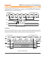
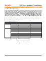
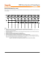
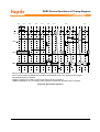
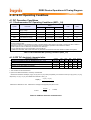
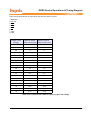
1. Functional Description
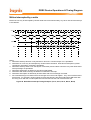
1.1 Simplified State Diagram
Initialization
Sequence
CKEL
OCD
calibration
Self
Refreshing
SRF
CKEH
PR
Idle
Setting
MR
EMR
(E)MR
REF
All banks
precharged
Refreshing
CKEL
ACT
CKEL
CKEH
Precharge
Power
Down
Activating
CKEL
CKEL
CKEL
Automatic Sequence
Active
Power
Down
Command Sequence
CKEH
CKEL
Bank
Active
Read
Write
Write
Read
WRA
Writing
RDA
Read
Write
Reading
RDA
WRA
WRA
Writing
with
Autoprecharge
RDA
PR, PRA
PR, PRA
PR, PRA
Precharging
Reading
with
Autoprecharge
CKEL = CKE LOW, enter Power Down
CKEH = CKE HIGH, exit Power Down, exit Self Refresh
ACT = Activate
WR(A) = Write (with Autoprecharge)
RD(A) = Read (with Autoprecharge)
PR(A) = Precharge (All)
(E)MR = (Extended) Mode Register
SRF = Enter Self Refresh
REF = Refresh
Note: Use caution with this diagram. It is intended to provide a floorplan of the possible state transitions
and the commands to control them, not all details. In particular situations involving more than one bank,
enabling/disabling on-die termination, Power Down entry/exit, timing restrictions during state transitions,
- among other things - are not captured in full detail
Figure 1. DDR2 SDRAM simplified state diagram
3
DDR2 Device Operations & Timing Diagram
1.2 Basic Function & Operation of DDR2 SDRAM
Read and write accesses to the DDR2 SDRAM are burst oriented; accesses start at a selected location and
continue for a burst length of four or eight in a programmed sequence. Accesses begin with the registration of
an Active command, which is then followed by a Read or Write command. The address bits registered coincident with the active command are used to select the bank and row to be accessed (BA0-BA2 select the bank;
A0-A15 select the row). The address bits registered coincident with the Read or Write command are used to
select the starting column location for the burst access and to determine if the auto precharge command is to
be issued.
Prior to normal operation, the DDR2 SDRAM must be initialized. The following sections provide detailed information covering device initialization, register definition, command descriptions and device operation.
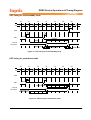
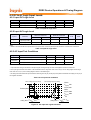
1.2.1 Power up and Initialization
DDR2 SDRAMs must be powered up and initialized in a predefined manner. Operational procedures other
than those specified may result in undefined operation.
Power-up and Initialization Sequence
The following sequence is required for POWER UP and Initialization.
1. Apply power and attempt to maintain CKE below 0.2*VDDQ and ODT*1 at a LOW state (all other inputs
may be undefined.)
- VDD, VDDL and VDDQ are driven from a single power converter output, AND
- VTT is limited to 0.95 V max, AND
- Vref tracks VDDQ/2.
or
- Apply VDD before or at the same time as VDDL.
- Apply VDDL before or at the same time as VDDQ.
- Apply VDDQ before or at the same time as VTT & Vref.
at least one of these two sets of conditions must be met.
2. Start clock and maintain stable condition.
3. For the minimum of 200 us after stable power and clock(CK, CK), then apply NOP or deselect & take
CKE HIGH.
4. Wait minimum of 400ns then issue precharge all command. NOP or deselect applied during 400ns
period.
5. Issue EMRS command to EMR(2). (To issue EMRS command to EMR(2), provide “LOW” to BA0 and
BA2, “HIGH” to BA1.)*2
6. Issue EMRS command to EMR(3). (To issueEMRS command to EMR(3), provide “LOW” to BA2, “HIGH”
to BA0 and BA1.)*2
7. Issue EMR to enable DLL. (To issue "DLL Enable" command, provide "LOW" to A0, "HIGH" to BA0 and
"LOW" to BA1-2 and A13~A15. And A9=A8=A7=LOW must be sued when issuing this command)
8. Issue a Mode Register set command for “DLL reset”.
(To issue DLL reset command, provide "HIGH" to A8 and "LOW" to BA0-2, and A13~15.)
9. Issue precharge all command.
10. Issue 2 or more auto-refresh commands.
11. Issue a mode register command with LOW to A8 to initialize device operation. (i.e. to program operating
parameters without resetting the DLL.)
12. At least 200 clocks after step 8, execute OCD Calibration ( Off Chip Driver impedance adjustment ).
4
DDR2 Device Operations & Timing Diagram
If OCD calibration is not used, EMR OCD Default command (A9=A8= A7=1) followed by EMR OCD Calibration Mode Exit command (A9=A8=A7=0) must be issued with other operating parameters of EMR.
13. The DDR2 SDRAM is now ready for normal operation.
*1) To guarantee ODT off, VREF must be valid and a LOW level must be applied to the ODT pin.
*2) Sequence 5 and 6 may be performed between 8 and 9.
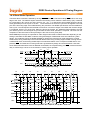
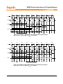
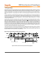
Initialization Sequence after Power Up
tCH tCL
CK
/CK
tIS
CKE
tIS
ODT
Command
PRE
ALL
NOP
400ns
tMRD
tMRD
tRP
DLL
ENABLE
PRE
ALL
MR
EMR
DLL
RESET
REF
tRP
MR
REF
tRFC
tRFC
EMR
tMRD
ANY
CMD
EMR
Follow OCD
Flowchart
tOIT
min. 200 Cycle
OCD
Default
OCD
CAL. MODE
EXIT
Figure 2. Initialization sequence after power-up
1.2.2 Programming the Mode and Extended Mode Registers
For application flexibility, burst length, burst type, CAS latency, DLL reset function, write recovery time(WR)
are user defined variables and must be programmed with a Mode Register Set(MRS) command. Additionally,
DLL disable function, driver impedance, additive CAS latency, ODT(On Die Termination), single-ended
strobe, and OCD(off chip driver impedance adjustment) are also user defined variables and must be programmed with an Extended Mode Register Set (EMRS) command. Contents of the Mode Register(MR) or
Extended Mode Registers(EMR(#)) can be altered by re-executing the MRS and EMRS Commands. Even if
the user chooses to modify only a subset of the MR or EMR(#) variables, all variables within the addressed
register must be redefined when the MRS or EMRS commands are issued.
MR, EMR and Reset DLL do not affect array contents, which means reinitialization including those can be
executed any time after power-up without affecting array contents.
5
DDR2 Device Operations & Timing Diagram
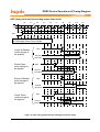
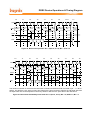
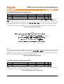
1.2.2.1 DDR2 SDRAM Mode Register (MR)
The mode register stores the data for controlling the various operating modes of DDR2 SDRAM. It controls
CAS latency, burst length, burst sequence, test mode, DLL reset, WR and various vendor specific options to
make DDR2 SDRAM useful for various applications. The default value of the mode register is not defined,
therefore the mode register must be programmed during initialization for proper operation. The mode register
is written by asserting LOW on CS, RAS, CAS, WE, BA0 and BA1, while controlling the state of address pins
A0 ~ A15. The DDR2 SDRAM should be in all bank precharge with CKE already HIGH prior to writing into the
mode register. The mode register set command cycle time (tMRD) is required to complete the write operation
to the mode register. The mode register contents can be changed using the same command and clock cycle
requirements during normal operation as long as all banks are in the precharge state. The mode register is
divided into various fields depending on functionality. Burst length is defined by A0 ~ A2 with options of 4 and
8 bit burst lengths. The burst length decodes are compatible with DDR SDRAM. Burst address sequence type
is defined by A3, CAS latency is defined by A4 ~ A6. The DDR2 doesn’t support half clock latency mode. A7
is used for test mode. A8 is used for DLL reset. A7 must be set to LOW for normal MR operation. Write recovery time WR is defined by A9 ~ A11. Refer to the table for specific codes.
BA1
0*1
0
0
0*1
A12 A11
A10
PD
A9
WR
A8
DLL Reset
A7
0
No
1
Yes
A8
A7
DLL
TM
A6
A5
A3
CAS Latency
BT
A2
A0
Burst Length
Address Field
Mode Register
Burst Length
A3
0
Normal
0
Sequential
A2
A1
A0
BL
1
Test
1
Interleave
0
1
0
4
0
1
1
8
A11
A10
A9
Burst Type
CAS Latency
WR(cycles)
Fast exit(use tXARD)
0
0
0
Reserved
1
Slow exit(use tXARDS)
0
0
1
2
0
1
0
3
0
1
1
4
1
0
0
5
MR mode
A1
mode
0
BA0
A4
Write recovery for autoprecharge
Active power
down exit time
A12
BA1
BA0 A15 ~ A13
0
0
MR
1
0
1
6
0
1
EMR(1)
1
1
0
Reserved
1
0
EMR(2): Reserved
1
1
1
Reserved
1
1
EMR(3): Reserved
*2
DDR2-400
DDR2-533
DDR2-667
DDR2-800
BA2
A6
A5
A4
0
0
0
Latency
0
0
1
Reserved
0
1
0
2(optional)
0
1
1
1
0
0
1
0
1
1
1
0
1
1
1
Reserved
3(speed bin
determined)*3
4
5(speed bin
determined)*3
6(speed bin
determined)*3
Reserved
*1 : BA2 and A13~A15 are reserved for future use and must be programmed to 0 when setting the mode register.
*2: For DDR2-400/533. WR(write recovery for autoprecharge) min is determined by tCK max and WR max is determined by tCK min. WR
in clock cycles is calculated by dividing WR (in ns) by tCK (in ns) and rounding up to the next integer (WR[cycles] = WR[ns]/tCK[ns]). For
DDR2-667/800. WR min is determined by tCK(avg) max and WR max is determined by tCK(avg) min. (WR[cycles] = WR[ns]/tCK(avg)[ns])
The mode register must be programmed to this value. This is also used with tRP to determine tDAL.
*3 : Speed bin determined. Not required on all speed bins.
Figure 3. DDR2 SDRAM mode register set (MRS)
6
DDR2 Device Operations & Timing Diagram
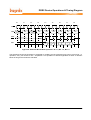
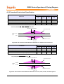
1.2.2.2 DDR2 SDRAM Extended Mode Register
EMR(1)
The extended mode register(1) stores the data for enabling or disabling the DLL, output driver strength, additive latency,
ODT, DQS disable, OCD program, RDQS enable. The default value of the extended mode register(1) is not defined,
therefore the extended mode register(1) must be programmed during initialization for proper operation. The extended
mode register(1) is written by asserting LOW on CS, RAS, CAS, WE, HIGH on BA0 and LOW on BA1, while controlling
the states of address pins A0 ~ A15. The DDR2 SDRAM should be in all bank precharge with CKE already HIGH prior to
writing into the extended mode register(1). The mode register set command cycle time (tMRD) must be satisfied to complete the write operation to the extended mode register(1). Mode register contents can be changed using the same command and clock cycle requirements during normal operation as long as all banks are in the precharge state. A0 is used for
DLL enable or disable. A1 is used for enabling a half strength output driver. A3~A5 determines the additive latency,
A7~A9 are used for OCD control, A10 is used for DQS disable and A11 is used for RDQS enable. A2 and A6 are used for
ODT setting.
DLL Enable/Disable
The DLL must be enabled for normal operation. DLL enable is required during power up initialization, and upon returning
to normal operation after having the DLL disabled. The DLL is automatically disabled when entering self refresh operation
and is automatically re-enabled upon exit of self refresh operation. Any time the DLL is enabled (and subsequently reset),
200 clock cycles must occur before a Read command can be issued to allow time for the internal clock to be synchronized
with the external clock. Failing to wait for synchronization to occur may result in a violation of the tAC or tDQSCK parameters.
7
DDR2 Device Operations & Timing Diagram
EMR(1) Programming:
BA2 BA1 BA0 A15 ~ A13
A12
0*1 0
Qoff RDQS DQS
0*1
1
BA1
A11
A10
A9
A8
A6
A5
Rtt
OCD program
MR mode
BA0
A7
A6
A2
A4
A3
A2
A1
A0
Additive latency
Rtt
D.I.C
DLL
Address Field
Extended Mode Register
Rtt (NOMINAL)
0
0
MR
0
0
ODT Disabled
0
1
EMR(1)
0
1
75 Ω
1
0
EMR(2)
1
0
150 Ω
1
1
EMR(3): Reserved
1
1
50 Ω*2
A0
DLL Enable
0
Enable
1
Disable
Additive Latency
*2 : Optional for DDR2-400/533/667
Mandatory for DDR2-800
A9
A8
A7
OCD Calibration Program
0
0
0
OCD Calibration mode exit; maintain setting
0
0
1
Drive(1)
0
1
0
Drive(0)
1
0
0
Adjust mode*3
1
1
1
OCD Calibration default
*4
* 3 : When Adjust mode is issued, AL from previously set value must be applied.
* 4 : After setting to default, OCD mode needs to be exited by setting A9-A7 to
000. Refer to the following 1.2.2.3 section for detailed information
A12
Output buffer enabled
1
Output buffer disabled
*5. Outputs disabled - DQs, DQSs, DQSs, RDQS, RDQS. This
feature is used in conjunction with DIMM IDD meaurements
when IDDQ is not desired to be included.
A3
0
0
0
0
0
0
1
1
0
1
0
2
0
1
1
3
1
0
0
4
1
0
1
5
1
1
0
Reserved
1
1
1
Reserved
A1
Output Driver
Impedence Control
Driver
Size
0
Full Strength
100%
1
Reduced Strength
60%
DQS
0
Enable
1
Disable
A11
A4
Qoff (Optional)*5
0
A10
A5
RDQS Enable*6
Disable
A11
(RDQS Enable)
1
Enable
0 (Disable)
0 (Enable)
DM
0 (Disable)
1 (Disable)
DM
*6. If RDQS is enabled, the DM
function is disabled. RDQS is active
for reads and don’t care for writes.
A10
(DQS Disable)
Strobe Function Matrix
0
RDQS/DM
RDQS
DQS
DQS
Hi-z
DQS
DQS
Hi-z
DQS
Hi-z
1 (Enable)
0 (Enable)
RDQS
RDQS
DQS
DQS
1 (Enable)
1 (Disable)
RDQS
Hi-z
DQS
Hi-z
*1 : BA2 and A13~A15 are reserved for future use and must be set to 0 when programming the EMR(1)
Figure 4. EMR(1) programming
8
DDR2 Device Operations & Timing Diagram
EMR(2)
The extended mode register(2) controls refresh related features. The default value of the extended mode register(2) is not defined, therefore the extended mode register(2) must be programmed during initialization for
proper operation. The extended mode register(2) is written by asserting LOW on /CS,/RAS,/CAS,/WE, HIGH
on BA1 and LOW on BA0, while controling the states of address pins A0~A15. The DDR2 SDRAM should be
in all bank precharge with CKE already HIGH prior to writing into the extended mode register(2). The mode
register set command cycle time(tMRD) must be satisfied to complete the write operation to the extended
mode register(2). Mode register contents can be changed using the same command and clock cycle requirements during normal operation as long as all banks are in the precharge state.
EMR(2) Programming:
BA2 BA1 BA0 A15 ~ A13
0*1 1
A12
A11
0*1
0
A7
BA1
A10
BA0
A9
A8
A7
A6
A5
A4
0*1
SRF
A3
A2
DCC*3
A1
A0
PASR*3
Address Field
Extended Mode
Register(2)
High Temp Self-refresh Rate Enable
0
Disable
1
Enable(Optional)*2
MR mode
A3
DCC Enable(Optional)*4
0
0
MR
0
1
EMR(1)
0
Disable
1
0
EMR(2)
1
Enable
1
1
EMR(3):Reserved
A2
A1
A0
Partial Array Self Refresh for 8 banks
Partial Array Self Refresh for 4 banks
0
0
0
Full Array
Full Array
0
0
1
Half Array (BA[2:0]=000,001,010&011)
Half Array (BA[1:0]=00&01)
0
1
0
Quarter Array (BA[2:0]=000&001)
Quarter Array (BA[1:0]=00)
0
1
1
1/8th Array (BA[2:0]=000)
Not Defined
1
0
0
3/4 Array (BA[2:0]=010,011,100,101,110&111)
3/4 Array (BA[1:0]=01,10&11)
1
0
1
Half Array (BA[2:0]=100,101,110&111)
Half Array (BA[1:0]=10&11)
1
1
0
Quarter Array (BA[2:0]=110&111)
Quarter Array (BA[1:0]=11)
1
1
1
1/8th Array (BA[2:0]=111)
Not Defined
*1 : The rest bits in EMR(2) are reserved for future use and all bits except A7, BA0 and BA1 must be programmed to 0 when setting the
mode register during initialization.
*2 : Currently the periodic Self-Refresh interval is hard coded whithin the DRAM to a specific value. EMR(2) bit A7 is a migration plan to
support higher Self-Refresh entry. However, since this Self-Refresh control function is an option and to be phased-in by manufacturer
individually, checking on the DRAM parts for function availablity is necessary. For more details, please refer to “Operating Temperature
Condition” section at “Chapter 5. AC & DC operation conditions”.
*3 Optional in DDR2 SDRAM. If PASR (Partial Array Self Refresh) is enabled, data located in areas of the array beyond the specified
address range will be lost if self refresh is entered. Data integrity will be maintained if tREF conditions are met and no Self Refresh command is issued. If the PASR feature is not supported, EMR(2)[A0-A2] must be set to 000 when programming EMR(2).
*4 Optional in DDR2 SDRAM. JEDEC standard DDR2 SDRAM may or may not have DCC (Duty Cycle Corrector) implemented, and in
some of the DRAMs implementing DCC, user may be given the controllability of DCC thru EMR(2)[A3] bit. JEDEC standard DDR2
SDRAM users can look at manufacturer's data sheet to check if the DRAM part supports DCC controllability. If Optional DCC Controllability is supported, user may enable or disable the DCC by programming EMR(2)[A3] accordingly. If the controllability feature is not supported, EMR(2)[A3] must be set to 0 when programming EMR(2).
Figure 5. EMR(2) programming
9
DDR2 Device Operations & Timing Diagram
EMR(3)
No function is defined in extended mode register(3). The default value of the extended mode register(3) is not
defined, therefore the extended mode register(3) must be programmed during initialization for proper operation.
EMR(3) Programming:
BA2 BA1 BA0 A15 ~ A13
0*1 1
1
A12
A11
A10
A9
A8
A7
A6
A5
A4
0*1
A3
A2
A1
A0
Address Field
Extended Mode
Register(2)
*1 :All bits in EMR(3) except BA0 and BA1 are reserved for future use and must be programmed to 0 when setting the mode register during
initialization.
Figure 6. EMR(3) programming
10
DDR2 Device Operations & Timing Diagram
1.2.2.3 Off-Chip Driver (OCD) Impedance Adjustment
DDR2 SDRAM supports driver calibration feature and the flow chart below is an example of sequence. Every
calibration mode command should be followed by “OCD calibration mode exit” before any other command
being issued. All MR should be programmed before entering OCD impedance adjustment and ODT (On Die
Termiantion) should be carefully controlled depending on system environment.
All MR shoud be programmed before entering OCD impedance adjustment and ODT
should be carefully controlled depending on system environment
Start
EMR: OCD calibration mode exit
EMR: Drive(1)
DQ & DQS HIGH; DQS LOW
EMR: Drive(0)
DQ & DQS LOW; DQS HIGH
ALL OK
ALL OK
Test
Test
Need Calibration
Need Calibration
EMR: OCD calibration mode exit
EMR: OCD calibration mode exit
EMR :
Enter Adjust Mode
EMR :
Enter Adjust Mode
BL=4 code input to all DQs
Inc, Dec, or NOP
BL=4 code input to all DQs
Inc, Dec, or NOP
EMR: OCD calibration mode exit
EMR: OCD calibration mode exit
EMR: OCD calibration mode exit
End
Figure 7. OCD Impedence adjustment
11
DDR2 Device Operations & Timing Diagram
Extended Mode Register for OCD impedance adjustment
OCD impedance adjustment can be done using the following EMR mode. In drive mode all outputs are driven
out by DDR2 SDRAM and drive of RDQS is depedent on EMR bit enabling RDQS operation. In Drive(1)
mode, all DQ, DQS (and RDQS) signals are driven HIGH and all DQS signals are driven LOW. In drive(0)
mode, all DQ, DQS (and RDQS) signals are driven LOW and all DQS signals are driven HIGH. In adjust
mode, BL = 4 of operation code data must be used. In case of OCD calibration default, output driver characteristics have a nominal impedance value of 18 Ω during nominal temperature and voltage conditions. Output
driver characteristics for OCD calibration default are specified in Table x. OCD applies only to normal full
strength output drive setting defined by EMR(1) and if half strength is set, OCD default output driver
characteristics are not applicable. When OCD calibration adjust mode is used, OCD default output driver
characteristics are not applicable. After OCD calibration is completed or driver strength is set to default,
subsequent EMR commands not intended to adjust OCD characteristics must specify A9-A7 as '000' in order
to maintain the default or calibrated value.
A9
A8
A7
0
0
0
Operation
OCD calibration mode exit
0
0
1
Drive(1) DQ, DQS, (RDQS) HIGH and DQS LOW
0
1
0
Drive(0) DQ, DQS, (RDQS) LOW and DQS HIGH
1
0
0
Adjust mode
1
1
1
OCD calibration default
Table 1. OCD drive mode program
OCD impedance adjust
To adjust output driver impedance, controllers must issue the ADJUST EMR command along with a 4bit burst
code to DDR2 SDRAM as in table X. For this operation, Burst Length has to be set to BL = 4 via MR command before activating OCD and controllers must drive this burst code to all DQs at the same time. DT0 in
table X means all DQ bits at bit time 0, DT1 at bit time 1, and so forth. The driver output impedance is
adjusted for all DDR2 SDRAM DQs simultaneously and after OCD calibration, all DQs of a given DDR2
SDRAM will be adjusted to the same driver strength setting. The maximum step count for adjustment is 16
and when the limit is reached, further increment or decrement code has no effect. The default setting may be
any step within the 16 step range. When Adjust mode command is issued, AL from previously set value must
be applied
4bit burst code inputs to all DQs
Operation
DT0
DT1
DT2
DT3
Pull-up driver strength
0
0
0
0
NOP (No operation)
NOP (No operation)
0
0
0
1
Increase by 1 step
NOP
0
0
1
0
Decrease by 1 step
NOP
0
1
0
0
NOP
Increase by 1 step
1
0
0
0
NOP
Decrease by 1 step
0
1
0
1
Increase by 1 step
Increase by 1 step
0
1
1
0
Decrease by 1 step
Increase by 1 step
1
0
0
1
Increase by 1 step
Decrease by 1 step
1
0
1
0
Decrease by 1 step
Decrease by 1 step
Other Combinations
Pull-down driver strength
Reserved
Table 2 : OCD adjust mode program
12
DDR2 Device Operations & Timing Diagram
For proper operation of adjust mode, WL = RL - 1 = AL + CL - 1 clocks and tDS/tDH should be met as the following timing diagram. For input data pattern for adjustment, DT0 - DT3 is a fixed order and "not affected by
MR addressing mode (ie. sequential or interleave).
OCD adjust mode
CMD
OCD calibration mode exit
EMR
NOP
NOP
NOP
NOP
NOP
EMR
NOP
CK
CK
WL
WR
DQS
DQS_in
tDS tDH
DQ_in
ViH(ac)
ViH(dc)
ViL(ac)
ViL(dc)
DT0
DT1
DT2
DT3
DM
Figure 8. OCD adjust mode
Drive Mode
Drive mode, both Drive(1) and Drive(0), is used for controllers to measure DDR2 SDRAM Driver impedance.
In this mode, all outputs are driven out tOIT after “enter drive mode” command and all output drivers are
turned-off tOIT after “OCD calibration mode exit” command as the following timing diagram
OCD calibration mode exit
Enter Drive mode
CMD
EMR
NOP
NOP
NOP
EMR
CK
CK
DQS
DQS
Hi-Z
Hi-Z
DQS HIGH & DQS LOW for Drive(1), DQS LOW & DQS HIGH for Drive(0)
DQs HIGH for Drive(1)
DQ
DQs LOW for Drive(0)
tOIT
tOIT
Figure 9. OCD drive mode
13
DDR2 Device Operations & Timing Diagram
1.2.2.4 ODT (On Die Termination)
On Die Termination (ODT) is a feature that allows a DRAM to turn on/off termination resistance for each DQ,
DQS/DQS, RDQS/RDQS, and DM signal for x4x8 configurations via the ODT control pin. For x16 configuration ODT is applied to each DQ, UDQS/UDQS, LDQS/LDQS, UDM, and LDM signal via the ODT control pin.
The ODT feature is designed to improve signal integrity of the memory channel by allowing the DRAM controller to independently turn on/off termination resistance for any or all DRAM devices.
The ODT function is supported for ACTIVE and STANDBY modes. ODT is turned off and not supported in
SELF REFRESH mode.
FUNCTIONAL REPRESENTATION OF ODT
VDDQ
sw1
Rval1
VDDQ
sw2
Rval2
VDDQ
sw3
Rval3
DRAM
Input
Buffer
Input
Pin
Rval1
sw1
VSSQ
Rval2
sw2
VSSQ
Rval3
sw3
VSSQ
Switch (sw1 , sw2 , sw3) is enabled by ODT pin.
Selection among sw1, sw2 and sw3 is determined by “Rtt (nominal)” in EMR
Termination included on all DQs, DM, DQS, DQS, RDQS, and RDQS pins.
Figure 10. Functional representation of ODT
14
DDR2 Device Operations & Timing Diagram
ODT timing for active/standby mode
T0
T1
T2
T3
T4
T5
T6
CK
CK
tIS
CKE
ODT
tIS
tIS
VIH(ac)
VIL(ac)
tAOFD
tAOND
Internal
Term Res.
RTT
tAOF,min
tAON,max
tAON,min
tAOF,max
Figure 11. ODT timing for active/standby mode
ODT timing for powerdown mode
T0
T1
T2
T3
T4
T5
T6
CK
CK
CKE
tIS
ODT
VIH(ac)
tIS
VIH(ac)
tAOFPD,max
tAOFPD,min
Internal
Term Res.
RTT
tAONPD,min
tAONPD,max
Figure 12. ODT timing for powerdown mode
15
DDR2 Device Operations & Timing Diagram
ODT timing mode switch at entering power down mode
T-5
T-4
T-3
T-2
CK
CK
T-1
T0
T2
T1
T3
T4
tANPD
tIS
CKE
Entering Slow Exit Active Power Down Mode
or Precharge Power Down Mode.
tIS
ODT
VIL(ac)
Active & Standby
mode timings to
be applied.
tAOFD
Internal
Term Res.
RTT
tIS
ODT
VIL(ac)
Power Down
mode timings to
be applied.
tAOFPDmax
Internal
Term Res.
RTT
tIS
ODT
VIH(ac)
tAOND
Internal
Term Res.
RTT
Active & Standby
mode timings to
be applied.
tIS
ODT
VIH(ac)
tAONPDmax
Internal
Term Res.
RTT
Power Down
mode timings to
be applied.
Figure 13. ODT timing mode switch at entering power-down mode
16
DDR2 Device Operations & Timing Diagram
ODT timing mode switch at exiting power down mode
T0
T1
T4
T5
T6
T7
T8
T9
T10
T11
CK
CK
tIS
CKE
tAXPD
VIH(ac)
Exiting from Slow Active Power Down Mode
or Precharge Power Down Mode.
tIS
Active & Standby
mode timings to
be applied.
ODT
VIL(ac)
tAOFD
Internal
Term Res.
RTT
tIS
Power Down
mode timings to
be applied.
ODT
VIL(ac)
tAOFPDmax
Internal
Term Res.
RTT
tIS
Active & Standby
mode timings to
be applied.
VIH(ac)
ODT
tAOND
Internal
Term Res.
RTT
tIS
Power Down
mode timings to
be applied.
ODT
VIH(ac)
tAONPDmax
Internal
Term Res.
RTT
Figure 14. ODT timing mode switch at exiting power-down mode
17
DDR2 Device Operations & Timing Diagram
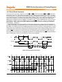
1.3 Bank Activate Command
The Bank Activate command is issued by holding CAS and WE HIGH with CS and RAS LOW at the rising
edge of the clock. The bank addresses BA0 ~ BA2 are used to select the desired bank. The row address A0
through A15 is used to determine which row to activate in the selected bank. The Bank Activate command
must be applied before any Read or Write operation can be executed. Immediately after the bank active
command, the DDR2 SDRAM can accept a read or write command on the following clock cycle. If a R/W
command is issued to a bank that has not satisfied the tRCDmin specification, then additive latency must be
programmed into the device to delay when the R/W command is internally issued to the device. The additive
latency value must be chosen to assure tRCDmin is satisfied. Additive latencies of 0, 1, 2, 3 and 4 are supported. Once a bank has been activated it must be precharged before another Bank Activate command can
be applied to the same bank. The bank active and precharge times are defined as tRAS and tRP, respectively. The minimum time interval between successive Bank Activate commands to the same bank is determined by the RAS cycle time of the device (tRC). The minimum time interval between Bank Activate
commands is tRRD.
In order to ensure that 8 bank devices do not exceed the instantaneous current supplying capability of 4
bank devices, certain restrictions on operation of the 8 bank devices must be observed. There are two rules.
One for restricting the number of sequential ACT commands that can be issued and another for allowing
more time for RAS precharge for a Precharge All command. The rules are as follows:
* 8 bank device Sequential Bank Activation Restriction: No more than 4 banks may be activated in a rolling
tFAW window. Converting to clocks is done by dividing tFAW[ns] by tCK[ns] or tCK(avg)[ns], depending on
the speed bin, and rounding up to next integer value. As an example of the rolling window, if (tFAW/tCK) or
(tFAW/tCK(avg) rounds up to 10 clocks, and an activate command is issued in clock N, no more than three
further activate commands may be issued at or betwen clock N+1 through N+9.
* 8 bank device Precharge All Allowance : tRP for a Precharge All command for an 8 Bank device will equal
to tRP+1*tCK or tnRP + 1*nCK, depending on the speed bin, where tnRP=tRP/tCK(avg) rounded up to the
next interger, where tRP is the value for a single bank pre-charge.
T0
T1
T2
T3
Tn
Tn+1
Tn+2
Tn+3
..........
CK / CK
Internal RAS-CAS delay (>= tRCDmin)
ADDRESS
Bank A
Row Addr.
Bank B
Bank B
Col. Addr.
Row Addr.
CAS-CAS delay time (tCCD)
additive latency delay (AL)
Bank A
Col. Addr.
tRCD =1
A
. . . . . . . . .Bank
.
Addr.
Bank B
Addr.
Bank A
Row Addr.
Bank B
Precharge
Bank A
Activate
Read Begins
RAS - RAS delay time (>= tRRD)
COMMAND
: “H” or “L”
Bank A
Activate
Bank A
Post CAS
Read
Bank B
Activate
Bank B
Post CAS
Read
A
. . . . . . . . Bank
..
Precharge
Bank Active (>= tRAS)
Bank Precharge time (>= tRP)
RAS Cycle time (>= tRC)
Figure 15. Bank active command cycle: tRCD =3, AL=2, tRP=3, tRRD=2, tCCD=2
18
DDR2 Device Operations & Timing Diagram
1.4 Read and Write Access Modes
After a bank has been activated, a read or write cycle can be executed. This is accomplished by setting RAS
HIGH, CS and CAS LOW at the clock’s rising edge. WE must also be defined at this time to determine
whether the access cycle is a read operation (WE HIGH) or a write operation (WE LOW).
The DDR2 SDRAM provides a fast column access operation. A single Read or Write Command will initiate a
serial read or write operation on successive clock cycles. The boundary of the burst cycle is strictly restricted
to specific segments of the page length. For example, the 32Mbit x 4 I/O x 4 Bank chip has a page length of
2048 bits (defined by CA0-CA9, CA11). The page length of 2048 is divided into 512 or 256 uniquely addressable boundary segments depending on burst length, 512 for 4 bit burst, 256 for 8 bit burst respectively. A 4bit or 8 bit burst operation will occur entirely within one of the 512 or 256 groups beginning with the column
address supplied to the device during the Read or Write Command (CA0-CA9, CA11). The second, third and
fourth access will also occur within this group segment, however, the burst order is a function of the starting
address, and the burst sequence.
A new burst access must not interrupt the previous 4 bit burst operation in case of BL = 4 setting. However,
in case of BL = 8 setting, two cases of interrupt by a new burst access are allowed, one reads interrupted by
a read, the other writes interrupted by a write with 4 bit burst boundry respectively. The minimum CAS to
CAS delay is defined by tCCD, and is a minimum of 2 clocks for read or write cycles.
19
DDR2 Device Operations & Timing Diagram
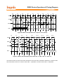
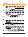
1.4.1 Posted CAS
Posted CAS operation is supported to make command and data bus efficient for sustainable bandwidths in DDR2
SDRAM. In this operation, the DDR2 SDRAM allows a CAS read or write command to be issued immediately after the
RAS bank activate command (or any time during the RAS-CAS-delay time, tRCD, period). The command is held for the
time of the Additive Latency (AL) before it is issued inside the device. The Read Latency (RL) is controlled by the sum of
AL and the CAS latency (CL). Therefore if a user chooses to issue a R/W command before the tRCDmin, then AL (greater
than 0) must be written into the EMR(1). The Write Latency (WL) is always defined as RL - 1 (read latency -1) where read
latency is defined as the sum of additive latency plus CAS latency (RL=AL+CL). Read or Write operations using AL allow
seamless bursts (refer to semaless operation timing diagram examples in Read burst and Wirte burst section)
Examples of posted CAS operation
-1
0
1
2
3
4
5
6
7
8
9
10
11
12
11
12
CK/CK
Active
A-Bank
CMD
Write
A-Bank
Read
A-Bank
DQS/DQS
> = tRCD
DQ
WL = RL -1 = 4
CL = 3
AL = 2
RL = AL + CL = 5
Dout0
Dout1
Dout2
Dout3
Din0
Din1
Din2
Din3
> = tRAC
Figure 16. Example 1 - Read followed by a write to the same bank
[AL = 2 and CL = 3, RL = (AL + CL) = 5, WL = (RL - 1) = 4, BL = 4]
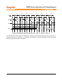
-1
0
1
2
3
4
5
6
7
8
9
10
CK/CK
AL = 0
CMD
DQS/DQS
DQ
Active
A-Bank
Write
A-Bank
Read
A-Bank
WL = RL -1 = 2
CL = 3
> = tRCD
RL = AL + CL = 3
Dout0
Dout1
Dout2
Dout3
Din0
Din1
Din2
Din3
> = tRAC
Figure 17. Example 2 - Read followed by a write to the same bank
[AL = 0 and CL = 3, RL = (AL + CL) = 3, WL = (RL - 1) = 2, BL = 4]
20
DDR2 Device Operations & Timing Diagram
1.4.2 Burst Mode Operation
Burst mode operation is used to provide a constant flow of data to memory locations (write cycle), or from
memory locations (read cycle). The parameters that define how the burst mode will operate are burst
sequence and burst length. DDR2 SDRAM supports 4 bit burst and 8 bit burst modes only. For 8 bit burst
mode, full interleave address ordering is supported, however, sequential address ordering is nibble based for
ease of implementation. The burst type, either sequential or interleaved, is programmable and defined by the
address bit 3 (A3) of the MR, which is similar to the DDR SDRAM operation. Seamless burst read or write
operations are supported. Unlike DDR devices, interruption of a burst read or write cycle during BL = 4 mode
operation is prohibited. However in case of BL = 8 mode, interruption of a burst read or write operation is limited to two cases, reads interrupted by a read, or writes interrupted by a write. Therefore the Burst Stop command is not supported on DDR2 SDRAM devices.
Burst Length and Sequence
Burst Length
Starting Address (A2 A1 A0)
Sequential Addressing (decimal)
Interleave Addressing (decimal)
000
0, 1, 2, 3
0, 1, 2, 3
001
1, 2, 3, 0
1, 0, 3, 2
010
2, 3, 0, 1
2, 3, 0, 1
011
3, 0, 1, 2
3, 2, 1, 0
000
0, 1, 2, 3, 4, 5, 6, 7
0, 1, 2, 3, 4, 5, 6, 7
001
1, 2, 3, 0, 5, 6, 7, 4
1, 0, 3, 2, 5, 4, 7, 6
010
2, 3, 0, 1, 6, 7, 4, 5
2, 3, 0, 1, 6, 7, 4, 5
011
3, 0, 1, 2, 7, 4, 5, 6
3, 2, 1, 0, 7, 6, 5, 4
100
4, 5, 6, 7, 0, 1, 2, 3
4, 5, 6, 7, 0, 1, 2, 3
101
5, 6, 7, 4, 1, 2, 3, 0
5, 4, 7, 6, 1, 0, 3, 2
110
6, 7, 4, 5, 2, 3, 0, 1
6, 7, 4, 5, 2, 3, 0, 1
111
7, 4, 5, 6, 3, 0, 1, 2
7, 6, 5, 4, 3, 2, 1, 0
4
8
Note: Page length is a function of I/O organization and column addressing
Table 3. Burst length and sequence
21
DDR2 Device Operations & Timing Diagram
1.4.3 Burst Read Command
The Burst Read command is initiated by having CS and CAS LOW while holding RAS and WE HIGH at the
rising edge of the clock. The address inputs determine the starting column address for the burst. The delay
from the start of the command to when the data from the first cell appears on the outputs is equal to the value
of the read latency (RL). The data strobe output (DQS) is driven LOW 1 clock cycle before valid data (DQ) is
driven onto the data bus. The first bit of the burst is synchronized with the rising edge of the data strobe
(DQS). Each subsequent data-out appears on the DQ pin in phase with the DQS signal in a source synchronous manner. The RL is equal to an additive latency (AL) plus CAS latency (CL). The CL is defined by the
Mode Register (MR), similar to the existing SDR and DDR SDRAMs. The AL is defined by the Extended
Mode Register (1)(EMR(1)).
DDR2 SDRAM pin timings are specified for either single ended mode or differential mode depending on
the setting of the EMR(1) “Enable DQS” mode bit; timing advantages of differential mode are realized in system design. The method by which the DDR2 SDRAM pin timings are measured is mode dependent. In single
ended mode, timing relationships are measured relative to the rising or falling edges of DQS crossing at VREF.
In differential mode, these timing relationships are measured relative to the crosspoint of DQS and its complement, DQS. This distinction in timing methods is guaranteed by design and characterization. Note that
when differential data strobe mode is disabled via the EMR, the complementary pin, DQS, must be tied externally to VSS through a 20 Ω to 10 KΩ resistor to insure proper operation.
tCH
tCL
CK
CK
CK
DQS
DQS/DQS
DQS
tRPST
tRPRE
DQ
Q
Q
Q
tDQSQmax
Q
tDQSQmax
tQH
tQH
Figure 18. Data output (read) timing
T0
T1
T2
T3
T4
T5
T6
T7
T8
CK/CK
CMD
Posted CAS
READ A
NOP
NOP
NOP
NOP
NOP
NOP
NOP
NOP
≤ tDQSCK
DQS/DQS
AL = 2
CL =3
RL = 5
DQs
DOUT A0
DOUT A1
DOUT A2
DOUT A3
Figure 19. Burst read operation: RL =5 (AL=2, CL=3, BL=4)
22
DDR2 Device Operations & Timing Diagram
T0
T1
T2
T3
T4
T5
T6
T7
T8
CK/CK
READ A
CMD
NOP
NOP
NOP
NOP
NOP
NOP
NOP
NOP
≤ tDQSCK
DQS/DQS
CL =3
RL = 3
DQs
DOUT A0
DOUT A1
DOUT A2
DOUT A3
DOUT A4
DOUT A5
DOUT A6
DOUT A7
Figure 20. Burst read operation: RL =3 (AL=0, CL=3, BL=8)
T0
T1
Tn-1
Tn
Tn+1
Tn+2
Tn+3
Tn+4
Tn+5
NOP
NOP
NOP
NOP
CK/CK
CMD
Post CAS
READ A
NOP
Post CAS
NOP
WRITE A
tRTW (Read to Write turn around time)
NOP
DQS/DQS
RL =5
WL = RL - 1 = 4
DQ’s
DOUT A0
DOUT A1
DOUT A2
DOUT A3
DIN A0
DIN A1
DIN A2
DIN A3
Figure 21. Burst read followed by burst write: RL = 5, WL = (RL-1) = 4, BL = 4
The minimum time from the burst read command to the burst write command is defined by a read-to-writeturn-around-time, which is 4 clocks in case of BL = 4 operation, 6 clocks in case of BL = 8 operation.
23
DDR2 Device Operations & Timing Diagram
T0
T1
T2
T3
T4
T5
T6
T7
T8
CK/CK
CMD
Post CAS
READ A
NOP
Post CAS
READ B
NOP
NOP
NOP
NOP
NOP
NOP
DQS/DQS
CL =3
AL = 2
RL = 5
DQs
DOUT A0
DOUT A1
DOUT A2
DOUT A3
DOUT B0
DOUT B1
DOUT B2
Figure 22. Seamless burst read operation: RL = 5, AL = 2, and CL = 3, BL = 4
The seamless burst read operation is supported by enabling a read command at every other clock for BL = 4
operation, and every 4 clock for BL = 8 operation. This operation is allowed regardless of same or different
banks as long as the banks are activated.
24
DDR2 Device Operations & Timing Diagram
Reads interrupted by a read
Burst read can only be interrupted by another read with 4 bit burst boundary. Any other case of read interrupt
is not allowed.
CK/CK
CMD
Read A
NOP
Read B
NOP
NOP
NOP
NOP
NOP
NOP
NOP
DQS/DQS
DQs
A0
A1
A2
A3
B0
B1
B2
B3
B4
B5
B6
B7
Note
1.
2.
3.
4.
5.
6.
7.
Read burst interrupt function is only allowed on burst of 8. Burst interrupt of 4 is prohibited.
Read burst of 8 can only be interrupted by another Read command. Read burst interruption by Write command or
Precharge command is prohibited.
Read burst interrupt must occur exactly two clocks after previous Read command. Any other Read burst interrupt
timings are prohibited.
Read burst interruption is allowed to any bank inside DRAM.
Read burst with Auto Precharge enabled is not allowed to interrupt.
Read burst interruption is allowed by another Read with Auto Precharge command.
All command timings are referenced to burst length set in the mode register. They are not referenced to actual
burst. For example, Minimum Read to Precharge timing is AL + BL/2 where BL is the burst length set in the mode
register and not the actual burst (which is shorter because of interrupt).
Figure 23. Read burst interrupt timing example: (CL=3, AL=0, RL=3, BL=8)
25
DDR2 Device Operations & Timing Diagram
1.4.4 Burst Write Operation
The Burst Write command is initiated by having CS, CAS and WE LOW while holding RAS HIGH at the rising
edge of the clock. The address inputs determine the starting column address. Write latency (WL) is defined
by a read latency (RL) minus one and is equal to (AL + CL -1). A data strobe signal (DQS) should be driven
LOW (preamble) one clock prior to the WL. The first data bit of the burst cycle must be applied to the DQ
pins at the first rising edge of the DQS following the preamble. The tDQSS specification must be satisfied for
write cycles. The subsequent burst bit data are issued on successive edges of the DQS until the burst length
is completed, which is 4 or 8 bit burst. When the burst has finished, any additional data supplied to the DQ
pins will be ignored. The DQ Signal is ignored after the burst write operation is complete. The time from the
completion of the burst write to bank precharge is the write recovery time (WR).
DDR2 SDRAM pin timings are specified for either single ended mode or differential mode depending on the
setting of the EMR “Enable DQS” mode bit; timing advantages of differential mode are realized in system
design. The method by which the DDR2 SDRAM pin timings are measured is mode dependent. In single
ended mode, timing relationships are measured relative to the rising or falling edges of DQS crossing at VREF.
In differential mode, these timing relationships are measured relative to the crosspoint of DQS and its complement, DQS. This distinction in timing methods is guaranteed by design and characterization. Note that
when differential data strobe mode is disabled via the EMR, the complementary pin, DQS, must be tied externally to VSS through a 20 Ω to 10 KΩ resistor to insure proper operation.
tDQSH
DQS
DQS/
DQS
tDQSL
tDS
DQS
tWPRE
tWPST
VIH(ac)
DQ
D
VIH(dc)
D
DM
DMin
tDH
tDH
tDS
tDS
D
D
VIL(dc)
VIL(ac)
VIH(ac)
VIH(dc)
DMin
DMin
DMin
VIL(dc)
VIL(ac)
Figure 24. Data input(write) timing
T0
T1
T2
T3
T4
T5
T6
T7
Tn
CK/CK
CMD
Posted CAS
WRITE A
NOP
NOP
NOP
NOP
tDQSS
CASE1: with tDQSS (max)
NOP
tDSS tDQSS
NOP
NOP
Precharge
tDSS Completion of
the Burst Write
DQS/DQS
> = WR
WL = RL - 1 = 4
DQs
DIN A0
CASE2: with tDQSS (min)
DIN A1
tDQSS tDSH
DIN A2
DIN A3
tDQSStDSH
DQS/DQS
WL = RL - 1 = 4
DQs
> = WR
DIN A0
DIN A1
DIN A2
DIN A3
Figure 25. Burst write operation: RL = 5(AL=2, CL=3), WL = 4, BL = 4
26
DDR2 Device Operations & Timing Diagram
T0
T1
T2
T3
T4
T5
Tm
Tm+1
Tn
CK/CK
WRITE A
CMD
NOP
NOP
NOP
NOP
NOP
Precharge
NOP
Completion of
the Burst Write
< = tDQSS
Bank A
Activate
DQS/
DQS
WL = RL - 1 = 2
> = WR
DQs
DIN A0
DIN A1
DIN A2
> = tRP
DIN A3
Figure 26. Burst write operation: RL = 3(AL=0, CL=3), WL = 2, BL = 4
T0
T1
T2
T3
T4
T5
T6
T7
T8
T9
CK/CK
Write to Read = CL - 1 + BL/2 + tWTR
CMD
NOP
NOP
NOP
Post CAS
READ A
NOP
NOP
NOP
NOP
NOP
DQS
DQS/
DQS
DQS
CL = 3
AL = 2
WL = RL - 1 = 4
RL =5
> = tWTR
DQ
DIN A0
DIN A1
DIN A2
DIN A3
DOUT
The minimum number of clock from the burst write command to the burst read command is [CL - 1 + BL/2 +
tWTR]. This tWTR is not a write recovery time (WR) but the time required to transfer the 4bit write data from
the input buffer into sense amplifiers in the array. tWTR is defined in AC spec table of this data sheet.
Figure 27. Burst write followed by burst read: RL = 5 (AL=2, CL=3), WL = 4, tWTR = 2, BL = 4
27
DDR2 Device Operations & Timing Diagram
T0
T1
T2
T3
T4
T5
T6
T7
T8
CK/CK
CMD
Post CAS
Write A
NOP
Post CAS
Write B
DQS/
DQS
NOP
NOP
NOP
NOP
NOP
NOP
DQS
DQS
WL = RL - 1 = 4
DQ’s
DIN A0
DIN A1
DIN A2
DIN A3
DIN B0
DIN B1
DIN B2
DIN B3
Figure 28. Seamless Burst Write Operation: RL = 5, WL = 4, BL = 4
The seamless burst write operation is supported by enabling a write command every other clock for BL = 4
operation, every four clocks for BL = 8 operation. This operation is allowed regardless of same or different
banks as long as the banks are activated
28
DDR2 Device Operations & Timing Diagram
Writes interrupted by a write
Burst write can only be interrupted by another write with 4 bit burst boundary. Any other case of write interrupt
is not allowed.
CK/CK
CMD
NOP
Write A
NOP
NOP
Write B
NOP
NOP
NOP
NOP
NOP
DQS/DQS
DQs
A0
A1
A2
A3
B0
B1
B2
B3
B4
B5
B6
B7
Notes:
1. Write burst interrupt function is only allowed on burst of 8. Burst interrupt of 4 is prohibited.
2. Write burst of 8 can only be interrupted by another Write command. Write burst interruption by Read
command or Precharge command is prohibited.
3. Write burst interrupt must occur exactly two clocks after previous Write command. Any other Write burst
interrupt timings are prohibited.
4. Write burst interruption is allowed to any bank inside DRAM.
5. Write burst with Auto Precharge enabled is not allowed to interrupt.
6. Write burst interruption is allowed by another Write with Auto Precharge command.
7. All command timings are referenced to burst length set in the mode register. They are not referenced to
actual burst. For example, minimum Write to Precharge timing is WL+BL/2+WR where WR starts with
the rising clock after the un-interrupted burst end and not from the end of actual burst end.
Figure 29. Write Burst Interrupt Timing Example: (CL=3, AL=0, RL=3, WL=2, BL=8)
29
DDR2 Device Operations & Timing Diagram
1.4.5 Write data mask
One write data mask (DM) pin for each 8 data bits (DQ) will be supported on DDR2 SDRAMs, Consistent with
the implementation on DDR SDRAMs. It has identical timings on write operations as the data bits, and though
used in a uni-directional manner, is internally loaded identically to data bits to insure matched system timing.
DM of x4 and x16 bit organization is not used during read cycles. However DM of x8 bit organization can be
used as RDQS during read cycles by EMR(1) settng.
Data Mask Timing
DQS/
DQS
DQ
DM
VIH(ac) VIH(dc)
VIH(ac) V (dc)
IH
VIL(dc)
VIH(ac) VIL(dc)
VIL(ac)
tDS tDH
tDS tDH
Data Mask Function, WL=3, AL=0, BL = 4 shown
Case 1 : min tDQSS
CK
CK
COMMAND
Write
WL
tWR
tDQSS
DQS/DQS
DQ
DM
Case 2 : max tDQSS
tDQSS
DQS/DQS
DQ
DM
Figure 30. Write data mask
30
DDR2 Device Operations & Timing Diagram
1.5 Precharge Operation
The Precharge Command is used to precharge or close a bank that has been activated. The Precharge Command is triggered when CS, RAS and WE are LOW and CAS is HIGH at the rising edge of the clock. The Precharge Command can be used to precharge each bank independently or all banks simultaneously. Three
address bits A10, BA0 and BA1 for 512Mb and four address bits A10, BA0~BA2 for 1Gb and higher densities
are used to define which bank to precharge when the command is issued. For 8 bank devices, refer to Bank
Active section of this data sheet.
A10
BA2
BA1
BA0
Precharged Bank(s)
LOW
LOW
LOW
LOW
Bank 0 only
Remarks
LOW
LOW
LOW
HIGH
Bank 1 only
LOW
LOW
HIGH
LOW
Bank 2 only
LOW
LOW
HIGH
HIGH
Bank 3 only
LOW
HIGH
LOW
LOW
Bank 4 only
1Gb and higher
LOW
HIGH
LOW
HIGH
Bank 5 only
1Gb and higher
LOW
HIGH
HIGH
LOW
Bank 6 only
1Gb and higher
LOW
HIGH
HIGH
HIGH
Bank 7only
1Gb and higher
HIGH
DON’T CARE
DON’T CARE
DON’T CARE
All Banks
Table 4. Bank selection for precharge by address bits
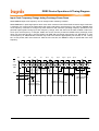
Burst Read Operation Followed by Precharge
Minimum Read to precharge command spacing to the same bank = AL + BL/2 + max(RTP,2) - 2 clocks
For the earliest possible precharge, the precharge command may be issued on the rising edge which is
“Additive latency(AL) + BL/2 + max(RTP,2) - 2clocks” after a Read command. A new bank active (command)
may be issued to the same bank after the RAS precharge time (tRP). A precharge command cannot be issued
until tRAS is satisfied.
The minimum Read to Precharge spacing has also to satisfy a minimum analog time from the rising clock
egde that initiates the last 4-bit prefetch of a Read to Precharge command. This time is called tRTP (Read to
Precharge). For BL = 4 this is the time from the actual read (AL after the Read command) to Precharge command. For BL = 8 this is the time from AL + 2 clocks after the Read to the Precharge command.
31
DDR2 Device Operations & Timing Diagram
T0
T1
T2
T3
T4
T5
T6
T7
T8
NOP
Bank A
Active
NOP
CK/CK
CMD
Post CAS
READ A
NOP
NOP
Precharge
NOP
NOP
AL + BL/2 clks
DQS/DQS
> = tRP
CL = 3
AL = 1
RL =4
DQ’s
DOUT A0
> = tRAS
DOUT A1
DOUT A2
DOUT A3
CL =3
> = tRTP
Figure 31. Example 1: Burst Read Operation Followed by Precharge:
RL = 4, AL = 1, CL = 3, BL = 4, tRTP <= 2 clocks
T0
T1
T2
T3
T4
T5
T6
T7
T8
NOP
NOP
NOP
CK/CK
CMD
Post CAS
READ A
NOP
NOP
NOP
NOP
Precharge A
AL + BL/2 clks
DQS/DQS
CL = 3
AL = 1
RL =4
DQ’s
DOUT A0
DOUT A1
DOUT A2
DOUT A3
DOUT A4
DOUT A5
DOUT A6
DOUT A7
> = tRTP
first 4-bit prefetch
second 4-bit prefetch
Figure 32. Example 2: Burst Read Operation Followed by Precharge:
RL = 4, AL = 1, CL = 3, BL = 8, tRTP <= 2 clocks
32
DDR2 Device Operations & Timing Diagram
T0
T1
T2
T3
T4
T5
T6
T7
T8
Bank A
Activate
NOP
CK/CK
CMD
Posted CAS
READ A
NOP
NOP
NOP
Precharge A
NOP
NOP
AL + BL/2 clks
DQS/DQS
> = tRP
CL =3
AL = 2
RL =5
DQ’s
DOUT A0
> = tRAS
DOUT A1
DOUT A2
DOUT A3
CL =3
> = tRTP
Figure 33. Example 3: Burst Read Operation Followed by Precharge:
RL = 5, AL = 2, CL = 3, BL = 4, tRTP <= 2 clocks
T0
T1
T2
T3
T4
T5
T6
T7
T8
Bank A
Activate
NOP
CK/CK
CMD
Post CAS
READ A
NOP
NOP
NOP
Precharge A
NOP
NOP
AL + BL/2 Clks
DQS/DQS
> = tRP
AL = 2
CL =4
RL = 6
DQ’s
DOUT A0
> = tRAS
DOUT A1
DOUT A2
DOUT A3
CL =4
> = tRTP
Figure 34. Example 4: Burst Read Operation Followed by Precharge:
RL = 6, AL = 2, CL = 4, BL = 4, tRTP <= 2 clocks
33
DDR2 Device Operations & Timing Diagram
T0
T1
T2
T3
T4
T5
T6
T7
T8
NOP
Bank A
Activate
CK/CK
CMD
Post CAS
READ A
NOP
NOP
NOP
NOP
NOP
Precharge A
AL + 2 Clks + max{tRTP;2 tCK}*
DQS/DQS
> = tRP
CL =4
AL = 0
RL = 4
DQ’s
DOUT A0
DOUT A1
DOUT A2
DOUT A3
DOUT A4
DOUT A5
DOUT A6
DOUT A7
> = tRAS
> = tRTP
first 4-bit prefetch
second 4-bit prefetch
* : rounded to next interger
Figure 35. Example 5: Burst Read Operation Followed by Precharge:
RL = 4, AL = 0, CL = 4, BL = 8, tRTP > 2 clocks
34
DDR2 Device Operations & Timing Diagram
Burst Write followed by Precharge
Minimum Write to Precharge Command spacing to the same bank = WL + BL/2 clks + tWR
For write cycles, a delay must be satisfied from the completion of the last burst write cycle until the Precharge
Command can be issued. This delay is known as a write recovery time (tWR) referenced from the completion
of the burst write to the precharge command. No Precharge command should be issued prior to the tWR delay.
T0
T1
T2
T3
T4
T5
T6
T7
T8
CK/CK
CMD
Posted CAS
WRITE A
NOP
NOP
NOP
NOP
NOP
NOP
NOP
Precharge A
Completion of the Burst Write
> = tWR
DQS/DQS
WL = 3
DQs
DIN A0
DIN A1
DIN A2
DIN A3
Figure 36. Example 1: Burst Write followed by Precharge: WL = (RL-1) =3
T0
T1
T2
T3
T4
T5
T6
T7
T9
CK/CK
CMD
Posted CAS
WRITE A
NOP
NOP
NOP
NOP
NOP
NOP
NOP
Precharge A
Completion of the Burst Write
> = WR
DQS/DQS
WL = 4
DQs
DIN A0
DIN A1
DIN A2
DIN A3
Figure 37. Example 2: Burst Write followed by Precharge: WL = (RL-1) = 4
35
DDR2 Device Operations & Timing Diagram
1.6 Auto Precharge Operation
Before a new row in an active bank can be opened, the active bank must be precharged using either the Precharge command or the auto-precharge function. When a Read or a Write command is given to the DDR2
SDRAM, the CAS timing accepts one extra address, column address A10, to allow the active bank to automatically begin precharge at the earliest possible moment during the burst read or write cycle. If A10 is LOW
when the READ or WRITE command is issued, then normal Read or Write burst operation is executed and
the bank remains active at the completion of the burst sequence. If A10 is HIGH when the Read or Write command is issued, then the auto-precharge function is engaged. During auto-precharge, a Read command will
execute as normal with the exception that the active bank will begin to precharge on the rising edge which is
CAS latency (CL) clock cycles before the end of the read burst.
Auto-precharge is also implemented during Write commands. The precharge operation engaged by the Auto
precharge command will not begin until the last data of the burst write sequence is properly stored in the
memory array.
This feature allows the precharge operation to be partially or completely hidden during burst read cycles
(dependent upon CAS latency) thus improving system performance for random data access. The RAS lockout circuit internally delays the Precharge operation until the array restore operation has been completed
(tRAS satisfied) so that the auto precharge command may be issued with any read or write command.
Burst Read with Auto Precharge
If A10 is HIGH when a Read Command is issued, the Read with Auto-Precharge function is engaged. The
DDR2 SDRAM starts an Auto Precharge operation on the rising edge which is (AL + BL/2) cycles later than
the read with AP command if tRAS(min) and tRTP(min) are satisfied.
If tRAS(min) is not satisfied at the edge, the start point of auto-precharge operation will be delayed until
tRAS(min) is satisfied.
If tRTP(min) is not satisfied at the edge, the start point of auto-precharge operation will be delayed until
tRTP(min) is satisfied.
In case the internal precharge is pushed out by tRTP, tRP starts at the point where tRTP ends(not at the next
rising clock edge after this event). So for BL = 4 the minimum time from Read_AP to the next Activate command becomes AL + {(tRTP + tRP)/ tCK}* (see example 2) for BL = 8 the time from Read_AP to the next Activate is AL + 2 + {(tRTP + tRP)/tCK}*, where “*” means: “rounded up to the next integer”. These equations
change to AL + {tRTP + tRP)/tCK(avg)}*and AL + 2 +{tRTP + tRP)/tCK(avg)}*, respectively, for DDR2667/800. In any event internal precharge does not start earlier than two clocks after the last 4-bit prefetch.
A new bank activate (command) may be issued to the same bank if the following two conditions are satisfied
simultaneously.
(1) The RAS precharge time (tRP) has been satisfied from the clock at which the auto precharge begins.
(2) The RAS cycle time (tRC) from the previous bank activation has been satisfied.
36
DDR2 Device Operations & Timing Diagram
T0
T1
T2
T3
T4
T5
T6
T7
NOP
NOP
NOP
T8
CK/CK
Post CAS
CMD
NOP
READ A
NOP
NOP
NOP
Bank A
Activate
Autoprecharge
AL + BL/2 clks
> = tRP
DQS/DQS
CL = 3
AL = 1
RL =4
DQ’s
DOUT A0
DOUT A1
DOUT A2
DOUT A3
DOUT A4
DOUT A5
DOUT A6
DOUT A7
> = tRTP
second 4-bit prefetch
first 4-bit prefetch
tRTP
Precharge begins here
Figure 38. Example 1: Burst Read Operation with Auto Precharge:
RL = 4, AL = 1, CL = 3, BL = 8, tRTP <= 2 clocks
T0
T1
T2
T3
T4
T5
T6
T7
T8
NOP
NOP
Bank A
Activate
NOP
CK/CK
CMD
Post CAS
READ A
NOP
NOP
NOP
NOP
Autoprecharge
> = AL + tRTP + tRP
DQS/DQS
CL = 3
AL = 1
RL =4
DQ’s
DOUT A0
DOUT A1
DOUT A2
DOUT A3
4-bit prefetch
tRTP
Precharge begins here
tRP
Figure 39. Example 2: Burst Read Operation with Auto Precharge:
RL = 4, AL = 1, CL = 3, BL = 4, tRTP > 2 clocks
37
DDR2 Device Operations & Timing Diagram
T0
T1
T2
T3
T4
T5
T6
T7
T8
CK/CK
A10 = 1
CMD
Post CAS
READ A
NOP
NOP
NOP
> = tRAS(min)
NOP
NOP
NOP
NOP
Bank A
Activate
Auto Precharge Begins
DQS/DQS
> = tRP
AL = 2
CL =3
RL = 5
DQ’s
DOUT A0
DOUT A1
DOUT A2
DOUT A3
CL =3
> = tRC
Figure 40. Example 3: Burst Read with Auto Precharge
Followed by an activation to the Same Bank(tRC Limit):
RL = 5 (AL = 2, CL = 3, internal tRCD = 3, BL = 4, tRTP <= 2 clocks)
T0
T1
T2
T3
T4
T5
T6
T7
T8
CK/CK
A10 = 1
CMD
Post CAS
READ A
NOP
NOP
NOP
> = tRAS(min)
NOP
NOP
Bank A
Activate
NOP
NOP
Auto Precharge Begins
DQS/DQS
> = tRP
AL = 2
CL =3
RL = 5
DQ’s
DOUT A0
> = tRC
DOUT A1
DOUT A2
DOUT A3
CL =3
Figure 41.Example 4: Burst Read with Auto Precharge
Followed by an Activation to the Same Bank(tRP Limit):
RL = 5 (AL = 2, CL = 3, internal tRCD = 3, BL = 4, tRTP <= 2 clocks)
38
DDR2 Device Operations & Timing Diagram
Burst Write with Auto-Precharge
If A10 is HIGH when a Write Command is issued, the Write with Auto-Precharge function is engaged. The
DDR2 SDRAM automatically begins precharge operation after the completion of the burst write plus write
recovery time (WR) programmed in the mode register. The bank undergoing auto-precharge from the completion of the write burst may be reactivated if the following two conditions are satisfied.
(1) The data-in to bank activate delay time (WR + tRP) has been satisfied.
(2) The RAS cycle time (tRC) from the previous bank activation has been satisfied.
T0
T1
T2
T3
T4
T5
T6
T7
Tm
CK/CK
A10 = 1
Post CAS
CMD WRA
BankA
NOP
NOP
NOP
NOP
NOP
Completion of the Burst Write
NOP
NOP
Bank A
Active
Auto Precharge Begins
DQS/DQS
DQs
> = tRP
> = WR
WL =RL - 1 = 2
DIN A0
DIN A1
DIN A2
DIN A3
> = tRC
Figure 42.Burst Write with Auto-Precharge (tRC Limit):
WL = 2, WR =2, BL = 4, tRP=3
T0
T3
T4
T5
T6
T7
T8
T9
T12
CK/CK
A10 = 1
Post CAS
CMD WRA
Bank A
NOP
NOP
NOP
NOP
NOP
Completion of the Burst Write
NOP
NOP
Bank A
Active
Auto Precharge Begins
DQS/DQS
> = WR
WL =RL - 1 = 4
DQs
DIN A0
DIN A1
DIN A2
> = tRP
DIN A3
> = tRC
Figure 43. Burst Write with Auto-Precharge (WR + tRP):
WL = 4, WR =2, BL = 4, tRP=3
39
DDR2 Device Operations & Timing Diagram
Precharge & Auto Precharge Clarification
From Command
Read
Read w/AP
Write
Write w/AP
Precharge
Precharge All
To Command
Minimum Delay between “From
Command” to “To Command”
Unit
Notes
Precharge(to same Bank as Read)
AL + BL/2 + max(RTP,2) - 2
clks
1,2
Precharge All
AL + BL/2 + max(RTP,2) - 2
clks
1,2
Precharge(to same Bank as Read w/AP)
AL + BL/2 + max(RTP,2) - 2
clks
1,2
Precharge All
AL + BL/2 + max(RTP,2) - 2
clks
1,2
Precharge(to same Bank as Read)
WL + BL/2 + WR
clks
2
Precharge All
WL + BL/2 + WR
clks
2
Precharge(to same Bank as Read)
WL + BL/2 + WR
clks
2
Precharge All
WL + BL/2 + WR
clks
2
Precharge(to same Bank as Read)
1
clks
2
Precharge All
1
clks
2
Precharge
1
clks
2
Precharge All
1
clks
2
Note 1: RTP[cycles] = RU{tRTP(ns)/tCK(ns)}, where RU stands for round up. tCK(avg) should be used in
place of tCK for DDR2-667/800.
Note 2: For a given bank, the precharge period should be counted from the latest precharge command, either
one bank precharge or precharge all, issued to that bank. The precharge period is satisfied after tRP or tRPall
(=tRP for 4 bank device, = tRP +1*tCK for 8 bank device) depending on the latest precharge command
issued to that bank
.
Table 5. Precharge & auto precharge clarification
1.7 Refresh Commands
DDR2 SDRAMs require a refresh of all rows in any rolling 64 ms interval. Each refresh is generated in one of
two ways: by an explicit Auto-Refresh command, or by an internally timed event in SELF REFRESH mode.
Dividing the number of device rows into the rolling 64ms interval, tREFI, which is a guideline to controllers for
distributed refresh timing. For example, a 512Mb DDR2 SDRAM has 8192 rows resulting in a tREFI of 7.8㎲.
To avoid excessive interruptions to the memory controller, higher density DDR2 SDRAMS maintain 7.8㎲
average refresh time and perform multiple internal refresh bursts. In these cases, the refresh recovery times,
tRFC an tXSNR are extended to accomodate these internal operations.
1.7.1 Auto Refresh Command
AUTO REFRESH is used during normal operation of the DDR2 SDRAM. This command is nonpersistent, so
it must be issued each time a refresh is required. The refresh addressing is generated by the internal refresh
controller. This makes the address bits “Don’t Care” during an AUTO REFRESH command.
When CS, RAS and CAS are held LOW and WE HIGH at the rising edge of the clock, the chip enters the
Refresh mode (REF). All banks of the DDR2 SDRAM must be precharged and idle for a minimum of the Precharge time (tRP) before the Refresh command (REF) can be applied. An address counter, internal to the
device, supplies the bank address during the refresh cycle. No control of the external address bus is required
once this cycle has started.
When the refresh cycle has completed, all banks of the DDR2 SDRAM will be in the precharged (idle) state. A
delay between the Refresh command (REF) and the next Activate command or subsequent Refresh command must be greater than or equal to the Refresh cycle time (tRFC).
40
DDR2 Device Operations & Timing Diagram
To allow for improved efficiency in scheduling and switching between tasks, some flexibility in the absolute
refresh interval is provided. A maximum of eight Refresh commands can be posted to any given DDR2
SDRAM, meaning that the maximum absolute interval between any Refresh command and the next Refresh
command is 9 * tREFI.
T0
T1
T2
T3
Tm
Tn
Tn + 1
CK/CK
HIGH
CKE
CMD
Precharge
NOP
> = tRFC
> = tRFC
> = tRP
REF
NOP
REF
NOP
ANY
Figure 44. Refresh command
1.7.2 Self Refresh Operation
The Self Refresh command can be used to retain data in the DDR2 SDRAM, even if the rest of the system is
powered down. When in the Self Refresh mode, the DDR2 SDRAM retains data without external clocking.
The DDR2 SDRAM device has a built-in timer to accommodate Self Refresh operation. The Self Refresh
Command is defined by having CS, RAS, CAS and CKE held LOW with WE HIGH at the rising edge of the
clock. ODT must be turned off before issuing Self Refresh command, by either driving ODT pin LOW or using
EMR command. Once the Command is registered, CKE must be held LOW to keep the device in Self Refresh
mode. The DLL is automatically disabled upon entering Self Refresh and is automatically enabled upon existing Self Refresh. When the DDR2 SDRAM has entered Self Refresh mode all of the external signals except
CKE, are “don’t care”. The DRAM initiates a minimum of one Auto Refresh command internally within tCKE
period once it enters Self Refresh mode.The clock is internally disabled during Self Refresh Operation to save
power. The minimum time that the DDR2 SDRAM must remain in Self Refresh mode is tCKE. The user may
change the external clock frequency or halt the external clock one clock after Self-Refresh entry is registered,
however, the clock must be restarted and stable before the device can exit Self Refresh operation.
The procedure for existing Self Refresh requires a sequence of commands. First, the clock must be stable
prior to CKE going back HIGH. Once Self Refresh Exit command is registered, a delay equal or longer than
the tXSNR or tXSRD must be satisfied before a valid command can be issued to the device. CKE must
remain HIGH for the entire Self Refresh exit period tXSRD for proper operation. Upon exit from Self Refresh,
the DDR2 SDRAM can be put back into Self Refresh mode after tXSRD expires.NOP or deselect commands
must be registered on each positive clock edge during the Self Refresh exit interval. ODT should also be
turned off during tXSRD.
The Use of Self Refresh mode introduce the possibility that an internally timed refresh event can be missed
when CKE is raised for exit from Self Refresh mode. Upon exit from Self Refresh, the DDR2 SDRAM requires
a minimum of one extra auto refresh command before it is put back into Self Refresh mode.
41
DDR2 Device Operations & Timing Diagram
T0
T1
T2
T3
T4
T5
T6
Tm
Tn
tCK
tCH tCL
CK
CK
> = tXSNR
tRP*
> = tXSRD
CKE
VIH(ac)
VIL(ac)
tIS
tIS
tAOFD
ODT
VIL(ac)
tIH
tIS
tIS
tIH
tIS tIH
VIL(ac)
CMD
VIL(ac)
VIH(dc)
Self
Refresh
NOP
NOP
NOP
Valid
VIL(dc)
- Device must be in the “All banks idle” state prior to entering Self Refresh mode.
- ODT must be turned off tAOFD before entering Self Refresh mode, and can be turned on again
when tXSRD timing is satisfied.
- tXSRD is applied for a Read or a Read with autoprecharge command
- tXSNR is applied for any command except a Read or a Read with autoprecharge command.
Figure 45. Self refresh operation
42
DDR2 Device Operations & Timing Diagram
1.8 Power-Down
Power-down is synchronously entered when CKE is registered LOW (along with Nop or Deselect command).
CKE is not allowed to go LOW while mode register or extended mode register command time, or read or write
operation is in progress. CKE is allowed to go LOW while any of other operations such as row activation, precharge or autoprecharge, or auto-refresh is in progress, but power-down IDD spec will not be applied until finishing those operations. Timing diagrams are shown in the following pages with details for entry into power
down.
The DLL should be in a locked state when power-down is entered. Otherwise DLL should be reset after exiting power-down mode for proper read operation. DRAM design guarantees its DLL in a locked state with any
CKE intensive operations as long as DRAM controller complies with DRAM specifications. Figure X and figure
Y show two examples of CKE intensive applications. In both examples, DRAM maintains DLL in a locked
state throughout the period.
If power-down occurs when all banks are idle, this mode is referred to as precharge power-down; if powerdown occurs when there is a row active in any bank, this mode is referred to as active power-down. Entering
power-down deactivates the input and output buffers, excluding CK, CK, ODT and CKE. Also the DLL is disabled upon entering precharge power-down or slow exit active power-down, but the DLL is kept enabled during fast exit active power-down. In power-down mode, CKE LOW and a stable clock signal must be
maintained at the inputs of the DDR2 SDRAM, and ODT should be in a valid state but all other input signals
are “Don’t Care”. CKE LOW must be maintained until tCKE has been satisfied. Maximum Power-down duration is limited by the refresh rquirements of the device, which allows a maximum of 9*tREFI if maximum posting of REF is utilized immediately before entering power down.
The power-down state is synchronously exited when CKE is registered HIGH (along with a Nop or Deselect
command). CKE HIGH must be maintained until tCKE has been satisfied. A valid, executable command can
be applied with power-down exit latency, tXP, tXARD, or tXARDS, after CKE goes HIGH. Power-down exit
latency is defined in the AC spec table of this data sheet.
Basic Power Down Entry and Exit timing diagram
CK/CK
tIH
tIH
tIS
tIH
tIS
tIS tIH
CKE
Command
VALID
NOP
NOP
NOP
tCKE(min)
VALID
VALID
or NOP
tXP, tXARD
tXARDS
Enter Power-Down mode
tCKE(min)
Exit Power-Down mode
Don’t Care
Figure 46. Basic power down entry and exit timing diagram
43
DDR2 Device Operations & Timing Diagram
T0
T1
T2
Tx
Tx+ 1
Tx+ 2
Tx+ 3
Tx+4
Tx+5
Tx+6
Tx+7
Tx+8
Tx+9
CK
CK
CMD
Read operation starts with a read command and
CKE should be kept HIGH until the end of burst operation.
RD
BL=4
CKE
AL + CL
DQ
tI S
Q
Q
Q
Q
DQS
DQS
T0
CMD
T1
T2
Tx
Tx+1
Tx+2
Tx+3
RD
Tx+4
Tx+5
Tx+6
Tx+7
Tx+ 8
Tx+ 9
CKE should be kept HIGH until the end of burst operation.
BL=8
CKE
tIS
AL + CL
DQ
Q
Q
Q
Q
Q
Q
Q
Q
DQS
DQS
Figure 47. Read to power down entry
T0
T1
T2
Tx
Tx +1
Tx +2
Tx+3
Tx +4
Tx +5
Tx +6
T x+7
T x+8
T x+9
CK
CK
CM D
RDA
P RE
BL=4
AL + BL/2
with tRT P = 7.5ns
& tRA S min satisfied
CKE
C KE s hould be kept H IGH
until the end of burst operation.
AL + CL
DQ
t IS
Q
Q
Q
Q
DQS
D QS
T0
T1
T2
Tx
T x+ 1
T x+ 2
T x+ 3
T x+ 4
T x+5
T x+6
Tx +7
Tx +8
Tx +9
Start internal precharge
CM D
RDA
BL=8
AL + BL/2
with tRT P = 7.5ns
& tRAS m in s atisfied
PRE
CKE should be kept HIGH
until the end of burst operation.
CKE
AL + CL
DQ
tIS
Q
Q
Q
Q
Q
Q
Q
Q
DQS
DQS
Figure 48. Read with autoprecharge to power
44
DDR2 Device Operations & Timing Diagram
T0
T1
Tm
Tm+1
Tm+2
Tm+3
Tx
Tx+1
Tx+2
Ty
Ty+1
Ty+2
Ty+3
Tx
Tx+1
Tx+2
Tx+3
Tx+4
T x+3
Tx +4
Tx +5
Tx +6
T x+1
Tx +2
Tx +3
Tx +4
CK
CK
CMD
WR
BL=4
CKE
WL
tIS
DQ
D
D
D
D
tWTR
DQS
DQS
T0
CMD
T1
Tm
Tm+1
Tm+2
Tm+3
Tm+4
D
D
D
D
Tm+5
WR
BL=8
CKE
WL
t IS
DQ
D
D
D
D
tWTR
DQS
DQS
Figure 49. Write to power down entry
T0
T1
Tm
T m+ 1
T m+ 2
T m+ 3
Tx
T x+ 1
T x+2
CK
CK
CM D
WR A
P RE
BL =4
CK E
WL
tI S
DQ
D
D
D
D
W R *1
DQ S
DQ S
T0
T1
Tm
T m+ 1
T m+ 2
T m+ 3
T m+ 4
T m+ 5
Tx
CK
CK
S ta rt Int e rn al P re c h arg e
CM D
WR A
P RE
B L =8
CK E
WL
t IS
DQ
D
D
D
D
D
D
D
D
WR * 1
DQ S
D QS
* 1: WR is programmed through MR
Figure 50. Write with Autoprecharge to power down entry
45
DDR2 Device Operations & Timing Diagram
T0
T1
T2
T3
T4
T5
T6
T7
T8
T9
T10
T11
CK
CK
CMD
REF
CKE can go to LOW one clock after an Auto-refresh command
CKE
tIS
Figure 51. Refresh command to power down entry
CMD
ACT
CKE can go to LOW one clock after an Active command
CKE
tIS
Figure 52. Active command to power down entry
CMD
PR or
PRA
CKE can go to LOW one clock after a Precharge or Precharge all command
CKE
tIS
Figure 53. Precharge/Precharge all command to power down entry
CMD
MR or
EMR
CKE
tIS
tMRD
Figure 54. MR/EMR command to power down entry
46
DDR2 Device Operations & Timing Diagram
1.9 Asynchronous CKE LOW Event
DRAM requires CKE to be maintained “HIGH” for all valid operations as defined in this data sheet. If CKE
asynchronously drops “LOW” during any valid operation DRAM is not guaranteed to preserve the contents of
array. If this event occurs, memory controller must satisfy DRAM timing specification tDelay before turning off
the clocks. Stable clocks must exist at the input of DRAM before CKE is raised “HIGH” again. DRAM must be
fully re-initialized (steps 4 thru 13) as described in initializaliation sequence. DRAM is ready for normal operation after the initialization sequence. See AC timing parametric table for tDelay specification
Stable clocks
tCK
CK#
CK
CKE
tDelay
tIS
CKE asynchronously drops LOW
Clocks can be turned
off after this point
Figure 55. Asynchronous CKE LOW event
47
DDR2 Device Operations & Timing Diagram
Input Clock Frequency Change during Precharge Power Down
DDR2 SDRAM input clock frequency can be changed under following condition:
DDR2 SDRAM is in precharged power down mode. ODT must be turned off and CKE must be at logic LOW level.
A minimum of 2 clocks must be waited after CKE goes LOW before clock frequency may change. SDRAM input
clock frequency is allowed to change only within minimum and maximum operating frequency specified for the
particular speed grade. During input clock frequency change, ODT and CKE must be held at stable LOW levels.
Once input clock frequency is changed, stable new clocks must be provided to DRAM before precharge power
down may be exited and DLL must be RESET via EMR after precharge power down exit. Depending on new
clock frequency an additional MR command may need to be issued to appropriately set the WR, CL etc.. During
DLL re-lock period, ODT must remain off. After the DLL lock time, the DRAM is ready to operate with new clock
frequency.
T0
T1
T2
NOP
NOP
T4
Tx
Tx+1
Ty
Ty+1
Ty+2
Ty+3
Ty+4
Tz
CK
CK
CMD
CKE
NOP
NOP
Frequency Change
Occurs here
NOP
Valid
200 Clocks
tIS
tIS
ODT
DLL
RESET
tRP
tIH
tXP
ODT is off during
DLL RESET
tAOFD
Minmum 2 clocks
required before
changing frequency
Stable new clock
before power down exit
Figure 56. Clock Frequency Change in Precharge Power Down Mode
48
DDR2 Device Operations & Timing Diagram
1.10 No Operation Command
The No Operation command should be used in cases when the DDR2 SDRAM is in an idle or a wait state.
The purpose of the No Operation command (NOP) is to prevent the DDR2 SDRAM from registering any
unwanted commands between operations. A No Operation command is registered when CS is LOW with
RAS, CAS, and WE held HIGH at the rising edge of the clock. A No Operation command will not terminate a
previous operation that is still executing, such as a burst read or write cycle.
1.11 Deselect Command
The Deselect command performs the same function as a No Operation command. Deselect command occurs
when CS is brought HIGH at the rising edge of the clock, the RAS, CAS, and WE signals become don’t cares.
49
DDR2 Device Operations & Timing Diagram
2. Truth Tables
2.1 Command truth table.
CKE
Function
CS
RAS
CAS
WE
BA0
BA1
BA2
A15-A11
A10
A9 - A0
Notes
Previous
Cycle
Current
Cycle
(Extended) Mode Register
H
H
L
L
L
L
BA
Refresh (REF)
H
H
L
L
L
H
X
X
X
X
1
Self Refresh Entry
H
L
L
L
L
H
X
X
X
X
1
H
X
X
X
Self Refresh Exit
L
H
X
X
X
X
1,7
L
H
H
H
OP Code
1,2
Single Bank Precharge
H
H
L
L
H
L
BA
X
L
X
1,2
Precharge all Banks
H
H
L
L
H
L
X
X
H
X
1
Bank Activate
H
H
L
L
H
H
BA
Write
H
H
L
H
L
L
BA
Column
L
Column
1,2,3,
Write with Auto Precharge
H
H
L
H
L
L
BA
Column
H
Column
1,2,3,
Read
H
H
L
H
L
H
BA
Column
L
Column
1,2,3
Read with Auto-Precharge
H
H
L
H
L
H
BA
Column
H
Column
1,2,3
No Operation
H
X
L
H
H
H
X
X
X
X
1
Device Deselect
H
X
H
X
X
X
X
X
X
X
1
H
X
X
X
Power Down Entry
H
L
X
X
X
X
1,4
L
H
H
H
H
X
X
X
X
X
X
X
1,4
L
H
H
H
Power Down Exit
L
H
Row Address
1,2
1. All DDR2 SDRAM commands are defined by states of CS, RAS, CAS , WE and CKE at the rising edge of the clock.
2. Bank addesses BA0, BA1, BA2 (BA) determine which bank is to be operated upon. For (E)MR BA selects an (Extended) Mode
Register.
3. Burst reads or writes at BL=4 cannot be terminated or interrupted. See sections "Reads interrupted by a Read" and "Writes interrupted by a Write" in section 1.4 for details.
4. The Power Down Mode does not perform any refresh operations. The duration of Power Down is therefore limited by the refresh
requirements outlined in section 1.2.2.
5. The state of ODT does not affect the states described in this table. The ODT function is not available during Self Refresh. See
section 1.2.2.4.
6. “X” means “H or L (but a defined logic level)”.
7. Self refresh exit is asynchronous.
8. VREF must be maintained during Self Refresh operation
Table 6. Command truth table
50
DDR2 Device Operations & Timing Diagram
2.2 Clock Enable (CKE) Truth Table for Synchronous
CKE
Current State 2
Command (N) 3
Action (N) 3
Notes
X
Maintain Power-Down
11, 13, 15
H
DESELECT or NOP
Power Down Exit
4, 8, 11,13
L
L
X
Maintain Self Refresh
11, 15
L
H
DESELECT or NOP
Self Refresh Exit
4, 5,9,16
H
L
DESELECT or NOP
Active Power Down Entry
4,8,10,11,13
H
L
DESELECT or NOP
Precharge Power Down Entry
4, 8, 10,11,13
H
L
REFRESH
Self Refresh Entry
6, 9, 11,13
H
H
Previous Cycle 1
(N-1)
Current Cycle 1
(N)
RAS, CAS, WE, CS
L
L
L
Power Down
Self Refresh
Bank(s) Active
All Banks Idle
Refer to the Command Truth Table
7
Notes:
1. CKE (N) is the logic state of CKE at clock edge N; CKE (N–1) was the state of CKE at the previous clock edge.
2. Current state is the state of the DDR SDRAM immediately prior to clock edge N.
3. COMMAND (N) is the command registered at clock edge N, and ACTION (N) is a result of COMMAND (N).
4. All states and sequences not shown are illegal or reserved unless explicitely described elsewhere in this document.
5. On Self Refresh Exit DESELECT or NOP commands must be issued on every clock edge occurring during the tXSNR period. Read commands may
be issued only after tXSRD (200 clocks) is satisfied.
6. Self Refresh mode can only be entered from the All Banks Idle state.
7. Must be a legal command as defined in the Command Truth Table.
8. Valid commands for Power Down Entry and Exit are NOP and DESELECT only.
9. Valid commands for Self Refresh Exit are NOP and DESELECT only.
10. Power Down and Self Refresh can not be entered while Read or Write operations, (Extended) Mode Register operations or Precharge operations
are in progress. See section 1.8 "Power Down" and 1.7.2 "Self Refresh Command" for a detailed list of restrictions.
11. tCKEmin of 3 clocks means CKE must be registered on three consecutive positive clock edges. CKE must remain at the valid input level the entire
time it takes to achieve the 3 clocks of registration. Thus, after any CKE transition, CKE may not transition from its valid level during the time period
of tIS + 2*tCKE + tIH.
12. The state of ODT does not affect the states described in this table. The ODT function is not available during Self Refresh. See section 1.2.2.4.
13. The Power Down does not perform any refresh operations. The duration of Power Down Mode is therefore limited by the refresh requirements outlined in section 1.2.2.
14. CKE must be maintained HIGH while the SDRAM is in OCD calibration mode .
15. “X” means “don’t care (including floating around VREF)” in Self Refresh and Power Down. However ODT must be driven HIGH or LOW in Power
Down if the ODT fucntion is enabled (Bit A2 or A6 set to “1” in EMR(1) ).
16. VREF must be maintained during Self Refresh operation.
Table 7. Clock enable(CKE) truth table for synchronous transitions
2.3 Data Mask Truth Table
Name (Functional)
DM
DQs
Note
Write enable
L
Valid
1
Write inhibit
H
X
1
1. Used to mask write data, provided coincident with the corresponding data
Table 8. Data mask truth table
51
DDR2 Device Operations & Timing Diagram
3. Maximum DC Ratings
3.1 Absolute Maximum DC Ratings
Symbol
Rating
Units
Notes
Voltage on VDD pin relative to Vss
- 1.0 V ~ 2.3 V
V
1,3
VDDQ
Voltage on VDDQ pin relative to Vss
- 0.5 V ~ 2.3 V
V
1,3
VDDL
Voltage on VDDL pin relative to Vss
- 0.5 V ~ 2.3 V
V
1,3
Voltage on any pin relative to Vss
- 0.5 V ~ 2.3 V
V
1
-55 to +100
°C
1, 2
VDD
VIN, VOUT
TSTG
Parameter
Storage Temperature
1.Stresses greater than those listed under “Absolute Maximum Ratings” may cause permanent damage to the device. This is a stress
rating only and functional operation of the device at these or any other conditions above those indicated in the operational sections of
this specification is not implied. Exposure to absolute maximum rating conditions for extended periods may affect reliability.
2.Storage Temperature is the case surface temperature on the denter/top side of the DRAM. For the measurement conditions. Please
refer to JESD51-2 standard.
3. VDD and VDDQ must be within 300mV of each other at all times; and VREF must be not greater than 0.6xVDDQ. When VDD and
VDDQ and VDDL are less than 500mV, Vref may be equal to or less than 300mV.
Table 9. Absolute maximum DC ratings
3.2 Operating Temperature Condition
Symbol
TOPER
Parameter
Operating Temperature
Rating
Units
Notes
0 to 85
°C
1,2
1. Operating Temperature is the case surface temperature on the center/top side of the DRAM. For the measurement conditions,
please refer to JESD51-2 standard.
2. The operatin temperature range are the temperature where all DRAM specification will be supported. Outside of this temperature
rang, even it is still within the limit of stress condition, some deviation on portion of operation specification may be required. During
operation, the DRAM case temperature must be maintained between 0 ~ 85°C under all other specification parameters. However,
in some applications, it is desirable to operate the DRAM up to 95°C case temperature. Therefore 2 spec options may exist.
1) Supporting 0 - 85°C with full JEDEC AC & DC specifications. This is the minimum requirements for all oprating temperature
options.
2) Supporting 0 - 85°C and being able to extend to 95°C with doubling auto-refresh commands in frequency to a 32 ms
period(tRFI=3.9us).
Note; Currently the periodic Self-Refresh interval is hard coded within the DRAM to a specificic value.
There is a migration plan to support higher temperature Self-Refresh entry via the control of EMR(2) bit A7. However, since
Self-Refresh control function is a migrated process. For our DDR2 module user, it is imperative to check SPD Byte 49 Bit 0
to ensure the DRAM parts support higer than 85°C case temperature Self-Refresh entry.
1) if SPD Byte 49 Bit 0 is a “0” means DRAM does not support Self-Refresh at higher than 85°C, then system have to ensure
the DRAM is at or below 85°C case temperature before initiating Self-Refresh operation.
2) if SPD Byte 49 Bit 0 is a “1” means DRAM supports Self-Refresh at higher than 85°C case temperature, then system can
use register bit A7 at EMR(2) control DRAM to operate at proper Self-Refresh rate for higher temperature. Please also
refer to EMR(2) register definition section and DDR2 DIMM SPD definition for details.
Table 10. Operating temperature condition
52
DDR2 Device Operations & Timing Diagram
4. AC & DC Operating Conditons
4.1 DC Operation Conditions
4.1.1 Recommended DC Operating Conditions (SSTL_1.8)
Rating
Symbol
Parameter
Min.
Typ.
Max.
Units
Notes
VDD
Supply Voltage
1.7
1.8
1.9
V
1
VDDL
Supply Voltage for DLL
1.7
1.8
1.9
V
5
VDDQ
Supply Voltage for Output
1.7
1.8
1.9
V
1,5
VREF
Input Reference Voltage
0.49*VDDQ
0.50*VDDQ
0.51*VDDQ
mV
2,3
Termination Voltage
VREF-0.04
VREF
VREF+0.04
V
4
VTT
1. There is no specific device VDD supply voltage requirement SSTL-1.8 compliance. However under all conditions VDDQ must be
less than or equal to VDD.
2. The value of VREF may be selected by the user to provide optimum noise margin in the system. Typically the value of VREF is
expected to be about 0.5 x VDDQ of the transmitting device and VREF is expected to track variations in VDDQ.
3. Peak to peak ac noise on VREF may not exceed +/-2% VREF (dc).
4. VTT of transmitting device must track VREF of receiving device.
5. VDDQ tracks with VDD, VDDL tracks with VDD. AC parameters are measured with VDD, VDDQ and VDDDL tied together.
Table 11. REcommended DC operating conditions (SSTL_1.8)
4.1.2 ODT DC electrical characteristics
PARAMETER/CONDITION
Rtt effective impedance value for EMRS(A6,A2)=0,1; 75 Ω
Rtt effective impedance value for EMRS(A6,A2)=1,0; 150 Ω
Rtt effective impedance value for EMRS(A6,A2)=1,1; 50 Ω
Deviation of VM with respect to VDDQ/2
SYMBOL
MIN
NOM
MAX
Rtt1(eff)
Rtt2(eff)
Rtt2(eff)
∆VM
60
120
40
-6
75
150
50
90
180
60
+6
UNITS NOTES
Ω
Ω
Ω
%
1
1
1,2
1
Note
1. Test condition for Rtt measurements
2. Optional for DDR2-400/533/667, mandatory for DDR2-800.
Measurement Definition for Rtt(eff): Apply VIH (ac) and VIL (ac) to test pin separately, then measure current I(VIH (ac)) and I( VIL (ac))
respectively. VIH (ac), VIL (ac), and VDDQ values defined in SSTL_18
Rtt(eff) =
VIH (ac) - VIL (ac)
I(VIH (ac)) - I(VIL (ac))
Measurement Definition for VM : Measurement Voltage at test pin(mid point) with no load.
∆ VM =
2 x Vm
VDDQ
-1
x 100%
Table 12. PDDT DC electrical characteristics
53
DDR2 Device Operations & Timing Diagram
4.2 DC & AC Logic Input Levels
4.2.1 Input DC Logic Level
Symbol
Parameter
Min.
Max.
Units
VIH(dc)
dc input logic HIGH
VREF + 0.125
VDDQ + 0.3
V
VIL(dc)
dc input logic LOW
- 0.3
VREF - 0.125
V
Notes
Table 13. Input DC logic level
4.2.2 Input AC Logic Level
Symbol
DDR2-400, DDR2-533
DDR2-667, DDR2-800
Min.
Max.
Min.
Max.
Parameter
Units
Notes
VIH (ac)
ac input logic HIGH
VREF + 0.250
VDDQ+Vpeak
VREF + 0.200
VDDQ+Vpeak
V
1
VIL (ac)
ac input logic LOW
VSSQ-Vpeak
VREF - 0.250
VSSQ-Vpeak
VREF - 0.200
V
1
Notes:
1. Refer to Overshoot/undershoot specifications for Vpeak value: maximum peak amplitude allowed for overshoot adn undershoot.
Table 14. Input AC logic level
4.2.3 AC Input Test Conditions
Symbol
Condition
Value
Units
Notes
VREF
Input reference voltage
0.5 * VDDQ
V
1
VSWING(MAX)
Input signal maximum peak to peak swing
1.0
V
1
SLEW
Input signal minimum slew rate
1.0
V/ns
2, 3
Notes:
1. Input waveform timing is referenced to the input signal crossing through the VREF level applied to the device under test.
2. The input signal minimum slew rate is to be maintained over the range from VREF max to VIH(ac) min for rising edges and the range
from VREF min to VIL(ac) max for falling edges as shown in the below figure.
3. AC timings are referenced with input waveforms switching from VIL(ac) to VIH(ac) on the positive transitions and VIH(ac) to VIL(ac) on
the negative transitions.
Table 15. AC input test conditions
Start of Falling Edge Input Timing
Start of Rising Edge Input Timing
VDDQ
VIH(ac) min
VIH(dc) min
VSWING(MAX)
VREF
VIL(dc) max
VIL(ac) max
∆TF
Falling Slew =
VREF - VIL(ac) max
∆TF
VSS
∆TR
Rising Slew =
VIH(ac)min - VREF
∆TR
Figure 57. AC input test signal waveform
54
DDR2 Device Operations & Timing Diagram
4.2.4 Differential Input AC logic Level
Symbol
Parameter
VID (ac)
ac differential input voltage
VIX (ac)
ac differential cross point voltage
Min.
Max.
Units
Notes
0.5
VDDQ
V
1,3
0.5 * VDDQ - 0.175
0.5 * VDDQ + 0.175
V
2
1. VIN(DC) specifies the allowable DC execution of each input of differential pair such as CK, CK, DQS, DQS, LDQS, LDQS, UDQS and
UDQS.
2. VID(DC) specifies the input differential voltage |VTR -VCP | required for switching, where VTR is the true input (such as CK, DQS, LDQS
or UDQS) level and VCP is the complementary input (such as CK, DQS, LDQS or UDQS) level. The minimum value is equal to VIH(DC) - V
IL(DC).
3. Refer to Overshoot/undershoot specifications for Vpeak value: maximum peak amplitude allowed for overshoot adn undershoot.
Table 15. AC input test conditions
VDDQ
VTR
Crossing point
VID
VIX or VOX
VCP
VSSQ
Notes:
1. VID(AC) specifies the input differential voltage |VTR -VCP | required for switching, where VTR is the true input signal (such as CK, DQS,
LDQS or UDQS) and VCP is the complementary input signal (such as CK, DQS, LDQS or UDQS). The minimum value is equal to V IH(AC)
- V IL(AC).
2. The typical value of VIX(AC) is expected to be about 0.5 * VDDQ of the transmitting device and VIX(AC) is expected to track variations in
VDDQ . VIX(AC) indicates the voltage at which differential input signals must cross.
Figure 58. Differential signal levels
4.2.5 Differential AC output parameters
Symbol
VOX (ac)
Parameter
ac differential cross point voltage
Min.
Max.
Units
Notes
0.5 * VDDQ - 0.125
0.5 * VDDQ + 0.125
V
1
Notes:
1. The typical value of VOX(AC) is expected to be about 0.5 * V DDQ of the transmitting device and VOX(AC) is expected to track variations
in VDDQ . VOX(AC) indicates the voltage at whitch differential output signals must cross.
Table 16. Differential AC output parameters
55
DDR2 Device Operations & Timing Diagram
4.2.6 Overshoot/Undershoot Specification
Specification
Parameter
DDR2400
DDR2533
DDR2667
DDR2800
Maximum peak amplitude allowed for overshoot area (See Figure 1):
0.5V
0.5V
0.5V
0.5V
Maximum peak amplitude allowed for undershoot area (See Figure 1):
0.5V
0.5V
0.5V
0.5V
Maximum overshoot area above VDD (See Figure1).
1.33 V-ns
1.0 V-ns
0.8V-ns
0.66V-ns
Maximum undershoot area below VSS (See Figure 1).
1.33 V-ns
1.0 V-ns
0.8V-ns
0.66V-ns
Table 17. AC Overshoot/Undershoot Specification for Address and Control Pins:
A0-A15, BA0-BA2, CS, RAS, CAS, WE, CKE, ODT
M a x im u m A m p litu d e
O v e rs h o o t A re a
V o lts
(V )
V DD
VS S
U n d e rs h o o t A re a
M a x im u m A m p litu d e
T im e (n s)
Figure 59. AC overshoot and undershoot definition for address and control pins
Specification
Parameter
Maximum peak amplitude allowed for overshoot area (See Figure 2):
Maximum peak amplitude allowed for undershoot area (See Figure 2):
DDR2400
DDR2533
DDR2667
DDR2800
0.5V
0.5V
0.5V
0.5V
0.5V
0.5V
0.5V
0.5V
Maximum overshoot area above VDDQ (See Figure 2).
0.38 V-ns
0.28 V-ns
0.23 V-ns
0.23 V-ns
Maximum undershoot area below VSSQ (See Figure 2).
0.38 V-ns
0.28 V-ns
0.23 V-ns
0.23 V-ns
Table 18. AC Overshoot/Undershoot Specification for Clock, Data, Strobe, and Mask Pins:
DQ, (U/L/R)DQS, (U/L/R)DQS, DM, CK, CK
M a x im u m A m p litu d e
O v e rs h o o t A re a
V o lts
(V )
V DDQ
V SSQ
U n d e rs h o o t A re a
M a x im u m A m p litu d e
T im e (n s)
Figure 60. AC overshoot and undershoot definition for clock, data, strobe, and mask pinsns
56
DDR2 Device Operations & Timing Diagram
Power and ground clamps are required on the following input only pins:
1. BA0-BA2
2. A0-A15
3. RAS
4. CAS
5. WE
6. CS
7. ODT
8. CKE
Voltage across
clamp(V)
Minimum Power Minimum Ground
Clamp Current (mA) Clamp Current (mA)
0.0
0
0
0.1
0
0
0.2
0
0
0.3
0
0
0.4
0
0
0.5
0
0
0.6
0
0
0.7
0
0
0.8
0.1
0.1
0.9
1.0
1.0
1.0
2.5
2.5
1.1
4.7
4.7
1.2
6.8
6.8
1.3
9.1
9.1
1.4
11.0
11.0
1.5
13.5
13.5
1.6
16.0
16.0
1.7
18.2
18.2
1.8
21.0
21.0
Table 19. V-I Characteristics table for input only pins with clamps
57
DDR2 Device Operations & Timing Diagram
4.3 Output Buffer Characteristics
4.3.1 Output AC Test Conditions
Symbol
VOTR
Parameter
Output Timing Measurement Reference Level
SSTL_18 Class II
Units
Notes
0.5 * VDDQ
V
1
1. The VDDQ of the device under test is referenced.
Table 20. Output AC test conditions
4.3.2 Output DC Current Drive
Symbol
1.
2.
3.
4.
Parameter
IOH(dc)
Output Minimum Source DC Current
IOL(dc)
Output Minimum Sink DC Current
SSTl_18
Units
Notes
- 13.4
mA
1, 3, 4
13.4
mA
2, 3, 4
VDDQ = 1.7 V; VOUT = 1420 mV. (VOUT - VDDQ)/IOH must be less than 21 Ω for values of VOUT between VDDQ and VDDQ - 280
mV.
VDDQ = 1.7 V; VOUT = 280 mV. VOUT/IOL must be less than 21 Ω for values of VOUT between 0 V and 280 mV.
The dc value of VREF applied to the receiving device is set to VTT
The values of IOH(dc) and IOL(dc) are based on the conditions given in Notes 1 and 2. They are used to test device drive current
capability to ensure VIH min plus a noise margin and VIL max minus a noise margin are delivered to an SSTL_18 receiver. The
actual current values are derived by shifting the desired driver operating point (see Section 3.3) along a 21 Ω load line to define a
convenient driver current for measurement.
Table 21. Output DC current drive
58
DDR2 Device Operations & Timing Diagram
4.3.3 OCD default characteristics
Description
Parameter
Output impedance
Min
Nom
Max
Unit
Notes
12.6
18
23.4
Ω
1,2
Output impedance step size for
OCD calibration
0
1.5
Ω
6
Pull-up and pull-down mismatch
0
4
Ω
1,2,3
5
V/ns
1,4,5,6,7,8
Output slew rate
Sout
1.5
-
Note:
1. Absolute Specifications (0°C ≤ TCASE ≤ +tbd°C; VDD = +1.8V ±0.1V, VDDQ = +1.8V ±0.1V)
2 Impedance measurement condition for output source dc current: VDDQ = 1.7V; VOUT = 1420mV;
(VOUT-VDDQ)/Ioh must be less
than 23.4 Ω for values of VOUT between VDDQ and VDDQ-280mV. Impedance measurement condition for output sink dc current:
VDDQ = 1.7V; VOUT = 280mV; VOUT/Iol must be less than 23.4 Ω for values of VOUT between 0V and 280mV.
3. Mismatch is absolute value between pull-up and pull-down, both are measured at same temperature and voltage.
4. Slew rate measured from vil(ac) to vih(ac).
5. The absolute value of the slew rate as measured from DC to DC is equal to or greater than the slew rate as measured from AC to AC.
This is guaranteed by design and characterization.
6. This represents the step size when the OCD is near 18 Ω at nominal conditions across all process corners/variations and represents
only the DRAM uncertainty. A 0 Ω value(no calibration) can only be achieved if the OCD impedance is 18 Ω +/- 0.75 Ω under nominal
conditions.
7. DRAM output slew rate specification applies to 400MT/s & 533MT/s speed bins.
8. Timing skew due to DRAM output slew rate mis-match between DQS / DQS and associated DQs is included in tDQSQ and tQHS
specification.
9. DDR2 SDRAM output slew rate test load is defined in General Note 3 of the AC Timing specification Table in Hynix DDR2 SDRAM
component datasheet.
Table 22. Output DC current drive
4.4 Default Output V-I characteristics
DDR2 SDRAM output driver characteristics are defined for full strength default operation as selected by the
EMR1 bits A7-A9 = ‘111’. The above Figures show the driver characteristics graphically, and tables show the
same data in tabular format suitable for input into simulation tools.
Default Output Driver Charcateristic Curves Notes:
1) The full variation in driver current from minimum to maximum process, temperature and voltage will lie
within the outer bounding lines of the V-I curve of the following related Figures.
2) It is recommended that the “typical” IBIS V-I curve lie within the inner bounding lines of the V-I curves of the
following related Figures.
59
DDR2 Device Operations & Timing Diagram
4.4.1 Full Strength Default Pulldown Driver Characteristics
Pulldown Current (mA)
Voltage (V)
Minimum
(23.4 Ohms)
Nominal Default
Low (18 ohms)
Nominal Default
High (18 ohms)
Maximum
(12.6 Ohms)
0.2
0.3
0.4
0.5
8.5
12.1
14.7
16.4
11.3
16.5
21.2
25.0
11.8
16.8
22.1
27.6
15.9
23.8
31.8
39.7
0.6
0.7
0.8
0.9
17.8
18.6
19.0
19.3
28.3
30.9
33.0
34.5
32.4
36.9
40.9
44.6
47.7
55.0
62.3
69.4
1.0
1.1
19.7
19.9
1.2
20.0
35.5
36.1
36.6
47.7
50.4
52.6
75.3
80.5
84.6
1.3
1.4
1.5
20.1
20.2
20.3
36.9
37.1
37.4
54.2
55.9
87.7
90.8
1.6
1.7
1.8
1.9
20.4
20.6
37.6
57.1
58.4
59.6
60.9
92.9
94.9
97.0
99.1
101.1
37.7
37.9
Table 23. Full strength default pulldown driver characteristics
120
Pulldowncurrent (mA)
100
Maximum
80
Nominal
Default
High
60
Nominal
Default
Low
40
20
Minimum
0
0.2 0.4 0.6 0.8 1.0 1.2 1.4 1.6 1.8
0.3 0.5 0.7 0.9 1.1 1.3 1.5 1.7 1.9
VOUT to VSSQ (V)
Figure 61. DDR2 default pulldown characteristics for full strength driver
60
DDR2 Device Operations & Timing Diagram
4.4.2
Full
Strengt
h
Default
Pullup
Driver
Charac
teristic
s
Pullup Current (mA)
Voltage (V)
Minimum
(23.4 Ohms)
0.2
-8.5
0.3
0.4
0.5
-12.1
-14.7
-16.4
0.6
0.7
0.8
0.9
-17.8
-18.6
-19.0
-19.3
1.0
1.1
-19.7
-19.9
1.2
-20.0
-20.1
-20.2
-20.3
-20.4
-20.6
1.3
1.4
1.5
1.6
1.7
1.8
1.9
Nominal Default
Low (18 ohms)
Nominal Default
High (18 ohms)
Maximum
(12.6 Ohms)
-11.1
-16.0
-20.3
-24.0
-11.8
-15.9
-17.0
-22.2
-27.5
-23.8
-31.8
-39.7
-27.2
-29.8
-32.4
-36.9
-40.8
-44.5
-47.7
-55.0
-62.3
-69.4
-47.7
-50.4
-52.5
-75.3
-80.5
-84.6
-54.2
-55.9
-87.7
-90.8
-57.1
-58.4
-59.6
-60.8
-92.9
-94.9
-97.0
-99.1
-101.1
-31.9
-33.4
-34.6
-35.5
-36.2
-36.8
-37.2
-37.7
-38.0
-38.4
-38.6
Table 24. Default pullup characteristics for full strength output driver
0
Pullup current (mA)
-20
Minimum
-40
Nominal
Default
Low
-60
Nominal
Default
High
-80
-100
Maximum
-120
0.2 0.4 0.6 0.8 1.0 1.2 1.4 1.6 1.8
0.3 0.5 0.7 0.9 1.1 1.3 1.5 1.7 1.9
VDDQ to VOUT (V)
Figure 62. DDR2 default pullup characteristics for full strength driver
61
DDR2 Device Operations & Timing Diagram
4.4.3 Calibrated Output Driver V-I Characteristics
DDR2 SDRAM output driver characteristics are defined for full strength calibrated operation as selected by
the procedure in OCD impedance adjustment. The below Tables show the data in tabular format suitable for
input into simulation tools. The nominal points represent a device at exactly 18 Ω. The nominal low and nominal high values represent the range that can be achieved with a maximum 1.5 Ω step size with no calibration
error at the exact nominal conditions only (i.e. perfect calibration procedure, 1.5 Ω maximum step size guaranteed by specification). Real system calibration error needs to be added to these values. It must be understood that these V-I curves as represented here or in supplier IBIS models need to be adjusted to a wider
range as a result of any system calibration error. Since this is a system specific phenomena, it cannot be
quantified here. The values in the calibrated tables represent just the DRAM portion of uncertainty while looking at one DQ only. If the calibration procedure is used, it is possible to cause the device to operate outside
the bounds of the default device characteristics tables and figures. In such a situation, the timing parameters
in the specification cannot be guaranteed. It is solely up to the system application to ensure that the device is
calibrated between the minimum and maximum default values at all times. If this can’t be guaranteed by the
system calibration procedure, re-calibration policy, and uncertainty with DQ to DQ variation, then it is recommended that only the default values be used. The nominal maximum and minimum values represent the
change in impedance from nominal low and high as a result of voltage and temperature change from the
nominal condition to the maximum and minimum conditions. If calibrated at an extreme condition, the amount
of variation could be as much as from the nominal minimum to the nominal maximum or vice versa. The
driver characteristics evaluation conditions are:
a) Nominal 25 oC (T case), VDDQ = 1.8 V, typical process
b) Nominal Low and Nominal High 25 oC (T case), VDDQ = 1.8 V, any process
c) Nominal Minimum TBD oC (T case), VDDQ = 1.7 V, any process
d) Nominal Maximum 0 oC (T case), VDDQ = 1.9 V, any process
Calibrated Pulldown Current (mA)
Voltage (V)
0.2
0.3
0.4
Nominal
Minimum
Nominal
Low
(21 ohms)
(18.75 ohms)
9.5
14.3
18.7
10.7
16.0
21.0
Nominal
(18 ohms)
11.5
16.6
21.6
Nominal
High
Nominal
Maximum
(17.25 ohms)
(15 ohms)
11.8
17.4
23.0
13.3
20.0
27.0
Table 25. Full strength calibrated pulldown driver characteristics
Calibrated Pullup Current (mA)
Voltage (V)
0.2
0.3
0.4
Nominal
Minimum
Nominal
Low
(21 ohms)
(18.75 ohms)
-9.5
-14.3
-18.7
-10.7
-16.0
-21.0
Nominal
(18 ohms)
-11.4
-16.5
-21.2
Nominal
High
Nominal
Maximum
(17.25 ohms)
(15 ohms)
-11.8
-17.4
-23.0
-13.3
-20.0
-27.0
Table 26. Full strength calibrated pullup driver characteristics
62