1
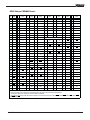
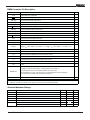
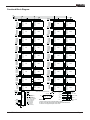
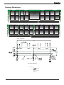
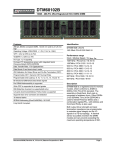
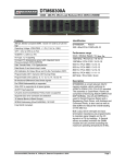
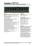
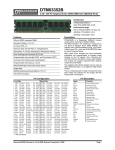
Memory Module Specifications KVR667D2D4F5/4GEF 4GB 512M x 72-Bit PC2-5300 CL5 ECC 240-Pin FBDIMM Description: This document describes ValueRAM's 4GB (512M x 72-bit) PC2-5300 CL5 SDRAM (Synchronous DRAM) "fully buffered" ECC "dual rank" memory module. This module is based on eighteen stacked 512M x 4-bit (thirty-six 256M x 4-bit) 667MHz DDR2 FBGA components. The module also includes an AMB device (Advanced Memory Buffer). The electrical and mechanical specifications are as follows: Feature: DRAM Supported: · FBDIMM Module: 240-pin · JEDEC Standard: R/C H or E · Memory Organization: 2 rank of x4 devices · DDR2 DRAM Interface: SSTL_18 · DDR2 Speed Grade: 667 Mbps · CAS Latency: 5-5-5 · Module Bandwidth: 5.3 GB/s · DRAM: VDD = VDDQ = 1.8V · AMB: VCC = VCCFBD = 1.5V · EEPROM: VDDSPD = 3.3V (typical) · Heat Spreader: Full DIMM Heat Spreader (FDHS) · PCB Height: 30.35mm, double-side · RoHS Compliant VALUERAM0886-001.A00 Elpida F-die 02/02/10 Page 1 T E C H N O L O G Y DDR2 240-pin FBDIMM Pinout: Pin # Front Side Pin # Back Side Pin # Front Side Pin # Back Side Pin # Front Side Pin # Back Side Pin # Front Side Pin # Back Side 1 VDD 121 VDD 31 PN3 151 SN3 61 PN9 181 SN9 91 PS9 211 SS9 2 VDD 122 VDD 32 PN3 152 SN3 62 VSS 182 VSS 92 VSS 212 VSS 3 VDD 123 VDD 33 VSS 153 VSS 63 PN10 183 SN10 93 PS5 213 SS5 4 VSS 124 VSS 34 PN4 154 SN4 64 PN10 184 SN10 94 PS5 214 SS5 5 VDD 125 VDD 35 PN4 155 SN4 65 VSS 185 VSS 95 VSS 215 VSS 6 VDD 126 VDD 36 VSS 156 VSS 66 PN11 186 SN11 96 PS6 216 SS6 7 VDD 127 VDD 37 PN5 157 SN5 67 PN11 187 SN11 97 PS6 217 SS6 8 VSS 128 VSS 38 PN5 158 SN5 68 VSS 188 VSS 98 VSS 218 VSS 9 VCC 129 VCC 39 VSS 159 VSS 99 PS7 219 SS7 10 VCC 130 VCC 40 PN13 160 SN13 69 VSS 189 VSS 100 PS7 220 SS7 11 VSS 131 VSS 41 PN13 161 SN13 70 PS0 190 SS0 101 VSS 221 VSS 12 VCC 132 VCC 42 VSS 162 VSS 71 PS0 191 SS0 102 PS8 222 SS8 13 VCC 133 VCC 43 VSS 163 VSS 72 VSS 192 VSS 103 PS8 223 SS8 14 VSS 134 VSS 44 RFU* 164 RFU* 73 PS1 193 SS1 104 VSS 224 VSS 15 VTT 135 VTT 45 RFU* 165 RFU* 74 PS1 194 SS1 105 RFU** 225 RFU** 16 VID1 136 VID0 46 VSS 166 VSS 75 VSS 195 VSS 106 RFU** 226 RFU** 17 RESET 47 VSS 167 VSS 76 PS2 196 SS2 107 VSS 227 VSS 18 VSS 19 137 DNU/M_Test KEY 138 VSS 48 PN12 168 SN12 77 PS2 197 SS2 108 VDD 228 SCK RFU** 139 RFU** 49 PN12 169 SN12 78 VSS 198 VSS 109 VDD 229 SCK 20 RFU** 140 RFU** 50 VSS 170 VSS 79 PS3 199 SS3 110 VSS 230 VSS 21 VSS 141 VSS 51 PN6 171 SN6 80 PS3 200 SS3 111 VDD 231 VDD 22 PN0 142 SN0 52 PN6 172 SN6 81 VSS 201 VSS 112 VDD 232 VDD 23 PN0 143 SN0 53 VSS 173 VSS 82 PS4 202 SS4 113 VDD 233 VDD 24 VSS 144 VSS 54 PN7 174 SN7 83 PS4 203 SS4 114 VSS 234 VSS 25 PN1 145 SN1 55 PN7 175 SN7 84 VSS 204 VSS 115 VDD 235 VDD 26 PN1 146 SN1 56 VSS 176 VSS 85 VSS 205 VSS 116 VDD 236 VDD 27 VSS 147 VSS 57 PN8 177 SN8 86 RFU* 206 RFU* 117 VTT 237 VTT 28 PN2 148 SN2 58 PN8 178 SN8 87 RFU* 207 RFU* 118 SA2 238 VDDSPD 29 PN2 149 SN2 59 VSS 179 VSS 88 VSS 208 VSS 119 SDA 239 SA0 30 VSS 150 VSS 60 PN9 180 SN9 89 VSS 209 VSS 120 SCL 240 SA1 90 PS9 210 SS9 RFU = Reserved Future Use. * These pin positions are reserved for forwarded clocks to be used in future module implementations ** These pin positions are reserved for future architecture flexibility 1) The following signals are CRC bits and thus appear out of the normal sequence: PN12/PN12, SN12/SN12, PN13/PN13, SN13/SN13, PS9/PS9, SS9/SS9 VALUERAM0886-001.A00 Page 2 T E C H N O L O G Y DIMM Connector Pin Description: Pin Name Pin Description Count SCK System Clock Input, positive line1 1 SCK System Clock Input, negative line1 1 PN[13:0] Primary Northbound Data, positive lines 14 PN[13:0] Primary Northbound Data, negative lines 14 PS[9:0] Primary Southbound Data, positive lines 10 Primary Southbound Data, negative lines 10 SN[13:0] Secondary Northbound Data, positive lines 14 SN[13:0] Secondary Northbound Data, negative lines 14 SS[9:0] Secondary Southbound Data, positive lines 10 SS[9:0] Secondary Southbound Data, negative lines 10 SCL Serial Presence Detect (SPD) Clock Input 1 SDA SPD Data Input / Output 1 SA[2:0] SPD Address Inputs, also used to select the DIMM number in the AMB 3 VID[1:0] Voltage ID: These pins must be unconnected for DDR2-based Fully Buffered DIMMs VID[0] is VDD value: OPEN = 1.8 V, GND = 1.5 V; VID[1] is V CC value: OPEN = 1.5 V, GND = 1.2 V 2 RESET AMB reset signal 1 PS[9:0] 2 RFU Reserved for Future Use 16 VCC AMB Core Power and AMB Channel Interface Power (1.5 Volt) 8 VDD DRAM Power and AMB DRAM I/O Power (1.8 Volt) 24 VTT DRAM Address/Command/Clock Termination Power (V DD/2) 4 SPD Power 1 Ground 80 The DNU/M_Test pin provides an exter nal connection on R/Cs A-D for testing the margin of Vref which is produced by a voltage divider on the module. It is not intended to be used in normal system operation and must not be connected (DNU) in a system. This test pin may have other features on future card designs and if it does, will be included in this specification at that time. 1 1 Total 240 VDDSPD VSS DNU/M_Test 1. System Clock Signals SCK and SCK switch at one half the DRAM CK/CK frequency 2. Eight pins reserved for forwarded clocks, eight pins reserved for future architecture flexibility Absolute Maximum Ratings Symbol MIN MAX Units SS -0.3 1.75 V VCC Voltage on V CC pin relative to V SS -0.3 1.75 V VDD VTT TSTG Voltage V DD pin relative to Vss -0.5 2.3 V Voltage on V TT pin relative to V SS Storage temperature -0.5 -55 2.3 100 V °C TCASE DDR2 SDRAM device operat ing temperature (Ambient) AMB device operating temperature (Ambient) 0 95 (1) °C 0 110 °C VIN, VOUT Parameter Voltage on any pin relative to V Note: (1) Above 85°C DRAM case temperature the Auto-Refresh command interval has to be reduced to tREFI = 3.9 µs. VALUERAM0886-001.A00 Page 3 T E C H N O L O G Y Functional Block Diagram: VSS S1 S0 DQS0 DQS0 DQ0 DQ1 DQ2 DQ3 DM I/O 0 I/O 1 I/O 2 I/O 3 CS DQS DQS D0 DQS9 DQS9 DM DM CS DQS DQS I/O 0 I/O 1 I/O 2 I/O 3 DQ4 DQ5 DQ6 DQ7 D18 DQS1 DQS1 DQ8 DQ9 DQ10 DQ11 DQS2 DQS2 DQ16 DQ17 DQ18 DQ19 DQS3 DQS3 DQ24 DQ25 DQ26 DQ27 DQS4 DQS4 DQ32 DQ33 DQ34 DQ35 DQS5 DQS5 DQ40 DQ41 DQ42 DQ43 DQS6 DQS6 DQ48 DQ49 DQ50 DQ51 DQS7 DQS7 DQ56 DQ57 DQ58 DQ59 DQS8 DQS8 CB0 CB1 CB2 CB3 DM I/O 0 I/O 1 I/O 2 I/O 3 DM I/O 0 I/O 1 I/O 2 I/O 3 DM I/O 0 I/O 1 I/O 2 I/O 3 DM I/O 0 I/O 1 I/O 2 I/O 3 DM I/O 0 I/O 1 I/O 2 I/O 3 DM I/O 0 I/O 1 I/O 2 I/O 3 DM I/O 0 I/O 1 I/O 2 I/O 3 DM I/O 0 I/O 1 I/O 2 I/O 3 CS DQS DQS D1 CS DQS DQS D2 CS DQS DQS D3 CS DQS DQS D4 CS DQS DQS D5 CS DQS DQS D6 CS DQS DQS D7 CS DQS DQS D8 SN0-SN13 SN0-SN13 SS0-SS9 SS0-SS9 PN0-PN13 PN0-PN13 PS0-PS9 PS0-PS9 A M B SCL SDA SA1-SA2 SA0 RESET SCK/SCK I/O 0 I/O 1 I/O 2 I/O 3 CS DQS DQS DM I/O 0 I/O 1 I/O 2 I/O 3 D9 CS DQS DQS D27 DQS10 DQS10 DM DM CS DQS DQS I/O 0 I/O 1 I/O 2 I/O 3 DQ12 DQ13 DQ14 DQ15 D19 I/O 0 I/O 1 I/O 2 I/O 3 DQS11 DQS11 DM DM CS DQS DQS I/O 0 I/O 1 I/O 2 I/O 3 DQ20 DQ21 DQ22 DQ23 D20 DM DQS12 DQS12 CS DQS DQS I/O 0 I/O 1 I/O 2 I/O 3 I/O 0 I/O 1 I/O 2 I/O 3 DM DQ28 DQ29 DQ30 DQ31 D21 I/O 0 I/O 1 I/O 2 I/O 3 DQS13 DQS13 DM DM CS DQS DQS I/O 0 I/O 1 I/O 2 I/O 3 DQ36 DQ37 DQ38 DQ39 DQS14 DQS14 D22 DM I/O 0 I/O 1 I/O 2 I/O 3 DM CS DQS DQS I/O 0 I/O 1 I/O 2 I/O 3 DQ44 DQ45 DQ46 DQ47 DQS15 DQS15 D23 DM I/O 0 I/O 1 I/O 2 I/O 3 DM CS DQS DQS I/O 0 I/O 1 I/O 2 I/O 3 DQ52 DQ53 DQ54 DQ55 D24 DM DQS16 DQS16 CS DQS DQS I/O 0 I/O 1 I/O 2 I/O 3 DM DQ60 DQ61 DQ62 DQ63 DQS17 DQS17 D25 DM I/O 0 I/O 1 I/O 2 I/O 3 I/O 0 I/O 1 I/O 2 I/O 3 DM CS DQS DQS I/O 0 I/O 1 I/O 2 I/O 3 CB4 CB5 CB6 CB7 D26 All address/command/control/clock S0 -> CS (D0-D17) CKE0 -> CKE (D0-D17) S1 -> CS (D18-D35) CKE1 -> CKE (D18-D35) ODT -> ODT0 (all SDRAMs) BA0-BA2 (all SDRAMs) A0-A15 (all SDRAMs) RAS (all SDRAMs) CAS (all SDRAMs) WE (all SDRAMs) CK/CK (all SDRAMs) I/O 0 I/O 1 I/O 2 I/O 3 33 VTT Serial PD SCL WP A0 A1 A2 SA0 SA1 SA2 SDA CS DQS DQS D10 CS DQS DQS D11 CS DQS DQS D12 CS DQS DQS D13 CS DQS DQS D14 CS DQS DQS D15 CS DQS DQS D16 CS DQS DQS D17 DM I/O 0 I/O 1 I/O 2 I/O 3 CS DQS DQS D28 DM I/O 0 I/O 1 I/O 2 I/O 3 CS DQS DQS D29 DM I/O 0 I/O 1 I/O 2 I/O 3 CS DQS DQS D30 DM I/O 0 I/O 1 I/O 2 I/O 3 CS DQS DQS D31 DM I/O 0 I/O 1 I/O 2 I/O 3 CS DQS DQS D32 DM I/O 0 I/O 1 I/O 2 I/O 3 CS DQS DQS D33 DM I/O 0 I/O 1 I/O 2 I/O 3 CS DQS DQS D34 DM I/O 0 I/O 1 I/O 2 I/O 3 CS DQS DQS D35 VTT Terminators VCC AMB VDDSPD SPD, AMB VDD D0-D35, AMB VREF D0-D35 VSS Notes: 1. DQ-to-I/O wiring may be changed within a nibble 2. There are two physical copies of each address/command/control D0-D35, SPD, AMB 3. There are four physical copies of each clock 825 VALUERAM0886-001.A00 Page 4 T E C H N O L O G Y Architecture: Advanced Memory Buffer Pin Description: Pin Name Pin Description Count FB-DIMM Channel Signals 99 SCK System Clock Input, positive line 1 SCK System Clock Input, negative line 1 PN[13:0] Primary Northbound Data, positive lines 14 PN[13:0] Primary Northbound Data, negative lines 14 PS[9:0] Primary Southbound Data, positive lines 10 PS[9:0] Primary Southbound Data, negative lines 10 SN[13:0] Secondary Northbound Data, positive lines 14 SN[13:0] Secondary Northbound Data, negative lines 14 SS[9:0] Secondary Southbound Data, positive lines 10 SS[9:0] Secondary Southbound Data, negative lines 10 To an external precision calibration resistor connected to Vcc 1 FBDRES DDR2 Interface Signals 175 DQS[8:0] Data Strobes, positive lines 9 DQS[8:0] Data Strobes, negative lines 9 DQS[17:9]/DM[8:0] Data Strobes (x4 DRAM only), positive lines. These signals are driven low to x8 DRAM on writes. 9 Data Strobes (x4 DRAM only), negative lines 9 Data 64 Checkbits 8 A[15:0]A, A[15:0]B Addresses. A10 is part of the pre-charge command 32 BA[2:0]A, BA[2:0]B Bank Addresses 6 RASA, RASB Part of command, with CAS, WE, and CS[1:0]. 2 CASA, CASB Part of command, with RAS, WE, and CS[1:0]. 2 Part of command, with RAS, CAS, and CS[1:0]. 2 On-die Termination Enable 2 DQS[17:9] DQ[63:0] CB[7:0] WEA, WEB ODTA, ODTB CKE[1:0]A, CKE[1:0]B Clock Enable (one per rank) CS[1:0]A, CS[1:0]B Chip Select (one per rank) 4 4 CLK[3:0] CLK[1:0] used on 9 and 18 device DIMMs, CLK[3:0] used on 36 device DIMMs. CLK[3:2] should be out4 put disabled when not in use. CLK[3:0] Negative lines for CLK[3:0] 4 DDRC_C14 DDR Compensation: Common return pin for DDRC_B18 and DDRC_C18. 1 DDRC_B18 DDR Compensation: Resistor connected to common return pin DDRC_C14 1 DDRC_C18 DDR Compensation: Resistor connected to common return pin DDRC_C14 1 DDRC_B12 DDR Compensation: Resistor connected to VSS 1 DDRC_C12 DDR Compensation: Resistor connected to VDD 1 VALUERAM0886-001.A00 Page 5 T E C H N O L O G Y Advanced Memory Buffer Pin Description: SPD Bus Interface Signals 5 SCL Serial Presence Detect (SPD) Clock Input 1 SDA SPD Data Input / Output 1 SPD Address Inputs, also used to select the DIMM number in the AMB 3 SA[2:0] Miscellaneous Signals 163 PLLTSTO PLL Clock Observability Output 1 VCCAPLL Analog VCC for the PLL. Tied with low pass filter to VCC. 1 VSSAPLL Analog VSS for the PLL. Tied to ground on the AMB die. Do not tie to ground on the DIMM. 1 TEST_pin# Leave floating on the DIMM 6 2 5 TESTLO_pin# Tie to ground on the DIMM BFUNC Tie to ground to set functionality as buffer on DIMM. 1 RESET AMB reset signal 1 No connect. Many NC are connected to VDD on the DIMM, to lower the impedance of the VDD power islands. 129 Reserved for Future Use 18 NC RFU Power/Ground Signals VCC VCCFBD VDD VDDSPD VSS 213 AMB Core Power (1.5 Volt) 24 AMB Channel I/O Power (1.5 Volt) 8 AMB DRAM I/O Power (1.8 Volt) 24 SPD Power (3.3 Volt) 1 Ground 156 Total 655 1. System Clock Signals SCK and SCK switch at one half the DRAM CK/CK frequency. 2. TESTLO_AB20 and TESTLO_AC20 should be configured for debug purposes on prototype DIMMs: each pin should have a zero ohm resistor pulldown to ground, and an unpopulated resistor pullup to VCC. These resistors can be replaced on production DIMMs with a direct connection to ground. VALUERAM0886-001.A00 Page 6 T E C H N O L O G Y Package Dimensions: AMB Advanced Memory Buffer T E C H N O L O G Y (Units = millimeters) Units: inches (millimeters) 45°x 0.0071(0.18) 0.042 (1.06) 0.047 (1.19) 0.042 (1.06) Detail A VALUERAM0886-001.A00 Page 7