1
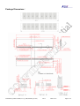
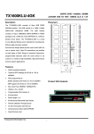
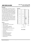
AD64I1B16
DDR3-1600G(CL9) 240-Pin O.C. U-DIMM
2GB (256M x 64-bits)
General Description
The ADATA’s AD64I1B16 is a 256Mx64 bits 2GB(2048MB) DDR3-1600(CL9)-9-9-24 SDRAM over clocking
memory module, The SPD is programmed to JEDEC standard latency 1600Mbps timing of 9-9-9-28 at 1.5V. The
module is composed of sixteen 128Mx8 bits CMOS DDR3 SDRAMs in FBGA package and one 2Kbit EEPROM in
8pin TDFN package on a 240pin glass–epoxy printed circuit board.
The AD64I1B16 is a Dual In-line Memory Module and intended for mounting onto 240-pins edge connector
sockets. Synchronous design allows precise cycle control with the use of system clock. Data I/O transactions are
possible on both edges of DQS. Range of operating frequencies, programmable latencies and burst lengths allow
the same device to be useful for a variety of high bandwidth, high performance memory system applications.
Features
• Power supply (Normal): VDD & VDDQ = 1.5V ± 0.075V
• 1.5V (SSTL_15 compatible) I/O
• Timing Reference
- DDR3 1600 CL9-9-9-28 at 1.5V
- DDR3 1600 CL9-9-9-24 at 1.7V
• Burst Length: 4, 8
• Programmable Additive Latency: 0, CL - 2, or CL - 1 clock
• Bi-directional, differential data strobe (DQS and /DQS)
• Differential clock input (CK, /CK) operation
• DLL aligns DQ and DQS transition with CK transition
• Addresses are mirrored for second rank
• Average Refresh Period 7.8us at lower then TCASE 85°C, 3.9us at 85°C < TCASE ≤ 95°C
• 8-bit pre-fetch.
• On Die Termination using ODT pin
• Internal (self) calibration: Internal self calibration through ZQ pin (RZQ: 240 ohm ± 1%)
• EEPROM VDDSPD=3.3V (Typical)
• PCB Height 30.00mm (1.181”), Double sided component
• Clock Cycle Time (tCK):
- DDR3-1600 tCK=1.25ns
• Refresh to Active/Refresh Command Time (tRFC): 110ns
• Lead-free products are RoHS compliant
Pin Assignment
Pin
Front
Pin
Front
Pin
Front
Pin
Back
Pin
Back
Pin
Back
1
VREFDQ
41
VSS
81
DQ32
121
VSS
161
NC,DM8
201
DQ37
2
VSS
42
NC
82
DQ33
122
DQ4
162
NC
202
VSS
3
DQ0
43
NC
83
VSS
123
DQ5
163
VSS
203
DM4
4
DQ1
44
VSS
84
/DQS4
124
VSS
164
NC,CB6
204
NC
5
VSS
45
NC,CB2
85
DQS4
125
DM0
165
NC,CB7
205
VSS
6
/DQS0
46
NC,CB3
86
VSS
126
NC
166
VSS
206
DQ38
7
DQS0
47
VSS
87
DQ34
127
VSS
167
NC
207
DQ39
8
VSS
48
NC
88
DQ35
128
DQ6
168
/RESET
208
VSS
9
DQ2
49
NC
89
VSS
129
DQ7
169
CKE1,NC
209
DQ44
10
DQ3
50
CKE0
90
DQ40
130
VSS
170
VDD
210
DQ45
11
VSS
51
VDD
91
DQ41
131
DQ12
171
A15
211
VSS
12
DQ8
52
BA2
92
VSS
132
DQ13
172
A14
212
DM5
13
DQ9
53
NC
93
/DQS5
133
VSS
173
VDD
213
NC
14
VSS
54
VDD
94
DQS5
134
DM1
174
A12
214
VSS
15
/DQS1
55
A11
95
VSS
135
NC
175
A9
215
DQ46
16
DQS1
56
A7
96
DQ42
136
VSS
176
VDD
216
DQ47
17
VSS
57
VDD
97
DQ43
137
DQ14
177
A8
217
VSS
18
DQ10
58
A5
98
VSS
138
DQ15
178
A6
218
DQ52
19
DQ11
59
A4
99
DQ48
139
VSS
179
VDD
219
DQ53
20
VSS
60
VDD
100
DQ49
140
DQ20
180
A3
220
VSS
21
DQ16
61
A2
101
VSS
141
DQ21
181
A1
221
DM6
22
DQ17
62
VDD
102
/DQS6
142
VSS
182
VDD
222
NC
23
VSS
63
CK1,NC
103
DQS6
143
DM2
183
VDD
223
VSS
24
/DQS2
64
/CK1,NC
104
VSS
144
NC
184
CK0
224
DQ54
25
DQS2
65
VDD
105
DQ50
145
VSS
185
/CK0
225
DQ55
26
VSS
66
VDD
106
DQ51
146
DQ22
186
VDD
226
VSS
27
DQ18
67
VREFCA
107
VSS
147
DQ23
187
NC,/EVENT
227
DQ60
28
DQ19
68
NC
108
DQ56
148
VSS
188
A0
228
DQ61
29
VSS
69
VDD
109
DQ57
149
DQ28
189
VDD
229
VSS
30
DQ24
70
A10/AP
110
VSS
150
DQ29
190
BA1
230
DM7
31
DQ25
71
BA0
111
/DQS7
151
VSS
191
VDD
231
NC
32
VSS
72
VDD
112
DQS7
152
DM3
192
/RAS
232
VSS
33
/DQS3
73
/WE
113
VSS
153
NC
193
/S0
233
DQ62
34
DQS3
74
/CAS
114
DQ58
154
VSS
194
VDD
234
DQ63
35
VSS
75
VDD
115
DQ59
155
DQ30
195
ODT0
235
VSS
36
DQ26
76
/S1,NC
116
VSS
156
DQ31
196
A13
236
VDDSPD
37
DQ27
77
ODT1,NC
117
SA0
157
VSS
197
VDD
237
SA1
38
VSS
78
VDD
118
SCL
158
NC,CB4
198
NC
238
SDA
39
NC,CB0
79
NC
119
SA2
159
NC,CB5
199
VSS
239
VSS
40
NC,CB1
80
VSS
120
VTT
160
VSS
200
DQ36
240
VTT
AD64I1B16_DDR3-1600G(CL=9)_2GB(128Mx8_Pb free)
Rev.1
2008/10/17
Page 2 of 6
Pin Description
PIN
NAME
FUNCTION
CK0~CK1,
System Clock
Active on the positive and negative edge to sample all inputs.
/CK0~/CK1
Masks system clock to freeze operation from the next clock cycle. CKE should be enabled at
CKE0, CKE1
Clock Enable
least on cycle prior new command. Disable input buffers for power down in standby
Disables or Enables device operation by masking or enabling all input except CK, CKE and
/S0,/S1
Chip Select
L(U)DQM
Row / Column address are multiplexed on the same pins.
A0~A13
Address
(Row Address: A0~A13 , Column Address: A0~A9 , Auto precharge: A10/AP)
Selects bank to be activated during row address latch time.
BA0~BA2
Banks Select
Selects bank for read / write during column address latch time.
DQ0~DQ63
Data
Data and check bit inputs / outputs are multiplexed on the same pins.
DQS0~DQS7,
Data Strobe
Bi-directional Data Strobe
DM0~DM7
Data Mask
Mask input data when DM is high.
/RAS
Row Address Strobe
/DQS0~/DQS7
/CAS
Latches row addresses on the positive edge of the CK with /RAS low
Column Address Strobe Latches Column addresses on the positive edge of the CK with /CAS low
/WE
Write Enable
VDD / VSS
Power Supply/Ground
Enables write operation and row recharge.
Power and Ground for the input buffers and the core logic.
VREFDQ
Power Supply reference Power Supply for reference.DQ,DM.VDD/2
VREFCA
Power Supply reference Power Supply for reference. Command , address, & control.VDD/2
VTT
Power Supply
Termination voltage. Used for address, command & control.VDD/2
SDA
Serial data I/O
EEPROM serial data I/O
SCL
Serial clock
SA0~SA2
Address in EEPROM
ODT0, ODT1
On Die Termination
EEPROM clock input
EEPROM address input
When high, termination resistance is enabled for all DQ, /DQ and DM pins, assuming the
function is enabled in the Extended Mode Register Set.
NC
No Connection
This pin is recommended to be left No Connection on the device.
AD64I1B16_DDR3-1600G(CL=9)_2GB(128Mx8_Pb free)
Rev.1
2008/10/17
Page 3 of 6
Block Diagram
AD64I1B16_DDR3-1600G(CL=9)_2GB(128Mx8_Pb free)
Rev.1
2008/10/17
Page 4 of 6
Absolute Maximum Ratings
Parameter
Voltage on VDD supply relative to Vss
Voltage on VDDQ pin relative to Vss
Voltage on any pin relative to Vss
Storage temperature
Note: DDR3 SDRAM component specification
Symbol
Value
Unit
VDD
-0.4 ~ 1.975
V
VDDQ
-0.4 ~ 1.975
V
VIN, Vout
-0.4 ~ 1.975
V
TStg
-55 ~ +100
Operation Temperature Condition
Parameter
Symbol
Value
Normal Operating Temperature Range
TC
0~+85
Extended Temperature Range (Optional)
TC
+85~+95
Note: (1) If the DRAM case temperature is above 85
Unit
Note
1
1
, the Auto-Refresh command interval has to be reduced to tREFI=3.9us.
DC Operating Condition
Voltage referenced to Vss = 0V, VDD&VDDQ=1.5V±0.075V, Tc = 0 to 85
Parameter
Symbol
Min
Max
Unit
Note
VDD
1.425
1.575
V
1,2
VDDSPD
1.7
3.6
V
VDDQ
1.425
1.575
V
1,2
I/O Reference Voltage(CMD/ADD)
VREFCA, (DC)
0.49 x VDDQ
0.51 x VDDQ
V
3,4
I/O Reference Voltage(DQ)
VREFDQ, (DC)
0.49 x VDDQ
0.51 x VDDQ
V
3,4
VTT
VDDQ/2 - TBD
VDDQ/2 +TBD
V
Supply Voltage
Supply Voltage for Output
Termination Voltage
Note: (1) Under all conditions VDDQ must be less than or equal to VDD.
(2) VDDQ tracks with VDD. AC parameters are measured with VDD and VDDQ tied together.
(3) The AC peak noise on VREF may not allow VREF to deviate from VREF(DC) by more than 1% VDD
15mV)
(4) For reference: approx. VDD/2 15mV
(for reference: approx.
AD64I1B16_DDR3-1600G(CL=9)_2GB(128Mx8_Pb free)
Rev.1
2008/10/17
Page 5 of 6
Package Dimensions
AD64I1B16_DDR3-1600G(CL=9)_2GB(128Mx8_Pb free)
Rev.1
2008/10/17
Page 6 of 6