1
Intel® Xeon® Processor 5500 Series
Datasheet, Volume 1
March 2009
Document Number: 321321-001
INFORMATION IN THIS DOCUMENT IS PROVIDED IN CONNECTION WITH INTEL® PRODUCTS. NO LICENSE, EXPRESS OR IMPLIED,
BY ESTOPPEL OR OTHERWISE, TO ANY INTELLECTUAL PROPERTY RIGHTS IS GRANTED BY THIS DOCUMENT. EXCEPT AS
PROVIDED IN INTEL'S TERMS AND CONDITIONS OF SALE FOR SUCH PRODUCTS, INTEL ASSUMES NO LIABILITY WHATSOEVER,
AND INTEL DISCLAIMS ANY EXPRESS OR IMPLIED WARRANTY, RELATING TO SALE AND/OR USE OF INTEL PRODUCTS INCLUDING
LIABILITY OR WARRANTIES RELATING TO FITNESS FOR A PARTICULAR PURPOSE, MERCHANTABILITY, OR INFRINGEMENT OF ANY
PATENT, COPYRIGHT OR OTHER INTELLECTUAL PROPERTY RIGHT. Intel products are not intended for use in medical, life saving, or
life sustaining applications.
Intel may make changes to specifications and product descriptions at any time, without notice.
Designers must not rely on the absence or characteristics of any features or instructions marked “reserved” or “undefined.” Intel
reserves these for future definition and shall have no responsibility whatsoever for conflicts or incompatibilities arising from future
changes to them.
The Intel® Xeon® Processor 5500 Series may contain design defects or errors known as errata which may cause the product to
deviate from published specifications.Current characterized errata are available on request.
Intel processor numbers are not a measure of performance. Processor numbers differentiate features within each processor family,
not across different processor families. See http://www.intel.com/products/processor_number for details. Over time processor
numbers will increment based on changes in clock, speed, cache, FSB, or other features, and increments are not intended to
represent proportional or quantitative increases in any particular feature. Current roadmap processor number progression is not
necessarily representative of future roadmaps. See www.intel.com/products/processor_number for details.
Hyper-Threading Technology requires a computer system with a processor supporting HT Technology and an HT Technologyenabled chipset, BIOS and operating system. Performance will vary depending on the specific hardware and software you use. For
more information including details on which processors support HT Technology, see
http://www.intel.com/products/ht/hyperthreading_more.htm
Enabling Execute Disable Bit functionality requires a PC with a processor with Execute Disable Bit capability and a supporting
operating system. Check with your PC manufacturer on whether your system delivers Execute Disable Bit functionality.
64-bit computing on Intel architecture requires a computer system with a processor, chipset, BIOS, operating system, device
drivers and applications enabled for Intel® 64 architecture. Performance will vary depending on your hardware and software
configurations. Consult with your system vendor for more information.
Intel® Virtualization Technology requires a computer system with an enabled Intel® processor, BIOS, virtual machine monitor
(VMM) and, for some uses, certain computer system software enabled for it. Functionality, performance or other benefits will vary
depending on hardware and software configurations and may require a BIOS update. Software applications may not be compatible
with all operating systems. Please check with your application vendor.
Intel® Turbo Boost Technology requires a PC with a processor with Intel Turbo Boost Technology capability. Intel Turbo Boost
Technology performance varies depending on hardware, software and overall system configuration. Check with your PC
manufacturer on whether your system delivers Intel Turbo Boost Technology. For more information, see www.intel.com.
Enhanced Intel SpeedStep® Technology. See the http://processorfinder.intel.com or contact your Intel representative for more
information.
Contact your local Intel sales office or your distributor to obtain the latest specifications and before placing your product order.
I2C is a two-wire communications bus/protocol developed by Philips. SMBus is a subset of the I2C bus/protocol and was developed
by Intel. Implementations of the I2C bus/protocol may require licenses from various entities, including Philips Electronics N.V. and
North American Philips Corporation.
Intel, Xeon, Enhanced Intel SpeedStep Technology, and the Intel logo are trademarks of Intel Corporation in the United States and
other countries.
*Other brands and names are the property of their respective owners.
Copyright © 2009, Intel Corporation.
2
Intel® Xeon® Processor 5500 Series Datasheet, Volume 1
Contents
1
Introduction .............................................................................................................. 9
1.1
Terminology ..................................................................................................... 10
1.2
References ....................................................................................................... 12
2
Intel® Xeon® Processors 5500 Series Electrical Specifications ............................... 13
2.1
Processor Signaling ........................................................................................... 13
2.1.1 Intel QuickPath Interconnect.................................................................... 13
2.1.2 DDR3 Signal Groups ............................................................................... 13
2.1.3 Platform Environmental Control Interface (PECI) ........................................ 14
2.1.4 Processor Sideband Signals ..................................................................... 14
2.1.5 System Reference Clock .......................................................................... 14
2.1.6 Test Access Port (TAP) Signals ................................................................. 15
2.1.7 Power / Other Signals ............................................................................. 15
2.1.8 Reserved or Unused Signals..................................................................... 23
2.2
Signal Group Summary ...................................................................................... 23
2.3
Mixing Processors.............................................................................................. 25
2.4
Flexible Motherboard Guidelines (FMB) ................................................................. 26
2.5
Absolute Maximum and Minimum Ratings ............................................................. 26
2.6
Processor DC Specifications ................................................................................ 28
2.6.1 VCC Overshoot Specifications................................................................... 31
2.6.2 Die Voltage Validation ............................................................................. 32
3
Package Mechanical Specifications .......................................................................... 43
3.1
Package Mechanical Specifications ....................................................................... 43
3.1.1 Package Mechanical Drawing.................................................................... 44
3.1.2 Processor Component Keep-Out Zones ...................................................... 47
3.1.3 Package Loading Specifications ................................................................ 47
3.1.4 Package Handling Guidelines.................................................................... 47
3.1.5 Package Insertion Specifications............................................................... 47
3.1.6 Processor Mass Specification .................................................................... 48
3.1.7 Processor Materials................................................................................. 48
3.1.8 Processor Markings................................................................................. 48
3.1.9 Processor Land Coordinates ..................................................................... 48
4
Land Listing............................................................................................................. 49
4.1
Intel® Xeon® Processors 5500 Series Pin Assignments .......................................... 49
4.1.1 Land Listing by Land Name ...................................................................... 49
4.1.2 Land Listing by Land Number ................................................................... 67
5
Signal Definitions .................................................................................................... 85
5.1
Signal Definitions .............................................................................................. 85
6
Thermal Specifications ............................................................................................ 89
6.1
Package Thermal Specifications ........................................................................... 89
6.1.1 Thermal Specifications ............................................................................ 89
6.1.2 Thermal Metrology ............................................................................... 103
6.2
Processor Thermal Features .............................................................................. 104
6.2.1 Processor Temperature ......................................................................... 104
6.2.2 Adaptive Thermal Monitor...................................................................... 104
6.2.3 On-Demand Mode ................................................................................ 106
6.2.4 PROCHOT# Signal ................................................................................ 106
6.2.5 THERMTRIP# Signal ............................................................................. 107
6.3
Platform Environment Control Interface (PECI) .................................................... 107
6.3.1 PECI Client Capabilities ......................................................................... 108
6.3.2 Client Command Suite .......................................................................... 109
Intel® Xeon® Processor 5500 Series Datasheet, Volume 1
3
6.3.3
6.3.4
6.3.5
6.3.6
6.3.7
Multi-Domain Commands ....................................................................... 125
Client Responses .................................................................................. 125
Originator Responses ............................................................................ 126
Temperature Data ................................................................................ 127
Client Management ............................................................................... 128
7
Features ................................................................................................................ 131
7.1
Power-On Configuration (POC)........................................................................... 131
7.2
Clock Control and Low Power States ................................................................... 132
7.2.1 Thread and Core Power State Descriptions ............................................... 133
7.2.2 Package Power State Descriptions ........................................................... 134
7.2.3 Intel® Xeon® Processor 5500 Series C-State Power Specifications.............. 135
7.3
Sleep States ................................................................................................... 136
7.4
Intel® Turbo Boost Technology .......................................................................... 136
7.5
Enhanced Intel SpeedStep® Technology ............................................................. 136
8
Boxed Processor Specifications.............................................................................. 137
8.1
Introduction .................................................................................................... 137
8.1.1 Available Boxed Thermal Solution Configurations ...................................... 137
8.1.2 An Intel “Combo” Boxed Passive / Active Combination Heat Sink Solution..... 137
8.1.3 Intel Boxed “Active” Heat Sink Solution ................................................... 138
8.1.4 Intel Boxed 25.5mm Tall Passive Heat Sink Solution.................................. 139
8.2
Mechanical Specifications .................................................................................. 140
8.2.1 Boxed Processor Heat Sink Dimensions and Baseboard Keepout Zones ........ 140
8.2.2 Boxed Processor Retention Mechanism and Heat Sink
Support (URS)...................................................................................... 149
8.3
Fan Power Supply (“Combo” and “Active” Solution) .............................................. 150
8.3.1 Boxed Processor Cooling Requirements.................................................... 151
8.4
Boxed Processor Contents................................................................................. 153
4
Intel® Xeon® Processor 5500 Series Datasheet, Volume 1
Figures
2-1
2-2
2-3
2-4
2-5
2-6
2-7
2-8
2-9
2-10
3-1
3-2
3-3
3-4
6-1
6-2
6-3
6-4
6-5
6-6
6-7
6-8
6-9
6-10
6-11
6-12
6-13
6-14
6-15
6-16
6-17
6-18
6-19
6-20
6-21
6-22
6-23
6-24
6-25
6-26
6-27
7-1
7-2
8-1
8-2
8-3
8-4
8-5
8-6
8-7
Active ODT for a Differential Link Example ............................................................ 13
Input Device Hysteresis ..................................................................................... 14
VCC Static and Transient Tolerance Loadlines1,2,3,4.............................................. 31
VCC Overshoot Example Waveform...................................................................... 32
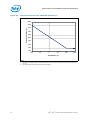
Load Current Versus Time (130W TDP Processor),2................................................ 33
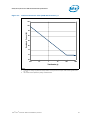
Load Current Versus Time (95W TDP Processor),2 ................................................. 34
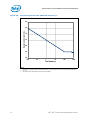
Load Current Versus Time (80W TDP Processor),2 ................................................. 35
Load Current Versus Time (60W TDP Processor),2 ................................................. 36
Load Current Versus Time (38W TDP Processor),2 ................................................. 37
VTT Static and Transient Tolerance Loadlines ........................................................ 39
Processor Package Assembly Sketch .................................................................... 43
Processor Package Drawing (Sheet 1 of 2) ............................................................ 45
Processor Package Drawing (Sheet 2 of 2) ............................................................ 46
Processor Top-Side Markings .............................................................................. 48
Intel Xeon Processor W5580 Thermal Profile ......................................................... 91
Intel Xeon Processor 5500 Series Advanced SKU Thermal Profile ............................. 93
Intel Xeon Processor 5500 Series Standard/Basic SKUs Thermal Profile .................... 95
Intel Xeon Processor 5500 Series Low Power SKU Thermal Profile ............................ 97
Intel Xeon Processor L5518 Thermal Profile .......................................................... 99
Intel Xeon Processor L5508 Thermal Profile ........................................................ 101
Case Temperature (TCASE) Measurement Location .............................................. 103
Frequency and Voltage Ordering........................................................................ 105
Ping() ............................................................................................................ 109
Ping() Example ............................................................................................... 109
GetDIB() ........................................................................................................ 110
Device Info Field Definition ............................................................................... 110
Revision Number Definition............................................................................... 110
GetTemp() ..................................................................................................... 111
GetTemp() Example......................................................................................... 111
PCI Configuration Address ................................................................................ 112
PCIConfigRd()................................................................................................. 113
PCIConfigWr() ................................................................................................ 115
Thermal Status Word ....................................................................................... 117
Thermal Data Configuration Register.................................................................. 118
Machine Check Read MbxSend() Data Format...................................................... 118
ACPI T-state Throttling Control Read / Write Definition ......................................... 120
MbxSend() Command Data Format .................................................................... 121
MbxSend() ..................................................................................................... 121
MbxGet() ....................................................................................................... 123
Temperature Sensor Data Format...................................................................... 127
PECI Power-up Timeline ................................................................................... 129
PROCHOT# POC Timing Requirements ............................................................... 132
Power States .................................................................................................. 133
Boxed Active Heat Sink .................................................................................... 138
Boxed Passive / Active Combination Heat Sink (With Removable Fan) .................... 138
Boxed Passive/Active Combination Heat Sink (with Fan Removed) ......................... 139
Intel Boxed 25.5 mm Tall Passive Heat Sink Solution ........................................... 139
Top Side Baseboard Keep-Out Zones ................................................................. 141
Top Side Baseboard Mounting-Hole Keep-Out Zones ............................................ 142
Bottom Side Baseboard Keep-Out Zones ............................................................ 143
Intel® Xeon® Processor 5500 Series Datasheet, Volume 1
5
8-8
8-9
8-10
8-11
8-12
8-13
8-14
Primary and Secondary Side 3D Height Restriction Zones ...................................... 144
Volumetric Height Keep-Ins............................................................................... 145
Volumetric Height Keep-Ins............................................................................... 146
4-Pin Fan Cable Connector (For Active Heat Sink) ................................................ 147
4-Pin Base Baseboard Fan Header (For Active Heat Sink) ...................................... 148
Thermal Solution Installation ............................................................................. 150
Fan Cable Connector Pin Out For 4-Pin Active Thermal Solution.............................. 151
Tables
1-1
1-2
2-1
2-2
2-3
2-4
2-5
2-6
2-7
2-8
2-9
2-10
2-11
2-12
2-13
2-14
2-15
2-16
2-17
3-1
3-2
3-3
4-1
4-2
5-1
6-1
6-2
6-3
6-4
6-5
6-6
6-7
6-8
6-9
6-10
6-11
6-12
6-13
6-14
6-15
6
Intel Xeon Processor 5500 Series Feature Set Overview ..........................................10
References........................................................................................................12
Processor Power Supply Voltages1 .......................................................................15
Voltage Identification Definition ...........................................................................17
Power-On Configuration (POC[7:0]) Decode ..........................................................22
VTT Voltage Identification Definition .....................................................................23
Signal Groups ...................................................................................................23
Signals With On-Die Termination (ODT) ................................................................25
Processor Absolute Minimum and Maximum Ratings ...............................................27
Voltage and Current Specifications .......................................................................28
VCC Static and Transient Tolerance .....................................................................30
VCC Overshoot Specifications ..............................................................................31
VTT Static and Transient Tolerance .....................................................................37
DDR3 Signal Group DC Specifications ...................................................................39
PECI DC Electrical Limits.....................................................................................40
RESET# Signal DC Specifications .........................................................................41
TAP Signal Group DC Specifications ......................................................................41
PWRGOOD Signal Group DC Specifications ............................................................41
Control Sideband Signal Group DC Specifications ...................................................42
Processor Loading Specifications ..........................................................................47
Package Handling Guidelines ...............................................................................47
Processor Materials ............................................................................................48
Land Listing by Land Name .................................................................................49
Land Listing by Land Number ..............................................................................67
Signal Definitions...............................................................................................85
Intel Xeon Processor W5580 Thermal Specifications ...............................................91
Intel Xeon Processor W5580 Thermal Profile..........................................................92
Intel Xeon Processor 5500 Series Advanced SKU Thermal Specifications....................92
Intel Xeon Processor 5500 Series Advanced SKU Thermal Profile A ...........................94
Intel Xeon Processor 5500 Series Advanced SKU Thermal Profile B ...........................94
Intel Xeon Processor 5500 Series Standard/Basic SKUs Thermal Specifications...........95
Intel Xeon Processor 5500 Series Standard/Basic SKUs Thermal Profile .....................96
Intel Xeon Processor 5500 Series Low Power SKU Thermal Specifications ..................96
Intel Xeon Processor 5500 Series Low Power SKU Thermal Profile ............................98
Intel Xeon Processor L5518 Thermal Specifications.................................................98
Intel Xeon Processor L5518 Thermal Profile ......................................................... 100
Intel Xeon Processor L5508 Thermal Specifications............................................... 100
Intel Xeon Processor L5508 Thermal Profile ......................................................... 102
Summary of Processor-specific PECI Commands .................................................. 108
GetTemp() Response Definition ......................................................................... 112
Intel® Xeon® Processor 5500 Series Datasheet, Volume 1
6-16
6-17
6-18
6-19
6-20
6-21
6-22
6-23
6-24
6-25
6-26
6-27
6-28
6-29
6-30
6-31
6-32
6-33
7-1
7-2
7-3
7-4
8-1
8-2
8-3
PCIConfigRd() Response Definition .................................................................... 113
PCIConfigWr() Device/Function Support ............................................................. 114
PCIConfigWr() Response Definition .................................................................... 115
Mailbox Command Summary ............................................................................ 116
Counter Definition ........................................................................................... 117
Machine Check Bank Definitions ........................................................................ 119
ACPI T-state Duty Cycle Definition ..................................................................... 120
MbxSend() Response Definition ......................................................................... 122
MbxGet() Response Definition ........................................................................... 123
Domain ID Definition ....................................................................................... 125
Multi-Domain Command Code Reference ............................................................ 125
Completion Code Pass/Fail Mask........................................................................ 125
Device Specific Completion Code (CC) Definition.................................................. 126
Originator Response Guidelines ......................................................................... 126
Error Codes and Descriptions ............................................................................ 128
PECI Client Response During Power-Up (During ‘Data Not Ready’) ......................... 128
Power Impact of PECI Commands versus C-states ............................................... 130
PECI Client Response During S1 ........................................................................ 130
Power On Configuration Signal Options............................................................... 131
Coordination of Thread Power States at the Core Level ......................................... 133
Processor C-State Power Specifications .............................................................. 135
Processor S-States .......................................................................................... 136
PWM Fan Frequency Specifications For 4-Pin Active Thermal Solution ..................... 151
Fan Specifications For 4-Pin Active Thermal Solution ............................................ 151
Fan Cable Connector Pin Out for 4-Pin Active Thermal Solution .............................. 151
Intel® Xeon® Processor 5500 Series Datasheet, Volume 1
7
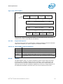
Revision History
Document
Number
Revision
Number
321321
001
Description
•
Initial release
Date
March 2009
§
8
Intel® Xeon® Processor 5500 Series Datasheet, Volume 1
Introduction
1
Introduction
The Intel® Xeon® Processor 5500 Series is the first-generation server/workstation
multi-core processor to implement key new technologies:
• Integrated Memory Controller
• Point-to-point link interface based on Intel® QuickPath Technology
The processor is optimized for performance with the power efficiencies of a low-power
microarchitecture to enable smaller, quieter systems.
This document provides DC electrical specifications, differential signaling specifications,
pinout and signal definitions, package mechanical specifications and thermal
requirements, and additional features pertinent to implementation and operation of the
processor. For information on register descriptions, refer to the Intel® Xeon® Processor
5500 Series Datasheet, Volume 2
Intel Xeon Processor 5500 Series are multi-core processors, based on 45 nm process
technology. The processor family features a range of thermal design power (TDP)
envelopes from 38W TDP up to 130W TDP. These processors feature two Intel
QuickPath Interconnect point-to-point links capable of up to 6.4 GT/s, up to 8 MB of
shared cache, and an Integrated Memory Controller. The processors support all the
existing Streaming SIMD Extensions 2 (SSE2), Streaming SIMD Extensions 3 (SSE3)
and Streaming SIMD Extensions 4 (SSE4). The processors support several Advanced
Technologies: Execute Disable Bit, Intel® 64 Technology, Enhanced Intel SpeedStep®
Technology, Intel® Virtualization Technology (Intel® VT), Intel® Hyper-Threading
Technology (Intel® HT Technology), and Intel® Turbo Boost Technology (Intel® TBT).
The Intel Xeon Processor 5500 Series family supports multiple platform segments.
• 2-Socket Workstation Platforms support Intel® Xeon® Processor W5580, a 130W
Thermal Design Power (TDP) SKU. These platforms provide optimal overall
performance and reliability, in addition to high-end graphics support. Note, specific
platform usage conditions apply when implementing these processors.
• 2-Socket High Performance Server and High Performance Computing (HPC)
Platforms support Intel Xeon Processor 5500 Series Advanced SKU (95W TDP).
These platforms provide optimal overall performance.
• 2-Socket Volume Server Platforms support Intel Xeon Processor 5500 Series
Standard/Basic SKUs (80W TDP). These platforms provide optimal performance per
watt for rack-optimized platforms.
• Ultra Dense Platforms implement Intel Xeon Processor 5500 Series Low Power SKU
(60W TDP). These processors are intended for dual-processor server blades and
embedded servers.
• Intel® Xeon® Processor L5518 with 60W TDP and elevated case temperatures. The
elevated case temperatures are intended to meet the short-term thermal profile
requirements of NEBS Level 3. These 2-Socket processors are ideal for thermallyconstrained form factors in embedded servers, comms and storage markets.
• Intel® Xeon® Processor L5508 with 38W TDP and elevated case temperatures. The
elevated case temperatures are intended to meet the short-term thermal profile
requirements of NEBS Level 3. These 2-Socket processors are ideal for thermallyconstrained form factors in embedded servers, comms and storage markets.
Intel® Xeon® Processor 5500 Series Datasheet, Volume 1
9
Introduction
• 1-Socket Workstation Platforms support Intel Xeon Processor 5500 Series SKUs.
These platforms enable a wide range of options for either the performance, power,
or cost sensitive customer.
Note:
All references to “chipset” in this document pertain to the Intel® 5520 chipset and
Intel® 5500 chipset, unless specifically stated otherwise.
Table 1-1.
Intel Xeon Processor 5500 Series Feature Set Overview
Feature
1.1
Intel Xeon Processor 5500 Series
Cache Sizes
-
Instruction Cache = 32 KB, per core
Data Cache = 32 KB, per core
256 KB Mid-Level Cache per core
8 MB shared among cores (up to 4)
Data Transfer Rate
Two (2) full-width Intel QuickPath Interconnect links, up to 6.4 GT/s in
each direction
Multi-Core Support
Up to 4 Cores per processor
Dual Processor Support
Up to 2 processors per platform
Package
1366-land FCLGA
Terminology
A ‘#’ symbol after a signal name refers to an active low signal, indicating a signal is in
the active state when driven to a low level. For example, when RESET# is low, a reset
has been requested.
A ‘_N’ and ‘_P’ after a signal name refers to a differential pair.
Commonly used terms are explained here for clarification:
• 1366-land FC-LGA package — The Intel Xeon Processor 5500 Series is available
in a Flip-Chip Land Grid Array (FC-LGA) package, consisting of processor mounted
on a land grid array substrate with an integrated heat spreader (IHS).
• DDR3 — Double Data Rate 3 synchronous dynamic random access memory
(SDRAM) is the name of the new DDR memory standard that is being developed as
the successor to DDR2 SDRAM.
• Enhanced Intel SpeedStep Technology — Enhanced Intel SpeedStep
Technology allows the operating system to reduce power consumption when
performance is not needed.
• Intel Turbo Boost Technology — Intel Turbo Boost Technology is a way to
automatically run the processor core faster than the marked frequency if the part is
operating under power, temperature, and current specifications limits of the
Thermal Design Power (TDP). This results in increased performance of both single
and multi-threaded applications.
• Execute Disable Bit — Execute Disable allows memory to be marked as
executable or non-executable, when combined with a supporting operating system.
If code attempts to run in non-executable memory the processor raises an error to
the operating system. This feature can prevent some classes of viruses or worms
that exploit buffer over run vulnerabilities and can thus help improve the overall
security of the system. See the Intel® 64 and IA-32 Architecture Software
Developer's Manuals for more detailed information.
• Functional Operation — Refers to the normal operating conditions in which all
processor specifications, including DC, AC, signal quality, mechanical, and thermal,
are satisfied.
10
Intel® Xeon® Processor 5500 Series Datasheet, Volume 1
Introduction
• Intel Xeon Processor 5500 Series — Includes processor substrate and
integrated heat spreader (IHS).
• Integrated Memory Controller (IMC) — As the term implies, the Memory
Controller is integrated on the processor die.
• Intel QuickPath Interconnect (Intel® QPI) — A cache-coherent, link-based
Interconnect specification for Intel processors, chipsets, and I/O bridge
components.
• Intel® 64 Architecture — An enhancement to Intel's IA-32 architecture, allowing
the processor to execute operating systems and applications written to take
advantage of Intel® 64.
• Intel Virtualization Technology (Intel® VT) — A set of hardware
enhancements to Intel server and client platforms that can improve virtualization
solutions. VT provides a foundation for widely-deployed virtualization solutions and
enables more robust hardware assisted virtualization solution.
• Integrated Heat Spreader (IHS) — A component of the processor package used
to enhance the thermal performance of the package. Component thermal solutions
interface with the processor at the IHS surface.
• Jitter — Any timing variation of a transition edge or edges from the defined Unit
Interval (UI).
• LGA1366 Socket — The 1366-land FC-LGA package mates with the system board
through this surface mount, 1366-contact socket.
• Server SKU — A processor Stock Keeping Unit (SKU) to be installed in either
server or workstation platforms. Electrical, power and thermal specifications for
these SKU’s are based on specific use condition assumptions. Server processors
may be further categorized as Advanced, Standard/Basic, and Low Power SKUs. For
further details on use condition assumptions, please refer to the latest Product
Release Qualification (PRQ) Report available via your Customer Quality Engineer
(CQE) contact.
• Storage Conditions — Refers to a non-operational state. The processor may be
installed in a platform, in a tray, or loose. Processors may be sealed in packaging or
exposed to free air. Under these conditions, processor lands should not be
connected to any supply voltages, have any I/Os biased, or receive any clocks.
• Unit Interval (UI) — Signaling convention that is binary and unidirectional. In
this binary signaling, one bit is sent for every edge of the forwarded clock, whether
it be a rising edge or a falling edge. If a number of edges are collected at instances
t1, t2, tn,...., tk then the UI at instance “n” is defined as:
UI
n
=t
n
-t
n-1
• Workstation SKU — A processor SKU to be installed in workstation platforms
only. Electrical, power and thermal specifications for these processors have been
developed based on Intel’s reliability goals at a reference use condition. In addition,
the processor validation and production test conditions have been optimized based
on these conditions. Operating “Workstation” processors in a server environment or
other application, could impact reliability performance, which means Intel’s
reliability goals may not be met. For further details on use condition assumptions or
reliability performance, please refer to the latest Product Release Qualification
(PRQ) Report available via your Customer Quality Engineer (CQE) contact.
• NEBS — Network Equipment Building System. NEBS is the most common set of
environmental design guidelines applied to telecommunications equipment in the
United States.
Intel® Xeon® Processor 5500 Series Datasheet, Volume 1
11
Introduction
1.2
References
Platform designers are strongly encouraged to maintain familiarity with the most up-todate revisions of processor and platform collateral.
Table 1-2.
References
Document
AP-485, Intel
®
Location
Processor Identification and the CPUID Instruction
Intel® 64 and IA-32 Architecture Software Developer's Manual
• Volume 1: Basic Architecture
• Volume 2A: Instruction Set Reference, A-M
• Volume 2B: Instruction Set Reference, N-Z
• Volume 3A: System Programming Guide, Part 1
• Volume 3B: Systems Programming Guide, Part 2
Intel® 64 and IA-32 Architectures Optimization Reference Manual
Intel® Virtualization Technology Specification for Directed I/O
Architecture Specification
Intel® Xeon® Processor 5500 Series Datasheet, Volume 2
®
Intel Xeon
Guide
®
Processor 5500 Series Thermal / Mechanical Design
Intel® Xeon® Processor 5500 Series Specification Update
Entry-Level Electronics-Bay Specifications: A Server System
Infrastructure (SSI) Specification for Entry Pedestal Servers and
Workstations
ACPI Specifications
241618
Notes
1
1
253665
253666
253667
253668
253669
248966
1
D51397-001
1
321322
1
321323
1
321324
1
www.ssiforum.org
www.acpi.info
Notes:
1.
Document is available publicly at http://www.intel.com.
12
Intel® Xeon® Processor 5500 Series Datasheet, Volume 1
Intel® Xeon® Processors 5500 Series Electrical Specifications
2
Intel® Xeon® Processors 5500
Series Electrical Specifications
2.1
Processor Signaling
Intel® Xeon® Processor 5500 Series include 1366 lands, which utilize various signaling
technologies. Signals are grouped by electrical characteristics and buffer type into
various signal groups. These include Intel® QuickPath Interconnect, DDR3 (Reference
Clock, Command, Control and Data), Platform Environmental Control Interface (PECI),
Processor Sideband, System Reference Clock, Test Access Port (TAP), and Power/Other
signals. Refer to Table 2-5 for details.
Detailed layout, routing, and termination guidelines corresponding to these signal
groups can be found in the applicable platform design guide (Refer to Section 1.2).
Intel strongly recommends performing analog simulations of all interfaces. Please refer
to Section 1.2 for signal integrity model availability.
2.1.1
Intel QuickPath Interconnect
Intel Xeon Processor 5500 Series provide two Intel QuickPath Interconnect ports for
high speed serial transfer between other enabled components. Each port consists of
two uni-directional links (for transmit and receive). A differential signaling scheme is
utilized, which consists of opposite-polarity (D_P, D_N) signal pairs.
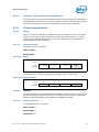
On-die termination (ODT) is included on the processor silicon and terminated to VSS.
Intel chipsets also provide ODT, thus eliminating the need to terminate on the system
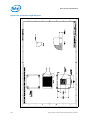
board. Figure 2-1 illustrates the active ODT.
Figure 2-1.
Active ODT for a Differential Link Example
TX
RX
Signal
Signal
RTT
2.1.2
RTT
RTT
RTT
DDR3 Signal Groups
The memory interface utilizes DDR3 technology, which consists of numerous signal
groups. These include: Reference Clocks, Command Signals, Control Signals, and Data
Signals. Each group consists of numerous signals, which may utilize various signaling
technologies. Please refer to Table 2-5 for further details.
Intel® Xeon® Processor 5500 Series Datasheet, Volume 1
13
Intel® Xeon® Processors 5500 Series Electrical Specifications
2.1.3
Platform Environmental Control Interface (PECI)
PECI is an Intel proprietary interface that provides a communication channel between
Intel processors and chipset components to external thermal monitoring devices. The
Intel Xeon Processor 5500 Series contains a Digital Thermal Sensor (DTS) that reports
a relative die temperature as an offset from Thermal Control Circuit (TCC) activation
temperature. Temperature sensors located throughout the die are implemented as
analog-to-digital converters calibrated at the factory. PECI provides an interface for
external devices to read processor temperature, perform processor manageability
functions, and manage processor interface tuning and diagnostics. Please refer to
Section 6 for processor specific implementation details for PECI.
The PECI interface operates at a nominal voltage set by VTTD. The set of DC electrical
specifications shown in Table 2-13 is used with devices normally operating from a VTTD
interface supply.
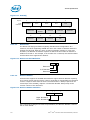
2.1.3.1
Input Device Hysteresis
The PECI client and host input buffers must use a Schmitt-triggered input design for
improved noise immunity. Please refer to Figure 2-2 and Table 2-13.
Figure 2-2.
Input Device Hysteresis
VTTD
Maximum VP
PECI High Range
Minimum VP
Minimum
Hysteresis
Valid Input
Signal Range
Maximum VN
Minimum VN
PECI Low Range
PECI Ground
2.1.4
Processor Sideband Signals
Intel Xeon Processor 5500 Series include sideband signals that provide a variety of
functions. Details can be found in Table 2-5 and the applicable platform design guide.
All Asynchronous Processor Sideband signals are required to be asserted/deasserted
for at least eight BCLKs in order for the processor to recognize the proper signal state.
See Table 2-17 for DC specifications.
2.1.5
System Reference Clock
The processor core, processor uncore, Intel QuickPath Interconnect link, and DDR3
memory interface frequencies are generated from BCLK_DP and BCLK_DN signals.
There is no direct link between core frequency and Intel QuickPath Interconnect link
frequency (e.g., no core frequency to Intel QuickPath Interconnect multiplier). The
processor maximum core frequency, Intel QuickPath Interconnect link frequency and
14
Intel® Xeon® Processor 5500 Series Datasheet, Volume 1
Intel® Xeon® Processors 5500 Series Electrical Specifications
DDR3 memory frequency are set during manufacturing. It is possible to override the
processor core frequency setting using software. This permits operation at lower core
frequencies than the factory set maximum core frequency.
The processor core frequency is configured during reset by using values stored within
the device during manufacturing. The stored value sets the lowest core multiplier at
which the particular processor can operate. If higher speeds are desired, the
appropriate ratio can be configured via the IA32_PERF_CTL MSR.
Clock multiplying within the processor is provided by the internal phase locked loop
(PLL), which requires a constant frequency BCLK_DP, BCLK_DN input, with exceptions
for spread spectrum clocking.
2.1.6
Test Access Port (TAP) Signals
Due to the voltage levels supported by other components in the Test Access Port (TAP)
logic, it is recommended that the processor(s) be first in the TAP chain and followed by
any other components within the system. A translation buffer should be used to
connect to the rest of the chain unless one of the other components is capable of
accepting an input of the appropriate voltage. Similar considerations must be made for
TCK, TDO, TMS, and TRST#. Two copies of each signal may be required with each
driving a different voltage level.
Processor TAP signal DC specifications can be found in Table 2-17.
Note:
While TDI, TMS and TRST# do not include On-Die Termination (ODT), these signals are
weakly pulled-up via a 1-5 kΩ resistor to VTT.
Note:
While TCK does not include ODT, this signal is weakly pulled-down via a 1-5 kΩ resistor
to VSS.
2.1.7
Power / Other Signals
Processors also include various other signals including power/ground, sense points, and
analog inputs. Details can be found in Table 2-5 and the applicable platform design
guide.
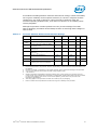
Table 2-1 outlines the required voltage supplies necessary to support Intel Xeon
Processor 5500 Series.
Table 2-1.
Processor Power Supply Voltages1
Power Rail
Nominal Voltage
Notes
VCC
See Table 2-9;
Figure 2-3
VCCPLL
1.80 V
Each processor includes dedicated VCCPLL and PLL circuits.
VDDQ
1.50 V
Each processor and DDR3 stack shares a dedicated voltage regulator.
VTTA, VTTD
See Table 2-11;
Figure 2-10
Each processor includes a dedicated VR11.1 regulator.
Each processor includes a dedicated VR11.0 regulator.
VTT = VTTA + VTTD; P1V1_Vtt is VID[4:2] controlled,
VID range is 1.0255-1.2000V; 20 mV offset (see Table 2-4); VTT
represents a typical voltage. VTT_MIN and VTT_MAX loadlines represent a
31.5 mV offset from VTT (typ).
Note:
1.
Refer to Table 2-8 for voltage and current specifications.
Further platform and processor power delivery details can be found in the Intel® Xeon®
Processor 5500 Platform Design Guide (PDG).
Intel® Xeon® Processor 5500 Series Datasheet, Volume 1
15
Intel® Xeon® Processors 5500 Series Electrical Specifications
2.1.7.1
Power and Ground Lands
For clean on-chip power distribution, processors include lands for all required voltage
supplies. These include:
• 210 each VCC (271 ea. VSS) lands must be supplied with the voltage determined by
the VID[7:0] signals. Table 2-2 defines the voltage level associated with each core
VID pattern. Table 2-9 and Figure 2-3 represent VCC static and transient limits.
• 3 each VCCPLL lands, connected to a 1.8 V supply, power the Phase Lock Loop (PLL)
clock generation circuitry. An on-die PLL filter solution is implemented within the
Intel Xeon Processor 5500 Series.
• 45 each VDDQ (17 ea. VSS) lands, connected to a 1.50 V supply, provide power to
the processor DDR3 interface. This supply also powers the DDR3 memory
subsystem.
• 7 each VTTA (5 ea. VSS) and 26 ea. VTTD (17 ea. VSS) lands must be supplied with
the voltage determined by the VTT_VID[4:2] signals. Coupled with a 20 mV offset,
this corresponds to a VTT_VID pattern of ‘010xxx10’. Table 2-4 specifies the
voltage levels associated with each VTT_VID pattern. Table 2-11 and Figure 2-10
represent VTT static and transient limits.
All VCC, VCCPLL, VDDQ, VTTA, and VTTD lands must be connected to their respective
processor power planes, while all VSS lands must be connected to the system ground
plane. Refer to the Intel® Xeon® Processor 5500 Platform Design Guide (PDG) for
decoupling, voltage plane and routing guidelines for each power supply voltage.
2.1.7.2
Decoupling Guidelines
Due to its large number of transistors and high internal clock speeds, the Intel Xeon
Processor 5500 Series is capable of generating large current swings between low and
full power states. This may cause voltages on power planes to sag below their
minimum values if bulk decoupling is not adequate. Larger bulk storage (CBULK), such
as electrolytic capacitors, supply current during longer lasting changes in current
demand, for example coming out of an idle condition. Similarly, they act as a storage
well for current when entering an idle condition from a running condition. Care must be
taken in the baseboard design to ensure that the voltages provided to the processor
remains within the specifications listed in Table 2-8. Failure to do so can result in timing
violations or reduced lifetime of the processor.
2.1.7.3
Processor VCC Voltage Identification (VID) Signals
The voltage set by the VID signals is the maximum reference voltage regulator (VR)
output to be delivered to the processor VCC lands. VID signals are CMOS push/pull
outputs. Please refer to Table 2-17 for the DC specifications for these and other
processor sideband signals.
Individual processor VID values may be calibrated during manufacturing such that two
processor units with the same core frequency may have different default VID settings.
The Intel Xeon Processor 5500 Series uses eight voltage identification signals,
VID[7:0], to support automatic selection of core power supply voltages. Table 2-2
specifies the voltage level corresponding to the state of VID[7:0]. A ‘1’ in this table
refers to a high voltage level and a ‘0’ refers to a low voltage level. If the processor
socket is empty (SKTOCC# high), or the voltage regulation circuit cannot supply the
voltage that is requested, the voltage regulator must disable itself.
16
Intel® Xeon® Processor 5500 Series Datasheet, Volume 1
Intel® Xeon® Processors 5500 Series Electrical Specifications
The Intel Xeon Processor 5500 Series provides the ability to operate while transitioning
to an adjacent VID and its associated processor core voltage (VCC). This is represented
by a DC shift in the loadline. It should be noted that a low-to-high or high-to-low
voltage state change may result in as many VID transitions as necessary to reach the
target core voltage. Transitions above the maximum specified VID are not permitted.
Table 2-8 includes VID step sizes and DC shift ranges. Minimum and maximum voltages
must be maintained as shown in Table 2-9.
The VRM or EVRD utilized must be capable of regulating its output to the value defined
by the new VID. DC specifications for dynamic VID transitions are included in Table 2-8
and Table 2-9.
Power source characteristics must be guaranteed to be stable whenever the supply to
the voltage regulator is stable.
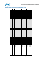
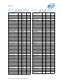
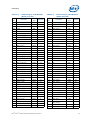
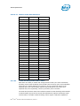
Table 2-2.Voltage Identification Definition (Sheet 1 of 5)
VID7
VID6
VID5
VID4
VID3
VID2
VID1
VID0
VCC_MAX
0
0
0
0
0
0
0
0
OFF
0
0
0
0
0
0
0
1
OFF
0
0
0
0
0
0
1
0
1.60000
0
0
0
0
0
0
1
1
1.59375
0
0
0
0
0
1
0
0
1.58750
0
0
0
0
0
1
0
1
1.58125
0
0
0
0
0
1
1
0
1.57500
0
0
0
0
0
1
1
1
1.56875
0
0
0
0
1
0
0
0
1.56250
0
0
0
0
1
0
0
1
1.55625
0
0
0
0
1
0
1
0
1.55000
0
0
0
0
1
0
1
1
1.54375
0
0
0
0
1
1
0
0
1.53750
0
0
0
0
1
1
0
1
1.53125
0
0
0
0
1
1
1
0
1.52500
0
0
0
0
1
1
1
1
1.51875
0
0
0
1
0
0
0
0
1.51250
0
0
0
1
0
0
0
1
1.50625
0
0
0
1
0
0
1
0
1.50000
0
0
0
1
0
0
1
1
1.49375
0
0
0
1
0
1
0
0
1.48750
0
0
0
1
0
1
0
1
1.48125
0
0
0
1
0
1
1
0
1.47500
0
0
0
1
0
1
1
1
1.46875
0
0
0
1
1
0
0
0
1.46250
0
0
0
1
1
0
0
1
1.45625
0
0
0
1
1
0
1
0
1.45000
0
0
0
1
1
0
1
1
1.44375
0
0
0
1
1
1
0
0
1.43750
0
0
0
1
1
1
0
1
1.43125
Intel® Xeon® Processor 5500 Series Datasheet, Volume 1
17
Intel® Xeon® Processors 5500 Series Electrical Specifications
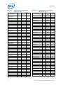
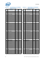
Table 2-2.Voltage Identification Definition (Sheet 2 of 5)
18
VID7
VID6
VID5
VID4
VID3
VID2
VID1
VID0
VCC_MAX
0
0
0
1
1
1
1
0
1.42500
0
0
0
1
1
1
1
1
1.41875
0
0
1
0
0
0
0
0
1.41250
0
0
1
0
0
0
0
1
1.40625
0
0
1
0
0
0
1
0
1.40000
0
0
1
0
0
0
1
1
1.39375
0
0
1
0
0
1
0
0
1.38750
0
0
1
0
0
1
0
1
1.38125
0
0
1
0
0
1
1
0
1.37500
0
0
1
0
0
1
1
1
1.36875
0
0
1
0
1
0
0
0
1.36250
0
0
1
0
1
0
0
1
1.35625
0
0
1
0
1
0
1
0
1.35000
0
0
1
0
1
0
1
1
1.34375
0
0
1
0
1
1
0
0
1.33750
0
0
1
0
1
1
0
1
1.33125
0
0
1
0
1
1
1
0
1.32500
0
0
1
0
1
1
1
1
1.31875
0
0
1
1
0
0
0
0
1.31250
0
0
1
1
0
0
0
1
1.30625
0
0
1
1
0
0
1
0
1.30000
0
0
1
1
0
0
1
1
1.29375
0
0
1
1
0
1
0
0
1.28750
0
0
1
1
0
1
0
1
1.28125
0
0
1
1
0
1
1
0
1.27500
0
0
1
1
0
1
1
1
1.26875
0
0
1
1
1
0
0
0
1.26250
0
0
1
1
1
0
0
1
1.25625
0
0
1
1
1
0
1
0
1.25000
0
0
1
1
1
0
1
1
1.24375
0
0
1
1
1
1
0
0
1.23750
0
0
1
1
1
1
0
1
1.23125
0
0
1
1
1
1
1
0
1.22500
0
0
1
1
1
1
1
1
1.21875
0
1
0
0
0
0
0
0
1.21250
0
1
0
0
0
0
0
1
1.20625
0
1
0
0
0
0
1
0
1.20000
0
1
0
0
0
0
1
1
1.19375
0
1
0
0
0
1
0
0
1.18750
0
1
0
0
0
1
0
1
1.18125
0
1
0
0
0
1
1
0
1.17500
0
1
0
0
0
1
1
1
1.16875
Intel® Xeon® Processor 5500 Series Datasheet, Volume 1
Intel® Xeon® Processors 5500 Series Electrical Specifications
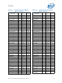
Table 2-2.Voltage Identification Definition (Sheet 3 of 5)
VID7
VID6
VID5
VID4
VID3
VID2
VID1
VID0
VCC_MAX
0
1
0
0
1
0
0
0
1.16250
0
1
0
0
1
0
0
1
1.15625
0
1
0
0
1
0
1
0
1.15000
0
1
0
0
1
0
1
1
1.14375
0
1
0
0
1
1
0
0
1.13750
0
1
0
0
1
1
0
1
1.13125
0
1
0
0
1
1
1
0
1.12500
0
1
0
0
1
1
1
1
1.11875
0
1
0
1
0
0
0
0
1.11250
0
1
0
1
0
0
0
1
1.10625
0
1
0
1
0
0
1
0
1.10000
0
1
0
1
0
0
1
1
1.09375
0
1
0
1
0
1
0
0
1.08750
0
1
0
1
0
1
0
1
1.08125
0
1
0
1
0
1
1
0
1.07500
0
1
0
1
0
1
1
1
1.06875
0
1
0
1
1
0
0
0
1.06250
0
1
0
1
1
0
0
1
1.05625
0
1
0
1
1
0
1
0
1.05000
0
1
0
1
1
0
1
1
1.04375
0
1
0
1
1
1
0
0
1.03750
0
1
0
1
1
1
0
1
1.03125
0
1
0
1
1
1
1
0
1.02500
0
1
0
1
1
1
1
1
1.01875
0
1
1
0
0
0
0
0
1.01250
0
1
1
0
0
0
0
1
1.00625
0
1
1
0
0
0
1
0
1.00000
0
1
1
0
0
0
1
1
0.99375
0
1
1
0
0
1
0
0
0.98750
0
1
1
0
0
1
0
1
0.98125
0
1
1
0
0
1
1
0
0.97500
0
1
1
0
0
1
1
1
0.96875
0
1
1
0
1
0
0
0
0.96250
0
1
1
0
1
0
0
1
0.95625
0
1
1
0
1
0
1
0
0.95000
0
1
1
0
1
0
1
1
0.94375
0
1
1
0
1
1
0
0
0.93750
0
1
1
0
1
1
0
1
0.93125
0
1
1
0
1
1
1
0
0.92500
0
1
1
0
1
1
1
1
0.91875
0
1
1
1
0
0
0
0
0.91250
0
1
1
1
0
0
0
1
0.90625
Intel® Xeon® Processor 5500 Series Datasheet, Volume 1
19
Intel® Xeon® Processors 5500 Series Electrical Specifications
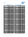
Table 2-2.Voltage Identification Definition (Sheet 4 of 5)
20
VID7
VID6
VID5
VID4
VID3
VID2
VID1
VID0
VCC_MAX
0
1
1
1
0
0
1
0
0.90000
0
1
1
1
0
0
1
1
0.89375
0
1
1
1
0
1
0
0
0.88750
0
1
1
1
0
1
0
1
0.88125
0
1
1
1
0
1
1
0
0.87500
0
1
1
1
0
1
1
1
0.86875
0
1
1
1
1
0
0
0
0.86250
0
1
1
1
1
0
0
1
0.85625
0
1
1
1
1
0
1
0
0.85000
0
1
1
1
1
0
1
1
0.84375
0
1
1
1
1
1
0
0
0.83750
0
1
1
1
1
1
0
1
0.83125
0
1
1
1
1
1
1
0
0.82500
0
1
1
1
1
1
1
1
0.81875
1
0
0
0
0
0
0
0
0.81250
1
0
0
0
0
0
0
1
0.80625
1
0
0
0
0
0
1
0
0.80000
1
0
0
0
0
0
1
1
0.79375
1
0
0
0
0
1
0
0
0.78750
1
0
0
0
0
1
0
1
0.78125
1
0
0
0
0
1
1
0
0.77500
1
0
0
0
0
1
1
1
0.76875
1
0
0
0
1
0
0
0
0.76250
1
0
0
0
1
0
0
1
0.75625
1
0
0
0
1
0
1
0
0.75000
1
0
0
0
1
0
1
1
0.74375
1
0
0
0
1
1
0
0
0.73750
1
0
0
0
1
1
0
1
0.73125
1
0
0
0
1
1
1
0
0.72500
1
0
0
0
1
1
1
1
0.71875
1
0
0
1
0
0
0
0
0.71250
1
0
0
1
0
0
0
1
0.70625
1
0
0
1
0
0
1
0
0.70000
1
0
0
1
0
0
1
1
0.69375
1
0
0
1
0
1
0
0
0.68750
1
0
0
1
0
1
0
1
0.68125
1
0
0
1
0
1
1
0
0.67500
1
0
0
1
0
1
1
1
0.66875
1
0
0
1
1
0
0
0
0.66250
1
0
0
1
1
0
0
1
0.65625
1
0
0
1
1
0
1
0
0.65000
1
0
0
1
1
0
1
1
0.64375
Intel® Xeon® Processor 5500 Series Datasheet, Volume 1
Intel® Xeon® Processors 5500 Series Electrical Specifications
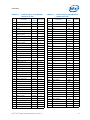
Table 2-2.Voltage Identification Definition (Sheet 5 of 5)
VID7
VID6
VID5
VID4
VID3
VID2
VID1
VID0
VCC_MAX
1
0
0
1
1
1
0
0
0.63750
1
0
0
1
1
1
0
1
0.63125
1
0
0
1
1
1
1
0
0.62500
1
0
0
1
1
1
1
1
0.61875
1
0
1
0
0
0
0
0
0.61250
1
0
1
0
0
0
0
1
0.60625
1
0
1
0
0
0
1
0
0.60000
1
0
1
0
0
0
1
1
0.59375
1
0
1
0
0
1
0
0
0.58750
1
0
1
0
0
1
0
1
0.58125
1
0
1
0
0
1
1
0
0.57500
1
0
1
0
0
1
1
1
0.56875
1
0
1
0
1
0
0
0
0.56250
1
0
1
0
1
0
0
1
0.55625
1
0
1
0
1
0
1
0
0.55000
1
0
1
0
1
0
1
1
0.54375
1
0
1
0
1
1
0
0
0.53750
1
0
1
0
1
1
0
1
0.53125
1
0
1
0
1
1
1
0
0.52500
1
0
1
0
1
1
1
1
0.51875
1
0
1
1
0
0
0
0
0.51250
1
0
1
1
0
0
0
1
0.50625
1
0
1
1
0
0
1
0
0.50000
1
1
1
1
1
1
1
0
OFF
1
1
1
1
1
1
1
1
OFF
Notes:
1.
When the “11111111” VID pattern is observed, or when the SKTOCC# pin is high, the voltage regulator
output should be disabled.
2.
Shading denotes the expected VID range of the Intel Xeon Processor 5500 Series.
3.
The VID range includes VID transitions that may be initiated by thermal events, Extended HALT state
transitions (see Section 7.2), higher C-States (see Section 7.2) or Enhanced Intel SpeedStep® Technology
transitions (see Section 7.5). The Extended HALT state must be enabled for the processor to
remain within its specifications
4.
Once the VRM/EVRD is operating after power-up, if either the Output Enable signal is de-asserted or a
specific VID off code is received, the VRM/EVRD must turn off its output (the output should go to high
impedance) within 500 ms and latch off until power is cycled.
2.1.7.3.1
Power-On Configuration (POC) Logic
VID[7:0] signals also serve a second function. During power-up, Power-On
Configuration POC[7:0] functionality is multiplexed onto these signals via 1-5 kΩ pullup or pull down resistors located on the baseboard. These values provide voltage
regulator keying (VID[7]), inform the processor of the platforms power delivery
capabilities (MSID[2:0]), and program the gain applied to the ISENSE input
(CSC[2:0]). Table 2-3 maps VID signals to the corresponding POC functionality.
Intel® Xeon® Processor 5500 Series Datasheet, Volume 1
21
Intel® Xeon® Processors 5500 Series Electrical Specifications
Table 2-3.
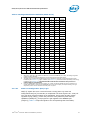
Power-On Configuration (POC[7:0]) Decode
Function
Bits
POC Settings
VR_Key
VID[7]
0b for VR11.1
Spare
VID[6]
CSC[2:0]
VID[5:3]
-000
-001
-010
-011
-100
-101
-111
0b (default)
Feature Disabled
ICC_MAX = 40A
ICC_MAX = 50A1
ICC_MAX = 80A
ICC_MAX = 100A
ICC_MAX = 120A
ICC_MAX = 150A2
MSID[2:0]
VID[2:0]
-001
-011
-100
-101
-110
38W TDP / 40A ICC_MAX
60W TDP / 80A ICC_MAX
80W TDP / 100A ICC_MAX
95W TDP / 120A ICC_MAX
130W TDP / 150A ICC_MAX
Description
Electronic safety key
distinguishing VR11.1
Reserved for future use
Current Sensor Configuration
(CSC) programs the gain
applied to the ISENSE A/D
output. ISENSE data is then
used to dynamically calculate
current and power.
MSID[2:0] signals are provided
to indicate the Market Segment
for the processor and may be
used for future processor
compatibility or keying. See
Figure 7-1 for platform timing
requirements of the MSID[2:0]
signals.
Notes:
1. This setting is defined for future use; no specific Intel Xeon Processor 5500 Series SKU is defined with ICC_MAX
= 50A
2. General rule: Set PWM IMON slope to: 900mV=IMAX, where IMAX =IccMAX with one exception: for Intel Xeon
Processor W5580 set IMON slope to 900mV=180A, but for all other SKUs they have to match, as shown above.
Consult your PWM data sheet for the IMON slope setting.
Some POC signals include specific timing requirements. Please refer to Section 7.1 for
further details.
2.1.7.4
Processor VTT Voltage Identification (VTT_VID) Signals
The voltage set by the VTT_VID signals is the typical reference voltage regulator (VR)
output to be delivered to the processor VTTA and VTTD lands. It is expected that one
regulator will supply all VTTA and VTTD lands. VTT_VID signals are CMOS push/pull
outputs. Please refer to Table 2-17 for the DC specifications for these signals.
Individual processor VTT_VID values may be calibrated during manufacturing such that
two processor units with the same core frequency may have different default VTT_VID
settings.
The Intel Xeon Processor 5500 Series utilizes three voltage identification signals to
support automatic selection of power supply voltages. These correspond to
VTT_VID[4:2]. The VTT voltage level delivered to the processor lands must also
encompass a 20 mV offset (See Table 2-4; VTT_TYP) above the voltage level
corresponding to the state of the VTT_VID[7:0] signals (See Table 2-4; VR 11.0
Voltage). Table 2-11 and Figure 2-10 provide the resulting static and transient
tolerances. Please note that the maximum and minimum electrical loadlines are defined
by a 31.5 mV tolerance band above and below VTT_TYP values.
Power source characteristics must be guaranteed to be stable whenever the supply to
the voltage regulator is stable.
22
Intel® Xeon® Processor 5500 Series Datasheet, Volume 1
Intel® Xeon® Processors 5500 Series Electrical Specifications
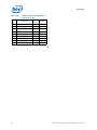
Table 2-4.
VTT Voltage Identification Definition
VID7
2.1.8
VID6
VID5
VID4
VID3
VID2
VID1
VID0
VR 11.0
Voltage
VTT_TYP
(Voltage + Offset)
0
1
0
0
0
0
1
0
1.200V
1.220V
0
1
0
0
0
1
1
0
1.175V
1.195V
0
1
0
0
1
0
1
0
1.150V
1.170V
0
1
0
0
1
1
1
0
1.125V
1.145V
0
1
0
1
0
0
1
0
1.100V
1.120V
0
1
0
1
0
1
1
0
1.075V
1.095V
0
1
0
1
1
0
1
0
1.050V
1.070V
0
1
0
1
1
1
1
0
1.025V
1.045V
Reserved or Unused Signals
All Reserved (RSVD) signals must remain unconnected. Connection of these signals to
VCC, VTTA, VTTD, VDDQ, VSS, or any other signal (including each other) can result in
component malfunction or incompatibility with future processors. See Section 4 for the
land listing and the location of all Reserved signals.
For reliable operation, connect unused inputs or bidirectional signals to an appropriate
signal level. Unused Intel QuickPath Interconnect input and output pins can be left
floating. Unused active high inputs should be connected through a resistor to ground
(VSS). Unused outputs can be left unconnected; however, this may interfere with some
TAP functions, complicate debug probing, and prevent boundary scan testing. A resistor
must be used when tying bidirectional signals to power or ground. When tying any
signal to power or ground, including a resistor will also allow for system testability.
Resistor values should be within ± 20% of the impedance of the baseboard trace,
unless otherwise noted in the appropriate platform design guidelines.
TAP signals do not include on-die termination, however they may include resistors on
package (refer to Section 2.1.6 for details). Inputs and utilized outputs must be
terminated on the baseboard. Unused outputs may be terminated on the baseboard or
left unconnected. Note that leaving unused outputs unterminated may interfere with
some TAP functions, complicate debug probing, and prevent boundary scan testing.
2.2
Signal Group Summary
Signals are combined in Table 2-5 by buffer type and characteristics. “Buffer Type”
denotes the applicable signaling technology and specifications.
Table 2-5.
Signal Groups (Sheet 1 of 2)
Signal Group
Signals1
Buffer Type
Intel QuickPath Interconnect Signals
Differential
Intel QuickPath Interconnect Input
QPI[0/1]_DRX_D[N/P][19:0],
QPI[0/1]_CLKRX_DP, QPI[0/1]_CLKRX_DN
Differential
Intel QuickPath Interconnect Output
QPI[0/1]_DTX_D[N/P][19:0],
QPI[0/1]_CLKTX_DP, QPI[0/1]_CLKTX_DN
Analog Input
QPI[0/1]_COMP
Single ended
DDR3 Reference Clocks
Differential
2
Output
Intel® Xeon® Processor 5500 Series Datasheet, Volume 1
DDR{0/1/2}_CLK_[P/N][3:0]
23
Intel® Xeon® Processors 5500 Series Electrical Specifications
Table 2-5.
Signal Groups (Sheet 2 of 2)
Signal Group
Signals1
Buffer Type
DDR3 Command Signals2
Single ended
CMOS Output
DDR{0/1/2}_RAS#, DDR{0/1/2}_CAS#,
DDR{0/1/2}_WE#, DDR{0/1/2}_MA[15:0],
DDR{0/1/2}_BA[2:0], DDR{0/1/2}_MA_PAR
Single ended
Asynchronous Output
DDR{0/1/2}_RESET#
DDR3 Control Signals
2
Single ended
CMOS Output
DDR{0/1/2}_CS#[7:0], DDR{0/1/2}_ODT[5:0],
DDR{0/1/2}_CKE[3:0]
Single ended
Analog Input
DDR_VREF, DDR_COMP[2:0]
DDR3 Data Signals2
Single ended
CMOS Input/Output
DDR{0/1/2}_DQ[63:0], DDR{0/1/2}_ECC[7:0]
Differential
CMOS Input/Output
DDR{0/1/2}_DQS_[N/P][17:0]
Single ended
Asynchronous Input
DDR{0/1/2}_PAR_ERR#[2:0],
DDR_THERM#
Platform Environmental Control Interface (PECI)
Single ended
Asynchronous Input/Output
PECI
Processor Sideband Signals
Single ended
GTL Input/Output
BPM#[7:0], CAT_ERR#
Single ended
Asynchronous Input
PECI_ID#
Single ended
Asynchronous GTL Output
PRDY#, THERMTRIP#
Single ended
Asynchronous GTL Input
PREQ#
Single ended
Asynchronous GTL Input/Output
PROCHOT#
Single ended
Asynchronous CMOS Output
PSI#
Single ended
CMOS Output
VID[7:6],
VID[5:3]/CSC[2:0],
VID[2:0]/MSID[2:0],
VTT_VID[4:2]
System Reference Clock
Differential
Input
BCLK_DP, BCLK_DN
Test Access Port (TAP) Signals
CMOS Output
BCLK_ITP_DP, BCLK_ITP_DN
Single ended
Differential
Input
TCK, TDI, TMS, TRST#
Single ended
GTL Output
TDO
PWRGOOD Signals
Single ended
Asynchronous Input
CCPWRGOOD, VDDPWRGOOD, VTTPWRGOOD
Asynchronous Input
RESET#
RESET Signal
Single ended
Power/Other Signals
24
Power / Ground
VCC, VCCPLL, VDDQ, VTTA, VTTD, VSS
Analog Input
COMP0, ISENSE
Sense Points
VCCSENSE, VSSSENSE, VSS_SENSE_VTTD,
VTTD_SENSE
Other
SKTOCC#, DBR#
Intel® Xeon® Processor 5500 Series Datasheet, Volume 1
Intel® Xeon® Processors 5500 Series Electrical Specifications
Notes:
1. Refer to Section 4 for land assignments and Section 5 for signal definitions.
2. DDR{0/1/2} refers to DDR3 Channel 0, DDR3 Channel1 and DDR3 Channel 2.
Signals that include on-die termination (ODT) are listed in Table 2-6.
Table 2-6. Signals With On-Die Termination (ODT)
Intel QuickPath Interface Signal Group1
QPI[1:0]_DRX_DP[19:0], QPI[1:0]_DRX_DN[19:0], QPI[1:0]_TRX_DP[19:0], QPI[1:0]_TRX_DN[19:0],
QPI[0/1]_CLKRX_D[N/P], QPI[0/1]_CLKTX_D[N/P]
DDR3 Signal Group2
DDR{0/1/2}_DQ[63:0], DDR{0/1/2}_DQS_[N/P][17:0], DDR{0/1/2}_ECC[7:0],
DDR{0/1/2}_PAR_ERR#[2:0]3
Processor Sideband Signal Group
BPM#[7:0]6, PECI_ID#7, PREQ#6
Test Access Port (TAP) Signal Group
TCK4, TDI5, TMS5, TRST#5
Power/Other Signal Group8
VCCPWRGOOD, VDDPWRGOOD, VTTPWRGOOD
Notes:
1.
Unless otherwise specified, signals have ODT in the package with a 50 Ω pull-down to VSS.
2.
Unless otherwise specified, all DDR3 signals are terminated to VDDQ/2.
3.
DDR{0/1/2}_PAR_ERR#[2:0] are terminated to VDDQ.
4.
TCK does not include ODT, this signal is weakly pulled-down via a 1-5 kΩ resistor to VSS.
5.
TDI, TMS, TRST# do not include ODT, these signals are weakly pulled-up via 1-5kΩ resistor to VTT.
6.
BPM[7:0]# and PREQ# signals have ODT in package with 35 Ω pull-ups to VTT.
7.
PECI_ID# has ODT in package with a 1-5 kΩ pull-up to VTT.
8.
VCCPWRGOOD, VDDPWRGOOD, and VTTPWRGOOD have ODT in package with a 5-20 kΩ pull-down to VSS.
2.3
Mixing Processors
Intel supports dual processor (DP) configurations consisting of processors:
1. from the same power optimization segment
2. that support the same maximum Intel QuickPath Interconnect and DDR3 memory
speeds
3. that share symmetry across physical packages with respect to the number of
logical processor per package, number of cores per package, number of Intel
QuickPath interfaces, and cache topology
4. that have identical Extended Family, Extended Model, Processor Type, Family Code
and Model Number as indicated by the function 1 of the CPUID instruction
Note:
Processors must operate with the same Intel QuickPath Interconnect, DDR3 memory,
and core frequency.
While Intel does nothing to prevent processors from operating together, some
combinations may not be supported due to limited validation, which may result in
uncharacterized errata. Coupling this fact with the large number of Intel Xeon
Processor 5500 series attributes, the following population rules and stepping matrix
have been developed to clearly define supported configurations.
1. Processors must be of the same power-optimization segment. This insures
processors include the same maximum Intel QuickPath interconnect and DDR3
operating speeds and cache sizes.
Intel® Xeon® Processor 5500 Series Datasheet, Volume 1
25
Intel® Xeon® Processors 5500 Series Electrical Specifications
2. Processors must operate at the same core frequency. Note, processors within the
same power-optimization segment supporting different maximum core frequencies
(e.g. a 2.93 GHz / 95 W and 2.66 GHz / 95 W) can be operated within a system.
However, both must operate at the highest frequency rating commonly supported.
Mixing components operating at different internal clock frequencies is not
supported and will not be validated by Intel.
3. Processors must share symmetry across physical packages with respect to the
number of logical processors per package, number of cores per package (but not
necessarily the same subset of cores within the packages), number of Intel
QuickPath interfaces, and cache topology.
4. Mixing dissimilar steppings is only supported with processors that have identical
Extended Family, Extended Model, Processor Type, Family Code and Model Number
as indicated by the function 1 of the CPUID instruction. Mixing processors of
different steppings but the same model (as per CPUID instruction) is supported.
Details regarding the CPUID instruction are provided in the AP-485,
Intel® Processor Identification and the CPUID Instruction application note and the
Intel® 64 and IA-32 Architectures Software Developer’s Manual, Volume 2A.
5. After AND’ing the feature flag and extended feature flags from the installed
processors, any processor whose set of feature flags exactly matches the AND’ed
feature flags can be selected by the BIOS as the BSP. If no processor exactly
matches the AND’ed feature flag values, then the processor with the numerically
lower CPUID should be selected as the BSP.
6. Intel requires that the proper microcode update be loaded on each processor
operating within the system. Any processor that does not have the proper
microcode update loaded is considered by Intel to be operating out of specification.
7. Customers are fully responsible for the validation of their system configuration.
2.4
Flexible Motherboard Guidelines (FMB)
The Flexible Motherboard (FMB) guidelines are estimates of the maximum values the
Intel Xeon Processor 5500 Series will have over certain time periods. The values are
only estimates and actual specifications for future processors may differ. Processors
may or may not have specifications equal to the FMB value in the foreseeable future.
System designers should meet the FMB values to ensure their systems will be
compatible with future Intel Xeon Processor 5500 Series.
2.5
Absolute Maximum and Minimum Ratings
Table 2-7 specifies absolute maximum and minimum ratings which lie outside the
functional limits of the processor. Only within specified operation limits, can
functionality and long-term reliability be expected.
At conditions outside functional operation condition limits, but within absolute
maximum and minimum ratings, neither functionality nor long-term reliability can be
expected. If a device is returned to conditions within functional operation limits after
having been subjected to conditions outside these limits, but within the absolute
maximum and minimum ratings, the device may be functional, but with its lifetime
degraded depending on exposure to conditions exceeding the functional operation
condition limits.
26
Intel® Xeon® Processor 5500 Series Datasheet, Volume 1
Intel® Xeon® Processors 5500 Series Electrical Specifications
At conditions exceeding absolute maximum and minimum ratings, neither functionality
nor long-term reliability can be expected. Moreover, if a device is subjected to these
conditions for any length of time then, when returned to conditions within the
functional operating condition limits, it will either not function or its reliability will be
severely degraded.
Although the processor contains protective circuitry to resist damage from static
electric discharge, precautions should always be taken to avoid high static voltages or
electric fields.
Table 2-7.
Processor Absolute Minimum and Maximum Ratings
Parameter
Min
VCC
Processor core voltage with respect to VSS
-0.300
VCCPLL
Processor PLL voltage with respect to VSS
1.800
V
4
VDDQ
Processor I/O supply voltage for DDR3
with respect to VSS
1.500
V
4
VTTA
Processor uncore analog voltage with
respect to VSS
0.825
1.350
V
3
VTTD
Processor uncore digital voltage with
respect to VSS
0.825
1.350
V
3
TCASE
Processor case temperature
See
Section 6
See
Section 6
°C
-40
85
°C
-0.30
1.150
V
TSTORAGE Storage temperature
VISENSE
Analog input voltage with respect to Vss
for sensing Core current consumption
Nominal
Max
Unit
1.350
V
Notes1,2
Symbol
5,6,7
Notes:
1.
For functional operation, all processor electrical, signal quality, mechanical and thermal specifications must
be satisfied.
2.
Excessive overshoot or undershoot on any signal will likely result in permanent damage to the processor.
3.
VTTA and VTTD should be derived from the same voltage regulator (VR).
4.
± 5% tolerance.
5.
Storage temperature is applicable to storage conditions only. In this scenario, the processor must not
receive a clock, and no lands can be connected to a voltage bias. Storage within these limits will not affect
the long-term reliability of the device. For functional operation, please refer to the processor case
temperature specifications.
6.
This rating applies to the processor and does not include any tray or packaging.
7.
Failure to adhere to this specification can affect the long-term reliability of the processor.
Intel® Xeon® Processor 5500 Series Datasheet, Volume 1
27
Intel® Xeon® Processors 5500 Series Electrical Specifications
2.6
Processor DC Specifications
DC specifications are defined at the processor pads, unless otherwise noted.
DC specifications are only valid while meeting specifications for case temperature
(TCASE specified in Section 6), clock frequency, and input voltages. Care should be
taken to read all notes associated with each specification.
Table 2-8.
Voltage and Current Specifications (Sheet 1 of 2)
Symbol
Voltage
Plane
Min
0.750
VID
VCC VID Range
-
VCC
Core Voltage
(Launch - FMB)
VCC
VVID_STEP
VID step size during a
transition
Typ
Unit
1.350
V
2,3
V
3,4,6,7,11
± 6.250
mV
9
See Table 2-9 and Figure 2-3
-
Notes1
Max
VCCPLL
PLL Voltage
(DC + AC specification)
VCCPLL
0.95*VCCPLL
(Typ)
1.800
1.05*VCCPLL
(Typ)
V
10
VDDQ
I/O Voltage for DDR3
(DC + AC specification)
VDDQ
0.95*VDDQ
(Typ)
1.500
1.05*VDDQ
(Typ)
V
10
VTT_VID
VTT VID Range
-
VTT
Uncore Voltage
(Launch - FMB)
VTT
ICC_MAX
ICCPLL_MAX
IDDQ_MAX
ITT_MAX
28
Parameter
1.045
1.220
See Table 2-11 and Figure 2-10
V
2,3
V
3,5,8,11
Max. Processor Current:
Intel® Xeon® Processor
W5580
(TDP = 130W)
(Launch - FMB)
VCC
VCCPLL
VDDQ
VTTA
VTTD
150
1.1
9
6
22
A
A
A
A
A
11
Max. Processor Current:
Intel Xeon Processor
5500 Series Advanced
SKU
(TDP = 95W)
(Launch - FMB)
VCC
VCCPLL
VDDQ
VTTA
VTTD
120
1.1
9
6
22
A
A
A
A
A
11
Max. Processor Current:
Intel Xeon Processor
5500 Series
Standard/Basic SKU
(TDP = 80W)
(Launch - FMB)
VCC
VCCPLL
VDDQ
VTTA
VTTD
100
1.1
9
6
22
A
A
A
A
A
11
Max. Processor Current:
Intel Xeon Processor
5500 Series Low Power
SKU
(TDP = 60W)
(Launch - FMB)
VCC
VCCPLL
VDDQ
VTTA
VTTD
80
1.1
9
6
20
A
A
A
A
A
11
Max. Processor Current:
Intel® Xeon® Processor
L5518
(TDP = 60W)
(Launch - FMB)
VCC
VCCPLL
VDDQ
VTTA
VTTD
80
1.1
9
6
20
A
A
A
A
A
11
Max. Processor Current:
Intel® Xeon® Processor
L5508
(TDP = 38W)
(Launch - FMB)
VCC
VCCPLL
VDDQ
VTTA
VTTD
40
1.1
9
6
20
A
A
A
A
A
11
Intel® Xeon® Processor 5500 Series Datasheet, Volume 1
Intel® Xeon® Processors 5500 Series Electrical Specifications
Table 2-8.
Voltage and Current Specifications (Sheet 2 of 2)
Symbol
ICC_TDC
ICCPLL_TDC
IDDQ_TDC
ITT_TDC
IDDQ_S3
Parameter
Voltage
Plane
Min
Typ
Max
Unit
Notes1
Thermal Design
Current:
Intel Xeon Processor
W5580
(TDP = 130W)
(Launch - FMB)
VCC
VCCPLL
VDDQ
VTTA
VTTD
110
1.1
9
6
22
A
A
A
A
A
11,12
Thermal Design
Current:
Intel Xeon Processor
5500 Series Advanced
SKU
(TDP = 95W)
(Launch - FMB)
VCC
VCCPLL
VDDQ
VTTA
VTTD
85
1.1
9
6
22
A
A
A
A
A
11,12
Thermal Design
Current:
Intel Xeon Processor
5500 Series
Standard/Basic SKU
(TDP = 80W)
(Launch - FMB)
VCC
VCCPLL
VDDQ
VTTA
VTTD
70
1.1
9
6
22
A
A
A
A
A
11,12
Thermal Design
Current:
Intel Xeon Processor
5500 Series Low Power
SKU
(TDP = 60W)
(Launch - FMB)
VCC
VCCPLL
VDDQ
VTTA
VTTD
60
1.1
9
6
20
A
A
A
A
A
11,12
Thermal Design
Current:
Intel Xeon Processor
L5518
(TDP = 60W)
(Launch - FMB)
VCC
VCCPLL
VDDQ
VTTA
VTTD
60
1.1
9
6
20
A
A
A
A
A
11,12
Thermal Design
Current:
Intel Xeon Processor
L5508
(TDP = 38W)
(Launch - FMB)
VCC
VCCPLL
VDDQ
VTTA
VTTD
28
1.1
9
6
20
A
A
A
A
A
11,12
VDDQ
1.0
A
13,14
DDR3 System Memory
Interface Supply
Current in Standby
State
Notes:
1. Unless otherwise noted, all specifications in this table apply to all processors. These specifications are based
on pre-silicon characterization and will be updated as further data becomes available.
2. Individual processor VID and/or VTT_VID values may be calibrated during manufacturing such that two
devices at the same speed may have different settings.
3. These voltages are targets only. A variable voltage source should exist on systems in the event that a
different voltage is required.
4. The VCC voltage specification requirements are measured across vias on the platform for the VCCSENSE and
VSSSENSE pins close to the socket with a 100 MHz bandwidth oscilloscope, 1.5 pF maximum probe
capacitance, and 1 MΩ minimum impedance. The maximum length of ground wire on the probe should be
less than 5 mm. Ensure external noise from the system is not coupled in the scope probe.
5. The VTT voltage specification requirements are measured across vias on the platform for the VTTD_SENSE
and VSS_SENSE_VTTD lands close to the socket with a 100 MHz bandwidth oscilloscope, 1.5 pF maximum
probe capacitance, and 1 MΩ minimum impedance. The maximum length of ground wire on the probe should
be less than 5 mm. Ensure external noise from the system is not coupled in the scope probe.
6. Refer to Table 2-9 and corresponding Figure 2-3. The processor should not be subjected to any static VCC
level that exceeds the VCC_MAX associated with any particular current. Failure to adhere to this specification
can shorten processor lifetime.
7. Minimum VCC and maximum ICC are specified at the maximum processor case temperature (TCASE) shown in
Table 6-1. ICC_MAX is specified at the relative VCC_MAX point on the VCC load line. The processor is capable of
Intel® Xeon® Processor 5500 Series Datasheet, Volume 1
29
Intel® Xeon® Processors 5500 Series Electrical Specifications
drawing ICC_MAX for up to 10 ms. Refer to Figure 2-5 through Figure 2-8 for further details on the average
processor current draw over various time durations.
8. Refer to Table 2-11 and corresponding Figure 2-10. The processor should not be subjected to any static VTT
level that exceeds the VTT_MAX associated with any particular current. Failure to adhere to this specification
can shorten processor lifetime.
9. This specification represents the VCC reduction due to each VID transition. See Section 2.1.7.3.
10.Baseboard bandwidth is limited to 20 MHz.
11.FMB is the flexible motherboard guidelines. See Section 2.4 for FMB details.
12.ICC_TDC (Thermal Design Current) is the sustained (DC equivalent) current that the processor is capable of
drawing indefinitely and should be used for the voltage regulator temperature assessment. The voltage
regulator is responsible for monitoring its temperature and asserting the necessary signal to inform the
processor of a thermal excursion.
13.Specification is at TCASE = 50°C.
14.Characterized by design (not tested).
Table 2-9.
VCC Static and Transient Tolerance
ICC (A)
VCC_MAX (V)
VCC_TYP (V)
VCC_MIN (V)
0
VID - 0.000
VID - 0.015
VID - 0.030
5
VID - 0.004
VID - 0.019
VID - 0.034
10
VID - 0.008
VID - 0.023
VID - 0.038
15
VID - 0.012
VID - 0.027
VID - 0.042
20
VID - 0.016
VID - 0.031
VID - 0.046
25
VID - 0.020
VID - 0.035
VID - 0.050
30
VID - 0.024
VID - 0.039
VID - 0.054
35
VID - 0.028
VID - 0.043
VID - 0.058
40
VID - 0.032
VID - 0.047
VID - 0.062
45
VID - 0.036
VID - 0.051
VID - 0.066
50
VID - 0.040
VID - 0.055
VID - 0.070
55
VID - 0.044
VID - 0.059
VID - 0.074
60
VID - 0.048
VID - 0.063
VID - 0.078
65
VID - 0.052
VID - 0.067
VID - 0.082
70
VID - 0.056
VID - 0.071
VID - 0.086
75
VID - 0.060
VID - 0.075
VID - 0.090
80
VID - 0.064
VID - 0.079
VID - 0.094
85
VID - 0.068
VID - 0.083
VID - 0.098
90
VID - 0.072
VID - 0.087
VID - 0.102
95
VID - 0.076
VID - 0.091
VID - 0.106
100
VID - 0.080
VID - 0.095
VID - 0.110
105
VID - 0.084
VID - 0.099
VID - 0.114
110
VID - 0.088
VID - 0.103
VID - 0.118
115
VID - 0.092
VID - 0.107
VID - 0.122
120
VID - 0.096
VID - 0.111
VID - 0.126
125
VID - 0.100
VID - 0.115
VID - 0.130
130
VID - 0.104
VID - 0.119
VID - 0.134
135
VID - 0.108
VID - 0.123
VID - 0.138
140
VID - 0.112
VID - 0.127
VID - 0.142
145
VID - 0.116
VID - 0.131
VID - 0.146
150
VID - 0.120
VID - 0.135
VID - 0.150
Notes1,2,3,4
Notes:
1.
The VCC_MIN and VCC_MAX loadlines represent static and transient limits. Please see Section 2.6.1 for VCC
overshoot specifications.
30
Intel® Xeon® Processor 5500 Series Datasheet, Volume 1
Intel® Xeon® Processors 5500 Series Electrical Specifications
2.
3.
This table is intended to aid in reading discrete points on Figure 2-3.
The loadlines specify voltage limits at the die measured at the VCC_SENSE and VSS_SENSE lands. Voltage
regulation feedback for voltage regulator circuits must also be taken from processor VCC_SENSE and
VSS_SENSE lands. Please refer to the appropriate platform design guide for further details on regulator and
decoupling implementations.
Processor core current (ICC) ranges are valid up to ICC_MAX of the processor SKU as defined in Table 2-8,
“Voltage and Current Specifications”.
4.
Figure 2-3.
VCC Static and Transient Tolerance Loadlines1,2,3,4
Icc [A]
0
10
20
30
40
50
60
70
80
90
100
110
120
130
140
150
VID - 0.000
VID - 0.020
VID - 0.040
Vcc [V]
VID - 0.060
VID - 0.080
VID - 0.100
VID - 0.120
VID - 0.140
VID - 0.160
VID - 0.180
Notes:
1.
The VCC_MIN and VCC_MAX loadlines represent static and transient limits. Please see Section 2.6.1 for VCC
overshoot specifications.
2.
Refer to Table 2-9 for VCC Static and Transient Tolerance.
3.
The loadlines specify voltage limits at the die measured at the VCC_SENSE and VSS_SENSE lands. Voltage
regulation feedback for voltage regulator circuits must also be taken from processor VCC_SENSE and
VSS_SENSE lands. Please refer to the appropriate platform design guide for further details on regulator and
decoupling implementations.
4.
Processor core current (ICC) ranges are valid up to ICC_MAX of the processor SKU as defined in Table 2-8,
“Voltage and Current Specifications”.
2.6.1
VCC Overshoot Specifications
The Intel Xeon Processor 5500 Series can tolerate short transient overshoot events
where VCC exceeds the VID voltage when transitioning from a high-to-low current load
condition. This overshoot cannot exceed VID + VOS_MAX (VOS_MAX is the maximum
allowable overshoot above VID). These specifications apply to the processor die voltage
as measured across the VCC_SENSE and VSS_SENSE lands.
Table 2-10. VCC Overshoot Specifications
Symbol
Parameter
Min
Max
Units
Figure
VOS_MAX
Magnitude of VCC overshoot above VID
-
50
mV
2-4
TOS_MAX
Time duration of VCC overshoot above VID
-
25
µs
2-4
Intel® Xeon® Processor 5500 Series Datasheet, Volume 1
Notes
31
Intel® Xeon® Processors 5500 Series Electrical Specifications
Figure 2-4.
VCC Overshoot Example Waveform
Example Overshoot Waveform
VOS
Voltage [V]
VID + 0.050
VID - 0.000
TOS
0
5
10
15
20
25
Time [us]
TOS: Overshoot time above VID
VOS: Overshoot above VID
Notes:
1.
VOS is the measured overshoot voltage.
2.
TOS is the measured time duration above VID.
2.6.2
Die Voltage Validation
Core voltage (VCC) overshoot events at the processor must meet the specifications in
Table 2-10 when measured across the VCC_SENSE and VSS_SENSE lands. Overshoot
events that are < 10 ns in duration may be ignored. These measurements of processor
die level overshoot should be taken with a 100 MHz bandwidth limited oscilloscope.
32
Intel® Xeon® Processor 5500 Series Datasheet, Volume 1
Intel® Xeon® Processors 5500 Series Electrical Specifications
Figure 2-5.
Load Current Versus Time (130W TDP Processor)1,2
155
150
Sustained Current (A)
145
140
135
130
125
120
115
110
105
0.01
0.1
1
10
100
1000
Time Duration, (s)
Notes:
1.
2.
Processor or voltage regulator thermal protection circuitry should not trip for load currents greater than
ICC_TDC.
Not 100% tested. Specified by design characterization.
Intel® Xeon® Processor 5500 Series Datasheet, Volume 1
33
Intel® Xeon® Processors 5500 Series Electrical Specifications
Figure 2-6.
Load Current Versus Time (95W TDP Processor)1,2
125.0
120.0
Sustained Current (A)
115.0
110.0
105.0
100.0
95.0
90.0
85.0
80.0
0.01
0.1
1
10
100
1000
Time Duration, (s)
Notes:
1.
2.
34
Processor or voltage regulator thermal protection circuitry should not trip for load currents greater than
ICC_TDC.
Not 100% tested. Specified by design characterization.
Intel® Xeon® Processor 5500 Series Datasheet, Volume 1
Intel® Xeon® Processors 5500 Series Electrical Specifications
Figure 2-7.
Load Current Versus Time (80W TDP Processor)1,2
105
100
Sustained Current (A)
95
90
85
80
75
70
65
0.01
0.1
1
10
100
1000
Time Duration, (s)
Notes:
1.
2.
Processor or voltage regulator thermal protection circuitry should not trip for load currents greater than
ICC_TDC.
Not 100% tested. Specified by design characterization.
Intel® Xeon® Processor 5500 Series Datasheet, Volume 1
35
Intel® Xeon® Processors 5500 Series Electrical Specifications
Figure 2-8.
Load Current Versus Time (60W TDP Processor)1,2
85
Sustained Current (A)
80
75
70
65
60
55
0.01
0.1
1
10
100
1000
Time Duration, (s)
Notes:
1.
2.
36
Processor or voltage regulator thermal protection circuitry should not trip for load currents greater than
ICC_TDC.
Not 100% tested. Specified by design characterization.
Intel® Xeon® Processor 5500 Series Datasheet, Volume 1
Intel® Xeon® Processors 5500 Series Electrical Specifications
Figure 2-9.
Load Current Versus Time (38W TDP Processor)1,2
45
Sustained Current (A)
40
35
30
25
20
0.01
0.1
1
10
100
1000
Time Duration, (s)
Notes:
1.
2.
Table 2-11.
Processor or voltage regulator thermal protection circuitry should not trip for load currents greater than
ICC_TDC.
Not 100% tested. Specified by design characterization.
VTT Static and Transient Tolerance (Sheet 1 of 2)
ITT (A)
VTT_Max (V)
VTT_Typ (V)
VTT_Min (V)
0
VTT_VID + 0.0315
VTT_VID - 0.0000
VTT_VID - 0.0315
1
VTT_VID + 0.0255
VTT_VID - 0.0060
VTT_VID - 0.0375
2
VTT_VID + 0.0195
VTT_VID - 0.0120
VTT_VID - 0.0435
3
VTT_VID + 0.0135
VTT_VID - 0.0180
VTT_VID - 0.0495
4
VTT_VID + 0.0075
VTT_VID - 0.0240
VTT_VID - 0.0555
5
VTT_VID + 0.0015
VTT_VID - 0.0300
VTT_VID - 0.0615
6
VTT_VID - 0.0045
VTT_VID - 0.0360
VTT_VID - 0.0675
7
VTT_VID - 0.0105
VTT_VID - 0.0420
VTT_VID - 0.0735
8
VTT_VID - 0.0165
VTT_VID - 0.0480
VTT_VID - 0.0795
9
VTT_VID - 0.0225
VTT_VID - 0.0540
VTT_VID - 0.0855
10
VTT_VID - 0.0285
VTT_VID - 0.0600
VTT_VID - 0.0915
11
VTT_VID - 0.0345
VTT_VID - 0.0660
VTT_VID - 0.0975
12
VTT_VID - 0.0405
VTT_VID - 0.0720
VTT_VID - 0.1035
Intel® Xeon® Processor 5500 Series Datasheet, Volume 1
Notes1,2,3,4
37
Intel® Xeon® Processors 5500 Series Electrical Specifications
Table 2-11.
VTT Static and Transient Tolerance (Sheet 2 of 2)
ITT (A)
VTT_Max (V)
VTT_Typ (V)
VTT_Min (V)
13
VTT_VID - 0.0465
VTT_VID - 0.0780
VTT_VID - 0.1095
14
VTT_VID - 0.0525
VTT_VID - 0.0840
VTT_VID - 0.1155
15
VTT_VID - 0.0585
VTT_VID - 0.0900
VTT_VID - 0.1215
16
VTT_VID - 0.0645
VTT_VID - 0.0960
VTT_VID - 0.1275
17
VTT_VID - 0.0705
VTT_VID - 0.1020
VTT_VID - 0.1335
18
VTT_VID - 0.0765
VTT_VID - 0.1080
VTT_VID - 0.1395
19
VTT_VID - 0.0825
VTT_VID - 0.1140
VTT_VID - 0.1455
20
VTT_VID - 0.0885
VTT_VID - 0.1200
VTT_VID - 0.1515
21
VTT_VID - 0.0945
VTT_VID - 0.1260
VTT_VID - 0.1575
22
VTT_VID - 0.1005
VTT_VID - 0.1320
VTT_VID - 0.1635
23
VTT_VID - 0.1065
VTT_VID - 0.1380
VTT_VID - 0.1695
24
VTT_VID - 0.1125
VTT_VID - 0.1440
VTT_VID - 0.1755
25
VTT_VID - 0.1185
VTT_VID - 0.1500
VTT_VID - 0.1815
26
VTT_VID - 0.1245
VTT_VID - 0.1560
VTT_VID - 0.1875
27
VTT_VID - 0.1305
VTT_VID - 0.1620
VTT_VID - 0.1935
28
VTT_VID - 0.1365
VTT_VID - 0.1680
VTT_VID - 0.1995
Notes1,2,3,4
Note:
1.
ITT listed in this table is the sum of ITTA and ITTD.
2.
This table is intended to aid in reading discrete points on Figure 2-10.
3.
The VTT_MIN and VTT_MAX loadlines represent static and transient limits. Each is characterized by a ±31.5 mV
offset from VTT_TYP.
4.
The loadlines specify voltage limits at the die measured at the VTTD_SENSE and VSS_SENSE_VTTD lands.
Voltage regulation feedback for regulator circuits must also be taken from VTTD_SENSE and
VSS_SENSE_VTTD lands.
38
Intel® Xeon® Processor 5500 Series Datasheet, Volume 1
Intel® Xeon® Processors 5500 Series Electrical Specifications
Figure 2-10. VTT Static and Transient Tolerance Loadlines
0
5
10
ITT [A]
15
20
25
0.0500
0.0375
0.0250
0.0125
0.0000
VTT_VID DevIatIon
-0.0125
-0.0250
-0.0375
-0.0500
-0.0625
-0.0750
-0.0875
-0.1000
-0.1125
-0.1250
-0.1375
-0.1500
-0.1625
-0.1750
-0.1875
-0.2000
-0.2125
Notes:
1.
The VTT_MIN and VTT_MAX loadlines represent static and transient limits. Each is characterized by a ±31.5 mV
offset from VTT_TYP.
2.
Refer to Table 2-4 for processor VTT_VID information.
3.
Refer to Table 2-11 for VTT Static and Transient Tolerance.
Table 2-12. DDR3 Signal Group DC Specifications (Sheet 1 of 2)
Symbol
Parameter
VIL
Input Low Voltage
VIH
Input High Voltage
VOL
VOH
Min
Typ
Notes1
Max
Units
0.43*VDDQ
V
2,
V
3, 4
0.57*VDDQ
Output Low Voltage
(VDDQ / 2)* (RON
/(RON+RVTT_TERM))
V
6
Output High Voltage
VDDQ - ((VDDQ / 2)*
(RON/(RON+RVTT_TERM))
V
4,6
RON
DDR3 Clock Buffer On
Resistance
21
31
Ω
5
RON
DDR3 Command Buffer
On Resistance
16
24
Ω
5
RON
DDR3 Reset Buffer On
Resistance
25
75
Ω
5
RON
DDR3 Control Buffer
On Resistance
21
31
Ω
5
RON
DDR3 Data Buffer On
Resistance
21
31
Ω
5
Data ODT
On-Die Termination for
Data Signals
45
90
55
110
Ω
7
ParErr ODT
On-Die Termination for
Parity Error bits
60
80
Ω
Intel® Xeon® Processor 5500 Series Datasheet, Volume 1
39
Intel® Xeon® Processors 5500 Series Electrical Specifications
Table 2-12. DDR3 Signal Group DC Specifications (Sheet 2 of 2)
Symbol
Parameter
Min
ILI
Input Leakage Current
Typ
Max
Units
Notes1
N/A
N/A
± 500
mA
DDR_COMP0 COMP Resistance
99
100
101
Ω
8
DDR_COMP1 COMP Resistance
24.65
24.9
25.15
Ω
8
DDR_COMP2 COMP Resistance
128.7
130
131.3
Ω
8
Notes:
1.
Unless otherwise noted, all specifications in this table apply to all processor frequencies.
2.
VIL is the maximum voltage level at a receiving agent that will be interpreted as a logical low value.
3.
VIH is the minimum voltage level at a receiving agent that will be interpreted as a logical high value.
4.
VIH and VOH may experience excursions above VDDQ.
5.
This is the pull down driver resistance. Refer to processor signal integrity models for I/V characteristics.
6.
RVTT_TERM is the termination on the DIMM and not controlled by the Intel Xeon Processor 5500 Series.
Please refer to the applicable DIMM datasheet.
7.
The minimum and maximum values for these signals are programmable by BIOS to one of the pairs.
8.
COMP resistance must be provided on the system board with 1% resistors. DDR_COMP[2:0] resistors are
to Vss.
Table 2-13. PECI DC Electrical Limits
Symbol
Definition and Conditions
VIn
Input Voltage Range
Min
Max
Units
-0.150
VTTD + 0.150
V
Notes1
VHysteresis
Hysteresis
0.100 * VTTD
VN
Negative-edge threshold voltage
0.275 * VTTD
0.500 * VTTD
V
2,6
VP
Positive-edge threshold voltage
0.550 * VTTD
0.725 * VTTD
V
2,6
RPullup
Pullup Resistance
(VOH = 0.75 * VTTD)
N/A
50
Ω
ILeak+
High impedance state leakage to
VTTD (Vleak = VOL)
N/A
50
µA
3
ILeak-
High impedance leakage to GND
(Vleak = VOH)
N/A
25
µA
3
CBus
Bus capacitance per node
N/A
10
pF
4,5
VNoise
Signal noise immunity above
300 MHz
0.100 * VTTD
N/A
Vp-p
V
Note:
1.
VTTD supplies the PECI interface. PECI behavior does not affect VTTD min/max specifications.
2.
It is expected that the PECI driver will take into account, the variance in the receiver input thresholds and
consequently, be able to drive its output within safe limits (-0.150 V to 0.275*VTTD for the low level and
0.725*VTTD to VTTD+0.150 for the high level).
3.
The leakage specification applies to powered devices on the PECI bus.
4.
One node is counted for each client and one node for the system host. Extended trace lengths might appear
as additional nodes.
5.
Excessive capacitive loading on the PECI line may slow down the signal rise/fall times and consequently
limit the maximum bit rate at which the interface can operate.
6.
Please refer to Figure 2-2 for further information.
40
Intel® Xeon® Processor 5500 Series Datasheet, Volume 1
Intel® Xeon® Processors 5500 Series Electrical Specifications
Table 2-14. RESET# Signal DC Specifications
Symbol
Parameter
VIL
Input Low Voltage
VIH
Input High Voltage
RON
Processor Sideband Buffer
On Resistance
ILI
Min
Typ
Units
0.60 * VTTA
V
2,3
V
2,3,5
0.70 * VTTA
10
Input Leakage Current
Notes1
Max
18
Ω
± 200
μA
4
Notes:
1.
Unless otherwise noted, all specifications in this table apply to all processor frequencies.
2.
The VTTA referred to in these specifications refers to instantaneous VTTA.
3.
Based on a test load of 50 Ω to VTTA.
4.
For VIN between 0 V and VTTA. Measured when the driver is tristated.
5.
VIH and VOHmay experience excursions above VTT.
Table 2-15. TAP Signal Group DC Specifications
Symbol
Parameter
VIL
Input Low Voltage
VIH
Input High Voltage
VOL
Output Low Voltage
VOH
Output High Voltage
RON
Processor Sideband Buffer
On Resistance
ILI
Min
Typ
Units
0.40 * VTTA
V
2,3
V
2,3,5
VTTA * RON /
(RON + RSYS_TERM)
V
2,6
V
2,5
18
Ω
± 200
μA
0.60 * VTTA
VTTA
10
Input Leakage Current
Notes1
Max
4
Notes:
1.
Unless otherwise noted, all specifications in this table apply to all processor frequencies.
2.
The VTTA referred to in these specifications refers to instantaneous VTTA.
3.
Based on a test load of 50 Ω to VTTA.
4.
For VIN between 0 V and VTTA. Measured when the driver is tristated.
5.
VIH and VOHmay experience excursions above VTT.
6.
RSYS_TERM is the termination on the system and is not controlled by the Intel Xeon Processor 5500 Series
Table 2-16. PWRGOOD Signal Group DC Specifications
Symbol
Parameter
Min
Typ
Max
Units
Notes1
VIL
Input Low Voltage for
VTTPWRGOOD and
VCCPWRGOOD signals
0.25 * VTTA
V
2,3
VIL
Input Low Voltage for
VDDPWRGOOD signal
0.29
V
3
VIH
Input High Voltage for
VTTPWRGOOD and
VCCPWRGOOD signals
0.75 * VTTA
V
2,3
VIH
Input High Voltage for
VDDPWRGOOD signal
0.87
V
3
ODT
On-Die Termination
45
55
RON
Processor Sideband Buffer
On Resistance
10
18
Ω
± 200
μA
ILI
Input Leakage Current
4
Notes:
1.
Unless otherwise noted, all specifications in this table apply to all processor frequencies.
2.
The VTTA referred to in these specifications refers to instantaneous VTTA.
3.
Based on a test load of 50 Ω to VTTA.
4.
For VIN between 0 V and VTTA. Measured when the driver is tristated.
5.
VIH and VOHmay experience excursions above VTT.
Intel® Xeon® Processor 5500 Series Datasheet, Volume 1
41
Intel® Xeon® Processors 5500 Series Electrical Specifications
Table 2-17. Control Sideband Signal Group DC Specifications
Symbol
Parameter
Min
Typ
Max
Units
Notes1
VIL
Input Low Voltage
0.64 * VTTA
V
2,3
VIL
Input Low Voltage for
PECI_ID signal
0.15 * VTTA
V
2,3
VIH
Input High Voltage
0.76 * VTTA
V
2,3
VIH
Input High Voltage for
PECI_ID signal
0.85 * VTTA
V
2,3
VOL
Output Low Voltage
V
2,4
VOH
Output High Voltage
V
2
VTTA * RON /
(RON + RSYS_TERM)
VTTA
ODT
On-Die Termination
45
55
RON
Processor Sideband Buffer
On Resistance
10
18
RON
Buffer On Resistance for
VID[7:0]
ILI
Input Leakage Current
ILI
Input Leakage Current for
DDR_THERM# signal
COMP0
COMP Resistance
100
49.4
49.9
5
Ω
Ω
± 200
μA
6
± 50
μA
6
50.4
Ω
7
Notes:
1.
Unless otherwise noted, all specifications in this table apply to all processor frequencies.
2.
The VTTA referred to in these specifications refers to instantaneous VTTA.
3.
Based on a test load of 50 Ω to VTTA.
4.
RSYS_TERM is the termination on the system and is not controlled by the Intel Xeon Processor 5500 Series.
5.
Applies to all Processor Sideband signals, unless otherwise mentioned in Table 2-5.
6.
For VIN between 0 V and VTTA. Measured when the driver is tristated.
7.
COMP resistance must be provided on the system board with 1% resistors. See the applicable platform
design guide for implementation details. COMP0 resistors are to VSS.
§
42
Intel® Xeon® Processor 5500 Series Datasheet, Volume 1
Package Mechanical Specifications
3
Package Mechanical
Specifications
3.1
Package Mechanical Specifications
The processor is packaged in a Flip-Chip Land Grid Array (FC-LGA6) package that
interfaces with the motherboard via an LGA1366 socket. The package consists of a
processor mounted on a substrate land-carrier. An integrated heat spreader (IHS) is
attached to the package substrate and core and serves as the mating surface for
processor component thermal solutions, such as a heatsink. Figure 3-1 shows a sketch
of the processor package components and how they are assembled together. Refer to
the Processors and Socket in the Intel® Xeon® Processor 5500 Series Thermal /
Mechanical Design Guide (TMDG) for complete details on the LGA1366 socket.
The package components shown in Figure 3-1 include the following:
1. Integrated Heat Spreader (IHS)
2. Thermal Interface Material (TIM)
3. Processor core (die)
4. Package substrate
5. Capacitors
Figure 3-1.
Processor Package Assembly Sketch
IHS
Die
TIM
Substrate
Capacitors
LGA1366 Socket
LGA
System Board
Note:
1.
Socket and motherboard are included for reference and are not part of processor package.
Intel® Xeon® Processor 5500 Series Datasheet, Volume 1
43
Package Mechanical Specifications
3.1.1
Package Mechanical Drawing
The package mechanical drawings are shown in Figure 3-2 and Figure 3-3. The
drawings include dimensions necessary to design a thermal solution for the processor.
These dimensions include:
1. Package reference with tolerances (total height, length, width, etc.)
2. IHS parallelism and tilt
3. Land dimensions
4. Top-side and back-side component keep-out dimensions
5. Reference datums
6. All drawing dimensions are in mm.
7. Guidelines on potential IHS flatness variation with socket load plate actuation and
installation of the cooling solution is available in the TMDG.
44
Intel® Xeon® Processor 5500 Series Datasheet, Volume 1
Package Mechanical Specifications
Figure 3-2.
Processor Package Drawing (Sheet 1 of 2)
Intel® Xeon® Processor 5500 Series Datasheet, Volume 1
45
Package Mechanical Specifications
Figure 3-3.
46
Processor Package Drawing (Sheet 2 of 2)
Intel® Xeon® Processor 5500 Series Datasheet, Volume 1
Package Mechanical Specifications
3.1.2
Processor Component Keep-Out Zones
The processor may contain components on the substrate that define component
keep-out zone requirements. A thermal and mechanical solution design must not
intrude into the required keep-out zones. Do not contact the Test Pad Area with
conductive material. Decoupling capacitors are typically mounted to either the topside
or land-side of the package substrate. See Figure 3-2 and Figure 3-3 for keep-out
zones. The location and quantity of package capacitors may change due to
manufacturing efficiencies but will remain within the component keep-in.
3.1.3
Package Loading Specifications
Table 3-1 provides load specifications for the processor package. These maximum
limits should not be exceeded during heatsink assembly, shipping conditions, or
standard use condition. Exceeding these limits during test may result in component
failure. The processor substrate should not be used as a mechanical reference or loadbearing surface for thermal solutions.
.
Table 3-1.
Processor Loading Specifications
Parameter
Maximum
Notes
Static Compressive Load
890 N [200 lbf]
1, 2, 3, 5
Dynamic Compressive Load
1779 N [400 lbf] [max static
compressive + dynamic load]
1, 3, 4, 5
Notes:
1.
These specifications apply to uniform compressive loading in a direction normal to the processor IHS.
2.
This is the maximum static force that can be applied by the heatsink and Independent Loading Mechanism
(ILM).
3.
These specifications are based on limited testing for design characterization. Loading limits are for the
package constrained by the limits of the processor socket.
4.
Dynamic loading is defined as an 11 ms duration average load superimposed on the static load
requirement.
5.
See Intel® Xeon® Processor 5500 Series Thermal / Mechanical Design Guide (TMDG) for minimum socket
load to engage processor within socket.
3.1.4
Package Handling Guidelines
Table 3-2 includes a list of guidelines on package handling in terms of recommended
maximum loading on the processor IHS relative to a fixed substrate. These package
handling loads may be experienced during heatsink removal.
Table 3-2.
Package Handling Guidelines
Parameter
3.1.5
Maximum Recommended
Notes
Shear
70 lbs
-
Tensile
25 lbs
-
Torque
35 in.lbs
-
Package Insertion Specifications
The processor can be inserted into and removed from a LGA1366 socket 15 times. The
socket should meet the LGA1366 requirements detailed in the TMDG.
Intel® Xeon® Processor 5500 Series Datasheet, Volume 1
47
Package Mechanical Specifications
3.1.6
Processor Mass Specification
The typical mass of the processor is 35 grams. This mass [weight] includes all the
components that are included in the package.
3.1.7
Processor Materials
Table 3-3 lists some of the package components and associated materials.
Table 3-3.
Processor Materials
Component
3.1.8
Material
Integrated Heat Spreader (IHS)
Nickel Plated Copper
Substrate
Fiber Reinforced Resin
Substrate Lands
Gold Plated Copper
Processor Markings
Figure 3-4 shows the topside markings on the processor. This diagram is to aid in the
identification of the processor.
Figure 3-4.
Processor Top-Side Markings
GRP1LINE1
GRP1LINE2
G2L1
G2L2
3.1.9
G3L1
G3L2
Legend:
GRP1LINE1:
GRP1LINE2:
GRP1LINE3:
GRP1LINE4:
GRP1LINE5:
Mark Text (Engineering Mark):
INTEL{M}{C}’YY
INTEL CONFIDENTIAL
QDF ES XXXXX
FORECAST-NAME
{FPO} {e4}
Legend:
GRP1LINE1:
GRP1LINE2:
GRP1LINE3:
GRP1LINE4:
GRP1LINE5:
Mark Text (Production Mark):
INTEL{M}{C}’YY PROC#
SUB-BRAND
SSPEC XXXXX
SPEED/CACHE/INTC
{FPO} {e4}
Processor Land Coordinates
Please refer to Figure 3-3 which shows the bottom view of the processor land
coordinates. The coordinates are referred to throughout the document to identify
processor lands.
§
48
Intel® Xeon® Processor 5500 Series Datasheet, Volume 1
Land Listing
4
Land Listing
4.1
Intel® Xeon® Processors 5500 Series Pin
Assignments
This section provides sorted land list in Table 4-1 and Table 4-2. Table 4-1 is a listing of
all processor lands ordered alphabetically by land name. Table 4-2 is a listing of all
processor lands ordered by land number.
Note: A land name prefixed with a FC denotes a Future Connect land.
4.1.1
Land Listing by Land Name
Table 4-1.
Land Listing by Land Name
(Sheet 1 of 36)
Land Name
BCLK_DN
Table 4-1.
Land Listing by Land Name
(Sheet 2 of 36)
Land Name
Land
No.
I
QPI0_DRX_DN[16]
AM41
QPI
I
AP40
QPI
I
Land
No.
Buffer
Type
Direction
AH35
CMOS
Buffer
Type
Direction
BCLK_DP
AJ35
CMOS
I
QPI0_DRX_DN[17]
BCLK_ITP_DN
AA4
CMOS
O
QPI0_DRX_DN[18]
AP39
QPI
I
QPI0_DRX_DN[19]
AR38
QPI
I
BCLK_ITP_DP
BPM#[0]
AA5
CMOS
O
B3
GTL
I/O
QPI0_DRX_DN[2]
AV37
QPI
I
AY36
QPI
I
BPM#[1]
A5
GTL
I/O
QPI0_DRX_DN[3]
BPM#[2]
C2
GTL
I/O
QPI0_DRX_DN[4]
BA37
QPI
I
AW38
QPI
I
BPM#[3]
B4
GTL
I/O
QPI0_DRX_DN[5]
BPM#[4]
D1
GTL
I/O
QPI0_DRX_DN[6]
AY38
QPI
I
AT39
QPI
I
BPM#[5]
C3
GTL
I/O
QPI0_DRX_DN[7]
BPM#[6]
D2
GTL
I/O
QPI0_DRX_DN[8]
AV40
QPI
I
AU41
QPI
I
BPM#[7]
CAT_ERR#
E2
GTL
I/O
QPI0_DRX_DN[9]
AC37
GTL
I/O
QPI0_DRX_DP[0]
AT37
QPI
I
QPI0_DRX_DP[1]
AU38
QPI
I
I
QPI0_DRX_DP[10]
AU42
QPI
I
AT43
QPI
I
COMP0
AB41
Analog
QPI0_CLKRX_DN
AR42
QPI
QPI0_CLKRX_DP
AR41
QPI
I
QPI0_DRX_DP[11]
QPI0_CLKTX_DN
AF42
QPI
O
QPI0_DRX_DP[12]
AT40
QPI
I
O
QPI0_DRX_DP[13]
AP42
QPI
I
QPI0_CLKTX_DP
AG42
QPI
QPI0_COMP
AL43
Analog
QPI0_DRX_DP[14]
AN43
QPI
I
AN40
QPI
I
QPI0_DRX_DN[0]
AU37
QPI
I
QPI0_DRX_DP[15]
QPI0_DRX_DN[1]
AV38
QPI
I
QPI0_DRX_DP[16]
AM42
QPI
I
AP41
QPI
I
QPI0_DRX_DN[10]
AT42
QPI
I
QPI0_DRX_DP[17]
QPI0_DRX_DN[11]
AR43
QPI
I
QPI0_DRX_DP[18]
AN39
QPI
I
AP38
QPI
I
QPI0_DRX_DN[12]
AR40
QPI
I
QPI0_DRX_DP[19]
QPI0_DRX_DN[13]
AN42
QPI
I
QPI0_DRX_DP[2]
AV36
QPI
I
AW36
QPI
I
BA36
QPI
I
QPI0_DRX_DN[14]
AM43
QPI
I
QPI0_DRX_DP[3]
QPI0_DRX_DN[15]
AM40
QPI
I
QPI0_DRX_DP[4]
Intel® Xeon® Processor 5500 Series Datasheet, Volume 1
49
Land Listing
Table 4-1.
Land Listing by Land Name
(Sheet 3 of 36)
Land
No.
Buffer
Type
Direction
AW37
QPI
I
QPI0_DRX_DP[6]
BA38
QPI
QPI0_DRX_DP[7]
AU39
QPI
QPI0_DRX_DP[8]
AW40
QPI0_DRX_DP[9]
AU40
QPI0_DTX_DN[0]
QPI0_DTX_DN[1]
QPI0_DTX_DN[10]
QPI0_DTX_DN[11]
Table 4-1.
Land Listing by Land Name
(Sheet 4 of 36)
Land
No.
Buffer
Type
Direction
QPI0_DTX_DP[5]
AK40
QPI
O
I
QPI0_DTX_DP[6]
AH41
QPI
O
I
QPI0_DTX_DP[7]
AK42
QPI
O
QPI
I
QPI0_DTX_DP[8]
AJ43
QPI
O
QPI
I
QPI0_DTX_DP[9]
AG40
QPI
O
AH38
QPI
O
QPI1_CLKRX_DN
AR6
QPI
I
AG39
QPI
O
QPI1_CLKRX_DP
AT6
QPI
I
AE43
QPI
O
QPI1_CLKTX_DN
AE6
QPI
O
AE41
QPI
O
QPI1_CLKTX_DP
AF6
QPI
O
QPI0_DTX_DN[12]
AC42
QPI
O
QPI1_COMP
AL6
Analog
QPI0_DTX_DN[13]
AB43
QPI
O
QPI1_DRX_DN[0]
AV8
QPI
I
QPI0_DTX_DN[14]
AD39
QPI
O
QPI1_DRX_DN[1]
AW7
QPI
I
QPI0_DTX_DN[15]
AC40
QPI
O
QPI1_DRX_DN[10]
AR1
QPI
I
QPI0_DTX_DN[16]
AC38
QPI
O
QPI1_DRX_DN[11]
AR5
QPI
I
QPI0_DTX_DN[17]
AB38
QPI
O
QPI1_DRX_DN[12]
AN2
QPI
I
QPI0_DTX_DN[18]
AE38
QPI
O
QPI1_DRX_DN[13]
AM1
QPI
I
QPI0_DTX_DN[19]
AF40
QPI
O
QPI1_DRX_DN[14]
AM3
QPI
I
QPI0_DTX_DN[2]
AK38
QPI
O
QPI1_DRX_DN[15]
AP4
QPI
I
QPI0_DTX_DN[3]
AJ39
QPI
O
QPI1_DRX_DN[16]
AN4
QPI
I
QPI0_DTX_DN[4]
AJ40
QPI
O
QPI1_DRX_DN[17]
AN6
QPI
I
QPI0_DTX_DN[5]
AK41
QPI
O
QPI1_DRX_DN[18]
AM7
QPI
I
QPI0_DTX_DN[6]
AH42
QPI
O
QPI1_DRX_DN[19]
AL8
QPI
I
QPI0_DTX_DN[7]
AJ42
QPI
O
QPI1_DRX_DN[2]
BA8
QPI
I
QPI0_DTX_DN[8]
AH43
QPI
O
QPI1_DRX_DN[3]
AW5
QPI
I
QPI0_DTX_DN[9]
AG41
QPI
O
QPI1_DRX_DN[4]
BA6
QPI
I
QPI0_DTX_DP[0]
AG38
QPI
O
QPI1_DRX_DN[5]
AY5
QPI
I
QPI0_DTX_DP[1]
AF39
QPI
O
QPI1_DRX_DN[6]
AU6
QPI
I
QPI0_DTX_DP[10]
AF43
QPI
O
QPI1_DRX_DN[7]
AW3
QPI
I
QPI0_DTX_DP[11]
AE42
QPI
O
QPI1_DRX_DN[8]
AU3
QPI
I
QPI0_DTX_DP[12]
AD42
QPI
O
QPI1_DRX_DN[9]
AT2
QPI
I
QPI0_DTX_DP[13]
AC43
QPI
O
QPI1_DRX_DP[0]
AU8
QPI
I
QPI0_DTX_DP[14]
AD40
QPI
O
QPI1_DRX_DP[1]
AV7
QPI
I
QPI0_DTX_DP[15]
AC41
QPI
O
QPI1_DRX_DP[10]
AT1
QPI
I
QPI0_DTX_DP[16]
AC39
QPI
O
QPI1_DRX_DP[11]
AR4
QPI
I
QPI0_DTX_DP[17]
AB39
QPI
O
QPI1_DRX_DP[12]
AP2
QPI
I
QPI0_DTX_DP[18]
AD38
QPI
O
QPI1_DRX_DP[13]
AN1
QPI
I
QPI0_DTX_DP[19]
AE40
QPI
O
QPI1_DRX_DP[14]
AM2
QPI
I
QPI0_DTX_DP[2]
AK37
QPI
O
QPI1_DRX_DP[15]
AP3
QPI
I
QPI0_DTX_DP[3]
AJ38
QPI
O
QPI1_DRX_DP[16]
AM4
QPI
I
QPI0_DTX_DP[4]
AH40
QPI
O
QPI1_DRX_DP[17]
AN5
QPI
I
Land Name
QPI0_DRX_DP[5]
50
Land Name
Intel® Xeon® Processor 5500 Series Datasheet, Volume 1
Land Listing
Table 4-1.
Land Listing by Land Name
(Sheet 5 of 36)
Table 4-1.
Land Listing by Land Name
(Sheet 6 of 36)
Land Name
Land
No.
Buffer
Type
Direction
Land
No.
Buffer
Type
Direction
QPI1_DRX_DP[18]
AM6
QPI
I
QPI1_DTX_DP[18]
AD5
QPI
O
QPI1_DRX_DP[19]
AM8
QPI
I
QPI1_DRX_DP[2]
AY8
QPI
I
QPI1_DTX_DP[19]
AC8
QPI
O
QPI1_DTX_DP[2]
AH6
QPI
O
Land Name
QPI1_DRX_DP[3]
AV5
QPI
I
QPI1_DTX_DP[3]
AK6
QPI
O
QPI1_DRX_DP[4]
BA7
QPI
I
QPI1_DTX_DP[4]
AJ4
QPI
O
QPI1_DRX_DP[5]
AY6
QPI
I
QPI1_DTX_DP[5]
AG7
QPI
O
QPI1_DRX_DP[6]
AU7
QPI
I
QPI1_DTX_DP[6]
AJ3
QPI
O
QPI1_DRX_DP[7]
AW4
QPI
I
QPI1_DTX_DP[7]
AK1
QPI
O
QPI1_DRX_DP[8]
AU4
QPI
I
QPI1_DTX_DP[8]
AH3
QPI
O
QPI1_DRX_DP[9]
AT3
QPI
I
QPI1_DTX_DP[9]
AH2
QPI
O
QPI1_DTX_DN[0]
AH8
QPI
O
DBR#
AF10
Asynch
I
QPI1_DTX_DN[1]
AJ7
QPI
O
DDR_COMP[0]
AA8
Analog
QPI1_DTX_DN[10]
AF3
QPI
O
DDR_COMP[1]
Y7
Analog
QPI1_DTX_DN[11]
AD1
QPI
O
DDR_COMP[2]
AC1
Analog
QPI1_DTX_DN[12]
AD3
QPI
O
DDR_THERM#
AB5
CMOS
QPI1_DTX_DN[13]
AB3
QPI
O
DDR_VREF
L23
Analog
I
QPI1_DTX_DN[14]
AE4
QPI
O
DDR0_BA[0]
B16
CMOS
O
QPI1_DTX_DN[15]
AD4
QPI
O
DDR0_BA[1]
A16
CMOS
O
QPI1_DTX_DN[16]
AC6
QPI
O
DDR0_BA[2]
C28
CMOS
O
QPI1_DTX_DN[17]
AD7
QPI
O
DDR0_CAS#
C12
CMOS
O
QPI1_DTX_DN[18]
AE5
QPI
O
DDR0_CKE[0]
C29
CMOS
O
QPI1_DTX_DN[19]
AD8
QPI
O
DDR0_CKE[1]
A30
CMOS
O
QPI1_DTX_DN[2]
AJ6
QPI
O
DDR0_CKE[2]
B30
CMOS
O
QPI1_DTX_DN[3]
AK5
QPI
O
DDR0_CKE[3]
B31
CMOS
O
QPI1_DTX_DN[4]
AK4
QPI
O
DDR0_CLK_N[0]
K19
CLOCK
O
QPI1_DTX_DN[5]
AG6
QPI
O
DDR0_CLK_N[1]
C19
CLOCK
O
QPI1_DTX_DN[6]
AJ2
QPI
O
DDR0_CLK_N[2]
E18
CLOCK
O
I
QPI1_DTX_DN[7]
AJ1
QPI
O
DDR0_CLK_N[3]
E19
CLOCK
O
QPI1_DTX_DN[8]
AH4
QPI
O
DDR0_CLK_P[0]
J19
CLOCK
O
QPI1_DTX_DN[9]
AG2
QPI
O
DDR0_CLK_P[1]
D19
CLOCK
O
QPI1_DTX_DP[0]
AG8
QPI
O
DDR0_CLK_P[2]
F18
CLOCK
O
QPI1_DTX_DP[1]
AJ8
QPI
O
DDR0_CLK_P[3]
E20
CLOCK
O
QPI1_DTX_DP[10]
AF2
QPI
O
DDR0_CS#[0]
G15
CMOS
O
QPI1_DTX_DP[11]
AE1
QPI
O
DDR0_CS#[1]
B10
CMOS
O
QPI1_DTX_DP[12]
AD2
QPI
O
DDR0_CS#[2]
C13
CMOS
O
QPI1_DTX_DP[13]
AC3
QPI
O
DDR0_CS#[3]
B9
CMOS
O
QPI1_DTX_DP[14]
AE3
QPI
O
DDR0_CS#[4]
B15
CMOS
O
QPI1_DTX_DP[15]
AC4
QPI
O
DDR0_CS#[5]
A7
CMOS
O
QPI1_DTX_DP[16]
AB6
QPI
O
C11
CMOS
O
QPI1_DTX_DP[17]
AD6
QPI
O
DDR0_CS#[6]/
DDR0_ODT[4]
Intel® Xeon® Processor 5500 Series Datasheet, Volume 1
51
Land Listing
Table 4-1.
Land Listing by Land Name
(Sheet 7 of 36)
Land
No.
Buffer
Type
Direction
B8
CMOS
O
DDR0_DQ[0]
W41
CMOS
I/O
DDR0_DQ[1]
V41
CMOS
I/O
DDR0_DQ[10]
K42
CMOS
I/O
DDR0_DQ[11]
K43
CMOS
I/O
DDR0_DQ[12]
P42
CMOS
I/O
DDR0_DQ[13]
P41
CMOS
I/O
DDR0_DQ[14]
L43
CMOS
I/O
DDR0_DQ[15]
L42
CMOS
I/O
DDR0_DQ[16]
H41
CMOS
I/O
DDR0_DQ[17]
H43
CMOS
I/O
DDR0_DQ[18]
E42
CMOS
I/O
DDR0_DQ[19]
E43
CMOS
I/O
DDR0_DQ[2]
R43
CMOS
I/O
DDR0_DQ[20]
J42
CMOS
I/O
DDR0_DQ[21]
J41
CMOS
I/O
DDR0_DQ[22]
F43
CMOS
I/O
DDR0_DQ[23]
F42
CMOS
I/O
DDR0_DQ[24]
D40
CMOS
I/O
DDR0_DQ[25]
C41
CMOS
I/O
DDR0_DQ[26]
A38
CMOS
I/O
DDR0_DQ[27]
D37
CMOS
I/O
DDR0_DQ[28]
D41
CMOS
I/O
DDR0_DQ[29]
D42
CMOS
I/O
DDR0_DQ[3]
R42
CMOS
I/O
DDR0_DQ[30]
C38
CMOS
I/O
DDR0_DQ[31]
B38
CMOS
I/O
DDR0_DQ[32]
B5
CMOS
I/O
DDR0_DQ[33]
C4
CMOS
I/O
DDR0_DQ[34]
F1
CMOS
I/O
DDR0_DQ[35]
G3
CMOS
I/O
DDR0_DQ[36]
B6
CMOS
I/O
DDR0_DQ[37]
C6
CMOS
I/O
DDR0_DQ[38]
F3
CMOS
I/O
DDR0_DQ[39]
F2
CMOS
I/O
W40
CMOS
I/O
DDR0_DQ[40]
H2
CMOS
I/O
DDR0_DQ[41]
H1
CMOS
I/O
DDR0_DQ[42]
L1
CMOS
I/O
DDR0_DQ[43]
M1
CMOS
I/O
Land Name
DDR0_CS#[7]/
DDR0_ODT[5]
DDR0_DQ[4]
52
Table 4-1.
Land Listing by Land Name
(Sheet 8 of 36)
Land
No.
Buffer
Type
Direction
DDR0_DQ[44]
G1
CMOS
I/O
DDR0_DQ[45]
H3
CMOS
I/O
DDR0_DQ[46]
L3
CMOS
I/O
DDR0_DQ[47]
L2
CMOS
I/O
DDR0_DQ[48]
N1
CMOS
I/O
Land Name
DDR0_DQ[49]
N2
CMOS
I/O
W42
CMOS
I/O
DDR0_DQ[50]
T1
CMOS
I/O
DDR0_DQ[51]
T2
CMOS
I/O
DDR0_DQ[52]
M3
CMOS
I/O
DDR0_DQ[53]
N3
CMOS
I/O
DDR0_DQ[54]
R4
CMOS
I/O
DDR0_DQ[55]
T3
CMOS
I/O
DDR0_DQ[56]
U4
CMOS
I/O
DDR0_DQ[57]
V1
CMOS
I/O
DDR0_DQ[58]
Y2
CMOS
I/O
DDR0_DQ[59]
Y3
CMOS
I/O
DDR0_DQ[5]
DDR0_DQ[6]
U41
CMOS
I/O
DDR0_DQ[60]
U1
CMOS
I/O
DDR0_DQ[61]
U3
CMOS
I/O
DDR0_DQ[62]
V4
CMOS
I/O
DDR0_DQ[63]
W4
CMOS
I/O
DDR0_DQ[7]
T42
CMOS
I/O
DDR0_DQ[8]
N41
CMOS
I/O
DDR0_DQ[9]
N43
CMOS
I/O
DDR0_DQS_N[0]
U43
CMOS
I/O
DDR0_DQS_N[1]
M41
CMOS
I/O
DDR0_DQS_N[10]
M43
CMOS
I/O
DDR0_DQS_N[11]
G43
CMOS
I/O
DDR0_DQS_N[12]
C39
CMOS
I/O
DDR0_DQS_N[13]
D4
CMOS
I/O
DDR0_DQS_N[14]
J1
CMOS
I/O
DDR0_DQS_N[15]
P1
CMOS
I/O
DDR0_DQS_N[16]
V3
CMOS
I/O
DDR0_DQS_N[17]
B35
CMOS
I/O
DDR0_DQS_N[2]
G41
CMOS
I/O
DDR0_DQS_N[3]
B40
CMOS
I/O
DDR0_DQS_N[4]
E4
CMOS
I/O
DDR0_DQS_N[5]
K3
CMOS
I/O
DDR0_DQS_N[6]
R3
CMOS
I/O
Intel® Xeon® Processor 5500 Series Datasheet, Volume 1
Land Listing
Table 4-1.
Land Listing by Land Name
(Sheet 9 of 36)
Land
No.
Buffer
Type
Direction
DDR0_DQS_N[7]
W1
CMOS
I/O
DDR0_DQS_N[8]
D35
CMOS
DDR0_DQS_N[9]
V42
CMOS
DDR0_DQS_P[0]
T43
DDR0_DQS_P[1]
L41
DDR0_DQS_P[10]
DDR0_DQS_P[11]
DDR0_DQS_P[12]
DDR0_DQS_P[13]
Land Name
Table 4-1.
Land Listing by Land Name
(Sheet 10 of 36)
Land
No.
Buffer
Type
Direction
DDR0_MA[5]
B24
CMOS
O
I/O
DDR0_MA[6]
C24
CMOS
O
I/O
DDR0_MA[7]
A25
CMOS
O
CMOS
I/O
DDR0_MA[8]
B25
CMOS
O
CMOS
I/O
DDR0_MA[9]
C26
CMOS
O
N42
CMOS
I/O
DDR0_MA_PAR
B20
CMOS
O
H42
CMOS
I/O
DDR0_ODT[0]
F12
CMOS
O
D39
CMOS
I/O
DDR0_ODT[1]
C9
CMOS
O
D5
CMOS
I/O
DDR0_ODT[2]
B11
CMOS
O
Land Name
DDR0_DQS_P[14]
J2
CMOS
I/O
DDR0_ODT[3]
C7
CMOS
O
DDR0_DQS_P[15]
P2
CMOS
I/O
DDR0_PAR_ERR#[0]
D25
Asynch
I
DDR0_DQS_P[16]
V2
CMOS
I/O
DDR0_PAR_ERR#[1]
B28
Asynch
I
DDR0_DQS_P[17]
B36
CMOS
I/O
DDR0_PAR_ERR#[2]
A27
Asynch
I
DDR0_DQS_P[2]
F41
CMOS
I/O
DDR0_RAS#
A15
CMOS
O
DDR0_DQS_P[3]
B39
CMOS
I/O
DDR0_RESET#
D32
CMOS
O
DDR0_DQS_P[4]
E3
CMOS
I/O
DDR0_WE#
B13
CMOS
O
DDR0_DQS_P[5]
K2
CMOS
I/O
DDR1_BA[0]
C18
CMOS
O
DDR0_DQS_P[6]
R2
CMOS
I/O
DDR1_BA[1]
K13
CMOS
O
DDR0_DQS_P[7]
W2
CMOS
I/O
DDR1_BA[2]
H27
CMOS
O
DDR0_DQS_P[8]
D34
CMOS
I/O
DDR1_CAS#
E14
CMOS
O
DDR0_DQS_P[9]
V43
CMOS
I/O
DDR1_CKE[0]
H28
CMOS
O
DDR0_ECC[0]
C36
CMOS
I/O
DDR1_CKE[1]
E27
CMOS
O
DDR0_ECC[1]
A36
CMOS
I/O
DDR1_CKE[2]
D27
CMOS
O
DDR0_ECC[2]
F32
CMOS
I/O
DDR1_CKE[3]
C27
CMOS
O
DDR0_ECC[3]
C33
CMOS
I/O
DDR1_CLK_N[0]
D21
CLOCK
O
DDR0_ECC[4]
C37
CMOS
I/O
DDR1_CLK_N[1]
G20
CLOCK
O
DDR0_ECC[5]
A37
CMOS
I/O
DDR1_CLK_N[2]
L18
CLOCK
O
DDR0_ECC[6]
B34
CMOS
I/O
DDR1_CLK_N[3]
H19
CLOCK
O
DDR0_ECC[7]
C34
CMOS
I/O
DDR1_CLK_P[0]
C21
CLOCK
O
DDR0_MA[0]
A20
CMOS
O
DDR1_CLK_P[1]
G19
CLOCK
O
DDR0_MA[1]
B21
CMOS
O
DDR1_CLK_P[2]
K18
CLOCK
O
DDR0_MA[10]
B19
CMOS
O
DDR1_CLK_P[3]
H18
CLOCK
O
DDR0_MA[11]
A26
CMOS
O
DDR1_CS#[0]
D12
CMOS
O
DDR0_MA[12]
B26
CMOS
O
DDR1_CS#[1]
A8
CMOS
O
DDR0_MA[13]
A10
CMOS
O
DDR1_CS#[2]
E15
CMOS
O
DDR0_MA[14]
A28
CMOS
O
DDR1_CS#[3]
E13
CMOS
O
DDR0_MA[15]
B29
CMOS
O
DDR1_CS#[4]
C17
CMOS
O
DDR0_MA[2]
C23
CMOS
O
DDR1_CS#[5]
E10
CMOS
O
DDR0_MA[3]
D24
CMOS
O
C14
CMOS
O
DDR0_MA[4]
B23
CMOS
O
DDR1_CS#[6]/
DDR1_ODT[4]
Intel® Xeon® Processor 5500 Series Datasheet, Volume 1
53
Land Listing
Table 4-1.
Land Listing by Land Name
(Sheet 11 of 36)
Land
No.
Buffer
Type
Direction
E12
CMOS
O
DDR1_DQ[0]
AA37
CMOS
I/O
DDR1_DQ[1]
AA36
CMOS
I/O
DDR1_DQ[10]
P39
CMOS
I/O
DDR1_DQ[11]
N39
CMOS
I/O
DDR1_DQ[12]
R34
CMOS
I/O
DDR1_DQ[13]
R35
CMOS
I/O
DDR1_DQ[14]
N37
CMOS
I/O
DDR1_DQ[15]
N38
CMOS
I/O
DDR1_DQ[16]
M35
CMOS
I/O
DDR1_DQ[17]
M34
CMOS
I/O
DDR1_DQ[18]
K35
CMOS
I/O
DDR1_DQ[19]
J35
CMOS
I/O
DDR1_DQ[2]
Y35
CMOS
I/O
DDR1_DQ[20]
N34
CMOS
I/O
DDR1_DQ[21]
M36
CMOS
I/O
DDR1_DQ[22]
J36
CMOS
I/O
DDR1_DQ[23]
H36
CMOS
I/O
DDR1_DQ[24]
H33
CMOS
I/O
DDR1_DQ[25]
L33
CMOS
I/O
DDR1_DQ[26]
K32
CMOS
I/O
DDR1_DQ[27]
J32
CMOS
I/O
DDR1_DQ[28]
J34
CMOS
I/O
DDR1_DQ[29]
H34
CMOS
I/O
DDR1_DQ[3]
Y34
CMOS
I/O
DDR1_DQ[30]
L32
CMOS
I/O
DDR1_DQ[31]
K30
CMOS
I/O
DDR1_DQ[32]
E9
CMOS
I/O
DDR1_DQ[33]
E8
CMOS
I/O
DDR1_DQ[34]
E5
CMOS
I/O
DDR1_DQ[35]
F5
CMOS
I/O
DDR1_DQ[36]
F10
CMOS
I/O
DDR1_DQ[37]
G8
CMOS
I/O
DDR1_DQ[38]
D6
CMOS
I/O
DDR1_DQ[39]
F6
CMOS
I/O
AA35
CMOS
I/O
DDR1_DQ[40]
H8
CMOS
I/O
DDR1_DQ[41]
J6
CMOS
I/O
DDR1_DQ[42]
G4
CMOS
I/O
DDR1_DQ[43]
H4
CMOS
I/O
Land Name
DDR1_CS#[7]/
DDR1_ODT[5]
DDR1_DQ[4]
54
Table 4-1.
Land Listing by Land Name
(Sheet 12 of 36)
Land Name
DDR1_DQ[44]
Land
No.
Buffer
Type
Direction
G9
CMOS
I/O
DDR1_DQ[45]
H9
CMOS
I/O
DDR1_DQ[46]
G5
CMOS
I/O
DDR1_DQ[47]
J5
CMOS
I/O
DDR1_DQ[48]
K4
CMOS
I/O
DDR1_DQ[49]
DDR1_DQ[5]
K5
CMOS
I/O
AB36
CMOS
I/O
DDR1_DQ[50]
R5
CMOS
I/O
DDR1_DQ[51]
T5
CMOS
I/O
DDR1_DQ[52]
J4
CMOS
I/O
DDR1_DQ[53]
M6
CMOS
I/O
DDR1_DQ[54]
R8
CMOS
I/O
DDR1_DQ[55]
R7
CMOS
I/O
DDR1_DQ[56]
W6
CMOS
I/O
DDR1_DQ[57]
W7
CMOS
I/O
DDR1_DQ[58]
Y10
CMOS
I/O
DDR1_DQ[59]
W10
CMOS
I/O
DDR1_DQ[6]
Y40
CMOS
I/O
DDR1_DQ[60]
V9
CMOS
I/O
DDR1_DQ[61]
W5
CMOS
I/O
DDR1_DQ[62]
AA7
CMOS
I/O
DDR1_DQ[63]
W9
CMOS
I/O
DDR1_DQ[7]
Y39
CMOS
I/O
DDR1_DQ[8]
P34
CMOS
I/O
DDR1_DQ[9]
P35
CMOS
I/O
DDR1_DQS_N[0]
Y37
CMOS
I/O
DDR1_DQS_N[1]
R37
CMOS
I/O
DDR1_DQS_N[10]
P37
CMOS
I/O
DDR1_DQS_N[11]
K37
CMOS
I/O
DDR1_DQS_N[12]
K33
CMOS
I/O
DDR1_DQS_N[13]
F7
CMOS
I/O
DDR1_DQS_N[14]
J7
CMOS
I/O
DDR1_DQS_N[15]
M4
CMOS
I/O
DDR1_DQS_N[16]
Y5
CMOS
I/O
DDR1_DQS_N[17]
E35
CMOS
I/O
DDR1_DQS_N[2]
L36
CMOS
I/O
DDR1_DQS_N[3]
L31
CMOS
I/O
DDR1_DQS_N[4]
D7
CMOS
I/O
DDR1_DQS_N[5]
G6
CMOS
I/O
DDR1_DQS_N[6]
L5
CMOS
I/O
Intel® Xeon® Processor 5500 Series Datasheet, Volume 1
Land Listing
Table 4-1.
Land Listing by Land Name
(Sheet 13 of 36)
Table 4-1.
Land Listing by Land Name
(Sheet 14 of 36)
Land
No.
Buffer
Type
Direction
Y9
CMOS
I/O
DDR1_MA[5]
DDR1_DQS_N[8]
G34
CMOS
I/O
DDR1_MA[6]
J27
CMOS
O
DDR1_DQS_N[9]
AA41
CMOS
I/O
DDR1_MA[7]
D22
CMOS
O
DDR1_DQS_P[0]
Y38
CMOS
I/O
DDR1_MA[8]
E22
CMOS
O
DDR1_DQS_P[1]
R38
CMOS
I/O
DDR1_MA[9]
G24
CMOS
O
DDR1_DQS_P[10]
P36
CMOS
I/O
DDR1_MA_PAR
D20
CMOS
O
DDR1_DQS_P[11]
L37
CMOS
I/O
DDR1_ODT[0]
D11
CMOS
O
DDR1_DQS_P[12]
K34
CMOS
I/O
DDR1_ODT[1]
C8
CMOS
O
DDR1_DQS_P[13]
F8
CMOS
I/O
DDR1_ODT[2]
D14
CMOS
O
DDR1_DQS_P[14]
H7
CMOS
I/O
DDR1_ODT[3]
F11
CMOS
O
DDR1_DQS_P[15]
M5
CMOS
I/O
DDR1_PAR_ERR#[0]
C22
Asynch
I
DDR1_DQS_P[16]
Y4
CMOS
I/O
DDR1_PAR_ERR#[1]
E25
Asynch
I
DDR1_DQS_P[17]
F35
CMOS
I/O
DDR1_PAR_ERR#[2]
F25
Asynch
I
DDR1_DQS_P[2]
L35
CMOS
I/O
DDR1_RAS#
G14
CMOS
O
DDR1_DQS_P[3]
L30
CMOS
I/O
DDR1_RESET#
D29
CMOS
O
Land Name
DDR1_DQS_N[7]
Land Name
Land
No.
Buffer
Type
Direction
F22
CMOS
O
DDR1_DQS_P[4]
E7
CMOS
I/O
DDR1_WE#
G13
CMOS
O
DDR1_DQS_P[5]
H6
CMOS
I/O
DDR2_BA[0]
A17
CMOS
O
DDR1_DQS_P[6]
L6
CMOS
I/O
DDR2_BA[1]
F17
CMOS
O
DDR1_DQS_P[7]
Y8
CMOS
I/O
DDR2_BA[2]
L26
CMOS
O
DDR1_DQS_P[8]
G33
CMOS
I/O
DDR2_CAS#
F16
CMOS
O
DDR1_DQS_P[9]
AA40
CMOS
I/O
DDR2_CKE[0]
J26
CMOS
O
DDR1_ECC[0]
D36
CMOS
I/O
DDR2_CKE[1]
G26
CMOS
O
DDR1_ECC[1]
F36
CMOS
I/O
DDR2_CKE[2]
D26
CMOS
O
DDR1_ECC[2]
E33
CMOS
I/O
DDR2_CKE[3]
L27
CMOS
O
DDR1_ECC[3]
G36
CMOS
I/O
DDR2_CLK_N[0]
J21
CLOCK
O
DDR1_ECC[4]
E37
CMOS
I/O
DDR2_CLK_N[1]
K20
CLOCK
O
DDR1_ECC[5]
F37
CMOS
I/O
DDR2_CLK_N[2]
G21
CLOCK
O
DDR1_ECC[6]
E34
CMOS
I/O
DDR2_CLK_N[3]
L21
CLOCK
O
DDR1_ECC[7]
G35
CMOS
I/O
DDR2_CLK_P[0]
J22
CLOCK
O
DDR1_MA[0]
J14
CMOS
O
DDR2_CLK_P[1]
L20
CLOCK
O
DDR1_MA[1]
J16
CMOS
O
DDR2_CLK_P[2]
H21
CLOCK
O
DDR1_MA[10]
H14
CMOS
O
DDR2_CLK_P[3]
L22
CLOCK
O
DDR1_MA[11]
E23
CMOS
O
DDR2_CS#[0]
G16
CMOS
O
DDR1_MA[12]
E24
CMOS
O
DDR2_CS#[1]
K14
CMOS
O
DDR1_MA[13]
B14
CMOS
O
DDR2_CS#[2]
D16
CMOS
O
DDR1_MA[14]
H26
CMOS
O
DDR2_CS#[3]
H16
CMOS
O
DDR1_MA[15]
F26
CMOS
O
DDR2_CS#[4]
E17
CMOS
O
DDR1_MA[2]
J17
CMOS
O
DDR2_CS#[5]
D9
CMOS
O
DDR1_MA[3]
L28
CMOS
O
L17
CMOS
O
DDR1_MA[4]
K28
CMOS
O
DDR2_CS#[6]/
DDR2_ODT[4]
Intel® Xeon® Processor 5500 Series Datasheet, Volume 1
55
Land Listing
Table 4-1.
Land Listing by Land Name
(Sheet 15 of 36)
Land
No.
Buffer
Type
Direction
DDR2_CS#[7]/
DDR2_ODT[5]
J15
CMOS
O
DDR2_DQ[0]
W34
CMOS
I/O
DDR2_DQ[1]
W35
CMOS
I/O
DDR2_DQ[10]
R39
CMOS
I/O
DDR2_DQ[11]
T36
CMOS
I/O
DDR2_DQ[12]
W39
CMOS
I/O
DDR2_DQ[13]
V39
CMOS
I/O
DDR2_DQ[14]
T41
CMOS
I/O
DDR2_DQ[15]
R40
CMOS
I/O
DDR2_DQ[16]
M39
CMOS
I/O
DDR2_DQ[17]
M40
CMOS
I/O
DDR2_DQ[18]
J40
CMOS
I/O
DDR2_DQ[19]
J39
CMOS
I/O
DDR2_DQ[2]
V36
CMOS
I/O
DDR2_DQ[20]
P40
CMOS
I/O
DDR2_DQ[21]
N36
CMOS
I/O
DDR2_DQ[22]
L40
CMOS
I/O
DDR2_DQ[23]
K38
CMOS
I/O
DDR2_DQ[24]
G40
CMOS
I/O
DDR2_DQ[25]
F40
CMOS
I/O
DDR2_DQ[26]
J37
CMOS
I/O
DDR2_DQ[27]
H37
CMOS
I/O
DDR2_DQ[28]
H39
CMOS
I/O
DDR2_DQ[29]
G39
CMOS
I/O
DDR2_DQ[3]
U36
CMOS
I/O
DDR2_DQ[30]
F38
CMOS
I/O
DDR2_DQ[31]
E38
CMOS
I/O
DDR2_DQ[32]
K12
CMOS
I/O
DDR2_DQ[33]
J12
CMOS
I/O
DDR2_DQ[34]
H13
CMOS
I/O
DDR2_DQ[35]
L13
CMOS
I/O
DDR2_DQ[36]
G11
CMOS
I/O
DDR2_DQ[37]
G10
CMOS
I/O
DDR2_DQ[38]
H12
CMOS
I/O
DDR2_DQ[39]
L12
CMOS
I/O
DDR2_DQ[4]
U34
CMOS
I/O
DDR2_DQ[40]
L10
CMOS
I/O
DDR2_DQ[41]
K10
CMOS
I/O
DDR2_DQ[42]
M9
CMOS
I/O
DDR2_DQ[43]
N9
CMOS
I/O
Land Name
56
Table 4-1.
Land Listing by Land Name
(Sheet 16 of 36)
Land
No.
Buffer
Type
Direction
DDR2_DQ[44]
L11
CMOS
I/O
DDR2_DQ[45]
M10
CMOS
I/O
DDR2_DQ[46]
L8
CMOS
I/O
DDR2_DQ[47]
M8
CMOS
I/O
DDR2_DQ[48]
P7
CMOS
I/O
DDR2_DQ[49]
N6
CMOS
I/O
DDR2_DQ[5]
V34
CMOS
I/O
DDR2_DQ[50]
P9
CMOS
I/O
DDR2_DQ[51]
P10
CMOS
I/O
DDR2_DQ[52]
N8
CMOS
I/O
DDR2_DQ[53]
N7
CMOS
I/O
DDR2_DQ[54]
R10
CMOS
I/O
DDR2_DQ[55]
R9
CMOS
I/O
DDR2_DQ[56]
U5
CMOS
I/O
DDR2_DQ[57]
U6
CMOS
I/O
Land Name
DDR2_DQ[58]
T10
CMOS
I/O
DDR2_DQ[59]
U10
CMOS
I/O
DDR2_DQ[6]
V37
CMOS
I/O
T6
CMOS
I/O
DDR2_DQ[61]
T7
CMOS
I/O
DDR2_DQ[62]
V8
CMOS
I/O
DDR2_DQ[63]
U9
CMOS
I/O
DDR2_DQ[7]
V38
CMOS
I/O
DDR2_DQ[8]
U38
CMOS
I/O
DDR2_DQ[9]
U39
CMOS
I/O
DDR2_DQS_N[0]
W36
CMOS
I/O
DDR2_DQS_N[1]
T38
CMOS
I/O
DDR2_DQS_N[10]
T40
CMOS
I/O
DDR2_DQS_N[11]
L38
CMOS
I/O
DDR2_DQS_N[12]
G38
CMOS
I/O
DDR2_DQS_N[13]
J11
CMOS
I/O
DDR2_DQS_N[14]
K8
CMOS
I/O
DDR2_DQS_N[15]
P4
CMOS
I/O
DDR2_DQS_N[16]
V7
CMOS
I/O
DDR2_DQS_N[17]
G31
CMOS
I/O
DDR2_DQS_N[2]
K39
CMOS
I/O
DDR2_DQS_N[3]
E40
CMOS
I/O
DDR2_DQ[60]
DDR2_DQS_N[4]
J9
CMOS
I/O
DDR2_DQS_N[5]
K7
CMOS
I/O
DDR2_DQS_N[6]
P5
CMOS
I/O
Intel® Xeon® Processor 5500 Series Datasheet, Volume 1
Land Listing
Table 4-1.
Land Listing by Land Name
(Sheet 17 of 36)
Land
No.
Buffer
Type
Direction
DDR2_DQS_N[7]
T8
CMOS
I/O
DDR2_DQS_N[8]
G30
CMOS
DDR2_DQS_N[9]
T35
CMOS
DDR2_DQS_P[0]
W37
DDR2_DQS_P[1]
T37
Land Name
Table 4-1.
Land Listing by Land Name
(Sheet 18 of 36)
Land
No.
Buffer
Type
Direction
DDR2_MA[5]
K23
CMOS
O
I/O
DDR2_MA[6]
K22
CMOS
O
I/O
DDR2_MA[7]
J24
CMOS
O
CMOS
I/O
DDR2_MA[8]
L25
CMOS
O
CMOS
I/O
DDR2_MA[9]
H22
CMOS
O
Land Name
DDR2_DQS_P[10]
U40
CMOS
I/O
DDR2_MA_PAR
B18
CMOS
O
DDR2_DQS_P[11]
M38
CMOS
I/O
DDR2_ODT[0]
L16
CMOS
O
DDR2_DQS_P[12]
H38
CMOS
I/O
DDR2_ODT[1]
F13
CMOS
O
DDR2_DQS_P[13]
H11
CMOS
I/O
DDR2_ODT[2]
D15
CMOS
O
DDR2_DQS_P[14]
K9
CMOS
I/O
DDR2_ODT[3]
D10
CMOS
O
DDR2_DQS_P[15]
N4
CMOS
I/O
DDR2_PAR_ERR#[0]
F21
Asynch
I
DDR2_DQS_P[16]
V6
CMOS
I/O
DDR2_PAR_ERR#[1]
J25
Asynch
I
DDR2_DQS_P[17]
H31
CMOS
I/O
DDR2_PAR_ERR#[2]
F23
Asynch
I
DDR2_DQS_P[2]
K40
CMOS
I/O
DDR2_RAS#
D17
CMOS
O
DDR2_DQS_P[3]
E39
CMOS
I/O
DDR2_RESET#
E32
CMOS
O
DDR2_DQS_P[4]
J10
CMOS
I/O
DDR2_WE#
C16
CMOS
O
DDR2_DQS_P[5]
L7
CMOS
I/O
FC_AH5
AH5
DDR2_DQS_P[6]
P6
CMOS
I/O
GTLREF
AJ37
Analog
I
DDR2_DQS_P[7]
U8
CMOS
I/O
ISENSE
AK8
Analog
I
DDR2_DQS_P[8]
G29
CMOS
I/O
PECI
AH36
Asynch
I/O
DDR2_DQS_P[9]
U35
CMOS
I/O
PECI_ID#
AK35
Asynch
I
DDR2_ECC[0]
H32
CMOS
I/O
PRDY#
B41
GTL
O
DDR2_ECC[1]
F33
CMOS
I/O
PREQ#
C42
GTL
I
DDR2_ECC[2]
E29
CMOS
I/O
PROCHOT#
AG35
GTL
I/O
DDR2_ECC[3]
E30
CMOS
I/O
PSI#
AP7
CMOS
O
DDR2_ECC[4]
J31
CMOS
I/O
RESET#
AL39
Asynch
I
DDR2_ECC[5]
J30
CMOS
I/O
RSVD
A31
DDR2_ECC[6]
F31
CMOS
I/O
RSVD
A40
DDR2_ECC[7]
F30
CMOS
I/O
RSVD
AF1
DDR2_MA[0]
A18
CMOS
O
RSVD
AF4
DDR2_MA[1]
K17
CMOS
O
RSVD
AG1
DDR2_MA[10]
H17
CMOS
O
RSVD
AG4
DDR2_MA[11]
H23
CMOS
O
RSVD
AG5
DDR2_MA[12]
G23
CMOS
O
RSVD
AK2
DDR2_MA[13]
F15
CMOS
O
RSVD
AK7
DDR2_MA[14]
H24
CMOS
O
RSVD
AK36
DDR2_MA[15]
G25
CMOS
O
RSVD
AL3
DDR2_MA[2]
G18
CMOS
O
RSVD
AL38
DDR2_MA[3]
J20
CMOS
O
RSVD
AL4
DDR2_MA[4]
F20
CMOS
O
RSVD
AL40
Intel® Xeon® Processor 5500 Series Datasheet, Volume 1
57
Land Listing
Table 4-1.
Land Listing by Land Name
(Sheet 19 of 36)
Land Name
RSVD
Land
No.
Buffer
Type
Table 4-1.
Direction
Land Listing by Land Name
(Sheet 20 of 36)
Land Name
Land
No.
Buffer
Type
Direction
GTL
O
AL41
RSVD
K15
RSVD
AL5
RSVD
K24
RSVD
AM36
RSVD
K25
RSVD
AM38
RSVD
K27
RSVD
AN36
RSVD
K29
RSVD
AN38
RSVD
L15
RSVD
AR36
RSVD
U11
RSVD
AR37
RSVD
RSVD
AT36
SKTOCC#
AG36
RSVD
AT4
TCK
AH10
TAP
I
RSVD
AT5
TDI
AJ9
TAP
I
RSVD
AU2
TDO
AJ10
TAP
O
RSVD
AV1
THERMTRIP#
AG37
GTL
O
RSVD
AV2
TMS
AG10
TAP
I
RSVD
AV35
TRST#
AH9
TAP
I
RSVD
AV42
VCC
AH11
PWR
RSVD
AV43
VCC
AH33
PWR
RSVD
AW2
VCC
AJ11
PWR
RSVD
AW39
VCC
AJ33
PWR
RSVD
AW41
VCC
AK11
PWR
RSVD
AW42
VCC
AK12
PWR
RSVD
AY3
VCC
AK13
PWR
RSVD
AY35
VCC
AK15
PWR
RSVD
AY39
VCC
AK16
PWR
RSVD
AY4
VCC
AK18
PWR
RSVD
AY40
VCC
AK19
PWR
RSVD
AY41
VCC
AK21
PWR
RSVD
B33
VCC
AK24
PWR
RSVD
BA4
VCC
AK25
PWR
RSVD
BA40
VCC
AK27
PWR
RSVD
C31
VCC
AK28
PWR
RSVD
C32
VCC
AK30
PWR
RSVD
D30
VCC
AK31
PWR
RSVD
D31
VCC
AK33
PWR
RSVD
E28
VCC
AL12
PWR
RSVD
F27
VCC
AL13
PWR
RSVD
F28
VCC
AL15
PWR
RSVD
G28
VCC
AL16
PWR
RSVD
H29
VCC
AL18
PWR
RSVD
J29
VCC
AL19
PWR
58
V11
Intel® Xeon® Processor 5500 Series Datasheet, Volume 1
Land Listing
Table 4-1.
Land Listing by Land Name
(Sheet 21 of 36)
Land
No.
Buffer
Type
VCC
AL21
PWR
VCC
AL24
VCC
AL25
VCC
VCC
Table 4-1.
Land Listing by Land Name
(Sheet 22 of 36)
Land
No.
Buffer
Type
VCC
AP13
PWR
PWR
VCC
AP15
PWR
PWR
VCC
AP16
PWR
AL27
PWR
VCC
AP18
PWR
AL28
PWR
VCC
AP19
PWR
VCC
AL30
PWR
VCC
AP21
PWR
VCC
AL31
PWR
VCC
AP24
PWR
VCC
AL33
PWR
VCC
AP25
PWR
VCC
AL34
PWR
VCC
AP27
PWR
VCC
AM12
PWR
VCC
AP28
PWR
VCC
AM13
PWR
VCC
AP30
PWR
VCC
AM15
PWR
VCC
AP31
PWR
VCC
AM16
PWR
VCC
AP33
PWR
VCC
AM18
PWR
VCC
AP34
PWR
VCC
AM19
PWR
VCC
AR10
PWR
VCC
AM21
PWR
VCC
AR12
PWR
VCC
AM24
PWR
VCC
AR13
PWR
VCC
AM25
PWR
VCC
AR15
PWR
VCC
AM27
PWR
VCC
AR16
PWR
VCC
AM28
PWR
VCC
AR18
PWR
VCC
AM30
PWR
VCC
AR19
PWR
VCC
AM31
PWR
VCC
AR21
PWR
VCC
AM33
PWR
VCC
AR24
PWR
VCC
AM34
PWR
VCC
AR25
PWR
VCC
AN12
PWR
VCC
AR27
PWR
VCC
AN13
PWR
VCC
AR28
PWR
VCC
AN15
PWR
VCC
AR30
PWR
VCC
AN16
PWR
VCC
AR31
PWR
VCC
AN18
PWR
VCC
AR33
PWR
VCC
AN19
PWR
VCC
AR34
PWR
VCC
AN21
PWR
VCC
AT10
PWR
VCC
AN24
PWR
VCC
AT12
PWR
VCC
AN25
PWR
VCC
AT13
PWR
VCC
AN27
PWR
VCC
AT15
PWR
VCC
AN28
PWR
VCC
AT16
PWR
VCC
AN30
PWR
VCC
AT18
PWR
VCC
AN31
PWR
VCC
AT19
PWR
VCC
AN33
PWR
VCC
AT21
PWR
VCC
AN34
PWR
VCC
AT24
PWR
VCC
AP12
PWR
VCC
AT25
PWR
Land Name
Direction
Intel® Xeon® Processor 5500 Series Datasheet, Volume 1
Land Name
Direction
59
Land Listing
Table 4-1.
Land Listing by Land Name
(Sheet 23 of 36)
Land
No.
Buffer
Type
VCC
AT27
PWR
VCC
AT28
VCC
AT30
VCC
VCC
Table 4-1.
Land Listing by Land Name
(Sheet 24 of 36)
Land
No.
Buffer
Type
VCC
AV9
PWR
PWR
VCC
AW10
PWR
PWR
VCC
AW12
PWR
AT31
PWR
VCC
AW13
PWR
AT33
PWR
VCC
AW15
PWR
VCC
AT34
PWR
VCC
AW16
PWR
VCC
AT9
PWR
VCC
AW18
PWR
VCC
AU10
PWR
VCC
AW19
PWR
VCC
AU12
PWR
VCC
AW21
PWR
VCC
AU13
PWR
VCC
AW24
PWR
VCC
AU15
PWR
VCC
AW25
PWR
VCC
AU16
PWR
VCC
AW27
PWR
VCC
AU18
PWR
VCC
AW28
PWR
VCC
AU19
PWR
VCC
AW30
PWR
VCC
AU21
PWR
VCC
AW31
PWR
VCC
AU24
PWR
VCC
AW33
PWR
VCC
AU25
PWR
VCC
AW34
PWR
VCC
AU27
PWR
VCC
AW9
PWR
VCC
AU28
PWR
VCC
AY10
PWR
VCC
AU30
PWR
VCC
AY12
PWR
VCC
AU31
PWR
VCC
AY13
PWR
VCC
AU33
PWR
VCC
AY15
PWR
VCC
AU34
PWR
VCC
AY16
PWR
Land Name
Direction
Land Name
VCC
AU9
PWR
VCC
AY18
PWR
VCC
AV10
PWR
VCC
AY19
PWR
VCC
AV12
PWR
VCC
AY21
PWR
VCC
AV13
PWR
VCC
AY24
PWR
VCC
AV15
PWR
VCC
AY25
PWR
VCC
AV16
PWR
VCC
AY27
PWR
VCC
AV18
PWR
VCC
AY28
PWR
VCC
AV19
PWR
VCC
AY30
PWR
VCC
AV21
PWR
VCC
AY31
PWR
VCC
AV24
PWR
VCC
AY33
PWR
VCC
AV25
PWR
VCC
AY34
PWR
VCC
AV27
PWR
VCC
AY9
PWR
VCC
AV28
PWR
VCC
BA10
PWR
VCC
AV30
PWR
VCC
BA12
PWR
VCC
AV31
PWR
VCC
BA13
PWR
VCC
AV33
PWR
VCC
BA15
PWR
VCC
AV34
PWR
VCC
BA16
PWR
60
Direction
Intel® Xeon® Processor 5500 Series Datasheet, Volume 1
Land Listing
Table 4-1.
Land Listing by Land Name
(Sheet 25 of 36)
Table 4-1.
Land Listing by Land Name
(Sheet 26 of 36)
Land
No.
Buffer
Type
VCC
BA18
PWR
VDDQ
VCC
BA19
PWR
VDDQ
B7
PWR
VCC
BA24
PWR
VDDQ
C10
PWR
VCC
BA25
PWR
VDDQ
C15
PWR
VCC
BA27
PWR
VDDQ
C20
PWR
VCC
BA28
PWR
VDDQ
C25
PWR
VCC
BA30
PWR
VDDQ
C30
PWR
Land Name
Direction
Land Name
Land
No.
Buffer
Type
B32
PWR
Direction
VCC
BA9
PWR
VDDQ
D13
PWR
VCC
M11
PWR
VDDQ
D18
PWR
VCC
M13
PWR
VDDQ
D23
PWR
VCC
M15
PWR
VDDQ
D28
PWR
VCC
M19
PWR
VDDQ
E11
PWR
VCC
M21
PWR
VDDQ
E16
PWR
VCC
M23
PWR
VDDQ
E21
PWR
VCC
M25
PWR
VDDQ
E26
PWR
VCC
M29
PWR
VDDQ
E31
PWR
VCC
M31
PWR
VDDQ
F14
PWR
VCC
M33
PWR
VDDQ
F19
PWR
VCC
N11
PWR
VDDQ
F24
PWR
VCC
N33
PWR
VDDQ
G17
PWR
VCC
R11
PWR
VDDQ
G22
PWR
VCC
R33
PWR
VDDQ
G27
PWR
VCC
T11
PWR
VDDQ
H15
PWR
VCC
T33
PWR
VDDQ
H20
PWR
VCC
W11
PWR
VDDQ
H25
PWR
VCC_SENSE
AR9
Analog
VDDQ
J18
PWR
VCCPLL
U33
PWR
VDDQ
J23
PWR
VCCPLL
V33
PWR
VDDQ
J28
PWR
VCCPLL
W33
PWR
VDDQ
K16
PWR
VCCPWRGOOD
AR7
Asynch
I
VDDQ
K21
PWR
VDDPWRGOOD
AA6
Asynch
I
VDDQ
K26
PWR
VDDQ
A14
PWR
VDDQ
L14
PWR
VDDQ
A19
PWR
VDDQ
L19
PWR
VDDQ
A24
PWR
VDDQ
L24
PWR
VDDQ
A29
PWR
VDDQ
M17
PWR
VDDQ
A9
PWR
VDDQ
M27
PWR
VDDQ
B12
PWR
VID[0]/MSID[0]
AL10
CMOS
VDDQ
B17
PWR
VID[1]/MSID[1]
AL9
CMOS
O
VDDQ
B22
PWR
VID[2]/MSID[2]
AN9
CMOS
O
VDDQ
B27
PWR
VID[3]/CSC[0]
AM10
CMOS
O
Intel® Xeon® Processor 5500 Series Datasheet, Volume 1
O
61
Land Listing
Table 4-1.
Land Listing by Land Name
(Sheet 27 of 36)
Table 4-1.
Land Listing by Land Name
(Sheet 28 of 36)
Land
No.
Buffer
Type
Direction
VID[4]/CSC[1]
AN10
CMOS
O
VSS
VID[5]/CSC[2]
AP9
CSMO
O
VSS
AH1
GND
VID[6]
AP8
CMOS
O
VSS
AH34
GND
VID[7]
AN8
CMOS
O
VSS
AH37
GND
VSS
A35
GND
VSS
AH39
GND
VSS
A39
GND
VSS
AH7
GND
VSS
A4
GND
VSS
AJ34
GND
VSS
A41
GND
VSS
AJ36
GND
VSS
A6
GND
VSS
AJ41
GND
Land Name
Land Name
Land
No.
Buffer
Type
AG9
GND
VSS
AA3
GND
VSS
AJ5
GND
VSS
AA34
GND
VSS
AK10
GND
VSS
AA38
GND
VSS
AK14
GND
VSS
AA39
GND
VSS
AK17
GND
VSS
AA9
GND
VSS
AK20
GND
VSS
AB37
GND
VSS
AK22
GND
VSS
AB4
GND
VSS
AK23
GND
VSS
AB40
GND
VSS
AK26
GND
VSS
AB42
GND
VSS
AK29
GND
VSS
AB7
GND
VSS
AK3
GND
VSS
AC2
GND
VSS
AK32
GND
VSS
AC36
GND
VSS
AK34
GND
VSS
AC5
GND
VSS
AK39
GND
VSS
AC7
GND
VSS
AK43
GND
VSS
AC9
GND
VSS
AK9
GND
VSS
AD11
GND
VSS
AL1
GND
VSS
AD33
GND
VSS
AL11
GND
VSS
AD37
GND
VSS
AL14
GND
VSS
AD41
GND
VSS
AL17
GND
VSS
AD43
GND
VSS
AL2
GND
VSS
AE2
GND
VSS
AL20
GND
VSS
AE39
GND
VSS
AL22
GND
VSS
AE7
GND
VSS
AL23
GND
VSS
AF35
GND
VSS
AL26
GND
VSS
AF38
GND
VSS
AL29
GND
VSS
AF41
GND
VSS
AL32
GND
VSS
AF5
GND
VSS
AL35
GND
VSS
AG11
GND
VSS
AL36
GND
VSS
AG3
GND
VSS
AL37
GND
VSS
AG33
GND
VSS
AL42
GND
VSS
AG43
GND
VSS
AL7
GND
62
Direction
Intel® Xeon® Processor 5500 Series Datasheet, Volume 1
Land Listing
Table 4-1.
Land Listing by Land Name
(Sheet 29 of 36)
Land
No.
Buffer
Type
VSS
AM11
GND
VSS
AM14
VSS
AM17
VSS
VSS
Table 4-1.
Land Listing by Land Name
(Sheet 30 of 36)
Land
No.
Buffer
Type
VSS
AP36
GND
GND
VSS
AP37
GND
GND
VSS
AP43
GND
AM20
GND
VSS
AP5
GND
AM22
GND
VSS
AP6
GND
VSS
AM23
GND
VSS
AR11
GND
VSS
AM26
GND
VSS
AR14
GND
VSS
AM29
GND
VSS
AR17
GND
VSS
AM32
GND
VSS
AR2
GND
VSS
AM35
GND
VSS
AR20
GND
VSS
AM37
GND
VSS
AR22
GND
VSS
AM39
GND
VSS
AR23
GND
VSS
AM5
GND
VSS
AR26
GND
Land Name
Direction
Land Name
VSS
AM9
GND
VSS
AR29
GND
VSS
AN11
GND
VSS
AR3
GND
VSS
AN14
GND
VSS
AR32
GND
VSS
AN17
GND
VSS
AR35
GND
VSS
AN20
GND
VSS
AR39
GND
VSS
AN22
GND
VSS
AT11
GND
VSS
AN23
GND
VSS
AT14
GND
VSS
AN26
GND
VSS
AT17
GND
VSS
AN29
GND
VSS
AT20
GND
VSS
AN3
GND
VSS
AT22
GND
VSS
AN32
GND
VSS
AT23
GND
VSS
AN35
GND
VSS
AT26
GND
VSS
AN37
GND
VSS
AT29
GND
VSS
AN41
GND
VSS
AT32
GND
VSS
AN7
GND
VSS
AT35
GND
VSS
AP1
GND
VSS
AT38
GND
VSS
AP10
GND
VSS
AT41
GND
VSS
AP11
GND
VSS
AT7
GND
VSS
AP14
GND
VSS
AT8
GND
VSS
AP17
GND
VSS
AU1
GND
VSS
AP20
GND
VSS
AU11
GND
VSS
AP22
GND
VSS
AU14
GND
VSS
AP23
GND
VSS
AU17
GND
VSS
AP26
GND
VSS
AU20
GND
VSS
AP29
GND
VSS
AU22
GND
VSS
AP32
GND
VSS
AU23
GND
VSS
AP35
GND
VSS
AU26
GND
Intel® Xeon® Processor 5500 Series Datasheet, Volume 1
Direction
63
Land Listing
Table 4-1.
Land Listing by Land Name
(Sheet 31 of 36)
Land
No.
Buffer
Type
VSS
AU29
GND
VSS
AU32
VSS
AU35
VSS
VSS
Table 4-1.
Land Listing by Land Name
(Sheet 32 of 36)
Land
No.
Buffer
Type
VSS
AY32
GND
GND
VSS
AY37
GND
GND
VSS
AY42
GND
AU36
GND
VSS
AY7
GND
AU43
GND
VSS
B2
GND
VSS
AU5
GND
VSS
B37
GND
VSS
AV11
GND
VSS
B42
GND
VSS
AV14
GND
VSS
BA11
GND
VSS
AV17
GND
VSS
BA14
GND
VSS
AV20
GND
VSS
BA17
GND
VSS
AV22
GND
VSS
BA20
GND
VSS
AV23
GND
VSS
BA26
GND
VSS
AV26
GND
VSS
BA29
GND
VSS
AV29
GND
VSS
BA3
GND
VSS
AV32
GND
VSS
BA35
GND
VSS
AV39
GND
VSS
BA39
GND
VSS
AV4
GND
VSS
BA5
GND
VSS
AV41
GND
VSS
C35
GND
VSS
AW1
GND
VSS
C40
GND
VSS
AW11
GND
VSS
C43
GND
VSS
AW14
GND
VSS
C5
GND
VSS
AW17
GND
VSS
D3
GND
VSS
AW20
GND
VSS
D33
GND
VSS
AW22
GND
VSS
D38
GND
VSS
AW23
GND
VSS
D43
GND
VSS
AW26
GND
VSS
D8
GND
VSS
AW29
GND
VSS
E1
GND
VSS
AW32
GND
VSS
E36
GND
VSS
AW35
GND
VSS
E41
GND
VSS
AW6
GND
VSS
E6
GND
VSS
AW8
GND
VSS
F29
GND
VSS
AY11
GND
VSS
F34
GND
VSS
AY14
GND
VSS
F39
GND
VSS
AY17
GND
VSS
F4
GND
VSS
AY2
GND
VSS
F9
GND
VSS
AY20
GND
VSS
G12
GND
VSS
AY22
GND
VSS
G2
GND
VSS
AY23
GND
VSS
G32
GND
VSS
AY26
GND
VSS
G37
GND
VSS
AY29
GND
VSS
G42
GND
Land Name
64
Direction
Land Name
Direction
Intel® Xeon® Processor 5500 Series Datasheet, Volume 1
Land Listing
Table 4-1.
Land Listing by Land Name
(Sheet 33 of 36)
Table 4-1.
Land Listing by Land Name
(Sheet 34 of 36)
Land
No.
Buffer
Type
VSS
G7
GND
VSS
VSS
H10
GND
VSS
N5
GND
VSS
H30
GND
VSS
P11
GND
VSS
H35
GND
VSS
P3
GND
VSS
H40
GND
VSS
P33
GND
Land Name
Direction
Land Name
Land
No.
Buffer
Type
N40
GND
VSS
H5
GND
VSS
P38
GND
VSS
J13
GND
VSS
P43
GND
VSS
J3
GND
VSS
P8
GND
VSS
J33
GND
VSS
R1
GND
VSS
J38
GND
VSS
R36
GND
VSS
J43
GND
VSS
R41
GND
VSS
J8
GND
VSS
R6
GND
VSS
K1
GND
VSS
T34
GND
VSS
K11
GND
VSS
T39
GND
VSS
K31
GND
VSS
T4
GND
VSS
K36
GND
VSS
T9
GND
VSS
K41
GND
VSS
U2
GND
VSS
K6
GND
VSS
U37
GND
VSS
L29
GND
VSS
U42
GND
VSS
L34
GND
VSS
U7
GND
VSS
L39
GND
VSS
V10
GND
VSS
L4
GND
VSS
V35
GND
VSS
L9
GND
VSS
V40
GND
VSS
M12
GND
VSS
V5
GND
VSS
M14
GND
VSS
W3
GND
VSS
M16
GND
VSS
W38
GND
VSS
M18
GND
VSS
W43
GND
VSS
M2
GND
VSS
W8
GND
VSS
M20
GND
VSS
Y1
GND
VSS
M22
GND
VSS
Y11
GND
VSS
M24
GND
VSS
Y33
GND
VSS
M26
GND
VSS
Y36
GND
VSS
M28
GND
VSS
Y41
GND
VSS
M30
GND
VSS
Y6
GND
VSS
M32
GND
VSS_SENSE
AR8
Analog
VSS
M37
GND
VSS_SENSE_VTTD
AE37
Analog
VSS
M42
GND
VTT_VID2
AV3
CMOS
Direction
O
VSS
M7
GND
VTT_VID3
AF7
CMOS
O
VSS
N10
GND
VTT_VID4
AV6
CMOS
O
VSS
N35
GND
VTTA
AD10
PWR
Intel® Xeon® Processor 5500 Series Datasheet, Volume 1
65
Land Listing
Table 4-1.
Land Listing by Land Name
(Sheet 35 of 36)
Land
No.
Buffer
Type
VTTA
AE10
PWR
VTTA
AE11
VTTA
AE33
VTTA
VTTA
Land Name
Table 4-1.
Land Listing by Land Name
(Sheet 36 of 36)
Land
No.
Buffer
Type
VTTD
AC11
PWR
PWR
VTTD
AC33
PWR
PWR
VTTD
AC34
PWR
AF11
PWR
VTTD
AC35
PWR
AF33
PWR
VTTD
AD34
PWR
Direction
Land Name
VTTA
AF34
PWR
VTTD
AD35
PWR
VTTA
AG34
PWR
VTTD
AD36
PWR
VTTD
AA10
PWR
VTTD
AD9
PWR
VTTD
AA11
PWR
VTTD
AE34
PWR
VTTD
AA33
PWR
VTTD
AE35
PWR
VTTD
AB10
PWR
VTTD
AE8
PWR
VTTD
AB11
PWR
VTTD
AE9
PWR
VTTD
AB33
PWR
VTTD
AF36
PWR
VTTD
AB34
PWR
VTTD
AF37
PWR
VTTD
AB8
PWR
VTTD
AF8
PWR
VTTD
AB9
PWR
VTTD
AF9
PWR
VTTD
AC10
PWR
VTTD_SENSE
AE36
Analog
VTTPWRGOOD
AB35
Asynch
66
Direction
I
Intel® Xeon® Processor 5500 Series Datasheet, Volume 1
Land Listing
4.1.2
Land Listing by Land Number
Table 4-2.
Land Listing by Land Number
(Sheet 1 of 35)
Land
No.
A4
Land Name
VSS
Buffer
Type
Direction
Table 4-2.
Land
No.
Land Listing by Land Number
(Sheet 2 of 35)
Land Name
Buffer
Type
Direction
GND
AA34
VSS
AA35
DDR1_DQ[4]
CMOS
I/O
I/O
GND
A5
BPM#[1]
GTL
A6
VSS
GND
AA36
DDR1_DQ[1]
CMOS
I/O
DDR1_DQ[0]
CMOS
I/O
A7
DDR0_CS#[5]
CMOS
O
AA37
A8
DDR1_CS#[1]
CMOS
O
AA38
VSS
GND
AA39
VSS
GND
A9
A10
VDDQ
DDR0_MA[13]
A14
VDDQ
A15
DDR0_RAS#
PWR
CMOS
O
PWR
CMOS
AA40
DDR1_DQS_P[9]
CMOS
I/O
AA41
DDR1_DQS_N[9]
CMOS
I/O
O
O
AB3
QPI1_DTX_DN[13]
QPI
VSS
GND
A16
DDR0_BA[1]
CMOS
O
AB4
A17
DDR2_BA[0]
CMOS
O
AB5
DDR_THERM#
O
AB6
QPI1_DTX_DP[16]
A18
DDR2_MA[0]
A19
VDDQ
A20
DDR0_MA[0]
A24
VDDQ
CMOS
CMOS
I
QPI
O
PWR
AB7
VSS
GND
CMOS
O
AB8
VTTD
PWR
PWR
AB9
VTTD
PWR
VTTD
PWR
A25
DDR0_MA[7]
CMOS
O
AB10
A26
DDR0_MA[11]
CMOS
O
AB11
VTTD
PWR
VTTD
PWR
A27
DDR0_PAR_ERR#[2]
Asynch
I
AB33
A28
DDR0_MA[14]
CMOS
O
AB34
VTTD
AB35
VTTPWRGOOD
Asynch
I
AB36
DDR1_DQ[5]
CMOS
I/O
AB37
VSS
A29
VDDQ
A30
DDR0_CKE[1]
A31
RSVD
A35
VSS
PWR
CMOS
O
PWR
GND
GND
AB38
QPI0_DTX_DN[17]
QPI
O
QPI0_DTX_DP[17]
QPI
O
A36
DDR0_ECC[1]
CMOS
I/O
AB39
A37
DDR0_ECC[5]
CMOS
I/O
AB40
VSS
I/O
AB41
COMP0
AB42
VSS
GND
AB43
QPI0_DTX_DN[13]
QPI
A38
DDR0_DQ[26]
A39
VSS
A40
RSVD
A41
VSS
AA3
VSS
AA4
BCLK_ITP_DN
CMOS
GND
GND
Analog
GND
AC1
DDR_COMP[2]
GND
AC2
VSS
GND
O
AC3
QPI1_DTX_DP[13]
QPI
O
QPI1_DTX_DP[15]
QPI
O
CMOS
Analog
AA5
BCLK_ITP_DP
CMOS
O
AC4
AA6
VDDPWRGOOD
Asynch
I
AC5
VSS
GND
I/O
AC6
QPI1_DTX_DN[16]
QPI
AA7
DDR1_DQ[62]
CMOS
AA8
DDR_COMP[0]
Analog
AC7
VSS
GND
VSS
GND
AC8
QPI1_DTX_DP[19]
QPI
VTTD
PWR
AC9
VSS
GND
VTTD
PWR
VTTD
PWR
AA9
AA10
O
AA11
VTTD
PWR
AC10
AA33
VTTD
PWR
AC11
Intel® Xeon® Processor 5500 Series Datasheet, Volume 1
O
O
67
Land Listing
Table 4-2.
Land
No.
Land Listing by Land Number
(Sheet 3 of 35)
Land Name
Buffer
Type
Direction
AC33
VTTD
PWR
AC34
VTTD
AC35
VTTD
AC36
VSS
GND
AC37
CAT_ERR#
GTL
I/O
AC38
QPI0_DTX_DN[16]
QPI
AC39
QPI0_DTX_DP[16]
QPI
AC40
QPI0_DTX_DN[15]
AC41
QPI0_DTX_DP[15]
AC42
AC43
Table 4-2.
Land
No.
Land Listing by Land Number
(Sheet 4 of 35)
Land Name
Buffer
Type
Direction
AE8
VTTD
PWR
PWR
AE9
VTTD
PWR
PWR
AE10
VTTA
PWR
AE11
VTTA
PWR
AE33
VTTA
PWR
O
AE34
VTTD
PWR
O
AE35
VTTD
PWR
QPI
O
AE36
VTTD_SENSE
Analog
QPI
O
AE37
VSS_SENSE_VTTD
Analog
QPI0_DTX_DN[12]
QPI
O
AE38
QPI0_DTX_DN[18]
QPI
QPI0_DTX_DP[13]
QPI
O
AE39
VSS
GND
AD1
QPI1_DTX_DN[11]
QPI
O
AE40
QPI0_DTX_DP[19]
QPI
O
AD2
QPI1_DTX_DP[12]
QPI
O
AE41
QPI0_DTX_DN[11]
QPI
O
AD3
QPI1_DTX_DN[12]
QPI
O
AE42
QPI0_DTX_DP[11]
QPI
O
AD4
QPI1_DTX_DN[15]
QPI
O
AE43
QPI0_DTX_DN[10]
QPI
O
AD5
QPI1_DTX_DP[18]
QPI
O
AF1
RSVD
AD6
QPI1_DTX_DP[17]
QPI
O
AF2
QPI1_DTX_DP[10]
QPI
O
AD7
QPI1_DTX_DN[17]
QPI
O
AF3
QPI1_DTX_DN[10]
QPI
O
AD8
QPI1_DTX_DN[19]
QPI
O
AF4
RSVD
O
AD9
VTTD
PWR
AF5
VSS
GND
AD10
VTTA
PWR
AF6
QPI1_CLKTX_DP
QPI
O
AD11
VSS
GND
AF7
VTT_VID3
CMOS
O
AD33
VSS
GND
AF8
VTTD
AD34
VTTD
PWR
AF9
VTTD
PWR
AD35
VTTD
PWR
AF10
DBR#
Asynch
AD36
VTTD
PWR
AF11
VTTA
PWR
AD37
VSS
GND
AF33
VTTA
PWR
AD38
QPI0_DTX_DP[18]
QPI
O
AF34
VTTA
PWR
AD39
QPI0_DTX_DN[14]
QPI
O
AF35
VSS
GND
O
AF36
VTTD
PWR
AF37
VTTD
AF38
VSS
GND
AF39
QPI0_DTX_DP[1]
QPI
O
O
AD40
QPI0_DTX_DP[14]
QPI
AD41
VSS
GND
AD42
QPI0_DTX_DP[12]
QPI
AD43
VSS
GND
68
O
O
PWR
I
AE1
QPI1_DTX_DP[11]
QPI
AE2
VSS
GND
AE3
QPI1_DTX_DP[14]
QPI
O
AF42
QPI0_CLKTX_DN
QPI
O
AE4
QPI1_DTX_DN[14]
QPI
O
AF43
QPI0_DTX_DP[10]
QPI
O
O
AF40
QPI0_DTX_DN[19]
QPI
AF41
VSS
GND
AE5
QPI1_DTX_DN[18]
QPI
O
AG1
RSVD
AE6
QPI1_CLKTX_DN
QPI
O
AG2
QPI1_DTX_DN[9]
QPI
AE7
VSS
GND
AG3
VSS
GND
Intel® Xeon® Processor 5500 Series Datasheet, Volume 1
Land Listing
Table 4-2.
Land
No.
AG4
Land Listing by Land Number
(Sheet 5 of 35)
Land Name
Buffer
Type
Direction
RSVD
Table 4-2.
Land
No.
Land Listing by Land Number
(Sheet 6 of 35)
Land Name
Buffer
Type
Direction
AH43
QPI0_DTX_DN[8]
QPI
O
AG5
RSVD
AJ1
QPI1_DTX_DN[7]
QPI
O
AG6
QPI1_DTX_DN[5]
QPI
O
AJ2
QPI1_DTX_DN[6]
QPI
O
AG7
QPI1_DTX_DP[5]
QPI
O
AJ3
QPI1_DTX_DP[6]
QPI
O
AG8
QPI1_DTX_DP[0]
QPI
O
AJ4
QPI1_DTX_DP[4]
QPI
O
AJ5
VSS
GND
AJ6
QPI1_DTX_DN[2]
QPI
O
AG9
VSS
GND
AG10
TMS
TAP
AG11
VSS
GND
AJ7
QPI1_DTX_DN[1]
QPI
O
AG33
VSS
GND
AJ8
QPI1_DTX_DP[1]
QPI
O
AG34
VTTA
PWR
AG35
PROCHOT#
GTL
I
AJ9
TDI
TAP
I
I/O
AJ10
TDO
TAP
O
AG36
SKTOCC#
GTL
O
AJ11
VCC
PWR
AG37
THERMTRIP#
GTL
O
AJ33
VCC
PWR
AG38
QPI0_DTX_DP[0]
QPI
O
AJ34
VSS
AG39
QPI0_DTX_DN[1]
QPI
O
AJ35
BCLK_DP
AG40
QPI0_DTX_DP[9]
QPI
O
AJ36
VSS
AG41
QPI0_DTX_DN[9]
QPI
O
AJ37
GTLREF
O
AJ38
AJ39
GND
CMOS
I
GND
Analog
I
QPI0_DTX_DP[3]
QPI
O
QPI0_DTX_DN[3]
QPI
O
O
AG42
QPI0_CLKTX_DP
QPI
AG43
VSS
GND
AH1
VSS
GND
AJ40
QPI0_DTX_DN[4]
QPI
AH2
QPI1_DTX_DP[9]
QPI
O
AJ41
VSS
GND
AH3
QPI1_DTX_DP[8]
QPI
O
AJ42
QPI0_DTX_DN[7]
QPI
O
AH4
QPI1_DTX_DN[8]
QPI
O
AJ43
QPI0_DTX_DP[8]
QPI
O
AK1
QPI1_DTX_DP[7]
QPI
O
O
AK2
RSVD
AH5
FC_AH5
AH6
QPI1_DTX_DP[2]
QPI
AH7
VSS
GND
AK3
VSS
GND
AH8
QPI1_DTX_DN[0]
QPI
O
AK4
QPI1_DTX_DN[4]
QPI
O
AH9
TRST#
TAP
I
AK5
QPI1_DTX_DN[3]
QPI
O
AH10
TCK
TAP
I
AK6
QPI1_DTX_DP[3]
QPI
O
AH11
VCC
PWR
AK7
RSVD
AH33
VCC
PWR
AK8
ISENSE
Analog
I
AH34
VSS
AH35
BCLK_DN
AH36
AH37
GND
AK9
VSS
GND
CMOS
I
AK10
VSS
GND
PECI
Asynch
I/O
AK11
VCC
PWR
VSS
GND
AK12
VCC
PWR
AK13
VCC
PWR
AK14
VSS
GND
AH38
QPI0_DTX_DN[0]
QPI
AH39
VSS
GND
O
AH40
QPI0_DTX_DP[4]
QPI
O
AK15
VCC
PWR
AH41
QPI0_DTX_DP[6]
QPI
O
AK16
VCC
PWR
AH42
QPI0_DTX_DN[6]
QPI
O
AK17
VSS
GND
Intel® Xeon® Processor 5500 Series Datasheet, Volume 1
69
Land Listing
Table 4-2.
Land
No.
Land Listing by Land Number
(Sheet 7 of 35)
Land Name
Buffer
Type
Direction
Table 4-2.
Land
No.
Land Listing by Land Number
(Sheet 8 of 35)
Land Name
Buffer
Type
AK18
VCC
PWR
AL15
VCC
PWR
AK19
VCC
PWR
AL16
VCC
PWR
AK20
VSS
GND
AL17
VSS
GND
AK21
VCC
PWR
AL18
VCC
PWR
AK22
VSS
GND
AL19
VCC
PWR
AK23
VSS
GND
AL20
VSS
GND
AK24
VCC
PWR
AL21
VCC
PWR
AK25
VCC
PWR
AL22
VSS
GND
AK26
VSS
GND
AL23
VSS
GND
AK27
VCC
PWR
AL24
VCC
PWR
AK28
VCC
PWR
AL25
VCC
PWR
AK29
VSS
GND
AL26
VSS
GND
AK30
VCC
PWR
AL27
VCC
PWR
AK31
VCC
PWR
AL28
VCC
PWR
AK32
VSS
GND
AL29
VSS
GND
AK33
VCC
PWR
AL30
VCC
PWR
AK34
VSS
GND
AL31
VCC
PWR
AK35
PECI_ID#
AK36
RSVD
AK37
QPI0_DTX_DP[2]
QPI
AK38
QPI0_DTX_DN[2]
QPI
AK39
VSS
GND
AK40
QPI0_DTX_DP[5]
QPI
O
AK41
QPI0_DTX_DN[5]
QPI
AK42
QPI0_DTX_DP[7]
QPI
Asynch
I
AL32
VSS
GND
AL33
VCC
PWR
O
AL34
VCC
PWR
O
AL35
VSS
GND
AL36
VSS
GND
AL37
VSS
GND
O
AL38
RSVD
O
AL39
RESET#
Asynch
Direction
I
AK43
VSS
GND
AL40
RSVD
AL1
VSS
GND
AL41
RSVD
AL2
VSS
GND
AL42
VSS
AL3
RSVD
AL43
QPI0_COMP
AL4
RSVD
AM1
QPI1_DRX_DN[13]
QPI
I
AL5
RSVD
AM2
QPI1_DRX_DP[14]
QPI
I
AL6
QPI1_COMP
AL7
VSS
GND
Analog
Analog
AM3
QPI1_DRX_DN[14]
QPI
I
GND
AM4
QPI1_DRX_DP[16]
QPI
I
AL8
QPI1_DRX_DN[19]
QPI
I
AM5
VSS
GND
AL9
VID[1]/MSID[1]
CMOS
O
AM6
QPI1_DRX_DP[18]
QPI
I
AL10
VID[0]/MSID[0]
CMOS
O
AM7
QPI1_DRX_DN[18]
QPI
I
AL11
VSS
GND
AM8
QPI1_DRX_DP[19]
QPI
I
AL12
VCC
PWR
AM9
AL13
VCC
PWR
AM10
VID[3]/CSC[0]
AL14
VSS
GND
AM11
VSS
70
VSS
GND
CMOS
O
GND
Intel® Xeon® Processor 5500 Series Datasheet, Volume 1
Land Listing
Table 4-2.
Land
No.
AM12
Land Listing by Land Number
(Sheet 9 of 35)
Land Name
Buffer
Type
Direction
Table 4-2.
Land
No.
Land Listing by Land Number
(Sheet 10 of 35)
Buffer
Type
Direction
VID[2]/MSID[2]
CMOS
O
CMOS
O
Land Name
VCC
PWR
AN9
AM13
VCC
PWR
AN10
VID[4]/CSC[1]
AM14
VSS
GND
AN11
VSS
GND
AM15
VCC
PWR
AN12
VCC
PWR
AM16
VCC
PWR
AN13
VCC
PWR
AM17
VSS
GND
AN14
VSS
GND
AM18
VCC
PWR
AN15
VCC
PWR
AM19
VCC
PWR
AN16
VCC
PWR
AM20
VSS
GND
AN17
VSS
GND
AM21
VCC
PWR
AN18
VCC
PWR
AM22
VSS
GND
AN19
VCC
PWR
AM23
VSS
GND
AN20
VSS
GND
AM24
VCC
PWR
AN21
VCC
PWR
AM25
VCC
PWR
AN22
VSS
GND
AM26
VSS
GND
AN23
VSS
GND
AM27
VCC
PWR
AN24
VCC
PWR
AM28
VCC
PWR
AN25
VCC
PWR
AM29
VSS
GND
AN26
VSS
GND
AM30
VCC
PWR
AN27
VCC
PWR
AM31
VCC
PWR
AN28
VCC
PWR
AM32
VSS
GND
AN29
VSS
GND
AM33
VCC
PWR
AN30
VCC
PWR
AM34
VCC
PWR
AN31
VCC
PWR
AM35
VSS
GND
AN32
VSS
GND
AM36
RSVD
AN33
VCC
PWR
AM37
VSS
AN34
VCC
PWR
AM38
RSVD
AN35
VSS
GND
GND
AM39
VSS
GND
AN36
RSVD
AM40
QPI0_DRX_DN[15]
QPI
I
AN37
VSS
AM41
QPI0_DRX_DN[16]
QPI
I
AN38
RSVD
AM42
QPI0_DRX_DP[16]
QPI
I
AN39
QPI0_DRX_DP[18]
AM43
QPI0_DRX_DN[14]
QPI
I
AN40
AN1
QPI1_DRX_DP[13]
QPI
I
AN41
I
AN42
QPI0_DRX_DN[13]
QPI
I
AN43
QPI0_DRX_DP[14]
QPI
I
GND
QPI
I
QPI0_DRX_DP[15]
QPI
I
VSS
GND
AN2
QPI1_DRX_DN[12]
QPI
AN3
VSS
GND
AN4
QPI1_DRX_DN[16]
QPI
I
AP1
VSS
GND
AN5
QPI1_DRX_DP[17]
QPI
I
AP2
QPI1_DRX_DP[12]
QPI
I
AP3
QPI1_DRX_DP[15]
QPI
I
AP4
QPI1_DRX_DN[15]
QPI
I
AP5
VSS
GND
AN6
QPI1_DRX_DN[17]
QPI
AN7
VSS
GND
AN8
VID[7]
CMOS
O
Intel® Xeon® Processor 5500 Series Datasheet, Volume 1
I
71
Land Listing
Table 4-2.
Land
No.
Land Listing by Land Number
(Sheet 11 of 35)
Land Name
Buffer
Type
AP6
VSS
AP7
PSI#
CMOS
AP8
VID[6]
CMOS
AP9
VID[5]/CSC[2]
CMOS
Direction
GND
Table 4-2.
Land
No.
Land Listing by Land Number
(Sheet 12 of 35)
Land Name
Buffer
Type
Direction
AR3
VSS
GND
O
AR4
QPI1_DRX_DP[11]
QPI
I
O
AR5
QPI1_DRX_DN[11]
QPI
I
O
AR6
QPI1_CLKRX_DN
AP10
VSS
GND
AR7
VCCPWRGOOD
AP11
VSS
GND
AR8
VSS_SENSE
Analog
AP12
VCC
PWR
AR9
VCC_SENSE
Analog
AP13
VCC
PWR
AR10
VCC
PWR
AP14
VSS
GND
AR11
VSS
GND
AP15
VCC
PWR
AR12
VCC
PWR
AP16
VCC
PWR
AR13
VCC
PWR
AP17
VSS
GND
AR14
VSS
GND
AP18
VCC
PWR
AR15
VCC
PWR
AP19
VCC
PWR
AR16
VCC
PWR
AP20
VSS
GND
AR17
VSS
GND
AP21
VCC
PWR
AR18
VCC
PWR
AP22
VSS
GND
AR19
VCC
PWR
AP23
VSS
GND
AR20
VSS
GND
AP24
VCC
PWR
AR21
VCC
PWR
AP25
VCC
PWR
AR22
VSS
GND
AP26
VSS
GND
AR23
VSS
GND
AP27
VCC
PWR
AR24
VCC
PWR
AP28
VCC
PWR
AR25
VCC
PWR
AP29
VSS
GND
AR26
VSS
GND
AP30
VCC
PWR
AR27
VCC
PWR
AP31
VCC
PWR
AR28
VCC
PWR
AP32
VSS
GND
AR29
VSS
GND
AP33
VCC
PWR
AR30
VCC
PWR
AP34
VCC
PWR
AR31
VCC
PWR
AP35
VSS
GND
AR32
VSS
GND
AP36
VSS
GND
AR33
VCC
PWR
AP37
VSS
GND
AR34
VCC
PWR
AP38
QPI0_DRX_DP[19]
QPI
I
AR35
VSS
GND
AP39
QPI0_DRX_DN[18]
QPI
I
AR36
RSVD
AP40
QPI0_DRX_DN[17]
QPI
I
AR37
RSVD
AP41
QPI0_DRX_DP[17]
QPI
I
AR38
QPI0_DRX_DN[19]
QPI
AP42
QPI0_DRX_DP[13]
QPI
I
AR39
VSS
GND
AP43
VSS
GND
AR40
QPI0_DRX_DN[12]
QPI
I
AR1
QPI1_DRX_DN[10]
QPI
AR41
QPI0_CLKRX_DP
QPI
I
AR2
VSS
GND
AR42
QPI0_CLKRX_DN
QPI
I
72
I
QPI
I
Asynch
I
I
Intel® Xeon® Processor 5500 Series Datasheet, Volume 1
Land Listing
Table 4-2.
Land Listing by Land Number
(Sheet 13 of 35)
Land
No.
Land Name
AR43
Table 4-2.
Land Listing by Land Number
(Sheet 14 of 35)
Buffer
Type
Direction
Land
No.
Land Name
QPI0_DRX_DN[11]
QPI
I
AT40
AT1
QPI1_DRX_DP[10]
QPI
I
AT2
QPI1_DRX_DN[9]
QPI
I
AT3
QPI1_DRX_DP[9]
QPI
I
AT4
RSVD
AT5
RSVD
AT6
QPI1_CLKRX_DP
QPI
AT7
VSS
GND
AU4
AT8
VSS
GND
AU5
I
Buffer
Type
Direction
QPI0_DRX_DP[12]
QPI
I
AT41
VSS
GND
AT42
QPI0_DRX_DN[10]
QPI
I
AT43
QPI0_DRX_DP[11]
QPI
I
AU1
VSS
GND
AU2
RSVD
AU3
QPI1_DRX_DN[8]
QPI
I
QPI1_DRX_DP[8]
QPI
I
VSS
GND
AT9
VCC
PWR
AU6
QPI1_DRX_DN[6]
QPI
I
AT10
VCC
PWR
AU7
QPI1_DRX_DP[6]
QPI
I
AT11
VSS
GND
AU8
QPI1_DRX_DP[0]
QPI
I
AT12
VCC
PWR
AU9
VCC
PWR
AT13
VCC
PWR
AU10
VCC
PWR
AT14
VSS
GND
AU11
VSS
GND
AT15
VCC
PWR
AU12
VCC
PWR
AT16
VCC
PWR
AU13
VCC
PWR
AT17
VSS
GND
AU14
VSS
GND
AT18
VCC
PWR
AU15
VCC
PWR
AT19
VCC
PWR
AU16
VCC
PWR
AT20
VSS
GND
AU17
VSS
GND
AT21
VCC
PWR
AU18
VCC
PWR
AT22
VSS
GND
AU19
VCC
PWR
AT23
VSS
GND
AU20
VSS
GND
AT24
VCC
PWR
AU21
VCC
PWR
AT25
VCC
PWR
AU22
VSS
GND
AT26
VSS
GND
AU23
VSS
GND
AT27
VCC
PWR
AU24
VCC
PWR
AT28
VCC
PWR
AU25
VCC
PWR
AT29
VSS
GND
AU26
VSS
GND
AT30
VCC
PWR
AU27
VCC
PWR
AT31
VCC
PWR
AU28
VCC
PWR
AT32
VSS
GND
AU29
VSS
GND
AT33
VCC
PWR
AU30
VCC
PWR
AT34
VCC
PWR
AU31
VCC
PWR
AT35
VSS
GND
AU32
VSS
GND
AT36
RSVD
AU33
VCC
PWR
AT37
QPI0_DRX_DP[0]
QPI
AU34
VCC
PWR
AT38
VSS
GND
AU35
VSS
GND
AT39
QPI0_DRX_DN[7]
QPI
AU36
VSS
GND
I
I
Intel® Xeon® Processor 5500 Series Datasheet, Volume 1
73
Land Listing
Table 4-2.
Land
No.
Land Listing by Land Number
(Sheet 15 of 35)
Land Name
Table 4-2.
Buffer
Type
Direction
Land
No.
Land Listing by Land Number
(Sheet 16 of 35)
Land Name
Buffer
Type
Direction
AU37
QPI0_DRX_DN[0]
QPI
I
AV34
AU38
QPI0_DRX_DP[1]
QPI
I
AV35
RSVD
AU39
QPI0_DRX_DP[7]
QPI
I
AV36
QPI0_DRX_DP[2]
QPI
I
AU40
QPI0_DRX_DP[9]
QPI
I
AV37
QPI0_DRX_DN[2]
QPI
I
AU41
QPI0_DRX_DN[9]
QPI
I
AV38
QPI0_DRX_DN[1]
QPI
I
I
AV39
VSS
GND
AV40
QPI0_DRX_DN[8]
QPI
GND
AU42
QPI0_DRX_DP[10]
QPI
AU43
VSS
GND
VCC
AV1
RSVD
AV41
VSS
AV2
RSVD
AV42
RSVD
AV3
VTT_VID2
AV4
VSS
AV5
QPI1_DRX_DP[3]
AV6
VTT_VID4
CMOS
O
GND
AV43
RSVD
AW1
VSS
QPI
I
AW2
RSVD
CMOS
O
AW3
QPI1_DRX_DN[7]
PWR
GND
QPI
I
AV7
QPI1_DRX_DP[1]
QPI
I
AW4
QPI1_DRX_DP[7]
QPI
I
AV8
QPI1_DRX_DN[0]
QPI
I
AW5
QPI1_DRX_DN[3]
QPI
I
AV9
VCC
PWR
AW6
VSS
GND
AV10
VCC
PWR
AW7
QPI1_DRX_DN[1]
QPI
AV11
VSS
GND
AW8
VSS
GND
AV12
VCC
PWR
AW9
VCC
PWR
AV13
VCC
PWR
AW10
VCC
PWR
AV14
VSS
GND
AW11
VSS
GND
AV15
VCC
PWR
AW12
VCC
PWR
AV16
VCC
PWR
AW13
VCC
PWR
AV17
VSS
GND
AW14
VSS
GND
AV18
VCC
PWR
AW15
VCC
PWR
AV19
VCC
PWR
AW16
VCC
PWR
AV20
VSS
GND
AW17
VSS
GND
AV21
VCC
PWR
AW18
VCC
PWR
AV22
VSS
GND
AW19
VCC
PWR
AV23
VSS
GND
AW20
VSS
GND
AV24
VCC
PWR
AW21
VCC
PWR
AV25
VCC
PWR
AW22
VSS
GND
AV26
VSS
GND
AW23
VSS
GND
AV27
VCC
PWR
AW24
VCC
PWR
AV28
VCC
PWR
AW25
VCC
PWR
AV29
VSS
GND
AW26
VSS
GND
AV30
VCC
PWR
AW27
VCC
PWR
AV31
VCC
PWR
AW28
VCC
PWR
AV32
VSS
GND
AW29
VSS
GND
AV33
VCC
PWR
AW30
VCC
PWR
74
I
I
Intel® Xeon® Processor 5500 Series Datasheet, Volume 1
Land Listing
Table 4-2.
Land
No.
Land Listing by Land Number
(Sheet 17 of 35)
Land Name
AW31
VCC
AW32
AW33
Buffer
Type
Direction
Table 4-2.
Land
No.
Land Listing by Land Number
(Sheet 18 of 35)
Land Name
Buffer
Type
PWR
AY30
VCC
PWR
VSS
GND
AY31
VCC
PWR
VCC
PWR
AY32
VSS
GND
AW34
VCC
PWR
AY33
VCC
PWR
AW35
VSS
GND
AY34
VCC
PWR
AW36
QPI0_DRX_DP[3]
QPI
I
AY35
RSVD
AW37
QPI0_DRX_DP[5]
QPI
I
AY36
QPI0_DRX_DN[3]
QPI
AW38
QPI0_DRX_DN[5]
QPI
I
AY37
VSS
GND
AW39
RSVD
AY38
QPI0_DRX_DN[6]
QPI
AW40
QPI0_DRX_DP[8]
AY39
RSVD
AW41
RSVD
AY40
RSVD
AY41
RSVD
AY42
VSS
GND
AW42
QPI
I
RSVD
GND
Direction
I
I
AY2
VSS
AY3
RSVD
B2
VSS
GND
AY4
RSVD
B3
BPM#[0]
GTL
AY5
QPI1_DRX_DN[5]
QPI
I
B4
BPM#[3]
GTL
I/O
AY6
QPI1_DRX_DP[5]
QPI
I
B5
DDR0_DQ[32]
CMOS
I/O
AY7
VSS
GND
B6
DDR0_DQ[36]
CMOS
I/O
AY8
QPI1_DRX_DP[2]
QPI
B7
VDDQ
B8
DDR0_CS#[7]/
DDR0_ODT[5]
CMOS
O
B9
DDR0_CS#[3]
CMOS
O
B10
DDR0_CS#[1]
CMOS
O
B11
DDR0_ODT[2]
CMOS
O
B12
VDDQ
B13
DDR0_WE#
AY9
VCC
PWR
AY10
VCC
PWR
AY11
VSS
GND
AY12
VCC
PWR
AY13
VCC
PWR
AY14
VSS
GND
AY15
VCC
PWR
AY16
VCC
PWR
AY17
VSS
GND
AY18
VCC
PWR
AY19
VCC
PWR
AY20
VSS
GND
AY21
VCC
PWR
AY22
VSS
GND
AY23
VSS
GND
AY24
VCC
PWR
AY25
VCC
PWR
AY26
VSS
GND
AY27
VCC
PWR
AY28
VCC
PWR
AY29
VSS
GND
I
Intel® Xeon® Processor 5500 Series Datasheet, Volume 1
I/O
PWR
PWR
CMOS
O
B14
DDR1_MA[13]
CMOS
O
B15
DDR0_CS#[4]
CMOS
O
B16
DDR0_BA[0]
CMOS
O
B17
VDDQ
B18
DDR2_MA_PAR
CMOS
O
B19
DDR0_MA[10]
CMOS
O
B20
DDR0_MA_PAR
CMOS
O
B21
DDR0_MA[1]
CMOS
O
B22
VDDQ
B23
DDR0_MA[4]
CMOS
O
B24
DDR0_MA[5]
CMOS
O
B25
DDR0_MA[8]
CMOS
O
B26
DDR0_MA[12]
CMOS
O
B27
VDDQ
B28
DDR0_PAR_ERR#[1]
PWR
PWR
PWR
Asynch
I
75
Land Listing
Table 4-2.
Land
No.
Land Listing by Land Number
(Sheet 19 of 35)
Land Name
Table 4-2.
Buffer
Type
Direction
Land
No.
Land Listing by Land Number
(Sheet 20 of 35)
Land Name
Buffer
Type
Direction
B29
DDR0_MA[15]
CMOS
O
BA36
QPI0_DRX_DP[4]
QPI
I
B30
DDR0_CKE[2]
CMOS
O
BA37
QPI0_DRX_DN[4]
QPI
I
B31
DDR0_CKE[3]
CMOS
O
BA38
QPI0_DRX_DP[6]
QPI
I
B32
VDDQ
BA39
VSS
GND
B33
RSVD
BA40
RSVD
PWR
B34
DDR0_ECC[6]
CMOS
I/O
C2
BPM#[2]
GTL
I/O
B35
DDR0_DQS_N[17]
CMOS
I/O
C3
BPM#[5]
GTL
I/O
B36
DDR0_DQS_P[17]
CMOS
I/O
C4
DDR0_DQ[33]
CMOS
I/O
B37
VSS
C5
VSS
B38
DDR0_DQ[31]
CMOS
I/O
C6
DDR0_DQ[37]
CMOS
I/O
B39
DDR0_DQS_P[3]
CMOS
I/O
C7
DDR0_ODT[3]
CMOS
O
B40
DDR0_DQS_N[3]
CMOS
I/O
C8
DDR1_ODT[1]
CMOS
O
B41
PRDY#
GTL
O
C9
DDR0_ODT[1]
CMOS
O
B42
VSS
GND
C10
VDDQ
BA3
VSS
GND
C11
DDR0_CS#[6]/
DDR0_ODT[4]
GND
BA4
RSVD
BA5
VSS
GND
BA6
QPI1_DRX_DN[4]
QPI
I
BA7
QPI1_DRX_DP[4]
QPI
I
I
GND
PWR
CMOS
O
C12
DDR0_CAS#
CMOS
O
C13
DDR0_CS#[2]
CMOS
O
C14
DDR1_CS#[6]/
DDR1_ODT[4]
CMOS
O
BA8
QPI1_DRX_DN[2]
QPI
C15
VDDQ
BA9
VCC
PWR
C16
DDR2_WE#
CMOS
O
BA10
VCC
PWR
C17
DDR1_CS#[4]
CMOS
O
BA11
VSS
GND
C18
DDR1_BA[0]
CMOS
O
BA12
VCC
PWR
C19
DDR0_CLK_N[1]
CLOCK
O
BA13
VCC
PWR
C20
VDDQ
BA14
VSS
GND
C21
DDR1_CLK_P[0]
CLOCK
BA15
VCC
PWR
C22
DDR1_PAR_ERR#[0]
Asynch
I
BA16
VCC
PWR
C23
DDR0_MA[2]
CMOS
O
BA17
VSS
GND
C24
DDR0_MA[6]
CMOS
O
BA18
VCC
PWR
C25
VDDQ
BA19
VCC
PWR
C26
DDR0_MA[9]
CMOS
O
BA20
VSS
GND
C27
DDR1_CKE[3]
CMOS
O
BA24
VCC
PWR
C28
DDR0_BA[2]
CMOS
O
BA25
VCC
PWR
C29
DDR0_CKE[0]
CMOS
O
BA26
VSS
GND
C30
VDDQ
BA27
VCC
PWR
C31
RSVD
BA28
VCC
PWR
C32
RSVD
BA29
VSS
GND
C33
DDR0_ECC[3]
CMOS
I/O
BA30
VCC
PWR
C34
DDR0_ECC[7]
CMOS
I/O
BA35
VSS
GND
C35
VSS
76
PWR
PWR
O
PWR
PWR
GND
Intel® Xeon® Processor 5500 Series Datasheet, Volume 1
Land Listing
Table 4-2.
Land
No.
Land Listing by Land Number
(Sheet 21 of 35)
Land Name
Table 4-2.
Buffer
Type
Direction
Land
No.
CMOS
I/O
D33
VSS
Land Listing by Land Number
(Sheet 22 of 35)
Land Name
Buffer
Type
Direction
C36
DDR0_ECC[0]
C37
DDR0_ECC[4]
CMOS
I/O
D34
DDR0_DQS_P[8]
CMOS
I/O
C38
DDR0_DQ[30]
CMOS
I/O
D35
DDR0_DQS_N[8]
CMOS
I/O
C39
DDR0_DQS_N[12]
CMOS
I/O
D36
DDR1_ECC[0]
CMOS
I/O
C40
VSS
D37
DDR0_DQ[27]
CMOS
I/O
GND
GND
C41
DDR0_DQ[25]
CMOS
I/O
D38
VSS
C42
PREQ#
GTL
I
D39
DDR0_DQS_P[12]
CMOS
I/O
C43
VSS
GND
D40
DDR0_DQ[24]
CMOS
I/O
D1
BPM#[4]
GTL
I/O
D41
DDR0_DQ[28]
CMOS
I/O
D2
BPM#[6]
GTL
I/O
D42
DDR0_DQ[29]
CMOS
I/O
D3
VSS
GND
D43
VSS
GND
GND
D4
DDR0_DQS_N[13]
CMOS
I/O
E1
VSS
GND
D5
DDR0_DQS_P[13]
CMOS
I/O
E2
BPM#[7]
GTL
D6
DDR1_DQ[38]
CMOS
I/O
E3
DDR0_DQS_P[4]
CMOS
I/O
D7
DDR1_DQS_N[4]
CMOS
I/O
E4
DDR0_DQS_N[4]
CMOS
I/O
CMOS
I/O
GND
I/O
D8
VSS
E5
DDR1_DQ[34]
D9
DDR2_CS#[5]
CMOS
O
E6
VSS
D10
DDR2_ODT[3]
CMOS
O
E7
DDR1_DQS_P[4]
CMOS
I/O
D11
DDR1_ODT[0]
CMOS
O
E8
DDR1_DQ[33]
CMOS
I/O
D12
DDR1_CS#[0]
CMOS
O
D13
VDDQ
D14
DDR1_ODT[2]
CMOS
D15
DDR2_ODT[2]
CMOS
D16
DDR2_CS#[2]
CMOS
O
D17
DDR2_RAS#
CMOS
O
D18
VDDQ
D19
DDR0_CLK_P[1]
D20
D21
E9
DDR1_DQ[32]
CMOS
I/O
E10
DDR1_CS#[5]
CMOS
O
O
E11
VDDQ
O
E12
DDR1_CS#[7]/
DDR1_ODT[5]
CMOS
O
E13
DDR1_CS#[3]
CMOS
O
E14
DDR1_CAS#
CMOS
O
E15
DDR1_CS#[2]
CMOS
O
E16
VDDQ
E17
DDR2_CS#[4]
CMOS
O
E18
DDR0_CLK_N[2]
CLOCK
O
E19
DDR0_CLK_N[3]
CLOCK
O
E20
DDR0_CLK_P[3]
CLOCK
O
E21
VDDQ
E22
DDR1_MA[8]
CMOS
O
E23
DDR1_MA[11]
CMOS
O
E24
DDR1_MA[12]
CMOS
O
E25
DDR1_PAR_ERR#[1]
Asynch
I
E26
VDDQ
E27
DDR1_CKE[1]
E28
RSVD
E29
DDR2_ECC[2]
PWR
PWR
CLOCK
O
DDR1_MA_PAR
CMOS
O
DDR1_CLK_N[0]
CLOCK
O
D22
DDR1_MA[7]
CMOS
O
D23
VDDQ
D24
DDR0_MA[3]
CMOS
O
D25
DDR0_PAR_ERR#[0]
Asynch
I
D26
DDR2_CKE[2]
CMOS
O
D27
DDR1_CKE[2]
CMOS
O
D28
VDDQ
D29
DDR1_RESET#
D30
RSVD
D31
RSVD
D32
DDR0_RESET#
PWR
PWR
CMOS
CMOS
GND
O
O
Intel® Xeon® Processor 5500 Series Datasheet, Volume 1
PWR
PWR
PWR
PWR
CMOS
O
CMOS
I/O
77
Land Listing
Table 4-2.
Land
No.
78
Land Listing by Land Number
(Sheet 23 of 35)
Land Name
Table 4-2.
Buffer
Type
Direction
Land
No.
CMOS
I/O
F27
Land Listing by Land Number
(Sheet 24 of 35)
Land Name
Buffer
Type
Direction
E30
DDR2_ECC[3]
E31
VDDQ
F28
RSVD
E32
DDR2_RESET#
CMOS
O
F29
VSS
E33
DDR1_ECC[2]
CMOS
I/O
F30
DDR2_ECC[7]
CMOS
I/O
E34
DDR1_ECC[6]
CMOS
I/O
F31
DDR2_ECC[6]
CMOS
I/O
E35
DDR1_DQS_N[17]
CMOS
I/O
F32
DDR0_ECC[2]
CMOS
I/O
E36
VSS
F33
DDR2_ECC[1]
CMOS
I/O
E37
DDR1_ECC[4]
CMOS
I/O
F34
VSS
E38
DDR2_DQ[31]
CMOS
I/O
F35
DDR1_DQS_P[17]
CMOS
I/O
PWR
GND
RSVD
GND
GND
E39
DDR2_DQS_P[3]
CMOS
I/O
F36
DDR1_ECC[1]
CMOS
I/O
E40
DDR2_DQS_N[3]
CMOS
I/O
F37
DDR1_ECC[5]
CMOS
I/O
CMOS
I/O
E41
VSS
E42
DDR0_DQ[18]
GND
CMOS
F38
DDR2_DQ[30]
I/O
F39
VSS
GND
E43
DDR0_DQ[19]
CMOS
I/O
F40
DDR2_DQ[25]
CMOS
I/O
F1
DDR0_DQ[34]
CMOS
I/O
F41
DDR0_DQS_P[2]
CMOS
I/O
F2
DDR0_DQ[39]
CMOS
I/O
F42
DDR0_DQ[23]
CMOS
I/O
F3
DDR0_DQ[38]
CMOS
I/O
F43
DDR0_DQ[22]
CMOS
I/O
CMOS
I/O
F4
VSS
F5
DDR1_DQ[35]
GND
F6
DDR1_DQ[39]
F7
DDR1_DQS_N[13]
F8
DDR1_DQS_P[13]
CMOS
F9
VSS
G1
DDR0_DQ[44]
I/O
G2
VSS
CMOS
I/O
G3
DDR0_DQ[35]
CMOS
I/O
CMOS
I/O
G4
DDR1_DQ[42]
CMOS
I/O
I/O
G5
DDR1_DQ[46]
CMOS
I/O
G6
DDR1_DQS_N[5]
CMOS
I/O
CMOS
GND
GND
F10
DDR1_DQ[36]
CMOS
I/O
G7
VSS
F11
DDR1_ODT[3]
CMOS
O
G8
DDR1_DQ[37]
CMOS
I/O
F12
DDR0_ODT[0]
CMOS
O
G9
DDR1_DQ[44]
CMOS
I/O
F13
DDR2_ODT[1]
CMOS
O
G10
DDR2_DQ[37]
CMOS
I/O
CMOS
I/O
F14
VDDQ
F15
DDR2_MA[13]
PWR
CMOS
G11
DDR2_DQ[36]
O
G12
VSS
GND
GND
F16
DDR2_CAS#
CMOS
O
G13
DDR1_WE#
CMOS
O
F17
DDR2_BA[1]
CMOS
O
G14
DDR1_RAS#
CMOS
O
F18
DDR0_CLK_P[2]
CLOCK
O
G15
DDR0_CS#[0]
CMOS
O
F19
VDDQ
G16
DDR2_CS#[0]
CMOS
O
F20
DDR2_MA[4]
CMOS
O
G17
VDDQ
F21
DDR2_PAR_ERR#[0]
Asynch
I
G18
DDR2_MA[2]
CMOS
O
F22
DDR1_MA[5]
CMOS
O
G19
DDR1_CLK_P[1]
CLOCK
O
F23
DDR2_PAR_ERR#[2]
Asynch
I
G20
DDR1_CLK_N[1]
CLOCK
O
CLOCK
O
PWR
F24
VDDQ
G21
DDR2_CLK_N[2]
F25
DDR1_PAR_ERR#[2]
Asynch
PWR
I
G22
VDDQ
F26
DDR1_MA[15]
CMOS
O
G23
DDR2_MA[12]
PWR
PWR
CMOS
O
Intel® Xeon® Processor 5500 Series Datasheet, Volume 1
Land Listing
Table 4-2.
Land
No.
Land Listing by Land Number
(Sheet 25 of 35)
Land Name
Table 4-2.
Buffer
Type
Direction
Land
No.
CMOS
O
H21
Land Listing by Land Number
(Sheet 26 of 35)
Buffer
Type
Direction
DDR2_CLK_P[2]
CLOCK
O
Land Name
G24
DDR1_MA[9]
G25
DDR2_MA[15]
CMOS
O
H22
DDR2_MA[9]
CMOS
O
G26
DDR2_CKE[1]
CMOS
O
H23
DDR2_MA[11]
CMOS
O
H24
DDR2_MA[14]
CMOS
O
H25
VDDQ
G27
VDDQ
G28
RSVD
G29
DDR2_DQS_P[8]
CMOS
I/O
H26
DDR1_MA[14]
CMOS
O
G30
DDR2_DQS_N[8]
CMOS
I/O
H27
DDR1_BA[2]
CMOS
O
G31
DDR2_DQS_N[17]
CMOS
I/O
H28
DDR1_CKE[0]
CMOS
O
G32
VSS
H29
RSVD
G33
DDR1_DQS_P[8]
CMOS
I/O
H30
VSS
G34
DDR1_DQS_N[8]
CMOS
I/O
H31
DDR2_DQS_P[17]
G35
DDR1_ECC[7]
CMOS
I/O
H32
DDR2_ECC[0]
CMOS
I/O
G36
DDR1_ECC[3]
CMOS
I/O
H33
DDR1_DQ[24]
CMOS
I/O
G37
VSS
H34
DDR1_DQ[29]
CMOS
I/O
G38
DDR2_DQS_N[12]
CMOS
I/O
H35
VSS
G39
DDR2_DQ[29]
CMOS
I/O
H36
DDR1_DQ[23]
CMOS
I/O
G40
DDR2_DQ[24]
CMOS
I/O
H37
DDR2_DQ[27]
CMOS
I/O
G41
DDR0_DQS_N[2]
CMOS
I/O
H38
DDR2_DQS_P[12]
CMOS
I/O
G42
VSS
H39
DDR2_DQ[28]
CMOS
I/O
G43
PWR
GND
GND
GND
PWR
GND
CMOS
I/O
GND
DDR0_DQS_N[11]
CMOS
I/O
H40
VSS
H1
DDR0_DQ[41]
CMOS
I/O
H41
DDR0_DQ[16]
CMOS
H2
DDR0_DQ[40]
CMOS
I/O
H42
DDR0_DQS_P[11]
CMOS
I/O
H3
DDR0_DQ[45]
CMOS
I/O
H43
DDR0_DQ[17]
CMOS
I/O
H4
DDR1_DQ[43]
CMOS
I/O
J1
DDR0_DQS_N[14]
CMOS
I/O
H5
VSS
J2
DDR0_DQS_P[14]
CMOS
I/O
GND
GND
I/O
H6
DDR1_DQS_P[5]
CMOS
I/O
J3
VSS
H7
DDR1_DQS_P[14]
CMOS
I/O
J4
DDR1_DQ[52]
CMOS
I/O
H8
DDR1_DQ[40]
CMOS
I/O
J5
DDR1_DQ[47]
CMOS
I/O
H9
DDR1_DQ[45]
CMOS
I/O
J6
DDR1_DQ[41]
CMOS
I/O
J7
DDR1_DQS_N[14]
CMOS
I/O
J8
VSS
GND
GND
H10
VSS
H11
DDR2_DQS_P[13]
CMOS
I/O
H12
DDR2_DQ[38]
CMOS
I/O
J9
DDR2_DQS_N[4]
CMOS
I/O
H13
DDR2_DQ[34]
CMOS
I/O
J10
DDR2_DQS_P[4]
CMOS
I/O
H14
DDR1_MA[10]
CMOS
O
J11
DDR2_DQS_N[13]
CMOS
I/O
H15
VDDQ
J12
DDR2_DQ[33]
CMOS
I/O
PWR
GND
H16
DDR2_CS#[3]
CMOS
O
J13
VSS
H17
DDR2_MA[10]
CMOS
O
J14
DDR1_MA[0]
CMOS
O
H18
DDR1_CLK_P[3]
CLOCK
O
J15
O
DDR1_CLK_N[3]
CLOCK
O
DDR2_CS#[7]/
DDR2_ODT[5]
CMOS
H19
H20
VDDQ
J16
DDR1_MA[1]
CMOS
O
J17
DDR1_MA[2]
CMOS
O
PWR
Intel® Xeon® Processor 5500 Series Datasheet, Volume 1
GND
79
Land Listing
Table 4-2.
Land
No.
80
Land Listing by Land Number
(Sheet 27 of 35)
Land Name
Buffer
Type
J18
VDDQ
J19
DDR0_CLK_P[0]
CLOCK
J20
DDR2_MA[3]
CMOS
J21
DDR2_CLK_N[0]
CLOCK
J22
DDR2_CLK_P[0]
CLOCK
Direction
PWR
J23
VDDQ
J24
DDR2_MA[7]
CMOS
J25
DDR2_PAR_ERR#[1]
J26
DDR2_CKE[0]
J27
DDR1_MA[6]
J28
VDDQ
J29
RSVD
J30
DDR2_ECC[5]
Table 4-2.
Land
No.
Land Listing by Land Number
(Sheet 28 of 35)
Land Name
Buffer
Type
Direction
K15
RSVD
O
K16
VDDQ
O
K17
DDR2_MA[1]
CMOS
O
O
K18
DDR1_CLK_P[2]
CLOCK
O
O
K19
DDR0_CLK_N[0]
CLOCK
O
CLOCK
O
PWR
PWR
K20
DDR2_CLK_N[1]
O
K21
VDDQ
Asynch
I
K22
DDR2_MA[6]
CMOS
O
CMOS
O
K23
DDR2_MA[5]
CMOS
O
CMOS
O
K24
RSVD
K25
RSVD
PWR
CMOS
K26
VDDQ
I/O
K27
RSVD
PWR
PWR
J31
DDR2_ECC[4]
CMOS
I/O
K28
DDR1_MA[4]
J32
DDR1_DQ[27]
CMOS
I/O
K29
RSVD
J33
VSS
K30
DDR1_DQ[31]
J34
DDR1_DQ[28]
CMOS
I/O
K31
VSS
J35
DDR1_DQ[19]
CMOS
I/O
K32
DDR1_DQ[26]
CMOS
I/O
J36
DDR1_DQ[22]
CMOS
I/O
K33
DDR1_DQS_N[12]
CMOS
I/O
J37
DDR2_DQ[26]
CMOS
I/O
K34
DDR1_DQS_P[12]
CMOS
I/O
J38
VSS
K35
DDR1_DQ[18]
CMOS
I/O
J39
DDR2_DQ[19]
CMOS
I/O
K36
VSS
J40
DDR2_DQ[18]
CMOS
I/O
K37
DDR1_DQS_N[11]
CMOS
J41
DDR0_DQ[21]
CMOS
I/O
K38
DDR2_DQ[23]
CMOS
I/O
J42
DDR0_DQ[20]
CMOS
I/O
K39
DDR2_DQS_N[2]
CMOS
I/O
J43
VSS
GND
K40
DDR2_DQS_P[2]
CMOS
I/O
K1
VSS
GND
K41
VSS
K2
DDR0_DQS_P[5]
CMOS
I/O
K42
DDR0_DQ[10]
CMOS
I/O
K3
DDR0_DQS_N[5]
CMOS
I/O
K43
DDR0_DQ[11]
CMOS
I/O
K4
DDR1_DQ[48]
CMOS
I/O
L1
DDR0_DQ[42]
CMOS
I/O
K5
DDR1_DQ[49]
CMOS
I/O
L2
DDR0_DQ[47]
CMOS
I/O
CMOS
I/O
GND
GND
GND
CMOS
O
CMOS
I/O
GND
GND
I/O
GND
K6
VSS
L3
DDR0_DQ[46]
K7
DDR2_DQS_N[5]
CMOS
I/O
L4
VSS
K8
DDR2_DQS_N[14]
CMOS
I/O
L5
DDR1_DQS_N[6]
CMOS
I/O
K9
DDR2_DQS_P[14]
CMOS
I/O
L6
DDR1_DQS_P[6]
CMOS
I/O
K10
DDR2_DQ[41]
CMOS
I/O
L7
DDR2_DQS_P[5]
CMOS
I/O
K11
VSS
L8
DDR2_DQ[46]
CMOS
I/O
K12
DDR2_DQ[32]
CMOS
I/O
L9
VSS
K13
DDR1_BA[1]
CMOS
O
L10
DDR2_DQ[40]
CMOS
I/O
K14
DDR2_CS#[1]
CMOS
O
L11
DDR2_DQ[44]
CMOS
I/O
GND
GND
GND
Intel® Xeon® Processor 5500 Series Datasheet, Volume 1
Land Listing
Table 4-2.
Land
No.
Land Listing by Land Number
(Sheet 29 of 35)
Land Name
Table 4-2.
Buffer
Type
Direction
Land
No.
Land Listing by Land Number
(Sheet 30 of 35)
Buffer
Type
Direction
DDR2_DQ[42]
CMOS
I/O
CMOS
I/O
Land Name
L12
DDR2_DQ[39]
CMOS
I/O
M9
L13
DDR2_DQ[35]
CMOS
I/O
M10
DDR2_DQ[45]
L14
VDDQ
M11
VCC
PWR
PWR
L15
RSVD
M12
VSS
GND
L16
DDR2_ODT[0]
CMOS
O
M13
VCC
PWR
L17
DDR2_CS#[6]/
DDR2_ODT[4]
CMOS
O
M14
VSS
GND
L18
DDR1_CLK_N[2]
CLOCK
M15
VCC
PWR
L19
VDDQ
M16
VSS
GND
L20
DDR2_CLK_P[1]
CLOCK
O
M17
VDDQ
PWR
L21
DDR2_CLK_N[3]
CLOCK
O
L22
DDR2_CLK_P[3]
CLOCK
O
L23
DDR_VREF
Analog
I
L24
VDDQ
L25
DDR2_MA[8]
CMOS
O
L26
DDR2_BA[2]
CMOS
O
L27
DDR2_CKE[3]
CMOS
O
L28
DDR1_MA[3]
CMOS
O
L29
VSS
L30
DDR1_DQS_P[3]
CMOS
I/O
L31
DDR1_DQS_N[3]
CMOS
I/O
L32
DDR1_DQ[30]
CMOS
I/O
L33
DDR1_DQ[25]
CMOS
I/O
L34
VSS
L35
DDR1_DQS_P[2]
CMOS
I/O
L36
DDR1_DQS_N[2]
CMOS
I/O
L37
DDR1_DQS_P[11]
CMOS
I/O
L38
DDR2_DQS_N[11]
CMOS
I/O
L39
VSS
L40
DDR2_DQ[22]
CMOS
I/O
L41
DDR0_DQS_P[1]
CMOS
I/O
L42
DDR0_DQ[15]
CMOS
I/O
L43
DDR0_DQ[14]
CMOS
I/O
M1
DDR0_DQ[43]
CMOS
I/O
M2
VSS
M3
DDR0_DQ[52]
CMOS
I/O
M4
DDR1_DQS_N[15]
CMOS
I/O
M5
DDR1_DQS_P[15]
CMOS
I/O
M6
DDR1_DQ[53]
CMOS
I/O
M7
VSS
M8
DDR2_DQ[47]
O
PWR
PWR
GND
GND
GND
GND
GND
CMOS
I/O
Intel® Xeon® Processor 5500 Series Datasheet, Volume 1
M18
VSS
GND
M19
VCC
PWR
M20
VSS
GND
M21
VCC
PWR
M22
VSS
GND
M23
VCC
PWR
M24
VSS
GND
M25
VCC
PWR
M26
VSS
GND
M27
VDDQ
PWR
M28
VSS
GND
M29
VCC
PWR
M30
VSS
GND
M31
VCC
PWR
M32
VSS
GND
M33
VCC
PWR
M34
DDR1_DQ[17]
CMOS
I/O
M35
DDR1_DQ[16]
CMOS
I/O
M36
DDR1_DQ[21]
CMOS
I/O
M37
VSS
GND
M38
DDR2_DQS_P[11]
CMOS
I/O
M39
DDR2_DQ[16]
CMOS
I/O
M40
DDR2_DQ[17]
CMOS
I/O
M41
DDR0_DQS_N[1]
CMOS
I/O
M42
VSS
M43
DDR0_DQS_N[10]
CMOS
I/O
N1
DDR0_DQ[48]
CMOS
I/O
N2
DDR0_DQ[49]
CMOS
I/O
N3
DDR0_DQ[53]
CMOS
I/O
N4
DDR2_DQS_P[15]
CMOS
I/O
N5
VSS
GND
GND
81
Land Listing
Table 4-2.
Land
No.
Land Name
Table 4-2.
Buffer
Type
Direction
Land
No.
Land Listing by Land Number
(Sheet 32 of 35)
Land Name
Buffer
Type
Direction
CMOS
I/O
N6
DDR2_DQ[49]
CMOS
I/O
R2
N7
DDR2_DQ[53]
CMOS
I/O
R3
DDR0_DQS_N[6]
CMOS
I/O
N8
DDR2_DQ[52]
CMOS
I/O
R4
DDR0_DQ[54]
CMOS
I/O
DDR2_DQ[43]
CMOS
I/O
CMOS
I/O
N9
82
Land Listing by Land Number
(Sheet 31 of 35)
DDR0_DQS_P[6]
R5
DDR1_DQ[50]
N10
VSS
GND
R6
VSS
N11
VCC
PWR
R7
DDR1_DQ[55]
CMOS
I/O
N33
VCC
PWR
R8
DDR1_DQ[54]
CMOS
I/O
CMOS
I/O
GND
N34
DDR1_DQ[20]
N35
VSS
N36
DDR2_DQ[21]
CMOS
N37
DDR1_DQ[14]
CMOS
N38
DDR1_DQ[15]
N39
DDR1_DQ[11]
N40
VSS
N41
DDR0_DQ[8]
CMOS
I/O
N42
DDR0_DQS_P[10]
CMOS
I/O
R38
N43
DDR0_DQ[9]
CMOS
I/O
R39
P1
DDR0_DQS_N[15]
CMOS
I/O
R40
DDR2_DQ[15]
P2
DDR0_DQS_P[15]
CMOS
I/O
R41
VSS
P3
VSS
R42
DDR0_DQ[3]
CMOS
I/O
P4
DDR2_DQS_N[15]
CMOS
I/O
R43
DDR0_DQ[2]
CMOS
I/O
P5
DDR2_DQS_N[6]
CMOS
I/O
T1
DDR0_DQ[50]
CMOS
I/O
P6
DDR2_DQS_P[6]
CMOS
I/O
T2
DDR0_DQ[51]
CMOS
I/O
P7
DDR2_DQ[48]
CMOS
I/O
T3
DDR0_DQ[55]
CMOS
I/O
P8
VSS
T4
VSS
R9
DDR2_DQ[55]
CMOS
I/O
R10
DDR2_DQ[54]
CMOS
I/O
I/O
R11
VCC
PWR
I/O
R33
VCC
PWR
CMOS
I/O
R34
DDR1_DQ[12]
CMOS
I/O
CMOS
I/O
R35
DDR1_DQ[13]
CMOS
I/O
R36
VSS
R37
DDR1_DQS_N[1]
GND
GND
GND
GND
GND
CMOS
I/O
DDR1_DQS_P[1]
CMOS
I/O
DDR2_DQ[10]
CMOS
I/O
CMOS
I/O
GND
GND
P9
DDR2_DQ[50]
CMOS
I/O
T5
DDR1_DQ[51]
CMOS
I/O
P10
DDR2_DQ[51]
CMOS
I/O
T6
DDR2_DQ[60]
CMOS
I/O
P11
VSS
GND
T7
DDR2_DQ[61]
CMOS
I/O
P33
VSS
GND
T8
DDR2_DQS_N[7]
CMOS
I/O
P34
DDR1_DQ[8]
CMOS
I/O
T9
VSS
P35
DDR1_DQ[9]
CMOS
I/O
T10
DDR2_DQ[58]
P36
DDR1_DQS_P[10]
CMOS
I/O
T11
VCC
PWR
P37
DDR1_DQS_N[10]
CMOS
I/O
T33
VCC
PWR
P38
VSS
T34
VSS
P39
DDR1_DQ[10]
CMOS
I/O
T35
DDR2_DQS_N[9]
CMOS
P40
DDR2_DQ[20]
CMOS
I/O
T36
DDR2_DQ[11]
CMOS
I/O
P41
DDR0_DQ[13]
CMOS
I/O
T37
DDR2_DQS_P[1]
CMOS
I/O
P42
DDR0_DQ[12]
CMOS
I/O
T38
DDR2_DQS_N[1]
CMOS
I/O
P43
VSS
GND
T39
VSS
R1
VSS
GND
T40
DDR2_DQS_N[10]
GND
GND
CMOS
I/O
GND
I/O
GND
CMOS
I/O
Intel® Xeon® Processor 5500 Series Datasheet, Volume 1
Land Listing
Table 4-2.
Land
No.
Land Listing by Land Number
(Sheet 33 of 35)
Table 4-2.
Land Listing by Land Number
(Sheet 34 of 35)
Buffer
Type
Direction
Land
No.
DDR2_DQ[14]
CMOS
I/O
V37
DDR2_DQ[6]
T42
DDR0_DQ[7]
CMOS
I/O
V38
DDR2_DQ[7]
CMOS
I/O
T43
DDR0_DQS_P[0]
CMOS
I/O
V39
DDR2_DQ[13]
CMOS
I/O
U1
DDR0_DQ[60]
CMOS
I/O
V40
VSS
U2
VSS
V41
DDR0_DQ[1]
CMOS
I/O
U3
DDR0_DQ[61]
CMOS
I/O
V42
DDR0_DQS_N[9]
CMOS
I/O
U4
DDR0_DQ[56]
CMOS
I/O
V43
DDR0_DQS_P[9]
CMOS
I/O
U5
DDR2_DQ[56]
CMOS
I/O
W1
DDR0_DQS_N[7]
CMOS
I/O
U6
DDR2_DQ[57]
CMOS
I/O
W2
DDR0_DQS_P[7]
CMOS
I/O
U7
VSS
W3
VSS
U8
DDR2_DQS_P[7]
CMOS
I/O
W4
DDR0_DQ[63]
CMOS
I/O
U9
DDR2_DQ[63]
CMOS
I/O
W5
DDR1_DQ[61]
CMOS
I/O
U10
DDR2_DQ[59]
CMOS
I/O
W6
DDR1_DQ[56]
CMOS
I/O
W7
DDR1_DQ[57]
CMOS
I/O
W8
VSS
T41
Land Name
GND
GND
Land Name
Buffer
Type
Direction
CMOS
I/O
GND
GND
U11
RSVD
U33
VCCPLL
U34
DDR2_DQ[4]
CMOS
I/O
W9
DDR1_DQ[63]
CMOS
I/O
U35
DDR2_DQS_P[9]
CMOS
I/O
W10
DDR1_DQ[59]
CMOS
I/O
U36
DDR2_DQ[3]
CMOS
I/O
W11
VCC
PWR
U37
VSS
W33
VCCPLL
PWR
U38
DDR2_DQ[8]
CMOS
I/O
W34
DDR2_DQ[0]
CMOS
I/O
U39
DDR2_DQ[9]
CMOS
I/O
W35
DDR2_DQ[1]
CMOS
I/O
PWR
GND
GND
U40
DDR2_DQS_P[10]
CMOS
I/O
W36
DDR2_DQS_N[0]
CMOS
I/O
U41
DDR0_DQ[6]
CMOS
I/O
W37
DDR2_DQS_P[0]
CMOS
I/O
U42
VSS
W38
VSS
U43
DDR0_DQS_N[0]
CMOS
I/O
W39
DDR2_DQ[12]
CMOS
I/O
V1
DDR0_DQ[57]
CMOS
I/O
W40
DDR0_DQ[4]
CMOS
I/O
V2
DDR0_DQS_P[16]
CMOS
I/O
W41
DDR0_DQ[0]
CMOS
I/O
V3
DDR0_DQS_N[16]
CMOS
I/O
W42
DDR0_DQ[5]
CMOS
I/O
V4
DDR0_DQ[62]
CMOS
I/O
W43
VSS
GND
V5
VSS
V6
DDR2_DQS_P[16]
V7
DDR2_DQS_N[16]
V8
DDR2_DQ[62]
V9
DDR1_DQ[60]
CMOS
V10
VSS
V11
RSVD
V33
VCCPLL
V34
DDR2_DQ[5]
V35
VSS
V36
DDR2_DQ[2]
GND
GND
GND
Y1
VSS
I/O
Y2
DDR0_DQ[58]
CMOS
I/O
Y3
CMOS
I/O
Y4
I/O
Y5
DDR1_DQS_N[16]
Y6
VSS
Y7
DDR_COMP[1]
Analog
Y8
DDR1_DQS_P[7]
CMOS
Y9
CMOS
GND
PWR
CMOS
I/O
GND
CMOS
I/O
Intel® Xeon® Processor 5500 Series Datasheet, Volume 1
GND
CMOS
I/O
DDR0_DQ[59]
CMOS
I/O
DDR1_DQS_P[16]
CMOS
I/O
CMOS
I/O
GND
I/O
DDR1_DQS_N[7]
CMOS
I/O
Y10
DDR1_DQ[58]
CMOS
I/O
Y11
VSS
GND
83
Land Listing
Table 4-2.
Land
No.
Land Listing by Land Number
(Sheet 35 of 35)
Land Name
Buffer
Type
Direction
Y33
VSS
Y34
DDR1_DQ[3]
CMOS
I/O
Y35
DDR1_DQ[2]
CMOS
I/O
Y36
VSS
Y37
DDR1_DQS_N[0]
GND
GND
CMOS
I/O
Y38
DDR1_DQS_P[0]
CMOS
I/O
Y39
DDR1_DQ[7]
CMOS
I/O
Y40
DDR1_DQ[6]
CMOS
I/O
Y41
VSS
GND
§
84
Intel® Xeon® Processor 5500 Series Datasheet, Volume 1
Signal Definitions
5
Signal Definitions
5.1
Signal Definitions
Table 5-1.
Signal Definitions (Sheet 1 of 4)
Name
Type
Description
BCLK_DN
BCLK_DP
I
Differential bus clock input to the processor.
BCLK_ITP_DN
BCLK_ITP_DP
O
Buffered differential bus clock pair to ITP.
BPM#[7:0]
I/O
BPM#[7:0] are breakpoint and performance monitor signals. They are outputs
from the processor which indicate the status of breakpoints and programmable
counters used for monitoring processor performance. BPM#[7:0] should be
connected in a wired OR topology between all packages on a platform.
CAT_ERR#
I/O
Indicates that the system has experienced a catastrophic error and cannot
continue to operate. The processor will set this for non-recoverable machine
check errors other internal unrecoverable error. It is expected that every
processor in the system will have this hooked up in a wired-OR configuration.
Since this is an I/O pin, external agents are allowed to assert this pin which will
cause the processor to take a machine check exception.
On Intel Xeon Processor 5500 Series, CAT_ERR# is used for signalling the
following types of errors:
• Legacy MCERR’s, CAT_ERR# is pulsed for 16 BCLKs.
• Legacy IERR’s, CAT_ERR remains asserted until warm or cold reset.
COMP0
I
Impedance Compensation must be terminated on the system board using
precision resistor.
QPI0_CLKRX_DN
QPI0_CLKRX_DP
I
Intel® QuickPath Interconnect received clock is the input clock that corresponds
to Intel QuickPath Interconnect port0 received data.
QPI0_CLKTX_DN
QPI0_CLKTX_DP
O
O
Intel QuickPath Interconnect forwarded clock sent with Intel QuickPath
Interconnect port 0 outbound data.
QPI0_COMP
I
Must be terminated on the system board using precision resistor.
QPI0_DRX_DN[19:0]
QPI0_DRX_DP[19:0]
I
I
QPI0_DRX_DN[19:0] and QPI0_DRX_DP[19:0] comprise the differential receive
data for Intel QuickPath Interconnect port0. The inbound 20 lanes are connected
to another component’s outbound lanes.
QPI0_DTX_DN[19:0]
QPI0_DTX_DP[19:0]
O
O
QPI0_DTX_DN[19:0] and QPI0_DTX_DP[19:0] comprise the differential transmit
data for Intel QuickPath Interconnect port0. The outbound 20 lanes are
connected to another component’s inbound lanes.
QPI1_CLKRX_DN
QPI1_CLKRX_DP
I
I
Intel QuickPath Interconnect received clock is the input clock that corresponds to
Intel QuickPath Interconnect 1 port received data.
QPI1_CLKTX_DN
QPI1_CLKTX_DP
O
O
Intel QuickPath Interconnect forwarded clock sent with Intel QuickPath
Interconnect port1 outbound data.
I
QPI1_COMP
I
Must be terminated on the system board using precision resistor.
QPI1_DRX_DN[19:0]
QPI1_DRX_DP[19:0]
I
QPI1_DRX_DN[19:0] and QPI1_DRX_DP[19:0] comprise the differential receive
data for Intel QuickPath Interconnect port1. The inbound 20 lanes are connected
to another component’s outbound lanes.
I
QPI1_DTX_DN[19:0]
QPI1_DTX_DP[19:0]
O
O
Notes
QPI1_DTX_DN[19:0] and QPI1_DTX_DP[19:0] comprise the differential transmit
data for Intel QuickPath Interconnect port1. The outbound 20 lanes are
connected to another component’s inbound lanes.
DBR#
I
DBR# is used only in systems where no debug port is implemented on the
system board. DBR# is used by a debug port interposer so that an in-target
probe can drive system reset.
DDR_COMP[2:0]
I
Must be terminated on the system board using precision resistors.
Intel® Xeon® Processor 5500 Series Datasheet, Volume 1
85
Signal Definitions
Table 5-1.
Signal Definitions (Sheet 2 of 4)
Name
Type
Description
DDR_THERM#
I
DDR_THERM# is used for imposing duty cycle throttling on all memory channels.
The platform should ensure that DDR_THERM# is exerted when any DIMM is
over T64 (85 °C)
DDR{0/1/2}_BA[2:0]
O
Defines the bank which is the destination for the current Activate, Read, Write,
or Precharge command.
DDR{0/1/2}_CAS#
O
Column Address Strobe.
DDR{0/1/2}_CKE[3:0]
O
Clock Enable.
DDR{0/1/2}_CLK_N[3:0]
DDR{0/1/2}_CLK_P[3:0]
O
Differential clocks to the DIMM. All command and control signals are valid on the
rising edge of clock.
DDR{0/1/2}_CS[7:0]#
O
DDR{0/1/2}_DQ[63:0]
I/O
DDR3 Data bits.
DDR{0/1/2}_DQS_N[17:0]
DDR{0/1/2}_DQS_P[17:0]
I/O
Differential pair, Data/ECC Strobe. Differential strobes latch data/ECC for each
DRAM. Different numbers of strobes are used depending on whether the
connected DRAMs are x4,x8. Driven with edges in center of data, receive edges
are aligned with data edges.
DDR{0/1/2}_ECC[7:0]
I/O
Check Bits - An Error Correction Code is driven along with data on these lines for
DIMMs that support that capability.
DDR{0/1/2}_MA[15:0]
O
Selects the Row address for Reads and writes, and the column address for
activates. Also used to set values for DRAM configuration registers.
DDR{0/1/2}_MA_PAR
O
Odd parity across Address and Command.
DDR{0/1/2}_ODT[3:0]
O
Enables various combinations of termination resistance in the target and nontarget DIMMs when data is read or written
DDR{0/1/
2}_PAR_ERR#[2:0]
I
Parity Error detected by Registered DIMM (one for each DIMM).
DDR{0/1/2}_RAS#
O
Row Address Strobe.
DDR{0/1/2}_RESET#
O
Resets DRAMs. Held low on power up, held high during self refresh, otherwise
controlled by configuration register.
DDR_VREF
I
Voltage reference for DDR3.
DDR{0/1/2}_WE#
O
Write Enable.
I
Voltage reference for GTL signals.
ISENSE
I
Current sense for VRD11.1.
I/O
PECI (Platform Environment Control Interface) is the serial sideband interface to
the processor and is used primarily for thermal, power and error management.
PECI_ID#
I
PECI_ID# is the PECI client address identifier. Assertion of this pin results in a
PECI client address of 0x31 (versus the default 0x30 client address). This pin is
primarily useful for PECI client address differentiation in DP platforms. One of
the two processors must be pulled down to VSS to strap to the address of 0x31.
PRDY#
O
PRDY# is a processor output used by debug tools to determine processor debug
readiness.
PREQ#
I/O
PREQ# is used by debug tools to request debug operation of the processor.
PROCHOT#
I/O
PROCHOT# will go active when the processor temperature monitoring sensor
detects that the processor has reached its maximum safe operating
temperature. This indicates that the processor Thermal Control Circuit has been
activated, if enabled. This signal can also be driven to the processor to activate
the Thermal Control Circuit.
If PROCHOT# is asserted at the deassertion of RESET#, the processor will tristate its outputs. This signal does not have on-die termination and must be
terminated on the system board.
86
1
Each signal selects one rank as the target of the command and address.
GTLREF
PECI
Notes
Intel® Xeon® Processor 5500 Series Datasheet, Volume 1
Signal Definitions
Table 5-1.
Signal Definitions (Sheet 3 of 4)
Name
Type
Description
PSI#
O
Processor Power Status Indicator signal. This signal is asserted when maximum
possible processor core current consumption is less than 20A, Assertion of this
signal is an indication that the VR controller does not currently need to be able to
provide ICC above 20A, and the VR controller can use this information to move
to more efficient operation point. This signal will de-assert at least 3.3µs before
the current consumption will exceed 20A. The minimum PSI# assertion time is 1
BCLK. The minimum PSI# de-assertion time is 3.3us.
This pin does not require a pull-down. For platforms which could experience false
PSI# assertions during power-up if this pin is left floating, a pull-up may be used
(1K-5K). Otherwise, it can be left floating. For boards currently pulling this signal
to Vss, this is not a critical change to make immediately, but it is recommended
for production builds.
RESET#
I
Asserting the RESET# signal resets the processor to a known state and
invalidates its internal caches without writing back any of their contents. Note
some PLL, Intel QuickPath Interconnect and error states are not effected by
reset and only VCCPWRGOOD forces them to a known state. For a power-on
Reset, RESET# must stay active for at least one millisecond after VCC and BCLK
have reached their proper specifications. RESET# must not be kept asserted for
more than 10 ms while VCCPWRGOOD is asserted. RESET# must be held
deasserted for at least one millisecond before it is asserted again. RESET# must
be held asserted before VCCPWRGOOD is asserted. This signal does not have ondie termination and must be terminated on the system board. RESET# is a
common clock signal.
SKTOCC#
O
Socket occupied, platform must sense a VSS at this pin to enable POWER_ON.
TCK
I
TCK (Test Clock) provides the clock input for the processor Test Bus (also known
as the Test Access Port).
TDI
I
TDI (Test Data In) transfers serial test data into the processor. TDI provides the
serial input needed for JTAG specification support.
TDO
O
TDO (Test Data Out) transfers serial test data out of the processor. TDO provides
the serial output needed for JTAG specification support.
THERMTRIP#
O
Assertion of THERMTRIP# (Thermal Trip) indicates the processor junction
temperature has reached a level beyond which permanent silicon damage may
occur. Measurement of the temperature is accomplished through an internal
thermal sensor. Once activated, the processor will stop all execution and shut
down all PLLs. To further protect the processor, its core voltage (VCC), VTTA VTTD
and VDDQ must be removed following the assertion of THERMTRIP#. Once
activated, THERMTRIP# remains latched until RESET# is asserted. While the
assertion of the RESET# signal may de-assert THERMTRIP#, if the processor's
junction temperature remains at or above the trip level, THERMTRIP# will again
be asserted after RESET# is de-asserted.
TMS
I
TMS (Test Mode Select) is a JTAG specification support signal used by debug
tools.
TRST#
I
TRST# (Test Reset) resets the Test Access Port (TAP) logic. TRST# must be
driven low during power on Reset.
VCC_SENSE
VSS_SENSE
O
O
VCC_SENSE and VSS_SENSE provide an isolated, low impedance connection to the
processor core voltage and ground. They can used to sense or measure power
near the silicon with little noise.
VCC
I
Power for processor core.
VCCPWRGOOD
I
VCCPWRGOOD (Power Good) is a processor input. The processor requires this
signal to be a clean indication that BCLK, VCC, VCCPLL, VTTA and VTTD supplies are
stable and within their specifications. 'Clean' implies that the signal will remain
low (capable of sinking leakage current), without glitches, from the time that the
power supplies are turned on until they come within specification. The signal
must then transition monotonically to a high state. VCCPWRGOOD can be driven
inactive at any time, but BCLK and power must again be stable before a
subsequent rising edge of VCCPWRGOOD. In addition at the time VCCPWRGOOD
is asserted RESET# must be active. The PWRGOOD signal must be supplied to
the processor; it is used to protect internal circuits against voltage sequencing
issues. It should be driven high throughout boundary scan operation.
VCCPLL
I
Analog Power for Clocks.
VDDQ
I
Power supply for the DDR3 interface.
Intel® Xeon® Processor 5500 Series Datasheet, Volume 1
Notes
87
Signal Definitions
Table 5-1.
Signal Definitions (Sheet 4 of 4)
Name
Type
Description
VTT_VID[4:2]
O
VTT_VID[4:2] is used to support automatic selection of power supply voltages
(VTT). The voltage supply for this signal must be valid before the VR can supply
VTT to the processor. Conversely, the VR output must be disabled until the
voltage supply for the VID signal become valid. The VID signal is needed to
support the processor voltage specification variations. The VR must supply the
voltage that is requested by the signal.
VTTA
I
Power for the analog portion of the Intel QuickPath Interconnect and Shared
Cache.
VTTD
I
Power for the digital portion of the Intel QuickPath Interconnect and Shared
Cache.
VDDPWRGOOD
I
VDDPWRGOOD is an input that indicates the Vddq power supply is good. The
processor requires this signal to be a clean indication that the Vddq power supply
is stable and within their specifications. "Clean" implies that the signal will
remain low (capable of sinking leakage current), without glitches, from the time
that the Vddq supply is turned on until it come within specification. The signals
must then transition monotonically to a high state.
The PwrGood signal must be supplied to the processor, This signal is used to
protect internal circuits against voltage sequencing issues.
I/O
VID[7:0] (Voltage ID) are output signals that are used to support automatic
selection of power supply voltages (VCC). The voltage supply for these signals
must be valid before the VR can supply VCC to the processor. Conversely, the VR
output must be disabled until the voltage supply for the VID signals become
valid. The VID signals are needed to support the processor voltage specification
variations. The VR must supply the voltage that is requested by the signals, or
disable itself.
VID7 and VID6 should be tied separately to VSS via 1kOhm resistors during reset
(this value is latched on the rising edge of VTTPWRGOOD).
MSID[2:0] - Market Segment ID, or MSID are provided to indicate the Market
Segment for the processor and may be used for future processor compatibility or
for keying. In addition, MSID protects the platform by preventing a higher power
processor from booting in a platform designed for lower power processors. This
value is latched from the platform in to the CPU, on the rising edge of
VTTPWRGOOD, during the cold boot power up sequence.
CSC[2:0] - Current Sense Configuration bits are output signals for ISENSE gain
setting. This value is latched on the rising edge of VTTPWRGOOD.
VTTD_SENSE
VSS_SENSE_VTT
O
O
VTTD_SENSE and VSS_SENSE_VTT provide an isolated, low impedance connection to
the processor power and ground. They can used to sense or measure power near
the silicon.
VTTPWRGOOD
I
The processor requires this input signal to be a clean indication that the VTT
power supply is stable and within their specifications. 'Clean' implies that the
signal will remain low (capable of sinking leakage current), without glitches,
from the time that the power supplies are turned on until they come within
specification. The signal must then transition monotonically to a high state. to
determine that the VTT voltage is stable and within specification. Note it is not
valid for VTTPWRGOOD to be deasserted while VCCPWRGOOD is asserted.
VID[7:6]
VID[5:3]/CSC[2:0]
VID[2:0]/MSID[2:0]
VSS
Notes
2
The processor ground.
Notes:
1. DDR{0/1/2} refers to DDR3 Channel 0, DDR3 Channel 1, and DDR3 Channel 2.
2. VID[7:0] is an Input only during Power On Configuration. It is an Output signal during normal operation.
§
88
Intel® Xeon® Processor 5500 Series Datasheet, Volume 1
Thermal Specifications
6
Thermal Specifications
6.1
Package Thermal Specifications
The Intel® Xeon® processor 5500 series requires a thermal solution to maintain
temperatures within operating limits. Any attempt to operate the processor outside
these limits may result in permanent damage to the processor and potentially other
components within the system. Maintaining the proper thermal environment is key to
reliable, long-term system operation.
A complete solution includes both component and system level thermal management
features. Component level thermal solutions can include active or passive heatsinks
attached to the processor integrated heat spreader (IHS). Typical system level thermal
solutions may consist of system fans combined with ducting and venting.
This section provides data necessary for developing a complete thermal solution. For
more information on designing a component level thermal solution, refer to the Intel®
Xeon® Processor 5500 Series Thermal / Mechanical Design Guide (TMDG).
Note:
The boxed processor will ship with a component thermal solution. Refer to Section 8 for
details on the boxed processor.
6.1.1
Thermal Specifications
To allow optimal operation and long-term reliability of Intel processor-based systems,
the processor must remain within the minimum and maximum case temperature
(TCASE) specifications as defined by the applicable thermal profile. See Table 6-2 and
Figure 6-1 for Intel® Xeon® Processor W5580 (130W TDP); Table 6-4 and Table 6-5,
and Figure 6-2 for Intel Xeon processor 5500 series Advanced SKU (95W TDP);
Table 6-7 and Figure 6-3 for Intel Xeon processor 5500 series Standard/Basic SKUs
(80W TDP); Table 6-9 and Figure 6-4 for Intel Xeon processor 5500 series Low Power
SKU (60W TDP); Table 6-11 and Figure 6-5 for Intel® Xeon® Processor L5518 (60W
TDP) supporting NEBS thermals; Table 6-13 and Figure 6-6 for Intel® Xeon® Processor
L5508 (38W TDP) supporting NEBS thermals. Thermal solutions not designed to
provide this level of thermal capability may affect the long-term reliability of the
processor and system. For more details on thermal solution design, please refer to this
processor’s TMDG.
The Intel Xeon processor 5500 series implement a methodology for managing
processor temperatures which is intended to support acoustic noise reduction through
fan speed control and to assure processor reliability. Selection of the appropriate fan
speed is based on the relative temperature data reported by the processor’s Platform
Environment Control Interface (PECI) as described in Section 6.3. If PECI is less than
TCONTROL, then the case temperature is permitted to exceed the Thermal Profile, but
PECI must remain at or below TCONTROL. If PECI >= TCONTROL, then the case
temperature must meet the Thermal Profile. The temperature reported over PECI is
always a negative value and represents a delta below the onset of thermal control
circuit (TCC) activation, as indicated by PROCHOT# (see Section 6.2, Processor
Thermal Features). Systems that implement fan speed control must be designed to use
this data. Systems that do not alter the fan speed only need to guarantee the case
temperature meets the thermal profile specifications.
Intel® Xeon® Processor 5500 Series Datasheet, Volume 1
89
Thermal Specifications
The Intel Xeon Processor W5580 (see Figure 6-1; Table 6-2) supports a single Thermal
Profile. For this processor, it is expected that the Thermal Control Circuit (TCC) would
only be activated for very brief periods of time when running the most power-intensive
applications. Refer to the Intel® Xeon® Processor 5500 Series Thermal / Mechanical
Design Guide (TMDG) for details on system thermal solution design, thermal profiles
and environmental considerations.
The Intel Xeon processor 5500 series Advanced SKU supports two thermal profiles,
either of which can be implemented. Both ensure adherence to Intel reliability
requirements. Thermal Profile A (see Figure 6-2; Table 6-4) is representative of a
volumetrically unconstrained thermal solution (that is, industry enabled 2U heatsink).
In this scenario, it is expected that the Thermal Control Circuit (TCC) would only be
activated for very brief periods of time when running the most power intensive
applications. Thermal Profile B (see Figure 6-2; Table 6-5) is indicative of a constrained
thermal environment (that is, 1U form factor). Because of the reduced cooling
capability represented by this thermal solution, the probability of TCC activation and
performance loss is increased. Additionally, utilization of a thermal solution that does
not meet Thermal Profile B will violate the thermal specifications and may result in
permanent damage to the processor. Refer to this processor’s TMDG for details on
system thermal solution design, thermal profiles and environmental considerations.
The upper point of the thermal profile consists of the Thermal Design Power (TDP) and
the associated TCASE value. It should be noted that the upper point associated with the
Intel Xeon processor 5500 series Advanced SKU Thermal Profile B (x = TDP and
y = TCASE_MAX_B @ TDP) represents a thermal solution design point. In actuality the
processor case temperature will not reach this value due to TCC activation (see
Figure 6-2 for Intel Xeon processor 5500 series Advanced SKU).
The Intel Xeon processor 5500 series Standard/Basic SKUs (see Figure 6-3; Table 6-7)
support a single Thermal Profile. For this processor, it is expected that the Thermal
Control Circuit (TCC) would only be activated for very brief periods of time when
running the most power-intensive applications. Refer to this processor’s TMDG for
details on system thermal solution design, thermal profiles and environmental
considerations.
The Intel Xeon processor 5500 series Low Power SKU (see Figure 6-4; Table 6-9)
supports a single Thermal Profile. For this processor, it is expected that the Thermal
Control Circuit (TCC) would only be activated for very brief periods of time when
running the most power-intensive applications. Refer to this processor’s TMDG for
details on system thermal solution design, thermal profiles and environmental
considerations.
The Intel Xeon Processor L5518 and Intel Xeon Processor L5508 both support Thermal
Profiles with nominal and short-term conditions designed to meet NEBS level 3
compliance (see Figure 6-5 and Figure 6-6 respectively). For these SKU’s operation at
either the nominal or short-term thermal profiles should result in virtually no TCC
activation.
Analysis indicates that real applications are unlikely to cause the processor to consume
maximum power dissipation for sustained time periods. Intel recommends that
complete thermal solution designs target the Thermal Design Power (TDP), instead of
the maximum processor power consumption. The Adaptive Thermal Monitor feature is
intended to help protect the processor in the event that an application exceeds the TDP
recommendation for a sustained time period. For more details on this feature, refer to
Section 6.2. To ensure maximum flexibility for future requirements, systems should be
90
Intel® Xeon® Processor 5500 Series Datasheet, Volume 1
Thermal Specifications
designed to the Flexible Motherboard (FMB) guidelines, even if a processor with lower
power dissipation is currently planned. The Adaptive Thermal Monitor feature
must be enabled for the processor to remain within its specifications.
Table 6-1.
Intel Xeon Processor W5580 Thermal Specifications
Core
Frequency
Launch to FMB
Thermal Design
Power
(W)
Minimum
TCASE
(°C)
Maximum
TCASE
(°C)
Notes
130
5
See Figure 6-2; Table 6-4
1, 2, 3, 4, 5
Notes:
1.
These values are specified at VCC_MAX for all processor frequencies. Systems must be designed to ensure
the processor is not to be subjected to any static VCC and ICC combination wherein VCC exceeds VCC_MAX at
specified ICC. Please refer to the loadline specifications in Section 2.6.
2.
Thermal Design Power (TDP) should be used for processor thermal solution design targets. TDP is not the
maximum power that the processor can dissipate. TDP is measured at maximum TCASE.
3.
These specifications are based on initial silicon characterization. These specifications may be further
updated as more characterization data becomes available.
4.
Power specifications are defined at all VIDs found in Table 2-2. The Intel Xeon processor 5500 series may
be shipped under multiple VIDs for each frequency.
5.
FMB, or Flexible Motherboard, guidelines provide a design target for meeting all planned processor
frequency requirements.
Figure 6-1.
Intel Xeon Processor W5580 Thermal Profile
Notes:
1.
Intel Xeon Processor W5580 Thermal Profile is representative of a volumetrically unconstrained platform.
Please refer to Table 6-2 for discrete points that constitute the thermal profile.
2.
Implementation of Intel Xeon Processor W5580 Thermal Profile should result in virtually no TCC activation.
3.
Refer to the Intel® Xeon® Processor 5500 Series Thermal / Mechanical Design Guide for system and
environmental implementation details.
Intel® Xeon® Processor 5500 Series Datasheet, Volume 1
91
Thermal Specifications
Table 6-2.
Table 6-3.
Intel Xeon Processor W5580 Thermal Profile
Power (W)
TCASE_MAX (°C)
0
43.5
5
44.4
10
45.3
15
46.2
20
47.1
25
48.0
30
48.9
35.6
49.9
40
50.7
45
51.6
50
52.6
55
53.5
60
54.4
65
55.3
70
56.2
75
57.1
80
58.0
85
58.9
90
59.8
95
60.7
100
61.6
105
62.5
110
63.4
115
64.3
120
65.2
125
66.1
130
67.0
Intel Xeon Processor 5500 Series Advanced SKU Thermal Specifications
Core
Frequency
Launch to FMB
Thermal Design
Power
(W)
Minimum
TCASE
(°C)
Maximum
TCASE
(°C)
Notes
95
5
See Figure 6-2; Table 6-4
1, 2, 3, 4, 5
Notes:
1.
These values are specified at VCC_MAX for all processor frequencies. Systems must be designed to ensure
the processor is not to be subjected to any static VCC and ICC combination wherein VCC exceeds VCC_MAX at
specified ICC. Please refer to the loadline specifications in Section 2.6.
2.
Thermal Design Power (TDP) should be used for processor thermal solution design targets. TDP is not the
maximum power that the processor can dissipate. TDP is measured at maximum TCASE.
3.
These specifications are based on initial silicon characterization. These specifications may be further
updated as more characterization data becomes available.
4.
Power specifications are defined at all VIDs found in Table 2-2. The Intel Xeon processor 5500 series may
be shipped under multiple VIDs for each frequency.
5.
FMB or Flexible Motherboard guidelines provide a design target for meeting all planned processor frequency
requirements.
92
Intel® Xeon® Processor 5500 Series Datasheet, Volume 1
Thermal Specifications
Figure 6-2.
Intel Xeon Processor 5500 Series Advanced SKU Thermal Profile
85
80
T C A S E _ M A X is a th erm a l so lu tio n d e s ig n
p o in t. In ac tu ality, u n its w ill n o t s ig n ific an tly
e x ce e d T C A S E _M A X _ A d u e to T C C ac tiv a tio n .
75
Thermal Profile B
Y = 0.244*p + 57.8
Temperature [C]
70
65
60
55
50
45
40
0
5
10 15 20 25 30 35 40 45 50 55 60 65 70 75 80 85 90 95
Power [W]
Notes:
1.
Intel Xeon processor 5500 series Advanced SKU Thermal Profile A is representative of a volumetrically
unconstrained platform. Please refer to Table 6-4 for discrete points that constitute thermal profile A.
2.
Implementation of Intel Xeon processor 5500 series Advanced SKU Thermal Profile A should result in
virtually no TCC activation. Furthermore, utilization of thermal solutions that do not meet Profile A will
result in increased probability of TCC activation and may incur measurable performance loss.
3.
Intel Xeon processor 5500 series Advanced SKU Thermal Profile B is representative of a volumetrically
constrained platform. Please refer to Table 6-5 for discrete points that constitute thermal profile B.
4.
Refer to the Intel® Xeon® Processor 5500 Series Thermal / Mechanical Design Guide for system and
environmental implementation details.
Intel® Xeon® Processor 5500 Series Datasheet, Volume 1
93
Thermal Specifications
Table 6-4.
Table 6-5.
94
Intel Xeon Processor 5500 Series Advanced SKU Thermal Profile A
Power (W)
TCASE_MAX (°C)
0
57.8
5
58.7
10
59.6
15
60.5
20
61.4
25
62.3
30
63.2
35.6
64.2
40
65.0
45
65.9
50
66.9
55
67.8
60
68.7
65
69.6
70
70.5
75
71.4
80
72.3
85
73.2
90
74.1
95
75.0
Intel Xeon Processor 5500 Series Advanced SKU Thermal Profile B
Power (W)
TCASE_MAX (°C)
0
57.8
5
59.0
10
60.2
15
61.5
20
62.7
25
63.9
30
65.1
35
66.3
40
67.6
45
68.8
50
70.0
55
71.2
60
72.4
65
73.7
70
74.9
75
76.1
80
77.3
85
78.5
90
79.8
95
81.0
Intel® Xeon® Processor 5500 Series Datasheet, Volume 1
Thermal Specifications
Table 6-6.
Intel Xeon Processor 5500 Series Standard/Basic SKUs Thermal Specifications
Core
Frequency
Launch to FMB
Thermal
Design Power
(W)
Minimum
TCASE
(°C)
Maximum
TCASE
(°C)
80
5
See Figure 6-3;
Table 6-7;
Notes
1, 2, 3, 4, 5
Notes:
1.
These values are specified at VCC_MAX for all processor frequencies. Systems must be designed to ensure
the processor is not to be subjected to any static VCC and ICC combination wherein VCC exceeds VCC_MAX at
specified ICC. Please refer to the loadline specifications in Section 2.6.
2.
Thermal Design Power (TDP) should be used for processor thermal solution design targets. TDP is not the
maximum power that the processor can dissipate. TDP is measured at maximum TCASE.
3.
These specifications are based on initial silicon characterization. These specifications may be further
updated as more characterization data becomes available.
4.
Power specifications are defined at all VIDs found in Table 2-2. The Intel Xeon processor 5500 series may
be shipped under multiple VIDs for each frequency.
5.
FMB, or Flexible Motherboard, guidelines provide a design target for meeting all planned processor
frequency requirements.
Figure 6-3.
Intel Xeon Processor 5500 Series Standard/Basic SKUs Thermal Profile
Notes:
1.
Intel Xeon processor 5500 series Standard/Basic SKUs processor Thermal Profile is representative of a
volumetrically constrained platform. Please refer to Table 6-7 for discrete points that constitute the thermal
profile.
2.
Implementation of Intel Xeon processor 5500 series Standard/Basic SKUs Thermal Profile should result in
virtually no TCC activation.
3.
Refer to the Intel® Xeon® Processor 5500 Series Thermal / Mechanical Design Guide for system and
environmental implementation details.
Intel® Xeon® Processor 5500 Series Datasheet, Volume 1
95
Thermal Specifications
Table 6-7.
Intel Xeon Processor 5500 Series Standard/Basic SKUs Thermal Profile
Power (W)
TCASE_MAX (°C)
0
51.8
5
53.3
10
54.8
15
56.3
20
57.9
25
59.4
30
60.9
35
62.4
40
63.9
45
65.4
50
67.0
55
68.5
60
70.0
65
71.5
70
73.0
75
74.5
80
76.0
Table 6-8. Intel Xeon Processor 5500 Series Low Power SKU Thermal Specifications
Core
Frequency
Launch to FMB
Thermal Design Power
(W)
Minimum TCASE
(°C)
Maximum TCASE
(°C)
60
5
See Figure 6-4;
Table 6-9
Notes
1, 2, 3, 4, 5
Notes:
1.
These values are specified at VCC_MAX for all processor frequencies. Systems must be designed to ensure
the processor is not to be subjected to any static VCC and ICC combination wherein VCC exceeds VCC_MAX at
specified ICC. Please refer to the loadline specifications in Section 2.6.
2.
Thermal Design Power (TDP) should be used for processor thermal solution design targets. TDP is not the
maximum power that the processor can dissipate. TDP is measured at maximum TCASE.
3.
These specifications are based on initial silicon characterization. These specifications may be further
updated as more characterization data becomes available.
4.
Power specifications are defined at all VIDs found in Table 2-2. The Intel Xeon processor 5500 series Low
Power SKU may be shipped under multiple VIDs for each frequency.
5.
FMB, or Flexible Motherboard, guidelines provide a design target for meeting all planned processor
frequency requirements.
96
Intel® Xeon® Processor 5500 Series Datasheet, Volume 1
Thermal Specifications
Figure 6-4.
Intel Xeon Processor 5500 Series Low Power SKU Thermal Profile
Notes:
1.
Intel Xeon processor 5500 series Low Power SKU Thermal Profile is representative of a volumetrically
constrained platform. Please refer to Table 6-9 for discrete points that constitute the thermal profile.
2.
Implementation of Intel Xeon processor 5500 series Low Power SKU Thermal Profile should result in
virtually no TCC activation. Furthermore, utilization of thermal solutions that do not meet Intel Xeon
processor 5500 series Low Power SKU Thermal Profile will result in increased probability of TCC activation
and may incur measurable performance loss.
3.
Refer to the Intel® Xeon® Processor 5500 Series Thermal / Mechanical Design Guide for system and
environmental implementation details.
Intel® Xeon® Processor 5500 Series Datasheet, Volume 1
97
Thermal Specifications
Table 6-9.
Intel Xeon Processor 5500 Series Low Power SKU Thermal Profile
Power (W)
TCASE_MAX (°C)
0
51.9
5
53.4
10
54.9
15
56.4
20
57.9
25
59.5
30
61.0
35
62.5
40
64.0
45
65.5
50
67.0
55
68.5
60
70.0
Notes:
1.
These values are specified at VCC_MAX for all processor frequencies. Systems must be designed to ensure
the processor is not to be subjected to any static VCC and ICC combination wherein VCC exceeds VCC_MAX at
specified ICC. Please refer to the loadline specifications in Section 2.6.
2.
Thermal Design Power (TDP) should be used for processor thermal solution design targets. TDP is not the
maximum power that the processor can dissipate. TDP is measured at maximum TCASE.
3.
These specifications are based on initial silicon characterization. These specifications may be further
updated as more characterization data becomes available.
4.
Power specifications are defined at all VIDs found in Table 2-2. The Intel Xeon processor 5500 series may
be shipped under multiple VIDs for each frequency.
5.
FMB, or Flexible Motherboard, guidelines provide a design target for meeting all planned processor
frequency requirements.
Table 6-10. Intel Xeon Processor L5518 Thermal Specifications
Core
Frequency
Launch to FMB
Thermal Design Power
(W)
Minimum TCASE
(°C)
Maximum TCASE
(°C)
60
5
See Figure 6-5;
Table 6-11
Notes
1, 2, 3, 4, 5
Notes:
1.
These values are specified at VCC_MAX for all processor frequencies. Systems must be designed to ensure
the processor is not to be subjected to any static VCC and ICC combination wherein VCC exceeds VCC_MAX at
specified ICC. Please refer to the loadline specifications in Section 2.6.
2.
Thermal Design Power (TDP) should be used for processor thermal solution design targets. TDP is not the
maximum power that the processor can dissipate. TDP is measured at maximum TCASE.
3.
These specifications are based on initial silicon characterization. These specifications may be further
updated as more characterization data becomes available.
4.
Power specifications are defined at all VIDs found in Table 2-2. The Intel Xeon Processor L5518 may be
shipped under multiple VIDs for each frequency.
5.
FMB, or Flexible Motherboard, guidelines provide a design target for meeting all planned processor
frequency requirements
98
Intel® Xeon® Processor 5500 Series Datasheet, Volume 1
Thermal Specifications
Figure 6-5.
Intel Xeon Processor L5518 Thermal Profile
Notes:
1.
Intel Xeon Processor L5518 Thermal Profile is representative of a volumetrically constrained platform.
Please refer to Table 6-11 for discrete points that constitute the thermal profile.
2.
Implementation of Intel Xeon Processor L5518 nominal and short-term thermal profiles should result in
virtually no TCC activation. Furthermore, utilization of thermal solutions that do not meet this Thermal
Profile will result in increased probability of TCC activation and may incur measurable performance loss.
3.
The Nominal Thermal Profile must be used for all normal operating conditions, or for products that do not
require NEBS Level 3 compliance.
4.
The Short-Term Thermal Profile may only be used for short-term excursions to higher ambient operating
temperatures, not to exceed 96 hours per instance, 360 hours per year, and a maximum of 15 instances
per year, as compliant with NEBS Level 3. Operation at the Short-Term Thermal Profile for durations
exceeding 360 hours per year violate the processor thermal specifications and may result in permanent
damage to the processor.
5.
Refer to the Intel® Xeon® Processor 5500 Series Thermal / Mechanical Design Guide for system and
environmental implementation details.
Intel® Xeon® Processor 5500 Series Datasheet, Volume 1
99
Thermal Specifications
Table 6-11. Intel Xeon Processor L5518 Thermal Profile
Power (W)
Nominal TCASE_MAX (°C)
Short-term TCASE_MAX (°C)
0
51.9
66.9
5
53.4
68.4
10
54.9
69.9
15
56.4
71.4
20
57.9
72.9
25
59.5
74.5
30
61.0
76.0
35
62.5
77.5
40
64.0
79.0
45
65.5
80.5
50
67.0
82.0
55
68.5
83.5
60
70.0
85.0
Notes:
1.
These values are specified at VCC_MAX for all processor frequencies. Systems must be designed to ensure
the processor is not to be subjected to any static VCC and ICC combination wherein VCC exceeds VCC_MAX at
specified ICC. Please refer to the loadline specifications in Section 2.6.
2.
Thermal Design Power (TDP) should be used for processor thermal solution design targets. TDP is not the
maximum power that the processor can dissipate. TDP is measured at maximum TCASE.
3.
These specifications are based on initial silicon characterization. These specifications may be further
updated as more characterization data becomes available.
4.
Power specifications are defined at all VIDs found in Table 2-2. The Intel Xeon Processor L5518 may be
shipped under multiple VIDs for each frequency.
5.
FMB, or Flexible Motherboard, guidelines provide a design target for meeting all planned processor
frequency requirements.
Table 6-12. Intel Xeon Processor L5508 Thermal Specifications
Core
Frequency
Launch to FMB
Thermal Design Power
(W)
Minimum TCASE
(°C)
Maximum TCASE
(°C)
38
5
See Figure 6-6;
Table 6-13
Notes
1, 2, 3, 4, 5, 6
Notes:
1.
These values are specified at VCC_MAX for all processor frequencies. Systems must be designed to ensure
the processor is not to be subjected to any static VCC and ICC combination wherein VCC exceeds VCC_MAX at
specified ICC. Please refer to the loadline specifications in Section 2.6.
2.
Thermal Design Power (TDP) should be used for processor thermal solution design targets. TDP is not the
maximum power that the processor can dissipate. TDP is measured at maximum TCASE.
3.
These specifications are based on initial silicon characterization. These specifications may be further
updated as more characterization data becomes available.
4.
Power specifications are defined at all VIDs found in Table 2-2. The Intel Xeon Processor L5508 may be
shipped under multiple VIDs for each frequency.
5.
FMB, or Flexible Motherboard, guidelines provide a design target for meeting all planned processor
frequency requirements.
100
Intel® Xeon® Processor 5500 Series Datasheet, Volume 1
Thermal Specifications
Figure 6-6.
Intel Xeon Processor L5508 Thermal Profile
Notes:
1.
Intel Xeon Processor L5508 Thermal Profile is representative of a volumetrically constrained platform.
Please refer to Table 6-13 for discrete points that constitute the thermal profile.
2.
Implementation of Intel Xeon Processor L5508 nominal and short-term thermal profiles should result in
virtually no TCC activation. Furthermore, utilization of thermal solutions that do not meet this Thermal
Profile will result in increased probability of TCC activation and may incur measurable performance loss.
3.
The Nominal Thermal Profile must be used for all normal operating conditions, or for products that do not
require NEBS Level 3 compliance.
4.
The Short-Term Thermal Profile may only be used for short-term excursions to higher ambient operating
temperatures, not to exceed 96 hours per instance, 360 hours per year, and a maximum of 15 instances
per year, as compliant with NEBS Level 3. Operation at the Short-Term Thermal Profile for durations
exceeding 360 hours per year violate the processor thermal specifications and may result in permanent
damage to the processor.
5.
Refer to the Intel® Xeon® Processor 5500 Series Thermal / Mechanical Design Guide for system and
environmental implementation details.
Intel® Xeon® Processor 5500 Series Datasheet, Volume 1
101
Thermal Specifications
Table 6-13. Intel Xeon Processor L5508 Thermal Profile
Power (W)
Nominal TCASE_MAX (°C)
Short-Term TCASE_MAX (°C)
0
50.0
65.0
5
52.7
67.7
10
55.3
70.3
15
58.0
73.0
20
60.6
75.6
25
63.3
78.3
30
66.0
81.0
35
68.6
83.6
38
70.2
85.2
Notes:
1.
These values are specified at VCC_MAX for all processor frequencies. Systems must be designed to ensure
the processor is not to be subjected to any static VCC and ICC combination wherein VCC exceeds VCC_MAX at
specified ICC. Please refer to the loadline specifications in Section 2.6.
2.
Thermal Design Power (TDP) should be used for processor thermal solution design targets. TDP is not the
maximum power that the processor can dissipate. TDP is measured at maximum TCASE.
3.
These specifications are based on initial silicon characterization. These specifications may be further
updated as more characterization data becomes available.
4.
Power specifications are defined at all VIDs found in Table 2-2. The Intel Xeon Processor L5508 may be
shipped under multiple VIDs for each frequency.
5.
FMB, or Flexible Motherboard, guidelines provide a design target for meeting all planned processor
frequency requirements.
102
Intel® Xeon® Processor 5500 Series Datasheet, Volume 1
Thermal Specifications
6.1.2
Thermal Metrology
The minimum and maximum case temperatures (TCASE) are specified in Table 6-6,
through Table 6-13 and are measured at the geometric top center of the processor
integrated heat spreader (IHS). Figure 6-7 illustrates the location where TCASE
temperature measurements should be made. For detailed guidelines on temperature
measurement methodology, refer to the Intel® Xeon® Processor 5500 Series Thermal
/ Mechanical Design Guide.
Figure 6-7.
Case Temperature (TCASE) Measurement Location
Notes:
1.
Figure is not to scale and is for reference only.
2.
B1: Max = 45.07 mm, Min = 44.93 mm.
3.
B2: Max = 42.57 mm, Min = 42.43 mm.
4.
C1: Max = 39.1 mm, Min = 38.9 mm.
5.
C2: Max = 36.6 mm, Min = 36.4 mm.
6.
C3: Max = 2.3 mm, Min = 2.2 mm
7.
C4: Max = 2.3 mm, Min = 2.2 mm.
Intel® Xeon® Processor 5500 Series Datasheet, Volume 1
103
Thermal Specifications
6.2
Processor Thermal Features
6.2.1
Processor Temperature
A new feature in the Intel Xeon processor 5500 series is a software readable field in the
IA32_TEMPERATURE_TARGET register that contains the minimum temperature at
which the TCC will be activated and PROCHOT# will be asserted. The TCC activation
temperature is calibrated on a part-by-part basis and normal factory variation may
result in the actual TCC activation temperature being higher than the value listed in the
register. TCC activation temperatures may change based on processor stepping,
frequency or manufacturing efficiencies.
Note:
There is no specified correlation between DTS temperatures and processor case
temperatures; therefore it is not possible to use this feature to ensure the processor
case temperature meets the Thermal Profile specifications.
6.2.2
Adaptive Thermal Monitor
The Adaptive Thermal Monitor feature provides an enhanced method for controlling the
processor temperature when the processor silicon reaches its maximum operating
temperature. Adaptive Thermal Monitor uses Thermal Control Circuit (TCC) activation
to reduce processor power via a combination of methods. The first method
(Frequency/VID control) involves the processor adjusting its operating frequency (via
the core ratio multiplier) and input voltage (via the VID signals). This combination of
reduced frequency and VID results in a reduction to the processor power consumption.
The second method (clock modulation) reduces power consumption by modulating
(starting and stopping) the internal processor core clocks. The processor intelligently
selects the appropriate TCC method to use on a dynamic basis. BIOS is not required to
select a specific method (as with previous-generation processors supporting TM1 or
TM2).
The Adaptive Thermal Monitor feature must be enabled for the processor to be
operating within specifications. The temperature at which Adaptive Thermal
Monitor activates the Thermal Control Circuit is not user configurable and is not
software visible. Snooping and interrupt processing are performed in the normal
manner while the TCC is active.
With a properly designed and characterized thermal solution, it is anticipated that the
TCC would only be activated for very short periods of time when running the most
power intensive applications. The processor performance impact due to these brief
periods of TCC activation is expected to be so minor that it would be immeasurable. An
under-designed thermal solution that is not able to prevent excessive activation of the
TCC in the anticipated ambient environment may cause a noticeable performance loss,
and in some cases may result in a TC that exceeds the specified maximum temperature
which may affect the long-term reliability of the processor. In addition, a thermal
solution that is significantly under-designed may not be capable of cooling the
processor even when the TCC is active continuously. Refer to the appropriate
Thermal/Mechanical Design Guide for information on designing a compliant thermal
solution.
The duty cycle for the TCC, when activated by the Thermal Monitor, is factory
configured and cannot be modified. The Thermal Monitor does not require any
additional hardware, software drivers, or interrupt handling routines.
The following sections provide more details on the different TCC mechanisms used by
Intel Xeon processor 5500 series.
104
Intel® Xeon® Processor 5500 Series Datasheet, Volume 1
Thermal Specifications
6.2.2.1
Frequency/VID Control
The processor uses Frequency/VID control whereby TCC activation causes the
processor to adjust its operating frequency (via the core ratio multiplier) and input
voltage (via the VID signals). This combination of reduced frequency and VID results in
a reduction to the processor power consumption.
This method includes multiple operating points, each consisting of a specific operating
frequency and voltage. The first operating point represents the normal operating
condition for the processor. The remaining points consist of both lower operating
frequencies and voltages. When the TCC is activated, the processor automatically
transitions to the new operating frequency. This transition occurs very rapidly (on the
order of 2 µs).
Once the new operating frequency is engaged, the processor will transition to the new
core operating voltage by issuing a new VID code to the voltage regulator. The voltage
regulator must support dynamic VID steps to support this method. During the voltage
change, it will be necessary to transition through multiple VID codes to reach the target
operating voltage. Each step will be one VID table entry (see Table 2-2). The processor
continues to execute instructions during the voltage transition. Operation at the lower
voltages reduces the power consumption of the processor.
A small amount of hysteresis has been included to prevent rapid active/inactive
transitions of the TCC when the processor temperature is near its maximum operating
temperature. Once the temperature has dropped below the maximum operating
temperature, and the hysteresis timer has expired, the operating frequency and
voltage transition back to the normal system operating point via the intermediate
VID/frequency points. Transition of the VID code will occur first, to insure proper
operation once the processor reaches its normal operating frequency. Refer to
Figure 6-8 for an illustration of this ordering.
Figure 6-8.
Frequency and Voltage Ordering
Temperature
fMAX
f1
f2
Frequency
VIDfMAX
VIDf1
VIDf2
VID
PROCHOT#
Time
Intel® Xeon® Processor 5500 Series Datasheet, Volume 1
105
Thermal Specifications
6.2.2.2
Clock Modulation
Clock modulation is performed by alternately turning the clocks off and on at a duty
cycle specific to the processor (factory configured to 37.5% on and 62.5% off). The
period of the duty cycle is configured to 32 microseconds when the TCC is active. Cycle
times are independent of processor frequency. A small amount of hysteresis has been
included to prevent rapid active/inactive transitions of the TCC when the processor
temperature is near its maximum operating temperature. Once the temperature has
dropped below the maximum operating temperature, and the hysteresis timer has
expired, the TCC goes inactive and clock modulation ceases. Clock modulation is
automatically engaged as part of the TCC activation when the Frequency/VID targets
are at their minimum settings. It may also be initiated by software at a configurable
duty cycle.
6.2.3
On-Demand Mode
The processor provides an auxiliary mechanism that allows system software to force
the processor to reduce its power consumption. This mechanism is referred to as “OnDemand” mode and is distinct from the Adaptive Thermal Monitor feature. On-Demand
mode is intended as a means to reduce system level power consumption. Systems
utilizing the Intel Xeon processor 5500 series must not rely on software usage of this
mechanism to limit the processor temperature. If bit 4 of the
IA32_CLOCK_MODULATION MSR is set to a ‘1’, the processor will immediately reduce
its power consumption via modulation (starting and stopping) of the internal core clock,
independent of the processor temperature. When using On-Demand mode, the duty
cycle of the clock modulation is programmable via bits 3:1 of the same
IA32_CLOCK_MODULATION MSR. In On-Demand mode, the duty cycle can be
programmed from 12.5% on/ 87.5% off to 87.5% on/12.5% off in 12.5% increments.
On-Demand mode may be used in conjunction with the Adaptive Thermal Monitor;
however, if the system tries to enable On-Demand mode at the same time the TCC is
engaged, the factory configured duty cycle of the TCC will override the duty cycle
selected by the On-Demand mode.
6.2.4
PROCHOT# Signal
An external signal, PROCHOT# (processor hot), is asserted when the processor core
temperature has reached its maximum operating temperature. If Adaptive Thermal
Monitor is enabled (note it must be enabled for the processor to be operating within
specification), the TCC will be active when PROCHOT# is asserted. The processor can
be configured to generate an interrupt upon the assertion or de-assertion of
PROCHOT#.
The PROCHOT# signal is bi-directional in that it can either signal when the processor
(any core) has reached its maximum operating temperature or be driven from an
external source to activate the TCC. The ability to activate the TCC via PROCHOT# can
provide a means for thermal protection of system components.
As an output, PROCHOT# will go active when the processor temperature monitoring
sensor detects that one or more cores has reached its maximum safe operating
temperature. This indicates that the processor Thermal Control Circuit (TCC) has been
activated, if enabled. As an input, assertion of PROCHOT# by the system will activate
the TCC, if enabled, for all cores. TCC activation due to PROCHOT# assertion by the
system will result in the processor immediately transitioning to the minimum frequency
and corresponding voltage (using Freq/VID control). Clock modulation is not activated
in this case. The TCC will remain active until the system de-asserts PROCHOT#.
106
Intel® Xeon® Processor 5500 Series Datasheet, Volume 1
Thermal Specifications
PROCHOT# can allow VR thermal designs to target maximum sustained current instead
of maximum current. Systems should still provide proper cooling for the VR, and rely
on PROCHOT# only as a backup in case of system cooling failure. The system thermal
design should allow the power delivery circuitry to operate within its temperature
specification even while the processor is operating at its Thermal Design Power.
With a properly designed and characterized thermal solution, it is anticipated that
PROCHOT# will only be asserted for very short periods of time when running the most
power intensive applications. An under-designed thermal solution that is not able to
prevent excessive assertion of PROCHOT# in the anticipated ambient environment may
cause a noticeable performance loss. Refer to the appropriate platform design guide
and for details on implementing the bi-directional PROCHOT# feature.
6.2.5
THERMTRIP# Signal
Regardless of whether Adaptive Thermal Monitor is enabled, in the event of a
catastrophic cooling failure, the processor will automatically shut down when the silicon
has reached an elevated temperature (refer to the THERMTRIP# definition in
Table 5-1). THERMTRIP# activation is independent of processor activity and does not
generate any Intel® QuickPath Interconnect transactions. The temperature at which
THERMTRIP# asserts is not user configurable and is not software visible.
6.3
Platform Environment Control Interface (PECI)
The Platform Environment Control Interface (PECI) uses a single wire for self-clocking
and data transfer. The bus requires no additional control lines. The physical layer is a
self-clocked one-wire bus that begins each bit with a driven, rising edge from an idle
level near zero volts. The duration of the signal driven high depends on whether the bit
value is a logic ‘0’ or logic ‘1’. PECI also includes variable data transfer rate established
with every message. In this way, it is highly flexible even though underlying logic is
simple.
The interface design was optimized for interfacing to Intel processor and chipset
components in both single processor and multiple processor environments. The single
wire interface provides low board routing overhead for the multiple load connections in
the congested routing area near the processor and chipset components. Bus speed,
error checking, and low protocol overhead provides adequate link bandwidth and
reliability to transfer critical device operating conditions and configuration information.
The PECI bus offers:
• A wide speed range from 2 Kbps to 2 Mbps
• CRC check byte used to efficiently and atomically confirm accurate data delivery
• Synchronization at the beginning of every message minimizes device timing
accuracy requirements
Note that the PECI commands described in this document apply to the Intel
Xeon processor 5500 series only. Refer to Table 6-14 for the list of PECI
commands supported by the Intel Xeon processor 5500 series PECI client.
Intel® Xeon® Processor 5500 Series Datasheet, Volume 1
107
Thermal Specifications
Table 6-14. Summary of Processor-specific PECI Commands
Command
Supported on Intel Xeon Processor
5500 Series CPU
Ping()
Yes
GetDIB()
Yes
GetTemp()
Yes
PCIConfigRd()
Yes
PCIConfigWr()
Yes
MbxSend()
MbxGet()
1
Yes
1
Yes
Note:
1.
Refer to Table 6-19 for a summary of mailbox commands supported by the Intel Xeon processor 5500
series CPU.
6.3.1
PECI Client Capabilities
The Intel Xeon processor 5500 series PECI client is designed to support the following
sideband functions:
• Processor and DRAM thermal management
• Platform manageability functions including thermal, power and electrical error
monitoring
• Processor interface tuning and diagnostics capabilities (Intel® Interconnect BIST
(Intel® IBIST)).
6.3.1.1
Thermal Management
Processor fan speed control is managed by comparing PECI thermal readings against
the processor-specific fan speed control reference point, or TCONTROL. Both TCONTROL
and PECI thermal readings are accessible via the processor PECI client. These variables
are referenced to a common temperature, the TCC activation point, and are both
defined as negative offsets from that reference. Algorithms for fan speed management
using PECI thermal readings and the TCONTROL reference are documented in
Section 6.3.2.6.
PECI-based access to DRAM thermal readings and throttling control coefficients provide
a means for Board Management Controllers (BMCs) or other platform management
devices to feed hints into on-die memory controller throttling algorithms. These control
coefficients are accessible using PCI configuration space writes via PECI. The PECIbased configuration write functionality is defined in Section 6.3.2.5, and the DRAM
throttling coefficient control functions are documented in the Intel® Xeon® Processor
5500 Series Datasheet, Volume 2.
6.3.1.2
Platform Manageability
PECI allows full read access to error and status monitoring registers within the
processor’s PCI configuration space. It also provides insight into thermal monitoring
functions such as TCC activation timers and thermal error logs.
The exact list of RAS-related registers in the PCI configuration space can be found in
the Intel® Xeon® Processor 5500 Series Datasheet, Volume 2.
108
Intel® Xeon® Processor 5500 Series Datasheet, Volume 1
Thermal Specifications
6.3.1.3
Processor Interface Tuning and Diagnostics
Intel Xeon processor 5500 series Intel IBIST allows for in-field diagnostic capabilities in
Intel QuickPath Interconnect and memory controller interfaces. PECI provides a port to
execute these diagnostics via its PCI Configuration read and write capabilities.
6.3.2
Client Command Suite
6.3.2.1
Ping()
Ping() is a required message for all PECI devices. This message is used to enumerate
devices or determine if a device has been removed, been powered-off, etc. A Ping()
sent to a device address always returns a non-zero Write FCS if the device at the
targeted address is able to respond.
6.3.2.1.1
Command Format
The Ping() format is as follows:
Write Length: 0
Read Length: 0
Figure 6-9.
Ping()
Byte #
Byte
Definition
0
1
2
3
Client Address
Write Length
0x00
Read Length
0x00
FCS
An example Ping() command to PECI device address 0x30 is shown below.
Figure 6-10. Ping() Example
Byte #
Byte
Definition
6.3.2.2
0
1
2
3
0x30
0x00
0x00
0xe1
GetDIB()
The processor PECI client implementation of GetDIB() includes an 8-byte response and
provides information regarding client revision number and the number of supported
domains. All processor PECI clients support the GetDIB() command.
6.3.2.2.1
Command Format
The GetDIB() format is as follows:
Write Length: 1
Read Length: 8
Command: 0xf7
Intel® Xeon® Processor 5500 Series Datasheet, Volume 1
109
Thermal Specifications
Figure 6-11. GetDIB()
Byte #
Byte
Definition
6.3.2.2.2
0
1
2
3
4
Client Address
Write Length
0x01
Read Length
0x08
Cmd Code
0xf7
FCS
5
6
7
8
9
Device Info
Revision
Number
Reserved
Reserved
Reserved
10
11
12
13
Reserved
Reserved
Reserved
FCS
Device Info
The Device Info byte gives details regarding the PECI client configuration. At a
minimum, all clients supporting GetDIB will return the number of domains inside the
package via this field. With any client, at least one domain (Domain 0) must exist.
Therefore, the Number of Domains reported is defined as the number of domains in
addition to Domain 0. For example, if the number 0b1 is returned, that would indicate
that the PECI client supports two domains.
Figure 6-12. Device Info Field Definition
7 6 5 4 3 2 1 0
Reserved
# of Domains
Reserved
6.3.2.2.3
Revision Number
All clients that support the GetDIB command also support Revision Number reporting.
The revision number may be used by a host or originator to manage different command
suites or response codes from the client. Revision Number is always reported in the
second byte of the GetDIB() response. The Revision Number always maps to the
revision number of this document.
Figure 6-13. Revision Number Definition
7
4
3
0
Major Revision#
Minor Revision#
For a client that is designed to meet the specification, the Revision Number it returns
will be ‘0010 0000b’.
110
Intel® Xeon® Processor 5500 Series Datasheet, Volume 1
Thermal Specifications
6.3.2.3
GetTemp()
The GetTemp() command is used to retrieve the temperature from a target PECI
address. The temperature is used by the external thermal management system to
regulate the temperature on the die. The data is returned as a negative value
representing the number of degrees centigrade below the Thermal Control Circuit
Activation temperature of the PECI device. Note that a value of zero represents the
temperature at which the Thermal Control Circuit activates. The actual value that the
thermal management system uses as a control set point (Tcontrol) is also defined as a
negative number below the Thermal Control Circuit Activation temperature. TCONTROL
may be extracted from the processor by issuing a PECI Mailbox MbxGet() (see
Section 6.3.2.8), or using a RDMSR instruction.
Please refer to Section 6.3.6 for details regarding temperature data formatting.
6.3.2.3.1
Command Format
The GetTemp() format is as follows:
Write Length: 1
Read Length: 2
Command: 0x01
Multi-Domain Support: Yes (see Table 6-26)
Description: Returns the current temperature for addressed processor PECI client.
Figure 6-14. GetTemp()
Byte #
Byte
Definition
0
1
2
3
Client Address
Write Length
0x01
Read Length
0x02
Cmd Code
0x01
4
5
6
7
FCS
Temp[7:0]
Temp[15:8]
FCS
Example bus transaction for a thermal sensor device located at address 0x30 returning
a value of negative 10° C:
Figure 6-15. GetTemp() Example
Byte #
Byte
Definition
0
1
2
3
0x30
0x01
0x02
0x01
4
5
6
7
0xef
0x80
0xfd
0x4b
Intel® Xeon® Processor 5500 Series Datasheet, Volume 1
111
Thermal Specifications
6.3.2.3.2
Supported Responses
The typical client response is a passing FCS and good thermal data. Under some
conditions, the client’s response will indicate a failure.
Table 6-15. GetTemp() Response Definition
Response
Meaning
General Sensor Error (GSE)
6.3.2.4
Thermal scan did not complete in time. Retry is appropriate.
0x0000
Processor is running at its maximum temperature or is currently being reset.
All other data
Valid temperature reading, reported as a negative offset from the TCC
activation temperature.
PCIConfigRd()
The PCIConfigRd() command gives sideband read access to the entire PCI configuration
space maintained in the processor. This capability does not include support for routethrough to downstream devices or sibling processors. The exact listing of supported
devices, functions, and registers can be found in the Intel® Xeon® Processor 5500
Series Datasheet, Volume 2. PECI originators may conduct a device/function/register
enumeration sweep of this space by issuing reads in the same manner that BIOS
would. A response of all 1’s indicates that the device/function/register is
unimplemented.
PCI configuration addresses are constructed as shown in the following diagram. Under
normal in-band procedures, the Bus number (including any reserved bits) would be
used to direct a read or write to the proper device. Since there is a one-to-one mapping
between any given client address and the bus number, any request made with a bad
Bus number is ignored and the client will respond with a ‘pass’ completion code but all
0’s in the data. The only legal bus number is 0x00. The client will return all 1’s in the
data response and ‘pass’ for the completion code for all of the following conditions:
• Unimplemented Device
• Unimplemented Function
• Unimplemented Register
Figure 6-16. PCI Configuration Address
31
Reserved
28
27
20
Bus
19
15
Device
14
12
11
Function
0
Register
PCI configuration reads may be issued in byte, word, or dword granularities.
6.3.2.4.1
Command Format
The PCIConfigRd() format is as follows:
Write Length: 5
Read Length: 2 (byte data), 3 (word data), 5 (dword data)
Command: 0xc1
Multi-Domain Support: Yes (see Table 6-26)
112
Intel® Xeon® Processor 5500 Series Datasheet, Volume 1
Thermal Specifications
Description: Returns the data maintained in the PCI configuration space at the PCI
configuration address sent. The Read Length dictates the desired data return size. This
command supports byte, word, and dword responses as well as a completion code. All
command responses are prepended with a completion code that includes additional
pass/fail status information. Refer to Section 6.3.4.2 for details regarding completion
codes.
Figure 6-17. PCIConfigRd()
Byte #
Byte
Definition
0
1
2
3
Client Address
Write Length
0x05
Read Length
{0x02,0x03,0x05}
Cmd Code
0xc1
4
5
LSB
6
PCI Configuration Address
9
10
Completion
Code
Data 0
...
7
8
MSB
FCS
8+RL
9+RL
Data N
FCS
Note that the 4-byte PCI configuration address defined above is sent in standard PECI
ordering with LSB first and MSB last.
6.3.2.4.2
Supported Responses
The typical client response is a passing FCS, a passing Completion Code (CC) and valid
Data. Under some conditions, the client’s response will indicate a failure.
Table 6-16. PCIConfigRd() Response Definition
Response
6.3.2.5
Meaning
Abort FCS
Illegal command formatting (mismatched RL/WL/Command Code)
CC: 0x40
Command passed, data is valid
CC: 0x80
Error causing a response timeout. Either due to a rare, internal timing condition or a
processor RESET or processor S1 state. Retry is appropriate outside of the RESET or
S1 states.
PCIConfigWr()
The PCIConfigWr() command gives sideband write access to the PCI configuration
space maintained in the processor. The exact listing of supported devices, functions is
defined below in Table 6-17. PECI originators may conduct a device/function/register
enumeration sweep of this space by issuing reads in the same manner that BIOS
would.
Intel® Xeon® Processor 5500 Series Datasheet, Volume 1
113
Thermal Specifications
Table 6-17. PCIConfigWr() Device/Function Support
Writable
Description
Device
Function
2
1
Intel QuickPath Interconnect Link 0 Intel IBIST
2
5
Intel QuickPath Interconnect Link 1 Intel IBIST
3
4
Memory Controller Intel IBIST1
4
3
Memory Controller Channel 0 Thermal Control / Status
5
3
Memory Controller Channel 1 Thermal Control / Status
6
3
Memory Controller Channel 2 Thermal Control / Status
Notes:
1. Currently not available for access through the PECI PCIConfigWr() command.
PCI configuration addresses are constructed as shown in Figure 6-16, and this
command is subject to the same address configuration rules as defined in
Section 6.3.2.4. PCI configuration reads may be issued in byte, word, or dword
granularities.
Because a PCIConfigWr() results in an update to potentially critical registers inside the
processor, it includes an Assured Write FCS (AW FCS) byte as part of the write data
payload. In the event that the AW FCS mismatches with the client-calculated FCS, the
client will abort the write and will always respond with a bad Write FCS.
6.3.2.5.1
Command Format
The PCIConfigWr() format is as follows:
Write Length: 7 (byte), 8 (word), 10 (dword)
Read Length: 1
Command: 0xc5
Multi-Domain Support: Yes (see Table 6-26)
Description: Writes the data sent to the requested register address. Write Length
dictates the desired write granularity. The command always returns a completion code
indicating the pass/fail status information. Write commands issued to illegal Bus
Numbers, or unimplemented Device / Function / Register addresses are ignored but
return a passing completion code. Refer to Section 6.3.4.2 for details regarding
completion codes.
114
Intel® Xeon® Processor 5500 Series Datasheet, Volume 1
Thermal Specifications
Figure 6-18. PCIConfigWr()
Byte #
Byte
Definition
0
1
2
3
Client Address
Write Length
{0x07,0x08,0x10}
Read Length
0x01
Cmd Code
0xc5
4
LSB
5
6
PCI Configuration Address
8
LSB
WL
AW FCS
7
MSB
WL-1
Data (1, 2 or 4 bytes)
MSB
WL+1
WL+2
WL+3
FCS
Completion
Code
FCS
Note that the 4-byte PCI configuration address and data defined above are sent in
standard PECI ordering with LSB first and MSB last.
6.3.2.5.2
Supported Responses
The typical client response is a passing FCS, a passing Completion Code and valid Data.
Under some conditions, the client’s response will indicate a failure.
Table 6-18. PCIConfigWr() Response Definition
Response
6.3.2.6
Meaning
Bad FCS
Electrical error or AW FCS failure
Abort FCS
Illegal command formatting (mismatched RL/WL/Command Code)
CC: 0x40
Command passed, data is valid
CC: 0x80
Error causing a response timeout. Either due to a rare, internal timing condition or a
processor RESET condition or processor S1 state. Retry is appropriate outside of the RESET
or S1 states.
Mailbox
The PECI mailbox (“Mbx”) is a generic interface to access a wide variety of internal
processor states. A Mailbox request consists of sending a 1-byte request type and
4-byte data to the processor, followed by a 4-byte read of the response data. The
following sections describe the Mailbox capabilities as well as the usage semantics for
the MbxSend and MbxGet commands which are used to send and receive data.
Intel® Xeon® Processor 5500 Series Datasheet, Volume 1
115
Thermal Specifications
6.3.2.6.1
Capabilities
Table 6-19. Mailbox Command Summary
Command
Name
Request
Type
Code
(byte)
MbxSend
Data
(dword)
MbxGet
Data
(dword)
Description
Ping
0x00
0x00
0x00
Verify the operability / existence of the Mailbox.
Thermal
Status
Read/Clear
0x01
Log bit clear
mask
Thermal
Status
Register
Read the thermal status register and optionally clear any log bits.
The thermal status has status and log bits indicating the state of
processor TCC activation, external PROCHOT# assertion, and
Critical Temperature threshold crossings.
Counter
Snapshot
0x03
0x00
0x00
Snapshots all PECI-based counters
Counter Clear
0x04
0x00
0x00
Concurrently clear and restart all counters.
Counter Read
0x05
Counter
Number
Counter Data
Returns the counter number requested.
0: Total reference time
1: Total TCC Activation time counter
Icc-TDC Read
0x06
0x00
Icc-TDC
Returns the specified Icc-TDC of this part, in Amps.
Thermal Config
Data Read
0x07
0x00
Thermal
config data
Reads the thermal averaging constant.
Thermal Config
Data Write
0x08
Thermal
Config Data
0x00
Writes the thermal averaging constant.
Tcontrol Read
0x09
0x00
Tcontrol
Reads the fan speed control reference temperature, Tcontrol, in
PECI temperature format.
Machine Check
Read
0x0A
Bank
Number /
Index
Register Data
Read CPU Machine Check Banks.
T-state
Throttling
Control Read
0xB
0x00
ACPI T-state
Control Word
Reads the PECI ACPI T-state throttling control word.
T-state
Throttling
Control Write
0xC
ACPI Tstate
Control
Word
0x00
Writes the PECI ACPI T-state throttling control word.
Any MbxSend request with a request type not defined in Table 6-19 will result in a
failing completion code.
More detailed command definitions follow.
6.3.2.6.2
Ping
The Mailbox interface may be checked by issuing a Mailbox ‘Ping’ command. If the
command returns a passing completion code, it is functional. Under normal operating
conditions, the Mailbox Ping command should always pass.
6.3.2.6.3
Thermal Status Read / Clear
The Thermal Status Read provides information on package level thermal status. Data
includes:
• The status of TCC activation
• Bidirectional PROCHOT# assertion
• Critical Temperature
116
Intel® Xeon® Processor 5500 Series Datasheet, Volume 1
Thermal Specifications
These status bits are a subset of the bits defined in the IA32_THERM_STATUS MSR on
the processor, and more details on the meaning of these bits may be found in the
Intel® 64 and IA-32 Architectures Software Developer’s Manual, Vol. 3B.
Both status and sticky log bits are managed in this status word. All sticky log bits are
set upon a rising edge of the associated status bit, and the log bits are cleared only by
Thermal Status reads or a processor reset. A read of the Thermal Status Word always
includes a log bit clear mask that allows the host to clear any or all log bits that it is
interested in tracking.
A bit set to 0b0 in the log bit clear mask will result in clearing the associated log bit. If
a mask bit is set to 0b0 and that bit is not a legal mask, a failing completion code will
be returned. A bit set to 0b1 is ignored and results in no change to any sticky log bits.
For example, to clear the TCC Activation Log bit and retain all other log bits, the
Thermal Status Read should send a mask of 0xFFFFFFFD.
Figure 6-19. Thermal Status Word
3
1
6 5 4 3 2 1 0
Reserved
Critical Temperature Log
Critical Temperature Status
Bidirectional PROCHOT# Log
Bidirectional PROCHOT#
Status
TCC Activation Log
TCC Activation Status
6.3.2.6.4
Counter Snapshot / Read / Clear
A reference time and ‘Thermally Constrained’ time are managed in the processor. These
two counters are managed via the Mailbox. These counters are valuable for detecting
thermal runaway conditions where the TCC activation duty cycle reaches excessive
levels.
The counters may be simultaneously snapshot, simultaneously cleared, or
independently read. The simultaneous snapshot capability is provided in order to
guarantee concurrent reads even with significant read latency over the PECI bus. Each
counter is 32-bits wide.
Table 6-20. Counter Definition
Counter Name
Counter
Number
Definition
Total Time
0x00
Counts the total time the processor has been executing with a
resolution of approximately 1ms. This counter wraps at 32 bits.
Thermally Constrained Time
0x01
Counts the total time the processor has been operating at a
lowered performance due to TCC activation. This timer includes
the time required to ramp back up to the original P-state target
after TCC activation expires. This timer does not include TCC
activation time as a result of an external assertion of
PROCHOT#.
Intel® Xeon® Processor 5500 Series Datasheet, Volume 1
117
Thermal Specifications
6.3.2.6.5
Icc-TDC Read
Icc-TDC is the Intel Xeon processor 5500 series TDC current draw specification. This
data may be used to confirm matching Icc profiles of processors in DP configurations. It
may also be used during the processor boot sequence to verify processor compatibility
with motherboard Icc delivery capabilities.
This command returns Icc-TDC in units of 1 Amp.
6.3.2.6.6
TCONTROL Read
TCONTROL is used for fan speed control management. The TCONTROL limit may be
read over PECI using this Mailbox function. Unlike the in-band MSR interface, this
TCONTROL value is already adjusted to be in the native PECI temperature format of a
2-byte, 2’s complement number.
6.3.2.6.7
Thermal Data Config Read / Write
The Thermal Data Configuration register allows the PECI host to control the window
over which thermal data is filtered. The default window is 256 ms. The host may
configure this window by writing a Thermal Filtering Constant as a power of two.
E.g., sending a value of 9 results in a filtering window of 29 or 512 ms.
Figure 6-20. Thermal Data Configuration Register
3
1
4 3
0
Reserved
Thermal Filter Const
6.3.2.6.8
Machine Check Read
PECI offers read access to processor machine check banks 0, 1, 6 and 8.
Because machine check bank reads must be delivered through the Intel Xeon processor
5500 series Power Control Unit, it is possible that a fatal error in that unit will prevent
access to other machine check banks. Host controllers may read Power Control Unit
errors directly by issuing a PCIConfigRd() command of address 0x000000B0.
Figure 6-21. Machine Check Read MbxSend() Data Format
Byte #
Data
0
1
2
0x0A
Bank Index
Bank Number
Request Type
118
3
4
Reserved
Data[31:0]
Intel® Xeon® Processor 5500 Series Datasheet, Volume 1
Thermal Specifications
Table 6-21. Machine Check Bank Definitions
6.3.2.6.9
Bank Number
Bank Index
Meaning
0
0
MC0_CTL[31:0]
0
1
MC0_CTL[63:32]
0
2
MC0_STATUS[31:0]
0
3
MC0_STATUS[63:32]
0
4
MC0_ADDR[31:0]
0
5
MC0_ADDR[63:32]
0
6
MC0_MISC[31:0]
0
7
MC0_MISC[63:32]
1
0
MC1_CTL[31:0]
1
1
MC1_CTL[63:32]
1
2
MC1_STATUS[31:0]
1
3
MC1_STATUS[63:32]
1
4
MC1_ADDR[31:0]
1
5
MC1_ADDR[63:32]
1
6
MC1_MISC[31:0]
1
7
MC1_MISC[63:32]
6
0
MC6_CTL[31:0]
6
1
MC6_CTL[63:32]
6
2
MC6_STATUS[31:0]
6
3
MC6_STATUS[63:32]
6
4
MC6_ADDR[31:0]
6
5
MC6_ADDR[63:32]
6
6
MC6_MISC[31:0]
6
7
MC6_MISC[63:32]
8
0
MC8_CTL[31:0]
8
1
MC8_CTL[63:32]
8
2
MC8_STATUS[31:0]
8
3
MC8_STATUS[63:32]
8
4
MC8_ADDR[31:0]
8
5
MC8_ADDR[63:32]
8
6
MC8_MISC[31:0]
8
7
MC8_MISC[63:32]
T-state Throttling Control Read / Write
PECI offers the ability to enable and configure ACPI T-state (core clock modulation)
throttling. ACPI T-state throttling forces all CPU cores into duty cycle clock modulation
where the core toggles between C0 (clocks on) and C1 (clocks off) states at the
specified duty cycle. This throttling reduces CPU performance to the duty cycle
specified and, more importantly, results in processor power reduction.
The Intel Xeon processor 5500 series software initiated T-state throttling and automatic
T-state throttling as part of the internal Thermal Monitor response mechanism (upon
TCC activation). The PECI T-state throttling control register read/write capability is
Intel® Xeon® Processor 5500 Series Datasheet, Volume 1
119
Thermal Specifications
managed only in the PECI domain. In-band software may not manipulate or read the
PECI T-state control setting. In the event that multiple agents are requesting T-state
throttling simultaneously, the CPU always gives priority to the lowest power setting, or
the numerically lowest duty cycle.
On Intel Xeon processor 5500 series, the only supported duty cycle is 12.5% (12.5%
clocks on, 87.5% clocks off). It is expected that T-state throttling will be engaged only
under emergency thermal or power conditions. Future products may support more duty
cycles, as defined in the following table:
Table 6-22. ACPI T-state Duty Cycle Definition
Duty Cycle Code
Definition
0x0
Undefined
0x1
12.5% clocks on / 87.5% clocks off
0x2
25% clocks on / 75% clocks off
0x3
37.5% clocks on / 62.5% clocks off
0x4
50% clocks on / 50% clocks off
0x5
62.5% clocks on / 37.5% clocks off
0x6
75% clocks on / 25% clocks off
0x7
87.5% clocks on / 12.5% clocks off
The T-state control word is defined as follows:
\
Figure 6-22. ACPI T-state Throttling Control Read / Write Definition
Byte #
0
1
2
Request Type
7
Data
0
0xB / 0xC
3
4
Request Data
7
5 4 3
1 0
Reserved
Enable
Duty Cycle
6.3.2.7
MbxSend()
The MbxSend() command is utilized for sending requests to the generic Mailbox
interface. Those requests are in turn serviced by the processor with some nominal
latency and the result is deposited in the mailbox for reading. MbxGet() is used to
retrieve the response and details are documented in Section 6.3.2.8.
The details of processor mailbox capabilities are described in Section 6.3.2.6.1, and
many of the fundamental concepts of Mailbox ownership, release, and management are
discussed in Section 6.3.2.9.
6.3.2.7.1
Write Data
Regardless of the function of the mailbox command, a request type modifier and 4-byte
data payload must be sent. For Mailbox commands where the 4-byte data field is not
applicable (e.g., the command is a read), the data written should be all zeroes.
120
Intel® Xeon® Processor 5500 Series Datasheet, Volume 1
Thermal Specifications
Figure 6-23. MbxSend() Command Data Format
1
0
Byte #
Byte
Definition
2
Request Type
3
4
Data[31:0]
Because a particular MbxSend() command may specify an update to potentially critical
registers inside the processor, it includes an Assured Write FCS (AW FCS) byte as part
of the write data payload. In the event that the AW FCS mismatches with the clientcalculated FCS, the client will abort the write and will always respond with a bad Write
FCS.
6.3.2.7.2
Command Format
The MbxSend() format is as follows:
Write Length: 7
Read Length: 1
Command: 0xd1
Multi-Domain Support: Yes (see Table 6-26)
Description: Deposits the Request Type and associated 4-byte data in the Mailbox
interface and returns a completion code byte with the details of the execution results.
Refer to Section 6.3.4.2 for completion code definitions.
Figure 6-24. MbxSend()
Byte #
Byte
Definition
0
1
2
3
Client Address
Write Length
0x07
Read Length
0x01
Cmd Code
0xd1
4
5
Request Type
LSB
9
10
11
12
AW FCS
FCS
Completion
Code
FCS
Intel® Xeon® Processor 5500 Series Datasheet, Volume 1
6
7
Data[31:0]
8
MSB
121
Thermal Specifications
Note that the 4-byte data defined above is sent in standard PECI ordering with LSB first
and MSB last.
Table 6-23. MbxSend() Response Definition
Response
Bad FCS
Meaning
Electrical error
CC: 0x4X
Semaphore is granted with a Transaction ID of ‘X’
CC: 0x80
Error causing a response timeout. Either due to a rare, internal timing condition or a
processor RESET condition or processor S1 state. Retry is appropriate outside of the
RESET or S1 states.
CC: 0x86
Mailbox interface is unavailable or busy
If the MbxSend() response returns a bad Read FCS, the completion code can't be
trusted and the semaphore may or may not be taken. In order to clean out the
interface, an MbxGet() must be issued and the response data should be discarded.
6.3.2.8
MbxGet()
The MbxGet() command is utilized for retrieving response data from the generic
Mailbox interface as well as for unlocking the acquired mailbox. Please refer to
Section 6.3.2.7 for details regarding the MbxSend() command. Many of the
fundamental concepts of Mailbox ownership, release, and management are discussed
in Section 6.3.2.9.
6.3.2.8.1
Write Data
The MbxGet() command is designed to retrieve response data from a previously
deposited request. In order to guarantee alignment between the temporally separated
request (MbxSend) and response (MbxGet) commands, the originally granted
Transaction ID (sent as part of the passing MbxSend() completion code) must be issued
as part of the MbxGet() request.
Any mailbox request made with an illegal or unlocked Transaction ID will get a failed
completion code response. If the Transaction ID matches an outstanding transaction ID
associated with a locked mailbox, the command will complete successfully and the
response data will be returned to the originator.
Unlike MbxSend(), no Assured Write protocol is necessary for this command because
this is a read-only function.
6.3.2.8.2
Command Format
The MbxGet() format is as follows:
Write Length: 2
Read Length: 5
Command: 0xd5
Multi-Domain Support: Yes (see Table 6-26)
Description: Retrieves response data from mailbox and unlocks / releases that
mailbox resource.
122
Intel® Xeon® Processor 5500 Series Datasheet, Volume 1
Thermal Specifications
Figure 6-25. MbxGet()
Byte #
Byte
Definition
0
1
2
3
Client Address
Write Length
0x02
Read Length
0x05
Cmd Code
0xd5
4
10
5
11
6
Transaction ID
FCS
Completion
Code
7
10
5
8
11
6
9
LSB
Response Data[31:0]
10
11
MSB
FCS
Note that the 4-byte data response defined above is sent in standard PECI ordering
with LSB first and MSB last.
Table 6-24. MbxGet() Response Definition
Response
Aborted Write FCS
Meaning
Response data is not ready. Command retry is appropriate.
CC: 0x40
Command passed, data is valid
CC: 0x80
Error causing a response timeout. Either due to a rare, internal timing condition or a
processor RESET condition or processor S1 state. Retry is appropriate outside of the
RESET or S1 states.
CC: 0x81
Thermal configuration data was malformed or exceeded limits.
CC: 0x82
Thermal status mask is illegal
CC: 0x83
Invalid counter select
CC: 0x84
Invalid Machine Check Bank or Index
CC: 0x85
Failure due to lack of Mailbox lock or invalid Transaction ID
CC: 0x86
Mailbox interface is unavailable or busy
CC: 0xFF
Unknown/Invalid Mailbox Request
6.3.2.9
Mailbox Usage Definition
6.3.2.9.1
Acquiring the Mailbox
The MbxSend() command is used to acquire control of the PECI mailbox and issue
information regarding the specific request. The completion code response indicates
whether or not the originator has acquired a lock on the mailbox, and that completion
code always specifies the Transaction ID associated with that lock (see
Section 6.3.2.9.2).
Once a mailbox has been acquired by an originating agent, future requests to acquire
that mailbox will be denied with an ‘interface busy’ completion code response.
The lock on a mailbox is not achieved until the last bit of the MbxSend() Read FCS is
transferred (in other words, it is not committed until the command completes). If the
host aborts the command at any time prior to that bit transmission, the mailbox lock
will be lost and it will remain available for any other agent to take control.
Intel® Xeon® Processor 5500 Series Datasheet, Volume 1
123
Thermal Specifications
6.3.2.9.2
Transaction ID
For all MbxSend() commands that complete successfully, the passing completion code
(0x4X) includes a 4-bit Transaction ID (‘X’). That ID is the key to the mailbox and must
be sent when retrieving response data and releasing the lock by using the MbxGet()
command.
The Transaction ID is generated internally by the processor and has no relationship to
the originator of the request. On Intel Xeon processor 5500 series, only a single
outstanding Transaction ID is supported. Therefore, it is recommended that all devices
requesting actions or data from the Mailbox complete their requests and release their
semaphore in a timely manner.
In order to accommodate future designs, software or hardware utilizing the PECI
mailbox must be capable of supporting Transaction IDs between 0 and 15.
6.3.2.9.3
Releasing the Mailbox
The mailbox associated with a particular Transaction ID is only unlocked / released
upon successful transmission of the last bit of the Read FCS. If the originator aborts the
transaction prior to transmission of this bit (presumably due to an FCS failure), the
semaphore is maintained and the MbxGet() command may be retried.
6.3.2.9.4
Mailbox Timeouts
The mailbox is a shared resource that can result in artificial bandwidth conflicts among
multiple querying processes that are sharing the same originator interface. The
interface response time is quick, and with rare exception, back to back MbxSend() and
MbxGet() commands should result in successful execution of the request and release of
the mailbox. In order to guarantee timely retrieval of response data and mailbox
release, the mailbox semaphore has a timeout policy. If the PECI bus has a cumulative
‘0 time of 1ms since the semaphore was acquired, the semaphore is automatically
cleared. In the event that this timeout occurs, the originating agent will receive a failed
completion code upon issuing a MbxGet() command, or even worse, it may receive
corrupt data if this MbxGet() command so happens to be interleaved with an
MbxSend() from another process. Please refer to Table 6-24 for more information
regarding failed completion codes from MbxGet() commands.
Timeouts are undesirable, and the best way to avoid them and guarantee valid data is
for the originating agent to always issue MbxGet() commands immediately following
MbxSend() commands.
Alternately, mailbox timeout can be disabled. BIOS may write MSR
MISC_POWER_MGMT (0x1AA), bit 11 to 0b1 in order to force a disable of this
automatic timeout.
6.3.2.9.5
Response Latency
The PECI mailbox interface is designed to have response data available within plenty of
margin to allow for back-to-back MbxSend() and MbxGet() requests. However, under
rare circumstances that are out of the scope of this specification, it is possible that the
response data is not available when the MbxGet() command is issued. Under these
circumstances, the MbxGet() command will respond with an Abort FCS and the
originator should re-issue the MbxGet() request.
124
Intel® Xeon® Processor 5500 Series Datasheet, Volume 1
Thermal Specifications
6.3.3
Multi-Domain Commands
The Intel Xeon processor 5500 series does not support multiple domains, but it is
possible that future products will, and the following tables are included as a reference
for domain-specific definitions.
Table 6-25. Domain ID Definition
Domain ID
Domain Number
0b01
0
0b10
1
Table 6-26. Multi-Domain Command Code Reference
Command Name
Domain 0
Code
Domain 1
Code
GetTemp()
0x01
0x02
PCIConfigRd()
0xC1
0xC2
PCIConfigWr()
0xC5
0xC6
MbxSend()
0xD1
0xD2
MbxGet()
0xD5
0xD6
6.3.4
Client Responses
6.3.4.1
Abort FCS
The Client responds with an Abort FCS under the following conditions:
• The decoded command is not understood or not supported on this processor (this
includes good command codes with bad Read Length or Write Length bytes).
• Data is not ready.
• Assured Write FCS (AW FCS) failure. Note that under most circumstances, an
Assured Write failure will appear as a bad FCS. However, when an originator issues
a poorly formatted command with a miscalculated AW FCS, the client will
intentionally abort the FCS in order to guarantee originator notification.
6.3.4.2
Completion Codes
Some PECI commands respond with a completion code byte. These codes are designed
to communicate the pass/fail status of the command and also provide more detailed
information regarding the class of pass or fail. For all commands listed in Section 6.3.2
that support completion codes, each command’s completion codes is listed in its
respective section. What follows are some generalizations regarding completion codes.
An originator that is decoding these commands can apply a simple mask to determine
pass or fail. Bit 7 is always set on a failed command, and is cleared on a passing
command.
Table 6-27. Completion Code Pass/Fail Mask
0xxx xxxxb
Command passed
1xxx xxxxb
Command failed
Intel® Xeon® Processor 5500 Series Datasheet, Volume 1
125
Thermal Specifications
Table 6-28. Device Specific Completion Code (CC) Definition
Completion
Code
0x00..0x3F
0x40
0x4X
0x50..0x7F
Description
Device specific pass code
Command Passed
Command passed with a transaction ID of ‘X’ (0x40 | Transaction_ID[3:0])
Device specific pass code
CC: 0x80
Error causing a response timeout. Either due to a rare, internal timing condition or a
processor RESET condition or processor S1 state. Retry is appropriate outside of the RESET
or S1 states.
CC: 0x81
Thermal configuration data was malformed or exceeded limits.
CC: 0x82
Thermal status mask is illegal
CC: 0x83
Invalid counter select
CC: 0x84
Invalid Machine Check Bank or Index
CC: 0x85
Failure due to lack of Mailbox lock or invalid Transaction ID
CC: 0x86
Mailbox interface is unavailable or busy
CC:0xFF
Unknown/Invalid Mailbox Request
Note:
The codes explicitly defined in this table may be useful in PECI originator response
algorithms. All reserved or undefined codes may be generated by a PECI client device,
and the originating agent must be capable of tolerating any code. The Pass/Fail mask
defined in Table 6-27 applies to all codes and general response policies may be based
on that limited information.
6.3.5
Originator Responses
The simplest policy that an originator may employ in response to receipt of a failing
completion code is to retry the request. However, certain completion codes or FCS
responses are indicative of an error in command encoding and a retry will not result in
a different response from the client. Furthermore, the message originator must have a
response policy in the event of successive failure responses.
Please refer to the definition of each command in Section 6.3.2 for a specific definition
of possible command codes or FCS responses for a given command. The following
response policy definition is generic, and more advanced response policies may be
employed at the discretion of the originator developer.
Table 6-29. Originator Response Guidelines
Response
After 1 Attempt
Bad FCS
Retry
Fail with PECI client device error
Abort FCS
Retry
Fail with PECI client device error. May be due to illegal command codes.
CC: Fail
Retry
Either the PECI client doesn’t support the current command code, or it has
failed in its attempts to construct a response.
None (all 0’s)
126
After 3 attempts
Force bus idle
(1ms low), retry
Fail with PECI client device error. Client may be dead or otherwise nonresponsive (in RESET or S1, for example).
CC: Pass
Pass
n/a
Good FCS
Pass
n/a
Intel® Xeon® Processor 5500 Series Datasheet, Volume 1
Thermal Specifications
6.3.6
Temperature Data
6.3.6.1
Format
The temperature is formatted in a 16-bit, 2’s complement value representing a number
of 1/64 degrees centigrade. This format allows temperatures in a range of ±512°C to
be reported to approximately a 0.016°C resolution.
Figure 6-26. Temperature Sensor Data Format
MSB
Upper nibble
S
x
Sign
6.3.6.2
MSB
Lower nibble
x
x
x
x
x
LSB
Upper nibble
x
Integer Value (0-511)
x
x
x
LSB
Lower nibble
x
x
x
x
x
Fractional Value (~0.016)
Interpretation
The resolution of the processor’s Digital Thermal Sensor (DTS) is approximately 1°C,
which can be confirmed by a RDMSR from IA32_THERM_STATUS MSR (0x19C) where it
is architecturally defined. PECI temperatures are sent through a configurable low-pass
filter prior to delivery in the GetTemp() response data. The output of this filter produces
temperatures at the full 1/64°C resolution even though the DTS itself is not this
accurate.
Temperature readings from the processor are always negative in a 2’s complement
format, and imply an offset from the reference TCC activation temperature. As an
example, assume that the TCC activation temperature reference is 100°C. A PECI
thermal reading of -10 indicates that the processor is running approximately 10°C
below the TCC activation temperature, or 90°C. PECI temperature readings are not
reliable at temperatures above TCC activation (since the processor is operating out of
specification at this temperature). Therefore, the readings are never positive.
6.3.6.3
Temperature Filtering
The processor digital thermal sensor (DTS) provides an improved capability to monitor
device hot spots, which inherently leads to more varying temperature readings over
short time intervals. Coupled with the fact that typical fan speed controllers may only
read temperatures at 4 Hz, it is necessary for the thermal readings to reflect thermal
trends and not instantaneous readings. Therefore, PECI supports a configurable lowpass temperature filtering function. By default, this filter results in a thermal reading
that is a moving average of 256 samples taken at approximately 1msec intervals. This
filter’s depth, or smoothing factor, may be configured to between 1 sample and 1024
samples, in powers of 2. See the equation below for reference where the configurable
variable is ‘X’.
TN = TN-1 + 1/2X * (TSAMPLE - TN-1)
Please refer to Section 6.3.2.6.7 for the definition of the thermal configuration
command.
Intel® Xeon® Processor 5500 Series Datasheet, Volume 1
127
Thermal Specifications
6.3.6.4
Reserved Values
Several values well out of the operational range are reserved to signal temperature
sensor errors. These are summarized in the table below:
Table 6-30. Error Codes and Descriptions
Error Code
0x8000
Description
General Sensor Error (GSE)
6.3.7
Client Management
6.3.7.1
Power-up Sequencing
The PECI client is fully reset during processor RESET# assertion. This means that any
transactions on the bus will be completely ignored, and the host will read the response
from the client as all zeroes. After processor RESET# deassertion, the Intel Xeon
processor 5500 series PECI client is operational enough to participate in timing
negotiations and respond with reasonable data. However, the client data is not
guaranteed to be fully populated until approximately 500 µS after processor RESET# is
deasserted. Until that time, data may not be ready for all commands. The client
responses to each command are as follows:
Table 6-31. PECI Client Response During Power-Up (During ‘Data Not Ready’)
Command
Response
Ping()
Fully functional
GetDIB()
Fully functional
GetTemp()
Client responds with a ‘hot’ reading, or 0x0000
PCIConfigRd()
Fully functional
PCIConfigWr()
Fully functional
MbxSend()
Fully functional
MbxGet()
Client responds with Abort FCS (if MbxSend() has been previously issued)
In the event that the processor is tri-stated using power-on-configuration controls, the
PECI client will also be tri-stated. Processor tri-state controls are described in
Section 7.
128
Intel® Xeon® Processor 5500 Series Datasheet, Volume 1
Thermal Specifications
Figure 6-27. PECI Power-up Timeline
Vtt
VttPwrGd
SupplyVcc
Bclk
VccPwrGd
RESET#
Mclk
CSI training
CSI pins
uOp execution
In Reset
PECI Client Status
PECI Node ID
6.3.7.2
x
Data Not Rdy
idle
running
Reset uCode
Boot BIOS
Fully Operational
0b1 or 0b0
Device Discovery
The PECI client is available on all processors, and positive identification of the PECI
revision number can be achieved by issuing the GetDIB() command. Please refer to
Section 6.3.2.2 for details on GetDIB response formatting.
6.3.7.3
Client Addressing
The PECI client assumes a default address of 0x30. If nothing special is done to the
processor, all PECI clients will boot with this address. For DP enabled parts, a special
PECI_ID# pin is available to strap each PECI socket to a different node ID. The package
pin strap is evaluated at the assertion of VCCPWRGOOD (as depicted in Figure 6-27).
Since PECI_ID# is active low, tying the pin to ground results in a client address of
0x31, and tying it to VTT results in a client address of 0x30.
The client address may not be changed after VCCPWRGOOD assertion, until the next
power cycle on the processor. Removal of a processor from its socket or tri-stating a
processor in a DP configuration will have no impact to the remaining non-tri-stated
PECI client address.
6.3.7.4
C-States
The Intel Xeon processor 5500 series PECI client is fully functional under all core and
package C-states. Support for package C-states is a function of processor SKU and
platform capabilities. All package C-states (C1/C1E, C3, and C6) are annotated here for
completeness, but actual processor support for these C-states may vary.
Because the Intel Xeon processor 5500 series takes aggressive power savings actions
under the deepest C-states (C1/C1E, C3, and C6), PECI requests may have an impact
to platform power. The impact is documented below:
• Ping(), GetDIB(), GetTemp() and MbxGet() have no measurable impact on
processor power under C-states.
Intel® Xeon® Processor 5500 Series Datasheet, Volume 1
129
Thermal Specifications
• MbxSend(), PCIConfigRd() and PCIConfigWr() usage under package C-states may
result in increased power consumption because the processor must temporarily
return to a C0 state in order to execute the request. The exact power impact of a
pop-up to C0 varies by product SKU, the C-state from which the pop-up is initiated,
and the negotiated TBIT.
Table 6-32. Power Impact of PECI Commands versus C-states
Command
6.3.7.5
Power Impact
Ping()
Not measurable
GetDIB()
Not measurable
GetTemp()
Not measurable
PCIConfigRd()
Requires a package ‘pop-up’ to a C0 state
PCIConfigWr()
Requires a package ‘pop-up’ to a C0 state
MbxSend()
Requires a package ‘pop-up’ to a C0 state
MbxGet()
Not measurable
S-States
The PECI client is always guaranteed to be operational under S0 and S1 sleep states.
Under S3 and deeper sleep states, the PECI client response is undefined and therefore
unreliable.
Table 6-33. PECI Client Response During S1
Command
6.3.7.6
Response
Ping()
Fully functional
GetDIB()
Fully functional
GetTemp()
Fully functional
PCIConfigRd()
Fully functional
PCIConfigWr()
Fully functional
MbxSend()
Fully functional
MbxGet()
Fully functional
Processor Reset
The Intel Xeon processor 5500 series PECI client is fully reset on all RESET# assertions.
Upon deassertion of RESET#, where power is maintained to the processor (otherwise
known as a ‘warm reset’), the following are true:
• The PECI client assumes a bus Idle state.
• The Thermal Filtering Constant is retained.
• PECI Node ID is retained.
• GetTemp() reading resets to 0x0000.
• Any transaction in progress is aborted by the client (as measured by the client no
longer participating in the response).
• The processor client is otherwise reset to a default configuration.
§
130
Intel® Xeon® Processor 5500 Series Datasheet, Volume 1
Features
7
Features
7.1
Power-On Configuration (POC)
Several options can be configured by hardware. Power-On configuration (POC)
functionality is provided by strapping VID signals (see Table 2-3) or sampled on the
active-to-inactive transition of RESET#. For specifics on these options, please refer to
Table 7-1.
Please note that requests to execute Built-In Self Test (BIST) are not selected by
hardware, but rather passed across the Intel® QuickPath Interconnect link during
initialization.
Processors sample VID[2:0]/MSID[2:0] and VID[5:3]/CSC[2:0] around the asserting
edge VTTPWRGOOD.
Table 7-1.
Power On Configuration Signal Options
Configuration Option
Output tristate
Signal
PROCHOT#
1
Section 6.2.4
2, 3
Section 6.3.7.3
PECI ID
ODT/PECI_ID#
MSID
VID[2:0]/MSID[2:0]2, 3
CSC
Reference
VID[5:3]/CSC[2:0]
2, 3
Table 2-3
Table 2-3
Notes:
1. Asserting this signal during RESET# de-assertion will select the corresponding option. Once selected, this
option cannot be changed except via another reset. The processor does not distinguish between a "warm"
reset and a "power-on" reset. Output tri-state via the PROCHOT# power-on configuration option is referred
to as Fault Resilient Boot (FRB).
2. Latched when VTTPWRGOOD is asserted and all internal power good conditions are met.
3. See the signal definitions in Table 5-1 for the description of PECI_ID#, MSID, and CSC.
Assertion of the PROCHOT# signal through RESET# de-assertion (also referred to as
Fault Resilient Boot (FRB)) will tri-state processor outputs. Figure 7-1 outlines timing
requirements when utilizing PROCHOT# as a power-on configuration option. In the
event an FRB is desired, PROCHOT# and RESET# should be asserted simultaneously.
Furthermore, once asserted, PROCHOT# should remain low long enough to meet the
Power-On Configuration Hold Time (PROCHOT#). Failure to do so may result in false
tri-state.
Intel® Xeon® Processor 5500 Series Datasheet, Volume 1
131
Features
Figure 7-1.
PROCHOT# POC Timing Requirements
Min Setup (2)
Min Hold (106)
BCLK
CPURESET#
Tri-State POC
(xxPROCHOT#)
Non-FRB assertion of
xxPROCHOT# during this window
can trigger false tri-state
xxPROCHOT# deassertion is not required for FRB
Power-On Configuration (POC) logic levels are MUX-ed onto the VID[7:0] signals with
1-5 KΩ pull-up and pull-down resistors located on the baseboard. These include:
• VID[2:0] / MSID[2:0] = Market Segment ID
• VID[5:3] / CSC[2:0] = Current Sense Configuration
• VID[6] = Reserved
• VID[7] = VR11.1 Select
Pull-up and pull-down resistors on the baseboard eliminate the need for timing
specifications After the voltage regulator’s OUTEN signal is asserted, the VID[7:0]
CMOS drivers (typically 50Ω up / down impedance) override the POC pull-up / down
resistors located on the baseboard and drive the necessary VID pattern. Please refer to
Table 2-3 for further details.
7.2
Clock Control and Low Power States
The processor supports low power states at the individual thread, core, and package
level for optimal power management. The processor implements software interfaces for
requesting low power states: MWAIT instruction extensions with sub-state hints, the
HLT instruction (for C1 and C1E) and P_LVLx reads to the ACPI P_BLK register block
mapped in the processor’s I/O address space. The P_LVLx I/O reads are converted to
equivalent MWAIT C-state requests inside the processor and do not directly result in
I/O reads to the system. The P_LVLx I/O Monitor address does not need to be set up
before using the P_LVLx I/O read interface.
Note:
Software may make C-state requests by using a legacy method involving I/O reads
from the ACPI-defined processor clock control registers, referred to as P_LVLx. This
feature is designed to provide legacy support for operating systems that initiate C-state
transitions via access to pre-defined ICH registers. The base P_LVLx register is P_LVL2,
corresponding to a C3 request. P_LVL3 is C6, and all P_LVL4+ are demoted to a C6.
P_LVLx is limited to a subset of C-states supported on the processor (E.g., P_LVL8 is
not supported and will not cause an I/O redirection to a C8 request. Instead, it will fall
through like a normal I/O instruction). The range of I/O addresses that may be
converted into C-state requests is also defined in the PMG_IO_CAPTURE MSR, in the
132
Intel® Xeon® Processor 5500 Series Datasheet, Volume 1
Features
‘C-state Range’ field. This field maybe written by BIOS to restrict the range of I/O
addresses that are trapped and redirected to MWAIT instructions. Note that when I/O
instructions are used, no MWAIT substates can be defined, as therefore the request
defaults to have a sub-state or zero, but always assumes the ‘break on EFLAGS.IF==0’
control that can be selected using ECX with an MWAIT instruction.
Figure 7-2.
Power States
C0
MWAIT C1,
HLT
2
2
2
MWAIT C1,
HLT (C1E
enabled)
1
C1
MWAIT C6,
I/O C6
2
MWAIT C3,
I/O C3
1
C3
C1E
C6
1. No transition to C0 is needed to service a snoop when in C1 or C1E.
,
.
2. Transitions back to C0 occur on an interrupt or on access
to monitored address (if state was entered via MWAIT).
.
7.2.1
Thread and Core Power State Descriptions
Individual threads may request low power states as described below. Core power states
are automatically resolved by the processor as shown in Table 7-2.
Table 7-2.
Coordination of Thread Power States at the Core Level
Core State
Thread 0 State
C0
C11
C3
C6
C0
C0
C0
C0
C0
Notes:
1.
7.2.1.1
Thread 1 State
C11
1
C0
C1
C3
C0
C11
C3
C3
C6
C0
C11
C3
C6
C1
1
C11
If enabled, state will be C1E.
C0 State
This is the normal operating state in the processor.
Intel® Xeon® Processor 5500 Series Datasheet, Volume 1
133
Features
7.2.1.2
C1/C1E State
C1/C1E is a low power state entered when all threads within a core execute a HLT or
MWAIT(C1E) instruction. The processor thread will transition to the C0 state upon
occurrence of an interrupt or an access to the monitored address if the state was
entered via the MWAIT instruction. RESET# will cause the processor to initialize itself
and return to C0.
A System Management Interrupt (SMI) handler will return execution to either Normal
state or the C1/C1E state. See the Intel® 64 and IA-32 Architectures Software
Developer's Manual, Volume III: System Programmer's Guide for more information.
While in C1/C1E state, the processor will process bus snoops and snoops from the
other threads.
To operate within specification, BIOS must enable the C1E feature for all installed
processors.
7.2.1.3
C3 State
Individual threads of the processor can enter the C3 state by initiating a P_LVL2 I/O
read to the P_BLK or an MWAIT(C3) instruction. Before entering core C3, the core
flushes the contents of its caches. Except for the caches, the processor core maintains
all its architectural state while in the C3 state. All of the clocks in the processor core are
stopped in the C3 state.
Because the core’s caches are flushed, the processor keeps the core in the C3 state
when the processor detects a snoop on the Intel QuickPath Interconnect Link or when
another logical processor in the same package accesses cacheable memory. The
processor core will transition to the C0 state upon occurrence of an interrupt. RESET#
will cause the processor core to initialize itself.
7.2.1.4
C6 State
Individual threads of the processor can enter the C6 state by initiating a P_LVL3 read to
the P_BLK or an MWAIT(C6) instruction. Before entering core C6, the processor saves it
state. The processor achieves additional power savings in the core C6 state.
7.2.2
Package Power State Descriptions
The package supports C0, C1/C1E, C3, and C6 power states. The package power state
is automatically resolved by the processor depending on the core power states and
permission from the rest of the system as described below.
7.2.2.1
Package C0 State
This is the normal operating state for the processor. The processor remains in the
Normal state when at least one of its cores is in the C0 or C1 state or when another
component in the system has not granted permission to the processor to go into a low
power state. Individual components of the processor may be in low power states while
the package in C0.
7.2.2.2
Package C1/C1E State
The package will enter the C1/C1E low power state when at least one core is in the
C1/C1E state and the rest of the cores are in the C1/C1E or lower power state. The
processor will also enter the C1/C1E state when all cores are in a power state lower
134
Intel® Xeon® Processor 5500 Series Datasheet, Volume 1
Features
than C1/C1E but the package low power state is limited to C1/C1E via the
PMG_CST_CONFIG_CONTROL MSR. In the C1E state, the processor will automatically
transition to the lowest power operating point (lowest supported voltage and associated
frequency). When entering the C1E state, the processor will first switch to the lowest
bus ratio and then transition to the lower VID. No notification to the system occurs
upon entry to C1/C1E.
To operate within specification, BIOS must enable the C1E feature for all installed
processors.
7.2.2.3
Package C3 State
The package will enter the C3 low power state when all cores are in the C3 or lower
power state and the processor has been granted permission by the other component(s)
in the system to enter the C3 state. The package will also enter the C3 state when all
cores are in an idle state lower than C3 but other component(s) in the system have
only granted permission to enter C3.
If Intel QuickPath Interconnect L1 has been granted, the processor will disable some
clocks and PLLs and for processors with an Integrated Memory Controller, the DRAM
will be put into self-refresh.
7.2.2.4
Package C6 State
The package will enter the C6 low power state when all cores are in the C6 or lower
power state and the processor has been granted permission by the other component(s)
in the system to enter the C6 state. The package will also enter the C6 state when all
cores are in an idle state lower than C6 but the other component(s) have only granted
permission to enter C6.
If Intel QuickPath Interconnect L1 has been granted, the processor will disable some
clocks and PLLs and the shared cache will enter a deep sleep state. Additionally, for
processors with an Integrated Memory Controller, the DRAM will be put into selfrefresh.
7.2.3
Intel® Xeon® Processor 5500 Series C-State Power
Specifications
Table 7-3 lists C-State power specifications for various Intel Xeon processor 5500 series
SKUs.
Table 7-3.
Processor C-State Power Specifications
Package
130W
95W
80W2
60W3
38W
C1E
35 W
30 W
30/40 W
22 W
16 W
C3
30 W
26 W
26/35 W
18 W
12 W
C6
12 W
10 W
10/15 W
8W
8W
C-State1
Notes:
1. Specifications are at Tcase = 50C with all cores in the specified C-State.
2. Standard/Basic SKUs.
3. Applies to Low Power SKU and Intel® Xeon® Processor L5518.
Intel® Xeon® Processor 5500 Series Datasheet, Volume 1
135
Features
7.3
Sleep States
The processor supports the ACPI sleep states S0, S1, S3, and S4/S5 as shown in. For
information on ACPI S-states and related terminology, refer to ACPI Specification. The
S-state transitions are coordinated by the processor in response PM Request (PMReq)
messages from the chipset. The processor itself will never request a particular S-state.
Table 7-4.
Processor S-States
S-State
Allowed Transitions
S0
Normal Code Execution
S1 (via PMReq)
S1
Cores in C1E like state, processor responds with
CmpD(S1) message.
S0 (via reset or PMReq)
S3, S4 (via PMReq)
S3
Memory put into self-refresh, processor responds with
CmpD(S3) message.
S0 (via reset)
S4/S5
Processor responds with CmpD(S4/S5) message.
S0 (via reset)
Notes:
1.
7.4
Power Reduction
If the chipset requests an S-state transition which is not allowed, a machine check error
will be generated by the processor.
Intel® Turbo Boost Technology
The processor supports ACPI Performance States (P-States). The P-state referred to as
P0 will be a request for Intel® Turbo Boost Technology (Intel® TBT). Intel TBT
opportunistically, and automatically, allows the processor to run faster than the marked
frequency if the part is operating below power, temperature and current limits. Max
Turbo Boost frequency is dependent on the number of active cores and varies by
processor line item configuration. Intel TBT doesn’t need special hardware support, and
can be enabled or disabled by BIOS.
7.5
Enhanced Intel SpeedStep® Technology
The processor features Enhanced Intel SpeedStep® Technology. Following are the key
features of Enhanced Intel SpeedStep Technology:
• Multiple voltage and frequency operating points provide optimal performance at the
lowest power.
• Voltage and frequency selection is software controlled by writing to processor
MSRs:
— If the target frequency is higher than the current frequency, VCC is ramped up
in steps by placing new values on the VID pins and the PLL then locks to the
new frequency.
— If the target frequency is lower than the current frequency, the PLL locks to the
new frequency and the VCC is changed through the VID pin mechanism.
— Software transitions are accepted at any time. If a previous transition is in
progress, the new transition is deferred until the previous transition completes.
• The processor controls voltage ramp rates internally to ensure smooth transitions.
• Low transition latency and large number of transitions possible per second:
— Processor core (including shared cache) is unavailable for less than 2µs during
the frequency transition.
§
136
Intel® Xeon® Processor 5500 Series Datasheet, Volume 1
Boxed Processor Specifications
8
Boxed Processor Specifications
8.1
Introduction
Intel boxed processors are intended for system integrators who build systems from
components available through distribution channels. The Intel® Xeon® processor 5500
series will be offered as an Intel boxed processor, however the thermal solution will be
sold separately.
Unlike previous-generation boxed processors, Intel Xeon processor 5500 series boxed
processors will not include thermal solution in the box. Intel will offer boxed thermal
solutions separately through the same distribution channels. Please reference
Section 8.1.1 - Section 8.1.4 for more details on Boxed Processor Thermal Solutions.
8.1.1
Available Boxed Thermal Solution Configurations
Intel will offer three different Boxed Heat Sink solutions to support the boxed
Processors.
• Boxed Intel “Combo” Thermal Solution. The Passive / Active Combination Heat Sink
Solution is intended for processors with a TDP up to 130W in a pedestal or 2U+
chassis with appropriate ducting)
• Boxed Intel “Active” Thermal Solution. The Active Heat Sink Solution is intended for
processors with a TDP of 80W or lower in pedestal chassis
• Boxed Intel “Passive” Thermal Solution. The 25.5mm tall Passive Heat Sink
Solution is intended for processors with a TDP of 95W or lower in Blades, 1U, or 2U
chassis with appropriate ducting.
8.1.2
An Intel “Combo” Boxed Passive / Active Combination
Heat Sink Solution
The Passive / Active combination solution, based on a 2U passive heat sink with a
removable fan, is intended for use with processors with TDP’s up to 130 W. This heat
pipe based solution is intended to be used as either a passive heat sink in a 2U or
larger chassis, or as an active heat sink for pedestal chassis. Figure 8-2 and Figure 8-3
are representations of the heat sink solution. Although the active combination solution
with the removable fan installed mechanically fits into a 2U keepout, its use has not
been validated in that configuration.
The Passive / Active combination solution in the active fan configuration is primarily
designed to be used in a pedestal chassis where sufficient air inlet space is present. The
Passive / Active combination solution with the fan removed, as with any passive
thermal solution, will require the use of chassis ducting and are targeted for use in rack
mount or ducted pedestal servers. The retention solution used for these products is
called Unified Retention System (URS).
Intel® Xeon® Processor 5500 Series Datasheet, Volume 1
137
Boxed Processor Specifications
8.1.3
Intel Boxed “Active” Heat Sink Solution
The Boxed Active solution will be available for purchase for processors with TDP’s of
80W and lower and will be an aluminum extrusion. This heat sink solution is intended
to be used as an active heat sink only for pedestal chassis. Figure 8-1 is a
representation of the heat sink solution.
Both active solutions will utilize a fan capable of 4-pin pulse width modulated (PWM)
control. Use of a 4-pin PWM controlled active thermal solution helps customers meet
acoustic targets in pedestal platforms through the baseboard’s ability to directly control
the RPM of the processor heat sink fan. See Section 8.3 for more details on fan speed
control, also see Section 6.3 for more on the PWM and PECI interface along with Digital
Thermal Sensors (DTS).
Figure 8-1.
Boxed Active Heat Sink
Figure 8-2.
Boxed Passive / Active Combination Heat Sink (With Removable Fan)
138
Intel® Xeon® Processor 5500 Series Datasheet, Volume 1
Boxed Processor Specifications
Figure 8-3.
Boxed Passive/Active Combination Heat Sink (with Fan Removed)
Figure 8-4.
Intel Boxed 25.5 mm Tall Passive Heat Sink Solution
8.1.4
Intel Boxed 25.5mm Tall Passive Heat Sink Solution
The boxed 25.5 mm Tall heatsink solution will be available for use with boxed
processors that have TDP’s of 95 W and lower. The 25.5 mm Tall passive solution is
designed to be used in Blades, 1U, and 2U chassis where ducting is present. The use of
a 25.5 mm Tall heatsink in a 2U chassis is recommended to achieve a lower heatsink
TLA and a more optimized heatsink design. Figure 8-4 is a representation of the heat
sink solution. The retention solution used for these products is called Unified Retention
System (URS).
Intel® Xeon® Processor 5500 Series Datasheet, Volume 1
139
Boxed Processor Specifications
8.2
Mechanical Specifications
This section documents the mechanical specifications of the boxed processor solution.
8.2.1
Boxed Processor Heat Sink Dimensions and Baseboard
Keepout Zones
The boxed processor and boxed thermal solution will be sold separately. Clearance is
required around the thermal solution to ensure unimpeded airflow for proper cooling.
Baseboard keepout zones are shown in Figure 8-5 through Figure 8-8. Physical space
requirements and dimensions for the boxed processor and assembled heat sink are
shown in Figure 8-9. Mechanical drawings for the 4-pin fan header and 4-pin connector
used for the active fan heat sink solution are represented in Figure 8-11 and
Figure 8-12.
None of the heat sink solutions exceed a mass of 550 grams. Note that this is per
processor, a dual processor system will have up to 1100 grams total mass in the heat
sinks.
See Section 3 for details on the processor mass.
140
Intel® Xeon® Processor 5500 Series Datasheet, Volume 1
Intel® Xeon® Processor 5500 Series Datasheet, Volume 1
A
B
C
D
8
7
6
5
8
BALL 1 POSITION
4
LINE REPRESENTS
OF
OUTERMOST ROWS AND COLUMNS
OF SOCKET BALL ARRAY OUTLINE.
FOR REFERENCE ONLY
SOCKET BODY OUTLINE
FOR REFERENCE ONLY
7
6
AS VIEWED FROM PRIMARY SIDE
OF THE MOTHERBOARD
36.00
[1.417]
SOCKET ILM
HOLE PATTERN
41.66
[1.640]
CENTERLINE OF OUTER
SOCKET BALL ARRAY
47.50
[1.870]
SOCKET BODY OUTLINE,
FOR REFERENCE ONLY
80.00
[3.150]
THERMAL RETENTION
HOLE PATTERN
90.00
[3.543]
MAX THERMAL
RETENTION OUTLINE
5
44.70
[1.760]
CENTERLINE OF OUTER
SOCKET BALL ARRAY
49.90
[1.965]
SOCKET BODY OUTLINE,
FOR REFERENCE ONLY
61.20
[2.409]
SOCKET ILM
HOLE PATTERN
90.00
[3.543]
MAX THERMAL
RETENTION OUTLINE
4
80.00
[3.150]
THERMAL RETENTION
HOLE PATTERN
4
3
THIRD ANGLE PROJECTION
UNLESS OTHERWISE SPECIFIED
INTERPRET DIMENSIONS AND TOLERANCES
IN ACCORDANCE WITH ASME Y14.5-1994
DIMENSIONS ARE IN MILLIMETERS
TOLERANCES:
.X # 0.0 Angles
# 0.0
.XX # 0.00
.XXX # 0.000
3
D77712
SHT.
1
REV
02
BALL 1 LOCATION WITH RESPECT TO SOCKET BALL ARRAY IS
FORMED BY INTERSECTION OF ROW A & COLUMN 1. MAXIMUM
OUTLINE OF SOCKET SOLDERBALL ARRAY MUST BE PLACED
SYMMETRIC TO THE ILM HOLE PATTERN (INNER PATTERN) FOR
PROPER ILM & SOCKET FUNCTION.
7
FOR ADDITIONAL DETAILS.
COMBINED COMPONENT AND SOLDER PASTE HEIGHT INCLUDING
TOLERANCES AFTER REFLOW.
7
ZONE 3:
3.0 MM MAX COMPONENT HEIGHT
FINISH
11/03/06
J. WILLIAMS
MATERIAL
DATE
CHECKED BY
-
09/28/06
DATE
DATE
N. ULEN
-
09/28/06
N. ULEN
DRAWN BY
APPROVED BY
DATE
DESIGNED BY
2
R
SCALE: 3.000
D77712
1
DO NOT SCALE DRAWING SHEET 1 OF 4
REV
02
2200 MISSION COLLEGE BLVD.
P.O. BOX 58119
SANTA CLARA, CA 95052-8119
7
1
THURLEY & GAINESTOWN
ENABLING KEEPIN / KEEPOUT
SIZE DRAWING NUMBER
D
TITLE
EASD / PTMI
DEPARTMENT
ZONE 6:
1.97 MM MAX COMPONENT HEIGHT, SOCKET CAVITY
ZONE 5:
0.0 MM MAX COMPONENT HEIGHT, NO COMPONENT PLACEMENT,
NO ROUTE ZONE
ZONE 4:
0.0 MM MAX COMPONENT HEIGHT, NO COMPONENT PLACEMENT
RETENTION MODULE OR HEAT SINK TOUCH ZONE
7
ZONE 2:
7.0 MM MAX COMPONENT HEIGHT
ZONE 1:
0.0 MM MAX COMPONENT HEIGHT, NO COMPONENT PLACEMENT,
SOCKET, ILM, AND FINGER ACCESS KEEPIN ZONE
LEGEND, THIS SHEET ONLY
7
6. SEE SHEET 4 FOR REVISION HISTORY.
SEE NOTE
A HEIGHT RESTRICTION OF 0.0 MM REPRESENTS
THE TOP (OR BOTTOM) SURFACE OF THE MOTHERBOARD AS
THE MAXIMUM HEIGHT.
UNLESS OTHERWISE NOTED ALL VIEW DIMENSION ARE NOMINAL.
ALL HEIGHT RESTRICTIONS ARE MAXIMUMS. NEITHER ARE
DRIVEN BY IMPLIED TOLERANCES.
ALL ZONES DEFINED WITHIN THE 90 X 90 MM
OUTLINE REPRESENT SPACE THAT RESIDES BENEATH THE HEAT
SINK FOOTPRINT.
5. A HEIGHT RESTRICTION ZONE IS DEFINED AS ONE WHERE
ALL COMPONENTS PLACED ON THE SURFACE OF THE MOTHERBOARD
MUST HAVE A MAXIMUM HEIGHT NO GREATER THAN THE HEIGHT
DEFINED BY THAT ZONE.
4
3. SOCKET KEEP OUT DIMENSIONS SHOWN FOR REFERNCE ONLY
PLEASE REFER TO THE SOCKET B KEEPOUT / KEEPIN DRAWING
FOR EXACT DIMENSIONS
2. PRIMARY DIMENSIONS STATED IN MILLIMETERS. [BRACKATED]
DIMENSIONS STATED IN INCHES
1. THIS DRAWING TO BE USED IN CORELATION WITH SUPPLIED
3D DATA BASE FILE. ALL DIMENSIONS AND TOLERANCES
ON THIS DRAWING TAKE PRECEDENCE OVER SUPPLIED FILE.
NOTES:
DWG. NO
A
B
C
D
Figure 8-5.
THIS DRAWING CONTAINS INTEL CORPORAT ION CONFIDENTIAL INFORMATION. IT IS DISCLOSED IN CONFIDENCE AND ITS CONT ENTS
MAY NOT BE DISCLOSED, REPRODUCED, DI SPLAYED OR MODIFIED, WITHOUT THE PRI OR WRITTEN CONSENT OF INTEL CORPORAT ION.
Boxed Processor Specifications
Top Side Baseboard Keep-Out Zones
141
A
B
C
D
8
7
6
8
5.00
[0.197 ]
85.00
[3.346 ]
3X 80.00
[3.150 ]
77.90
[3.067 ]
2X 72.50
[2.854 ]
2X 70.600
[2.7795 ]
62.39
[2.456 ]
BALL 1 4
49.40
[1.945 ]
30.600
[1.205 ]
29.90
[1.177 ]
9.900
[0.3898 ]
2X 9.400
[0.3701 ]
2X 7.50
[0.295 ]
2X 0.00
[0.000
]
3.30
[0.130 ]
7
67.70
[2.665 ]
58.000
[2.2835 ]
47.15
[1.856 ]
32.85
[1.293 ]
19.17
[0.755 ]
BALL 1 4
22.000
[0.8661 ]
9.60
[0.378 ]
12.30
[0.484 ]
6
AS VIEWED FROM PRIMARY SIDE
OF THE MOTHERBOARD
(DETAILS)
2X 72.50
[2.854 ]
2X 7.50
[0.295 ]
2X 0.00
[0.000
]
5.00
[0.197 ]
142
5
5
2X 80.00
[3.150 ]
SEE DETAIL
A
4
4X
6.00
[0.236 ]
NO ROUTE
COPPER PAD ON SURFACE
4
3
EASD / PTMI
DEPARTMENT
3
0.150
R
DETAIL A
SCALE 6.000
[
3.80
]
NPTH
D77712
SHT.
2
4X
6.00
[0.236 ]
[
02
+0.06
4.03
-0.03
+0.002
0.159
-0.001
THERMAL RETENTION
MOUNTING HOLES
4X
REV
7
ZONE 3:
3.0 MM MAX COMPONENT HEIGHT
2200 MISSION COLLEGE BLVD.
P.O. BOX 58119
SANTA CLARA, CA 95052-8119
2
D
SCALE: 3.000
D77712
7
]
NPTH
1
1
DO NOT SCALE DRAWING SHEET 2 OF 4
SIZE DRAWING NUMBER
ZONE 6:
1.97 MM MAX COMPONENT HEIGHT, SOCKET CAVITY
ZONE 5:
0.0 MM MAX COMPONENT HEIGHT, NO COMPONENT PLACEMENT,
NO ROUTE ZONE
ZONE 4:
0.0 MM MAX COMPONENT HEIGHT, NO COMPONENT PLACEMENT
RETENTION MODULE OR HEAT SINK TOUCH ZONE
7
ZONE 2:
7.0 MM MAX COMPONENT HEIGHT
ZONE 1:
0.0 MM MAX COMPONENT HEIGHT, NO COMPONENT PLACEMENT,
SOCKET, ILM, AND FINGER ACCESS KEEPIN ZONE
LEGEND, THIS SHEET ONLY
+0.06
-0.03
+0.002
-0.001
SOCKET ILM
MOUNTING HOLES
4X
DWG. NO
REV
02
A
B
C
D
Figure 8-6.
THIS DRAWING CONTAINS INTEL CORPORAT ION CONFIDENTIAL INFORMATION. IT IS DISCLOSED IN CONFIDENCE AND ITS CONT ENTS
MAY NOT BE DISCLOSED, REPRODUCED, DI SPLAYED OR MODIFIED, WITHOUT THE PRI OR WRITTEN CONSENT OF INTEL CORPORAT ION.
Boxed Processor Specifications
Top Side Baseboard Mounting-Hole Keep-Out Zones
Intel® Xeon® Processor 5500 Series Datasheet, Volume 1
85.00
[3.346 ]
Intel® Xeon® Processor 5500 Series Datasheet, Volume 1
A
B
C
D
8
7
6
5
8
(90.00 )
[3.543]
8X
7
6.00
[0.236 ]
(72.20 )
[2.843]
DESKTOP BACKPLATE
KEEPIN SHOWN FOR
REFERENCE ONLY
70.50
[2.776 ]
6
9.50
[0.374 ]
47.15
[1.856 ]
5
AS VIEWED FROM SECONDARY SIDE
OF THE MOTHERBOARD
(DETAILS)
(90.00 )
[3.543]
(47.00 )
[1.850]
32.85
[1.293 ]
85.00
[3.346 ]
4
4
0.00
[0.000
]
85.00
[3.346 ]
75.00
[2.953 ]
62.83
[2.474 ]
49.40
[1.945 ]
30.60
[1.205 ]
17.17
[0.676 ]
5.00
[0.197 ]
0.00
[0.000
]
5.00
[0.197 ]
3
EASD / PTMI
DEPARTMENT
3
R
D77712
SHT.
3
REV
02
7
2200 MISSION COLLEGE BLVD.
P.O. BOX 58119
SANTA CLARA, CA 95052-8119
2
D
SCALE: 3.000
D77712
1
1
DO NOT SCALE DRAWING SHEET 3 OF 4
SIZE DRAWING NUMBER
ZONE 9:
NO COMPONENT PLACEMENT & NO ROUTE ZONE
ZONE 8:
1.8 MM MAX COMPONENT HEIGHT
ZONE 7:
NO COMPONENT PLACEMENT, STIFFENING PLATE CONTACT AREA
LEGEND, THIS SHEET ONLY
DWG. NO
REV
02
A
B
C
D
Figure 8-7.
THIS DRAWING CONTAINS INTEL CORPORAT ION CONFIDENTIAL INFORMATION. IT IS DISCLOSED IN CONFIDENCE AND ITS CONT ENTS
MAY NOT BE DISCLOSED, REPRODUCED, DI SPLAYED OR MODIFIED, WITHOUT THE PRI OR WRITTEN CONSENT OF INTEL CORPORAT ION.
Boxed Processor Specifications
Bottom Side Baseboard Keep-Out Zones
143
5.00
[0.197 ]
144
7
6
5
8
7
6
5
4
DEPARTMENT
R
MOVED REVISION HISTORY TABLE TO SHEET 4
CORRECTED SOCKET SOLDERBALL ARRAY & POS
41.66 --> 40.64 (ARRAY SIZE)
44.85 --> 44.70 (ARRAY SIZE)
62.43 --> 62.39 (ARRAY POSITION)
19.17 --> 19.67 (ARRAY POSITION)
ADDED TOPSIDE CU PAD CALLOUT FOR ILM HOLES
SEE DETAIL A, SHEET 2
REVERTED SOCKET SOLDERBALL ARRAY
X DIRECTION SIZE AND POSITION TO REV G.
40.64 --> 41.66 (ARRAY WIDTH)
19.67 --> 19.17 (ARRAY POSITION)
SOLDERBALL ARRAY OUTLINE REPRESENTS THE
CENTERLINE OF THE OUTER BALL ROWS/COLS
ADDED ISO VIEW OF SECONDARY SIDE
MOVED ISO VEWS TO SHEET 4
MODIFIED BACKSIDE HEIGHT RESTRICTIONS FOR
NEW BACKPLATE GEOMETRY
ADDED NOTE 5 DETAILING HEIGHT RESTRICTION
NOMENCLATURE
REMOVED TOLERANCE BLOCK VALUES,
SEE NOTE 5
UPDATED ZONE 1 KEEPOUT ON SHEETS 1 & 2
TO ALLOW MORE SOCKET LEVER ARM ACCESS,
LEFT SIDE OF ZONE
PRODUCTION RELEASE
H
I
J
K
01
3
EASD / PTMI
2200 MISSION COLLEGE BLVD.
P.O. BOX 58119
SANTA CLARA, CA 95052-8119
2
D
SCALE: 2.500
D77712
02/24/09
08/02/07
02/27/07
02/06/07
01/22/07
01/19/07
01/12/07
12/18/06
11/30/06
11/03/06
-
APPROVED
1
1
DO NOT SCALE DRAWING SHEET 4 OF 4
SIZE DRAWING NUMBER
ZONE 6 HEIGHT FROM 1.8MM --> 1.97MM
ADDED NOTE 7
REMOVED 3.0 MM HEIGHT RESTRICTION ZONE
TO THE LEFT AND RIGHT OF SOCKET OUTLINE
G
02
CORRECTED ILM HOLE DIAMETER. WAS SHOWING
RADIUS VALUE. 1.9 --> 3.8
UPDATED BACKPLATE HOLE DIAMTER SIZE FOR DT
COMPATIBILITY. DIAMETER 4.0 --> 4.03
UPDATED SOCKET KEEPIN OUTLINE TO REFLECT
RECENT CHANGES. SEE KEEPIN ZONE 1
OUTLINE, SHEETS 1 & 2.
10/27/06
10/05/06
DATE
09/29/06
DESCRIPTION
02
M.B COMPONENT HEIGHT RESTRICTION
CHANGED FROM 2.5MM TO 7MM
ADDED ADDITION KO FOR RM, SHEET 1
DRAWING RE-DO, ADDED BALL PATTERN, SOCKET
BODY, BALL 1, BACKSIDE WINDOW, GENERAL
DRAWING CLARIFICATIONS.
REV
ORIGINAL RELEASE
4
F
E
D
C
SHT.
REVISION HISTORY
D77712
REV
C
D
02
A
SECONDARY SIDE
3D HEIGHT RESTRICTION ZONES
SHT 1
SHT 4
SHT 4
SHT 3
1C6
2D6
1C6
1B5
2B8
2D6
2D4
2C1
2D3
A
-
B
REV
ZONE
DWG. NO
A
ALL ZONES, SEE NOTE 5
THIS HEIGHT REPRESENTS AN ARBITRARY
MOTHERBOARD THICKNESS
3
B
PRIMARY SIDE
3D HEIGHT RESTRICTION ZONES
4
B
C
D
8
Figure 8-8.
THIS DRAWING CONTAINS INTEL CORPORAT ION CONFIDENTIAL INFORMATION. IT IS DISCLOSED IN CONFIDENCE AND ITS CONT ENTS
MAY NOT BE DISCLOSED, REPRODUCED, DI SPLAYED OR MODIFIED, WITHOUT THE PRI OR WRITTEN CONSENT OF INTEL CORPORAT ION.
Boxed Processor Specifications
Primary and Secondary Side 3D Height Restriction Zones
Intel® Xeon® Processor 5500 Series Datasheet, Volume 1
Boxed Processor Specifications
Figure 8-9.
Volumetric Height Keep-Ins
Intel® Xeon® Processor 5500 Series Datasheet, Volume 1
145
Boxed Processor Specifications
Figure 8-10. Volumetric Height Keep-Ins
146
Intel® Xeon® Processor 5500 Series Datasheet, Volume 1
Boxed Processor Specifications
Figure 8-11. 4-Pin Fan Cable Connector (For Active Heat Sink)
Intel® Xeon® Processor 5500 Series Datasheet, Volume 1
147
Boxed Processor Specifications
Figure 8-12. 4-Pin Base Baseboard Fan Header (For Active Heat Sink)
148
Intel® Xeon® Processor 5500 Series Datasheet, Volume 1
Boxed Processor Specifications
8.2.2
Boxed Processor Retention Mechanism and Heat Sink
Support (URS)
Baseboards designed for use by a system integrator should include holes that are in
proper alignment with each other to support the boxed processor. Refer to Figure 8-5
for mounting hole dimensions.
Figure 8-13 illustrates the Unified Retention System (URS) and the Unified Backplate
Assembly. The URS is designed to extend air-cooling capability through the use of
larger heat sinks with minimal airflow blockage and bypass. URS retention transfers
load to the baseboard via the Unified Backplate Assembly. The URS spring, captive in
the heatsink, provides the necessary compressive load for the thermal interface
material. For specific design details on the URS and the Unified Backplate please refer
to the Intel® Xeon® Processor 5500 Series Thermal / Mechanical Design Guide.
All components of the URS heat sink solution will be captive to the heat sink and will
only require a Phillips screwdriver to attach to the Unified Backplate Assembly. When
installing the URS the screws should be tightened until they will no longer turn easily.
This should represent approximately 8 inch-pounds of torque. More than that may
damage the retention mechanism components.
Intel® Xeon® Processor 5500 Series Datasheet, Volume 1
149
Boxed Processor Specifications
Figure 8-13. Thermal Solution Installation
8.3
Fan Power Supply (“Combo” and “Active”
Solution)
The 4-pin PWM controlled thermal solution is being offered to help provide better
control over pedestal chassis acoustics. This is achieved though more accurate
measurement of processor die temperature through the processor’s Digital Thermal
Sensors. Fan RPM is modulated through the use of an ASIC located on the baseboard
that sends out a PWM control signal to the 4th pin of the connector labeled as Control.
This thermal solution requires a constant +12 V supplied to pin 2 of the active thermal
solution and does not support variable voltage control or 3-pin PWM control. See
Table 8-1 through Table 8-3 for details on the 4-pin active heat sink solution
connectors.
150
Intel® Xeon® Processor 5500 Series Datasheet, Volume 1
Boxed Processor Specifications
The fan power header on the baseboard must be positioned to allow the fan heat sink
power cable to reach it. The fan power header identification and location must be
documented in the suppliers platform documentation, or on the baseboard itself. The
baseboard fan power header should be positioned within 177.8 mm [7 in.] from the
center of the processor socket.
Table 8-1.
Table 8-2.
PWM Fan Frequency Specifications For 4-Pin Active Thermal Solution
Description
Min Frequency
Nominal Frequency
Max Frequency
Unit
PWM Control
Frequency Range
21,000
25,000
28,000
Hz
Fan Specifications For 4-Pin Active Thermal Solution
Min
Typ
Steady
Max
Steady
Max
Startup
Unit
+12 V: 12 volt fan power supply
10.8
12
12
13.2
V
IC: Fan Current Draw
N/A
1.25
1.5
2.2
A
2
Pulses per fan
revolution
Description
SENSE: SENSE frequency
2
2
2
Figure 8-14. Fan Cable Connector Pin Out For 4-Pin Active Thermal Solution
Table 8-3.
Fan Cable Connector Pin Out for 4-Pin Active Thermal Solution
Pin Number
8.3.1
Signal
Color
1
Ground
Black
2
Power: (+12 V)
Yellow
3
Sense: 2 pulses per revolution
Green
4
Control: 21 KHz-28 KHz
Blue
Boxed Processor Cooling Requirements
As previously stated the boxed processor will have three cooling solutions available.
Each configuration will require unique design considerations. Meeting the processor’s
temperature specifications is also the function of the thermal design of the entire
system, and ultimately the responsibility of the system integrator. The processor
temperature specifications are found in Section 6 of this document.
Intel® Xeon® Processor 5500 Series Datasheet, Volume 1
151
Boxed Processor Specifications
8.3.1.1
2U Passive / Active Combination Heat Sink Solution
Active Configuration:
The active configuration of the combination solution is designed to help pedestal
chassis users to meet the thermal processor requirements without the use of chassis
ducting. It may be still be necessary to implement some form of chassis air guide or air
duct to meet the TLA temperature of 40°C depending on the pedestal chassis layout.
Use of the active configuration in a 2U rackmount chassis is not recommended.
It is recommended that the ambient air temperature outside of the chassis be kept at
or below 35°C. The air passing directly over the processor thermal solution should not
be preheated by other system components. Meeting the processor’s temperature
specification is the responsibility of the system integrator.
This thermal solution is for use with 95 W and 130 W TDP processor SKUs.
Passive Configuration:
In the passive configuration it is assumed that a chassis duct will be implemented.
Processors with a TDP of 130 W or 95 W must provide a minimum airflow of 30 CFM at
0.205 in. H2O (51 m3/hr at 51.1 Pa) of flow impedance. For processors with a TDP of
130 W it is assumed that a 40°C TLA is met. This requires a superior chassis design to
limit the TRISE at or below 5°C with an external ambient temperature of 35°C. For
processors with a TDP of 95W it is assumed that a 55°C TLA is met.
8.3.1.2
Active Heat Sink Solution (Pedestal only)
This active solution is designed to help pedestal chassis users to meet the thermal
processor requirements without the use of chassis ducting. It may be still be necessary
to implement some form of chassis air guide or air duct to meet the TLA temperature of
49°C depending on the pedestal chassis layout. Use of this active solution in a 2U
rackmount chassis has not been validated.
It is recommended that the ambient air temperature outside of the chassis be kept at
or below 35°C. The air passing directly over the processor thermal solution should not
be preheated by other system components. Meeting the processor’s temperature
specification is the responsibility of the system integrator.
This thermal solution is for use with processor SKUs no higher than 80W.
8.3.1.3
25.5mm Tall Passive Heat Sink Solution (Blade + 1U + 2U Rack)
Note:
95 W SKU’s using the 25.5 mm Tall passive HS are only intended for use in 1U rack
configurations (Thermal Profile B). For use in 2U configurations see Section 8.3.1.2 for
details.
In the Blade, 1U and 2U configurations it is assumed that a chassis duct will be
implemented. Due to the complexity of the number of chassis and baseboard
configurations, several airflow and flow impedance values exist. Please refer to the
Intel® Xeon® Processor 5500 Series Thermal / Mechanical Design Guide for detailed
mechanical drawings and specific airflow and impedance values applicable to your use
conditions. It is recommended that the ambient air temperature outside of the chassis
be kept at or below 35°C.
152
Intel® Xeon® Processor 5500 Series Datasheet, Volume 1
Boxed Processor Specifications
8.4
Boxed Processor Contents
The Boxed Processor and Boxed Thermal Solution contents are outlined below.
• Boxed Processor Contents
— Intel Xeon processor 5500 series
— Installation and warranty manual
— Intel Inside Logo
• Boxed Thermal Solution
— Heat sink assembly solution
— Thermal interface material (pre-applied on heat sink, if included)
— Installation and warranty manual
§
Intel® Xeon® Processor 5500 Series Datasheet, Volume 1
153
Boxed Processor Specifications
154
Intel® Xeon® Processor 5500 Series Datasheet, Volume 1