1
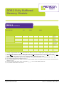
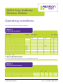
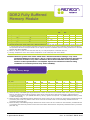
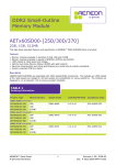
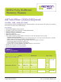
DDR2 Fully Buffered
Memory Module
AETx61FBxx-[30D/25D]xxxX
512MB, 1GB, 2GB and 4GB
This Data Sheet describes AENEON DDR2 Fully Buffered DIMM on 240-pin modules with parity bit for address
and control bus and its main characteristics.
Key features
•
•
•
•
•
•
•
Fully buffered DDR2 memory modules
Available in single pack of densities 512MB/1GB/2GB/4GB
Standard JEDEC pin configuration
Validated by major motherboard vendors
Fully RoHS compliant
MBIST and IBIST test function
Uses Advanced Memory Buffer [AMB] to effectively control and manages memory traffic
– Supports channel initialisation
– Supports the forwarding of southbound and northbound frames, servicing requests directed to a specific
AMB or DIMM, and merging the data in northbound frames
– Detects errors on the channel and reports them to the host memory controller
– Supports FB-DIMM configuration register set
– Acts as DRAM memory buffer for all operations
– Provides logic to support MEMBIST and IBIST design for test functions
• Module size of 133.35 x 30.35 x 8.2 (mm)
• Fully buffered DIMMs comes with heat sink
TABLE 1
Ordering Information
Product Type1)
Module Organization Rank
Module Speed No of Module Size
Density
Organization
Comp (mm)
DDR2-667, PC2-5300-555
AET661FB00-30DB19X
512MB
64M x 72
1Rx8
AET761FB00-30DB19X
1GB
128M x 72
2Rx8
PC2-5300-555
8
18
AET761FB28-30DB29X
1GB
128M x 72
2Rx4
18
AET861FB00-30DB19X
2GB
256M x 72
2Rx4
36
AET861FB28-30DC20X
2GB
256M x 72
2Rx8
18
AET961FB00-30DC10X
4GB
512M x 72
2Rx4
36
AET961FB48-30DC20X
4GB
512M x 72
4Rx8
36
133.35 x
30.35 x 8.2
DDR2-800, PC2-6400-555
AET861FB28-25DC20X
2GB
256M x 72
2Rx8
AET961FB48-25DC20X
4GB
512M x 72
4Rx8
PC2-6400-555
18
36
133.35 x
30.35 x 8.2
1) Full Product Type / Sales Description
AENEON™ Data Sheet
A Qimonda AG Brand
1
Revision 1.10, 2008-05
Doc. # 12272007-OKYD-PLKJ
DDR2 Fully Buffered
Memory Module
TABLE 2
Speed Grade Definition
Speed Grade
PC2
CAS-RCD-RP latencies
Parameter
–6400
–5300
5–5–5
5–5–5
Symbol
Min.
Max.
Min.
Max.
Unit
Note
@ CL = 3
tCK
5
8
5
8
ns
1)2)3)4)
@ CL = 4
tCK
3.75
8
3.75
8
ns
1)2)3)4)
@ CL = 5
tCK
2.5
8
3
8
ns
1)2)3)4)
@ CL = 6
tCK
2.5
8
—
—
ns
1)2)3)4)
@ CL = 7
tCK
2.5
8
—
—
ns
1)2)3)4)5)
Row Active Time
tRAS
45
70k
45
70k
ns
1)2)3)4)5)6)
Row Active Time
tRAS
40
70k
40
70k
ns
1)2)3)4)5)7)
Row Cycle Time
tRC
57.5
—
60
—
ns
1)2)3)4)
Row Cycle Time
tRC
52.5
—
55
–
ns
1)2)3)4)
RAS-CAS-Delay
tRCD
12.5
—
15
—
ns
1)2)3)4)
Row Precharge Time
tRP
12.5
—
15
—
ns
1)2)3)4)
Clock Period
1) Timings are guaranteed with CK/CK differential Slew Rate of 2.0 V/ns. For DQS signals timings are guaranteed with a
differential Slew Rate of 2.0 V/ns in differential strobe mode and a Slew Rate of 1 V/ns in single ended mode.
2) The CK/CK input reference level (for timing reference to CK/CK) is the point at which CK and CK cross. The DQS / DQS,
RDQS / RDQS, input reference level is the crosspoint when in differential strobe mode.
3) Inputs are not recognized as valid until VREF stabilizes. During the period before VREF stabilizes, CKE = 0.2 x VDDQ
4) The output timing reference voltage level is VTT.
5) tRAS.MAX is calculated from the maximum amount of time a DDR2 device can operate without a refresh command which is
equal to 9 x tREFI.
6) Products released after 2007-08-01 can support tRAS.MIN = 40 ns for all DDR2 speed sort.
7) For products released after 2007-08-01.
AENEON™ Data Sheet
A Qimonda AG Brand
2
Revision 1.10, 2008-05
Doc. # 12272007-OKYD-PLKJ
DDR2 Fully Buffered
Memory Module
Operating conditions
This chapter describes the operating conditions.
TABLE 3
DC Operating Conditions
Parameter
Symbol
Limit Values
Min.
Unit Notes
Nom.
Max.
1.455
1.5
1.575
V
1)
1.425
1.5
1.590
V
2)
VDD
1.7
1.8
1.9
V
–
Termination Voltage
VTT
0.48 ×VDD
0.50 ×VDD
0.52 ×VDD
V
–
EEPROM Supply Voltage
VDDSPD
3.0
3.3
3.6
V
–
AMB Supply Voltage DC
VCC
AMB Supply Voltage DC + AC
DRAM Supply Voltage
DC Input Logic High(SPD)
VIH(DC)
2.1
—
VDDSPD
V
3)
DC Input Logic Low(SPD)
VIL(DC)
—
—
0.8
V
3)
DC Input Logic High(RESET)
VIH(DC)
1.0
—
—
V
4)
DC Input Logic Low(RESET)
VIL(DC)
—
—
+0.5
V
3)
Leakage Current (RESET)
IL
–90
—
+90
μΑ
4)
Leakage Current (Link)
IL
–5
—
+5
μΑ
5)
1)
2)
3)
4)
5)
At 0KHz - 30KHz
AT 30KHz - 1 MHz
Applies for SMB and SPD Bus Signals
Applies for AMB CMOS Signal RESET
For all other AMB related DC parameters, contact AENEON technical staff.
TABLE 4
Absolute Maximum Ratings
Parameter
Symbol
Rating
Unit
Notes
Min.
Max.
Voltage on any SMbus interface signal pin relative to VSS VIN, VOUT
–0.5
+4.00
V
1)
Voltage on VDD pin relative to VSS
VDD
–0.5
+2.4
V
2)
Voltage on VCC pin relative to VSS
VCC
–0,3
+1.75
V
–
AENEON™ Data Sheet
A Qimonda AG Brand
3
Revision 1.10, 2008-05
Doc. # 12272007-OKYD-PLKJ
DDR2 Fully Buffered
Memory Module
Parameter
Symbol
Rating
Min.
Max.
Unit
Notes
Voltage on VDDQ pin relative to VSS
VDDQ
–0.5
+2.3
V
2)3)
Voltage on VDDL pin relative to VSS
VDDL
–0.5
+2.3
V
2)3)
Voltage on any pin relative to VSS
VIN, VOUT
–0.3
+1.75
V
2)
Voltage on VTT pin relative to VSS
VTT
–0.5
+2.3
V
–
°C
2)3)
Storage Temperature
TSTG
–55
+100
1) Stresses greater than those listed under “Absolute Maximum Ratings“ may cause permanent damage to the device. This
is a stress rating only and functional operation of the device at these or any other conditions above those indicated in
the operational sections of this specification is not implied. Exposure to absolute maximum rating conditions for extended
periods may affect reliability.
2) When VDD and VDDQ and VDDL are less than 500 mV; VREF may be equal to or less than 300 mV.
3) Storage Temperature is the case surface temperature on the center/top side of the DRAM.
Attention:Stresses greater than those listed under “Absolute Maximum Ratings” may cause
permanent damage to the device. This is a stress rating only and functional operation of
the device at these or any other conditions above those indicated in the operational
sections of this specification is not implied. Exposure to absolute maximum rating
conditions for extended periods may affect reliability.
TABLE 5
FB-DIMM Latency Range
Parameter
DDR2–800D
DDR2–667D
Unit
Note
Min.
Nom.
Max.
Min.
Typ.
Max.
tC2D_DIMM
Tbd
19.35
Tbd
17.5
21
21.5
ns
1)2)
tRESAMPLE_DIMM_SB
Tbd
1.68
Tbd
1.4
1.69
2.4
ns
2)3)
tRESAMPLE_DIMM_NB
Tbd
1.48
Tbd
1.3
1.73
2.3
ns
2)4)
tRESYNC_DIMM_SB
Tbd
2.66
Tbd
2.5
2.8
3.7
ns
2)5)
tRESYNC_DIMM_NB
Tbd
2.54
Tbd
2.4
2.8
3.6
ns
2)6)
1) For DDR-800D and DDR-800E no industry standard values are avalible for Min. and Max parameter.
2) Measured delay at FB-DIMM gold finger between the center of the1st UI of command frame on the primary southbound
lane 81 (connector pins 102 & 103) and the center of the 1st UI of return data on the primary northbound lane 0
(connector pins 22 & 23) – [CL (DRAM CAS latency) value] * [frame clock period – AL (DRAM additional latency) value
* frame clock period].
3) Measured delay at FB-DIMM gold finger between the center of the 1st UI of a frame on the primary southbound lane 8
(connector pins 102 & 103) and the center of the 1st UI of the same frame on the secondary southbound lane 8
(connector pins 222 & 223).
4) Measured delay at FB-DIMM gold finger between the center of the 1st UI of a frame on the secondary northbound lane
0 (connector pins 142 & 143) and the center of the 1st UI of the same frame on the primary northbound lane 0 (connector
pins 22 & 23).
AENEON™ Data Sheet
A Qimonda AG Brand
4
Revision 1.10, 2008-05
Doc. # 12272007-OKYD-PLKJ
DDR2 Fully Buffered
Memory Module
5) Measured delay at FB-DIMM gold finger between the center of the 1st UI of a frame on the secondary northbound lane
0 (connector pins 142 & 143) and the center of the 1st UI of the same frame on the primary northbound lane 0 (connector
pins 22 & 23).
6) Measured delay at FB-DIMM gold finger between the center of the1st UI of command frame on the primary southbound
lane 81 (connector pins 102 & 103) and the center of the 1st UI of return data on the primary northbound lane 0
(connector pins 22 & 23) – [CL (DRAM CAS latency) value] * [frame clock period – AL (DRAM additional latency) value
* frame clock period].
Information
To obtain more information about these products, please contact your AENEON representative.
Please Note
The information herein is given to describe certain components and shall not be
considered as a guarantee of characteristics. Terms of delivery and rights to
technical change reserved. We hereby disclaim any and all warranties, including
but not limited to warranties of non-infringement, regarding circuits,
descriptions, and charts stated herein.
Components may only be used in life support devices or systems with the
express written approval of Qimonda AG, if a failure of such components can
reasonably be expected to cause the failure of that life support device or system,
or to affect the safety or effectiveness of that device or system. Life support
devices or systems are intended to be implanted in the human body, or to
support and/or maintain and sustain and/or protect human life. If they fail, it is
reasonable to assume that the health of the user or other persons may be
endangered.
Warnings
Due to technical requirements components may contain dangerous substances.
For information on the types in question please contact your nearest distribution
partner.
AENEON™ Data Sheet
A Qimonda AG Brand
5
Revision 1.10, 2008-05
Doc. # 12272007-OKYD-PLKJ