1
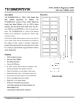
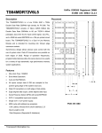
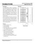
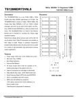
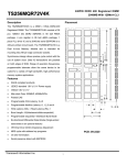
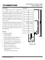
184Pin DDR266 1U Registered DIMM
1GB with 128Mx4 CL2.5
TS128MDR72V6K
Description
Placement
The TS128MDR72V6K is a 128M x 72bits Double Data
Rate
SDRAM
high-density
for
DDR266.
The
TS128MDR72V6K consists of 18pcs CMOS 128Mx4 bits
Double Data Rate SDRAMs in 66 pin TSOP-II 400mil
packages, 2pcs drive ICs for input control signal, 1pcs PLL,
and a 2048 bits serial EEPROM on a 184-pin printed circuit
board. The TS128MDR72V6K is a Dual In-Line Memory
Module and is intended for mounting into 184-pin edge
A
connector sockets.
Synchronous design allows precise cycle control with the
use of system clock. Data I/O transactions are possible on
both edges of DQS. Range of operation frequencies,
B
programmable latencies allow the same device to be useful
for a variety of high bandwidth, high performance memory
system applications.
C
D
Features
•
Max clock Freq: 133MHZ.
•
Burst Mode Operation.
•
Auto and Self Refresh.
•
All inputs except data & DM are sampled at the
I
H
G
positive going edge of the system clock (ck).
•
•
Data I/O transactions on both edge of data strobe.
•
Serial Presence Detect (SPD) with serial EEPROM
•
SSTL-2 compatible inputs and outputs.
•
Single 2.5V ± 0.2V power supply.
•
MRS cycle with address key programs.
F
Edge aligned data output, center aligned data input.
E
PCB: 09-1380
CAS Latency (Access from column address): 2.5
Burst Length (2,4,8)
Data Sequence (Sequential & Interleave)
Transcend Information Inc.
1
184Pin DDR266 1U Registered DIMM
1GB with 128Mx4 CL2.5
TS128MDR72V6K
Dimensions
Pin Identification
Side
Millimeters
Inches
Symbol
Function
A
133.35±0.20
5.250±0.008
SA0~SA12, SBA0, SBA1
Address input
B
72.39
2.850
SDQ0~SDQ63
Data Input / Output.
C
6.35
0.250000
SCB0~SCB7
Check bit
D
2.20
0.0870
SDQS0~SDQS8,
Data strobe input/output
E
30.48±0.20
1.20±0.00800
F
19.80
0.779
G
4.00
0.157
H
12.00
0.472
I
1.27±0.10
0.050±0.004
SDM0~SDM8
CK0, /CK0
Clock Input.
SCKE0, SCKE1
Clock Enable Input.
/SCS0, /SCS1
Chip Select Input.
/SRAS
Row Address Strobe
/SCAS
Column Address Strobe
/SWE
Write Enable
VDD
+2.5 Voltage power supply
VDDQ
+2.5 Voltage Power Supply
for DQS
VREF
Power Supply for
Reference
VDDSPD
+2.5 Voltage Serial
EEPROM Power Supply
EA0~EA2
Address in EEPROM
SCL
Serial PD Clock
SDA
Serial PD Add/Data
input/output
Transcend Information Inc.
2
VDDID
VDD Identification Flag
VSS
Ground
/RESET
Reset enable
NC
No Connection
184Pin DDR266 1U Registered DIMM
1GB with 128Mx4 CL2.5
TS128MDR72V6K
Pinouts:
Pin
No
01
02
03
04
05
06
07
08
09
10
11
12
13
14
15
16
17
18
19
20
21
22
23
24
25
26
27
28
29
30
31
32
33
34
35
36
37
38
39
40
41
42
43
44
45
46
Pin
Name
VREF
SDQ0
VSS
SDQ1
SDQS0
SDQ2
VDD
SDQ3
NC
/RESET
VSS
SDQ8
SDQ9
SDQS1
VDDQ
*CK1
*/CK1
VSS
SDQ10
SDQ11
SCKE0
VDDQ
SDQ16
SDQ17
SDQS2
VSS
SA9
SDQ18
SA7
VDDQ
SDQ19
SA5
SDQ24
VSS
SDQ25
SDQS3
SA4
VDD
SDQ26
SDQ27
SA2
VSS
SA1
SCB0
SCB1
VDD
Transcend Information Inc.
Pin
No
47
48
49
50
51
52
53
54
55
56
57
58
59
60
61
62
63
64
65
66
67
68
69
70
71
72
73
74
75
76
77
78
79
80
81
82
83
84
85
86
87
88
89
90
91
92
Pin
Name
SDQS8
SA0
SCB2
VSS
SCB3
SBA1
SDQ32
VDDQ
SDQ33
SDQS4
SDQ34
VSS
SBA0
SDQ35
SDQ40
VDDQ
/SWE
SDQ41
/SCAS
VSS
SDQS5
SDQ42
SDQ43
VDD
*/SCS2
SDQ48
SDQ49
VSS
*/CK2
*CK2
VDDQ
SDQS6
SDQ50
SDQ51
VSS
VDDID
SDQ56
SDQ57
VDD
SDQS7
SDQ58
SDQ59
VSS
NC
SDA
SCL
Pin
No
93
94
95
96
97
98
99
100
101
102
103
104
105
106
107
108
109
110
111
112
113
114
115
116
117
118
119
120
121
122
123
124
125
126
127
128
129
130
131
132
133
134
135
136
137
138
3
Pin
Name
VSS
SDQ4
SDQ5
VDDQ
SDM0
SDQ6
SDQ7
VSS
NC
NC
NC
VDDQ
SDQ12
SDQ13
SDM1
VDD
SDQ14
SDQ15
SCKE1
VDDQ
NC
SDQ20
SA12
VSS
SDQ21
SA11
SDM2
VDD
SDQ22
SA8
SDQ23
VSS
SA6
SDQ28
SDQ29
VDDQ
SDM3
SA3
SDQ30
VSS
SDQ31
SCB4
SCB5
VDDQ
CK0
/CK0
Pin
No
139
140
141
142
143
144
145
146
147
148
149
150
151
152
153
154
155
156
157
158
159
160
161
162
163
164
165
166
167
168
169
170
171
172
173
174
175
176
177
178
179
180
181
182
183
184
Pin
Name
VSS
SDM8
SA10
SCB6
VDDQ
SCB7
VSS
SDQ36
SDQ37
VDD
SDM4
SDQ38
SDQ39
VSS
SDQ44
/SRAS
SDQ45
VDDQ
/SCS0
/SCS1
SDM5
VSS
SDQ46
SDQ47
NC
VDDQ
SDQ52
SDQ53
NC
VDD
SDM6
SDQ54
SDQ55
VDDQ
NC
SDQ60
SDQ61
VSS
SDM7
SDQ62
SDQ63
VDDQ
EA0
EA1
EA2
VDDSPD