1
H8DA8
H8DAE
H8DAR-8
H8DAR-i
USER’S MANUAL
Revision 1.1
The information in this User’s Manual has been carefully reviewed and is believed to be accurate.
The vendor assumes no responsibility for any inaccuracies that may be contained in this document,
makes no commitment to update or to keep current the information in this manual, or to notify any
person or organization of the updates.
The manufacturer reserves the right to make changes to the product described in this manual at
any time and without notice. This product, including software, if any, and documentation may not,
in whole or in part, be copied, photocopied, reproduced, translated or reduced to any medium or
machine without prior written consent.
IN NO EVENT WILL THE MANUFACTURER BE LIABLE FOR DIRECT, INDIRECT, SPECIAL,
INCIDENTAL, OR CONSEQUENTIAL DAMAGES ARISING FROM THE USE OR INABILITY TO
USE THIS PRODUCT OR DOCUMENTATION, EVEN IF ADVISED OF THE POSSIBILITY OF
SUCH DAMAGES. IN PARTICULAR, THE VENDOR SHALL NOT HAVE LIABILITY FOR ANY
HARDWARE, SOFTWARE, OR DATA STORED OR USED WITH THE PRODUCT, INCLUDING
THE COSTS OF REPAIRING, REPLACING, INTEGRATING, INSTALLING OR RECOVERING
SUCH HARDWARE, SOFTWARE, OR DATA.
Any disputes arising between manufacturer and customer shall be governed by the laws of Santa
Clara County in the State of California, USA. The State of California, County of Santa Clara shall
be the exclusive venue for the resolution of any such disputes. The manufacturer's total liability for
all claims will not exceed the price paid for the hardware product.
Manual Revision 1.1
Release Date: October 5, 2006
Unless you request and receive written permission from the manufacturer, you may not copy any
part of this document.
Information in this document is subject to change without notice. Other products and companies
referred to herein are trademarks or registered trademarks of their respective companies or mark
holders.
Copyright © 2006
All rights reserved.
Printed in the United States of America
Preface
Preface
About This Manual
This manual is written for system integrators, PC technicians and
knowledgeable PC users. It provides information for the installation and use of the
H8DA8/H8DAE/H8DAR-8/H8DAR-i serverboard. The H8DA8/H8DAE/H8DAR-8/
H8DAR-i is based on the AMD-8131/8111 chipset and supports single or dual AMD
Opteron 200 series type processors in 940-pin microPGA ZIF sockets and up to 32
GB of DDR266 or 16 GB of DDR333/400.
Please refer to the serverboard specifications pages on our web site for updates
on supported processors. This product is intended to be professionally installed.
Manual Organization
Chapter 1 includes a checklist of what should be included in your serverboard
box, describes the features, specifications and performance of the serverboard and
provides detailed information about the chipset.
Chapter 2 begins with instructions on handling static-sensitive devices. Read this
chapter when installing the processor(s) and memory modules and when installing
the serverboard in a chassis. Also refer to this chapter to connect the floppy and
hard disk drives, the serial ports, the mouse and keyboard and the twisted wires
for the power and reset buttons and the system LEDs.
If you encounter any problems, see Chapter 3, which describes troubleshooting
procedures for the video, the memory and the setup configuration stored in CMOS.
For quick reference, a general FAQ (Frequently Asked Questions) section is provided. Instructions are also included for contacting technical support. In addition,
you can visit our web site for more detailed information.
Chapter 4 includes an introduction to BIOS and provides detailed information on
running the CMOS Setup utility.
Appendix A provides BIOS Error Beep Code Messages.
Appendix B lists BIOS POST Checkpoint Codes.
iii
H8DA8/H8DAE/H8DAR-8/H8DAR-i User’s Manual
Table of Contents
Preface
About This Manual ...................................................................................................... iii
Manual Organization ................................................................................................... iii
Chapter 1: Introduction
1-1
Overview ......................................................................................................... 1-1
Checklist ..................................................................................................... 1-1
H8DA8/H8DAE Image .............................................................................. 1-3
H8DA8/H8DAE Serverboard Layout ......................................................... 1-4
H8DA8/H8DAE Quick Reference ............................................................... 1-5
H8DAR-8/H8DAR-i Serverboard Layout ................................................... 1-6
H8DAR-8/H8DAR-i Quick Reference ......................................................... 1-7
H8DAR-8/H8DAR-i Image ........................................................................ 1-8
Serverboard Features .............................................................................. 1-9
AMD-8131 Chipset: System Block Diagram ........................................... 1-11
1-2
Chipset Overview ......................................................................................... 1-12
1-3
PC Health Monitoring ................................................................................... 1-13
1-4
Power Configuration Settings ....................................................................... 1-14
1-5
Power Supply ............................................................................................... 1-15
1-6
Super I/O ....................................................................................................... 1-16
Chapter 2: Installation
2-1
Static-Sensitive Devices ................................................................................. 2-1
2-2
Processor and Heatsink Installation ............................................................... 2-2
2-3
Mounting the Serverboard into a Chassis ...................................................... 2-4
2-4
Installing Memory ........................................................................................... 2-4
2-5
I/O Port and Control Panel Connections ........................................................ 2-7
2-6
Connecting Cables ......................................................................................... 2-8
Power Supply Connectors ...................................................................... 2-8
Secondary Power Connector .................................................................... 2-8
NMI Button ................................................................................................ 2-8
Power LED ............................................................................................... 2-8
HDD LED ................................................................................................ 2-9
NIC1 LED .................................................................................................. 2-9
NIC2 LED .................................................................................................. 2-9
iv
Table of Contents
Overheat/Fan Fail LED ........................................................................... 2-9
Power Fail LED ......................................................................................... 2-9
Reset Button............................................................................................ 2-10
Power Button ........................................................................................ 2-10
Universal Serial Bus Ports (USB0/1) ...................................................... 2-10
Chassis Intrusion ..................................................................................... 2-10
Serial Ports .............................................................................................. 2-11
Power Fail and Alarm Reset Header ...................................................... 2-11
Fan Headers .......................................................................................... 2-11
JLAN1/2 (Ethernet Ports) ........................................................................ 2-11
Extra USB Headers ................................................................................. 2-12
Power LED/Speaker ............................................................................. 2-12
ATX PS/2 Keyboard/Mouse Ports ......................................................... 2-12
Wake-On-LAN ......................................................................................... 2-13
Wake-On-Ring ......................................................................................... 2-13
SMB Power (I2C) Header ........................................................................ 2-13
SMB Header ............................................................................................ 2-13
2-7
Jumper Settings ............................................................................................ 2-14
Explanation of Jumpers ......................................................................... 2-14
CMOS Clear ........................................................................................... 2-14
JLAN1/2 Enable/Disable ......................................................................... 2-15
VGA Enable/Disable ................................................................................ 2-15
I2C to PCI Enable/Disable ....................................................................... 2-15
SCSI Controller Enable/Disable .............................................................. 2-15
SCSI Termination Enable/Disable ........................................................... 2-16
3rd Power Supply Fail Signal Enable/Disable ........................................ 2-16
Watch Dog Enable/Disable ..................................................................... 2-16
Onboard Speaker Enable/Disable ........................................................... 2-17
PCI-X Slot Speed .................................................................................... 2-17
2-8
Onboard Indicators ........................................................................................ 2-18
JLAN1/2 LEDs ......................................................................................... 2-18
+3.3V Power LED ................................................................................... 2-18
2-9
Floppy, IDE and SCSI Drive Connections .................................................... 2-19
Floppy Connector .................................................................................... 2-19
IDE Connectors ....................................................................................... 2-20
SCSI Connectors..................................................................................... 2-21
v
H8DA8/H8DAE/H8DAR-8/H8DAR-i User’s Manual
Chapter 3: Troubleshooting
3-1
Troubleshooting Procedures ........................................................................... 3-1
Before Power On....................................................................................... 3-1
No Power................................................................................................... 3-1
No Video .................................................................................................. 3-1
Memory Errors........................................................................................... 3-2
Losing the System’s Setup Configuration ................................................ 3-2
3-2
Technical Support Procedures ....................................................................... 3-2
3-3
Frequently Asked Questions .......................................................................... 3-3
3-4
Returning Merchandise for Service ................................................................. 3-4
Chapter 4: BIOS
4-1
Introduction ...................................................................................................... 4-1
4-2
Main Setup ..................................................................................................... 4-2
4-3
Advanced Settings Menu ............................................................................... 4-2
4-4
PCI/PnP Menu ............................................................................................... 4-10
4-5
Boot Menu ..................................................................................................... 4-11
4-6
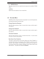
Security Menu ............................................................................................... 4-13
4-7
Chipset Menu ............................................................................................... 4-14
4-8
Power Menu ................................................................................................. 4-18
4-9
Exit Menu ...................................................................................................... 4-19
Appendices:
Appendix A: BIOS Error Beep Codes ...................................................................... A-1
Appendix B: BIOS POST Checkpoint Codes ............................................................ B-1
vi
Chapter 1: Introduction
Chapter 1
Introduction
1-1
Overview
Checklist
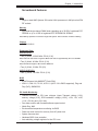
Congratulations on purchasing your computer serverboard from an acknowledged
leader in the industry. Our boards are designed with the utmost attention to detail
to provide you with the highest standards in quality and performance.
Please check that the following items have all been included with your serverboard.
If anything listed here is damaged or missing, contact your retailer.
Included with retail box only
One (1) H8DA8/H8DAE/H8DAR-8/H8DAR-i serverboard
One (1) IDE cable (CBL-036)
One (1) floppy cable (CBL-022)
Two (2) CPU backplates (BKT-0004)
Two (2) heatsink retention modules with four (4) screws (BKT-0005)
One (1) I/O backpanel shield for chassis (CSE-PT7)
One (1) CD containing drivers and utilities
1-1
H8DA8/H8DAE/H8DAR-8/H8DAR-i User’s Manual
Notes
1-2
Chapter 1: Introduction
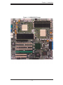
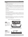
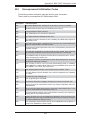
Figure 1-1. H8DA8/H8DAE Image
1-3
H8DA8/H8DAE/H8DAR-8/H8DAR-i User’s Manual
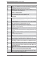
J24
ATX Power
J101
FAN5 FAN6 FAN8 (CPU2 Fan)
J3P
JAR
Figure 1-2. H8DA8/H8DAE Serverboard Layout
(not drawn to scale)
JPW2
J1B4
CPU1 DIMM 1B
USB0/1
CPU1 DIMM 1A
JP10
CPU1 DIMM 2B
CPU1 DIMM 2A
COM1
CPU2
FAN1
VGA
JF1
CPU1
JLAN1
FAN2
CPU2 DIMM 2A
CPU2 DIMM 2B
JLAN2
CPU2 DIMM 1A
CPU2 DIMM 1B
FAN7 (CPU1 Fan)
FAN3
1U IPMI
AMD-8131
PCI-X 133/100 MHz #5
JIDE#1
JFDD1
JPG1
JIDE#2
PCI-X 133/100 MHz #6
Rage XL
Graphics
JPXB0
Broadcom
BCM5704
PCI-X 66 MHz #4
JPA3
JPL
AMD-8111
7902W
JPA1
JI2C1/2
JBT1
SCSI Controller
JPA2
PCI 33 MHz #1
BIOS
COM2
USB4
JWD
J22
JB2
JWOL
USB2/3
Notes:
Jumpers not indicated are for test purposes only.
SCSI components, connectors and jumpers are for the H8DA8 only.
1-4
JA1
Adaptec
Battery
JPXA0
PCI 33 MHz #2
SPKR
DP1
Winbond
Super I/O
JK1/JWOR/JOH/JL1
PCI-X 66 MHz #3 ZCR
FAN4
JD1
Chapter 1: Introduction
H8DA8/H8DAE Quick Reference
Jumpers
Description
J3P
3rd Power Fail Signal En/Dis Open (Disabled)
JBT1
JI2C1/2
CMOS Clear
I2C to PCI Enable/Disable
See Section 2-7
Closed (Enabled)
JPA1*
SCSI Controller En/Disable
Pins 1-2 (Enabled)
JPA2/3*
JPG1
SCSI CH A/B Term. En/Dis
VGA Enable/Disable
Open (Enabled)
Pins 1-2 (Enabled)
JPL
JLAN1/JLAN2 En/Disable
Pins 1-2 (Enabled)
JPXA0
PCI-X Slot #3/4 Speed
Open (Auto)
JPXB0
JWD
PCI-X Slot #5/6 Speed
Watch Dog
Open (Auto)
Pins 1-2 (Reset)
Connectors
Description
1U IPMI
COM1, COM2
DP1
Fans 1-8
J22
J24
IPMI 2.0 Socket
COM1/COM2 Serial Port/Header
Onboard +3.3V Power LED
System Fan Headers
System Management Bus Header
I2C Header
J101
J1B4
JA1*
JAR
JB2*
JD1
JF1
JFDD1
JIDE#1/JIDE#2
JK1
JL1
JLAN1/2
JOH1
JP10
JPW2
JWOL
JWOR
SPKR
USB0/1
USB2/3/4
VGA
*H8DA8 only
PS/2 Keyboard/Mouse Ports
24-Pin ATX Power Connector
Ultra320 SCSI Channel A Connector
Power Supply Alarm Reset Header
Ultra320 SCSI Channel B Connector
Internal Speaker (Buzzer) Enable/Power LED Header
Front Panel Connector
Floppy Disk Drive Connector
IDE#1/IDE#2 Connectors
Keylock Header
Chassis Intrusion Header
Gigabit Ethernet (RJ45) Ports
Overheat Warning Header
Power Fail and Alarm Reset Header
8-Pin Power Connector
Wake-On-LAN Header
Wake-On-Ring Header
Onboard Speaker (Buzzer)
Universal Serial Ports1/2
USB Headers
Video Port
1-5
Default Setting
H8DA8/H8DAE/H8DAR-8/H8DAR-i User’s Manual
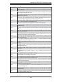
J101
J24
ATX Power
FAN5
J3P
JAR
Figure 1-3. H8DAR-8/H8DAR-i Serverboard Layout
(not drawn to scale)
JPW2
J1B4
CPU1 DIMM 1B
USB0/1
CPU1 DIMM 1A
JP10
CPU1 DIMM 2B
CPU1 DIMM 2A
COM1
CPU2
FAN1
VGA
JF1
CPU1
JLAN1
FAN2
CPU2 DIMM 2A
CPU2 DIMM 2B
JLAN2
CPU2 DIMM 1A
CPU2 DIMM 1B
FAN4
1U IPMI
Broadcom
BCM5704
Rage XL
Graphics
DP1
Battery
SCSI Controller
JR1
JPA2
Winbond
Super I/O
JBT1
JPL
JPG1
JI2C1/2
COM2
USB4
JWD
J22 JWOL
JPXB0
JPA1
USB2/3
Notes:
Jumpers not indicated are for test purposes only.
SCSI components, connectors and jumpers are for the H8DAR-8 only.
1-6
JA1
AMD-8111
7902W
SPKR
Adaptec
JK1/JWOR/JOH/JL1
JPA3
JB2
BIOS
JIDE#1
JFDD1
AMD-8131
JIDE#2
PCI-X 100 MHz #6
FAN3
JD1
Chapter 1: Introduction
H8DAR-8/H8DAR-i Quick Reference
Jumpers
Description
J3P
3rd Power Fail Signal En/Dis Open (Disabled)
JBT1
JI2C1/2
CMOS Clear
I2C to PCI Enable/Disable
See Section 2-7
Closed (Enabled)
JPA1*
SCSI Controller En/Disable
Pins 1-2 (Enabled)
JPA2/3*
JPG1
SCSI CH A/B Term. En/Dis
VGA Enable/Disable
Open (Enabled)
Pins 1-2 (Enabled)
JPL
JLAN1/JLAN2 En/Disable
Pins 1-2 (Enabled)
JPXB0
PCI-X Slot #6 Speed
Open (Auto)
JWD
Watch Dog
Pins 1-2 (Reset)
Connectors
Description
1U IPMI
COM1/COM2
DP1
Fans 1-5
J22
J24
IPMI 2.0 Socket
COM1/COM2 Serial Port/Header
Onboard +3.3V Power LED
System Fan Headers
System Management Bus Header
I2C Header
J101
J1B4
JA1*
JAR
JB2*
JD1
JF1
JFDD1
JIDE#1/JIDE#2
JK1
JL1
JLAN1/2
JOH1
JP10
JPW2
JR1
JWOL
JWOR
SPKR
USB0/1/2/3/4
VGA
*H8DAR-8 only
PS/2 Keyboard/Mouse Ports
24-Pin ATX Power Connector
Ultra320 SCSI Channel A Connector
Power Supply Alarm Reset Header
Ultra320 SCSI Channel B Connector
Internal Speaker (Buzzer) Enable/Power LED Header
Front Panel Connector
Floppy Disk Drive Connector
IDE#1/IDE#2 Connectors
Keylock Header
Chassis Intrusion Header
Gigabit Ethernet (RJ45) Ports
Overheat Warning Header
Power Fail and Alarm Reset Header
8-Pin Power Connector
64-bit, 100 MHz PCI-X Slot
Wake-On-LAN Header
Wake-On-Ring Header
Onboard Speaker (Buzzer)
Universal Serial Bus (Ports: 0/1, Headers: 2/3/4)
Video Port
1-7
Default Setting
H8DA8/H8DAE/H8DAR-8/H8DAR-i User’s Manual
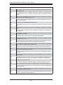
Figure 1-4. H8DAR-8/H8DAR-i Image
1-8
Chapter 1: Introduction
Serverboard Features
CPU
•
Single or dual AMD Opteron 200 series 64-bit processors in 940-pin microPGA
ZIF sockets
Memory
•
Eight dual/single channel DIMM slots supporting up to 32 GB of registered ECC
DDR266 or up to 16 GB of registered ECC DDR400/333 SDRAM
Note: Memory capacities are halved for single CPU systems. Refer to Section 2-4 before installing.
Chipset
•
AMD-8131/8111
Expansion Slots
H8DA8/H8DAE:
• Two (2) 64-bit, 133/100 MHz PCI-X (3.3V)
Note: These two slots share a single bus. When both slots are populated they will run at 100 MHz.
• Two (2) 64-bit, 66 MHz PCI-X (3.3V)
Note: PCI-X-#3 will support a Zero Channel RAID card
• Two (2) 32-bit, 33 MHz PCI (5V)
H8DAR-8/H8DAR-i:
• One (1) 64-bit, 100 MHz PCI-X (3.3V)
BIOS
• 4 Mb Firmware Hub AMIBIOS® Flash ROM
•
APM 1.2, DMI 2.3, PCI 2.2, ACPI 1.0 (ACPI 2.0 is BIOS supported), Plug and
Play (PnP), SMBIOS2.3
PC Health Monitoring
•
Onboard monitors for CPU core voltages, Hyper Transport voltage (1.2V),
memory voltage (2.5V), DDR temination voltage (1.25V), +3.3V, +5V, ±12V,
+1.8V, +5V stby and +3.3V stby
• Fan status monitor with firmware/software speed control
• Watch Dog, NMI
•
Environmental temperature monitoring via BIOS
•
Power-up mode control for recovery from AC power loss
•
System resource alert
•
Hardware BIOS virus protection
•
Auto-switching voltage regulator for the CPU core
1-9
H8DA8/H8DAE/H8DAR-8/H8DAR-i User’s Manual
ACPI Features
• Microsoft OnNow
•
Slow blinking LED for suspend state indicator
• BIOS support for USB keyboard
•
Main switch override mechanism
•
Internal/external modem ring-on
Onboard I/O
• Adaptec 7902W dual channel Ultra320 SCSI controller (H8DA8 and H8DAR-8
only)
• Adaptec SCSI RAID 2010S supported (Host RAID 0, 1, 10, JBOD: H8DA8 only)
• Adaptec SCSI RAID 2015S supported (Host RAID 0, 1, 10, JBOD: H8DAR-8
only)
•
Two (2) ATA133 IDE headers
• One (1) floppy port interface (up to 2.88 MB)
•
Two (2) Fast UART 16550 compatible serial connectors (1 header, 1 port)
•
Broadcom BCM5704 Ethernet controller supports two Gigabit LAN ports
•
PS/2 mouse and PS/2 keyboard ports
•
Up to five (5) USB (Universal Serial Bus) 1.1 ports/headers
•
ATI Rage 8 MB XL graphics chip
• VGA port
Other
•
Wake-on-Ring (JWOR)
• Wake-on-LAN (JWOL)
•
Onboard +3.3V power LED ("DP1")
CD Utilities
•
BIOS flash upgrade utility
Dimensions
• Extended ATX form factor, 12" x 13.05" (305 x 332 mm)
1-10
Chapter 1: Introduction
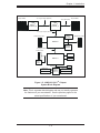
184-pin DIMMs
16 x 16 Hyper Transport (2000 MT/s)
AMD
OpteronTM
Processor (2)
144-bit, 200-400 MT/s
184 -pin DIMMs
AMD
OpteronTM
Processor (1)
144-bit, 200 -400 MT/s
16 x 16 Hyper Transport (1200 MT/s)
Adaptec
AIC-7902W
133/100 MHz PCI-X Slots
100/66 MHz PCI-X Slots
AMD-8131
Broadcom
BC5704C
8 x 8 ncHyper Transport (400 MT/s)
33 MHz PCI Slots
ATA133
AMD-8111
USB 1.1
ATI
Rage XL
8 MB
BIOS
LPC Link
Parallel Port
Serial Ports
Winbond
W83627 HF
Super I /O
Floppy Disk Drive
PS /2 Kybd/Mouse
Figure 1-5. AMD-8131/8111TM Chipset:
System Block Diagram
Note: This is a general block diagram and may not exactly represent
the features on your serverboard. See the previous pages for the
actual specifications of your serverboard.
1-11
H8DA8/H8DAE/H8DAR-8/H8DAR-i User’s Manual
1-2
Chipset Overview
The H8DA8/H8DAE/H8DAR-8/H8DAR-i serverboard is based on the AMD-8131TM
chipset.
This chipset is composed of two main components: the AMD-8131
HyperTransportTM PCI-X Tunnel and the AMD-8111TM HyperTransportTM I/O Hub.
The AMD-8131 chipset provides high performance and an excellent feature-set
for multi-processor server solutions. Controllers for the system memory are built
directly into the processors.
8131 HyperTransport PCI-X Tunnel
This hub includes AMD-specific technology that provides two PCI-X bridges with
each bridge supporting a 64-bit data bus as well as separate PCI-X operational
modes and independent transfer rates. Each bridge supports up to five PCI masters
that include clock, request and grant signals. This hub connects to the processors
and through them to system memory. It also interfaces directly with the SCSI and
Ethernet controllers.
8111 HyperTransport I/O Hub
The 8111 I/O hub provides the interface between the 8131 hub and various subsystems including the Winbond Super I/O functions, the onboard graphics, the IDE
controller and the USB ports.
HyperTransport Technology
HyperTransport technology is a high-speed, low latency point to point link that was
designed to increase the communication speed by a factor of up to 48x between
integrated circuits. This is done partly by reducing the number of buses in the
chipset to reduce bottlenecks and by enabling a more efficient use of memory in
multi-processor systems. The end result is a significant increase in bandwidth
within the chipset.
1-12
Chapter 1: Introduction
1-3
PC Health Monitoring
This section describes the PC health monitoring features of the H8DA8/H8DAE/
H8DAR-8/H8DAR-i. The serverboard has an onboard System Hardware Monitor
chip that supports PC health monitoring.
Onboard Voltage Monitors for the CPU Core voltages, Hyper
Transport voltage (1.2V), memory voltage (2.5V), DDR temination
voltage (1.25V), +3.3V, +5V, ±12V, +1.8V, +5V stby and +3.3V stby
The onboard voltage monitor will scan these voltages continuously. Once a voltage
becomes unstable, it will give a warning or send an error message to the screen.
Users can adjust the voltage thresholds to define the sensitivity of the voltage monitor. Real time readings of these voltage levels are all displayed in BIOS.
Fan Status Monitor with Firmware/Software Speed Control
The PC health monitor can check the RPM status of the cooling fans. The onboard
fans are controlled by thermal management via BIOS.
CPU Overheat/Fan Fail LED and Control
This feature is available when the user enables the CPU overheat/Fan Fail warning
function in the BIOS. This allows the user to define an overheat temperature. When
this temperature is exceeded or when a fan failure occurs, then, the Overheat/Fan
Fail warning LED is triggered.
Auto-Switching Voltage Regulator for the CPU Core
The 3-phase-switching voltage regulator for the CPU core can support up to 80A and
auto-sense voltage IDs ranging from 0.875 V to 1.6V. This will allow the regulator
to run cooler and thus make the system more stable.
1-13
H8DA8/H8DAE/H8DAR-8/H8DAR-i User’s Manual
1-4
Power Configuration Settings
This section describes the features of your serverboard that deal with power and
power settings.
Microsoft OnNow
The OnNow design initiative is a comprehensive, system-wide approach to system
and device power control. OnNow is a term for a PC that is always on but appears
to be off and responds immediately to user or other requests.
Slow Blinking LED for Suspend-State Indicator
When the CPU goes into a suspend state, the chassis power LED will start blinking
to indicate that the CPU is in suspend mode. When the user presses any key, the
CPU will wake-up and the LED will automatically stop blinking and remain on.
BIOS Support for USB Keyboard
If a USB keyboard is the only keyboard in the system, it will function like a normal
keyboard during system boot-up.
Main Switch Override Mechanism
When an ATX power supply is used, the power button can function as a system
suspend button. When the user depresses the power button, the system will enter
a SoftOff state. The monitor will be suspended and the hard drive will spin down.
Depressing the power button again will cause the whole system to wake-up. During the SoftOff state, the ATX power supply provides power to keep the required
circuitry in the system alive. In case the system malfunctions and you want to turn
off the power, just depress and hold the power button for 4 seconds. The power
will turn off and no power will be provided to the serverboard.
Wake-On-LAN (JWOL)
Wake-On-LAN is defined as the ability of a management application to remotely
power up a computer that is powered off. Remote PC setup, up-dates and access
tracking can occur after hours and on weekends so that daily LAN traffic is kept
to a minimum and users are not interrupted. The serverboard has a 3-pin header
(JWOL) to connect to the 3-pin header on a Network Interface Card (NIC) that has
1-14
Chapter 1: Introduction
WOL capability. Wake-On-LAN must be enabled in BIOS. Note that Wake-On-LAN
can only be used with an ATX 2.01 (or above) compliant power supply.
Wake-On-Ring Header (JWOR)
Wake-up events can be triggered by a device such as the external modem ringing
when the system is in the SoftOff state. Note that external modem ring-on can only
be used with an ATX 2.01 (or above) compliant power supply.
1-5
Power Supply
As with all computer products, a stable power source is necessary for proper and
reliable operation. It is even more important for processors that have high CPU
clock rates of 1 GHz and faster.
The H8DA8/H8DAE/H8DAR-8/H8DAR-i accommodates 12V ATX power supplies.
Although most power supplies generally meet the specifications required by the
CPU, some are inadequate. A 2 amp current supply on a 5V Standby rail is strongly
recommended.
It is strongly recommended that you use a high quality power supply that meets
12V ATX power supply Specification 1.1 or above. Additionally, in areas where
noisy power transmission is present, you may choose to install a line filter to shield
the computer from noise. It is recommended that you also install a power surge
protector to help avoid problems caused by power surges.
Warning: To prevent the possibility of explosion, do not use the wrong type of
onboard CMOS battery or install it upside down.
1-15
H8DA8/H8DAE/H8DAR-8/H8DAR-i User’s Manual
1-6
Super I/O
The disk drive adapter functions of the Super I/O chip include a floppy disk drive
controller that is compatible with industry standard 82077/765, a data separator,
write pre-compensation circuitry, decode logic, data rate selection, a clock generator, drive interface control logic and interrupt and DMA logic. The wide range of
functions integrated onto the Super I/O greatly reduces the number of components
required for interfacing with floppy disk drives. The Super I/O supports two 360
K, 720 K, 1.2 M, 1.44 M or 2.88 M disk drives and data transfer rates of 250 Kb/s,
500 Kb/s or 1 Mb/s.
It also provides two high-speed, 16550 compatible serial communication ports
(UARTs), one of which supports serial infrared communication. Each UART includes a 16-byte send/receive FIFO, a programmable baud rate generator, complete
modem control capability and a processor interrupt system. Both UARTs provide
legacy speed with baud rate of up to 115.2 Kbps as well as an advanced speed
with baud rates of 250 K, 500 K, or 1 Mb/s, which support higher speed modems.
The Super I/O provides functions that comply with ACPI (Advanced Configuration
and Power Interface), which includes support of legacy and ACPI power management through a SMI or SCI function pin. It also features auto power management
to reduce power consumption.
The IRQs, DMAs and I/O space resources of the Super I/O can be flexibly adjusted
to meet ISA PnP requirements, which support ACPI and APM (Advanced Power
Management).
1-16
Chapter 2: Installation
Chapter 2
Installation
2-1
Static-Sensitive Devices
Electric Static Discharge (ESD) can damage electronic components. To prevent
damage to your system board, it is important to handle it very carefully. The following
measures are generally sufficient to protect your equipment from ESD.
Precautions
•
Use a grounded wrist strap designed to prevent static discharge.
•
Touch a grounded metal object before removing the board from the antistatic
bag.
•
Handle the board by its edges only; do not touch its components, peripheral
chips, memory modules or gold contacts.
•
When handling chips or modules, avoid touching their pins.
•
Put the serverboard and peripherals back into their antistatic bags when not in
use.
•
For grounding purposes, make sure your computer chassis provides excellent
conductivity between the power supply, the case, the mounting fasteners and
the serverboard.
•
Use only the correct type of CMOS onboard battery as specified by the manufacturer. Do not install the CMOS onboard battery upside down, which may result
in a possible explosion.
Unpacking
The serverboard is shipped in antistatic packaging to avoid static damage. When
unpacking the board, make sure the person handling it is static protected.
Installation Procedures
Follow the procedures as listed below to install the serverboard into a chassis:
1.
2.
3.
4.
Install the processor(s) and the heatsink(s).
Install the serverboard in the chassis.
Install the memory and add-on cards.
Finally, connect the cables and install the drivers.
2-1
H8DA8/H8DAE/H8DAR-8/H8DAR-i User's Manual
2-2
Processor and Heatsink Installation
Exercise extreme caution when handling and installing the proces-
!
sor. Always connect the power cord last and always remove it before adding, removing or changing any hardware components.
Installing the CPU Backplates
Two CPU backplates (BKT-0004) are included in the retail box. The backplates
prevent the CPU area of the serverboard from bending and provide a base for attaching the heatsink retention modules. To install, begin by peeling off the release
paper to expose the adhesive. On the underside of the serverboard, locate the two
holes on either side of the CPU socket. Attach the adhesive side of the backplate
to the board by inserting the standoffs into the two holes and applying light pressure
so that the backplate sticks to the underside of the board. Repeat for the second
CPU socket. See Figure 2-1.
Installing the Processor (install to the CPU#1 socket first)
1. Lift the lever on CPU socket #1 until
it points straight up.
2. Use your thumb and your index finger to hold the CPU. Locate pin 1 on
the CPU socket and pin 1 on the CPU.
Both are marked with a triangle.
3. Align pin 1 of the CPU with pin 1
of the socket. Once aligned, carefully
place the CPU into the socket. Do not
drop the CPU on the socket, move the
CPU horizontally or vertically or rub the
CPU against the socket or against any
pins of the socket, which may damage
the CPU and/or the socket.
2-2
Triangles
Chapter 2: Installation
4. With the CPU inserted into the
socket, inspect the four corners of the
CPU to make sure that it is properly
installed and flush with the socket.
5. Gently press the CPU socket lever
down until it locks in the plastic tab.
For a dual-processor system, repeat
these steps to install another CPU into
the CPU#2 socket.
Note: if using a single processor, only
CPU 1 DIMM slots are addressable.
Installing the Heatsink Retention Modules
Two heatsink retention modules (BKT-0005) and four screws are included in the
retail box. Once installed, these are used to help attach the heatsinks to the CPUs.
To install, position the module so that the CPU backplate standoffs insert through the
holes on the heatsink retention module and the four feet on the module contact the
serverboard. Secure the retention module to the backplate with two of the screws
provided. See Figure 2-1. Repeat for the second CPU socket. Note: BKT-0005
is included for use with non-proprietary heatsinks only. When installing proprietary
heatsinks, only BKT-0004 (CPU backplate) is needed. The BKT-0005 retention
module was designed to provide compatibility with clip-and-cam type heatsinks
from third parties.
Figure 2-1. CPU Backplate/Heatsink Retention Module Installation
Installing the Heatsink
We recommend the use of active type heatsinks (except for 1U systems). Use the
Fan7 header for the CPU1 fan and the Fan8 header for the CPU2 fan due to fan
monitoring and wiring considerations. To install the heatsinks, please follow the
installation instructions included with your heatsink package (not included).
2-3
H8DA8/H8DAE/H8DAR-8/H8DAR-i User's Manual
2-3
Mounting the Serverboard into a Chassis
All serverboards and motherboards have standard mounting holes to fit different
types of chassis. Make sure that the locations of all the mounting holes for both
the serverboard and the chassis match. Although a chassis may have both plastic
and metal mounting fasteners, metal ones are highly recommended because they
ground the serverboard to the chassis. Make sure that the metal standoffs click in
or are screwed in tightly.
1. Check the compatibility of the serverboard ports and the I/O shield
The H8DA8/H8DAE/H8DAR-8/H8DAR-i serverboard requires a chassis that can
support extended ATX boards of 12" x 13.05" in size. Make sure that the I/O ports
on the serverboard align with their respective holes in the I/O shield at the rear of
the chassis.
2. Mounting the serverboard onto the mainboard tray in the chassis
Carefully mount the serverboard onto the mainboard tray by aligning the serverboard
mounting holes with the raised metal standoffs in the tray. Insert screws into all
the mounting holes in the serverboard that line up with the standoffs. Then use a
screwdriver to secure the serverboard to the mainboard tray - tighten until just snug
(if too tight you might strip the threads). Metal screws provide an electrical contact
to the serverboard ground to provide a continuous ground for the system.
2-4
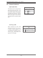
Installing Memory
CAUTION
Exercise extreme care when installing or removing memory modules
to prevent any possible damage.
1. Insert each memory module vertically into its slot, paying attention to the notch
along the bottom of the module to prevent inserting the module incorrectly (see
Figure 2-2). See support information below.
2. Gently press down on the memory module until it snaps into place.
Note: each processor has its own built-in memory controller, so CPU2 DIMMs cannot be addressed if only a single CPU is installed. 128 MB, 256 MB, 512 MB, 1
GB, 2 GB* and 4 GB* memory modules are supported.
2-4
Chapter 2: Installation
Support
The H8DA8/H8DAE/H8DAR-8/H8DAR-i supports single or dual-channel, registered
ECC DDR400/333/266 SDRAM.
Both interleaved and non-interleaved memory are supported, so you may populate
any number of DIMM slots (see note on previous page and charts on following
page). The CPU2 DIMM slots can only be accessed when two CPUs are installed
(however, the CPU2 DIMM slots are not required to be populated when two CPUs
are installed).
Populating two adjacent slots at a time with memory modules of the same size and
type will result in interleaved (128-bit) memory, which is faster than non-interleaved
(64-bit) memory.
Optimizing memory performance
If two processors are installed, it is better to stagger pairs of DIMMs across both
sets of CPU DIMM slots, e.g. first populate CPU1 slots 1A and 1B, then CPU2 slots
1A, and 1B, then the next two CPU1 slots, etc. This balances the load over both
CPUs to optimize performance.
Maximum memory (two CPUs): 32 GB for DDR266 and 16 GB for DDR400/333.
If only one CPU is installed, maximum supported memory is halved (16 GB for
DDR266 and 8 GB for DDR400/333).
Figure 2-2. Side and Top Views of DDR Installation
To Install:
Insert module vertically
and press down until it
snaps into place. The
release tabs should
close - if they do not
you should close them
yourself.
Note the notch in the slot and on the bottom of the DIMM.
These prevent the DIMM from being installed incorrectly.
To Remove:
Use your thumbs to
gently push each release tab outward to
release the DIMM from
the slot.
2-5
H8DA8/H8DAE/H8DAR-8/H8DAR-i User's Manual
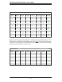
Populating Memory Banks for 128-bit Operation
CPU1
DIMM1A
CPU1
DIMM1B
CPU1
DIMM2A
CPU1
DIMM2B
X
X
X
X
X
X
X
X
X
X
X
X
X
X
X
X
X
X
X
X
X
X
X
X
X
X
X
X
X
X
X
X
CPU2
DIMM1A
CPU2
DIMM1B
X
X
X
X
X
X
X
X
X
X
X
X
CPU2
DIMM2A
CPU2
DIMM2B
X
X
X
X
X
X
X
X
X
X
X
X
Notes: X indicates a populated DIMM slot. If adding at least four DIMMs (with two CPUs
installed), the configurations with DIMMs spread over both CPUs (and not like the configuration in row 5) will result in optimized performance. Note that the first two DIMMs
must be installed in the CPU1 memory slots.
Populating Memory Banks for 64-bit Operation
CPU1
DIMM1A
CPU1
DIMM1B
CPU1
DIMM2A
CPU1
DIMM2B
CPU2
DIMM1A
CPU2
DIMM1B
CPU2
DIMM2A
X
X
X
X
X
X
X
X
X
X
X
X
2-6
CPU2
DIMM2B
Chapter 2: Installation
2-5
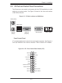
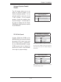
I/O Port and Control Panel Connections
The I/O ports are color coded in conformance with the PC99 specification to make
setting up your system easier. See Figure 2-3 below for the colors and locations
of the various I/O ports.
Figure 2-3. I/O Port Locations and Definitions
Mouse (Green)
USB 0/1 Ports
Keyboard
COM1 Port
(Purple)
(Turquoise)
VGA Port (Blue)
JLAN1 / JLAN2
Front Control Panel
JF1 contains header pins for various front control panel connectors. See Figure 2-4
for the pin definitions of the various connectors. Refer to Section 2-6 for details.
Figure 2-4. JF1: Front Control Panel Header (JF1)
20
19
Ground
NMI
x (key)
x (key)
Power LED
Vcc
HDD LED
Vcc
NIC1
Vcc
NIC2
Vcc
OH/Fan Fail LED
Vcc
Power Fail LED
Vcc
Ground
Reset Button
Ground
Power Button
2
2-7
1
H8DA8/H8DAE/H8DAR-8/H8DAR-i User's Manual
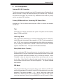
2-6
Connecting Cables
ATX Power 24-pin Connector
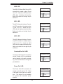
Pin Definitions (J1B4)
Power Supply Connectors
Pin#
Definition
13
+3.3V
1
+3.3V
14
-12V
2
+3.3V
15
COM
3
COM
16
PS_ON
4
+5V
Refer to the table on the right for the
17
COM
5
COM
pin definitions of the ATX 24-pin power
18
COM
6
+5V
connector.
19
COM
7
COM
20
Res (NC)
8
PWR_OK
21
+5V
9
5VSB
22
+5V
10
+12V
23
+5V
11
+12V
24
COM
12
+3.3V
The primary power supply connector (J1B4) on the H8DA8/H8DAE/
H8DAR-8/H8DAR-i meets the SSI
(Superset ATX) 24-pin specification.
Note: You must also connect the 8pin (JPW2) power connector to your
power supply (see below).
Pin #
Definition
Secondary Power
Connector
In addition to the Primary ATX power
connector (above), the Secondary
12v 8-pin power connector at JPW2
must also be connected to your power
supply. See the table on the right for
pin definitions.
Secondary Power
Connector
Pin Definitions (JPW2)
Pins
Definition
1 through 4
Ground
5 through 8
+12V
Required Connection
NMI Button
NMI Button
Pin Definitions (JF1)
The non-maskable interrupt button
header is located on pins 19 and 20
of JF1. Refer to the table on the right
for pin definitions.
Power LED
Pin#
Definition
19
Control
20
Ground
Power LED
Pin Definitions (JF1)
The Power LED connection is located
on pins 15 and 16 of JF1. Refer to the
table on the right for pin definitions.
2-8
Pin#
Definition
15
Vcc
16
Control
Chapter 2: Installation
HDD LED
The HDD (IDE Hard Disk Drive) LED
connection is located on pins 13 and
14 of JF1. Attach the IDE hard drive
LED cable to display disk activity.
HDD LED
Pin Definitions (JF1)
Pin#
Definition
13
Vcc
14
HD Active
Refer to the table on the right for pin
definitions.
NIC1 LED
The NIC1 (Network Interface Controller) LED connection is located on pins
11 and 12 of JF1. Attach the NIC1
LED cable to display network activity.
Refer to the table on the right for pin
definitions.
NIC1 LED
Pin Definitions (JF1)
Pin#
Definition
11
Vcc
12
NIC1 Active
NIC2 LED
The NIC2 (Network Interface Controller) LED connection is located on pins
9 and 10 of JF1. Attach the NIC2
LED cable to display network activity.
Refer to the table on the right for pin
definitions.
NIC2 LED
Pin Definitions (JF1)
Pin#
Definition
9
Vcc
10
NIC2 Active
Overheat/Fan Fail LED
Connect an LED to the OH connection
on pins 7 and 8 of JF1 to provide advanced warning of chassis overheating. Refer to the table on the right for
pin definitions.
OH/Fan Fail LED
Pin Definitions (JF1)
Pin#
Definition
7
Vcc
8
Control
Power Fail LED
The Power Fail LED connection is
located on pins 5 and 6 of JF1. Refer
to the table on the right for pin definitions. This feature is only available
for systems with redundant power
supplies.
2-9
Power Fail LED
Pin Definitions (JF1)
Pin#
Definition
5
Vcc
6
Control
H8DA8/H8DAE/H8DAR-8/H8DAR-i User's Manual
Reset Button
Reset Button
Pin Definitions (JF1)
The Reset Button connection is located on pins 3 and 4 of JF1. Attach
Pin#
Definition
it to the hardware reset switch on the
computer case. Refer to the table on
3
Reset
4
Ground
the right for pin definitions.
Power Button
The Power Button connection is
located on pins 1 and 2 of JF1. Momentarily contacting both pins will
power on/off the system. This button
can also be configured to function
as a suspend button (see the Power
Button Mode setting in BIOS). To turn
off the power when set to suspend
mode, depress the button for at least
4 seconds. Refer to the table on the
right for pin definitions.
Power Button
Pin Definitions (JF1)
Pin#
Definition
1
PW_ON
2
Ground
Universal Serial Bus Ports
Pin Definitions (USB0/1)
Universal Serial Bus Ports
(USB0/1)
USB0
Pin # Definition
Two Universal Serial Bus ports
(USB1.1) are located beside the keyboard/mouse ports. See the table on
the right for pin definitions.
USB1
Pin # Definition
1
+5V
1
+5V
2
PO-
2
PO-
3
PO+
3
PO+
4
Ground
4
Ground
Chassis Intrusion
Chassis Intrusion
Pin Definitions (JL1)
A Chassis Intrusion header is located
at JL1. Attach the appropriate cable
to inform you of a chassis intrusion.
2-10
Pin#
Definition
1
Intrusion Input
2
Ground
Chapter 2: Installation
Serial Ports
Serial Port Pin Definitions
(COM1/COM2)
The COM1 serial port is located be-
Pin #
Definition
Pin #
Definition
1
DCD
6
DSR
on the serverboard located near the
BIOS chip (see serverboard layout for
2
RXD
7
RTS
3
TXD
8
CTS
location). See the table on the right
4
DTR
9
RI
for pin definitions.
5
Ground
10
NC
side the VGA port. COM2 is a header
Note: Pin 10 is included on the header but not on
the port. NC indicates no connection.
Power Fail and Alarm Reset
Header
Connect a cable from your power supply to the JP10 header to provide you
with warning of a power supply failure.
The warning signal is passed through
the PWR_LED pin to indicate a power
failure. See the table on the right for
pin definitions.
Power Fail/Alarm Reset
Header
Pin Definitions (JP10)
Pin#
Definition
1
P/S 1 Fail Signal
2
P/S 2 Fail Signal
3
P/S 3 Fail Signal
4
Reset (from MB)
Note: This feature is only available when using
redundant power supplies.
Fan Headers
The H8DA8/H8DAE has eight fan
headers (FAN1-FAN8) and the
H8DAR-8/H8DAR-i has five fan headers (FAN1-FAN5). Fan speed is controlled with a BIOS setting. See the
table on the right for pin definitions.
Note: the H8DAR-8 and H8DAR-i
have 3-pin fan headers. Pin 4 on
the table is not included on these
headers.
JLAN1/2 (Ethernet Ports)
Two Gigabit Ethernet ports (designated JLAN1 and JLAN2) are located
beside the VGA port. These ports
accept RJ45 type cables.
2-11
Fan Header
Pin Definitions
(FAN1-8)
Pin#
Definition
1
Ground (Black)
2
+12V (Red)
3
Tachometer
4
PWM Control
H8DA8/H8DAE/H8DAR-8/H8DAR-i User's Manual
Extra USB Headers
Extra Universal Serial Bus Headers
Pin Definitions (USB2/3/4)
Three additional USB1.1 headers
(USB2/3/4) are included on the
USB2
Pin #
Definition
USB3/4
Pin #
Definition
1
+5V
1
+5V
2
PO-
2
PO-
A USB cable (not included) is needed
3
PO+
3
PO+
for the connection. See the table on
4
Ground
4
Ground
the right for pin definitions.
5
Key
5
No connection
serverboard. These may be connected to provide front side access.
PWR LED Connector
Pin Definitions (JD1)
Power LED/Speaker
On JD1, pins 1, 2, and 3 are for the
power LED and pins 4 through 7 are
for the speaker. See the tables on the
right for pin definitions.
Note: The speaker connector pins are
for use with an external speaker. If
you wish to use the onboard speaker,
you should close pins 6 and 7 with a
jumper.
Pin#
Definition
1
+Vcc
2
-Vcc
3
-Vcc
Speaker Connector
Pin Definitions (JD1)
Pin#
Definition
4
Red wire, Speaker data
5
No connection
6
Buzzer signal
7
Speaker data
PS/2 Keyboard and
Mouse Port Pin
Definitions (J101)
ATX PS/2 Keyboard and
PS/2 Mouse Ports
The ATX PS/2 keyboard and the PS/2
mouse ports are located at J101. See
the table on the right for pin definitions.
2-12
Pin#
Definition
1
Data
2
NC
3
Ground
4
VCC
5
Clock
6
NC
Chapter 2: Installation
Wake-On-LAN
Wake-On-LAN
Pin Definitions
(JWOL)
The Wake-On-LAN header is designated JWOL. See the table on the
Pin#
Definition
right for pin definitions. You must
have a LAN card with a Wake-On-LAN
1
+5V Standby
2
Ground
3
Wake-up
connector and cable to use the WakeOn-LAN feature.
Wake-On-Ring
The Wake-On-Ring header is designated JWOR. This function allows
your computer to receive and "wakeup" by an incoming call to the modem
when in suspend state. See the table
on the right for pin definitions. You
must have a Wake-On-Ring card and
cable to use this feature.
Wake-On-Ring
Pin Definitions
(JWOR)
Pin#
Definition
1
Ground (Black)
2
Wake-up
SMB Power (I2C)
Pin Definitions (J24)
SMB Power (I2C) Header
The header at J24 is for I2C, which
may be used to monitor the status of
the power supply, fans and system
temperature. See the table on the right
for pin definitions.
Pin#
Definition
1
Clock
2
Data
3
N/A
4
N/A
5
N/A
SMB Header
SMB
Pin Definitions (J22)
The System Management Bus header
is located at J22. Connect the appropriate cable here to utilize SMB on your
system. See the table on the right for
pin definitions.
2-13
Pin#
Definition
1
SMB Data
2
Ground
3
SMB Clock
4
N/A
H8DA8/H8DAE/H8DAR-8/H8DAR-i User's Manual
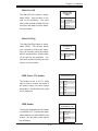
2-7
Jumper Settings
Explanation of
Jumpers
To modify the operation of the
serverboard, jumpers can be used to
3
2
1
3
2
1
Connector
Pins
choose between optional settings.
Jumpers create shorts between two
pins to change the function of the
Jumper
connector. Pin 1 is identified with
a square solder pad on the printed
circuit board. See the diagram at
right for an example of jumping pins
1 and 2. Refer to the serverboard
layout page for jumper locations.
Setting
Note 1: On t wo - pin jumpers,
"Closed" means the jumper is on
and "Open" means the jumper is
off the pins.
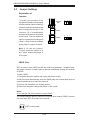
CMOS Clear
JBT1 is used to clear CMOS and will also clear any passwords. Instead of pins,
this jumper consists of contact pads to prevent accidentally clearing the contents
of CMOS.
To clear CMOS,
1) First power down the system and unplug the power cord(s).
2) With the power disconnected, short the CMOS pads with a metal object such as
a small screwdriver for at least four seconds.
3) Remove the screwdriver (or shorting device).
4) Reconnect the power cord(s) and power on the system.
Notes:
Do not use the PW_ON connector to clear CMOS.
The onboard battery does not need to be removed when clearing CMOS, however
you must short JBT1 for at least four seconds.
JBT1 contact pads
2-14
Chapter 2: Installation
JLAN1/2 Enable/Disable
Change the setting of jumper JPL
JLAN1/2 Enable/Disable
Jumper Settings (JPL)
to enable or disable the JLAN1 and
Jumper Setting
Definition
JLAN2 Gb Ethernet ports. See the
table on the right for jumper settings.
Pins 1-2
Enabled
Pins 2-3
Disabled
The default setting is enabled
VGA Enable/Disable
JPG1 allows you to enable or disable
the VGA port. The default position is
on pins 1 and 2 to enable VGA. See
the table on the right for jumper settings.
VGA Enable/Disable
Jumper Settings (JPG1)
Jumper Setting
Definition
Pins 1-2
Enabled
Pins 2-3
Disabled
I2C to PCI Enable/Disable
JI2C1/2 pair of jumpers allow you to
connect the System Management Bus
to any one of the PCI slots. The default
setting is closed (on) for both jumpers
to enable the connection. Both connectors must have the same setting
(JI2C1 is for data and JI2C2 is for the
I2C to PCI Enable/Disable
Jumper Settings
(JI2C1/2)
Jumper Setting
Definition
Closed
Enabled
Open
Disabled
clock). See the table on right for jumper settings.
SCSI Controller Enable/
Disable (H8DA8/H8DAR-8)
Jumper JPA1 is used to enable or disable the Adaptec SCSI controller. The
default setting is on pins 1-2 to enable
SCSI. See the table on right for jumper
settings.
2-15
SCSI Enable/Disable
Jumper Settings (JPA1)
Both Jumpers
Definition
Pins 1-2
Enabled
Pins 2-3
Disabled
H8DA8/H8DAE/H8DAR-8/H8DAR-i User's Manual
SCSI Termination Enable/
Disable (H8DA8/H8DAR-8)
Jumper JPA2 and JPA3 are used to
enable or disable termination for the
SCSI Channel A and B connectors, respectively. The default setting for both
SCSI Term. Enable/Disable
Jumper Settings (JPA2/JPA3)
is open to enable termination. See the
Jumper Setting
Definition
table on right for jumper settings.
Open
Enabled
Closed
Disabled
Note: In order for the SCSI drives to
function properly, please do not change
the default setting (enabled) set by the
manufacturer.
3rd Power Supply Fail Signal
Enable/Disable
The system can notify you in the event
of a power supply failure. This feature
assumes that three redundant power
supply units are installed in the chassis. If you only have one or two power
supplies installed, you should disable
the function with the J3P header to prevent false alarms. See the table on the
right for jumper settings.
3rd Power Supply Fail Signal
Jumper Settings (J3P)
Jumper Setting
Definition
Open
Enabled
Closed
Disabled
Watch Dog Enable/Disable
JWD controls the Watch Dog function.
Watch Dog is a system monitor that
can reboot the system when a software
application hangs. Pins 1-2 will cause
WD to reset the system if an application has frozen. Pins 2-3 will generate
a non-maskable interrupt signal for the
application that is frozen. See the table
on the right for jumper settings. Watch
Dog must also be enabled in BIOS.
2-16
Watch Dog
Jumper Settings (JWD)
Jumper Setting
Definition
Pins 1-2
Reset
Pins 2-3
NMI
Open
Disabled
Note: When enabled, the user needs to
write their own application software in order to disable the Watch Dog Timer.
Chapter 2: Installation
Onboard Speaker Enable/
Disable
The JD1 header allows you to use
either an external speaker or the
internal (onboard) speaker. For an
onboard speaker, close pins 6 and
7 with a jumper.
For an external
speaker, connect the speaker wires
Onboard Speaker Enable/Disable
Jumper Settings (JD1)
Pins
Definition
6-7
Jump for onboard speaker
4-7
Attach external speaker wires
to pins 4 through 7. See the table on
the right for settings and the Power
LED/Speaker table (previous section)
for pin definitions.
H8DA8/H8DAE: PCI-X Slot Speed
Jumper Settings (JPXA0/JPXB0)
PCI-X Slot Speed
Jumper Setting
Jumpers JPXA0 and JPXB0 on the
H8DA8/H8DAE can be used to change
the speed of PCI-X slots 3 and 4 and
PCI-X slots 5 and 6, respectively.
On the H8DAR-8/H8DAR-i, jumper
JPXB0 can be used to change the
speed of PCI-X slot 6. See the tables
on the right for jumper settings.
Definition
Open
Auto
Pins 1-2
PCI-X 66 MHz
Pins 2-3
PCI 66 MHz
Note: JPXA0 controls the speed for PCI-X slots
#3 and #4 and JPXB0 controls the speed for
PCI-X slots #5 and #6. The default setting for
both is Auto.
H8DAR-8/H8DAR-i: PCI-X Slot Speed
Jumper Settings (JPXB0)
Jumper Setting
Definition
Open
Auto
Pins 1-2
PCI-X 66 MHz
Pins 2-3
PCI 66 MHz
Note: JPXB0 controls the speed for PCI-X slot #6.
The default setting is Auto.
2-17
H8DA8/H8DAE/H8DAR-8/H8DAR-i User's Manual
2-8
Onboard Indicators
JLAN1/JLAN2 LEDs
JLAN LED
(Connection Speed Indicator)
The Ethernet ports (located beside
the VGA port) have two LEDs. One
LED indicates activity while the other
may be green, amber or off to indicate
the speed of the connection. See the
LED Color
Definition
Off
10 MHz
Green
100 MHz
Amber
1 GHz
table on the right for the functions
associated with the connection speed
LED.
+3.3V Power LED
When illuminated, the DP1 LED
indicates that power from the power supply is being supplied to the
serverboard (DP1 indicates the presence of +3.3V). See the table on the
right for DP1 LED states.
2-18
+3.3V Power LED
(DP1)
Color
System Status
Green
Power present on serverboard
Off
No power present on serverboard
Chapter 2: Installation
2-9
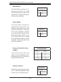
Floppy, IDE and SCSI Drive Connections
Use the following information to connect the floppy and hard disk drive cables.
The floppy disk drive cable has seven twisted wires.
A red mark on a wire typically designates the location of pin 1.
A single floppy disk drive ribbon cable has 34 wires and two connectors to provide
for two floppy disk drives. The connector with twisted wires always connects to
drive A, and the connector that does not have twisted wires always connects to
drive B.
The 80-wire ATA133 IDE hard disk drive cable that came with your system has
two connectors to support two drives. This special cable should be used to take
advantage of the speed this new technology offers. The blue connector connects
to the onboard IDE connector interface and the other connector(s) to your hard
drive(s). Consult the documentation that came with your disk drive for details
on actual jumper locations and settings for the hard disk drive.
Floppy Connector
The floppy connector is located
beside the IDE#2 connector.
See the table on the right for
pin definitions.
Floppy Drive Connector
Pin Definitions (JFDD1)
Pin#
Definition
1
GND
2
FDHDIN
3
GND
4
Reserved
5
Key
6
FDEDIN
7
GND
8
Index-
9
GND
10
Motor Enable
11
GND
12
Drive Select B-
13
GND
14
Drive Select A-
15
GND
16
Motor Enable
17
GND
18
DIR-
19
GND
20
STEP-
21
GND
22
Write Data-
23
GND
24
Write Gate-
25
GND
26
Track 00-
27
GND
28
Write Protect-
29
GND
30
Read Data-
31
GND
32
Side 1 Select-
33
GND
34
Diskette
2-19
Pin #
Definition
H8DA8/H8DAE/H8DAR-8/H8DAR-i User's Manual
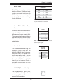
IDE Connectors
IDE Drive Connectors
Pin Definitions (JIDE#1/JIDE#2)
There are no jumpers to config-
Pin#
Definition
ure the onboard IDE#1 and #2
1
Reset IDE
2
Ground
connectors. See the table on
the right for pin definitions.
3
Host Data 7
4
Host Data 8
5
Host Data 6
6
Host Data 9
7
Host Data 5
8
Host Data 10
9
Host Data 4
10
Host Data 11
11
Host Data 3
12
Host Data 12
13
Host Data 2
14
Host Data 13
15
Host Data 1
16
Host Data 14
17
Host Data 0
18
Host Data 15
19
Ground
20
Key
21
DRQ3
22
Ground
23
I/O Write
24
Ground
25
I/O Read
26
Ground
27
IOCHRDY
28
BALE
29
DACK3
30
Ground
31
IRQ14
32
IOCS16
33
Addr1
34
Ground
35
Addr0
36
Addr2
37
Chip Select 0
38
Chip Select 1
39
Activity
40
Ground
2-20
Pin #
Definition
Chapter 2: Installation
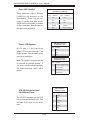
SCSI Connectors
(H8DA8/H8DAR-8)
Ultra320 SCSI Drive Connectors
Pin Definitions (JA1/JB2)
Pin#
Definition
Pin #
Definition
Refer to the table at right for
1
+DB (12)
35
-DB (12)
pin definitions for the Ultra320
2
+DB (13)
36
-DB (13)
SCSI connectors located at
JA1 and JB2.
3
+DB (14)
37
-DB (14)
4
+DB (15)
38
-DB (15)
5
+DB (P1)
39
-DB (P1)
6
+DB (0)
40
-DB (0)
7
+DB (1)
41
-DB (1)
8
+DB (2)
42
-DB (2)
9
+DB (3)
43
-DB (3)
10
+DB (4)
44
-DB (4)
11
+DB (5)
45
-DB (5)
12
+DB (6)
46
-DB (6)
13
+DB (7)
47
-DB (7)
14
+DB (P)
48
-DB (P)
15
Ground
49
Ground
16
DIFFSENS
50
Ground
17
TERMPWR
51
TERMPWR
18
TERMPWR
52
TERMPWR
19
Reserved
53
Reserved
20
Ground
54
Ground
21
+ATN
55
-ATN
22
Ground
56
Ground
23
+BSY
57
-BSY
24
+ACK
58
-ACK
25
+RST
59
-RST
26
+MSG
60
-MSG
27
+SEL
61
-SEL
28
+C/D
62
-C/D
29
+REQ
63
-REQ
30
+I/O
64
-I/O
31
+DB (8)
65
-DB (8)
32
+DB (9)
66
-DB (9)
33
+DB (10)
67
-DB (10)
34
+DB (11)
68
-DB (11)
2-21
H8DA8/H8DAE/H8DAR-8/H8DAR-i User's Manual
Notes
2-22
Chapter 3: Troubleshooting
Chapter 3
Troubleshooting
3-1
Troubleshooting Procedures
Use the following procedures to troubleshoot your system. If you have followed all
of the procedures below and still need assistance, refer to the ‘Technical Support
Procedures’ and/or ‘Returning Merchandise for Service’ section(s) in this chapter.
Always disconnect the AC power cord before adding, changing or installing any
hardware components.
Before Power On
1. Check that the onboard Power LED is lit (DP1 on the serverboard).
2. Make sure that the 8-pin 12v power connector at JPW2 is connected to your
power supply.
3. Make sure that no short circuits exist between the serverboard and chassis.
4. Disconnect all ribbon/wire cables from the serverboard, including those for the
keyboard and mouse.
5. Remove all add-on cards.
6. Install a CPU and heatsink (making sure it is fully seated) and connect the chassis speaker and the power LED to the serverboard. Check all jumper settings as
well.
7. Use the correct type of onboard CMOS battery as recommended by the manufacturer. To avoid possible explosion, do not install the CMOS battery upside down.
No Power
1. Make sure that no short circuits exist between the serverboard and the chassis.
2. Verify that all jumpers are set to their default positions.
3. Check that the 115V/230V switch on the power supply is properly set.
4. Turn the power switch on and off to test the system.
5. The battery on your serverboard may be old. Check to verify that it still supplies
~3VDC. If it does not, replace it with a new one.
No Video
1. If the power is on but you have no video, remove all the add-on cards and
cables.
2. Use the speaker to determine if any beep codes exist. Refer to Appendix A for
details on beep codes.
3-1
H8DA8/H8DAE/H8DAR-8/H8DAR-i User's Manual
NOTE
If you are a system integrator, VAR or OEM, a POST diagnostics
card is recommended. For I/O port 80h codes, refer to App. B.
Memory Errors
1. Make sure that the DIMM modules are properly and fully installed.
2. You should be using registered ECC DDR memory (see next page). Also, it is
recommended that you use the same memory type and speed for all DIMMs in the
system. See Section 2-4 for memory details and limitations.
3. Check for bad DIMM modules or slots by swapping modules between slots and
noting the results.
4. Check the power supply voltage 115V/230V switch.
Losing the System’s Setup Configuration
1. Make sure that you are using a high quality power supply. A poor quality power
supply may cause the system to lose the CMOS setup information. Refer to Section 1-6 for details on recommended power supplies.
2. The battery on your serverboard may be old. Check to verify that it still supplies
~3VDC. If it does not, replace it with a new one.
3. If the above steps do not fix the setup configuration problem, contact your vendor
for repairs.
3-2
Technical Support Procedures
Before contacting Technical Support, please take the following steps. Also, note
that as a serverboard manufacturer, we do not sell directly to end-users, so it is
best to first check with your distributor or reseller for troubleshooting services. They
should know of any possible problem(s) with the specific system configuration that
was sold to you.
1. Please review the ‘Troubleshooting Procedures’ and 'Frequently Asked Questions'
(FAQs) sections in this chapter or see the FAQs on our web site before contacting
Technical Support.
2. BIOS upgrades can be downloaded from our web site.
Note: Not all BIOS can be flashed depending on the modifications to the boot block
code.
3-2
Chapter 3: Troubleshooting
3. If you still cannot resolve the problem, include the following information when
contacting us for technical support:
Serverboard model and PCB revision number
BIOS release date/version (this can be seen on the initial display when your
system first boots up)
System configuration
An example of a Technical Support form is posted on our web site.
4. Distributors: For immediate assistance, please have your account number ready
when contacting our technical support department by e-mail.
3-3
Frequently Asked Questions
Question: What type of memory does my serverboard support?
Answer: The H8DA8/H8DAE/H8DAR-8/H8DAR-i supports up to 32 GB of registered ECC DDR266 or up to 16 GB of registered ECC DDR400/333 interleaved
or non-interleaved SDRAM with two CPUs installed. With only one CPU installed
the maximum memory support is halved. See Section 2-4 for details on installing
memory.
Question: How do I update my BIOS?
Answer: It is recommended that you not upgrade your BIOS if you are not experiencing problems with your system. Updated BIOS files are located on our web site.
Please check our BIOS warning message and the information on how to update
your BIOS on our web site. Also, check the current BIOS revision and make sure
it is newer than your current BIOS before downloading.
Select your mainboard model on the web page and download the corresponding
BIOS file to your computer. Unzip the BIOS update file, in which you will find the
readme.txt (flash instructions), the amiflash.exe (BIOS flash utility) and the BIOS
image (xxx.rom) files. Copy these files to a bootable floppy disk, insert the disk
into drive A and reboot the system. At the DOS prompt after rebooting, enter the
command "amiflash" (without quotation marks) then type in the BIOS file that you
want to update with (xxxx.rom).
Question: What's on the CD that came with my serverboard?
Answer: The supplied compact disc has quite a few drivers and programs that will
greatly enhance your system. We recommend that you review the CD and install the
applications you need. Applications on the CD include chipset drivers for Windows
and security and audio drivers.
3-3
H8DA8/H8DAE/H8DAR-8/H8DAR-i User's Manual
Question: Why can't I turn off the power using the momentary power on/off
switch?
Answer: The instant power off function is controlled in BIOS by the Power Button Mode setting. When the On/Off feature is enabled, the serverboard will have
instant off capabilities as long as the BIOS has control of the system. When the
Standby or Suspend feature is enabled or when the BIOS is not in control such
as during memory count (the first screen that appears when the system is turned
on), the momentary on/off switch must be held for more than four seconds to shut
down the system. This feature is required to implement the ACPI features on the
serverboard.
Question: How do I connect the ATA133 cable to my IDE device(s)?
Answer: The 80-wire/40-pin high-density ATA133 IDE cable that came with your
system has two connectors to support two drives. This special cable must be used
to take advantage of the speed the ATA133 technology offers. Connect the blue
connector to the onboard IDE header and the other connector(s) to your hard
drive(s). Consult the documentation that came with your disk drive for details on
actual jumper locations and settings.
3-4
Returning Merchandise for Service
A receipt or copy of your invoice marked with the date of purchase is required before any warranty service will be rendered. You can obtain service by calling your
vendor for a Returned Merchandise Authorization (RMA) number. When returning
to the manufacturer, the RMA number should be prominently displayed on the
outside of the shipping carton, and mailed prepaid or hand-carried. Shipping and
handling charges will be applied for all orders that must be mailed when service
is complete.
This warranty only covers normal consumer use and does not cover damages incurred in shipping or from failure due to the alteration, misuse, abuse or improper
maintenance of products.
During the warranty period, contact your distributor first for any product problems.
3-4
Chapter 4: BIOS
Chapter 4
BIOS
4-1
Introduction
This chapter describes the AMIBIOS™ Setup utility for the H8DA8/H8DAE/H8DAR8/H8DAR-i. The AMI ROM BIOS is stored in a flash chip and can be easily upgraded
using a floppy disk-based program.
Note: Due to periodic changes to the BIOS, some settings may have been added or
deleted and might not yet be recorded in this manual. Please refer to the Manual
Download area of our web site for any changes to BIOS that may not be reflected
in this manual.
Starting the Setup Utility
To enter the BIOS Setup Utility, hit the <Delete> key while the system is booting-up.
(In most cases, the <Delete> key is used to invoke the BIOS setup screen. There are
a few cases when other keys are used, such as <F1>, <F2>, etc.) Each main BIOS
menu option is described in this manual.
The Main BIOS screen has two main frames. The left frame displays all the options
that can be configured. “Grayed-out” options cannot be configured. The right frame
displays the key legend. Above the key legend is an area reserved for a text message. When an option is selected in the left frame, it is highlighted in white. Often a
text message will accompany it. (Note that BIOS has default text messages built in.
We retain the option to include, omit, or change any of these text messages.) Settings printed in Bold are the default values.
A " " indicates a submenu. Highlighting such an item and pressing the <Enter>
key will open the list of settings within that submenu.
The BIOS setup utility uses a key-based navigation system called hot keys. Most of
these hot keys (<F1>, <F10>, <Enter>, <ESC>, <Arrow> keys, etc.) can be used at
any time during the setup navigation process.
4-1
H8DA8/H8DAE/H8DAR-8/H8DAR-i User's Manual
4-2
Main Setup
When you first enter AMI BIOS Setup Utility, you will see the Main setup screen.
You can always return to the Main setup screen by selecting the Main tab on the
top of the screen.
The Main Setup screen provides you with a system overview, which includes the
version, built date and ID of the AMIBIOS, the type, speed and number of the
processors in the system and the amount of memory installed in the system.
System Time/System Date
You can edit this field to change the system time and date. Highlight System Time
or System Date using the <Arrow> keys. Enter new values through the keyboard.
Press the <Tab> key or the <Arrow> keys to move between fields. The date must
be entered in DAY/MM/DD/YYYY format. The time is entered in HH:MM:SS format.
Please note that time is in a 24-hour format. For example, 5:30 A.M. appears as
05:30:00 and 5:30 P.M. as 17:30:00.
4-3
Advanced Settings Menu
CPU Configuration Sub-Menu
GART Error Reporting
This setting is used for testing only.
MTRR Mapping
This determines the method used for programming CPU MTRRs when 4 GB or more
memory is present. The options are Continuous, which makes the PCI hole noncacheable, and Discrete, which places the PCI hole below the 4 GB boundary.
4-2
Chapter 4: BIOS
IDE Configuration
Onboard PCI IDE Controller
The following options are available to set the IDE controller status: Disabled will disable the controller. Primary will enable the primary IDE controller only. Secondary
will enable the secondary IDE controller only. Both will enable both the primary
and the secondary IDE controllers.
Primary IDE Master/Slave, Secondary IDE Master/Slave
Highlight one of the four items above and press <Enter> to access the submenu
for that item.
Type
Select the type of device connected to the system. The options are Not Installed,
Auto, CDROM and ARMD.
LBA/Large Mode
LBA (Logical Block Addressing) is a method of addressing data on a disk drive.
In the LBA mode, the maximum drive capacity is 137 GB. For drive capacities of
over 137 GB, your system must be equipped with 48-bit LBA mode addressing.
If not, contact your manufacturer or install an ATA/133 IDE controller card that
supports 48-bit LBA mode. The options are Disabled and Auto.
Block (Multi-Sector Transfer)
Block mode boosts IDE drive performance by increasing the amount of data
transferred. Only 512 bytes of data can be transferred per interrupt if block mode
is not used. Block mode allows transfers of up to 64 KB per interrupt. Select
"Disabled" to allow the data to be transferred from and to the device one sector at a time. Select "Auto" to allows the data transfer from and to the device
occur multiple sectors at a time if the device supports it. The options are Auto
and Disabled.
PIO Mode
PIO (Programmable I/O) mode programs timing cycles between the IDE drive
and the programmable IDE controller. As the PIO mode increases, the cycle time
decreases. The options are Auto, 0, 1, 2, 3, and 4. Select Auto to allow AMI
BIOS to auto detect the PIO mode. Use this value if the IDE disk drive support
cannot be determined. Select 0 to allow AMI BIOS to use PIO mode 0. It has a
4-3
H8DA8/H8DAE/H8DAR-8/H8DAR-i User's Manual
data transfer rate of 3.3 MBs. Select 1 to allow AMI BIOS to use PIO mode 1 for
a data transfer rate of 5.2 MBs. Select 2 to allow AMI BIOS to use PIO mode 2
for a data transfer rate of 8.3 MBs. Select 3 to allow AMI BIOS to use PIO mode
3 for a data transfer rate of 11.1 MBs. Select 4 to allow AMI BIOS to use PIO
mode 4 for a data transfer rate of 16.6 MBs. This setting generally works with
all hard disk drives manufactured after 1999. For other disk drives, such as IDE
CD-ROM drives, check the specifications of the drive.
DMA Mode
Selects the DMA Mode. Options are Auto, SWDMA0, SWDMA1, SWDMA2,
MWDMA0. MDWDMA1, MWDMA2, UDMA0. UDMA1, UDMA2, UDMA3,
UDMA4 and UDMA5. (SWDMA=Single Word DMA, MWDMA=Multi Word DMA,
UDMA=UltraDMA.)
S.M.A.R.T. For Hard disk drives
Self-Monitoring Analysis and Reporting Technology (SMART) can help predict
impending drive failures. Select "Auto" to allow BIOS to auto detect hard disk
drive support. Select "Disabled" to prevent AMI BIOS from using the S.M.A.R.T.
Select "Enabled" to allow AMI BIOS to use the S.M.A.R.T. to support hard drive
disk. The options are Disabled, Enabled, and Auto.
32-Bit Data Transfer
Select "Enabled" to activate the function of 32-Bit data transfer. Select "Disabled"
to deactivate the function. The options are Enabled and Disabled.
Hard Disk Write Protect
Select Enabled to enable the function of Hard Disk Write Protect to prevent data
from being written to HDD. The options are Enabled or Disabled.
IDE Detect Time Out (Sec)
This feature allows the user to set the time-out value for detecting ATA, ATA PI
devices installed in the system. The options are 0 (sec), 5, 10, 15, 20, 25, 30 and
35.
ATA(PI) 80Pin Cable Detection
This setting allows AMI BIOS to auto-detect the 80-Pin ATA(PI) cable. The options
are Host & Device, Host and Device.
4-4
Chapter 4: BIOS
Floppy Configuration
Floppy A
Move the cursor to these fields via up and down <arrow> keys to select the floppy
type. The options are Disabled, 360 KB 5 1/4", 1.2 MB 5 1/4", 720 KB 3½", 1.44
MB 3½”, and 2.88 MB 3½".
Floppy B
Move the cursor to these fields via up and down <arrow> keys to select the floppy
type. The options are Disabled, 360 KB 5 1/4", 1.2 MB 5 1/4", 720 KB 3½", 1.44
MB 3½”, and 2.88 MB 3½".
Onboard Floppy Controller
Use this setting to Enable or Disable the onboard floppy controller.
Super IO Configuration
Serial Port1 Address
This option specifies the base I/O port address and Interrupt Request address of
serial port 1. Select "Disabled" to prevent the serial port from accessing any system
resources. When this option is set to Disabled, the serial port physically becomes
unavailable. Select "3F8/IRQ4" to allow the serial port to use 3F8 as its I/O port
address and IRQ 4 for the interrupt address. The options are Disabled, 3F8/IRQ4,
3E8/IRQ4 and 2E8/IRQ3.
Serial Port2 Address
This option specifies the base I/O port address and Interrupt Request address of
serial port 2. Select "Disabled" to prevent the serial port from accessing any system
resources. When this option is set to "Disabled", the serial port physically becomes
unavailable. Select "2F8/IRQ3" to allow the serial port to use 2F8 as its I/O port
address and IRQ 3 for the interrupt address. The options are Disabled, 2F8/IRQ3,
3E8/IRQ4 and 2E8/IRQ3.
Serial Port 2 Mode
Tells BIOS which mode to select for serial port 2. The options are Normal,
IrDA and ASKIR.
4-5
H8DA8/H8DAE/H8DAR-8/H8DAR-i User's Manual
Parallel Port Address
This option specifies the I/O address used by the parallel port. Select Disabled to
prevent the parallel port from accessing any system resources. When the value of
this option is set to Disabled, the printer port becomes unavailable. Select 378 to
allow the parallel port to use 378 as its I/O port address. The majority of parallel
ports on computer systems use IRQ7 and I/O Port 378H as the standard setting.
Select 278 to allow the parallel port to use 278 as its I/O port address. Select 3BC
to allow the parallel port to use 3BC as its I/O port address.
Parallel Port Mode
Specify the parallel port mode. The options are Normal, Bi-directional, EPP
and ECP.
Parallel Port IRQ
Select the IRQ (interrupt request) for the parallel port. The options are IRQ5
and IRQ7.
ACPI Configuration
ACPI Aware OS
Use this setting to tell BIOS if the operating system recognizes ACPI functions.
The options are Yes and No.
Advanced ACPI Configuration
ACPI 2.0 Support
Select "Yes" if your system supports ACPI 2.0, which will add additional tables
as per ACPI 2.0 specifications. Options are Yes and No.
ACPI APIC Support
Select "Enabled" to allow the ACPI APIC Table Pointer to be included in the
RSDT pointer list. The options are Enabled and Disabled.
ACPI SRAT Table
This setting allows you to enable or disable the building of an ACPI SRAT table.
Options are Enabled and Disabled.
4-6
Chapter 4: BIOS
BIOS --> AML ACPI Table
When Enabled, BIOS-->AML exchange table pointer to be included in (X) REDT
pointer list. Options are Enabled and Disabled.
Headless Mode
Select "Enabled" to activate the Headless Operation Mode through ACPI. The
options are Enabled and Disabled.
OS Console Redirection
When "Enabled", BIOS provides additional options to select remote access type.
The options are Enabled and Disabled.
PME, R1 S5 Wake Up
The options are Enabled and Disabled.
Event Log Configuration
View Event Log
Highlight this item and press <Enter> to view the contents of the event log.
Mark All Events as Read
Highlight this item and press <Enter> to mark the DMI events as read.
Clear Event Log
This setting will clear all event logs when set to "OK". The options are OK and
Cancel.
Event Log Statistics
Highlight this item and press <Enter> to view details on the count of total unread
events.
Hyper Transport Configuration
CPU0: CPU1 HT Link1 Speed
The HT link will run at the speed specified in this setting if it is slower than or equal
to the system clock and if the board is capable. Options are Auto, 200 MHz, 400
MHz, 600 MHz, 800 MHz and 1 GHz.
4-7
H8DA8/H8DAE/H8DAR-8/H8DAR-i User's Manual
CPU0: CPU1 HT Link1 Width
The HT link will run at the width specified in this setting. Options are Auto, 2 bit,
4 bit, 8 bit and 16 bit.
CPU0: PCI-X0 HT Link1 Speed
The HT link will run at the speed specified in this setting if it is slower than or equal
to the system clock and if the board is capable. Options are Auto, 200 MHz, 400
MHz and 600 MHz.
CPU0: PCI-X0 HT Link1 Width
The HT link will run at the width specified in this setting. Options are Auto, 2 bit,
4 bit, 8 bit and 16 bit.
MPS Configuration
MPS Revision
This setting allows the user to select the MPS revision level. The options are 1.1
and 1.4.
Remote Access Configuration
Remote Access
Use this setting to Enable or Disable remote access. If Enabled is selected, you
can select a Remote Access type.
USB Configuration
This screen will display the module version and all USB enabled devices.
Legacy USB Support
Select "Enabled" to enable the support for USB Legacy. Disable Legacy support
if there are no USB devices installed in the system. The options are Disabled,
Enabled and Auto.
4-8
Chapter 4: BIOS
System Health Monitor
CPU Overheat Temperature
Use the "+" and "-" keys to set the CPU temperature threshold to between 65o
and 90o C. When this threshold is exceeded, the overheat LED on the chassis
will light up and an alarm will sound. The LED and alarm will turn off once the
CPU temperature has dropped to 5 degrees below the threshold set. The default
setting is 78o C.
The other items in the submenu are all systems monitor displays for the following
information:
CPU1 Temperature, CPU2 Temperature (for 2U systems), System Temperature,
CPU1 Vcore, CPU2 Vcore (for 2U systems), 3.3V Vcc, +5 Vin, +12Vin, -12V Vcc,
DDRA VTT, DDRB VTT, 1.2V for Hyper Transport, DIMM Voltage, 1.8V for chipset,
5V Standby and 3.3V Standby.
System Fan Monitor
Fan Speed Control Modules
This feature allows the user to determine how the system will control the speed
of the onboard fans. If the option is set to "3-pin fan", the fan speed is controlled based upon the CPU die temperature. When the CPU die temperature
is higher, the fan speed will be higher as well. If the option is set to "4-pin", the
fan speed will be controlled by the Thermal Management Settings pre-configured
by the user with this setting. Select "3-pin" if your chassis came with 3-pin fan
headers. Select "4-pin" if your chassis came with 4-pin fan headers. Select
"Workstation" if your system is used as a Workstation. Select "Server" if your
system is used as a Server. Select "Disable" to disable the fan speed control
function to allow the onboard fans to continuously run at full speed (12V). The
options are 1) Disable, Full Speed 2) 3-pin (Server), 3) 3-pin (Workstation),
4) 4-pin (Server) and 5) 4-pin (Workstation).
Note: the 4-pin fan speed settings are not available for the H8DAR-8 and
H8DAR-i, which have 3-pin fan headers.
FAN1 Speed through FAN8 Speed
The speeds of the onboard fans (in rpm) are displayed here.
Note: the FAN1 through FAN5 speeds will be displayed for the H8DAR-8 and
H8DAR-i.
4-9
H8DA8/H8DAE/H8DAR-8/H8DAR-i User's Manual
4-4
PCI/PnP Menu
Plug & Play OS
Select Yes to allow the OS to configure Plug & Play devices. (This is not required
for system boot if your system has an OS that supports Plug & Play.) Select No
to allow AMIBIOS to configure all devices in the system.
PCI Latency Timer
This option sets the latency of all PCI devices on the PCI bus. Select a value to
set the PCI latency in PCI clock cycles. Options are 32, 64, 96, 128, 160, 192,
224 and 248.
Allocate IRQ to PCI VGA
Set this value to allow or restrict the system from giving the VGA adapter card an
interrupt address. The options are Yes and No.
Palette Snooping
Select "Enabled" to inform the PCI devices that an ISA graphics device is installed
in the system in order for the graphics card to function properly. The options are
Enabled and Disabled.
PCI IDE BusMaster
Set this value to allow or prevent the use of PCI IDE busmastering. Select "Enabled"
to allow AMI BIOS to use PCI busmaster for reading and writing to IDE drives. The
options are Disabled and Enabled.
Offboard PCI/ISA IDE Card
This option allows the user to assign a PCI slot number to an Off-board PCI/ISA
IDE card in order for it to function properly. The options are Auto, PCI Slot1, PCI
Slot2, PCI Slot3, PCI Slot4, PCI Slot5, and PCI Slot6.
IRQ3/IRQ4/IRQ5/IRQ7/IRQ9/IRQ10/IRQ11/IRQ14/IRQ15
This feature specifies the availability of an IRQ to be used by a PCI/PnP device.
Select Reserved for the IRQ to be used by a Legacy ISA device. The options are
Available and Reserved.
4-10
Chapter 4: BIOS
DMA Channel 0/Channel 1/Channel 3/Channel 5/Channel 6/Channel
7
Select Available to indicate that a specific DMA channel is available to be used by
a PCI/PnP device. Select Reserved if the DMA channel specified is reserved for
a Legacy ISA device. The options are Available and Reserved.
Reserved Memory Size
This feature specifies the size of memory block to be reserved for Legacy ISA
devices. The options are Disabled, 16K, 32K and 64K.
4-5
Boot Menu
The Boot menu contains several sub-menus.
Boot Settings Configuration
Quick Boot
If Enabled, this option will skip certain tests during POST to reduce the time needed
for the system to boot up. The options are Enabled and Disabled.
Quiet Boot
If Disabled, normal POST messages will be displayed on boot-up. If Enabled, this
display the OEM logo instead of POST messages.
Add-On ROM Display Mode
This setting controls the display of add-on ROM (read-only memory) messages.
Select "Force BIOS" to allow the computer system to force a third party BIOS to
display during system boot. Select "Keep Current" to allow the computer system
to display the BIOS information during system boot.
Boot up Num-Lock
Set this to "On" to allow the Number Lock setting to be modified during boot up.
The options are On and Off.
PS/2 Mouse Support
This setting is to specify PS/2 mouse support. The options are Auto, Enabled
and Disabled.
4-11
H8DA8/H8DAE/H8DAR-8/H8DAR-i User's Manual
Wait for ‘F1’ If Error
Enable to activate the Wait for F1 if Error function. The options are Enabled and
Disabled.
Hit ‘DEL’ Message Display
Enable to display the message telling the user to hit the DEL key to enter the setup
utility. The options are Enabled and Disabled.
Interrupt 19 Capture
Enable to allow ROMs to trap Interrupt 19. The options are Enabled and Disabled.
Boot Device Priority
This feature allows the user to prioritize the sequence for the Boot Device with the
devices installed in the system. The default settings (with generic names) are:
· 1st Boot Device – Removeable drive (e.g. floppy drive)
· 2nd Boot Device – CD/DVD
· 3rd Boot Device – Hard drive
· 4th Boot Device – LAN
· 5th Boot Device – LAN
Hard Disk Drives
This feature allows the user to prioritize the Boot sequence from available hard
drives.
1st Drive/2nd Drive
Specify the boot sequence for 1st Hard Drive and 2nd Hard Drive.
Removable Drives
This feature allows the user to specify the Boot sequence from available removable drives.
1st Drive
Specifies the boot sequence for the 1st Removable Drive. The options are 1st
Floppy Drive and Disabled.
4-12
Chapter 4: BIOS
CD/DVD Drives
This feature allows the user to specify the boot sequence from available CDROM
drives.
1st Drive
Specifies the boot sequence for the 1st Hard Drive.
4-6
Security Menu
AMI BIOS provides a Supervisor and a User password. If you use both passwords,
the Supervisor password must be set first.
Change Supervisor Password
Select this option and press <Enter> to access the sub menu, and then type in
the password.
Change User Password
Select this option and press <Enter> to access the sub menu, and then type in
the password.
Clear User Password
Select this option and press <Enter> to access the sub menu. You can use the
sub menu to clear the user password.
Boot Sector Virus Protection
This option is near the bottom of the Security Setup screen. Select "Disabled" to
deactivate the Boot Sector Virus Protection. Select "Enabled" to enable boot sector
protection. When "Enabled", AMI BIOS displays a warning when any program (or
virus) issues a Disk Format command or attempts to write to the boot sector of the
hard disk drive. The options are Enabled and Disabled.
4-13
H8DA8/H8DAE/H8DAR-8/H8DAR-i User's Manual
4-7
Chipset Menu
North Bridge Configuration
Memory Configuration
Memclock Mode
This setting determines how the memory clock is set. Auto has the
memory clock set by the code and Limit allows the user to set a standard value.
MCT Timing Mode
Sets the timing mode for memory. Options are Auto and Manual.
User Configuration Mode
Options are Auto and Manual.
Burst Length
Use this setting to set the memory burst length. 64-bit Dq must use 4
beats. Options are 8 beats, 4 beats and 2 beats.
Enable Clock to All DIMMs
This setting allows the user to enable unused clocks to DIMMs, even if
DIMM slots are empty. Options are Enabled and Disabled.
Software Memory Hole
When "Enabled", allows software memory remapping around the
memory hole. Options are Enabled and Disabled.
Hardware Memory Hole
When "Enabled", allows software memory remapping around the memory hole (only supported by rev. EO processors and above). Options
are Enabled and Disabled.
4-14
Chapter 4: BIOS
ECC Configuration
DRAM ECC Enable
DRAM ECC allows hardware to report and correct memory errors automatically. Options are Enabled and Disabled.
MCA DRAM ECC Logging
When "Enabled", MCA DRAM ECC logging and reporting is enabled. Options
are Enabled and Disabled.
ECC Chipkill
Allows the user to enabled ECC Chipkill. Options are Enabled and Disabled.
DRAM Scrub Redirect
Allows system to correct DRAM ECC errors immediately, even with background scrubbing on. Options are Enabled and Disabled.
DRAM BG Scrub
Corrects memory errors so later reads are correct. Options are Disabled
and various times in nanoseconds and microseconds.
L2 Cache BG Scrub
Allows L2 cache RAM to be corrected when idle. Options are Disabled and
various times in nanoseconds and microseconds.
Data Cache BG Scrub
Allows L1 cache RAM to be corrected when idle. Options are Disabled and
various times in nanoseconds and microseconds.
IOMMU Option Menu
IOMMU Mode
IOMMU is supported on Linux-based systems to convert 32-bit I/O addresses
to 64-bit. Options are Disabled, Best Fit and Absolute. Selecting the Best Fit
or Absolute settings allows the user to select aperture size.
4-15
H8DA8/H8DAE/H8DAR-8/H8DAR-i User's Manual
South Bridge Configuration
2.0 SMBus Controller
Allows the user to Enable or Disable the SMBus controller.
HT Link0 P-Comp Mode
Allows user to set values for this mode. Options are Auto (hardware compensation values), Data (allows user to override auto values with an absolute value),
CalComp + Data (allows user to add to the generated value) and CalComp - Data
(allows user to subtract from the generated value).
HT Link0 N-Comp Mode
Allows user to set values for this mode. Options are Auto (hardware compensation values), Data (allows user to override auto values with an absolute value),
CalComp + Data (allows user to add to the generated value) and CalComp - Data
(allows user to subtract from the generated value).
HT Link0 RZ-Comp Mode
Allows user to set values for this mode. Options are Auto (hardware compensation values), Data (allows user to override auto values with an absolute value),
CalComp + Data (allows user to add to the generated value) and CalComp - Data
(allows user to subtract from the generated value).
PCI-X Configuration
Errata 56 PCLCK
Enables or Disables 8131 Errata 56 if a PC card behind 8131 bridge has more
than four functions and bus speed is 133 MHz.
HT Link0 P-Comp Mode
Allows user to set values for this mode. Options are Auto (hardware compensation values), Data (allows user to override auto values with an absolute value),
CalComp + Data (allows user to add to the generated value) and CalComp - Data
(allows user to subtract from the generated value).
HT Link0 N-Comp Mode
Allows user to set values for this mode. Options are Auto (hardware compensation values), Data (allows user to override auto values with an absolute value),
4-16
Chapter 4: BIOS
CalComp + Data (allows user to add to the generated value) and CalComp - Data
(allows user to subtract from the generated value).
HT Link0 RZ-Comp Mode
Allows user to set values for this mode. Options are Auto (hardware compensation values), Data (allows user to override auto values with an absolute value),
CalComp + Data (allows user to add to the generated value) and CalComp - Data
(allows user to subtract from the generated value).
HT Link1 P-Comp Mode
Allows user to set values for this mode. Options are Auto (hardware compensation values), Data (allows user to override auto values with an absolute value),
CalComp + Data (allows user to add to the generated value) and CalComp - Data
(allows user to subtract from the generated value).
HT Link1 N-Comp Mode
Allows user to set values for this mode. Options are Auto (hardware compensation values), Data (allows user to override auto values with an absolute value),
CalComp + Data (allows user to add to the generated value) and CalComp - Data
(allows user to subtract from the generated value).
HT Link1 RZ-Comp Mode
Allows user to set values for this mode. Options are Auto (hardware compensation values), Data (allows user to override auto values with an absolute value),
CalComp + Data (allows user to add to the generated value) and CalComp - Data
(allows user to subtract from the generated value).
4-17
H8DA8/H8DAE/H8DAR-8/H8DAR-i User's Manual
4-8
Power Menu
Power Button Mode
Allows the user to change the function of the power button. Options are Instant
Off and 4-Sec. Delay.
Restore on AC Power Loss
This setting allows you to choose how the system will react when power returns
after an unexpected loss of power. The options are Power Off, Power On and
Last State.
Watch Dog Timer
This setting is used to enable or disabled the Watch Dog Timer function. It must
be used in conjunction with the Watch Dog jumper (see Chapter 2 for details). The
options are Disabled and Enabled.
4-18
Chapter 4: BIOS
4-9
Exit Menu
Select the Exit tab from AMI BIOS Setup Utility screen to enter the Exit BIOS Setup
screen.
Save Changes and Exit
When you have completed the system configuration changes, select this option
to leave BIOS Setup and reboot the computer, so the new system configuration
parameters can take effect. Select Save Changes and Exit from the Exit menu
and press <Enter>.
Discard Changes and Exit
Select this option to quit BIOS Setup without making any permanent changes to
the system configuration and reboot the computer. Select Discard Changes and
Exit from the Exit menu and press <Enter>.
Discard Changes
Select this option and press <Enter> to discard all the changes and return to AMI
BIOS Utility Program.
Load Optimal Defaults
To set this feature, select Load Optimal Defaults from the Exit menu and press
<Enter>. Then Select "OK" to allow BIOS to automatically load the Optimal Defaults
as the BIOS Settings. The Optimal settings are designed for maximum system
performance, but may not work best for all computer applications.
Load Fail-Safe Defaults
To set this feature, select Load Fail-Safe Defaults from the Exit menu and press
<Enter>. The Fail-Safe settings are designed for maximum system stability, but
not maximum performance.
4-19
H8DA8/H8DAE/H8DAR-8/H8DAR-i User's Manual
Notes
4-20
Appendix A: BIOS Error Beep Codes
Appendix A
BIOS Error Beep Codes
During the POST (Power-On Self-Test) routines, which are performed each time
the system is powered on, errors may occur.
Non-fatal errors are those which, in most cases, allow the system to continue the
boot-up process. The error messages normally appear on the screen.
Fatal errors are those which will not allow the system to continue the boot-up procedure. If a fatal error occurs, you should consult with your system manufacturer
for possible repairs.
These fatal errors are usually communicated through a series of audible beeps.
The numbers on the fatal error list, on the following page, correspond to the number
of beeps for the corresponding error. All errors listed, with the exception of Beep
Code 8, are fatal errors.
A-1
AMIBIOS Error Beep Codes
Beep Code
Error Message
Description
1 beep
Refresh
Circuits have been reset.
(Ready to power up.)
5 short, 1 long
Memory error
No memory detected in
system
8 beeps
Display memory read/write error
Video adapter missing or
with faulty memory
A-1
H8DA8/H8DAE/H8DAR-8/H8DAR-i User's Manual
Notes
A-2
Appendix B: BIOS POST Checkpoint Codes
Appendix B
BIOS POST Checkpoint Codes
When AMIBIOS performs the Power On Self Test, it writes checkpoint codes to I/O
port 0080h. If the computer cannot complete the boot process, diagnostic equipment
can be attached to the computer to read I/O port 0080h.
B-1
Uncompressed Initialization Codes
The uncompressed initialization checkpoint codes are listed in order of execution:
Checkpoint
Code Description
D0h
The NMI is disabled. Power on delay is starting. Next, the initialization code checksum will be verified.
D1h
Initializing the DMA controller, performing the keyboard controller BAT test, starting
memory refresh and entering 4 GB flat mode next.
D3h
Starting memory sizing next.
D4h
Returning to real mode. Executing any OEM patches and setting the Stack next.
D5h
Passing control to the uncompressed code in shadow RAM at E000:0000h. The
initialization code is copied to segment 0 and control will be transferred to segment
0.
B-1
H8DA8/H8DAE/H8DAR-8/H8DAR-i User's Manual
B-2
Bootblock Recovery Codes
The bootblock recovery checkpoint codes are listed in order of execution:
Checkpoint
Code Description
E0h
The onboard floppy controller if available is initialized. Next, beginning the base
512 KB memory test.
E1h
Initializing the interrupt vector table next.
E2h
Initializing the DMA and Interrupt controllers next.
E6h
Enabling the floppy drive controller and Timer IRQs. Enabling internal cache memory.
Edh
Initializing the floppy drive.
Eeh
Looking for a floppy diskette in drive A:. Reading the first sector of the diskette.
Efh
A read error occurred while reading the floppy drive in drive A:.
F0h
Next, searching for the AMIBOOT.ROM file in the root directory.
F1h
The AMIBOOT.ROM file is not in the root directory.
F2h
Next, reading and analyzing the floppy diskette FAT to find the clusters occupied
by the AMIBOOT.ROM file.
F3h
Next, reading the AMIBOOT.ROM file, cluster by cluster.
F4h
The AMIBOOT.ROM file is not the correct size.
F5h
Next, disabling internal cache memory.
FBh
Next, detecting the type of flash ROM.
FCh
Next, erasing the flash ROM.
FDh
Next, programming the flash ROM.
FFh
Flash ROM programming was successful. Next, restarting the system BIOS.
B-2
Appendix B: BIOS POST Checkpoint Codes
B-3
Uncompressed Initialization Codes
The following runtime checkpoint codes are listed in order of execution.
These codes are uncompressed in F0000h shadow RAM.
Checkpoint
Code Description
03h
The NMI is disabled. Next, checking for a soft reset or a power on condition.
05h
The BIOS stack has been built. Next, disabling cache memory.
06h
Uncompressing the POST code next.
07h
Next, initializing the CPU and the CPU data area.
08h
The CMOS checksum calculation is done next.
0Ah
The CMOS checksum calculation is done. Initializing the CMOS status register for
date and time next.
0Bh
The CMOS status register is initialized. Next, performing any required initialization
before the keyboard BAT command is issued.
0Ch
The keyboard controller input buffer is free. Next, issuing the BAT command to the
keyboard controller.
0Eh
The keyboard controller BAT command result has been verified. Next, performing
any necessary initialization after the keyboard controller BAT command test.
0Fh
The initialization after the keyboard controller BAT command test is done. The keyboard command byte is written next.
10h
The keyboard controller command byte is written. Next, issuing the Pin 23 and 24
blocking and unblocking command.
11h
Next, checking if <End or <Ins> keys were pressed during power on. Initializing
CMOS RAM if the Initialize CMOS RAM in every boot AMIBIOS POST option was
set in AMIBCP or the <End> key was pressed.
12h
Next, disabling DMA controllers 1 and 2 and interrupt controllers 1 and 2.
13h
The video display has been disabled. Port B has been initialized. Next, initializing
the chipset.
14h
The 8254 timer test will begin next.
19h
Next, programming the flash ROM.
1Ah
The memory refresh line is toggling. Checking the 15 second on/off time next.
2Bh
Passing control to the video ROM to perform any required configuration before the
video ROM test.
2Ch
All necessary processing before passing control to the video ROM is done. Looking for the video ROM next and passing control to it.
2Dh
The video ROM has returned control to BIOS POST. Performing any required processing after the video ROM had control
23h
Reading the 8042 input port and disabling the MEGAKEY Green PC feature next.
Making the BIOS code segment writable and performing any necessary configuration before initializing the interrupt vectors.
24h
The configuration required before interrupt vector initialization has completed. Interrupt vector initialization is about to begin.
B-3
H8DA8/H8DAE/H8DAR-8/H8DAR-i User's Manual
Checkpoint
Code Description
25h
Interrupt vector initialization is done. Clearing the password if the POST DIAG
switch is on.
27h
Any initialization before setting video mode will be done next.
28h
Initialization before setting the video mode is complete. Configuring the monochrome mode and color mode settings next.
2Ah
Bus initialization system, static, output devices will be done next, if present. See the
last page for additional information.
2Eh
Completed post-video ROM test processing. If the EGA/VGA controller is not
found, performing the display memory read/write test next.
2Fh
The EGA/VGA controller was not found. The display memory read/write test is
about to begin.
30h
The display memory read/write test passed. Look for retrace checking next.
31h
The display memory read/write test or retrace checking failed. Performing the alternate display memory read/write test next.
32h
The alternate display memory read/write test passed. Looking for alternate display
retrace checking next.
34h
Video display checking is over. Setting the display mode next.
37h
The display mode is set. Displaying the power on message next.
38h
Initializing the bus input, IPL, general devices next, if present. See the last page of
this chapter for additional information.
39h
Displaying bus initialization error messages. See the last page of this chapter for
additional information.
3Ah
The new cursor position has been read and saved. Displaying the Hit <DEL> message next.
3Bh
The Hit <DEL> message is displayed. The protected mode memory test is about
to start.
40h
Preparing the descriptor tables next.
42h
The descriptor tables are prepared. Entering protected mode for the memory test
next.
43h
Entered protected mode. Enabling interrupts for diagnostics mode next.
44h
Interrupts enabled if the diagnostics switch is on. Initializing data to check memory
wraparound at 0:0 next.
45h
Data initialized. Checking for memory wraparound at 0:0 and finding the total system memory size next.
46h
The memory wraparound test is done. Memory size calculation has been done.
Writing patterns to test memory next.
47h
The memory pattern has been written to extended memory. Writing patterns to the
base 640 KB memory next.
48h
Patterns written in base memory. Determining the amount of memory below 1 MB
next.
49h
The amount of memory below 1 MB has been found and verified.
4Bh
The amount of memory above 1 MB has been found and verified. Checking for a
soft reset and clearing the memory below 1 MB for the soft reset next. If this is a
power on situation, going to checkpoint 4Eh next.
B-4
Appendix B: BIOS POST Checkpoint Codes
Checkpoint
Code Description
4Ch
The memory below 1 MB has been cleared via a soft reset. Clearing the memory
above 1 MB next.
4Dh
The memory above 1 MB has been cleared via a soft reset. Saving the memory size
next. Going to checkpoint 52h next.
4Eh
The memory test started, but not as the result of a soft reset. Displaying the first
64 KB memory size next.
4Fh
The memory size display has started. The display is updated during the memory
test. Performing the sequential and random memory test next.
50h
The memory below 1 MB has been tested and initialized. Adjusting the displayed
memory size for relocation and shadowing next.
51h
The memory size display was adjusted for relocation and shadowing.
52h
The memory above 1 MB has been tested and initialized. Saving the memory size
information next.
53h
The memory size information and the CPU registers are saved. Entering real mode
next.
54h
Shutdown was successful. The CPU is in real mode. Disabling the Gate A20 line,
parity, and the NMI next.
57h
The A20 address line, parity, and the NMI are disabled. Adjusting the memory size
depending on relocation and shadowing next.
58h
The memory size was adjusted for relocation and shadowing. Clearing the Hit
<DEL> message next.
59h
The Hit <DEL> message is cleared. The <WAIT...> message is displayed. Starting
the DMA and interrupt controller test next.
60h
The DMA page register test passed. Performing the DMA Controller 1 base register
test next.
62h
The DMA controller 1 base register test passed. Performing the DMA controller 2
base register test next.
65h
The DMA controller 2 base register test passed. Programming DMA controllers 1
and 2 next.
66h
Completed programming DMA controllers 1 and 2. Initializing the 8259 interrupt
controller next.
67h
Completed 8259 interrupt controller initialization.
7Fh
Extended NMI source enabling is in progress.
80h
The keyboard test has started. Clearing the output buffer and checking for stuck
keys. Issuing the keyboard reset command next.
81h
A keyboard reset error or stuck key was found. Issuing the keyboard controller
interface test command next.
82h
The keyboard controller interface test completed. Writing the command byte and
initializing the circular buffer next.
83h
The command byte was written and global data initialization has completed. Checking for a locked key next.
84h
Locked key checking is over. Checking for a memory size mismatch with CMOS
RAM data next.
85h
The memory size check is done. Displaying a soft error and checking for a password
or bypassing WINBIOS Setup next.
B-5
H8DA8/H8DAE/H8DAR-8/H8DAR-i User's Manual
Checkpoint
Code Description
86h
The password was checked. Performing any required programming before WINBIOS Setup next.
87h
The programming before WINBIOS Setup has completed. Uncompressing the
WINBIOS Setup code and executing the AMIBIOS Setup or WINBIOS Setup utility
next.
88h
Returned from WINBIOS Setup and cleared the screen. Performing any necessary
programming after WINBIOS Setup next.
89h
The programming after WINBIOS Setup has completed. Displaying the power on
screen message next.
8Ch
Programming the WINBIOS Setup options next.
8Dh
The WINBIOS Setup options are programmed. Resetting the hard disk controller
next.
8Fh
The hard disk controller has been reset. Configuring the floppy drive controller
next.
91h
The floppy drive controller has been configured. Configuring the hard disk drive
controller next.
95h
Initializing the bus option ROMs from C800 next. See the last page of this chapter
for additional information.
96h
Initializing before passing control to the adaptor ROM at C800.
97h
Initialization before the C800 adaptor ROM gains control has completed. The adaptor ROM check is next.
98h
The adaptor ROM had control and has now returned control to BIOS POST. Performing any required processing after the option ROM returned control.
99h
Any initialization required after the option ROM test has completed. Configuring the
timer data area and printer base address next.
9Ah
Set the timer and printer base addresses. Setting the RS-232 base address next.
9Bh
Returned after setting the RS-232 base address. Performing any required initialization before the Coprocessor test next.
9Ch
Required initialization before the Coprocessor test is over. Initializing the Coprocessor next.
9Dh
Coprocessor initialized. Performing any required initialization after the Coprocessor test next.
9Eh
Initialization after the Coprocessor test is complete. Checking the extended keyboard,
keyboard ID, and Num Lock key next. Issuing the keyboard ID command next.
A2h
Displaying any soft errors next.
A3h
The soft error display has completed. Setting the keyboard typematic rate next.
A4h
The keyboard typematic rate is set. Programming the memory wait states next.
A5h
Memory wait state programming is over. Clearing the screen and enabling parity
and the NMI next.
A7h
NMI and parity enabled. Performing any initialization required before passing control
to the adaptor ROM at E000 next.
A8h
Initialization before passing control to the adaptor ROM at E000h completed. Passing
control to the adaptor ROM at E000h next.
B-6
Appendix B: BIOS POST Checkpoint Codes
Checkpoint
Code Description
A9h
Returned from adaptor ROM at E000h control. Performing any initialization required
after the E000 option ROM had control next.
Aah
Initialization after E000 option ROM control has completed. Displaying the system
configuration next.
Abh
Uncompressing the DMI data and executing DMI POST initialization next.
B0h
The system configuration is displayed.
B1h
Copying any code to specific areas.
00h
Code copying to specific areas is done. Passing control to INT 19h boot loader
next.
B-7
H8DA8/H8DAE/H8DAR-8/H8DAR-i User's Manual
Notes
B-8