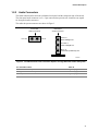
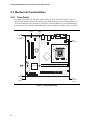
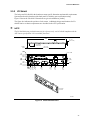
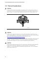
1
Intel® Desktop Board
D101GGC
Technical Product Specification
November 2005
Order Number: D36105-002US
The Intel® Desktop Board D101GGC may contain design defects or errors known as errata that may cause the product to deviate from published specifications. Current
characterized errata are documented in the Intel Desktop Board D101GGC Specification Update.
Revision History
Revision
Revision History
Date
Intel®
-001
First release of the
Specification.
Desktop Board D101GGC Technical Product
-002
Second release of the Intel® Desktop Board D101GGC Technical Product
Specification. Summary of changes: corrected name of Northbridge
component to read “ATI Radeon* Xpress 200 Northbridge”.
October 2005
November 2005
This product specification applies to only standard Intel Desktop Board D101GGC with BIOS
identifier GC11010N.86A.
Changes to this specification will be published in the Intel Desktop Board D101GGC Specification
Update before being incorporated into a revision of this document.
INFORMATION IN THIS DOCUMENT IS PROVIDED IN CONNECTION WITH INTEL® PRODUCTS. NO LICENSE,
EXPRESS OR IMPLIED, BY ESTOPPEL OR OTHERWISE, TO ANY INTELLECTUAL PROPERTY RIGHTS IS GRANTED
BY THIS DOCUMENT. EXCEPT AS PROVIDED IN INTEL’S TERMS AND CONDITIONS OF SALE FOR SUCH
PRODUCTS, INTEL ASSUMES NO LIABILITY WHATSOEVER, AND INTEL DISCLAIMS ANY EXPRESS OR IMPLIED
WARRANTY, RELATING TO SALE AND/OR USE OF INTEL PRODUCTS INCLUDING LIABILITY OR WARRANTIES
RELATING TO FITNESS FOR A PARTICULAR PURPOSE, MERCHANTABILITY, OR INFRINGEMENT OF ANY PATENT,
COPYRIGHT OR OTHER INTELLECTUAL PROPERTY RIGHT. INTEL PRODUCTS ARE NOT INTENDED FOR USE IN
MEDICAL, LIFE SAVING, OR LIFE SUSTAINING APPLICATIONS.
Intel Corporation may have patents or pending patent applications, trademarks, copyrights, or other intellectual property
rights that relate to the presented subject matter. The furnishing of documents and other materials and information does not
provide any license, express or implied, by estoppel or otherwise, to any such patents, trademarks, copyrights, or other
intellectual property rights.
Intel may make changes to specifications and product descriptions at any time, without notice.
Designers must not rely on the absence or characteristics of any features or instructions marked “reserved” or “undefined.”
Intel reserves these for future definition and shall have no responsibility whatsoever for conflicts or incompatibilities arising
from future changes to them.
Intel® desktop boards may contain design defects or errors known as errata, which may cause the product to deviate from
published specifications. Current characterized errata are available on request.
Contact your local Intel sales office or your distributor to obtain the latest specifications before placing your product order.
Copies of documents which have an ordering number and are referenced in this document, or other Intel literature, may be
obtained from:
Intel Corporation
P.O. Box 5937
Denver, CO 80217-9808
or call in North America 1-800-548-4725, Europe 44-0-1793-431-155, France 44-0-1793-421-777,
Germany 44-0-1793-421-333, other Countries 708-296-9333.
Intel, Pentium, and Celeron are registered trademarks of Intel Corporation or its subsidiaries in the United States and other
countries.
* Other names and brands may be claimed as the property of others.
Copyright © 2005, Intel Corporation. All rights reserved.
Preface
This Technical Product Specification (TPS) specifies the board layout, components, connectors,
power and environmental requirements, and the BIOS for the Intel® Desktop Board D101GGC. It
describes the standard product and available manufacturing options.
Intended Audience
The TPS is intended to provide detailed, technical information about the Desktop Board D101GGC
and its components to the vendors, system integrators, and other engineers and technicians who
need this level of information. It is specifically not intended for general audiences.
What This Document Contains
Chapter
1
2
Description
A description of the hardware used on the Desktop Board D101GGC
A map of the resources of the Desktop Board
Typographical Conventions
This section contains information about the conventions used in this specification. Not all of these
symbols and abbreviations appear in all specifications of this type.
Notes, Cautions, and Warnings
NOTE
Notes call attention to important information.
#
INTEGRATOR’S NOTES
Integrator’s notes are used to call attention to information that may be useful to system integrators.
CAUTION
Cautions are included to help you avoid damaging hardware or losing data.
WARNING
Warnings indicate conditions, which if not observed, can cause personal injury.
iii
Intel Desktop Board D101GGC Technical Product Specification
Other Common Notation
iv
#
Used after a signal name to identify an active-low signal (such as USBP0#)
(NxnX)
When used in the description of a component, N indicates component type, xn are the relative
coordinates of its location on the board, and X is the instance of the particular part at that
general location. For example, J5J1 is a connector, located at 5J. It is the first connector in
the 5J area.
GB
Gigabyte (1,073,741,824 bytes)
GB/sec
Gigabytes per second
KB
Kilobyte (1024 bytes)
Kbit
Kilobit (1024 bits)
kbits/sec
1000 bits per second
MB
Megabyte (1,048,576 bytes)
MB/sec
Megabytes per second
Mbit
Megabit (1,048,576 bits)
Mbit/sec
Megabits per second
xxh
An address or data value ending with a lowercase h indicates a hexadecimal value.
x.x V
Volts. Voltages are DC unless otherwise specified.
*
This symbol is used to indicate third-party brands and names that are the property of their
respective owners.
Contents
1 Product Description
1.1
Overview ...................................................................................................................... 10
1.1.1
Feature Summary.......................................................................................... 10
1.1.2
Block Diagram ............................................................................................... 11
1.1.3
Board Layout ................................................................................................. 12
1.2 Online Support ............................................................................................................. 14
1.3 Processor ..................................................................................................................... 14
1.4 System Memory ........................................................................................................... 15
1.5 ATI Radeon* Xpress 200 Chipset ................................................................................ 16
1.5.1
Graphics Subsystem ..................................................................................... 16
1.5.2
Firmware Hub (FWH) .................................................................................... 16
1.5.3
USB ............................................................................................................... 16
1.5.4
IDE Support ................................................................................................... 17
1.5.5
Real-Time Clock, CMOS SRAM, and Battery................................................ 18
1.6 PCI Express* Connectors ............................................................................................ 18
1.7 Legacy I/O Controller ................................................................................................... 19
1.7.1
Serial Port...................................................................................................... 19
1.7.2
Parallel Port ................................................................................................... 19
1.7.3
Diskette Drive Controller................................................................................ 19
1.7.4
Keyboard and Mouse Interface ..................................................................... 19
1.8 High Definition Audio Subsystem................................................................................. 20
1.8.1
Audio Subsystem Software ........................................................................... 20
1.8.2
Audio Connectors .......................................................................................... 21
1.9 LAN Subsystem ........................................................................................................... 22
1.9.1
LAN Subsystem Software.............................................................................. 22
1.10 Hardware Management Subsystem............................................................................. 23
1.10.1 Fan Monitoring............................................................................................... 23
1.10.2 Chassis Intrusion and Detection.................................................................... 23
1.11 Power Management ..................................................................................................... 23
1.11.1 ACPI .............................................................................................................. 24
1.11.2 Hardware Support ......................................................................................... 26
2 Technical Reference
2.1
2.2
2.3
2.4
2.5
2.6
2.7
2.8
Memory Map ................................................................................................................ 31
DMA Channels ............................................................................................................. 32
Fixed I/O Map............................................................................................................... 33
Interrupts ...................................................................................................................... 34
PCI Configuration Space Map...................................................................................... 35
PCI Conventional Interrupt Routing Map ..................................................................... 35
Connectors................................................................................................................... 36
2.7.1
Back Panel Connectors ................................................................................. 37
2.7.2
Component-side Connectors......................................................................... 38
2.7.3
Front Panel USB Connectors ........................................................................ 44
Jumper Block ............................................................................................................... 45
v
Intel Desktop Board D101GGC Technical Product Specification
2.9
2.10
2.11
2.12
2.13
2.14
Mechanical Considerations .......................................................................................... 46
2.9.1
Form Factor ................................................................................................... 46
2.9.2
I/O Shield....................................................................................................... 47
Electrical Considerations.............................................................................................. 48
2.10.1 DC Loading.................................................................................................... 48
2.10.2 Add-in Board Considerations......................................................................... 48
2.10.3 Fan Connector Current Capability ................................................................. 49
2.10.4 Power Supply Considerations ....................................................................... 49
Thermal Considerations ............................................................................................... 50
Reliability...................................................................................................................... 52
Environmental .............................................................................................................. 53
Regulatory Compliance................................................................................................ 54
2.14.1 Safety Regulations ........................................................................................ 54
2.14.2 European Union Declaration of Conformity Statement.................................. 54
2.14.3 Product Ecology Statements ......................................................................... 56
2.14.4 EMC Regulations........................................................................................... 59
2.14.5 Product Certification Markings (Board Level) ................................................ 60
3 Overview of BIOS Features
3.1
3.2
3.3
3.4
3.5
3.6
3.7
3.8
3.9
Introduction .................................................................................................................. 61
BIOS Flash Memory Organization ............................................................................... 62
Resource Configuration ............................................................................................... 62
3.3.1
PCI Autoconfiguration.................................................................................... 62
3.3.2
PCI IDE Support ............................................................................................ 62
System Management BIOS (SMBIOS) ........................................................................ 63
Legacy USB Support.................................................................................................... 63
BIOS Updates .............................................................................................................. 64
3.6.1
Language Support ......................................................................................... 64
3.6.2
Custom Splash Screen.................................................................................. 64
Boot Options ................................................................................................................ 65
3.7.1
CD-ROM Boot ............................................................................................... 65
3.7.2
Network Boot ................................................................................................. 65
3.7.3
Booting Without Attached Devices ................................................................ 65
3.7.4
Changing the Default Boot Device During POST .......................................... 65
Adjusting Boot Speed................................................................................................... 66
3.8.1
Peripheral Selection and Configuration ......................................................... 66
3.8.2
BIOS Boot Optimizations............................................................................... 66
BIOS Security Features ............................................................................................... 67
4 Error Messages and Beep Codes
4.1
4.2
4.3
4.4
vi
Speaker ....................................................................................................................... 69
BIOS Beep Code.......................................................................................................... 69
BIOS Error Messages .................................................................................................. 69
Port 80h POST Codes ................................................................................................. 70
Contents
Figures
1.
2.
3.
4.
5.
6.
7.
8.
9.
10.
11.
12.
13.
14.
Block Diagram.............................................................................................................. 11
Board Components ...................................................................................................... 12
Front/Back Panel Audio Connector Options for High Definition Audio Subsystem...... 21
LAN Connector LED Locations .................................................................................... 22
Location of the Standby Power Indicator LED ............................................................. 29
Back Panel Connectors................................................................................................ 37
Component-side Connectors ....................................................................................... 38
Connection Diagram for Front Panel Connector .......................................................... 43
Connection Diagram for Front Panel USB Connectors................................................ 44
Location of the Jumper Block....................................................................................... 45
Board Dimensions........................................................................................................ 46
I/O Shield Dimensions.................................................................................................. 47
Processor Heatsink for Omni-directional Airflow.......................................................... 50
Localized High Temperature Zones ............................................................................. 51
Tables
1.
2.
3.
4.
5.
6.
7.
8.
9.
10.
11.
12.
13.
14.
15.
16.
17.
18.
19.
20.
21.
22.
23.
24.
25.
26.
27.
28.
29.
30.
31.
Feature Summary ........................................................................................................ 10
Board Components Shown in Figure 2 ........................................................................ 13
Supported System Bus Frequency and Memory Speed Combinations ....................... 15
Supported Memory Configurations .............................................................................. 15
LAN Connector LED States ......................................................................................... 22
Effects of Pressing the Power Switch .......................................................................... 24
Power States and Targeted System Power ................................................................. 25
Wake-up Devices and Events ...................................................................................... 25
System Memory Map ................................................................................................... 31
DMA Channels ............................................................................................................. 32
I/O Map ........................................................................................................................ 33
Interrupts ...................................................................................................................... 34
PCI Configuration Space Map...................................................................................... 35
PCI Interrupt Routing Map ........................................................................................... 35
Back Panel Connectors Shown in Figure 6.................................................................. 37
Component-side Connectors Shown in Figure 7 ......................................................... 39
Front Panel Audio Connector....................................................................................... 39
Chassis Intrusion Connector ........................................................................................ 40
Serial ATA Connectors................................................................................................. 40
Processor Fan Connector ............................................................................................ 40
Chassis Fan Connectors.............................................................................................. 40
Main Power Connector................................................................................................. 41
ATX12V Power Connector ........................................................................................... 41
Auxiliary Front Panel Power/Sleep LED Connector ..................................................... 42
Front Panel Connector ................................................................................................. 42
States for a One-Color Power LED .............................................................................. 43
States for a Two-Color Power LED .............................................................................. 43
BIOS Setup Configuration Jumper Settings................................................................. 45
DC Loading Characteristics ......................................................................................... 48
Fan Connector Current Capability................................................................................ 49
Thermal Considerations for Components .................................................................... 52
vii
Intel Desktop Board D101GGC Technical Product Specification
32.
33.
34.
35.
36.
37.
38.
39.
40.
41.
42.
viii
Environmental Specifications ....................................................................................... 53
Safety Regulations ....................................................................................................... 54
Lead Free Desktop Board ............................................................................................ 58
EMC Regulations ......................................................................................................... 59
Product Certification Markings ..................................................................................... 60
BIOS Setup Program Menu Bar................................................................................... 62
BIOS Setup Program Function Keys............................................................................ 62
Boot Device Menu Options .......................................................................................... 65
Supervisor and User Password Functions ................................................................... 67
BIOS Error Messages .................................................................................................. 69
Port 80h POST Codes ................................................................................................. 70
1 Product Description
What This Chapter Contains
1.1
1.2
1.3
1.4
1.5
1.6
1.7
1.8
1.9
1.10
1.11
Overview ...................................................................................................................... 10
Online Support ............................................................................................................. 14
Processor ..................................................................................................................... 14
System Memory ........................................................................................................... 15
ATI Radeon* Xpress 200 Chipset ................................................................................ 16
PCI Express* Connectors ............................................................................................ 18
Legacy I/O Controller ................................................................................................... 19
High Definition Audio Subsystem................................................................................. 20
LAN Subsystem ........................................................................................................... 22
Hardware Management Subsystem............................................................................. 23
Power Management ..................................................................................................... 23
9
Intel Desktop Board D101GGC Technical Product Specification
1.1 Overview
1.1.1
Feature Summary
Table 1 summarizes the major features of the board.
Table 1.
10
Feature Summary
Form Factor
microATX (9.60 inches by 8.60 inches [243.84 millimeters by 218.44 millimeters])
Processor
Support for the following:
• Intel® Pentium® 4 processor in an LGA775 socket with an 800 or 533 MHz
system bus
• Intel® Celeron® D processor in an LGA775 socket with a 533 MHz system bus
Memory
• Two DDR SDRAM Dual Inline Memory Module (DIMM) sockets
• Support for DDR 400 MHz and DDR 333 MHz DIMMs
• Support for up to 2 GB of system memory
Chipset
• ATI Radeon* Xpress 200 Northbridge
• ATI IXP 450 Southbridge
• 4 Mbit Firmware Hub (FWH)
Video
ATI Radeon Xpress 200 Northbridge
Audio
High Definition Audio subsystem using the Realtek ALC861 audio codec
Legacy I/O Control
SMSC SCH5017 Legacy I/O controller for hardware management, diskette drive,
serial, parallel, and PS/2* ports
USB
Support for USB 2.0 devices
Peripheral
Interfaces
•
•
•
•
•
•
•
LAN Support
10/100 Mbits/sec LAN subsystem using the Realtek 8101L LAN adapter device
BIOS
AwardBIOS* for Intel® resident in the 4 Mbit FWH
Expansion
Capabilities
• Two PCI Conventional* bus connectors
• One PCI Express* x1 bus add-in card connector
• One PCI Express x16 bus add-in card connector
Instantly Available
PC Technology
•
•
•
•
Support for PCI Local Bus Specification Revision 2.2
Support for PCI Express Revision 1.0a
Suspend to RAM support
Wake on PCI, RS-232, front panel, PS/2 devices, and USB ports
Hardware Monitor
Subsystem
(controlled by SMSC
SCH5017 I/O
controller)
•
•
•
•
•
Voltage sense to detect out of range power supply voltages
Thermal sense to detect out of range thermal values
Three fan connectors
Three fan sense inputs used to monitor fan activity
Fan speed control
Eight USB ports
One serial port
One parallel port
Four Serial ATA interfaces
Two Parallel ATA IDE interfaces with UDMA 33, ATA-66/100 support
One diskette drive interface
PS/2 keyboard and mouse ports
For information about
Refer to
Available configurations for the Desktop Board D101GGC
Section 1.2, page 14
Product Description
1.1.2
Block Diagram
Figure 1 is a block diagram of the major functional areas of the board.
Back Panel/
Front Panel
USB Ports
USB
PCI Express x1 Slot 1
PCI Express x1 Interface
Parallel ATA
IDE Connectors (2)
LGA775
Processor Socket
SMSC
SCH5017
Legacy
I/O
Controller
Parallel ATA
IDE Interface
Serial Port
Parallel Port
PS/2 Mouse
PS/2 Keyboard
System Bus
(800/533 MHz)
Diskette Drive
Connector
ATI Radeon Xpress 200
Northbridge
Display Interface
Memory Bus
SMBus
High Definition Audio Link
Channel A
DIMMs (2)
4 Mbit
Firmware Hub
(FWH)
ATI IXP 450
Southbridge
PCI Bus
VGA
Port
PCI Express x4
Interface
LPC Bus
PCI Bus
PCI Slot 1
PCI Slot 2
Realtek
8101L
LAN Controller
Serial ATA
IDE Interface
LAN
Connector
Serial ATA IDE
Connectors (4)
Line In or Rear Left/Right Out
SMBus
Realtek
ALC861
Audio
Codec
Line Out or Front Left/Right Out
Mic In or Center/LFE Out
Line Out [Front Panel]
Mic In [Front Panel]
= connector or socket
OM18245
Figure 1. Block Diagram
11
Intel Desktop Board D101GGC Technical Product Specification
1.1.3
Board Layout
Figure 2 shows the location of the major components.
A B C D
E
DD
F
G
CC
H
BB
AA
Z
Y
I
X
J
W
V
K
L
U
T
S
RQP
O
N
M
OM18247
Figure 2. Board Components
Table 2 lists the components identified in Figure 2.
12
Product Description
Table 2.
Board Components Shown in Figure 2
Item/callout
from Figure 2
Description
A
Front panel audio connector
B
Audio codec
C
PCI Express x16 add-in card connector
D
Ethernet device
E
Back panel connectors
F
+12V power connector (ATX12V)
G
Rear chassis fan connector
H
LGA775 processor socket
I
ATI Radeon Xpress 200 Northbridge
J
DIMM Channel A sockets [2]
K
Processor fan connector
L
Chassis intrusion connector
M
Legacy I/O controller
N
Main power connector
O
Diskette drive connector
P
Parallel ATE IDE connectors [2]
Q
Battery
R
Front chassis fan connector
S
Serial ATA connectors [4]
T
Auxiliary front panel power LED connector
U
Front panel connector
V
4 Mbit Firmware Hub (FWH)
W
IXP 450 Southbridge
X
Speaker
Y
Front panel USB connector
Z
BIOS Setup configuration jumper block
AA
PCI Conventional bus add-in card connectors [2]
BB
Front panel USB connector
CC
PCI Express x1 bus add-in card connector
DD
Standby power indicator LED
13
Intel Desktop Board D101GGC Technical Product Specification
1.2 Online Support
To find information about…
Visit this World Wide Web site:
Intel Desktop Board D101GGC under
“Desktop Board Products” or “Desktop
Board Support”
http://www.intel.com/design/motherbd
http://support.intel.com/support/motherboards/desktop
Available configurations for the Desktop
Board D101GGC
http://developer.intel.com/design/motherbd/gc/gc_available.htm
Processor data sheets
http://www.intel.com/design/litcentr
Audio software and utilities
http://www.intel.com/design/motherbd
1.3 Processor
The board is designed to support the following processors:
•
•
Intel Pentium 4 processor in an LGA775 processor socket with an 800 or 533 MHz system bus
Intel Celeron D processor in an LGA775 processor socket with a 533 MHz system bus
For information about…
Refer to:
Supported processors for the D101GGC
board
http://www.intel.com/design/motherbd/gc/gc_documentation.htm
CAUTION
Use only the processors listed on web site above. Use of unsupported processors can damage the
board, the processor, and the power supply.
#
14
INTEGRATOR’S NOTE
•
•
Use only ATX12V-compliant power supplies.
Refer to Table 3 on page 15 for a list of supported system bus frequency and memory speed
combinations.
For information about
Refer to
Power supply connectors
Section 2.7.2.1, page 41
Product Description
1.4 System Memory
The board has two DIMM sockets and supports the following memory features:
•
•
2.5 V (only) DDR SDRAM DIMMs
Unbuffered, single-sided or double-sided DIMMs with the following restriction:
Double-sided DIMMS with x16 organization are not supported.
•
•
•
•
Minimum total system memory: 128 MB
Non-ECC DIMMs
Serial Presence Detect
DDR 400 MHz and DDR 333 MHz SDRAM DIMMs
Table 3 lists the supported system bus frequency and memory speed combinations.
Table 3.
Supported System Bus Frequency and Memory Speed Combinations
To use this type of DIMM…
The processor's system bus frequency must be…
DDR 400
800 MHz
DDR 333
800 or 533 MHz
NOTE
To be fully compliant with all applicable DDR SDRAM memory specifications, the board should be
populated with DIMMs that support the Serial Presence Detect (SPD) data structure. This allows
the BIOS to read the SPD data and program the chipset to accurately configure memory settings
for optimum performance. If non-SPD memory is installed, the BIOS will attempt to correctly
configure the memory settings, but performance and reliability may be impacted or the DIMMs
may not function under the determined frequency.
Table 4 lists the supported DIMM configurations.
Table 4.
Supported Memory Configurations
DIMM
Capacity
Configuration
SDRAM
Density
SDRAM Organization
Front-side/Back-side
Number of SDRAM
Devices
128 MB
SS
256 Mbit
16 M x 16/empty
4
256 MB
SS
256 Mbit
32 M x 8/empty
8
256 MB
SS
512 Mbit
32 M x 16/empty
4
512 MB
DS
256 Mbit
32 M x 8/32 M x 8
16
512 MB
SS
512 Mbit
64 M x 8/empty
8
512 MB
SS
1 Gbit
64 M x 16/empty
4
1024 MB
DS
512 Mbit
64 M x 8/64 M x 8
16
1024 MB
SS
1 Gbit
128 M x 8/empty
8
Note: In the second column, “DS” refers to double-sided memory modules (containing two rows of SDRAM) and “SS” refers
to single-sided memory modules (containing one row of SDRAM).
15
Intel Desktop Board D101GGC Technical Product Specification
1.5 ATI Radeon* Xpress 200 Chipset
The ATI Radeon Xpress 200 chipset consists of the following devices:
•
•
ATI Radeon Xpress 200 Northbridge
IXP 450 Southbridge
The ATI Radeon Xpress 200 Northbridge is a centralized controller for the system bus, the memory
bus, and the PCI Express bus. The ATI Radeon Xpress 200 Northbridge also provides integrated
graphics capabilities supporting 3D, 2D and display capabilities. The IXP 450 is a centralized
controller for the board’s I/O paths. The FWH provides the nonvolatile storage of the BIOS.
For information about
Refer to
The ATI Radeon Xpress 200 Northbridge
http://www.ati.com/
The IXP 450 Southbridge
http://www.ati.com/
Resources used by the chipset
Chapter 2
1.5.1
Graphics Subsystem
The board contains two separate, mutually exclusive graphics options. Either the integrated
graphics processor (contained within the ATI Radeon Xpress 200 Northbridge) is used, or a PCI
Express x16 add-in card can be used. When a PCI Express x16 add-in card is installed, the ATI
Radeon Xpress 200 Northbridge graphics controller is disabled.
1.5.2
Firmware Hub (FWH)
The Firmware Hub provides the nonvolatile storage of the AwardBIOS for Intel.
1.5.3
USB
The board supports up to eight USB 2.0 ports, supports UHCI and EHCI, and uses UHCI- and
EHCI-compatible drivers.
The IXP 450 Southbridge provides the USB controller for all ports. The port arrangement is as
follows:
•
•
Four ports are implemented with dual stacked back panel connectors adjacent to the audio
connectors
Four ports are routed to two separate front panel USB connectors
NOTE
Computer systems that have an unshielded cable attached to a USB port may not meet FCC
Class B requirements, even if no device is attached to the cable. Use shielded cable that meets the
requirements for full-speed devices.
16
For information about
Refer to
The location of the USB connectors on the back panel
Figure 6, page 37
The location of the front panel USB connectors
Figure 7, page 38
Product Description
1.5.4
IDE Support
The board provides six IDE interface connectors:
•
•
1.5.4.1
Two parallel ATA IDE connector that supports two devices
Four serial ATA IDE connectors that support one device per connector
Parallel ATE IDE Interface
The IXP 450’s Parallel ATA IDE controller has two bus-mastering Parallel ATA IDE interfaces.
The Parallel ATA IDE interfaces support the following modes:
•
•
•
•
•
Programmed I/O (PIO): processor controls data transfer.
8237-style DMA: DMA offloads the processor, supporting transfer rates of up to 16 MB/sec.
Ultra DMA: DMA protocol on IDE bus supporting host and target throttling and transfer rates
of up to 33 MB/sec.
ATA-66: DMA protocol on IDE bus supporting host and target throttling and transfer rates of
up to 66 MB/sec. ATA-66 protocol is similar to Ultra DMA and is device driver compatible.
ATA-100: DMA protocol on IDE bus allows host and target throttling. The IXP 450’s
ATA-100 logic can achieve read transfer rates up to 100 MB/sec and write transfer rates up to
88 MB/sec.
NOTE
ATA-66 and ATA-100 are faster timings and require a specialized cable to reduce reflections,
noise, and inductive coupling.
The Parallel ATA IDE interfaces also support ATAPI devices (such as CD-ROM drives) and ATA
devices using the transfer modes.
For information about
Refer to
The location of the Parallel ATA IDE connectors
Figure 7, page 38
1.5.4.2
Serial ATA Interfaces
The IXP 450’s Serial ATA controller offers four independent Serial ATA ports with a theoretical
maximum transfer rate of 150 MB/s per port. One device can be installed on each port for a
maximum of four Serial ATA devices. A point-to-point interface is used for host to device
connections, unlike Parallel ATA IDE which supports a master/slave configuration and two devices
per channel.
For compatibility, the underlying Serial ATA functionality is transparent to the operating system.
The Serial ATA controller can operate in both legacy and native modes. In legacy mode, standard
IDE I/O and IRQ resources are assigned (IRQ 14 and 15). In Native mode, standard PCI
Conventional bus resource steering is used. Native mode is the preferred mode for configurations
using the Windows* XP and Windows 2000 operating systems.
17
Intel Desktop Board D101GGC Technical Product Specification
NOTE
Many Serial ATA drives use new low-voltage power connectors and require adaptors or power
supplies equipped with low-voltage power connectors.
For more information, see: http://www.serialata.org/
For information about
Refer to
The location of the Serial ATA IDE connectors
Figure 7, page 38
1.5.5
Real-Time Clock, CMOS SRAM, and Battery
A coin-cell battery (CR2032) powers the real-time clock and CMOS memory. When the computer
is not plugged into a wall socket, the battery has an estimated life of three years. When the
computer is plugged in, the standby current from the power supply extends the life of the battery.
The clock is accurate to ± 13 minutes/year at 25 ºC with 3.3 VSB applied.
NOTE
If the battery and AC power fail, custom defaults, if previously saved, will be loaded into CMOS
RAM at power-on.
1.6 PCI Express* Connectors
The board provides the following PCI Express connectors:
•
•
One PCI Express x16 connector supporting simultaneous transfer speeds up to 8 GBytes/sec
One PCI Express x1 connector. The x1 interface supports simultaneous transfer speeds up to
500 MBytes/sec
The PCI Express interface supports the PCI Conventional bus configuration mechanism so that the
underlying PCI Express architecture is compatible with PCI Conventional compliant operating
systems. Additional features of the PCI Express interface include the following:
•
•
•
•
•
•
18
Support for the PCI Express enhanced configuration mechanism
Automatic discovery, link training, and initialization
Support for Active State Power Management (ASPM)
SMBus 2.0 support
Wake# signal supporting wake events from ACPI S1, S3, S4, or S5
Software compatible with the PCI Power Management Event (PME) mechanism defined in the
PCI Power Management Specification Rev. 1.1
Product Description
1.7 Legacy I/O Controller
The SMSC SCH5017 Legacy I/O controller provides the following features:
•
•
•
•
•
•
•
One serial port
One parallel port with Extended Capabilities Port (ECP) and Enhanced Parallel Port
(EPP) support
Serial IRQ interface compatible with serialized IRQ support for PCI Conventional bus systems
PS/2-style mouse and keyboard interfaces
Interface for one 1.44 MB or 2.88 MB diskette drive
Intelligent power management, including a programmable wake-up event interface
PCI Conventional bus power management support
The BIOS Setup program provides configuration options for the I/O controller.
1.7.1
Serial Port
The Serial port A connector is located on the back panel. The serial port supports data transfers at
speeds up to 115.2 kbits/sec with BIOS support.
For information about
Refer to
The location of the serial port A connector
Figure 6, page 37
1.7.2
Parallel Port
The 25-pin D-Sub parallel port connector is located on the back panel. Use the BIOS Setup
program to set the parallel port mode.
For information about
Refer to
The location of the parallel port connector
Figure 6, page 37
1.7.3
Diskette Drive Controller
The I/O controller supports one diskette drive. Use the BIOS Setup program to configure the
diskette drive interface.
For information about
Refer to
The location of the diskette drive connector
Figure 7, page 38
1.7.4
Keyboard and Mouse Interface
PS/2 keyboard and mouse connectors are located on the back panel.
NOTE
The keyboard is supported in the bottom PS/2 connector and the mouse is supported in the top PS/2
connector. Power to the computer should be turned off before a keyboard or mouse is connected or
disconnected.
For information about
Refer to
The location of the keyboard and mouse connectors
Figure 6, page 37
19
Intel Desktop Board D101GGC Technical Product Specification
1.8 High Definition Audio Subsystem
The board includes a flexible 6-channel audio subsystem based on an Intel® High Definition Audio
interface. The audio subsystem features:
•
•
•
•
•
ATI IXP 450 Southbridge
Realtek ALC861 audio codec
Impedance sensing capability for jack re-tasking
S/N (signal-to-noise) ratio of 90 dB
Microphone input supporting:
⎯ Stereo microphone
⎯ Microphone boost
#
INTEGRATOR’S NOTE
For the front panel jack sensing and automatic retasking feature to function, a front panel daughter
card that is designed for Intel High Definition Audio must be used. Otherwise, an AC ’97 style
audio front panel connector will be assumed and the Line Out and Mic In functions will be
permanent.
1.8.1
Audio Subsystem Software
Audio software and drivers are available from Intel’s World Wide Web site.
20
For information about
Refer to
Obtaining audio software and drivers
Section 1.2, page 14
Product Description
1.8.2
Audio Connectors
The board contains audio connector on both the back panel and the component side of the board.
The front panel audio connector is a 2 x 5-pin connector that provides mic in and line out signals
for front panel audio connectors.
The audio subsystem connectors are shown in Figure 3.
Back Panel
Audio Connectors
Front Panel
Audio Connectors
Line Out
Mic In
Line In or
Rear Left/Right Out
Line Out or
Front Left/Right Out
Mic In or
Center/LFE (Subwoofer) Out
OM18246
Figure 3. Front/Back Panel Audio Connector Options for High Definition Audio Subsystem
For information about
Refer to
The location of the front panel audio connector
Figure 7, page 38
The signal names of the front panel audio connector
Table 17, page 39
The back panel audio connectors
Figure 6, page 37
21
Intel Desktop Board D101GGC Technical Product Specification
1.9 LAN Subsystem
The LAN subsystem consists of the following:
•
•
•
•
Realtek 8101L LAN adapter device for 10/100 Mbits/sec Ethernet LAN connectivity
RJ-45 LAN connector with integrated status LEDs
Programmable transit threshold
Configurable EEPROM that contains the MAC address
Two LEDs are built into the RJ-45 LAN connector (shown in Figure 4).
Green LED
Yellow LED
OM15076
Figure 4. LAN Connector LED Locations
Table 5 describes the LED states when the board is powered up and the 10/100 Mbits/sec LAN
subsystem is operating.
Table 5.
LAN Connector LED States
LED Color
LED State
Condition
Green
Off
LAN link is not established.
On
LAN link is established.
Blinking
LAN activity is occurring.
Off
10 Mbits/sec data rate is selected.
On
100 Mbits/sec data rate is selected.
Yellow
1.9.1
LAN Subsystem Software
LAN software and drivers are available from Intel’s World Wide Web site.
22
For information about
Refer to
Obtaining LAN software and drivers
Section 1.2, page 14
Product Description
1.10 Hardware Management Subsystem
The hardware management features enable the board to be compatible with the Wired for
Management (WfM) specification. The SMSC SCH5017 I/O controller is used to implement
hardware monitoring and fan control. The features of the SMSC SCH5017 I/O controller include:
•
•
•
•
•
1.10.1
Internal ambient temperature sensor
Two remote thermal diode sensors for direct monitoring of processor temperature and ambient
temperature sensing
Power supply monitoring of five voltages (+5 V, +12 V, +3.3 VSB, +1.5 V, and +VCCP) to
detect levels above or below acceptable values
Thermally monitored closed-loop fan control, for all three fans, that can adjust the fan speed or
switch the fans on or off as needed
SMBus interface
Fan Monitoring
Fan monitoring can be implemented using Intel® Desktop Utilities, LANDesk* software, or thirdparty software.
For information about
Refer to
The functions of the fan connectors
Section 1.11.2.2, page 27
1.10.2
Chassis Intrusion and Detection
The board supports a chassis security feature that detects if the chassis cover is removed. The
security feature uses a mechanical switch on the chassis that attaches to the chassis intrusion
connector. When the chassis cover is removed, the mechanical switch is in the closed position.
For information about
Refer to
The location of the chassis intrusion connector
Figure 7, page 38
The signal names of the chassis intrusion connector
Table 18, page 40
1.11 Power Management
Power management is implemented at several levels, including:
•
•
Software support through Advanced Configuration and Power Interface (ACPI)
Hardware support:
⎯ Power connector
⎯ Fan connectors
⎯ LAN wake capabilities
⎯ Instantly Available PC technology
⎯ Resume on Ring
⎯ Wake from USB
⎯ Wake from PS/2 devices
⎯ Power Management Event signal (PME#) wake-up support
23
Intel Desktop Board D101GGC Technical Product Specification
1.11.1
ACPI
ACPI gives the operating system direct control over the power management and Plug and Play
functions of a computer. The use of ACPI with this board requires an operating system that
provides full ACPI support. ACPI features include:
•
•
•
•
•
•
Plug and Play (including bus and device enumeration)
Power management control of individual devices, add-in boards (some add-in boards may
require an ACPI-aware driver), video displays, and hard disk drives
Methods for achieving less than 15-watt system operation in the power-on/standby
sleeping state
A Soft-off feature that enables the operating system to power-off the computer
Support for multiple wake-up events (see Table 8 on page 25)
Support for a front panel power and sleep mode switch
Table 6 lists the system states based on how long the power switch is pressed, depending on how
ACPI is configured with an ACPI-aware operating system.
Table 6.
Effects of Pressing the Power Switch
If the system is in this state…
Off
(ACPI G2/G5 – Soft off)
On
(ACPI G0 – working state)
On
(ACPI G0 – working state)
Sleep
(ACPI G1 – sleeping state)
Sleep
(ACPI G1 – sleeping state)
1.11.1.1
…and the power switch is
pressed for
Less than four seconds
Less than four seconds
More than four seconds
Less than four seconds
More than four seconds
…the system enters this state
Power-on
(ACPI G0 – working state)
Soft-off/Standby
(ACPI G1 – sleeping state)
Fail safe power-off
(ACPI G2/G5 – Soft off)
Wake-up
(ACPI G0 – working state)
Power-off
(ACPI G2/G5 – Soft off)
System States and Power States
Under ACPI, the operating system directs all system and device power state transitions. The
operating system puts devices in and out of low-power states based on user preferences and
knowledge of how devices are being used by applications. Devices that are not being used can be
turned off. The operating system uses information from applications and user settings to put the
system as a whole into a low-power state.
Table 7 lists the power states supported by the board along with the associated system power
targets. See the ACPI specification for a complete description of the various system and power
states.
24
Product Description
Table 7.
Power States and Targeted System Power
Global States
G0 – working
state
G1 – sleeping
state
Sleeping States
S0 – working
Processor
States
C0 – working
S1 – Processor
stopped
C1 – stop
grant
G1 – sleeping
state
S3 – Suspend to
RAM. Context
saved to RAM.
S4 – Suspend to
disk. Context
saved to disk.
S5 – Soft off.
Context not saved.
Cold boot is
required.
No power to the
system.
No power
G1 – sleeping
state
G2/S5
G3 –
mechanical off
AC power is
disconnected
from the
computer.
No power
No power
No power
Device States
D0 – working state.
Targeted System
Power (Note 1)
Full power > 30 W
D1, D2, D3 – device
specification
specific.
D3 – no power
except for wake-up
logic.
D3 – no power
except for wake-up
logic.
D3 – no power
except for wake-up
logic.
5 W < power < 52.5 W
D3 – no power for
wake-up logic,
except when
provided by battery
or external source.
No power to the system.
Service can be
performed safely.
Power < 5 W
(Note 2)
Power < 5 W
(Note 2)
Power < 5 W
(Note 2)
Notes:
1.
Total system power is dependent on the system configuration, including add-in boards and peripherals powered
by the system chassis’ power supply.
2.
Dependent on the standby power consumption of wake-up devices used in the system.
1.11.1.2
Wake-up Devices and Events
Table 8 lists the devices or specific events that can wake the computer from specific states.
Table 8.
Wake-up Devices and Events
These devices/events can wake up the computer…
…from this state
LAN
S1, S3, S4, S5 (Note)
Modem (back panel Serial Port A)
S1, S3
PME# signal
S1, S3, S4, S5 (Note)
Power switch
S1, S3, S4, S5
PS/2 devices
S1, S3
RTC alarm
S1, S3, S4, S5
USB
S1, S3
WAKE# signal
Note:
S1, S3, S4, S5
For LAN and PME# signal, S5 is disabled by default in the BIOS Setup program. Setting this option to Power On
will enable a wake-up event from LAN in the S5 state.
25
Intel Desktop Board D101GGC Technical Product Specification
NOTE
The use of these wake-up events from an ACPI state requires an operating system that provides full
ACPI support. In addition, software, drivers, and peripherals must fully support ACPI wake
events.
1.11.2
Hardware Support
CAUTION
Ensure that the power supply provides adequate +5 V standby current if LAN wake capabilities and
Instantly Available PC technology features are used. Failure to do so can damage the power
supply. The total amount of standby current required depends on the wake devices supported and
manufacturing options.
The board provides several power management hardware features, including:
•
•
•
•
•
•
•
•
•
Power connector
Fan connectors
LAN wake capabilities
Instantly Available PC technology
Resume on Ring
Wake from USB
Wake from PS/2 keyboard
PME# signal wake-up support
WAKE# signal wake-up support
LAN wake capabilities and Instantly Available PC technology require power from the +5 V
standby line.
Resume on Ring enables telephony devices to access the computer when it is in a power-managed
state. The method used depends on the type of telephony device (external or internal).
NOTE
The use of Resume on Ring and Wake from USB technologies from an ACPI state requires an
operating system that provides full ACPI support.
26
Product Description
1.11.2.1
Power Connector
ATX12V-compliant power supplies can turn off the system power through system control. When
an ACPI-enabled system receives the correct command, the power supply removes all non-standby
voltages.
When resuming from an AC power failure, the computer returns to the power state it was in before
power was interrupted (on or off). The computer’s response can be set using the Last Power State
feature in the BIOS Setup program’s Boot menu.
For information about
Refer to
The location of the main power connector
Figure 7, page 38
The signal names of the main power connector
Table 22, page 41
1.11.2.2
Fan Connectors
The function/operation of the fan connectors is as follows:
•
•
•
•
•
The fans are on when the board is in the S0 or S1 state.
The fans are off when the board is off or in the S3, S4, or S5 state.
Each fan connector is wired to a fan tachometer input of the SMSC SCH5017 I/O controller.
All fan connectors support closed-loop fan control that can adjust the fan speed or switch the
fan on or off as needed.
All fan connectors have a +12 V DC connection.
For information about
Refer to
The signal names of the processor fan connector
Table 20, page 40
The signal names of the chassis fan connectors
Table 21, page 40
1.11.2.3
LAN Wake Capabilities
CAUTION
For LAN wake capabilities, the +5 V standby line for the power supply must be capable of
providing adequate +5 V standby current. Failure to provide adequate standby current when
implementing LAN wake capabilities can damage the power supply.
LAN wake capabilities enable remote wake-up of the computer through a network. The LAN
network adapter monitors network traffic at the Media Independent Interface. Upon detecting a
Magic Packet* frame, the LAN subsystem asserts a wake-up signal that powers up the computer.
Depending on the LAN implementation, the board supports LAN wake capabilities with ACPI in
the following ways:
•
•
•
The PCI Express WAKE# signal
The PCI Conventional bus PME# signal for PCI 2.2 compliant LAN designs
The onboard LAN subsystem
27
Intel Desktop Board D101GGC Technical Product Specification
1.11.2.4
Instantly Available PC Technology
CAUTION
For Instantly Available PC technology, the +5 V standby line for the power supply must be capable
of providing adequate +5 V standby current. Failure to provide adequate standby current when
implementing Instantly Available PC technology can damage the power supply.
Instantly Available PC technology enables the board to enter the ACPI S3 (Suspend-to-RAM)
sleep-state. While in the S3 sleep-state, the computer will appear to be off (the power supply is off,
and the front panel LED is amber if dual colored, or off if single colored.) When signaled by a
wake-up device or event, the system quickly returns to its last known wake state. Table 8 on
page 25 lists the devices and events that can wake the computer from the S3 state.
The board supports the PCI Bus Power Management Interface Specification. Add-in boards that
also support this specification can participate in power management and can be used to wake the
computer.
The use of Instantly Available PC technology requires operating system support and PCI 2.2
compliant add-in cards, PCI Express add-in cards, and drivers.
1.11.2.5
Resume on Ring
The operation of Resume on Ring can be summarized as follows:
•
•
•
1.11.2.6
Resumes operation from ACPI S1 or S3 states
Detects incoming call similarly for external and internal modems
Requires modem interrupt be unmasked for correct operation
Wake from USB
USB bus activity wakes the computer from ACPI S1 or S3 states.
NOTE
Wake from USB requires the use of a USB peripheral that supports Wake from USB.
1.11.2.7
Wake from PS/2 Devices
PS/2 device activity wakes the computer from an ACPI S1 or S3 state.
1.11.2.8
PME# Signal Wake-up Support
When the PME# signal on the PCI Conventional bus is asserted, the computer wakes from an ACPI
S1, S3, S4, or S5 state (with Wake on PME enabled in BIOS).
1.11.2.9
WAKE# Signal Wake-up Support
When the WAKE# signal on the PCI Express bus is asserted, the computer wakes from an ACPI
S1, S3, S4, or S5 state.
28
Product Description
1.11.2.10
+5 V Standby Power Indicator LED
The +5 V standby power indicator LED shows that power is still present even when the computer
appears to be off. Figure 5 shows the location of the standby power indicator LED.
CAUTION
If AC power has been switched off and the standby power indicator is still lit, disconnect the power
cord before installing or removing any devices connected to the board. Failure to do so could
damage the board and any attached devices.
CR1
OM19010
Figure 5. Location of the Standby Power Indicator LED
29
Intel Desktop Board D101GGC Technical Product Specification
30
2 Technical Reference
What This Chapter Contains
2.1
2.2
2.3
2.4
2.5
2.6
2.7
2.8
2.9
2.10
2.11
2.12
2.13
2.14
Memory Map ................................................................................................................ 31
DMA Channels ............................................................................................................. 32
Fixed I/O Map............................................................................................................... 33
Interrupts ...................................................................................................................... 34
PCI Configuration Space Map...................................................................................... 35
PCI Conventional Interrupt Routing Map ..................................................................... 35
Connectors................................................................................................................... 36
Jumper Block ............................................................................................................... 45
Mechanical Considerations .......................................................................................... 46
Electrical Considerations.............................................................................................. 48
Thermal Considerations ............................................................................................... 50
Reliability...................................................................................................................... 52
Environmental .............................................................................................................. 53
Regulatory Compliance................................................................................................ 54
2.1 Memory Map
Table 9 lists the system memory map.
Table 9.
System Memory Map
Address Range (decimal)
Address Range (hex)
Size
Description
1024 K - 4194304 K
100000 - FFFFFFFF
4095 MB
Extended memory
960 K - 1024 K
F0000 - FFFFF
64 KB
Runtime BIOS
896 K - 960 K
E8000 - EFFFF
32 KB
Reserved
800 K - 896 K
C8000 – E7FFF
128 KB
Potential available high DOS
memory (open to the PCI
Conventional bus). Dependent on
video adapter used.
640 K - 800 K
A0000 - C7FFF
160 KB
Video memory and BIOS
639 K - 640 K
9FC00 - 9FFFF
1 KB
Extended BIOS data (movable by
memory manager software)
512 K - 639 K
80000 - 9FBFF
127 KB
Extended conventional memory
0 K - 512 K
00000 - 7FFFF
512 KB
Conventional memory
31
Intel Desktop Board D101GGC Technical Product Specification
2.2 DMA Channels
Table 10.
32
DMA Channels
DMA Channel Number
Data Width
System Resource
0
8 or 16 bits
Open
1
8 or 16 bits
Parallel port
2
8 or 16 bits
Diskette drive
3
8 or 16 bits
Parallel port (for ECP or EPP)
4
8 or 16 bits
DMA controller
5
16 bits
Open
6
16 bits
Open
7
16 bits
Open
Technical Reference
2.3 Fixed I/O Map
Table 11.
I/O Map
Address (hex)
Size
Description
0000 - 00FF
256 bytes
0170 - 0177
01F0 - 01F7
8 bytes
8 bytes
Used by the Desktop Board D101GGC. Refer to the
IXP 450 data sheet for dynamic addressing information.
Secondary Parallel ATA IDE channel command block
Primary Parallel ATA IDE channel command block
0228 - 022F (Note 1)
0278 - 027F (Note 1)
02E8 - 02EF (Note 1)
02F8 - 02FF (Note 1)
0374 - 0377
0377, bits 6:0
0378 - 037F
03E8 - 03EF
03F0 - 03F5
03F6 – 03F7
03F8 - 03FF
04D0 - 04D1
LPTn + 400
0CF8 - 0CFB (Note 2)
0CF9 (Note 3)
0CFC - 0CFF
FB00 – FB07
FB08 – FB0F
8 bytes
8 bytes
8 bytes
8 bytes
4 bytes
7 bits
8 bytes
8 bytes
6 bytes
1 byte
8 bytes
2 bytes
8 bytes
4 bytes
1 byte
4 bytes
8 bytes
8 bytes
LPT3
LPT2
COM4
COM2
Secondary Parallel ATA IDE channel control block
Secondary IDE channel status port
LPT1
COM3
Diskette channel
Primary Parallel ATA IDE channel control block
COM1
Edge/level triggered PIC
ECP port, LPTn base address + 400h
PCI Conventional bus configuration address register
Reset control register
PCI Conventional bus configuration data register
Primary Parallel ATA IDE bus master registers
Secondary Parallel ATA IDE bus master registers
Notes:
1.
Default, but can be changed to another address range
2.
Dword access only
3.
Byte access only
NOTE
Some additional I/O addresses are not available due to IXP 450 address aliasing. The IXP 450
data sheet provides more information on address aliasing.
33
Intel Desktop Board D101GGC Technical Product Specification
2.4 Interrupts
The interrupts can be routed through either the Programmable Interrupt Controller (PIC) or the
Advanced Programmable Interrupt Controller (APIC) portion of the IXP 450 Southbridge
component. The PIC is supported in Windows 98 SE and Windows ME and uses the first
16 interrupts. The APIC is supported in Windows 2000 and Windows XP and supports a total of
24 interrupts.
Table 12.
Interrupts
IRQ
System Resource
NMI
I/O channel check
0
Reserved, interval timer
1
Reserved, keyboard buffer full
2
Reserved, cascade interrupt from slave PIC
3
COM2 (Note 1)
4
COM1 (Note 1)
5
LPT2 (Plug and Play option)/User available
6
Diskette drive
7
LPT1 (Note 1)
8
Real-time clock
9
User available
10
User available
11
User available
12
Onboard mouse port (if present, else user available)
13
Reserved, math coprocessor
14
Primary IDE/Serial ATA (if present, else user available)
15
Secondary IDE/Serial ATA (if present, else user available)
(Note 2)
User available (through PIRQA)
17 (Note 2)
User available (through PIRQB)
18
(Note 2)
User available (through PIRQC)
19
(Note 2)
User available (through PIRQD)
20
(Note 2)
User available (through PIRQE)
21 (Note 2)
User available (through PIRQF)
22
(Note 2)
User available (through PIRQG)
23
(Note 2)
User available (through PIRQH)
16
Notes:
34
1.
Default, but can be changed to another IRQ.
2.
Available in APIC mode only.
Technical Reference
2.5 PCI Configuration Space Map
Table 13.
PCI Configuration Space Map
Bus
Number (hex)
Device
Number (hex)
Function
Number (hex)
Description
00
00
00
ATI Host Bridge
00
02
00
ATI PCI Express x16 port Bridge (Note 1)
00
06
00
ATI PCI Express x1 port Bridge (Note 2)
00
11
00
ATI IDE controller
00
12
00
ATI IDE controller
00
13
00
ATI USB OHCI controller 1
00
13
01
ATI USB OHCI controller 2
00
13
02
ATI USB OHCI controller 3
00
14
00
ATI SMBus controller
00
14
01
ATI IDE controller
00
14
02
ATI Azalia controller
00
14
03
ATI ISA bridge
00
14
04
ATI Decode PCI/PCI bridge
05
00
ATI VGA controller
01
01
(Notes 1 and 3)
PCI Express x16 connector
02 (Notes 2 and 3)
PCI Express x1 connector
02 (Note 3)
02
00
Ethernet controller
(Note 3)
03
00
PCI Conventional bus connector 1
03 (Note 3)
04
00
PCI Conventional bus connector 2
03
Notes:
1.
Present only when a PCI Express x16 graphics card is installed.
2.
Present only when a PCI Express x1 add-in card is installed.
3.
Bus number is dynamic and can change based on add-in cards used.
2.6 PCI Conventional Interrupt Routing Map
Table 14 lists how the PIRQ signals are routed.
Table 14.
PCI Interrupt Routing Map
IXP 450 PIRQ Signal Name
PCI Interrupt Source
PIRQA
PIRQB
PCI bus connector 1
INTA
INTB
INTC
INTD
PCI bus connector 2
INTB
INTC
INTD
INTA
Realtek LAN
INTF
PIRQC
PIRQD
PIRQE
PIRQF
PIRQG
PIRQH
35
Intel Desktop Board D101GGC Technical Product Specification
2.7 Connectors
CAUTION
Only the following connectors have overcurrent protection: back panel USB, front panel USB, and
PS/2.
The other internal connectors are not overcurrent protected and should connect only to devices
inside the computer’s chassis, such as fans and internal peripherals. Do not use these connectors
to power devices external to the computer’s chassis. A fault in the load presented by the external
devices could cause damage to the computer, the power cable, and the external devices themselves.
This section describes the board’s connectors. The connectors can be divided into these groups:
•
•
36
Back panel I/O connectors (see page 37)
Component-side I/O connectors (see page 38)
Technical Reference
2.7.1
Back Panel Connectors
Figure 6 shows the location of the back panel connectors. The back panel connectors are
color-coded. The figure legend (Table 15) lists the colors used (when applicable).
A
B
C
D
G
E
F
I
H
J
OM18248
Figure 6. Back Panel Connectors
Table 15.
Back Panel Connectors Shown in Figure 6
Item/callout
from Figure 6
A
Description
PS/2 mouse port (Green)
B
PS/2 keyboard port (Purple)
C
Parallel port (Burgundy)
D
Serial port A (Teal)
E
VGA port
F
USB ports [4]
G
LAN
H
Line in or Rear Left/Right Out
I
Line out or Front Left/Right Out
J
Mic in or Center/LFE (Subwoofer) Out
NOTE
The back panel audio line out connector is designed to power headphones or amplified speakers
only. Poor audio quality occurs if passive (non-amplified) speakers are connected to this output.
37
Intel Desktop Board D101GGC Technical Product Specification
2.7.2
Component-side Connectors
Figure 7 shows the locations of the component-side connectors.
A
B C D E
10
9
2
1
F
2 4
G
1
3
1
V
2
7
10
1
U
2
7
10
1
1
T
1 3
9
1
2
1
2
1 3
1
1
SR Q
1
P
2
1
ONM
40 39 24
13
40
1 1
39
L
1
4
1
2
1
H
I
33
K
J
OM19009
Figure 7. Component-side Connectors
Table 16 lists the component-side connectors identified in Figure 7.
38
Technical Reference
Table 16.
Component-side Connectors Shown in Figure 7
Item/callout
from Figure 7
PCI Conventional bus add-in card connector 2
B
PCI Conventional bus add-in card connector 1
C
Front panel audio connector
D
PCI Express x1 bus add-in card connector
E
PCI Express x16 add-in card connector
F
Rear chassis fan connector
G
+12V power connector (ATX12V)
H
Processor fan connector
I
Chassis intrusion connector
J
Main power connector
K
Diskette drive connector
L
Primary parallel ATA IDE connector
M
Secondary parallel ATA IDE connector
N
Serial ATA connector 1
O
Front chassis fan connector
P
Serial ATA connector 2
Q
Serial ATA connector 4
R
Serial ATA connector 3
S
Auxiliary front panel power LED connector
T
Front panel connector
U
Front panel USB connector
V
Front panel USB connector
Table 17.
#
Description
A
Front Panel Audio Connector
Pin
Signal Name
Pin
Signal Name
1
Port F Left Channel
2
Ground
3
Port F Right Channel
4
Presence# (dongle present)
5
Port E Right Channel
6
Port F Sense return
(jack detection)
7
Port E and Port F
Sense send (jack detection)
8
Key
9
Port E Left Channel
10
Port E Sense return
(jack detection)
INTEGRATOR’S NOTE
The front panel audio connector is colored yellow.
39
Intel Desktop Board D101GGC Technical Product Specification
Table 18.
Pin
Signal Name
1
Intruder
2
Ground
Table 19.
Serial ATA Connectors
Pin
Signal Name
1
Ground
2
TXP
3
TXN
4
Ground
5
RXN
6
RXP
7
Ground
Table 20.
Processor Fan Connector
Pin
Signal Name
1
Ground
2
+12 V
3
FAN_TACH
4
FAN_CONTROL
Table 21.
40
Chassis Intrusion Connector
Chassis Fan Connectors
Pin
Signal Name
1
Control
2
+12 V
3
Tach
Technical Reference
2.7.2.1
Power Supply Connectors
The board has three power supply connectors:
•
•
Main power – a 2 x 12 connector. This connector is compatible with 2 x 10 connectors
previously used on Intel Desktop boards. The board supports the use of ATX12V power
supplies with either 2 x 10 or 2 x 12 main power cables. When using a power supply with a
2 x 10 main power cable, attach that cable on the rightmost pins of the main power connector,
leaving pins 11, 12, 23, and 24 unconnected.
ATX12V power – a 2 x 2 connector. This connector provides power directly to the processor
voltage regulator and must always be used. Failure to do so will prevent the board from
booting.
Table 22.
Pin
Main Power Connector
Signal Name
Pin
Signal Name
1
+3.3 V
13
+3.3 V
2
+3.3 V
14
-12 V
3
Ground
15
Ground
4
+5 V
16
PS-ON# (power supply remote on/off)
5
Ground
17
Ground
6
+5 V
18
Ground
7
Ground
19
Ground
8
PWRGD (Power Good)
20
No connect
9
+5 V (Standby)
21
+5 V
10
+12 V
22
+5 V
11
+12 V
23
+5 V
24
Ground
12
(Note)
2 x 12 connector detect
(Note)
(Note)
(Note)
Note: When using a 2 x 10 power supply cable, this pin will be unconnected.
Table 23.
ATX12V Power Connector
Pin
Signal Name
Pin
Signal Name
1
Ground
2
Ground
3
+12 V
4
+12 V
41
Intel Desktop Board D101GGC Technical Product Specification
2.7.2.2
Add-in Card Connectors
The board has the following add-in card connectors:
•
•
•
PCI Express x16: one connector supporting simultaneous transfer speeds up to 8 GBytes/sec.
PCI Express x1: one PCI Express x1 connector. The x1 interface supports simultaneous
transfer speeds up to 500 MBytes/sec.
PCI Conventional (rev 2.3 compliant) bus: two PCI Conventional bus add-in card connectors.
The SMBus is routed to PCI Conventional bus connector 2 only (ATX expansion slot 6). PCI
Conventional bus add-in cards with SMBus support can access sensor data and other
information residing on the board.
Note the following considerations for the PCI Conventional bus connectors:
•
•
All of the PCI Conventional bus connectors are bus master capable.
SMBus signals are routed to PCI Conventional bus connector 2. This enables PCI
Conventional bus add-in boards with SMBus support to access sensor data on the board. The
specific SMBus signals are as follows:
⎯ The SMBus clock line is connected to pin A40.
2.7.2.3
Auxiliary Front Panel Power/Sleep LED Connector
Pins 1 and 3 of this connector duplicate the signals on pins 2 and 4 of the front panel connector.
Table 24.
Auxiliary Front Panel Power/Sleep LED Connector
Pin
Signal Name
In/Out
Description
1
HDR_BLNK_GRN
Out
Front panel green LED
2
Not connected
3
HDR_BLNK_YEL
Out
Front panel yellow LED
2.7.2.4
Front Panel Connector
This section describes the functions of the front panel connector. Table 25 lists the signal names of
the front panel connector. Figure 8 is a connection diagram for the front panel connector.
Table 25.
Pin
Front Panel Connector
Signal
In/Out
Description
Pin
Signal
In/Out
Hard Drive Activity LED
[Orange]
1
HD_PWR
Out
Hard disk LED pull-up
(750 Ω) to +5 V
2
HDR_BLNK_
GRN
Out
Front panel green
LED
3
HAD#
Out
Hard disk active LED
4
HDR_BLNK_
YEL
Out
Front panel yellow
LED
Reset Switch
[Blue]
5
Ground
7
FP_RESET#
In
On/Off Switch
[Red]
Ground
6
FPBUT_IN
Reset switch
8
Ground
Power
9
42
Description
Power LED
[Green]
+5 V
In
Power switch
Ground
Not Connected
Power
10
N/C
Not connected
Technical Reference
+5 V DC
2
3
4
5
6
7
8
9
Red
Blue
Reset
Switch
1
Green
−
Orange
+
Hard Drive
Activity LED
Single-colored
Power LED
Dual-colored
Power LED
+
−
−
+
Power
Switch
N/C
OM18249
Figure 8. Connection Diagram for Front Panel Connector
2.7.2.4.1
Hard Drive Activity LED Connector [Orange]
Pins 1 and 3 [Orange] can be connected to an LED to provide a visual indicator that data is being
read from or written to a hard drive. Proper LED function requires one of the following:
•
•
2.7.2.4.2
A Serial ATA hard drive connected to an onboard Serial ATA connector
An IDE hard drive connected to an onboard IDE connector
Reset Switch Connector [Blue]
Pins 5 and 7 [Blue] can be connected to a momentary single pole, single throw (SPST) type switch
that is normally open. When the switch is closed, the board resets and runs the POST.
2.7.2.4.3
Power/Sleep LED Connector [Green]
Pins 2 and 4 [Green] can be connected to a one- or two-color LED. Table 26 shows the possible
states for a one-color LED. Table 27 shows the possible states for a two-color LED.
Table 26.
States for a One-Color Power LED
LED State
Description
Off
Power off/sleeping
Steady Green
Running
Table 27.
States for a Two-Color Power LED
LED State
Description
Off
Power off
Steady Green
Running
Steady Yellow
Sleeping
43
Intel Desktop Board D101GGC Technical Product Specification
NOTE
The colors listed in Table 26 and Table 27 are suggested colors only. Actual LED colors are
product- or customer-specific.
2.7.2.4.4
Power Switch Connector [Red]
Pins 6 and 8 [Red] can be connected to a front panel momentary-contact power switch. The switch
must pull the SW_ON# pin to ground for at least 50 ms to signal the power supply to switch on or
off. (The time requirement is due to internal debounce circuitry on the board.) At least two
seconds must pass before the power supply will recognize another on/off signal.
2.7.3
Front Panel USB Connectors
Figure 9 is a connection diagram for the front panel USB connectors.
#
INTEGRATOR’S NOTES
•
•
•
•
The +5 V DC power on the USB connector is fused.
Pins 1, 3, 5, and 7 comprise one USB port.
Pins 2, 4, 6, and 8 comprise one USB port.
Use only a front panel USB connector that conforms to the USB 2.0 specification for highspeed USB devices.
One
USB
Port
Power
(+5 V DC)
1
2
Power
(+5 V DC)
D−
3
4
D−
D+
5
6
D+
Ground
7
8
Ground
10
No Connect
Key (no pin)
One
USB
Port
OM15963
Figure 9. Connection Diagram for Front Panel USB Connectors
44
Technical Reference
2.8 Jumper Block
CAUTION
Do not move the jumper with the power on. Always turn off the power and unplug the power cord
from the computer before changing a jumper setting. Otherwise, the board could be damaged.
Figure 10 shows the location of the jumper block. The jumper block determines the BIOS Setup
program’s mode. Table 28 describes the jumper settings for the three modes: normal, configure, and
recovery. When the jumper is set to configure mode and the computer is powered-up, the BIOS
compares the processor version and the microcode version in the BIOS and reports if the two match.
1
3
OM19011
Figure 10. Location of the Jumper Block
Table 28.
BIOS Setup Configuration Jumper Settings
Function/Mode
Jumper Setting
Normal
1-2
1
Configuration
The BIOS uses current configuration information and
passwords for booting.
3
Configure
2-3
1
3
Recovery
None
1
After the POST runs, Setup runs automatically. The
maintenance menu is displayed.
The BIOS attempts to recover the BIOS configuration. A
recovery diskette is required.
3
45
Intel Desktop Board D101GGC Technical Product Specification
2.9 Mechanical Considerations
2.9.1
Form Factor
The board is designed to fit into either a microATX or an ATX-form-factor chassis. Figure 11
illustrates the mechanical form factor of the board. Dimensions are given in inches [millimeters].
The outer dimensions are 9.60 inches by 8.60 inches [243.84 millimeters by 218.44 millimeters].
Location of the I/O connectors and mounting holes are in compliance with the ATX specification.
1.00
[45.72]
0.00
6.50
[165.10]
6.10
[154.94]
5.20
[132.08]
0.00
2.10
[53.34]
6.45
[163.83]
3.15
[80.01]
OM19012
Figure 11. Board Dimensions
46
Technical Reference
2.9.2
I/O Shield
The back panel I/O shield for the board must meet specific dimension and material requirements.
Systems based on this board need the back panel I/O shield to pass certification testing.
Figure 12 shows the I/O shield. Dimensions are given in millimeters [inches].
The figure also indicates the position of each cutout. Additional design considerations for I/O
shields relative to chassis requirements are described in the ATX specification.
NOTE
The I/O shield drawing in this document is for reference only. An I/O shield compliant with the
ATX chassis specification 2.03 is available from Intel.
162.3 REF
[6.390]
1.6 ± 0.12
[0.063 ± 0.005]
20 ± 0.254 TYP
[0.787 ± 0.10]
159.2 ± 0.12
[6.268 ± 0.005]
1.55 REF
[0.061]
22.45
[0.884]
8x R 0.5 MIN
7.01
[0.276]
Ø 1.00
[0.039]
A
A
0.00
[0.00]
11.81
[0.465]
11.81
[0.465]
14.17
[0.558]
146.88
[5.783]
113.63
[4.473]
93.74
[3.690]
56.31
[2.217]
26.91
[1.059]
0.00
[0.00]
8.805
[0.347]
20.283
[0.799]
12.04
[0.474]
Pictorial View
Scale 1.000
OM18251
Figure 12. I/O Shield Dimensions
47
Intel Desktop Board D101GGC Technical Product Specification
2.10 Electrical Considerations
2.10.1
DC Loading
Table 29 lists the DC loading characteristics of the board. This data is based on a DC analysis of
all active components within the board that impact its power delivery subsystems. The analysis
does not include PCI add-in cards. Minimum values assume a light load placed on the board that is
similar to an environment with no applications running and no USB current draw. Maximum
values assume a load placed on the board that is similar to a heavy gaming environment with a
500 mA current draw per USB port. These calculations are not based on specific processor values
or memory configurations but are based on the minimum and maximum current draw possible from
the board’s power delivery subsystems to the processor, memory, and USB ports.
Use the datasheets for add-in cards, such as PCI, to determine the overall system power
requirements. The selection of a power supply at the system level is dependent on the system’s
usage model and not necessarily tied to a particular processor speed.
Table 29.
DC Loading Characteristics
DC Current at:
Mode
DC Power
+3.3 V
+5 V
+12 V
-12 V
+5 VSB
Minimum loading
247 W
2.1 A
2.9 A
18.1 A
0.05 A
1.8 A
Maximum loading
480 W
20.1 A
19.3 A
25 A
0.1 A
2.3 A
2.10.2
Add-in Board Considerations
The board is designed to provide 2 A (average) of +5 V current for each add-in board. The total
+5 V current draw for the board is as follows: a fully loaded D101GGC board (all three expansion
slots and the PCI Express x16 add-in card connector filled) must not exceed 8 A.
48
Technical Reference
2.10.3
Fan Connector Current Capability
CAUTION
The processor fan must be connected to the processor fan connector, not to a chassis fan
connector. Connecting the processor fan to a chassis fan connector may result in onboard
component damage that will halt fan operation.
Table 30 lists the current capability of the fan connectors.
Table 30.
Fan Connector Current Capability
Fan Connector
Maximum Available Current
Processor fan
3000 mA
Front chassis fan
1500 mA
Rear chassis fan
1500 mA
2.10.4
Power Supply Considerations
CAUTION
The +5 V standby line for the power supply must be capable of providing adequate +5 V standby
current. Failure to do so can damage the power supply. The total amount of standby current
required depends on the wake devices supported and manufacturing options.
System integrators should refer to the power usage values listed in Table 29 when selecting a power
supply for use with the board.
Additional power required will depend on configurations chosen by the integrator.
The power supply must comply with the following recommendations found in the indicated
sections of the ATX form factor specification.
• The potential relation between 3.3 VDC and +5 VDC power rails
• The current capability of the +5 VSB line
• All timing parameters
• All voltage tolerances
49
Intel Desktop Board D101GGC Technical Product Specification
2.11 Thermal Considerations
CAUTION
A chassis with a maximum internal ambient temperature of 38 oC at the processor fan inlet is a
requirement. Use a processor heatsink that provides omni-directional airflow (similar to the type
shown in Figure 13) to maintain required airflow across the processor voltage regulator area.
OM16996
Figure 13. Processor Heatsink for Omni-directional Airflow
CAUTION
Failure to ensure appropriate airflow may result in reduced performance of both the processor
and/or voltage regulator or, in some instances, damage to the board. For a list of chassis that have
been tested with Intel desktop boards please refer to the following website:
http://developer.intel.com/design/motherbd/cooling.htm
All responsibility for determining the adequacy of any thermal or system design remains solely with
the reader. Intel makes no warranties or representations that merely following the instructions
presented in this document will result in a system with adequate thermal performance.
CAUTION
Ensure that the ambient temperature does not exceed the board’s maximum operating temperature.
Failure to do so could cause components to exceed their maximum case temperature and
malfunction. For information about the maximum operating temperature, see the environmental
specifications in Section 2.13.
50
Technical Reference
CAUTION
Ensure that proper airflow is maintained in the processor voltage regulator circuit. Failure to do
so may result in damage to the voltage regulator circuit. The processor voltage regulator area
(item A in Figure 14) can reach a temperature of up to 85 oC in an open chassis.
Figure 14 shows the locations of the localized high temperature zones.
A
B
D
C
OM19013
Item
A
B
C
D
Description
Processor voltage regulator area
Processor
ATI Radeon Xpress 200 Northbridge
IXP 450 Southbridge
Figure 14. Localized High Temperature Zones
51
Intel Desktop Board D101GGC Technical Product Specification
Table 31 provides maximum case temperatures for the components that are sensitive to thermal
changes. The operating temperature, current load, or operating frequency could affect case
temperatures. Maximum case temperatures are important when considering proper airflow to cool
the board.
Table 31.
Thermal Considerations for Components
Component
Maximum Case Temperature
Intel Pentium 4 processor
For processor case temperature, see processor datasheets and
processor specification updates
ATI Radeon Xpress 200 Northbridge
95 oC
IXP 450 Southbridge
85 oC
For information about
Intel Pentium 4 processor datasheets and specification updates
Refer to
Section 1.2, page 14
2.12 Reliability
The Mean Time Between Failures (MTBF) prediction is calculated using component and
subassembly random failure rates. The calculation is based on the Bellcore Reliability Prediction
Procedure, TR-NWT-000332, Issue 4, September 1991. The MTBF prediction is used to estimate
repair rates and spare parts requirements.
The MTBF data is calculated from predicted data at 55 ºC. The MTBF for the D101GGC board is
95,006 hours.
52
Technical Reference
2.13 Environmental
Table 32 lists the environmental specifications for the board.
Table 32.
Environmental Specifications
Parameter
Specification
Temperature
Non-Operating
-40 °C to +70 °C
Operating
0 °C to +55 °C
Shock
Unpackaged
50 g trapezoidal waveform
Velocity change of 170 inches/second
Packaged
Half sine 2 millisecond
Product Weight (pounds)
Free Fall (inches)
Velocity Change (inches/sec)
<20
36
167
21-40
30
152
41-80
24
136
81-100
18
118
Vibration
Unpackaged
5 Hz to 20 Hz: 0.01 g² Hz sloping up to 0.02 g² Hz
Packaged
5 Hz to 40 Hz: 0.015 g² Hz (flat)
20 Hz to 500 Hz: 0.02 g² Hz (flat)
40 Hz to 500 Hz: 0.015 g² Hz sloping down to 0.00015 g² Hz
53
Intel Desktop Board D101GGC Technical Product Specification
2.14 Regulatory Compliance
This section contains the following regulatory compliance information for Desktop Board
D101GGC:
•
•
•
•
•
2.14.1
Safety regulations
European Union Declaration of Conformity statement
Product Ecology statements
Electromagnetic Compatibility (EMC) regulations
Product certification markings
Safety Regulations
Desktop Board D101GGC complies with the safety regulations stated in Table 33 when correctly
installed in a compatible host system.
Table 33.
Safety Regulations
Regulation
Title
UL 60950-1:2003/
Information Technology Equipment – Safety - Part 1: General
Requirements (USA and Canada)
CSA C22.2 No. 60950-1-03
EN 60950-1:2002
Information Technology Equipment – Safety - Part 1: General
Requirements (European Union)
IEC 60950-1:2001, First Edition
Information Technology Equipment – Safety - Part 1: General
Requirements (International)
2.14.2
European Union Declaration of Conformity Statement
We, Intel Corporation, declare under our sole responsibility that the product Intel® Desktop Board
D101GGC is in conformity with all applicable essential requirements necessary for CE marking,
following the provisions of the European Council Directive 89/336/EEC (EMC Directive) and
Council Directive 73/23/EEC (Safety/Low Voltage Directive).
The product is properly CE marked demonstrating this conformity and is for distribution within all
member states of the EU with no restrictions.
This product follows the provisions of the European Directives 89/336/EEC and 73/23/EEC.
54
Technical Reference
Čeština Tento výrobek odpovídá požadavkům evropských směrnic 89/336/EEC a 73/23/EEC.
Dansk Dette produkt er i overensstemmelse med det europæiske direktiv 89/336/EEC &
73/23/EEC.
Dutch Dit product is in navolging van de bepalingen van Europees Directief 89/336/EEC &
73/23/EEC.
Eesti Antud toode vastab Euroopa direktiivides 89/336/EEC ja 73/23/EEC kehtestatud nõuetele.
Suomi Tämä tuote noudattaa EU-direktiivin 89/336/EEC & 73/23/EEC määräyksiä.
Français Ce produit est conforme aux exigences de la Directive Européenne 89/336/EEC &
73/23/EEC.
Deutsch Dieses Produkt entspricht den Bestimmungen der Europäischen Richtlinie 89/336/EEC &
73/23/EEC.
Ελληνικά Το παρόν προϊόν ακολουθεί τις διατάξεις των Ευρωπαϊκών Οδηγιών 89/336/ΕΟΚ και
73/23/ΕΟΚ.
Magyar E termék megfelel a 89/336/EEC és 73/23/EEC Európai Irányelv előírásainak.
Icelandic Þessi vara stenst reglugerð Evrópska Efnahags Bandalagsins númer 89/336/ EEC &
73/23/EEC.
Italiano Questo prodotto è conforme alla Direttiva Europea 89/336/EEC & 73/23/EEC.
Latviešu Šis produkts atbilst Eiropas Direktīvu 89/336/EEC un 73/23/EEC noteikumiem.
Lietuvių Šis produktas atitinka Europos direktyvų 89/336/EEC ir 73/23/EEC nuostatas.
Malti Dan il-prodott hu konformi mal-provvedimenti tad-Direttivi Ewropej 89/336/EEC u
73/23/EEC.
Norsk Dette produktet er i henhold til bestemmelsene i det europeiske direktivet 89/336/ EEC &
73/23/EEC.
Polski Niniejszy produkt jest zgodny z postanowieniami Dyrektyw Unii Europejskiej
89/336/EWG i 73/23/EWG.
Portuguese Este produto cumpre com as normas da Diretiva Européia 89/336/EEC &
73/23/EEC.
Español Este producto cumple con las normas del Directivo Europeo 89/336/EEC & 73/23/EEC.
Slovensky Tento produkt je v súlade s ustanoveniami európskych direktív 89/336/EEC a
73/23/EEC.
Slovenščina Izdelek je skladen z določbami evropskih direktiv 89/336/EGS in 73/23/EGS.
Svenska Denna produkt har tillverkats i enlighet med EG-direktiv 89/336/EEC & 73/23/EEC.
Türkçe Bu ürün, Avrupa Birliği’nin 89/336/EEC ve 73/23/EEC yönergelerine uyar.
55
Intel Desktop Board D101GGC Technical Product Specification
2.14.3
Product Ecology Statements
The following information is provided to address worldwide product ecology concerns and
regulations.
2.14.3.1
Disposal Considerations
This product contains the following materials that may be regulated upon disposal: lead solder on
the printed wiring board assembly.
2.14.3.2
Recycling Considerations
As part of its commitment to environmental responsibility, Intel has implemented the Intel Product
Recycling Program to allow retail consumers of Intel’s branded products to return used products to
select locations for proper recycling.
Please consult the http://www.intel.com/intel/other/ehs/product_ecology/Recycling_Program.htm
for the details of this program, including the scope of covered products, available locations,
shipping instructions, terms and conditions, etc.
中文
作为其对环境责任之承诺的部分,英特尔已实施 Intel Product Recycling Program
(英特尔产品回收计划),以允许英特尔品牌产品的零售消费者将使用过的产品退还至指定地点作
恰当的重复使用处理。
请参考http://www.intel.com/intel/other/ehs/product_ecology/Recycling_Program.htm
了解此计划的详情,包括涉及产品之范围、回收地点、运送指导、条款和条件等。
Deutsch
Als Teil von Intels Engagement für den Umweltschutz hat das Unternehmen das Intel ProduktRecyclingprogramm implementiert, das Einzelhandelskunden von Intel Markenprodukten
ermöglicht, gebrauchte Produkte an ausgewählte Standorte für ordnungsgemäßes Recycling
zurückzugeben.
Details zu diesem Programm, einschließlich der darin eingeschlossenen Produkte, verfügbaren
Standorte, Versandanweisungen, Bedingungen usw., finden Sie auf der
http://www.intel.com/intel/other/ehs/product_ecology/Recycling_Program.htm
Español
Como parte de su compromiso de responsabilidad medioambiental, Intel ha implantado el programa
de reciclaje de productos Intel, que permite que los consumidores al detalle de los productos Intel
devuelvan los productos usados en los lugares seleccionados para su correspondiente reciclado.
Consulte la http://www.intel.com/intel/other/ehs/product_ecology/Recycling_Program.htm para ver
los detalles del programa, que incluye los productos que abarca, los lugares disponibles,
instrucciones de envío, términos y condiciones, etc.
56
Technical Reference
Français
Dans le cadre de son engagement pour la protection de l'environnement, Intel a mis en œuvre le
programme Intel Product Recycling Program (Programme de recyclage des produits Intel) pour
permettre aux consommateurs de produits Intel de recycler les produits usés en les retournant à des
adresses spécifiées.
Visitez la page Web http://www.intel.com/intel/other/ehs/product_ecology/Recycling_Program.htm
pour en savoir plus sur ce programme, à savoir les produits concernés, les adresses disponibles, les
instructions d'expédition, les conditions générales, etc.
日本語
インテルでは、環境保護活動の一環として、使い終えたインテル
ブランド製品を指定の場所へ返送していただき、リサイクルを適切に行えるよう、インテル製品リサイクル
プログラムを発足させました。
対象製品、返送先、返送方法、ご利用規約など、このプログラムの詳細情報は、http://www.intel.com/intel/
other/ehs/product_ecology/Recycling_Program.htm (英語)をご覧ください。
Malay
Sebagai sebahagian daripada komitmennya terhadap tanggungjawab persekitaran, Intel telah
melaksanakan Program Kitar Semula Produk untuk membenarkan pengguna-pengguna runcit
produk jenama Intel memulangkan produk terguna ke lokasi-lokasi terpilih untuk dikitarkan semula
dengan betul.
Sila rujuk http://www.intel.com/intel/other/ehs/product_ecology/Recycling_Program.htm untuk
mendapatkan butir-butir program ini, termasuklah skop produk yang dirangkumi, lokasi-lokasi
tersedia, arahan penghantaran, terma & syarat, dsb.
Portuguese
Como parte deste compromisso com o respeito ao ambiente, a Intel implementou o Programa de
Reciclagem de Produtos para que os consumidores finais possam enviar produtos Intel usados para
locais selecionados, onde esses produtos são reciclados de maneira adequada.
Consulte o site http://www.intel.com/intel/other/ehs/product_ecology/Recycling_Program.htm (em
Inglês) para obter os detalhes sobre este programa, inclusive o escopo dos produtos cobertos, os
locais disponíveis, as instruções de envio, os termos e condições, etc.
Russian
В качестве части своих обязательств к окружающей среде, в Intel создана программа
утилизации продукции Intel (Product Recycling Program) для предоставления конечным
пользователям марок продукции Intel возможности возврата используемой продукции в
специализированные пункты для должной утилизации.
Пожалуйста, обратитесь на веб-сайт
http://www.intel.com/intel/other/ehs/product_ecology/Recycling_Program.htm за информацией
об этой программе, принимаемых продуктах, местах приема, инструкциях об отправке,
положениях и условиях и т.д.
57
Intel Desktop Board D101GGC Technical Product Specification
Türkçe
Intel, çevre sorumluluğuna bağımlılığının bir parçası olarak, perakende tüketicilerin Intel markalı
kullanılmış ürünlerini belirlenmiş merkezlere iade edip uygun şekilde geri dönüştürmesini
amaçlayan Intel Ürünleri Geri Dönüşüm Programı’nı uygulamaya koymuştur.
Bu programın ürün kapsamı, ürün iade merkezleri, nakliye talimatları, kayıtlar ve şartlar v.s dahil
bütün ayrıntılarını ögrenmek için lütfen
http://www.intel.com/intel/other/ehs/product_ecology/Recycling_Program.htm
Web sayfasına gidin.
2.14.3.3
Lead Free Desktop Board
The desktop board is lead free. Other box contents may contain lead.
Table 34.
Lead Free Desktop Board
Description
Lead-Free: The symbol is used to identify electrical and electronic assemblies
and components in which the lead (Pb) concentration level in any of the raw
materials and the end product is not greater than 0.1% by weight (1000 ppm).
This symbol is also used to indicate conformance to lead-free requirements and
definitions adopted under the European Union’s Restriction on Hazardous
Substances (RoHS) directive, 2002/95/EC.
58
Mark
Technical Reference
2.14.4
EMC Regulations
Desktop Board D101GGC complies with the EMC regulations stated in Table 35 when correctly
installed in a compatible host system.
Table 35.
EMC Regulations
Regulation
Title
FCC Class B
Title 47 of the Code of Federal Regulations, Parts 2 and 15, Subpart B,
Radio Frequency Devices. (USA)
ICES-003 (Class B)
Interference-Causing Equipment Standard, Digital Apparatus. (Canada)
EN55022: 1998 (Class B)
Limits and methods of measurement of Radio Interference Characteristics of
Information Technology Equipment. (European Union)
EN55024: 1998
Information Technology Equipment – Immunity Characteristics Limits and
methods of measurement. (European Union)
AS/NZS CISPR 22
(Class B)
Australian Communications Authority, Standard for Electromagnetic
Compatibility. (Australia and New Zealand)
CISPR 22, 3rd Edition,
(Class B)
Limits and methods of measurement of Radio Disturbance Characteristics of
Information Technology Equipment. (International)
CISPR 24: 1997
Information Technology Equipment – Immunity Characteristics – Limits and
Methods of Measurement. (International)
VCCI (Class B)
Voluntary Control for Interference by Information Technology Equipment.
(Japan)
Japanese Kanji statement translation: this is a Class B product based on the standard of the
Voluntary Control Council for Interference from Information Technology Equipment (VCCI). If
this is used near a radio or television receiver in a domestic environment, it may cause radio
interference. Install and use the equipment according to the instruction manual.
Korean Class B statement translation: this is household equipment that is certified to comply with
EMC requirements. You may use this equipment in residential environments and other nonresidential environments.
59
Intel Desktop Board D101GGC Technical Product Specification
2.14.5
Product Certification Markings (Board Level)
Desktop Board D101GGC has the product certification markings shown in Table 36:
Table 36.
Product Certification Markings
Description
Mark
UL joint US/Canada Recognized Component mark. Includes adjacent UL file
number for Intel desktop boards: E210882.
FCC Declaration of Conformity logo mark for Class B equipment. Includes
Intel name and D101GGC model designation.
CE mark. Declaring compliance to European Union (EU) EMC directive
(89/336/EEC) and Low Voltage directive (73/23/EEC).
Australian Communications Authority (ACA) C-tick mark. Includes adjacent
Intel supplier code number, N-232.
Japan VCCI (Voluntary Control Council for Interference) mark.
S. Korea MIC (Ministry of Information and Communication) mark. Includes
adjacent MIC certification number: CPU-D101GGC
For information about MIC certification, go to
http://support.intel.com/support/motherboards/desktop/
Taiwan BSMI (Bureau of Standards, Metrology and Inspections) mark.
Includes adjacent Intel company number, D33025.
Printed wiring board manufacturer’s recognition mark. Consists of a unique UL
recognized manufacturer’s logo, along with a flammability rating (solder side).
60
V-0
3 Overview of BIOS Features
What This Chapter Contains
3.1
3.2
3.3
3.4
3.5
3.6
3.7
3.8
3.9
Introduction .................................................................................................................. 61
BIOS Flash Memory Organization ............................................................................... 62
Resource Configuration ............................................................................................... 62
System Management BIOS (SMBIOS) ........................................................................ 63
Legacy USB Support.................................................................................................... 63
BIOS Updates .............................................................................................................. 64
Boot Options ................................................................................................................ 65
Adjusting Boot Speed................................................................................................... 66
BIOS Security Features ............................................................................................... 67
3.1 Introduction
The boards use an Intel BIOS that is stored in the Firmware Hub (FWH) and can be updated using a
disk-based program. The FWH contains the BIOS Setup program, POST, the PCI autoconfiguration utility, and Plug and Play support.
The BIOS displays a message during POST identifying the type of BIOS and a revision code. The
initial production BIOSs are identified as GC11010N.86A.
When the BIOS Setup configuration jumper is set to configure mode and the computer is poweredup, the BIOS compares the CPU version and the microcode version in the BIOS and reports if the
two match.
The BIOS Setup program can be used to view and change the BIOS settings for the computer. The
BIOS Setup program is accessed by pressing the <Del> key after the Power-On Self-Test (POST)
memory test begins and before the operating system boot begins. The menu bar is shown below.
Maintenance Main
Advanced
Security
Power
Boot
Exit
NOTE
The maintenance menu is displayed only when the Desktop Board is in configure mode. Section 2.8
on page 45 shows how to put the Desktop Board in configure mode.
61
Intel Desktop Board D101GGC Technical Product Specification
Table 37 lists the BIOS Setup program menu features.
Table 37.
BIOS Setup Program Menu Bar
Maintenance
Main
Advanced
Security
Power
Boot
Clears
passwords and
displays
processor
information
Displays
processor
and memory
configuration
Configures
advanced
features
available
through the
chipset
Sets
passwords
and security
features
Selects boot
Configures
options
power
management
features and
power supply
controls
Exit
Saves or
discards
changes to
Setup
program
options
Table 38 lists the function keys available for menu screens.
Table 38.
BIOS Setup Program Function Keys
BIOS Setup Program Function Key
Description
<←> or <→>
Selects a different menu screen (Moves the cursor left or right)
<↑> or <↓>
Selects an item (Moves the cursor up or down)
<Tab>
Selects a field (Not implemented)
<Enter>
Executes command or selects the submenu
<F9>
Load the default configuration values for the current menu
<F10>
Save the current values and exits the BIOS Setup program
<Esc>
Exits the menu
3.2 BIOS Flash Memory Organization
The Firmware Hub (FWH) includes a 4 Mbit (512 KB) flash memory device.
3.3 Resource Configuration
3.3.1
PCI Autoconfiguration
The BIOS can automatically configure PCI devices. PCI devices may be onboard or add-in cards.
Autoconfiguration lets a user insert or remove PCI cards without having to configure the system.
When a user turns on the system after adding a PCI card, the BIOS automatically configures
interrupts, the I/O space, and other system resources. Any interrupts set to Available in Setup are
considered to be available for use by the add-in card.
3.3.2
PCI IDE Support
If you select Auto in the BIOS Setup program, the BIOS automatically sets up the
PCI IDE connector with independent I/O channel support. The IDE interface supports hard drives
up to ATA-66/100 and recognizes any ATAPI compliant devices, including CD-ROM drives, tape
drives, and Ultra DMA drives. The interface also supports second-generation SATA drives. The
BIOS determines the capabilities of each drive and configures them to optimize capacity and
performance. To take advantage of the high capacities typically available today, hard drives are
automatically configured for Logical Block Addressing (LBA) and to PIO Mode 3 or 4, depending
62
Overview of BIOS Features
on the capability of the drive. You can override the auto-configuration options by specifying
manual configuration in the BIOS Setup program.
To use ATA-66/100 features the following items are required:
•
•
•
An ATA-66/100 peripheral device
An ATA-66/100 compatible cable
ATA-66/100 operating system device drivers
NOTE
Do not connect an ATA device as a slave on the same IDE cable as an ATAPI master device. For
example, do not connect an ATA hard drive as a slave to an ATAPI CD-ROM drive.
3.4 System Management BIOS (SMBIOS)
SMBIOS is a Desktop Management Interface (DMI) compliant method for managing computers in
a managed network.
The main component of SMBIOS is the Management Information Format (MIF) database, which
contains information about the computing system and its components. Using SMBIOS, a system
administrator can obtain the system types, capabilities, operational status, and installation dates for
system components. The MIF database defines the data and provides the method for accessing this
information. The BIOS enables applications such as third-party management software to use
SMBIOS. The BIOS stores and reports the following SMBIOS information:
•
•
•
•
BIOS data, such as the BIOS revision level
Fixed-system data, such as peripherals, serial numbers, and asset tags
Resource data, such as memory size, cache size, and processor speed
Dynamic data, such as event detection and error logging
Non-Plug and Play operating systems, such as Windows NT*, require an additional interface for
obtaining the SMBIOS information. The BIOS supports an SMBIOS table interface for such
operating systems. Using this support, an SMBIOS service-level application running on a
non-Plug and Play operating system can obtain the SMBIOS information.
3.5 Legacy USB Support
Legacy USB support enables USB devices to be used even when the operating system’s USB
drivers are not yet available. Legacy USB support is used to access the BIOS Setup program, and
to install an operating system that supports USB.
Legacy USB support operates as follows:
1. When you apply power to the computer, legacy support is disabled.
2. POST begins.
3. Legacy USB support is enabled by the BIOS allowing you to use a USB keyboard to enter and
configure the BIOS Setup program and the maintenance menu.
4. POST completes.
63
Intel Desktop Board D101GGC Technical Product Specification
5. The operating system loads. While the operating system is loading, USB keyboards and mice
are recognized and may be used to configure the operating system.
6. After the operating system loads the USB drivers, all legacy and non-legacy USB devices are
recognized by the operating system, and Legacy USB support from the BIOS is no longer used.
To install an operating system that supports USB, follow the operating system’s installation
instructions.
3.6 BIOS Updates
The BIOS can be updated using the AwardBIOS for Intel® Flash Utility that is available on the
Intel World Wide Web site. The AwardBIOS for Intel Flash Utility requires creation of a boot
diskette and manual rebooting of the system. Using this utility, the BIOS can be updated from a
file on a 1.44 MB diskette (from a legacy diskette drive or an LS-120 diskette drive) or a CD-ROM.
The utility verifies that the updated BIOS matches the target system to prevent accidentally
installing an incompatible BIOS.
NOTE
Review the instructions distributed with the upgrade utility before attempting a BIOS update.
For information about
Refer to
The Intel World Wide Web site
Section 1.2, page 14
3.6.1
Language Support
The BIOS Setup program and help messages are supported in US English. Check the Intel website
for additional languages as they become available.
3.6.2
Custom Splash Screen
During POST, an Intel® splash screen is displayed by default. This splash screen can be augmented
with a custom splash screen. A tool is available at the Intel website than can be used to create a
custom splash screen.
NOTE
If you add a custom splash screen, it will share space with the Intel branded logo.
64
For information about
Refer to
The Intel World Wide Web site
Section 1.2, page 14
Overview of BIOS Features
3.7 Boot Options
In the BIOS Setup program, the user can choose to boot from a diskette drive, hard drives,
CD-ROM, or the network. The default setting is for the diskette drive to be the first boot device,
the hard drive second, and the ATAPI CD-ROM third. The fourth device is disabled.
3.7.1
CD-ROM Boot
Booting from CD-ROM is supported in compliance to the El Torito bootable CD-ROM format
specification. Under the Boot menu in the BIOS Setup program, ATAPI CD-ROM is listed as a
boot device. Boot devices are defined in priority order. Accordingly, if there is not a bootable CD
in the CD-ROM drive, the system will attempt to boot from the next defined drive.
3.7.2
Network Boot
The network can be selected as a boot device. This selection allows booting from the onboard LAN
or a network add-in card with a remote boot ROM installed.
3.7.3
Booting Without Attached Devices
For use in embedded applications, the BIOS has been designed so that after passing the POST, the
operating system loader is invoked even if the following devices are not present:
•
•
•
3.7.4
Video adapter
Keyboard
Mouse
Changing the Default Boot Device During POST
Pressing the <F8> key during POST causes a boot device menu to be displayed. This menu
displays the list of available boot devices (as set in the BIOS setup program’s Boot Device Priority
Submenu). Table 39 lists the boot device menu options.
Table 39.
Boot Device Menu Options
Boot Device Menu Function Keys
Description
<↑> or <↓>
Selects a default boot device
<Enter>
Exits the menu, saves changes, and boots from the selected device
<Esc>
Exits the menu without saving changes
65
Intel Desktop Board D101GGC Technical Product Specification
3.8 Adjusting Boot Speed
These factors affect system boot speed:
•
•
3.8.1
Selecting and configuring peripherals properly
Optimized BIOS boot parameters
Peripheral Selection and Configuration
The following techniques help improve system boot speed:
•
•
•
•
3.8.2
Choose a hard drive with parameters such as “power-up to data ready” less than eight seconds,
that minimize hard drive startup delays.
Select a CD-ROM drive with a fast initialization rate. This rate can influence POST
execution time.
Eliminate unnecessary add-in adapter features, such as logo displays, screen repaints, or mode
changes in POST. These features may add time to the boot process.
Try different monitors. Some monitors initialize and communicate with the BIOS more
quickly, which enables the system to boot more quickly.
BIOS Boot Optimizations
Use of the following BIOS Setup program settings reduces the POST execution time.
In the Boot Menu:
•
•
Set the hard disk drive as the first boot device. As a result, the POST does not first seek a
diskette drive, which saves about one second from the POST execution time.
Disable Quiet Boot, which eliminates display of the logo splash screen. This could save several
seconds of painting complex graphic images and changing video modes.
In the Peripheral Configuration submenu, disable the LAN device if it will not be used. This can
reduce up to four seconds of option ROM boot time.
NOTE
It is possible to optimize the boot process to the point where the system boots so quickly that the
Intel logo screen (or a custom logo splash screen) will not be seen. Monitors and hard disk drives
with minimum initialization times can also contribute to a boot time that might be so fast that
necessary logo screens and POST messages cannot be seen.
This boot time may be so fast that some drives might be not be initialized at all. If this condition
should occur, it is possible to introduce a programmable delay ranging from three to 30 seconds
(using the Hard Disk Pre-Delay feature of the Advanced Menu in the Drive Configuration Submenu
of the BIOS Setup program).
66
Overview of BIOS Features
3.9 BIOS Security Features
The BIOS includes security features that restrict access to the BIOS Setup program and who can
boot the computer. A supervisor password and a user password can be set for the BIOS Setup
program and for booting the computer, with the following restrictions:
•
•
•
•
•
•
The supervisor password gives unrestricted access to view and change all the Setup options in
the BIOS Setup program. This is the supervisor mode.
The user password gives restricted access to view and change Setup options in the BIOS Setup
program. This is the user mode.
If both the supervisor and user passwords are set, users can enter either the supervisor password
or the user password to access Setup. Users have access to Setup respective to which password
is entered.
Both the supervisor and user passwords can be set to boot the system or enter the BIOS setup
menu.
For enhanced security, use different passwords for the supervisor and user passwords.
Valid password characters are A-Z, a-z, and 0-9. Passwords may be up to 8 characters in
length.
Table 40 shows the effects of setting the supervisor password and user password. This table is for
reference only and is not displayed on the screen.
Table 40.
Supervisor and User Password Functions
Password Set
Neither
Supervisor Mode
Can change all options
User Mode
(Note)
Can change all options
(Note)
Supervisor only
Can change all options
Can change a limited number of options
Supervisor and user set
Can change all options
Can change a limited number of options
Note:
If no password is set, any user can change all Setup options.
67
Intel Desktop Board D101GGC Technical Product Specification
68
4 Error Messages and Beep Codes
What This Chapter Contains
4.1
4.2
4.3
4.4
Speaker ....................................................................................................................... 69
BIOS Beep Code.......................................................................................................... 69
BIOS Error Messages .................................................................................................. 69
Port 80h POST Codes ................................................................................................. 70
4.1 Speaker
The board-mounted speaker provides audible error code (beep code) information during POST.
For information about
Refer to
The location of the onboard speaker
Figure 2, page 12
4.2 BIOS Beep Code
If a memory error occurs during POST, three long beeps will sound.
4.3 BIOS Error Messages
Table 41 lists the error messages and provides a brief description of each.
Table 41.
BIOS Error Messages
Error Message
Explanation
CMOS Battery Low
The battery may be losing power. Replace the battery soon.
CMOS Checksum error – defaults
loaded
The CMOS checksum is incorrect. CMOS memory may have
been corrupted. Run Setup to reset values.
Disk Boot Failure, Insert System Disk
and Press Enter
System did not find a device to boot.
69
Intel Desktop Board D101GGC Technical Product Specification
4.4 Port 80h POST Codes
During the POST, the BIOS generates diagnostic progress codes (POST-codes) to I/O port 80h. If
the POST fails, execution stops and the last POST code generated is left at port 80h. This code is
useful for determining the point where an error occurred.
Displaying the POST-codes requires a PCI bus add-in card, often called a POST card. The POST
card can decode the port and display the contents on a medium such as a seven-segment display.
Table 42 lists the Port 80h POST codes.
NOTE
The POST card must be installed in PCI bus connector 1.
Table 42.
Port 80h POST Codes
POST Code
Description of POST Operation
CFh
Test CMOS read/write functionality
C0h
Early chipset initialization:
- Disable shadow RAM
- Disable L2 cache (socket 7 or below)
- Program basic chipset registers
C1h
Detect memory
- Auto-detection of DRAM size, type, and ECC.
- Auto-detection of L2 cache
C3h
Expand compressed BIOS code to DRAM
C5h
Call chipset hook to copy BIOS back to E000 and F000 shadow RAM.
01h
Expand the Xgroup codes locating in physical address 1000:0
03h
Initial SuperIO_Early_Init switch.
05h
1.
2.
Blank out screen
Clear CMOS error flag
07h
1.
2.
Clear 8042 interface
Initialize 8042 self-test
08h
1.
2.
Test special keyboard controller for Winbond 977 series Super I/O chips.
Enable keyboard interface.
0Ah
1.
2.
Disable PS/2 mouse interface (optional).
Auto-detect ports for keyboard and mouse followed by a port and interface swap
(optional).
Reset keyboard for Winbond 977 series Super I/O chips.
0Eh
Test F000h segment shadow to see if it is read/writable. If test fails, keep beeping the
speaker.
10h
Auto-detect flash type to load appropriate flash read/write codes into the run time area in F000
for ESCD and DMI support.
12h
Use walking 1’s algorithm to check out interface in CMOS circuitry. Also set real-time clock
power status and then check for override.
3.
continued
70
Error Messages and Beep Codes
Table 42.
Port 80h POST Codes (continued)
POST Code
Description of POST Operation
14h
Program chipset default values into chipset. Chipset default values are MODBINable by OEM
customers.
16h
Initial Early_Init_Onboard_Generator switch.
18h
Detect CPU information including brand, SMI type and CPU level.
1Bh
Initial interrupts vector table. If no special interrupts are specified, all hardware interrupts are
directed to SPURIOUS_INT_HDLR and software interrupts to SPURIOUS_soft_HDLR.
1Dh
Initial EARLY_PM_INIT switch.
1Fh
Load keyboard matrix (notebook platform)
21h
HPM initialization (notebook platform)
23h
1.
2.
3.
4.
5.
Check validity of RTC value: for example, a value of 5Ah is an invalid value for RTC
minute.
Load CMOS settings into BIOS stack. If CMOS checksum fails, use default value instead.
Prepare BIOS resource map for PCI and Plug and Play use. If ESCD is valid, take into
consideration the ESCD’s legacy information.
Onboard clock generator initialization. Disable respective clock resource to empty PCI
and DIMM slots.
Early PCI initialization:
- Enumerate PCI bus number
- Assign memory and I/O resource
- Search for a valid VGA device and VGA BIOS, and put it into C000:0.
27h
Initialize INT 09 buffer
29h
1.
2.
3.
4.
5.
Program CPU internal MTRR for 0-640K memory address.
Initialize the APIC for Pentium class CPU.
Program early chipset according to CMOS setup. Example: onboard IDE controller.
Measure CPU speed.
Invoke video BIOS.
2Dh
1.
2.
Initialize multi-language
Put information on screen display, including Award title, CPU type, and CPU speed.
33h
Reset keyboard except Winbond 977 series Super I/O chips.
3Ch
Test 8254
3Eh
Test 8259 interrupt mask bits for channel 1
40h
Test 8259 interrupt mask bits for channel 2
43h
Test 8259 functionality
47h
Initialize EISA slot
49h
Calculate total memory by testing the last double word of each 64K page.
4Eh
1.
2.
3.
4.
Program MTRR of M1 CPU
Initialize L2 cache and program CPU with proper cacheable range.
Initialize the APIC.
On MP platform, adjust the cacheable range to smaller one in case the cacheable ranges
between each CPU are not identical.
continued
71
Intel Desktop Board D101GGC Technical Product Specification
Table 42.
Port 80h POST Codes (continued)
POST Code
Description of POST Operation
50h
Initialize USB
52h
Test all memory (clear all extended memory to 0)
55h
Display number of processors (multi-processor platform)
57h
1.
2.
59h
Initialize the combined Trend Anti-Virus code.
5Bh
Show message for entering AWDFLASH.EXE from FDD (optional feature)
5Dh
1.
2.
60h
OK to enter Setup utility. (User cannot enter the CMOS setup utility until this POST stage.)
65h
Initialize PS/2 Mouse
Display Plug and Play logo
Early ISA Plug and Play initialization; assign CSN to every ISA Plug and Play device.
Initialize Init_Onboard_Super_IO switch.
Initialize Init_Onbaord_AUDIO switch.
67h
Prepare memory size information for function call: INT 15h ax=E820h
69h
Turn on L2 cache
6Bh
Program chipset registers according to items described in Setup and Auto-configuration table.
6Dh
1.
2.
Assign resources to all ISA Plug and Play devices.
Auto assign ports to onboard COM ports if the corresponding item in Setup is set to Auto.
6Fh
1.
2.
Initialize floppy controller.
Set up floppy related fields in 40:hardware.
73h
(Optional Feature)
Enter AWDFLASH.EXE if:
- AWDFLASH is found in floppy drive.
- <Alt> <F2> is pressed
75h
Detect and install all IDE devices: hard disk drive, LS-120 drive, ZIP drive , CD-ROM drive
77h
Detect serial port and parallel port
7Ah
Detect and install co-processor
7Fh
Switch back to text mode if full screen logo is supported.
- If errors occur, report errors and wait for keys
- If no errors occur or <F1> key is pressed to continue, clear EPA or customization logo.
continued
72
Error Messages and Beep Codes
Table 42.
Port 80h POST Codes (continued)
POST Code
Description of POST Operation
82h
1.
2.
3.
83h
Save all data in stack back to CMOS
E8POST.ASM starts
Call chipset power management hook.
Recover the text used by EPA logo (not for full screen logo).
If password is set, ask for password.
84h
Initialize ISA PnP boot devices
85h
1.
2.
3.
4.
5.
6.
7.
8.
93h
Read hard disk drive boot sector information for Trend Anti-Virus code
94h
1.
2.
3.
4.
5.
6.
Enable L2 cache
Program boot up speed
Chipset final initialization
Power management final initialization
Clear screen and display summary table
Program P6 class write combining
95h
1.
2.
Program daylight savings time
Update keyboard LED and typematic rate
96h
1.
2.
3.
4.
5.
Build MP table
Build and update ESCD
Set CMOS century to 20h or 19h
Load CMOS time into DOS timer tick
Build MSIRQ routing table
FFh
Boot attempt (INT 19h)
USB final Initialization
NET PC: Build SYSID structure
Switch screen back to text mode
Set up ACPI table at top of memory
Invoke ISA adapter ROMs
Assign IRQs to PCI devices
Initialize APM
Clear noise of IRQs
73
Intel Desktop Board D101GGC Technical Product Specification
74