1
AMD Preliminary Information
AMD Sempron
Processor Model 10
TM
Data Sheet
Publication # 31993 Rev. A-1
Issue Date: September 2004
AMD Preliminary Information
©2004 Advanced Micro Devices, Inc. All rights reserved.
The contents of this document are provided in connection with Advanced
Micro Devices, Inc. (“AMD”) products. AMD makes no representations or warranties with respect to the accuracy or completeness of the contents of this
publication and reserves the right to make changes to specifications and product descriptions at any time without notice. No license, whether express,
implied, arising by estoppel or otherwise, to any intellectual property rights is
granted by this publication. Except as set forth in AMD’s Standard Terms and
Conditions of Sale, AMD assumes no liability whatsoever, and disclaims any
express or implied warranty, relating to its products including, but not limited
to, the implied warranty of merchantability, fitness for a particular purpose,
or infringement of any intellectual property right.
AMD’s products are not designed, intended, authorized or warranted for use
as components in systems intended for surgical implant into the body, or in
other applications intended to support or sustain life, or in any other application in which the failure of AMD’s product could create a situation where personal injury, death, or severe property or environmental damage may occur.
AMD reserves the right to discontinue or make changes to its products at any
time without notice.
Trademarks
AMD, the AMD Arrow logo, AMD Athlon, AMD Duron, AMD Sempron, and combinations thereof, QuantiSpeed,
and 3DNow! are trademarks of Advanced Micro Devices, Inc.
HyperTransport is a licensed trademark of the HyperTransport Technology Consortium.
MMX is a trademark of Intel Corporation.
Windows is a registered trademark of Microsoft Corporation.
Other product names used in this publication are for identification purposes only and may be trademarks of
their respective companies.
AMD Preliminary Information
AMD Sempron™ Processor Model 10 Data Sheet
31993A-1 September 2004
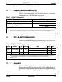
Table of Contents
Revision History . . . . . . . . . . . . . . . . . . . . . . . . . . . . . . . . . . . . . . . . . . . xi
1
Overview . . . . . . . . . . . . . . . . . . . . . . . . . . . . . . . . . . . . . . . . . . . . 1
1.1
2
Interface Signals . . . . . . . . . . . . . . . . . . . . . . . . . . . . . . . . . . . . . 5
2.1
2.2
2.3
2.4
Overview . . . . . . . . . . . . . . . . . . . . . . . . . . . . . . . . . . . . . . . . . . . 5
Signaling Technology . . . . . . . . . . . . . . . . . . . . . . . . . . . . . . . . . 5
Push-Pull (PP) Drivers . . . . . . . . . . . . . . . . . . . . . . . . . . . . . . . . 6
AMD Athlon™ System Bus Signals . . . . . . . . . . . . . . . . . . . . . . 6
3
Logic Symbol Diagram. . . . . . . . . . . . . . . . . . . . . . . . . . . . . . . . . 7
4
Power Management . . . . . . . . . . . . . . . . . . . . . . . . . . . . . . . . . . . 9
4.1
4.2
4.3
Power Management States . . . . . . . . . . . . . . . . . . . . . . . . . . . . . 9
Working State. . . . . . . . . . . . . . . . . . . . . . . . . . . . . . . . . . . . 10
Halt State . . . . . . . . . . . . . . . . . . . . . . . . . . . . . . . . . . . . . . . 10
Stop Grant States. . . . . . . . . . . . . . . . . . . . . . . . . . . . . . . . . 10
Probe State. . . . . . . . . . . . . . . . . . . . . . . . . . . . . . . . . . . . . . 12
Connect and Disconnect Protocol . . . . . . . . . . . . . . . . . . . . . . 12
Connect Protocol . . . . . . . . . . . . . . . . . . . . . . . . . . . . . . . . . 12
Connect State Diagram . . . . . . . . . . . . . . . . . . . . . . . . . . . . 16
Clock Control . . . . . . . . . . . . . . . . . . . . . . . . . . . . . . . . . . . . . . . 18
5
CPUID Support. . . . . . . . . . . . . . . . . . . . . . . . . . . . . . . . . . . . . . 19
6
333 FSB AMD Sempron™ Processor Model 10
Specifications . . . . . . . . . . . . . . . . . . . . . . . . . . . . . . . . . . . . . . . 21
6.1
6.2
6.3
6.4
7
Electrical and Thermal Specifications for the 333 FSB
AMD Sempron™ Processor Model 10 . . . . . . . . . . . . . . . . . . . 21
333 FSB AMD Sempron Processor Model 10 SYSCLK
and SYSCLK# AC Characteristics . . . . . . . . . . . . . . . . . . . . . . 22
333 FSB AMD Athlon System Bus AC Characteristics . . . . . 23
333 FSB AMD Athlon System Bus DC Characteristics . . . . . 24
Electrical Data . . . . . . . . . . . . . . . . . . . . . . . . . . . . . . . . . . . . . . 25
7.1
7.2
7.3
7.4
7.5
7.6
7.7
7.8
7.9
Table of Contents
QuantiSpeed™ Architecture Summary. . . . . . . . . . . . . . . . . . . 2
Conventions . . . . . . . . . . . . . . . . . . . . . . . . . . . . . . . . . . . . . . . . 25
Interface Signal Groupings . . . . . . . . . . . . . . . . . . . . . . . . . . . 25
Voltage Identification (VID[4:0]) . . . . . . . . . . . . . . . . . . . . . . 26
Frequency Identification (FID[3:0]) . . . . . . . . . . . . . . . . . . . . 27
VCCA AC and DC Characteristics . . . . . . . . . . . . . . . . . . . . . . 27
Decoupling . . . . . . . . . . . . . . . . . . . . . . . . . . . . . . . . . . . . . . . . . 27
VCC_CORE Characteristics. . . . . . . . . . . . . . . . . . . . . . . . . . . . . 28
Absolute Ratings . . . . . . . . . . . . . . . . . . . . . . . . . . . . . . . . . . . . 30
SYSCLK and SYSCLK# DC Characteristics . . . . . . . . . . . . . . 31
iii
AMD Preliminary Information
AMD Sempron™ Processor Model 10 Data Sheet
7.10
7.11
7.12
7.13
8
8.2
9.3
Die Loading . . . . . . . . . . . . . . . . . . . . . . . . . . . . . . . . . . . . . . . . 43
AMD Sempron Processor Model 10 Part Number 27488
OPGA Package Dimensions . . . . . . . . . . . . . . . . . . . . . . . . . . . 44
AMD Sempron Processor Model 10 Part Number 27493
OPGA Package Dimensions . . . . . . . . . . . . . . . . . . . . . . . . . . . 46
Pin Descriptions . . . . . . . . . . . . . . . . . . . . . . . . . . . . . . . . . . . . . 49
10.1
10.2
10.3
iv
Power-Up Requirements . . . . . . . . . . . . . . . . . . . . . . . . . . . . . 39
Signal Sequence and Timing Description . . . . . . . . . . . . . 39
Clock Multiplier Selection (FID[3:0]) . . . . . . . . . . . . . . . . 42
Processor Warm Reset Requirements. . . . . . . . . . . . . . . . . . . 42
Northbridge Reset Pins. . . . . . . . . . . . . . . . . . . . . . . . . . . . 42
Mechanical Data. . . . . . . . . . . . . . . . . . . . . . . . . . . . . . . . . . . . . 43
9.1
9.2
10
General AC and DC Characteristics . . . . . . . . . . . . . . . . . . . . 32
Open Drain Test Circuit . . . . . . . . . . . . . . . . . . . . . . . . . . . . . . 34
Thermal Diode Characteristics . . . . . . . . . . . . . . . . . . . . . . . . 35
Thermal Diode Electrical Characteristics. . . . . . . . . . . . . 35
Thermal Protection Characterization . . . . . . . . . . . . . . . . 35
APIC Pins AC and DC Characteristics . . . . . . . . . . . . . . . . . . 37
Signal and Power-Up Requirements . . . . . . . . . . . . . . . . . . . . 39
8.1
9
31993A-1 September 2004
Pin Diagram and Pin Name Abbreviations. . . . . . . . . . . . . . . 49
Pin List . . . . . . . . . . . . . . . . . . . . . . . . . . . . . . . . . . . . . . . . . . . . 59
Detailed Pin Descriptions. . . . . . . . . . . . . . . . . . . . . . . . . . . . . 68
A20M# Pin . . . . . . . . . . . . . . . . . . . . . . . . . . . . . . . . . . . . . . 68
AMD Pin . . . . . . . . . . . . . . . . . . . . . . . . . . . . . . . . . . . . . . . . 68
AMD Athlon System Bus Pins . . . . . . . . . . . . . . . . . . . . . . 68
Analog Pin . . . . . . . . . . . . . . . . . . . . . . . . . . . . . . . . . . . . . . 68
APIC Pins, PICCLK, PICD[1:0]# . . . . . . . . . . . . . . . . . . . . 68
CLKFWDRST Pin . . . . . . . . . . . . . . . . . . . . . . . . . . . . . . . . 68
CLKIN, RSTCLK (SYSCLK) Pins. . . . . . . . . . . . . . . . . . . . 69
CONNECT Pin . . . . . . . . . . . . . . . . . . . . . . . . . . . . . . . . . . . 69
COREFB and COREFB# Pins . . . . . . . . . . . . . . . . . . . . . . . 69
CPU_PRESENCE# Pin . . . . . . . . . . . . . . . . . . . . . . . . . . . . 69
DBRDY and DBREQ# Pins . . . . . . . . . . . . . . . . . . . . . . . . . 69
FERR Pin . . . . . . . . . . . . . . . . . . . . . . . . . . . . . . . . . . . . . . . 69
FID[3:0] Pins . . . . . . . . . . . . . . . . . . . . . . . . . . . . . . . . . . . . 70
FSB_Sense[1:0] Pins . . . . . . . . . . . . . . . . . . . . . . . . . . . . . . 71
FLUSH# Pin . . . . . . . . . . . . . . . . . . . . . . . . . . . . . . . . . . . . . 71
IGNNE# Pin . . . . . . . . . . . . . . . . . . . . . . . . . . . . . . . . . . . . . 71
INIT# Pin . . . . . . . . . . . . . . . . . . . . . . . . . . . . . . . . . . . . . . . 71
INTR Pin. . . . . . . . . . . . . . . . . . . . . . . . . . . . . . . . . . . . . . . . 72
JTAG Pins . . . . . . . . . . . . . . . . . . . . . . . . . . . . . . . . . . . . . . . 72
K7CLKOUT and K7CLKOUT# Pins . . . . . . . . . . . . . . . . . . 72
Key Pins . . . . . . . . . . . . . . . . . . . . . . . . . . . . . . . . . . . . . . . . 72
NC Pins . . . . . . . . . . . . . . . . . . . . . . . . . . . . . . . . . . . . . . . . . 72
NMI Pin. . . . . . . . . . . . . . . . . . . . . . . . . . . . . . . . . . . . . . . . . 72
Table of Contents
AMD Preliminary Information
31993A-1 September 2004
AMD Sempron™ Processor Model 10 Data Sheet
PGA Orientation Pins . . . . . . . . . . . . . . . . . . . . . . . . . . . . . 72
PLL Bypass and Test Pins . . . . . . . . . . . . . . . . . . . . . . . . . . 72
PWROK Pin . . . . . . . . . . . . . . . . . . . . . . . . . . . . . . . . . . . . . 73
SADDIN[1:0]# and SADDOUT[1:0]# Pins . . . . . . . . . . . . . 73
Scan Pins . . . . . . . . . . . . . . . . . . . . . . . . . . . . . . . . . . . . . . . 73
SMI# Pin . . . . . . . . . . . . . . . . . . . . . . . . . . . . . . . . . . . . . . . . 73
STPCLK# Pin . . . . . . . . . . . . . . . . . . . . . . . . . . . . . . . . . . . . 73
SYSCLK and SYSCLK#. . . . . . . . . . . . . . . . . . . . . . . . . . . . 73
THERMDA and THERMDC Pins . . . . . . . . . . . . . . . . . . . . 73
VCCA Pin . . . . . . . . . . . . . . . . . . . . . . . . . . . . . . . . . . . . . . . 73
VID[4:0] Pins . . . . . . . . . . . . . . . . . . . . . . . . . . . . . . . . . . . . 74
VREFSYS Pin . . . . . . . . . . . . . . . . . . . . . . . . . . . . . . . . . . . 74
ZN and ZP Pins . . . . . . . . . . . . . . . . . . . . . . . . . . . . . . . . . . 74
11
Ordering Information. . . . . . . . . . . . . . . . . . . . . . . . . . . . . . . . . 77
Standard AMD Sempron Processor Model 10 Products . . . . . . . . . . 77
Appendix A Thermal Diode Calculations . . . . . . . . . . . . . . . . . . . . . 79
Ideal Diode Equation . . . . . . . . . . . . . . . . . . . . . . . . . . . . . . . . . . . . . . 79
Temperature Offset Correction . . . . . . . . . . . . . . . . . . . . . . . . . . . . . . 80
Appendix B Conventions and Abbreviations . . . . . . . . . . . . . . . . . . 83
Signals and Bits . . . . . . . . . . . . . . . . . . . . . . . . . . . . . . . . . . . . . . . . . . . 83
Data Terminology . . . . . . . . . . . . . . . . . . . . . . . . . . . . . . . . . . . . . . . . . 84
Abbreviations and Acronyms. . . . . . . . . . . . . . . . . . . . . . . . . . . . . . . . 85
Related Publications. . . . . . . . . . . . . . . . . . . . . . . . . . . . . . . . . . . . . . . 89
Table of Contents
v
AMD Preliminary Information
AMD Sempron™ Processor Model 10 Data Sheet
vi
31993A-1 September 2004
Table of Contents
AMD Preliminary Information
31993A-1 September 2004
AMD Sempron™ Processor Model 10 Data Sheet
List of Figures
Figure 1. Typical AMD Sempron™ Processor Model 10 System Block
Diagram . . . . . . . . . . . . . . . . . . . . . . . . . . . . . . . . . . . . . . . . . . . . . . . 3
Figure 2. Logic Symbol Diagram. . . . . . . . . . . . . . . . . . . . . . . . . . . . . . . . . . . 7
Figure 3. AMD Sempron Processor Model 10 Power Management
States . . . . . . . . . . . . . . . . . . . . . . . . . . . . . . . . . . . . . . . . . . . . . . . . . 9
Figure 4. AMD Athlon™ System Bus Disconnect Sequence in the Stop
Grant State . . . . . . . . . . . . . . . . . . . . . . . . . . . . . . . . . . . . . . . . . . . 14
Figure 5. Exiting the Stop Grant State and Bus Connect Sequence . . . . . 15
Figure 6. Northbridge Connect State Diagram . . . . . . . . . . . . . . . . . . . . . . 16
Figure 7. Processor Connect State Diagram . . . . . . . . . . . . . . . . . . . . . . . . 17
Figure 8. SYSCLK Waveform . . . . . . . . . . . . . . . . . . . . . . . . . . . . . . . . . . . . 22
Figure 9. VCC_CORE Voltage Waveform . . . . . . . . . . . . . . . . . . . . . . . . . . . . 29
Figure 10. SYSCLK and SYSCLK# Differential Clock Signals . . . . . . . . . . 31
Figure 11. General ATE Open-Drain Test Circuit. . . . . . . . . . . . . . . . . . . . . 34
Figure 12. Signal Relationship Requirements During Power-Up
Sequence . . . . . . . . . . . . . . . . . . . . . . . . . . . . . . . . . . . . . . . . . . . . 39
Figure 13. AMD Sempron Processor Model 10 Part Number 27488 OPGA
Package Diagram . . . . . . . . . . . . . . . . . . . . . . . . . . . . . . . . . . . . . . 45
Figure 14. AMD Sempron Processor Model 10 Part Number 27493 OPGA
Package Diagram . . . . . . . . . . . . . . . . . . . . . . . . . . . . . . . . . . . . . . 47
Figure 15. AMD Sempron Processor Model 10 Pin Diagram — Topside View
50
Figure 16. AMD Sempron Processor Model 10 Pin Diagram — Bottomside
View . . . . . . . . . . . . . . . . . . . . . . . . . . . . . . . . . . . . . . . . . . . . . . . . . 51
Figure 17. OPN Example for the AMD Sempron Processor Model 10 . . . . 77
List of Figures
vii
AMD Preliminary Information
AMD Sempron™ Processor Model 10 Data Sheet
viii
31993A-1 September 2004
List of Figures
AMD Preliminary Information
31993A-1 September 2004
AMD Sempron™ Processor Model 10 Data Sheet
List of Tables
Table 1.
Electrical and Thermal Specifications for the Advanced
333 FSB AMD Sempron™ Processor Model 10 . . . . . . . . . . . . . 21
Table 2.
333 FSB SYSCLK and SYSCLK# AC Characteristics . . . . . . . . . 22
Table 3.
333 FSB AMD Athlon™ System Bus AC Characteristics . . . . . . 23
Table 4.
333 FSB AMD Athlon System Bus DC Characteristics . . . . . . . . 24
Table 5.
Interface Signal Groupings . . . . . . . . . . . . . . . . . . . . . . . . . . . . . 25
Table 6.
VID[4:0] DC Characteristics . . . . . . . . . . . . . . . . . . . . . . . . . . . . . 26
Table 7.
FID[3:0] DC Characteristics . . . . . . . . . . . . . . . . . . . . . . . . . . . . . 27
Table 8.
VCCA AC and DC Characteristics . . . . . . . . . . . . . . . . . . . . . . . . 27
Table 9.
VCC_CORE AC and DC Characteristics . . . . . . . . . . . . . . . . . . . . . 28
Table 10. Absolute Ratings . . . . . . . . . . . . . . . . . . . . . . . . . . . . . . . . . . . . . . 30
Table 11. SYSCLK and SYSCLK# DC Characteristics . . . . . . . . . . . . . . . . 31
Table 12. General AC and DC Characteristics. . . . . . . . . . . . . . . . . . . . . . . 32
Table 13. Thermal Diode Electrical Characteristics . . . . . . . . . . . . . . . . . . 35
Table 14. Guidelines for Platform Thermal Protection of the Processor . 36
Table 15. APIC Pin AC and DC Characteristics. . . . . . . . . . . . . . . . . . . . . . 37
Table 16. Mechanical Loading . . . . . . . . . . . . . . . . . . . . . . . . . . . . . . . . . . . . 43
Table 17. Dimensions for the AMD Sempron Processor Model 10
Part Number 27488 OPGA Package . . . . . . . . . . . . . . . . . . . . . . . 44
Table 18. Dimensions for the AMD Sempron Processor Model 10
Part Number 27493 OPGA Package . . . . . . . . . . . . . . . . . . . . . . . 46
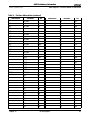
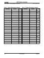
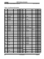
Table 19. Pin Name Abbreviations . . . . . . . . . . . . . . . . . . . . . . . . . . . . . . . . 52
Table 20. Cross-Reference by Pin Location . . . . . . . . . . . . . . . . . . . . . . . . . 60
Table 21. FID[3:0] Clock Multiplier Encodings . . . . . . . . . . . . . . . . . . . . . . 70
Table 22. Front-Side Bus Sense Truth Table . . . . . . . . . . . . . . . . . . . . . . . . 71
Table 23. VID[4:0] Code to Voltage Definition . . . . . . . . . . . . . . . . . . . . . . 74
Table 24. Constants and Variables for the Ideal Diode Equation . . . . . . . 79
Table 25. Constants and Variables Used in Temperature Offset
Equations . . . . . . . . . . . . . . . . . . . . . . . . . . . . . . . . . . . . . . . . . . . . 80
Table 26. Abbreviations . . . . . . . . . . . . . . . . . . . . . . . . . . . . . . . . . . . . . . . . . 85
Table 27. Acronyms. . . . . . . . . . . . . . . . . . . . . . . . . . . . . . . . . . . . . . . . . . . . . 86
List of Tables
ix
AMD Preliminary Information
AMD Sempron™ Processor Model 10 Data Sheet
x
31993A-1 September 2004
List of Tables
AMD Preliminary Information
AMD Sempron™ Processor Model 10 Data Sheet
31993A-1 September 2004
Revision History
Date
September 2004
Revision History
Rev
A-1
Description
■
Initial release of the AMD Sempron™ processor model 10 data sheet.
xi
AMD Preliminary Information
AMD Sempron™ Processor Model 10 Data Sheet
xii
31993A-1 September 2004
Revision History
AMD Preliminary Information
AMD Sempron™ Processor Model 10 Data Sheet
31993A-1 September 2004
1
Overview
The AMD Sempron™ processor model 10 with QuantiSpeed™
architecture powers the next generation in computing
platforms, delivering extreme performance for Windows® XP.
The AMD Sempron processor model 10, based on leading-edge
0.13 micron technology and increased on-chip cache, integrates
the innovative design and manufacturing expertise of AMD to
deliver improved performance while maintaining the stable
and compatible Socket A infrastructure of the AMD Sempron
processor.
Delivered in an OPGA package, the AMD Sempron processor
mode l 10 delivers the integ er, floati ng-point, and 3D
multimedia performance for highly demanding applications
running on x86 system platforms. The AMD Sempron processor
model 10 delivers compelling performance for cutting-edge
software applications that include high-speed Internet
capability, digital content creation, digital photo editing, digital
video, image compression, video encoding for streaming over
t h e I n t e r n e t , s o f t DV D, c o m m e rc i a l 3 D m o d e l i n g ,
workstation-class computer-aided design (CAD), commercial
desktop publishing, and speech recognition. The AMD Sempron
processor model 10 also offers the scalability and reliability
that IT managers and business users require for enterprise
computing.
T h e A M D S e m p ro n p ro c e s s o r m o d e l 1 0 f e a t u re s a
seventh-generation microarchitecture with an integrated,
exclusive L2 cache, which supports the growing processor and
system bandwidth requirements of emerging software,
graphics, I/O, and memory technologies. The high-speed
execution core of the AMD Sempron processor model 10
includes multiple x86 instruction decoders, a dual-ported
128-Kbyte split level-one (L1) cache, an exclusive 512-Kbyte L2
cache, three independent integer pipelines, three address
calculation pipelines, and a superscalar, fully pipelined,
out-of-order, three-way floating-point engine. The floating-point
engine is capable of delivering outstanding performance on
numerically complex applications.
The features of the AMD Sempron processor model 10 include
Q u a n t i S p e e d a rch i t e c t u re , 6 4 0 K by t e s o f t o t a l , h i g h -
Chapter 1
Overview
1
AMD Preliminary Information
AMD Sempron™ Processor Model 10 Data Sheet
31993A-1 September 2004
performance, full-speed, on-chip cache, an advanced 333 FSB
with a 2.7-Gigabyte per second system bus, and 3DNow!™
Professional technology. The AMD Athlon system bus combines
the latest technological advances, such as point-to-point topology,
source-synchronous packet-based transfers, and low-voltage
signaling to provide an extremely powerful, scalable bus for an
x86 processor.
The AMD Sempron processor model 10 is binary-compatible with
ex i s t i n g x 86 so f t wa re a n d b a ck ward s c om p at ib le w i t h
applications optimized for MMX™, SSE, and 3DNow! technology.
Using a data format and single-instruction multiple-data (SIMD)
o p e ra t i o n s b a s e d o n t h e M M X i n s t r u c t i o n m o d e l , t h e
AMD Sempron processor model 10 can produce as many as four,
32-bit, single-precision floating-point results per clock cycle. The
3 D N ow ! P ro f e s s i o n a l t e ch n o l ogy i m p l e m e n t e d i n t h e
AMD Sempron processor model 10 includes new integer
multimedia instructions and software-directed data movement
instructions for optimizing such applications as digital content
creation and streaming video for the internet, as well as new
i n s t r u c t i o n s fo r d i g i t a l s i g n a l p r o c e s s i n g ( D S P ) a n d
communications applications.
1.1
QuantiSpeed™ Architecture Summary
The following features summarize the AMD Sempron processor
model 10 QuantiSpeed architecture:
■
■
■
■
2
An advanced nine-issue, superpipelined, superscalar x86
processor microarchitecture designed for increased
instructions per cycle (IPC) and high clock frequencies
Fully pipelined floating-point unit that executes all x87
(floating-point), MMX, SSE and 3DNow! instructions
Hardware data pre-fetch that increases and optimizes
performance on high-end software applications utilizing
high-bandwidth system capabilities
Advanced two-level translation look-aside buffer (TLB)
structures for both enhanced data and instruction address
translation. The AMD Sempron processor model 10 with
QuantiSpeed architecture
incorporates three
TLB
optimizations: the L1 DTLB increases from 32 to 40 entries,
the L2 ITLB and L2 DTLB both use exclusive architecture,
and the TLB entries can be speculatively loaded.
Overview
Chapter 1
AMD Preliminary Information
AMD Sempron™ Processor Model 10 Data Sheet
31993A-1 September 2004
The AMD Sempron processor model 10 delivers excellent
system performance in a cost-effective, industry-standard form
factor. The AMD Sempron processor model 10 is compatible
with motherboards based on Socket A.
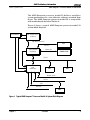
Figure 1 shows a typical AMD Sempron processor model 10
system block diagram.
Thermal Monitor
AMD Sempron™ Processor Model 10
AMD Athlon™ System Bus
AGP
AGP Bus
Memory Bus
System Controller
(Northbridge)
SDRAM or DDR
PCI Bus
Peripheral Bus Controller
(Southbridge)
LAN
SCSI
Modem / Audio
LPC Bus
USB
Dual EIDE
BIOS
Figure 1. Typical AMD Sempron™ Processor Model 10 System Block Diagram
Chapter 1
Overview
3
AMD Preliminary Information
AMD Sempron™ Processor Model 10 Data Sheet
4
31993A-1 September 2004
Overview
Chapter 1
AMD Preliminary Information
AMD Sempron™ Processor Model 10 Data Sheet
31993A-1 September 2004
2
Interface Signals
Chapter 2 discusses the AMD Athlon™ system bus architecture,
design, and signal support that is used in the AMD Sempron™
processor model 10.
2.1
Overview
The AMD Athlon system bus architecture is designed to deliver
excellent data movement bandwidth for next-generation x86
platforms as well as the high-performance required by
enterprise-class application software. The system bus
archit ect ure co nsist s of t hree high-speed channels (a
unidirectional processor request channel, a unidirectional
probe channel, and a 64-bit bidirectional data channel),
source-synchronous clocking, and a packet-based protocol. In
addition, the system bus supports several control, clock, and
legacy signals. The interface signals use an impedance
controlled push-pull, low-voltage, swing-signaling technology
contained within the Socket A socket.
For more information, see “AMD Athlon™ System Bus Signals”
on page 6, Chapter 10, “Pin Descriptions” on page 49, and the
AMD Athlon™ and AMD Duron™ System Bus Specification,
order# 21902.
2.2
Signaling Technology
The AMD Athlon system bus uses a low-voltage, swing-signaling
technology, that has been enhanced to provide larger noise
margins, reduced ringing, and variable voltage levels. The
signals are push-pull and impedance compensated. The signal
inputs use differential receivers that require a reference
voltage (VREF). The reference signal is used by the receivers to
determine if a signal is asserted or deasserted by the source.
Termination resistors are not needed because the driver is
impedance-matched to the motherboard and a high impedance
reflection is used at the receiver to bring the signal past the
input threshold.
For more information about pins and signals, see Chapter 10,
“Pin Descriptions” on page 49.
Chapter 2
Interface Signals
5
AMD Preliminary Information
AMD Sempron™ Processor Model 10 Data Sheet
2.3
31993A-1 September 2004
Push-Pull (PP) Drivers
The AMD Sempron processor model 10 supports push-pull (PP)
drivers. The system logic configures the processor with the
configuration parameter called SysPushPull (1=PP). The
impedance of the PP drivers is set to match the impedance of
the motherboard by two external resistors connected to the ZN
and ZP pins.
See “ZN and ZP Pins” on page 74 for more information.
2.4
AMD Athlon™ System Bus Signals
The AMD Athlon system bus is a clock-forwarded, point-topoint interface with the following three point-to-point channels:
■
■
■
A 13-bit unidirectional output address/command channel
A 13-bit unidirectional input address/command channel
A 72-bit bidirectional data channel
Fo r m o re i n f o r m a t i o n , s e e C h a p t e r 6 , “ 3 3 3 F S B
AMD Sempron™ Processor Model 10 Specifications” on page
21, Chapt er 7, “Elect rical D ata” on page 25 , and t he
AMD Athlon™ and AMD Duron™ System Bus Specification,
order# 21902.
6
Interface Signals
Chapter 2
AMD Preliminary Information
AMD Sempron™ Processor Model 10 Data Sheet
31993A-1 September 2004
3
Logic Symbol Diagram
Figure 2 is the logic symbol diagram of the processor. This
diagram shows the logical grouping of the input and output
signals.
Clock
{
{
VID[4:0]
COREFB
COREFB#
PWROK
FID[3:0]
FSB_SENSE[1:0]
Power
Management
and Initialization
{
{
SADDOUT[14:2]#
SADDOUTCLK#
AMD Sempron™
Processor Model 10
PROCRDY
CLKFWDRST
CONNECT
STPCLK#
RESET#
FERR
IGNNE#
INIT#
INTR
NMI
A20M#
SMI#
FLUSH#
Front-Side Bus
Autodetect
Legacy
THERMDA
THERMDC
Thermal
Diode
PICCLK
PICD[1:0]
{
Request
SADDIN[14:2]#
SADDINCLK#
Frequency
Control
{
Probe/SysCMD {
Voltage
Control
{
Data
SYSCLK#
{
SYSCLK
SDATA[63:0]#
SDATAINCLK[3:0]#
SDATAOUTCLK[3:0]#
SDATAINVALID#
SDATAOUTVALID#
SFILLVALID#
APIC
Figure 2. Logic Symbol Diagram
Chapter 3
Logic Symbol Diagram
7
AMD Preliminary Information
AMD Sempron™ Processor Model 10 Data Sheet
8
Logic Symbol Diagram
31993A-1 September 2004
Chapter 3
AMD Preliminary Information
AMD Sempron™ Processor Model 10 Data Sheet
31993A-1 September 2004
4
Power Management
This chapter describes the power management control system
o f t h e A M D S e m p ron p ro c e s so r m o d el 1 0 . The p owe r
management features of the processor are compliant with the
ACPI 1.0b and ACPI 2.0 specifications.
4.1
Power Management States
The AMD Sempron processor model 10 supports low-power
Halt and Stop Grant states. These states are used by advanced
configuration and power interface (ACPI) enabled operating
systems for processor power management.
Figure 3 shows the power management states of the processor.
The figure includes the ACPI “Cx” naming convention for these
states.
Execute HLT
C1
Halt
C0
Working4
SMI#, INTR, NMI, INIT#, RESET#
Probe Serviced
STPCLK# deasserted
Incoming Probe
STPCLK# asserted
PC
LK
#d
ST
ea
PC
sse
LK
rte
#a
d3
sse
rte
d2
(Read PLVL2 register
or throttling)
Probe Serviced
Incoming Probe
Probe
State1
ST
ST
ST
PC
LK
#
PC
LK
#
C2
Stop Grant
Cache Snoopable
ass
e
de
ass
ert
ed
rte
d
S1
Stop Grant
Cache Not Snoopable
Sleep
Legend
Hardware transitions
Software transitions
Note:
The AMD AthlonTM System Bus is connected during the following states:
1) The Probe state
2) During transitions between the Halt state and the C2 Stop Grant state
3) During transitions between the C2 Stop Grant state and the Halt state
4) C0 Working state
Figure 3. AMD Sempron™ Processor Model 10 Power Management States
Chapter 4
Power Management
9
AMD Preliminary Information
AMD Sempron™ Processor Model 10 Data Sheet
31993A-1 September 2004
The following sections provide an overview of the power
m a n a g e m e n t s t a t e s . Fo r m o re d e t a i l s , re f e r t o t h e
AMD Athlon™ and AMD Duron™ System Bus Specification,
order# 21902.
Note: In all power management states that the processor is
powered, the system must not stop the system clock
(SYSCLK/SYSCLK#) to the processor.
Working State
The Working state is the state in which the processor is
executing instructions.
Halt State
When the processor executes the HLT instruction, the processor
enters the Halt state and issues a Halt special cycle to the
AMD Athlon system bus. The processor only enters the low
power state dictated by the CLK_Ctl MSR if the system
controller (Northbridge) disconnects the AMD Athlon system
bus in response to the Halt special cycle.
If STPCLK# is asserted, the processor will exit the Halt state
and enter the Stop Grant state. The processor will initiate a
system bus connect, if it is disconnected, then issue a Stop
Grant special cycle. When STPCLK# is deasserted, the
processor will exit the Stop Grant state and re-enter the Halt
state. The processor will issue a Halt special cycle when
re-entering the Halt state.
The Halt state is exited when the processor detects the
assertion of INIT#, RESET#, SMI#, or an interrupt via the INTR
or NMI pins, or via a local APIC interrupt message. When the
Halt state is exited, the processor will initiate an AMD Athlon
system bus connect if it is disconnected.
Stop Grant States
10
The processor enters the Stop Grant state upon recognition of
assertion of STPCLK# input. After entering the Stop Grant
state, the processor issues a Stop Grant special bus cycle on the
AMD Athlon system bus. The processor is not in a low-power
state at this time, because the AMD Athlon system bus is still
connected. After the Northbridge disconnects the AMD Athlon
system bus in response to the Stop Grant special bus cycle, the
processor enters a low-power state dictated by the CLK_Ctl
MSR. If the Northbridge needs to probe the processor during
the Stop Grant state while the system bus is disconnected, it
Power Management
Chapter 4
AMD Preliminary Information
31993A-1 September 2004
AMD Sempron™ Processor Model 10 Data Sheet
must first connect the system bus. Connecting the system bus
places the processor into the higher power probe state. After
the Northbridge has completed all probes of the processor, the
Northbridge must disconnect the AMD Athlon system bus
again so that the processor can return to the low-power state.
During the Stop Grant states, the processor latches INIT#,
INTR, NMI, SMI#, or a local APIC interrupt message, if they are
asserted.
The Stop Grant state is exited upon the deassertion of
STPCLK# or the assertion of RESET#. When STPCLK# is
d e a s s e r t e d , t h e p ro c e s s o r i n i t i a t e s a c o n n e c t o f t h e
AMD Athlon system bus if it is disconnected. After the
processor enters the Working state, any pending interrupts are
recognized and serviced and the processor resumes execution
at the instruction boundary where STPCLK# was initially
recognized. If RESET# is sampled asserted during the Stop
Grant state, the processor exits the Stop Grant state and the
reset process begins.
There are two mechanisms for asserting STPCLK#—hardware
and software.
The Southbridge can force STPCLK# assertion for throttling to
protect the processor from exceeding its maximum case
temperature. This is accomplished by asserting the THERM#
input to the Southbridge. Throttling asserts STPCLK# for a
percentage of a predefined throttling period: STPCLK# is
repetitively asserted and deasserted until THERM# is
deasserted.
Software can force the processor into the Stop Grant state by
accessing ACPI-defined registers typically located in the
Southbridge.
The operating system places the processor into the C2 Stop
Grant state by reading the P_LVL2 register in the Southbridge.
If an ACPI Thermal Zone is defined for the processor, the
operating system can initiate throttling with STPCLK# using
the ACPI defined P_CNT register in the Southbridge. The
Northbridge connects the AMD Athlon system bus, and the
processor enters the Probe state to service cache snoops during
Stop Grant for C2 or throttling.
Chapter 4
Power Management
11
AMD Preliminary Information
AMD Sempron™ Processor Model 10 Data Sheet
31993A-1 September 2004
In C2, probes are allowed, as shown in Figure 3 on page 9
The Stop Grant state is also entered for the S1, Powered On
Suspend, system sleep state based on a write to the SLP_TYP
and SLP_EN fields in the ACPI-defined Power Management 1
control register in the Southbridge. During the S1 Sleep state,
system software ensures no bus master or probe activity occurs.
The Southbridge deasserts STPCLK# and brings the processor
out of the S1 Stop Grant state when any enabled resume event
occurs.
Probe State
4.2
The Probe state is entered when the Northbridge connects the
AMD Athlon system bus to probe the processor (for example, to
snoop the processor caches) when the processor is in the Halt or
Stop Grant state. When in the Probe state, the processor
responds to a probe cycle in the same manner as when it is in
the Working state. When the probe has been serviced, the
processor returns to the same state as when it entered the
Probe state (Halt or Stop Grant state). When probe activity is
completed the processor only returns to a low-power state after
the Northbridge disconnects the AMD Athlon system bus again.
Connect and Disconnect Protocol
Significant power savings of the processor only occur if the
proc essor is disconnected from the system bus by the
Northbridge while in the Halt or Stop Grant state. The
Northbridge can optionally initiate a bus disconnect upon the
receipt of a Halt or Stop Grant special cycle. The option of
disconnecting is controlled by an enable bit in the Northbridge.
If the Northbridge requires the processor to service a probe
after the system bus has been disconnected, it must first
initiate a system bus connect.
Connect Protocol
In addition to the legacy STPCLK# signal and the Halt and Stop
Grant special cycles, the AMD Athlon system bus connect
protocol includes the CONNECT, PROCRDY, and CLKFWDRST
signals and a Connect special cycle.
AMD Athlon system bus disconnects are initiated by the
Northbridge in response to the receipt of a Halt or Stop Grant.
Reconnect is initiated by the processor in response to an
12
Power Management
Chapter 4
AMD Preliminary Information
31993A-1 September 2004
AMD Sempron™ Processor Model 10 Data Sheet
interrupt for Halt or STPCLK# deassertion. Reconnect is
initiated by the Northbridge to probe the processor.
The Northbridge contains BIOS programmable registers to
enable the system bus disconnect in response to Halt and Stop
Grant special cycles. When the Northbridge receives the Halt or
Stop Grant special cycle from the processor and, if there are no
outstanding probes or data movements, the Northbridge
deasserts CONNECT a minimum of eight SYSCLK periods after
the last command sent to the processor. The processor detects
the deassertion of CONNECT on a rising edge of SYSCLK and
deasserts PROCRDY to the Northbridge. In return, the
Northbridge asserts CLKFWDRST in anticipation of
reestablishing a connection at some later point.
Note: The Northbridge must disconnect the processor from the
AMD Athlon system bus before issuing the Stop Grant
special cycle to the PCI bus or passing the Stop Grant special
cycle to the Southbridge for systems that connect to the
Southbridge with HyperTransport™ technology.
This note applies to current chipset implementation—
alternate chipset implementations that do not require this
are possible.
Note: In response to Halt special cycles, the Northbridge passes the
Halt special cycle to the PCI bus or Southbridge
immediately.
The processor can receive an interrupt after it sends a Halt
special cycle, or STPCLK# deassertion after it sends a Stop
Grant special cycle to the Northbridge but before the
disconnect actually occurs. In this case, the processor sends the
Connect special cycle to the Northbridge, rather than
continuing with the disconnect sequence. In response to the
Connect special cycle, the Northbridge cancels the disconnect
request.
The system is required to assert the CONNECT signal before
returning the C-bit for the connect special cycle (assuming
CONNECT has been deasserted).
For more information, see the AMD Athlon™ and AMD Duron™
System Bus Specification, order# 21902 for the definition of the
C-bit and the Connect special cycle.
Chapter 4
Power Management
13
AMD Preliminary Information
AMD Sempron™ Processor Model 10 Data Sheet
31993A-1 September 2004
Figure 4 shows STPCLK# assertion resulting in the processor in
the St op Gra nt st ate and the A MD A thlon system bus
disconnected.
STPCLK#
AMD Athlon™
System Bus
Stop Grant
CONNECT
PROCRDY
CLKFWDRST
Stop Grant
PCI Bus
Figure 4. AMD Athlon™ System Bus Disconnect Sequence in the Stop Grant State
An example of the AMD Athlon system bus disconnect
sequence is as follows:
1. The peripheral controller (Southbridge) asserts STPCLK#
to place the processor in the Stop Grant state.
2. When the processor recognizes STPCLK# asserted, it enters
the Stop Grant state and then issues a Stop Grant special
cycle.
3. When the special cycle is received by the Northbridge, it
deasserts CONNECT, assuming no probes are pending,
initiating a bus disconnect to the processor.
4. The processor responds to the Northbridge by deasserting
PROCRDY.
5. The Northbridge asserts CLKFWDRST to complete the bus
disconnect sequence.
6. After the processor is disconnected from the bus, the
processor enters a low-power state. The Northbridge passes
the Stop Grant special cycle along to the Southbridge.
14
Power Management
Chapter 4
AMD Preliminary Information
31993A-1 September 2004
AMD Sempron™ Processor Model 10 Data Sheet
Figure 5 shows the signal sequence of events that takes the
processor out of the Stop Grant state, connects the processor to
the AMD Athlon system bus, and puts the processor into the
Working state.
Figure 5. Exiting the Stop Grant State and Bus Connect Sequence
The following sequence of events removes the processor from
the Stop Grant state and connects it to the system bus:
1. The Southbridge deasserts
processor of a wake event.
STPCLK#,
informing
the
2. When the processor recognizes STPCLK# deassertion, it
exits the low-power state and asserts PROCRDY, notifying
the Northbridge to connect to the bus.
3. The Northbridge asserts CONNECT.
4. The Northbridge deasserts CLKFWDRST, synchronizing the
forwarded clocks between the processor and the
Northbridge.
5. The processor issues a Connect special cycle on the system
bus and resumes operating system and application code
execution.
Chapter 4
Power Management
15
AMD Preliminary Information
AMD Sempron™ Processor Model 10 Data Sheet
Connect State
Diagram
31993A-1 September 2004
Figure 6 below and Figure 7 on page 17 show the Northbridge
and processor connect state diagrams, respectively.
.
Condition
Action
1 A disconnect is requested and probes are still pending.
2 A disconnect is requested and no probes are pending.
A
Deassert CONNECT eight SYSCLK periods
after last SysDC sent.
3 A Connect special cycle from the processor.
B Assert CLKFWDRST.
4 No probes are pending.
C Assert CONNECT.
5 PROCRDY is deasserted.
D Deassert CLKFWDRST.
6 A probe needs service.
7 PROCRDY is asserted.
Three SYSCLK periods after CLKFWDRST is deasserted.
Although reconnected to the system interface, the
8 Northbridge must not issue any non-NOP SysDC
commands for a minimum of four SYSCLK periods after
deasserting CLKFWDRST.
Figure 6. Northbridge Connect State Diagram
16
Power Management
Chapter 4
AMD Preliminary Information
AMD Sempron™ Processor Model 10 Data Sheet
31993A-1 September 2004
Connect
6/B
1
2/B
Connect
Pending 2
Disconnect
Pending
5
Connect
Pending 1
3/A
Disconnect
4/C
Condition
1
Action
CONNECT is deasserted by the Northbridge (for a
previously sent Halt or Stop Grant special cycle).
Processor receives a wake-up event and must cancel
2
the disconnect request.
3 Deassert PROCRDY and slow down internal clocks.
4
Processor wake-up event or CONNECT asserted by
Northbridge.
A CLKFWDRST is asserted by the Northbridge.
B Issue a Connect special cycle.*
C
Return internal clocks to full speed and assert
PROCRDY.
Note:
*
5 CLKFWDRST is deasserted by the Northbridge.
6
Forward clocks start three SYSCLK periods after
CLKFWDRST is deasserted.
The Connect special cycle is only issued after a
processor wake-up event (interrupt or STPCLK#
deassertion) occurs. If the AMD Athlon™ system
bus is connected so the Northbridge can probe the
processor, a Connect special cycle is not issued at
that time (it is only issued after a subsequent
processor wake-up event).
Figure 7. Processor Connect State Diagram
Chapter 4
Power Management
17
AMD Preliminary Information
AMD Sempron™ Processor Model 10 Data Sheet
4.3
31993A-1 September 2004
Clock Control
The processor implements a Clock Control (CLK_Ctl) MSR
(address C001_001Bh) that determines the internal clock
divisor when the AMD Athlon system bus is disconnected.
Refer to the AMD Athlon™ and AMD Duron™ Processors BIOS,
Software, and Debug Developers Guide, order# 21656, for more
details on the CLK_Ctl register.
18
Power Management
Chapter 4
AMD Preliminary Information
AMD Sempron™ Processor Model 10 Data Sheet
31993A-1 September 2004
5
CPUID Support
AMD Sempron™ processor model 10 version and feature set
recognition can be performed through the use of the CPUID
instruction, that provides complete information about the
processor—vendor, type, name, etc., and its capabilities.
Software can make use of this information to accurately tune
the system for maximum performance and benefit to users.
For information on the use of the CPUID instruction see the
following document:
■
Chapter 5
AMD Processor Recognition Application Note, order# 20734
CPUID Support
19
AMD Preliminary Information
AMD Sempron™ Processor Model 10 Data Sheet
20
CPUID Support
31993A-1 September 2004
Chapter 5
AMD Preliminary Information
AMD Sempron™ Processor Model 10 Data Sheet
31993A-1 September 2004
6
333 FSB AMD Sempron™ Processor Model 10
Specifications
This chapter describes the electrical specifications that are
u n i q u e t o t h e a dva n c e d 3 3 3 f ro n t - s i d e b u s ( F S B )
AMD Sempron™ Processor Model 10.
6.1
Electrical and Thermal Specifications for the 333 FSB
AMD Sempron™ Processor Model 10
Table 1 shows the electrical and thermal specifications in the
C0 working state and the S1 Stop Grant state for this processor.
Table 1.
Electrical and Thermal Specifications for the Advanced 333 FSB AMD Sempron™ Processor
Model 10
V
Frequency in MHz CC_CORE
(Core
(Model Number)
Voltage)
2000 (3000+)
1.60 V
ICC (Processor Current)
Working State C0
Stop Grant
Maximum Typical
Maximum
38.75 A
30.9 A
8.10 A
S11, 2, 3, 4
Thermal Power5
Maximum Die
Temperature
Typical Maximum Typical
4.94 A
62.0 W
49.4 W
90°C
Notes:
1. See Figure 3, "AMD Sempron™ Processor Model 10 Power Management States" on page 9.
2. The maximum Stop Grant currents are absolute worst case currents for parts that may yield from the worst case corner of the
process and are not representative of the typical Stop Grant current that is currently about one-third of the maximum specified
current.
3. These currents occur when the AMD Athlon™ system bus is disconnected and has a low power ratio of 1/8 for Stop Grant
disconnect and a low power ratio of 1/8 Halt disconnect applied to the core clock grid of the processor as dictated by a value of
2003_1223h programmed into the Clock Control (CLK_Ctl) MSR. For more information, refer to the AMD Athlon™ and
AMD Duron™ Processors BIOS, Software, and Debug Developers Guide, order# 21656.
4. The Stop Grant current consumption is characterized at 50°C and not tested.
5. Thermal design power represents the maximum sustained power dissipated while executing publicly-available software or
instruction sequences under normal system operation at nominal VCC_CORE . Thermal solutions must monitor the temperature of
the processor to prevent the processor from exceeding its maximum die temperature.
Chapter 6
333 FSB AMD Sempron™ Processor Model 10 Specifications
21
AMD Preliminary Information
AMD Sempron™ Processor Model 10 Data Sheet
6.2
31993A-1 September 2004
333 FSB AMD Sempron™ Processor Model 10 SYSCLK and
SYSCLK# AC Characteristics
Table 2 shows the SYSCLK/SYSCLK# differential clock AC
characteristics of this processor.
Table 2.
333 FSB SYSCLK and SYSCLK# AC Characteristics
Symbol
Parameter Description
Minimum
Maximum
Units
Notes
50
166
MHz
1
30%
70%
2, 3
Clock Frequency
Duty Cycle
t1
Period
6
ns
t2
High Time
1.0
ns
t3
Low Time
1.0
ns
t4
Fall Time
2
ns
t5
Rise Time
2
ns
± 300
ps
Period Stability
Notes:
1. The AMD Athlon™ system bus operates at twice this clock frequency.
2. Circuitry driving the AMD Athlon system bus clock inputs must exhibit a suitably low closed-loop jitter bandwidth to allow the PLL
to track the jitter. The –20dB attenuation point, as measured into a 20- or 30-pF load must be less than 500 kHz.
3. Circuitry driving the AMD Athlon system bus clock inputs may purposely alter the AMD Athlon system bus clock frequency (spread
spectrum clock generators). In no cases can the AMD Athlon system bus period violate the minimum specification above.
AMD Athlon system bus clock inputs can vary from 100% of the specified frequency to 99% of the specified frequency at a
maximum rate of 100 kHz.
Figure 8 shows a sample waveform of the SYSCLK signal.
t2
VThreshold-AC
VCROSS
t3
t4
t5
t1
Figure 8. SYSCLK Waveform
22
333 FSB AMD Sempron™ Processor Model 10 Specifications
Chapter 6
AMD Preliminary Information
AMD Sempron™ Processor Model 10 Data Sheet
31993A-1 September 2004
6.3
333 FSB AMD Athlon™ System Bus AC Characteristics
The AC characteristics of the AMD Athlon system bus of this
processor are shown in Table 3. The parameters are grouped
based on the source or destination of the signals involved.
Table 3.
333 FSB AMD Athlon™ System Bus AC Characteristics
Group
All Signals
Forward
Clocks
Sync
Symbol
Parameter
Min
Max
Units
Notes
TRISE
Output Rise Slew Rate
1
3
V/ns
1
TFALL
Output Fall Slew Rate
1
3
V/ns
1
TSKEW-DIFFEDGE
Output skew with respect to a
different clock edge
–
770
ps
2
TSU
Input Data Setup Time
300
ps
3
THD
Input Data Hold Time
300
ps
3
CIN
Capacitance on input clocks
4
25
pF
COUT
Capacitance on output clocks
4
12
pF
TVAL
RSTCLK to Output Valid
800
2000
ps
4, 5
TSU
Setup to RSTCLK
500
ps
4, 6
THD
Hold from RSTCLK
500
ps
4, 6
Notes:
1. Rise and fall time ranges are guidelines over which the I/O has been characterized.
2. TSKEW-DIFFEDGE is the maximum skew within a clock forwarded group between any two signals or between any signal and its
forward clock, as measured at the package, with respect to different clock edges.
3. Input SU and HD times are with respect to the appropriate Clock Forward Group input clock.
4. The synchronous signals include PROCRDY, CONNECT, and CLKFWDRST.
5. T VAL is RSTCLK rising edge to output valid for PROCRDY. Test Load is 25 pF.
6. TSU is setup of CONNECT/CLKFWDRST to rising edge of RSTCLK. THD is hold of CONNECT/CLKFWDRST from rising edge of
RSTCLK.
Chapter 6
333 FSB AMD Sempron™ Processor Model 10 Specifications
23
AMD Preliminary Information
AMD Sempron™ Processor Model 10 Data Sheet
6.4
31993A-1 September 2004
333 FSB AMD Athlon™ System Bus DC Characteristics
Table 4 shows the DC characteristics of the AMD Athlon
system bus for this processor.
Table 4.
333 FSB AMD Athlon™ System Bus DC Characteristics
Symbol
VREF
Parameter
Condition
Min
Max
(0.5 x VCC_CORE) (0.5 x VCC_CORE)
–50
+50
DC Input Reference Voltage
IVREF_LEAK_P VREF Tristate Leakage Pullup
VIN = VREF Nominal
IVREF_LEAK_N VREF Tristate Leakage Pulldown
VIN = VREF Nominal
Units Notes
mV
µA
–100
100
µA
VIH
Input High Voltage
VREF +200
VCC_CORE +500
mV
VIL
Input Low Voltage
–500
VREF –200
mV
ILEAK_P
Tristate Leakage Pullup
ILEAK_N
Tristate Leakage Pulldown
CIN
Input Pin Capacitance
RON
Output Resistance
RsetP
RsetN
VIN = VSS
(Ground)
1
–1
mA
VIN = VCC_CORE
Nominal
1
mA
4
7
pF
0.90 x RsetN,P
1.1 x RsetN,P
Ω
2
Impedance Set Point, P Channel
40
70
Ω
2
Impedance Set Point, N Channel
40
70
Ω
2
Notes:
1. VREF is nominally set to 50% of VCC_CORE with actual values that are specific to motherboard design implementation. VREF must be
created with a sufficiently accurate DC source and a sufficiently quiet AC response to adhere to the ± 50 mV specification listed
above.
2. Measured at VCC_CORE / 2.
24
333 FSB AMD Sempron™ Processor Model 10 Specifications
Chapter 6
AMD Preliminary Information
AMD Sempron™ Processor Model 10 Data Sheet
31993A-1 September 2004
7
Electrical Data
This chapter describes the electrical characteristics that apply
to all desktop AMD Sempron™ processors model 10.
7.1
Conventions
The conventions used in this chapter are as follows:
■
■
7.2
Current specified as being sourced by the processor is
negative.
Current specified as being sunk by the processor is positive.
Interface Signal Groupings
The electrical data in this chapter is presented separately for
each signal group.
Table 5 defines each group and the signals contained in each
group.
Table 5.
Interface Signal Groupings
Signal Group
Signals
Notes
Power
VID[4:0], VCCA, VCC_CORE, COREFB,
COREFB#
See “Voltage Identification (VID[4:0])” on page 26,
“VID[4:0] Pins” on page 74, “VCCA AC and DC
Characteristics” on page 27, “VCC_CORE Characteristics”
on page 28, “VCCA Pin” on page 73, and “COREFB and
COREFB# Pins” on page 69.
Frequency
FID[3:0]
See “Frequency Identification (FID[3:0])” on page 27 and
“FID[3:0] Pins” on page 70.
SYSCLK, SYSCLK# (Tied to CLKIN/CLKIN#
System Clocks and RSTCLK/RSTCLK#), PLLBYPASSCLK#,
PLLBYPASSCLK
See Table 11, “SYSCLK and SYSCLK# DC Characteristics,”
on page 31, Table 3, “333 FSB AMD Athlon™ System Bus
AC Characteristics,” on page 23, “SYSCLK and SYSCLK#”
on page 73, and “PLL Bypass and Test Pins” on page 72.
SADDIN[14:2]#, SADDOUT[14:2]#,
SADDINCLK#, SADDOUTCLK#, SFILLVAL#,
AMD Athlon™ SDATAINVAL#, SDATAOUTVAL#,
SDATA[63:0]#, SDATAINCLK[3:0]#,
System Bus
SDATAOUTCLK[3:0]#, CLKFWDRST,
PROCRDY, CONNECT
See “333 FSB AMD Sempron™ Processor Model 10
Specifications” on page 21, Table 3, “333 FSB
AMD Athlon™ System Bus AC Characteristics,” on
page 23, Table 4, “333 FSB AMD Athlon™ System Bus DC
Characteristics,” on page 24, and “CLKFWDRST Pin” on
page 68.
Chapter 7
Electrical Data
25
AMD Preliminary Information
AMD Sempron™ Processor Model 10 Data Sheet
Table 5.
31993A-1 September 2004
Interface Signal Groupings (continued)
Signal Group
Signals
Notes
Southbridge
RESET#, INTR, NMI, SMI#, INIT#, A20M#,
FERR, IGNNE#, STPCLK#, FLUSH#
See “General AC and DC Characteristics” on page 32,
“INTR Pin” on page 72, “NMI Pin” on page 72, “SMI#
Pin” on page 73, “INIT# Pin” on page 71, “A20M# Pin”
on page 68, “FERR Pin” on page 69,“IGNNE# Pin” on
page 71, “STPCLK# Pin” on page 73, and “FLUSH# Pin”
on page 71.
JTAG
TMS, TCK, TRST#, TDI, TDO
See “General AC and DC Characteristics” on page 32.
Test
PLLBYPASS#, PLLTEST#, PLLMON1,
PLLMON2, SCANCLK1, SCANCLK2,
SCANSHIFTEN, SCANINTEVAL, ANALOG
See “General AC and DC Characteristics” on page 32,
“PLL Bypass and Test Pins” on page 72, “Scan Pins” on
page 73, “Analog Pin” on page 68.
Miscellaneous DBREQ#, DBRDY, PWROK
See “General AC and DC Characteristics” on page 32,
“DBRDY and DBREQ# Pins” on page 69, “PWROK Pin”
on page 73.
APIC
PICD[1:0]#, PICCLK
See “APIC Pins AC and DC Characteristics” on page 37,
and “APIC Pins, PICCLK, PICD[1:0]#” on page 68.
Thermal
THERMDA, THERMDC
See Table 13, “Thermal Diode Electrical Characteristics,”
on page 35, and “THERMDA and THERMDC Pins” on
page 73.
7.3
Voltage Identification (VID[4:0])
Table 6 shows the VID[4:0] DC Characteristics. For more
information on VID[4:0] DC Characteristics, see “VID[4:0]
Pins” on page 74.
Table 6.
Parameter
VID[4:0] DC Characteristics
Description
Min
IOL
Output Current Low
6 mA
VOH
Output High Voltage
–
Max
5.25 V *
Note:
*
26
The VID pins are either open circuit or pulled to ground. It is recommended that these pins
are not pulled above 5.25 V, which is 5.0 V + 5%.
Electrical Data
Chapter 7
AMD Preliminary Information
AMD Sempron™ Processor Model 10 Data Sheet
31993A-1 September 2004
7.4
Frequency Identification (FID[3:0])
Table 7 shows the FID[3:0] DC characteristics. For more
information, see “FID[3:0] Pins” on page 70.
Table 7.
FID[3:0] DC Characteristics
Parameter
Description
Min
Max
IOL
Output Current Low
6 mA
VOH
Output High Voltage
–
2.625 V 1
| VOH – VCC_CORE | ≤ 1.60 V 2
Note:
1. The FID pins must not be pulled above 2.625 V, which is equal to 2.5 V plus a maximum of five percent.
2. Refer to “VCC_2.5V Generation Circuit” found in the section, “Motherboard Required Circuits,” of the AMD Athlon™ ProcessorBased Motherboard Design Guide, order# 24363.
7.5
VCCA AC and DC Characteristics
Table 8 shows the AC and DC characteristics for VCCA. For
more information, see “VCCA Pin” on page 73.
Table 8.
Symbol
VCCA AC and DC Characteristics
Parameter
Min
Nominal
VVCCA
VCCA Pin Voltage
2.25
2.5
IVCCA
VCCA Pin Current
0
Max
Units
Notes
2.75
V
1
| VVCCA – VCC_CORE | ≤ 1.60 V
–
2
50
mA/GHz
3
Notes:
1. Minimum and Maximum voltages are absolute. No transients below minimum nor above maximum voltages are permitted.
2. For more information, refer to the AMD Athlon™ Processor-Based Motherboard Design Guide, order# 24363.
3. Measured at 2.5 V.
7.6
Decoupling
See the AMD Athlon™ Processor-Based Motherboard Design
Guide, order# 24363, or contact your local AMD office for
information about the decoupling required on the motherboard
for use with the AMD Sempron processor model 10.
Chapter 7
Electrical Data
27
AMD Preliminary Information
AMD Sempron™ Processor Model 10 Data Sheet
7.7
31993A-1 September 2004
VCC_CORE Characteristics
Table 9 shows the AC and DC characteristics for VCC_CORE. See
Figure 9 on page 29 for a graphical representation of the
VCC_CORE waveform.
Table 9.
VCC_CORE AC and DC Characteristics
Symbol
Parameter
Limit in Working State
Units
VCC_CORE_DC_MAX Maximum static voltage above VCC_CORE_NOM*
50
mV
VCC_CORE_DC_MIN Maximum static voltage below VCC_CORE_NOM*
–50
mV
VCC_CORE_AC_MAX Maximum excursion above VCC_CORE_NOM*
150
mV
VCC_CORE_AC_MIN Maximum excursion below VCC_CORE_NOM*
–100
mV
tMAX_AC
Maximum excursion time for AC transients
10
µs
tMIN_AC
Negative excursion time for AC transients
5
µs
Note:
* All voltage measurements are taken
28
differentially at the COREFB/COREFB# pins.
Electrical Data
Chapter 7
AMD Preliminary Information
AMD Sempron™ Processor Model 10 Data Sheet
31993A-1 September 2004
Figure 9 shows the processor core voltage (V C C_C ORE )
waveform response to perturbation. The tMIN_AC (negative AC
transient excursion time) and tMAX_AC (positive AC transient
excursion time) represent the maximum allowable time below
or above the DC tolerance thresholds.
tmax_AC
VCC_CORE_AC_MAX
VCC_CORE_DC_MAX
VCC_CORE_NOM
VCC_CORE_DC_MIN
VCC_CORE_AC_MIN
tmin_AC
ICORE_MAX
dI /dt
ICORE_MIN
Figure 9. VCC_CORE Voltage Waveform
Chapter 7
Electrical Data
29
AMD Preliminary Information
AMD Sempron™ Processor Model 10 Data Sheet
7.8
31993A-1 September 2004
Absolute Ratings
The AMD Sempron processor model 10 should not be subjected
to conditions exceeding the absolute ratings, as such conditions
can adversely affect long-term reliability or result in functional
damage.
Table 10 lists the maximum absolute ratings of operation for the
AMD Sempron processor model 10.
Table 10. Absolute Ratings
Parameter
Description
Min
Max
VCC_CORE
Processor core voltage supply
–0.5 V
VCC_CORE Max + 0.5 V
VCCA
Processor PLL voltage supply
–0.5 V
VCCA Max + 0.5 V
VPIN
Voltage on any signal pin
–0.5 V
VCC_CORE Max + 0.5 V
TSTORAGE
Storage temperature of processor
–40ºC
100ºC
30
Electrical Data
Chapter 7
AMD Preliminary Information
AMD Sempron™ Processor Model 10 Data Sheet
31993A-1 September 2004
7.9
SYSCLK and SYSCLK# DC Characteristics
Table 11 shows the DC characteristics of the SYSCLK and
SYSCLK# differential clocks. The SYSCLK signal represents
CLKIN and RSTCLK tied together while the SYSCLK# signal
represents CLKIN# and RSTCLK# tied together. For more
information about SYSCLK and SYSCLK#, see “SYSCLK and
S Y S C L K # ” o n p a g e 7 3 a n d Ta b l e 1 9 , “ P i n N a m e
Abbreviations,” on page 52.
Table 11. SYSCLK and SYSCLK# DC Characteristics
Symbol
Description
Min
Max
Units
VThreshold-DC Crossing before transition is detected (DC)
400
mV
VThreshold-AC Crossing before transition is detected (AC)
450
mV
–1
mA
ILEAK_P
Leakage current through P-channel pullup to VCC_CORE
ILEAK_N
Leakage current through N-channel pulldown to VSS (Ground)
VCROSS
Differential signal crossover
CPIN
Capacitance *
4
1
mA
V CC_CORE
----------------------- ± 100
2
mV
25 *
pF
Note:
*
The following processor inputs have twice the listed capacitance because they connect to two input pads—SYSCLK and SYSCLK#.
SYSCLK connects to CLKIN/RSTCLK. SYSCLK# connects to CLKIN#/RSTCLK#.
Figure 10 shows the DC characteristics of the SYSCLK and
SYSCLK# signals.
VCROSS
VThreshold-DC = 400 mV
VThreshold-AC = 450 mV
Figure 10. SYSCLK and SYSCLK# Differential Clock Signals
Chapter 7
Electrical Data
31
AMD Preliminary Information
AMD Sempron™ Processor Model 10 Data Sheet
7.10
31993A-1 September 2004
General AC and DC Characteristics
Table 12 shows the AMD Sempron processor model 10 AC and
DC characteristics of the Southbridge, JTAG, test, and
miscellaneous pins.
Table 12. General AC and DC Characteristics
Symbol
Parameter Description
Condition
Min
Max
Units
Notes
VIH
Input High Voltage
(VCC_CORE / 2) +
200 mV
VCC_CORE +
300 mV
V
1, 2
VIL
Input Low Voltage
–300
350
mV
1, 2
VOH
Output High Voltage
VCC_CORE –
400
VCC_CORE +
300
mV
VOL
Output Low Voltage
–300
400
mV
ILEAK_P
Tristate Leakage Pullup
ILEAK_N
Tristate Leakage Pulldown
IOH
Output High Current
IOL
Output Low Current
TSU
THD
VIN = VSS
(Ground)
–1
VIN = VCC_CORE
Nominal
mA
600
µA
–6
mA
3
6
mA
3
Sync Input Setup Time
2.0
ns
4, 5
Sync Input Hold Time
0.0
ps
4, 5
Notes:
1. Characterized across DC supply voltage range.
2. Values specified at nominal VCC_CORE . Scale parameters between VCC_CORE. minimum and VCC_CORE. maximum.
3. IOL and IOH are measured at VOL maximum and VOH minimum, respectively.
4. Synchronous inputs/outputs are specified with respect to RSTCLK and RSTCK# at the pins.
5. These are aggregate numbers.
6. Edge rates indicate the range over which inputs were characterized.
7. In asynchronous operation, the signal must persist for this time to enable capture.
8. This value assumes RSTCLK period is 10 ns ==> TBIT = 2*fRST.
9. The approximate value for standard case in normal mode operation.
10. This value is dependent on RSTCLK frequency, divisors, Low Power mode, and core frequency.
11. Reassertions of the signal within this time are not guaranteed to be seen by the core.
12. This value assumes that the skew between RSTCLK and K7CLKOUT is much less than one phase.
13. This value assumes RSTCLK and K7CLKOUT are running at the same frequency, though the processor is capable of other
configurations.
14. Time to valid is for any open-drain pins. See requirements 7 and 8 in the “Power-Up Timing Requirements“ chapter for more
information.
32
Electrical Data
Chapter 7
AMD Preliminary Information
AMD Sempron™ Processor Model 10 Data Sheet
31993A-1 September 2004
Table 12. General AC and DC Characteristics (continued)
Symbol
Parameter Description
Condition
Min
Max
Units
Notes
6.1
ns
5
TDELAY
Output Delay with respect to RSTCLK
0.0
TBIT
Input Time to Acquire
20.0
ns
7, 8
TRPT
Input Time to Reacquire
40.0
ns
9–13
TRISE
Signal Rise Time
1.0
3.0
V/ns
6
TFALL
Signal Fall Time
1.0
3.0
V/ns
6
CPIN
Pin Capacitance
4
12
pF
T VALID
Time to data valid
100
ns
14
Notes:
1. Characterized across DC supply voltage range.
2. Values specified at nominal VCC_CORE . Scale parameters between VCC_CORE. minimum and VCC_CORE. maximum.
3. IOL and IOH are measured at VOL maximum and VOH minimum, respectively.
4. Synchronous inputs/outputs are specified with respect to RSTCLK and RSTCK# at the pins.
5. These are aggregate numbers.
6. Edge rates indicate the range over which inputs were characterized.
7. In asynchronous operation, the signal must persist for this time to enable capture.
8. This value assumes RSTCLK period is 10 ns ==> TBIT = 2*fRST.
9. The approximate value for standard case in normal mode operation.
10. This value is dependent on RSTCLK frequency, divisors, Low Power mode, and core frequency.
11. Reassertions of the signal within this time are not guaranteed to be seen by the core.
12. This value assumes that the skew between RSTCLK and K7CLKOUT is much less than one phase.
13. This value assumes RSTCLK and K7CLKOUT are running at the same frequency, though the processor is capable of other
configurations.
14. Time to valid is for any open-drain pins. See requirements 7 and 8 in the “Power-Up Timing Requirements“ chapter for more
information.
Chapter 7
Electrical Data
33
AMD Preliminary Information
AMD Sempron™ Processor Model 10 Data Sheet
7.11
31993A-1 September 2004
Open Drain Test Circuit
Figure 11 is a test circuit that may be used on automated test
equipment (ATE) to test for validity on open-drain pins.
Refer to Table 12, “General AC and DC Characteristics,” on
page 32 for timing requirements.
VTermination1
50 Ω ±3%
Open-Drain Pin
IOL = Output Current2
Notes:
1. VTermination = 1.2 V for VID and FID pins
VTermination = 1.0 V for APIC pins
2. IOL = –6 mA for VID and FID pins
IOL = –9 mA for APIC pins
Figure 11. General ATE Open-Drain Test Circuit
34
Electrical Data
Chapter 7
AMD Preliminary Information
AMD Sempron™ Processor Model 10 Data Sheet
31993A-1 September 2004
7.12
Thermal Diode Characteristics
The AMD Sempron processor model 10 provides a diode that
can be used in conjunction with an external temperature sensor
to determine the die temperature of the processor. The diode
anode (THERMDA) and cathode (THERMDC) are available as
pins on the processor, as described in “THERMDA and
THERMDC Pins” on page 73.
For information about thermal design for the AMD Sempron
p r o c e s s o r m o d e l 1 0 , i n c l u d i n g l ayo u t a n d a i r f l o w
considerations, see the AMD Processor Thermal, Mechanical, and
Chassis Cooling Design Guide, order# 23794, and the cooling
guidelines on http://www.amd.com.
Thermal Diode
Electrical
Characteristics
Table 13 shows the AMD Sempron processor model 10 characteristics of the on-die thermal diode. For information about calculations for the ideal diode equation and temperature offset
correction, see Appendix A, "Thermal Diode Calculations," on
page 77.
Table 13. Thermal Diode Electrical Characteristics
Symbol
I
Parameter
Description
Sourcing current
nf, lumped Lumped ideality
factor
nf, actual
RT
Actual ideality factor
Series Resistance
Min
Nom
5
1.00000
1.00374
Max
Units
Notes
300
µA
1
1.00900
2, 3, 4
1.00261
0.93
3, 4
Ω
3, 4
Notes:
1. The sourcing current should always be used in forward bias only.
2. Characterized at 95°C with a forward bias current pair of 10 µA and 100 µA. AMD
recommends using a minimum of two sourcing currents to accurately measure the
temperature of the thermal diode.
3. Not 100% tested. Specified by design and limited characterization.
4. The lumped ideality factor adds the effect of the series resistance term to the actual ideality
factor. The series resistance term indicates the resistance from the pins of the processor to the
on-die thermal diode. The value of the lumped ideality factor depends on the sourcing current
pair used.
Thermal Protection
Characterization
Chapter 7
The following section describes parameters relating to thermal
protection. The implementation of thermal control circuitry to
control processor temperature is left to the manufacturer to
determine how to implement.
Electrical Data
35
AMD Preliminary Information
AMD Sempron™ Processor Model 10 Data Sheet
31993A-1 September 2004
Thermal limits in motherboard design are necessary to protect
the processor from thermal damage. T S HU TD OW N is the
temperature for thermal protection circuitry to initiate
shutdown of the processor. T SD_DELAY is the maximum time
allowed from the detection of the over-temperature condition to
processor shutdown to prevent thermal damage to the
processor.
Systems that do not implement thermal protection circuitry or
that do not react within the time specified by TSD_DELAY can
cause thermal damage to the processor during the unlikely
events of fan failure or powering up the processor without a
heat-sink. The processor relies on thermal circuitry on the
motherboard to turn off the regulated core voltage to the
processor in response to a thermal shutdown event.
Thermal protection circuitry reference designs and thermal
solution guidelines are found in the following documents:
■
■
AMD Athlon™ Processor-Based Motherboard Design Guide,
order# 24363
AMD Thermal, Mechanical, and Chassis Cooling Design Guide,
order# 23794
See http://www.amd.com for more information about thermal
solutions.
Table 14 shows the TSHUTDOWN and TSD_DELAY specifications
for circuitry in motherboard design necessary for thermal
protection of the processor.
Table 14. Guidelines for Platform Thermal Protection of the Processor
Symbol
Parameter Description
Max
Units
Notes
TSHUTDOWN Thermal diode shutdown temperature for processor protection
125
°C
1, 2, 3
TSD_DELAY
500
ms
1, 3
Maximum allowed time from TSHUTDOWN detection to processor shutdown
Notes:
1. The thermal diode is not 100% tested, it is specified by design and limited characterization.
2. The thermal diode is capable of responding to thermal events of 40°C/s or faster.
3. The AMD Sempron™ processor model 10 provides a thermal diode for measuring die temperature of the processor. The
processor relies on thermal circuitry on the motherboard to turn off the regulated core voltage to the processor in response to a
thermal shutdown event. Refer to AMD Athlon™ Processor-Based Motherboard Design Guide, order# 24363, for thermal
protection circuitry designs.
36
Electrical Data
Chapter 7
AMD Preliminary Information
AMD Sempron™ Processor Model 10 Data Sheet
31993A-1 September 2004
7.13
APIC Pins AC and DC Characteristics
Table 15 shows the AMD Sempron processor model 10 AC and
DC characteristics of the APIC pins.
Table 15. APIC Pin AC and DC Characteristics
Symbol Parameter Description
Condition
Min
Max
Units
Notes
1.7
2.625
V
1, 2
| VIH – VCC_CORE | ≤ 1.60 V
V
3
700
mV
1
2.625
V
2
| VOH – VCC_CORE | ≤ 1.60 V
V
3
400
mV
VIH
Input High Voltage
VIL
Input Low Voltage
VOH
Output High Voltage
VOL
Output Low Voltage
ILEAK_P
Tristate Leakage Pullup
ILEAK_N
Tristate Leakage
Pulldown
IOL
Output Low Current
TRISE
Signal Rise Time
1.0
3.0
V/ns
3
TFALL
Signal Fall Time
1.0
3.0
V/ns
3
TSU
Setup Time
1
ns
THD
Hold Time
1
ns
CPIN
Pin Capacitance
4
VCC_CORE < VCC_CORE_MAX
–300
VCC_CORE < VCC_CORE_MAX
–300
VIN = VSS (Ground)
–1
VIN = 2.5 V
mA
1
VOL Max
9
mA
mA
12
pF
Notes:
1. Characterized across DC supply voltage range.
2. The 2.625-V value is equal to 2.5 V plus a maximum of five percent.
3. Refer to “VCC_2.5V Generation Circuit” found in the section, “Motherboard Required Circuits,” of the AMD Athlon™ ProcessorBased Motherboard Design Guide, order# 24363.
4. Edge rates indicate the range for characterizing the inputs.
Chapter 7
Electrical Data
37
AMD Preliminary Information
AMD Sempron™ Processor Model 10 Data Sheet
38
Electrical Data
31993A-1 September 2004
Chapter 7
AMD Preliminary Information
AMD Sempron™ Processor Model 10 Data Sheet
31993A-1 September 2004
8
Signal and Power-Up Requirements
The AMD Sempron™ processor model 10 is designed to provide
functional operation if the voltage and temperature parameters
are within the limits of normal operating ranges.
8.1
Power-Up Requirements
Signal Sequence and
Timing Description
Figure 12 shows the relationship between key signals in the
system during a power-up sequence. This figure details the
requirements of the processor.
3.3 V Supply
VCCA (2.5 V)
(for PLL)
VCC_CORE
(Processor Core)
2
1
RESET#
Warm reset
condition
6
4
NB_RESET#
5
PWROK
7
8
FID[3:0]
3
System Clock
Figure 12. Signal Relationship Requirements During Power-Up Sequence
Notes: 1. Figure 12 represents several signals generically by using names not necessarily consistent
with any pin lists or schematics.
2. Requirements 1–8 in Figure 12 are described in “Power-Up Timing Requirements” on page 40.
Chapter 8
Signal and Power-Up Requirements
39
AMD Preliminary Information
AMD Sempron™ Processor Model 10 Data Sheet
31993A-1 September 2004
Power-Up Timing Requirements. The signal timing requirements are
as follows:
1. RESET# must be asserted before PWROK is asserted.
The AMD Sempron processor model 10 does not set the
correct clock multiplier if PWROK is asserted prior to a
RESET# assertion. It is recommended that RESET# be
asserted at least 10 nanoseconds prior to the assertion of
PWROK.
In practice, a Southbridge asserts RESET# milliseconds
before PWROK is asserted.
2. All motherboard voltage planes must be within
specification before PWROK is asserted.
PWROK is an output of the voltage regulation circuit on the
motherboard. PWROK indicates that VCC_CORE and all
other voltage planes in the system are within specification.
The motherboard is required to delay PWROK assertion for
a minimum of three milliseconds from the 3.3 V supply
being within specification. This delay ensures that the
system clock (SYSCLK/SYSCLK#) is operating within
specification when PWROK is asserted.
The processor core voltage, VCC_CORE, must be within
specification as dictated by the VID[4:0] pins driven by the
processor before PWROK is asserted. Before PWROK
assertion, the AMD Sempron processor is clocked by a ring
oscillator.
The processor PLL is powered by VCCA. The processor PLL
does not lock if VCCA is not high enough for the processor
logic to switch for some period before PWROK is asserted.
VCCA must be within specification at least five
microseconds before PWROK is asserted.
In practice VCCA, VCC_CORE, and all other voltage planes
must be within specification for several milliseconds before
PWROK is asserted.
After PWROK is asserted, the processor PLL locks to its
operational frequency.
3. The system clock (SYSCLK/SYSCLK#) must be running
before PWROK is asserted.
When PWROK is asserted, the processor switches from
driving the internal processor clock grid from the ring
oscillator to driving from the PLL. The reference system
40
Signal and Power-Up Requirements
Chapter 8
AMD Preliminary Information
31993A-1 September 2004
AMD Sempron™ Processor Model 10 Data Sheet
clock must be valid at this time. The system clocks are
designed to be running after 3.3 V has been within
specification for three milliseconds.
4. PWROK assertion to deassertion of RESET#
The duration of RESET# assertion during cold boots is
intended to satisfy the time it takes for the PLL to lock with
a less than 1 ns phase error. The processor PLL begins to
run after PWROK is asserted and the internal clock grid is
switched from the ring oscillator to the PLL. The PLL lock
time may take from hundreds of nanoseconds to tens of
microseconds. It is recommended that the minimum time
between PWROK assertion to the deassertion of RESET# be
at least 1.0 milliseconds. Southbridges enforce a delay of
1.5 to 2.0 milliseconds between PWRGD (Southbridge
version of PWROK) assertion and NB_RESET# deassertion.
5. PWROK must be monotonic and meet the timing
requirements as defined in Table 12, “General AC and DC
Characteristics,” on page 32. The processor should not
switch between the ring oscillator and the PLL after the
initial assertion of PWROK.
6. NB_RESET# must be asserted (causing CONNECT to also
assert) before RESET# is deasserted. In practice all
Southbridges enforce this requirement.
If NB_RESET# does not assert until after RESET# has
deasserted, the processor misinterprets the CONNECT
assertion (due to NB_RESET# being asserted) as the
beginning of the SIP transfer. There must be sufficient
overlap in the resets to ensure that CONNECT is sampled
asserted by the processor before RESET# is deasserted.
7. The FID[3:0] signals are valid within 100 ns after PWROK is
asserted. The chipset must not sample the FID[3:0] signals
until they become valid. Refer to the AMD Athlon™
Processor-Based Motherboard Design Guide, order# 24363, for
the specific implementation and additional circuitry
required.
8. The FID[3:0] signals become valid within 100 ns after
RESET# is asserted. Refer to the AMD Athlon™ ProcessorBased Motherboard Design Guide, order# 24363, for the
specific implementation and additional circuitry required.
Chapter 8
Signal and Power-Up Requirements
41
AMD Preliminary Information
AMD Sempron™ Processor Model 10 Data Sheet
Clock Multiplier
Selection (FID[3:0])
31993A-1 September 2004
The chipset samples the FID[3:0] signals in a chipset-specific
manner from the processor and uses this information to
determine the correct serial initialization packet (SIP). The
chipset then sends the SIP information to the processor for
configuration of the AMD Athlon system bus for the clock
multiplier that determines the processor frequency indicated
by the FID[3:0] code. The SIP is sent to the processor using the
SIP protocol. This protocol uses the PROCRDY, CONNECT, and
CLKFWDRST signals, that are synchronous to SYSCLK.
For more information about FID[3:0], see “FID[3:0] Pins” on
page 70.
Serial Initialization Packet (SIP) Protocol. Refer to AMD Athlon™ and
AMD Duron™ System Bus Specification, order# 21902 for details
of the SIP protocol.
8.2
Processor Warm Reset Requirements
Northbridge Reset
Pins
42
RESET# cannot be asserted to the processor without also being
asserted to the Northbridge. RESET# to the Northbridge is the
same as PCI RESET#. The minimum assertion for PCI RESET#
is one millisecond. Southbridges enforce a minimum assertion
of RESET# for the processor, Northbridge, and PCI of 1.5 to 2.0
milliseconds.
Signal and Power-Up Requirements
Chapter 8
AMD Preliminary Information
AMD Sempron™ Processor Model 10 Data Sheet
31993A-1 September 2004
9
Mechanical Data
Th e A MD S e m p ron ™ p roc es s o r m o d e l 10 c o n ne c t s t o
themotherboard through a Pin Grid Array (PGA) socket named
Socket A. This processor utilizes the Organic Pin Grid Array
(OPGA) package type described in this chapter. For more
information, see the AMD Athlon™ Processor-Based Motherboard
Design Guide, order# 24363.
9.1
Die Loading
The processor die on the OPGA package is exposed at the top of
the package. This feature facilitates heat transfer from the die
to an approved heat sink. Any heat sink design should avoid
loads on corners and edges of die. The OPGA package has
compliant pads that serve to bring surfaces in planar contact.
Tool-assisted zero insertion force sockets should be designed so
that no load is placed on the ceramic substrate of the package.
Table 16 shows the mechanical loading specifications for the
processor die. It is critical that the mechanical loading of the
heat sink does not exceed the limits shown in Table 16.
Table 16. Mechanical Loading
Location
Dynamic (MAX)
Static (MAX)
Units
Note
Die Surface
100
30
lbf
1
Die Edge
10
10
lbf
2
Notes:
1. Load specified for coplanar contact to die surface.
2. Load defined for a surface at no more than a two-degree angle of inclination to die surface.
Chapter 9
Mechanical Data
43
AMD Preliminary Information
AMD Sempron™ Processor Model 10 Data Sheet
9.2
31993A-1 September 2004
AMD Sempron™ Processor Model 10 Part Number 27488 OPGA
Package Dimensions
Table 17 shows the part number 27488 OPGA package
dimensions in millimeters assigned to the letters and symbols
used in the 27488 package diagram, Figure 13 on page 45.
Table 17. Dimensions for the AMD Sempron™ Processor Model 10 Part
Number 27488 OPGA Package
Letter or
Symbol
D/E
Minimum
Maximum
Dimension1 Dimension1
49.27
49.78
Letter or
Symbol
Minimum
Maximum
Dimension1 Dimension1
E9
1.66
1.96
–
4.50
D1/E1
45.72 BSC
G/H
D2
7.42 REF
A
1.942 REF
D3
3.30
3.60
A1
1.00
1.20
D4
10.78
11.33
A2
0.80
0.88
D5
10.78
11.33
A3
0.116
–
D6
8.13
8.68
A4
–
1.90
D7
12.33
12.88
φP
–
6.60
D8
3.05
3.35
φb
0.43
0.50
D9
12.71
13.26
φb1
E2
13.61 REF
1.40 REF
S
1.435
2.375
3.05
3.31
E3
2.35
2.65
L
E4
7.87
8.42
M
37
E5
7.87
8.42
N
453
E6
11.41
11.96
e
1.27 BSC
E7
11.41
11.96
e1
2.54 BSC
E8
13.28
13.83
Mass2
11.0 g REF
Note:
1. Dimensions are given in millimeters.
2. The mass consists of the completed package, including processor, surface mounted parts and
pins.
44
Mechanical Data
Chapter 9
AMD Preliminary Information
31993A-1 September 2004
AMD Sempron™ Processor Model 10 Data Sheet
Figure 13. AMD Sempron™ Processor Model 10 Part Number 27488 OPGA Package Diagram
Chapter 9
Mechanical Data
45
AMD Preliminary Information
AMD Sempron™ Processor Model 10 Data Sheet
9.3
31993A-1 September 2004
AMD Sempron™ Processor Model 10 Part Number 27493 OPGA
Package Dimensions
Table 18 shows the part number 27493 OPGA package
dimensions in millimeters assigned to the letters and symbols
shown in the 27493 package diagram, Figure 14 on page 47.
Table 18. Dimensions for the AMD Sempron™ Processor Model 10 Part
Number 27493 OPGA Package
Letter or
Symbol
D/E
Minimum
Maximum
Dimension1 Dimension1
49.27
49.78
Letter or
Symbol
G/H
Minimum
Maximum
Dimension1 Dimension1
–
4.50
D1/E1
45.72 BSC
A
1.917 REF
D2
7.42 REF
A1
0.977
1.177
D3
3.30
3.60
A2
0.80
0.88
D4
10.78
11.33
A3
0.116
–
D5
10.78
11.33
A4
–
1.90
D6
8.13
8.68
φP
–
6.60
D7
12.33
12.88
φb
0.43
0.50
D8
3.05
3.35
φb1
D9
12.71
13.26
S
1.435
2.375
L
3.05
3.31
E2
13.61 REF
1.40 REF
E3
2.35
2.65
M
37
E4
7.87
8.42
N
453
E5
7.87
8.42
e
1.27 BSC
E6
11.41
11.96
e1
2.54 BSC
E8
13.28
13.83
Mass2
11.0 g REF
E9
1.66
1.96
Note:
1. Dimensions are given in millimeters.
2. The mass consists of the completed package, including processor, surface mounted parts and
pins.
46
Mechanical Data
Chapter 9
AMD Preliminary Information
31993A-1 September 2004
AMD Sempron™ Processor Model 10 Data Sheet
Figure 14. AMD Sempron™ Processor Model 10 Part Number 27493 OPGA Package Diagram
Chapter 9
Mechanical Data
47
AMD Preliminary Information
AMD Sempron™ Processor Model 10 Data Sheet
48
Mechanical Data
31993A-1 September 2004
Chapter 9
AMD Preliminary Information
AMD Sempron™ Processor Model 10 Data Sheet
31993A-1 September 2004
10
Pin Descriptions
This chapter includes pin diagrams of the organic pin grid array
(OPGA) for the AMD Sempron™ processor model 10, a listing
of pin name abbreviations, and a cross-referenced listing of pin
locations to signal names.
10.1
Pin Diagram and Pin Name Abbreviations
Figure 15 on page 50 shows the staggered Pin Grid Array (PGA)
for the AMD Sempron™ processor model 10. Because some of
the pin names are too long t o fit in the g rid, they are
abbreviated. Figure 16 on page 51 shows the bottomside view of
the array. Table 19 on page 52 lists all the pins in alphabetical
order by pin name, along with the abbreviation where
necessary.
Chapter 10
Pin Descriptions
49
50
Pin Descriptions
Z
X
V
T
R
P
AK
AN
AM
AL
1
INTR
IGNNE#
FERR
A20M#
STPC#
DBRDY
FID[2]
FID[0]
TDI
SCNCK1
TCK
PICCLK
VID[0]
SAO#0
SAO#10
SAO#11
SAO#7
1
2
VCC
VSS
VCC
VSS
VCC
VSS
VCC
VSS
VCC
VSS
VCC
VSS
VCC
VSS
VCC
VSS
VCC
VSS
2
3
3
NMI
FLUSH#
INIT#
RESET#
PWROK
PLTST#
DBREQ#
FID[3]
FID[1]
TRST#
SCNINV
TMS
PICD#0
VID[1]
SAO#1
SAO#14
SAOC#
SAO#9
SAO#12
4
VSS
VSS
VCC
VSS
VCC
VSS
VCC
VSS
VCC
VSS
VCC
VSS
VCC
VSS
VCC
VSS
VCC
VCC
4
5
5
SMI#
VCC
VCC
NC
ZP
ZN
NC
NC
VREF_S
TDO
SCNCK2
SCNSN
PICD#1
VID[2]
NC
SAO#13
SAO#4
SAO#8
SAO#5
6
VSS
CPR#
AMD
NC
VCC
VSS
VCC
VSS
VCC
VSS
VCC
VSS
VCC
VSS
NC
VSS
VSS
VSS
6
7
7
NC
NC
NC
KEY
NC
NC
KEY
KEY
NC
THDC
THDA
KEY
KEY
VID[3]
VID[4]
KEY
SAO#6
SAO#2
SAO#3
9
9
NC
NC
NC
KEY
KEY
SD#52
SD#54
SD#55
10
VCC
VCC
VCC
NC
NC
VSS
VSS
VSS
10
11
11
NC
NC
NC
COREFB
NC
SD#50
SDOC#3
SD#61
12
VSS
VSS
VSS
VSS
VCC
VCC
VCC
VCC
12
13
13
PLMN1
PLMN2
ANLOG
COREFB#
NC
SD#49
NC
SD#53
15
KEY
SDIC#3
SD#51
SD#63
VCC
VCC
VCC
VCC
16
17
KEY
SD#48
SD#60
SD#62
VSS
VSS
VSS
VSS
18
NC
SD#58
SD#59
NC
19
VCC
VCC
VCC
VCC
20
21
NC
SD#36
SD#56
SD#57
VSS
VSS
VSS
VSS
22
23
KEY
SD#46
SD#37
SD#39
14
VCC
VCC
VCC
VCC
15
PLBYC
PLBYC#
NC
KEY
16
VSS
VSS
VSS
VSS
17
CLKIN
CLKIN#
NC
KEY
18
VCC
VCC
VCC
VCC
19
RCLK
RCLK#
NC
NC
20
VSS
VSS
VSS
VSS
21
K7CO#
K7CO
CLKFR
NC
22
VCC
VCC
VCC
VCC
23
PRCRDY
CNNCT
VCCA
NC
AMD Sempron™ Processor
Model 10
Topside View
VSS
VSS
VSS
VSS
14
24
VSS
VSS
VSS
VSS
VCC
VCC
VCC
VCC
24
25
25
NC
NC
PLBYP#
NC
KEY
NC
SD#47
SD#35
26
VCC
VCC
VCC
VCC
VSS
VSS
VSS
VSS
26
27
27
NC
NC
NC
KEY
NC
SDIC#2
SD#38
SD#34
28
VSS
VSS
VSS
NC
NC
VCC
VCC
VCC
28
29
29
SAI#12
SAI#1
SAI#0
KEY
NC
SD#33
SD#45
SD#44
30
VCC
VCC
FSB1
NC
NC
VCC
VSS
VCC
VSS
VCC
VSS
VCC
VSS
NC
NC
NC
VSS
VSS
30
Figure 15. AMD Sempron™ Processor Model 10 Pin Diagram — Topside View
8
NC
NC
NC
NC
NC
VSS
VCC
VSS
VCC
VSS
VCC
VSS
VCC
NC
NC
NC
VCC
VCC
8
31
SAI#14
SDOV#
SFILLV#
FSB0
NC
NC
NC
NC
NC
NC
NC
NC
NC
NC
NC
NC
SD#32
SD#43
NC
31
32
VSS
VSS
VSS
NC
VSS
VCC
VSS
VCC
VSS
VCC
VSS
VCC
VSS
VCC
NC
VCC
VCC
VCC
32
33
33
SDINV#
SAI#8
SAIC#
SAI#2
SAI#5
SD#10
SD#8
NC
SDIC#0
SD#5
SD#7
SD#24
SD#25
SD#26
SD#19
SD#20
NC
SD#42
SDOC#2
34
VCC
VCC
VSS
VCC
VSS
VCC
VSS
VCC
VSS
VCC
VSS
VCC
VSS
VCC
VSS
VCC
VSS
VSS
34
35
35
SAI#13
SAI#4
SAI#6
SAI#11
SDOC#0
SD#14
SD#0
SD#3
SD#2
SD#4
SD#15
SD#17
SD#27
NC
SDIC#1
SD#23
SD#31
SD#41
SD#40
36
VSS
VCC
VSS
VCC
VSS
VCC
VSS
VCC
VSS
VCC
VSS
VCC
VSS
VCC
VSS
VCC
VSS
VCC
36
37
37
SAI#9
SAI#10
SAI#3
SAI#7
SD#9
SD#11
SD#13
SD#12
SD#1
NC
SD#6
SD#16
SD#18
SD#28
SD#29
SD#21
SD#22
SDOC#1
SD#30
Z
X
V
T
R
P
AN
AM
AL
AK
AJ
AH
AG
AF
AE
AD
AC
AB
AA
Y
K
H
F
D
B
M
W
U
S
Q
N
L
J
G
E
C
A
AMD Sempron™ Processor Model 10 Data Sheet
AJ
AH
AG
AF
AE
AD
AC
AB
AA
Y
K
H
F
D
B
M
W
U
S
Q
N
L
J
G
E
C
A
AMD Preliminary Information
31993A-1 September 2004
Chapter 10
Chapter 10
8
6
4
2
10
Pin Descriptions
37
36
35
34
33
32
31
30
29
28
27
26
25
24
23
C
C
A
SD#41
SD#42
SD#43
SD#45
SD#38
SD#47
SD#37
SD#56
SD#59
SD#60
SD#51
NC
SDOC#3
SD#54
SAO#2
SAO#8
SAO#9
SAO#7
SDOC#1
B
VCC
VSS
VCC
VSS
VCC
VSS
VCC
VSS
VCC
VSS
VCC
VSS
VCC
VSS
VCC
VSS
VCC
VSS
B
SD#30
SD#40
SDOC#2
NC
SD#44
SD#34
SD#35
SD#39
SD#57
NC
SD#62
SD#63
SD#53
SD#61
SD#55
SAO#3
SAO#5
SAO#12
A
D
VSS
VSS
VCC
VSS
VCC
VSS
VCC
VSS
VCC
VSS
VCC
VSS
VCC
VSS
VCC
VSS
VCC
VCC
D
E
E
SD#22
SD#31
NC
SD#32
SD#33
SDIC#2
NC
SD#46
SD#36
SD#58
SD#48
SDIC#3
SD#49
SD#50
SD#52
SAO#6
SAO#4
SAOC#
SAO#11
F
VCC
VCC
VCC
NC
VCC
VSS
VCC
VSS
VCC
VSS
VCC
VSS
VCC
VSS
NC
VSS
VSS
VSS
F
G
G
SD#21
SD#23
SD#20
NC
NC
NC
KEY
KEY
NC
NC
KEY
KEY
NC
NC
KEY
KEY
SAO#13
SAO#14
SAO#10
J
J
SD#29
SDIC#1
SD#19
NC
VID[4]
NC
SAO#1
SAO#0
K
VCC
VCC
VCC
NC
NC
VSS
VSS
VSS
K
L
L
SD#28
NC
SD#26
NC
VID[3]
VID[2]
VID[1]
VID[0]
M
VSS
VSS
VSS
VSS
VCC
VCC
VCC
VCC
M
N
N
SD#18
SD#27
SD#25
NC
KEY
PICD#1
PICD#0
PICCLK
P
VCC
VCC
VCC
VCC
VSS
VSS
VSS
VSS
P
Q
VCC
VCC
VCC
VCC
R
S
THDA
SCNCK2
SCNINV
SCNCK1
VSS
VSS
VSS
VSS
T
U
THDC
TDO
TRST#
TDI
VCC
VCC
VCC
VCC
V
W
NC
VREF_S
FID[1]
FID[0]
VSS
VSS
VSS
VSS
X
Y
KEY
NC
FID[3]
FID[2]
VCC
VCC
VCC
VCC
Z
Q
SD#16
SD#17
SD#24
NC
R
VSS
VSS
VSS
VSS
S
SD#6
SD#15
SD#7
NC
T
VCC
VCC
VCC
VCC
U
NC
SD#4
SD#5
NC
V
VSS
VSS
VSS
VSS
W
SD#1
SD#2
SDIC#0
NC
X
VCC
VCC
VCC
VCC
Y
SD#12
SD#3
NC
NC
Z
VSS
VSS
VSS
VSS
AMD Sempron™ Processor
Model 10
Bottomside View
KEY
SCNSN
TMS
TCK
AA
AA
SD#13
SD#0
SD#8
NC
KEY
NC
DBREQ#
DBRDY
AB
VCC
VCC
VCC
VCC
VSS
VSS
VSS
VSS
AB
AC
AC
SD#11
SD#14
SD#10
NC
NC
ZN
PLTST#
STPC#
AD
VSS
VSS
VSS
NC
NC
VCC
VCC
VCC
AD
AE
AE
SD#9
SDOC#0
SAI#5
NC
NC
ZP
PWROK
A20M#
AF
VCC
VCC
NC
NC
NC
VCC
VSS
VCC
VSS
VCC
VSS
VCC
VSS
NC
NC
NC
VSS
VSS
AF
AG
FERR
AG
SAI#7
SAI#11
SAI#2
FSB0
KEY
KEY
NC
NC
NC
NC
KEY
KEY
COREFB#
COREFB
KEY
KEY
NC
RESET#
Figure 16. AMD Sempron™ Processor Model 10 Pin Diagram — Bottomside View
H
VSS
VSS
NC
NC
NC
VSS
VCC
VSS
VCC
VSS
VCC
VSS
VCC
NC
NC
NC
VCC
VCC
H
AH
VSS
VSS
VSS
FSB1
VSS
VCC
VSS
VCC
VSS
VCC
VSS
VCC
VSS
VCC
NC
AMD
VCC
VCC
AH
AJ
AJ
SAI#3
SAI#6
SAIC#
SFILLV#
SAI#0
NC
PLBYP#
VCCA
CLKFR
NC
NC
NC
ANLOG
NC
NC
NC
VCC
INIT#
IGNNE#
AK
VCC
VCC
VSS
VCC
VSS
VCC
VSS
VCC
VSS
VCC
VSS
VCC
VSS
VCC
NC
CPR#
VSS
VSS
AK
AL
AL
SAI#10
SAI#4
SAI#8
SDOV#
SAI#1
NC
NC
CNNCT
K7CO
RCLK#
CLKIN#
PLBYC#
PLMN2
NC
NC
NC
VCC
FLUSH#
INTR
AM
VSS
VCC
VSS
VCC
VSS
VCC
VSS
VCC
VSS
VCC
VSS
VCC
VSS
VCC
NC
VSS
VSS
VCC
AM
AN
SAI#9
SAI#13
SDINV#
SAI#14
SAI#12
NC
NC
PRCRDY
K7CO#
RCLK
CLKIN
PLBYC
PLMN1
NC
NC
NC
SMI#
NMI
AN
8
6
4
2
10
37
36
35
34
33
32
31
30
29
28
27
26
25
24
23
22
21
20
19
18
17
16
15
14
13
12
11
9
7
5
3
1
31993A-1 September 2004
22
21
20
19
18
17
16
15
14
13
12
11
9
7
5
3
1
AMD Preliminary Information
AMD Sempron™ Processor Model 10 Data Sheet
51
AMD Preliminary Information
AMD Sempron™ Processor Model 10 Data Sheet
Table 19. Pin Name Abbreviations
Abbreviation
31993A-1 September 2004
Table 19. Pin Name Abbreviations (continued)
Full Name
Pin
Abbreviation
Full Name
Pin
A20M#
AE1
KEY
AA7
AMD
AH6
KEY
AG7
ANLOG
ANALOG
AJ13
KEY
AG9
CLKFR
CLKFWDRST
AJ21
KEY
AG15
CLKIN
AN17
KEY
AG17
CLKIN#
AL17
KEY
AG27
CONNECT
AL23
KEY
AG29
COREFB
AG11
NC
A19
COREFB#
AG13
NC
A31
CPU_PRESENCE#
AK6
NC
C13
DBRDY
AA1
NC
E25
DBREQ#
AA3
NC
E33
FERR
AG1
NC
F8
FID[0]
W1
NC
F30
FID[1]
W3
NC
G11
FID[2]
Y1
NC
G13
FID[3]
Y3
NC
G19
FLUSH#
AL3
NC
G21
FSB0
FSB_Sense[0]
AG31
NC
G27
FSB1
FSB_Sense[1]
AH30
NC
G29
IGNNE#
AJ1
NC
G31
INIT#
AJ3
NC
H6
INTR
AL1
NC
H8
K7CO
K7CLKOUT
AL21
NC
H10
K7CO#
K7CLKOUT#
AN21
NC
H28
KEY
G7
NC
H30
KEY
G9
NC
H32
KEY
G15
NC
J5
KEY
G17
NC
J31
KEY
G23
NC
K8
KEY
G25
NC
K30
KEY
N7
NC
L31
KEY
Q7
NC
L35
KEY
Y7
NC
N31
CNNCT
CPR#
52
Pin Descriptions
Chapter 10
AMD Preliminary Information
AMD Sempron™ Processor Model 10 Data Sheet
31993A-1 September 2004
Table 19. Pin Name Abbreviations (continued)
Abbreviation
Chapter 10
Full Name
Pin
Table 19. Pin Name Abbreviations (continued)
Abbreviation
Full Name
Pin
NC
Q31
NC
AJ19
NC
S31
NC
AJ27
NC
U31
NC
AK8
NC
U37
NC
AL7
NC
W7
NC
AL9
NC
W31
NC
AL11
NC
Y5
NC
AL25
NC
Y31
NC
AL27
NC
Y33
NC
AM8
NC
AA5
NC
AN7
NC
AA31
NC
AN9
NC
AC7
NC
AN11
NC
AC31
NC
AN25
NC
AD8
NC
AN27
NC
AD30
NMI
AN3
NC
AE7
PICCLK
N1
NC
AE31
PICD#0
PICD[0]#
N3
NC
AF6
PICD#1
PICD[1]#
N5
NC
AF8
PLBYP#
PLLBYPASS#
AJ25
NC
AF10
PLBYC
PLLBYPASSCLK
AN15
NC
AF28
PLBYC#
PLLBYPASSCLK#
AL15
NC
AF30
PLMN1
PLLMON1
AN13
NC
AF32
PLMN2
PLLMON2
AL13
NC
AG5
PLTST#
PLLTEST#
AC3
NC
AG19
PRCRDY
PROCREADY
AN23
NC
AG21
PWROK
AE3
NC
AG23
RESET#
AG3
NC
AG25
RCLK
RSTCLK
AN19
NC
AH8
RCLK#
RSTCLK#
AL19
NC
AJ7
SAI#0
SADDIN[0]#
AJ29
NC
AJ9
SAI#1
SADDIN[1]#
AL29
NC
AJ11
SAI#2
SADDIN[2]#
AG33
NC
AJ15
SAI#3
SADDIN[3]#
AJ37
NC
AJ17
SAI#4
SADDIN[4]#
AL35
Pin Descriptions
53
AMD Preliminary Information
AMD Sempron™ Processor Model 10 Data Sheet
Table 19. Pin Name Abbreviations (continued)
Abbreviation
Full Name
Pin
31993A-1 September 2004
Table 19. Pin Name Abbreviations (continued)
Abbreviation
Full Name
Pin
SAI#5
SADDIN[5]#
AE33
SD#3
SDATA[3]#
Y35
SAI#6
SADDIN[6]#
AJ35
SD#4
SDATA[4]#
U35
SAI#7
SADDIN[7]#
AG37
SD#5
SDATA[5]#
U33
SAI#8
SADDIN[8]#
AL33
SD#6
SDATA[6]#
S37
SAI#9
SADDIN[9]#
AN37
SD#7
SDATA[7]#
S33
SAI#10
SADDIN[10]#
AL37
SD#8
SDATA[8]#
AA33
SAI#11
SADDIN[11]#
AG35
SD#9
SDATA[9]#
AE37
SAI#12
SADDIN[12]#
AN29
SD#10
SDATA[10]#
AC33
SAI#13
SADDIN[13]#
AN35
SD#11
SDATA[11]#
AC37
SAI#14
SADDIN[14]#
AN31
SD#12
SDATA[12]#
Y37
SAIC#
SADDINCLK#
AJ33
SD#13
SDATA[13]#
AA37
SAO#0
SADDOUT[0]#
J1
SD#14
SDATA[14]#
AC35
SAO#1
SADDOUT[1]#
J3
SD#15
SDATA[15]#
S35
SAO#2
SADDOUT[2]#
C7
SD#16
SDATA[16]#
Q37
SAO#3
SADDOUT[3]#
A7
SD#17
SDATA[17]#
Q35
SAO#4
SADDOUT[4]#
E5
SD#18
SDATA[18]#
N37
SAO#5
SADDOUT[5]#
A5
SD#19
SDATA[19]#
J33
SAO#6
SADDOUT[6]#
E7
SD#20
SDATA[20]#
G33
SAO#7
SADDOUT[7]#
C1
SD#21
SDATA[21]#
G37
SAO#8
SADDOUT[8]#
C5
SD#22
SDATA[22]#
E37
SAO#9
SADDOUT[9]#
C3
SD#23
SDATA[23]#
G35
SAO#10
SADDOUT[10]#
G1
SD#24
SDATA[24]#
Q33
SAO#11
SADDOUT[11]#
E1
SD#25
SDATA[25]#
N33
SAO#12
SADDOUT[12]#
A3
SD#26
SDATA[26]#
L33
SAO#13
SADDOUT[13]#
G5
SD#27
SDATA[27]#
N35
SAO#14
SADDOUT[14]#
G3
SD#28
SDATA[28]#
L37
SAOC#
SADDOUTCLK#
E3
SD#29
SDATA[29]#
J37
SCNCK1
SCANCLK1
S1
SD#30
SDATA[30]#
A37
SCNCK2
SCANCLK2
S5
SD#31
SDATA[31]#
E35
SCNINV
SCANINTEVAL
S3
SD#32
SDATA[32]#
E31
SCNSN
SCANSHIFTEN
Q5
SD#33
SDATA[33]#
E29
SD#0
SDATA[0]#
AA35
SD#34
SDATA[34]#
A27
SD#1
SDATA[1]#
W37
SD#35
SDATA[35]#
A25
SD#2
SDATA[2]#
W35
SD#36
SDATA[36]#
E21
54
Pin Descriptions
Chapter 10
AMD Preliminary Information
AMD Sempron™ Processor Model 10 Data Sheet
31993A-1 September 2004
Table 19. Pin Name Abbreviations (continued)
Abbreviation
Full Name
Table 19. Pin Name Abbreviations (continued)
Pin
Abbreviation
Full Name
Pin
SD#37
SDATA[37]#
C23
SDOC#2
SDATAOUTCLK[2]#
A33
SD#38
SDATA[38]#
C27
SDOC#3
SDATAOUTCLK[3]#
C11
SD#39
SDATA[39]#
A23
SDOV#
SDATAOUTVALID#
AL31
SD#40
SDATA[40]#
A35
SFILLV#
SFILLVALID#
AJ31
SD#41
SDATA[41]#
C35
SMI#
AN5
SD#42
SDATA[42]#
C33
STPCLK#
AC1
SD#43
SDATA[43]#
C31
TCK
Q1
SD#44
SDATA[44]#
A29
TDI
U1
SD#45
SDATA[45]#
C29
TDO
U5
SD#46
SDATA[46]#
E23
THDA
THERMDA
S7
SD#47
SDATA[47]#
C25
THDC
THERMDC
U7
SD#48
SDATA[48]#
E17
TMS
Q3
SD#49
SDATA[49]#
E13
SD#50
SDATA[50]#
E11
VCC
TRST#
VCC_CORE
U3
B4
SD#51
SDATA[51]#
C15
VCC
VCC_CORE
B8
SD#52
SDATA[52]#
E9
VCC
VCC_CORE
B12
SD#53
SDATA[53]#
A13
VCC
VCC_CORE
B16
SD#54
SDATA[54]#
C9
VCC
VCC_CORE
B20
SD#55
SDATA[55]#
A9
VCC
VCC_CORE
B24
SD#56
SDATA[56]#
C21
VCC
VCC_CORE
B28
SD#57
SDATA[57]#
A21
VCC
VCC_CORE
B32
SD#58
SDATA[58]#
E19
VCC
VCC_CORE
B36
SD#59
SDATA[59]#
C19
VCC
VCC_CORE
D2
SD#60
SDATA[60]#
C17
VCC
VCC_CORE
D4
SD#61
SDATA[61]#
A11
VCC
VCC_CORE
D8
SD#62
SDATA[62]#
A17
VCC
VCC_CORE
D12
SD#63
SDATA[63]#
A15
VCC
VCC_CORE
D16
SDIC#0
SDATAINCLK[0]#
W33
VCC
VCC_CORE
D20
SDIC#1
SDATAINCLK[1]#
J35
VCC
VCC_CORE
D24
SDIC#2
SDATAINCLK[2]#
E27
VCC
VCC_CORE
D28
SDIC#3
SDATAINCLK[3]#
E15
VCC
VCC_CORE
D32
SDINV#
SDATAINVALID#
AN33
VCC
VCC_CORE
F12
SDOC#0
SDATAOUTCLK[0]#
AE35
VCC
VCC_CORE
F16
SDOC#1
SDATAOUTCLK[1]#
C37
VCC
VCC_CORE
F20
Chapter 10
STPC#
Pin Descriptions
55
AMD Preliminary Information
AMD Sempron™ Processor Model 10 Data Sheet
Table 19. Pin Name Abbreviations (continued)
Abbreviation
VCC
Full Name
VCC_CORE
Pin
F24
VCC
VCC_CORE
VCC
31993A-1 September 2004
Table 19. Pin Name Abbreviations (continued)
VCC
Full Name
VCC_CORE
Pin
X30
F28
VCC
VCC_CORE
X32
VCC_CORE
F32
VCC
VCC_CORE
X34
VCC
VCC_CORE
F34
VCC
VCC_CORE
X36
VCC
VCC_CORE
F36
VCC
VCC_CORE
Z2
VCC
VCC_CORE
H2
VCC
VCC_CORE
Z4
VCC
VCC_CORE
H4
VCC
VCC_CORE
Z6
VCC
VCC_CORE
H12
VCC
VCC_CORE
Z8
VCC
VCC_CORE
H16
VCC
VCC_CORE
AB30
VCC
VCC_CORE
H20
VCC
VCC_CORE
AB32
VCC
VCC_CORE
H24
VCC
VCC_CORE
AB34
VCC
VCC_CORE
K32
VCC
VCC_CORE
AB36
VCC
VCC_CORE
K34
VCC
VCC_CORE
AD2
VCC
VCC_CORE
K36
VCC
VCC_CORE
AD4
VCC
VCC_CORE
M2
VCC
VCC_CORE
AD6
VCC
VCC_CORE
M4
VCC
VCC_CORE
AF14
VCC
VCC_CORE
M6
VCC
VCC_CORE
AF18
VCC
VCC_CORE
M8
VCC
VCC_CORE
AF22
VCC
VCC_CORE
P30
VCC
VCC_CORE
AF26
VCC
VCC_CORE
P32
VCC
VCC_CORE
AF34
VCC
VCC_CORE
P34
VCC
VCC_CORE
AF36
VCC
VCC_CORE
P36
VCC
VCC_CORE
AH2
VCC
VCC_CORE
R2
VCC
VCC_CORE
AH4
VCC
VCC_CORE
R4
VCC
VCC_CORE
AH10
VCC
VCC_CORE
R6
VCC
VCC_CORE
AH14
VCC
VCC_CORE
R8
VCC
VCC_CORE
AH18
VCC
VCC_CORE
T30
VCC
VCC_CORE
AH22
VCC
VCC_CORE
T32
VCC
VCC_CORE
AH26
VCC
VCC_CORE
T34
VCC
VCC_CORE
AK10
VCC
VCC_CORE
T36
VCC
VCC_CORE
AK14
VCC
VCC_CORE
V2
VCC
VCC_CORE
AK18
VCC
VCC_CORE
V4
VCC
VCC_CORE
AK22
VCC
VCC_CORE
V6
VCC
VCC_CORE
AK26
VCC
VCC_CORE
V8
VCC
VCC_CORE
AK30
56
Abbreviation
Pin Descriptions
Chapter 10
AMD Preliminary Information
AMD Sempron™ Processor Model 10 Data Sheet
31993A-1 September 2004
Table 19. Pin Name Abbreviations (continued)
Abbreviation
VCC
Full Name
VCC_CORE
Pin
AK34
VCC
VCC_CORE
VCC
Table 19. Pin Name Abbreviations (continued)
Abbreviation
Full Name
Pin
VSS
D22
AK36
VSS
D26
VCC_CORE
AJ5
VSS
D30
VCC
VCC_CORE
AL5
VSS
D34
VCC
VCC_CORE
AM2
VSS
D36
VCC
VCC_CORE
AM10
VSS
F2
VCC
VCC_CORE
AM14
VSS
F4
VCC
VCC_CORE
AM18
VSS
F6
VCC
VCC_CORE
AM22
VSS
F10
VCC
VCC_CORE
AM26
VSS
F14
VCC
VCC_CORE
AM22
VSS
F18
VCC
VCC_CORE
AM26
VSS
F22
VCC
VCC_CORE
AM30
VSS
F26
VCC
VCC_CORE
AM34
VSS
H14
VCCA
AJ23
VSS
H18
VID[0]
L1
VSS
H22
VID[1]
L3
VSS
H26
VID[2]
L5
VSS
H34
VID[3]
L7
VSS
H36
VID[4]
J7
VSS
K2
VREF_SYS
W5
VSS
K4
VSS
B2
VSS
K6
VSS
B6
VSS
M30
VSS
B10
VSS
M32
VSS
B14
VSS
M34
VSS
B18
VSS
M36
VSS
B22
VSS
P2
VSS
B26
VSS
P4
VSS
B30
VSS
P6
VSS
B34
VSS
P8
VSS
D6
VSS
R30
VSS
D10
VSS
R32
VSS
D14
VSS
R34
VSS
D18
VSS
R36
VREF_S
Chapter 10
Pin Descriptions
57
AMD Preliminary Information
AMD Sempron™ Processor Model 10 Data Sheet
Table 19. Pin Name Abbreviations (continued)
Abbreviation
58
Full Name
Pin
31993A-1 September 2004
Table 19. Pin Name Abbreviations (continued)
Abbreviation
Full Name
Pin
VSS
T2
VSS
AH12
VSS
T4
VSS
AH16
VSS
T6
VSS
AH20
VSS
T8
VSS
AH24
VSS
V30
VSS
AH28
VSS
V32
VSS
AH32
VSS
V34
VSS
AH34
VSS
V36
VSS
AH36
VSS
X2
VSS
AK2
VSS
X4
VSS
AK4
VSS
X6
VSS
AK12
VSS
X8
VSS
AK16
VSS
Z30
VSS
AK20
VSS
Z32
VSS
AK24
VSS
Z34
VSS
AK28
VSS
Z36
VSS
AK32
VSS
AB2
VSS
AM4
VSS
AB8
VSS
AM6
VSS
AB4
VSS
AM12
VSS
AB6
VSS
AM16
VSS
AD32
VSS
AM20
VSS
AD34
VSS
AM24
VSS
AD36
VSS
AM28
VSS
AF2
VSS
AM32
VSS
AF4
VSS
AM36
VSS
AF12
ZN
AC5
VSS
AF16
ZP
AE5
Pin Descriptions
Chapter 10
AMD Preliminary Information
31993A-1 September 2004
10.2
AMD Sempron™ Processor Model 10 Data Sheet
Pin List
Table 20 on page 60 cross-references Socket A pin location to
signal name.
The “L” (Level) column shows the electrical specification for
this pin. “P” indicates a push-pull mode driven by a single
source. “O” indicates open-drain mode that allows devices to
share the pin.
Note: The AMD Sempron processor supports push-pull drivers. For
more information, see “Push-Pull (PP) Drivers” on page 6.
The “P” (Port) column indicates if this signal is an input (I),
output (O), or bidirectional (B) signal. The “R” (Reference)
column indicates if this signal should be referenced to VSS (G)
or VCC_CORE (P) planes for the purpose of signal routing with
respect to the current return paths.
Chapter 10
Pin Descriptions
59
AMD Preliminary Information
AMD Sempron™ Processor Model 10 Data Sheet
31993A-1 September 2004
Table 20. Cross-Reference by Pin Location
Pin
Name
Table 20. Cross-Reference by Pin Location
Description
L
P
R
Pin
page 72
-
-
-
B24
Name
Description
L
P
R
VCC_CORE
-
-
-
A1
No Pin
A3
SADDOUT[12]#
P
O
G
B26
VSS
-
-
-
A5
SADDOUT[5]#
P
O
G
B28
VCC_CORE
-
-
-
A7
SADDOUT[3]#
P
O
G
B30
VSS
-
-
-
A9
SDATA[55]#
P
B
P
B32
VCC_CORE
-
-
-
A11
SDATA[61]#
P
B
P
B34
VSS
-
-
-
A13
SDATA[53]#
P
B
G
B36
VCC_CORE
-
-
-
A15
SDATA[63]#
P
B
G
C1
SADDOUT[7]#
P
O
G
A17
SDATA[62]#
P
B
G
C3
SADDOUT[9]#
P
O
G
A19
NC Pin
-
-
-
C5
SADDOUT[8]#
P
O
G
A21
SDATA[57]#
P
B
G
C7
SADDOUT[2]#
P
O
G
A23
SDATA[39]#
P
B
G
C9
SDATA[54]#
P
B
P
A25
SDATA[35]#
P
B
P
C11
SDATAOUTCLK[3]#
P
O
G
A27
SDATA[34]#
P
B
P
C13
NC Pin
-
-
-
A29
SDATA[44]#
P
B
G
C15
SDATA[51]#
P
B
P
A31
NC Pin
-
-
-
C17
SDATA[60]#
P
B
G
A33
SDATAOUTCLK[2]#
P
O
P
C19
SDATA[59]#
P
B
G
A35
SDATA[40]#
P
B
G
C21
SDATA[56]#
P
B
G
A37
SDATA[30]#
P
B
P
C23
SDATA[37]#
P
B
P
B2
VSS
-
-
-
C25
SDATA[47]#
P
B
G
B4
VCC_CORE
-
-
-
C27
SDATA[38]#
P
B
G
B6
VSS
-
-
-
C29
SDATA[45]#
P
B
G
B8
VCC_CORE
-
-
-
C31
SDATA[43]#
P
B
G
B10
VSS
-
-
-
C33
SDATA[42]#
P
B
G
B12
VCC_CORE
-
-
-
C35
SDATA[41]#
P
B
G
B14
VSS
-
-
-
C37
SDATAOUTCLK[1]#
P
O
G
B16
VCC_CORE
-
-
-
D2
VCC_CORE
-
-
-
B18
VSS
-
-
-
D4
VCC_CORE
-
-
-
B20
VCC_CORE
-
-
-
D6
VSS
-
-
-
B22
VSS
-
-
-
D8
VCC_CORE
-
-
-
60
page 72
page 72
Pin Descriptions
page 72
Chapter 10
AMD Preliminary Information
AMD Sempron™ Processor Model 10 Data Sheet
31993A-1 September 2004
Table 20. Cross-Reference by Pin Location (continued)
Table 20. Cross-Reference by Pin Location
Pin
Name
Description
L
P
R
Pin
Name
Description
L
P
R
page 72
-
-
-
D10
VSS
-
-
-
E33
NC Pin
D12
VCC_CORE
-
-
-
E35
SDATA[31]#
P
B
P
D14
VSS
-
-
-
E37
SDATA[22]#
P
B
G
D16
VCC_CORE
-
-
-
F2
VSS
-
-
-
D18
VSS
-
-
-
F4
VSS
-
-
-
D20
VCC_CORE
-
-
-
F6
VSS
-
-
-
D22
VSS
-
-
-
F8
NC Pin
-
-
-
D24
VCC_CORE
-
-
-
F10
VSS
-
-
-
D26
VSS
-
-
-
F12
VCC_CORE
-
-
-
D28
VCC_CORE
-
-
-
F14
VSS
-
-
-
D30
VSS
-
-
-
F16
VCC_CORE
-
-
-
D32
VCC_CORE
-
-
-
F18
VSS
-
-
-
D34
VSS
-
-
-
F20
VCC_CORE
-
-
-
D36
VSS
-
-
-
F22
VSS
-
-
-
E1
SADDOUT[11]#
P
O
P
F24
VCC_CORE
-
-
-
E3
SADDOUTCLK#
P
O
G
F26
VSS
-
-
-
E5
SADDOUT[4]#
P
O
P
F28
VCC_CORE
-
-
-
E7
SADDOUT[6]#
P
O
G
F30
NC Pin
-
-
-
E9
SDATA[52]#
P
B
P
F32
VCC_CORE
-
-
-
E11
SDATA[50]#
P
B
P
F34
VCC_CORE
-
-
-
E13
SDATA[49]#
P
B
G
F36
VCC_CORE
-
-
-
E15
SDATAINCLK[3]#
P
I
G
G1
SADDOUT[10]#
P
O
P
E17
SDATA[48]#
P
B
P
G3
SADDOUT[14]#
P
O
G
E19
SDATA[58]#
P
B
G
G5
SADDOUT[13]#
P
O
G
E21
SDATA[36]#
P
B
P
G7
Key Pin
page 72
-
-
-
E23
SDATA[46]#
P
B
P
G9
Key Pin
page 72
-
-
-
E25
NC Pin
-
-
-
G11
NC Pin
page 72
-
-
-
E27
SDATAINCLK[2]#
P
I
G
G13
NC Pin
page 72
-
-
-
E29
SDATA[33]#
P
B
P
G15
Key Pin
page 72
-
-
-
E31
SDATA[32]#
P
B
P
G17
Key Pin
page 72
-
-
-
Chapter 10
page 72
Pin Descriptions
page 72
page 72
61
AMD Preliminary Information
AMD Sempron™ Processor Model 10 Data Sheet
31993A-1 September 2004
Table 20. Cross-Reference by Pin Location (continued)Table 20. Cross-Reference by Pin Location
Pin
Name
Description
L
P
R
Pin
Name
Description
L
P
R
G19
NC Pin
page 72
-
-
-
J5
NC Pin
page 72
-
-
-
G21
NC Pin
page 72
-
-
-
J7
VID[4]
page 74
O
O
-
G23
Key Pin
page 72
-
-
-
J31
NC Pin
page 72
-
-
-
G25
Key Pin
page 72
-
-
-
J33
SDATA[19]#
P
B
G
G27
NC Pin
page 72
-
-
-
J35
SDATAINCLK[1]#
P
I
P
G29
NC Pin
page 72
-
-
-
J37
SDATA[29]#
P
B
P
G31
NC Pin
page 72
-
-
-
K2
VSS
-
-
-
G33
SDATA[20]#
P
B
G
K4
VSS
-
-
-
G35
SDATA[23]#
P
B
G
K6
VSS
-
-
-
G37
SDATA[21]#
P
B
G
K8
NC Pin
page 72
-
-
-
H2
VCC_CORE
-
-
-
K30
NC Pin
page 72
-
-
-
H4
VCC_CORE
-
-
-
K32
VCC_CORE
-
-
-
H6
NC Pin
page 72
-
-
-
K34
VCC_CORE
-
-
-
H8
NC Pin
page 72
-
-
-
K36
VCC_CORE
-
-
-
H10
NC Pin
page 72
-
-
-
L1
VID[0]
page 74
O
O
-
H12
VCC_CORE
-
-
-
L3
VID[1]
page 74
O
O
-
H14
VSS
-
-
-
L5
VID[2]
page 74
O
O
-
H16
VCC_CORE
-
-
-
L7
VID[3]
page 74
O
O
-
H18
VSS
-
-
-
L31
NC Pin
page 72
-
-
-
H20
VCC_CORE
-
-
-
L33
SDATA[26]#
P
B
P
H22
VSS
-
-
-
L35
NC Pin
-
-
-
H24
VCC_CORE
-
-
-
L37
SDATA[28]#
P
B
P
H26
VSS
-
-
-
M2
VCC_CORE
-
-
-
H28
NC Pin
page 72
-
-
-
M4
VCC_CORE
-
-
-
H30
NC Pin
page 72
-
-
-
M6
VCC_CORE
-
-
-
H32
NC Pin
page 72
-
-
-
M8
VCC_CORE
-
-
-
H34
VSS
-
-
-
M30
VSS
-
-
-
H36
VSS
-
-
-
M32
VSS
-
-
-
J1
SADDOUT[0]#
page 73
P
O
-
M34
VSS
-
-
-
J3
SADDOUT[1]#
page 73
P
O
-
M36
VSS
-
-
-
62
Pin Descriptions
page 72
Chapter 10
AMD Preliminary Information
AMD Sempron™ Processor Model 10 Data Sheet
31993A-1 September 2004
Table 20. Cross-Reference by Pin Location (continued)Table 20. Cross-Reference by Pin Location
Pin
Name
Description
L
P
R
Pin
Name
Description
L
P
R
N1
PICCLK
page 68
O
I
-
R34
VSS
-
-
-
N3
PICD#[0]
page 68
O
B
-
R36
VSS
-
-
-
N5
PICD#[1]
page 68
O
B
-
S1
SCANCLK1
page 73
P
I
-
N7
Key Pin
page 72
-
-
-
S3
SCANINTEVAL
page 73
P
I
-
N31
NC Pin
page 72
-
-
-
S5
SCANCLK2
page 73
P
I
-
N33
SDATA[25]#
P
B
P
S7
THERMDA
page 73
-
-
-
N35
SDATA[27]#
P
B
P
S31
NC Pin
page 72
-
-
-
N37
SDATA[18]#
P
B
G
S33
SDATA[7]#
P
B
G
P2
VSS
-
-
-
S35
SDATA[15]#
P
B
P
P4
VSS
-
-
-
S37
SDATA[6]#
P
B
G
P6
VSS
-
-
-
T2
VSS
-
-
-
P8
VSS
-
-
-
T4
VSS
-
-
-
P30
VCC_CORE
-
-
-
T6
VSS
-
-
-
P32
VCC_CORE
-
-
-
T8
VSS
-
-
-
P34
VCC_CORE
-
-
-
T30
VCC_CORE
-
-
-
P36
VCC_CORE
-
-
-
T32
VCC_CORE
-
-
-
Q1
TCK
page 72
P
I
-
T34
VCC_CORE
-
-
-
Q3
TMS
page 72
P
I
-
T36
VCC_CORE
-
-
-
Q5
SCANSHIFTEN
page 73
P
I
-
U1
TDI
page 72
P
I
-
Q7
Key Pin
page 72
-
-
-
U3
TRST#
page 72
P
I
-
Q31
NC Pin
page 72
-
-
-
U5
TDO
page 72
P
O
-
Q33
SDATA[24]#
P
B
P
U7
THERMDC
page 73
-
-
-
Q35
SDATA[17]#
P
B
G
U31
NC Pin
page 72
-
-
-
Q37
SDATA[16]#
P
B
G
U33
SDATA[5]#
P
B
G
R2
VCC_CORE
-
-
-
U35
SDATA[4]#
P
B
G
R4
VCC_CORE
-
-
-
U37
NC Pin
-
-
-
R6
VCC_CORE
-
-
-
V2
VCC_CORE
-
-
-
R8
VCC_CORE
-
-
-
V4
VCC_CORE
-
-
-
R30
VSS
-
-
-
V6
VCC_CORE
-
-
-
R32
VSS
-
-
-
V8
VCC_CORE
-
-
-
Chapter 10
Pin Descriptions
page 72
63
AMD Preliminary Information
AMD Sempron™ Processor Model 10 Data Sheet
31993A-1 September 2004
Table 20. Cross-Reference by Pin Location (continued)Table 20. Cross-Reference by Pin Location
Pin
Name
Description
L
P
R
Pin
Name
Description
L
P
R
V30
VSS
-
-
-
Z6
VCC_CORE
-
-
-
V32
VSS
-
-
-
Z8
VCC_CORE
-
-
-
V34
VSS
-
-
-
Z30
VSS
-
-
-
V36
VSS
-
-
-
Z32
VSS
-
-
-
W1
FID[0]
page 70
O
O
-
Z34
VSS
-
-
-
W3
FID[1]
page 70
O
O
-
Z36
VSS
-
-
-
W5
VREFSYS
page 74
P
-
-
AA1
DBRDY
page 69
P
O
-
W7
NC Pin
page 72
-
-
-
AA3
DBREQ#
page 69
P
I
-
W31
NC Pin
page 72
-
-
-
AA5
NC
-
-
-
W33
SDATAINCLK[0]#
P
I
G
AA7
Key Pin
page 72
-
-
-
W35
SDATA[2]#
P
B
G
AA31
NC Pin
page 72
-
-
-
W37
SDATA[1]#
P
B
P
AA33
SDATA[8]#
P
B
P
X2
VSS
-
-
-
AA35
SDATA[0]#
P
B
G
X4
VSS
-
-
-
AA37
SDATA[13]#
P
B
G
X6
VSS
-
-
-
AB2
VSS
-
-
-
X8
VSS
-
-
-
AB4
VSS
-
-
-
X30
VCC_CORE
-
-
-
AB6
VSS
-
-
-
X32
VCC_CORE
-
-
-
AB8
VSS
-
-
-
X34
VCC_CORE
-
-
-
AB30
VCC_CORE
-
-
-
X36
VCC_CORE
-
-
-
AB32
VCC_CORE
-
-
-
Y1
FID[2]
page 70
O
O
-
AB34
VCC_CORE
-
-
-
Y3
FID[3]
page 70
O
O
-
AB36
VCC_CORE
-
-
-
Y5
NC Pin
page 72
-
-
-
AC1
STPCLK#
page 73
P
I
-
Y7
Key Pin
page 72
-
-
-
AC3
PLLTEST#
page 72
P
I
-
Y31
NC Pin
page 72
-
-
-
AC5
ZN
page 74
P
-
-
Y33
NC Pin
page 72
-
-
-
AC7
NC
-
-
-
Y35
SDATA[3]#
P
B
G
AC31
NC Pin
-
-
-
Y37
SDATA[12]#
P
B
P
AC33
SDATA[10]#
P
B
P
Z2
VCC_CORE
-
-
-
AC35
SDATA[14]#
P
B
G
Z4
VCC_CORE
-
-
-
AC37
SDATA[11]#
P
B
G
64
Pin Descriptions
page 72
Chapter 10
AMD Preliminary Information
AMD Sempron™ Processor Model 10 Data Sheet
31993A-1 September 2004
Table 20. Cross-Reference by Pin Location (continued)Table 20. Cross-Reference by Pin Location
Pin
Name
Description
L
P
R
Pin
Name
Description
L
P
R
AD2
VCC_CORE
-
-
-
AF30
NC Pin
page 72
-
-
-
AD4
VCC_CORE
-
-
-
AF32
NC Pin
page 72
-
-
-
AD6
VCC_CORE
-
-
-
AF34
VCC_CORE
-
-
-
AD8
NC Pin
page 72
-
-
-
AF36
VCC_CORE
-
-
-
AD30
NC Pin
page 72
-
-
-
AG1
FERR
P
O
-
AD32
VSS
-
-
-
AG3
RESET#
-
I
-
AD34
VSS
-
-
-
AG5
NC Pin
page 72
-
-
-
AD36
VSS
-
-
-
AG7
Key Pin
page 72
-
-
-
AE1
A20M#
P
I
-
AG9
Key Pin
page 72
-
-
-
AE3
PWROK
P
I
-
AG11
COREFB
page 69
-
-
-
AE5
ZP
P
-
-
AG13
COREFB#
page 69
-
-
-
AE7
NC
-
-
-
AG15
Key Pin
page 72
-
-
-
AE31
NC Pin
-
-
-
AG17
Key Pin
page 72
-
-
-
AE33
SADDIN[5]#
P
I
G
AG19
NC Pin
page 72
-
-
-
AE35
SDATAOUTCLK[0]#
P
O
P
AG21
NC Pin
page 72
-
-
-
AE37
SDATA[9]#
P
B
G
AG23
NC Pin
page 72
-
-
-
AF2
VSS
-
-
-
AG25
NC Pin
page 72
-
-
-
AF4
VSS
-
-
-
AG27
Key Pin
page 72
-
-
-
AF6
NC Pin
page 72
-
-
-
AG29
Key Pin
page 72
-
-
-
AF8
NC Pin
page 72
-
-
-
AG31
FSB_Sense[0]
page 71
-
O
G
AF10
NC Pin
page 72
-
-
-
AG33
SADDIN[2]#
P
I
G
AF12
VSS
-
-
-
AG35
SADDIN[11]#
P
I
G
AF14
VCC_CORE
-
-
-
AG37
SADDIN[7]#
P
I
P
AF16
VSS
-
-
-
AH2
VCC_CORE
-
-
-
AF18
VCC_CORE
-
-
-
AH4
VCC_CORE
-
-
-
AF20
VSS
-
-
-
AH6
AMD Pin
page 68
-
-
-
AF22
VCC_CORE
-
-
-
AH8
NC Pin
page 72
-
-
-
AF24
VSS
-
-
-
AH10
VCC_CORE
-
-
-
AF26
VCC_CORE
-
-
-
AH12
VSS
-
-
-
AF28
NC Pin
-
-
-
AH14
VCC_CORE
-
-
-
Chapter 10
page 74
page 72
page 72
Pin Descriptions
page 69
65
AMD Preliminary Information
AMD Sempron™ Processor Model 10 Data Sheet
31993A-1 September 2004
Table 20. Cross-Reference by Pin Location (continued)Table 20. Cross-Reference by Pin Location
Pin
Name
Description
L
P
R
Pin
Name
Description
L
P
R
AH16
VSS
-
-
-
AK2
VSS
-
-
-
AH18
VCC_CORE
-
-
-
AK4
VSS
-
-
-
AH20
VSS
-
-
-
AK6
CPU_PRESENCE#
page 69
-
-
-
AH22
VCC_CORE
-
-
-
AK8
NC Pin
page 72
-
-
-
AH24
VSS
-
-
-
AK10
VCC_CORE
-
-
-
AH26
VCC_CORE
-
-
-
AK12
VSS
-
-
-
AH28
VSS
-
-
-
AK14
VCC_CORE
-
-
-
AH30
FSB_Sense[1]
-
O
G
AK16
VSS
-
-
-
AH32
VSS
-
-
-
AK18
VCC_CORE
-
-
-
AH34
VSS
-
-
-
AK20
VSS
AH36
VSS
-
-
-
AK22
VCC_CORE
-
-
-
AJ1
IGNNE#
page 71
P
I
-
AK24
VSS
-
-
-
AJ3
INIT#
page 71
P
I
-
AK26
VCC_CORE
-
-
-
AJ5
VCC_CORE
-
-
-
AK28
VSS
-
-
-
AJ7
NC Pin
page 72
-
-
-
AK30
VCC_CORE
-
-
-
AJ9
NC Pin
page 72
-
-
-
AK32
VSS
-
-
-
AJ11
NC Pin
page 72
-
-
-
AK34
VCC_CORE
-
-
-
AJ13
Analog
page 68
-
-
-
AK36
VCC_CORE
-
-
-
AJ15
NC Pin
page 72
-
-
-
AL1
INTR
page 72
P
I
-
AJ17
NC Pin
page 72
-
-
-
AL3
FLUSH#
page 71
P
I
-
AJ19
NC Pin
page 72
-
-
-
AL5
VCC_CORE
-
-
-
AJ21
CLKFWDRST
page 68
P
I
P
AL7
NC Pin
page 72
-
-
-
AJ23
VCCA
page 73
-
-
-
AL9
NC Pin
page 72
-
-
-
AJ25
PLLBYPASS#
page 72
P
I
-
AL11
NC Pin
page 72
-
-
-
AJ27
NC Pin
page 72
-
-
-
AL13
PLLMON2
page 72
O
O
-
AJ29
SADDIN[0]#
page 73
P
I
-
AL15
PLLBYPASSCLK#
page 72
P
I
-
AJ31
SFILLVALID#
P
I
G
AL17
CLKIN#
page 69
P
I
P
AJ33
SADDINCLK#
P
I
G
AL19
RSTCLK#
page 69
P
I
P
AJ35
SADDIN[6]#
P
I
P
AL21
K7CLKOUT
page 72
P
O
-
AJ37
SADDIN[3]#
P
I
G
AL23
CONNECT
page 69
P
I
P
66
page 71
Pin Descriptions
-
-
-
Chapter 10
AMD Preliminary Information
AMD Sempron™ Processor Model 10 Data Sheet
31993A-1 September 2004
Table 20. Cross-Reference by Pin Location (continued)Table 20. Cross-Reference by Pin Location
Pin
Name
Description
L
P
R
Pin
Name
Description
L
P
R
AL25
NC Pin
page 72
-
-
-
AM32
VSS
-
-
-
AL27
NC Pin
page 72
-
-
-
AM34
VCC_CORE
-
-
-
AL29
SADDIN[1]#
page 73
P
I
-
AM36
VSS
-
-
-
AL31
SDATAOUTVALID#
P
O
P
AN1
No Pin
-
-
-
AL33
SADDIN[8]#
P
I
P
AN3
NMI
P
I
-
AL35
SADDIN[4]#
P
I
G
AN5
SMI#
P
I
-
AL37
SADDIN[10]#
P
I
G
AN7
NC Pin
page 72
-
-
-
AM2
VCC_CORE
-
-
-
AN9
NC Pin
page 72
-
-
-
AM4
VSS
-
-
-
AN11
NC Pin
page 72
-
-
-
AM6
VSS
-
-
-
AN13
PLLMON1
page 72
O
B
-
AM8
NC Pin
-
-
-
AN15
PLLBYPASSCLK
page 72
P
I
-
AM10
VCC_CORE
-
-
-
AN17
CLKIN
page 69
P
I
P
AM12
VSS
-
-
-
AN19
RSTCLK
page 69
P
I
P
AM14
VCC_CORE
-
-
-
AN21
K7CLKOUT#
page 72
P
O
-
AM16
VSS
-
-
-
AN23
PROCRDY
P
O
P
AM18
VCC_CORE
-
-
-
AN25
NC Pin
page 72
-
-
-
AM20
VSS
-
-
-
AN27
NC Pin
page 72
-
-
-
AM22
VCC_CORE
-
-
-
AN29
SADDIN[12]#
P
I
G
AM24
VSS
-
-
-
AN31
SADDIN[14]#
P
I
G
AM26
VCC_CORE
-
-
-
AN33
SDATAINVALID#
P
I
P
AM28
VSS
-
-
-
AN35
SADDIN[13]#
P
I
G
AM30
VCC_CORE
-
-
-
AN37
SADDIN[9]#
P
I
G
Chapter 10
page 72
Pin Descriptions
page 72
67
AMD Preliminary Information
AMD Sempron™ Processor Model 10 Data Sheet
31993A-1 September 2004
10.3
Detailed Pin Descriptions
The information in this section pertains to Table 20 on page 60.
A20M# Pin
A20M# is an input from the system used to simulate address
wrap-around in the 20-bit 8086.
AMD Pin
AMD Socket A processors do not implement a pin at location
AH6. All Socket A designs must have a top plate or cover that
blocks this pin location. When the cover plate blocks this
location, a non-AMD part (e.g., PGA370) does not fit into the
socket. However, socket manufacturers are allowed to have a
contact loaded in the AH6 position. Therefore, motherboard
socket design should account for the possibility that a contact
could be loaded in this position.
AMD Athlon™
System Bus Pins
See the AMD Athlon™ and AMD Duron™ System Bus
Specification, order# 21902 for information about the system
bus pins — PROCRDY, PWROK, RESET#, SADDIN[14:2]#,
SADDINCLK#, SADDOUT[14:2]#, SADDOUTCLK#,
SDATA[63:0]#, SDATAINCLK[3:0]#, SDATAINVALID#,
SDATAOUTCLK[3:0]#, SDATAOUTVALID#, SFILLVALID#.
Analog Pin
Treat this pin as a NC.
APIC Pins, PICCLK,
PICD[1:0]#
The Advanced Programmable Interrupt Controller (APIC) is a
feature that provides a flexible and expandable means of
delivering interrupts in a system using an AMD processor. The
pins, PICD[1:0], are the bidirectional message-passing signals
used for the APIC and are driven to the Southbridge or a
dedicated I/O APIC. The pin, PICCLK, must be driven with a
valid clock input.
Refer to “VCC_2.5V Generation Circuit” found in the section,
“Motherboard Required Circuits,” of the AMD Athlon™
Processor Motherboard Design Guide, order# 24363 for the
required supporting circuitry.
For more information, see Table 15, “APIC Pin AC and DC
Characteristics,” on page 37.
CLKFWDRST Pin
Chapter 10
CLKFWDRST resets clock-forward circuitry for both the system
and processor.
Pin Descriptions
68
AMD Preliminary Information
31993A-1 September 2004
CLKIN, RSTCLK
(SYSCLK) Pins
AMD Sempron™ Processor Model 10 Data Sheet
Connect CLKIN with RSTCLK and name it SYSCLK. Connect
CLKIN# with RSTCLK# and name it SYSCLK#. Length match
the clocks from the clock generator to the Northbridge and
processor.
See “SYSCLK and SYSCLK#” on page 73 for more information.
CONNECT Pin
CONNECT is an input from the system used for power
management and clock-forward initialization at reset.
COREFB and
COREFB# Pins
COREFB and COREFB# are outputs to the system that provide
processor core voltage feedback to the system.
CPU_PRESENCE# Pin
CPU_PRESENCE# is connected to VSS on the processor
package. If pulled-up on the motherboard, CPU_PRESENCE#
may be used to detect the presence or absence of a processor in
the Socket A-style socket.
DBRDY and DBREQ#
Pins
DBRDY and DBREQ# are routed to the debug connector.
DBREQ# is tied to VCC_CORE with a pullup resistor.
FERR Pin
FERR is an output to the system that is asserted for any
unmasked numerical exception independent of the NE bit in
CR0. FERR is a push-pull active High signal that must be
inverted and level shifted to an active Low signal. For more
information about FERR and FERR#, see the “Required
Circuits” chapter of the AMD Athlon™ Processor-Based
Motherboard Design Guide, order# 24363.
Chapter 10
Pin Descriptions
69
AMD Preliminary Information
AMD Sempron™ Processor Model 10 Data Sheet
FID[3:0] Pins
31993A-1 September 2004
FID[3] (Y3), FID[2] (Y1), FID[1] (W3), and FID[0] (W1) are the
4-bit processor clock-to-SYSCLK ratio.
Table 21 describes the encodings of the clock multipliers on
FID[3:0].
Table 21. FID[3:0] Clock Multiplier Encodings
FID[3:0]2
0000
0001
0010
0011
0100
0101
0110
0111
1000
1001
1010
1011
1100
1101
1110
1111
Processor Clock to SYSCLK Frequency Ratio
11
11.5
12
≥ 12.51
5
5.5
6
6.5
7
7.5
8
8.5
9
9.5
10
10.5
Notes:
1. All ratios greater than or equal to 12.5x have the same FID[3:0] code of 0011b, which causes
the SIP configuration for all ratios of 12.5x or greater to be the same.
2. BIOS initializes the CLK_Ctl MSR during the POST routine. This CLK_Ctl setting is used with all
FID combinations and selects a Halt disconnect divisor and a Stop Grant disconnect divisor.
For more information, refer to the AMD Athlon™ and AMD Duron™ Processors BIOS,
Software, and Debug Developers Guide, order# 21656.
The FID[3:0] signals are open-drain processor outputs that are
pulled High on the motherboard and sampled by the chipset to
determine the SIP (serial initialization packet) that is sent to
the processor. The FID[3:0] signals are valid after PWROK is
asserted. The FID[3:0]signals must not be sampled until they
become valid. See the AMD Athlon™ and AMD Duron™ System
Bus Specification, order# 21902 for more information about
Serialization Initialization Packets and SIP protocol.
The processor FID[3:0] outputs are open-drain and 2.5-V
tolerant. To prevent damage to the processor, do not pull these
70
Pin Descriptions
Chapter 10
AMD Preliminary Information
AMD Sempron™ Processor Model 10 Data Sheet
31993A-1 September 2004
signals High above 2.5 V. Do not expose these pins to a
differential voltage greater than 1.60 V, relative to the
processor core voltage.
Refer to “VCC_2.5V Generation Circuit” found in the section,
“Motherboard Required Circuits,” of the AMD Athlon™
Processor Motherboard Design Guide, order# 24363 for the
required supporting circuitry.
See “Frequency Identification (FID[3:0])” on page 27 for the
DC characteristics for FID[3:0].
FSB_Sense[1:0] Pins
FSB_Sense[1:0] pins are either open circuit (logic level of 1) or
are pulled to ground (logic level of 0) on the processor package
with a 1 kΩ resistor. In conjunction with a circuit on the
motherboard, these pins may be used to automatically detect
the front-side bus (FSB) setting of this processor. Proper
detection of the FSB setting requires the implementation of a
pull-up resistor on the motherboard. Refer to the AMD Athlon™
Processor-Based Motherboard Design Guide, order# 24363 and the
technical note FSB_Sense Auto Detection Circuitry for Desktop
Processors, order# TN26673 for more information.
Table 22 is the truth table to determine the FSB of desktop
processors.
Table 22. Front-Side Bus Sense Truth Table
FSB_Sense[1]
FSB_Sense[0]
Bus Frequency
1
0
RESERVED
1
1
133 MHz
0
1
166 MHz
0
0
200 MHz
The FSB_Sense[1:0] pins are 3.3-V tolerant.
FLUSH# Pin
FLUSH# must be tied to VCC_CORE with a pullup resistor. If a
debug connector is implemented, FLUSH# is routed to the
debug connector.
IGNNE# Pin
IGNNE# is an input from the system that tells the processor to
ignore numeric errors.
INIT# Pin
INIT# is an input from the system that resets the integer
registers without affecting the floating-point registers or the
internal caches. Execution starts at 0_FFFF_FFF0h.
Chapter 10
Pin Descriptions
71
AMD Preliminary Information
AMD Sempron™ Processor Model 10 Data Sheet
31993A-1 September 2004
INTR Pin
INTR is an input from the system that causes the processor to
start an interrupt acknowledge transaction that fetches the
8-bit interrupt vector and starts execution at that location.
JTAG Pins
TCK, TMS, TDI, TRST#, and TDO are the JTAG interface.
Connect these pins directly to the motherboard debug
connector. Pull TDI, TCK, TMS, and TRST# up to VCC_CORE with
pullup resistors.
K7CLKOUT and
K7CLKOUT# Pins
K7CLKOUT and K7CLKOUT# are each run for two to three
inches and then terminated with a resistor pair: 100 ohms to
V CC_CORE and 100 ohms to VSS. The effective termination
resistance and voltage are 50 ohms and VCC_CORE /2.
Key Pins
These 16 locations are for processor type keying for forwards
and backwards compatibility (G7, G9, G15, G17, G23, G25, N7,
Q7, Y7, AA7, AG7, AG9, AG15, AG17, AG27, and AG29).
Motherboard designers should treat key pins like NC (No
Connect) pins. A socket designer has the option of creating a
top mold piece that allows PGA key pins only where designated.
However, sockets that populate all 16 key pins must be allowed,
so the motherboard must always provide for pins at all key pin
locations.
See “NC Pins“ for more information.
NC Pins
The motherboard should provide a plated hole for an NC pin.
The pin hole should not be electrically connected to anything.
NMI Pin
NMI is an input from the system that causes a non-maskable
interrupt.
PGA Orientation Pins
No pin is present at pin locations A1 and AN1. Motherboard
designers should not allow for a PGA socket pin at these
locations.
For more information, see the AMD Athlon™ Processor-Based
Motherboard Design Guide, order# 24363.
PLL Bypass and Test
Pins
72
P L LT E S T # , P L L B Y PA S S # , P L L M O N 1 , P L L M O N 2 ,
PLLBYPASSCLK, and PLLBYPASSCLK# are the PLL bypass
and test interface. This interface is tied disabled on the
motherboard. All six pin signals are routed to the debug
connector. All four processor inputs (PLLTEST#, PLLBYPASS#,
PLLMON1, and PLLMON2) are tied to V CC_CORE with pullup
resistors.
Pin Descriptions
Chapter 10
AMD Preliminary Information
31993A-1 September 2004
PWROK Pin
AMD Sempron™ Processor Model 10 Data Sheet
The PWROK input to the processor must not be asserted until
all voltage planes in the system are within specification and all
system clocks are running within specification.
For more information, Chapter 8, “Signal and Power-Up
Requirements” on page 39.
SADDIN[1:0]# and
SADDOUT[1:0]# Pins
The AMD Sempron processor model 10 does not support
SADDIN[1:0]# or SADDOUT[1:0]#. SADDIN[1]# is tied to VCC
with pullup resistors, if this bit is not supported by the
Northbridge (future models can support SADDIN[1]#).
SADDOUT[1:0]# are tied to VCC with pullup resistors if these
pins are supported by the Northbridge. For more information,
see the AMD Athlon™ and AMD Duron™ System Bus
Specification, order# 21902.
Scan Pins
SCANSHIFTEN, SCANCLK1, SCANINTEVAL, and SCANCLK2
are the scan interface. This interface is AMD internal and is
tied disabled with pulldown resistors to ground on the
motherboard.
SMI# Pin
SMI# is an input that causes the processor to enter the system
management mode.
STPCLK# Pin
STPCLK# is an input that causes the processor to enter a lower
power mode and issue a Stop Grant special cycle.
SYSCLK and SYSCLK#
SYSCLK and SYSCLK# are differential input clock signals
provided to the PLL of the processor from a system-clock
generator.
See “CLKIN, RSTCLK (SYSCLK) Pins” on page 69 for more
information.
THERMDA and
THERMDC Pins
Thermal Diode anode and cathode pins are used to monitor the
actual temperature of the processor die, providing more
accurate temperature control to the system.
See Table 13, “Thermal Diode Electrical Characteristics,” on
page 35 for more information.
VCCA Pin
VCCA is the processor PLL supply. For information about the
VCCA pin, see Table 5, “VCCA AC and DC Characteristics,” on
page 35 and the AMD Athlon™ Processor-Based Motherboard
Design Guide, order# 24363.
To prevent damage to the processor, do not pull this signal High
above 2.5 V. Do not expose this pin to a differential voltage
greater than 1.60 V, relative to the processor core voltage.
Chapter 10
Pin Descriptions
73
AMD Preliminary Information
AMD Sempron™ Processor Model 10 Data Sheet
VID[4:0] Pins
31993A-1 September 2004
The VID[4:0] (Voltage Identification) outputs are used to
dictate the V CC_CORE voltage level. The VID[4:0] pins are
strapped to ground or left unconnected on the processor
package. The VID[4:0] pins are pulled up on the motherboard
and used by the VCC_CORE DC/DC converter.
The VID codes and corresponding voltage levels are shown in
Table 23.
Table 23. VID[4:0] Code to Voltage Definition
VID[4:0]
VCC_CORE (V)
VID[4:0]
VCC_CORE (V)
00000
1.850
10000
1.450
00001
1.825
10001
1.425
00010
1.800
10010
1.400
00011
1.775
10011
1.375
00100
1.750
10100
1.350
00101
1.725
10101
1.325
00111
1.675
10111
1.275
01000
1.650
11000
1.250
01001
1.625
11001
1.225
01010
1.600
11010
1.200
01011
1.575
11011
1.175
01100
1.550
11100
1.150
01101
1.525
11101
1.125
01110
1.500
11110
1.100
01111
1.475
11111
No CPU
For more information, see the “Required Circuits” chapter of
the AMD Athlon™ Processor-Based Motherboard Design Guide,
order# 24363.
VREFSYS Pin
VREFSYS (W5) drives the threshold voltage for the system bus
input receivers. The value of VREFSYS is system specific. In
addition, to minimize VCC_CORE noise rejection from VREFSYS,
include decoupling capacitors. For more information, see the
AMD Athlon™ Processor-Based Motherboard Design Guide, order#
24363.
ZN and ZP Pins
ZN (AC5) and ZP (AE5) are the push-pull compensation circuit
pins. In Push-Pull mode (selected by the SIP parameter
74
Pin Descriptions
Chapter 10
AMD Preliminary Information
31993A-1 September 2004
AMD Sempron™ Processor Model 10 Data Sheet
SysPushPull asserted), ZN is tied to VCC_CORE with a resistor
that has a resistance matching the impedance Z 0 of the
transmission line. ZP is tied to VSS with a resistor that has a
resistance matching the impedance Z0 of the transmission line.
Chapter 10
Pin Descriptions
75
AMD Preliminary Information
AMD Sempron™ Processor Model 10 Data Sheet
76
Pin Descriptions
31993A-1 September 2004
Chapter 10
AMD Preliminary Information
AMD Sempron™ Processor Model 10 Data Sheet
31993A-1 September 2004
11
Ordering Information
Standard AMD Sempron™ Processor Model 10 Products
AMD standard products are available in several operating ranges. The ordering part
numbers (OPN) are formed by a combination of the elements, as shown in Figure 17.
OPN1
SD A 3000 D U T 4 D
Advanced Front-Side Bus: D = 333
Size of L2 Cache: 4 = 512 Kbytes
Die Temperature: T = 90°C
Operating Voltage: U = 1.60 V
Package Type: D = OPGA
Model Number: 3000 operates at 2000 MHz2
Maximum Power: A = Desktop Processor
Architecture Segment: SD = AMD Sempron™ Processor Model 10 with
QuantiSpeed™ Architecture for Desktop Products
Note:
1. Spaces are added to the number shown above for viewing clarity only.
2. This processor is available only with an advanced 333 FSB.
Figure 17. OPN Example for the AMD Sempron™ Processor Model 10
Chapter 11
Ordering Information
77
AMD Preliminary Information
AMD Sempron™ Processor Model 10 Data Sheet
78
Ordering Information
31993A-1 September 2004
Chapter 11
AMDAMD
Confidential—Advance
Information
Preliminary Information
AMD Sempron™ Processor Model 10 Data Sheet
31993A-1 September 2004
Appendix A
Thermal Diode Calculations
This section contains information about the calculations for the
on-die thermal diode of the AMD Sempron™ processor model
10. For electrical information about this thermal diode, see
Table 13, “Thermal Diode Electrical Characteristics,” on
page 35.
Ideal Diode Equation
The ideal diode equation uses the variables and constants
defined in Table 24.
Table 24. Constants and Variables for the Ideal Diode Equation
Equation Symbol
nf, lumped
Variable, Constant Description
Lumped ideality factor
k
Boltzmann constant
q
Electron charge constant
T
Diode temperature (Kelvin)
VBE
Voltage from base to emitter
IC
Collector current
IS
Saturation current
Appendix A - Thermal Diode Calculations
79
AMD Preliminary Information
AMD Sempron™ Processor Model 10 Data Sheet
31993A-1 September 2004
Equation (1) shows the ideal diode calculation.
k
I
V BE = n f, lumped ⋅ --- ⋅ T ⋅ ln ⎛⎝ ---C-⎞⎠
IS
q
(1)
Sourcing two currents and using Equation (1) derives the
difference in the base-to-emitter voltage that leads to finding
the diode temperature as shown in Equation (2). The use of
dual sourcing currents allows the measurement of the thermal
diode temperature to be more accurate and less susceptible to
die and process revisions. Temperature sensors that utilize
series resistance cancellation can use more than two sourcing
currents and are suitable to be used with the AMD thermal
diode. Equation (2) is the formula for calculating the
temperature of a thermal diode.
T =
V BE, high – V BE, low -------------------------------------------------------------k
I high⎞
n f, lumped ⋅ --- ⋅ ln ⎛ ------⎝
q
I low ⎠
(2)
Temperature Offset Correction
A temperature offset may be required to correct the value
measured by a temperature sensor. An offset is necessary if a
difference exists between the lumped ideality factor of the
processor and the ideality factor assumed by the temperature
sensor. The lumped ideality factor can be calculated using the
equations in this section to find the temperature offset that
should be used with the temperature sensor.
Table 25 shows the constants and variables used to calculate the
temperature offset correction.
Table 25. Constants and Variables Used in Temperature Offset Equations
Equation Symbol
nf, actual
Actual ideality factor
nf, lumped
Lumped ideality factor
nf, TS
Ideality factor assumed by temperature sensor
Ihigh
High sourcing current
Ilow
Low sourcing current
Tdie, spec
Toffset
80
Variable, Constant Description
Die temperature specification
Temperature offset
Appendix A - Thermal Diode Calculations
AMD Preliminary Information
AMD Sempron™ Processor Model 10 Data Sheet
31993A-1 September 2004
The formulas in Equation (3) and Equation (4) can be used to
calculate the temperature offset for temperature sensors that
do not employ series resistance cancellation. The result is
added to the value measured by the temperature sensor.
Contact the vendor of the temperature sensor being used for
the value of nf,TS. Refer to the document, On-Die Thermal Diode
Characterization, order# 25443, for further details.
Equation (3) shows the equation for calculating the lumped
ideality factor (nf, lumped) in sensors that do not employ series
resistance cancellation.
R T ⋅ ( I high – I low )
n f, lumped = n f, actual + --------------------------------------------------------------------k
I high⎞
⎛
--- ( T die, spec + 273.15 ) ⋅ ln -------⎝ I low ⎠
q
(3)
Equation (4) shows the equation for calculating temperature
offset (Toffset) in sensors that do not employ series resistance
cancellation.
n f, lumped⎞
T o f f s e t = ( T die, spec + 273.15 ) ⋅ ⎛⎝ 1 – -------------n f, TS ⎠
(4)
Equation (5) is the temperature offset for temperature sensors
that utilize series resistance cancellation. Add the result to the
value measured by the temperature sensor. Note that the value
of n f,TS in Equation (5) may not equal the value used in
Equation (4).
n f, actual⎞
T o f f s e t = ( T die, spec + 273.15 ) ⋅ ⎛ 1 – -------------⎝
n f, TS ⎠
Appendix A - Thermal Diode Calculations
(5)
81
AMD Preliminary Information
AMD Sempron™ Processor Model 10 Data Sheet
82
31993A-1 September 2004
Appendix A - Thermal Diode Calculations
AMD Preliminary Information
AMD Sempron™ Processor Model 10 Data Sheet
31993A-1 September 2004
Appendix B
Conventions and
Abbreviations
This section contains information about the conventions and
abbreviations used in this document.
Signals and Bits
■
■
■
■
■
Active-Low Signals — Signal names containing a pound sign,
such as SFILL#, indicate active-Low signals. They are
asserted in their Low-voltage state and negated in their
High-voltage state. When used in this context, High and Low
are written with an initial upper case letter.
Signal Ranges — In a range of signals, the highest and lowest
signal numbers are contained in brackets and separated by a
colon (for example, D[63:0]).
Reserved Bits and Signals — Signals or bus bits marked
reserved must be driven inactive or left unconnected, as
indicated in the signal descriptions. These bits and signals
are reserved by AMD for future implementations. When
software reads registers with reserved bits, the reserved bits
must be masked. When software writes such registers, it
must first read the register and change only the
non-reserved bits before writing back to the register.
Three-State — In timing diagrams, signal ranges that are
high impedance are shown as a straight horizontal line
half-way between the high and low levels.
Invalid and Don’t-Care — In timing diagrams, signal ranges
that are invalid or don't-care are filled with a screen pattern.
Appendix B - Conventions and Abbreviations
83
AMD Preliminary Information
AMD Sempron™ Processor Model 10 Data Sheet
31993A-1 September 2004
Data Terminology
The following list defines data terminology:
■
■
■
■
■
■
■
84
Quantities
• A word is two bytes (16 bits)
• A doubleword is four bytes (32 bits)
• A quadword is eight bytes (64 bits)
Addressing—Memory is addressed as a series of bytes on
eight-byte (64-bit) boundaries in which each byte can be
separately enabled.
Abbreviations — The following notation is used for bits and
bytes:
• Kilo (K, as in 4-Kbyte page)
• Mega (M, as in 4 Mbits/sec)
• Giga (G, as in 4 Gbytes of memory space)
See Table 26 on page 85 for more abbreviations.
Little-Endian Convention — The byte with the address
xx...xx00 is in the least-significant byte position (little end).
In byte diagrams, bit positions are numbered from right to
left — the little end is on the right and the big end is on the
left. Data structure diagrams in memory show low addresses
at the bottom and high addresses at the top. When data
items are aligned, bit notation on a 64-bit data bus maps
directly to bit notation in 64-bit-wide memory. Because byte
addresses increase from right to left, strings appear in
reverse order when illustrated.
Bit Ranges — In text, bit ranges are shown with a dash (for
example, bits 9–1). When accompanied by a signal or bus
name, the highest and lowest bit numbers are contained in
brackets and separated by a colon (for example, AD[31:0]).
Bit Values — Bits can either be set to 1 or cleared to 0.
Hexadecimal and Binary Numbers — Unless the context
makes interpretation clear, hexadecimal numbers are
followed by an h and binary numbers are followed by a b.
Appendix B - Conventions and Abbreviations
AMD Preliminary Information
AMD Sempron™ Processor Model 10 Data Sheet
31993A-1 September 2004
Abbreviations and Acronyms
Table 26 contains the definitions of abbreviations used in this
document.
Table 26. Abbreviations
Abbreviation
Meaning
A
Ampere
F
Farad
G
Giga–
Gbit
Gigabit
Gbyte
Gigabyte
H
Henry
h
Hexadecimal
K
Kilo–
Kbyte
Kilobyte
M
Mega–
Mbit
Megabit
Mbyte
Megabyte
MHz
Megahertz
m
Milli–
ms
Millisecond
mW
Milliwatt
µ
Micro–
µA
Microampere
µF
Microfarad
µH
Microhenry
µs
Microsecond
µV
Microvolt
n
nano–
nA
nanoampere
nF
nanofarad
nH
nanohenry
ns
nanosecond
ohm
Ohm
p
pico–
pA
picoampere
Appendix B - Conventions and Abbreviations
85
AMD Preliminary Information
AMD Sempron™ Processor Model 10 Data Sheet
31993A-1 September 2004
Table 26. Abbreviations (continued)
Abbreviation
Meaning
pF
picofarad
pH
picohenry
ps
picosecond
s
Second
V
Volt
W
Watt
Table 27 contains the definitions of acronyms used in this
document.
Table 27. Acronyms
86
Abbreviation
Meaning
ACPI
Advanced Configuration and Power Interface
AGP
Accelerated Graphics Port
APCI
AGP Peripheral Component Interconnect
API
Application Programming Interface
APIC
Advanced Programmable Interrupt Controller
BIOS
Basic Input/Output System
BIST
Built-In Self-Test
BIU
Bus Interface Unit
CPGA
Ceramic Pin Grid Array
DDR
Double-Data Rate
DIMM
Dual Inline Memory Module
DMA
Direct Memory Access
DRAM
Direct Random Access Memory
EIDE
Enhanced Integrated Device Electronics
EISA
Extended Industry Standard Architecture
EPROM
Enhanced Programmable Read Only Memory
FIFO
First In, First Out
GART
Graphics Address Remapping Table
HSTL
High-Speed Transistor Logic
IDE
Integrated Device Electronics
ISA
Industry Standard Architecture
JEDEC
Joint Electron Device Engineering Council
JTAG
Joint Test Action Group
Appendix B - Conventions and Abbreviations
AMD Preliminary Information
AMD Sempron™ Processor Model 10 Data Sheet
31993A-1 September 2004
Table 27. Acronyms (continued)
Abbreviation
Meaning
LAN
Large Area Network
LRU
Least-Recently Used
LVTTL
Low Voltage Transistor Transistor Logic
MSB
Most Significant Bit
MTRR
Memory Type and Range Registers
MUX
Multiplexer
NMI
Non-Maskable Interrupt
OD
Open-Drain
OPGA
Organic Pin Grid Array
PBGA
Plastic Ball Grid Array
PA
Physical Address
PCI
Peripheral Component Interconnect
PDE
Page Directory Entry
PDT
Page Directory Table
PGA
Pin Grid Array
PLL
Phase Locked Loop
PMSM
Power Management State Machine
POS
Power-On Suspend
POST
Power-On Self-Test
RAM
Random Access Memory
ROM
Read Only Memory
RXA
Read Acknowledge Queue
SCSI
Small Computer System Interface
SDI
System DRAM Interface
SDRAM
Synchronous Direct Random Access Memory
SIMD
Single Instruction Multiple Data
SIP
Serial Initialization Packet
SMbus
System Management Bus
SPD
Serial Presence Detect
SRAM
Synchronous Random Access Memory
SROM
Serial Read Only Memory
TLB
Translation Lookaside Buffer
TOM
Top of Memory
TTL
Transistor Transistor Logic
Appendix B - Conventions and Abbreviations
87
AMD Preliminary Information
AMD Sempron™ Processor Model 10 Data Sheet
31993A-1 September 2004
Table 27. Acronyms (continued)
88
Abbreviation
Meaning
VAS
Virtual Address Space
VPA
Virtual Page Address
VGA
Video Graphics Adapter
USB
Universal Serial Bus
ZDB
Zero Delay Buffer
Appendix B - Conventions and Abbreviations
AMD Preliminary Information
AMD Sempron™ Processor Model 10 Data Sheet
31993A-1 September 2004
Related Publications
These documents provide helpful information about the
AMD Sempron™ processor model 10, and can be found with
o t h e r re l a t e d d o c u m e n t s a t t h e A M D We b s i t e ,
http://www.amd.com.
■
■
■
■
■
AMD Athlon™ Processor x86 Code Optimization Guide, order#
22007
AMD Processor Recognition Application Note, order# 20734
Methodologies for Measuring Temperature on AMD Athlon™
and AMD Duron™ Processors, order# 24228
AMD Thermal, Mechanical, and Chassis Cooling Design Guide,
order# 23794
Builders Guide for Desktop/Tower Systems, order# 26003
Other Web sites of interest include the following:
■
■
■
JEDEC home page — www.jedec.org
IEEE home page — www.computer.org
AGP Forum — www.agpforum.or
Appendix B - Conventions and Abbreviations
89
AMD Preliminary Information
AMD Sempron™ Processor Model 10 Data Sheet
90
31993A-1 September 2004
Appendix B - Conventions and Abbreviations