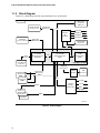
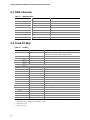
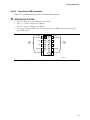
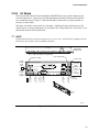
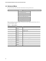
1
Intel® Desktop Board D865PCD Technical Product Specification April 2004 Order Number: C73314-001 The Intel® Desktop Board D865PCD may contain design defects or errors known as errata that may cause the product to deviate from published specifications. Current characterized errata are documented in the Intel Desktop Board D865PCD Specification Update. Revision History Revision -001 Revision History First release of the Specification. Date Intel® Desktop Board D865PCD Technical Product April 2004 This product specification applies to only standard Intel® Desktop Board D865PCD with BIOS identifier RC86510A.86A. Changes to this specification will be published in the Intel Desktop Board D865PCD Specification Update before being incorporated into a revision of this document. INFORMATION IN THIS DOCUMENT IS PROVIDED IN CONNECTION WITH INTEL® PRODUCTS. NO LICENSE, EXPRESS OR IMPLIED, BY ESTOPPEL OR OTHERWISE, TO ANY INTELLECTUAL PROPERTY RIGHTS IS GRANTED BY THIS DOCUMENT. EXCEPT AS PROVIDED IN INTEL’S TERMS AND CONDITIONS OF SALE FOR SUCH PRODUCTS, INTEL ASSUMES NO LIABILITY WHATSOEVER, AND INTEL DISCLAIMS ANY EXPRESS OR IMPLIED WARRANTY, RELATING TO SALE AND/OR USE OF INTEL PRODUCTS INCLUDING LIABILITY OR WARRANTIES RELATING TO FITNESS FOR A PARTICULAR PURPOSE, MERCHANTABILITY, OR INFRINGEMENT OF ANY PATENT, COPYRIGHT OR OTHER INTELLECTUAL PROPERTY RIGHT. INTEL PRODUCTS ARE NOT INTENDED FOR USE IN MEDICAL, LIFE SAVING, OR LIFE SUSTAINING APPLICATIONS. Intel Corporation may have patents or pending patent applications, trademarks, copyrights, or other intellectual property rights that relate to the presented subject matter. The furnishing of documents and other materials and information does not provide any license, express or implied, by estoppel or otherwise, to any such patents, trademarks, copyrights, or other intellectual property rights. Intel may make changes to specifications and product descriptions at any time, without notice. Designers must not rely on the absence or characteristics of any features or instructions marked “reserved” or “undefined.” Intel reserves these for future definition and shall have no responsibility whatsoever for conflicts or incompatibilities arising from future changes to them. Intel® desktop boards may contain design defects or errors known as errata, which may cause the product to deviate from published specifications. Current characterized errata are available on request. Contact your local Intel sales office or your distributor to obtain the latest specifications before placing your product order. Copies of documents which have an ordering number and are referenced in this document, or other Intel literature, may be obtained from: Intel Corporation P.O. Box 5937 Denver, CO 80217-9808 or call in North America 1-800-548-4725, Europe 44-0-1793-431-155, France 44-0-1793-421-777, Germany 44-0-1793-421-333, other Countries 708-296-9333. Intel, Pentium, and Celeron are registered trademarks of Intel Corporation or its subsidiaries in the United States and other countries. * Other names and brands may be claimed as the property of others. Copyright 2004, Intel Corporation. All Rights Reserved. Preface This Technical Product Specification (TPS) specifies the board layout, components, connectors, power and environmental requirements, and the BIOS for the Intel® Desktop Board D865PCD. It describes the standard product and available manufacturing options. Intended Audience The TPS is intended to provide detailed, technical information about the Desktop Board D865PCD and its components to the vendors, system integrators, and other engineers and technicians who need this level of information. It is specifically not intended for general audiences. What This Document Contains Chapter 1 2 3 4 5 Description A description of the hardware used on the Desktop Board D865PCD A map of the resources of the Desktop Board The features supported by the BIOS Setup program The contents of the BIOS Setup program’s menus and submenus A description of the BIOS error messages, beep codes, and POST codes Typographical Conventions This section contains information about the conventions used in this specification. Not all of these symbols and abbreviations appear in all specifications of this type. Notes, Cautions, and Warnings ✏ NOTE Notes call attention to important information. # INTEGRATOR’S NOTES Integrator’s notes are used to call attention to information that may be useful to system integrators. CAUTION Cautions are included to help you avoid damaging hardware or losing data. iii Intel Desktop Board D865PCD Technical Product Specification WARNING Warnings indicate conditions, which if not observed, can cause personal injury. Other Common Notation iv # Used after a signal name to identify an active-low signal (such as USBP0#) (NxnX) When used in the description of a component, N indicates component type, xn are the relative coordinates of its location on the Desktop Board D865PCD, and X is the instance of the particular part at that general location. For example, J5J1 is a connector, located at 5J. It is the first connector in the 5J area. GB Gigabyte (1,073,741,824 bytes) GB/sec Gigabytes per second KB Kilobyte (1024 bytes) Kbit Kilobit (1024 bits) kbits/sec 1000 bits per second MB Megabyte (1,048,576 bytes) MB/sec Megabytes per second Mbit Megabit (1,048,576 bits) Mbit/sec Megabits per second xxh An address or data value ending with a lowercase h indicates a hexadecimal value. x.x V Volts. Voltages are DC unless otherwise specified. * This symbol is used to indicate third-party brands and names that are the property of their respective owners. Contents 1 Product Description 1.1 Overview ....................................................................................................................12 1.1.1 Feature Summary ........................................................................................12 1.1.2 Board Layout................................................................................................13 1.1.3 Block Diagram..............................................................................................14 1.2 Online Support ...........................................................................................................15 1.3 Design Specifications .................................................................................................16 1.4 Processor ...................................................................................................................19 1.5 System Memory .........................................................................................................20 1.5.1 Memory Configurations ................................................................................22 ® 1.6 Intel 865P Chipset ....................................................................................................24 1.6.1 Universal 0.8 V / 1.5 V AGP 3.0 Connector..................................................24 1.6.2 USB..............................................................................................................25 1.6.3 IDE Support .................................................................................................26 1.6.4 Real-Time Clock, CMOS SRAM, and Battery...............................................26 1.7 I/O Controller ..............................................................................................................27 1.7.1 Serial Port ....................................................................................................27 1.7.2 Parallel Port..................................................................................................27 1.7.3 Diskette Drive Controller ..............................................................................27 1.7.4 Keyboard and Mouse Interface ....................................................................28 1.8 Audio Subsystem........................................................................................................28 1.8.1 Realtek ALC202-based Audio Subsystem....................................................28 1.8.2 Audio Connectors.........................................................................................28 1.8.3 Audio Subsystem Software ..........................................................................29 1.9 LAN Subsystem..........................................................................................................29 1.9.1 Intel® 82562EZ Physical Layer Interface Device ..........................................29 1.9.2 RJ-45 LAN Connector with Integrated LEDs ................................................30 1.9.3 LAN Subsystem Software ............................................................................30 1.10 Chassis Intrusion and Detection .................................................................................30 1.11 Power Management ...................................................................................................30 1.11.1 ACPI.............................................................................................................31 1.11.2 Hardware Support ........................................................................................33 2 Technical Reference 2.1 2.2 2.3 2.4 2.5 2.6 2.7 2.8 Introduction.................................................................................................................37 Memory Map ..............................................................................................................37 DMA Channels ...........................................................................................................38 Fixed I/O Map.............................................................................................................38 PCI Configuration Space Map ....................................................................................39 Interrupts ....................................................................................................................40 PCI Interrupt Routing Map ..........................................................................................41 Connectors .................................................................................................................43 2.8.1 Back Panel Connectors................................................................................44 v Intel Desktop Board D865PCD Technical Product Specification 2.9 2.10 2.11 2.12 2.13 2.14 2.15 2.8.2 Internal I/O Connectors ................................................................................45 2.8.3 External I/O Connectors ...............................................................................52 Jumper Blocks............................................................................................................56 2.9.1 Front Panel Audio Connector/Jumper Block.................................................56 2.9.2 BIOS Setup Configuration Jumper Block......................................................57 Mechanical Considerations.........................................................................................58 2.10.1 Form Factor .................................................................................................58 2.10.2 I/O Shield .....................................................................................................59 Electrical Considerations ............................................................................................60 2.11.1 DC Loading ..................................................................................................60 2.11.2 Add-in Board Considerations........................................................................60 2.11.3 Fan Connector Current Capability ................................................................60 2.11.4 Power Supply Considerations ......................................................................61 Thermal Considerations..............................................................................................61 Reliability ....................................................................................................................63 Environmental ............................................................................................................64 Regulatory Compliance ..............................................................................................65 2.15.1 Safety Regulations .......................................................................................65 2.15.2 EMC Regulations .........................................................................................65 2.15.3 European Union Declaration of Conformity Statement .................................66 2.15.4 Product Ecology Statements ........................................................................67 2.15.5 Product Certification Markings (Board Level) ...............................................67 3 Overview of BIOS Features 3.1 3.2 3.3 Introduction.................................................................................................................69 BIOS Flash Memory Organization ..............................................................................69 Resource Configuration ..............................................................................................70 3.3.1 PCI Autoconfiguration ..................................................................................70 3.3.2 PCI IDE Support...........................................................................................70 3.4 System Management BIOS (SMBIOS) .......................................................................71 3.5 Legacy USB Support ..................................................................................................71 3.6 BIOS Updates ............................................................................................................72 3.6.1 Language Support........................................................................................72 3.6.2 Custom Splash Screen.................................................................................73 3.7 Recovering BIOS Data ...............................................................................................73 3.8 Boot Options...............................................................................................................74 3.8.1 CD-ROM Boot ..............................................................................................74 3.8.2 Network Boot................................................................................................74 3.8.3 Booting Without Attached Devices ...............................................................74 3.8.4 Changing the Default Boot Device During POST..........................................74 3.9 Fast Booting Systems with Intel® Rapid BIOS Boot ....................................................75 3.9.1 Peripheral Selection and Configuration ........................................................75 3.9.2 Intel Rapid BIOS Boot ..................................................................................75 3.10 BIOS Security Features..............................................................................................76 vi Contents 4 BIOS Setup Program 4.1 4.2 4.3 4.4 4.5 4.6 4.7 4.8 Introduction.................................................................................................................77 Maintenance Menu .....................................................................................................78 Main Menu..................................................................................................................79 Advanced Menu..........................................................................................................80 4.4.1 PCI Configuration Submenu.........................................................................81 4.4.2 Boot Configuration Submenu .......................................................................82 4.4.3 Peripheral Configuration Submenu...............................................................83 4.4.4 Drive Configuration Submenu ......................................................................85 4.4.5 Floppy Configuration Submenu ....................................................................88 4.4.6 Event Log Configuration Submenu...............................................................89 4.4.7 Video Configuration Submenu......................................................................90 4.4.8 USB Configuration Submenu .......................................................................91 4.4.9 Chipset Configuration Submenu...................................................................92 Security Menu ............................................................................................................94 Power Menu ...............................................................................................................95 4.6.1 ACPI Submenu ............................................................................................95 Boot Menu ..................................................................................................................96 4.7.1 Boot Device Priority Submenu......................................................................97 4.7.2 Hard Disk Drives Submenu ..........................................................................98 4.7.3 Removable Devices Submenu .....................................................................98 4.7.4 ATAPI CD-ROM Drives Submenu ................................................................99 Exit Menu ...................................................................................................................99 5 Error Messages and Beep Codes 5.1 5.2 5.3 5.4 5.5 BIOS Error Messages...............................................................................................101 Port 80h POST Codes..............................................................................................103 Bus Initialization Checkpoints ...................................................................................107 Speaker ...................................................................................................................108 BIOS Beep Codes ....................................................................................................108 vii Intel Desktop Board D865PCD Technical Product Specification Figures 1. 2. 3. 4. 5. 6. 7. 8. 9. 10. 11. 12. 13. 14. 15. 16. 17. 18. Desktop Board D865PCD Components......................................................................13 Block Diagram ............................................................................................................14 Memory Channel Configuration ..................................................................................22 Example of Dual Channel Configuration with Dynamic Mode .....................................23 Example of Single Channel Configuration with Dynamic Mode...................................23 Example of Single Channel Configuration without Dynamic Mode.............................24 LAN Connector LED Locations ...................................................................................30 Back Panel Connectors ..............................................................................................44 Audio Connectors .......................................................................................................46 Power and Hardware Control Connectors ..................................................................48 D865PCD Add-in Board and Peripheral Interface Connectors....................................51 External I/O Connectors .............................................................................................52 Connection Diagram for Front Panel Connector .........................................................53 Connection Diagram for Front Panel USB Connector .................................................55 Location of the Jumper Blocks....................................................................................56 Desktop Board D865PCD Dimensions .......................................................................58 I/O Shield Dimensions ................................................................................................59 Localized High Temperature Zones............................................................................62 Tables 1. 2. 3. 4. 5. 6. 7. 8. 9. 10. 11. 12. 13. 14. 15. 16. 17. 18. 19. 20. 21. 22. 23. 24. 25. viii Feature Summary.......................................................................................................12 Specifications .............................................................................................................16 Supported System Bus Frequency and Memory Speed Combinations.......................20 Supported Memory Configurations .............................................................................21 Characteristics of Dual/Single Channel Configuration with/without Dynamic Mode.....22 LAN Connector LED States ........................................................................................30 Effects of Pressing the Power Switch .........................................................................31 Power States and Targeted System Power ................................................................32 Wake-up Devices and Events.....................................................................................32 System Memory Map..................................................................................................37 DMA Channels ...........................................................................................................38 I/O Map ......................................................................................................................38 PCI Configuration Space Map ....................................................................................39 Interrupts ....................................................................................................................40 PCI Interrupt Routing Map ..........................................................................................42 ATAPI CD-ROM Connector ........................................................................................47 Front Panel Audio Connector .....................................................................................47 Rear Chassis Fan Connector .....................................................................................49 ATX12V Power Connector..........................................................................................49 Processor Fan Connector...........................................................................................49 Main Power Connector ...............................................................................................49 Front Chassis Fan Connector .....................................................................................50 Chassis Intrusion Connector.......................................................................................50 Auxiliary Front Panel Power/Sleep/Message-Waiting LED Connector ........................53 Front Panel Connector ...............................................................................................53 Contents 26. 27. 28. 29. 30. 31. 32. 33. 34. 35. 36. 37. 38. 39. 40. 41. 42. 43. 44. 45. 46. 47. 48. 49. 50. 51. 52. 53. 54. 55. 56. 57. 58. 59. 60. 61. 62. 63. 64. 65. 66. 67. 68. 69. 70. States for a One-Color Power LED.............................................................................54 States for a Two-Color Power LED.............................................................................54 Front Panel Audio Connector/Jumper Block ...............................................................57 BIOS Setup Configuration Jumper Settings................................................................57 DC Loading Characteristics ........................................................................................60 Fan Connector Current Capability ..............................................................................60 Thermal Considerations for Components ...................................................................63 Desktop Board D865PCD Environmental Specifications ............................................64 Safety Regulations .....................................................................................................65 EMC Regulations........................................................................................................65 Product Certification Markings....................................................................................67 Boot Device Menu Options .........................................................................................74 Supervisor and User Password Functions ..................................................................76 BIOS Setup Program Menu Bar .................................................................................77 BIOS Setup Program Function Keys ..........................................................................78 Maintenance Menu .....................................................................................................78 Main Menu..................................................................................................................79 Advanced Menu..........................................................................................................80 PCI Configuration Submenu .......................................................................................81 Boot Configuration Submenu......................................................................................82 Peripheral Configuration Submenu.............................................................................83 Drive Configuration Submenu.....................................................................................85 PATA Submenus ........................................................................................................87 Floppy Configuration Submenu ..................................................................................88 Event Log Configuration Submenu .............................................................................89 Video Configuration Submenu ....................................................................................90 USB Configuration Submenu......................................................................................91 Chipset Configuration Submenu .................................................................................92 Security Menu ............................................................................................................94 Power Menu ...............................................................................................................95 ACPI Submenu...........................................................................................................95 Boot Menu ..................................................................................................................96 Boot Device Priority Submenu ....................................................................................97 Hard Disk Drives Submenu ........................................................................................98 Removable Devices Submenu....................................................................................98 ATAPI CD-ROM Drives Submenu ..............................................................................99 Exit Menu ...................................................................................................................99 BIOS Error Messages...............................................................................................101 Uncompressed INIT Code Checkpoints....................................................................103 Boot Block Recovery Code Checkpoints ..................................................................103 Runtime Code Uncompressed in F000 Shadow RAM ..............................................104 Bus Initialization Checkpoints ...................................................................................107 Upper Nibble High Byte Functions............................................................................107 Lower Nibble High Byte Functions............................................................................108 Beep Codes..............................................................................................................109 ix Intel Desktop Board D865PCD Technical Product Specification x 1 Product Description What This Chapter Contains 1.1 1.2 1.3 1.4 1.5 1.6 1.7 1.8 1.9 1.10 1.11 Overview ....................................................................................................................12 Online Support ...........................................................................................................15 Design Specifications .................................................................................................16 Processor ...................................................................................................................19 System Memory .........................................................................................................20 Intel® 865P Chipset ....................................................................................................24 I/O Controller ..............................................................................................................27 Audio Subsystem........................................................................................................28 LAN Subsystem..........................................................................................................29 Chassis Intrusion and Detection .................................................................................30 Power Management ...................................................................................................30 11 Intel Desktop Board D865PCD Technical Product Specification 1.1 Overview 1.1.1 Feature Summary Table 1 summarizes the major features of the Desktop Board D865PCD. Table 1. Feature Summary Form Factor microATX (9.60 inches by 9.60 inches [243.84 millimeters by 243.84 millimeters]) Processor • Support for an Intel® Pentium® 4 processor in an mPGA478 socket with a 400 or 533 MHz system bus • Support for an Intel® Celeron® processor in an mPGA478 socket with a 400 MHz system bus Memory • Two 184-pin DDR SDRAM Dual Inline Memory Module (DIMM) sockets • Support for DDR 333 and DDR 266 DIMMs • Support for up to 2 GB of system memory Chipset Intel® 865P Chipset, consisting of: • Intel® 82865P Memory Controller Hub (MCH) • Intel® 82801EB I/O Controller Hub (ICH5) • 4 Mbit Firmware Hub (FWH) Video Universal 0.8 V / 1.5 V AGP 3.0 connector (with integrated retention mechanism) supporting 1x, 4x, and 8x AGP cards or an AGP Digital Display (ADD) card Audio Audio subsystem using the Realtek ALC202 codec I/O Control LPC Bus I/O controller USB Support for USB 2.0 devices Peripheral Interfaces • Six USB ports • One serial port • One parallel port • Two Parallel ATA IDE interfaces with UDMA 33, ATA-66/100 support • One diskette drive interface • PS/2* keyboard and mouse ports LAN Support 10/100 Mbits/sec LAN subsystem using the Intel® 82562EZ Platform LAN Connect (PLC) device BIOS • Intel/AMI BIOS (resident in the 4 Mbit FWH) • Support for Advanced Configuration and Power Interface (ACPI), Plug and Play, and SMBIOS Instantly Available PC Technology • Support for PCI Local Bus Specification Revision 2.2 • Suspend to RAM support • Wake on PCI, RS-232, front panel, PS/2 devices, and USB ports Expansion Capabilities 12 Three PCI bus add-in card connectors (SMBus routed to PCI bus connector 2) For information about Refer to Available configurations for the Desktop Boards D865PCD Section 1.2, page 16 The board’s compliance level with ACPI, Plug and Play, and SMBIOS Section 1.3, page 16 Product Description 1.1.2 Board Layout Figure 1 shows the location of the major components. B A F C DE G BB AA H Z Y I J K X L W V T U R S Q P O N M OM17040 A B C D E F G H I J K L M N Audio codec Front panel audio connector Ethernet PLC device (optional) AGP connector Rear chassis fan connector Back panel connectors +12V power connector (ATX12V) mPGA478 processor socket Processor fan connector Intel 82865P MCH DIMM Channel A socket DIMM Channel B socket I/O controller Power connector O P Q R S T U V W X Y Z AA BB Diskette drive connector Parallel ATE IDE connectors Front chassis fan connector Chassis intrusion connector 4 Mbit Firmware Hub (FWH) Speaker BIOS Setup configuration jumper block Auxiliary front panel power LED connector Front panel connector Intel 82801EB I/O Controller Hub (ICH5) Front panel USB connector Battery PCI bus add-in card connectors ATAPI CD-ROM connector Figure 1. Desktop Board D865PCD Components 13 Intel Desktop Board D865PCD Technical Product Specification 1.1.3 Block Diagram Figure 2 is a block diagram of the major functional areas of the board. = connector or socket Parallel ATA IDE Connectors (2) Back Panel/ Front Panel USB Ports Parallel ATA IDE Interface USB Serial Port LPC Bus I/O Controller mPGA478 Processor Socket Parallel Port PS/2 Mouse PS/2 Keyboard System Bus (400/533 MHz) Diskette Drive Connector LPC Bus AGP Interface Intel 82865P Memory Controller Hub (MCH) AHA Bus Intel 82801EB I/O Controller Hub (ICH5) 4 Mbit Firmware Hub (FWH) Universal 0.8/ 1.5 V AGP 3.0 Connector Intel 865P Chipset CSMA/CD Unit Interface Channel A DIMM 10/100 LAN PLC Dual-Channel Memory Bus SMBus AC Link Channel B DIMM Line Out Realtek ALC202 Audio Codec PCI Bus Line In Mic In CD-ROM PCI Slot 1 PCI Slot 2 LAN Connector SMBus PCI Slot 3 OM17046 Figure 2. Block Diagram 14 Product Description 1.2 Online Support To find information about… Visit this World Wide Web site: Intel Desktop Board D865PCD under “Desktop Board Products” or “Desktop Board Support” http://www.intel.com/design/motherbd Available configurations for the Desktop Board D865PCD http://developer.intel.com/design/motherbd/cd/cd_available.htm Processor data sheets http://www.intel.com/design/litcentr ICH5 addressing http://developer.intel.com/design/chipsets/datashts Custom splash screens http://intel.com/design/motherbd/gen_indx.htm Audio software and utilities http://www.intel.com/design/motherbd LAN software and drivers http://www.intel.com/design/motherbd http://support.intel.com/support/motherboards/desktop 15 Intel Desktop Board D865PCD Technical Product Specification 1.3 Design Specifications Table 2 lists the specifications applicable to the Desktop Board D865PCD. Table 2. Specifications Reference Name Specification Title Version, Revision Date, and Ownership The information is available from… AC ’97 Audio Codec ’97 Revision 2.2, September 2000, Intel Corporation. ftp://download.intel.com/labs/ media/audio/download/ac97r 22.pdf ACPI Advanced Configuration and Power Interface Specification Version 2.0, July 27, 2000, Compaq Computer Corporation, Intel Corporation, Microsoft Corporation, Phoenix Technologies Limited, and Toshiba Corporation. http://www.acpi.info/spec.htm AGP Accelerated Graphics Port Interface Specification Revision 3.0, September 2002, Intel Corporation. http://www.agpforum.org/spec s_specs.htm AMI BIOS AMIBIOS Desktop Core 8.0 AMIBIOS 8.0, 2001, American Megatrends, Inc. http://www.ami.com/support/d oc/amibios8.pdf ASF Alert Standard Format (ASF) Specification http://www.dmtf.org/standards /documents/ASF/DSP0114.p df ATA/ ATAPI-5 Information Technology-AT Attachment with Packet Interface - 5 (ATA/ATAPI-5) Version 1.03, June 20, 2001, DMTF, Intel Corporation. Revision 3, February 29, 2000, Contact: T13 Chair, Seagate Technology. ATX ATX Specification Version 2.03, December 1998, Intel Corporation. http://www.formfactors.org/de veloper/specs/atx/atxspecs.ht m ATX12V ATX/ATX12V Power Supply Design Guide Version 1.2, August 2000, Intel Corporation. http://www.formfactors.org/de veloper/specs/atx/atxspecs.ht m BIS Boot Integrity Services (BIS) Application Programming Interface (API) Version 1.0, August 4, 1999, Intel Corporation. http://www.intel.com/labs/man age/wfm/wfmspecs.htm http://www.t13.org continued 16 Product Description Table 2. Specifications (continued) Reference Name Specification Title Version, Revision Date and Ownership The information is available from… DDR SDRAM Double Data Rate (DDR) SDRAM Specification Version 1.0, June 2000, JEDEC Solid State Technology Association. http://www.jedec.org/ Design Specification for a 184 Pin DDR Unbuffered DIMM Revision 1.0, October 2001, JEDEC Solid State Technology Association. http://www.jedec.org/ Intel ® JEDEC DDR 200/266 Unbuffered DIMM Specification Addendum Revision 0.9, September 27, 2001, Intel Corporation. http://developer.intel.com/t echnology/memory/index.ht m EHCI Enhanced Host Controller Interface Specification for Universal Serial Bus Revision 1.0, March 12, 2002, Intel Corporation. http://developer.intel.com/t echnology/usb/download/e hci-r10.pdf EPP IEEE Std 1284.1-1997 (Enhanced Parallel Port) Version 1.7, 1997, Institute of Electrical and Electronic Engineers. http://standards.ieee.org/re ading/ieee/std_public/descr iption/busarch/1284.11997_desc.html El Torito Bootable CD-ROM Format Specification Version 1.0, January 25, 1995, Phoenix Technologies Limited and International Business Machines Corporation. http://www.phoenix.com/res ources/specs-cdrom.pdf LPC Low Pin Count Interface Specification Revision 1.0, September 29, 1997, Intel Corporation. http://www.intel.com/design /chipsets/industry/lpc.htm MicroATX microATX Motherboard Interface Specification Version 1.0, December 1997, Intel Corporation. http://www.formfactors.org/ developer/specs/microatx/ microatxspecs.htm PCI PCI Local Bus Specification Revision 2.2, December 18, 1998, PCI Special Interest Group. http://www.pcisig.com/speci fications PCI Bus Power Management Interface Specification Revision 1.1, December 18, 1998, PCI Special Interest Group. http://www.pcisig.com/speci fications Plug and Play BIOS Specification Version 1.0a, May 5, 1994, Compaq Computer Corporation, Phoenix Technologies Limited, and Intel Corporation. http://www.microsoft.com/h wdev/tech/PnP/default.asp Plug and Play continued 17 Intel Desktop Board D865PCD Technical Product Specification Table 2. 18 Specifications (continued) Reference Name Specification Title Version, Revision Date and Ownership The information is available from… PXE Preboot Execution Environment Version 2.1, September 20, 1999, Intel Corporation. ftp://download.intel.com/lab s/manage/wfm/download/p xespec.pdf SFX SFX/SFX12V Power Supply Design Guide Version 2.0, May 2001, Intel Corporation. http://www.formfactors.org/ developer/specs/sfx/sfx12v. pdf SMBIOS System Management BIOS Version 2.3.1, March 16, 1999, American Megatrends Incorporated, Award Software International Incorporated, Compaq Computer Corporation, Dell Computer Corporation, Hewlett-Packard Company, Intel Corporation, International Business Machines Corporation, Phoenix Technologies Limited, and SystemSoft Corporation. http://www.dmtf.org/downlo ad/standards/DSP0119.pdf TFX12V TFX12V Power Supply Design Guide Revision 1.01, May 2002, Intel Corporation. http://www.formfactors.org/ developer/specs/tfx12v/tfx1 2v_psdg_101.pdf UHCI Universal Host Controller Interface Design Guide Revision 1.1, March 1996, Intel Corporation. http://developer.intel.com/d esign/USB/UHCI11D.htm USB Universal Serial Bus Specification Revision 2.0, April 27, 2000, Compaq Computer Corporation, Hewlett-Packard Company, Lucent Technologies Inc., Intel Corporation, Microsoft Corporation, NEC Corporation, and Koninklijke Philips Electronics N.V. http://www.usb.org/develop ers/docs WfM Wired for Management Baseline Version 2.0, December 18, 1998, Intel Corporation. http://www.intel.com/labs/m anage/wfm/wfmspecs.htm Product Description 1.4 Processor ✏ NOTE Refer to Thermal Considerations (Section 2.12, page 61) for important information when using an Intel Pentium 4 processor operating above 2.80 GHz with this Intel® desktop board. The board is designed to support the following: • • Intel Pentium 4 processors in an mPGA478 processor socket with a 400 or 533 MHz system bus Intel Celeron processors in an mPGA478 processor socket with a 400 MHz system bus See the Intel web site listed below for the most up-to-date list of supported processors. For information about… Refer to: Supported processors for the D865PCD board http://www.intel.com/design/motherbd/cd/cd_proc.htm CAUTION Use only the processors listed on web site above. Use of unsupported processors can damage the board, the processor, and the power supply. # INTEGRATOR’S NOTES • • • Use only ATX12V-, SFX12V-, or TFX12V-compliant power supplies. ATX12V, SFX12V, and TFX12V power supplies have an additional power lead that provides required supplemental power for the processor. Always connect the 20-pin and 4-pin leads of ATX12V, SFX12V, and TFX12V power supplies to the corresponding connectors on the desktop board, otherwise the board will not boot. Do not use a standard ATX power supply. The board will not boot with a standard ATX power supply. Refer to Table 3 on page 20 for a list of supported system bus frequency and memory speed combinations. For information about Refer to Power supply connectors Section 2.8.2.2, page 46 19 Intel Desktop Board D865PCD Technical Product Specification 1.5 System Memory The board has two DIMM sockets and supports the following memory features: • • • • • • • 2.5 V (only) 184-pin DDR SDRAM DIMMs with gold-plated contacts Unbuffered, single-sided or double-sided DIMMs with the following restriction: Double-sided DIMMS with x16 organization are not supported. 2 GB maximum total system memory Minimum total system memory: 64 MB Non-ECC DIMMs Serial Presence Detect DDR333 and DDR266 SDRAM DIMMs Table 3 lists the supported system bus frequency and memory speed combinations. Table 3. Supported System Bus Frequency and Memory Speed Combinations To use this type of DIMM… ✏ DDR333 533 MHz DDR266 533 or 400 MHz NOTES • • 20 The processor's system bus frequency must be… Remove the AGP video card before installing or upgrading memory to avoid interference with the memory retention mechanism. To be fully compliant with all applicable DDR SDRAM memory specifications, the board should be populated with DIMMs that support the Serial Presence Detect (SPD) data structure. This allows the BIOS to read the SPD data and program the chipset to accurately configure memory settings for optimum performance. If non-SPD memory is installed, the BIOS will attempt to correctly configure the memory settings, but performance and reliability may be impacted or the DIMMs may not function under the determined frequency. For information about Refer to Obtaining DDR SDRAM specifications Section 1.3, page 16 Product Description Table 4 lists the supported DIMM configurations. Table 4. Supported Memory Configurations DIMM Capacity Configuration DDR SDRAM Density DDR SDRAM Organization Front-side/Back-side Number of DDR SDRAM Devices 64 MB SS 64 Mbit 8 M x 8/empty 8 64 MB SS 128 Mbit 8 M x 16/empty 4 128 MB DS 64 Mbit 8 M x 8/8 M x 8 16 128 MB SS 128 Mbit 16 M x 8/empty 8 128 MB SS 256 Mbit 16 M x 16/empty 4 256 MB DS 128 Mbit 16 M x 8/16 M x 8 16 256 MB SS 256 Mbit 32 M x 8/empty 8 256 MB SS 512 Mbit 32 M x 16/empty 4 512 MB DS 256 Mbit 32 M x 8/32 M x 8 16 512 MB SS 512 Mbit 64 M x 8/empty 8 1024 MB DS 512 Mbit 64 M x 8/64 M x 8 16 Note: In the second column, “DS” refers to double-sided memory modules (containing two rows of DDR SDRAM) and “SS” refers to single-sided memory modules (containing one row of DDR SDRAM). 21 Intel Desktop Board D865PCD Technical Product Specification 1.5.1 Memory Configurations The Intel 82865P MCH component provides two features for enhancing memory throughput: • • Dual Channel memory interface. The board has two memory channels, each with a single DIMM socket, as shown in Figure 3 Dynamic Addressing Mode. Dynamic mode minimizes overhead by reducing memory accesses Table 5 summarizes the characteristics of Dual and Single Channel configurations with and without the use of Dynamic Mode. Table 5. Characteristics of Dual/Single Channel Configuration with/without Dynamic Mode Throughput Level Configuration Characteristics Highest Dual Channel with Dynamic Mode DIMMs matched Single Channel with Dynamic Mode Single DIMM (Example configuration shown in Figure 4) (Example configuration shown in Figure 5) Single Channel without Dynamic Mode DIMMs not matched (Example configuration shown in Figure 6) Lowest Channel A DIMM Channel B, DIMM OM17042 Figure 3. Memory Channel Configuration 22 Product Description Single Channel Configuration without Dynamic Mode (DIMMs not matched) Channel A DIMM Intel 82865P MCH Channel B DIMM OM17043 Throughput Level Configuration Highest Dual Channel with Dynamic Mode DIMMs matched Single Channel with Dynamic Mode Single DIMM Single Channel without Dynamic Mode DIMMs not matched Characteristics Lowest Figure 4. Example of Dual Channel Configuration with Dynamic Mode Single Channel Configuration with Dynamic Mode (Single DIMM) Channel A DIMM Intel 82865P MCH Channel B DIMM OM17044 Throughput Level Configuration Characteristics Highest Dual Channel with Dynamic Mode DIMMs matched Single Channel with Dynamic Mode Single DIMM Single Channel without Dynamic Mode DIMMs not matched Lowest Figure 5. Example of Single Channel Configuration with Dynamic Mode 23 Intel Desktop Board D865PCD Technical Product Specification Dual Channel Configuration with Dynamic Mode (DIMMs matched) Channel A DIMM Intel 82865P MCH Channel B DIMM OM17045 Throughput Level Highest Configuration Characteristics Dual Channel with Dynamic Mode DIMMs matched Single Channel with Dynamic Mode Single DIMM Single Channel without Dynamic Mode DIMMs not matched Lowest Figure 6. Example of Single Channel Configuration without Dynamic Mode 1.6 Intel® 865P Chipset The Intel 865P chipset consists of the following devices: • • • Intel 82865P Memory Controller Hub (MCH) with Accelerated Hub Architecture (AHA) bus Intel 82801EB I/O Controller Hub (ICH5) with AHA bus Firmware Hub (FWH) The MCH is a centralized controller for the system bus, the memory bus, the AGP bus, and the Accelerated Hub Architecture interface. The ICH5 is a centralized controller for the board’s I/O paths. The FWH provides the nonvolatile storage of the BIOS. For information about Refer to The Intel 865P chipset http://developer.intel.com/ Resources used by the chipset Chapter 2 1.6.1 Universal 0.8 V / 1.5 V AGP 3.0 Connector The AGP connector supports the following: • • • 24 4x, 8x AGP 3.0 add-in cards with 0.8 V I/O 1x, 4x AGP 2.0 add-in cards with 1.5 V I/O AGP Digital Display (ADD) cards Product Description AGP is a high-performance interface for graphics-intensive applications, such as 3D applications. While based on the PCI Local Bus Specification, Rev. 2.2, AGP is independent of the PCI bus and is intended for exclusive use with graphical display devices. AGP overcomes certain limitations of the PCI bus related to handling large amounts of graphics data with the following features: • • # Pipelined memory read and write operations that hide memory access latency Demultiplexing of address and data on the bus for nearly 100 percent efficiency INTEGRATOR’S NOTES • • • AGP 2x operation is not supported. Install memory in the DIMM sockets prior to installing the AGP video card to avoid interference with the memory retention mechanism. The AGP connector is keyed for Universal 0.8 V AGP 3.0 cards or 1.5 V AGP 2.0 cards only. Do not attempt to install a legacy 3.3 V AGP card. The AGP connector is not mechanically compatible with legacy 3.3 V AGP cards. For information about Refer to The location of the AGP connector Figure 1, page 13 Obtaining the Accelerated Graphics Port Interface Specification Section 1.3, page 16 1.6.2 USB The board supports up to six USB 2.0 ports, supports UHCI and EHCI, and uses UHCI- and EHCIcompatible drivers. The ICH5 provides the USB controller for all ports. The port arrangement is as follows: • • • ✏ Two ports are implemented with stacked back panel connectors, adjacent to the PS/2 connectors Two ports are implemented with stacked back panel connectors, adjacent to the audio connectors Two ports are routed to a front panel USB connector NOTES • Computer systems that have an unshielded cable attached to a USB port may not meet FCC Class B requirements, even if no device is attached to the cable. Use shielded cable that meets the requirements for full-speed devices. • Native USB 2.0 support has been tested with drivers for Windows* 2000 (with Service Pack 3) and Windows XP (with Service Pack 1) and is not currently supported by any other operating system. Check Intel’s Desktop Board website for possible driver updates for other operating systems. For information about Refer to The location of the USB connectors on the back panel Figure 8, page 44 The location of the front panel USB connector Figure 12, page 52 The EHCI, front panel, UHCI, and USB specifications Section 1.3, page 16 25 Intel Desktop Board D865PCD Technical Product Specification 1.6.3 IDE Support The board provides two Parallel ATA IDE connectors, which support a total of four devices (two per connector). The ICH5’s Parallel ATA IDE controller has two independent bus-mastering Parallel ATA IDE interfaces that can be independently enabled. The Parallel ATA IDE interfaces support the following modes: • • • • • ✏ Programmed I/O (PIO): processor controls data transfer. 8237-style DMA: DMA offloads the processor, supporting transfer rates of up to 16 MB/sec. Ultra DMA: DMA protocol on IDE bus supporting host and target throttling and transfer rates of up to 33 MB/sec. ATA-66: DMA protocol on IDE bus supporting host and target throttling and transfer rates of up to 66 MB/sec. ATA-66 protocol is similar to Ultra DMA and is device driver compatible. ATA-100: DMA protocol on IDE bus allows host and target throttling. The ICH5’s ATA-100 logic can achieve read transfer rates up to 100 MB/sec and write transfer rates up to 88 MB/sec. NOTE ATA-66 and ATA-100 are faster timings and require a specialized cable to reduce reflections, noise, and inductive coupling. The Parallel ATA IDE interfaces also support ATAPI devices (such as CD-ROM drives) and ATA devices using the transfer modes listed in Section 4.4.4.1 on page 86. The BIOS supports Logical Block Addressing (LBA) and Extended Cylinder Head Sector (ECHS) translation modes. The drive reports the transfer rate and translation mode to the BIOS. The board supports Laser Servo (LS-120) diskette technology through the Parallel ATA IDE interfaces. An LS-120 drive can be configured as a boot device by setting the BIOS Setup program’s Boot menu to one of the following: • • ARMD-FDD (ATAPI removable media device – floppy disk drive) ARMD-HDD (ATAPI removable media device – hard disk drive) For information about Refer to The location of the Parallel ATA IDE connectors Figure 11, page 51 1.6.4 Real-Time Clock, CMOS SRAM, and Battery A coin-cell battery (CR2032) powers the real-time clock and CMOS memory. When the computer is not plugged into a wall socket, the battery has an estimated life of three years. When the computer is plugged in, the standby current from the power supply extends the life of the battery. The clock is accurate to ± 13 minutes/year at 25 ºC with 3.3 VSB applied. ✏ NOTE If the battery and AC power fail, custom defaults, if previously saved, will be loaded into CMOS RAM at power-on. 26 Product Description 1.7 I/O Controller The I/O controller provides the following features: • • • • • • • One serial port One parallel port with Extended Capabilities Port (ECP) and Enhanced Parallel Port (EPP) support Serial IRQ interface compatible with serialized IRQ support for PCI systems PS/2-style mouse and keyboard interfaces Interface for one 1.44 MB or 2.88 MB diskette drive Intelligent power management, including a programmable wake-up event interface PCI power management support The BIOS Setup program provides configuration options for the I/O controller. For information about Refer to SMSC LPC47M172 I/O controller http://www.smsc.com National Semiconductor PC87372 I/O Controller http://www.national.com/ 1.7.1 Serial Port The boards have one serial port connector located on the back panel. The serial port supports data transfers at speeds up to 115.2 kbits/sec with BIOS support. For information about Refer to The location of the serial port A connector Figure 8, page 44 1.7.2 Parallel Port The 25-pin D-Sub parallel port connector is located on the back panel. Use the BIOS Setup program to set the parallel port mode. For information about Refer to The location of the parallel port connector Figure 8, page 44 Setting the parallel port’s mode Table 46, page 83 1.7.3 Diskette Drive Controller The I/O controller supports one diskette drive. Use the BIOS Setup program to configure the diskette drive interface. For information about Refer to The location of the diskette drive connector on the D865PCD board Figure 11, page 51 The supported diskette drive capacities and sizes Table 49, page 88 27 Intel Desktop Board D865PCD Technical Product Specification 1.7.4 Keyboard and Mouse Interface PS/2 keyboard and mouse connectors are located on the back panel. ✏ NOTE The keyboard is supported in the bottom PS/2 connector and the mouse is supported in the top PS/2 connector. Power to the computer should be turned off before a keyboard or mouse is connected or disconnected. For information about Refer to The location of the keyboard and mouse connectors Figure 8, page 44 1.8 Audio Subsystem The board provides an audio subsystem based on the Realtek ALC202 codec. 1.8.1 Realtek ALC202-based Audio Subsystem The Realtek ALC202-based audio subsystem consists of the following devices: • • Intel 82801EB I/O Controller Hub (ICH5) Realtek ALC202 audio codec The audio subsystem includes these features: • • • Signal-to-noise ratio ≥ 90 dB Supports wake events (driver dependent) Mic in pre-amp that supports dynamic, condenser, and electret microphones The back panel audio connectors for this audio subsystem including the following: • • • 1.8.2 1.8.2.1 Line out Line in Mic in Audio Connectors Front Panel Audio Connector A 2 x 5-pin connector provides mic in and line out signals for front panel audio connectors. For information about ✏ Refer to The location of the connector Figure 9, page 46 The signal names of the front panel audio connector Table 17, page 47 NOTE The front panel audio connector is alternately used as a jumper block for routing audio signals. Refer to Section 2.9.1 on page 56 for more information. 28 Product Description 1.8.2.2 ATAPI CD-ROM Audio Connector A 1 x 4-pin ATAPI-style connector connects an internal ATAPI CD-ROM drive to the audio mixer. For information about Refer to The location of the ATAPI CD-ROM connector Figure 9, page 46 The signal names of the ATAPI CD-ROM connector Table 16, page 47 1.8.3 Audio Subsystem Software Audio software and drivers are available from Intel’s World Wide Web site. For information about Refer to Obtaining audio software and drivers Section 1.2, page 15 1.9 LAN Subsystem The 10/100 Mbits/sec LAN subsystem consists of the following: • • • Intel® 82562EZ Platform LAN Connect (PLC) device for 10/100 Mbits/sec Ethernet LAN connectivity Intel 82801EB ICH5 (with its CSMA/CD interface) RJ-45 LAN connector with integrated status LEDs Additional features of the LAN subsystem include: • • • PCI bus master interface CSMA/CD protocol engine PCI power management Supports ACPI technology Supports LAN wake capabilities 1.9.1 Intel® 82562EZ Physical Layer Interface Device The Intel 82562EZ provides the following functions: • • • • Basic 10/100 Ethernet LAN connectivity Full device driver compatibility Programmable transit threshold Configuration EEPROM that contains the MAC address 29 Intel Desktop Board D865PCD Technical Product Specification 1.9.2 RJ-45 LAN Connector with Integrated LEDs Two LEDs are built into the RJ-45 LAN connector (shown in Figure 7 below). Green LED Yellow LED OM15076 Figure 7. LAN Connector LED Locations Table 6 describes the LED states when the board is powered up and the 10/100 Mbits/sec LAN subsystem is operating. Table 6. LED Color Green Yellow 1.9.3 LAN Connector LED States LED State Off On Blinking Off On Condition LAN link is not established LAN link is established LAN activity is occurring 10 Mbits/sec data rate is selected 100 Mbits/sec data rate is selected LAN Subsystem Software LAN software and drivers are available from Intel’s World Wide Web site. For information about Refer to Obtaining LAN software and drivers Section 1.2, page 15 1.10 Chassis Intrusion and Detection The Desktop Board D865PCD supports a chassis security feature that detects if the chassis cover is removed. The security feature uses a mechanical switch on the chassis that attaches to the chassis intrusion connector. When the chassis cover is removed, the mechanical switch is in the closed position. 1.11 Power Management Power management is implemented at several levels, including: • • 30 Software support through Advanced Configuration and Power Interface (ACPI) Hardware support: Power connector Fan connectors LAN wake capabilities Instantly Available PC technology Resume on Ring Wake from USB Wake from PS/2 devices Product Description Power Management Event signal (PME#) wake-up support 1.11.1 ACPI ACPI gives the operating system direct control over the power management and Plug and Play functions of a computer. The use of ACPI with the Desktop Board D865PCD requires an operating system that provides full ACPI support. ACPI features include: • • • • • • Plug and Play (including bus and device enumeration) Power management control of individual devices, add-in boards (some add-in boards may require an ACPI-aware driver), video displays, and hard disk drives Methods for achieving less than 15-watt system operation in the power-on/standby sleeping state A Soft-off feature that enables the operating system to power-off the computer Support for multiple wake-up events (see Table 9 on page 32) Support for a front panel power and sleep mode switch Table 7 lists the system states based on how long the power switch is pressed, depending on how ACPI is configured with an ACPI-aware operating system. Table 7. Effects of Pressing the Power Switch If the system is in this state… Off (ACPI G2/G5 – Soft off) On (ACPI G0 – working state) On (ACPI G0 – working state) Sleep (ACPI G1 – sleeping state) Sleep (ACPI G1 – sleeping state) …and the power switch is pressed for Less than four seconds Less than four seconds More than four seconds Less than four seconds More than four seconds …the system enters this state Power-on (ACPI G0 – working state) Soft-off/Standby (ACPI G1 – sleeping state) Fail safe power-off (ACPI G2/G5 – Soft off) Wake-up (ACPI G0 – working state) Power-off (ACPI G2/G5 – Soft off) For information about Refer to The Desktop Boards’ compliance level with ACPI Section 1.3, page 16 1.11.1.1 System States and Power States Under ACPI, the operating system directs all system and device power state transitions. The operating system puts devices in and out of low-power states based on user preferences and knowledge of how devices are being used by applications. Devices that are not being used can be turned off. The operating system uses information from applications and user settings to put the system as a whole into a low-power state. Table 8 lists the power states supported by the Desktop Board D865PCD and along with the associated system power targets. See the ACPI specification for a complete description of the various system and power states. 31 Intel Desktop Board D865PCD Technical Product Specification Table 8. Power States and Targeted System Power Global States Sleeping States Processor States G0 – working state S0 – working C0 – working D0 – working state. Full power > 30 W G1 – sleeping state S1 – Processor stopped C1 – stop grant D1, D2, D3 – device specification specific. 5 W < power < 52.5 W G1 – sleeping state S3 – Suspend to RAM. Context saved to RAM. No power D3 – no power except for wake-up logic. Power < 5 W (Note 2) G1 – sleeping state S4 – Suspend to disk. Context saved to disk. No power D3 – no power except for wake-up logic. Power < 5 W (Note 2) G2/S5 S5 – Soft off. Context not saved. Cold boot is required. No power D3 – no power except for wake-up logic. Power < 5 W (Note 2) G3 – mechanical off No power to the system. No power D3 – no power for wake-up logic, except when provided by battery or external source. No power to the system. Service can be performed safely. AC power is disconnected from the computer. Device States Targeted System Power (Note 1) Notes: 1. Total system power is dependent on the system configuration, including add-in boards and peripherals powered by the system chassis’ power supply. 2. Dependent on the standby power consumption of wake-up devices used in the system. 1.11.1.2 Wake-up Devices and Events Table 9 lists the devices or specific events that can wake the computer from specific states. Table 9. These devices/events can wake up the computer… …from this state LAN S1, S3, S4, S5 (Note) Modem (back panel Serial Port A) S1, S3 PME# signal S1, S3, S4, S5 (Note) Power switch S1, S3, S4, S5 PS/2 devices S1, S3 RTC alarm S1, S3, S4, S5 USB S1, S3 Note: 32 Wake-up Devices and Events For LAN and PME# signal, S5 is disabled by default in the BIOS Setup program. Setting this option to Power On will enable a wake-up event from LAN in the S5 state. Product Description ✏ NOTE The use of these wake-up events from an ACPI state requires an operating system that provides full ACPI support. In addition, software, drivers, and peripherals must fully support ACPI wake events. 1.11.2 Hardware Support CAUTION Ensure that the power supply provides adequate +5 V standby current if LAN wake capabilities and Instantly Available PC technology features are used. Failure to do so can damage the power supply. The total amount of standby current required depends on the wake devices supported and manufacturing options. The Desktop Board D865PCD provides several power management hardware features, including: • • • • • • • • Power connector Fan connectors LAN wake capabilities Instantly Available PC technology Resume on Ring Wake from USB Wake from PS/2 keyboard PME# signal wake-up support LAN wake capabilities and Instantly Available PC technology require power from the +5 V standby line. The sections discussing these features describe the incremental standby power requirements for each. Resume on Ring enables telephony devices to access the computer when it is in a power-managed state. The method used depends on the type of telephony device (external or internal). ✏ NOTE The use of Resume on Ring and Wake from USB technologies from an ACPI state requires an operating system that provides full ACPI support. 1.11.2.1 Power Connector ATX12V-, SFX12V-, and TFX12V-compliant power supplies can turn off the system power through system control. When an ACPI-enabled system receives the correct command, the power supply removes all non-standby voltages. When resuming from an AC power failure, the computer returns to the power state it was in before power was interrupted (on or off). The computer’s response can be set using the Last Power State feature in the BIOS Setup program’s Boot menu. 33 Intel Desktop Board D865PCD Technical Product Specification For information about Refer to The location of the power connector Figure 9, page 46 The signal names of the power connector Table 21, page 49 The BIOS Setup program’s Boot menu Table 57, page 96 The ATX12V, SFX12V, and TFX12V specifications Section 1.3, page 16 1.11.2.2 LAN Wake Capabilities CAUTION For LAN wake capabilities, the +5 V standby line for the power supply must be capable of providing adequate +5 V standby current. Failure to provide adequate standby current when implementing LAN wake capabilities can damage the power supply. LAN wake capabilities enable remote wake-up of the computer through a network. The LAN subsystem PCI bus network adapter monitors network traffic at the Media Independent Interface. Upon detecting a Magic Packet* frame, the LAN subsystem asserts a wake-up signal that powers up the computer. Depending on the LAN implementation, the Desktop Board D865PCD support LAN wake capabilities with ACPI in the following ways: • • 1.11.2.3 The PCI bus PME# signal for PCI 2.2 compliant LAN designs The onboard LAN subsystem Instantly Available PC Technology CAUTION For Instantly Available PC technology, the +5 V standby line for the power supply must be capable of providing adequate +5 V standby current. Failure to provide adequate standby current when implementing Instantly Available PC technology can damage the power supply. Instantly Available PC technology enables the Desktop Board D865PCD to enter the ACPI S3 (Suspend-to-RAM) sleep-state. While in the S3 sleep-state, the computer will appear to be off (the power supply is off, and the front panel LED is amber if dual colored, or off if single colored.) When signaled by a wake-up device or event, the system quickly returns to its last known wake state. Table 9 on page 32 lists the devices and events that can wake the computer from the S3 state. The Desktop Board D865PCD supports the PCI Bus Power Management Interface Specification. For information on the version of this specification, see Section 1.3. Add-in boards that also support this specification can participate in power management and can be used to wake the computer. The use of Instantly Available PC technology requires operating system support and PCI 2.2 compliant add-in cards and drivers. 34 Product Description 1.11.2.4 Resume on Ring The operation of Resume on Ring can be summarized as follows: • • • 1.11.2.5 Resumes operation from ACPI S1 or S3 states Detects incoming call similarly for external and internal modems Requires modem interrupt be unmasked for correct operation Wake from USB USB bus activity wakes the computer from ACPI S1 or S3 states. ✏ NOTE Wake from USB requires the use of a USB peripheral that supports Wake from USB. 1.11.2.6 Wake from PS/2 Devices PS/2 device activity wakes the computer from an ACPI S1 or S3 state. 1.11.2.7 PME# Signal Wake-up Support When the PME# signal on the PCI bus is asserted, the computer wakes from an ACPI S1, S3, S4, or S5 state (with Wake on PME enabled in BIOS). 35 Intel Desktop Board D865PCD Technical Product Specification 36 2 Technical Reference What This Chapter Contains 2.1 2.2 2.3 2.4 2.5 2.6 2.7 2.8 2.9 2.10 2.11 2.12 2.13 2.14 Introduction.................................................................................................................37 Memory Map ..............................................................................................................37 DMA Channels ...........................................................................................................38 Fixed I/O Map.............................................................................................................38 PCI Configuration Space Map ....................................................................................39 Interrupts ....................................................................................................................40 PCI Interrupt Routing Map ..........................................................................................41 Connectors .................................................................................................................43 Jumper Blocks............................................................................................................56 Mechanical Considerations.........................................................................................58 Electrical Considerations ............................................................................................60 Thermal Considerations..............................................................................................61 Reliability ....................................................................................................................63 Environmental ............................................................................................................64 2.1 Introduction Sections 2.2 - 2.6 contain several standalone tables. Table 10 describes the system memory map, Table 11 lists the DMA channels, Table 12 shows the I/O map, Table 13 defines the PCI configuration space map, and Table 14 describes the interrupts. The remaining sections in this chapter are introduced by text found with their respective section headings. 2.2 Memory Map Table 10 lists the system memory map. Table 10. System Memory Map Address Range (decimal) Address Range (hex) Size Description 1024 K - 2097152 K 100000 - 7FFFFFFF 2047 MB Extended memory 960 K - 1024 K F0000 - FFFFF 64 KB Runtime BIOS 896 K - 960 K E0000 - EFFFF 64 KB Reserved 800 K - 896 K C8000 - DFFFF 96 KB Potential available high DOS memory (open to the PCI bus). Dependent on video adapter used. 640 K - 800 K A0000 - C7FFF 160 KB Video memory and BIOS 639 K - 640 K 9FC00 - 9FFFF 1 KB Extended BIOS data (movable by memory manager software) 512 K - 639 K 80000 - 9FBFF 127 KB Extended conventional memory 0 K - 512 K 00000 - 7FFFF 512 KB Conventional memory 37 Intel Desktop Board D865PCD Technical Product Specification 2.3 DMA Channels Table 11. DMA Channels DMA Channel Number Data Width System Resource 0 8 or 16 bits Open 1 8 or 16 bits Parallel port 2 8 or 16 bits Diskette drive 3 8 or 16 bits Parallel port (for ECP or EPP) 4 8 or 16 bits DMA controller 5 16 bits Open 6 16 bits Open 7 16 bits Open 2.4 Fixed I/O Map Table 12. I/O Map Address (hex) Size Description 0000 - 00FF 256 bytes 0170 - 0177 01F0 - 01F7 8 bytes 8 bytes Used by the Desktop Board D865PCD. Refer to the ICH5 data sheet for dynamic addressing information. Secondary Parallel ATA IDE channel command block Primary Parallel ATA IDE channel command block 0228 - 022F (Note 1) 0278 - 027F (Note 1) 02E8 - 02EF (Note 1) 02F8 - 02FF (Note 1) 0374 - 0377 0377, bits 6:0 0378 - 037F 03B0 - 03BB 03C0 - 03DF 03E8 - 03EF 03F0 - 03F5 03F4 – 03F7 03F8 - 03FF 04D0 - 04D1 LPTn + 400 0CF8 - 0CFB (Note 2) 0CF9 (Note 3) 0CFC - 0CFF FFA0 - FFA7 FFA8 - FFAF 8 bytes 8 bytes 8 bytes 8 bytes 4 bytes 7 bits 8 bytes 12 bytes 32 bytes 8 bytes 6 bytes 1 byte 8 bytes 2 bytes 8 bytes 4 bytes 1 byte 4 bytes 8 bytes 8 bytes LPT3 LPT2 COM4 COM2 Secondary Parallel ATA IDE channel control block Secondary IDE channel status port LPT1 Intel 82865P MCH Intel 82865P MCH COM3 Diskette channel Primary Parallel ATA IDE channel control block COM1 Edge/level triggered PIC ECP port, LPTn base address + 400h PCI configuration address register Reset control register PCI configuration data register Primary Parallel ATA IDE bus master registers Secondary Parallel ATA IDE bus master registers Notes: 38 1. Default, but can be changed to another address range 2. Dword access only 3. Byte access only Technical Reference ✏ NOTE Some additional I/O addresses are not available due to ICH5 address aliasing. The ICH5 data sheet provides more information on address aliasing. For information about Refer to Obtaining the ICH5 data sheet Section 1.2 on page 15 2.5 PCI Configuration Space Map Table 13. PCI Configuration Space Map Bus Number (hex) Device Number (hex) Function Number (hex) Description 00 00 00 Memory controller of Intel 82865P component 00 01 00 Host to AGP bridge (virtual PCI-to-PCI) 00 03 00 PCI to CSA Bridge (virtual PCI-to-PCI) 00 1E 00 Hub link to PCI bridge 00 1F 00 Intel 82801EB ICH5 PCI to LPC bridge 00 1F 01 Parallel ATA IDE controller 00 1F 03 SMBus controller 00 1F 05 AC ’97 audio controller 00 1F 06 AC ’97 modem controller 00 1D 00 USB UHCI controller 1 00 1D 01 USB UHCI controller 2 00 1D 02 USB UHCI controller 3 00 1D 03 USB UHCI controller 4 00 1D 07 EHCI controller 01 00 00 AGP add-in card (Note) 01 00 Intel 82547EI Gigabit LAN PLC (if present) (Note) 08 00 Intel 82562EZ 10/100 Mbits/sec LAN PLC (if present) (Note) 00 00 PCI bus connector 1 (Note) 01 00 PCI bus connector 2 (Note) 02 00 PCI bus connector 3 Note: Bus number = 03 when the Intel 82547EI Gigabit LAN controller is used. Otherwise, bus number = 02. 39 Intel Desktop Board D865PCD Technical Product Specification 2.6 Interrupts The interrupts can be routed through either the Programmable Interrupt Controller (PIC) or the Advanced Programmable Interrupt Controller (APIC) portion of the ICH5 component. The PIC is supported in Windows 98 SE and Windows ME and uses the first 16 interrupts. The APIC is supported in Windows 2000 and Windows XP and supports a total of 24 interrupts. Table 14. Interrupts IRQ System Resource NMI I/O channel check 0 Reserved, interval timer 1 Reserved, keyboard buffer full 2 Reserved, cascade interrupt from slave PIC 3 COM2 (Note 1) 4 COM1 (Note 1) 5 LPT2 (Plug and Play option)/User available 6 Diskette drive 7 LPT1 (Note 1) 8 Real-time clock 9 Reserved for ICH5 system management bus 10 User available 11 User available 12 Onboard mouse port (if present, else user available) 13 Reserved, math coprocessor 14 Primary IDE 15 Secondary IDE 16 (Note 2) USB UHCI controller 1 / USB UHCI controller 4 (through PIRQA) 17 (Note 2) AC ‘97 audio/modem/User available (through PIRQB) 18 (Note 2) ICH5 USB controller 3 (through PIRQC) 19 (Note 2) ICH5 USB controller 2 (through PIRQD) 20 (Note 2) ICH5 LAN (through PIRQE) 21 (Note 2) User available (through PIRQF) 22 (Note 2) User available (through PIRQG) 23 (Note 2) ICH5 USB 2.0 EHCI controller/User available (through PIRQH) Notes: 40 1. Default, but can be changed to another IRQ. 2. Available in APIC mode only. Technical Reference 2.7 PCI Interrupt Routing Map This section describes interrupt sharing and how the interrupt signals are connected between the PCI bus connectors and onboard PCI devices. The PCI specification specifies how interrupts can be shared between devices attached to the PCI bus. In most cases, the small amount of latency added by interrupt sharing does not affect the operation or throughput of the devices. In some special cases where maximum performance is needed from a device, a PCI device should not share an interrupt with other PCI devices. Use the following information to avoid sharing an interrupt with a PCI add-in card. PCI devices are categorized as follows to specify their interrupt grouping: • • • INTA: By default, all add-in cards that require only one interrupt are in this category. For almost all cards that require more than one interrupt, the first interrupt on the card is also classified as INTA. INTB: Generally, the second interrupt on add-in cards that require two or more interrupts is classified as INTB. (This is not an absolute requirement.) INTC and INTD: Generally, a third interrupt on add-in cards is classified as INTC and a fourth interrupt is classified as INTD. The ICH5 has eight Programmable Interrupt Request (PIRQ) input signals. All PCI interrupt sources either onboard or from a PCI add-in card connect to one of these PIRQ signals. Some PCI interrupt sources are electrically tied together on the Desktop Boards D865PCD and therefore share the same interrupt. Table 15 shows an example of how the PIRQ signals are routed. For example, using Table 15 as a reference, assume an add-in card using INTA is plugged into PCI bus connector 3. In PCI bus connector 3, INTA is connected to PIRQB, which is already connected to the ICH5 audio controller. The add-in card in PCI bus connector 3 now shares an interrupt with the onboard interrupt source. 41 Intel Desktop Board D865PCD Technical Product Specification Table 15. PCI Interrupt Routing Map ICH5 PIRQ Signal Name PCI Interrupt Source PIRQA PIRQB AGP connector INTA INTB PIRQC PIRQD PIRQE PIRQF PIRQG PIRQH ICH5 USB UHCI controller 1 INTA SMBus controller INTB ICH5 USB UHCI controller 2 INTB AC ’97 ICH5 Audio INTB ICH5 LAN INTA ICH5 USB UHCI controller 3 INTC ICH5 USB UHCI controller 4 INTA ICH5 USB 2.0 EHCI controller PCI bus connector 1 INTD INTA INTB INTC PCI bus connector 2 INTC INTB INTA INTD PCI bus connector 3 ✏ INTD INTD INTA INTB INTC NOTE In PIC mode, the ICH5 can connect each PIRQ line internally to one of the IRQ signals (3, 4, 5, 6, 7, 9, 10, 11, 12, 14, and 15). Typically, a device that does not share a PIRQ line will have a unique interrupt. However, in certain interrupt-constrained situations, it is possible for two or more of the PIRQ lines to be connected to the same IRQ signal. Refer to Table 14 for the allocation of PIRQ lines to IRQ signals in APIC mode. 42 Technical Reference 2.8 Connectors CAUTION Only the following connectors have overcurrent protection: back panel USB, front panel USB, and PS/2. The other internal connectors are not overcurrent protected and should connect only to devices inside the computer’s chassis, such as fans and internal peripherals. Do not use these connectors to power devices external to the computer’s chassis. A fault in the load presented by the external devices could cause damage to the computer, the power cable, and the external devices themselves. This section describes the board’s connectors. The connectors can be divided into these groups: • Back panel I/O connectors (see page 44) PS/2 keyboard and mouse USB (four ports) Parallel port Serial port A LAN • Audio (line out, line in, and mic in) Internal I/O connectors (see page 45) Audio (ATAPI CD-ROM and front panel audio) Fans [three] Power Add-in boards (PCI and AGP) Parallel ATA IDE Diskette drive • Chassis intrusion External I/O connectors (see page 52) Front panel USB (two connector for four ports) Auxiliary front panel power/sleep/message-waiting LED Front panel (power/sleep/message-waiting LED, power switch, hard drive activity LED, reset switch, and auxiliary front panel power LED) ✏ NOTE When installing the board in a microATX chassis, make sure that peripheral devices are installed at least 1.5 inches above the main power connector, the diskette drive connector, the Parallel ATA IDE connectors, and the DIMM sockets. 43 Intel Desktop Board D865PCD Technical Product Specification 2.8.1 Back Panel Connectors Figure 8 shows the location of the back panel connectors. The back panel connectors are color-coded in compliance with PC 99 recommendations. The figure legend below lists the colors used. F E H C A J B D G I OM17034 Item Description Color Item Description Color A PS/2 mouse port Green F LAN Black B PS/2 keyboard port Purple G USB ports Black C USB ports Black H Audio line in Light blue D Serial port A Teal I Mic in Pink E Parallel port Burgundy J Audio line out Lime green Figure 8. Back Panel Connectors ✏ NOTE The back panel audio line out connector is designed to power headphones or amplified speakers only. Poor audio quality occurs if passive (non-amplified) speakers are connected to this output. 44 Technical Reference 2.8.2 Internal I/O Connectors The internal I/O connectors are divided into the following functional groups: • • • 2.8.2.1 Audio (see page 46) ATAPI CD-ROM Front panel audio Power and hardware control (see page 48) Fans [3] ATX12V power Main power Chassis intrusion Add-in boards and peripheral interfaces (see page 51) PCI bus AGP IDE Diskette drive Expansion Slots The board has the following expansion slots: • • ✏ AGP connector: The AGP connector is keyed for Universal 0.8 V AGP 3.0 cards or 1.5 V AGP 2.0 cards only. Do not install a legacy 3.3 V AGP card. The AGP connector is not mechanically compatible with legacy 3.3 V AGP cards. Three PCI rev 2.2 compliant local bus slots. The SMBus is routed to PCI bus connector 2 only (ATX expansion slot 6). PCI add-in cards with SMBus support can access sensor data and other information residing on the Desktop Board. NOTE This document references back-panel slot numbering with respect to processor location on the board. The AGP slot is not numbered. PCI slots are identified as PCI slot #x, starting with the slot closest to the processor. Figure 11 (page 51) illustrates the board’s PCI slot numbering. 45 Intel Desktop Board D865PCD Technical Product Specification 2.8.2.2 Audio Connectors Figure 9 shows the location of the audio connectors. A B 1 2 9 10 1 4 OM17035 Item Description For more information see: A ATAPI CD-ROM (black) Table 16 B Front panel audio Table 17 Figure 9. Audio Connectors 46 Technical Reference Table 16. Pin Signal Name 1 Left audio input from CD-ROM 2 CD audio differential ground 3 CD audio differential ground 4 Right audio input from CD-ROM Table 17. # ATAPI CD-ROM Connector Front Panel Audio Connector Pin Signal Name Pin Signal Name 1 Mono Mic in (Stereo Mic 1) 2 Ground 3 Mono Mic Bias (Stereo Mic 2) 4 +5 V 5 RIGHT_OUT 6 Right channel return 7 Ground 8 Key 9 LEFT_OUT 10 Left channel return INTEGRATOR’S NOTE The front panel audio connector is alternately used as a jumper block for routing audio signals. Refer to Section 2.9.1 on page 56 for more information. 47 Intel Desktop Board D865PCD Technical Product Specification 2.8.2.3 Power and Hardware Control Connectors Figure 10 shows the location of the power and hardware control connectors. A B 1 1 2 3 3 4 1 3 20 11 1 1 1 3 F E D C OM17036 Item Description For more information see: A Rear chassis fan Table 18 B +12 V power connector (ATX12V) Table 19 C Processor fan Table 20 D Main power Table 21 E Front chassis fan Table 22 F Chassis intrusion Table 23 Figure 10. Power and Hardware Control Connectors 48 Technical Reference Table 18. # Rear Chassis Fan Connector Pin Signal Name 1 Control 2 +12 V 3 REAR_TACH_OUT INTEGRATOR’S NOTES • • Use only ATX12V-, SFX12V-, or TFX12V-compliant power supplies with the Desktop Board D865PCD. ATX12V, SFX12V, and TFX12V power supplies have an additional power lead that provides required supplemental power for the processor. Always connect the 20-pin and 4-pin leads of ATX12V, SFX12V, and TFX12V power supplies to the corresponding connectors on the desktop board, otherwise the board will not boot. Do not use a standard ATX power supply. The board will not boot with a standard ATX power supply. Table 19. Pin ATX12V Power Connector Signal Name Pin Signal Name 1 Ground 2 Ground 3 +12 V 4 +12 V Table 20. Pin Processor Fan Connector Signal Name 1 Control 2 +12 V 3 CPU_FAN_TACH Table 21. Main Power Connector Pin Signal Name Pin Signal Name 1 +3.3 V 11 +3.3 V 2 +3.3 V 12 -12 V 3 Ground 13 Ground 4 +5 V 14 PS-ON# (power supply remote on/off) 5 Ground 15 Ground 6 +5 V 16 Ground 7 Ground 17 Ground 8 PWRGD (Power Good) 18 No connect 9 +5 V (Standby) 19 +5 V 10 +12 V 20 +5 V 49 Intel Desktop Board D865PCD Technical Product Specification Table 22. Pin Signal Name 1 Control 2 +12 V 3 Tach Table 23. 50 Front Chassis Fan Connector Chassis Intrusion Connector Pin Signal Name 1 Intruder 2 Ground Technical Reference 2.8.2.4 Add-in Board and Peripheral Interface Connectors Figure 11 shows the location of the add-in board connector and peripheral connectors. Note the following considerations for the PCI bus connectors: • • All of the PCI bus connectors are bus master capable. SMBus signals are routed to PCI bus connector 2. This enables PCI bus add-in boards with SMBus support to access sensor data on the Desktop Board. The specific SMBus signals are as follows: The SMBus clock line is connected to pin A40. The SMBus data line is connected to pin A41. A B C D 40 2 1 2 1 39 2 34 33 39 1 G F E OM17037 Item Description Item Description A B C D PCI bus connector 3 PCI bus connector 2 PCI bus connector 1 AGP connector E F G Diskette drive Primary IDE [black] Secondary IDE [white] Figure 11. D865PCD Add-in Board and Peripheral Interface Connectors 51 Intel Desktop Board D865PCD Technical Product Specification # INTEGRATOR’S NOTES • • 2.8.3 The AGP connector is keyed for Universal 0.8 V AGP 3.0 cards or 1.5 V AGP 2.0 cards only. Do not attempt to install a legacy 3.3 V AGP card. The AGP connector is not mechanically compatible with legacy 3.3 V AGP cards. Not all PCI video cards can be used in PCI bus connectors 1 and 2 (the PCI bus connectors closest to the processor). To avoid clearance problems, install PCI video cards in PCI bus connector 3. External I/O Connectors Figure 12 shows the locations of the external I/O connectors. 2 1 C 7 1 B 10 2 8 9 1 3 A OM17038 Item Description Color For more information see: A B C Auxiliary front panel power/sleep/message-waiting LED Front panel Front panel USB Black White Black Table 24 Table 25 Figure 14 Figure 12. External I/O Connectors 52 Technical Reference 2.8.3.1 Auxiliary Front Panel Power/Sleep/Message-Waiting LED Connector Pins 1 and 3 of this connector duplicate the signals on pins 2 and 4 of the front panel connector. Table 24. Auxiliary Front Panel Power/Sleep/Message-Waiting LED Connector Pin Signal Name In/Out Description 1 HDR_BLNK_GRN Out Front panel green LED 2 Not connected 3 HDR_BLNK_YEL Out Front panel yellow LED 2.8.3.2 Front Panel Connector This section describes the functions of the front panel connector. Table 25 lists the signal names of the front panel connector. Figure 13 is a connection diagram for the front panel connector. Table 25. Pin Front Panel Connector Signal In/Out Description Pin Signal In/Out Hard Drive Activity LED Description Power LED 1 HD_PWR Out Hard disk LED pull-up (750 Ω) to +5 V 2 HDR_BLNK_ GRN Out Front panel green LED 3 HAD# Out Hard disk active LED 4 HDR_BLNK_ YEL Out Front panel yellow LED 5 Ground Ground 6 FPBUT_IN 7 FP_RESET# Reset switch 8 Ground Reset Switch In On/Off Switch Power 9 +5 V Power switch Ground Not Connected Power Hard Drive Activity LED In 10 N/C Not connected Single-colored Power LED Dual-colored Power LED 1 2 3 4 5 6 7 8 Reset Switch +5 V DC 9 Power Switch N/C OM16110 Figure 13. Connection Diagram for Front Panel Connector 53 Intel Desktop Board D865PCD Technical Product Specification 2.8.3.2.1 Hard Drive Activity LED Connector Pins 1 and 3 can be connected to an LED to provide a visual indicator that data is being read from or written to a hard drive. Proper LED function requires an IDE hard drive connected to an onboard IDE connector. 2.8.3.2.2 Reset Switch Connector Pins 5 and 7 can be connected to a momentary single pole, single throw (SPST) type switch that is normally open. When the switch is closed, the board resets and runs the POST. 2.8.3.2.3 Power/Sleep/Message Waiting LED Connector Pins 2 and 4 can be connected to a one- or two-color LED. Table 26 shows the possible states for a one-color LED. Table 27 shows the possible states for a two-color LED. Table 26. LED State Description Off Power off/sleeping Steady Green Running Blinking Green Running/message waiting Table 27. ✏ States for a One-Color Power LED States for a Two-Color Power LED LED State Description Off Power off Steady Green Running Blinking Green Running/message waiting Steady Yellow Sleeping Blinking Yellow Sleeping/message waiting NOTE To use the message waiting function, ACPI must be enabled in the operating system and a message-capturing application must be invoked. 2.8.3.2.4 Power Switch Connector Pins 6 and 8 can be connected to a front panel momentary-contact power switch. The switch must pull the SW_ON# pin to ground for at least 50 ms to signal the power supply to switch on or off. (The time requirement is due to internal debounce circuitry on the board.) At least two seconds must pass before the power supply will recognize another on/off signal. 54 Technical Reference 2.8.3.3 Front Panel USB Connectors Figure 14 is a connection diagram for the front panel USB connector. # INTEGRATOR’S NOTES • • • • The +5 V DC power on the USB connector is fused. Pins 1, 3, 5, and 7 comprise one USB port. Pins 2, 4, 6, and 8 comprise one USB port. Use only a front panel USB connector that conforms to the USB 2.0 specification for highspeed USB devices. One USB Port Power (+5 V DC) 1 2 Power (+5 V DC) D− 3 4 D− D+ 5 6 D+ Ground 7 8 Ground 10 No Connect Key (no pin) One USB Port OM15963 Figure 14. Connection Diagram for Front Panel USB Connector 55 Intel Desktop Board D865PCD Technical Product Specification 2.9 Jumper Blocks CAUTION Do not move any jumpers with the power on. Always turn off the power and unplug the power cord from the computer before changing a jumper setting. Otherwise, the board could be damaged. Figure 15 shows the location of the jumper blocks. A 1 2 9 10 J9A2 B 1 3 J9J4 OM17039 Item Description Reference Designator A B Front panel audio connector/jumper block BIOS Setup configuration jumper block J9A2 J9J4 Figure 15. Location of the Jumper Blocks 2.9.1 Front Panel Audio Connector/Jumper Block This connector has two functions: • • 56 With jumpers installed, the audio line out signals are routed to the back panel audio line out connector. With jumpers removed, the connector provides audio line out and mic in signals for front panel audio connectors. Technical Reference Table 28 describes the two configurations of this connector/jumper block. CAUTION Do not place jumpers on this block in any configuration other than the one described in Table 28. Other jumper configurations are not supported and could damage the Desktop Board. Table 28. Front Panel Audio Connector/Jumper Block Jumper Setting 1 2 3 4 5 6 1 and 2 3 and 4 5 and 6 10 9 and 10 Configuration Audio line out signals are routed to the back panel audio line out connector. The back panel audio line out connector is shown in Figure 8 on page 44. 7 9 1 2 3 4 5 6 Audio line out and mic in signals are available for front panel audio connectors. Table 17 on page 47 lists the names of the signals available on this connector when no jumpers are installed. No jumpers installed 7 10 9 # INTEGRATOR’S NOTE When the jumpers are removed and this connector is used for front panel audio, the back panel audio line out and mic in connectors are disabled. 2.9.2 BIOS Setup Configuration Jumper Block The 3-pin jumper block determines the BIOS Setup program’s mode. Table 29 describes the jumper settings for the three modes: normal, configure, and recovery. When the jumper is set to configure mode and the computer is powered-up, the BIOS compares the processor version and the microcode version in the BIOS and reports if the two match. Table 29. BIOS Setup Configuration Jumper Settings Function/Mode Jumper Setting Configuration Normal 1-2 1 3 The BIOS uses current configuration information and passwords for booting. 2-3 1 3 After the POST runs, Setup runs automatically. The maintenance menu is displayed. None 1 3 The BIOS attempts to recover the BIOS configuration. A recovery diskette is required. Configure Recovery 57 Intel Desktop Board D865PCD Technical Product Specification 2.10 Mechanical Considerations 2.10.1 Form Factor The Desktop Board D865PCD is designed to fit into either a microATX or an ATX-form-factor chassis. Figure 16 illustrates the mechanical form factor for the Desktop Board D865PCD. Dimensions are given in inches [millimeters]. The outer dimensions are 9.60 inches by 9.60 inches [243.84 millimeters by 243.84 millimeters]. Location of the I/O connectors and mounting holes are in compliance with the ATX specification (see Section 1.3). ✏ NOTE When installing the Desktop Board in a microATX chassis, make sure that peripheral devices are installed at least 1.5 inches above the main power connector, the diskette drive connector, and the IDE connector, and the DIMM sockets. 1.800 [45.72] 6.500 [165.10] 6.100 [154.94] 5.200 [132.08] 0.00 2.85 [72.39] 3.100 [78.74] 3.150 [80.01] 2.600 [66.04] 0.00 6.200 [157.48] 6.450 [163.83] OM17042 Figure 16. Desktop Board D865PCD Dimensions 58 Technical Reference 2.10.2 I/O Shield The back panel I/O shield for the Desktop Board D865PCD must meet specific dimension and material requirements. Systems based on this Desktop Board need the back panel I/O shield to pass certification testing. Figure 17 shows the I/O shield. Dimensions are given in inches to a tolerance of ±0.02 inches. The figure also indicates the position of each cutout. Additional design considerations for I/O shields relative to chassis requirements are described in the ATX specification. See Section 1.3 for information about the ATX specification. NOTE The I/O shield drawings in this document are for reference only. An I/O shield compliant with the ATX chassis specification 2.03 is available from Intel. 6.390 Ref [162.300] 0.063±0.005 [1.600±0.120] 0.787±0.010 TYP [20±0.254] 3x Dia 0.330 [8.380] 0.039 Dia. [1.000] 8X R0.5 MIN 0.884 [22.450] 0.519 [13.190] 0.276 [7.012] 0.027 [0.690] 1.89 Ref 0.465 [11.811] 0.00 0.465 [11.811] 0.567 [14.400] 5.732 [145.584] 5.010 [127.250] 2.079 [52.804] 1.807 [45.892] 1.195 [30.360] 0.447 [11.345] 0.567 [14.400] 0.00 ✏ 0.621 [15.770] Pictorial View OM12352 Figure 17. I/O Shield Dimensions 59 Intel Desktop Board D865PCD Technical Product Specification 2.11 Electrical Considerations 2.11.1 DC Loading Table 30 lists the DC loading characteristics of the board. This data is based on a DC analysis of all active components within the board that impact its power delivery subsystems. The analysis does not include PCI add-in cards. Minimum values assume a light load placed on the board that is similar to an environment with no applications running and no USB current draw. Maximum values assume a load placed on the board that is similar to a heavy gaming environment with a 500 mA current draw per USB port. These calculations are not based on specific processor values or memory configurations but are based on the minimum and maximum current draw possible from the board’s power delivery subsystems to the processor, memory, and USB ports. Use the datasheets for add-in cards, such as PCI, to determine the overall system power requirements. The selection of a power supply at the system level is dependent on the system’s usage model and not necessarily tied to a particular processor speed. Table 30. DC Loading Characteristics DC Current at: Mode DC Power +3.3 V +5 V +12 V -12 V +5 VSB Minimum loading 190.00 W 5.00 A 11.00 A 9.00 A 0.03 A 0.60 A Maximum loading 286.00 W 11.00 A 15.00 A 13.00 A 0.10 A 1.38 A 2.11.2 Add-in Board Considerations The boards are designed to provide 2 A (average) of +5 V current for each add-in board. The total +5 V current draw for add-in boards for a fully loaded Desktop Board D865PCD (all three expansion slots and the AGP slot filled) must not exceed 8 A. 2.11.3 Fan Connector Current Capability CAUTION The processor fan must be connected to the processor fan connector, not to a chassis fan connector. Connecting the processor fan to a chassis fan connector may result in onboard component damage that will halt fan operation. Table 31 lists the current capability of the fan connectors. Table 31. 60 Fan Connector Current Capability Fan Connector Maximum Available Current Processor fan 1600 mA Front chassis fan 600 mA Rear chassis fan 600 mA Technical Reference 2.11.4 Power Supply Considerations CAUTION The +5 V standby line for the power supply must be capable of providing adequate +5 V standby current. Failure to do so can damage the power supply. The total amount of standby current required depends on the wake devices supported and manufacturing options. System integrators should refer to the power usage values listed in Table 30 when selecting a power supply for use with the board. Additional power required will depend on configurations chosen by the integrator. The power supply must comply with the following recommendations found in the indicated sections of the ATX form factor specification. • The potential relation between 3.3 VDC and +5 VDC power rails (Section 4.2) • The current capability of the +5 VSB line (Section 4.2.1.2) • All timing parameters (Section 4.2.1.3) • All voltage tolerances (Section 4.2.2) For information about The ATX form factor specification Refer to Section 1.3, page 16 2.12 Thermal Considerations CAUTION The use of an Intel Pentium 4 processor operating above 2.80 GHz with this Intel desktop board requires the following: • • A chassis with appropriate airflow to ensure proper cooling of the components on the board A processor fan heatsink that meets the thermal performance targets for Pentium 4 processors operating above 2.80 GHz Failure to ensure appropriate airflow may result in reduced performance of both the processor and/or voltage regulator or, in some instances, damage to the desktop board. For a list of chassis that have been tested with Intel desktop boards please refer to the following website: http://developer.intel.com/design/motherbd/cooling.htm All responsibility for determining the adequacy of any thermal or system design remains solely with the reader. Intel makes no warranties or representations that merely following the instructions presented in this document will result in a system with adequate thermal performance. 61 Intel Desktop Board D865PCD Technical Product Specification CAUTION Ensure that the ambient temperature does not exceed the Desktop Board’s maximum operating temperature. Failure to do so could cause components to exceed their maximum case temperature and malfunction. For information about the maximum operating temperature, see the environmental specifications in Section 2.14. CAUTION Ensure that proper airflow is maintained in the processor voltage regulator circuit. Failure to do so may result in damage to the voltage regulator circuit. The processor voltage regulator area o (item A in Figure 18) can reach a temperature of up to 85 C in an open chassis. Figure 18 shows the locations of the localized high temperature zones. A B C D OM17041 Item Description A B C D Processor voltage regulator area Processor Intel 82865P MCH Intel 82801EB ICH5 Figure 18. Localized High Temperature Zones 62 Technical Reference Table 32 provides maximum case temperatures for the Desktop Board D865PCD components that are sensitive to thermal changes. The operating temperature, current load, or operating frequency could affect case temperatures. Maximum case temperatures are important when considering proper airflow to cool the Desktop Board D865PCD. Table 32. Thermal Considerations for Components Component Maximum Case Temperature Intel Pentium 4 processor For processor case temperature, see processor datasheets and processor specification updates Intel 82865P MCH 99 C (under bias) Intel 82801EB ICH5 115 C (under bias) o o For information about Intel Pentium 4 processor datasheets and specification updates Refer to Section 1.2, page 15 2.13 Reliability The Mean Time Between Failures (MTBF) prediction is calculated using component and subassembly random failure rates. The calculation is based on the Bellcore Reliability Prediction Procedure, TR-NWT-000332, Issue 4, September 1991. The MTBF prediction is used to estimate repair rates and spare parts requirements. The MTBF data is calculated from predicted data at 55 ºC. The Desktop Board D865PCD MTBF is 101,425 hours. 63 Intel Desktop Board D865PCD Technical Product Specification 2.14 Environmental Table 33 lists the environmental specifications for the Desktop Board D865PCD. Table 33. Desktop Board D865PCD Environmental Specifications Parameter Specification Temperature Non-Operating -40 °C to +70 °C Operating 0 °C to +55 °C Shock Unpackaged 50 g trapezoidal waveform Velocity change of 170 inches/second Packaged Half sine 2 millisecond Product Weight (pounds) Free Fall (inches) Velocity Change (inches/sec) <20 36 167 21-40 30 152 41-80 24 136 81-100 18 118 Vibration Unpackaged 5 Hz to 20 Hz: 0.01 g² Hz sloping up to 0.02 g² Hz 20 Hz to 500 Hz: 0.02 g² Hz (flat) Packaged 10 Hz to 40 Hz: 0.015 g² Hz (flat) 40 Hz to 500 Hz: 0.015 g² Hz sloping down to 0.00015 g² Hz 64 Technical Reference 2.15 Regulatory Compliance This section describes the Desktop Boards’ compliance with U.S. and international safety and electromagnetic compatibility (EMC) regulations. 2.15.1 Safety Regulations Table 34 lists the safety regulations the Desktop Board D865PCD complies with when correctly installed in a compatible host system. Table 34. Safety Regulations Regulation Title UL 60950 3rd ed.,2000/CSA C22.2 No. 60950-00 Bi-National Standard for Safety of Information Technology Equipment including Electrical Business Equipment. (USA and Canada) EN 60950:2000 The Standard for Safety of Information Technology Equipment including Electrical Business Equipment. (European Union) rd IEC 60950, 3 Edition, 1999 2.15.2 The Standard for Safety of Information Technology Equipment including Electrical Business Equipment. (International) EMC Regulations Table 35 lists the EMC regulations the Desktop Board D865PCD complies with when correctly installed in a compatible host system. Table 35. EMC Regulations Regulation Title FCC (Class B) Title 47 of the Code of Federal Regulations, Parts 2 and 15, Subpart B, Radio Frequency Devices. (USA) ICES-003 (Class B) Interference-Causing Equipment Standard, Digital Apparatus. (Canada) EN55022: 1998 (Class B) Limits and methods of measurement of Radio Interference Characteristics of Information Technology Equipment. (European Union) EN55024: 1998 Information Technology Equipment – Immunity Characteristics Limits and methods of measurement. (European Union) AS/NZS 3548 (Class B) Australian Communications Authority, Standard for Electromagnetic Compatibility. (Australia and New Zealand) rd CISPR 22, 3 Edition (Class B) Limits and methods of measurement of Radio Disturbance Characteristics of Information Technology Equipment. (International) CISPR 24: 1997 Information Technology Equipment – Immunity Characteristics – Limits and Methods of Measurements. (International) 65 Intel Desktop Board D865PCD Technical Product Specification 2.15.2.1 FCC Compliance Statement (USA) Product Type: D865PCD Desktop Board This device complies with Part 15 of the FCC Rules. Operation is subject to the following two conditions: (1) This device may not cause harmful interference, and (2) this device must accept any interference received, including interference that may cause undesired operation. This equipment has been tested and found to comply with the limits for a Class B digital device, pursuant to Part 15 of the FCC Rules. These limits are designed to provide reasonable protection against harmful interference in a residential environment. This equipment generates, uses, and can radiate radio frequency energy and, if not installed and used in accordance with the instructions, may cause harmful interference to radio communications. However, there is no guarantee that interference will not occur in a particular installation. If this equipment does cause harmful interference to radio or television reception, which can be determined by turning the equipment off and on, the user is encouraged to try to correct the interference by one or more of the following measures: • • • • Reorient or relocate the receiving antenna. Increase the separation between the equipment and the receiver. Connect the equipment to a different electrical branch circuit from that to which the receiver is connected. Consult the dealer or an experienced radio/TV technician for help. Any changes or modifications to the equipment not expressly approved by Intel Corporation could void the user’s authority to operate the equipment. 2.15.2.2 Canadian Compliance Statement This Class B digital apparatus complies with Canadian ICES-003. Cet appereil numérique de la classe B est conforme à la norme NMB-003 du Canada. 2.15.3 European Union Declaration of Conformity Statement We, Intel Corporation, declare under our sole responsibility that the product: Intel® Desktop Board D865PCD is in conformity with all applicable essential requirements necessary for CE marking, following the provisions of the European Council Directive 89/336/EEC (EMC Directive) and Council Directive 73/23/EEC (Safety/Low Voltage Directive). The product is properly CE marked demonstrating this conformity and is for distribution within all member states of the EU with no restrictions. This product follows the provisions of the European Directives 89/336/EEC and 73/23/EEC. 66 Technical Reference 2.15.4 Product Ecology Statements The following information is provided to address worldwide product ecology concerns and regulations. 2.15.4.1 Disposal Considerations This product contains the following materials that may be regulated upon disposal: lead solder on the printed wiring board assembly. 2.15.4.2 Recycling Considerations Intel encourages its customers to recycle its products and their components (e.g., batteries, circuit boards, plastic enclosures, etc.) whenever possible. In the U.S., a list of recyclers in your area can be found at: http://www.eiae.org/ In the absence of a viable recycling option, products and their components must be disposed of in accordance with all applicable local environmental regulations. 2.15.5 Product Certification Markings (Board Level) Table 36 lists the board’s product certification markings. Table 36. Product Certification Markings Description Marking UL joint US/Canada Recognized Component mark. Includes adjacent UL file number for Intel Desktop Boards: E210882 (component side). FCC Declaration of Conformity logo mark for Class B equipment; includes Intel name and D865PCD model designation (component side). CE mark. Declares compliance to European Union (EU) EMC directive (89/336/EEC) and Low Voltage directive (73/23/EEC) (component side). The CE mark should also be on the shipping container. Australian Communications Authority (ACA) C-Tick mark. Includes adjacent Intel supplier code number, N-232. The C-tick mark should also be on the shipping container. Printed wiring board manufacturer’s recognition mark: consists of a unique UL recognized manufacturer’s logo, along with a flammability rating (solder side). 94V-0 67 Intel Desktop Board D865PCD Technical Product Specification 68 3 Overview of BIOS Features What This Chapter Contains 3.1 3.2 3.3 3.4 3.5 3.6 3.7 3.8 3.9 3.10 Introduction.................................................................................................................69 BIOS Flash Memory Organization ..............................................................................69 Resource Configuration ..............................................................................................70 System Management BIOS (SMBIOS) .......................................................................71 Legacy USB Support ..................................................................................................71 BIOS Updates ............................................................................................................72 Recovering BIOS Data ...............................................................................................73 Boot Options...............................................................................................................74 Fast Booting Systems with Intel® Rapid BIOS Boot ....................................................75 BIOS Security Features..............................................................................................76 3.1 Introduction The Desktop Board D865PCD uses an Intel/AMI BIOS that is stored in the Firmware Hub (FWH) and can be updated using a disk-based program. The FWH contains the BIOS Setup program, POST, the PCI auto-configuration utility, and Plug and Play support. The BIOS displays a message during POST identifying the type of BIOS and a revision code. The initial production BIOSs are identified as RC86510A.86A. When the BIOS Setup configuration jumper is set to configure mode and the computer is poweredup, the BIOS compares the CPU version and the microcode version in the BIOS and reports if the two match. For information about Refer to The Desktop Boards’ compliance level with Plug and Play Section 1.3, page 16 3.2 BIOS Flash Memory Organization The Firmware Hub (FWH) includes a 4 Mbit (512 KB) symmetrical flash memory device. 69 Intel Desktop Board D865PCD Technical Product Specification 3.3 Resource Configuration 3.3.1 PCI Autoconfiguration The BIOS can automatically configure PCI devices. PCI devices may be onboard or add-in cards. Autoconfiguration lets a user insert or remove PCI cards without having to configure the system. When a user turns on the system after adding a PCI card, the BIOS automatically configures interrupts, the I/O space, and other system resources. Any interrupts set to Available in Setup are considered to be available for use by the add-in card. For information about Refer to The versions of PCI and Plug and Play supported by the BIOS Section 1.3, page 16 3.3.2 PCI IDE Support If you select Auto in the BIOS Setup program, the BIOS automatically sets up the two PCI IDE connectors with independent I/O channel support. The IDE interface supports hard drives up to ATA-66/100 and recognizes any ATAPI compliant devices, including CD-ROM drives, tape drives, and Ultra DMA drives (see Section 1.3 for the supported version of ATAPI). The BIOS determines the capabilities of each drive and configures them to optimize capacity and performance. To take advantage of the high capacities typically available today, hard drives are automatically configured for Logical Block Addressing (LBA) and to PIO Mode 3 or 4, depending on the capability of the drive. You can override the auto-configuration options by specifying manual configuration in the BIOS Setup program. To use ATA-66/100 features the following items are required: • • • ✏ An ATA-66/100 peripheral device An ATA-66/100 compatible cable ATA-66/100 operating system device drivers NOTE Do not connect an ATA device as a slave on the same IDE cable as an ATAPI master device. For example, do not connect an ATA hard drive as a slave to an ATAPI CD-ROM drive. 70 Overview of BIOS Features 3.4 System Management BIOS (SMBIOS) SMBIOS is a Desktop Management Interface (DMI) compliant method for managing computers in a managed network. The main component of SMBIOS is the Management Information Format (MIF) database, which contains information about the computing system and its components. Using SMBIOS, a system administrator can obtain the system types, capabilities, operational status, and installation dates for system components. The MIF database defines the data and provides the method for accessing this information. The BIOS enables applications such as third-party management software to use SMBIOS. The BIOS stores and reports the following SMBIOS information: • • • • BIOS data, such as the BIOS revision level Fixed-system data, such as peripherals, serial numbers, and asset tags Resource data, such as memory size, cache size, and processor speed Dynamic data, such as event detection and error logging Non-Plug and Play operating systems, such as Windows NT*, require an additional interface for obtaining the SMBIOS information. The BIOS supports an SMBIOS table interface for such operating systems. Using this support, an SMBIOS service-level application running on a non-Plug and Play operating system can obtain the SMBIOS information. For information about Refer to The Desktop Boards’ compliance level with SMBIOS Section 1.3, page 16 3.5 Legacy USB Support Legacy USB support enables USB devices such as keyboards, mice, and hubs to be used even when the operating system’s USB drivers are not yet available. Legacy USB support is used to access the BIOS Setup program, and to install an operating system that supports USB. By default, Legacy USB support is set to Enabled. Legacy USB support operates as follows: 1. When you apply power to the computer, legacy support is disabled. 2. POST begins. 3. Legacy USB support is enabled by the BIOS allowing you to use a USB keyboard to enter and configure the BIOS Setup program and the maintenance menu. 4. POST completes. 5. The operating system loads. While the operating system is loading, USB keyboards and mice are recognized and may be used to configure the operating system. (Keyboards and mice are not recognized during this period if Legacy USB support was set to Disabled in the BIOS Setup program.) 6. After the operating system loads the USB drivers, all legacy and non-legacy USB devices are recognized by the operating system, and Legacy USB support from the BIOS is no longer used. 71 Intel Desktop Board D865PCD Technical Product Specification To install an operating system that supports USB, verify that Legacy USB support in the BIOS Setup program is set to Enabled and follow the operating system’s installation instructions. ✏ NOTE Legacy USB support is for keyboards, mice, and hubs only. Other USB devices are not supported in legacy mode. 3.6 BIOS Updates The BIOS can be updated using either of the following utilities, which are available on the Intel World Wide Web site: • • Intel® Express BIOS Update utility, which enables automated updating while in the Windows environment. Using this utility, the BIOS can be updated from a file on a hard disk, a 1.44 MB diskette, or a CD-ROM, or from the file location on the Web. Intel® Flash Memory Update Utility, which requires creation of a boot diskette and manual rebooting of the system. Using this utility, the BIOS can be updated from a file on a 1.44 MB diskette (from a legacy diskette drive or an LS-120 diskette drive) or a CD-ROM. Both utilities support the following BIOS maintenance functions: • • • • • • ✏ Verifying that the updated BIOS matches the target system to prevent accidentally installing an incompatible BIOS. Updating both the BIOS boot block and the main BIOS. This process is fault tolerant to prevent boot block corruption. Updating the BIOS boot block separately. Changing the language section of the BIOS. Updating replaceable BIOS modules, such as the video BIOS module. Inserting a custom splash screen. NOTE Review the instructions distributed with the upgrade utility before attempting a BIOS update. For information about Refer to The Intel World Wide Web site Section 1.2, page 15 3.6.1 Language Support The BIOS Setup program and help messages are supported in five languages: US English, German, Italian, French, and Spanish. The default language is US English, which is present unless another language is selected in the BIOS Setup program. 72 Overview of BIOS Features 3.6.2 Custom Splash Screen During POST, an Intel® splash screen is displayed by default. This splash screen can be augmented with a custom splash screen. A utility is available from Intel to assist with creating a custom splash screen. The custom splash screen can be programmed into the flash memory using the BIOS upgrade utility. Information about this capability is available on the Intel Support World Wide Web site. ✏ NOTE If you add a custom splash screen, it will share space with the Intel branded logo. For information about Refer to The Intel World Wide Web site Section 1.2, page 15 3.7 Recovering BIOS Data Some types of failure can destroy the BIOS. For example, the data can be lost if a power outage occurs while the BIOS is being updated in flash memory. The BIOS can be recovered from a diskette using the BIOS recovery mode. When recovering the BIOS, be aware of the following: • • • • Because of the small amount of code available in the non-erasable boot block area, there is no video support. You can only monitor this procedure by listening to the speaker or looking at the diskette drive LED. The recovery process may take several minutes; larger BIOS flash memory devices require more time. Two beeps and the end of activity in the diskette drive indicate successful BIOS recovery. A series of continuous beeps indicates a failed BIOS recovery. To create a BIOS recovery diskette, a bootable diskette must be created and the BIOS update files copied to it. BIOS upgrades and the Intel Flash Memory Update Utility are available from Intel Customer Support through the Intel World Wide Web site. ✏ NOTE Even if the computer is configured to boot from an LS-120 diskette (in the Setup program’s Removable Devices submenu), the BIOS recovery diskette must be a standard 1.44 MB diskette not a 120 MB diskette. For information about Refer to The BIOS recovery mode jumper settings Section 2.9.2, page 57 The Boot menu in the BIOS Setup program Section 4.7, page 96 Contacting Intel customer support Section 1.2, page 15 73 Intel Desktop Board D865PCD Technical Product Specification 3.8 Boot Options In the BIOS Setup program, the user can choose to boot from a diskette drive, hard drives, CD-ROM, or the network. The default setting is for the diskette drive to be the first boot device, the hard drive second, and the ATAPI CD-ROM third. The fourth device is disabled. 3.8.1 CD-ROM Boot Booting from CD-ROM is supported in compliance to the El Torito bootable CD-ROM format specification. Under the Boot menu in the BIOS Setup program, ATAPI CD-ROM is listed as a boot device. Boot devices are defined in priority order. Accordingly, if there is not a bootable CD in the CD-ROM drive, the system will attempt to boot from the next defined drive. For information about Refer to The El Torito specification Section 1.3, page 16 3.8.2 Network Boot The network can be selected as a boot device. This selection allows booting from the onboard LAN or a network add-in card with a remote boot ROM installed. Pressing the <F12> key during POST automatically forces booting from the LAN. To use this key during POST, the User Access Level in the BIOS Setup program’s Security menu must be set to Full. For information about Refer to The BIOS Setup program’s Security menu Table 54, page 94 3.8.3 Booting Without Attached Devices For use in embedded applications, the BIOS has been designed so that after passing the POST, the operating system loader is invoked even if the following devices are not present: • • • 3.8.4 Video adapter Keyboard Mouse Changing the Default Boot Device During POST Pressing the <F10> key during POST causes a boot device menu to be displayed. This menu displays the list of available boot devices (as set in the BIOS setup program’s Boot Device Priority Submenu). Table 37 lists the boot device menu options. Table 37. 74 Boot Device Menu Options Boot Device Menu Function Keys Description <↑> or <↓> Selects a default boot device <Enter> Exits the menu, saves changes, and boots from the selected device <Esc> Exits the menu without saving changes Overview of BIOS Features 3.9 Fast Booting Systems with Intel® Rapid BIOS Boot These factors affect system boot speed: • • 3.9.1 Selecting and configuring peripherals properly Using an optimized BIOS, such as the Intel® Rapid BIOS Peripheral Selection and Configuration The following techniques help improve system boot speed: • • • • 3.9.2 Choose a hard drive with parameters such as “power-up to data ready” less than eight seconds, that minimize hard drive startup delays. Select a CD-ROM drive with a fast initialization rate. This rate can influence POST execution time. Eliminate unnecessary add-in adapter features, such as logo displays, screen repaints, or mode changes in POST. These features may add time to the boot process. Try different monitors. Some monitors initialize and communicate with the BIOS more quickly, which enables the system to boot more quickly. Intel Rapid BIOS Boot Use of the following BIOS Setup program settings reduces the POST execution time. In the Boot Menu: • • • Set the hard disk drive as the first boot device. As a result, the POST does not first seek a diskette drive, which saves about one second from the POST execution time. Disable Quiet Boot, which eliminates display of the logo splash screen. This could save several seconds of painting complex graphic images and changing video modes. Enable Intel Rapid BIOS Boot. This feature bypasses memory count and the search for a diskette drive. In the Peripheral Configuration submenu, disable the LAN device if it will not be used. This can reduce up to four seconds of option ROM boot time. ✏ NOTE It is possible to optimize the boot process to the point where the system boots so quickly that the Intel logo screen (or a custom logo splash screen) will not be seen. Monitors and hard disk drives with minimum initialization times can also contribute to a boot time that might be so fast that necessary logo screens and POST messages cannot be seen. This boot time may be so fast that some drives might be not be initialized at all. If this condition should occur, it is possible to introduce a programmable delay ranging from three to 30 seconds (using the Hard Disk Pre-Delay feature of the Advanced Menu in the Drive Configuration Submenu of the BIOS Setup program). For information about Refer to Drive Configuration Submenu in the BIOS Setup program Section 4.4.4, page 85 75 Intel Desktop Board D865PCD Technical Product Specification 3.10 BIOS Security Features The BIOS includes security features that restrict access to the BIOS Setup program and who can boot the computer. A supervisor password and a user password can be set for the BIOS Setup program and for booting the computer, with the following restrictions: • • • • • The supervisor password gives unrestricted access to view and change all the Setup options in the BIOS Setup program. This is the supervisor mode. The user password gives restricted access to view and change Setup options in the BIOS Setup program. This is the user mode. If only the supervisor password is set, pressing the <Enter> key at the password prompt of the BIOS Setup program allows the user restricted access to Setup. If both the supervisor and user passwords are set, users can enter either the supervisor password or the user password to access Setup. Users have access to Setup respective to which password is entered. Setting the user password restricts who can boot the computer. The password prompt will be displayed before the computer is booted. If only the supervisor password is set, the computer boots without asking for a password. If both passwords are set, the user can enter either password to boot the computer. Table 38 shows the effects of setting the supervisor password and user password. This table is for reference only and is not displayed on the screen. Table 38. Supervisor and User Password Functions Supervisor Password Set Mode 76 Setup Options Password to Enter Setup Password During Boot Neither Can change all options (Note) Can change all None options (Note) None None Supervisor only Can change all options Can change a limited number of options Supervisor None User only N/A Can change all Enter Password options Clear User Password User User Supervisor and user set Can change all options Can change a limited number of options Supervisor or user Supervisor or user Note: ✏ User Mode Supervisor Password Supervisor Password Enter Password If no password is set, any user can change all Setup options. For information about Refer to Setting user and supervisor passwords Section 4.5, page 94 NOTES • • For enhanced security, use different passwords for the supervisor and user passwords. Valid password characters are A-Z, a-z, and 0-9. 4 BIOS Setup Program What This Chapter Contains 4.1 4.2 4.3 4.4 4.5 4.6 4.7 4.8 Introduction.................................................................................................................77 Maintenance Menu .....................................................................................................78 Main Menu..................................................................................................................79 Advanced Menu..........................................................................................................80 Security Menu ............................................................................................................94 Power Menu ...............................................................................................................95 Boot Menu ..................................................................................................................96 Exit Menu ...................................................................................................................99 4.1 Introduction The BIOS Setup program can be used to view and change the BIOS settings for the computer. The BIOS Setup program is accessed by pressing the <F2> key after the Power-On Self-Test (POST) memory test begins and before the operating system boot begins. The menu bar is shown below. Maintenance Main Advanced Security Power Boot Exit Boot Exit Table 39 lists the BIOS Setup program menu features. Table 39. ✏ BIOS Setup Program Menu Bar Maintenance Main Advanced Security Power Clears passwords and displays processor information Displays processor and memory configuration Configures advanced features available through the chipset Sets passwords and security features Selects boot Configures options power management features and power supply controls Saves or discards changes to Setup program options NOTE In this chapter, all examples of the BIOS Setup program menu bar include the maintenance menu; however, the maintenance menu is displayed only when the Desktop Board is in configure mode. Section 2.9.2 on page 57 tells how to put the Desktop Board in configure mode. 77 Intel Desktop Board D865PCD Technical Product Specification Table 40 lists the function keys available for menu screens. Table 40. BIOS Setup Program Function Keys BIOS Setup Program Function Key Description <←> or <→> Selects a different menu screen (Moves the cursor left or right) <↑> or <↓> Selects an item (Moves the cursor up or down) <Tab> Selects a field (Not implemented) <Enter> Executes command or selects the submenu <F9> Load the default configuration values for the current menu <F10> Save the current values and exits the BIOS Setup program <Esc> Exits the menu 4.2 Maintenance Menu To access this menu, select Maintenance on the menu bar at the top of the screen. Maintenance Main Advanced Security Power Boot Exit The menu shown in Table 41 is for clearing Setup passwords and displaying processor information. Setup only displays this menu in configure mode. See Section 2.9.2 on page 57 for configure mode setting information. Table 41. Maintenance Menu Feature Options Description Clear All Passwords • Ok (default) Clears the user and supervisor passwords. • Cancel 78 CPU Stepping Signature No options Displays CPU’s Stepping Signature. CPU Microcode Update Revision No options Displays CPU’s Microcode Update Revision. BIOS Setup Program 4.3 Main Menu To access this menu, select Main on the menu bar at the top of the screen. Maintenance Main Advanced Security Power Boot Exit Table 42 describes the Main menu. This menu reports processor and memory information and is for configuring the system date and system time. Table 42. Main Menu Feature Options Description BIOS Version No options Displays the version of the BIOS. Processor Type No options Displays processor type. Hyper-Threading Technology • Disabled • Enabled (default) Disables/enables Hyper-Threading Technology. This option is present only when a processor that supports Hyper-Threading Technology is installed. Processor Speed No options Displays processor speed. System Bus Speed No options Displays the system bus speed. System Memory Speed No options Displays the system memory speed. L2 Cache RAM No options Displays the size of second-level cache. Total Memory No options Displays the total amount of RAM. Memory Mode No options Displays the memory mode (Dual Channel or Single Channel). Memory Channel A Slot 0 No options Memory Channel B Slot 0 Language • English (default) Displays the amount and type of RAM in the DIMM sockets. Selects the current default language used by the BIOS. • Francais System Time Hour, minute, and second Specifies the current time. System Date Day of week Month/day/year Specifies the current date. 79 Intel Desktop Board D865PCD Technical Product Specification 4.4 Advanced Menu To access this menu, select Advanced on the menu bar at the top of the screen. Maintenance Main Advanced Security Power Boot Exit PCI Configuration Boot Configuration Peripheral Configuration Drive Configuration Floppy Configuration Event Log Configuration Video Configuration USB Configuration Chipset Configuration Table 43 describes the Advanced Menu. This menu is used for setting advanced features that are available through the chipset. Table 43. 80 Advanced Menu Feature Options Description PCI Configuration Select to display submenu Configures individual PCI slot’s IRQ priority. Boot Configuration Select to display submenu Configures Plug and Play and the Numlock key, and resets configuration data. Peripheral Configuration Select to display submenu Configures peripheral ports and devices. Drive Configuration Select to display submenu Specifies type of connected IDE devices. Floppy Configuration Select to display submenu Configures the diskette drive. Event Log Configuration Select to display submenu Configures Event Logging. Video Configuration Select to display submenu Configures video features. USB Configuration Select to display submenu Configures USB support. Chipset Configuration Select to display submenu Configures advanced chipset features. BIOS Setup Program 4.4.1 PCI Configuration Submenu To access this submenu, select Advanced on the menu bar and then PCI Configuration. Maintenance Main Advanced Security Power Boot Exit PCI Configuration Boot Configuration Peripheral Configuration Drive Configuration Floppy Configuration Event Log Configuration Video Configuration USB Configuration Chipset Configuration The submenu shown in Table 44 is used to configure the IRQ priority of PCI slots individually. Table 44. PCI Configuration Submenu Feature Options Description PCI Slot1 IRQ Priority • Auto (default) Allows selection of IRQ priority for PCI bus connector 1. (Note) • 3 • 5 • 9 • 10 • 11 PCI Slot2 IRQ Priority • Auto (default) (Note) • 3 Allows selection of IRQ priority for PCI bus connector 2. • 5 • 9 • 10 • 11 PCI Slot3 IRQ Priority • Auto (default) (Note) • 3 Allows selection of IRQ priority for PCI bus connector 3. • 5 • 9 • 10 • 11 Note: Additional interrupts may be available if certain onboard devices (such as the serial and parallel ports) are disabled. 81 Intel Desktop Board D865PCD Technical Product Specification 4.4.2 Boot Configuration Submenu To access this submenu, select Advanced on the menu bar and then Boot Configuration. Maintenance Main Advanced Security Power Boot Exit PCI Configuration Boot Configuration Peripheral Configuration Drive Configuration Floppy Configuration Event Log Configuration Video Configuration USB Configuration Chipset Configuration The submenu represented by Table 45 is for setting Plug and Play options and the power-on state of the Numlock key. Table 45. Boot Configuration Submenu Feature Options Description Plug & Play O/S • No (default) Specifies if manual configuration is desired. No lets the BIOS configure all devices. This setting is appropriate when using a Plug and Play operating system. Yes lets the operating system configure Plug and Play devices not required to boot the system. This option is available for use during lab testing. • Yes Numlock • Off • On (default) 82 Specifies the power-on state of the Numlock feature on the numeric keypad of the keyboard. BIOS Setup Program 4.4.3 Peripheral Configuration Submenu To access this submenu, select Advanced on the menu bar and then Peripheral Configuration. Maintenance Main Advanced Security Power Boot Exit PCI Configuration Boot Configuration Peripheral Configuration Drive Configuration Floppy Configuration Event Log Configuration Video Configuration USB Configuration Chipset Configuration The submenu represented in Table 46 is used for configuring computer peripherals. Table 46. Peripheral Configuration Submenu Feature Options Description Serial Port A • Disabled Configures serial port A. • Enabled Auto assigns the first free COM port, normally COM1, the • Auto (default) address 3F8h, and the interrupt IRQ4. An * (asterisk) displayed next to an address indicates a conflict with another device. Base I/O address (This feature is present only when Serial Port A is set to Enabled) • 3F8 (default) Interrupt (This feature is present only when Serial Port A is set to Enabled) • IRQ 3 • 2F8 Specifies the base I/O address for serial port A, if serial port A is set to Enabled. • 3E8 • 2E8 • IRQ 4 (default) Specifies the interrupt for serial port A, if serial port A is set to Enabled. continued 83 Intel Desktop Board D865PCD Technical Product Specification Table 46. Peripheral Configuration Submenu (continued) Feature Options Description Parallel port • Disabled Configures the parallel port. • Enabled Auto assigns LPT1 the address 378h and the interrupt IRQ7. • Auto (default) An * (asterisk) displayed next to an address indicates a conflict with another device. Mode • Output Only • Bi-directional (default) Selects the mode for the parallel port. Not available if the parallel port is disabled. Output Only operates in AT*-compatible mode. • EPP Bi-directional operates in PS/2-compatible mode. • ECP EPP is Extended Parallel Port mode, a high-speed bi-directional mode. ECP is Enhanced Capabilities Port mode, a high-speed bi-directional mode. Base I/O address (This feature is present only when Parallel Port is set to Enabled) • 378 (default) Interrupt (This feature is present only when Parallel Port is set to Enabled) • IRQ 5 DMA (This feature is present only when Parallel Port Mode is set to ECP) • 1 Audio • Enabled (default) Specifies the base I/O address for the parallel port. • 278 Specifies the interrupt for the parallel port. • IRQ 7 (default) Specifies the DMA channel. • 3 (default) Enables or disables the onboard audio subsystem. • Disabled Onboard LAN • Enabled (default) Enables or disables the onboard LAN device. • Disabled ASF Support • Disabled • Enabled (default) 84 Enables or disables ASF (Alert Standard Format) support. BIOS Setup Program 4.4.4 Drive Configuration Submenu To access this submenu, select Advanced on the menu bar and then Drive Configuration. Maintenance Main Advanced Security Power Boot Exit PCI Configuration Boot Configuration Peripheral Configuration Drive Configuration Floppy Configuration Event Log Configuration Video Configuration USB Configuration Chipset Configuration The menu represented in Table 47 is used to configure IDE device options. Table 47. Drive Configuration Submenu Feature Options Description PCI IDE Bus Master • Disabled • Enabled (default) Enables/disables the use of DMA for hard drive BIOS INT13 reads and writes. • Disabled (default) Specifies the hard disk drive pre-delay. Hard Disk Pre-Delay • 1 Second • 2 Seconds • 3 Seconds • 4 Seconds • 5 Seconds • 6 Seconds • 9 Seconds • 12 Seconds • 15 Seconds • 21 Seconds • 30 Seconds SATA Port-0 None Not supported SATA Port-1 None Not supported PATA Primary Master Select to display sub-menu Reports type of connected device on Parallel ATA (PATA) IDE primary master interface. PATA Primary Slave Select to display sub-menu Reports type of connected device on Parallel ATA (PATA) IDE primary slave interface. PATA Secondary Master Select to display sub-menu Reports type of connected device on Parallel ATA (PATA) IDE secondary master interface. PATA Secondary Slave Reports type of connected device on Parallel ATA (PATA) IDE secondary slave interface. Select to display sub-menu continued 85 Intel Desktop Board D865PCD Technical Product Specification 4.4.4.1 PATA Submenus To access these submenus, select Advanced on the menu bar, then Drive Configuration, and then the master or slave to be configured. Maintenance Main Advanced Security Power Boot Exit PCI Configuration Boot Configuration Peripheral Configuration Drive Configuration SATA Port-0 SATA Port-1 PATA Primary Master PATA Primary Slave PATA Secondary Master PATA Secondary Slave Floppy Configuration Event Log Configuration Video Configuration USB Configuration Chipset Configuration There are four available submenus in this screen: • • • • PATA primary master PATA primary slave PATA secondary master PATA secondary slave Table 48 on page 87 shows the format of the PATA IDE submenus. For brevity, only one example is shown. ✏ NOTE SATA support is not present on the Desktop Board D865PCD. The SATA submenus in this BIOS screen are not accessible. 86 BIOS Setup Program Table 48. PATA Submenus Feature Options Description Drive Installed No options Displays the type of drive installed. Type • Auto (default) Specifies the IDE configuration mode for IDE devices. • User User allows capabilities to be changed. Auto fills-in capabilities from ATA/ATAPI device. Maximum Capacity No options Displays the drive capacity. LBA/Large Mode • Disabled Displays whether automatic translation mode is enabled for the hard disk. • Auto (default) (This item is read-only unless Type is set to User.) Block Mode • Disabled • Auto (default) Displays whether automatic multiple sector data transfers are enabled. (This item is read-only unless Type is set to User.) PIO Mode Auto (default) Sets the PIO mode. 0 (This item is read-only unless Type is set to User.) 1 2 3 4 DMA Mode • Auto (default) Specifies the DMA mode for the drive. • SWDMA0 Auto = Auto-detected • SWDMA1 SWDMAn = Single Word DMAn • SWDMA2 SWDMAn = Multi Word DMAn • MWDMA0 UDMAn = Ultra DMAn • MWDMA1 • MWDMA2 (This item is read-only unless Type is set to User.) • UDMA0 • UDMA1 • UDMA2 S.M.A.R.T. Cable Detected Note: • Auto (default) • Disabled Enables/disables S.M.A.R.T. (Self-Monitoring, Analysis, and Reporting Technology). • Enabled (This item is read-only unless Type is set to User.) No options Displays the type of cable connected to the IDE interface: 40-conductor or 80-conductor (for ATA-100 peripherals). If an LS-120 drive is attached to the system, a row entitled ARMD Emulation Type will be displayed in the above table. The BIOS will always recognize the drive as an ATAPI floppy drive. The ARMD Emulation Type should always be set to Floppy. 87 Intel Desktop Board D865PCD Technical Product Specification 4.4.5 Floppy Configuration Submenu To access this menu, select Advanced on the menu bar and then Floppy Configuration. Maintenance Main Advanced Security Power Boot Exit PCI Configuration Boot Configuration Peripheral Configuration Drive Configuration Floppy Configuration Event Log Configuration Video Configuration USB Configuration Chipset Configuration The submenu represented by Table 49 is used for configuring the diskette drive. Table 49. Floppy Configuration Submenu Feature Options Description Diskette Controller • Disabled Disables or enables the integrated diskette controller. • Enabled (default) Floppy A • Disabled • 360 KB Diskette Write Protect • 1.2 MB 5¼” • 720 KB 3½” • 1.44 MB 3½” (default) • 2.88 MB 3½” • Disabled (default) • Enabled 88 5¼” Specifies the capacity and physical size of diskette drive A. Disables or enables write protection for the diskette drive. BIOS Setup Program 4.4.6 Event Log Configuration Submenu To access this menu, select Advanced on the menu bar and then Event Log Configuration. Maintenance Main Advanced Security Power Boot Exit PCI Configuration Boot Configuration Peripheral Configuration Drive Configuration Floppy Configuration Event Log Configuration Video Configuration USB Configuration Chipset Configuration The submenu represented by Table 50 is used to configure the event logging features. Table 50. Event Log Configuration Submenu Feature Options Description Event Log No options Indicates if there is space available in the event log. View Event Log [Enter] Displays the event log. Clear Event Log • Ok (default) Clears the event log after rebooting. • Cancel Event Logging • Disabled Enables/disables logging of DMI events. • Enabled (default) Mark Events As Read • Ok (default) Marks all events as read. • Cancel 89 Intel Desktop Board D865PCD Technical Product Specification 4.4.7 Video Configuration Submenu To access this menu, select Advanced on the menu bar and then Video Configuration. Maintenance Main Advanced Security Power Boot Exit PCI Configuration Boot Configuration Peripheral Configuration Drive Configuration Floppy Configuration Event Log Configuration Video Configuration USB Configuration Chipset Configuration The submenu represented in Table 51 is for configuring the video features. Table 51. Video Configuration Submenu Feature Options Description AGP Aperture Size • 4 MB Sets the aperture size for the video controller. • 8 MB • 16 MB • 32 MB • 64 MB (default) • 128 MB • 256 MB Primary Video Adapter • AGP (default) • PCI 90 Selects primary video adapter to be used during boot. BIOS Setup Program 4.4.8 USB Configuration Submenu To access this menu, select Advanced on the menu bar and then USB Configuration. Maintenance Main Advanced Security Power Boot Exit PCI Configuration Boot Configuration Peripheral Configuration Drive Configuration Floppy Configuration Event Log Configuration Video Configuration USB Configuration Chipset Configuration The submenu represented in Table 52 is for configuring the USB features. Table 52. USB Configuration Submenu Feature Options Description High-Speed USB • Enabled (default) • Disabled Set to Disabled when a USB 2.0 driver is not available. • Disabled Enables/disables legacy USB support. Legacy USB Support • Enabled (default) USB 2.0 Legacy Support • Full-Speed (default) • Hi-Speed Configures the USB 2.0 Legacy support to Hi-Speed (480 Mbps) or Full-Speed (12 Mbps). 91 Intel Desktop Board D865PCD Technical Product Specification 4.4.9 Chipset Configuration Submenu To access this menu, select Advanced on the menu bar and then Chipset Configuration. Maintenance Main Advanced Security Power Boot Exit PCI Configuration Boot Configuration Peripheral Configuration Drive Configuration Floppy Configuration Event Log Configuration Video Configuration USB Configuration Chipset Configuration The submenu represented in Table 53 is for configuring chipset options. Table 53. Chipset Configuration Submenu Feature Options Description ISA Enable Bit • Disabled When set to Enable, a PCI-to-PCI bridge will only recognize I/O addresses that do not alias to an ISA range (within the bridge’s assigned I/O range). • Enabled (default) PCI Latency Timer • 32 (default) • 64 • 96 Allows you to control the time (in PCI bus clock cycles) that an agent on the PC bus can hold the bus when another agent has requested the bus. • 128 • 160 • 192 • 224 • 248 Extended Configuration • Default (default) Allows the setting of extended configuration options. • User Defined SDRAM Frequency • Auto (default) (Note 1) • 266 MHz • 333 MHz (Note 2) Allows override of the detected memory frequency. NOTE: If SDRAM Frequency is changed, you must reboot for the change to take effect. After changing this setting and rebooting, the System Memory Speed parameter in the Main menu will reflect the new value. continued 92 BIOS Setup Program Table 53. Chipset Configuration Submenu (continued) Feature Options Description CPC Override • Auto (default) Controls the CPC/1n rule mode. • Enabled Enabled allows the DRAM controller to attempt chip select assertions in two consecutive common clocks. • Disabled SDRAM Timing Control • Auto (default) (Note 1) • Manual – Aggressive • Manual – User Defined Auto = Timings will be programmed according to the memory detected. Manual – Aggressive = Selects most aggressive user-defined timings. Manual – User Defined = Allows manual override of detected SDRAM settings. SDRAM RAS Active to Precharge (Note 3) • 8 Corresponds to tRAS. • 7 • 6 (default) • 5 SDRAM CAS# Latency • 2.0 (Note 3) • 2.5 (default) Selects the number of clock cycles required to address a column in memory. • 3.0 SDRAM RAS# to CAS# Delay (Note 3) • 4 • 3 (default) Selects the number of clock cycles between addressing a row and addressing a column. • 2 SDRAM RAS# Precharge (Note 3) • 4 • 3 (default) Selects the length of time required before accessing a new row. • 2 Notes: 1. This feature is displayed only if Extended Configuration is set to User Defined. 2. This option is displayed only if the installed processor has a 533 MHz system bus. 3. This feature is displayed only if SDRAM Timing Control is set to Manual – User Defined. 93 Intel Desktop Board D865PCD Technical Product Specification 4.5 Security Menu To access this menu, select Security from the menu bar at the top of the screen. Maintenance Main Advanced Security Power Boot Exit The menu represented by Table 54 is for setting passwords and security features. Table 54. Security Menu If no password entered previously: Feature Options Description Supervisor Password No options Reports if there is a supervisor password set. User Password No options Reports if there is a user password set. Set Supervisor Password Password can be up to seven alphanumeric characters. Specifies the supervisor password. (Note 1) User Access Level • No Access (Note 2) • View Only • Limited • Full (default) Sets the user access rights to the BIOS Setup Utility. No Access prevents user access to the BIOS Setup Utility. View Only allows the user to view but not change the BIOS Setup Utility fields. Limited allows the user to changes some fields. Full allows the user to changes all fields except the supervisor password. Set User Password Password can be up to seven alphanumeric characters. Specifies the user password. (Note 1) Clear User Password • Ok (default) (Note 3) • Cancel Chassis Intrusion • Disabled (default) Disabled = Disables Chassis Intrusion • Log Log = Logs the intrusion in the event log • Log, notify once Log, notify once = Halts system during POST. User must press <F4> to continue. Intrusion flag is cleared and the event log is updated. • Log, notify until cleared Clears the user password. Log, notify til cleared = Halts system during POST. User must enter BIOS setup Security Menu and select “Clear Chassis Intrusion Status” to clear the Chassis intrusion flag. Notes: 94 1. Valid password characters are A-Z, a-z, and 0-9. 2. This feature is displayed only if a supervisor password has been set. 3. This feature is displayed only if a user password has been set. BIOS Setup Program 4.6 Power Menu To access this menu, select Power from the menu bar at the top of the screen. Maintenance Main Advanced Security Power Boot Exit ACPI The menu represented in Table 55 is for setting the power management features. Table 55. Power Menu Feature Options Description ACPI Select to display submenu Sets the ACPI power management options. After Power Failure • Stay Off Specifies the mode of operation if an AC power loss occurs. • Last State (default) • Power On Stay Off keeps the power off until the power button is pressed. Last State restores the previous power state before power loss occurred. Power On restores power to the computer. • Stay Off (default) Wake on PCI PME • Power On 4.6.1 Specifies how the computer responds to a PCI power management event. ACPI Submenu To access this menu, select Power from the menu bar at the top of the screen and then ACPI. Maintenance Main Advanced Security Power Boot Exit ACPI The submenu represented in Table 56 is for setting the ACPI power options. Table 56. ACPI Submenu Feature Options Description ACPI Suspend State • S1 State S1 is the safest mode but consumes more power. S3 consumes less power, but some drivers may not support this state. • S3 State (default) Wake on LAN* from S5 • Stay Off (default) • Power On In ACPI soft-off mode only, determines how the system responds to a LAN wake-up event. 95 Intel Desktop Board D865PCD Technical Product Specification 4.7 Boot Menu To access this menu, select Boot from the menu bar at the top of the screen. Maintenance Main Advanced Security Power Boot Exit Boot Device Priority Hard Disk Drives Removable Devices ATAPI CD-ROM Drives The menu represented in Table 57 is used to set the boot features and the boot sequence. Table 57. Boot Menu Feature Options Description Silent Boot • Disabled Disabled displays normal POST messages. • Enabled (default) Enabled displays OEM graphic instead of POST messages. • Disabled • Enabled (default) Enables the computer to boot without running certain POST tests. • Disabled (default) Disables/enables PXE boot to LAN. • Enabled Note: When set to Enabled, you must reboot for the Intel Boot Agent device to be available in the Boot Device menu. • Disabled Disables/enables booting to USB boot devices. Intel(R) Rapid BIOS Boot Boot from Network USB Boot • Enabled (default) 96 Boot Device Priority Select to display submenu Specifies the boot sequence from the available types of boot devices. Hard Disk Drives Select to display submenu Specifies the boot sequence from the available hard disk drives. Removable Devices Select to display submenu Specifies the boot sequence from the available removable devices. ATAPI CD-ROM Drives Select to display submenu Specifies the boot sequence from the available ATAPI CD-ROM drives. BIOS Setup Program 4.7.1 Boot Device Priority Submenu To access this menu, select Boot on the menu bar and then Boot Devices Priority. Maintenance Main Advanced Security Power Boot Exit Boot Device Priority Hard Disk Drives Removable Devices ATAPI CD-ROM Drives The submenu represented in Table 58 is for setting boot devices priority. Table 58. Boot Device Priority Submenu Feature Options Description st • Removable Dev. nd • Hard Drive rd • ATAPI CD-ROM th • Intel® Boot Agent Specifies the boot sequence according to the device type. The computer will attempt to boot from up to five devices as specified here. Only one of the devices can be an IDE hard disk drive. To specify boot sequence: 1 Boot Device 2 Boot Device 3 Boot Device 4 Boot Device (Note) • Disabled 1. Select the boot device with <↑> or <↓>. 2. Press <Enter> to set the selection as the intended boot device. The default settings for the first through fourth boot devices are, respectively: • Removable Dev. • Hard Drive • ATAPI CD-ROM • Intel Boot Agent Note: The boot device identifier for Intel Boot Agent (IBA) may vary depending on the BIOS release. 97 Intel Desktop Board D865PCD Technical Product Specification 4.7.2 Hard Disk Drives Submenu To access this menu, select Boot on the menu bar and then Hard Disk Drives. Maintenance Main Advanced Security Power Boot Exit Boot Device Priority Hard Disk Drives Removable Devices ATAPI CD-ROM Drives The submenu represented in Table 59 is for setting hard disk drive priority. Table 59. Hard Disk Drives Submenu Feature st 1 Hard Disk Drive (Note) Note: 4.7.3 Options Description Dependent on installed hard drives Specifies the boot sequence from the available hard disk drives. To specify boot sequence: 1. Select the boot device with <↑> or <↓>. 2. Press <Enter> to set the selection as the intended boot device. This boot device submenu appears only if at least one boot device of this type is installed. This list will display up to twelve hard disk drives, the maximum number of hard disk drives supported by the BIOS. Removable Devices Submenu To access this menu, select Boot on the menu bar, then Removable Devices. Maintenance Main Advanced Security Power Boot Exit Boot Device Priority Hard Disk Drives Removable Devices ATAPI CD-ROM Drives The submenu represented in Table 60 is for setting removable device priority. Table 60. Removable Devices Submenu Feature st 1 Removable Device (Note) Note: 98 Options Description Dependent on installed removable devices Specifies the boot sequence from the available removable devices. To specify boot sequence: 1. Select the boot device with <↑> or <↓>. 2. Press <Enter> to set the selection as the intended boot device. This boot device submenu appears only if at least one boot device of this type is installed. This list will display up to four removable devices, the maximum number of removable devices supported by the BIOS. BIOS Setup Program 4.7.4 ATAPI CD-ROM Drives Submenu To access this menu, select Boot on the menu bar and then ATAPI CD-ROM Drives. Maintenance Main Advanced Security Power Boot Exit Boot Device Priority Hard Disk Drives Removable Devices ATAPI CD-ROM Drives The submenu represented in Table 61 is for setting ATAPI CD-ROM drive priority. Table 61. ATAPI CD-ROM Drives Submenu Feature Options Description Dependent on installed ATAPI CD-ROM drives Specifies the boot sequence from the available ATAPI CD-ROM drives. To specify boot sequence: st 1 ATAPI CDROM (Note) Note: 1. Select the boot device with <↑> or <↓>. 2. Press <Enter> to set the selection as the intended boot device. This boot device submenu appears only if at least one boot device of this type is installed. This list will display up to four ATAPI CD-ROM drives, the maximum number of ATAPI CD-ROM drives supported by the BIOS. 4.8 Exit Menu To access this menu, select Exit from the menu bar at the top of the screen. Maintenance Main Advanced Security Power Boot Exit The menu represented in Table 62 is for exiting the BIOS Setup program, saving changes, and loading and saving defaults. Table 62. Exit Menu Feature Description Exit Saving Changes Exits and saves the changes in CMOS SRAM. Exit Discarding Changes Exits without saving any changes made in the BIOS Setup program. Load Optimal Defaults Loads the optimal default values for all the Setup options. Load Custom Defaults Loads the custom defaults for Setup options. Save Custom Defaults Saves the current values as custom defaults. Normally, the BIOS reads the Setup values from flash memory. If this memory is corrupted, the BIOS reads the custom defaults. If no custom defaults are set, the BIOS reads the factory defaults. Discard Changes Discards changes without exiting Setup. The option values present when the computer was turned on are used. 99 Intel Desktop Board D865PCD Technical Product Specification 100 5 Error Messages and Beep Codes What This Chapter Contains 5.1 5.2 5.3 5.4 5.5 BIOS Error Messages...............................................................................................101 Port 80h POST Codes..............................................................................................103 Bus Initialization Checkpoints ...................................................................................107 Speaker ....................................................................................................................108 BIOS Beep Codes ....................................................................................................108 5.1 BIOS Error Messages Table 63 lists the error messages and provides a brief description of each. Table 63. BIOS Error Messages Error Message Explanation GA20 Error An error occurred with Gate A20 when switching to protected mode during the memory test. Pri Master HDD Error Pri Slave HDD Error Sec Master HDD Error Sec Slave HDD Error Could not read sector from corresponding drive. Pri Master Drive - ATAPI Incompatible Pri Slave Drive - ATAPI Incompatible Sec Master Drive - ATAPI Incompatible Sec Slave Drive - ATAPI Incompatible Corresponding drive in not an ATAPI device. Run Setup to make sure device is selected correctly. A: Drive Error No response from diskette drive. Cache Memory Bad An error occurred when testing L2 cache. Cache memory may be bad. CMOS Battery Low The battery may be losing power. Replace the battery soon. CMOS Display Type Wrong The display type is different than what has been stored in CMOS. Check Setup to make sure type is correct. CMOS Checksum Bad The CMOS checksum is incorrect. CMOS memory may have been corrupted. Run Setup to reset values. CMOS Settings Wrong CMOS values are not the same as the last boot. These values have either been corrupted or the battery has failed. CMOS Date/Time Not Set The time and/or date values stored in CMOS are invalid. Run Setup to set correct values. DMA Error Error during read/write test of DMA controller. FDC Failure Error occurred trying to access diskette drive controller. HDC Failure Error occurred trying to access hard disk controller. continued 101 Intel Desktop Board D865PCD Technical Product Specification Table 63. BIOS Error Messages (continued) Error Message Explanation Checking NVRAM..... NVRAM is being checked to see if it is valid. Update OK! NVRAM was invalid and has been updated. Updated Failed NVRAM was invalid but was unable to be updated. Keyboard Error Error in the keyboard connection. Make sure keyboard is connected properly. KB/Interface Error Keyboard interface test failed. Memory Size Decreased Memory size has decreased since the last boot. If no memory was removed then memory may be bad. Memory Size Increased Memory size has increased since the last boot. If no memory was added there may be a problem with the system. Memory Size Changed Memory size has changed since the last boot. If no memory was added or removed then memory may be bad. No Boot Device Available System did not find a device to boot. Off Board Parity Error A parity error occurred on an off-board card. This error is followed by an address. On Board Parity Error A parity error occurred in onboard memory. This error is followed by an address. Parity Error A parity error occurred in onboard memory at an unknown address. NVRAM/CMOS/PASSWORD cleared by NVRAM, CMOS, and passwords have been cleared. The system Jumper should be powered down and the jumper removed. <CTRL_N> Pressed 102 CMOS is ignored and NVRAM is cleared. User must enter Setup. Error Messages and Beep Codes 5.2 Port 80h POST Codes During the POST, the BIOS generates diagnostic progress codes (POST-codes) to I/O port 80h. If the POST fails, execution stops and the last POST code generated is left at port 80h. This code is useful for determining the point where an error occurred. Displaying the POST-codes requires a PCI bus add-in card, often called a POST card. The POST card can decode the port and display the contents on a medium such as a seven-segment display. ✏ NOTE The POST card must be installed in PCI bus connector 1. The tables below offer descriptions of the POST codes generated by the BIOS. Table 64 defines the uncompressed INIT code checkpoints, Table 65 describes the boot block recovery code checkpoints, and Table 66 lists the runtime code uncompressed in F000 shadow RAM. Some codes are repeated in the tables because that code applies to more than one operation. Table 64. Uncompressed INIT Code Checkpoints Code Description of POST Operation D0 NMI is Disabled. Onboard KBC, RTC enabled (if present). Init code Checksum verification starting. D1 Keyboard controller BAT test, CPU ID saved, and going to 4 GB flat mode. D3 Do necessary chipset initialization, start memory refresh, and do memory sizing. D4 Verify base memory. D5 Init code to be copied to segment 0 and control to be transferred to segment 0. D6 Control is in segment 0. To check recovery mode and verify main BIOS checksum. If either it is recovery mode or main BIOS checksum is bad, go to check point E0 for recovery else go to check point D7 for giving control to main BIOS. D7 Find Main BIOS module in ROM image. D8 Uncompress the main BIOS module. D9 Copy main BIOS image to F000 shadow RAM and give control to main BIOS in F000 shadow RAM. Table 65. Boot Block Recovery Code Checkpoints Code Description of POST Operation E0 Onboard Floppy Controller (if any) is initialized. Compressed recovery code is uncompressed in F000:0000 in Shadow RAM and give control to recovery code in F000 Shadow RAM. Initialize interrupt vector tables, initialize system timer, initialize DMA controller and interrupt controller. E8 Initialize extra (Intel Recovery) Module. E9 Initialize floppy drive. EA Try to boot from floppy. If reading of boot sector is successful, give control to boot sector code. EB Booting from floppy failed, look for ATAPI (LS-120, Zip) devices. EC Try to boot from ATAPI. If reading of boot sector is successful, give control to boot sector code. EF Booting from floppy and ATAPI device failed. Give two beeps. Retry the booting procedure again (go to check point E9). 103 Intel Desktop Board D865PCD Technical Product Specification Table 66. Runtime Code Uncompressed in F000 Shadow RAM Code Description of POST Operation 03 NMI is Disabled. To check soft reset/power-on. 05 BIOS stack set. Going to disable cache if any. 06 POST code to be uncompressed. 07 CPU init and CPU data area init to be done. 08 CMOS checksum calculation to be done next. 0B Any initialization before keyboard BAT to be done next. 0C KB controller I/B free. To issue the BAT command to keyboard controller. 0E Any initialization after KB controller BAT to be done next. 0F Keyboard command byte to be written. 10 Going to issue Pin-23,24 blocking/unblocking command. 11 Going to check pressing of <INS>, <END> key during power-on. 12 To init CMOS if "Init CMOS in every boot" is set or <END> key is pressed. Going to disable DMA and Interrupt controllers. 13 Video display is disabled and port-B is initialized. Chipset init about to begin. 14 8254 timer test about to start. 19 About to start memory refresh test. 1A Memory Refresh line is toggling. Going to check 15 µs ON/OFF time. 23 To read 8042 input port and disable Megakey GreenPC feature. Make BIOS code segment writeable. 24 To do any setup before Int vector init. 25 Interrupt vector initialization to begin. To clear password if necessary. 27 Any initialization before setting video mode to be done. 28 Going for monochrome mode and color mode setting. 2A Different buses init (system, static, output devices) to start if present. (See Section 5.3 for details of different buses.) 2B To give control for any setup required before optional video ROM check. 2C To look for optional video ROM and give control. 2D To give control to do any processing after video ROM returns control. 2E If EGA/VGA not found then do display memory R/W test. 2F EGA/VGA not found. Display memory R/W test about to begin. 30 Display memory R/W test passed. About to look for the retrace checking. 31 Display memory R/W test or retrace checking failed. To do alternate Display memory R/W test. 32 Alternate Display memory R/W test passed. To look for the alternate display retrace checking. 34 Video display checking over. Display mode to be set next. 37 Display mode set. Going to display the power-on message. 38 Different buses init (input, IPL, general devices) to start if present. (See Section 5.3 for details of different buses.) 39 Display different buses initialization error messages. (See Section 5.3 for details of different buses.) 3A New cursor position read and saved. To display the Hit <DEL> message. continued 104 Error Messages and Beep Codes Table 66. Runtime Code Uncompressed in F000 Shadow RAM (continued) Code Description of POST Operation 40 To prepare the descriptor tables. 42 To enter in virtual mode for memory test. 43 To enable interrupts for diagnostics mode. 44 To initialize data to check memory wrap around at 0:0. 45 Data initialized. Going to check for memory wrap around at 0:0 and finding the total system memory size. 46 Memory wrap around test done. Memory size calculation over. About to go for writing patterns to test memory. 47 Pattern to be tested written in extended memory. Going to write patterns in base 640k memory. 48 Patterns written in base memory. Going to find out amount of memory below 1M memory. 49 Amount of memory below 1M found and verified. Going to find out amount of memory above 1M memory. 4B Amount of memory above 1M found and verified. Check for soft reset and going to clear memory below 1M for soft reset. (If power on, go to check point # 4Eh). 4C Memory below 1M cleared. (SOFT RESET) Going to clear memory above 1M. 4D Memory above 1M cleared. (SOFT RESET) Going to save the memory size. (Go to check point # 52h). 4E Memory test started. (NOT SOFT RESET) About to display the first 64k memory size. 4F Memory size display started. This will be updated during memory test. Going for sequential and random memory test. 50 Memory testing/initialization below 1M complete. Going to adjust displayed memory size for relocation/shadow. 51 Memory size display adjusted due to relocation/ shadow. Memory test above 1M to follow. 52 Memory testing/initialization above 1M complete. Going to save memory size information. 53 Memory size information is saved. CPU registers are saved. Going to enter in real mode. 54 Shutdown successful, CPU in real mode. Going to disable gate A20 line and disable parity/NMI. 57 A20 address line, parity/NMI disable successful. Going to adjust memory size depending on relocation/shadow. 58 Memory size adjusted for relocation/shadow. Going to clear Hit <DEL> message. 59 Hit <DEL> message cleared. <WAIT...> message displayed. About to start DMA and interrupt controller test. 60 DMA page register test passed. To do DMA#1 base register test. 62 DMA#1 base register test passed. To do DMA#2 base register test. 65 DMA#2 base register test passed. To program DMA unit 1 and 2. 66 DMA unit 1 and 2 programming over. To initialize 8259 interrupt controller. 7F Extended NMI sources enabling is in progress. 80 Keyboard test started. Clearing output buffer, checking for stuck key, to issue keyboard reset command. 81 Keyboard reset error/stuck key found. To issue keyboard controller interface test command. 82 Keyboard controller interface test over. To write command byte and init circular buffer. 83 Command byte written, global data init done. To check for lock-key. continued 105 Intel Desktop Board D865PCD Technical Product Specification Table 66. Runtime Code Uncompressed in F000 Shadow RAM (continued) Code Description of POST Operation 84 Lock-key checking over. To check for memory size mismatch with CMOS. 85 Memory size check done. To display soft error and check for password or bypass setup. 86 Password checked. About to do programming before setup. 87 Programming before setup complete. To uncompress SETUP code and execute CMOS setup. 88 Returned from CMOS setup program and screen is cleared. About to do programming after setup. 89 Programming after setup complete. Going to display power-on screen message. 8B First screen message displayed. <WAIT...> message displayed. PS/2 Mouse check and extended BIOS data area allocation to be done. 8C Setup options programming after CMOS setup about to start. 8D Going for hard disk controller reset. 8F Hard disk controller reset done. Floppy setup to be done next. 91 Floppy setup complete. Hard disk setup to be done next. 95 Init of different buses optional ROMs from C800 to start. (See Section 5.3 for details of different buses.) 96 Going to do any init before C800 optional ROM control. 97 Any init before C800 optional ROM control is over. Optional ROM check and control will be done next. 98 Optional ROM control is done. About to give control to do any required processing after optional ROM returns control and enable external cache. 99 Any initialization required after optional ROM test over. Going to setup timer data area and printer base address. 9A Return after setting timer and printer base address. Going to set the RS-232 base address. 9B Returned after RS-232 base address. Going to do any initialization before Coprocessor test. 9C Required initialization before Coprocessor is over. Going to initialize the Coprocessor next. 9D Coprocessor initialized. Going to do any initialization after Coprocessor test. 9E Initialization after Coprocessor test is complete. Going to check extended keyboard, keyboard ID and num-lock. A2 Going to display any soft errors. A3 Soft error display complete. Going to set keyboard typematic rate. A4 Keyboard typematic rate set. To program memory wait states. A5 Going to enable parity/NMI. A7 NMI and parity enabled. Going to do any initialization required before giving control to optional ROM at E000. A8 Initialization before E000 ROM control over. E000 ROM to get control next. A9 Returned from E000 ROM control. Going to do any initialization required after E000 optional ROM control. AA Initialization after E000 optional ROM control is over. Going to display the system configuration. AB Put INT13 module runtime image to shadow. AC Generate MP for multiprocessor support (if present). AD Put CGA INT10 module (if present) in Shadow. continued 106 Error Messages and Beep Codes Table 66. Runtime Code Uncompressed in F000 Shadow RAM (continued) Code Description of POST Operation AE Uncompress SMBIOS module and init SMBIOS code and form the runtime SMBIOS image in shadow. B1 Going to copy any code to specific area. 00 Copying of code to specific area done. Going to give control to INT-19 boot loader. 5.3 Bus Initialization Checkpoints The system BIOS gives control to the different buses at several checkpoints to do various tasks. Table 67 describes the bus initialization checkpoints. Table 67. Bus Initialization Checkpoints Checkpoint Description 2A Different buses init (system, static, and output devices) to start if present. 38 Different buses init (input, IPL, and general devices) to start if present. 39 Display different buses initialization error messages. 95 Init of different buses optional ROMs from C800 to start. While control is inside the different bus routines, additional checkpoints are output to port 80h as WORD to identify the routines under execution. In these WORD checkpoints, the low byte of the checkpoint is the system BIOS checkpoint from which the control is passed to the different bus routines. The high byte of the checkpoint is the indication of which routine is being executed in the different buses. Table 68 describes the upper nibble of the high byte and indicates the function that is being executed. Table 68. Upper Nibble High Byte Functions Value Description 0 func#0, disable all devices on the bus concerned. 1 func#1, static devices init on the bus concerned. 2 func#2, output device init on the bus concerned. 3 func#3, input device init on the bus concerned. 4 func#4, IPL device init on the bus concerned. 5 func#5, general device init on the bus concerned. 6 func#6, error reporting for the bus concerned. 7 func#7, add-on ROM init for all buses. 107 Intel Desktop Board D865PCD Technical Product Specification Table 69 describes the lower nibble of the high byte and indicates the bus on which the routines are being executed. Table 69. Lower Nibble High Byte Functions Value Description 0 Generic DIM (Device Initialization Manager) 1 On-board System devices 2 ISA devices 3 EISA devices 4 ISA PnP devices 5 PCI devices 5.4 Speaker A 47 Ω inductive speaker is mounted on the Desktop Board D865PCD. The speaker provides audible error code (beep code) information during POST. For information about Refer to The location of the onboard speaker on the Desktop Board D865PCD Figure 1, on page 13 5.5 BIOS Beep Codes Whenever a recoverable error occurs during POST, the BIOS displays an error message describing the problem (see Table 70). The BIOS also issues a beep code (one long tone followed by two short tones) during POST if the video configuration fails (a faulty video card or no card installed) or if an external ROM module does not properly checksum to zero. An external ROM module (for example, a video BIOS) can also issue audible errors, usually consisting of one long tone followed by a series of short tones. For more information on the beep codes issued, check the documentation for that external device. There are several POST routines that issue a POST terminal error and shut down the system if they fail. Before shutting down the system, the terminal-error handler issues a beep code signifying the test point error, writes the error to I/O port 80h, attempts to initialize the video and writes the error in the upper left corner of the screen (using both monochrome and color adapters). 108 Error Messages and Beep Codes If POST completes normally, the BIOS issues one short beep before passing control to the operating system. Table 70. Beep Codes Beep Description 1 Memory error 3 Memory error 6 System failure 7 System failure 8 Video error 109 Intel Desktop Board D865PCD Technical Product Specification 110