1
Intel® Quark SoC X1000 Core
Developer’s Manual
October 2013
Order Number: 329679-001US
INFORMATION IN THIS DOCUMENT IS PROVIDED IN CONNECTION WITH INTEL PRODUCTS. NO LICENSE, EXPRESS OR IMPLIED, BY ESTOPPEL OR
OTHERWISE, TO ANY INTELLECTUAL PROPERTY RIGHTS IS GRANTED BY THIS DOCUMENT. EXCEPT AS PROVIDED IN INTEL'S TERMS AND CONDITIONS
OF SALE FOR SUCH PRODUCTS, INTEL ASSUMES NO LIABILITY WHATSOEVER AND INTEL DISCLAIMS ANY EXPRESS OR IMPLIED WARRANTY, RELATING
TO SALE AND/OR USE OF INTEL PRODUCTS INCLUDING LIABILITY OR WARRANTIES RELATING TO FITNESS FOR A PARTICULAR PURPOSE,
MERCHANTABILITY, OR INFRINGEMENT OF ANY PATENT, COPYRIGHT OR OTHER INTELLECTUAL PROPERTY RIGHT.
Legal Lines and Disclaimers
A "Mission Critical Application" is any application in which failure of the Intel Product could result, directly or indirectly, in personal injury or death.
SHOULD YOU PURCHASE OR USE INTEL'S PRODUCTS FOR ANY SUCH MISSION CRITICAL APPLICATION, YOU SHALL INDEMNIFY AND HOLD INTEL AND
ITS SUBSIDIARIES, SUBCONTRACTORS AND AFFILIATES, AND THE DIRECTORS, OFFICERS, AND EMPLOYEES OF EACH, HARMLESS AGAINST ALL
CLAIMS COSTS, DAMAGES, AND EXPENSES AND REASONABLE ATTORNEYS' FEES ARISING OUT OF, DIRECTLY OR INDIRECTLY, ANY CLAIM OF PRODUCT
LIABILITY, PERSONAL INJURY, OR DEATH ARISING IN ANY WAY OUT OF SUCH MISSION CRITICAL APPLICATION, WHETHER OR NOT INTEL OR ITS
SUBCONTRACTOR WAS NEGLIGENT IN THE DESIGN, MANUFACTURE, OR WARNING OF THE INTEL PRODUCT OR ANY OF ITS PARTS.
Intel may make changes to specifications and product descriptions at any time, without notice. Designers must not rely on the absence or characteristics
of any features or instructions marked "reserved" or "undefined". Intel reserves these for future definition and shall have no responsibility whatsoever
for conflicts or incompatibilities arising from future changes to them. The information here is subject to change without notice. Do not finalize a design
with this information.
The products described in this document may contain design defects or errors known as errata which may cause the product to deviate from published
specifications. Current characterized errata are available on request.
Contact your local Intel sales office or your distributor to obtain the latest specifications and before placing your product order.
Copies of documents which have an order number and are referenced in this document, or other Intel literature, may be obtained by calling 1-800-5484725, or go to: http://www.intel.com/design/literature.htm
Any software source code reprinted in this document is furnished for informational purposes only and may only be used or copied and no license, express
or implied, by estoppel or otherwise, to any of the reprinted source code is granted by this document.
Intel processor numbers are not a measure of performance. Processor numbers differentiate features within each processor family, not across different
processor families. Go to: http://www.intel.com/products/processor_number/
Code Names are only for use by Intel to identify products, platforms, programs, services, etc. (“products”) in development by Intel that have not been
made commercially available to the public, i.e., announced, launched or shipped. They are never to be used as “commercial” names for products. Also,
they are not intended to function as trademarks.
Intel and the Intel logo are trademarks of Intel Corporation in the U.S. and/or other countries.
*Other names and brands may be claimed as the property of others.
Copyright © 2013, Intel Corporation. All rights reserved.
Intel® Quark SoC X1000 Core
Developer’s Manual
2
October 2013
Order Number: 329679-001US
Revision History—Intel® Quark Core
Revision History
Date
Revision
September 2013
001
October 2013
Order Number: 329679-001US
Description
First external release of document.
Intel® Quark SoC X1000 Core
Developer’s Manual
3
Intel® Quark Core—Contents
Contents
1.0
About
1.1
1.2
1.3
1.4
this Manual .......................................................................................................17
Manual Contents................................................................................................17
Notation Conventions .........................................................................................18
Special Terminology ...........................................................................................19
Related Documents ............................................................................................20
2.0
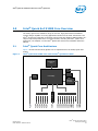
Intel® Quark SoC X1000 Core Overview.........................................................................21
2.1
Intel® Quark Core Architecture ............................................................................21
3.0
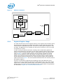
Architectural Overview.................................................................................................22
3.1
Internal Architecture ..........................................................................................22
3.2
System Architecture...........................................................................................22
3.3
Memory Organization .........................................................................................22
3.3.1 Address Spaces ......................................................................................23
3.3.2 Segment Register Usage..........................................................................24
3.4
I/O Space .........................................................................................................25
3.5
Addressing Modes ..............................................................................................25
3.5.1 Addressing Modes Overview .....................................................................25
3.5.2 Register and Immediate Modes.................................................................26
3.5.3 32-Bit Memory Addressing Modes .............................................................26
3.5.4 Differences Between 16- and 32-Bit Addresses ...........................................28
3.6
Data Types .......................................................................................................28
3.6.1 Data Types ............................................................................................28
3.6.1.1 Unsigned Data Types .................................................................29
3.6.1.2 Signed Data Types ....................................................................29
3.6.1.3 BCD Data Types ........................................................................30
3.6.1.4 Floating-Point Data Types...........................................................30
3.6.1.5 String Data Types .....................................................................30
3.6.1.6 ASCII Data Types ......................................................................31
3.6.1.7 Pointer Data Types ....................................................................32
3.6.2 Little Endian vs. Big Endian Data Formats ..................................................33
3.7
Interrupts .........................................................................................................33
3.7.1 Interrupts and Exceptions ........................................................................33
3.7.2 Interrupt Processing................................................................................34
3.7.3 Maskable Interrupt..................................................................................34
3.7.4 Non-Maskable Interrupt ...........................................................................35
3.7.5 Software Interrupts.................................................................................36
3.7.6 Interrupt and Exception Priorities ..............................................................36
3.7.7 Instruction Restart ..................................................................................37
3.7.8 Double Fault ..........................................................................................38
3.7.9 Floating-Point Interrupt Vectors ................................................................38
4.0
System Register Organization .......................................................................................39
4.1
Register Set Overview ........................................................................................39
4.2
Floating-Point Registers ......................................................................................39
4.3
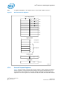
Base Architecture Registers.................................................................................39
4.3.1 General Purpose Registers .......................................................................40
4.3.2 Instruction Pointer ..................................................................................41
4.3.3 Flags Register ........................................................................................41
4.3.4 Segment Registers..................................................................................44
4.3.5 Segment Descriptor Cache Registers .........................................................44
4.4
System-Level Registers ......................................................................................45
4.4.1 Control Registers ....................................................................................46
Intel® Quark SoC X1000 Core
Developer’s Manual
4
October 2013
Order Number: 329679-001US
Contents—Intel® Quark Core
4.5
4.6
4.7
4.8
4.9
4.4.1.1 Control Register 0 (CR0) ............................................................ 47
4.4.1.2 Control Register 1 (CR1) ............................................................ 51
4.4.1.3 Control Register 2 (CR2) ............................................................ 51
4.4.1.4 Control Register 3 (CR3) ............................................................ 51
4.4.1.5 Control Register 4 (CR4) ............................................................ 51
4.4.2 System Address Registers ....................................................................... 52
Floating-Point Registers...................................................................................... 53
4.5.1 Floating-Point Data Registers ................................................................... 53
4.5.2 Floating-Point Tag Word .......................................................................... 54
4.5.3 Floating-Point Status Word ...................................................................... 54
4.5.4 Instruction and Data Pointers................................................................... 58
4.5.5 FPU Control Word ................................................................................... 61
Debug and Test Registers ................................................................................... 62
4.6.1 Debug Registers..................................................................................... 62
4.6.2 Test Registers........................................................................................ 62
Register Accessibility ......................................................................................... 62
4.7.1 FPU Register Usage ................................................................................ 63
Reserved Bits and Software Compatibility ............................................................. 63
Intel® Quark Core Model Specific Registers (MSRs)................................................ 64
5.0
Real Mode Architecture................................................................................................ 65
5.1
Introduction ..................................................................................................... 65
5.2
Memory Addressing ........................................................................................... 66
5.3
Reserved Locations............................................................................................ 66
5.4
Interrupts ........................................................................................................ 67
5.5
Shutdown and Halt ............................................................................................ 67
6.0
Protected Mode Architecture ........................................................................................ 68
6.1
Addressing Mechanism ....................................................................................... 68
6.2
Segmentation ................................................................................................... 69
6.2.1 Segmentation Introduction ...................................................................... 69
6.2.2 Terminology .......................................................................................... 70
6.2.3 Descriptor Tables ................................................................................... 70
6.2.3.1 Descriptor Tables Introduction .................................................... 70
6.2.3.2 Global Descriptor Table.............................................................. 71
6.2.3.3 Local Descriptor Table ............................................................... 71
6.2.3.4 Interrupt Descriptor Table .......................................................... 71
6.2.4 Descriptors............................................................................................ 72
6.2.4.1 Descriptor Attribute Bits ............................................................ 72
6.2.4.2 Intel® Quark Core Code, Data Descriptors (S=1) .......................... 72
6.2.4.3 System Descriptor Formats ........................................................ 74
6.2.4.4 LDT Descriptors (S=0, TYPE=2) .................................................. 75
6.2.4.5 TSS Descriptors (S=0, TYPE=1, 3, 9, B) ...................................... 75
6.2.4.6 Gate Descriptors (S=0, TYPE=4–7, C, F)...................................... 75
6.2.4.7 Selector Fields.......................................................................... 77
6.2.4.8 Segment Descriptor Cache ......................................................... 77
6.2.4.9 Segment Descriptor Register Settings.......................................... 77
6.3
Protection ........................................................................................................ 81
6.3.1 Protection Concepts ................................................................................ 81
6.3.2 Rules of Privilege.................................................................................... 82
6.3.3 Privilege Levels ...................................................................................... 82
6.3.3.1 Task Privilege ........................................................................... 82
6.3.3.2 Selector Privilege (RPL) ............................................................. 82
6.3.3.3 I/O Privilege and I/O Permission Bitmap ...................................... 83
6.3.3.4 Privilege Validation.................................................................... 85
6.3.3.5 Descriptor Access ..................................................................... 85
6.3.4 Privilege Level Transfers.......................................................................... 86
October 2013
Order Number: 329679-001US
Intel® Quark SoC X1000 Core
Developer’s Manual
5
Intel® Quark Core—Contents
6.3.5
6.3.6
6.4
6.5
Call Gates ..............................................................................................87
Task Switching .......................................................................................88
6.3.6.1 Floating-Point Task Switching......................................................89
6.3.7 Initialization and Transition to Protected Mode ............................................89
Paging..............................................................................................................91
6.4.1 Paging Concepts .....................................................................................91
6.4.2 Paging Organization ................................................................................91
6.4.2.1 Page Mechanism .......................................................................91
6.4.2.2 Page Descriptor Base Register.....................................................91
6.4.2.3 Page Directory ..........................................................................92
6.4.2.4 Page Tables ..............................................................................92
6.4.2.5 Page Directory/Table Entries .......................................................92
6.4.2.6 Paging-Mode Modifiers ..............................................................92
6.4.3 PAE Paging ............................................................................................93
6.4.3.1 PDPTE Registers........................................................................93
6.4.3.2 Linear-Address Translation with PAE Paging ..................................94
6.4.4 #GP Faults for Intel® Quark SoC X1000 Core .......................................... 100
6.4.5 Access Rights ...................................................................................... 100
6.4.5.1 SMEP Details for Intel® Quark SoC X1000 Core ........................... 101
6.4.6 Page Level Protection (R/W, U/S Bits)...................................................... 102
6.4.7 Page Cacheability (PWT and PCD Bits) ..................................................... 103
6.4.8 Translation Lookaside Buffer .................................................................. 103
6.4.9 Page-Fault Exceptions .......................................................................... 104
6.4.10 Paging Operation .................................................................................. 106
6.4.11 Operating System Responsibilities........................................................... 107
Virtual 8086 Environment ................................................................................. 107
6.5.1 Executing Programs .............................................................................. 107
6.5.2 Virtual 8086 Mode Addressing Mechanism ................................................ 108
6.5.3 Paging in Virtual Mode ........................................................................... 108
6.5.4 Protection and I/O Permission Bitmap...................................................... 109
6.5.5 Interrupt Handling ................................................................................ 110
6.5.6 Entering and Leaving Virtual 8086 Mode .................................................. 111
6.5.6.1 Task Switches to and from Virtual 8086 Mode ............................. 112
6.5.6.2 Transitions Through Trap and Interrupt Gates, and IRET............... 112
7.0
On-Chip Cache ......................................................................................................... 114
7.1
Cache Organization .......................................................................................... 114
7.1.1 Write-Back Enhanced Intel® Quark SoC X1000 Core Cache ........................ 115
7.2
Cache Control ................................................................................................. 116
7.2.1 Write-Back Enhanced Intel® Quark SoC X1000 Core Cache Control and
Operating Modes .................................................................................. 116
7.3
Cache Line Fills................................................................................................ 117
7.4
Cache Line Invalidations ................................................................................... 118
7.4.1 Write-Back Enhanced Intel® Quark SoC X1000 Core Snoop Cycles and
Write-Back Mode Invalidation ................................................................. 118
7.5
Cache Replacement.......................................................................................... 118
7.6
Page Cacheability ............................................................................................ 119
7.6.1 Write-Back Enhanced Intel® Quark SoC X1000 Core and Processor Page
Cacheability ......................................................................................... 121
7.7
Cache Flushing ................................................................................................ 122
7.7.1 Write-Back Enhanced Intel® Quark SoC X1000 Core Cache Flushing ............ 122
7.8
Write-Back Enhanced Intel® Quark SoC X1000 Core Write-Back Cache Architecture . 123
7.8.1 Write-Back Cache Coherency Protocol...................................................... 123
7.8.2 Detecting On-Chip Write-Back Cache of the Write-Back Enhanced Intel®
Quark SoC X1000 Core.......................................................................... 125
8.0
System Management Mode (SMM) Architectures ........................................................... 127
Intel® Quark SoC X1000 Core
Developer’s Manual
6
October 2013
Order Number: 329679-001US
Contents—Intel® Quark Core
8.1
8.2
8.3
8.4
8.5
8.6
8.7
9.0
SMM Overview ................................................................................................ 127
Terminology ................................................................................................... 127
System Management Interrupt Processing .......................................................... 128
8.3.1 System Management Interrupt (SMI#).................................................... 129
8.3.2 SMI# Active (SMIACT#) ........................................................................ 129
8.3.3 SMRAM ............................................................................................... 130
8.3.3.1 SMRAM State Save Map ........................................................... 131
8.3.4 Exit From SMM..................................................................................... 133
System Management Mode Programming Model .................................................. 134
8.4.1 Entering System Management Mode ....................................................... 134
8.4.2 Processor Environment.......................................................................... 135
8.4.2.1 Write-Back Enhanced Intel® Quark SoC X1000 Core Environment . 136
8.4.3 Executing System Management Mode Handler.......................................... 136
8.4.3.1 Exceptions and Interrupts within System Management Mode ........ 137
SMM Features ................................................................................................. 138
8.5.1 SMM Revision Identifier......................................................................... 138
8.5.2 Auto Halt Restart ................................................................................. 138
8.5.3 I/O Instruction Restart .......................................................................... 139
8.5.4 SMM Base Relocation ............................................................................ 140
SMM System Design Considerations ................................................................... 141
8.6.1 SMRAM Interface.................................................................................. 141
8.6.2 Cache Flushes...................................................................................... 142
8.6.2.1 Write-Back Enhanced Intel® Quark SoC X1000 Core System
Management Mode and Cache Flushing ...................................... 144
8.6.2.2 Snoop During SMM.................................................................. 146
8.6.3 A20M# Pin and SMBASE Relocation ........................................................ 146
8.6.4 Processor Reset During SMM.................................................................. 146
8.6.5 SMM and Second-Level Write Buffers ...................................................... 147
8.6.6 Nested SMI#s and I/O Restart ............................................................... 147
SMM Software Considerations ........................................................................... 147
8.7.1 SMM Code Considerations...................................................................... 147
8.7.2 Exception Handling ............................................................................... 148
8.7.3 Halt During SMM .................................................................................. 148
8.7.4 Relocating SMRAM to an Address Above One Megabyte ............................. 148
Hardware Interface................................................................................................... 149
9.1
Introduction ................................................................................................... 149
9.2
Signal Descriptions .......................................................................................... 150
9.2.1 Clock (CLK) ......................................................................................... 150
9.2.2 Address Bus (A[31:2], BE[3:0]#) ........................................................... 150
9.2.3 Data Lines (D[31:0]) ............................................................................ 151
9.2.4 Parity ................................................................................................. 151
9.2.4.1 Data Parity Input/Outputs (DP[3:0]) ......................................... 151
9.2.4.2 Parity Status Output (PCHK#) .................................................. 151
9.2.5 Bus Cycle Definition.............................................................................. 152
9.2.5.1 M/IO#, D/C#, W/R# Outputs ................................................... 152
9.2.5.2 Bus Lock Output (LOCK#) ........................................................ 152
9.2.5.3 Pseudo-Lock Output (PLOCK#) ................................................. 153
9.2.5.4 PLOCK# Floating-Point Considerations ....................................... 153
9.2.6 Bus Control ......................................................................................... 153
9.2.6.1 Address Status Output (ADS#) ................................................. 153
9.2.6.2 Non-Burst Ready Input (RDY#)................................................. 153
9.2.7 Burst Control ....................................................................................... 154
9.2.7.1 Burst Ready Input (BRDY#) ..................................................... 154
9.2.7.2 Burst Last Output (BLAST#) ..................................................... 154
9.2.8 Interrupt Signals .................................................................................. 154
October 2013
Order Number: 329679-001US
Intel® Quark SoC X1000 Core
Developer’s Manual
7
Intel® Quark Core—Contents
9.3
9.4
9.5
9.6
9.2.8.1 Reset Input (RESET) ................................................................ 154
9.2.8.2 Soft Reset Input (SRESET) ....................................................... 155
9.2.8.3 System Management Interrupt Request Input (SMI#) .................. 155
9.2.8.4 System Management Mode Active Output (SMIACT#) .................. 155
9.2.8.5 Maskable Interrupt Request Input (INTR) ................................... 155
9.2.8.6 Non-maskable Interrupt Request Input (NMI).............................. 156
9.2.8.7 Stop Clock Interrupt Request Input (STPCLK#) ........................... 156
9.2.9 Bus Arbitration Signals .......................................................................... 156
9.2.9.1 Bus Request Output (BREQ)...................................................... 156
9.2.9.2 Bus Hold Request Input (HOLD) ................................................ 156
9.2.9.3 Bus Hold Acknowledge Output (HLDA)........................................ 157
9.2.9.4 Backoff Input (BOFF#) ............................................................. 157
9.2.10 Cache Invalidation ................................................................................ 157
9.2.10.1 Address Hold Request Input (AHOLD) ........................................ 158
9.2.10.2 External Address Valid Input (EADS#)........................................ 158
9.2.11 Cache Control ...................................................................................... 158
9.2.11.1 Cache Enable Input (KEN#) ...................................................... 158
9.2.11.2 Cache Flush Input (FLUSH#)..................................................... 158
9.2.12 Page Cacheability (PWT, PCD) ................................................................ 159
9.2.13 RESERVED#......................................................................................... 159
9.2.14 Numeric Error Reporting (FERR#, IGNNE#) .............................................. 159
9.2.14.1 Floating-Point Error Output (FERR#) .......................................... 159
9.2.14.2 Ignore Numeric Error Input (IGNNE#)........................................ 160
9.2.15 Bus Size Control (BS16#, BS8#) ............................................................ 160
9.2.16 Address Bit 20 Mask (A20M#) ................................................................ 161
9.2.17 Write-Back Enhanced Intel® Quark SoC X1000 Core Signals and Other
Enhanced Bus Features ......................................................................... 161
9.2.17.1 Cacheability (CACHE#) ............................................................ 161
9.2.17.2 Cache Flush (FLUSH#) ............................................................. 162
9.2.17.3 Hit/Miss to a Modified Line (HITM#) ........................................... 162
9.2.17.4 Soft Reset (SRESET)................................................................ 163
9.2.17.5 Invalidation Request (INV) ....................................................... 163
9.2.17.6 Write-Back/Write-Through (WB/WT#) ........................................ 164
9.2.17.7 Pseudo-Lock Output (PLOCK#).................................................. 164
9.2.18 Test Signals ......................................................................................... 164
9.2.18.1 Test Clock (TCK) ..................................................................... 164
9.2.18.2 Test Mode Select (TMS) ........................................................... 165
9.2.18.3 Test Data Input (TDI) .............................................................. 165
9.2.18.4 Test Data Output (TDO) ........................................................... 165
Interrupt and Non-Maskable Interrupt Interface ................................................... 165
9.3.1 Interrupt Logic ..................................................................................... 166
9.3.2 NMI Logic ............................................................................................ 166
9.3.3 SMI# Logic .......................................................................................... 166
9.3.4 STPCLK# Logic ..................................................................................... 167
Write Buffers................................................................................................... 167
9.4.1 Write Buffers and I/O Cycles .................................................................. 169
9.4.2 Write Buffers on Locked Bus Cycles ......................................................... 169
Reset and Initialization ..................................................................................... 169
9.5.1 Floating-Point Register Values ................................................................ 170
9.5.2 Pin State During Reset .......................................................................... 171
9.5.2.1 Controlling the CLK Signal in the Processor during Power On ......... 173
9.5.2.2 FERR# Pin State During Reset for Intel® Quark SoC X1000 Core ... 173
9.5.2.3 Power Down Mode (In-circuit Emulator Support).......................... 174
Clock Control .................................................................................................. 174
9.6.1 Stop Grant Bus Cycles ........................................................................... 174
9.6.2 Pin State During Stop Grant ................................................................... 175
Intel® Quark SoC X1000 Core
Developer’s Manual
8
October 2013
Order Number: 329679-001US
Contents—Intel® Quark Core
9.6.3
9.6.4
9.6.5
9.6.6
Write-Back Enhanced Intel® Quark SoC X1000 Core Pin States During Stop
Grant State ......................................................................................... 176
Clock Control State Diagram .................................................................. 177
9.6.4.1 Normal State.......................................................................... 177
9.6.4.2 Stop Grant State .................................................................... 177
9.6.4.3 Stop Clock State ..................................................................... 179
9.6.4.4 Auto HALT Power Down State ................................................... 179
9.6.4.5 Stop Clock Snoop State (Cache Invalidations)............................. 179
9.6.4.6 Auto Idle Power Down State ..................................................... 180
Write-Back Enhanced Intel® Quark SoC X1000 Core Clock Control State
Diagram.............................................................................................. 180
9.6.5.1 Normal State.......................................................................... 180
9.6.5.2 Stop Grant State .................................................................... 181
9.6.5.3 Stop Clock State ..................................................................... 182
9.6.5.4 Auto HALT Power Down State ................................................... 182
Stop Clock Snoop State (Cache Invalidations) .......................................... 183
9.6.6.1 Auto HALT Power Down Flush State (Cache Flush) for the
Write-Back Enhanced Intel® Quark SoC X1000 Core .................... 183
10.0 Bus Operation .......................................................................................................... 184
10.1 Data Transfer Mechanism ................................................................................. 184
10.1.1 Memory and I/O Spaces ........................................................................ 184
10.1.1.1 Memory and I/O Space Organization ......................................... 185
10.1.2 Dynamic Data Bus Sizing....................................................................... 186
10.1.3 Interfacing with 8-, 16-, and 32-Bit Memories .......................................... 187
10.1.4 Dynamic Bus Sizing during Cache Line Files ............................................. 191
10.1.5 Operand Alignment............................................................................... 192
10.2 Bus Arbitration Logic........................................................................................ 193
10.3 Bus Functional Description................................................................................ 196
10.3.1 Non-Cacheable Non-Burst Single Cycles .................................................. 196
10.3.1.1 No Wait States ....................................................................... 196
10.3.1.2 Inserting Wait States............................................................... 197
10.3.2 Multiple and Burst Cycle Bus Transfers .................................................... 198
10.3.2.1 Burst Cycles ........................................................................... 198
10.3.2.2 Terminating Multiple and Burst Cycle Transfers ........................... 199
10.3.2.3 Non-Cacheable, Non-Burst, Multiple Cycle Transfers .................... 200
10.3.2.4 Non-Cacheable Burst Cycles ..................................................... 200
10.3.3 Cacheable Cycles ................................................................................. 201
10.3.3.1 Byte Enables during a Cache Line Fill ......................................... 202
10.3.3.2 Non-Burst Cacheable Cycles ..................................................... 202
10.3.3.3 Burst Cacheable Cycles............................................................ 203
10.3.3.4 Effect of Changing KEN# during a Cache Line Fill ........................ 204
10.3.4 Burst Mode Details ............................................................................... 205
10.3.4.1 Adding Wait States to Burst Cycles............................................ 205
10.3.4.2 Burst and Cache Line Fill Order ................................................. 206
10.3.4.3 Interrupted Burst Cycles .......................................................... 207
10.3.5 8- and 16-Bit Cycles ............................................................................. 209
10.3.6 Locked Cycles ...................................................................................... 211
10.3.7 Pseudo-Locked Cycles ........................................................................... 212
10.3.7.1 Floating-Point Read and Write Cycles......................................... 213
10.3.8 Invalidate Cycles.................................................................................. 213
10.3.8.1 Rate of Invalidate Cycles ......................................................... 215
10.3.8.2 Running Invalidate Cycles Concurrently with Line Fills.................. 215
10.3.9 Bus Hold ............................................................................................. 217
10.3.10Interrupt Acknowledge .......................................................................... 219
10.3.11Special Bus Cycles................................................................................ 220
10.3.11.1HALT Indication Cycle.............................................................. 220
October 2013
Order Number: 329679-001US
Intel® Quark SoC X1000 Core
Developer’s Manual
9
Intel® Quark Core—Contents
10.4
10.3.11.2Shutdown Indication Cycle ....................................................... 221
10.3.11.3Stop Grant Indication Cycle ...................................................... 221
10.3.12Bus Cycle Restart ................................................................................. 222
10.3.13Bus States ........................................................................................... 224
10.3.14Floating-Point Error Handling for the Intel® Quark SoC X1000 Core ............. 225
10.3.14.1Floating-Point Exceptions ......................................................... 225
10.3.15Intel® Quark SoC X1000 Core Floating-Point Error Handling in
AT-Compatible Systems......................................................................... 226
Enhanced Bus Mode Operation for the Write-Back Enhanced Intel® Quark SoC X1000
Core .............................................................................................................. 226
10.4.1 Summary of Bus Differences .................................................................. 226
10.4.2 Burst Cycles......................................................................................... 227
10.4.2.1 Non-Cacheable Burst Operation................................................. 227
10.4.2.2 Burst Cycle Signal Protocol ....................................................... 228
10.4.3 Cache Consistency Cycles ...................................................................... 228
10.4.3.1 Snoop Collision with a Current Cache Line Operation .................... 229
10.4.3.2 Snoop under AHOLD ................................................................ 230
10.4.3.3 Snoop During Replacement Write-Back ...................................... 234
10.4.3.4 Snoop under BOFF# ................................................................ 235
10.4.3.5 Snoop under HOLD .................................................................. 237
10.4.3.6 Snoop under HOLD during Replacement Write-Back ..................... 239
10.4.4 Locked Cycles ...................................................................................... 239
10.4.4.1 Snoop/Lock Collision................................................................ 241
10.4.5 Flush Operation .................................................................................... 241
10.4.6 Pseudo Locked Cycles............................................................................ 242
10.4.6.1 Snoop under AHOLD during Pseudo-Locked Cycles....................... 242
10.4.6.2 Snoop under HOLD during Pseudo-Locked Cycles......................... 243
10.4.6.3 Snoop under BOFF# Overlaying a Pseudo-Locked Cycle ................ 244
11.0 Debugging Support ................................................................................................... 246
11.1 Breakpoint Instruction ...................................................................................... 246
11.2 Single-Step Trap.............................................................................................. 246
11.3 Debug Registers .............................................................................................. 246
11.3.1 Linear Address Breakpoint Registers (DR[3:0]) ......................................... 247
11.3.2 Debug Control Register (DR7) ................................................................ 247
11.3.3 Debug Status Register (DR6) ................................................................. 250
11.3.4 Use of Resume Flag (RF) in Flag Register ................................................. 251
12.0 Instruction Set Summary ........................................................................................... 252
12.1 Instruction Set ................................................................................................ 252
12.1.1 Floating-Point Instructions ..................................................................... 253
12.2 Instruction Encoding ........................................................................................ 253
12.2.1 Overview ............................................................................................. 253
12.2.2 32-Bit Extensions of the Instruction Set ................................................... 254
12.2.3 Encoding of Integer Instruction Fields...................................................... 255
12.2.3.1 Encoding of Operand Length (w) Field ........................................ 255
12.2.3.2 Encoding of the General Register (reg) Field ............................... 255
12.2.3.3 Encoding of the Segment Register (sreg) Field ............................ 256
12.2.3.4 Encoding of Address Mode ........................................................ 257
12.2.3.5 Encoding of Operation Direction (d) Field.................................... 260
12.2.3.6 Encoding of Sign-Extend (s) Field .............................................. 261
12.2.3.7 Encoding of Conditional Test (tttn) Field ..................................... 261
12.2.3.8 Encoding of Control or Debug or Test Register (eee) Field ............. 261
12.2.4 Encoding of Floating-Point Instruction Fields ............................................. 262
12.2.5 Intel® Quark SoC X1000 Core Instructions ............................................... 263
12.2.5.1 CMPXCHG8B - Compare and Exchange Bytes .............................. 263
12.2.5.2 RDMSR .................................................................................. 264
Intel® Quark SoC X1000 Core
Developer’s Manual
10
October 2013
Order Number: 329679-001US
Contents—Intel® Quark Core
12.3
12.2.5.3 RDTSC .................................................................................. 264
12.2.5.4 WRMSR ................................................................................. 264
Clock Count Summary ..................................................................................... 265
12.3.1 Instruction Clock Count Assumptions ...................................................... 265
A
Signal Descriptions ................................................................................................... 291
B
Testability ............................................................................................................... 296
B.1
On-Chip Cache Testing..................................................................................... 296
B.1.1 Cache Testing Registers TR3, TR4 and TR5 .............................................. 296
B.1.2 Cache Testability Write ......................................................................... 297
B.1.3 Cache Testability Read .......................................................................... 298
B.1.4 Flush Cache......................................................................................... 299
B.1.5 Additional Cache Testing Features for Write-Back Enhanced Intel® Quark
SoC X1000 Core................................................................................... 299
B.2
Translation Lookaside Buffer (TLB) Testing ......................................................... 300
B.2.1 Translation Lookaside Buffer Organization................................................ 300
B.2.2 TLB Test Registers TR6 and TR7 ............................................................. 301
B.2.2.1 Command Test Register: TR6 ................................................... 301
B.2.2.2 Data Test Register: TR7........................................................... 303
B.2.3 TLB Write Test ..................................................................................... 303
B.2.4 TLB Lookup Test .................................................................................. 304
B.3
Intel® Quark SoC X1000 Core JTAG ................................................................... 304
B.3.1 Test Access Port (TAP) Controller ........................................................... 304
B.3.1.1 Test-Logic-Reset State ............................................................ 305
B.3.1.2 Run-Test/Idle State................................................................. 305
B.3.1.3 Select-DR-Scan State .............................................................. 305
B.3.1.4 Capture-DR State ................................................................... 306
B.3.1.5 Shift-DR State ........................................................................ 306
B.3.1.6 Exit1-DR State ....................................................................... 306
B.3.1.7 Pause-DR State ...................................................................... 306
B.3.1.8 Exit2-DR State ....................................................................... 306
B.3.1.9 Update-DR State .................................................................... 307
B.3.1.10 Select-IR-Scan State ............................................................... 307
B.3.1.11 Capture-IR State .................................................................... 307
B.3.1.12 Shift-IR State ......................................................................... 307
B.3.1.13 Exit1-IR State ........................................................................ 307
B.3.1.14 Pause-IR State ....................................................................... 307
B.3.1.15 Exit2-IR State ........................................................................ 308
B.3.1.16 Update-IR State ..................................................................... 308
B.3.2 TAP Controller Initialization.................................................................... 308
C
Feature Determination .............................................................................................. 309
C.1
CPUID Instruction ........................................................................................... 309
C.2
Intel® Quark SoC X1000 Stepping ..................................................................... 311
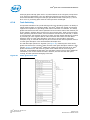
Figures
1
2
3
4
5
6
7
8
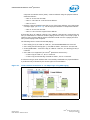
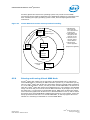
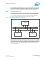
Intel® Quark SoC X1000 Core used in Intel® Quark SoC X1000 ..................................... 21
Address Translation.................................................................................................. 24
Addressing Mode Calculations .................................................................................... 27
Data Types ............................................................................................................. 29
Data Types ............................................................................................................. 31
String and ASCII Data Types ..................................................................................... 32
Pointer Data Types ................................................................................................... 32
Big vs. Little Endian Memory Format........................................................................... 33
October 2013
Order Number: 329679-001US
Intel® Quark SoC X1000 Core
Developer’s Manual
11
Intel® Quark Core—Contents
9
10
11
12
13
14
15
16
17
18
19
20
21
22
23
24
25
26
27
28
29
30
31
32
33
34
35
36
37
38
39
40
41
42
43
44
45
46
47
48
49
50
51
52
53
54
55
56
57
58
59
60
Base Architecture Registers .......................................................................................40
Flag Registers ..........................................................................................................41
Intel® Quark SoC X1000 Core Segment Registers and Associated Descriptor Cache
Registers.................................................................................................................45
System-Level Registers .............................................................................................46
Control Registers .....................................................................................................47
Intel® Quark SoC X1000 Core CR4 Register .................................................................52
Floating-Point Registers.............................................................................................53
Floating-Point Tag Word ............................................................................................54
Floating-Point Status Word ........................................................................................55
Protected Mode FPU Instructions and Data Pointer Image in Memory (32-Bit Format) ........59
Real Mode FPU Instruction and Data Pointer Image in Memory (32-Bit Format) .................59
Protected Mode FPU Instruction and Data Pointer Image in Memory (16-Bit Format)..........60
Real Mode FPU Instruction and Data Pointer Image in Memory (16-Bit Format) .................60
FPU Control Word .....................................................................................................61
Real Address Mode Addressing ...................................................................................66
Protected Mode Addressing ........................................................................................69
Paging and Segmentation ..........................................................................................69
Descriptor Table Registers .........................................................................................71
Interrupt Descriptor Table Register Use .......................................................................72
Segment Descriptors.................................................................................................73
System Segment Descriptors .....................................................................................75
Gate Descriptor Formats............................................................................................76
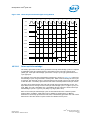
Example Descriptor Selection .....................................................................................78
Segment Descriptor Caches for Real Address Mode (Segment Limit and Attributes Are
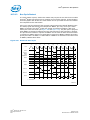
Fixed) .....................................................................................................................79
Segment Descriptor Caches for Protected Mode (Loaded per Descriptor) ..........................80
Segment Descriptor Caches for Virtual 8086 Mode within Protected Mode (Segment Limit
and Attributes are Fixed) ...........................................................................................81
Four-Level Hierarchical Protection ...............................................................................82
Intel® Quark Core TSS and TSS Registers....................................................................84
Sample I/O Permission Bit Map ..................................................................................85
Intel® Quark Core TSS .............................................................................................88
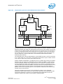
Simple Protected System...........................................................................................90
GDT Descriptors for Simple System.............................................................................91
Linear-Address Translation to a 4-KByte Page using PAE Paging......................................95
Linear-Address Translation to a 2-MByte Page using PAE Paging .....................................96
Formats of CR3 and Paging-Structure Entries in 32-bit Mode with PAE Paging Disabled ......98
Formats of CR3 and Paging-Structure Entries in 32-bit Mode with PAE Paging Enabled .......99
Translation Lookaside Buffer .................................................................................... 104
Page-Fault Error Code ............................................................................................. 105
Page Fault System Information................................................................................. 107
Virtual 8086 Environment Memory Management ......................................................... 108
Virtual 8086 Environment Interrupt and Call Handling ................................................. 111
On-Chip Cache Physical Organization ........................................................................ 114
On-Chip Cache Replacement Strategy ....................................................................... 119
Page Cacheability ................................................................................................... 121
Basic SMI# Interrupt Service ................................................................................... 128
Basic SMI# Hardware Interface ................................................................................ 129
SMI# Timing for Servicing an I/O Trap ...................................................................... 130
Intel® Quark SoC X1000 Core SMIACT# Timing.......................................................... 130
Redirecting System Memory Addresses to SMRAM....................................................... 132
Transition to and from System Management Mode ...................................................... 135
SMM Revision Identifier ........................................................................................... 138
Auto HALT Restart .................................................................................................. 139
Intel® Quark SoC X1000 Core
Developer’s Manual
12
October 2013
Order Number: 329679-001US
Contents—Intel® Quark Core
61
62
63
64
65
66
67
68
69
70
71
72
73
74
75
76
77
78
79
80
81
82
83
84
85
86
87
88
89
90
91
92
93
94
95
96
97
98
99
100
101
102
103
104
105
106
107
108
109
110
111
112
I/O Instruction Restart............................................................................................ 139
SMM Base Location ................................................................................................ 140
SMRAM Usage ....................................................................................................... 141
SMRAM Location .................................................................................................... 142
FLUSH# Mechanism during SMM .............................................................................. 143
Cached SMM ......................................................................................................... 143
Non-Cached SMM................................................................................................... 144
Write-Back Enhanced Intel® Quark SoC X1000 Core Cache Flushing for Overlaid
SMRAM upon Entry and Exit of Cached SMM .............................................................. 145
Functional Signal Groupings .................................................................................... 150
Reordering of a Reads with Write Buffers................................................................... 168
Reordering of a Reads with Write Buffers................................................................... 168
Pin States During RESET ......................................................................................... 172
Stop Clock Protocol ................................................................................................ 175
Intel® Quark SoC X1000 Core Stop Clock State Machine ............................................. 178
Recognition of Inputs when Exiting Stop Grant State .................................................. 179
Write-Back Enhanced Intel® Quark SoC X1000 Core Stop Clock State Machine
(Enhanced
Bus Configuration) ................................................................................................. 181
Physical Memory and I/O Spaces.............................................................................. 185
Physical Memory and I/O Space Organization............................................................. 186
Intel® Quark SoC X1000 Core with 32-Bit Memory ..................................................... 188
Addressing 16- and 8-Bit Memories .......................................................................... 188
Logic to Generate A1, BHE# and BLE# for 16-Bit Buses .............................................. 190
Data Bus Interface to 16- and 8-Bit Memories............................................................ 191
Single Master Intel® Quark Core System ................................................................... 193
Single Intel® Quark Core with DMA .......................................................................... 194
Single Intel® Quark Core with Multiple Secondary Masters........................................... 195
Basic 2-2 Bus Cycle ................................................................................................ 197
Basic 3-3 Bus Cycle ................................................................................................ 198
Non-Cacheable, Non-Burst, Multiple-Cycle Transfers ................................................... 200
Non-Cacheable Burst Cycle...................................................................................... 201
Non-Burst, Cacheable Cycles ................................................................................... 203
Burst Cacheable Cycle ............................................................................................ 204
Effect of Changing KEN# ......................................................................................... 205
Slow Burst Cycle .................................................................................................... 206
Burst Cycle Showing Order of Addresses ................................................................... 207
Interrupted Burst Cycle........................................................................................... 208
Interrupted Burst Cycle with Non-Obvious Order of Addresses...................................... 209
8-Bit Bus Size Cycle ............................................................................................... 210
Burst Write as a Result of BS8# or BS16#................................................................. 211
Locked Bus Cycle ................................................................................................... 212
Pseudo Lock Timing................................................................................................ 213
Fast Internal Cache Invalidation Cycle ...................................................................... 214
Typical Internal Cache Invalidation Cycle................................................................... 214
System with Second-Level Cache ............................................................................. 216
Cache Invalidation Cycle Concurrent with Line Fill....................................................... 217
HOLD/HLDA Cycles................................................................................................. 218
HOLD Request Acknowledged during BOFF# .............................................................. 219
Interrupt Acknowledge Cycles.................................................................................. 220
Stop Grant Bus Cycle.............................................................................................. 221
Restarted Read Cycle.............................................................................................. 222
Restarted Write Cycle ............................................................................................. 223
Bus State Diagram ................................................................................................. 224
Basic Burst Read Cycle ........................................................................................... 227
October 2013
Order Number: 329679-001US
Intel® Quark SoC X1000 Core
Developer’s Manual
13
Intel® Quark Core—Contents
113
114
115
116
117
118
119
120
121
122
123
124
125
126
127
128
129
130
131
132
133
134
Snoop Cycle Invalidating a Modified Line ................................................................... 231
Snoop Cycle Overlaying a Line-Fill Cycle .................................................................... 232
Snoop Cycle Overlaying a Non-Burst Cycle................................................................. 233
Snoop to the Line that is Being Replaced ................................................................... 234
Snoop under BOFF# during a Cache Line-Fill Cycle...................................................... 236
Snoop under BOFF# to the Line that is Being Replaced ................................................ 237
Snoop under HOLD during Line Fill............................................................................ 238
Snoop using HOLD during a Non-Cacheable, Non-Burstable Code Prefetch ..................... 239
Locked Cycles (Back-to-Back) .................................................................................. 240
Snoop Cycle Overlaying a Locked Cycle ..................................................................... 241
Flush Cycle ............................................................................................................ 242
Snoop under AHOLD Overlaying Pseudo-Locked Cycle ................................................. 243
Snoop under HOLD Overlaying Pseudo-Locked Cycle ................................................... 244
Snoop under BOFF# Overlaying a Pseudo-Locked Cycle ............................................... 245
Size Breakpoint Fields ............................................................................................. 248
General Instruction Format ..................................................................................... 253
Intel® Quark SoC X1000 Core Cache Test Registers .................................................... 296
TR4 Definition for Standard and Enhanced Bus Modes for the Write-Back Enhanced
Intel® Quark SoC X1000 Core .................................................................................. 300
TR5 Definition for Standard and Enhanced Bus Modes for the Write-Back Enhanced
Intel® Quark SoC X1000 Core .................................................................................. 300
TLB Organization .................................................................................................... 301
TLB Test Registers .................................................................................................. 302
TAP Controller State Diagram................................................................................... 305
Tables
1
2
3
4
5
6
7
8
9
10
11
12
13
14
15
16
17
18
19
20
21
22
23
24
25
26
27
Manual Contents ......................................................................................................17
Related Documents...................................................................................................20
Segment Register Selection Rules ...............................................................................25
BASE and INDEX Registers for 16- and 32-Bit Addresses ...............................................28
Interrupt Vector Assignments.....................................................................................35
FPU Interrupt Vector Assignments ..............................................................................35
Sequence of Exception Checking.................................................................................37
Interrupt Vectors Used by FPU ...................................................................................38
Data Type Alignment Requirements ............................................................................42
Intel® Quark SoC X1000 Core Operating Modes............................................................48
On-Chip Cache Control Modes ....................................................................................48
Recommended Values of the Floating-Point Related Bits for Intel® Quark SoC X1000
Core .......................................................................................................................50
Interpreting Different Combinations of EM, TS and MP Bits .............................................50
Condition Code Interpretation after FPREM and FPREM1 Instructions ...............................56
Floating-Point Condition Code Interpretation ................................................................56
Condition Code Resulting from Comparison ..................................................................57
Condition Code Defining Operand Class .......................................................................57
FPU Exceptions ........................................................................................................58
Debug Registers .......................................................................................................62
Test Registers ..........................................................................................................62
Register Usage.........................................................................................................63
FPU Register Usage Differences ..................................................................................63
MSRs for Intel® Quark Core 1 ....................................................................................64
Instruction Forms in which LOCK Prefix Is Legal............................................................65
Exceptions with Different Meanings in Real Mode (see Table 24) .....................................67
Access Rights Byte Definition for Code and Data Descriptions .........................................74
Pointer Test Instructions............................................................................................85
Intel® Quark SoC X1000 Core
Developer’s Manual
14
October 2013
Order Number: 329679-001US
Contents—Intel® Quark Core
28
29
30
31
32
33
34
35
36
37
38
39
40
41
42
43
44
45
46
47
48
49
50
51
52
53
54
55
56
57
58
59
60
61
62
63
64
65
66
67
68
69
70
71
72
73
74
75
76
77
Descriptor Types Used for Control Transfer .................................................................. 86
Use of CR3 with PAE Paging....................................................................................... 93
Format of a PAE Page-Directory-Pointer-Table Entry (PDPTE) ......................................... 94
Format of a PAE Page-Directory Entry that Maps a 2-MByte Page.................................... 96
Format of a PAE Page-Directory Entry that References a Page Table................................ 97
Format of a PAE Page-Table Entry that Maps a 4-KByte Page ......................................... 97
Page Level Protection Attributes ............................................................................... 103
Write-Back Enhanced Intel® Quark SoC X1000 Core WB/WT# Initialization.................... 115
Cache Operating Modes .......................................................................................... 116
Write-Back Enhanced Intel® Quark SoC X1000 Core Write-Back Cache Operating
Modes .................................................................................................................. 117
Encoding of the Special Cycles for Write-Back Cache................................................... 119
Cache State Transitions for Write-Back Enhanced Intel® Quark SoC X1000
Core-Initiated Unlocked Read Cycles......................................................................... 124
Cache State Transitions for Write-Back Enhanced Intel® Quark SoC X1000
Core-Initiated Write Cycles...................................................................................... 125
Cache State Transitions During Snoop Cycles............................................................. 125
SMRAM State Save Map .......................................................................................... 132
SMM Initial Processor Core Register Settings ............................................................. 136
Bit Values for SMM Revision Identifier ....................................................................... 138
Bit Values for Auto HALT Restart .............................................................................. 139
I/O Instruction Restart Value ................................................................................... 140
Cache Flushing (Non-Overlaid SMRAM) ..................................................................... 144
Cache Flushing (Overlaid SMRAM) ............................................................................ 145
ADS# Initiated Bus Cycle Definitions ........................................................................ 152
Differences between CACHE# and PCD ..................................................................... 161
CACHE# vs. Other Intel® Quark Core Signals ............................................................ 162
HITM# vs. Other Intel® Quark Core Signals............................................................... 163
INV vs. Other Intel® Quark Core Signals ................................................................... 163
WB/WT# vs. Other Intel® Quark Core Signals............................................................ 164
Register Values after Reset...................................................................................... 170
Floating-Point Values after Reset.............................................................................. 170
FERR# Pin State after Reset and before FP Instructions............................................... 174
Pin State during Stop Grant Bus State ...................................................................... 175
Write-Back Enhanced Intel® Quark SoC X1000 Core Pin States during Stop Grant Bus
Cycle.................................................................................................................... 176
Byte Enables and Associated Data and Operand Bytes................................................. 184
Generating A[31:0] from BE[3:0]# and A[31:A2]....................................................... 185
Next Byte Enable Values for BSx# Cycles .................................................................. 187
Data Pins Read with Different Bus Sizes .................................................................... 187
Generating A1, BHE# and BLE# for Addressing 16-Bit Devices ..................................... 189
Generating A0, A1 and BHE# from the Intel® Quark SoC X1000 Core Byte Enables ........ 191
Transfer Bus Cycles for Bytes, Words and Dwords ...................................................... 192
Burst Order (Both Read and Write Bursts) ................................................................. 206
Special Bus Cycle Encoding ..................................................................................... 221
Bus State Description ............................................................................................. 224
Snoop Cycles under AHOLD, BOFF#, or HOLD ............................................................ 228
Various Scenarios of a Snoop Write-Back Cycle Colliding with an On-Going Cache Fill or
Replacement Cycle ................................................................................................. 230
Debug Registers .................................................................................................... 247
LENi Encoding........................................................................................................ 248
RW Encoding ......................................................................................................... 248
Fields within Intel® Quark Core Instructions .............................................................. 254
Encoding of Operand Length (w) Field....................................................................... 255
Encoding of reg Field when the (w) Field is Not Present in Instruction............................ 255
October 2013
Order Number: 329679-001US
Intel® Quark SoC X1000 Core
Developer’s Manual
15
Intel® Quark Core—Contents
78
79
80
81
82
83
84
85
86
87
88
89
90
91
92
93
94
95
96
97
98
99
100
101
102
103
104
Encoding of reg Field when the (w) Field is Present in Instruction.................................. 256
2-Bit sreg2 Field..................................................................................................... 256
3-Bit sreg3 Field..................................................................................................... 257
Encoding of 16-Bit Address Mode with “mod r/m” Byte ................................................ 258
Encoding of 32-Bit Address Mode with “mod r/m” Byte
(No “s-i-b” Byte Present) ......................................................................................... 259
Encoding of 32-Bit Address Mode (“mod r/m” Byte and “s-i-b” Byte Present) .................. 260
Encoding of Operation Direction (d) Field ................................................................... 260
Encoding of Sign-Extend (s) Field ............................................................................. 261
Encoding of Conditional Test (tttn) Field .................................................................... 261
Encoding of Control or Debug or Test Register (eee) Field ............................................ 262
Encoding of Floating-Point Instruction Fields............................................................... 263
Clock Count Summary............................................................................................. 267
Task Switch Clock Counts ........................................................................................ 279
Interrupt Clock Counts ............................................................................................ 279
Notes and Abbreviations (for Table 89 through Table 91) ............................................. 280
I/O Instructions Clock Count Summary...................................................................... 281
Floating-Point Clock Count Summary......................................................................... 283
Intel® Quark SoC X1000 Core Pin Descriptions ........................................................... 291
Cache Control Bit Encoding and Effect of Control Bits on Entry Select and Set Select
Functionality .......................................................................................................... 298
State Bit Assignments for the Write-Back Enhanced Intel® Quark SoC X1000 Core.......... 299
Meaning of a Pair of TR6 Protection Bits..................................................................... 302
TR6 Operation Bit Encoding ..................................................................................... 302
Encoding of Bit 4 of TR7 on Writes ............................................................................ 303
Encoding of Bit 4 of TR7 on Lookups ......................................................................... 303
CPUID with PAE/XD/SMEP features implemented ........................................................ 309
Intel® Quark SoC X1000 CPUID................................................................................ 310
Component Identification......................................................................................... 311
§§
Intel® Quark SoC X1000 Core
Developer’s Manual
16
October 2013
Order Number: 329679-001US
About this Manual—Intel® Quark Core
1.0
About this Manual
This manual describes the embedded Intel® Quark SoC X1000 Core. It is intended for
use by hardware designers familiar with the principles of embedded microprocessors
and with the Intel® Quark SoC X1000 Core architecture.
1.1
Manual Contents
Table 1 summarizes the contents of the remaining chapters and appendixes. The
remainder of this chapter describes notation conventions and special terminology used
throughout the manual and provides references to related documentation.
Table 1.
Manual Contents (Sheet 1 of 2)
Chapter
Description
Chapter 2.0, “Intel®
Quark SoC X1000 Core
Overview”
Provides an overview of the current embedded Intel® Quark SoC X1000 Core,
including product features, system components, system architecture, and
applications. This chapter also lists product frequency, voltage, and package
offerings.
Chapter 3.0,
“Architectural Overview”
Describes the Intel® Quark SoC X1000 Core internal architecture, with an
overview of the processor’s functional units.
Chapter 4.0, “System
Register Organization”
Details the Intel® Quark SoC X1000 Core register set, including the base
architecture registers, system-level registers, debug and test registers, and Intel®
Quark SoC X1000 Core Model Specific Registers (MSRs).
Chapter 5.0, “Real Mode
Architecture”
When the Intel® Quark SoC X1000 Core is powered-up, it is initialized in Real
Mode, which is described in this chapter.
Chapter 6.0, “Protected
Mode Architecture”
Describes Protected Mode, including segmentation, protection, and paging.
Chapter 7.0, “On-Chip
Cache”
The Intel® Quark SoC X1000 Core contains an on-chip cache, also known as L1
cache. This chapter describes its functionality.
Chapter 8.0, “System
Management Mode
(SMM) Architectures”
Describes the System Management Mode architecture of the Intel® Quark SoC
X1000 Core, including System Management Mode interrupt processing and
programming.
Chapter 9.0, “Hardware
Interface”
Describes the hardware interface of the Intel® Quark SoC X1000 Core, including
signal descriptions, interrupt interfaces, write buffers, reset and initialization, and
clock control.
Chapter 10.0, “Bus
Operation”
Describes the features of the processor bus, including bus cycle handling,
interrupt and reset signals, cache control, and floating-point error control.
Chapter 11.0,
“Debugging Support”
Describes the Intel® Quark SoC X1000 Core debugging support, including the
breakpoint instruction, single-step trap, and debug registers.
Chapter 12.0,
“Instruction Set
Summary”
Describes the Intel® Quark SoC X1000 Core instruction set and the encoding of
each field within the instructions.
October 2013
Order Number: 329679-001US
Intel® Quark SoC X1000 Core
Developer’s Manual
17
Intel® Quark Core—About this Manual
Table 1.
Manual Contents (Sheet 2 of 2)
Chapter
1.2
Description
Appendix A, “Signal
Descriptions”
Lists each Intel® Quark SoC X1000 Core signal and describes its function.
Appendix B, “Testability”
Describes the testability of the Intel® Quark SoC X1000 Core, including on-chip
cache testing, translation lookaside buffer (TLB) testing, and JTAG.
Appendix C, “Feature
Determination”
Documents the CPUID function, which is used to determine the Intel® Quark SoC
X1000 Core identification and processor-specific information.
Notation Conventions
The following notations are used throughout this manual.
#
The pound symbol (#) appended to a signal name indicates that
the signal is active low.
Variables
Variables are shown in italics. Variables must be replaced with
correct values.
New Terms
New terms are shown in italics.
Instructions
Instruction mnemonics are shown in upper case. When you are
programming, instructions are not case-sensitive. You may use
either upper or lower case.
Numbers
Hexadecimal numbers are represented by a string of
hexadecimal digits followed by the character H. A zero prefix is
added to numbers that begin with A through F. (For example, FF
is shown as 0FFH.) Decimal and binary numbers are
represented by their customary notations. (That is, 255 is a
decimal number and 1111 1111 is a binary number. In some
cases, the letter B is added for clarity.)
Units of Measure
The following abbreviations are used to represent units of
measure:
Intel® Quark SoC X1000 Core
Developer’s Manual
18
A
amps, amperes
mA
milliamps, milliamperes
µA
microamps,
microamperes
Mbyte
megabytes
Kbyte
kilobytes
Gbyte
gigabyte
W
watts
KW
kilowatts
mW
milliwatts
µW
microwatts
MHz
megahertz
ms
milliseconds
ns
nanoseconds
µs
microseconds
October 2013
Order Number: 329679-001US
About this Manual—Intel® Quark Core
1.3
µF
microfarads
pF
picofarads
V
volts
Register Bits
When the text refers to more that one bit, the range of bits is
represented by the highest and lowest numbered bits,
separated by a colon (example: A[15:8]). The first bit shown
(15 in the example) is the most-significant bit and the second
bit shown (8) is the least-significant bit.
Register Names
Register names are shown in upper case. If a register name
contains a lower case, italic character, it represents more than
one register. For example, PnCFG represents three registers:
P1CFG, P2CFG, and P3CFG.
Signal Names
Signal names are shown in upper case. When several signals
share a common name, an individual signal is represented by
the signal name followed by a number, whereas the group is
represented by the signal name followed by a variable (n). For
example, the lower chip select signals are named CS0#, CS1#,
CS2#, and so on; they are collectively called CSn#. A pound
symbol (#) appended to a signal name identifies an active-low
signal. Port pins are represented by the port abbreviation, a
period, and the pin number (e.g., P1.0, P1.1).
Special Terminology
The following terms have special meanings in this manual.
Assert and De-assert
The terms assert and de-assert refer to the act of making a
signal active and inactive, respectively. The active polarity
(high/low) is defined by the signal name. Active-low signals are
designated by the pound symbol (#) suffix; active-high signals
have no suffix. To assert RD# is to drive it low; to assert HOLD
is to drive it high; to de-assert RD# is to drive it high; to deassert HOLD is to drive it low.
DOS I/O Address
Peripherals compatible with PC/AT system architecture can be
mapped into DOS (or PC/AT) addresses 0H–03FFH. In this
manual, DOS address and PC/AT address are synonymous.
Expanded I/O Address All peripheral registers reside at I/O addresses 0F000H–0FFFFH.
PC/AT-compatible integrated peripherals can also be mapped
into DOS (or PC/AT) address space (0H–03FFH).
PC/AT Address
Integrated peripherals that are compatible with PC/AT system
architecture can be mapped into PC/AT (or DOS) addresses 0H–
03FFH. In this manual, the terms DOS address and PC/AT
address are synonymous.
Set and Clear
The terms set and clear refer to the value of a bit or the act of
giving it a value. If a bit is set, its value is “1”; setting a bit gives
it a “1” value. If a bit is clear, its value is “0”; clearing a bit gives
it a “0” value.
October 2013
Order Number: 329679-001US
Intel® Quark SoC X1000 Core
Developer’s Manual
19
Intel® Quark Core—About this Manual
1.4
Related Documents
The following Intel documents contain additional information on designing systems that
incorporate the Intel® Quark SoC X1000 Core.
Table 2.
Related Documents
Ref.
[HRM]
[Intel Arch SDM]
Intel® Quark SoC X1000 Core
Developer’s Manual
20
Document Name
Intel®
Order Number
Quark SoC X1000 Core Hardware Reference Manual
329678
Intel® 64 and IA-32 Architectures Software Developer’s Manual
Combined Volumes: 1, 2A, 2B, 2C, 3A, 3B and 3C
325462
October 2013
Order Number: 329679-001US
Intel® Quark SoC X1000 Core Overview—Intel® Quark Core
2.0
Intel® Quark SoC X1000 Core Overview
The Intel® Quark Core enables a range of low-cost, high-performance embedded
system designs capable of running applications written for the Intel architecture. The
Intel® Quark Core integrates a 16-Kbyte unified cache and floating-point hardware onchip for improved performance. For further details, including the Intel® Quark Core
feature list, see Chapter 2 in the Intel® Quark SoC X1000 Core Hardware Reference
Manual.
2.1
Intel® Quark Core Architecture
Figure 1 shows how the Intel® Quark Core is implemented in the Intel® Quark SoC
X1000.
Figure 1.
Intel® Quark SoC X1000 Core used in Intel® Quark SoC X1000
,QWHO4XDUN
&RUH
&ORFN
H65$0
+RVW%ULGJH
-7$*
''5
0HPRU\
&RQWUROOHU
$0%$)DEULF
,2
,2
,2
,2
,2
+3(7
,2
520
,2
,2
,2
63,
57&
,2
$3,&
30&
,2
*3,2
,2
,2
6',2
,2
3&,H
8$57
,2
,2
,2
(7+
63,
86%
,&*3,2
,2
October 2013
Order Number: 329679-001US
/HJDF\%ULGJH
Intel® Quark SoC X1000 Core
Developer’s Manual
21
Intel® Quark Core—Architectural Overview
3.0
Architectural Overview
3.1
Internal Architecture
The Intel® Quark Core has a 32-bit architecture with on-chip memory management
and cache and floating-point units. The Intel® Quark Core also supports dynamic bus
sizing for the external data bus; that is, the bus size can be specified as 8-, 16-, or 32bits wide.
Note:
The implementation of Intel® Quark Core on Intel® Quark SoC X1000 does not support
dynamic bus sizing. Bus width is fixed at 32 bits.
Intel® Quark Core functional units are listed below:
• Bus Interface Unit (BIU)
• Cache Unit
• Instruction Prefetch Unit
• Instruction Decode Unit
• Control Unit
• Integer (Datapath) Unit
• Floating-Point Unit
• Segmentation Unit
• Paging Unit
For further details, see Chapter 3 in the Intel® Quark SoC X1000 Core Hardware
Reference Manual.
3.2
System Architecture
Intel® Quark Core System Architecture includes the following:
• Memory Organization
• I/O Space
• Addressing Modes
• Data Types
• Interrupts
3.3
Memory Organization
Memory on the Intel® Quark SoC X1000 Core is divided up into 8-bit quantities (bytes),
16-bit quantities (words), and 32-bit quantities (dwords). Words are stored in two
consecutive bytes in memory with the low-order byte at the lowest address, the high
order byte at the high address. Dwords are stored in four consecutive bytes in memory
with the low-order byte at the lowest address, the high-order byte at the highest
address. The address of a word or dword is the byte address of the low-order byte.
Intel® Quark SoC X1000 Core
Developer’s Manual
22
October 2013
Order Number: 329679-001US
Architectural Overview—Intel® Quark Core
In addition to these basic data types, the Intel® Quark SoC X1000 Core supports two
larger units of memory: pages and segments. Memory can be divided up into one or
more variable-length segments, which can be swapped to disk or shared between
programs. Memory can also be organized into one or more 4-Kbyte pages. Both
segmentation and paging can be combined, gaining the advantages of both systems.
The Intel® Quark SoC X1000 Core supports both pages and segments in order to
provide maximum flexibility to the system designer. Segmentation and paging are
complementary. Segmentation is useful for organizing memory in logical modules, and
as such is a tool for the application programmer, while pages are useful for the system
programmer for managing the physical memory of a system.
3.3.1
Address Spaces
The Intel® Quark SoC X1000 Core has three distinct address spaces: logical, linear, and
physical. A logical address (also known as a virtual address) consists of a selector and
an offset. A selector is the contents of a segment register. An offset is formed by
summing all of the addressing components (BASE, INDEX, DISPLACEMENT) discussed
in Section 3.5.3 into an effective address. Because each task on the Intel® Quark SoC
X1000 Core has a maximum of 16 K (214 - 1) selectors, and offsets can be 4 Gbytes
(232 bits), this gives a total of 246 bits or 64 terabytes of logical address space per task.
The programmer sees this virtual address space.
The segmentation unit translates the logical address space into a 32-bit linear address
space. If the paging unit is not enabled then the 32-bit linear address corresponds to
the physical address. The paging unit translates the linear address space into the
physical address space. The physical address is what appears on the address pins.
The primary difference between Real Mode and Protected Mode is how the
segmentation unit performs the translation of the logical address into the linear
address. In Real Mode, the segmentation unit shifts the selector left four bits and adds
the result to the offset to form the linear address. While in Protected Mode every
selector has a linear base address associated with it. The linear base address is stored
in one of two operating system tables (i.e., the Local Descriptor Table or Global
Descriptor Table). The selector's linear base address is added to the offset to form the
final linear address.
Figure 2 shows the relationship between the various address spaces.
October 2013
Order Number: 329679-001US
Intel® Quark SoC X1000 Core
Developer’s Manual
23
Intel® Quark Core—Architectural Overview
Figure 2.
Address Translation
Effective Address Calculation
Index
Base
Displacement
X
Scale
1, 2, 3, 4
31
BE3#–BE0#
A31–A2
0
Physical
Memory
+
Effective
Address
32
15
3 2 0
Selector
R
P
L
Segmentation
Unit
Logical or
Virtual Address
32
Linear
Address
Paging Unit
(optional use)
32
Physical
Address
13
Descriptor Index
Segment Register
A5158-01
3.3.2
Segment Register Usage
The main data structure used to organize memory is the segment. On the Intel® Quark
SoC X1000 Core, segments are variable sized blocks of linear addresses which have
certain attributes associated with them. There are two main types of segments: code
and data. The segments are of variable size and can be as small as 1 byte or as large
as 4 Gbytes (232 bytes).
In order to provide compact instruction encoding, and increase Intel® Quark SoC
X1000 Core performance, instructions do not need to explicitly specify which segment
register is used. A default segment register is automatically chosen according to the
rules of Table 3. In general, data references use the selector contained in the DS
register; stack references use the SS register and Instruction fetches use the CS
register. The contents of the Instruction Pointer provide the offset. Special segment
override prefixes allow the explicit use of a given segment register, and override the
implicit rules listed in Table 3. The override prefixes also allow the use of the ES, FS and
GS segment registers.
There are no restrictions regarding the overlapping of the base addresses of any
segments. Thus, all 6 segments could have the base address set to zero and create a
system with a 4-Gbyte linear address space. This creates a system where the virtual
address space is the same as the linear address space. Further details of segmentation
are discussed in Chapter 6.0, “Protected Mode Architecture.”
Intel® Quark SoC X1000 Core
Developer’s Manual
24
October 2013
Order Number: 329679-001US
Architectural Overview—Intel® Quark Core
3.4
I/O Space
The Intel® Quark SoC X1000 Core allows 64 K+3 bytes to be addressed within the I/O
space. The Host Bridge propagates the Intel® Quark SoC X1000 Core I/O address
without any translation on to the destination bus and, therefore, provides
addressability for 64 K+3 byte locations. Note that the upper three locations can be
accessed only during I/O address wrap-around when processor bus A16# address
signal is asserted. A16# is asserted on the processor bus when an I/O access is made
to 4 bytes from address 0FFFDh, 0FFFEh, or 0FFFFh. A16# is also asserted when an I/O
access is made to 2 bytes from address 0FFFFh.
Table 3.
Segment Register Selection Rules
Implied (Default)
Segment Use
Segment Override
Prefixes Possible
Code Fetch
CS
None
Destination of PUSH, PUSHF, INT, CALL, PUSHA
Instructions
SS
None
Source of POP, POPA, POPF, IRET, RET instructions
SS
None
Destination of STOS, MOVS, REP STOS, REP MOVS
Instructions (DI is Base Register)
ES
None
Type of Memory Reference
Other Data References, with Effective Address using
Base Register of:
[EAX]
DS
[EBX]
DS
[ECX]
DS
[EDX]
DS
[ESI]
DS
[EDI]
DS
[EBP]
SS
[ESP]
SS
All
The I/O ports are accessed via the IN and OUT I/O instructions, with the port address
supplied as an immediate 8-bit constant in the instruction or in the DX register. All 8and 16-bit port addresses are zero extended on the upper address lines. The I/O
instructions cause the M/IO# pin to be driven low.
I/O port addresses 00F8H through 00FFH are reserved for use by Intel.
I/O instruction code is cacheable.
I/O data is not cacheable.
I/O transfers (data or code) can be bursted.
3.5
Addressing Modes
3.5.1
Addressing Modes Overview
The Intel® Quark SoC X1000 Core provides a total of 11 addressing modes for
instructions to specify operands. The addressing modes are optimized to allow the
efficient execution of high-level languages such as C and FORTRAN, and they cover the
vast majority of data references needed by high-level languages.
October 2013
Order Number: 329679-001US
Intel® Quark SoC X1000 Core
Developer’s Manual
25
Intel® Quark Core—Architectural Overview
3.5.2
Register and Immediate Modes
The following two addressing modes provide for instructions that operate on register or
immediate operands:
• Register Operand Mode: The operand is located in one of the 8-, 16- or 32-bit
general registers.
• Immediate Operand Mode: The operand is included in the instruction as part of the
opcode.
3.5.3
32-Bit Memory Addressing Modes
The remaining modes provide a mechanism for specifying the effective address of an
operand. The linear address consists of two components: the segment base address
and an effective address. The effective address is calculated by using combinations of
the following four address elements:
• DISPLACEMENT: An 8-, or 32-bit immediate value, following the instruction.
• BASE: The contents of any general purpose register. The base registers are
generally used by compilers to point to the start of the local variable area.
• INDEX: The contents of any general purpose register except for ESP. The index
registers are used to access the elements of an array, or a string of characters.
• SCALE: The index register's value can be multiplied by a scale factor, either 1, 2, 4
or 8. Scaled index mode is especially useful for accessing arrays or structures.
Combinations of these 4 components make up the 9 additional addressing modes.
There is no performance penalty for using any of these addressing combinations,
because the effective address calculation is pipelined with the execution of other
instructions. The one exception is the simultaneous use of Base and Index components,
which requires one additional clock.
As shown in Figure 3, the effective address (EA) of an operand is calculated according
to the following formula:
EA = Base Reg + (Index Reg * Scaling) + Displacement
Direct Mode: The operand’s offset is contained as part of the instruction as an 8-, 16or 32-bit displacement.
Example: INC Word PTR [500]
Register Indirect Mode: A BASE register contains the address of the operand.
Example: MOV [ECX], EDX
Based Mode: A BASE register's contents is added to a DISPLACEMENT to form the
operand's offset.
Example: MOV ECX, [EAX+24]
Index Mode: An INDEX register’s contents is added to a DISPLACEMENT to form the
operand's offset.
Example: ADD EAX, TABLE[ESI]
Scaled Index Mode: An INDEX register's contents is multiplied by a scaling factor
which is added to a DISPLACEMENT to form the operand's offset.
Example: IMUL EBX, TABLE[ESI*4],7
Based Index Mode: The contents of a BASE register is added to the contents of an
INDEX register to form the effective address of an operand.
Example: MOV EAX, [ESI] [EBX]
Intel® Quark SoC X1000 Core
Developer’s Manual
26
October 2013
Order Number: 329679-001US
Architectural Overview—Intel® Quark Core
Based Scaled Index Mode: The contents of an INDEX register is multiplied by a
SCALING factor and the result is added to the contents of a BASE register to obtain the
operand's offset.
Example: MOV ECX, [EDX*8] [EAX]
Figure 3.
Addressing Mode Calculations
Segment Register
Base Register
Selector
SS
GS
Index Register
Selector
FS
Selector
ES
X
Selector
DS
Selector
CS
Scale
1, 2, 4, or 8
Selector
Displacement
(in instruction)
+
Selected
Limit
Effective
Address
+
Linear
Address
Target Address
Selected
Segment
Descriptor Register
Access Rights
SS
Access Rights
GS
Access Rights
FS
Access Rights
Access Rights
Access Rights
Limits
ES
DS
Segment Base Address
CS
Base Address
A5159-01
Based Index Mode with Displacement: The contents of an INDEX Register and a
BASE register's contents and a DISPLACEMENT are all summed together to form the
operand offset.
Example: ADD EDX, [ESI] [EBP+00FFFFF0H]
Based Scaled Index Mode with Displacement: The contents of an INDEX register
are multiplied by a SCALING factor, the result is added to the contents of a BASE
register and a DISPLACEMENT to form the operand’s offset.
Example: MOV EAX, LOCALTABLE[EDI*4] [EBP+80]
October 2013
Order Number: 329679-001US
Intel® Quark SoC X1000 Core
Developer’s Manual
27
Intel® Quark Core—Architectural Overview
3.5.4
Differences Between 16- and 32-Bit Addresses
In order to provide software compatibility with older processors, the Intel® Quark SoC
X1000 Core can execute 16-bit instructions in Real and Protected Modes. The processor
determines the size of the instructions it is executing by examining the D bit in the CS
segment Descriptor. If the D bit is 0 then all operand lengths and effective addresses
are assumed to be 16 bits long. If the D bit is 1 then the default length for operands
and addresses is 32 bits. In Real Mode the default size for operands and addresses is
16-bits.
Regardless of the default precision of the operands or addresses, the Intel® Quark SoC
X1000 Core is able to execute either 16- or 32-bit instructions. This is specified via the
use of override prefixes. Two prefixes, the Operand Size Prefix and the Address Length
Prefix, override the value of the D bit on an individual instruction basis. These prefixes
are automatically added by Intel assemblers.
Example: The Intel® Quark SoC X1000 Core is executing in Real Mode and the
programmer needs to access the EAX registers. The assembler code for this might be
MOV EAX, 32-bit MEMORY OP. The Macro Assembler automatically determines that an
Operand Size Prefix is needed and generates it.
Example: The D bit is 0, and the programmer wishes to use Scaled Index addressing
mode to access an array. The Address Length Prefix allows the use of MOV DX,
TABLE[ESI*2]. The assembler uses an Address Length Prefix because, with D=0, the
default addressing mode is 16-bits.
Example: The D bit is 1, and the program wants to store a 16-bit quantity. The Operand
Length Prefix is used to specify only a 16-bit value; MOV MEM16, DX.
The OPERAND LENGTH and Address Length Prefixes can be applied separately or in
combination to any instruction. The Address Length Prefix does not allow addresses
over 64 Kbytes to be accessed in Real Mode. A memory address which exceeds FFFFH
will result in a General Protection Fault. An Address Length Prefix only allows the use of
the additional Intel® Quark SoC X1000 Core addressing modes.
When executing 32-bit code, the Intel® Quark SoC X1000 Core uses either 8-, or 32-bit
displacements, and any register can be used as base or index registers. When
executing 16-bit code, the displacements are either 8, or 16 bits, and the base and
index register are as listed in Table 4 below.
Table 4.
BASE and INDEX Registers for 16- and 32-Bit Addresses
16-Bit Addressing
32-Bit Addressing
BASE REGISTER
BX,BP
Any 32-bit GP Register
INDEX REGISTER
SI,DI
Any 32-bit GP Register Except ESP
SCALE FACTOR
none
DISPLACEMENT
0, 8, 16 bits
3.6
Data Types
3.6.1
Data Types
1, 2, 4, 8
0, 8, 32 bits
The Intel® Quark SoC X1000 Core can support a wide-variety of data types. In the
following descriptions, the processor consists of the base architecture registers.
Intel® Quark SoC X1000 Core
Developer’s Manual
28
October 2013
Order Number: 329679-001US
Architectural Overview—Intel® Quark Core
Figure 4.
Data Types
Supported by FPU
Supported by Base Registers
Data Format
Range
Precision 7
Byte
X
0–255
8 bits
Word
X
0–64K
16 bits
Dword
X
0–4G
32 bits
8-Bit Integer
X
10
16-Bit Integer
2
X X
4
10
Least Significant Byte
0 7
0 7
0 7
0 7
0 7
0 7
0 7
0 7
0 7
0
7
0
15
0
0
31
Two's
Complement
8 bits
7
Sign Bit
15
0
Two's
Complement
16 bits
0
Sign Bit
32-Bit Integer
X X
64-Bit Integer
X
9
10
32 bits
1019
64 bits
0
Two's 31
Complement
Sign Bit
Two's
Complement
0
63
Sign Bit
8-Bit Unpacked BCD
X
0–9
1 Digit
One BCD Digit per Byte
8-Bit Packed BCD
X
0–9
2 Digits
Two BCD Digits per Byte
X
±10±18
18 Digits
Single Precision Real
X
±38
±10
24 bits
Double Precision Real
X
±10
±308
53 bits
80-Bit Packed BCD
79
7
0
7
0
0
72
Ignored
Sign Bit
23
31
0
Biased Exp Biased Exp
Sign Bit
63
0
52
Biased Exp
Significand
Sign Bit
Extended Precision Real
±4932
X ±10
79
64 bits
0
63
Biased Exp.
Significand
Sign Bit
3.6.1.1
Unsigned Data Types
Byte:
Unsigned 8-bit quantity
Word:
Unsigned 16-bit quantity
Dword:
Unsigned 32-bit quantity
The least significant bit (LSB) in a byte is bit 0, and the most significant bit is 7.
3.6.1.2
Signed Data Types
All signed data types assume 2's complement notation. The signed data types contain
two fields, a sign bit and a magnitude. The sign bit is the most significant bit (MSB).
The number is negative if the sign bit is 1. If the sign bit is 0, the number is positive.
The magnitude field consists of the remaining bits in the number. (Refer to Figure 5.)
October 2013
Order Number: 329679-001US
Intel® Quark SoC X1000 Core
Developer’s Manual
29
Intel® Quark Core—Architectural Overview
8-bit Integer:
Signed 8-bit quantity
16-bit Integer:
Signed 16-bit quantity
32-bit Integer:
Signed 32-bit quantity
64-bit Integer:
Signed 64-bit quantity
The integer core of the Intel® Quark SoC X1000 Core only support 8-, 16- and 32-bit
integers. See Section 3.6.1.4 for details.
3.6.1.3
BCD Data Types
The Intel® Quark SoC X1000 Core supports packed and unpacked binary coded decimal
(BCD) data types. A packed BCD data type contains two digits per byte, the lower digit
is in bits 3:0 and the upper digit in bits 7:4. An unpacked BCD data type contains 1
digit per byte stored in bits 3:0.
The Intel® Quark SoC X1000 Core supports 8-bit packed and unpacked BCD data
types. (Refer to Figure 5.)
3.6.1.4
Floating-Point Data Types
In addition to the base registers, the Intel® Quark SoC X1000 Core on-chip floatingpoint unit consists of the floating-point registers. The floating-point unit data type
contain three fields: sign, significand, and exponent. The sign field is one bit and is the
MSB of the floating-point number. The number is negative if the sign bit is 1. If the sign
bit is 0, the number is positive. The significand gives the significant bits of the number.
The exponent field contains the power of 2 needed to scale the significand, see
Figure 5.
Only the FPU supports floating-point data types.
Single Precision Real:
23-bit significand and 8-bit exponent. 32 bits total.
Double Precision Real:
52-bit significand and 11-bit exponent. 64 bits total.
Extended Precision Real: 64-bit significand and 15-bit exponent. 80 bits total.
Floating-Point Unsigned Data Types
The on-chip FPU does not support unsigned data types. (Refer to Figure 5.)
Floating-Point Signed Data Types
The on-chip FPU only supports 16-, 32- and 64-bit integers.
Floating-Point BCD Data Types
The on-chip FPU only supports 80-bit packed BCD data types.
3.6.1.5
String Data Types
A string data type is a contiguous sequence of bits, bytes, words or dwords. A string
may contain between 1 byte and 4 Gbytes. (Refer to Figure 6.)
String data types are only supported by the CPU section of the Intel® Quark SoC X1000
Core.
Byte String:
Contiguous sequence of bytes.
Word String:
Contiguous sequence of words.
Dword String:
Contiguous sequence of dwords.
Bit String:
A set of contiguous bits. In the Intel® Quark SoC X1000 Core bit
strings can be up to 4-gigabits long.
Intel® Quark SoC X1000 Core
Developer’s Manual
30
October 2013
Order Number: 329679-001US
Architectural Overview—Intel® Quark Core
3.6.1.6
ASCII Data Types
The Intel® Quark SoC X1000 Core supports ASCII (American Standard Code for
Information Interchange) strings and can perform arithmetic operations (such as
addition and division) on ASCII data. The Intel® Quark SoC X1000 Core can only
operate on ASCII data; see Figure 6.
Figure 5.
Data Types
Supported by FPU
Supported by Base Registers
Data Format
Range
Byte
X
0–255
8 bits
Word
X
0–64K
16 bits
Dword
X
0–4G
32 bits
8-Bit Integer
X
10
8 bits
16-Bit Integer
X X
104
16 bits
32-Bit Integer
X X
109
32 bits
64-Bit Integer
X
19
64 bits
2
Least Significant Byte
Precision 7
0 7
0 7
0 7
0 7
0 7
0 7
0 7
0 7
0 7
0
7
0
15
0
0
31
7
0
Two's
Complement
Sign Bit
15
0
Two's
Complement
Sign Bit
Two's
Complement
31
0
Sign Bit
10
Two's
Complement
0
63
Sign Bit
8-Bit Unpacked BCD
X
0–9
1 Digit
One BCD Digit per Byte
8-Bit Packed BCD
X
0–9
2 Digits
Two BCD Digits per Byte
80-Bit Packed BCD
X
±18
±10
18 Digits
79
7
0
7
0
0
72
Ignored
Sign Bit
Single Precision Real
X
±38
±10
23
31
24 bits
0
Biased Exp Biased Exp
Sign Bit
Double Precision Real
X
±308
±10
63
53 bits
0
52
Biased Exp
Significand
Sign Bit
Extended Precision Real
±4932
X ±10
79
64 bits
0
63
Biased Exp.
Significand
Sign Bit
October 2013
Order Number: 329679-001US
Intel® Quark SoC X1000 Core
Developer’s Manual
31
Intel® Quark Core—Architectural Overview
Figure 6.
String and ASCII Data Types
String Data Types
Address
A+N
A+1
Byte
N
String 7
0
A+2N-1
Word
String 15
A+4N+3 A+4N+2 A+4N+1
Dword
String
0
31
0 7
7
0
7
0 7
....
A+6
A+5
0
A+2
A+1
A
0
0 31
A
A+1
0 7
A
0 15
A+3
A+4
0
0
15
31
0 7
0
A-268,435,455
A-3
A-2
A-1
0 7 ..1 0 7
+7
+2,147,483,647
A+1
1
1
A+2
A+3
A+2
0
0 7
7
A+3
0
....
A+268,435,455
Bit
String
A+7
A+4N
N
A+2N
N
A
1
....
0 7 ..1 0
7
0 7
0
-2,147,483,647
+1 0
ASCII Data Types
ASCII
Character 7
0
A5161-01
Figure 7.
Pointer Data Types
Least Significant Byte
Data Format
47
48-bit Pointer
0
31
Selector
Offset
0
31
32-bit Pointer
Offset
A5162-01
3.6.1.7
Pointer Data Types
A pointer data type contains a value that gives the address of a piece of data. Intel®
Quark SoC X1000 Core support the following two types of pointers (see Figure 7):
• 48-bit Pointer: 16-bit selector and 32-bit offset
• 32-bit Pointer: 32-bit offset
Intel® Quark SoC X1000 Core
Developer’s Manual
32
October 2013
Order Number: 329679-001US
Architectural Overview—Intel® Quark Core
3.6.2
Little Endian vs. Big Endian Data Formats
The Intel® Quark SoC X1000 Core, as well as all other members of the Intel
architecture, use the “little-endian” method for storing data types that are larger than
one byte. Words are stored in two consecutive bytes in memory with the low-order byte
at the lowest address and the high order byte at the high address. Dwords are stored in
four consecutive bytes in memory with the low-order byte at the lowest address and
the high order byte at the highest address. The address of a word or dword data item is
the byte address of the low-order byte.
Figure 8 illustrates the differences between the big-endian and little-endian formats for
dwords. The 32 bits of data are shown with the low order bit numbered bit 0 and the
high order bit numbered 32. Big-endian data is stored with the high-order bits at the
lowest addressed byte. Little-endian data is stored with the high-order bits in the
highest addressed byte.
The Intel® Quark SoC X1000 Core has the following two instructions that can convert
16- or 32-bit data between the two byte orderings:
• BSWAP (byte swap) handles 4-byte values
• XCHG (exchange) handles 2-byte values
Figure 8.
Big vs. Little Endian Memory Format
24 23
m
m+1
m+2
m+3
31
87
16 15
0
Dword in Little-Endian Memory Format
24 23
m+3
m+2
m+1
m
31
16 15
87
0
Dword in Big-Endian Memory Format
A5163-01
3.7
Interrupts
3.7.1
Interrupts and Exceptions
Interrupts and exceptions alter the normal program flow, in order to handle external
events, to report errors or exceptional conditions. The difference between interrupts
and exceptions is that interrupts are used to handle asynchronous external events
while exceptions handle instruction faults. Although a program can generate a software
interrupt via an INT N instruction, the Intel® Quark SoC X1000 Core treats software
interrupts as exceptions.
Hardware interrupts occur as the result of an external event and are classified into two
types: maskable or non-maskable. Interrupts are serviced after the execution of the
current instruction. After the interrupt handler is finished servicing the interrupt,
execution proceeds with the instruction immediately after the interrupted instruction.
Section 3.7.3 and Section 3.7.4 discuss the differences between Maskable and NonMaskable interrupts.
October 2013
Order Number: 329679-001US
Intel® Quark SoC X1000 Core
Developer’s Manual
33
Intel® Quark Core—Architectural Overview
Exceptions are classified as faults, traps, or aborts, depending on the way they are
reported, and whether or not restart of the instruction causing the exception is
supported. Faults are exceptions that are detected and serviced before the execution
of the faulting instruction. A fault would occur in a virtual memory system when the
processor referenced a page or a segment that was not present. The operating system
would fetch the page or segment from disk, and then the Intel® Quark Core would
restart the instruction. Traps are exceptions that are reported immediately after the
execution of the instruction that caused the problem. User defined interrupts are
examples of traps. Aborts are exceptions that do not permit the precise location of the
instruction causing the exception to be determined. Aborts are used to report severe
errors, such as a hardware error or illegal values in system tables.
Thus, when an interrupt service routine has been completed, execution proceeds from
the instruction immediately following the interrupted instruction. On the other hand,
the return address from an exception fault routine will always point at the instruction
causing the exception and include any leading instruction prefixes. Table 5 and Table 6
summarize the possible interrupts for Intel® Quark SoC X1000 Core and shows where
the return address points.
Intel® Quark SoC X1000 Core can handle up to 256 different interrupts and/or
exceptions. In order to service the interrupts, a table with up to 256 interrupt vectors
must be defined. The interrupt vectors are simply pointers to the appropriate interrupt
service routine. In Real Mode (see Chapter 5.0, “Real Mode Architecture”), the vectors
are 4-byte quantities, a Code Segment plus a 16-bit offset; in Protected Mode, the
interrupt vectors are 8-byte quantities, which are put in an Interrupt Descriptor Table
(see Section 6.2.3.4, “Interrupt Descriptor Table” on page 71). Of the 256 possible
interrupts, 32 are reserved for use by Intel, the remaining 224 are free to be used by
the system designer.
3.7.2
Interrupt Processing
When an interrupt occurs, the following actions happen. First, the current program
address and the Flags are saved on the stack to allow resumption of the interrupted
program. Next, an 8-bit vector is supplied to the Intel® Quark Core which identifies the
appropriate entry in the interrupt table. The table contains the starting address of the
interrupt service routine. Then, the user supplied interrupt service routine is executed.
Finally, when an IRET instruction is executed the old Intel® Quark Core state is
restored and program execution resumes at the appropriate instruction.
The 8-bit interrupt vector is supplied to the Intel® Quark Core in several different
ways: exceptions supply the interrupt vector internally; software INT instructions
contain or imply the vector; maskable hardware interrupts supply the 8-bit vector via
the interrupt acknowledge bus sequence. Non-maskable hardware interrupts are
assigned to interrupt vector 2.
3.7.3
Maskable Interrupt
Maskable interrupts are the most common way used by the Intel® Quark Core to
respond to asynchronous external hardware events. A hardware interrupt occurs when
the INTR is pulled high and the Interrupt Flag bit (IF) is enabled. The Intel® Quark Core
only responds to interrupts between instructions, (REPeat String instructions, have an
“interrupt window,” between memory moves, which allows interrupts during long string
moves). When an interrupt occurs, the Intel® Quark Core reads an 8-bit vector
supplied by the hardware which identifies the source of the interrupt, (one of 224 user
defined interrupts). The exact nature of the interrupt sequence is discussed in Section
10.3.10, “Interrupt Acknowledge” on page 219.
Intel® Quark SoC X1000 Core
Developer’s Manual
34
October 2013
Order Number: 329679-001US
Architectural Overview—Intel® Quark Core
The IF bit in the EFLAG registers is reset when an interrupt is being serviced. This
effectively disables servicing additional interrupts during an interrupt service routine.
However, the IF may be set explicitly by the interrupt handler, to allow the nesting of
interrupts. When an IRET instruction is executed, the original state of the IF is restored.
Table 5.
Interrupt Vector Assignments
Interrupt
Number
Function
Instruction that can cause
exception
Return Address
Points to Faulting
Instruction
Type
Divide Error
0
DIV, IDIV
YES
FAULT
Debug Exception
1
Any instruction
YES
TRAP†
NMI Interrupt
2
INT 2 or NMI
NO
NMI
One Byte Interrupt
3
INT
NO
TRAP
Interrupt on Overflow
4
INTO
NO
TRAP
Array Bounds Check
5
BOUND
YES
FAULT
Invalid OP-Code
6
Any illegal instruction
YES
FAULT
Device Not Available
7
ESC, WAIT
YES
FAULT
Double Fault
8
Any instruction that can
generate an exception
Intel Reserved
9
ABORT
Invalid TSS
10
JMP, CALL, IRET, INT
YES
FAULT
Segment Not Present
11
Segment Register Instructions
YES
FAULT
Stack Fault
12
Stack References
YES
FAULT
General Protection Fault
13
Any Memory Reference
YES
FAULT
Page Fault
14
Any Memory Access or Code
Fetch
YES
FAULT
Intel Reserved
15
Unaligned Memory Access
YES
FAULT
INT n
NO
TRAP
Alignment Check Interrupt
17
Intel Reserved
18–31
Two Byte Interrupt
0–255
†Some debug exceptions may report both traps on the previous instruction, and faults on the next instruction.
Table 6.
FPU Interrupt Vector Assignments
Function
Floating-Point Error
3.7.4
Interrupt
Number
16
Instruction that can
cause exception
Floating-point, WAIT
Return Address Points to
Faulting Instruction
Type
YES
FAULT
Non-Maskable Interrupt
Non-maskable interrupts provide a method of servicing very high priority interrupts. A
common example of the use of a non-maskable interrupt (NMI) would be to activate a
power failure routine or SMI# to activate a power saving mode. When the NMI input is
pulled high, it causes an interrupt with an internally supplied vector value of 2. Unlike a
normal hardware interrupt, no interrupt acknowledgment sequence is performed for an
NMI.
October 2013
Order Number: 329679-001US
Intel® Quark SoC X1000 Core
Developer’s Manual
35
Intel® Quark Core—Architectural Overview
While executing the NMI servicing procedure, the Intel® Quark Core will not service
further NMI requests until an interrupt return (IRET) instruction is executed or the
processor is reset (RSM in the case of SMI#). If NMI occurs while currently servicing an
NMI, its presence will be saved for servicing after executing the first IRET instruction.
The IF bit is cleared at the beginning of an NMI interrupt to inhibit further INTR
interrupts.
3.7.5
Software Interrupts
A third type of interrupt/exception for the Intel® Quark Core is the software interrupt.
An INT n instruction causes the processor to execute the interrupt service routine
pointed to by the nth vector in the interrupt table.
A special case of the two byte software interrupt INT n is the one byte INT 3, or
breakpoint interrupt. By inserting this one byte instruction in a program, you can set
breakpoints in your program as a debugging tool.
A final type of software interrupt is the single step interrupt. It is discussed in Section
11.2, “Single-Step Trap” on page 246.
3.7.6
Interrupt and Exception Priorities
Interrupts are externally-generated events. Maskable Interrupts (on the INTR input)
and Non-Maskable Interrupts (on the NMI input or SMI# input) are recognized at
instruction boundaries. When more than one interrupt or external event are both
recognized at the same instruction boundary, the Intel® Quark Core invokes the
highest priority routine first. (See list below.) If, after the NMI service routine has been
invoked, maskable interrupts are still enabled, then the Intel® Quark SoC X1000 Core
will invoke the appropriate interrupt service routine.
Priority for Servicing External Events for Intel® Quark SoC X1000 Core:
1. RESET/SRESET
2. FLUSH#
3. SMI#
4. NMI
5. INTR
6. STPCLK#
Note:
STPCLK# will be recognized while in an interrupt service routine or an SMM handler.
Exceptions are internally-generated events. Exceptions are detected by the Intel®
Quark SoC X1000 Core if, in the course of executing an instruction, the Intel® Quark
SoC X1000 Core detects a problematic condition. The Intel® Quark SoC X1000 Core
then immediately invokes the appropriate exception service routine. The state of the
Intel® Quark SoC X1000 Core is such that the instruction causing the exception can be
restarted. If the exception service routine has taken care of the problematic condition,
the instruction will execute without causing the same exception.
It is possible for a single instruction to generate several exceptions (for example,
transferring a single operand could generate two page faults if the operand location
spans two “not present” pages). However, only one exception is generated upon each
attempt to execute the instruction. Each exception service routine should correct its
corresponding exception, and restart the instruction. In this manner, exceptions are
serviced until the instruction executes successfully.
Intel® Quark SoC X1000 Core
Developer’s Manual
36
October 2013
Order Number: 329679-001US
Architectural Overview—Intel® Quark Core
As the Intel® Quark SoC X1000 Core executes instructions, it follows a consistent cycle
in checking for exceptions. Consider the case of the Intel® Quark SoC X1000 Core
having just completed an instruction. It then performs the checks listed in Table 7
before reaching the point where the next instruction is completed. This cycle is
repeated as each instruction is executed, and occurs in parallel with instruction
decoding and execution. Checking for EM, TS, or FPU error status only occurs for
processors with on-chip Floating-Point Units.
Table 7.
Sequence of Exception Checking
Sequence
Description
1
Check for Exception 1 Traps from the instruction just completed (single-step via Trap Flag, or
Data Breakpoints set in the Debug Registers).
2
Check for Exception 1 Faults in the next instruction (Instruction Execution Breakpoint set in
the Debug Registers for the next instruction).
3
Check for external NMI and INTR.
4
Check for Segmentation Faults that prevented fetching the entire next instruction
(exceptions 11 or 13).
5
Check for Page Faults that prevented fetching the entire next instruction (exception 14).
6
Check for Faults decoding the next instruction (exception 6 if illegal opcode; exception 6 if in
Real Mode or in Virtual 8086 Mode and attempting to execute an instruction for Protected
Mode only (see Section 6.5.4, “Protection and I/O Permission Bitmap” on page 109); or
exception 13 if instruction is longer than 15 bytes, or privilege violation in Protected Mode
(i.e., not at IOPL or at CPL=0).
7
If WAIT opcode, check if TS=1 and MP=1 (exception 7 if both are 1).
8
If opcode for Floating-Point Unit, check if EM=1 or TS=1 (exception 7 if either are 1).
9
If opcode for Floating-Point Unit (FPU), check FPU error status (exception 16 if error status is
asserted).
Check in the following order for each memory reference required by the instruction:
a. Check for Segmentation Faults that prevent transferring the entire memory quantity
(exceptions 11, 12, 13).
b. Check for Page Faults that prevent transferring the entire memory quantity (exception
14).
10
Note:
3.7.7
The order stated supports the concept of the paging mechanism being “underneath” the
segmentation mechanism. Therefore, for any given code or data reference in memory,
segmentation exceptions are generated before paging exceptions are generated.
Instruction Restart
The Intel® Quark SoC X1000 Core fully supports restarting all instructions after faults.
If an exception is detected in the instruction to be executed (exception categories 4
through 10 in Table 8), the Intel® Quark SoC X1000 Core invokes the appropriate
exception service routine.
The Intel® Quark SoC X1000 Core is in a state that permits restart of the instruction,
for all cases except the following. An instruction causes a task switch to a task whose
Task State Segment is partially “not present.” (An entirely “not present” TSS is
restartable.) Partially present TSSs can be avoided either by keeping the TSSs of such
tasks present in memory, or by aligning TSS segments to reside entirely within a single
4 K page (for TSS segments of 4 Kbytes or less).
Note:
Partially present task state segments can be easily avoided by proper design of the
operating system.
October 2013
Order Number: 329679-001US
Intel® Quark SoC X1000 Core
Developer’s Manual
37
Intel® Quark Core—Architectural Overview
3.7.8
Double Fault
A Double Fault (exception 8) results when the Intel® Quark SoC X1000 Core attempts
to invoke an exception service routine for the segment exceptions (10, 11, 12 or 13),
but in the process of doing so, detects an exception other than a Page Fault (exception
14).
A Double Fault (exception 8) will also be generated when the Intel® Quark SoC X1000
Core attempts to invoke the Page Fault (exception 14) service routine, and detects an
exception other than a second Page Fault. In any functional system, the entire Page
Fault service routine must remain “present” in memory.
When a Double Fault occurs, the Intel® Quark SoC X1000 Core invokes the exception
service routine for exception 8.
3.7.9
Floating-Point Interrupt Vectors
Several interrupt vectors of the Intel® Quark SoC X1000 Core are used to report
exceptional conditions while executing numeric programs in either real or protected
mode. Table 8 shows these interrupts and their causes.
Table 8.
Interrupt Vectors Used by FPU
Interrupt Number
Cause of Interrupt
7
A Floating-Point instruction was encountered when EM or TS of the Intel® Quark
SoC X1000 Core control register zero (CR0) was set. EM = 1 indicates that
software emulation of the instruction is required. When TS is set, either a FloatingPoint or WAIT instruction causes interrupt 7. This indicates that the current FPU
context may not belong to the current task.
13
The first word or doubleword of a numeric operand is not entirely within the limit
of its segment. The return address pushed onto the stack of the exception handler
points at the Floating-Point instruction that caused the exception, including any
prefixes. The FPU has not executed this instruction; the instruction pointer and
data pointer register refer to a previous, correctly executed instruction.
16
The previous numerics instruction caused an unmasked exception. The address of
the faulty instruction and the address of its operand are stored in the instruction
pointer and data pointer registers. Only Floating-Point and WAIT instructions can
cause this interrupt. The Intel® Quark SoC X1000 Core return address pushed
onto the stack of the exception handler points to a WAIT or Floating-Point
instruction (including prefixes). This instruction can be restarted after clearing the
exception condition in the FPU. The FNINIT, FNCLEX, FNSTSW, FNSTENV, and
FNSAVE instructions can not cause this interrupt.
Intel® Quark SoC X1000 Core
Developer’s Manual
38
October 2013
Order Number: 329679-001US
System Register Organization—Intel® Quark Core
4.0
System Register Organization
4.1
Register Set Overview
The Intel® Quark SoC X1000 Core register set can be split into the following
categories:
• Base Architecture Registers
— General Purpose Registers
— Instruction Pointer
— Flags Register
— Segment Registers
• System-Level Registers
— Control Registers
— System Address Registers
• Debug and Test Registers
The base architecture and floating-point registers (see below) are accessible by the
applications program. The system-level registers can only be accessed at privilege level
0 and can only be used by system-level programs. The debug and test registers also
can only be accessed at privilege level 0.
4.2
Floating-Point Registers
In addition to the registers listed above, the Intel® Quark SoC X1000 Core has the
following:
• Floating-Point Registers
• Data Registers
• Tag Word
• Status Word
• Instruction and Data Pointers
• Control Word
4.3
Base Architecture Registers
Figure 9 shows the Intel® Quark SoC X1000 Core base architecture registers. The
contents of these registers are task-specific and are automatically loaded with a new
context upon a task switch operation.
The base architecture includes six directly accessible descriptors, each specifying a
segment up to 4 Gbytes in size. The descriptors are indicated by the selector values
placed in the Intel® Quark SoC X1000 Core segment registers. Various selector values
can be loaded as a program executes.
October 2013
Order Number: 329679-001US
Intel® Quark SoC X1000 Core
Developer’s Manual
39
Intel® Quark Core—System Register Organization
Note:
In register descriptions, “set” means “set to 1,” and “reset” means “set to 0.”
Figure 9.
Base Architecture Registers
General Purpose Registers
31
24 23
16 15
0
8 7
AH
AX
AL
EAX
BH
BX
BL
EBX
CH
BX
CL
ECX
DH
DX
DL
EDX
ESI
EDI
EBP
ESP
Segment Registers
15
0
CS
Code Segment
SS
Stack Segment
DS
ES
Data Segments
FS
GS
Instruction Pointer
31
16 15
0
IP
EIP
Flags Register
FLAGS
EFLAGS
A5144-01
4.3.1
General Purpose Registers
Figure 9 shows the eight 32-bit general purpose registers. These registers hold data or
address quantities. The general purpose registers can support data operands of 1, 8,
16 and 32 bits, and bit fields of 1 to 32 bits. Address operands of 16 and 32 bits are
supported. The 32-bit registers are named EAX, EBX, ECX, EDX, ESI, EDI, EBP and ESP.
Intel® Quark SoC X1000 Core
Developer’s Manual
40
October 2013
Order Number: 329679-001US
System Register Organization—Intel® Quark Core
The least significant 16 bits of the general purpose registers can be accessed separately
using the 16-bit names of the registers AX, BX, CX, DX, SI, DI, BP and SP. The upper
16 bits of the register are not changed when the lower 16 bits are accessed separately.
Finally, 8-bit operations can individually access the lower byte (bits 7:0) and the
highest byte (bits 15:8) of the general purpose registers AX, BX, CX and DX. The
lowest bytes are named AL, BL, CL and DL, respectively. The higher bytes are named
AH, BH, CH and DH, respectively. The individual byte accessibility offers additional
flexibility for data operations, but is not used for effective address calculation.
4.3.2
Instruction Pointer
The instruction pointer shown in Figure 9 is a 32-bit register named EIP. EIP holds the
offset of the next instruction to be executed. The offset is always relative to the base of
the code segment (CS). The lower 16 bits (bits 15:0) of the EIP contain the 16-bit
instruction pointer named IP, which is used for 16-bit addressing.
4.3.3
Flags Register
The flags register is a 32-bit register named EFLAGS. The defined bits and bit fields
within EFLAGS control certain operations and indicate the status of the Intel® Quark
SoC X1000 Core. The lower 16 bits (bit 15:0) of EFLAGS contain the 16-bit register
named FLAGS, which is most useful when executing legacy processor code. Figure 10
shows the EFLAGS register.
EFLAGS bits 1, 3, 5, 15, and 22 to 31 are defined as “Intel Reserved.” When these bits
are stored during interrupt processing or with a PUSHF instruction (push flags onto
stack), a “1” is stored in bit 1 and zeros are stored in bits 3, 5, 15, and 22 to 31.
Figure 10.
Flag Registers
Flags
31 30 29 28 27 26 25 24 23 22 21 20 19 18 17 16 15 14 13 12 11 10 9 8 7 6 5 4 3 2 1 0
EFLAGS
Intel Reserved
V V
I
N IOP O D I T S Z
A V R
A
P
C
0
I I
0
0
1
D
T L F F F F F F
C M F
F
F
F
P F
Identification Flag
Virtual Interrupt Pending
Virtual Interrupt Flag
Alignment Check
Virtual Mode
Resume Flag
Nested Task Flag
I/O Privilege Level
Overflow
Direction Flag
Interrupt Enable
0
Carry Flag
Parity Flag
Auxillary Flag
Zero Flag
Sign Flag
Trap Flag
Indicates Intel Reserved; do not define.
Note:
Seesection
Section4.2.7
4.8 for
RESERVED bits.
See
"Compatibility."
A5145-01
October 2013
Order Number: 329679-001US
Intel® Quark SoC X1000 Core
Developer’s Manual
41
Intel® Quark Core—System Register Organization
ID (Identification Flag, bit 21)
The ability of a program to set and clear the ID flag indicates that the processor
supports the CPUID instruction. Refer to Chapter 12.0, “Instruction Set Summary”
and Appendix C, “Feature Determination.”
VIP (Virtual Interrupt Pending Flag, bit 20)
The VIP flag together with the VIF enable each applications program in a multitasking environment to have virtualized versions of the system's IF flag.
VIF (Virtual Interrupt Flag, bit 19)
The VIF is a virtual image of the IF (interrupt flag) used with VIP.
AC (Alignment Check, bit 18)
The AC bit is defined in the upper 16 bits of the register. It enables the generation
of faults when a memory reference is to a misaligned address. Alignment faults are
enabled when AC is set to 1. A misaligned address is a word access to an odd
address, a dword access to an address that is not on a dword boundary, or an
8-byte reference to an address that is not on a 64-bit word boundary. See Section
10.1.5, “Operand Alignment” on page 192.
Alignment faults are only generated by programs running at privilege level 3. The
AC bit setting is ignored at privilege levels 0, 1, and 2. Note that references to the
descriptor tables (for selector loads), or the task state segment (TSS), are
implicitly level 0 references even when the instructions causing the references are
executed at level 3. Alignment faults are reported through interrupt 17, with an
error code of 0. Table 9 gives the alignment required for the Intel® Quark SoC
X1000 Core data types.
Table 9.
Note:
Data Type Alignment Requirements
Memory Access
Alignment
(Byte Boundary)
Word
2
Dword
4
Single Precision Real
4
Double Precision Real
8
Extended Precision Real
8
Selector
2
48-bit Segmented Pointer
4
32-bit Flat Pointer
4
32-bit Segmented Pointer
2
48-bit “Pseudo-Descriptor”
4
FSTENV/FLDENV Save Area
4/2 (On Operand Size)
FSAVE/FRSTOR Save Area
4/2 (On Operand Size)
Bit String
4
Several instructions on the Intel® Quark SoC X1000 Core generate misaligned
references, even when their memory address is aligned. For example, on the Intel®
Quark SoC X1000 Core, the SGDT/SIDT (store global/interrupt descriptor table)
instruction reads/writes two bytes, and then reads/writes four bytes from a “pseudodescriptor” at the given address. The Intel® Quark SoC X1000 Core generates
misaligned references unless the address is on a 2 mod 4 boundary. The FSAVE and
FRSTOR instructions (floating-point save and restore state) generate misaligned
references for one-half of the register save/restore cycles. The Intel® Quark SoC
Intel® Quark SoC X1000 Core
Developer’s Manual
42
October 2013
Order Number: 329679-001US
System Register Organization—Intel® Quark Core
X1000 Core does not cause any AC faults when the effective address given in the
instruction has the proper alignment.
VM (Virtual 8086 Mode, bit 17)
The VM bit provides Virtual 8086 Mode within Protected Mode. When the VM bit is
set while the Intel® Quark SoC X1000 Core is in Protected Mode, the Intel® Quark
SoC X1000 Core switches to Virtual 8086 operation, handling segment loads and
generating exception 13 faults on privileged opcodes. The VM bit can be set only in
Protected Mode by the IRET instruction (when current privilege level = 0) and by
task switches at any privilege level. The VM bit is unaffected by POPF. PUSHF
always pushes a 0 in this bit, even when executing in Virtual 8086 Mode. The
EFLAGS image pushed during interrupt processing or saved during task switches
contains a 1 in this bit if the interrupted code was executing as a Virtual 8086 Task.
RF (Resume Flag, bit 16)
The RF flag is used in conjunction with the debug register breakpoints. It is checked
at instruction boundaries before breakpoint processing. When RF is set, it causes
any debug fault to be ignored on the next instruction. RF is then automatically
reset at the successful completion of every instruction (no faults are signaled)
except the IRET instruction, the POPF instruction, (and JMP, CALL, and INT
instructions causing a task switch). These instructions set RF to the value specified
by the memory image. For example, at the end of the breakpoint service routine,
the IRET instruction can pop an EFLAG image having the RF bit set and resume the
program's execution at the breakpoint address without generating another
breakpoint fault on the same location.
NT (Nested Task, bit 14)
The flag applies to Protected Mode. NT is set to indicate that the execution of this
task is within another task. When set, it indicates that the current nested task's
Task State Segment (TSS) has a valid back link to the previous task's TSS. This bit
is set or reset by control transfers to other tasks. The value of NT in EFLAGS is
tested by the IRET instruction to determine whether to do an inter-task return or
an intra-task return. A POPF or an IRET instruction affects the setting of this bit
according to the image popped, at any privilege level.
IOPL (Input/Output Privilege Level, bits 12-13)
This two-bit field applies to Protected Mode. IOPL indicates the numerically
maximum CPL (current privilege level) value permitted to execute I/O instructions
without generating an exception 13 fault or consulting the I/O Permission Bitmap.
It also indicates the maximum CPL value allowing alteration of the IF (INTR Enable
Flag) bit when new values are popped into the EFLAG register. POPF and IRET
instruction can alter the IOPL field when executed at CPL = 0. Task switches can
always alter the IOPL field, when the new flag image is loaded from the incoming
task's TSS.
OF (Overflow Flag, bit 11)
The OF bit is set when the operation results in a signed overflow. Signed overflow
occurs when the operation resulted in carry/borrow into the sign bit (high-order
bit) of the result but did not result in a carry/borrow out of the high-order bit, or
vice-versa. For 8-, 16-, 32-bit operations, OF is set according to overflow at bit 7,
15, and 31, respectively.
DF (Direction Flag, bit 10)
DF defines whether ESI and/or EDI registers post decrement or post increment
during the string instructions. Post increment occurs when DF is reset. Post
decrement occurs when DF is set.
October 2013
Order Number: 329679-001US
Intel® Quark SoC X1000 Core
Developer’s Manual
43
Intel® Quark Core—System Register Organization
IF (INTR Enable Flag, bit 9)
The IF flag, when set, allows recognition of external interrupts signaled on the INTR
pin. When IF is reset, external interrupts signaled on the INTR are not recognized.
IOPL indicates the maximum CPL value allowing alteration of the IF bit when new
values are popped into EFLAGS or FLAGS.
TF (Trap Enable Flag, bit 8)
TF controls the generation of the exception 1 trap when the processor is singlestepping through code. When TF is set, the Intel® Quark SoC X1000 Core
generates an exception 1 trap after the next instruction is executed. When TF is
reset, exception 1 traps occur only as a function of the breakpoint addresses loaded
into debug registers DR[3:0].
SF (Sign Flag, bit 7)
SF is set if the high-order bit of the result is set; otherwise, it is reset. For 8-, 16-,
32-bit operations, SF reflects the state of bits 7, 15, and 31 respectively.
ZF (Zero Flag, bit 6)
ZF is set if all bits of the result are 0; otherwise, it is reset.
AF (Auxiliary Carry Flag, bit 4)
The Auxiliary Flag is used to simplify the addition and subtraction of packed BCD
quantities. AF is set if the operation resulted in a carry out of bit 3 (addition) or a
borrow into bit 3 (subtraction). Otherwise, AF is reset. AF is affected by carry out
of, or borrow into bit 3 only, regardless of overall operand length: 8, 16 or 32 bits.
PF (Parity Flags, bit 2)
PF is set if the low-order eight bits of the operation contain an even number of “1's”
(even parity). PF is reset if the low-order eight bits have odd parity. PF is a function
of only the low-order eight bits, regardless of operand size.
CF (Carry Flag, bit 0)
CF is set if the operation resulted in a carry out of (addition), or a borrow into
(subtraction) the high-order bit. Otherwise, CF is reset. For 8-, 16-, or 32-bit
operations, CF is set according to carry/borrow at bit 7, 15, or 31, respectively.
4.3.4
Segment Registers
Six 16-bit segment registers hold segment selector values identifying the currently
addressable memory segments. In Protected Mode, each segment may range in size
from one byte up to the entire linear and physical address space of the machine, 4
Gbytes (232 bytes). In Real Mode, the maximum segment size is fixed at 64 Kbytes
(216 bytes).
The six addressable segments are defined by the segment registers CS, SS, DS, ES, FS
and GS. The selector in CS indicates the current code segment; the selector in SS
indicates the current stack segment; the selectors in DS, ES, FS, and GS indicate the
current data segments.
4.3.5
Segment Descriptor Cache Registers
The segment descriptor cache registers are not programmer-visible, but it is useful to
understand their content. A programmer-invisible descriptor cache register is
associated with each programmer-visible segment register, as shown in Figure 11. Each
descriptor cache register holds a 32-bit base address, a 32-bit segment limit, and the
other necessary segment attributes.
Intel® Quark SoC X1000 Core
Developer’s Manual
44
October 2013
Order Number: 329679-001US
System Register Organization—Intel® Quark Core
Intel® Quark SoC X1000 Core Segment Registers and Associated Descriptor
Cache Registers
Figure 11.
Descriptor Registers (Loaded Automatically)
Segment Registers
15
Physical Base Address
0
Segment Limit
Other Segment Attributes
from Descriptor
—
Selector
CS—
Selector
SS—
—
Selector
DS—
— — —
Selector
ES—
— — —
Selector
FS—
— — —
Selector
GS—
— — —
—
A5147-01
When a selector value is loaded into a segment register, the associated descriptor
cache register is automatically updated with the correct information. In Real Mode, only
the base address is updated directly (by shifting the selector value four bits to the left),
because the segment maximum limit and attributes are fixed in Real Mode. In
Protected Mode, the base address, the limit, and the attributes are all updated with the
contents of the segment descriptor indexed by the selector.
When a memory reference occurs, the segment descriptor cache register associated
with the segment being used is automatically involved with the memory reference. The
32-bit segment base address becomes a component of the linear address calculation,
the 32-bit limit is used for the limit-check operation, and the attributes are checked
against the type of memory reference requested.
4.4
System-Level Registers
Figure 12 illustrates the system-level registers, which are the control operation of the
on-chip cache, the on-chip floating-point unit (on the Intel® Quark SoC X1000 Core)
and the segmentation and paging mechanisms. These registers are only accessible to
programs running at privilege level 0, the highest privilege level.
The system-level registers include three control registers and four segmentation base
registers. The three control registers are CR0, CR2 and CR3. CR1 is reserved for future
Intel processors. The four segmentation base registers are the Global Descriptor Table
Register (GDTR), the Interrupt Descriptor Table Register (IDTR), the Local Descriptor
Table Register (LDTR) and the Task State Segment Register (TR).
October 2013
Order Number: 329679-001US
Intel® Quark SoC X1000 Core
Developer’s Manual
45
Intel® Quark Core—System Register Organization
Figure 12.
System-Level Registers
31
24 23
16 15
8 7
0
CR0
Page Fault Linear Address Register
CR2
Page Directory Base Register
CR3
CR4
32-Bit Linear Base Address
47
16 15
Limit
GDTR
Selector
IDTR
Selector
System
Segment Registers
15
Descriptor Registers (Loaded Automatically)
0
TR
Selector
LDTR
Selector
0
32-Bit Linear Base Address
20-Bit Segment Limit
Attributes
A5148-01
4.4.1
Control Registers
Figure 13 shows the Control Registers which are described in the following sections:
• Section 4.4.1.1, “Control Register 0 (CR0)” on page 47
• Section 4.4.1.2, “Control Register 1 (CR1)” on page 51
• Section 4.4.1.3, “Control Register 2 (CR2)” on page 51
• Section 4.4.1.4, “Control Register 3 (CR3)” on page 51
• Section 4.4.1.5, “Control Register 4 (CR4)” on page 51
Intel® Quark SoC X1000 Core
Developer’s Manual
46
October 2013
Order Number: 329679-001US
System Register Organization—Intel® Quark Core
Figure 13.
Control Registers
4.4.1.1
Control Register 0 (CR0)
CR0, shown in Figure 13, contains 10 bits for control and status purposes. The function
of the bits in CR0 can be categorized as follows:
• Intel® Quark SoC X1000 Core Operating Modes: PG, PE (Table 10)
• On-Chip Cache Control Modes: CD, NW (Table 11)
• On-Chip Floating-Point Unit: NE, TS, EM, TS (Table 12 and Table 13). (Also applies
for the Intel® Quark SoC X1000 Core.)
• Alignment Check Control: AM
• Supervisor Write Protect: WP
October 2013
Order Number: 329679-001US
Intel® Quark SoC X1000 Core
Developer’s Manual
47
Intel® Quark Core—System Register Organization
Table 10.
Table 11.
Intel® Quark SoC X1000 Core Operating Modes
PG
PE
Mode
0
0
Real Mode. 32-bit extensions available with prefixes.
0
1
Protected Mode. 32-bit extensions through both prefixes and “default” prefix setting
associated with code segment descriptors. Also, a sub-mode is defined to support a virtual
8086 processor within the context of the extended processor protection model.
1
0
Undefined. Loading CR0 with this combination of PG and PE bits causes a GP fault with
error code 0.
1
1
Paged Protected Mode. All the facilities of Protected Mode, with paging enabled underneath
segmentation.
On-Chip Cache Control Modes
CD
NW
Operating Mode
1
1
Cache fills disabled, write-through and invalidates disabled.
1
0
Cache fills disabled, write-through and invalidates enabled.
0
1
INVALID. If CR0 is loaded with this configuration of bits, a GP fault with error code results.
0
0
Cache fills enabled, write-through and invalidates enabled.
The low-order 16 bits of CR0 are also known as the Machine Status Word (MSW). LMSW
and SMSW (load and store MSW) instructions are taken as special aliases of the load
and store CR0 operations, where only the low-order 16 bits of CR0 are involved. The
LMSW and SMSW instructions in the Intel® Quark SoC X1000 Core operate only on the
low-order 16 bits of CR0 and ignore the new bits. New Intel® Quark SoC X1000 Core
operating systems should use the MOV CR0, Reg instruction.
The defined CR0 bits are described as follows.
PG (Paging Enable, bit 31)
The PG bit is used to indicate whether paging is enabled (PG=1) or disabled
(PG=0). (See Table 10.)
CD (Cache Disable, bit 30)
The CD bit is used to enable the on-chip cache. When CD=1, the cache is not filled
on cache misses. When CD=0, cache fills may be performed on misses. (See
Table 11.)
The state of the CD bit, the cache enable input pin (KEN#), and the relevant page
cache disable (PCD) bit determine whether a line read in response to a cache miss
will be installed in the cache. A line is installed in the cache only when CD=0 and
KEN# and PCD are both zero. The relevant PCD bit comes from either the page
table entry, page directory entry or control register 3. Refer to Section 6.4.7, “Page
Cacheability (PWT and PCD Bits)” on page 103.
CD is set to “1” after RESET.
NW (Not Write-Through, bit 29)
The NW bit enables on-chip cache write-throughs and write-invalidate cycles
(NW=0).
When NW=0, all writes, including cache hits, are sent out to the pins. Invalidate
cycles are enabled when NW=0. During an invalidate cycle, a line is removed from
the cache if the invalidate address hits in the cache. (See Table 11.)
When NW=1, write-throughs and write-invalidate cycles are disabled. A write is not
sent to the pins if the write hits in the cache. With NW=1 the only write cycles that
Intel® Quark SoC X1000 Core
Developer’s Manual
48
October 2013
Order Number: 329679-001US
System Register Organization—Intel® Quark Core
reach the external bus are cache misses. Write hits with NW=1 never update main
memory. Invalidate cycles are ignored when NW=1.
AM (Alignment Mask, bit 18)
Enables automatic alignment checking when set; disables alignment checking when
clear. Alignment checking is performed only when the AM flag is set, the AC flag in
the EFLAGS register is set, CPL is 3, and the processor is operating in either
protected or virtual-8086 mode.
Setting AM=0 prevents AC faults from occurring before the Intel® Quark SoC
X1000 Core has created the AC interrupt service routine.
WP (Write Protect, bit 16)
When set, inhibits supervisor-level procedures from writing into read-only pages;
when clear, allows supervisor-level procedures to write into read-only pages
(regardless of the U/S bit setting). This flag facilitates implementation of the copyon-write method of creating a new process (forking) used by operating systems
such as UNIX.
Refer to Section 6.4.6, “Page Level Protection (R/W, U/S Bits)” on page 102.
Note:
Refer to Table 12 and Table 13 for values and interpolation of NE, EM, TS, and MP bits,
in addition to the sections below.
NE (Numeric Error, bit 5)
Enables the native (internal) mechanism for reporting x87 FPU errors when set;
enables the PC-style x87 FPU error reporting mechanism when clear. When the NE
flag is clear and the IGNNE# input is asserted, x87 FPU errors are ignored. When
the NE flag is clear and the IGNNE# input is deasserted, an unmasked x87 FPU
error causes the processor to assert the FERR# pin to generate an external
interrupt and to stop instruction execution immediately before executing the next
waiting floating-point instruction or WAIT/FWAIT instruction.
The FERR# pin is intended to drive an input to an external interrupt controller (the
FERR# pin emulates the ERROR# pin of the Intel 287 and Intel 387 DX math
coprocessors). The NE flag, IGNNE# pin, and FERR# pin are used with external
logic to implement PC-style error reporting.
Refer to Section 9.2.14, “Numeric Error Reporting (FERR#, IGNNE#)” on page 159
and Section 10.3.14, “Floating-Point Error Handling for the Intel® Quark SoC
X1000 Core” on page 225.
For any unmasked floating-point exceptions (UFPE), the floating-point error output
pin (FERR#) is driven active.
For NE=0, the Intel® Quark SoC X1000 Core works in conjunction with the ignore
numeric error input (IGNNE#) and the FERR# output pins. When a UFPE occurs and
the IGNNE# input is inactive, the Intel® Quark SoC X1000 Core freezes
immediately before executing the next floating-point instruction. An external
interrupt controller supplies an interrupt vector when FERR# is driven active. The
UFPE is ignored if IGNNE# is active and floating-point execution continues.
Note: The implementation of Intel® Quark Core on Intel® Quark SoC X1000
provides the capability to control the IGNNE# pin via a register; the default
value of the register is 1'b0.
Note:
The freeze does not take place when the next instruction is one of the control
instructions FNCLEX, FNINIT, FNSAVE, FNSTENV, FNSTCW, FNSTSW, FNSTSW AX,
FNENI, FNDISI and FNSETPM. The freeze does occur when the next instruction is WAIT.
Note:
For NE=1, any UFPE results in a software interrupt 16, immediately before executing
the next non-control floating-point or WAIT instruction. The ignore numeric error input
(IGNNE#) signal is ignored.
October 2013
Order Number: 329679-001US
Intel® Quark SoC X1000 Core
Developer’s Manual
49
Intel® Quark Core—System Register Organization
TS (Task Switch, bit 3)
• Intel® Quark SoC X1000 Core TS bit:
For Intel® Quark SoC X1000 Core, the TS bit is set whenever a task switch
operation is performed. Execution of floating-point instructions with TS=1 causes a
Device Not Available (DNA) fault (trap vector 7). If TS=1 and MP=1 (monitor
coprocessor in CR0), a WAIT instruction causes a DNA fault.
EM (Emulate Coprocessor, bit 2)
• Intel® Quark SoC X1000 Core EM bit:
For Intel® Quark SoC X1000 Core, the EM bit determines whether floating-point
instructions are trapped (EM=1) or executed. If EM=1, all floating-point
instructions cause fault 7.
If EM=0, the on-chip floating-point is used.
Note: WAIT instructions are not affected by the state of EM. (See Table 13.)
MP (Monitor Coprocessor, bit 1)
• Intel® Quark SoC X1000 Core MP bit:
For the Intel® Quark SoC X1000 Core, the MP is used in conjunction with the TS bit
to determine whether WAIT instructions cause fault 7. (See Table 13.) The TS bit is
set to 1 on task switches by the Intel® Quark SoC X1000 Core. Floating-point
instructions are not affected by the state of the MP bit. It is recommended that the
MP bit be set to one for normal processor operation.
PE (Protection Enable, bit 0)
The PE bit enables the segment based protection mechanism when PE=1 protection
is enabled. When PE=0 the Intel® Quark SoC X1000 Core operates in Real Mode.
(Refer to Table 10.)
Table 12.
Recommended Values of the Floating-Point Related Bits for Intel® Quark SoC
X1000 Core
CR0 Bit
Intel® Quark SoC X1000 Core
EM
0
MP
1
NE
Table 13.
0 for DOS Systems; 1 for User-Defined Exception Handler
Interpreting Different Combinations of EM, TS and MP Bits (Sheet 1 of 2)
CR0 Bit
Note:
Instruction Type
EM
TS
MP
Floating-Point
Wait
0
0
0
Execute
Execute
0
0
1
Execute
Execute
0
1
0
Exception 7
Execute
0
1
1
Exception 7
Exception 7
1
0
0
Exception 7
Execute
For Intel® Quark SoC X1000 Core, when MP=1 and TS=1, the processor generates a trap 7 so that
the system software can save the floating-point status of the old task.
Intel® Quark SoC X1000 Core
Developer’s Manual
50
October 2013
Order Number: 329679-001US
System Register Organization—Intel® Quark Core
Table 13.
Interpreting Different Combinations of EM, TS and MP Bits (Sheet 2 of 2)
CR0 Bit
Note:
4.4.1.2
Instruction Type
EM
TS
MP
Floating-Point
Wait
1
0
1
Exception 7
Execute
1
1
0
Exception 7
Execute
1
1
1
Exception 7
Exception 7
For Intel® Quark SoC X1000 Core, when MP=1 and TS=1, the processor generates a trap 7 so that
the system software can save the floating-point status of the old task.
Control Register 1 (CR1)
CR1 is reserved for use in future Intel processors.
4.4.1.3
Control Register 2 (CR2)
CR2, shown in Figure 13, contains the page-fault linear address (the linear address
that caused a page fault).
4.4.1.4
Control Register 3 (CR3)
CR3, shown in Figure 13, contains the physical address of the base of the pagingstructure hierarchy and two flags (PCD and PWT). Only the most-significant bits
(less the lower 12 bits) of the base address are specified; the lower 12 bits of the
address are assumed to be 0. The first paging structure must thus be aligned to a
page (4-KByte) boundary. The PCD and PWT flags control caching of that paging
structure in the processor’s internal data caches (they do not control TLB caching of
page-directory information).
When using the physical address extension, the CR3 register contains the base
address of the page-directory-pointer table In IA-32e mode, the CR3 register
contains the base address of the PML4 table.
In the Intel® Quark SoC X1000 Core, CR3 contains two bits, page write-through
(PWT) (bit 3) and page cache disable (PCD) (bit 4). The page table entry (PTE) and
page directory entry (PDE) also contain PWT and PCD bits. PWT and PCD control
page cacheability. When a page is accessed in external memory, the states of PWT
and PCD are driven out on the PWT and PCD pins. The source of PWT and PCD can
be CR3, the PTE or the PDE. PWT and PCD are sourced from CR3 when the PDE is
being updated. When paging is disabled (PG = 0 in CR0), PCD and PWT are
assumed to be 0, regardless of their state in CR3.
A task switch through a task state segment (TSS) which changes the values in CR3,
or an explicit load into CR3 with any value, invalidates all cached page table entries
in the translation lookaside buffer (TLB).
The page directory base address in CR3 is a physical address. The page directory
can be paged out while its associated task is suspended, but the operating system
must ensure that the page directory is resident in physical memory before the task
is dispatched. The entry in the TSS for CR3 has a physical address, with no
provision for a present bit. This means that the page directory for a task must be
resident in physical memory. The CR3 image in a TSS must point to this area,
before the task can be dispatched through its TSS.
4.4.1.5
Control Register 4 (CR4)
CR4, shown in Figure 14, contains a group of flags that enable several architectural
extensions, and indicate operating system or executive support for specific processor
capabilities. The control registers can be read and loaded (or modified) using the move
to-or-from-control-registers forms of the MOV instruction. In protected mode, the MOV
October 2013
Order Number: 329679-001US
Intel® Quark SoC X1000 Core
Developer’s Manual
51
Intel® Quark Core—System Register Organization
instructions allow the control registers to be read or loaded (at privilege level 0 only).
This restriction means that application programs or operating system procedures
(running at privilege levels 1, 2, or 3) are prevented from reading or loading the control
registers.
Figure 14.
Intel® Quark SoC X1000 Core CR4 Register
Flags relevant to Intel® Quark SoC X1000 Core are described below.
PSE Page Size Extension (bit 4 of CR4)
When set, enables 4MB pages with 32-bit paging.
PAE Physical Address Extension (bit 5 of CR4)
When set, enables paging to produce physical addresses with more than 32 bits.
When clear, restricts physical addresses to 32 bits. PAE must be set before entering
IA-32e mode.
SMEP SMEP-Enable Bit (bit 20 of CR4)
Enables supervisor-mode execution prevention (SMEP) when set.
Note:
Features described in CR4 (VME, PVI, and PSE) in the CPUID Feature Flag should be
qualified with the CPUID instruction. The CPUID instruction and CPUID Feature Flag are
specific to particular models. (Refer to Appendix C, “Feature Determination.”)
4.4.2
System Address Registers
Four special registers are defined to reference the tables or segments supported by the
Intel® Quark SoC X1000 Core protection model. These tables or segments are: GDT
(Global Descriptor Table), IDT (Interrupt Descriptor Table), LDT (Local Descriptor
Table), TSS (Task State Segment).
The addresses of these tables and segments are stored in special registers: the System
Address and System Segment Registers, illustrated in Figure 12. These registers are
named GDTR, IDTR, LDTR, and TR respectively. Chapter 6.0, “Protected Mode
Architecture” describes how to use these registers.
System Address Registers: GDTR and IDTR
The GDTR and IDTR hold the 32-bit linear-base address and 16-bit limit of the GDT
and IDT, respectively.
Because the GDT and IDT segments are global to all tasks in the system, the GDT
and IDT are defined by 32-bit linear addresses (subject to page translation when
paging is enabled) and 16-bit limit values.
System Segment Registers: LDTR and TR
The LDTR and TR hold the 16-bit selector for the LDT descriptor and the TSS
descriptor, respectively.
Because the LDT and TSS segments are task-specific segments, the LDT and TSS
are defined by selector values stored in the system segment registers.
Note:
A programmer-invisible segment descriptor register is associated with each system
segment register.
Intel® Quark SoC X1000 Core
Developer’s Manual
52
October 2013
Order Number: 329679-001US
System Register Organization—Intel® Quark Core
4.5
Floating-Point Registers
Figure 15 shows the floating-point register set. The on-chip FPU contains eight data
registers, a tag word, a control register, a status register, an instruction pointer and a
data pointer.
4.5.1
Floating-Point Data Registers
Floating-point computations use the Intel® Quark SoC X1000 Core FPU data registers.
These eight 80-bit registers provide the equivalent capacity of twenty 32-bit registers.
Each of the eight data registers is divided into “fields” corresponding to the FPU’s
extended-precision data type.
Figure 15.
Floating-Point Registers
Tag Field
78
79
R0
Sign
0
64 63
Exponent
1
0
Significand
R1
R2
R3
R4
R5
R6
R7
15
0
47
0
Control Register
Instruction Pointer
Status Register
Data Pointer
Tag Word
A5150-01
The FPU’s register set can be accessed either as a stack, with instructions operating on
the top one or two stack elements, or as a fixed register set, with instructions operating
on explicitly designated registers. The TOP field in the status word identifies the current
top-of-stack register. A “push” operation decrements TOP by one and loads a value into
the new top register. A “pop” operation stores the value from the current top register
and then increments TOP by one. Like other Intel® Quark SoC X1000 Core stacks in
memory, the FPU register stack grows “down” toward lower-addressed registers.
Instructions may address the data registers either implicitly or explicitly. Many
instructions operate on the register at the TOP of the stack. These instructions implicitly
address the register at which TOP points. Other instructions allow the programmer to
explicitly specify which register to use. This explicit register addressing is also relative
to TOP.
October 2013
Order Number: 329679-001US
Intel® Quark SoC X1000 Core
Developer’s Manual
53
Intel® Quark Core—System Register Organization
4.5.2
Floating-Point Tag Word
The tag word marks the content of each numeric data register, as shown in Figure 16.
Each two-bit tag represents one of the eight data registers. The principal function of
the tag word is to optimize the FPU’s performance and stack handling by making it
possible to distinguish between empty and non-empty register locations. It also
enables exception handlers to check the contents of a stack location without the need
to perform complex decoding of the actual data.
Figure 16.
Floating-Point Tag Word
15
0
Tag (7)
Tag (6)
Tag (5)
Tag (4)
Tag (3)
Tag (2)
Tag (1)
Tag (0)
Note:
The index i of tag(i) is not top-relative. A program typically uses the "top" field of Status Word to
determine which tag(i) field refers to logical top of stack.
Tag Values:
00 = Valid
01 = Zero
10 = QNaN, SNaN, Infinity, Denormal, and Unsupported Formats
11 = Empty
A5151-01
4.5.3
Floating-Point Status Word
The 16-bit status word reflects the overall state of the FPU. The status word is shown in
Figure 17 and is located in the status register.
Intel® Quark SoC X1000 Core
Developer’s Manual
54
October 2013
Order Number: 329679-001US
System Register Organization—Intel® Quark Core
Figure 17.
Floating-Point Status Word
Busy
Top of Stack Pointer
Condition Code
15
7
B
C
3
TOP
C
2
C
1
C
0
0
E
S
S
F
P
E
U
E
O
E
Z
E
D
E
I
E
Error Summary Status
Stack Flag
Exception Flags:
Precision
Underflow
Overflow
Zero Divide
Denormalized Operand
Invalid Operation
ES is set if any unmasked exception bit is set; cleared otherwise.
See Table 14
4-7for
forinterpretation
interpretationofofcondition
conditioncode.
code.
Top Values:
000 = Register 0 is Top of Stack
001 = Register 1 is Top of Stack
*
*
*
111 = Register 7 is Top of Stack
For definitions of exceptions, refer to the section entitled, "Exception Handling".
Note:
The B-bit (Busy, bit 15) is included for 8087 compatibility. The B-bit reflects the contents of the ES
bit (bit 7 of the status word).
Bits 13-11 (TOP) point to the FPU register that is the current top-of-stack.
The four numeric condition code bits, C0-C3, are similar to the flags in EFLAGS. Instructions that
perform arithmetic operations update C0-C3 to reflect the outcome. The effects of these
instructions on the condition codes are summarized in Table 4-7 through Table 4-10.
A5152-01
October 2013
Order Number: 329679-001US
Intel® Quark SoC X1000 Core
Developer’s Manual
55
Intel® Quark Core—System Register Organization
Table 14.
Condition Code Interpretation after FPREM and FPREM1 Instructions
Condition Code
Interpretation after FPREM and FPREM1
C2
C3
C1
C0
1
X
X
X
Q1
Q0
Q2
Q MOD8
0
0
0
0
0
1
0
1
0
Table 15.
Incomplete Reduction:
further interaction required for complete reduction
1
0
0
2
1
1
0
3
0
0
1
4
0
1
1
5
1
0
1
6
1
1
1
7
Complete Reduction:
C0, C3, and C1 contain the three
least-significant bits of the quotient
Floating-Point Condition Code Interpretation
Instruction
FPREM, FPREM1
C0 (S)
C3 (Z)
Three least significant bits of quotient (See Table 14.)
Q2
FCOM, FCOMP, FCOMPP, FTST,
FUCOM, FUCOMP, FUCOMPP,
FICOM, FICOMP
FXAM
C1 (A)
Q0
C2 (C)
Reduction
0 = complete
Q1 or O/U#
1 = incomplete
Result of comparison (see Table 16)
Zero or O/U#
Operand is not
comparable
Operand class (see Table 17)
Sign or O/U#
Operand class
FCHS, FABS, FXCH, FINCTOP,
FDECTOP, Constant loads,
FXTRACT, FLD, FILD, FBLD, FSTP
(ext real)
UNDEFINED
Zero or O/U#
UNDEFINED
FIST, FBSTP, FRNDINT, FST, FSTP,
FADD, FMUL, FDIV, FDIVR, FSUB,
FSUBR, FSCALE, FSQRT, FPATAN,
F2XM1, FYL2X, FYL2XP1
UNDEFINED
Roundup or O/U#
UNDEFINED
FPTAN, FSIN, FCOS, FSINCOS
UNDEFINED
Roundup or
O/U#, if C2 = 1
FLDENV, FRSTOR
FINIT
FLDCW, FSTENV, FSTCW, FSTSW,
FCLEX, FSAVE
Reduction
0 = complete
1 = incomplete
Each bit loaded from memory
Clears these bits
UNDEFINED
Notes:
1.
When both IE and SF bits of status word are set, indicating a stack exception, this bit distinguishes
between stack overflow (C1 = 1) and underflow (C1 = 0).
2.
Reduction: If FPREM or FPREM1 produces a remainder that is less than the modulus, reduction is complete.
When reduction is incomplete, the value at the top of the stack is a partial remainder, which can be used as
input to further reduction. For FPTAN, FSIN, FCOS, and FSINCOS, the reduction bit is set if the operand at
the top of the stack is too large. In this case, the original operand remains at the top of the stack.
3.
Roundup: When the PE bit of the status word is set, this bit indicates whether the last rounding in the
instruction was upward.
4.
UNDEFINED: Do not rely on finding any specific value in these bits. See Section 4.8, “Reserved Bits and
Software Compatibility” on page 63.
Intel® Quark SoC X1000 Core
Developer’s Manual
56
October 2013
Order Number: 329679-001US
System Register Organization—Intel® Quark Core
Table 16.
Table 17.
Condition Code Resulting from Comparison
Order
C3
C2
C0
TOP > Operand
0
0
0
TOP < Operand
0
0
1
TOP = Operand
1
0
0
Unordered
1
1
1
Condition Code Defining Operand Class
C3
C2
C1
C0
Value at TOP
0
0
0
0
+ Unsupported
0
0
0
1
+ NaN
0
0
1
0
- Unsupported
0
0
1
1
- NaN
0
1
0
0
+ Normal
0
1
0
1
+ Infinity
0
1
1
0
- Normal
0
1
1
1
- Infinity
1
0
0
0
+0
1
0
0
1
+ Empty
1
0
1
0
-0
1
0
1
1
- Empty
1
1
0
0
+ Denormal
1
1
1
0
- Denormal
Bit 7 is the error summary (ES) status bit. The ES bit is set if any unmasked exception
bit (bits 5:0 in the status word) is set; ES is clear otherwise. The FERR# (floating-point
error) signal is asserted when ES is set.
Bit 6 is the stack flag (SF). This bit is used to distinguish invalid operations due to stack
overflow or underflow. When SF is set, bit 9 (C1) distinguishes between stack overflow
(C1=1) and underflow (C1=0).
Table 18 shows the six exception flags in bits 5:0 of the status word. Bits 5:0 are set to
indicate that the FPU has detected an exception while executing an instruction.
The six exception flags in the status word can be individually masked by mask bits in
the FPU control word. Table 18 lists the exception conditions, and their causes in order
of precedence. Table 18 also shows the action taken by the FPU if the corresponding
exception flag is masked.
An exception that is not masked by the control word causes three things to happen: the
corresponding exception flag in the status word is set, the ES bit in the status word is
set, and the FERR# output signal is asserted. When the Intel® Quark SoC X1000 Core
attempts to execute another floating-point or WAIT instruction, exception 16 occurs or
an external interrupt happens if the NE=1 in control register 0. The exception condition
must be resolved via an interrupt service routine. The FPU saves the address of the
floating-point instruction that caused the exception and the address of any memory
operand required by that instruction in the instruction and data pointers. See
October 2013
Order Number: 329679-001US
Intel® Quark SoC X1000 Core
Developer’s Manual
57
Intel® Quark Core—System Register Organization
Section 4.5.4.
Note that when a new value is loaded into the status word by the FLDENV (load
environment) or FRSTOR (restore state) instruction, the value of ES (bit 7) and its
reflection in the B bit (bit 15) are not derived from the values loaded from memory. The
values of ES and B are dependent upon the values of the exception flags in the status
word and their corresponding masks in the control word. If ES is set in such a case, the
FERR# output of the Intel® Quark SoC X1000 Core is activated immediately.
Table 18.
FPU Exceptions
Exception
4.5.4
Cause
Default Action (if
exception is masked)
Invalid
Operation
Operation on a signaling NaN, unsupported format,
indeterminate form (0*∞, 0/0, (+∞) + (-∞), etc.), or stack
overflow/underflow (SF is also set).
Result is a quiet NaN,
integer indefinite, or
BCD indefinite
Denormalized
Operand
At least one of the operands is denormalized; i.e., it has the
smallest exponent but a non-zero significand.
Normal processing
continues
Zero Divisor
The divisor is zero while the dividend is a non-infinite, non-zero
number.
Result is ∞
Overflow
The result is too large in magnitude to fit in the specified
format.
Result is largest finite
value or ∞
Underflow
The true result is non-zero but too small to be represented in
the specified format, and, when underflow exception is
masked, denormalization causes loss of accuracy.
Result is denormalized
or zero
Inexact Result
(Precision)
The true result is not exactly representable in the specified
format (e.g., 1/3); the result is rounded according to the
rounding mode.
Normal processing
continues
Instruction and Data Pointers
Because the FPU operates in parallel with the ALU (in the Intel® Quark SoC X1000 Core
the arithmetic and logic unit (ALU) consists of the base architecture registers), any
errors detected by the FPU may be reported after the ALU has executed the floatingpoint instruction that caused it. To allow identification of the failing numeric instruction,
the Intel® Quark SoC X1000 Core contains two pointer registers that supply the
address of the failing numeric instruction and the address of its numeric memory
operand (if appropriate).
The instruction and data pointers are provided for user-written error handlers. These
registers are accessed by the FLDENV (load environment), FSTENV (store
environment), FSAVE (save state) and FRSTOR (restore state) instructions. Whenever
the Intel® Quark SoC X1000 Core decodes a new floating-point instruction, it saves the
instruction (including any prefixes that may be present), the address of the operand (if
present) and the opcode.
The instruction and data pointers appear in one of four formats depending on the
operating mode of the Intel® Quark SoC X1000 Core (Protected Mode or Real Mode)
and depending on the operand-size attribute in effect (32-bit operand or 16-bit
operand). When the Intel® Quark SoC X1000 Core is in the Virtual-86 Mode, the Real
Mode formats are used. Figure 18 through Figure 21 show the four formats. The
floating-point instructions FLDENV, FSTENV, FSAVE and FRSTOR are used to transfer
these values to and from memory. Note that the value of the data pointer is undefined
if the prior floating-point instruction did not have a memory operand.
Note:
The operand size attribute is the D bit in a segment descriptor.
Intel® Quark SoC X1000 Core
Developer’s Manual
58
October 2013
Order Number: 329679-001US
System Register Organization—Intel® Quark Core
Figure 18.
Protected Mode FPU Instructions and Data Pointer Image in Memory (32-Bit
Format)
32-Bit Protected Mode Format
31
23
15
7
0
Intel Reserved
Control Word
0
Intel Reserved
Status Word
4
Intel Reserved
Tag Word
8
c
IP Offset
CS Selector
OPCODE 10..0
0000
10
14
Data Operand Offset
Intel Reserved
18
Operand Selector
A5153-01
Figure 19.
Real Mode FPU Instruction and Data Pointer Image in Memory (32-Bit Format)
32-Bit Protected Mode Format
31
23
0000
15
7
Intel Reserved
Control Word
0
Intel Reserved
Status Word
4
Intel Reserved
Tag Word
8
Intel Reserved
Instruction Pointer 15..0
c
Instruction Pointer 31..16
0
Operand 31..16
OPCODE 10..0
0000
10
14
Operand Pointer 15..0
Intel Reserved
0000
0
00000000
18
A5154-01
October 2013
Order Number: 329679-001US
Intel® Quark SoC X1000 Core
Developer’s Manual
59
Intel® Quark Core—System Register Organization
Figure 20.
Protected Mode FPU Instruction and Data Pointer Image in Memory (16-Bit
Format)
16-Bit Protected Mode Format
15
7
0
Control Word
0
Status Word
2
Tag Word
4
IP Offset
6
CS Selector
8
Operand Offset
A
Operand Selector
C
A5155-01
Figure 21.
Real Mode FPU Instruction and Data Pointer Image in Memory (16-Bit Format)
16-Bit Real Address Mode and
Virtual-8086 Mode Format
15
7
IP19.16
0
Control Word
0
Status Word
2
Tag Word
4
Instruction Pointer 15..0
6
0
OPCODE 10..0
Operand Pointer 15..0
DP19.16
0
000
0 0 0 0 0 0 0 0
8
A
C
A5156-01
Intel® Quark SoC X1000 Core
Developer’s Manual
60
October 2013
Order Number: 329679-001US
System Register Organization—Intel® Quark Core
Figure 22.
FPU Control Word
Reserved
Reserved†
Rounding Control
Precision Control
15
7
X
X
X
X
RC
PC
0
X
X
P
M
U O
M M
Reserved
Exception Masks:
Precision
Underflow
Overflow
Zero Divide
Denormalized Operand
Invalid Operation
Precision Control:
00-24 bits (single precision)
01- (reserved)
10-53 bits (double precision)
11-64 bits (extended precision)
Z
M
D I
M M
†
"0" after reset or FINIT;
changeable upon loading the
control word (CW). Programs
must ignore this bit.
Rounding Control:
00-Round to nearest or even
01- Round down (toward -œ)
10- Round up (toward +œ)
11- Chop (truncate toward zero)
See
Section 4.8 for RESERVED bits.
Note:
See section 4.2.7, "Compatibility," for RESERVED bits.
A5157-01
4.5.5
FPU Control Word
The FPU provides several processing options that are selected by loading a control word
from memory into the control register. Figure 22 shows the format and encoding of
fields in the control word.
The low-order byte of the FPU control word configures the FPU error and exception
masking. Bits 5:0 of the control word contain individual masks for each of the six
exceptions that the FPU recognizes.
The high-order byte of the control word configures the FPU operating mode, including
precision and rounding.
RC (Rounding Control, bits 11:10)
RC bits provide for directed rounding and true chop, as well as the unbiased round
to nearest even mode specified in the IEEE standard. Rounding control affects only
those instructions that perform rounding at the end of the operation (and thus can
generate a precision exception); namely, FST, FSTP, FIST, all arithmetic instructions
(except FPREM, FPREM1, FXTRACT, FABS and FCHS), and all transcendental
instructions.
PC (Precision Control, bits 9:8)
PC bits can be used to set the FPU internal operating precision of the significand at
less than the default of 64 bits (extended precision). This can be useful in providing
compatibility with early generation arithmetic processors of smaller precision. PC
October 2013
Order Number: 329679-001US
Intel® Quark SoC X1000 Core
Developer’s Manual
61
Intel® Quark Core—System Register Organization
affects only the instructions ADD, SUB, DIV, MUL, and SQRT. For all other
instructions, either the precision is determined by the opcode or extended precision
is used.
4.6
Debug and Test Registers
4.6.1
Debug Registers
The programmer accessible debug registers in Table 19 provide on-chip support for
debugging. Debug registers DR[3:0] specify the four linear breakpoints. The Debug
control register DR7, is used to set the breakpoints and the Debug Status Register,
DR6, displays the current state of the breakpoints. The use of the Debug registers is
described in Chapter 11.0, “Debugging Support.”
Table 19.
Debug Registers
Debug Registers
4.6.2
Linear Breakpoint Address 0
DR0
Linear Breakpoint Address 1
DR1
Linear Breakpoint Address 2
DR2
Linear Breakpoint Address 3
DR3
Intel Reserved, Do Not Define
DR4
Intel Reserved, Do Not Define
DR5
Breakpoint Status
DR6
Breakpoint Control
DR7
Test Registers
The Intel® Quark SoC X1000 Core contains the test registers listed in Table 20. TR6
and TR7 are used to control the testing of the translation lookaside buffer. TR3, TR4
and TR5 are used for testing the on-chip cache. The use of the test registers is
discussed in Appendix B, “Testability.”
Table 20.
Test Registers
Test Registers
4.7
Cache Test Data
TR3
Cache Test Status
TR4
Cache Test Control
TR5
TLB (Translation Lookaside Buffer) Test Control
TR6
TLB (Translation Lookaside Buffer) Test Status
TR7
Register Accessibility
There are a few differences regarding the accessibility of the registers in Real and
Protected Mode. Table 21 summarizes these differences. See Chapter 6.0, “Protected
Mode Architecture.”
Intel® Quark SoC X1000 Core
Developer’s Manual
62
October 2013
Order Number: 329679-001US
System Register Organization—Intel® Quark Core
4.7.1
FPU Register Usage
In addition to the differences listed in Table 21, Table 22 summarizes the differences for
the on-chip FPU.
Table 21.
Register Usage
Use in
Real Mode
Register
General Registers
Use in
Protected Mode
Use in
Virtual 8086 Mode
Load
Store
Load
Store
Load
Store
Yes
Yes
Yes
Yes
Yes
Yes
Segment Register
Yes
Yes
Yes
Yes
Yes
Yes
Flag Register
Yes
Yes
Yes
Yes
IOPL(1)
IOPL
Control Registers
Yes
Yes
PL = 0(2)
PL = 0
No
Yes
GDTR
Yes
Yes
PL = 0
Yes
No
Yes
IDTR
Yes
Yes
PL = 0
Yes
No
Yes
LDTR
No
No
PL = 0
Yes
No
No
TR
No
No
PL = 0
Yes
No
No
Debug Registers
Yes
Yes
PL = 0
PL = 0
No
No
Test Registers
Yes
Yes
PL = 0
PL = 0
No
No
Notes:
1.
IOPL: The PUSHF and POPF instructions are made I/O Privilege Level sensitive in Virtual 8086 Mode.
2.
PL = 0: The registers can be accessed only when the current privilege level is zero.
Table 22.
FPU Register Usage Differences
Register
4.8
Use in
Real Mode
Use in
Protected Mode
Use in
Virtual 8086 Mode
Load
Store
Load
Store
Load
Store
FPU Data Registers
Yes
Yes
Yes
Yes
Yes
Yes
FPU Control Registers
Yes
Yes
Yes
Yes
Yes
Yes
FPU Status Registers
Yes
Yes
Yes
Yes
Yes
Yes
FPU Instruction Pointer
Yes
Yes
Yes
Yes
Yes
Yes
FPU Data Pointer
Yes
Yes
Yes
Yes
Yes
Yes
Reserved Bits and Software Compatibility
In many register and memory layout descriptions, certain bits are marked as reserved.
When bits are marked as reserved, it is essential for compatibility with future
processors that software treat these bits as having a future, though unknown, effect.
The behavior of reserved bits should be regarded as not only undefined, but
unpredictable.
Follow these guidelines in dealing with reserved bits:
• Do not depend on the states of any reserved bits when testing the values of
registers that contain such bits. Mask out the reserved bits when testing.
• Do not depend on the states of any reserved bits when storing to memory or
another register.
October 2013
Order Number: 329679-001US
Intel® Quark SoC X1000 Core
Developer’s Manual
63
Intel® Quark Core—System Register Organization
• Do not depend on the ability to retain information written into any reserved bits.
• When loading a register, always load the reserved bits with the values indicated in
the documentation, if any, or reload them with values previously read from the
same register.
Note:
Avoid any software dependence upon the state of reserved bits in Intel® Quark SoC
X1000 Core registers. Depending upon the values of reserved register bits will make
software dependent upon the unspecified manner in which the processor handles these
bits. Programs that depend upon reserved values risk incompatibility with future
processors.
4.9
Intel® Quark Core Model Specific Registers (MSRs)
Table 23.
MSRs for Intel® Quark Core 1
Name
IA32_TSC
Address
0x10
Feature
Bit definition
Time Stamp Counter
This is a 64-bit counter that increments on
core clock.
IA32_MISC_ENABLE
0x1A0
PAE/XD
[22]=BOOT_NT4
[34]=XD Disable
All other bits are reserved. Writing of 1'b1
to reserved bits causes #GP(0) Fault.
IA32_EFER
0xC000_0080
PAE/XD
[11] - NXE - Execute Disable bit Enable.
All other bits are reserved. Writing of 1'b1
to reserved bits causes #GP(0) Fault.
The following fault conditions are honored when reading/writing to these MSRs:
• #GP(0) is raised if trying to read/write privilege level greater than 0
• #GP(0) is raised if trying to read/write in virtual-8086 mode
• #GP(0) is raised if trying to read/write unimplemented MSR
• #GP(0) is raised if trying to write to reserved bits
When bit 22 of IA32_MISC_ENABLE is set, all CPUID basic leaves above 3 are invisible.
When bit 34 of IA32_MISC_ENABLE is set, CPUID.80000001H:EDX[20] is cleared.
When bit 11 of IA32_EFER is set, XD feature is enabled. However, when bit 34 of
IA32_MISC_ENABLE is set, setting bit 11 of IA32_EFER has no effect.
Intel® Quark SoC X1000 Core
Developer’s Manual
64
October 2013
Order Number: 329679-001US
Real Mode Architecture—Intel® Quark Core
5.0
Real Mode Architecture
5.1
Introduction
When the Intel® Quark SoC X1000 Core is powered up or reset, it is initialized in Real
Mode. Real Mode allows access to the 32-bit register set of the Intel® Quark SoC X1000
Core.
All of the Intel® Quark SoC X1000 Core instructions are available in Real Mode (except
those instructions listed in Section 6.5.4, “Protection and I/O Permission Bitmap” on
page 109). The default operand size in Real Mode is 16 bits. In order to use the 32-bit
registers and addressing modes, override prefixes must be used. Also, the segment
size on the Intel® Quark SoC X1000 Core in Real Mode is 64 Kbytes, forcing 32-bit
effective addresses to have a value less than 0000FFFFH. The primary purpose of Real
Mode is to enable Protected Mode operation.
Due to the addition of paging on the Intel® Quark SoC X1000 Core in Protected Mode
and Virtual 8086 Mode, it is impossible to guarantee that repeated string instructions
can be LOCKed. The Intel® Quark SoC X1000 Core cannot require that all pages
holding the string be physically present in memory. Hence, a Page Fault (exception 14)
might have to be taken during the repeated string instruction. Therefore, the LOCK
prefix can not be supported during repeated string instructions.
Table 24 lists the only instruction forms in which the LOCK prefix is legal on the Intel®
Quark SoC X1000 Core.
An exception 6 is generated if a LOCK prefix is placed before any instruction form or
opcode not listed Table 24. The LOCK prefix allows indivisible read/modify/write
operations on memory operands using the instructions Table 24. For example, even the
ADD Reg, Mem instruction is not LOCKable, because the Mem operand is not the
destination (and therefore no memory read/modify/operation is being performed).
On the Intel® Quark SoC X1000 Core, repeated string instructions are not LOCKable;
therefore, it is not possible to LOCK the bus for a long period of time. Therefore, the
LOCK prefix is not IOPL-sensitive on the Intel® Quark SoC X1000 Core. The LOCK
prefix can be used at any privilege level, but only on the instruction forms listed in
Table 24.
Table 24.
Instruction Forms in which LOCK Prefix Is Legal
October 2013
Order Number: 329679-001US
Opcode
Operands (Dest, Source)
BIT Test and SET/RESET/COMPLEMENT
Mem, Reg/immed.
XCHG
Reg, Mem
CHG
Mem, Reg
ADD, OR, ADC, SBB, AND, SUB, XOR
Mem, Reg/immed.
NOT, NEG, INC, DEC
Mem
CMPXCHG, XADD
Mem, Reg
Intel® Quark SoC X1000 Core
Developer’s Manual
65
Intel® Quark Core—Real Mode Architecture
5.2
Memory Addressing
In Real Mode, the maximum memory size is limited to 1 Mbyte. (See Figure 23.) Thus,
only address lines A[19:2] are active with this exception: after RESET address lines
A[31:20] are high during CS-relative memory cycles until an intersegment jump or call
is executed. See Section 9.5, “Reset and Initialization” on page 169.
Figure 23.
Real Address Mode Addressing
Because paging is not allowed in Real Mode, the linear addresses are the same as the
physical addresses. Physical addresses are formed in Real Mode by adding the contents
of the appropriate segment register, which is shifted left by four bits to create an
effective address. This addition results in a physical address from 00000000H to
0010FFEFH. This is compatible with 80286 Real Mode. Because segment registers are
shifted left by 4 bits, Real Mode segments always start on 16-byte boundaries.
All segments in Real Mode are exactly 64-Kbytes long, and may be read, written, or
executed. The Intel® Quark SoC X1000 Core generates an exception 13 if a data
operand or instruction fetch occurs past the end of a segment (i.e., if an operand has
an offset greater than FFFFH, as when a word has a low byte at FFFFH and the high
byte at 0000H).
Segments may be overlapped in Real Mode. If a segment does not use all 64 Kbytes,
another segment can be overlaid on top of the unused portion of the previous segment.
This allows the programmer to minimize the amount of physical memory needed for a
program.
5.3
Reserved Locations
There are two fixed areas in memory that are reserved in Real Address Mode: the
system initialization area and the interrupt table area. Locations 00000H through
003FFH are reserved for interrupt vectors. Each one of the 256 possible interrupts has
a 4-byte jump vector reserved for it. Locations FFFFFFF0H through FFFFFFFFH are
reserved for system initialization.
Intel® Quark SoC X1000 Core
Developer’s Manual
66
October 2013
Order Number: 329679-001US
Real Mode Architecture—Intel® Quark Core
5.4
Interrupts
Many of the exceptions discussed in Section 3.7.3, “Maskable Interrupt” on page 34 are
not applicable to Real Mode operation, in particular exceptions 10, 11, 14, and 17,
which do not occur in Real Mode. Other exceptions have slightly different meanings in
Real Mode; Table 25 identifies these exceptions.
5.5
Shutdown and Halt
The HALT instruction stops program execution and prevents the Intel® Quark SoC
X1000 Core from using the local bus until restarted via the RESUME instruction. The
Intel® Quark SoC X1000 Core is forced out of halt by NMI, INTR with interrupts enabled
(IF=1), or by RESET. If interrupted, the saved CS:IP points to the next instruction after
the HLT.
As in the case of Protected Mode, the shutdown occurs when a severe error is detected
that prevents further processing. In Real Mode, shutdown can occur under the following
two conditions:
• An interrupt or an exception occurs (exceptions 8 or 13) and the interrupt vector is
larger than the Interrupt Descriptor Table (i.e., there is not an interrupt handler for
the interrupt).
• A CALL, INT or PUSH instruction attempts to wrap around the stack segment when
SP is not even (i.e., pushing a value on the stack when SP = 0001, resulting in a
stack segment greater than FFFFH).
An NMI input can bring the processor out of shutdown if the Interrupt Descriptor Table
limit is large enough to contain the NMI interrupt vector (at least 0017H) and the stack
has enough room to contain the vector and flag information (i.e., SP is greater than
0005H). If these conditions are not met, the Intel® Quark SoC X1000 Core is unable to
execute the NMI and executes another shutdown cycle. In this case, the Intel® Quark
SoC X1000 Core remains in the shutdown and can only exit via the RESET input.
Table 25.
Exceptions with Different Meanings in Real Mode (see Table 24)
Function
Interrupt
Number
Interrupt table limit too small
8
CS, DS, ES, FS, GS Segment
overrun exception
SS Segment overrun
exception
October 2013
Order Number: 329679-001US
Return Address
Location
Related Instructions
INT Vector is not within table limit
Before Instruction
13
Word memory reference beyond offset =
FFFFH.
An attempt to execute past the end of
CS segment.
Before Instruction
12
Stack Reference beyond offset = FFFFH
Before Instruction
Intel® Quark SoC X1000 Core
Developer’s Manual
67
Intel® Quark Core—Protected Mode Architecture
6.0
Protected Mode Architecture
The full capabilities of the Intel® Quark SoC X1000 Core are available when it operates
in Protected Virtual Address Mode (Protected Mode). Protected Mode vastly increases
the linear address space to four Gbytes (232 bytes) and allows the processor to run
virtual memory programs of almost unlimited size (64 terabytes or 246 bytes).
Protected Mode allows the use of additional instructions that support multi-tasking
operating systems. The base architecture of the Intel® Quark SoC X1000 Core remains
the same and the registers, instructions, and addressing modes described in the
previous chapters are retained. The main difference between Protected Mode and Real
Mode from a programmer’s view is the increased address space and a different
addressing mechanism.
6.1
Addressing Mechanism
Like Real Mode, Protected Mode uses two components to form the logical address: a
16-bit selector is used to determine the linear base address of a segment, then the
base address is added to a 32-bit effective address to form a 32-bit linear address. The
linear address is either used as the 32-bit physical address, or if paging is enabled, the
paging mechanism maps the 32-bit linear address into a 32-bit physical address.
The difference between the two modes lies in calculating the base address. In Protected
Mode the selector is used to specify an index into an operating system defined table
(see Figure 24). The table contains the 32-bit base address of a given segment. The
physical address is formed by adding the base address obtained from the table to the
offset.
Paging provides an additional memory management mechanism that operates only in
Protected Mode. Paging provides a means of managing the very large segments of the
Intel® Quark SoC X1000 Core. As such, paging operates beneath segmentation. The
paging mechanism translates the protected linear address that comes from the
segmentation unit into a physical address. Figure 25 shows the complete Intel® Quark
SoC X1000 Core addressing mechanism with paging enabled.
Intel® Quark SoC X1000 Core
Developer’s Manual
68
October 2013
Order Number: 329679-001US
Protected Mode Architecture—Intel® Quark Core
Figure 24.
Protected Mode Addressing
Figure 25.
Paging and Segmentation
6.2
Segmentation
6.2.1
Segmentation Introduction
Segmentation is one method of memory management. Segmentation provides the
basis for protection. Segments are used to encapsulate regions of memory that have
common attributes. For example, all of the code of a given program could be contained
in a segment, or an operating system table may reside in a segment. All information
about a segment is stored in an 8-byte data structure called a descriptor. All of the
descriptors in a system are contained in tables recognized by hardware.
October 2013
Order Number: 329679-001US
Intel® Quark SoC X1000 Core
Developer’s Manual
69
Intel® Quark Core—Protected Mode Architecture
6.2.2
Terminology
The following terms are used throughout the discussion of descriptors, privilege levels
and protection:
PL: Privilege Level
One of the four hierarchical privilege levels. Level 0 is the
most privileged level and level 3 is the least privileged.
Higher privilege levels are numerically smaller than lower
privilege levels.
RPL: Requester
Privilege Level
The privilege level of the original supplier of the selector.
RPL is determined by the least two significant bits of a
selector.
DPL: Descriptor
Privilege Level
The least privileged level at which a task may access that
descriptor (and the segment associated with that
descriptor). Descriptor Privilege Level is determined by
bits 6:5 in the Access Right Byte of a descriptor.
CPL: Current
Privilege Level
The privilege level at which a task is currently executing,
which equals the privilege level of the code segment being
executed. CPL can also be determined by examining the
lowest 2 bits of the CS register, except for conforming
code segments.
EPL: Effective
Privilege Level
The effective privilege level is the least privileged of the
RPL and DPL. Because smaller privilege level values
indicate greater privilege, EPL is the numerical maximum
of RPL and DPL.
Task
One instance of the execution of a program. Tasks are also
referred to as processes.
6.2.3
Descriptor Tables
6.2.3.1
Descriptor Tables Introduction
The descriptor tables define all of the segments that are used in a Intel® Quark SoC
X1000 Core system (see Figure 26). There are three types of tables on the Intel®
Quark SoC X1000 Core that hold descriptors: the Global Descriptor Table, Local
Descriptor Table, and the Interrupt Descriptor Table. All of the tables are variable
length memory arrays. They range in size between 8 bytes and 64 Kbytes. Each table
can hold up to 8192 8-byte descriptors. The upper 13 bits of a selector are used as an
index into the descriptor table. The tables have registers associated with them that
hold the 32-bit linear base address, and the 16-bit limit of each table.
Each table has a different register associated with it: the GDTR, LDTR, and the IDTR
(see Figure 26). The LGDT, LLDT, and LIDT instructions load the base and limit of the
Global, Local, and Interrupt Descriptor Tables, respectively, into the appropriate
register. The SGDT, SLDT, and SIDT store the base and limit values. These tables are
manipulated by the operating system. Therefore, the load descriptor table instructions
are privileged instructions.
Intel® Quark SoC X1000 Core
Developer’s Manual
70
October 2013
Order Number: 329679-001US
Protected Mode Architecture—Intel® Quark Core
Figure 26.
Descriptor Table Registers
6.2.3.2
Global Descriptor Table
The Global Descriptor Table (GDT) contains descriptors that are possibly available to all
of the tasks in a system. The GDT can contain any type of segment descriptor except
for descriptors that are used for servicing interrupts (i.e., interrupt and trap
descriptors). Every Intel® Quark SoC X1000 Core system contains a GDT. Generally the
GDT contains code and data segments used by the operating systems and task state
segments, and descriptors for the LDTs in a system.
The first slot of the Global Descriptor Table corresponds to the null selector and is not
used. The null selector defines a null pointer value.
6.2.3.3
Local Descriptor Table
LDTs contain descriptors that are associated with a given task. Generally, operating
systems are designed so that each task has a separate LDT. The LDT may contain only
code, data, stack, task gate, and call gate descriptors. LDTs provide a mechanism for
isolating a given task's code and data segments from the rest of the operating system,
while the GDT contains descriptors for segments that are common to all tasks. A
segment cannot be accessed by a task if its segment descriptor does not exist in either
the current LDT or the GDT. This provides both isolation and protection for a task's
segments, while still allowing global data to be shared among tasks.
Unlike the 6-byte GDT or IDT registers which contain a base address and limit, the
visible portion of the LDT register contains only a 16-bit selector. This selector refers to
a Local Descriptor Table descriptor in the GDT.
6.2.3.4
Interrupt Descriptor Table
The third table needed for Intel® Quark SoC X1000 Core systems is the Interrupt
Descriptor Table (see Figure 27). The IDT contains the descriptors that point to the
location of up to 256 interrupt service routines. The IDT may contain only task gates,
interrupt gates, and trap gates. The IDT should be at least 256 bytes in order to hold
the descriptors for the 32 Intel Reserved Interrupts. Every interrupt used by a system
must have an entry in the IDT. The IDT entries are referenced via INT instructions,
external interrupt vectors, and exceptions (see Section 3.7, “Interrupts” on page 33).
October 2013
Order Number: 329679-001US
Intel® Quark SoC X1000 Core
Developer’s Manual
71
Intel® Quark Core—Protected Mode Architecture
Figure 27.
Interrupt Descriptor Table Register Use
Memory
Gate for
Interrupt #n
Gate for
Interrupt #n-1
Interrupt
Descriptor
Table (DT)
Processor
15
0
IDT
Limit
Gate for
Interrupt #1
Gate for
Interrupt #0
Increasing
Memory
Addresses
IDT Base
31
0
A5212-01
6.2.4
Descriptors
6.2.4.1
Descriptor Attribute Bits
The object to which the segment selector points to is called a descriptor. Descriptors
are eight-byte quantities that contain attributes about a given region of linear address
space (i.e., a segment). These attributes include the 32-bit base linear address of the
segment; the 20-bit length and granularity of the segment; the protection level; read,
write or execute privileges; the default size of the operands (16-bit or 32-bit); and the
type of segment. All attribute information about a segment is contained in 12 bits in the
segment descriptor. All segments on the Intel® Quark SoC X1000 Core have three
attribute fields in common: the Present (P) bit, the Descriptor Privilege Level (DPL) bit,
and the Segment (S) bit. The P bit is 1 if the segment is loaded in physical memory. If
P=0, any attempt to access this segment causes a not present exception (exception
11). The DPL is a two-bit field that specifies the protection level 0–3 associated with a
segment.
The Intel® Quark SoC X1000 Core has two main categories of segments: system
segments and non-system segments (for code and data). The S bit in the segment
descriptor determines if a given segment is a system segment or a code or data
segment. If the S bit is 1, the segment is either a code or data segment. If it is 0, the
segment is a system segment.
6.2.4.2
Intel® Quark Core Code, Data Descriptors (S=1)
Figure 28 shows the general format of a code and data descriptor and Table 26
illustrates how the bits in the Access Rights Byte are interpreted. The Access Rights
Bytes are bits 31:24 associated with the segment limit.
Code and data segments have several descriptor fields in common. The accessed (A)
bit is set whenever the processor accesses a descriptor. The A bit is used by operating
systems to keep usage statistics on a given segment. The G bit, or granularity bit,
specifies if a segment length is byte-granular or page-granular. Intel® Quark SoC
X1000 Core segments can be one Mbyte long with byte granularity (G=0) or four
Gbytes with page granularity (G=1), (i.e., 220 pages, each page 4 Kbytes long). The
Intel® Quark SoC X1000 Core
Developer’s Manual
72
October 2013
Order Number: 329679-001US
Protected Mode Architecture—Intel® Quark Core
granularity is unrelated to paging. A Intel® Quark SoC X1000 Core system can consist
of segments with byte granularity and page granularity, whether or not paging is
enabled.
The executable (E) bit tells if a segment is a code or data segment. A code segment
(E=1, S=1) may be execute-only or execute/read as determined by the Read (R) bit.
Code segments are execute-only if R=0, and execute/read if R=1. Code segments may
never be written to.
Note:
Code segments can be modified via aliases. Aliases are writeable data segments that
occupy the same range of linear address space as the code segment.
The D bit indicates the default length for operands and effective addresses. If D=1, 32bit operands and 32-bit addressing modes are assumed. When D=0, 16-bit operands
and 16-bit addressing modes are assumed.
Another attribute of code segments is determined by the conforming (C) bit.
Conforming segments, indicated when C=1, can be executed and shared by programs
at different privilege levels (see Section 6.3).
Figure 28.
Segment Descriptors
31
0
Segment Base 15...0
Base 31...24
BASE
G
D
0
AVL
Segment Limit 15...0
Limit
19...16
P
DPL
S
Type
A
Base 23...16
Byte
Address
0
+4
Base Address of the segment
LIMIT
The length of the segment
P
Present Bit 1=Present, 0=Not Present
DPL
Descriptor Privilege Level 0–3
S
Segment Descriptor 0=System Descriptor, 1=Code or Data Segment Descriptor
TYPE
Type of Segment
A
Accessed Bit
G
Granularity Bit 1=Segment length is page granular, 0=Segment length is byte granular
D
Default Operation Size (recognized in code segment descriptors only)
0
Bit must be zero (0) for compatibility with future processors
AVL
Available field for user or OS
1=32-bit segment, 0=16-bit segment
Note:
October 2013
Order Number: 329679-001US
In a maximum-size segment (i.e., a segment with G=1 and segment limit 19...0=FFFFFH), the
lowest 12 bits of the segment base should be zero (i.e., segment base 11...000=000H).
Intel® Quark SoC X1000 Core
Developer’s Manual
73
Intel® Quark Core—Protected Mode Architecture
Table 26.
Access Rights Byte Definition for Code and Data Descriptions
Bit
Position
7
6–5
Name
Function
P=1
P=0
Present (P)
Descriptor Privilege
Level (DPL)
Segment is mapped into physical memory.
No mapping to physical memory exits, base and limit
are not used.
Segment privilege attribute used in privilege tests.
4
Segment
Descriptor (S)
S=1
S=0
Code or Data (includes stacks) segment descriptor.
System Segment Descriptor or Gate Descriptor.
3
Executable (E)
E=0
2
Expansion
Direction (ED)
ED = 0
ED = 1
Expand up segment, offsets must be ≤ limit.
Expand down segment, offsets must be > limit.
1
Writeable (W)
W=0
W=1
Data segment may not be written to.
Data segment may be written to.
3
Executable (E)
E=1
Descriptor type is code segment
2
Conforming (C)
C=1
Code segment may only be executed when CPL ³ DPL
and CPL remains unchanged.
1
Readable (R)
R=0
R=1
Code segment may not be read.
Code segment may be read.
0
Accessed (A)
A=0
A=1
Segment has not been accessed.
Segment selector has been loaded into segment
register or used by selector test instructions.
If Data Segment (S = 1, E = 0)
Descriptor type is data segment
If Code Segment (S = 1, E = 1)
Segments identified as data segments (E=0, S=1) are used for two types of Intel®
Quark SoC X1000 Core segments: stack and data segments. The expansion direction
(ED) bit specifies if a segment expands downward (stack) or upward (data). If a
segment is a stack segment, all offsets must be greater than the segment limit. On a
data segment, all offsets must be less than or equal to the limit. In other words, stack
segments start at the base linear address plus the maximum segment limit and grow
down to the base linear address plus the limit. On the other hand, data segments start
at the base linear address and expand to the base linear address plus limit.
The write W bit controls the ability to write into a segment. Data segments are readonly if W=0. The stack segment must have W=1.
The B bit controls the size of the stack pointer register. If B=1, then PUSHes, POPs, and
CALLs all use the 32-bit ESP register for stack references and assume an upper limit of
FFFFFFFFH. If B=0, stack instructions all use the 16-bit SP register and assume an
upper limit of FFFFH.
6.2.4.3
System Descriptor Formats
System segments describe information about operating system tables, tasks, and
gates. Figure 29 shows the general format of system segment descriptors, and the
various types of system segments. Intel® Quark SoC X1000 Core system descriptors
contain a 32-bit base linear address and a 20-bit segment limit.
Intel® Quark SoC X1000 Core
Developer’s Manual
74
October 2013
Order Number: 329679-001US
Protected Mode Architecture—Intel® Quark Core
Figure 29.
System Segment Descriptors
31
16
0
Segment Base 15...0
Base 31...24
G
0
Type
0
6.2.4.4
0
0
Segment Limit 15...0
Limit
19...16
P
DPL
Defines
Invalid
0
Type
Type
Byte
Address
0
Base 23...16
+4
Defines
8
Invalid
Available Intel® Quark SoC X1000
Core TSS
1
Available 80286 TSS
9
2
LDT
A
Undefined (Intel Reserved)
3
Busy 80286 TSS
B
Busy Intel® Quark SoC X1000
Core TSS
4
80286 call gate
C
Intel® Quark SoC X1000 Core call
gate
5
Task Gate (for 80286, Intel® Quark SoC X1000
Core task)
D
Undefined (Intel Reserved)
6
80286 interrupt gate
E
Intel® Quark SoC X1000 Core
LDT Descriptors (S=0, TYPE=2)
LDT descriptors (S=0, TYPE=2) contain information about Local Descriptor Tables. LDTs
contain a table of segment descriptors, unique to a particular task. Because the
instruction to load the LDTR is only available at privilege level 0, the DPL field is
ignored. LDT descriptors are only allowed in the Global Descriptor Table (GDT).
6.2.4.5
TSS Descriptors (S=0, TYPE=1, 3, 9, B)
A Task State Segment (TSS) descriptor contains information about the location, size,
and privilege level of a Task State Segment (TSS). A TSS in turn is a special fixed
format segment that contains all the state information for a task and a linkage field to
permit nesting tasks. The TYPE field is used to indicate whether the task is currently
busy (i.e., on a chain of active tasks) or the TSS is available. The Task Register (TR)
contains the selector that points to the current Task State Segment.
6.2.4.6
Gate Descriptors (S=0, TYPE=4–7, C, F)
Gates are used to control access to entry points within the target code segment. The
various types of gate descriptors are call gates, task gates, interrupt gates, and trap
gates. Gates provide a level of indirection between the source and destination of the
control transfer. This indirection allows the processor to automatically perform
protection checks. It also allows system designers to control entry points to the
operating system. Call gates are used to change privilege levels (see Section 6.3), task
gates are used to perform a task switch, and interrupt and trap gates are used to
specify interrupt service routines.
Figure 30 shows the format of the four types of gate descriptors. Call gates are
primarily used to transfer program control to a more privileged level. The call gate
descriptor consists of three fields: the access byte, a long pointer (selector and offset)
that points to the start of a routine, and a word count that specifies how many
October 2013
Order Number: 329679-001US
Intel® Quark SoC X1000 Core
Developer’s Manual
75
Intel® Quark Core—Protected Mode Architecture
parameters are to be copied from the caller's stack to the stack of the called routine.
The word count field is only used by call gates when there is a change in the privilege
level; other types of gates ignore the word count field.
Figure 30.
Gate Descriptor Formats
31
24
16
8
Selector
5
0
Offset 15...0
Offset 31...16
P
DPL
0
Type
0
0
0
Word
Count
4...0
Gate Descriptor Fields
Name
Value
Description
Type
4
80286 call gate
5
Task gate (for 80286 or Intel® Quark SoC X1000 Core task)
6
80286 interrupt gate
P
7
80286 trap gate
C
Intel® Quark SoC X1000 Core call gate
E
Intel® Quark SoC X1000 Core interrupt gate
F
Intel® Quark SoC X1000 Core trap gate
0
Descriptor contents are not valid
1
Descriptor contents are valid
Byte
Address
0
+4
DPL—least privileged level at which a task may access the gate. WORD COUNT 0–31—the number of
parameters to copy from caller's stack to the called procedure's stack. The parameters are 32-bit quantities for Intel® Quark SoC X1000 Core gates, and 16-bit quantities for 80286 gates.
DESTINATION
SELECTOR
16-bit
selector
Selector to the target code segment
or
Selector to the target task state segment for task gate
DESTINATION
OFFSET
offset
Entry point within the target code segment
16-bit 80286
®
32-bit Intel Quark SoC X1000 Core
Interrupt and trap gates use the destination selector and destination offset fields of the
gate descriptor as a pointer to the start of the interrupt or trap handler routines. The
difference between interrupt gates and trap gates is that the interrupt gate disables
interrupts (resets the IF bit), whereas the trap gate does not.
Task gates are used to switch tasks. Task gates may only refer to a task state segment
(see Section 6.3.6). Therefore, only the destination selector portion of a task gate
descriptor is used, and the destination offset is ignored.
Exception 13 is generated when a destination selector does not refer to a correct
descriptor type, i.e., a code segment for an interrupt, trap or call gate, or a TSS for a
task gate.
The access byte format is the same for all gate descriptors. P=1 indicates that the gate
contents are valid. P=0 indicates the contents are not valid and causes exception 11
when referenced. DPL is the descriptor privilege level and specifies when this descriptor
may be used by a task (see Section 6.3). The S field, bit 4 of the access rights byte,
must be 0 to indicate a system control descriptor. The type field specifies the descriptor
type as indicated in Figure 30.
Intel® Quark SoC X1000 Core
Developer’s Manual
76
October 2013
Order Number: 329679-001US
Protected Mode Architecture—Intel® Quark Core
6.2.4.7
Selector Fields
A selector in Protected Mode has three fields: Local or Global Descriptor Table Indicator
(TI), Descriptor Entry Index (Index), and Requester (the selector's) Privilege Level
(RPL) as shown in Figure 31. The TI bits select one of two memory-based tables of
descriptors (the Global Descriptor Table or the Local Descriptor Table). The Index
selects one of 8 K descriptors in the appropriate descriptor table. The RPL bits allow
high speed testing of the selector's privilege attributes.
6.2.4.8
Segment Descriptor Cache
In addition to the selector value, every segment register has a segment descriptor
cache register associated with it. Whenever a segment register's contents are changed,
the 8-byte descriptor associated with that selector is automatically loaded (cached) on
the chip. Once loaded, all references to that segment use the cached descriptor
information instead of re-accessing the descriptor. The contents of the descriptor cache
are not visible to the programmer. Because descriptor caches only change when a
segment register is changed, programs that modify the descriptor tables must reload
the appropriate segment registers after changing a descriptor’s value.
6.2.4.9
Segment Descriptor Register Settings
The contents of the segment descriptor cache vary depending on the mode in which the
Intel® Quark SoC X1000 Core is operating. When operating in Real Address Mode, the
segment base, limit, and other attributes within the segment cache registers are
defined as shown in Figure 32. For backwards compatibility with older architecture, the
base is set to 16 times the current selector value, the limit is fixed at 0000FFFFH, and
the attributes are fixed to indicate that the segment is present and fully usable. In Real
Address Mode, the internal “privilege level” is always fixed to the highest level, level 0,
so I/O and other privileged opcodes may be executed.
October 2013
Order Number: 329679-001US
Intel® Quark SoC X1000 Core
Developer’s Manual
77
Intel® Quark Core—Protected Mode Architecture
Figure 31.
Example Descriptor Selection
Selector
15
Segment
Register
0
0
----
0
0
Index
4
3
1
TI
1 1
2
1
0
RPL
Table Indicator
TI = 1
TI = 0
N
N
Descriptor
Number
6
6
5
5
4
4
3
Descriptor
3
2
2
1
1
0
0
Local Descriptor
Table
Null
Global Descriptor
Table
A5213-01
Intel® Quark SoC X1000 Core
Developer’s Manual
78
October 2013
Order Number: 329679-001US
Protected Mode Architecture—Intel® Quark Core
Figure 32.
Segment Descriptor Caches for Real Address Mode (Segment Limit and
Attributes Are Fixed)
Key:
Y = yes
D = expand down
N = no
B = byte granularity
0 = privilege level 0 P = page granularity
1 = privilege level 1 W = push/pop 16-bit words
2 = privilege level 2 F = push/pop 32-bit dwords
3 = privilege level 3 – = does not apply to that segment cache register
U = expand up
*Except the 32-bit CS base is initialized to FFFFF000H after reset until first intersegment control transfer (i.e.,
intersegment CALL, or intersegment JMP, or INT). See Figure 34 for an example.
When operating in Protected Mode, the segment base, limit, and other attributes within
the segment cache registers are defined as shown in Figure 33. In Protected Mode,
each of these fields are defined according to the contents of the segment descriptor
indexed by the selector value loaded into the segment register.
When operating in a Virtual 8086 Mode within the Protected Mode, the segment base,
limit, and other attributes within the segment cache registers are defined as shown in
Figure 34. For compatibility with legacy architecture, the base is set to sixteen times
the current selector value, the limit is fixed at 0000FFFFH, and the attributes are fixed
so as to indicate the segment is present and fully usable. The virtual program executes
at lowest privilege level, level 3, to allow trapping of all IOPL-sensitive instructions and
level-0-only instructions.
October 2013
Order Number: 329679-001US
Intel® Quark SoC X1000 Core
Developer’s Manual
79
Intel® Quark Core—Protected Mode Architecture
Figure 33.
Segment Descriptor Caches for Protected Mode (Loaded per Descriptor)
Key:
Y =
N =
d =
p =
fixed yes
fixed no
per segment descriptor
per segment descriptor; descriptor must indicate “present” to avoid exception 11
(exception 12 in case of SS)
r = per segment descriptor, but descriptor must indicate “readable” to avoid exception 13
(special case for SS)
w = per segment descriptor, but descriptor must indicate “writeable” to avoid exception 13
(special case for SS)
– = does not apply to that segment cache register
Intel® Quark SoC X1000 Core
Developer’s Manual
80
October 2013
Order Number: 329679-001US
Protected Mode Architecture—Intel® Quark Core
Figure 34.
Segment Descriptor Caches for Virtual 8086 Mode within Protected Mode
(Segment Limit and Attributes are Fixed)
Key:
Y =
N =
0 =
1 =
2 =
3 =
U =
yes
no
privilege level
privilege level
privilege level
privilege level
expand up
0
1
2
3
D
B
P
W
F
–
=
=
=
=
=
=
expand down
byte granularity
page granularity
push/pop 16-bit words
push/pop 32-bit dwords
does not apply to that segment cache register
6.3
Protection
6.3.1
Protection Concepts
The Intel® Quark SoC X1000 Core has four levels of protection that support multitasking by isolating and protecting user programs from each other and the operating
system. The privilege levels control the use of privileged instructions, I/O instructions,
and access to segments and segment descriptors. Unlike traditional processor-based
systems, in which this protection is achieved only through the use of complex external
hardware and software, the Intel® Quark SoC X1000 Core provides the protection as
part of its integrated Memory Management Unit. The Intel® Quark SoC X1000 Core
offers an additional type of protection on a page basis, when paging is enabled. See
Section 6.4.6.
The four-level hierarchical privilege system is illustrated in Figure 35. It is an extension
of the user/supervisor privilege mode commonly used by minicomputers. The
user/supervisor mode is fully supported by the Intel® Quark SoC X1000 Core paging
mechanism. The privilege levels (PLs) are numbered 0 through 3. Level 0 is the most
privileged or trusted level.
October 2013
Order Number: 329679-001US
Intel® Quark SoC X1000 Core
Developer’s Manual
81
Intel® Quark Core—Protected Mode Architecture
Figure 35.
Four-Level Hierarchical Protection
6.3.2
Rules of Privilege
The Intel® Quark SoC X1000 Core controls access to both data and procedures
between levels of a task, according to the following rules.
• Data stored in a segment with privilege level p can be accessed only by code
executing at a privilege level at least as privileged as p.
• A code segment/procedure with privilege level p can only be called by a task
executing at the same or a lesser privilege level than p.
6.3.3
Privilege Levels
6.3.3.1
Task Privilege
At any point in time, a task on the Intel® Quark SoC X1000 Core always executes at
one of the four privilege levels. The current privilege level (CPL) specifies the task’s
privilege level. A task's CPL may be changed only by control transfers through gate
descriptors to a code segment with a different privilege level (see Section 6.3.4). Thus,
an application program running at PL = 3 may call an operating system routine at PL =
1 (via a gate), which would cause the task's CPL to be set to 1 until the operating
system routine finishes.
6.3.3.2
Selector Privilege (RPL)
The privilege level of a selector is specified by the RPL field. The RPL is the two least
significant bits of the selector. The selector's RPL is used only to establish a less trusted
privilege level than the current privilege level for the use of a segment. This level is
called the task's effective privilege level (EPL). The EPL is defined as the least privileged
(i.e., numerically larger) level of a task's CPL and a selector's RPL. Thus, if selector's
RPL = 0 then the CPL always specifies the privilege level for making an access using the
selector. On the other hand, if RPL = 3, a selector can only access segments at level 3
regardless of the task's CPL. The RPL is most commonly used to verify that pointers
passed to an operating system procedure do not access data that is of higher privilege
than the procedure that originated the pointer. Because the originator of a selector can
specify any RPL value, the Adjust RPL (ARPL) instruction is provided to force the RPL
bits to the originator's CPL.
Intel® Quark SoC X1000 Core
Developer’s Manual
82
October 2013
Order Number: 329679-001US
Protected Mode Architecture—Intel® Quark Core
6.3.3.3
I/O Privilege and I/O Permission Bitmap
The I/O privilege level (IOPL, a 2-bit field in the EFLAG register) defines the least
privileged level at which I/O instructions can be unconditionally performed. I/O
instructions can be unconditionally performed when CPL ≥ IOPL. (The I/O instructions
are IN, OUT, INS, OUTS, REP INS, and REP OUTS.) When CPL > IOPL and the current
task is associated with a 286 TSS, attempted I/O instructions cause an exception 13
fault. When CPL > IOPL and the current task is associated with a Intel® Quark SoC
X1000 Core TSS, the I/O permission bitmap (part of a Intel® Quark SoC X1000 Core
TSS) is consulted on whether I/O to the port is allowed; otherwise an exception 13 fault
is generated. For diagrams of the I/O Permission Bitmap, refer to Figure 36 and
Figure 37. For further information on how the I/O Permission Bitmap is used in
Protected Mode or in Virtual 8086 Mode, refer to Section 6.5.4.
The I/O privilege level (IOPL) also affects whether several other instructions can be
executed or whether an exception 13 fault should be generated. These instructions,
called “IOPL-sensitive” instructions, are CLI and STI. (Note that the LOCK prefix is not
IOPL-sensitive on the Intel® Quark SoC X1000 Core.)
October 2013
Order Number: 329679-001US
Intel® Quark SoC X1000 Core
Developer’s Manual
83
Intel® Quark Core—Protected Mode Architecture
Figure 36.
Intel® Quark Core TSS and TSS Registers
(63
(63
(63
%DFN/LQN 66 &
66 66 &
&
&
(6 &6 &
66 '6 )6 *6 &
/'7 7 &5
(,3
()/$*6
($;
(&;
(';
(%;
(63
(%3
(6,
(',
%LW0DS2IIVHW
$YDLODEOH
6\VWHP6WDWXVHWF
LQVLGH/DNHPRQW&RUH766
$FFHVV
5LJKWV
3URJUDP
,QYLVLEOH
6HOHFWRU
&XUUHQW
7DVN
6WDWH
'HEXJ7UDS%LW
2IIVHW
7DVN5HJLVWHU
75
6WDFNVIRU
&3/
%LWB0DSB2IIVHW
2IIVHW&
766
/LPLW
$FFHVV5LJKWV
766%DVH
,23HUPLVVLRQ%LWPDS
RQHELWSHU,2SRUW
ELWPD\EHWUXQFDWHG
XVLQJ766OLPLW
2IIVHW)(&
2IIVHW))
2IIVHW))
2IIVHW))
2IIVHW))&
))+
2IIVHW
766/LPLW 2IIVHW+
/DNHPRQW&RUH766'HVFULSWRULQ*'7
6HJPHQW%DVH
6HJPHQW%DVH
%DVH
%DVH
/LPLW
*
'3/
3
7\SH 7\SH $YDLODEOH/DNHPRQW&RUH766
7\SH %%XV\/DNHPRQW&RUH766
1RWH
%,7B0$3B2))6(7PXVWEH')))+
Intel® Quark SoC X1000 Core
Developer’s Manual
84
October 2013
Order Number: 329679-001US
Protected Mode Architecture—Intel® Quark Core
Figure 37.
Sample I/O Permission Bit Map
I/O Ports Accessible: 2-9, 12, 13, 15, 20-24, 27, 33, 34, 40, 41, 48, 50, 52, 53, 58-60, 62, 63, 96-127
The IOPL also affects whether the IF (interrupts enable flag) bit can be changed by
loading a value into the EFLAGS register. When CPL ≥ IOPL, the IF bit can be changed
by loading a new value into the EFLAGS register. When CPL > IOPL, the IF bit cannot be
changed by a new value POPed into (or otherwise loaded into) the EFLAGS register; the
IF bit remains unchanged and no exception is generated.
6.3.3.4
Privilege Validation
The Intel® Quark SoC X1000 Core provides several instructions to speed pointer
testing and help maintain system integrity by verifying that the selector value refers to
an appropriate segment. Table 27 summarizes the selector validation procedures
available for the Intel® Quark SoC X1000 Core.
Table 27.
Pointer Test Instructions
Instruction
Operands
Function
ARPL
Selector, Register
Adjust Requested Privilege Level: adjusts the RPL of the selector to
the numeric maximum of current selector RPL value and the RPL value
in the register. Set zero flag if selector RPL was changed.
VERR
Selector
VERify for Read: sets the zero flag if the segment referred to by the
selector can be read.
VERW
Selector
VERify for Write: sets the zero flag if the segment referred to by the
selector can be written.
LSL
Register, Selector
Load Segment Limit: reads the segment limit into the register if
privilege rules and descriptor type allow. Set zero flag if successful.
LAR
Register, Selector
Load Access Rights: reads the descriptor access rights byte into the
register if privilege rules allow. Set zero flag if successful.
This pointer verification prevents this common problem: An application at PL = 3 calls
an operating systems routine at PL = 0, and then passes the operating system routine
a “bad” pointer that corrupts a data structure belonging to the operating system. This
problem can be avoided if the operating system routine uses the ARPL instruction to
ensure that the RPL of the selector has no greater privilege than that of the caller.
6.3.3.5
Descriptor Access
There are two types of segment accesses: those involving code segments such as
control transfers, and those involving data accesses. Determining the ability of a task
to access a segment requires determining the type of segment to be accessed, the
instruction used, the type of descriptor used, and CPL, RPL, and DPL, as described
above.
October 2013
Order Number: 329679-001US
Intel® Quark SoC X1000 Core
Developer’s Manual
85
Intel® Quark Core—Protected Mode Architecture
Any time an instruction loads data segment registers (DS, ES, FS, GS) the Intel® Quark
SoC X1000 Core makes protection validation checks. Selectors loaded in the DS, ES,
FS, GS registers must refer only to data segments or readable code segments. (The
data access rules are specified in Section 6.3.2. The only exception to those rules is
readable conforming code segments, that can be accessed at any privilege level.)
Finally, the privilege validation checks are performed. The CPL is compared to the EPL,
and if the EPL is more privileged than the CPL, an exception 13 (general protection
fault) is generated.
The rules for the stack segment are slightly different than those for data segments.
Instructions that load selectors into the SS must refer to data segment descriptors for
writeable data segments. The DPL and RPL must equal the CPL. All other descriptor
types and privilege level violations cause exception 13. A stack not present fault causes
exception 12. Note that an exception 11 is used for a not-present code or data
segment.
6.3.4
Privilege Level Transfers
Inter-segment control transfers occur when a selector is loaded in the CS register. In a
typical system, most of these transfers are the result of a call or a jump to another
routine. There are five types of control transfers, which are summarized in Table 28.
Many of these transfers result in a privilege level transfer. Changing privilege levels is
done only via control transfers, by using gates, task switches, and interrupt or trap
gates.
Control transfers can only occur if the operation that loaded the selector references the
correct descriptor type. Any violation of these descriptor usage rules causes an
exception 13 (e.g., JMP through a call gate, or IRET from a normal subroutine call).
To provide further system security, all control transfers are also subject to the privilege
rules.
Table 28.
Descriptor Types Used for Control Transfer
Descriptor
Referenced
Descriptor
Table
Code Segment
GDT/LDT
Call Gate
GDT/LDT
Trap or Interrupt
Gate
IDT
Code Segment
GDT/LDT
CALL, JMP
Task State
Segment
GDT
CALL, JMP
Task Gate
GDT/LDT
IRET(2)
Interrupt Instruction,
Exception, External
Interrupt
Task Gate
IDT
Control Transfer Types
Operation Types
Intersegment within the same privilege
level
JMP, CALL, RET, IRET
Intersegment to the same or higher
privilege level
CALL
Interrupt within task may change CPL
Interrupt Instruction,
Exception, External
Interrupt
Intersegment to a lower privilege level
(changes task CPL)
Task Switch
RET, IRET(1)
Notes:
1.
NT (Nested Task bit of flag register) = 0
2.
NT (Nested Task bit of flag register) = 1
Intel® Quark SoC X1000 Core
Developer’s Manual
86
October 2013
Order Number: 329679-001US
Protected Mode Architecture—Intel® Quark Core
The privilege rules require that:
• Privilege level transitions can only occur via gates.
• JMPs can be made to a non-conforming code segment with the same privilege or to
a conforming code segment with greater or equal privilege.
• CALLs can be made to a non-conforming code segment with the same privilege or
via a gate to a more privileged level.
• Interrupts handled within the task obey the same privilege rules as CALLs.
• Conforming code segments are accessible by privilege levels that are the same or
less privileged than the conforming-code segment's DPL.
• Both the requested privilege level (RPL) in the selector pointing to the gate and the
task's CPL must be of equal or greater privilege than the gate's DPL.
• The code segment selected in the gate must be the same or more privileged than
the task's CPL.
• Return instructions that do not switch tasks can only return control to a code
segment with the same or less privilege.
• Task switches can be performed by a CALL, JMP, or INT that references either a
task gate or task state segment who's DPL is less privileged or the same privilege
as the old task's CPL.
Any control transfer that changes CPL within a task causes a change of stacks as a
result of the privilege level change. The initial values of SS:ESP for privilege levels 0, 1,
and 2 are retained in the task state segment (see Section 6.3.6). During a JMP or CALL
control transfer, the new stack pointer is loaded into the SS and ESP registers and the
previous stack pointer is pushed onto the new stack.
When returning to the original privilege level, use of the lower-privileged stack is
restored as part of the RET or IRET instruction operation. For subroutine calls that pass
parameters on the stack and cross privilege levels, a fixed number of words (as
specified in the gate's word count field) are copied from the previous stack to the
current stack. The inter-segment RET instruction with a stack adjustment value
correctly restores the previous stack pointer upon return.
6.3.5
Call Gates
Gates provide protected, indirect CALLs. One of the major uses of gates is to provide a
secure method of privilege transfers within a task. Because the operating system
defines all of the gates in a system, it can ensure that all gates allow entry into a few
trusted procedures only (such as those that allocate memory or perform I/O).
Gate descriptors follow the data access rules of privilege; that is, gates can be accessed
by a task if the EPL is equal to or more privileged than the gate descriptor's DPL. Gates
follow the control transfer rules of privilege and therefore may only transfer control to a
more privileged level.
Call Gates are accessed via a CALL instruction and are syntactically identical to calling a
normal subroutine. When an inter-level Intel® Quark SoC X1000 Core call gate is
activated, the following actions occur.
1. Load CS:EIP from gate check for validity.
2. SS is pushed zero-extended to 32 bits.
3. ESP is pushed.
4. Copy Word Count 32-bit parameters from the old stack to the new stack.
5. Push Return address on stack.
October 2013
Order Number: 329679-001US
Intel® Quark SoC X1000 Core
Developer’s Manual
87
Intel® Quark Core—Protected Mode Architecture
Interrupt gates and trap gates work in a similar fashion as the call gates, except there
is no copying of parameters. The only difference between trap and interrupt gates is
that control transfers through an interrupt gate disable further interrupts (i.e., the IF
bit is set to 0), and trap gates leave the interrupt status unchanged.
6.3.6
Task Switching
An important attribute of any multi-tasking/multi-user operating system is its ability to
switch between tasks or processes rapidly. The Intel® Quark SoC X1000 Core directly
supports this operation by providing a task switch instruction in hardware. The Intel®
Quark SoC X1000 Core task switch operation saves the entire state of the machine (all
of the registers, address space, and a link to the previous task), loads a new execution
state, performs protection checks, and commences execution in the new task, in about
10 microseconds. Like transfer of control via gates, the task switch operation is invoked
by executing an inter-segment JMP or CALL instruction that refers to a Task State
Segment (TSS) or a task gate descriptor in the GDT or LDT. An INT n instruction,
exception, trap, or external interrupt may also invoke the task switch operation if there
is a task gate descriptor in the associated IDT descriptor slot.
The TSS descriptor points to a segment (see Figure 36) containing the entire Intel®
Quark SoC X1000 Core execution state whereas a task gate descriptor contains a TSS
selector. Figure 38 shows a Intel® Quark SoC X1000 Core TSS. The limit of an Intel®
Quark SoC X1000 Core TSS must be greater than 0064H and can be as large as
4 Gbytes. In the additional TSS space, the operating system is free to store additional
information, such as the reason the task is inactive, the time the task has spent
running, and the open files belonging to the task.
Figure 38.
Intel® Quark Core TSS
Intel® Quark SoC X1000 Core
Developer’s Manual
88
October 2013
Order Number: 329679-001US
Protected Mode Architecture—Intel® Quark Core
Each task must have a TSS associated with it. The current TSS is identified by a special
register in the Intel® Quark SoC X1000 Core called the Task State Segment Register
(TR). This register contains a selector referring to the task state segment descriptor
that defines the current TSS. A hidden base register and limit register associated with
TR are loaded whenever TR is loaded with a new selector. Returning from a task is
accomplished by the IRET instruction. When IRET is executed, control is returned to the
task that was interrupted. The currently executing task's state is saved in the TSS and
the old task state is restored from its TSS.
Several bits in the flag register and machine status word (CR0) give information about
the state of a task that is useful to the operating system. The Nested Task (NT) (bit 14
in EFLAGS) controls the function of the IRET instruction. If NT = 0, the IRET instruction
performs the regular return; when NT = 1, IRET performs a task switch operation back
to the previous task.
The NT bit is set or reset in the following fashion:
• When a CALL or INT instruction initiates a task switch, the new TSS is marked busy
and the back link field of the new TSS is set to the old TSS selector.
• The NT bit of the new task is set by CALL or INT initiated task switches. An
interrupt that does not cause a task switch clears NT. (The NT bit is restored after
execution of the interrupt handler.) NT may also be set or cleared by POPF or IRET
instructions.
The Intel® Quark SoC X1000 Core task state segment is marked busy by changing the
descriptor type field from TYPE 9H to TYPE BH. Use of a selector that references a busy
task state segment causes an exception 13.
The Virtual Mode (VM) bit 17 is used to indicate if a task is a virtual 8086 task. If
VM = 1, the tasks use the Real Mode addressing mechanism. The virtual 8086
environment is entered and exited only via a task switch (see Section 6.5).
The T bit in the Intel® Quark SoC X1000 Core TSS indicates that the processor should
generate a debug exception when switching to a task. If T = 1, a debug exception 1 is
generated upon entry to a new task.
6.3.6.1
Floating-Point Task Switching
The FPU's state is not automatically saved when a task switch occurs, because the
incoming task may not use the FPU. The Task Switched (TS) Bit (bit 3 in the CR0) helps
identify the FPU’s state in a multi-tasking environment. Whenever the Intel OverDrive
processors switch tasks, they set the TS bit. The Intel OverDrive processors detect the
first use of a processor extension instruction after a task switch and causes the
processor extension not available exception 7. The exception handler for exception 7
may then decide whether to save the state of the FPU. A processor extension not
present exception (7) occurs when attempting to execute a Floating-Point or WAIT
instruction if the Task Switched and Monitor coprocessor extension bits are both set
(i.e., TS = 1 and MP = 1).
6.3.7
Initialization and Transition to Protected Mode
Because the Intel® Quark SoC X1000 Core begins executing in Real Mode immediately
after RESET, it is necessary to initialize the system tables and registers with the
appropriate values.
The GDT and IDT registers must refer to a valid GDT and IDT. The IDT should be at
least 256-bytes long, and GDT must contain descriptors for the initial code and data
segments. Figure 39 shows the tables and Figure 40 shows the descriptors needed for
October 2013
Order Number: 329679-001US
Intel® Quark SoC X1000 Core
Developer’s Manual
89
Intel® Quark Core—Protected Mode Architecture
a simple Protected Mode Intel® Quark SoC X1000 Core system. It has a single code
and single data/stack segment, each four-Gbytes long, and a single privilege level, PL
= 0.
The actual method of enabling Protected Mode is to load CR0 with the PE bit set via the
MOV CR0, R/M instruction.
After enabling Protected Mode, the next instruction should execute an intersegment
JMP to load the CS register and flush the instruction decode queue. The final step is to
load all of the data segment registers with the initial selector values.
Figure 39.
Simple Protected System
An alternate approach to entering Protected Mode that is especially appropriate for
multi-tasking operating systems is to use the built-in task-switch to load all the
registers. In this case, the GDT contains two TSS descriptors in addition to the code
and data descriptors needed for the first task. The first JMP instruction in Protected
Mode jumps to the TSS, causing a task switch and loading all of the registers with the
values stored in the TSS. Because a task switch saves the state of the current task in a
task state segment, the Task State Segment register should be initialized to point to a
valid TSS descriptor.
Intel® Quark SoC X1000 Core
Developer’s Manual
90
October 2013
Order Number: 329679-001US
Protected Mode Architecture—Intel® Quark Core
Figure 40.
GDT Descriptors for Simple System
2
Data
Descriptor
Base 31...24
00(H)
G
1
D
1
0
0
Limit
19.16
F(H)
Segment Base 15...0
0118(H)
1
Code
Descriptor
Base 31...24
00(H)
G
1
D
1
1
0
0
1
0
0
1
0
Base 23...16
00(H)
1
Base 23...16
00(H)
Segment Base 15...0
FFFF(H)
0
0
Limit
19.16
F(H)
Segment Base 15...0
0118(H)
1
0
0
1
0
0
1
Segment Base 15...0
FFFF(H)
NULL
DESCRIPTOR
0
31
6.4
Paging
6.4.1
Paging Concepts
24
16
15
8
0
Paging is another type of memory management useful for virtual memory multi-tasking
operating systems. Unlike segmentation, which modularizes programs and data into
variable length segments, paging divides programs into multiple uniform size pages.
Pages bear no direct relation to the logical structure of a program. Whereas segment
selectors can be considered the logical “name” of a program module or data structure,
a page most likely corresponds to only a portion of a module or data structure.
By taking advantage of the locality of reference displayed by most programs, only a
small number of pages from each active task need be in memory at any moment.
6.4.2
Paging Organization
6.4.2.1
Page Mechanism
The Intel® Quark SoC X1000 Core uses two levels of tables to translate the linear
address (from the segmentation unit) to a physical address. There are three
components to the paging mechanism of the Intel® Quark SoC X1000 Core: the page
directory, the page tables, and the page itself (page frame). All memory-resident
elements of the Intel® Quark SoC X1000 Core paging mechanism are 4 Kbytes. A
uniform size for all of the elements simplifies memory allocation and reallocation
schemes by eliminating problems with memory fragmentation.
6.4.2.2
Page Descriptor Base Register
CR2 is the Page Fault Linear Address register. It holds the 32-bit linear address that
caused the last page fault detected.
CR3 is the Page Directory Physical Base Address register. It contains the physical
starting address of the page directory. The lower 12 bits of CR3 are always zero to
ensure that the page directory is always page aligned. Loading it via a MOV CR3 reg
instruction causes the page table entry cache to be flushed, as does a task switch
through a TSS that changes the value of CR0 (see Section 6.4.8).
October 2013
Order Number: 329679-001US
Intel® Quark SoC X1000 Core
Developer’s Manual
91
Intel® Quark Core—Protected Mode Architecture
6.4.2.3
Page Directory
The Page Directory is 4 Kbytes long and allows up to 1024 page directory entries. Each
page directory entry contains the address of the next level of tables, the Page Tables
and information about the page table. The upper 10 bits of the linear address
(A[31:22]) are used as an index to select the correct page directory entry.
6.4.2.4
Page Tables
Each Page Table is 4 Kbytes and holds up to 1024 page table entries. Page table entries
contain the starting address of the page frame and statistical information about the
page. Address bits A[21:12] are used as an index to select one of the 1024 page table
entries. The 20 upper-bit page frame address is concatenated with the lower 12 bits of
the linear address to form the physical address. Page tables can be shared between
tasks and swapped to disks.
6.4.2.5
Page Directory/Table Entries
The lower 12 bits of the page table entries and page directory entries contain statistical
information about pages and page tables, respectively. The P (Present) bit 0 indicates
whether a page directory or page table entry can be used in address translation. If
P = 1 the entry can be used for address translation. If P = 0 the entry cannot be used
for translation, and all other bits are available for use by the software. For example the
remaining 31 bits could be used to indicate where on the disk the page is stored.
Bit 5, the Accessed (A) bit, is set by the Intel® Quark SoC X1000 Core for both types of
entries before a read or write access occurs to an address covered by the entry. Bit 6,
the D (Dirty) bit, is set to 1 before a write to an address covered by that page table
entry occurs. The D bit is undefined for page directory entries. When the P, A and D bits
are updated by the Intel® Quark SoC X1000 Core, a read-modify-write cycle is
generated that locks the bus and prevents conflicts with other processors or
peripherals. Software that modifies these bits should use the LOCK prefix to ensure the
integrity of the page tables in multi-master systems.
The three bits marked OS Reserved (bits 11:9) are software-definable. OSs are free to
use these bits for any purpose. An example of the use of the OS Reserved bits is storing
information about page aging. By keeping track of how long a page has been in
memory since being accessed, an operating system can implement a page replacement
algorithm such as least recently used.
Bit 2, the User/Supervisor (U/S) bit, and bit 1, the Read/Write (R/W) bit, are used to
provide protection attributes for individual pages.
6.4.2.6
Paging-Mode Modifiers
Details of how each paging mode operates are determined by the following control bits:
• The WP flag in CR0 (bit 16).
• The PSE, PGE, PCIDE, and SMEP flags in CR4 (bit 4, bit 7, bit 17, and bit 20,
respectively).
• The NXE flag in the IA32_EFER MSR (bit 11).
CR0.WP allows pages to be protected from supervisor-mode writes. If CR0.WP = 0,
supervisor-mode write accesses are allowed to linear addresses with read-only access
rights; if CR0.WP = 1, they are not. (User-mode write accesses are never allowed to
linear addresses with read-only access rights, regardless of the value of CR0.WP.)
Intel® Quark SoC X1000 Core
Developer’s Manual
92
October 2013
Order Number: 329679-001US
Protected Mode Architecture—Intel® Quark Core
CR4.PGE enables global pages. If CR4.PGE = 0, no translations are shared across
address spaces; if CR4.PGE = 1, specified translations may be shared across address
spaces.
CR4.SMEP allows pages to be protected from supervisor-mode instruction fetches. If
CR4.SMEP = 1, software operating in supervisor mode cannot fetch instructions from
linear addresses that are accessible in user mode.
IA32_EFER.NXE enables execute-disable access rights for PAE paging. If
IA32_EFER.NXE = 1, instructions fetches can be prevented from specified linear
addresses (even if data reads from the addresses are allowed).
6.4.3
PAE Paging
A logical processor uses PAE paging if CR0.PG = 1 and CR4.PAE = 1
With PAE paging, a logical processor maintains a set of four (4) PDPTE registers, which
are loaded from an address in CR3. Linear address are translated using 4 hierarchies of
in-memory paging structures, each located using one of the PDPTE registers. (This is
different from the other paging modes, in which there is one hierarchy referenced by
CR3.)
6.4.3.1
PDPTE Registers
When PAE paging is used, CR3 references the base of a 32-Byte page-directory-pointer
table. Table 29 illustrates how CR3 is used with PAE paging.
Table 29.
Use of CR3 with PAE Paging
Bit Position(s)
Contents
4:0
Ignored
31:5
Physical address of the 32-Byte aligned page-directory-pointer table used for
linear-address translation
The page-directory-pointer-table comprises four (4) 64-bit entries called PDPTEs. Each
PDPTE controls access to a 1-GByte region of the linear-address space. Corresponding
to the PDPTEs, the logical processor maintains a set of four (4) internal,
non-architectural PDPTE registers, called PDPTE0, PDPTE1, PDPTE2, and PDPTE3.
The logical processor loads these registers from the PDPTEs in memory as part of
certain operations:
• If PAE paging would be in use following an execution of MOV to CR0 or MOV to CR4
and the instruction is modifying any of CR0.CD, CR0.NW, CR0.PG, CR4.PAE,
CR4.PGE, CR4.PSE, or CR4.SMEP; then the PDPTEs are loaded from the address in
CR3.
• If MOV to CR3 is executed while the logical processor is using PAE paging, the
PDPTEs are loaded from the address being loaded into CR3.
• If PAE paging is in use and a task switch changes the value of CR3, the PDPTEs are
loaded from the address in the new CR3 value.
Table 30 gives the format of a PDPTE. If any of the PDPTEs sets both the P flag (bit 0)
and any reserved bit, the MOV to CR instruction causes a general-protection exception
(#GP(0)) and the PDPTEs are not loaded. As shown in Table 30, bits 2:1, 8:5, and
63:MAXPHYADDR are reserved in the PDPTEs.
October 2013
Order Number: 329679-001US
Intel® Quark SoC X1000 Core
Developer’s Manual
93
Intel® Quark Core—Protected Mode Architecture
Note:
On some processors, reserved bits are checked even in PDPTEs in which the P flag
(bit 0) is 0.
Table 30.
Format of a PAE Page-Directory-Pointer-Table Entry (PDPTE)
Bit Position(s)
0 (P)
Present; must be 1 to reference a page directory
2:1
Reserved (must be 0)
3 (PWT)
Page-level write-through; indirectly determines the memory type used to access
the page directory referenced by this entry
4 (PCD)
Page-level cache disable; indirectly determines the memory type used to access
the page directory referenced by this entry
8:5
Reserved (must be 0)
11:9
Ignored
(M–1):12
Physical address of 4-KByte aligned page directory referenced by this entry†
63:M
Reserved (must be 0)
†
6.4.3.2
Contents
M is an abbreviation for MAXPHYADDR, which is set to 32 for Intel® Quark SoC X1000 Core.
Linear-Address Translation with PAE Paging
PAE paging may map linear addresses to either 4-KByte pages or 2-MByte pages.
Figure 41 illustrates the translation process when it produces a 4-KByte page;
Figure 42 covers the case of a 2-MByte page. The following items describe the PAE
paging process in more detail as well has how the page size is determined:
• Bits 31:30 of the linear address select a PDPTE register; this is PDPTEi, where i is
the value of bits 31:30. Because a PDPTE register is identified using bits 31:30 of
the linear address, it controls access to a 1-GByte region of the linear-address
space. If the P flag (bit 0) of PDPTEi is 0, the processor ignores bits 63:1, and there
is no mapping for the 1-GByte region controlled by PDPTEi. A reference using a
linear address in this region causes a page-fault exception.
Note: With PAE paging, the processor does not use CR3 when translating a linear
address (as it does the other paging modes). It does not access the PDPTEs
in the page-directory-pointer table during linear-address translation.
• If the P flag of PDPTEi is 1, 4-KByte naturally aligned page directory is located at
the physical address specified in bits 31:12 of PDPTEi (see Table 30). A page
directory comprises 512 64-bit entries (PDEs). A PDE is selected using the physical
address defined as follows:
— Bits 31:12 are from PDPTEi.
— Bits 11:3 are bits 29:21 of the linear address.
— Bits 2:0 are 0.
Because a PDE is identified using bits 31:21 of the linear address, it controls access to
a 2-Mbyte region of the linear-address space. Use of the PDE depends on its PS flag
(bit 7):
• If the PDE’s PS flag is 1, the PDE maps a 2-MByte page (see Table 31). The final
physical address is computed as follows:
— Bits 31:21 are from the PDE.
— Bits 20:0 are from the original linear address.
• If the PDE’s PS flag is 0, a 4-KByte naturally aligned page table is located at the
physical address specified in bits 31:12 of the PDE (see Table 32). A page directory
Intel® Quark SoC X1000 Core
Developer’s Manual
94
October 2013
Order Number: 329679-001US
Protected Mode Architecture—Intel® Quark Core
comprises 512 64-bit entries (PTEs). A PTE is selected using the physical address
defined as follows:
— Bits 31:12 are from the PDE.
— Bits 11:3 are bits 20:12 of the linear address.
— Bits 2:0 are 0.
• Because a PTE is identified using bits 31:12 of the linear address, every PTE maps
a 4-KByte page (see Table 33). The final physical address is computed as follows:
— Bits 31:12 are from the PTE.
— Bits 11:0 are from the original linear address.
If the P flag (bit 0) of a PDE or a PTE is 0 or if a PDE or a PTE sets any reserved bit, the
entry is used neither to reference another paging-structure entry nor to map a page. A
reference using a linear address whose translation would use such a paging structure
entry causes a page-fault exception.
The following bits are reserved with PAE paging:
• If the P flag (bit 0) of a PDE or a PTE is 1, bits 62:MAXPHYADDR are reserved.
• If the P flag and the PS flag (bit 7) of a PDE are both 1, bits 20:13 are reserved.
• If IA32_EFER.NXE = 0 and the P flag of a PDE or a PTE is 1, the XD flag (bit 63) is
reserved.
• If the PAT is not supported (as in Intel® Quark SoC X1000 Core):
— If the P flag of a PTE is 1, bit 7 is reserved.
— If the P flag and the PS flag of a PDE are both 1, bit 12 is reserved.
A reference using a linear address that is successfully translated to a physical address
is performed only if allowed by the access rights of the translation.
Figure 41.
Linear-Address Translation to a 4-KByte Page using PAE Paging
October 2013
Order Number: 329679-001US
Intel® Quark SoC X1000 Core
Developer’s Manual
95
Intel® Quark Core—Protected Mode Architecture
Figure 42.
Linear-Address Translation to a 2-MByte Page using PAE Paging
Table 31.
Format of a PAE Page-Directory Entry that Maps a 2-MByte Page
Bit Position(s)
Contents
0 (P)
Present; must be 1 to map a 2-MByte page
1 (R/W)
Read/write; if 0, writes may not be allowed to the 2-MByte page referenced by this
entry
2 (U/S)
User/supervisor; if 0, user-mode accesses are not allowed to the 2-MByte page
referenced by this entry
3 (PWT)
Page-level write-through; indirectly determines the memory type used to access the
2-MByte page referenced by this entry
4 (PCD)
Page-level cache disable; indirectly determines the memory type used to access the
2-MByte page referenced by this entry
5 (A)
Accessed; indicates whether software has accessed the 2-MByte page referenced by
this entry
6 (D)
Dirty; indicates whether software has written to the 2-MByte page referenced by this
entry
7 (PS)
Page size; must be 1 (otherwise, this entry references a page table; see Table 32)
8 (G)
Global; if CR4.PGE = 1, determines whether the translation is global; ignored
otherwise
11:9
Ignored
12 (PAT)
Reserved for Intel® Quark SoC X1000 Core (must be 0)
20:13
Reserved (must be 0)
(M–1):21
Physical address of the 2-MByte page referenced by this entry
62:M
Reserved (must be 0)
63 (XD)
If IA32_EFER.NXE = 1, execute-disable (if 1, instruction fetches are not allowed from
the 2-MByte page controlled by this entry); otherwise, reserved (must be 0)
Intel® Quark SoC X1000 Core
Developer’s Manual
96
October 2013
Order Number: 329679-001US
Protected Mode Architecture—Intel® Quark Core
Table 32.
Format of a PAE Page-Directory Entry that References a Page Table
Bit Position(s)
Table 33.
Contents
0 (P)
Present; must be 1 to map a page table
1 (R/W)
Read/write; if 0, writes may not be allowed to the 2-MByte region controlled by this
entry
2 (U/S)
User/supervisor; if 0, user-mode accesses are not allowed to the 2-MByte region
controlled by this entry
3 (PWT)
Page-level write-through; indirectly determines the memory type used to access the
page table referenced by this entry
4 (PCD)
Page-level cache disable; indirectly determines the memory type used to access the
page table referenced by this entry
5 (A)
Accessed; indicates whether this entry has been used for linear-address translation
6 (D)
Ignored
7 (PS)
Page size; must be 0 (otherwise, this entry maps a 2-MByte page; see Table 31)
11:8
Ignored
(M–1):12
Physical address of 4-KByte aligned page table referenced by this entry
62:M
Reserved (must be 0)
63 (XD)
If IA32_EFER.NXE = 1, execute-disable (if 1, instruction fetches are not allowed from
the 2-MByte region controlled by this entry); otherwise, reserved (must be 0)
Format of a PAE Page-Table Entry that Maps a 4-KByte Page
Bit Position(s)
Contents
0 (P)
Present; must be 1 to map a 4-KByte page
1 (R/W)
Read/write; if 0, writes may not be allowed to the 4-KByte page referenced by this
entry
2 (U/S)
User/supervisor; if 0, user-mode accesses are not allowed to the 4-KByte page
referenced by this entry
3 (PWT)
Page-level write-through; indirectly determines the memory type used to access
the 4-KByte page referenced by this entry
4 (PCD)
Page-level cache disable; indirectly determines the memory type used to access
the 4-KByte page referenced by this entry
5 (A)
Accessed; indicates whether software has accessed the 4-KByte page referenced
by this entry
6 (D)
Dirty; indicates whether software has written to the 4-KByte page referenced by
this entry
7 (PAT)
Reserved for Intel® Quark SoC X1000 Core (must be 0)
8 (G)
Global; if CR4.PGE = 1, determines whether the translation is global; ignored
otherwise
11:9
Ignored
(M–1):12
Physical address of 4-KByte page referenced by this entry
62:M
Reserved (must be 0)
63 (XD)
If IA32_EFER.NXE = 1, execute-disable (if 1, instruction fetches are not allowed
from the 4-KByte page controlled by this entry); otherwise, reserved (must be 0)
October 2013
Order Number: 329679-001US
Intel® Quark SoC X1000 Core
Developer’s Manual
97
Intel® Quark Core—Protected Mode Architecture
Figure 43 and Figure 44 show a summary of the formats of CR3 and the pagingstructure entries with PAE paging. For the paging structure entries, it identifies
separately the format of entries that map pages, those that reference other paging
structures, and those that do neither because they are “not present”; bit 0 (P) and bit 7
(PS) are highlighted because they determine how a paging-structure entry is used.
Figure 43.
Formats of CR3 and Paging-Structure Entries in 32-bit Mode with PAE Paging
Disabled
Intel® Quark SoC X1000 Core
Developer’s Manual
98
October 2013
Order Number: 329679-001US
Protected Mode Architecture—Intel® Quark Core
Figure 44.
Formats of CR3 and Paging-Structure Entries in 32-bit Mode with PAE Paging
Enabled
October 2013
Order Number: 329679-001US
Intel® Quark SoC X1000 Core
Developer’s Manual
99
Intel® Quark Core—Protected Mode Architecture
6.4.4
#GP Faults for Intel® Quark SoC X1000 Core
Failures to load the PDPTE registers with PAE paging causes #GP fault.
• If any of the PDPTEs sets both the P flag (bit 0) and any reserved bit, it causes a
general-protection exception (#GP(0)) and the PDPTEs are not loaded.
• If any of the PDPTE entries have P flag (bit 0) cleared and any of the reserved bits
are set this does not cause #GP(0) fault.
#GP(0) Fault is caused when reading/writing to IA32_EFER, IA32_MISC_ENABLES
MSRs:
• In privilege level greater than 0
• In virtual-8086 mode
• Unimplemented MSRs
• Writing to reserved bits
6.4.5
Access Rights
There is a translation for a linear address if the processes described in Section 6.4.3.2
completes and produces a physical address. Whether an access is permitted by a
translation is determined by the access rights specified by the paging-structure entries
controlling the translation; paging-mode modifiers in CR0, CR4, and the IA32_EFER
MSR; and the mode of the access.
Note: With PAE paging, the PDPTEs do not determine access rights.
Every access to a linear address is either a supervisor-mode access or a usermode
access. All accesses performed while the current privilege level (CPL) is less than 3 are
supervisor-mode accesses. If CPL = 3, accesses are generally user-mode accesses.
However, some operations implicitly access system data structures with linear
addresses; the resulting accesses to those data structures are supervisormode
accesses regardless of CPL. Examples of such implicit supervisor accesses include the
following: accesses to the global descriptor table (GDT) or local descriptor table (LDT)
to load a segment descriptor; accesses to the interrupt descriptor table (IDT) when
delivering an interrupt or exception; and accesses to the task-state segment (TSS) as
part of a task switch or change of CPL.
The following items detail how paging determines access rights:
For supervisor-mode accesses:
• Data reads.
Data may be read from any linear address with a valid translation.
• Data writes.
— If CR0.WP = 0, data may be written to any linear address with a valid
translation.
— If CR0.WP = 1, data may be written to any linear address with a valid
translation for which the R/W flag (bit 1) is 1 in every paging-structure entry
controlling the translation.
• Instruction fetches.
— For 32-bit paging or if IA32_EFER.NXE = 0, access rights depend on the value
of CR4.SMEP:
If CR4.SMEP = 0, instructions may be fetched from any linear address with a
valid translation.
Intel® Quark SoC X1000 Core
Developer’s Manual
100
October 2013
Order Number: 329679-001US
Protected Mode Architecture—Intel® Quark Core
If CR4.SMEP = 1, instructions may be fetched from any linear address with a
valid translation for which the U/S flag (bit 2) is 0 in at least one of the pagingstructure entries controlling the translation.
— For PAE paging or IA-32e paging with IA32_EFER.NXE = 1, access rights
depend on the value of CR4.SMEP:
If CR4.SMEP = 0, instructions may be fetched from any linear address with a
valid translation for which the XD flag (bit 63) is 0 in every paging-structure
entry controlling the translation.
If CR4.SMEP = 1, instructions may be fetched from any linear address with a
valid translation for which (1) the U/S flag is 0 in at least one of the pagingstructure entries controlling the translation; and (2) the XD flag is 0 in every
paging-structure entry controlling the translation.
For user-mode accesses:
• Data reads.
Data may be read from any linear address with a valid translation for which the U/S
flag (bit 2) is 1 in every paging-structure entry controlling the translation.
• Data writes.
Data may be written to any linear address with a valid translation for which both
the R/W flag and the U/S flag are 1 in every paging-structure entry controlling the
translation.
• Instruction fetches.
— For 32-bit paging or if IA32_EFER.NXE = 0, instructions may be fetched from
any linear address with a valid translation for which the U/S flag is 1 in every
paging-structure entry controlling the translation.
— For PAE paging or IA-32e paging with IA32_EFER.NXE = 1, instructions may be
fetched from any linear address with a valid translation for which the U/S flag is
1 and the XD flag is 0 in every paging-structure entry controlling the
translation.
A processor may cache information from the paging-structure entries in TLBs and
paging-structure caches (see Section 6.4.8). These structures may include information
about access rights. The processor may enforce access rights based on the TLBs and
paging-structure caches instead of on the paging structures in memory.
This fact implies that, if software modifies a paging-structure entry to change access
rights, the processor might not use that change for a subsequent access to an affected
linear address.
6.4.5.1
SMEP Details for Intel® Quark SoC X1000 Core
• Functionality/implementation is same as Silvermont.
• Enabled by setting CR4.SMEP (CR4[20])= 1.
• In supervisor mode (CPL < 3), a #PF is caused by code fetch from a page whose
mapping has the U/S bit set (CPL=3) at every level of the translation for the linear
address. If U/S is 0 at any level, CR4.SMEP does not cause a #PF.
— (CPL==OS) & PAGE==USER & (CR0.PG==1)
• #PF: if (CR4.SMEP=1), and CPL<3 and instruction is fetched from user mode page.
Error code = 10001b
— Page is present, Access was not a write (data read or code fetch), Access was
in supervisor mode (CPL < 3), No reserved-bit violation, Access was an
instruction fetch.
October 2013
Order Number: 329679-001US
Intel® Quark SoC X1000 Core
Developer’s Manual
101
Intel® Quark Core—Protected Mode Architecture
— The I/D bit of the page fault error code (bit 4) will be set when an instruction
page faults occurs and CR4.SMEP. It may also be set in other cases.
• CR4.SMEP is zero by default: set to zero on RESET
• CPUID >3 <8000_0000 are visible only when IA32_MISC_ENABLES.BOOT_NT4[22]
= 1’b0.
• Requires supporting IA32_MISC_ENABLE Model Specific Register (MSR).
6.4.5.1.1
Instruction Fetches Access Rights in Supervisor Mode (CPL <3)
For 32-bit paging when IA32_EFER.NXE = 0, access rights depend on the value of
CR4.SMEP:
• If CR4.SMEP = 0, instructions may be fetched from any linear address with a valid
translation.
• If CR4.SMEP = 1, instructions may be fetched from any linear address with a valid
translation for which the U/S flag (bit 2) is 0 in at least one of the paging-structure
entries controlling the translation.
For PAE paging with IA32_EFER.NXE = 1, access rights depend on the value of
CR4.SMEP:
• If CR4.SMEP = 0, instructions may be fetched from any linear address with a valid
translation for which the XD flag (bit 63) is 0 in every paging-structure entry
controlling the translation. If XD flag is set Page Fault is generated.
• If CR4.SMEP = 1, instructions may be fetched from any linear address with a valid
translation for which the U/S flag is 0 in at least one of the paging-structure entries
controlling the translation; and the XD flag is 0 in every paging-structure entry
controlling the translation.
6.4.5.1.2
Instruction Fetches Access Rights in User Mode (CPL=3)
For 32-bit paging when IA32_EFER.NXE = 0, instructions may be fetched from any
linear address with a valid translation for which the U/S flag is 1 in every pagingstructure entry controlling the translation.
For PAE paging with IA32_EFER.NXE = 1, instructions may be fetched from any linear
address with a valid translation for which the U/S flag is 1 and the XD flag is 0 in every
paging-structure entry controlling the translation.
6.4.6
Page Level Protection (R/W, U/S Bits)
The Intel® Quark SoC X1000 Core provides a set of protection attributes for paging
systems. The paging mechanism distinguishes between two levels of protection: user,
which corresponds to level 3 of the segmentation based protection; and supervisor,
which encompasses all of the other protection levels (0, 1, 2).
The R/W and U/S bits are used in conjunction with the WP bit in the flags register
(EFLAGS). The WP bit is used by the Intel® Quark SoC X1000 Core to protect read-only
pages from supervisor write accesses. When WP=0, the supervisor can write to a readonly page as defined by the U/S and R/W bits. When WP=1, supervisor access to a
read-only page (R/W=0) causes a page fault (exception 14).
Table 34 shows the affect of the WP, U/S and R/W bits on accessing memory. When
WP=0, the supervisor can write to pages regardless of the state of the R/W bit. When
WP=1 and R/W=0, the supervisor cannot write to a read-only page. A user attempt to
access a supervisor-only page (U/S=0) or to write to a read-only page causes a page
fault (exception 14).
Intel® Quark SoC X1000 Core
Developer’s Manual
102
October 2013
Order Number: 329679-001US
Protected Mode Architecture—Intel® Quark Core
Table 34.
Page Level Protection Attributes
U/S
R/W
WP
0
0
0
0
1
1
0
1
0
0
1
1
0
1
1
User Access
Supervisor Access
None
Read/Write/Execute
0
None
Read/Write/Execute
0
Read/Execute
Read/Write/Execute
1
0
Read/Write/Execute
Read/Write/Execute
0
1
None
Read/Execute
1
None
Read/Write/Execute
1
Read/Execute
Read/Execute
1
Read/Write/Execute
Read/Write/Execute
The R/W and U/S bits provide protection from user access on a page-by-page basis
because the bits are contained in the page table entry and the page directory table.
The U/S and R/W bits in the first-level page directory table apply to all entries in the
page table pointed to by that directory entry. The U/S and R/W bits in the second-level
page table entry apply only to the page described by that entry. The most restrictive
U/S and R/W bits from the page directory table and the page table entry are used to
address a page.
Example: If the U/S and R/W bits for the page directory entry were 10 (user
read/execute) and the U/S and R/W bits for the page table entry were 01 (no user
access at all), the access rights for the page would be 01, the numerically smaller of
the two.
Note:
A given segment can be easily made read-only for level 0, 1, or 2 via use of segmented
protection mechanisms.
6.4.7
Page Cacheability (PWT and PCD Bits)
See Section 7.6, “Page Cacheability” on page 119 for a detailed description of page
cacheability and the PWT and PCD bits.
6.4.8
Translation Lookaside Buffer
The Intel® Quark SoC X1000 Core paging hardware is designed to support demand
paged virtual memory systems. However, performance would degrade substantially if
the Intel® Quark SoC X1000 Core were required to access two levels of tables for every
memory reference. To solve this problem, the Intel® Quark SoC X1000 Core keeps a
cache of the most recently accessed pages. This cache is called the Translation
Lookaside Buffer (TLB). The TLB is a four-way set associative 32-entry page table
cache. It automatically keeps the most commonly used page table entries in the Intel®
Quark SoC X1000 Core. The 32-entry TLB coupled with a 4 Kbyte page size, results in
coverage of 128 Kbytes of memory addresses.
Figure 45 illustrates how the TLB complements the Intel® Quark SoC X1000 Core's
paging mechanism.
October 2013
Order Number: 329679-001US
Intel® Quark SoC X1000 Core
Developer’s Manual
103
Intel® Quark Core—Protected Mode Architecture
Figure 45.
Translation Lookaside Buffer
Reading a new entry into the TLB (TLB refresh) is a two step process handled by the
Intel® Quark SoC X1000 Core hardware. The sequence of data cycles to perform a TLB
refresh is as follows:
1. Read the correct page directory entry, as pointed to by the page base register and
the upper 10 bits of the linear address. The page base register is in Control
Register 3.
Optionally, perform a locked read/write to set the accessed bit in the directory
entry. The directory entry is read twice if the Intel® Quark SoC X1000 Core needs
to set any of the bits in the entry. If the page directory entry changes between the
first and second reads, the data returned for the second read is used.
2. Read the correct entry in the Page Table and place the entry in the TLB.
Optionally, perform a locked read/write to set the accessed and/or dirty bit in the
page table entry. Again, note that the page table entry actually is read twice if the
Intel® Quark SoC X1000 Core needs to set any of the bits in the entry. Like the
directory entry, if the data changes between the first and second read, the data
returned for the second read is used.
Note:
The directory entry must always be read into the Intel® Quark SoC X1000 Core,
because directory entries are never placed in the paging TLB. Page faults can be
signaled from either the page directory read or the page table read. Page directory and
page table entries can be placed in the Intel® Quark SoC X1000 Core on-chip cache like
normal data.
6.4.9
Page-Fault Exceptions
Accesses using linear addresses may cause page-fault exceptions (#PF; exception 14).
An access to a linear address may cause page-fault exception for either of two reasons:
(1) there is no valid translation for the linear address; or (2) there is a valid translation
for the linear address, but its access rights do not permit the access.
As noted in Section 6.4.3.2, there is no valid translation for a linear address if the
translation process for that address would use a paging structure entry in which the P
flag (bit 0) is 0 or one that sets a reserved bit. If there is a valid translation for a linear
address, its access rights are determined as specified in Section 6.4.5.
Intel® Quark SoC X1000 Core
Developer’s Manual
104
October 2013
Order Number: 329679-001US
Protected Mode Architecture—Intel® Quark Core
Figure 46 illustrates the error code that the processor provides on delivery of a pagefault exception.
Figure 46.
Page-Fault Error Code
The following items explain how the bits in the error code describe the nature of the
page-fault exception:
• P flag (bit 0).
This flag is 0 if there is no valid translation for the linear address because the P flag
was 0 in one of the paging-structure entries used to translate that address.
• W/R (bit 1).
If the access causing the page-fault exception was a write, this flag is 1; otherwise,
it is 0. This flag describes the access causing the page-fault exception, not the
access rights specified by paging.
• U/S (bit 2).
If a user-mode access caused the page-fault exception, this flag is 1; it is 0 if a
supervisor-mode access did so. This flag describes the access causing the pagefault
exception, not the access rights specified by paging. User-mode and supervisormode accesses are defined in Section 6.4.5.
• RSVD flag (bit 3).
This flag is 1 if there is no valid translation for the linear address because a
reserved bit was set in one of the paging-structure entries used to translate that
address. (Because reserved bits are not checked in a paging-structure entry whose
P flag is 0, bit 3 of the error code can be set only if bit 0 is also set.)
Bits reserved in the paging-structure entries are reserved for future functionality.
Software developers should be aware that such bits may be used in the future and
that a paging-structure entry that causes a page-fault exception on one processor
might not do so in the future.
October 2013
Order Number: 329679-001US
Intel® Quark SoC X1000 Core
Developer’s Manual
105
Intel® Quark Core—Protected Mode Architecture
• I/D flag (bit 4).
This flag is 1 if (1) the access causing the page-fault exception was an instruction
fetch; and (2) either (a) CR4.SMEP = 1; or (b) both (i) CR4.PAE = 1 (either PAE
paging or IA-32e paging is in use); and (ii) IA32_EFER.NXE = 1. Otherwise, the
flag is 0. This flag describes the access causing the page-fault exception, not the
access rights specified by paging.
Page-fault exceptions occur only due to an attempt to use a linear address. Failures to
load the PDPTE registers with PAE paging (see Section 6.4.3.1) cause general
protection exceptions (#GP(0)) and not page-fault exceptions.
6.4.10
Paging Operation
The paging hardware operates in the following fashion. The paging unit hardware
receives a 32-bit linear address from the segmentation unit. The upper 20 linear
address bits are compared with all 32 entries in the TLB to determine if there is a
match. If there is a match (i.e., a TLB hit), then the 32-bit physical address is
calculated and is placed on the address bus.
If the page table entry is not in the TLB, the Intel® Quark SoC X1000 Core reads the
appropriate page directory entry. When P = 1 on the page directory entry, indicating
that the page table is in memory, then the Intel® Quark SoC X1000 Core reads the
appropriate page table entry and sets the Access bit. When P = 1 on the page table
entry, indicating that the page is in memory, the Intel® Quark SoC X1000 Core updates
the Access and Dirty bits as needed and fetches the operand. The upper 20 bits of the
linear address, read from the page table, are stored in the TLB for future accesses.
However, if P = 0 for either the page directory entry or the page table entry, the Intel®
Quark SoC X1000 Core generates a page fault, exception 14.
The Intel® Quark SoC X1000 Core also generates an exception 14 page fault if the
memory reference violated the page protection attributes such as U/S or R/W (for
example, when trying to write to a read-only page). CR2 holds the linear address that
caused the page fault. If a second page fault occurs while the Intel® Quark SoC X1000
Core is attempting to enter the service routine for the first, the Intel® Quark SoC
X1000 Core invokes the page fault handler a second time, rather than the double fault
(exception 8) handler. Because exception 14 is classified as a fault, CS: EIP points to
the instruction causing the page fault. The 16-bit error code pushed as part of the page
fault handler contains status bits that indicate the cause of the page fault.
The 16-bit error code is used by the operating system to determine how to handle the
page fault. The upper portion of Figure 47 shows the format of the page-fault error
code and the interpretation of the bits.
Intel® Quark SoC X1000 Core
Developer’s Manual
106
October 2013
Order Number: 329679-001US
Protected Mode Architecture—Intel® Quark Core
Figure 47.
Page Fault System Information
15
U
U
U
U
U
U
U
U
U
U
U
U/S
W/R
0
0
Supervisor† Read
0
1
Supervisor Write
1
0
User Read
1
1
User Write
U
3
2
1
0
U
US
WR
P
Access Type
† Descriptor table access faults with U/S = 0, even if the program is executing at level 3.
Key
•
U: UNDEFINED
•
U/S: The U/S bit indicates whether the access causing the fault occurred when the Intel® Quark
SoC X1000 Core was executing in User Mode (U/S = 1) or in Supervisor mode (U/S = 0).
•
W/R: The W/R bit indicates whether the access causing the fault was a Read (W/R = 0) or a
Write (W/R = 1).
•
P: The P bit indicates whether a page fault was caused by a not-present page (P = 0), or by a
page level protection violation (P = 1).
Note:
Even though the bits in the error code (U/S, W/R, and P) have similar names as the bits
in the Page Directory/Table Entries, the interpretation of the error code bits is different.
Figure 47 indicates what type of access caused the page fault.
6.4.11
Operating System Responsibilities
The Intel® Quark SoC X1000 Core takes care of the page address translation process,
relieving the burden from an operating system in a demand-paged system. The
operating system is responsible for setting up the initial page tables, and handling any
page faults. The operating system also is required to invalidate (i.e., flush) the TLB
when any changes are made to any of the page table entries. The operating system
must reload CR3 to cause the TLB to be flushed.
Setting up the tables requires loading CR3 with the address of the page directory, and
allocating space for the page directory and the page tables. The primary responsibilities
of the operating system are to implement a swapping policy and handle all of the page
faults.
The operating system must ensure that the TLB cache matches the information in the
paging tables. In particular, when the operating system sets the P bit of page table
entry to zero, the TLB must be flushed. Operating systems may want to take advantage
of the fact that CR3 is stored as part of a TSS, to give every task or group of tasks its
own set of page tables.
6.5
Virtual 8086 Environment
6.5.1
Executing Programs
The Intel® Quark SoC X1000 Core allows the execution of application programs in both
Real Mode and in the Virtual 8086 Mode (Virtual Mode). Of the two methods, Virtual
8086 Mode offers the system designer the most flexibility. The Virtual 8086 Mode
allows the execution of applications while still allowing the system designer to take full
advantage of the Intel® Quark SoC X1000 Core protection mechanism. Figure 48
illustrates this concept.
October 2013
Order Number: 329679-001US
Intel® Quark SoC X1000 Core
Developer’s Manual
107
Intel® Quark Core—Protected Mode Architecture
Figure 48.
Virtual 8086 Environment Memory Management
3K\VLFDO0HPRU\
+
3DJH1
26
(PSW\
7DVN
3DJH7DEOH
9LUWXDO0RGH
7DVN
3DJH'LUHFWRU\
7DVN
$YDLODEOH
3DJH1
3DJH
26
+
(PSW\
3DJH'LUHFWRU\
5RRW
9LUWXDO0RGH
7DVN
7DVN
3DJH7DEOH
3DJH'LUHFWRU\
7DVN
7DVN0HPRU\
7DVN0HPRU\
/DNHPRQW&RUH260HPRU\
260HPRU\
6.5.2
Virtual 8086 Mode Addressing Mechanism
One of the major differences between Real and Protected Modes is how the segment
selectors are interpreted. When the Intel® Quark SoC X1000 Core is executing in
Virtual 8086 Mode, the segment registers are used in an identical fashion to Real Mode.
The contents of the segment register are shifted left four bits and added to the offset to
form the segment base linear address.
The Intel® Quark SoC X1000 Core allows the operating system to specify which
programs use Real Mode and which programs use Protected Mode addressing. Through
the use of paging, the one megabyte address space of the Virtual Mode task can be
mapped to anywhere in the 4-Gbyte linear address space of the Intel® Quark SoC
X1000 Core. Like Real Mode, Virtual Mode effective addresses (i.e., segment offsets)
that exceed 64 Kbyte cause an exception 13. However, these restrictions should not
prove to be important, because most tasks running in Virtual 8086 Mode are legacy
application programs.
6.5.3
Paging in Virtual Mode
The paging hardware allows the concurrent running of multiple Virtual Mode tasks, and
provides protection and operating system isolation. Although it is not strictly necessary
to have the paging hardware enabled to run Virtual Mode tasks, it is needed in order to
run multiple Virtual Mode tasks or to relocate the address space of a Virtual Mode task
to physical address space greater than one Mbyte.
Intel® Quark SoC X1000 Core
Developer’s Manual
108
October 2013
Order Number: 329679-001US
Protected Mode Architecture—Intel® Quark Core
The paging hardware allows the 20-bit linear address produced by a Virtual Mode
program to be divided into up to 256 pages. Each one of the pages can be located
anywhere within the maximum 4-Gbyte physical address space of the Intel® Quark
SoC X1000 Core. In addition, because CR3 (the Page Directory Base Register) is loaded
by a task switch, each Virtual Mode task can use a different mapping scheme to map
pages to different physical locations. Finally, the paging hardware allows the sharing of
the operating system code between multiple applications. Figure 48 shows how the
Intel® Quark SoC X1000 Core paging hardware enables multiple programs to run under
a virtual memory demand paged system.
6.5.4
Protection and I/O Permission Bitmap
All Virtual 8086 Mode programs execute at privilege level 3, the level of least privilege.
As such, Virtual 8086 Mode programs are subject to all of the protection checks defined
in Protected Mode. (This is different from Real Mode, which implicitly is executing at
privilege level 0, the level of greatest privilege.) Thus, an attempt to execute a
privileged instruction when in Virtual 8086 Mode causes an exception 13 fault.
The following are privileged instructions that can be executed only at Privilege Level 0.
Therefore, attempting to execute these instructions in Virtual 8086 Mode (or anytime
CPL > 0) causes an exception 13 fault:
LIDT; MOV DRn,reg; MOV reg,DRn;
LGDT; MOV TRn,reg; MOV reg,TRn;
LMSW; MOV CRn,reg; MOV reg,CRn;
CLTS;
HLT;
Several instructions, particularly those applying to the multi-tasking model and
protection model, are available only in Protected Mode. Therefore, attempting to
execute the following instructions in Real Mode or in Virtual 8086 Mode generates an
exception 6 fault:
LTR;
LLDT;
LAR;
LSL;
ARPL.
STR;
SLDT;
VERR;
VERW;
The instructions that are IOPL-sensitive in Protected Mode are:
IN;
STI;
OUT;
CLI;
INS;
OUTS;
REP INS;
REP OUTS;
In Virtual 8086 Mode, a slightly different set of instructions are made IOPL-sensitive.
The following instructions are IOPL-sensitive in Virtual 8086 Mode:
INT n; STI;
PUSHF; CLI;
POPF; IRET
The PUSHF, POPF, and IRET instructions are IOPL-sensitive in Virtual 8086 Mode only.
This provision allows the IF flag (interrupt enable flag) to be virtualized to the Virtual
8086 Mode program. The INT n software interrupt instruction is also IOPL-sensitive in
Virtual 8086 Mode. Note, however, that the INT 3 (opcode 0CCH), INTO, and BOUND
instructions are not IOPL-sensitive in Virtual 8086 Mode (they are not IOPL sensitive in
Protected Mode either).
October 2013
Order Number: 329679-001US
Intel® Quark SoC X1000 Core
Developer’s Manual
109
Intel® Quark Core—Protected Mode Architecture
Note that the I/O instructions (IN, OUT, INS, OUTS, REP INS, and REP OUTS) are not
IOPL-sensitive in Virtual 8086 Mode. Rather, the I/O instructions become automatically
sensitive to the I/O permission bitmap contained in the Intel® Quark SoC X1000 Core
Task State Segment. The I/O permission bitmap, automatically used by the Intel®
Quark SoC X1000 Core in Virtual 8086 Mode, is illustrated by Figure 36 and Figure 37.
The I/O Permission Bitmap can be viewed as a 0–64 Kbit string, which begins in
memory at offset Bit_Map_Offset in the current TSS. Bit_Map_Offset must be ≤ DFFFH
so the entire bit map and the byte FFH that follows the bit map are all at offsets ≤
FFFFH from the TSS base. The 16-bit pointer Bit_Map_Offset (15:0) is found in the
word beginning at offset 66H (102 decimal) from the TSS base, as shown in Figure 36.
Each bit in the I/O permission bitmap corresponds to a single byte-wide I/O port, as
illustrated in Figure 36. If a bit is 0, I/O to the corresponding byte-wide port can occur
without generating an exception. Otherwise the I/O instruction causes an exception 13
fault. Because every byte-wide I/O port must be protectable, all bits corresponding to a
word-wide or dword-wide port must be 0 for the word-wide or dword-wide I/O to be
permitted. If all the referenced bits are 0, the I/O is allowed. If any referenced bits are
1, the attempted I/O causes an exception 13 fault.
Due to the use of a pointer to the base of the I/O permission bitmap, the bitmap may
be located anywhere within the TSS, or may be ignored completely by pointing the
Bit_Map_Offset (15:0) beyond the limit of the TSS segment. In the same manner, by
adjusting the TSS limit to truncate the bitmap, only a small portion of the 64 Kbyte I/O
space need have an associated map bit. This eliminates the commitment of 8 Kbyte of
memory when a complete bitmap is not required.
Example of Bitmap for I/O Ports 0–255: Setting the TSS limit to {bit_Map_Offset
+ 31 + 1} (see note below) allows a 32-byte bitmap for the I/O ports 0–255, plus a
terminator byte of all ones (see note below). This allows the I/O bitmap to control I/O
permission to I/O port 0–255, but causes an exception 13 fault on attempted I/O to
any I/O port 80256 through 65,565.
Note:
Beyond the last byte of I/O mapping information in the I/O permission bitmap, there
must be a byte containing all ones. The byte of all ones must be within the limit of the
Intel® Quark SoC X1000 Core TSS segment (see Figure 36).
6.5.5
Interrupt Handling
Interrupts in Virtual 8086 Mode are handled in a unique way. When running in Virtual
Mode, all interrupts and exceptions involve a privilege change back to the host Intel®
Quark SoC X1000 Core operating system. The Intel® Quark SoC X1000 Core operating
system determines if the interrupt comes from a protected mode application or from a
Virtual Mode program by examining the VM bit in the EFLAGS image stored on the
stack.
When a Virtual Mode program is interrupted and execution passes to the interrupt
routine at level 0, the VM bit is cleared. However, the VM bit is still set in the EFLAG
image on the stack.
The Intel® Quark SoC X1000 Core operating system in turn handles the exception or
interrupt and then returns control to the program. The Intel® Quark SoC X1000 Core
operating system may choose to let the operating system handle the interrupt or it may
emulate the function of the interrupt handler. For example, many operating system
calls are accessed by PUSHing parameters on the stack, and then executing an INT n
instruction. If the IOPL is set to 0, then all INT n instructions are intercepted by the
Intel® Quark SoC X1000 Core operating system. The Intel® Quark SoC X1000 Core
operating system could emulate the operating system's call. Figure 49 shows how the
Intel® Quark SoC X1000 Core operating system could intercept an operating system's
call to “Open a File.”
Intel® Quark SoC X1000 Core
Developer’s Manual
110
October 2013
Order Number: 329679-001US
Protected Mode Architecture—Intel® Quark Core
An Intel® Quark SoC X1000 Core operating system can provide a Virtual 8086
environment that is totally transparent to the application software by intercepting and
then emulating the legacy operating system's calls, and intercepting IN and OUT
instructions.
Figure 49.
Virtual 8086 Environment Interrupt and Call Handling
$SSOLFDWLRQ
3URJUDP
/DNHPRQW&RUH
$SSOLFDWLRQ3URJUDP
*3)DXOW
2SHUDWLQJ
6\VWHP
9LUWXDO
0RGH0RQLWRU
$SSOLFDWLRQ
PDNHV2SHQ)LOH
&DOOFDXVHV*HQHUDO
3URWHFWLRQ)DXOW
9LUWXDOPRQLWRU
LQWHUFHSWVFDOO&DOOV
/DNHPRQW&RUH26
/DNHPRQW&RUH26
RSHQVILOHV5HWXUQV
FRQWUROWR26
26UHWXUQV
FRQWUROWRDSSOLFDWLRQ
WUDQVSDUHQWWRDSSOLFDWLRQ
/DNHPRQW
&RUH
)LOH2SHQ
5RXWLQHV
3ULYLOHJH/HYHO
+LJKHVW
3ULYLOHJH/HYHO
/RZHVW
6.5.6
$SSOLFDWLRQ
3URJUDP
Entering and Leaving Virtual 8086 Mode
A Intel® Quark SoC X1000 Core is executing in Protected Mode can be switched to
Virtual 8086 Mode by executing an IRET instruction (at CPL=0), or task switch (at any
CPL) to a Intel® Quark SoC X1000 Core task whose TSS has a FLAGS image containing
a 1 in the VM bit position. That is, one way to enter Virtual 8086 Mode is to switch to a
task with a Intel® Quark SoC X1000 Core TSS that has a 1 in the VM bit in the EFLAGS
image. The other way is to execute a 32-bit IRET instruction at privilege level 0, where
the stack has a 1 in the VM bit in the EFLAGS image. POPF does not affect the VM bit,
even if the Intel® Quark SoC X1000 Core is in Protected Mode or level 0, and so cannot
be used to enter Virtual 8086 Mode. PUSHF always pushes a 0 in the VM bit, even if the
Intel® Quark SoC X1000 Core is in Virtual 8086 Mode, so that a program cannot tell
whether it is executing in Real Mode or in Virtual 8086 Mode.
October 2013
Order Number: 329679-001US
Intel® Quark SoC X1000 Core
Developer’s Manual
111
Intel® Quark Core—Protected Mode Architecture
The VM bit can be set by executing an IRET instruction only at privilege level 0, or by
any instruction or interrupt that causes a task switch in Protected Mode (with VM=1 in
the new FLAGS image). The UM bit can be cleared only by an interrupt or exception in
Virtual 8086 Mode. IRET and POPF instructions executed in Real Mode or Virtual 8086
Mode do not change the value in the VM bit.
The transition out of Virtual 8086 Mode to Protected Mode occurs only on receipt of an
interrupt or exception (such as due to a sensitive instruction). In Virtual 8086 Mode, all
interrupts and exceptions vector through the Protected Mode IDT, and enter an
interrupt handler in protected Intel® Quark SoC X1000 Core mode. That is, as part of
interrupt processing, the VM bit is cleared.
Because the matching IRET must occur from level 0, if an interrupt or trap gate is used
to field an interrupt or exception out of Virtual 8086 Mode, the Gate must perform an
inter-level interrupt only to level 0. Interrupt or trap gates through conforming
segments, or through segments with DPL>0, raise a GP fault with the CS selector as
the error code.
6.5.6.1
Task Switches to and from Virtual 8086 Mode
Tasks that can execute in Virtual 8086 Mode must be described by a TSS with the new
Intel® Quark SoC X1000 Core format (TYPE 9 or 11 descriptor).
A task switch out of Virtual 8086 Mode operates exactly the same as any other task
switch out of a task with a Intel® Quark SoC X1000 Core TSS. The programmer visible
state, including the FLAGS register with the VM bit set to 1, is stored in the TSS.
The segment registers in the TSS contain legacy segment base values rather than
selectors.
A task switch into a task described by a Intel® Quark SoC X1000 Core TSS has an
additional check to determine if the incoming task should be resumed in Virtual 8086
Mode. Before loading the segment register images from a Intel® Quark SoC X1000
Core TSS, the FLAGS image is loaded, so that the segment registers are loaded from
the TSS image as legacy segment base values. The task is now ready to resume in
Virtual 8086 Mode.
6.5.6.2
Transitions Through Trap and Interrupt Gates, and IRET
A task switch is one way to enter or exit Virtual 8086 Mode. The other method is to exit
through a trap or interrupt gate as part of handling an interrupt, and to enter as part of
executing an IRET instruction. The transition out must use a Intel® Quark SoC X1000
Core trap gate (Type 14) or Intel® Quark SoC X1000 Core interrupt gate (Type 15),
which must point to a non-conforming level 0 segment (DPL=0) in order to permit the
trap handler to IRET back to the Virtual 8086 program. The gate must point to a nonconforming level 0 segment to perform a level switch to level 0 so the matching IRET
can change the VM bit. The action taken for a Intel® Quark SoC X1000 Core trap or
interrupt gate if an interrupt occurs while the task is executing in Virtual 8086 Mode is
given by the following sequence:
1. Save the FLAGS register in a temp to push later. Turn off the VM and TF bits and, if
the interrupt is serviced by an Interrupt Gate, turn off the IF bit also.
2. Interrupt and trap gates must perform a level switch from level 3 (where the VM86
program executes) to level 0 (so IRET can return). This process involves a stack
switch to the stack given in the TSS for privilege level 0. Save the Virtual 8086
Mode SS and ESP registers to push in a later step. The segment register load of SS
is done as a Protected Mode segment load, because the VM bit was turned off in
step 1.
Intel® Quark SoC X1000 Core
Developer’s Manual
112
October 2013
Order Number: 329679-001US
Protected Mode Architecture—Intel® Quark Core
3. Push the legacy segment register values onto the new stack, in the order: GS, FS,
DS, ES. These are pushed as 32-bit quantities, with undefined values in the upper
16 bits. Then, load these four registers with null selectors (0).
4. Push the old stack pointer onto the new stack by pushing the SS register (as
32-bits, high bits undefined), then pushing the 32-bit ESP register saved above.
5. Push the 32-bit FLAGS register saved in step 1.
6. Push the old instruction pointer onto the new stack by pushing the CS register (as
32-bits, high bits undefined), then pushing the 32-bit EIP register.
7. Load the new CS:EIP value from the interrupt gate, and begin execution of the
interrupt routine in Protected Mode.
The transition out of Virtual 8086 Mode performs a level change and stack switch, in
addition to changing back to Protected Mode. In addition, all of the legacy segment
register images are stored on the stack (behind the SS:ESP image), and then loaded
with null (0) selectors before entering the interrupt handler. This permits the handler to
safely save and restore the DS, ES, FS, and GS registers. This is needed so that
interrupt handlers that do not care about the mode of the interrupted program can use
the same prolog and epilog code for state saving (i.e., push all registers in prolog, pop
all in epilog), regardless of whether or not a “native” mode or Virtual 8086 Mode
program was interrupted. Restoring null selectors to these registers before executing
the IRET instruction does not cause a trap in the interrupt handler. Interrupt routines
that obtain values from the segment registers or return values to segment registers
have to obtain/return them from the register images pushed onto the new stack. They
need to know the mode of the interrupted program in order to know where to
find/return segment registers, and also to know how to interpret segment register
values.
October 2013
Order Number: 329679-001US
Intel® Quark SoC X1000 Core
Developer’s Manual
113
Intel® Quark Core—On-Chip Cache
7.0
On-Chip Cache
The Intel® Quark SoC X1000 Core processor has a 16-Kbyte cache, as discussed in
Section 7.1.1. The cache is software-transparent to maintain binary compatibility with
previous generations of the Intel Architecture.
The on-chip cache is designed for maximum flexibility and performance. The cache has
several operating modes, offering flexibility during program execution and debugging.
Memory areas can be defined as non-cacheable by software and external hardware.
Protocols for cache line invalidations and cache replacement are implemented in
hardware, easing system design.
7.1
Cache Organization
The on-chip cache is a unified code and data cache; that is, the cache is used for both
instruction and data accesses and acts on physical addresses.
The cache organization is 4-way set associative and each line is 16 bytes wide. The 16
Kbytes of cache memory are logically organized as 256 sets, each containing four lines.
The cache memory is physically split into four 4-Kbyte blocks, each containing 256 lines
(see Figure 50). There are 256 21-bit tags associated with each 4-Kbyte block. There is
a valid bit for each line in the cache. Each line in the cache is either valid or not valid;
there are no provisions for partially valid lines.
Figure 50.
On-Chip Cache Physical Organization
20-Bit
Tag
16-Byte
Line Size
256
Tags
4K Bytes
256
Sets
4K Bytes
4K Bytes
4K Bytes
3 LRU
Bits
4 Valid
Bits
256
Sets
Intel® Quark SoC X1000 Core
Developer’s Manual
114
October 2013
Order Number: 329679-001US
On-Chip Cache—Intel® Quark Core
The Write-Back Enhanced Intel® Quark SoC X1000 Core supports two modes of
operation with respect to internal cache configurations: Standard Bus Mode (writethrough cache) and Enhanced Bus Mode (write-back cache). See Section 7.1.1 and
other write-back enhanced sections below for write-back cache information.
7.1.1
Write-Back Enhanced Intel® Quark SoC X1000 Core Cache
The Write-Back Enhanced Intel® Quark SoC X1000 Core implements a unified cache,
with a total cache size of 16 Kbytes. The processor's on-chip cache supports a modified
MESI (modified / exclusive / shared / invalid) write-back cache consistency protocol.
The Write-Back Enhanced Intel® Quark SoC X1000 Core internal cache is configurable
as write-back or write-through on a line-by-line basis, provided the cache is enabled for
write-back operation. The cache is enabled for write-back operation by driving the
WB/WT# pin to a high state for at least two clocks before and two clocks after the
falling edge of RESET. Cache write-back and invalidations can be initiated by hardware
or software. Protocols for cache consistency and line replacement are implemented in
hardware to ease system design.
Once the cache configuration is selected, the Write-Back Enhanced Intel® Quark SoC
X1000 Core continues to operate in the selected configuration and can be changed to a
different configuration only by starting the RESET process again. Asserting SRESET
does not change the operating mode of the processor. WB/WT# has an internal pull
down; when WB/WT# is unconnected, the processor is in Standard Bus Mode, i.e., the
on-chip cache is write-through. Table 35 lists the two modes of operation and the
differences between the two modes.
Unless specifically noted, the following sections apply to the Write-Back Enhanced
Intel® Quark SoC X1000 Core in Standard Bus Mode (write-through cache).
Table 35.
Write-Back Enhanced Intel® Quark SoC X1000 Core WB/WT# Initialization
State of
WB/WT# at
Falling Edge of
RESET
Effect on Intel® Quark SoC X1000 Core Operation
WB/WT# = LOW
Processor is in Standard Bus Mode (write-through cache)
1. When FLUSH# is asserted, the internal cache is invalidated in one system CLK.
2. No Special FLUSH# acknowledge cycles appear on the bus after the assertion of
FLUSH#.
3. All write-back specific inputs are ignored (INV, WB/WT#).
4. SRESET does not clear the SMBASE register. It behaves much like a RESET
(invalidating the on-chip cache and resetting the CR0 register, for example). SRESET is
not an interrupt.
WB/WT# =
HIGH
Processor is in Enhanced Bus Mode (Write-Back Cache)
1. Write backs are performed when a cache flush is requested (via the FLUSH# pin or
the WBINVD instruction). The system must watch for the FLUSH# special cycles to
determine the end of the flush.
2. The special FLUSH# acknowledge cycles appear on the bus after the assertion of
the FLUSH# and after all the cache write backs (if any) are completed on the bus.
3. WB/WT# is sampled on a line-by-line basis to determine the state of a line to be
allocated in the cache (as a write through (S state) or as write back (E state)).
4. The WB/WT# and INV inputs are no longer ignored. HITM# and CACHE# are
driven during appropriate bus cycles.
5. PLOCK# is always driven inactive.
6. SRESET is an interrupt. SRESET does not reset the SMBASE register or flush the
on-chip cache. The CR0 register gets the same values as after RESET, with the
exception of the CD and NW bits. These two bits retain their previous status. See
Section 9.2.17.4, “Soft Reset (SRESET)” on page 163 and Table 41 for details on
SRESET for enhanced bus (write-back) mode.
October 2013
Order Number: 329679-001US
Intel® Quark SoC X1000 Core
Developer’s Manual
115
Intel® Quark Core—On-Chip Cache
Table 36.
7.2
Cache Operating Modes
CD
NW
Operating Mode
1
1
1
0
Cache fills disabled, write-through and invalidates enabled.
0
1
INVALID. When CR0 is loaded with this configuration of bits, a GP fault with error code of
0 is raised.
0
0
Cache fills enabled, write-through and invalidates enabled.
Cache fills disabled, write-through and invalidates disabled.
Cache Control
Control of the cache is provided by the CD and NW bits in CR0. CD enables and disables
the cache. NW controls memory write-throughs and invalidates.
The CD and NW bits define four operating modes of the on-chip cache, as given in
Table 36. These modes provide flexibility in how the on-chip cache is used.
CD=1, NW=1
The cache is completely disabled by setting CD=1 and NW=1 and then flushing the
cache. This mode may be useful for debugging programs in which it is important to
see all memory cycles at the pins. Writes that hit in the cache do not appear on the
external bus.
It is possible to use the on-chip cache as fast static RAM by “pre-loading” certain
memory areas into the cache and then setting CD=1 and NW=1. Pre-loading can
be done by careful choice of memory references with the cache turned on or by
using of the testability functions (see Section B.1, “On-Chip Cache Testing” on
page 296). When the cache is turned off, the memory mapped by the cache is
“frozen” into the cache because fills and invalidates are disabled.
CD=1, NW=0
Cache fills are disabled but write-throughs and invalidates are enabled. This mode
is the same as if the KEN# pin was strapped high, disabling cache fills. Writethroughs and invalidates still may occur to keep the cache valid. This mode is
useful when the software must disable the cache for a short period of time, and
then re-enable it without flushing the original contents.
CD=0, NW=1
Invalid. When CR0 is loaded with this bit configuration, a General Protection fault
with an error code of 0 occurs.
CD=0, NW=0
This is the normal operating mode.
Completely disabling the cache is a two-step process. First, CD and NW must be set to
1, and then the cache must be flushed. When the cache is not flushed, cache hits on
reads still occur and data is read from the cache.
7.2.1
Write-Back Enhanced Intel® Quark SoC X1000 Core Cache
Control and Operating Modes
The Write-Back Enhanced Intel® Quark SoC X1000 Core retains the use of CR0.CD and
CR0.NW when the 1,1 state forces a cache-off condition after RESET and the 0,0 state
is the normal run state. Table 37 defines these control bits when the cache is enabled
for write-back operation. The values in Table 37 are also valid when the cache is in
write-back mode and some lines are in a write-through state.
Intel® Quark SoC X1000 Core
Developer’s Manual
116
October 2013
Order Number: 329679-001US
On-Chip Cache—Intel® Quark Core
CD=1, NW=1
The 1,1 state is best used when no lines are allocated, which occurs naturally after
RESET (but not SRESET), but must be forced (e.g., by the WBINVD instruction)
when entered during normal operation. In these cases, the Write-Back Enhanced
Intel® Quark SoC X1000 Core operates as if it had no cache at all.
When the 1,1 state is exited, lines that are allocated as write-back are written back
upon a snoop hit or replacement cycle. Lines that were allocated as write-through
(and later modified while in the 1,1 state) never appear on the bus.
CD=1, NW=0
The only difference between this state and the normal 0,0 “run” state is that new
line fills (and the line replacements that result from capacity limitations) do not
occur. This causes the contents of the cache to be locked in, unless lines are
invalidated using snoops.
7.3
Cache Line Fills
Any area of memory can be cached in the Intel® Quark SoC X1000 Core. Noncacheable portions of memory can be defined by the external system or by software.
The external system can inform the Intel® Quark SoC X1000 Core that a memory
address is non-cacheable by returning the KEN# pin inactive during a memory access.
(Refer to Section 10.3.3, “Cacheable Cycles” on page 201.) Software can prevent
certain pages from being cached by setting the PCD bit in the page table entry.
A read request can be generated from program operation or by an instruction prefetch. The data is supplied from the on-chip cache when a cache hit occurs on the read
address. When the address is not in the cache, a read request for the data is generated
on the external bus.
When the read request is to a cacheable portion of memory, the Intel® Quark SoC
X1000 Core initiates a cache line fill. During a line fill a 16-byte line is read into the
Intel® Quark SoC X1000 Core. Cache line fills are generated only for read misses. Write
misses never cause a line in the internal cache to be allocated. When a cache hit occurs
on a write, the line is updated. Cache line fills can be performed over 8- and 16-bit
buses using the dynamic bus sizing feature. Refer to Section 10.1.2, “Dynamic Data
Bus Sizing” on page 186 and Section 10.3.3, “Cacheable Cycles” on page 201 for
further information.
Table 37.
Write-Back Enhanced Intel® Quark SoC X1000 Core Write-Back Cache
Operating Modes
CR0, CD, NW
Read Hit
Read Miss
Write
Miss
WRITE HIT
(See Note)
Snoops
1,1
(state after reset)
read cache
read bus (no fill)
write cache
(no write-through)
write bus
not
accepted
1,0
read cache
read bus (no fill)
write cache, write bus if S
write bus
normal
operation
0,1
This is a fault-protected disallowed state. A GP(0) occurs when an attempt is made to
load CR0 with this state.
0,0
(state DURING
normal operation)
read cache
Note:
read bus, line fill
write cache, write bus if S
write bus
normal
operation
Normal MESI state transitions occur on write hits in all legal states.
October 2013
Order Number: 329679-001US
Intel® Quark SoC X1000 Core
Developer’s Manual
117
Intel® Quark Core—On-Chip Cache
7.4
Cache Line Invalidations
The Intel® Quark SoC X1000 Core contains both a hardware and software mechanism
for invalidating internal cache lines. Cache line invalidations are needed to keep the
cache contents consistent with external memory. Refer to Section 10.3.8, “Invalidate
Cycles” on page 213 for further information.
7.4.1
Write-Back Enhanced Intel® Quark SoC X1000 Core Snoop
Cycles and Write-Back Mode Invalidation
In Enhanced Bus Mode, the Write-Back Enhanced Intel® Quark SoC X1000 Core
performs invalidations differently. Snoop cycles are initiated by the system to
determine whether a line is present in the cache, and what the state is. Snoop cycles
may be classified further as Inquire cycles or Invalidate cycles. When another bus
master initiates a memory read cycle, inquire cycles are driven to the Write-Back
Enhanced Intel® Quark SoC X1000 Core to determine whether the processor cache
contains the latest data. When the snooped line is in the Write-Back Enhanced Intel®
Quark SoC X1000 Core’s cache and the line contains the most recent information, the
processor must schedule a write back of the data. Inquire cycles are driven with INV =
‘0’. Invalidate cycles are driven to the Write-Back Enhanced Intel® Quark SoC X1000
Core when the other bus master initiates a memory write cycle to determine whether
the Write-Back Enhanced Intel® Quark SoC X1000 Core cache contains the snooped
line. The invalidate cycles are driven with INV = ‘1’, so that when the snooped line is in
the on-chip cache, the line is invalidated. Snoop cycles are described in detail in Section
10.3, “Bus Functional Description” on page 196.
The Write-Back Enhanced Intel® Quark SoC X1000 Core has control mechanisms
(including snooping) for writing back the modified lines and invalidating the cache.
There are special bus cycles associated with write-backs and with invalidation. All of the
Write-Back Enhanced Intel® Quark SoC X1000 Core’s special cycles require
acknowledgment by RDY# or BRDY#. During the special cycles, the addresses shown in
Table 38 are driven onto the address bus and the data bus is left undefined.
7.5
Cache Replacement
Before a line is placed in its internal cache, the Intel® Quark SoC X1000 Core checks
whether there is a non-valid line in the set; that line is replaced first. When all four
lines in the set are valid, a pseudo least-recently-used mechanism is used to determine
which line should be replaced.
A valid bit is associated with each line in the cache. Before a line is placed in a set, the
four valid bits are checked to see whether there is a non-valid line that can be replaced.
When a non-valid line is found, that line is marked for replacement.
The four lines in the set are labeled l0, l1, l2, and l3. The order in which the valid bits
are checked during an invalidation is l0, l1, l2 and l3. All valid bits are cleared when the
processor is reset or when the cache is flushed.
Intel® Quark SoC X1000 Core
Developer’s Manual
118
October 2013
Order Number: 329679-001US
On-Chip Cache—Intel® Quark Core
The pseudo LRU mechanism works in the following manner: When a line must be
replaced, the cache first selects which of lines 11:10 and 13:12 was least recently
used. Then the cache determines which of the two lines was least recently used and
mark it for replacement. This decision tree is shown in Figure 51.
Table 38.
Encoding of the Special Cycles for Write-Back Cache
Cycle Name
†
Write-Back
First Flush Ack
Cycle†
Flush†
†
D/C#
W/R#
BE[3:0]#
A[4:2]
0
0
1
0111
000
0
0
1
0111
001
0
0
1
1101
000
Second Flush Ack Cycle
0
0
1
1101
001
Shutdown
0
0
1
1110
000
HALT
0
0
1
1011
000
Stop Grant Ack Cycle
0
0
1
1011
100
†
Figure 51.
M/IO#
Write-Back Enhanced Intel® Quark SoC X1000 Core only. FLUSH differs for Standard Mode.
On-Chip Cache Replacement Strategy
All four lines
in the set valid?
No
Replace
non-valid line
Yes
B0 = 0?
Yes: I0 or I1
least recently used
No: I2 or I3
least recently used
B1 = 0?
Yes
Replace
I0
7.6
B2 = 0?
No
Replace
I1
Yes
Replace
I2
No
Replace
I3
Page Cacheability
Two bits for cache control, PWT and PCD, are defined in the page table and page
directory entries. The states of these bits are driven out on the PWT and PCD pins
during memory access cycles.
The PWT bit controls the write policy for second-level caches used with the Intel®
Quark SoC X1000 Core. Setting PWT=1 defines a write-through policy for the current
page while PWT=0 defines the possibility of write-back. The state of PWT is ignored
internally by the Intel® Quark SoC X1000 Core for on-chip cache in write through
mode.
The PCD bit controls cacheability on a page-by-page basis. The PCD bit is internally
AND’ed with the KEN# signal to control cacheability on a cycle-by-cycle basis (see
Figure 52). PCD=0 enables caching while PCD=1 forbids it. Note that cache fills are
enabled when PCD=0 AND KEN#=0. This logical AND is implemented physically with a
NOR gate.
October 2013
Order Number: 329679-001US
Intel® Quark SoC X1000 Core
Developer’s Manual
119
Intel® Quark Core—On-Chip Cache
The state of the PCD bit in the page table entry is driven on the PCD pin when a page in
external memory is accessed. The state of the PCD pin informs the external system of
the cacheability of the requested information. The external system then returns KEN#,
telling the Intel® Quark SoC X1000 Core whether the area is cacheable. The Intel®
Quark SoC X1000 Core initiates a cache line fill when PCD and KEN# indicate that the
requested information is cacheable.
The PCD bit is OR’ed with the CD (cache disable) bit in control register 0 to determine
the state of the PCD pin. When CD=1, the Intel® Quark SoC X1000 Core forces the PCD
pin HIGH. When CD=0, the PCD pin is driven with the value for the page table
entry/directory (see Figure 52).
The PWT and PCD bits for a bus cycle are obtained from CR3, the page directory or
page table entry. These bits are assumed to be zero during Real Mode, whenever
paging is disabled, or for cycles that bypass paging (I/O references, interrupt
acknowledge cycles, and HALT cycles).
When paging is enabled, the bits from the page table entry are cached in the TLB, and
are driven when the page mapped by the TLB entry is referenced. For normal memory
cycles, PWT and PCD are taken from the page table entry. During TLB refresh cycles in
which the page table and directory entries are read, the PWT and PCD bits must be
obtained elsewhere. During page table updates the bits are obtained from the page
directory. When the page directory is updated, these bits are obtained from CR3. PCD
and PWT bits are initialized to zero at reset, but can be modified by level 0 software.
Intel® Quark SoC X1000 Core
Developer’s Manual
120
October 2013
Order Number: 329679-001US
On-Chip Cache—Intel® Quark Core
Figure 52.
Page Cacheability
C
D
CR0
N
W
FLUSH#
Cache Control Logic
KEN#
Cache Memory
31
Linear
Address
31
22
Directory
12
Table
0
Offset
PCD
PCD
10
10
PWT
0
31
CR0
31
0
CR1
+
PCD, PWT
+
0
PCD, PWT
CR2
CR3
PCD, PWT
Control Registers
7.6.1
Page Table
Directory
CD
(From CR0)
Write-Back Enhanced Intel® Quark SoC X1000 Core and
Processor Page Cacheability
In Write-Back Enhanced Intel® Quark SoC X1000 Core-based systems, both the
processor and the system hardware must determine the cacheability and the
configuration (write-back or write-through) on a line-by-line basis. The system
hardware's cacheability is determined by KEN# and the configuration by WB/WT#. The
processor's indication of cacheability is determined by PCD and the configuration by
PWT. The PWT bit controls the write policy for the second-level caches used with the
Write-Back Enhanced Intel® Quark SoC X1000 Core. Setting PWT to 1 defines a writethrough policy for the current page, while clearing PWT to 0 defines a write-back policy
for the current page.
October 2013
Order Number: 329679-001US
Intel® Quark SoC X1000 Core
Developer’s Manual
121
Intel® Quark Core—On-Chip Cache
7.7
Cache Flushing
The on-chip cache can be flushed by external hardware or by software instructions.
Flushing the cache clears all valid bits for all lines in the cache. The cache is flushed
when external hardware asserts the FLUSH# pin.
The FLUSH# pin must to be asserted for one clock when driven synchronously or for
two clocks when driven asynchronously. FLUSH# is asynchronous, but setup and hold
times must be met for recognition in a particular cycle. FLUSH# should be deasserted
before the cache flush is complete. Failure to deassert the pin causes execution to stop
as the processor repeatedly flushes the cache. When external hardware activates
FLUSH# in response to an I/O write, FLUSH# must be asserted for at least two clocks
prior to ready being returned for the I/O write. This ensures that the flush completes
before the processor begins execution of the instruction following the OUT instruction.
The instructions INVD and WBINVD cause the on-chip cache to be flushed. External
caches connected to the Intel® Quark SoC X1000 Core are signaled to flush their
contents when these instructions are executed.
WBINVD also cause an external write-back cache to write back dirty lines before
flushing its contents. The external cache is signaled using the bus cycle definition pins
and the byte enables. Refer to Section 9.2.5, “Bus Cycle Definition” on page 152 for the
bus cycle definition pins and Section 10.3.11, “Special Bus Cycles” on page 220 for
special bus cycles.
The results of the INVD and WBINVD instructions are identical for the operation of the
non-write-back enhanced Intel® Quark SoC X1000 Core on-chip cache because the
cache is write-through.
7.7.1
Write-Back Enhanced Intel® Quark SoC X1000 Core Cache
Flushing
The on-chip cache can be flushed by external hardware or by software instructions.
Flushing the cache through hardware is accomplished by asserting the FLUSH# pin.
This causes the cache to write back all modified lines in the cache and mark the state
bits invalid. The first flush acknowledge cycle is driven by the Write-Back Enhanced
Intel® Quark SoC X1000 Core, followed by the second flush acknowledge cycle after all
write-backs and invalidations are complete. The two special cycles are issued even
when there are no dirty lines to write back.
The INVD and WBINVD instructions cause the on-chip cache to be invalidated. WBINVD
causes the modified lines in the internal cache to be written back, and all lines to be
marked invalid. After execution of the WBINVD instruction, the write-back and flush
special cycles are driven to indicate to external cache that it should write back and
invalidate its contents. These two special cycles are issued even when there are no
dirty lines to be written back. INVD causes all lines in the cache to be invalidated, so
modified lines in the cache are not written back. The Flush special cycle is driven after
the INVD instruction is executed to indicate to any external cache that it should
invalidate its contents. Care should be taken when using the INVD instruction to avoid
creating cache consistency problems.
Note:
It is recommended to use the WBINVD instruction instead of the INVD instruction when
the on-chip cache is configured in write-back mode.
The assertion of RESET invalidates the entire cache without writing back the modified
lines. No special cycles are issued after the invalidation is complete.
Intel® Quark SoC X1000 Core
Developer’s Manual
122
October 2013
Order Number: 329679-001US
On-Chip Cache—Intel® Quark Core
Snoop cycles with invalidation (INV=1) cause the Write-Back Enhanced Intel® Quark
SoC X1000 Core to invalidate an individual cache line. When the snooped line is a
modified line, then the processor schedules a write-back cycle. Inquire cycles with noinvalidation cause the Write-Back Enhanced Intel® Quark SoC X1000 Core only to
write-back the line, when the inquired line is in M-state, and not invalidate the line.
SRESET, STPCLK#, INTR, NMI and SMI# are recognized and latched, but not serviced
during the full-cache, modified-line write-backs, caused either by the WBINVD
instruction or by FLUSH#. However, BOFF#, AHOLD and HOLD are recognized during
the full-cache, modified-line write-backs.
7.8
Write-Back Enhanced Intel® Quark SoC X1000 Core WriteBack Cache Architecture
This section describes additional features pertaining to the write-back mode of the
Write-Back Enhanced Intel® Quark SoC X1000 Core.
7.8.1
Write-Back Cache Coherency Protocol
The Write-Back Enhanced Intel® Quark SoC X1000 Core cache protocol supports a
cache line in one of the following four states:
• The line is valid and defined as write-back during allocation (E-state)
• The line is valid and defined as write-through during allocation (S-state)
• The line has been modified (M-state)
• The line is invalid (I-state)
These four states are the M (Modified line), E (write-back line), S (write-through line)
and I (Invalid line) states, and the protocol is referred to as the “Modified MESI
protocol.” A definition of the states is given below:
M - Modified:
An M-state line is modified (different from main memory) and
can be accessed (read/written to) without sending a cycle out
on the bus.
E - Exclusive:
An E-state line is a ‘write-back’ line, but the line is not modified
(i.e., it is consistent with main memory). An E-state line can be
accessed (read/written to) without generating a bus cycle and a
write to an E-state line causes the line to become modified.
S - Shared:
An S-state line is a ‘write-through’ line, and is consistent with
main memory. A read hit to an S-state line does not generate
bus activity, but a write hit to an S-state line generates a writethrough cycle on the bus. A write to an S-state line updates the
cache and the main memory.
I - Invalid:
This state indicates that the line is not in the cache. A read to
this line is a miss and may cause the Write-Back Enhanced
Intel® Quark SoC X1000 Core to execute a line fill (i.e., fetch the
whole line into the cache from main memory). A write to an
invalid line causes the Write-Back Enhanced Intel® Quark SoC
X1000 Core to execute a write-through cycle on the bus.
Every line in the Write-Back Enhanced Intel® Quark SoC X1000 Core cache is assigned
a state that depends on both Write-Back Enhanced Intel® Quark SoC X1000 Coregenerated activities and activities generated by the system hardware. As the WriteBack Enhanced Intel® Quark SoC X1000 Core is targeted for uniprocessor systems, a
subset of MESI protocol, namely MEI, is used to maintain cache coherency.
October 2013
Order Number: 329679-001US
Intel® Quark SoC X1000 Core
Developer’s Manual
123
Intel® Quark Core—On-Chip Cache
With the modified MESI protocol it is assumed that in a uniprocessor system, lines are
defined as write-back or write-through at allocation time. This property associated with
a line is never altered. The lines allocated as write-through go to S-state and remain in
S-state. A cache line that is allocated as write-back never enters the S-state. The
WB/WT# pin is sampled during line allocation and is used strictly to characterize a line
as write-back or write-through.
State Transition Tables
State transitions are caused by processor-generated transactions (memory
reads/writes) and by a set of external input signals and internally-generated variables.
The Write-Back Enhanced Intel® Quark SoC X1000 Core also drives certain pins as a
consequence of the cache consistency protocol.
Read Cycles
Table 39 shows the state transitions for lines in the cache during unlocked read cycles.
Write Cycles
The state transitions of cache lines during Write-Back Enhanced Intel® Quark SoC
X1000 Core-generated write cycles are described in Table 40.
Table 39.
Cache State Transitions for Write-Back Enhanced Intel® Quark SoC X1000
Core-Initiated Unlocked Read Cycles
Present
State
Pin Activity
Next State
Description
M
n/a
M
Read hit; data is provided to processor core by cache.
No bus cycle is generated.
E
n/a
E
Read hit; data is provided to processor core by cache.
No bus cycle is generated.
S
n/a
S
Read hit; Data is provided to the processor by the
cache. No bus cycle is generated.
I
CACHE# low
AND
KEN# low
AND
WB/WT# high
AND
PWT low
E
Data item does not exist in cache (MISS).
I
CACHE# low
AND
KEN# low
AND
(WB/WT# low
OR PWT high)
S
Same as previous read miss case except that WB/WT#
is sampled low with first BRDY# or PWT is high.
I
CACHE# high
OR
KEN# high
I
KEN# pin inactive; the line is not intended to be
cached in the Write-Back Enhanced Intel® Quark SoC
X1000 Core.
Notes:
1.
Locked accesses to the cache cause the accessed line to transition to the Invalid state.
2.
PCD can also be used by the processor to determine the cacheability, but using the CACHE# pin is
recommended. The transition from I to E or S states (based on WB/WT#) occurs only when KEN# is
sampled low one clock prior to the first BRDY# and then one clock prior to the last BRDY#, and the
cycle is transformed into a line fill cycle. When KEN# is sampled high, the line is not cached and
remains in the I state.
Intel® Quark SoC X1000 Core
Developer’s Manual
124
October 2013
Order Number: 329679-001US
On-Chip Cache—Intel® Quark Core
Table 40.
Cache State Transitions for Write-Back Enhanced Intel® Quark SoC X1000
Core-Initiated Write Cycles
Present
State
Pin
Activity
Next
State
M
n/a
M
Write hit; update cache. No bus cycle generated to update memory.
Description
E
n/a
M
Write hit; update cache only. No bus cycle generated; line is now
modified.
S
n/a
S
Write hit; cache updated with write data item. A write-through cycle
is generated on the bus to update memory. Subsequent writes to Estate or M-state lines are held up until this write through cycle is
completed.
I
n/a
I
Write miss; a write-through cycle is generated on the bus to update
external memory. No allocation is done. Subsequent writes to the E
or M lines are blocked until the write miss is completed.
Note that even though memory writes are buffered while I/O writes are not, these
writes appear at the pins in the same order as they were generated by the processor.
Write-back cycles caused by the replacement of M-state lines are buffered, while write
backs due to snoop hit to M-state lines are not buffered.
Cache Consistency Cycles (Snoop Cycles)
The purpose of snoop cycles is to check whether the address being presented by
another bus master is contained within the cache of the Write-Back Enhanced Intel®
Quark SoC X1000 Core. Snoop cycles may be initiated with or without an invalidation
request (INV = 1 or 0). When a snoop cycle is initiated with INV = 0 (usually during
memory read cycles by another master), it is referred to as an inquire cycle. When a
snoop cycle is initiated with INV = 1 (usually during memory write cycles), it is referred
to as an invalidate cycle. When the address hits a modified line in the cache, HITM# is
asserted and the modified line is written back to the bus. Table 41 describes state
transitions for snoop cycles.
Table 41.
7.8.2
Cache State Transitions During Snoop Cycles
Present
State
Next
State
INV=1
Next
State
INV=0
Description
M
I
E
Snoop hit to a modified line indicated by HITM# low. The state of the
line changes to E provided INV = 0 and changes to I when INV = 1.
E
I
E
Snoop hit, no bus cycle generated. State remains unaltered when
INV = 0, and changes to I when INV = 1. There is no external
indication of this snoop hit.
S
I
S
Snoop hit, no bus cycle generated. State remains unaltered when
INV = 0, and changes to I when INV = 1. There is no external
indication of this snoop hit.
I
I
I
Address not in cache.
Detecting On-Chip Write-Back Cache of the Write-Back
Enhanced Intel® Quark SoC X1000 Core
The Write-Back Enhanced Intel® Quark SoC X1000 Core write-back policy for the onchip cache can be detected by software or hardware. The software mechanism uses the
CPUID instruction. (See Section C.1, “CPUID Instruction” on page 309 for details.) The
hardware mechanism uses a write-back related output signal from the processor.
October 2013
Order Number: 329679-001US
Intel® Quark SoC X1000 Core
Developer’s Manual
125
Intel® Quark Core—On-Chip Cache
A software mechanism to determine whether a processor has write-back support for
the on-chip cache should drive the WB/WT# pin to ‘1’ during RESET. This pin is sampled
by the processor during the falling edge of RESET. Execute the CPUID instruction, which
returns the model number in the EAX register, EAX[7:4]. When the model number
returned is 7 (identifying the presence of a Write-Back Enhanced Intel® Quark SoC
X1000 Core) and the family number is 4, the on-chip cache supports the write-back
policy. When the model number returned is in the range 0 through 6 or 8, the on-chip
cache supports the write-through policy only.
The following pseudo code/steps give an example of the initialization BIOS that can
detect the presence of the write-back on-chip cache:
• Boot address cold start
• Load segment registers and null IDTR
• Execute CPUID instruction and determine the family ID and model ID.
• Compare the family ID to 4 and the Model ID to the values listed in Table 103.
The hardware mechanism for detecting the presence of write-back cache uses the
HITM# signal. For the Write-Back Enhanced Intel® Quark SoC X1000 Core, this signal
is driven inactive (high) during RESET. The chipset can sample this output on the falling
edge of RESET. When HITM# is sampled high on the falling edge of RESET, the
processor supports on-chip write-back cache configuration. For those processors that
do not support internal write-back caching, this signal is an INC, and this output is not
driven.
Intel® Quark SoC X1000 Core
Developer’s Manual
126
October 2013
Order Number: 329679-001US
System Management Mode (SMM) Architectures—Intel® Quark Core
8.0
System Management Mode (SMM) Architectures
8.1
SMM Overview
The Intel® Quark SoC X1000 Core supports four modes: Real, Virtual-86, Protected,
and System Management Mode (SMM). As an operating mode, SMM has a distinct
processor environment, interface and hardware/software features.
SMM provides system designers with a means of adding new software-controlled
features to computer products that operate transparently to the operating system and
software applications. SMM is intended for use only by system firmware, not by
applications software or general purpose systems software.
The SMM architectural extension consists of the following elements:
1. System Management Interrupt (SMI#) hardware interface.
2. Dedicated and secure memory space (SMRAM) for SMI# handler code and
processor state (context) data with a status signal (SMIACT#) for to decoding
access to that memory space. (The SMBASE address is relocatable and can also be
relocated to non-cacheable address space.)
3. Resume (RSM) instruction, for exiting the System Management Mode.
4. Special Features such as I/O-Restart, for transparent power management of I/O
peripherals, and Auto HALT Restart.
8.2
Terminology
The following terms are used throughout the discussion of System Management Mode.
SMM
System Management Mode. This is the operating environment
that the processor (system) enters when the System
Management Interrupt is being serviced.
SMI#
System Management Interrupt. This is part of the SMM
interface. When SMI# is asserted (low) it causes the processor
to invoke SMM. The SMI# pin is the only means of entering
SMM.
SMM Handler
System Management Mode handler. This is the code that is
executed when the processor is in SMM. An example application
that this code might implement is a power management control
or a system control function.
RSM
Resume instruction. This instruction is used by the SMM handler
to exit SMM and return to the operating system or application
process that was interrupted.
SMRAM
Physical memory dedicated to SMM. The SMM handler code and
related data reside in this memory. This memory is also used by
the processor to store its context before executing the SMM
handler. The operating system and applications do not have
access to this memory space.
October 2013
Order Number: 329679-001US
Intel® Quark SoC X1000 Core
Developer’s Manual
127
Intel® Quark Core—System Management Mode (SMM) Architectures
8.3
SMBASE
Control register that contains the address of the SMRAM space.
Context
The processor state just before the processor invokes SMM. The
context normally consists of the processor registers that fully
represent the processor state.
Context Switch
The process of either saving or restoring the context. The SMM
discussion refers to the context switch as the process of
saving/restoring the context while invoking/exiting SMM,
respectively.
System Management Interrupt Processing
The system interrupts the normal program execution and invokes SMM by generating a
System Management Interrupt (SMI#) to the processor. The processor services the
SMI# by executing the following sequence (see Figure 53):
1. The processor asserts SMIACT#, indicating to the system that it should enable the
SMRAM.
2. The processor saves its state (context) to SMRAM, starting at default address
location 3FFFFH, proceeding downward in a stack-like fashion.
3. The processor switches to the System Management Mode processor environment (a
pseudo-real mode).
Figure 53.
Basic SMI# Interrupt Service
SMI#
Instr
Instr
Instr
Instr
Instr
#1
#2
#3
#4
#5
State Slave
State Resume
SMM Handler
SMI#
SMIACT#
RSM
Flush cache
Cache must
be empty
Cache must
be empty
A5237-01
4. The processor then jumps to the default absolute address of 38000H in SMRAM to
execute the SMI# handler. This SMI# handler performs the system management
activities.
5. The SMI# handler then executes the RSM instruction (which restores the
processors context from SMRAM), de-asserts the SMIACT# signal, and then returns
control to the previously interrupted program execution.
Note:
The above sequence is valid for the default SMBASE value only. See the following
sections for a description of the SMBASE register and SMBASE relocation.
Intel® Quark SoC X1000 Core
Developer’s Manual
128
October 2013
Order Number: 329679-001US
System Management Mode (SMM) Architectures—Intel® Quark Core
The System Management Interrupt hardware interface consists of the SMI# interrupt
request input and the SMIACT# output the system uses to decode the SMRAM.
Figure 54.
Basic SMI# Hardware Interface
CPU
8.3.1
}
SMI Interface
System Management Interrupt (SMI#)
SMI# is a falling-edge triggered, non-maskable interrupt request signal. SMI# is an
asynchronous signal, but setup and hold times t20 and t21 must be met in order to
guarantee recognition on a specific clock. The SMI# input need not remain active until
the interrupt is actually serviced. The SMI# input must remain active for a single clock
if the required setup and hold times are met. SMI# also works correctly if it is held
active for an arbitrary number of clocks.
The SMI# input must be held inactive for at least four external clocks after it is
asserted to reset the edge triggered logic. A subsequent SMI# might not be recognized
if the SMI# input is not held inactive for at least four clocks after being asserted.
SMI#, like NMI, is not affected by the IF bit in the EFLAGS register and is recognized on
an instruction boundary. An SMI# does not break locked bus cycles. The SMI# has a
higher priority than NMI and is not masked during an NMI. In order for SMI# to be
recognized with respect to SRESET, SMI# should not be asserted until two (2) clocks
after SRESET becomes inactive.
After the SMI# interrupt is recognized, the SMI# signal is masked internally until the
RSM instruction is executed and the interrupt service routine is complete. Masking the
SMI# prevents recursive SMI# calls. SMI# must be deasserted for at least four clocks
to reset the edge triggered logic. If another SMI# occurs while the SMI# is masked, the
pending SMI# is recognized and executed on the next instruction boundary after the
current SMI# completes. This instruction boundary occurs before execution of the next
instruction in the interrupted application code, resulting in back-to-back SMM handlers.
Only one SMI# can be pending while SMI# is masked.
The SMI# signal is synchronized internally and must be asserted at least three CLK
periods prior to asserting the RDY# signal in order to guarantee recognition on a
specific instruction boundary. This is important for servicing an I/O trap with an SMI#
handler (see Figure 55).
8.3.2
SMI# Active (SMIACT#)
SMIACT# indicates that the processor is operating in System Management Mode. The
processor asserts SMIACT# in response to an SMI# interrupt request on the SMI# pin.
SMIACT# is driven active after the processor has completed all pending write cycles
(including emptying the write buffers), and before the first access to SMRAM, when the
processor saves (writes) its state (or context) to SMRAM. SMIACT# remains active until
the last access to SMRAM when the processor restores (reads) its state from SMRAM.
SMIACT# does not float in response to HOLD. SMIACT# is used by the system logic to
decode SMRAM (see Figure 56).
October 2013
Order Number: 329679-001US
Intel® Quark SoC X1000 Core
Developer’s Manual
129
Intel® Quark Core—System Management Mode (SMM) Architectures
The number of CLKs required to complete the SMM state save and restore is dependent
on-system memory performance. The values listed in Table 42 assume zero wait-state
memory writes (two CLK cycles), 2-1-1-1 burst read cycles, and zero wait-state nonburst reads (2 CLK cycles). Additionally, it is assumed that the data read during the
SMM state restore sequence is not cacheable.
Figure 55.
SMI# Timing for Servicing an I/O Trap
CLK
SMI#
Sampled
SMI#
tsu
tnd
A
BRDY#
Note: Setup time (A) for recognition on I/O instruction boundary.
A5232-01
Figure 56 can be used for latency calculations.
Figure 56.
Intel® Quark SoC X1000 Core SMIACT# Timing
T1 T2
CLK
SMI#
B
ADS#
BRDY#
G
SMIACT#
A
C
D
E
State SIMM
State
Save Handler Restore
Normal State
F
Normal
State
System Management Mode
Normal State
A5233-01
8.3.3
SMRAM
The Intel® Quark SoC X1000 Core uses the SMRAM space for state save and state
restore operations during an SMI# and RSM. The SMI# handler, which also resides in
SMRAM, uses the SMRAM space to store code, data and stacks. In addition, the SMI#
handler can use the SMRAM for system management information such as the system
configuration, configuration of a powered-down device, and system design-specific
information.
Intel® Quark SoC X1000 Core
Developer’s Manual
130
October 2013
Order Number: 329679-001US
System Management Mode (SMM) Architectures—Intel® Quark Core
The processor asserts the SMIACT# output to indicate to the memory controller that it
is operating in System Management Mode. The system logic should ensure that only
the processor has access to this area. Alternate bus masters or DMA devices that try to
access the SMRAM space when SMIACT# is active should be directed to system RAM in
the respective area.
The system logic is minimally required to decode the physical memory address range
from 38000H-3FFFFH as SMRAM area. The processor saves its state to the state save
area from 3FFFFH downward to 3FE00H. After saving its state the processor jumps to
the address location 38000H to begin executing the SMI# handler. The system logic
can choose to decode a larger area of SMRAM as needed. The size of this SMRAM can
be between 32 Kbytes and 4 Gbytes.
The system logic should provide a manual method for switching the SMRAM into
system memory space when the processor is not in SMM. This enables initialization of
the SMRAM space (i.e., loading SMI# handler) before executing the SMI# handler
during SMM (see Figure 57).
8.3.3.1
SMRAM State Save Map
When the SMI# is recognized on an instruction boundary, the processor core first sets
SMIACT# low, indicating to the system logic that accesses are now being made to the
system-defined SMRAM areas. The processor then writes its state to the state save
area in the SMRAM. The state save area starts at CS Base + [8000H + 7FFFH]. The
default CS Base is 30000H; therefore the default state save area is at 3FFFFH. In this
case, the CS Base can also be referred to as the SMBASE.
If SMBASE relocation is enabled, then the SMRAM addresses can change. The following
formula is used to determine the relocated addresses where the context is saved. The
context resides at CS Base + [8000H + Register Offset], where the default initial CS
Base is 30000H and the Register Offset is listed in the SMRAM state save map
(Table 42). Reserved spaces are used to accommodate new registers in future
processors. The state save area starts at 7FFFH and continues downward in a stack-like
fashion.
Some of the registers in the SMRAM state save area may be read and changed by the
SMI# handler, with the changed values restored to the processor registers by the RSM
instruction. Some register images are read-only, and must not be modified (modifying
these registers results in unpredictable behavior). The values stored in reserved areas
may change in future processors. An SMM handler should not rely on any values stored
in a reserved area.
October 2013
Order Number: 329679-001US
Intel® Quark SoC X1000 Core
Developer’s Manual
131
Intel® Quark Core—System Management Mode (SMM) Architectures
Figure 57.
Redirecting System Memory Addresses to SMRAM
System memory
accesses redirected
to SMRAM
Processor accesses
to system address
space used for
loading SMRAM
SMRAM
System memory
accesses not
redirected to
SMRAM
Normal
memory
space
The following registers are saved and restored (in reserved areas of the state save),
but are not visible to the system software programmer: CR1, CR2, and CR4, hidden
descriptor registers for CS, DS, ES, FS, GS, and SS.
If an SMI# request is issued for the purpose of powering down the processor, the
values of all reserved locations in the SMM state save must be saved to non-volatile
memory.
The following registers are not automatically saved and restored by SMI# and RSM:
DR5:0, TR7:3, and the FPU registers STn, FCS, FSW, tag word, FP instruction pointer,
FP opcode, and operand pointer.
For all SMI# requests except for suspend/resume, these registers do not have to be
saved because their contents do not change. However, during a power down
suspend/resume, a resume reset clears these registers to their default values. In this
case, the suspend SMI# handler should read these registers directly to save them and
restore them during the power up resume. Anytime the SMI# handler changes these
registers in the processor, it must also save and restore them.
Table 42.
SMRAM State Save Map (Sheet 1 of 2)
Register Offset
Register
Writeable?2
7FFC
CR0
NO
7FF8
CR3
NO
7FF4
EFLAGS
YES
7FF0
EIP
YES
7FEC
EDI
YES
7FE8
ESI
YES
7FE4
EBP
YES
Notes:
1.
Upper two bytes are reserved.
2.
Modifying a value that is marked as not writeable results in
unpredictable behavior.
3.
Words are stored in two consecutive bytes in memory with
the low-order byte at the lowest address and the high-order
byte at the high address.
Intel® Quark SoC X1000 Core
Developer’s Manual
132
October 2013
Order Number: 329679-001US
System Management Mode (SMM) Architectures—Intel® Quark Core
Table 42.
SMRAM State Save Map (Sheet 2 of 2)
Register Offset
Writeable?2
Register
7FE0
ESP
YES
7FDC
EBX
YES
7FD8
EDX
YES
7FD4
ECX
YES
7FD0
EAX
YES
7FCC
DR6
NO
7FC8
DR7
NO
7FC4
TR1
NO
7FC0
LDTR1
NO
7FBC
GS1
NO
7FB8
FS
1
NO
7FB4
DS1
NO
7FB0
SS1
NO
7FAC
CS1
NO
7FA8
1
ES
NO
7FA7–7F98
Reserved
NO
7F94
IDT Base
NO
7F93–7F8C
Reserved
NO
7F88
GDT Base
NO
7F87-7F04
Reserved
7F02
Auto HALT Restart Slot (Word)
7F00
I/O Trap Restart Slot (Word)3
NO
3
YES
YES
3
7EFC
SMM Revision Identifier (Dword)
7EF8
SMBASE Slot (Dword)3
YES
7EF7–7E00
Reserved
NO
NO
Notes:
1.
Upper two bytes are reserved.
2.
Modifying a value that is marked as not writeable results in
unpredictable behavior.
3.
Words are stored in two consecutive bytes in memory with
the low-order byte at the lowest address and the high-order
byte at the high address.
8.3.4
Exit From SMM
The RSM instruction is only available to the SMI# handler. The opcode of the instruction
is 0FAAH. Execution of this instruction while the processor is executing outside of SMM
causes an invalid opcode error. The last instruction of the SMI# handler is the RSM
instruction.
The RSM instruction restores the state save image from SMRAM back to the processor,
then returns control back to the interrupted program execution. There are three SMM
features that can be enabled by writing to control “slots” in the SMRAM state save area.
October 2013
Order Number: 329679-001US
Intel® Quark SoC X1000 Core
Developer’s Manual
133
Intel® Quark Core—System Management Mode (SMM) Architectures
Auto HALT Restart. It is possible for the SMI# request to interrupt the HALT state.
The SMI# handler can tell the RSM instruction to return control to the HALT instruction
or to return control to the instruction following the HALT instruction by appropriately
setting the Auto HALT Restart slot. The default operation is to restart the HALT
instruction.
I/O Trap Restart. If the SMI# interrupt was generated on an I/O access to a
powered-down device, the SMI# handler can tell the RSM instruction to re-execute that
I/O instruction by setting the I/O Trap Restart slot.
SMBASE Relocation. The system can relocate the SMRAM by setting the SMBASE
Relocation slot in the state save area. The RSM instruction sets the SMBASE in the
processor based on the value in the SMBASE Relocation slot. The SMBASE must be 32Kbyte aligned.
For further details on these SMM features, see Section 8.5.
If the processor detects invalid state information, it enters the shutdown state. This
happens only in the following situations:
• The value stored in the SMBASE slot is not a 32-Kbyte aligned address.
• A reserved bit of CR4 is set to 1.
• A combination of bits in CR0 is illegal; namely, (PG=1 and PE=0) or (NW=1 and
CD=0).
In shutdown mode, the processor stops executing instructions until an NMI interrupt is
received or reset initialization is invoked. The processor generates a special bus cycle to
indicate it has entered shutdown mode.
Note:
INTR and SMI# also brings the processor out of a shutdown that is encountered due to
invalid state information from SMM execution. Make sure that INTR and SMI# are not
asserted if SMM routines are written such that a shutdown occurs.
8.4
System Management Mode Programming Model
8.4.1
Entering System Management Mode
SMM is one of the major operating modes, on a level with Protected Mode, Real Mode
or Virtual-86 Mode. Figure 58 shows how the processor can enter SMM from any of the
three modes and then return.
Intel® Quark SoC X1000 Core
Developer’s Manual
134
October 2013
Order Number: 329679-001US
System Management Mode (SMM) Architectures—Intel® Quark Core
Figure 58.
Transition to and from System Management Mode
Real Mode
Reset or RSM
Reset or
PE=0
Reset
SMI#
Protected Mode
RSM
VM=0
SMI#
PE=1
VM=1
System
Management
Mode
SMI#
RSM
Virtual - 86 Mode
Note: Reset could occur by asserting the RESET or SRESET pin.
A5234-01
The external signal SMI# causes the processor to switch to SMM. The RSM instruction
exits SMM. SMM is transparent to applications programs and operating systems
because of the following:
• The only way to enter SMM is via a type of non-maskable interrupt triggered by an
external signal.
• The processor begins executing SMM code from a separate address space, called
system management RAM (SMRAM).
• Upon entry into SMM, the processor saves the register state of the interrupted
program in a part of SMRAM called the SMM context save space.
• All interrupts normally handled by the operating system or by applications are
disabled upon entry into SMM.
• A special instruction, RSM, restores processor registers from the SMM context save
space and returns control to the interrupted program.
SMM is similar to Real Mode in that there are no privilege levels or address mapping. An
SMM program can execute all I/O and other system instructions and can address up to
4 Gbytes of memory.
8.4.2
Processor Environment
When an SMI# signal is recognized on an instruction execution boundary, the processor
waits for all stores to complete, including emptying of the write buffers. The final write
cycle is complete when the system returns RDY# or BRDY#. The processor then drives
SMIACT# active, saves its register state to SMRAM space, and begins to execute the
SMM handler.
SMI# has greater priority than debug exceptions and external interrupts. This means
that if more than one of these conditions occur at an instruction boundary, only the
SMI# processing occurs, not a debug exception or external interrupt. Subsequent
SMI# requests are not acknowledged while the processor is in SMM. The first SMI#
interrupt request that occurs while the processor is in SMM is latched and serviced
when the processor exits SMM with the RSM instruction. The processor latches only one
SMI# while it is in SMM.
October 2013
Order Number: 329679-001US
Intel® Quark SoC X1000 Core
Developer’s Manual
135
Intel® Quark Core—System Management Mode (SMM) Architectures
When the processor invokes SMM, the processor core registers are initialized as shown
in Table 43.
Table 43.
SMM Initial Processor Core Register Settings
Register
Contents
General Purpose Registers
Unpredictable
EFLAGS
00000002H
EIP
00008000H
CS Selector
3000H
CS Base
SMM Base
(default 30000H)
DS, ES, FS, GS, SS
Selectors
0000H
DS, ES, FS, GS, SS Bases
000000000H
DS, ES, FS, GS, SS Limits
0FFFFFFFFH
CR0
Bits 0,2,3 & 31 cleared
(PE, EM, TS & PG); others
are unmodified
DR6
Unpredictable
DR7
00000000H
The following is a summary of the key features in the SMM environment:
1. Real Mode style address calculation.
2. 4-Gbyte limit checking.
3. IF flag is cleared.
4. NMI is disabled.
5. TF flag in EFLAGS is cleared; single step traps are disabled.
6. DR7 is cleared, except for bits 12 and 13; debug traps are disabled.
7. The RSM instruction no longer generates an invalid opcode error.
8. Default 16-bit opcode, register and stack use.
All bus arbitration (HOLD, AHOLD, BOFF#) inputs and bus sizing (BS8#, BS16#) inputs
operate normally while the processor is in SMM.
8.4.2.1
Write-Back Enhanced Intel® Quark SoC X1000 Core Environment
When the Write-Back Enhanced Intel® Quark SoC X1000 Core is in Enhanced Bus
Mode, SMI# has greater priority than debug exceptions and external interrupts, except
for FLUSH# and SRESET (see Section 3.7.6).
8.4.3
Executing System Management Mode Handler
The processor begins execution of the SMM handler at offset 8000H in the CS segment.
The CS Base is initially 30000H. However, the CS Base can be changed by using the
SMM Base relocation feature.
When the SMM handler is invoked, the processors PE and PG bits in CR0 are reset to 0.
The processor is in an environment similar to Real mode, but without the 64-Kbyte limit
checking. However, the default operand size and the default address size are set to 16
bits.
Intel® Quark SoC X1000 Core
Developer’s Manual
136
October 2013
Order Number: 329679-001US
System Management Mode (SMM) Architectures—Intel® Quark Core
The EM bit is cleared so that no exceptions are generated. (If the SMM was entered
from Protected Mode, the Real Mode interrupt and exception support is not available.)
The SMI# handler should not use floating-point unit instructions until the FPU is
properly detected (within the SMI# handler) and the exception support is initialized.
Because the segment bases (other than CS) are cleared to 0 and the segment limits
are set to 4 Gbytes, the address space may be treated as a single flat 4-Gbyte linear
space that is unsegmented. The processor is still in Real Mode and when a segment
selector is loaded with a 16-bit value, that value is then shifted left by 4 bits and loaded
into the segment base cache. The limits and attributes are not modified.
In SMM, the processor can access or jump anywhere within the 4-Gbyte logical address
space. The processor can also indirectly access or perform a near jump anywhere
within the 4-Gbyte logical address space.
8.4.3.1
Exceptions and Interrupts within System Management Mode
When the processor enters SMM, it disables INTR interrupts, debug and single-step
traps by clearing the EFLAGS, DR6 and DR7 registers. This prevents a debug
application from accidentally breaking into an SMM handler. This is necessary because
the SMM handler operates from a distinct address space (SMRAM), and hence, the
debug trap does not represent the normal system memory space.
If an SMM handler wishes to use the debug trap feature of the processor to debug SMM
handler code, it must first ensure that an SMM-compliant debug handler is available.
The SMM handler must also ensure DR3:0 is saved to be restored later. The debug
registers DR3:0 and DR7 must then be initialized with the appropriate values.
If the processor wishes to use the single step feature of the processor, it must ensure
that an SMM compliant single step handler is available and then set the trap flag in the
EFLAGS register.
If the system design requires the processor to respond to hardware INTR requests
while in SMM, it must ensure that an SMM compliant interrupt handler is available and
then set the interrupt flag in the EFLAGS register (using the STI instruction). Software
interrupts are not blocked upon entry to SMM, and the system software designer must
provide an SMM compliant interrupt handler before attempting to execute any software
interrupt instructions. Note that in SMM mode, the interrupt vector table has the same
properties and location as the Real Mode vector table.
NMI interrupts are blocked upon entry to the SMM handler. If an NMI request occurs
during the SMM handler, it is latched and serviced after the processor exits SMM. Only
one NMI request is latched during the SMM handler. If an NMI request is pending when
the processor executes the RSM instruction, the NMI is serviced before the next
instruction of the interrupted code sequence.
Although NMI requests are blocked when the processor enters SMM, they may be
enabled through software by executing an IRET instruction. If the SMM handler
requires the use of NMI interrupts, it should invoke a dummy interrupt service routine
for the purpose of executing an IRET instruction. Once an IRET instruction is executed,
NMI interrupt requests are serviced in the same “Real Mode” manner in which they are
handled outside of SMM.
October 2013
Order Number: 329679-001US
Intel® Quark SoC X1000 Core
Developer’s Manual
137
Intel® Quark Core—System Management Mode (SMM) Architectures
8.5
SMM Features
8.5.1
SMM Revision Identifier
The SMM revision identifier is used to indicate the version of SMM and the SMM
extensions supported by the processor. The SMM revision identifier is written during
SMM entry and can be examined in SMRAM space at register offset 7EFCH. The lower
word of the SMM revision identifier refers to the version of the base SMM architecture.
The upper word of the SMM revision identifier refers to the extensions available (see
Figure 59).
Figure 59.
SMM Revision Identifier
17
16
Register Offset
7EFCH
Intel Reserved
SMBASE Relocation
SMM Revision Level
I/O Trap with Restart
Table 44.
Bit Values for SMM Revision Identifier
Bits
Value
Comments
16
0
Processor does not support I/O trap restart
16
1
Processor supports I/O trap restart
17
0
Processor does not support SMBASE relocation
17
1
Processor supports SMBASE relocation
Bit 16 of the SMM revision identifier is used to indicate to the SMM handler that this
processor supports the SMM I/O trap extension. If this bit is high, then the processor
supports the SMM I/O trap extension. If this bit is low, then this processor does not
support I/O trapping using the I/O trap slot mechanism (see Table 44).
Bit 17 of this slot indicates whether the processor supports relocation of the SMM jump
vector and the SMRAM base address (see Table 44).
The Intel® Quark SoC X1000 Core supports I/O trap restart and SMBASE relocation
features.
8.5.2
Auto Halt Restart
The Auto HALT restart slot at register offset (word location) 7F02H in SMRAM indicates
to the SMM handler that the SMI# interrupted the processor during a HALT state (bit 0
of slot 7F02H is set to 1 if the previous instruction was a HALT). If the SMI# does not
interrupt the processor in a HALT state, then the SMI# microcode sets bit 0 of the Auto
HALT Restart slot to a value of 0. If the previous instruction was a HALT, the SMM
handler can choose to either set or reset bit 0. If this bit is set to 1, the RSM microcode
execution forces the processor to re-enter the HALT state. If this bit is set to 0 when
the RSM instruction is executed, the processor continues execution starting with the
instruction just after the interrupted HALT instruction. Note that if the interrupted
instruction was not a HALT instruction (bit 0 is set to 0 in the Auto HALT restart slot
upon SMM entry), setting bit 0 to 1 causes unpredictable behavior when the RSM
Intel® Quark SoC X1000 Core
Developer’s Manual
138
October 2013
Order Number: 329679-001US
System Management Mode (SMM) Architectures—Intel® Quark Core
instruction is executed (see Figure 60 and Table 45).
Figure 60.
Auto HALT Restart
1
15
0
Register Offset
7F02H
Intel Reserved
Auto HALT
Restart
Table 45.
Bit Values for Auto HALT Restart
Value of
Bit 0 at
Entry
Value of
Bit 0 at
Exit
0
0
Returns to next instruction in interrupted
program.
0
1
Unpredictable.
1
0
Returns to next instruction after HALT.
1
1
Returns to HALT state.
Comments
If the HALT instruction is restarted, the processor generates a memory access to fetch
the HALT instruction (if it is not in the internal cache) and executes a HALT bus cycle.
8.5.3
I/O Instruction Restart
The I/O instruction restart slot (register offset 7F00H in SMRAM) gives the SMM handler
the option of causing the RSM instruction to automatically re-execute the interrupted
I/O instruction. When the RSM instruction is executed, if the I/O instruction restart slot
contains the value 0FFH, then the processor automatically re-executes the I/O
instruction that the SMI# trapped. If the I/O instruction restart slot contains the value
00H when the RSM instruction is executed, then the processor does not re-execute the
I/O instruction. The processor automatically initializes the I/O instruction restart slot to
00H during SMM entry. The I/O instruction restart slot should be written only when the
processor has generated an SMI# on an I/O instruction boundary. Processor operation
is unpredictable when the I/O instruction restart slot is set when the processor is
servicing an SMI# that originated on a non-I/O instruction boundary (see Figure 61
and Table 46).
Figure 61.
I/O Instruction Restart
15
0
Register Offset
7F00H
I/O Instruction
Restart Slot
October 2013
Order Number: 329679-001US
Intel® Quark SoC X1000 Core
Developer’s Manual
139
Intel® Quark Core—System Management Mode (SMM) Architectures
Table 46.
I/O Instruction Restart Value
Value at Entry
Value at Exit
Comments
00H
00H
Do not restart trapped I/O instruction
00H
0FFH
Restart trapped I/O instruction
If the system executes back-to-back SMI# requests, the second SMM handler must not
set the I/O instruction restart slot (see Section 8.6.6).
8.5.4
SMM Base Relocation
The Intel® Quark SoC X1000 Core provides a control register, SMBASE. The address
space used as SMRAM can be modified by changing the SMBASE register before exiting
an SMI# handler routine. SMBASE can be changed to any 32-Kbyte aligned value
(values that are not 32-Kbyte aligned cause the processor to enter the shutdown state
when executing the RSM instruction). SMBASE is set to the default value of 30000H on
RESET, but is not changed on SRESET. If the SMBASE register is changed during an
SMM handler, all subsequent SMI# requests initiate a state save at the new SMBASE
(see Figure 62).
Figure 62.
SMM Base Location
31
0
Register Offset
7EF8H
SMM Base
The SMBASE slot in the SMM state save area is used to indicate and change the SMI#
jump vector location and the SMRAM save area. When bit 17 of the SMM revision
identifier is set, then this feature exists and the SMRAM base and jump vector are as
indicated by the SMM base slot. During the execution of the RSM instruction, the
processor reads this slot and initializes the processor to use the new SMBASE during
the next SMI#. During an SMI#, the processor performs a context save to the new
SMRAM area pointed to by the SMBASE, stores the current SMBASE in the SMM Base
slot (offset 7EF8H), and then start execution of the new jump vector based on the
current SMBASE.
The SMBASE must be a 32-Kbyte aligned, 32-bit integer that indicates a base address
for the SMRAM context save area and the SMI# jump vector. For example when the
processor first powers up, the minimum SMRAM area is from 38000H-3FFFFH. The
default SMBASE is 30000H. Hence the starting address of the jump vector is calculated
by:
SMBASE + 8000H
While the starting address for the SMRAM state save area is calculated by:
SMM Base + [8000H + 7FFFH]
Hence, when this feature is enabled, the SMRAM register map is addressed according
to the above formulas (see Figure 63).
Intel® Quark SoC X1000 Core
Developer’s Manual
140
October 2013
Order Number: 329679-001US
System Management Mode (SMM) Architectures—Intel® Quark Core
To change the SMRAM base address and SMM jump vector location, the SMM handler
should modify the SMBASE slot. Upon executing an RSM instruction, the processor
reads the SMBASE slot and stores it internally. Upon recognition of the next SMI#
request, the processor uses the new SMBASE slot for the SMRAM dump and SMI# jump
vector.
If the modified SMBASE slot does not contain a 32-Kbyte aligned value, the RSM
microcode causes the processor to enter the shutdown state.
Figure 63.
SMRAM Usage
SMRAM
SMBASE + 8000H
+ 7FFFH
Start of State Slave
SMBASE + 8000H
SMM Handler Entry
SMBASE
8.6
SMM System Design Considerations
8.6.1
SMRAM Interface
The hardware designed to control the SMRAM space must follow these guidelines:
1. A provision should be made to allow for initialization of SMRAM space during
system boot up. This initialization of SMRAM space must happen before the first
occurrence of an SMI# interrupt. Initializing the SMRAM space must include
installation of an SMM handler, and may include installation of related data
structures necessary for particular SMM applications. The memory controller
providing the interface to the SMRAM should provide a means for the initialization
code to manually open the SMRAM space.
2. A minimum initial SMRAM address space of 38000H-3FFFFH should be decoded by
the memory controller.
3. Alternate bus masters (such as DMA controllers) should not be allowed to access
SMRAM space. Only the processor, either through SMI# or during initialization,
should be allowed access to SMRAM.
4. In order to implement a zero-volt suspend function, the system must have access
to all of normal system memory from within an SMM handler routine. If the SMRAM
is going to overlay normal system memory, there must be a method of accessing
any system memory located underneath SMRAM.
There are two potential schemes for locating the SMRAM: either overlaid to an address
space on top of normal system memory, or placed in a distinct address space (see
Figure 64). When SMRAM is overlaid on top of normal system memory, the processor
output signal SMIACT# must be used to distinguish SMRAM from main system memory.
Additionally, if the overlaid normal memory is cacheable, both the processor internal
cache and any second-level caches must be empty before the first read of an SMM
handler routine. If the SMM memory is cacheable, the caches must be empty before
the first read of normal memory following an SMM handler routine. This is done by
flushing the caches, and is required to maintain cache coherency. When the default
SMRAM location is used, SMRAM is overlaid on top of system main memory (at 38000H
through 3FFFFH).
October 2013
Order Number: 329679-001US
Intel® Quark SoC X1000 Core
Developer’s Manual
141
Intel® Quark Core—System Management Mode (SMM) Architectures
If SMRAM is located in its own distinct memory space, that can be completely decoded
using only the processor address signals, it is said to be non-overlaid. In this case,
there are no new requirements for maintaining cache coherency.
Figure 64.
SMRAM Location
SMRAM
Normal
Memory
SMRAM
Normal
Memory
Shadowed Region
Normal
Memory
Non-overlaid
(no need to
flush caches)
Overlaid
(caches must
be flushed)
8.6.2
Cache Flushes
Note:
The implementation of Intel® Quark Core on Intel® Quark SoC X1000 does not support
second-level cache.
The processor does not unconditionally flush its cache before entering SMM (this option
is left to the system designer). If SMRAM is shadowed in a cacheable memory area that
is visible to the application or operating system, it is necessary for the system to empty
both the processor cache and any second-level cache before entering SMM. That is, if
SMRAM is in the same physical address location as the normal cacheable memory
space, then an SMM read may hit the cache, which would contain normal memory
space code/data. If the SMM memory is cacheable, the normal read cycles after SMM
may hit the cache, which may contain SMM code/data. In this case the cache should be
empty before the first memory read cycle during SMM and before the first normal cycle
after exiting SMM (see Figure 65).
Intel® Quark SoC X1000 Core
Developer’s Manual
142
October 2013
Order Number: 329679-001US
System Management Mode (SMM) Architectures—Intel® Quark Core
Figure 65.
FLUSH# Mechanism during SMM
SMI#
Instr
Instr
Instr
Instr
Instr
#1
#2
#3
#4
#5
State Slave
State Resume
SMM Handler
SMI#
SMIACT#
RSM
Flush cache
Cache must
be empty
Cache must
be empty
A5237-01
The FLUSH# and KEN# signals can be used to ensure cache coherency when switching
between normal and SMM modes. Cache flushing during SMM entry is accomplished by
asserting the FLUSH# pin when SMI# is driven active. Cache flushing during SMM exit
is accomplished by asserting the FLUSH# pin after the SMIACT# pin is deasserted
(within one CLK). To guarantee this behavior, the constraints on setup and hold timings
on the interaction of FLUSH# and SMIACT# as specified for a processor should be
followed.
If the SMRAM area is overlaid over normal memory and if the system designer does not
want to flush the caches upon leaving SMM, then references to the SMRAM area should
not be cached. It is the obligation of the system designer to ensure that the KEN# pin
is sampled inactive during all references to the SMRAM area. Figure 66 and Figure 67
illustrate a cached and non-cached SMM using FLUSH# and KEN#.
Figure 66.
Cached SMM
State
Slave
SMM
Handler
State
Resume
Normal
Cycle
SMI#
SMIACT#
FLUSH#
A5238-01
October 2013
Order Number: 329679-001US
Intel® Quark SoC X1000 Core
Developer’s Manual
143
Intel® Quark Core—System Management Mode (SMM) Architectures
Figure 67.
Non-Cached SMM
State
Slave
SMM
Handler
State
Resume
Normal
Cycle
SMI#
RSM
SMIACT#
KEN#
FLUSH#
A5239-01
8.6.2.1
Write-Back Enhanced Intel® Quark SoC X1000 Core System
Management Mode and Cache Flushing
Regardless of the on-chip cache mode (i.e., write-through or write-back) it is
recommended that SMRAM be non-overlaid. This provides the greatest freedom for
caching both SMRAM and normal memory, provides a simplified memory controller
design, and eliminates the performance penalty of flushing.
In general, cache flushing is not required when the SMRAM and normal memory are not
overlaid. Table 47 gives the cache flushing requirements for entering and exiting SMM,
when the SMRAM is not overlaid with normal memory space.
SMRAM can not be cached as write-back lines. If SMRAM is cached, it should be cached
only as write-through lines. This is because dirty lines can not be written back to
SMRAM upon exit from SMM. The de-assertion of SMIACT# signals that the processor is
exiting SMM, and is used to assert FLUSH#. By the time the write back of dirty lines
occurs, SMIACT# would already be inactive, so the SMRAM could no longer be decoded.
When the SMRAM is cached as write-through, this problem does not occur.
Table 47.
Cache Flushing (Non-Overlaid SMRAM)
Normal Memory
Cacheable
SMRAM Cacheable
No
No
No
FLUSH Entering SMM
No
WT
No
WT
No
No
WB
No
No, but Snoop WBs must go to Normal
Memory Space.
WT
WT
No
WB
WT
No, but Snoop and Replacement WBs
must go to normal memory space.
Coherency requirements must be met when normal memory is cached in write-back
mode. In this case, the snoop and replacement write-backs that occur during SMM
must go to normal memory, even though SMIACT# is active. This requirement is
compatible with SMM security requirements, because these write backs can not decode
the SMRAM, and the memory system must be able to handle this situation properly.
Intel® Quark SoC X1000 Core
Developer’s Manual
144
October 2013
Order Number: 329679-001US
System Management Mode (SMM) Architectures—Intel® Quark Core
If SMRAM is overlaid with normal memory space, additional system design features are
needed to ensure that cache coherency is maintained. Table 48 lists the cache flushing
requirements for entering and exiting the SMM when the SMRAM is overlaid with
normal memory space.
Table 48.
Cache Flushing (Overlaid SMRAM)
Normal Memory
Cacheable
SMRAM Cacheable
FLUSH Entering
SMM
FLUSH Exiting
SMM
No
No
No
No
No
WT
No
Yes
WT or WB
No
Yes
No
WT or WB
WT
Yes
Yes
If SMI# and FLUSH# are asserted together, the Write-Back Enhanced Intel® Quark SoC
X1000 Core guarantees that FLUSH# is recognized first, followed by the SMI#. If the
cache is configured in the write-back mode, the modified lines are written back to the
normal user space, followed by the two special cycles. The SMI# is then recognized and
the transition to SMM occurs, as shown in Figure 68.
Cache flushing during SMM exit is accomplished by asserting the FLUSH# pin after the
SMIACT# pin is deasserted (within 1 CLK). To guarantee this behavior, follow the
constraints on setup and hold timings for the interaction of FLUSH# and SMIACT# as
specified for the Write-Back Enhanced Intel® Quark SoC X1000 Core.
The WBINVD instruction should not be used to flush the cache when exiting SMM.
Instead, the FLUSH# pin should be asserted after the SMIACT# pin is deasserted
(within one CLK). The cache coherency requirements associated with SMM and writethrough vs. write-back caches also apply to second-level cache control designs. The
appropriate second-level cache flushing also is required upon entering and exiting the
SMM.
Note:
The implementation of Intel® Quark Core on Intel® Quark SoC X1000 does not support
second-level cache.
Figure 68.
Write-Back Enhanced Intel® Quark SoC X1000 Core Cache Flushing for
Overlaid SMRAM upon Entry and Exit of Cached SMM
WriteBack
Flash Cache Cycles
State
Slave
SMM
Handler
State
Resume
Normal
Cycle
SMI#
RSM
SMIACT#
FLUSH#
Cache must
be empty
Cache must
be empty
A5240-01
October 2013
Order Number: 329679-001US
Intel® Quark SoC X1000 Core
Developer’s Manual
145
Intel® Quark Core—System Management Mode (SMM) Architectures
8.6.2.2
Snoop During SMM
Snoops cycles are allowed during SMM. However, because the SMRAM is always cached
as a write-through, there can never be a snoop hit to a modified line in the SMRAM
address space. Consequently, if there is a snoop hit to a modified line, it corresponds to
the normal address space. In this case, even though SMIACT# is asserted, the memory
controller must drive the snoop write-back cycle to the normal memory space and not
to the SMRAM address space.
If the overlaid normal memory is cacheable, FLUSH# must be asserted when entering
SMM, causing all modified lines of normal memory to be written back. As a result, there
cannot be a snoop hit to a modified line in the cacheable normal memory space that is
overlaid with the SMRAM space.
If the overlaid normal memory is not cacheable, no flushing is necessary when entering
SMM. If normal memory is not overlaid with SMRAM, no flushing is required upon
entering SMM and it is possible that a snoop can hit a modified line cached from
anywhere in normal memory space while the processor is in SMM.
8.6.3
A20M# Pin and SMBASE Relocation
Note:
The implementation of Intel® Quark Core on Intel® Quark SoC X1000 does not use the
A20M# pin; it is tied to 1'b1.
Systems based on a PC-compatible architecture contain a feature that enables the
processor address bit A20 to be forced to 0. This limits physical memory to a maximum
of 1 Mbyte, and is provided to ensure compatibility with those programs that relied on
the physical address wrap around functionality of the 8088 processor. The A20M# pin
on Intel® Quark SoC X1000 Core provides this function. When A20M# is active, all
external bus cycles drive A20M# low, and all internal cache accesses are performed
with A20M# low.
The A20M# pin is recognized while the processor is in SMM. The functionality of the
A20M# input must be recognized in the following two instances:
1. If the SMM handler needs to access system memory space above 1 Mbyte (for
example, when saving memory to disk for a zero-volt suspend), the A20M# pin
must be deasserted before the memory above 1 Mbyte is addressed.
2. If SMRAM has been relocated to address space above 1 Mbyte, and A20M# is active
upon entering SMM, the processor attempts to access SMRAM at the relocated
address, but with A20 low. This could cause the system to crash, because there
would be no valid SMM interrupt handler at the accessed location.
In order to account for the above two situations, the system designer must ensure that
A20M# is deasserted on entry to SMM. A20M# must be driven inactive before the first
cycle of the SMM state save, and must be returned to its original level after the last
cycle of the SMM state restore. This can be done by blocking the assertion of A20M#
when SMIACT# is active.
8.6.4
Processor Reset During SMM
The system designer should take into account the following restrictions while
implementing the processor RESET logic:
1. When running software written for the 80286 processor, an SRESET is used to
switch the processor from Protected Mode to Real Mode. Note that SRESET has a
higher interrupt priority than SMIACT#. When the processor is in SMM, the SRESET
to the processor during SMM should be blocked until the processor exits SMM.
SRESET must be blocked starting from the time SMI# is driven active and ending at
Intel® Quark SoC X1000 Core
Developer’s Manual
146
October 2013
Order Number: 329679-001US
System Management Mode (SMM) Architectures—Intel® Quark Core
least 20 CLK cycles after SMIACT# is de-asserted. Be careful not to block the global
system RESET, which may be necessary to recover from a system crash.
2. During execution of the RSM instruction to exit SMM, there is a small time window
between the de-assertion of SMIACT# and the completion of the RSM microcode. If
SRESET is asserted during this window, it is possible that the SMRAM space will be
violated. The system designer must guarantee that SRESET is blocked until at least
20 processor clock cycles after SMIACT# has been driven inactive.
3. Any request for a processor SRESET for the purpose of switching the processor
from Protected Mode to Real Mode must be acknowledged after the processor has
exited SMM. In order to maintain software transparency, the system logic must
latch any SRESET signals that are blocked during SMM.
8.6.5
SMM and Second-Level Write Buffers
Before the Intel® Quark SoC X1000 Core enters SMM, it empties its internal write
buffers. This is necessary so that the data in the write buffers is written to normal
memory space, not SMM space. Once the processor is ready to begin writing an SMM
state save to SMRAM, it asserts SMIACT#. SMIACT# may be driven active by the
processor before the system memory controller has had an opportunity to empty the
second-level write buffers.
To prevent the data from these second level write buffers from being written to the
wrong location, the system memory controller must direct the memory write cycles to
either SMM space or normal memory space. This can be accomplished by saving the
status of SMIACT# along with the address for each word in the write buffers.
8.6.6
Nested SMI#s and I/O Restart
Special care must be taken when executing an SMM handler for the purpose of
restarting an I/O instruction. When the processor executes a RSM instruction with the
I/O restart slot set, the restored EIP is modified to point to the instruction immediately
preceding the SMI# request, so that the I/O instruction can be re-executed. If a new
SMI# request is received while the processor is executing an SMM handler, the
processor services this SMI# request before restarting the original I/O instruction. If
the I/O restart slot is set when the processor executes the RSM instruction for the
second SMM handler, the RSM microcode decrements the restored EIP again. EI,
therefore, points to an address different than the originally interrupted instruction, and
the processor begins execution of the interrupted application code at an incorrect entry
point.
To prevent this problem, the SMM handler routine must not set the I/O restart slot
during the second of two consecutive SMM handlers.
8.7
SMM Software Considerations
8.7.1
SMM Code Considerations
The default operand size and the default address size are 16 bits; however, operandsize override and address-size override prefixes can be used as needed to directly
access data anywhere within the 4-Gbyte logical address space.
With operand-size override prefixes, the SMM handler can use jumps, calls, and returns
to transfer control to any location within the 4-Gbyte space. Note, however, the
following restrictions:
• Any control transfer that does not have an operand-size override prefix truncates
EIP to 16 low-order bits.
October 2013
Order Number: 329679-001US
Intel® Quark SoC X1000 Core
Developer’s Manual
147
Intel® Quark Core—System Management Mode (SMM) Architectures
• Due to the Real Mode style of base-address formation, a far jump or call cannot
transfer control to a segment with a base address of more than 20 bits (one
Mbyte).
8.7.2
Exception Handling
Upon entry into SMM, external interrupts that require handlers are disabled (the IF bit
in the EFLAGS is cleared). This is necessary because, while the processor is in SMM, it
is running in a separate memory space. Consequently the vectors stored in the
interrupt descriptor table (IDT) for the prior mode are not applicable. Before allowing
exception handling (or software interrupts), the SMM program must initialize new
interrupt and exception vectors. The interrupt vector table for SMM has the same
format as for Real Mode. Until the interrupt vector table is correctly initialized, the SMM
handler must not generate an exception (or software interrupt). Even though hardware
interrupts are disabled, exceptions and software interrupts can occur. Only a correctly
written SMM handler can prevent internal exceptions. When new exception vectors are
initialized, internal exceptions can be serviced. The following restrictions apply:
1. Due to the Real Mode style of base address formation, an interrupt or exception
cannot transfer control to a segment with a base address of more that 20 bits.
2. An interrupt or exception cannot transfer control to a segment offset of more than
16 bits (64 Kbytes).
3. If exceptions or interrupts are allowed to occur, only the low order 16 bits of the
return address (EIP) are pushed onto the stack. If the offset of the interrupted
procedure is greater than 64 Kbytes, it is not possible for the interrupt/exception
handler to return control to that procedure. (One work-around could be to perform
software adjustment of the return address on the stack.)
4. The SMBASE relocation feature affects the way the processor returns from an
interrupt or exception during an SMI# handler.
8.7.3
Halt During SMM
HALT should not be executed during SMM, unless interrupts have been enabled (see
Section 8.7.2). Interrupts are disabled in SMM. INTR, NMI, and SMI# are the only
events that take the processor out of HALT.
8.7.4
Relocating SMRAM to an Address Above One Megabyte
Within SMM (or Real Mode), the segment base registers can be updated only by
changing the segment register. The segment registers contain only 16 bits, which
allows only 20 bits to be used for a segment base address (the segment register is
shifted left four bits to determine the segment base address). If SMRAM is relocated to
an address above one megabyte, the segment registers can no longer be initialized to
point to SMRAM.
These areas can be accessed by using address override prefixes to generate an offset
to the correct address. For example, if the SMBASE has been relocated immediately
below 16 Mbytes, the DS and ES registers are still initialized to 0000 0000H. We can
still access data in SMRAM by using 32-bit displacement registers:
mov
mov
esi,00FFxxxxH;64K segment
;immediately
;below 16 M
ax,ds:[esi]
Intel® Quark SoC X1000 Core
Developer’s Manual
148
October 2013
Order Number: 329679-001US
Hardware Interface—Intel® Quark Core
9.0
Hardware Interface
9.1
Introduction
The Intel® Quark SoC X1000 Core has separate parallel buses for addresses and data.
The bidirectional data bus is 32 bits wide. The address bus consists of two components:
30 address lines (A[31:2]) and 4-byte enable lines (BE[3:0]#). The address lines form
the upper 30 bits of the address and the byte enables select individual bytes within a
4-byte location. The address lines are bidirectional for use in cache line invalidations
(see Figure 69).
The Intel® Quark SoC X1000 Core’s burst bus mechanism enables high-speed cache
fills from external memory. Burst cycles can strobe data into the processor at a rate of
one item every clock. Non-burst cycles have a maximum rate of one item every two
clocks. Burst cycles are not limited to cache fills: all read bus cycles requiring more
than a single data cycle can be burst.
During bus hold, the Intel® Quark SoC X1000 Core relinquishes control of the local bus
by floating its address, data, and control lines. The Intel® Quark SoC X1000 Core has
an address hold (AHOLD) feature in addition to bus hold. During address hold, only the
address bus is floated; the data and control buses can remain active. Address hold is
used for cache line invalidations.
This section provides a brief description of the Intel® Quark SoC X1000 Core input and
output signals arranged by functional groups. The # symbol at the end of a signal name
indicates that the active or asserted state occurs when the signal is at a low voltage.
When # is not present after the signal name, the signal is active at a high voltage level.
The term “ready” is used to indicate that the cycle is terminated with RDY# or BRDY#.
This chapter and Chapter 10.0, “Bus Operation,” describe bus cycles and data cycles. A
bus cycle is at least two-clocks long and begins with ADS# active in the first clock, and
RDY# and/or BRDY# are active in the last clock. Data is transferred to or from the
Intel® Quark SoC X1000 Core during a data cycle. A bus cycle contains one or more
data cycles.
October 2013
Order Number: 329679-001US
Intel® Quark SoC X1000 Core
Developer’s Manual
149
Intel® Quark Core—Hardware Interface
Figure 69.
Functional Signal Groupings
&/.
&ORFNLQJ
$$
'$7$%86
%LW
'DWD
%(
''
%(
%(
%XV&RQWURO
,QWHUUXSW6LJQDOV
$'6
/DNHPRQW&RUH
5'<
&DFKH&RQWURO
3DJH&DFKLQJ
&RQWURO
0,2
'&
,175
:5
5(6(765(6(7
/2&.
10,60,
3/2&.
60,$&7
+2/'
($'6
.(1
)/86+
3:7
3&'
1XPHULF(UURU
5HSRUWLQJ
)(55
$GGUHVV%LW
0DVN
$0
%LW
$GGUHVV
%XV
%(
673&/.
$+2/'
&DFKH,QYDOLGDWLRQ
%\WH
(QDEOHV
+/'$
%2))
%XV&\FOH
'HILQLWLRQ
%XV$UELWUDWLRQ
%5(4
%5'<
%/$67
%6
%6
%XUVW&RQWURO
%XV6L]H&RQWURO
,*11(
'3
7&.
706
-7$*,QWHUIDFH
7',
'3
'3
3DULW\
'3
3&+.
7'2
:ULWH%DFN
&DFKH&RQWURO
&$&+(
+,70
,19
:%:7
9.2
Signal Descriptions
9.2.1
Clock (CLK)
CLK provides the fundamental timing and the internal operating frequency for the
Intel® Quark SoC X1000 Core. All external timing parameters are specified with respect
to the rising edge of CLK.
9.2.2
Address Bus (A[31:2], BE[3:0]#)
A[31:2] and BE[3:0]# form the address bus and provide physical memory and I/O port
addresses. The Intel® Quark SoC X1000 Core is capable of addressing 4 gigabytes of
physical memory space (00000000H through FFFFFFFFH), and 64 Kbytes of I/O
Intel® Quark SoC X1000 Core
Developer’s Manual
150
October 2013
Order Number: 329679-001US
Hardware Interface—Intel® Quark Core
address space (00000000H through 0000FFFFH). A[31:2] identify addresses to a 4byte location. BE[3:0]# identify which bytes within the 4-byte location are involved in
the current transfer.
Addresses are driven back into the Intel® Quark SoC X1000 Core over A[31:4] during
cache line invalidations. The address lines are active high. When used as inputs into the
processor, A[31:4] must meet the setup and hold times t22 and t23. A[31:2] are not
driven during bus or address hold.
The byte enable outputs, BE[3:0]#, determine which bytes must be driven valid for
read and write cycles to external memory.
• BE3# applies to D[31:24]
• BE2# applies to D[23:16]
• BE1# applies to D[15:8]
• BE0# applies to D[7:0]
BE[3:0]# can be decoded to generate A0, A1 and BHE# signals used in 8- and 16-bit
systems (see Table 64 in Chapter 10.0, “Bus Operation”). BE[3:0]# are active low and
are not driven during bus hold.
9.2.3
Data Lines (D[31:0])
The bidirectional lines D[31:0] form the data bus for the Intel® Quark SoC X1000 Core.
D[7:0] define the least significant byte and D[31:24] the most significant byte. Data
transfers to 8- or 16-bit devices are enabled using the data bus sizing feature, which is
controlled by the BS8# or BS16# input signals. D[31:0] are active high. For reads,
D[31:0] must meet the setup and hold times t22 and t23. D[31:0] are not driven during
read cycles and bus hold.
9.2.4
Parity
9.2.4.1
Data Parity Input/Outputs (DP[3:0])
DP[3:0] are the data parity pins for the processor. There is one pin for each byte of the
data bus. Even parity is generated or checked by the parity generators/checkers. Even
parity means that there are an even number of high inputs on the eight corresponding
data bus pins and parity pin.
Data parity is generated on all write data cycles with the same timing as the data
driven by the Intel® Quark SoC X1000 Core. Even parity information must be driven
back to the Intel® Quark SoC X1000 Core on these pins with the same timing as read
information to ensure that the correct parity check status is indicated by the Intel®
Quark SoC X1000 Core.
The values read on these pins do not affect program execution. It is the responsibility
of the system to take appropriate actions if a parity error occurs.
Input signals on DP[3:0] must meet setup and hold times t22 and t23 for proper
operation.
9.2.4.2
Parity Status Output (PCHK#)
Parity status is driven on the PCHK# pin, and a parity error is indicated by this pin
being low. For read operations, PCHK# is driven the clock after ready to indicate the
parity status for the data sampled at the end of the previous clock. Parity is checked
during code reads, memory reads and I/O reads. Parity is not checked during interrupt
acknowledge cycles. PCHK# only checks the parity status for enabled bytes as
October 2013
Order Number: 329679-001US
Intel® Quark SoC X1000 Core
Developer’s Manual
151
Intel® Quark Core—Hardware Interface
indicated by the byte enable and bus size signals. It is valid only in the clock
immediately after read data is returned to the Intel® Quark SoC X1000 Core. At all
other times, it is inactive (high). PCHK# is never floated.
Driving PCHK# is the only effect that bad input parity has on the Intel® Quark SoC
X1000 Core. The Intel® Quark SoC X1000 Core does not vector to a bus error interrupt
when bad data parity is returned. In systems that do not employ parity, PCHK# can be
ignored. In systems not using parity, DP[3:0] should be connected to VCC through a
pull-up resistor.
9.2.5
Bus Cycle Definition
9.2.5.1
M/IO#, D/C#, W/R# Outputs
M/IO#, D/C# and W/R# are the primary bus cycle definition signals. They are driven
valid as the ADS# signal is asserted. M/IO# distinguishes between memory and I/O
cycles, D/C# distinguishes between data and control cycles and W/R# distinguishes
between write and read cycles.
Table 49 shows bus cycle definitions as a function of M/IO#, D/C# and W/R#.
Special bus cycles are discussed in Section 10.3.11.
Table 49.
9.2.5.2
ADS# Initiated Bus Cycle Definitions
M/IO#
D/C#
W/R#
Bus Cycle Initiated
0
0
0
Interrupt Acknowledge
0
0
1
Halt/Special Cycle
0
1
0
I/O Read
0
1
1
I/O Write
1
0
0
Code Read
1
0
1
Reserved
1
1
0
Memory Read
1
1
1
Memory Write
Bus Lock Output (LOCK#)
LOCK# indicates that the Intel® Quark SoC X1000 Core is running a read-modify-write
cycle in which the external bus must not be relinquished between the read and write
cycles. Read-modify-write cycles are used to implement memory-based semaphores.
Multiple reads or writes can be locked.
When LOCK# is asserted, the current bus cycle is locked and the Intel® Quark SoC
X1000 Core should be allowed exclusive access to the system bus. LOCK# goes active
in the first clock of the first locked bus cycle and goes inactive after ready is returned
indicating the last locked bus cycle.
The Intel® Quark SoC X1000 Core does not acknowledge bus hold when LOCK# is
asserted (although it does allow an address hold). LOCK# is active low and is floated
during bus hold. Locked read cycles are not transformed into cache fill cycles if KEN# is
returned active. Refer to Section 10.3.7 for a detailed discussion of locked bus cycles.
Intel® Quark SoC X1000 Core
Developer’s Manual
152
October 2013
Order Number: 329679-001US
Hardware Interface—Intel® Quark Core
9.2.5.3
Pseudo-Lock Output (PLOCK#)
The pseudo-lock feature allows atomic reads and writes of memory operands greater
than 32 bits. These operands require more than one cycle to transfer. The Intel® Quark
SoC X1000 Core asserts PLOCK# during segment table descriptor reads (64 bits) and
cache line fills (128 bits).
When PLOCK# is asserted, no other master is given control of the bus between cycles.
A bus hold request (HOLD) is not acknowledged during pseudo-locked reads and
writes, with one exception. During non-cacheable non-burst code prefetches, HOLD is
recognized on memory cycle boundaries even though PLOCK# is asserted. The Intel®
Quark SoC X1000 Core drives PLOCK# active until the addresses for the last bus cycle
of the transaction have been driven, regardless of whether BRDY# or RDY# are
returned.
A pseudo-locked transfer is meaningful only if the memory operand is aligned and if it
is completely contained within a single cache line.
Because PLOCK# is a function of the bus size and KEN# inputs, PLOCK# should be
sampled only in the clock ready is returned. PLOCK# is active low and is not driven
during bus hold (see Section 10.3.7).
9.2.5.4
PLOCK# Floating-Point Considerations
For processors with an on-chip FPU, the following must be noted for PLOCK# operation.
A 64-bit floating-point number must be aligned to an 8-byte boundary to guarantee an
atomic access. Normally, PLOCK# and BLAST# are inverses of each other. However,
during the first cycle of a 64-bit floating-point write, both PLOCK# and BLAST# are
asserted. Intel® Quark SoC X1000 Core with on-chip FPUs also assert PLOCK# during
floating-point long reads and writes (64 bits), segmentable description reads (64 bits),
and code line fills (128 bits).
9.2.6
Bus Control
The bus control signals allow the Intel® Quark SoC X1000 Core to indicate when a bus
cycle has begun, and allow other system hardware to control burst cycles, data bus
width, and bus cycle termination.
9.2.6.1
Address Status Output (ADS#)
The ADS# output indicates that the address and bus cycle definition signals are valid.
This signal goes active in the first clock of a bus cycle and goes inactive in the second
and subsequent clocks of the cycle. ADS# is also inactive when the bus is idle.
ADS# is used by the external bus circuitry as the indication that the Intel® Quark SoC
X1000 Core has started a bus cycle. The external circuit must sample the bus cycle
definition pins on the next rising edge of the clock after ADS# is driven active.
ADS# is active low and is not driven during bus hold.
9.2.6.2
Non-Burst Ready Input (RDY#)
RDY# indicates that the current bus cycle is complete. In response to a read, RDY#
indicates that the external system has presented valid data on the data pins. In
response to a write request, RDY# indicates that the external system has accepted the
Intel® Quark SoC X1000 Core data. RDY# is ignored when the bus is idle and at the
end of the first clock of the bus cycle. Because RDY# is sampled during address hold,
data can be returned to the processor when AHOLD is active.
October 2013
Order Number: 329679-001US
Intel® Quark SoC X1000 Core
Developer’s Manual
153
Intel® Quark Core—Hardware Interface
RDY# is active low, and is not provided with an internal pull-up resistor. This input must
satisfy setup and hold times t16 and t17 for proper chip operation.
9.2.7
Burst Control
9.2.7.1
Burst Ready Input (BRDY#)
BRDY# performs the same function during a burst cycle that RDY# performs during a
non-burst cycle. BRDY# indicates that the external system has presented valid data on
the data pins in response to a read or that the external system has accepted the Intel®
Quark SoC X1000 Core data in response to a write. BRDY# is ignored when the bus is
idle and at the end of the first clock in a bus cycle.
During a burst cycle, BRDY# is sampled each clock. If it is active, the data presented
on the data bus pins is strobed into the Intel® Quark SoC X1000 Core. ADS# is
negated during the second through last data cycles in the burst, but address lines
A[3:2] and the byte enables change to reflect the next data item expected by the
Intel® Quark SoC X1000 Core.
If RDY# is returned simultaneously with BRDY#, BRDY# is ignored and the burst cycle
is prematurely aborted. An additional complete bus cycle is initiated after an aborted
burst cycle if the cache line fill was not complete. BRDY# is treated as a normal ready
for the last data cycle in a burst transfer or for non-burstable cycles (see Section 10.3.2
for burst cycle timing).
BRDY# is active low and is provided with a small internal pull-up resistor. BRDY# must
satisfy the setup and hold times t16 and t17.
9.2.7.2
Burst Last Output (BLAST#)
BLAST# indicates that the next time BRDY# is returned it will be treated as a normal
RDY#, terminating the line fill or other multiple-data-cycle transfer. BLAST# is active
for all bus cycles regardless of whether they are cacheable or not. This pin is active low
and is not driven during bus hold.
9.2.8
Interrupt Signals
The interrupt signals can interrupt or suspend execution of the processor’s instruction
stream.
9.2.8.1
Reset Input (RESET)
The RESET input must be used at power-up to initialize the processor. RESET forces the
processor to begin execution at a known state. The processor cannot begin execution of
instructions until at least 1 ms after VCC and CLK reach their proper DC and AC
specifications. The RESET pin should remain active during this time to ensure proper
processor operation. However, for warm boot-ups RESET should remain active for at
least 15 CLK periods. RESET is active high. RESET is asynchronous but must meet
setup and hold times t20 and t21 for recognition in any specific clock.
RESET returns SMBASE to the default value of 30000H. If SMBASE relocation is not
used, RESET can be used as the only reset (see Chapter 8.0, “System Management
Mode (SMM) Architectures”).
The Intel® Quark SoC X1000 Core is placed in the Power Down Mode if RESERVED# is
sampled active at the falling edge of RESET.
Intel® Quark SoC X1000 Core
Developer’s Manual
154
October 2013
Order Number: 329679-001US
Hardware Interface—Intel® Quark Core
9.2.8.2
Soft Reset Input (SRESET)
The SRESET (soft reset) input has the same functions as RESET, but does not change
the SMBASE, and RESERVED# is not sampled on the falling edge of SRESET. If the
system uses SMBASE relocation, the soft resets should be handled using the SRESET
input. SRESET should not be used for the cold boot-up power-on reset.
The SRESET input pin is provided to save the status of SMBASE during a mode change.
SRESET leaves the location of SMBASE intact while resetting other units, including the
on-chip cache. See Section 9.2.17.4 for Write-Back Enhanced Intel® Quark SoC X1000
Core differences for SRESET. For compatibility, the system should use SRESET to flush
the on-chip cache. The FLUSH# input pin should be used to flush the on-chip cache.
SRESET should not be used to initiate test modes.
9.2.8.3
System Management Interrupt Request Input (SMI#)
SMI# is the system management mode interrupt request signal. The SMI# request is
acknowledged by the SMIACT# signal. After the SMI# interrupt is recognized, the
SMI# signal is masked internally until the RSM instruction is executed and the interrupt
service routine is complete. SMI# is falling-edge sensitive after internal
synchronization.
The SMI# input must be held inactive for at least four clocks after it is asserted to reset
the edge triggered logic. SMI# is provided with a pull-up resistor to maintain
compatibility with designs that do not use this feature. SMI# is an asynchronous signal,
but setup and hold times t20 and t21 must be met in order to guarantee recognition on a
specific clock.
9.2.8.4
System Management Mode Active Output (SMIACT#)
SMIACT# indicates that the processor is operating in System Management Mode. The
processor asserts SMIACT# in response to an SMI interrupt request on the SMI# pin.
SMIACT# is driven active after the processor has completed all pending write cycles
(including emptying the write buffers), and before the first access to SMRAM, in which
the processor saves (writes) its state (or context) to SMRAM. SMIACT# remains active
until the last access to SMRAM when the processor restores (reads) its state from
SMRAM. The SMIACT# signal does not float in response to HOLD. The SMIACT# signal
is used by the system logic to decode SMRAM.
9.2.8.5
Maskable Interrupt Request Input (INTR)
INTR indicates that an external interrupt has been generated. Interrupt processing is
initiated when the IF flag is active in the EFLAGS register.
The Intel® Quark SoC X1000 Core generates two locked interrupt acknowledge bus
cycles in response to asserting the INTR pin. An 8-bit interrupt number is latched from
an external interrupt controller at the end of the second interrupt acknowledge cycle.
INTR must remain active until the interrupt acknowledges have been performed to
assure program interruption. Refer to Section 10.3.10 for a detailed discussion of
interrupt acknowledge cycles.
The INTR pin is active high and is not provided with an internal pull-down resistor. INTR
is asynchronous, but the INTR setup and hold times t20 and t21 must be met to assure
recognition on any specific clock.
October 2013
Order Number: 329679-001US
Intel® Quark SoC X1000 Core
Developer’s Manual
155
Intel® Quark Core—Hardware Interface
9.2.8.6
Non-maskable Interrupt Request Input (NMI)
NMI is the non-maskable interrupt request signal. Asserting NMI causes an interrupt
with an internally supplied vector value of 2. External interrupt acknowledge cycles are
not generated because the NMI interrupt vector is internally generated. When NMI
processing begins, the NMI signal is masked internally until the IRET instruction is
executed.
NMI is rising edge sensitive after internal synchronization. NMI must be held low for at
least four CLK periods before this rising edge for proper operation. NMI is not provided
with an internal pull-down resistor. NMI is asynchronous but setup and hold times, t20
and t21 must be met to assure recognition on any specific clock.
9.2.8.7
Stop Clock Interrupt Request Input (STPCLK#)
The Intel® Quark SoC X1000 Core provides an interrupt mechanism, STPCLK#, that
allows system hardware to control the processor’s power consumption. The STPCLK#
signal can be asserted to stop the internal clock (output of the PLL) to the processor
core in a controlled manner. This low-power state is called the Stop Grant state. In
addition, the STPCLK# interrupt allows the system to change the input frequency
within the specified range or completely stop the CLK input frequency (input to the
PLL). If the CLK input is completely stopped, the processor enters into the Stop Clock
state—the lowest power state. If the frequency is changed or stopped, the Intel®
Quark SoC X1000 Core does not return to the Stop Grant state until the CLK input has
been running at a constant frequency for the time period necessary to stabilize the PLL
(minimum of 1 ms).
The Intel® Quark SoC X1000 Core generates a Stop Grant bus cycle in response to the
STPCLK# interrupt request. STPCLK# is active low and is provided with an internal pullup resistor. STPCLK# is an asynchronous signal, but must remain active until the
processor issues the Stop Grant bus cycle (see Section 10.3.11.3).
9.2.9
Bus Arbitration Signals
This section describes the mechanism by which the processor relinquishes control of its
local bus when the local bus is requested by another bus master.
9.2.9.1
Bus Request Output (BREQ)
The Intel® Quark SoC X1000 Core asserts BREQ when a bus cycle is pending internally.
Thus, BREQ is always asserted in the first clock of a bus cycle, along with ADS#. If the
Intel® Quark SoC X1000 Core currently is not driving the bus (due to HOLD, AHOLD, or
BOFF#), BREQ is asserted in the same clock that ADS# would have been asserted if the
Intel® Quark SoC X1000 Core were driving the bus. After the first clock of the bus
cycle, BREQ may change state. It is asserted if additional cycles are necessary to
complete a transfer (via BS8#, BS16#, KEN#), or if more cycles are pending internally.
However, if no additional cycles are necessary to complete the current transfer, BREQ
can be negated before ready comes back for the current cycle. External logic can use
the BREQ signal to arbitrate among multiple processors. This pin is driven regardless of
the state of bus hold or address hold. BREQ is active high and is never floated. During a
hold state, internal events may cause BREQ to be de-asserted prior to any bus cycles.
9.2.9.2
Bus Hold Request Input (HOLD)
HOLD allows another bus master complete control of the Intel® Quark SoC X1000 Core
bus. The Intel® Quark SoC X1000 Core responds to an active HOLD signal by asserting
HLDA and placing most of its output and input/output pins in a high impedance state
(floated) after completing its current bus cycle, burst cycle, or sequence of locked
cycles. In addition, if the Intel® Quark SoC X1000 Core receives a HOLD request while
Intel® Quark SoC X1000 Core
Developer’s Manual
156
October 2013
Order Number: 329679-001US
Hardware Interface—Intel® Quark Core
performing a code fetch, and that cycle is backed off (BOFF#), the Intel® Quark SoC
X1000 Core will recognize HOLD before restarting the cycle. The code fetch can be noncacheable or cacheable and non-burst or burst. The BREQ, HLDA, PCHK# and FERR#
pins are not floated during bus hold. The Intel® Quark SoC X1000 Core maintains its
bus in this state until the HOLD is de-asserted. Refer to Section 10.3.9 for timing
diagrams for bus hold cycles and HOLD request acknowledge during BOFF#.
The Intel® Quark SoC X1000 Core recognizes HOLD during reset. Pull-up resistors are
not provided for the outputs that are floated in response to HOLD. HOLD is active high
and is not provided with an internal pull-down resistor. HOLD must satisfy setup and
hold times t18 and t19 for proper chip operation.
9.2.9.3
Bus Hold Acknowledge Output (HLDA)
HLDA indicates that the Intel® Quark SoC X1000 Core has given the bus to another
local bus master. HLDA goes active in response to a hold request presented on the
HOLD pin. HLDA is driven active in the same clock in which the Intel® Quark SoC
X1000 Core floats its bus.
HLDA is driven inactive when leaving bus hold, and the Intel® Quark SoC X1000 Core
resumes driving the bus. The Intel® Quark SoC X1000 Core does not cease internal
activity during bus hold because the internal cache satisfies the majority of bus
requests. HLDA is active high and remains driven during bus hold.
9.2.9.4
Backoff Input (BOFF#)
Asserting the BOFF# input forces the Intel® Quark SoC X1000 Core to release control
of its bus in the next clock. The pins floated are exactly the same as those floated in
response to HOLD. The response to BOFF# differs from the response to HOLD in two
ways: First, the bus is floated immediately in response to BOFF#, whereas the Intel®
Quark SoC X1000 Core completes the current bus cycle before floating its bus in
response to HOLD. Second the Intel® Quark SoC X1000 Core does not assert HLDA in
response to BOFF#.
The Intel® Quark SoC X1000 Core remains in bus hold until BOFF# is negated. Upon
negation, the Intel® Quark SoC X1000 Core restarts the bus cycle that was aborted
when BOFF# was asserted. To the internal execution engine the effect of BOFF# is the
same as inserting a few wait states to the original cycle. Refer to Section 10.3.12 for a
description of bus cycle restart.
Any data returned to the Intel® Quark SoC X1000 Core while BOFF# is asserted is
ignored. BOFF# has higher priority than RDY# or BRDY#. If both BOFF# and ready are
returned in the same clock, BOFF# takes effect. If BOFF# is asserted while the bus is
idle, the Intel® Quark SoC X1000 Core floats its bus in the next clock. BOFF# is active
low and must meet setup and hold times t18 and t19 for proper chip operation.
9.2.10
Cache Invalidation
The AHOLD and EADS# inputs are used during cache invalidation cycles. AHOLD
conditions the Intel® Quark SoC X1000 Core address lines, A[31:4], to accept an
address input. EADS# indicates that an external address is actually valid on the
address inputs. Activating EADS# causes the Intel® Quark SoC X1000 Core to read the
external address bus and perform an internal cache invalidation cycle to the address
indicated. Refer to Section 10.3.8 for cache invalidation cycle timing.
October 2013
Order Number: 329679-001US
Intel® Quark SoC X1000 Core
Developer’s Manual
157
Intel® Quark Core—Hardware Interface
9.2.10.1
Address Hold Request Input (AHOLD)
AHOLD is the address hold request. It allows another bus master access to the Intel®
Quark SoC X1000 Core address bus for performing an internal cache invalidation cycle.
Asserting AHOLD forces the Intel® Quark SoC X1000 Core to stop driving its address
bus in the next clock. While AHOLD is active only the address bus is floated, the
remainder of the bus can remain active. For example, data can be returned for a
previously specified bus cycle when AHOLD is active. The Intel® Quark SoC X1000 Core
does not initiate another bus cycle during address hold. Because the Intel® Quark SoC
X1000 Core floats its bus immediately in response to AHOLD, an address hold
acknowledge is not required. If AHOLD is asserted while a bus cycle is in progress and
no readies are returned during the time AHOLD is asserted, the Intel® Quark SoC
X1000 Core re-drives the same address (that it originally sent out) once AHOLD is
negated.
AHOLD is recognized during reset. Because the entire cache is invalidated by reset, any
invalidation cycles run during reset is unnecessary. AHOLD is active high and is
provided with a small internal pull-down resistor. It must satisfy the setup and hold
times t18 and t19 for proper chip operation. AHOLD also determines whether or not the
built-in self-test features of the Intel® Quark SoC X1000 Core are exercised on
assertion of RESET.
9.2.10.2
External Address Valid Input (EADS#)
EADS# indicates that a valid external address has been driven onto the Intel® Quark
SoC X1000 Core address pins. This address is used to perform an internal cache
invalidation cycle. The external address is checked with the current cache contents. If
the specified address matches an area in the cache, that area is immediately
invalidated.
An invalidation cycle can be run by asserting EADS# regardless of the state of AHOLD,
HOLD and BOFF#. EADS# is active low and is provided with an internal pull-up resistor.
EADS# must satisfy the setup and hold times t12 and t13 for proper chip operation.
9.2.11
Cache Control
9.2.11.1
Cache Enable Input (KEN#)
KEN# is the cache enable pin. KEN# is used to determine whether the data being
returned by the current cycle is cacheable. When KEN# is active and the Intel® Quark
SoC X1000 Core generates a cycle that can be cached (most read cycles), the cycle is
transformed into a cache line fill cycle.
A cache line is 16 bytes long. During the first cycle of a cache line fill, the byte-enable
pins should be ignored and data should be returned as if all four byte enables were
asserted. The Intel® Quark SoC X1000 Core runs between 4 and 16 contiguous bus
cycles to fill the line depending on the bus data width selected by BS8# and BS16#.
Refer to Section 10.3.3 for a description of cache line fill cycles.
The KEN# input is active low and is provided with a small internal pull-up resistor. It
must satisfy the setup and hold times t14 and t15 for proper chip operation.
9.2.11.2
Cache Flush Input (FLUSH#)
The FLUSH# input forces the Intel® Quark SoC X1000 Core to flush its entire internal
cache. FLUSH# is active low and must be asserted for one clock only. FLUSH# is
asynchronous but setup and hold times t20 and t21 must be met for recognition on any
specific clock.
Intel® Quark SoC X1000 Core
Developer’s Manual
158
October 2013
Order Number: 329679-001US
Hardware Interface—Intel® Quark Core
FLUSH# also determines whether or not the three-state test mode of the Intel® Quark
SoC X1000 Core is invoked on assertion of RESET (see Section B.3, “Intel® Quark SoC
X1000 Core JTAG” on page 304).
9.2.12
Page Cacheability (PWT, PCD)
The PWT and PCD output signals correspond to two user attribute bits in the page table
entry. When paging is enabled, PWT and PCD correspond to bits 3 and 4 of the page
table entry, respectively. For cycles that are not paged when paging is enabled (for
example I/O cycles) PWT and PCD correspond to bits 3 and 4 in Control Register 3.
When paging is disabled, the Intel® Quark SoC X1000 Core ignores the PCD and PWT
bits and assumes they are zero for the purpose of caching and driving PCD and PWT.
PCD is masked by the CD (cache disable) bit in Control Register 0 (CR0). When CD=1
(cache line fills disabled) the Intel® Quark SoC X1000 Core forces PCD high. When
CD=0, PCD is driven with the value of the page table entry/directory.
The purpose of PCD is to provide a cacheable/non-cacheable indication on a page by
page basis. The Intel® Quark SoC X1000 Core does not perform a cache fill to any page
in which bit 4 of the page table entry is set. PWT corresponds to the write-back bit and
can be used by an external cache to provide this functionality. PCD and PWT bits are
assigned a value of zero during Real Mode and when paging is disabled. Refer to
Section 7.6 for a discussion of non-cacheable pages.
PCD and PWT have the same timing as the cycle definition pins (M/IO#, D/C#, W/R#).
PCD and PWT are active high and are not driven during bus hold.
Note:
The PWT and PCD bits function differently in the write-back mode of the Write-Back
Enhanced Intel® Quark SoC X1000 Cores (see Section 7.6.1, “Write-Back Enhanced
Intel® Quark SoC X1000 Core and Processor Page Cacheability” on page 121).
9.2.13
RESERVED#
The RESERVED# input detects the presence of an in-circuit emulator, then powers
down the core, and three-states all outputs of the original processor, so that the
original processor consumes very low current. This state is known as Reserved Power
Down Mode. RESERVED# is active low and sampled at all times, including after powerup and during reset.
9.2.14
Numeric Error Reporting (FERR#, IGNNE#)
To allow PC-type floating-point error reporting, Intel® Quark SoC X1000 Core provides
two pins, FERR# and IGNNE#.
9.2.14.1
Floating-Point Error Output (FERR#)
The processor asserts FERR# when an unmasked floating-point error is encountered.
FERR# can be used by external logic for PC-type floating-point error reporting. FERR#
is active low and is not floated during bus hold.
In some cases, FERR# is asserted when the next floating-point instruction is
encountered. In other cases, it is asserted before the next floating-point instruction is
encountered, depending on the execution state of the instruction that caused the
exception.
The following class of floating-point exceptions assert FERR# at the time the exception
occurs (i.e., before encountering the next floating-point instruction):
October 2013
Order Number: 329679-001US
Intel® Quark SoC X1000 Core
Developer’s Manual
159
Intel® Quark Core—Hardware Interface
1. The stack fault, invalid operation, and denormal exceptions on all transcendental
instructions, integer arithmetic instructions, FSQRT, FSCALE, FPREM(1), FXTRACT,
FBLD, and FBSTP.
2. Any exceptions on store instructions (including integer store instructions).
The following class of floating-point exceptions assert FERR# only after encountering
the next floating-point instruction:
1. Exceptions other than on all transcendental instructions, integer arithmetic
instructions, FSQRT, FSCALE, FPREM(1), FXTRACT, FBLD, and FBSTP.
2. Any exception on all basic arithmetic, load, compare, and control instructions (i.e.,
all other instructions).
In the event of a pending unmasked floating-point exception the FNINIT, FNCLEX,
FNSTENV, FNSAVE, FNSTSW and FNSTCW instructions assert the FERR# pin. Shortly
after the assertion of the pin, an interrupt window is opened during which the processor
samples and services interrupts, if any. If no interrupts are sampled within this window,
the processor then executes these instructions with the pending unmasked exception.
However, for the FNCLEX, FNINIT, FNSTENV and FNSAVE instructions, the FERR# pin is
de-asserted to enable the execution of these instructions.
9.2.14.2
Ignore Numeric Error Input (IGNNE#)
Note:
The implementation of Intel® Quark Core on Intel® Quark SoC X1000 provides the
capability to control the IGNNE# pin via a register; the default value of the register is
1'b0.
When IGNNE# is asserted and FERR# is still activated, Intel® Quark SoC X1000 Core
ignores numeric errors and continue executing non-control floating-point instructions.
When IGNNE# is not asserted and a pending unmasked numeric exception exists
(SW.ES=1), the Intel® Quark SoC X1000 Core behaves as follows:
When the Intel® Quark SoC X1000 Core encounters the floating-point instructions
FNINIT, FNCLEX, FNSTENV, FNSAVE, FNSTSW or FNSTCW, the processor asserts the
FERR# pin. Subsequently, the processor opens an interrupt sampling window. The
interrupts are checked and serviced during this window. If no interrupts are sampled
within this window the processor then executes these instructions in spite of the
pending unmasked exception.
When the Intel® Quark SoC X1000 Core encounters any floating-point instruction other
than FNINIT, FNCLEX, FNSTENV, FNSAVE, FNSTSW or FNSTCW, the processor stops
execution, asserts the FERR# pin, and waits for an external interrupt.
IGNNE# has no effect when the NE bit in control register 0 is set.
The IGNNE# input is active low and provided with a small internal pull-up resistor. This
input is asynchronous, but must meet setup and hold times t20 and t21 to ensure
recognition on any specific clock.
9.2.15
Bus Size Control (BS16#, BS8#)
The BS16# and BS8# inputs allow external 16- and 8-bit buses to be supported with a
small number of external components. The Intel® Quark SoC X1000 Core samples
these pins every clock. The bus size is determined by the value sampled in the clock
before ready. When asserting BS16# or BS8#, only 16 or 8 bits of the data bus must
be valid. If both BS16# and BS8# are asserted, an 8-bit bus width is selected.
When BS16# or BS8# are asserted, the Intel® Quark SoC X1000 Core converts a
larger data request to the appropriate number of smaller transfers. The byte enables
are also modified appropriately for the bus size selected.
Intel® Quark SoC X1000 Core
Developer’s Manual
160
October 2013
Order Number: 329679-001US
Hardware Interface—Intel® Quark Core
BS16# and BS8# are active low and are provided with small internal pull-up resistors.
BS16# and BS8# must satisfy the setup and hold times t14 and t15 for proper chip
operation.
9.2.16
Address Bit 20 Mask (A20M#)
Note:
The implementation of Intel® Quark Core on Intel® Quark SoC X1000 does not use the
A20M# pin; it is tied to 1'b1.
Asserting the A20M# input causes the Intel® Quark SoC X1000 Core to mask physical
address bit 20 before performing a lookup in the internal cache and before driving a
memory cycle to the outside world. When A20M# is asserted, the Intel® Quark SoC
X1000 Core emulates the 1-Mbyte address wraparound. A20M# is active low and must
be asserted only when the processor is in Real Mode. A20M# is not defined in Protected
Mode. A20M# is asynchronous but should meet setup and hold times t20 and t21 for
recognition in any specific clock. For correct operation of the chip, A20M# should not be
active at the falling edge of RESET.
A20M# exhibits a minimum 4 clock latency, from time of assertion to masking of the
A20 bit. A20M# is ignored during cache invalidation cycles. I/O writes require A20M#
to be asserted a minimum of 2 clocks prior to RDY being returned for the I/O write. This
ensures recognition of the address mask before the Intel® Quark SoC X1000 Core
begins executing the instruction following OUT. If A20M# is asserted after the ADS# of
a data cycle, the A20 address signal is not masked during this cycle but is masked in
the next cycle. During a prefetch (cacheable or not), if A20M# is asserted after the first
ADS#, A20 is not masked for the duration of the prefetch even if BS16# or BS8# is
asserted.
9.2.17
Write-Back Enhanced Intel® Quark SoC X1000 Core Signals and
Other Enhanced Bus Features
This section describes the pins that interface with the system to support the Enhanced
Bus mode/write-back cache features at system level.
9.2.17.1
Cacheability (CACHE#)
The CACHE# output indicates the internal cacheability on read cycles and a burst writeback on write cycles. CACHE# is asserted for cacheable reads, cacheable code fetches
and write-backs. It is driven inactive for non-cacheable reads, special cycles, I/O cycles
and write-through cycles. This is different from the PCD (page cache disable) pin. The
operational differences between CACHE# and PCD are listed in Table 50. See Table 51
for operational differences between CACHE# and other Intel® Quark SoC X1000 Core
signals.
Table 50.
Differences between CACHE# and PCD (Sheet 1 of 2)
Bus Operation
All reads
(1)
Replacement write-back
CACHE#
PCD
(3)
same as PCD
low
same as PCD(3)
low
Notes:
1.
Includes line fills and non-cacheable reads. During locked read cycles CACHE# is inactive. The noncacheable reads may or may not be burst.
2.
Due to the non-allocate on write policy, this includes both cacheable and non-cacheable writes. PCD
distinguishes between the two, but CACHE# does not.
3.
This behavior is the same as the existing specification of the Intel® Quark SoC X1000 Core in writethrough mode.
October 2013
Order Number: 329679-001US
Intel® Quark SoC X1000 Core
Developer’s Manual
161
Intel® Quark Core—Hardware Interface
Table 50.
Differences between CACHE# and PCD (Sheet 2 of 2)
Snoop-forced write-back
low
low
S-state write-through
high
same as PCD(3)
I-state write-through (2)
high
same as PCD(3)
Notes:
1.
Includes line fills and non-cacheable reads. During locked read cycles CACHE# is inactive. The noncacheable reads may or may not be burst.
2.
Due to the non-allocate on write policy, this includes both cacheable and non-cacheable writes. PCD
distinguishes between the two, but CACHE# does not.
3.
This behavior is the same as the existing specification of the Intel® Quark SoC X1000 Core in writethrough mode.
Table 51.
CACHE# vs. Other Intel® Quark Core Signals
Pin Symbol
9.2.17.2
Relation To This Signal
ADS#
CACHE# is driven to valid state with ADS#.
RDY#, BRDY#
CACHE# is de-asserted with the first RDY# or BRDY#.
HLDA, BOFF#
CACHE# floats under these signals.
KEN#
The combination of CACHE# and KEN# determines if a read miss is converted into a
cache line fill.
Cache Flush (FLUSH#)
FLUSH# is an existing pin that operates differently if the processor is configured for
Enhanced Bus mode (write-back) operation. In Enhanced Bus mode, FLUSH# is treated
as an interrupt and acts similarly to the WBINVD instruction. It is sampled at each
clock, but is recognized only on an instruction boundary. Pending writes are completed
before FLUSH# is serviced, and all prefetching is stopped. Depending on the number of
modified lines in the cache, the flush could take up to a minimum of 1280 bus clocks or
2560 processor clocks and a maximum of 5000+ bus clocks to scan the cache, perform
the write backs, invalidate the cache and run two special cycles. After all modified lines
are written back to memory, two special bus cycles, the first flush ACK cycle and the
second flush ACK cycle, are issued, in that order. These cycles differ from the special
cycles issued after WBINVD only in that address line 2 = 1. SRESET, STPCLK#, INTR,
NMI and SMI# are not recognized during a flush write-back, whereas BOFF#, AHOLD
and HOLD are recognized.
FLUSH# may be asserted just for a single clock or may be retained asserted, but
should be de-asserted at or prior to the RDY# returned from the first flush ACK special
bus cycle. If asserted during INVD or WBINVD, FLUSH# is recognized. If asserted
simultaneously with SMI#, then SMI# is recognized after FLUSH# is serviced.
FLUSH# may be driven at any time. If driven during SRESET, it must be held for one
clock after SRESET is de-asserted to be recognized.
9.2.17.3
Hit/Miss to a Modified Line (HITM#)
HITM# is a cache coherency protocol pin that is driven only in Enhanced Bus mode.
When a snoop cycle is generated (with INV = 0 or INV = 1), HITM# indicates whether
the processor contains the snooped line in the M-state. HITM# asserted indicates that
the line will be written back in total, unless the processor is already generating a
replacement write-back of the same line.
HITM# is valid on the bus two system clocks after EADS# is asserted on the bus. If
asserted, HITM# remains asserted until the last RDY# or BRDY# of the snoop writeback cycle is returned. It is de-asserted before the next ADS# (see Table 52).
Intel® Quark SoC X1000 Core
Developer’s Manual
162
October 2013
Order Number: 329679-001US
Hardware Interface—Intel® Quark Core
Table 52.
HITM# vs. Other Intel® Quark Core Signals
Pin Symbol
EADS#
9.2.17.4
Relation To This Signal
HITM# is asserted due to an EADS#-driven snoop, provided the snooped line is in the
M-state in the cache.
HLDA, BOFF#
HITM# does not float under these signals.
ADS#, CACHE#
The beginning of a snoop write-back cycle is identified by the assertion of ADS#,
CACHE#, and HITM#.
Soft Reset (SRESET)
When in Enhanced Bus mode, SRESET has the following differences: SRESET, unlike
RESET, does not cause the AHOLD, A20M#, FLUSH#, RESERVED#, and WB/WT# pins
to be sampled (i.e., special test modes and on-chip cache configuration cannot be
accessed with SRESET.)
Note:
The implementation of Intel® Quark Core on Intel® Quark SoC X1000 does not use the
A20M# pin; it is tied to 1'b1.
On SRESET, the internal SMRAM base register retains its previous value and the
processor does not flush, write-back or disable the internal cache. CR0.CD and CR0.NW
retain previous values, CR0.4 is set to 1, and the remaining bits are cleared. Because
SRESET is treated as an interrupt, it is possible to have a bus cycle while SRESET is
asserted. A bus cycle could be due to an on-going instruction, emptying the write
buffers of the processor, or snoop write-back cycles if there is a snoop hit to an M-state
line while SRESET is asserted.
Note:
For both Standard Bus mode and Enhanced Bus mode:
• SMI# must be blocked during SRESET. It must also be blocked for a minimum of
two clocks after SRESET is de-asserted.
• SRESET must be blocked during SMI#. It must also be blocked for a minimum of 20
clocks after SMIACT# is de-asserted.
9.2.17.5
Invalidation Request (INV)
INV is a cache coherency protocol pin that is used only in Enhanced Bus mode. It is
sampled by the processor on EADS#-driven snoop cycles. It is necessary to assert this
pin to simulate the Standard mode processor invalidate cycle on write-through-only
lines. INV also invalidates the write-back lines. However, when the snooped line is in
the M-state, the line is written back and then invalidated.
INV is sampled when EADS# is asserted. When INV is not asserted with EADS#, the
snoop cycle has no effect on a write-through-only line or on a line allocated as writeback but not yet modified. If the line is write-back and modified, it is written back to
memory but is not de-allocated (invalidated) from the internal cache. The address of
the snooped cache line is provided on the address bus (see Table 53).
Table 53.
INV vs. Other Intel® Quark Core Signals
Pin Symbol
Relation To This Signal
EADS#
EADS# determines when INV is sampled.
A[31:4]
The address of the snooped cache line is provided on these pins.
October 2013
Order Number: 329679-001US
Intel® Quark SoC X1000 Core
Developer’s Manual
163
Intel® Quark Core—Hardware Interface
9.2.17.6
Write-Back/Write-Through (WB/WT#)
WB/WT# enables Enhanced Bus mode (write-back cache). It also allows the system to
define a cached line as write-through or write-back.
WB/WT# is sampled at the falling edge of RESET to determine if Enhanced Bus mode is
enabled (WB/WT# must be driven for two clocks before and two clocks after RESET to
be recognized by the processor). If sampled low or floated, the Write-Back Enhanced
Intel® Quark SoC X1000 Core operates in Standard mode. For write-through only
operation, (i.e. Standard mode), WB/WT# does not need to be connected.
In Enhanced Bus mode, WB/WT# allows the system hardware to force any allocated
line to be treated as write-through or write-back. As with cacheability, both the
processor and the external system must agree that a line may be treated as write-back
for the internal cache to be allocated as write-back. The default is always writethrough. The processor's indication of write-back vs. write-through is from the PWT
pin, in which function and timing are the same as in the Standard mode of the Intel®
Quark SoC X1000 Core.
To define write-back or write-through configuration of a line, WB/WT# is sampled in the
same clock in which the first RDY# or BRDY# is returned during a line fill (allocation)
cycle (see Table 54).
Table 54.
WB/WT# vs. Other Intel® Quark Core Signals
Pin Symbol
9.2.17.7
Relation to This Signal
RDY#, BRDY#
WB/WT# is sampled with the first RDY# or BRDY#.
PWT
The combination of WB/WT# and PWT determine whether the Write-Back Enhanced
Intel® Quark SoC X1000 Core treats the line as WB.
PCD, CACHE#,
KEN#
The state of WB/WT# does not matter if PCD, CACHE# or KEN# define the line to be
non-cacheable.
W/R#
WB/WT# is significant only on read fill cycles.
RESET
WB/WT# is sampled on the falling edge of RESET to define the cache configuration.
Pseudo-Lock Output (PLOCK#)
In the Enhanced Bus mode, PLOCK# is always driven inactive. In this mode, a 64-bit
data read (caused by an FP operand access or a segment descriptor read) is treated as
a multiple cycle read request, which may be a burst or a non-burst access based on
whether BRDY# or RDY# is returned by the system. Because only write-back cycles
(caused by snoop write-back or replacement write-back) are burstable, a 64-bit write is
driven out as two non-burst bus cycles. BLAST# is asserted during both writes. Refer to
Section 10.3 for details on pseudo-locked bus cycles.
9.2.18
Test Signals
The following test signals are available on the Intel® Quark SoC X1000 Core.
9.2.18.1
Test Clock (TCK)
TCK is an input to the Intel® Quark SoC X1000 Core and provides the clocking function
required by JTAG. TCK is used to clock state information and data into and out of the
component. State select information and data are clocked into the component on the
rising edge of TCK on TMS and TDI, respectively. Data is clocked out of the part on the
falling edge of TCK on TDO.
Intel® Quark SoC X1000 Core
Developer’s Manual
164
October 2013
Order Number: 329679-001US
Hardware Interface—Intel® Quark Core
In addition to using TCK as a free running clock, it may be stopped in a low, O, state,
indefinitely as described in IEEE 1149.1. While TCK is stopped in the low state, the
JTAG latches retain their state.
TCK is a clock signal and is used as a reference for sampling other JTAG signals. On the
rising edge of TCK, TMS and TDI are sampled. On the falling edge of TCK, TDO is
driven.
9.2.18.2
Test Mode Select (TMS)
TMS is decoded by the JTAG TAP (Test Access Port) to select the operation of the test
logic, as described in Section B.3.1.
To guarantee deterministic behavior of the TAP controller, TMS is provided with an
internal pull-up resistor. If JTAG is not used, TMS may be tied high or left unconnected.
TMS is sampled on the rising edge of TCK. TMS is used to select the internal TAP states
required to load JTAG instructions to data on TDI. For proper initialization of the JTAG
logic, TMS should be driven high, “1,” for at least four TCK cycles following the rising
edge of RESET.
9.2.18.3
Test Data Input (TDI)
TDI is the serial input used to shift JTAG instructions and data into the component. The
shifting of instructions and data occurs during the SHIFT-IR and SHIFT-DR TAP
controller states, respectively. These states are selected using the TMS signal, as
described in Section B.3.1, “Test Access Port (TAP) Controller” on page 304.
An internal pull-up resistor is provided on TDI to ensure a known logic state if an open
circuit occurs on the TDI path. Note that when “1” is continuously shifted into the
instruction register, the BYPASS instruction is selected. TDI is sampled on the rising
edge of TCK, during the SHIFT-IR and the SHIFT-DR states. During all other TAP
controller states, TDI is a “don't care.” TDI is sampled only when TMS and TCK have
been used to select the SHIFT-IR or SHIFT-DR states in the TAP controller. For proper
initialization of JTAG logic, TDI should be driven high for at least four TCK cycles
following the rising edge of RESET.
9.2.18.4
Test Data Output (TDO)
TDO is the serial output used to shift JTAG instructions and data out of the component.
The shifting of instructions and data occurs during the SHIFT-IR and SHIFT-DR TAP
controller states, respectively. These states are selected using the TMS signal, as
described in Section B.3.1, “Test Access Port (TAP) Controller” on page 304. When not
in SHIFT-IR or SHIFT-DR states, TDO is driven to a high impedance state to allow
connecting TDO to different devices in parallel. TDO is driven on the falling edge of TCK
during the SHIFT-IR and SHIFT-DR TAP controller states. At all other times TDO is
driven to the high impedance state. TDO is only driven when TMS and TCK have been
used to select the SHIFT-IR or SHIFT-DR states in the TAP controller.
9.3
Interrupt and Non-Maskable Interrupt Interface
The Intel® Quark SoC X1000 Core provides four asynchronous interrupt inputs: INTR
(interrupt request), NMI (non-maskable interrupt), SMI# (system management
interrupt) and STPCLK# (stop clock interrupt). This section describes the hardware
interface between the instruction execution unit and the pins. For a description of the
algorithmic response to interrupts, refer to Section 3.7. For interrupt timings refer to
Section 10.3.10.
October 2013
Order Number: 329679-001US
Intel® Quark SoC X1000 Core
Developer’s Manual
165
Intel® Quark Core—Hardware Interface
9.3.1
Interrupt Logic
The Intel® Quark SoC X1000 Core contains a two-clock synchronizer on the interrupt
line. An interrupt request reaches the internal instruction execution unit two clocks
after the INTR pin is asserted if proper setup is provided to the first stage of the
synchronizer.
There is no special logic in the interrupt path other than the synchronizer. The INTR
signal is level sensitive and must remain active for the instruction execution unit to
recognize it. The interrupt is not serviced by the Intel® Quark SoC X1000 Core if the
INTR signal does not remain active.
The instruction execution unit looks at the state of the synchronized interrupt signal at
specific clocks during the execution of instructions (if interrupts are enabled). These
specific clocks are at instruction boundaries, or iteration boundaries in the case of
string move instructions. Interrupts are accepted at these boundaries only.
An interrupt must be presented to the Intel® Quark SoC X1000 Core INTR pin three
clocks before the end of an instruction for the interrupt to be acknowledged. Presenting
the interrupt three clocks before the end of an instruction allows the interrupt to pass
through the two-clock synchronizer, leaving one clock to prevent the initiation of the
next sequential instruction and begin interrupt service. If the interrupt is not received
in time to prevent the next instruction, it will be accepted at the end of the next
instruction, assuming INTR is still held active.
The longest latency between when an interrupt request is presented on the INTR pin
and when the interrupt service begins is determined as follows:
longest instruction used + the two clocks for synchronization + one clock
required to vector into the interrupt service microcode.
9.3.2
NMI Logic
The NMI pin has a synchronizer much like that used on the INTR line. The NMI logic is
otherwise different from that of the maskable interrupt.
NMI is edge triggered, as opposed to the level triggered INTR signal. The rising edge of
the NMI signal is used to generate the interrupt request. The NMI input need not
remain active until the interrupt is actually serviced. The NMI pin must remain active
only for a single clock if the required setup and hold times are met. NMI operates
properly if it is held active for an arbitrary number of clocks.
The NMI input must be held inactive for at least four clocks after it is asserted to reset
the edge triggered logic. A subsequent NMI may not be generated if the NMI is not held
inactive for at least four clocks after being asserted.
The NMI input is internally masked when the NMI routine is entered. The NMI input
remains masked until an IRET (return from interrupt) instruction is executed. Masking
the NMI signal prevents recursive NMI calls. If another NMI occurs while the NMI is
masked off, the pending NMI is executed after the current NMI is done. Only one NMI
can be pending while NMI is masked.
9.3.3
SMI# Logic
SMI# is edge triggered like NMI, but the interrupt request is generated on the fallingedge. SMI# is an asynchronous signal, but must meet setup and hold times t20 and t21
in order to guarantee recognition on a specific clock. The SMI# input need not remain
active until the interrupt is actually serviced. The SMI# input only needs to remain
active for a single clock if the required setup and hold times are met. SMI# also works
correctly if it is held active for an arbitrary number of clocks.
Intel® Quark SoC X1000 Core
Developer’s Manual
166
October 2013
Order Number: 329679-001US
Hardware Interface—Intel® Quark Core
The SMI# input must be held inactive for at least four clocks after it is asserted to reset
the edge triggered logic. A subsequent SMI# might not be recognized if the SMI# input
is not held inactive for at least four clocks after being asserted.
SMI#, like NMI, is not affected by the IF bit in the EFLAGS register and is recognized on
an instruction boundary. An SMI# does not break locked bus cycles. SMI# has a higher
priority than NMI and is not masked during an NMI.
After the SMI# interrupt is recognized, the SMI# signal is masked internally until the
RSM instruction is executed and the interrupt service routine is complete. Masking the
SMI# prevents recursive SMI# calls. The SMI# input must be de-asserted for at least
four clocks to reset the edge triggered logic. If another SMI# occurs while the SMI# is
masked, the pending SMI# is recognized and executed on the next instruction
boundary after the current SMI# completes. This instruction boundary occurs before
execution of the next instruction in the interrupted application code, resulting in backto-back SMM handlers. Only one SMI# can be pending while SMI# is masked.
The SMI# signal is synchronized internally and should be asserted at least three CLK
periods prior to asserting the RDY# signal to guarantee recognition on a specific
instruction boundary. This is important for servicing an I/O trap with an SMI# handler.
9.3.4
STPCLK# Logic
STPCLK# is level triggered and active low. STPCLK# is an asynchronous signal, but
must remain active until the processor issues the Stop Grant bus cycle. STPCLK# may
be de-asserted at any time after the processor generates the Stop Grant bus cycle.
When the processor enters the Stop Grant state, the internal pull-up resistor of
STPCLK#, CLKMUL (for Intel® Quark SoC X1000 Core), and RESERVED# are disabled
to reduce processor power consumption. The STPCLK# input must be driven high (not
floated) in order to exit the Stop Grant state. After RDY# or BRDY# is returned active
for the Stop Grant bus cycle, STPCLK# must be de-asserted for a minimum of five
clocks before being asserted again.
When the processor recognizes a STPCLK# interrupt, the processor stops execution on
the next instruction boundary (unless superseded by a higher priority interrupt) stops
the prefetch unit, empties all internal pipelines and the write buffers, generates a Stop
Grant bus cycle, and stops the internal clock. At this point, the processor is in the Stop
Grant state.
The processor cannot respond to a STPCLK# request from an HLDA state because it
cannot empty the write buffers and, therefore, cannot generate a Stop Grant cycle.
The rising edge of STPCLK# tells the processor that it can return to program execution
at the instruction following the interrupted instruction.
Unlike the normal interrupts, INTR and NMI, the STPCLK# interrupt does not initiate
acknowledge cycles or interrupt table reads. The STPCLK# order of priority among
external interrupts is shown in Section 3.7.6.
9.4
Write Buffers
The Intel® Quark SoC X1000 Core contains four write buffers to enhance the
performance of consecutive writes to memory. The buffers can be filled at a rate of one
write per clock until all buffers are filled.
When all four buffers are empty and the bus is idle, a write request propagates directly
to the external bus, bypassing the write buffers. If the bus is not available at the time
the write is generated internally, the write is placed in the write buffers and propagates
to the bus as soon as the bus becomes available. The write is stored in the on-chip
cache immediately if the write is a cache hit.
October 2013
Order Number: 329679-001US
Intel® Quark SoC X1000 Core
Developer’s Manual
167
Intel® Quark Core—Hardware Interface
Writes are driven onto the external bus in the same order in which they are received by
the write buffers. Under certain conditions, a memory read can go onto the external
bus before the memory writes pending in the buffer, even though the writes occurred
earlier in the program execution.
A memory read is reordered in front of all writes in the buffers only under the following
conditions: If all writes pending in the buffers are cache hits and the read is a cache
miss. Under these conditions, the Intel® Quark SoC X1000 Core does not read from an
external memory location that needs to be updated by one of the pending writes.
Reordering of a read with the writes pending in the buffers can only occur once before
all the buffers are emptied. Reordering read once maintains cache consistency.
Consider the following example: The processor writes to location X. Location X is in the
internal cache, so it is updated there immediately. However, the bus is busy, so the
write out to main memory is buffered (see Figure 70). Under these conditions, any
reads to location X are cache hits and the most up-to-date data is read.
Figure 70.
Reordering of a Reads with Write Buffers
X
Intel® Quark
Core Cache
Write
Buffer
New
Data X
New
Data X
X
Main
Memory
W
X New Data X
Y New Data Y
Z
The next instruction causes a read to location Y. Location Y is not in the cache (a cache
miss). Because the write in the write buffer is a cache hit, the read is reordered. When
location Y is read, it is put into the cache. The possibility exists that location Y will
replace location X in the cache. If this is true, location X would no longer be cached
(see Figure 71).
Figure 71.
Reordering of a Reads with Write Buffers
Intel® Quark
Core Cache
X
Data Y
Write
Buffer
X
New
Data X
Main
Memory
W
X
Y
Z
Data X
Cache consistency has been maintained up to this point. If a subsequent read is to
location X (now a cache miss) and it was reordered in front of the buffered write to
location X, stale data would be read. This is why only one read is allowed to be
reordered. Once a read is reordered, all writes in the write buffer are flagged as cache
misses to ensure that no more reads are reordered. Because one of the conditions to
reorder a read is that all writes in the write buffer must be cache hits, no further
reordering is allowed until all flagged writes propagate to the bus. Similarly, if an
invalidation cycle is run, all entries in the write buffer are flagged as cache misses.
In multiple processor systems and/or systems using DMA techniques such as bus
snooping, locked semaphores should be used to maintain cache consistency.
Intel® Quark SoC X1000 Core
Developer’s Manual
168
October 2013
Order Number: 329679-001US
Hardware Interface—Intel® Quark Core
9.4.1
Write Buffers and I/O Cycles
Input/Output (I/O) cycles must be handled in a different manner by the write buffers.
I/O reads are never reordered in front of buffered memory writes. This ensures that the
Intel® Quark SoC X1000 Core updates all memory locations before reading status from
an I/O device.
The Intel® Quark SoC X1000 Core never buffers single I/O writes. When processing an
OUT instruction, internal execution stops until the I/O write completes on the external
bus. This allows time for the external system to drive an invalidate into the Intel®
Quark SoC X1000 Core or to mask interrupts before the processor progresses to the
instruction following OUT. REP OUTS instructions are buffered.
A read cycle must be generated explicitly to a non-cacheable location in memory to
guarantee that a read bus cycle is performed. This read is not allowed to proceed to the
bus until after the I/O write has completed because I/O writes are not buffered. The
I/O device has time to recover to accept another write during the read cycle.
9.4.2
Write Buffers on Locked Bus Cycles
Locked bus cycles are used for read-modify-write accesses to memory. During a readmodify-write access, a memory base variable is read, modified and then written back to
the same memory location. It is important that no other bus cycles, generated by other
bus masters or by the Intel® Quark SoC X1000 Core itself, be allowed on the external
bus between the read and write portion of the locked sequence.
During a locked read cycle, the Intel® Quark SoC X1000 Core always accesses external
memory; it does not look for the location in the on-chip cache. For write cycles, data is
written to the internal cache (if cache hit) and the external memory. All data pending in
the Intel® Quark SoC X1000 Core's write buffers is written to memory before a locked
cycle is allowed to proceed to the external bus.
The Intel® Quark SoC X1000 Core asserts LOCK# after the write buffers are emptied
during a locked bus cycle. With LOCK# asserted, the processor reads the data,
operates on the data, and places the results in a write buffer. The contents of the write
buffer are then written to external memory. LOCK# becomes inactive after the write
part of the locked cycle.
9.5
Reset and Initialization
The Intel® Quark SoC X1000 Core has a built in self test (BIST) that can be run during
reset. BIST is invoked when the AHOLD pin is asserted for one clock before and deasserted one clock after RESET is de-asserted. RESET must be active for 15 clocks with
or without BIST being enabled. To ensure proper results, neither FLUSH# nor SRESET
can be asserted while BIST is executing.
The Intel® Quark SoC X1000 Core registers have the values shown in Table 55 after
RESET is performed. The EAX register contains information on the success or failure of
the BIST if the self test is executed. The DX register always contains a component
identifier at the conclusion of RESET. The upper byte of DX (DH) contains 04 and the
lower byte (DL) contains the revision identifier (see Table 56).
RESET forces the Intel® Quark SoC X1000 Core to terminate all execution and local bus
activity. No instruction or bus activity occurs as long as RESET is active.
All entries in the cache are invalidated by RESET.
October 2013
Order Number: 329679-001US
Intel® Quark SoC X1000 Core
Developer’s Manual
169
Intel® Quark Core—Hardware Interface
9.5.1
Floating-Point Register Values
In addition to the register values listed above, Intel® Quark SoC X1000 Core has the
floating-point register values shown in Table 57.
If the BIST is performed, the floating-point registers are initialized as if the
FINIT/FNINIT (initialize processor) instruction were executed. If the BIST is not
executed, the floating-point registers are unchanged.
The Intel® Quark SoC X1000 Core starts executing instructions at location FFFFFFF0H
after RESET. When the first Inter Segment Jump or Call is executed, address lines
A[31:20] drop low for CS-relative memory cycles, and the Intel® Quark SoC X1000
Core executes instructions only in the lower 1 Mbyte of physical memory. This allows
the system designer to use ROM at the top of physical memory to initialize the system
and take care of RESETs.
Table 55.
Register Values after Reset
Register
EAX
Zero (Pass)
Undefined
Undefined
Undefined
EDX
0400 + Revision ID
0400 + Revision ID
EBX
Undefined
Undefined
ESP
Undefined
Undefined
EBP
Undefined
Undefined
ESI
Undefined
Undefined
EDI
Undefined
Undefined
00000002h
00000002h
EIP
0FFF0h
0FFF0h
ES
0000h
0000h
CS
F000h
F000h
SS
0000h
0000h
DS
0000h
0000h
FS
0000h
0000h
GS
0000h
0000h
IDTR
Base = 0,
Limit = 3FFh
Base = 0,
Limit = 3FFh
CR0
60000010h
60000010h
DR7
00000000h
00000000h
Floating-Point Values after Reset (Sheet 1 of 2)
Register
Intel® Quark SoC X1000 Core
Developer’s Manual
170
Initial Value
(No BIST)
ECX
EFLAGS
Table 56.
Initial Value
(BIST)
Initial Value
(BIST)
Initial Value
(No BIST)
CW
037Fh
Unchanged
SW
0000h
Unchanged
TW
FFFFh
Unchanged
FIP
00000000h
Unchanged
October 2013
Order Number: 329679-001US
Hardware Interface—Intel® Quark Core
Table 56.
Floating-Point Values after Reset (Sheet 2 of 2)
FEA
Unchanged
FCS
0000h
Unchanged
FDS
0000h
Unchanged
FOP
000h
Unchanged
Undefined
Unchanged
FSTACK
9.5.2
00000000h
Pin State During Reset
The Intel® Quark SoC X1000 Core recognizes and can respond to HOLD, AHOLD, and
BOFF# requests regardless of the state of RESET. Thus, even though the processor is in
reset, it can float its bus in response to any of these requests.
While in reset, the Intel® Quark SoC X1000 Core bus is in the state shown in Figure 72
if the HOLD, AHOLD and BOFF# requests are inactive. Note that the address (A[31:2],
BE[3:0]#) and cycle definition (M/IO#, D/C#, W/R#) pins are undefined from the time
reset is asserted until the start of the first bus cycle. All undefined pins (except FERR#)
assume known values at the beginning of the first bus cycle. The first bus cycle is
always a code fetch to address FFFFFFF0H.
October 2013
Order Number: 329679-001US
Intel® Quark SoC X1000 Core
Developer’s Manual
171
Intel® Quark Core—Hardware Interface
Figure 72.
Pin States During RESET
TX
TX
TX
TX
TI
TI
TI
TI
(8)
CLK
At least 15 CLK periods
RESET
~217CLK if no self-test
(1)
(1)
~220 CLK if no self-test
T20
T20
AHOLD
INPUTS
(6)
(4)
FLUSH#
Sync)
FLUSH#
(Async)
(5)
A20M#
(Sync)
(2)
A20M#
(Async)
(3)
ADS#
A31:4,
MIO#,
BLAST
UNDEFINED
A3, A2,
PLOCK
UNDEFINED
OUTPUTS
BREQ
D/C#, W/R#,
PCHK#
LOCK#
D[31:0]
HLDA
(7)
SMIACT#
WB/WT#
CACHE#
HITM#
(9)
(10)
See notes on next page.
Intel® Quark SoC X1000 Core
Developer’s Manual
172
October 2013
Order Number: 329679-001US
Hardware Interface—Intel® Quark Core
Notes to Figure 72:
1.
RESET is an asynchronous input. t20 must be met only to guarantee recognition on a specific clock
edge.
2.
When A20M# is driven synchronously, it must be driven high (inactive) for the CLK edge prior to
the falling edge of RESET to ensure proper operation. A20M# setup and hold times must be met.
Intel® Quark Core on Intel® Quark SoC X1000 does not use the A20M# pin; it is tied to 1'b1.
3.
When A20M# is driven asynchronously, it should be driven low (active) for two CLKs prior to and
two CLKs after the falling edge of RESET to ensure proper operation.
Intel® Quark Core on Intel® Quark SoC X1000 does not use the A20M# pin; it is tied to 1'b1.
4.
When FLUSH# is driven synchronously, it must be driven low (high) for the CLK edge prior to the
falling edge of RESET to invoke the three-state Output Test Mode. All outputs are guaranteed
three-stated within 10 CLKs of RESET being de-asserted. FLUSH# setup and hold times must be
met.
5.
When FLUSH# is driven asynchronously, it must be driven low (active) for two CLKs prior to and
two CLKs after the falling edge of RESET to invoke the three-state Output Test Mode. All outputs
are guaranteed three-stated within 10 CLKs of RESET being de-asserted.
6.
AHOLD should be driven high (active) for the CLK edge prior to the falling edge of RESET to invoke
the Built-in Self Test (BIST). AHOLD setup and hold times must be met.
7.
Hold is recognized normally during RESET. On power-up, HLDA is indeterminate until RESET is
recognized by the processor.
8.
15 CLKs RESET pulse width for warm resets. Power-up resets require RESET to be asserted for at
least 1 ms after VCC and CLK are stable.
9.
WB/WT# should be driven high for at least one CLK before the falling edge of RESET and at least
one CLK after the falling edge of RESET to enable the Enhanced Bus mode. Standard Bus mode is
enabled if WB/WT# is sampled low or left floating at the falling edge of RESET.
10.
The system may sample HITM# to detect the presence of the Enhanced Bus mode. If HITM# is
high for one CLK after RESET is inactive, Enhanced Bus mode is present.
9.5.2.1
Controlling the CLK Signal in the Processor during Power On
Intel does not specify the power on requirements of the Intel® Quark SoC X1000 Core
allowable CLK input during the power on sequence. Clocking the processor before VCC
reaches its normal operating level can cause unpredictable results on Intel® Quark SoC
X1000 Core. The information in this section reflects what Intel considers a good clock
design.
Intel strongly recommends that system designers ensure that a clock signal is not
presented to the Intel® Quark SoC X1000 Core until VCC has stabilized at its normal
operating level. This design recommendation can easily be met by gating the clock
signal with a POWERGOOD signal. The POWERGOOD signal should reflect the status of
VCC at the Intel® Quark SoC X1000 Core (which may be different from the power
supply status in designs that provide power to the processor using a voltage regulator
or converter).
Most clock synthesizers and some clock oscillators contain on-board gating logic. If
external gating logic is implemented, it should be done on the original clock signal
output from the clock oscillator/synthesizer. Gating the clock to the processor
independently of the clock to the rest of the motherboard causes clock skew, which
may violate processor or chipset timing requirements. If the clock signal to the
motherboard is enabled with a POWERGOOD signal, verify that the motherboard logic
does not require a clock input prior to this POWERGOOD signal. Some chipsets also
gate the clock to the processor only after a POWERGOOD signal, which inherently
meets the requirements of this design. Designs should implement the design as
described in this section to maintain maximum flexibility with all Intel® Quark SoC
X1000 Core steppings.
9.5.2.2
FERR# Pin State During Reset for Intel® Quark SoC X1000 Core
FERR# reflects the state of the ES (error summary status) bit in the floating-point unit
status word. The ES bit is initialized when the floating-point unit state is initialized. The
floating-point unit's status word register can be initialized by BIST or by executing the
FINIT/FNINIT instruction. Thus, after reset and before executing the first FINIT or
FNINIT instruction, the values of the FERR# and the numeric status word register bits
October 2013
Order Number: 329679-001US
Intel® Quark SoC X1000 Core
Developer’s Manual
173
Intel® Quark Core—Hardware Interface
7:0 depend on whether or not BIST is performed. Table 57 shows the state of FERR#
signal after reset and before the execution of the FINIT/FNINIT instruction.
Table 57.
FERR# Pin State after Reset and before FP Instructions
BIST Performed
FERR# Pin
FPU Status Word Register Bits 7:0
YES
Inactive (High)
Inactive (Low)
NO
Undefined (Low or High)
Undefined (Low or High)
After the first FINIT or FNINIT instruction, FERR# and the FPU status word register bits
(7:0) are inactive, irrespective of the Built-In Self-Test (BIST).
9.5.2.3
Power Down Mode (In-circuit Emulator Support)
The Power Down mode on the Intel® Quark SoC X1000 Core, when initiated by the
Reserved# signal, reduces the power consumption of the Intel® Quark SoC X1000
Core, as well as forces all of its output signals to be three-stated. The RERSERVED# pin
on the Intel® Quark SoC X1000 Core is used for enabling the Power Down mode.
When the RESERVED# pin is driven active upon power-up, the Intel® Quark SoC X1000
Core's bus is floated immediately. The Intel® Quark SoC X1000 Core enters Power
Down mode when the RESERVED# pin is sampled asserted in the clock before the
falling edge of RESET. The RESERVED# pin has no effect on the power down status,
except during this edge. The Intel® Quark SoC X1000 Core then remains in the Power
Down mode until the next time the RESET signal is activated. For warm resets, with the
upgrade processor in the system, the Intel® Quark SoC X1000 Core remains threestated and re-enters the Power Down mode once RESET is de-asserted. Similarly for
power-up resets, if the upgrade processor is not taken out of the system, the Intel®
Quark SoC X1000 Core three-states its outputs upon sensing the RESERVED# pin
active and enters the Power Down Mode after the falling edge of RESET.
9.6
Clock Control
The Intel® Quark SoC X1000 Core provides an interrupt mechanism (STPCLK#) that
allows system hardware to control the power consumption of the processor by stopping
the internal clock (output of the PLL) to the processor core in a controlled manner. This
low-power state is called the Stop Grant state. In addition, the STPCLK# interrupt
allows the system to change the input frequency within the specified range or
completely stop the CLK input frequency (an input to the PLL). If the CLK input is
stopped completely, the processor enters into the Stop Clock state—the lowest power
state.
See Section 9.6.4.2 and Section 9.6.4.3, for a detailed description of the Stop Grant
and Stop Clock states, respectively.
9.6.1
Stop Grant Bus Cycles
A special Stop Grant bus cycle is driven to the bus after the processor recognizes the
STPCLK# interrupt. The definition of this bus cycle is the same as the HALT cycle
definition for the standard Intel® Quark SoC X1000 Core, with the exception that the
Stop Grant bus cycle drives the value 0000 0010H on the address pins. The system
hardware must acknowledge this cycle by returning RDY# or BRDY#. The processor
does not enter the Stop Grant state until either RDY# or BRDY# has been returned.
The Stop Grant bus cycle is defined as follows:
Intel® Quark SoC X1000 Core
Developer’s Manual
174
October 2013
Order Number: 329679-001US
Hardware Interface—Intel® Quark Core
M/IO# = 0, D/C# = 0, W/R# = 1, address bus = 0000 0010H (A4 = 1), BE3:0# =
1011, data bus = undefined
The latency between a STPCLK# request and the Stop Grant bus cycle depends on the
current instruction, the amount of data in the processor write buffers, and the system
memory performance (see Figure 73).
Figure 73.
Stop Clock Protocol
CLK
STPCLK#
TSU
THD
Stop Grant Bus Cycle
ADDR
RDY#
9.6.2
Pin State During Stop Grant
During the Stop Grant state, most output and input/output signals of the processor
maintain their previous condition (the level they held when entering the Stop Grant
state). The data and data parity signals are three-stated. In response to HOLD being
driven active during the Stop Grant state (when the CLK input is running), the
processor generates HLDA and three-states all output and input/output signals that are
three-stated during the HOLD/HLDA state. After HOLD is de-asserted, all signals return
to their prior state before the HOLD/HLDA sequence.
In order to achieve the lowest possible power consumption during the Stop Grant state,
the system designer must ensure that the input signals with pull-up resistors are not
driven low and the input signals with pull-down resistors are not driven high.
All inputs except the data bus pins must be driven to the power supply rails to ensure
the lowest possible current consumption during Stop Grant or Stop Clock states. For
compatibility with future processors, data pins should be driven low to achieve the
lowest possible power consumption. Pull-down resistors/bus keepers are needed to
minimize leakage current.
If HOLD is asserted during the Stop Grant state, all pins that are normally floated
during HLDA are still floated by the processor. The floated pins should be driven to a
low level (see Table 58).
Table 58.
October 2013
Order Number: 329679-001US
Pin State during Stop Grant Bus State (Sheet 1 of 2)
Signal
Type
State
A[3:2]
O
Previous state
A[31:4]
I/O
Previous state
D[31:0]
I/O
Floated
BE[3:0]#
O
Previous state
Intel® Quark SoC X1000 Core
Developer’s Manual
175
Intel® Quark Core—Hardware Interface
Table 58.
9.6.3
Pin State during Stop Grant Bus State (Sheet 2 of 2)
Signal
Type
State
DP[3:0]
I/O
Floated
W/R#, D/C#, M/IO#
O
Previous state
ADS#
O
Inactive
LOCK#, PLOCK#
O
Inactive
BREQ
O
Previous state
HLDA
O
As per HOLD
BLAST#
O
Previous state
FERR#
O
Previous state
PCD, PWT
O
Previous state
PCHK#
O
Previous state
PWT, PCD
O
Previous state
SMIACT#
O
Previous state
Write-Back Enhanced Intel® Quark SoC X1000 Core Pin States
During Stop Grant State
During the Stop Grant state, most output signals of the processor maintain their
previous condition, which is the level they held when entering the Stop Grant state. The
data bus and data parity signals also maintain their previous state. In response to
HOLD being driven active during the Stop Grant state when the CLK input is running,
the Write-Back Enhanced Intel® Quark SoC X1000 Core generates HLDA and threestates all output and input/output signals that are three-stated during the HOLD/HLDA
state. After HOLD is de-asserted, all signals return to the state they were in prior to the
HOLD/HLDA sequence.
All inputs should be driven to the power supply rails to ensure the lowest possible
current consumption during the Stop Grant or Stop Clock states (see Table 59).
Table 59.
Write-Back Enhanced Intel® Quark SoC X1000 Core Pin States
during Stop Grant Bus Cycle (Sheet 1 of 2)
Signal
Type
State
A[3:2]
O
Previous state
A[31:4]
I/O
Previous state
D[31:0]
I/O
Previous state
BE[3:0]#
O
Previous state
DP[3:0]
I/O
Previous state
W/R#, D/C#, M/IO#
O
Previous state
ADS#
O
Inactive (high)
LOCK#, PLOCK#
O
Inactive (high)
BREQ
O
Previous state
HLDA
O
As per HOLD
Notes:
1.
For the case of snoop cycles (via EADS#) during Stop Grant state, both HITM#
and CACHE# may go active depending on the snoop hit in the internal cache.
2.
During Stop Grant state, AHOLD, HOLD, BOFF# and EADS# are serviced normally.
Intel® Quark SoC X1000 Core
Developer’s Manual
176
October 2013
Order Number: 329679-001US
Hardware Interface—Intel® Quark Core
Table 59.
Write-Back Enhanced Intel® Quark SoC X1000 Core Pin States
during Stop Grant Bus Cycle (Sheet 2 of 2)
Signal
Type
State
BLAST#
O
Previous state
FERR#
O
Previous state
PCHK#
O
Previous state
PWT, PCD
O
Previous state
CACHE#
O
Inactive(1) (high)
HITM#
O
Inactive(1) (high)
SMIACT#
O
Previous state
Notes:
1.
For the case of snoop cycles (via EADS#) during Stop Grant state, both HITM#
and CACHE# may go active depending on the snoop hit in the internal cache.
2.
During Stop Grant state, AHOLD, HOLD, BOFF# and EADS# are serviced normally.
The Write-Back Enhanced Intel® Quark SoC X1000 Core has bus keepers features. The
data bus and data parity pins have bus keepers that maintain the previous state while
in the Stop Grant state. External resistors are no longer required, which prevents
excess current during the Stop Grant state. (If external resistors are present, they
should be strong enough to “flip” the bus hold circuitry and eliminate potential DC
paths. Alternately, “weak” resistors may be added to prevent excessive current flow.)
In order to obtain the lowest possible power consumption during the Stop Grant state,
system designers must ensure that the input signals with pull-up resistors are not
driven low, and the input signals with pull-down resistors are not driven high.
9.6.4
Clock Control State Diagram
The following state descriptions and diagram show the state transitions during a Stop
Clock cycle for the Intel® Quark SoC X1000 Core. (Refer to Figure 74 for a Stop Clock
state diagram.) Refer to Section 9.6.5 for Write-Back Enhanced Intel® Quark SoC
X1000 Core Clock Control State specifics.
9.6.4.1
Normal State
This is the normal operating state of the processor.
9.6.4.2
Stop Grant State
The Stop Grant state provides a fast wake-up state that can be entered by simply
asserting the external STPCLK# interrupt pin. Once the Stop Grant bus cycle has been
placed on the bus, and either RDY# or BRDY# is returned, the processor is in this state
(depending on the CLK input frequency). The processor returns to the normal execution
state approximately 10–20 clock periods after STPCLK# has been de-asserted.
While in the Stop Grant state, the pull-up resistors on STPCLK#, CLKMUL (for the
Intel® Quark SoC X1000 Core) and RESERVED# are disabled internally. The system
must continue to drive these inputs to the state they were in immediately before the
processor entered the Stop Grant state. For minimum processor power consumption,
all other input pins should be driven to their inactive level while the processor is in the
Stop Grant state.
A RESET or SRESET brings the processor from the Stop Grant state to the Normal
state. The processor recognizes the inputs required for cache invalidations (HOLD,
AHOLD, BOFF# and EADS#), as explained later in this section. The processor does not
recognize any other inputs while in the Stop Grant state. Input signals to the processor
October 2013
Order Number: 329679-001US
Intel® Quark SoC X1000 Core
Developer’s Manual
177
Intel® Quark Core—Hardware Interface
are not recognized until one CLK after STPCLK# is de-asserted (see Figure 75).
While in the Stop Grant state, the processor does not recognize transitions on the
interrupt signals (SMI#, NMI, and INTR). Driving an active edge on either SMI# or NMI
does not guarantee recognition and service of the interrupt request following exit from
the Stop Grant state. However, if one of the interrupt signals (SMI#, NMI, or INTR) is
driven active while the processor is in the Stop Grant state, and held active for at least
one CLK after STPCLK# is de-asserted, the corresponding interrupt is serviced. The
Intel® Quark SoC X1000 Core requires INTR to be held active until the processor issues
an interrupt acknowledge cycle in order to guarantee recognition (see Figure 75).
When the processor is in the Stop Grant state, the system can stop or change the CLK
input. When the CLK input to the processor is stopped or changed, the Intel® Quark
SoC X1000 Core requires the CLK input to be held at a constant frequency for a
minimum of 1 ms before de-asserting STPCLK#. This 1-ms time period is necessary so
that the PLL can stabilize, and it must be met before the processor returns to the Stop
Grant state.
Figure 74.
Intel® Quark SoC X1000 Core Stop Clock State Machine
4. Auto HALT Power Down State
CLK Running
ICC ~ 100 mA
HALT asserted and
HALT Bus cycle
generated
1. Normal State
Reset
Normal Execution
INTR, NMI, SMI#,
RESET, SRESET
STPCLK# de-asserted and
HALT Bus cycle generated
STPCLK# asserted and
Stop Grant Bus cycle
generated
EADS#
STPCLK# asserted and
Stop Grant Bus cycle generated
5. Stop Clock Snoop State
EADS#
One Clock Powerup
Perform Cache Invalidation
2. Stop Grant State
Clock Running
ICC – 20 mA – 50 mA
STOP CLK
START CLK
+ PLL STARTUP LATENCY
3. Stop Clock State
†
The system can change the input frequency within the
specified range or completely stop the CLK input frequency
Internal Powerdown
CLK Changed †
ICC ~ 100 mA
The Intel® Quark SoC X1000 Core generates a Stop Grant bus cycle only when entering
that state from the Normal or the Auto HALT Power Down state. When the Intel® Quark
SoC X1000 Core enters the Stop Grant state from the Stop Clock state or the Stop
Clock Snoop state, the processor does not generate a Stop Grant bus cycle.
Intel® Quark SoC X1000 Core
Developer’s Manual
178
October 2013
Order Number: 329679-001US
Hardware Interface—Intel® Quark Core
9.6.4.3
Stop Clock State
Stop Clock state is entered from the Stop Grant state by stopping the CLK input (either
logic high or logic low). None of the processor input signals should change state while
the CLK input is stopped. Any transition on an input signal (with the exception of INTR,
NMI and SMI#) before the processor has returned to the Stop Grant state results in
unpredictable behavior. If INTR is driven active while the CLK input is stopped, and held
active until the processor issues an interrupt acknowledge bus cycle, it is serviced in
the normal manner. The system design must ensure that the processor is in the correct
state prior to asserting cache invalidation or interrupt signals to the processor.
Figure 75.
Recognition of Inputs when Exiting Stop Grant State
CLK
STPCLK#
STPCLK# Sampled
TSU
THD
NMI
A
SMI#
A: Earliest time at which NMI or SMI# is recognized.
The processor returns to the Stop Grant state after the CLK input has been running at a
constant frequency for a period of time equal to the PLL startup latency (see
Section 9.6.4.2). The CLK input can be restarted to any frequency between the
minimum and maximum frequency listed in the AC timing specifications.
9.6.4.4
Auto HALT Power Down State
The execution of a HALT instruction also causes the processor to automatically enter
the Auto HALT Power Down state. The processor issues a normal HALT bus cycle before
entering this state. The processor transitions to the Normal state on the occurrence of
INTR, NMI, SMI#, RESET, or SRESET.
The system can generate a STPCLK# while the processor is in the Auto HALT Power
Down state. The processor generates a Stop Grant bus cycle when it enters the Stop
Grant state from the HALT state.
When the system de-asserts the STPCLK# interrupt, the processor returns execution to
the HALT state. The processor generates a new HALT bus cycle when it re-enters the
HALT state from the Stop Grant state.
9.6.4.5
Stop Clock Snoop State (Cache Invalidations)
When the processor is in the Stop Grant state or the Auto HALT Power Down state, the
processor recognizes HOLD, AHOLD, BOFF# and EADS# for cache invalidation. When
the system asserts HOLD, AHOLD, or BOFF#, the processor floats the bus accordingly.
When the system then asserts EADS#, the processor transparently enters the Stop
Clock Snoop state and powers up for one full core clock in order to perform the
required cache snoop cycle. It then re-freezes the clock to the processor core and
returns to the previous state. The processor does not generate a bus cycle when it
returns to the previous state.
October 2013
Order Number: 329679-001US
Intel® Quark SoC X1000 Core
Developer’s Manual
179
Intel® Quark Core—Hardware Interface
A FLUSH# event during the Stop Grant state or the Auto HALT Power Down state is
latched and acted upon by asserting the internal FLUSH# signal for one clock upon reentering the Normal state.
9.6.4.6
Auto Idle Power Down State
When the processor is known to be truly idle and waiting for RDY# or BRDY# from a
memory or I/O bus cycle read, the Intel® Quark SoC X1000 Core reduces its core clock
rate to equal that of the external CLK frequency without affecting performance. When
RDY# or BRDY# is asserted, the processor returns to clocking the core at the specified
multiplier of the external CLK frequency. This functionality is transparent to software
and external hardware.
9.6.5
Write-Back Enhanced Intel® Quark SoC X1000 Core Clock
Control State Diagram
Figure 76 shows the state transitions during Stop Clock for the Write-Back Enhanced
Intel® Quark SoC X1000 Core.
9.6.5.1
Normal State
This is the normal operating state of the processor. When the processor is executing
program/instruction and the STPCLK# pin is not asserted, the processor is said to be in
its Normal state.
Intel® Quark SoC X1000 Core
Developer’s Manual
180
October 2013
Order Number: 329679-001US
Hardware Interface—Intel® Quark Core
Figure 76.
Write-Back Enhanced Intel® Quark SoC X1000 Core Stop Clock State Machine
(Enhanced
Bus Configuration)
4. Auto HALT Power Down State
1. Normal State
HALT
CLK Running
Halt Bus Cycle Generated
ICC approximately 100 µA
INTR, NMI, SMI#,
RESET, SRESET
Reset
Normal Execution
All Clocks Running
STPCLK# asserted
STPCLK#
asserted and
Stop Grant
bus cycles
generated
STPCLK# de-asserted
EADS#
STPCLK# asserted
5. Stop Clock Snoop State
Clock Powerup
Write through: Cache Invalidation
Write back: Write, Invalidation
EADS#
2. Stop Grant State
Clock Running
ICC Approximately 20 mA – 50 mA
STOP CLK
START CLK
+ PLL STARTUP LATENCY
FLUSH#
6. Auto HALT Power Down
Flush State
Write through: Cache Invalidation
Write back: Write-back, Invalidation,
2 flush acknowledge cycles
9.6.5.2
3. Stop Clock State
Internal Powerdown
CLK Stopped
ICC Approximately 100 µA
Stop Grant State
For minimum processor power consumption, all other input pins should be driven to
their inactive level while the processor is in the Stop Grant state except for the data
bus, data parity, WB/WT# and INV pins. WB/WT# should be driven low and INV should
be driven high.
In both the Standard mode and Enhanced mode, the following conditions exist:
• A RESET, SRESET or de-assertion of STPCLK# brings the processor from the Stop
Grant state to the Normal state.
• While in the Stop Grant state, the processor does not recognize transitions on the
interrupt signals (SMI#, NMI, and INTR). This means SMI#, NMI, and INTR are not
Stop Break events. The external logic should de-assert STPCLK# before issuing
interrupts, or if an interrupt is asserted it should be kept asserted for at least one
clock after STPCLK# is removed. (Note that the Write-Back Enhanced Intel® Quark
SoC X1000 Core requires that INTR be held active until the processor issues an
interrupt acknowledge cycle in order to guarantee recognition).
• FLUSH# is not a Stop Break event. But if FLUSH# is asserted during the Stop Grant
state, it is latched by the Write-Back Enhanced Intel® Quark SoC X1000 Core and
serviced later when STPCLK# is de-asserted.
October 2013
Order Number: 329679-001US
Intel® Quark SoC X1000 Core
Developer’s Manual
181
Intel® Quark Core—Hardware Interface
• The processor latches and responds to the inputs BOFF#, EADS#, AHOLD, and
HOLD. The processor does not recognize any other inputs while in the Stop Grant
state except FLUSH#. Other input signals to the processor are not recognized until
the CLK following the CLK in which STPCLK# is de-asserted (see Figure 76).
• The processor generates a Stop Grant bus cycle only when entering that state from
the Normal or the Auto HALT Power Down state. The Stop Grant bus cycle is not
generated when the processor enters the Stop Grant state from the Stop Clock
state or the Stop Clock Snoop state.
• The processor does not enter the Stop Grant state until all the pending writes are
completed, all pending interrupts are serviced, and the processor is idle.
9.6.5.3
Stop Clock State
The Stop Clock state is the lowest power consumption mode of the Intel® Quark SoC
X1000 Core, because it allows removal of the external clock. It also has the longest
latency for returning to normal state. The Stop Clock state is entered from the Stop
Grant state by stopping the CLK input. In the Stop Clock state, total processor power
consumption drops to 100 A, which is approximately 200–250 times lower than the
Stop Grant state. None of the processor input signals should change state while the
CLK input is stopped. Any transition on an input signal before the processor has
returned to the Stop Grant state results in unpredictable behavior. If INTR is driven
active, it must remain active until the processor issues an interrupt acknowledge cycle.
In the Stop Clock state, the processor is dormant. It does not respond to transitions on
any of the input pins, including snoops, flushes and interrupts. It is recommended that
this mode only be entered if the processor cache is coherent with main memory and
the processor is not processing interrupts. If this mode is entered with a dirty cache, no
alternate master cycles can be allowed while the processor is in the Stop Clock state.
The processor returns to the Stop Grant state after the CLK input has been running at a
constant frequency for a period of time equal to the PLL startup latency. The CLK input
can be restarted to any frequency between the minimum and maximum frequency
listed in the AC timing specifications.
In Enhanced Bus mode, if the processor is taken into the Stop Clock state with a dirty
cache, alternate bus master cycles are not allowed while the processor remains in the
Stop Clock state. In order to take the processor into the Stop Clock state with a clean
cache, the cache must be flushed. During the time the cache is being flushed, the
system must block interrupts to the processor. With all interrupts other than STPCLK#
blocked, the processor does not write into the cache during the time from the
completion of the flush and time it enters the Stop Grant state. This is necessary for
the cache to be coherent. To ensure cache coherency, the system should drive KEN#
inactive from the time the flush starts until the Stop Grant cycle is issued. The system
can then put the processor in the Stop Clock state by stopping the clock.
If the processor is already in the Stop Grant state and entering the Stop Clock state is
desired, the system must de-assert STPCLK# before flushing the cache in order to
ensure cache coherency. The five-clock de-assertion specification for STPCLK# must
also be met before the above sequence can occur.
9.6.5.4
Auto HALT Power Down State
Upon execution of a HALT instruction, the processor automatically enters a low power
state called the Auto HALT Power Down state. The processor issues a normal HALT bus
cycle when entering this state. Because interrupts are HALT break events, the
processor transitions to the Normal state on the occurrence of INTR, NMI, SMI# or
RESET (SRESET is also a HALT break event). If a FLUSH# occurs while the processor is
Intel® Quark SoC X1000 Core
Developer’s Manual
182
October 2013
Order Number: 329679-001US
Hardware Interface—Intel® Quark Core
in this state, the FLUSH# is serviced by transitioning to the Stop Clock Flush state.
After the FLUSH# is completed, the processor returns to the Auto HALT Power Down
state.
The system can generate a STPCLK# while the processor is in the Auto HALT Power
Down state. The processor then generates a Stop Grant bus cycle and enters the Stop
Grant state from the Auto HALT Power Down state. When the system de-asserts the
STPCLK# interrupt, the processor returns to the Auto HALT Power Down state. The
processor does not generate a new HALT bus cycle when it re-enters the Auto HALT
Power Down state from the Stop Grant state.
9.6.6
Stop Clock Snoop State (Cache Invalidations)
When the processor is in the Stop Grant state or the Auto HALT Power Down state, the
processor recognizes HOLD, AHOLD, BOFF#, and EADS# for cache invalidation. When
the system asserts HOLD, AHOLD, or BOFF#, the processor floats the bus accordingly.
When the system asserts EADS#, the processor transparently enters the Stop Clock
Snoop state and powers up in order to perform the required cache snoop cycle and
write-back cycles. It then refreezes the CLK to the processor core and returns to the
previous state (i.e., either the Stop Grant state or the Auto HALT Power Down state).
The processor does not generate a bus cycle when it returns to the previous state.
9.6.6.1
Auto HALT Power Down Flush State (Cache Flush) for the Write-Back
Enhanced Intel® Quark SoC X1000 Core
When the Write-Back Enhanced Intel® Quark SoC X1000 Core is in either Standard or
Enhanced Bus mode, and a FLUSH# event occurs during Auto HALT Power Down state,
the processor transitions to the Auto HALT Power Down Flush state. If the on-chip
cache is configured as a write-back cache, the CLK to the processor core is turned on
until all the dirty lines are written back, the cache is invalidated, and the two flush
acknowledge cycles are completed. If the on-chip cache is configured as a writethrough cache, the CLK to the processor core is turned on until the cache is invalidated.
The processor then refreezes the CLK and returns to the previous state (i.e., the Auto
HALT Power Down state). Auto HALT Power Down Flush state is entered only from the
Auto HALT Power Down state and not from the Stop Grant state.
October 2013
Order Number: 329679-001US
Intel® Quark SoC X1000 Core
Developer’s Manual
183
Intel® Quark Core—Bus Operation
10.0
Bus Operation
When the internal cache of the Write-Back Enhanced Intel® Quark SoC X1000 Core is
configured in write-through mode, the processor bus operates in Standard Bus mode.
However, when the internal cache of the Write-Back Enhanced Intel® Quark SoC X1000
Core is configured in write-back mode, the bus then operates in the Enhanced Bus
mode, which is described in Section 10.4.
10.1
Data Transfer Mechanism
All data transfers occur as a result of one or more bus cycles. Logical data operands of
byte, word and doubleword lengths may be transferred without restrictions on physical
address alignment. Data may be accessed at any byte boundary but two or three cycles
may be required for unaligned data transfers. See Section 10.1.2 and Section 10.1.5
for details.
The Intel® Quark SoC X1000 Core address signals are split into two components. Highorder address bits are provided by the address lines, A[31:2]. The byte enables,
BE[3:0]#, form the low-order address and provide linear selects for the four bytes of
the 32-bit address bus.
The byte enable outputs are asserted when their associated data bus bytes are
involved with the present bus cycle, as listed in Table 60. Byte enable patterns that
have a deasserted byte enable separating two or three asserted byte enables never
occur (see Table 64). All other byte enable patterns are possible.
Table 60.
Byte Enables and Associated Data and Operand Bytes
Byte Enable Signal
BE0#
Associated Data Bus Signals
D[7:0]
(byte 0–least significant)
BE1#
D[15:8]
(byte 1)
BE2#
D[23:16]
(byte 2)
BE3#
D[31:24]
(byte 3–most significant)
Address bits A0 and A1 of the physical operand's base address can be created when
necessary. Use of the byte enables to create A0 and A1 is shown in Table 61. The byte
enables can also be decoded to generate BLE# (byte low enable) and BHE# (byte high
enable). These signals are needed to address 16-bit memory systems. (See
Section 10.1.3.)
10.1.1
Memory and I/O Spaces
Bus cycles may access physical memory space or I/O space. Peripheral devices in the
system can be either memory-mapped, I/O-mapped, or both. Physical memory
addresses range from 00000000H to FFFFFFFFH (4 gigabytes). I/O addresses range
from 00000000H to 0000FFFFH (64 Kbytes) for programmed I/O. (See Figure 77.)
Intel® Quark SoC X1000 Core
Developer’s Manual
184
October 2013
Order Number: 329679-001US
Bus Operation—Intel® Quark Core
Table 61.
Generating A[31:0] from BE[3:0]# and A[31:A2]
Intel® Quark SoC X1000 Core Address Signals
Physical Address
Figure 77.
BE3#
BE2#
BE1#
BE0#
A31
...
A2
A1
A0
A31
...
A2
0
0
X
X
X
0
A31
...
A2
0
1
X
X
0
1
A31
...
A2
1
0
X
0
1
1
A31
...
A2
1
1
0
1
1
1
Physical Memory and I/O Spaces
FFFFFFFFH
Not
Accessible
Physical
Memory
4 Gbyte
Not
Accessible
00000000H
Physical Memory
Space
10.1.1.1
64 Kbyte
{
0000FFFFH
00000000H
Accessible
Programmed
I/O Space
I/O Space
Memory and I/O Space Organization
The Intel® Quark SoC X1000 Core datapath to memory and input/output (I/O) spaces
can be 8, 16, or 32 bits wide. The byte enable signals, BE[3:0]#, allow byte granularity
when addressing any memory or I/O structure, whether 8, 16, or 32 bits wide.
The Intel® Quark SoC X1000 Core includes bus control pins, BS16# and BS8#, which
allow direct connection to 16- and 8-bit memories and I/O devices. Cycles of 32-, 16and 8-bits may occur in any sequence, since the BS8# and BS16# signals are sampled
during each bus cycle.
Memory and I/O spaces that are 32-bit wide are organized as arrays of four bytes each.
Each four bytes consists of four individually addressable bytes at consecutive byte
addresses (see Figure 78). The lowest addressed byte is associated with data signals
D[7:0]; the highest-addressed byte with D[31:24]. Each 4 bytes begin at an address
that is divisible by four.
October 2013
Order Number: 329679-001US
Intel® Quark SoC X1000 Core
Developer’s Manual
185
Intel® Quark Core—Bus Operation
Figure 78.
Physical Memory and I/O Space Organization
32-Bit Wide Organization
FFFFFFFFH
FFFFFFFCH
{
{
{
{
00000003H
BE3#
BE2#
BE1#
00000000H
BE0#
16-Bit Wide Organization
FFFFFFFEH
00000001H
00000000H
{
{
FFFFFFFFH
BHE#
BLE#
16-bit memories are organized as arrays of two bytes each. Each two bytes begins at
addresses divisible by two. The byte enables BE[3:0]#, must be decoded to A1, BLE#
and BHE# to address 16-bit memories.
To address 8-bit memories, the two low order address bits A0 and A1 must be decoded
from BE[3:0]#. The same logic can be used for 8- and 16-bit memories, because the
decoding logic for BLE# and A0 are the same. (See Section 10.1.3)
10.1.2
Dynamic Data Bus Sizing
Note:
The implementation of Intel® Quark Core on Intel® Quark SoC X1000 does not support
dynamic data bus sizing. Bus width is fixed at 32 bits.
Dynamic data bus sizing is a feature that allows processor connection to 32-, 16- or 8bit buses for memory or I/O. The Intel® Quark SoC X1000 Core can access all three
bus sizes. Transfers to or from 32-, 16- or 8-bit devices are supported by dynamically
determining the bus width during each bus cycle. Address decoding circuitry may
assert BS16# for 16-bit devices or BS8# for 8-bit devices during each bus cycle. BS8#
and BS16# must be deasserted when addressing 32-bit devices. An 8-bit bus width is
selected if both BS16# and BS8# are asserted.
BS16# and BS8# force the Intel® Quark SoC X1000 Core to run additional bus cycles
to complete requests larger than 16 or 8 bits. A 32-bit transfer is converted into two
16-bit transfers (or 3 transfers if the data is misaligned) when BS16# is asserted.
Asserting BS8# converts a 32-bit transfer into four 8-bit transfers.
Extra cycles forced by BS16# or BS8# should be viewed as independent bus cycles.
BS16# or BS8# must be asserted during each of the extra cycles unless the addressed
device has the ability to change the number of bytes it can return between cycles.
The Intel® Quark SoC X1000 Core drives the byte enables appropriately during extra
cycles forced by BS8# and BS16#. A[31:2] does not change if accesses are to a 32-bit
aligned area. Table 62 shows the set of byte enables that is generated on the next cycle
for each of the valid possibilities of the byte enables on the current cycle.
The Intel® Quark SoC X1000 Core requires that data bytes be driven on the addressed
data pins. The simplest example of this function is a 32-bit aligned, BS16# read. When
the Intel® Quark SoC X1000 Core reads the two high order bytes, they must be driven
on the data bus pins D[31:16]. The Intel® Quark SoC X1000 Core expects the two low
order bytes on D[15:0].
Intel® Quark SoC X1000 Core
Developer’s Manual
186
October 2013
Order Number: 329679-001US
Bus Operation—Intel® Quark Core
The external system must contain buffers to enable the Intel® Quark SoC X1000 Core
to read and write data on the appropriate data bus pins. Table 63 shows the data bus
lines to which the Intel® Quark SoC X1000 Core expects data to be returned for each
valid combination of byte enables and bus sizing options.
Table 62.
Next Byte Enable Values for BSx# Cycles
Current
Next with BS16#
BE3#
BE2#
BE1#
BE0#
BE3#
BE2#
BE1#
BE0#
BE3#
BE2#
BE1#
BE0#
1
1
1
0
N
N
N
N
N
N
N
N
1
1
0
0
1
1
0
1
N
N
N
N
1
0
0
0
1
0
0
1
1
0
1
1
0
0
0
0
0
0
0
1
0
0
1
1
1
1
0
1
N
N
N
N
N
N
N
N
1
0
0
1
1
0
1
1
1
0
1
1
0
0
0
1
0
0
1
1
0
0
1
1
1
0
1
1
N
N
N
N
N
N
N
N
0
0
1
1
0
1
1
1
N
N
N
N
1
1
1
N
N
N
N
N
N
N
N
0
Note:
Table 63.
Next with
“N” means that another bus cycle is not required to satisfy the request.
Data Pins Read with Different Bus Sizes
BE3#
BE2#
BE1#
BE0#
w/o BS8#/BS16#
w BS8#
w BS16#
1
1
1
0
D[7:0]
D[7:0]
D[7:0]
1
1
0
0
D[15:0]
D[7:0]
D[15:0]
1
0
0
0
D[23:0]
D[7:0]
D[15:0]
0
0
0
0
D[31:0]
D[7:0]
D[15:0]
1
1
0
1
D[15:8]
D[15:8]
D[15:8]
1
0
0
1
D[23:8]
D[15:8]
D[15:8]
0
0
0
1
D[31:8]
D[15:8]
D[15:8]
1
0
1
1
D[23:16]
D[23:16]
D[23:16]
0
0
1
1
D[31:16]
D[23:16]
D[31:16]
0
1
1
1
D[31:24]
D[31:24]
D[31:24]
Valid data is only driven onto data bus pins corresponding to asserted byte enables
during write cycles. Other pins in the data bus are driven but they contain no valid
data. The Intel® Quark SoC X1000 Core does not duplicate write data onto parts of the
data bus for which the corresponding byte enable is deasserted.
10.1.3
Interfacing with 8-, 16-, and 32-Bit Memories
Note:
The implementation of Intel® Quark Core on Intel® Quark SoC X1000 supports 32-bit
data mode only.
October 2013
Order Number: 329679-001US
Intel® Quark SoC X1000 Core
Developer’s Manual
187
Intel® Quark Core—Bus Operation
In 32-bit physical memories, such as the one shown in Figure 79, each 4-byte word
begins at a byte address that is a multiple of four. A[31:2] are used as a 4-byte word
select. BE[3:0]# select individual bytes within the 4-byte word. BS8# and BS16# are
deasserted for all bus cycles involving the 32-bit array.
For 16- and 8-bit memories, byte swapping logic is required for routing data to the
appropriate data lines and logic is required for generating BHE#, BLE# and A1. In
systems where mixed memory widths are used, extra address decoding logic is
necessary to assert BS16# or BS8#.
Figure 79.
Intel® Quark SoC X1000 Core with 32-Bit Memory
32
Data Bus (D[31:0])
32-Bit
Memory
Intel® Quark
Core
Address Bus
(BE[3:0]#, A[31:2])
BS8#
“HIGH”
BS16#
“HIGH”
Figure 80 shows the Intel® Quark SoC X1000 Core address bus interface to 32-, 16and 8-bit memories. To address 16-bit memories the byte enables must be decoded to
produce A1, BHE# and BLE# (A0). For 8-bit wide memories the byte enables must be
decoded to produce A0 and A1. The same byte select logic can be used in 16- and 8-bit
systems, because BLE# is exactly the same as A0 (see Table 64).
Figure 80.
Addressing 16- and 8-Bit Memories
Address Bus (A[31:2], BE[3:0]#)
Intel® Quark
Core
32-Bit Memory
BS16#
BS8#
A[31:2]
Address
Decode
BHE#, BLE#, A1
BE[3:0]#
16-Bit Memory
Byte
Select Logic
A0 (BLE#), A1
A[31:2]
8-Bit Memory
BE[3:0]# can be decoded as shown in Table 64. The byte select logic necessary to
generate BHE# and BLE# is shown in Figure 81.
Intel® Quark SoC X1000 Core
Developer’s Manual
188
October 2013
Order Number: 329679-001US
Bus Operation—Intel® Quark Core
Table 64.
Generating A1, BHE# and BLE# for Addressing 16-Bit Devices
Intel® Quark SoC X1000 Core
8-, 16-Bit Bus Signals
A13
BHE#2
BLE# (A0)1
BE3#
BE2#
BE1#
BE0#
1†
1†
1†
1†
x
x
x
1
1
1
0
0
1
0
1
1
0
1
0
0
1
1
1
0
0
0
0
0
1
0
1
1
1
1
0
1†
0†
1†
0†
x
x
x
1
0
0
1
0
0
1
1
0
0
0
0
0
0
Comments
x–no asserted bytes
x–not contiguous bytes
0
1
1
1
1
0
1
0†
1†
1†
0†
x
x
x
x–not contiguous bytes
0†
1†
0†
1†
x
x
x
x–not contiguous bytes
0†
1†
0†
0†
x
x
x
x–not contiguous bytes
1
1
1
0
0
0†
0†
1†
0†
x
x
x
0
0
0
1
0
0
1
0
0
0
0
0
0
0
0
x–not contiguous bytes
Notes:
1.
BLE# asserted when D[7:0] of 16-bit bus is asserted.
2.
BHE# asserted when D[15:8] of 16-bit bus is asserted.
3.
A1 low for all even words; A1 high for all odd words.
KEY:
x = don't care
† = non-occurring pattern of byte enables; either none are asserted or the pattern has byte enables
asserted for non-contiguous bytes
October 2013
Order Number: 329679-001US
Intel® Quark SoC X1000 Core
Developer’s Manual
189
Intel® Quark Core—Bus Operation
Figure 81.
Logic to Generate A1, BHE# and BLE# for 16-Bit Buses
Combinations of BE[3:0]# that never occur are those in which two or three asserted
byte enables are separated by one or more deasserted byte enables. These
combinations are “don't care” conditions in the decoder. A decoder can use the nonoccurring BE[3:0]# combinations to its best advantage.
Figure 82 shows a Intel® Quark SoC X1000 Core data bus interface to 16- and 8-bit
wide memories. External byte swapping logic is needed on the data lines so that data is
supplied to and received from the Intel® Quark SoC X1000 Core on the correct data
pins (see Table 63).
Intel® Quark SoC X1000 Core
Developer’s Manual
190
October 2013
Order Number: 329679-001US
Bus Operation—Intel® Quark Core
Figure 82.
Data Bus Interface to 16- and 8-Bit Memories
Intel® Quark
Core
D[7:0]
8
D[15:8]
D[23:16]
D[31:24]
8
8
8
32-Bit
Memory
BS8#
BS16#
(A[31:2], BE[3:0]#)
Address
Decode
10.1.4
Byte Swap
Logic
16
Byte Swap
Logic
8
16-Bit Memory
8-Bit Memory
Dynamic Bus Sizing during Cache Line Files
BS8# and BS16# can be driven during cache line fills. The Intel® Quark SoC X1000
Core generates enough 8- or 16-bit cycles to fill the cache line. This can be up to
sixteen 8-bit cycles.
The external system should assume that all byte enables are asserted for the first cycle
of a cache line fill. The Intel® Quark SoC X1000 Core generates proper byte enables for
subsequent cycles in the line fill. Table 65 shows the appropriate A0 (BLE#), A1 and
BHE# for the various combinations of the Intel® Quark SoC X1000 Core byte enables
on both the first and subsequent cycles of the cache line fill. The “†” marks all
combinations of byte enables that are generated by the Intel® Quark SoC X1000 Core
during a cache line fill.
Table 65.
Generating A0, A1 and BHE# from the Intel® Quark SoC X1000 Core Byte
Enables (Sheet 1 of 2)
First Cache Fill Cycle
BE3#
BE2#
BE1#
Any Other Cycle
BE0#
A0
A1
BHE#
A0
A1
BHE#
1
1
1
0
0
0
0
0
0
1
1
1
0
0
0
0
0
0
0
0
1
0
0
0
0
0
0
0
0
0
†0
0
0
0
0
0
0
0
0
0
1
1
0
1
0
0
0
1
0
0
1
0
0
1
0
0
0
1
0
0
†0
0
0
1
0
0
0
1
0
0
1
0
1
1
0
0
0
0
1
1
October 2013
Order Number: 329679-001US
Intel® Quark SoC X1000 Core
Developer’s Manual
191
Intel® Quark Core—Bus Operation
Table 65.
Generating A0, A1 and BHE# from the Intel® Quark SoC X1000 Core Byte
Enables (Sheet 2 of 2)
First Cache Fill Cycle
BE3#
BE2#
BE1#
Any Other Cycle
BE0#
A0
A1
BHE#
A0
A1
BHE#
†0
0
1
1
0
0
0
0
1
0
†0
1
1
1
0
0
0
1
1
0
KEY:
† =a non-occurring pattern of Byte Enables; either none are asserted or the pattern has byte
enables asserted for non-contiguous bytes
10.1.5
Operand Alignment
Physical 4-byte words begin at addresses that are multiples of four. It is possible to
transfer a logical operand that spans more than one physical 4-byte word of memory or
I/O at the expense of extra cycles. Examples are 4-byte operands beginning at
addresses that are not evenly divisible by 4, or 2-byte words split between two physical
4-byte words. These are referred to as unaligned transfers.
Operand alignment and data bus size dictate when multiple bus cycles are required.
Table 66 describes the transfer cycles generated for all combinations of logical operand
lengths, alignment, and data bus sizing. When multiple cycles are required to transfer a
multibyte logical operand, the highest-order bytes are transferred first. For example,
when the processor executes a 4-byte unaligned read beginning at byte location 11 in
the 4-byte aligned space, the three high-order bytes are read in the first bus cycle. The
low byte is read in a subsequent bus cycle.
Table 66.
Transfer Bus Cycles for Bytes, Words and Dwords
Byte-Length of Logical Operand
1
2
4
Physical Byte Address in
Memory (Low Order Bits)
xx
00
01
10
11
00
01
10
11
Transfer Cycles over 32-Bit
Bus
b
w
w
w
hb
lb
d
hb
l3
hw
lw
h3
lb
Transfer Cycles over 16-Bit
Bus
(† = BS#16 asserted)
b
w
lb †
hb †
w
hb
lb
lw †
hw †
hb
lb †
mw †
hw
lw
mw †
hb †
lb
Transfer Cycles over 8-Bit
Bus
(‡ = BS8# Asserted)
b
lb ‡
hb ‡
lb ‡
hb‡
lb ‡
hb ‡
hb
lb
lb ‡
mlb ‡
mhb ‡
hb ‡
hb
lb ‡
mlb ‡
mhb ‡
mhb ‡
hb ‡
lb ‡
mlb ‡
mlb ‡
mhb ‡
hb ‡
lb
lb
mlb
mhb
hb
KEY:
b = byte transferh = high-order portion4-Byte Operand
w = 2-byte transferl = low-order portion
3 = 3-byte transferm = mid-order portion
d = 4-byte transfer
↑ byte with
lowest address
↑byte with
highest
address
The function of unaligned transfers with dynamic bus sizing is not obvious. When the
external systems asserts BS16# or BS8#, forcing extra cycles, low-order bytes or
words are transferred first (opposite to the example above). When the Intel® Quark
SoC X1000 Core requests a 4-byte read and the external system asserts BS16#, the
lower two bytes are read first followed by the upper two bytes.
Intel® Quark SoC X1000 Core
Developer’s Manual
192
October 2013
Order Number: 329679-001US
Bus Operation—Intel® Quark Core
In the unaligned transfer described above, the processor requested three bytes on the
first cycle. When the external system asserts BS16# during this 3-byte transfer, the
lower word is transferred first followed by the upper byte. In the final cycle, the lower
byte of the 4-byte operand is transferred, as shown in the 32-bit example above.
10.2
Bus Arbitration Logic
Bus arbitration logic is needed with multiple bus masters. Hardware implementations
range from single-master designs to those with multiple masters and DMA devices.
Figure 83 shows a simple system in which only one master controls the bus and
accesses the memory and I/O devices. Here, no arbitration is required.
Figure 83.
Single Master Intel® Quark Core System
Intel® Quark
Core
Address Bus
Data Bus
Control Bus
I/O
MEM
Figure 84 shows a single processor and a DMA device. Here, arbitration is required to
determine whether the processor, which acts as a master most of the time, or a DMA
controller has control of the bus. When the DMA wants control of the bus, it asserts the
HOLD request to the processor. The processor then responds with a HLDA output when
it is ready to relinquish bus control to the DMA device. Once the DMA device completes
its bus activity cycles, it negates the HOLD signal to relinquish the bus and return
control to the processor.
October 2013
Order Number: 329679-001US
Intel® Quark SoC X1000 Core
Developer’s Manual
193
Intel® Quark Core—Bus Operation
Figure 84.
Single Intel® Quark Core with DMA
Intel® Quark
Core
DMA
Address Bus
Data Bus
Control Bus
I/O
MEM
Figure 85 shows more than one primary bus master and two secondary masters, and
the arbitration logic is more complex. The arbitration logic resolves bus contention by
ensuring that all device requests are serviced one at a time using either a fixed or a
rotating scheme. The arbitration logic then passes information to the Intel® Quark SoC
X1000 Core, which ultimately releases the bus. The arbitration logic receives bus
control status information via the HOLD and HLDA signals and relays it to the
requesting devices.
Intel® Quark SoC X1000 Core
Developer’s Manual
194
October 2013
Order Number: 329679-001US
Bus Operation—Intel® Quark Core
Figure 85.
Single Intel® Quark Core with Multiple Secondary Masters
BREQ
BDCK
ACK
HLDA 0
HOLD 0
Arbitration
Logic
ACQ
DRQ
Intel® Quark
Core
DMA
DACK
Address Bus
Data Bus
Control Bus
I/O
MEM
As systems become more complex and include multiple bus masters, hardware must be
added to arbitrate and assign the management of bus time to each master. The second
master may be a DMA controller that requires bus time to perform memory transfers or
it may be a second processor that requires the bus to perform memory or I/O cycles.
Any of these devices may act as a bus master. The arbitration logic must assign only
one bus master at a time so that there is no contention between devices when
accessing main memory.
The arbitration logic may be implemented in several different ways. The first technique
is to “round-robin” or to “time slice” each master. Each master is given a block of time
on the bus to match their priority and need for the bus.
Another method of arbitration is to assign the bus to a master when the bus is needed.
Assigning the bus requires the arbitration logic to sample the BREQ or HOLD outputs
from the potential masters and to assign the bus to the requestor. A priority scheme
must be included to handle cases where more than one device is requesting the bus.
The arbitration logic must assert HOLD to the device that must relinquish the bus. Once
HLDA is asserted by all of these devices, the arbitration logic may assert HLDA or
BACK# to the device requesting the bus. The requestor remains the bus master until
another device needs the bus.
These two arbitration techniques can be combined to create a more elaborate
arbitration scheme that is driven by a device that needs the bus but guarantees that
every device gets time on the bus. It is important that an arbitration scheme be
selected to best fit the needs of each system's implementation.
October 2013
Order Number: 329679-001US
Intel® Quark SoC X1000 Core
Developer’s Manual
195
Intel® Quark Core—Bus Operation
The Intel® Quark SoC X1000 Core asserts BREQ when it requires control of the bus.
BREQ notifies the arbitration logic that the processor has pending bus activity and
requests the bus. When its HOLD input is inactive and its HLDA signal is deasserted,
the Intel® Quark SoC X1000 Core can acquire the bus. Otherwise if HOLD is asserted,
then the Intel® Quark SoC X1000 Core has to wait for HOLD to be deasserted before
acquiring the bus. If the Intel® Quark SoC X1000 Core does not have the bus, then its
address, data, and status pins are 3-stated. However, the processor can execute
instructions out of the internal cache or instruction queue, and does not need control of
the bus to remain active.
The address buses shown in Figure 84 and Figure 85 are bidirectional to allow cache
invalidations to the processors during memory writes on the bus.
10.3
Bus Functional Description
The Intel® Quark SoC X1000 Core supports a wide variety of bus transfers to meet the
needs of high performance systems. Bus transfers can be single cycle or multiple cycle,
burst or non-burst, cacheable or non-cacheable, 8-, 16- or 32-bit, and pseudo-locked.
Cache invalidation cycles and locked cycles provide support for multiprocessor systems.
This section explains basic non-cacheable, non-burst single cycle transfers. It also
details multiple cycle transfers and introduces the burst mode. Cacheability is
introduced in Section 10.3.3. The remaining sections describe locked, pseudo-locked,
invalidate, bus hold, and interrupt cycles.
Bus cycles and data cycles are discussed in this section. A bus cycle is at least two
clocks long and begins with ADS# asserted in the first clock and RDY# or BRDY#
asserted in the last clock. Data is transferred to or from the Intel® Quark SoC X1000
Core during a data cycle. A bus cycle contains one or more data cycles.
Refer to Section 10.3.13 for a description of the bus states shown in the timing
diagrams.
10.3.1
Non-Cacheable Non-Burst Single Cycles
10.3.1.1
No Wait States
The fastest non-burst bus cycle that the Intel® Quark SoC X1000 Core supports is two
clocks. These cycles are called 2-2 cycles because reads and writes take two cycles
each. The first “2” refers to reads and the second “2” to writes. If a wait state needs to
be added to the write, the cycle is called “2-3.”
Basic two-clock read and write cycles are shown in Figure 86. The Intel® Quark SoC
X1000 Core initiates a cycle by asserting the address status signal (ADS#) at the rising
edge of the first clock. The ADS# output indicates that a valid bus cycle definition and
address is available on the cycle definition lines and address bus.
Intel® Quark SoC X1000 Core
Developer’s Manual
196
October 2013
Order Number: 329679-001US
Bus Operation—Intel® Quark Core
Figure 86.
Basic 2-2 Bus Cycle
Ti
T1
T2
T1
T2
T1
T2
T1
T2
Ti
CLK
ADS#
A31–A2
M/IO#
D/C#
BE3#–BE0#
W/R#
RDY#
BLAST#
†
‡
†
DATA
‡
PCHK#
Read
Write
Read
Write
† To Processor
‡ From Processor
242202-031
The non-burst ready input (RDY#) is asserted by the external system in the second
clock. RDY# indicates that the external system has presented valid data on the data
pins in response to a read or the external system has accepted data in response to a
write.
The Intel® Quark SoC X1000 Core samples RDY# at the end of the second clock. The
cycle is complete if RDY# is asserted (LOW) when sampled. Note that RDY# is ignored
at the end of the first clock of the bus cycle.
The burst last signal (BLAST#) is asserted (LOW) by the Intel® Quark SoC X1000 Core
during the second clock of the first cycle in all bus transfers illustrated in Figure 86.
This indicates that each transfer is complete after a single cycle. The Intel® Quark SoC
X1000 Core asserts BLAST# in the last cycle, “T2”, of a bus transfer.
The timing of the parity check output (PCHK#) is shown in Figure 86. The Intel® Quark
SoC X1000 Core drives the PCHK# output one clock after RDY# or BRDY# terminates a
read cycle. PCHK# indicates the parity status for the data sampled at the end of the
previous clock. The PCHK# signal can be used by the external system. The Intel®
Quark SoC X1000 Core does nothing in response to the PCHK# output.
10.3.1.2
Inserting Wait States
The external system can insert wait states into the basic 2-2 cycle by deasserting RDY#
at the end of the second clock. RDY# must be deasserted to insert a wait state.
Figure 87 illustrates a simple non-burst, non-cacheable signal with one wait state
added. Any number of wait states can be added to an Intel® Quark SoC X1000 Core
bus cycle by maintaining RDY# deasserted.
October 2013
Order Number: 329679-001US
Intel® Quark SoC X1000 Core
Developer’s Manual
197
Intel® Quark Core—Bus Operation
Figure 87.
Basic 3-3 Bus Cycle
Ti
T1
T2
T2
T1
T2
T2
Ti
CLK
ADS#
A31–A2
M/IO#
D/C#
BE3#–BE0#
W/R#
RDY#
BLAST#
‡
†
DATA
Read
†
‡
Write
To Processor
From Processor
242202-032
The burst ready input (BRDY#) must be deasserted on all clock edges where RDY# is
deasserted for proper operation of these simple non-burst cycles.
10.3.2
Multiple and Burst Cycle Bus Transfers
Multiple cycle bus transfers can be caused by internal requests from the Intel® Quark
SoC X1000 Core or by the external memory system. An internal request for a 128-bit
pre-fetch requires more than one cycle. Internal requests for unaligned data may also
require multiple bus cycles. A cache line fill requires multiple cycles to complete.
The external system can cause a multiple cycle transfer when it can only supply 8- or
16-bits per cycle.
Only multiple cycle transfers caused by internal requests are considered in this section.
Cacheable cycles and 8- and 16-bit transfers are covered in Section 10.3.3 and
Section 10.3.5.
An internal request by the Intel® Quark SoC X1000 Core for a 64-bit floating-point load
must take more than one internal cycle.
10.3.2.1
Burst Cycles
The Intel® Quark SoC X1000 Core can accept burst cycles for any bus requests that
require more than a single data cycle. During burst cycles, a new data item is strobed
into the Intel® Quark SoC X1000 Core every clock rather than every other clock as in
non-burst cycles. The fastest burst cycle requires two clocks for the first data item, with
subsequent data items returned every clock.
The Intel® Quark SoC X1000 Core is capable of bursting a maximum of 32 bits during a
write. Burst writes can only occur if BS8# or BS16# is asserted. For example, the
Intel® Quark SoC X1000 Core can burst write four 8-bit operands or two 16-bit
operands in a single burst cycle. But the Intel® Quark SoC X1000 Core cannot burst
multiple 32-bit writes in a single burst cycle.
Intel® Quark SoC X1000 Core
Developer’s Manual
198
October 2013
Order Number: 329679-001US
Bus Operation—Intel® Quark Core
Burst cycles begin with the Intel® Quark SoC X1000 Core driving out an address and
asserting ADS# in the same manner as non-burst cycles. The Intel® Quark SoC X1000
Core indicates that it is willing to perform a burst cycle by holding the burst last signal
(BLAST#) deasserted in the second clock of the cycle. The external system indicates its
willingness to do a burst cycle by asserting the burst ready signal (BRDY#).
The addresses of the data items in a burst cycle all fall within the same 16-byte aligned
area (corresponding to an internal Intel® Quark SoC X1000 Core cache line). A 16-byte
aligned area begins at location XXXXXXX0 and ends at location XXXXXXXF. During a
burst cycle, only BE[3:0]#, A2, and A3 may change. A[31:4], M/IO#, D/C#, and W/R#
remain stable throughout a burst. Given the first address in a burst, external hardware
can easily calculate the address of subsequent transfers in advance. An external
memory system can be designed to quickly fill the Intel® Quark SoC X1000 Core
internal cache lines.
Burst cycles are not limited to cache line fills. Any multiple cycle read request by the
Intel® Quark SoC X1000 Core can be converted into a burst cycle. The Intel® Quark
SoC X1000 Core only bursts the number of bytes needed to complete a transfer. For
example, the Intel® Quark SoC X1000 Core bursts eight bytes for a 64-bit floatingpoint non-cacheable read.
The external system converts a multiple cycle request into a burst cycle by asserting
BRDY# rather than RDY# (non-burst ready) in the first cycle of a transfer. For cycles
that cannot be burst, such as interrupt acknowledge and halt, BRDY# has the same
effect as RDY#. BRDY# is ignored if both BRDY# and RDY# are asserted in the same
clock. Memory areas and peripheral devices that cannot perform bursting must
terminate cycles with RDY#.
10.3.2.2
Terminating Multiple and Burst Cycle Transfers
The Intel® Quark SoC X1000 Core deasserts BLAST# for all but the last cycle in a
multiple cycle transfer. BLAST# is deasserted in the first cycle to inform the external
system that the transfer could take additional cycles. BLAST# is asserted in the last
cycle of the transfer to indicate that the next time BRDY# or RDY# is asserted the
transfer is complete.
BLAST# is not valid in the first clock of a bus cycle. It should be sampled only in the
second and subsequent clocks when RDY# or BRDY# is asserted.
The number of cycles in a transfer is a function of several factors including the number
of bytes the Intel® Quark SoC X1000 Core needs to complete an internal request (1, 2,
4, 8, or 16), the state of the bus size inputs (BS8# and BS16#), the state of the cache
enable input (KEN#) and the alignment of the data to be transferred.
When the Intel® Quark SoC X1000 Core initiates a request, it knows how many bytes
are transferred and if the data is aligned. The external system must indicate whether
the data is cacheable (if the transfer is a read) and the width of the bus by returning
the state of the KEN#, BS8# and BS16# inputs one clock before RDY# or BRDY# is
asserted. The Intel® Quark SoC X1000 Core determines how many cycles a transfer
will take based on its internal information and inputs from the external system.
BLAST# is not valid in the first clock of a bus cycle because the Intel® Quark SoC
X1000 Core cannot determine the number of cycles a transfer will take until the
external system asserts KEN#, BS8# and BS16#. BLAST# should only be sampled in
the second T2 state and subsequent T2 states of a cycle when the external system
asserts RDY# or BRDY#.
The system may terminate a burst cycle by asserting RDY# instead of BRDY#. BLAST#
remains deasserted until the last transfer. However, any transfers required to complete
a cache line fill follow the burst order; for example, if burst order was 4, 0, C, 8 and
RDY# was asserted after 0, the next transfers are from C and 8.
October 2013
Order Number: 329679-001US
Intel® Quark SoC X1000 Core
Developer’s Manual
199
Intel® Quark Core—Bus Operation
10.3.2.3
Non-Cacheable, Non-Burst, Multiple Cycle Transfers
Figure 88 illustrates a two-cycle, non-burst, non-cacheable read. This transfer is simply
a sequence of two single cycle transfers. The Intel® Quark SoC X1000 Core indicates to
the external system that this is a multiple cycle transfer by deasserting BLAST# during
the second clock of the first cycle. The external system asserts RDY# to indicate that it
will not burst the data. The external system also indicates that the data is not
cacheable by deasserting KEN# one clock before it asserts RDY#. When the Intel®
Quark SoC X1000 Core samples RDY# asserted, it ignores BRDY#.
Figure 88.
Non-Cacheable, Non-Burst, Multiple-Cycle Transfers
Ti
T1
T2
T1
T2
Ti
CLK
ADS#
A31–A2
M/IO#
D/C#
W/R#
BE3#–BE0#
RDY#
BRDY#
KEN#
BLAST#
†
DATA
1st Data
†
2nd Data
† To Processor
242202-033
Each cycle in the transfer begins when ADS# is asserted and the cycle is complete
when the external system asserts RDY#.
The Intel® Quark SoC X1000 Core indicates the last cycle of the transfer by asserting
BLAST#. The next RDY# asserted by the external system terminates the transfer.
10.3.2.4
Non-Cacheable Burst Cycles
The external system converts a multiple cycle request into a burst cycle by asserting
BRDY# rather than RDY# in the first cycle of the transfer. This is illustrated in
Figure 89.
There are several features to note in the burst read. ADS# is asserted only during the
first cycle of the transfer. RDY# must be deasserted when BRDY# is asserted.
BLAST# behaves exactly as it does in the non-burst read. BLAST# is deasserted in the
second clock of the first cycle of the transfer, indicating more cycles to follow. In the
last cycle, BLAST# is asserted, prompting the external memory system to end the
burst after asserting the next BRDY#.
Intel® Quark SoC X1000 Core
Developer’s Manual
200
October 2013
Order Number: 329679-001US
Bus Operation—Intel® Quark Core
Figure 89.
Non-Cacheable Burst Cycle
Ti
T1
T2
T1
T2
Ti
CLK
ADS#
A31–A2
M/IO#
D/C#
W/R#
BE3#–BE0#
RDY#
BRDY#
KEN#
BLAST#
†
DATA
†
† To Processor
10.3.3
242202-034
Cacheable Cycles
Any memory read can become a cache fill operation. The external memory system can
allow a read request to fill a cache line by asserting KEN# one clock before RDY# or
BRDY# during the first cycle of the transfer on the external bus. Once KEN# is asserted
and the remaining three requirements described below are met, the Intel® Quark SoC
X1000 Core fetches an entire cache line regardless of the state of KEN#. KEN# must be
asserted in the last cycle of the transfer for the data to be written into the internal
cache. The Intel® Quark SoC X1000 Core converts only memory reads or prefetches
into a cache fill.
KEN# is ignored during write or I/O cycles. Memory writes are stored only in the onchip cache if there is a cache hit. I/O space is never cached in the internal cache.
To transform a read or a prefetch into a cache line fill, the following conditions must be
met:
1. The KEN# pin must be asserted one clock prior to RDY# or BRDY# being asserted
for the first data cycle.
2. The cycle must be of a type that can be internally cached. (Locked reads, I/O
reads, and interrupt acknowledge cycles are never cached.)
3. The page table entry must have the page cache disable bit (PCD) set to 0. To cache
a page table entry, the page directory must have PCD=0. To cache reads or
prefetches when paging is disabled, or to cache the page directory entry, control
register 3 (CR3) must have PCD=0.
4. The cache disable (CD) bit in control register 0 (CR0) must be clear.
External hardware can determine when the Intel® Quark SoC X1000 Core has
transformed a read or prefetch into a cache fill by examining the KEN#, M/IO#, D/C#,
W/R#, LOCK#, and PCD pins. These pins convey to the system the outcome of
October 2013
Order Number: 329679-001US
Intel® Quark SoC X1000 Core
Developer’s Manual
201
Intel® Quark Core—Bus Operation
conditions 1–3 in the above list. In addition, the Intel® Quark SoC X1000 Core drives
PCD high whenever the CD bit in CR0 is set, so that external hardware can evaluate
condition 4.
Cacheable cycles can be burst or non-burst.
10.3.3.1
Byte Enables during a Cache Line Fill
For the first cycle in the line fill, the state of the byte enables should be ignored. In a
non-cacheable memory read, the byte enables indicate the bytes actually required by
the memory or code fetch.
The Intel® Quark SoC X1000 Core expects to receive valid data on its entire bus (32
bits) in the first cycle of a cache line fill. Data should be returned with the assumption
that all the byte enable pins are asserted. However if BS8# is asserted, only one byte
should be returned on data lines D[7:0]. Similarly if BS16# is asserted, two bytes
should be returned on D[15:0].
The Intel® Quark SoC X1000 Core generates the addresses and byte enables for all
subsequent cycles in the line fill. The order in which data is read during a line fill
depends on the address of the first item read. Byte ordering is discussed in
Section 10.3.4.
10.3.3.2
Non-Burst Cacheable Cycles
Figure 90 shows a non-burst cacheable cycle. The cycle becomes a cache fill when the
Intel® Quark SoC X1000 Core samples KEN# asserted at the end of the first clock. The
Intel® Quark SoC X1000 Core deasserts BLAST# in the second clock in response to
KEN#. BLAST# is deasserted because a cache fill requires three additional cycles to
complete. BLAST# remains deasserted until the last transfer in the cache line fill. KEN#
must be asserted in the last cycle of the transfer for the data to be written into the
internal cache.
Note that this cycle would be a single bus cycle if KEN# was not sampled asserted at
the end of the first clock. The subsequent three reads would not have happened since a
cache fill was not requested.
The BLAST# output is invalid in the first clock of a cycle. BLAST# may be asserted
during the first clock due to earlier inputs. Ignore BLAST# until the second clock.
During the first cycle of the cache line fill the external system should treat the byte
enables as if they are all asserted. In subsequent cycles in the burst, the Intel® Quark
SoC X1000 Core drives the address lines and byte enables. (See Section 10.3.4.2.)
Intel® Quark SoC X1000 Core
Developer’s Manual
202
October 2013
Order Number: 329679-001US
Bus Operation—Intel® Quark Core
Figure 90.
Non-Burst, Cacheable Cycles
Ti
T1
T2
T1
T2
T1
T2
T1
T2
Ti
CLK
ADS#
A31–A2
M/IO#
D/C#
W/R#
BE3#–BE0#
RDY#
BRDY#
KEN#
BLAST#
DATA
†
†
†
†
† To Processor
242202-035
10.3.3.3
Burst Cacheable Cycles
Figure 91 illustrates a burst mode cache fill. As in Figure 90, the transfer becomes a
cache line fill when the external system asserts KEN# at the end of the first clock in the
cycle.
The external system informs the Intel® Quark SoC X1000 Core that it will burst the line
in by asserting BRDY# at the end of the first cycle in the transfer.
Note that during a burst cycle, ADS# is only driven with the first address.
October 2013
Order Number: 329679-001US
Intel® Quark SoC X1000 Core
Developer’s Manual
203
Intel® Quark Core—Bus Operation
Figure 91.
Burst Cacheable Cycle
Ti
T1
T2
T2
T2
T2
Ti
CLK
ADS#
A31–A4
M/IO#
D/C#
W/R#
A3–A2
BE3#–BE0#
RDY#
BRDY#
KEN#
BLAST#
†
DATA
†
†
†
PCHK#
† To Processor
242202-036
10.3.3.4
Effect of Changing KEN# during a Cache Line Fill
KEN# can change multiple times as long as it arrives at its final value in the clock
before RDY# or BRDY# is asserted. This is illustrated in Figure 92. Note that the timing
of BLAST# follows that of KEN# by one clock. The Intel® Quark SoC X1000 Core
samples KEN# every clock and uses the value returned in the clock before BRDY# or
RDY# to determine if a bus cycle would be a cache line fill. Similarly, it uses the value
of KEN# in the last cycle before early RDY# to load the line just retrieved from memory
into the cache. KEN# is sampled every clock and it must satisfy setup and hold times.
KEN# can also change multiple times before a burst cycle, as long as it arrives at its
final value one clock before BRDY# or RDY# is asserted.
Intel® Quark SoC X1000 Core
Developer’s Manual
204
October 2013
Order Number: 329679-001US
Bus Operation—Intel® Quark Core
Figure 92.
Effect of Changing KEN#
Ti
T1
T2
T2
T2
T1
T2
T2
CLK
ADS#
A31–A2
M/IO#
D/C#
W/R#
A3–A2
BE3#–BE0#
RDY#
KEN#
BLAST#
†
DATA
†
† To Processor
242202-037
10.3.4
Burst Mode Details
10.3.4.1
Adding Wait States to Burst Cycles
Burst cycles need not return data on every clock. The Intel® Quark SoC X1000 Core
strobes data into the chip only when either RDY# or BRDY# is asserted. Deasserting
BRDY# and RDY# adds a wait state to the transfer. A burst cycle where two clocks are
required for every burst item is shown in Figure 93.
October 2013
Order Number: 329679-001US
Intel® Quark SoC X1000 Core
Developer’s Manual
205
Intel® Quark Core—Bus Operation
Figure 93.
Slow Burst Cycle
Ti
T1
T2
T2
T2
T2
T2
T2
T2
T2
CLK
ADS#
A31–A2
M/IO#
D/C#
W/R#
A3–A2
BE3#–BE0#
RDY#
BRDY#
KEN#
BLAST#
†
†
DATA
†
†
† To Processor
242202-038
10.3.4.2
Burst and Cache Line Fill Order
The burst order used by the Intel® Quark SoC X1000 Core is shown in Table 67. This
burst order is followed by any burst cycle (cache or not), cache line fill (burst or not) or
code prefetch.
The Intel® Quark SoC X1000 Core presents each request for data in an order
determined by the first address in the transfer. For example, if the first address was
104 the next three addresses in the burst will be 100, 10C and 108. An example of
burst address sequencing is shown in Figure 94.
Table 67.
Intel® Quark SoC X1000 Core
Developer’s Manual
206
Burst Order (Both Read and Write Bursts)
First Address
Second Address
Third Address
Fourth Address
0
4
4
8
C
0
C
8
8
C
0
4
C
8
4
0
October 2013
Order Number: 329679-001US
Bus Operation—Intel® Quark Core
Figure 94.
Burst Cycle Showing Order of Addresses
Ti
T1
T2
T2
T2
T2
Ti
CLK
ADS#
A31–A2
104
100
10C
108
RDY#
BRDY#
KEN#
BLAST#
†
DATA
†
†
†
† To Processor
242202-039
The sequences shown in Table 67 accommodate systems with 64-bit buses as well as
systems with 32-bit data buses. The sequence applies to all bursts, regardless of
whether the purpose of the burst is to fill a cache line, perform a 64-bit read, or
perform a pre-fetch. If either BS8# or BS16# is asserted, the Intel® Quark SoC X1000
Core completes the transfer of the current 32-bit word before progressing to the next
32-bit word. For example, a BS16# burst to address 4 has the following order:
4-6-0-2-C-E-8-A.
10.3.4.3
Interrupted Burst Cycles
Some memory systems may not be able to respond with burst cycles in the order
defined in Table 67. To support these systems, the Intel® Quark SoC X1000 Core allows
a burst cycle to be interrupted at any time. The Intel® Quark SoC X1000 Core
automatically generates another normal bus cycle after being interrupted to complete
the data transfer. This is called an interrupted burst cycle. The external system can
respond to an interrupted burst cycle with another burst cycle.
The external system can interrupt a burst cycle by asserting RDY# instead of BRDY#.
RDY# can be asserted after any number of data cycles terminated with BRDY#.
An example of an interrupted burst cycle is shown in Figure 95. The Intel® Quark SoC
X1000 Core immediately asserts ADS# to initiate a new bus cycle after RDY# is
asserted. BLAST# is deasserted one clock after ADS# begins the second bus cycle,
indicating that the transfer is not complete.
October 2013
Order Number: 329679-001US
Intel® Quark SoC X1000 Core
Developer’s Manual
207
Intel® Quark Core—Bus Operation
Figure 95.
Interrupted Burst Cycle
Ti
T1
T2
T2
T1
T2
Ti
T2
CLK
ADS#
A31–A2
104
100
10C
108
RDY#
BRDY#
KEN#
BLAST#
†
DATA
†
†
†
† To Processor
242202-067
KEN# need not be asserted in the first data cycle of the second part of the transfer
shown in Figure 96. The cycle had been converted to a cache fill in the first part of the
transfer and the Intel® Quark SoC X1000 Core expects the cache fill to be completed.
Note that the first half and second half of the transfer in Figure 95 are both two-cycle
burst transfers.
The order in which the Intel® Quark SoC X1000 Core requests operands during an
interrupted burst transfer is shown by Table 66. Mixing RDY# and BRDY# does not
change the order in which operand addresses are requested by the Intel® Quark SoC
X1000 Core.
An example of the order in which the Intel® Quark SoC X1000 Core requests operands
during a cycle in which the external system mixes RDY# and BRDY# is shown in
Figure 96. The Intel® Quark SoC X1000 Core initially requests a transfer beginning at
location 104. The transfer becomes a cache line fill when the external system asserts
KEN#. The first cycle of the cache fill transfers the contents of location 104 and is
terminated with RDY#. The Intel® Quark SoC X1000 Core drives out a new request (by
asserting ADS#) to address 100. If the external system terminates the second cycle
with BRDY#, the Intel® Quark SoC X1000 Core next requests/expects address 10C.
The correct order is determined by the first cycle in the transfer, which may not be the
first cycle in the burst if the system mixes RDY# with BRDY#.
Intel® Quark SoC X1000 Core
Developer’s Manual
208
October 2013
Order Number: 329679-001US
Bus Operation—Intel® Quark Core
Figure 96.
Interrupted Burst Cycle with Non-Obvious Order of Addresses
Ti
T1
T2
T1
T2
T2
Ti
T2
CLK
ADS#
A31–A2
104
100
10C
108
RDY#
BRDY#
KEN#
BLAST#
†
DATA
†
†
†
† To Processor
242202-068
10.3.5
8- and 16-Bit Cycles
The Intel® Quark SoC X1000 Core supports both 16- and 8-bit external buses through
the BS16# and BS8# inputs. BS16# and BS8# allow the external system to specify, on
a cycle-by-cycle basis, whether the addressed component can supply 8, 16 or 32 bits.
BS16# and BS8# can be used in burst cycles as well as non-burst cycles. If both
BS16# and BS8# are asserted for any bus cycle, the Intel® Quark SoC X1000 Core
responds as if only BS8# is asserted.
The timing of BS16# and BS8# is the same as that of KEN#. BS16# and BS8# must be
asserted before the first RDY# or BRDY# is asserted. Asserting BS16# and BS8# can
force the Intel® Quark SoC X1000 Core to run additional cycles to complete what would
have been only a single 32-bit cycle. BS8# and BS16# may change the state of
BLAST# when they force subsequent cycles from the transfer.
Figure 97 shows an example in which BS8# forces the Intel® Quark SoC X1000 Core to
run two extra cycles to complete a transfer. The Intel® Quark SoC X1000 Core issues a
request for 24 bits of information. The external system asserts BS8#, indicating that
only eight bits of data can be supplied per cycle. The Intel® Quark SoC X1000 Core
issues two extra cycles to complete the transfer.
October 2013
Order Number: 329679-001US
Intel® Quark SoC X1000 Core
Developer’s Manual
209
Intel® Quark Core—Bus Operation
Figure 97.
8-Bit Bus Size Cycle
Ti
T1
T1
T2
T2
T1
T2
Ti
CLK
ADS#
A31–A2
M/IO#
D/C#
W/R#
BE3#–BE0#
RDY#
BS8#
BLAST#
†
DATA
†
†
† To Processor
242202-069
Extra cycles forced by BS16# and BS8# signals should be viewed as independent bus
cycles. BS16# and BS8# should be asserted for each additional cycle unless the
addressed device can change the number of bytes it can return between cycles. The
Intel® Quark SoC X1000 Core deasserts BLAST# until the last cycle before the transfer
is complete.
Refer to Section 10.1.2 for the sequencing of addresses when BS8# or BS16# are
asserted.
During burst cycles, BS8# and BS16# operate in the same manner as during non-burst
cycles. For example, a single non-cacheable read could be transferred by the Intel®
Quark SoC X1000 Core as four 8-bit burst data cycles. Similarly, a single 32-bit write
could be written as four 8-bit burst data cycles. An example of a burst write is shown in
Figure 98. Burst writes can only occur if BS8# or BS16# is asserted.
Intel® Quark SoC X1000 Core
Developer’s Manual
210
October 2013
Order Number: 329679-001US
Bus Operation—Intel® Quark Core
Figure 98.
Burst Write as a Result of BS8# or BS16#
Ti
T1
T2
T2
T2
T2
Ti
CLK
ADS#
ADDR
SPEC
BE3#–BE0#
RDY#
BRDY#
BS8#
BLAST#
DATA
‡
‡ From Processor
242202–143
10.3.6
Locked Cycles
Locked cycles are generated in software for any instruction that performs a readmodify-write operation. During a read-modify-write operation, the Intel® Quark SoC
X1000 Core can read and modify a variable in external memory and ensure that the
variable is not accessed between the read and write.
Locked cycles are automatically generated during certain bus transfers. The XCHG
(exchange) instruction generates a locked cycle when one of its operands is memorybased. Locked cycles are generated when a segment or page table entry is updated and
during interrupt acknowledge cycles. Locked cycles are also generated when the LOCK
instruction prefix is used with selected instructions.
Locked cycles are implemented in hardware with the LOCK# pin. When LOCK# is
asserted, the Intel® Quark SoC X1000 Core is performing a read-modify-write
operation and the external bus should not be relinquished until the cycle is complete.
Multiple reads or writes can be locked. A locked cycle is shown in Figure 99. LOCK# is
asserted with the address and bus definition pins at the beginning of the first read cycle
and remains asserted until RDY# is asserted for the last write cycle. For unaligned 32bit read-modify-write operations, the LOCK# remains asserted for the entire duration
of the multiple cycle. It deasserts when RDY# is asserted for the last write cycle.
When LOCK# is asserted, the Intel® Quark SoC X1000 Core recognizes address hold
and backoff but does not recognize bus hold. It is left to the external system to
properly arbitrate a central bus when the Intel® Quark SoC X1000 Core generates
LOCK#.
October 2013
Order Number: 329679-001US
Intel® Quark SoC X1000 Core
Developer’s Manual
211
Intel® Quark Core—Bus Operation
Figure 99.
Locked Bus Cycle
Ti
T1
T2
T1
T2
Ti
CLK
ADS#
A31–A2
M/IO#
D/C#
BE3#–BE0#
W/R#
RDY#
†
DATA
‡
LOCK#
Read
Write
† To Processor
‡ From Processor
242202-080
10.3.7
Pseudo-Locked Cycles
Pseudo-locked cycles assure that no other master is given control of the bus during
operand transfers that take more than one bus cycle.
For the Intel® Quark SoC X1000 Core, examples include 64-bit description loads and
cache line fills.
Pseudo-locked transfers are indicated by the PLOCK# pin. The memory operands must
be aligned for correct operation of a pseudo-locked cycle.
PLOCK# need not be examined during burst reads. A 64-bit aligned operand can be
retrieved in one burst (note that this is only valid in systems that do not interrupt
bursts).
The system must examine PLOCK# during 64-bit writes since the Intel® Quark SoC
X1000 Core cannot burst write more than 32 bits. However, burst can be used within
each 32-bit write cycle if BS8# or BS16# is asserted. BLAST is de-asserted in response
to BS8# or BS16#. A 64-bit write is driven out as two non-burst bus cycles. BLAST# is
asserted during both 32-bit writes, because a burst is not possible. PLOCK# is asserted
during the first write to indicate that another write follows. This behavior is shown in
Figure 100.
The first cycle of a 64-bit floating-point write is the only case in which both PLOCK#
and BLAST# are asserted. Normally PLOCK# and BLAST# are the inverse of each other.
During all of the cycles in which PLOCK# is asserted, HOLD is not acknowledged until
the cycle completes. This results in a large HOLD latency, especially when BS8# or
BS16# is asserted. To reduce the HOLD latency during these cycles, windows are
available between transfers to allow HOLD to be acknowledged during non-cacheable
code prefetches. PLOCK# is asserted because BLAST# is deasserted, but PLOCK# is
ignored and HOLD is recognized during the prefetch.
Intel® Quark SoC X1000 Core
Developer’s Manual
212
October 2013
Order Number: 329679-001US
Bus Operation—Intel® Quark Core
PLOCK# can change several times during a cycle, settling to its final value in the clock
in which RDY# is asserted.
10.3.7.1
Floating-Point Read and Write Cycles
For Intel® Quark SoC X1000 Core, 64-bit floating-point read and write cycles are also
examples of operand transfers that take more than one bus cycle.
Figure 100. Pseudo Lock Timing
Ti
T1
T2
T1
T2
Ti
CLK
ADS#
A31–A2
M/IO#
D/C#
BE3#–BE0#
W/R#
PLOCK#
RDY#
BLAST#
DATA
‡
‡
Write
Write
‡ From Processor
242202-144
10.3.8
Invalidate Cycles
Invalidate cycles keep the Intel® Quark SoC X1000 Core internal cache contents
consistent with external memory. The Intel® Quark SoC X1000 Core contains a
mechanism for monitoring writes by other devices to external memory. When the
Intel® Quark SoC X1000 Core finds a write to a section of external memory contained
in its internal cache, the Intel® Quark SoC X1000 Core's internal copy is invalidated.
Invalidations use two pins, address hold request (AHOLD) and valid external address
(EADS#). There are two steps in an invalidation cycle. First, the external system
asserts the AHOLD input forcing the Intel® Quark SoC X1000 Core to immediately
relinquish its address bus. Next, the external system asserts EADS#, indicating that a
valid address is on the Intel® Quark SoC X1000 Core address bus. Figure 101 shows
the fastest possible invalidation cycle. The Intel® Quark SoC X1000 Core recognizes
AHOLD on one CLK edge and floats the address bus in response. To allow the address
bus to float and avoid contention, EADS# and the invalidation address should not be
driven until the following CLK edge. The Intel® Quark SoC X1000 Core reads the
address over its address lines. If the Intel® Quark SoC X1000 Core finds this address in
its internal cache, the cache entry is invalidated. Note that the Intel® Quark SoC X1000
Core address bus is input/output.
October 2013
Order Number: 329679-001US
Intel® Quark SoC X1000 Core
Developer’s Manual
213
Intel® Quark Core—Bus Operation
Figure 101. Fast Internal Cache Invalidation Cycle
Ti
T1
Ti
T2
Ti
T1
T2
Ti
CLK
ADS#
ADDR
†
AHOLD
EADS#
RDY#
DATA
†
†
BREQ
† To Processor
242202-091
Figure 102. Typical Internal Cache Invalidation Cycle
Ti
T1
T2
Ti
Ti
T1
T1
T2
CLK
ADS#
†
ADDR
AHOLD
EADS#
RDY#
†
DATA
BREQ
† To Processor
242202-092
Intel® Quark SoC X1000 Core
Developer’s Manual
214
October 2013
Order Number: 329679-001US
Bus Operation—Intel® Quark Core
10.3.8.1
Rate of Invalidate Cycles
The Intel® Quark SoC X1000 Core can accept one invalidate per clock except in the last
clock of a line fill. One invalidate per clock is possible as long as EADS# is deasserted in
ONE or BOTH of the following cases:
1. In the clock in which RDY# or BRDY# is asserted for the last time.
2. In the clock following the clock in which RDY# or BRDY# is asserted for the last
time.
This definition allows two system designs. Simple designs can restrict invalidates to one
every other clock. The simple design need not track bus activity. Alternatively, systems
can request one invalidate per clock provided that the bus is monitored.
10.3.8.2
Running Invalidate Cycles Concurrently with Line Fills
Note:
The implementation of Intel® Quark Core on Intel® Quark SoC X1000 does not support
second-level cache.
Precautions are necessary to avoid caching stale data in the Intel® Quark SoC X1000
Core cache in a system with a second-level cache. An example of a system with a
second-level cache is shown in Figure 103.
An external device can write to main memory over the system bus while the Intel®
Quark SoC X1000 Core is retrieving data from the second-level cache. The Intel®
Quark SoC X1000 Core must invalidate a line in its internal cache if the external device
is writing to a main memory address that is also contained in the Intel® Quark SoC
X1000 Core cache.
A potential problem exists if the external device is writing to an address in external
memory, and at the same time the Intel® Quark SoC X1000 Core is reading data from
the same address in the second-level cache. The system must force an invalidation
cycle to invalidate the data that the Intel® Quark SoC X1000 Core has requested during
the line fill.
October 2013
Order Number: 329679-001US
Intel® Quark SoC X1000 Core
Developer’s Manual
215
Intel® Quark Core—Bus Operation
Figure 103. System with Second-Level Cache
Intel® Quark
Core
Address, Data and
Control Bus
Second-Level
Cache
Address, Data and
Control Bus
System Bus
External
Memory
External Bus
Master
If the system asserts EADS# before the first data in the line fill is returned to the Intel®
Quark SoC X1000 Core, the system must return data consistent with the new data in
the external memory upon resumption of the line fill after the invalidation cycle. This is
illustrated by the asserted EADS# signal labeled “1” in Figure 104.
If the system asserts EADS# at the same time or after the first data in the line fill is
returned (in the same clock that the first RDY# or BRDY# is asserted or any
subsequent clock in the line fill) the data is read into the Intel® Quark SoC X1000 Core
input buffers but it is not stored in the on-chip cache. This is illustrated by asserted
EADS# signal labeled “2” in Figure 104. The stale data is used to satisfy the request
that initiated the cache fill cycle.
Intel® Quark SoC X1000 Core
Developer’s Manual
216
October 2013
Order Number: 329679-001US
Bus Operation—Intel® Quark Core
Figure 104. Cache Invalidation Cycle Concurrent with Line Fill
Ti
T1
T2
T2
T2
T2
T2
T2
Ti
CLK
ADS#
†
ADDR
†
AHOLD
1
2
EADS#
RDY#
BRDY#
KEN#
†
DATA
†
†
†
† To Processor
NOTES:
1. Data returned must be consistent if its address equals the invalidation address in this clock.
2. Data returned is not cached if its address equals the invalidation address in this clock.
10.3.9
242202-093
Bus Hold
The Intel® Quark SoC X1000 Core provides a bus hold, hold acknowledge protocol
using the bus hold request (HOLD) and bus hold acknowledge (HLDA) pins. Asserting
the HOLD input indicates that another bus master has requested control of the Intel®
Quark SoC X1000 Core bus. The Intel® Quark SoC X1000 Core responds by floating its
bus and asserting HLDA when the current bus cycle, or sequence of locked cycles, is
complete. An example of a HOLD/HLDA transaction is shown in Figure 105. The Intel®
Quark SoC X1000 Core can respond to HOLD by floating its bus and asserting HLDA
while RESET is asserted.
October 2013
Order Number: 329679-001US
Intel® Quark SoC X1000 Core
Developer’s Manual
217
Intel® Quark Core—Bus Operation
Figure 105. HOLD/HLDA Cycles
Ti
Ti
T1
T2
Ti
Ti
T1
CLK
ADS#
A31–A2
M/IO#
D/C#
W/R#
BE3#–BE0#
RDY#
‡
DATA
HOLD
HLDA
‡
From Processor
242202-146
Note that HOLD is recognized during un-aligned writes (less than or equal to 32 bits)
with BLAST# being asserted for each write. For a write greater than 32-bits or an unaligned write, HOLD# recognition is prevented by PLOCK# getting asserted. However,
HOLD is recognized during non-cacheable, non-burstable code prefetches even though
PLOCK# is asserted.
For cacheable and non-burst or burst cycles, HOLD is acknowledged during backoff only
if HOLD and BOFF# are asserted during an active bus cycle (after ADS# asserted) and
before the first RDY# or BRDY# has been asserted (see Figure 106). The order in which
HOLD and BOFF# are asserted is unimportant (as long as both are asserted prior to the
first RDY#/BRDY# asserted by the system). Figure 106 shows the case where HOLD is
asserted first; HOLD could be asserted simultaneously or after BOFF# and still be
acknowledged.
The pins floated during bus hold are: BE[3:0]#, PCD, PWT, W/R#, D/C#, M/O#,
LOCK#, PLOCK#, ADS#, BLAST#, D[31:0], A[31:2], and DP[3:0].
Intel® Quark SoC X1000 Core
Developer’s Manual
218
October 2013
Order Number: 329679-001US
Bus Operation—Intel® Quark Core
Figure 106. HOLD Request Acknowledged during BOFF#
Ti
Ti
Ti
Ti
Ti
T1
T2
Ti
Ti
Ti
Ti
CLK
ADS#
M/IO#
D/C#
W/R#
KEN#
BRDY#
RDY#
HOLD
HLDA
BOFF#
242202-095
10.3.10
Interrupt Acknowledge
The Intel® Quark SoC X1000 Core generates interrupt acknowledge cycles in response
to maskable interrupt requests that are generated on the interrupt request input
(INTR) pin. Interrupt acknowledge cycles have a unique cycle type generated on the
cycle type pins.
An example of an interrupt acknowledge transaction is shown in Figure 107. Interrupt
acknowledge cycles are generated in locked pairs. Data returned during the first cycle
is ignored. The interrupt vector is returned during the second cycle on the lower 8 bits
of the data bus. The Intel® Quark SoC X1000 Core has 256 possible interrupt vectors.
The state of A2 distinguishes the first and second interrupt acknowledge cycles. The
byte address driven during the first interrupt acknowledge cycle is 4 (A[31:3] low, A2
high, BE[3:1]# high, and BE0# low). The address driven during the second interrupt
acknowledge cycle is 0 (A[31:2] low, BE[3:1]# high, BE0# low).
Each of the interrupt acknowledge cycles is terminated when the external system
asserts RDY# or BRDY#. Wait states can be added by holding RDY# or BRDY#
deasserted. The Intel® Quark SoC X1000 Core automatically generates four idle clocks
between the first and second cycles to allow for 8259A recovery time.
October 2013
Order Number: 329679-001US
Intel® Quark SoC X1000 Core
Developer’s Manual
219
Intel® Quark Core—Bus Operation
Figure 107. Interrupt Acknowledge Cycles
Ti
T1
T2
Ti
Ti
T1
T2
Ti
CLK
4 Clocks
ADS#
04
ADDR
00
RDY#
†
DATA
LOCK#
† To Processor
242202-096
10.3.11
Special Bus Cycles
The Intel® Quark SoC X1000 Core provides special bus cycles to indicate that certain
instructions have been executed, or certain conditions have occurred internally. The
special bus cycles are identified by the status of the pins shown in Table 68.
During these cycles the address bus is driven low while the data bus is undefined.
Two of the special cycles indicate halt or shutdown. Another special cycle is generated
when the Intel® Quark SoC X1000 Core executes an INVD (invalidate data cache)
instruction and could be used to flush an external cache. The Write Back cycle is
generated when the Intel® Quark SoC X1000 Core executes the WBINVD (write-back
invalidate data cache) instruction and could be used to synchronize an external writeback cache.
The external hardware must acknowledge these special bus cycles by asserting RDY#
or BRDY#.
10.3.11.1
HALT Indication Cycle
The Intel® Quark SoC X1000 Core halts as a result of executing a HALT instruction. A
HALT indication cycle is performed to signal that the processor has entered into the
HALT state. The HALT indication cycle is identified by the bus definition signals in
special bus cycle state and by a byte address of 2. BE0# and BE2# are the only signals
that distinguish HALT indication from shutdown indication, which drives an address of
0. During the HALT cycle, undefined data is driven on D[31:0]. The HALT indication
cycle must be acknowledged by RDY# asserted.
A halted Intel® Quark SoC X1000 Core resumes execution when INTR (if interrupts are
enabled), NMI, or RESET is asserted.
Intel® Quark SoC X1000 Core
Developer’s Manual
220
October 2013
Order Number: 329679-001US
Bus Operation—Intel® Quark Core
10.3.11.2
Shutdown Indication Cycle
The Intel® Quark SoC X1000 Core shuts down as a result of a protection fault while
attempting to process a double fault. A shutdown indication cycle is performed to
indicate that the processor has entered a shutdown state. The shutdown indication
cycle is identified by the bus definition signals in special bus cycle state and a byte
address of 0.
10.3.11.3
Stop Grant Indication Cycle
A special Stop Grant bus cycle is driven to the bus after the processor recognizes the
STPCLK# interrupt. The definition of this bus cycle is the same as the HALT cycle
definition for the Intel® Quark SoC X1000 Core, with the exception that the Stop Grant
bus cycle drives the value 0000 0010H on the address pins. The system hardware must
acknowledge this cycle by asserting RDY# or BRDY#. The processor does not enter the
Stop Grant state until either RDY# or BRDY# has been asserted. (See Figure 108.)
The Stop Grant Bus Cycle is defined as follows:
M/IO# = 0, D/C# = 0, W/R# = 1, Address Bus = 0000 0010H (A4 = 1), BE[3:0]# =
1011, Data bus = undefined.
The latency between a STPCLK# request and the Stop Grant bus cycle is dependent on
the current instruction, the amount of data in the processor write buffers, and the
system memory performance.
Table 68.
Special Bus Cycle Encoding
Cycle Name
†
M/IO#
D/C#
W/R#
BE[3:0]#
A4-A2
Write-Back†
0
0
1
0111
000
First Flush Ack Cycle†
0
0
1
0111
001
Flush†
0
0
1
1101
000
Second Flush Ack Cycle†
0
0
1
1101
001
Shutdown
0
0
1
1110
000
HALT
0
0
1
1011
000
Stop Grant Ack Cycle
0
0
1
1011
100
These cycles are specific to the Write-Back Enhanced Intel® Quark SoC X1000 Core.
Figure 108. Stop Grant Bus Cycle
CLK
Tsu
Thd
STPCLK#
ADDR Data
Stop Grant Cycle
BRDY# or RDY#
A4401-01
October 2013
Order Number: 329679-001US
Intel® Quark SoC X1000 Core
Developer’s Manual
221
Intel® Quark Core—Bus Operation
10.3.12
Bus Cycle Restart
In a multi-master system, another bus master may require the use of the bus to enable
the Intel® Quark SoC X1000 Core to complete its current bus request. In this situation,
the Intel® Quark SoC X1000 Core must restart its bus cycle after the other bus master
has completed its bus transaction.
A bus cycle may be restarted if the external system asserts the backoff (BOFF#) input.
The Intel® Quark SoC X1000 Core samples the BOFF# pin every clock cycle. When
BOFF# is asserted, the Intel® Quark SoC X1000 Core floats its address, data, and
status pins in the next clock (see Figure 109 and Figure 110). Any bus cycle in progress
when BOFF# is asserted is aborted and any data returned to the processor is ignored.
The pins that are floated in response to BOFF# are the same as those that are floated
in response to HOLD. HLDA is not generated in response to BOFF#. BOFF# has higher
priority than RDY# or BRDY#. If either RDY# or BRDY# are asserted in the same clock
as BOFF#, BOFF# takes effect.
Figure 109. Restarted Read Cycle
Ti
T1
T2
Tb
Tb
T1b
T2
T2
T2
T2
T2
CLK
ADS#
A31–A2
M/IO#
D/C#
BE3#–BE0#
100
100
104
108
10C
RDY#
BRDY#
KEN#
BOFF#
BLAST#
†
DATA
†
†
†
† To Processor
242202-097
Intel® Quark SoC X1000 Core
Developer’s Manual
222
October 2013
Order Number: 329679-001US
Bus Operation—Intel® Quark Core
Figure 110. Restarted Write Cycle
Ti
T1
Tb
T2
Tb
T1b
T2
Ti
CLK
ADS#
ADDR
SPEC
100
100
RDY#
BRDY#
BOFF#
‡
DATA
‡
‡
From Processor
242202-147
The device asserting BOFF# is free to run cycles while the Intel® Quark SoC X1000
Core bus is in its high impedance state. If backoff is requested after the Intel® Quark
SoC X1000 Core has started a cycle, the new master should wait for memory to assert
RDY# or BRDY# before assuming control of the bus. Waiting for RDY# or BRDY#
provides a handshake to ensure that the memory system is ready to accept a new
cycle. If the bus is idle when BOFF# is asserted, the new master can start its cycle two
clocks after issuing BOFF#.
The external memory can view BOFF# in the same manner as BLAST#. Asserting
BOFF# tells the external memory system that the current cycle is the last cycle in a
transfer.
The bus remains in the high impedance state until BOFF# is deasserted. Upon
negation, the Intel® Quark SoC X1000 Core restarts its bus cycle by driving out the
address and status and asserting ADS#. The bus cycle then continues as usual.
Asserting BOFF# during a burst, BS8#, or BS16# cycle forces the Intel® Quark SoC
X1000 Core to ignore data returned for that cycle only. Data from previous cycles is still
valid. For example, if BOFF# is asserted on the third BRDY# of a burst, the Intel®
Quark SoC X1000 Core assumes the data returned with the first and second BRDY# is
correct and restarts the burst beginning with the third item. The same rule applies to
transfers broken into multiple cycles by BS8# or BS16#.
Asserting BOFF# in the same clock as ADS# causes the Intel® Quark SoC X1000 Core
to float its bus in the next clock and leave ADS# floating low. Because ADS# is floating
low, a peripheral may think that a new bus cycle has begun even though the cycle was
aborted. There are two possible solutions to this problem. The first is to have all
devices recognize this condition and ignore ADS# until RDY# is asserted. The second
approach is to use a “two clock” backoff: in the first clock AHOLD is asserted, and in the
second clock BOFF# is asserted. This guarantees that ADS# is not floating low. This is
necessary only in systems where BOFF# may be asserted in the same clock as ADS#.
October 2013
Order Number: 329679-001US
Intel® Quark SoC X1000 Core
Developer’s Manual
223
Intel® Quark Core—Bus Operation
10.3.13
Bus States
A bus state diagram is shown in Figure 111. A description of the signals used in the
diagram is given in Table 69.
Figure 111. Bus State Diagram
(RDY# Asserted + (BRDY# · BLAST#) Asserted) ·
(HOLD + AHOLD + No Request) · BOFF# Deasserted
Request Pending · (RDY# Asserted +
(BRDY# · BLAST#) Asserted) ·
HOLD Deasserted · AHOLD Deasserted · BOFF# Deasserted
Ti
Request Pending ·
HOLD Deasserted ·
AHOLD Deasserted ·
BOFF# Deasserted
T1
T2
BOFF# Deasserted
BOFF#
Asserted
BO
s
#A
FF
d
rt e
se
BOFF#
Deasserted
BOFF# Asserted
Tb
T1b
AHOLD Deasserted ·
BOFF# Deasserted ·
(HOLD) Deasserted†
† HOLD is only factored into this state transition if Tb was
240950–069
entered while a non-cacheable. non-burst, code prefetch was
in progress. Otherwise, ignore HOLD.
Table 69.
Bus State Description
State
Means
Ti
Bus is idle. Address and status signals may be driven to undefined values, or the bus may be
floated to a high impedance state.
T1
First clock cycle of a bus cycle. Valid address and status are driven and ADS# is asserted.
T2
Second and subsequent clock cycles of a bus cycle. Data is driven if the cycle is a write, or data is
expected if the cycle is a read. RDY# and BRDY# are sampled.
T1b
Tb
First clock cycle of a restarted bus cycle. Valid address and status are driven and ADS# is asserted.
Second and subsequent clock cycles of an aborted bus cycle.
Intel® Quark SoC X1000 Core
Developer’s Manual
224
October 2013
Order Number: 329679-001US
Bus Operation—Intel® Quark Core
10.3.14
Floating-Point Error Handling for the Intel® Quark SoC X1000
Core
The Intel® Quark SoC X1000 Core provides two options for reporting floating-point
errors. The simplest method is to raise interrupt 16 whenever an unmasked floatingpoint error occurs. This option may be enabled by setting the NE bit in control register
0 (CR0).
The Intel® Quark SoC X1000 Core also provides the option of allowing external
hardware to determine how floating-point errors are reported. This option is necessary
for compatibility with the error reporting scheme used in DOS-based systems. The NE
bit must be cleared in CR0 to enable user-defined error reporting. User-defined error
reporting is the default condition because the NE bit is cleared on reset.
Two pins, floating-point error (FERR#, an output) and ignore numeric error (IGNNE#,
an input) are provided to direct the actions of hardware if user-defined error reporting
is used. The Intel® Quark SoC X1000 Core asserts the FERR# output to indicate that a
floating-point error has occurred.
Note:
The implementation of Intel® Quark Core on Intel® Quark SoC X1000 provides the
capability to control the IGNNE# pin via a register; the default value of the register is
1'b0.
In some cases FERR# is asserted when the next floating-point instruction is
encountered, and in other cases it is asserted before the next floating-point instruction
is encountered, depending upon the execution state of the instruction causing the
exception.
10.3.14.1
Floating-Point Exceptions
The following class of floating-point exceptions drive FERR# at the time the exception
occurs (i.e., before encountering the next floating-point instruction).
1. The stack fault, invalid operation, and denormal exceptions on all transcendental
instructions, integer arithmetic instructions, FSQRT, FSEALE, FPREM(1), FXTRACT,
FBLD, and FBSTP.
2. Any exceptions on store instructions (including integer store instructions).
The following class of floating-point exceptions drive FERR# only after encountering the
next floating-point instruction.
1. Exceptions other than on all transcendental instructions, integer arithmetic
instructions, FSQRT, FSCALE, FPREM(1), FXTRACT, FBLD, and FBSTP.
2. Any exception on all basic arithmetic, load, compare, and control instructions (i.e.,
all other instructions).
Note:
The implementation of Intel® Quark Core on Intel® Quark SoC X1000 provides the
capability to control the IGNNE# pin via a register; the default value of the register is
1'b0.
IGNNE# is an input to the Intel® Quark SoC X1000 Core. When the NE bit in CR0 is
cleared, and IGNNE# is asserted, the Intel® Quark SoC X1000 Core ignores user
floating-point errors and continue executing floating-point instructions. When IGNNE#
is deasserted, the IGNNE# is an input to these processors that freeze on floating-point
instructions that get errors (except for the control instructions FNCLEX, FNINIT,
FNSAVE, FNSTENV, FNSTCW, FNSTSW, FNSTSW AX, FNENI, FNDISI and FNSETPM).
IGNNE# may be asynchronous to the Intel® Quark SoC X1000 Core clock.
October 2013
Order Number: 329679-001US
Intel® Quark SoC X1000 Core
Developer’s Manual
225
Intel® Quark Core—Bus Operation
In systems with user-defined error reporting, the FERR# pin is connected to the
interrupt controller. When an unmasked floating-point error occurs, an interrupt is
raised. If IGNNE# is high at the time of this interrupt, the Intel® Quark SoC X1000
Core freezes (disallowing execution of a subsequent floating-point instruction) until the
interrupt handler is invoked. By driving the IGNNE# pin low (when clearing the
interrupt request), the interrupt handler can allow execution of a floating-point
instruction, within the interrupt handler, before the error condition is cleared (by
FNCLEX, FNINIT, FNSAVE or FNSTENV). If execution of a non-control floating-point
instruction, within the floating-point interrupt handler, is not needed, the IGNNE# pin
can be tied high.
10.3.15
Intel® Quark SoC X1000 Core Floating-Point Error Handling in
AT-Compatible Systems
The Intel® Quark SoC X1000 Core provides special features to allow the
implementation of an AT-compatible numerics error reporting scheme. These features
DO NOT replace the external circuit. Logic is still required that decodes the OUT F0
instruction and latches the FERR# signal. The use of these features is described below.
• The NE bit in the Machine Status Register
• The IGNNE# pin
Note: The implementation of Intel® Quark Core on Intel® Quark SoC X1000
provides the capability to control the IGNNE# pin via a register; the default
value of the register is 1'b0.
• The FERR# pin
The NE bit determines the action taken by the Intel® Quark SoC X1000 Core when a
numerics error is detected. When set, this bit signals that non-DOS compatible error
handling is implemented. In this mode the Intel® Quark SoC X1000 Core takes a
software exception (16) if a numerics error is detected.
If the NE bit is reset, the Intel® Quark SoC X1000 Core uses the IGNNE# pin to allow
an external circuit to control the time at which non-control numerics instructions are
allowed to execute. Note that floating-point control instructions such as FNINIT and
FNSAVE can be executed during a floating-point error condition regardless of the state
of IGNNE#.
10.4
Enhanced Bus Mode Operation for the Write-Back
Enhanced Intel® Quark SoC X1000 Core
Note:
The implementation of Intel® Quark Core on Intel® Quark SoC X1000 supports
enhanced bus mode only (standard bus mode is not supported).
The Intel® Quark SoC X1000 Core operates in Standard Bus (write-through) mode.
However, when the internal cache is configured in write-back mode, the processor bus
operates in the Enhanced Bus mode. This section describes how the bus operation
changes for the Enhanced Bus mode when the internal cache is configured in writeback mode.
10.4.1
Summary of Bus Differences
Differences between the Enhanced Bus and Standard Bus modes are summarized as:
1. Burst write capability is extended to four doubleword burst cycles (for write-back
cycles only).
Intel® Quark SoC X1000 Core
Developer’s Manual
226
October 2013
Order Number: 329679-001US
Bus Operation—Intel® Quark Core
2. Four signals: INV, WB/WT#, HITM#, and CACHE#, support the write-back
operation of the internal cache.
3. The SRESET signal does not write back, invalidate, or disable the cache. Special
test modes are also not initiated through SRESET.
4. The FLUSH# signal behaves the same as the WBINVD instruction. Upon assertion,
FLUSH# writes back all modified lines, invalidates the cache, and issues two special
bus cycles.
5. The PLOCK# signal remains deasserted.
10.4.2
Burst Cycles
Figure 112 shows a basic burst read cycle of the Write-Back Enhanced Intel® Quark
SoC X1000 Core. In the Enhanced Bus mode, both PCD and CACHE# are asserted if the
cycle is internally cacheable. The Write-Back Enhanced Intel® Quark SoC X1000 Core
samples KEN# in the clock before the first BRDY#. If KEN# is asserted by the system,
this cycle is transformed into a multiple-transfer cycle. With each data item returned
from external memory, the data is “cached” only if KEN# is asserted again in the clock
before the last BRDY# signal. Data is sampled only in the clock in which BRDY# is
asserted. If the data is not sent to the processor every clock, it causes a “slow burst”
cycle.
Figure 112. Basic Burst Read Cycle
1
2
3
4
5
6
7
8
9
10
11
12
13
CLK
ADS#
A31–A4
M/IO#
D/C#
W/R#
A3–A2
0
4
8
C
BLAST#
CACHE#
PCD
BRDY#
KEN#
WB/WT#
242202-149
10.4.2.1
Non-Cacheable Burst Operation
When CACHE# is asserted on a read cycle, the processor follows with BLAST# high
when KEN# is asserted. However, the converse is not true. The Write-Back Enhanced
Intel® Quark SoC X1000 Core may elect to read burst data that are identified as non-
October 2013
Order Number: 329679-001US
Intel® Quark SoC X1000 Core
Developer’s Manual
227
Intel® Quark Core—Bus Operation
cacheable by either CACHE# or KEN#. In this case, BLAST# is also high in the same
cycle as the first BRDY# (in clock four). To improve performance, the memory
controller should try to complete the cycle as a burst cycle.
The assertion of CACHE# on a write cycle signifies a replacement or snoop write-back
cycle. These cycles consist of four doubleword transfers (either bursts or non-burst).
The signals KEN# and WB/WT# are not sampled during write-back cycles because the
processor does not attempt to redefine the cacheability of the line.
10.4.2.2
Burst Cycle Signal Protocol
The signals from ADS# through BLAST#, which are shown in Figure 112, have the
same function and timing in both Standard Bus and Enhanced Bus modes. Burst cycles
can be up to 16-bytes long (four aligned doublewords) and can start with any one of
the four doublewords. The sequence of the addresses is determined by the first address
and the sequence follows the order shown in Table 67. The burst order for reads is the
same as the burst order for writes. (See Section 10.3.4.2.)
An attempted line fill caused by a read miss is indicated by the assertion of CACHE#
and W/R#. For a line fill to occur, the system must assert KEN# twice: one clock prior
to the first BRDY# and one clock prior to last BRDY#. It takes only one deassertion of
KEN# to mark the line as non-cacheable. A write-back cycle of a cache line, due to
replacement or snoop, is indicated by the assertion of CACHE# low and W/R# high.
KEN# has no effect during write-back cycles. CACHE# is valid from the assertion of
ADS# through the clock in which the first RDY# or BRDY# is asserted. CACHE# is
deasserted at all other times. PCD behaves the same in Enhanced Bus mode as in
Standard Bus mode, except that it is low during write-back cycles.
The Write-Back Enhanced Intel® Quark SoC X1000 Core samples WB/WT# once, in the
same clock as the first BRDY#. This sampled value of WB/WT# is combined with PWT
to bring the line into the internal cache, either as a write-back line or write-through
line.
10.4.3
Cache Consistency Cycles
The system performs snooping to maintain cache consistency. Snoop cycles can be
performed under AHOLD, BOFF#, or HOLD, as described in Table 70.
Table 70.
Snoop Cycles under AHOLD, BOFF#, or HOLD
AHOLD
Floats the address bus. ADS# is asserted under AHOLD only to initiate a snoop write-back cycle.
An ongoing burst cycle is completed under AHOLD. For non-burst cycles, a specific non-burst
transfer (ADS#-RDY# transfer) is completed under AHOLD and fractured before the next
assertion of ADS#. A snoop write-back cycle is reordered ahead of a fractured non-burst cycle
and the non-burst cycle is completed only after the snoop write-back cycle is completed,
provided there are no other snoop write-back cycles scheduled.
BOFF#
Overrides AHOLD and takes effect in the next clock. On-going bus cycles will stop in the clock
following the assertion of BOFF# and resume when BOFF# is de-asserted. The snoop write-back
cycle begins after BOFF# is de-asserted followed by the backed-off cycle.
HOLD
HOLD is acknowledged only between bus cycles, except for a non-cacheable, non-burst code
prefetch cycle. In a non-cacheable, non-burst code prefetch cycle, HOLD is acknowledged after
the system asserts RDY#. Once HOLD is asserted, the processor blocks all bus activities until
the system releases the bus (by de-asserting HOLD).
The snoop cycle begins by checking whether a particular cache line has been “cached”
and invalidates the line based on the state of the INV pin. If the Write-Back Enhanced
Intel® Quark SoC X1000 Core is configured in Enhanced Bus mode, the system must
drive INV high to invalidate a particular cache line. The Write-Back Enhanced Intel®
Quark SoC X1000 Core does not have an output pin to indicate a snoop hit to an Sstate line or an E-state line. However, the Write-Back Enhanced Intel® Quark SoC
Intel® Quark SoC X1000 Core
Developer’s Manual
228
October 2013
Order Number: 329679-001US
Bus Operation—Intel® Quark Core
X1000 Core invalidates the line if the system snoop hits an S-state, E-state, or M-state
line, provided INV was driven high during snooping. If INV is driven low during a snoop
cycle, a modified line is written back to memory and remains in the cache as a writeback line; a write-through line also remains in the cache as a write-through line.
After asserting AHOLD or BOFF#, the external bus master driving the snoop cycle must
wait for two clocks before driving the snoop address and asserting EADS#. If snooping
is done under HOLD, the master performing the snoop must wait for at least one clock
cycle before driving the snoop addresses and asserting EADS#. INV should be driven
low during read operations to minimize invalidations, and INV should be driven high to
invalidate a cache line during write operations. The Write-Back Enhanced Intel® Quark
SoC X1000 Core asserts HITM# if the cycle hits a modified line in the cache. This
output signal becomes valid two clock periods after EADS# is valid on the bus. HITM#
remains asserted until the modified line is written back and remains asserted until the
RDY# or BRDY# of the snoop cycle is asserted. Snoop operations could interrupt an
ongoing bus operation in both the Standard Bus and Enhanced Bus modes.
The Write-Back Enhanced Intel® Quark SoC X1000 Core can accept EADS# in every
clock period while in Standard Bus mode. In Enhanced Bus mode, the Write-Back
Enhanced Intel® Quark SoC X1000 Core can accept EADS# every other clock period or
until a snoop hits an M-state line.
The Write-Back Enhanced Intel® Quark SoC X1000 Core does not accept any further
snoop cycles inputs until the previous snoop write-back operation is completed.
All write-back cycles adhere to the burst address sequence of 0-4-8-C. The CACHE#,
PWT, and PCD output pins are asserted and the KEN# and WB/WT# input pins are
ignored. Write-back cycles can be either burst or non-burst. All write-back operations
write 16 bytes of data to memory corresponding to the modified line that hit during the
snoop.
Note:
The Write-Back Enhanced Intel® Quark SoC X1000 Core accepts BS8# and BS16# linefill cycles, but not on replacement or snoop-forced write-back cycles.
10.4.3.1
Snoop Collision with a Current Cache Line Operation
The system can also perform snooping concurrent with a cache access and may collide
with a current cache bus cycle. Table 71 lists some scenarios and the results of a snoop
operation colliding with an on-going cache fill or replacement cycle.
October 2013
Order Number: 329679-001US
Intel® Quark SoC X1000 Core
Developer’s Manual
229
Intel® Quark Core—Bus Operation
Table 71.
Various Scenarios of a Snoop Write-Back Cycle Colliding with an On-Going
Cache Fill or Replacement Cycle
Snoop to a
Different Line than
the Line Being
Filled
Snoop to the Line
That Is Being
Replaced
Snoop to a Different
Line than the Line
Being Replaced
AHOLD
Read all line fill data
into cache line
buffer.
Update cache only if
snoop occurred with
INV = 0
No write-back cycle
because the line has
not been modified
yet.
Complete fill if the
cycle is burst. Start
snoop write-back.
If the cycle is nonburst, the snoop
write-back is
reordered ahead of
the line fill.
After the snoop writeback cycle is
completed, continue
with line fill.
Complete replacement
write-back if the cycle
is burst. Processor
does not initiate a
snoop write-back, but
asserts HITM# until
the replacement writeback is completed.
If the replacement
cycle is non-burst, the
snoop write-back is
re-ordered ahead of
the replacement writeback cycle. The
processor does not
continue with the
replacement writeback cycle.
Complete replacement
write-back if it is a burst
cycle. Initiate snoop
write-back.
If the replacement
write-back is a nonburst cycle, the snoop
write-back cycle is reordered in front of the
replacement cycle. After
the snoop write-back,
the replacement writeback is continued from
the interrupt point.
BOFF#
Stop reading line fill
data
Wait for BOFF# to
be deasserted.
Continue read from
backed off point
Update cache only if
snoop occurred with
INV = '0'.
Stop fill
Wait for BOFF# to be
deasserted.
Do snoop write-back
Continue fill from
interrupt point.
Stop replacement
write-back
Wait for BOFF# to be
deasserted.
Initiate snoop writeback
Processor does not
continue replacement
write-back.
Stop replacement writeback
Wait for BOFF# to be
de-asserted
Initiate snoop writeback
Continue replacement
write-back from point of
interrupt.
HOLD
HOLD is not acknowledged until the current bus cycle (i.e., the line operation) is completed,
except for a non-cacheable, non-burst code prefetch cycle. Consequently there can be no
collision with the snoop cycles using HOLD, except as mentioned earlier. In this case the snoop
write-back is re-ordered ahead of an on-going non-burst, non-cached code prefetch cycle. After
the write-back cycle is completed, the code prefetch cycle continues from the point of interrupt.
Arbitration
Control
10.4.3.2
Snoop to the Line
That Is Being
Filled
Snoop under AHOLD
Snooping under AHOLD begins by asserting AHOLD to force the Write-Back Enhanced
Intel® Quark SoC X1000 Core to float the address bus, as shown in Figure 113. The
ADS# for the write-back cycle is guaranteed to occur no sooner than the second clock
following the assertion of HITM# (i.e., there is a dead clock between the assertion of
HITM# and the first ADS# of the snoop write-back cycle).
When a line is written back, KEN#, WB/WT#, BS8#, and BS16# are ignored, and PWT
and PCD are always low during write-back cycles.
Intel® Quark SoC X1000 Core
Developer’s Manual
230
October 2013
Order Number: 329679-001US
Bus Operation—Intel® Quark Core
Figure 113. Snoop Cycle Invalidating a Modified Line
1
2
3
4
5
6
7
8
9
10
11
12
13
CLK
AHOLD
EADS#
INV
HITM#
A31–A4
*
A3–A2
**
0
4
8
C
ADS#
BLAST#
CACHE#
BRDY#
W/R#
*
**
To Processor
Write-back from Processor
242202-150
The next ADS# for a new cycle can occur immediately after the last RDY# or BRDY# of
the write-back cycle. The Write-Back Enhanced Intel® Quark SoC X1000 Core does not
guarantee a dead clock between cycles unless the second cycle is a snoop-forced writeback cycle. This allows snoop-forced write-backs to be backed off (BOFF#) when
snooping under AHOLD.
HITM# is guaranteed to remain asserted until the RDY# or BRDY# signals
corresponding to the last doubleword of the write-back cycle is returned. HITM# is deasserted from the clock edge in which the last BRDY# or RDY# for the snoop writeback cycle is asserted. The write-back cycle could be a burst or non-burst cycle. In
either case, 16 bytes of data corresponding to the modified line that has a snoop hit is
written back.
10.4.3.2.1
Snoop under AHOLD Overlaying a Line-Fill Cycle
The assertion of AHOLD during a line fill is allowed on the Write-Back Enhanced Intel®
Quark SoC X1000 Core. In this case, when a snoop cycle is overlaid by an on-going
line-fill cycle, the chipset must generate the burst addresses internally for the line fill to
complete, because the address bus has the valid snoop address. The write-back mode
is more complex compared to the write-through mode because of the possibility of a
line being written back. Figure 114 shows a snoop cycle overlaying a line-fill cycle,
when the snooped line is not the same as the line being filled.
October 2013
Order Number: 329679-001US
Intel® Quark SoC X1000 Core
Developer’s Manual
231
Intel® Quark Core—Bus Operation
In Figure 114, the snoop to an M-state line causes a snoop write-back cycle. The WriteBack Enhanced Intel® Quark SoC X1000 Core asserts HITM# two clocks after the
EADS#, but delays the snoop write-back cycle until the line fill is completed, because
the line fill shown in Figure 114 is a burst cycle. In this figure, AHOLD is asserted one
clock after ADS#. In the clock after AHOLD is asserted, the Write-Back Enhanced
Intel® Quark SoC X1000 Core floats the address bus (not the Byte Enables). Hence,
the memory controller must determine burst addresses in this period. The chipset must
comprehend the special ordering required by all burst sequences of the Write-Back
Enhanced Intel® Quark SoC X1000 Core. HITM# is guaranteed to remain asserted until
the write-back cycle completes.
If AHOLD continues to be asserted over the forced write-back cycle, the memory
controller also must supply the write-back addresses to the memory. The Write-Back
Enhanced Intel® Quark SoC X1000 Core always runs the write-back with an address
sequence of 0-4-8-C.
In general, if the snoop cycle overlays any burst cycle (not necessarily a line-fill cycle)
the snoop write-back is delayed because of the on-going burst cycle. First, the burst
cycle goes to completion and only then does the snoop write-back cycle start.
Figure 114. Snoop Cycle Overlaying a Line-Fill Cycle
1
2
3
4
5
6
7
8
9
10
11
12
13
CLK
AHOLD
EADS#
INV
HITM#
A31–A4
Fill
A3–A2
0
†
‡
Fill
0
4
8
C
ADS#
BLAST#
CACHE#
BRDY#
W/R#
† To Processor
‡ Write-back from Processor
242202-151
Intel® Quark SoC X1000 Core
Developer’s Manual
232
October 2013
Order Number: 329679-001US
Bus Operation—Intel® Quark Core
10.4.3.2.2
AHOLD Snoop Overlaying a Non-Burst Cycle
When AHOLD overlays a non-burst cycle, snooping is based on the completion of the
current non-burst transfer (ADS#-RDY# transfer). Figure 115 shows a snoop cycle
under AHOLD overlaying a non-burst line-fill cycle. HITM# is asserted two clocks after
EADS#, and the non-burst cycle is fractured after the RDY# for a specific single
transfer is asserted. The snoop write-back cycle is re-ordered ahead of an ongoing nonburst cycle. After the write-back cycle is completed, the fractured non-burst cycle
continues. The snoop write-back ALWAYS precedes the completion of a fractured cycle,
regardless of the point at which AHOLD is de-asserted, and AHOLD must be deasserted before the fractured non-burst cycle can complete.
Figure 115. Snoop Cycle Overlaying a Non-Burst Cycle
1
2
3
4
5
6
7
8
9
10
11
12
13
14
15
16
17
18
19
20
21
22 23
CLK
AHOLD
EADS#
INV
HITM#
ADS#
A31–A4
A3–A2
Fill
†
0
‡
0
4
Fill Cont.
8
C
4
8
C
RDY#
CACHE#
BLAST#
W/R#
† To Processor
‡ Write-back from Processor
242202-152
10.4.3.2.3
AHOLD Snoop to the Same Line that is being Filled
A system snoop does not cause a write-back cycle to occur if the snoop hits a line while
the line is being filled. The processor does not allow a line to be modified until the fill is
completed (and a snoop only produces a write-back cycle for a modified line). Although
a snoop to a line that is being filled does not produce a write-back cycle, the snoop still
has an effect based on the following rules:
1. The processor always snoops the line being filled.
2. In all cases, the processor uses the operand that triggered the line fill.
October 2013
Order Number: 329679-001US
Intel® Quark SoC X1000 Core
Developer’s Manual
233
Intel® Quark Core—Bus Operation
3. If the snoop occurs when INV = “1”, the processor never updates the cache with
the fill data.
4. If the snoop occurs when INV = “0”, the processor loads the line into the internal
cache.
10.4.3.3
Snoop During Replacement Write-Back
If the cache contains valid data during a line fill, one of the cache lines may be replaced
as determined by the Least Recently Used (LRU) algorithm. Refer to Chapter 7.0, “OnChip Cache” for a detailed discussion of the LRU algorithm. If the line being replaced is
modified, this line is written back to maintain cache coherency. When a replacement
write-back cycle is in progress, it might be necessary to snoop the line that is being
written back (see Figure 116).
Figure 116. Snoop to the Line that is Being Replaced
1
2
3
4
5
6
7
8
9
10
11
CLK
AHOLD
EADS#
INV
HITM#
A31–A4
Replace
A3–A2
†
0
Replace
8
C
ADS#
BLAST#
CACHE#
BRDY#
0
4
8
C
W/R#
† To Processor
242202-153
If the replacement write-back cycle is burst and there is a snoop hit to the same line as
the line that is being replaced, the on-going replacement cycle runs to completion.
HITM# is asserted until the line is written back and the snoop write-back is not
initiated. In this case, the replacement write-back is converted to the snoop write-back,
and HITM# is asserted and de-asserted without a specific ADS# to initiate the writeback cycle.
Intel® Quark SoC X1000 Core
Developer’s Manual
234
October 2013
Order Number: 329679-001US
Bus Operation—Intel® Quark Core
If there is a snoop hit to a different line from the line being replaced, and if the
replacement write-back cycle is burst, the replacement cycle goes to completion. Only
then is the snoop write-back cycle initiated.
If the replacement write-back cycle is a non-burst cycle, and if there is a snoop hit to
the same line as the line being replaced, it fractures the replacement write-back cycle
after RDY# is asserted for the current non-burst transfer. The snoop write-back cycle is
reordered in front of the fractured replacement write-back cycle and is completed
under HITM#. However, after AHOLD is deasserted, the replacement write-back cycle is
not completed.
If there is a snoop hit to a line that is different from the one being replaced, the nonburst replacement write-back cycle is fractured, and the snoop write-back cycle is
reordered ahead of the replacement write-back cycle. After the snoop write-back is
completed, the replacement write-back cycle continues.
10.4.3.4
Snoop under BOFF#
BOFF# is capable of fracturing any transfer, burst or non-burst. The output pins (see
Table 67 and Table 71) of the Write-Back Enhanced Intel® Quark SoC X1000 Core are
floated in the clock period following the assertion of BOFF#. If the system snoop hits a
modified line using BOFF#, the snoop write-back cycle is reordered ahead of the
current cycle. BOFF# must be de-asserted for the processor to perform a snoop writeback cycle and resume the fractured cycle. The fractured cycle resumes with a new
ADS# and begins with the first uncompleted transfer. Snoops are permitted under
BOFF#, but write-back cycles are not started until BOFF# is de-asserted. Consequently,
multiple snoop cycles can occur under a continuously asserted BOFF#, but only up to
the first asserted HITM#.
10.4.3.4.1
Snoop under BOFF# during Cache Line Fill
As shown in Figure 117, BOFF# fractures the second transfer of a non-burst cache linefill cycle. The system begins snooping by driving EADS# and INV in clock six. The
assertion of HITM# in clock eight indicates that the snoop cycle hit a modified line and
the cache line is written back to memory. The assertion of HITM# in clock eight and
CACHE# and ADS# in clock ten identifies the beginning of the snoop write-back cycle.
ADS# is guaranteed to be asserted no sooner than two clock periods after the assertion
of HITM#. Write-back cycles always use the four-doubleword address sequence of 0-48-C (burst or non-burst). The snoop write-back cycle begins upon the de-assertion of
BOFF# with HITM# asserted throughout the duration of the snoop write-back cycle.
If the snoop cycle hits a line that is different from the line being filled, the cache line fill
resumes after the snoop write-back cycle completes, as shown in Figure 117.
October 2013
Order Number: 329679-001US
Intel® Quark SoC X1000 Core
Developer’s Manual
235
Intel® Quark Core—Bus Operation
Figure 117. Snoop under BOFF# during a Cache Line-Fill Cycle
1
2
3
4
5
6
7
8
9
10
11
12
13
14
15
16
17
18
19
20
21
22 23
CLK
BOFF#
EADS#
INV
HITM#
A31–A4
A3–A2
†
Linefill
4
0
Write Back Cycle
0
4
C
8
Line Fill Cycle Cont.
0
C
8
ADS#
BLAST#
CACHE#
RDY#
BRDY#
W/R#
† To Processor
242202-154
An ADS# is always issued when a cycle resumes after being fractured by BOFF#. The
address of the fractured data transfer is reissued under this ADS#, and CACHE# is not
issued unless the fractured operation resumes from the first transfer (e.g., first
doubleword). If the system asserts BOFF# and RDY# simultaneously, as shown in clock
four on Figure 117, BOFF# dominates and RDY# is ignored. Consequently, the WriteBack Enhanced Intel® Quark SoC X1000 Core accepts only up to the x4h doubleword,
and the line fill resumes with the x0h doubleword. ADS# initiates the resumption of the
line-fill operation in clock period 15. HITM# is de-asserted in the clock period following
the clock period in which the last RDY# or BRDY# of the write-back cycle is asserted.
Hence, HITM# is guaranteed to be de-asserted before the ADS# of the next cycle.
Figure 117 also shows the system asserting RDY# to indicate a non-burst line-fill cycle.
Burst cache line-fill cycles behave similarly to non-burst cache line-fill cycles when
snooping using BOFF#. If the system snoop hits the same line as the line being filled
(burst or non-burst), the Write-Back Enhanced Intel® Quark SoC X1000 Core does not
assert HITM# and does not issue a snoop write-back cycle, because the line was not
modified, and the line fill resumes upon the de-assertion of BOFF#. However, the line
fill is cached only if INV is driven low during the snoop cycle.
Intel® Quark SoC X1000 Core
Developer’s Manual
236
October 2013
Order Number: 329679-001US
Bus Operation—Intel® Quark Core
10.4.3.4.2
Snoop under BOFF# during Replacement Write-Back
If the system snoop under BOFF# hits the line that is currently being replaced (burst or
non-burst), the entire line is written back as a snoop write-back line, and the
replacement write-back cycle is not continued. However, if the system snoop hits a
different line than the one currently being replaced, the replacement write-back cycle
continues after the snoop write-back cycle has been completed. Figure 118 shows a
system snoop hit to the same line as the one being replaced (non-burst).
Figure 118. Snoop under BOFF# to the Line that is Being Replaced
1
2
3
4
5
6
7
8
9
10
11
12
13
14
15
16
17
18
19
CLK
BOFF#
EADS#
INV
HITM#
A31–A4
Repl Wb
A3–A2
Repl Wb
†
Write Back Cycle
0
4
8
C
ADS#
BLAST#
CACHE#
RDY#
BRDY#
W/R#
† To Processor
10.4.3.5
Snoop under HOLD
Note:
The implementation of Intel® Quark Core on Intel® Quark SoC X1000 does not support
the HOLD mechanism.
HOLD can only fracture a non-cacheable, non-burst code prefetch cycle. For all other
cycles, the Write-Back Enhanced Intel® Quark SoC X1000 Core does not assert HLDA
until the entire current cycle is completed. If the system snoop hits a modified line
under HLDA during a non-cacheable, non-burstable code prefetch, the snoop writeback cycle is reordered ahead of the fractured cycle. The fractured non-cacheable, nonburst code prefetch resumes with an ADS# and begins with the first uncompleted
transfer. Snoops are permitted under HLDA, but write-back cycles do not occur until
HOLD is de-asserted. Consequently, multiple snoop cycles are permitted under a
continuously asserted HLDA only up to the first asserted HITM#.
October 2013
Order Number: 329679-001US
Intel® Quark SoC X1000 Core
Developer’s Manual
237
Intel® Quark Core—Bus Operation
10.4.3.5.1
Snoop under HOLD during Cache Line Fill
As shown in Figure 119, HOLD (asserted in clock two) does not fracture the burst cache
line-fill cycle until the line fill is completed (in clock five). Upon completing the line fill in
clock five, the Write-Back Enhanced Intel® Quark SoC X1000 Core asserts HLDA and
the system begins snooping by driving EADS# and INV in the following clock period.
The assertion of HITM# in clock nine indicates that the snoop cycle has hit a modified
line and the cache line is written back to memory. The assertion of HITM# in clock nine
and CACHE# and ADS# in clock 11 identifies the beginning of the snoop write-back
cycle. The snoop write-back cycle begins upon the de-assertion of HOLD, and HITM# is
asserted throughout the duration of the snoop write-back cycle.
Figure 119. Snoop under HOLD during Line Fill
1
2
3
4
5
6
7
8
9
10
11
12
13
14
15
16
17
18
19
CLK
HOLD
HLDA
EADS#
INV
HITM#
A3–A2
†
Linefill
A31–A4
0
4
8
C
0
4
8
C
ADS#
BLAST#
CACHE#
BRDY#
W/R#
† To Processor
242202-156
If HOLD is asserted during a non-cacheable, non-burst code prefetch cycle, as shown in
Figure 120, the Write-Back Enhanced Intel® Quark SoC X1000 Core issues HLDA in
clock seven (which is the clock period in which the next RDY# is asserted). If the
system snoop hits a modified line, the snoop write-back cycle begins after HOLD is
released. After the snoop write-back cycle is completed, an ADS# is issued and the
code prefetch cycle resumes.
Intel® Quark SoC X1000 Core
Developer’s Manual
238
October 2013
Order Number: 329679-001US
Bus Operation—Intel® Quark Core
Figure 120. Snoop using HOLD during a Non-Cacheable, Non-Burstable Code Prefetch
1
2
3
4
5
6
7
8
9
10
11
12
13
14
15
16
17
18
19
CLK
HOLD
HLDA
EADS#
INV
HITM#
A3–A2
†
Prefetch Cycle
A31–A4
0
4
8
Prefetch
Cont.
Write Back Cycle
0
4
8
C
C
ADS#
BLAST#
CACHE#
RDY#
BRDY#
W/R#
† To Processor
242202-157
10.4.3.6
Snoop under HOLD during Replacement Write-Back
Collision of snoop cycles under a HOLD during the replacement write-back cycle can
never occur, because HLDA is asserted only after the replacement write-back cycle
(burst or non-burst) is completed.
10.4.4
Locked Cycles
In both Standard and Enhanced Bus modes, the Write-Back Enhanced Intel® Quark
SoC X1000 Core architecture supports atomic memory access. A programmer can
modify the contents of a memory variable and be assured that the variable is not
accessed by another bus master between the read of the variable and the update of
that variable. This function is provided for instructions that contain a LOCK prefix, and
also for instructions that implicitly perform locked read modify write cycles. In
hardware, the LOCK function is implemented through the LOCK# pin, which indicates
October 2013
Order Number: 329679-001US
Intel® Quark SoC X1000 Core
Developer’s Manual
239
Intel® Quark Core—Bus Operation
to the system that the processor is performing this sequence of cycles, and that the
processor should be allowed atomic access for the location accessed during the first
locked cycle.
A locked operation is a combination of one or more read cycles followed by one or more
write cycles with the LOCK# pin asserted. Before a locked read cycle is run, the
processor first determines if the corresponding line is in the cache. If the line is present
in the cache, and is in an E or S state, it is invalidated. If the line is in the M state, the
processor does a write-back and then invalidates the line. A locked cycle to an M, S, or
E state line is always forced out to the bus. If the operand is misaligned across cache
lines, the processor could potentially run two write back cycles before starting the first
locked read. In this case the sequence of bus cycles is: write back, write back, locked
read, locked read, locked write and the final locked write. Note that although a total of
six cycles are generated, the LOCK# pin is asserted only during the last four cycles, as
shown in Figure 121.
LOCK# is not deasserted if AHOLD is asserted in the middle of a locked cycle. LOCK#
remains asserted even if there is a snoop write-back during a locked cycle. LOCK# is
floated if BOFF# is asserted in the middle of a locked cycle. However, it is driven LOW
again when the cycle restarts after BOFF#. Locked read cycles are never transformed
into line fills, even if KEN# is asserted. If there are back-to-back locked cycles, the
Write-Back Enhanced Intel® Quark SoC X1000 Core does not insert a dead clock
between these two cycles. HOLD is recognized if there are two back-to-back locked
cycles, and LOCK# floats when HLDA is asserted.
Figure 121. Locked Cycles (Back-to-Back)
Ti
T1
T2
T1
T2
T1
T2
T1
T2
T1
CLK
Rd1
ADS#
Wt1
Rd2
Wt2
ADDR
CACHE#
W/R#
†
DATA
‡
†
‡
RDY#
BRDY#
LOCK#
† To Processor
‡ From Processor
242202-158
Intel® Quark SoC X1000 Core
Developer’s Manual
240
October 2013
Order Number: 329679-001US
Bus Operation—Intel® Quark Core
10.4.4.1
Snoop/Lock Collision
If there is a snoop cycle overlaying a locked cycle, the snoop write-back cycle fractures
the locked cycle. As shown in Figure 122, after the read portion of the locked cycle is
completed, the snoop write-back starts under HITM#. After the write-back is
completed, the locked cycle continues. But during all this time (including the write-back
cycle), the LOCK# signal remains asserted.
Because HOLD is not acknowledged if LOCK# is asserted, snoop-lock collisions are
restricted to AHOLD and BOFF# snooping.
Figure 122. Snoop Cycle Overlaying a Locked Cycle
1
2
3
4
5
6
7
8
9
10
11
12
13
14
15
16
CLK
Read
WB
Write
ADS#
WB1 WB2 WB3 WB4
RDY#
BRDY#
Write
AHOLD
ADDR
‡
†
0
4
8
C
‡
EADS#
HITM#
LOCK#
CACHE#
W/R#
† To Processor
‡ From Processor
242202-159
10.4.5
Flush Operation
The Write-Back Enhanced Intel® Quark SoC X1000 Core executes a flush operation
when the FLUSH# pin is asserted, and no outstanding bus cycles, such as a line fill or
write back, are being processed. In the Enhanced Bus mode, the processor first writes
back all the modified lines to external memory. After the write-back is completed, two
special cycles are generated, indicating to the external system that the write-back is
done. All lines in the internal cache are invalidated after all the write-back cycles are
done. Depending on the number of modified lines in the cache, the flush could take a
minimum of 1280 bus clocks (2560 processor clocks) and up to a maximum of 5000+
bus clocks to scan the cache, perform the write backs, invalidate the cache, and run the
flush acknowledge cycles. FLUSH# is implemented as an interrupt in the Enhanced Bus
mode, and is recognized only on an instruction boundary. Write-back system designs
should look for the flush acknowledge cycles to recognize the end of the flush
operation. Figure 123 shows the flush operation of the Write-Back Enhanced Intel®
Quark SoC X1000 Core when configured in the Enhanced Bus mode.
October 2013
Order Number: 329679-001US
Intel® Quark SoC X1000 Core
Developer’s Manual
241
Intel® Quark Core—Bus Operation
If the processor is in Standard Bus mode, the processor does not issue special
acknowledge cycles in response to the FLUSH# input, although the internal cache is
invalidated. The invalidation of the cache in this case, takes only two bus clocks.
Figure 123. Flush Cycle
T1
T1
T2
T2
T2
T2
T1
T1
T2
T1
T2
T1
T1
CLK
ADS#
RDY#
BRDY#
FLUSH#
ADDR
M/IO#
D/C#
W/R#,
BE3–0#
CACHE#
Write-Back
1st Flush
Acknowledge
2nd Flush
Acknowledge
BLAST#
DATA
242202-160
10.4.6
Pseudo Locked Cycles
In Enhanced Bus mode, PLOCK# is always deasserted for both burst and non-burst
cycles. Hence, it is possible for other bus masters to gain control of the bus during
operand transfers that take more than one bus cycle. A 64-bit aligned operand can be
read in one burst cycle or two non-burst cycles if BS8# and BS16# are not asserted.
Figure 124 shows a 64-bit floating-point operand or Segment Descriptor read cycle,
which is burst by the system asserting BRDY#.
10.4.6.1
Snoop under AHOLD during Pseudo-Locked Cycles
AHOLD can fracture a 64-bit transfer if it is a non-burst cycle. If the 64-bit cycle is
burst, as shown in Figure 124, the entire transfer goes to completion and only then
does the snoop write-back cycle start.
Intel® Quark SoC X1000 Core
Developer’s Manual
242
October 2013
Order Number: 329679-001US
Bus Operation—Intel® Quark Core
Figure 124. Snoop under AHOLD Overlaying Pseudo-Locked Cycle
1
2
3
4
5
6
7
8
9
10
11
12
13
14
15
16
17
18
19
CLK
AHOLD
EADS#
INV
HITM#
A31–A4
A3–A2
†
Write Back Cycle
0
4
8
C
ADS#
BLAST#
CACHE#
PLOCK#
W/R#
BRDY#
† To Processor
242202-161
10.4.6.2
Snoop under HOLD during Pseudo-Locked Cycles
As shown in Figure 125, HOLD does not fracture the 64-bit burst transfer. The WriteBack Enhanced Intel® Quark SoC X1000 Core does not issue HLDA until clock four.
After the 64-bit transfer is completed, the Write-Back Enhanced Intel® Quark SoC
X1000 Core writes back the modified line to memory (if snoop hits a modified line). If
the 64-bit transfer is non-burst, the Write-Back Enhanced Intel® Quark SoC X1000
Core can issue HLDA in between bus cycles for a 64-bit transfer.
October 2013
Order Number: 329679-001US
Intel® Quark SoC X1000 Core
Developer’s Manual
243
Intel® Quark Core—Bus Operation
Figure 125. Snoop under HOLD Overlaying Pseudo-Locked Cycle
1
2
3
4
5
6
7
8
9
10
11
12
13
14
15
16
17
18
19
CLK
HOLD
HLDA
EADS#
INV
HITM#
A31–A4
64-Bit
Read Cycle
†
Write Back Cycle
0
A3–A2
4
8
C
ADS#
BLAST#
CACHE#
PLOCK#
BRDY#
W/R#
† To Processor
242202-162
10.4.6.3
Snoop under BOFF# Overlaying a Pseudo-Locked Cycle
BOFF# is capable of fracturing any bus operation. In Figure 126, BOFF# fractured a
current 64-bit read cycle in clock four. If there is a snoop hit under BOFF#, the snoop
write-back operation begins after BOFF# is deasserted. The 64-bit write cycle resumes
after the snoop write-back operation completes.
Intel® Quark SoC X1000 Core
Developer’s Manual
244
October 2013
Order Number: 329679-001US
Bus Operation—Intel® Quark Core
Figure 126. Snoop under BOFF# Overlaying a Pseudo-Locked Cycle
1
2
3
4
5
6
7
8
9
10
11
12
13
14
15
16
17
18
19
CLK
AHOLD
EADS#
INV
HITM#
A31–A4
A3–A2
†
Write Back Cycle
0
4
8
C
ADS#
BLAST#
CACHE#
PLOCK#
W/R#
BRDY#
† To Processor
242202-163
October 2013
Order Number: 329679-001US
Intel® Quark SoC X1000 Core
Developer’s Manual
245
Intel® Quark Core—Debugging Support
11.0
Debugging Support
The Intel® Quark SoC X1000 Core provides several features that simplify the
debugging process. The three categories of on-chip debugging aids are:
1. Code execution breakpoint opcode (0CCH)
2. Single-step capability provided by the TF bit in the Flag register
3. Code and data breakpoint capability provided by the Debug Registers DR[3:0],
DR6, and DR7
11.1
Breakpoint Instruction
A single-byte opcode breakpoint instruction is available for use by software debuggers.
The breakpoint opcode, 0CCH, generates an exception 3 trap when executed. In typical
use, a debugger program “plants” the breakpoint instruction at all desired code
execution breakpoints. The single-byte breakpoint opcode is an alias for the two-byte
general software interrupt instruction INT n, where n=3. The only difference between
INT 3 (0CCh) and INT n is that INT 3 is never IOPL-sensitive, whereas INT n is IOPLsensitive in Protected Mode and Virtual 8086 Mode.
11.2
Single-Step Trap
When the single-step flag (TF, bit 8) in the EFLAG register is set at the end of an
instruction, a single-step exception occurs. The single-step exception is auto vectored
to exception number 1. Precisely, exception 1 occurs as a trap after the instruction
following the instruction that set TF. In typical practice, a debugger sets the TF bit of a
flag register image on the debugger's stack. Typically, it then transfers control to the
user program and loads the flag image with a signal instruction, the IRET instruction.
The single-step trap occurs after executing one instruction of the user program.
Because exception 1 occurs as a trap (that is, it occurs after the instruction has
executed), the CS:EIP pushed onto the debugger's stack points to the next unexecuted
instruction of the program being debugged. Therefore, by ending with an IRET
instruction, an exception 1 handler can efficiently support single-stepping through a
user program.
11.3
Debug Registers
The Debug Registers are an advanced debugging feature of the Intel® Quark SoC
X1000 Core. They allow data access breakpoints and code execution breakpoints.
Because the breakpoints are indicated by on-chip registers, an instruction execution
breakpoint can be placed in ROM code or in code shared by several tasks, neither of
which can be supported by the INT3 breakpoint opcode.
The Intel® Quark SoC X1000 Core contains six Debug Registers, providing the ability to
specify up to four distinct breakpoint addresses, breakpoint control options, and read
breakpoint status. Initially after reset, breakpoints are in the disabled state. Therefore,
no breakpoints occur unless the debug registers are programmed. Breakpoints set up
in the Debug Registers are auto-vectored to exception number 1.
Intel® Quark SoC X1000 Core
Developer’s Manual
246
October 2013
Order Number: 329679-001US
Debugging Support—Intel® Quark Core
11.3.1
Linear Address Breakpoint Registers (DR[3:0])
Up to four breakpoint addresses can be specified by writing to Debug Registers
DR[3:0], shown in Figure 72. The breakpoint addresses specified are 32-bit linear
addresses. Intel® Quark SoC X1000 Core hardware continuously compares the linear
breakpoint addresses in DR[3:0] with the linear addresses generated by executing
software (a linear address is the result of computing the effective address and adding
the 32-bit segment base address). Note that when paging is not enabled, the linear
address equals the physical address. If paging is enabled, the linear address is
translated to a physical 32-bit address by the on-chip paging unit. Regardless of
whether paging is enabled or not, however, the breakpoint registers hold linear
addresses.
11.3.2
Debug Control Register (DR7)
A Debug Control Register, DR7 shown in Figure 72, allows several debug control
functions, such as enabling the breakpoints and setting up other control options for the
breakpoints. The fields within the Debug Control Register, DR7, are as follows:
Table 72.
Debug Registers
31
16
15
0
Breakpoint 0 Linear Address
DR0
Breakpoint 1 Linear Address
DR1
Breakpoint 2 Linear Address
DR2
Breakpoint 3 Linear Address
DR3
Intel Reserved. Do not define.
DR4
Intel Reserved. Do not define.
DR5
0
LEN
3
R
3
W
3
LEN
2
R
2
W
2
LEN
1
R
1
W LEN
1 0
31
R
0
16
B
T
B
S
B
D
0
0
0
0
0
0
0
0
0
B
3
B
2
B
1
B
0
DR6
W
0
0
0
G
D
0
0
0
G
E
L
E
G
3
L
3
G
2
L
2
G
1
L
1
G
0
L
0
DR7
15
0
Note: 0 indicates Intel reserved: Do not define.
LENi (breakpoint length specification bits)
A 2-bit LEN field exists for each of the four breakpoints. LEN specifies the length of the
associated breakpoint field. The choices for data breakpoints are: 1 byte, 2 bytes, and
4 bytes. Instruction execution breakpoints must have a length of 1 (LENi = 00).
Encoding of the LENi field is as described in Table 73.
The LENi field controls the size of breakpoint field i by controlling whether all low-order
linear address bits in the breakpoint address register are used to detect the breakpoint
event. Therefore, all breakpoint fields are aligned: 2-byte breakpoint fields begin on
word boundaries, and 4-byte breakpoint fields begin on dword boundaries.
Figure 127 is an example of various size breakpoint fields. Assume the breakpoint
linear address in DR2 is 00000005H. In that situation, Figure 127 indicates the region
of the breakpoint field for lengths of 1, 2, or 4 bytes.
October 2013
Order Number: 329679-001US
Intel® Quark SoC X1000 Core
Developer’s Manual
247
Intel® Quark Core—Debugging Support
RWi (memory access qualifier bits)
A 2-bit RW field exists for each of the four breakpoints. The 2-bit RW field specifies the
type of usage that must occur to activate the associated breakpoint.
Table 73.
LENi Encoding
LENi
Encoding
Breakpoint
Field Width
Usage of Least Significant Bits in Breakpoint Address
Register i, (i=0-3)
00
1 byte
All 32-bits used to specify a single-byte breakpoint field.
01
2 bytes
A[31:1] used to specify a two-byte, word-aligned breakpoint
field. A0 in Breakpoint Address Register is not used.
10
Undefined—do not use
this encoding
11
4 bytes
A[31:1] used to specify a four-byte, dword-aligned breakpoint
field. A0 and A1 in Breakpoint Address Register are not used.
Figure 127. Size Breakpoint Fields
DR2 = 00000005H; LEN2 = 00B
31
0
00000008H
BKPT FLD2
00000004H
00000000H
DR2 = 00000005H; LEN2 = 01B
31
0
00000008H
BKPTFLD2
00000004H
00000000H
DR2 = 00000005H; LEN2 = 11B
31
0
00000008H
BKPTFLD2
RW encoding 00 is used to set up an instruction execution breakpoint. RW encodings 01
or 11 are used to set up write-only or read/write data breakpoints.
Table 74.
RW Encoding
RW Encoding
Intel® Quark SoC X1000 Core
Developer’s Manual
248
Usage Causing Breakpoint
00
Instruction execution only
01
Data writes only
10
Undefined–do not use this encoding
11
Data reads and writes only
October 2013
Order Number: 329679-001US
Debugging Support—Intel® Quark Core
Note that instruction execution breakpoints are taken as faults (i.e., before the
instruction executes), but data breakpoints are taken as traps (i.e., after the data
transfer takes place).
Using LENi and RWi to Set Data Breakpoint i
A data breakpoint can be set up by writing the linear address into DRi (i = 0–3). For
data breakpoints, RWi can equal 01 (write-only) or 11 (write/read). LEN can equal 00,
01, or 11.
When a data access entirely or partly falls within the data breakpoint field, the data
breakpoint condition has occurred, and if the breakpoint is enabled, an exception 1 trap
occurs.
Using LENi and RWi to Set Instruction Execution Breakpoint i
An instruction execution breakpoint can be set up by writing the address of the
beginning of the instruction (including prefixes if any) into DRi (i = 0–3). RWi must
equal 00 and LEN must equal 00 for instruction execution breakpoints.
When the instruction beginning at the breakpoint address is about to be executed, the
instruction execution breakpoint condition has occurred, and if the breakpoint is
enabled, an exception 1 fault occurs before the instruction is executed.
Note that an instruction execution breakpoint address must be equal to the beginning
byte address of an instruction (including prefixes) for the instruction execution
breakpoint to occur.
GD (Global Debug Register access detect)
The Debug Registers can be accessed only in Real Mode or at privilege level 0 in
Protected Mode. The GD bit, when set, provides extra protection against any Debug
Register access even in Real Mode or at privilege level 0 in Protected Mode. This
additional protection feature is provided to guarantee that a software debugger can
have full control over the Debug Register resources when required. The GD bit, when
set, causes an exception 1 fault when an instruction attempts to read or write any
Debug Register. The GD bit is automatically cleared when the exception 1 handler is
invoked, allowing the exception 1 handler free access to the debug registers.
GE and LE (Exact data breakpoint match, global and local)
The Intel® Quark SoC X1000 Core always does exact data breakpoint matching,
regardless of GE/LE bit settings. Any data breakpoint trap is reported exactly after
completion of the instruction that caused the operand transfer. Exact reporting is
provided by forcing the Intel® Quark SoC X1000 Core execution unit to wait for
completion of data operand transfers before beginning execution of the next
instruction.
When the Intel® Quark SoC X1000 Core performs a task switch, the LE bit is cleared.
Thus, the LE bit supports fast task switching out of tasks that have enabled the exact
data breakpoint match for their task-local breakpoints. The LE bit is cleared by the
Intel® Quark SoC X1000 Core during a task switch to avoid having exact data
breakpoint match enabled in the new task. Note that exact data breakpoint match must
be re-enabled under software control.
The Intel® Quark SoC X1000 Core GE bit is unaffected during a task switch. The GE bit
supports exact data breakpoint match that remains enabled during all tasks executing
in the system.
Note that instruction execution breakpoints are always reported exactly.
October 2013
Order Number: 329679-001US
Intel® Quark SoC X1000 Core
Developer’s Manual
249
Intel® Quark Core—Debugging Support
Gi and Li (breakpoint enable, global and local)
When either Gi or Li is set, then the associated breakpoint (as defined by the linear
address in DRi, the length in LENi and the usage criteria in RWi) is enabled. When
either Gi or Li is set, and the Intel® Quark SoC X1000 Core detects the ith breakpoint
condition, the exception 1 handler is invoked.
When the Intel® Quark SoC X1000 Core performs a task switch to a new Task State
Segment (TSS), all Li bits are cleared. Thus, the Li bits support fast task switching out
of tasks that use some task-local breakpoint registers. The Li bits are cleared by the
Intel® Quark SoC X1000 Core during a task switch to avoid spurious exceptions in the
new task. Note that the breakpoints must be re-enabled under software control.
All Intel® Quark SoC X1000 Core Gi bits are unaffected during a task switch. The Gi bits
support breakpoints that are active in all tasks executing in the system.
11.3.3
Debug Status Register (DR6)
A Debug Status Register (DR6 shown in Figure 72) allows the exception 1 handler to
easily determine why it was invoked. Note that the exception 1 handler can be invoked
as a result of one of several events:
• DR0 Breakpoint fault/trap
• DR1 Breakpoint fault/trap
• XDR2 Breakpoint fault/trap
• XDR3 Breakpoint fault/trap
• XSingle-step (TF) trap
• XTask switch trap
• XFault due to attempted debug register access when GD=1
The Debug Status Register contains single-bit flags for each of the possible events that
invoke exception 1. Note below that some of these events are faults (exception taken
before the instruction is executed), whereas other events are traps (exception taken
after the debug events occurred).
The flags in DR6 are set by hardware but never cleared by hardware. Exception 1
handler software should clear DR6 before returning to the user program to avoid future
confusion in identifying the source of exception 1.
The fields within the Debug Status Register, DR6, are as follows:
Bi (debug fault/trap due to breakpoint 0–3)
Four breakpoint indicator flags, B[3:0], correspond one-to-one with the breakpoint
registers in DR[3:0]. A flag Bi is set when the condition described by DRi, LENi, and
RWi occurs.
If Gi or Li is set, and if the ith breakpoint is detected, the Intel® Quark SoC X1000 Core
invokes the exception 1 handler. The exception is handled as a fault when an
instruction execution breakpoint occurs, or as a trap if a data breakpoint occurs.
Note:
A flag Bi is set whenever the hardware detects a match condition on enabled breakpoint
i. When a match is detected on at least one enabled breakpoint i, the hardware
immediately sets all Bi bits that correspond to breakpoint conditions matching at that
instant, whether enabled or not. Although the exception 1 handler may see that
multiple Bi bits are set, only those set Bi bits that correspond to enabled breakpoints (Li
or Gi set) are true indications of why the exception 1 handler was invoked.
Intel® Quark SoC X1000 Core
Developer’s Manual
250
October 2013
Order Number: 329679-001US
Debugging Support—Intel® Quark Core
BD (debug fault due to attempted register access when GD bit set)
This bit is set when the exception 1 handler is invoked due to an instruction that
attempts to read or write to the debug registers when the GD bit was set. If such an
event occurs, then the GD bit is automatically cleared when the exception 1 handler is
invoked, allowing the handler access to the debug registers.
BS (debug trap due to single-step)
This bit is set when the exception 1 handler is invoked due to the TF bit in the flag
register being set (for single-stepping).
BT (debug trap due to task switch)
This bit is set when the exception 1 handler was invoked due to a task switch that
occurs on a task having a Intel® Quark SoC X1000 Core TSS with the T bit set. Note
the task switch into the new task occurs normally, but before the first instruction of the
task is executed, the exception 1 handler is invoked. With respect to the task switch
operation, the operation is considered to be a trap.
11.3.4
Use of Resume Flag (RF) in Flag Register
The Resume Flag (RF) in the flag word can suppress an instruction execution
breakpoint when the exception 1 handler returns to a user program at a user address
that is also an instruction execution breakpoint.
October 2013
Order Number: 329679-001US
Intel® Quark SoC X1000 Core
Developer’s Manual
251
Intel® Quark Core—Instruction Set Summary
12.0
Instruction Set Summary
This chapter describes the entire encoding structure and provides definitions of all
fields occurring within the Intel® Quark SoC X1000 Core instructions.
Section 12.2.5, “Intel® Quark SoC X1000 Core Instructions” on page 263 provides
product-specific details.
• Detailed information on the CPUID instructions can be found in Appendix C,
“Feature Determination.”
12.1
Instruction Set
The Intel® Quark SoC X1000 Core instruction set can be divided into the following
categories of operations:
• Data Transfer
• Arithmetic
• Shift/Rotate
• String Manipulation
• Bit Manipulation
• Control Transfer
• High Level Language Support
• Operating System Support
• Processor Control
All Intel® Quark SoC X1000 Core instructions operate on either 0, 1, 2 or 3 operands;
where an operand resides in a register, in the instruction itself, or in memory. Most
zero-operand instructions (e.g., CLI, STI) take only one byte. One-operand instructions
generally are two bytes long. The average instruction is 3.2-bytes long. Because the
Intel® Quark SoC X1000 Core has a 32-byte instruction queue, an average of 10
instructions are prefetched. The use of two operands permits the following types of
common instructions:
• Register to register
• Memory to register
• Memory to memory
• Immediate to register
• Register to memory
• Immediate to memory
The operands can be 8-, 16-, or 32-bits long. As a general rule, when executing 32-bit
code, operands are 8 or 32 bits; when executing 16-bit code, operands are 8 or 16
bits. Prefixes can be added to all instructions to override the default length of the
operands (i.e., to use 32-bit operands for 16-bit code, or 16-bit operands for 32-bit
code).
Intel® Quark SoC X1000 Core
Developer’s Manual
252
October 2013
Order Number: 329679-001US
Instruction Set Summary—Intel® Quark Core
12.1.1
Floating-Point Instructions
In addition to the instructions listed above, the Intel® Quark SoC X1000 Core has
floating-point instructions and Floating-Point Control instructions. Note that all
Floating-Point Unit instruction mnemonics begin with an F.
12.2
Instruction Encoding
12.2.1
Overview
All instruction encodings are subsets of the general instruction format shown in
Figure 128. Instructions consist of one or two primary opcode bytes, possibly an
address specifier consisting of the “mod r/m” byte and “scaled index” byte, a
displacement if required, and an immediate data field if required.
Within the primary opcode or opcodes, smaller encoding fields may be defined. These
fields vary according to the class of operation. The fields define such information as
direction of the operation, size of the displacements, register encoding, or sign
extension.
Almost all instructions referring to an operand in memory have an addressing mode
byte following the primary opcode byte(s). This byte, the mod r/m byte, specifies the
address mode to be used. Certain encodings of the mod r/m byte indicate a second
addressing byte, the scale-index-base byte, that follows the mod r/m byte to fully
specify the addressing mode.
Addressing modes can include a displacement immediately following the mod r/m byte
or scaled index byte. When a displacement exists, the possible sizes are 8, 16, or 32
bits.
When the instruction specifies an immediate operand, the it follows any displacement
bytes. The immediate operand, when specified, is always the last field of the
instruction.
Figure 128 illustrates several of the fields that can appear in an instruction, such as the
mod field and the r/m field, but the figure does not show all fields. Several smaller
fields also appear in certain instructions, sometimes within the opcode bytes
themselves. Table 75 is a complete list of all fields appearing in the Intel® Quark SoC
X1000 Core instruction set. Following Table 75 are detailed tables for each field.
Figure 128. General Instruction Format
October 2013
Order Number: 329679-001US
Intel® Quark SoC X1000 Core
Developer’s Manual
253
Intel® Quark Core—Instruction Set Summary
Table 75.
Fields within Intel® Quark Core Instructions
Field
Name
w
Specifies whether data is byte or full size (full size is either 16 or 32 bits)
d
Specifies direction of data operation
1
s
Specifies whether an immediate data field must be sign-extended
1
reg
General register specifier
mod
r/m
ss
1
3
2 for mod;
3 for r/m
Address mode specifier (effective address can be a general register)
index
Scale factor for scaled index address mode
2
General register to be used as index register
3
base
General register to be used as base register
3
sreg2
Segment register specifier for CS, SS, DS, ES
2
sreg3
Segment register specifier for CS, SS, DS, ES, FS, GS
3
For conditional instructions, specifies a condition asserted or a condition negated
4
tttn
Note:
12.2.2
Number of
Bits
Description
Table 89 through Table 93 show encoding of individual instructions.
32-Bit Extensions of the Instruction Set
With the Intel® Quark SoC X1000 Core, the instruction set is extended in two
orthogonal directions: 32-bit forms of all 16-bit instructions support the 32-bit data
types and 32-bit addressing modes are available for all instructions referencing
memory. This orthogonal instruction set extension is accomplished having a Default (D)
bit in the code segment descriptor, and by having two prefixes to the instruction set.
Whether the instruction defaults to operations of 16 bits or 32 bits depends on the
setting of the D bit in the code segment descriptor, which gives the default length
(either 32 bits or 16 bits) for both operands and effective addresses when executing
that code segment. In Real Address Mode or Virtual 8086 Mode, no code segment
descriptors are used, but the Intel® Quark SoC X1000 Core assumes a D value of 0
when operating in those modes (for 16-bit default sizes).
Two prefixes, the Operand Size Prefix and the Effective Address Size Prefix, allow
overriding individually the Default selection of operand size and effective address size.
These prefixes may precede any opcode bytes and affect only the instruction they
precede. If necessary, one or both of the prefixes may be placed before the opcode
bytes. The Operand Size Prefix and the Effective Address Prefix toggle the operand size
or the effective address size, respectively, to the value “opposite” the Default setting.
For example, when the default operand size is for 32-bit data operations, the presence
of the Operand Size Prefix toggles the instruction to 16-bit data operation. When the
default effective address size is 16 bits, the presence of the Effective Address Size
prefix toggles the instruction to use 32-bit effective address computations.
These 32-bit extensions are available in all Intel® Quark SoC X1000 Core modes,
including Real Address Mode or Virtual 8086 Mode. In these modes the default is
always 16 bits, so prefixes are needed to specify 32-bit operands or addresses. For
instructions with more than one prefix, the order of prefixes is unimportant.
Unless specified otherwise, instructions with 8-bit and 16-bit operands do not affect the
contents of the high-order bits of the extended registers.
Intel® Quark SoC X1000 Core
Developer’s Manual
254
October 2013
Order Number: 329679-001US
Instruction Set Summary—Intel® Quark Core
12.2.3
Encoding of Integer Instruction Fields
Within the instruction are several fields that indicate register selection, addressing
mode and so on. The exact encodings of these fields are defined in this section.
12.2.3.1
Encoding of Operand Length (w) Field
For any given instruction that performs a data operation, the instruction executes as a
32-bit operation or a 16-bit operation. Within the constraints of the operation size, the
w field encodes the operand size as either one byte or the full operation size, as shown
in Table 76.
Table 76.
Encoding of Operand Length (w) Field
w Field
12.2.3.2
Operand Size during 16-Bit Data
Operations
Operand Size during 32-Bit Data
Operations
0
8 Bits
8 Bits
1
16 Bits
32 Bits
Encoding of the General Register (reg) Field
The general register is specified by the reg field, which may appear in the primary
opcode bytes, as the reg field of the “mod r/m” byte, or as the r/m field of the “mod
r/m” byte.
Table 77.
Encoding of reg Field when the (w) Field is Not Present in Instruction
reg Field
October 2013
Order Number: 329679-001US
Register Selected during 16-Bit
Data Operations
Register Selected during 32-Bit
Data Operations
000
AX
EAX
001
CX
ECX
010
DX
EDX
011
BX
EBX
100
SP
ESP
101
BP
EBP
110
SI
ESI
111
DI
EDI
Intel® Quark SoC X1000 Core
Developer’s Manual
255
Intel® Quark Core—Instruction Set Summary
Table 78.
Encoding of reg Field when the (w) Field is Present in Instruction
Register Specified by reg Field during 16-Bit Data Operations:
Function of w Field
reg
000
(when w = 0)
(when w = 1)
AL
AX
001
CL
CX
010
DL
DX
011
BL
BX
100
AH
SP
101
CH
BP
110
DH
SI
111
BH
DI
Register Specified by reg Field during 32-Bit Data Operations
Function of w Field
reg
(when w = 0)
12.2.3.3
(when w = 1)
000
AL
EAX
001
CL
ECX
010
DL
EDX
011
BL
EBX
100
AH
ESP
101
CH
EBP
110
DH
ESI
111
BH
EDI
Encoding of the Segment Register (sreg) Field
The sreg field in certain instructions is a 2-bit field allowing one of the four segment
registers to be specified. The sreg field in other instructions is a 3-bit field, allowing the
Intel® Quark SoC X1000 Core FS and GS segment registers to be specified.
Table 79.
2-Bit sreg2 Field
2-bit sreg2 Field
Intel® Quark SoC X1000 Core
Developer’s Manual
256
Segment Register Selected
00
ES
01
CS
10
SS
11
DS
October 2013
Order Number: 329679-001US
Instruction Set Summary—Intel® Quark Core
Table 80.
12.2.3.4
3-Bit sreg3 Field
3-bit sreg3 Field
Segment Register Selected
000
ES
001
CS
010
SS
011
DS
100
FS
101
GS
110
do not use
111
do not use
Encoding of Address Mode
Except for special instructions, such as PUSH or POP, where the addressing mode is
pre-determined, the addressing mode for the current instruction is specified by
addressing bytes following the primary opcode. The primary addressing byte is the
“mod r/m” byte, and a second byte of addressing information, the “s-i-b” (scale-indexbase) byte, can be specified.
The s-i-b (scale-index-base byte) byte is specified when using 32-bit addressing mode
and the “mod r/m” byte has r/m = 100 and mod = 00, 01 or 10. When the sib byte is
present, the 32-bit addressing mode is a function of the mod, ss, index, and base
fields.
The primary addressing byte, the “mod r/m” byte, also contains three bits (shown as
TTT in Figure 128) sometimes used as an extension of the primary opcode. The three
bits, however, may also be used as a register field (reg).
When calculating an effective address, either 16-bit addressing or 32-bit addressing is
used. 16-bit addressing uses 16-bit address components to calculate the effective
address, and 32-bit addressing uses 32-bit address components to calculate the
effective address. When 16-bit addressing is used, the “mod r/m” byte is interpreted as
a 16-bit addressing mode specifier. When 32-bit addressing is used, the “mod r/m”
byte is interpreted as a 32-bit addressing mode specifier.
The following tables define encodings of all 16-bit and 32-bit addressing modes.
October 2013
Order Number: 329679-001US
Intel® Quark SoC X1000 Core
Developer’s Manual
257
Intel® Quark Core—Instruction Set Summary
Table 81.
Encoding of 16-Bit Address Mode with “mod r/m” Byte
mod r/m
Effective Address
mod r/m
Effective Address
00 000
DS:[BX+SI]
10 000
DS:[BX+SI+d16]
00 001
DS:[BX+DI]
10 001
DS:[BX+DI+d16]
00 010
SS:[BP+SI]
10 010
SS:[BP+SI+d16]
00 011
SS:[BP+DI]
10 011
SS:[BP+DI+d16]
00 100
DS:[SI]
10 100
DS:[SI+d16]
00 101
DS:[DI]
10 101
DS:[DI+d16]
00 110
DS:d16
10 110
SS:[BP+d16]
00 111
DS:[BX]
10 111
DS:[BX+d16]
01 000
DS:[BX+SI+d8]
11 000
register–see below
01 001
DS:[BX+DI+d8]
11 001
register–see below
01 010
SS:[BP+SI+d8]
11 010
register–see below
01 011
SS:[BP+DI+d8]
11 011
register–see below
01 100
DS:[SI+d8]
11 100
register–see below
01 101
DS:[DI+d8]
11 101
register–see below
01 110
SS:[BP+d8]
11 110
register–see below
01 111
DS:[BX+d8]
11 111
register–see below
Register Specified by r/m during
16-Bit Data Operations
Register Specified by r/m during
32-Bit Data Operations
Function of w Field
mod r/m
11 000
Function of w Field
mod r/m
(when w=0)
(when w =1)
AL
AX
11 000
(when w=0)
(when w =1)
AL
EAX
11 001
CL
CX
11 001
CL
ECX
11 010
DL
DX
11 010
DL
EDX
11 011
BL
BX
11 011
BL
EBX
11 100
AH
SP
11 100
AH
ESP
11 101
CH
BP
11 101
CH
EBP
11 110
DH
SI
11 110
DH
ESI
11 111
BH
DI
11 111
BH
EDI
Intel® Quark SoC X1000 Core
Developer’s Manual
258
October 2013
Order Number: 329679-001US
Instruction Set Summary—Intel® Quark Core
Table 82.
Encoding of 32-Bit Address Mode with “mod r/m” Byte
(No “s-i-b” Byte Present)
mod r/m
Effective Address
mod r/m
Effective Address
00 000
DS:[EAX]
10 000
DS:[EAX+d32]
00 001
DS:[ECX]
10 001
DS:[ECX+d32]
00 010
DS:[EDX]
10 010
DS:[EDX+d32]
00 011
DS:[EBX]
10 011
DS:[EBX+d32]
00 100
s-i-b is present
10 100
s-i-b is present
00 101
DS:d32
10 101
SS:[EBP+d32]
00 110
DS:[ESI]
10 110
DS:[ESI+d32]
00 111
DS:[EDI]
10 111
DS:[EDI+d32]
01 000
DS:[EAX+d8]
11 000
register–see below
01 001
DS:[ECX+d8]
11 001
register–see below
01 010
DS:[EDX+d8]
11 010
register–see below
01 011
DS:[EBX+d8]
11 011
register–see below
01 100
s-i-b is present
11 100
register–see below
01 101
SS:[EBP+d8]
11 101
register–see below
01 110
DS:[ESI+d8]
11 110
register–see below
01 111
DS:[EDI+d8]
11 111
register–see below
Register Specified by reg or r/m
during 16-Bit Data Operations:
Register Specified by reg or r/m
during 32-Bit Data Operations:
Function of w field
mod r/m
Function of w field
mod r/m
(when w=0)
(when w=1)
(when w=0)
(when w=1)
11 000
AL
AX
11 000
AL
EAX
11 001
CL
CX
11 001
CL
ECX
11 010
DL
DX
11 010
DL
EDX
11 011
BL
BX
11 011
BL
EBX
11 100
AH
SP
11 100
AH
ESP
11 101
CH
BP
11 101
CH
EBP
11 110
DH
SI
11 110
DH
ESI
11 111
BH
DI
11 111
BH
EDI
October 2013
Order Number: 329679-001US
Intel® Quark SoC X1000 Core
Developer’s Manual
259
Intel® Quark Core—Instruction Set Summary
Table 83.
Encoding of 32-Bit Address Mode (“mod r/m” Byte and “s-i-b” Byte Present)
mod base
00 000
Effective Address
DS:[EAX+(scaled index)]
Scale Factor
00
x1
00 001
DS:[ECX+(scaled index)]
01
x2
00 010
DS:[EDX+(scaled index)]
10
x4
00 011
DS:[EBX+(scaled index)]
11
x8
00 100
SS:[ESP+(scaled index)]
Index
Index Register
00 101
DS:[d32+(scaled index)]
000
EAX
00 110
DS:[ESI+(scaled index)]
001
ECX
00 111
DS:[EDI+(scaled index)]
010
EDX
01 000
DS:[EAX+(scaled index)+d8]
011
EBX
01 001
DS:[ECX+(scaled index)+d8]
100
no index reg†
01 010
DS:[EDX+(scaled index)+d8]
101
EBP
01 011
DS:[EBX+(scaled index)+d8]
110
ESI
01 100
SS:[ESP+(scaled index)+d8]
111
EDI
01 101
SS:[EBP+(scaled index)+d8]
01 110
DS:[ESI+(scaled index)+d8]
01 111
DS:[EDI+(scaled index)+d8]
10 000
DS:[EAX+(scaled index)+d32]
Note:
10 001
DS:[ECX+(scaled index)+d32]
10 010
DS:[EDX+(scaled index)+d32]
10 011
DS:[EBX+(scaled index)+d32]
10 100
SS:[ESP+(scaled index)+d32]
10 101
SS:[EBP+(scaled index)+d32]
10 110
DS:[ESI+(scaled index)+d32]
10 111
DS:[EDI+(scaled index)+d32]
Note:
12.2.3.5
ss
When index field is 100, indicating “no index
register,” then ss field MUST equal 00. When
index is 100 and ss does not equal 00, the
effective address is undefined.
Mod field in “mod r/m” byte; ss, index,
base fields in “s-i-b” byte.
Encoding of Operation Direction (d) Field
In many two-operand instructions the d field is present to indicate which operand is
considered the source and which is the destination.
Table 84.
Encoding of Operation Direction (d) Field
d
Direction of Operation
0
Register/Memory ← Register “reg” Field Indicates Source Operand; “mod r/m” or
“mod ss index base” Indicates Destination Operand
1
Register ← Register/Memory “reg” Field Indicates Destination Operand; “mod
r/m” or “mod ss index base” Indicates Source Operand
Intel® Quark SoC X1000 Core
Developer’s Manual
260
October 2013
Order Number: 329679-001US
Instruction Set Summary—Intel® Quark Core
12.2.3.6
Encoding of Sign-Extend (s) Field
The s field occurs primarily to instructions with immediate data fields. The s field has an
effect only when the size of the immediate data is 8 bits and is being placed in a 16-bit
or 32-bit destination.
Table 85.
Encoding of Sign-Extend (s) Field
s
12.2.3.7
Effect on Immediate Data 8
Effect on Immediate Data 16 | 32
0
None
None
1
Sign-Extend Data 8 to Fill 16-bit or
32-bit Destination
None
Encoding of Conditional Test (tttn) Field
For the conditional instructions (conditional jumps and set on condition), tttn is
encoded with n, indicating to use the condition (n=0) or its negation (n=1), and ttt,
indicating the condition to test.
Table 86.
Encoding of Conditional Test (tttn) Field
Mnemonic
O
12.2.3.8
Condition
tttn
Overflow
0000
NO
No Overflow
0001
B/NAE
Below/Not Above or Equal
0010
NB/AE
Not Below/Above or Equal
0011
E/Z
Equal/Zero
0100
NE/NZ
Not Equal/Not Zero
0101
BE/NA
Below or Equal/Not Above
0110
NBE/A
Not Below or Equal/Above
0111
S
Sign
1000
NS
Not Sign
1001
P/PE
Parity/Parity Even
1010
NP/PO
Not Parity/Parity Odd
1011
L/NGE
Less Than/Not Greater or Equal
1100
NL/GE
Not Less Than/Greater or Equal
1101
LE/NG
Less Than or Equal/Greater Than
1110
NLE/G
Not Less or Equal/Greater Than
1111
Encoding of Control or Debug or Test Register (eee) Field
This field is used for loading and storing the Control, Debug and Test registers.
October 2013
Order Number: 329679-001US
Intel® Quark SoC X1000 Core
Developer’s Manual
261
Intel® Quark Core—Instruction Set Summary
Table 87.
Encoding of Control or Debug or Test Register (eee) Field
eee Code
TTReg Name
When Interpreted as Control Register Field:
000
CR0
010
CR2
011
CR3
When Interpreted as Debug Register Field:
000
DR0
001
DR1
010
DR2
011
DR3
110
DR6
111
DR7
When Interpreted as Test Register Field:
Note:
12.2.4
011
TR3
100
TR4
101
TR5
110
TR6
111
TR7
Do not use any other encoding
Encoding of Floating-Point Instruction Fields
Instructions for the FPU assume one of the five forms shown in Table 88. In all cases,
instructions are at least two bytes long and begin with the bit pattern 11011B.
The mod (Mode field) and r/m (Register/Memory specifier) have the same
interpretation as the corresponding fields of the integer instructions.
The s-i-b (Scale Index Base) byte and disp (displacement) are optionally present in
instructions that have mod and r/m fields. Their presence depends on the values of
mod and r/m, as for integer instructions.
Intel® Quark SoC X1000 Core
Developer’s Manual
262
October 2013
Order Number: 329679-001US
Instruction Set Summary—Intel® Quark Core
Table 88.
Encoding of Floating-Point Instruction Fields
Instruction
First Byte
Second Byte
1
11011
OPA
1
mod
2
11011
MF
OPA
mod
3
11011
d
P
OPA
1
1
4
11011
0
0
1
1
1
1
11011
0
1
1
1
1
1
15–11
10
9
8
7
6
5
5
Optional
Fields
1
OPB
OPB
OPB
r/m
s-i-b
disp
r/m
s-i-b
disp
ST(i)
OP
OP
4
3
2
1
0
Table Key:
OP = Instruction opcode,
possibly split into two fields OPA
and OPB
MF = Memory Format
00–32-bit real
01–32-bit integer
10–64-bit real
11–16-bit integer
12.2.5
P
d
= Pop
0–Do not pop stack
1–Pop stack after operation
= Destination
0–Destination is ST(0)
1–Destination is ST(i)
R XOR d=0–Destination (op)
Source
R XOR d=1–Source (op)
Destination
ST(i)= Register stack element i
000 = Stack top
001 = Second stack element
111 = Eighth stack element
Intel® Quark SoC X1000 Core Instructions
The instructions below were added to the Intel® Quark SoC X1000 Core (in microcode
and in hardware for RDTSC).
12.2.5.1
CMPXCHG8B
CoMPare and eXCHanGe 8 Bytes
RDMSR
ReaD from Model-Specific Register
RDTSC
ReaD Time Stamp Counter
WRMSR
WRite to Model-Specific Register
CMPXCHG8B - Compare and Exchange Bytes
Description
Compares the 64-bit value in EDX:EAX (or 128-bit value in RDX:RAX if operand size is
128 bits) with the operand (destination operand). If the values are equal, the 64-bit
value in ECX:EBX (or 128-bit value in RCX:RBX) is stored in the destination operand.
Otherwise, the value in the destination operand is loaded into EDX:EAX (or RDX:RAX).
The destination operand is an 8-byte memory location (or 16-byte memory location if
operand size is 128 bits). For the EDX:EAX and ECX:EBX register pairs, EDX and ECX
contain the high-order 32 bits and EAX and EBX contain the loworder 32 bits of a 64-bit
value. For the RDX:RAX and RCX:RBX register pairs, RDX and RCX contain the highorder 64 bits and RAX and RBX contain the low-order 64 bits of a 128-bit value.
This instruction can be used with a LOCK prefix to allow the instruction to be executed
atomically. To simplify the interface to the processor’s bus, the destination operand
receives a write cycle without regard to the result of the comparison. The destination
operand is written back if the comparison fails; otherwise, the source operand is
written into the destination. (The processor never produces a locked read without also
producing a locked write.)
October 2013
Order Number: 329679-001US
Intel® Quark SoC X1000 Core
Developer’s Manual
263
Intel® Quark Core—Instruction Set Summary
In 64-bit mode, default operation size is 64 bits. Use of the REX.W prefix promotes
operation to 128 bits. Note that CMPXCHG16B requires that the destination (memory)
operand be 16-byte aligned.
12.2.5.2
RDMSR
Description
Reads the contents of a 64-bit model specific register (MSR) specified in the ECX
register into registers EDX:EAX. (On processors that support the Intel 64 architecture,
the high-order 32 bits of RCX are ignored.) The EDX register is loaded with the highorder 32 bits of the MSR and the EAX register is loaded with the low-order 32 bits. (On
processors that support the Intel 64 architecture, the high-order 32 bits of each of RAX
and RDX are cleared.) If fewer than 64 bits are implemented in the MSR being read,
the values returned to EDX:EAX in unimplemented bit locations are undefined.
This instruction must be executed at privilege level 0 or in real-address mode;
otherwise, a general protection exception #GP(0) will be generated. Specifying a
reserved or unimplemented MSR address in ECX will also cause a general protection
exception.
The MSRs control functions for testability, execution tracing, performance-monitoring,
and machine check errors. Note that each processor family has its own set of MSRs.
The CPUID instruction should be used to determine whether MSRs are supported
(CPUID.01H:EDX[5] = 1) before using this instruction.
12.2.5.3
RDTSC
Description
Loads the current value of the processor’s time-stamp counter (a 64-bit MSR) into the
EDX:EAX registers. The EDX register is loaded with the high-order 32 bits of the MSR
and the EAX register is loaded with the low-order 32 bits. (On processors that support
the Intel 64 architecture, the high-order 32 bits of each of RAX and RDX are cleared.)
The processor monotonically increments the time-stamp counter MSR every clock cycle
and resets it to 0 whenever the processor is reset.
When in protected or virtual 8086 mode, the time stamp disable (TSD) flag in register
CR4 restricts the use of the RDTSC instruction as follows. When the TSD flag is clear,
the RDTSC instruction can be executed at any privilege level; when the flag is set, the
instruction can only be executed at privilege level 0. (When in real-address mode, the
RDTSC instruction is always enabled.)
The time-stamp counter can also be read with the RDMSR instruction, when executing
at privilege level 0.
12.2.5.4
WRMSR
Description
Writes the contents of registers EDX:EAX into the 64-bit model specific register (MSR)
specified in the ECX register. The contents of the EDX register are copied to high-order
32 bits of the selected MSR and the contents of the EAX register are copied to loworder 32 bits of the MSR. Undefined or reserved bits in an MSR should be set to values
previously read.
Intel® Quark SoC X1000 Core
Developer’s Manual
264
October 2013
Order Number: 329679-001US
Instruction Set Summary—Intel® Quark Core
This instruction must be executed at privilege level 0 or in real-address mode;
otherwise, a general protection exception #GP(0) is generated. Specifying a reserved
or unimplemented MSR address in ECX will also cause a general protection exception.
The processor will also generate a general protection exception if software attempts to
write to bits in a reserved MSR.
MSRs control functions for testability, execution tracing, performance-monitoring and
machine check errors. Note that each processor family has its own set of MSRs.
The WRMSR instruction is a serializing instruction.
The CPUID instruction should be used to determine whether MSRs are supported
(CPUID.01H:EDX[5] = 1) before using this instruction.
12.3
Clock Count Summary
To calculate elapsed time for an instruction, multiply the instruction clock count, as
listed in Table 89 through Table 93, by the processor core clock period.
12.3.1
Instruction Clock Count Assumptions
The Intel® Quark SoC X1000 Core instruction core clock count tables give clock counts
assuming data and instruction accesses hit in the cache. The combined instruction and
data cache hit rate is greater than 90%.
A cache miss forces the Intel® Quark SoC X1000 Core to run an external bus cycle. The
32-bit burst bus is defined as r-b-w, where:
r=
The number of bus clocks in the first cycle of a burst read or the
number of clocks per data cycle in a non-burst read.
b=
The number of bus clocks for the second and subsequent cycles
in a burst read.
w=
The number of bus clocks for a write.
The clock counts in the cache miss penalty column assume a 2-1-2 bus. For slower
buses add r-2 clocks to the cache miss penalty for the first dword accessed. Other
factors also affect instruction clock counts.
Instruction Clock Count Assumptions
1. The external bus is available for reads or writes at all times; otherwise, add bus
clocks to reads until the bus is available.
2. Accesses are aligned. Add three core clocks to each misaligned access.
3. Cache fills complete before subsequent accesses to the same line. When a read
misses the cache during a cache fill due to a previous read or pre-fetch, the read
must wait for the cache fill to complete. When a read or write accesses a cache line
still being filled, it must wait for the fill to complete.
4. When an effective address is calculated, the base register is not the destination
register of the preceding instruction. When the base register is the destination
register of the preceding instruction, add 1 to the core clock counts shown. Backto-back PUSH and POP instructions are not affected by this rule.
5. An effective address calculation uses one base register and does not use an index
register. However, when the effective address calculation uses an index register,
one core clock may be added to the clock count shown.
6. The target of a jump is in the cache. If not, add r clocks for accessing the
destination instruction of a jump. When the destination instruction is not
completely contained in the first dword read, add a maximum of 3b bus clocks.
October 2013
Order Number: 329679-001US
Intel® Quark SoC X1000 Core
Developer’s Manual
265
Intel® Quark Core—Instruction Set Summary
When the destination instruction is not completely contained in the first 16 byte
burst, add a maximum of r+3b bus clocks.
7. If no write buffer delay occurs, w bus clocks are added only when all write buffers
are full.
8. Displacement and immediate must not be used together. If displacement and
immediate are used together, one core clock may be added to the core clock count
shown.
9. No invalidate cycles. Add a delay of one bus clock for each invalidate cycle if the
invalidate cycle contends for the internal cache/external bus when the Intel® Quark
SoC X1000 Core needs to use it.
10. Page translation hits in TLB. A TLB miss adds 13, 21 or 28 bus clocks + 1 possible
core clock to the instruction depending on whether the Accessed and/or Dirty bit in
neither, one, or both of the page entries must be set in memory. This assumes that
neither page entry is in the data cache and a page fault does not occur on the
address translation.
11. No exceptions are detected during instruction execution. Refer to Table 91 for extra
clocks when an interrupt is detected.
12. Instructions that read multiple consecutive data items (i.e., task switch, POPA,
etc.) and miss the cache are assumed to start the first access on a 16-byte
boundary. If not, an extra cache line fill may be necessary, which may add up to
(r+3b) bus clocks to the cache miss penalty.
Intel® Quark SoC X1000 Core
Developer’s Manual
266
October 2013
Order Number: 329679-001US
Instruction Set Summary—Intel® Quark Core
Table 89.
Clock Count Summary (Sheet 1 of 13)
Instruction
Format
Cache
Hit
Penalty
if
Cache
Miss
Notes
INTEGER OPERATIONS
MOV = Move:
reg1 to reg2
1000 100w : 11 reg1 reg2
1
reg2 to reg1
1000 101w : 11 reg1 reg2
1
memory to reg
1000 100w : mod reg r/m
1
Immediate to reg
1100 011w : 11000 reg : immediate data
1
or
1011W reg : immediate data
1
Immediate to Memory
1100 01w : mod 000 r/m : displacement
immediate
1
Memory to Accumulator
1010 000w : full displacement
1
Accumulator to Memory
1010 001w : full displacement
1
2
2
MOVSX/MOVZX = Move with Sign/Zero Extension
reg2 to reg1
0000 1111 : 1011 z11w : 11 reg1 reg2
3
memory to reg
0000 1111 : 1011 z11w : mod reg r/m
3
z
0
1
2
instruction
MOVZX
MOVSX
PUSH = Push
reg
1111 1111 : 11 110 reg
4
or
01010 reg
1
memory
1111 1111 : mod 110 r/m
4
immediate
0110 10s0 : immediate data
1
PUSHA = Push All
0110 0000
1
1
11
POP = Pop
reg
1000 1111 : 11 000 reg
4
1
or
01011 reg
1
2
memory
1000 1111 : mod 000 r/m
5
2
1
POPA = Pop All
0110 0001
9
7/15
16/32
1000 011w : 11 reg1 reg2
3
XCHG = Exchange
reg1 with reg2
2
Accumulator with reg
10010 reg
3
2
Memory with reg
1000 011w : mod reg r/m
5
2
NOP = No Operation
1001 0000
1
Note:
See Table 92 for notes and abbreviations for items in this table.
October 2013
Order Number: 329679-001US
Intel® Quark SoC X1000 Core
Developer’s Manual
267
Intel® Quark Core—Instruction Set Summary
Table 89.
Clock Count Summary (Sheet 2 of 13)
Instruction
LEA = Load EA to Register
Format
Penalty
if
Cache
Miss
Notes
1000 1101 : mod reg r/m
no index register
1
with index register
Instruction
ADD = Add
ADC = Add with Carry
AND = Logical AND
OR = Logical OR
SUB = Subtract
SBB = Subtract with Borrow
XOR = Logical Exclusive OR
Cache
Hit
2
TTT
000
010
100
001
101
011
110
reg1 to reg2
00TT T00w : 11 reg1 reg2
1
reg2 to reg1
00TT T01w : 11 reg1 reg2
1
memory to register
00TT T01w : mod reg r/m
2
2
register to memory
00TT T00w : mod reg r/m
3
6/2
U/L
immediate to register
1000 00sw : 11 TTT reg : immediate
register
1
immediate to
Accumulator
00TT T10w : immediate data
1
immediate to memory
1000 00sw : mod TTT r/m : immediate
data
3
6/2
U/L
6/2
U/L
6/2
U/L
Instruction
INC = Increment
DEC = Decrement
TTT
000
001
reg
1111 111w : 11 TTT reg
1
or
01TTT reg
1
1111 111w : mod TTT r/m
3
memory
Instruction
NOT = Logical Complement
NEG = Negate
TTT
010
011
reg
1111 011w : 11 TTT reg
1
memory
1111 011w : mod TTT r/m
3
reg1 with reg2
0011 100w : 11 reg1 reg2
1
reg2 with reg1
0011 101w : 11 reg1 reg2
1
memory with register
0011 100w : mod reg r/m
2
2
register with memory
0011 101w : mod reg r/m
2
2
immediate with register
1000 00sw : 11 111 reg : immediate data
1
immediate with acc.
0011 110w : immediate data
1
immediate with memory
1000 00sw : mod 111 r/m : immediate
data
2
CMP = Compare
Note:
2
See Table 92 for notes and abbreviations for items in this table.
Intel® Quark SoC X1000 Core
Developer’s Manual
268
October 2013
Order Number: 329679-001US
Instruction Set Summary—Intel® Quark Core
Table 89.
Clock Count Summary (Sheet 3 of 13)
Instruction
Format
Cache
Hit
Penalty
if
Cache
Miss
Notes
TEST = Logical Compare
reg1 and reg2
1000 010w : 11 reg1 reg2
1
memory and register
1000 010w : mod reg r/m
2
immediate and register
1111 011w : 11 000 reg : immediate data
1
immediate and acc.
1010100w : immediate data
1
immediate and memory
1111 011w : mod 000 r/m : immediate
data
2
2
2
MUL = Multiply (unsigned)
acc. with register
1111 011w : 11 100 reg
Multiplier-Byte
Word
Dword
acc. with memory
13/18
13/26
13/42
MN/MX,3
MN/MX,3
MN/MX,3
1111 011w : mod 100 r/m
Multiplier-Byte
Word
Dword
13/18
13/26
13/42
1
1
1
MN/MX,3
MN/MX,3
MN/MX,3
IMUL = Integer Multiply (unsigned)
acc. with register
1111 011w : 11 101 reg
Multiplier-Byte
Word
Dword
acc. with memory
MN/MX,3
MN/MX,3
MN/MX,3
1
1
1
MN/MX,3
MN/MX,3
MN/MX,3
0110 10s1 : 11 reg1 reg2 : immediate
data
13/18
13/26
13/42
MN/MX,3
MN/MX,3
MN/MX,3
13/18
13/26
13/42
MN/MX,3
MN/MX,3
MN/MX,3
0110 10s1 : mod reg r/m : immediate
data
Multiplier-Byte
Word
Dword
Note:
13/18
13/26
13/42
13/18
13/26
13/42
Multiplier-Byte
Word
Dword
mem. with imm. to reg.
MN/MX,3
MN/MX,3
MN/MX,3
0000 1111 : 10101111 : mod reg r/m
Multiplier-Byte
Word
Dword
reg1 with imm. to reg2
13/18
13/26
13/42
0000 1111 : 10101111 : 11 reg1 reg2
Multiplier-Byte
Word
Dword
register with memory
MN/MX,3
MN/MX,3
MN/MX,3
1111 011w : mod 101 r/m
Multiplier-Byte
Word
Dword
reg1 with reg2
13/18
13/26
13/42
See Table 92 for notes and abbreviations for items in this table.
October 2013
Order Number: 329679-001US
Intel® Quark SoC X1000 Core
Developer’s Manual
269
Intel® Quark Core—Instruction Set Summary
Table 89.
Clock Count Summary (Sheet 4 of 13)
Instruction
Format
Cache
Hit
Penalty
if
Cache
Miss
Notes
IMUL = Integer Multiply (signed)
acc. with register
1111 011w : 11 101 reg
Multiplier-Byte
Word
Dword
acc. with memory
5/5
5/6
6/12
MN/MX,3
MN/MX,3
MN/MX,3
5/5
5/6
6/12
MN/MX,3
MN/MX,3
MN/MX,3
5/5
5/6
6/12
MN/MX,3
MN/MX,3
MN/MX,3
5/5
5/6
6/12
MN/MX,3
MN/MX,3
MN/MX,3
0110 10s1 : 11 reg1 reg2 : immediate
data
Multiplier-Byte
Word
Dword
mem. with imm. to reg.
MN/MX,3
MN/MX,3
MN/MX,3
0000 1111 : 1010 1111 : mod reg r/m
Multiplier-Byte
Word
Dword
reg1 with imm. to reg2
5/5
5/6
6/12
0000 1111 : 1010 1111 : 11 reg1 reg2
Multiplier-Byte
Word
Dword
register with memory
MN/MX,3
MN/MX,3
MN/MX,3
1111 011w : mod 1 01 r/m
Multiplier-Byte
Word
Dword
reg1 with reg2
5/5
5/6
6/12
0110 10s1 : mod reg r/m : immediate
data
Multiplier-Byte
Word
Dword
DIV = Divide (unsigned)
acc. by register
1111 011w : 1111 0 reg
Divisor-Byte
Word
Dword
acc. by memory
16
24
40
1111 011w : mod 11 0 r/m
16
24
40
Divisor-Byte
Word
Dword
IDIV = Integer Divide
(signed)
acc. by register
1111 011w : 1111 1 reg
Divisor-Byte
Word
Dword
acc. by memory
19
27
43
1111 011w : mod 11 1 r/m
Divisor-Byte
Word
Dword
CBW = Convert Byte to
Word
Note:
20
28
44
1001 1000
3
See Table 92 for notes and abbreviations for items in this table.
Intel® Quark SoC X1000 Core
Developer’s Manual
270
October 2013
Order Number: 329679-001US
Instruction Set Summary—Intel® Quark Core
Table 89.
Clock Count Summary (Sheet 5 of 13)
Instruction
CWD = Convert Word to
Dword
Instruction
ROL = Rotate Left
ROR = Rotate Right
RCL = Rotate Through Carry
Left
RDR = Rotate Through Carry
Right
SHL/SAL = Shift Logical/
Arithmetic Left
SHR = Shift Logical Right
SAR = Shift Arithmetic Right
Format
1001 1001
Cache
Hit
Penalty
if
Cache
Miss
Notes
3
TTT
000
001
010
011
100
101
111
Not Through Carry (ROL, ROR, SAR, SHL, and SHR)
reg by 1
1101 000w : 11 TTT reg
3
memory by 1
1101 000w : mod TTT r/m
4
reg by CL
1101 001w : 11 TTT reg
3
memory by CL
1101 001w : mod TTT r/m
4
reg by immediate count
1100 000w : 11 TTT reg : imm. 8-bit data
2
mem by immediate count
1100 000w : mod TTT r/m : imm. 8-bit
data
4
6
6
6
Through Carry (RCL and RCR)
reg by 1
1101 000w : 11 TTT reg
3
memory by 1
1101 000w : mod TTT r/m
4
6
reg by CL
1101 001w : 11 TTT reg
8/30
MN/MX,4
memory by CL
1101 001w : mod TTT r/m
9/31
MN/MX,5
reg by immediate count
1100 000w : 11 TTT reg : imm. 8-bit data
8/30
MN/MX,4
mem by immediate count
1100 000w : mod TTT r/m : imm. 8-bit
data
9/31
MN/MX,5
Instruction
SHLD = Shift Left Double
SHRD = Shift Right Double
TTT
100
101
register with immediate
0000 1111 : 10TT T100 : 11 reg2 reg1
: imm. 8-bit data
2
memory with immediate
0000 1111 : 10TT T100 : mod reg r/m
: imm. 8-bit data
3
register by CL
0000 1111 : 10TT T101 : 11 reg2 reg1
3
memory by CL
0000 1111 : 10TT T101 : mod reg r/m
4
0000 1111 : 11001 reg
1
reg1, reg2
0000 1111 : 1100 000w : 11 reg2 reg1
3
memory, reg
0000 1111 : 1100 000w : mod reg r/m
4
BSWAP = Byte Swap
6
5
XADD = Exchange and Add
6/2
U/L
2
6
CMPXCHG = Compare and Exchange
reg1, reg2
0000 1111 : 1011 000w : 11 reg2 reg1
6
memory, reg
0000 1111 : 1011 000w : mod reg r/m
7/10
Note:
See Table 92 for notes and abbreviations for items in this table.
October 2013
Order Number: 329679-001US
Intel® Quark SoC X1000 Core
Developer’s Manual
271
Intel® Quark Core—Instruction Set Summary
Table 89.
Clock Count Summary (Sheet 6 of 13)
Instruction
Format
Cache
Hit
Penalty
if
Cache
Miss
Notes
CONTROL TRANSFER (within segment)
Note: Times are jump taken/not taken
JCCCC = Jump on cccc
8-bit displacementt
0111 tttn : 8-bit disp.
3/1
T/NT,23
full displacement
0000 1111 : 1000 tttn : full displacement
3/1
T/NT,23
Note: Times are jump taken/not taken
SETCCCC = Set Byte on cccc (Times are cccc true/false)
reg
0000 1111 : 1001 tttn : 11 000 reg
4/3
memory
0000 1111 : 1001 tttn : mod 0000 r/m
3/4
Mnemonic cccc
O
NO
B/NAE
NB/AE
E/Z
NE/NZ
BE/NA
NBE/A
S
NS
P/PE
NP/PO
L/NGE
NL/GE
LE/NG
NLE/G
Condition
tttn
Overflow
0000
No Overflow 0001
Below/Not Above or Equal 0010
Not Below/Above or Equal 0011
Equal Zero 0100
Not Equal/Not Zero 0101
Below or Equal/Not Above 0110
Not Below or Equal/Above 0111
Sign 1000
Not Sign 1001
Parity/Parity Even 1010
Not Parity/Parity Odd 1011
Less Than/Not Greater or Equal 1100
Not Less Than/Greater or Equal 1101
Less Than or Equal/Greater Than 1110
Not Less Than or
Equal/Greater Than 1111
LOOP = LOOP CX Times
1110 0010 : 8-bit disp.
7/6
L/NL,23
9/6
L/NL,23
LOOPZ/LOOPE = Loop with Zero/Equal
1110 0001 : 8-bit disp.
LOOPNZ/LOOPNE = Loop While Not Zero
1110 0000 : 8-bit disp.
9/6
L/NL,23
JCXZ = Jump on CX Zero
1110 0011 : 8-bit disp.
8/5
T/NT,23
JECXZ = Jump on ECX Zero
1110 0011 : 8-bit disp.
8/5
T/NT,23
3
7,23
(Address Size Prefix Differentiates JCXZ for JECXZ)
JMP = Unconditional Jump (within segment)
Short
1110 1011 : 8-bit disp.
Direct
1110 1001 : full displacement
3
7,23
Register Indirect
1111 1111 : 11 100 reg
5
7,23
Memory Indirect
1111 1111 : mod 100 r/m
5
5
7
CALL = Call (within segment)
Direct
1110 1000 : full displacement
3
7,23
Register Indirect
1111 1111 : 11 010 reg
5
7,23
Memory Indirect
1111 1111 : mod 010 reg
5
Note:
5
7
See Table 92 for notes and abbreviations for items in this table.
Intel® Quark SoC X1000 Core
Developer’s Manual
272
October 2013
Order Number: 329679-001US
Instruction Set Summary—Intel® Quark Core
Table 89.
Clock Count Summary (Sheet 7 of 13)
Cache
Hit
Penalty
if
Cache
Miss
1100 0011
5
5
1100 0010 : 16-bit disp.
5
5
Instruction
Format
Notes
RET = Return from CALL (within segment)
Adding Immediate to SP
ENTER = Enter Procedure
1100 1000 : 16-bit disp., 8-bit level
Level = 0
Level = 1
Level (L) > 1
LEAVE = Leave Procedure
14
17
17+3L
1100 1001
5
8
1
MULTIPLE-SEGMENT INSTRUCTIONS
MOV = Move
reg. to segment reg.
1000 1110 : 11 sreg3 reg
3/9
0/3
RV/P,9
memory to segment reg.
1000 1110 : mod sreg3 r/m
3/9
2/5
RV/P,9
segment reg. to reg.
1000 1100 : 11 sreg3 reg
3
segment reg. to memory
1000 1100 : mod sreg3 r/m
3
segment reg.
(ES, CS, SS, or DS)
000sreg 2110
3
segment reg. (FS or GS)
0000 1111 : 10 sreg3001
3
PUSH = Push
POP = Pop
segment reg.
(ES, CS, SS, or DS)
000sreg 2111
3/0
2/5
RV/P,9
segment reg. (FS or GS)
0000 1111 : 10 sreg3001
3/9
2/5
RV/P,9
LDS = Load Pointer to DS
1100 0101 : mod reg r/m
6/12
7/10
RV/P,9
LES = Load Pointer to ES
1100 0100 : mod reg r/m
6/12
7/10
RV/P,9
LFS = Load Pointer to FS
0000 1111 : 1011 0100 : mod reg r/m
6/12
7/10
RV/P,9
LGS = Load Pointer to GS
0000 1111 : 1011 0101 : mod reg r/m
6/12
7/10
RV/P,9
LSS = Load Pointer to SS
0000 1111 : 1011 0010 : mod reg r/m
6/12
7/10
RV/P,9
18
2
R,7,22
20
35
69
77+4X
37+TS
38+TS
3
6
17
17+n
3
3
P,9
P,9
P,9
P,11,9
P,10,9
P,10,9,
17
8
R,7
20
35
69
77+4X
37+TS
38+TS
10
13
24
24+n
10
10
P,9
P,9
P,9
P,11,9
P,10,9
P,10,9,
CALL = Call
Direct intersegment
1001 1010 : unsigned full offset, selector
to same level
thru Gate to same level
to inner level, no parameters
to inner level, x parameters (d) words
to TSS
thru Task Gate
Indirect intersegment
1111 1111 : mod 011 r/m
to same level
thru Gate to same level
to inner level, no parameters
to inner level, x parameters (d) words
to TSS
thru Task Gate
Note:
See Table 92 for notes and abbreviations for items in this table.
October 2013
Order Number: 329679-001US
Intel® Quark SoC X1000 Core
Developer’s Manual
273
Intel® Quark Core—Instruction Set Summary
Table 89.
Clock Count Summary (Sheet 8 of 13)
Instruction
Format
Cache
Hit
Penalty
if
Cache
Miss
Notes
13
8
R,7
17
35
9
12
P,9
P,9
14
8
R,7
18
36
9
12
P,9
P,9
17
2
R,7,22
19
32
42+TS
43+TS
3
6
3
3
P,9
P,9
P,10,9
P,10,9,
13
9
R,7,9
18
31
41+TS
42+TS
10
13
10
10
P,9
P,9
P,10,9
P,10,9,
RET = Return from CALL
intersegment
1100 1010
to same level
to outet lever
intersegment adding
imm. to SP
1100 1010 : 16-bit disp.
to same level
to outer level
JMP = Unconditional Jump
Direct intersegment
1110 1010 : unsigned full offset, selector
to same level
thru Call Gate to same level
thru TSS
thru Task Gate
Indirect intersegment
1111 1111 : mod 011 r/m
to same level
thru Call Gate to same level
thru TSS
thru Task Gate
BIT MANIPULATION
BT = Test Bit
register, immediate
0000 1111 : 1011 1010 : 11 100 reg :
imm. 8-bit data
3
memory, immediate
0000 1111 : 1011 1010 : mod 100 r/m :
imm. 8-bit data
3
reg1, reg2
0000 1111 : 1010 0011 : 11 reg2 reg1
3
memory, reg
0000 1111 : 1010 0011 : mod reg r/m
8
Instruction
BTS = Test Bit and Set
BTR = Test Bit and Reset
BTC = Test Bit and
Complement
1
2
TTT
101
110
111
register, immediate
0000 1111 : 1011 1010 : 11 TTT reg
imm. 8-bit data
6
memory, immediate
0000 1111 : 1011 1010 : mod
imm. 8-bit data
8
reg1, reg2
0000 1111 : 10TT T011 : 1 1 reg2 reg1
memory, reg
0000 1111 : 10TT T011 : mod
TTT r/m
reg r/m
U/L
6
13
U/L
MN/MX,
12
BSF = Scan Bit Forward
reg1, reg2
0000 1111 : 1011 1100 : 11 reg2 reg1
6/42
memory, reg
0000 1111 : 1011 1100 : mod reg r/m
7/43
reg1, reg2
0000 1111 : 1011 1101 : 11 reg2 reg1
6/103
memory, reg
0000 1111 : 1011 1101 : mod reg r/m
7/104
2
MN/MX, 15
BSR = Scan Bit Reverse
Note:
MN/MX, 14
1
MN/MX, 15
See Table 92 for notes and abbreviations for items in this table.
Intel® Quark SoC X1000 Core
Developer’s Manual
274
October 2013
Order Number: 329679-001US
Instruction Set Summary—Intel® Quark Core
Table 89.
Clock Count Summary (Sheet 9 of 13)
Instruction
Format
Cache
Hit
Penalty
if
Cache
Miss
Notes
16
STRING INSTRUCTIONS
CMPS = Compare Byte Word
1010 011w
8
6
LODS = Load Byte/Word to
AL/AX/EAX
1010 111w
5
2
MOVS = Move Byte/Word
1010 010w
7
2
SCAS = Scan Byte/Word
1010 111w
6
2
STOS = Store Byte/Word
from AL/AX/EX
1010 101w
5
XLAT = Translate String
1101 0111
4
16
2
REPEATED STRING INSTRUCTIONS
Repeated by Count in CX or ECX (C=Count in CX or ECX)
REPE CMPS = Compare
String
(Find Non-match)
1111 0011 : 1010 011w
C=0
C>0
REPNE CMPS = Compare
String
(Find Match)
16, 18
1
16
16,19
1111 0011 : 1010 111w
5
7+5c
20
5
7+5c
20
1111 0010 : 1010 111w
C=0
C>0
REP STOS = Store String
5
7+4c
5
13
12+3c
C=0
C>0
REPNE SCAS = Scan String
(Find AL/AX/EAX)
16, 17
1111 0010 : 1010 010w
C=0
C=1
C>1
REPE SCAS = Scan String
(Find Non-AL/AX/EAX)
5
7+7c
1111 0010 : 1010 110w
C=0
C>0
REP MOVS = Move String
16, 17
1111 0010 : 1010 011w
C=0
C>0
REP LODS = Load String
5
7+7c
1111 0010 : 1010 101w
C=0
C>0
5
7+4c
FLAG CONTROL
CLC = Clear Carry Flag
1111 1000
2
STC = Set Carry Flag
1111 1001
2
CMC = Complement Carry
Flag
1111 0101
2
CLD = Clear Direction Flag
1111 1100
2
Note:
See Table 92 for notes and abbreviations for items in this table.
October 2013
Order Number: 329679-001US
Intel® Quark SoC X1000 Core
Developer’s Manual
275
Intel® Quark Core—Instruction Set Summary
Table 89.
Clock Count Summary (Sheet 10 of 13)
Instruction
Format
Cache
Hit
Penalty
if
Cache
Miss
Notes
STD = Set Direction Flag
1111 1101
2
CLI = Clear Interrupt Enable
Flag
1111 1010
5
STI = Set Interrupt Enable
Flag
1111 1011
5
LAHF = Load AH into Flag
1001 1111
3
SAHF = Store AH into Flag
1001 1110
2
PUSHF = Push Flags
1001 1100
4/3
RV/P
POFF = Pop Flags
1001 1101
9/6
RV/P
AAA = ASCII Adjust to Add
0011 0111
3
AAS = ASCII Adjust for
Subtract
0011 1111
3
AAM = ASCII Adjust for
Multiply
1101 0100 : 0000 1010
15
AAD = ASCII Adjust for
Divide
1101 0101 : 0000 1010
14
DAA = Decimal Adjust for
Add
0010 0111
2
DAS = Decimal Adjust for
Subtract
0010 1111
2
DECIMAL ARITHMETIC
PROCESSOR CONTROL INSTRUCTIONS
HLT = Halt
1111 0100
4
MOV = Move To and From Control/Debug/Test Registers
CR0 from register
0000 1111 : 0010 0010 : 11 000 reg
17
CR2/CR3 from register
0000 1111 : 0010 0010 : 11 eee reg
4
Reg from CR0-3
0000 1111 : 0010 0000 : 11 eee reg
4
DR0-3 from register
0000 1111 : 0010 0011 : 11 eee reg
10
DR6-7 from register
0000 1111 : 0010 0011 : 11 eee reg
10
Register from DR6-7
0000 1111 : 0010 0001 : 11 eee reg
9
Register from DR0-3
0000 1111 : 0010 0001 : 11 eee reg
9
TR3 from register
0000 1111 : 0010 0110 : 11 011 reg
4
TR4-7 from register
0000 1111 : 0010 0110 : 11 eee reg
4
Register from TR3
0000 1111 : 0010 0100 : 11 011 reg
3
Register from TR4-7
0000 1111 : 0010 0100 : 11 eee reg
4
CPUID = CPU Identification
0000 1111 : 1010 0010
EAX = 1
EAX = 0, >1
CLTS = Clear Task Switched
Flag
Note:
2
14
9
0000 1111 : 0000 0110
7
2
See Table 92 for notes and abbreviations for items in this table.
Intel® Quark SoC X1000 Core
Developer’s Manual
276
October 2013
Order Number: 329679-001US
Instruction Set Summary—Intel® Quark Core
Table 89.
Clock Count Summary (Sheet 11 of 13)
Instruction
Format
Cache
Hit
INVD = Invalidate Data
Cache
0000 1111 : 0000 1000
4
WBINVD = Write-Back and
Invalidate Data Cache
0000 1111 : 0000 1001
5
Penalty
if
Cache
Miss
Notes
INVLPG = Invalidate TLB Entry
INVLPG memory
0000 1111 : 0000 0001 : mod 111 r/m
12/11
H/NH
PREFIX BYTES
Address Size Prefix
0110 0111
1
LOCK = Bus Lock Prefix
1111 0000
1
Operand Size Prefix
0110 0110
1
CS:
0010 1110
1
DS:
0011 1110
1
ES:
0010 0110
1
FS:
0110 0100
1
GS:
0110 0101
1
SS:
0011 0110
1
Segment Override Prefix
PROTECTION CONTROL
ARPL = Adjust Requested Privilege Level
From register
0110 0011 : 11 reg1 reg2
9
From memory
0110 0011 : mod reg r/m
9
LAR = Load Access Rights
From register
0000 1111 : 0000 0010 : 11 reg1 reg2
11
3
From memory
0000 1111 : 0000 0010 : mod reg r/m
11
5
0000 1111 : 0000 0001 : mod 010 r/m
12
5
0000 1111 : 0000 0001 : mod 011 r/m
12
5
Table register from reg.
0000 1111 : 0000 0000 : 11 010 reg
11
3
Table register from mem.
0000 1111 : 0000 0000 : mod 010 r/m
11
6
LGDT = Load Global Descriptor
Table register
LIDT = Load Interrupt Descriptor
Table register
LLDT = Load Local Descriptor
LMSW = Load Machine Status Word
From register
0000 1111 : 0000 0001 : 11 110 reg
13
From memory
0000 1111 : 0000 0001 : mod 110 r/m
13
1
From register
0000 1111 : 0000 0011 : 11 reg1 reg2
10
3
From memory
0000 1111 : 0000 0011 : mod reg r/m
10
6
LSL = Load Segment Limit
Note:
See Table 92 for notes and abbreviations for items in this table.
October 2013
Order Number: 329679-001US
Intel® Quark SoC X1000 Core
Developer’s Manual
277
Intel® Quark Core—Instruction Set Summary
Table 89.
Clock Count Summary (Sheet 12 of 13)
Instruction
Format
Cache
Hit
Penalty
if
Cache
Miss
Notes
LTR = Load Task Register
From register
0000 1111 : 0000 0000 : 11 011 reg
20
From memory
0000 1111 : 0000 0000 : mod 011 r/m
20
SGDT = Store Global Descriptor Table
0000 1111 : 0000 0001 : mod 000 r/m
10
SIDT = Store Interrupt Descriptor Table
0000 1111 : 0000 0001 : mod 001 r/m
2
SLDT = Store Local Descriptor Table
To register
0000 1111 : 0000 0000 : 11 000 reg
2
To memory
0000 1111 : 0000 0001 : mod 000 r/m
3
SMSW = Store Machine Status Word
To register
0000 1111 : 0000 0001 : 11 000 reg
2
To memory
0000 1111 : 0000 0001 : mod 100 r/m
3
STR = Store Task Register
To register
0000 1111 : 0000 0000 : 11 001 r/m
2
To memory
0000 1111 : 0000 0000 : mod 001 r/m
3
VERR = Verify Read Access
Register
0000 1111 : 0000 0000 : 11 100 r/m
11
3
Memory
0000 1111 : 0000 0000 : mod 100 r/m
11
7
VERW = Verify Write Access
To register
0000 1111 : 0000 0000 : 11 101 r/m
11
3
To memory
0000 1111 : 0000 0000 : mod 101 r/m
11
7
INTERRUPT INSTRUCTIONS
INTn = Interrupt Type n
1100 1101 : type
INT3 = Interrupt Type 3
1100 1100
INT+4/0
RV/P, 21
INT+0
21
INT+2
3
21
21
INTO = Interrupt 4 if Overflow Flag Set
1100 1110
Taken
Not Taken
BOUND = Interrupt 5 if Detect Value Out Range
0110 0010 : mod reg r/m
If in range
If out of range
IRET = Interrupt Return
7
7
15
8
20
36
TS+32
11
19
4
21
21
1100 1111
Real Mode/Virtual Mode
Protected Mode
To same level
To outer level
To nested task
(EFLAGS.NT=1)
Note:
7
INT+24
9
9
9,10
See Table 92 for notes and abbreviations for items in this table.
Intel® Quark SoC X1000 Core
Developer’s Manual
278
October 2013
Order Number: 329679-001US
Instruction Set Summary—Intel® Quark Core
Table 89.
Clock Count Summary (Sheet 13 of 13)
Instruction
Penalty
if
Cache
Miss
Cache
Hit
Format
Notes
RSM = Exit System Management Mode
0000 1111 : 1010 1010
SMBASE Relocation
Auto HALT Restart
I/O Trap Restart
452
456
465
External Interrupt
INT+11
NMI = Non-Maskable Interrupt
Page Fault
VM86 Exceptions
CLK
STI
INTn
PUSHF
POPF
IRET
IN
Fixed Port
Variable Port
OUT
Fixed Port
Variable Port
INS
OUTS
REP INS
REPOUTS
Note:
Table 90.
21
INT+3
21
INT+24
21
INT+8
INT+8
INT+9
INT+9
INT+8
INT+9
21
21
INT+50
INT+51
21
21
INT+50
INT+51
INT+50
INT+50
INT+51
INT+51
21
21
21
21
21
21
21
21
See Table 92 for notes and abbreviations for items in this table.
Task Switch Clock Counts
Value for TS
Method
Cache Hit
Miss Penalty
VM/Intel® Quark SoC X1000 Core/286 TSS to Intel® Quark SoC
X1000 Core TSS
162
55
VM/Intel® Quark SoC X1000 Core/286 TSS to 286 TSS
144
31
Note:
Table 91.
See Table 92 for definitions and notes for items in this table.
Interrupt Clock Counts (Sheet 1 of 2)
Value for INT
Method
Real Mode
October 2013
Order Number: 329679-001US
Cache Hit
Miss Penalty
26
2
Notes
Intel® Quark SoC X1000 Core
Developer’s Manual
279
Intel® Quark Core—Instruction Set Summary
Table 91.
Interrupt Clock Counts (Sheet 2 of 2)
Value for INT
Method
Cache Hit
Miss Penalty
Notes
Protected Mode
Interrupt/Trap gate, same level
Interrupt/Trap gate, different level
Task Gate
44
71
37 + TS
6
17
3
9
9
9, 10
Virtual Mode
Interrupt/Trap gate, different level
Task Gate
82
37 + TS
17
3
10
Note:
Table 92.
See Table 92 for definitions and notes for items in this table.
Notes and Abbreviations (for Table 89 through Table 91) (Sheet 1 of 2)
The following abbreviations are used in Table 89 through Table 91:
Abbreviation
16/32
U/L
MN/MX
L/NL
RV/P
R
P
T/NT
H/NH
Definition
16/32 bit modes
unlocked/locked
minimum/maximum
loop/no loop
real and virtual mode/protected mode
real mode
protected mode
taken/not taken
hit/no hit
The following notes refer to Table 89 through Table 91.
Intel® Quark SoC X1000 Core
Developer’s Manual
280
October 2013
Order Number: 329679-001US
Instruction Set Summary—Intel® Quark Core
Table 92.
Notes and Abbreviations (for Table 89 through Table 91) (Sheet 2 of 2)
1.
2.
3.
4.
Assuming that the operand address and stack address fall in different cache sets.
Always locked, no cache hit case.
Clocks= 10 + max(log2(|m|),n)
Clocks
= {quotient(count/operand length)}*7+9
= 8 if count ≤ operand length (8/16/32)
5. Clocks
= {quotient(count/operand length)}*7+9
= 9 if count ≤ operand length (8/16/32)
6. Equal/not equal cases (penalty is the same regardless of lock)
7. Assuming that addresses for memory read (for indirection), stack puch/pop and branch fall in different
cache sets.
8. Penalty for cache miss: add 6 clocks for every 16 bytes copied to new stack frame.
9. Add 11 clocks for each unaccessed descriptor load.
10. Refer to task switch clock counts table for value of TS.
11. Add 4 extra clocks to the cache miss penalty for each 16 bytes.
For notes 12-13:b=0-3, non-zero byte number); (i=0-1, non-zero nibble number); (n=0-3, non-bit number in
nibble);
12. Clocks
= 8 + 4 (b+1) + 3(i+1) + 3(n+1)
= 6 if second operand = 0
13. Clocks
= 9 + 4 (b+1) + 3(i+1) + 3(n+1)
= 7 if second operand = 0
For notes 14-15:(n=bit position 0-31)
14. Clocks
= 7 + 3(32-n)
= 6 if second operand = 0
15. Clocks
= 8 + 3(32-n)
= 7 if second operand = 0
16. Assuming that the two string addresses fall in different cache sets.
17. Cache miss penalty: add 6 clocks for every 16 bytes compared. Entire penalty on first compare.
18. Cache miss penalty: add 2 clocks for every 16 bytes of data. Entire penalty on first load.
19. Cache miss penalty: add 4 clocks for every 16 bytes moved (1 clock for the first operation and 3 for the
second).
20. Cache miss penalty: add 4 clocks for every 16 bytes scanned (2 clocks each for first and second
operations).
21. Refer to interrupt clock counts table for value of INT.
22. Clock count includes one clock for using both displacement and immediate.
23. Refer to assumption 6 in the case of a cache miss.
24. Virtual Mode Extensions are disabled.
25. Protected Virtual Interrupts are disabled.
Table 93.
I/O Instructions Clock Count Summary (Sheet 1 of 2)
Instruction
Format
Real
Mode
Protected
Mode
(CPL≤IOPL)
Protected
Mode
(CPL>IOPL)
Virtual
86
Mode
Notes
IN = Input from:
Fixed Port
1110 010w : port number
14
9
29
27
Variable Port
1110 110w
14
8
28
27
1110 011w : port number
16
11
31
29
OUT = Output to:
Fixed Port
Notes:
1.
Two clock cache miss penalty in all cases.
2.
c = count in CX or ECX.
3.
Cache miss penalty in all modes: Add two clocks for every 16 bytes. Entire penalty on second
operation.
October 2013
Order Number: 329679-001US
Intel® Quark SoC X1000 Core
Developer’s Manual
281
Intel® Quark Core—Instruction Set Summary
Table 93.
I/O Instructions Clock Count Summary (Sheet 2 of 2)
Instruction
Variable Port
Format
1110 110w
Real
Mode
Protected
Mode
(CPL≤IOPL)
Protected
Mode
(CPL>IOPL)
Virtual
86
Mode
16
10
30
29
17
10
32
30
17
10
32
30
1
16+8c
10+8c
30+8c
29+8c
2
17+5c
11+5c
31+5c
30+5c
3
Notes
INS = Input Byte/Word from DX Port
0110 110w
OUTS = Output Byte/Word to DX Port
0110 111w
REP INS = Input String
1111 0010 : 0110 110w
REP OUTS = Output String
1111 0010 : 0110 111w
Notes:
1.
Two clock cache miss penalty in all cases.
2.
c = count in CX or ECX.
3.
Cache miss penalty in all modes: Add two clocks for every 16 bytes. Entire penalty on second
operation.
Intel® Quark SoC X1000 Core
Developer’s Manual
282
October 2013
Order Number: 329679-001US
Instruction Set Summary—Intel® Quark Core
Table 94.
Floating-Point Clock Count Summary (Sheet 1 of 8)
Instruction
Format
Cache Hit
Avg (Lower
Range...
Upper
Range)
Penalty
if
Cache
Miss
Concurrent
Execution
Avg (Lower
Range- Upper
Range)
Notes
DATA TRANSFER
FLD = Real Load to ST(0)
32-bit memory
11011 001 : mod 000 r/m : s-i-b/disp.
3
2
64-bit memory
11011 101 : mod 000 r/m : s-i-b/disp.
3
3
80-bit memory
11011 011 : mod 101 r/m : s-i-b/disp.
6
4
ST(i)
11011 001 : 11000 ST(i)
4
FILD = Integer Load to ST(0)
16-bit memory
11011 111 : mod 000 r/m : s-i-b/disp.
14.5(13-16)
2
4
32-bit memory
11011 011 : mod 000 r/m : s-i-b/disp.
11.5(9-12)
2
4(2-4)
64-bit memory
11011 111 : mod 101 r/m : s-i-b/disp.
16.8(10-18)
3
7.8(2-8)
75(70-103)
4
7.7(2-8)
FBLD = BCD Load to ST(0)
11011 111 : mod 100 r/m : s-i-b/disp.
FST = Store Real from ST(0)
32-bit memory
11011 011 : mod 010 r/m : s-i-b/disp.
7
1
64-bit memory
11011 101 : mod 010 r/m : s-i-b/disp.
8
2
ST(i)
11011 101 : 11001 ST(i)
3
FSTP = Store Real from ST(0) and Pop
32-bit memory
11011 011 : mod 011 r/m : s-i-b/disp.
7
1
64-bit memory
11011 101 : mod 011 r/m : s-i-b/disp.
8
2
80-bit memory
11011 011 : mod 111 r/m : s-i-b/disp.
6
ST(i)
11011 101 : 11001 ST(i)
3
FIST = Store Integer from ST(0)
16-bit memory
11011 111 : mod 010 r/m : s-i-b/disp.
33.4(29-34)
32-bit memory
11011 011 : mod 010 r/m : s-i-b/disp.
32.4(28-34)
FISTP = Store Integer from ST(0) and Pop
16-bit memory
11011 111 : mod 011 r/m : s-i-b/disp.
33.4(29-34)
32-bit memory
11011 011 : mod 011 r/m : s-i-b/disp.
33.4(29-34)
64-bit memory
11011 111 : mod 111 r/m : s-i-b/disp.
33.4(29-34)
FBSTP = Store BCD from ST(0) and Pop
11011 111 : mod 110 r/m : s-i-b/disp.
175(172-176)
Notes:
1.
If operand is 0 clock counts = 27.
2.
If operand is 0 clock counts = 28.
3.
If CW.PC indicates 24 bit precision then subtract 38 clocks.
If CW.PC indicates 53 bit precision then subtract 11 clocks.
4.
If there is a numeric error pending from a previous instruction, add 17 clocks.
5.
If there is a numeric error pending from a previous instruction, add 18 clocks.
6.
The INT pin is polled several times while this function is executing to ensure short interrupt latency.
7.
If ABS(operand) is greater than π/4 then add n clocks, where n=(operand/(π/4)).
October 2013
Order Number: 329679-001US
Intel® Quark SoC X1000 Core
Developer’s Manual
283
Intel® Quark Core—Instruction Set Summary
Table 94.
Floating-Point Clock Count Summary (Sheet 2 of 8)
Instruction
Format
Cache Hit
Avg (Lower
Range...
Upper
Range)
Penalty
if
Cache
Miss
Concurrent
Execution
Avg (Lower
Range- Upper
Range)
Notes
FXCH = Exchange ST(0) and ST(i)
11011 001 : 11001 ST(i)
4
COMPARISON INSTRUCTIONS
FCOM = Compare ST(0) with Real
32-bit memory
11011 000 : mod 010 r/m : s-i-b/disp.
4
2
1
64-bit memory
11011 100 : mod 010 r/m : s-i-b/disp.
4
3
1
ST(i)
11011 000 : 11010 ST(i)
4
FCOMP = Compare ST(0) with Real and Pop
32-bit memory
11011 000 : mod 011 r/m : s-i-b/disp.
4
2
1
64-bit memory
11011 100 : mod 011 r/m : s-i-b/disp.
4
3
1
ST(i)
11011 000 : 11011 ST(i)
4
1
5
1
FCOMPP = Compare ST(0) with ST(1) and Pop Twice
11011 110 : 1101 1001
FICOM = Compare ST(0) with Integer
16-bit memory
11011 110 : mod 010 r/m : s-i-b/disp.
18(16-20)
2
1
32-bit memory
11011 010 : mod 010 r/m : s-i-b/disp.
16.5(15-17)
2
1
FICOMP = Compare ST(0) with Integer
16-bit memory
11011 110 : mod 011 r/m : s-i-b/disp.
18(16-20)
2
1
32-bit memory
11011 010 : mod 011 r/m : s-i-b/disp.
16.5(15-17)
2
1
FTST = Compare ST(0) with 0.0
11011 011 : 1110 0100
4
1
4
1
4
1
5
1
FUCOM = Unordered compare ST(0) with ST(i)
11011 101 : 11100 ST(i)
FUCOMP = Unordered compare ST(0) with ST(i) and Pop
11011 101 : 11101 ST(i)
FUCOMPP = Unordered compare ST(0) with ST(1) and Pop
Twice
11011 101 : 11101 1001
FXAM = Examine ST(0)
11011 001 : 1110 0101
8
Notes:
1.
If operand is 0 clock counts = 27.
2.
If operand is 0 clock counts = 28.
3.
If CW.PC indicates 24 bit precision then subtract 38 clocks.
If CW.PC indicates 53 bit precision then subtract 11 clocks.
4.
If there is a numeric error pending from a previous instruction, add 17 clocks.
5.
If there is a numeric error pending from a previous instruction, add 18 clocks.
6.
The INT pin is polled several times while this function is executing to ensure short interrupt latency.
7.
If ABS(operand) is greater than π/4 then add n clocks, where n=(operand/(π/4)).
Intel® Quark SoC X1000 Core
Developer’s Manual
284
October 2013
Order Number: 329679-001US
Instruction Set Summary—Intel® Quark Core
Table 94.
Floating-Point Clock Count Summary (Sheet 3 of 8)
Instruction
Format
Cache Hit
Avg (Lower
Range...
Upper
Range)
Penalty
if
Cache
Miss
Concurrent
Execution
Avg (Lower
Range- Upper
Range)
Notes
CONSTANTS
FLDZ = Load +0.0 Into ST(0)
11011 001 : 1110 1110 :
4
FLD1 = Load +1.0 Into ST(0)
11011 001 : 1110 1000 :
4
FLDP1 = Load p Into ST(0)
11011 001 : 1110 1011 :
8
2
8
2
8
2
8
2
8
2
FLDL2T = Load log2(10) Into ST(0)
11011 001 : 1110 1001 :
FLDL2E = Load log2(e) Into ST(0)
11011 001 : 1110 1010 :
FLDLG2 = Load log10(2) Into ST(0)
11011 001 : 1110 1100 :
FLDLN2 = Load loge(2) Into ST(0)
11011 001 : 1110 1101 :
ARITHMETIC
FADD = Add Real with ST(0)
ST(0)←ST(0) + 32-bit memory
11011 000 : mod 000 r/m : s-i-b/disp.
10(8-20)
2
7(5-17)
10(8-20)
3
7(5-17)
ST(0)←ST(0) + 64-bit memory
11011 100 : mod 000 r/m : s-i-b/disp.
ST(d)←ST(0) + ST(i)
11011 d00 : 11000 ST(i)
10(8-20)
7(5-17)
10(8-20)
7(5-17)
FADDP = Add real with ST(0) and Pop (ST(i)← ST(0)
+ST(i))
11011 110 : 11000 ST(i) :
Notes:
1.
If operand is 0 clock counts = 27.
2.
If operand is 0 clock counts = 28.
3.
If CW.PC indicates 24 bit precision then subtract 38 clocks.
If CW.PC indicates 53 bit precision then subtract 11 clocks.
4.
If there is a numeric error pending from a previous instruction, add 17 clocks.
5.
If there is a numeric error pending from a previous instruction, add 18 clocks.
6.
The INT pin is polled several times while this function is executing to ensure short interrupt latency.
7.
If ABS(operand) is greater than π/4 then add n clocks, where n=(operand/(π/4)).
October 2013
Order Number: 329679-001US
Intel® Quark SoC X1000 Core
Developer’s Manual
285
Intel® Quark Core—Instruction Set Summary
Table 94.
Floating-Point Clock Count Summary (Sheet 4 of 8)
Instruction
Format
Cache Hit
Avg (Lower
Range...
Upper
Range)
Penalty
if
Cache
Miss
Concurrent
Execution
Avg (Lower
Range- Upper
Range)
10(8-20)
2
7(5-17)
10(8-20)
3
7(5-17)
Notes
FSUB = Subtract Real from ST(0)
ST(0)←ST(0) – 32-bit memory
11011 000 : mod 100 r/m : s-i-b/disp.
ST(0)←ST(0) – 64-bit memory
11011 100 : mod 100 r/m : s-i-b/disp.
ST(d)←ST(0) – ST(i)
11011 d00 : 11001 ST(i)
10(8-20)
7(5-17)
10(8-20)
7(5-17)
FSUBP = Subtract real from ST(0) and Pop (ST(i)← ST(0) ST(i))
11011 110 : 11001 ST(i)
FSUBR = Subtract Real reversed (Subtract ST(0) from Real)
ST(0)←32-bit memory – ST(0)
11011 000 : mod 101 r/m : s-i-b/disp.
10(8-20)
2
7(5-17)
10(8-20)
3
7(5-17)
ST(0)←64-bit memory – ST(0)
11011 100 : mod 101 r/m : s-i-b/disp.
ST(d)←ST(i) – ST(0)
11011 d00 : 11001 ST(i)
10(8-20)
7(5-17)
10(8-20)
7(5-17)
FSUBRP = Subtract Real reversed and Pop (ST(i)← ST(i) ST(0))
11011 110 : 11100 ST(i)
FMUL = Multiply Real with ST(0)
ST(0)←ST(0) X 32-bit memory
11011 000 : mod 001 r/m : s-i-b/disp.
11
2
8
14
3
11
ST(0)←ST(0) X 64-bit memory
11011 100 : mod 001 r/m : s-i-b/disp.
ST(d)←ST(0) X ST(i)
11011 d00 : 11001 ST(i)
16
13
16
13
FMULP = Multiply ST(0) with ST(i) and Pop (ST(i)← ST(0)
XST(i))
11011 110 : 11001 ST(i)
Notes:
1.
If operand is 0 clock counts = 27.
2.
If operand is 0 clock counts = 28.
3.
If CW.PC indicates 24 bit precision then subtract 38 clocks.
If CW.PC indicates 53 bit precision then subtract 11 clocks.
4.
If there is a numeric error pending from a previous instruction, add 17 clocks.
5.
If there is a numeric error pending from a previous instruction, add 18 clocks.
6.
The INT pin is polled several times while this function is executing to ensure short interrupt latency.
7.
If ABS(operand) is greater than π/4 then add n clocks, where n=(operand/(π/4)).
Intel® Quark SoC X1000 Core
Developer’s Manual
286
October 2013
Order Number: 329679-001US
Instruction Set Summary—Intel® Quark Core
Table 94.
Floating-Point Clock Count Summary (Sheet 5 of 8)
Instruction
Format
Cache Hit
Avg (Lower
Range...
Upper
Range)
Penalty
if
Cache
Miss
Concurrent
Execution
Avg (Lower
Range- Upper
Range)
Notes
73
2
70
3
73
3
70
3
73
70
3
73
70
3
FDIV = Divide ST(0) by Real
ST(0)←ST(0)/ 32-bit memory
11011 000 : mod 110 r/m : s-i-b/disp.
ST(0)←ST(0)/ 64-bit memory
11011 100 : mod 110 r/m : s-i-b/disp.
ST(d)←ST(0)/ ST(i)
11011 d00 : 11111 ST(i)
FDIVP = Divide ST(0) by ST(i) and Pop (ST(i)← ST(0)/
ST(i))
11011 110 : 11111 ST(i)
FDIVR = Divide real reversed (Real/ST(0))
ST(0)← 32-bit memory/ ST(0)
11011 000 : mod 111 r/m : s-i-b/disp.
73
2
70
3
73
3
70
3
73
70
3
73
70
3
ST(0)← 64-bit memory/ ST(0)
11011 100 : mod 111 r/m : s-i-b/disp.
ST(d)← ST(i)/ ST(0)
11011 d00 : 11110 ST(i)
FDIVRP = Divide real reversed and Pop (ST(i)← ST(i)/
ST(0))
11011 110 : 11110 ST(i)
FIADD = Add Integer to ST(0)
ST(0)←ST(0) + 16-bit memory
11011 110 : mod 000 r/m : s-i-b/disp.
24(20-35)
2
7(5-17)
22.5(19-32)
2
7(5-17)
24(20-35)
2
7(5-17)
22.5(19-32)
2
7(5-17)
ST(0)←ST(0) + 32-bit memory
11011 010 : mod 000 r/m : s-i-b/disp.
FISUB = Subtract Integer from ST(0)
ST(0)←ST(0) – 16-bit memory
11011 110 : mod 100 r/m : s-i-b/disp.
ST(0)←ST(0) – 32-bit memory
11011 010 : mod 100 r/m : s-i-b/disp.
Notes:
1.
If operand is 0 clock counts = 27.
2.
If operand is 0 clock counts = 28.
3.
If CW.PC indicates 24 bit precision then subtract 38 clocks.
If CW.PC indicates 53 bit precision then subtract 11 clocks.
4.
If there is a numeric error pending from a previous instruction, add 17 clocks.
5.
If there is a numeric error pending from a previous instruction, add 18 clocks.
6.
The INT pin is polled several times while this function is executing to ensure short interrupt latency.
7.
If ABS(operand) is greater than π/4 then add n clocks, where n=(operand/(π/4)).
October 2013
Order Number: 329679-001US
Intel® Quark SoC X1000 Core
Developer’s Manual
287
Intel® Quark Core—Instruction Set Summary
Table 94.
Floating-Point Clock Count Summary (Sheet 6 of 8)
Instruction
Format
Cache Hit
Avg (Lower
Range...
Upper
Range)
Penalty
if
Cache
Miss
Concurrent
Execution
Avg (Lower
Range- Upper
Range)
24(20-35)
2
7(5-17)
22.5(19-32)
2
7(5-17)
25(23-27)
2
8
23.5(19-32)
2
8
87(85-89)
2
70
3
85.5(84-86)
2
70
3
87(85-89)
2
70
3
85.5(84-86)
2
70
3
Notes
FISUBR = Integer Subtract Reversed
ST(0)←16-bit memory-ST(0)
11011 110 : mod 101 r/m : s-i-b/disp.
ST(0)←32-bit memory-ST(0)
11011 010 : mod 101 r/m : s-i-b/disp.
FIMUL = Multiply Integer with ST(0)
ST(0)←ST(0) X 16-bit memory
11011 110 : mod 101 r/m : s-i-b/disp.
ST(0)←ST(0) X 32-bit memory
11011 010 : mod 001 r/m : s-i-b/disp.
FIDIV = Integer Divide
ST(0)←ST(0)/ 16-bit memory
11011 110 : mod 110 r/m : s-i-b/disp.
ST(0)←ST(0)/ 32-bit memory
11011 010 : mod 110 r/m : s-i-b/disp.
FIDVR = Integer Divide Reversed
ST(0)←16-bit memory/ST(0)
11011 110 : mod 111 r/m : s-i-b/disp.
ST(0)←32-bit memory/ST(0)
11011 010 : mod 111 r/m : s-i-b/disp.
FSQRT = Square Root
11011 001 : 1111 1010
85.5(83-87)
70
31(30-32)
2
19(16-20)
4(2-4)
84(70-138)
2(2-8)
94.5(72-167)
5.5(2-18)
29.1(21-30)
7.4(2-8)
FSCALE = Scale ST(0) by ST(1)
11011 001 : 1111 1101
FXTRACT = Extract Components of ST(0)
11011 001 : 1111 0100
FPREM = Partial Reminder
11011 001 : 1111 1000
FPREM1 = Partial Reminder (IEEE)
11011 001 : 1111 0101
FRNDINT = Round ST(0) to Integer
11011 001 : 1111 1100
Notes:
1.
If operand is 0 clock counts = 27.
2.
If operand is 0 clock counts = 28.
3.
If CW.PC indicates 24 bit precision then subtract 38 clocks.
If CW.PC indicates 53 bit precision then subtract 11 clocks.
4.
If there is a numeric error pending from a previous instruction, add 17 clocks.
5.
If there is a numeric error pending from a previous instruction, add 18 clocks.
6.
The INT pin is polled several times while this function is executing to ensure short interrupt latency.
7.
If ABS(operand) is greater than π/4 then add n clocks, where n=(operand/(π/4)).
Intel® Quark SoC X1000 Core
Developer’s Manual
288
October 2013
Order Number: 329679-001US
Instruction Set Summary—Intel® Quark Core
Table 94.
Floating-Point Clock Count Summary (Sheet 7 of 8)
Instruction
Format
Cache Hit
Avg (Lower
Range...
Upper
Range)
Concurrent
Execution
Avg (Lower
Range- Upper
Range)
Notes
241(193-279)
2
6,7
244(200-273)
70
6,7
289(218-303)
5(2-17)
6
241(193-279)
2
6,7
291(243-329)
2
6,7
242(140-279)
2
6
311(196-329)
13
6
313(171-326)
13
6
Penalty
if
Cache
Miss
FABS = Absolute value of ST(0)
11011 001 : 1110 0001
3
FCHS = Change Sign of ST(0)
11011 001 : 1110 0000
6
TRANSCENDENTAL
FCOS = Cosine of ST(0)
11011 001 : 1111 1111
FPTAN = Partial Tangent of ST(0)
11011 001 : 1111 0010
FPATAN = Partial Arctangent
11011 001 : 1111 0011
FSIN = Sine of ST(0)
11011 001 : 1111 1110
FSINCOS = Sine and Cosine of ST(0)
11011 001 : 1111 1011
F2XM1 = 2ST(0)-1
11011 001 : 1111 0000
FYL2X = ST(1) x log2(ST(0))
11011 001 : 1111 0001
FYL2XP1 = ST(1) x log2(ST(0) + 1.0)
11011 001 : 1111 1001
PROCESSOR CONTROL
FINIT = Initialize FPU
11011 001 : 1110 0011
17
4
3
5
3
5
FSTSW AX = Store status word into AX
11011 111 : 1110 0000
FSTSW = Store status word into memory
11011 101 : mod 111 r/m : s-i-b/disp.
FLDCW = Load control word
11011 001 : mod 101 r/m : s-i-b/disp.
4
2
FSTCW = Store control word
11011 001 : mod 111 r/m : s-i-b/disp.
3
5
Notes:
1.
If operand is 0 clock counts = 27.
2.
If operand is 0 clock counts = 28.
3.
If CW.PC indicates 24 bit precision then subtract 38 clocks.
If CW.PC indicates 53 bit precision then subtract 11 clocks.
4.
If there is a numeric error pending from a previous instruction, add 17 clocks.
5.
If there is a numeric error pending from a previous instruction, add 18 clocks.
6.
The INT pin is polled several times while this function is executing to ensure short interrupt latency.
7.
If ABS(operand) is greater than π/4 then add n clocks, where n=(operand/(π/4)).
October 2013
Order Number: 329679-001US
Intel® Quark SoC X1000 Core
Developer’s Manual
289
Intel® Quark Core—Instruction Set Summary
Table 94.
Floating-Point Clock Count Summary (Sheet 8 of 8)
Instruction
Format
Cache Hit
Avg (Lower
Range...
Upper
Range)
Penalty
if
Cache
Miss
Concurrent
Execution
Avg (Lower
Range- Upper
Range)
Notes
FCLEX = Clear exceptions
11011 011 : 1110 0010
7
4
67
67
56
56
4
4
4
4
FSTENV = Store environment
11011 011 : mod 110 r/m : s-i-b/disp.
Real and Virtual Modes 16-bit address
Real and Virtual Modes 32-bit address
Protected Mode 16-bit address
Protected Mode 32-bit address
FLDENV = Load Environment
11011 011 : mod 100 r/m : s-i-b/disp.
Real and Virtual Modes 16-bit address
Real and Virtual Modes 32-bit address
Protected Mode 16-bit address
Protected Mode 32-bit address
44
44
34
34
2
2
2
2
FSAVE = Save State
11011 101 : mod 110 r/m : s-i-b/disp.
Real and Virtual Modes 16-bit address
Real and Virtual Modes 32-bit address
Protected Mode 16-bit address
Protected Mode 32-bit address
154
154
143
143
4
4
4
4
FRSTOR = Restore State
11011 101 : mod 100 r/m : s-i-b/disp.
Real and Virtual Modes 16-bit address
Real and Virtual Modes 32-bit address
Protected Mode 16-bit address
Protected Mode 32-bit address
131
131
120
120
23
27
23
27
FINCSTP = Increment Stack Pointer
11011 001 : 1111 0111
3
FDECSTP = Decrement Stack Pointer
11011 001 : 1111 0110
3
FFREE = Free ST(i)
11011 101 : 11000 ST(i)
3
FNOP = No Operations
11011 101 : 1101 0000
3
WAIT = Wait until FPU ready (min/max)
Notes:
1.
If operand is 0 clock counts = 27.
2.
If operand is 0 clock counts = 28.
3.
If CW.PC indicates 24 bit precision then subtract 38 clocks.
If CW.PC indicates 53 bit precision then subtract 11 clocks.
4.
If there is a numeric error pending from a previous instruction, add 17 clocks.
5.
If there is a numeric error pending from a previous instruction, add 18 clocks.
6.
The INT pin is polled several times while this function is executing to ensure short interrupt latency.
7.
If ABS(operand) is greater than π/4 then add n clocks, where n=(operand/(π/4)).
Intel® Quark SoC X1000 Core
Developer’s Manual
290
October 2013
Order Number: 329679-001US
Signal Descriptions—Intel® Quark Core
Appendix A Signal Descriptions
For pin diagrams and pin locations, refer to the individual processor datasheets.
Table 95.
Symbol
CLK
Intel® Quark SoC X1000 Core Pin Descriptions (Sheet 1 of 5)
Type
I
Name and Function
Clock provides the fundamental timing and the internal operating frequency for the Intel® Quark Core.
All external timing parameters are specified with respect to the rising edge of CLK.
ADDRESS BUS
A[31:4],
A[3:2]
I/O
O
The Address Lines A[31:2], together with the byte enables signals BE[3:0]#, define the physical area of
memory or input/output space accessed. Address lines A[31:4] are used to drive addresses to the
processor to perform cache line invalidations. Input signals must meet setup and hold times t22 and t23.
A[31:2] are not driven during bus or address hold.
BE[3:0]#
O
The Byte Enable signals indicate active bytes during read and write cycles. During the first cycle of a
cache fill, the external system should assume that all byte enables are active. BE3# applies to D[31:24],
BE2# applies to D[23:16], BE1# applies to D[15:8] and BE0# applies to D[7:0]. BE[3:0]# are active low
and are not driven during bus hold.
I/O
The Data Lines D[7:0] define the least significant byte of the data bus and lines D[31:24] define the
most significant byte of the data bus. These signals must meet setup and hold times t22 and t23 for
proper operation on reads. These pins are driven during the second and subsequent clocks of write cycles.
I/O
One Data Parity pin exists for each byte of the data bus. Data parity is generated on all write data cycles
with the same timing as the data driven by the Intel® Quark Core. Even parity information must be driven
back into the processor on the data parity pins with the same timing as read information to ensure that
the correct parity check status is indicated by the Intel® Quark Core. The signals read on these pins do
not affect program execution.
Input signals must meet setup and hold times t22 and t23. DP[3:0] should be connected to VCC through
a pull-up resistor in systems that do not use parity. DP[3:0] are active high and are driven during the
second and subsequent clocks of write cycles.
DATA BUS
D[31:0]
DATA PARITY
DP[3:0]
The Memory/Input-Output, Data/Control and Write/Read lines are the primary bus definition
signals. These signals are driven valid as the ADS# signal is asserted.
M/IO#
D/C#
W/R#
O
O
O
M/IO#
D/C#
W/R#
Bus Cycle Initiated
0
0
0
Interrupt Acknowledge
0
0
1
Halt/Special Cycle
0
1
0
I/O Read
0
1
1
I/O Write
1
0
0
Code Read
1
0
1
Reserved
1
1
0
Memory Read
1
1
1
Memory Write
The bus definition signals are not driven during bus hold and follow the timing of the address bus. Refer to
Section 10.3.11, “Special Bus Cycles” on page 220” for details.
October 2013
Order Number: 329679-001US
Intel® Quark SoC X1000 Core
Developer’s Manual
291
Intel® Quark Core—Signal Descriptions
Table 95.
Symbol
LOCK#
PLOCK#
Intel® Quark SoC X1000 Core Pin Descriptions (Sheet 2 of 5)
Type
Name and Function
O
The Bus Lock pin indicates that the current bus cycle is locked. The Intel® Quark Core does not allow a
bus hold when LOCK# is asserted (but address holds are allowed). LOCK# goes active in the first clock of
the first locked bus cycle and goes inactive after the last clock of the last locked bus cycle. The last locked
cycle ends when ready is asserted. LOCK# is active low and is not driven during bus hold. Locked read
cycles are not transformed into cache fill cycles when KEN# is asserted.
O
The Pseudo-Lock pin indicates that the current bus transaction requires more than one bus cycle to
complete. For the Intel® Quark Core, examples of such operations are segment table descriptor reads (64
bits) and cache line fills (128 bits). For Intel® Quark Cores with an on-chip Floating-Point Unit, floatingpoint long reads and writes (64 bits) also require more than one bus cycle to complete.
The Intel® Quark Core asserts PLOCK# until the addresses for the last bus cycle of the transaction have
been driven, regardless of whether RDY# or BRDY# have been asserted.
Normally PLOCK# and BLAST# are the inverse of each other. However, during the first bus cycle of a 64bit floating-point write (for Intel® Quark Cores with on-chip Floating-Point Unit) both PLOCK# and
BLAST# are asserted.
PLOCK# is a function of the BS8#, BS16# and KEN# inputs. PLOCK# should be sampled only in the clock
in which ready is asserted. PLOCK# is active low and is not driven during bus hold.
BUS CONTROL
O
The Address Status output indicates that a valid bus cycle definition and address are available on the
cycle definition lines and address bus. ADS# is driven active in the same clock in which the addresses are
driven. ADS# is active low and is not driven during bus hold.
I
The Non-burst Ready input indicates that the current bus cycle is complete. RDY# indicates that the
external system has presented valid data on the data pins in response to a read or that the external
system has accepted data from the Intel® Quark Core in response to a write. RDY# is ignored when the
bus is idle and at the end of the first clock of the bus cycle.
RDY# is active during address hold. Data can be returned to the processor while AHOLD is active.
RDY# is active low, and is not provided with an internal pull-up resistor. RDY# must satisfy setup and hold
times t16 and t17 for proper chip operation.
BRDY#
I
The Burst Ready input performs the same function during a burst cycle that RDY# performs during a
non-burst cycle. BRDY# indicates that the external system has presented valid data in response to a read
or that the external system has accepted data in response to a write. BRDY# is ignored when the bus is
idle and at the end of the first clock in a bus cycle.
BRDY# is sampled in the second and subsequent clocks of a burst cycle. The data presented on the data
bus is strobed into the processor when BRDY# is sampled asserted. When RDY# is asserted
simultaneously with BRDY#, BRDY# is ignored and the burst cycle is prematurely aborted.
BRDY# is active low and is provided with a small pull-up resistor. BRDY# must satisfy the setup and hold
times t16 and t17.
BLAST#
O
The Burst Last signal indicates that the next time BRDY# is asserted, the burst bus cycle is complete.
BLAST# is active for both burst and non-burst bus cycles. BLAST# is active low and is not driven during
bus hold.
ADS#
RDY#
BURST CONTROL
INTERRUPTS
®
I
The Reset input forces the Intel Quark Core to begin execution at a known state. The processor cannot
begin execution of instructions until at least 1 ms after VCC and CLK have reached their proper DC and AC
specifications. The RESET pin should remain active during this time to ensure proper processor operation.
RESET is active high. RESET is asynchronous but must meet setup and hold times t20 and t21 for
recognition in any specific clock.
INTR
I
The Maskable Interrupt indicates that an external interrupt has been generated. When the internal
interrupt flag is set in EFLAGS, active interrupt processing is initiated. The Intel® Quark Core generates
two locked interrupt acknowledge bus cycles in response to the INTR pin being asserted. INTR must
remain active until the interrupt acknowledges have been performed to ensure that the interrupt is
recognized.
INTR is active high and is not provided with an internal pull-down resistor. INTR is asynchronous, but
must meet setup and hold times t20 and t21 for recognition in any specific clock.
NMI
I
The Non-Maskable Interrupt request signal indicates that an external non-maskable interrupt has been
generated. NMI is rising edge sensitive. NMI must be held low for at least four CLK periods before this
rising edge. NMI is not provided with an internal pull-down resistor. NMI is asynchronous, but must meet
setup and hold times t20 and t21 for recognition in any specific clock.
RESET
Intel® Quark SoC X1000 Core
Developer’s Manual
292
October 2013
Order Number: 329679-001US
Signal Descriptions—Intel® Quark Core
Table 95.
Symbol
Intel® Quark SoC X1000 Core Pin Descriptions (Sheet 3 of 5)
Type
Name and Function
I
The Soft Reset pin duplicates all the functionality of the RESET pin with the following two exceptions:
1. The SMBASE register retains its previous value.
2. When UP# (I) is asserted, SRESET does not have an effect on the host processor.
For soft resets, SRESET should remain active for at least 15 CLK periods. SRESET is active high. SRESET
is asynchronous but must meet setup and hold times t20 and t21 for recognition in any specific clock.
SMI#
I
The System Management Interrupt input is used to invoke System Management Mode (SMM). SMI# is
a falling edge triggered signal that forces the processor into SMM at the completion of the current
instruction. SMI# is recognized on an instruction boundary and at each iteration for repeat string
instructions. SMI# does not break LOCKed bus cycles and cannot interrupt a currently executing SMM.
The processor latches the falling edge of one pending SMI# signal while the processor is executing an
existing SMI#. The nested SMI# is not recognized until after the execution of a Resume (RSM)
instruction.
SMIACT#
O
The System Management Interrupt Active is an active low output, indicating that the processor is
operating in SMM. It is asserted when the processor begins to execute the SMI# state save sequence and
remains asserted (low) until the processor executes the last state restore cycle out of SMRAM.
I
The Stop Clock Request input signal indicates that a request has been made to turn off the CLK input.
When the processor recognizes a STPCLK#, the processor stops execution on the next instruction
boundary, unless superseded by a higher priority interrupt, empties all internal pipelines and the write
buffers, and generates a Stop Grant acknowledge bus cycle. STPCLK# is active low and is provided with
an internal pull-up resistor.
STPCLK# is an asynchronous signal, but must remain active until the processor issues the Stop Grant bus
cycle. STPCLK# may be deasserted at any time after the processor has issued the Stop Grant bus cycle.
SRESET
STPCLK#
BUS ARBITRATION
O
The Bus Request signal indicates that the Intel® Quark Core has internally generated a bus request.
BREQ is generated whether or not the Intel® Quark Core is driving the bus. BREQ is active high and is
never floated.
HOLD
I
The Bus Hold request allows another bus master complete control of the processor bus. In response to
HOLD going active, the Intel® Quark Core floats most of its output and input/output pins. HLDA is
asserted after completing the current bus cycle, burst cycle or sequence of locked cycles. The Intel®
Quark Core remains in this state until HOLD is deasserted. HOLD is active high and is not provided with
an internal pull-down resistor. HOLD must satisfy setup and hold times t18 and t19 for proper operation.
HLDA
O
Hold Acknowledge goes active in response to a hold request presented on the HOLD pin. HLDA
indicates that the Intel® Quark Core has given the bus to another local bus master. HLDA is driven active
in the same clock in which the Intel® Quark Core floats its bus. HLDA is driven inactive when leaving bus
hold. HLDA is active high and remains driven during bus hold.
I
The Backoff input forces the Intel® Quark Core to float its bus in the next clock. The processor floats all
pins normally floated during bus hold but HLDA is not asserted in response to BOFF#. BOFF# has higher
priority than RDY# or BRDY#; when both are asserted in the same clock, BOFF# takes effect. The
processor remains in bus hold until BOFF# is negated. If a bus cycle was in progress when BOFF# was
asserted, the cycle is restarted. BOFF# is active low and must meet setup and hold times t18 and t19 for
proper operation.
I
The Address Hold request allows another bus master access to the processor's address bus for a cache
invalidation cycle. The Intel® Quark Core stops driving its address bus in the clock following AHOLD going
active. Only the address bus is floated during address hold, the remainder of the bus remains active.
AHOLD is active high and is provided with a small internal pull-down resistor. For proper operation AHOLD
must meet setup and hold times t18 and t19.
I
This signal indicates that a valid External Address has been driven onto the Intel® Quark Core address
pins. This address is used to perform an internal cache invalidation cycle. EADS# is active low and is
provided with an internal pull-up resistor. EADS# must satisfy setup and hold times t12 and t13 for
proper operation.
BREQ
BOFF#
CACHE INVALIDATION
AHOLD
EADS#
CACHE CONTROL
KEN#
I
The Cache Enable pin is used to determine whether the current cycle is cacheable. When the Intel®
Quark Core generates a cycle that can be cached and KEN# is active one clock before RDY# or BRDY#
during the first transfer of the cycle, the cycle becomes a cache line fill cycle. Asserting KEN# one clock
before RDY# during the last read in the cache line fill causes the line to be placed in the on-chip cache.
KEN# is active low and is provided with a small internal pull-up resistor. KEN# must satisfy setup and
hold times t14 and t15 for proper operation.
October 2013
Order Number: 329679-001US
Intel® Quark SoC X1000 Core
Developer’s Manual
293
Intel® Quark Core—Signal Descriptions
Table 95.
Symbol
FLUSH#
Intel® Quark SoC X1000 Core Pin Descriptions (Sheet 4 of 5)
Type
I
Name and Function
Intel®
The Cache Flush input forces the
Quark Core to flush its entire internal cache. FLUSH# is active
low and need only be asserted for one clock. FLUSH# is asynchronous but setup and hold times t20 and
t21 must be met for recognition in any specific clock.
PAGE CACHEABILITY
PWT
PCD
O
O
The Page Write-Through and Page Cache Disable pins reflect the state of the page attribute bits, PWT
and PCD, in the page table entry, page directory entry or control register 3 (CR3) when paging is enabled.
When paging is disabled, the processor ignores the PCD and PWT bits and assumes they are zero for the
purpose of caching and driving PCD and PWT pins. PWT and PCD have the same timing as the cycle
definition pins (M/IO#, D/C#, and W/R#). PWT and PCD are active high and are not driven during bus
hold. PCD is masked by the cache disable bit (CD) in Control Register 0.
BUS SIZE CONTROL
BS16#
BS8#
I
I
The Bus Size 16 and Bus Size 8 pins (bus sizing pins) cause the Intel® Quark Core to run multiple bus
cycles to complete a request from devices that cannot provide or accept 32 bits of data in a single cycle.
The bus sizing pins are sampled every clock. The state of these pins in the clock before ready is used by
the Intel® Quark Core to determine the bus size. These signals are active low and are provided with
internal pull-up resistors. These inputs must satisfy setup and hold times t14 and t15 for proper
operation.
ADDRESS MASK
Intel®
I
Quark Core on Intel® Quark SoC X1000 does not use the A20M# pin; it is tied to 1'b1.
Note:
When the Address Bit 20 Mask pin is asserted, the Intel® Quark Core masks physical address bit 20
(A20) before performing a lookup to the internal cache or driving a memory cycle on the bus. A20M#
emulates the address wraparound at one Mbyte. A20M# is active low and should be asserted only when
the processor is in Real Mode. This pin is asynchronous but should meet setup and hold times t20 and t21
for recognition in any specific clock. For proper operation, A20M# should be sampled high at the falling
edge of RESET.
TCK
I
Test Clock is an input to the Intel® Quark Core and provides the clocking function required by the JTAG
feature. TCK is used to clock state information and data into component on the rising edge of TCK on TMS
and TDI, respectively. Data is clocked out of the part on the falling edge of TCK and TDO. TCK is provided
with an internal pull-up resistor.
TDI
I
Test Data Input is the serial input used to shift JTAG instructions and data into component. TDI is
sampled on the rising edge of TCK, during the SHIFT-IR and SHIFT-DR TAP controller states. During all
other tap controller states, TDI is a “don't care.” TDI is provided with an internal pull-up resistor.
TDO
O
Test Data Output is the serial output used to shift JTAG instructions and data out of the component.
TDO is driven on the falling edge of TCK during the SHIFT-IR and SHIFT-DR TAP controller states. At all
other times TDO is driven to the high impedance state.
TMS
I
Test Mode Select is decoded by the JTAG TAP (Tap Access Port) to select the operation of the test logic.
TMS is sampled on the rising edge of TCK. To guarantee deterministic behavior of the TAP controller TMS
is provided with an internal pull-up resistor.
A20M#
TEST ACCESS PORT
PERFORMANCE UPGRADE SUPPORT
Reserved#
I
The Reserved input detects the presence of the in-circuit emulator, then powers down the core, and
three-states all outputs of the original processor, so that the original processor consumes very low
current. Reserved# is active low and sampled at all times, including after power-up and during reset.
NUMERIC ERROR REPORTING
FERR#
O
The Floating-Point Error pin is driven active when a floating-point error occurs. FERR# is included for
compatibility with systems using DOS type floating-point error reporting. FERR# does not go active when
FP errors are masked in FPU register. FERR# is active low, and is not floated during bus hold.
I
The implementation of Intel® Quark Core on Intel® Quark SoC X1000 provides the capability to
control the IGNNE# pin via a register; the default value of the register is 1'b0.
When the Ignore Numeric Error pin is asserted the processor ignores a numeric error and continue
executing non-control floating-point instructions, but FERR# is still activated by the processor. When
IGNNE# is deasserted, the processor freezes on a non-control floating-point instruction, when a previous
floating-point instruction caused an error. IGNNE# has no effect when the NE bit in control register 0 is
set. IGNNE# is active low and is provided with a small internal pull-up resistor. IGNNE# is asynchronous
but setup and hold times t20 and t21 must be met to insure recognition on any specific clock.
Note:
IGNNE#
Intel® Quark SoC X1000 Core
Developer’s Manual
294
October 2013
Order Number: 329679-001US
Signal Descriptions—Intel® Quark Core
Table 95.
Symbol
Intel® Quark SoC X1000 Core Pin Descriptions (Sheet 5 of 5)
Type
Name and Function
WRITE-BACK ENHANCED Intel® Quark Core SIGNAL PINS
CACHE#
O
The CACHE# output indicates internal cacheability on read cycles and burst write-back on write cycles.
CACHE# is asserted for cacheable reads, cacheable code fetches and write-backs. It is driven inactive for
non-cacheable reads, I/O cycles, special cycles, and write-through cycles.
FLUSH#
I
Cache Flush# is an existing pin that operates differently when the processor is configured as Enhanced
Bus mode (write-back). FLUSH# causes the processor to write back all modified lines and flush
(invalidate) the cache. FLUSH# is asynchronous, but must meet setup and hold times t20 and t21 for
recognition in any specific clock.
HITM#
O
The Hit/Miss to a Modified Line pin is a cache coherency protocol pin that is driven only in Enhanced
Bus mode. When a snoop cycle is run, HITM# indicates that the processor contains the snooped line and
that the line has been modified. Assertion of HITM# implies that the line is written back in its entirety,
unless the processor is already in the process of doing a replacement write-back of the same line.
I
The Invalidation Request pin is a cache coherency protocol pin that is used only in Enhanced Bus
mode. It is sampled by the processor on EADS#-driven snoop cycles. It is necessary to assert this pin to
get the effect of the processor invalidate cycle on write-through-only lines. INV also invalidates the writeback lines. However, when the snooped line is modified, the line is written back and then invalidated. INV
must satisfy setup and hold times t12 and t13 for proper operation.
O
In the Enhanced bus mode, Pseudo-Lock Output is always driven inactive. In this mode, a 64-bit data
read (caused by an FP operand access or a segment descriptor read) is treated as a multiple cycle read
request, which may be a burst or a non-burst access based on whether BRDY# or RDY# is asserted by
the system. Because only write-back cycles (caused by Snoop write-back or replacement write-back) are
write burstable, a 64-bit write is driven out as two non-burst bus cycles. BLAST# is asserted during both
writes. Refer to the Bus Functional Description section 10.3 for details on Pseudo-Locked bus cycles.
I
For the Write-Back Enhanced Intel® Quark Cores, Soft Reset operates similar to other Intel® Quark
Cores. On SRESET, the internal SMRAM base register retains its previous value, does not flush, write-back
or disable the internal cache. Because SRESET is treated as an interrupt, it is possible to have a bus cycle
while SRESET is asserted. SRESET is serviced only on an instruction boundary. SRESET is asynchronous
but must meet setup and hold times t20 and t21 for recognition in any specific clock.
I
The Write-Back/Write-Through pin enables Enhanced Bus mode (write-back cache). It also defines a
cached line as write-through or write-back. For cache configuration, WB/WT# must be valid during RESET
and be active for at least two clocks before and two clocks after RESET is deasserted. To define write-back
or write-through configuration of a line, WB/WT# is sampled in the same clock as the first RDY# or
BRDY# is asserted during a line fill (allocation) cycle.
INV
PLOCK#
SRESET
WB/WT#
October 2013
Order Number: 329679-001US
Intel® Quark SoC X1000 Core
Developer’s Manual
295
Intel® Quark Core—Testability
Appendix B Testability
This appendix contains the following subsections:
• Section B.1, “On-Chip Cache Testing” on page 296
• Section B.2, “Translation Lookaside Buffer (TLB) Testing” on page 300
• Section B.3, “Intel® Quark SoC X1000 Core JTAG” on page 304
B.1
On-Chip Cache Testing
The on-chip cache testability hooks are designed to be accessible for assembly
language testing of the cache.
The Intel® Quark SoC X1000 Core contains a cache fill buffer and a cache read buffer.
For testability writes, data must be written to the cache fill buffer before it can be
written to a location in the cache. Data must be read from a cache location into the
cache read buffer before the processor can access the data. The cache fill and cache
read buffer are both 128 bits wide.
B.1.1
Cache Testing Registers TR3, TR4 and TR5
Figure 129 shows the three cache testing registers: Cache Data Test Register (TR3),
Cache Status Test Register (TR4), and Cache Control Test Register (TR5). External
access to these registers is provided through MOV reg, TREG and MOV TREG, reg
instructions.
Figure 129. Intel® Quark SoC X1000 Core Cache Test Registers
31
0
TR3
Cache Data
Test Register
Data
31
Valid
Tag
Unused
12 11 10 9
8
7
LRU Bits
(used only
during reads)
12 11
Unused
Intel® Quark SoC X1000 Core
Developer’s Manual
296
6
4
3
Valid Bits
(used only
during reads)
4
Set Select
5
3
2
Entry
Select
2
1
0
Unused
1
TR4
Cache Status
Test Register
0
Control
TR5
Cache Control
Test Register
October 2013
Order Number: 329679-001US
Testability—Intel® Quark Core
Cache Data Test Register: TR3
The cache fill buffer and the cache read buffer can only be accessed through TR3. Data
to be written to the cache fill buffer must first be written to TR3. Data read from the
cache read buffer must be loaded into TR3.
TR3 is 32 bits wide while the cache fill and read buffers are 128 bits wide. 32 bits of
data must be written to TR3 four times to fill the cache fill buffer. 32 bits of data must
be read from TR3 four times to empty the cache read buffer. The entry select bits in
TR5 determine which 32 bits of data TR3 will access in the buffers.
Cache Status Test Register: TR4
TR4 handles tag, LRU and valid bit information during cache tests. TR4 must be loaded
with a tag and a valid bit before a write to the cache. After a read from a cache entry,
TR4 contains the tag and valid bit from that entry, and the LRU bits and four valid bits
from the accessed set.
Cache Control Test Register: TR5
TR5 specifies the testability operation to be performed and the set and entry to be
accessed. The set select field determines the set to be accessed. Note that the Intel®
Quark SoC X1000 Core has an 8-bit set select field and 256 sets.
The function of the two entry select bits depends on the state of the control bits. When
the fill or read buffers are being accessed, the entry select bits point to the 32-bit
location in the buffer being accessed. When a cache location is specified, the entry
select bits point to one of the four entries in a set (refer to Table 96).
Five testability functions can be performed on the cache. The two control bits in TR5
specify the operation to be executed. The five operations are:
1. Write cache fill buffer
2. Perform a cache testability write
3. Perform a cache testability read
4. Read the cache read buffer
5. Perform a cache flush
Table 96 shows the encoding of the two control bits in TR5 for the cache testability
functions. Table 96 also shows the functionality of the entry and set select bits for each
control operation.
The cache tests attempt to use as much of the normal operating circuitry as possible.
Therefore, when cache tests are being performed, the cache must be disabled (i.e.,the
CD and NW bits in control register 0 (CR0) must be set to 1 to disable the cache). See
Chapter 7.0, “On-Chip Cache.” for more information.
B.1.2
Cache Testability Write
A testability write to the cache is a two step process. First the cache fill buffer must be
loaded with 128 bits of data and TR4 loaded with the tag and valid bit. Next the
contents of the fill buffer are written to a cache location.
Loading the fill buffer is accomplished by first writing to the entry select bits in TR5 and
setting the control bits in TR5 to 00. The entry select bits identify one of four 32-bit
locations in the cache fill buffer to put 32 bits of data. Following the write to TR5, TR3 is
written with 32 bits of data which are immediately placed in the cache fill buffer. Writing
October 2013
Order Number: 329679-001US
Intel® Quark SoC X1000 Core
Developer’s Manual
297
Intel® Quark Core—Testability
to TR3 initiates the write to the cache fill buffer. The cache fill buffer is loaded with 128
bits of data by writing to TR5 and TR3 four times using a different entry select location
each time.
Table 96.
Cache Control Bit Encoding and Effect of Control Bits on Entry Select and Set
Select Functionality
Control Bits
Bit 1
Bit 0
0
0
Operation
Enable: Fill Buffer Write
Read Buffer Read
Entry Select Bits Function
Select 32-bit location in
fill/read buffer
Set Select Bits
—
0
1
Perform Cache Write
Select an entry in set
Select a set to write to
1
0
Perform Cache Read
Select an entry in set
Select a set to read from
1
1
Perform Cache Flush
—
—
TR4 must be loaded with the tag and valid bit (bit 10 in TR4) before the contents of the
fill buffer are written to a cache location. The Intel® Quark SoC X1000 Core has a 20bit tag in TR4.
The contents of the cache fill buffer are written to a cache location by writing TR5 with
a control field of 01 along with the set select and entry select fields. The set select and
entry select field indicate the location in the cache to be written. The normal cache LRU
update circuitry updates the internal LRU bits for the selected set.
Note that a cache testability write can only be done when the cache is disabled for
replaces (the CD bit is control register 0 is reset to 1). Care must be taken when
directly writing to entries in the cache. When the entry is set to overlap an area of
memory that is being used in external memory, that cache entry could inadvertently be
used instead of the external memory. This is exactly the type of operation that one
would desire if the cache were to be used as a high speed RAM. Also, a memory
reference (or any external bus cycle) should not occur in between the move to TR4 and
the move to TR5, in order to avoid having the value in TR4 change due to the memory
reference.
B.1.3
Cache Testability Read
A cache testability read is a two step process. First the contents of the cache location
are read into the cache read buffer. Next the data is examined by reading it out of the
read buffer.
Reading the contents of a cache location into the cache read buffer is initiated by
writing TR5 with the control bits set to 10 and the desired set select and two-bit entry
select. The Intel® Quark SoC X1000 Core has an eight-bit select field. In response to
the write to TR5, TR4 is loaded with the 21-bit tag field and the single valid bit from the
cache entry read. TR4 is also loaded with the three LRU bits and four valid bits
corresponding to the cache set that was accessed. The cache read buffer is filled with
the 128-bit value which was found in the data array at the specified location.
The contents of the read buffer are examined by performing four reads of TR3. Before
reading TR3 the entry select bits in TR5 must loaded to indicate which of the four 32-bit
words in the read buffer to transfer into TR3 and the control bits in TR5 must be loaded
with 00. The register read of TR3 initiates the transfer of the 32-bit value from the read
buffer to the specified general purpose register.
Note that it is very important that the entire 128-bit quantity from the read buffer and
also the information from TR4 be read before any memory references are allowed to
occur. When memory operations are allowed to happen, the contents of the read buffer
Intel® Quark SoC X1000 Core
Developer’s Manual
298
October 2013
Order Number: 329679-001US
Testability—Intel® Quark Core
will be corrupted. This is because the testability operations use hardware that is used in
normal memory accesses for the Intel® Quark SoC X1000 Core whether the cache is
enabled or not.
B.1.4
Flush Cache
The control bits in TR5 must be written with 11 to flush the cache. None of the other
bits in TR5 have any meaning when 11 is written to the control bits. Flushing the cache
resets the LRU bits and the valid bits to 0, but does not change the cache tag or data
arrays.
When the cache is flushed by writing to TR5 the special bus cycle indicating a cache
flush to the external system is not run (see Section 10.3.11). For normal operation, the
cache should be flushed with the instruction INVD (Invalidate Data Cache) instruction
or the WBINVD (Write-back and Invalidate Data Cache) instruction.
B.1.5
Additional Cache Testing Features for Write-Back Enhanced
Intel® Quark SoC X1000 Core
When in Enhanced Bus (Write-Back) mode, the Write-Back Enhanced Intel® Quark SoC
X1000 Core cache testing is a superset of the Standard Bus (Write-Through) mode. The
additional cache testing features are summarized below.
There are two state bits per cache line (VH and VL) instead of one (V). The assignment
of VH and VL state bits is shown in Table 97.
Table 97.
State Bit Assignments for the Write-Back Enhanced Intel® Quark SoC X1000
Core
State
VH, VL
M
1, 1
E
0, 1
S
1, 0
I
0, 0
The state assignments have been chosen so that VH is identical to the V-state of the
Intel® Quark SoC X1000 Core, when the Write-Back Enhanced Intel® Quark SoC X1000
Core is in Standard Bus mode and where only S and I states are possible.
There are no changes to TR3 between the Standard Bus mode and the Enhanced Bus
mode. The TR4 definition remains the same in Standard Bus mode. The changes to TR4
in Enhanced Bus mode are shown in Figure 130.
In Enhanced Bus mode, the cache line state bits of all four lines of the set are no longer
available, which eliminates the possibility of a conflicting definition of state bits for the
selected entry. The entry's state bits are moved to positions 0 and 1.
TR5 is also the same in Standard Bus mode. A minor change to TR5 in Enhanced Bus
mode is illustrated in Figure 131.
In Enhanced Bus mode, control bit TR5.SLF (bit 13) is added to allow 1,1 of TR5.CTL
(bits 1:0) to perform two different kinds of cache flushes. When SLF=0, CTL=1,1
performs a single clock invalidate of all lines in the cache, which does not write-back
M-state lines. When SLF=1, the specific line addressed is written back (IF in M-State)
and invalidated. The state of SLF is significant only when CTL=1,1.
October 2013
Order Number: 329679-001US
Intel® Quark SoC X1000 Core
Developer’s Manual
299
Intel® Quark Core—Testability
Figure 130. TR4 Definition for Standard and Enhanced Bus Modes for the Write-Back
Enhanced Intel® Quark SoC X1000 Core
31 30 29 28 27 26 25 24 23 22 21 20 19 18 17 16 15 14 13 12 11 10 9
8
7
TAG
r
V
LRU
TAG
r
r
LRU
6
5
4
3
2
VALID
(SET)
r
1
0
r
Standard
Bus Mode
TR4
V V
H L
Enhanced
Bus Mode
TR4
Figure 131. TR5 Definition for Standard and Enhanced Bus Modes for the Write-Back
Enhanced Intel® Quark SoC X1000 Core
31 30 29 28 27 26 25 24 23 22 21 20 19 18 17 16 15 14 13 12 11 10 9
reserved
reserved
B.2
S
r
L
F
8
7
6
5
4
3
2
1
0
Set Addr
ENT CTL
Standard
Bus Mode
TR5
Set Addr
ENT CTL
Enhanced
Bus Mode
TR5
Translation Lookaside Buffer (TLB) Testing
The Intel® Quark SoC X1000 Core TLB testability hooks are designed to be accessible
for assembly language testing of the TLB.
B.2.1
Translation Lookaside Buffer Organization
The Intel® Quark SoC X1000 Core TLB is 4-way set associative and has space for 32
entries. The TLB is logically split into three blocks shown in Figure 132.
The data block is physically split into four arrays, each with space for eight entries. An
entry in the data block is 22 bits wide containing a 20-bit physical address and two bits
for the page attributes. The page attributes are the PCD (page cache disable) bit and
the PWT (page write-through) bit. Refer to Section 7.6 for a discussion of the PCD and
PWT bits.
The tag block is also split into four arrays, one for each of the data arrays. A tag entry
is 21 bits wide containing a 17-bit linear address and four protection bits. The
protection bits are valid (V), user/supervisor (U/S), read/write (R/W) and dirty (D).
The third block contains eight three bit quantities used in the pseudo least recently
used (LRU) replacement algorithm. These bits are called the LRU bits. Unlike the onchip cache, the TLB replaces a valid line even when there is an invalid line in a set.
Intel® Quark SoC X1000 Core
Developer’s Manual
300
October 2013
Order Number: 329679-001US
Testability—Intel® Quark Core
Figure 132. TLB Organization
B.2.2
TLB Test Registers TR6 and TR7
The two TLB test registers are shown in Figure 133. TR6 is the command test register
and TR7 is the data test register. External access to these registers is provided through
MOV reg,TREG and MOV TREG,reg instructions.
B.2.2.1
Command Test Register: TR6
TR6 contains the tag information and control information used in a TLB test. Loading
TR6 with tag and control information initiates a TLB write or lookup test.
TR6 contains three bit fields, a 20-bit linear address (bits 31:12), seven bits for the TLB
tag protection bits (bits 11:5) and one bit (bit 0) to define the type of operation to be
performed on the TLB.
The 20-bit linear address forms the tag information used in the TLB access. The lower
three bits of the linear address select which of the eight sets are accessed. The upper
17 bits of the linear address form the tag stored in the tag array.
October 2013
Order Number: 329679-001US
Intel® Quark SoC X1000 Core
Developer’s Manual
301
Intel® Quark Core—Testability
Figure 133. TLB Test Registers
31
12 11 10 9
V
Linear Address
31
D
D#
12 11 10 9
PCD PWT L2
Physical Address
8
7
6
5
4
2
1
Unused
U
8
3
7
6
5
4
L1 L0 Unused
Replacement Pointer Select (Writes)
Hit Indication (Lookup)
3
2
0
Option
1
TR6
TLB Command
Test Register
0
Unused
TR7
TLB Data
Test Register
Replacement Pointer (Writes)
Hit Location (Lookup)
The seven TLB tag protection bits are described below.
V:
The valid bit for this TLB entry
D,D#: The dirty bit for/from the TLB entry
U,U#: The user/supervisor bit for/from the TLB entry
W,W#: The read/write bit for/from the TLB entry
Two bits are used to represent the D, U/S and R/W bits in the TLB tag to permit the
option of a forced miss or hit during a TLB lookup operation. The forced miss or hit
occurs regardless of the state of the actual bit in the TLB. The meaning of these pairs of
bits is given in Table 98.
The operation bit in TR6 determines whether the TLB test operation is a write or a
lookup. The function of the operation bit is given in Table 99.
Table 98.
Meaning of a Pair of TR6 Protection Bits
TR6 Protection Bit
(B)
Meaning on
TLB Write Operation
Meaning on
TLB Lookup Operation
0
0
Undefined
Miss any TLB TAG Bit B
0
1
Write 0 to TLB TAG Bit B
Match TLB TAG Bit B if 0
1
0
Write 1 to TLB TAG Bit B
Match TLB TAG Bit B if 1
1
1
Undefined
Match any TLB TAG Bit B
Table 99.
Intel® Quark SoC X1000 Core
Developer’s Manual
302
TR6 Protection Bit#
(B#)
TR6 Operation Bit Encoding
TR6 Bit 0
TLB Operation to Be Performed
0
TLB Write
1
TLB Lookup
October 2013
Order Number: 329679-001US
Testability—Intel® Quark Core
B.2.2.2
Data Test Register: TR7
TR7 contains the information stored or read from the data block during a TLB test
operation. Before a TLB test write, TR7 contains the physical address and the page
attribute bits to be stored in the entry. After a TLB test lookup hit, TR7 contains the
physical address, page attributes, LRU bits and entry location from the access.
TR7 contains a 20-bit physical address (bits 31:12), PLD bit (bit 11), PWT bit (bit 10),
and three bits for the LRU bits (bits 9:7). The LRU bits in TR7 are only used during a
TLB lookup test. The functionality of TR7 bit 4 differs for TLB writes and lookups. The
encoding of bit 4 is defined in Table 100 and Table 101. Finally, TR7 contains two bits
(bits 3:2) to specify a TLB replacement pointer or the location of a TLB hit.
Table 100.
Encoding of Bit 4 of TR7 on Writes
TR7 Bit 4
Replacement Pointer Used on TLB Write
0
Pseudo-LRU Replacement Pointer
1
Data Test Register Bits 3:2
A replacement pointer is used during a TLB write. The pointer indicates which of the
four entries in an accessed set is to be written. The replacement pointer can be
specified to be the internal LRU bits or bits 3:2 in TR7. The source of the replacement
pointer is specified by TR7 bit 4. The encoding of bit 4 during a write is given by
Table 100.
Note that both testability writes and lookups affect the state of the internal LRU bits
regardless of the replacement pointer used. All TLB write operations (testability or
normal operation) cause the written entry to become the most recently used. For
example, during a testability write with the replacement pointer specified by TR7 bits
3:2, the indicated entry is written and that entry becomes the most recently used as
specified by the internal LRU bits.
There are two TLB testing operations: write entries into the TLB, and perform TLB
lookups.
Note that any time one TLB set contains the same linear address in more than one of
its entries, looking up that linear address gives unpredictable results. Therefore a single
linear address should not be written to one TLB set more than once.
Table 101.
B.2.3
Encoding of Bit 4 of TR7 on Lookups
TR7 Bit 4
Meaning after TLB Lookup Operation
0
TLB Lookup Resulted in a Miss
1
TLB Lookup Resulted in a Hit
TLB Write Test
To perform a TLB write TR7 must be loaded followed by a TR6 load. The register
operations must be performed in this order because the TLB operation is triggered by
the write to TR6.
TR7 is loaded with a 20-bit physical address and values for PCD and PWT to be written
to the data portion of the TLB. In addition, bit 4 of TR7 must be loaded to indicate
whether to use TR7 bits 3-2 or the internal LRU bits as the replacement pointer on the
TLB write operation. Note that the LRU bits in TR7 are not used in a write test.
October 2013
Order Number: 329679-001US
Intel® Quark SoC X1000 Core
Developer’s Manual
303
Intel® Quark Core—Testability
TR6 must be written to initiate the TLB write operation. Bit 0 in TR6 must be reset to
zero to indicate a TLB write. The 20-bit linear address and the seven page protection
bits must also be written in TR6 to specify the tag portion of the TLB entry. Note that
the three least significant bits of the linear address specify which of the eight sets in
the data block is loaded with the physical address data. Thus only 17 of the linear
address bits are stored in the tag array.
B.2.4
TLB Lookup Test
To perform a TLB lookup it is only necessary to write the proper tags and control
information into TR6. Bit 0 in TR6 must be set to 1 to indicate a TLB lookup. TR6 must
be loaded with a 20-bit linear address and the seven protection bits. To force misses
and matches of the individual protection bits on TLB lookups, set the seven protection
bits as specified in Table 98.
A TLB lookup operation is initiated by the write to TR6. TR7 indicates the result of the
lookup operation following the write to TR6. The hit/miss indication can be found in TR7
bit 4 (see Table 101).
TR7 contains the following information if bit 4 indicates that the lookup test resulted in
a hit.
Bits 3:2 specify the set in which the match occurred. The 22 most significant bits in TR7
contain the physical address and page attributes contained in the entry. Bits 9:7
contain the LRU bits associated with the accessed set. The state of the LRU bits is does
not reflect their being updated for the current lookup.
When bit 4 in TR7 indicates that the lookup test resulted in a miss, the remaining bits in
TR7 are undefined.
Again it should be noted that a TLB testability lookup operation affects the state of the
LRU bits. The LRU bits are updated if a hit occurs. The entry which was hit becomes the
most recently used.
B.3
Intel® Quark SoC X1000 Core JTAG
The Intel® Quark SoC X1000 Core provides additional testability features compatible
with the IEEE Standard Test Access Port.
B.3.1
Test Access Port (TAP) Controller
The TAP controller is a synchronous, finite state machine. It controls the sequence of
operations of the test logic. The TAP controller changes state only in response to the
following events:
1. A rising edge of TCK
2. Power-up
The value of the test mode state (TMS) input signal at a rising edge of TCK controls the
sequence of the state changes. The state diagram for the TAP controller is shown in
Figure 134. Test designers must consider the operation of the state machine in order to
design the correct sequence of values to drive on TMS.
Intel® Quark SoC X1000 Core
Developer’s Manual
304
October 2013
Order Number: 329679-001US
Testability—Intel® Quark Core
Figure 134. TAP Controller State Diagram
B.3.1.1
Test-Logic-Reset State
In this state, the test logic is disabled so that normal operation of the device can
continue unhindered. This is achieved by initializing the instruction register such that
the IDCODE instruction is loaded. No matter what the original state of the controller,
the controller enters Test-Logic-Reset state when the TMS input is held high (1) for at
least five rising edges of TCK. The controller remains in this state while TMS is high.
The TAP controller is also forced to enter this state at power-up.
B.3.1.2
Run-Test/Idle State
A controller state between scan operations. Once in this state, the controller remains in
this state as long as TMS is held low. For instruction not causing functions to execute
during this state, no activity occurs in the test logic. The instruction register and all test
data registers retain their previous state. When TMS is high and a rising edge is applied
to TCK, the controller moves to the Select-DR state.
B.3.1.3
Select-DR-Scan State
This is a temporary controller state. The test data register selected by the current
instruction retains its previous state. If TMS is held low and a rising edge is applied to
TCK when in this state, the controller moves into the Capture-DR state, and a scan
sequence for the selected test data register is initiated. If TMS is held high and a rising
edge is applied to TCK, the controller moves to the Select-IR-Scan state. The
instruction does not change in this state.
October 2013
Order Number: 329679-001US
Intel® Quark SoC X1000 Core
Developer’s Manual
305
Intel® Quark Core—Testability
B.3.1.4
Capture-DR State
In this state, the JTAG register captures input pin data if the current instruction is
EXTEST or SAMPLE/PRELOAD. The other test data registers, which do not have parallel
input, are not changed.
The instruction does not change in this state.
When the TAP controller is in this state and a rising edge is applied to TCK, the
controller enters the Exit1-DR state if TMS is high or the Shift-DR state if TMS is low.
B.3.1.5
Shift-DR State
In this controller state, the test data register connected between TDI and TDO as a
result of the current instruction shifts data one stage toward its serial output on each
rising edge of TCK.
The instruction does not change in this state.
When the TAP controller is in this state and a rising edge is applied to TCK, the
controller enters the Exit1-DR state if TMS is high or remains in the Shift-DR state if
TMS is low.
B.3.1.6
Exit1-DR State
This is a temporary state. While in this state, if TMS is held high, a rising edge applied
to TCK causes the controller to enter the Update-DR state, which terminates the
scanning process. If TMS is held low and a rising edge is applied to TCK, the controller
enters the Pause-DR state.
The test data register selected by the current instruction retains its previous value
during this state. The instruction does not change in this state.
B.3.1.7
Pause-DR State
The pause state allows the test controller to temporarily halt the shifting of data
through the test data register in the serial path between TDI and TDO. An example of
using this state could be to allow a tester to reload its pin memory from disk during
application of a long test sequence.
The test data register selected by the current instruction retains its previous value
during this state. The instruction does not change in this state.
The controller remains in this state as long as TMS is low. When TMS goes high and a
rising edge is applied to TCK, the controller moves to the Exit2-DR state.
B.3.1.8
Exit2-DR State
This is a temporary state. While in this state, if TMS is held high, a rising edge applied
to TCK causes the controller to enter the Update-DR state, which terminates the
scanning process. If TMS is held low and a rising edge is applied to TCK, the controller
enters the Shift-DR state.
The test data register selected by the current instruction retains its previous value
during this state. The instruction does not change in this state.
Intel® Quark SoC X1000 Core
Developer’s Manual
306
October 2013
Order Number: 329679-001US
Testability—Intel® Quark Core
B.3.1.9
Update-DR State
The JTAG register is provided with a latched parallel output to prevent changes at the
parallel output while data is shifted in response to the EXTEST and SAMPLE/PRELOAD
instructions. When the TAP controller is in this state and the JTAG register is selected,
data is latched onto the parallel output of this register from the shift-register path on
the falling edge of TCK. The data held at the latched parallel output does not change
other than in this state.
All test data registers selected by the current instruction retains its previous value
during this state. The instruction does not change in this state.
B.3.1.10
Select-IR-Scan State
This is a temporary controller state. The test data register selected by the current
instruction retains its previous value. If TMS is held low and a rising edge is applied to
TCK when in this state, the controller moves into the Capture-IR state, and a scan
sequence for the instruction register is initiated. If TMS is held high and a rising edge is
applied to TCK, the controller moves to the Test-Logic-Reset state.
The instruction does not change in this state.
B.3.1.11
Capture-IR State
In this controller state the shift register contained in the instruction register loads the
fixed value “0001” on the rising edge of TCK.
The test data register selected by the current instruction retains its previous value
during this state. The instruction does not change in this state. When the controller is in
this state and a rising edge is applied to TCK, the controller enters the Exit1-IR state if
TMS is held high, or the Shift-IR state if TMS is held low.
B.3.1.12
Shift-IR State
In this state the shift register contained in the instruction register is connected between
TDI and TDO and shifts data one stage towards its serial output on each rising edge of
TCK.
The test data register selected by the current instruction retains its previous value
during this state. The instruction does not change in this state.
When the controller is in this state and a rising edge is applied to TCK, the controller
enters the Exit1-IR state if TMS is held high, or remains in the Shift-IR state if TMS is
held low.
B.3.1.13
Exit1-IR State
This is a temporary state. While in this state, if TMS is held high, a rising edge applied
to TCK causes the controller to enter the Update-IR state, which terminates the
scanning process. If TMS is held low and a rising edge is applied to TCK, the controller
enters the Pause-IR state.
The test data register selected by the current instruction retains its previous value
during this state. The instruction does not change in this state.
B.3.1.14
Pause-IR State
The pause state allows the test controller to temporarily halt the shifting of data
through the instruction register.
October 2013
Order Number: 329679-001US
Intel® Quark SoC X1000 Core
Developer’s Manual
307
Intel® Quark Core—Testability
The test data register selected by the current instruction retains its previous value
during this state. The instruction does not change in this state.
The controller remains in this state as long as TMS is low. When TMS goes high and a
rising edge is applied to TCK, the controller moves to the Exit2-IR state.
B.3.1.15
Exit2-IR State
This is a temporary state. While in this state, if TMS is held high, a rising edge applied
to TCK causes the controller to enter the Update-IR state, which terminates the
scanning process. If TMS is held low and a rising edge is applied to TCK, the controller
enters the Shift-IR state.
The test data register selected by the current instruction retains its previous value
during this state. The instruction does not change in this state.
B.3.1.16
Update-IR State
The instruction shifted into the instruction register is latched onto the parallel output
from the shift-register path on the falling edge of TCK. Once the new instruction has
been latched, it becomes the current instruction.
Test data registers selected by the new current instruction retain the previous value.
B.3.2
TAP Controller Initialization
The TAP controller is automatically initialized when a device is powered up. In addition,
the TAP controller can be initialized by applying a high signal level on the TMS input for
five TCK periods.
Intel® Quark SoC X1000 Core
Developer’s Manual
308
October 2013
Order Number: 329679-001US
Feature Determination—Intel® Quark Core
Appendix C Feature Determination
C.1
CPUID Instruction
CPUID instruction returns processor identification and feature information in the EAX,
EBX, ECX, and EDX registers. The instruction's output values are dependent on the
contents of the EAX register upon execution. Table 102 summarizes the information
returned depending on the initial value loaded into EAX register.
CPUID returns 0 for leaves greater than 0x02 but less than 0x07 (the highest basic
leaf) as stated in the [Intel Arch SDM]: "If a value entered for CPUID.EAX is less than
or equal to the maximum input value and the leaf is not supported on the processor
then 0 is returned in all registers."
Furthermore, CPUID returns values corresponding to leaf 0x01 for all other EAX values
not listed in the table, as stated in the [Intel Arch SDM]: "If a value entered for
CPUID.EAX is higher than the maximum input value for basic or extended function for
that processor then the data for the highest basic information leaf is returned."
Note that zeroes are currently returned for the Processor Brand String (leaf
0x8000002-0x80000004).
Table 102.
CPUID with PAE/XD/SMEP features implemented (Sheet 1 of 2)
EAX value
Register
Return value
Information provided about the processor
0x2
EAX
EBX,ECX,EDX
0x00000001
0x0
0x3-0x6
EAX,EBX,
ECX,EDX
0x0
0x7†& ECX=0
EAX
0x1
Maximum number of supported leaf 7 sub-leaves
EBX
0x80 or 0x0
Bit 7: SMEP (Returns if SMEP is enabled)
ECX,EDX
0x0
EAX
0x80000008
EBX,ECX,EDX
0x0
EAX,EBX,ECX
0x0
EDX
0x100000
0x7 & ECX!=0
0X80000000
0X80000001
†
No cache information to report
EAX=EBX=ECX=EDX=All 0's
Maximum input value for extended function CPUID leaf
Bit 20: execute disable bit available if the
IA32_MISC_ENABLES[34]=0; If IA32_MISC_ENABLES[34]=1
EDX[20]=1'b0
When the value of Limit CPUID Maxval (bit 22 of IA32_MISC_ENABLE) is set to 1, all basic leaves above 3 should be
invisible. In this case, leaf 7 returns all zeros.
October 2013
Order Number: 329679-001US
Intel® Quark SoC X1000 Core
Developer’s Manual
309
Intel® Quark Core—Feature Determination
Table 102.
CPUID with PAE/XD/SMEP features implemented (Sheet 2 of 2)
EAX value
Register
Return value
0x800000020x80000007
EAX,EBX,
ECX,EDX
0x0
0x80000008
EAX
0x2020
EBX,ECX,EDX
0x0
†
Information provided about the processor
Bit 7-0: physical address width
Bit 15-8: linear address bits
When the value of Limit CPUID Maxval (bit 22 of IA32_MISC_ENABLE) is set to 1, all basic leaves above 3 should be
invisible. In this case, leaf 7 returns all zeros.
Table 103.
Intel® Quark SoC X1000 CPUID
Initial EAX Value
0x0;
When IA32_MISC_ENABLES
[22]=1
Basic CPUID Information;
Return Value
Description
EAX=0x2;
EBX "Genu"
ECX "ntel"
EDX "ntel"
EAX = 590
Family ID = 0x5, Model = 0x9, Stepping ID = 0x0
ECX=All 0's
EBX
[7:0] = Brand Index = All 0's.
[15:8] = 8'b0000_0010; CLFLUSH line size;
[23:16] = 8'b0000_0001;
Max. no.of addressable ID's for logical processors in this physical
package.
EDX = Value depends on
the RTL Knob
[0] = FPU on-chip
[1] = Virtual 8086 Mode enhancements.
[3] = PSE = Page Size Exntension; Large Pages of size 4MB are
supported, including CR4.PSE
[4] = TSC = Time Stamp Counter; RDTSC instruction is supported,
including CR4.TSD for controlling privilege.
[5] = MSR = Model Specific Register RDMSR/WRMSR Instructions
[6] = PAE = Physical Address Extension
[8] = CMXCHG8B Instruction Support
[9] = APIC = APIC on Chip
[13] = PGE = Page Global Bit
[31] = PBE = Pending Break Event
0x80000000
EAX=0x80000008;
EBX=ECX=EDX=All 0's
When CPUID executes with EAX set to 80000000H, the processor
returns the highest value the processor recognizes for returning
extended processor information. The value is returned in the EAX
register.
0x8000_0001
EDX[31:0] = 0x000100000;
EAX=EBX=ECX=0
When PAE is enabled.
0x8000_0008
EAX[31:0] = 0x00002020
EAX[7:0] = Physical Address Bits;0x20h; EAX[15:8] = Virtual
Address Bits; 0x20h
0x1
The Intel® Quark SoC X1000 Core implements the CPUID instruction to make
information available to the system software about the family, model, and stepping of
the processor. Support of this instruction is indicated by the ability of system software
to write and read the bit in position EFLAGS.21, referred to as the EFLAGS.ID bit. The
actual state of the EFLAGS.ID bit is irrelevant to the hardware. This bit is reset to zero
upon device reset (RESET and SRESET) for compatibility with legacy processor designs.
Intel® Quark SoC X1000 Core
Developer’s Manual
310
October 2013
Order Number: 329679-001US
Feature Determination—Intel® Quark Core
Refer to the Intel application note, Intel Processor Identification with the CPUID
Instruction, for more details:
http://www.intel.com/content/www/us/en/processors/processor-identification-cpuidinstruction-note.html link
C.2
Intel® Quark SoC X1000 Stepping
The Intel® Quark SoC X1000 stepping is identified by both:
• Processor ‘Family/Model/Stepping’ returned by the CPUID instruction. This will
always return 0x590 for Intel® Quark SoC X1000.
• Revision ID register of the Host Bridge, located at D0:F0. Reads of the register will
reflect the stepping.
Table 104.
Component Identification
Vendor ID1
Device ID2
Revision ID3
Stepping
8086h
0958h
00h
A0h
Notes:
1.
Vendor ID corresponds to bits 15-0 of the Vendor ID Register located at offset 00-01h in the PCI
configuration space of the device.
2.
Device ID corresponds to bits 15-0 of the Device ID Register located at offset 02-03h in the PCI
configuration space of the device.
3.
Revision ID corresponds to bits 7-0 of the Revision ID Register located at offset 08h in the PCI
configuration space of the device.
§§
October 2013
Order Number: 329679-001US
Intel® Quark SoC X1000 Core
Developer’s Manual
311