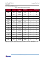
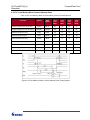
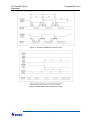
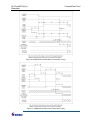
1
128MB to 16GB CompactFlash Card www.stec-inc.com SLCFxxxM2TU(I)(-x) Solid-State Memory Card (No Moving Parts) Capacity: 128MB - 16GB CFA 4.1 and ATA-7 Compatible PCMCIA Memory Mode: UDMA Modes Supported: Up to 4 PIO Modes Timing: up to 80ns PCMCIA I/O Mode: UDMA Modes Supported: Up to 4 PIO Modes Timing: Up to 80ns TrueIDE Mode: UDMA Modes Supported: Up to 4 MWDMA Modes Supported: Up to 4 PIO Modes Supported: Up to 6 Options: General Description STEC’s MACH2 CompactFlash (CF) card is an extremely high-performance, multi-channel solution available in capacities from 128MB to 16GB using SLC NAND flash. The standard CompactFlash interface provides designers with a true plug-n-play storage device, allowing for short design cycles and fast time to market, while the extreme performance enables hard disk drive performance in a much smaller and more reliable design. CompactFlash cards have quickly become the product of choice for applications requiring high reliability and high tolerance to shock, vibration, humidity, altitude, and temperature. Because the MACH2 CompactFlash uses NAND flash technology (e.g. no moving parts), it is more reliable and has much lower latency compared to a traditional hard disk drive and consumes far less power (approximately 1 watt compared to 12 watts for a standard 7200rpm ATA disk drive). With its small footprint, high capacity, and rugged design, the MACH2 CompactFlash is an ideal hard disk drive replacement or alternate storage solution in space-constrained applications or those requiring less capacity than available hard disk drives offer including blade servers and embedded PCs. STEC’s MACH2 CF Card is available in a CompactFlash Type I package and adheres to the latest industry compliance and regulatory standards including UL, FCC, RoHS, and the Compact Flash Association (CFA). Because the MACH2 CF incorporates a proprietary state-of-the-art flash memory controller, it provides the greatest flexibility to customer-specific applications while supporting key flash management features resulting in the industry’s highest reliability and endurance. Key features include: Standard LBA/CHS Configuration Maximized Performance for Multiple Simultaneous Random Writes SMART, Security, and HPA Command Sets TrueIDE PIO-Only Configuration Full datapath protection with built-in 8-bit BCH ECC engine to detect and correct up to 8-bit errors per 512 Bytes of data Commercial/Industrial Operating Temperature Sophisticated bad block management and wear leveling algorithms dramatically enhance flash memory endurance Form Factors: Power-down data protection ensures data integrity in case of power loss CompactFlash Type I CompactFlash Adapter Lifecycle management feature allows users to monitor the card's lifetime by monitoring the card's remaining spare blocks Guaranteed 2M Write Operations Card Information Structure (CIS) Programmed into Internal Memory PC Card and Socket Services Release 2.1 or later compatible STEC’s MACH2 CF card offers the highest reliability and tolerance to shock, vibration, humidity, altitude, ESD, and temperature. The rugged industrial design combined with temperature testing and adherence to rigid JEDEC JESD22 standards ensures flawless execution in the harshest environments. In addition to custom hardware and firmware designs, STEC also offers valueadded services including: Custom labeling and packaging 5V or 3.3V Power Supply Custom software imaging and ID strings Full Data-Path Protection with built-in ECC Engine Full BOM control and product change notification 10 Year Data Retention In-field application engineering to help customers through product design-ins RoHS-6 Compliant Total supply-chain management to ensure continuity of supply SLCFxxxM2TU(I)(-x) Datasheet CompactFlash Card Table of Contents 1.0 Ordering Information ........................................................................................................ 4 2.0 Product Specifications ..................................................................................................... 5 2.1 Product Marking ........................................................................................................................... 5 2.1.1 Front Label ........................................................................................................................ 5 2.1.2 Back Label ........................................................................................................................ 6 2.2 Package Dimensions and Pin Locations ...................................................................................... 8 2.3 Pin Assignments ........................................................................................................................... 9 2.4 Signal Description ....................................................................................................................... 10 2.5 Performance ............................................................................................................................... 16 2.6 LBA and CHS Parameters.......................................................................................................... 17 2.7 Standards Compliance ............................................................................................................... 18 2.7.1 CE and FCC Class B & D ............................................................................................... 18 2.7.2 RoHS .............................................................................................................................. 18 3.0 Environmental Specifications .........................................................................................19 3.1 Recommended Operating Conditions ........................................................................................ 19 3.2 Reliability .................................................................................................................................... 19 3.3 Shock, Vibration, and Humidity .................................................................................................. 19 4.0 Electrical Specifications .................................................................................................20 4.1 Absolute Maximum Ratings ........................................................................................................ 20 4.2 DC Characteristics...................................................................................................................... 20 4.3 AC Characteristics ...................................................................................................................... 21 4.3.1 PC Card Memory Mode Attribute Memory Read ............................................................ 21 4.3.2 PC Card Memory Mode Attribute Memory Write ............................................................ 22 4.3.3 PC Card Memory Mode Common Memory Read ........................................................... 23 4.3.4 PC Card Memory Mode Common Memory Write ........................................................... 24 4.3.5 PC Card I/O Mode Read AC Characteristics .................................................................. 25 4.3.6 PC Card I/O Mode Write AC Characteristics .................................................................. 26 4.3.7 TrueIDE Mode Register & PIO Access ........................................................................... 27 4.3.8 TrueIDE Mode Multiword DMA ....................................................................................... 29 4.3.9 Ultra DMA AC Characteristics ........................................................................................ 30 5.0 Host Access Specification ..............................................................................................39 5.1 Task File Register and Byte/Word/Odd-Byte Mode Mappings ................................................... 39 5.2 Host Access Interface Modes ..................................................................................................... 39 5.3 Card Information Structure (CIS) ................................................................................................ 40 5.4 Identify Drive Parameter ............................................................................................................. 44 6.0 Registers ..........................................................................................................................54 6.1 Configuration Registers .............................................................................................................. 54 6.2 Task File Registers ..................................................................................................................... 55 61000-07000-106, May 2011 2 SLCFxxxM2TU(I)(-x) Datasheet CompactFlash Card 7.0 Supported ATA Commands ............................................................................................56 8.0 Security Mode Feature Set ..............................................................................................59 8.1 Security Mode Feature Set Support and Identify Command ...................................................... 59 8.2 Security Commands ................................................................................................................... 60 9.0 Host Protected Area Feature Set ....................................................................................61 9.1 HPA Feature Set Support and Identify Command...................................................................... 61 9.2 HPA Commands ......................................................................................................................... 61 10.0 SMART Feature Set..........................................................................................................62 10.1 SMART Support and Identify Command .................................................................................... 62 10.2 SMART Commands ................................................................................................................... 62 10.3 SMART Attributes ....................................................................................................................... 63 11.0 Appendix: CompactFlash Adapter .................................................................................64 11.1 CF Adapter Ordering Information ............................................................................................... 64 11.2 CF Adapter Specifications .......................................................................................................... 64 11.3 CF Adapter Package Dimensions and Pin Locations ................................................................. 65 11.4 CF Adapter Pin Assignment ....................................................................................................... 66 12.0 Contact Information.........................................................................................................67 12.1 STEC Worldwide Headquarters ................................................................................................. 67 12.2 STEC Worldwide Locations ........................................................................................................ 67 13.0 Revision History ..............................................................................................................68 61000-07000-106, May 2011 3 SLCFxxxM2TU(I)(-x) Datasheet 1.0 CompactFlash Card Ordering Information Table 1 lists the Ordering Part Number for STEC MACH2 CompactFlash cards. Cards can be ordered with options by appending the part number with designators (I, -P, -S): Configured for STEC Standard LBA/CHS (Part Numbers without -S): Card is optimized for applications requiring STEC Standard LBA/CHS configurations Maximized Performance for multiple simultaneous random writes (-S): Card performance is optimized to handle multiple simultaneous random writes. Security Command Set Support (-S) HPA Command Set Support (-S) TrueIDE PIO-only modes (-P): Card has UDMA and MWDMA transfer modes turned off. Use this option if required for compatibility. Industrial (I): Card has an expanded operating temperature range of -40ºC to +85ºC. SMART Command Set Support (as shown in Table 1): Card issues advisory notification on product wear parameters for scheduled replacement. Note: While cards are shipped formatted for most applications, STEC recommends reformatting the cards as needed for the customer’s application. Table 1: Ordering Information Ordering Part Number Capacity SMART Support SLCF128M2TU(I,-P,-S) 128MB -S SLCF256M2TU(I,-P,-S) 256MB -S SLCF512M2TU(I,-P,-S) 512MB -S SLCF1GM2TU(I, -P,-S) 1GB -S SLCF2GM2TU(I, -P,-S) 2GB Standard & -S SLCF4GM2TU(I, -P) 4GB Standard SLCF8GM2TU(I, -P) 8GB Standard SLCF16GM2TU(I, -P) 16GB Standard Ordering Part Number Legend: SLCF = STEC standard CompactFlash card part number prefix 128/256/512/1G/2G/4G/8G/16G = 128MB / 256MB / 512MB / 1GB / 2GB / 4GB / 8GB / 16GB Capacity M2T = MACH2 controller (2 nd Generation) U = RoHS-6 compliant lead-free Part numbers without “I” = Commercial temperature range (0ºC to 70ºC) I = Industrial temperature range (-40ºC to +85ºC) -P = TrueIDE PIO-only modes Part numbers without “-S” = Configured for STEC Standard LBA/CHS -S = Maximized Performance, Security and HPA Command Sets 61000-07000-106, May 2011 4 SLCFxxxM2TU(I)(-x) Datasheet CompactFlash Card 2.0 Product Specifications 2.1 Product Marking STEC cards are labeled as specified by customer, using STEC standard labeling or custom labeling printed from customer-supplied artwork. 2.1.1 Front Label The STEC standard front label is described in Figure 1 and Table 2. Figure 1: STEC Standard Front Label Table 2: Front Label Post Printed Fields Capacity STEC Ordering Part Number Customer Number As listed in Ordering Information As listed in Ordering Information As supplied by customer 61000-07000-106, May 2011 5 SLCFxxxM2TU(I)(-x) Datasheet CompactFlash Card 2.1.2 Back Label The STEC RoHS Back Label is described in Figure 2 and Table 3. Figure 2: RoHS Back Label 61000-07000-106, May 2011 6 SLCFxxxM2TU(I)(-x) Datasheet CompactFlash Card Table 3: Back Label Post Printed Fields STEC Ordering Part Number Mfg Number SLCF128M2TU 94000-01889-3A2TCU SLCF256M2TU 94000-01889-3A3TCU SLCF512M2TU 94000-01889-3A4TCU SLCF1GM2TU 94000-01889-3A5TCU SLCF2GM2TU 94000-01889-3A6TCU SLCF4GM2TU 94000-01864-3C7TCU SLCF8GM2TU 94000-01864-3C8TCU SLCF16GM2TU 94000-01864-3C9TCU SLCF128M2TUI 94000-01889-3A2IU SLCF256M2TUI 94000-01889-3A3IU SLCF512M2TUI 94000-01889-3A4TIU SLCF1GM2TUI 94000-01889-3A5TIU SLCF2GM2TUI 94000-01889-3A6TIU SLCF4GM2TUI 94000-01864-3C7TIU SLCF8GM2TUI 94000-01864-3C8TIU SLCF16GM2TUI 94000-01864-3C9TIU SLCF128M2TU-S 94000-01889-5A2TCU SLCF256M2TU-S 94000-01889-5A3TCU SLCF512M2TU-S 94000-01889-5A4TCU SLCF1GM2TU-S 94000-01889-5A5TCU SLCF2GM2TU-S 94000-01889-5A6TCU SLCF128M2TUI-S 94000-01889-5A2TIU SLCF256M2TUI-S 94000-01889-5A3TIU SLCF512M2TUI-S 94000-01889-5A4TIU SLCF1GM2TUI-S 94000-01889-5A5TIU SLCF2GM2TUI-S 94000-01889-5A6TIU Assembly Location Assembled in Malaysia Mfg Number Legend: 94000 =STEC designation for OEM Flash products 01889/01864 = PCB # 1889 / 1864 3A/3C/5A/5C = Product revision 2-9 = Capacity Designator randomly assigned per PCB number based on designator availability T = Model Revision C/I = Commercial / Industrial Operating Temperature U = RoHS-6 compliant lead free Note: Mfg Number for products not listed is assigned when BOM is created. 61000-07000-106, May 2011 7 SLCFxxxM2TU(I)(-x) Datasheet 2.2 CompactFlash Card Package Dimensions and Pin Locations Table 4 and Figure 3 show the mechanical dimensions of the CF Card Type I. Table 4: Mechanical dimensions CF Card Type I Parameter Value Length 36.40 ± 0.15 mm (1.433 ±. 0.006 in) Width 42.80 ± 0.10 mm (1.685 ± 0.004 in) Height (including label area) 3.30 ± 0.10 mm (0.130 ± 0.004 in) Figure 3: Mechanical dimensions CF Card Type I 61000-07000-106, May 2011 8 SLCFxxxM2TU(I)(-x) Datasheet 2.3 CompactFlash Card Pin Assignments Table 5: CF Card Pin Assignment Pin Number Signal Name Pin Type Pin Number Signal Name Pin Type 1 GND Ground 26 -CD1 O 2 D03 I/O 27 D11 I/O 3 D04 I/O 28 D12 I/O 4 D05 I/O 29 D13 I/O 5 D06 I/O 30 D14 I/O 6 D07 I/O 31 D15 I/O 7 -CE1 -CS0 I 32 -CE2 -CS1 I 8 A10 I 33 -VS1 O 9 -OE -ATASEL I 34 -IORD HSTROBE (-)HDMARDY I 10 A09 I 35 -IOWR STOP I 11 A08 I 36 -WE I O Power 12 A07 I 37 READY -IREQ INTRQ 13 VCC Power 38 VCC 14 A06 I 39 -CSEL I 15 A05 I 40 -VS2 O 16 A04 I 41 (-)RESET I O 17 A03 I 42 -WAIT IORDY -DDMARDY DSTROBE 18 A02 I 43 -INPACK (-)DMARQ O 19 A01 I 44 -REG (-)DMACK I 20 A00 I 45 BVD2 -SPKR -DASP I/O 21 D00 I/O 46 BVD1 -STSCHG -PDIAG I/O 22 D01 I/O 47 D08 I/O 23 D02 I/O 48 D09 I/O 24 WP -IOIS16 -IOCS16 O 49 D10 I/O 25 -CD2 O 50 GND Ground Legend: ―-― = Low active 61000-07000-106, May 2011 9 SLCFxxxM2TU(I)(-x) Datasheet 2.4 CompactFlash Card Signal Description Note: Part numbers with -P extension do not support MDWMA and UMDA. Table 6: CF Card Signal Description Signal Name BVD2 (PC Card Memory Mode) Type I/O Pin Number 45 Description This output line is always driven to a high state in Memory Mode since a battery is not required for this product. -SPKR (PC Card I/O Mode) This output line is always driven to a high state in I/O Mode since this product produces no audio. -DASP (TrueIDE Mode) In the TrueIDE Mode, this input/output is the Disk Active/Slave Present signal in the Master/Slave handshake protocol. -CD1, -CD2 (PC Card Memory Mode) I/O 26, 25 These Card Detect pins are connected to ground on the card. They are used by the host to determine that the card is fully inserted into the socket. -CD1, -CD2 (PC Card I/O Mode) This signal is the same as Memory Mode. -CD1, -CD2 (TrueIDE Mode) These signals are not used in TrueIDE Mode. D15 - D00 (PC Card Memory Mode) I/O 31, 30, 29, 28, 27, 49, 48, 47, 6, 5, 4, 3, 2, 23, 22, 21 These lines carry the Data, Commands and Status information between the host and the controller. D00 is the LSB of the Even Byte of the Word. D08 is the LSB of the Odd Byte of the Word. D15 - D00 PC Card I/O Mode This signal is the same as the PC Card Memory Mode signal. D15 - D00 (TrueIDE Mode) In TrueIDE Mode, all Task File operations occur in byte mode on the low order bus D00-D07 while all data transfers are 16 bit using D00-D15. -IOWR (PC Card Memory Mode except UDMA protocol active) I 35 This signal is not used in this mode. STOP (All Modes: UDMA protocol active) In all modes, while UDMA mode protocol is active, the assertion of this signal causes the termination of the UDMA data burst. -IOWR (PC Card I/O Mode except UDMA protocol active) The I/O Write strobe pulse is used to clock I/O data onto the data bus and into the controller registers. The clocking occurs on the negative to positive edge of the signal (trailing edge). STOP (All Modes: UDMA protocol active) Same as STOP above. -IOWR (TrueIDE Mode except UDMA protocol active) In TrueIDE Mode, this signal has the same function as in PC Card I/O Mode. STOP (All Modes: UDMA protocol active) Same as STOP above. 61000-07000-106, May 2011 10 SLCFxxxM2TU(I)(-x) Datasheet Signal Name -IORD (PC Card Memory Mode except UDMA protocol active) CompactFlash Card Type I Pin Number 34 Description This signal is not used in this mode. -HDMARDY (All Modes: UDMA protocol DMA Read) In all modes when UDMA mode DMA Read is active, this signal is asserted by the host to indicate that the host is ready to receive UDMA data-in bursts. The host may negate -HDMARDY to pause an UDMA transfer HSTROBE (All Modes: UDMA protocol DMA Write) In all modes when UDMA mode DMA Write is active, this signal is the data out strobe generated by the host. Both the rising and falling edge of HSTROBE cause data to be latched by the device. The host may stop generating HSTROBE edges to pause an UDMA data-out burst. -IORD (PC Card I/O Mode except UDMA protocol active) This is an I/O Read strobe generated by the host. This signal gates I/O data onto the bus from the CF Card. -HDMARDY (All Modes: UDMA protocol DMA Read) Same as -HDMARDY above. HSTROBE (All Modes: UDMA protocol DMA Write) Same as HSTROBE above. -IORD (TrueIDE Mode except UDMA protocol active) In TrueIDE Mode, this signal has the same function as in PC Card I/O Mode. -HDMARDY (All Modes: UDMA protocol DMA Read) Same as -HDMARDY above. HSTROBE (All Modes: UDMA protocol DMA Write) Same as HSTROBE above. -WE (PC Card Memory Mode) I 36 This is a signal driven by the host and used for strobing memory write data into the registers. It is also used for writing the configuration registers. -WE (PC Card I/O Mode) In PC Card I/O Mode, this signal is used for writing the configuration registers. -WE (TrueIDE Mode) In TrueIDE Mode, this input signal is not used and should be connected to VCC. -OE (PC Card Memory Mode) I 9 This is an Output Enable strobe generated by the host interface. It is used to read data from the CF Card in PC Card Memory Mode and to read the CIS and configuration registers. -OE (PC Card I/O Mode) In PC Card I/O Mode, this signal is used to read the CIS and configuration registers. -ATASEL (TrueIDE Mode) To enable TrueIDE Mode, this input should be grounded by the host. 61000-07000-106, May 2011 11 SLCFxxxM2TU(I)(-x) Datasheet Signal Name READY (PC Card Memory Mode) CompactFlash Card Type O Pin Number 37 -IREQ Description In Memory Mode, this signal is set high when the CF Card is ready to accept a new data transfer operation and held low when the CF Card is busy. The host must provide a pull-up resistor. At power up and at reset, the READY signal is held low (busy) until the CF Card completes its power up or reset function. No access of any type should be made to the CF Card during this time. The READY signal is held high (disabled from being busy) when the CF Card is powered up with RESET continuously disconnected or asserted high. (PC Card I/O Mode) After card has been configured for I/O operation, signal is used as active low interrupt request. Strobe low to generate pulse mode interrupt or hold low for level mode interrupt. INTRQ (TrueIDE Mode) In TrueIDE Mode, this signal is the active high interrupt request to the host. A10 - A0 (PC Card Memory Mode) I 8, 10, 11, 12, 14, 15, 16, 17, 18, 19, 20 A10 - A0 (PC Card I/O Mode) This signal is the same as the PC Card Memory Mode signal. A2 - A0 (TrueIDE Mode) -CE1, -CE2 (PC Card Memory Mode) Card Enable These address lines along with the -REG signal are used to select the following: the I/O port address registers within the CF Card, the memory mapped port address registers within the CF Card, a byte in the CIS and the Configuration Control and Status Registers. I 18, 19, 20 In TrueIDE Mode only, A2:A0 are used to select the one of eight registers in the Task File. The remaining address lines should be grounded. 7, 32 These input signals are used both to select the CF Card and to indicate to the CF Card whether a byte or a word operation is being performed. -CE2 always accesses the odd byte of the word. -CE1 accesses the even byte or the odd byte of the word depending on A0 and -CE2. A multiplexing scheme based on A0, -CE1, -CE2 allows 8-bit hosts to access all data on D0-D7. -CE1, -CE2 (PC Card I/O Mode) Card Enable This signal is the same as the PC Card Memory Mode signal. -CS0, -CS1 (TrueIDE Mode) In the TrueIDE Mode, -CS0 is the chip enable for the task file registers while -CS1 is used to select the Alternate Status Register and the CF Card Control Register. -CSEL (PC Card Memory Mode) I 39 This signal is not used for this mode. -CSEL (PC Card I/O Mode) This signal is not used for this mode. -CSEL (TrueIDE Mode) This internally pulled up signal is used to configure the card as a Master or Slave. When the pin is grounded, the card is configured as a Master. When the pin is open, the card is configured as a Slave. 61000-07000-106, May 2011 12 SLCFxxxM2TU(I)(-x) Datasheet Signal Name -REG (PC Card Memory Mode except UDMA protocol active) Attribute Memory Select CompactFlash Card Type I Pin Number 44 Description This signal distinguishes between accesses to Common Memory (high) and Register Attribute Memory (low). In PC Card Memory Mode, when UDMA protocol is supported by host and host has enable UDMA on the card, the host shall keep the –REG signal negated during the execution of any DMA Command by the device. -DMACK (PC Card Memory Mode when UDMA protocol is active) This is a DMA Acknowledge signal that is asserted by the host in response to (-)DMARQ to initiate DMA transfers. In TrueIDE Mode, while DMA operations are not active, the card shall ignore the (-)DMARQ signal, including a floating condition. If DMA operation is not supported by a TrueIDE Mode only host, this signal should be driven high or connected to VCC by the host. A host that does not support DMA and implements both PC Card and TrueIDE modes of operation need not alter the PC Card mode connections while in TrueIDE mode as long as this does not prevent proper operation all modes -REG (PC Card I/O Mode except UDMA protocol active) The signal must also be active (low) during I/O Cycles when the I/O address is on the bus. In PC Card I/O Mode, when UDMA protocol is support by host and host has enable UDMA on card, the host shall keep the –REG signal asserted during the execution of any DMA Command by the device. DMACK (PC Card I/O Mode when UDMA protocol is active) Same as (-)DMACK above. -DMACK (TrueIDE Mode) Same as (-)DMACK above. WP (PC Card Memory Mode) Write Protect O 24 The CF Card does not have a write protect switch; therefore, this signal is held low after the completion of the reset initialization sequence. -IOIS16 (PC Card I/O Mode) A low signal indicates that a 16 bit or odd byte only operation can be performed at the addressed port. -IOCS16 (TrueIDE Mode) In TrueIDE Mode this output signal is asserted low when this device is expecting a word data transfer cycle. 61000-07000-106, May 2011 13 SLCFxxxM2TU(I)(-x) Datasheet Signal Name -INPACK (PC Card Memory Mode except UDMA protocol active) CompactFlash Card Type O Pin Number 43 -DMARQ (PC Card Memory Mode: UDMA protocol active) Description This signal is not used in this mode. This signal is a DMA Request that is used for DMA data transfers between host and device. It shall be asserted by the device when it is ready to transfer data to or from the host. For Multiword DMA transfers, the direction of data transfer is controlled by -IORD and -IOWR. This signal is used in a handshake manner with (-)DMACK, i.e., the device shall wait until the host asserts (-)DMACK before negating (-)DMARQ, and re-asserting (-)DMARQ if there is more data to transfer. In PCMCIA I/O Mode, the -DMARQ shall be ignored by the host while the host is performing an I/O Read cycle to the device. The host shall not initiate an I/O Read cycle while DMARQ is asserted by the device. In TrueIDE Mode, DMARQ shall not be driven when the device is not selected in the Drive-Head register. While a DMA operation is in progress, -CS0 (-CE1)and -CS1 (-CE2) shall be held negated and the width of the transfers shall be 16 bits. If there is no hardware support for TrueIDE DMA mode in the host, this output signal is not used and should not be connected at the host. In this case, the BIOS must report that DMA mode is not supported by the host so that device drivers will not attempt DMA mode operation. A host that does not support DMA mode and implements both PC Card and TrueIDE modes of operation need not alter the PC Card mode connections while in TrueIDE mode as long as this does not prevent proper operation in any mode. -INPACK (PC Card I/O Mode except UDMA protocol active) Input Acknowledge The Input Acknowledge signal is asserted by the CF Card when it is selected and responding to an I/O read cycle at the address that is on the bus. The host uses this signal to control the enable of any input data buffers between the CF Card and the host’s CPU. -DMARQ (PC Card I/O Mode: UDMA protocol active) Same as (-)DMARQ above. DMARQ (TrueIDE Mode) BVD1 (PC Card Memory Mode) Same as (-)DMARQ above. I/O 46 This signal is asserted high as since a battery is not used with this product. -STSCHG (PC Card I/O Mode) Status Changed Asserted low to alert host to changes in READY, Write Protect states. Use is controlled by Configuration and Status Register. -PDIAG (TrueIDE Mode) In TrueIDE Mode, this input/output signal is the Pass Diagnostic signal in the Master/Slave handshake protocol. 61000-07000-106, May 2011 14 SLCFxxxM2TU(I)(-x) Datasheet Signal Name -WAIT (PC Card Memory Mode except UDMA protocol active) CompactFlash Card Type O Pin Number 42 Description This signal is not used by the CF Card, and is pulled up to VCC through a 4.7K ohm resistor. In all modes, when Ultra DMA mode DMA Write is active, this signal is asserted by the device during a data burst to indicate that the device is ready to receive Ultra DMA data out bursts. The device may negate -DDMARDY to pause an Ultra DMA transfer. -DDMARDY (All Modes: UDMA Write protocol active) DSTROBE (All Modes: UDMA Read protocol active) In all modes, when Ultra DMA mode DMA Read is active, this signal is the data in strobe generated by the device. Both the rising and falling edge of DSTROBE cause data to be latched by the host. The device may stop generating DSTROBE edges to pause an Ultra DMA data in burst -WAIT (PC Card I/O Mode except UDMA protocol active) This signal is not used by the CF Card, and is pulled up to VCC through a 4.7K ohm resistor. -DDMARDY (All Modes: UDMA Write protocol active) Same as -DDMARDY above. DSTROBE (All Modes: UDMA Read protocol active) Same as DSTROBE above. IORDY (TrueIDE Mode except UDMA protocol active) This signal is not used by the CF Card, and is pulled up to VCC through a 4.7K ohm resistor. -DDMARDY (All Modes: UDMA Write protocol active) Same as -DDMARDY above. DSTROBE (All Modes: UDMA Read protocol active) Same as DSTROBE above. GND (PC Card Memory Mode) GND 1, 50 Ground GND (PC Card I/O Mode) Ground GND (TrueIDE Mode) Ground VCC (PC Card Memory Mode) VCC 13, 38 +5 V or 3.3V power VCC (PC Card I/O Mode) +5 V or 3.3V power VCC (TrueIDE Mode) +5 V or 3.3V power RESET (PC Card Memory Mode) I 41 When RESET is high, this signal resets the CF Card. The CF Card is reset only at power up if this signal is left high or open from power-up. The CF Card can also be reset when the soft reset bit in the Configuration Option Register is set. RESET (PC Card I/O Mode) This signal is the same as the PC Card Memory Mode signal. -RESET (TrueIDE Mode) In the TrueIDE Mode this input pin is the active low hardware reset from the host. 61000-07000-106, May 2011 15 SLCFxxxM2TU(I)(-x) Datasheet Signal Name -VS1 -VS2 (PC Card Memory Mode) CompactFlash Card Type O Pin Number 33, 40 Description -VS1 is grounded, so that the card CIS can be read 3.3 volts. -VS2 is reserved for a secondary voltage and is not connected. -VS1 -VS2 (PC Card I/O Mode) This signal is the same for all modes. -VS1 -VS2 (TrueIDE Mode) This signal is not used in IDE Mode. 2.5 Performance Table 7: CF Card Read/Write Performance Parameter Flash Type 128MB-2GB 4GB-16GB Data transfer rate to/from host SLC 66 MBytes/s (burst) 66 MBytes/s (burst) Sustained read SLC up to 20 MBytes/s up to 37 MBytes/s Sustained write SLC up to 12 MBytes/s up to 22 MBytes/s Note: Performance may vary under extreme temperatures. 61000-07000-106, May 2011 16 SLCFxxxM2TU(I)(-x) Datasheet 2.6 CompactFlash Card LBA and CHS Parameters Table 8: LBA and CHS Parameters per capacity Capacity Flash Type Logical Block Addresses (LBA) Cylinders (C) (standard) Heads (H) Sectors/Track (S) 128MB SLC 250,880 980 8 32 128MB (S option) SLC 236,544 924 8 32 256MB SLC 501,760 980 16 32 256MB (S option) SLC 473,088 924 16 32 512MB SLC 1,000,944 993 16 63 512MB (S option) SLC 946,512 939 16 63 1GB SLC 2,001,888 1,986 16 63 1GB (S option) SLC 1,893,024 1,878 16 63 2GB SLC 4,001,760 3,970 16 63 2GB (S option) SLC 3,786,048 3,756 16 63 4GB SLC 7,276,752 7,219 16 63 8GB SLC 14,568,624 14,453 16 63 16GB SLC 29,191,680 28,960 16 63 Notes: The unformatted capacity of the card may be less than the perceived or stated capacity on the label. Please use the LBA count in this table for reference. 61000-07000-106, May 2011 17 SLCFxxxM2TU(I)(-x) Datasheet 2.7 CompactFlash Card Standards Compliance STEC products specified in this document are certified for compliance with the following industry standards: CFA v4.1, PCMCIA v7.0 UL 950 CE, and FCC Class B & D RoHS 2.7.1 CE and FCC Class B & D The STEC products specified in this document meet the following requirements and limits of the European Standards: Class B requirements of the following European Standard: EN 55022: 1998 – ―Information technology equipment – Radio disturbance characteristics – Limits and methods of measurement‖ Class D limits of the following European Standards: EN 61000-3-2 ―Electromagnetic compatibility (EMC) Part 3-2: Limits – Limits for harmonic current emissions (equipment input current up to and including 16 A per phase)‖ EN 61000-3-3: 1995 – ―Part 3: Limits – Section 3: Limitation of voltage fluctuations and flicker in low-voltage supply systems for equipment with rated current ≤ 16A‖ EN 55024 – ―Information technology equipment – Immunity characteristics – Limits and methods of measurement‖ 2.7.2 RoHS STEC certifies that its products do not contain any of the restricted substances as stated below and are in compliance with RoHS EU directive 2002/95/EC, specifically: Mercury (Hg) Cadmium Cd) Chromium VI (Cr +6) Polybrominated biphenyl (PBB) Polybrominated biphenyl ether (PBDE) Lead (Pb) Materials used in the STEC’s products are limited to the following: Steel, Nylon 6/6, PCB laminate Copper, Gold, Nickel Silicon on ICs and Components Polyester on Labels 61000-07000-106, May 2011 18 SLCFxxxM2TU(I)(-x) Datasheet CompactFlash Card 3.0 Environmental Specifications 3.1 Recommended Operating Conditions Table 9: CF Card Recommended Operating Conditions Parameter Symbol Min Typ Max Unit Commercial Operating Temperature Ta1 0 25 70 C Industrial Operating Temperature Ta2 -40 - +85 C VCC voltage (5V) VCC5.0 4.5 5.0 5.5 V VCC voltage (3.3V) VCC3.3 3.13 3.3 3.46 V 3.2 Reliability Table 10: CF Card Reliability Parameter Value >4,000,000 power on hours, (per MIL-HDBK-217F, rated at 40°C, ground benign environment) MTBF Endurance 2M write operations Uncorrectable Bit Error Rate (UBER) Data retention 3.3 <1 uncorrectable error per 10 14 bits read 10 years Shock, Vibration, and Humidity Table 11: CF Card Shock, Vibration & Humidity Parameter Shock Value 1.5K G peak, 0.5ms pulse duration, five (5) pulses per each of six (6) directions (per JEDEC JESD22 standard, method B110) Vibration 20 G peak, 20Hz-2000Hz, 4 cycles per direction (per JEDEC JESD22 standard, method B103) Humidity 85°C 85% RH, 500 hrs 61000-07000-106, May 2011 19 SLCFxxxM2TU(I)(-x) Datasheet CompactFlash Card 4.0 Electrical Specifications 4.1 Absolute Maximum Ratings Table 12: CF Card Absolute Maximum Ratings 4.2 Parameter Symbol Value Unit Voltage Vin, Vout -0.5 to VCC +0.5 V Storage temperature range Tstg -40 to +95 C DC Characteristics Measurements at Recommended Operating Conditions unless otherwise specified. Table 13: CF Card DC Characteristics Symbol Parameter VIL (5V) Max Unit Input LOW Voltage +0.8 V VCC= 5.0V VIL (3.3V) Input LOW Voltage +0.6 V VCC= 3.3V VIH (5V) Input HIGH Voltage 4.0 V VCC= 5.0V VIH (3.3V) Input HIGH Voltage 2.4 V VCC= 3.3V VOL Output LOW Voltage V VCC=5.0V or 3.3V VOH Output HIGH Voltage V VCC=5.0V or 3.3V ICCSB Standby Mode Operating Current (128MB-2GB) ICC Operating Current (4GB-8GB) Operating Current (16GB) Min GND+0.4 VCC-0.8 3 mA 95 mA 145 mA 180 mA 61000-07000-106, May 2011 Notes ICC at VCC=5.0V or 3.3V ICC at VCC=5.0V or 3.3V 20 SLCFxxxM2TU(I)(-x) Datasheet 4.3 CompactFlash Card AC Characteristics Measurements at Recommended Operating Conditions, unless otherwise specified. 4.3.1 PC Card Memory Mode Attribute Memory Read Table 14: PC Card Memory Mode Attribute Memory Read AC Characteristics Parameter Symbol IEEE Symbol Min (ns) Read Cycle Time tc(R) tAVAV 300 Address Access Time ta(A) tAVQV 300 Card Enable Access Time ta(CE) tELQV 300 Output Enable Access Time ta(OE) tGLQV 150 Output Disable Time from -CE tdis(CE) tEHQZ 100 Output Disable Time from -OE tdis(OE) tGHQZ 100 tsu(A) tAVGL 30 Output Enable Time from -CE ten(CE) tELQNZ 5 Output Enable Time from -OE ten(OE) tGLQNZ 5 tv(A) tAXQX 0 Address Setup Time Data Valid from Address Change Max (ns) Figure 4: PC Card Memory Mode Attribute Memory Read Timing Diagram 61000-07000-106, May 2011 21 SLCFxxxM2TU(I)(-x) Datasheet CompactFlash Card 4.3.2 PC Card Memory Mode Attribute Memory Write Table 15: PC Card Memory Mode Attribute Memory Write AC Characteristics Parameter Symbol IEEE Symbol Min (ns) Write Cycle Time tc(W) tAVAV 250 Write Pulse Width tw(WE) tWLWH 150 tsu(A) tAVWL 30 tsu(D-WEH) tDVWH 80 th(D) tWMDX 30 trec(WE) tWMAX 30 Address Setup Time Data Setup Time (-WE) Data Hold Time Write Recovery Time Max (ns) Figure 5: PC Card Memory Mode Attribute Memory Write Timing Diagram 61000-07000-106, May 2011 22 SLCFxxxM2TU(I)(-x) Datasheet CompactFlash Card 4.3.3 PC Card Memory Mode Common Memory Read Table 16: PC Card Memory Mode Common Memory Read AC Characteristics Symbol IEEE Symbol 250 ns Cycle Time Mode 120 ns Cycle Time Mode 100 ns Cycle Time Mode 80 ns Cycle Time Mode ta(OE) tGLQV 125 60 50 45 tdis(OE) tGHQZ 100 60 50 45 Address Setup Time (min) tsu(A) tAVGL 30 15 10 10 Address Hold Time (min) th(A) tGHAX 20 15 15 10 CE Setup before OE (min) tsu(CE) tELGL 0 0 0 0 CE Hold following OE (min) th(CE) tGHEH 20 15 15 10 tv(WT-OE) tGLWTV 35 35 35 N/A Data Setup for Wait Release (max) tv(WT) tQVWTH 0 0 0 N/A Wait Width Time (max) tw(WT) tWTLWTH 350 350 350 N/A Parameter Output Enable Access Time (max) Output Disable Time from OE (max) Wait Delay Falling from OE (max) Figure 6: PC Card Memory Mode Common Memory Read Timing Diagram 61000-07000-106, May 2011 23 SLCFxxxM2TU(I)(-x) Datasheet CompactFlash Card 4.3.4 PC Card Memory Mode Common Memory Write Table 17: PC Card Memory Mode Common Memory Write AC Characteristics Symbol IEEE Symbol 250 ns Cycle Time Mode 120 ns Cycle Time Mode 100 ns Cycle Time Mode 80 ns Cycle Time Mode tsu(D-WEH) tDVWH 80 50 40 30 th(D) tWMDX 30 15 10 10 tw(WE) tWLWH 150 70 60 55 Address Setup Time (min) tsu(A) tAVWL 30 15 10 10 CE Setup before WE (min) tsu(CE) tELWL 0 0 0 0 Write Recovery Time (min) trec(WE) tWMAX 30 15 15 15 th(A) tGHAX 20 15 15 15 th(CE) tGHEH 20 15 15 10 Wait Delay Falling from WE (max) tv(WT-WE) tWLWTV 35 35 35 N/A WE High from Wait Release (min) tv(WT) tWTHWH 0 0 0 N/A Wait Width Time (max) tw(WT) tWTLWTH 350 350 350 N/A Parameter Data Setup before WE(min) Data Hold following WE (min) WE Pulse Width (min) Address Hold Time (min) CE Hold following WE (min) Figure 7: PC Card Memory Mode Common Memory Write Timing Diagram 61000-07000-106, May 2011 24 SLCFxxxM2TU(I)(-x) Datasheet CompactFlash Card 4.3.5 PC Card I/O Mode Read AC Characteristics Table 18: PC Card I/O Mode Read AC Characteristics Symbol IEEE Symbol 250 ns Cycle Time Mode 120 ns Cycle Time Mode 100 ns Cycle Time Mode 80 ns Cycle Time Mode Data Delay after -IORD (max) td(IORD) tIGLQV 100 50 50 45 Data Hold following -IORD (min) th(IORD) tIGHQX 0 5 5 5 -IORD Width Time (min) tw(IORD) tIGLIGH 165 70 65 55 Address Setup before -IORD (min) tsuA(IORD) tAVIGL 70 25 25 15 Address Hold following -IORD (min) thA(IORD) tIGHAX 20 10 10 10 -CE Setup before -IORD (min) tsuCE(IORD) tELIGL 5 5 5 5 -CE Hold following -IORD (min) thCE(IORD) tIGHEH 20 10 10 10 -REG Setup before -IORD (min) tsuREG(IORD) tRGLIGL 5 5 5 5 -REG Hold following -IORD (min) thREG(IORD) tIGHRGH 0 0 0 0 Parameter Figure 8: PC Card I/O Mode Read Timing Diagram 61000-07000-106, May 2011 25 SLCFxxxM2TU(I)(-x) Datasheet CompactFlash Card 4.3.6 PC Card I/O Mode Write AC Characteristics Table 19: PC Card I/O Mode Write AC Characteristics Symbol IEEE Symbol 250 ns Cycle Time Mode 120 ns Cycle Time Mode 100 ns Cycle Time Mode 80 ns Cycle Time Mode Data Setup before -IOWR (min) tsu(IOWR) tDVIWH 60 20 20 15 Data Hold following -IOWR (min) th(IOWR) tIWHDX 30 10 5 5 -IOWR Width Time (min) tw(IOWR) tIWLIWH 165 70 65 55 Address Setup before -IOWR (min) tsuA(IOWR) tAVIWL 70 25 25 15 Address Hold following -IOWR (min) thA(IOWR) tIWHAX 20 20 10 10 -CE Setup before -IOWR (min) tsuCE(IOWR) tELIWL 5 5 5 5 -CE Hold following -IOWR (min) thCE(IOWR) tIWHEH 20 20 10 10 -REG Setup before -IOWR (min) tsuREG(IOWR) tRGLIWL 5 5 5 5 -REG Hold following -IOWR (min) thREG(IOWR) tIWHRGH 0 0 0 0 Parameter Figure 9: PC Card I/O Mode Write Timing Diagram 61000-07000-106, May 2011 26 SLCFxxxM2TU(I)(-x) Datasheet CompactFlash Card 4.3.7 TrueIDE Mode Register & PIO Access Table 20: TrueIDE Mode Register & PIO Access AC Characteristics Parameter Symbol Mode0 Mode1 Mode2 Mode3 Mode4 Mode5 Mode6 Unit Cycle time (min) t0 600 383 240 180 120 100 80 ns Address valid to -IORD/-IOWR (min) setup t1 70 50 30 30 25 15 10 ns -IORD/-IOWR (min) t2 165 125 100 80 70 65 55 ns -IORD/-IOWR register (min) 8bit t2 290 290 290 80 70 65 55 ns -IORD/-IOWR recovery time (min) t2i — — — 70 25 25 20 ns -IOWR data setup (min) t3 60 45 30 30 20 20 15 ns -IOWR data hold (min) t4 30 20 15 10 10 5 5 ns -IORD data setup (min) t5 50 35 20 20 20 15 10 ns -IORD data hold (min) t6 5 5 5 5 5 5 5 ns -IORD data tristate (max) t6z 30 30 30 30 30 20 20 ns Addresses valid to -IOCS16 assert. (max) t7 90 50 40 N/A N/A N/A N/A ns Address valid to IOCS16 release (max) t8 60 45 30 N/A N/A N/A N/A ns -IORD/-IOWR to address valid hold t9 20 15 10 10 10 10 10 ns tRD 0 0 0 0 0 0 0 ns IORDY setup tA 35 35 35 35 35 N/A N/A ns IORDY pulse width (max) tB 1,250 1,250 1,250 1,250 1,250 N/A N/A ns IORDY assertion to release (max) tC 5 5 5 5 5 N/A N/A ns Read Data valid to IORDY active (min), if IORDY initially low after tA 61000-07000-106, May 2011 27 SLCFxxxM2TU(I)(-x) Datasheet CompactFlash Card Figure 10: TrueIDE Mode PIO Access Timing Diagram 61000-07000-106, May 2011 28 SLCFxxxM2TU(I)(-x) Datasheet CompactFlash Card 4.3.8 TrueIDE Mode Multiword DMA Note: Part numbers with -P extension do not support MWDMA. Table 21: TrueIDE Mode Multiword DMA AC Characteristics Parameter Symbol Mode 0 Mode 1 Mode 2 Mode 3 Mode 4 Unit Cycle time (min) t0 480 150 120 100 80 ns -IORD/-IOWR Asserted Width (min) tD 215 80 70 65 55 ns -IORD data access (max) tE 150 60 50 50 45 ns -IORD data hold (min) tF 5 5 5 5 5 ns -IORD/-IOWR data setup (min) tG 100 30 20 15 10 ns -IOWR data hold (min) tH 20 15 10 5 5 ns DMACK to -IORD/-IOWR setup (min) tI 0 0 0 0 0 ns -IORD/-IOWR to DMACK hold (min) tJ 20 5 5 5 5 ns -IORD negated pulse width (max) tKR 50 50 25 25 20 ns -IOWR negated pulse width (min) tKW 215 50 25 25 20 ns -IORD to DMARQ delay (max) tLR 120 40 35 35 35 ns -IOWR to DMARQ delay (max) tLW 40 40 35 35 35 ns Figure 11: TrueIDE Mode Multiword DMA Timing Diagram 61000-07000-106, May 2011 29 SLCFxxxM2TU(I)(-x) Datasheet CompactFlash Card 4.3.9 Ultra DMA AC Characteristics Note: Part numbers with -P extension do not support TrueIDE UDMA. Table 22: UDMA Burst Timing Requirements Symbol UDMA0 (ns) UDMA1 (ns) UDMA2 (ns) UDMA3 (ns) UDMA4 (ns) Measure location (see Note2) t2CYCTYP (min) 240 160 120 90 60 Sender tCYC (min) 112 73 54 39 25 Note3 t2CYC (min) 230 153 115 86 57 Sender tDS (min) 15.0 10.0 7.0 7.0 5.0 Recip’nt tDH (min) 5.0 5.0 5.0 5.0 5.0 Recip’nt tDVS (min) 70.0 48.0 31.0 20.0 6.7 Sender tDVH (min) 6.2 6.2 6.2 6.2 6.2 Sender tCS (min) 15.0 10.0 7.0 7.0 5.0 Device tCH (min) 5.0 5.0 5.0 5.0 5.0 Device tCVS (min) 70.0 48.0 31.0 20.0 6.7 Host tCVH (min) 6.2 6.2 6.2 6.2 6.2 Host tZFS (min) 0 0 0 0 0 Device tDZFS (min) 70.0 48.0 31.0 20.0 6.7 Sender tFS (max) 230 200 170 130 120 Device tLI (min) 0 0 0 0 0 Note4 tLI (max) 150 150 150 100 100 Note4 tMLI (min) 20 20 20 20 20 Host tUI (min) 0 0 0 0 0 Host tAZ (max) 10 10 10 10 10 Note5 tZAH (min) 20 20 20 20 20 Host tZAD (min) 0 0 0 0 0 Device tENV (min) 20 20 20 20 20 Host tENV (max) 70 70 70 55 55 Host tRFS (max) 75 70 60 60 60 Sender tRP (min) 160 125 100 100 100 Recip’nt tIORDYZ (max) 20 20 20 20 20 Device tZIORDY (min) 0 0 0 0 0 Device tACK (min) 20 20 20 20 20 Host tSS (min) 50 50 50 50 50 Sender Notes: 1. 2. 3. 4. 5. All timing measurement switching points (low to high and high to low) shall be taken at 1.5 V. All signal transitions for a timing parameter shall be measured at the connector specified in the measurement location column. For example, in the case of tRFS, both STROBE and -DMARDY transitions are measured at the sender connector. The parameter tCYC shall be measured at the recipient’s connector farthest from the sender. The parameter tLI shall be measured at the connector of the sender or recipient that is responding to an incoming transition from the recipient or sender respectively. Both the incoming signal and the outgoing response shall be measured at the same connector. The parameter tAZ shall be measured at the connector of the sender or recipient that is driving the bus but must release the bus to allow for a bus turnaround. 61000-07000-106, May 2011 30 SLCFxxxM2TU(I)(-x) Datasheet CompactFlash Card Table 23: UDMA Timing Parameter Descriptions Symbol Parameter t2CYCTYP Typical sustained average two cycle time tCYC Cycle time allowing for asymmetry and clock variations (from STROBE edge to STROBE edge) t2CYC Two cycle time allowing for clock variations (from rising edge to next rising edge or from falling edge to next falling edge of STROBE) tDS Data setup time at recipient (from data valid until STROBE edge) tDH Data hold time at recipient (from STROBE edge until data may become invalid) tDVS Data valid setup time at sender (from data valid until STROBE edge) tDVH Data valid hold time at sender (from STROBE edge until data may become invalid) tCS CRC word setup time at device tCH CRC word hold time device tCVS CRC word valid setup time at host (from CRC valid until -DMACK negation) tCVH CRC word valid hold time at sender (from -DMACK negation until CRC may become invalid) tZFS Time from STROBE output released-to-driving until the first transition of critical timing. tDZFS Time from data output released-to-driving until the first transition of critical timing. tFS First STROBE time (for device to first negate DSTROBE from STOP during a data in burst) tLI Limited interlock time tMLI Interlock time with minimum tUI Unlimited interlock time tAZ Maximum time allowed for output drivers to release (from asserted or negated) tZAH Minimum delay time required for output tZAD Drivers to assert or negate (from released) tENV Envelope time (from -DMACK to STOP and -HDMARDY during data in burst initiation and from DMACK to STOP during data out burst initiation) tRFS Ready-to-final-STROBE time (no STROBE edges shall be sent this long after negation of DMARDY) tRP Ready-to-pause time (that recipient shall wait to pause after negating -DMARDY) tIORDYZ Maximum time before releasing IORDY tZIORDY Minimum time before driving IORDY tACK Setup and hold times for -DMACK (before assertion or negation) tSS Time from STROBE edge to negation of DMARQ or assertion of STOP (when sender terminates a burst) 61000-07000-106, May 2011 31 SLCFxxxM2TU(I)(-x) Datasheet CompactFlash Card Table 24: Ultra DMA Sender and Recipient IC Timing Requirements Symbol UDMA0 UDMA1 UDMA2 UDMA3 UDMA4 Unit tDSIC (min) 14.7 9.7 6.8 6.8 4.8 ns tDHIC (min) 4.8 4.8 4.8 4.8 4.8 ns tDVSIC (min) 72.9 50.9 33.9 22.6 9.5 ns tDVHIC (min) 9.0 9.0 9.0 9.0 9.0 ns Table 25: Ultra DMA Sender and Recipient IC Timing Parameter Descriptions Symbol Parameter tDSIC Recipient IC data setup time (from data valid until STROBE edge) tDHIC Recipient IC data hold time (from STROBE edge until data may become invalid) tDVSIC Sender IC data valid setup time (from data valid until STROBE edge) tDVHIC Sender IC data valid hold time (from STROBE edge until data may become invalid Table 26: Ultra DMA AC Signal Requirements Symbol Parameter Max (V/ns) SRISE Rising Edge Slew Rate for any signal 1.25 SFALL Falling Edge Slew Rate for any signal 1.25 61000-07000-106, May 2011 32 SLCFxxxM2TU(I)(-x) Datasheet CompactFlash Card Figure 12: UDMA Data-In Burst Initiation Timing 61000-07000-106, May 2011 33 SLCFxxxM2TU(I)(-x) Datasheet CompactFlash Card Figure 13: Sustained UDMA Data-In Burst Timing Figure 14: UDMA Data-In Burst Host Pause Timing 61000-07000-106, May 2011 34 SLCFxxxM2TU(I)(-x) Datasheet CompactFlash Card Figure 15: UDMA Data-In Burst Device Termination Timing 61000-07000-106, May 2011 35 SLCFxxxM2TU(I)(-x) Datasheet CompactFlash Card Figure 16: UDMA Data-In Burst Host Termination Timing Figure 17: UDMA Data-Out Burst Initiation Timing 61000-07000-106, May 2011 36 SLCFxxxM2TU(I)(-x) Datasheet CompactFlash Card Figure 18: Sustained UDMA Data-Out Burst Timing Figure 19: UDMA Data-Out Burst Device Pause Timing 61000-07000-106, May 2011 37 SLCFxxxM2TU(I)(-x) Datasheet CompactFlash Card Figure 20: UDMA Data-Out Burst Device Termination Timing Figure 21: UDMA Data-Out Burst Host Termination Timing 61000-07000-106, May 2011 38 SLCFxxxM2TU(I)(-x) Datasheet CompactFlash Card 5.0 Host Access Specification 5.1 Task File Register and Byte/Word/Odd-Byte Mode Mappings Please refer to the CompactFlash standard for complete details on the following items: Task File Register mapping for the interface modes Byte/Word/Odd-byte mode mapping within each of the interface modes 5.2 Host Access Interface Modes The host can access the CF Card by using the following interface modes with the Task Registers: PC Card Memory Mode, Attribute Memory The Card Information Structure (CIS) in Attribute Memory can be accessed by Byte/Word/Odd-byte modes in PC Card Memory Mode. The -REG signal must be asserted when accessing Attribute Memory. The CF Card is mapped to PC Card Memory Mode by the Index bits in the Configuration Option Register. An example of a CIS is listed in 5.3, Card Information Structure (CIS). PC Card Memory Mode, Common Memory Common Memory can be accessed in the Byte/Word/Odd Byte modes in PC Card Memory Mode. The -REG signal must be de-asserted when accessing the Common Memory. The CF Card is mapped to PC Card Memory Mode by the Index bits in the Configuration Option Register PC Card I/O Mode The CF Card can be accessed by Byte/Word/Odd Byte modes in PC Card I/O Mode. The CF Card is mapped to PC Card I/O Mode by the Index bits in the Configuration Option Register. The Index bits also select Contiguous I/O, Primary I/O, or Secondary I/O mapping when using the PC Card I/O Mode. True-IDE mode The CF Card is configured in a TrueIDE Mode of operation when the -ATASEL input signal is asserted GND by the host at power up. In the TrueIDE Mode, Attribute Registers are not accessible from the host. The Data Register is accessed in word (16-bit) mode at power up. The CF Card permits 8-bit accesses if the host issues a Set Feature Command to put the CF Card in 8-bit mode. Parameter information that the CF Card uses in TrueIDE mode is returned when the Identify Drive command (ECh) is invoked. Refer to 5.4 Identify Drive Parameter for an example. 61000-07000-106, May 2011 39 SLCFxxxM2TU(I)(-x) Datasheet 5.3 CompactFlash Card Card Information Structure (CIS) The card uses a Card Information Structure (CIS) as summarized below: 1. 2. 3. 0000h: Code 01h, link 04h 0D 79 01 FFh Tuple CISTPL_DEVICE (01h), length 4 (04h) at offset 0h Device type is FUNCSPEC Device speed is 80ns Write protect switch is not in control Device size is 2K bytes 0006h: Code 1Ch, link 05h 02 DF 79 01 FFh Tuple CISTPL_DEVICE_OC (1Ch), length 5 (05h) at offset 6h Device conditions: minimum cycle with WAIT at Vcc = 3.3V Device type is FUNCSPEC Device speed is 80ns Write protect switch is not in control Device size is 2K bytes 000Dh: Code 18h, link 02h DF 01h Tuple CISTPL_JEDEC_C (18h), length 2 (02h) at offset Bh 4. 0011h: Code 20h, link 04h 4F 00 00 00h Tuple CISTPL_MANFID (20h), length 4h (04h) at offset 11h 5. 6. Device 0 JEDEC id: Manufacturer DF, ID 01h Manufacturer # 0x004F hardware rev 0.00 0017h: Code 15h, link 14h 04 01 53 54 45 43 20 4D 32 00 53 54 45 43 20 4D 32 00 00 FFh Tuple CISTPL_VERS_1 (15h), length 20 (14h) at offset 17h Major version 4, minor version 1 Product Information: "STEC M2" (Manufacturer) "STEC M2" (Product Name) 002Dh: Code 21h, link 02h 04 01h Tuple CISTPL_FUNCID (21h), length 2 (02h) at offset 2Dh Function code 04h (Fixed) system init 01 7. 0031h: Code 22h, link 02h 01 01h Tuple CISTPL_FUNCE (22h), length 2 (02h) at offset 31h This is an PC Card ATA Disk 61000-07000-106, May 2011 40 SLCFxxxM2TU(I)(-x) Datasheet 8. 9. CompactFlash Card 0035h: Code 22h, link 03h 02 0C 0Fh Tuple CISTPL_FUNCE (22h), length 3 (03h) at offset 35h Vpp is not required This is a silicon device Identify Drive Model/Serial Number is guaranteed unique Low-Power Modes supported: Sleep Standby Idle Drive automatically minimizes power All modes include 3F7h or 377h Index bit is not supported -IOIS16 is unspecified in Twin configurations 003Ah: Code 1Ah, link 05h 01 03 00 02 0Fh Tuple CISTPL_CONFIG (1Ah), length 5 (05h) at offset 3Ah Last valid configuration index is 3h Configuration Register Base Address is 200h Configuration Registers Present: Configuration Option Register at 200h Card Configuration and Status Register at 202h Pin Replacement Register at 204h Socket and Copy Register at 206h 10. 0041h: Code 1Bh, link 08h C0 C0 A1 01 55 08 00 20h Tuple CISTPL_CFTABLE_ENTRY (1Bh), length 8 (08h) at offset 41h Configuration Table Index is 00h (default) Interface type is Memory BVDs not active, WP not active, RdyBsy active Wait signal support required Vcc Power Description: Nom V = 5.0 V Map 2048 bytes of memory to CF Card address 0 Miscellaneous Features: Max Twins 0, -Audio, -ReadOnly, +PowerDown 11. 004Bh: Code 1Bh, link 06h 00 01 21 B5 1E 4Dh Tuple CISTPL_CFTABLE_ENTRY (1Bh), length 6 (06h) at offset 4Bh Configuration Table Index is 00h Vcc Power Description: Nom V = 3.30 V, Peak I = 45.0 mA 61000-07000-106, May 2011 41 SLCFxxxM2TU(I)(-x) Datasheet CompactFlash Card 12. 0053h: Code 1Bh, link 0Ah C1 41 99 01 55 64 F0 FF FF 20h Tuple CISTPL_CFTABLE_ENTRY (1Bh), length 10 (0Ah) at offset 53h Configuration Table Index is 01 (default) Interface type is I/O BVDs not active, WP not active, RdyBsy active Wait signal support not required Vcc Power Description: Nom V = 5.0 V Decode 4 I/O lines, bus size 8 or 16 IRQ may be shared, pulse and level mode interrupts are supported Interrupts in mask FFFF are supported Miscellaneous Features: Max Twins 0, -Audio, -ReadOnly, +PowerDown 13. 005Fh: Code 1Bh, link 06h 01 01 21 B5 1E 4Dh Tuple CISTPL_CFTABLE_ENTRY (1Bh), length 6 (06h) at offset 5Fh Configuration Table Index is 01 Vcc Power Description: Nom V = 3.30 V, Peak I = 45.0 mA 14. 0067h: Code 1Bh, link 0Fh C2 41 99 01 55 EA 61 F0 01 07 F6 03 01 EE 20h Tuple CISTPL_CFTABLE_ENTRY (1Bh), length 15 (0Fh) at offset 67h Configuration Table Index is 02h (default) Interface type is I/O BVDs not active, WP not active, RdyBsy active Wait signal support not required Vcc Power Description: Nom V = 5.0 V Decode 10 I/O lines, bus size 8 or 16 I/O block at 01F0h, length 8h I/O block at 03F6h, length 2h IRQ may be shared, pulse and level mode interrupts are supported Only IRQ14 is supported Miscellaneous Features: Max Twins 0, -Audio, -ReadOnly, +PowerDown 15. 0078h: Code 1Bh, link 06h 02 01 21 B5 1E 4Dh Tuple CISTPL_CFTABLE_ENTRY (1Bh), length 6 (06h) at offset 78h Configuration Table Index is 02h Vcc Power Description: Nom V = 3.30 V, Peak I = 45.0 mA 61000-07000-106, May 2011 42 SLCFxxxM2TU(I)(-x) Datasheet CompactFlash Card 16. 0080h: Code 1Bh, link 0Fh C3 41 99 01 55 EA 61 70 01 07 76 03 01 EE 20h Tuple CISTPL_CFTABLE_ENTRY (1Bh), length 15 (0Fh) at offset 80h Configuration Table Index is 03h (default) Interface type is I/O BVDs not active, WP not active, RdyBsy active Wait signal support not required Vcc Power Description: Nom V = 5.0 V Decode 10 I/O lines, bus size 8 or 16 I/O block at 0170h, length 8h I/O block at 0376h, length 2h IRQ may be shared, pulse and level mode interrupts are supported Only IRQ14 is supported Miscellaneous Features: Max Twins 0, -Audio, -ReadOnly, +PowerDown 17. 0091h: Code 1Bh, link 06h 03 01 21 B5 1E 4Dh Tuple CISTPL_CFTABLE_ENTRY (1Bh), length 6 (06h) at offset 91h Configuration Table Index is 03h Vcc Power Description: Nom V = 3.30 V, Peak I = 45.0 mA 18. 0099h: Code 14h, link 00h Tuple CISTPL_NO_LINK (14h), length 0 (00h) at offset 99h 19. 009Bh: Code FFh Tuple CISTPL_END (FFh) at offset 9Bh 61000-07000-106, May 2011 43 SLCFxxxM2TU(I)(-x) Datasheet 5.4 CompactFlash Card Identify Drive Parameter An example of the parameter information received from the CF Card when invoking the IDENTIFY DRIVE command (ECh) is listed Table 27. Note: For reference only, data subject to change. Table 27: Identify Drive Parameters Hex Data Field Type Information 0 848Ah or 044Ah General Configuration bit significant information - 1 XXXXh Default Number of Cylinders X 2 0000h Reserved V 3 XXXXh Default Number of Heads X 4-5 0000h 0200h Obsolete X 6 XXXXh Default Number of Sectors per Track X 7-8 2@ XXXXh Number of Sectors per Card Word 9 Subset Fixed (F) Variable (V) or Both (X) Word 7 Description 848Ah (Removable): When card is in PCMCIA transfer modes, this word is set to CF Standard Configuration Values 044Ah (Non-Removable): When card is in TrueIDE transfer modes, this word is set to CF Alternate Configuration Values Default Number of Cylinders Default Number of Heads Default Number of Sectors per Track Number of Sectors per Card (MSW) V Word 8 Number of Sectors per Card (LSW) Obsolete X 10-19 Unique Serial Number F 20-21 2@ 0000h Obsolete X 22 0004h ECC Count X Number of ECC Bytes used on each sector in the READ/WRITE LONG commands 23-26 4 Words Firmware Revision F Reserved (8 ASCII Characters) 27-46 20 Words Model Number F Reserved (40 ASCII Characters) Bit 15-8 F Permitted Value of 00h 0001h Read/Write Multiple Sector Count Bit 7-0 F Maximum number of sectors per block (1) that the card supports for READ/WRITE MULTIPLE commands 47 48 0000h Reserved Reserved (20 ASCII Characters) F 61000-07000-106, May 2011 44 SLCFxxxM2TU(I)(-x) Datasheet Word Hex Data Field Type Information 2B00h 49 or Capabilities 2A00h (-P) 50 0000h CompactFlash Card Subset Fixed (F) Variable (V) or Both (X) Bit 15-14 F Reserved Bit 13 F Standby timer is supported as defined in IDLE command Bit 12 F Reserved Bit 11 F IORDY supported Bit 10 F IORDY shall not be disabled Bit 9 F LBA transition supported Bit 8 F Bit 7-0 X Reserved Description 1 (P/Ns without -P) READ DMA and WRITE DMA commands supported 0 (P/Ns with -P) READ DMA and WRITE DMA commands not supported Reserved X PIO Modes 0-2 supported 51 0200h PIO Data Transfer Cycle Timing Mode Bit 15-8 X Support for PIO Modes 5 and 6 are reported in Word 163 (Modes 0-2) Bit 7-0 52 0000h Obsolete 53 or 0003h (-P) Translation Parameters Valid X Reserved X Bit 15-3 0007h Support for PIO Modes 3 and 4 are reported in Word 64 Bit 2 F Reserved F 1(P/Ns without -P): Word 88 is valid and reflects the supported TrueIDE UDMA transfer modes 0 (P/Ns with -P): Word 88 is not valid Bit 1 X 1 (Default): Words 64 to 70 are valid Bit 0 F Words 54 to 58 are valid and reflect current number of cylinders, heads, and sectors 54-56 3@ XXXXh Current Number of Cylinders, Heads, Sectors/Track X Current number of user addressable Cylinders, Heads, Sectors/Track in the current translation mode 57-58 2@ XXXXh Current Capacity X Capacity = Cylinders x Heads x Sectors Bit 15-9 F Reserved Bit 8 V 1 (Default): Multiple Sector Setting is valid 0101h Multiple Sector Setting Validity and Current Setting Bit 0-7 F 1 (Default): Current setting for the number of sectors (1) that shall be transferred per interrupt on Read/Write Multiple commands Total sectors addressable in LBA 59 60-61 2@ XXXXh Total Sectors Addressable in LBA F 62 0000h Reserved X 61000-07000-106, May 2011 45 SLCFxxxM2TU(I)(-x) Datasheet Word Hex 0407h 63 or 0000h (-P) Data Field Type Information MWDMA Transfer (Modes 0-2) CompactFlash Card Subset Fixed (F) Variable (V) or Both (X) Bit 15-11 F Description Reserved 100 (Default for P/Ns without -P): MWDMA 2 is selected Bit 10-8 V Bit 7-3 F Reserved F 111 (P/Ns without -P): MWDMA modes 0-2 supported Bit 2-0 000 (Default for P/Ns with -P): MWDMA not supported 000 (P/Ns with -P): MWDMA not supported PIO Modes 3 and 4 are supported 64 0003h 0078h 65 or 0000h (-P) 0078h PIO Transfer Modes Support F Support for PIO Mode 2 is reported in Word 51 (Modes 3 & 4) Support for PIO Modes 5 and above are reported in Word 163 Minimum MWDMA Transfer Cycle Time 0078h (P/Ns without -P): 120ns F 0000h (P/Ns with -P): 0ns 0078h (P/Ns without -P): 120ns Recommended MWDMA Transfer Cycle Time F 0078h Minimum PIO Transfer Cycle Time without flow control F 120ns 68 0078h Minimum PIO Transfer Cycle Time with IORDY F 120ns 69-79 11 @ 0000h Reserved F 66 or 0000h (-P) 67 80 81 0078h 0000h Major Version Number Minor Version Number 0000h (P/Ns with -P): 0ns Bit 15-7 F Reserved Bit 6 F ATA/ATAPI-6 supported Bit 5 F ATA/ATAPI-5 supported Bit 4 F ATA/ATAPI-4 supported Bit 3 F ATA-3 supported Bit 2-1 X Obsolete Bit 0 F Reserved F Device does not report version 61000-07000-106, May 2011 46 SLCFxxxM2TU(I)(-x) Datasheet Word Hex Data Field Type Information 742Bh (SMART) (-S), 82 7029h (SMART) or 7028h Command Sets Supported CompactFlash Card Subset Fixed (F) Variable (V) or Both (X) Bit 15 F Obsolete Bit 14 F NOP command is supported Bit 13 F READ BUFFER command is supported Bit 12 F WRITE BUFFER command is supported Bit 11 F Obsolete Description 1 (P/Ns with -S): Host Protected Area (HPA) feature set is supported Bit 10 F Bit 9 F DEVICE RESET command in not supported Bit 8 F SERVICE interrupt is not supported Bit 7 F Release interrupt is not supported Bit 6 F Look-ahead is not supported Bit 5 F Write cache is supported (for compatibility) Bit 4 F Packet command feature set is not supported Bit 3 F Power Management feature set is supported Bit 2 F Removable Media feature set is not supported Bit 1 F Bit 0 F 0 (P/Ns without -S): Host Protected Area (HPA) is not supported 1 (P/Ns with -S): Security Mode feature set is supported 0 (P/Ns without -S): Security Mode feature set is not supported 1 (SMART): SMART feature set is supported 0 (No SMART): SMART feature set is not supported 61000-07000-106, May 2011 47 SLCFxxxM2TU(I)(-x) Datasheet Word 83 Hex 4004h 4002h (SMART) 84 or 4000h Data Field Type Information Command Set Supported Command Set/Feature Supported Extension CompactFlash Card Subset Fixed (F) Variable (V) or Both (X) Bit 15-14 F Reserved Bit 13 F FLUSH CACHE EXT command not supported Bit 12 F FLUSH CACHE command not supported Bit 11 F Device Configuration Overlay feature set not supported Bit 10 F 48-bit Address feature set not supported Bit 9 F Automatic Acoustic Management feature set not supported Bit 8 F SET MAX security extension not supported Bit 7 F Address Offset Reserved Area Bit 6 F SET FEATURES subcommand not required to spinup after power-up Bit 5 F Power-Up in Standby feature set not supported Bit 4 F Removable Media Status Notification feature set not supported Bit 3 F Advanced Power Management feature set not supported Bit 2 F CFA feature set supported Bit 1 F READ/WRITE DMA QUEUED not supported Bit 0 F DOWNLOAD MICROCODE command not supported Bit 15-11 F Reserved Bit 10 F URG bit not supported for WRITE STREAM DMA and WRITE STREAM PIO Bit 9 F URG bit not supported for READ STREAM DMA and READ STREAM PIO Bit 8 F World wide name not supported Bit 7 F WRITE DMA QUEUED FUA EXT command not supported Bit 6 F WRITE DMA FUA EXT and WRITE MULTIPLE FUA EXT commands not supported Bit 5 F General Purpose Logging feature set not supported Bit 4 F Streaming feature set not supported Bit 3 F Media Card Pass Through Command feature set not supported Bit 2 F Media serial number not supported Description 1 (SMART): SMART self-test is supported Bit 1 F 0 (No SMART): SMART self-test is not supported Bit 0 F SMART error logging not supported 61000-07000-106, May 2011 48 SLCFxxxM2TU(I)(-x) Datasheet Word Hex 742Bh (SMART) (-S), 85 7029h (SMART) or 7028h Data Field Type Information Command Set/Feature Enabled CompactFlash Card Subset Fixed (F) Variable (V) or Both (X) Bit 15 X Obsolete Bit 14 F NOP command enabled Bit 13 F READ BUFFER command enabled Bit 12 F WRITE BUFFER command enabled Bit 11 X Obsolete Description 1 (Default for P/Ns with -S): Host Protected Area (HPA) feature set enabled Bit 10 V Bit 9 F DEVICE RESET command not supported Bit 8 - SERVICE interrupt not supported Bit 7 - Release interrupt not supported Bit 6 V 0 (Default): Look-ahead cached is disabled Bit 5 V 1 (Default): Write cache is enabled (Default for compatibility) Bit 4 F Packet Command feature set is not supported Bit 3 F Power Management feature set is enabled Bit 2 F Removable Media feature set is not supported Bit 1 Bit 0 V V 0 (Default for P/Ns without -S): Host Protected Area (HPA) feature set not enabled 1 (Default for P/Ns with -S): Security Mode feature set enabled via the SECURITY SET PASSWORD command 0 (Default for P/Ns without -S): Security Mode feature set not enabled via the SECURITY SET PASSWORD command 1 (Default with SMART): SMART feature set enabled 0 (Default with No SMART): SMART feature set not enabled 61000-07000-106, May 2011 49 SLCFxxxM2TU(I)(-x) Datasheet Word 86 Hex 0004h 4002h (SMART) 87 or Data Field Type Information Command Set/Feature Enabled Command Set/Feature Default CompactFlash Card Subset Fixed (F) Variable (V) or Both (X) Bit 15-14 F Reserved Bit 13 F FLUSH CACHE EXT command not supported Bit 12 F FLASH CACHE command not supported Bit 11 F Device Configuration Overlay not supported Bit 10 F 48-bit Address features set not supported Bit 9 - Automatic Acoustic Management feature set not supported Bit 8 F SET MAX security extension not supported Bit 7 F Address Offset Reserved Area Boot Bit 6 F SET FEATURES subcommand not required to spin-up after power-up Bit 5 - Power-Up In Standby feature set not supported Bit 4 - Removable Media Status Notification feature set not supported Bit 3 - Advanced Power Management feature set not supported Bit 2 F CFA feature set enabled Bit 1 F READ/WRITE DMA QUEUED command not supported Bit 0 F DOWNLOAD MICROCODE command not supported Bit 15-11 F Reserved Bit 10 F URG bit not supported for WRITE STREAM DMA and WRITE STREAM PIO Bit 9 F URG bit not supported for READ STREAM DMA and READ STREAM PIO Bit 8 F World wide name not supported Bit 7 F WRITE DMA QUEUE FUA EXT command not supported Bit 6 F WRITE DMA FUA EXT and WRITE MULTIPLE FUA EXT commands not supported Bit 5 F General Purpose Logging feature set not supported Bit 4 - Valid CONFIGURE STREAM command not supported Bit 3 - Media Card Pass Through Command feature set not supported Bit 2 - Media serial number is not valid 4000h) Bit 1 F Bit 0 F Description 1 (Default for SMART): SMART self-test is enabled 0 (Default for No SMART): SMART self-test is not supported SMART error logging is not supported 61000-07000-106, May 2011 50 SLCFxxxM2TU(I)(-x) Datasheet Word Hex 001Fh 88 or 0000h (-P) Data Field Type Information TrueIDE UDMA Modes Supported and Selected CompactFlash Card Subset Fixed (F) Variable (V) or Both (X) Bit 15 F Reserved Bit 14-8 V 0 (Default): TrueIDE UDMA modes 6-0 not selected Bit 7 F Reserved Bit 6-5 F TrueIDE UDMA modes 5-6 not supported (Modes 0-6) Bit 4-0 F Description 1111 (P/Ns without -P): TrueIDE UDMA modes 4-0 supported 0000 (P/Ns with -P): TrueIDE UDMA modes not supported 89 0000h Time required for security erase unit compleation 90 0000h Time required for Enhanced security erase unit completion F Not Specified (Not Supported) 0000h Advanced Power Management level value - Not Specified (Not Supported) 91 92 XXXXh F Not Specified (Not Supported) 0001h-FFFEh (P/Ns with -S): Master Password Revision Code set when the Master Password from when last changed Master Password Revision Code V Factory Set Master Password Revision Code is FFFEh. 0000h (P/Ns without -S): Master Password Revision Code is not supported Bit 15-14 93 XXXXh 94-127 35 @ 0000h Hardware Reset Result Bit 13 F V Bit 12-0 Reserved Reserved 1 = 80-pin PATA cable is detected in TrueIDE mode. 0 = 80-pin PATA cable is not detected in TrueIDE mode Reserved X 61000-07000-106, May 2011 51 SLCFxxxM2TU(I)(-x) Datasheet Word Hex Data Field Type Information 0001h (-S), 128 or Security Status 0000h 129159 160 161 162 31 @ 0000h 0000h CompactFlash Card Subset Fixed (F) Variable (V) or Both (X) Bit 15-9 F Bit 8 V Bit 7-6 F Reserved Bit 5 F Enhanced security erase unit feature set not supported Bit 4 V 0 (Default): Security count not expired Bit 3 V 0 (Default): Security not frozen Bit 2 V 0 (Default): Security not locked Bit 1 V 0 (Default:) Security is disabled Bit 0 F Reserved CFA Power Mode 0000h Reserved 0000h Key Management Schemes Supported Description Reserved 0 (Default): High Security Level, 1 = Maximum Security Level 1 (P/Ns with -S): Security supported 0 (P/Ns without -S): Security not supported X Bit 15 F This Word does not contain a valid power requirement description Bit 14 F Reserved Bit 13 F CF has Power Level 1 commands Bit 12 V 0 (Default): Power Level 1 commands are enabled Bit 11-0 F Maximum current in mA X Bit 15-1 F Reserved Bit 0 F Device does not support CPRM Scheme (Content Protection for Recoardable Media) Bit 15-12 F Reserved 010 (Default for P/Ns without -P): Current MWDMA timing mode 4 is selected 0012h 163 or 0000 (-P) CF Advanced TrueIDE Timing Modes Capabilities and Settings (PIO Modes 5/6 & MWDMA Modes 3/4) Bit 11-9 V Bit 8-6 V Bit 5-3 F Bit 2-0 F 000 (Default for P/Ns with -P): Current MWDMA timing mode selected is specified in Word 63 010 (Default): Current PIO timing mode 6 is selected 010 (P/Ns without -P): Maximum MWDMA time mode 4 is supported 000 (P/Ns with -P): Maximum MWDMA time mode supported is specified in Word 63 Maximum PIO mode 6 is supported 61000-07000-106, May 2011 52 SLCFxxxM2TU(I)(-x) Datasheet Word 164 Hex A91Bh Data Field Type Information CF Advanced PCMCIA I/O and Memory Timing Modes and Capabilities and Settings 165254 0000h Reserved 255 XXXXh Integrity Word CompactFlash Card Subset Fixed (F) Variable (V) or Both (X) Bit 15 F PCMCIA UMDA support values in bits 11-6 are valid Bit 14-12 V 010 (Default): PCMCIA Memory or I/O UMDA timing mode 2 is selected Bit 11-9 F Maximum PCMCIA Memory UMDA timing mode 4 is supported Bit 8-6 F Maximum PCMCIA I/O UMDA timing mode 4 is supported Bit 5-3 F Maximum Memory timing mode is 80ns Bit 2-0 F Maximium I/O timing mode is 80ns Description F Bit 15-8 X Checksum Bit 7-0 X Signature 61000-07000-106, May 2011 53 SLCFxxxM2TU(I)(-x) Datasheet 6.0 CompactFlash Card Registers This chapter lists the registers of the CF Card. Refer to CompactFlash standards for further details. 6.1 Configuration Registers In PC Card Mode, four configuration registers, as listed in Table 28, are used. Note: In TrueIDE Mode, these registers cannot be used. Table 28: Configuration Registers Configuration Register Description Configuration Option Register This register is used to configure and observe the status of the CF Card, and to issue soft resets to it. Also, the Index bits of this register are used to select the PC Card mapping mode that the CF Card uses: 1) PC Card Memory, 2) PC Card Contiguous I/O, 3).PC Card Primary I/O, and 4) PC Card Secondary I/O Configuration and Status Register This register is used for observing the CF Card state. Pin Replacement Register This register is used for providing the signal state of -IREQ when the CF Card is configured in the PC Card I/O Mode. Socket and Copy Register. This read/write register is used to identify the CF Card from other devices. This register should be set by the host before this Configuration Option register is set. 61000-07000-106, May 2011 54 SLCFxxxM2TU(I)(-x) Datasheet 6.2 CompactFlash Card Task File Registers Table 29: CF Card Task File Registers Task File Register Description Data Register The Data Register is a 16-bit read/write register used for transferring data between the CF Card and the host. This register can be accessed in word mode and byte mode. Error Register The Error Register is a read-only register that is used for analyzing an error. This register is valid when the BSY bit in the Status register and Alternate Status register are set to ―0‖ (Ready). Diagnostic Codes are returned in the Error Register after an EXECUTE DRIVE DIAGNOSTIC command (code 90h). Extended Error Codes returned in the Error Register after a REQUEST SENSE command (code 03h). Sector Count Register This register contains the numbers of sectors of data requested to be transferred on a read or write operation between the host and the CF Card. If the value in the register is 0, a count of 256 sectors is indicated. Sector Number Register When the LBA bit in the Drive/Head register is 0, this register contains the starting sector number for any media access. When the LBA bit is set to 1, this register contains bits 7:0 of the LBA for any media access. Cylinder Low Register In CHS mode (LBA=0), this register contains the low-order bits of the starting cylinder address. In LBA mode, it contains bits 15:8 of the LBA. Cylinder High Register In CHS mode (LBA=0), this register contains the high-order bits of the starting cylinder address. In LBA mode, it contains bits 23:16 of the LBA. Drive/Head Register This register selects the CF Card address translation (CHS or LBA) and provides head address (CHS) or high-order address bits 27:24 for LBA. Status Register This read-only register indicates status of a command execution. When the BSY bit is ―0‖, the other bits are valid; when the BSY bit is ―1‖, the other bits are not valid. When the register is read, the interrupt pin is cleared. Alternate Status Register This register is the same as the Status register, except that is not negated when the register is read. Device Control Register This write-only register is used for controlling the interrupt request and issuing an ATA soft reset to the CF Card. Drive Address Register This read-only register is used for confirming the CF Card’s status. This register is provided for compatibility with the AT disk drive interface and it is not recommended that this register be mapped into the host’s I/O space because of potential conflicts on bit 7. Command Register This write-only register is used for writing the command that executes the CF Card’s operation. The command code is written in the command register after its parameters are written in the Task File during the CF Card ready state. 61000-07000-106, May 2011 55 SLCFxxxM2TU(I)(-x) Datasheet 7.0 CompactFlash Card Supported ATA Commands The ATA commands used by the CF Card are listed in Table 30. Refer to CompactFlash standards for details. Table 30: CF Card Supported ATA Commands Command Set Code Description CHECK POWER MODE E5h or 98h This command checks the power mode. EXECUTE DRIVE DIAGNOSTIC 90h Command performs internal diagnostic tests implemented by the CF Card. Diagnostic Code is returned in Error Register. ERASE SECTOR(S) C0h Cmd is used to pre-erase/condition data sectors in advance. FORMAT TRACK 50h This command writes the desired head and cylinder of the selected drive with a vender unique data pattern (typically 00h or FFh). Card accepts a sector buffer of data from the host to follow the command with the same protocol as the WRITE SECTOR(S) Command although the information in the buffer is not used. IDENTIFY DRIVE ECh This command lets the host receive parameter information from the CF Card in the same protocol as READ SECTOR(S) command. IDLE E3h or 97h Command causes the CF Card to set BSY, enter the Idle mode, clear BSY, and generate an interrupt. If the sector count is non-zero, automatic power down mode is enabled. If the sector count is zero, the automatic power down mode is disabled. IDLE IMMEDIATE E1h or 95h This command causes the CF Card to set BSY, enter the Idle mode, clear BSY, and generate an interrupt. INITIALIZE DRIVE PARAMETERS 91h This command enables the host to set the number of sectors per track and the number of heads per cylinder. NOP 00h No Operation. READ BUFFER E4h Command enables host to read contents of card’s sector buffer. C8h If UDMA is enabled, this command is the sector read command used for UDMA transfer. If UDMA is not enabled, this command is the sector read command used for MWDMA transfer. READ MULTIPLE C4h This command performs similarly to the READ SECTOR(S) command. Interrupts are not generated on each sector, but on the transfer of a block which contains the number of sectors defined by a SET MULTIPLE command. READ LONG SECTOR 22h or 23h Command performs similarly to the READ SECTOR(S) command except that it returns 516 bytes of data instead of 512 bytes. READ SECTOR(S) 20h (w/ retry) 21h (w/o retry) READ DMA Command reads from 1 to 256 sectors as specified in Sector Count register. A sector count of 0 requests 256 sectors. Transfer begins at sector specified in Sector Number register. 61000-07000-106, May 2011 56 SLCFxxxM2TU(I)(-x) Datasheet CompactFlash Card Command Set Code Description 40h (w/ retry) 41h (w/o retry This command verifies one or more sectors on the CF Card by transferring data from the flash media to the data buffer in the CF Card and verifying that the ECC is correct. This command is identical to the READ SECTOR(S) command, except that DRQ is never set and no data is transferred to the host. RECALIBRATE 1Xh The CF Card performs only the interface timing and register operations. When this command is issued, the CF Card sets BSY and waits for an appropriate length of time, after which it clears BSY and issues an interrupt. When this command ends normally, the CF Card is initialized. REQUEST SENSE (EXTENDED ERROR) 03h Command requests extended error code after command ends with error. Extended error code is returned in Error Register. SEEK 7Xh This command is effectively a NOP command to the CF Card although it does perform a range check. SET FEATURES EFh Command is used by the host to establish or select features. SET MULTIPLE MODE C6h Command enables card to perform multiple read and write operations and establishes block count for these commands. E6h or 99h This is the only command that allows the host to set the CF Card into Sleep mode. When the CF Card is set to sleep mode, the CF Card clears the BSY line and issues an interrupt. The CF Card enters sleep mode and the only method to make the CF Card active again (back to normal operation) is by performing a hardware reset or a software reset. STAND BY E2h or 96h This command sets the CF Card in Standby mode. If the Sector Count Register is a value other than 0H, an Auto Power Down is enabled and when the CF Card returns to the Idle mode, the timer starts a countdown. Time is set in Sector Count Register. STAND BY IMMEDIATE E0h or 94h This command causes the CF Card to set BSY, enter the Standby mode, clear BSY and return the interrupt immediately. READ VERIFY SECTOR(S) SET SLEEP MODE When Security Command Set is not supported: The command code is effectively a NOP command and only implemented for backward compatibility. The Sector Count Register is always returned with a 00h indicating Wear Level is not needed. WEAR LEVEL / SECURITY FREEZE LOCK F5h WRITE BUFFER E8h This command enables the host to overwrite the contents of the CF Card’s sector buffer with any data pattern desired. CAh If UDMA is enabled, this command is the sector write command used for UDMA transfer. If UDMA is not enabled, this command is the sector write command used for MWDMA transfer. WRITE DMA When Security Command Set is supported and Security is enabled or disabled: The command code invokes the SECURITY FREEZE LOCK command. 61000-07000-106, May 2011 57 SLCFxxxM2TU(I)(-x) Datasheet CompactFlash Card Command Set WRITE LONG SECTOR WRITE MULTIPLE Code Description 32h or 33h This command is provided for compatibility purposes and is similar to the WRITE SECTOR(S) command except that it writes 516 bytes instead of 512 bytes. C5h Command is similar to the WRITE SECTOR(S) command. Interrupts are not presented on each sector, but on transfer of block which contains number of sectors defined by SET MULTIPLE command. This command is similar to the WRITE MULTIPLE command, except that an implied erase before the write operation is not performed. WRITE MULTIPLE W/O ERASE CDh WRITE SECTOR(S) 30h (w/ retry) 31h (w/o retry) Note: Before using this command, it is required to erase the respective sectors using the Erase Sectors command WRITE SECTOR(S) W/O ERASE 38h WRITE VERIFY 3Ch This command writes from 1 to 256 sectors as specified in the Sector Count register. A sector count of zero requests 256 sectors. The transfer begins at the sector specified in the Sector Number register. This command is similar to the WRITE SECTOR(S) command, except that an implied erase before the write operation is not performed. Note: Before using this command, it is required to erase the respective sectors using the Erase Sectors command. This command is similar to the WRITE SECTOR(S) command except each sector is verified immediately after being written. 61000-07000-106, May 2011 58 SLCFxxxM2TU(I)(-x) Datasheet 8.0 CompactFlash Card Security Mode Feature Set Note: Part Numbers with -S support the Security Mode feature set. The Security Mode feature set allows the host to set and use a security password system to prevent unauthorized CF Card access. After the initial setting of the User Password, the card enters Lock mode on the next power-up or hardware reset. When card is in Lock mode the card rejects access commands until a SECURITY UNLOCK command is invoked. To prevent accidental or malicious password activation or setting, it is recommended that the host issue a SECURITY FREEZE LOCK command on initialization. This command places the card in Frozen mode which disables the following commands until a power off or hardware reset: Security Set Password Security Unlock Security Disable Password Security Erase Unit If SECURITY FREEZE LOCK is issued when card is already in Frozen mode, the command executes and card remains in Frozen mode. When the passwords are set, the Security Level parameter may be set to High or Maximum. If the User Password is forgotten, the Master Password can be used to unlock the card only if the Security Level has been set to High. If the Security Level was set at Maximum and the User Password is forgotten, data on the card is lost and only a SECURITY ERASE UNIT command can be invoke (along with the Master Password) to recover use of the card. During a power up session, the card keeps security count of failed User and Master Password SECRUITY UNLOCK commands. After 5 failed attempts, the Expire bit 4 of Word 128 in IDENTIFY DRIVE information is set and SECURITY UNLOCK and SECURITY ERASE UNIT commands are aborted until power down or hardware reset. 8.1 Security Mode Feature Set Support and Identify Command When Security Mode feature set is implemented, the IDENTIFY DRIVE Command returns the following information for Word 128: Word 128 bit 0 shall be set to ―1‖ to configure the card for Security feature set support. Word 128 bit 5 shall be cleared to ―0‖ to indicate that Enhanced Security Erase feature set is not supported. Word 128 bit 1 shall be cleared to ―0‖ at first use turning off (disabling) security in until a SECURITY SET PASSWORD command is issued by host. Word 128 bit 2 shall be cleared to ―0‖ at first use to indicate card is not locked until a SECURITY SET PASSWORD command is issued by host. Word 128 bit 3 shall be cleared to ―0‖ at power up or hardware reset to indicate card is not frozen. If a SECURITY FREEZE LOCK is issued when card is already frozen, Word 128 bit 4 shall be set to―1‖ even at power up or hardware reset to indicate CF card is frozen. Word 128 bit 4 shall be cleared to ―0‖ at power up or hardware reset to indicate security count is not expired. Word 128 bit 8 shall be cleared to ―0‖ at first use to indicate a high security level until changed by a SECURITY SET PASSWORD command. 61000-07000-106, May 2011 59 SLCFxxxM2TU(I)(-x) Datasheet 8.2 CompactFlash Card Security Commands Security commands are invoked by writing the command code to the Command Register. Refer to Table 33 for a description of the supported Security Commands. Table 31: Supported Security Commands Command Code Description SECURITY DISABLE PASSWORD F6 This command requests transfer of single sector of data from host which contains Control Word 0 (to select Master or User Password compare), and Password 1-16 (32 Bytes). If password matches password previously saved by the card, the card disables lock mode. Command does not change Master password which may be reactivated later by setting a User password. SECURITY ERASE PREPARE F3 This command shall be issued immediately before SECURITY ERASE UNIT command to enable device erasing and unlocking. Command prevents accidental erase of card. F4 This command requests transfer of single sector of data with control and password. If password is matched, command executes. The SECURITY ERASE PREPARE command shall be completed immediately prior to this command. SECURITY FREEZE LOCK F5 This command sets the card to Frozen mode in which the following commands are disabled: 1) Security Set Password, 2) Security Unlock, 3) Security Disable Password, and 4) Security Erase Unit. Frozen mode is disabled by power off or hardware reset. If Security Freeze Lock is issued when card is in Frozen mode, command executes and card remains in Frozen mode. SECURITY SET PASSWORD F1 This command requests transfer of single sector of data with Control and Passwords. Depending on the content of the Control Word, the User or Master Password, and the High or Maximum Security Level is set. F2 This command requests transfer of single sector of data from host. If identifier bit is set to Master and the device is in high security level, then the password supplied shall be compared with the stored Master password. If card is in maximum security level, then the unlock command shall be rejected. If the identifier bit is set to user, then card compares the supplied password with the stored User password. If the password compare fails then card returns command aborted to host and decrements the unlock counter. Counter is initially set to five and is decremented for each password mismatch when Security Unlock is issued and card is locked. Once this counter reaches zero, SECURITY UNLOCK and SECURITY ERASE UNIT commands are command aborted until after a power-on reset or a hardware reset is received. SECURITY UNLOCK commands issued when the device is unlocked have no effect on the unlock counter. SECURITY ERASE UNIT SECURITY UNLOCK 61000-07000-106, May 2011 60 SLCFxxxM2TU(I)(-x) Datasheet 9.0 CompactFlash Card Host Protected Area Feature Set Note: Part Numbers with -S support the Host Protected Area feature set. The Host Protected Area (HPA) feature set allows data storage outside the normal OS file system when the card is initially configured. For example, during initialization the BIOS can obtain full access to the card by issuing a SET MAX ADDRESS to the card’s native address. The BIOS can read hidden configuration data, and then when exiting initialization, the BIOS issue another SET MAX ADDRESS command to lower the maximum address and hide the configuration data from the OS. The SET MAX ADDRESS command also allows the maximum address to be volatile (card returns to the last set maximum address after power or hardware reset cycle) or non-volatile, (card retains the set maximum address after a power or reset cycle). When the BIOS receives control prior to power down, the BIOS can READ NATIVE MAX ADDRESS, then issue a volatile SET MAX ADDRESS to the native maximum address. The BIOS can write configuration data to the HPA. On power down, the maximum address returns to the last non-volatile setting. 9.1 HPA Feature Set Support and Identify Command When HPA feature set is implemented, the IDENTIFY DRIVE Command returns the following information for Words 82, 83, 85, and 86: Word 82 bit 10 shall be set to ―1‖ to configure the card for Host Protected Area feature set support. Word 85 bit 10 shall be set to ―1‖ to at power on to indicate that Host Protected Area feature set is enabled. Words 83 and 86 bit 8 shall be cleared to ―0‖ to indicate that SET MAX SECURITY EXT is not supported. 9.2 HPA Commands HPA command set is invoked by writing the command code to the Command Register. Refer to Table 33 for a description of the supported Security Commands. Table 32: HPA Commands Command READ NATIVE MAX ADDRESS SET MAX ADDRESS Code Description F8 This command returns the native maximum address. The native maximum address is the highest address accepted by the device in the factory default condition. The native maximum address is the maximum address that is valid when using the SET MAX ADDRESS command. F9 After successful command completion, all read and write access attempts to addresses greater than specified by the successful SET MAX ADDRESS command shall be rejected with an IDNF error. After a successful SET MAX ADDRESS command using a new maximum LBA the content of IDENTIFY DEVICE words (61:60) shall be equal to the new Maximum LBA + 1. More than one non-volatile SET MAX ADDRESS command after a power-on or hardware reset will report an IDNF error. 61000-07000-106, May 2011 61 SLCFxxxM2TU(I)(-x) Datasheet CompactFlash Card 10.0 SMART Feature Set Note: The following part numbers support the SMART feature set: Part Numbers without -S (capacities > 2GB) Part Numbers with -S (all capacities) Self-Monitoring, Analysis, and Reporting Technology (the SMART feature set) is used to protect the user from unscheduled downtime. By monitoring and storing critical performance and calibration parameters, SMART feature set devices attempt to predict the likelihood of near-term degradation or fault condition. Informing the host system of a negative reliability condition allows the host system to warn the user of the impending risk of a data loss and advise the user of appropriate action. 10.1 SMART Support and Identify Command When SMART feature set is implemented, the IDENTIFY DRIVE Command returns the following information for Words 82, 84, and 85: Word 82 bit 0 shall be set to ―1‖ to configure the card for SMART feature set support. Word 84 bit 1 shall be set to ―1‖ to indicate that SMART self test is supported. Word 84 bit 0 shall be cleared to ―0‖ to indicate that SMART error logging is not supported. Word 85 bit 0 shall be set to ―1‖ turning on (enabling) the SMART features at plug in until a SMART DISABLE OPERATIONS command is issued by host. Word 87 bit 1 shall be set to ―1‖ turning on (enabling) the SMART self test at plug in. 10.2 SMART Commands A command code of 0xB0 with a SMART command selected in the Feature Register invokes a SMART command. Refer to Table 33 for the Feature Register values associated with each SMART command. Table 33: Supported SMART Commands Feature Register Command D0h SMART READ ATTRIBUTE DATA D1h SMART READ ATTRIBUTE THRESHOLDS D2h SMART ENABLE/DISABLE ATTRIBUTE AUTOSAVE D4h SMART EXECUTE OFF-LINE IMMEDIATE D5h SMART READ LOG D6h SMART WRITE LOG D8h SMART ENABLE OPERATIONS D9h SMART DISABLE OPERATIONS DAh SMART RETURN STATUS 61000-07000-106, May 2011 62 SLCFxxxM2TU(I)(-x) Datasheet CompactFlash Card 10.3 SMART Attributes The SMART attributes used by the card are listed in Table 34. Table 34: CF Card Supported SMART Attributes ID Name Description Type 9 Power On Hours Number of hours elapsed in the Power-On state. Advisory 12 Power Cycle Number of power-on events. Advisory 13 Soft Read Error Rate Number of corrected read errors reported to the operating system (SLC = 3 or more bits; MLC =5 or more bits). Advisory 100 Erase/Program Cycles Count of erase program cycles for entire card. Advisory 170 Reserved Block Count Numbers of reserved spares for bad block handling. Warranty 187 Reported Uncorrectable Errors Number of uncorrectable errors reported at the interface. Advisory 188 Command Timeout Tracks the number of command time outs as defined by an active command being interrupted. Advisory 199 UDMA CRC Error Number of CRC errors during UDMA mode. Advisory 61000-07000-106, May 2011 63 SLCFxxxM2TU(I)(-x) Datasheet CompactFlash Card 11.0 Appendix: CompactFlash Adapter In addition to the CF Card form factors, passive CompactFlash Adapters allow the card to be used in a PC Card Type II slot. This appendix provides information on the CompactFlash Adapter available from STEC. 11.1 CF Adapter Ordering Information Refer to Table 35 for the CF Adapter ordering part number. Table 35: CF Adapter Ordering Information Part Number CF Form Factor PC Card Form Factor SLCFADU Type I Type II Legend: SLCFAD = STEC standard CompactFlash Adapter part number prefix. Part numbers without (I) = Commercial temperature range (0ºC to 70ºC). U = RoHS-6 compliant lead-free. 11.2 CF Adapter Specifications Table 36: CF Adapter Specifications Parameter Value Mating/unmating life 10,000 cycles Operating voltage 240 VAC max Current rating 1A max Contact resistance 3 ohms max Insulation resistance 200M ohms min (300V DC) Commercial Operating Temperature 0ºC to 70ºC Lead content RoHS-6 compliant, lead-free 61000-07000-106, May 2011 64 SLCFxxxM2TU(I)(-x) Datasheet CompactFlash Card 11.3 CF Adapter Package Dimensions and Pin Locations Table 37 and Figure 22 show the mechanical dimensions of the CF Adapter Type I. Table 37: Mechanical dimensions CF Adapter Type I Parameter Value Length 85.50 ± 0.20 mm (3.366 ±. 0.008 in) Width 54.40 ± 0.10 mm (2.126 ± 0.004 in) Height (including label area) 5.00 mm (0.197 in) max Figure 22: Mechanical dimensions CF Adapter Type I 61000-07000-106, May 2011 65 SLCFxxxM2TU(I)(-x) Datasheet CompactFlash Card 11.4 CF Adapter Pin Assignment Table 38: CF Adapter Pin Assignment CF Adapter 68-Pin 68-Pin Number 50-Pin Number CF Card 50-Pin CF Adapter 68-Pin 68-Pin Number 50-Pin Number CF Card 50-Pin GND D03 D04 D05 D06 D07 Pin 1 Pin 2 Pin 3 Pin 4 Pin 5 Pin 6 Pin 1 Pin 2 Pin 3 Pin 4 Pin 5 Pin 6 GND -CD1 D11 D12 D13 D14 Pin 35 Pin 36 Pin 37 Pin 38 Pin 39 Pin 40 Pin 1 Pin 26 Pin 27 Pin 28 Pin 29 Pin 30 -CE1 Pin 7 Pin 7 D15 Pin 41 Pin 31 A10 Pin 8 Pin 8 -CE2 Pin 42 Pin 32 GND -CD1 D11 D12 D13 D14 D15 (-CS1) -CE2 -OE Pin 9 Pin 9 -VS1 Pin 43 Pin 33 -VS1 A11 A09 A08 A13 A14 -WE Pin 10 Pin 11 Pin 12 Pin 13 Pin 14 Pin 15 Pin 44 -IOWR A17 Pin 47 Pin 48 A20 Pin 34 Pin 45 Pin 46 -IORD Pin 35 -IOWR READY / -IREQ Pin 16 Pin 37 A21 Pin 50 VCC VPP1 A16 A15 A12 A07 A06 Pin 17 Pin 18 Pin 19 Pin 20 Pin 21 Pin 22 Pin 23 Pin 13 VCC Pin 52 Pin 53 Pin 54 Pin 55 A25 -VS2 Pin 51 Pin 38 VCC Pin 12 Pin 14 GND D03 D04 D05 D06 D07 -CE1 (-CS0) A10 -OE (-ATASEL) -IORD A09 A08 A18 A19 -WE READY / -IREQ (INTRQ) VCC VPP2 A22 A23 A24 A07 A06 Pin 56 Pin 57 Pin 39 Pin 40 A05 Pin 24 Pin 15 A05 RESET Pin 58 Pin 41 A04 Pin 25 Pin 16 A04 -WAIT Pin 59 Pin 42 A03 Pin 26 Pin 17 A03 -INPACK Pin 60 Pin 43 A02 Pin 27 Pin 18 A02 -REG Pin 61 Pin 44 A01 Pin 28 Pin 19 A01 BVD2/ -SPKR Pin 62 Pin 45 A00 Pin 29 Pin 20 A00 BVD1/ -STSCHG Pin 63 Pin 46 D00 D01 D02 Pin 30 Pin 31 Pin 32 Pin 21 Pin 22 Pin 23 D08 D09 D10 Pin 64 Pin 65 Pin 66 Pin 47 Pin 48 Pin 49 WP / -IOIS16 Pin 33 Pin 24 -CD2 Pin 67 Pin 25 -CD2 GND Pin 34 Pin 50 D00 D01 D02 WP / -IOIS16 (-IOCS16) GND CSEL -VS2 RESET (-RESET) -WAIT (IORDY) -INPACK (-DMARQ*) -REG (DMACK*) BVD2 / -SPKR (-DASP) BVD1 / -STSCHG (-PDIAG) D08 D09 D10 GND Pin 68 Pin 50 GND Pin 10 Pin 11 Pin 36 Pin 49 1. A signal name appearing alone is a PC Card memory mode, PC Card I/O and TrueIDE signal name 4. A signal appearing after ―/‖ is a PC Card I/O mode signal name. 2. A signal appearing alone before a ―(‖ is both a PC Card memory mode and PC Card I/O mode signal name. 5. A signal appearing in ―( )‖ is a TrueIDE mode signal name. 6. 3. A signal appearing before ―/‖ is a PC Card memory mode signal name. A signal appearing in ―(*)‖ is a TrueIDE mode DMA-only signal name. 7. Legend: ―-― = Low active 61000-07000-106, May 2011 66 SLCFxxxM2TU(I)(-x) Datasheet CompactFlash Card 12.0 Contact Information 12.1 STEC Worldwide Headquarters STEC INC 3001 Daimler Street General Support: 1-949-476-1180 Santa Ana, California 92705 Fax Number: 1-949-476-1209 United States of America (USA) E-mail: [email protected] 12.2 STEC Worldwide Locations STEC ITALY S. R. L. STEC TAIWAN STEC JAPAN G.K. Via del Caravaggio, 3 RM1101, 11F, No. 495 Shinyurigaoka-City Building 4-402 20111 Milano Guang-Fu S. Road 1-1-1, Manpukuji, Aso-ku, Kawaski-shi Italy Taipei Kanagawa-ken 215-0004 Taiwan Japan Phone: +39 02 497 56 213 Phone: +886 2 8780 8000 Ext. 1101 Phone: +81 44-959-2883 Fax: +886 2 8725 7711 Fax: +81 44-959-2887 STEC MALAYSIA STEC CHINA STEC Technology Sdn RM1805, 18F Bund Centre Plot 107 Bayan Lepas Industrial Park 222 Yan An Road East Phase 4 HuangPu District Shanghai 200002 11900 Penang, Malaysia P.R. China Phone: Phone: +86 21 6132 3892 Ext. 629 Fax: +86 21 6335 1336 +60 (4) 8887888 61000-07000-106, May 2011 67 SLCFxxxM2TU(I)(-x) Datasheet CompactFlash Card 13.0 Revision History Revision Date Description -101 03/23/2011 Initial Release -102 04/08/2011 Reliability table corrected (paper error only). -103 04/20/2011 Features (transfer modes and option bullets); Ordering Information (options) clarified; ID Parameters table (Words 82 and 85) -104 04/22/2011 Preliminary notice removed. -105 05/11/2011 Note on formatting added to Ordering Information. -106 05/16/2011 Transposed settings in ID table, Word 0 corrected. 61000-07000-106, May 2011 68 SLCFxxxM2TU(I)(-x) Datasheet CompactFlash Card DISCLAIMER OF LIABILITY STEC™ Inc. reserves the right to make changes to specifications and product descriptions such as but not limited to numbers, parameters and other technical information contained herein without notice. Please contact the STEC™ Inc. sales office to obtain the latest specifications. STEC™ Inc. grants no warranty with respect to this datasheet, neither explicit or implied, and is not liable for direct or indirect damages. Some states do not grant the exclusion of incidental damages and as such this statement may not be valid in such states. The provisions of the datasheet do not convey to the purchaser of the device any license under any patent rights or other intellectual property rights of STEC Inc. or others. EXPORT ADMINISTRATION REGULATIONS The information provided may be subject to United States Export Controls. Such information should not be downloaded or exported (i), into (or to a national or resident of) Cuba, Iraq, Libya, North Korea, Iran, Syria, or any other country to which the United States has embargoed goods; or given to (ii), anyone on the United States Treasury Department’s list of Specially Designated Nationals or the U.S. Commerce Departments’s Table of Deny Orders. By using the information, you represent and warrant that you are not located in, under the control of, or a national or resident of any such country or on any such list. COPYRIGHT NOTICE Copyright © 2011 by STEC™ Inc. All rights reserved. Information contained in this document, including but not limited to any instructions, descriptions and product specifications, is considered proprietary and confidential to STEC™, Inc. and shall not be modified, used, copied, reproduced or disclosed in whole or in part, in any form or by any means, electronic or mechanical, for any purpose, without the written consent of STEC™ Inc 61000-07000-106, May 2011 69