1
SUPER
X7DA3+
USER’S MANUAL
Revision 1.0b
®
The information in this User’s Manual has been carefully reviewed and is believed to be accurate.
The vendor assumes no responsibility for any inaccuracies that may be contained in this document,
makes no commitment to update or to keep current the information in this manual, or to notify any
person or organization of the updates. Please Note: For the most up-to-date version of this
manual, please see our web site at www.supermicro.com.
Super Micro Computer, Inc. ("Supermicro") reserves the right to make changes to the product
described in this manual at any time and without notice. This product, including software, if any,
and documentation may not, in whole or in part, be copied, photocopied, reproduced, translated or
reduced to any medium or machine without prior written consent.
IN NO EVENT WILL SUPERMICRO BE LIABLE FOR DIRECT, INDIRECT, SPECIAL, INCIDENTAL,
SPECULATIVE OR CONSEQUENTIAL DAMAGES ARISING FROM THE USE OR INABILITY TO
USE THIS PRODUCT OR DOCUMENTATION, EVEN IF ADVISED OF THE POSSIBILITY OF
SUCH DAMAGES. IN PARTICULAR, SUPERMICRO SHALL NOT HAVE LIABILITY FOR ANY
HARDWARE, SOFTWARE, OR DATA STORED OR USED WITH THE PRODUCT, INCLUDING THE
COSTS OF REPAIRING, REPLACING, INTEGRATING, INSTALLING OR RECOVERING SUCH
HARDWARE, SOFTWARE, OR DATA.
Any disputes arising between manufacturer and customer shall be governed by the laws of Santa
Clara County in the State of California, USA. The State of California, County of Santa Clara shall
be the exclusive venue for the resolution of any such disputes. Supermicro's total liability for all
claims will not exceed the price paid for the hardware product.
FCC Statement: This equipment has been tested and found to comply with the limits for a Class B
digital device pursuant to Part 15 of the FCC Rules. These limits are designed to provide reasonable
protection against harmful interference in a residential installation. This equipment generates,
uses, and can radiate radio frequency energy and, if not installed and used in accordance with the
manufacturer’s instruction manual, may cause interference with radio communications. However,
there is no guarantee that interference will not occur in a particular installation. If this equipment
does cause harmful interference to radio or television reception, which can be determined by turning
the equipment off and on, you are encouraged to try to correct the interference by one or more
of the following measures: Reorient or relocate the receiving antenna. Increase the separation
between the equipment and the receiver. Connect the equipment into an outlet on a circuit different
from that to which the receiver is connected. Consult the dealer or an experienced radio/television
technician for help.
California Best Management Practices Regulations for Perchlorate Materials: This Perchlorate
warning applies only to products containing CR (Manganese Dioxide) Lithium coin cells. “Perchlorate
Material-special handling may apply. See www.dtsc.ca.gov/hazardouswaste/perchlorate”
WARNING: Handling of lead solder materials used
in this product may expose you to lead, a chemical
known to the State of California to cause birth defects
and other reproductive harm.
Manual Revision: Rev. 1.0b
Release Date: August 4, 2009
Unless you request and receive written permission from Super Micro Computer, Inc., you may not
copy any part of this document.
Information in this document is subject to change without notice. Other products and companies
referred to herein are trademarks or registered trademarks of their respective companies or mark
holders.
Copyright © 2009 by Super Micro Computer, Inc.
All rights reserved.
Printed in the United States of America
Preface
Preface
About This Manual
This manual is written for system integrators, PC technicians, and knowledgeable
PC users. It provides information for the installation and use of the
X7DA3+
X7DA3+ supports dual Intel Quad-Core and Dual-Core
motherboard. The
processors with a front side bus speed of 1.333 GHz/1.066 GHz/667 MHz. With two
64-bit Quad-Core and Dual-Core processors built-in, the X7DA3+ offers substantial
functionality enhancements to the motherboards based on the Intel Quad-Core/
Dual-Core architecture while remaining compatible with the IA-32 software. The
features include the Intel Virtualization Technology, Thermal Monitor 1/2 (TM1/TM2),
Enhanced Intel SpeedStep technology, Advanced Dynamic Execution, Advanced
Transfer Cache, Streaming SIMD Extensions 3 (SSE3) and Extended Memory 64
Technology (EM64T). These features allow the motherboard to operate at higher
speeds with better power management in safer thermal environments than the
traditional motherboards. The X7DA3+ is ideal for high performance quad processor or dual processor workstation and server environments. Refer to our web site
(http://www.supermicro.com/products/) for updates on supported processors. This
product is intended to be professionally installed.
Manual Organization
Chapter 1 describes the features, specifications and performance of the motherboard and provides detailed information about the chipset.
Chapter 2 provides hardware installation instructions. Read this chapter when installing the processor, memory modules and other hardware components into the
system. If you encounter any problems, see Chapter 3, which describes troubleshooting procedures for video, memory and system setup stored in CMOS.
Chapter 4 includes an introduction to BIOS and provides detailed information on
running the CMOS Setup utility.
Appendix A and Appendix B provide BIOS POST Messages and POST Codes.
Appendix C, Appendix D and Appendix E list HostRAID, Windows OS and Other
Software Program Installation Instructions.
Conventions Used in the Manual
Special attention should be given to the following symbols for proper installation and
to prevent damage done to the components or injury to yourself:
Danger/Caution: Instructions to be strictly followed to prevent
catastrophic system failure or to avoid bodily injury.
Warning: Important information given to ensure proper system installation
or to prevent damage to the components.
Note: Additional Information given to differentiate various models or to ensure correct system setup.
iii
X7DA3+ User's Manual
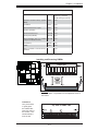
Table of Contents
Preface
About This Manual ...................................................................................................... iii
Manual Organization ................................................................................................... iii
Conventions Used in the Manual .................................................................................. iii
Chapter 1: Introduction
1-1
Overview ......................................................................................................... 1-1
Checklist ................................................................................................... 1-1
Contacting Supermicro ............................................................................. 1-2
X7DA3+ Image ........................................................................... 1-3
X7DA3+ Layout .......................................................................... 1-4
Quick Reference ...................................................................................... 1-5
Motherboard Features ................................................................................ 1-6
Intel 5000X (Greencreek) Chipset: System Block Diagram .................... 1-8
1-2
Chipset Overview ........................................................................................... 1-9
1--3 Special Features ........................................................................................... 1-10
1-4
PC Health Monitoring .................................................................................... 1-10
1-5
ACPI Features .............................................................................................. 1-11
1-6
Power Supply ............................................................................................... 1-12
1-7
Super I/O ........................................................................................................ 1-12
Chapter 2: Installation
2-1
Static-Sensitive Devices ................................................................................. 2-1
Precautions................................................................................................ 2-1
Unpacking ................................................................................................ 2-1
2-2
Motherboard Installation ................................................................................. 2-1
2-3
Processor and Heatsink Installation ............................................................... 2-2
2-4
Installing DIMMs ............................................................................................. 2-6
2-5
Control Panel Connectors and IO Ports ......................................................... 2-8
A. Back Panel Connectors/IO Ports .............................................................. 2-8
B. Front Control Panel ................................................................................... 2-9
C. Front Control Panel Pin Definitions ........................................................ 2-10
NMI Button ............................................................................................. 2-10
Power LED ............................................................................................. 2-10
HDD LED .............................................................................................. 2-11
NIC1/NIC2 LED Indicators ..................................................................... 2-11
Overheat/Fan Fail LED ......................................................................... 2-12
Power Fail LED ........................................................................................ 2-12
iv
Table of Contents
Reset Button ......................................................................................... 2-13
Power Button .......................................................................................... 2-13
2-6
Connectors and Headers ............................................................................... 2-14
ATX Power Connector .......................................................................... 2-14
Processor Power Connector ................................................................. 2-14
Universal Serial Bus (USB) ..................................................................... 2-15
Chassis Intrusion .................................................................................... 2-15
Fan Headers .......................................................................................... 2-16
ATX PS/2 Keyboard and Mouse Ports..................................................... 2-17
Serial Port .............................................................................................. 2-17
Wake-On-Ring .......................................................................................... 2-18
Wake-On-LAN .......................................................................................... 2-18
GLAN 1/2 (Ethernet) Ports ....................................................................... 2-19
Speaker/Power LED Header .................................................................. 2-19
Power Fault .............................................................................................. 2-20
Overheat/Fan Fail LED ............................................................................ 2-20
SMB Connector ........................................................................................ 2-21
Power SMB Connector ............................................................................. 2-21
Compact Flash Card PWR Connector ..................................................... 2-22
SGPIO Headers ....................................................................................... 2-22
High Definition Audio ................................................................................ 2-23
CD Connector........................................................................................... 2-23
2-7
Jumper Settings ............................................................................................ 2-24
Explanation of Jumpers ......................................................................... 2-24
GLAN Enable/Disable ............................................................................ 2-24
CMOS Clear ............................................................................................ 2-25
Watch Dog ................................................................................................ 2-25
3rd PWR Supply PWR Fault .................................................................... 2-26
SAS Controller Enable ............................................................................. 2-26
Compact Flash Master/Slave Enable/Disable .......................................... 2-27
Alarm Reset.............................................................................................. 2-27
SMB to PCI-X/PCI-E Slots ....................................................................... 2-28
2-8
Onboard Indicators ....................................................................................... 2-29
GLAN LEDs .............................................................................................. 2-29
Onboard Power LED ................................................................................ 2-29
Onboard SAS Activity LED Indicators ...................................................... 2-30
2-9
Parallel Port, Floppy, SIMLP IPMI, Hard Disk Drive and SAS Connections
2-31
Parallel Port Connector ........................................................................... 2-31
Floppy Connector .................................................................................... 2-32
v
X7DA3+ User's Manual
SIMLP IPMI Slot ...................................................................................... 2-32
IDE Connectors ........................................................................................ 2-33
SAS Connectors ....................................................................................... 2-34
Chapter 3: Troubleshooting
3-1
Troubleshooting Procedures ........................................................................... 3-1
Before Power On....................................................................................... 3-1
No Power................................................................................................... 3-1
No Video .................................................................................................. 3-1
Losing the System’s Setup Configuration ................................................ 3-2
Memory Errors........................................................................................... 3-2
3-2
Technical Support Procedures ........................................................................ 3-2
3-3
Frequently Asked Questions ........................................................................... 3-3
3-4
Returning Merchandise for Service ................................................................. 3-4
Chapter 4: BIOS
4-1
Introduction ....................................................................................................... 4-1
4-2
Running Setup ................................................................................................. 4-2
4-3
Main BIOS Setup ............................................................................................. 4-2
4-4
Advanced Setup ............................................................................................... 4-6
4-5
Security Setup ............................................................................................... 4-23
4-6
Boot Setup ...................................................................................................... 4-24
4-7
Exit .................................................................................................................. 4-25
Appendices:
Appendix A: BIOS POST Messages .......................................................................... A-1
Appendix B: BIOS POST Codes ................................................................................ B-1
Appendix C: Installing the Adaptec HostRAID Utility and the Windows OS ............C-1
Appendix D: Intel HostRAID and the Windows OS Setup Guidelines ......................D-1
Appendix E: Installing Other Software Programs and Drivers .................................. E-1
vi
Chapter 1: Introduction
Chapter 1
Introduction
1-1
Overview
Checklist
Congratulations on purchasing your computer motherboard from an acknowledged
leader in the industry. Supermicro boards are designed with the utmost attention to
detail to provide you with the highest standards in quality and performance. Check
that the following items have all been included with your motherboard. If anything
listed here is damaged or missing, contact your retailer.
All the items are included in the retail box.
One (1) Supermicro Mainboard
One (1) ribbon cable for IDE devices (CBL-0036L-02)
One (1) floppy ribbon cable (CBL-0022L)
Four (4) SATA cables (CBL-0044L)
Two (2) I-Pass-to-4 SATA Straight Through Cables (CBL-0097L-02)
One (1) I/O backpanel shield (MCP-260-74301-0N)
One (1) Supermicro CD containing drivers and utilities
One (1) User's/BIOS Manual
1-1
X7DA3+ User's Manual
Contacting Supermicro
Headquarters
Address:
Super Micro Computer, Inc.
980 Rock Ave.
San Jose, CA 95131 U.S.A.
Tel:
+1 (408) 503-8000
Fax:
+1 (408) 503-8008
Email:
[email protected] (General Information)
[email protected] (Technical Support)
Web Site:
www.supermicro.com
Europe
Address:
Super Micro Computer B.V.
Het Sterrenbeeld 28, 5215 ML
's-Hertogenbosch, The Netherlands
Tel:
+31 (0) 73-6400390
Fax:
+31 (0) 73-6416525
Email:
[email protected] (General Information)
[email protected] (Technical Support)
[email protected] (Customer Support)
Asia-Pacific
Address:
Super Micro Computer, Inc.
4F, No. 232-1, Liancheng Rd.
Chung-Ho 235, Taipei County
Taiwan, R.O.C.
Tel:
+886-(2) 8226-3990
Fax:
+886-(2) 8226-3991
Web Site:
www.supermicro.com.tw
Technical Support:
Email:
[email protected]
Tel:
886-2-8228-1366, ext.132 or 139
1-2
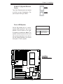
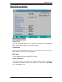
Chapter 1: Introduction
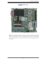
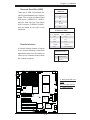
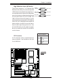
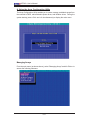
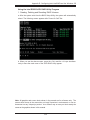
X7DA3+ Image
Note: The drawings and pictures shown in this manual were based on the latest
PCB Revision available at the time of publishing of the manual. The motherboard
you’ve received may or may not look exactly the same as the graphics shown in
the manual.
1-3
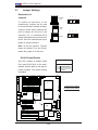
X7DA3+ User's Manual
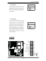
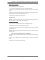
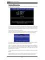
X7DA3+ Motherboard Layout
(not drawn to scale)
PSF
8-pin PWR
JPW3
JF1
Fan2 FP Control Fan1
CPU Fan7 J17
4-Pin
24-Pin ATX PWR
PWR
JPW1 Fan 1 J3P
JAR
JPW2
Fan6 Fan5
KB/
Mouse
DIMM 4B (Bank 4)
USB 0/
1/2/3
DIMM 4A (Bank 4)
COM1
DIMM 3B (Bank 3)
Parrallel
J L APort
N1
DIMM 3A (Bank 3)
CPU1
DIMM 1B (Bank 1)
PW LEDSPK
DIMM 2B (Bank 2)
DIMM 1A (Bank 1)
LE1
JOH1
DIMM 2A (Bank 2)
SUPER ®X7DA3+
LAN1/2
CD1
Greencreek
HD
Audio
Audio
CTRL
CPU2
SGPIO1
North Bridge
SGPIO2
Slot7
JCF1JWF1
PCI-33MHz
South
Bridge
JI2C3 JI2C4
Slot4
IDE1
Fan8
PCI-Exp x16
JBT1
Slot5
Fan3
CPU
Fan2
Battery
Compact Flash
Slot6
Floppy
GLAN
CTLR
SIM LP IPMI
BIOS
PCI-Exp x4
ACT4-7
JWD
ACT0-3
JPS1
SAS
Controller
PXH
PCI-X 133 MHz
JI2C1 JI2C2
JWOR
Slot1
PCI-X 100 MHz ZCR (Green Slot)
SAS4-7
SAS0-3
USB4/5
SMB
JL1
SATA4 SATA5
SATA0 SATA1 SATA2 SATA3 JWOL
JS10
Fan4
Slot2
PCI-X 133 MHz
JPL2
JPL1
Slot3
SAS ACT4-7 LEDs
SAS ACT0-3 LEDs
Notes:
1. Jumpers not indicated are for test purposes only.
2. See Chapter 2 for detailed information on jumpers, I/O ports and JF1 front panel
connections.
3. " " indicates the location of Pin 1.
4. Please install the ZCR card on the green slot for it to work properly.
5. The drawings and pictures shown in this manual were based on the latest
PCB Revision available at the time of publishing of the manual. The motherboard
you’ve received may or may not look exactly the same as the graphics shown in
the manual.
1-4
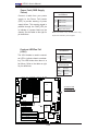
Chapter 1: Introduction
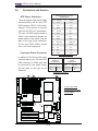
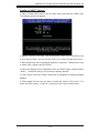
Quick Reference (X7DA3+)
Jumper
J3P
Description
3rd PWR Failure Detect
Off (Disabled)
JAR
Alarm Reset
Off (Disabled)
JBT1
JCF1
CMOS Clear
Compact Card Master/Slave Select
See Chapter 2
On (Master)
JI2C1/JI2C2
SMB to PCI-X Slots
Pins 2-3 (Disabled)
JI2C3/JI2C4
SMB to PCI-E Slots
Pins 2-3 (Disabled)
JPS1
JPL1/ JPL2
JWD
Default Setting
SAS Controller Enable
Pins 1-2 (Enabled)
GLAN1/GLAN2 Enable
Watch Dog
Pins 1-2 (Enabled)
Pins 1-2 (Reset)
Connector
Description
ATX PWR (JPW1)
Primary 24-Pin ATX PWR Connector
Aux. PWR/CPU PWR
+12V 4-pin PWR (JWP2)/+12V 8-pin PWR(JPW3)
HD Audio (JC1)
High Definition Audio Connector (JC1)
Chassis Intrusion (JL1) Chassis Intrusion Header
COM1 (JCOM1)
COM1 Serial Port Connector
Compact PWR (JWF1) Compact Card PWR Connector
DIMM#1A-DIMM#4B
Memory DDRII Fully Buffered DIMM Slots
FAN 1-8
Fans 1-8 (Fan7: CPU Fan1, Fan8: CPU Fan2)
Floppy (J22)
Floppy Disk Drive Connector
FP Control (JF1)
Front Control Panel Connector
GLAN 1/2 (JLAN1)
G-bit Ethernet Ports
IDE1/IDE2(Note 1 Below)IDE1 Hard Drive (JIDE1)/Compact Flash Card (JIDE2)
LE1 LED (Note 2 Below) 5V Standby PWR LED Indicator
OH LED (JOH1)
Overheat LED
Parallel (J21)
Parallel (Printer) Port
PWR LED/SPKR (JD1) PWR LED(pins1-3)/SpeakerHeader (pins 4-7)
PWR SMB (J17)
Power System Management (I2C) Header
PSF
Power Supply Failure (See Chapter 2)
SAS#0-#3,#4-#7(JSM1/2) SAS (Serial Attached SCSI) Connectors #0-#3, #4-#7
SATA#0-#5(JS1-JS6)
Serial ATA Connectors #0-5
SGPIO 1/2(J29,J30)
Serial General Purpose Input/Output Headers
SMB (J18)
System Management Bus Header
Slot 7
SIM Low Profile IPMI Connector
USB 0/1/2/3 (JUSB1)
Back Panel USB 0/1/2/3(JUSB1)
USB 4/5 (JUSB2)
Front Panel USB4/5 (JUSB2)
WOL (JWOL)
Wake-on-LAN Header
WOR (JWOR)
Wake-on-Ring Header
Notes: 1.JIDE2 is for Compact Card Use only. JCF1 is used to configure the compact flash card as a master or a slave drive. Be sure to connect JWF1 to a power
supply to provide power to the compact flash card. 2. When LE1 is on, the Standby
Power is on. Unplug the PWR cables before changing components.
1-5
X7DA3+ User's Manual
Motherboard Features
CPU
•
Dual Intel® 64-bit LGA 771 Quad-Core/Dual-Core Xeon 5300/5100/5000 Series
processors at a front side bus speed of 1.333 GHz/1.066 GHz/667 MHz
Memory
• Eight 240-pin DIMM sockets with support up to 32 GB ECC DDR2 FBD 667/533
Memory (See Section 2-3 in Chapter 2 for DIMM Slot Population.)
Chipset
•
Intel 5000X (Greencreek) chipset, including: the 5000X (Greencreek) Memory
Control Hub (MCH), the Enterprise South Bridge 2 (ESB2), and the I/O subsystem (PXH-V).
Expansion Slots
Two PCI-E slots (one x16 signal on x16 slot, one x4 signal on x16 slot)
Three 64-bit PCI-X slots (two: PCI-X-133 slots, one PCI-X-100 ZCR Slot)
One PCI-33 MHz slot
One Low Profile IPMI slot
BIOS
•
•
8 Mb Phoenix® Flash ROM
DMI 2.1, PCI 2.2, ACPI 1.0, Plug and Play (PnP), SMBIOS 2.3, PCI-X 1.0
PC Health Monitoring
•
•
Onboard voltage monitors for CPU cores, chipset voltage, 1.8V, 3.3V, +5V,
12V, 12V, 3.3V standby and 5V standby
Fan status monitor with firmware speed control
•
•
•
•
•
•
•
•
•
CPU/chassis temperature monitors
Platform Environment Control Interface (PECI)
CPU slow-down on temperature overheat
CPU thermal trip support for processor protection
Power-up mode control for recovery from AC power loss
Auto-switching voltage regulator for CPU core
System overheat LED and control
Chassis intrusion detection
System resource alert
ACPI Features
•
•
Slow blinking LED for suspend state indicator
Main switch override mechanism
1-6
Chapter 1: Introduction
Onboard I/O
•
Adaptec AIC-9410W SAS Controller w/HostRAID support (RAID 0, 1,10)
•
Intel ESB-2 South Bridge supports 6 SATA connectors (w/RAID 0, 1, 5,10) (For
the Windows OS only)
•
•
One SIM Low Profile IPMI slot
Intel 82563EB Gigabit Dual-Port Ethernet controller
•
1 EIDE Ultra DMA/100 bus master interfaces w/2 devices supported
•
1 floppy port interface
•
1 serial port
•
1 EPP/ECP Parallel Port
•
7.1+2 Channel High Definition Audio Connection
•
•
•
•
Super I/O: Winbond W83627HG w/Hardware Monitor support: W83793G
PS/2 mouse and PS/2 keyboard ports
Up to 6 USB 2.0 (Universal Serial Bus) (4 ports, 2 Headers)
Super I/O
Other
•
•
External modem ring-on
Wake-on-LAN (WOL)
•
Wake-on-Ring (WOR)
•
Console redirection
•
Onboard Fan Speed Control by Thermal Management via BIOS
CD/Diskette Utilities
•
BIOS flash upgrade utility and device drivers
Dimensions
•
Ext. ATX 12.08" x 13.05" (306.8 mm x 331.5 mm)
1-7
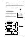
X7DA3+ User's Manual
667/1067/
1333 MHz
FBD
CHNL0
J14
#3
PCI-X SLOT
PCI-X SLOT
J13
#2
PXH-V
Port
#6,7
FBD
CHNL2
FBD
CHNL3
Port
#3
Port
#4
2A
Port
#0
Port
#3
ATA100
IDE
CONN
EXP.
BUS
PCI-EXP X8
3A
4B
4A
PCIE X4
PCI-EXP X4
1A
3B
FBD
CHNL1
MCH
5000X
Port
#2
2B
FBD DIMM
PCI-EXP X8
1B
FBD DIMM
PCI-EXP X8
PCIE X4
PCI-EXP_X4_in_X16_SLOT
J9
#4
PCI-EX_X16_SLOT
J5
#6
FBD DIMM
667/1067/
1333 MHz
Port
#4,5
VRM
PROCESSOR#1
PROCESSOR#2
FBD DIMM
VRM
Port
#1,2
EBUS
CONN
#5
#4
#3
#2
#1
#0
ESB2
SAS
9410
PCI-X 133
J6
SIMLP-IPMI
CONN
#5
#4
#3
#2
#1
#0
PCI 32/
33MMZ
#5
USB 2.0
PCI32_SLOT
FRONT
PANEL
SATA
3.0 Gb/S
USB
PCI-X SLOT
zcr
J12
#1
LPC
RJ45
GB LAN
GILGAL
HD Audio
SIO
W83627
FWH
EHF
PARALLEL
PORT
FDD
RJ45
MS
KB
COM1
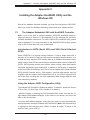
Block Diagram of the 5000X (Greencreek) Chipset
Note: This is a general block diagram. Please see the previous Motherboard Features
pages for details on the features of each motherboard.
1-8
Chapter 1: Introduction
1-2
Chipset Overview
Built upon the functionality and the capability of the 5000X (Greencreek) chipset,
the X7DA3+ motherboard provides the performance and feature set required for
dual processor-based workstations with configuration options optimized for communications, presentation, storage, computation or database applications. The
5000X (Greencreek) chipset supports single or dual Xeon 64-bit dual core processor
with front side bus speeds of up to 1.333 GHz. The chipset consists of the 5000X
(Greencreek) Memory Controller Hub (MCH), the Enterprise South Bridge 2 (ESB2),
and the I/O subsystem (PXH-V).
The 5000X (Greencreek) MCH chipset is designed for symmetric multiprocessing
across two independent front side bus interfaces. Each front side bus uses a 64-bit
wide, 1.333 GHz data bus that transfers data at 10.7 GB/sec. The MCH chipset connects up to 8 Fully Buffered DIMM modules, providing a total of 32.0 GB/s for DDR2
667/533 memory. The MCH chipset also provides one x8 PCI-Express and one x4
ESI interface to the ESB2. In addition, the 5000X (Greencreek) chipset offers a wide
range of RAS features, including memory interface ECC, x4/x8 Single Device Data
Correction, CRC, parity protection, memory mirroring and memory sparing.
Xeon Dual Core Processor Features
Designed to be used with conjunction of the 5000X (Greencreek) chipset, the Xeon
Dual Core Processors provide a feature set as follows:
The Xeon Dual Core Processors
L1 Cache Size: Instruction Cache (32KB/16KB), Data Cache (32KB/24KB)
L2 Cache Size: 2MB (per core)
Data Bus Transfer Rate: 8.5 GB/s
Package: FC-LGA6/FC-LGA4, 771 Lands
1-9
X7DA3+ User's Manual
1-3
Special Features
Recovery from AC Power Loss
BIOS provides a setting for you to determine how the system will respond when
AC power is lost and then restored to the system. You can choose for the system
to remain powered off (in which case you must hit the power switch to turn it back
on) or for it to automatically return to a power- on state. See the Power Lost Control
setting in the Advanced BIOS Setup section (Boot Features) to change this setting.
The default setting is Last State.
1-4
PC Health Monitoring
This section describes the PC health monitoring features of the X7DA3+. All have
an onboard System Hardware Monitor chip that supports PC health monitoring.
Onboard Voltage Monitoring
An onboard voltage monitor will scan these voltages continuously: CPU Cores,
Chipset Voltage, +3.3V, +5V, +12V, -12V, +3.3V Standby, +5V Standby and Vbat.
Once a voltage becomes unstable, a warning is given or an error message is sent
to the screen. Users can adjust the voltage thresholds to define the sensitivity of
the voltage monitor.
Fan Status Monitor with Firmware Control
The PC health monitor can check the RPM status of the cooling fans. The onboard
CPU and chassis fans are controlled by Thermal Management via BIOS (under
Hardware Monitoring in the Advanced Setting).
Environmental Temperature Control
The thermal control sensor monitors the CPU temperature in real time and will turn
on the thermal control fan whenever the CPU temperature exceeds a user-defined
threshold. The overheat circuitry runs independently from the CPU. Once it detects
that the CPU temperature is too high, it will automatically turn on the thermal fan
control to prevent any overheat damage to the CPU. The onboard chassis thermal
circuitry can monitor the overall system temperature and alert users when the chassis temperature is too high.
CPU Fan Auto-Off in Sleep Mode
The CPU fan activates when the power is turned on. It continues to operate when
the system enters Standby mode. When in sleep mode, the CPU will not run at full
power, thereby generating less heat.
1-10
Chapter 1: Introduction
System Resource Alert
This feature is available when used with Supero Doctor III in the Windows OS
environment or used with Supero Doctor II in Linux. Supero Doctor is used to
notify the user of certain system events. For example, if the system is running low
on virtual memory and there is insufficient hard drive space for saving the data,
you can be alerted of the potential problem. You can also configure Supero Doctor
to provide you with warnings when the system temperature goes beyond a predefined range.
1-5
ACPI Features
ACPI stands for Advanced Configuration and Power Interface. The ACPI specification defines a flexible and abstract hardware interface that provides a standard
way to integrate power management features throughout a PC system, including
its hardware, operating system and application software. This enables the system
to automatically turn on and off peripherals such as CD-ROMs, network cards, hard
disk drives and printers. This also includes consumer devices connected to the PC
such as VCRs, TVs, telephones and stereos.
In addition to enabling operating system-directed power management, ACPI
provides a generic system event mechanism for Plug and Play and an operating
system-independent interface for configuration control. ACPI leverages the Plug
and Play BIOS data structures while providing a processor architecture-independent
implementation that is compatible with Windows 2000, Windows XP and Windows
2003 Server.
Slow Blinking LED for Suspend-State Indicator
When the CPU goes into a suspend state, the chassis power LED will start blinking
to indicate that the CPU is in suspend mode. When the user presses any key, the
CPU will wake-up and the LED will automatically stop blinking and remain on.
Main Switch Override Mechanism
When an ATX power supply is used, the power button can function as a system suspend button to make the system enter a SoftOff state. The monitor will be suspended
and the hard drive will spin down. Pressing the power button again will "wake-up"
the system. During the SoftOff state, the ATX power supply provides power to keep
the required circuitry in the system "alive." In case the system malfunctions and you
want to turn off the power, just press and hold the power button for 4 seconds. This
option can be set in the Power section of the BIOS Setup routine.
1-11
X7DA3+ User's Manual
External Wake-On-LAN
Wake-On-LAN is defined as the ability of a management application to remotely
power up a computer that is powered off. Remote PC setup, up-dates and asset
tracking can occur after hours and on weekends so that daily LAN traffic is kept
to a minimum and users are not interrupted. The motherboard has a 3-pin header
(WOL) to connect to the 3-pin header on a Network Interface Card (NIC) that has
WOL capability. In addition, an onboard LAN controller can also support WOL
without any connection to the WOL header. The 3-pin WOL header is to be used
with a LAN add-on card only.
Note: Wake-On-LAN requires an ATX 2.01 (or above) compliant power supply.
1-6
Power Supply
As with all computer products, a stable power source is necessary for proper and
reliable operation. It is even more important for processors that have high CPU
clock rates.
The X7DA3+ can only accommodate 24-pin ATX power supply. Although most power
supplies generally meet the specifications required by the motherboard, some are
inadequate. You should use one that will supply at least 400W of power. In addition,
the 12V 8-pin and the 4-pin are also required for adequate power supply to the
system. Also your power supply must supply 1.5A for the Ethernet ports.
It is strongly recommended that you use a high quality power supply that meets ATX
power supply Specification 2.01 or above. It must also be SSI compliant (For more
information, please refer to the website at http://www.ssiforum.org/). Additionally, in
areas where noisy power transmission is present, you may choose to install a line
filter to shield the computer from noise. It is recommended that you also install a
power surge protector to help avoid problems caused by power surges.
1-7
Super I/O
The disk drive adapter functions of the Super I/O chip include a floppy disk drive
controller that is compatible with industry standard 82077/765, a data separator,
write pre-compensation circuitry, decode logic, data rate selection, a clock generator,
drive interface control logic and interrupt and DMA logic. The wide range of functions
integrated onto the Super I/O greatly reduces the number of components required
for interfacing with floppy disk drives. The Super I/O supports 360 K, 720 K, 1.2
M, 1.44 M or 2.88 M disk drives and data transfer rates of 250 Kb/s, 500 Kb/s or
1 Mb/s. It also provides two high-speed, 16550 compatible serial communication
ports (UARTs). Each UART includes a 16-byte send/receive FIFO, a programmable
baud rate generator, complete modem control capability and a processor interrupt
system. Both UARTs provide legacy speed with baud rate of up to 115.2 Kbps as
1-12
Chapter 1: Introduction
well as an advanced speed with baud rates of 250 K, 500 K, or 1 Mb/s, which support higher speed modems.
The Super I/O supports one PC-compatible printer port (SPP), Bi-directional Printer
Port (BPP), Enhanced Parallel Port (EPP) or Extended Capabilities Port (ECP).
The Super I/O provides functions that comply with ACPI (Advanced Configuration
and Power Interface), which includes support of legacy and ACPI power management through an SMI or SCI function pin. It also features auto power management
to reduce power consumption.
1-13
X7DA3+ User's Manual
Notes
1-14
Chapter 2: Installation
Chapter 2
Installation
2-1
Static-Sensitive Devices
ElectroStatic-Discharge (ESD) can damage electronic components. To prevent damage to your system board, it is important to handle it very carefully. The following
measures are generally sufficient to protect your equipment from ESD.
Precautions
•
Use a grounded wrist strap designed to prevent static discharge.
•
Touch a grounded metal object before removing the board from the antistatic
bag.
•
Handle the board by its edges only; do not touch its components, peripheral
chips, memory modules or gold contacts.
•
When handling chips or modules, avoid touching their pins.
•
Put the motherboard and peripherals back into their antistatic bags when not in
use.
•
For grounding purposes, make sure your computer chassis provides excellent
conductivity between the power supply, the case, the mounting fasteners and
the motherboard.
Unpacking
The motherboard is shipped in antistatic packaging to avoid static damage. When
unpacking the board, make sure the person handling it is static protected.
2-2
Motherboard Installation
(Note: Be sure to mount the motherboard into the chassis before you
install the CPU onto the motherboard.)
All motherboards have standard mounting holes to fit different types of chassis.
Make sure that the locations of all the mounting holes for both motherboard and
chassis match. Make sure that the metal standoffs click in or are screwed in
tightly. Then, use a screwdriver to secure the motherboard onto the motherboard
tray. (Note: some components are very close to the mounting holes. Please
take precautionary measures to prevent damage done to these components
when you install the motherboard into the chassis.)
2-1
X7DA3+ User's Manual
2-3
Processor and Heatsink Installation
!
When handling the processor package, avoid placing
direct pressure on the label area of the fan.
Notes: 1. Always connect the power cord last and always remove it before adding,
removing or changing any hardware components. Make sure that you install the
processor into the CPU socket before you install the CPU heatsink.
2. Intel's boxed Xeon CPU package contains the CPU fan and heatsink assembly.
If you buy a CPU separately, make sure that you use only Intel-certified multi-directional heatsink and fan.
3. The Intel Xeon LGA 771 heatsink and fan comes with a push-pin design and no
tool is needed for installation.
4. Make sure to install the motherboard into the chassis before you install the CPU
heatsink and fan.
5. When purchasing an LGA 771 CPU or when receiving a motherboard with an LGA
771 CPU pre-installed, make sure that the CPU plastic cap is in place and none of
the CPU pins are bent; otherwise, contact the retailer immediately.
6. Refer to the MB Features Section for more details on CPU support.
Installing the LGA771 Processor
Load Lever
1. Press the load lever to release
the load plate, which covers the CPU
socket, from its locking position.
PnP Cap on
top of the
Load Plate
2. Gently lift the load lever to open the
load plate.
Load Plate
(with PnP Cap
attached)
2-2
Chapter 2: Installation
North Center Edge
3. Use your thumb and your index
finger to hold the CPU at the North
Center Edge and the South Center
Edge of the CPU.
4. Align CPU Pin1 (the CPU corner
marked with a triangle) against the
socket corner that is marked with a
triangle cutout.
South Center Edge
gold dot
5. Align the CPU key that is the semi-
Socket Key
circle cutout below a gold dot against
the socket key, the Notch on the
(Socket Notch)
same side of the triangle cutout on
the socket.
CPU Key (semicircle cutout) below the circle.
6. Once aligned, carefully lower the
CPU straight down to the socket.
(Do not drop the CPU on the socket.
Do not move the CPU horizontally or
vertically. Do not rub the CPU against
the surface or against any pins of the
socket to avoid damage to the CPU
or the socket.)
7. With the CPU inside the socket,
inspect the four corners of the CPU
to make sure that the CPU is properly
installed.
Corner with a
triangle cutout
Load Lever
CPU in the CPU socket
8. Use your thumb to gently push the
load lever down to the lever lock.
9. If the CPU is properly installed into
the socket, the plastic PnP cap will be
automatically released from the load
plate when the load lever is pushed
in the lever lock. Remove the PnP cap
from the motherboard.
(Warning: Please save the plastic PnP cap. The motherboard must
be shipped with the PnP cap properly
installed to protect the CPU socket
pins. Shipment without the PnP cap
properly installed will cause damage
to the socket pins.)
!
2-3
CPU Pin1
Plastic cap
is released
from the
load plate
if CPU
properly
installed.
X7DA3+ User's Manual
Installing the Heatsink
CEK Heatsink Installation
CEK Passive Heatsink
1. Do not apply any thermal grease to
the heatsink or the CPU die-the required
amount has already been applied.
2. Place the heatsink on top of the CPU so
that the four mounting holes are aligned with
those on the retention mechanism.
Screw#1
3. Screw in two diagonal screws (ie the #1
and the #2 screws) until just snug (-do not
fully tighten the screws to avoid possible
damage to the CPU.)
Screw#2
Screw#1
4. Finish the installation by fully tightening
all four screws.
Screw#2
2-4
Chapter 2: Installation
Removing the Heatsink
(Warning: We do not recommend
!
that the CPU or the heatsink be
removed. However, if you do need
to remove the heatsink, please
follow the instructions below to
uninstall the heatsink to prevent
damage done to the CPU or the
CPU socket.)
1. Unscrew and remove the heatsink screws
from the motherboard in the sequence as
shown in the picture on the right.
2. Hold the heatsink as shown in the picture
on the right and gently wriggle the heatsink to
loosen it from the CPU. (Do not use excessive
force when wriggling the heatsink!!)
3. Once the CPU is loosened, remove the
heatsink from the CPU socket.
4. Clean the surface of the CPU and the
heatsink to get rid of the old thermal grease.
Reapply the proper amount of thermal grease
on the surface before you re-install the CPU
and the heatsink.
2-5
X7DA3+ User's Manual
2-4
Installing DIMMs
Note: Check the Supermicro web site for recommended memory modules.
CAUTION
Exercise extreme care when installing or removing DIMM
modules to prevent any possible damage. Also note that the
memory is interleaved to improve performance (See step 1).
DIMM Installation
1. Insert the desired number of DIMMs into the memory slots, starting with Bank
1. (For optimal memory performance, please install four modules at a time.
Please refer to the table below.)
2. Insert each DIMM module vertically into its slot. Pay attention to the notch along
the bottom of the module to prevent inserting the DIMM module incorrectly.
3. Gently press down on the DIMM module until it snaps into place in the slot.
Repeat for all modules (see step 1 above).
Memory Support
The X7DA3+ supports up to 32 GB fully buffered (FBD) ECC DDR2 533/667 in 8
DIMMs. Populating DIMM modules with a pair (or pairs) of memory modules that
are of the same size and of the same type in Bank1, Bank2, Bank3 and Bank4 will
result in interleaving memory.
Note 1: Due to the OS limitations, some operating systems may not show more
than 4 GB of memory.
Optimized DIMM Population Configurations
Branch0
Branch1
Number of
DIMMs
2 DIMMs
4 DIMMs
6 DIMMs
8 DIMMs
Bank 1
(Channel 0)
1A
1A
1A
1A
----------1B
1B
Bank 2
(Channel 1)
2A
2A
2A
2A
----------2B
2B
Bank 3
(Channel 2)
-----3A
3A
3A
---------------3B
Bank 4
(Channel 3)
-----4A
4A
4A
---------------4B
(*Notes: i. DIMM slot# specified: DIMM slot to be populated; “---“: DIMM slot not to
be populated. ii. Both FBD 533 MHz and 667MHz DIMMs are supported; however,
you need to use the memory modules of the same speed and of the same type on a
motherboard. iii. Interleaved memory is supported when pairs of DIMM modules are
installed. To optimize memory performance, please install pairs of DIMMs in both
Branch 0 and Branch 1. iv. For memory to work properly, you need to follow the
restrictions listed above. )
Note 2: Due to memory allocation to system devices, memory remaining available
for operational use will be reduced when 4 GB of RAM is used. The reduction in
memory availability is disproportional. (Refer to the following Memory Availability
Table for details.)
2-6
Chapter 2: Installation
Possible System Memory Allocation & Availability
System Device
Size
Physical
Memory
Remaining (-Available)
(4 GB Total System Memory)
Firmware Hub flash memory (System
BIOS)
1 MB
3.99
Local APIC
4 KB
3.99
Area Reserved for the chipset
2 MB
3.99
I/O APIC (4 Kbytes)
4 KB
3.99
PCI Enumeration Area 1
256 MB
3.76
PCI Express (256 MB)
256 MB
3.51
PCI Enumeration Area 2 (if needed)
-Aligned on 256-MB boundary-
512 MB
3.01
VGA Memory
16 MB
2.85
TSEG
1 MB
2.84
Memory available to OS and other applications
2.84
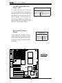
Installing and Removing DIMMs
JLAN1
DDR2
FBD
DIMM
DDR2
FBD
SUPER ®X7DA3+
To Install: Insert module vertically and press down until it
snaps into place. Pay attention to the alignment notch at
the bottom.
To Remove:
Use your thumbs
to gently push
the release tabs
near both ends of
the module. This
should release it
from the slot.
Top
View
of DDR2
FBD Slot
Top
View
of DDR2
FBD
2-7
X7DA3+ User's Manual
2-5
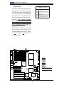
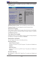
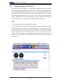
Control Panel Connectors/IO Ports
The I/O ports are color coded in conformance with the PC 99 specification. See
Figure 2-3 below for the colors and locations of the various I/O ports.
Back Panel Connectors/IO Ports
JLAN1
6
SUPER
®
5
X7DA3+
1
13 16
8
2
10
4
3
7
Back Panel I/O Port Locations and Definitions
Back Panel Connectors
1. Keyboard (Purple)
2. PS/2 Mouse (Green)
3. Back Panel USB Port 0
4. Back Panel USB Port 1
5. Back Panel USB Port 2
6. Back Panel USB Port 3
7. COM Port 1 (Turquoise)
8. Parallel Port (Printer)
9. Gigabit LAN 2
10. Gigabit LAN 1
11. Side_Surround (Grey)
12. Back_Surround (Black)
13. CEN/LFE (Orange)
14. Microphone-In (Pink)
15. Front (Green)
16. Line-In (Blue)
(See Section 2-5 for details.)
2-8
9
12 15
11 14
Chapter 2: Installation
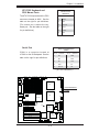
Front Control Panel
JF1 contains header pins for various buttons and indicators that are normally located on a control panel at the front of the chassis. These connectors are designed
specifically for use with Supermicro server chassis. See the figure below for the
descriptions of the various control panel buttons and LED indicators. Refer to the
following section for descriptions and pin definitions.
JF1 Header Pins
20
19
JLAN1
Ground
NMI
X
SUPER
®
X
X7DA3+
Power LED
Vcc
HDD LED
Vcc
NIC1 LED
Vcc
NIC2 LED
Vcc
OH/Fan Fail LED
Vcc
PWR Fail LED
Vcc
Ground
Reset
Reset Button
Ground
PWR
Power Button
2
2-9
1
X7DA3+ User's Manual
Front Control Panel Pin Definitions
NMI Button
The non-maskable interrupt button
NMI Button
Pin Definitions (JF1)
header is located on pins 19 and 20
Pin#
Definition
of JF1. Refer to the table on the right
for pin definitions.
19
Control
20
Ground
Power LED
The Power LED connection is located
on pins 15 and 16 of JF1. Refer to the
table on the right for pin definitions.
Power LED
Pin Definitions (JF1)
Pin#
Definition
15
+5V
16
Ground
A. NMI
B. PWR LED
20
19
Ground
NMI
JLAN1
X
SUPER ®X7DA3+
X
B Power LED
Vcc
HDD LED
Vcc
NIC1 LED
Vcc
NIC2 LED
Vcc
OH/Fan Fail LED
Vcc
PWR Fail LED
Vcc
Ground
Ground
2
2-10
A
1
Reset
Reset Button
PWR
Power Button
Chapter 2: Installation
HDD LED
HDD LED
Pin Definitions (JF1)
The HDD LED connection is located
on pins 13 and 14 of JF1. Attach the
hard drive LED cable here to display
disk activity (for any hard drives on the
Pin#
Definition
13
+5V
14
HD Active
system, including SAS, Serial ATA and
IDE). See the table on the right for pin
definitions.
NIC1/NIC2 LED Indicators
GLAN1/2 LED
Pin Definitions (JF1)
The NIC (Network Interface Controller) LED connection for GLAN port1 is
located on pins 11 and 12 of JF1 and
the LED connection for GLAN Port2
is on Pins 9 and 10. Attach the NIC
LED cables to display network activity.
Refer to the table on the right for pin
definitions.
Pin#
Definition
9/11
Vcc
10/12
Ground
A. HDD LED
B. NIC1 LED
C. NIC2 LED
20
19
Ground
NMI
JLAN1
X
X
Vcc
Power LED
SUPER X7DA3+
®
HDD LED
Vcc
B NIC1 LED
Vcc
C
Vcc
A
NIC2 LED
OH/Fan Fail LED
Vcc
PWR Fail LED
Vcc
Ground
Reset
Reset Button
Ground
PWR
Power Button
2
2-11
1
X7DA3+ User's Manual
Overheat/Fan Fail LED (OH)
OH/Fan Fail LED
Pin Definitions (JF1)
Connect an LED to the OH/Fan Fail
connection on pins 7 and 8 of JF1 to
Pin#
Definition
7
Vcc
provide advanced warning of chassis
overheating or fan failure. Refer to the
8
Ground
table on the right for pin definitions.
OH/Fan Fail Indicator
Status
State
Power Fail LED
Definition
Off
Normal
On
Overheat
Flashing
Fan Fail
PWR Fail LED
Pin Definitions (JF1)
The Power Fail LED connection is
located on pins 5 and 6 of JF1. Refer
to the table on the right for pin definitions.
Pin#
Definition
5
Vcc
6
Ground
A. OH/Fan Fail LED
B. PWR Supply Fail
20
19
Ground
NMI
JLAN1
X
SUPER X7DA3+
X
Power LED
Vcc
HDD LED
Vcc
NIC1 LED
Vcc
NIC2 LED
Vcc
®
OH/Fan Fail LED
Vcc
PWR Fail LED
Vcc
A
B
Ground
Ground
2
2-12
1
Reset
Reset Button
PWR
Power Button
Chapter 2: Installation
Reset Button
Reset Button
Pin Definitions (JF1)
The Reset Button connection is located
on pins 3 and 4 of JF1. Attach it to the
hardware reset switch on the computer
case. Refer to the table on the right for
Pin#
Definition
3
Reset
4
Ground
pin definitions.
Power Button
The Power Button connection is located
on pins 1 and 2 of JF1. Momentarily
contacting both pins will power on/off
the system. This button can also be configured to function as a suspend button
(with a setting in BIOS - See Chapter 4.)
To turn off the power when set to suspend
mode, press the button for at least 4
seconds. Refer to the table on the right
for pin definitions.
Power Button
Pin Definitions (JF1)
Pin#
Definition
1
Signal
2
+3V Standby
A. Reset Button
B. PWR Button
20
19
Ground
NMI
JLAN1
X
SUPER ®X7DA3+
X
Power LED
Vcc
HDD LED
Vcc
NIC1 LED
Vcc
NIC2 LED
Vcc
OH/Fan Fail LED
Vcc
PWR Fail LED
Vcc
Ground
Reset
Reset Button
Ground
PWR
Power Button
A
2
2-13
1
B
X7DA3+ User's Manual
2-6
Connectors and Headers
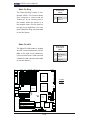
ATX Power 24-pin Connector
Pin Definitions
ATX Power Connector
There are a 24-pin main power supply
Pin#
Definition
connector(JPW1) and an 8-pin CPU
13
+3.3V
1
+3.3V
PWR connector (JPW3) on the motherboard. These power connectors
14
-12V
2
+3.3V
15
COM
3
COM
meet the SSI EPS 12V specification.
16
PS_ON
4
+5V
The 4-pin 12V PWR supply located at
17
COM
5
COM
JPW2 is also required to provide adequate power to the system. See the
table on the right for pin definitions.
For the 8-pin PWR (JPW3), please
refer to the item listed below.
18
COM
6
+5V
19
COM
7
COM
20
Res (NC)
8
PWR_OK
21
+5V
9
5VSB
22
+5V
10
+12V
23
+5V
11
+12V
24
COM
12
+3.3V
Processor Power Connector
In addition to the Primary ATX power
connector (above), the 12V 8-pin CPU
PWR connector at JPW3 must also
be connected to your power supply.
See the table on the right for pin
definitions.
Pin #
Definition
Required Connection
12V 4-pin Power
Connector
Pin Definitions
Pins
Definition
12V 8-pin Power Connector
Pin Definitions
Pins
Definition
1 and 2
Ground
1 through 4
Ground
3 and 4
+12V
5 through 8
+12V
Required Connection
KB/
Mouse
A
B
PSF
8-pin PWR
JPW3
JF1
Fan2 FP Control Fan1
C
CPU Fan7 J17
4-Pin
24-Pin ATX PWR
PWR
JPW1 Fan 1 J3P
JAR
JPW2
Fan6 Fan5
DIMM 4B (Bank 4)
USB 0/
1/2/3
DIMM 4A (Bank 4)
DIMM 3B (Bank 3)
COM1
Parrallel
J L APort
N1
DIMM 3A (Bank 3)
CPU1
DIMM 1B (Bank 1)
PW LEDSPK
DIMM 2B (Bank 2)
DIMM 1A (Bank 1)
LE1
SUPER ®X7DA3+
LAN1/2
CD1
Greencreek
HD
Audio
Audio
CTRL
CPU2
SGPIO1
North Bridge
SGPIO2
Slot7
PCI-33MHz
South
Bridge
2
2
JI C3 JI C4
Slot4
IDE1
Compact Flash
JCF1JWF1
JBT1
Slot5
Fan3
CPU
Fan2
Battery
PCI-Exp x16
Floppy
Slot6
Fan8
SIM LP IPMI
BIOS
PCI-Exp x4
ACT4-7
JWD
ACT0-3
JPS1
SAS
Controller
PXH
PCI-X 133 MHz
JI2C1 JI2C2
JWOR
Slot1
PCI-X 100 MHz ZCR (Green Slot)
SAS4-7
SAS0-3
USB4/5
SMB
JL1
SATA4 SATA5
SATA0 SATA1 SATA2 SATA3 JWOL
2-14
JS10
Fan4
Slot2
PCI-X 133 MHz
JPL2
Slot3
JPL1
GLAN
CTLR
A. 24-pin ATX PWR
B. 8-pin Processor PWR
JOH1
DIMM 2A (Bank 2)
C. 4-pin PWR
Chapter 2: Installation
Universal Serial Bus (USB)
Back Panel USB
(USB0/1/2/3)
There are six USB 2.0 (Universal Serial Bus) ports/headers on the motherboard. Four of them are Back Panel
USB ports (USB#0/1/2/3: JUSB1),
and the other two are Front Panel
USB headers (USB#4/5:JUSB2).
See the tables on the right for pin
Pin#
Definitions
1
+5V
2
PO-
3
PO+
4
Ground
5
N/A
Front Panel USB
Pin Definitions (USB4)
definitions.
USB4
Pin #
Definition
Chassis Intrusion
1
+5V
1
+5V
2
PO-
2
PO-
3
PO+
3
PO+
4
Ground
4
Ground
5
Key
5
No connection
A Chassis Intrusion header is located
at JL1 on the motherboard. Attach the
appropriate cable from the chassis to
inform you of a chassis intrusion when
the chassis is opened.
Chassis Intrusion
Pin Definitions (JL1)
PSF
DIMM 4A (Bank 4)
DIMM 3B (Bank 3)
COM1
DIMM 3A (Bank 3)
Parrallel
J L APort
N1
Definition
1
Intrusion Input
2
Ground
8-pin PWR
JPW3
DIMM 4B (Bank 4)
A
Pin#
JF1
Fan2 FP Control Fan1
USB 0/
1/2/3
CPU Fan7 J17
4-Pin
24-Pin ATX PWR
PWR
JPW1 Fan 1 J3P
JAR
JPW2
Fan6 Fan5
KB/
Mouse
CPU1
DIMM 1B (Bank 1)
PW LEDSPK
DIMM 2B (Bank 2)
DIMM 1A (Bank 1)
LE1
SUPER ®X7DA3+
CD1
Greencreek
HD
Audio
Audio
CTRL
North Bridge
SGPIO2
PCI-33MHz
South
Bridge
2
2
JI C3 JI C4
Slot4
IDE1
Compact Flash
JCF1JWF1
JBT1
Slot5
Fan3
CPU
Fan2
Battery
PCI-Exp x16
Floppy
Slot6
Fan8
SIM LP IPMI
BIOS
PCI-Exp x4
ACT4-7
JWD
ACT0-3
JPS1
SAS
Controller
PXH
PCI-X 133 MHz
B
JI2C1 JI2C2
JWOR
Slot1
PCI-X 100 MHz ZCR (Green Slot)
SAS4-7
SAS0-3
USB4/5
C
JL1
SMB
SATA4 SATA5
SATA0 SATA1 SATA2 SATA3 JWOL
2-15
JS10
Fan4
Slot2
PCI-X 133 MHz
JPL2
Slot3
JPL1
GLAN
CTLR
B. Front Panel USB 4/5
C. Chassis Intrusion
CPU2
SGPIO1
Slot7
A. Back panel USB Ports
01/2/3
JOH1
DIMM 2A (Bank 2)
LAN1/2
USB5
Pin #
Definition
X7DA3+ User's Manual
Fan Headers
Fan Header
Pin Definitions (Fan1-8)
The X7DA3+ has eight chassis/system
Pin#
fan headers (Fan1 to Fan8), including
two CPU Fans (Fans 7/8). (Note: Pins
1-3 of 4-pin fan headers are backward
compatible with the traditional 3-pin
fans). See the table on the right for pin
Definition
1
Ground
2
+12V
3
Tachometer
4
Pulse Width Modulation
definitions. (The onboard fan speeds
are controlled by Thermal Management via BIOS Hardware Monitor
in the Advanced Setting. Note: The
Manufacturer Default is set to Disabled to allow the fans to constantly
run at the full speed. When using
Thermal Management setting, please
use all 3-pin fans or all 4-pin fans on
the motherboard.)
G
E
CPU Fan7 J17
4-Pin
24-Pin ATX PWR
PWR
JPW1 Fan 1 J3P
JAR
JPW2
Fan6 Fan5
KB/
Mouse
PSF
8-pin PWR
JPW3
A
JF1
Fan2 FP Control Fan1
F
DIMM 4B (Bank 4)
USB 0/
1/2/3
DIMM 4A (Bank 4)
DIMM 3B (Bank 3)
COM1
B
Parrallel
J L APort
N1
DIMM 3A (Bank 3)
CPU1
DIMM 1B (Bank 1)
PW LEDSPK
DIMM 2B (Bank 2)
DIMM 1A (Bank 1)
LE1
SUPER X7DA3+
®
LAN1/2
A. Fan 1
B. Fan 2
JOH1
DIMM 2A (Bank 2)
C. Fan 3
CD1
Greencreek
Audio
CTRL
D. Fan 4
SGPIO2
E. Fan 5
HC
PCI-33MHz
South
Bridge
JI2C3 JI2C4
Slot4
IDE1
JCF1JWF1
Floppy
PCI-Exp x16
JBT1
Slot5
F. Fan 6
Compact Flash
Battery
Fan3
CPU
Fan2
SIM LP IPMI
Slot6
Fan8
Slot7
BIOS
PCI-Exp x4
ACT4-7
JWD
Slot2
PCI-X 133 MHz
ACT0-3
JPS1
SAS
Controller
PXH
PCI-X 133 MHz
JI2C1 JI2C2
JWOR
Slot1
PCI-X 100 MHz ZCR (Green Slot)
SAS4-7
SAS0-3
D
USB4/5
SMB
JL1
SATA4 SATA5
SATA0 SATA1 SATA2 SATA3 JWOL
2-16
JS10
Fan4
Slot3
JPL1
GLAN
CTLR
SGPIO1
CPU2
North Bridge
JPL2
HD
Audio
G. Fan 7 (CPU Fan 1)
H. Fan 8 (CPU Fan 2)
Chapter 2: Installation
ATX PS/2 Keyboard and
PS/2 Mouse Ports
PS/2 Keyboard and
Mouse Port Pin
Definitions
The ATX PS/2 keyboard and the PS/2
Pin#
Definition
mouse are located at JKM1. See the
1
Data
table on the right for pin definitions.
(The mouse port is above the key-
2
NC
3
Ground
board port. See the table on the right
4
VCC
for pin definitions.)
5
Clock
6
NC
Serial Port
Serial Port Pin Definitions
(COM1)
COM1 is a connector located at
JCOM1 on the IO Backpanel. See the
table on the right for pin definitions.
Pin #
Definition
Pin #
Definition
1
CD
6
DSR
2
RD
7
RTS
3
TD
8
CTS
4
DTR
9
RI
5
Ground
10
NC
( NC: No Connection.)
PSF
8-pin PWR
JPW3
DIMM 4B (Bank 4)
USB 0/
1/2/3
COM1
CPU Fan7 J17
4-Pin
24-Pin ATX PWR
PWR
JPW1 Fan 1 J3P
JAR
JPW2
Fan6 Fan5
A
JF1
Fan2 FP Control Fan1
KB/
Mouse
DIMM 4A (Bank 4)
B
DIMM 3B (Bank 3)
Parrallel
J L APort
N1
DIMM 3A (Bank 3)
CPU1
DIMM 1B (Bank 1)
PW LEDSPK
DIMM 2B (Bank 2)
DIMM 1A (Bank 1)
LE1
SUPER ®X7DA3+
LAN1/2
A. Keyboard/Mouse
B. COM1
JOH1
DIMM 2A (Bank 2)
CD1
Greencreek
HD
Audio
Audio
CTRL
CPU2
SGPIO1
North Bridge
SGPIO2
Slot7
South
Bridge
IDE1
Compact Flash
PCI-33MHz
JI2C3 JI2C4
Slot4
Fan3
CPU
Fan2
JCF1JWF1
JBT1
Slot5
Fan8
Battery
PCI-Exp x16
Floppy
Slot6
BIOS
PCI-Exp x4
ACT4-7
JWD
ACT0-3
JPS1
SAS
Controller
PXH
PCI-X 133 MHz
JI2C1 JI2C2
JWOR
Slot1
PCI-X 100 MHz ZCR (Green Slot)
SAS4-7
SAS0-3
USB4/5
SMB
JL1
SATA4 SATA5
SATA0 SATA1 SATA2 SATA3 JWOL
2-17
JS10
Fan4
Slot2
PCI-X 133 MHz
JPL2
Slot3
JPL1
GLAN
CTLR
SIM LP IPMI
X7DA3+ User's Manual
Wake-On-Ring
Wake-On-Ring
Pin Definitions
(JWOR)
The Wake-On-Ring header is designated JWOR. This function allows
Pin#
Definition
your computer to receive and be
"woken up" by an incoming call to
1
Ground
2
Wake-up
the modem when the system is in
the suspend state. See the table on
the right for pin definitions. You must
have a Wake-On-Ring card and cable
to use this feature.
Wake-On-LAN
Wake-On-LAN
Pin Definitions
(JWOL)
The Wake-On-LAN header is located
at JWOL on the motherboard. See the
table on the right for pin definitions.
(You must also have a LAN card with
a Wake-On-LAN connector and cable
to use this feature.)
PSF
DIMM 4A (Bank 4)
DIMM 3B (Bank 3)
COM1
Parrallel
J L APort
N1
DIMM 3A (Bank 3)
CPU1
DIMM 1B (Bank 1)
PW LEDSPK
DIMM 2B (Bank 2)
DIMM 1A (Bank 1)
LE1
+5V Standby
2
Ground
3
Wake-up
A. WOR
B. WOL
JOH1
DIMM 2A (Bank 2)
SUPER ®X7DA3+
LAN1/2
1
8-pin PWR
JPW3
DIMM 4B (Bank 4)
USB 0/
1/2/3
Definition
JF1
Fan2 FP Control Fan1
CPU Fan7 J17
4-Pin
24-Pin ATX PWR
PWR
JPW1 Fan 1 J3P
JAR
JPW2
Fan6 Fan5
KB/
Mouse
Pin#
CD1
Greencreek
HD
Audio
Audio
CTRL
CPU2
SGPIO1
North Bridge
SGPIO2
Slot7
South
Bridge
2
JI C3 JI C4
Slot4
IDE1
Compact Flash
JCF1JWF1
PCI-33MHz
2
Floppy
PCI-Exp x16
JBT1
Slot5
Fan3
CPU
Fan2
Battery
Fan8
SIM LP IPMI
Slot6
BIOS
PCI-Exp x4
ACT4-7
JWD
ACT0-3
JPS1
SAS
Controller
PXH
PCI-X 133 MHz
A
JI2C1 JI2C2
JWOR
Slot1
PCI-X 100 MHz ZCR (Green Slot)
SAS4-7
SAS0-3
USB4/5
SMB
JL1
SATA4 SATA5
SATA0 SATA1 SATA2 SATA3 JWOL
B
2-18
JS10
Fan4
Slot2
PCI-X 133 MHz
JPL2
Slot3
JPL1
GLAN
CTLR
Chapter 2: Installation
GLAN 1/2 (Giga-bit Ethernet
Ports)
GLAN1
Two G-bit Ethernet ports are located
at JLAN1 on the IO backplane. This
GLAN2
port accepts RJ45 type cables.
Power LED/Speaker
Speaker Connector
On the JD1 header, pins 1-3 are for
a power LED and pins 4-7 are for the
speaker. See the table on the right
for speaker pin definitions. Note: The
speaker connector pins are to be used
with an external speaker. If you wish to
use the onboard speaker, you should
close pins 6-7 with a jumper.
Pins 6-7
Internal Speaker
Pins 4-7
External Speaker
PSF
8-pin PWR
JPW3
DIMM 4B (Bank 4)
USB 0/
1/2/3
DIMM 4A (Bank 4)
DIMM 3B (Bank 3)
COM1
Parrallel
J L APort
N1
DIMM 3A (Bank 3)
CPU1
DIMM 1B (Bank 1)
PW LEDSPK
DIMM 2B (Bank 2)
DIMM 1A (Bank 1)
LE1
SUPER ®X7DA3+
A
CD1
Greencreek
HD
Audio
Audio
CTRL
CPU2
SGPIO1
North Bridge
SGPIO2
Slot7
PCI-33MHz
South
Bridge
2
2
JI C3 JI C4
Slot4
IDE1
Compact Flash
JCF1JWF1
JBT1
Slot5
Fan3
CPU
Fan2
Battery
PCI-Exp x16
Floppy
Slot6
Fan8
SIM LP IPMI
BIOS
PCI-Exp x4
ACT4-7
JWD
ACT0-3
JPS1
SAS
Controller
PXH
PCI-X 133 MHz
JI2C1 JI2C2
JWOR
Slot1
PCI-X 100 MHz ZCR (Green Slot)
SAS4-7
SAS0-3
USB4/5
SMB
JL1
SATA4 SATA5
SATA0 SATA1 SATA2 SATA3 JWOL
2-19
JS10
Fan4
Slot2
PCI-X 133 MHz
JPL2
Slot3
JPL1
GLAN
CTLR
A. GLAN1/2
B
JOH1
DIMM 2A (Bank 2)
LAN1/2
Definition
JF1
Fan2 FP Control Fan1
CPU Fan7 J17
4-Pin
24-Pin ATX PWR
PWR
JPW1 Fan 1 J3P
JAR
JPW2
Fan6 Fan5
KB/
Mouse
Pin Setting
B. PWR LED/Speaker
X7DA3+ User's Manual
Power Fault (PWR Supply
Failure)
PWR Supply Fail LED
Pin Definitions
Connect a cable from your power
supply to the Power Fail header
(PSF) to provide warning of power
supply failure. This warning signal is
passed through the PWR_LED pin
to indicate of a power failure on the
chassis. See the table on the right for
pin definitions.
Pin#
Definition
1
PWR 1: Fail
2
PWR 2: Fail
3
PWR 3: Fail
4
Signal: Alarm Reset
Note: This feature is only available when using
Supermicro redundant power supplies.
Overheat LED/Fan Fail
(JOH1)
Overheat LED
Pin Definitions
The JOH1 header is used to connect
an LED to indicate chassis overheating. This LED blinks when there is a
fan failure. Refer to the table on right
for pin definitions.
PSF
Definition
1
5vDC
2
OH Active
OH/Fan Fail LED
A
State
Message
Solid
Overheat
Blinking
Fan Fail
8-pin PWR
JPW3
JF1
Fan2 FP Control Fan1
CPU Fan7 J17
4-Pin
24-Pin ATX PWR
PWR
JPW1 Fan 1 J3P
JAR
JPW2
Fan6 Fan5
KB/
Mouse
Pin#
DIMM 4B (Bank 4)
USB 0/
1/2/3
DIMM 4A (Bank 4)
DIMM 3B (Bank 3)
COM1
Parrallel
J L APort
N1
DIMM 3A (Bank 3)
CPU1
DIMM 1B (Bank 1)
PW LEDSPK
DIMM 2B (Bank 2)
DIMM 1A (Bank 1)
LE1
SUPER ®X7DA3+
LAN1/2
CD1
Greencreek
HD
Audio
Audio
CTRL
CPU2
SGPIO1
North Bridge
SGPIO2
Slot7
PCI-33MHz
South
Bridge
2
2
JI C3 JI C4
Slot4
IDE1
Compact Flash
JCF1JWF1
JBT1
Slot5
Fan3
CPU
Fan2
Battery
PCI-Exp x16
Floppy
Slot6
Fan8
SIM LP IPMI
BIOS
PCI-Exp x4
ACT4-7
JWD
ACT0-3
JPS1
SAS
Controller
PXH
PCI-X 133 MHz
JI2C1 JI2C2
JWOR
Slot1
PCI-X 100 MHz ZCR (Green Slot)
SAS4-7
SAS0-3
USB4/5
SMB
JL1
SATA4 SATA5
SATA0 SATA1 SATA2 SATA3 JWOL
2-20
JS10
Fan4
Slot2
PCI-X 133 MHz
JPL2
Slot3
JPL1
GLAN
CTLR
A. Power Fault
B. Overheat LED
JOH1
DIMM 2A (Bank 2)
B
Chapter 2: Installation
SMB
SMB Header
Pin Definitions
A System Management Bus header is
located at J18. Connect the appropriate cable here to utilize SMB on your
system.
Pin#
Definition
1
Data
2
Ground
3
Clock
4
No Connection
PWR SMB
Pin Definitions
2
Power SMB (I C) Connector
Power SMB (I2 C) Connector (J17)
monitors onboard power supply, fan
and system temperature. See the
table on the right for pin definitions.
Pin#
Definition
1
Clock
2
Data
3
PWR Fail
4
Ground
5
+3.3V
B
PSF
8-pin PWR
JPW3
JF1
Fan2 FP Control Fan1
CPU Fan7 J17
4-Pin
24-Pin ATX PWR
PWR
JPW1 Fan 1 J3P
JAR
JPW2
Fan6 Fan5
KB/
Mouse
DIMM 4B (Bank 4)
USB 0/
1/2/3
DIMM 4A (Bank 4)
DIMM 3B (Bank 3)
COM1
Parrallel
J L APort
N1
DIMM 3A (Bank 3)
CPU1
DIMM 1B (Bank 1)
PW LEDSPK
DIMM 2B (Bank 2)
DIMM 1A (Bank 1)
LE1
SUPER ®X7DA3+
LAN1/2
A. SMB
B. PWR SMB
JOH1
DIMM 2A (Bank 2)
CD1
Greencreek
HD
Audio
Audio
CTRL
CPU2
SGPIO1
North Bridge
SGPIO2
Slot7
South
Bridge
2
JI C3 JI C4
IDE1
Compact Flash
PCI-33MHz
2
Slot4
Fan3
CPU
Fan2
JCF1JWF1
JBT1
Slot5
Fan8
Battery
PCI-Exp x16
Floppy
Slot6
BIOS
PCI-Exp x4
ACT4-7
JWD
ACT0-3
JPS1
SAS
Controller
PXH
PCI-X 133 MHz
JI2C1 JI2C2
JWOR
Slot1
PCI-X 100 MHz ZCR (Green Slot)
A
SMB
JL1
SAS4-7
SAS0-3
USB4/5
SATA4 SATA5
SATA0 SATA1 SATA2 SATA3 JWOL
2-21
JS10
Fan4
Slot2
PCI-X 133 MHz
JPL2
Slot3
JPL1
GLAN
CTLR
SIM LP IPMI
X7DA3+ User's Manual
Compact Flash Card PWR
Connector
Compact Flash Card PWR
Connector
Jumper Definition
A Compact Flash Card Power Connector is
located at JWF1. For the Compact Flash Card
to work properly, you will need to configure
the Jumper-JCF1 properly and connect a
On
Compact Flash
Power On
Off
Compact Flash
Power Off
Compact Flash Card power cable to JWF1
first. Refer to the board layout below for
the location.
SGPIO Headers
SGPIO
Pin Definitions
There are two SGPIO (Serial General Purpose
Input/Output) headers (J29, J30) located on
the motherboard. These headers support
serial link interfaces for the onboard SATA
connectors. See the table on the right for pin
definitions. Refer to the board layout below
for the location.
Definition
Pin
Definition
1
NC
2
NC
3
Ground
4
DATA Out
5
Load
6
Ground
7
Clock
8
NC
Note: NC= No Connections
PSF
8-pin PWR
JPW3
JF1
Fan2 FP Control Fan1
CPU Fan7 J17
4-Pin
24-Pin ATX PWR
PWR
JPW1 Fan 1 J3P
JAR
JPW2
Fan6 Fan5
KB/
Mouse
Pin#
DIMM 4B (Bank 4)
USB 0/
1/2/3
DIMM 4A (Bank 4)
DIMM 3B (Bank 3)
COM1
Parrallel
J L APort
N1
DIMM 3A (Bank 3)
CPU1
DIMM 1B (Bank 1)
PW LEDSPK
DIMM 2B (Bank 2)
DIMM 1A (Bank 1)
LE1
SUPER ®X7DA3+
LAN1/2
B. SGPIO 1
C. SGPIO 2
JOH1
DIMM 2A (Bank 2)
A. Compact Flash PWR
CD1
Greencreek
HD
Audio
Audio
CTRL
CPU2
SGPIO1
North Bridge
SGPIO2
Slot7
IDE1
Compact Flash
South
Bridge
JI2C3 JI2C4
Fan3
CPU
Fan2
PCI-33MHz
Slot4
A
JCF1JWF1
JBT1
Slot5
Fan8
Battery
PCI-Exp x16
Floppy
Slot6
BIOS
PCI-Exp x4
ACT4-7
JWD
ACT0-3
JPS1
SAS
Controller
PXH
PCI-X 133 MHz
JI2C1 JI2C2
JWOR
Slot1
PCI-X 100 MHz ZCR (Green Slot)
SAS4-7
SAS0-3
USB4/5
SMB
JL1
SATA4 SATA5
SATA0 SATA1 SATA2 SATA3 JWOL
2-22
JS10
Fan4
Slot2
PCI-X 133 MHz
JPL2
Slot3
JPL1
GLAN
CTLR
SIM LP IPMI
B
C
Chapter 2: Installation
High Definition Audio (HD Audio)
Orange:
CEN/LFE
Blue: Line-In
10DAC channels, simultaneously supporting 7.1
sound playback with 2 channels of independent
Black: Back
Surround
Green:Front
stereo sound output (multiple streaming) through
Grey: Side
Surround
Pink: Mic-In
The X7DA3+ features a 7.1+2 Channel High
Definition Audio (HDA) (JC1) codecs that provide
the front panel stereo out (for front L&R, rear
L&R), center and subwoofer speakers. Use the
advanced software included in the CD-ROM that
came with your motherboard and enable the
Audio settings in the BIOS to use this feature.
Sound is then output through the Line In, Line
Out and MIC jacks (see the graphics at right).
Be sure to enable this function in the BIOS to
use this feature.
CD1 Pin Definition
CD Connector
Pin#
A CD connectors (CD1) is located below the
memory modules. See the tables on the right
for pin definitions.
PSF
DIMM 4A (Bank 4)
DIMM 3B (Bank 3)
COM1
Parrallel
J L APort
N1
DIMM 3A (Bank 3)
PW LEDSPK
DIMM 1A (Bank 1)
LE1
SUPER ®X7DA3+
CD1
B
Audio
CTRL
2
Ground
3
Ground
4
Right
JOH1
DIMM 2A (Bank 2)
Greencreek
CPU2
SGPIO1
North Bridge
A
SGPIO2
Slot7
PCI-33MHz
South
Bridge
JI2C3 JI2C4
Slot4
IDE1
Compact Flash
JCF1JWF1
JBT1
Slot5
Fan3
CPU
Fan2
Battery
PCI-Exp x16
Floppy
Slot6
Fan8
SIM LP IPMI
BIOS
PCI-Exp x4
ACT4-7
JWD
Slot2
PCI-X 133 MHz
ACT0-3
JPS1
SAS
Controller
PXH
PCI-X 133 MHz
JI2C1 JI2C2
JWOR
Slot1
PCI-X 100 MHz ZCR (Green Slot)
SAS4-7
SAS0-3
USB4/5
SMB
JL1
SATA4 SATA5
SATA0 SATA1 SATA2 SATA3 JWOL
2-23
JS10
Fan4
Slot3
JPL1
GLAN
CTLR
DIMM 1B (Bank 1)
JPL2
HD
Audio
CPU1
DIMM 2B (Bank 2)
LAN1/2
Left
8-pin PWR
JPW3
DIMM 4B (Bank 4)
USB 0/
1/2/3
1
JF1
Fan2 FP Control Fan1
CPU Fan7 J17
4-Pin
24-Pin ATX PWR
PWR
JPW1 Fan 1 J3P
JAR
JPW2
Fan6 Fan5
KB/
Mouse
Definition
A. HD Audio
B. CD1
X7DA3+ User's Manual
2-7
Jumper Settings
Explanation of
Jumpers
3
2
1
3
2
1
Connector
Pins
To modify the operation of the
motherboard, jumpers can be used
to choose between optional settings.
Jumpers create shorts between two
Jumper
Cap
pins to change the function of the
connector. Pin 1 is identified with a
Setting
square solder pad on the printed circuit
Pin 1-2 short
board. See the motherboard layout
pages for jumper locations.
Note: On two pin jumpers, "Closed"
means the jumper is on and "Open"
means the jumper is off the pins.
GLAN Enable/Disable
GLAN Enable
JPL1/JPL2 enable or disable GLAN
Port1 and GLAN Port2 on the motherboard. See the table on the right for
jumper settings. The default setting
is enabled.
PSF
Definition
1-2
Enabled (default)
2-3
Disabled
8-pin PWR
JPW3
JF1
Fan2 FP Control Fan1
CPU Fan7 J17
4-Pin
24-Pin ATX PWR
PWR
JPW1 Fan 1 J3P
JAR
JPW2
Fan6 Fan5
KB/
Mouse
Pin#
DIMM 4B (Bank 4)
USB 0/
1/2/3
DIMM 4A (Bank 4)
DIMM 3B (Bank 3)
COM1
Parrallel
J L APort
N1
DIMM 3A (Bank 3)
CPU1
DIMM 1B (Bank 1)
PW LEDSPK
DIMM 2B (Bank 2)
DIMM 1A (Bank 1)
LE1
SUPER ®X7DA3+
LAN1/2
CD1
Greencreek
HD
Audio
Audio
CTRL
CPU2
SGPIO1
North Bridge
SGPIO2
Slot7
PCI-33MHz
South
Bridge
JI2C3 JI2C4
Slot4
IDE1
Compact Flash
JCF1JWF1
JBT1
Slot5
Fan3
CPU
Fan2
Battery
PCI-Exp x16
Floppy
Slot6
Fan8
SIM LP IPMI
BIOS
PCI-Exp x4
ACT4-7
JWD
Slot3
APCI-X
B 133 MHz
SAS
Controller
PXH
PCI-X 133 MHz
JI2C1 JI2C2
JWOR
Slot1
PCI-X 100 MHz ZCR (Green Slot)
SAS4-7
SAS0-3
USB4/5
SMB
JL1
SATA4 SATA5
SATA0 SATA1 SATA2 SATA3 JWOL
2-24
JS10
Fan4
Slot2
ACT0-3
JPS1
JPL2
JPL1
GLAN
CTLR
A. GLAN Port1 Enable
B. GLAN Port2 Enable
JOH1
DIMM 2A (Bank 2)
Chapter 2: Installation
CMOS Clear
JBT1 is used to clear CMOS. Instead of pins, this "jumper" consists of contact pads
to prevent the accidental clearing of CMOS. To clear CMOS, use a metal object such
as a small screwdriver to touch both pads at the same time to short the connection.
Always remove the AC power cord from the system before clearing CMOS.
Note: For an ATX power supply, you must completely shut down the system, remove
the AC power cord and then short JBT1 to clear CMOS.
Watch Dog Enable/Disable
Watch Dog is a system monitor that can reboot
the system when a software application hangs.
Close Pins 1-2 to reset the system if an application hangs. Close Pins 2-3 to generate a nonmaskable interrupt signal for the application that
hangs. See the table on the right for jumper settings. Watch Dog must also be enabled in the
BIOS.
PSF
Jumper Setting
DIMM 4A (Bank 4)
DIMM 3B (Bank 3)
COM1
Parrallel
J L APort
N1
DIMM 3A (Bank 3)
CPU1
DIMM 1B (Bank 1)
PW LEDSPK
DIMM 2B (Bank 2)
DIMM 1A (Bank 1)
LE1
SUPER ®X7DA3+
CD1
Greencreek
HD
Audio
Audio
CTRL
CPU2
SGPIO1
North Bridge
SGPIO2
Slot7
South
Bridge
JI2C3 JI2C4
JWD
Slot2
ACT4-7
B
PCI-X 133 MHz
ACT0-3
JPS1
JPL2
Slot3
BIOS
PCI-Exp x4
SAS
Controller
PXH
PCI-X 133 MHz
JI2C1 JI2C2
JWOR
Slot1
PCI-X 100 MHz ZCR (Green Slot)
SAS4-7
SAS0-3
USB4/5
SMB
JL1
SATA4 SATA5
SATA0 SATA1 SATA2 SATA3 JWOL
2-25
JS10
Fan4
Slot4
IDE1
JCF1JWF1
PCI-33MHz
Compact Flash
A
JBT1
Slot5
Fan3
CPU
Fan2
Battery
PCI-Exp x16
Floppy
Slot6
Fan8
SIM LP IPMI
JPL1
GLAN
CTLR
Reset
(default)
Pins 2-3
NMI
Open
Disabled
A. Clear CMOS
JOH1
DIMM 2A (Bank 2)
LAN1/2
Pins 1-2
8-pin PWR
JPW3
DIMM 4B (Bank 4)
USB 0/
1/2/3
Definition
JF1
Fan2 FP Control Fan1
CPU Fan7 J17
4-Pin
24-Pin ATX PWR
PWR
JPW1 Fan 1 J3P
JAR
JPW2
Fan6 Fan5
KB/
Mouse
Watch Dog
Jumper Settings (JWD)
B. Watch Dog Enable
X7DA3+ User's Manual
3rd PWR Supply PWR Fault
Detect (J3P)
3rd PWR Supply PWR Fault
Jumper Settings
The system can notify you in the event
Jumper Setting
of a power supply failure. This feature is
available when three power supply units
are installed in the chassis with one act-
Definition
Closed
Enabled
Open
Disabled (Default)
ing as a backup. If you only have one
or two power supply units installed, you
should disable this (the default setting)
with J3P to prevent false alarms.
SAS Controller Enable/
Disable
SAS Controller Enable
Jumper Settings
JPS1 enables or disables the AIC
9140W Adaptec SAS Controller on the
motherboard. See the table on the right
for jumper settings. The default setting
is enabled.
PSF
Enabled
(default)
Pins 2-3
Disabled
8-pin PWR
JPW3
DIMM 4B (Bank 4)
USB 0/
1/2/3
DIMM 4A (Bank 4)
DIMM 3B (Bank 3)
COM1
Parrallel
J L APort
N1
DIMM 3A (Bank 3)
CPU1
DIMM 1B (Bank 1)
PW LEDSPK
DIMM 2B (Bank 2)
DIMM 1A (Bank 1)
LE1
JOH1
DIMM 2A (Bank 2)
SUPER ®X7DA3+
LAN1/2
CD1
Greencreek
HD
Audio
Audio
CTRL
CPU2
SGPIO1
North Bridge
SGPIO2
Slot7
PCI-33MHz
South
Bridge
2
JI C3 JI C4
ACT4-7
B
JWD
Slot2
PCI-X 133 MHz
ACT0-3
JPS1
JPL2
Slot3
IDE1
BIOS
PCI-Exp x4
SAS
Controller
PXH
PCI-X 133 MHz
JI2C1 JI2C2
JWOR
Slot1
PCI-X 100 MHz ZCR (Green Slot)
SAS4-7
SAS0-3
USB4/5
SMB
JL1
SATA4 SATA5
SATA0 SATA1 SATA2 SATA3 JWOL
2-26
JS10
Fan4
2
Slot4
Compact Flash
JCF1JWF1
JBT1
Slot5
Fan3
CPU
Fan2
Battery
PCI-Exp x16
Floppy
Slot6
Fan8
SIM LP IPMI
JPL1
GLAN
CTLR
Definition
Pins 1-2
JF1
Fan2 FP Control Fan1
A
CPU Fan7 J17
4-Pin
24-Pin ATX PWR
PWR
JPW1 Fan 1 J3P
JAR
JPW2
Fan6 Fan5
KB/
Mouse
Jumper Setting
A. 3rd PWR Fail
B. SAS Enable
Chapter 2: Installation
Compact Flash Master/Slave
Select
Compact Flash Card Master/
Slave Select
Jumper Definition
A Compact Flash Master/Slave Select
Jumper is located at JCF1. Close this
jumper to enable Compact Flash Card.
For the Compact Flash Card or the
Open
Slave
Closed
Master
Compact Flash Jumper (JCF1) to work
properly, you will need to connect the
Compact Flash Card power cable to JWF1
first. Refer to the board layout below for
the location.
Alarm Reset
Alarm Reset
If three power supplies are installed
and Alarm Reset (JAR) is enabled, the
system will notify you when any of the
three power modules fails. Connect JAR
to a micro-switch to enable you to turn
off the alarm that is activated when a
power module fails. See the table on the
right for pin definitions.
DIMM 4B (Bank 4)
USB 0/
1/2/3
Ground
Pin 2
+5V
PSF
8-pin PWR
JPW3
B
DIMM 4A (Bank 4)
DIMM 3B (Bank 3)
COM1
Parrallel
J L APort
N1
DIMM 3A (Bank 3)
CPU1
DIMM 1B (Bank 1)
PW LEDSPK
DIMM 2B (Bank 2)
DIMM 1A (Bank 1)
LE1
SUPER ®X7DA3+
CD1
Greencreek
HD
Audio
Audio
CTRL
CPU2
SGPIO1
North Bridge
SGPIO2
Slot7
PCI-33MHz
South
Bridge
JI2C3 JI2C4
Slot4
IDE1
Compact Flash
A
JCF1JWF1
JBT1
Slot5
Fan3
CPU
Fan2
Battery
PCI-Exp x16
Floppy
Slot6
Fan8
SIM LP IPMI
BIOS
PCI-Exp x4
ACT4-7
JWD
ACT0-3
JPS1
SAS
Controller
PXH
PCI-X 133 MHz
JI2C1 JI2C2
JWOR
Slot1
PCI-X 100 MHz ZCR (Green Slot)
SAS4-7
SAS0-3
USB4/5
SMB
JL1
SATA4 SATA5
SATA0 SATA1 SATA2 SATA3 JWOL
2-27
JS10
Fan4
Slot2
PCI-X 133 MHz
JPL2
Slot3
JPL1
GLAN
CTLR
A. Compact Flash Master/
Slave Select
B. Alarm Reset
JOH1
DIMM 2A (Bank 2)
LAN1/2
Definition
Pin 1
JF1
Fan2 FP Control Fan1
CPU Fan7 J17
4-Pin
24-Pin ATX PWR
PWR
JPW1 Fan 1 J3P
JAR
JPW2
Fan6 Fan5
KB/
Mouse
Pin Setting
X7DA3+ User's Manual
SMB to PCI-X/PCI-E Slots
SMBus to PCI-X/PCI-Exp Slots
Jumper Settings
Jumpers JI2C1/JI2C2 allow you to connect PCI-X Slots to the System Man2
Jumper Setting
2
Definition
agement Bus and Jumpers JI C3/JI C4
Pins 1-2
Enabled
allow you to connect PCI-Exp. Slots to
Pins 2-3
Disabled (Default)
the System Management Bus. See the
table on the right for jumper settings.
PSF
8-pin PWR
JPW3
JF1
Fan2 FP Control Fan1
CPU Fan7 J17
4-Pin
24-Pin ATX PWR
PWR
JPW1 Fan 1 J3P
JAR
JPW2
Fan6 Fan5
KB/
Mouse
DIMM 4B (Bank 4)
USB 0/
1/2/3
DIMM 4A (Bank 4)
COM1
DIMM 3B (Bank 3)
Parrallel
J L APort
N1
DIMM 3A (Bank 3)
CPU1
DIMM 1B (Bank 1)
PW LEDSPK
DIMM 2B (Bank 2)
DIMM 1A (Bank 1)
LE1
JOH1
DIMM 2A (Bank 2)
SUPER ®X7DA3+
LAN1/2
CD1
Greencreek
HD
Audio
Audio
CTRL
CPU2
SGPIO1
North Bridge
SGPIO2
Slot7
Slot4
South
Bridge
B
IDE1
Compact Flash
JCF1JWF1
PCI-33MHz
JI2C3 JI2C4
Floppy
PCI-Exp x16
JBT1
Slot5
Fan3
CPU
Fan2
Battery
Fan8
SIM LP IPMI
Slot6
BIOS
PCI-Exp x4
ACT4-7
JWD
ACT0-3
JPS1
SAS
Controller
PXH
PCI-X 133 MHz
SAS4-7
A
JI2C1 JI2C2
JWOR
Slot1
PCI-X 100 MHz ZCR (Green Slot)
SAS0-3
USB4/5
SMB
JL1
SATA4 SATA5
SATA0 SATA1 SATA2 SATA3 JWOL
2-28
JS10
Fan4
Slot2
PCI-X 133 MHz
JPL2
Slot3
JPL1
GLAN
CTLR
A. JI2C 1/2
B. JI2C 3/4
Chapter 2: Installation
2-8
Onboard Indicators
Activity
Link
LED
LED
has two LEDs. The green LED indicates
activity, while the Link LED may be green,
Activity
Link
amber or off to indicate the speed of the
LED
LED
GLAN LEDs
There are two GLAN ports on the motherboard. Each Gigabit Ethernet LAN port
connection. See the tables at right for
GLAN Activity Indicator
more information.
Color
Status
Green
Flashing
Definition
Active
Onboard Power LED
GLAN Link Indicator
There is an Onboard Power LED located
on the motherboard. When this LED is
lit, the onboard power is on. Be sure to
turn off the system and unplug the power
cord before removing or installing components. See the layout below for the
LED location.
No Connection or 10 Mbps
Green (On)
100 Mbps
Amber (On)
1 Gbps
PSF
8-pin PWR
JPW3
DIMM 4B (Bank 4)
USB 0/
1/2/3
DIMM 4A (Bank 4)
DIMM 3B (Bank 3)
COM1
Parrallel
J L APort
N1
DIMM 3A (Bank 3)
CPU1
PW LEDSPK
DIMM 2B (Bank 2)
DIMM 2A (Bank 2)
B
DIMM 1A (Bank 1)
LE1
JOH1
DIMM 1B (Bank 1)
SUPER ®X7DA3+
LAN1/2
CD1
Greencreek
HD
Audio
Audio
CTRL
CPU2
SGPIO1
A
North Bridge
SGPIO2
Slot7
PCI-33MHz
South
Bridge
JI2C3 JI2C4
Slot4
IDE1
Compact Flash
JCF1JWF1
JBT1
Slot5
Fan3
CPU
Fan2
Battery
PCI-Exp x16
Floppy
Slot6
Fan8
SIM LP IPMI
BIOS
PCI-Exp x4
ACT4-7
JWD
ACT0-3
JPS1
SAS
Controller
PXH
PCI-X 133 MHz
JI2C1 JI2C2
JWOR
Slot1
PCI-X 100 MHz ZCR (Green Slot)
SAS4-7
SAS0-3
USB4/5
SMB
JL1
SATA4 SATA5
SATA0 SATA1 SATA2 SATA3 JWOL
2-29
JS10
Fan4
Slot2
PCI-X 133 MHz
JPL2
Slot3
JPL1
GLAN
CTLR
Definition
Off
JF1
Fan2 FP Control Fan1
CPU Fan7 J17
4-Pin
24-Pin ATX PWR
PWR
JPW1 Fan 1 J3P
JAR
JPW2
Fan6 Fan5
KB/
Mouse
LED Color
A. GLAN Port1 LEDs
B. Standby PWR LED
X7DA3+ User's Manual
Onboard SAS Activity LED
Indicators
Onboard SAS_Activity_LED Indicators (Note: Act=Active)
Act# Definition
Act# Definition
There are eight Onboard SAS Activity
Act#0
SAS0:Act
Act#4
SAS4:Act
LED indicators on the X7DA3+. LED In-
Act#1
SAS1:Act
Act#5
SAS5:Act
Act#2
SAS2:Act
Act#6
SAS6:Act
Act#3
SAS3:Act
Act#7
SAS7:Act
dicators Act#0 to Act#7 indicate onboard
SAS connector activities. See the table on
the right for more information.
PSF
8-pin PWR
JPW3
JF1
Fan2 FP Control Fan1
CPU Fan7 J17
4-Pin
24-Pin ATX PWR
PWR
JPW1 Fan 1 J3P
JAR
JPW2
Fan6 Fan5
KB/
Mouse
DIMM 4B (Bank 4)
USB 0/
1/2/3
DIMM 4A (Bank 4)
COM1
DIMM 3B (Bank 3)
Parrallel
J L APort
N1
DIMM 3A (Bank 3)
CPU1
DIMM 1B (Bank 1)
PW LEDSPK
DIMM 2B (Bank 2)
DIMM 1A (Bank 1)
LE1
SUPER ®X7DA3+
LAN1/2
B. SAS Act. #4-#7 LEDs
JOH1
DIMM 2A (Bank 2)
A. SAS Act. #0-#3 LEDs
CD1
Greencreek
HD
Audio
Audio
CTRL
CPU2
SGPIO1
North Bridge
SGPIO2
Slot7
South
Bridge
2
JI C3 JI C4
IDE1
Compact Flash
PCI-33MHz
2
Slot4
Fan3
CPU
Fan2
JCF1JWF1
JBT1
Slot5
Fan8
Battery
PCI-Exp x16
Floppy
Slot6
B Act. #4-#7 LEDs
BIOS
PCI-Exp x4
ACT4-7
JWD
ACT0-3
JPS1
SAS
Controller
PXH
PCI-X 133 MHz
JI2C1 JI2C2
JWOR
Slot1
PCI-X 100 MHz ZCR (Green Slot)
SAS4-7
SAS0-3
USB4/5
SMB
JL1
SATA4 SATA5
SATA0 SATA1 SATA2 SATA3 JWOL
2-30
JS10
Fan4
Slot2
PCI-X 133 MHz
JPL2
Slot3
JPL1
GLAN
CTLR
SIM LP IPMI
A Act. #0-#3 LEDs
Chapter 2: Installation
2-9
Parallel Port, Floppy Drive, Hard Disk Drive and
SIMLP IPMI Connections
Note the following when connecting the floppy and hard disk drive cables:
•
The floppy disk drive cable has seven twisted wires.
• A red mark on a wire typically designates the location of pin 1.
• A single floppy disk drive ribbon cable has two connectors to provide for two
floppy disk drives. The connector with twisted wires always connects to drive
A, and the connector that does not have twisted wires always connects to drive
B.
Parallel (Printer) Port Connector
Pin Definitions
Parallel (Printer) Port
Connector
The parallel (printer) port is located
at J21. See the table on the right for
pin definitions.
Definition
Strobe-
2
Auto Feed-
3
Data Bit 0
4
Error-
5
Data Bit 1
6
Init-
7
Data Bit 2
8
SLCT IN-
9
Data Bit 3
10
GND
11
Data Bit 4
12
GND
13
Data Bit 5
14
GND
15
Data Bit 6
16
GND
17
Data Bit 7
18
GND
19
ACK
20
GND
21
BUSY
22
Write Data
23
PE
24
Write Gate
25
SLCT
26
NC
PSF
DIMM 4A (Bank 4)
DIMM 3B (Bank 3)
COM1
CPU1
DIMM 1B (Bank 1)
PW LEDSPK
DIMM 2B (Bank 2)
DIMM 1A (Bank 1)
LE1
DIMM 2A (Bank 2)
JOH1
Parrallel
J L APort
N1
DIMM 3A (Bank 3)
A
SUPER ®X7DA3+
LAN1/2
CD1
Greencreek
HD
Audio
Audio
CTRL
CPU2
SGPIO1
North Bridge
SGPIO2
Slot7
PCI-33MHz
South
Bridge
2
2
JI C3 JI C4
Slot4
IDE1
Compact Flash
JCF1JWF1
JBT1
Slot5
Fan3
CPU
Fan2
Battery
PCI-Exp x16
Floppy
Slot6
Fan8
SIM LP IPMI
BIOS
PCI-Exp x4
ACT4-7
JWD
ACT0-3
JPS1
SAS
Controller
PXH
PCI-X 133 MHz
JI2C1 JI2C2
JWOR
Slot1
PCI-X 100 MHz ZCR (Green Slot)
SAS4-7
SAS0-3
USB4/5
SMB
JL1
SATA4 SATA5
SATA0 SATA1 SATA2 SATA3 JWOL
2-31
JS10
Fan4
Slot2
PCI-X 133 MHz
JPL2
Slot3
JPL1
GLAN
CTLR
Definition
8-pin PWR
JPW3
DIMM 4B (Bank 4)
USB 0/
1/2/3
Pin #
JF1
Fan2 FP Control Fan1
CPU Fan7 J17
4-Pin
24-Pin ATX PWR
PWR
JPW1 Fan 1 J3P
JAR
JPW2
Fan6 Fan5
KB/
Mouse
Pin#
1
A. Parallel Port
X7DA3+ User's Manual
Floppy Connector
Floppy Drive Connector
Pin Definitions (Floppy)
The floppy connector is located at
Pin#
Definition
J22. See the table below for pin
1
Ground
2
FDHDIN
definitions.
3
Ground
4
Reserved
5
Key
6
FDEDIN
7
Ground
8
Index
9
Ground
10
Motor Enable
11
Ground
12
Drive Select B
13
Ground
14
Drive Select B
15
Ground
16
Motor Enable
17
Ground
18
DIR
19
Ground
20
STEP
21
Ground
22
Write Data
23
Ground
24
Write Gate
25
Ground
26
Track 00
27
Ground
28
Write Protect
29
Ground
30
Read Data
31
Ground
32
Side 1 Select
33
Ground
34
Diskette
SIMLP IPMI Slot
There is a SIM Low Profile IPMI Slot
on the motherboard. Refer to the
layout below for the SIMLP IPMI Slot
location.
PSF
8-pin PWR
JPW3
JF1
Fan2 FP Control Fan1
CPU Fan7 J17
4-Pin
24-Pin ATX PWR
PWR
JPW1 Fan 1 J3P
JAR
JPW2
Fan6 Fan5
KB/
Mouse
DIMM 4B (Bank 4)
USB 0/
1/2/3
DIMM 4A (Bank 4)
COM1
DIMM 3B (Bank 3)
Parrallel
J L APort
N1
DIMM 3A (Bank 3)
CPU1
DIMM 1B (Bank 1)
PW LEDSPK
DIMM 2B (Bank 2)
DIMM 1A (Bank 1)
LE1
JOH1
DIMM 2A (Bank 2)
SUPER ®X7DA3+
LAN1/2
Pin #
CD1
Greencreek
CPU2
SGPIO1
North Bridge
SGPIO2
B
PCI-33MHz
South
Bridge
JI2C3 JI2C4
Slot4
Fan3
CPU
Fan2
JCF1JWF1
JBT1
Slot5
Fan8
Battery
PCI-Exp x16
IDE1
Slot6
BIOS
PCI-Exp x4
ACT4-7
JWD
ACT0-3
JPS1
SAS
Controller
PXH
PCI-X 133 MHz
JI2C1 JI2C2
JWOR
Slot1
PCI-X 100 MHz ZCR (Green Slot)
SAS4-7
SAS0-3
USB4/5
SMB
JL1
SATA4 SATA5
SATA0 SATA1 SATA2 SATA3 JWOL
2-32
JS10
Fan4
Slot2
PCI-X 133 MHz
JPL2
Slot3
JPL1
GLAN
CTLR
A
SIM LP IPMI
Compact Flash
Slot7
Floppy
HD
Audio
Audio
CTRL
Definition
A. Floppy
B. SIMLP IPMI
Chapter 2: Installation
IDE Connectors
IDE Drive Connectors
Pin Definitions
There are two IDE Connectors
Pin#
Definition
(JIDE1: Blue, JIDE2: White) on
1
Reset IDE
2
Ground
3
Host Data 7
4
Host Data 8
5
Host Data 6
6
Host Data 9
the Primary IDE Drive. The white
7
Host Data 5
8
Host Data 10
IDE connector (JIDE2) is desig-
9
Host Data 4
10
Host Data 11
nated as the Secondary IDE Drive,
11
Host Data 3
12
Host Data 12
reserved for Compact Flash Card
use only. (See the note below.)
13
Host Data 2
14
Host Data 13
15
Host Data 1
16
Host Data 14
See the table on the right for pin
17
Host Data 0
18
Host Data 15
definitions.
19
Ground
20
Key
21
DRQ3
22
Ground
23
I/O Write
24
Ground
25
I/O Read
26
Ground
27
IOCHRDY
28
BALE
29
DACK3
30
Ground
31
IRQ14
32
IOCS16
33
Addr1
34
Ground
35
Addr0
36
Addr2
37
Chip Select 0
38
Chip Select 1
39
Activity
40
Ground
the motherboard. The blue IDE
connector (JIDE1) is designated
Note: JIDE2 (the white slot) is
reserved for Compact Flash Card
use only. Do not use it for other
devices. If JIDE2 is populated
with a Compact Flash Card, JIDE1
(the blue slot) will be available for
one device only. For the Compact
Flash Card to work properly, you
will need to connect a power cable
to JWF1 first.
PSF
8-pin PWR
JPW3
DIMM 4B (Bank 4)
USB 0/
1/2/3
DIMM 4A (Bank 4)
DIMM 3B (Bank 3)
COM1
Parrallel
J L APort
N1
DIMM 3A (Bank 3)
CPU1
DIMM 1B (Bank 1)
PW LEDSPK
DIMM 2B (Bank 2)
DIMM 1A (Bank 1)
LE1
JOH1
DIMM 2A (Bank 2)
SUPER ®X7DA3+
LAN1/2
Definition
JF1
Fan2 FP Control Fan1
CPU Fan7 J17
4-Pin
24-Pin ATX PWR
PWR
JPW1 Fan 1 J3P
JAR
JPW2
Fan6 Fan5
KB/
Mouse
Pin #
CD1
Greencreek
HD
Audio
Audio
CTRL
CPU2
SGPIO1
North Bridge
BSGPIO2
A
Slot7
PCI-33MHz
South
Bridge
JI2C3 JI2C4
Slot4
IDE1
Compact Flash
JCF1JWF1
JBT1
Slot5
Fan3
CPU
Fan2
Battery
PCI-Exp x16
Floppy
Slot6
Fan8
SIM LP IPMI
BIOS
PCI-Exp x4
ACT4-7
JWD
ACT0-3
JPS1
SAS
Controller
PXH
PCI-X 133 MHz
JI2C1 JI2C2
JWOR
Slot1
PCI-X 100 MHz ZCR (Green Slot)
SAS4-7
SAS0-3
USB4/5
SMB
JL1
SATA4 SATA5
SATA0 SATA1 SATA2 SATA3 JWOL
2-33
JS10
Fan4
Slot2
PCI-X 133 MHz
JPL2
Slot3
JPL1
GLAN
CTLR
A. IDE#1
B. IDE#2 (Compact Flash)
X7DA3+ User's Manual
SAS Connectors
SAS Connector
Pin Definitions
There are eight Serial Attached
Pin#
Definition
SCSI (SAS#0-#3, SAS#4-#7)
A1
Ground
B1
Ground
A2
RX 0+
B2
TX 0+
A3
RX 0-
B3
TX 0-
A4
Ground
B4
Ground
A5
RX 1+
B5
TX 1+
A6
RX 1-
B6
TX 1-
A7
Ground
B7
Ground
A8
SB7
B8
SB0
on the motherboard. See the
tables on the right for pin
definitions.
SB3
B9
SB1
A10
SB4
B10
SB2
A11
SB5
B11
SB6
A12
Ground
B12
Ground
A13
RX 2+
B13
TX 2+
A14
RX 2-
B14
TX 2-
A15
Ground
B15
Ground
A16
RX 3+
B16
TX 3+
A17
RX 3-
B17
TX 3-
A18
Ground
B18
Ground
PSF
DIMM 4A (Bank 4)
DIMM 3B (Bank 3)
COM1
Parrallel
J L APort
N1
DIMM 3A (Bank 3)
CPU1
DIMM 1B (Bank 1)
PW LEDSPK
DIMM 2B (Bank 2)
DIMM 1A (Bank 1)
LE1
B. SAS #4-#7
JOH1
DIMM 2A (Bank 2)
SUPER ®X7DA3+
LAN1/2
A. SAS #0-#3
8-pin PWR
JPW3
DIMM 4B (Bank 4)
USB 0/
1/2/3
CD1
Greencreek
HD
Audio
Audio
CTRL
CPU2
SGPIO1
North Bridge
SGPIO2
Slot7
PCI-33MHz
South
Bridge
2
2
JI C3 JI C4
Slot4
IDE1
Compact Flash
JCF1JWF1
JBT1
Slot5
Fan3
CPU
Fan2
Battery
PCI-Exp x16
Floppy
Slot6
Fan8
SIM LP IPMI
BIOS
PCI-Exp x4
ACT4-7
JWD
ACT0-3
JPS1
SAS
Controller
PXH
PCI-X 133 MHz
JI2C1 JI2C2
JWOR
Slot1
PCI-X 100 MHz ZCR (Green Slot)
SAS4-7
SAS0-3
USB4/5
SMB
JL1
SATA4 SATA5
SATA0 SATA1 SATA2 SATA3 JWOL
2-34
JS10
Fan4
Slot2
PCI-X 133 MHz
JPL2
Slot3
JPL1
GLAN
CTLR
Definition
A9
JF1
Fan2 FP Control Fan1
CPU Fan7 J17
4-Pin
24-Pin ATX PWR
PWR
JPW1 Fan 1 J3P
JAR
JPW2
Fan6 Fan5
KB/
Mouse
Pin #
B
A
Chapter 3: Troubleshooting
Chapter 3
Troubleshooting
3-1
Troubleshooting Procedures
Use the following procedures to troubleshoot your system. If you have followed all
of the procedures below and still need assistance, refer to the ‘Technical Support
Procedures’ and/or ‘Returning Merchandise for Service’ section(s) in this chapter.
Note: Always disconnect the power cord before adding, changing or installing any
hardware components.
Before Power On
1. Make sure that there are no short circuits between the motherboard and chassis.
2. Disconnect all ribbon/wire cables from the motherboard, including those for the
keyboard and mouse.
3. Remove all add-on cards.
4. Install one CPU (making sure it is fully seated) and connect the chassis speaker
and the power LED to the motherboard. (Check all jumper settings as well.)
No Power
1. Make sure that there are no short circuits between the motherboard and the
chassis.
2. Make sure that all jumpers are set to their default positions.
3. Check that the 115V/230V switch on the power supply is properly set.
4. Turn the power switch on and off to test the system.
5. The battery on your motherboard may be old. Check to make sure that it still
supplies ~3VDC. If it does not, replace it with a new one.
No Video
1. If the power is on, but you have no video, remove all the add-on cards and
cables.
2. Use the speaker to determine if any beep codes exist. Refer to the Appendix B
for details on beep codes.
3. Remove all memory modules and turn on the system. (If the alarm is on, check
the specs of the memory, reset the memory or try a different one.)
3-1
X7DA3+ User's Manual
Losing the System’s Setup Configuration
1. Make sure that you are using a high quality power supply. A poor quality power
supply may cause the system to lose the CMOS setup information. Refer to
Section 1-6 for details on recommended power supplies.
2. The battery on your motherboard may be old. Check to make sure that it still
supplies ~3VDC. If it does not, replace it with a new one.
3. If the above steps do not fix the Setup Configuration problem, contact your
vendor for repairs.
NOTE
If you are a system integrator, VAR or OEM, a POST diagnostics
card is recommended. For I/O port 80h codes, refer to App. B.
Memory Errors
1. Make sure that the DIMM modules are properly and fully installed.
2. Check if different speeds of DIMMs have been installed and make sure that the
BIOS setup is configured for the fastest speed of RAM used. It is recommended
to use the same RAM speed for all DIMMs in the system.
3. Make sure you are using the correct type of DDR2 FBD (Fully Buffered) ECC
533/667 SDRAM (recommended by the manufacturer.)
4. Check for bad DIMM modules or slots by swapping a single module between
four slots and noting the results.
5. Make sure that all memory modules are fully seated in their slots. As an interleaved memory scheme is used, you must install pair(s) of modules at a time,
beginning with Branch 1, then Branch 2, and so on (see Page 2-6).
6. Check the position of the 115V/230V switch on the power supply.
3-2
Technical Support Procedures
Before contacting Technical Support, please take the following steps. Also, note that
as a motherboard manufacturer, Super Micro does not sell directly to end-users, so
it is best to first check with your distributor or reseller for troubleshooting services.
They should know of any possible problem(s) with the specific system configuration
that was sold to you.
1. Please go through the ‘Troubleshooting Procedures’ and 'Frequently Asked Question' (FAQ) sections in this chapter or see the FAQs on our web site http://www.
supermicro.com/support/faqs/ before contacting Technical Support.
2. BIOS upgrades can be downloaded from our web site at http://www.supermicro.
com/support/bios/.
3-2
Chapter 3: Troubleshooting
Note: Not all BIOS can be flashed. It depends on the modifications to the boot
block code.
3.
If
you still cannot resolve the problem, make sure to have the following information
ready when contacting Super Micro for technical support:
• Motherboard model and PCB revision number
• BIOS release date/version (this can be seen on the initial display when your
system first boots up)
•System configuration
An example of a Technical Support form is on our web site at http://www.
supermicro.com/support/contact.cfm/).
4. Distributors: For immediate assistance, please have your account number ready
when placing a call to our technical support department. We can be reached
by e-mail at [email protected] or by fax at: (408) 503-8000, option
2.
3-3
Frequently Asked Questions
Question: What are the various types of memory that my motherboard can
support?
Answer: The X7DA3+ has eight 240-pin DIMM slots that support DDR2 FBD ECC
533/667 SDRAM modules. It is strongly recommended that you do not mix memory
modules of different speeds and sizes.
Question: How do I update my BIOS?
Answer: It is recommended that you do not upgrade your BIOS if you are experiencing no problems with your system. Updated BIOS files are located on our web
site at http://www.supermicro.com/support/bios/. Please check our BIOS warning
message and the information on how to update your BIOS on our web site. Also,
check the current BIOS revision and make sure that it is newer than your BIOS
before downloading. Select your motherboard model and download the BIOS file to
your computer. Unzip the BIOS files onto a bootable floppy and reboot your system.
Follow the Readme.txt to continue flashing the BIOS.
(Warning: Do not shut down or reset the system while updating BIOS to
prevent possible system boot failure!)
Question: What's on the CD that came with my motherboard?
Answer: The supplied compact disc has quite a few drivers and programs that will
greatly enhance your system. We recommend that you review the CD and install the
applications you need. Applications on the CD include chipset drivers for Windows
and security and audio drivers.
3-3
X7DA3+ User's Manual
3-4
Returning Merchandise for Service
A receipt or copy of your invoice marked with the date of purchase is required before
any warranty service will be rendered. You can obtain service by calling your vendor
for a Returned Merchandise Authorization (RMA) number. You can also request a
RMA authorization online (http://www.supermicro.com/support/rma/). When returning to the manufacturer, the RMA number should be prominently displayed on the
outside of the shipping carton, and mailed prepaid or hand-carried. Shipping and
handling charges will be applied for all orders that must be mailed when service
is complete.
This warranty only covers normal consumer use and does not cover damages incurred in shipping or from failure due to the alternation, misuse, abuse or improper
maintenance of products.
During the warranty period, contact your distributor first for any product problems.
3-4
Chapter 4: BIOS
Chapter 4
BIOS
4-1
Introduction
This chapter describes the Phoenix BIOS™ Setup utility for the X7DA3+. The
Phoenix ROM BIOS is stored in a flash chip and can be easily upgraded using a
floppy disk-based program.
Note: Due to periodic changes to the BIOS, some settings may have been added or
deleted and might not yet be recorded in this manual. Please refer to the Manual
Download area of the Supermicro web site <http://www.supermicro.com> for any
changes to the BIOS that may not be reflected in this manual.
System BIOS
The BIOS is the Basic Input Output System used in all IBM® PC, XT™, AT®, and
PS/2® compatible computers. The Phoenix BIOS stores the system parameters,
types of disk drives, video displays, etc. in the CMOS. The CMOS memory requires
very little electrical power. When the computer is turned off, a backup battery provides power to the CMOS logic, enabling it to retain system parameters. When a
computer is powered on, the computer is configured with the values stored in the
CMOS logic by the system BIOS, which gains control at boot up.
How To Change the Configuration Data
The CMOS information that determines the system parameters may be changed by
entering the BIOS Setup utility. This Setup utility can be accessed by pressing the
<Delete> key at the appropriate time during system boot. (See below.)
Starting the Setup Utility
Normally, the only visible POST (Power On Self Test) routine is the memory test. As
the memory is being tested, press the <Delete> key to enter the main menu of the
BIOS Setup utility. From the main menu, you can access the other setup screens,
such as the Security and Power menus. Beginning with Section 4-3, detailed descriptions are given for each parameter setting in the Setup utility.
Warning: Do not shut down or reset the system while updating BIOS to
prevent possible boot failure.
4-1
X7DA3+ User's Manual
4-2
Running Setup
Default settings are in bold text unless otherwise noted.
The BIOS setup options described in this section are selected by choosing the appropriate text from the main BIOS Setup screen. All displayed text is described in
this section, although the screen display is often all you need to understand how
to set the options (see the next page).
When you first power on the computer, the Phoenix BIOS™ is immediately activated.
While the BIOS is in control, the Setup program can be activated in one of two
ways:
1.
By pressing <Delete> immediately after turning the system on, or
2. When the message shown below appears briefly at the bottom of the screen
during the POST (Power On Self-Test), press the <Delete> key to activate the main
Setup menu:
Press the <Delete> key to enter Setup
4-3
Main BIOS Setup
All main Setup options are described in this section. The main BIOS Setup screen
is displayed below.
Use the Up/Down arrow keys to move between the different settings in each menu.
Use the Left/Right arrow keys to change the options for each setting.
Press the <Esc> key to exit the CMOS Setup Menu. The next section describes in
detail how to navigate through the menus.
Items that use submenus are indicated with the icon. With the item highlighted,
press the <Enter> key to access the submenu.
4-2
Chapter 4: BIOS
Main BIOS Setup Menu
Main Setup Features
System Time
To set the system date and time, key in the correct information in the appropriate
fields. Then press the <Enter> key to save the data.
System Date
Using the arrow keys, highlight the month, day and year fields, and enter the correct
data. Press the <Enter> key to save the data.
BIOS Date
The item displays the date that the BIOS was built.
Legacy Diskette A
This setting allows the user to set the type of floppy disk drive installed as diskette A.
The options are Disabled, 360Kb 5.25 in, 1.2MB 5.25 in, 720Kb 3.5 in, 1.44/1.25MB,
3.5 in and 2.88MB 3.5 in.
4-3
X7DA3+ User's Manual
IDE Channel 0 Master/Slave, Secondary Master/Slave, SATA Port2,
SATA Port3
These settings allow the user to set the parameters of IDE Channel 0 Master/Slave,
Secondary Master/Slave, SATA Port2, SATA Port3 slots. Hit <Enter> to activate
the following submenu screen for detailed options of these items. Set the correct
configurations accordingly. The items included in the submenu are:
Type
This option allows the user to select the type of IDE hard drive. The option
Auto will allow the BIOS to automatically confi gure the parameters of the
HDD installed at the connection. Enter a number between 1 to 39 to select a
predetermined HDD type. Select User to allow the user to enter the parameters
of the HDD installed. Select CDROM if a CDROM drive is installed. Select
ATAPI if a removable disk drive is installed.
Total Sectors: This item displays the number of total sectors available in the
LBA Format.
Maximum Capacity: This item displays the maximum capacity in the LBA
Format.
Multi-Sector Transfer
This item allows the user to specify the number of sectors per block to be used
in multi-sector transfer. The options are Disabled, 4 Sectors, 8 Sectors, and
16 Sectors.
4-4
Chapter 4: BIOS
LBA Mode Control
This item determines whether the Phoenix BIOS will access the IDE Channel 0
Master Device via the LBA mode. The options are Enabled and Disabled.
32 Bit I/O
This option allows the user to enable or disable the function of 32-bit data transfer.
The options are Enabled and Disabled.
Transfer Mode
This option allows the user to set the transfer mode. The options are Standard, Fast
PIO1, Fast PIO2, Fast PIO3, Fast PIO4, FPIO3/DMA1 and FPIO4/DMA2.
Ultra DMA Mode
This option allows the user to select Ultra DMA Mode. The options are Disabled,
Mode 0, Mode 1, Mode 2, Mode 3, Mode 4, and Mode 5.
Parallel ATA
This setting allows the user to enable or disable the function of Parallel ATA. The
options are Disabled and Enabled.
Serial ATA
This setting allows the user to enable or disable the function of Serial ATA. The
options are Disabled and Enabled.
Native Mode Operation
This feature allows you to select Serial ATA for SATA or Auto (Native Mode) for
ATA. The options are: Serial ATA and Auto.
SATA Controller Mode
Select Compatible to allow the SATA and PATA drives to be automatically-detected
and be placed in the Legacy Mode by the BIOS. Select Enhanced to allow the
SATA and PATA drives to be to be automatically-detected and be placed in the
Native IDE Mode. (Note: The Enhanced mode is supported by the Windows
2000 OS or a later version.)
Serial ATA (SATA) RAID Enable (Available when SATA Controller is
enabled.)
Select Enable to enable Serial ATA RAID Functions. (For the Windows OS
environment, use the RAID driver if this feature is set to Enabled. When this item
is set to Enabled, the item: "ICH RAID Code Base" will be available for you to
select either Intel or Adaptec Host RAID firmware to be activated. If this item is
set to Disabled, the item-SATA AHCI Enable will be available.) The options are
Enabled and Disabled.
4-5
X7DA3+ User's Manual
ICH RAID Code Base (Available when SATA RAID is enabled.)
Select Intel to enable Intel's SATA RAID firmware. Select Adaptec to use Adaptec's
HostRAID firmware. The options are Intel and Adaptec.
SATA AHCI (Available when SATA RAID is disabled.)
Select Enable to enable the function of Serial ATA Advanced Host Interface. (Take
caution when using this function. This feature is for advanced programmers only.
The options are Enabled and Disabled.)
System Memory
This display informs you how much system memory is recognized as being present
in the system.
Extended Memory
This display informs you how much extended memory is recognized as being
present in the system.
4-4
Advanced Setup
Choose Advanced from the Phoenix BIOS Setup Utility main menu with the arrow keys.
You should see the following display. The items with a triangle beside them have sub
menus that can be accessed by highlighting the item and pressing <Enter>.
4-6
Chapter 4: BIOS
Boot Features
Access the submenu to make changes to the following settings.
QuickBoot Mode
If enabled, this feature will speed up the POST (Power On Self Test) routine by
skipping certain tests after the computer is turned on. The settings are Enabled
and Disabled. If Disabled, the POST routine will run at normal speed.
Quiet Boot
This setting allows you to Enable or Disable the graphic logo screen during
boot-up.
POST Errors
Select Enabled to temporarily halt system boot and display POST (Power-OnSelf Testing) error messages when errors occur during bootup. Select Disable
to continue with system boot even when an error occurs. The options are
Enabled and Disabled.
ACPI Mode
Select Yes to use ACPI (Advanced Configuration and Power Interface) power
management on your system. The options are Yes and No.
ACPI Sleep Mode
This option allows you to decide how you are going to use the ACPI (Advanced
Configuration and Power Interface) power management on your system when
it is in the sleep mode. The options are S1, S1&S3, and S3.
Power Button Behavior
If set to Instant-Off, the system will power off immediately as soon as the user
hits the power button. If set to 4-sec., the system will power off when the user
presses the power button for 4 seconds or longer. The options are Instant-off
and 4-sec override.
Resume On Modem Ring
Select On to wake your system up when an incoming call is received by your
modem. The options are On and Off.
Keyboard On Now Function
This feature allows you to determine how a user can power on the system
by using the keyboard when it is in S3 or S5 state. Select Disable to disable
this feature. Select Space to allow the user to power on the system when the
user presses the <Space> bar. Select Password to allow the user to power
on the system by entering a pre-set password. (The preset password must be
5-character long.)
4-7
X7DA3+ User's Manual
Power Loss Control
This setting allows you to decide how the system will react when power returns
after an unexpected loss of power. The options are Stay Off, Power On, and
Last State.
Watch Dog
If enabled, this option will automatically reset the system if the system is not
active for more than 5 minutes. The options are Enabled and Disabled.
Summary Screen
This setting allows you to Enable or Disable the summary screen which displays
the system configuration during bootup.
Memory Cache
Cache System BIOS Area
This setting allows you to designate a reserve area in the system memory to be used
as a System BIOS buffer to allow the BIOS to write (cache) data into this reserved
memory area. Select Write Protect to enable this function, and this area will be
reserved for BIOS ROM access only. Select Uncached to disable this function and
make this area available for other devices.
Cache Video BIOS Area
This setting allows you to designate a reserve area in the system memory to be
used as a Video BIOS buffer to allow the BIOS to write (cache) data into this
reserved memory area. Select Write Protect to enable the function and this area
will be reserved for Video BIOS ROM access only. Select Uncached to disable this
function and make this area available for other devices.
Cache Base 0-512K
512K to be cached (written) into a buffer, a storage area in Static DROM (SDROM)
or to be written into L1, L2 cache inside the CPU to speed up CPU operations.
Select Uncached to disable this function. Select Write Through to allow data to
be cached into the buffer and written into the system memory at the same time.
Select Write Protect to prevent data from being written into the base memory
area of Block 0-512K. Select Write Back to allow the CPU to write data back
directly from the buffer without writing data to the System Memory for fast CPU
data processing and operation. The options are Uncached, Write Through, Write
Protect, and Write Back.
Cache Base 512K-640K
If enabled, this feature will allow the data stored in the memory area: 512K-640K
to be cached (written) into a buffer, a storage area in the Static DROM (SDROM)
or written into L1, L2, L3 cache inside the CPU to speed up CPU operations.
4-8
Chapter 4: BIOS
Select Uncached to disable this function. Select Write Through to allow data to
be cached into the buffer and written into the system memory at the same time.
Select Write Protect to prevent data from being written into the base memory
area of Block 512-640K. Select Write Back to allow the CPU to write data back
directly from the buffer without writing data to the System Memory for fast CPU
data processing and operation. The options are Uncached, Write Through, Write
Protect, and Write Back.
Cache Extended Memory
If enabled, this feature will allow the data stored in the extended memory area
to be cached (written) into a buffer, a storage area in Static DROM (SDROM) or
written into L1, L2, L3 cache inside the CPU to speed up CPU operations. Select
Uncached to disable this function. Select Write Through to allow data to be cached
into the buffer and written into the system memory at the same time. Select Write
Protect to prevent data from being written into the system memory area above 1MB.
Select Write Back to allow the CPU to write data back directly from the buffer without
writing data to the System Memory for fast CPU data processing and operation. The
options are Uncached, Write Through, Write Protect, and Write Back.
Discrete MTRR Allocation
If enabled, MTRRs (-Memory Type Range Registers) are configured as distinct,
separate units and cannot be overlapped. If enabled, the user can achieve better
graphic effects when using a Linux graphic driver that requires the write-combining
configuration with 4GB or more memory. The options are Enabled and Disabled.
PCI Configuration
Access the submenu to make changes to the following settings for PCI devices.
Onboard GLAN1/Onboard GLAN2 (Gigabit- LAN) OPROM Configure
Enabling this option provides the capability to boot from GLAN. The options are
Disabled and Enabled.
Onboard Storage OPROM Configure (Available if an onboard MASS
Storage Controller is detected.)
Select Enable to allow the user to boot from a onboard mass storage device. The
options are Enabled and Disabled.
Default Primary Video Adapter
This feature allows the user to specify which video adapter to be used as the
default primary video adapter--the onboard video adapter or others. The options
are Other and Onboard Video.
4-9
X7DA3+ User's Manual
Emulated IRQ Solutions
When Enabled, the Emulated IRQ Scheme will allow PCI devices to run on legacy
operating systems that use the MSI mechanism to generate INTX compatible
interrupts. The options are Disabled and Enabled.
PCI-Exp. I/O Performance
Some add-on cards perform faster with the coalesce feature, which limits the
payload size to 128 Bytes; while others perform better with a payload size of 256
Bytes, which inhibits the coalesce feature. Please refer to your add-on card user
guide for the desired setting. The options are Payload (256 Bytes) and Coalesce
Enabled (128 Bytes).
PCI Parity Error Forwarding
The feature allows SERR and PERR errors detected in the PCI slots to be sent
(forwarded) to the BIOS DMI Event Log for the user to review. The options are
Enabled and Disabled.
ROM Scan Ordering
This feature allows the user to decide which Option ROM to be activated first. The
options are Onboard first and Add-On first.
PCI Fast Delayed Transaction
Enable this function to improve DMA data transfer rate for a PCI 32-bit multimedia
card. The options are Enable and Disabled.
Reset Configuration Data
If set to Yes, this setting clears the Extended System Configuration Data- (ESCD)
area. The options are Yes and No.
Frequency for PCI-X#1/Mass (Mass Storage)
This option allows the user to change the bus frequency for the devices installed
in the slot indicated. The options are Auto, PCI 33 MHz, PCI 66 MHz, PCI-X 66
MHz, PCI-X 100 MHz, and PCI-X 133 MHz.
Frequency for PCI-X#2-#3
This option allows the user to change the bus frequency for the devices installed
in the slot indicated. The options are Auto, PCI 33 MHz, PCI 66 MHz, PCI-X 66
MHz, PCI-X 100 MHz, and PCI-X 133 MHz.
4-10
Chapter 4: BIOS
Slot#1 PCI-X100 MHz ZCR, Slot#2 PCI-X 133MHz, Slot#3 PCI-X
133MHz, Slot#4 PCI-E x4, Slot#5 PCI-33MHz and Slot#6 PCI-E x16
Access the submenu for each of the settings above to make changes to the
following:
Option ROM Scan
When enabled, this setting will initialize the device expansion ROM. The options
are Enabled and Disabled.
Enable Master
This setting allows you to enable the selected device as the PCI bus master.
The options are Enabled and Disabled.
Latency Timer
This setting allows you to set the clock rate for Bus Master. A high-priority, highthroughout device may benefit from a greater clock rate. The options are Default,
0020h, 0040h, 0060h, 0080h, 00A0h, 00C0h, and 00E0h. For Unix, Novell and
other Operating Systems, please select the option: other. If a drive fails after
the installation of a new software, you might want to change this setting and
try again. A different OS requires a different Bus Master clock rate.
Large Disk Access Mode
This setting determines the size of a hard drive to be accessed by the user.
The options are DOS or Other (for Unix, Novelle NetWare and other operating
systems).
Advanced Chipset Control
Access the submenu to make changes to the following settings.
Warning: Take Caution when changing the Advanced settings. Incorrect
values entered may cause the system to malfunction. Also, a very high DRAM
frequency or incorrect DRAM timing may cause system instability. When this
occurs, revert the setting to the default setting.
SERR Signal Condition
This setting specifies the ECC Error conditions that an SERR# is to be asserted.
The options are None, Single Bit, Multiple Bit, and Both.
4GB PCI Hole Granularity
This feature allows you to select the granularity of PCI holes for the PCI slots. If
MTRRs are not enough, this option may be used to reduce MTRR occupation. The
options are: 256 MB, 512 MB, 1GB and 2GB.
4-11
X7DA3+ User's Manual
Memory Branch Mode
This option determines how the two memory branches operate. System address
space can either be interleaved between the two branches or Sequential from one
branch to another. Mirror mode allows data correction by maintaining two copies
of data in two branches. Single Channel 0 allows a single DIMM population during
system manufacturing. The options are Interleave, Sequential, Mirroring, and
Single Channel 0.
Branch 0 Rank Sparing/Branch 1 Rank Sparing
Select enable to enable the function of memory sparing for Memory Bus Branch
0 or Branch 1. The options are Enabled and Disabled.
Branch 0 Rank Interleaving/Branch 1 Rank Interleaving
Select enable to enable Interleaved Memory for Memory Bus Branch 0 Rank or
Branch 1 Rank. The options for Memory Interleaving are 1:1, 2:1 and 4:1.
Enhanced x8 Detection
Select Enabled to enable Enhanced x8 DRAM UC Error Detection. The options
are Disabled and Enabled.
High Temperature DRAM Operation
When set to Enabled, the BIOS will refer to the SPD table to set the maximum
DRAM temperature. If disabled, the BIOS will set the maximum DRAM temperature
based on a predefined value. The options are Enabled and Disabled.
AMB Thermal Sensor
Select Enabled to enable the thermal sensor embedded in the Advanced Memory
Buffer on a fully buffered memory module for thermal monitoring. The options are
Disabled and Enabled.
Thermal Throttle
Select Enabled to enable closed-loop thermal throttling on a fully buffered (FBD)
memory module. In the closed-loop thermal environment, thermal throttling will be
activated when the temperature of the FBD DIMM module exceeds a predefined
threshold. The options are Enabled and Disabled.
Global Activation Throttle
Select Enabled to enable the function of open-loop global thermal throttling on the
fully buffered (FBD) memory modules and allow global thermal throttling to become
active when the number of activate control exceeds a predefined number. The
options are Enabled and Disabled.
4-12
Chapter 4: BIOS
Snoop Filter
Select Enabled to eliminate snoop traffic to the graphics port to greatly improve
system performance when running graphics intensive applications. The options are
Enabled and Disabled.
Crystal Beach Features
Select Enabled to use the Intel I/O AT (Acceleration Technology) to accelerate
the performance of TOE devices. (Note: A TOE device is a specialized, dedicated
processor that is installed on an add-on card or a network card to handle some or all
packet processing of this add-on card. For this motherboard, the TOE device is built
inside the ESB 2 South Bridge chip.) The options are Enabled and Disabled.
HD (High Definition) Audio Controller
This option allows the user to enable or disable the onboard HD Audio Controller.
Select Auto to allow the HD Audio Controller to be automatically enabled when
detected by the BIOS. The options are Disabled and Auto.
Route Port 80h Cycles to
This feature allows the user to decide which bus to send debug information to. The
options are Disabled, PCI and LPC.
Clock Spectrum Feature
If Enabled, the BIOS will monitor the level of Electromagnetic Interference caused
by the components and will attempt to decrease the interference whenever needed.
The options are Enabled and Disabled.
High Precision Event Time
Select Yes to activate the High Precision Event Timer (HPET), which is capable of
producing periodic interrupts at a much higher frequency than a Real-time Clock
(RTC) can in synchronizing multimedia streams, providing smooth playback and
reducing the dependency on other timestamp calculation devices, such as an x86
RDTSC Instruction embedded in a CPU. The High Precision Event Timer is used
to replace the 8254 Programmable Interval Timer. The options for this feature are
Yes and No.
USB Function
Select Enabled to enable the function of USB devices specified. The settings are
Enabled and Disabled.
Legacy USB Support
This setting allows you to enable support for Legacy USB devices. The settings
are Enabled and Disabled.
4-13
X7DA3+ User's Manual
Advanced Processor Options
Access the submenu to make changes to the following settings.
CPU Speed
This is a display that indicates the speed of the installed processor.
Frequency Ratio (Available when supported by the CPU.)
The feature allows the user to set the internal frequency multiplier for the CPU. The
options are: Default, x12, x13, x14, x15, x16, x17 and x18. (Note: The settings
can be different, depending on the CPU speed.)
Core-Multi-Processing (Available when supported by the CPU.)
Set to Enabled to use a processor's Second Core and beyond. (Please refer to
Intel's web site for more information.) The options are Disabled and Enabled.
Machine Checking (Available when supported by the CPU.)
Set to Enabled to activate the function of Machine Checking and allow the CPU to
detect and report hardware (machine) errors via a set of model-specific registers
(MSRs). The options are Disabled and Enabled.
Thermal Management 2 (Available when supported by the CPU.)
Set to Enabled to use Thermal Management 2 (TM2) which will lower CPU voltage
and frequency when the CPU temperature reaches a predefined overheat threshold.
Set to Disabled to use Thermal Manager 1 (TM1), allowing CPU clocking to be
regulated via CPU Internal Clock modulation when the CPU temperature reaches
the overheat threshold.
C1 Enhanced Mode (Available when supported by the CPU.)
Set to Enabled to enable Enhanced Halt State to lower CPU voltage/frequency to
prevent overheat. The options are Enabled and Disabled. Note: please refer to
Intel’s web site for detailed information.
Execute Disable Bit (Available when supported by the CPU and the
OS.)
Set to Enabled to enable Execute Disable Bit and allow the processor
to classify areas in memory where an application code can execute and where
it cannot, and thus preventing a worm or a virus from inserting or creating a flood
of codes to overwhelm the processor or damage the system during an attack.
(Note: this feature is available when your OS and your CPU support the function
of Execute Disable Bit.) The options are Disabled and Enabled. Note: For more
information regarding hardware/software support for this function, please refer to
Intel's and Microsoft's web sites.
4-14
Chapter 4: BIOS
Adjacent Cache Line Prefetch (Available when supported by the
CPU.)
The CPU fetches the cache line for 64 bytes if this option is set to Disabled. The
CPU fetches both cache lines for 128 bytes as comprised if Enabled. The options
are Disabled and Enabled.
Hardware Prefetch (Available when supported by the CPU.)
Set to this option to enabled to enable the hardware components that are used in
conjunction with software programs to prefetch data in order to shorten execution
cycles and maximize data processing efficiency. The options are Disabled and
Enabled.
Direct Cache Access (Available when supported by the CPU.)
Set to Enable to route inbound network IO traffic directly into processor caches
to reduce memory latency and improve network performance. The options are
Disabled and Enabled.
DCA Delay Clocks(Available when supported by the CPU.)
This feature allows the user to set the clock delay setting from snoop to prefetch
for Direct Cache Access. Select a setting from 8 (bus cycles) to 120 (bus cycles)
(in 8-cycle increment). The default setting is 32 (bus cycles).
Intel <R> Virtualization Technology (Available when supported by
the CPU.)
Select Enabled to use the feature of Virtualization Technology to allow one platform
to run multiple operating systems and applications in independent partitions, creating
multiple "virtual" systems in one physical computer. The options are Enabled and
Disabled. Note: If there is any change to this setting, you will need to power off
and restart the system for the change to take effect. Please refer to Intel’s web
site for detailed information.
Intel EIST Support (Available when supported by the CPU.)
Select Enabled to use the Enhanced Intel SpeedStep Technology and allows the
system to automatically adjust processor voltage and core frequency in an effort
to reduce power consumption and heat dissipation. The options are Enabled and
Disabled. Please refer to Intel’s web site for detailed information.
4-15
X7DA3+ User's Manual
I/O Device Configuration
Access the submenu to make changes to the following settings.
KBC Clock Input
This setting allows you to select clock frequency for KBC. The options are 6MHz,
8MHz, 12MHz, and 16MHz.
Serial Port A
This setting allows you to assign control of Serial Port A. The options are Enabled
(user defined), Disabled, and Auto (BIOS- or OS- controlled).
Base I/O Address
This setting allows you to select the base I/O address for Serial Port A. The
options are 3F8, 2F8, 3E8, and 2E8.
Interrupt
This setting allows you to select the IRQ (interrupt request) for Serial Port A.
The options are IRQ3 and IRQ4.
Serial Port B (Not for external use, used for IPMI only)
This setting allows you to assign control of Serial Port B. The options are Enabled
(user defined), Disabled, Auto (BIOS controlled) and OS Controlled.
Mode
This setting allows you to set the type of device that will be connected to Serial
Port B. The options are Normal and IR (for an infrared device).
Base I/O Address
This setting allows you to select the base I/O address for Serial Port B. The
options are 3F8, 2F8, 3E8 and 2E8.
Interrupt
This setting allows you to select the IRQ (interrupt request) for Serial Port B.
The options are IRQ3 and IRQ4.
Parallel Port
This setting allows you to assign control of the parallel port. The options are
Enabled (user defined), Disabled and Auto (BIOS-or OS- controlled).
Base I/O Address
Select the base I/O address for the parallel port. The options are 378, 278
and 3BC.
Interrupt
This setting allows you to select the IRQ (interrupt request) for the parallel port.
The options are IRQ5 and IRQ7.
4-16
Chapter 4: BIOS
Mode
This feature allows you to specify the parallel port mode. The options are Output
only, Bi-Directional, EPP and ECP.
DMA Channel
This item allows you to specify the DMA channel for the parallel port. The
options are DMA1 and DMA3.
Floppy Disk Controller
This setting allows you to assign control of the floppy disk controller. The options
are Enabled (user defined), Disabled, and Auto (BIOS and OS controlled).
Base I/O Address
This setting allows you to select the base I/O address for the parallel port. The
options are Primary and Secondary.
DMI Event Logging
Access the submenu to make changes to the following settings.
Event Log Validity
This is a display to inform you of the event log validity. It is not a setting.
Event Log Capacity
This is a display to inform you of the event log capacity. It is not a setting.
View DMI Event Log
Highlight this item and press <Enter> to view the contents of the event log.
Event Logging
This setting allows you to Enable or Disable event logging.
ECC Event Logging
This setting allows you to Enable or Disable ECC event logging.
Mark DMI Events as Read
Highlight this item and press <Enter> to mark the DMI events as read.
Clear All DMI Event Logs
Select Yes and press <Enter> to clear all DMI event logs. The options are Yes
and No.
4-17
X7DA3+ User's Manual
Console Redirection
Access the submenu to make changes to the following settings.
COM Port Address
This item allows you to specify which COM port to direct the remote console to:
Onboard COM A or Onboard COM B. This setting can also be Disabled.
BAUD Rate
This item allows you to set the BAUD rate for Console Redirection. The options
are 300, 1200, 2400, 9600, 19.2K, 38.4K, 57.6K, and 115.2K.
Console Type
This item allows you to choose the console redirection type. The options are VT100,
VT100,8bit, PC-ANSI, 7bit, PC ANSI, VT100+, and VT-UTF8.
Flow Control
This item allows you to set the flow control for the console redirection. The options
are: None, XON/XOFF, and CTS/RTS.
Console Connection
This item allows you to decide how the console redirection is to be connected:
either Direct or Via Modem.
Continue CR after POST
This item allows you to decide whether you want to continue with console redirection
after POST routines. The options are On and Off.
.
4-18
Chapter 4: BIOS
Hardware Monitor Logic
Note: The Phoenix BIOS will automatically detect the type of CPU(s) and hardware
monitoring chip used on the motherboard and will display the Hardware Monitoring
Screen accordingly. Your screen may look differently from the one shown below.
CPU Temperature Threshold
This option allows the user to set a CPU temperature threshold that will activate
the alarm system when the CPU temperature reaches this pre-set temperature
threshold. The options are 70oC, 75oC, 80oC and 85oC.
Highlight this and hit <Enter> to see the status for each of the following items:
CPU1 Temperature/CPU1 Second Core
CPU2 Temperature/CPU2 Second Core
PECI Agent 1 Temperature/PECI Agent 2 Temperature
PECI Agent 3 Temperature/PECI Agent 4 Temperature
System Temperature
Fan1-Fan8 Speeds: If the feature of Auto Fan Control is enabled, the BIOS will
automatically display the status of the fans indicated in this item.
Fan Speed Control Modes
This feature allows the user to decide how the system controls the speeds of the
onboard fans. The CPU temperature and the fan speed are correlative. When the
CPU on-die temperature increases, the fan speed will also increase, and vice versa.
If the option is set to 3-pin fan, the fan speed is controlled by voltage. If the option
is set to 4-pin, the fan speed will be controlled by Pulse Width Modulation (PWM).
Select 3-pin if your chassis came with 3-pin fan headers. Select 4-pin if your chassis came with 4-pin fan headers. Select Workstation if your system is used as a
Workstation. Select Server if your system is used as a Server. Select Disable to
disable the fan speed control function and allow the onboard fans to constantly run
at full speed (12V). The Options are: 1. Full Speed@12V (Disable), 2. Optimized
Server w/3-pin, 3.Optimized Workstation w/3-pin, 4. Optimized Server w/4-pin, and
5. Optimized Server w/4-pin.
Voltage Monitoring
The following items will be monitored and displayed:
Vcore A/Vcore B/-12V/P1V5/+3.3V/+12V/5Vsb/5VDD/P_VTT/Vbat
Note: In the Windows OS environment, the Supero Doctor III settings take precedence over the BIOS settings. When first installed, Supero Doctor III adopts the
temperature threshold settings previously set in the BIOS. Any subsequent changes
to these thresholds must be made within Supero Doctor, since the SD III settings
override the BIOS settings. For the Windows OS to adopt the BIOS temperature
threshold settings, please change the SDIII settings to be the same as those set
in the BIOS.
4-19
X7DA3+ User's Manual
IPMI (The option is available only when an IPMI card is installed
in the system.)
IPMI Specification Version: This item displays the current IPMI Version.
Firmware Version: This item displays the current Firmware Version.
System Event Logging
Select Enabled to enable IPMI Event Logging. When this function is set to Disabled,
the system will continue to log events received via system interface. The options
are Enabled and Disabled.
Clear System Event Logging
Enabling this function to force the BIOS to clear the system event logs during the
next cold boot. The options are Enabled and Disabled.
Existing Event Log Number
This item displays the number of the existing event log.
Event Log Control
System Firmware Progress
Enabling this function to log POST progress. The options are Enabled and
Disabled.
BIOS POST Errors
Enabling this function to log POST errors. The options are Enabled and
Disabled.
BIOS POST Watch Dog
Set to Enabled to enable POST Watch Dog. The options are Enabled and
Disabled.
4-20
Chapter 4: BIOS
OS Boot Watch Dog
Set to Enabled to enable OS Boot Watch Dog. The options are Enabled and
Disabled.
Timer for Loading OS (Minutes)
This feature allows the user to set the time value (in minutes) for the previous
item: OS Boot Watch Dog by keying-in a desired number in the blank. The default
setting is 10 (minutes.) (Please ignore this option when OS Boot Watch Dog is
set to Disabled.)
Time Out Option
This feature allows the user to determine what action to take in an event of a system
boot failure. The options are No Action, Reset, Power Off and Power Cycles.
System Event Log/System Event Log (List Mode)
These options display the System Event (SEL) Log and System Event (SEL) Log
in List Mode. Items include: SEL (System Event Log) Entry Number, SEL Record
ID, SEL Record Type, Time Stamp, Generator ID, SEL Message Revision, Sensor
Type, Sensor Number, SEL Event Type, Event Description, and SEL Event Data.
4-21
X7DA3+ User's Manual
Realtime Sensor Data
This feature display information from motherboard sensors, such as temperatures,
fan speeds and voltages of various components.
4-22
Chapter 4: BIOS
4-5
Security Settings
Choose Security from the Phoenix BIOS Setup Utility main menu with the arrow
keys. You should see the following display. Security setting options are displayed
by highlighting the setting using the arrow keys and pressing <Enter>. All Security
BIOS settings are described in this section.
Supervisor Password Is:
This feature indicates if a supervisor password has been entered to the system.
Clear means such a password has not been used, and Set means a supervisor
password has been entered.
User Password Is:
This feature indicates if a user password has been entered to the system. Clear
means such a password has not been used, and Set means a user password has
been entered.
Set Supervisor Password
When this item is highlighted, hit the <Enter> key. When prompted, type the
Supervisor's password in the dialogue box to set or to change supervisor's password
to allow access to the BIOS.
Set User Password
When the item is highlighted, hit the <Enter> key. When prompted, type the user's
password in the dialogue box to set or to change the user's password, which will
allow access to the system at boot-up.
4-23
X7DA3+ User's Manual
Password on Boot
This setting allows you to determine if a password is required for a user to enter
the system at bootup. The options are Enabled (password required) and Disabled
(password not required).
4-6
Boot Settings
Choose Boot from the Phoenix BIOS Setup Utility main menu with the arrow keys.
You should see the following display. See details on how to change the order and
specs of boot devices in the Item Specific Help window. All Boot BIOS settings are
described in this section.
Boot List
Candidate
List
Boot Priority Order/Excluded from Boot Orders
The items included in the boot list section are bootable devices listed in the
sequence of boot order as specified. The items included in the candidate list are
currently not bootable. Use the <+> key or the <-> key to move the device up or
down. Use the <f> key or the <r> key to specify the type of USB device, either
fixed or removable. You can select one item from the boot list and hit the <x> key
to remove it from the list of bootable devices (to make its resource available for
other bootable devices). Conversely, you can select an item from the candidate
list and hit the <x> key to remove it from the candidate list and put it in the boot
list to make it bootable. See details on how to change the priority of boot order of
devices in the "Item Specific Help" window.
4-24
Chapter 4: BIOS
4-7
Exit
Choose Exit from the Phoenix BIOS Setup Utility main menu with the arrow keys.
You should see the following display. All Exit BIOS settings are described in this
section.
Exit Saving Changes
Highlight this item and hit <Enter> to save any changes you've made and to exit
the BIOS Setup utility.
Exit Discarding Changes
Highlight this item and hit <Enter> to exit the BIOS Setup utility without saving any
changes you may have made.
Load Setup Defaults
Highlight this item and hit <Enter> to load the default settings for all items in the
BIOS Setup. These are the safest settings to use.
Discard Changes
Highlight this item and hit <Enter> to discard (cancel) any changes you've made.
You will remain in the Setup utility.
Save Changes
Highlight this item and hit <Enter> to save any changes you've made. You will
remain in the Setup utility.
4-25
X7DA3+ User's Manual
Notes
4-26
Appendix A: BIOS POST Messages
Appendix A
BIOS POST Messages
During the Power-On Self-Test (POST), the BIOS will check for problems. If a problem
is found, the BIOS will activate an alarm or display a message. The following is a list
of such BIOS messages.
Failure Fixed Disk
Fixed disk is not working or not configured properly. Check to see if fixed disk is
attached properly. Run Setup. Find out if the fixed-disk type is correctly identified.
Stuck key
Stuck key on keyboard.
Keyboard error
Keyboard not working.
Keyboard Controller Failed
Keyboard controller failed test. May require replacing keyboard controller.
Keyboard locked - Unlock key switch
Unlock the system to proceed.
Monitor type does not match CMOS - Run SETUP
Monitor type not correctly identified in Setup
Shadow Ram Failed at offset: nnnn
Shadow RAM failed at offset nnnn of the 64k block at which the error was detected.
System RAM Failed at offset: nnnn
System RAM failed at offset nnnn of in the 64k block at which the error was detected.
Extended RAM Failed at offset: nnnn Extended memory not working or not configured properly at offset nnnn.
System battery is dead - Replace and run SETUP
The CMOS clock battery indicator shows the battery is dead. Replace the battery and
run Setup to reconfigure the system.
A-1
X7DA3+ User's Manual
System CMOS checksum bad - Default configuration used
System CMOS has been corrupted or modified incorrectly, perhaps by an application
program that changes data stored in CMOS. The BIOS installed Default Setup Values.
If you do not want these values, enter Setup and enter your own values. If the error
persists, check the system battery or contact your dealer.
System timer error
The timer test failed. Requires repair of system board.
Real time clock error
Real-Time Clock fails BIOS hardware test. May require board repair.
Check date and time settings
BIOS found date or time out of range and reset the Real-Time Clock. May require
setting legal date (1991-2099).
Previous boot incomplete - Default configuration used
Previous POST did not complete successfully. POST loads default values and offers
to run Setup. If the failure was caused by incorrect values and they are not corrected,
the next boot will likely fail. On systems with control of wait states, improper Setup
settings can also terminate POST and cause this error on the next boot. Run Setup
and verify that the waitstate configuration is correct. This error is cleared the next
time the system is booted.
Memory Size found by POST differed from CMOS
Memory size found by POST differed from CMOS.
Diskette drive A error
Diskette drive B error
Drive A: or B: is present but fails the BIOS POST diskette tests. Check to see that
the drive is defined with the proper diskette type in Setup and that the diskette drive
is attached correctly.
Incorrect Drive A type - run SETUP
Type of floppy drive A: not correctly identified in Setup.
Incorrect Drive B type - run SETUP
Type of floppy drive B: not correctly identified in Setup.
A-2
Appendix A: BIOS POST Messages
System cache error - Cache disabled
RAM cache failed and BIOS disabled the cache. On older boards, check the cache
jumpers. You may have to replace the cache. See your dealer. A disabled cache slows
system performance considerably.
CPU ID:
CPU socket number for Multi-Processor error.
EISA CMOS not writeable
ServerBIOS2 test error: Cannot write to EISA CMOS.
DMA Test Failed
ServerBIOS2 test error: Cannot write to extended DMA (Direct Memory Access)
registers.
Software NMI Failed
ServerBIOS2 test error: Cannot generate software NMI (Non-Maskable Interrupt).
Fail-Safe Timer NMI Failed
ServerBIOS2 test error: Fail-Safe Timer takes too long.
device Address Conflict
Address conflict for specified device.
Allocation Error for: device
Run ISA or EISA Configuration Utility to resolve resource conflict for the specified
device.
CD ROM Drive
CD ROM Drive identified.
Entering SETUP ...
Starting Setup program
Failing Bits: nnnn
The hex number nnnn is a map of the bits at the RAM address which failed the memory
test. Each 1 (one) in the map indicates a failed bit. See errors 230, 231, or 232 above
for offset address of the failure in System, Extended, or Shadow memory.
Fixed Disk n
Fixed disk n (0-3) identified.
A-3
X7DA3+ User's Manual
Invalid System Configuration Data
Problem with NVRAM (CMOS) data.
I/O device IRQ conflict
I/O device IRQ conflict error.
PS/2 Mouse Boot Summary Screen:
PS/2 Mouse installed.
nnnn kB Extended RAM Passed
Where nnnn is the amount of RAM in kilobytes successfully tested.
nnnn Cache SRAM Passed
Where nnnn is the amount of system cache in kilobytes successfully tested.
nnnn kB Shadow RAM Passed
Where nnnn is the amount of shadow RAM in kilobytes successfully tested.
nnnn kB System RAM Passed
Where nnnn is the amount of system RAM in kilobytes successfully tested.
One or more I2O Block Storage Devices were excluded from the Setup Boot
Menu
There was not enough room in the IPL table to display all installed I2O block-storage
devices.
Operating system not found
Operating system cannot be located on either drive A: or drive C:. Enter Setup and
see if fixed disk and drive A: are properly identified.
Parity Check 1 nnnn
Parity error found in the system bus. BIOS attempts to locate the address and display
it on the screen. If it cannot locate the address, it displays ????. Parity is a method
for checking errors in binary data. A parity error indicates that some data has been
corrupted.
Parity Check 2 nnnn
Parity error found in the I/O bus. BIOS attempts to locate the address and display it
on the screen. If it cannot locate the address, it displays ????.
A-4
Appendix A: BIOS POST Messages
Press <F1> to resume, <F2> to Setup, <F3> for previous
Displayed after any recoverable error message. Press <F1> to start the boot process
or <F2> to enter Setup and change the settings. Press <F3> to display the previous
screen (usually an initialization error of an Option ROM, i.e., an add-on card). Write
down and follow the information shown on the screen.
Press <F2> to enter Setup
Optional message displayed during POST. Can be turned off in Setup.
PS/2 Mouse:
PS/2 mouse identified.
Run the I2O Configuration Utility
One or more unclaimed block storage devices have the Configuration Request bit set
in the LCT. Run an I2O Configuration Utility (e.g. the SAC utility).
System BIOS shadowed
System BIOS copied to shadow RAM.
UMB upper limit segment address: nnnn
Displays the address nnnn of the upper limit of Upper Memory Blocks, indicating
released segments of the BIOS which can be reclaimed by a virtual memory manager.
Video BIOS shadowed
Video BIOS successfully copied to shadow RAM.
A-5
X7DA3+ User's Manual
Notes
A-6
Appendix B: POST Error Beep Codes
Appendix B
POST Error Beep Codes
This section lists POST (Power On Self Test) error beep codes for the Phoenix BIOS.
POST error beep codes are divided into two categories: recoverable and terminal.
This section lists Beep Codes for recoverable POST errors.
Recoverable POST Error Beep Codes
When a recoverable type of error occurs during POST, BIOS will display a POST
code that describes the problem. BIOS may also issue one of the following beep
codes:
1 long and two short beeps - video configuration error
1 repetitive long beep - no memory detected
1 continuous beep with front panel Overheat LED on - system overheat
B-1
X7DA3+ User's Manual
Notes
B-2
Appendix C: Installing the Adaptec HostRAID Utility and the Windows OS
Appendix C
Installing the Adaptec HostRAID Utility and the
Windows OS
After all the hardware has been installed, you must first configure the SAS RAID
before you install the Windows Operating System and other software drivers.
C-1
The Adaptec Embedded SAS with HostRAID Controller
Note: If you do not wish to configure Adaptec SAS/SATA HostRAID functions,
please go directly to Section C-2 and Appendix E for the Windows OS and Other
Software Installation instructions. For Intel's ESB2 SATA HostRAID Utility, please
refer to Appendix D. For more information on the SAS/SATA RAID settings, please
refer to the CD that came with your motherboard.
Introduction to SATA (Serial ATA) and SAS (Serial Attached
SCSI)
Serial ATA(SATA) is a physical storage interface. It uses a single cable with a
minimum of four wires to create a point-to-point connection between devices. It is
a serial link which supports SATA transfer rates up to 150Mbps. Because the serial
cables used in Serial ATA are thinner than the traditional cables used in Parallel ATA
(PATA), SATA systems provide more efficient system cooling, faster data transfer
and better functionality than Parallel ATA. In addition to SATA which is supported
by the Intel ESB2 South Bridge, the X7DA3+ has an Adaptec SAS (Serial Attached
SCSI) 9410W Controller built in. SAS supports serial link data transfer rates up
to 3Gbps. With the dynamic SAS infrastructure built in, the X7DA3+ supports both
SATA and SAS, providing the user with unparalleled data storage expansion and
inter-connectivity capability.
Using the Adaptec RAID Configuration Utility
The onboard SAS Controller is enabled by default. To disable it, please set Jumper
JPS1 to Pins 2-3 (See Page 2-28 in Chapter 2 for details.)
When the system is detecting the SAS Controller BIOS, make sure that the 16digit Adapter WWN address displays. If this number is not shown, you will not be
able to use the controller.
Once the WWN address appears, press the <Ctrl> and <A> keys simultaneously
when prompted to access the Adaptec SAS RAID BIOS. (Note: Use the arrow keys
to highlight an item and then press <Enter> to select an option. To return to the
previous menu, press <ESC>.)
C-1
X7DA3+ User's Manual
A. Using the Array Configuration Utility
The Array Configuration Utility enables you to create, manage, and delete arrays from
the controller’s BIOS, add and delete spare drives, and initialize drives. During the
system startup, press <Ctrl> and <A> simultaneously to display the main menu.
Managing Arrays
From the main menu (as shown above), select "Managing Arrays" and hit <Enter> to
access the following submenu:
C-2
Appendix C: Installing the Adaptec HostRAID Utility and the Windows OS
Viewing Array Properties
To view the properties of an existing array:
1. From the Array Configuration Utility menu, select Manage Arrays.
2. From the List of Arrays dialog box, select the array you want to view and press
<Enter>.
The Array Properties dialog box displays, showing detailed information on the array,
including the physical disks associated with the array.
3. Press <Esc> to return to the previous menu.
Deleting Arrays
Warning: To prevent accidental loss of data, be sure to back up the data on an array
before you delete it. Deleted arrays cannot be restored.
To delete an existing array:
1. From the Array Configuration Utility menu, select Manage Arrays.
2. Select the array you wish to delete and press <Delete>.
3. In the Array Properties dialog box, select Delete and press <Enter>. A warning
message displays:
Warning!! Deleting the array will render array unusable. Do you want to delete the
array? (Yes/No):
RAID 1 only—the following prompt is also displayed:
Deleting the partition will result in data loss! Do you also want to delete the partition?
(Yes/No):
4. Press <Yes> to delete the array or partition or <No> to return to the previous
menu.
5. Press <Esc> to return to the previous menu.
C-3
X7DA3+ User's Manual
Creating Arrays
Before creating arrays, make sure that the disks for the array are connected and
installed in your system. Note that disks with no usable space, or disks that are uninitialized are shown in gray and cannot be used.
To create an array:
1. From the Array Configuration Utility menu, select Create Array.
2. Select the disks for the new array and press <Insert> (as the screen shown below).
(Note: To de-select any disk, highlight the disk and press <Delete>.)
3. After both disks for the new array are selected, press <Enter>. The Array Properties
menu displays (as the screen shown below).
C-4
Appendix C: Installing the Adaptec HostRAID Utility and the Windows OS
Assigning Array Properties
Once a new array is created, you can assign the properties to the array.
Caution: Once the array is created and its properties are assigned, you cannot
change the array properties using the Array Configuration Utility. You will need to
use the Adaptec Storage Manager to do so. (Refer to Adaptec's User's Guide in the
enclosed CD.)
To assign properties to the new array:
1. In the Array Properties menu (as shown in the screen below), select an array type
and press <Enter>.
Only the available array types: RAID 0, and RAID1, are displayed on the screen.
(RAID 0 or RAID 1 requires two drives.)
2. Type in an label Under the item Arrays Label, and press <Enter>. (Note: The label
shall not be more than 15 characters.)
3. For RAID 0, select the desired stripe size. (Note: Available stripe sizes are 16, 32.
64LK is default. Please do not change the default setting.)
4. You can select between the different creating methods for RAID 0 and RAID 1,
using "Create RAID via" .
5. When you are finished, press Done (as shown in the previous screen ).
The following table gives examples of when each is appropriate.
Raid Level
RAID 0
RAID 1
Create Via
No Init
Build1
RAID 1
Clear
RAID 1
Quick
RAID 1
Init
When Appropriate
Creating a RAID 0 on new drives
Any time you wish to create a RAID 1, but especially if
you have data on one drive that you wish to preserve
Creating a RAID 1 on new drives, or when you want to
ensure that the array contains no data after creation.
Fastest way to create a RAID 1.
Appropriate when using new drives
C-5
X7DA3+ User's Manual
Notes:
1. Before adding a new drive to an array, back up any data contained on the new
drive to prevent data loss.
2. If you stop the Build or Clear process on a RAID 1 from Array Configuration Utility,
you can restart it by pressing Ctrl+R.
3. If you have used Quick Init to create a RAID 1, you might find some data incompatible after running a consistency check. This is normal.
4. You can use drives of different sizes in a RAID. However, during a build process,
only the smaller drive can be selected as the source or first drive.
5. When migrating from single volume to RAID 0, migrating from a larger drive to
a smaller drive is allowed. However, the destination drive must be at least half the
capacity of the source drive.
6. It is not recommended that you migrate or build an array on Windows dynamic
disks (volumes), as it will result in data loss.
Warning: Do not interrupt the creation of a RAID 0 using the Migrate option. If you do,
you will not be able to restart, or to recover the data that was on the source drive.
C-6
Appendix C: Installing the Adaptec HostRAID Utility and the Windows OS
Adding a Bootable Array
To make an array bootable:
1. From the Main menu, select Configure Boot Unit and press <Enter>. The following
screen displays.
2. From the "Select Drive to Create Boot Unit" list, select the drive you wish to Configure Boot Unit and press <Insert>. The Drive you have selected appears in the right
window as shown in the screen below:
3. Select the disk drive you wish to configure as a bootable drive from the "Selected
Drives" List (in the right window) and press <Enter>. The next screen appears.
C-7
X7DA3+ User's Manual
Deleting a Bootable Array
To delete a bootable array:
1. From the Main menu, select Configure Boot Unit and press <Enter>.
2. From the "Select the Boot Unit" list (in the right window), select the bootable drive
you wish to delete and press <Delete>. The following screen appears:
3. When the screen shown above appears, select Delete and press <Enter>.
4. Enter <Y> to delete a bootable array when the following message is displayed:
"Do you want to delete the Bootable Unit? (Yes/No):" Then, the bootable array will
be deleted.
C-8
Appendix C: Installing the Adaptec HostRAID Utility and the Windows OS
Adding/Deleting Hotspares
Note: In order to rebuild a RAID (RAID 0 or RAID 1), you will need to add a new
HDD as a hotspare.
1. Turn on your computer and press <Ctrl><A> as prompted to access the Adaptec
RAID Configuration Utility.
2. From the ARC menu, select Array Configuration Utility.
3. From the Array Configuration Utility menu, select Add/Delete Hotspares and press
<Enter>. The following screen appears:
To Add a HotSpare Drive
4. Use the arrow keys to highlight and select the disk you want to designate as a
Hotspare, and press <Insert> and <Enter>.
5. Press yes when the following prompt displays : "Do you want to create spare?"
(Yes/No?)
The spare drive you have selected will appear in the Select Drive Menu.
To Delete a HotSpare Drive
4. From the List of "Assigned HotSpare Drives" (in the right window), select the hotspare
drive you want to delete. Then, press <Delete> and <Enter>.
5. When the following prompt displays: "Do you want to Delete the Hotspare?" (Yes/No?)
Press <Yes> to delete the selected hotspare.
The hotspare drive you have selected will be deleted.
C-9
X7DA3+ User's Manual
Initializing Disk Drives
If an installed disk does not appear in the disk selection list for creating a new array,
or if it appears grayed out, you may have to initialize it before you can use it as part
of an array. Drives attached to the controller must be initialized before they can be
used in an array.
Caution: Initializing a disk overwrites the partition table on the disk and makes any
data on the disk inaccessible. If the drive is used in an array, you may not be able to
use the array again.
Do not initialize a disk that is part of a boot array. To determine which disks are associated with a particular array, please refer to "Viewing Array Properties."
C-10
Appendix C: Installing the Adaptec HostRAID Utility and the Windows OS
1. Turn on your computer and press <Ctrl><A> as prompted to access the Adaptec
RAID Configuration Utility.
2. From the ARC menu, select Array Configuration Utility.
3. From the screen below, select Initialize Drives and press <Enter>.
4. From the "Select drives for initialization" list (on the left screen), select the disk
you wish to initialize and press <Insert>. The drive you've selected will appear on the
"Selected Drives" list as show below:
C-11
X7DA3+ User's Manual
5. Repeat Step 4 so that both drives you want to initialize are selected and press
<Enter>.
6. When the following message appears, make sure that you have selected the correct
drive to initialize and press <Y> to initialize the drive or press <N> to quit.
Warning: Initialization will configure the drive(s) as simple volume disk(s). Do you
want to continue? (Yes/No):
Press <Yes> to continue with the Initialization.
C-12
Appendix C: Installing the Adaptec HostRAID Utility and the Windows OS
Rebuilding Arrays
Note 1: You can use Rebuilding on Fault Tolerant array (RAID 1) only.
If an array Build or Initialization process is interrupted or critical with one member
missing, you must perform a Rebuild to get the array to the Optimal status. For a
critical array Rebuild operation, the optimal drive is the source drive.
Note 2: If no spare array exists and a hard disk drive fails, you need to create a spare
before you can rebuild an array.
To Rebuild an array:
1 From the Main Menu, select Manage Arrays (as shown in the screen below). From
the List of Arrays, select the array you want to Rebuild.
2 Press <Ctrl> <R> for Array Rebuild.
C-13
X7DA3+ User's Manual
Using the SerialSelect Utility to Configure SAS Settings
The SerialSelect Utility enables you to configure SAS disk drive settings.
To access the SAS utilities:
1. Turn on your computer and press <Ctrl> <A> when prompted to access the Adaptec
RAID Configuration Utility as shown in the screen below.
2. Use the arrow keys to select "SerialSelect Utility" and press <Enter> to access the
Controller Configuration submenu:
C-14
Appendix C: Installing the Adaptec HostRAID Utility and the Windows OS
To Set Controller Configuration:
3. Select "Controller Configuration" and press <Enter> to access the submenu as
shown below:
4. Use the arrow keys to select an item. Then, press <Enter> and the arrow keys to
configure the setting for the item selected.
5. To load the default settings, press <F6>.
(Note: The default setting for each item is listed below:
Runtime BIOS: Enabled,
BBS Support: Device,
POST Banner Display: Enabled,
CTRL-A Message Display: Enabled,
Physical Drives Display during POST: Enabled,)
6. Press <Esc> to return to the previous menu and to exit the utility.
C-15
X7DA3+ User's Manual
To Set Physical Configuration:
1. Turn on your computer and press <Ctrl> <A> when prompted to access the Adaptec
RAID Configuration Utility.
2. Use the arrow keys to select "SerialSelect Utility" and press <Enter> to access the
Physical Configuration submenu as shown below:
3. Select "Physical Configuration" and press <Enter> to access SAS Device Configuration submenu as shown below:
4. Use the arrow keys to select an item. Then, press <Enter> and the arrow keys
to configure the item selected.
5. To load default settings, press <F6>.
6. Press <Esc> to return to the previous menu and to exit the utility.
C-16
Appendix C: Installing the Adaptec HostRAID Utility and the Windows OS
Using the Disk Utilities
The Disk Utilities enable you to format or verify the media of your Serial ATA hard
disks.
To access the disk utilities:
1. Turn on your computer and press <Ctrl> <A> when prompted to access the Adaptec
RAID Configuration Utility (as shown in the screen below.)
2. From the Adaptec RAID Configuration Utility menu, select Disk Utilities from the
screen as shown above and press <Enter>.
3. When the submenu appears, select the desired disk and press <Enter>.
The following options are available:
1. Format Disk—Simulates a low-level format of the hard drive by writing zeros to
the entire disk. (Note: Serial ATA drives are low-level formatted at the factory and do
not need to be low-level formatted again.)
(Caution: Formatting disk erases all data on the drive. Be sure to back up your data
before performing this operation.)
2. Verify Disk Media—Scans the media of a disk drive for defects.
C-17
X7DA3+ User's Manual
To Exit Adaptec RAID Configuration Utility
1. Once you have completed RAID array configurations, press <ESC> to exit. The
following screen will appear.
2. Press <Yes> to exit the Adaptec RAID Configuration Utility.
(For more information regarding the Adaptec RAID Utility, please refer to the Adaptec
User Guide included in the CD that came with your shipping package. You can also
download a copy of the Adaptec User Guide from our web site at: www. supermicro.
com.)
C-18
Appendix C: Installing the Adaptec HostRAID Utility and the Windows OS
C-2
1.
Installing the ESB2/SAS Driver and the Operating
System
Insert Supermicro's bootable CD that came with the package into the CD
Drive during the system reboot, and the screen:"Super Micro Driver Diskette
Maker" will appear.
2.
From the list displayed on the screen, choose the option that best suits your
need:
3.
a. To use the Adaptec SAS Controller, select the item-"Adaptec SAS Driver"
from the CD, and press <Enter>,
4.
b. To use the Intel ESB2 SATA RAID Controller, select "Intel" from the BIOS
item-"ICH RAID Code Base" in the Main Setup Menu, and then select "Intel
ESB2 SATARaid Driver" from the CD and press <Enter>,
5.
c. To use the Intel ESB2 SATA RAID Driver produced by Adaptec, select
"Adaptec" from the BIOS item-"ICH RAID Code Base" in the Main Setup Menu,
and then select "Intel ESB2 SATARaid Driver by 3rd Party (Adaptec)" from the
CD and press <Enter>,
6.
From the next screen displayed, choose the OS driver you want to install and
press <Enter>.
7.
Insert a formatted diskette into drive A: and press <Enter> as prompted.
8.
Exit the program after the process is completed. Then, reboot the system.
9.
Insert the Microsoft Windows OS Setup CD in the CD Driver, and the system
will start to boot up from CD.
10. Press the <F6> key when the message-"Press F6 if you need to install a third
party SCSI or RAID driver" displays.
11. When the Windows OS Setup screen appears, press "S" to specify additional
device(s).
12. Insert the driver diskette-"Adaptec Embedded Serial ATA Raid Controller
Driver" into Drive A: and press the <Enter> key.
13. Choose the Adaptec Embedded Host Serial ATA Raid Controller from the list
indicated in the Windows OS Setup Screen, and press the <Enter> key.
14. Press the <Enter> key to continue the installation process. (If you need to
specify any additional devices to be installed, do it at this time.) Once all devices are specified, press the <Enter> key to continue with the installation.
15. From the Windows OS Setup screen, press the <Enter> key. The OS Setup
will automatically load all device files, and, then, continue the Windows OS
installation.
C-19
X7DA3+ User's Manual
16. After Windows OS Installation is completed, the system will automatically
reboot.
Note: The Intel RAID Configuration Utility is only available for systems with two
or more drives installed. The Intel RAID Utility screen will not display in systems
with one drive installed.
C-20
Appendix D: Configuring Intel HostRAID and the Windows OS
Appendix D
Configuring Intel SATA HostRAID and the
Windows Operating System
After all the hardware has been installed, you must first configure the Intel ESB2
SATA RAID before you install the Windows Operating System and other software
drivers.
Important Notes to the User:
Note 1: If you do not wish to configure onboard SATA RAID functions, please go
directly to Section D-2 and Appendix E for the Windows Operating System & Other
Software Installation. For more information on the Intel SATA HostRAID settings,
refer to the documentation posted on our website at www.supermicro.com.
Note 2: Please refer to Appendix C for the Adaptec SAS/SATA HostRAID configuration
instructions.
D-1
Introduction to Serial ATA and Parallel ATA
To configure the SATA RAID functions, you must first use the Intel ESB2 SATA
RAID Utility program to configure the RAID Level that you desire before installing
the Windows XP/2000/2003 operating system and other software drivers. (The
necessary drivers are all included in the Supermicro CD that came with your
motherboard.) Note: the current version of the ESB2 SATA RAID Utility can only
support Windows XP/2000/2003 Operating Systems.
Serial ATA (SATA)
Serial ATA (SATA) is a physical storage interface that uses a single cable with a
minimum of four wires to create a point-to-point connection between devices. It is
a serial link, which supports transfer rates up to 3Gbps. Because the serial cables
used in Serial ATA are thinner than the traditional cables used in Parallel ATA (PATA),
SATA systems have better airflow and can be installed in smaller chassis than
Parallel ATA. In addition, the cables used in PATA are limited to a length of 40cm,
while Serial ATA cables can be up to one meter in length. Overall, SATA provides
better functionality than PATA.
Introduction to the Intel ESB2 Serial RAID Controller Hub
Located in the South Bridge of the 5000X (Greencreek) chipset, the I/O Controller Hub (ESB2) provides the I/O subsystem with access to the rest of the system.
It supports an 1-channel UltraATA/100 Bus Master IDE controller (PATA) and six
Serial ATA (SATA) ports. The ESB2 supports the following PATA and SATA device
configurations: Legacy mode and Native mode.
D-1
X7DA3+ User's Manual
The Intel HostRAID Configurations
The following types of Intel's HostRAID configurations are supported:
RAID 0 (Data Striping): this writes data in parallel, interleaved ("striped") sections
of two hard drives. Data transfer rate is doubled over using a single disk.
RAID1 (Data Mirroring): an identical data image from one drive is copied to another
drive. The second drive must be the same size or larger than the first drive.
RAID 10 (Striping & Mirroring): RAID 0 and 1 schemes are combined (without parity
information) to get the benefits of both.
RAID 5: both data and parity information are striped and mirrored across three or
more hard drives.
The Intel Matrix Storage
The Intel Matrix Storage, supported by the ESB2, allows the user to create RAID
0, RAID 1, RAID 10 and RAID 5 sets by using only six identical hard disk drives.
The Intel Matrix Storage Technology creates two partitions on each hard disk drive
and generate a virtual RAID 0, RAID 1, RAID 10 and RAID 5 sets. It also allows
you the change the HDD partition size without any data.
Configuring BIOS settings for SATA RAID Functions (Native Mode)
1. Press the <Del> key during system bootup to enter the BIOS Setup Utility.
Note: If it is the first time powering on the system, we recommend you load the
Optimized Default Settings. If you have already done so, please skip to Step 3.
2. Use the arrow keys to select the "Exit" Settings. Once in the "Exit" settings,
Scroll down to select "Load Optimized Default Settings" and press the <Enter>
key. Select "OK" to confirm the selection. Press the <Enter> key to load the default
settings for the BIOS.
3. Use the arrow keys to select the "Main" section in BIOS.
4. Scroll down to "SATA Controller Mode" and press the <Enter> key to select
"Enhanced"
5. Scroll down to "SATA RAID Enabled" and press <Enter>. Then, select "Enabled."
6. Scroll down to "Exit". Select "Save and Exit" from the "Exit" menu. Press the
<Enter> key to save the changes and exit the BIOS.
7. Once you've exited the BIOS Utility, the system will re-boot.
8. During the system boot-up, press the <Ctrl> and <I> keys simultaneously to run
the Intel RAID Configuration Utility when prompted by the following message: Press
<Ctrl> <I> for the Intel RAID Configuration Utility.
Note: The Intel RAID Configuration Utility is only available for systems with two or
more drives installed. The Intel RAID Utility screen will not display in systems with
one drive installed.
D-2
Appendix D: Configuring Intel HostRAID and the Windows OS
Using the Intel ESB2 SATA RAID Utility Program
1. Creating, Deleting and Resetting RAID Volumes:
a. After the system exits from the BIOS Setup Utility, the system will automatically
reboot. The following screen appears after Power-On Self Test.
b. When you see the above screen, press the <Ctrl> and the <I> keys simultaneously to have the main menu of the SATA RAID Utility appear:
Note: All graphics and screen shots shown in the manual are for reference only. The
screen shots shown in the manual do not imply Supernicro's endorsement or non-endorsement on any 3rd party's product. Your screens may or many not look exactly the
same as the graphics shown in this manual.
D-3
X7DA3+ User's Manual
Creating a RAID 0 Volume:
1. Select "Create RAID Volume" from the main menu and press the <Enter> key.
The following screen will appear:
2. Specify a name for the RAID 0 set and press the <Tab> key or the <Enter> key
to go to the next field. (You can use the <Esc> key to select the previous menu.)
3. When RAID Level item is highlighted, press the <Up Arrow>, <Down Arrow> keys
to select RAID 0 (Stripe) and hit <Enter>.
4. When the Disks item is highlighted, press <Enter> to select the HDD to configure
as RAID. The following pop-up screen (See the note on Page D-3) displays:
5. Use the <Up Arrow>, <Down Arrow> keys to highlight a drive and press <Space>
to select it. A triangle appears to confirm the selection of the drive.
6. Use the <Up Arrow>, <Down Arrow> keys to select the stripe size, ranging from
4 KB to 128 KB for the RAID 0 array, and hit <Enter>. Note: For a server, please
use a lower stripe size, and for a multimedia system, use a higher stripe size. The
default stripe size is 128 KB.)
7. Press <Enter> when the Create Volume item is highlighted. A warning message
displays.
8. When asked "Are you sure you want to create this volume (Y/N), press "Y" to
create the RAID volume, or type "N" to go back to the Create Volume menu.
D-4
Appendix D: Configuring Intel HostRAID and the Windows OS
Creating a RAID 1 Volume:
1. Select "Create RAID Volume" from the main menu and press the <Enter> key.
The following screen will appear:
2. Specify a name for the RAID 1 set and press the <Tab> key or the <Enter> key
to go to the next field. (You can use the <Esc> key to select the previous menu.)
3. When RAID Level item is highlighted, press the <Up Arrow>, <Down Arrow> keys
to select RAID 1 (Mirror) and hit <Enter>.
4. When the Capacity item is highlighted, enter your RAID volume capacity and hit
<Enter>. The default setting is the maximum capacity allowed.
5. Press <Enter> when the Create Volume item is highlighted. A warning message
displays.
6. When asked "Are you sure you want to create this volume (Y/N), press "Y" to
create the RAID volume, or type "N" to go back to the Create Volume menu.
D-5
X7DA3+ User's Manual
Creating a RAID 10 (RAID 1+ RAID 0):
1. Select "Create RAID Volume" from the main menu and press the <Enter> key.
The following screen will appear:
2. Specify a name for the RAID 10 set and press <Enter>.
3. When RAID Level item is highlighted, use the <Up Arrow>, <Down Arrow> keys
to select RAID 10 (RAID1 + RAID0) and hit <Enter>.
4. When the Stripe Size is highlighted, use the <Up Arrow>, <Down Arrow> keys to
select the stripe size from 4 KB to 128 KB for your RAID 10 and hit <Enter>. The
default setting is 64 KB. (Note: For a server, please use a lower stripe size, and
for a multimedia system, use a higher stripe size.)
5. When the RAID Volume Capacity item is highlighted, enter your RAID volume
capacity and hit <Enter>. The default setting is the maximum capacity allowed.
6. Press <Enter> when the Create Volume item is highlighted. A warning message
displays.
7. When asked "Are you sure you want to create this volume (Y/N), press "Y" to
create the RAID volume, or type "N" to go back to the Create Volume menu.
D-6
Appendix D: Configuring Intel HostRAID and the Windows OS
Creating a RAID 5 Set (Parity):
1. Select "Create RAID Volume" from the main menu and press the <Enter> key.
The following screen will appear:
2. Specify a name for the RAID 5 set and press <Enter>.
3. When the Raid Level is highlighted, use the <Up Arrow>, <Down Arrow> keys to
select RAID 5 (Parity) and hit <Enter>.
4. When the Disk item is highlighted, press <Enter> to select the HDD to configure
as RAID. The following pop-up screen (See the note on Page C-3) displays:
5. Use the <Up Arrow>, <Down Arrow> keys to highlight a drive and press <Space>
to select it. A triangle appears to confirm the selection of the drive.
6. Use the <Up Arrow>, <Down Arrow> keys to select the stripe size, ranging from
4 KB to 128 KB for the RAID 5 array, and hit <Enter>. (Note: For a server, please
use a lower stripe size, and for a multimedia system, use a higher stripe size. The
default stripe size is 128 KB.)
7. Enter your desired RAID volume capacity and press <Enter> when the capacity
item is highlighted. The default setting is the maximum capacity allowed.
8. Press Enter when the Create Volume item is highlighted. A warning message
displays.
9. When asked "Are you sure you want to create this volume (Y/N), press "Y" to
create the RAID volume, or type "N" to go back to the Create Volume menu.
D-7
X7DA3+ User's Manual
Deleting RAID Volume:
Warning: Be sure to back up your data before deleting a RAID set. You
will lose all data on the disk drives when deleting a RAID set.)
1. From the main menu, select item2-Delete RAID Volume, and press <Enter>.
2. Use the <Up Arrow>, <Down Arrow> keys to select the RAID set you want to
delete and press <Del>. A Warning message displays.
3. When asked "Are you sure you want to delete this volume (Y/N), press "Y" to
delete the RAID volume, or type "N" to go back to the Delete Volume menu.
D-8
Appendix D: Configuring Intel HostRAID and the Windows OS
Resetting to Non-RAID and Resetting a RAID HDD
(Warning: Be cautious when you reset a RAID volume HDD to nonRAID or Resetting a RAID HDD. Resetting a RAID volume HDD or
Resetting a RAID HDD will reformat the HDD and delete the internal
RAID structure on the drive.)
1. From the main menu, select item3-Reset Disks to Non- RAID, and press <Enter>.
The following screen will appear:
2. Use the <Up Arrow>, <Down Arrow> keys to highlight the RAID set drive to reset
and press <Space> to select.
3. Press <Enter> to reset the RAID set drive. A Warning message displays.
4. Press "Y" to reset the drive, or type "N" to go back to the main menu.
Exiting the Intel Matrix Storage Manager Utility:
1. From the main menu, select item4-Exit, and press <Enter>. A warning message
will appear.
2. Press "Y" to reset the drive, or type "N" to go back to the main menu.
D-9
X7DA3+ User's Manual
D-2
Installing the Windows XP/2000/2003 for systems
with RAID Functions
New Operating System-Windows XP/2000/2003 Installation
1. Insert the Microsoft Windows XP/2000/2003 Setup CD in the CD Driver, and the
system will start booting up from CD.
2. Press the <F6> key when the message-" Press F6 if you need to install a third
party SCSI or RAID driver" displays.
3. When the Windows XP/2000/2003 Setup screen appears, press "S" to specify
additional device(s).
4. Insert the driver diskette-"Intel AA RAID XP/2000/2003 Driver for ESB2 into Drive
A: and press the <Enter> key.
5. Choose the Intel(R) ESB2 SATA RAID Controller from the list indicated in the
XP/2000/2003 Setup Screen, and press the <Enter> key.
6. Press the <Enter> key to continue the installation process. (If you need to specify
any additional devices to be installed, do it at this time.) Once all devices are specified, press the <Enter> key to continue with the installation.
7. From the Windows XP/2000/2003 Setup screen, press the <Enter> key. The
XP/2000/2003 Setup will automatically load all device files and then, continue the
Windows XP/2000/2003 installation.
8. After Windows XP/2000/2003 Installation is completed, the system will automatically reboot.
Note: the current version of the ESB2 SATA RAID Utility can only support the
Windows XP/2000/2003 Operating System.
D-10
Appendix E: Installing Other Software Programs and Drivers
Appendix E
Installing Other Software Programs and Drivers
E-1
Installing Other Software Programs and Drivers
After you've installed the Windows Operating System, a screen as shown below
will appear. You are ready to install software programs and drivers that have
not yet been installed. To install these software programs and drivers, click the
icons to the right of these items.
Driver/Tool Installation Display Screen
Note: Click the icons showing a hand writing on the paper to view the readme files
for each item. Click a computer icon to the right of an item to install an item (from
top to the bottom) one at a time. After installing each item, you must re-boot
the system before proceeding with the next item on the list. The bottom icon
with a CD on it allows you to view the entire contents of the CD.
E-1
X7DA3+ User's Manual
E-2
Configuring Supero Doctor III
The Supero Doctor III program is a Web-base management tool that supports
remote management capability. It includes Remote and Local Management tools.
The local management is called the SD III Client. The Supero Doctor III program
included on the CDROM that came with your motherboard allows you to monitor
the environment and operations of your system. Supero Doctor III displays crucial
system information such as CPU temperatures, system voltages and fan status.
See the Figure below for a display of the Supero Doctor III interface.
Notes:
1. The default password and username are ADMIN.
2. In the Windows OS environment, the Supero Doctor III settings take precedence
over the BIOS settings. When first installed, Supero Doctor III adopts the temperature threshold settings previously set in the BIOS. Any subsequent changes
to these thresholds must be made within Supero Doctor, since the SD III settings
override the BIOS settings. For the Windows OS to adopt the BIOS temperature
threshold settings, please change the SDIII settings to be the same as those set
in the BIOS.
Supero Doctor III Interface Display Screen-I (Health Information)
E-2
Appendix E: Installing Other Software Programs and Drivers
Supero Doctor III Interface Display Screen-II (Remote Control)
Note: SD III Software Revision 1.0 can be downloaded from our Web site at: ftp://
ftp.supermicro.com/utility/Supero_Doctor_III/. You can also download SDIII User's
Guide at: http://www.supermicro.com/PRODUCT/Manuals/SDIII/UserGuide.pdf. For
Linux, we will still recommend that you use Supero Doctor II.
E-3
X7DA3+ User's Manual
Notes
E-4
(Disclaimer Continued)
The products sold by Supermicro are not intended for and will not be used in life support systems, medical equipment, nuclear facilities or systems, aircraft, aircraft devices,
aircraft/emergency communication devices or other critical systems whose failure to perform be reasonably expected to result in significant injury or loss of life or catastrophic
property damage. Accordingly, Supermicro disclaims any and all liability, and should buyer use or sell such products for use in such ultra-hazardous applications, it does so
entirely at its own risk. Furthermore, buyer agrees to fully indemnify, defend and hold Supermicro harmless for and against any and all claims, demands, actions, litigation, and
proceedings of any kind arising out of or related to such ultra-hazardous use or sale.