1
Intel® Core™ i5-600, i3-500 Desktop
Processor Series and Intel®
Pentium® Desktop Processor 6000
Series
Datasheet – Volume 2
January 2011
Document Number: 322910-003
INFORMATION IN THIS DOCUMENT IS PROVIDED IN CONNECTION WITH INTEL® PRODUCTS. NO LICENSE, EXPRESS OR IMPLIED,
BY ESTOPPEL OR OTHERWISE, TO ANY INTELLECTUAL PROPERTY RIGHTS IS GRANTED BY THIS DOCUMENT. EXCEPT AS
PROVIDED IN INTEL'S TERMS AND CONDITIONS OF SALE FOR SUCH PRODUCTS, INTEL ASSUMES NO LIABILITY WHATSOEVER,
AND INTEL DISCLAIMS ANY EXPRESS OR IMPLIED WARRANTY, RELATING TO SALE AND/OR USE OF INTEL PRODUCTS INCLUDING
LIABILITY OR WARRANTIES RELATING TO FITNESS FOR A PARTICULAR PURPOSE, MERCHANTABILITY, OR INFRINGEMENT OF ANY
PATENT, COPYRIGHT OR OTHER INTELLECTUAL PROPERTY RIGHT. Intel products are not intended for use in medical, life saving,
life sustaining, critical control or safety systems, or in nuclear facility applications.
Legal Lines and Disclaimers
Intel may make changes to specifications and product descriptions at any time, without notice.
Designers must not rely on the absence or characteristics of any features or instructions marked “reserved” or “undefined.” Intel
reserves these for future definition and shall have no responsibility whatsoever for conflicts or incompatibilities arising from future
changes to them.
The Intel Core™ i7-800 and i5-700 desktop processor series and Intel Pentium desktop processor 6000 series may contain design
defects or errors known as errata which may cause the product to deviate from published specifications. Current characterized
errata are available on request.
Intel
processor numbers are not a measure of performance. Processor numbers differentiate features within each processor
family, not across different processor families. See http://www.intel.com/products/processor_number for details. Over time
processor numbers will increment based on changes in clock, speed, cache, FSB, or other features, and increments are not
intended to represent proportional or quantitative increases in any particular feature. Current roadmap processor number
progression is not necessarily representative of future roadmaps. See www.intel.com/products/processor_number for details.
No computer system can provide absolute security under all conditions. Intel® Trusted Execution Technology (Intel® TXT) requires
a computer system with Intel® Virtualization Technology, an Intel TXT-enabled processor, chipset, BIOS, Authenticated Code
Modules and an Intel TXT-compatible measured launched environment (MLE). The MLE could consist of a virtual machine monitor,
an OS or an application. In addition, Intel TXT requires the system to contain a TPM v1.2, as defined by the Trusted Computing
Group and specific software for some uses. For more information, see http://www.intel.com/technology/security/.
Intel® Virtualization Technology requires a computer system with an enabled Intel® processor, BIOS, virtual machine monitor
(VMM) and, for some uses, certain platform software enabled for it. Functionality, performance or other benefits will vary
depending on hardware and software configurations and may require a BIOS update. Software applications may not be compatible
with all operating systems. Please check with your application vendor.
Intel® Active Management Technology requires the computer system to have an Intel(R) AMT-enabled chipset, network hardware
and software, as well as connection with a power source and a corporate network connection. Setup requires configuration by the
purchaser and may require scripting with the management console or further integration into existing security frameworks to
enable certain functionality. It may also require modifications of implementation of new business processes. With regard to
notebooks, Intel AMT may not be available or certain capabilities may be limited over a host OS-based VPN or when connecting
wirelessly, on battery power, sleeping, hibernating or powered off. For more information, see www.intel.com/technology/platformtechnology/intel-amt/
Enabling Execute Disable Bit functionality requires a PC with a processor with Execute Disable Bit capability and a supporting
operating system. Check with your PC manufacturer on whether your system delivers Execute Disable Bit functionality.
Contact your local Intel sales office or your distributor to obtain the latest specifications and before placing your product order.
Copies of documents which have an order number and are referenced in this document, or other Intel literature may be obtained
by calling 1-800-548-4725 or by visiting Intel's website at http://www.intel.com.
Intel, Intel Core, Intel Scalable Memory Interconnect (Intel SMI), Intel Virtualization Technology for Directed I/O, Intel Trusted
Execution Technology (Intel TXT), Intel Management Engine (Intel ME), Intel Interconnect BIST (Intel IBIST), and the Intel logo
are trademarks of Intel Corporation in the U. S. and other countries.
*Other names and brands may be claimed as the property of others.
Copyright © 2011 Intel Corporation. All Rights Reserved.
2
Datasheet, Volume 2
Contents
1
Introduction ............................................................................................................ 13
2
Processor Configuration Registers ........................................................................... 15
2.1
Register Terminology ......................................................................................... 15
2.2
System Address Map ......................................................................................... 17
2.2.1
Legacy Address Range ......................................................................... 19
2.2.1.1 DOS Range (0000_0000h – 0009_FFFFh)..................................... 19
2.2.1.2 Legacy Video Area (000A_0000h – 000B_FFFFh)........................... 19
2.2.1.3 PAM (000C_0000h-000F_FFFFh) ................................................. 20
2.2.2
Main Memory Address Range (1MB – TOLUD).......................................... 21
2.2.2.1 ISA Hole (15 MB – 16 MB) ......................................................... 21
2.2.2.2 TSEG ...................................................................................... 22
2.2.2.3 Protected Memory Range (PMR) – (programmable) ....................... 22
2.2.2.4 DRAM Protected Range (DPR) ..................................................... 23
2.2.2.5 Pre-allocated Memory ............................................................... 23
2.2.2.6 Graphics Stolen Spaces ............................................................. 23
2.2.2.7 Intel® Management Engine (Intel® ME) UMA ............................... 24
2.2.2.8 PCI Memory Address Range (TOLUD – 4 GB) ................................ 24
2.2.2.9 APIC Configuration Space (FEC0_0000h–FECF_FFFFh) ................... 26
2.2.2.10 High BIOS Area ........................................................................ 26
2.2.3
Main Memory Address Space (4 GB to TOUUD)........................................ 27
2.2.3.1 Programming Model .................................................................. 28
2.2.4
PCI Express* Configuration Address Space ............................................. 33
2.2.5
PCI Express* Graphics Attach (PEG) ...................................................... 33
2.2.6
Graphics Memory Address Ranges ......................................................... 34
2.2.6.1 IOBAR Mapped Access to Device 2 MMIO Space ............................ 34
2.2.7
System Management Mode (SMM) ......................................................... 35
2.2.8
SMM and VGA Access through GTT TLB ................................................. 35
2.2.9
I/O Address Space .............................................................................. 35
2.2.9.1 PCI Express* I/O Address Mapping.............................................. 36
2.3
Configuration Process and Registers..................................................................... 37
2.3.1
Platform Configuration Structure ........................................................... 37
2.4
Configuration Mechanisms .................................................................................. 38
2.4.1
Standard PCI Configuration Mechanism .................................................. 38
2.4.2
PCI Express* Enhanced Configuration Mechanism .................................... 39
2.4.3
Routing Configuration Accesses ............................................................. 40
2.4.4
Internal Device Configuration Accesses .................................................. 41
2.4.5
Bridge Related Configuration Accesses ................................................... 42
2.4.5.1 PCI Express* Configuration Accesses ........................................... 42
2.4.5.2 DMI Configuration Accesses ....................................................... 43
2.5
Processor Register Introduction ........................................................................... 43
2.6
I/O Mapped Registers ........................................................................................ 44
2.7
PCI Express* Device 0 Registers.......................................................................... 45
2.7.1
VID—Vendor Identification Register ....................................................... 46
2.7.2
DID—Device Identification Register........................................................ 46
2.7.3
PCICMD—PCI Command Register .......................................................... 47
2.7.4
PCISTS—PCI Status Register ................................................................ 48
2.7.5
RID—Revision Identification.................................................................. 49
2.7.6
CC—Class Code Register ...................................................................... 49
2.7.7
MLT—Master Latency Timer Register ...................................................... 49
2.7.8
HDR—Header Type Register.................................................................. 50
2.7.9
SVID—Subsystem Vendor Identification Register ..................................... 50
2.7.10
SID—Subsystem Identification Register.................................................. 51
2.7.11
PXPEPBAR—PCI Express Egress Port Base Address Register ...................... 51
Datasheet, Volume 2
3
2.7.12
2.7.13
2.7.14
2.7.15
2.7.16
2.7.17
2.7.18
2.7.19
2.7.20
2.7.21
2.7.22
2.7.23
2.7.24
2.7.25
2.7.26
2.7.27
2.7.28
2.7.29
2.8
4
MCHBAR—MCH Memory Mapped Register Range Base Register ..................52
GGC—Graphics Control Register ............................................................53
DEVEN—Device Enable Register.............................................................54
DMIBAR—Root Complex Register Range Base Address Register..................55
LAC—Legacy Access Control Register......................................................56
TOUUD—Top of Upper Usable DRAM Register ..........................................58
GBSM— Graphics Base of Pre-allocated Memory Register ..........................58
BGSM—Base of GTT Pre-allocated Memory Register.................................59
TSEGMB—TSEG Memory Base Register ...................................................59
TOLUD—Top of Low Usable DRAM Register..............................................60
PBFC—Primary Buffer Flush Control Register ...........................................61
SBFC—Secondary Buffer Flush Control Register .......................................61
ERRSTS—Error Status Register ..............................................................62
ERRCMD—Error Command Register ........................................................63
SMICMD—SMI Command Register..........................................................64
SKPD—Scratchpad Data Register ...........................................................64
CAPID0—Capability Identifier Register ....................................................65
MCSAMPML—Memory Configuration, System Address
Map and Pre-allocated Memory Lock Register ..........................................65
MCHBAR Registers .............................................................................................66
2.8.1
CSZMAP—Channel Size Mapping Register................................................68
2.8.2
CHDECMISC—Channel Decode Miscellaneous Register ..............................69
2.8.3
C0DRB0—Channel 0 DRAM Rank Boundary Address 0 Register...................70
2.8.4
C0DRB1—Channel 0 DRAM Rank Boundary Address 1 Register...................71
2.8.5
C0DRB2—Channel 0 DRAM Rank Boundary Address 2 Register...................71
2.8.6
C0DRB3—Channel 0 DRAM Rank Boundary Address 3 Register...................72
2.8.7
C0DRA01—Channel 0 DRAM Rank 0,1 Attribute Register ...........................73
2.8.8
C0DRA23—Channel 0 DRAM Rank 2,3 Attribute Register ...........................74
2.8.9
C0WRDATACTRL—Channel 0 Write Data Control Register ..........................74
2.8.10
C0CYCTRKPCHG—Channel 0 CYCTRK PCHG Register.................................75
2.8.11
C0CYCTRKACT—Channel 0 CYCTRK ACT Register .....................................76
2.8.12
C0CYCTRKWR—Channel 0 CYCTRK WR Register .......................................77
2.8.13
C0CYCTRKRD—Channel 0 CYCTRK READ Register ....................................77
2.8.14
C0CYCTRKREFR—Channel 0 CYCTRK REFR Register ..................................78
2.8.15
C0PWLRCTRL—Channel 0 Partial Write Line Read Control Register..............78
2.8.16
C0REFRCTRL—Channel 0 DRAM Refresh Control Register ..........................79
2.8.17
C0JEDEC—Channel 0 JEDEC Control Register...........................................81
2.8.18
C0ODT—Channel 0 ODT Matrix Register..................................................82
2.8.19
C0ODTCTRL—Channel 0 ODT Control Register .........................................84
2.8.20
C0DTC—Channel 0 DRAM Throttling Control Register ................................84
2.8.21
C0RSTCTL—Channel 0 Reset Controls Register ........................................85
2.8.22
C1DRB0—Channel 1 DRAM Rank Boundary Address 0 Register...................86
2.8.23
C1DRB1—Channel 1 DRAM Rank Boundary Address 1 Register...................86
2.8.24
C1DRB2—Channel 1 DRAM Rank Boundary Address 2 Register...................86
2.8.25
C1DRB3—Channel 1 DRAM Rank Boundary Address 3 Register...................87
2.8.26
C1DRA01—Channel 1 DRAM Rank 0,1 Attributes Register..........................87
2.8.27
C1DRA23—Channel 1 DRAM Rank 2, 3 Attributes Register.........................87
2.8.28
C1WRDATACTRL—Channel 1 Write Data Control Register ..........................88
2.8.29
C1CYCTRKPCHG—Channel 1 CYCTRK PCHG Register.................................88
2.8.30
C1CYCTRKACT—Channel 1 CYCTRK ACT Register .....................................89
2.8.31
C1CYCTRKWR—Channel 1 CYCTRK WR Register .......................................90
2.8.32
C1CYCTRKRD—Channel 1 CYCTRK READ Register ....................................90
2.8.33
C1CKECTRL—Channel 1 CKE Control Register ..........................................91
2.8.34
C1PWLRCTRL—Channel 1 Partial Write Line Read Control Register..............92
2.8.35
C1ODTCTRL—Channel 1 ODT Control Register .........................................92
2.8.36
C1DTC—Channel 1 DRAM Throttling Control Register ................................93
Datasheet, Volume 2
2.9
2.10
2.8.37
SSKPD—Sticky Scratchpad Data Register ............................................... 94
2.8.38
TSC1—Thermal Sensor Control 1 Register .............................................. 94
2.8.39
TSS1—Thermal Sensor Status 1 Register................................................ 95
2.8.40
TR1—Thermometer Read 1 Register ...................................................... 95
2.8.41
TOF1—Thermometer Offset 1 Register ................................................... 96
2.8.42
RTR1—Relative Thermometer Read 1 Register......................................... 96
2.8.43
TSTTPA1—Thermal Sensor Temperature Trip Point A1 Register.................. 97
2.8.44
TSTTPB1—Thermal Sensor Temperature Trip Point B1 Register.................. 98
2.8.45
TS10BITMCTRL—Thermal Sensor 10-bit Mode Control Register.................. 98
2.8.46
HWTHROTCTRL1—Hardware Throttle Control 1 Register ........................... 99
2.8.47
TIS1—Thermal Interrupt Status 1 Register ........................................... 100
2.8.48
TERATE—Thermometer Mode Enable and Rate Register .......................... 102
2.8.49
TERRCMD—Thermal Error Command Register ....................................... 103
2.8.50
TSMICMD—Thermal SMI Command Register ......................................... 104
2.8.51
TSCICMD—Thermal SCI Command Register .......................................... 105
2.8.52
TINTRCMD—Thermal INTR Command Register ...................................... 106
2.8.53
EXTTSCS—External Thermal Sensor Control and Status Register ............. 107
2.8.54
DDRMPLL1—DDR PLL BIOS Register .................................................... 109
EPBAR Registers.............................................................................................. 110
2.9.1
EPPVCCAP1—EP Port VC Capability Register 1 ....................................... 110
2.9.2
EPPVCCTL—EP Port VC Control Register................................................ 110
2.9.3
EPVC0RCTL—EP VC 0 Resource Control Register.................................... 111
2.9.4
EPVC0RCAP—EP VC 0 Resource Capability Register ................................ 112
2.9.5
EPVC1RCTL—EP VC 1 Resource Control Register.................................... 113
2.9.6
EPVC1RSTS—EP VC 1 Resource Status Register..................................... 114
PCI Device 1 Registers ..................................................................................... 115
2.10.1
VID1—Vendor Identification Register ................................................... 117
2.10.2
DID1—Device Identification Register.................................................... 117
2.10.3
PCICMD1—PCI Command Register....................................................... 117
2.10.4
PCISTS1—PCI Status Register............................................................. 119
2.10.5
RID1—Revision Identification Register.................................................. 120
2.10.6
CC1—Class Code Register................................................................... 120
2.10.7
CL1—Cache Line Size Register ............................................................ 121
2.10.8
HDR1—Header Type Register .............................................................. 121
2.10.9
PBUSN1—Primary Bus Number Register ............................................... 121
2.10.10 SBUSN1—Secondary Bus Number Register ........................................... 122
2.10.11 SUBUSN1—Subordinate Bus Number Register ....................................... 122
2.10.12 IOBASE1—I/O Base Address Register................................................... 123
2.10.13 IOLIMIT1—I/O Limit Address Register .................................................. 123
2.10.14 SSTS1—Secondary Status Register...................................................... 124
2.10.15 MBASE1—Memory Base Address Register ............................................. 125
2.10.16 MLIMIT1—Memory Limit Address Register ............................................ 126
2.10.17 PMBASE1—Prefetchable Memory Base Address Register ......................... 127
2.10.18 PMLIMIT1—Prefetchable Memory Limit Address Register ......................... 128
2.10.19 PMBASEU1—Prefetchable Memory Base Address Upper Register .............. 128
2.10.20 PMLIMITU1—Prefetchable Memory Limit Address Upper Register.............. 129
2.10.21 CAPPTR1—Capabilities Pointer Register ................................................ 129
2.10.22 INTRLINE1—Interrupt Line Register ..................................................... 130
2.10.23 INTRPIN1—Interrupt Pin Register ........................................................ 130
2.10.24 BCTRL1—Bridge Control Register......................................................... 131
2.10.25 MSAC—Multi Size Aperture Control Register .......................................... 132
2.10.26 PM_CAPID1—Power Management Capabilities Register ........................... 133
2.10.27 PM_CS1—Power Management Control/Status Register............................ 134
2.10.28 SS_CAPID—Subsystem ID and Vendor ID Capabilities Register................ 135
2.10.29 SS—Subsystem ID and Subsystem Vendor ID Register........................... 135
2.10.30 MSI_CAPID—Message Signaled Interrupts Capability ID Register ............. 136
Datasheet, Volume 2
5
2.11
2.12
2.13
6
2.10.31 MC—Message Control Register............................................................. 137
2.10.32 MA—Message Address Register............................................................ 138
2.10.33 MD—Message Data Register ................................................................ 138
2.10.34 PEG_CAPL—PCI Express-G Capability List Register ................................. 138
2.10.35 PEG_CAP—PCI Express-G Capabilities Register ...................................... 139
2.10.36 DCAP—Device Capabilities Register ...................................................... 139
2.10.37 DCTL—Device Control Register ............................................................ 140
2.10.38 DSTS—Device Status Register ............................................................. 141
2.10.39 LCAP—Link Capabilities Register .......................................................... 142
2.10.40 CTL—Link Control Register .................................................................. 144
2.10.41 LSTS—Link Status Register ................................................................. 146
2.10.42 SLOTCAP—Slot Capabilities Register..................................................... 148
2.10.43 SLOTCTL—Slot Control Register ........................................................... 149
2.10.44 SLOTSTS—Slot Status Register............................................................ 151
2.10.45 RCTL—Root Control Register ............................................................... 153
2.10.46 RSTS—Root Status Register ................................................................ 154
2.10.47 LCTL2—Link Control 2 Register ............................................................ 154
2.10.48 LSTS2—Link Status 2 Register............................................................. 155
2.10.49 PEGLC—PCI Express* Legacy Control Register ....................................... 155
Device 1 Extended Configuration Registers.......................................................... 156
2.11.1
PVCCAP1—Port VC Capability Register 1 ............................................... 156
2.11.2
PVCCAP2—Port VC Capability Register 2 ............................................... 157
2.11.3
PVCCTL—Port VC Control Register........................................................ 157
2.11.4
VC0RCAP—VC0 Resource Capability Register ......................................... 158
2.11.5
VC0RCTL—VC0 Resource Control Register ............................................. 158
2.11.6
VC0RSTS—VC0 Resource Status Register.............................................. 159
2.11.7
PEG_TC—PCI Express Completion Timeout Register................................ 160
DMIBAR Registers............................................................................................ 161
2.12.1
DMIVCECH—DMI Virtual Channel Enhanced Capability Register ................ 161
2.12.2
DMIPVCCAP1—DMI Port VC Capability Register 1 ................................... 162
2.12.3
DMIPVCCAP2—DMI Port VC Capability Register 2 ................................... 162
2.12.4
DMIPVCCTL—DMI Port VC Control Register............................................ 163
2.12.5
DMIVC0RCAP—DMI VC0 Resource Capability Register ............................. 163
2.12.6
DMIVC0RCTL0—DMI VC0 Resource Control Register ............................... 164
2.12.7
DMIVC0RSTS—DMI VC0 Resource Status Register.................................. 165
2.12.8
DMIVC1RCAP—DMI VC1 Resource Capability Register ............................. 165
2.12.9
DMIVC1RCTL1—DMI VC1 Resource Control Register ............................... 166
2.12.10 DMIVC1RSTS—DMI VC1 Resource Status Register.................................. 167
2.12.11 DMIVCPRCTL—DMI VCp Resource Control Register ................................. 168
2.12.12 DMIVCPRSTS—DMI VCp Resource Status Register.................................. 169
2.12.13 DMIESD—DMI Element Self Description Register .................................... 169
2.12.14 DMILE1D—DMI Link Entry 1 Description Register ................................... 170
2.12.15 DMILE1A—DMI Link Entry 1 Address Register ........................................ 170
2.12.16 DMILE2D—DMI Link Entry 2 Description Register ................................... 171
2.12.17 DMILE2A—DMI Link Entry 2 Address Register ........................................ 171
2.12.18 DMILCAP—DMI Link Capabilities Register .............................................. 172
2.12.19 DMILCTL—DMI Link Control Register .................................................... 173
2.12.20 DMILSTS—DMI Link Status Register ..................................................... 173
PCI Device 2, Function 0 Registers ..................................................................... 174
2.13.1
VID2—Vendor Identification Register .................................................... 174
2.13.2
DID2—Device Identification Register .................................................... 175
2.13.3
PCICMD2—PCI Command Register ....................................................... 175
2.13.4
PCISTS2—PCI Status Register ............................................................. 176
2.13.5
RID2—Revision Identification Register .................................................. 177
2.13.6
CC—Class Code Register..................................................................... 177
2.13.7
CLS—Cache Line Size Register............................................................. 178
Datasheet, Volume 2
2.13.8
2.13.9
2.13.10
2.14
2.15
2.16
MLT2—Master Latency Timer Register .................................................. 178
HDR2—Header Type Register .............................................................. 178
GTTMMADR—Graphics Translation Table, Memory Mapped Range Address
Register ........................................................................................... 179
2.13.11 GMADR—Graphics Memory Range Address Register ............................... 180
2.13.12 IOBAR—I/O Base Address Register ...................................................... 181
2.13.13 SVID2—Subsystem Vendor Identification Register ................................. 181
2.13.14 SID2—Subsystem Identification Register .............................................. 182
2.13.15 ROMADR—Video BIOS ROM Base Address Register ................................ 182
2.13.16 INTRPIN—Interrupt Pin Register .......................................................... 182
2.13.17 MINGNT—Minimum Grant Register ...................................................... 183
2.13.18 MAXLAT—Maximum Latency Register ................................................... 183
Device 2 I/O Registers ..................................................................................... 183
2.14.1
Index—MMIO Address Register ........................................................... 184
2.14.2
Data—MMIO Data Register ................................................................. 184
DMI and PEG VC0/VCp Remap Registers............................................................. 185
2.15.1
VER_REG—Version Register ................................................................ 186
2.15.2
CAP_REG—Capability Register............................................................. 187
2.15.3
ECAP_REG—Extended Capability Register ............................................. 190
2.15.4
GCMD_REG—Global Command Register................................................ 191
2.15.5
GSTS_REG—Global Status Register...................................................... 194
2.15.6
RTADDR_REG—Root-Entry Table Address Register................................. 195
2.15.7
CCMD_REG—Context Command Register.............................................. 196
2.15.8
FSTS_REG—Fault Status Register ........................................................ 198
2.15.9
FECTL_REG—Fault Event Control Register............................................. 199
2.15.10 FEDATA_REG—Fault Event Data Register.............................................. 200
2.15.11 FEADDR_REG—Fault Event Address Register ......................................... 200
2.15.12 FEUADDR_REG—Fault Event Upper Address Register.............................. 200
2.15.13 AFLOG_REG—Advanced Fault Log Register ........................................... 201
2.15.14 PMEM_REG—Protected Memory Enable Register .................................... 202
2.15.15 PLMBASE_REG—Protected Low-Memory Base Register ........................... 203
2.15.16 PLMLIMIT_REG—Protected Low-Memory Limit Register........................... 204
2.15.17 PHMBASE_REG—Protected High-Memory Base Register .......................... 205
2.15.18 PHMLIMIT_REG—Protected High-Memory Limit Register ......................... 206
2.15.19 IQH_REG—Invalidation Queue Head Register ........................................ 206
2.15.20 IQT_REG—Invalidation Queue Tail Register........................................... 207
2.15.21 IQA_REG—Invalidation Queue Address Register .................................... 207
2.15.22 ICS_REG—Invalidation Completion Status Register ................................ 208
2.15.23 IECTL_REG—Invalidation Event Control Register.................................... 208
2.15.24 IEDATA_REG—Invalidation Event Data Register..................................... 209
2.15.25 IEADDR_REG—Invalidation Event Address Register................................ 209
2.15.26 IEUADDR_REG—Invalidation Event Upper Address Register..................... 210
2.15.27 IRTA_REG—Interrupt Remapping Table Address Register........................ 210
2.15.28 IVA_REG—Invalidate Address Register ................................................. 211
2.15.29 IOTLB_REG—IOTLB Invalidate Register ................................................ 212
2.15.30 FRCD_REG—Fault Recording Registers ................................................. 214
2.15.31 VTCMPLRESR—VT Completion Resource Dedication ................................ 215
2.15.32 VTFTCHARBCTL—VC0/VCp VTd Fetch Arbiter Control.............................. 216
2.15.33 PEGVTCMPLRESR—PEG VT Completion Resource Dedication .................... 217
2.15.34 VTPOLICY—DMA Remap Engine Policy Control ....................................... 219
DMI VC1 REMAP Registers ................................................................................ 221
2.16.1
VER_REG—Version Register ................................................................ 222
2.16.2
CAP_REG—Capability Register............................................................. 223
2.16.3
ECAP_REG—Extended Capability Register ............................................. 225
2.16.4
GCMD_REG—Global Command Register................................................ 227
2.16.5
GSTS_REG—Global Status Register...................................................... 230
Datasheet, Volume 2
7
2.17
2.18
8
2.16.6
RTADDR_REG—Root-Entry Table Address Register ................................. 231
2.16.7
CCMD_REG—Context Command Register .............................................. 232
2.16.8
FSTS_REG—Fault Status Register ........................................................ 234
2.16.9
FECTL_REG—Fault Event Control Register ............................................. 235
2.16.10 FEDATA_REG—Fault Event Data Register .............................................. 236
2.16.11 FEADDR_REG—Fault Event Address Register ......................................... 236
2.16.12 FEUADDR_REG—Fault Event Upper Address Register .............................. 237
2.16.13 AFLOG_REG—Advanced Fault Log Register ............................................ 237
2.16.14 PMEN_REG—Protected Memory Enable Register ..................................... 238
2.16.15 PLMBASE_REG—Protected Low-Memory Base Register ............................ 239
2.16.16 PLMLIMIT_REG—Protected Low-Memory Limit Register ........................... 240
2.16.17 PHMBASE_REG—Protected High-Memory Base Register .......................... 241
2.16.18 PHMLIMIT_REG—Protected High-Memory Limit Register .......................... 242
2.16.19 IQH_REG—Invalidation Queue Head Register......................................... 243
2.16.20 IQT_REG—Invalidation Queue Tail Register ........................................... 243
2.16.21 IQA_REG—Invalidation Queue Address Register ..................................... 244
2.16.22 ICS_REG—Invalidation Completion Status Register ................................ 244
2.16.23 IECTL_REG—Invalidation Event Control Register .................................... 245
2.16.24 IEDATA_REG—Invalidation Event Data Register ..................................... 246
2.16.25 IEADDR_REG—Invalidation Event Address Register ................................ 246
2.16.26 IEUADDR_REG—Invalidation Event Upper Address Register ..................... 247
2.16.27 IRTA_REG—Interrupt Remapping Table Address Register ........................ 247
2.16.28 IVA_REG—Invalidate Address Register.................................................. 248
2.16.29 IOTLB_REG—IOTLB Invalidate Register................................................. 249
2.16.30 FRCD_REG—Fault Recording Registers.................................................. 251
2.16.31 VTPOLICY—DMA Remap Engine Policy Control ....................................... 252
Graphics Control Registers ................................................................................ 253
2.17.1
MGGC—Graphics Control Register ........................................................ 253
2.17.2
GFXPLL1—GFX PLL BIOS..................................................................... 254
GFXVTBAR Registers ........................................................................................ 255
2.18.1
VER_REG—Version Register ................................................................ 256
2.18.2
CAP_REG—Capability Register ............................................................. 257
2.18.3
ECAP_REG—Extended Capability Register ............................................. 260
2.18.4
GCMD_REG—Global Command Register ................................................ 261
2.18.5
GSTS_REG—Global Status Register ...................................................... 264
2.18.6
RTADDR_REG—Root-Entry Table Address Register ................................. 266
2.18.7
CCMD_REG—Context Command Register .............................................. 266
2.18.8
FSTS_REG—Fault Status Register ........................................................ 268
2.18.9
FECTL_REG—Fault Event Control Register ............................................. 270
2.18.10 FEDATA_REG—Fault Event Data Register .............................................. 271
2.18.11 FEADDR_REG—Fault Event Address Register ......................................... 271
2.18.12 FEUADDR_REG—Fault Event Upper Address Register .............................. 271
2.18.13 AFLOG_REG—Advanced Fault Log Register ............................................ 272
2.18.14 PMEN_REG—Protected Memory Enable Register ..................................... 273
2.18.15 PLMBASE_REG—Protected Low Memory Base Register ............................ 274
2.18.16 PLMLIMIT_REG—Protected Low Memory Limit Register ........................... 275
2.18.17 PHMBASE_REG—Protected High Memory Base Register........................... 276
2.18.18 PHMLIMIT_REG—Protected High Memory Limit Register .......................... 277
2.18.19 IQH_REG—Invalidation Queue Head Register......................................... 278
2.18.20 IQT_REG—Invalidation Queue Tail Register ........................................... 278
2.18.21 IQA_REG—Invalidation Queue Address Register ..................................... 279
2.18.22 ICS_REG—Invalidation Completion Status Register ................................ 279
2.18.23 IECTL_REG—Invalidation Completion Event Control Register ................... 280
2.18.24 IEDATA_REG—Invalidation Completion Event Data Register..................... 281
2.18.25 IEUADDR_REG—Invalidation Completion Event Upper Address Register .... 281
2.18.26 IRTA_REG—Interrupt Remapping Table Address Register ........................ 282
Datasheet, Volume 2
2.19
2.20
2.18.27 IVA_REG—Invalidate Address Register ................................................. 283
2.18.28 IOTLB_REG—IOTLB Invalidate Register ................................................ 284
2.18.29 FRCD_REG—Fault Recording Registers ................................................. 286
2.18.30 VTPOLICY—VT Policy Register ............................................................. 287
PCI Device 6 Registers ..................................................................................... 288
2.19.1
VID6—Vendor Identification Register ................................................... 289
2.19.2
DID6—Device Identification Register.................................................... 290
2.19.3
PCICMD6—PCI Command Register....................................................... 290
2.19.4
PCISTS6—PCI Status Register............................................................. 292
2.19.5
RID6—Revision Identification Register.................................................. 293
2.19.6
CC6—Class Code Register................................................................... 293
2.19.7
CL6—Cache Line Size Register ............................................................ 294
2.19.8
HDR6—Header Type Register .............................................................. 294
2.19.9
PBUSN6—Primary Bus Number Register ............................................... 294
2.19.10 SBUSN6—Secondary Bus Number Register ........................................... 295
2.19.11 SUBUSN6—Subordinate Bus Number Register ....................................... 295
2.19.12 IOBASE6—I/O Base Address Register................................................... 296
2.19.13 IOLIMIT6—I/O Limit Address Register .................................................. 296
2.19.14 SSTS6—Secondary Status Register...................................................... 297
2.19.15 MBASE6—Memory Base Address Register ............................................. 298
2.19.16 MLIMIT6—Memory Limit Address Register ............................................ 299
2.19.17 PMBASE6—Prefetchable Memory Base Address Register ......................... 300
2.19.18 PMLIMIT6—Prefetchable Memory Limit Address Register ......................... 301
2.19.19 PMBASEU6—Prefetchable Memory Base Address Upper Register .............. 302
2.19.20 PMLIMITU6—Prefetchable Memory Limit Address Upper Register.............. 303
2.19.21 CAPPTR6—Capabilities Pointer Register ................................................ 303
2.19.22 INTRLINE6—Interrupt Line Register ..................................................... 304
2.19.23 INTRPIN6—Interrupt Pin Register ........................................................ 304
2.19.24 BCTRL6—Bridge Control Register......................................................... 304
2.19.25 PM_CAPID6—Power Management Capabilities Register ........................... 306
2.19.26 PM_CS6—Power Management Control/Status Register............................ 307
2.19.27 SS_CAPID—Subsystem ID and Vendor ID Capabilities Register................ 308
2.19.28 SS—Subsystem ID and Subsystem Vendor ID Register........................... 308
2.19.29 MSI_CAPID—Message Signaled Interrupts Capability ID Register ............. 309
2.19.30 MC—Message Control Register ............................................................ 310
2.19.31 MA—Message Address Register ........................................................... 311
2.19.32 MD—Message Data Register ............................................................... 311
2.19.33 PEG_CAPL—PCI Express-G Capability List Register ................................. 311
2.19.34 PEG_CAP—PCI Express-G Capabilities Register ...................................... 312
2.19.35 DCAP—Device Capabilities Register...................................................... 312
2.19.36 DCTL—Device Control Register ............................................................ 313
2.19.37 DSTS—Device Status Register............................................................. 314
2.19.38 LCAP—Link Capabilities Register .......................................................... 315
2.19.39 LCTL—Link Control Register ................................................................ 317
2.19.40 LSTS—Link Status Register................................................................. 319
2.19.41 SLOTCAP—Slot Capabilities Register .................................................... 320
2.19.42 SLOTCTL—Slot Control Register .......................................................... 322
2.19.43 SLOTSTS—Slot Status Register ........................................................... 324
2.19.44 RCTL—Root Control Register ............................................................... 326
2.19.45 RSTS—Root Status ............................................................................ 327
2.19.46 PEGLC—PCI Express-G Legacy Control Register ..................................... 327
Device 6 Extended Configuration Registers ......................................................... 328
2.20.1
PVCCAP1—Port VC Capability Register 1 ............................................... 328
2.20.2
PVCCAP2—Port VC Capability Register 2 ............................................... 329
2.20.3
PVCCTL—Port VC Control Register ....................................................... 329
2.20.4
VC0RCAP—VC0 Resource Capability Register......................................... 330
Datasheet, Volume 2
9
2.21
3
10
2.20.5
VC0RCTL—VC0 Resource Control Register ............................................. 331
2.20.6
VC0RSTS—VC0 Resource Status Register.............................................. 332
Intel® Trusted Execution Technology (Intel® TXT) Specific Registers ...................... 332
2.21.1
TXT.DID—TXT Device ID Register ........................................................ 333
2.21.2
TXT.DPR—DMA Protected Range Register.............................................. 333
2.21.3
TXT.PUBLIC.KEY.LOWER—TXT Processor Public Key Hash
Lower Half Register............................................................................ 334
2.21.4
TXT.PUBLIC.KEY.UPPER—TXT Processor Public Key Hash
Upper Half Register............................................................................ 334
Intel® QuickPath Architecture System Address Decode Register Description ......... 335
3.1
Register Terminology ....................................................................................... 335
3.2
Platform Configuration Structure........................................................................ 337
3.3
Detailed Configuration Space Maps..................................................................... 338
3.4
PCI Standard Registers..................................................................................... 342
3.4.1
VID—Vendor Identification Register...................................................... 342
3.4.2
DID—Device Identification Register ...................................................... 342
3.4.3
RID—Revision Identification Register .................................................... 343
3.4.4
CCR—Class Code Register ................................................................... 344
3.4.5
HDR—Header Type Register ................................................................ 345
3.4.6
SID/SVID—Subsystem Identity/Subsystem Vendor Identification Register . 345
3.4.7
PCICMD—Command Register............................................................... 346
3.4.8
PCISTS—PCI Status Register ............................................................... 347
3.5
Generic Non-core Registers ............................................................................... 349
3.5.1
MAX_RTIDS ...................................................................................... 349
3.6
SAD—System Address Decoder Registers ............................................................ 349
3.6.1
SAD_PAM0123 .................................................................................. 349
3.6.2
SAD_PAM456 .................................................................................... 351
3.6.3
SAD_HEN ......................................................................................... 352
3.6.4
SAD_SMRAM ..................................................................................... 353
3.6.5
SAD_PCIEXBAR ................................................................................. 354
3.6.6
SAD_DRAM_RULE_0, SAD_DRAM_RULE_1, SAD_DRAM_RULE_2,
SAD_DRAM_RULE_3, SAD_DRAM_RULE_4, SAD_DRAM_RULE_5,
SAD_DRAM_RULE_6, SAD_DRAM_RULE_7 ............................................ 355
3.7
Intel® QPI Link Registers .................................................................................. 356
3.7.1
QPI_QPILCL_L0, QPI_QPILCL_L1 ......................................................... 356
3.8
Intel® QPI Physical Layer Registers .................................................................... 357
3.8.1
QPI_0_PH_CPR, QPI_1_PH_CPR .......................................................... 357
3.8.2
QPI_0_PH_CTR, QPI_1_PH_CTR .......................................................... 358
3.8.3
QPI_0_PH_PIS, QPI_1_PH_PIS ............................................................ 359
Datasheet, Volume 2
Figures
2-1
2-2
2-3
2-4
2-5
2-6
2-7
2-8
2-9
2-10
System Address Range ..................................................................................... 18
DOS Legacy Address Range ................................................................................ 19
Main Memory Address Range .............................................................................. 21
PCI Memory Address Range ................................................................................ 25
Case 1 — Less than 4 GB of Physical Memory (no remap) ....................................... 29
Case 2 — Greater than 4 GB of Physical Memory ................................................... 30
4 GB or Less of Physical Memory ......................................................................... 31
Greater than 4 GB, Remap Enabled...................................................................... 32
Memory Map to PCI Express Device Configuration Space ........................................ 39
Processor Configuration Cycle Flow Chart ............................................................. 41
Tables
2-1
2-2
2-3
2-4
2-5
2-6
2-7
2-8
2-9
2-10
2-11
2-12
2-13
2-14
2-15
2-16
3-1
3-2
3-3
3-4
3-5
3-6
Register Terminology ......................................................................................... 15
SMM Regions .................................................................................................... 35
Device Number Assignment for Internal Processor Devices...................................... 38
PCI Express* Device 0 Register Address Map ........................................................ 45
MCHBAR Register Address Map ........................................................................... 66
DRAM Rank Attribute Register Programming ......................................................... 73
PCI Express* Device 1 Register Address Map ...................................................... 115
Device 1 Extended Configuration Register Address Map ........................................ 156
DMI Register Address Map ................................................................................ 161
PCI (Device 2, Function 0) Register Address Map ................................................. 174
MMI and PEG VC0/VCp Remap Register Address Map ........................................... 185
DMI VC1 Remap Register Address Map............................................................... 221
GFXVTBAR Register Address Map....................................................................... 255
PCI Device 6 Register Address Map .................................................................... 288
Device 6 Extended Configuration Register Address Map ........................................ 328
Intel® TXT Register Address Map....................................................................... 332
Register Terminology ....................................................................................... 335
Functions Specifically Handled by the Processor................................................... 337
Device 0, Function 0 — Generic Non-core Registers ............................................. 338
Device 0, Function 1 — System Address Decoder Registers ................................... 339
Device 2, Function 0 — Intel® QPI Link 0 Registers.............................................. 340
Device 2, Function 1 — Intel® QPI Physical 0 Registers ........................................ 341
Datasheet, Volume 2
11
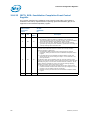
Revision History
Revision
Number
-001
January
2010
Initial release
•
-002
Revision
Date
Description
•
•
•
-003
•
Added the MCSAMPML—Memory Configuration, System Address Map and
Pre-allocated Memory Lock Register. See Section 2.7.28.
Added the PEG_TC—PCI Express Completion Timeout Register. See
Section 2.11.7.
Updated the system address map section, and main memory address space
for better clarification
Added the series designation “Intel® Pentium® desktop processor 6000
series”.
Added the Intel® Pentium® processor G6960.
November
2010
January
2011
§
12
Datasheet, Volume 2
Introduction
1
Introduction
This is Volume 2 of the Datasheet for the Intel® Core™ i5-600, i3-500 Desktop
processor series and Intel® Pentium® desktop processor 6000 series.
The processor contains one or more PCI devices within a single physical component.
The configuration registers for these devices are mapped as devices residing on the PCI
Bus assigned for the processor socket. This document describes these configuration
space registers or device-specific control and status registers (CSRs) only. This
document does NOT include Model Specific Registers (MSRs).
Note:
Throughout this document, the Intel® Core™ i5-600, i3-500 Desktop processor series
and Intel® Pentium® desktop processor 6000 seriesmay be referred to as “processor”.
Note:
Througout this document, the Intel® 5 series Chipset Platform Controller Hub is also
referred to as “PCH”.
Note:
The term “DT” refers to desktop platforms.
§
Datasheet, Volume 2
13
Introduction
14
Datasheet, Volume 2
Processor Configuration Registers
2
Processor Configuration
Registers
2.1
Register Terminology
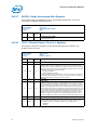
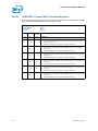
Table 2-1 shows the register-related terminology that is used in this chapter.
Table 2-1.
Register Terminology (Sheet 1 of 2)
Item
Description
RO
Read Only bit(s). Writes to these bits have no effect. These are static values only.
RO-V
Read Only/Volatile bit(s). Writes to these bits have no effect. These are status bits only. The
value to be read may change based on internal events.
RO-V-S
Read Only/Volatile/Sticky bit(s). Writes to these bits have no effect. These are status bits
only. The value to be read may change based on internal events. Bits are not returned to their
Reset Values by “warm” reset, but is reset with a cold/complete reset (for PCI Express* related
bits a cold reset is “Power Good Reset” as defined in the PCI Express Base Specification).
AF
Atomic Flag bit(s). The first time the bit is read with an enabled byte, it returns the value 0, but
a side-effect of the read is that the value changes to 1. Any subsequent reads with enabled bytes
return a 1 until a 1 is written to the bit. When the bit is read, but the byte is not enabled, the
state of the bit does not change, and the value returned is irrelevant, but will match the state of
the bit.
When a 0 is written to the bit, there is no effect. When a 1 is written to the bit, its value becomes
0, until the next byte-enabled read. When the bit is written, but the byte is not enabled, there is
no effect.
Conceptually, this is “Read to Set, Write 1 to Clear”
RW
Read/Write bit(s). These bits can be read and written by software. Hardware may only change
the state of this bit by reset.
RW1C
Read/Write 1 to Clear bit(s). These bits can be read. Internal events may set this bit. A
software write of 1 clears (sets to 0) the corresponding bit(s) and a write of 0 has no effect.
RW1C-L-S
Read/Write 1 to Clear/Lockable/Sticky bit(s). These bits can be read. Internal events may
set this bit. A software write of 1 clears (sets to 0) the corresponding bit(s) and a write of 0 has
no effect. Bits are not cleared by “warm” reset, but is reset with a cold/complete reset (for PCI
Express related bits a cold reset is “Power Good Reset” as defined in the PCI Express Base spec).
Additionally there is a Key bit (which is marked RW-K or RW-L-K) that, when set, prohibits this bit
field from being writable (bit field becomes Read Only/Volatile).
RW1C-S
Read/Write 1 to Clear/Sticky bit(s). These bits can be read. Internal events may set this bit.
A software write of 1 clears (sets to 0) the corresponding bit(s) and a write of 0 has no effect.
Bits are not cleared by "warm" reset, but is reset with a cold/complete reset (for PCI Express
related bits a cold reset is “Power Good Reset” as defined in the PCI Express Base spec).
RW-K
Read/Write/Key bit(s). These bits can be read and written by software. Additionally this bit,
when set, prohibits some other target bit field from being writable (bit fields become Read Only).
RW-L
Read/Write/Lockable bit(s). These bits can be read and written by software. Additionally
there is a Key bit (which is marked RW-K or RW-L-K) that, when set, prohibits this bit field from
being writable (bit field becomes Read Only).
RW-L-K
Read/Write/Lockable/Key bit(s). These bits can be read and written by software. This bit,
when set, prohibits some other bit field(s) from being writable (bit fields become Read Only).
Additionally there is a Key bit (which is marked RW-K or RW-L-K) that, when set, prohibits this bit
field from being writable (bit field becomes Read Only).
Conceptually, this may be a cascaded lock, or it may be self-locking when in its non-default state.
When self-locking, it differs from RW-O in that writing back the Reset Value will not set the lock.
RW-V
Write/Volatile bit(s). These bits can be read and written by software. Hardware may set or
clear the bit based on internal events, possibly sooner than any subsequent software read could
retrieve the value written.
Datasheet, Volume 2
15
Processor Configuration Registers
Table 2-1.
Register Terminology (Sheet 2 of 2)
Item
16
Description
RW-V-L
Read/Write/Volatile/Lockable bit(s). These bits can be read and written by software.
Hardware may set or clear the bit based upon internal events, possibly sooner than any
subsequent software read could retrieve the value written. Additionally, there is a bit (which is
marked RW-K or RW-L-K) that, when set, prohibits this bit field from being writable (bit field
becomes Read Only).
RW-V-L-S
Read/Write/Volatile/Lockable/Sticky bit(s). These bits can be read and written by
software. Hardware may set or clear the bit based upon internal events, possibly sooner than any
subsequent software read could retrieve the value written. Additionally, there is a bit (which is
marked RW-K or RW-L-K) that, when set, prohibits this bit field from being writable (bit field
becomes Read Only). These bits return to their Reset Values on cold reset.
RW-S
Read/Write/Sticky bit(s). These bits can be read and written by software. Bits are not
returned to their Reset Values by “warm” reset, but will return to Reset Values with a
cold/complete reset (for PCI Express related bits a cold reset is “Power Good Reset” as defined in
the PCI Express spec).
RW-O
Read/Write Once bit(s). Reads prior to the first write return the Reset Value. The first write
after warm reset stores any value written. Any subsequent write to this bit field is ignored. All
subsequent reads return the first value written. The value returns to default on warm reset. If
there are multiple RW-O or RW-O-S fields within a DWORD, they should be written all at once
(atomically) to avoid capturing an incorrect value.
RW-O-S
Read/Write Once/Sticky bit(s). Reads prior to the first write return the Reset Value. The first
write after cold reset stores any value written. Any subsequent write to this bit field is ignored. All
subsequent reads return the first value written. The value returns to default on cold reset. If
there are multiple RW-O or RW-O-S fields within a DWORD, they should be written all at once
(atomically) to avoid capturing an incorrect value.
W
Write-only. These bits may be written by software, but will always return zeros when read. They
are used for write side-effects. Any data written to these registers cannot be retrieved.
W1C
Write 1 to Clear-only. These bits may be cleared by software by writing a 1. Writing a 0 has no
effect. The state of the bits cannot be read directly. The states of such bits are tracked outside
the processor and all read transactions to the address of such bits are routed to the other agent.
Write transactions to these bits go to both agents.
MBZ
Must Be Zero when writing this bit.
Datasheet, Volume 2
Processor Configuration Registers
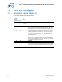
2.2
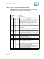
System Address Map
Note:
The processor’s Multi Chip Package (MCP) conceptually consists of the processor and
the north bridge chipset (GMCH) combined together in a single package. Hence, this
section will have references to the processor as well as GMCH (or MCH) address
mapping.
The MCP supports 64 GB (36 bit) of addressable memory space and 64 KB+3 of
addressable I/O space. With the new QPI interface, the processor performs decoding
that historically occurred within the GMCH. Specifically, the GMCH address decoding for
processor initiated PAM, 15 MB–16 MB ISA hole, SMM CSEG/TSEG, PCIexBAR, and
DRAM accesses will occur within the processor and the GMCH has no direct knowledge.
In addition, the ME (device 3) will move to the PCH, so ME associated register ranges
have been removed from the graphics controller. This section focuses on how the
memory space is partitioned and what the separate memory regions are used for. I/O
address space has simpler mapping and is explained near the end of this section.
The MCP supports PEG port upper prefetchable base/limit registers. This allows the PEG
unit to claim IO accesses above 36 bit, complying with the PCI Express Base
Specificaiton 2.1. Addressing of greater than 4 GB is allowed on either the DMI
Interface or PCI Express interface. The MCP supports a maximum of 16 GB of DRAM.
No DRAM memory will be accessible above 16 GB. DRAM capacity is limited by the
number of address pins available.
When running in internal graphics mode, Tilex/Tiley/linear reads/writes to GMADR
range are supported. Write accesses to GMADR linear regions are supported from both
DMI and PEG. GMADR write accesses to tileX and tileY regions (defined using fence
registers) are not supported from DMI or the PEG port. GMADR read accesses are not
supported from either DMI or PEG.
In the following sections, it is assumed that all of the compatibility memory ranges
reside on the DMI Interface. The exception to this rule is VGA ranges, which may be
mapped to PCI Express*, or DMI, or to the internal graphics device (IGD). In the
absence of more specific references, cycle descriptions referencing PCI should be
interpreted as the DMI Interface/PCI, while cycle descriptions referencing PCI Express
or IGD are related to the PCI Express bus or the internal graphics device respectively.
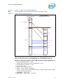
The processor does not remap APIC or any other memory spaces above TOLUD (Top of
Low Usable DRAM). The TOLUD register is set to the appropriate value by BIOS. The
remapbase/remaplimit registers remap logical accesses bound for addresses above
4 GB onto physical addresses that fall within DRAM.
Datasheet, Volume 2
17
Processor Configuration Registers
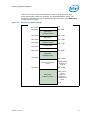
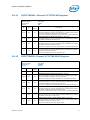
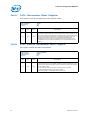
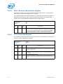
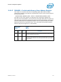
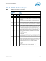
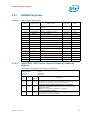
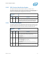
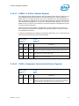
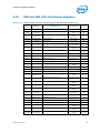
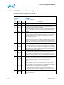
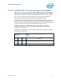
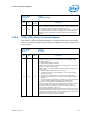
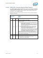
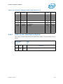
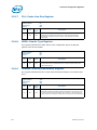
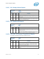
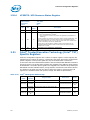
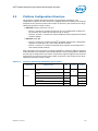
Figure 2-1 represents system memory address map in a simplified form.
Figure 2-1.
System Address Range
PHYSICAL MEMORY
(DRAM CONTROLLER VIEW)
HOST/SYSTEM VIEW
64G
Device 6
Bars
(PMUBASE1/
PMULIMIT1)
Device 3
(EPHECIBAR,
EPHECI2BAR )
Device 2
(GTTMMADR
, GMADR)
Independently Programmable
Non-Overlapping Windows
Device 1
Bars
(PMUBASE1/
PMULIMIT1)
PCI
Memory
Address
Range
Device 0
Bars
(PXPEPBAR,
MCHBAR,
PCIEXBAR,
DMIBAR)
(subtractively
decoded to
DMI)
TOUUD BASE RECLAIM LIMIT =
RECLAIM BASE + x
64MB aligned
RECLAIM BASE
TOM
Main
Memory
Reclaim
Address
Range
64MB aligned
EP-UMA
(1-64MB)
EP Stolen BASE
0MB - 63MB
Wasted
1MB aligned
64MB aligned
64MB aligned
Main
Memory
Address
Range
OS
VISIBLE
>4 GB
4G
MCHBAR
(GFXVTBAR,
DMIVC1BAR,
VTMEBAR,
VTDPVC0BAR)
Device 7
(CHAPADR)
Device 6
Bars
(MBASE1/
MLIMIT1,
PMBASE1/
PMLIMIT1)
Device 3
(EPHECIBAR,
EPHECI2BAR
, EPKTBAR)
Device 2
(GTTMMADR
, GMADR)
Device 1
Bars
(MBASE1/
MLIMIT1,
PMBASE1/
PMLIMIT1)
Device 0
GGC
(Graphics
Stolen
Memory,
Graphics GTT
Stolen
Memory)
Device 0
Bars
(PXPEPBAR,
MCHBAR,
PCIEXBAR,
DMIBAR)
TOLUD BASE
64MB aligned
PCI
Memory
Address
Range
(subtractively
decoded to
DMI)
OS
INVISIBLE
RECLAIM
X
64MB aligned for reclaim
GFX
STOLEN
(0-256 MB)
GFX Stolen BASE
GFX GTT Stolen BASE
Independently Programmable
Non-Overlapping Windows
TSEG
TSEG BASE
GFX- GTT
(0-2 MB)
1MB aligned
1MB aligned
TSEG
(0-8 MB)
1MB aligned
Main
Memory
Address
Range
1MB
0
18
Legacy
Address
Range
OS
VISIBLE
< 4GB
0
Datasheet, Volume 2
Processor Configuration Registers
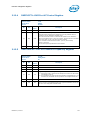
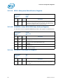
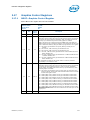
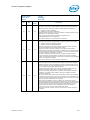
2.2.1
Legacy Address Range
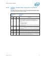
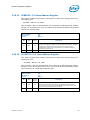
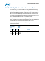
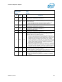
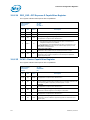
This area is divided into the following address regions:
• 0 – 640 KB — DOS Area
• 640 – 768 KB — Legacy Video Buffer Area
• 768 – 896 KB in 16 KB sections (total of 8 sections) — Expansion Area
• 896 – 960 KB in 16 KB sections (total of 4 sections) — Extended System BIOS Area
• 960 KB – 1 MB Memory — System BIOS Area
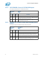
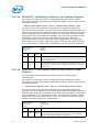
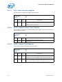
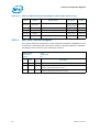
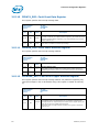
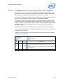
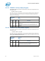
Figure 2-2.
DOS Legacy Address Range
000F_FFFFh
000F_0000h
000E_FFFFh
000E_0000h
System BIOS (Upper)
64 KB
Extended System BIOS (Lower)
64 KB (16 KB x 4)
000D_FFFFh
1 MB
960 KB
896 KB
Expansion Area
128 KB (16 KB x 8)
000C_0000h
768 KB
000B_FFFFh
Legacy Video Area
(SMM Memory)
128 KB
000A_0000h
640 KB
0009_FFFFh
DOS Area
0000_0000h
2.2.1.1
DOS Range (0000_0000h – 0009_FFFFh)
The DOS area is 640 KB (0000_0000h – 0009_FFFFh) in size and is always mapped to
the main memory controlled by the processor.
2.2.1.2
Legacy Video Area (000A_0000h – 000B_FFFFh)
The legacy 128 KB VGA memory range, frame buffer, (000A_0000h – 000B_FFFFh) can
be mapped to IGD (Device 2), to PCI Express (Device 1), and/or to the DMI Interface.
The appropriate mapping depends on which devices are enabled and the programming
of the VGA steering bits. Based on the VGA steering bits, priority for VGA mapping is
constant. The processor always decodes internally mapped devices first. Internal to the
processor, decode priority is:
1. IGD
2. PCI Express
3. DMI Interface (subtractive)
Datasheet, Volume 2
19
Processor Configuration Registers
Non-SMM-mode processor accesses to this range are considered to be to the Video
Buffer Area as described above. The processor will route these accesses on the noncoherent (NCS or NCB) channels.
The processor always positively decodes internally mapped devices, namely the IGD
and PCI-Express. Subsequent decoding of regions mapped to PCI Express or the DMI
Interface depends on the Legacy VGA configuration bits (VGA Enable and MDAP). This
region is also the default for SMM space.
Compatible SMRAM Address Range (000A_0000h – 000B_FFFFh)
Unlike FSB platforms, the Intel® Core™ i5-600, i3-500 Desktop processor series and
Intel® Pentium® desktop processor 6000 series see no SMM indication with processor
accesses. When compatible SMM space is enabled, SMM-mode processor accesses to
this range route to physical system DRAM at 000A_0000h – 000B_FFFFh. The
processor performs the decode and routes the access to physical system DRAM. In
other words, an SMM-mode processor access to this range will be sent on the HOM QPI
channel.
PCI Express and DMI originated cycles to enabled SMM space are not allowed and are
considered to be to the Video Buffer Area, if IGD is not enabled as the VGA device. DMI
initiated writes cycles are attempted as peer writes cycles to a VGA enabled PCIe port.
Monochrome Adapter (MDA) Range (000B_0000h – 000B_7FFFh)
Legacy support requires the ability to have a second graphics controller (monochrome)
in the system. Accesses in the standard VGA range are forwarded to IGD, PCI-Express,
or the DMI Interface (depending on configuration bits). Since the monochrome adapter
may be mapped to any of these devices, the processor must decode cycles in the MDA
range (000B_0000h – 000B_7FFFh) and forward either to IGD, PCI-Express, or the DMI
Interface. This capability is controlled by a VGA steering bits and the legacy
configuration bit (MDAP bit). In addition to the memory range B0000h to B7FFFh, the
processor decodes I/O cycles at 3B4h, 3B5h, 3B8h, 3B9h, 3BAh and 3BFh and forwards
them to the either IGD, PCI-Express, and/or the DMI Interface.
2.2.1.3
PAM (000C_0000h-000F_FFFFh)
The 13 sections from 768 KB to 1 MB comprise what is also known as the PAM Memory
Area. Each section has Read enable and Write enable attributes. The processor
documentation will now contain the registers and decode rules/restrictions.
The PAM registers have moved to the processor. For the PAM register details, refer to
processor documentation.
• ISA Expansion Area (000C_0000h – 000D_FFFFh)
• Extended System BIOS Area (000E_0000h – 000E_FFFFh)
• System BIOS Area (000F_0000h – 000F_FFFFh)
The processor contains the PAM registers and the GMCH has no knowledge of the
register programming. The processor decodes the request and routes to the
appropriate destination (DRAM or DMI) by sending the request on HOM or NCS/NCB.
Snooped accesses from PCI Express or DMI to this region are snooped on QPI.
Non-snooped accesses from PCI Express or DMI to this region are always sent to
DRAM. Graphics translated requests to this region are not allowed. If such a mapping
error occurs, the request will be routed to 000C_0000h. Writes will have the byte
enables de-asserted.
20
Datasheet, Volume 2
Processor Configuration Registers
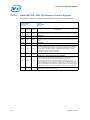
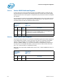
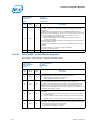
2.2.2
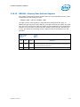
Main Memory Address Range (1MB – TOLUD)
This address range extends from 1 MB to the top of Low Usable physical memory that is
permitted to be accessible by the GMCH (as programmed in the TOLUD register). The
processor will route all addresses within this range as HOM accesses, which will be
forwarded by the GMCH to the DRAM unless it falls into the optional TSEG, optional ISA
Hole, or optional IGD stolen VGA memory.
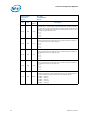
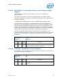
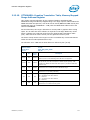
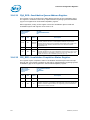
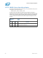
Figure 2-3.
Main Memory Address Range
FFFF_FFFFh
FLASH
4 GB Max
APIC
Intel TXT
Contains:
Dev 0, 1, 2, 6 BARS
and PCH/PCI ranges
PCI Memory Range
TOLUD
IGD
IGGTT
TSEG
TSEG_BASE
DPR
Main Memory
0100_0000h
00F0_0000h
16 MB
ISA Hole (optional)
15 MB
Main Memory
0010_0000h
1 MB
DOS Compatibility Memory
0h
2.2.2.1
0 MB
ISA Hole (15 MB – 16 MB)
This register moved to the processor. As such, the processor performs the necessary
decode and routes the request appropriately. Specifically, if no hole is created, the
processor will route the request to DRAM (HOM channel). If a hole is created, the
processor will route the request on NCS/NCB, since the request does not target DRAM.
Graphics translated requests to the range will always route to DRAM.
Datasheet, Volume 2
21
Processor Configuration Registers
2.2.2.2
TSEG
The TSEG register was moved from the GMCH to the processor. The GMCH will have no
direct knowledge of the TSEG size. For processor initiated transactions, the processor
will perform necessary decode and route appropriately on HOM (to DRAM) or NCS/NCB.
TSEG is below IGD stolen memory, which is at the Top of Low Usable physical memory
(TOLUD). When SMM is enabled, the maximum amount of memory available to the
system is equal to the amount of physical DRAM minus the value in the TSEG register.
BIOS will calculate and program a register, so the GMCH has knowledge of where
(TOLUD) – (Gfx stolen) – (Gfx GTT stolen) – (TSEG) is located. This is indicated by the
TSEG_BASE register.
SMM-mode processor accesses to enabled TSEG access the physical DRAM at the same
address. The processor will route these accesses on the QPI HOM channel.
When the extended SMRAM space is enabled, processor accesses to the TSEG range
without SMM attribute or without WB attribute are handled by the processor as invalid
accesses. Refer to the processor documentation for how the processor handles these
accesses.
Non- processor originated accesses are not allowed to SMM space. PCI-Express, DMI,
and Internal Graphics originated cycle to enabled SMM space are handled as invalid
cycle type with reads and writes to location 0 and byte enables turned off for writes.
2.2.2.3
Protected Memory Range (PMR) – (programmable)
For robust and secure launch of the MVMM, the MVMM code and private data needs to
be loaded to a memory region protected from bus master accesses. Support for
protected memory region is required for DMA-remapping hardware implementations on
platforms supporting Intel® Trusted Execution Technology (Intel TXT), and is optional
for non-Intel TxT platforms. Since the protected memory region needs to be enabled
before the MVMM is launched, hardware must support enabling of the protected
memory region independently from enabling the DMA-remapping hardware.
As part of the secure launch process, the SINIT-AC module verifies the protected
memory regions are properly configured and enabled. Once launched, the MVMM can
setup the initial DMA-remapping structures in protected memory (to ensure they are
protected while being setup) before enabling the DMA-remapping hardware units.
To optimally support platform configurations supporting varying amounts of main
memory, the protected memory region is defined as two non-overlapping regions:
• Protected Low-memory Region: This is defined as the protected memory region
below 4 GB to hold the MVMM code/private data, and the initial DMA-remapping
structures that control DMA to host physical addresses below 4 GB. DMAremapping hardware implementations on platforms supporting Intel TXT are
required to support protected low-memory region 5.
• Protected High-memory Region: This is defined as a variable sized protected
memory region above 4 GB, enough to hold the initial DMA-remapping structures
for managing DMA accesses to addresses above 4 GB. DMA-remapping hardware
implementations on platforms supporting Intel TXT are required to support
protected high-memory region 6, if the platform supports main memory above
4 GB.
22
Datasheet, Volume 2
Processor Configuration Registers
Once the protected low/high memory region registers are configured, bus master
protection to these regions is enabled through the Protected Memory Enable register.
For platforms with multiple DMA-remapping hardware units, each of the DMAremapping hardware units must be configured with the same protected memory
regions and enabled.
2.2.2.4
DRAM Protected Range (DPR)
This protection range only applies to DMA accesses and GMADR translations. It serves a
purpose of providing a memory range that is only accessible to processor streams.
The DPR range works independent of any other range, including the PMRC checks in
VTd. It occurs post any VTd translation. Therefore, incoming cycles are checked against
this range after the VTd translation and faulted if they hit this protected range, even if
they passed the VTd translation.
The system will set up:
1. 0 to (TSEG_BASE – DPR size – 1) for DMA traffic
2. TSEG_BASE to (TSEG_BASE – DPR size) as no DMA
After some time, software could request more space for not allowing DMA. It will get
some more pages and make sure there are no DMA cycles to the new region. DPR size
is changed to the new value. When it does this, there should not be any DMA cycles
going to DRAM to the new region.
If there were cycles from a rogue device to the new region, then those could use the
previous decode until the new decode can ensure PV. No flushing of cycles is required.
On a clock by clock basis proper decode with the previous or new decode needs to be
ensured.
All upstream cycles from 0 to (TSEG_BASE – 1 – DPR size), and not in the legacy holes
(VGA), are decoded to dram.
2.2.2.5
Pre-allocated Memory
Voids of physical addresses that are not accessible as general system memory and
reside within system memory address range (< TOLUD) are created for SMM-mode,
legacy VGA graphics compatibility, and graphics GTT stolen memory. It is the
responsibility of BIOS to properly initialize these regions.
2.2.2.6
Graphics Stolen Spaces
2.2.2.6.1
GTT Stolen Space (GSM)
GSM is allocated to store the GFX translation table entries, depending on VT-d support
it may be divided into 2 sections.
2.2.2.6.2
Global GTT Stolen Space (GGSM)
GGSM always exists regardless of VT-d as long as internal GFX is enabled. This space is
allocated to store accesses as page table entries are getting updated through virtual
GTTMMADR range. Hardware is responsible to map PTEs into this physical space.
Direct accesses to GGSM is not allowed, only hardware translations and fetches can be
directed to GGSM.
Datasheet, Volume 2
23
Processor Configuration Registers
2.2.2.6.3
Shadow GTT Stolen Space (SGSM)
Shadow GSM will be only used once internal GFX and VT-d translations are enabled.
The purpose of shadow GSM is to provide a physical space to hardware, where VT-d
translation for PTE updates can be made on the fly and re-written back into physical
memory.
2.2.2.7
Intel® Management Engine (Intel® ME) UMA
ME (the iAMT Manageability Engine) can be allocated UMA memory. ME memory is
“stolen” from the top of the host address map. The ME stolen memory base is
calculated by subtracting the amount of memory stolen by the Manageability Engine
from TOM.
Only ME can access this space; it is not accessible by or coherent with any processor
side accesses.
2.2.2.8
PCI Memory Address Range (TOLUD – 4 GB)
This address range, from the top of low usable DRAM (TOLUD) to 4 GB is normally
mapped to the DMI Interface.
Device 0 exceptions are:
1. Addresses decoded to the egress port registers (PXPEPBAR)
2. Addresses decoded to the memory mapped range for internal processor registers
(GMCHBAR)
3. Addresses decoded to the registers associated with the processor/PCH Serial
Interconnect (DMI) register memory range. (DMIBAR)
For each PCI Express port, there are two exceptions to this rule:
1. Addresses decoded to the PCI Express Memory Window defined by the MBASE1,
MLIMIT1, registers are mapped to PCI Express.
2. Addresses decoded to the PCI Express prefetchable Memory Window defined by the
PMBASE1, PMLIMIT1, registers are mapped to PCI Express.
In integrated graphics configurations, there are exceptions to this rule:
1. Addresses decode to the internal graphics translation window (GMADR)
2. Addresses decode to the Internal graphics translation table or IGD registers.
(GTTMMADR)
In a VT enable configuration, there are exceptions to this rule:
1. Addresses decoded to the memory mapped window to DMI VC1 VT remap engine
registers (DMIVC1BAR)
2. Addresses decoded to the memory mapped window to Graphics VT remap engine
registers (GFXVTBAR)
3. Addresses decoded to the memory mapped window to PEG/DMI/ME VC0 VT remap
engine registers (VTDPVC0BAR)
4. TCm accesses (to ME stolen memory) from PCH do not go through VT remap
engines.
Some of the MMIO Bars may be mapped to this range or to the range above TOUUD.
24
Datasheet, Volume 2
Processor Configuration Registers
There are sub-ranges within the PCI Memory address range defined as APIC
Configuration Space, MSI Interrupt Space, and High BIOS Address Range. The
exceptions listed above for internal graphics and the PCI Express ports MUST NOT
overlap with these ranges.
Figure 2-4.
PCI Memory Address Range
FFFF_FFFFh
4 GB
High BIOS
FFE0_0000h
4 GB – 2 MB
DMI Interface
(subtractive decode)
4 GB – 17 MB
FEF0_0000h
MSI Interrupts
FEE0_0000h
FED0_0000h
DMI Interface
(subtractive decode)
4 GB – 18 MB
4 GB – 19 MB
Local (CPU) APIC
FEC8_0000h
I/O APIC
FEC0_0000h
4 GB – 20 MB
DMI Interface
(subtractive decode)
F000_0000h
4 GB – 256 MB
PCI Express Configuration
Space
E000_0000h
Possible address
range/size (not
ensured)
4 GB – 512 MB
DMI Interface
(subtractive decode)
BARs, Internal
Graphics
ranges, PCI
Express Port,
CHAPADR could
be here.
TOLUD
Datasheet, Volume 2
25
Processor Configuration Registers
2.2.2.9
APIC Configuration Space (FEC0_0000h–FECF_FFFFh)
This range is reserved for APIC configuration space. The I/O APIC(s) usually reside in
the PCH portion of the chipset, but may also exist as stand-alone components like PXH.
The IOAPIC spaces are used to communicate with IOAPIC interrupt controllers that
may be populated in the system. Since it is difficult to relocate an interrupt controller
using plug-and-play software, fixed address decode regions have been allocated for
them. Processor accesses to the default IOAPIC region (FEC0_0000h to FEC7_FFFFh)
are always forwarded to DMI.
The processor optionally supports additional I/O APICs behind the PCI Express
“Graphics” port. When enabled using the PCI Express Configuration register (Device 1,
Offset 200h and Device 6, Offset 200h), the PCI Express port(s) will positively decode a
subset of the APIC configuration space. Specifically,
• Device 6 can be enabled to claim FEC8_0000h thru FECB_FFFFh.
• Device 1 can be enabled to claim FECC_0000h thru FECF_FFFFh.
Memory requests to this range would then be forwarded to the PCI Express port. This
mode is intended for the entry Workstation SKU of the processor, and would be
disabled in typical Desktop systems. When disabled, any access within entire APIC
Configuration space (FEC0_0000h to FECF_FFFFh) is forwarded to DMI.
2.2.2.9.1
MSI Interrupt Memory Space (FEE0_0000 – FEEF_FFFF)
Any PCI Express or DMI device may issue a Memory Write to 0FEEx_xxxxh. This
Memory Write cycle does not go to DRAM. The processor will forward this Memory Write
along with the data to the processor as a QPI Interrupt Message Transaction.
This interrupt message will be delivered to the processor as an IntPhysical or IntLogical
message.
2.2.2.10
High BIOS Area
For security reasons, the processor will now positively decode this range to DMI. This
positive decode will ensure any overlapping ranges will be ignored.
The top 2 MB (FFE0_0000h – FFFF_FFFFh) of the PCI Memory Address Range is
reserved for System BIOS (High BIOS), extended BIOS for PCI devices, and the A20
alias of the system BIOS. The processor begins execution from the High BIOS after
reset. This region is positively decoded to DMI Interface so that the upper subset of this
region aliases to 16 MB – 256 KB range. The actual address space required for the
BIOS is less than 2 MB but the minimum processor MTRR range for this region is 2 MB
so that full 2 MB must be considered.
26
Datasheet, Volume 2
Processor Configuration Registers
2.2.3
Main Memory Address Space (4 GB to TOUUD)
The processor will support 36 bit addressing. The maximum main memory size
supported is 16 GB total DRAM memory. A hole between TOLUD and 4 GB occurs when
main memory size approaches 4 GB or larger. As a result, TOM, and TOUUD registers
and REMAPBASE/REMAPLIMIT registers become relevant.
The remap configuration registers exist to remap lost main memory space. The greater
than 32 bit remap handling will be handled similar to other processors.
Upstream read and write accesses above 36-bit addressing will be treated as invalid
cycles by PEG and DMI.
Top of Memory (TOM)
The “Top of Memory” (TOM) register reflects the total amount of populated physical
memory. This is NOT necessarily the highest main memory address (holes may exist in
main memory address map due to addresses allocated for memory mapped I/O above
TOM).
The Manageability Engine's (ME) stolen size register reflects the total amount of
physical memory stolen by the Manageability Engine. The ME stolen memory is located
at the top of physical memory. The ME stolen memory base is calculated by subtracting
the amount of memory stolen by the Manageability Engine from TOM.
Top of Upper Usable DRAM (TOUUD)
The Top of Upper Usable Dram (TOUUD) register reflects the total amount of
addressable DRAM. If remap is disabled, TOUUD will reflect TOM minus Manageability
Engine's stolen size. If remap is enabled, then it will reflect the remap limit.
Note:
When there is more than 4 GB of DRAM and reclaim is enabled, the reclaim base will be
the same as TOM minus ME stolen memory size to the nearest 64 MB alignment (shown
in case 2 below).
Top of Low Usable DRAM (TOLUD)
TOLUD register is restricted to 4 GB memory (A[31:20]), but the processor can support
up to 16 GB, limited by DRAM pins. For physical memory greater than 4 GB, the TOUUD
register helps identify the address range in between the 4 GB boundary and the top of
physical memory. This identifies memory that can be directly accessed (including
remap address calculation) which is useful for memory access indication and early path
indication. When remap is enabled, TOLUD must be 64 MB aligned, but when remap is
disabled, TOLUD can be 1 MB aligned.
TSEG_BASE
The “TSEG_BASE” register reflects the total amount of low addressable DRAM, below
TOLUD. BIOS will calculate and program this register, so the processor has knowledge
of where (TOLUD) – (Gfx stolen) – (Gfx GTT stolen) – (TSEG) is located. I/O blocks use
this minus DPR for upstream DRAM decode.
Datasheet, Volume 2
27
Processor Configuration Registers
2.2.3.1
Programming Model
The memory boundaries of interest are:
• Bottom of Logical Address Remap Window defined by the REMAPBASE register,
which is calculated and loaded by BIOS.
• Top of Logical Address Remap Window defined by the REMAPLIMIT register, which
is calculated and loaded by BIOS.
• Bottom of Physical Remap Memory defined by the existing TOLUD register.
• Top of Physical Remap Memory, which is implicitly defined by either 4 GB or TOM
minus Manageability Engine stolen size.
Mapping steps:
1. Determine TOM
2. Determine TOM minus ME stolen size
3. Determine MMIO allocation
4. Determine TOLUD
5. Determine GFX stolen base
6. Determine GFX GTT stolen base
7. Determine TSEG base
8. Determine remap base/limit
9. Determine TOUUD
The following diagrams show the three possible general cases of remapping.
Case 1: Less than 4 GB of Physical Memory, no remap
Case 2: Greater than 4 GB of Physical Memory
Case 3: 4 GB or Less of Physical Memory
28
Datasheet, Volume 2
Processor Configuration Registers
2.2.3.1.1
Case 1 — Less than 4 GB of Physical Memory (no remap)
Figure 2-5.
Case 1 — Less than 4 GB of Physical Memory (no remap)
PHYSICAL MEMORY
(DRAM CONTROLLER VIEW)
HOST/SYSTEM VIEW
4 GB
64 MB aligned
TOM
64 MB aligned
EP-UMA
(0-64 MB)
EP Stolen
BASE
TOUUD BASE
1 MB aligned
PCI MMIO
TOLUD BASE
1 MB aligned
Wasted
(Only if 4G
minus PCI
MMIO
space is
greater
than 4G
minus EP
stolen
base)
1 MB aligned
1 MB aligned
GFX Stolen
GFX Stolen BASE
1 MB aligned
GFX GTT
STOLEN
GFX GTT Stolen BASE
1 MB aligned
TSEG
TSEG
TSEG BASE
1 MB aligned
OS
VISIBLE
< 4 GB
“LOW
DRAM”
0
0
•
•
•
•
•
•
•
Populated Physical Memory = 2 GB
Address Space allocated to memory mapped I/O = 1 GB
Remapped Physical Memory = 0 GB
TOM – 020h (2 GB)
ME stolen size – 00001b (1 MB)
TOUUD – 07FFh (2 GB minus 1 MB) (1 MB aligned)
TOLUD – 01F00h (2 GB minus 64 MB) (63 MB wasted because MMIO space required
is greater than 4G to EP stolen base.)
• REMAPBASE – 3FFh (64 GB – 1 boundary, default)
• REMAPLIMIT – 000h (0GB boundary, default)
Datasheet, Volume 2
29
Processor Configuration Registers
2.2.3.1.2
Case 2 — Greater than 4 GB of Physical Memory
Note:
Internal graphics is not supported on the Intel Xeon processor L3406.
Figure 2-6.
Case 2 — Greater than 4 GB of Physical Memory
PHYSICAL MEMORY
(DRAM CONTROLLER VIEW)
HOST/SYSTEM VIEW
64G
TOM
64MB aligned
EP-UMA
(1-64MB)
HMMIO
TOUUD BASE
RECLAIM LIMIT =
RECLAIM BASE + x
64MB aligned
MEMORY
RECLAIM
REGION
EP Stolen BASE
0MB 63MB
Wasted
1MB aligned
64MB aligned
RECLAIM BASE
64MB aligned
DRAM
ABOVE
4 GB
OS
VISIBLE
>4 GB
4G
OS
INVISIBLE
RECLAIM
X
TOLUD BASE
64MB aligned
64MB aligned for reclaim
GFX
STOLEN
(0-256 MB)
PCI MMIO
GFX Stolen BASE
1MB aligned
GFX GTT
(0-64 MB)
GFX GTT Stolen BASE
TSEG
TSEG BASE
1MB aligned
1MB aligned
OS
VISIBLE
< 4GB
“LOW
DRAM”
0
TSEG
(0-8 MB)
0
In this case the amount of memory remapped is the range between TOLUD and 4 GB.
This physical memory will be mapped to the logical address range defined between the
REMAPBASE and the REMAPLIMIT registers.
Example: 5 GB Physical Memory, with 1 GB allocated to Memory Mapped I/O
•
•
•
•
•
•
•
Populated Physical Memory = 5 GB
Address Space allocated to memory mapped I/O = 1 GB
Remapped Physical Memory = 1 GB
TOM – 050h (5 GB)
ME stolen size – 00000b (0 MB)
TOUUD – 1800h (6 GB) (1 MB aligned)
TOLUD – 06000h (3 GB) (64 MB aligned because remap is enabled and the remap
register has 64 MB granularity)
• REMAPBASE – 050h (5 GB)
• REMAPLIMIT – 05Fh (6 GB – 1 boundary)
30
Datasheet, Volume 2
Processor Configuration Registers
2.2.3.1.3
Case 3 — 4 GB or less of Physical Memory
Note:
Internal graphics is not supported on the Intel Xeon processor L3406.
Figure 2-7.
4 GB or Less of Physical Memory
PHYSICAL MEMORY
(DRAM CONTROLLER VIEW)
HOST/SYSTEM VIEW
64 GB
HMMIO
TOUUD BASE
RECLAIM LIMIT =
RECLAIM BASE + x
64 MB aligned
4 GB
RECLAIM BASE
64 MB aligned
TOM
64 MB aligned
EP-UMA
(1-64 MB)
EP Stolen
BASE
1 MB aligned
0 MB –
63 MB
Wasted
64 MB aligned
PCI MMIO
x
TOLUD BASE
64 MB aligned for reclaim
64 MB aligned
GFX Stolen
GFX Stolen BASE
1 MB aligned
GFX GTT
Stolen
GFX GTT Stolen BASE
1 MB aligned
TSEG
TSEG
TSEG BASE
1 MB aligned
OS
VISIBLE
< 4 GB
“LOW
DRAM”
0
0
In this case the amount of memory remapped is the range between TOLUD and TOM
minus the ME stolen memory. This physical memory will be mapped to the logical
address range defined between the REMAPBASE and the REMAPLIMIT registers.
Example: 3 GB Physical Memory, with 2 GB allocated to Memory Mapped I/O
•
•
•
•
•
•
•
Populated Physical Memory = 3 GB
Address Space allocated to memory mapped I/O = 2 GB
Remapped Physical Memory = 1 GB
TOM – 030h (3 GB)
ME stolen size – 00000b (0 MB)
TOUUD – 1400h (5GB) (1 MB aligned)
TOLUD – 02000h (2 GB) (64 MB aligned because remap is enabled and the remap
register has 64 MB granularity)
• REMAPBASE – 040h (4 GB)
• REMAPLIMIT – 04Fh (5 GB – 1 boundary)
Datasheet, Volume 2
31
Processor Configuration Registers
2.2.3.1.4
Case 4 — Greater than 4 GB of Physical Memory, Remap
Note:
Internal graphics is not supported on the Intel Xeon processor L3406.
Figure 2-8.
Greater than 4 GB, Remap Enabled
PHYSICAL MEMORY
(DRAM CONTROLLER VIEW)
HOST/SYSTEM VIEW
64 GB
TOM
64 MB aligned
EP-UMA
(1-64 MB)
HMMIO
RECLAIM LIMIT =
RECLAIM BASE + x
64 MB aligned
MEMORY
RECLAIM
REGION
EP Stolen BASE
0 MB –
63 MB
Wasted
1 MB aligned
64 MB aligned
RECLAIM BASE
64 MB aligned
DRAM
ABOVE
4 GB
OS
VISIBLE
>4 GB
4 GB
OS
INVISIBLE
RECLAIM
X
TOLUD BASE
64 MB aligned
64 MB aligned for reclaim
PCI MMIO
GFX
STOLEN
(0-64 MB)
GFX Stolen BASE
TSEG
GFX GTT Stolen BASE
GFX GTT
(0-64 MB)
TSEG BASE
TSEG
(0-8 MB)
1 MB aligned
1 MB aligned
OS
VISIBLE
< 4 GB
“LOW
DRAM”
0
1 MB aligned
0
In this case the amount of memory remapped is the range between TOLUD and 4 GB.
This physical memory will be mapped to the logical address range defined between the
REMAPBASE and the REMAPLIMIT registers.
Example: 5 GB Physical Memory, with 1 GB allocated to Memory Mapped I/O
• Populated Physical Memory = 5 GB
• Address Space allocated to memory mapped I/O = 1 GB
• Remapped Physical Memory = 1 GB
• TOM – 050h (5 GB)
• ME stolen size – 00000b (0 MB)
• TOUUD – 17FFh (6 GB – 1 MB) (1 MB aligned)
• TOLUD – 06000h (3 GB) (64 MB aligned because remap is enabled and the remap
register has 64 MB granularity)
• REMAPBASE – 050h (5GB)
• REMAPLIMIT – 05Fh (6 GB – 1 boundary)
32
Datasheet, Volume 2
Processor Configuration Registers
2.2.4
PCI Express* Configuration Address Space
PCIEXBAR has moved to the processor. The processor now detects memory accesses
targeting PCIEXBAR and the processor converts that access to QPI configuration
accesses. BIOS must assign this address range such that it will not conflict with any
other address ranges.
2.2.5
PCI Express* Graphics Attach (PEG)
The processor can be programmed to direct memory accesses to a PCI Express
interface. When addresses are within either of two ranges specified using registers in
each PEG(s) configuration space:
• The first range is controlled using the Memory Base Register (MBASE) and Memory
Limit Register (MLIMIT) registers.
• The second range is controlled using the Pre-fetchable Memory Base (PMBASE) and
Pre-fetchable Memory Limit (PMLIMIT) registers.
Conceptually, address decoding for each range follows the same basic concept. The top
12 bits of the respective Memory Base and Memory Limit registers correspond to
address bits A[31:20] of a memory address. For the purpose of address decoding, the
processor assumes that address bits A[19:0] of the memory base are zero and that
address bits A[19:0] of the memory limit address are F_FFFFh. This forces each
memory address range to be aligned to a 1MB boundary and to have a size granularity
of 1 MB.
The processor positively decodes memory accesses to PCI Express memory address
space as defined by the following equations:
Memory_Base_Address Address Memory_Limit_Address
Prefetchable_Memory_Base_Address Address
Prefetchable_Memory_Limit_Address
The window size is programmed by the plug-and-play configuration software. The
window size depends on the size of memory claimed by the PCI Express device.
Normally, these ranges will reside above the Top-of-Low Usable-DRAM and below High
BIOS and APIC address ranges. They MUST reside above the top of low memory
(TOLUD) if they reside below 4 GB and MUST reside above top of upper memory
(TOUUD) if they reside above 4 GB or they will steal physical DRAM memory space.
It is essential to support a separate Pre-fetchable range in order to apply USWC
attribute (from the processor point of view) to that range. The USWC attribute is used
by the processor for write combining.
Note that the processor memory range registers described above are used to allocate
memory address space for any PCI Express devices sitting on PCI Express that require
such a window.
The PCICMD1 register can override the routing of memory accesses to PCI Express. In
other words, the memory access enable bit must be set to enable the memory
base/limit and pre-fetchable base/limit windows.
The upper PMUBASE/PMULIMIT registers have been implemented for PCI Express
Specification compliance. The processor locates MMIO space above 4 GB using these
registers.
Datasheet, Volume 2
33
Processor Configuration Registers
2.2.6
Graphics Memory Address Ranges
The processor can be programmed to direct memory accesses to IGD when addresses
are within any of five ranges specified using registers in the processor Device 2
configuration space.
1. The Graphics Memory Aperture Base Register (GMADR) is used to access graphics
memory allocated using the graphics translation table.
2. The Graphics Translation Table Base Register (GTTADR) is used to access the
translation table and graphics control registers.
3. This is part of GTTMMADR register.
These ranges can reside above the Top-of-Low-DRAM and below High BIOS and APIC
address ranges. They MUST reside above the top of memory (TOLUD) and below 4 GB
so they do not steal any physical DRAM memory space.
Alternatively, these ranges can reside above 4 GB, similar to other BARs which are
larger than 32 bits in size.
GMADR is a Prefetchable range in order to apply USWC attribute (from the processor
point of view) to that range. The USWC attribute is used by the processor for write
combining.
2.2.6.1
IOBAR Mapped Access to Device 2 MMIO Space
Device 2, integrated graphics device, contains an IOBAR register. If Device 2 is
enabled, then IGD registers or the GTT table can be accessed using this IOBAR. The
IOBAR is composed of an index register and a data register.
MMIO_Index — MMIO_INDEX is a 32 bit register. An IO write to this port loads the
offset of the MMIO register or offset into the GTT that needs to be accessed. An IO
Read returns the current value of this register. See IOBAR rules for detailed
information.
MMIO_Data — MMIO_DATA is a 32 bit register. An IO write to this port is re-directed
to the MMIO register pointed to by the MMIO-index register. An IO read to this port is
re-directed to the MMIO register pointed to by the MMIO-index register. See IOBAR
rules for detailed information.
The result of accesses through IOBAR can be:
• Accesses directed to the GTT table. (that is, route to DRAM)
• Accesses to internal graphics registers with the processor (that is, route to internal
configuration bus)
• Accesses to internal graphics display registers now located within the PCH. (that is,
route to DMI).
Note:
GTT table space writes (GTTADR) are supported through this mapping mechanism.
This mechanism to access internal graphics MMIO registers must not be used to access
VGA IO registers which are mapped through the MMIO space. VGA registers must be
accessed directly through the dedicated VGA I/O ports.
34
Datasheet, Volume 2
Processor Configuration Registers
2.2.7
System Management Mode (SMM)
The processor handles all SMM mode transaction routing. The processor has no direct
knowledge of SMM mode. The processor will never allow I/O devices access to
CSEG/TSEG/HSEG ranges.
DMI Interface and PCI Express masters are not allowed to access the SMM space.
Table 2-2.
2.2.8
SMM Regions
SMM Space Enabled
Transaction Address Space
DRAM Space (DRAM)
Compatible (C)
000A_0000h to 000B_FFFFh
000A_0000h to 000B_FFFFh
TSEG (T)
(TOLUD–STOLEN–TSEG) to
TOLUD-STOLEN
(TOLUD–STOLEN–TSEG) to
TOLUD-STOLEN
SMM and VGA Access through GTT TLB
Accesses through GTT TLB address translation SMM DRAM space are not allowed.
Writes will be routed to Memory address 000C_0000h with byte enables de-asserted
and reads will be routed to Memory address 000C_0000h. If a GTT TLB translated
address hits SMM DRAM space, an error is recorded in the PGTBL_ER register.
PCI Express and DMI Interface originated accesses are never allowed to access SMM
space directly or through the GTT TLB address translation. If a GTT TLB translated
address hits enabled SMM DRAM space, an error is recorded in the PGTBL_ER register.
PCI Express* and DMI Interface write accesses through GMADR range will not be
snooped. Only PCI Express* and DMI assesses to GMADR linear range (defined using
fence registers) are supported. PCI Express and DMI Interface tileY and tileX writes to
GMADR are not supported. If, when translated, the resulting physical address is to
enabled SMM DRAM space, the request will be remapped to address 000C_0000h with
de-asserted byte enables.
PCI Express and DMI Interface read accesses to the GMADR range are not supported;
therefore, will have no address translation concerns. PCI Express and DMI Interface
reads to GMADR will be remapped to address 000C_0000h. The read will complete with
UR (unsupported request) completion status.
GTT fetches are always decoded (at fetch time) to ensure that they are not in SMM
(actually, anything above base of TSEG or 640 KB–1 MB). Thus, they will be invalid and
go to address 000C_0000h, but that is not specific to PCI Express or DMI; it applies to
the processor or internal graphics engines.
2.2.9
I/O Address Space
The processor generates either DMI Interface or PCI Express* bus cycles for all
processor I/O accesses that it does not claim. The processor no longer contains the two
internal registers in the processor I/O space, Configuration Address Register
(CONFIG_ADDRESS) and the Configuration Data Register (CONFIG_DATA). The
processor now handles accesses to these registers, which ultimate generate a QPI
configuration access.
The processor allows 64K+3 bytes to be addressed within the I/O space. The processor
propagates the processor I/O address without any translation on to the destination bus
and, therefore, provides addressability for 64K+3 byte locations. Note that the upper 3
Datasheet, Volume 2
35
Processor Configuration Registers
locations can be accessed only during I/O address wrap-around when address bit 16 is
asserted. Address bit 16 is asserted on the processor bus whenever an I/O access is
made to 4 bytes from address 0FFFDh, 0FFFEh, or 0FFFFh. Address bit 16 is also
asserted when an I/O access is made to 2 bytes from address 0FFFFh.
A set of I/O accesses are consumed by the internal graphics device if it is enabled. The
mechanisms for internal graphics IO decode and the associated control is explained
later.
The I/O accesses are forwarded normally to the DMI Interface bus unless they fall
within the PCI Express I/O address range as defined by the mechanisms explained
below. I/O writes are NOT posted. Memory writes to PCH or PCI Express are posted.
The PCI Express devices have a register that can disable the routing of I/O cycles to the
PCI Express device.
The processor responds to I/O cycles initiated on PCI Express or DMI with an UR status.
Upstream I/O cycles and configuration cycles should never occur. If one does occur, the
request will route as a read to Memory address 000C_0000h so a completion is
naturally generated (whether the original request was a read or write). The transaction
will complete with an UR completion status.
QPI I/O reads that lie within 8-byte boundaries but cross 4-byte boundaries are issued
from the processor as 1 transaction. The processor will break this into 2 separate
transactions. I/O writes that lie within 8-byte boundaries but cross 4-byte boundaries
will be split into 2 transactions by the processor.
2.2.9.1
PCI Express* I/O Address Mapping
The processor can be programmed to direct non-memory (I/O) accesses to the PCI
Express bus interface when processor initiated I/O cycle addresses are within the PCI
Express I/O address range. This range is controlled using the I/O Base Address
(IOBASE) and I/O Limit Address (IOLIMIT) registers in processor Device 1 or Device 6
(if a 2nd PEG port is enabled) configuration space.
Address decoding for this range is based on the following concept. The top 4 bits of the
respective I/O Base and I/O Limit registers correspond to address bits A[15:12] of an
I/O address. For the purpose of address decoding, the processor assumes that lower 12
address bits A[11:0] of the I/O base are zero and that address bits A[11:0] of the I/O
limit address are FFFh. This forces the I/O address range alignment to 4 KB boundary
and produces a size granularity of 4 KB.
The processor positively decodes I/O accesses to PCI Express I/O address space as
defined by the following equation:
I/O_Base_Address processor I/O Cycle Address I/O_Limit_Address
The effective size of the range is programmed by the plug-and-play configuration
software and it depends on the size of I/O space claimed by the PCI Express device.
The processor also forwards accesses to the Legacy VGA I/O ranges according to the
settings in the Device 1 configuration registers BCTRL (VGA Enable) and PCICMD1
(IOAE1), unless a second adapter (monochrome) is present on the DMI Interface/PCI
(or ISA). The presence of a second graphics adapter is determined by the MDAP
configuration bit. When MDAP is set, the processor will decode legacy monochrome IO
ranges and forward them to the DMI Interface. The IO ranges decoded for the
monochrome adapter are 3B4h, 3B5h, 3B8h, 3B9h, 3Bah and 3BFh.
36
Datasheet, Volume 2
Processor Configuration Registers
Note that the processor Device 1 I/O address range registers defined above are used
for all I/O space allocation for any devices requiring such a window on PCI-Express.
The PCICMD1 register can disable the routing of I/O cycles to PCI-Express.
2.3
Configuration Process and Registers
2.3.1
Platform Configuration Structure
The DMI physically connects the processor and the Intel PCH; so, from a configuration
standpoint, the DMI is logically PCI Bus 0. As a result, all devices internal to the
processor and the Intel PCH appear to be on PCI Bus 0.
Note:
The PCH internal LAN controller does not appear on Bus 0 — it appears on the external
PCI bus (whose number is configurable).
The system’s primary PCI expansion bus is physically attached to the PCH and, from a
configuration perspective, appears to be a hierarchical PCI bus behind a PCI-to-PCI
bridge and therefore has a programmable PCI Bus number. The PCI Express Graphics
Attach appears to system software to be a real PCI bus behind a PCI-to-PCI bridge that
is a device resident on PCI Bus 0.
Note:
A physical PCI bus 0 does not exist. DMI and the internal devices in the processor and
PCH logically constitute PCI Bus 0 to configuration software.
The processor contains the following PCI devices within a single physical component.
The configuration registers for these devices are mapped as devices residing on PCI
Bus 0.
• Device 0 — Host Bridge/DRAM Controller. Logically this appears as a PCI device
residing on PCI Bus 0. Device 0 contains the standard PCI header registers, PCI
Express base address register, DRAM control (including thermal/throttling control),
configuration for the DMI, and other processor specific registers.
• Device 1 — Host-PCI Express Bridge. Logically this appears as a “virtual” PCI-toPCI bridge residing on PCI Bus 0 and is compliant with PCI Express Base
Specification. Device 1 contains the standard PCI-to-PCI bridge registers and the
standard PCI Express/PCI configuration registers (including the PCI Express
memory address mapping).
• Device 2 — Internal Graphics Device. Logically, this appears as an APCI device
residing on PCI Bus 0. Physically, Device 2 contains the configurations registers for
3D, 2D, and display functions.
• Device 6 — Secondary Host to PCI Express Bridge. (Not supported on all SKUs)
Datasheet, Volume 2
37
Processor Configuration Registers
Table 2-3.
Device Number Assignment for Internal Processor Devices
Processor Function
2.4
Device Number
Host Bridge/DRAM Controller
Device 0
Host-to-PCI Express* Bridge (virtual P2P)
Device 1
Internal Graphics Device
Device 2
Secondary Host-to-PCI Express Bridge
(Device 6 is not supported on all SKUs.)
Device 6
Configuration Mechanisms
The GMCH is the originator of configuration cycles. Internal to the GMCH transactions
received through both configuration mechanisms are translated to the same format.
2.4.1
Standard PCI Configuration Mechanism
The following is the mechanism for translating GMCH I/O bus cycles to configuration
cycles.
The PCI specification defines a slot based "configuration space" that allows each device
to contain up to eight functions with each function containing up to 256, 8-bit
configuration registers. The PCI specification defines two bus cycles to access the PCI
configuration space: Configuration Read and Configuration Write. Memory and I/O
spaces are supported directly by the GMCH. Configuration space is supported by a
mapping mechanism implemented within the GMCH.
The configuration access mechanism makes use of the CONFIG_ADDRESS Register (at
I/O address 0CF8h though 0CFBh) and CONFIG_DATA Register (at I/O address 0CFCh
though 0CFFh). To reference a configuration register, a DW I/O write cycle is used to
place a value into CONFIG_ADDRESS that specifies the PCI bus, the device on that bus,
the function within the device and a specific configuration register of the device
function being accessed. CONFIG_ADDRESS[31] must be 1 to enable a configuration
cycle. CONFIG_DATA then becomes a window into the four bytes of configuration space
specified by the contents of CONFIG_ADDRESS. Any read or write to CONFIG_DATA will
result in the GMCH translating the CONFIG_ADDRESS into the appropriate
configuration cycle.
The GMCH is responsible for translating and routing the GMCH’s I/O accesses to the
CONFIG_ADDRESS and CONFIG_DATA registers to internal GMCH configuration
registers, DMI or PCI Express.
38
Datasheet, Volume 2
Processor Configuration Registers
2.4.2
PCI Express* Enhanced Configuration Mechanism
PCI Express extends the configuration space to 4096 bytes per device/function as
compared to 256 bytes allowed by the latest PCI Local Bus Specification. PCI Express
configuration space is divided into a PCI 3.0 compatible region, which consists of the
first 256B of a logical device’s configuration space and a PCI Express extended region
which consists of the remaining configuration space.
The PCI compatible region can be accessed using either the Standard PCI Configuration
Mechanism or using the PCI Express Enhanced Configuration Mechanism described in
this section. The extended configuration registers may only be accessed using the PCI
Express Enhanced Configuration Mechanism. To maintain compatibility with PCI
configuration addressing mechanisms, system software must access the extended
configuration space using 32-bit operations (32-bit aligned) only. These 32-bit
operations include byte enables allowing only appropriate bytes within the DWord to be
accessed. Locked transactions to the PCI Express memory mapped configuration
address space are not supported. All changes made using either access mechanism are
equivalent.
The PCI Express Enhanced Configuration Mechanism utilizes a flat memory-mapped
address space to access device configuration registers. This address space is reported
by the system firmware to the operating system. There is a register, PCIEXBAR, that
defines the base address for the block of addresses below 4 GB for the configuration
space associated with busses, devices and functions that are potentially a part of the
PCI Express root complex hierarchy. In the PCIEXBAR register there are controls to
limit the size of this reserved memory mapped space. 256 MB is the amount of address
space required to reserve space for every bus, device, and function that could possibly
exist. Options for 128 MB and 64 MB exist in order to free up those addresses for other
uses. In these cases the number of busses and all of their associated devices and
functions are limited to 128 or 64 busses, respectively.
The PCI Express Configuration Transaction Header includes an additional 4 bits
(ExtendedRegisterAddress[3:0]) between the Function Number and Register Address
fields to provide indexing into the 4 KB of configuration space allocated to each
potential device. For PCI Compatible Configuration Requests, the Extended Register
Address field must be all zeros.
Figure 2-9.
Memory Map to PCI Express Device Configuration Space
FFFFFFFh
7FFFh
FFFFFh
Bus 255
Device 31
FFFh
Function 7
PCI Express
Extended
Configuration
Space
FFh
FFFFh
1FFFFFh
1FFFh
Device 1
Bus 1
Bus 0
Function 1
3Fh
7FFFh
FFFFFh
FFFh
Device 0
Function 0
PCI Compatible
Configuration
Space
PCI Compatible
Configuration
Space Header
0
Located by
PCI Express* Base Address
Datasheet, Volume 2
39
Processor Configuration Registers
Just the same as with PCI devices, each device is selected based on decoded address
information that is provided as a part of the address portion of Configuration Request
packets. A PCI Express device will decode all address information fields (bus, device,
function and extended address numbers) to provide access to the correct register.
To access this space (step 1 is done only once by BIOS),
First determine the maximum bus number using the following algorithm.
1. Write to I/O address 0CF8h with value 80FF_1050h.
2. Read from I/O address 0CFCh. If the value is FFFF_FFFFh (master abort), then go
to step 3, otherwise max bus number is FFh.
3. Write to I/O address 0CF8h with value 807F_1050h.
4. Read from I/O address 0CFCh. If the value is FFFF_FFFFh (master abort), then
maximum bus number is 3Fh; otherwise, maximum bus number is 7Fh.
Write to the PCIEXBAR register at the maximum bus number, device 2, function 0,
offset 50h. Write 1 to bit 0 of the register to enable the enhanced configuration
mechanism. Allocate either 256, 128, or 64 busses to PCI Express by writing “000”,
“111”, or “110” respectively to bits 3:1. Pick a naturally aligned base address for
mapping the configuration space onto memory space using 1 MB per bus number and
write that base address into Bits 39:20.
Calculate the host address of the register you wish to set using (PCI Express base +
(bus number * 1 MB) + (device number * 32 KB) + (function number * 4 KB) + (1 B *
offset within the function) = host address)
Use a memory write or memory read cycle to the calculated host address to write or
read that register.
2.4.3
Routing Configuration Accesses
The processor supports two PCI related interfaces — DMI and PCI Express. The
processor is responsible for routing PCI and PCI Express configuration cycles to the
appropriate device that is an integrated part of the processor or to one of these two
interfaces. Configuration cycles to the PCH internal devices and Primary PCI (including
downstream devices) are routed to the PCH using DMI. Configuration cycles to both the
PCI Express Graphics PCI compatibility configuration space and the PCI Express
Graphics extended configuration space are routed to the PCI Express Graphics port
device or associated link.
40
Datasheet, Volume 2
Processor Configuration Registers
Figure 2-10. Processor Configuration Cycle Flow Chart
DW I/O Write to
CONFIG_ADDRESS
with bit 31 = 1
I/O Read/Write to
CONFIG_DATA
Bus# = 0
Yes
No
Processor Generates
Type 1 Access
to PCI Express
Yes
Dev # 1
Enabled &
Bus# > SEC BUS
Bus# SUB BUS
in Bus 0
Dev 1
No
Yes
Dev # 1
Enabled &
Bus# =
SECONDARY BUS
in Bus 0
Dev 1
No
Processor Generates
DMI Type 1
Configuration Cycle
Device# = 0 &
Function# = 0
Yes
Processor
Claims
Yes
Processor
Claims
Yes
Processor
Claims
No
Device # = 1 &
Dev # 1 Enabled
& Function# = 0
No
Device # = 2 &
Dev # 2 Enabled
& Function# = 0
No
Device# = 0
Yes
Processor Generates
Type 0 Access
to PCI Express
Processor Generates
DMI Type0
Configuration Cycles
No
Processor allows
cycle to go to DMI
resulting in Master
Abort
2.4.4
Internal Device Configuration Accesses
The processor decodes the Bus Number (Bits 23:16) and the Device Number fields of
the CONFIG_ADDRESS register. If the Bus Number field of CONFIG_ADDRESS is 0, the
configuration cycle is targeting a PCI Bus 0 device.
If the targeted PCI Bus 0 device exists in the processor and is not disabled, the
configuration cycle is claimed by the appropriate device.
Datasheet, Volume 2
41
Processor Configuration Registers
2.4.5
Bridge Related Configuration Accesses
Configuration accesses on PCI Express or DMI are PCI Express Configuration TLPs.
• Bus Number [7:0] is Header Byte 8 [7:0]
• Device Number [4:0] is Header Byte 9 [7:3]
• Function Number [2:0] is Header Byte 9 [2:0]
And special fields for this type of TLP:
• Extended Register Number [3:0] is Header Byte 10 [3:0]
• Register Number [5:0] is Header Byte 11 [7:2]
See the PCI Express Base Specification and the PCI Local Bus Specification Revision 3.0
for more information on both the PCI 3.0-compatible and PCI Express Enhanced
Configuration Mechanism and transaction rules.
2.4.5.1
PCI Express* Configuration Accesses
When the Bus Number of a type 1 Standard PCI Configuration cycle or PCI Express
Enhanced Configuration access matches the Device 1 Secondary Bus Number, a PCI
Express Type 0 Configuration TLP is generated on the PCI Express link targeting the
device directly on the opposite side of the link. This should be Device 0 on the bus
number assigned to the PCI Express link (likely Bus 1).
The device on other side of link must be Device 0. The processor will Master Abort any
Type 0 Configuration access to a non-zero device number. If there is to be more than
one device on that side of the link there must be a bridge implemented in the
downstream device.
When the bus number of a type 1 Standard PCI Configuration cycle or PCI Express
Enhanced Configuration access is within the claimed range (between the upper bound
of the bridge device’s Subordinate Bus Number register and the lower bound of the
bridge device’s Secondary Bus Number register) but does not match the Device 1
Secondary Bus Number, a PCI Express Type 1 Configuration TLP is generated on the
secondary side of the PCI Express link.
PCI Express Configuration Writes:
• Internally the processor will translate writes to PCI Express extended configuration
space to configuration writes on the backbone.
• Posted writes to extended space are non-posted on the PCI Express or DMI (that is,
translated to configuration writes)
42
Datasheet, Volume 2
Processor Configuration Registers
2.4.5.2
DMI Configuration Accesses
Accesses to disabled processor internal devices, bus numbers not claimed by the HostPCI Express bridge, or PCI Bus 0 devices not part of the processor will subtractively
decode to the PCH and consequently be forwarded over the DMI using a PCI Express
configuration TLP.
If the Bus Number is zero, the processor will generate a Type 0 Configuration cycle TLP
on DMI. If the Bus Number is non-zero, and falls outside the range claimed by the
Host-PCI Express bridge, the processor will generate a Type 1 Configuration cycle TLP
on DMI.
The PCH routes configurations accesses in a manner similar to the processor. The PCH
decodes the configuration TLP and generates a corresponding configuration access.
Accesses targeting a device on PCI Bus 0 may be claimed by an internal device. The
PCH compares the non-zero Bus Number with the Secondary Bus Number and
Subordinate Bus Number registers of its PCI-to-PCI bridges to determine if the
configuration access is meant for Primary PCI, or some other downstream PCI bus or
PCI Express link.
Configuration accesses that are forwarded to the PCH, but remain unclaimed by any
device or bridge will result in a master abort.
2.5
Processor Register Introduction
The processor contains two sets of software accessible registers, accessed using the
Host processor I/O address space — Control registers and internal configuration
registers.
• Control registers are I/O mapped into the processor I/O space, which control
access to PCI and PCI Express configuration space (see section entitled I/O Mapped
Registers).
• Internal configuration registers residing within the processor are partitioned into
three logical device register sets (“logical” since they reside within a single physical
device). The first register set is dedicated to Host Bridge functionality (that is,
DRAM configuration, other chip-set operating parameters and optional features).
The second register block is dedicated to Host-PCI Express Bridge functions
(controls PCI Express interface configurations and operating parameters). The third
register block is for the internal graphics functions.
The processor internal registers (I/O Mapped, Configuration and PCI Express Extended
Configuration registers) are accessible by the Host processor. The registers that reside
within the lower 256 bytes of each device can be accessed as Byte, Word (16 bit), or
DWord (32 bit) quantities, with the exception of CONFIG_ADDRESS, which can only be
accessed as a DWord. All multi-byte numeric fields use "little-endian" ordering (that is,
lower addresses contain the least significant parts of the field). Registers that reside in
bytes 256 through 4095 of each device may only be accessed using memory mapped
transactions in DWord (32 bit) quantities.
Some of the processor registers described in this section contain reserved bits. These
bits are labeled "Reserved”. Software must deal correctly with fields that are reserved.
On reads, software must use appropriate masks to extract the defined bits and not rely
on reserved bits being any particular value. On writes, software must ensure that the
values of reserved bit positions are preserved. That is, the values of reserved bit
Datasheet, Volume 2
43
Processor Configuration Registers
positions must first be read, merged with the new values for other bit positions and
then written back. Note the software does not need to perform read, merge, and write
operation for the Configuration Address Register.
In addition to reserved bits within a register, the processor contains address locations
in the configuration space of the Host Bridge entity that are marked either "Reserved"
or “Intel Reserved”. The processor responds to accesses to Reserved address locations
by completing the host cycle. When a Reserved register location is read, a zero value is
returned. (Reserved registers can be 8-, 16-, or 32 bits in size). Writes to Reserved
registers have no effect on the processor. Registers that are marked as Intel Reserved
must not be modified by system software. Writes to Intel Reserved registers may cause
system failure. Reads from Intel Reserved registers may return a non-zero value.
Upon a Full Reset, the processor sets its entire set of internal configuration registers to
predetermined default states. Some register values at reset are determined by external
strapping options. The default state represents the minimum functionality feature set
required to successfully bringing up the system. Hence, it does not represent the
optimal system configuration. It is the responsibility of the system initialization
software (usually BIOS) to properly determine the DRAM configurations, operating
parameters and optional system features that are applicable, and to program the
processor registers accordingly.
2.6
I/O Mapped Registers
The processor contains two registers that reside in the processor I/O address space the Configuration Address (CONFIG_ADDRESS) Register and the Configuration Data
(CONFIG_DATA) Register. The Configuration Address Register enables/disables the
configuration space and determines what portion of configuration space is visible
through the Configuration Data window.
44
Datasheet, Volume 2
Processor Configuration Registers
2.7
PCI Express* Device 0 Registers
Table 2-4 shows the PCI Express Device 0 register address map. Detailed register bit
descriptions follow Table 2-4.
Table 2-4.
PCI Express* Device 0 Register Address Map
Datasheet, Volume 2
Offset
Address
Register
Symbol
0–1h
VID
2–3h
DID
4–5h
PCICMD
6–7h
PCISTS
8h
RID
Register Name
Reset Value
Access
Vendor Identification
8086h
RO
Device Identification
0040h
RO
PCI Command
0006h
RO, RW
PCI Status
0090h
RW1C, RO
12h
RO
060000h
RO
00h
RO
Revision Identification
9–Bh
CC
Class Code
Dh
MLT
Master Latency Timer
Eh
HDR
Header Type
2C–2Dh
SVID
Subsystem Vendor Identification
2E–2Fh
SID
40–47h
PXPEPBAR
48–4Fh
MCHBAR
52–53h
GGC
54–57h
DEVEN
68–6Fh
DMIBAR
97h
LAC
A2–A3h
TOUUD
Subsystem Identification
00h
RO
0000h
RW-O
0000h
RW-O
PCI Express Egress Port Base Address
0000_0000_0
000_0000h
RW-L, RO
MCH Memory Mapped Register Range Base
0000_0000_0
000_0000h
RW-L, RO
Graphics Control Register
Device Enable
Root Complex Register Range Base Address
Legacy Access Control
Top of Upper Usable DRAM
0030h
RW-L, RO
0000210Bh
RW-L, RO
0000_0000_0
000_0000h
RW-L, RO
00h
RW
0000h
RW-L
A4–A7h
GBSM
Graphics Base of Pre-Allocated Memory
0000_0000h
RW-L, RO
A8–ABh
BGSM
Base of GTT Pre-allocated memory
0000_0000h
RW-L, RO
AC–AFh
TSEGMB
TSEG Memory Base
0000_0000h
RO, RW-L
B0–B1h
TOLUD
0010h
RW-L, RO
Top of Low Usable DRAM
C0–C3h
PBFC
Primary Buffer Flush Control
0000_0000h
RO, W
C4–C7h
SBFC
Secondary Buffer Flush Control
0000_0000h
RO, W
C8–C9h
ERRSTS
Error Status
0000h
RO, RW1C-S
CA–CBh
ERRCMD
Error Command
0000h
RO, RW
DC–DFh
SKPD
Scratchpad Data
0000_0000h
RW
SKU
dependent
RO
00h
RW-O, RW-L,
RW-L-K
E0–EBh
CAPID0
F4h
MCSAMPML
Capability Identifier
Memory Configuration, System Address Map
and Pre-allocated Memory Lock
45
Processor Configuration Registers
2.7.1
VID—Vendor Identification Register
This register combined with the Device Identification register uniquely identifies any
PCI device.
B/D/F/Type:
Address Offset:
Reset Value:
Access:
2.7.2
0/0/0/PCI
0–1h
8086h
RO
Bit
Attr
Reset
Value
15:0
RO
8086h
Description
Vendor Identification Number (VID)
PCI standard identification for Intel.
DID—Device Identification Register
This register combined with the Vendor Identification register uniquely identifies any
PCI device.
B/D/F/Type:
Address Offset:
Reset Value:
Access:
46
0/0/0/PCI
2–3h
0040h
RO
Bit
Attr
Reset
Value
15:0
RO
0040h
Description
Device Identification Number (DID)
Identifier assigned to the processor core/primary PCI device.
Datasheet, Volume 2
Processor Configuration Registers
2.7.3
PCICMD—PCI Command Register
Since processor Device 0 does not physically reside on PCI_A many of the bits are not
implemented.
B/D/F/Type:
Address Offset:
Reset Value:
Access:
0/0/0/PCI
4–5h
0006h
RO, RW
Bit
Attr
Reset
Value
15:10
RO
00h
9
RO
0b
Fast Back-to-Back Enable (FB2B)
This bit controls whether or not the master can do fast back-to-back write.
Since device 0 is strictly a target this bit is not implemented and is hardwired
to 0. Writes to this bit position have no effect.
Datasheet, Volume 2
Description
Reserved
8
RW
0b
SERR Enable (SERRE)
This bit is a global enable bit for Device 0 SERR messaging. The processor
does not have an SERR signal. The processor communicates the SERR
condition by sending an SERR message over DMI to the PCH.
1 = The processor is enabled to generate SERR messages over DMI for
specific Device 0 error conditions that are individually enabled in the
ERRCMD and DMIUEMSK registers. The error status is reported in the
ERRSTS, PCISTS, and DMIUEST registers.
0 = The SERR message is not generated by the processor for Device 0.
This bit only controls SERR messaging for Device 0. Device 1 has its own
SERRE bits to control error reporting for error conditions occurring in that
device. The control bits are used in a logical OR manner to enable the SERR
DMI message mechanism.
0 = Device 0 SERR disabled
1 = Device 0 SERR enabled
7
RO
0b
Address/Data Stepping Enable (ADSTEP)
Address/data stepping is not implemented in the processor, and this bit is
hardwired to 0. Writes to this bit position have no effect.
6
RW
0b
Parity Error Enable (PERRE)
This bit controls whether or not the Master Data Parity Error bit in the PCI
Status register can bet set.
0 = Master Data Parity Error bit in PCI Status register can NOT be set.
1 = Master Data Parity Error bit in PCI Status register CAN be set.
5
RO
0b
VGA Palette Snoop Enable (VGASNOOP)
The processor does not implement this bit and it is hardwired to a 0. Writes
to this bit position have no effect.
4
RO
0b
Memory Write and Invalidate Enable (MWIE)
The processor will never issue memory write and invalidate commands. This
bit is therefore hardwired to 0. Writes to this bit position will have no effect.
3:3
RO
0h
Reserved
2
RO
1b
Bus Master Enable (BME)
The processor is always enabled as a master on the backbone. This bit is
hardwired to a 1. Writes to this bit position have no effect.
1
RO
1b
Memory Access Enable (MAE)
The processor always allows access to main memory, except when such
access would violate security principles. Such exceptions are outside the
scope of PCI control. This bit is not implemented and is hardwired to 1.
Writes to this bit position have no effect.
0
RO
0b
I/O Access Enable (IOAE)
This bit is not implemented in the processor and is hardwired to a 0. Writes
to this bit position have no effect.
47
Processor Configuration Registers
2.7.4
PCISTS—PCI Status Register
This status register reports the occurrence of error events on Device 0's PCI interface.
Since the processor Device 0 does not physically reside on PCI_A, many of the bits are
not implemented.
B/D/F/Type:
Address Offset:
Reset Value:
Access:
48
0/0/0/PCI
6–7h
0090h
RW1C, RO
Bit
Attr
Reset
Value
15
RW1C
0b
Detected Parity Error (DPE)
This bit is set when this device receives a Poisoned TLP.
Description
14
RW1C
0b
Signaled System Error (SSE)
This bit is set to 1 when the processor Device 0 generates an SERR message
over DMI for any enabled Device 0 error condition. Device 0 error conditions
are enabled in the PCICMD, ERRCMD, and DMIUEMSK registers. Device 0
error flags are read/reset from the PCISTS, ERRSTS, or DMIUEST registers.
Software clears this bit by writing a 1 to it.
13
RW1C
0b
Received Master Abort Status (RMAS)
This bit is set when the processor generates a DMI request that receives an
Unsupported Request completion packet. Software clears this bit by writing a
1 to it.
12
RW1C
0b
Received Target Abort Status (RTAS)
This bit is set when the processor generates a DMI request that receives a
Completer Abort completion packet. Software clears this bit by writing a 1 to
it.
11
RO
0b
Signaled Target Abort Status (STAS)
The processor will not generate a Target Abort DMI completion packet or
Special Cycle. This bit is not implemented in the processor and is hardwired
to a 0. Writes to this bit position have no effect.
10:9
RO
00b
DEVSEL Timing (DEVT)
These bits are hardwired to "00". Writes to these bit positions have no affect.
Device 0 does not physically connect to PCI_A. These bits are set to "00"
(fast decode) so that optimum DEVSEL timing for PCI_A is not limited by the
processor.
8
RW1C
0b
Master Data Parity Error Detected (DPD)
This bit is set when DMI received a Poisoned completion from PCH.
This bit can only be set when the Parity Error Enable bit in the PCI Command
register is set.
7
RO
1b
Fast Back-to-Back (FB2B)
This bit is hardwired to 1. Writes to these bit positions have no effect. Device
0 does not physically connect to PCI_A. This bit is set to 1 (indicating fast
back-to-back capability) so that the optimum setting for PCI_A is not limited
by the processor.
6
RO
0b
Reserved
5
RO
0b
66 MHz Capable (66MC)
Does not apply to PCI Express. Must be hardwired to 0.
1b
Capability List (CLIST)
This bit is hardwired to 1 to indicate to the configuration software that this
device/function implements a list of new capabilities. A list of new capabilities
is accessed using register CAPPTR at configuration address offset 34h.
Register CAPPTR contains an offset pointing to the start address within
configuration space of this device where the Capability Identification register
resides.
4
RO
3
RO
0b
Reserved
2:0
RO
000b
Reserved
Datasheet, Volume 2
Processor Configuration Registers
2.7.5
RID—Revision Identification
This register contains the revision number of the processor. The Revision ID (RID) is a
traditional 8-bit Read Only (RO) register located at offset 08h in the standard PCI
header of every PCI/PCI Express compatible device and function.
B/D/F/Type:
Address Offset:
Reset Value:
Access:
Bit
7:0
2.7.6
Attr
RO
0/0/0/PCI
8h
08h
RO
Reset
Value
Description
12h
Revision Identification Number (RID)
This is an 8-bit value that indicates the revision identification number for the
processor Device 0. Refer to the Intel® Core™ i5-600 and i3-500 Desktop
Processor Series and Intel® Pentium® Desktop Processor 6000 Series
Specification Update for the value of the Revision ID Register.
CC—Class Code Register
This register identifies the basic function of the device, a more specific sub-class, and a
register-specific programming interface.
B/D/F/Type:
Address Offset:
Reset Value:
Access:
2.7.7
0/0/0/PCI
9–Bh
060000h
RO
Bit
Attr
Reset
Value
23:16
RO
06h
Base Class Code (BCC)
This is an 8-bit value that indicates the base class code for the processor.
This code has the value 06h, indicating a Bridge device.
15:8
RO
00h
Sub-Class Code (SUBCC)
This is an 8-bit value that indicates the category of Bridge into which the
processor falls. The code is 00h indicating a Host Bridge.
7:0
RO
00h
Programming Interface (PI)
This is an 8-bit value that indicates the programming interface of this device.
This value does not specify a particular register set layout and provides no
practical use for this device.
Description
MLT—Master Latency Timer Register
Device 0 in the processor is not a PCI master. Therefore, this register is not
implemented.
B/D/F/Type:
Address Offset:
Reset Value:
Access:
Datasheet, Volume 2
0/0/0/PCI
Dh
00h
RO
Bit
Attr
Reset
Value
7:0
RO
00h
Description
Reserved
49
Processor Configuration Registers
2.7.8
HDR—Header Type Register
This register identifies the header layout of the configuration space. No physical
register exists at this location.
B/D/F/Type:
Address Offset:
Reset Value:
Access:
2.7.9
0/0/0/PCI
Eh
00h
RO
Bit
Attr
Reset
Value
Description
7:0
RO
00h
PCI Header (HDR)
This field always returns 0 to indicate that the processor is a single function
device with standard header layout. Reads and writes to this location have no
effect.
SVID—Subsystem Vendor Identification Register
This value is used to identify the vendor of the subsystem.
B/D/F/Type:
Address Offset:
Reset Value:
Access:
50
0/0/0/PCI
2C–2Dh
0000h
RW-O
Bit
Attr
Reset
Value
Description
15:0
RW-O
0000h
Subsystem Vendor ID (SUBVID)
This field should be programmed during boot-up to indicate the vendor of the
system board. After it has been written once, it becomes read only.
Datasheet, Volume 2
Processor Configuration Registers
2.7.10
SID—Subsystem Identification Register
This value is used to identify a particular subsystem.
B/D/F/Type:
Address Offset:
Reset Value:
Access:
2.7.11
0/0/0/PCI
2E–2Fh
0000h
RW-O
Bit
Attr
Reset
Value
Description
15:0
RW-O
0000h
Subsystem ID (SUBID)
This field should be programmed during BIOS initialization. After it has been
written once, it becomes read only.
PXPEPBAR—PCI Express Egress Port Base Address
Register
This is the base address for the PCI Express Egress Port MMIO Configuration space.
There is no physical memory within this 4 KB window that can be addressed. The 4 KB
reserved by this register does not alias to any PCI 2.3 compliant memory mapped
space. On reset, the EGRESS port MMIO configuration space is disabled and must be
enabled by writing a 1 to PXPEPBAREN [Device 0, offset 40h, bit 0].
All the bits in this register are locked in Intel TXT mode.
B/D/F/Type:
Address Offset:
Reset Value:
Access:
0/0/0/PCI
40–47h
0000_0000_0000_0000h
RW-L, RO
Bit
Attr
Reset
Value
63:36
RO
0000000h
35:12
RW-L
000000h
11:1
RO
000h
0
Datasheet, Volume 2
RW-L
0b
Description
Reserved
PCI Express Egress Port MMIO Base Address (PXPEPBAR)
This field corresponds to bits 35:12 of the base address PCI Express Egress
Port MMIO configuration space. BIOS will program this register resulting in a
base address for a 4 KB block of contiguous memory address space. This
register ensures that a naturally aligned 4 KB space is allocated within the
first 64 GB of addressable memory space. System Software uses this base
address to program the processor MMIO register set. All the bits in this
register are locked in Intel TXT mode.
Reserved
PXPEPBAR Enable (PXPEPBAREN)
0 = Disable. PXPEPBAR is disabled and does not claim any memory
1 = Enable. PXPEPBAR memory mapped accesses are claimed and decoded
appropriately
This register is locked by Intel TXT.
51
Processor Configuration Registers
2.7.12
MCHBAR—MCH Memory Mapped Register Range Base
Register
This is the base address for the processor memory mapped configuration space. There
is no physical memory within this 16 KB window that can be addressed. The 16 KB
reserved by this register does not alias to any PCI 2.3 compliant memory mapped
space. On reset, the processor MMIO memory mapped configuation space is disabled
and must be enabled by writing a 1 to MCHBAREN [Device 0, offset48h, bit 0].
All the bits in this register are locked in Intel TXT mode.
The register space contains memory control, initialization, timing, and buffer strength
registers — clocking registers and power and thermal management registers. The
16 KB space reserved by the MCHBAR register is not accessible during Intel TXT mode
of operation or if the ME security lock is asserted (MESMLCK.ME_SM_lock at PCI device
0, function 0, offset F4h) except for the following offset ranges.
02B8h to 02BFh: Channel 0 Throttle Counter Status Registers
06B8h to 06BFh: Channel 1 Throttle Counter Status Registers
0CD0h to 0CFFh: Thermal Sensor Control Registers
3000h to 3FFFh: Unlocked registers for future expansion
B/D/F/Type:
Address Offset:
Reset Value:
Access:
Bit
Attr
Reset
Value
63:36
RO
0000000h
35:14
RW-L
000000h
13:1
RO
0000h
0
52
0/0/0/PCI
48–4Fh
0000_0000_0000_0000h
RW-L, RO
RW-L
0b
Description
Reserved
MCH Memory Mapped Base Address (MCHBAR)
This field corresponds to bits 35:4 of the base address processor memory
mapped configuration space. BIOS will program this register resulting in a
base address for a 16 KB block of contiguous memory address space. This
register ensures that a naturally aligned 16 KB space is allocated within the
first 64 GB of addressable memory space. System Software uses this base
address to program the processor memory mapped register set. All the bits
in this register are locked in Intel TXT mode.
Reserved
MCHBAR Enable (MCHBAREN)
0 = Disable. MCHBAR is disabled and does not claim any memory
1 = Enable. MCHBAR memory mapped accesses are claimed and decoded
appropriately
This register is locked by Intel TXT.
Datasheet, Volume 2
Processor Configuration Registers
2.7.13
GGC—Graphics Control Register
All the bits in this register are Intel TXT lockable.
B/D/F/Type:
Address Offset:
Reset Value:
Access:
0/0/0/PCI
52–53h
0030h
RW-L, RO
Bit
Attr
Reset
Value
15:12
RO
0h
Reserved
0h
GTT Graphics Memory Size (GGMS)
This field is used to select the amount of main memory that is pre-allocated
to support the Internal Graphics Translation Table. The BIOS ensures that
memory is pre-allocated only when internal graphics is enabled.
Memory pre-allocated for internal graphics is assumed to be a contiguous
physical DRAM space with memory pre-allocated for data, and BIOS needs to
allocate a contiguous memory chunk. Hardware will drive the base of
memory pre-allocated for internal graphics from memory pre-allocated for
data, only using the memory pre-allocated for graphics size programmed in
the register.
0h = No memory pre-allocated. GTT cycles (memory and I/O) are not
claimed.
1h =No VT mode, 1 MB of memory pre-allocated for GTT.
3h =No VT mode, 2 MB of memory pre-allocated for GTT.
9h =VT mode, 2 MB of memory pre-allocated for 1 MB of Global GTT and
1 MB for Shadow GTT.
Ah =VT mode, 3 MB of memory pre-allocated for 1.5 MB of Global GTT and
1.5 MB for Shadow GTT.
Bh =VT mode, 4 MB of memory pre-allocated for 2 MB of Global GTT and
2 MB for Shadow GTT.
All unspecified encodings of this register field are reserved, hardware
functionality is not ensured if used.
This register is locked and becomes read only when CMD.LOCK.MEMCONFIG
is received or when ME_SM_LOCK is set to 1.
3h
Graphics Mode Select (GMS)
This field is used to select the amount of Main Memory that is pre-allocated to
support the Internal Graphics device in VGA (non-linear) and Native (linear)
modes. The BIOS ensures that memory is pre-allocated only when Internal
graphics is enabled.
0h =
No memory pre-allocated. Device 2 (IGD) does not claim VGA cycles
(Memory and IO), and the Sub-Class Code field within Device 2,
Function 0 Class Code register is 80h.
1h-4h = Reserved.
5h-Dh = DVMT (UMA) mode, memory pre-allocated for frame buffer, in
quantities as shown in the Encoding table.
Eh-Fh = Reserved.
This register is locked and becomes read only when CMD.LOCK.MEMCONFIG
is received or when ME_SM_LOCK is set to 1.
Hardware does not clear or set any of these bits automatically based on IGD
being disabled/enabled.
BIOS Requirement: BIOS must not set this field to 0h if IVD (bit 1 of this
register) is 0.
0h = No memory pre-allocated
5h = 32 MB
6h = 48 MB
7h = 64 MB
8h = 128 MB
9h = 256 MB
Ah = 96 MB
Bh = 160 MB
Ch = 224 MB
Dh = 352 MB
11:8
7:4
Datasheet, Volume 2
RW-L
RW-L
Description
53
Processor Configuration Registers
B/D/F/Type:
Address Offset:
Reset Value:
Access:
2.7.14
0/0/0/PCI
52–53h
0030h
RW-L, RO
Bit
Attr
Reset
Value
3:2
RO
00b
Description
Reserved
1
RW-L
0b
IGD VGA Disable (IVD):
0 = Enable. Device 2 (IGD) claims VGA memory and IO cycles, the SubClass Code within Device 2 Class Code register is 00.
1 = Disable. Device 2 (IGD) does not claim VGA cycles (Memory and IO),
and the Sub- Class Code field within Device 2 function 0 Class Code
register is 80.
BIOS Requirement: BIOS must not set this bit to 0 if the GMS field (bits
6:4 of this register) pre-allocates no memory. This bit MUST be set to 1 if
Device 2 is disabled either using a fuse or fuse override (CAPID0[46] = 1) or
using a register (DEVEN[3] = 0).
This register is locked and becomes Read Only when CMD.LOCK.MEMCONFIG
is received or when ME_SM_LOCK is set to 1.
0
RO
0b
Reserved
DEVEN—Device Enable Register
This register allows for enabling/disabling of PCI devices and functions that are within
the processor. The table below describes the behavior of all combinations of
transactions to devices controlled by this register. All the bits in this register are Intel
TXT Lockable.
B/D/F/Type:
Address Offset:
Reset Value:
Access:
BIOS Optimal Reset Value
54
0/0/0/PCI
54–57h
0000_210Bh
RW-L, RO
000000h
Bit
Attr
Reset
Value
31:4
RO
0h
Reserved
1
RW-L
1b
PCI Express Port (D6EN)
0 = Bus 0, Device 1, Function 0 is disabled and hidden.
1 = Bus 0, Device 1, Function 0 is enabled and visible.
12:4
RO
00h
Description
Reserved
3
RW-L
1b
Internal Graphics Engine Function 0 (D2F0EN)
0 = Bus 0, Device 2, Function 0 is disabled and hidden
1 = Bus 0, Device 2, Function 0 is enabled and visible
If this processor does not have internal graphics capability, then Device 2,
Function 0 is disabled and hidden independent of the state of this bit.
2
RO
0h
Reserved
1
RW-L
1b
PCI Express Port (D1EN)
0 = Bus 0, Device 1, Function 0 is disabled and hidden.
1 = Bus 0, Device 1, Function 0 is enabled and visible.
0
RO
1b
Host Bridge (D0EN)
Bus 0: Device 0, Function 0 may not be disabled and is therefore hardwired
to 1.
Datasheet, Volume 2
Processor Configuration Registers
2.7.15
DMIBAR—Root Complex Register Range Base Address
Register
This is the base address for the Root Complex configuration space. This window of
addresses contains the Root Complex Register set for the PCI Express Hierarchy
associated with the processor. There is no physical memory within this 4 KB window
that can be addressed. The 4 KB reserved by this register does not alias to any PCI 2.3
compliant memory mapped space. On reset, the Root Complex configuration space is
disabled and must be enabled by writing a 1 to DMIBAREN [Device 0, offset 68h, bit 0].
All the bits in this register are locked in Intel TXT mode.
B/D/F/Type:
Address Offset:
Reset Value:
Access:
0/0/0/PCI0000_0
68–6Fh
0000_0000_0000_0000h
RW-L, RO
Bit
Attr
Reset
Value
63:36
RO
0000000h
35:12
RW-L
000000h
11:1
RO
000h
0
Datasheet, Volume 2
RW-L
0b
Description
Reserved (DMIBAR_rsv)
DMI Base Address (DMIBAR)
This field corresponds to bits 35:12 of the base address DMI configuration
space. BIOS will program this register resulting in a base address for a 4 KB
block of contiguous memory address space. This register ensures that a
naturally aligned 4 KB space is allocated within the first 64 GB of addressable
memory space. System software uses this base address to program the DMI
register set. All the bits in this register are locked in Intel TXT mode.
Reserved
DMIBAR Enable (DMIBAREN)
0 = Disable. DMIBAR is disabled and does not claim any memory
1 = Enable. DMIBAR memory mapped accesses are claimed and decoded
appropriately
This register is locked by Intel TXT.
55
Processor Configuration Registers
2.7.16
LAC—Legacy Access Control Register
This 8-bit register controls steering of MDA cycles.
There can only be at most one MDA device in the system. BIOS must not program bits
1:0 to 11b.
B/D/F/Type:
Address Offset:
Reset Value:
Access:
BIOS Optimal Reset Value
Bit
Attr
Reset
Value
7:2
RO
0h
Reserved
0b
PEG1 MDA Present (MDAP1)
This bit works with the VGA Enable bits in the BCTRL register of Device 6 to
control the routing of processor initiated transactions targeting MDA
compatible I/O and memory address ranges. This bit should not be set if
device 6's VGA Enable bit is not set.
If device 6's VGA enable bit is not set, then accesses to IO address range
x3BCh–x3BFh remain on the backbone.
If the VGA enable bit is set and MDA is not present, then accesses to IO
address range x3BCh–x3BFh are forwarded to PCI Express through device 6
if the address is within the corresponding IOBASE and IOLIMIT, otherwise
they remain on the backbone.
MDA resources are defined as the following:
Memory:
0B0000h – 0B7FFFh
I/O:
3B4h, 3B5h, 3B8h, 3B9h, 3BAh, 3BFh
(including ISA address aliases, A[15:10] are not used in decode)
Any I/O reference that includes the I/O locations listed above, or their
aliases, will remain on the backbone even if the reference also includes I/O
locations not listed above.
The following table shows the behavior for all combinations of MDA and VGA:
VGAEN MDAP
Description
0
0
All References to MDA and VGA space are not claimed by
Device 6.
0
1
Illegal combination
1
0
All VGA and MDA references are routed to PCI Express
Graphics Attach device 6.
1
1
All VGA references are routed to PCI Express Graphics
Attach device 6. MDA references are not claimed by
device 6.
VGA and MDA memory cycles can only be routed across PEG1 when MAE
(PCICMD6[1]) is set. VGA and MDA I/O cycles can only be routed across
PEG1 if IOAE (PCICMD6[0]) is set.
0 = No MDA
1 = MDA Present
1
56
0/0/0/PCI
97h
00h
RW
00h
RW
Description
Datasheet, Volume 2
Processor Configuration Registers
B/D/F/Type:
Address Offset:
Reset Value:
Access:
BIOS Optimal Reset Value
Bit
0
Datasheet, Volume 2
Attr
RW
0/0/0/PCI
97h
00h
RW
00h
Reset
Value
Description
0b
PEG0 MDA Present (MDAP0)
This bit works with the VGA Enable bits in the BCTRL register of Device 1 to
control the routing of processor initiated transactions targeting MDA
compatible I/O and memory address ranges. This bit should not be set if
device 1's VGA Enable bit is not set.
If device 1's VGA enable bit is not set, then accesses to I/O address range
x3BCh–x3BFh remain on the backbone.
If the VGA enable bit is set and MDA is not present, accesses to I/O address
range x3BCh–x3BFh are forwarded to PCI Express through device 1 if the
address is within the corresponding IOBASE and IOLIMIT; otherwise, they
remain on the backbone.
MDA resources are defined as the following:
Memory:
0B0000h – 0B7FFFh
I/O:
3B4h, 3B5h, 3B8h, 3B9h, 3BAh, 3BFh
(including ISA address aliases, A[15:10] are not used in decode)
Any I/O reference that includes the I/O locations listed above, or their
aliases, will remain on the backbone even if the reference also includes I/O
locations not listed above.
The following table shows the behavior for all combinations of MDA and VGA:
VGAEN MDAP
Description
0
0
All References to MDA and VGA space are not claimed by
Device 1.
0
1
Illegal combination
1
0
All VGA and MDA references are routed to PCI Express
Graphics Attach device 1.
1
1
All VGA references are routed to PCI Express Graphics
Attach device 1. MDA references are not claimed by
device 1.
VGA and MDA memory cycles can only be routed across PEG0 when MAE
(PCICMD1[1]) is set. VGA and MDA I/O cycles can only be routed across
PEG0 if IOAE (PCICMD1[0]) is set.
0 = No MDA
1 = MDA Present
57
Processor Configuration Registers
2.7.17
TOUUD—Top of Upper Usable DRAM Register
This 16 bit register defines the Top of Upper Usable DRAM.
Configuration software must set this value to TOM minus all EP pre-allocated memory if
reclaim is disabled. If reclaim is enabled, this value must be set to reclaim limit +
1byte, 64 MB aligned, since reclaim limit is 64 MB aligned. Address bits 19:0 are
assumed to be 000_0000h for the purposes of address comparison. The Host interface
positively decodes an address towards DRAM if the incoming address is less than the
value programmed in this register and greater than or equal to 4 GB.
These bits are Intel TXT lockable.
B/D/F/Type:
Address Offset:
Reset Value:
Access:
Bit
15:0
2.7.18
Attr
RW-L
0/0/0/PCI
A2–A3h
0000h
RW-L
Reset
Value
Description
0000h
TOUUD (TOUUD)
This register contains bits 35:20 of an address one byte above the maximum
DRAM memory above 4 GB that is usable by the operating system.
Configuration software must set this value to TOM minus all EP pre-allocated
memory if reclaim is disabled. If reclaim is enabled, this value must be set to
reclaim limit 64 MB aligned since reclaim limit + 1byte is 64 MB aligned.
Address bits 19:0 are assumed to be 000_0000h for the purposes of address
comparison. The Host interface positively decodes an address towards DRAM
if the incoming address is less than the value programmed in this register
and greater than 4 GB.
All the bits in this register are locked in Intel TXT mode.
GBSM— Graphics Base of Pre-allocated Memory Register
This register contains the base address of DRAM memory pre-allocated for graphics
data. BIOS determines the base of memory pre-allocated for graphics by subtracting
the graphics data pre-allocated memory size (PCI Device 0, offset 52h, bits 7:4) from
TOLUD (PCI Device 0, offset B0h, bits 15:4).
This register is locked and becomes read only when CMD.LOCK.MEMCONFIG is received
or when ME_SM_LOCK is set to 1.
B/D/F/Type:
Address Offset:
Reset Value:
Access:
Bit
58
Attr
0/0/0/PCI
A4–A7h
0000_0000h
RW-L, RO
Reset
Value
Description
Graphics Base of Pre-allocated Memory (GBSM)
This register contains bits 31:20 of the base address of DRAM memory preallocated for graphics. BIOS determines the base of memory pre-allocated
for graphics by subtracting the pre-allocated memory size (PCI Device 0,
offset 52h, bits 6:4) from TOLUD (PCI Device 0, offset B0h, bits 15:4).
This register is locked and becomes Read Only when CMD.LOCK.MEMCONFIG
is received or when ME_SM_LOCK is set to 1.
31:20
RW-L
000h
19:0
RO
00000h
Reserved
Datasheet, Volume 2
Processor Configuration Registers
2.7.19
BGSM—Base of GTT Pre-allocated Memory Register
This register contains the base address of DRAM memory pre-allocated for the GTT.
BIOS determines the base of pre-allocated GTT memory by subtracting the GTT
graphics memory pre-allocated size (PCI Device 0, offset 52h, bits 11:8) from the Base
of memory pre-allocated for graphics (PCI Device 0, offset A4h, bits 31:20).
This register is locked and becomes Read Only when CMD.LOCK.MEMCONFIG is
received or when ME_SM_LOCK is set to 1.
B/D/F/Type:
Address Offset:
Reset Value:
Access:
Bit
2.7.20
Attr
0/0/0/PCI
A8–ABh
0000_0000h
RW-L, RO
Reset
Value
Description
Memory Pre-allocated for graphics (MPG)
This register contains bits 31:20 of the base address of pre-allocated DRAM
memory. BIOS determines the base of memory pre-allocated for graphics by
subtracting the graphics pre-allocated memory size (PCI Device 0, offset
52h, bits 9:8) from the graphics pre-allocated memory base (PCI Device 0,
offset A4h, bits 31:20).
This register is locked and becomes Read Only when CMD.LOCK.MEMCONFIG
is received or when ME_SM_LOCK is set to 1.
31:20
RW-L
000h
19:0
RO
00000h
Reserved
TSEGMB—TSEG Memory Base Register
This register contains the base address of TSEG DRAM memory. BIOS determines the
base of TSEG memory which must be at or below memory pre-allocated for graphics
(PCI Device 0, offset A8h, bits 31:20).
This register is locked and becomes Read Only when CMD.LOCK.MEMCONFIG is
received or when ME_SM_LOCK is set to 1.
B/D/F/Type:
Address Offset:
Reset Value:
Access:
Bit
Attr
0/0/0/PCI
AC–AFh
0000_0000h
RO, RW-L
Reset
Value
Description
TESG Memory base (TSEGMB)
This register contains bits 31:20 of the base address of TSEG DRAM memory.
BIOS determines the base of TSEG memory by subtracting the TSEG size
(PCI Device 0, offset 9Eh, bits 2:1) from graphics GTT memory pre-allocated
for graphics base (PCI Device 0, offset A8h, bits 31:20).
This register is locked and becomes read only when CMD.LOCK.MEMCONFIG
is received or when ME_SM_LOCK is set to 1.
31:20
RW-L
000h
19:0
RO
00000h
Datasheet, Volume 2
Reserved
59
Processor Configuration Registers
2.7.21
TOLUD—Top of Low Usable DRAM Register
This 16-bit register defines the Top of Low Usable DRAM. TSEG, GTT Graphics memory,
and Memory pre-allocated for graphics are within the usable DRAM space defined.
Programming Example:
C1DRB3 is set to 5 GB
BIOS knows the OS requires 1 GB of PCI space.
BIOS also knows the range from 0_FEC0_0000h to 0_FFFF_FFFFh is not usable by the
system. This 20 MB range at the very top of addressable memory space is lost to APIC
and Intel TXT.
According to the above information, TOLUD is originally calculated to:
4 GB = 1_0000_0000h
The system memory requirements are: 4 GB – 1 GB (PCI space) – 20 MB (lost
memory)
Due to the minimum granularity of the REMAPBASE and REMAPLIMIT registers, this
becomes 3 GB – 64 MB = 0_BC00_0000h
Since 0_BC00_0000h (PCI and other system requirements) is less than
1_0000_0000h, TOLUD should be programmed to BC0h.
These bits are Intel TXT lockable.
B/D/F/Type:
Address Offset:
Reset Value:
Access:
Bit
60
Attr
0/0/0/PCI
B0–B1h
0010h
RW-L, RO
Reset
Value
Description
Top of Low Usable DRAM (TOLUD)
This register contains bits 31:20 of an address one byte above the maximum
DRAM memory below 4 GB that is usable by the operating system. Address
bits 31:20 programmed to 01h implies a minimum memory size of 1 MB.
Configuration software must set this value to the smaller of the following 2
choices: maximum amount memory in the system minus memory preallocated for ME plus one byte or the minimum address allocated for PCI
memory.
Address bits 19:0 are assumed to be 0_0000h for the purposes of address
comparison. The Host interface positively decodes an address towards DRAM
if the incoming address is less than the value programmed in this register.
The Top of Low Usable DRAM is the lowest address above both memory prallocated for graphics and TSEG. BIOS determines the base of memory preallocated for graphics by subtracting the memory pre-allocated for Graphics
Size from TOLUD and further decrements by TSEG size to determine the base
of TSEG. All the bits in this register are locked in Intel TXT mode.
This register must be 64 MB aligned when reclaim is enabled.
15:4
RW-L
001h
3:0
RO
0h
Reserved
Datasheet, Volume 2
Processor Configuration Registers
2.7.22
PBFC—Primary Buffer Flush Control Register
B/D/F/Type:
Address Offset:
Reset Value:
Access:
2.7.23
0/0/0/PCI
C0–C3h
0000_0000h
RO, W
Bit
Attr
Reset
Value
31:1
RO
0h
Reserved
0
W
0b
Primary CWB Flush Control (PCWBFLSH)
A processor write to this bit flushes the PCWB of all writes.
The data associated with the write to this register is discarded.
Description
SBFC—Secondary Buffer Flush Control Register
B/D/F/Type:
Address Offset:
Reset Value:
Access:
Datasheet, Volume 2
0/0/0/PCI
C4–C7h
0000_0000h
RO, W
Bit
Attr
Reset
Value
31:1
RO
0h
Reserved
0
W
0b
Secondary CWB Flush Control (SCWBFLSH)
A processor write to this bit flushes the SCWB of all writes.
The data associated with the write to this register is discarded.
Description
61
Processor Configuration Registers
2.7.24
ERRSTS—Error Status Register
This register is used to report various error conditions using the SERR DMI messaging
mechanism. An SERR DMI message is generated on a zero to one transition of any of
these flags (if enabled by the ERRCMD and PCICMD registers).
These bits are set regardless of whether or not the SERR is enabled and generated.
After the error processing is complete, the error logging mechanism can be unlocked by
clearing the appropriate status bit, by software writing a 1 to it.
B/D/F/Type:
Address Offset:
Reset Value:
Access:
BIOS Optimal Reset Value
62
0/0/0/PCI
C8–C9h
0000h
RO, RW1C-S
0h
Bit
Attr
Reset
Value
15:13
RO
000b
12
RW1C-S
0b
Processor Software Generated Event for SMI (GSGESMI)
This bit indicates the source of the SMI was a Device 2 Software Event.
Description
Reserved
11
RW1C-S
0b
Processor Thermal Sensor Event for SMI/SCI/SERR (GTSE)
This bit indicates that a processor Thermal Sensor trip has occurred and an
SMI, SCI or SERR has been generated. The status bit is set only if a message
is sent based on thermal event enables in Error command, SMI command
and SCI command registers. A trip point can generate one of SMI, SCI, or
SERR interrupts (two or more per event is illegal). Multiple trip points can
generate the same interrupt, if software chooses this mode, subsequent
trips may be lost. If this bit is already set, then an interrupt message will not
be sent on a new thermal sensor event.
10
RO
0b
Reserved
9
RW1C-S
0b
LOCK to non-DRAM Memory Flag (LCKF)
When this bit is set to 1, the processor has detected a lock operation to
memory space that did not map into DRAM.
8:2
RO
0b
Reserved
1
RW1C-S
0b
Reserved
0
RW1C-S
0b
Reserved
Datasheet, Volume 2
Processor Configuration Registers
2.7.25
ERRCMD—Error Command Register
This register controls the processor responses to various system errors. Since the
processor does not have an SERR# signal, SERR messages are passed from the
processor to the PCH over DMI.
When a bit in this register is set, a SERR message will be generated on DMI whenever
the corresponding flag is set in the ERRSTS register. The actual generation of the SERR
message is globally enabled for Device 0 using the PCI Command register.
B/D/F/Type:
Address Offset:
Reset Value:
Access:
0/0/0/PCI
CA–CBh
0000h
RO, RW
Bit
Attr
Reset
Value
15:12
RO
0h
Reserved
Datasheet, Volume 2
Description
11
RW
0b
SERR on Processor Thermal Sensor Event (TSESERR)
1 = The processor generates a DMI SERR special cycle when bit 11 of the
ERRSTS is set. The SERR must not be enabled at the same time as the
SMI for the same thermal sensor event.
0 = Reporting of this condition using SERR messaging is disabled.
10
RO
0b
Reserved
9
RW
0b
SERR on LOCK to non-DRAM Memory (LCKERR)
1 = The processor will generate a DMI SERR special cycle whenever a
processor lock cycle is detected that does not hit DRAM.
0 = Reporting of this condition using SERR messaging is disabled.
8
RW
0b
Reserved
7:2
RO
0h
Reserved
1
RW
0b
Reserved
0
RW
0b
Reserved
63
Processor Configuration Registers
2.7.26
SMICMD—SMI Command Register
This register enables various errors to generate an SMI DMI special cycle. When an
error flag is set in the ERRSTS register, it can generate an SERR, SMI, or SCI DMI
special cycle when enabled in the ERRCMD, SMICMD, or SCICMD registers,
respectively. Note that one and only one message type can be enabled.
B/D/F/Type:
Address Offset:
Reset Value:
Access:
2.7.27
0/0/0/PCI
CC–CDh
0000h
RO, RW
Bit
Attr
Reset
Value
15:12
RO
0h
Reserved
SMI on Processor Thermal Sensor Trip (TSTSMI)
1 = A SMI DMI special cycle is generated by the processor when the thermal
sensor trip requires an SMI. A thermal sensor trip point cannot generate
more than one special cycle.
0 = Reporting of this condition using SMI messaging is disabled.
Description
11
RW
0b
10:2
RO
000h
Reserved
1
RW
0b
Reserved
0
RW
0b
Reserved
SKPD—Scratchpad Data Register
This register holds 32 writable bits with no functionality behind them. It is for the
convenience of BIOS and graphics drivers.
B/D/F/Type:
Address Offset:
Reset Value:
Access:
64
0/0/0/PCI
DC–DFh
0000_0000h
RW
Bit
Attr
Reset
Value
31:0
RW
0000_000
0h
Description
Scratchpad Data (SKPD)
1 DWORD of data storage.
Datasheet, Volume 2
Processor Configuration Registers
2.7.28
CAPID0—Capability Identifier Register
This register is used to report various processor capabilities.
B/D/F/Type:
Address Offset:
Reset Value:
Access:
2.7.29
0/0/0/PCI
E0–EBh
SKU dependent
RO
Reset
Value
Bit
Attr
Description
96:35
RO
Reserved
34:32
RO
DMFC: DDR3 Maximum Frequency Capability
This field controls which values may be written to the Memory Frequency
Select field 6:4 of the Clocking Configuration registers (MCHBAR Offset
C00h). Any attempt to write an unsupported value will be ignored.
000 = GMCH capable of "All" memory frequencies
001 = Reserved
010 = Reserved
011 = Reserved
100 = Reserved
101 = GMCH capable of up to DDR3 1333 MHz
110 = GMCH capable of up to DDR3 1067 MHz
111 = Reserved
31:0
RO
Reserved
MCSAMPML—Memory Configuration, System Address
Map and Pre-allocated Memory Lock Register
B/D/F/Type:
Address Offset:
Reset Value:
Access:
Bit
Attr
Reset
Value
7:5
RW-O
000b
Reserved
4
RW-L
0
Reserved
Description
3
RW-L-K
0
Lock Mode (LOCKMODE)
LOCKMODE and ME_SM_LOCK (bit 0) must always be programmed to the
same value. See bit 0 for description details.
0 = Registers are not locked
1 = Registers are locked.
2
RW-L
0
Reserved
1
RO
0
Reserved
0
ME Stolen Memory Lock (ME_SM_LOCK)
When ME_SM_LOCK is set to 1, all registers related to MCH configuration
become read only. BIOS will initialize configuation bits related to MCH
configuration and then use ME_SM_lock to "lock down" the MCH
configuration in the future so that no application software (or BIOS itself) can
violate the integrity of DRAM - including ME stolen memory space.
If BIOS writes this bit to 1, bit 3 "LOCKMODE" bit must also be written to 1 to
ensure proper register lockdown.
If BIOS writes this bit to 0, bit 3 "LOCKMODE" bit must also be written to 0.
This bit and the LOCKMODE bit 3 should never be programmed differently.
PCI device 0 and MCHBAR registers affected by this bit are detailed within
the descriptions of the affected registers.
0
Datasheet, Volume 2
0/0/0/PCI
F4h
00h
RW-O, RW-L, RW-L-K
RW-L-K
65
Processor Configuration Registers
2.8
MCHBAR Registers
Table 2-5.
MCHBAR Register Address Map (Sheet 1 of 2)
66
Address
Offset
Register Symbol
Register Name
Channel Decode Misc
Reset
Value
Access
111h
CHDECMISC
00h
RW-L, RO
200–201h
C0DRB0
Channel 0 DRAM Rank Boundary Address 0
0000h
RW-L, RO
202–203h
C0DRB1
Channel 0 DRAM Rank Boundary Address 1
0000h
RW-L, RO
204–205h
C0DRB2
Channel 0 DRAM Rank Boundary Address 2
0000h
RO, RW-L
206–207h
C0DRB3
Channel 0 DRAM Rank Boundary Address 3
0000h
RO, RW-L
208–209h
C0DRA01
Channel 0 DRAM Rank 0,1 Attribute
0000h
RW-L
20A–20Bh
C0DRA23
24D–24Fh
C0WRDATACTRL
Channel 0 DRAM Rank 2,3 Attribute
250–251h
C0CYCTRKPCHG
252–255h
C0CYCTRKACT
Channel 0 CYCTRK ACT
Channel 0 Write Data Control
Channel 0 CYCTRK PCHG
0000h
RW-L
004111h
RW
0000h
RO, RW
0000_0000h
RW, RO
256–257h
C0CYCTRKWR
Channel 0 CYCTRK WR
0000h
RW
258–25Ah
C0CYCTRKRD
Channel 0 CYCTRK READ
000000h
RO, RW
25B–25Ch
C0CYCTRKREFR
Channel 0 CYCTRK REFR
0000h
RO, RW
265–266h
C0PWLRCTRL
Channel 0 PWLRCTL
0000h
RO, RW
269–26Eh
C0REFRCTRL
241830000C
30h
RW, RO
Channel 0 DRAM Refresh Control
271h
C0JEDEC
Channel 0 JEDEC CTRL
00h
RW, RO
298–29Bh
C0ODT
Channel 0 ODT Matrix
0000_0000h
RW, RO
29C–29Fh
C0ODTCTRL
Channel 0 ODT Control
0000_0000h
RW, RO
0000_0000h
RO, RW-L-K,
RW-L
Channel 0 DRAM Throttling Control
2B4–2B7h
C0DTC
600–601h
C1DRB0
Channel 1 DRAM Rank Boundary Address 0
0000h
RW-L, RO
602–603h
C1DRB1
Channel 1 DRAM Rank Boundary Address 1
0000h
RO, RW-L
604–605h
C1DRB2
Channel 1 DRAM Rank Boundary Address 2
0000h
RW-L, RO
606–607h
C1DRB3
Channel 1 DRAM Rank Boundary Address 3
0000h
RW-L, RO
608–609h
C1DRA01
Channel 1 DRAM Rank 0,1 Attributes
0000h
RW-L
60A–60Bh
C1DRA23
Channel 1 DRAM Rank 2,3 Attributes
0000h
RW-L
64D–64Fh
C1WRDATACTRL
Channel 1 Write Data Control
650–651h
C1CYCTRKPCHG
Channel 1 CYCTRK PCHG
652–655h
C1CYCTRKACT
656–657h
C1CYCTRKWR
658–65Ah
C1CYCTRKRD
660–663h
C1CKECTRL
69C–69Fh
C1ODTCTRL
6A4–6A7h
C1GTC
6B4–6B7h
C1DTC
C20–C27h
SSKPD
004111h
RW
0000h
RW, RO
Channel 1 CYCTRK ACT
0000_0000h
RW, RO
Channel 1 CYCTRK WR
0000h
RW
000000h
RW, RO
Channel 1 CKE Control
Channel 1 CYCTRK READ
0000_0800h
RW, RW-L, RO
Channel 1 ODT Control
0000_0000h
RO, RW
0000_0000h
RW-L-K, RO,
RW-L
0000_0000h
RO, RW-L-K,
RW-L
0000_0000_
0000_0000h
RW/P
Channel 1 Processor Throttling Control
Channel 1 DRAM Throttling Control
Sticky Scratchpad Data
Datasheet, Volume 2
Processor Configuration Registers
Table 2-5.
MCHBAR Register Address Map (Sheet 2 of 2)
Address
Offset
Register Symbol
1001–1002h
TSC1
1004–1005h
TSS1
Reset
Value
Access
Thermal Sensor Control 1
0000h
RW-L, RO,
RW, AF
Thermal Sensor Status 1
0000h
RO
Register Name
1006h
TR1
Thermometer Read 1
FFh
RO
1007h
TOF1
Thermometer Offset 1
00h
RW
1008h
RTR1
Relative Thermometer Read 1
00h
RO
1010–1013h
TSTTPA1
Thermal Sensor Temperature Trip Point A1
0000_0000h
RW-L, RO
1014–1017h
TSTTPB1
Thermal Sensor Temperature Trip Point B1
0000_0000h
RW-L
1018–1019h
TS10BITMCTRL
0000h
RW-L
101Ch
HWTHROTCTRL1
00h
RW-L, RO,
RW-O
101E–101Fh
TIS1
1070h
TERATE
10E4h
10E5h
Hardware Throttle Control 1
0000h
RO, RW1C
Thermometer Mode Enable and Rate
00h
RO, RW
TERRCMD
Thermal Error Command
00h
RO, RW
TSMICMD
Thermal SMI Command
00h
RO, RW
10E6h
TSCICMD
10E7h
TINTRCMD
10EC–10EDh
EXTTSCS
1300–13FFh
RSVD
2C20–2C22h
DDRMPLL1
Datasheet, Volume 2
Thermal Sensor 10-bit Mode Control
Thermal Interrupt Status 1
Thermal SCI Command
00h
RW, RO
Thermal INTR Command
00h
RO, RW
0000h
RO, RW-O,
RW-L
0h
RO
000000h
RO, RW
External Thermal Sensor Control and Status
Reserved
DDR PLL BIOS
67
Processor Configuration Registers
2.8.1
CSZMAP—Channel Size Mapping Register
This register indicates the total memory that is mapped to Interleaved and Asymmetric
operation respectively (1 MB granularity) used for Channel address decode.
B/D/F/Type:
Address Offset:
Reset Value:
Access:
Bit
Attr
Reset
Value
63:48
RO
0h
47:32
68
0/0/0/MCHBAR
100–107h
0000_0000_0000_0000h
RW
RW-L
Description
Reserved
0000h
2 Channel Size (2CHSZ)
This register indicates the total memory that is mapped to 2-channel
operation (1 MB granularity)
This register is locked by ME pre-allocated Memory lock and may also be
forced to 0000h by the Performance Dual Channel Disable fuse.
31:16
RW-L
0000h
1 Channel Size (1CHSZ)
This register indicates the total memory that is mapped to 1-channel
operation (1 MB granularity)
This register is locked by ME pre-allocated Memory lock.
15:0
RW-L
0000h
Channel 0 Single Channel Size (C0SCSIZE)
This register indicates the quantity of memory physically in channel 0 that is
mapped to 1-channel operation (1 MB granularity).
Datasheet, Volume 2
Processor Configuration Registers
2.8.2
CHDECMISC—Channel Decode Miscellaneous Register
This register provides enhanced addressing configuration bits.
B/D/F/Type:
Address Offset:
Reset Value:
Access:
BIOS Optimal Reset Value
Bit
7
RW-L
Reset
Value
Description
0b
Enhanced Address for DIMM Select (ENHDIMMSEL)
This bit may only be set when enhanced mode of addressing for ranks is
enabled (bit 6 is '0' and at least one of bit 3 or bit 2 are '1') and all four ranks
are populated with equal amount of memory.
0 = Use Standard methods for DIMM Select.
1 = Use Enhanced Address as DIMM Select.
This register is locked by Memory pre-allocated for ME lock.
Enhanced Mode Select (ENHMODESEL)
Enhanced Mode select applies only when enhanced addressing is enabled (at
least one of bit 3 or bit 2 is '1').
00 =Swap Enabled for Bank Selects and Rank Selects
01 =XOR Enabled for Bank Selects and Rank Selects
10 =Swap Enabled for Bank Selects only
11 =XOR Enabled for Bank Select only
This register is locked by Memory pre allocated for MWlock.
6:5
RW-L
00b
4
RO
0b
Reserved
0b
Channel 1 Enhanced Mode (CH1_ENHMODE)
This bit indicates that enhanced addressing mode of operation is enabled for
channel 1.
Enhanced addressing mode of operation should be enabled only when both
the channels are equally populated with same size and same type of DRAM
memory.
An added restriction is that the number of ranks/channel has to be 1, 2, or 4.
Note: If any of the channels is in enhanced mode, the other channel should
also be in enhanced mode.
0 = Standard addressing
1 = Enhanced addressing
This register is locked by Memory Pre-allocated for Graphics lock.
Channel 0 Enhanced Mode (CH0_ENHMODE)
This bit indicates that enhanced addressing mode of operation is enabled for
Channel 0.
Enhanced addressing mode of operation should be enabled only when both
the channels are equally populated with same size and same type of DRAM
memory.
An added restriction is that the number of ranks/channel has to be 1, 2 or 4.
0 = Standard addressing
1 = Enhanced addressing
Note: If any of the two channels is in enhanced mode, the other channel
should also be in enhanced mode.
This register is locked by Memory pre-allocated for MElock.
3
Datasheet, Volume 2
Attr
0/0/0/MCHBAR
111h
00h
RW-L, RO
0h
RW-L
2
RW-L
0b
1:0
RO
00b
Reserved
69
Processor Configuration Registers
2.8.3
C0DRB0—Channel 0 DRAM Rank Boundary Address 0
Register
The DRAM Rank Boundary Registers define the upper boundary address of each DRAM
rank with a granularity of 64 MB. Each rank has its own single-word DRB register. These
registers are used to determine which chip select will be active for a given address.
Channel and rank map:
ch0
ch0
ch0
ch0
ch1
ch1
ch1
ch1
rank0:
rank1:
rank2:
rank3:
rank0:
rank1:
rank2:
rank3:
200h
202h
204h
206h
600h
602h
604h
606h
Programming guide:
If Channel 0 is empty, all of the C0DRBs are programmed with 00h.
C0DRB0 = Total memory in ch0 rank0 (in 64 MB increments)
C0DRB1 = Total memory in ch0 rank0 + ch0 rank1 (in 64 MB increments)
and so on.
If Channel 1 is empty, all of the C1DRBs are programmed with 00h.
C1DRB0 = Total memory in ch1 rank0 (in 64 MB increments)
C1DRB1 = Total memory in ch1 rank0 + ch1 rank1 (in 64 MB increments) and so on.
B/D/F/Type:
Address Offset:
Reset Value:
Access:
Bit
Attr
Reset
Value
15:10
RO
00h
9:0
70
0/0/0/MCHBAR
200–201h
0000h
RW-L, RO
RW-L
000h
Description
Reserved
Channel 0 DRAM Rank Boundary Address 0 (C0DRBA0)
This register defines the DRAM rank boundary for rank0 of Channel 0 (64 MB
granularity)
=R0
R0 = Total rank0 memory size/64 MB
R1 = Total rank1 memory size/64 MB
R2 = Total rank2 memory size/64 MB
R3 = Total rank3 memory size/64 MB
This register is locked by Memory pre-allocated for ME lock.
Datasheet, Volume 2
Processor Configuration Registers
2.8.4
C0DRB1—Channel 0 DRAM Rank Boundary Address 1
Register
See C0DRB0 register description for details.
B/D/F/Type:
Address Offset:
Reset Value:
Access:
Bit
Attr
Reset
Value
15:10
RO
00h
9:0
2.8.5
0/0/0/MCHBAR
202–203h
0000h
RW-L, RO
RW-L
000h
Description
Reserved
Channel 0 DRAM Rank Boundary Address 1 (C0DRBA1)
This register defines the DRAM rank boundary for rank1 of Channel 0 (64 MB
granularity)
=(R1 + R0)
R0 = Total rank0 memory size/64 MB
R1 = Total rank1 memory size/64 MB
R2 = Total rank2 memory size/64 MB
R3 = Total rank3 memory size/64 MB
This register is locked by Memory pre-allocated for ME lock.
C0DRB2—Channel 0 DRAM Rank Boundary Address 2
Register
See C0DRB0 register description for details.
B/D/F/Type:
Address Offset:
Reset Value:
Access:
0/0/0/MCHBAR
204–205h
0000h
RO, RW-L
Bit
Attr
Reset
Value
15:10
RO
00h
9:0
Datasheet, Volume 2
RW-L
000h
Description
Reserved
Channel 0 DRAM Rank Boundary Address 2 (C0DRBA2)
This register defines the DRAM rank boundary for rank2 of Channel 0 (64 MB
granularity)
=(R2 + R1 + R0)
R0 = Total rank0 memory size/64 MB
R1 = Total rank1 memory size/64 MB
R2 = Total rank2 memory size/64 MB
R3 = Total rank3 memory size/64 MB
This register is locked by Memory pre-allocated for ME lock.
71
Processor Configuration Registers
2.8.6
C0DRB3—Channel 0 DRAM Rank Boundary Address 3
Register
See C0DRB0 register description for details.
B/D/F/Type:
Address Offset:
Reset Value:
Access:
Bit
Attr
Reset
Value
15:10
RO
00h
9:0
72
0/0/0/MCHBAR
206–207h
0000h
RO, RW-L
RW-L
000h
Description
Reserved
Channel 0 DRAM Rank Boundary Address 3 (C0DRBA3)
This register defines the DRAM rank boundary for rank3 of Channel 0 (64 MB
granularity)
=(R3 + R2 + R1 + R0)
R0 = Total rank0 memory size/64 MB
R1 = Total rank1 memory size/64 MB
R2 = Total rank2 memory size/64 MB
R3 = Total rank3 memory size/64 MB
This register is locked by Memory pre-allocated for MR lock.
Datasheet, Volume 2
Processor Configuration Registers
2.8.7
C0DRA01—Channel 0 DRAM Rank 0,1 Attribute Register
The DRAM Rank Attribute Registers define the page sizes/number of banks to be used
when accessing different ranks. These registers should be left with their Reset Value
(all zeros) for any rank that is unpopulated, as determined by the corresponding
CxDRB registers. Each byte of information in the CxDRA registers describes the page
size of a pair of ranks. Channel and rank map:
Ch0 Rank0, 1:
208h–209h
Ch0 Rank2, 3:
20Ah–20Bh
Ch1 Rank0, 1:
608h–609h
Ch1 Rank2, 3:
60Ah–60Bh
DRA[7:0] = "00" means cfg0, DRA[7:0] ="01" means cfg1....DRA[7:0] = "09" means
cfg9 and so on.
Table 2-6.
DRAM Rank Attribute Register Programming
DRA Config
Tech
00h through 83h
Reserved
84h
512Mb
85h
512Mb
86h
1Gb
Width
Row
Col
Bank
Rank
Capacity
Page
Size
64M
8
13
10
3
512 MB
8K
32M
16
12
10
3
256 MB
8K
128M
8
14
10
3
1 GB
8K
Depth
87h
1Gb
64M
16
13
10
3
512MB
8K
88h
2Gb
256M
8
15
10
3
2 GB
8K
89h
2Gb
128M
16
14
10
3
1 GB
8K
8Ah
Reserved
256M
16
15
10
3
2 GB
8K
8Bh
4Gb
8Ch through FFh
Reserved
B/D/F/Type:
Address Offset:
Reset Value:
Access:
Bit
15:8
7:0
Datasheet, Volume 2
Attr
RW-L
RW-L
0/0/0/MCHBAR
208–209h
0000h
RW-L
Reset
Value
Description
00h
Channel 0 DRAM Rank-1 Attributes (C0DRA1)
This register defines DRAM page size/number-of-banks for rank 1 for given
channel.
See Table 2-6 for programming.
This register is locked by Memory pre-allocated for MR lock.
00h
Channel 0 DRAM Rank-0 Attributes (C0DRA0)
This register defines DRAM page size/number-of-banks for rank 0 for given
channel.
See Table 2-6 for programming.
This register is locked by Memory pre-allocated for MRE lock.
73
Processor Configuration Registers
2.8.8
C0DRA23—Channel 0 DRAM Rank 2,3 Attribute Register
See C0DRA01 register description for programming details.
B/D/F/Type:
Address Offset:
Reset Value:
Access:
Bit
2.8.9
Attr
0/0/0/MCHBAR
20A–20Bh
0000h
RW-L
Reset
Value
Description
15:8
RW-L
00h
Channel 0 DRAM Rank-3 Attributes (C0DRA3)
This register defines DRAM page size/number-of-banks for rank 3 for given
channel.
This register is locked by Memory pre-allocated for ME lock.
7:0
RW-L
00h
Channel 0 DRAM Rank-2 Attributes (C0DRA2)
This register defines DRAM page size/number-of-banks for rank2 for given
channel.
This register is locked by Memory Pre-allocated for graphics lock.
C0WRDATACTRL—Channel 0 Write Data Control Register
Channel 0 WR Data Control Registers.
B/D/F/Type:
Address Offset:
Reset Value:
Access:
BIOS Optimal Reset Value
Attr
Reset
Value
23:16
RW
00h
Reserved
15
RW
0b
Reserved
14:0
RW
4110h
Reserved
Bit
74
0/0/0/MCHBAR
24D–24Fh
004111h
RW
00h
Description
Datasheet, Volume 2
Processor Configuration Registers
2.8.10
C0CYCTRKPCHG—Channel 0 CYCTRK PCHG Register
B/D/F/Type:
Address Offset:
Reset Value:
Access:
0/0/0/MCHBAR
250-251h
0000h
RO, RW
Bit
Attr
Reset
Value
15:11
RO
00h
Reserved
Datasheet, Volume 2
Description
10:6
RW
00h
Write To Precharge Delay (C0sd_cr_wr_pchg)
This field indicates the minimum allowed spacing (in DRAM clocks) between
the WRITE and PRE commands to the same rank-bank.
This value corresponds to the tWR parameter in the DDR3 Specification.
5:2
RW
0h
Read To Precharge Delay (C0sd_cr_rd_pchg)
This field indicates the minimum allowed spacing (in DRAM clocks) between
the READ and PRE commands to the same rank-bank.
1:0
RW
00b
Precharge To Precharge Delay (C0sd_cr_pchg_pchg)
This configuration register indicates the minimum allowed spacing (in DRAM
clocks) between two PRE commands to the same rank.
75
Processor Configuration Registers
2.8.11
C0CYCTRKACT—Channel 0 CYCTRK ACT Register
B/D/F/Type:
Address Offset:
Reset Value:
Access:
Bit
Attr
Reset
Value
31:30
RO
00b
29
28
76
0/0/0/MCHBAR
252–255h
0000_0000h
RW, RO
RW
RW
Description
Reserved
0b
FAW Windowcnt Bug Fix Disable (FAWWBFD)
This bit disables the CYCTRK FAW windowcnt bug fix.
1 = Disable CYCTRK FAW windowcnt bug fix
0 = Enable CYCTRK FAW windowcnt bug fix
(C0sd_cr_cyctrk_faw_windowcnt_fix_disable)
0b
FAW Phase Bug Fix Disable (FAWPBFD)
This bit disables the CYCTRK FAW phase indicator bug fix.
1 = Disable CYCTRK FAW phase indicator bug fix
0 = Enable CYCTRK FAW phase indicator bug fix
(C0sd_cr_cyctrk_faw_phase_fix_disable)
Activate Window Count (C0sd_cr_act_windowcnt)
This field indicates the window duration (in DRAM clocks) during which the
controller counts the number of activate commands which are launched to a
particular rank. If the number of activate commands launched within this
window is greater than 4, then a check is implemented to block launch of
further activates to this rank for the rest of the duration of this window.
27:22
RW
00h
21
RW
0b
Max Activate Check (C0sd_cr_maxact_dischk)
This bit enables the check which ensures that there are no more than four
activates to a particular rank in a given window.
20:17
RW
0h
Activate to Activate Delay (C0sd_cr_act_act)
This field indicates the minimum allowed spacing (in DRAM clocks) between
two ACT commands to the same rank.
This value corresponds to the tRRD parameter in the DDR3 specification.
16:13
RW
0h
Precharge to Activate Delay (C0sd_cr_pre_act)
This configuration register indicates the minimum allowed spacing (in DRAM
clocks) between the PRE and ACT commands to the same rank-bank.
This value corresponds to the tRP parameter in the DDR3 specification.
12:9
RW
0h
Precharge All to Activate Delay (C0sd_cr_preall_act)
From the launch of a precharge-all command wait for this many memory bus
clocks before launching an activate command.
This value corresponds to the tPALL_RP parameter.
8:0
RW
000h
Refresh to Activate Delay (C0sd_cr_rfsh_act)
This configuration register indicates the minimum allowed spacing (in DRAM
clocks) between REF and ACT commands to the same rank.
This value corresponds to the tRFC parameter in the DDR3 specification.
Datasheet, Volume 2
Processor Configuration Registers
2.8.12
C0CYCTRKWR—Channel 0 CYCTRK WR Register
B/D/F/Type:
Address Offset:
Reset Value:
Access:
2.8.13
0/0/0/MCHBAR
256–257h
0000h
RW
Bit
Attr
Reset
Value
Description
15:12
RW
0h
Activate To Write Delay (C0sd_cr_act_wr)
This field indicates the minimum allowed spacing (in DRAM clocks) between
the ACT and WRITE commands to the same rank-bank.
This value corresponds to the tRCD_wr parameter in the DDR3 specification.
11:8
RW
0h
Same Rank Write To Write Delay (C0sd_cr_wrsr_wr)
This field indicates the minimum allowed spacing (in DRAM clocks) between
two WRITE commands to the same rank.
7:4
RW
0h
Different Rank Write to Write Delay (C0sd_cr_wrdr_wr)
This field indicates the minimum allowed spacing (in DRAM clocks) between
two WRITE commands to different ranks.
This value corresponds to the tWR_WR parameter in the DDR3 specification.
3:0
RW
0h
Read To Write Delay (C0sd_cr_rd_wr)
This field indicates the minimum allowed spacing (in DRAM clocks) between
the READ and WRITE commands.
This value corresponds to the tRD_WR parameter.
C0CYCTRKRD—Channel 0 CYCTRK READ Register
B/D/F/Type:
Address Offset:
Reset Value:
Access:
0/0/0/MCHBAR
258–25Ah
000000h
RO, RW
Bit
Attr
Reset
Value
23:21
RO
000b
Description
Reserved
20:17
RW
0h
Minimum Activate To Read Delay (C0sd_cr_act_rd)
This field indicates the minimum allowed spacing (in DRAM clocks) between
the ACT and READ commands to the same rank-bank.
This value corresponds to tRCD_rd parameter in the DDR3 specification.
16:12
RW
00h
Same Rank Write To Read Delayed (C0sd_cr_wrsr_rd)
This field indicates the minimum allowed spacing (in DRAM clocks) between
the WRITE and READ commands to the same rank.
This value corresponds to the tWTR parameter in the DDR3 specification.
Datasheet, Volume 2
11:8
RW
0h
Different Ranks Write To Read Delayed (C0sd_cr_wrdr_rd)
This field indicates the minimum allowed spacing (in DRAM clocks) between
the WRITE and READ commands to different ranks.
This value corresponds to the tWR_RD parameter in the DDR3 specification.
7:4
RW
0h
Same Rank Read To Read Delayed (C0sd_cr_rdsr_rd)
This field indicates the minimum allowed spacing (in DRAM clocks) between
two READ commands to the same rank.
3:0
RW
0h
Different Ranks Read To Read Delayed (C0sd_cr_rddr_rd)
This field indicates the minimum allowed spacing (in DRAM clocks) between
two READ commands to different ranks.
This value corresponds to the tRD_RD parameter.
77
Processor Configuration Registers
2.8.14
C0CYCTRKREFR—Channel 0 CYCTRK REFR Register
This register provides Channel 0 CYCTRK Refresh control.
B/D/F/Type:
Address Offset:
Reset Value:
Access:
2.8.15
0/0/0/MCHBAR
25B–25Ch
0000h
RO, RW
Bit
Attr
Reset
Value
15:13
RO
000b
12:9
RW
0h
Same Rank Precharge All to Refresh Delay (C0sd_cr_pchgall_rfsh)
This field indicates the minimum allowed spacing (in DRAM clocks) between
the PRE-ALL and REF commands to the same rank.
8:0
RW
000h
Same Rank Refresh to Refresh Delay (C0sd_cr_rfsh_rfsh)
This field indicates the minimum allowed spacing (in DRAM clocks) between
two REF commands to the same rank.
Description
Reserved
C0PWLRCTRL—Channel 0 Partial Write Line Read Control
Register
This register configures the DRAM controller partial write policies.
B/D/F/Type:
Address Offset:
Reset Value:
Access:
78
0/0/0/MCHBAR
265–266h
0000h
RW, RO
Bit
Attr
Reset
Value
15:14
RO
00b
Reserved
13:8
RW
00h
Read And Merging-write Window (C0sd_cr_rdmodwr_window)
This configuration setting defines the time period (in mclks) between the
read and the merging-write commands on the DRAM bus. This window
duration is a function of the tRD and write data latency through the chipset.
7:5
RO
000b
4:0
RW
00h
Description
Reserved
Partial Write Trip Threshold (PWTRIP)
This configuration setting indicates the threshold for number of partial writes
which are blocked from arbitration before indicating a trip.
Datasheet, Volume 2
Processor Configuration Registers
2.8.16
C0REFRCTRL—Channel 0 DRAM Refresh Control Register
This register provides settings to configure the DRAM refresh controller.
B/D/F/Type:
Address Offset:
Reset Value:
Access:
0/0/0/MCHBAR
269–26Eh
241830000C30h
RW, RO
Bit
Attr
Reset
Value
47
RO
0b
46:44
RW
010b
43:38
RW
10h
Direct Rcomp Quiet Window (DIRQUIET)
This configuration setting indicates the amount of refresh_tick events to wait
before the service of rcomp request in non-default mode of independent rank
refresh.
37:32
RW
18h
Indirect Rcomp Quiet Window (INDIRQUIET)
This configuration setting indicates the amount of refresh_tick events to wait
before the service of rcomp request in non-default mode of independent rank
refresh.
31:27
RW
06h
Rcomp Wait (RCOMPWAIT)
This configuration setting indicates the amount of refresh_tick events to wait
before the service of rcomp request in non-default mode of independent rank
refresh.
26
RW
0b
ZQCAL Enable (ZQCALEN)
This bit enables the DRAM controller to issue ZQCAL commands periodically.
0b
Refresh Counter Enable (REFCNTEN)
This bit is used to enable the refresh counter to count during times that
DRAM is not in self-refresh, but refreshes are not enabled. Such a condition
may occur due to need to reprogram the DIMMs following a DRAM controller
switch.
This bit has no effect when Refresh is enabled (that is, there is no mode
where Refresh is enabled but the counter does not run) so, in conjunction
with bit 23 REFEN, the modes are:
REFEN:REFCNTEN
Description
0:0
Normal refresh disable
0:1
Refresh disabled, but counter is accumulating
refreshes.
1:X
Normal refresh enable
25
Datasheet, Volume 2
RW
Description
Reserved
Initial Refresh Count (INITREFCNT)
Initial Refresh Count Value.
24
RW
0b
All Rank Refresh (ALLRKREF)
This configuration bit enables (by default) that all the ranks are refreshed in
a staggered/atomic fashion. If set, the ranks are refreshed in an independent
fashion.
0 = Ranks are refreshed atomically staggered
1 = Ranks are refreshed independently
23
RW
0b
Refresh Enable (REFEN)
0 = Disabled
1 = Enabled
22
RW
0b
DDR Initialization Done (INITDONE)
Indicates that DDR initialization is complete.
79
Processor Configuration Registers
B/D/F/Type:
Address Offset:
Reset Value:
Access:
Bit
21:20
19:18
17:16
15:14
13:0
80
Attr
RW
RW
RW
RW
RW
0/0/0/MCHBAR
269–26Eh
241830000C30h
RW, RO
Reset
Value
Description
00b
DRAM Refresh Hysterisis (REFHYSTERISIS)
Hysterisis level — useful for dref_high watermark cases. The dref_high flag is
set when the dref_high watermark level is exceeded, and is cleared when the
refresh count is less than the hysterisis level. This bit should be set to a value
less than the high watermark level.
00 = 3
01 = 4
10 = 5
11 = 6
00b
DRAM Refresh Panic Watermark (REFPANICWM)
When the refresh count exceeds this level, a refresh request is launched to
the scheduler and the dref_panic flag is set.
00 = 5
01 = 6
10 = 7
11 = 8
00b
DRAM Refresh High Watermark (REFHIGHWM)
When the refresh count exceeds this level, a refresh request is launched to
the scheduler and the dref_high flag is set.
00 = 3
01 = 4
10 = 5
11 = 6
00b
DRAM Refresh Low Watermark (REFLOWWM)
When the refresh count exceeds this level, a refresh request is launched to
the scheduler and the dref_low flag is set.
00 = 1
01 = 2
10 = 3
11 = 4
0C30h
Refresh Counter Time Out Value (REFTIMEOUT)
Program this field with a value that will provide 7.8 us at mb4clk frequency.
At various mb4clk frequencies this results in the following values:
266 MHz -> 820 hex
333 MHz -> A28 hex
400 MHz -> C30 hex
533 MHz -> 1040 hex
666 MHz -> 1450 hex
Datasheet, Volume 2
Processor Configuration Registers
2.8.17
C0JEDEC—Channel 0 JEDEC Control Register
This is the Channel 0 JEDEC Control Register.
B/D/F/Type:
Address Offset:
Reset Value:
Access:
Bit
Attr
Reset
Value
Description
7
RW
0b
Functional Loopback Mode Enable (FLME)
This configuration setting indicates that the chip is placed in FME (Functional
Loopback Mode Enable) mode.
6
RW
0b
Write Levelization Mode (WRLVLMDE)
This configuration bit indicates that memory controller is in write levelization
mode.
00b
EMRS Mode (sd0_cr_emrs_mode)
This configuration field indicates the type of the EMRS command being issued
as a part of the JEDEC initialization.
00 = no EMRS command
01 = EMRS
10 = EMRS2
11 = EMRS3
5:4
Datasheet, Volume 2
0/0/0/MCHBAR
271h
00h
RW, RO
RW
3:1
RW
000b
0
RO
0b
Mode Select (sd0_cr_sms)
This configuration setting indicates the mode in which the controller is
operating.
000 = Post Reset state
001 = NOP Command Enable
010 = All Banks Pre-charge Enable
011 = Mode Register Set Enable
100 = Extended Mode Register Set Enable
101 = Reserved
110 = CBR Refresh Enable
111 = Normal mode of operation.
Reserved
81
Processor Configuration Registers
2.8.18
C0ODT—Channel 0 ODT Matrix Register
This is an ODT related configuration register. It is BIOS responsibility to program these
bits to turn on/off the DRAM ODT signals according to how the system is populated;
that is, 2r/2r, 2r/1r, 1r/2r, 1r/1r, 2r/nc, nc/2r, 1r/nc, nc/1r. This software approach has
the benefit of simplifying the hardware, helping PV and increasing greater flexibility in
ODT choices (especially when multiple ODT are required to be turned on).
B/D/F/Type:
Address Offset:
Reset Value:
Access:
Bit
Attr
Reset
Value
31:20
RO
000h
19
RW
0b
DODTAO3 (sd0_cr_dodtao_r3)
Force DRAM ODT Always ON for rank3.
1 = ON
0 = OFF (except during self refresh commands).
Description
Reserved
18
RW
0b
DODTAO2 (sd0_cr_dodtao_r2)
Force DRAM ODT Always ON for rank2.
1 = ON
0 = OFF (except during self refresh commands).
17
RW
0b
DODTAO1 (sd0_cr_dodtao_r1)
Force DRAM ODT Always ON for rank1.
1 = ON
0 = OFF (except during self refresh commands).
16
RW
0b
DODTAO0 (sd0_cr_dodtao_r0)
Force DRAM ODT Always ON for rank0.
1 = ON
0 = OFF (except during self refresh commands).
15
RW
0b
DODTRD1R3 (sd0_cr_rdrank1_r3odt)
Assert rank3 ODT during Reads from RANK1.
1 = ON
0 = OFF
14
RW
0b
DODTRD1R2 (sd0_cr_rdrank1_r2odt)
Assert rank2 ODT during Reads from RANK1.
1 = ON
0 = OFF
13
RW
0b
DODTRD1R1 (sd0_cr_rdrank1_r1odt)
Assert rank1 ODT during Reads from RANK1.
1 = ON
0 = OFF
12
RW
0b
DODTRD1R0 (sd0_cr_rdrank1_r0odt)
Assert rank0 ODT during Reads from RANK1.
1 = ON
0 = OFF
11
RW
0b
DODTRD0R3 (sd0_cr_rdrank0_r3odt)
Assert rank3 ODT during Reads from RANK0.
1 = ON
0 = OFF
0b
DODTRD0R2 (sd0_cr_rdrank0_r2odt)
Assert rank2 ODT during Reads from RANK0.
1 = ON
0 = OFF
10
82
0/0/0/MCHBAR
298–29Bh
0000_0000h
RW, RO
RW
Datasheet, Volume 2
Processor Configuration Registers
B/D/F/Type:
Address Offset:
Reset Value:
Access:
Bit
Reset
Value
Description
9
RW
0b
DODTRD0R1 (sd0_cr_rdrank0_r1odt)
Assert rank1 ODT during Reads from RANK0.
1 = ON
0 = OFF
8
RW
0b
DODTRD0R0 (sd0_cr_rdrank0_r0odt)
Assert rank0 ODT during Reads from RANK0.
1 = ON
0 = OFF
7
RW
0b
DODTWR1R3 (sd0_cr_wrrank1_r3odt)
Assert rank3 ODT during Writes to RANK1.
1 = ON
0 = OFF
6
RW
0b
DODTWR1R2 (sd0_cr_wrrank1_r2odt)
Assert rank2 ODT during Writes to RANK1.
1 = ON
0 = OFF
5
RW
0b
DODTWR1R1 (sd0_cr_wrrank1_r1odt)
Assert rank1 ODT during Writes to RANK1.
1 = ON
0 = OFF
4
RW
0b
DODTWR1R0 (sd0_cr_wrrank1_r0odt)
Assert rank0 ODT during Writes to RANK1.
1 = ON
0 = OFF
3
RW
0b
DODTWR0R3 (sd0_cr_wrrank0_r3odt)
Assert rank3 ODT during Writes to RANK0.
1 = ON
0 = OFF
2
RW
0b
DODTWR0R2 (sd0_cr_wrrank0_r2odt)
Assert rank2 ODT during Writes to RANK0.
1 = ON
0 = OFF
1
RW
0b
DODTWR0R1 (sd0_cr_wrrank0_r1odt)
Assert rank1 ODT during Writes to RANK0.
1 = ON
0b
DODTWR0R0 (sd0_cr_wrrank0_r0odt)
Assert rank0 ODT during Writes to RANK0.
1 = ON
0 = OFF
0
Datasheet, Volume 2
Attr
0/0/0/MCHBAR
298–29Bh
0000_0000h
RW, RO
RW
83
Processor Configuration Registers
2.8.19
C0ODTCTRL—Channel 0 ODT Control Register
B/D/F/Type:
Address Offset:
Reset Value:
Access:
2.8.20
0/0/0/MCHBAR
29C–29Fh
0000_0000h
RW, RO
Bit
Attr
Reset
Value
31:12
RO
00000h
11:8
RW
0h
DRAM ODT for Read Commands (sd0_cr_odt_duration_rd)
Specifies the duration in mb2clks to assert DRAM ODT for Read Commands.
The Async value should be used when the Dynamic Powerdown bit is set.
Otherwise, use the Sync value.
7:4
RW
0h
DRAM ODT for Write Commands (sd0_cr_odt_duration_wr)
Specifies the duration in mb2clks to assert DRAM ODT for Write Commands.
The Async value should be used when the Dynamic Powerdown bit is set.
Otherwise, use the Sync value.
3:0
RW
0h
MCH ODT for Read Commands (sd0_cr_mchodt_duration)
This field specifies the duration in mb2clks to assert MCH ODT for Read
Commands.
Description
Reserved
C0DTC—Channel 0 DRAM Throttling Control Register
Programmable Event weights are input into the averaging filter. Each Event weight is an
normalized 8 bit value that the BIOS must program. The BIOS must account for burst
length and 1N/2N rule considerations. It is also possible for BIOS to take into account
loading variations of memory caused as a function of memory types and population of
ranks.
B/D/F/Type:
Address Offset:
Reset Value:
Access:
Bit
Attr
Reset
Value
31:24
RO
00h
23
RW-L-K
0b
DRAM Throttle Lock (DTLOCK)
This bit secures the DRAM throttling control registers DT*EW and DTC. Once
a 1 is written to this bit, all of these configuration register bits become readonly.
22:22
RO
0h
Reserved
0b
DRAM Bandwidth Based Throttling Enable (DBBTE)
0 = Bandwidth Threshold (WAB) is not used for throttling.
1 = Bandwidth Threshold (WAB) is used for throttling. If both Bandwidth
based and thermal sensor based throttling modes are on and the
thermal sensor trips, weighted average WAT is used for throttling.
21
84
0/0/0/MCHBAR
2B4–2B7h
0000_0000h
RO, RW-L-K, RW-L
RW-L
Description
Reserved
20
RW-L
0b
DRAM Thermal Sensor Trip Enable (DTSTE)
0 = GMCH throttling is not initiated when the GMCH thermal sensor trips.
1 = GMCH throttling is initiated when the GMCH thermal sensor trips and the
Filter output is equal to or exceeds thermal threshold WAT.
19
RO
0b
Reserved
Datasheet, Volume 2
Processor Configuration Registers
B/D/F/Type:
Address Offset:
Reset Value:
Access:
Bit
Reset
Value
Description
Time Constant (TC)
000 = 2^28 Clocks
001 = 2^29 Clocks
010 = 2^30 Clocks
011 = 2^31 Clocks
Others = Reserved
18:16
RW-L
000b
15:8
RW-L
00h
Weighted Average Bandwidth Limit (WAB)
Average weighted bandwidth allowed per clock during bandwidth based
throttling. The processor does not allow any transactions to proceed on the
System Memory bus if the output of the filter equals or exceeds this value.
00h
Weighted Average Thermal Limit (WAT)
Average weighted bandwidth allowed per clock during for thermal sensor
enabled throttling. The processor does not allow any transactions to proceed
on the System Memory bus if the output of the filter equals or exceeds this
value.
7:0
2.8.21
Attr
0/0/0/MCHBAR
2B4–2B7h
0000_0000h
RO, RW-L-K, RW-L
RW-L
C0RSTCTL—Channel 0 Reset Controls Register
This register contains all the reset controls for the DDR IO buffers.
B/D/F/Type:
Address Offset:
Reset Value:
Access:
Bit
Attr
Reset
Value
7:1
RO
00h
0
Datasheet, Volume 2
0/0/0/MCHBAR
5D8h
0Eh
RW/P, RO
RW-S
0b
Description
Reserved
DRAM IO Buffers Activate (IOBUFACT)
This bit controls BOTH channels. This bit is cleared to 0 during reset and
remains inactive (even after reset de-asserts) until it is set to 1 by BIOS. If at
any time this bit is cleared, both channels' IO buffers will be put into their
reset state.
0 = All DDR IO buffers are put into reset state
1 = All DDR IO buffers are out of reset and in normal operation mode
85
Processor Configuration Registers
2.8.22
C1DRB0—Channel 1 DRAM Rank Boundary Address 0
Register
The operation of this register is detailed in the description for register C0DRB0.
B/D/F/Type:
Address Offset:
Reset Value:
Access:
2.8.23
0/0/0/MCHBAR
600–601h
0000h
RW-L, RO
Bit
Attr
Reset
Value
15:10
RO
000000b
9:0
RW-L
000h
Description
Reserved
Channel 1 DRAM Rank Boundary Address 0 (C1DRBA0)
See C0DRB0 register description.
This register is locked by Memory pre-allocated for ME lock.
C1DRB1—Channel 1 DRAM Rank Boundary Address 1
Register
The operation of this register is detailed in the description for register C0DRB0.
B/D/F/Type:
Address Offset:
Reset Value:
Access:
2.8.24
0/0/0/MCHBAR
602–603h
0000h
RO, RW-L
Bit
Attr
Reset
Value
15:10
RO
000000b
9:0
RW-L
000h
Description
Reserved
Channel 1 DRAM Rank Boundary Address 1 (C1DRBA1)
See C0DRB1 register description.
This register is locked by Memory pre-allocated for ME lock.
C1DRB2—Channel 1 DRAM Rank Boundary Address 2
Register
The operation of this register is detailed in the description for register C0DRB0.
B/D/F/Type:
Address Offset:
Reset Value:
Access:
86
0/0/0/MCHBAR
604–605h
0000h
RW-L, RO
Bit
Attr
Reset
Value
15:10
RO
000000b
9:0
RW-L
000h
Description
Reserved
Channel 1 DRAM Rank Boundary Address 2 (C1DRBA2)
See C0DRB2 register description.
This register is locked by Memory pre-allocated for ME lock.
Datasheet, Volume 2
Processor Configuration Registers
2.8.25
C1DRB3—Channel 1 DRAM Rank Boundary Address 3
Register
The operation of this register is detailed in the description for register C0DRB0.
B/D/F/Type:
Address Offset:
Reset Value:
Access:
2.8.26
0/0/0/MCHBAR
606–607h
0000h
RW-L, RO
Bit
Attr
Reset
Value
15:10
RO
000000b
9:0
RW-L
000h
Description
Reserved
Channel 1 DRAM Rank Boundary Address 3 (C1DRBA3)
See C0DRB3 register description.
This register is locked by Memory pre-allocated for ME lock.
C1DRA01—Channel 1 DRAM Rank 0,1 Attributes Register
The operation of this register is detailed in the description for register C0DRA01.
B/D/F/Type:
Address Offset:
Reset Value:
Access:
2.8.27
0/0/0/MCHBAR
608–609h
0000h
RW-L
Bit
Attr
Reset
Value
15:8
RW-L
00h
Channel 1 DRAM Rank-1 Attributes (C1DRA1)
See C0DRA1 register description.
This register is locked by Memory pre-allocated for ME lock.
7:0
RW-L
00h
Channel 1 DRAM Rank-0 Attributes (C1DRA0)
See C0DRA0 register description.
This register is locked by Memory pre-allocated for ME lock.
Description
C1DRA23—Channel 1 DRAM Rank 2, 3 Attributes Register
The operation of this register is detailed in the description for register C0DRA01.
B/D/F/Type:
Address Offset:
Reset Value:
Access:
Datasheet, Volume 2
0/0/0/MCHBAR
60A–60Bh
0000h
RW-L
Bit
Attr
Reset
Value
15:8
RW-L
00h
Channel 1 DRAM Rank-3 Attributes (C1DRA3)
See C0DRA3 register description.
This register is locked by Memory pre-allocated for ME lock.
7:0
RW-L
00h
Channel 1 DRAM Rank-2 Attributes (C1DRA2)
See C0DRA2 register description.
This register is locked by Memory pre-allocated for ME lock.
Description
87
Processor Configuration Registers
2.8.28
C1WRDATACTRL—Channel 1 Write Data Control Register
This register provides Channel 1 Write Data Control.
B/D/F/Type:
Address Offset:
Reset Value:
Access:
BIOS Optimal Reset Value
2.8.29
0/0/0/MCHBAR
64D–64Fh
004111h
RW
00h
Bit
Attr
Reset
Value
23:16
RW
00h
Reserved
15
RW
0b
Reserved
14:0
RW
4110h
Description
Reserved (sd1_cr_wrblk_wriodlldur)
There is a legacy signal connected to this register that attaches to logic, but
the output of that logic does not connect to any functionality.
C1CYCTRKPCHG—Channel 1 CYCTRK PCHG Register
This register provides Channel 1 CYCTRK Precharge control.
B/D/F/Type:
Address Offset:
Reset Value:
Access:
88
0/0/0/MCHBAR
650–651h
0000h
RW, RO
Bit
Attr
Reset
Value
15:11
RO
00000b
Reserved
10:6
RW
00000b
Write To PRE Delayed (C1sd_cr_wr_pchg)
This field indicates the minimum allowed spacing (in DRAM clocks) between
the WRITE and PRE commands to the same rank-bank This field corresponds
to tWR in the DDR Specification.
5:2
RW
0000b
READ To PRE Delayed (C1sd_cr_rd_pchg)
This field indicates the minimum allowed spacing (in DRAM clocks) between
the READ and PRE commands to the same rank-bank.
1:0
RW
00b
PRE To PRE Delayed (C1sd_cr_pchg_pchg)
This field indicates the minimum allowed spacing (in DRAM clocks) between
two PRE commands to the same rank.
Description
Datasheet, Volume 2
Processor Configuration Registers
2.8.30
C1CYCTRKACT—Channel 1 CYCTRK ACT Register
This register provides Channel 1 CYCTRK ACT control.
B/D/F/Type:
Address Offset:
Reset Value:
Access:
0/0/0/MCHBAR
652–655h
0000_0000h
RW, RO
Bit
Attr
Reset
Value
31:30
RO
0h
Reserved
0b
FAW Windowcnt Bug Fix Disable (FAWWBFD)
This bit disables the CYCTRK FAW windowcnt bug fix.
1 = Disable CYCTRK FAW windowcnt bug fix
0 = Enable CYCTRK FAW windowcnt bug fix
(C1sd_cr_cyctrk_faw_windowcnt_fix_disable)
0b
FAW Phase Bug Fix Disable (FAWPBFD)
This bit disables the CYCTRK FAW phase indicator bug fix.
1 = Disable CYCTRK FAW phase indicator bug fix
0 = Enable CYCTRK FAW phase indicator bug fix
(C1sd_cr_cyctrk_faw_phase_fix_disable)
29
28
RW
RW
Description
ACT Window Count (C1sd_cr_act_windowcnt)
This field indicates the window duration (in DRAM clocks) during which the
controller counts the number of activate commands which are launched to a
particular rank. If the number of activate commands launched within this
window is greater than 4, then a check is implemented to block launch of
further activates to this rank for the rest of the duration of this window.
27:22
RW
000000b
21
RW
0b
20:17
RW
0000b
ACT to ACT Delayed (C1sd_cr_act_act)
This field indicates the minimum allowed spacing (in DRAM clocks) between
two ACT commands to the same rank.
This field corresponds to tRRD in the DDR specification.
Max ACT Check (C1sd_cr_maxact_dischk)
This bit enables the check which ensures that there are no more than four
activates to a particular rank in a given window.
16:13
RW
0000b
PRE to ACT Delayed (C1sd_cr_pre_act)
This field indicates the minimum allowed spacing (in DRAM clocks) between
the PRE and ACT commands to the same rank-bank:12:9R/W0000bPRE-ALL
to ACT Delayed (C1sd_cr_preall_act):This field indicates the minimum
allowed spacing (in DRAM clocks) between the PRE-ALL and ACT commands
to the same rank. This field corresponds to tRP in the DDR specification.
12:9
RW
0h
ALLPRE to ACT Delay (C1sd_cr_preall_act)
From the launch of a prechargeall command wait for these many numbers of
mclks before launching a activate command. Corresponds to tPALL_RP.
RW
00000000
0b
REF to ACT Delayed (C1sd_cr_rfsh_act)
This field indicates the minimum allowed spacing (in DRAM clocks) between
REF and ACT commands to the same rank. This field corresponds to tRFC in
the DDR specification.
8:0
Datasheet, Volume 2
89
Processor Configuration Registers
2.8.31
C1CYCTRKWR—Channel 1 CYCTRK WR Register
This register provides Channel 1 CYCTRK WR control.
B/D/F/Type:
Address Offset:
Reset Value:
Access:
Bit
2.8.32
Attr
0/0/0/MCHBAR
656–657h
0000h
RW
Reset
Value
Description
15:12
RW
0h
ACT To Write Delay (C1sd_cr_act_wr)
This field indicates the minimum allowed spacing (in DRAM clocks) between
the ACT and WRITE commands to the same rank-bank. This field corresponds
to tRCD_wr in the DDR specification.
11:8
RW
0h
Same Rank Write To Write Delayed (C1sd_cr_wrsr_wr)
This field indicates the minimum allowed spacing (in DRAM clocks) between
two WRITE commands to the same rank.
7:4
RW
0h
Different Rank Write to Write Delay (C1sd_cr_wrdr_wr)
This field indicates the minimum allowed spacing (in DRAM clocks) between
two WRITE commands to different ranks. This field corresponds to tWR_WR
in the DDR specification.
3:0
RW
0h
READ To WRTE Delay (C1sd_cr_rd_wr)
This field indicates the minimum allowed spacing (in DRAM clocks) between
the READ and WRITE commands. This field corresponds to tRD_WR.
C1CYCTRKRD—Channel 1 CYCTRK READ Register
This register is for Channel 1 CYCTRK READ control.
B/D/F/Type:
Address Offset:
Reset Value:
Access:
90
0/0/0/MCHBAR
658–65Ah
000000h
RW, RO
Bit
Attr
Reset
Value
23:21
RO
0h
Reserved
20:17
RW
0h
Min ACT To READ Delayed (C1sd_cr_act_rd)
This field indicates the minimum allowed spacing (in DRAM clocks) between
the ACT and READ commands to the same rank-bank. This field corresponds
to tRCD_rd in the DDR specification.
Description
16:12
RW
00000b
Same Rank Write To READ Delayed (C1sd_cr_wrsr_rd)
This field indicates the minimum allowed spacing (in DRAM clocks) between
the WRITE and READ commands to the same rank.
This field corresponds to tWTR in the DDR specification.
11:8
RW
0000b
Different Ranks Write To READ Delayed (C1sd_cr_wrdr_rd)
This field indicates the minimum allowed spacing (in DRAM clocks) between
the WRITE and READ commands to different ranks.
This field corresponds to tWR_RD in the DDR specification.
7:4
RW
0000b
Same Rank Read To Read Delayed (C1sd_cr_rdsr_rd)
This field indicates the minimum allowed spacing (in DRAM clocks) between
two READ commands to the same rank.
3:0
RW
0000b
Different Ranks Read To Read Delayed (C1sd_cr_rddr_rd)
This field indicates the minimum allowed spacing (in DRAM clocks) between
two READ commands to different ranks. This field corresponds to tRD_RD.
Datasheet, Volume 2
Processor Configuration Registers
2.8.33
C1CKECTRL—Channel 1 CKE Control Register
This register provides Channel 1 CKE Control.
B/D/F/Type:
Address Offset:
Reset Value:
Access:
0/0/0/MCHBAR
660–663h
0000_0800h
RW, RW-L, RO
Bit
Attr
Reset
Value
31:28
RO
0h
Reserved
27
RW
0b
start the self-refresh exit sequence (sd1_cr_srcstart)
This bit indicates the request to start the self-refresh exit sequence.
26:24
RW
000b
23
RW-L
0b
Rank 3 Population (sd1_cr_rankpop3)
1 = Rank 3 populated
0 = Rank 3 not populated.
This register is locked by ME pre-allocated Memory lock.
Description
CKE pulse width requirement in high phase
(sd1_cr_cke_pw_hl_safe)
This field indicates CKE pulse width requirement in high phase. The field
corresponds to tCKE (high) in the DDR specification.
22
RW-L
0b
Rank 2 Population (sd1_cr_rankpop2)
1 = Rank 2 populated
0 = Rank 2 not populated
This register is locked by ME pre-allocated Memory lock.
21
RW-L
0b
Rank 1 Population (sd1_cr_rankpop1)
1 = Rank 1 populated
0 = Rank 1 not populated
This register is locked by ME pre-allocated Memory lock.
Rank 0 Population (sd1_cr_rankpop0)
1 = Rank 0 populated
0 = Rank 0 not populated
This register is locked by ME pre-allocated Memory lock.
20
RW-L
0b
19:17
RW
000b
CKE pulse width requirement in low phase (sd1_cr_cke_pw_lh_safe)
This field indicates CKE pulse width requirement in low phase. The field
corresponds to tCKE (low) in the DDR Specification.
16:14
RO
000b
Reserved
13:10
RW
0010b
9:1
RW
00000000
0b
0
RW
0b
Datasheet, Volume 2
Minimum Powerdown Exit to Non-Read command spacing
(sd1_cr_txp)
This field indicates the minimum number of clocks to wait following assertion
of CKE before issuing a non-read command.
1010-1111 = Reserved
0010-1001 = 2-9 clocks
0000-0001 = Reserved.
Self refresh exit count (sd1_cr_slfrfsh_exit_cnt)
This field indicates the Self refresh exit count. (Program to 255). This field
corresponds to tXSNR/tXSRD in the DDR specification.
This bit indicates only 1 DIMM populated (sd1_cr_singledimmpop)
This configuration register indicates that only 1 DIMM is populated.
91
Processor Configuration Registers
2.8.34
C1PWLRCTRL—Channel 1 Partial Write Line Read Control
Register
This register is to configure the DRAM controller's partial write policies.
B/D/F/Type:
Address Offset:
Reset Value:
Access:
2.8.35
0/0/0/MCHBAR
665–666h
0000h
RW, RO
Bit
Attr
Reset
Value
15:14
RO
00b
13:8
RW
000000b
7:5
RO
000b
4:0
RW
00000b
Description
Reserved
Read And Merging-write Window (C1sd_cr_rdmodwr_window)
This configuration setting defines the time period (in mclks) between the
read and the merging-write commands on the DRAM bus. This window
duration is a function of the tRD and write data latency through the chipset.
Reserved
Partial Write Trip Threshold (PWTRIP)
This configuration setting indicates the threshold for number of partial writes
which are blocked from arbitration before indicating a trip.
C1ODTCTRL—Channel 1 ODT Control Register
This register provides ODT controls.
B/D/F/Type:
Address Offset:
Reset Value:
Access:
Bit
Attr
Reset
Value
31:12
RO
00000h
11:8
92
0/0/0/MCHBAR
69C–69Fh
0000_0000h
RO, RW
RW
Description
Reserved
0h
DRAM ODT for Read Commands (sd1_cr_odt_duration_rd)
This field specifies the duration in DRAM bus clocks to assert DRAM ODT for
Read Commands. The Async value should be used when the Dynamic
Powerdown bit is set. Otherwise, use the Sync value.
7:4
RW
0h
DRAM ODT for Write Commands (sd1_cr_odt_duration_wr)
This field specifies the duration in DRAM bus clocks to assert DRAM ODT for
Write Commands. The Async value should be used when the Dynamic
Powerdown bit is set. Otherwise, use the Sync value.
3:0
RW
0h
MCH ODT for Read Commands (sd1_cr_mchodt_duration)
This field specifies the duration in DRAM bus clocks to assert MCH ODT for
Read Commands.
Datasheet, Volume 2
Processor Configuration Registers
2.8.36
C1DTC—Channel 1 DRAM Throttling Control Register
Programmable Event weights are input into the averaging filter. Each Event weight is an
normalized 8 bit value that the BIOS must program. The BIOS must account for burst
length and 1N/2N rule considerations. It is also possible for BIOS to take into account
loading variations of memory caused as a function of memory types and population of
ranks.
B/D/F/Type:
Address Offset:
Reset Value:
Access:
0/0/0/MCHBAR
6B4–6B7h
0000_0000h
RO, RW-L-K, RW-L
Bit
Attr
Reset
Value
31:24
RO
00h
23
RW-L-K
0b
DRAM Throttle Lock (DTLOCK)
This bit secures the DRAM throttling control registers DT*EW and DTC. Once
a 1 is written to this bit, all of these configuration register bits become readonly.
22
RO
0b
Reserved
0b
DRAM Bandwidth Based Throttling Enable (DBBTE)
0 = Bandwidth Threshold (WAB) is not used for throttling.
1 = Bandwidth Threshold (WAB) is used for throttling. If both Bandwidth
based and thermal sensor based throttling modes are on and the
thermal sensor trips, weighted average WAT is used for throttling.
21
RW-L
Description
Reserved
20
RW-L
0b
DRAM Thermal Sensor Trip Enable (DTSTE)
0 = GMCH throttling is not initiated when the processor thermal sensor trips.
1 = GMCH throttling is initiated when the processor thermal sensor trips and
the Filter output is equal to or exceeds thermal threshold WAT.
19
RO
0b
Reserved
Time Constant (TC)
000 = 2^28 Clocks
001 = 2^29 Clocks
010 = 2^30 Clocks
011 = 2^31 Clocks
Others = Reserved.
18:16
RW-L
000b
15:8
RW-L
00h
Weighted Average Bandwidth Limit (WAB)
Average weighted bandwidth allowed per clock during for bandwidth based
throttling. The processor does not allow any transactions to proceed on the
system memory bus if the output of the filter equals or exceeds this value.
00h
Weighted Average Thermal Limit (WAT)
Average weighted bandwidth allowed per clock during for thermal sensor
enabled throttling. The processor does not allow any transactions to proceed
on the system memory bus if the output of the filter equals or exceeds this
value.
7:0
Datasheet, Volume 2
RW-L
93
Processor Configuration Registers
2.8.37
SSKPD—Sticky Scratchpad Data Register
This register holds 64 writable bits with no functionality behind them. It is for the
convenience of BIOS and graphics drivers.
B/D/F/Type:
Address Offset:
Reset Value:
Access:
2.8.38
0/0/0/MCHBAR
C20–C27h
0000_0000_0000_0000h
RW/P
Bit
Attr
Reset
Value
63:0
RW-S
00..00b
Description
Scratchpad Data (SKPD)
4 Words of data storage
TSC1—Thermal Sensor Control 1 Register
This register controls the operation of the internal thermal sensor located in the
graphics region of the die.
B/D/F/Type:
Address Offset:
Reset Value:
Access:
Bit
Attr
Reset
Value
15:14
RO
00b
Description
Reserved
13:10
RW
0h
Digital Hysteresis Amount (DHA)
This bit enables the analog hysteresis control to the thermal sensor. When
enabled, about 1 degree of hysteresis is applied. This bit should normally be
off in thermometer mode since the thermometer mode of the thermal sensor
defeats the usefulness of analog hysteresis.
0 = Hysteresis disabled
1 = Analog hysteresis enabled.
This setting falls within the same byte as the In Use bit in bit 8. Therefore, if
this setting is read, software must write a 1 to bit 8 if it does not intend to
maintain ownership of the Thermal Sensor resource.
9:9
RO
0h
Reserved
In Use (IU)
Software semaphore bit. After a full MCH RESET, a read to this bit returns a
0. After the first read, subsequent reads will return a 1. A write of a 1 to this
bit will reset the next read value to 0. Writing a 0 to this bit has no effect.
Software can poll this bit until it reads a 0, and will then own the usage of the
thermal sensor. This bit has no other effect on the hardware, and is only used
as a semaphore among various independent software threads that may need
to use the thermal sensor. Software that reads this register but does not
intend to claim exclusive access of the thermal sensor must write a one to
this bit if it reads a 0, in order to allow other software threads to claim it.
See also THERM bit 15, which is an independent additional semaphore bit.
8
AF
0b
7:1
RO
00h
0
94
0/0/0/MCHBAR
1001–1002h
0000h
RW-L, RO, RW, AF
RW-L
0b
Reserved
Thermal Sensor Enable (TSE)
This bit enables the thermal sensor logic in the core. The thermal sensor
circuit EBB is enabled on PWROK. Lockable using TSTTPA1 bit 30.
0 = Disabled
1 = Enabled
Datasheet, Volume 2
Processor Configuration Registers
2.8.39
TSS1—Thermal Sensor Status 1 Register
This read only register provides trip point and other status of the thermal sensor.
B/D/F/Type:
Address Offset:
Reset Value:
Access:
2.8.40
0/0/0/MCHBAR
1004–1005h
0000h
RO
Bit
Attr
Reset
Value
15:11
RO
00h
Description
Reserved
10
RO
0b
Thermometer Mode Output Valid (TMOV)
1 = The Thermometer mode is able to converge to a temperature and the TR
register is reporting a reasonable estimate of the thermal sensor
temperature.
0 = The Thermometer mode is off, or the temperature is out of range, or the
TR register is being looked at before a temperature conversion has had
time to complete.
9:9
RO
0h
Reserved
8
RO
0b
Reserved
7:6
RO
00b
Reserved
5
RO
0b
Catastrophic Trip Indicator (CTI)
1 = Internal thermal sensor temperature is above the catastrophic setting.
4
RO
0b
Hot Trip Indictor (HTI)
1 = Internal thermal sensor temperature is above the Hot setting.
3
RO
0b
Aux3 Trip Indicator (A3TI)
1 = Internal thermal sensor temperature is above the Aux3 setting.
2
RO
0b
Aux2 Trip Indicator (A2TI)
1 = Internal thermal sensor temperature is above the Aux2 setting.
1
RO
0b
Aux1 Trip Indicator (A1TI)
1 = Internal thermal sensor temperature is above the Aux1 setting.
0
RO
0b
Aux0 Trip Indicator (A0TI)
1 = Internal thermal sensor temperature is above the Aux0 setting.
TR1—Thermometer Read 1 Register
This register generally provides the uncalibrated counter value from the thermometer
circuit when the Thermometer mode is enabled. See the temperature tables for the
temperature calculations.
B/D/F/Type:
Address Offset:
Reset Value:
Access:
Bit
7:0
Datasheet, Volume 2
Attr
RO
0/0/0/MCHBAR
1006h
FFh
RO
Reset
Value
FFh
Description
Thermometer Reading (TR)
This field provides the current counter value. The current counter value
corresponds to thermal sensor temperature if TSS[Thermometer mode
Output Valid] = 1.
This register has a straight binary encoding that will range from 00h to FFh.
Note: When thermometer mode is disabled using TERATE register, TR will
read FFh.
95
Processor Configuration Registers
2.8.41
TOF1—Thermometer Offset 1 Register
This register is used for programming the thermometer offset.
B/D/F/Type:
Address Offset:
Reset Value:
Access:
Bit
7:0
2.8.42
Attr
RW
0/0/0/MCHBAR
1007h
00h
RW
Reset
Value
Description
00h
Thermometer Offset (TOF)
This value is used to adjust the current thermometer reading so that the TR
value is not relative to a specific trip or calibration point, and is positive going
for positive increases in temperature. The initial Reset Value is 00h and
software must determine the correct temperature adjustment that
corresponds to a zero reading by reading the fuses and referring to the
temperature tables, and then programming the computed offset into this
register.
RTR1—Relative Thermometer Read 1 Register
This register contains the relative temperature.
B/D/F/Type:
Address Offset:
Reset Value:
Access:
Bit
7:0
96
Attr
RO
0/0/0/MCHBAR
1008h
00h
RO
Reset
Value
00h
Description
Relative Thermometer Reading (RTR1)
In Thermometer mode, this register reports the relative temperature of the
thermal sensor. This field provides a two's complement value of the thermal
sensor relative to TOF.
TR and HTPS can both vary between 0 and 255. RTR1= TR+TOF
See also TSS [Thermometer mode Output Valid]
In the Analog mode, the RTR field reports HTPS value.
Datasheet, Volume 2
Processor Configuration Registers
2.8.43
TSTTPA1—Thermal Sensor Temperature Trip Point A1
Register
This register sets the target values for some of the trip points in thermometer mode.
See also TST [Direct DAC Connect Test Enable]. This register also reports the relative
thermal sensor temperature. See also TSTTPB.
B/D/F/Type:
Address Offset:
Reset Value:
Access:
Bit
31
Attr
RW-L
0/0/0/MCHBAR
1010–1013h
0000_0000h
RW-L, RO
Reset
Value
Description
0b
Lock Bit for Aux0, Aux1, Aux2 and Aux3 Trip points (AUXLOCK)
This bit, when written to a 1, locks the Aux x Trip point settings.
This lock is reversible. The reversing procedure is the following sequence,
which must be done in order, without any other configuration cycles inbetween.
write testtpa1 04C1C202
write testtpa1 04C15202
write testtpa1 04C1C202
It is expected that the Aux x Trip point settings can be changed dynamically
when this lock is not set.
Lock Bit for Catastrophic (LBC)
This bit, when written to a 1, locks the Catastrophic programming interface,
including bits 7:0 of TSTTPA[15-0], bits 15 and 9 of TSC, and bits 10 and 8 of
TST1. This bit may only be set to a 0 by a hardware reset. Writing a 0 to this
bit has no effect.
30
RW-L
0b
29:16
RO
0000h
15:8
RW-L
00h
Hot Trip Point Setting (HTPS)
Sets the target value for the Hot trip point. Lockable using TSTTPA1 bit 30.
7:0
RW-L
00h
Catastrophic Trip Point Setting (CTPS)
This field sets the target for the Catastrophic trip point. See TST [Direct DAC
Connect Test Enable]. Lockable using TSTTPA1 bit 30.
Datasheet, Volume 2
Reserved
97
Processor Configuration Registers
2.8.44
TSTTPB1—Thermal Sensor Temperature Trip Point B1
Register
This register sets the target values for some of the trip points in the Thermometer
mode. See also TSTTPA1.
B/D/F/Type:
Address Offset:
Reset Value:
Access:
2.8.45
0/0/0/MCHBAR
1014–1017h
0000_0000h
RW-L
Bit
Attr
Reset
Value
31:24
RW-L
00h
Aux 3 Trip Point Setting (A3TPS)
Sets the target value for the Aux3 trip point Lockable by TSTTPA1[31].
23:16
RW-L
00h
Aux 2 Trip Point Setting (A2TPS)
Sets the target value for the Aux2 trip point Lockable by TSTTPA1[31].
15:8
RW-L
00h
Aux 1 Trip Point Setting (A1TPS)
Sets the target value for the Aux1 trip point Lockable by TSTTPA1[31].
7:0
RW-L
00h
Aux 0 Trip Point Setting (A0TPS)
Sets the target value for the Aux0 trip point Lockable by TSTTPA1[31].
TS10BITMCTRL—Thermal Sensor 10-bit Mode Control
Register
B/D/F/Type:
Address Offset:
Reset Value:
Access:
BIOS Optimal Reset Value
Bit
Attr
0/0/0/MCHBAR
1018–1019h
0000h
RW-L
00h
Reset
Value
Description
15
RW-L
0b
Thermal Sensor 10-bit Mode Enable (TS10BITEN)
0 = Normal operation (DTS 8-bit mode)
1 = DTS is operating in 10-bit mode. ROTS10BIT calculation is applied to
TR1.
Locked by LBC.
14:10
RO
0h
Reserved
9:0
98
Description
RW-L
000h
Relative Offset when Thermal Sensor is Operating in 10-bit Mode
(ROTS10BIT)
Software needs to program this field such that the following equation is
ensured to yield an 8-bit value.
TR = ROTS10BIT - Raw Temp Code from DTS
TR[9:8] should always be 0.
TR[7:0] is reported in the TR1 register.
Locked by LBC.
Datasheet, Volume 2
Processor Configuration Registers
2.8.46
HWTHROTCTRL1—Hardware Throttle Control 1 Register
B/D/F/Type:
Address Offset:
Reset Value:
Access:
Bit
Reset
Value
Description
7
RW-L
0b
Internal Thermal Hardware Throttling Enable (ITHTE)
This bit is a master enable for internal thermal sensor-based hardware
throttling:
0 = Hardware actions using the internal thermal sensor are disabled.
1 = Hardware actions using the internal thermal sensor are enabled.
6
RO
0b
Reserved
5
RW-L
0b
Use Direct Catastrophic Trip for HOC (UDCTHOC)
1 = Catastrophic trip output of DTS circuit is used to control THRMTRIP#.
0 = Thermometer comparison to catastrophic trip value is used to control
THRMTRIP#.
0b
Throttle Zone Selection (TZS)
This bit determines what temperature zones will enable autothrottling. This
register applies to internal thermal sensor throttling. Lockable by bit 0 of this
register.
0 = Hot, Aux2, and Catastrophic.
1 = Hot and Catastrophic.
Halt on Catastrophic (HOC)
When this bit is set, THRMTRIP# is asserted on catastrophic trip to bring the
platform down. A system reboot is required to bring the system out of a halt
from the thermal sensor. Once the catastrophic trip point is reached,
THRMTRIP# will stay asserted even if the catastrophic trip de-asserts before
the platform is shut down.
4
Datasheet, Volume 2
Attr
0/0/0/MCHBAR
101Ch
00h
RW-L, RO, RW-O
RW-L
3
RW-L
0b
2:1
RO
00b
0
RW-O
0b
Reserved
Hardware Throttling Lock Bit (HTL)
This bit locks bits 7:1 of this register. When this bit is set to a one, the
register bits are locked. It may only be set to a 0 by a hardware reset.
Writing a 0 to this bit has no effect.
99
Processor Configuration Registers
2.8.47
TIS1—Thermal Interrupt Status 1 Register
This register is used to report which specific error condition resulted in the D2F0 or
D2F1 ERRSTS[Thermal Sensor event for SMI/SCI/SERR] or memory mapped IIR
Thermal Event. Software can examine the current state of the thermal zones by
examining the TSS. Software can distinguish internal or external Trip Event by
examining TSS.
B/D/F/Type:
Address Offset:
Reset Value:
Access:
Bit
Attr
Reset
Value
15:14
RO
00b
13
12
11
10
9
RW1C
RW1C
RW1C
RW1C
RW1C
0b
Was Hot Thermal Sensor Interrupt Event (WHTSIE)
1 = A Hot Thermal Sensor trip occurred based on a higher to lower
temperature transition through the trip point.
0 = No trip for this event.
Software must write a 1 to clear this status bit.
0b
Was Aux 3 Thermal Sensor Interrupt Event (WA3TSIE)
1 = Aux 3 Thermal Sensor trip occurred based on a higher to lower
temperature transition through the trip point.
0 = No trip for this event.
Software must write a 1 to clear this status bit.
0b
Was Aux 2 Thermal Sensor Interrupt Event (WA2TSIE)
1 = Aux 2 Thermal Sensor trip occurred based on a higher to lower
temperature transition through the trip point.
0 = No trip for this event.
Software must write a 1 to clear this status bit.
0b
Was Aux 1 Thermal Sensor Interrupt Event (WA1TSIE)
1 = Aux 1 Thermal Sensor trip occurred based on a higher to lower
temperature transition through the trip point.
0 = No trip for this event.
Software must write a 1 to clear this status bit.
Was Aux 0 Thermal Sensor Interrupt Event (WA0TSIE)
1 = Aux 0 Thermal Sensor trip occurred based on a higher to lower
temperature transition through the trip point.
0 = No trip for this event.
Software must write a 1 to clear this status bit.
0b
7:6
RO
00b
4
RW1C
Reserved
0b
RW1C
RW1C
Description
Was Catastrophic Thermal Sensor Interrupt Event (WCTSIE)
1 = Indicates that a Catastrophic Thermal Sensor trip based on a higher to
lower temperature transition thru the trip point.
0 = No trip for this event.
Software must write a 1 to clear this status bit.
8
5
100
0/0/0/MCHBAR
101E–101Fh
0000h
RO, RW1C
Reserved
0b
Catastrophic Thermal Sensor Interrupt Event (CTSIE)
1 = A Catastrophic Thermal Sensor trip event occurred based on a lower to
higher temperature transition through the trip point.
0 = No trip for this event.
Software must write a 1 to clear this status bit.
0b
Hot Thermal Sensor Interrupt Event (HTSIE)
1 = A Hot Thermal Sensor trip event occurred based on a lower to higher
temperature transition through the trip point.
0 = No trip for this event.
Software must write a 1 to clear this status bit.
Datasheet, Volume 2
Processor Configuration Registers
B/D/F/Type:
Address Offset:
Reset Value:
Access:
Bit
3
2
1
0
Datasheet, Volume 2
Attr
RW1C
RW1C
RW1C
RW1C
0/0/0/MCHBAR
101E–101Fh
0000h
RO, RW1C
Reset
Value
Description
0b
Aux 3 Thermal Sensor Interrupt Event (A3TSIE)
1 = Aux 3 Thermal Sensor trip event occurred based on a lower to higher
temperature transition through the trip point.
0 = No trip for this event.
Software must write a 1 to clear this status bit.
0b
Aux 2 Thermal Sensor Interrupt Event (A2TSIE)
1 = Aux 2 Thermal Sensor trip event occurred based on a lower to higher
temperature transition thru the trip point.
0 = No trip for this event.
Software must write a 1 to clear this status bit.
0b
Aux 1 Thermal Sensor Interrupt Event (A1TSIE)
1 = Aux1 Thermal Sensor trip event occurred based on a lower to higher
temperature transition thru the trip point.
0 = No trip for this event.
Software must write a 1 to clear this status bit.
0b
Aux 0 Thermal Sensor Interrupt Event (A0TSIE)
1 = Aux 0 Thermal Sensor trip event occurred based on a lower to higher
temperature transition through the trip point.
0 = No trip for this event.
Software must write a 1 to clear this status bit.
The following scenario is possible. An interrupt is initiated on a rising
temperature trip, the appropriate DMI cycles are generated, and eventually
the software services the interrupt and sees a rising temperature trip as the
cause in the status bits for the interrupts. Assume that the software then
goes and clears the local interrupt status bit in the TIS register for that trip
event. It is possible at this point that a falling temperature trip event occurs
before the software has had the time to clear the global interrupts status bit.
But since software has already looked at the status register before this event
happened, software may not clear the local status flag for this event.
Therefore, after the global interrupt is cleared by software, software must
look at the instantaneous status in the TSS register.
101
Processor Configuration Registers
2.8.48
TERATE—Thermometer Mode Enable and Rate Register
This common register helps select between the analog and the thermometer mode and
also helps select the DAC settling timer.
B/D/F/Type:
Address Offset:
Reset Value:
Access:
Bit
Attr
Reset
Value
7:4
RO
0h
Reserved
0h
Thermometer Mode Enable and Rate (TE)
If analog thermal sensor mode is not enabled by setting these bits to 0000b,
these bits enable the thermometer mode functions and set the Thermometer
controller rate. When the Thermometer mode is disabled and TSC1[TSC]
=enabled, the analog sensor mode should be fully functional.
In the analog sensor mode, the Catastrophic trip is functional. The other trip
points are not functional in this mode.
When Thermometer mode is enabled, all the trip points (Catastrophic, Hot,
Aux 0, Aux 1, Aux 2 will all operate using the programmed trip points and
Thermometer mode rate.
Note: When disabling the Thermometer mode while the thermometer is
running, the Thermometer mode controller will finish the current cycle.
Note: During boot, all other thermometer mode registers (except lock bits)
should be programmed appropriately before enabling the Thermometer
Mode.
Thermometer rate select (that is, fast clock select)
0000 = Thermometer mode disabled (that is, analog sensor mode)
0001 = enabled, 2 usec
0010 = enabled, 4 usec
0011 = enabled, 6 usec
0100 = enabled, 8 usec
0101 = enabled, 10 usec
0110 = enabled, 12 usec
0111 = enabled, 14 usec
all other permutations reserved;
1111 = enabled, 8 clock mode (for testing digital logic)
3:0
102
0/0/0/MCHBAR
1070h
00h
RO, RW
RW
Description
Datasheet, Volume 2
Processor Configuration Registers
2.8.49
TERRCMD—Thermal Error Command Register
This register select which errors are generate a SERR DMI interface special cycle, as
enabled by ERRCMD [SERR Thermal Sensor event]. The SERR and SCI must not be
enabled at the same time for the thermal sensor event.
B/D/F/Type:
Address Offset:
Reset Value:
Access:
Bit
Attr
Reset
Value
7:6
RO
00b
5
4
3
2
1
0
Datasheet, Volume 2
0/0/0/MCHBAR
10E4h
00h
RO, RW
RW
RW
RW
RW
RW
RW
Description
Reserved
0b
SERR on Catastrophic Thermal Sensor Event (CATSERR)
1 = Does not mask the generation of a SERR DMI cycle on a catastrophic
thermal sensor trip.
0 = Disable. Reporting of this condition using SERR messaging is disabled.
0b
SERR on Hot Thermal Sensor Event (HOTSERR)
1 = Do not mask the generation of a SERR DMI cycle on a Hot thermal
sensor trip.
0 = Disable. Reporting of this condition using SERR messaging is disabled.
0b
SERR on Aux 3 Thermal Sensor Event (AUX3SERR)
1 = Do not mask the generation of a SERR DMI cycle on a Aux3 thermal
sensor trip
0 = Disable. Reporting of this condition using SERR messaging is disabled.
0b
SERR on Aux 2 Thermal Sensor Event (AUX2SERR)
1 = Do not mask the generation of a SERR DMI cycle on a Aux2 thermal
sensor trip
0 = Disable. Reporting of this condition using SERR messaging is disabled.
0b
SERR on Aux 1 Thermal Sensor Event (AUX1SERR)
1 = Do not mask the generation of a SERR DMI cycle on a Aux1 thermal
sensor trip
0 = Disable. Reporting of this condition using SERR messaging is disabled.
0b
SERR on Aux 0 Thermal Sensor Event (AUX0SERR)
1 = Do not mask the generation of a SERR DMI cycle on a Aux0 thermal
sensor trip
0 = Disable. Reporting of this condition using SERR messaging is disabled.
103
Processor Configuration Registers
2.8.50
TSMICMD—Thermal SMI Command Register
This register selects specific errors to generate a SMI DMI cycle, as enabled by the SMI
Error Command Register[SMI on Thermal Sensor Trip].
B/D/F/Type:
Address Offset:
Reset Value:
Access:
104
0/0/0/MCHBAR
10E5h
00h
RO, RW
Bit
Attr
Reset
Value
7:6
RO
00b
5
RW
0b
SMI on Catastrophic Thermal Sensor Trip (CATSMI)
1 = Does not mask the generation of an SMI DMI cycle on a catastrophic
thermal sensor trip.
0 = Disable reporting of this condition using SMI messaging.
4
RW
0b
SMI on Hot Thermal Sensor Trip (HOTSMI)
1 = Does not mask the generation of an SMI DMI cycle on a Hot thermal
sensor trip.
0 = Disable reporting of this condition using SMI messaging.
3
RW
0b
SMI on AUX3 Thermal Sensor Trip (AUX3SMI)
1 = Does not mask the generation of an SMI DMI cycle on an Aux3 thermal
sensor trip.
0 = Disable reporting of this condition using SMI messaging.
2
RW
0b
SMI on AUX2 Thermal Sensor Trip (AUX2SMI)
1 = Does not mask the generation of an SMI DMI cycle on an Aux2 thermal
sensor trip.
0 = Disable reporting of this condition using SMI messaging.
1
RW
0b
SMI on AUX1 Thermal Sensor Trip (AUX1SMI)
1 = Does not mask the generation of an SMI DMI cycle on an Aux1 thermal
sensor trip.
0 = Disable reporting of this condition using SMI messaging.
0
RW
0b
SMI on AUX0 Thermal Sensor Trip (AUX0SMI)
1 = Does not mask the generation of an SMI DMI cycle on an Aux0 thermal
sensor trip.
0 = Disable reporting of this condition using SMI messaging.
Description
Reserved
Datasheet, Volume 2
Processor Configuration Registers
2.8.51
TSCICMD—Thermal SCI Command Register
This register selects specific errors to generate a SCI DMI cycle, as enabled by the SCI
Error Command Register[SCI on Thermal Sensor Trip]. The SCI and SERR must not be
enabled at the same time for the thermal sensor event.
B/D/F/Type:
Address Offset:
Reset Value:
Access:
Bit
Attr
Reset
Value
7:6
RO
00b
5
4
3
2
1
0
Datasheet, Volume 2
0/0/0/MCHBAR
10E6h
00h
RW, RO
RW
RW
RW
RW
RW
RW
Description
Reserved
0b
SCI on Catastrophic Thermal Sensor Trip (CATSCI)
1 = Does not mask the generation of an SCI DMI cycle on a catastrophic
thermal sensor trip.
0 = Disable reporting of this condition using SCI messaging.
0b
SCI on Hot Thermal Sensor Trip (HOTSCI)
1 = Does not mask the generation of an SCI DMI cycle on a Hot thermal
sensor trip.
0 = Disable reporting of this condition using SCI messaging.
0b
SCI on AUX 3 Thermal Sensor Trip (AUX3SCI)
1 = Does not mask the generation of an SCI DMI cycle on an Aux3 thermal
sensor trip.
0 = Disable reporting of this condition using SCI messaging.
0b
SCI on AUX 2 Thermal Sensor Trip (AUX2SCI)
1 = Does not mask the generation of an SCI DMI cycle on an Aux2 thermal
sensor trip.
0 = Disable reporting of this condition using SCI messaging.
0b
SCI on AUX 1 Thermal Sensor Trip (AUX1SCI)
1 = Does not mask the generation of an SCI DMI cycle on an Aux1 thermal
sensor trip.
0 = Disable reporting of this condition using SCI messaging.
0b
SCI on AUX 0 Thermal Sensor Trip (AUX0SCI)
1 = Does not mask the generation of an SCI DMI cycle on an Aux0 thermal
sensor trip.
0 = Disable reporting of this condition using SCI messaging.
105
Processor Configuration Registers
2.8.52
TINTRCMD—Thermal INTR Command Register
This register selects specific errors to generate a INT DMI cycle.
B/D/F/Type:
Address Offset:
Reset Value:
Access:
106
0/0/0/MCHBAR
10E7h
00h
RO, RW
Bit
Attr
Reset
Value
7:6
RO
00b
5
RW
0b
INTR on Catastrophic Thermal Sensor Trip (CATINTR)
1 = A INTR DMI cycle is generated by the processor
4
RW
0b
INTR on Hot Thermal Sensor Trip (HOTINTR)
1 = A INTR DMI cycle is generated by the processor
3
RW
0b
INTR on AUX3 Thermal Sensor Trip (AUX3INTR)
1 = A INTR DMI cycle is generated by the processor
2
RW
0b
INTR on AUX2 Thermal Sensor Trip (AUX2INTR)
1 = A INTR DMI cycle is generated by the processor
1
RW
0b
INTR on AUX1 Thermal Sensor Trip (AUX1INTR)
1 = A INTR DMI cycle is generated by the processor
0
RW
0b
INTR on AUX0 Thermal Sensor Trip (AUX0INTR)
1 = A INTR DMI cycle is generated by the processor
Description
Reserved
Datasheet, Volume 2
Processor Configuration Registers
2.8.53
EXTTSCS—External Thermal Sensor Control and Status
Register
B/D/F/Type:
Address Offset:
Reset Value:
Access:
Bit
Reset
Value
Description
15
RW-O
0b
External Sensor Enable (ESE)
Setting this bit to 1 locks the lockable bits in this register. This bit may only
be set to a zero by a hardware reset. Once locked, writing a 0 to bit has no
effect. EXTTS0 and EXTTS1 input signal pins are dedicated for external
thermal sensor use. An asserted External Thermal Sensor Trip signal can also
cause a SCI, SMI, SERR or INTR interrupt in the same manner as the Internal
Sensor can. A "0" on the pins can be used to trigger throttling. If both
internal sensor throttling and external sensor throttling are enabled, either
can initiate throttling. The AS0 and AS1 bits of this register allow control of
what action is triggered by external sensor trips. The processor Throttling
select bit controls the type of throttling action that will happen, and the
{AS0, AS1} bits control what trip actions will result.
0 = External Sensor input is disabled.
1 = External Sensor input is enabled.
14
RO
0b
Reserved
13
RW-L
0b
Select between EXTTS PIN 0 and 1 (EXTTPINSEL)
0 = Use EXTTS Pin 0 for Thermal throttling, based of EXTTPMTRIP, EXTTFMX
and SD2X.
1 = Use EXTTS Pin 1 for the above.
0b
EXTTS Based Power Monitor Trip (EXTTPMTRIP)
When this is set on extts, bit 0 can be programmed to look like a powermonitor trip
1.
will be OR’ed with the Global monitor/Gfx monitor so that, when
programmed for gfx throttle, when EXTTS# is asserted at the sample
point, it will look like a monitor trip and force RP down by the
programmed amount
2.
EXTTS# is only sampled on the sampling window for graphics throttling,
so even if both the Gfx monitor and global monitor are disabled, the
sampling window must be programmed in order to have EXTTS# work
as a graphics throttle
0b
Force DDR on EXTTS bit (EXTTFMX)
Enables forcing of DDR to specified MX state in registers EXTTSMXST when
the selected EXTTS bit 0 or 1(from exttpinsel field) is asserted.
Note: PMU looks at all enabled throttling and picks the highest value of Mx
for EXTTS#, or from the global power M state, or any other throttling and
passes it to the SD unit
EXTTSS Programmable MX state (EXTTSMXST)
MX state to which DDR to be forced to if EXTTS bit 0 asserts and Force DDR
on EXTTS bit (EXTTFMX) is enabled.
Note: PMU looks at all enabled throttling and picks the highest value of Mx
for EXTTS#, or from the global power M state, or any other throttling and
passes it to the SD unit.
12
11
Datasheet, Volume 2
Attr
0/0/0/MCHBAR
10EC–10EDh
0000h
RO, RW-O, RW-L
RW-L
RW-L
10:8
RW-L
000b
7
RW-L
0b
Force SD 2X Refresh Rate (SD2X)
When enabled on EXTTS bit 0 getting asserted will force memory into 2X
Refresh mode.
107
Processor Configuration Registers
B/D/F/Type:
Address Offset:
Reset Value:
Access:
Bit
6
5
4
3
108
Attr
RW-L
RW-L
RW-L
RO
0/0/0/MCHBAR
10EC–10EDh
0000h
RO, RW-O, RW-L
Reset
Value
Description
0b
Throttling Type Select (TTS)
Lockable by EXTTSCS [External Sensor Enable]. If External Thermal Sensor
Enable = 1, then 0 = DRAM throttling based on the settings in the Device 0
MCHBAR DRAM Throttling Control register 1 = processor throttling, based on
the settings in the Device 0 MCHBAR processor Throttling Control Register
and the Device 2 Graphics Render Throttle Control Register [Catastrophic and
Hot Hardware controlled Thermal Throttle Duty Cycle]; otherwise, (TTS) has
no meaning. Software must keep this bit at 0.
0b
EXTTS1 Action Select (AS1)
Lockable by EXTTSCS [External Sensor Enable]. If External Thermal Sensor
Enable = 1, then
0 = The external sensor trip functions same as a Thermometer mode hot trip
1 = The external sensor trip functions same as a Thermometer mode aux0
trip
0b
EXTTS0 Action Select (AS0)
Lockable by EXTTSCS [External Sensor Enable]. If External Thermal Sensor
Enable = 1, then
0 = The external sensor trip functions same as a Thermometer mode
catastrophic trip
1 = The external sensor trip functions same as a Thermometer mode hot trip
0b
EXTTS0 Trip Indicator (S0TI)
1 = An externally monitored temperature is exceeding the programmed
setting of its external thermal sensor.
0 = This externally monitored temperature is not exceeding the
programmed setting of its external thermal sensor.
2
RO
0b
EXTTS1 Trip Indicator (S1TI)
1 = An externally monitored temperature is exceeding the programmed
setting of its external thermal sensor.
0 = This externally monitored temperature is not exceeding the
programmed setting of its external thermal sensor.
1
RO
0b
Reserved
0
RW-L
0b
External Thermal Sensor Signals Routing Control (EXTTSSRC)
0 = Route all external sensor signals to affect internal thermal sensor
registers, as appropriate
1 = No affect of external sensor signals to internal thermal sensor registers
Datasheet, Volume 2
Processor Configuration Registers
2.8.54
DDRMPLL1—DDR PLL BIOS Register
This register is for DDR PLL register programming.
B/D/F/Type:
Address Offset:
Reset Value:
Access:
0/0/0/MCHBAR
2C20–2C22h
00000Ch
RO, RW, RW-S
Bit
Attr
Reset
Value
23:12
RO
00b
11
Datasheet, Volume 2
RW-S
Description
Reserved
0b
Alternative VCO Select (VCOSEL)
0 = Use VCO A
1 = Use VCO B
VCO A is recommended Default value.
10
RW-S
0b
Post Divide For DDR 800 Mode (DIVSEL)
Post Divider value 1 versus 2.
0 = Divide by 1
1 = Divide by 2
Only DRR 800 uses the additional divide by 2 due to the increased VCO speed
used by DRR 800 mode.
9:8
RW-S
0b
Reserved
7
RO
0b
Reserved
6:1
RW
000110b
0
RO
0b
Feedback Divider Ratio[6:1] (FBRATIO)
Encoding for bits 7:0 Data edge rate in MHz
0Ch = 800 MHz
10h = 1066 MHz
14h = 1333 MHz
Feedback Divider Ratio[0] (FBRATIONLSB)
FB ratios are always even so the LSB is not needed.
A write to this bit will be dropped; will have no effect.
109
Processor Configuration Registers
2.9
EPBAR Registers
2.9.1
EPPVCCAP1—EP Port VC Capability Register 1
This register describes the configuration of PCI Express Virtual Channels associated
with this port.
B/D/F/Type:
Address Offset:
Reset Value:
Access:
2.9.2
0/0/0/PXPEPBAR
4–7h
0000_0001h
RO, RWO
Bit
Attr
Reset
Value
31:12
RO
00000h
11:10
RO
00b
Port Arbitration Table Entry Size (PATES)
This field indicates that the size of the Port Arbitration table entry is 1 bit.
Reference Clock (RC)
This field indicates the reference clock for Virtual Channels that support timebased WRR Port Arbitration.
00 = 100 ns
9:8
RO
00b
7
RO
0b
6:4
RO
000b
3
RO
0b
2:0
RW-O
001b
Reserved
Reserved
Low Priority Extended VC Count (LPEVCC)
This field indicates the number of (extended) Virtual Channels in addition to
the default VC belonging to the low-priority VC (LPVC) group that has the
lowest priority with respect to other VC resources in a strict-priority VC
Arbitration.
The value of 0 in this field implies strict VC arbitration.
Reserved
Extended VC Count (EVCC)
This field indicates the number of (extended) Virtual Channels in addition to
the default VC supported by the device.
EPPVCCTL—EP Port VC Control Register
B/D/F/Type:
Address Offset:
Reset Value:
Access:
110
Description
0/0/0/PXPEPBAR
C–Dh
0000h
RO, RW
Bit
Attr
Reset
Value
15:4
RO
000h
Reserved
VC Arbitration Select (VCAS)
This field will be programmed by software to the only possible value as
indicated in the VC Arbitration Capability field. The value 000b when written
to this field will indicate the VC arbitration scheme is hardware fixed (in the
root complex).
This field cannot be modified when more than one VC in the LPVC group is
enabled.
3:1
RW
000b
0
RO
0b
Description
Reserved for Load VC Arbitration Table
Datasheet, Volume 2
Processor Configuration Registers
2.9.3
EPVC0RCTL—EP VC 0 Resource Control Register
This register controls the resources associated with Egress Port Virtual Channel 0.
B/D/F/Type:
Address Offset:
Reset Value:
Access:
0/0/0/PXPEPBAR
14–17h
8000_00FFh
RO, RW
Bit
Attr
Reset
Value
31
RO
1b
VC0 Enable (VC0E)
For VC0, this is hardwired to 1 and read only as VC0 can never be disabled.
30:27
RO
0h
Reserved
26:24
RO
000b
23:20
RO
0h
19:17
RW
000b
Port Arbitration Select (PAS)
This field configures the VC resource to provide a particular Port Arbitration
service. The value of 0h corresponds to the bit position of the only asserted
bit in the Port Arbitration Capability field.
16:8
RO
000h
Reserved
Datasheet, Volume 2
Description
VC0 ID (VC0ID)
Assigns a VC ID to the VC resource. For VC0 this is hardwired to 0 and read
only.
Reserved
7:1
RW
7Fh
TC/VC0 Map (TCVC0M)
This field indicates the TCs (Traffic Classes) that are mapped to the VC
resource. Bit locations within this field correspond to TC values. For example,
when bit 7 is set in this field, TC7 is mapped to this VC resource. When more
than one bit in this field is set, it indicates that multiple TCs are mapped to
the VC resource.
In order to remove one or more TCs from the TC/VC Map of an enabled VC,
software must ensure that no new or outstanding transactions with the TC
labels are targeted at the given Link.
0
RO
1b
TC0/VC0 Map (TC0VC0M)
Traffic Class 0 is always routed to VC0.
111
Processor Configuration Registers
2.9.4
EPVC0RCAP—EP VC 0 Resource Capability Register
B/D/F/Type:
Address Offset:
Reset Value:
Access:
112
0/0/0/PXPEPBAR
10–13h
0000_0001h
RO
Bit
Attr
Reset
Value
31:24
RO
00h
23
RO
0b
22:16
RO
00h
Description
Reserved for Port Arbitration Table Offset
No VC0 port arbitration necessary.
Reserved
Reserved for Maximum Time Slots
No VC0 port arbitration necessary.
Reject Snoop Transactions (RSNPT)
0 = Transactions with or without the No Snoop bit set within the TLP header
are allowed on this VC.
1 = When Set, any transaction for which the No Snoop attribute is applicable
but is not Set within the TLP Header will be rejected as an Unsupported
Request.
15
RO
0b
14:8
RO
00h
Reserved
7:0
RO
01h
Port Arbitration Capability (PAC)
This field indicates types of Port Arbitration supported by this VC0 resource.
The Reset Value of 01h indicates that the only port arbitration capability for
VC0 is non-configurable, hardware-fixed arbitration scheme.
Datasheet, Volume 2
Processor Configuration Registers
2.9.5
EPVC1RCTL—EP VC 1 Resource Control Register
This register controls the resources associated with PCI Express Virtual Channel 1.
B B/D/F/Type:
Address Offset:
Reset Value:
Access:
Bit
Attr
0/0/0/PXPEPBAR
20–23h
0100_0000h
RW, RO
Reset
Value
Description
31
RW
0b
VC1 Enable (VC1E)
This bit will be ignored by the hardware. The bit is RW for specification
compliance, but writing to it will result in no behavior change in the hardware
(other than the bit value reflecting the written value).
0 = Virtual Channel is disabled.
1 = Virtual Channel is enabled.
See exceptions in notes below.
Software must use the VC Negotiation Pending bit to check whether the VC
negotiation is complete. When VC Negotiation Pending bit is cleared, a 1 read
from this VC Enable bit indicates that the VC is enabled (Flow Control
Initialization is completed for the PCI Express port). A 0 read from this bit
indicates that the Virtual Channel is currently disabled.
Notes:
1.
To enable a Virtual Channel, the VC Enable bits for that Virtual Channel
must be set in both Components on a Link.
2.
To disable a Virtual Channel, the VC Enable bits for that Virtual Channel
must be cleared in both Components on a Link.
3.
Software must ensure that no traffic is using a Virtual Channel at the
time it is disabled.
4.
Software must fully disable a Virtual Channel in both Components on a
Link before re-enabling the Virtual Channel.
30:27
RO
0h
Reserved
26:24
RW
001b
23:20
RO
0h
19:17
RW
000b
16
RO
0b
Reserved
15:8
RO
00h
Reserved
TC/VC1 Map (TCVC1M)
This field indicates the TCs (Traffic Classes) that are mapped to the VC
resource. Bit locations within this field correspond to TC values. For example,
when bit 7 is set in this field, TC7 is mapped to this VC resource.
When more than one bit in this field is set, it indicates that multiple TCs are
mapped to the VC resource. In order to remove one or more TCs from the
TC/VC Map of an enabled VC, software must ensure that no new or
outstanding transactions with the TC labels are targeted at the given Link.
Datasheet, Volume 2
7:1
RW
00h
0
RO
0b
VC1 ID (VC1ID)
Assigns a VC ID to the VC resource. Assigned value must be non-zero. This
field can not be modified when the VC is already enabled.
Reserved
Port Arbitration Select (PAS)
This field configures the VC resource to provide a particular Port Arbitration
service. The Reset Value of 0h corresponds to bit position of the only
asserted bit in the Port Arbitration Capability field.
TC0/VC1 Map (TC0/VC1M)
Traffic Class 0 is always routed to VC0.
113
Processor Configuration Registers
2.9.6
EPVC1RSTS—EP VC 1 Resource Status Register
B/D/F/Type:
Address Offset:
Reset Value:
Access:
114
0/0/0/PXPEPBAR
26–27h
0000h
RO
Bit
Attr
Reset
Value
15:2
RO
0000h
Description
Reserved and zero
1
RO
0b
VC1 Negotiation Pending (VC1NP)
0 = The VC negotiation is complete.
1 = The VC resource is still in the process of negotiation (initialization or
disabling).
For this non-default Virtual Channel, software may use this bit when enabling
or disabling the VC.
Before using a Virtual Channel, software must check whether the VC
Negotiation Pending fields for that Virtual Channel are cleared in both
Components on a Link.
0
RO
0b
Reserved for Port Arbitration Table Status (PATS)
Datasheet, Volume 2
Processor Configuration Registers
2.10
PCI Device 1 Registers
Table 2-7.
PCI Express* Device 1 Register Address Map
Address
Offset
Datasheet, Volume 2
Register
Symbol
Register Name
Reset
Value
Access
0–1h
VID1
Vendor Identification
8086h
RO
2–3h
DID1
Device Identification
0041h
RO
4–5h
PCICMD1
PCI Command
0000h
RO, RW
6–7h
PCISTS1
PCI Status
0010h
RO, RW1C
8h
RID1
Revision Identification
9–Bh
CC1
Class Code
Ch
CL1
Eh
HDR1
12h
RO
060400h
RO
Cache Line Size
00h
RW
Header Type
01h
RO
18h
PBUSN1
Primary Bus Number
00h
RO
19h
SBUSN1
Secondary Bus Number
00h
RW
1Ah
SUBUSN1
Subordinate Bus Number
00h
RW
1Ch
IOBASE1
I/O Base Address
F0h
RW, RO
1Dh
IOLIMIT1
I/O Limit Address
00h
RW, RO
1E–1Fh
SSTS1
Secondary Status
0000h
RW1C, RO
20–21h
MBASE1
Memory Base Address
FFF0h
RW, RO
22–23h
MLIMIT1
Memory Limit Address
0000h
RW, RO
24–25h
PMBASE1
Prefetchable Memory Base Address
FFF1h
RW, RO
26–27h
PMLIMIT1
Prefetchable Memory Limit Address
0001h
RW, RO
28–2Bh
PMBASEU1
Prefetchable Memory Base Address Upper
0000_0000h
RW
2C–2Fh
PMLIMITU1
Prefetchable Memory Limit Address Upper
0000_0000h
RW
34h
CAPPTR1
3Ch
INTRLINE1
Capabilities Pointer
88h
RO
Interrupt Line
00h
RW
3Dh
INTRPIN1
3E–3Fh
BCTRL1
Interrupt Pin
40–7Eh
RSVD
Reserved
7Fh
CAPL
Capabilities List Control
80–83h
PM_CAPID1
Bridge Control
Power Management Capabilities
Power Management Control/Status
01h
RO
0000h
RO, RW
0h
RO
02h
RO, RW
C8039001h
RO
0000_0008h
RO, RW-S,
RW
84–87h
PM_CS1
88–8Bh
SS_CAPID
Subsystem ID and Vendor ID Capabilities
0000800Dh
RO
Subsystem ID and Subsystem Vendor ID
00008086h
RW-O
A005h
RO
8C–8Fh
SS
90–91h
MSI_CAPID
92–93h
MC
Message Control
0000h
RO, RW
94–97h
MA
Message Address
0000_0000h
RW, RO
Message Data
0000h
RW
PCI Express-G Capability List
0010h
RO
0142h
RO, RW-O
00008000h
RO
98–99h
MD
A0–A1h
PEG_CAPL
A2–A3h
PEG_CAP
A4–A7h
DCAP
Message Signaled Interrupts Capability ID
PCI Express-G Capabilities
Device Capabilities
115
Processor Configuration Registers
Table 2-7.
PCI Express* Device 1 Register Address Map
Address
Offset
Register Name
Reset
Value
Access
A8–A9h
DCTL
Device Control
0000h
RO, RW
AA–ABh
DSTS
Device Status
0000h
RO, RW1C
AC–AFh
LCAP
Link Capabilities
02214D02h
RO, RW-O
0000h
RO, RW,
RW-SC
1000h
RW1C, RO
00040000h
RW-O, RO
B0–B1h
116
Register
Symbol
LCTL
B2–B3h
LSTS
B4–B7h
SLOTCAP
Link Control
Link Status
Slot Capabilities
B8–B9h
SLOTCTL
Slot Control
0000h
RO, RW
BA–BBh
SLOTSTS
Slot Status
0000h
RO, RW1C
0000h
RW, RO
0h
RO
BC–BDh
RCTL
Root Control
BE–BFh
RSVD
Reserved
C0–C3h
RSTS
Root Status
Link Control 2
D0–D1h
LCTL2
D2–D3h
LSTS2
Link Status 2
EC–EFh
PEGLC
PCI Express-G Legacy Control
0000_0000h
RO, RW1C
0002h
RO, RW-S,
RW
0000h
RO
0000_0000h
RO, RW
Datasheet, Volume 2
Processor Configuration Registers
2.10.1
VID1—Vendor Identification Register
This register combined with the Device Identification register uniquely identify any PCI
device.
B/D/F/Type:
Address Offset:
Reset Value:
Access:
2.10.2
0/1/0/PCI
0–1h
8086h
RO
Bit
Attr
Reset
Value
15:0
RO
8086h
Description
Vendor Identification (VID1)
PCI standard identification for Intel.
DID1—Device Identification Register
This register combined with the Vendor Identification register uniquely identifies any
PCI device.
B/D/F/Type:
Address Offset:
Reset Value:
Access:
2.10.3
0/1/0/PCI
2–3h
0041h
RO
Bit
Attr
Reset
Value
15:4
RO
004h
Device Identification Number (DID1(UB))
Identifier assigned to the processor device 1 (virtual PCI-to-PCI bridge, PCI
Express Graphics port).
3:2
RO
00b
Device Identification Number (DID1(HW))
Identifier assigned to the processor device 1 (virtual PCI-to-PCI bridge, PCI
Express Graphics port).
1:0
RO
01b
Device Identification Number (DID1(LB))
Identifier assigned to the processor device 1 (virtual PCI-to-PCI bridge, PCI
Express Graphics port).
Description
PCICMD1—PCI Command Register
B/D/F/Type:
Address Offset:
Reset Value:
Access:
0/1/0/PCI
4–5h
0000h
RO, RW
Bit
Attr
Reset
Value
15:11
RO
00h
Datasheet, Volume 2
Description
Reserved
10
RW
0b
INTA Assertion Disable (INTAAD)
0 = This device is permitted to generate INTA interrupt messages.
1 = This device is prevented from generating interrupt messages. Any INTA
emulation interrupts already asserted must be de-asserted when this bit
is set. Only affects interrupts generated by the device (PCI INTA from a
PME or Hot Plug event) controlled by this command register. It does not
affect upstream MSIs, upstream PCI INTA-INTD assert and de-assert
messages.
9
RO
0b
Fast Back-to-Back Enable (FB2B)
Not Applicable or Implemented. Hardwired to 0.
117
Processor Configuration Registers
B/D/F/Type:
Address Offset:
Reset Value:
Access:
Bit
118
Attr
0/1/0/PCI
4–5h
0000h
RO, RW
Reset
Value
Description
8
RW
0b
SERR# Message Enable (SERRE1)
This bit controls Device 1 SERR# messaging. The processor communicates
the SERR# condition by sending an SERR message to the PCH. This bit, when
set, enables reporting of non-fatal and fatal errors detected by the device to
the Root Complex. Note that errors are reported if enabled either through
this bit or through the PCI-Express specific bits in the Device Control
Register.
In addition, for Type 1 configuration space header devices, this bit, when set,
enables transmission by the primary interface of ERR_NONFATAL and
ERR_FATAL error messages forwarded from the secondary interface. This bit
does not affect the transmission of forwarded ERR_COR messages.
0 = The SERR message is generated by the processor for Device 1 only
under conditions enabled individually through the Device Control
Register.
1 = The processor is enabled to generate SERR messages which will be sent
to the PCH for specific Device 1 error conditions generated/detected on
the primary side of the virtual PCI to PCI bridge (not those received by
the secondary side). The status of SERRs generated is reported in the
PCISTS1 register.
7
RO
0b
Reserved
Not Applicable or Implemented. Hardwired to 0.
6
RW
0b
Parity Error Response Enable (PERRE)
Controls whether or not the Master Data Parity Error bit in the PCI Status
register can bet set.
0 = Master Data Parity Error bit in PCI Status register can NOT be set.
1 = Master Data Parity Error bit in PCI Status register CAN be set.
5
RO
0b
VGA Palette Snoop (VGAPS)
Not Applicable or Implemented. Hardwired to 0.
4
RO
0b
Memory Write and Invalidate Enable (MWIE)
Not Applicable or Implemented. Hardwired to 0.
3
RO
0b
Special Cycle Enable (SCE)
Not Applicable or Implemented. Hardwired to 0.
2
RW
0b
Bus Master Enable (BME)
This bit controls the ability of the PEG port to forward Memory and IO
Read/Write Requests in the upstream direction.
0 = This device is prevented from making memory or IO requests to its
primary bus. Note that according to PCI Specification, as MSI interrupt
messages are in-band memory writes, disabling the bus master enable
bit prevents this device from generating MSI interrupt messages or
passing them from its secondary bus to its primary bus. Upstream
memory writes/reads, IO writes/reads, peer writes/reads, and MSIs will
all be treated as illegal cycles. Writes are forwarded to memory address
C0000h with byte enables de-asserted. Reads will be forwarded to
memory address C0000h and will return Unsupported Request status (or
Master abort) in its completion packet.
1 = This device is allowed to issue requests to its primary bus. Completions
for previously issued memory read requests on the primary bus will be
issued when the data is available. This bit does not affect forwarding of
Completions from the primary interface to the secondary interface.
1
RW
0b
Memory Access Enable (MAE)
0 = All of device 1's memory space is disabled.
1 = Enable the Memory and Pre-fetchable memory address ranges defined
in the MBASE1, MLIMIT1, PMBASE1, and PMLIMIT1 registers.
0
RW
0b
IO Access Enable (IOAE)
0 = All of device 1's I/O space is disabled.
1 = Enable the I/O address range defined in the IOBASE1, and IOLIMIT1
registers.
Datasheet, Volume 2
Processor Configuration Registers
2.10.4
PCISTS1—PCI Status Register
This register reports the occurrence of error conditions associated with primary side of
the "virtual" Host-PCI Express bridge embedded within the processor.
B/D/F/Type:
Address Offset:
Reset Value:
Access:
Datasheet, Volume 2
0/1/0/PCI
6–7h
0010h
RO, RW1C
Bit
Attr
Reset
Value
Description
15
RO
0b
Detected Parity Error (DPE)
Not Applicable or Implemented. Hardwired to 0. Parity (generating poisoned
TLPs) is not supported on the primary side of this device (we don't do error
forwarding).
14
RW1C
0b
Signaled System Error (SSE)
This bit is set when this Device sends an SERR due to detecting an
ERR_FATAL or ERR_NONFATAL condition and the SERR Enable bit in the
Command register is '1'. Both received (if enabled by BCTRL1[1]) and
internally detected error messages do not affect this field.
13
RO
0b
Received Master Abort Status (RMAS)
Not Applicable or Implemented. Hardwired to 0. The concept of a master
abort does not exist on primary side of this device.
12
RO
0b
Received Target Abort Status (RTAS)
Not Applicable or Implemented. Hardwired to 0. The concept of a target abort
does not exist on primary side of this device.
11
RO
0b
Signaled Target Abort Status (STAS)
Not Applicable or Implemented. Hardwired to 0. The concept of a target abort
does not exist on primary side of this device.
10:9
RO
00b
DEVSELB Timing (DEVT)
This device is not the subtractively decoded device on bus 0. This bit field is
therefore hardwired to 00 to indicate that the device uses the fastest possible
decode.
8
RO
0b
Master Data Parity Error (PMDPE)
Because the primary side of the PEG's virtual P2P bridge is integrated with
the MCH functionality there is no scenario where this bit will get set. Because
hardware will never set this bit, it is impossible for software to have an
opportunity to clear this bit or otherwise test that it is implemented. The PCI
specification defines it as a R/WC, but for our implementation an RO
definition behaves the same way and will meet all Microsoft testing
requirements.
This bit can only be set when the Parity Error Enable bit in the PCI Command
register is set.
7
RO
0b
Fast Back-to-Back (FB2B)
Not Applicable or Implemented. Hardwired to 0.
6
RO
0b
Reserved
5
RO
0b
66/60MHz capability (CAP66)
Not Applicable or Implemented. Hardwired to 0.
4
RO
1b
Capabilities List (CAPL)
Indicates that a capabilities list is present. Hardwired to 1.
INTA Status (INTAS)
Indicates that an interrupt message is pending internally to the device. Only
PME and Hot Plug sources feed into this status bit (not PCI INTA-INTD assert
and de-assert messages). The INTA Assertion Disable bit, PCICMD1[10], has
no effect on this bit.
Note that INTA emulation interrupts received across the link are not reflected
in this bit.
3
RO
0b
2:0
RO
000b
Reserved
119
Processor Configuration Registers
2.10.5
RID1—Revision Identification Register
This register contains the revision number of the processor device 1. These bits are
read only and writes to this register have no effect.
This register contains the revision number of the processor. The Revision ID (RID) is a
traditional 8-bit Read Only (RO) register located at offset 08h in the standard PCI
header of every PCI/PCI Express compatible device and function.
B/D/F/Type:
Address Offset:
Reset Value:
Access:
Bit
7:0
2.10.6
Attr
RO
0/1/0/PCI
8h
08h
RO
Reset
Value
Description
08h
Revision Identification Number (RID1)
This is an 8-bit value that indicates the revision identification number for the
processor Device 0. Refer to the Intel® Core™ i5-600 and i3-500 Desktop
Processor Series and Intel® Pentium® Desktop Processor 6000 Series
Specification Update for the value of the Revision ID Register.
CC1—Class Code Register
This register identifies the basic function of the device, a more specific sub-class, and a
register- specific programming interface.
B/D/F/Type:
Address Offset:
Reset Value:
Access:
120
0/1/0/PCI
9–Bh
060400h
RO
Bit
Attr
Reset
Value
23:16
RO
06h
Base Class Code (BCC)
Indicates the base class code for this device. This code has the value 06h,
indicating a Bridge device.
15:8
RO
04h
Sub-Class Code (SUBCC)
Indicates the sub-class code for this device. The code is 04h indicating a PCI
to PCI Bridge.
7:0
RO
00h
Programming Interface (PI)
Indicates the programming interface of this device. This value does not
specify a particular register set layout and provides no practical use for this
device.
Description
Datasheet, Volume 2
Processor Configuration Registers
2.10.7
CL1—Cache Line Size Register
B/D/F/Type:
Address Offset:
Reset Value:
Access:
2.10.8
0/1/0/PCI
Ch
00h
RW
Bit
Attr
Reset
Value
7:0
RW
00h
Description
Cache Line Size (Scratch pad)
Implemented by PCI Express devices as a read-write field for legacy
compatibility purposes but has no impact on any PCI Express device
functionality.
HDR1—Header Type Register
This register identifies the header layout of the configuration space. No physical
register exists at this location.
B/D/F/Type:
Address Offset:
Reset Value:
Access:
2.10.9
0/1/0/PCI
Eh
01h
RO
Bit
Attr
Reset
Value
Description
7:0
RO
01h
Header Type Register (HDR)
Returns 01 to indicate that this is a single function device with bridge header
layout.
PBUSN1—Primary Bus Number Register
This register identifies that this "virtual" Host-PCI Express bridge is connected to PCI
bus 0.
B/D/F/Type:
Address Offset:
Reset Value:
Access:
Bit
7:0
Datasheet, Volume 2
Attr
RO
0/1/0/PCI
18h
00h
RO
Reset
Value
Description
00h
Primary Bus Number (BUSN)
Configuration software typically programs this field with the number of the
bus on the primary side of the bridge. Since device 1 is an internal device
and its primary bus is always 0, these bits are read only and are hardwired to
0.
121
Processor Configuration Registers
2.10.10
SBUSN1—Secondary Bus Number Register
This register identifies the bus number assigned to the second bus side of the "virtual"
bridge (that is, to PCI Express-G). This number is programmed by the PCI configuration
software to allow mapping of configuration cycles to PCI Express-G.
B/D/F/Type:
Address Offset:
Reset Value:
Access:
2.10.11
0/1/0/PCI
19h
00h
RW
Bit
Attr
Reset
Value
7:0
RW
00h
Description
Secondary Bus Number (BUSN)
This field is programmed by configuration software with the bus number
assigned to PCI Express* G.
SUBUSN1—Subordinate Bus Number Register
This register identifies the subordinate bus (if any) that resides at the level below PCI
Express-G. This number is programmed by the PCI configuration software to allow
mapping of configuration cycles to PCI Express-G.
B/D/F/Type:
Address Offset:
Reset Value:
Access:
Bit
7:0
122
Attr
RW
0/1/0/PCI
1Ah
00h
RW
Reset
Value
Description
00h
Subordinate Bus Number (BUSN)
This register is programmed by configuration software with the number of
the highest subordinate bus that lies behind the device 1 bridge. When only a
single PCI device resides on the PCI Express-G segment, this register will
contain the same value as the SBUSN1 register.
Datasheet, Volume 2
Processor Configuration Registers
2.10.12
IOBASE1—I/O Base Address Register
This register controls the processor to PCI Express-G I/O access routing based on the
following formula:
IO_BASE address IO_LIMIT
Only the upper 4 bits are programmable. For the purpose of address decode, address
bits A[11:0] are treated as 0. Thus, the bottom of the defined I/O address range will be
aligned to a 4 KB boundary.
B/D/F/Type:
Address Offset:
Reset Value:
Access:
Bit
2.10.13
Attr
0/1/0/PCI
1Ch
F0h
RW, RO
Reset
Value
Description
7:4
RW
Fh
I/O Address Base (IOBASE)
This field corresponds to A[15:12] of the I/O addresses passed by bridge 1 to
PCI Express-G. BIOS must not set this register to 00h; otherwise,
0CF8h/0CFCh accesses will be forwarded to the PCI Express hierarchy
associated with this device.
3:0
RO
0h
Reserved
IOLIMIT1—I/O Limit Address Register
This register controls the processor to PCI Express-G I/O access routing based on the
following formula:
IO_BASE address IO_LIMIT
Only the upper 4 bits are programmable. For the purpose of address decode, address
bits A[11:0] are assumed to be FFFh. Thus, the top of the defined I/O address range
will be at the top of a 4 KB aligned address block.
B/D/F/Type:
Address Offset:
Reset Value:
Access:
Datasheet, Volume 2
0/1/0/PCI
1Dh
00h
RW, RO
Bit
Attr
Reset
Value
7:4
RW
0h
I/O Address Limit (IOLIMIT)
This field corresponds to A[15:12] of the I/O address limit of device 1.
Devices between this upper limit and IOBASE1 will be passed to the PCI
Express hierarchy associated with this device.
3:0
RO
0h
Reserved
Description
123
Processor Configuration Registers
2.10.14
SSTS1—Secondary Status Register
SSTS1 is a 16-bit status register that reports the occurrence of error conditions
associated with secondary side (that is, PCI Express-G side) of the "virtual" PCI-PCI
bridge embedded within processor.
B/D/F/Type:
Address Offset:
Reset Value:
Access:
124
0/1/0/PCI
1E–1Fh
0000h
RW1C, RO
Bit
Attr
Reset
Value
Description
15
RW1C
0b
Detected Parity Error (DPE)
This bit is set by the Secondary Side for a Type 1 Configuration Space header
device whenever it receives a Poisoned TLP, regardless of the state of the
Parity Error Response Enable bit in the Bridge Control Register.
14
RW1C
0b
Received System Error (RSE)
This bit is set when the Secondary Side for a Type 1 configuration space
header device receives an ERR_FATAL or ERR_NONFATAL.
13
RW1C
0b
Received Master Abort (RMA)
This bit is set when the Secondary Side for Type 1 Configuration Space
Header Device (for requests initiated by the Type 1 Header Device itself)
receives a Completion with Unsupported Request Completion Status.
12
RW1C
0b
Received Target Abort (RTA)
This bit is set when the Secondary Side for Type 1 Configuration Space
Header Device (for requests initiated by the Type 1 Header Device itself)
receives a Completion with Completer Abort Completion Status.
11
RO
0b
Signaled Target Abort (STA)
Not Applicable or Implemented. Hardwired to 0. The processor does not
generate Target Aborts (the processor will never complete a request using
the Completer Abort Completion status).
10:9
RO
00b
8
RW1C
0b
Master Data Parity Error (SMDPE)
When set indicates that the MCH received across the link (upstream) a Read
Data Completion Poisoned TLP (EP=1). This bit can only be set when the
Parity Error Enable bit in the Bridge Control register is set.
7
RO
0b
Fast Back-to-Back (FB2B)
Not Applicable or Implemented. Hardwired to 0.
6
RO
0b
Reserved
5
RO
0b
66/60 MHz capability (CAP66)
Not Applicable or Implemented. Hardwired to 0.
4:0
RO
00h
DEVSELB Timing (DEVT)
Not Applicable or Implemented. Hardwired to 0.
Reserved
Datasheet, Volume 2
Processor Configuration Registers
2.10.15
MBASE1—Memory Base Address Register
This register controls the processor to PCI Express-G non-prefetchable memory access
routing based on the following formula:
MEMORY_BASE address MEMORY_LIMIT
The upper 12 bits of the register are read/write and correspond to the upper 12
address bits A[31:20] of the 32 bit address. The bottom 4 bits of this register are readonly and return zeroes when read. This register must be initialized by the configuration
software. For the purpose of address decode, address bits A[19:0] are assumed to be
0. Thus, the bottom of the defined memory address range will be aligned to a 1 MB
boundary.
B/D/F/Type:
Address Offset:
Reset Value:
Access:
Datasheet, Volume 2
0/1/0/PCI
20–21h
FFF0h
RW, RO
Bit
Attr
Reset
Value
15:4
RW
FFFh
3:0
RO
0h
Description
Memory Address Base (MBASE)
This field corresponds to A[31:20] of the lower limit of the memory range
that will be passed to PCI Express-G.
Reserved
125
Processor Configuration Registers
2.10.16
MLIMIT1—Memory Limit Address Register
This register controls the processor to PCI Express-G non-prefetchable memory access
routing based on the following formula:
MEMORY_BASE address MEMORY_LIMIT
The upper 12 bits of the register are read/write and correspond to the upper 12
address bits A[31:20] of the 32 bit address. The bottom 4 bits of this register are readonly and return zeroes when read. This register must be initialized by the configuration
software. For the purpose of address decode, address bits A[19:0] are assumed to be
FFFFFh. Thus, the top of the defined memory address range will be at the top of a 1 MB
aligned memory block.
Note:
Memory range covered by MBASE and MLIMIT registers are used to map nonprefetchable PCI Express-G address ranges (typically where control/status memorymapped I/O data structures of the graphics controller will reside) and PMBASE and
PMLIMIT are used to map prefetchable address ranges (typically graphics local
memory). This segregation allows application of USWC space attribute to be performed
in a true plug-and-play manner to the prefetchable address range for improved
processor — PCI Express memory access performance.
Note:
Configuration software is responsible for programming all address range registers
(prefetchable, non-prefetchable) with the values that provide exclusive address ranges
(that is, prevent overlap with each other and/or with the ranges covered with the main
memory). There is no provision in the processor hardware to enforce prevention of
overlap and operations of the system in the case of overlap are not ensured.
B/D/F/Type:
Address Offset:
Reset Value:
Access:
126
0/1/0/PCI
22–23h
0000h
RW, RO
Bit
Attr
Reset
Value
15:4
RW
000h
3:0
RO
0h
Description
Memory Address Limit (MLIMIT)
This field corresponds to A[31:20] of the upper limit of the address range
passed to PCI Express-G.
Reserved
Datasheet, Volume 2
Processor Configuration Registers
2.10.17
PMBASE1—Prefetchable Memory Base Address Register
This register in conjunction with the corresponding Upper Base Address register
controls the processor to PCI Express-G prefetchable memory access routing based on
the following formula:
PREFETCHABLE_MEMORY_BASE address PREFETCHABLE_MEMORY_LIMIT
The upper 12 bits of this register are read/write and correspond to address bits
A[31:20] of the 40-bit address. The lower 8 bits of the Upper Base Address register are
read/write and correspond to address bits A[39:32] of the 40-bit address. This register
must be initialized by the configuration software. For the purpose of address decode,
address bits A[19:0] are assumed to be 0. Thus, the bottom of the defined memory
address range will be aligned to a 1 MB boundary.
B/D/F/Type:
Address Offset:
Reset Value:
Access:
Datasheet, Volume 2
0/1/0/PCI
24–25h
FFF1h
RW, RO
Bit
Attr
Reset
Value
15:4
RW
FFFh
3:0
RO
1h
Description
Prefetchable Memory Base Address (MBASE)
This field corresponds to A[31:20] of the lower limit of the memory range
that will be passed to PCI Express-G.
64-bit Address Support (64-bit Address Support)
This field indicates that the upper 32 bits of the prefetchable memory region
base address are contained in the Prefetchable Memory base Upper Address
register at 28h.
127
Processor Configuration Registers
2.10.18
PMLIMIT1—Prefetchable Memory Limit Address Register
This register in conjunction with the corresponding Upper Limit Address register
controls the processor to PCI Express-G prefetchable memory access routing based on
the following formula:
PREFETCHABLE_MEMORY_BASE address PREFETCHABLE_MEMORY_LIMIT
The upper 12 bits of this register are read/write and correspond to address bits
A[31:20] of the 40-bit address. The lower 8 bits of the Upper Limit Address register are
read/write and correspond to address bits A[39:32] of the 40-bit address. This register
must be initialized by the configuration software. For the purpose of address decode,
address bits A[19:0] are assumed to be FFFFFh. Thus, the top of the defined memory
address range will be at the top of a 1 MB aligned memory block. Note that
prefetchable memory range is supported to allow segregation by the configuration
software between the memory ranges that must be defined as UC and the ones that
can be designated as a USWC (that is, prefetchable) from the processor perspective.
B/D/F/Type:
Address Offset:
Reset Value:
Access:
2.10.19
0/1/0/PCI
26–27h
0001h
RW, RO
Bit
Attr
Reset
Value
15:4
RW
000h
3:0
RO
1h
Description
Prefetchable Memory Address Limit (PMLIMIT)
This field corresponds to A[31:20] of the upper limit of the address range
passed to PCI Express-G.
64-bit Address Support
This field indicates that the upper 32 bits of the prefetchable memory region
limit address are contained in the Prefetchable Memory Base Limit Address
register at 2Ch
PMBASEU1—Prefetchable Memory Base Address Upper
Register
The functionality associated with this register is present in the PEG design
implementation.
This register in conjunction with the corresponding Upper Base Address register
controls the processor to PCI Express-G prefetchable memory access routing based on
the following formula:
PREFETCHABLE_MEMORY_BASE address PREFETCHABLE_MEMORY_LIMIT
The upper 12 bits of this register are read/write and correspond to address bits
A[31:20] of the 40-bit address. The lower 8 bits of the Upper Base Address register are
read/write and correspond to address bits A[39:32] of the 40-bit address. This register
must be initialized by the configuration software. For the purpose of address decode,
address bits A[19:0] are assumed to be 0. Thus, the bottom of the defined memory
address range will be aligned to a 1 MB boundary.
B/D/F/Type:
Address Offset:
Reset Value:
Access:
128
0/1/0/PCI
28–2Bh
0000_0000h
RW
Bit
Attr
Reset
Value
31:0
RW
0000_000
0h
Description
Prefetchable Memory Base Address (MBASEU)
This field corresponds to A[63:32] of the lower limit of the prefetchable
memory range that will be passed to PCI Express-G.
Datasheet, Volume 2
Processor Configuration Registers
2.10.20
PMLIMITU1—Prefetchable Memory Limit Address Upper
Register
The functionality associated with this register is present in the PEG design
implementation.
This register in conjunction with the corresponding Upper Limit Address register
controls the processor to PCI Express-G prefetchable memory access routing based on
the following formula:
PREFETCHABLE_MEMORY_BASE address PREFETCHABLE_MEMORY_LIMIT
The upper 12 bits of this register are read/write and correspond to address bits
A[31:20] of the 40- bit address. The lower 8 bits of the Upper Limit Address register
are read/write and correspond to address bits A[39:32] of the 40-bit address. This
register must be initialized by the configuration software. For the purpose of address
decode, address bits A[19:0] are assumed to be FFFFFh. Thus, the top of the defined
memory address range will be at the top of a 1 MB aligned memory block.
Note that prefetchable memory range is supported to allow segregation by the
configuration software between the memory ranges that must be defined as UC and the
ones that can be designated as a USWC (that is, prefetchable) from the processor
perspective.
B/D/F/Type:
Address Offset:
Reset Value:
Access:
2.10.21
0/1/0/PCI
2C–2Fh
0000_0000h
RW
Bit
Attr
Reset
Value
31:0
RW
0000_000
0h
Description
Prefetchable Memory Address Limit (MLIMITU)
This field corresponds to A[63:32] of the upper limit of the prefetchable
Memory range that will be passed to PCI Express-G.
CAPPTR1—Capabilities Pointer Register
The capabilities pointer provides the address offset to the location of the first entry in
this device's linked list of capabilities.
B/D/F/Type:
Address Offset:
Reset Value:
Access:
Datasheet, Volume 2
0/1/0/PCI
34h
88h
RO
Bit
Attr
Reset
Value
Description
7:0
RO
88h
First Capability (CAPPTR1)
The first capability in the list is the Subsystem ID and Subsystem Vendor ID
Capability.
129
Processor Configuration Registers
2.10.22
INTRLINE1—Interrupt Line Register
This register contains interrupt line routing information. The device itself does not use
this value, rather it is used by device drivers and operating systems to determine
priority and vector information.
B/D/F/Type:
Address Offset:
Reset Value:
Access:
Bit
7:0
2.10.23
Attr
RW
0/1/0/PCI
3Ch
00h
RW
Reset
Value
Description
00h
Interrupt Connection (INTCON)
This field is used to communicate interrupt line routing information.
BIOS Requirement: POST software writes the routing information into this
register as it initializes and configures the system. The value indicates to
which input of the system interrupt controller this device's interrupt pin is
connected.
INTRPIN1—Interrupt Pin Register
This register specifies which interrupt pin this device uses.
B/D/F/Type:
Address Offset:
Reset Value:
Access:
130
0/1/0/PCI
3Dh
01h
RO
Bit
Attr
Reset
Value
7:0
RO
01h
Description
Interrupt Pin (INTPIN)
As a single function device, the PCI Express device specifies INTA as its
interrupt pin. 01h=INTA.
Datasheet, Volume 2
Processor Configuration Registers
2.10.24
BCTRL1—Bridge Control Register
This register provides extensions to the PCICMD1 register that are specific to PCI-PCI
bridges. The BCTRL provides additional control for the secondary interface (that is, PCI
Express-G) as well as some bits that affect the overall behavior of the "virtual" HostPCI Express bridge embedded within the processor, such as, VGA compatible address
ranges mapping.
B/D/F/Type:
Address Offset:
Reset Value:
Access:
0/1/0/PCI
3E–3Fh
0000h
RO, RW
Bit
Attr
Reset
Value
15:12
RO
0h
Reserved
11
RO
0b
Discard Timer SERR# Enable (DTSERRE)
Not Applicable or Implemented. Hardwired to 0.
10
RO
0b
Discard Timer Status (DTSTS)
Not Applicable or Implemented. Hardwired to 0.
9
RO
0b
Secondary Discard Timer (SDT)
Not Applicable or Implemented. Hardwired to 0.
8
RO
0b
Primary Discard Timer (PDT)
Not Applicable or Implemented. Hardwired to 0.
7
RO
0b
Fast Back-to-Back Enable (FB2BEN)
Not Applicable or Implemented. Hardwired to 0.
6
RW
0b
Secondary Bus Reset (SRESET)
Setting this bit triggers a hot reset on the corresponding PCI Express Port.
This will force the LTSSM to transition to the Hot Reset state (using Recovery)
from L0, L0s, or L1 states.
5
RO
0b
Master Abort Mode (MAMODE)
Does not apply to PCI Express. Hardwired to 0.
0b
VGA 16-bit Decode (VGA16D)
Enables the PCI-to-PCI bridge to provide 16-bit decoding of VGA I/O address
precluding the decoding of alias addresses every 1 KB. This bit only has
meaning if bit 3 (VGA Enable) of this register is also set to 1, enabling VGA
I/O decoding and forwarding by the bridge.
0 = Execute 10-bit address decodes on VGA I/O accesses.
1 = Execute 16-bit address decodes on VGA I/O accesses.
0b
VGA Enable (VGAEN)
Controls the routing of processor initiated transactions targeting VGA
compatible I/O and memory address ranges. See the VGAEN/MDAP table in
device 0, offset 97h[0].
0b
ISA Enable (ISAEN)
Needed to exclude legacy resource decode to route ISA resources to legacy
decode path. Modifies the response by the processor to an I/O access issued
by the processor that target ISA I/O addresses. This applies only to I/O
addresses that are enabled by the IOBASE and IOLIMIT registers.
0 = All addresses defined by the IOBASE and IOLIMIT for processor I/O
transactions will be mapped to PCI Express-G.
1 = GMCH will not forward to PCI Express-G any I/O transactions addressing
the last 768 bytes in each 1 KB block even if the addresses are within
the range defined by the IOBASE and IOLIMIT registers.
4
3
2
Datasheet, Volume 2
RW
RW
RW
Description
131
Processor Configuration Registers
B/D/F/Type:
Address Offset:
Reset Value:
Access:
Bit
1
0
2.10.25
Attr
RW
RW
0/1/0/PCI
3E–3Fh
0000h
RO, RW
Reset
Value
Description
0b
SERR Enable (SERREN)
0 = No forwarding of error messages from secondary side to primary side
that could result in an SERR.
1 = ERR_COR, ERR_NONFATAL, and ERR_FATAL messages result in SERR
message when individually enabled by the Root Control register.
0b
Parity Error Response Enable (PEREN)
Controls whether or not the Master Data Parity Error bit in the Secondary
Status register is set when the MCH receives across the link (upstream) a
Read Data Completion Poisoned TLP
0 = Master Data Parity Error bit in Secondary Status register can NOT be
set.
1 = Master Data Parity Error bit in Secondary Status register CAN be set.
MSAC—Multi Size Aperture Control Register
This register determines the size of the graphics memory aperture in function 0 and in
the trusted space. Only the system BIOS will write this register based on pre- boot
address allocation efforts, but the graphics may read this register to determine the
correct aperture size. System BIOS needs to save this value on boot so that it can reset
it correctly during S3 resume.
B/D/F/Type:
Address Offset:
Reset Value:
Access:
132
0/2/0/PCI
62h
02h
RO, RW, RW-K
Bit
Attr
Reset
Value
Description
7:4
RW
0h
Reserved: These RW bits are Scratch Bits Only. They have no physical effect
on hardware.
3
RO
0b
2:1
RW-K
01b
0
RO
0h
Reserved
Untrusted Aperture Size (LHSAS)
11 = bits [28:27] of GMADR register are made Read only and forced to zero,
allowing only 512 MB of GMADR
01 = bit [28] of GMADR is made R/W and bit [27] of GMADR is forced to zero
allowing 256 MB of GMADR
00 = bits [28:27] of GMADR register are made RW allowing 128 MB of
GMADR
10 = Ivalid programming.
Reserved
Datasheet, Volume 2
Processor Configuration Registers
2.10.26
PM_CAPID1—Power Management Capabilities Register
B/D/F/Type:
Address Offset:
Reset Value:
Access:
Bit
Attr
0/1/0/PCI
80–83h
C8039001h
RO
Reset
Value
Description
PME Support (PMES)
This field indicates the power states in which this device may indicate PME
wake using PCI Express messaging. D0, D3hot, and D3cold. This device is not
required to do anything to support D3hot and D3cold, it simply must report
that those states are supported. Refer to the PCI Power Management 1.1
specification for encoding explanation and other power management details.
31:27
RO
19h
26
RO
0b
D2 Power State Support (D2PSS)
Hardwired to 0 to indicate that the D2 power management state is NOT
supported.
25
RO
0b
D1 Power State Support (D1PSS)
Hardwired to 0 to indicate that the D1 power management state is NOT
supported.
24:22
RO
000b
21
RO
0b
Device Specific Initialization (DSI)
Hardwired to 0 to indicate that special initialization of this device is NOT
required before generic class device driver is to use it.
20
RO
0b
Auxiliary Power Source (APS)
Hardwired to 0.
19
RO
0b
PME Clock (PMECLK)
Hardwired to 0 to indicate this device does NOT support PMEB generation.
18:16
RO
011b
PCI PM CAP Version (PCIPMCV)
Version — A value of 011b indicates that this function complies with revision
1.2 of the PCI Power Management Interface Specification.
Datasheet, Volume 2
Auxiliary Current (AUXC)
Hardwired to 0 to indicate that there are no 3.3Vaux auxiliary current
requirements.
15:8
RO
90h
Pointer to Next Capability (PNC)
This contains a pointer to the next item in the capabilities list. If MSICH
(CAPL[0] @ 7Fh) is 0, the next item in the capabilities list is the Message
Signaled Interrupts (MSI) capability at 90h. If MSICH (CAPL[0] @ 7Fh) is 1,
then the next item in the capabilities list is the PCI Express capability at A0h.
7:0
RO
01h
Capability ID (CID)
Value of 01h identifies this linked list item (capability structure) as being for
PCI Power Management registers.
133
Processor Configuration Registers
2.10.27
PM_CS1—Power Management Control/Status Register
B/D/F/Type:
Address Offset:
Reset Value:
Access:
Bit
Attr
Reset
Value
31:16
RO
0000h
15
RO
0b
14:13
RO
00b
Data Scale (DSCALE)
Indicates that this device does not support the power management data
register.
12:9
RO
0h
Data Select (DSEL)
Indicates that this device does not support the power management data
register.
PME Enable (PMEE)
Indicates that this device does not generate PMEB assertion from any Dstate.
0 = PMEB generation not possible from any D State
1 = PMEB generation enabled from any D State
The setting of this bit has no effect on hardware. See PM_CAP[15:11]
8
RW-S
0b
7:4
RO
0000b
Description
Reserved
Not Applicable or Implemented. Hardwired to 0.
PME Status (PMESTS)
Indicates that this device does not support PMEB generation from D3cold.
Reserved
3
RO
1b
No Soft Reset (NSR)
When set to 1 this bit indicates that the device is transitioning from D3hot to
D0 because the power state commands do not perform a internal reset.
Config context is preserved. Upon transition no additional operating system
intervention is required to preserve configuration context beyond writing the
power state bits. When clear the devices do not perform an internal reset
upon transitioning from D3hot to D0 using software control of the power
state bits.
Regardless of this bit, the devices that transition from a D3hot to D0 by a
system or bus segment reset will return to the device state D0 uniintialized
with only PME context preserved if PME is supported and enabled.
2
RO
0b
Reserved
1:0
134
0/1/0/PCI
84–87h
0000_0008h
RO, RW-S, RW
RW
00b
Power State (PS)
This field indicates the current power state of this device and can be used to
set the device into a new power state. If software attempts to write an
unsupported state to this field, write operation must complete normally on
the bus, but the data is discarded and no state change occurs.
00 = D0
01 = D1 (Not supported in this device.)
10 = D2 (Not supported in this device.)
11 = D3
Support of D3cold does not require any special action. While in the D3hot
state, this device can only act as the target of PCI configuration transactions
(for power management control). This device also cannot generate interrupts
or respond to MMR cycles in the D3 state. The device must return to the D0
state in order to be fully-functional. When the Power State is other than D0,
the bridge will Master Abort (that is, not claim) any downstream cycles (with
exception of type 0 config cycles). Consequently, these unclaimed cycles will
go down DMI and come back up as Unsupported Requests, which the MCH
logs as Master Aborts in Device 0 PCISTS[13].
There is no additional hardware functionality required to support these Power
States.
Datasheet, Volume 2
Processor Configuration Registers
2.10.28
SS_CAPID—Subsystem ID and Vendor ID Capabilities
Register
This capability is used to uniquely identify the subsystem where the PCI device resides.
Because this device is an integrated part of the system and not an add-in device, it is
anticipated that this capability will never be used. However, it is necessary because
Microsoft will test for its presence.
B/D/F/Type:
Address Offset:
Reset Value:
Access:
2.10.29
0/1/0/PCI
88–8Bh
0000800Dh
RO
Bit
Attr
Reset
Value
31:16
RO
0000h
15:8
RO
80h
Pointer to Next Capability (PNC)
This contains a pointer to the next item in the capabilities list which is the PCI
Power Management capability.
7:0
RO
0Dh
Capability ID (CID)
Value of 0Dh identifies this linked list item (capability structure) as being for
SSID/SSVID registers in a PCI-to-PCI Bridge.
Description
Reserved
SS—Subsystem ID and Subsystem Vendor ID Register
System BIOS can be used as the mechanism for loading the SSID/SVID values. These
values must be preserved through power management transitions and a hardware
reset.
B/D/F/Type:
Address Offset:
Reset Value:
Access:
0/1/0/PCI
8C–8Fh
00008086h
RW-O
Bit
Attr
Reset
Value
31:16
RW-O
0000h
Subsystem ID (SSID)
This field identifies the particular subsystem and is assigned by the vendor.
15:0
RW-O
8086h
Subsystem Vendor ID (SSVID)
This field identifies the manufacturer of the subsystem and is the same as
the vendor ID which is assigned by the PCI Special Interest Group.
Datasheet, Volume 2
Description
135
Processor Configuration Registers
2.10.30
MSI_CAPID—Message Signaled Interrupts Capability ID
Register
When a device supports MSI, it can generate an interrupt request to the processor by
writing a predefined data item (a message) to a predefined memory address.
The reporting of the existence of this capability can be disabled by setting MSICH
(CAPL[0] @ 7Fh). In that case walking this linked list will skip this capability and
instead go directly from the PCI PM capability to the PCI Express capability.
B/D/F/Type:
Address Offset:
Reset Value:
Access:
136
0/1/0/PCI
90–91h
A005h
RO
Bit
Attr
Reset
Value
Description
15:8
RO
A0h
Pointer to Next Capability (PNC)
This contains a pointer to the next item in the capabilities list which is the PCI
Express capability.
7:0
RO
05h
Capability ID (CID)
Value of 05h identifies this linked list item (capability structure) as being for
MSI registers.
Datasheet, Volume 2
Processor Configuration Registers
2.10.31
MC—Message Control Register
System software can modify bits in this register, but the device is prohibited from doing
so.
If the device writes the same message multiple times, only one of those messages is
ensured to be serviced. If all of them must be serviced, the device must not generate
the same message again until the driver services the earlier one.
B/D/F/Type:
Address Offset:
Reset Value:
Access:
Bit
Attr
Reset
Value
15:8
RO
00h
7
6:4
3:1
0
Datasheet, Volume 2
0/1/0/PCI
92–93h
0000h
RO, RW
RO
RW
RO
RW
Description
Reserved
0b
64-bit Address Capable (64AC)
Hardwired to 0 to indicate that the function does not implement the upper 32
bits of the Message Address register and is incapable of generating a 64-bit
memory address.
This may need to change in future implementations when addressable
system memory exceeds the 32b/4 GB limit.
000b
Multiple Message Enable (MME)
System software programs this field to indicate the actual number of
messages allocated to this device. This number will be equal to or less than
the number actually requested. The encoding is the same as for the MMC
field below.
000b
Multiple Message Capable (MMC)
System software reads this field to determine the number of messages being
requested by this device.
000 = 1
All of the following are reserved in this implementation:
001 = 2
010 = 4
011 = 8
100 = 16
101 = 32
110 = Reserved
111 = Reserved
0b
MSI Enable (MSIEN)
This bit controls the ability of this device to generate MSIs.
0 = MSI will not be generated.
1 = MSI will be generated when we receive PME or HotPlug messages. INTA
will not be generated and INTA Status (PCISTS1[3]) will not be set.
137
Processor Configuration Registers
2.10.32
MA—Message Address Register
B/D/F/Type:
Address Offset:
Reset Value:
Access:
2.10.33
0/1/0/PCI
94–97h
0000_0000h
RW, RO
Bit
Attr
Reset
Value
Description
31:2
RW
0000_000
0h
Message Address (MA)
This field is used by system software to assign an MSI address to the device.
The device handles an MSI by writing the padded contents of the MD register
to this address.
1:0
RO
00b
MD—Message Data Register
B/D/F/Type:
Address Offset:
Reset Value:
Access:
Bit
15:0
2.10.34
Force DWord Align (FDWA)
Hardwired to 0 so that addresses assigned by system software are always
aligned on a dword address boundary.
Attr
RW
0/1/0/PCI
98–99h
0000h
RW
Reset
Value
Description
0000h
Message Data (MD)
Base message data pattern assigned by system software and used to handle
an MSI from the device.
When the device must generate an interrupt request, it writes a 32-bit value
to the memory address specified in the MA register. The upper 16 bits are
always set to 0. The lower 16 bits are supplied by this register.
PEG_CAPL—PCI Express-G Capability List Register
This register enumerates the PCI Express capability structure.
B/D/F/Type:
Address Offset:
Reset Value:
Access:
Bit
138
Attr
0/1/0/PCI
A0–A1h
0010h
RO
Reset
Value
Description
15:8
RO
00h
Pointer to Next Capability (PNC)
This value terminates the capabilities list. The Virtual Channel capability and
any other PCI Express specific capabilities that are reported using this
mechanism are in a separate capabilities list located entirely within PCI
Express Extended Configuration Space.
7:0
RO
10h
Capability ID (CID)
Identifies this linked list item (capability structure) as being for PCI Express
registers.
Datasheet, Volume 2
Processor Configuration Registers
2.10.35
PEG_CAP—PCI Express-G Capabilities Register
This register indicates PCI Express device capabilities.
B/D/F/Type:
Address Offset:
Reset Value:
Access:
2.10.36
0/1/0/PCI
A2–A3h
0142h
RO, RW-O
Bit
Attr
Reset
Value
15
RO
0b
Reserved
14
RO
0b
Reserved: Reserved for TCS Routing Supported.
13:9
RO
00h
Description
Interrupt Message Number (IMN)
Not Applicable or Implemented. Hardwired to 0.
8
RW-O
1b
Slot Implemented (SI)
0 = The PCI Express Link associated with this port is connected to an
integrated component or is disabled.
1 = The PCI Express Link associated with this port is connected to a slot.
BIOS Requirement: This field must be initialized appropriately if a slot
connection is not implemented.
7:4
RO
4h
Device/Port Type (DPT)
Hardwired to 4h to indicate root port of PCI Express Root Complex.
3:0
RO
2h
PCI Express Capability Version (PCIECV)
Hardwired to 2h to indicate compliance to the PCI Express Capabilities
Register Expansion ECN.
DCAP—Device Capabilities Register
This register indicates PCI Express device capabilities.
B/D/F/Type:
Address Offset:
Reset Value:
Access:
0/1/0/PCI
A4–A7h
00008000h
RO
Bit
Attr
Reset
Value
31:16
RO
0000h
15
RO
1b
14:6
RO
000h
5
RO
0b
4:3
RO
00b
2:0
RO
000b
Datasheet, Volume 2
Description
Reserved: Not Applicable or Implemented. Hardwired to 0.
Role Based Error Reporting (RBER)
This bit indicates that this device implements the functionality defined in the
Error Reporting ECN as required by the PCI Express 1.1 specification.
Reserved: Not Applicable or Implemented.
Hardwired to 0.
Extended Tag Field Supported (ETFS)
Hardwired to indicate support for 5-bit Tags as a Requestor.
Phantom Functions Supported (PFS)
Not Applicable or Implemented. Hardwired to 0.
Max Payload Size (MPS)
Hardwired to indicate 128B max supported payload for Transaction Layer
Packets (TLP).
139
Processor Configuration Registers
2.10.37
DCTL—Device Control Register
This register provides control for PCI Express device specific capabilities.
The error reporting enable bits are in reference to errors detected by this device, not
error messages received across the link. The reporting of error messages (ERR_CORR,
ERR_NONFATAL, ERR_FATAL) received by Root Port is controlled exclusively by Root
Port Command Register.
B/D/F/Type:
Address Offset:
Reset Value:
Access:
140
Bit
Attr
0/1/0/PCI
A8–A9h
0000h
RO, RW
Reset
Value
Description
15
RO
0h
14:12
RO
000b
Reserved
11
RO
0b
Reserved for Enable No Snoop
10
RO
0b
Reserved: Reserved for Auxiliary (AUX) PM Enable
9
RO
0b
Reserved: Reserved for Phantom Functions Enable
8
RO
0b
Reserved: Reserved for Extended Tag Field Enable
Reserved for Max Read Request Size (MRRS)
Max Payload Size (MPS)
000 = 128B max supported payload for Transaction Layer Packets (TLP). As
a receiver, the Device must handle TLPs as large as the set value; as
transmitter, the Device must not generate TLPs exceeding the set
value.
All other encodings are reserved.
Hardware will actually ignore this field. It is writeable only to support
compliance testing.
7:5
RW
000b
4
RO
0b
Reserved for Enable Relaxed Ordering
3
RW
0b
Unsupported Request Reporting Enable (URRE)
When set, this bit allows signaling ERR_NONFATAL, ERR_FATAL, or
ERR_CORR to the Root Control register when detecting an unmasked
Unsupported Request (UR). An ERR_CORR is signaled when an unmasked
Advisory Non-Fatal UR is received. An ERR_FATAL or ERR_NONFATAL is sent
to the Root Control register when an uncorrectable non-Advisory UR is
received with the severity bit set in the Uncorrectable Error Severity register.
2
RW
0b
Fatal Error Reporting Enable (FERE)
When set, this bit enables signaling of ERR_FATAL to the Root Control
register due to internally detected errors or error messages received across
the link. Other bits also control the full scope of related error reporting.
1
RW
0b
Non-Fatal Error Reporting Enable (NERE)
When set, this bit enables signaling of ERR_NONFATAL to the Root Control
register due to internally detected errors or error messages received across
the link. Other bits also control the full scope of related error reporting.
0
RW
0b
Correctable Error Reporting Enable (CERE)
When set, this bit enables signaling of ERR_CORR to the Root Control register
due to internally detected errors or error messages received across the link.
Other bits also control the full scope of related error reporting.
Datasheet, Volume 2
Processor Configuration Registers
2.10.38
DSTS—Device Status Register
This register reflects status corresponding to controls in the Device Control register.
The error reporting bits are in reference to errors detected by this device, not errors
messages received across the link.
B/D/F/Type:
Address Offset:
Reset Value:
Access:
Bit
Attr
Reset
Value
Description
15:6
RO
000h
Reserved and Zero: Reserved for future R/WC/S implementations; software
must use 0 for writes to bits.
5
RO
0b
Transactions Pending (TP)
0 = All pending transactions (including completions for any outstanding nonposted requests on any used virtual channel) have been completed.
1 = Indicates that the device has transaction(s) pending (including
completions for any outstanding non-posted requests for all used Traffic
Classes).
4
RO
0b
Reserved
0b
Unsupported Request Detected (URD)
When set, this bit indicates that the Device received an Unsupported
Request. Errors are logged in this register regardless of whether error
reporting is enabled or not in the Device Control Register.
Additionally, the Non-Fatal Error Detected bit or the Fatal Error Detected bit is
set according to the setting of the Unsupported Request Error Severity bit. In
production systems setting the Fatal Error Detected bit is not an option as
support for AER will not be reported.
0b
Fatal Error Detected (FED)
When set, this bit indicates that fatal error(s) were detected. Errors are
logged in this register regardless of whether error reporting is enabled or not
in the Device Control register. When Advanced Error Handling is enabled,
errors are logged in this register regardless of the settings of the
uncorrectable error mask register.
0b
Non-Fatal Error Detected (NFED)
When set, this bit indicates that non-fatal error(s) were detected. Errors are
logged in this register regardless of whether error reporting is enabled or not
in the Device Control register. When Advanced Error Handling is enabled,
errors are logged in this register regardless of the settings of the
uncorrectable error mask register.
0b
Correctable Error Detected (CED)
When set, this bit indicates that correctable error(s) were detected. Errors
are logged in this register regardless of whether error reporting is enabled or
not in the Device Control register.
When Advanced Error Handling is enabled, errors are logged in this register
regardless of the settings of the correctable error mask register.
3
2
1
0
Datasheet, Volume 2
0/1/0/PCI
AA–ABh
0000h
RO, RW1C
RW1C
RW1C
RW1C
RW1C
141
Processor Configuration Registers
2.10.39
LCAP—Link Capabilities Register
This register indicates PCI Express device specific capabilities.
B/D/F/Type:
Address Offset:
Reset Value:
Access:
Bit
Attr
Reset
Value
Description
31:24
RO
02h
Port Number (PN)
This bit indicates the PCI Express port number for the given PCI Express link.
Matches the value in Element Self Description[31:24].
23:22
RO
00b
Reserved
21
20
19
18
17:15
142
0/1/0/PCI
AC–AFh
02214D02h
RO, RW-O
RO
RO
RO
RO
RW-O
1b
Reserved
Link Bandwidth Notification Capability – A value of 1b indicates support for
the Link Bandwidth Notification status and interrupt mechanisms. This
capability is required for all Root Ports and Switch downstream ports
supporting Links wider than x1 and/or multiple Link speeds.
This field is not applicable and is reserved for Endpoint devices, PCI Express
to PCI/PCI-X bridges, and Upstream Ports of Switches.
Devices that do not implement the Link Bandwidth Notification capability
must hardwire this bit to 0b.
0b
Data Link Layer Link Active Reporting Capable (DLLLARC)
For a Downstream Port, this bit must be set to 1b if the component supports
the optional capability of reporting the DL_Active state of the Data Link
Control and Management State Machine. For a hot-plug capable Downstream
Port (as indicated by the Hot-Plug Capable field of the Slot Capabilities
register), this bit must be set to 1b.
For Upstream Ports and components that do not support this optional
capability, this bit must be hardwired to 0b.
0b
Surprise Down Error Reporting Capable (SDERC)
For a Downstream Port, this bit must be set to 1b if the component supports
the optional capability of detecting and reporting a Surprise Down error
condition.
For Upstream Ports and components that do not support this optional
capability, this bit must be hardwired to 0b.
0b
Clock Power Management (CPM)
A value of 1b in this bit indicates that the component tolerates the removal of
any reference clock(s) when the link is in the L1 and L2/3 Ready link states.
A value of 0b indicates the component does not have this capability and that
reference clock(s) must not be removed in these link states.
This capability is applicable only in form factors that support "clock request"
(CLKREQ#) capability.
For a multi-function device, each function indicates its capability
independently. Power Management configuration software must only permit
reference clock removal if all functions of the multifunction device indicate a
1b in this bit.
010b
L1 Exit Latency (L1ELAT)
This field indicates the length of time this Port requires to complete the
transition from L1 to L0. The value 010 b indicates the range of 2 us to less
than 4 us.
BIOS Requirement: If this field is required to be any value other than the
default, BIOS must initialize it accordingly. Both bytes of this register that
contain a portion of this field must be written simultaneously in order to
prevent an intermediate (and undesired) value from ever existing.
Datasheet, Volume 2
Processor Configuration Registers
B/D/F/Type:
Address Offset:
Reset Value:
Access:
Bit
Attr
0/1/0/PCI
AC–AFh
02214D02h
RO, RW-O
Reset
Value
Description
L0s Exit Latency (L0SELAT)
This field indicates the length of time this Port requires to complete the
transition from L0s to L0.
000 = Less than 64 ns
001 = 64ns to less than 128ns
010 = 128ns to less than 256 ns
011 = 256ns to less than 512ns
100 = 512ns to less than 1us
101 = 1 us to less than 2 us
110 = 2 us – 4 us
111 = More than 4 us
The actual value of this field depends on the common Clock Configuration bit
(LCTL[6]) and the Common and Non-Common clock L0s Exit Latency values
in PEGL0SLAT (Offset 22Ch)
14:12
RO
100b
11:10
RW-O
11b
Active State Link PM Support (ASLPMS)
Graphics Processing Engine supports ASPM L0s and L1.
9:4
RW-O
10h
Max Link Width (MLW)
This field indicates the maximum number of lanes supported for this link.
2h
Max Link Speed (MLS)
Supported Link Speed – This field indicates the supported Link speed(s) of
the associated Port.
Defined encodings are:
0001b = 2.5GT/s Link speed supported
0010b = 5.0GT/s and 2.5GT/s Link speeds supported
All other encodings are reserved.
3:0
Datasheet, Volume 2
RW-O
143
Processor Configuration Registers
2.10.40
CTL—Link Control Register
This register allows control of PCI Express link.
B/D/F/Type:
Address Offset:
Reset Value:
Access:
Bit
Attr
Reset
Value
15:12
RO
0000b
11
10
9
8
7
6
144
0/1/0/PCI
B0–B1h
0000h
RO, RW, RW-SC
RW
RW
RW
RO
RW
RW
Description
Reserved
0b
Link Autonomous Bandwidth Interrupt Enable (LABIE)
Link Autonomous Bandwidth Interrupt Enable – When Set, this bit enables
the generation of an interrupt to indicate that the Link Autonomous
Bandwidth Status bit has been Set.
This bit is not applicable and is reserved for Endpoint devices, PCI Express to
PCI/PCI-X bridges, and Upstream Ports of Switches.
Devices that do not implement the Link Bandwidth Notification capability
must hardwire this bit to 0b.
0b
Link Bandwidth Management Interrupt Enable (LBMIE)
Link Bandwidth Management Interrupt Enable – When Set, this bit enables
the generation of an interrupt to indicate that the Link Bandwidth
Management Status bit has been Set.
This bit is not applicable and is reserved for Endpoint devices, PCI Express to
PCI/PCI-X bridges, and Upstream Ports of Switches.
0b
Hardware Autonomous Width Disable (HAWD)
Hardware Autonomous Width Disable - When Set, this bit disables hardware
from changing the Link width for reasons other than attempting to correct
unreliable Link operation by reducing Link width.
Devices that do not implement the ability autonomously to change Link width
are permitted to hardwire this bit to 0b.
0b
Enable Clock Power Management (ECPM)
Applicable only for form factors that support a "Clock Request" (CLKREQ#)
mechanism, this enable functions as follows:
0 = Clock power management is disabled and device must hold CLKREQ#
signal low
1 = When this bit is set to 1 the device is permitted to use CLKREQ# signal
to power manage link clock according to protocol defined in appropriate
form factor specification.
The Reset Value of this field is 0b. Components that do not support Clock
Power Management (as indicated by a 0b value in the Clock Power
Management bit of the Link Capabilities Register) must hardwire this bit to
0b.
0b
Extended Synch (ES)
0 = Standard Fast Training Sequence (FTS).
1 = Forces the transmission of additional ordered sets when exiting the L0s
state and when in the Recovery state. This mode provides external
devices (such as, logic analyzers) monitoring the Link time to achieve bit
and symbol lock before the link enters L0 and resumes communication.
This is a test mode only and may cause other undesired side effects
such as buffer overflows or underruns.
0b
Common Clock Configuration (CCC)
0 = Indicates that this component and the component at the opposite end of
this Link are operating with asynchronous reference clock.
1 = Indicates that this component and the component at the opposite end of
this Link are operating with a distributed common reference clock.
The state of this bit affects the L0s Exit Latency reported in LCAP[14:12] and
the N_FTS value advertised during link training. See PEGL0SLAT at offset
22Ch.
Datasheet, Volume 2
Processor Configuration Registers
B/D/F/Type:
Address Offset:
Reset Value:
Access:
Bit
5
RW-SC
Reset
Value
Description
0b
Retrain Link (RL)
0 = Normal operation.
1 = Full Link retraining is initiated by directing the Physical Layer LTSSM
from L0, L0s, or L1 states to the Recovery state.
This bit always returns 0 when read. This bit is cleared automatically (no
need to write a 0).
4
RW
0b
Link Disable (LD)
0 = Normal operation
1 = Link is disabled. Forces the LTSSM to transition to the Disabled state
(using Recovery) from L0, L0s, or L1 states. Link retraining happens
automatically on 0 to 1 transition, just like when coming out of reset.
Writes to this bit are immediately reflected in the value read from the bit,
regardless of actual Link state.
3
RO
0b
Read Completion Boundary (RCB)
Hardwired to 0 to indicate 64 byte.
2
RO
0b
Reserved (FEDLB):
1:0
Datasheet, Volume 2
Attr
0/1/0/PCI
B0–B1h
0000h
RO, RW, RW-SC
RW
00b
Active State PM (ASPM)
This field controls the level of active state power management supported on
the given link.
00 = Disabled
01 = L0s Entry Supported
10 = L1 Entry Enabled
11 = L0s and L1 Entry Supported
Note: “L0s Entry Enabled” indicates the Transmitter entering L0s is
supported. The Receiver must be capable of entering L0s even when the field
is disabled (00b).
ASPM L1 must be enabled by software in the Upstream component on a Link
prior to enabling ASPM L1 in the Downstream component on that Link. When
disabling ASPM L1, software must disable ASPM L1 in the Downstream
component on a Link prior to disabling ASPM L1 in the Upstream component
on that Link. ASPM L1 must only be enabled on the Downstream component
if both components on a Link support ASPM L1.
145
Processor Configuration Registers
2.10.41
LSTS—Link Status Register
This register indicates PCI Express link status.
B/D/F/Type:
Address Offset:
Reset Value:
Access:
Bit
15
14
13
12
11
10
146
Attr
RW1C
RW1C
RO
RO
RO
RO
0/1/0/PCI
B2–B3h
1000h
RW1C, RO
Reset
Value
Description
0b
Link Autonomous Bandwidth Status (LABWS)
This bit is set to 1b by hardware to indicate that hardware has autonomously
changed link speed or width, without the port transitioning through DL_Down
status, for reasons other than to attempt to correct unreliable link operation.
This bit must be set if the Physical Layer reports a speed or width change was
initiated by the downstream component that was indicated as an
autonomous change.
This bit must be set when the upstream component receives eight
consecutive TS1 or TS2 ordered sets with the Autonomous Change bit set.
0b
Link Bandwidth Management Status (LBWMS)
This bit is set to 1b by hardware to indicate that either of the following has
occurred without the port transitioning through DL_Down status:
• A link retraining initiated by a write of 1b to the Retrain Link bit has
completed.
Note: This bit is Set following any write of 1b to the Retrain Link bit, including
when the Link is in the process of retraining for some other reason.
• Hardware has autonomously changed link speed or width to attempt to
correct unreliable link operation, either through an LTSSM time-out or a
higher level process.
This bit must be set if the Physical Layer reports a speed or width change was
initiated by the downstream component that was not indicated as an
autonomous change.
0b
Data Link Layer Link Active (Optional) (DLLLA)
This bit indicates the status of the Data Link Control and Management State
Machine. It returns a 1b to indicate the DL_Active state, 0b otherwise.
This bit must be implemented if the corresponding Data Link Layer Active
Capability bit is implemented. Otherwise, this bit must be hardwired to 0b.
1b
Slot Clock Configuration (SCC)
0 = The device uses an independent clock irrespective of the presence of a
reference on the connector.
1 = The device uses the same physical reference clock that the platform
provides on the connector.
0b
Link Training (LTRN)
This bit indicates that the Physical Layer LTSSM is in the Configuration or
Recovery state, or that 1b was written to the Retrain Link bit but Link training
has not yet begun. Hardware clears this bit when the LTSSM exits the
Configuration/Recovery state once Link training is complete.
0b
Undefined (Undefined)
The value read from this bit is undefined. In previous versions of this
specification, this bit was used to indicate a Link Training Error. System
software must ignore the value read from this bit. System software is
permitted to write any value to this bit.
Datasheet, Volume 2
Processor Configuration Registers
B/D/F/Type:
Address Offset:
Reset Value:
Access:
Bit
9:4
3:0
Datasheet, Volume 2
Attr
RO
RO
0/1/0/PCI
B2–B3h
1000h
RW1C, RO
Reset
Value
Description
00h
Negotiated Link Width (NLW)
This field indicates negotiated link width. This field is valid only when the link
is in the L0, L0s, or L1 states (after link width negotiation is successfully
completed).
00h = Reserved
01h = X1
02h = X2
04h = X4
08h = X8
10h = X16
All other encodings are reserved.
0h
Current Link Speed (CLS)
This field indicates the negotiated Link speed of the given PCI Express Link.
Defined encodings are:
0001b = 2.5 GT/s PCI Express Link
0010b = 5 GT/s PCI Express Link
All other encodings are reserved. The value in this field is undefined when the
Link is not up.
147
Processor Configuration Registers
2.10.42
SLOTCAP—Slot Capabilities Register
Note:
Hot Plug is not supported on the platform.
B/D/F/Type:
Address Offset:
Reset Value:
Access:
Bit
Attr
Reset
Value
31:19
RW-O
0000h
Physical Slot Number (PSN)
Indicates the physical slot number attached to this Port.
BIOS Requirement: This field must be initialized by BIOS to a value that
assigns a slot number that is globally unique within the chassis.
Description
18
RW-O
1b
No Command Completed Support (NCCS)
When set to 1b, this bit indicates that this slot does not generate software
notification when an issued command is completed by the Hot-Plug
Controller. This bit is only permitted to be set to 1b if the hotplug capable
port is able to accept writes to all fields of the Slot Control register without
delay between successive writes.
17
RO
0b
Reserved for Electromechanical Interlock Present (EIP)
When set to 1b, this bit indicates that an Electromechanical Interlock is
implemented on the chassis for this slot.
00b
Slot Power Limit Scale (SPLS)
Specifies the scale used for the Slot Power Limit Value.
00 = 1.0x
01 = 0.1x
10 = 0.01x
11 = 0.001x
If this field is written, the link sends a Set_Slot_Power_Limit message.
16:15
148
0/1/0/PCI
B4–B7h
00040000h
RW-O, RO
RW-O
14:7
RW-O
00h
Slot Power Limit Value (SPLV)
In combination with the Slot Power Limit Scale value, specifies the upper
limit on power supplied by slot. Power limit (in Watts) is calculated by
multiplying the value in this field by the value in the Slot Power Limit Scale
field.
If this field is written, the link sends a Set_Slot_Power_Limit message.
6
RO
0b
Reserved for Hot-plug Capable (HPC)
When set to 1b, this bit indicates that this slot is capable of supporting hotlug operations.
5
RO
0b
Reserved for Hot-plug Surprise (HPS)
When set to 1b, this bit indicates that an adapter present in this slot might be
removed from the system without any prior notification. This is a form factor
specific capability. This bit is an indication to the operating system to allow
for such removal without impacting continued software operation.
4
RO
0b
Reserved for Power Indicator Present (PIP)
When set to 1b, this bit indicates that a Power Indicator is electrically
controlled by the chassis for this slot.
3
RO
0b
Reserved for Attention Indicator Present (AIP)
When set to 1b, this bit indicates that an Attention Indicator is electrically
controlled by the chassis.
2
RO
0b
Reserved for MRL Sensor Present (MSP)
When set to 1b, this bit indicates that an MRL Sensor is implemented on the
chassis for this slot.
1
RO
0b
Reserved for Power Controller Present (PCP)
When set to 1b, this bit indicates that a software programmable Power
Controller is implemented for this slot/adapter (depending on form factor).
0
RO
0b
Reserved for Attention Button Present (ABP)
When set to 1b, this bit indicates that an Attention Button for this slot is
electrically controlled by the chassis.
Datasheet, Volume 2
Processor Configuration Registers
2.10.43
SLOTCTL—Slot Control Register
Note:
Hot Plug is not supported on the platform.
B/D/F/Type:
Address Offset:
Reset Value:
Access:
0/1/0/PCI
B8–B9h
0000h
RO, RW
Bit
Attr
Reset
Value
15:13
RO
000b
Reserved
12
RO
0b
Reserved for Data Link Layer State Changed Enable (DLLSCE)
If the Data Link Layer Link Active capability is implemented, when set to 1b,
this field enables software notification when Data Link Layer Link Active field
is changed.
If the Data Link Layer Link Active capability is not implemented, this bit is
permitted to be read-only with a value of 0b.
11
RO
0b
Reserved for Electromechanical Interlock Control (EIC)
If an Electromechanical Interlock is implemented, a write of 1b to this field
causes the state of the interlock to toggle. A write of 0b to this field has no
effect. A read to this register always returns a 0.
0b
Reserved for Power Controller Control (PCC)
If a Power Controller is implemented, this field when written sets the power
state of the slot per the defined encodings. Reads of this field must reflect
the value from the latest write, even if the corresponding hotplug command
is not complete, unless software issues a write without waiting for the
previous command to complete in which case the read value is undefined.
Depending on the form factor, the power is turned on/off either to the slot or
within the adapter. Note that in some cases the power controller may
autonomously remove slot power or not respond to a power-up request
based on a detected fault condition, independent of the Power Controller
Control setting.
The defined encodings are:
0b = Power On
1b = Power Off
If the Power Controller Implemented field in the Slot Capabilities register is
set to 0b, then writes to this field have no effect and the read value of this
field is undefined.
00b
Reserved Power Indicator Control (PIC)
If a Power Indicator is implemented, writes to this field set the Power
Indicator to the written state. Reads of this field must reflect the value from
the latest write, even if the corresponding hot-plug command is not
complete, unless software issues a write without waiting for the previous
command to complete in which case the read value is undefined.
00 = Reserved
01 = On
10 = Blink
11 = Off
If the Power Indicator Present bit in the Slot Capabilities register is 0b, this
field is permitted to be read-only with a value of 00b.
10
9:8
Datasheet, Volume 2
Description
RO
RO
149
Processor Configuration Registers
B/D/F/Type:
Address Offset:
Reset Value:
Access:
Bit
7:6
5
RO
RO
Reset
Value
Description
00b
Reserved for Attention Indicator Control (AIC)
If an Attention Indicator is implemented, writes to this field set the Attention
Indicator to the written state. Reads of this field must reflect the value from
the latest write, even if the corresponding hot-plug command is not
complete, unless software issues a write without waiting for the previous
command to complete in which case the read value is undefined. If the
indicator is electrically controlled by chassis, the indicator is controlled
directly by the downstream port through implementation specific
mechanisms.
00 = Reserved
01 = On
10 = Blink
11 = Off
If the Attention Indicator Present bit in the Slot Capabilities register is 0b,
this field is permitted to be read only with a value of 00b.
0b
Reserved for Hot-plug Interrupt Enable (HPIE)
When set to 1b, this bit enables generation of an interrupt on enabled hotplug events
The Reset Value of this field is 0b. If the Hot Plug Capable field in the Slot
Capabilities register is set to 0b, this bit is permitted to be read-only with a
value of 0b.
4
RO
0b
Reserved for Command Completed Interrupt Enable (CCI)
If Command Completed notification is supported (as indicated by No
Command Completed Support field of Slot Capabilities Register), when set to
1b, this bit enables software notification when a hot-plug command is
completed by the Hot-Plug Controller.
Reset Value of this field is 0b. If Command Completed notification is not
supported, this bit must be hardwired to 0b.
3
RW
0b
Presence Detect Changed Enable (PDCE)
When set to 1b, this bit enables software notification on a presence detect
changed event.
0b
Reserved for MRL Sensor Changed Enable (MSCE)
When set to 1b, this bit enables software notification on a MRL sensor
changed event.
Reset Value of this field is 0b. If the MRL Sensor Present field in the Slot
Capabilities register is set to 0b, this bit is permitted to be read-only with a
value of 0b.
2
150
Attr
0/1/0/PCI
B8–B9h
0000h
RO, RW
RO
1
RO
0b
Reserved for Power Fault Detected Enable (PFDE)
When set to 1b, this bit enables software notification on a power fault event.
Reset Value of this field is 0b. If Power Fault detection is not supported, this
bit is permitted to be read-only with a value of 0b
0
RO
0b
Reserved for Attention Button Pressed Enable (ABPE)
When set to 1b, this bit enables software notification on an attention button
pressed event.
Datasheet, Volume 2
Processor Configuration Registers
2.10.44
SLOTSTS—Slot Status Register
Note:
Hot Plug is not supported on the platform.
B/D/F/Type:
Address Offset:
Reset Value:
Access:
Bit
Attr
Reset
Value
Description
15:9
RO
0000000b
Reserved and Zero: Reserved for future R/WC/S implementations; software
must use 0 for writes to bits.
0b
Reserved for Data Link Layer State Changed (DLLSC)
This bit is set when the value reported in the Data Link Layer Link Active field
of the Link Status register is changed. In response to a Data Link Layer State
Changed event, software must read the Data Link Layer Link Active field of
the Link Status register to determine if the link is active before initiating
configuration cycles to the hot plugged device.
0b
Reserved for Electromechanical Interlock Status (EIS)
If an Electromechanical Interlock is implemented, this bit indicates the
current status of the Electromechanical Interlock. Defined encodings are:
0 = Electromechanical Interlock Disengaged
1 = Electromechanical Interlock Engaged
0b
Presence Detect State (PDS)
This bit indicates the presence of an adapter in the slot, reflected by the
logical "OR" of the Physical Layer in-band presence detect mechanism and, if
present, any out-of-band presence detect mechanism defined for the slot's
corresponding form factor. Note that the in-band presence detect mechanism
requires that power be applied to an adapter for its presence to be detected.
Consequently, form factors that require a power controller for hot-plug must
implement a physical pin presence detect mechanism.
Defined encodings are:
0b = Slot Empty
1b = Card Present in slot
This register must be implemented on all Downstream Ports that implement
slots. For Downstream Ports not connected to slots (where the Slot
Implemented bit of the PCI Express Capabilities Register is 0b), this bit must
return 1b.
0b
Reserved for MRL Sensor State (MSS)
This register reports the status of the MRL sensor if it is implemented.
0b = MRL Closed
1b = MRL Open
8
7
6
5
Datasheet, Volume 2
0/1/0/PCI
BA–BBh
0000h
RO, RW1C
RO
RO
RO
RO
4
RO
0b
Reserved for Command Completed (CC)
If Command Completed notification is supported (as indicated by No
Command Completed Support field of Slot Capabilities Register), this bit is
set when a hot-plug command has completed and the Hot-Plug Controller is
ready to accept a subsequent command. The Command Completed status bit
is set as an indication to host software that the Hot-Plug Controller has
processed the previous command and is ready to receive the next command;
it provides no assurance that the action corresponding to the command is
complete.
If Command Completed notification is not supported, this bit must be
hardwired to 0b.
3
RW1C
0b
Presence Detect Changed (PDC)
A pulse indication that the inband presence detect state has changed.
This bit is set when the value reported in Presence Detect State is changed.
151
Processor Configuration Registers
B/D/F/Type:
Address Offset:
Reset Value:
Access:
152
0/1/0/PCI
BA–BBh
0000h
RO, RW1C
Bit
Attr
Reset
Value
Description
2
RO
0b
Reserved for MRL Sensor Changed (MSC)
If an MRL sensor is implemented, this bit is set when a MRL Sensor state
change is detected. If an MRL sensor is not implemented, this bit must not be
set.
1
RO
0b
Reserved for Power Fault Detected (PFD)
If a Power Controller that supports power fault detection is implemented, this
bit is set when the Power Controller detects a power fault at this slot. Note
that, depending on hardware capability, it is possible that a power fault can
be detected at any time, independent of the Power Controller Control setting
or the occupancy of the slot. If power fault detection is not supported, this bit
must not be set.
0
RO
0b
Reserved for Attention Button Pressed (ABP)
If an Attention Button is implemented, this bit is set when the attention
button is pressed. If an Attention Button is not supported, this bit must not
be set.
Datasheet, Volume 2
Processor Configuration Registers
2.10.45
RCTL—Root Control Register
Allows control of PCI Express Root Complex specific parameters. The system error
control bits in this register determine if corresponding SERRs are generated when our
device detects an error (reported in this device's Device Status register) or when an
error message is received across the link. Reporting of SERR as controlled by these bits
takes precedence over the SERR Enable in the PCI Command Register.
B/D/F/Type:
Address Offset:
Reset Value:
Access:
Bit
Attr
Reset
Value
15:5
RO
000h
4
RO
0b
Reserved for CRS Software Visibility Enable (CSVE)
This bit, when set, enables the Root Port to return Configuration Request
Retry Status (CRS) Completion Status to software.
Root Ports that do not implement this capability must hardwire this bit to 0b.
0b
PME Interrupt Enable (PMEIE)
0 = No interrupts are generated as a result of receiving PME messages.
1 = Enables interrupt generation upon receipt of a PME message as reflected
in the PME Status bit of the Root Status Register. A PME interrupt is also
generated if the PME Status bit of the Root Status Register is set when
this bit is set from a cleared state.
0b
System Error on Fatal Error Enable (SEFEE)
This bit controls the Root Complex's response to fatal errors.
0 = No SERR generated on receipt of fatal error.
1 = Indicates that an SERR should be generated if a fatal error is reported
by any of the devices in the hierarchy associated with this Root Port, or
by the Root Port itself.
0b
System Error on Non-Fatal Uncorrectable Error Enable (SENFUEE)
This bit controls the Root Complex's response to non-fatal errors.
0 = No SERR generated on receipt of non-fatal error.
1 = Indicates that an SERR should be generated if a non-fatal error is
reported by any of the devices in the hierarchy associated with this Root
Port, or by the Root Port itself.
0b
System Error on Correctable Error Enable (SECEE)
This bit controls the Root Complex's response to correctable errors.
0 = No SERR generated on receipt of correctable error.
1 = Indicates that an SERR should be generated if a correctable error is
reported by any of the devices in the hierarchy associated with this Root
Port, or by the Root Port itself.
3
2
1
0
Datasheet, Volume 2
0/1/0/PCI
BC–BDh
0000h
RW, RO
RW
RW
RW
RW
Description
Reserved
153
Processor Configuration Registers
2.10.46
RSTS—Root Status Register
This register provides information about PCI Express Root Complex specific
parameters.
B/D/F/Type:
Address Offset:
Reset Value:
Access:
2.10.47
0/1/0/PCI
C0–C3h
0000_0000h
RO, RW1C
Bit
Attr
Reset
Value
Description
31:18
RO
0000h
Reserved and Zero: Reserved for future R/WC/S implementations; software
must use 0 for writes to bits.
17
RO
0b
PME Pending (PMEP)
Indicates that another PME is pending when the PME Status bit is set. When
the PME Status bit is cleared by software; the PME is delivered by hardware
by setting the PME Status bit again and updating the Requestor ID
appropriately. The PME pending bit is cleared by hardware if no more PMEs
are pending.
16
RW1C
0b
PME Status (PMES)
Indicates that PME was asserted by the requestor ID indicated in the PME
Requestor ID field. Subsequent PMEs are kept pending until the status
register is cleared by writing a 1 to this field.
15:0
RO
0000h
LCTL2—Link Control 2 Register
B/D/F/Type:
Address Offset:
Reset Value:
Access:
154
PME Requestor ID (PMERID)
Indicates the PCI requestor ID of the last PME requestor.
0/1/0/PCI
D0–D1h
0002h
RO, RW-S
Bit
Attr
Reset
Value
15:13
RO
000
12
RW-S
0b
11:0
RO
002h
Description
Reserved
Compliance De-emphasis (ComplianceDeemphasis)
This bit sets the de-emphasis level in Polling.Compliance state if the entry
occurred due to the Enter Compliance bit being 1b.
1 = 3.5 dB
0 = 6 dB
When the link is operating at 2.5 GT/s, the setting of this bit has no effect.
Components that support only 2.5 GT/s speed are permitted to hardwire this
bit to 0b. For a multi-function device associated with an upstream port,the bit
in Function 0 is of type RWS, and only Function 0 controls the component’s
link behavior. In all other functions of that device, this bit is of type RsvdP.
The default value of this bit is 0b. This bit is intended for debug, compliance
testing purposes. System firmware and software are allowed to modify this
bit only during debug or compliance testing.
Reserved
Datasheet, Volume 2
Processor Configuration Registers
2.10.48
LSTS2—Link Status 2 Register
B/D/F/Type:
Address Offset:
Reset Value:
Access:
Bit
Attr
Reset
Value
15:1
RO
0000h
0
2.10.49
0/1/0/PCI
D2–D3h
0000h
RO
RO
0b
Description
Reserved
Current De-emphasis Level (CURDELVL)
1 = 3.5 dB
0 = 6 dB
When the link is operating at 2.5 GT/s speed, this bit is 0b.
PEGLC—PCI Express* Legacy Control Register
This register controls functionality that is needed by Legacy (non-PCI Express aware)
OS's during run time.
B/D/F/Type:
Address Offset:
Reset Value:
Access:
Bit
Attr
Reset
Value
31:3
RO
00000000
h
2
1
0
Datasheet, Volume 2
0/1/0/PCI
EC–EFh
0000_0000h
RO, RW
RW
RW
RW
Description
Reserved
0b
PME GPE Enable (PMEGPE)
0 = Do not generate GPE PME message when PME is received.
1 = Generate a GPE PME message when PME is received (Assert_PMEGPE
and Deassert_PMEGPE messages on DMI). This enables the MCH to
support PMEs on the PEG port under legacy OSs.
0b
Hot-Plug GPE Enable (HPGPE)
0 = Do not generate GPE Hot-Plug message when Hot-Plug event is
received.
1 = Generate a GPE Hot-Plug message when Hot-Plug Event is received
(Assert_HPGPE and Deassert_HPGPE messages on DMI). This enables
the MCH to support Hot-Plug on the PEG port under legacy OSs.
0b
General Message GPE Enable (GENGPE)
0 = Do not forward received GPE assert/de-assert messages.
1 = Forward received GPE assert/de-assert messages. These general GPE
message can be received using the PEG port from an external Intel
device (that is, PxH) and will be subsequently forwarded to the PCH
(using Assert_GPE and Deassert_GPE messages on DMI). For example,
PxH might send this message if a PCI Express device is hot plugged into
a PxH downstream port.
155
Processor Configuration Registers
2.11
Device 1 Extended Configuration Registers
Table 2-8.
Device 1 Extended Configuration Register Address Map
Address
Offset
2.11.1
Register
Symbol
Register Name
Virtual Channel Enhanced Capability Header
Reset Value
Access
100–103h
VCECH
00010002h
RW-O, RO
104–107h
PVCCAP1
Port VC Capability Register 1
0000_0000h
RO
Port VC Capability Register 2
0000_0000h
RO
0000h
RO, RW
108–10Bh
PVCCAP2
10C–10Dh
PVCCTL
110–113h
VC0RCAP
VC0 Resource Capability
0000_0001h
RO
114–117h
VC0RCTL
VC0 Resource Control
8000_00FFh
RO, RW
11A–11Bh
VC0RSTS
VC0 Resource Status
204–207h
PEG_TC
Port VC Control
PCI Express Completion Timeout
0002h
RO,
0000_0000h
RW
PVCCAP1—Port VC Capability Register 1
This register describes the configuration of PCI Express Virtual Channels associated
with this port.
B/D/F/Type:
Address Offset:
Reset Value:
Access:
156
0/1/0/MMR
104–107h
0000_0000h
RO
Bit
Attr
Reset
Value
31:12
RO
00000h
11:10
RO
00b
Reserved: Reserved for Port Arbitration Table Entry Size
9:8
RO
00b
Reserved: Reserved for Reference Clock
7
RO
0b
6:4
RO
000b
3
RO
0b
2:0
RO
000b
Description
Reserved
Reserved
Low Priority Extended VC Count (LPEVCC)
This field indicates the number of (extended) Virtual Channels in addition to
the default VC belonging to the low-priority VC (LPVC) group that has the
lowest priority with respect to other VC resources in a strict-priority VC
Arbitration. The value of 0 in this field implies strict VC arbitration.
Reserved
Extended VC Count (EVCC)
This field indicates the number of (extended) Virtual Channels in addition to
the default VC supported by the device.
Datasheet, Volume 2
Processor Configuration Registers
2.11.2
PVCCAP2—Port VC Capability Register 2
This register describes the configuration of PCI Express Virtual Channels associated
with this port.
B/D/F/Type:
Address Offset:
Reset Value:
Access:
Bit
2.11.3
Attr
0/1/0/MMR
108–10Bh
0000_0000h
RO
Reset
Value
Description
VC Arbitration Table Offset (VCATO)
This field indicates the location of the VC Arbitration Table. This field contains
the zero-based offset of the table in DQWORDS (16 bytes) from the base
address of the Virtual Channel Capability Structure. A value of 0 indicates
that the table is not present (due to fixed VC priority).
31:24
RO
00h
23:8
RO
0000h
7:0
RO
00h
Reserved
Reserved for VC Arbitration Capability (VCAC)
PVCCTL—Port VC Control Register
B/D/F/Type:
Address Offset:
Reset Value:
Access:
Datasheet, Volume 2
0/1/0/MMR
10C–10Dh
0000h
RO, RW
Bit
Attr
Reset
Value
15:4
RO
000h
Reserved
3:1
RW
000b
VC Arbitration Select (VCAS)
This field will be programmed by software to the only possible value as
indicated in the VC Arbitration Capability field. Since there is no other VC
supported than the default, this field is reserved.
0
RO
0b
Description
Reserved for Load VC Arbitration Table
This bit is used for software to update the VC Arbitration Table when VC
arbitration uses the VC Arbitration Table. As a VC Arbitration Table is never
used by this component this field will never be used.
157
Processor Configuration Registers
2.11.4
VC0RCAP—VC0 Resource Capability Register
B/D/F/Type:
Address Offset:
Reset Value:
Access:
Attr
Reset
Value
31:24
RO
00h
23
RO
0b
22:16
RO
00h
Bit
2.11.5
0/1/0/MMR
110–113h
0000_0001h
RO
15
RO
0b
14:8
RO
00h
Description
Reserved for Port Arbitration Table Offset
Reserved
Reserved for Maximum Time Slots
Reject Snoop Transactions (RSNPT)
0 = Transactions with or without the No Snoop bit set within the TLP header
are allowed on this VC.
1 = When Set, any transaction for which the No Snoop attribute is applicable
but is not Set within the TLP Header will be rejected as an Unsupported
Request
Reserved
VC0RCTL—VC0 Resource Control Register
This register controls the resources associated with PCI Express Virtual Channel 0.
B/D/F/Type:
Address Offset:
Reset Value:
Access:
158
0/1/0/MMR
114–117h
8000_00FFh
RO, RW
Bit
Attr
Reset
Value
31
RO
1b
VC0 Enable (VC0E)
For VC0, this is hardwired to 1 and read only as VC0 can never be disabled.
30:27
RO
0h
Reserved
26:24
RO
000b
23:20
RO
0h
19:17
RW
000b
16
RO
0b
Description
VC0 ID (VC0ID)
This field assigns a VC ID to the VC resource. For VC0 this is hardwired to 0
and read only.
Reserved
Port Arbitration Select (PAS)
This field configures the VC resource to provide a particular Port Arbitration
service. This field is valid for RCRBs, Root Ports that support peer to peer
traffic, and Switch Ports, but not for PCI Express Endpoint devices or Root
Ports that do not support peer to peer traffic.
The permissible value of this field is a number corresponding to one of the
asserted bits in the Port Arbitration Capability field of the VC resource.
Reserved: Reserved for Load Port Arbitration Table
Datasheet, Volume 2
Processor Configuration Registers
B/D/F/Type:
Address Offset:
Reset Value:
Access:
2.11.6
0/1/0/MMR
114–117h
8000_00FFh
RO, RW
Bit
Attr
Reset
Value
15:8
RO
00h
Reserved
Description
7:1
RW
7Fh
TC/VC0 Map (TCVC0M)
This field indicates the TCs (Traffic Classes) that are mapped to the VC
resource. Bit locations within this field correspond to TC values. For example,
when bit 7 is set in this field, TC7 is mapped to this VC resource. When more
than one bit in this field is set, it indicates that multiple TCs are mapped to
the VC resource. In order to remove one or more TCs from the TC/VC Map of
an enabled VC, software must ensure that no new or outstanding
transactions with the TC labels are targeted at the given Link.
0
RO
1b
TC0/VC0 Map (TC0VC0M)
Traffic Class 0 is always routed to VC0.
VC0RSTS—VC0 Resource Status Register
This register reports the Virtual Channel specific status.
B/D/F/Type:
Address Offset:
Reset Value:
Access:
Datasheet, Volume 2
0/1/0/MMR
11A–11Bh
0002h
RO
Bit
Attr
Reset
Value
15:2
RO
0000h
Description
Reserved and Zero
1
RO
1b
VC0 Negotiation Pending (VC0NP)
0 = The VC negotiation is complete.
1 = The VC resource is still in the process of negotiation (initialization or
disabling).
This bit indicates the status of the process of Flow Control initialization. It is
set by default on Reset, as well as whenever the corresponding Virtual
Channel is Disabled or the Link is in the DL_Down state. It is cleared when
the link successfully exits the FC_INIT2 state.
Before using a Virtual Channel, software must check whether the VC
Negotiation Pending fields for that Virtual Channel are cleared in both
Components on a Link.
0
RO
0b
Reserved for Port Arbitration Table Status
159
Processor Configuration Registers
2.11.7
PEG_TC—PCI Express Completion Timeout Register
This register reports PCI Express configuration control of PCI Express Completion
Timeout related parameters that are not required by the PCI Express specificaiton.
B/D/F/Type:
Address Offset:
Reset Value:
Access:
160
0/1/0/MMR
204h
0000_0C00h
RW
Bit
Attr
Reset
Value
31:12
RW
0000_0h
11:12
RW
11b
9:0
RW
0_0000_0
000b
Description
Reserved
PCI Express Completion Timeout (PEG_TC)
This field determines the number of milliseconds the Transaction Layer will
wait to receive an expected completion. To avoid hang conditions, the
Transaction Layer will generate a dummy completion to the requestor if it
does not receive the completion within this time period.
00 = Disable
01 = Reserved
10 = Reserved
11 = 48 ms - for normal operation (default)
Reserved
Datasheet, Volume 2
Processor Configuration Registers
2.12
DMIBAR Registers
Table 2-9.
DMI Register Address Map
2.12.1
Offset
Address
Register Symbol
0–3h
DMIVCECH
4–7h
DMIPVCCAP1
8– Bh
DMIPVCCAP2
C– Dh
DMIPVCCTL
Register Name
Reset Value
Access
00010002h
RW-O, RO
DMI Port VC Capability Register 1
0000_0000h
RO, RW-O
DMI Port VC Capability Register 2
0000_0000h
RO
0000h
RO, RW
DMI Virtual Channel Enhanced
Capability
DMI Port VC Control
E– Fh
RSVD
0h
RO
10–13h
DMIVC0RCAP
DMI VC0 Resource Capability
Reserved
0000_0001h
RO
14–17h
DMIVC0RCTL0
DMI VC0 Resource Control
8000_00FFh
RW, RO
18–19h
RSVD
0h
RO
Reserved
1A–1Bh
DMIVC0RSTS
DMI VC0 Resource Status
1C–1Fh
DMIVC1RCAP
DMI VC1 Resource Capability
20–23h
DMIVC1RCTL1
DMI VC1 Resource Control
24–25h
RSVD
26–27h
DMIVC1RSTS
84–87h
DMILCAP
Reserved
DMI VC1 Resource Status
DMI Link Capabilities
0002h
RO
00008001h
RO
0100_0000h
RO, RW
0h
RO
0002h
RO
00012C41h
RO, RW-O
88–89h
DMILCTL
DMI Link Control
0000h
RO, RW
8A–8Bh
DMILSTS
DMI Link Status
0001h
RO
DMIVCECH—DMI Virtual Channel Enhanced Capability
Register
This register indicates DMI Virtual Channel capabilities.
B/D/F/Type:
Address Offset:
Reset Value:
Access:
0/0/0/DMIBAR
0–3h
00010002h
RW-O, RO
Bit
Attr
Reset
Value
31:20
RW-O
000h
19:16
RO
1h
15:0
RO
0002h
Datasheet, Volume 2
Description
Pointer to Next Capability (PNC)
This field contains the offset to the next PCI Express capability structure in
the linked list of capabilities (Link Declaration Capability).
PCI Express Virtual Channel Capability Version (PCIEVCCV)
Hardwired to 1 to indicate compliances with the 1.1 version of the PCI
Express specification.
Note: This version does not change for 2.0 compliance.
Extended Capability ID (ECID)
Value of 0002h identifies this linked list item (capability structure) as being
for PCI Express Virtual Channel registers.
161
Processor Configuration Registers
2.12.2
DMIPVCCAP1—DMI Port VC Capability Register 1
Describes the configuration of PCI Express Virtual Channels associated with this port.
B/D/F/Type:
Address Offset:
Reset Value:
Access:
Bit
Attr
Reset
Value
31:7
RO
0000000h
6:4
RO
000b
3
RO
0b
2:0
2.12.3
0/0/0/DMIBAR
4–7h
0000_0000h
RO, RW-O
RW-O
000b
Description
Reserved
Low Priority Extended VC Count (LPEVCC)
This field indicates the number of (extended) Virtual Channels in addition to
the default VC belonging to the low-priority VC (LPVC) group that has the
lowest priority with respect to other VC resources in a strict-priority VC
Arbitration.
The value of 0 in this field implies strict VC arbitration.
Reserved
Extended VC Count (EVCC)
This field indicates the number of (extended) Virtual Channels in addition to
the default VC supported by the device.
For DMI, only the default Virtual Channel (VC0) is advertised in the Extended
VC Capability structure.
DMIPVCCAP2—DMI Port VC Capability Register 2
This register describes the configuration of PCI Express Virtual Channels associated
with this port.
B/D/F/Type:
Address Offset:
Reset Value:
Access:
162
0/0/0/DMIBAR
8–Bh
0000_0000h
RO
Bit
Attr
Reset
Value
31:24
RO
00h
23:8
RO
0000h
7:0
RO
00h
Description
Reserved for VC Arbitration Table Offset
Reserved
Reserved for VC Arbitration Capability (VCAC)
Datasheet, Volume 2
Processor Configuration Registers
2.12.4
DMIPVCCTL—DMI Port VC Control Register
B/D/F/Type:
Address Offset:
Reset Value:
Access:
2.12.5
0/0/0/DMIBAR
C–Dh
0000h
RO, RW
Bit
Attr
Reset
Value
15:4
RO
000h
Reserved
VC Arbitration Select (VCAS)
This field will be programmed by software to the only possible value as
indicated in the VC Arbitration Capability field.
The value 000b when written to this field will indicate the VC arbitration
scheme is hardware fixed (in the root complex). This field cannot be modified
when more than one VC in the LPVC group is enabled.
000 = Hardware fixed arbitration scheme. (such as, Round Robin)
Others = Reserved
See the PCI express specification for more details.
3:1
RW
000b
0
RO
0b
Description
Reserved for Load VC Arbitration Table
DMIVC0RCAP—DMI VC0 Resource Capability Register
B/D/F/Type:
Address Offset:
Reset Value:
Access:
0/0/0/DMIBAR
10–13h
0000_0001h
RO
Bit
Attr
Reset
Value
31:24
RO
00h
23
RO
0b
22:16
RO
00h
Datasheet, Volume 2
Description
Reserved for Port Arbitration Table Offset
Reserved
Reserved for Maximum Time Slots
Reject Snoop Transactions (REJSNPT)
0 = Transactions with or without the No Snoop bit set within the TLP header
are allowed on this VC.
1 = Any transaction for which the No Snoop attribute is applicable but is not
set within the TLP Header will be rejected as an Unsupported Request.
15
RO
0b
14:8
RO
00h
Reserved
7:0
RO
01h
Port Arbitration Capability (PAC)
Having only bit 0 set indicates that the only supported arbitration scheme for
this VC is non-configurable hardware-fixed.
163
Processor Configuration Registers
2.12.6
DMIVC0RCTL0—DMI VC0 Resource Control Register
This register controls the resources associated with PCI Express Virtual Channel 0.
B/D/F/Type:
Address Offset:
Reset Value:
Access:
164
0/0/0/DMIBAR
14–17h
8000_00FFh
RW, RO
Bit
Attr
Reset
Value
31
RO
1b
Virtual Channel 0 Enable (VC0E)
For VC0, this is hardwired to 1 and read only as VC0 can never be disabled.
30:27
RO
0h
Reserved
26:24
RO
000b
23:20
RO
0h
Description
Virtual Channel 0 ID (VC0ID)
Assigns a VC ID to the VC resource. For VC0 this is hardwired to 0 and read
only.
Reserved
19:17
RW
000b
Port Arbitration Select (PAS)
This field configures the VC resource to provide a particular Port Arbitration
service. Valid value for this field is a number corresponding to one of the
asserted bits in the Port Arbitration Capability field of the VC resource.
Because only bit 0 of that field is asserted.
This field will always be programmed to 1.
16:8
RO
000h
Reserved
7:1
RW
7Fh
Traffic Class / Virtual Channel 0 Map (TCVC0M)
This field indicates the TCs (Traffic Classes) that are mapped to the VC
resource. Bit locations within this field correspond to TC values.
For example, when bit 7 is set in this field, TC7 is mapped to this VC
resource. When more than one bit in this field is set, it indicates that multiple
TCs are mapped to the VC resource. In order to remove one or more TCs
from the TC/VC Map of an enabled VC, software must ensure that no new or
outstanding transactions with the TC labels are targeted at the given Link.
0
RO
1b
Traffic Class 0 / Virtual Channel 0 Map (TC0VC0M)
Traffic Class 0 is always routed to VC0.
Datasheet, Volume 2
Processor Configuration Registers
2.12.7
DMIVC0RSTS—DMI VC0 Resource Status Register
This register reports the Virtual Channel specific status.
B/D/F/Type:
Address Offset:
Reset Value:
Access:
2.12.8
0/0/0/DMIBAR
1A–1Bh
0002h
RO
Bit
Attr
Reset
Value
Description
15:2
RO
0000h
Reserved: Reserved and Zero for future R/WC/S implementations. Software
must use 0 for writes to these bits.
1
RO
1b
Virtual Channel 0 Negotiation Pending (VC0NP)
0 = The VC negotiation is complete.
1 = The VC resource is still in the process of negotiation (initialization or
disabling).
This bit indicates the status of the process of Flow Control initialization. It is
set by default on Reset, as well as whenever the corresponding Virtual
Channel is Disabled or the Link is in the DL_Down state.
It is cleared when the link successfully exits the FC_INIT2 state.
BIOS Requirement: Before using a Virtual Channel, software must check
whether the VC Negotiation Pending fields for that Virtual Channel are
cleared in both Components on a Link.
0
RO
0b
Reserved
DMIVC1RCAP—DMI VC1 Resource Capability Register
B/D/F/Type:
Address Offset:
Reset Value:
Access:
0/0/0/DMIBAR
1C–1Fh
00008001h
RO
Attr
Reset
Value
31:24
RO
00h
23
RO
0b
22:16
RO
00h
Bit
Datasheet, Volume 2
Description
Reserved for Port Arbitration Table Offset
Reserved
Reserved for Maximum Time Slots
Reject Snoop Transactions (REJSNPT)
0 = Transactions with or without the No Snoop bit set within the TLP header
are allowed on this VC.
1 = When Set, any transaction for which the No Snoop attribute is applicable
but is not Set within the TLP Header will be rejected as an Unsupported
Request.
15
RO
1b
14:8
RO
00h
Reserved
7:0
RO
01h
Port Arbitration Capability (PAC)
Having only bit 0 set indicates that the only supported arbitration scheme for
this VC is non-configurable hardware-fixed.
165
Processor Configuration Registers
2.12.9
DMIVC1RCTL1—DMI VC1 Resource Control Register
This register controls the resources associated with PCI Express Virtual Channel 1.
B/D/F/Type:
Address Offset:
Reset Value:
Access:
Bit
166
Attr
0/0/0/DMIBAR
20–23h
0100_0000h
RO, RW
Reset
Value
Description
31
RW
0b
Virtual Channel Enable (VCE)
0 = Virtual Channel is disabled.
1 = Virtual Channel is enabled. See exceptions below.
Software must use the VC Negotiation Pending bit to check whether the VC
negotiation is complete. When VC Negotiation Pending bit is cleared, a 1 read
from this VC Enable bit indicates that the VC is enabled (Flow Control
Initialization is completed for the PCI Express port). A 0 read from this bit
indicates that the Virtual Channel is currently disabled.
BIOS Requirement:
1.
To enable a Virtual Channel, the VC Enable bits for that Virtual Channel
must be set in both Components on a Link.
2.
To disable a Virtual Channel, the VC Enable bits for that Virtual Channel
must be cleared in both Components on a Link.
3.
Software must ensure that no traffic is using a Virtual Channel at the
time it is disabled.
4.
Software must fully disable a Virtual Channel in both Components on a
Link before re-enabling the Virtual Channel.
30:27
RO
0h
Reserved
26:24
RW
001b
23:20
RO
0h
Virtual Channel ID (VCID)
Assigns a VC ID to the VC resource. Assigned value must be non-zero. This
field can not be modified when the VC is already enabled.
Reserved
19:17
RW
000b
Port Arbitration Select (PAS)
This field configures the VC resource to provide a particular Port Arbitration
service. Valid value for this field is a number corresponding to one of the
asserted bits in the Port Arbitration Capability field of the VC resource.
16:8
RO
000h
Reserved
7:1
RW
00h
0
RO
0b
Traffic Class / Virtual Channel Map (TCVCM)
Indicates the TCs (Traffic Classes) that are mapped to the VC resource. Bit
locations within this field correspond to TC values.
For example, when bit 7 is set in this field, TC7 is mapped to this VC
resource. When more than one bit in this field is set, it indicates that multiple
TCs are mapped to the VC resource. In order to remove one or more TCs
from the TC/VC Map of an enabled VC, software must ensure that no new or
outstanding transactions with the TC labels are targeted at the given Link.
BIOS Requirement: Program this field, including bit 0, with the value
00100010b (22h), which maps TC1 and TC5 to VC1.
Traffic Class 0 / Virtual Channel 1 Map (TC0VC1M)
Traffic Class 0 is always routed to VC0.
Datasheet, Volume 2
Processor Configuration Registers
2.12.10
DMIVC1RSTS—DMI VC1 Resource Status Register
This register reports the Virtual Channel specific status.
B/D/F/Type:
Address Offset:
Reset Value:
Access:
Datasheet, Volume 2
0/0/0/DMIBAR
26–27h
0002h
RO
Bit
Attr
Reset
Value
15:2
RO
0000h
Description
Reserved
1
RO
1b
Virtual Channel 1 Negotiation Pending (VC1NP)
0 = The VC negotiation is complete.
1 = The VC resource is still in the process of negotiation (initialization or
disabling).
Software may use this bit when enabling or disabling the VC. This bit
indicates the status of the process of Flow Control initialization. It is set by
default on Reset, as well as whenever the corresponding Virtual Channel is
Disabled or the Link is in the DL_Down state. It is cleared when the link
successfully exits the FC_INIT2 state.
Before using a Virtual Channel, software must check whether the VC
Negotiation Pending fields for that Virtual Channel are cleared in both
Components on a Link.
0
RO
0b
Reserved
167
Processor Configuration Registers
2.12.11
DMIVCPRCTL—DMI VCp Resource Control Register
This register controls the resources associated with the DMI Private Channel.
B/D/F/Type:
Address Offset:
Reset Value:
Access:
Bit
168
Attr
0/0/0/DMIBAR
2C–2Fh
0000_0000h
RW, RO
Reset
Value
Description
31
RW
0b
Virtual Channel Enable (VCE)
0 = Virtual Channel is disabled.
1 = Virtual Channel is enabled. See exceptions below.
Software must use the VC Negotiation Pending bit to check whether the VC
negotiation is complete. When VC Negotiation Pending bit is cleared, a 1 read
from this VC Enable bit indicates that the VC is enabled (Flow Control
Initialization is completed for the PCI Express port). A 0 read from this bit
indicates that the Virtual Channel is currently disabled.
BIOS Requirement:
1.
To enable a Virtual Channel, the VC Enable bits for that Virtual Channel
must be set in both Components on a Link.
2.
To disable a Virtual Channel, the VC Enable bits for that Virtual Channel
must be cleared in both Components on a Link.
3.
Software must ensure that no traffic is using a Virtual Channel at the
time it is disabled.
4.
Software must fully disable a Virtual Channel in both Components on a
Link before re-enabling the Virtual Channel.
30:27
RO
0h
Reserved
26:24
RW
010b
23:8
RO
0000h
7:1
RW
00h
0
RO
0b
Virtual Channel ID (VCID)
Assigns a VC ID to the VC resource. This field can not be modified when the
VC is already enabled.
Reserved
Traffic Class / Virtual Channel Map (TCVCM)
This field indicates the TCs that are mapped to the VC resource. This field is
valid for all Functions.
Bit locations within this field correspond to TC values. For example, when bit
7 is Set in this field, TC7 is mapped to this VC resource. When more than 1
bit in this field is set, it indicates that multiple TCs are mapped to the VC
resource.
To remove one or more TCs from the TC/VC Map of an enabled VC, software
must ensure that no new or outstanding transactions with the TC labels are
targeted at the given Link.
BIOS Requirement: Program this field, including bit 0, with the value
01000100b, which maps TC2 and TC6 to VCp.
Traffic Class 0 / Virtual Channel Map (TC0VCM)
Traffic Class 0 is always routed to VC0.
Datasheet, Volume 2
Processor Configuration Registers
2.12.12
DMIVCPRSTS—DMI VCp Resource Status Register
This register reports the Virtual Channel specific status.
B/D/F/Type:
Address Offset:
Reset Value:
Access:
2.12.13
0/0/0/DMIBAR
32–33h
0002h
RO
Bit
Attr
Reset
Value
Description
15:2
RO
0000h
Reserved: Reserved and Zero for future R/WC/S implementations. Software
must use 0 for writes to these bits.
1
RO
1b
Virtual Channel private Negotiation Pending (VCPNP)
0 = The VC negotiation is complete.
1 = The VC resource is still in the process of negotiation (initialization or
disabling).
Software may use this bit when enabling or disabling the VC. This bit
indicates the status of the process of Flow Control initialization. It is set by
default on Reset, as well as whenever the corresponding Virtual Channel is
Disabled or the Link is in the DL_Down state. It is cleared when the link
successfully exits the FC_INIT2 state.
Before using a Virtual Channel, software must check whether the VC
Negotiation Pending fields for that Virtual Channel are cleared in both
Components on a Link.
0
RO
0b
Reserved
DMIESD—DMI Element Self Description Register
This register provides information about the root complex element containing this Link
Declaration Capability.
B/D/F/Type:
Address Offset:
Reset Value:
Access:
Bit
31:24
23:16
Datasheet, Volume 2
Attr
RO
RW-O
0/0/0/DMIBAR
44–47h
01000202h
RO, RWO
Reset
Value
Description
01h
Port Number (PORTNUM)
This field specifies the port number associated with this element with respect
to the component that contains this element. This port number value is
utilized by the egress port of the component to provide arbitration to this
Root Complex Element.
00h
Component ID (CID)
This field identifies the physical component that contains this Root Complex
Element.
BIOS Requirement: Must be initialized according to guidelines in the PCI
Express* Isochronous/Virtual Channel Support Hardware Programming
Specification (HPS).
Number of Link Entries (NLE)
This field indicates the number of link entries following the Element Self
Description. This field reports 2 (one for the processor egress port to main
memory and one to egress port belonging to PCH on other side of internal
link).
15:8
RO
02h
7:4
RO
0h
Reserved
3:0
RO
2h
Element Type (ETYP)
This field indicates the type of the Root Complex Element.
Value of 2h represents an Internal Root Complex Link (DMI).
169
Processor Configuration Registers
2.12.14
DMILE1D—DMI Link Entry 1 Description Register
This register provides the first part of a Link Entry which declares an internal link to
another Root Complex Element.
B/D/F/Type:
Address Offset:
Reset Value:
Access:
Bit
31:24
2.12.15
Attr
RW-O
0/0/0/DMIBAR
50–53h
0000_0000h
RWO, RO
Reset
Value
Description
00h
Target Port Number (TPN)
This field specifies the port number associated with the element targeted by
this link entry (egress port of the PCH). The target port number is with
respect to the component that contains this element as specified by the
target component ID.
This can be programmed by BIOS, but the Reset Value will likely be correct
because the DMI RCRB in the PCH will likely be associated with the default
egress port for the PCH meaning it will be assigned port number 0.
Target Component ID (TCID)
This field identifies the physical component that is targeted by this link entry.
BIOS Requirement: Must be initialized according to guidelines in the PCI
Express* Isochronous/Virtual Channel Support Hardware Programming
Specification (HPS).
23:16
RW-O
00h
15:2
RO
0000h
1
RO
0b
Link Type (LTYP)
This field indicates that the link points to memory-mapped space (for RCRB).
The link address specifies the 64-bit base address of the target RCRB.
0
RW-O
0b
Link Valid (LV)
0 = Link Entry is not valid and will be ignored.
1 = Link Entry specifies a valid link.
Reserved
DMILE1A—DMI Link Entry 1 Address Register
This field provides the second part of a Link Entry which declares an internal link to
another Root Complex Element.
B/D/F/Type:
Address Offset:
Reset Value:
Access:
170
0/0/0/DMIBAR
58–5Fh
0000_0000_0000_0000h
RO, RWO
Bit
Attr
Reset
Value
63:36
RO
0000000h
35:12
RW-O
000000h
11:0
RO
000h
Description
Reserved: Reserved for Link Address high order bits.
Link Address (LA)
This field provides the memory mapped base address of the RCRB that is the
target element (egress port of the PCH) for this link entry.
Reserved
Datasheet, Volume 2
Processor Configuration Registers
2.12.16
DMILE2D—DMI Link Entry 2 Description Register
This register provides the first part of a Link Entry which declares an internal link to
another Root Complex Element.
B/D/F/Type:
Address Offset:
Reset Value:
Access:
Bit
31:24
2.12.17
Attr
RO
0/0/0/DMIBAR
60–63h
0000_0000h
RO, RWO
Reset
Value
Description
00h
Target Port Number (TPN)
This field specifies the port number associated with the element targeted by
this link entry (Egress Port). The target port number is with respect to the
component that contains this element as specified by the target component
ID.
Target Component ID (TCID
This field identifies the physical or logical component that is targeted by this
link entry.
BIOS Requirement: Must be initialized according to guidelines in the PCI
Express* Isochronous/Virtual Channel Support Hardware Programming
Specification (HPS).
23:16
RW-O
00h
15:2
RO
0000h
1
RO
0b
Link Type (LTYP)
This field indicates that the link points to memory-mapped space (for RCRB).
The link address specifies the 64-bit base address of the target RCRB.
0
RW-O
0b
Link Valid (LV)
0 = Link Entry is not valid and will be ignored.
1 = Link Entry specifies a valid link.
Reserved
DMILE2A—DMI Link Entry 2 Address Register
This register provides the second part of a Link Entry which declares an internal link to
another Root Complex Element.
B/D/F/Type:
Address Offset:
Reset Value:
Access:
0/0/0/DMIBAR
68–6Fh
0000_0000_0000_0000h
RO, RWO
Bit
Attr
Reset
Value
63:36
RO
0000000h
35:12
RW-O
000000h
11:0
RO
000h
Datasheet, Volume 2
Description
Reserved: Reserved for Link Address high order bits.
Link Address (LA)
This field provides the memory mapped base address of the RCRB that is the
target element (Egress Port) for this link entry.
Reserved
171
Processor Configuration Registers
2.12.18
DMILCAP—DMI Link Capabilities Register
This field indicates DMI specific capabilities.
B/D/F/Type:
Address Offset:
Reset Value:
Access:
Bit
Attr
Reset
Value
31:18
RO
0000h
17:15
172
0/0/0/DMIBAR
84–87h
00012C41h
RO, RW-O
RW-O
Description
Reserved
010b
L1 Exit Latency (L1SELAT)
This field indicates the length of time this Port requires to complete the
transition from L1 to L0. The value 010b indicates the range of 2 us to less
than 4 us.
000 = Less than 1µs
001 = 1 µs to less than 2 µs
010 = 2 µs to less than 4 µs
011 = 4 µs to less than 8 µs
100 = 8 µs to less than 16 µs
101 = 16 µs to less than 32 µs
110 = 32 µs–64 µs
111 = More than 64 µs
Both bytes of this register that contain a portion of this field must be written
simultaneously in order to prevent an intermediate (and undesired) value
from ever existing.
L0s Exit Latency (L0SELAT)
This field indicates the length of time this Port requires to complete the
transition from L0s to L0.
000 = Less than 64 ns
001 = 64 ns to less than 128 ns
010 = 128 ns to less than 256 ns
011 = 256 ns to less than 512 ns
100 = 512 ns to less than 1 µs
101 = 1 µs to less than 2 µs
110 = 2 µs–4 µs
111 = More than 4 µs
14:12
RW-O
010b
11:10
RO
11b
Active State Link PM Support (ASLPMS)
L0s and L1 entry supported.
9:4
RO
04h
Max Link Width (MLW)
This field indicates the maximum number of lanes supported for this link.
3:0
RO
1h
Max Link Speed (MLS)
Hardwired to indicate 2.5 Gb/s.
Datasheet, Volume 2
Processor Configuration Registers
2.12.19
DMILCTL—DMI Link Control Register
This register allows control of DMI.
B/D/F/Type:
Address Offset:
Reset Value:
Access:
Bit
Attr
Reset
Value
15:8
RO
00h
Description
Reserved
7
RW
0b
Extended Synch (EXTSYNC)
0 = Standard Fast Training Sequence (FTS).
1 = Forces the transmission of additional ordered sets when exiting the L0s
state and when in the Recovery state.
This mode provides external devices (such as, logic analyzers) monitoring
the Link time to achieve bit and symbol lock before the link enters L0 and
resumes communication.
This is a test mode only and may cause other undesired side effects such as
buffer overflows or underruns.
6:3
RO
0h
Reserved
2
RO
0b
Reserved
1:0
2.12.20
0/0/0/DMIBAR
88–89h
0000h
RO, RW
RW
00b
Active State Power Management Support (ASPMS)
This field controls the level of active state power management supported on
the given link.
00 = Disabled
01 = L0s Entry Supported
10 = L1 Entry Enabled
11 = L0s and L1 Entry Supported
DMILSTS—DMI Link Status Register
B/D/F/Type:
Address Offset:
Reset Value:
Access:
0/0/0/DMIBAR
8A–8Bh
0001h
RO
Bit
Attr
Reset
Value
15:10
RO
00h
Reserved
00h
Negotiated Width (NWID)
This field indicates negotiated link width. This field is valid only when the link
is in the L0, L0s, or L1 states (after link width negotiation is successfully
completed).
00h = Reserved
01h = X1
02h = X2
04h = X4
All other encodings are reserved.
9:4
3:0
Datasheet, Volume 2
RO
RO
1h
Description
Negotiated Speed (NSPD)
This field indicates negotiated link speed.
1h = 2.5 Gb/s
All other encodings are reserved.
173
Processor Configuration Registers
2.13
PCI Device 2, Function 0 Registers
Table 2-10. PCI (Device 2, Function 0) Register Address Map
2.13.1
Address
Offset
Register
Symbol
0–1h
VID2
2–3h
DID2
4–5h
PCICMD2
6–7h
PCISTS2
8h
RID2
Register Name
Reset Value
Access
Vendor Identification
8086h
RO
Device Identification
0042h
RO
PCI Command
0000h
RO, RW
PCI Status
0090h
RO
12h
RO
Revision Identification
9–Bh
CC
Class Code
030000h
RO
Ch
CLS
Cache Line Size
00h
RO
Dh
MLT2
Master Latency Timer
00h
RO
Eh
HDR2
Header Type
00h
RO
10–17h
GTTMMADR
Graphics Translation Table, Memory Mapped
Range Address
0000_0000_0
000_0004h
RW, RO
18–1Fh
GMADR
Graphics Memory Range Address
0000_0000_0
000_000Ch
RO, RW-L,
RW
20–23h
IOBAR
I/O Base Address
0000_0001h
RO, RW
2C–2Dh
SVID2
Subsystem Vendor Identification
0000h
RW-O
0000h
RW-O
0000_0000h
RO
2E–2Fh
SID2
30–33h
ROMADR
Subsystem Identification
34h
CAPPOINT
3Dh
INTRPIN
3Eh
3Fh
Video BIOS ROM Base Address
Capabilities Pointer
90h
RO
Interrupt Pin
01h
RO
MINGNT
Minimum Grant
00h
RO
MAXLAT
Maximum Latency
00h
RO
VID2—Vendor Identification Register
This register combined with the Device Identification register uniquely identifies any
PCI device.
B/D/F/Type:
Address Offset:
Reset Value:
Access:
174
0/2/0/PCI
0–1h
8086h
RO
Bit
Attr
Reset
Value
15:0
RO
8086h
Description
Vendor Identification Number (VID)
PCI standard identification for Intel.
Datasheet, Volume 2
Processor Configuration Registers
2.13.2
DID2—Device Identification Register
This register combined with the Vendor Identification register uniquely identifies any
PCI device.
B/D/F/Type:
Address Offset:
Reset Value:
Access:
2.13.3
0/2/0/PCI
2–3h
0042h
RO
Bit
Attr
Reset
Value
15:0
RO
0042h
Description
Device Identification Number (DID)
This is a 16 bit value assigned to the processor Graphics device.
PCICMD2—PCI Command Register
This 16-bit register provides basic control over the IGD ability to respond to PCI cycles.
The PCICMD Register in the IGD disables the IGD PCI compliant master accesses to
main memory.
B/D/F/Type:
Address Offset:
Reset Value:
Access:
0/2/0/PCI
4–5h
0000h
RO, RW
Bit
Attr
Reset
Value
15:11
RO
00h
Reserved
10:10
RO
0h
Reserved
9
RO
0b
Fast Back-to-Back (FB2B)
Not Implemented. Hardwired to 0.
8
RO
0b
SERR Enable (SERRE)
Not Implemented. Hardwired to 0.
7
RO
0b
Address/Data Stepping Enable (ADSTEP)
Not Implemented. Hardwired to 0.
Datasheet, Volume 2
Description
6
RO
0b
Parity Error Enable (PERRE)
Not Implemented. Hardwired to 0. Since the IGD belongs to the category of
devices that does not corrupt programs or data in system memory or hard
drives, the IGD ignores any parity error that it detects and continues with
normal operation.
5
RO
0b
Video Palette Snooping (VPS)
This bit is hardwired to 0 to disable snooping.
4
RO
0b
Memory Write and Invalidate Enable (MWIE)
Hardwired to 0. The IGD does not support memory write and invalidate
commands.
3
RO
0b
Special Cycle Enable (SCE)
This bit is hardwired to 0. The IGD ignores Special cycles.
2
RW
0b
Bus Master Enable (BME)
0 = Disable IGD bus mastering.
1 = Enable the IGD to function as a PCI compliant master.
1
RW
0b
Memory Access Enable (MAE)
This bit controls the IGD response to memory space accesses.
0 = Disable
1 = Enable
0
RW
0b
I/O
This
0=
1=
Access Enable (IOAE)
bit controls the IGD response to I/O space accesses.
Disable
Enable
175
Processor Configuration Registers
2.13.4
PCISTS2—PCI Status Register
PCISTS is a 16-bit status register that reports the occurrence of a PCI compliant master
abort and PCI compliant target abort.
PCISTS also indicates the DEVSEL# timing that has been set by the IGD.
B/D/F/Type:
Address Offset:
Reset Value:
Access:
176
0/2/0/PCI
6–7h
0090h
RO
Bit
Attr
Reset
Value
15
RO
0b
Detected Parity Error (DPE)
Since the IGD does not detect parity, this bit is always hardwired to 0.
14
RO
0b
Signaled System Error (SSE)
The IGD never asserts SERR#, therefore this bit is hardwired to 0.
13
RO
0b
Received Master Abort Status (RMAS)
The IGD never gets a Master Abort, therefore this bit is hardwired to 0.
12
RO
0b
Received Target Abort Status (RTAS)
The IGD never gets a Target Abort, therefore this bit is hardwired to 0.
11
RO
0b
Signaled Target Abort Status (STAS)
Hardwired to 0. The IGD does not use target abort semantics.
10:9
RO
00b
8
RO
0b
Master Data Parity Error Detected (DPD)
Since Parity Error Response is hardwired to disabled (and the IGD does not
do any parity detection), this bit is hardwired to 0.
7
RO
1b
Fast Back-to-Back (FB2B)
Hardwired to 1. The IGD accepts fast back-to-back when the transactions are
not to the same agent.
6
RO
0b
User Defined Format (UDF)
Hardwired to 0.
5
RO
0b
66 MHz PCI Capable (66C)
Not applicable. Hardwired to 0.
4
RO
1b
Capability List (CLIST)
This bit is set to 1 to indicate that the register at 34h provides an offset into
the function's PCI Configuration Space containing a pointer to the location of
the first item in the list.
3
RO
0b
Interrupt Status (INTSTS)
This bit reflects the state of the interrupt in the device. Only when the
Interrupt Disable bit in the command register is a 0 and this Interrupt Status
bit is a 1, will the devices INTx# signal be asserted.
2:0
RO
000b
Description
DEVSEL Timing (DEVT)
Not applicable. These bits are hardwired to 00.
Reserved
Datasheet, Volume 2
Processor Configuration Registers
2.13.5
RID2—Revision Identification Register
This register contains the revision number for Device 2, Functions 0 and 1.
This register contains the revision number of the processor. The Revision ID (RID) is a
traditional 8-bit Read Only (RO) register located at offset 08h in the standard PCI
header of every PCI/PCI Express compatible device and function.
B/D/F/Type:
Address Offset:
Reset Value:
Access:
Bit
7:0
2.13.6
Attr
RO
0/2/0/PCI
8h
08h
RO
Reset
Value
Description
08h
Revision Identification Number (RID)
This is an 8-bit value that indicates the revision identification number for the
processor Device 0. Refer to the Intel® Core™ i5-600 and i3-500 Desktop
Processor Series and Intel® Pentium® Desktop Processor 6000 Series
Specification Update for the value of the Revision ID Register.
CC—Class Code Register
This register contains the device programming interface information related to the SubClass Code and Base Class Code definition for the IGD. This register also contains the
Base Class Code and the function sub-class in relation to the Base Class Code.
B/D/F/Type:
Address Offset:
Reset Value:
Access:
Bit
23:16
15:8
7:0
Datasheet, Volume 2
Attr
RO
RO
RO
0/2/0/PCI
9–Bh
030000h
RO
Reset
Value
Description
03h
Base Class Code (BCC)
This is an 8-bit value that indicates the base class code for the processor.
This code has the value 03h, indicating a Display Controller.
When MCHBAR offset 44 bit 31 is 0 this code has the value 03h, indicating a
Display Controller.
When MCHBAR offset 44 bit 31 is 1 this code has the value 04h, indicating a
Multimedia Device.
00h
Sub-Class Code (SUBCC)
When MCHBAR offset 44 bit 31 is 0 this value will be determined based on
Device 0 GGC register, GMS and IVD fields.
00h = VGA compatible
80h = Non VGA (GMS = "0000" or IVD = "1")
When MCHBAR offset 44 bit 31 is 1 this value is 80h, indicating other
multimedia device.
00h
Programming Interface (PI)
When MCHBAR offset 44 bit 31 is 0 this value is 00h, indicating a Display
Controller.
When MCHBAR offset 44 bit 31 is 1 this value is 00h, indicating a NOP.
177
Processor Configuration Registers
2.13.7
CLS—Cache Line Size Register
The IGD does not support this register as a PCI slave.
B/D/F/Type:
Address Offset:
Reset Value:
Access:
Bit
7:0
2.13.8
Attr
RO
0/2/0/PCI
Ch
00h
RO
Reset
Value
Description
00h
Cache Line Size (CLS)
This field is hardwired to 0s. The IGD as a PCI compliant master does not use
the Memory Write and Invalidate command and, in general, does not perform
operations based on cache line size.
MLT2—Master Latency Timer Register
The IGD does not support the programmability of the master latency timer because it
does not perform bursts.
B/D/F/Type:
Address Offset:
Reset Value:
Access:
2.13.9
0/2/0/PCI
Dh
00h
RO
Bit
Attr
Reset
Value
7:0
RO
00h
Description
Master Latency Timer Count Value (MLTCV)
Hardwired to 0s.
HDR2—Header Type Register
This register contains the Header Type of the IGD.
B/D/F/Type:
Address Offset:
Reset Value:
Access:
178
0/2/0/PCI
Eh
00h
RO
Bit
Attr
Reset
Value
Description
7
RO
0b
Multi Function Status (MFUNC)
Indicates if the device is a Multi-Function Device. The value is hardwired to 0
to indicate that this Internal Graphics Device is a single-function device.
6:0
RO
00h
Header Code (H)
This is a 7-bit value that indicates the Header Code for the IGD. This code
has the value 00h, indicating a type 0 configuration space format.
Datasheet, Volume 2
Processor Configuration Registers
2.13.10
GTTMMADR—Graphics Translation Table, Memory Mapped
Range Address Register
This register requests allocation for the combined Graphics Translation Table
Modification Range and Memory Mapped Range. The range requires 4 MB combined for
MMIO and Global GTT aperture, with 512K of that used by MMIO and 2MB used by GTT.
GTTADR will begin at (GTTMMADR + 2 MB) while the MMIO base address will be the
same as GTTMMADR.
For the Global GTT, this range is defined as a memory BAR in graphics device config
space. It is an alias into which software is required to write Page Table Entry values
(PTEs). Software may read PTE values from the global Graphics Translation Table
(GTT). PTEs cannot be written directly into the global GTT memory area.
The device snoops writes to this region in order to invalidate any cached translations
within the various TLBs implemented on-chip.
The allocation is for 4 MB and the base address is defined by bits [35:22].
B/D/F/Type:
Address Offset:
Reset Value:
Access:
0/2/0/PCI
10–17h
0000_0000_0000_0004h
RW, RO
Bit
Attr
Reset
Value
63:36
RW
0000000h
35:22
RW
0000h
21:4
RO
00000h
3
RO
0b
Datasheet, Volume 2
2:1
RO
10b
0
RO
0b
Description
Reserved: Reserved for Memory Base Address
Must be set to 0 since addressing above 64 GB is not supported.
Memory Base Address (MBA)
Set by the OS, these bits correspond to address signals [35:22]. 4 MB
combined for MMIO and Global GTT table aperture (512 KB for MMIO and
2 MB for GTT).
Reserved
Hardwired to 0s to indicate at least 4 MB address range.
Prefetchable Memory (PREFMEM)
Hardwired to 0 to prevent prefetching.
Memory Type (MEMTYP)
00 = To indicate 32 bit base address
01 = Reserved
10 = To indicate 64 bit base address
11 = Reserved
Memory/IO Space (MIOS)
Hardwired to 0 to indicate memory space.
179
Processor Configuration Registers
2.13.11
GMADR—Graphics Memory Range Address Register
The IGD graphics memory base address is specified in this register.
Software must not change the value in MSAC[1:0] (offset 62h) after writing to the
GMADR register.
B/D/F/Type:
Address Offset:
Reset Value:
Access:
180
0/2/0/PCI
18–1Fh
0000_0000_0000_000Ch
RO, RW-L, RW
Bit
Attr
Reset
Value
63:36
RW
0000000h
Memory Base Address (MBA2)
Memory Base Address (MBA): Set by the OS, these bits correspond to
address signals [63:36].
35:29
RW
0000000b
Memory Base Address (MBA)
Memory Base Address (MBA): Set by the OS, these bits correspond to
address signals [35:29].
Description
28
RW-L
0b
512MB Address Mask (512ADMSK)
This bit is either part of the Memory Base Address (R/W) or part of the
Address Mask (RO), depending on the value of MSAC[2:1].
See MSAC (Dev2, Function 0, offset 62h) for details.
27
RW-L
0b
256 MB Address Mask (256ADMSK)
This bit is either part of the Memory Base Address (R/W) or part of the
Address Mask (RO), depending on the value of MSAC[2:1]. See MSAC
(Device 2, Function 0, offset 62h) for details.
26:4
RO
000000h
3
RO
1b
2:1
RO
10b
0
RO
0b
Address Mask (ADM)
Hardwired to 0s to indicate at least 128MB address range.
Prefetchable Memory (PREFMEM)
Hardwired to 1 to enable prefetching.
Memory Type (MEMTYP)
00 = 32-bit address.
10 = 64-bit address
Memory/IO Space (MIOS)
Hardwired to 0 to indicate memory space.
Datasheet, Volume 2
Processor Configuration Registers
2.13.12
IOBAR—I/O Base Address Register
This register provides the Base offset of the I/O registers within Device 2. Bits 15:3 are
programmable allowing the I/O Base to be located anywhere in 16bit I/O Address
Space. Bits 2:1 are fixed and return zero, bit 0 is hardwired to a one indicating that 8
bytes of I/O space are decoded. Access to the 8Bs of IO space is allowed in PM state D0
when IO Enable (PCICMD bit 0) set. Access is disallowed in PM states D1–D3 or if IO
Enable is clear or if Device 2 is turned off or if Internal graphics is disabled thru the fuse
or fuse override mechanisms.
Note that access to this IO BAR is independent of VGA functionality within Device 2.
Also note that this mechanism is available only through function 0 of Device 2 and is
not duplicated in function 1.
If accesses to this IO bar are allowed, the processor claims all 8, 16, or 32 bit IO cycles
from the processor that falls within the 8B claimed.
B/D/F/Type:
Address Offset:
Reset Value:
Access:
2.13.13
0/2/0/PCI
20–23h
0000_0001h
RO, RW
Bit
Attr
Reset
Value
31:16
RO
0000h
Reserved
15:3
RW
0000h
I/O Base Address (IOBASE)
This field is set by the OS. The bits correspond to address signals [15:3].
2:1
RO
00b
0
RO
1b
Description
Memory Type (MEMTYPE)
Hardwired to 0s to indicate 32-bit address.
Memory/IO Space (MIOS)
Hardwired to 1 to indicate I/O space.
SVID2—Subsystem Vendor Identification Register
B/D/F/Type:
Address Offset:
Reset Value:
Access:
Bit
15:0
Datasheet, Volume 2
Attr
RW-O
0/2/0/PCI
2C–2Dh
0000h
RW-O
Reset
Value
0000h
Description
Subsystem Vendor ID (SUBVID)
This value is used to identify the vendor of the subsystem. This register
should be programmed by BIOS during boot-up. Once written, this register
becomes Read Only. This register can only be cleared by a Reset.
181
Processor Configuration Registers
2.13.14
SID2—Subsystem Identification Register
B/D/F/Type:
Address Offset:
Reset Value:
Access:
2.13.15
0/2/0/PCI
2E–2Fh
0000h
RW-O
Bit
Attr
Reset
Value
15:0
RW-O
0000h
Description
Subsystem Identification (SUBID)
This value is used to identify a particular subsystem. This field should be
programmed by BIOS during boot-up. Once written, this register becomes
Read Only. This register can only be cleared by a Reset.
ROMADR—Video BIOS ROM Base Address Register
The IGD does not use a separate BIOS ROM, therefore this register is hardwired to 0s.
B/D/F/Type:
Address Offset:
Reset Value:
Access:
2.13.16
0/2/0/PCI
30–33h
0000_0000h
RO
Bit
Attr
Reset
Value
31:18
RO
0000h
17:11
RO
00h
10:1
RO
000h
0
RO
0b
ROM Base Address (RBA)
Hardwired to 0s.
Address Mask (ADMSK)
Hardwired to 0s to indicate 256 KB address range.
Reserved
Hardwired to 0s.
ROM BIOS Enable (RBE)
0 = ROM not accessible.
INTRPIN—Interrupt Pin Register
B/D/F/Type:
Address Offset:
Reset Value:
Access:
182
Description
0/2/0/PCI
3Dh
01h
RO
Bit
Attr
Reset
Value
7:0
RO
01h
Description
Interrupt Pin (INTPIN)
As a single function device, the IGD specifies INTA# as its interrupt pin.
01h = INTA#.
Datasheet, Volume 2
Processor Configuration Registers
2.13.17
MINGNT—Minimum Grant Register
B/D/F/Type:
Address Offset:
Reset Value:
Access:
2.13.18
0/2/0/PCI
3Eh
00h
RO
Bit
Attr
Reset
Value
7:0
RO
00h
Minimum Grant Value (MGV)
The IGD does not burst as a PCI compliant master.
MAXLAT—Maximum Latency Register
B/D/F/Type:
Address Offset:
Reset Value:
Access:
2.14
Description
0/2/0/PCI
3Fh
00h
RO
Bit
Attr
Reset
Value
7:0
RO
00h
Description
Maximum Latency Value (MLV)
The IGD has no specific requirements for how often it needs to access the
PCI bus.
Device 2 I/O Registers
Datasheet, Volume 2
Address
Offset
Register
Symbol
0–3h
Index
4–7h
Data
Register Name
Reset Value
Access
MMIO Address Register
0000_0000h
RW
MMIO Data Register
0000_0000h
RW
183
Processor Configuration Registers
2.14.1
Index—MMIO Address Register
A 32 bit I/O write to this port loads the offset of the MMIO register or offset into the
GTT that needs to be accessed. An I/O Read returns the current value of this register.
An 8/16 bit I/O write to this register is completed by the processor but does not update
this register.
This mechanism to access internal graphics MMIO registers must not be used to access
VGA IO registers which are mapped through the MMIO space. VGA registers must be
accessed directly through the dedicated VGA I/O ports.
B/D/F/Type:
Address Offset:
Reset Value:
Access:
Attr
Reset
Value
31:2
RW
00000000
h
1:0
RO
0h
Bit
2.14.2
0/2/0/PCI IO
0–3h
0000_0000h
RW
Description
Register/GTT Offset (REGGTTO)
This field selects any one of the DWORD registers within the MMIO register
space of Device 2 if the target is MMIO Registers.
This field selects a GTT offset if the target is the GTT.
Reserved
Data—MMIO Data Register
A 32 bit IO write to this port is re-directed to the MMIO register/GTT location pointed to
by the MMIO-index register. A 32 bit IO read to this port is re-directed to the MMIO
register address pointed to by the MMIO-index register regardless of the target
selection in MMIO_INDEX(1:0). 8 or 16 bit IO writes are completed by the processor
and may have un-intended side effects, hence must not be used to access the data
port. 8 or 16 bit IO reads are completed normally.
Note that if the target field in MMIO Index selects "GTT", reads to MMIO data return is
undefined.
B/D/F/Type:
Address Offset:
Reset Value:
Access:
184
Bit
Attr
31:0
RW
0/2/0/PCI IO
4–7h
0000_0000h
RW
Reset
Value
00000000
h
Description
MMIO Data Window (DATA)
Datasheet, Volume 2
Processor Configuration Registers
2.15
DMI and PEG VC0/VCp Remap Registers
Table 2-11. MMI and PEG VC0/VCp Remap Register Address Map (Sheet 1 of 2)
Address
Offset
Register
Symbol
0–3h
VER_REG
Register Name
Version
Reset Value
Access
0000_0010h
RO
Capability
00C90080206302
72h
RO
Extended Capability
0000_0000_0000
_1000h
RO
8–Fh
CAP_REG
10–17h
ECAP_REG
18–1Bh
GCMD_REG
Global Command
0000_0000h
W, WO, RO
1C–1Fh
GSTS_REG
Global Status
0000_0000h
RO
20–27h
RTADDR_REG
Root-Entry Table Address
00000_0000_000
0_0000_0000h
RW, RO
28–2Fh
CCMD_REG
Context Command
0000_0000_0000
_0000h
W, RW, RO,
34–37h
FSTS_REG
Fault Status
0000_0000h
RO, RO-V-S,
RW1C-S
38–3Bh
FECTL_REG
Fault Event Control
8000_0000h
RW, RO
3C–3Fh
FEDATA_REG
Fault Event Data
0000_0000h
RO, RW
40–43h
FEADDR_REG
Fault Event Address
0000_0000h
RW, RO
44–47h
FEUADDR_REG
58–5Fh
AFLOG_REG
Fault Event Upper Address
Advanced Fault Log
0000_0000h
RO
0000_0000_0000
_0000h
RO
64–67h
PMEM_REG
Protected Memory Enable
0000_0000h
RW, RO
68–6Bh
PLMBASE_REG
Protected Low-Memory Base
0000_0000h
RW, RO
6C–6Fh
PLMLIMIT_REG
Protected Low-Memory Limit
0000_0000h
RW, RO
Protected High-Memory Base
0000_0000_0000
_0000h
RW, RO
Protected High-Memory Limit
0000_0000_0000
_0000h
RW, RO
Invalidation Queue Head
0000_0000_0000
_0000h
RO
70–77h
PHMBASE_REG
78–7Fh
PHMLIMIT_REG
80–87h
IQH_REG
88–8Fh
IQT_REG
Invalidation Queue Tail
0000_0000_0000
_0000h
RO
90–97h
IQA_REG
Invalidation Queue Address
0000_0000_0000
_0000h
RW, RO
9C–9Fh
ICS_REG
0000_0000h
RO, RW1CS
Invalidation Completion Status
A0–A3h
IECTL_REG
Invalidation Event Control
0000_0000h
RW, RO
A4–A7h
IEDATA_REG
Invalidation Event Data
0000_0000h
RW
A8–ABh
IEADDR_REG
Invalidation Event Address
0000_0000h
RW, RO
AC–AFh
IEUADDR_REG
Invalidation Event Upper Address
0000_0000h
RW
B8–BFh
IRTA_REG
Interrupt Remapping Table Address
0000_0000_0000
_0000h
RW, RO
100–107h
IVA_REG
Invalidate Address
0000_0000_0000
_0000h
W, RO
108–10Fh
IOTLB_REG
IOTLB Invalidate
0000_0000_0000
_0000h
RW, RO
Datasheet, Volume 2
185
Processor Configuration Registers
Table 2-11. MMI and PEG VC0/VCp Remap Register Address Map (Sheet 2 of 2)
2.15.1
Address
Offset
Register
Symbol
200–20Fh
FRCD_REG
Register Name
Fault Recording
Reset Value
Access
0000_0000_0000
_0000_0000_000
0_0000_0000h
RW1C-S,
RO-V-S, RO
F00–F03h
VTCMPLRESR
VT Completion Resource Dedication
0006_0000h
RW-L, RO
F04–F07h
VTFTCHARBCTL
VC0/VCp VTd Fetch Arbiter Control
0000_FFFFh
RW-L
F08–F0Bh
PEGVTCMPLRESR
PEG VT Completion Resource Dedication
2000_4000h
RW-L, RO
FFC–FFFh
VTPOLICY
DMA Remap Engine Policy Control
0000_0000h
RW-L
VER_REG—Version Register
This register reports the architecture version supported. Backward compatibility for the
architecture is maintained with new revision numbers, allowing software to load DMAremapping drivers written for prior architecture versions.
B/D/F/Type:
Address Offset:
Reset Value:
Access:
Attr
Reset
Value
31:8
RO
000000h
7:4
RO
1h
Major Version number (MAX)
Indicates supported architecture version.
3:0
RO
0h
Minor Version number (MIN)
Indicates supported architecture minor version.
Bit
186
0/0/0/VC0PREMAP
0–3h
0000_0010h
RO
Description
Reserved
Datasheet, Volume 2
Processor Configuration Registers
2.15.2
CAP_REG—Capability Register
This register reports general DMA remapping hardware capabilities.
B/D/F/Type:
Address Offset:
Reset Value:
Access:
0/0/0/VC0PREMAP
8–Fh
00C9008020630272h
RO
Bit
Attr
Reset
Value
63:56
RO
00h
55
RO
1b
DMA Write Draining (DWD)
0 = On IOTLB invalidations, hardware does not support draining of
translated DMA writes queued within the root complex.
1 = On IOTLB invalidations, hardware supports draining of translated DMA
writes queued within the root complex.
RO
1b
53:48
RO
001001b
00000000
b
Maximum Address Mask Value (MAMV)
The value in this field indicates the maximum supported value for the
Address Mask (AM) field in the Invalidation Address (IVA_REG) register.
Number of Fault Recording Registers (NFR)
This field indicates a value of N-1, where N is the number of fault recording
registers supported by hardware.
Implementations must support at least one fault recording register (NFR = 0)
for each DMA-remapping hardware unit in the platform. The maximum
number of fault recording registers per DMA-remapping hardware unit is 256.
Bit 40 in the capability register is the least significant bit of the NFR field
(47:40).
39
RO
1b
Page Selective Invalidation Support (PSI)
0 = DMAr engine does not support page selective invalidations
1 = DMAr engine does support page-selective IOTLB invalidations. The
MAMV field indicates the maximum number of contiguous translations
that may be invalidated in a single request.
38
RO
0b
Reserved
37:34
33:24
Datasheet, Volume 2
RO
Reserved
DMA Read Draining (DRD)
0 = On IOTLB invalidations, hardware does not support draining of
translated DMA read requests queued within the root complex.
1 = On IOTLB invalidations, hardware supports draining of translated DMA
read requests queued within the root complex. Indicates supported
architecture version.
54
47:40
Description
RO
RO
0000b
Super Page Support (SPS)
This field indicates the super page sizes supported by hardware. A value of 1
in any of these bits indicates the corresponding super-page size is supported.
The super-page sizes corresponding to various bit positions within this field
are:
0 = 21-bit offset to page frame
1 = 30-bit offset to page frame
2 = 39-bit offset to page frame
3 = 48-bit offset to page frame
020h
Fault-recording Register offset (FRO)
This field specifies the location to the first fault recording register relative to
the register base address of this DMA-remapping hardware unit.
If the register base address is X, and the value reported in this field is Y, the
address for the first fault recording register is calculated as X+(16*Y).
187
Processor Configuration Registers
B/D/F/Type:
Address Offset:
Reset Value:
Access:
Bit
23
22
RO
RO
Reset
Value
Description
0b
Isochrony (Isoch)
0 = Indicates this DMA-remapping hardware unit has no critical isochronous
requesters in its scope.
1 = Indicates this DMA-remapping hardware unit has one or more critical
isochronous requesters in its scope. To ensure isochronous performance,
software must ensure invalidation operations do not impact active DMA
streams. This implies that when DMA is active, software perform pageselective invalidations (instead of coarser invalidations).
1b
Zero Length Read (ZLR)
0 = Indicates the remapping hardware unit blocks (and treats as fault) zero
length DMA read requests to write-only pages.
1 = Indicates the remapping hardware unit supports zero length DMA read
requests to write-only pages.
Maximum Guest Address Width (MGAW)
This field indicates the maximum DMA virtual addressability supported by
remapping hardware.
The Maximum Guest Address Width (MGAW) is computed as (N+1), where N
is the value reported in this field.
For example, a hardware implementation supporting 48-bit MGAW reports a
value of 47 (101111b) in this field.
If the value in this field is X, DMA requests to addresses above 2(x+1)–1 are
always blocked by hardware. Guest addressability for a given DMA request is
limited to the minimum of the value reported through this field and the
adjusted guest address width of the corresponding page-table structure.
(Adjusted guest address widths supported by hardware are reported through
the SAGAW field).
21:16
RO
100011b
15:13
RO
000b
12:8
7
188
Attr
0/0/0/VC0PREMAP
8–Fh
00C9008020630272h
RO
RO
RO
Reserved
00010b
Supported Adjusted Guest Address Widths (SAGAW)
This 5-bit field indicates the supported adjusted guest address widths (which
in turn represents the levels of page-table walks) supported by the hardware
implementation.
A value of 1 in any of these bits indicates the corresponding adjusted guest
address width is supported. The adjusted guest address widths
corresponding to various bit positions within this field are:
0 = 30-bit AGAW (2-level page table)
1 = 39-bit AGAW (3-level page table)
2 = 48-bit AGAW (4-level page table)
3 = 57-bit AGAW (5-level page table)
4 = 64-bit AGAW (6-level page table)
Software must ensure that the adjusted guest address width used to setup
the page tables is one of the supported guest address widths reported in this
field.
0b
Caching Mode (CM)
0 = Hardware does not cache not present and erroneous entries in the
context-cache and IOTLB. Invalidations are not required for
modifications to individual not present or invalid entries. However, any
modifications that result in decreasing the effective permissions or
partial permission increases require invalidations for them to be
effective.
1 = Hardware may cache not present and erroneous mappings in the
context-cache or IOTLB. Any software updates to the DMA-remapping
structures (including updates to not-present or erroneous entries)
require explicit invalidation.
Refer to the VTd specification for more details on caching mode.
Hardware implementations are recommended to support operation
corresponding to CM=0.
Datasheet, Volume 2
Processor Configuration Registers
B/D/F/Type:
Address Offset:
Reset Value:
Access:
Bit
6
5
RO
RO
Reset
Value
Description
1b
Protected High-Memory Region (PHMR)
0 = Indicates protected high-memory region not supported.
1 = Indicates protected high-memory region is supported.
DMA-remapping hardware implementations on Intel TXT platforms
supporting main memory above 4 GB are required to support protected highmemory region.
1b
Protected Low-Memory Region (PLMR)
0 = Indicates protected low-memory region not supported.
1 = Indicates protected low-memory region is supported.
DMA-remapping hardware implementations on Intel TXT platforms are
required to support protected low-memory region.
4
RO
1b
Required Write-Buffer Flushing (RWBF)
0 = Indicates no write-buffer flushing needed to ensure changes to memoryresident structures are visible to hardware.
1 = Indicates software must explicitly flush the write buffers (through the
Global Command register) to ensure updates made to memory-resident
DMA-remapping structures are visible to hardware.
Refer to the VTd specification for more details on write buffer flushing
requirements.
3
RO
0b
Advanced Fault Logging (AFL)
0 = Indicates advanced fault logging not supported. Only primary fault
logging is supported.
1 = Indicates advanced fault logging is supported.
2:0
Datasheet, Volume 2
Attr
0/0/0/VC0PREMAP
8–Fh
00C9008020630272h
RO
RO
010b
Number of domains supported (ND)
000b = Hardware supports 4-bit domain-ids with support for up to 16
domains.
001b =Hardware supports 6-bit domain-ids with support for up to 64
domains.
010b = Hardware supports 8-bit domain-ids with support for up to 256
domains.
011b = Hardware supports 10-bit domain-ids with support for up to 1024
domains.
100b = Hardware supports 12-bit domain-ids with support for up to 4K
domains.
101b = Hardware supports 14-bit domain-ids with support for up to 16K
domains.
110b = Hardware supports 16-bit domain-ids with support for up to 64K
domains.
111b =Reserved.
189
Processor Configuration Registers
2.15.3
ECAP_REG—Extended Capability Register
This register reports DMA-remapping hardware extended capabilities.
B/D/F/Type:
Address Offset:
Reset Value:
Access:
Bit
Attr
Reset
Value
63:32
RO
00000000
h
Description
Reserved
31:24
RO
00h
Number of IOTLB Invalidation Units (NIU)
This field indicates a value of N-1, where N is the number of IOTLB
invalidation units supported by hardware. Each IOTLB invalidation unit
consists of two registers: A 64-bit IOTLB Invalidation Register (IOTLB_REG),
followed by a 64-bit Invalidation Address Register (IVA_REG).
Implementations must support at least one IOTLB invalidation unit (NIVU =
0) for each DMA-remapping hardware unit in the platform. The maximum
number of IOTLB invalidation register units per DMA-remapping hardware
unit is 256.
23:20
RO
0000b
Maximum Handle Mask Value (MHMV)
The value in this field indicates the maximum supported value for the Handle
Mask (HM) field in the interrupt entry cache invalidation descriptor
(iec_inv_dsc). This field is valid only when the IR field is reported as Set.
19:18
RO
00b
17:8
RO
Reserved
010h
Invalidation Unit Offset (IVO)
This field specifies the location to the first IOTLB invalidation unit relative to
the register base address of this DMA-remapping hardware unit. If the
register base address is X, and the value reported in this field is Y, the
address for the first IOTLB invalidation unit is calculated as X+(16*Y). If N is
the value reported in NIU field, the address for the last IOTLB invalidation
unit is calculated as X+(16*Y)+(16*N).
7
RO
0b
Snoop Control (SC)
0 = Hardware does not support 1-setting of the SNP field in the page-table
entries.
1 = Hardware supports the 1-setting of the SNP field in the page-table
entries.
6
RO
0b
Pass Through (PT)
0 = Hardware does not support pass through translation type in context
entries.
1 = Hardware supports pass-through translation type in context entries.
0b
Caching Hints (CH)
0 = Hardware does not support IOTLB caching hints (ALH and EH fields in
context-entries are treated as reserved).
1 = Hardware supports IOLTB caching hints through the ALH and EH fields in
context-entries.
5
190
0/0/0/VC0PREMAP
10–17h
0000000000001000h
RO
RO
4
RO
0b
Extended Interrupt Mode (EIM)
0 = Hardware supports only 8-bit APICIDs (Legacy Interrupt Mode) on Intel
64 and IA-32 architecture and 16- bit APIC-IDs.
1 = Hardware supports Extended Interrupt Mode (32-bit APIC-IDs) on Intel
64 platforms. This field is valid only when the IR field is reported as Set.
3
RO
0b
Interrupt Remapping Support (IR)
0 = Hardware does not support interrupt remapping.
1 = Hardware supports interrupt remapping. Implementations reporting this
field as Set must also support Queued Invalidation (QI = 1b).
Datasheet, Volume 2
Processor Configuration Registers
B/D/F/Type:
Address Offset:
Reset Value:
Access:
Bit
Attr
Reset
Value
Description
2
RO
0b
Device IOTLB Support (DI)
0 = Hardware does not support device- IOTLBs.
1 = Hardware supports Device-IOTLBs. Implementations reporting this field
as Set must also support Queued Invalidation (QI = 1b).
1
RO
0b
Queued Invalidation Support (QI)
0 = Hardware does not support queued invalidations.
1 = Hardware supports queued invalidations.
0b
Coherency (C)
0 = Indicates that hardware accesses to the root, context, and page table
structures are non-coherent (non-snoop).
1 = Indicates that hardware accesses to the root, context, and page table
structures are coherent (snoop).
Hardware writes to the advanced fault log is required to be coherent
0
2.15.4
0/0/0/VC0PREMAP
10–17h
0000000000001000h
RO
RO
GCMD_REG—Global Command Register
This register controls DMA-remapping hardware. If multiple control fields in this
register need to be modified, software must serialize through multiple writes to this
register.
B/D/F/Type:
Address Offset:
Reset Value:
Access:
Bit
31
Datasheet, Volume 2
Attr
W
0/0/0/VC0PREMAP
18–1Bh
00000000h
W, WO, RO
Reset
Value
Description
0b
Translation Enable (TE)
Software writes to this field to request hardware to enable/disable DMAremapping hardware.
0 = Disable DMA-remapping hardware
1 = Enable DMA-remapping hardware
Hardware reports the status of the translation enable operation through the
TES field in the Global Status register.
Before enabling (or re-enabling) DMA-remapping hardware through this field,
software must:
• Setup the DMA-remapping structures in memory
• Flush the write buffers (through WBF field), if write buffer flushing is
reported as required.
• Set the root-entry table pointer in hardware (through SRTP field).
• Perform global invalidation of the context-cache and global invalidation of
IOTLB
• If advanced fault logging supported, setup fault log pointer (through SFL
field) and enable advanced fault logging (through EAFL field).
Refer to the VTd specification for detailed software requirements.
There may be active DMA requests in the platform when software updates this
field. Hardware must enable or disable remapping logic only at deterministic
transaction boundaries, so that any in-flight transaction is either subject to
remapping or not at all.
Hardware implementations supporting DMA draining must drain any in-flight
translated DMA read/write requests queued within the root complex before
completing the translation enable command and reflecting the status of the
command through the TES field in the GSTS_REG.
Value returned on read of this field is undefined.
191
Processor Configuration Registers
B/D/F/Type:
Address Offset:
Reset Value:
Access:
Bit
30
29
28
27
192
Attr
WO
W
W
WO
0/0/0/VC0PREMAP
18–1Bh
00000000h
W, WO, RO
Reset
Value
Description
0b
Set Root Table Pointer (SRTP)
Software sets this field to set/update the root-entry table pointer used by
hardware. The root-entry table pointer is specified through the Root-entry Table
Address register. Hardware reports the status of the root table pointer set
operation through the RTPS field in the Global Status register.
The root table pointer set operation must be performed before enabling or reenabling (after disabling) DMA-remapping hardware.
After a root table pointer set operation, software must globally invalidate the
context cache followed by global invalidate of IOTLB. This is required to ensure
hardware uses only the remapping structures referenced by the new root table
pointer, and not any stale cached entries.
While DMA-remapping hardware is active, software may update the root table
pointer through this field. However, to ensure valid in-flight DMA requests are
deterministically remapped, software must ensure that the structures
referenced by the new root table pointer are programmed to provide the same
remapping results as the structures referenced by the previous root table
pointer.
Clearing this bit has no effect. The value returned on read of this field is
undefined.
0b
Set Fault Log (SFL)
This field is valid only for implementations supporting advanced fault logging. If
advanced fault logging is not supported, writes to this field are ignored.
Software sets this field to request hardware to set/update the fault-log pointer
used by hardware. The fault-log pointer is specified through Advanced Fault Log
register.
Hardware reports the status of the fault log set operation through the FLS field
in the Global Status register.
The fault log pointer must be set before enabling advanced fault logging
(through EAFL field). Once advanced fault logging is enabled, the fault log
pointer may be updated through this field while DMA-remapping hardware is
active.
Clearing this bit has no effect. The value returned on read of this field is
undefined.
0b
Enable Advanced Fault Logging (EAFL)
This field is valid only for implementations supporting advanced fault logging. If
advanced fault logging is not supported, writes to this field are ignored.
Software writes to this field to request hardware to enable or disable advanced
fault logging.
0 = Disable advanced fault logging. In this case, translation faults are reported
through the Fault Recording registers.
1 = Enable use of memory-resident fault log.
When enabled, translation faults are recorded in the memory-resident log. The
fault log pointer must be set in hardware (through SFL field) before enabling
advanced fault logging.
Hardware reports the status of the advanced fault logging enable operation
through the AFLS field in the Global Status register. Value returned on read of
this field is undefined.
0b
Write Buffer Flush (WBF)
This bit is valid only for implementations requiring write buffer flushing. If write
buffer flushing is not required, writes to this field are ignored.
Software sets this field to request hardware to flush the root-complex internal
write buffers. This is done to ensure any updates to the memory-resident DMAremapping structures are not held in any internal write posting buffers. Refer to
the VTd specification for details on write-buffer flushing requirements.
Hardware reports the status of the write buffer flushing operation through the
WBFS field in the Global Status register.
Clearing this bit has no effect.
Value returned on read of this field is undefined.
Datasheet, Volume 2
Processor Configuration Registers
B/D/F/Type:
Address Offset:
Reset Value:
Access:
Bit
26
25
24
Datasheet, Volume 2
Attr
W
W
W
0/0/0/VC0PREMAP
18–1Bh
00000000h
W, WO, RO
Reset
Value
Description
0b
Queued Invalidation Enable (QIE)
This field is valid only for implementations supporting queued invalidations.
Software writes to this field to enable or disable queued invalidations.
0 = Disable queued invalidations.
1 = Enable use of queued invalidations.
Hardware reports the status of queued invalidation enable operation through
QIES field in the Global Status register.
Refer to the VTd specification for software requirements for enabling/disabling
queued invalidations.
The value returned on a read of this field is undefined.
0b
Interrupt Remapping Enable (IRE)
This field is valid only for implementations supporting interrupt remapping.
0 = Disable interrupt-remapping hardware
1 = Enable interrupt-remapping hardware. Hardware reports the status of the
interrupt remapping enable operation through the IRES field in the Global
Status register.
There may be active interrupt requests in the platform when software updates
this field. Hardware must enable or disable interrupt-remapping logic only at
deterministic transaction boundaries, so that any in-flight interrupts are either
subject to remapping or not at all. Hardware implementations must drain any
in-flight interrupts requests queued in the Root-Complex before completing the
interrupt-remapping enable command and reflecting the status of the command
through the IRES field in the Global Status register. The value returned on a
read of this field is undefined.
0b
Set Interrupt Remap Table Pointer (SIRTP)
This field is valid only for implementations supporting interrupt-remapping.
Software sets this field to set/update the interrupt remapping table pointer
used by hardware. The interrupt remapping table pointer is specified through
the Interrupt Remapping Table Address register.
Hardware reports the status of the interrupt remapping table pointer set
operation through the IRTPS field in the Global Status register. The interrupt
remap table pointer set operation must be performed before enabling or reenabling (after disabling) interrupt-remapping hardware through the IRE field.
After an interrupt remap table pointer set operation, software must globally
invalidate the interrupt entry cache. This is required to ensure hardware uses
only the interrupt-remapping entries referenced by the new interrupt remap
table pointer, and not any stale cached entries.
While interrupt remapping is active, software may update the interrupt
remapping table pointer through this field. However, to ensure valid in-flight
interrupt requests are deterministically remapped, software must ensure that
the structures referenced by the new interrupt remap table pointer are
programmed to provide the same remapping results as the structures
referenced by the previous interrupt remap table pointer. Clearing this bit has
no effect. The value returned on a read of this field is undefined.
Compatibility Format Interrupt (CFI)
This field is valid only for Intel 64 implementations supporting interruptremapping. Software writes to this field to enable or disable Compatibility
Format interrupts on Intel 64 platforms. The value in this field is effective only
when interrupt-remapping is enabled and Legacy Interrupt Mode is active.
0 = Block Compatibility format interrupts.
1 = Process Compatibility format interrupts as pass-through (bypass interrupt
remapping).
Hardware reports the status of updating this field through the CFIS field in the
Global Status register.
Refer to the VTd specification for details on Compatibility Format interrupt
requests.
The value returned on a read of this field is undefined.
This field is not implemented.
23
W
0b
22:0
RO
000000h
Reserved
193
Processor Configuration Registers
2.15.5
GSTS_REG—Global Status Register
This register reports general DMA-remapping hardware status.
B/D/F/Type:
Address Offset:
Reset Value:
Access:
Bit
31
30
29
28
27
RO
RO
RO
RO
RO
Reset
Value
Description
0b
Translation Enable Status (TES)
This field indicates the status of DMA-remapping hardware.
0 = DMA-remapping hardware is not enabled
1 = DMA-remapping hardware is enabled
0b
Root Table Pointer Status (RTPS)
This field indicates the status of the root-table pointer in hardware. This field
is cleared by hardware when software sets the SRTP field in the Global
Command register. This field is set by hardware when hardware completes
the set root-table pointer operation using the value provided in the RootEntry Table Address register.
0b
Fault Log Status (FLS)
This field is valid only for implementations supporting advanced fault logging.
This field indicates the status of the fault-log pointer in hardware. This field is
cleared by hardware when software sets the SFL field in the Global Command
register. This field is set by hardware when hardware completes the set faultlog pointer operation using the value provided in the Advanced Fault Log
register.
0b
Advanced Fault Logging Status (AFLS)
This field is valid only for implementations supporting advanced fault logging.
This field indicates advanced fault logging status.
0 = Advanced Fault Logging is not enabled
1 = Advanced Fault Logging is enabled
0b
Write Buffer Flush Status (WBFS)
This bit is valid only for implementations requiring write buffer flushing. This
field indicates the status of the write buffer flush operation. This field is set
by hardware when software sets the WBF field in the Global Command
register. This field is cleared by hardware when hardware completes the write
buffer flushing operation.
26
RO
0b
Queued Invalidation Enable Status (QIES)
This field indicates queued invalidation enable status.
0 = queued invalidation is not enabled
1 = queued invalidation is enabled
25
RO
0b
Interrupt Remapping Enable Status (IRES)
This field indicates the status of Interrupt-remapping hardware.
0 = Interrupt-remapping hardware is not enabled
1 = Interrupt-remapping hardware is enabled
0b
Interrupt Remapping Table Pointer Status (IRTPS)
This field indicates the status of the interrupt remapping table pointer in
hardware.
This field is cleared by hardware when software sets the SIRTP field in the
Global Command register. This field is Set by hardware when hardware
completes the set interrupt remap table pointer operation using the value
provided in the Interrupt Remapping Table Address register.
24
194
Attr
0/0/0/VC0PREMAP
1C–1Fh
00000000h
RO
RO
Datasheet, Volume 2
Processor Configuration Registers
B/D/F/Type:
Address Offset:
Reset Value:
Access:
Bit
2.15.6
Attr
0/0/0/VC0PREMAP
1C–1Fh
00000000h
RO
Reset
Value
Description
Compatibility Format Interrupt Status (CFIS)
This field indicates the status of Compatibility format interrupts on Intel 64
implementations supporting interrupt-remapping. The value reported in this
field is applicable only when interrupt-remapping is enabled and Legacy
interrupt mode is active.
0 = Compatibility format interrupts are blocked.
1 = Compatibility format interrupts are processed as pass-through
(bypassing interrupt remapping).
23
RO
0b
22:0
RO
000000h
Reserved
RTADDR_REG—Root-Entry Table Address Register
This register provides the base address of root-entry table.
B/D/F/Type:
Address Offset:
Reset Value:
Access:
Bit
Attr
0/0/0/VC0PREMAP
20–27h
0000000000000000h
RW, RO
Reset
Value
63:12
RW
00000000
00000h
11:0
RO
000h
Datasheet, Volume 2
Description
Root table address (RTA)
This register points to base of page aligned, 4 KB-sized root-entry table in
system memory. Hardware may ignore and not implement bits 63:HAW,
where HAW is the host address width.
Software specifies the base address of the root-entry table through this
register, and programs it in hardware through the SRTP field in the Global
Command register. Reads of this register returns value that was last
programmed to it.
Reserved
195
Processor Configuration Registers
2.15.7
CCMD_REG—Context Command Register
Register to manage context cache. The act of writing the uppermost byte of the
CCMD_REG with ICC field set causes the hardware to perform the context-cache
invalidation.
B/D/F/Type:
Address Offset:
Reset Value:
Access:
Bit
63
62:61
196
Attr
RW
RW
0/0/0/VC0PREMAP
28–2Fh
0000000000000000h
W, RW, RO
Reset
Value
Description
0b
Invalidate Context-Cache (ICC)
Software requests invalidation of context-cache by setting this field. Software
must also set the requested invalidation granularity by programming the
CIRG field.
Software must read back and check the ICC field to be clear to confirm the
invalidation is complete. Software must not update this register when this
field is set.
Hardware clears the ICC field to indicate the invalidation request is complete.
Hardware also indicates the granularity at which the invalidation operation
was performed through the CAIG field. Software must not submit another
invalidation request through this register while the ICC field is set.
Software must submit a context cache invalidation request through this field
only when there are no invalidation requests pending at this DMA-remapping
hardware unit. Refer to the VTd specification for software programming
requirements.
Since information from the context-cache may be used by hardware to tag
IOTLB entries, software must perform domain-selective (or global)
invalidation of IOTLB after the context cache invalidation has completed.
Hardware implementations reporting write-buffer flushing requirement
(RWBF=1 in Capability register) must implicitly perform a write buffer
flushing before reporting invalidation complete to software through the ICC
field.
Refer to the VTd specification for write buffer flushing requirements.
0h
Context Invalidation Request Granularity (CIRG)
Software provides the requested invalidation granularity through this field
when setting the ICC field. Following are the encodings for the CIRG field:
00 =Reserved
01 = Global Invalidation request
10 = Domain-selective invalidation request. The target domain-id must be
specified in the DID field.
11 = Device-selective invalidation request. The target source-id(s) must be
specified through the SID and FM fields, and the domain-id (that was
programmed in the context-entry for these device(s)) must be provided
in the DID field.
Hardware implementations may process an invalidation request by
performing invalidation at a coarser granularity than requested.
Hardware indicates completion of the invalidation request by clearing the ICC
field. At this time, hardware also indicates the granularity at which the actual
invalidation was performed through the CAIG field.
Datasheet, Volume 2
Processor Configuration Registers
B/D/F/Type:
Address Offset:
Reset Value:
Access:
Bit
Attr
0/0/0/VC0PREMAP
28–2Fh
0000000000000000h
W, RW, RO
Reset
Value
Description
Context Actual Invalidation Granularity (CAIG)
Hardware reports the granularity at which an invalidation request was
processed through the CAIG field at the time of reporting invalidation
completion (by clearing the ICC field). The following are the encodings for
the CAIG field:
00 = Reserved
01 = Global Invalidation performed. This could be in response to a global,
domain-selective or device-selective invalidation request.
10 = Domain-selective invalidation performed using the domain-id specified
by software in the DID field. This could be in response to a domainselective or device-selective invalidation request.
11 = Device-selective invalidation performed using the source-id and
domain-id specified by software in the SID and FM fields. This can only
be in response to a device-selective invalidation request.
60:59
RO
0h
58:34
RO
00..00b
33:32
31:16
15:0
Datasheet, Volume 2
W
W
RW
Reserved
0h
Function Mask (FM)
This field specifies which bits of the function number portion (least significant
three bits) of the SID field to mask when performing device-selective
invalidations. The following encodings are defined for this field:
00 = No bits in the SID field masked.
01 = Mask most significant bit of function number in the SID field.
10 =Mask two most significant bit of function number in the SID field.
11 =Mask all three bits of function number in the SID field. The device(s)
specified through the FM and SID fields must correspond to the domainid specified in the DID field. Value returned on read of this field is
undefined.
0000h
Source ID (SID)
This field indicates the source-id of the device whose corresponding contextentry needs to be selectively invalidated. This field along with the FM field
must be programmed by software for device-selective invalidation requests.
Value returned on read of this field is undefined.
0000h
Domain-ID (DID)
This field indicates the ID of the domain whose context-entries needs to be
selectively invalidated. This field must be programmed by software for both
domain-selective and device-selective invalidation requests. The Capability
register reports the domain-id width supported by hardware. Software must
ensure that the value written to this field is within this limit. Hardware may
ignore and not implement bits 15:N where N is the supported domain-id
width reported in the capability register.
197
Processor Configuration Registers
2.15.8
FSTS_REG—Fault Status Register
This register indicates the primary fault logging status. The VTd specification describes
hardware behavior for primary fault logging.
B/D/F/Type:
Address Offset:
Reset Value:
Access:
Bit
Attr
Reset
Value
31:16
RO
0000h
Description
Reserved
Fault Record Index (FRI)
This field is valid only when the PPF field is set. The FRI field indicates the index
(from base) of the fault recording register to which the first pending fault was
recorded when the PPF field was set by hardware.
Valid values for this field are from 0 to N, where N is the value reported through
NFR field in the Capability register. The value read from this field is undefined
when the PPF field is clear.
15:8
RO-V-S
00h
7
RO
0b
Reserved
0b
Invalidation Time-out Error (ITE)
Hardware detected a Device-IOTLB invalidation completion time-out. At this time,
a fault event may be generated based on the programming of the Fault Event
Control register. Hardware implementations not supporting Device-IOTLBs
implement this bit as reserved.
0b
Invalidation Completion Error (ICE)
Hardware received an unexpected or invalid Device-IOTLB invalidation completion.
This could be due to either an invalid ITag or invalid source-id in an invalidation
completion response. At this time, a fault event may be generated based on the
programming of the Fault Event Control register. Hardware implementations not
supporting Device-IOTLBs implement this bit as reserved.
0b
Invalidation Queue Error (IQE)
Hardware detected an error associated with the invalidation queue. This could be
due to either a hardware error while fetching a descriptor from the invalidation
queue, or hardware detecting an erroneous or invalid descriptor in the invalidation
queue. At this time, a fault event may be generated based on the programming of
the Fault Event Control register. Hardware implementations not supporting queued
invalidations implement this bit as reserved.
0b
Advanced Pending Fault (APF)
When this field is Clear, hardware sets this field when the first fault record (at
index 0) is written to a fault log. At this time, a fault event is generated based on
the programming of the Fault Event Control register. Software writing 1 to this
field clears it. Hardware implementations not supporting advanced fault logging
implement this bit as reserved.
0b
Advanced Fault Overflow (AFO)
Hardware sets this field to indicate advanced fault log overflow condition. At this
time, a fault event is generated based on the programming of the Fault Event
Control register. Software writing 1 to this field clears it. Hardware
implementations not supporting advanced fault logging implement this bit as
reserved.
6
5
4
3
2
198
0/0/0/VC0PREMAP
34–37h
00000000h
RO, RO-V-S, RW1C-S
RW1C-S
RW1C-S
RW1C-S
RW1C-S
RW1C-S
1
RO-V-S
0h
Primary Pending Fault (PPF)
This field indicates if there are one or more pending faults logged in the fault
recording registers. Hardware computes this field as the logical OR of Fault (F)
fields across all the fault recording registers of this DMA-remapping hardware unit.
0 = No pending faults in any of the fault recording registers
1 = One or more fault recording registers has pending faults. The FRI field is
updated by hardware whenever the PPF field is set by hardware. Also,
depending on the programming of the Fault Event Control register, a fault
event is generated when hardware sets this field.
0
RW1C-S
0h
Primary Fault Overflow (PFO)
Hardware sets this field to indicate overflow of fault recording registers. Software
writing 1 clears this field.
Datasheet, Volume 2
Processor Configuration Registers
2.15.9
FECTL_REG—Fault Event Control Register
This register specifies the fault event interrupt message control bits. The VTd
specification describes hardware handling of fault events.
B/D/F/Type:
Address Offset:
Reset Value:
Access:
Bit
31
Datasheet, Volume 2
Attr
RW
0/0/0/VC0PREMAP
38–3Bh
80000000h
RW, RO
Reset
Value
Description
1b
Interrupt Mask (IM)
0 = No masking of interrupt. When a interrupt condition is detected,
hardware issues an interrupt message (using the Fault Event Data &
Fault Event Address register values).
1 = This is the value on reset. Software may mask interrupt message
generation by setting this field. Hardware is prohibited from sending the
interrupt message when this field is set.
Interrupt Pending (IP)
Hardware sets the IP field whenever it detects an interrupt condition. An
interrupt condition is defined as:
• When primary fault logging is active, an interrupt condition occurs when
hardware records a fault through one of the Fault Recording registers
and sets the PPF field in Fault Status register. If the PPF field was already
set at the time of recording a fault, it is not treated as a new interrupt
condition.
• When advanced fault logging is active, an interrupt condition occurs
when hardware records a fault in the first fault record (at index 0) of the
current fault log and sets the APF field in the Advanced Fault Log register.
If the APF field was already set at the time of detecting/recording a fault,
it is not treated as a new interrupt condition.
The IP field is kept set by hardware while the interrupt message is held
pending. The interrupt message could be held pending due to interrupt mask
(IM field) being set, or due to other transient hardware conditions.
The IP field is cleared by hardware as soon as the interrupt message pending
condition is serviced.
This could be due to either:
• Hardware issuing the interrupt message due to either change in the
transient hardware condition that caused interrupt message to be held
pending or due to software clearing the IM field.
• Software servicing the interrupting condition through one of the following
ways:
— When primary fault logging is active, software clearing the Fault
(F) field in all the Fault Recording registers with faults, causing the
PPF field in Fault Status register to be evaluated as clear.
— When advanced fault logging is active, software clearing the APF
field in Advanced Fault Log register.
30
RO
0b
29:0
RO
00..00b
Reserved
199
Processor Configuration Registers
2.15.10
FEDATA_REG—Fault Event Data Register
This register specifies the interrupt message data.
B/D/F/Type:
Address Offset:
Reset Value:
Access:
Bit
2.15.11
Attr
0/0/0/VC0PREMAP
3C–3Fh
00000000h
RO, RW
Reset
Value
Description
31:16
RO
0000h
Extended Interrupt Message Data (EIMD)
This field is valid only for implementations supporting 32-bit MSI data fields.
Hardware implementations supporting only 16-bit MSI data may treat this
field as read-only (0).
15:0
RW
0000h
Interrupt message data (ID)
Data value in the fault-event interrupt message.
FEADDR_REG—Fault Event Address Register
This register specifies the interrupt message address.
B/D/F/Type:
Address Offset:
Reset Value:
Access:
2.15.12
0/0/0/VC0PREMAP
40–43h
00000000h
RW, RO
Reset
Value
Bit
Attr
31:2
RW
00000000
h
1:0
RO
0h
Description
Message Address (MA)
When fault events are enabled, the contents of this register specify the
DWORD aligned address (bits 31:2) for the MSI memory write transaction.
Reserved
FEUADDR_REG—Fault Event Upper Address Register
This register specifies the interrupt message address. For platforms supporting only
interrupt messages in the 32-bit address range, this register is treated as read-only
(0).
B/D/F/Type:
Address Offset:
Reset Value:
Access:
Bit
31:0
200
Attr
RO
0/0/0/VC0PREMAP
44–47h
00000000h
RO
Reset
Value
00000000
h
Description
Message upper address (MUA)
This register need to be implemented only if hardware supports 64-bit
message address. If implemented, the contents of this register specify the
upper 32-bits of a 64- bit MSI write transaction.
If hardware does not support 64-bit messages, the register is treated as
read-only (0).
Datasheet, Volume 2
Processor Configuration Registers
2.15.13
AFLOG_REG—Advanced Fault Log Register
This register specifies the base address of memory-resident fault-log region.
This register is treated as read-only (0) for implementations not supporting advanced
translation fault logging (AFL field reported as 0 in the Capability register).
This register is sticky and can be cleared only through a powergood reset or using
software clearing the RW1C fields by writing a 1.
B/D/F/Type:
Address Offset:
Reset Value:
Access:
Bit
63:12
Datasheet, Volume 2
Attr
RO
0/0/0/VC0PREMAP
58–5Fh
0000000000000000h
RO
Reset
Value
Description
00000000
00000h
Fault Log Address (FLA)
This field specifies the base of size-aligned fault-log region in system
memory. Hardware may ignore and not implement bits 63:HAW, where HAW
is the host address width.
Software specifies the base address and size of the fault log region through
this register, and programs it in hardware through the SFL field in the Global
Command register. When implemented, reads of this field returns value that
was last programmed to it.
Fault Log Size (FLS)
This field specifies the size of the fault log region pointed by the FLA field.
The size of the fault log region is 2X * 4KB, where X is the value programmed
in this register. When implemented, reads of this field returns value that was
last programmed to it.
11:9
RO
0h
8:2
RO
00h
Reserved
1
RO
0h
Advanced Pending Fault (APF)
When this field is clear, hardware sets this field When the first fault record (at
index 0) is written to a fault log. At this time, a fault event is generated
based on the programming of the Fault Event Control register. Software
writing 1 to this field clears it.
0
RO
0h
Advanced Fault Overflow (AFO)
Hardware sets this field to indicate advanced fault log overflow condition.
Software writing 1 to this field clears it.
201
Processor Configuration Registers
2.15.14
PMEM_REG—Protected Memory Enable Register
This register enables the DMA protected memory regions setup through the PLMBASE,
PLMLIMT, PHMBASE, PHMLIMIT registers. When LT.CMD.LOCK.PMRC command is
invoked, this register is locked (treated RO). When LT.CMD.UNLOCK.PMRC command is
invoked, this register is unlocked (treated RW). This register is always treated as RO
(0) for implementations not supporting protected memory regions (PLMR and PHMR
fields reported as 0 in the Capability register).
B/D/F/Type:
Address Offset:
Reset Value:
Access:
Bit
Reset
Value
Description
Enable Protected Memory (EPM)
This field controls DMA accesses to the protected low-memory and protected
high-memory regions.
0 = DMA accesses to protected memory regions are handled as follows:
— If DMA-remapping hardware is not enabled, DMA requests
(including those to protected regions) are not blocked.
— If DMA-remapping hardware is enabled, DMA requests are
translated per the programming of the DMA-remapping
structures. Software may program the DMA-remapping structures
to allow or block DMA to the protected memory regions.
1 = DMA accesses to protected memory regions are handled as follows:
— If DMA-remapping hardware is not enabled, DMA to protected
memory regions are blocked. These DMA requests are not
recorded or reported as DMA-remapping faults.
— If DMA-remapping hardware is enabled, hardware may or may not
block DMA to the protected memory region(s). Software must not
depend on hardware protection of the protected memory regions,
and must ensure the DMA-remapping structures are properly
programmed to not allow DMA to the protected memory regions.
Hardware reports the status of the protected memory
enable/disable operation through the PRS field in this register.
Hardware implementations supporting DMA draining must drain
any in-flight translated DMA requests queued within the root
complex before indicating the protected memory region as enabled
through the PRS field.
31
RW
0h
30:1
RO
00000000
h
0
202
Attr
0/0/0/VC0PREMAP
64–67h
00000000h
RW, RO
RO
0h
Reserved
Protected Region Status (PRS)
This field indicates the status of protected memory region.
0 = Protected memory region(s) not enabled.
1 = Protected memory region(s) enabled.
Datasheet, Volume 2
Processor Configuration Registers
2.15.15
PLMBASE_REG—Protected Low-Memory Base Register
This register is used to setup the base address of DMA protected low-memory region.
The register must be setup before enabling protected memory through PMEN_REG, and
must not be updated when protected memory regions are enabled. When
LT.CMD.LOCK.PMRC command is invoked, this register is locked (treated RO). When
LT.CMD.UNLOCK.PMRC command is invoked, this register is unlocked (treated RW).
This register is always treated as RO for implementations not supporting protected low
memory region (PLMR field reported as 0 in the Capability register). The alignment of
the protected low memory region base depends on the number of reserved bits (N) of
this register. Software may determine the value of N by writing all 1s to this register,
and finding most significant zero bit position with 0 in the value read back from the
register. Bits N:0 of this register is decoded by hardware as all 0s.
B/D/F/Type:
Address Offset:
Reset Value:
Access:
0/0/0/VC0PREMAP
68–6Bh
00000000h
RW, RO
Bit
Attr
Reset
Value
31:21
RW
000h
20:0
RO
000000h
Datasheet, Volume 2
Description
Protected Low-Memory Base (PLMB)
This register specifies the base of size aligned, protected low-memory region
in system memory. The protected low-memory region has a minimum size of
2 MB and must be size aligned.
Reserved
203
Processor Configuration Registers
2.15.16
PLMLIMIT_REG—Protected Low-Memory Limit Register
Register to setup the limit address of DMA protected low-memory region. This register
must be setup before enabling protected memory through PMEN_REG, and must not be
updated when protected memory regions are enabled. When LT.CMD.LOCK.PMRC
command is invoked, this register is locked (treated RO). When LT.CMD.UNLOCK.PMRC
command is invoked, this register is unlocked (treated RW). This register is always
treated as RO for implementations not supporting protected low memory region (PLMR
field reported as 0 in the Capability register). The alignment of the protected low
memory region limit depends on the number of reserved bits (N) of this register.
Software may determine the value of N by writing all 1s to this register, and finding
most significant zero bit position with 0 in the value read back from the register. Bits
N:0 of the limit register is decoded by hardware as all 1s. The Protected low-memory
base & limit registers functions as follows.
• Programming the protected low-memory base and limit registers with the same
value in bits 31:(N+1) specifies a protected low-memory region of size 2(N+1)
bytes.
• Programming the protected low-memory limit register with a value less than the
protected low-memory base register disables the protected low-memory region.
B/D/F/Type:
Address Offset:
Reset Value:
Access:
204
0/0/0/VC0PREMAP
6C–6Fh
00000000h
RW, RO
Bit
Attr
Reset
Value
31:21
RW
000h
20:0
RO
000000h
Description
Protected Low-Memory Limit (PLML)
This register specifies the last host physical address of the DMA protected
low-memory region in system memory.
Reserved
Datasheet, Volume 2
Processor Configuration Registers
2.15.17
PHMBASE_REG—Protected High-Memory Base Register
This register is used to setup the base address of DMA protected high-memory region.
This register must be setup before enabling protected memory through PMEN_REG,
and must not be updated when protected memory regions are enabled. When
LT.CMD.LOCK.PMRC command is invoked, this register is locked (treated RO). When
LT.CMD.UNLOCK.PMRC command is invoked, this register is unlocked (treated RW).
This register is always treated as RO for implementations not supporting protected high
memory region (PHMR field reported as 0 in the Capability register). The alignment of
the protected high memory region base depends on the number of reserved bits (N) of
this register. Software may determine the value of N by writing all 1s to this register,
and finding most significant zero bit position below host address width (HAW) in the
value read back from the register. Bits N:0 of the limit register is decoded by hardware
as all 0s.
B/D/F/Type:
Address Offset:
Reset Value:
Access:
0/0/0/VC0PREMAP
70–77h
0000000000000000h
RW, RO
Attr
Reset
Value
63:21
RW
00000000
000h
20:0
RO
000000h
Bit
Datasheet, Volume 2
Description
Protected High-Memory Base (PHMB)
This register specifies the base of size aligned, protected memory region in
system memory. Hardware may not utilize bits 63:HAW, where HAW is the
host address width. The protected high-memory region has a minimum size
of 2 MB and must be size aligned.
Reserved
205
Processor Configuration Registers
2.15.18
PHMLIMIT_REG—Protected High-Memory Limit Register
Register to setup the limit address of DMA protected high-memory region. This register
must be setup before enabling protected memory through PMEN_REG, and must not be
updated when protected memory regions are enabled. When LT.CMD.LOCK.PMRC
command is invoked, this register is locked (treated RO). When LT.CMD.UNLOCK.PMRC
command is invoked, this register is unlocked (treated RW). This register is always
treated as RO for implementations not supporting protected high memory region
(PHMR field reported as 0 in the Capability register). The alignment of the protected
high memory region limit depends on the number of reserved bits (N) of this register.
Software may determine the value of N by writing all 1's to this register, and finding
most significant zero bit position below host address width (HAW) in the value read
back from the register. Bits N:0 of the limit register is decoded by hardware as all 1s.
The protected high-memory base and limit registers functions as follows:
• Programming the protected low-memory base and limit registers with the same
value in bits HAW:(N+1) specifies a protected low-memory region of size 2(N+1)
bytes.
• Programming the protected high-memory limit register with a value less than the
protected high-memory base register disables the protected high-memory region.
B/D/F/Type:
Address Offset:
Reset Value:
Access:
2.15.19
0/0/0/VC0PREMAP
78–7Fh
0000000000000000h
RW, RO
Reset
Value
Bit
Attr
63:21
RW
00000000
000h
20:0
RO
000000h
Description
Protected High-Memory Limit (PHML)
This register specifies the last host physical address of the DMA protected
high-memory region in system memory. Hardware may not use bits 63:HAW,
where HAW is the host address width.
Reserved
IQH_REG—Invalidation Queue Head Register
This register indicates the invalidation queue head. This register is treated as reserved
by implementations reporting Queued Invalidation (QI) as not supported in the
Extended Capability register.
B/D/F/Type:
Address Offset:
Reset Value:
Access:
206
0/0/0/VC0PREMAP
80–87h
0000000000000000h
RO
Reset
Value
Bit
Attr
63:19
RO
00000000
0000h
18:4
RO
0000h
3:0
RO
0h
Description
Reserved
Queue Head (QH)
This field specifies the offset (128-bit aligned) to the invalidation queue for
the command that will be fetched next by hardware. Hardware resets this
field to 0 whenever the queued invalidation is disabled (QIES field Clear in
the Global Status register).
Reserved
Datasheet, Volume 2
Processor Configuration Registers
2.15.20
IQT_REG—Invalidation Queue Tail Register
Register indicating the invalidation tail head. This register is treated as reserved by
implementations reporting Queued Invalidation (QI) as not supported in the Extended
Capability register.
B/D/F/Type:
Address Offset:
Reset Value:
Access:
2.15.21
0/0/0/VC0PREMAP
88–8Fh
0000000000000000h
RO
Bit
Attr
Reset
Value
63:19
RO
00000000
0000h
18:4
RO
0000h
3:0
RO
0h
Description
Reserved
Queue Tail (QT)
This field specifies the offset (128-bit aligned) to the invalidation queue for
the command that will be written next by software.
Reserved
IQA_REG—Invalidation Queue Address Register
Register to configure the base address and size of the invalidation queue. This register
is treated as reserved by implementations reporting Queued Invalidation (QI) as not
supported in the Extended Capability register. When supported, writing to this register
causes the Invalidation Queue Head and Invalidation Queue Tail registers to be reset to
0h.
B/D/F/Type:
Address Offset:
Reset Value:
Access:
0/0/0/VC0PREMAP
90–97h
0000000000000000h
RW, RO
Attr
Reset
Value
Description
63:12
RW
00000000
00000h
Invalidation Queue Base Address (IQA)
This field points to the base of 4 KB aligned invalidation request queue.
Hardware ignores and not implement bits 63:HAW,where HAW is the host
address width. Reads of this field return the value that was last programmed
to it.
11:3
RO
000h
Bit
2:0
Datasheet, Volume 2
RW
0h
Reserved
Queue Size (QS)
This field specifies the size of the invalidation request queue. A value of X in
this field indicates an invalidation request queue of (X+1) 4 KB pages. The
number of entries in the invalidation queue is 2(X + 8).
207
Processor Configuration Registers
2.15.22
ICS_REG—Invalidation Completion Status Register
This register reports the completion status of invalidation wait descriptor with Interrupt
Flag (IF) Set. This register is treated as reserved by implementations reporting Queued
Invalidation (QI) as not supported in the Extended Capability register.
B/D/F/Type:
Address Offset:
Reset Value:
Access:
2.15.23
0/0/0/VC0PREMAP
9C–9Fh
00000000h
RO, RW1C-S
Bit
Attr
Reset
Value
31:1
RO
00000000
h
0
RW1CS
0b
Description
Reserved
Invalidation Wait Descriptor Complete (IWC)
This bit indicates completion of Invalidation Wait Descriptor with Interrupt
Flag (IF) field Set. Hardware implementations not supporting queued
invalidations implement this field as reserved.
IECTL_REG—Invalidation Event Control Register
This register specifies the invalidation event interrupt control bits. This register is
treated as reserved by implementations reporting Queued Invalidation (QI) as not
supported in the Extended Capability register.
B/D/F/Type:
Address Offset:
Reset Value:
Access:
Bit
31
208
Attr
RW
0/0/0/VC0PREMAP
A0–A3h
00000000h
RW, RO
Reset
Value
Description
0b
Interrupt Mask (IM)
0 = No masking of interrupt. When a invalidation event condition is
detected, hardware issues an interrupt message (using the Invalidation
Event Data & Invalidation Event Address register values).
1 = This is the value on reset. Software may mask interrupt message
generation by setting this field. Hardware is prohibited from sending the
interrupt message when this field is Set.
Interrupt Pending (IP)
Hardware sets the IP field whenever it detects an interrupt condition.
Interrupt condition is defined as:
• An Invalidation Wait Descriptor with Interrupt Flag (IF) field Set
completed, setting the IWC field in the Invalidation Completion Status
register.
• If the IWC field in the Invalidation Completion Status register was
already set at the time of setting this field, it is not treated as a new
interrupt condition.
The IP field is kept set by hardware while the interrupt message is held
pending. The interrupt message could be held pending due to interrupt mask
(IM field) being set, or due to other transient hardware conditions. The IP
field is cleared by hardware as soon as the interrupt message pending
condition is serviced. This could be due to either:
• Hardware issuing the interrupt message due to either change in the
transient hardware condition that caused interrupt message to be held
pending or due to software clearing the IM field.
• Software servicing the IWC field in the Invalidation Completion Status
register.
30
RO
0b
29:0
RO
00000000
h
Reserved
Datasheet, Volume 2
Processor Configuration Registers
2.15.24
IEDATA_REG—Invalidation Event Data Register
Register specifying the Invalidation Event interrupt message data. This register is
treated as reserved by implementations reporting Queued Invalidation (QI) as not
supported in the Extended Capability register.
B/D/F/Type:
Address Offset:
Reset Value:
Access:
Bit
2.15.25
Attr
0/0/0/VC0PREMAP
A4–A7h
00000000h
RW
Reset
Value
Description
31:16
RW
0000h
Extended Interrupt Message Data (EIMD)
This field is valid only for implementations supporting 32-bit interrupt data
fields.
Hardware implementations supporting only 16-bit interrupt data treat this
field as reserved.
15:0
RW
0000h
Interrupt Message Data (IMD)
Data value in the interrupt request. Software requirements for programming
this register are described in the VTd specification.
IEADDR_REG—Invalidation Event Address Register
This register specifies the Invalidation Event Interrupt message address. This register
is treated as reserved by implementations reporting Queued Invalidation (QI) as not
supported in the Extended Capability register.
B/D/F/Type:
Address Offset:
Reset Value:
Access:
Bit
Datasheet, Volume 2
Attr
0/0/0/VC0PREMAP
A8–ABh
00000000h
RW, RO
Reset
Value
31:2
RW
00000000
h
1:0
RO
00b
Description
Message address (MA)
When fault events are enabled, the contents of this register specify the
DWORD-aligned address (bits 31:2) for the interrupt request.
Software requirements for programming this register are described in the
VTd specification.
Reserved
209
Processor Configuration Registers
2.15.26
IEUADDR_REG—Invalidation Event Upper Address
Register
This register specifies the Invalidation Event interrupt message upper address. This
register is treated as reserved by implementations reporting both Queued Invalidation
(QI) and Extended Interrupt Mode (EIM) as not supported in the Extended Capability
register.
B/D/F/Type:
Address Offset:
Reset Value:
Access:
Bit
31:0
2.15.27
Attr
RW
0/0/0/VC0PREMAP
AC–AFh
00000000h
RW
Reset
Value
00000000
h
Description
Message Upper Address (MUA)
Hardware implementations supporting Queued Invalidations and Extended
Interrupt Mode are required to implement this register.
Software requirements for programming this register are described in the
VTd specification. Hardware implementations not supporting Queued
Invalidations and Extended Interrupt Mode may treat this field as reserved.
IRTA_REG—Interrupt Remapping Table Address Register
Register providing the base address of Interrupt remapping table. This register is
treated as reserved by implementations reporting Interrupt Remapping (IR) as not
supported in the Extended Capability register.
B/D/F/Type:
Address Offset:
Reset Value:
Access:
Bit
63:12
210
0/0/0/VC0PREMAP
B8–BFh
0000000000000000h
RW, RO
Attr
Reset
Value
RW
00000000
00000h
Description
Interrupt Remapping Table Address (IRTA)
This field points to the base interrupt remapping table.
Hardware ignores and not 63:HAW, where HAW is the width.
Reads of this field returns last programmed to it.
Datasheet, Volume 2
Processor Configuration Registers
2.15.28
IVA_REG—Invalidate Address Register
This register provides the DMA address whose corresponding IOTLB entry needs to be
invalidated through the corresponding IOTLB Invalidate register. This register is a
write-only register. Value returned on reads of this register is undefined. There is an
IVA_REG for each IOTLB Invalidation unit supported by hardware.
B/D/F/Type:
Address Offset:
Reset Value:
Access:
Bit
Attr
0/0/0/VC0PREMAP
100–107h
0000000000000000h
W, RO
Reset
Value
Description
Address (Addr)
Software provides the DMA address that needs to be page-selectively
invalidated. To request a page-selective invalidation request to hardware,
software must first write the appropriate fields in this register, and then issue
appropriate page-selective invalidate command through the IOTLB_REG.
Hardware ignores bits 63:N, where N is the maximum guest address width
(MGAW) supported. Value returned on read of this field is undefined.
63:12
W
00000000
00000h
11:7
RO
00h
6
5:0
Datasheet, Volume 2
W
W
Reserved
0h
Invalidation Hint (IH)
The field provides hint to hardware to preserve or flush the non-leaf (pagedirectory) entries that may be cached in hardware.
0 = Software may have modified both leaf and non-leaf page-table entries
corresponding to mappings specified in the ADDR and AM fields. On a
page selective invalidation request, hardware must flush both the
cached leaf and non-leaf page-table Value returned on a read of this
field is undefined. Entries corresponding to mappings specified by ADDR
and AM fields.
1 = Software has not modified any non-leaf page-table entries
corresponding to mappings specified in the ADDR and AM fields. On a
page-selective invalidation request, hardware may preserve the cached
non-leaf page-table entries corresponding to mappings specified by
ADDR and AM fields.
00h
Address Mask (AM)
The value in this field specifies the number of low order bits of the ADDR field
that must be masked for the invalidation operation. The Mask field enables
software to request invalidation of contiguous mappings for size-aligned
regions. For example: Mask Value ADDR bits masked Pages invalidated
Mask Value
Addr bits masked
Pg inval
0
Nil
1
1
12
2
2
13:12
4
3
14:12
8
4
15:12
16
5
16:12
32
6
17:12
64
7
18:12
128
8
19:12
256
Hardware implementations report the maximum supported mask value
through the Capability register. Value returned on read of this field is
undefined.
211
Processor Configuration Registers
2.15.29
IOTLB_REG—IOTLB Invalidate Register
Register to control page-table entry caching. The act of writing the upper byte of the
IOTLB_REG with IVT field set causes the hardware to perform the IOTLB invalidation.
There is an IOTLB_REG for each IOTLB Invalidation unit supported by hardware.
B/D/F/Type:
Address Offset:
Reset Value:
Access:
Bit
63
62:60
212
Attr
RW
RW
0/0/0/VC0PREMAP
108–10Fh
0000000000000000h
RW, RO
Reset
Value
Description
0b
Invalidate IOTLB (IVT)
Software requests IOTLB invalidation by setting this field.
Software must also set the requested invalidation granularity by
programming the IIRG field.
Hardware clears the IVT field to indicate the invalidation request is complete.
Hardware also indicates the granularity at which the invalidation operation
was performed through the IAIG field. Software must not submit another
invalidation request through this register while the IVT field is set, nor
update the associated Invalidate Address register.
Software must not submit IOTLB invalidation requests through any of the
IOTLB invalidation units when there is a context-cache invalidation request
pending at this DMA-remapping hardware unit.
When more than one IOTLB invalidation units are supported by a DMAremapping hardware unit, software may submit IOTLB invalidation request
through any of the currently free units while there are pending requests on
other units.
Refer to the VTd specification for software programming requirements.
Hardware implementations reporting write-buffer flushing requirement
(RWBF=1 in Capability register) must implicitly perform a write buffer
flushing before reporting invalidation complete to software through the IVT
field.
Refer to the VTd specification for write buffer flushing requirements.
0h
IOTLB Invalidation Request Granularity (IIRG)
When requesting hardware to invalidate the IOTLB (by setting the IVT field),
software writes the requested invalidation granularity through this IIRG field.
Following are the encodings for the IIRG field.
000 = Reserved.
001 = Global invalidation request.
010 = Domain-selective invalidation request. The target domain-id must be
specified in the DID field.
011 = Domain-page-selective invalidation request. The target address, mask
and invalidation hint must be specified in the Invalidate Address
register, and the domain-id must be provided in the DID field.
100–111 = Reserved.
Hardware implementations may process an invalidation request by
performing invalidation at a coarser granularity than requested. Hardware
indicates completion of the invalidation request by clearing the IVT field. At
this time, the granularity at which actual invalidation was performed is
reported through the IAIG field.
Datasheet, Volume 2
Processor Configuration Registers
B/D/F/Type:
Address Offset:
Reset Value:
Access:
Bit
Attr
0/0/0/VC0PREMAP
108–10Fh
0000000000000000h
RW, RO
Reset
Value
Description
IOTLB Actual Invalidation Granularity (IAIG)
Hardware reports the granularity at which an invalidation request was
processed through this field at the time of reporting invalidation completion
(by clearing the IVT field).
The following are the encodings for the IAIG field.
000 = Reserved. This indicates hardware detected an incorrect invalidation
request and ignored the request. Examples of incorrect invalidation
requests include detecting an unsupported address mask value in
Invalidate Address register for page-selective invalidation requests.
001 = Global Invalidation performed. This could be in response to a global,
domain-selective, domain-page-selective, or device-page-selective
invalidation request.
010 = Domain-selective invalidation performed using the domain-id
specified by software in the DID field. This could be in response to a
domain-selective, domain-page-selective, or device-page-selective
invalidation request.
011 = Domain-page-selective invalidation performed using the address,
mask and hint specified by software in the Invalidate Address register
and domain-id specified in DID field. This can be in response to a
domain-page-selective or device-page-selective invalidation request.
100– 111 = Reserved.
59:57
RO
0h
56:50
RO
00h
49
48
RW
RW
000000h
Drain Reads (DR)
This field is ignored by hardware if the DRD field is reported as clear in the
Capability register. When the DRD field is reported as set in the Capability
register, the following encodings are supported for this field:
0 = Hardware may complete the IOTLB invalidation without draining any
translated DMA reads that are queued in the root-complex and yet to be
processed.
1 = Hardware must drain all/relevant translated DMA reads that are queued
in the root-complex before indicating IOTLB invalidation completion to
software. A DMA read request to system memory is defined as drained
when root-complex has finished fetching all of its read response data
from memory.
00h
Drain Writes (DW)
This field is ignored by hardware if the DWD field is reported as clear in the
Capability register. When DWD field is reported as set in the Capability
register, the following encodings are supported for this field:
0 = Hardware may complete the IOTLB invalidation without draining any
translated DMA writes that are queued in the root-complex for
processing.
1 = Hardware must drain all/relevant translated DMA writes that are queued
in the root-complex before indicating IOTLB invalidation completion to
software. A DMA write request to system memory is defined as drained
when the effects of the write is visible to the processor accesses to all
addresses targeted by the DMA write.
Domain-ID (DID)
This field indicates the ID of the domain whose IOTLB entries needs to be
selectively invalidated. This field must be programmed by software for
domain-selective, domainpage-selective, and device-page-selective
invalidation requests. The Capability register reports the domain-id width
supported by hardware. Software must ensure that the value written to this
field is within this limit. Hardware may ignore and not implement bits
47:(32+N) where N is the supported domain-id width reported in the
capability register.
47:32
RW
0000h
31:0
RO
00000000h
Datasheet, Volume 2
Reserved
Reserved
213
Processor Configuration Registers
2.15.30
FRCD_REG—Fault Recording Registers
This registers records DMA-remapping fault information when primary fault logging is
active. Hardware reports the number and location of fault recording registers through
the Capability register.
This register is relevant only for primary fault logging.
These registers are sticky and can be cleared only through powergood reset or using
software clearing the RW1C fields by writing a 1.
B/D/F/Type:
Address Offset:
Reset Value:
Access:
Bit
127
126
214
Attr
RW1CS
RO-V-S
0/0/0/VC0PREMAP
200–20Fh
00000000000000000000000000000000h
RW1C-S, RO-V-S, RO
Reset
Value
Description
0b
Fault (F)
Hardware sets this field to indicate a fault is logged in this Fault Recording
register. The F field is set by hardware after the details of the fault is
recorded in the PADDR, SID, FR, and T fields.
When this field is set, hardware may collapse additional faults from the same
requestor (SID).
Software writes the value read from this field to clear it.
Refer to the VTd specification for hardware details of primary fault logging.
0b
Type (T)
Type of the faulted DMA request
0 = DMA write
1 = DMA read request
This field is relevant only when the F field is set.
125:124
RO-V-S
00b
123:104
RO
00000h
Address Type (AT)
This field captures the AT field from the faulted DMA request. Hardware
implementations not supporting Device- IOTLBs (DI field Clear in Extended
Capability register) treat this field as reserved. When supported, this field is
valid only when the F field is Set, and when the fault reason (FR) indicates
one of the DMA-remapping fault conditions.
Reserved
Fault Reason (FR)
This field contains the reason for the fault.
The VT specification 1.2 Appendix enumerates the various translation fault
reason encodings.
This field is relevant only when the F field is set.
103:96
RO-V-S
00h
95:80
RO
0000h
Reserved
79:64
RO-V-S
0000h
Source Identifier (SID)
This field contains the Requester-id of the faulted DMA request.
This field is relevant only when the F field is set.
63:12
RO-V-S
00000000
00000h
11:0
RO
000h
Page Address (PADDR)
This field contains the address (page-granular) in the faulted DMA request.
Hardware may treat bits 63:N as reserved (0), where N is the maximum
guest address width (MGAW) supported.
This field is relevant only when the F field is set.
Reserved
Datasheet, Volume 2
Processor Configuration Registers
2.15.31
VTCMPLRESR—VT Completion Resource Dedication
This register provides a programmable interface to dedicate the DMI Completion
Tracking Queue resources to DMI VC0 Read, DMI VC0 Write, DMI VC1 and DMI VCp VT
fetch and PEG Completion Tracking Queue resources to PEG VC0 read and PEG VC0
write VT fetch.
B/D/F/Type:
Address Offset:
Reset Value:
Access:
0/0/0/VC0PREMAP
F00–F03h
00060000h
RW-L, RO
Bit
Attr
Reset
Value
31:20
RW-L
000h
19:16
15:12
11:8
7:4
Datasheet, Volume 2
RO
RW-L
RW-L
RW-L
Description
Reserved
6h
DMI VT Completion Tracking Queue Resource Available
(DMIVTCTRA)
Number of entries available in DMI VT Completion Tracking Queue. 1-based.
The values programmed in the fields below must not be greater than the
value advertised in this field.
0h
DMI VC1 VT Completion Tracking Queue Resource Threshold
(DMIVC1CTQRT)
This field provides a 1-based minimum threshold value used to throttle DMI
VC1 VT fetch. When the number of free DMI VT Completion Tracking Queue
entries equals or falls below the value programmed in this field, DMI VC1 VT
fetch is throttled until the number of free DMI Completion Tracking Queue
entries rise above this threshold. For example:
0000 = Throttle DMI VC1 VT Fetch when there is no entry left.
0001 = Throttle DMI VC1 VT Fetch when there is 1 or less entry left.
0010 = Throttle DMI VC1 VT Fetch when there is 2 or less entry left.
0011 = Throttle DMI VC1 VT Fetch when there is 3 or less entry left.
0100 = Throttle DMI VC1 VT Fetch when there is 4 or less entry left.
0101–1111 = Reserved.
0h
DMI VCp VT Completion Tracking Queue Resource Threshold
(DMIVCPCTQRT)
This field provides a 1-based minimum threshold value used to throttle DMI
VCp VT fetch. When the number of free DMI VT Completion Tracking Queue
entries equals or falls below the value programmed in this field, DMI VCp VT
fetch is throttled until the number of free DMI Completion Tracking Queue
entries rise above this threshold. For example:
0000 = Throttle DMI VCp VT Fetch when there is no entry left.
0001 = Throttle DMI VCp VT Fetch when there is 1 or less entry left.
0010 = Throttle DMI VCp VT Fetch when there is 2 or less entry left.
0011 = Throttle DMI VCp VT Fetch when there is 3 or less entry left.
0100 = Throttle DMI VCp VT Fetch when there is 4 or less entry left.
0101–1111 = Reserved.
0h
DMI VC0 Write VT Completion Tracking Queue Resource Threshold
(DMIVC0WRCTQRT)
This field provides a 1-based minimum threshold value used to throttle DMI
VC0 Write VT fetch. When the number of free DMI VT Completion Tracking
Queue entries equals or falls below the value programmed in this field, DMI
VC0 Write VT fetch is throttled until the number of free DMI Completion
Tracking Queue entries rise above this threshold. For example:
0000 = Throttle DMI VC0 Write VT Fetch when there is no entry left.
0001 = Throttle DMI VC0 Write VT Fetch when there is 1 or less entry left.
0010 = Throttle DMI VC0 Write VT Fetch when there is 2 or less entry left.
0011 = Throttle DMI VC0 Write VT Fetch when there is 3 or less entry left.
0100 = Throttle DMI VC0 Write VT Fetch when there is 4 or less entry left.
0101– 1111 = Reserved.
215
Processor Configuration Registers
B/D/F/Type:
Address Offset:
Reset Value:
Access:
Bit
3:0
2.15.32
Attr
RW-L
0/0/0/VC0PREMAP
F00–F03h
00060000h
RW-L, RO
Reset
Value
0h
Description
DMI VC0 Read VT Completion Tracking Queue Resource Threshold
(DMIVC0RDCTQRT)
This field provides a 1-based minimum threshold value used to throttle DMI
VC0 Read VT fetch. When the number of free DMI VT Completion Tracking
Queue entries equals or falls below the value programmed in this field, DMI
VC0 Read VT fetch is throttled until the number of free DMI Completion
Tracking Queue entries rise above this threshold. For example:
0000 = Throttle DMI VC0 Read VT Fetch when there is no entry left.
0001 = Throttle DMI VC0 Read VT Fetch when there is 1 or less entry left.
0010 = Throttle DMI VC0 Read VT Fetch when there is 2 or less entry left.
0011 = Throttle DMI VC0 Read VT Fetch when there is 3 or less entry left.
0100 = Throttle DMI VC0 Read VT Fetch when there is 4 or less entry left.
0101–1111 = Reserved.
VTFTCHARBCTL—VC0/VCp VTd Fetch Arbiter Control
This register controls the relative grant count given to each of the DMI VC0, DMI VC1,
and PEG VC0 VT fetch requests.
B/D/F/Type:
Address Offset:
Reset Value:
Access:
Bit
Attr
Reset
Value
31:16
RW-L
0000h
15:12
RW-L
Fh
PEG1 VC0 VT Fetch Grant Count (PEG1VC0GNTCNT)
The arbiter will continue to grant PEG1 VC0 VT fetch as long as the grant
count value in this field is greater than zero.
11:8
RW-L
Fh
PEG VC0 VT Fetch Grant Count (PEGVC0GNTCNT)
The arbiter will continue to grant PEG VC0 VT fetch as long as the grant count
value in this field is greater than zero.
Fh
DMI VCp VT Fetch Grant Count (DMIVCPGNTCNT)
The arbiter will continue to grant DMI VCp VT fetch as long as the grant count
value in this field is greater than zero and there is no higher priority VT fetch
request. Arbitration will switch to PEG VC0 VT fetch request if the grant count
corresponding to PEG VC0 VT fetch is greater than zero and the VT fetch
request corresponding to PEG VC0 stream is available.
Fh
DMI VC0 VT Fetch Grant Count. (DMIVC0GNTCNT)
The arbiter will continue to grant DMI VC0 VT fetch as long as the grant count
value in this field is greater than zero and there is no higher priority VT fetch
requests. Arbitration will switch to DMI VCp or PEG VC0 VT fetch requests if
the grant count corresponding to those VT fetch is greater than zero and the
VT fetch requests corresponding to those streams are available.
7:4
3:0
216
0/0/0/VC0PREMAP
F04–F07h
0000_FFFFh
RW-L
RW-L
RW-L
Description
Reserved
Datasheet, Volume 2
Processor Configuration Registers
2.15.33
PEGVTCMPLRESR—PEG VT Completion Resource
Dedication
This register provides a programmable interface to dedicate the PEG0 and PEG1
Completion Tracking Queue resources to PEG0 VC0 read, PEG0 VC0 write, PEG1 VC0
read and PEG1 VC0 write VT fetch.
B/D/F/Type:
Address Offset:
Reset Value:
Access:
Bit
31:30
29:25
24:20
19:15
Datasheet, Volume 2
Attr
RW-L
RO
RW-L
RW-L
0/0/0/VC0PREMAP
F08–F0Bh
20004000h
RW-L, RO
Reset
Value
Description
00b
PEG Completion Tracking Queue Resource Sharing Mode (PCTQRSM)
11 = PEG1 and PEG0 will each be assigned half of the resources in the
Completion Tracking Queue.
10 = PEG1 will be assigned all of the resources in the Completion Tracking
Queue.
01 = PEG0 will be assigned all of the resources in the Completion Tracking
Queue.
00 = See below for more description for this encoding:
If both Device 1 and Device 6 are enabled, PEG1 and PEG0 will each be
assigned half of the resources in the Completion Tracking Queue. If Device 6
is enabled and Device 1 is disabled, PEG1 will be assigned all of the resources
in the Completion Tracking Queue. If Device 1 is enabled and Device 6 is
disabled, PEG0 will be assigned all of the resources in the Completion
Tracking Queue. If both Device 1 and Device 6 are disabled, PEG1 and PEG0
will each be assigned half of the resources in the Completion Tracking Queue.
10000b
PEG1 VT Completion Tracking Queue Resource Available
(PEG1VTCTRA)
Number of entries available in PEG1 VT Completion Tracking Queue. 1-based.
The values programmed in the fields below must not be greater than the
value advertised in this field.
Note: If device 1 is disabled, the default is 10000b; otherwise, it is 01000b.
This is a status bit.
00000b
PEG1 VC0 Write VT Completion Tracking Queue Resource Threshold
(PEG1VC0WRCTQRT)
This field provides a 1-based minimum threshold value used to throttle PEG1
VC0 Write VT fetch. When the number of free PEG1 VT Completion Tracking
Queue entries equals or falls below the value programmed in this field, PEG1
VC0 Write VT fetch is throttled until the number of free PEG1 Completion
Tracking Queue entries rise above this threshold. For example:
00000 = Throttle PEG1 VC0 Write VT Fetch when there is no entry left.
00001 = Throttle PEG1 VC0 Write VT Fetch when there is 1 or less entry left.
00010 = Throttle PEG1 VC0 Write VT Fetch when there is 2 or less entry left.
00011 = Throttle PEG1 VC0 Write VT Fetch when there is 3 or less entry left.
00100 = Throttle PEG1 VC0 Write VT Fetch when there is 4 or less entry left.
00000b
PEG1 VC0 Read VT Completion Tracking Queue Resource Threshold
(PEG1VC0RDCTQRTCT)
This field provides a 1-based minimum threshold value used to throttle PEG1
VC0 Read VT fetch. When the number of free PEG1 VT Completion Tracking
Queue entries equals or falls below the value programmed in this field, PEG1
VC0 Read VT fetch is throttled until the number of free PEG1 Completion
Tracking Queue entries rise above this threshold. For example:
00000 = Throttle PEG1 VC0 Read VT Fetch when there is no entry left.
00001 = Throttle PEG1 VC0 Read VT Fetch when there is 1 or less entry left.
00010 =Throttle PEG1 VC0 Read VT Fetch when there is 2 or less entry left.
00011 =Throttle PEG1 VC0 Read VT Fetch when there is 3 or less entry left.
00100 =Throttle PEG1 VC0 Read VT Fetch when there is 4 or less entry left.
217
Processor Configuration Registers
B/D/F/Type:
Address Offset:
Reset Value:
Access:
Bit
14:10
9:5
4:0
218
Attr
RO
RW-L
RW-L
0/0/0/VC0PREMAP
F08–F0Bh
20004000h
RW-L, RO
Reset
Value
Description
10000b
PEG0 VT Completion Tracking Queue Resource Available
(PEG0VTCTRA)
Number of entries available in PEG0 VT Completion Tracking Queue. 1-based.
The values programmed in the fields below must not be greater than the
value advertised in this field.
Note: If device 6 is also enabled, the default is 01000b; otherwise, it is
10000b.
00000b
PEG0 VC0 Write VT Completion Tracking Queue Resource Threshold
(PEG0VC0WRCTQRT)
This field provides a 1-based minimum threshold value used to throttle PEG0
VC0 Write VT fetch. When the number of free PEG0 VT Completion Tracking
Queue entries equals or falls below the value programmed in this field, PEG0
VC0 Write VT fetch is throttled until the number of free PEG0 Completion
Tracking Queue entries rise above this threshold. For example:
00000 = Throttle PEG0 VC0 Write VT Fetch when there is no entry left.
00001 = Throttle PEG0 VC0 Write VT Fetch when there is 1 or less entry left.
00010 = Throttle PEG0 VC0 Write VT Fetch when there is 2 or less entry left.
00011 = Throttle PEG0 VC0 Write VT Fetch when there is 3 or less entry left.
00100 = Throttle PEG0 VC0 Write VT Fetch when there is 4 or less entry left.
00000b
PEG0 VC0 Read VT Completion Tracking Queue Resource Threshold
(PEG0VC0RDCTQRTCT)
This field provides a 1-based minimum threshold value used to throttle PEG0
VC0 Read VT fetch. When the number of free PEG0 VT Completion Tracking
Queue entries equals or falls below the value programmed in this field, PEG0
VC0 Read VT fetch is throttled until the number of free PEG0 Completion
Tracking Queue entries rise above this threshold. For example:
00000 = Throttle PEG0 VC0 Read VT Fetch when there is no entry left.
00001 = Throttle PEG0 VC0 Read VT Fetch when there is 1 or less entry left.
00010 = Throttle PEG0 VC0 Read VT Fetch when there is 2 or less entry left.
00011 = Throttle PEG0 VC0 Read VT Fetch when there is 3 or less entry left.
00100 = Throttle PEG0 VC0 Read VT Fetch when there is 4 or less entry left.
Datasheet, Volume 2
Processor Configuration Registers
2.15.34
VTPOLICY—DMA Remap Engine Policy Control
This registers contains all the policy bits related to the DMA remap engine.
B/D/F/Type:
Address Offset:
Reset Value:
Access:
Bit
31
Attr
RW-L
0/0/0/VC0PREMAP
FFC–FFFh
00000000h
RW-L
Reset
Value
Description
0b
DMA Remap Engine Policy Lock-Down (DMAR_LCKDN)
This register bit protects all the DMA remap engine specific policy
configuration registers. Once this bit is set by software all the DMA remap
engine registers within the range F00h to FFCh will be read-only. This bit can
only be clear through platform reset.
DMA Remap Engine Policy Control (DMAR_CTL)
lt_gv_vt_scr_reserved_fault_en.
0 = "Default" Hardware support's reserved field programming faults in root,
context and page translation structure (that is, fault code of Ah, Bh, Ch).
1 = Hardware ignores reserved field programming faults in the root, context
and page translation structure.
30
RW-L
0b
29:23
RW-L
00h
Datasheet, Volume 2
Reserved
22
RW-L
0b
Lookup Policy TLB Invalidation (LKUPPOLTLBINVL)
VC0/VCp Remap Engine TLB Lookup Policy On TLB Invalidation.
1 = Mask all TLB Lookup to VC0/VCp remap engine during TLB Invalidation
Window.
0 = Continue to perform TLB lookup to VC0/VCp remap engine during TLB
Invalidation Window.
TLB Invalidation Window refers to the period from when the TLB Invalidation
is initiated until all the outstanding DMA read and write cycles at the point of
TLB Invalidation are initiated are Globally Ordered.
21
RW-L
0b
PEG1 VC0 Read Hit Queue Throttling (PEG1VC0RDHTQT)
1 = Throttle the outlet PEG0 VC1 Read Hit Queue to fill up the queue.
0 = No throttling at the outlet of the PEG1 VC0 Read Hit Queue.
20
RW-L
0b
PEG1 VC0 Write Queue Throttling (PEG1VC0WRHTQT)
1 = Throttle the outlet PEG1 VC0 Write Hit Queue to fill up the queue.
0 = No throttling at the outlet of the PEG1 VC0 Write Hit Queue.
19
RW-L
0b
PEG0 VC0 Read Hit Queue Throttling (PEGVC0RDHTQT)
1 = Throttle the outlet PEG0 VC0 Read Hit Queue to fill up the queue.
0 = No throttling at the outlet of the PEG0 VC0 Read Hit Queue.
18
RW-L
0b
PEG0 VC0 Write Queue Throttling (PEGVC0WRHTQT)
1 = Throttle the outlet PEG0 VC0 Write Hit Queue to fill up the queue.
0 = No throttling at the outlet of the PEG0 VC0 Write Hit Queue.
17
RW-L
0b
DMI VCp Hit Queue Throttling (DMIVCPHTQT)
1 = Throttle the outlet DMI VCp Hit Queue to fill up the queue.
0 = No throttling at the outlet of the DMI VCp Hit Queue.
16
RW-L
0b
DMI VC0 Read Hit Queue Throttling (DMIVC0RDHTQT)
1 = Throttle the outlet DMI VC0 Read Hit Queue to fill up the queue.
0 = No throttling at the outlet of the DMI VC0 Read Hit Queue.
15
RW-L
0b
DMI VC0 Write Queue Throttling (DMIVC0WRHTQT)
1 = Throttle the outlet DMI VC0 Write Hit Queue to fill up the queue.
0 = No throttling at the outlet of the DMI VC0 Write Hit Queue.
14
RW-L
0b
PEG1 Context Cache TLBR (PEG1CTXTTLBR)
This is a TLBR policy bit for PEG1VC0 Context Cache
13
RW-L
0b
PEG1 L1 TLBR (PEG1L1TLBR)
This is a TLBR policy bit for PEG1VC0 L1 Cache
219
Processor Configuration Registers
B/D/F/Type:
Address Offset:
Reset Value:
Access:
Bit
Attr
Reset
Value
12
RW-L
0b
PEG1 L3 TLBR (PEG1L3TLBR)
This is a TLBR policy bit for PEG1VC0 L3 Cache
0b
PEG1 TLB Disable (PEG1TLBDIS)
1 = PEG1VC0 TLBs are disabled and each GPA request will result in a miss
and a root walk will be requested from VTd Dispatcher
0 = Normal mode (default), PEG1VC0 TLBs are enabled and normal hit/miss
flows are followed
0b
DMIVC0TLBDisable (DMIVC0 TLB Disable)
1 = DMIVC0P TLBs are disabled and each GPA request will result in a miss
and a root walk will be requested from VTd Dispatcher
0 = Normal mode (default), DMIVC0P TLBs are enabled and normal hit/miss
flows are followed
11
10
220
0/0/0/VC0PREMAP
FFC–FFFh
00000000h
RW-L
RW-L
RW-L
Description
9
RW-L
0b
PEG TLB Disable (PEGTLBDIS)
1 = PEGVC0 TLBs are disabled and each GPA request will result in a miss
and a root walk will be requested from VTd Dispatcher
0 = Normal mode (default), PEGVC0 TLBs are enabled and normal hit/miss
flows are followed
8
RW-L
0b
PEG Context Cache TLBR (PEGCTXTTLBR)
This is a TLBR policy bit for PEGVC0 Context Cache
7
RW-L
0b
PEG L1 TLBR (PEGL1TLBR)
This is a TLBR policy bit for PEGVC0 L1 Cache
6
RW-L
0b
PEG L3 TLBR (PEGL3TLBR)
This is a TLBR policy bit for PEGVC0 L3 Cache
5
RW-L
0b
DMI Context Cache TLBR (DMICTXTTLBR)
This is a TLBR policy bit for DMIVC0p Context Cache.
4
RW-L
0b
DMI L1 TLBR (DMIL1TLBR)
This is a TLBR policy bit for DMIVC0p L1 Cache.
3
RW-L
0b
DMI L3 TLBR (DMIL3TLBR)
This is a TLBR policy bit for DMIVC0p L3 Cache.
2
RW-L
0b
Maximum Guest Physical Address Mode (GPAMODE)
Maximum Guest Physical Address Mode. This bit is static and will be modified
by BIOS only.
1 = 48 bit AGAW mode
0 = 39 bit AGAW mode
1
RW-L
0b
Global IOTLB Invalidation Promotion (GLBIOTLBINV)
This bit controls the IOTLB Invalidation behavior of the DMA remap engine.
When this bit is set, any type of IOTLB Invalidation (valid or invalid) will be
promoted to Global IOTLB Invalidation.
0
RW-L
0b
Global Context Invalidation Promotion (GLBCTXTINV)
This bit controls the Context Invalidation behavior of the DMA remap engine.
When this bit is set, any type of Context Invalidation (valid or invalid) will be
promoted to Global Context Invalidation.
Datasheet, Volume 2
Processor Configuration Registers
2.16
DMI VC1 REMAP Registers
Table 2-12. DMI VC1 Remap Register Address Map
Address
Offset
Register Name
Reset Value
Access
0–3h
VER_REG
Version Register
00000010h
RO
8–Fh
CAP_REG
Capability Register
00C9008020E30272h
RO
0000000000001000h
RO
00000000h
W, RO
10–17h
ECAP_REG
Extended Capability Register
18–1Bh
GCMD_REG
Global Command Register
1C–1Fh
GSTS_REG
Global Status Register
20–27h
RTADDR_REG
Root-Entry Table Address Register
CCMD_REG
Context Command Register
FSTS_REG
Fault Status Register
38–3Bh
FECTL_REG
Fault Event Control Register
3C–3Fh
FEDATA_REG
40–43h
FEADDR_REG
28–2Fh
34–37h
00000000h
RO
0000000000000000h
RW, RO
0000000000000000h
RW-SC, RW,
RO, W
00000000h
RW1C-S,
RO-V-S, RO
80000000h
RW, RO
Fault Event Data Register
00000000h
RO, RW
Fault Event Address Register
00000000h
RW, RO
44–47h
FEUADDR_REG
Fault Event Upper Address Register
58–5Fh
AFLOG_REG
Advanced Fault Log Register
64–67h
PMEN_REG
68–6Bh
PLMBASE_REG
6C–6Fh
00000000h
RO
0000000000000000h
RO
Protected Memory Enable Register
00000000h
RW, RO
Protected Low-Memory Base Register
00000000h
RW, RO
PLMLIMIT_REG
Protected Low-Memory Limit Register
00000000h
RW, RO
PHMBASE_REG
Protected High-Memory Base
Register
0000000000000000h
RW, RO
PHMLIMIT_REG
Protected High-Memory Limit
Register
0000000000000000h
RW, RO
80–87h
IQH_REG
Invalidation Queue Head Register
0000000000000000h
RO
88–8Fh
IQT_REG
Invalidation Queue Tail Register
0000000000000000h
RO
90–97h
IQA_REG
Invalidation Queue Address Register
0000000000000000h
RO
ICS_REG
Invalidation Completion Status
Register
00000000h
RO
IECTL_REG
Invalidation Event Control Register
00000000h
RO
A4–A7h
IEDATA_REG
Invalidation Event Data Register
00000000h
RO
A8–ABh
IEADDR_REG
Invalidation Event Address Register
00000000h
RO
IEUADDR_REG
Invalidation Event Upper Address
Register
00000000h
RO
IRTA_REG
Interrupt Remapping Table Address
Register
0000000000000000h
RO
0000000000000000h
W, RO
0000000000000000h
RO, RW, RWSC
00000000000000000
000000000000000h
RW1C-S,
RO-V-S, RO
00000000h
RO, RW-L-K,
RW-L
70–77h
78–7Fh
9C–9Fh
A0–A3h
AC–AFh
B8–BFh
100–107h
108–10Fh
200–20Fh
FFC–FFFh
Datasheet, Volume 2
Register
Symbol
IVA_REG
Invalidate Address Register
IOTLB_REG
IOTLB Invalidate Register
FRCD_REG
Fault Recording Registers
VTPOLICY
DMA Remap Engine Policy Control
221
Processor Configuration Registers
2.16.1
VER_REG—Version Register
This register reports the architecture version supported. Backward compatibility for the
architecture is maintained with new revision numbers, allowing software to load DMAremapping drivers written for prior architecture versions.
B/D/F/Type:
Address Offset:
Reset Value:
Access:
222
0/0/0/DMIVC1REMAP
0–3h
00000010h
RO
Bit
Attr
Reset
Value
31:8
RO
000000h
7:4
RO
1h
Major Version number (MAX)
Indicates supported architecture version.
3:0
RO
0h
Minor Version number (MIN)
Indicates supported architecture minor version.
Description
Reserved
Datasheet, Volume 2
Processor Configuration Registers
2.16.2
CAP_REG—Capability Register
This register reports general DMA remapping hardware capabilities.
B/D/F/Type:
Address Offset:
Reset Value:
Access:
0/0/0/DMIVC1REMAP
8–Fh
00C9008020E30272h
RO
Bit
Attr
Reset
Value
63:56
RO
00h
55
RO
Description
Reserved
1b
DMA Read Draining (DRD)
0 = On IOTLB invalidations, hardware does not support draining of DMA read
requests.
1 = On IOTLB invalidations, hardware supports draining of DMA read
requests.
Refer to VTd specification Section 6.3 for description of DMA draining.
54
RO
1b
DMA Write Draining (DWD)
0 = On IOTLB invalidations, hardware does not support draining of DMA
writes.
1 = On IOTLB invalidations, hardware supports draining of DMA writes.
Refer to VTd specification Section 6.3 for description of DMA draining.
53:48
RO
09h
Maximum Address Mask Value (MAMV)
The value in this field indicates the maximum supported value for the
Address Mask (AM) field in the Invalidation Address (IVA_REG) register.
This field is valid only when the PSI field is reported as Set.
00h
Number of Fault Recording Registers (NFR)
This field indicates a value of N-1, where N is the number of fault recording
registers supported by hardware.
Implementations must support at least one fault recording register (NFR = 0)
for each DMA-remapping hardware unit in the platform.
The maximum number of fault recording registers per DMA-remapping
hardware unit is 256.
47:40
39
RO
1b
Page Selective Invalidation Support (PSI)
0 = Hardware supports only domain and global invalidates for IOTLB.
1 = Hardware supports page selective, domain, and global invalidates for
IOTLB and hardware must support a minimum MAMV value of 9.
38
RO
0b
Reserved
0h
Super Page Support (SPS)
This field indicates the super page sizes supported by hardware.
A value of 1 in any of these bits indicates the corresponding super-page size
is supported. The super-page sizes corresponding to various bit positions
within this field are:
0 = 21-bit offset to page frame
1 = 30-bit offset to page frame
2 = 39-bit offset to page frame
3 = 48-bit offset to page frame
Hardware implementations supporting a specific super-page size must
support all smaller superpage sizes. That is, the only valid values for this field
are 0001b, 0011b, 0111b, 1111b.
020h
Fault-recording Register Offset (FRO)
This field specifies the location to the first fault recording register relative to
the register base address of this DMA-remapping hardware unit. If the
register base address is X, and the value reported in this field is Y, the
address for the first fault recording register is calculated as X+(16*Y).
37:34
33:24
Datasheet, Volume 2
RO
RO
RO
223
Processor Configuration Registers
B/D/F/Type:
Address Offset:
Reset Value:
Access:
Bit
23
22
RO
RO
Reset
Value
Description
1b
Isochrony (Isoch)
0 = Indicates this DMA-remapping hardware unit has no critical isochronous
requesters in its scope.
1 = Indicates this DMA-remapping hardware unit has one or more critical
isochronous requesters in its scope. To ensure isochronous performance,
software must ensure invalidation operations do not impact active DMA
streams from such requesters. This implies that when DMA is active,
software perform page-selective invalidations (instead of coarser
invalidations).
1b
Zero Length Read (ZLR)
0 = Indicates the remapping hardware unit blocks (and treats as fault) zero
length DMA read requests to write-only pages.
1 = Indicates the remapping hardware unit supports zero length DMA read
requests to write-only pages.
Maximum Guest Address Width (MGAW)
This field indicates the maximum DMA virtual addressability supported by
remapping hardware.
The Maximum Guest Address Width (MGAW) is computed as (N+1), where N
is the value reported in this field. For example, a hardware implementation
supporting 48-bit MGAW reports a value of 47 (101111b = 2Fh) in this field.
If the value in this field is X, DMA requests to addresses above 2^(x+1)–1
are always blocked by hardware.
Guest addressability for a given DMA request is limited to the minimum of
the value reported through this field and the adjusted guest address width of
the corresponding page-table structure. (Adjusted guest address widths
supported by hardware are reported through the SAGAW field).
Implementations are recommended to support MGAW at least equal to the
physical addressability (host address width) of the platform.
21:16
RO
23h
15:13
RO
000b
12:8
7
224
Attr
0/0/0/DMIVC1REMAP
8–Fh
00C9008020E30272h
RO
RO
RO
Reserved
02h
Supported Adjusted Guest Address Widths (SAGAW)
This 5-bit field indicates the supported adjusted guest address widths (which
in turn represents the levels of page-table walks for the 4 KB page size)
supported by the hardware implementation.
A value of 1 in any of these bits indicates the corresponding adjusted guest
address width is supported. The adjusted guest address widths
corresponding to various bit positions within this field are:
0 = 30-bit AGAW (2-level page table)
1 = 39-bit AGAW (3-level page table)
2 = 48-bit AGAW (4-level page table)
3 = 57-bit AGAW (5-level page table)
4 = 64-bit AGAW (6-level page table)
Software must ensure that the adjusted guest address width used to setup
the page tables is one of the supported guest address widths reported in this
field.
0b
Caching Mode (CM)
0 = Hardware does not cache not present and erroneous entries in any of
the remapping caches. Invalidations are not required for modifications
to individual not present or invalid entries. However, any modifications
that result in decreasing the effective permissions or partial permission
increases require invalidations for them to be effective.
1 = Hardware may cache not present and erroneous mappings in the
remapping caches. Any software updates to the DMA-remapping
structures (including updates to not-present or erroneous entries)
require explicit invalidation.
Refer to the VTd specification for more details on caching mode.
Hardware implementations are required to support operation corresponding
to CM=0.
Datasheet, Volume 2
Processor Configuration Registers
B/D/F/Type:
Address Offset:
Reset Value:
Access:
Bit
Attr
Reset
Value
6
RO
1b
Protected High-Memory Region (PHMR)
0 = Protected high-memory region not supported.
1 = Protected high-memory region is supported.
5
RO
1b
Protected Low-Memory Region (PLMR)
0 = Protected low-memory region not supported.
1 = Protected low-memory region is supported.
Description
4
RO
1b
Required Write-Buffer Flushing (RWBF)
0 = No write-buffer flushing needed to ensure changes to memory-resident
structures are visible to hardware.
1 = Software must explicitly flush the write buffers to ensure updates made
to memory-resident DMA-remapping structures are visible to hardware.
Refer to the VTd specification for more details on write buffer flushing
requirements.
3
RO
0b
Advanced Fault Logging (AFL)
0 = Advanced fault logging not supported. Only primary fault logging is
supported.
1 = Advanced fault logging is supported.
2:0
2.16.3
0/0/0/DMIVC1REMAP
8–Fh
00C9008020E30272h
RO
RO
010b
Number of domains supported (ND)
000b = Hardware supports 4-bit domain-ids with support for up to 16
domains.
001b = Hardware supports 6-bit domain-ids with support for up to 64
domains.
010b = Hardware supports 8-bit domain-ids with support for up to 256
domains.
011b = Hardware supports 10-bit domain-ids with support for up to 1024
domains.
100b = Hardware supports 12-bit domain-ids with support for up to 4K
domains.
100b = Hardware supports 14-bit domain-ids with support for up to 16K
domains.
110b = Hardware supports 16-bit domain-ids with support for up to 64K
domains.
111b =Reserved.
ECAP_REG—Extended Capability Register
This register reports DMA-remapping hardware extended capabilities.
B/D/F/Type:
Address Offset:
Reset Value:
Access:
0/0/0/DMIVC1REMAP
10–17h
0000000000001000h
RO
Bit
Attr
Reset
Value
63:24
RO
00000000
00h
23:20
RO
0h
19:18
RO
00b
Datasheet, Volume 2
Description
Reserved
Maximum Handle Mask Value (MHMV)
The value in this field indicates the maximum supported value for the Handle
Mask (HM) field in the interrupt entry cache invalidation descriptor
(iec_inv_dsc).
This field is valid only when the IR field is reported as set to 1.
Reserved
225
Processor Configuration Registers
B/D/F/Type:
Address Offset:
Reset Value:
Access:
Bit
Reset
Value
Description
17:8
RO
010h
Invalidation Unit Offset (IVO)
This field specifies the location to the first IOTLB registers relative to the
register base address of this DMA-remapping hardware unit.
If the register base address is X, and the value reported in this field is Y, the
address for the first IOTLB register is calculated as X+(16*Y).
7
RO
0b
Snoop Control (SC)
0 = Hardware does not support setting the SNP field to '1' in the page-table
entries.
1 = Hardware supports setting the SNP field to '1' in the page-table entries.
6
RO
0b
Pass Through (PT)
0 = Hardware does not support pass-through translation type in context
entries.
1 = Hardware supports pass-through translation type in context entries.
0b
Caching Hints (CH)
0 = Hardware does not support IOTLB caching hints (ALH and EH fields in
context-entries are treated as reserved).
1 = Hardware supports IOLTB caching hints through the ALH and EH fields in
context-entries.
0b
Extended Interrupt Mode (EIM)
0 = On Intel 64 platforms, hardware supports only 8-bit APIC-IDs (xAPIC
Mode).
1 = On Intel 64 platforms, hardware supports 32-bit APIC-IDs (x2APIC
mode).
The processor supports 16-bit APICIDs and always report this field as 0.
This field is valid only when the IR field is reported as Set.
0b
Interrupt Remapping Support (IR)
0 = Hardware does not support interrupt remapping.
1 = Hardware supports interrupt remapping.
Implementations reporting this field as Set must also support Queued
Invalidation (QI = 1b).
5
4
3
RO
RO
RO
2
RO
0b
Device IOTLB Support (DI)
0 = Hardware does not support device-IOTLBs.
1 = Hardware supports Device-IOTLBs.
Implementations reporting this field as Set must also support Queued
Invalidation (QI = 1b).
1
RO
0b
Queued Invalidation Support (QI)
0 = Hardware does not support queued invalidations.
1 = Hardware supports queued invalidations.
0b
Coherency (C)
This field indicates if hardware access to the root, context, page-table and
interrupt remap structures are coherent (snooped) or not.
0 = Indicates hardware accesses to remapping structures are noncoherent.
1 = Indicates hardware accesses to remapping structures are coherent.
Hardware access to advanced fault log and invalidation queue are always
coherent.
0
226
Attr
0/0/0/DMIVC1REMAP
10–17h
0000000000001000h
RO
RO
Datasheet, Volume 2
Processor Configuration Registers
2.16.4
GCMD_REG—Global Command Register
This register controls DMA-remapping hardware. If multiple control fields in this
register need to be modified, software must serialize the modifications through multiple
writes to this register.
B/D/F/Type:
Address Offset:
Reset Value:
Access:
Bit
31
30
29
Datasheet, Volume 2
Attr
W
W
W
0/0/0/DMIVC1REMAP
18–1Bh
00000000h
W, RO
Reset
Value
Description
0b
Translation Enable (TE)
Software writes to this field to request hardware to enable/disable DMAremapping hardware.
0 = Disable DMA-remapping
1 = Enable DMA-remapping
Hardware reports the status of the translation enable operation through the
TES field in the Global Status register.
There may be active DMA requests in the platform when software updates
this field. Hardware must enable or disable remapping logic only at
deterministic transaction boundaries, so that any in-flight transaction is
either subject to remapping or not at all.
Hardware implementations supporting DMA draining must drain any in-flight
DMA read/write requests queued within the root complex before completing
the translation enable command and reflecting the status of the command
through the TES field in the GSTS_REG.
Value returned on read of this field is undefined.
0b
Set Root Table Pointer (SRTP)
Software sets this field to set/update the root-entry table pointer used by
hardware. The root-entry table pointer is specified through the Root-entry
Table Address register.
Hardware reports the status of the root table pointer set operation through
the RTPS field in the Global Status register.
The root table pointer set operation must be performed before enabling or
re-enabling (after disabling) DMA-remapping through the TE field.
After a root table pointer set operation, software must globally invalidate the
context cache followed by global invalidate of IOTLB. This is required to
ensure hardware uses only the remapping structures referenced by the new
root table pointer, and not any stale cached entries.
While DMA-remapping hardware is active, software may update the root
table pointer through this field.
However, to ensure valid in-flight DMA requests are deterministically
remapped, software must ensure that the structures referenced by the new
root table pointer are programmed to provide the same remapping results as
the structures referenced by the previous root table pointer.
Clearing this bit has no effect.
Value returned on read of this field is undefined.
0b
Set Fault Log (SFL)
This field is valid only for implementations supporting advanced fault logging.
Software sets this field to request hardware to set/update the fault-log
pointer used by hardware. The fault-log pointer is specified through
Advanced Fault Log register.
Hardware reports the status of the fault log set operation through the FLS
field in the Global Status register.
The fault log pointer must be set before enabling advanced fault logging
(through EAFL field). Once advanced fault logging is enabled, the fault log
pointer may be updated through this field while DMA-remapping is active.
Clearing this bit has no effect.
Value returned on read of this field is undefined.
227
Processor Configuration Registers
B/D/F/Type:
Address Offset:
Reset Value:
Access:
Bit
28
27
26
25
228
Attr
W
W
RO
RO
0/0/0/DMIVC1REMAP
18–1Bh
00000000h
W, RO
Reset
Value
Description
0b
Enable Advanced Fault Logging (EAFL)
This field is valid only for implementations supporting advanced fault logging.
Software writes to this field to request hardware to enable or disable
advanced fault logging.
0 = Disable advanced fault logging. In this case, translation faults are
reported through the Fault Recording registers.
1 = Enable use of memory-resident fault log. When enabled, translation
faults are recorded in the memory-resident log. The fault log pointer
must be set in hardware (through SFL field) before enabling advanced
fault logging.
Hardware reports the status of the advanced fault logging enable operation
through the AFLS field in the Global Status register.
Value returned on read of this field is undefined.
0b
Write Buffer Flush (WBF)
This bit is valid only for implementations requiring write buffer flushing.
Software sets this field to request hardware to flush the root-complex
internal write buffers. This is done to ensure any updates to the memoryresident DMA-remapping structures are not held in any internal write posting
buffers. Refer to the VTd specification for details on write-buffer flushing
requirements.
Hardware reports the status of the write buffer flushing operation through
the WBFS field in the Global Status register.
Clearing this bit has no effect.
Value returned on read of this field is undefined.
0b
Queued Invalidation Enable (QIE)
This field is valid only for implementations supporting queued invalidations.
Software writes to this field to enable or disable queued invalidations.
0 = Disable queued invalidations.
1 = Enable use of queued invalidations.
Hardware reports the status of queued invalidation enable operation through
QIES field in the Global Status register.
Refer to the VTd specification for software requirements for
enabling/disabling queued invalidations.
The value returned on a read of this field is undefined.
0b
Interrupt Remapping Enable (IRE)
This field is valid only for implementations supporting interrupt remapping.
0 = Disable interrupt-remapping hardware
1 = Enable interrupt-remapping hardware
Hardware reports the status of the interrupt remapping enable operation
through the IRES field in the Global Status register.
There may be active interrupt requests in the platform when software
updates this field. Hardware must enable or disable interrupt-remapping logic
only at deterministic transaction boundaries, so that any in-flight interrupts
are either subject to remapping or not at all.
Hardware implementations must drain any in-flight interrupts requests
queued in the Root-Complex before completing the interrupt-remapping
enable command and reflecting the status of the command through the IRES
field in the Global Status register.
The value returned on a read of this field is undefined.
Datasheet, Volume 2
Processor Configuration Registers
B/D/F/Type:
Address Offset:
Reset Value:
Access:
Bit
24
Datasheet, Volume 2
Attr
RO
0/0/0/DMIVC1REMAP
18–1Bh
00000000h
W, RO
Reset
Value
Description
0b
Set Interrupt Remap Table Pointer (SIRTP)
This field is valid only for implementations supporting interrupt-remapping.
Software sets this field to set/update the interrupt remapping table pointer
used by hardware. The interrupt remapping table pointer is specified through
the Interrupt Remapping Table Address register.
Hardware reports the status of the interrupt remapping table pointer set
operation through the IRTPS field in the Global Status register. The interrupt
remap table pointer set operation must be performed before enabling or reenabling (after disabling) interrupt-remapping hardware through the IRE
field.
After an interrupt remap table pointer set operation, software must globally
invalidate the interrupt entry cache. This is required to ensure hardware uses
only the interrupt-remapping entries referenced by the new interrupt remap
table pointer, and not any stale cached entries.
While interrupt remapping is active, software may update the interrupt
remapping table pointer through this field. However, to ensure valid in-flight
interrupt requests are deterministically remapped, software must ensure that
the structures referenced by the new interrupt remap table pointer are
programmed to provide the same remapping results as the structures
referenced by the previous interrupt remap table pointer.
Clearing this bit has no effect. The value returned on a read of this field is
undefined.
Compatibility Format Interrupt (CFI)
This field is valid only for Intel 64 implementations supporting interruptremapping. Software writes to this field to enable or disable Compatibility
Format interrupts on Intel 64 platforms. The value in this field is effective
only when interrupt-remapping is enabled and Extended Interrupt Mode
(x2APIC mode) is disabled.
0 = Block Compatibility format interrupts.
1 = Process Compatibility format interrupts as pass-through (bypass
interrupt remapping).
Hardware reports the status of updating this field through the CFIS field in
the Global Status register.
Refer to the VTd specification for details on Compatibility Format interrupt
requests.
The value returned on a read of this field is undefined.
This field is not implemented.
23
RO
0b
22:0
RO
000000h
Reserved
229
Processor Configuration Registers
2.16.5
GSTS_REG—Global Status Register
This register reports general DMA-remapping hardware status.
B/D/F/Type:
Address Offset:
Reset Value:
Access:
Bit
31
30
29
28
RO
RO
RO
RO
Reset
Value
Description
0b
Translation Enable Status (TES)
This field indicates the status of DMA-remapping hardware.
0 = DMA-remapping hardware is not enabled
1 = DMA-remapping hardware is enabled
0b
Root Table Pointer Status (RTPS)
This field indicates the status of the root-table pointer in hardware.
This field is cleared by hardware when software sets the SRTP field in the
Global Command register. This field is set by hardware when hardware
completes the set root-table pointer operation using the value provided in the
Root-Entry Table Address register.
0b
Fault Log Status (FLS)
This field is cleared by hardware when software sets the SFL field in the
Global Command register. This field is set by hardware when hardware
completes the set fault-log pointer operation using the value provided in the
Advanced Fault Log register.
0b
Advanced Fault Logging Status (AFLS)
This field is valid only for implementations supporting advanced fault logging.
This field indicates advanced fault logging status.
0 = Advanced Fault Logging is not enabled
1 = Advanced Fault Logging is enabled
27
RO
0b
Write Buffer Flush Status (WBFS)
This bit is valid only for implementations requiring write buffer flushing.
This field indicates the status of the write buffer flush operation. This field is
set by hardware when software sets the WBF field in the Global Command
register. This field is cleared by hardware when hardware completes the write
buffer flushing operation.
26
RO
0b
Queued Invalidation Enable Status (QIES)
This field indicates queued invalidation enable status.
0 = queued invalidation is not enabled
1 = queued invalidation is enabled
0b
Interrupt Remapping Enable Status (IRES)
This field indicates the status of Interrupt-remapping hardware.
0 = Interrupt-remapping hardware is not enabled
1 = Interrupt-remapping hardware is enabled
0b
Interrupt Remapping Table Pointer Status (IRTPS)
This field indicates the status of the interrupt remapping table pointer in
hardware.
This field is cleared by hardware when software sets the SIRTP field in the
Global Command register. This field is Set by hardware when hardware
completes the set interrupt remap table pointer operation using the value
provided in the Interrupt Remapping Table Address register.
Compatibility Format Interrupt Status (CFIS)
This field indicates the status of Compatibility format interrupts on Intel 64
implementations supporting interrupt-remapping. The value reported in this
field is applicable only when interrupt-remapping is enabled and extended
interrupt mode (x2APIC mode) is disabled.
0 = Compatibility format interrupts are blocked.
1 = Compatibility format interrupts are processed as pass-through
(bypassing interrupt remapping).
25
24
230
Attr
0/0/0/DMIVC1REMAP
1C–1Fh
00000000h
RO
RO
RO
23
RO
0b
22:0
RO
000000h
Reserved
Datasheet, Volume 2
Processor Configuration Registers
2.16.6
RTADDR_REG—Root-Entry Table Address Register
This register provides the base address of the root-entry table.
B/D/F/Type:
Address Offset:
Reset Value:
Access:
Bit
Attr
0/0/0/DMIVC1REMAP
20–27h
0000000000000000h
RW, RO
Reset
Value
63:12
RW
00000000
00000h
11:0
RO
000h
Datasheet, Volume 2
Description
Root Table Address (RTA)
This register points to base of page aligned, 4 KB-sized root-entry table in
system memory. Hardware may ignore and not implement bits 63:HAW,
where HAW is the host address width.
Software specifies the base address of the root-entry table through this
register, and programs it in hardware through the SRTP field in the Global
Command register.
Reads of this register returns value that was last programmed to it.
Reserved
231
Processor Configuration Registers
2.16.7
CCMD_REG—Context Command Register
This register manages context cache. The act of writing the uppermost byte of the
CCMD_REG with ICC field set causes the hardware to perform the context-cache
invalidation.
B/D/F/Type:
Address Offset:
Reset Value:
Access:
Bit
63
62:61
232
Attr
RW-SC
RW
0/0/0/DMIVC1REMAP
28–2Fh
0000000000000000h
RW-SC, RW, RO, W
Reset
Value
Description
0b
Invalidate Context-Cache (ICC)
Software requests invalidation of context-cache by setting this field. Software
must also set the requested invalidation granularity by programming the
CIRG field.
Software must read back and check the ICC field to be clear to confirm the
invalidation is complete. Software must not update this register when this
field is set.
Hardware clears the ICC field to indicate the invalidation request is complete.
Hardware also indicates the granularity at which the invalidation operation
was performed through the CAIG field. Software must not submit another
invalidation request through this register while the ICC field is set.
Software must submit a context cache invalidation request through this field
only when there are no invalidation requests pending at this DMA-remapping
hardware unit. Refer to the VTd specification for software programming
requirements.
Since information from the context-cache may be used by hardware to tag
IOTLB entries, software must perform domain-selective (or global)
invalidation of IOTLB after the context cache invalidation has completed.
Hardware implementations reporting write-buffer flushing requirement
(RWBF=1 in Capability register) must implicitly perform a write buffer flush
before invalidating the context-cache.
Refer to the VTd specification for write buffer flushing requirements.
00b
Context Invalidation Request Granularity (CIRG)
Software provides the requested invalidation granularity through this field
when setting the ICC field.
Following are the encodings for the CIRG field:
00 = Reserved.
01 = Global Invalidation request.
10 = Domain-selective invalidation request. The target domain-id must be
specified in the DID field.
11 = Device-selective invalidation request. The target source-id(s) must be
specified through the SID and FM fields, and the domain-id (that was
programmed in the context-entry for these device(s)) must be provided
in the DID field.
Hardware implementations may process an invalidation request by
performing invalidation at a coarser granularity than requested. Hardware
indicates completion of the invalidation request by clearing the ICC field. At
this time, hardware also indicates the granularity at which the actual
invalidation was performed through the CAIG field.
Datasheet, Volume 2
Processor Configuration Registers
B/D/F/Type:
Address Offset:
Reset Value:
Access:
Bit
Attr
0/0/0/DMIVC1REMAP
28–2Fh
0000000000000000h
RW-SC, RW, RO, W
Reset
Value
Description
Context Actual Invalidation Granularity (CAIG)
Hardware reports the granularity at which an invalidation request was
processed through the CAIG field at the time of reporting invalidation
completion (by clearing the ICC field).
The following are the encodings for the CAIG field:
00 = Reserved.
01 = Global Invalidation performed. This could be in response to a global,
domain-selective or device-selective invalidation request.
10 = Domain-selective invalidation performed using the domain-id specified
by software in the DID field. This could be in response to a domainselective or device-selective invalidation request.
11 = Device-selective invalidation performed using the source-id and
domain-id specified by software in the SID and FM fields. This can only
be in response to a device-selective invalidation request.
60:59
RO
00b
58:34
RO
0000000h
33:32
31:16
15:0
Datasheet, Volume 2
W
W
RW
Reserved
00b
Function Mask (FM)
Software may use the Function Mask to perform device-selective
invalidations on behalf of devices supporting PCI Express Phantom Functions.
This field specifies which bits of the function number portion (least significant
three bits) of the SID field to mask when performing device-selective
invalidations.
The following encodings are defined for this field:
00 = No bits in the SID field masked.
01 = Mask most significant bit of function number in the SID field.
10 = Mask two most significant bit of function number in the SID field.
11 = Mask all three bits of function number in the SID field.
The context-entries corresponding to all the source-ids specified through the
FM and SID fields must have the domain-id specified in the DID field.
Value returned on read of this field is undefined.
0000h
Source ID (SID)
Indicates the source-id of the device whose corresponding context-entry
needs to be selectively invalidated. This field along with the FM field must be
programmed by software for device-selective invalidation requests.
Value returned on read of this field is undefined.
0000h
Domain-ID (DID)
Indicates the ID of the domain whose context-entries needs to be selectively
invalidated. This field must be programmed by software for both domainselective and device-selective invalidation requests.
The Capability register reports the domain-id width supported by hardware.
Software must ensure that the value written to this field is within this limit.
Hardware may ignore and not implement bits 15:N where N is the supported
domain-id width reported in the capability register.
233
Processor Configuration Registers
2.16.8
FSTS_REG—Fault Status Register
This register indicates the various error status.
B/D/F/Type:
Address Offset:
Reset Value:
Access:
Bit
Attr
Reset
Value
31:16
RO
0000h
Description
Reserved
Fault Record Index (FRI)
This field is valid only when the PPF field is set.
The FRI field indicates the index (from base) of the fault recording register to
which the first pending fault was recorded when the PPF field was set by
hardware.
The value read from this field is undefined when the PPF field is clear.
15:8
RO-V-S
00h
7
RO
0b
Reserved
0b
Invalidation Time-out Error (ITE)
Hardware detected a Device-IOTLB invalidation completion time-out. At this
time, a fault event may be generated based on the programming of the Fault
Event Control register.
Hardware implementations not supporting Device-IOTLBs implement this bit as
reserved.
0b
Invalidation Completion Error (ICE)
Hardware received an unexpected or invalid Device-IOTLB invalidation
completion. This could be due to either an invalid ITag or invalid source-id in an
invalidation completion response. At this time, a fault event may be generated
based on the programming of the Fault Event Control register.
Hardware implementations not supporting Device-IOTLBs implement this bit as
reserved.
0b
Invalidation Queue Error (IQE)
Hardware detected an error associated with the invalidation queue. This could
be due to either a hardware error while fetching a descriptor from the
invalidation queue, or hardware detecting an erroneous or invalid descriptor in
the invalidation queue. At this time, a fault event may be generated based on
the programming of the Fault Event Control register.
Hardware implementations not supporting queued invalidations implement this
bit as reserved.
0b
Advanced Pending Fault (APF)
When this field is Clear, hardware sets this field when the first fault record (at
index 0) is written to a fault log. At this time, a fault event is generated based
on the programming of the Fault Event Control register.
Software writing 1 to this field clears it. Hardware implementations not
supporting advanced fault logging implement this bit as reserved.
0b
Advanced Fault Overflow (AFO)
Hardware sets this field to indicate advanced fault log overflow condition. At
this time, a fault event is generated based on the programming of the Fault
Event Control register.
Software writing 1 to this field clears it. Hardware implementations not
supporting advanced fault logging implement this bit as reserved.
0b
Primary Pending Fault (PPF)
This field indicates if there are one or more pending faults logged in the fault
recording registers. Hardware computes this field as the logical OR of Fault (F)
fields across all the fault recording registers of this DMA-remapping HW unit.
0 = No pending faults in any of the fault recording registers.
1 = One or more fault recording registers has pending faults.
The FRI field is updated by hardware whenever the PPF field is set by
hardware. Also, depending on the programming of Fault Event Control register,
a fault event is generated when hardware sets this field.
0b
Primary Fault Overflow (PFO)
Hardware sets this field to indicate overflow of fault recording registers.
Software writing 1 clears this field. When this field is set, hardware does not
record any new faults until software clears this field.
6
5
4
3
2
234
0/0/0/DMIVC1REMAP
34–37h
00000000h
RW1C-S, RO-V-S, RO
RW1CS
RW1CS
RO
RW1CS
RW1CS
1
RO-V-S
0
RW1CS
Datasheet, Volume 2
Processor Configuration Registers
2.16.9
FECTL_REG—Fault Event Control Register
This register specifies the fault event interrupt message control bits. The VTd
specification describes hardware handling of fault events.
B/D/F/Type:
Address Offset:
Reset Value:
Access:
Bit
31
Datasheet, Volume 2
Attr
RW
0/0/0/DMIVC1REMAP
38-3Bh
80000000h
RW, RO
Reset
Value
Description
1b
Interrupt Mask (IM)
0 = No masking of interrupt. When a interrupt condition is detected,
hardware issues an interrupt message (using the Fault Event Data &
Fault Event Address register values).
1 = This is the value on reset. Software may mask interrupt message
generation by setting this field. Hardware is prohibited from sending the
interrupt message when this field is set.
Interrupt Pending (IP)
Hardware sets the IP field whenever it detects an interrupt condition, which is
defined as:
• When primary fault logging is active, an interrupt condition occurs when
hardware records a fault through one of the Fault Recording registers
and sets the PPF field in the Fault Status register.
• When advanced fault logging is active, an interrupt condition occurs
when hardware records a fault in the first fault record (at index 0) of the
current fault log and sets the APF field in the Fault Status register.
• Hardware detected error associated with the Invalidation Queue, setting
the IQE field in the Fault Status register.
• Hardware detected invalid Device-IOTLB invalidation completion, setting
the ICE field in the Fault Status register.
• Hardware detected Device-IOTLB invalidation completion time-out,
setting the ITE field in the Fault Status register.
If any of the status fields in the Fault Status register was already Set at the
time of setting any of these fields, it is not treated as a new interrupt
condition.
The IP field is kept Set by hardware while the interrupt message is held
pending. The interrupt message could be held pending due to the interrupt
mask (IM field) being Set or other transient hardware conditions.
The IP field is cleared by hardware as soon as the interrupt message pending
condition is serviced.
This could be due to either:
• Hardware issuing the interrupt message due to either a change in the
transient hardware condition that caused the interrupt message to be
held pending, or due to software clearing the IM field.
• Software servicing all the pending interrupt status fields in the Fault
Status register as follows.
— When primary fault logging is active, software clearing the Fault
(F) field in all the Fault Recording registers with faults, causing the
PPF field in the Fault Status register to be evaluated as Clear.
— Software clearing other status fields in the Fault Status register by
writing back the value read from the respective fields.
30
RO
0b
29:0
RO
00..00h
Reserved
235
Processor Configuration Registers
2.16.10
FEDATA_REG—Fault Event Data Register
This register specifies the interrupt message data.
B/D/F/Type:
Address Offset:
Reset Value:
Access:
Bit
2.16.11
Attr
0/0/0/DMIVC1REMAP
3C–3Fh
00000000h
RO, RW
Reset
Value
Description
31:16
RO
0000h
Extended Interrupt Message Data (EIMD)
This field is valid only for implementations supporting 32-bit MSI data fields.
Hardware implementations supporting only 16-bit MSI data may treat this
field as read-only (0).
15:0
RW
0000h
Interrupt message Data (ID)
Data value in the interrupt request. Software requirements for programming
this register are described in the VTd specification.
FEADDR_REG—Fault Event Address Register
This Register specifies the interrupt message address.
B/D/F/Type:
Address Offset:
Reset Value:
Access:
Attr
Reset
Value
31:2
RW
00000000
h
1:0
RO
00b
Bit
236
0/0/0/DMIVC1REMAP
40–43h
00000000h
RW, RO
Description
Message Address (MA)
When fault events are enabled, the contents of this register specify the
DWORD aligned address (bits 31:2) for the interrupt request.
Software requirements for programming this register are described in the
VTd specification.
Reserved
Datasheet, Volume 2
Processor Configuration Registers
2.16.12
FEUADDR_REG—Fault Event Upper Address Register
This register specifies the interrupt message upper address. The register is treated as
reserved by implementations reporting Extended Interrupt Mode (EIM) as not
supported in the Extended Capability register.
B/D/F/Type:
Address Offset:
Reset Value:
Access:
Bit
31:0
2.16.13
Attr
RO
0/0/0/DMIVC1REMAP
44–47h
00000000h
RO
Reset
Value
Description
00000000
h
Message Upper Address (MUA)
Hardware implementations supporting Extended Interrupt Mode are required
to implement this register.
Software requirements for programming this register are described in the
VTd specification.
Hardware implementations not supporting Extended Interrupt Mode may
treat this field as reserved.
AFLOG_REG—Advanced Fault Log Register
This register specifies the base address of the memory-resident fault-log region. The
register is treated as reserved for implementations not supporting advanced translation
fault logging (AFL field reported as 0 in the Capability register).
B/D/F/Type:
Address Offset:
Reset Value:
Access:
Bit
63:12
Datasheet, Volume 2
Attr
RO
0/0/0/DMIVC1REMAP
58–5Fh
0000000000000000h
RO
Reset
Value
Description
00000000
00000h
Fault Log Address (FLA)
This field specifies the base of 4KB aligned fault-log region in system
memory. Hardware may ignore and not implement bits 63:HAW, where HAW
is the host address width.
Software specifies the base address and size of the fault log region through
this register, and programs it in hardware through the SFL field in the Global
Command register.
When implemented, reads of this field returns value that was last
programmed to it.
11:9
RO
000b
Fault Log Size (FLS)
This field specifies the size of the fault log region pointed by the FLA field.
The size of the fault log region is (2^X) * 4KB, where X is the value
programmed in this register.
000 = 4 KB
001 = 8 KB
010 = 16 KB
011 = 32 KB
100 = 64 KB
101 = 128 KB
110 = 256 KB
111 = 512 KB
When implemented, reads of this field returns value that was last
programmed to it.
8:0
RO
000h
Reserved
237
Processor Configuration Registers
2.16.14
PMEN_REG—Protected Memory Enable Register
This register enables the DMA-protected memory regions set up through the PLMBASE,
PLMLIMT, PHMBASE, PHMLIMIT registers. This register is treated as RO for
implementations not supporting protected memory regions (PLMR and PHMR fields
reported as Clear in the Capability register).
Protected memory regions may be used by software to securely initialize remapping
structures in memory.
B/D/F/Type:
Address Offset:
Reset Value:
Access:
Bit
Reset
Value
Description
Enable Protected Memory (EPM)
This field controls DMA accesses to the protected low-memory and protected
high memory regions.
0 = Protected memory regions are disabled.
1 = Protected memory regions are enabled.
DMA requests accessing protected memory regions are handled as follows:
When DMA remapping is not enabled, all DMA requests accessing protected
memory regions are blocked.
When DMA remapping is enabled:
DMA requests processed as pass-through (Translation Type value of 10b in
Context-Entry) and accessing the protected memory regions are blocked.
DMA requests with translated address (AT=10b) and accessing the protected
memory regions are blocked.
DMA requests that are subject to address remapping, and accessing the
protected memory regions may or may not be blocked by hardware. For such
requests, software must not depend on hardware protection of the protected
memory regions, and instead program the DMA-remapping page-tables to
not allow DMA to protected memory regions.
Remapping hardware access to the remapping structures are not subject to
protected memory region checks.
DMA requests blocked due to protected memory region violation are not
recorded or reported as remapping faults.
Hardware reports the status of the protected memory enable/disable
operation through the PRS field in this register. Hardware implementations
supporting DMA draining must drain any in-flight translated DMA requests
queued within the Root-Complex before indicating the protected memory
region as enabled through the PRS field.
31
RW
0b
30:1
RO
00..00b
0
238
Attr
0/0/0/DMIVC1REMAP
64–67h
00000000h
RW, RO
RO
0b
Reserved
Protected Region Status (PRS)
This field indicates the status of protected memory region.
0 = Protected memory region(s) not enabled.
1 = Protected memory region(s) enabled.
Datasheet, Volume 2
Processor Configuration Registers
2.16.15
PLMBASE_REG—Protected Low-Memory Base Register
This register is used to set up the base address of DMA-protected low-memory region
below 4 GB. This register must be set up before enabling protected memory through
PMEN_REG, and must not be updated when protected memory regions are enabled.
This register is treated as RO for implementations not supporting protected low
memory region (PLMR field reported as Clear in the Capability register).
The alignment of the protected low memory region base depends on the number of
reserved bits (N:0) of this register. Software may determine N by writing all 1s to this
register, and finding the most significant bit position with 0 in the value read back from
the register. Bits N:0 of this register are decoded by hardware as all 0s.
Software must setup the protected low memory region below 4 GB. The VTd
specification describes the Protected Low-Memory Limit register and hardware
decoding of these registers.
Software must not modify this register when protected memory regions are enabled.
(PRS field Set in PMEN_REG).
B/D/F/Type:
Address Offset:
Reset Value:
Access:
0/0/0/DMIVC1REMAP
68–6Bh
00000000h
RW, RO
Bit
Attr
Reset
Value
31:21
RW
000h
20:0
RO
000000h
Datasheet, Volume 2
Description
Protected Low-Memory Base (PLMB)
This register specifies the base of protected low-memory region in system
memory.
Reserved
239
Processor Configuration Registers
2.16.16
PLMLIMIT_REG—Protected Low-Memory Limit Register
This register is used to setup the limit address of DMA protected low-memory region
below 4 GB. This register must be setup before enabling protected memory through
PMEN_REG, and must not be updated when protected memory regions are enabled.
This register is always treated as RO for implementations not supporting protected low
memory region (PLMR field reported as 0 in the Capability register).
The alignment of the protected low memory region limit depends on the number of
reserved bits (N) of this register. Software may determine the value of N by writing all
1s to this register, and finding most significant zero bit position with 0 in the value read
back from the register. Bits N:0 of the limit register is decoded by hardware as all 1s.
The Protected low-memory base & limit registers functions as follows.
• Programming the protected low-memory base and limit registers with the same
value in bits 31:(N+1) specifies a protected low-memory region of size 2^(N+1)
bytes.
• Programming the protected low-memory limit register with a value less than the
protected low-memory base register disables the protected low-memory region.
Software must not modify this register when protected memory regions are enabled.
(PRS field Set in PMEN_REG).
B/D/F/Type:
Address Offset:
Reset Value:
Access:
240
0/0/0/DMIVC1REMAP
6C–6Fh
00000000h
RW, RO
Bit
Attr
Reset
Value
31:21
RW
000h
20:0
RO
000000h
Description
Protected Low-Memory Limit (PLML)
This register specifies the last host physical address of the DMA protected
low-memory region in system memory.
Reserved
Datasheet, Volume 2
Processor Configuration Registers
2.16.17
PHMBASE_REG—Protected High-Memory Base Register
This register is used to set up the base address of DMA-protected high-memory region.
This register must be set up before enabling protected memory through PMEN_REG,
and must not be updated when protected memory regions are enabled.
This register is always treated as RO for implementations not supporting protected high
memory region (PHMR field reported as Clear in the Capability register).
The alignment of the protected high memory region base depends on the number of
reserved bits (N:0) of this register. Software may determine N by writing all 1s to this
register, and finding most significant zero bit position below host address width (HAW)
in the value read back from the register. Bits N:0 of this register are decoded by
hardware as all 0s.
Software may setup the protected high memory region either above or below 4GB.
The VTd specification describes the Protected High-Memory Limit register and hardware
decoding of these registers.
Software must not modify this register when protected memory regions are enabled.
(PRS field Set in PMEN_REG).
B/D/F/Type:
Address Offset:
Reset Value:
Access:
Bit
Attr
0/0/0/DMIVC1REMAP
70–77h
0000000000000000h
RW, RO
Reset
Value
Description
Protected High-Memory Base (PHMB)
This register specifies the base of protected (high) memory region in system
memory.
Hardware ignores, and does not implement, bits 63:HAW, where HAW is the
host address width.
63:21
RW
00000000
000h
20:0
RO
000000h
Datasheet, Volume 2
Reserved
241
Processor Configuration Registers
2.16.18
PHMLIMIT_REG—Protected High-Memory Limit Register
This register is used to setup the limit address of DMA protected high-memory region.
This register must be setup before enabling protected memory through PMEN_REG,
and must not be updated when protected memory regions are enabled.
This register is always treated as RO for implementations not supporting protected high
memory region (PHMR field reported as 0 in the Capability register).
The alignment of the protected high memory region limit depends on the number of
reserved bits (N) of this register. Software may determine the value of N by writing all
1s to this register, and finding most significant zero bit position below host address
width (HAW) in the value read back from the register. Bits N:0 of the limit register is
decoded by hardware as all 1s.
The protected high-memory base & limit registers functions as follows.
• Programming the protected low-memory base and limit registers with the same
value in bits HAW:(N+1) specifies a protected low-memory region of size 2^(N+1)
bytes.
• Programming the protected high-memory limit register with a value less than the
protected high-memory base register disables the protected high-memory region.
Software must not modify this register when protected memory regions are enabled.
(PRS field Set in PMEN_REG).
B/D/F/Type:
Address Offset:
Reset Value:
Access:
242
0/0/0/DMIVC1REMAP
78–7Fh
0000000000000000h
RW, RO
Reset
Value
Bit
Attr
63:21
RW
00000000
000h
20:0
RO
000000h
Description
Protected High-Memory Limit (PHML)
This register specifies the last host physical address of the DMA protected
high-memory region in system memory.
Hardware may not use bits 63:HAW, where HAW is the host address width.
Reserved
Datasheet, Volume 2
Processor Configuration Registers
2.16.19
IQH_REG—Invalidation Queue Head Register
This register indicates the invalidation queue head. This register is treated as reserved
by implementations reporting Queued Invalidation (QI) as not supported in the
Extended Capability register.
B/D/F/Type:
Address Offset:
Reset Value:
Access:
2.16.20
0/0/0/DMIVC1REMAP
80–87h
0000000000000000h
RO
Bit
Attr
Reset
Value
63:19
RO
00000000
0000h
18:4
RO
0000h
3:0
RO
0h
Description
Reserved
Queue Head (QH)
Specifies the offset (128-bit aligned) to the invalidation queue for the
command that will be fetched next by hardware. Hardware resets this field to
0 whenever the queued invalidation is disabled (QIES field Clear in the Global
Status register).
Reserved
IQT_REG—Invalidation Queue Tail Register
This register indicates the invalidation tail head. This register is treated as reserved by
implementations reporting Queued Invalidation (QI) as not supported in the Extended
Capability register.
B/D/F/Type:
Address Offset:
Reset Value:
Access:
0/0/0/DMIVC1REMAP
88–8Fh
0000000000000000h
RO
Bit
Attr
Reset
Value
63:19
RO
00000000
0000h
18:4
RO
0000h
3:0
RO
0h
Datasheet, Volume 2
Description
Reserved
Queue Tail (QT)
Specifies the offset (128-bit aligned) to the invalidation queue for the
command that will be written next by software.
Reserved
243
Processor Configuration Registers
2.16.21
IQA_REG—Invalidation Queue Address Register
This register is used to configure the base address and size of the invalidation queue.
The register is treated as reserved by implementations reporting Queued Invalidation
(QI) as not supported in the Extended Capability register.
When supported, writing to this register causes the Invalidation Queue Head and
Invalidation Queue Tail registers to be reset to 0h.
B/D/F/Type:
Address Offset:
Reset Value:
Access:
Attr
Reset
Value
63:12
RO
00000000
00000h
11:3
RO
000h
Reserved
2:0
RO
000b
Queue Size (QS)
This field specifies the size of the invalidation request queue. A value of X in
this field indicates an invalidation request queue of (2^X) 4KB pages. The
number of entries in the invalidation queue is 2^(X + 8).
Bit
2.16.22
0/0/0/DMIVC1REMAP
90–97h
0000000000000000h
RO
Description
Invalidation Queue Base Address (IQA)
This field points to the base of 4 KB aligned invalidation request queue.
Hardware ignores and does not implement bits 63:HAW, where HAW is the
host address width. Reads of this field return the value that was last
programmed to it.
ICS_REG—Invalidation Completion Status Register
This register reports completion status of invalidation wait descriptor with Interrupt
Flag (IF) Set. The register is treated as reserved by implementations reporting Queued
Invalidation (QI) as not supported in the Extended Capability register.
B/D/F/Type:
Address Offset:
Reset Value:
Access:
244
0/0/0/DMIVC1REMAP
9C–9Fh
00000000h
RO
Bit
Attr
Reset
Value
31:1
RO
00000000
h
0
RO
0b
Description
Reserved
Invalidation Wait Descriptor Complete (IWC)
Indicates completion of Invalidation Wait Descriptor with Interrupt Flag (IF)
field Set. Hardware implementations not supporting queued invalidations
implement this field as reserved.
Datasheet, Volume 2
Processor Configuration Registers
2.16.23
IECTL_REG—Invalidation Event Control Register
This register specifies the invalidation event interrupt control bits. This register is
treated as reserved by implementations reporting Queued Invalidation (QI) as not
supported in the Extended Capability register.
B/D/F/Type:
Address Offset:
Reset Value:
Access:
Bit
31
Datasheet, Volume 2
Attr
RO
0/0/0/DMIVC1REMAP
A0–A3h
00000000h
RO
Reset
Value
Description
0b
Interrupt Mask (IM)
0 = No masking of interrupt. When a invalidation event condition is
detected, hardware issues an interrupt message (using the Invalidation
Event Data & Invalidation Event Address register values).
1 = When implemented, this is the value on reset. Software may mask
interrupt message generation by setting this field. Hardware is
prohibited from sending the interrupt message when this field is Set.
Interrupt Pending (IP)
Hardware sets the IP field whenever it detects an interrupt condition.
Interrupt condition is defined as:
• An Invalidation Wait Descriptor with Interrupt Flag (IF) field Set
completed, setting the IWC field in the Invalidation Completion Status
register.
• If the IWC field in the Invalidation Completion Status register was
already Set at the time of setting this field, it is not treated as a new
interrupt condition.
The IP field is kept Set by hardware while the interrupt message is held
pending. The interrupt message could be held pending due to interrupt mask
(IM field) being set, or due to other transient hardware conditions. The IP
field is cleared by hardware as soon as the interrupt message pending
condition is serviced. This could be due to either:
• Hardware issuing the interrupt message due to either change in the
transient hardware condition that caused interrupt message to be held
pending or due to software clearing the IM field.
• Software servicing the IWC field in the Invalidation Completion Status
register.
30
RO
0b
29:0
RO
00..00b
Reserved
245
Processor Configuration Registers
2.16.24
IEDATA_REG—Invalidation Event Data Register
This register specifies the Invalidation Event interrupt message data. This register is
treated as reserved by implementations reporting Queued Invalidation (QI) as not
supported in the Extended Capability register.
B/D/F/Type:
Address Offset:
Reset Value:
Access:
Bit
2.16.25
Attr
0/0/0/DMIVC1REMAP
A4–A7h
00000000h
RO
Reset
Value
Description
31:16
RO
0000h
Extended Interrupt Message Data (EIMD)
This field is valid only for implementations supporting 32-bit interrupt data
fields.
Hardware implementations supporting only 16-bit interrupt data treat this
field as reserved.
15:0
RO
0000h
Interrupt Message Data (IMD)
Data value in the interrupt request. Software requirements for programming
this register are described in the VTd specification.
IEADDR_REG—Invalidation Event Address Register
This register specifies the Invalidation Event Interrupt message address. This register
is treated as reserved by implementations reporting Queued Invalidation (QI) as not
supported in the Extended Capability register.
B/D/F/Type:
Address Offset:
Reset Value:
Access:
Bit
246
Attr
0/0/0/DMIVC1REMAP
A8–ABh
00000000h
RO
Reset
Value
31:2
RO
00000000
h
1:0
RO
00b
Description
Message Address (MA)
When fault events are enabled, the contents of this register specify the
DWORD-aligned address (bits 31:2) for the interrupt request.
Software requirements for programming this register are described in the
VTd specification Section 5.7.
Reserved
Datasheet, Volume 2
Processor Configuration Registers
2.16.26
IEUADDR_REG—Invalidation Event Upper Address
Register
This register specifies the Invalidation Event interrupt message upper address. This
register is treated as reserved by implementations reporting both Queued Invalidation
(QI) and Extended Interrupt Mode (EIM) as not supported in the Extended Capability
register.
B/D/F/Type:
Address Offset:
Reset Value:
Access:
Bit
31:0
2.16.27
Attr
RO
0/0/0/DMIVC1REMAP
AC–AFh
0000_0000h
RO
Reset
Value
0000_000
0h
Description
Message Upper Address (MUA)
Hardware implementations supporting Queued Invalidations and Extended
Interrupt Mode are required to implement this register.
Software requirements for programming this register are described in the
VTd specification. Hardware implementations not supporting Queued
Invalidations and Extended Interrupt Mode may treat this field as reserved.
IRTA_REG—Interrupt Remapping Table Address Register
This register provides the base address of Interrupt remapping table. The register is
treated as reserved by implementations reporting Interrupt Remapping (IR) as not
supported in the Extended Capability register.
B/D/F/Type:
Address Offset:
Reset Value:
Access:
Bit
63:12
Datasheet, Volume 2
0/0/0/DMIVC1REMAP
B8–BFh
0000000000000000h
RO
Attr
Reset
Value
RO
00000000
00000h
11
RO
0b
10:4
RO
00h
3:0
RO
0h
Description
Interrupt Remapping Table Address (IRTA)
This field points to the base of the 4 KB aligned interrupt remapping table.
Hardware ignores and not 63:HAW, where HAW is the width.
Reads of this field returns last value programmed to it.
Extended Interrupt Mode Enable (EIMI)
0 = xAPIC mode is active. Hardware interprets only low 8-bits of
Destination-ID field in the IRTEs. The high 24 bits of the Destination-ID
field are treated as reserved. On the processor platforms hardware
interprets low 16-bits of Destination-ID field in the IRTEs and treats the
high 16-bits as reserved.
1 = x2APIC mode is active. Hardware interprets all 32-bits of the
Destination-ID field in the IRTEs.
Hardware reporting Extended Interrupt Mode (EIM) as Clear in the Capability
register treats this field as reserved.
Reserved
Size (S)
This field specifies the size of the interrupt remapping table. The number of
entries in the interrupt remapping table is 2^(X+1), where X is the value
programmed in this field.
247
Processor Configuration Registers
2.16.28
IVA_REG—Invalidate Address Register
This register provides the DMA address whose corresponding IOTLB entry needs to be
invalidated through the corresponding IOTLB Invalidate register. The register is a writeonly register. Value returned on reads of this register is undefined.
B/D/F/Type:
Address Offset:
Reset Value:
Access:
Bit
Reset
Value
Description
Address (ADDR)
Software provides the DMA address that needs to be page-selectively
invalidated. To request a page-selective invalidation request to hardware,
software must first write the appropriate fields in this register, and then issue
appropriate page-selective invalidate command through the IOTLB_REG.
Hardware ignores bits 63:N, where N is the maximum guest address width
(MGAW) supported.
Value returned on read of this field is undefined.
63:12
W
00000000
00000h
11:7
RO
00h
6
5:0
248
Attr
0/0/0/DMIVC1REMAP
100–107h
0000000000000000h
W, RO
W
W
Reserved
0b
Invalidation Hint (IH)
The field provides hint to hardware to preserve or flush the non-leaf (pagedirectory) entries that may be cached in hardware.
0 = Software may have modified both leaf and non-leaf page-table entries
corresponding to mappings specified in the ADDR and AM fields. On a
page-selective invalidation request, hardware must flush both the
cached leaf and non-leaf page-table entries corresponding to mappings
specified by ADDR and AM fields.
1 = Software has not modified any non-leaf page-table entries
corresponding to mappings specified in the ADDR and AM fields. On a
page-selective invalidation request, hardware may preserve the cached
non-leaf page-table entries corresponding to mappings specified by
ADDR and AM fields.
Value returned on read of this field is undefined.
00h
Address Mask (AM)
The value in this field specifies the number of low order bits of the ADDR field
that must be masked for the invalidation operation. Mask field enables
software to request invalidation of contiguous mappings for size-aligned
regions. For example:
Mask Value ADDR bits masked Pages invalidated
Mask Value
Addr bits masked Pg inval
0
Nil
1
1
12
2
2
13:12
4
3
14:12
8
4
15:12
16
5
16:12
32
6
17:12
64
7
18:12
128
8
19:12
256
Hardware implementations report the maximum supported mask value
through the Capability register.
Value returned on read of this field is undefined.
Datasheet, Volume 2
Processor Configuration Registers
2.16.29
IOTLB_REG—IOTLB Invalidate Register
This register is used to invalidate IOTLB. The act of writing the upper byte of the
IOTLB_REG with IVT field set causes the hardware to perform the IOTLB invalidation.
B/D/F/Type:
Address Offset:
Reset Value:
Access:
Bit
63
62:60
Datasheet, Volume 2
Attr
RW-SC
RW
0/0/0/DMIVC1REMAP
108–10Fh
0000000000000000h
RO, RW, RW-SC
Reset
Value
Description
0b
Invalidate IOTLB (IVT)
Software requests IOTLB invalidation by setting this field.
Software must also set the requested invalidation granularity by
programming the IIRG field.
Hardware clears the IVT field to indicate the invalidation request is complete.
Hardware also indicates the granularity at which the invalidation operation
was performed through the IAIG field. Software must not submit another
invalidation request through this register while the IVT field is set, nor update
the associated Invalidate Address register.
Software must not submit IOTLB invalidation requests when there is a
context-cache invalidation request pending at this DMA-remapping hardware
unit.
Refer to the VTd specification for software programming requirements.
Hardware implementations reporting write-buffer flushing requirement
(RWBF=1 in Capability register) must implicitly perform a write buffer flush
before invalidating the IOTLB.
Refer to the VTd specification for write buffer flushing requirements.
000b
IOTLB Invalidation Request Granularity (IIRG)
When requesting hardware to invalidate the IOTLB (by setting the IVT field),
software writes the requested invalidation granularity through this IIRG field.
Following are the encodings for the IIRG field.
000 = Reserved.
001 = Global invalidation request.
010 = Domain-selective invalidation request. The target domain-id must be
specified in the DID field.
011 = Domain-page-selective invalidation request. The target address, mask
and invalidation hint must be specified in the Invalidate Address
register, and the domain-id must be provided in the DID field.
100 – 111 = Reserved.
Hardware implementations may process an invalidation request by
performing invalidation at a coarser granularity than requested. Hardware
indicates completion of the invalidation request by clearing the IVT field. At
this time, the granularity at which actual invalidation was performed is
reported through the IAIG field.
249
Processor Configuration Registers
B/D/F/Type:
Address Offset:
Reset Value:
Access:
Bit
Reset
Value
Description
IOTLB Actual Invalidation Granularity (IAIG)
Hardware reports the granularity at which an invalidation request was
processed through this field at the time of reporting invalidation completion
(by clearing the IVT field).
The following are the encodings for the IAIG field.
000 = Reserved. This indicates hardware detected an incorrect invalidation
request and ignored the request. Examples of incorrect invalidation
requests include detecting an unsupported address mask value in
Invalidate Address register for page-selective invalidation requests.
001 = Global Invalidation performed. This could be in response to a global,
domain-selective, or page-selective invalidation request.
010 = Domain-selective invalidation performed using the domain-id specified
by software in the DID field. This could be in response to a domainselective or page-selective invalidation request.
011 = Domain-page-selective invalidation performed using the address,
mask and hint specified by software in the Invalidate Address register
and domain-id specified in DID field. This can be in response to a
domain-page-selective invalidation request.
100–111 = Reserved.
59:57
RO
000b
56:50
RO
00h
49
48
250
Attr
0/0/0/DMIVC1REMAP
108–10Fh
0000000000000000h
RO, RW, RW-SC
RW
RW
Reserved
0b
Drain Reads (DR)
This field is ignored by hardware if the DRD field is reported as clear in the
Capability register.
When DRD field is reported as set in the Capability register, the following
encodings are supported for this field:
0 = Hardware may complete the IOTLB invalidation without draining any
translated DMA reads that are queued in the root-complex and yet to be
processed.
1 = Hardware must drain all/relevant translated DMA reads that are queued
in the root-complex before indicating IOTLB invalidation completion to
software.
Refer to the VTd specification for description of DMA draining.
0b
Drain Writes (DW)
This field is ignored by hardware if the DWD field is reported as clear in the
Capability register.
When DWD field is reported as set in the Capability register, the following
encodings are supported for this field:
0 = Hardware may complete the IOTLB invalidation without draining any
translated DMA writes that are queued in the root-complex for
processing.
1 = Hardware must drain all/relevant translated DMA writes that are queued
in the root-complex before indicating IOTLB invalidation completion to
software.
Refer to the VTd specification for description of DMA draining.
Domain-ID (DID)
Indicates the ID of the domain whose IOTLB entries need to be selectively
invalidated. This field must be programmed by software for domain-selective
and domain-page-selective invalidation requests.
The Capability register reports the domain-id width supported by hardware.
Software must ensure that the value written to this field is within this limit.
Hardware may ignore and not implement bits 47:(32+N) where N is the
supported domain-id width reported in the capability register.
47:32
RW
0000h
31:0
RO
0000_000
0h
Reserved
Datasheet, Volume 2
Processor Configuration Registers
2.16.30
FRCD_REG—Fault Recording Registers
These Registers record fault information when primary fault logging is active. Hardware
reports the number and location of fault recording registers through the Capability
register. This register is relevant only for primary fault logging.
These registers are sticky and can be cleared only through powergood reset or using
software clearing the RWC fields by writing a 1.
B/D/F/Type:
Address Offset:
Reset Value:
Access:
Bit
127
126
Attr
RW1CS
RO-V-S
0/0/0/DMIVC1REMAP
200–20Fh
00000000000000000000000000000000h
RW1C-S, RO-V-S, RO
Reset
Value
Description
0b
Fault (F)
Hardware sets this field to indicate a fault is logged in this Fault Recording
register. The F field is Set by hardware after the details of the fault is
recorded in other fields.
When this field is Set, hardware may collapse additional faults from the
same source-id (SID).
Software writes the value read from this field to Clear it.
Refer to the VTd specification for hardware details of primary fault logging.
0b
Type (T)
Type of the faulted request:
0 = Write request
1 = Read request
This field is relevant only when the F field is set, and when the fault reason
(FR) indicates one of the DMA-remapping fault conditions.
Address Type (AT)
This field captures the AT field from the faulted DMA request. Hardware
implementations not supporting Device-IOTLBs (DI field Clear in Extended
Capability register) treat this field as reserved.
When supported, this field is valid only when the F field is set, and when the
fault reason (FR) indicates one of the DMA-remapping fault conditions.
125:124
RO-V-S
00b
123:104
RO
00000h
Reserved
Fault Reason (FR)
Reason for the fault. VTd specification 1.2 Appendix enumerates the various
translation fault reason encodings.
This field is relevant only when the F field is set.
103:96
RO-V-S
00h
95:80
RO
0000h
Reserved
0000h
Source Identifier (SID)
Requester-id associated with the fault condition.
This field is relevant only when the F field is set.
79:64
Datasheet, Volume 2
RO-V-S
63:12
RO-V-S
00000000
00000h
11:0
RO
000h
Fault Info (FI)
When the Fault Reason (FR) field indicates one of the DMA-remapping fault
conditions, bits 63:12 of this field contains the page address in the faulted
DMA request. Hardware treat bits 63:N as reserved (0), where N is the
maximum guest address width (MGAW) supported.
When the Fault Reason (FR) field indicates one of the interrupt-remapping
fault conditions, bits 63:48 of this field indicate the interrupt_index
computed for the faulted interrupt request, and bits 47:12 are cleared.
This field is relevant only when the F field is set.
Reserved
251
Processor Configuration Registers
2.16.31
VTPOLICY—DMA Remap Engine Policy Control
This registers contains all the policy bits related to the DMA remap engine.
B/D/F/Type:
Address Offset:
Reset Value:
Access:
Bit
Reset
Value
Description
DMA Remap Engine Policy Lock-Down (DMAR_LCKDN)
This bit protects all the DMA remap engine specific policy configuration
registers. Once this bit is set by software all the DMA remap engine registers
within the range 0xF00 to 0xFFC will be read-only. This bit can only be clear
through platform reset.
31
RW-L-K
0b
30:5
RO
0000000h
Reserved
4
RW-L
0b
TLB Lookup Policy TLB Invalidation (LKUPPTLBINV)
DMI Intel High Definition Audio Remap Engine TLB Lookup Policy On TLB
Invalidation:
1 = Mask all TLB Lookup to DMI Intel High Definition Audio remap engine
during TLB Invalidation Window.
0 = Continue to perform TLB lookup to DMI Intel High Definition Audio
remap engine during TLB Invalidation Window.
TLB Invalidation Window refers to the period from when the TLB Invalidation
is initiated until all the outstanding DMA read and write cycles at the point of
TLB Invalidation are initiated are Globally Ordered.
3
RW-L
0b
DMI VC1 Hit Queue Throttling (DMIVC1HTQT)
1 = Throttle the outlet DMI VC1 Hit Queue to fill up the queue.
0 = No throttling at the outlet of the DMI VC1 Hit Queue.
0b
DMIVC1 TLB Disable (DMIVC1TLBDIS)
1 = DMIVC1 TLBs are disabled and each GPA request will result in a miss
and a root walk will be requested from VTd Dispatcher.
0 = normal mode, DMIVC1 TLBs are enabled and normal hit/miss flows are
followed.
0b
Global IOTLB Invalidation Promotion (GLBIOTLBINV)
This bit controls the IOTLB Invalidation behavior of the DMA remap engine.
1 = any type of IOTLB Invalidation (valid or invalid) will be promoted to
Global IOTLB Invalidation.
0 = normal operation.
0b
Global Context Invalidation Promotion (GLBCTXTINV)
This bit controls the Context Invalidation behavior of the DMA remap engine.
1 = any type of Context Invalidation (valid or invalid) will be promoted to
Global Context Invalidation.
0 = normal operation.
2
1
0
252
Attr
0/0/0/DMIVC1REMAP
FFC–FFFh
00000000h
RO, RW-L-K, RW-L
RW-L
RW-L
RW-L
Datasheet, Volume 2
Processor Configuration Registers
2.17
Graphics Control Registers
2.17.1
MGGC—Graphics Control Register
All the Bits in this register are Intel TXT lockable.
B/D/F/Type:
Address Offset:
Reset Value:
Access:
0/2/0/PCI
52–53h
0030h
RO
Bit
Attr
Reset
Value
15:12
RO
0h
Reserved
0h
GTT Graphics Memory Size (GGMS)
This field is used to select the amount of main memory that is pre-allocated
to support the Internal Graphics Translation Table. The BIOS ensures that
memory is pre-allocated only when Internal graphics is enabled.
GSM is assumed to be a contiguous physical DRAM space with DSM, and
BIOS needs to allocate a contiguous memory chunk. Hardware will drive the
base of GSM from DSM only using the GSM size programmed in the register.
0h = No memory pre-allocated. GTT cycles (Memory and IO) are not
claimed.
1h = No VT mode, 1 MB of memory pre-allocated for GTT.
3h = No VT mode, 2 MB of memory pre-allocated for GTT.
9h = VT mode, 2 MB of memory pre-allocated for 1 MB of Global GTT and 1
MB for Shadow GTT.
Ah = VT mode, 3 MB of memory pre-allocated for 1.5 MB of Global GTT and
1.5 MB for Shadow GTT.
Bh = VT mode, 4 MB of memory pre-allocated for 2 MB of Global GTT and 2
MB for Shadow GTT.
All unspecified encodings of this register field are reserved, hardware
functionality is not ensured if used.
Graphics Mode Select (GMS)
This field is used to select the amount of main memory that is pre-allocated
to support the Internal Graphics device in VGA (non-linear) and Native
(linear) modes. The BIOS ensures that memory is pre-allocated only when
Internal graphics is enabled.
0h = No memory pre-allocated. Device 2 (IGD) does not claim VGA cycles
(Memory and IO), and the Sub-Class Code field within Device 2 function
0 Class Code register is 80h.
1h = DVMT (UMA) mode, 1 MB of memory pre-allocated for frame buffer.
2h = DVMT (UMA) mode, 4 MB of memory pre-allocated for frame buffer.
3h = DVMT (UMA) mode, 8 MB of memory pre-allocated for frame buffer.
4h = DVMT (UMA) mode, 16 MB of memory pre-allocated for frame buffer.
5h = DVMT (UMA) mode, 32 MB of memory pre-allocated for frame buffer.
6h = DVMT (UMA) mode, 48 MB of memory pre-allocated for frame buffer.
7h = DVMT (UMA) mode, 64 MB of memory pre-allocated for frame buffer.
8h = DVMT (UMA) mode, 128 MB of memory pre-allocated for frame buffer.
9h = DVMT (UMA) mode, 256 MB of memory pre-allocated for frame buffer.
BIOS Requirement: BIOS must not set this field to 000 if IVD (bit 1 of this
register) is 0.
11:8
Datasheet, Volume 2
RO
7:4
RO
0011b
3:2
RO
00b
Description
Reserved
253
Processor Configuration Registers
B/D/F/Type:
Address Offset:
Reset Value:
Access:
Bit
2.17.2
Attr
0/2/0/PCI
52–53h
0030h
RO
Reset
Value
Description
1
RO
0b
IGD VGA Disable (IVD)
0 = Enable. Device 2 (IGD) claims VGA memory and IO cycles, the SubClass Code within Device 2 Class Code register is 00.
1 = Disable. Device 2 (IGD) does not claim VGA cycles (Memory and IO),
and the Sub- Class Code field within Device 2 function 0 Class Code
register is 80.
BIOS Requirement: BIOS must not set this bit to 0 if the GMS field (bits
6:4 of this register) pre-allocates no memory. This bit MUST be set to 1 if
Device 2 is disabled either using a fuse or fuse override (CAPID0[38] = 1) or
using a register (DEVEN[3] = 0).
0
RO
0b
Reserved
GFXPLL1—GFX PLL BIOS
This is the GFX PLL BIOS register. See latest BIOS specification for more details.
B/D/F/Type:
Address Offset:
Reset Value:
Access:
Bit
Attr
Reset
Value
15:11
RO
00b
Description
Reserved
Core Sampler Clock Pre-Div (CSPRE)
The CS pre-divider encoding is
000 = 2
001 = 2
010 = 2
011 = 3
100 = 4
101 = 5
110 = 6
111 = 6
10:8
RW
100b
7:6
RO
00b
Reserved
Core Render/Sampler Clock Post-Div (GFXPOST)
Select CR/CS clocks output
sel1 sel0 CRpostdiv
0
0
div1
0
1
div2
1
0
div4
1
1
div8
5:4
RW
10b
3
RO
0b
2:0
254
0/0/0/MCHBAR
2C32–2C33h
0434h
RO, RW
RW
101b
Reserved
Core Render Clock Pre-Div (CRPRE)
The CR pre-divider encoding is:
000 = 2
001 = 2
010 = 2
011 = 3
100 = 4
101 = 5
110 = 6
111 = 6
Datasheet, Volume 2
Processor Configuration Registers
2.18
GFXVTBAR Registers
Table 2-13. GFXVTBAR Register Address Map
Address
Offset
Register
Symbol
0–3h
VER_REG
Version Register
00000010h
RO
CAP_REG
Capability Register
00C00000202
30272h
RO
ECAP_REG
Extended Capability Register
00000000000
01000h
RO
18–1Bh
GCMD_REG
Global Command Register
00000000h
W, RO, RW
1C–1Fh
GSTS_REG
Global Status Register
00000000h
RO
Root-Entry Table Address Register
00000000000
00000h
RO, RW
CCMD_REG
Context Command Register
08000000000
00000h
RW, RO
FSTS_REG
Fault Status Register
00000000h
RO, RW1CS, RO-V-S
38–3Bh
FECTL_REG
Fault Event Control Register
80000000h
RO, RW
3C–3Fh
FEDATA_REG
Fault Event Data Register
00000000h
RO, RW
40–43h
FEADDR_REG
Fault Event Address Register
00000000h
RW, RO
44–47h
FEUADDR_REG
Fault Event Upper Address Register
00000000h
RO
00000000000
00000h
RO
00000000h
RW, RO
RO, RW
8–Fh
10–17h
20–27h
28–2Fh
34–37h
58–5Fh
64–67h
AFLOG_REG
Advanced Fault Log Register
PMEN_REG
Protected Memory Enable Register
Reset Value
Access
68–6Bh
PLMBASE_REG
Protected Low Memory Base Register
00000000h
6C–6Fh
PLMLIMIT_REG
Protected Low Memory Limit Register
00000000h
RW, RO
PHMBASE_REG
Protected High Memory Base Register
00000000000
00000h
RO, RW
PHMLIMIT_REG
Protected High Memory Limit Register
00000000000
00000h
RO, RW
IQH_REG
Invalidation Queue Head
00000000000
00000h
RO
IQT_REG
Invalidation Queue Tail
00000000000
00000h
RO
IQA_REG
Invalidation Queue Address
00000000000
00000h
RO
ICS_REG
Invalidation Completion Status
00000000h
RO
70–77h
78–7Fh
80–87h
88–8Fh
90–97h
9C–9Fh
A0–A3h
IECTL_REG
A4–A7h
IEDATA_REG
AC–AFh
IEUADDR_REG
B8–BFh
100–107h
108–10Fh
200–20Fh
FFC–FFFh
Datasheet, Volume 2
RTADDR_REG
Register Name
Invalidation Completion Event Control
80000000h
RO
Invalidation Completion Event Data
00000000h
RO
00000000h
RO
IRTA_REG
Interrupt Remapping Table Address
Invalidation Completion Event Upper Address
00000000000
00000h
RO
IVA_REG
Invalidate Address Register
00000000000
00000h
RO
IOTLB_REG
IOTLB Invalidate Register
02000000000
00000h
RW, RO
FRCD_REG
Fault Recording Registers
00000000000
00000000000
0000000000h
RO-V-S,
RO, RW1CS
VTPOLICY
VT Policy
40000000h
RW-L, RWO, RO
255
Processor Configuration Registers
2.18.1
VER_REG—Version Register
This register reports the architecture version supported. Backward compatibility for the
architecture is maintained with new revision numbers, allowing software to load DMAremapping drivers written for prior architecture versions.
B/D/F/Type:
Address Offset:
Reset Value:
Access:
256
0/2/0/GFXVTBAR
0–3h
00000010h
RO
Bit
Attr
Reset
Value
31:8
RO
000000h
7:4
RO
1h
Major Version number (MAX)
Indicates supported architecture version.
3:0
RO
0h
Minor Version number (MIN)
Indicates supported architecture minor version.
Description
Reserved
Datasheet, Volume 2
Processor Configuration Registers
2.18.2
CAP_REG—Capability Register
This register reports general DMA remapping hardware capabilities.
B/D/F/Type:
Address Offset:
Reset Value:
Access:
0/2/0/GFXVTBAR
8–Fh
00C0000020230272h
RO
Bit
Attr
Reset
Value
63:56
RO
00h
55
RO
Description
Reserved
1b
DMA Read Draining (DRD)
0 = On IOTLB invalidations, hardware does not support draining of
translated DMA read requests queued within the root complex.
1 = On IOTLB invalidations, hardware supports draining of translated DMA
read requests queued within the root complex.
Indicates supported architecture version.
54
RO
1b
DMA Write Draining (DWD)
0 = On IOTLB invalidations, hardware does not support draining of
translated DMA writes queued within the root complex.
1 = IOTLB invalidations, hardware supports draining of translated DMA
writes queued within the root complex.
53:48
RO
00h
Maximum Address Mask Value (MAMV)
The value in this field indicates the maximum supported value for the
Address Mask (AM) field in the Invalidation Address (IVA_REG) register.
00h
Number of Fault Recording Registers (NFR)
Number of fault recording registers is computed as N+1, where N is the value
reported in this field.
Implementations must support at least one fault recording register (NFR = 0)
for each DMA remapping hardware unit in the platform.
The maximum number of fault recording registers per DMA-remapping
hardware unit is 256.
47:40
39
RO
0b
Page-Selective Invalidation Support (PSI)
0 = Hardware supports only domain and global invalidates for IOTLB.
1 = Hardware supports page selective, domain, and global invalidates for
IOTLB and hardware must support a minimum MAMV value of 9.
38
RO
0b
Reserved
0h
Super-Page support (SPS)
This field indicates the super page sizes supported by hardware.
A value of 1 in any of these bits indicates the corresponding super-page size
is supported.
The super-page sizes corresponding to various bit positions within this field
are:
0h = 21-bit offset to page frame (2 MB)
1h = 30-bit offset to page frame (1 GB)
2h = 39-bit offset to page frame (512 GB)
3h = 48-bit offset to page frame (1 TB)
020h
Fault-recording Register offset (FRO)
This field specifies the location to the first fault recording register relative to
the register base address of this DMA-remapping hardware unit.
If the register base address is X, and the value reported in this field is Y, the
address for the first fault recording register is calculated as X+(16*Y).
37:34
33:24
Datasheet, Volume 2
RO
RO
RO
257
Processor Configuration Registers
B/D/F/Type:
Address Offset:
Reset Value:
Access:
Bit
23
22
RO
RO
Reset
Value
Description
0b
Isochrony (ISOCH)
0 = Indicates this DMA-remapping hardware unit has no critical isochronous
requesters in its scope.
1 = Indicates this DMA-remapping hardware unit has one or more critical
isochronous requesters in its scope. To ensure isochronous performance,
software must ensure invalidation operations do not impact active DMA
streams from such requesters. This implies that when DMA is active,
software perform page-selective invalidations (instead of coarser
invalidations).
0b
Zero Length Read (ZLR)
0 = Indicates the remapping hardware unit blocks (and treats as fault) zero
length DMA read requests to write-only pages.
1 = Indicates the remapping hardware unit supports zero length DMA read
requests to write-only pages.
Maximum Guest Address Width (MGAW)
This field indicates the maximum DMA virtual addressability supported by
remapping hardware.
The Maximum Guest Address Width (MGAW) is computed as (N+1), where N
is the value reported in this field. For example, a hardware implementation
supporting 48-bit MGAW reports a value of 47 (101111b) in this field.
If the value in this field is X, untranslated and translated DMA requests to
addresses above 2^^(x+1) – 1 are always blocked by hardware. Translation
requests to address above 2^^(X+1) – 1 from allowed devices return a null
Translation Completion Data Entry with R=W=0.
Guest addressability for a given DMA request is limited to the minimum of
the value reported through this field and the adjusted guest address width of
the corresponding page-table structure. (Adjusted guest address widths
supported by hardware are reported through the SAGAW field).
21:16
RO
23h
15:13
RO
000b
12:8
7
258
Attr
0/2/0/GFXVTBAR
8–Fh
00C0000020230272h
RO
RO
RO
Reserved
02h
Supported adjusted guest address width (SAGAW)
This 5-bit field indicates the supported adjusted guest address widths (which
in turn represents the levels of page-table walks for the 4KB base page size)
supported by the hardware implementation.
A value of 1 in any of these bits indicates the corresponding adjusted guest
address width is supported. The adjusted guest address widths
corresponding to various bit positions within this field are:
0h = 30-bit AGAW (2-level page-table)
1h = 39-bit AGAW (3-level page-table)
2h = 48-bit AGAW (4-level page-table)
3h = 57-bit AGAW (5-level page-table)
4h = 64-bit AGAW (6-level page-table)
Software must ensure that the adjusted guest address width used to set up
the page tables is one of the supported guest address widths reported in this
field.
0b
Caching Mode (CM)
0 = Not-present and erroneous entries are not cached in any of the
remapping caches. Invalidations are not required for modifications to
individual not present or invalid entries. However, any modifications that
result in decreasing the effective permissions or partial permission
increases require invalidations for them to be effective.
1 = Not-present and erroneous mappings may be cached in the remapping
caches. Any software updates to the remapping structures (including
updates to “notpresent” or erroneous entries) require explicit
invalidation.
Hardware implementations of this architecture must support a value of 0 in
this field. Refer to the VTd specification for more details on Caching Mode.
Datasheet, Volume 2
Processor Configuration Registers
B/D/F/Type:
Address Offset:
Reset Value:
Access:
Bit
6
5
RO
RO
Reset
Value
Description
1b
Protected High-Memory Region (PHMR)
0 = Indicates protected high-memory region is not supported.
1 = Indicates protected high-memory region is supported.
DMA-remapping hardware implementations on Intel TXT platforms
supporting main memory above 4 GB are required to support protected highmemory region.
1b
Protected Low-Memory Region (PLMR)
0 = Indicates protected low-memory region is not supported.
1 = Indicates protected low-memory region is supported.
DMA-remapping hardware implementations on Intel TXT platforms are
required to support protected low-memory region.
4
RO
1b
Required Write-Buffer Flushing (RWBF)
0 = Indicates no write-buffer flushing is needed to ensure changes to
memory-resident structures are visible to hardware.
1 = Indicates software must explicitly flush the write buffers to ensure
updates made to memory-resident remapping structures are visible to
hardware. Refer to the VTd specification for more details on write buffer
flushing requirements.
3
RO
0b
Advanced Fault Logging (AFL)
0 = Indicates advanced fault logging is not supported. Only primary fault
logging is supported.
1 = Indicates advanced fault logging is supported.
2:0
Datasheet, Volume 2
Attr
0/2/0/GFXVTBAR
8–Fh
00C0000020230272h
RO
RO
00b
Number of domains supported (ND)
000b = 4-bit domain-IDs with support for up to 16 domains.
001b =6-bit domain-IDs with support for up to 64 domains.
010b =8-bit domain-IDs with support for up to 256 domains.
011b =10-bit domain-IDs with support for up to 1024 domains.
100b =12-bit domain-IDs with support for up to 4K domains.
100b =14-bit domain-IDs with support for up to 16K domains.
110b =16-bit domain-IDs with support for up to 64K domains.
111b =Reserved.
259
Processor Configuration Registers
2.18.3
ECAP_REG—Extended Capability Register
This register reports DMA-remapping hardware extended capabilities.
B/D/F/Type:
Address Offset:
Reset Value:
Access:
Bit
Attr
Reset
Value
63:24
RO
0h
Reserved
Maximum Handle Mask Value (MHMV)
The value in this field indicates the maximum supported value for the Handle
Mask (HM) field in the interrupt entry cache invalidation descriptor
(iec_inv_dsc).
This field is valid only when the IR field is reported as Set.
23:20
RO
0h
19:18
RO
00b
17:8
7
6
5
4
3
260
0/2/0/GFXVTBAR
10–17h
0000000000001000h
RO
RO
RO
RO
RO
RO
RO
Description
Reserved
010h
Invalidation Unit Offset (IVO)
This field specifies the offset to the IOTLB invalidation register relative to the
register base address of this remapping hardware unit.
If the register base address is X, and the value reported in this field is Y, the
address for the IOTLB invalidation register is calculated as X+(16*Y).
0b
Snoop Control (SC)
0 = Hardware does not support setting the SNP field to 1 in the page-table
entries.
1 = Hardware supports setting the SNP field to 1 in the page-table entries.
0b
Pass Through (PT)
0 = Hardware does not support pass through translation type in context
entries.
1 = Hardware supports pass-through translation type in context entries.
0b
Caching Hints (CH)
0 = Hardware does not support IOTLB caching hints (ALH and EH fields in
context-entries are treated as reserved).
1 = Hardware supports IOLTB caching hints through the ALH and EH fields in
context-entries.
0b
Extended Interrupt Mode (EIM)
0 = Hardware supports only 8-bit APICIDs (Legacy Interrupt Mode) on Intel
64 and IA-32 platforms and 16-bit APIC-IDs on the processor platforms.
1 = Hardware supports Extended Interrupt Mode (32-bit APIC-IDs) on Intel
64 platforms.
This field is valid only when the IR field is reported as Set.
0b
Interrupt Remapping (IR)
0 = Hardware does not support interrupt remapping.
1 = Hardware supports interrupt remapping.
Implementations reporting this field as Set must also support Queued
Invalidation (QI = 1b).
2
RO
0b
Device IOTLB Support (DI)
0 = Hardware does not support device-IOTLBs.
1 = Hardware supports Device-IOTLBs.
Implementations reporting this field as Set must also support Queued
Invalidation (QI = 1b).
1
RO
0b
Queued Invalidation (QI)
0 = Hardware does not support queued invalidations.
1 = Hardware supports queued invalidations.
Datasheet, Volume 2
Processor Configuration Registers
B/D/F/Type:
Address Offset:
Reset Value:
Access:
Bit
0
2.18.4
Attr
RO
0/2/0/GFXVTBAR
10–17h
0000000000001000h
RO
Reset
Value
Description
0b
Coherency (C)
This field indicates if hardware access to the root, context, page-table and
interrupt-remap structures are coherent (snooped) or not.
0 = Indicates hardware accesses to remapping structures are noncoherent.
1 = Indicates hardware accesses to remapping structures are coherent.
Hardware access to advanced fault log and invalidation queue are always
coherent.
GCMD_REG—Global Command Register
This register to controls remapping hardware. If multiple control fields in this register
need to be modified, software must serialize the modifications through multiple writes
to this register.
B/D/F/Type:
Address Offset:
Reset Value:
Access:
Bit
31
Datasheet, Volume 2
Attr
RW
0/2/0/GFXVTBAR
18–1Bh
00000000h
W, RO, RW
Reset
Value
Description
0b
Translation Enable (TE)
Software writes to this field to request hardware to enable/disable DMAremapping hardware.
0 = Disable DMA-remapping hardware
1 = Enable DMA-remapping hardware
Hardware reports the status of the translation enable operation through the
TES field in the Global Status register.
Before enabling (or re-enabling) DMA-remapping hardware through this field,
software must:
• Setup the DMA-remapping structures in memory
• Flush the write buffers (through WBF field), if write buffer flushing is
reported as required.
• Set the root-entry table pointer in hardware (through SRTP field).
• Perform global invalidation of the context-cache and global invalidation
of IOTLB
• If advanced fault logging supported, setup fault log pointer (through SFL
field) and enable advanced fault logging (through EAFL field).
Refer to the VTd specification for detailed software requirements.
There may be active DMA requests in the platform when software updates
this field. Hardware must enable or disable remapping logic only at
deterministic transaction boundaries, so that any in-flight transaction is
either subject to remapping or not at all.
Hardware implementations supporting DMA draining must drain any in-flight
translated DMA read/write requests queued within the root complex before
completing the translation enable command and reflecting the status of the
command through the TES field in the GSTS_REG.
Value returned on read of this field is undefined.
261
Processor Configuration Registers
B/D/F/Type:
Address Offset:
Reset Value:
Access:
Bit
30
29
28
27
262
Attr
W
RO
RO
W
0/2/0/GFXVTBAR
18–1Bh
00000000h
W, RO, RW
Reset
Value
Description
0b
Set Root Table Pointer (SRTP)
Software sets this field to set/update the root-entry table pointer used by
hardware. The root-entry table pointer is specified through the Root-entry
Table Address register.
Hardware reports the status of the “root table pointer set” operation through
the RTPS field in the Global Status register.
The root table pointer set operation must be performed before enabling or
re-enabling (after disabling) DMA remapping through the TE field.
After a “root table pointer set” operation, software must globally invalidate
the context cache and then globally invalidate the IOTLB. This is required to
ensure hardware uses only the remapping structures referenced by the new
root table pointer, and not any stale cached entries.
While DMA remapping is active, software may update the root table pointer
through this field. However, to ensure valid in-flight DMA requests are
deterministically remapped, software must ensure that the structures
referenced by the new root table pointer are programmed to provide the
same remapping results as the structures referenced by the previous roottable pointer.
Clearing this bit has no effect. The value returned on a read of this field is
undefined.
0b
Set Fault Log (SFL)
This field is valid only for implementations supporting advanced fault logging.
Software sets this field to request hardware to set/update the fault-log
pointer used by hardware.
The fault-log pointer is specified through Advanced Fault Log register.
Hardware reports the status of the fault log set operation through the FLS
field in the Global Status register.
The fault log pointer must be set before enabling advanced fault logging
(through EAFL field). Once advanced fault logging is enabled, the fault log
pointer may be updated through this field while DMA remapping is active.
Clearing this bit has no effect.
The value returned on read of this field is undefined.
0b
Enable Advanced Fault Logging (EAFL)
This field is valid only for implementations supporting advanced fault logging.
Software writes to this field to request hardware to enable or disable
advanced fault logging.
0 = Disable advanced fault logging. In this case, translation faults are
reported through the Fault Recording registers.
1 = Enable use of memory-resident fault log.
When enabled, translation faults are recorded in the memory-resident log.
The fault log pointer must be set in hardware (through SFL field) before
enabling advanced fault logging.
Hardware reports the status of the advanced fault logging enable operation
through the AFLS field in the Global Status register.
Value returned on read of this field is undefined.
0b
Write Buffer Flush (WBF)
This bit is valid only for implementations requiring write buffer flushing.
Software sets this field to request hardware to flush the root-complex
internal write buffers. This is done to ensure any updates to the memoryresident remapping structures are not held in any internal write posting
buffers.
Refer to the VTd specification for details on write-buffer flushing
requirements.
Hardware reports the status of the write buffer flushing operation through
the WBFS field in the Global Status register.
Clearing this bit has no effect.
Value returned on read of this field is undefined.
Datasheet, Volume 2
Processor Configuration Registers
B/D/F/Type:
Address Offset:
Reset Value:
Access:
Bit
26
25
24
Datasheet, Volume 2
Attr
RO
RO
RO
0/2/0/GFXVTBAR
18–1Bh
00000000h
W, RO, RW
Reset
Value
Description
0b
Queued Invalidation Enable (QIE)
This field is valid only for implementations supporting queued invalidations.
Software writes to this field to enable or disable queued invalidations.
0 = Disable queued invalidations.
1 = Enable use of queued invalidations.
Hardware reports the status of queued invalidation enable operation through
QIES field in the Global Status register.
Refer to the VTd specification for software requirements for
enabling/disabling queued invalidations.
The value returned on a read of this field is undefined.
0b
Interrupt Remapping Enable (IRE)
This field is valid only for implementations supporting interrupt remapping.
0 = Disable interrupt-remapping hardware
1 = Enable interrupt-remapping hardware
Hardware reports the status of the interrupt remapping enable operation
through the IRES field in the Global Status register.
There may be active interrupt requests in the platform when software
updates this field. Hardware must enable or disable interrupt-remapping logic
only at deterministic transaction boundaries, so that any in-flight interrupts
are either subject to remapping or not at all.
Hardware implementations must drain any in-flight interrupts requests
queued in the Root-Complex before completing the interrupt-remapping
enable command and reflecting the status of the command through the IRES
field in the Global Status register.
The value returned on a read of this field is undefined.
0b
Set Interrupt Remap Table Pointer (SIRTP)
This field is valid only for implementations supporting interrupt-remapping.
Software sets this field to set/update the interrupt remapping table pointer
used by hardware. The interrupt remapping table pointer is specified through
the Interrupt Remapping Table Address register.
Hardware reports the status of the interrupt remapping table pointer set
operation through the IRTPS field in the Global Status register.
The interrupt remap table pointer set operation must be performed before
enabling or re-enabling (after disabling) interrupt-remapping hardware
through the IRE field.
After an interrupt remap table pointer set operation, software must globally
invalidate the interrupt entry cache. This is required to ensure hardware uses
only the interrupt-remapping entries referenced by the new interrupt remap
table pointer, and not any stale cached entries.
While interrupt remapping is active, software may update the interrupt
remapping table pointer through this field. However, to ensure valid in-flight
interrupt requests are deterministically remapped, software must ensure that
the structures referenced by the new interrupt remap table pointer are
programmed to provide the same remapping results as the structures
referenced by the previous interrupt remap table pointer.
Clearing this bit has no effect. The value returned on a read of this field is
undefined.
263
Processor Configuration Registers
B/D/F/Type:
Address Offset:
Reset Value:
Access:
Bit
2.18.5
Attr
0/2/0/GFXVTBAR
18–1Bh
00000000h
W, RO, RW
Reset
Value
Description
Compatibility Format Interrupt (CFI)
This field is valid only for Intel 64 implementations supporting interruptremapping.
Software writes to this field to enable or disable Compatibility Format
interrupts on Intel 64 platforms. The value in this field is effective only when
interrupt-remapping is enabled and Legacy Interrupt Mode is active.
0 = Block Compatibility format interrupts.
1 = Process Compatibility format interrupts as pass-through (bypass
interrupt remapping).
Hardware reports the status of updating this field through the CFIS field in
the Global Status register.
Refer to the VTd specification for details on Compatibility Format interrupt
requests.
The value returned on a read of this field is undefined.
This field is not implemented.
23
RO
0b
22:0
RO
000000h
Reserved
GSTS_REG—Global Status Register
This register reports general remapping hardware status.
B/D/F/Type:
Address Offset:
Reset Value:
Access:
Bit
31
30
29
28
264
Attr
RO
RO
RO
RO
0/2/0/GFXVTBAR
1C–1Fh
00000000h
RO
Reset
Value
Description
0b
Translation Enable Status (TES)
This field indicates the status of DMA-remapping hardware.
0 = DMA-remapping hardware is not enabled
1 = DMA-remapping hardware is enabled
0b
Root Table Pointer Status (RTPS)
This field indicates the status of the root-table pointer in hardware.
This field is cleared by hardware when software sets the SRTP field in the
Global Command register. This field is set by hardware when hardware
completes the set root-table pointer operation using the value provided in the
Root-Entry Table Address register.
0b
Fault Log Status (FLS)
This field:
• Is cleared by hardware when software Sets the SFL field in the Global
Command register.
• Is Set by hardware when hardware completes the set fault-log pointer
operation using the value provided in the Advanced Fault Log register.
0b
Advanced Fault Logging Status (AFLS)
This field is valid only for implementations supporting advanced fault logging.
It indicates the advanced fault logging status:
0 = Advanced Fault Logging is not enabled
1 = Advanced Fault Logging is enabled
Datasheet, Volume 2
Processor Configuration Registers
B/D/F/Type:
Address Offset:
Reset Value:
Access:
Bit
27
26
25
24
Datasheet, Volume 2
Attr
RO
RO
RO
RO
0/2/0/GFXVTBAR
1C–1Fh
00000000h
RO
Reset
Value
Description
0b
Write Buffer Flush Status (WBFS)
This field is valid only for implementations requiring write buffer flushing.
This field indicates the status of the write buffer flush command. It is
Set by hardware when software sets the WBF field in the Global Command
register.
Cleared by hardware when hardware completes the write buffer flushing
operation.
0b
Queued Invalidation Enable Status (QIES)
This field indicates queued invalidation enable status.
0 = Queued invalidation is not enabled
1 = Queued invalidation is enabled
0b
Interrupt Remapping Enable Status (IRES)
This field indicates the status of Interrupt-remapping hardware.
0 = Interrupt-remapping hardware is not enabled
1 = Interrupt-remapping hardware is enabled
0b
Interrupt Remapping Table Pointer Status (IRTPS)
This field indicates the status of the interrupt remapping table pointer in
hardware.
This field is cleared by hardware when software sets the SIRTP field in the
Global Command register.
This field is set by hardware when hardware completes the set interrupt
remap table pointer operation using the value provided in the Interrupt
Remapping Table Address register.
Compatibility Format Interrupt Status (CIFS)
This field indicates the status of Compatibility format interrupts on Intel 64
implementations supporting interrupt-remapping. The value reported in this
field is applicable only when interrupt-remapping is enabled and Legacy
interrupt mode is active.
0 = Compatibility format interrupts are blocked.
1 = Compatibility format interrupts are processed as pass-through
(bypassing interrupt remapping).
23
RO
0b
22:0
RO
000000h
Reserved
265
Processor Configuration Registers
2.18.6
RTADDR_REG—Root-Entry Table Address Register
This register provides the base address of root-entry table.
B/D/F/Type:
Address Offset:
Reset Value:
Access:
2.18.7
0/2/0/GFXVTBAR
20–27h
0000000000000000h
RO, RW
Bit
Attr
Reset
Value
63:36
RO
0000000h
35:12
RW
000000h
11:0
RO
000h
Description
Reserved
Root table address (RTA)
This register points to base of page aligned, 4 KB-sized root-entry table in
system memory. Hardware may ignore and not implement bits 63:HAW,
where HAW is the host address width.
Software specifies the base address of the root-entry table through this
register, and programs it in hardware through the SRTP field in the Global
Command register.
Reads of this register return the value that was last programmed to it.
Reserved
CCMD_REG—Context Command Register
This register manages context cache. The act of writing the uppermost byte of the
CCMD_REG with the ICC field set causes the hardware to perform the context-cache
invalidation.
B/D/F/Type:
Address Offset:
Reset Value:
Access:
Bit
63
266
Attr
RW
0/2/0/GFXVTBAR
28–2Fh
0800000000000000h
RW, RO
Reset
Value
Description
0b
Invalidate Context Cache (ICC)
Software requests invalidation of context-cache by setting this field. Software
must also set the requested invalidation granularity by programming the
CIRG field. Software must read back and check the ICC field is Clear to
confirm the invalidation is complete. Software must not update this register
when this field is Set.
Hardware clears the ICC field to indicate the invalidation request is
complete.Hardware also indicates the granularity at which the invalidation
operation was performed through the CAIG field.
Software must submit a context-cache invalidation request through this field
only when there are no invalidation requests pending at this remapping
hardware unit. Refer to the VTd specification for software programming
requirements.
Since information from the context-cache may be used by hardware to tag
IOTLB entries, software must perform domain-selective (or global)
invalidation of IOTLB after the context cache invalidation has completed.
Hardware implementations reporting a write-buffer flushing requirement
(RWBF=1 in the Capability register) must implicitly perform a write buffer
flush before invalidating the context-cache. Refer to the VTd specification for
write buffer flushing requirements.
Datasheet, Volume 2
Processor Configuration Registers
B/D/F/Type:
Address Offset:
Reset Value:
Access:
Bit
62:61
Attr
RW
0/2/0/GFXVTBAR
28–2Fh
0800000000000000h
RW, RO
Reset
Value
Description
00b
Context Invalidation Request Granularity (CIRG)
Software provides the requested invalidation granularity through this field
when setting the ICC field:
00 = Reserved.
01 = Global Invalidation request.
10 = Domain-selective invalidation request. The target domain-id must be
specified in the DID field.
11 = Device-selective invalidation request. The target source-id(s) must be
specified through the SID and FM fields, and the domain-id [that was
programmed in the context-entry for these device(s)] must be provided
in the DID field.
Hardware implementations may process an invalidation request by
performing invalidation at a coarser granularity than requested. Hardware
indicates completion of the invalidation request by clearing the ICC field. At
this time, hardware also indicates the granularity at which the actual
invalidation was performed through the CAIG field.
Context Actual Invalidation Granularity (CAIG)
Hardware reports the granularity at which an invalidation request was
processed through the CAIG field at the time of reporting invalidation
completion (by clearing the ICC field).
The following are the encodings for this field:
00 = Reserved.
01 = Global Invalidation performed. This could be in response to a global,
domain-selective, or device-selective invalidation request.
10 = Domain-selective invalidation performed using the domain-id specified
by software in the DID field. This could be in response to a domainselective or device-selective invalidation request.
11 = Device-selective invalidation performed using the source-id and
domain-id specified by software in the SID and FM fields. This can only
be in response to a device-selective invalidation request.
60:59
RO
01b
58:34
RO
0000000h
33:32
31:16
15:0
Datasheet, Volume 2
RO
RO
RW
Reserved
00b
Function Mask (FM)
This field specifies which bits of the function number portion (least significant
three bits) of the SID field to mask when performing device-selective
invalidations.
The following encodings are defined for this field:
00 =No bits in the SID field masked.
01 =Mask most significant bit of function number in the SID field.
10 =Mask two most significant bit of function number in the SID field.
11 =Mask all three bits of function number in the SID field.
The device(s) specified through the FM and SID fields must correspond to the
domain-ID specified in the DID field.
Value returned on read of this field is undefined.
0000h
Source-ID (SID)
This field indicates the source-id of the device whose corresponding contextentry needs to be selectively invalidated. This field along with the FM field
must be programmed by software for device-selective invalidation requests.
Value returned on read of this field is undefined.
0000h
Domain-ID (DID)
This field indicates the ID of the domain whose context-entries need to be
selectively invalidated. This field must be programmed by software for both
domain-selective and device-selective invalidation requests.
The Capability register reports the domain-id width supported by hardware.
Software must ensure that the value written to this field is within this limit.
Hardware ignores (and may not implement) bits 15:N where N is the
supported domain-id width reported in the capability register.
267
Processor Configuration Registers
2.18.8
FSTS_REG—Fault Status Register
This register indicates the various error statuses.
B/D/F/Type:
Address Offset:
Reset Value:
Access:
Bit
Attr
Reset
Value
31:16
RO
0000h
Description
Reserved
Fault Record Index (FRI)
This field is valid only when the PPF field is Set.
The FRI field indicates the index (from base) of the fault recording register to
which the first pending fault was recorded when the PPF field was Set by
hardware.
The value read from this field is undefined when the PPF field is Clear.
15:8
RO-V-S
00h
7
RO
0b
Reserved
0b
Invalidation Time-out Error (ITE)
Hardware detected a Device-IOTLB invalidation completion time-out. At this
time, a fault event may be generated based on the programming of the Fault
Event Control register.
Hardware implementations not supporting Device-IOTLBs implement this bit
as reserved.
0b
Invalidation Completion Error (ICE)
Hardware received an unexpected or invalid Device-IOTLB invalidation
completion. This could be due to either an invalid ITag or invalid source-id in
an invalidation completion response. At this time, a fault event may be
generated based on the programming of the Fault Event Control register.
Hardware implementations not supporting Device-IOTLBs implement this bit
as reserved.
0b
Invalidation Queue Error (IQE)
Hardware detected an error associated with the invalidation queue. This
could be due to either a hardware error while fetching a descriptor from the
invalidation queue, or hardware detecting an erroneous or invalid descriptor
in the invalidation queue. At this time, a fault event may be generated based
on the programming of the Fault Event Control register.
Hardware implementations not supporting queued invalidations implement
this bit as reserved.
0b
Advanced Pending Fault (APF)
When this field is Clear, hardware sets this field when the first fault record (at
index 0) is written to a fault log. At this time, a fault event is generated
based on the programming of the Fault Event Control register.
Software writing 1 to this field clears it. Hardware implementations not
supporting advanced fault logging implement this bit as reserved.
0b
Advanced Fault Overflow (AFO)
Hardware sets this field to indicate advanced fault log overflow condition. At
this time, a fault event is generated based on the programming of the Fault
Event Control register.
Software writing 1 to this field clears it. Hardware implementations not
supporting advanced fault logging implement this bit as reserved.
6
5
4
3
2
268
0/2/0/GFXVTBAR
34–37h
00000000h
RO, RW1C-S, RO-V-S
RO
RO
RO
RO
RO
Datasheet, Volume 2
Processor Configuration Registers
B/D/F/Type:
Address Offset:
Reset Value:
Access:
Bit
Datasheet, Volume 2
Attr
0/2/0/GFXVTBAR
34–37h
00000000h
RO, RW1C-S, RO-V-S
Reset
Value
Description
1
RO-V-S
0b
Primary Pending Fault (PPF)
This field indicates if there are one or more pending faults logged in the fault
recording registers. Hardware computes this field as the logical OR of Fault
(F) fields across all the fault recording registers of this remapping hardware
unit.
0 = No pending faults in any of the fault recording registers
1 = One or more fault recording registers has pending faults. The FRI field is
updated by hardware whenever the PPF field is Set by hardware. Also,
depending on the programming of Fault Event Control register, a fault
event is generated when hardware sets this field.
0
RW1CS
0b
Primary Fault Overflow (PFO)
Hardware sets this field to indicate overflow of the fault recording registers.
Software writing 1 clears this field. When this field is Set, hardware does not
record any new faults until software clears this field.
269
Processor Configuration Registers
2.18.9
FECTL_REG—Fault Event Control Register
This register specifies the fault event interrupt message control bits. The VTd
specification describes hardware handling of fault events.
B/D/F/Type:
Address Offset:
Reset Value:
Access:
Bit
31
270
Attr
RW
0/2/0/GFXVTBAR
38–3Bh
80000000h
RO, RW
Reset
Value
Description
1b
Interrupt Mask (IM)
0 = No masking of interrupts. When an interrupt condition is detected,
hardware issues an interrupt message (using the Fault Event Data &
Fault Event Address register values).
1 = This is the value on reset. Software may mask interrupt message
generation by setting this field. Hardware is prohibited from sending the
interrupt message when this field is set.
Interrupt Pending (IP)
Hardware sets the IP field whenever it detects an interrupt condition, which is
defined as:
• When primary fault logging is active, an interrupt condition occurs when
hardware records a fault through one of the Fault Recording registers
and sets the PPF field in the Fault Status register.
• When advanced fault logging is active, an interrupt condition occurs
when hardware records a fault in the first fault record (at index 0) of the
current fault log and sets the APF field in the Fault Status register.
• Hardware detected error associated with the Invalidation Queue, setting
the IQE field in the Fault Status register.
• Hardware detected invalid Device-IOTLB invalidation completion, setting
the ICE field in the Fault Status register.
• Hardware detected Device-IOTLB invalidation completion time-out,
setting the ITE field in the Fault Status register.
If any of the status fields in the Fault Status register was already Set at the
time of setting any of these fields, it is not treated as a new interrupt
condition.
The IP field is kept Set by hardware while the interrupt message is held
pending. The interrupt message could be held pending due to the interrupt
mask (IM field) being Set or other transient hardware conditions.
The IP field is cleared by hardware as soon as the interrupt message pending
condition is serviced.
This could be due to either:
• Hardware issuing the interrupt message due to either a change in the
transient hardware condition that caused the interrupt message to be
held pending, or due to software clearing the IM field.
• Software servicing all the pending interrupt status fields in the Fault
Status register as follows.
— When primary fault logging is active, software clearing the Fault
(F) field in all the Fault Recording registers with faults, causing the
PPF field in the Fault Status register to be evaluated as Clear.
— Software clearing other status fields in the Fault Status register by
writing back the value read from the respective fields.
30
RO
0b
29:0
RO
00..00b
Reserved
Datasheet, Volume 2
Processor Configuration Registers
2.18.10
FEDATA_REG—Fault Event Data Register
This register specifies the interrupt message data.
B/D/F/Type:
Address Offset:
Reset Value:
Access:
Bit
2.18.11
Attr
0/2/0/GFXVTBAR
3C–3Fh
00000000h
RO, RW
Reset
Value
Description
31:16
RO
0000h
Extended Interrupt Message Data (EID)
This field is valid only for implementations supporting 32-bit interrupt data
fields.
Hardware implementations supporting only 16-bit interrupt data treat this
field as reserved.
15:0
RW
0000h
Interrupt message data (ID)
Data value in the interrupt request. Software requirements for programming
this register are described in the VTd specification.
FEADDR_REG—Fault Event Address Register
This register specifies the interrupt message address.
B/D/F/Type:
Address Offset:
Reset Value:
Access:
Bit
2.18.12
Attr
0/2/0/GFXVTBAR
40–43h
0000_0000h
RW, RO
Reset
Value
31:2
RW
0000_000
0h
1:0
RO
00b
Description
Message Address (MA)
When fault events are enabled, the contents of this register specify the
DWORD-aligned address (bits 31:2) for the interrupt request.
Software requirements for programming this register are described in the
VTd specification.
Reserved
FEUADDR_REG—Fault Event Upper Address Register
This register specifies the interrupt message upper address. This register is treated as
reserved by implementations reporting Extended Interrupt Mode (EIM) as not
supported in the Extended Capability register.
B/D/F/Type:
Address Offset:
Reset Value:
Access:
Bit
31:0
Datasheet, Volume 2
Attr
RO
0/2/0/GFXVTBAR
44–47h
0000_0000h
RO
Reset
Value
Description
0000_000
0h
Message Upper Address (MUA)
Hardware implementations supporting Extended Interrupt Mode are required
to implement this register.
Software requirements for programming this register are described in the
VTd specification.
Hardware implementations not supporting Extended Interrupt Mode may
treat this field as reserved.
271
Processor Configuration Registers
2.18.13
AFLOG_REG—Advanced Fault Log Register
This register specifies the base address of memory-resident fault-log region.
This register is treated as read-only (0) for implementations not supporting advanced
translation fault logging (AFL field reported as 0 in the Capability register).
B/D/F/Type:
Address Offset:
Reset Value:
Access:
Bit
63:12
272
Attr
RO
0/2/0/GFXVTBAR
58–5Fh
0000000000000000h
RO
Reset
Value
Description
00000000
00000h
Fault Log Address (FLA)
This field specifies the base of 4KB aligned fault-log region in system
memory. Hardware ignores and not implement bits 63:HAW, where HAW is
the host address width.
Software specifies the base address and size of the fault log region through
this register, and programs it in hardware through the SFL field in the Global
Command register. When implemented, reads of this field return the value
that was last programmed to it.
11:9
RO
000b
Fault Log Size (FLS)
This field specifies the size of the fault log region pointed to by the FLA field.
The size of the fault log region is (2^^X)*4KB, where X is the value
programmed in this register.
When implemented, reads of this field return the value that was last
programmed to it.
8:0
RO
000h
Reserved
Datasheet, Volume 2
Processor Configuration Registers
2.18.14
PMEN_REG—Protected Memory Enable Register
This register enables the DMA-protected memory regions set up through the PLMBASE,
PLMLIMT, PHMBASE, PHMLIMIT registers. This register is always treated as RO (0) for
implementations not supporting protected memory regions (PLMR and PHMR fields
reported as 0 in the Capability register).
Protected memory regions may be used by software to securely initialize remapping
structures in memory.
B/D/F/Type:
Address Offset:
Reset Value:
Access:
Bit
Datasheet, Volume 2
Attr
0/2/0/GFXVTBAR
64–67h
00000000h
RW, RO
Reset
Value
Description
Enable Protected Memory Region (EPM)
This field controls DMA accesses to the protected low-memory and protected
high memory regions.
0 = DMA accesses to protected memory regions are handled as follows:
— If DMA remapping is not enabled, DMA requests (including those to
protected regions) are not blocked.
— If DMA remapping is enabled, DMA requests are translated per the
programming of the DMA remapping structures. Software may
program the DMA-remapping structures to allow or block DMA to
the protected memory regions.
1 = DMA accesses to protected memory regions are handled as follows:
— If DMA remapping is not enabled, DMA requests to protected
memory regions are blocked. These DMA requests are not
recorded or reported as DMA-remapping faults.
— If DMA remapping is enabled, hardware may or may not block DMA
to the protected memory region(s). Software must not depend on
hardware protection of the protected memory regions, and must
ensure the DMA-remapping structures are properly programmed to
not allow DMA to the protected memory regions.
Hardware reports the status of the protected memory enable/disable
operation through the PRS field in this register. Hardware implementations
supporting DMA draining must drain any in-flight translated DMA requests
queued within the Root-Complex before indicating the protected memory
region as enabled through the PRS field.
31
RW
0b
30:1
RO
00..00b
0
RO
0b
Reserved
Protected Region Status (PRS)
This field indicates the status of protected memory region(s):
0 = Protected memory region(s) disabled.
1 = Protected memory region(s) enabled.
273
Processor Configuration Registers
2.18.15
PLMBASE_REG—Protected Low Memory Base Register
This register is used to set up the base address of DMA-protected low-memory region
below 4 GB. This register must be set up before enabling protected memory through
PMEN_REG, and must not be updated when protected memory regions are enabled.
When the LT CMD.LOCK.PMRC command is invoked, this register is locked (treated as
RO). When the LT CMD.UNLOCK.PMRC command is invoked, this register is unlocked
(treated as RW). Refer to the VTd specification for security considerations.
This register is always treated as RO for implementations not supporting protected low
memory region (PLMR field reported as 0 in the Capability register).
The alignment of the protected low memory region base depends on the number of
reserved bits (N:0) of this register. Software may determine N by writing all 1s to this
register, and finding the most significant bit position with 0 in the value read back from
the register. Bits N:0 of this register are decoded by hardware as all 0s.
Software must setup the protected low memory region below 4 GB. The VTd
specification describes the Protected Low-Memory Limit register and hardware
decoding of these registers.
B/D/F/Type:
Address Offset:
Reset Value:
Access:
274
0/2/0/GFXVTBAR
68–6Bh
00000000h
RO, RW
Bit
Attr
Reset
Value
31:21
RW
000h
20:0
RO
000000h
Description
Protected Low-Memory Base (PLMB)
This register specifies the base of protected low-memory region in system
memory.
Reserved
Datasheet, Volume 2
Processor Configuration Registers
2.18.16
PLMLIMIT_REG—Protected Low Memory Limit Register
This register is used to set up the limit address of DMA-protected low-memory region
below 4 GB. The register must be set up before enabling protected memory through
PMEN_REG, and must not be updated when protected memory regions are enabled.
When the LT CMD.LOCK.PMRC command is invoked, this register is locked (treated as
RO). When the LT CMD.UNLOCK.PMRC command is invoked, this register is unlocked
(treated as RW). Refer to the VTd specification for security considerations.
This register is always treated as RO for implementations not supporting protected low
memory region (PLMR field reported as 0 in the Capability register).
The alignment of the protected low memory region limit depends on the number of
reserved bits (N:0) of this register. Software may determine N by writing all 1s to this
register, and finding most significant zero bit position with 0 in the value read back
from the register. Bits N:0 of the limit register are decoded by hardware as all 1s.
The Protected low-memory base and limit registers function as follows:
• Programming the protected low-memory base and limit registers the same value in
bits 31:(N+1) specifies a protected low-memory region of size 2^^(N+1) bytes.
• Programming the protected low-memory limit register with a value less than the
protected low-memory base register disables the protected low-memory region.
B/D/F/Type:
Address Offset:
Reset Value:
Access:
0/2/0/GFXVTBAR
6C–6Fh
0000_0000h
RW, RO
Bit
Attr
Reset
Value
31:21
RW
000h
20:0
RO
000000h
Datasheet, Volume 2
Description
Protected Low-Memory Limit (PLML)
This register specifies the last host physical address of the DMA-protected
low-memory region in system memory.
Reserved
275
Processor Configuration Registers
2.18.17
PHMBASE_REG—Protected High Memory Base Register
This register is used to set up the base address of DMA-protected high-memory region.
This register must be set up before enabling protected memory through PMEN_REG,
and must not be updated when protected memory regions are enabled.
When the LT CMD.LOCK.PMRC command is invoked, this register is locked (treated as
RO). When the LT CMD.UNLOCK.PMRC command is invoked, this register is unlocked
(treated as RW).
This register is always treated as RO for implementations not supporting protected high
memory region (PHMR field reported as 0 in the Capability register).
The alignment of the protected high memory region base depends on the number of
reserved bits (N:0) of this register. Software may determine N by writing all 1s to this
register, and finding most significant zero bit position below host address width (HAW)
in the value read back from the register. Bits N:0 of this register are decoded by
hardware as all 0s.
Software may setup the protected high memory region either above or below 4 GB.
B/D/F/Type:
Address Offset:
Reset Value:
Access:
276
0/2/0/GFXVTBAR
70–77h
0000000000000000h
RO, RW
Bit
Attr
Reset
Value
63:36
RO
0000000h
35:21
RW
0000h
20:0
RO
000000h
Description
Reserved
Protected High-Memory Base (PHMB)
This register specifies the base of protected (high) memory region in system
memory.
Hardware ignores, and does not implement, bits 63:HAW, where HAW is the
host address width.
Reserved
Datasheet, Volume 2
Processor Configuration Registers
2.18.18
PHMLIMIT_REG—Protected High Memory Limit Register
This register is used to set up the limit address of DMA-protected high-memory region.
The register must be set up before enabling protected memory through PMEN_REG,
and must not be updated when protected memory regions are enabled.
When the LT CMD.LOCK.PMRC command is invoked, this register is locked (treated as
RO). When the LT CMD.UNLOCK.PMRC command is invoked, this register is unlocked
(treated as RW).
This register is always treated as RO for implementations not supporting protected high
memory region (PHMR field reported as 0 in the Capability register).
The alignment of the protected high memory region limit depends on the number of
reserved bits (N:0) of this register. Software may determine N by writing all 1’s to this
register, and finding most significant zero bit position below host address width (HAW)
in the value read back from the register. Bits N:0 of the limit register are decoded by
hardware as all 1s.
The protected high-memory base & limit registers function as follows.
• in bits HAW:(N+1) specifies a protected low-memory region of size 2^^(N+1)
bytes.
• Programming the protected high-memory limit register with a value less than the
protected high-memory base register disables the protected high-memory region.
B/D/F/Type:
Address Offset:
Reset Value:
Access:
0/2/0/GFXVTBAR
78–7Fh
0000000000000000h
RO, RW
Bit
Attr
Reset
Value
63:36
RO
0000000h
35:21
RW
0000h
20:0
RO
000000h
Datasheet, Volume 2
Description
Reserved
Protected High-Memory Limit (PHML)
This field specifies the last host physical address of the DMA-protected highmemory region in system memory.
Hardware ignores and does not implement bits 63:HAW, where HAW is the
host address width.
Reserved
277
Processor Configuration Registers
2.18.19
IQH_REG—Invalidation Queue Head Register
This register indicates the invalidation queue head. The register is treated as reserved
by implementations reporting Queued Invalidation (QI) as not supported in the
Extended Capability register.
B/D/F/Type:
Address Offset:
Reset Value:
Access:
2.18.20
0/2/0/GFXVTBAR
80–87h
0000000000000000h
RO
Bit
Attr
Reset
Value
63:19
RO
00000000
0000h
18:4
RO
0000h
3:0
RO
0h
Description
Reserved
Queue Head (QH)
Specifies the offset (128-bit aligned) to the invalidation queue for the
command that will be fetched next by hardware.
Hardware resets this field to 0 whenever the queued invalidation is disabled
(QIES field Clear in the Global Status register).
Reserved
IQT_REG—Invalidation Queue Tail Register
This register indicates the invalidation tail head. The register is treated as reserved by
implementations reporting Queued Invalidation (QI) as not supported in the Extended
Capability register.
B/D/F/Type:
Address Offset:
Reset Value:
Access:
278
0/2/0/GFXVTBAR
88–8Fh
0000000000000000h
RO
Bit
Attr
Reset
Value
63:19
RO
00000000
0000h
18:4
RO
0000h
3:0
RO
0h
Description
Reserved
Queue Tail (QT)
Specifies the offset (128-bit aligned) to the invalidation queue for the
command that will be written next by software.
Reserved
Datasheet, Volume 2
Processor Configuration Registers
2.18.21
IQA_REG—Invalidation Queue Address Register
This register is used to configure the base address and size of the invalidation queue.
The register is treated as reserved by implementations reporting Queued Invalidation
(QI) as not supported in the Extended Capability register.
When supported, writing to this register causes the Invalidation Queue Head and
Invalidation Queue Tail registers to be reset to 0h.
B/D/F/Type:
Address Offset:
Reset Value:
Access:
Bit
2.18.22
Attr
0/2/0/GFXVTBAR
90–97h
0000000000000000h
RO
Reset
Value
Description
Invalidation Queue Address (IQA)
This field points to the base of 4 KB aligned invalidation request queue.
Hardware ignores and not implement bits 63:HAW, where HAW is the host
address width.
Reads of this field return the value that was last programmed to it.
63:12
RO
00..00b
11:3
RO
000h
Reserved
2:0
RO
000b
Queue Size (QS)
This field specifies the size of the invalidation request queue. A value of X in
this field indicates an invalidation request queue of (X+1) 4 KB pages. The
number of entries in the invalidation queue is 2^^(X + 8).
ICS_REG—Invalidation Completion Status Register
This register reports completion status of invalidation wait descriptor with Interrupt
Flag (IF) Set. The register is treated as reserved by implementations reporting Queued
Invalidation (QI) as not supported in the Extended Capability register.
B/D/F/Type:
Address Offset:
Reset Value:
Access:
Bit
Attr
Reset
Value
31:1
RO
00..00b
0
Datasheet, Volume 2
0/2/0/GFXVTBAR
9C–9Fh
00000000h
RO
RO
0b
Description
Reserved
Invalidation Wait Descriptor Complete (IWC)
This bit indicates completion of Invalidation Wait Descriptor with Interrupt
Flag (IF) field Set.
Hardware implementations not supporting queued invalidations implement
this field as reserved.
279
Processor Configuration Registers
2.18.23
IECTL_REG—Invalidation Completion Event Control
Register
This register specifies the invalidation event interrupt control bits. The register is
treated as reserved by implementations reporting Queued Invalidation (QI) as not
supported in the Extended Capability register.
B/D/F/Type:
Address Offset:
Reset Value:
Access:
Bit
31
280
Attr
RO
0/2/0/GFXVTBAR
A0–A3h
80000000h
RO
Reset
Value
Description
1b
Interrupt Mask (IM)
0 = No masking of interrupt. When a invalidation event condition is
detected, hardware issues an interrupt message (using the Invalidation
Event Data & Invalidation Event Address register values).
1 = This is the value on reset. Software may mask interrupt message
generation by setting this field. Hardware is prohibited from sending the
interrupt message when this field is Set.
Interrupt Pending (IP)
Hardware sets the IP field whenever it detects an interrupt condition.
Interrupt condition is defined as:
• An Invalidation Wait Descriptor with Interrupt Flag (IF) field Set
completed, setting the IWC field in the Invalidation Completion Status
register.
• If the IWC field in the Invalidation Completion Status register was
already Set at the time of setting this field, it is not treated as a new
interrupt condition.
The IP field is kept Set by hardware while the interrupt message is held
pending. The interrupt message could be held pending due to interrupt mask
(IM field) being Set, or due to other transient hardware conditions. The IP
field is cleared by hardware as soon as the interrupt message pending
condition is serviced. This could be due to either:
• Hardware issuing the interrupt message due to either change in the
transient hardware condition that caused interrupt message to be held
pending or due to software clearing the IM field.
• Software servicing the IWC field in the Invalidation Completion Status
register.
30
RO
0b
29:0
RO
00..00b
Reserved
Datasheet, Volume 2
Processor Configuration Registers
2.18.24
IEDATA_REG—Invalidation Completion Event Data
Register
This register specifies the Invalidation Event interrupt message data. The register is
treated as reserved by implementations reporting Queued Invalidation (QI) as not
supported in the Extended Capability register.
B/D/F/Type:
Address Offset:
Reset Value:
Access:
Bit
2.18.25
Attr
0/2/0/GFXVTBAR
A4–A7h
0000_0000h
RO
Reset
Value
Description
31:16
RO
0000h
Extended Interrupt Message Data (EIMD)
This field is valid only for implementations supporting 32-bit interrupt data
fields.
Hardware implementations supporting only 16-bit interrupt data treat this
field as reserved.
15:0
RO
0000h
Interrupt Message Data (IMD)
Data value in the interrupt request. Software requirements for programming
this register are described in the VTd specification.
IEUADDR_REG—Invalidation Completion Event Upper
Address Register
This register specifies the Invalidation Event interrupt message upper address. The
register is treated as reserved by implementations reporting both Queued Invalidation
(QI) and Extended Interrupt Mode (EIM) as not supported in the Extended Capability
register.
B/D/F/Type:
Address Offset:
Reset Value:
Access:
Bit
31:0
Datasheet, Volume 2
Attr
RO
0/2/0/GFXVTBAR
AC–AFh
0000_0000h
RO
Reset
Value
0000_000
0h
Description
Message Upper Address (MUA)
Hardware implementations supporting Queued Invalidations and Extended
Interrupt Mode are required to implement this register.
Software requirements for programming this register are described in the
VTd specification.
Hardware implementations not supporting Queued Invalidations and
Extended Interrupt Mode may treat this field as reserved.
281
Processor Configuration Registers
2.18.26
IRTA_REG—Interrupt Remapping Table Address Register
This register provides the base address of Interrupt remapping table. The register is
treated as reserved by implementations reporting Interrupt Remapping (IR) as not
supported in the Extended Capability register.
B/D/F/Type:
Address Offset:
Reset Value:
Access:
Bit
63:12
282
Attr
RO
0/2/0/GFXVTBAR
B8–BFh
0000000000000000h
RO
Reset
Value
00..00b
11
RO
0b
10:4
RO
00h
3:0
RO
0h
Description
Interrupt Remapping Table Address (IRTA)
This field points to the base of 4 KB aligned interrupt remapping table.
Hardware ignores and not implement bits 63:HAW, where HAW is the host
address width.
Reads of this field returns value that was last programmed to it.
Extended Interrupt Mode Enable (EIME)
0 = Legacy interrupt mode is active. Hardware interprets only low 8 bits of
Destination-ID field in the IRTEs. The high 24 bits of the Destination-ID
field is treated as reserved. On the processor platforms hardware
interprets the low 16 bits of the Destination-ID field in the IRTEs and
treats the high 16 bits as reserved.
1 = Intel 64 platform is operating in Extended Interrupt Mode. Hardware
interprets all 32 bits of the Destination-ID field in the IRTEs.
Hardware reporting Extended Interrupt Mode (EIM) as Clear in the Capability
register treats this field as reserved.
Reserved
Size (S)
This field specifies the size of the interrupt remapping table. The number of
entries in the interrupt remapping table is 2^^(X+1), where X is the value
programmed in this field.
Datasheet, Volume 2
Processor Configuration Registers
2.18.27
IVA_REG—Invalidate Address Register
This register provides the DMA address whose corresponding IOTLB entry needs to be
invalidated through the corresponding IOTLB Invalidate register. The register is a writeonly register. A value returned on a read of this register is undefined.
B/D/F/Type:
Address Offset:
Reset Value:
Access:
0/2/0/GFXVTBAR
100–107h
0000000000000000h
RO
Bit
Attr
Reset
Value
63:36
RO
0000000h
35:12
RO
000000h
11:7
RO
00h
6
5:0
Datasheet, Volume 2
RO
RO
Description
Reserved
Address (ADDR)
Software provides the DMA address that needs to be page-selectively
invalidated. To make a page-selective invalidation request to hardware,
software must first write the appropriate fields in this register, and then issue
appropriate page-selective invalidate command through the IOTLB_REG.
Hardware ignores bits 63:N, where N is the maximum guest address width
(MGAW) supported.
Value returned on read of this field is undefined.
Reserved
0b
Invalidation Hint (IH)
The field provides hints to hardware about preserving or flushing the non-leaf
(page directory) entries that may be cached in hardware:
0 = Software may have modified both leaf and non-leaf page-table entries
corresponding to mappings specified in the ADDR and AM fields. On a
page-selective invalidation request, hardware must flush both the
cached leaf and non-leaf page-table entries corresponding to the
mappings specified by ADDR and AM fields.
1 = Software has not modified any non-leaf page-table entries
corresponding to mappings specified in the ADDR and AM fields. On a
page-selective invalidation request, hardware may preserve the cached
non-leaf page-table entries corresponding to the mappings specified by
the ADDR and AM fields.
A value returned on a read of this field is undefined.
00h
Address Mask (AM)
The value in this field specifies the number of low order bits of the ADDR field
that must be masked for the invalidation operation. Mask field enables
software to request invalidation of contiguous mappings for size-aligned
regions. For example:
Mask Value
ADDR bits masked Pages invalidated
0
None
1
1
12
2
2
13:12
4
3
14:12
8
4
15:12
16
5
16:12
32
6
17:12
64
7
18:12
128
8
19:12
256
Hardware implementations report the maximum supported mask value
through the Capability register.
Value returned on read of this field is undefined.
283
Processor Configuration Registers
2.18.28
IOTLB_REG—IOTLB Invalidate Register
This register is used to invalidate IOTLB. The act of writing the upper byte of the IOTLB_REG
with the IVT field Set causes the hardware to perform the IOTLB invalidation.
B/D/F/Type:
Address Offset:
Reset Value:
Access:
Bit
63
62:60
59:57
284
Attr
RW
RW
RO
0/2/0/GFXVTBAR
108–10Fh
0200000000000000h
RW, RO
Reset
Value
Description
0b
Invalidate IOTLB (IVT)
Software requests IOTLB invalidation by setting this field. Software must also
set the requested invalidation granularity by programming the IIRG field.
Hardware clears the IVT field to indicate the invalidation request is complete.
Hardware also indicates the granularity at which the invalidation operation
was performed through the IAIG field.
Software must not submit another invalidation request through this register
while the IVT field is Set, nor update the associated Invalidate Address
register.
Software must not submit IOTLB invalidation requests when there is a
context-cache invalidation request pending at this remapping hardware unit.
Refer to the VTd specification for software programming requirements.
Hardware implementations reporting a write-buffer flushing requirement
(RWBF=1 in Capability register) must implicitly perform a write buffer
flushing before invalidating the IOTLB. Refer to the VTd specification for write
buffer flushing requirements.
000b
IOTLB Invalidation Request Granularity (IIRG)
When requesting hardware to invalidate the IOTLB (by setting the IVT field),
software writes the requested invalidation granularity through this field. The
following are the encodings for the field.
000 = Reserved.
001 = Global invalidation request.
010 = Domain-selective invalidation request. The target domain-id must be
specified in the DID field.
011 = Page-selective invalidation request. The target address, mask and
invalidation hint must be specified in the Invalidate Address register,
and the domain-id must be provided in the DID field.
100 – 111 = Reserved.
Hardware implementations may process an invalidation request by
performing invalidation at a coarser granularity than requested. Hardware
indicates completion of the invalidation request by clearing the IVT field. At
that time, the granularity at which actual invalidation was performed is
reported through the IAIG field.
001b
IOTLB Actual Invalidation Granularity (IAIG)
Hardware reports the granularity at which an invalidation request was
processed through this field when reporting invalidation completion (by
clearing the IVT field).
The following are the encodings for this field.
000 =Reserved. This indicates hardware detected an incorrect invalidation
request and ignored the request. Examples of incorrect invalidation
requests include detecting an unsupported address mask value in
Invalidate Address register for page-selective invalidation requests.
001 =Global Invalidation performed. This could be in response to a global,
domain-selective, or page-selective invalidation request.
010 =Domain-selective invalidation performed using the domain-id specified
by software in the DID field. This could be in response to a domainselective, or page-selective invalidation request.
011 =Domain-page-selective invalidation performed using the address, mask
and hint specified by software in the Invalidate Address register and
domain-id specified in DID field. This can be in response to a pageselective invalidation request.
100–111 = Reserved.
Datasheet, Volume 2
Processor Configuration Registers
B/D/F/Type:
Address Offset:
Reset Value:
Access:
0/2/0/GFXVTBAR
108–10Fh
0200000000000000h
RW, RO
Bit
Attr
Reset
Value
56:50
RO
00h
49
48
RW
RW
Reserved
0b
Drain Reads (DR)
This field is ignored by hardware if the DRD field is reported as clear in the
Capability register.
When DRD field is reported as set in the Capability register, the following
encodings are supported for this field:
0 = Hardware may complete the IOTLB invalidation without draining DMA
read requests.
1 = Hardware must drain DMA read requests.
Refer VTd specification for description of DMA draining.
0b
Drain Writes (DW)
This field is ignored by hardware if the DWD field is reported as clear in the
Capability register.
When DWD field is reported as set in the Capability register, the following
encodings are supported for this field:
0 = Hardware may complete the IOTLB invalidation without draining DMA
write requests.
1 = Hardware must drain relevant translated DMA write requests.
Refer VTd specification for description of DMA draining.
Domain-ID (DID)
Indicates the ID of the domain whose IOTLB entries need to be selectively
invalidated. This field must be programmed by software for domain-selective
and page-selective invalidation requests.
The Capability register reports the domain-id width supported by hardware.
Software must ensure that the value written to this field is within this limit.
Hardware ignores and not implement bits 47:(32+N), where N is the
supported domain-id width reported in the Capability register.
47:32
RW
0000h
31:0
RO
0000_000
0h
Datasheet, Volume 2
Description
Reserved
285
Processor Configuration Registers
2.18.29
FRCD_REG—Fault Recording Registers
Registers to record fault information when primary fault logging is active. Hardware
reports the number and location of fault recording registers through the Capability
register. This register is relevant only for primary fault logging.
These registers are sticky and can be cleared only through power good reset or by
software clearing the RW1C fields by writing a 1.
B/D/F/Type:
Address Offset:
Reset Value:
Access:
Bit
127
126
286
Attr
RW1C-S
RO-V-S
0/2/0/GFXVTBAR
200–20Fh
00000000000000000000000000000000h
RO-V-S, RO, RW1C-S
Reset
Value
Description
0b
Fault (F)
Hardware sets this field to indicate a fault is logged in this Fault Recording
register. The F field is Set by hardware after the details of the fault is
recorded in other fields.
When this field is Set, hardware may collapse additional faults from the
same source-id (SID).
Software writes the value read from this field to Clear it.
Refer to the VTd specification for hardware details of primary fault logging.
0b
Type (T)
Type of the faulted request:
0 = Write request
1 = Read request
This field is relevant only when the F field is Set, and when the fault reason
(FR) indicates one of the DMA-remapping fault conditions.
Address Type (AT)
This field captures the AT field from the faulted DMA request.
Hardware implementations not supporting Device-IOTLBs (DI field Clear in
Extended Capability register) treat this field as reserved.
When supported, this field is valid only when the F field is Set, and when
the fault reason (FR) indicates one of the DMA-remapping fault conditions.
125:124
RO
00b
123:104
RO
00000h
103:96
RO-V-S
00h
95:80
RO
0000h
Reserved
79:64
RO-V-S
0000h
Source Identifier (SID)
Requester-id associated with the fault condition. This field is relevant only
when the F field is Set.
Page Address (PADDR)
When the Fault Reason (FR) field indicates one of the DMA-remapping fault
conditions, bits 63:12 of this field contains the page address in the faulted
DMA request. Hardware treat bits 63:N as reserved (0), where N is the
maximum guest address width (MGAW) supported.
When the Fault Reason (FR) field indicates one of the interrupt-remapping
fault conditions, bits 63:48 of this field indicate the interrupt_index
computed for the faulted interrupt request, and bits 47:12 are cleared.
This field is relevant only when the F field is Set.
63:12
RO-V-S
00000000
00000h
11:0
RO
000h
Reserved
Fault Reason (FR)
Reason for the fault. The VT specification 1.2 Appendix enumerates the
various translation fault reason encodings.
This field is relevant only when the F field is set.
Reserved
Datasheet, Volume 2
Processor Configuration Registers
2.18.30
VTPOLICY—VT Policy Register
B/D/F/Type:
Address Offset:
Reset Value:
Access:
Bit
Reset
Value
Description
31
RW-O
0b
DMA Remap Engine Policy Lock-Down (DMAR_LCKDN)
This register bit protects all the DMA remap engine specific policy
configuration registers. Once this bit is set by software, all the DMA remap
engine registers within the range F00h to FFCh will be read-only. This bit can
only be clear through platform reset.
30
RO
1b
CI VT Level 2 Cache allocation mode (CIL2TLBMODE)
1 = Uniform replacement algorithm.
29
RW-L
0b
CI VT Level 2 Cache Disable (CIL2TLBDIS)
This bit will disable caching of Level 2 HPA completions within CI if set.
0b
CI VT Level 1 Cache Disable (CIL1TLBDIS)
This bit will disable caching of Level 1 HPA completions within CI if set.
0 = Level 1 IOTLB is enabled and will be used to cache level 1 page table
translations
1 = Level 1 IOTLB is disabled and will not be used to cache level 1 page
table translation.
28
RW-L
27
RW-L
0b
CI Remap Engine Policy Control (CIR_CTL)
cic_scr_reserved_fault_en.
0 = "Default" Hardware support's reserved field programming faults in root,
context and page translation structure (that is, fault code of Ah, Bh, Ch).
1 = Hardware ignores reserved field programming faults in the root, context
and page translation structure.
26:5
RO
0h
Reserved
4
RW-L
0b
Level 1 Allocation Mode Selection (L1ALOCMODE)
0 = Enables Round Robin re-allocation mode.
1 = Enables LRU re-allocation mode.
3
RW-L
0b
Level 1 Cache LRU mode Selection (L1LRUMODE)
0 = Enables the LRU scheme to use a first avail starting from entry 0 to find
one of the oldest entries when more than 1 are available.
1 = Enables the LRU scheme to use a first avail starting from a round robin
selected entry.
2
RW-L
0b
Context Cache Disable (CCDIS)
0 = Context Cache is enabled and will be used to cache context translations
1 = Context Cache is disabled and will not be used to cache context
translation.
0b
Level 1 IOTLB Disable (L1TLBDIS)
0 = Level 1 IOTLB is enabled and will be used to cache level 1 page table
translations
1 = Level 1 IOTLB is disabled and will not be used to cache level 1 page
table translation.
0b
Level 3 IOTLB Disable (L3TLBDIS)
0 = Level 3 IOTLB is enabled and will be used to cache level 3 page table
translations
1 = Level 3 IOTLB is disabled and will not be used to cache level 3 page
table translation.
1
0
Datasheet, Volume 2
Attr
0/2/0/GFXVTBAR
FFC–FFFh
4000_0000h
RW-L, RW-O, RO
RW-L
RW-L
287
Processor Configuration Registers
2.19
PCI Device 6 Registers
Note:
Device 6 is not supported on all SKUs.
Table 2-14. PCI Device 6 Register Address Map (Sheet 1 of 2)
Address
Offset
288
Register
Symbol
Register Name
Reset
Value
Access
0–1h
VID6
Vendor Identification
8086h
RO
2–3h
DID6
Device Identification
0043h
RO
4–5h
PCICMD6
PCI Command
0000h
RO, RW
6–7h
PCISTS6
PCI Status
0010h
RO, RW1C
8h
RID6
Revision Identification
9–Bh
CC6
Class Code
Ch
CL6
Eh
HDR6
08h
RO
060400h
RO
Cache Line Size
00h
RW
Header Type
01h
RO
18h
PBUSN6
Primary Bus Number
00h
RO
19h
SBUSN6
Secondary Bus Number
00h
RW
1Ah
SUBUSN6
Subordinate Bus Number
00h
RW
1Ch
IOBASE6
I/O Base Address
F0h
RW, RO
1Dh
IOLIMIT6
I/O Limit Address
00h
RO, RW
1E–1Fh
SSTS6
Secondary Status
0000h
RW1C, RO
20–21h
MBASE6
Memory Base Address
FFF0h
RW, RO
22–23h
MLIMIT6
Memory Limit Address
0000h
RO, RW
24–25h
PMBASE6
Prefetchable Memory Base Address
FFF1h
RW, RO
26–27h
PMLIMIT6
Prefetchable Memory Limit Address
0001h
RO, RW
28–2Bh
PMBASEU6
Prefetchable Memory Base Address Upper
00000000h
RW
2C–2Fh
PMLIMITU6
Prefetchable Memory Limit Address Upper
00000000h
RW
34h
CAPPTR6
Capabilities Pointer
88h
RO
3Ch
INTRLINE6
Interrupt Line
00h
RW
Interrupt Pin
3Dh
INTRPIN6
3E–3Fh
BCTRL6
40–7Eh
RSVD
Reserved
7Fh
CAPL
Capabilities List Control
80–83h
PM_CAPID6
Bridge Control
Power Management Capabilities
Power Management Control/Status
01h
RO
0000h
RO, RW
0h
RO
02h
RW, RO
C8039001h
RO
00000008h
RO, RW,
RW-S
84–87h
PM_CS6
88–8Bh
SS_CAPIDWs
Subsystem ID and Vendor ID Capabilities
0000800Dh
RO
8C–8Fh
SS
Subsystem ID and Subsystem Vendor ID
00008086h
RW-O
90–91h
MSI_CAPID
A005h
RO
Message Signaled Interrupts Capability ID
92–93h
MC
Message Control
0000h
RO, RW
94–97h
MA
Message Address
00000000h
RW, RO
98–99h
MD
Message Data
0000h
RW
A0–A1h
PEG_CAPL
PCI Express-G Capability List
0010h
RO
A2–A3h
PEG_CAP
PCI Express-G Capabilities
0142h
RO, RW-O
Datasheet, Volume 2
Processor Configuration Registers
Table 2-14. PCI Device 6 Register Address Map (Sheet 2 of 2)
2.19.1
Address
Offset
Register
Symbol
A4–A7h
DCAP
Device Capabilities
A8–A9h
DCTL
Device Control
AA–ABh
DSTS
Device Status
AC–AFh
LCAP
Link Capabilities
B0–B1h
LCTL
B2–B3h
LSTS
B4–B7h
SLOTCAP
Slot Capabilities
B8–B9h
SLOTCTL
Slot Control
BA–BBh
SLOTSTS
BC–BDh
RCTL
C0–C3h
RSTS
EC–EFh
PEGLC
Reset
Value
Register Name
Access
00008000h
RO
0000h
RW, RO
0000h
RO, RW1C
03214C82h
RO, RW-O
0000h
RW, RO,
RW-SC
1000h
RO, RW1C
00040000h
RW-O, RO
0000h
RO, RW
Slot Status
0000h
RO, RW1C
Root Control
0000h
RO, RW
Root Status
00000000h
RO, RW1C
PCI Express-G Legacy Control
00000000h
RO, RW
Link Control
Link Status
VID6—Vendor Identification Register
This register, combined with the Device Identification register, uniquely identify any PCI
device.
B/D/F/Type:
Address Offset:
Reset Value:
Access:
Datasheet, Volume 2
0/6/0/PCI
0–1h
8086h
RO
Bit
Attr
Reset
Value
15:0
RO
8086h
Description
Vendor Identification (VID6)
PCI standard identification for Intel.
289
Processor Configuration Registers
2.19.2
DID6—Device Identification Register
This register combined with the Vendor Identification register uniquely identifies any
PCI device.
B/D/F/Type:
Address Offset:
Reset Value:
Access:
2.19.3
0/6/0/PCI
2–3h
0043h
RO
Bit
Attr
Reset
Value
15:4
RO
004h
3:2
RO
00b
Device Identification Number Hardware controlled (DID6HW)
Identifier assigned to the device 6 (virtual PCI-to-PCI bridge, PCI Express
Graphics port).
1:0
RO
11b
Device Identification Number Lower Bits (DID6LB)
Identifier assigned to the device 6 (virtual PCI-to-PCI bridge, PCI Express
Graphics port).
Device Identification Number Upper Bits (DID6UB)
Identifier assigned to device 6 (virtual PCI-to-PCI bridge, PCI Express
Graphics port).
PCICMD6—PCI Command Register
B/D/F/Type:
Address Offset:
Reset Value:
Access:
0/6/0/PCI
4–5h
0000h
RO, RW
Bit
Attr
Reset
Value
15:11
RO
00h
Description
Reserved
10
RW
0b
INTA Assertion Disable (INTAAD)
0 = This device is permitted to generate INTA interrupt messages.
1 = This device is prevented from generating interrupt messages. Any INTA
emulation interrupts already asserted must be de-asserted when this bit
is set.
Only affects interrupts generated by the device (PCI INTA from a PME or Hot
Plug event) controlled by this command register. It does not affect upstream
MSIs, upstream PCI INTA-INTD assert and de-assert messages.
9
RO
0b
Fast Back-to-Back Enable (FB2B)
Not Applicable or Implemented. Hardwired to 0.
0b
SERR# Message Enable (SERRE6)
This bit controls Device 6 SERR# messaging. The root port communicates the
SERR# condition by sending an SERR message to the PCH. This bit, when
set, enables reporting of non-fatal and fatal errors detected by the device to
the Root Complex. Note that errors are reported if enabled either through
this bit or through the PCI-Express specific bits in the Device Control
Register.
In addition, for Type 1 configuration space header devices, this bit, when set,
enables transmission by the primary interface of ERR_NONFATAL and
ERR_FATAL error messages forwarded from the secondary interface. This bit
does not affect the transmission of forwarded ERR_COR messages.
0 = The SERR message is generated by the root port only under conditions
enabled individually through the Device Control Register.
1 = The root port is enabled to generate SERR messages which will be sent
to the PCH for specific root port error conditions generated/detected or
received on the secondary side of the virtual PCI to PCI bridge. The
status of SERRs generated is reported in the PCISTS6 register.
8
290
Description
RW
Datasheet, Volume 2
Processor Configuration Registers
B/D/F/Type:
Address Offset:
Reset Value:
Access:
Datasheet, Volume 2
0/6/0/PCI
4–5h
0000h
RO, RW
Bit
Attr
Reset
Value
7
RO
0b
Reserved
Not Applicable or Implemented. Hardwired to 0.
Description
6
RW
0b
Parity Error Response Enable (PERRE)
Controls whether or not the Master Data Parity Error bit in the PCI Status
register can bet set.
0 = Master Data Parity Error bit in PCI Status register can NOT be set.
1 = Master Data Parity Error bit in PCI Status register CAN be set.
5
RO
0b
VGA Palette Snoop (VGAPS)
Not Applicable or Implemented. Hardwired to 0.
4
RO
0b
Memory Write and Invalidate Enable (MWIE)
Not Applicable or Implemented. Hardwired to 0.
3
RO
0b
Special Cycle Enable (SCE)
Not Applicable or Implemented. Hardwired to 0.
2
RW
0b
Bus Master Enable (BME)
This bit controls the ability of the PEG port to forward Memory and IO
Read/Write Requests in the upstream direction.
0 = This device is prevented from making memory or IO requests to its
primary bus. Note that according to PCI Specification, as MSI interrupt
messages are in-band memory writes, disabling the bus master enable
bit prevents this device from generating MSI interrupt messages or
passing them from its secondary bus to its primary bus. Upstream
memory writes/reads, IO writes/reads, peer writes/reads, and MSIs will
all be treated as illegal cycles. Writes are forwarded to memory address
C0000h with byte enables de-asserted. Reads will be forwarded to
memory address C0000h and will return Unsupported Request status (or
Master abort) in its completion packet.
1 = This device is allowed to issue requests to its primary bus. Completions
for previously issued memory read requests on the primary bus will be
issued when the data is available. This bit does not affect forwarding of
Completions from the primary interface to the secondary interface.
1
RW
0b
Memory Access Enable (MAE)
0 = All of device 6's memory space is disabled.
1 = Enable the Memory and Pre-fetchable memory address ranges defined
in the MBASE6, MLIMIT6, PMBASE6, and PMLIMIT6 registers.
0
RW
0b
IO Access Enable (IOAE)
0 = All of device 6's I/O space is disabled.
1 = Enable the I/O address range defined in the IOBASE6, and IOLIMIT6
registers.
291
Processor Configuration Registers
2.19.4
PCISTS6—PCI Status Register
This register reports the occurrence of error conditions associated with primary side of
the "virtual" Host-PCI Express bridge embedded within the GMCH.
B/D/F/Type:
Address Offset:
Reset Value:
Access:
292
0/6/0/PCI
6–7h
0010h
RO, RW1C
Bit
Attr
Reset
Value
Description
15
RO
0b
Detected Parity Error (DPE)
Not Applicable or Implemented. Hardwired to 0. Parity (generating poisoned
TLPs) is not supported on the primary side of this device (we don't do error
forwarding).
14
RW1C
0b
Signaled System Error (SSE)
This bit is set when this Device sends an SERR due to detecting an
ERR_FATAL or ERR_NONFATAL condition and the SERR Enable bit in the
Command register is '1'. Both received (if enabled by BCTRL6[1]) and
internally detected error messages do not affect this field.
13
RO
0b
Received Master Abort Status (RMAS)
Not Applicable or Implemented. Hardwired to 0. The concept of a master
abort does not exist on primary side of this device.
12
RO
0b
Received Target Abort Status (RTAS)
Not Applicable or Implemented. Hardwired to 0. The concept of a target abort
does not exist on primary side of this device.
11
RO
0b
Signaled Target Abort Status (STAS)
Not Applicable or Implemented. Hardwired to 0. The concept of a target abort
does not exist on primary side of this device.
10:9
RO
00b
DEVSELB Timing (DEVT)
This device is not the subtractively decoded device on bus 0. This bit field is
therefore hardwired to 00 to indicate that the device uses the fastest possible
decode.
8
RO
0b
Master Data Parity Error (PMDPE)
Because the primary side of the PEG's virtual P2P bridge is integrated with
the MCH functionality there is no scenario where this bit will get set. Because
hardware will never set this bit, it is impossible for software to have an
opportunity to clear this bit or otherwise test that it is implemented. The PCI
specification defines it as a R/WC, but for our implementation an RO
definition behaves the same way and will meet all Microsoft testing
requirements.
This bit can only be set when the Parity Error Enable bit in the PCI Command
register is set.
7
RO
0b
Fast Back-to-Back (FB2B)
Not Applicable or Implemented. Hardwired to 0.
6
RO
0b
Reserved
5
RO
0b
66/60MHz capability (CAP66)
Not Applicable or Implemented. Hardwired to 0.
4
RO
1b
Capabilities List (CAPL)
Indicates that a capabilities list is present. Hardwired to 1.
INTA Status (INTAS)
This bit indicates that an interrupt message is pending internally to the
device. Only PME and Hot Plug sources feed into this status bit (not PCI INTAINTD assert and de-assert messages). The INTA Assertion Disable bit,
PCICMD6[10], has no effect on this bit.
Note that INTA emulation interrupts received across the link are not reflected
in this bit.
3
RO
0b
2:0
RO
000b
Reserved
Datasheet, Volume 2
Processor Configuration Registers
2.19.5
RID6—Revision Identification Register
This register contains the revision number of the processor. The Revision ID (RID) is a
traditional 8-bit Read Only (RO) register located at offset 08h in the standard PCI
header of every PCI/PCI Express compatible device and function.
This register contains the revision number of Device 6. These bits are read only and
writes to this register have no effect.
B/D/F/Type:
Address Offset:
Reset Value:
Access:
Bit
7:0
Attr
RO
0/6/0/PCI
8h
08h
RO
Reset
Value
08h
Description
Revision Identification Number (RID6)
This is an 8-bit value that indicates the revision identification number for the
Device 6. Refer to the Intel® Core™ i5-600 and i3-500 Desktop Processor
Series and Intel® Pentium® Desktop Processor 6000 Series Specification
Update for the value of the Revision ID Register.
2.19.6
CC6—Class Code Register
This register identifies the basic function of the device, a more specific sub-class, and a
register-specific programming interface.
B/D/F/Type:
Address Offset:
Reset Value:
Access:
0/6/0/PCI
9–Bh
060400h
RO
Bit
Attr
Reset
Value
23:16
RO
06h
Base Class Code (BCC)
Indicates the base class code for this device. This code has the value 06h,
indicating a Bridge device.
15:8
RO
04h
Sub-Class Code (SUBCC)
Indicates the sub-class code for this device. The code is 04h indicating a PCI
to PCI Bridge.
7:0
RO
00h
Programming Interface (PI)
Indicates the programming interface of this device. This value does not
specify a particular register set layout and provides no practical use for this
device.
Datasheet, Volume 2
Description
293
Processor Configuration Registers
2.19.7
CL6—Cache Line Size Register
B/D/F/Type:
Address Offset:
Reset Value:
Access:
2.19.8
0/6/0/PCI
Ch
00h
RW
Bit
Attr
Reset
Value
7:0
RW
00h
Description
Cache Line Size (Scratch pad)
Implemented by PCI Express devices as a read-write field for legacy
compatibility purposes but has no impact on any PCI Express device
functionality.
HDR6—Header Type Register
This register identifies the header layout of the configuration space. No physical
register exists at this location.
B/D/F/Type:
Address Offset:
Reset Value:
Access:
2.19.9
0/6/0/PCI
Eh
01h
RO
Bit
Attr
Reset
Value
7:0
RO
01h
Description
Header Type Register (HDR)
This field returns 01 to indicate that this is a single function device with
bridge header layout.
PBUSN6—Primary Bus Number Register
This register identifies that this "virtual" Host-PCI Express bridge is connected to PCI
bus 0.
B/D/F/Type:
Address Offset:
Reset Value:
Access:
Bit
7:0
294
Attr
RO
0/6/0/PCI
18h
00h
RO
Reset
Value
Description
00h
Primary Bus Number (BUSN)
Configuration software typically programs this field with the number of the
bus on the primary side of the bridge. Since device 6 is an internal device
and its primary bus is always 0, these bits are read only and are hardwired to
0.
Datasheet, Volume 2
Processor Configuration Registers
2.19.10
SBUSN6—Secondary Bus Number Register
This register identifies the bus number assigned to the second bus side of the "virtual"
bridge (that is, to PCI Express-G). This number is programmed by the PCI configuration
software to allow mapping of configuration cycles to PCI Express-G.
B/D/F/Type:
Address Offset:
Reset Value:
Access:
2.19.11
0/6/0/PCI
19h
00h
RW
Bit
Attr
Reset
Value
7:0
RW
00h
Description
Secondary Bus Number (BUSN)
This field is programmed by configuration software with the bus number
assigned to PCI Express-G.
SUBUSN6—Subordinate Bus Number Register
This register identifies the subordinate bus (if any) that resides at the level below PCI
Express-G. This number is programmed by the PCI configuration software to allow
mapping of configuration cycles to PCI Express-G.
B/D/F/Type:
Address Offset:
Reset Value:
Access:
Bit
7:0
Datasheet, Volume 2
Attr
RW
0/6/0/PCI
1Ah
00h
RW
Reset
Value
Description
00h
Subordinate Bus Number (BUSN)
This register is programmed by configuration software with the number of
the highest subordinate bus that lies behind the device 6 bridge. When only a
single PCI device resides on the PCI Express-G segment, this register will
contain the same value as the SBUSN6 register.
295
Processor Configuration Registers
2.19.12
IOBASE6—I/O Base Address Register
This register controls the processor to PCI Express-G I/O access routing based on the
following formula:
IO_BASE address IO_LIMIT
Only upper 4 bits are programmable. For the purpose of address decode, address bits
A[11:0] are treated as 0. Thus the bottom of the defined I/O address range will be
aligned to a 4 KB boundary.
B/D/F/Type:
Address Offset:
Reset Value:
Access:
Bit
2.19.13
Attr
0/6/0/PCI
1Ch
F0h
RW, RO
Reset
Value
Description
7:4
RW
Fh
I/O Address Base (IOBASE)
This field corresponds to A[15:12] of the I/O addresses passed by bridge 1 to
PCI Express-G.
BIOS must not set this register to 00h otherwise 0CF8h/0CFCh accesses will
be forwarded to the PCI Express hierarchy associated with this device.
3:0
RO
0h
Reserved
IOLIMIT6—I/O Limit Address Register
This register controls the processor to PCI Express-G I/O access routing based on the
following formula:
IO_BASE address IO_LIMIT
Only upper 4 bits are programmable. For the purpose of address decode, address bits
A[11:0] are assumed to be FFFh. Thus, the top of the defined I/O address range will be
at the top of a 4 KB aligned address block.
B/D/F/Type:
Address Offset:
Reset Value:
Access:
296
0/6/0/PCI
1Dh
00h
RO, RW
Bit
Attr
Reset
Value
7:4
RW
0h
I/O Address Limit (IOLIMIT)
This field corresponds to A[15:12] of the I/O address limit of device 6.
Devices between this upper limit and IOBASE6 will be passed to the PCI
Express hierarchy associated with this device.
3:0
RO
0h
Reserved
Description
Datasheet, Volume 2
Processor Configuration Registers
2.19.14
SSTS6—Secondary Status Register
SSTS6 is a 16-bit status register that reports the occurrence of error conditions
associated with secondary side (that is, PCI Express-G side) of the "virtual" PCI-PCI
bridge embedded within GMCH.
B/D/F/Type:
Address Offset:
Reset Value:
Access:
Datasheet, Volume 2
0/6/0/PCI
1E–1Fh
0000h
RW1C, RO
Bit
Attr
Reset
Value
Description
15
RW1C
0b
Detected Parity Error (DPE)
This bit is set by the Secondary Side for a Type 1 Configuration Space header
device whenever it receives a Poisoned TLP, regardless of the state of the
Parity Error Response Enable bit in the Bridge Control Register.
14
RW1C
0b
Received System Error (RSE)
This bit is set when the Secondary Side for a Type 1 configuration space
header device receives an ERR_FATAL or ERR_NONFATAL.
13
RW1C
0b
Received Master Abort (RMA)
This bit is set when the Secondary Side for Type 1 Configuration Space
Header Device (for requests initiated by the Type 1 Header Device itself)
receives a Completion with Unsupported Request Completion Status.
12
RW1C
0b
Received Target Abort (RTA)
This bit is set when the Secondary Side for Type 1 Configuration Space
Header Device (for requests initiated by the Type 1 Header Device itself)
receives a Completion with Completer Abort Completion Status.
11
RO
0b
Signaled Target Abort (STA)
Not Applicable or Implemented. Hardwired to 0. The GMCH does not
generate Target Aborts (the GMCH will never complete a request using the
Completer Abort Completion status).
10:9
RO
00b
8
RW1C
0b
Master Data Parity Error (SMDPE)
When set indicates that the MCH received across the link (upstream) a Read
Data Completion Poisoned TLP (EP=1). This bit can only be set when the
Parity Error Enable bit in the Bridge Control register is set.
7
RO
0b
Fast Back-to-Back (FB2B)
Not Applicable or Implemented. Hardwired to 0.
6
RO
0b
Reserved
5
RO
0b
66/60 MHz capability (CAP66)
Not Applicable or Implemented. Hardwired to 0.
4:0
RO
00h
DEVSELB Timing (DEVT)
Not Applicable or Implemented. Hardwired to 0.
Reserved
297
Processor Configuration Registers
2.19.15
MBASE6—Memory Base Address Register
This register controls the processor to PCI Express-G non-prefetchable memory access
routing based on the following formula:
MEMORY_BASE address MEMORY_LIMIT
The upper 12 bits of the register are read/write and correspond to the upper 12
address bits A[31:20] of the 32 bit address. The bottom 4 bits of this register are readonly and return zeroes when read. This register must be initialized by the configuration
software. For the purpose of address decode, address bits A[19:0] are assumed to be
0. Thus, the bottom of the defined memory address range will be aligned to a 1 MB
boundary.
B/D/F/Type:
Address Offset:
Reset Value:
Access:
298
0/6/0/PCI
20–21h
FFF0h
RW, RO
Bit
Attr
Reset
Value
15:4
RW
FFFh
3:0
RO
0h
Description
Memory Address Base (MBASE)
This field corresponds to A[31:20] of the lower limit of the memory range
that will be passed to PCI Express-G.
Reserved
Datasheet, Volume 2
Processor Configuration Registers
2.19.16
MLIMIT6—Memory Limit Address Register
This register controls the processor to PCI Express-G non-prefetchable memory access
routing based on the following formula:
MEMORY_BASE address MEMORY_LIMIT
The upper 12 bits of the register are read/write and correspond to the upper 12
address bits A[31:20] of the 32 bit address. The bottom 4 bits of this register are readonly and return zeroes when read. This register must be initialized by the configuration
software. For the purpose of address decode, address bits A[19:0] are assumed to be
FFFFFh. Thus, the top of the defined memory address range will be at the top of a 1 MB
aligned memory block.
Note:
Memory range covered by MBASE and MLIMIT registers are used to map nonprefetchable PCI Express-G address ranges (typically where control/status memorymapped I/O data structures of the graphics controller will reside) and PMBASE and
PMLIMIT are used to map prefetchable address ranges (typically graphics local
memory). This segregation allows application of USWC space attribute to be performed
in a true plug-and-play manner to the prefetchable address range for improved
processor - PCI Express memory access performance.
Note:
Configuration software is responsible for programming all address range registers
(prefetchable, non-prefetchable) with the values that provide exclusive address ranges
(that is, prevent overlap with each other and/or with the ranges covered with the main
memory). There is no provision in the GMCH hardware to enforce prevention of overlap
and operations of the system in the case of overlap are not ensured.
B/D/F/Type:
Address Offset:
Reset Value:
Access:
Datasheet, Volume 2
0/6/0/PCI
22–23h
0000h
RO, RW
Bit
Attr
Reset
Value
15:4
RW
000h
3:0
RO
0h
Description
Memory Address Limit (MLIMIT)
This field corresponds to A[31:20] of the upper limit of the address range
passed to PCI Express-G.
Reserved
299
Processor Configuration Registers
2.19.17
PMBASE6—Prefetchable Memory Base Address Register
This register in conjunction with the corresponding Upper Base Address register
controls the processor to PCI Express-G prefetchable memory access routing based on
the following formula:
PREFETCHABLE_MEMORY_BASE address PREFETCHABLE_MEMORY_LIMIT
The upper 12 bits of this register are read/write and correspond to address bits
A[31:20] of the 40-bit address. The lower 8 bits of the Upper Base Address register are
read/write and correspond to address bits A[39:32] of the 40-bit address. This register
must be initialized by the configuration software. For the purpose of address decode
address bits A[19:0] are assumed to be 0. Thus, the bottom of the defined memory
address range will be aligned to a 1 MB boundary.
B/D/F/Type:
Address Offset:
Reset Value:
Access:
300
0/6/0/PCI
24-25h
FFF1h
RW, RO
Bit
Attr
Reset
Value
15:4
RW
FFFh
3:0
RO
1h
Description
Prefetchable Memory Base Address (MBASE)
This field corresponds to A[31:20] of the lower limit of the memory range
that will be passed to PCI Express-G.
64-bit Address Support (Reserved)
This field indicates that the upper 32 bits of the prefetchable memory region
base address are contained in the Prefetchable Memory base Upper Address
register at 28h.
Datasheet, Volume 2
Processor Configuration Registers
2.19.18
PMLIMIT6—Prefetchable Memory Limit Address Register
This register in conjunction with the corresponding Upper Limit Address register
controls the processor to PCI Express-G prefetchable memory access routing based on
the following formula:
PREFETCHABLE_MEMORY_BASE address PREFETCHABLE_MEMORY_LIMIT
The upper 12 bits of this register are read/write and correspond to address bits
A[31:20] of the 40-bit address. The lower 8 bits of the Upper Limit Address register are
read/write and correspond to address bits A[39:32] of the 40-bit address. This register
must be initialized by the configuration software. For the purpose of address decode,
address bits A[19:0] are assumed to be FFFFFh. Thus, the top of the defined memory
address range will be at the top of a 1 MB aligned memory block. Note that
prefetchable memory range is supported to allow segregation by the configuration
software between the memory ranges that must be defined as UC and the ones that
can be designated as a USWC (that is, prefetchable) from the processor perspective.
B/D/F/Type:
Address Offset:
Reset Value:
Access:
Datasheet, Volume 2
0/6/0/PCI
26–27h
0001h
RO, RW
Bit
Attr
Reset
Value
15:4
RW
000h
3:0
RO
1h
Description
Prefetchable Memory Address Limit (PMLIMIT)
This field corresponds to A[31:20] of the upper limit of the address range
passed to PCI Express-G.
64-bit Address Support (Reserved)
Indicates that the upper 32 bits of the prefetchable memory region limit
address are contained in the Prefetchable Memory Base Limit Address
register at 2Ch.
301
Processor Configuration Registers
2.19.19
PMBASEU6—Prefetchable Memory Base Address Upper
Register
The functionality associated with this register is present in the PEG design
implementation.
This register in conjunction with the corresponding Upper Base Address register
controls the processor to PCI Express-G prefetchable memory access routing based on
the following formula:
PREFETCHABLE_MEMORY_BASE address PREFETCHABLE_MEMORY_LIMIT
The upper 12 bits of this register are read/write and correspond to address bits
A[31:20] of the 40-bit address. The lower 8 bits of the Upper Base Address register are
read/write and correspond to address bits A[39:32] of the 40-bit address. This register
must be initialized by the configuration software. For the purpose of address decode,
address bits A[19:0] are assumed to be 0. Thus, the bottom of the defined memory
address range will be aligned to a 1 MB boundary.
B/D/F/Type:
Address Offset:
Reset Value:
Access:
302
0/6/0/PCI
28–2Bh
0000_0000h
RW
Bit
Attr
Reset
Value
31:0
RW
0000_000
0h
Description
Prefetchable Memory Base Address (MBASEU)
This field corresponds to A[63:32] of the lower limit of the prefetchable
memory range that will be passed to PCI Express-G.
Datasheet, Volume 2
Processor Configuration Registers
2.19.20
PMLIMITU6—Prefetchable Memory Limit Address Upper
Register
The functionality associated with this register is present in the PEG design
implementation.
This register in conjunction with the corresponding Upper Limit Address register
controls the processor to PCI Express-G prefetchable memory access routing based on
the following formula:
PREFETCHABLE_MEMORY_BASE address PREFETCHABLE_MEMORY_LIMIT
The upper 12 bits of this register are read/write and correspond to address bits
A[31:20] of the 40- bit address. The lower 8 bits of the Upper Limit Address register
are read/write and correspond to address bits A[39:32] of the 40-bit address. This
register must be initialized by the configuration software. For the purpose of address
decode, address bits A[19:0] are assumed to be FFFFFh. Thus, the top of the defined
memory address range will be at the top of a 1 MB aligned memory block.
Note that prefetchable memory range is supported to allow segregation by the
configuration software between the memory ranges that must be defined as UC and the
ones that can be designated as a USWC (that is, prefetchable) from the processor
perspective.
B/D/F/Type:
Address Offset:
Reset Value:
Access:
2.19.21
Bit
Attr
31:0
RW
0/6/0/PCI
2C–2Fh
00000000h
RW
Reset
Value
00000000
h
Description
Prefetchable Memory Address Limit (MLIMITU)
This field corresponds to A[63:32] of the upper limit of the prefetchable
Memory range that will be passed to PCI Express-G.
CAPPTR6—Capabilities Pointer Register
The capabilities pointer provides the address offset to the location of the first entry in
this device's linked list of capabilities.
B/D/F/Type:
Address Offset:
Reset Value:
Access:
Datasheet, Volume 2
0/6/0/PCI
34h
88h
RO
Bit
Attr
Reset
Value
Description
7:0
RO
88h
First Capability (CAPPTR1)
The first capability in the list is the Subsystem ID and Subsystem Vendor ID
Capability.
303
Processor Configuration Registers
2.19.22
INTRLINE6—Interrupt Line Register
This register contains interrupt line routing information. The device itself does not use
this value, rather it is used by device drivers and operating systems to determine
priority and vector information.
B/D/F/Type:
Address Offset:
Reset Value:
Access:
Bit
7:0
2.19.23
Attr
RW
0/6/0/PCI
3Ch
00h
RW
Reset
Value
Description
00h
Interrupt Connection (INTCON)
This field is used to communicate interrupt line routing information.
BIOS Requirement: POST software writes the routing information into this
register as it initializes and configures the system. The value indicates to
which input of the system interrupt controller this device's interrupt pin is
connected.
INTRPIN6—Interrupt Pin Register
This register specifies which interrupt pin this device uses.
B/D/F/Type:
Address Offset:
Reset Value:
Access:
2.19.24
0/6/0/PCI
3Dh
01h
RO
Bit
Attr
Reset
Value
7:0
RO
01h
Description
Interrupt Pin (INTPIN)
As a single function device, the PCI Express device specifies INTA as its
interrupt pin. 01h=INTA.
BCTRL6—Bridge Control Register
This register provides extensions to the PCICMD6 register that are specific to PCI-PCI
bridges. The BCTRL provides additional control for the secondary interface (that is, PCI
Express-G) as well as some bits that affect the overall behavior of the "virtual" HostPCI Express bridge embedded within GMCH (such as, VGA compatible address ranges
mapping).
B/D/F/Type:
Address Offset:
Reset Value:
Access:
304
0/6/0/PCI
3E–3Fh
0000h
RO, RW
Bit
Attr
Reset
Value
15:12
RO
0h
Reserved
11
RO
0b
Discard Timer SERR# Enable (DTSERRE)
Not Applicable or Implemented. Hardwired to 0.
10
RO
0b
Discard Timer Status (DTSTS)
Not Applicable or Implemented. Hardwired to 0.
Description
Datasheet, Volume 2
Processor Configuration Registers
B/D/F/Type:
Address Offset:
Reset Value:
Access:
Bit
Attr
Reset
Value
9
RO
0b
Secondary Discard Timer (SDT)
Not Applicable or Implemented. Hardwired to 0.
8
RO
0b
Primary Discard Timer (PDT)
Not Applicable or Implemented. Hardwired to 0.
7
RO
0b
Fast Back-to-Back Enable (FB2BEN)
Not Applicable or Implemented. Hardwired to 0.
6
RW
0b
Secondary Bus Reset (SRESET)
Setting this bit triggers a hot reset on the corresponding PCI Express Port.
This will force the LTSSM to transition to the Hot Reset state (using Recovery)
from L0, L0s, or L1 states.
5
RO
0b
Master Abort Mode (MAMODE)
Does not apply to PCI Express. Hardwired to 0.
Description
4
RW
0b
VGA 16-bit Decode (VGA16D)
Enables the PCI-to-PCI bridge to provide 16-bit decoding of VGA I/O address
precluding the decoding of alias addresses every 1 KB. This bit only has
meaning if bit 3 (VGA Enable) of this register is also set to 1, enabling VGA
I/O decoding and forwarding by the bridge.
0 = Execute 10-bit address decodes on VGA I/O accesses.
1 = Execute 16-bit address decodes on VGA I/O accesses.
3
RW
0b
VGA Enable (VGAEN)
This bit controls the routing of processor initiated transactions targeting VGA
compatible I/O and memory address ranges. See the VGAEN/MDAP table in
device 0, offset 97h[0].
0b
ISA Enable (ISAEN)
Needed to exclude legacy resource decode to route ISA resources to legacy
decode path. Modifies the response by the GMCH to an I/O access issued by
the processor that target ISA I/O addresses. This applies only to I/O
addresses that are enabled by the IOBASE and IOLIMIT registers.
0 = All addresses defined by the IOBASE and IOLIMIT for processor I/O
transactions will be mapped to PCI Express-G.
1 = GMCH will not forward to PCI Express-G any I/O transactions addressing
the last 768 bytes in each 1 KB block even if the addresses are within
the range defined by the IOBASE and IOLIMIT registers.
0b
SERR Enable (SERREN)
0 = No forwarding of error messages from secondary side to primary side
that could result in an SERR.
1 = ERR_COR, ERR_NONFATAL, and ERR_FATAL messages result in SERR
message when individually enabled by the Root Control register.
0b
Parity Error Response Enable (PEREN)
This bit controls whether or not the Master Data Parity Error bit in the
Secondary Status register is set when the MCH receives across the link
(upstream) a Read Data Completion Poisoned TLP.
0 = Master Data Parity Error bit in Secondary Status register can NOT be
set..
1 = Master Data Parity Error bit in Secondary Status register CAN be set.
2
1
0
Datasheet, Volume 2
0/6/0/PCI
3E–3Fh
0000h
RO, RW
RW
RW
RW
305
Processor Configuration Registers
2.19.25
PM_CAPID6—Power Management Capabilities Register
B/D/F/Type:
Address Offset:
Reset Value:
Access:
Bit
306
Attr
0/6/0/PCI
80–83h
C8039001h
RO
Reset
Value
Description
PME Support (PMES)
This field indicates the power states in which this device may indicate PME
wake using PCI Express messaging. D0, D3hot & D3cold. This device is not
required to do anything to support D3hot & D3cold, it simply must report that
those states are supported. Refer to the PCI Power Management 1.1
specification for encoding explanation and other power management details.
31:27
RO
19h
26
RO
0b
D2 Power State Support (D2PSS)
Hardwired to 0 to indicate that the D2 power management state is NOT
supported.
25
RO
0b
D1 Power State Support (D1PSS)
Hardwired to 0 to indicate that the D1 power management state is NOT
supported.
24:22
RO
000b
21
RO
0b
Device Specific Initialization (DSI)
Hardwired to 0 to indicate that special initialization of this device is NOT
required before generic class device driver is to use it.
20
RO
0b
Auxiliary Power Source (APS)
Hardwired to 0.
19
RO
0b
PME Clock (PMECLK)
Hardwired to 0 to indicate this device does NOT support PMEB generation.
18:16
RO
011b
PCI PM CAP Version (PCIPMCV)
Version - A value of 011b indicates that this function complies with revision
1.2 of the PCI Power Management Interface Specification.
Auxiliary Current (AUXC)
Hardwired to 0 to indicate that there are no 3.3Vaux auxiliary current
requirements.
15:8
RO
90h
Pointer to Next Capability (PNC)
This field contains a pointer to the next item in the capabilities list. If MSICH
(CAPL[0] @ 7Fh) is 0, then the next item in the capabilities list is the
Message Signaled Interrupts (MSI) capability at 90h. If MSICH (CAPL[0] @
7Fh) is 1, then the next item in the capabilities list is the PCI Express
capability at A0h.
7:0
RO
01h
Capability ID (CID)
Value of 01h identifies this linked list item (capability structure) as being for
PCI Power Management registers.
Datasheet, Volume 2
Processor Configuration Registers
2.19.26
PM_CS6—Power Management Control/Status Register
B/D/F/Type:
Address Offset:
Reset Value:
Access:
0/6/0/PCI
84–87h
00000008h
RO, RW, RW-S
Bit
Attr
Reset
Value
31:16
RO
0000h
15
RO
0b
14:13
RO
00b
Data Scale (DSCALE)
Indicates that this device does not support the power management data
register.
12:9
RO
0h
Data Select (DSEL)
Indicates that this device does not support the power management data
register.
PME Enable (PMEE)
Indicates that this device does not generate PMEB assertion from any Dstate.
0 = PMEB generation not possible from any D State
1 = PMEB generation enabled from any D State
The setting of this bit has no effect on hardware.
See PM_CAP[15:11]
8
RW-S
0b
7:4
RO
0000b
Reserved
Not Applicable or Implemented. Hardwired to 0.
PME Status (PMESTS)
Indicates that this device does not support PMEB generation from D3cold.
Reserved
3
RO
1b
No Soft Reset (NSR)
1 = When set to 1 this bit indicates that the device is transitioning from
D3hot to D0 because the power state commands do not perform a
internal reset. Config context is preserved. Upon transition no additional
operating system intervention is required to preserve configuration
context beyond writing the power state bits.
0 = When clear the devices do not perform an internal reset upon
transitioning from D3hot to D0 using software control of the power state
bits.
Regardless of this bit, the devices that transition from a D3hot to D0 by a
system or bus segment reset will return to the device state D0 uniintialized
with only PME context preserved if PME is supported and enabled.
2
RO
0b
Reserved
1:0
Datasheet, Volume 2
Description
RW
00b
Power State (PS)
This field indicates the current power state of this device and can be used to
set the device into a new power state. If software attempts to write an
unsupported state to this field, write operation must complete normally on
the bus, but the data is discarded and no state change occurs.
00 =D0
01 =D1 (Not supported in this device.)
10 = D2 (Not supported in this device.)
11 = D3
Support of D3cold does not require any special action.
While in the D3hot state, this device can only act as the target of PCI
configuration transactions (for power management control). This device also
cannot generate interrupts or respond to MMR cycles in the D3 state. The
device must return to the D0 state in order to be fully-functional.
When the Power State is other than D0, the bridge will Master Abort (that is,
not claim) any downstream cycles (with exception of type 0 config cycles).
Consequently, these unclaimed cycles will go down DMI and come back up as
Unsupported Requests, which the MCH logs as Master Aborts in Device 0
PCISTS[13]
There is no additional hardware functionality required to support these Power
States.
307
Processor Configuration Registers
2.19.27
SS_CAPID—Subsystem ID and Vendor ID Capabilities
Register
This capability is used to uniquely identify the subsystem where the PCI device resides.
Because this device is an integrated part of the system and not an add-in device, it is
anticipated that this capability will never be used. However, it is necessary because
Microsoft will test for its presence.
B/D/F/Type:
Address Offset:
Reset Value:
Access:
2.19.28
0/6/0/PCI
88–8Bh
0000800Dh
RO
Bit
Attr
Reset
Value
31:16
RO
0000h
15:8
RO
80h
Pointer to Next Capability (PNC)
This field contains a pointer to the next item in the capabilities list which is
the PCI Power Management capability.
7:0
RO
0Dh
Capability ID (CID)
Value of 0Dh identifies this linked list item (capability structure) as being for
SSID/SSVID registers in a PCI-to-PCI Bridge.
Description
Reserved
SS—Subsystem ID and Subsystem Vendor ID Register
System BIOS can be used as the mechanism for loading the SSID/SVID values. These
values must be preserved through power management transitions and a hardware
reset.
B/D/F/Type:
Address Offset:
Reset Value:
Access:
308
0/6/0/PCI
8C–8Fh
00008086h
RW-O
Bit
Attr
Reset
Value
31:16
RW-O
0000h
Subsystem ID (SSID)
This field identifies the particular subsystem and is assigned by the vendor.
15:0
RW-O
8086h
Subsystem Vendor ID (SSVID)
This field identifies the manufacturer of the subsystem and is the same as
the vendor ID which is assigned by the PCI Special Interest Group.
Description
Datasheet, Volume 2
Processor Configuration Registers
2.19.29
MSI_CAPID—Message Signaled Interrupts Capability ID
Register
When a device supports MSI it can generate an interrupt request to the processor by
writing a predefined data item (a message) to a predefined memory address.
The reporting of the existence of this capability can be disabled by setting MSICH
(CAPL[0] @ 7Fh). In that case walking this linked list will skip this capability and
instead go directly from the PCI PM capability to the PCI Express capability.
B/D/F/Type:
Address Offset:
Reset Value:
Access:
Datasheet, Volume 2
0/6/0/PCI
90–91h
A005h
RO
Bit
Attr
Reset
Value
15:8
RO
A0h
Pointer to Next Capability (PNC)
This field contains a pointer to the next item in the capabilities list which is
the PCI Express capability.
7:0
RO
05h
Capability ID (CID)
Value of 05h identifies this linked list item (capability structure) as being for
MSI registers.
Description
309
Processor Configuration Registers
2.19.30
MC—Message Control Register
System software can modify bits in this register, but the device is prohibited from doing
so.
If the device writes the same message multiple times, only one of those messages is
ensured to be serviced. If all of them must be serviced, the device must not generate
the same message again until the driver services the earlier one.
B/D/F/Type:
Address Offset:
Reset Value:
Access:
Bit
Attr
Reset
Value
15:8
RO
00h
7
RO
0b
64-bit Address Capable (64AC)
Hardwired to 0 to indicate that the function does not implement the upper 32
bits of the Message Address register and is incapable of generating a 64-bit
memory address.
000b
Multiple Message Enable (MME)
System software programs this field to indicate the actual number of
messages allocated to this device. This number will be equal to or less than
the number actually requested.
The encoding is the same as for the MMC field below.
000b
Multiple Message Capable (MMC)
System software reads this field to determine the number of messages being
requested by this device.
000 = 1
All of the following are reserved in this implementation:
001 = 2
010 = 4
011 = 8
100 = 16
101 = 32
110 = Reserved
111 = Reserved
0b
MSI Enable (MSIEN)
Controls the ability of this device to generate MSIs.
0 = MSI will not be generated.
1 = MSI will be generated when we receive PME or HotPlug messages. INTA
will not be generated and INTA Status (PCISTS1[3]) will not be set.
6:4
3:1
0
310
0/6/0/PCI
92–93h
0000h
RO, RW
RW
RO
RW
Description
Reserved
Datasheet, Volume 2
Processor Configuration Registers
2.19.31
MA—Message Address Register
B/D/F/Type:
Address Offset:
Reset Value:
Access:
2.19.32
0/6/0/PCI
94–97h
00000000h
RW, RO
Bit
Attr
Reset
Value
Description
31:2
RW
00000000
h
Message Address (MA)
This field is used by system software to assign an MSI address to the device.
The device handles an MSI by writing the padded contents of the MD register
to this address.
1:0
RO
00b
MD—Message Data Register
B/D/F/Type:
Address Offset:
Reset Value:
Access:
Bit
15:0
2.19.33
Force DWord Align (FDWA)
Hardwired to 0 so that addresses assigned by system software are always
aligned on a dword address boundary.
Attr
RW
0/6/0/PCI
98–99h
0000h
RW
Reset
Value
Description
0000h
Message Data (MD)
Base message data pattern assigned by system software and used to handle
an MSI from the device.
When the device must generate an interrupt request, it writes a 32-bit value
to the memory address specified in the MA register. The upper 16 bits are
always set to 0. The lower 16 bits are supplied by this register.
PEG_CAPL—PCI Express-G Capability List Register
This register enumerates the PCI Express capability structure.
B/D/F/Type:
Address Offset:
Reset Value:
Access:
Bit
Datasheet, Volume 2
Attr
0/6/0/PCI
A0–A1h
0010h
RO
Reset
Value
Description
15:8
RO
00h
Pointer to Next Capability (PNC)
This value terminates the capabilities list. The Virtual Channel capability and
any other PCI Express specific capabilities that are reported using this
mechanism are in a separate capabilities list located entirely within PCI
Express Extended Configuration Space.
7:0
RO
10h
Capability ID (CID)
Identifies this linked list item (capability structure) as being for PCI Express
registers.
311
Processor Configuration Registers
2.19.34
PEG_CAP—PCI Express-G Capabilities Register
This register indicates PCI Express device capabilities.
B/D/F/Type:
Address Offset:
Reset Value:
Access:
2.19.35
0/6/0/PCI
A2–A3h
0142h
RO, RW-O
Bit
Attr
Reset
Value
15
RO
0b
Reserved
14
RO
0b
Reserved: Reserved for TCS Routing Supported.
13:9
RO
00h
Description
Interrupt Message Number (IMN)
Not Applicable or Implemented. Hardwired to 0.
8
RW-O
1b
Slot Implemented (SI)
0 = The PCI Express Link associated with this port is connected to an
integrated component or is disabled.
1 = The PCI Express Link associated with this port is connected to a slot.
BIOS Requirement: This field must be initialized appropriately if a slot
connection is not implemented.
7:4
RO
4h
Device/Port Type (DPT)
Hardwired to 4h to indicate root port of PCI Express Root Complex.
3:0
RO
2h
PCI Express Capability Version (PCIECV)
Hardwired to 2h to indicate compliance to the PCI Express Capabilities
Register Expansion ECN.
DCAP—Device Capabilities Register
This register indicates PCI Express device capabilities.
B/D/F/Type:
Address Offset:
Reset Value:
Access:
312
0/6/0/PCI
A4–A7h
00008000h
RO
Bit
Attr
Reset
Value
31:16
RO
0000h
15
RO
1b
14:6
RO
000h
5
RO
0b
4:3
RO
00b
2:0
RO
000b
Description
Reserved
Not Applicable or Implemented. Hardwired to 0.
Role Based Error Reporting (RBER)
This bit indicates that this device implements the functionality defined in the
Error Reporting ECN as required by the PCI Express 1.1 spec.
Reserved
Not Applicable or Implemented. Hardwired to 0.
Extended Tag Field Supported (ETFS)
Hardwired to indicate support for 5-bit Tags as a Requestor.
Phantom Functions Supported (PFS)
Not Applicable or Implemented. Hardwired to 0.
Max Payload Size (MPS)
Hardwired to indicate 128B max supported payload for Transaction Layer
Packets (TLP).
Datasheet, Volume 2
Processor Configuration Registers
2.19.36
DCTL—Device Control Register
This register provides control for PCI Express device specific capabilities.
The error reporting enable bits are in reference to errors detected by this device, not
error messages received across the link. The reporting of error messages (ERR_CORR,
ERR_NONFATAL, ERR_FATAL) received by Root Port is controlled exclusively by Root
Port Command Register.
B/D/F/Type:
Address Offset:
Reset Value:
Access:
Bit
Attr
0/6/0/PCI
A8–A9h
0000h
RW, RO
Reset
Value
Description
15
RO
0h
14:12
RO
000b
11
RO
0b
Reserved for Enable No Snoop
10
RO
0b
Reserved
9
RO
0b
Reserved
8
RO
0b
Reserved
Datasheet, Volume 2
Reserved
Reserved for Max Read Request Size (MRRS)
Max Payload Size (MPS)
000 =128B maximum supported payload for Transaction Layer Packets
(TLP). As a receiver, the Device must handle TLPs as large as the set
value; as transmitter, the Device must not generate TLPs exceeding
the set value.
All other encodings are reserved.
Hardware will actually ignore this field. It is writeable only to support
compliance testing.
7:5
RW
000b
4
RO
0b
Reserved for Enable Relaxed Ordering
3
RW
0b
Unsupported Request Reporting Enable (URRE)
When set, this bit allows signaling ERR_NONFATAL, ERR_FATAL, or
ERR_CORR to the Root Control register when detecting an unmasked
Unsupported Request (UR). An ERR_CORR is signaled when an unmasked
Advisory Non-Fatal UR is received. An ERR_FATAL or ERR_NONFATAL is sent
to the Root Control register when an uncorrectable non-Advisory UR is
received with the severity bit set in the Uncorrectable Error Severity register.
2
RW
0b
Fatal Error Reporting Enable (FERE)
When set, this bit enables signaling of ERR_FATAL to the Root Control
register due to internally detected errors or error messages received across
the link. Other bits also control the full scope of related error reporting.
1
RW
0b
Non-Fatal Error Reporting Enable (NERE)
When set, this bit enables signaling of ERR_NONFATAL to the Root Control
register due to internally detected errors or error messages received across
the link. Other bits also control the full scope of related error reporting.
0
RW
0b
Correctable Error Reporting Enable (CERE)
When set, this bit enables signaling of ERR_CORR to the Root Control register
due to internally detected errors or error messages received across the link.
Other bits also control the full scope of related error reporting.
313
Processor Configuration Registers
2.19.37
DSTS—Device Status Register
This register reflects status corresponding to controls in the Device Control register.
The error reporting bits are in reference to errors detected by this device, not errors
messages received across the link.
B/D/F/Type:
Address Offset:
Reset Value:
Access:
Bit
Attr
Reset
Value
15:6
RO
000h
Description
Reserved and Zero
For future R/WC/S implementations; software must use 0 for writes to bits.
5
RO
0b
Transactions Pending (TP)
0 = All pending transactions (including completions for any outstanding nonposted requests on any used virtual channel) have been completed.
1 = Indicates that the device has transaction(s) pending (including
completions for any outstanding non-posted requests for all used Traffic
Classes).
4
RO
0b
Reserved
0b
Unsupported Request Detected (URD)
When set, this bit indicates that the Device received an Unsupported
Request. Errors are logged in this register regardless of whether error
reporting is enabled or not in the Device Control Register.
Additionally, the Non-Fatal Error Detected bit or the Fatal Error Detected bit is
set according to the setting of the Unsupported Request Error Severity bit. In
production systems setting the Fatal Error Detected bit is not an option as
support for AER will not be reported.
0b
Fatal Error Detected (FED)
When set, this bit indicates that fatal error(s) were detected. Errors are
logged in this register regardless of whether error reporting is enabled or not
in the Device Control register. When Advanced Error Handling is enabled,
errors are logged in this register regardless of the settings of the
uncorrectable error mask register.
0b
Non-Fatal Error Detected (NFED)
When set, this bit indicates that non-fatal error(s) were detected. Errors are
logged in this register regardless of whether error reporting is enabled or not
in the Device Control register.
When Advanced Error Handling is enabled, errors are logged in this register
regardless of the settings of the uncorrectable error mask register.
0b
Correctable Error Detected (CED)
When set, this bit indicates that correctable error(s) were detected. Errors
are logged in this register regardless of whether error reporting is enabled or
not in the Device Control register.
When Advanced Error Handling is enabled, errors are logged in this register
regardless of the settings of the correctable error mask register.
3
2
1
0
314
0/6/0/PCI
AA–ABh
0000h
RO, RW1C
RW1C
RW1C
RW1C
RW1C
Datasheet, Volume 2
Processor Configuration Registers
2.19.38
LCAP—Link Capabilities Register
This register indicates PCI Express device specific capabilities.
B/D/F/Type:
Address Offset:
Reset Value:
Access:
0/6/0/PCI
AC–AFh
03214C82h
RO, RW-O
Bit
Attr
Reset
Value
31:24
RO
03h
Port Number (PN)
This field indicates the PCI Express port number for the given PCI Express
link. Matches the value in Element Self Description[31:24].
23:22
RO
00b
Reserved
21
20
19
18
17:15
Datasheet, Volume 2
RO
RO
RO
RO
RW-O
Description
1b
Link Bandwidth Notification Capability (LBNC)
A value of 1b indicates support for the Link Bandwidth Notification status and
interrupt mechanisms. This capability is required for all Root Ports and Switch
downstream ports supporting Links wider than x1 and/or multiple Link
speeds.
This field is not applicable and is reserved for Endpoint devices, PCI Express
to PCI/PCI-X bridges, and Upstream Ports of Switches.
Devices that do not implement the Link Bandwidth Notification capability
must hardwire this bit to 0b.
0b
Data Link Layer Link Active Reporting Capable (DLLLARC)
For a Downstream Port, this bit must be set to 1b if the component supports
the optional capability of reporting the DL_Active state of the Data Link
Control and Management State Machine. For a hot-plug capable Downstream
Port (as indicated by the Hot-Plug Capable field of the Slot Capabilities
register), this bit must be set to 1b.
For Upstream Ports and components that do not support this optional
capability, this bit must be hardwired to 0b.
0b
Surprise Down Error Reporting Capable (SDERC)
For a Downstream Port, this bit must be set to 1b if the component supports
the optional capability of detecting and reporting a Surprise Down error
condition.
For Upstream Ports and components that do not support this optional
capability, this bit must be hardwired to 0b.
0b
Clock Power Management (CPM)
A value of 1b in this bit indicates that the component tolerates the removal of
any reference clock(s) when the link is in the L1 and L2/3 Ready link states.
A value of 0b indicates the component does not have this capability and that
reference clock(s) must not be removed in these link states.
This capability is applicable only in form factors that support "clock request"
(CLKREQ#) capability.
For a multi-function device, each function indicates its capability
independently. Power Management configuration software must only permit
reference clock removal if all functions of the multifunction device indicate a
1b in this bit.
010b
L1 Exit Latency (L1ELAT)
Indicates the length of time this Port requires to complete the transition from
L1 to L0. The value 010 b indicates the range of 2 us to less than 4 us.
BIOS Requirement: If this field is required to be any value other than the
default,
BIOS must initialize it accordingly.
Both bytes of this register that contain a portion of this field must be written
simultaneously in order to prevent an intermediate (and undesired) value
from ever existing.
315
Processor Configuration Registers
B/D/F/Type:
Address Offset:
Reset Value:
Access:
Bit
Reset
Value
Description
L0s Exit Latency (L0SELAT)
This field indicates the length of time this Port requires to complete the
transition from L0s to L0.
000 =Less than 64 ns
001 =64 ns to less than 128 ns
010 =128 ns to less than 256 ns
011 =256 ns to less than 512 ns
100 =512 ns to less than 1 us
101 =1 us to less than 2 us
110 =2 us – 4 us
111 =More than 4 us
The actual value of this field depends on the common Clock Configuration bit
(LCTL[6]) and the Common and Non-Common clock L0s Exit Latency values
in PEGL0SLAT (Offset 22Ch)
14:12
RO
100b
11:10
RW-O
11b
Active State Link PM Support (ASLPMS)
This field indicates support for ASPM L0s and L1.
9:4
RW-O
08h
Max Link Width (MLW)
This field indicates the maximum number of lanes supported for this link.
3:0
316
Attr
0/6/0/PCI
AC–AFh
03214C82h
RO, RW-O
RW-O
0010b
Max Link Speed (MLS)
This field indicates the supported Link speed(s) of the associated Port.
Defined encodings are:
0001b =2.5GT/s Link speed supported
0010b =5.0GT/s and 2.5GT/s Link speeds supported
All other encodings are reserved.
Datasheet, Volume 2
Processor Configuration Registers
2.19.39
LCTL—Link Control Register
This register allows control of PCI Express link.
B/D/F/Type:
Address Offset:
Reset Value:
Access:
0/6/0/PCI
B0–B1h
0000h
RW, RO, RW-SC
Bit
Attr
Reset
Value
15:12
RO
0000b
11
10
9
8
7
6
Datasheet, Volume 2
RW
RW
RW
RO
RW
RW
Description
Reserved
0b
Link Autonomous Bandwidth Interrupt Enable (LABIE)
When Set, this bit enables the generation of an interrupt to indicate that the
Link Autonomous Bandwidth Status bit has been Set.
This bit is not applicable and is reserved for Endpoint devices, PCI Express to
PCI/PCI-X bridges, and Upstream Ports of Switches.
Devices that do not implement the Link Bandwidth Notification capability
must hardwire this bit to 0b.
0b
Link Bandwidth Management Interrupt Enable (LBMIE)
When Set, this bit enables the generation of an interrupt to indicate that the
Link Bandwidth Management Status bit has been Set.
This bit is not applicable and is reserved for Endpoint devices, PCI Express to
PCI/PCI-X bridges, and Upstream Ports of Switches.
0b
Hardware Autonomous Width Disable (HAWD)
When Set, this bit disables hardware from changing the Link width for
reasons other than attempting to correct unreliable Link operation by
reducing Link width.
Devices that do not implement the ability autonomously to change Link width
are permitted to hardwire this bit to 0b.
0b
Enable Clock Power Management (ECPM)
Applicable only for form factors that support a "Clock Request" (CLKREQ#)
mechanism, this enable functions as follows
0 = Clock power management is disabled and device must hold CLKREQ#
signal low
1 = When this bit is set to 1 the device is permitted to use CLKREQ# signal
to power manage link clock according to protocol defined in appropriate
form factor specification.
Components that do not support Clock Power Management (as indicated by a
0b value in the Clock Power Management bit of the Link Capabilities Register)
must hardwire this bit to 0b.
0b
Extended Synch (ES)
0 = Standard Fast Training Sequence (FTS).
1 = Forces the transmission of additional ordered sets when exiting the L0s
state and when in the Recovery state.
This mode provides external devices (such as, logic analyzers) monitoring
the Link time to achieve bit and symbol lock before the link enters L0 and
resumes communication.
This is a test mode only and may cause other undesired side effects such as
buffer overflows or underruns.
0b
Common Clock Configuration (CCC)
0 = Indicates that this component and the component at the opposite end of
this Link are operating with asynchronous reference clock.
1 = Indicates that this component and the component at the opposite end of
this Link are operating with a distributed common reference clock.
The state of this bit affects the L0s Exit Latency reported in LCAP[14:12] and
the N_FTS value advertised during link training.
See PEGL0SLAT at offset 22Ch.
317
Processor Configuration Registers
B/D/F/Type:
Address Offset:
Reset Value:
Access:
Bit
5
RW-SC
Reset
Value
Description
0b
Retrain Link (RL)
0 = Normal operation.
1 = Full Link retraining is initiated by directing the Physical Layer LTSSM
from L0, L0s, or L1 states to the Recovery state.
This bit always returns 0 when read. This bit is cleared automatically (no
need to write a 0). It is permitted to write 1b to this bit while simultaneously
writing modified values to other fields in this register. If the LTSSM is not
already in Recovery or Configuration, the resulting Link training must use the
modified values. If the LTSSM is already in Recovery or Configuration, the
modified values are not required to affect the Link training that's already in
progress.
4
RW
0b
Link Disable (LD)
0 = Normal operation
1 = Link is disabled. Forces the LTSSM to transition to the Disabled state
(using Recovery) from L0, L0s, or L1 states. Link retraining happens
automatically on 0 to 1 transition, just like when coming out of reset.
Writes to this bit are immediately reflected in the value read from the bit,
regardless of actual Link state.
3
RO
0b
Read Completion Boundary (RCB)
Hardwired to 0 to indicate 64 byte.
2
RO
0b
Reserved
1:0
318
Attr
0/6/0/PCI
B0–B1h
0000h
RW, RO, RW-SC
RW
00b
Active State PM (ASPM)
This bit controls the level of active state power management supported on
the given link.
00 = Disabled
01 = L0s Entry Supported
10 = L1 Entry Enabled
11 = L0s and L1 Entry Supported
Note: “L0s Entry Enabled” indicates the Transmitter entering L0s is
supported. The Receiver must be capable of entering L0s even when the field
is disabled (00b).
ASPM L1 must be enabled by software in the Upstream component on a Link
prior to enabling ASPM L1 in the Downstream component on that Link. When
disabling ASPM L1, software must disable ASPM L1 in the Downstream
component on a Link prior to disabling ASPM L1 in the Upstream component
on that Link. ASPM L1 must only be enabled on the Downstream component
if both components on a Link support ASPM L1.
Datasheet, Volume 2
Processor Configuration Registers
2.19.40
LSTS—Link Status Register
This register indicates PCI Express link status.
B/D/F/Type:
Address Offset:
Reset Value:
Access:
Bit
15
14
13
12
11
10
9:4
Datasheet, Volume 2
Attr
RW1C
RW1C
RO
RO
RO
RO
RO
0/6/0/PCI
B2–B3h
1000h
RO, RW1C
Reset
Value
Description
0b
Link Autonomous Bandwidth Status (LABWS)
This bit is set to 1b by hardware to indicate that hardware has autonomously
changed link speed or width, without the port transitioning through DL_Down
status, for reasons other than to attempt to correct unreliable link operation.
This bit must be set if the Physical Layer reports a speed or width change was
initiated by the downstream component that was indicated as an
autonomous change.
0b
Link Bandwidth Management Status (LBWMS)
This bit is set to 1b by hardware to indicate that either of the following has
occurred without the port transitioning through DL_Down status:
A link retraining initiated by a write of 1b to the Retrain Link bit has
completed.
Note: This bit is Set following any write of 1b to the Retrain Link bit,
including when the Link is in the process of retraining for some other reason.
Hardware has autonomously changed link speed or width to attempt to
correct unreliable link operation, either through an LTSSM time-out or a
higher level process.
This bit must be set if the Physical Layer reports a speed or width change was
initiated by the downstream component that was not indicated as an
autonomous change.
0b
Data Link Layer Link Active (Optional) (DLLLA)
This bit indicates the status of the Data Link Control and Management State
Machine. It returns a 1b to indicate the DL_Active state, 0b otherwise.
This bit must be implemented if the corresponding Data Link Layer Active
Capability bit is implemented. Otherwise, this bit must be hardwired to 0b.
1b
Slot Clock Configuration (SCC)
0 = The device uses an independent clock irrespective of the presence of a
reference on the connector.
1 = The device uses the same physical reference clock that the platform
provides on the connector.
0b
Link Training (LTRN)
This bit indicates that the Physical Layer LTSSM is in the Configuration or
Recovery state, or that 1b was written to the Retrain Link bit but Link training
has not yet begun. Hardware clears this bit when the LTSSM exits the
Configuration/Recovery state once Link training is complete.
0b
Undefined (Reserved)
The value read from this bit is undefined. In previous versions of this
specification, this bit was used to indicate a Link Training Error. System
software must ignore the value read from this bit. System software is
permitted to write any value to this bit.
00h
Negotiated Link Width (NLW)
This field indicates negotiated link width. This field is valid only when the link
is in the L0, L0s, or L1 states (after link width negotiation is successfully
completed).
00h = Reserved
01h = X1
02h = X2
04h = X4
08h = X8
10h = X16
All other encodings are reserved.
319
Processor Configuration Registers
B/D/F/Type:
Address Offset:
Reset Value:
Access:
Bit
3:0
Attr
RO
0/6/0/PCI
B2–B3h
1000h
RO, RW1C
Reset
Value
Description
0h
Current Link Speed (CLS)
This field indicates the negotiated Link speed of the given PCI Express Link.
Defined encodings are:
0001b = 2.5 GT/s PCI Express Link
0010b = 5.0 GT/s PCI Express Link
All other encodings are reserved. The value in this field is undefined when the
Link is not up
2.19.41
SLOTCAP—Slot Capabilities Register
Note:
Hot Plug is not supported on the platform.
B/D/F/Type:
Address Offset:
Reset Value:
Access:
Bit
31:19
RW-O
Reset
Value
Description
0000h
Physical Slot Number (PSN)
This field indicates the physical slot number attached to this Port.
BIOS Requirement: This field must be initialized by BIOS to a value that
assigns a slot number that is globally unique within the chassis.
18
RW-O
1b
No Command Completed Support (NCCS)
When set to 1, this bit indicates that this slot does not generate software
notification when an issued command is completed by the Hot-Plug
Controller. This bit is only permitted to be set to 1b if the hotplug capable
port is able to accept writes to all fields of the Slot Control register without
delay between successive writes.
17
RO
0b
Reserved for Electromechanical Interlock Present (EIP)
When set to 1, this bit indicates that an Electromechanical Interlock is
implemented on the chassis for this slot.
00b
Slot Power Limit Scale (SPLS)
This field specifies the scale used for the Slot Power Limit Value.
00 = 1.0x
01 = 0.1x
10 = 0.01x
11 = 0.001x
If this field is written, the link sends a Set_Slot_Power_Limit message.
Slot Power Limit Value (SPLV)
In combination with the Slot Power Limit Scale value, specifies the upper
limit on power supplied by slot. Power limit (in Watts) is calculated by
multiplying the value in this field by the value in the Slot Power Limit Scale
field.
If this field is written, the link sends a Set_Slot_Power_Limit message.
16:15
320
Attr
0/6/0/PCI
B4–B7h
00040000h
RW-O, RO
RW-O
14:7
RW-O
00h
6
RO
0b
Reserved for Hot-plug Capable (HPC)
When set to 1, this bit indicates that this slot is capable of supporting hot-lug
operations.
Datasheet, Volume 2
Processor Configuration Registers
B/D/F/Type:
Address Offset:
Reset Value:
Access:
Bit
Datasheet, Volume 2
Attr
0/6/0/PCI
B4–B7h
00040000h
RW-O, RO
Reset
Value
Description
5
RO
0b
Reserved for Hot-plug Surprise (HPS)
When set to 1, this bit indicates that an adapter present in this slot might be
removed from the system without any prior notification. This is a form factor
specific capability. This bit is an indication to the operating system to allow
for such removal without impacting continued software operation.
4
RO
0b
Reserved for Power Indicator Present (PIP)
When set to 1, this bit indicates that a Power Indicator is electrically
controlled by the chassis for this slot.
3
RO
0b
Reserved for Attention Indicator Present (AIP)
When set to 1, this bit indicates that an Attention Indicator is electrically
controlled by the chassis.
2
RO
0b
Reserved for MRL Sensor Present (MSP)
When set to 1, this bit indicates that an MRL Sensor is implemented on the
chassis for this slot.
1
RO
0b
Reserved for Power Controller Present (PCP)
When set to 1, this bit indicates that a software programmable Power
Controller is implemented for this slot/adapter (depending on form factor).
0
RO
0b
Reserved for Attention Button Present (ABP)
When set to 1, this bit indicates that an Attention Button for this slot is
electrically controlled by the chassis.
321
Processor Configuration Registers
2.19.42
SLOTCTL—Slot Control Register
Note:
Hot Plug is not supported on the platforms.
B/D/F/Type:
Address Offset:
Reset Value:
Access:
Bit
Attr
Reset
Value
15:13
RO
000b
Description
Reserved
12
RO
0b
Reserved for Data Link Layer State Changed Enable (DLLSCE)
If the Data Link Layer Link Active capability is implemented, when set to 1b,
this field enables software notification when Data Link Layer Link Active field
is changed.
If the Data Link Layer Link Active capability is not implemented, this bit is
permitted to be read-only with a value of 0b.
11
RO
0b
Reserved for Electromechanical Interlock Control (EIC)
If an Electromechanical Interlock is implemented, a write of 1b to this field
causes the state of the interlock to toggle. A write of 0b to this field has no
effect. A read to this register always returns a 0.
0b
Reserved for Power Controller Control (PCC)
If a Power Controller is implemented, this field when written sets the power
state of the slot per the defined encodings. Reads of this field must reflect
the value from the latest write, even if the corresponding hotplug command
is not complete, unless software issues a write without waiting for the
previous command to complete in which case the read value is undefined.
Depending on the form factor, the power is turned on/off either to the slot or
within the adapter. Note that in some cases the power controller may
autonomously remove slot power or not respond to a power-up request
based on a detected fault condition, independent of the Power Controller
Control setting.
The defined encodings are:
0b = Power On
1b = Power Off
If the Power Controller Implemented field in the Slot Capabilities register is
set to 0b, then writes to this field have no effect and the read value of this
field is undefined.
00b
Reserved Power Indicator Control (PIC)
If a Power Indicator is implemented, writes to this field set the Power
Indicator to the written state. Reads of this field must reflect the value from
the latest write, even if the corresponding hot-plug command is not
complete, unless software issues a write without waiting for the previous
command to complete in which case the read value is undefined.
00 = Reserved
01 = On
10 = Blink
11 = Off
If the Power Indicator Present bit in the Slot Capabilities register is 0b, this
field is permitted to be read-only with a value of 00b.
10
9:8
322
0/6/0/PCI
B8–B9h
0000h
RO, RW
RO
RO
Datasheet, Volume 2
Processor Configuration Registers
B/D/F/Type:
Address Offset:
Reset Value:
Access:
Bit
7:6
5
Datasheet, Volume 2
Attr
RO
RO
0/6/0/PCI
B8–B9h
0000h
RO, RW
Reset
Value
Description
00b
Reserved for Attention Indicator Control (AIC)
If an Attention Indicator is implemented, writes to this field set the Attention
Indicator to the written state. Reads of this field must reflect the value from
the latest write, even if the corresponding hot-plug command is not
complete, unless software issues a write without waiting for the previous
command to complete in which case the read value is undefined. If the
indicator is electrically controlled by chassis, the indicator is controlled
directly by the downstream port through implementation specific
mechanisms.
00 = Reserved
01 = On
10 = Blink
11 = Off
If the Attention Indicator Present bit in the Slot Capabilities register is 0b,
this field is permitted to be read only with a value of 00b.
0b
Reserved for Hot-plug Interrupt Enable (HPIE)
When set to 1, this bit enables generation of an interrupt on enabled hot-plug
events
Reset Value of this field is 0b. If the Hot Plug Capable field in the Slot
Capabilities register is set to 0b, this bit is permitted to be read-only with a
value of 0b.
4
RO
0b
Reserved for Command Completed Interrupt Enable (CCI)
If Command Completed notification is supported (as indicated by No
Command Completed Support field of Slot Capabilities Register), when set to
1b, this bit enables software notification when a hot-plug command is
completed by the Hot-Plug Controller.
Reset Value of this field is 0b.
If Command Completed notification is not supported, this bit must be
hardwired to 0b.
3
RW
0b
Presence Detect Changed Enable (PDCE)
When set to 1, this bit enables software notification on a presence detect
changed event.
2
RO
0b
Reserved for MRL Sensor Changed Enable (MSCE)
When set to 1, this bit enables software notification on a MRL sensor changed
event.
Reset Value of this field is 0b. If the MRL Sensor Present field in the Slot
Capabilities register is set to 0b, this bit is permitted to be read-only with a
value of 0b.
1
RO
0b
Reserved for Power Fault Detected Enable (PFDE)
When set to 1, this bit enables software notification on a power fault event.
Reset Value of this field is 0b. If Power Fault detection is not supported, this
bit is permitted to be read-only with a value of 0b
0
RO
0b
Reserved for Attention Button Pressed Enable (ABPE)
When set to 1, this bit enables software notification on an attention button
pressed event.
323
Processor Configuration Registers
2.19.43
SLOTSTS—Slot Status Register
Note:
Hot Plug is not supported on the platform.
B/D/F/Type:
Address Offset:
Reset Value:
Access:
Bit
Attr
Reset
Value
15:9
RO
0000000b
Reserved. MBZ
For future R/WC/S implementations; software must use 0 for writes to bits.
0b
Reserved for Data Link Layer State Changed (DLLSC)
This bit is set when the value reported in the Data Link Layer Link Active field
of the Link Status register is changed. In response to a Data Link Layer State
Changed event, software must read the Data Link Layer Link Active field of
the Link Status register to determine if the link is active before initiating
configuration cycles to the hot plugged device.
0b
Reserved for Electromechanical Interlock Status (EIS)
If an Electromechanical Interlock is implemented, this bit indicates the
current status of the Electromechanical Interlock.
0 = Electromechanical Interlock Disengaged
1 = Electromechanical Interlock Engaged
0b
Presence Detect State (PDS)
This bit indicates the presence of an adapter in the slot, reflected by the
logical "OR" of the Physical Layer in-band presence detect mechanism and, if
present, any out-of-band presence detect mechanism defined for the slot's
corresponding form factor. Note that the in-band presence detect mechanism
requires that power be applied to an adapter for its presence to be detected.
Consequently, form factors that require a power controller for hot-plug must
implement a physical pin presence detect mechanism.
0 = Slot Empty
1 = Card Present in slot
This register must be implemented on all Downstream Ports that implement
slots. For Downstream Ports not connected to slots (where the Slot
Implemented bit of the PCI Express Capabilities Register is 0b), this bit must
return 1b.
0b
Reserved for MRL Sensor State (MSS)
This register reports the status of the MRL sensor if it is implemented.
0 = MRL Closed
1 = MRL Open
8
7
6
5
324
0/6/0/PCI
BA–BBh
0000h
RO, RW1C
RO
RO
RO
RO
Description
4
RO
0b
Reserved for Command Completed (CC)
If Command Completed notification is supported (as indicated by No
Command Completed Support field of Slot Capabilities Register), this bit is
set when a hot-plug command has completed and the Hot-Plug Controller is
ready to accept a subsequent command. The Command Completed status bit
is set as an indication to host software that the Hot-Plug Controller has
processed the previous command and is ready to receive the next command;
it provides no assurance that the action corresponding to the command is
complete.
If Command Completed notification is not supported, this bit must be
hardwired to 0b.
3
RW1C
0b
Presence Detect Changed (PDC)
A pulse indication that the inband presence detect state has changed
This bit is set when the value reported in Presence Detect State is changed.
Datasheet, Volume 2
Processor Configuration Registers
B/D/F/Type:
Address Offset:
Reset Value:
Access:
Datasheet, Volume 2
0/6/0/PCI
BA–BBh
0000h
RO, RW1C
Bit
Attr
Reset
Value
Description
2
RO
0b
Reserved for MRL Sensor Changed (MSC)
If an MRL sensor is implemented, this bit is set when a MRL Sensor state
change is detected. If an MRL sensor is not implemented, this bit must not be
set.
1
RO
0b
Reserved for Power Fault Detected (PFD)
If a Power Controller that supports power fault detection is implemented, this
bit is set when the Power Controller detects a power fault at this slot. Note
that, depending on hardware capability, it is possible that a power fault can
be detected at any time, independent of the Power Controller Control setting
or the occupancy of the slot. If power fault detection is not supported, this bit
must not be set.
0
RO
0b
Reserved for Attention Button Pressed (ABP)
If an Attention Button is implemented, this bit is set when the attention
button is pressed. If an Attention Button is not supported, this bit must not
be set.
325
Processor Configuration Registers
2.19.44
RCTL—Root Control Register
This register allows control of PCI Express Root Complex specific parameters. The
system error control bits in this register determine if corresponding SERRs are
generated when our device detects an error (reported in this device's Device Status
register) or when an error message is received across the link. Reporting of SERR as
controlled by these bits takes precedence over the SERR Enable in the PCI Command
Register.
B/D/F/Type:
Address Offset:
Reset Value:
Access:
Bit
Attr
Reset
Value
15:5
RO
000h
4
RO
0b
Reserved for CRS Software Visibility Enable (CSVE)
This bit, when set, enables the Root Port to return Configuration Request
Retry Status (CRS) Completion Status to software.
Root Ports that do not implement this capability must hardwire this bit to 0b.
0b
PME Interrupt Enable (PMEIE)
0 = No interrupts are generated as a result of receiving PME messages.
1 = Enables interrupt generation upon receipt of a PME message as reflected
in the PME Status bit of the Root Status Register. A PME interrupt is also
generated if the PME Status bit of the Root Status Register is set when
this bit is set from a cleared state.
0b
System Error on Fatal Error Enable (SEFEE)
This bit controls the Root Complex's response to fatal errors.
0 = No SERR generated on receipt of fatal error.
1 = Indicates that a SERR should be generated if a fatal error is reported by
any of the devices in the hierarchy associated with this Root Port, or by
the Root Port itself.
0b
System Error on Non-Fatal Uncorrectable Error Enable (SENFUEE)
This bit controls the Root Complex's response to non-fatal errors.
0 = No SERR generated on receipt of non-fatal error.
1 = Indicates that a SERR should be generated if a non-fatal error is
reported by any of the devices in the hierarchy associated with this Root
Port, or by the Root Port itself.
0b
System Error on Correctable Error Enable (SECEE)
This bit controls the Root Complex's response to correctable errors.
0 = No SERR generated on receipt of correctable error.
1 = Indicates that a SERR should be generated if a correctable error is
reported by any of the devices in the hierarchy associated with this Root
Port, or by the Root Port itself.
3
2
1
0
326
0/6/0/PCI
BC–BDh
0000h
RO, RW
RW
RW
RW
RW
Description
Reserved
Datasheet, Volume 2
Processor Configuration Registers
2.19.45
RSTS—Root Status
This register provides information about PCI Express Root Complex specific
parameters.
B/D/F/Type:
Address Offset:
Reset Value:
Access:
2.19.46
0/6/0/PCI
C0–C3h
00000000h
RO, RW1C
Bit
Attr
Reset
Value
31:18
RO
0000h
Reserved: MBZ
For future R/WC/S implementations; software must use 0 for writes to bits.
Description
17
RO
0b
PME Pending (PMEP)
This bit indicates that another PME is pending when the PME Status bit is set.
When the PME Status bit is cleared by software; the PME is delivered by
hardware by setting the PME Status bit again and updating the Requestor ID
appropriately. The PME pending bit is cleared by hardware if no more PMEs
are pending.
16
RW1C
0b
PME Status (PMES)
This bit indicates that PME was asserted by the requestor ID indicated in the
PME Requestor ID field. Subsequent PMEs are kept pending until the status
register is cleared by writing a 1 to this field.
15:0
RO
0000h
PME Requestor ID (PMERID)
This bit indicates the PCI requestor ID of the last PME requestor.
PEGLC—PCI Express-G Legacy Control Register
This register controls functionality that is needed by Legacy (non-PCI Express aware)
OSs during run time.
B/D/F/Type:
Address Offset:
Reset Value:
Access:
Bit
Attr
Reset
Value
31:3
RO
00..00b
2
1
0
Datasheet, Volume 2
0/6/0/PCI
EC–EFh
0000_0000h
RO, RW
RW
RW
RW
Description
Reserved
0b
PME GPE Enable (PMEGPE)
0 = Do not generate GPE PME message when PME is received.
1 = Generate a GPE PME message when PME is received (Assert_PMEGPE
and Deassert_PMEGPE messages on DMI). This enables the MCH to
support PMEs on the PEG port under legacy OSs.
0b
Hot-Plug GPE Enable (HPGPE)
0 = Do not generate GPE Hot-Plug message when Hot-Plug event is
received.
1 = Generate a GPE Hot-Plug message when Hot-Plug Event is received
(Assert_HPGPE and Deassert_HPGPE messages on DMI). This enables
the MCH to support Hot-Plug on the PEG port under legacy OSs.
0b
General Message GPE Enable (GENGPE)
0 = Do not forward received GPE assert/de-assert messages.
1 = Forward received GPE assert/de-assert messages. These general GPE
message can be received using the PEG port from an external Intel
device (that is, PxH) and will be subsequently forwarded to the PCH
(using Assert_GPE and Deassert_GPE messages on DMI). For example,
PxH might send this message if a PCI Express device is hot plugged into
a PxH downstream port.
327
Processor Configuration Registers
2.20
Device 6 Extended Configuration Registers
Note:
Device 6 is not supported on all SKUs.
Table 2-15. Device 6 Extended Configuration Register Address Map
Address
Offset
2.20.1
Register
Symbol
Register Name
Reset Value
Access
104–107h
PVCCAP1
Port VC Capability Register 1
00000000h
RO
108–10Bh
PVCCAP2
Port VC Capability Register 2
00000000h
RO
10C–10Dh
PVCCTL
110–113h
VC0RCAP
Port VC Control
0000h
RO, RW
VC0 Resource Capability
00000001h
RO
114–117h
VC0RCTL
VC0 Resource Control
800000FFh
RO, RW
11A–11Bh
VC0RSTS
VC0 Resource Status
0002h
RO
140–143h
RCLDECH
Root Complex Link Declaration Enhanced
00010005h
RO
PVCCAP1—Port VC Capability Register 1
This register describes the configuration of PCI Express Virtual Channels associated
with this port.
B/D/F/Type:
Address Offset:
Reset Value:
Access:
328
0/6/0/MMR
104–107h
0000_0000h
RO
Bit
Attr
Reset
Value
31:12
RO
00000h
Description
Reserved
11:10
RO
00b
Reserved: Reserved for Port Arbitration Table Entry Size
9:8
RO
00b
Reserved: Reserved for Reference Clock
7
RO
0b
6:4
RO
000b
3
RO
0b
2:0
RO
000b
Reserved
Low Priority Extended VC Count (LPEVCC)
Indicates the number of (extended) Virtual Channels in addition to the
default VC belonging to the low-priority VC (LPVC) group that has the lowest
priority with respect to other VC resources in a strict-priority VC Arbitration.
The value of 0 in this field implies strict VC arbitration.
Reserved
Extended VC Count (EVCC)
Indicates the number of (extended) Virtual Channels in addition to the
default VC supported by the device.
Datasheet, Volume 2
Processor Configuration Registers
2.20.2
PVCCAP2—Port VC Capability Register 2
This register describes the configuration of PCI Express Virtual Channels associated
with this port.
B/D/F/Type:
Address Offset:
Reset Value:
Access:
Bit
2.20.3
Attr
0/6/0/MMR
108–10Bh
0000_0000h
RO
Reset
Value
Description
VC Arbitration Table Offset (VCATO)
This field indicates the location of the VC Arbitration Table. This field contains
the zero-based offset of the table in DQWORDS (16 bytes) from the base
address of the Virtual Channel Capability Structure. A value of 0 indicates
that the table is not present (due to fixed VC priority).
31:24
RO
00h
23:8
RO
0000h
7:0
RO
00h
Reserved
Reserved for VC Arbitration Capability (VCAC)
PVCCTL—Port VC Control Register
B/D/F/Type:
Address Offset:
Reset Value:
Access:
Datasheet, Volume 2
0/6/0/MMR
10C–10Dh
0000h
RO, RW
Bit
Attr
Reset
Value
15:4
RO
000h
Reserved
3:1
RW
000b
VC Arbitration Select (VCAS)
This field will be programmed by software to the only possible value as
indicated in the VC Arbitration Capability field. Since there is no other VC
supported than the default, this field is reserved.
0
RO
0b
Description
Reserved for Load VC Arbitration Table
Used for software to update the VC Arbitration Table when VC arbitration
uses the VC Arbitration Table. As a VC Arbitration Table is never used by this
component, this field will never be used.
329
Processor Configuration Registers
2.20.4
VC0RCAP—VC0 Resource Capability Register
B/D/F/Type:
Address Offset:
Reset Value:
Access:
Attr
Reset
Value
31:24
RO
00h
23
RO
0b
22:16
RO
00h
Bit
15
RO
0b
14:8
RO
0000000b
7:0
330
0/6/0/MMR
110–113h
0000_0001h
RO
RO
01h
Description
Reserved for Port Arbitration Table Offset
Reserved
Reserved for Maximum Time Slots
Reject Snoop Transactions (RSNPT)
0 = Transactions with or without the No Snoop bit set within the TLP header
are allowed on this VC.
1 = Any transaction for which the No Snoop attribute is applicable but is not
set within the TLP Header will be rejected as an Unsupported Request.
Reserved
The Port Arbitration Capability is not valid for root ports.
Port Arbitration Capability (PAC)
This field indicates types of Port Arbitration supported by the VC resource.
This field is valid for all Switch Ports, Root Ports that support peer-to-peer
traffic, and RCRBs, but not for PCI Express Endpoint devices or Root Ports
that do not support peer to peer traffic.
Each bit location within this field corresponds to a Port Arbitration Capability
defined below. When more than one bit in this field is Set, it indicates that
the VC resource can be configured to provide different arbitration services.
Software selects among these capabilities by writing to the Port Arbitration
Select field (see below).
Defined bit positions are:
Bit 0 =Non-configurable hardware-fixed arbitration scheme (such as, Round
Robin (RR))
Bit 1 =Weighted Round Robin (WRR) arbitration with 32 phases
Bit 2 = WRR arbitration with 64 phases
Bit 3 = WRR arbitration with 128 phases
Bit 4 = Time-based WRR with 128 phases
Bit 5 = WRR arbitration with 256 phases
Bits 6–7 = Reserved
MCH default indicates "Non-configurable hardware-fixed arbitration scheme".
Datasheet, Volume 2
Processor Configuration Registers
2.20.5
VC0RCTL—VC0 Resource Control Register
This register controls the resources associated with PCI Express Virtual Channel 0.
B/D/F/Type:
Address Offset:
Reset Value:
Access:
0/6/0/MMR
114–117h
800000FFh
RO, RW
Bit
Attr
Reset
Value
31
RO
1b
VC0 Enable (VC0E)
For VC0 this is hardwired to 1 and read only as VC0 can never be disabled.
30:27
RO
0h
Reserved
26:24
RO
000b
23:20
RO
0h
VC0 ID (VC0ID)
Assigns a VC ID to the VC resource. For VC0 this is hardwired to 0 and read
only.
Reserved
Port Arbitration Select (PAS)
This field configures the VC resource to provide a particular Port Arbitration
service. This field is valid for RCRBs, Root Ports that support peer to peer
traffic, and Switch Ports, but not for PCI Express Endpoint devices or Root
Ports that do not support peer to peer traffic.
The permissible value of this field is a number corresponding to one of the
asserted bits in the Port Arbitration Capability field of the VC resource.
19:17
RW
16
RO
0b
15:8
RO
00h
Reserved
Datasheet, Volume 2
000b
Description
Reserved: Reserved for Load Port Arbitration Table
7:1
RW
7Fh
TC/VC0 Map (TCVC0M)
Indicates the TCs (Traffic Classes) that are mapped to the VC resource. Bit
locations within this field correspond to TC values. For example, when bit 7 is
set in this field, TC7 is mapped to this VC resource. When more than one bit
in this field is set, it indicates that multiple TCs are mapped to the VC
resource. In order to remove one or more TCs from the TC/VC Map of an
enabled VC, software must ensure that no new or outstanding transactions
with the TC labels are targeted at the given Link.
0
RO
1b
TC0/VC0 Map (TC0VC0M)
Traffic Class 0 is always routed to VC0.
331
Processor Configuration Registers
2.20.6
VC0RSTS—VC0 Resource Status Register
B/D/F/Type:
Address Offset:
Reset Value:
Access:
2.21
0/6/0/MMR
11A–11Bh
0002h
RO
Bit
Attr
Reset
Value
15:2
RO
0000h
Description
Reserved: MBZ
1
RO
1b
VC0 Negotiation Pending (VC0NP)
0 = The VC negotiation is complete.
1 = The VC resource is still in the process of negotiation (initialization or
disabling).
This bit indicates the status of the process of Flow Control initialization. It is
set by default on Reset, as well as whenever the corresponding Virtual
Channel is Disabled or the Link is in the DL_Down state. It is cleared when
the link successfully exits the FC_INIT2 state.
Before using a Virtual Channel, software must check whether the VC
Negotiation Pending fields for that Virtual Channel are cleared in both
Components on a Link.
0
RO
0b
Reserved for Port Arbitration Table Status
Intel® Trusted Execution Technology (Intel® TXT)
Specific Registers
Intel TXT configuration registers are a subset of chipset registers. These registers are
mapped into two regions of memory, representing the public and private configuration
spaces. Registers in the private space can only be accessed after a measured
environment has been established and before the TXT.CMD.CLOSE-PRIVATE command
has been issued. The private space registers are mapped to the address range starting
at FED20000h. The public space registers are mapped to the address range starting at
FED30000h and are available before, during and after a measured environment launch.
The offsets in the table are from the start of either the public or private spaces (all
registers are available within both spaces, though with different permissions).
Table 2-16. Intel® TXT Register Address Map
332
Address
Offset
Register
Symbol
110–117h
TXT.DID
330–337h
TXT.DPR
400–40Fh
TXT.PUBLI
C.KEY.LOW
ER
TXT Processor Public Key Hash Lower Half
410–41Fh
TXT.PUBLI
C.KEY.UPP
ER
TXT Processor Public Key Hash Upper Half
Register Name
TXT Device ID Register
TXT DMA Protected Range
Reset Value
Access
00000003A0008086h
RO
0000000000000000h
RW-L,
RW-L-K,
RO
73A13C69E7DCF24C3
84C652BA19DA250h
RO
D884C70067DFC104B
FDF8368D7254DBBh
RO
Datasheet, Volume 2
Processor Configuration Registers
2.21.1
TXT.DID—TXT Device ID Register
This register contains the TXT ID for the processor.
B/D/F/Type:
Address Offset:
Reset Value:
Access:
2.21.2
0/0/0/TXT Specific
110–117h
00000003A0008086h
RO
Bit
Attr
Reset
Value
63:48
RO
0000h
Reserved
47:32
RO
0003h
Revision ID (TXT.RID)
For the initial stepping of the component, the value is 0001h. The value is a
bit-mask for compatibility with prior steppings.
31:16
RO
A00h
Device ID (TXT.DID)
A000h = This processor
15:0
RO
8086h
Vendor ID (TXT.VID)
This register field contains the PCI standard identification for Intel, 8086h.
Description
TXT.DPR—DMA Protected Range Register
This is the DMA protected range register.
B/D/F/Type:
Address Offset:
Reset Value:
Access:
0/0/0/TXT Specific
330–337h
0000000000000000h
RO, RW-L, RW-L-K
Bit
Attr
Reset
Value
63:32
RO
00000000
h
31:20
RO
000h
19:12
RO
00h
Reserved
11:4
RW-L
00h
DMA Protected Memory Size (DPR.SIZE)
This is the size of memory, in MB, that will be protected from DMA accesses.
A value of 00h in this field means no additional memory is protected. The
maximum amount of memory that will be protected is 255 MB.
3:1
RO
000b
0
Datasheet, Volume 2
RW-L-K
0b
Description
Reserved
Top of DMA Protected Range (TopOfDPR)
Top address + 1 of DPR. On the processor, this is the base of TSEG. Bits 19:0
of the BASE reported here are 0_0000h.
Reserved
Lock (LOCK)
Bits 19:0 are locked down in this register when this bit is set.
This bit is a write-once bit. If BIOS writes a 0 to the bit, then it can not be
written to a 1 on subsequent writes. BIOS must write the entire register with
the correct values and set this bit with that write.
333
Processor Configuration Registers
2.21.3
TXT.PUBLIC.KEY.LOWER—TXT Processor Public Key Hash
Lower Half Register
These registers hold the hash of the processor's public key. It is 256 bits (32 Bytes).
B/D/F/Type:
Address Offset:
Reset Value:
Access:
Bit
127:0
2.21.4
Attr
RO
0/0/0/TXT Specific
400–40Fh
73A13C69E7DCF24C384C652BA19DA250h
RO
Reset
Value
73A13C69
E7DCF24
C384C652
BA19DA2
50h
Description
Public Key Hash Lower half (TXT.PUBLIC.KEYHASH)
This is a 256 bit (32 byte) field that contains the hash of the processor's
public key. For the processor, the value of the processor's public key differs
between Production mode and Debug mode.
Debug Mode Public Key lower half:
73A13C69E7DCF24C384C652BA19DA250h
Production Mode Public Key lower half:
C8012D55129B7568DF3979FC2B8BDE54h
TXT.PUBLIC.KEY.UPPER—TXT Processor Public Key Hash
Upper Half Register
B/D/F/Type:
Address Offset:
Reset Value:
Access:
Bit
127:0
Attr
RO
0/0/0/TXT Specific
410–41Fh
D884C70067DFC104BFDF8368D7254DBBh
RO
Reset
Value
D884C70
067DFC1
04BFDF83
68D7254
DBBh
Description
Public Key Hash Upper half (TXT.PUBLIC.KEYHASH)
This is a 256 bit (32 byte) field that contains the hash of the processor's
public key. For this processor, the value of the processor's public key differs
between Production mode and Debug mode.
Debug Mode Public Key upper half:
D884C70067DFC104BFDF8368D7254DBBh
Production Mode Public Key upper half:
1337927100B39E8EC9166899A0E12BE0h.
§§
334
Datasheet, Volume 2
Intel® QuickPath Architecture System Address Decode Register Description
3
Intel® QuickPath Architecture
System Address Decode
Register Description
The processor supports PCI configuration space accesses using the mechanism denoted
as Configuration Mechanism in the PCI specification as defined in the PCI Local Bus
Specification, Revision 2.3, as well as the PCI Express* enhanced configuration
mechanism as specified in the PCI Express Base Specification, Revision 1.1. All the
registers are organized by bus, device, function, etc. as defined in the PCI Express Base
Specification, Revision 1.1. All processor registers appear on the PCI bus assigned for
the processor socket. Bus number is derived by the maximum bus range setting and
processor socket number. All multi-byte numeric fields use “little-endian” ordering (that
is, lower addresses contain the least significant parts of the field).
As processor features vary by SKU, not all of the register descriptions in this chapter
apply to all processors. This document highlights registers that do not apply to all
processor SKUs. Refer to the particular processor specification update for a list of
features supported.
3.1
Register Terminology
Registers and register bits are assigned one or more of the following attributes. These
attributes define the behavior of register and the bit(s) that are contained within. All
bits are set to Reset Values by a hard reset. Sticky bits retain their states between hard
resets.
Table 3-1.
Register Terminology (Sheet 1 of 2)
Term
Description
RO
Read Only. If a register bit is read only, the hardware sets its state. The bit may be read by
software. Writes to this bit have no effect.
WO
Write Only. The register bit is not implemented as a bit. The write causes some hardware
event to take place.
RW
Read/Write. A register bit with this attribute can be read and written by software.
RC
Read Clear: The bit or bits can be read by software, but the act of reading causes the value to
be cleared.
RCW
Read Clear/Write: A register bit with this attribute will get cleared after the read. The register
bit can be written.
RW1C
Read/Write 1 Clear. A register bit with this attribute can be read or cleared by software. In
order to clear this bit, a one must be written to it. Writing a zero will have no effect.
RW0C
Read/Write 0 Clear. A register bit with this attribute can be read or cleared by software. In
order to clear this bit, a zero must be written to it. Writing a one will have no effect.
RW1S
Read/Write 1 Set: A register bit can be either read or set by software. In order to set this bit,
a one must be written to it. Writing a zero to this bit has no effect. Hardware will clear this bit.
RW0S
Read/Write 0 Set: A register bit can be either read or set by software. In order to set this bit,
a zero must be written to it. Writing a one to this bit has no effect. Hardware will clear this bit.
RWL
Read/Write/Lock. A register bit with this attribute can be read or written by software.
Hardware or a configuration bit can lock the bit and prevent it from being updated.
Datasheet, Volume 2
335
Intel® QuickPath Architecture System Address Decode Register Description
Table 3-1.
Register Terminology (Sheet 2 of 2)
Term
336
Description
RWO
Read/Write Once. A register bit with this attribute can be written to only once after power up.
After the first write, the bit becomes read only. This attribute is applied on a bit by bit basis. For
example, if the RWO attribute is applied to a 2 bit field, and only one bit is written, then the
written bit cannot be rewritten (unless reset). The unwritten bit, of the field, may still be written
once. This is special case of RWL.
RRW
Read/Restricted Write. This bit can be read and written by software. However, only
supported values is written. Writes of non supported values will have no effect.
L
Lock. A register bit with this attribute becomes Read Only after a lock bit is set.
RSVD
Reserved Bit. This bit is reserved for future expansion and must not be written. The PCI Local
Bus Specification, Revision 2.2 requires that reserved bits must be preserved. Any software that
modifies a register that contains a reserved bit is responsible for reading the register, modifying
the desired bits, and writing back the result.
Reserved
Bits
Some of the processor registers described in this section contain reserved bits. These bits are
labeled “Reserved”. Software must deal correctly with fields that are reserved. On reads,
software must use appropriate masks to extract the defined bits and not rely on reserved bits
being any particular value. On writes, software must ensure that the values of reserved bit
positions are preserved. That is, the values of reserved bit positions must first be read, merged
with the new values for other bit positions and then written back. Note that software does not
need to perform a read-merge-write operation for the Configuration Address
(CONFIG_ADDRESS) register.
Reserved
Registers
In addition to reserved bits within a register, the processor contains address locations in the
configuration space that are marked either “Reserved” or “Intel Reserved”. The processor
responds to accesses to “Reserved” address locations by completing the host cycle. When a
“Reserved” register location is read, a zero value is returned. (“Reserved” registers can be 8, 16,
or 32 bits in size). Writes to “Reserved” registers have no effect on the processor. Registers that
are marked as “Intel Reserved” must not be modified by system software. Writes to “Intel
Reserved” registers may cause system failure. Reads to “Intel Reserved” registers may return a
non-zero value.
Reset Value
upon a
Reset
Upon a reset, the processor sets all of its internal configuration registers to predetermined
default states. Some register values at reset are determined by external strapping options. The
default state represents the minimum functionality feature set required to successfully bring up
the system. Hence, it does not represent the optimal system configuration. It is the
responsibility of the system initialization software (usually BIOS) to properly determine the
DRAM configurations, operating parameters and optional system features that are applicable,
and to program the processor registers accordingly.
“ST”
appended to
the end of a
bit name
The bit is “sticky” or unchanged by a hard reset. These bits can only be cleared by a PWRGOOD
reset.
MBZ
Must Be Zero when writing this bit.
Datasheet, Volume 2
Intel® QuickPath Architecture System Address Decode Register Description
3.2
Platform Configuration Structure
The processor contains PCI devices within a single physical component. The
configuration registers for these devices are mapped as devices residing on the PCI bus
assigned for the processor socket. Bus number is derived by the maximum bus range
setting and processor socket number.
• Device 0: Generic processor non-core
— Device 0, Function 0 contains the generic non-core configuration registers for
the processor and resides at DID (Device ID) of 2C62h.
— Device 0, Function 1 contains the System Address Decode registers and resides
at DID of 2D01h.
• Device 2: Intel QPI
— Device 2, Function 0 contains the Intel® QuickPath Interconnect configuration
registers for Intel QPI Link 0 and resides at DID of 2D10h.
— Device 2, Function 1 contains the physical layer registers for Intel QPI Link 0
and resides at DID of 2D11h.
Each component in the processor is uniquely identified by a PCI bus address consisting
of Bus Number, Device Number and Function Number. Device configuration is based on
the PCI Type 0 configuration conventions. All processor registers appear on the PCI bus
assigned for the processor socket. Bus number is derived by the maximum bus range
setting and processor socket number.
Table 3-2.
Functions Specifically Handled by the Processor
Component
Processor
Datasheet, Volume 2
Register Group
DID
Device
Function
Intel QuickPath Architecture Generic Non-core
Registers
2C61h
Intel QuickPath Architecture System Address
Decoder
2D01h
1
Intel QPI Link 0
2D10h
0
Intel QPI Physical 0
2D11h
Intel Reserved
2D12h
Intel Reserved
2D13h
0
0
2
1
2
3
337
Intel® QuickPath Architecture System Address Decode Register Description
3.3
Detailed Configuration Space Maps
Table 3-3.
Device 0, Function 0 — Generic Non-core Registers
DID
VID
00h
80h
PCISTS
PCICMD
04h
84h
CCR
RID
HDR
SID
SVID
08h
88h
0Ch
8Ch
10h
90h
14h
94h
18h
98h
1Ch
9Ch
20h
A0h
24h
A4h
28h
A8h
2Ch
ACh
30h
B0h
34h
B4h
38h
B8h
3Ch
BCh
40h
44h
MAX_RTIDS
338
CURRENT_UCLK_RATIO
C0h
C4h
48h
C8h
4Ch
CCh
50h
D0h
54h
D4h
58h
D8h
5Ch
DCh
60h
E0h
64h
E4h
68h
E8h
6Ch
ECh
70h
F0h
74h
F4h
78h
F8h
7Ch
FCh
Datasheet, Volume 2
Intel® QuickPath Architecture System Address Decode Register Description
Table 3-4.
Device 0, Function 1 — System Address Decoder Registers
DID
VID
PCISTS
00h
PCICMD
CCR
RID
HDR
80h
04h
SAD_DRAM_RULE_1
84h
08h
SAD_DRAM_RULE_2
88h
0Ch
SAD_DRAM_RULE_3
8Ch
10h
SAD_DRAM_RULE_4
90h
14h
SAD_DRAM_RULE_5
94h
18h
SAD_DRAM_RULE_6
98h
1Ch
SAD_DRAM_RULE_7
9Ch
20h
A0h
24h
A4h
28h
A8h
2Ch
ACh
30h
B0h
34h
B4h
38h
B8h
3Ch
BCh
40h
C0h
SAD_PAM456
44h
C4h
SAD_HEN
48h
C8h
SAD_SMRAM
4Ch
CCh
50h
D0h
54h
D4h
58h
D8h
5Ch
DCh
60h
E0h
64h
E4h
68h
E8h
6Ch
ECh
70h
F0h
74h
F4h
78h
F8h
7Ch
FCh
SID
SVID
SAD_PAM0123
SAD_PCIEXBAR
Datasheet, Volume 2
SAD_DRAM_RULE_0
339
Intel® QuickPath Architecture System Address Decode Register Description
Table 3-5.
Device 2, Function 0 — Intel® QPI Link 0 Registers
DID
VID
00h
80h
PCISTS
PCICMD
04h
84h
08h
88h
0Ch
8Ch
10h
90h
14h
94h
18h
98h
1Ch
9Ch
20h
A0h
24h
A4h
28h
A8h
2Ch
ACh
30h
B0h
34h
B4h
38h
B8h
3Ch
BCh
40h
C0h
44h
C4h
48h
C8h
CCR
RID
HDR
SID
SVID
QPI_QPILCL_L0
340
4Ch
CCh
50h
D0h
54h
D4h
58h
D8h
5Ch
DCh
60h
E0h
64h
E4h
68h
E8h
6Ch
ECh
70h
F0h
74h
F4h
78h
F8h
7Ch
FCh
Datasheet, Volume 2
Intel® QuickPath Architecture System Address Decode Register Description
Table 3-6.
Device 2, Function 1 — Intel® QPI Physical 0 Registers
DID
VID
00h
PCISTS
PCICMD
04h
84h
08h
88h
0Ch
8Ch
10h
90h
14h
94h
18h
98h
1Ch
9Ch
20h
A0h
24h
A4h
28h
A8h
2Ch
ACh
30h
B0h
34h
B4h
38h
B8h
3Ch
BCh
40h
C0h
44h
C4h
48h
C8h
CCR
RID
HDR
SID
SVID
QPI_0_PH_PIS
80h
4Ch
CCh
50h
D0h
54h
D4h
58h
D8h
5Ch
DCh
60h
E0h
64h
E4h
QPI_0_PH_CPR
68h
E8h
QPI_0_PH_CTR
6Ch
ECh
70h
F0h
74h
F4h
78h
F8h
7Ch
FCh
Datasheet, Volume 2
341
Intel® QuickPath Architecture System Address Decode Register Description
3.4
PCI Standard Registers
These registers appear in every function for every device.
3.4.1
VID—Vendor Identification Register
The VID Register contains the vendor identification number. This 16-bit register,
combined with the Device Identification Register uniquely identifies the manufacturer
of the function within the processor. Writes to this register have no effect.
3.4.2
Device:
Function:
Offset:
0
0–1
00h
Device:
Function:
Offset:
2
0–1,
00h
Bit
Type
Reset
Value
15:0
RO
8086h
Description
Vendor Identification Number
The value assigned to Intel.
DID—Device Identification Register
This 16-bit register combined with the Vendor Identification register uniquely identifies
the Function within the processor. Writes to this register have no effect. See
Section 3.2 for the DID of each processor function.
342
Device:
Function:
Offset:
0
0–1
02h
Device:
Function:
Offset:
2
0–1,
02h
Bit
Type
Reset
Value
15:0
RO
*See
Section 3.2
Description
Device Identification Number
This field identifies each function of the processor.
Datasheet, Volume 2
Intel® QuickPath Architecture System Address Decode Register Description
3.4.3
RID—Revision Identification Register
This register contains the revision number of the processor. The Revision ID (RID) is a
traditional 8-bit Read Only (RO) register located at offset 08h in the standard PCI
header of every PCI/PCI Express compatible device and function.
Device:
Function:
Offset:
0
0–1
08h
Device:
Function:
Offset:
2
0–1
08h
Bit
7:0
Type
RO
Reset
Value
0h
Description
Revision Identification Number
This is an 8-bit value that indicates the revision identification number for
the processor Device 0 and 2. Refer to the Intel® Core™ i5-600 and i3500 Desktop Processor Series and Intel® Pentium® Desktop Processor
6000 Series Specification Update for the value of the Revision ID
Register.
Datasheet, Volume 2
343
Intel® QuickPath Architecture System Address Decode Register Description
3.4.4
CCR—Class Code Register
This register contains the Class Code for the device. Writes to this register have no
effect.
Device:
Function:
Offset:
0
0–1
09h
Device:
Function:
Offset:
2
0–1
09h
Bit
Type
Reset
Value
23:16
RO
06h
15:8
7:0
344
RO
RO
Description
Base Class
This field indicates the general device category. For the processor, this
field is hard wired to 06h, indicating it is a “Bridge Device”.
0
Sub-Class
This field qualifies the Base Class, providing a more detailed specification
of the device function.
For all devices the default is 00h, indicating “Host Bridge”.
0
Register-Level Programming Interface
This field identifies a specific programming interface (if any), that device
independent software can use to interact with the device. There are no
such interfaces defined for “Host Bridge” types, and this field is hard
wired to 00h.
Datasheet, Volume 2
Intel® QuickPath Architecture System Address Decode Register Description
3.4.5
HDR—Header Type Register
This register identifies the header layout of the configuration space.
Device:
Function:
Offset:
0
0–1
0Eh
Device:
Function:
Offset:
2
0–1
0Eh
Bit
7
6:0
3.4.6
Type
RO
RO
Reset
Value
Description
1
Multi-function Device
This bit selects whether this is a multi-function device, that may have
alternative configuration layouts. This bit is hard wired to 1 for devices in
the processor.
0
Configuration Layout
This field identifies the format of the configuration header layout for a
PCI-to-PCI bridge from bytes 10h through 3Fh.
For all devices, the default is 00h indicating a conventional type 00h PCI
header.
SID/SVID—Subsystem Identity/Subsystem Vendor
Identification Register
This register identifies the manufacturer of the system. This 32-bit register uniquely
identifies any PCI device.
Device:
Function:
Offset:
0
0–1
2Ch, 2Eh
Device:
Function:
Offset:
2
0–1
2Ch, 2Eh
Access as a DWord
Datasheet, Volume 2
Bit
Type
Reset
Value
31:16
RWO
8086h
Subsystem Identification Number
The Reset Value specifies Intel
15:0
RWO
8086h
Vendor Identification Number
The Reset Value specifies Intel.
Description
345
Intel® QuickPath Architecture System Address Decode Register Description
3.4.7
PCICMD—Command Register
This register defines the PCI 3.0 compatible command register values applicable to PCI
Express space.
346
Device:
Function:
Offset:
0
0–1
04h
Device:
Function:
Offset:
2
0–1
04h
Bit
Type
Reset
Value
15:11
RV
0
Reserved. (by PCI SIG)
Description
10
RO
0
INTxDisable: Interrupt Disable
This bit controls the ability of the PCI Express port to generate INTx
messages.
If this device does not generate interrupts, then this bit is not
implemented and is RO.
If this device generates interrupts, then this bit is RW and this bit
disables the device/function from asserting INTx#. A value of 0 enables
the assertion of its INTx# signal. A value of 1 disables the assertion of its
INTx# signal.
0 = Legacy Interrupt mode is disabled
1 = Legacy Interrupt mode is enabled
9
RO
0
FB2B: Fast Back-to-Back Enable
This bit controls whether or not the master can do fast back-to-back
writes. Since this device is strictly a target this bit is not implemented.
This bit is hard wired to 0. Writes to this bit position have no effect.
8
RO
0
SERRE: SERR Message Enable
This bit is a global enable bit for this devices SERR messaging. This host
bridge will not implement SERR messaging. This bit is hard wired to 0.
Writes to this bit position have no effect.If SERR is used for error
generation, then this bit must be RW and enable/disable SERR signaling.
7
RO
0
IDSELWCC: IDSEL Stepping/Wait Cycle Control
Per the PCI 2.3 specification this bit is hard wired to 0. Writes to this bit
position have no effect.
6
RO
0
PERRE: Parity Error Response Enable
Parity error is not implemented in this host bridge. This bit is hard wired
to 0. Writes to this bit position have no effect.
5
RO
0
VGAPSE: VGA palette snoop Enable
This host bridge does not implement this bit. This bit is hard wired to a 0.
Writes to this bit position have no effect.
4
RO
0
MWIEN: Memory Write and Invalidate Enable
This host bridge will never issue memory write and invalidate commands.
This bit is therefore hard wired to 0. Writers to this bit position will have
no effect.
3
RO
0
SCE: Special Cycle Enable
This host bridge does not implement this bit. This bit is hard wired to a 0.
Writers to this bit position will have no effect.
2
RO
1
BME: Bus Master Enable
This host bridge is always enabled as a master. This bit is hard wired to a
1. Writes to this bit position have no effect.
1
RO
1
MSE: Memory Space Enable
This host bridge always allows access to main memory. This bit is not
implemented and is hard wired to 1. Writes to this bit position have no
effect.
0
RO
0
IOAE: Access Enable
This bit is not implemented in this host bridge and is hard wired to 0.
Writes to this bit position have no effect.
Datasheet, Volume 2
Intel® QuickPath Architecture System Address Decode Register Description
3.4.8
PCISTS—PCI Status Register
The PCI Status register is a 16-bit status register that reports the occurrence of various
error events on this device's PCI interface.
Device:
Function:
Offset:
0
0–1
06h
Device:
Function:
Offset:
2
0–1
06h
Bit
Type
Reset
Value
15
RO
0
Detect Parity Error (DPE)
The host bridge does not implement this bit and is hard wired to a 0.
Writes to this bit position have no effect.
0
Signaled System Error (SSE)
This bit is set to 1 when this device generates an SERR message over the
bus for any enabled error condition. If the host bridge does not signal
errors using this bit, this bit is hard wired to a “0” and is read-only. Writes
to this bit position have no effect.
0
Received Master Abort Status (RMAS)
This bit is set when this device generates request that receives an
Unsupported Request completion packet. Software clears the bit by
writing 1 to it.
If this device does not receive Unsupported Request completion packets,
the bit is hard wired to “0” and is read-only. Writes to this bit position
have no effect.
14
13
Datasheet, Volume 2
RO
RO
Description
12
RO
0
Received Target Abort Status (RTAS)
This bit is set when this device generates a request that receives a
Completer Abort completion packet. Software clears this bit by writing a 1
to it.
If this device does not receive Completer Abort completion packets, this
bit is hard wired to “0” and read-only. Writes to this bit position have no
effect.
11
RO
0
Signaled Target Abort Status (STAS)
This device will not generate a Target Abort completion or Special Cycle.
This bit is not implemented in this device and is hard wired to a 0. Writes
to this bit position have no effect.
10:9
RO
0
DEVSEL Timing (DEVT)
These bits are hard wired to “00”. Writes to these bit positions have no
effect. This device does not physically connect to any PCI bus. These bits
are set to “00” (fast decode) so that optimum DEVSEL timing for physical
PCI busses are not limited by this device.
8
RO
0
Master Data Parity Error Detected (DPD)
PERR signaling and messaging are not implemented by this bridge,
therefore this bit is hard wired to 0. Writes to this bit position have no
effect.
7
RO
1
Fast Back-to-Back (FB2B)
This bit is hard wired to 1. Writes to this bit position have no effect. This
device is not physically connected to a PCI bus. This bit is set to 1
(indicating back-to-back capabilities) so that the optimum setting for this
PCI bus is not limited by this device.
6
RO
0
Reserved
5
RO
0
66 MHz Capable
Does not apply to PCI Express. Must be hard wired to 0.
347
Intel® QuickPath Architecture System Address Decode Register Description
Device:
Function:
Offset:
0
0–1
06h
Device:
Function:
Offset:
2
0–1
06h
Bit
4
348
Type
RO
Reset
Value
Description
0
Capability List (CLIST)
This bit is hard wired to 1 to indicate to the configuration software that
this device/function implements a list of new capabilities. A list of new
capabilities is accessed using registers CAPPTR at the configuration
address offset 34h from the start of the PCI configuration space header of
this function. Register CAPPTR contains the offset pointing to the start
address with configuration space of this device where the capability
register resides. This bit must be set for a PCI Express device or if the
VSEC capability.
If no capability structures are implemented, this bit is hard wired to 0.
3
RO
0
Interrupt Status
If this device generates an interrupt, then this read-only bit reflects the
state of the interrupt in the device/function. Only when the Interrupt
Disable bit in the command register is a 0 and this Interrupt Status bit is
a 1, will the device’s/function’s INTx# signal be asserted. Setting the
Interrupt Disable bit to a 1 has no effect on the state of this bit.
If this device does not generate interrupts, then this bit is not
implemented (RO and reads returns 0).
2:0
RO
0
Reserved
Datasheet, Volume 2
Intel® QuickPath Architecture System Address Decode Register Description
3.5
Generic Non-core Registers
3.5.1
MAX_RTIDS
Maximum number of RTIDs other homes have. How many requests can this caching
agent send to the other home agents. This number is one more than the highest
numbered RTID to use. Note that these values reset to 2, and need to be increased by
BIOS to whatever the home agents can support.
Device:
Function:
Offset:
Access as a Dword
0
0
60h
Bit
Type
Reset
Value
31:22
RV
000h
21:16
RW
2
15:14
RV
00b
13:8
RW
2h
7:6
RV
00b
5:0
RW
2h
Description
Reserved
LOCAL_MC
Maximum number of RTIDs for the local home agent.
Reserved
SIBLING
Maximum number of RTIDs for the sibling home agent.
Reserved
CHIPSET
Maximum number of RTIDs for the IOH home agent.
3.6
SAD—System Address Decoder Registers
3.6.1
SAD_PAM0123
This register is for legacy Device 0, Function 0 90h–93h address space.
Device:
Function:
Offset:
Access as a Dword
Datasheet, Volume 2
0
1
40h
Bit
Type
Reset
Value
31:30
RV
0
Reserved
Description
29:28
RW
0
PAM3_HIENABLE. 0D4000h–0D7FFFh Attribute (HIENABLE)
This field controls the steering of read and write cycles that address the BIOS
area from 0D4000h to 0D7FFFh.
00 = DRAM Disabled: All accesses are directed to ESI.
01 = Read Only: All reads are sent to DRAM. All writes are forwarded to ESI.
10 = Write Only: All writes are send to DRAM. Reads are serviced by ESI.
11 = Normal DRAM Operation: All reads and writes are serviced by DRAM.
27:26
RV
0
Reserved
349
Intel® QuickPath Architecture System Address Decode Register Description
Device:
Function:
Offset:
Access as a Dword
Bit
350
Type
0
1
40h
Reset
Value
Description
25:24
RW
0
PAM3_LOENABLE. 0D0000h–0D3FFFh Attribute (LOENABLE)
This field controls the steering of read and write cycles that address the BIOS
area from 0D0000h to 0D3FFFh.
00 = DRAM Disabled: All accesses are directed to ESI.
01 = Read Only: All reads are sent to DRAM. All writes are forwarded to ESI.
10 = Write Only: All writes are send to DRAM. Reads are serviced by ESI.
11 = Normal DRAM Operation: All reads and writes are serviced by DRAM.
23:22
RV
0
Reserved
21:20
RW
0
PAM2_HIENABLE. 0CC000h–0CFFFFh Attribute (HIENABLE)
This field controls the steering of read and write cycles that address the BIOS
area from 0CC000h to 0CFFFFh.
00 = DRAM Disabled: All accesses are directed to ESI.
01 = Read Only: All reads are sent to DRAM. All writes are forwarded to ESI.
10 = Write Only: All writes are send to DRAM. Reads are serviced by ESI.
11 = Normal DRAM Operation: All reads and writes are serviced by DRAM.
19:18
RV
0
Reserved
17:16
RW
0
PAM2_LOENABLE. 0C8000h–0CBFFFh Attribute (LOENABLE)
This field controls the steering of read and write cycles that address the BIOS
area from 0C8000h to 0CBFFFh.
00 = DRAM Disabled: All accesses are directed to ESI.
01 = Read Only: All reads are sent to DRAM. All writes are forwarded to ESI.
10 = Write Only: All writes are send to DRAM. Reads are serviced by ESI.
11 = Normal DRAM Operation: All reads and writes are serviced by DRAM.
15:14
RV
0
Reserved
13:12
RW
0
PAM1_HIENABLE. 0C4000h–0C7FFFh Attribute (HIENABLE)
This field controls the steering of read and write cycles that address the BIOS
area from 0C4000h to 0C7FFFh.
00 = DRAM Disabled: All accesses are directed to ESI.
01 = Read Only: All reads are sent to DRAM. All writes are forwarded to ESI.
10 = Write Only: All writes are send to DRAM. Reads are serviced by ESI.
11 = Normal DRAM Operation: All reads and writes are serviced by DRAM.
11:10
RV
0
Reserved
9:8
RW
0
PAM1_LOENABLE. 0C0000h–0C3FFFh Attribute (LOENABLE)
This field controls the steering of read and write cycles that address the BIOS
area from 0C0000h to 0C3FFFh.
00 = DRAM Disabled: All accesses are directed to ESI.
01 = Read Only: All reads are sent to DRAM. All writes are forwarded to ESI.
10 = Write Only: All writes are send to DRAM. Reads are serviced by ESI.
11 = Normal DRAM Operation: All reads and writes are serviced by DRAM.
7:6
RV
0
Reserved
5:4
RW
0
PAM0_HIENABLE. 0F0000h–0FFFFFh Attribute (HIENABLE)
This field controls the steering of read and write cycles that address the BIOS
area from 0F0000h to 0FFFFFh.
00 = DRAM Disabled: All accesses are directed to ESI.
01 = Read Only: All reads are sent to DRAM. All writes are forwarded to ESI.
10 = Write Only: All writes are send to DRAM. Reads are serviced by ESI.
11 = Normal DRAM Operation: All reads and writes are serviced by DRAM.
3:0
RV
0
Reserved
Datasheet, Volume 2
Intel® QuickPath Architecture System Address Decode Register Description
3.6.2
SAD_PAM456
This register is for legacy Device 0, Function 0 94h–97h address space.
Device:
Function:
Offset:
Access as a Dword
Bit
Type
Reset
Value
31:22
RV
0
Reserved
Description
21:20
RW
0
PAM6_HIENABLE. 0EC000h–0EFFFFh Attribute (HIENABLE)
This field controls the steering of read and write cycles that address the BIOS
area from 0EC000h to 0EFFFFh.
00 = DRAM Disabled: All accesses are directed to ESI.
01 = Read Only: All reads are sent to DRAM. All writes are forwarded to ESI.
10 = Write Only: All writes are send to DRAM. Reads are serviced by ESI.
11 = Normal DRAM Operation: All reads and writes are serviced by DRAM.
19:18
RV
0
Reserved
17:16
RW
0
PAM6_LOENABLE. 0E8000h–0EBFFFh Attribute (LOENABLE)
This field controls the steering of read and write cycles that address the BIOS
area from 0E8000h to 0EBFFFh.
00 = DRAM Disabled: All accesses are directed to ESI.
01 = Read Only: All reads are sent to DRAM. All writes are forwarded to ESI.
10 = Write Only: All writes are send to DRAM. Reads are serviced by ESI.
11 = Normal DRAM Operation: All reads and writes are serviced by DRAM.
15:14
RV
0
Reserved
13:12
RW
0
PAM5_HIENABLE. 0E4000h–0E7FFFh Attribute (HIENABLE)
This field controls the steering of read and write cycles that address the BIOS
area from 0E4000h to 0E7FFFh.
00 = DRAM Disabled: All accesses are directed to ESI.
01 = Read Only: All reads are sent to DRAM. All writes are forwarded to ESI.
10 = Write Only: All writes are send to DRAM. Reads are serviced by ESI.
11 = Normal DRAM Operation: All reads and writes are serviced by DRAM.
11:10
RV
0
Reserved
9:8
RW
0
PAM5_LOENABLE. 0E0000h–0E3FFFh Attribute (LOENABLE)
This field controls the steering of read and write cycles that address the BIOS
area from 0E0000h to 0E3FFFh.
00 = DRAM Disabled: All accesses are directed to ESI.
01 = Read Only: All reads are sent to DRAM. All writes are forwarded to ESI.
10 = Write Only: All writes are send to DRAM. Reads are serviced by ESI.
11 = Normal DRAM Operation: All reads and writes are serviced by DRAM.
7:6
RV
0
Reserved
5:4
RW
0
PAM4_HIENABLE. 0DC000h–0DFFFFh Attribute (HIENABLE)
This field controls the steering of read and write cycles that address the BIOS
area from 0DC000h to 0DFFFFh.
00 = DRAM Disabled: All accesses are directed to ESI.
01 = Read Only: All reads are sent to DRAM. All writes are forwarded to ESI.
10 = Write Only: All writes are send to DRAM. Reads are serviced by ESI.
11 = Normal DRAM Operation: All reads and writes are serviced by DRAM.
3:2
RV
0
Reserved
0
PAM4_LOENABLE. 0D8000h–0DBFFFh Attribute (LOENABLE)
This field controls the steering of read and write cycles that address the BIOS
area from 0D8000h to 0DBFFFh.
00 = DRAM Disabled: All accesses are directed to ESI.
01 = Read Only: All reads are sent to DRAM. All writes are forwarded to ESI.
10 = Write Only: All writes are send to DRAM. Reads are serviced by ESI.
11 = Normal DRAM Operation: All reads and writes are serviced by DRAM.
1:0
Datasheet, Volume 2
0
1
44h
RW
351
Intel® QuickPath Architecture System Address Decode Register Description
3.6.3
SAD_HEN
This register is for legacy Hole Enable.
Device:
Function:
Offset:
Access as a Dword
352
0
1
48h
Bit
Type
Reset
Value
31:8
RV
0
Reserved
Description
7
RW
0
HEN
This bit enables a memory hole in DRAM space. The DRAM that lies "behind"
this space is not remapped.
0 = No Memory hole.
1 = Memory hole from 15 MB to 16 MB.
6:0
RV
0
Reserved
Datasheet, Volume 2
Intel® QuickPath Architecture System Address Decode Register Description
3.6.4
SAD_SMRAM
This register is for legacy 9Dh address space.
Note:
This register must be programmed consistently with any other registers controlling
access to SMM space within the system, such as on IOH devices if present.
Device:
Function:
Offset:
Access as a Dword
Bit
Type
Reset
Value
31:15
RV
0
Reserved
0
SMM Space Open (D_OPEN)
When D_OPEN=1 and D_LCK=0, the SMM space DRAM is made visible even
when SMM decode is not active. This is intended to help BIOS initialize SMM
space. Software should ensure that D_OPEN=1 and D_CLS=1 are not set at
the same time.
0
SMM Space Closed (D_CLS)
When D_CLS = 1 SMM space DRAM is not accessible to data references,
even if SMM decode is active. Code references may still access SMM space
DRAM. This will allow SMM software to reference through SMM space to
update the display even when SMM is mapped over the VGA range.
Software should ensure that D_OPEN=1 and D_CLS=1 are not set at the
same time.
0
SMM Space Locked (D_LCK)
When D_LCK is set to 1 then D_OPEN is reset to 0 and D_LCK, D_OPEN,
C_BASE_SEG, G_SMRAME, PCIEXBAR, (DRAM_RULEs and
INTERLEAVE_LISTs) become read only. D_LCK can be set to 1 using a
normal configuration space write but can only be cleared by a Reset. The
combination of D_LCK and D_OPEN provide convenience with security. The
BIOS can use the D_OPEN function to initialize SMM space and then use
D_LCK to "lock down" SMM space in the future so that no application
software (or BIOS itself) can violate the integrity of SMM space, even if the
program has knowledge of the D_OPEN function. Note that TAD does not
implement this lock.
0
Global SMRAM Enable (G_SMRAME)
If set to a 1, then Compatible SMRAM functions are enabled, providing
128 KB of DRAM accessible at the A0000h address while in SMM (ADSB with
SMM decode). To enable Extended SMRAM function this bit has to be set to
1. Once D_LCK is set, this bit becomes read only.
14
13
12
11
Datasheet, Volume 2
0
1
4Ch
RW
RW
RW1S
RW
Description
10:8
RO
–
Compatible SMM Space Base Segment (C_BASE_SEG)
This field indicates the location of SMM space. SMM DRAM is not remapped.
It is simply made visible if the conditions are right to access SMM space,
otherwise the access is forwarded to HI. Only SMM space between A0000h
and BFFFFh is supported so this field is hard wired to 010.
7:0
RV
–
Reserved
353
Intel® QuickPath Architecture System Address Decode Register Description
3.6.5
SAD_PCIEXBAR
This is the Global register for PCIEXBAR address space.
Device:
Function:
Offset:
Access as a QWord
354
0
1
50h
Bit
Type
Reset
Value
63:40
RV
0
Reserved
39:20
RW
0
ADDRESS
This field contains the Base address of PCIEXBAR. It must be naturally
aligned to size; low order bits are ignored.
19:4
RV
0
Reserved
Description
3:1
RW
0
SIZE
Size of the PCIEXBAR address space. (Maximum bus number).
000 = 256 MB.
001 = Reserved
010 = Reserved
011 = Reserved
100 = Reserved
101 = Reserved
110 = 64 MB
111 = 128 MB
0
RW
0
ENABLE
Enable for PCIEXBAR address space. Editing size should not be done without
also enabling range.
Datasheet, Volume 2
Intel® QuickPath Architecture System Address Decode Register Description
3.6.6
SAD_DRAM_RULE_0,
SAD_DRAM_RULE_2,
SAD_DRAM_RULE_4,
SAD_DRAM_RULE_6,
SAD_DRAM_RULE_1,
SAD_DRAM_RULE_3,
SAD_DRAM_RULE_5,
SAD_DRAM_RULE_7
This register provides the SAD DRAM rules. Address Map for package determination.
Device:
Function:
Offset:
Access as a Dword
Bit
Type
Reset
Value
31:20
RV
0
Reserved
Description
19:6
RW
–
LIMIT
DRAM rule top limit address. Must be strictly greater than previous rule,
even if this rule is disabled, unless this rule and all following rules are
disabled. Lower limit is the previous rule (or 0 if it is first rule). This field is
compared against MA[39:26] in the memory address map.
5:3
RV
0
Reserved
–
MODE
DRAM rule interleave mode. If a DRAM_RULE hits a 3 bit number is used to
index into the corresponding interleave_list to determine which package
the DRAM belongs to. This mode selects how that number is computed.
00 = Address bits {8,7,6}.
01 = Address bits {8,7,6} XORed with {18,17,16}.
10 = Address bit {6}, MOD3(Address[39..6]). (Note 6 is the high order
bit)
11 = Reserved.
0
ENABLE
Enable for DRAM rule. If Enabled Range between this rule and previous
rule is Directed to HOME channel (unless overridden by other dedicated
address range registers). If disabled, all accesses in this range are directed
in MMIO to the IOH.
2:1
0
Datasheet, Volume 2
0
1
80h, 84h, 88h, 8Ch, 90h, 94h, 98h, 9Ch
RW
RW
355
Intel® QuickPath Architecture System Address Decode Register Description
3.7
Intel® QPI Link Registers
3.7.1
QPI_QPILCL_L0, QPI_QPILCL_L1
This register provides Intel QPI Link Control.
Device:
Function:
Offset:
Access as a Dword
Bit
Type
Reset
Value
31:22
RV
0
Reserved
0
L1_MASTER
This bit indicates that this end of the link is the L1 master. This link
transmitter bit is an L1 power state master and can initiate an L1 power
state transition. If this bit is not set, then the link transmitter is an L1
power state slave and should respond to L1 transitions with an ACK or
NACK.
If the link power state of L1 is enabled, then there is one master and
one slave per link. The master may only issue single L1 requests, while
the slave can only issue single L1_Ack or L1_NAck responses for the
corresponding request.
21
356
2
0
48h
RW
Description
20
RW
0
L1_ENABLE
This bit enables L1 mode at the transmitter. This bit should be ANDed
with the receive L1 capability bit received during parameter exchange to
determine if a transmitter is allowed to enter into L1. This is NOT a bit
that determines the capability of a device.
19
RV
0
Reserved
18
RW
0
L0S_ENABLE
This bit enables L0s mode at the transmitter. This bit should be ANDed
with the receive L0s capability bit received during parameter exchange
to determine if a transmitter is allowed to enter into L0s. This is NOT a
bit that determines the capability of a device.
17:0
RW
0
Intel Reserved
Datasheet, Volume 2
Intel® QuickPath Architecture System Address Decode Register Description
3.8
Intel® QPI Physical Layer Registers
3.8.1
QPI_0_PH_CPR, QPI_1_PH_CPR
This is the Intel QPI Physical Layer Capability Register.
Device:
Function:
Offset:
Access as a Dword
Bit
Type
Reset
Value
31:30
RV
–
Reserved
29
RO
–
LFSR_POLYNOMIAL.
Agent's ITU polynomial capability for loopback.
Description
28:24
RO
–
NUMBER_OF_TX_LANES
Number of Tx lanes with which an implementation can operate for full
width.
Bit 28 – If set, 20 lanes.
The bit indicating the maximum lanes will determine the number of
control/status bits implemented in Tx/Rx Data lane Control/Status
Registers.
23
RO
–
PRBS_CAPABILITY
If set, implementation is capable of using specified pattern in
bitlock/retraining.
22
RO
–
SCRAMBLE_CAPABILITY
If set, implementation is capable of data scrambling/descrambling with
LFSR.
21:20
RO
–
RAS_CAPABILITY
Any of these bits set indicates Alternate Clock RAS capability available
and that corresponding control bits in QPI_*_PH_CTR are implemented.
19:18
RV
–
Reserved
17:16
RO
–
DETERMINISM_SUPPORT
Determinism supported mode of operations.
Bit 17 =If set, Master mode of operation supported. Component
Specification or equivalent document should contain the
information about PhyL0Synch.
Bit 16 = If set, Slave mode of operation supported.
15:11
RV
0
Reserved
10:8
RO
–
LINK_WIDTH_CAPABILITY
Bit 8: If set, Full Width capable.
7:5
RO
0
DEBUG_CAPABILITY
Bit7 =If set, an implementation is not capable of extracting slave
electrical parameter from TS.Loopback and apply during the test.
Bit 6 =If set, an implementation is not capable of running in Compliance
slave mode as well as transitioning to Loopback.Pattern from
Compliance state.
Bit 5 =If set, an implementation is not capable of doing Loopcount Stal
4
RO
0
RETRAIN_GRANULARITY
If set, implementation is capable of 16UI granularity in retraining
duration.
–
PHY_VERSION
This is the Intel QPI Phy version.
0 = Current Intel QPI version 0.
Others = Reserved.
3:0
Datasheet, Volume 2
2
1
68h
RO
357
Intel® QuickPath Architecture System Address Decode Register Description
3.8.2
QPI_0_PH_CTR, QPI_1_PH_CTR
This is the Intel QPI Physical Layer Control Register.
Device:
Function:
Offset:
Access as a Dword
Bit
Type
Reset
Value
31:28
RV
0
Reserved
27
RW
0
LA_LOAD_DISABLE
This bit disables the loading of the effective values of the Intel QPI CSRs
when set.
26:24
RV
0
Reserved
0
ENABLE_PRBS
This bit enables LFSR pattern during bitlock/training.
1 = Use pattern in bitlock/retraining.
0 = Use clock pattern for bitlock/retraining.
23
RW
Description
22
RW
0
ENABLE_SCRAMBLE
This bit enables data scrambling through LFSR.
1 = Data scrambled/descrambled with LFSR
0 = Data not scrambled/descrambled.
21:16
RV
0
Reserved
15:14
RW
2
DETERMINISM_MODE. Sets determinism mode of operation.
00 = Non-deterministic initialization.
01 = Slave mode initialization.
10 = Master mode of initialization - valid only if a component can
generate its PhyL0Synch.
13
RW
1
DISABLE_AUTO_COMP. Disables automatic entry into compliance.
0 = Path from detect.clkterm to compliance is allowed.
1 = Path from detect.clkterm to compliance is disabled.
12
RW
0
INIT_FREEZE
When this bit is set, it freezes the FSM when initialization aborts.
11
RW
0
DISABLE_ISI_CHECK
Defeature mode to disable ISI checking during Polling.LaneDeskew state.
10:8
RW
0
INIT_MODE
Initialization mode that determines altered initialization modes.
0
LINK_SPEED. Identifies slow speed or at-speed operation for the Intel
QPI port.
1 = Force direct operational speed initialization.
0 = Slow speed initialization.
7
358
2
1
6Ch
RW
6
RV
0
Reserved
5
RW
1
PHYINITBEGIN. Instructs the port to start initialization.
4
RW
0
SINGLE_STEP. Enables single step mode.
3
RW
0
LAT_FIX_CTL. If set, instructs the remote agent to fix the latency.
2
RW
0
BYPASS_CALIBRATION. Indicates the physical layer to bypass
calibration.
1
RW
0
RESET_MODIFIER. Modifies soft reset to default reset when set.
0
RW1S
0
PHY_RESET. Physical Layer Reset.
Datasheet, Volume 2
Intel® QuickPath Architecture System Address Decode Register Description
3.8.3
QPI_0_PH_PIS, QPI_1_PH_PIS
This is an Intel QPI Physical Layer Initialization Status Register.
Device:
Function:
Offset:
Access as a Dword
2
1
80h
Bit
Type
Reset
Value
31:30
RV
–
Reserved
29
RO
–
GLOBAL_ERROR
Set upon any error detected on the link during Loopback Pattern.
28
RO
–
TEST_BUSY
Test busy bit indicating that a test is in progress.
27
RW1C
0
STATE_HOLD.
State machine hold bit for single step and init freeze modes.
26
RO
–
INIT_SPEED. Current initialization speed.
1 = Operational Speed Initialization.
0 = Slow Speed Initialization.
25
RO
–
PORT_RMT_ACK. Port Remote ACK status.
Description
24
RO
–
PORT_TX_RDY. Port Tx Ready status.
23:21
RV
–
Reserved
20:16
RO
–
RX_STATE. Current state of the local Rx.
15:13
RV
–
Reserved
12:8
RO
–
TX_STATE. Current state of the local Tx.
7:2
RV
–
Reserved
1
RW1C
0
CALIBRATION_DONE.
This bit indicates that calibration has been completed for the Intel QPI
link.
0
RW1C
0
LINKUP_IDENTIFIER. Link up identifier for the Intel QPI link.
Set to 0 during Default Reset.
Set to 1 when initialization completes and link enters L0.
§§
Datasheet, Volume 2
359
Intel® QuickPath Architecture System Address Decode Register Description
360
Datasheet, Volume 2