1
SUPER
H8DGU-LN4F+
USER’S MANUAL
Revision 1.1c
®
The information in this User’s Manual has been carefully reviewed and is believed to be accurate.
The vendor assumes no responsibility for any inaccuracies that may be contained in this document,
and makes no commitment to update or to keep current the information in this manual, or to notify
any person or organization of the updates. Please Note: For the most up-to-date version of this
manual, please see our web site at www.supermicro.com.
Super Micro Computer, Inc. ("Supermicro") reserves the right to make changes to the product
described in this manual at any time and without notice. This product, including software and
documentation, is the property of Supermicro and/or its licensors, and is supplied only under a
license. Any use or reproduction of this product is not allowed, except as expressly permitted by
the terms of said license.
IN NO EVENT WILL Super Micro Computer, Inc. BE LIABLE FOR DIRECT, INDIRECT, SPECIAL,
INCIDENTAL, SPECULATIVE OR CONSEQUENTIAL DAMAGES ARISING FROM THE USE
OR INABILITY TO USE THIS PRODUCT OR DOCUMENTATION, EVEN IF ADVISED OF THE
POSSIBILITY OF SUCH DAMAGES. IN PARTICULAR, SUPER MICRO COMPUTER, INC. SHALL
NOT HAVE LIABILITY FOR ANY HARDWARE, SOFTWARE, OR DATA STORED OR USED
WITH THE PRODUCT, INCLUDING THE COSTS OF REPAIRING, REPLACING, INTEGRATING,
INSTALLING OR RECOVERING SUCH HARDWARE, SOFTWARE, OR DATA.
Any disputes arising between manufacturer and customer shall be governed by the laws of Santa
Clara County in the State of California, USA. The State of California, County of Santa Clara shall be
the exclusive venue for the resolution of any such disputes. Supermicro's total liability for all claims
will not exceed the price paid for the hardware product.
FCC Statement: Refer to Supermicro's web site for FCC Compliance Information.
California Best Management Practices Regulations for Perchlorate Materials: This Perchlorate
warning applies only to products containing CR (Manganese Dioxide) Lithium coin cells. “Perchlorate
Material-special handling may apply. See www.dtsc.ca.gov/hazardouswaste/perchlorate”.
WARNING: Handling of lead solder materials used in this
product may expose you to lead, a chemical known to
the State of California to cause birth defects and other
reproductive harm.
Manual Revision 1.1c
Release Date: March 06, 2014
Unless you request and receive written permission from Super Micro Computer, Inc., you may not
copy any part of this document.
Information in this document is subject to change without notice. Other products and companies
referred to herein are trademarks or registered trademarks of their respective companies or mark
holders.
Copyright © 2014 by Super Micro Computer, Inc.
All rights reserved.
Printed in the United States of America
Preface
Preface
About This Manual
This manual is written for system integrators, PC technicians and
knowledgeable PC users. It provides information for the installation and use of the
H8DGU-LN4F+ serverboard.
The H8DGU-LN4F+ serverboard is based on the AMD® SR5690/SP5100 chipset
and supports one AMD Socket G34 type processor with up to 128 GB of ECC/NonECC Unbuffered or 768 GB of ECC Registered DIMM in 24 slots.
Please refer to the motherboard specifications pages on our web site for updates on
supported processors (http://www.supermicro.com/aplus/). This product is intended
to be professionally installed.
Manual Organization
Chapter 1 includes a checklist of what should be included in your motherboard
box, describes the features, specifications and performance of the motherboard
and provides detailed information about the chipset.
Chapter 2 begins with instructions on handling static-sensitive devices. Read this
chapter when installing the processor(s) and memory modules and when installing
the motherboard in a chassis. Also refer to this chapter to connect the hard disk
drives, the various ports, and the power and reset buttons and the system LEDs.
If you encounter any problems, see Chapter 3, which describes troubleshooting
procedures for the video, the memory and the setup configuration stored in CMOS.
For quick reference, a general FAQ (Frequently Asked Questions) section is
provided. Instructions are also included for contacting technical support. In addition,
you can visit our web site for more detailed information.
Chapter 4 includes an introduction to BIOS and provides detailed information on
running the CMOS Setup utility.
Appendix A provides BIOS Error Beep Code Messages.
Appendix B lists BIOS POST Checkpoint Codes.
iii
Table of Contents
Table of Contents
Chapter 1 Introduction
1-1
Overview ......................................................................................................... 1-1
Checklist .......................................................................................................... 1-1
1-2
Contacting Supermicro .................................................................................... 1-2
1-3
Motherboard Features ..................................................................................... 1-7
1-4
Chipset Overview .......................................................................................... 1-10
AMD SR5690/SP5100 Chipset ..................................................................... 1-10
HyperTransport Technology .......................................................................... 1-10
1-5
PC Health Monitoring .................................................................................... 1-10
1-6
Power Configuration Settings.........................................................................1-11
1-7
Power Supply ................................................................................................ 1-12
1-8
Super I/O ....................................................................................................... 1-12
Chapter 2 Installation
2-1
Standardized Warning Statements ................................................................. 2-1
About Standardized Warning Statements ....................................................... 2-1
2-2
Static-Sensitive Devices .................................................................................. 2-4
Precautions ..................................................................................................... 2-4
Unpacking ....................................................................................................... 2-4
2-3
Processor and Heatsink Installation................................................................ 2-5
2-4
Mounting the Motherboard into a Chassis ...................................................... 2-7
2-5
Installing Memory ............................................................................................ 2-7
DIMM Module Population Configuration .................................................. 2-10
2-6
PCI Expansion Cards .....................................................................................2-11
2-7
I/O Port and Control Panel Connections ...................................................... 2-12
Front Control Panel ....................................................................................... 2-12
2-8
Connector Definitions ................................................................................... 2-13
Power Connectors ................................................................................... 2-13
Power Connector...................................................................................... 2-13
Reset Connector ...................................................................................... 2-14
Power Fail LED ........................................................................................ 2-14
Overheat (OH)/Fan Fail/PWR Fail/UID LED ............................................ 2-14
NIC2 (Link/Activity) LED ........................................................................... 2-14
NIC1 (Link/Activity) LED ........................................................................... 2-14
HDD LED.................................................................................................. 2-15
Power LED Connector ............................................................................. 2-15
NMI Button ............................................................................................... 2-15
iv
H8DGU-LN4F+ Serverboard User’s Manual
NIC4 (LAN4) LED ..................................................................................... 2-15
NIC3 (LAN3) LED ..................................................................................... 2-15
Chassis Intrusion ..................................................................................... 2-15
Universal Serial Bus Ports ....................................................................... 2-16
USB Headers ........................................................................................... 2-16
SGPIO ...................................................................................................... 2-16
Overheat LED........................................................................................... 2-16
Serial Ports ............................................................................................... 2-17
Power SMB (I2C) ...................................................................................... 2-17
IPMB ......................................................................................................... 2-17
Video Connector ....................................................................................... 2-17
Power LED/Speaker ................................................................................. 2-18
ATX PS/2 Keyboard and PS/2 Mouse Ports ............................................ 2-18
Compact Flash Card PWR Connector ..................................................... 2-18
LAN1/2/3/4 (Ethernet Ports) ..................................................................... 2-19
Unit Identifier Button................................................................................. 2-19
Fan Headers............................................................................................. 2-19
UIO Power Connector .............................................................................. 2-20
Trusted Platform Module Header ............................................................. 2-20
2-8
Jumper Settings ............................................................................................ 2-21
Explanation of Jumpers ................................................................................ 2-21
CMOS Clear ............................................................................................. 2-21
LAN1/2/3/4 Enable/Disable ..................................................................... 2-22
Watch Dog Enable/Disable ...................................................................... 2-22
I2C to PCI-Express Slot ........................................................................... 2-22
VGA Enable/Disable ................................................................................. 2-22
2-9
Onboard Indicators........................................................................................ 2-23
LAN1/LAN2/LAN3/LAN4 LEDs ................................................................. 2-23
IPMI Dedicated LAN LEDs ....................................................................... 2-23
Power LED ............................................................................................... 2-23
BMC Heartbeat LED ................................................................................ 2-24
UID LED (LE1) ........................................................................................ 2-24
2-10
SATA Drive Connections ............................................................................... 2-24
SATA Ports ............................................................................................... 2-24
2-11
Enabling SATA RAID ..................................................................................... 2-25
Serial ATA (SATA).......................................................................................... 2-25
Installing the OS/SATA Driver ....................................................................... 2-25
Building a Driver Diskette ......................................................................... 2-25
v
Table of Contents
Enabling SATA RAID in the BIOS ................................................................. 2-26
Using the DotHill and Adaptec RAID Utility .................................................. 2-28
Installing the RAID Driver During OS Installation ......................................... 2-28
2-12
Installing Drivers............................................................................................ 2-29
2-13
Serverboard Battery ...................................................................................... 2-32
Supero Doctor III ........................................................................................... 2-30
Chapter 3 Troubleshooting
3-1
Troubleshooting Procedures ........................................................................... 3-1
Before Power On ............................................................................................ 3-1
No Power ........................................................................................................ 3-1
No Video ......................................................................................................... 3-2
Memory Errors ............................................................................................... 3-2
Losing the System’s Setup Configuration ....................................................... 3-2
3-2
Technical Support Procedures ........................................................................ 3-2
3-3
Frequently Asked Questions ........................................................................... 3-3
3-4
Returning Merchandise for Service................................................................. 3-4
Chapter 4 BIOS
4-1
Introduction...................................................................................................... 4-1
4-2
Main Menu ...................................................................................................... 4-2
4-3
Advanced Settings Menu ................................................................................ 4-2
4-3
Security Menu ............................................................................................... 4-16
4-4
Boot Menu ..................................................................................................... 4-16
4-5
Exit Menu ...................................................................................................... 4-17
Appendix A BIOS Error Beep Codes
Appendix B BIOS POST Checkpoint Codes
B-1
Uncompressed Initialization Codes ................................................................. B-1
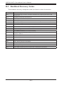
B-2
Bootblock Recovery Codes ............................................................................. B-2
B-3
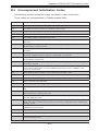
Uncompressed Initialization Codes ................................................................. B-3
vi
Chapter 1: Introduction
Chapter 1
Introduction
1-1
Overview
Checklist
Congratulations on purchasing your computer motherboard from an acknowledged
leader in the industry. Supermicro boards are designed with the utmost attention to
detail to provide you with the highest standards in quality and performance.
Please check that the following items have all been included with your motherboard.
If anything listed here is damaged or missing, contact your retailer.
•
•
•
One (1) H8DGU-LN4F+ serverboard
Two (2) 2ft. Amphenol, SATA cable (CBL-0044L)
Two (2) Retention brackets (BKT-0035L)
Note: For your system to work properly, please follow the links below to download
all necessary drivers/utilities and the user’s manual for your motherboard.
•
•
•
•
Supermicro product manuals: http://www.supermicro.com/support/manuals/
Product drivers and utilities: ftp://ftp.supermicro.com
Product safety information:
http://super-dev/about/policies/safety_information.cfm
If you have any questions, please contact our support team at:
[email protected]
1-1
H8DGU-LN4F+ Serverboard User’s Manual
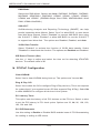
1-2
Contacting Supermicro
Headquarters
Address:
Super Micro Computer, Inc.
980 Rock Ave.
San Jose, CA 95131 U.S.A.
Tel:
+1 (408) 503-8000
Fax:
+1 (408) 503-8008
Email:
[email protected] (General Information)
Web Site:
www.supermicro.com
[email protected] (Technical Support)
Europe
Address:
Super Micro Computer B.V.
Het Sterrenbeeld 28, 5215 ML
's-Hertogenbosch, The Netherlands
Tel:
+31 (0) 73-6400390
Fax:
+31 (0) 73-6416525
Email:
[email protected] (General Information)
[email protected] (Technical Support)
[email protected] (Customer Support)
Web Site:
www.supermicro.com
Asia-Pacific
Address:
Super Micro Computer, Inc.
3F, No. 150, Jian 1st Rd.
Zhonghe Dist., New Taipei City 235
Taiwan (R.O.C)
Tel:
+886-(2) 8226-3990
Fax:
+886-(2) 8226-3992
Email:
[email protected]
Tel:
+886-(2)-8226-3990
Web Site:
www.supermicro.com.tw
1-2
Chapter 1: Introduction
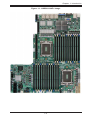
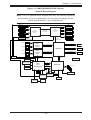
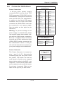
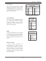
Figure 1-1. H8DGU-LN4F+ Image
1-3
H8DGU-LN4F+ Serverboard User’s Manual
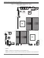
Figure 1-2. H8DGU-LN4F+ Motherboard Layout
(not drawn to scale)
COM1
VGA1
KB/
MOUSE
IPMI_LAN
USB0/1
VGA2
JPL1
JPL2
P1-DIMM1A
P1-DIMM1B
P1-DIMM1C
P1-DIMM2A
P1-DIMM2B
P1-DIMM2C
P1-DIMM3A
P1-DIMM3B
P1-DIMM3C
P1-DIMM4A
P2-DIMM4C
P2-DIMM4B
P2-DIMM4A
P2-DIMM3C
JPW1
JPW2
JPW3
FAN1
FAN2
FAN8
JPK1
FAN3
FAN4
FAN5
JWD1
JPI2C
SATA2
JTPM1
FAN6
SATA1
SATA0
JIPMB1
T-SGPIO1
T-SGPIO2
1-4
P2-DIMM3A
BATTERY
SATA3
DP4 SPEAKER
P2-DIMM3B
P2-DIMM2C
P2-DIMM2A
P2-DIMM2B
SATA5
SATA4
USB2/3 USB4/5
JOH1
JF1
P2-DIMM1C
P2-DIMM1A
USB6
JD1
P2-DIMM1B
COM2
JBT1
P1-DIMM4B
CPU1
CPU2
AMD
SP5100
P1-DIMM4C
PCI-E 2.0 X8 in X4
JWF1
LAN1
PCI-E 2.0 X16
JL1
LAN2
FAN7
JI2C1
INTEL
82576
INTEL
82576
AMD
SR5690
PCI-E 2.0 (X4+X1+X1) IN X8
JI2C2
LAN3
UIOP
WINBOND
BMC
JPG1
LAN4
UID
LE1
DP5
Notes:
Note 1: Jumpers not indicated are for test purposes only.
Note 2: Not all ports, jumpers or LED Indicators are available on all serverboards.
Chapter 1: Introduction
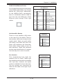
H8DGU-LN4F+ Quick Reference
Jumper
Description
Default Setting
JBT1
CMOS Clear
(See Section 2-7)
JI2C1/JI2C2
I2C to PCI-E Slot Enable/Disable
Both Open (Disabled)
JPG1
VGA Enable/Disable
Pins 1-2 (Enabled)
JPL1
LAN 1/2 Enable/Disable
Pins 1-2 (Enabled)
JPL2
LAN 3/4 Enable/Disable
Pins 1-2 (Enabled)
JWD1
Watch Dog
Pins 1-2 (Reset)
LED
Description
LAN Ports
LEDs for the LAN Ethernet ports
Dedicated IPMI LAN
LEDs for the dedicated IPMI LAN Ethernet port
DP4
LED for Serverboard Power-On
DP5
LED for BMC Heartbeat
LE1
LED for UID Button
1-5
H8DGU-LN4F+ Serverboard User’s Manual
Connector
Description
COM1/COM2
COM1 Serial Port/Header
FAN 1-8
Chassis/CPU Fan Headers
IPMI LAN
Dedicated IPMI LAN Port
JIPMB1
System Management Bus Header for the IPMI Slot
JD1
Speaker Header
JF1
Front Panel Connector
JL1
Chassis Intrusion Header
JOH1
Overheat Warning Header
JPI2C
Power I2C Header
JPK1
NIC3/NIC4 LED Header
JTPM1
Trusted Platform Module Header
JPW1
24-pin Main ATX Power Connector
JPW2/3
+12V 8-pin CPU Power Connectors
JWF1
Compact Flash Card Power Connector
LAN1/2/3/4
Gigabit Ethernet (RJ45) Ports
PS2 Mouse/Keyboard
PS2 Mouse/Keyboard connectors
UID
Unit Identifier Button
UIOP
Universal I/O Power Connector
SATA0 ~ SATA5
SATA Ports
T-SGPIO-1/TSGPIO-2
Serial General Purpose Input/Output Header for SATA
USB0/1, USB2/3, USB4/5, USB6
Universal Serial Bus (USB) Ports, Headers and Type-A Port
VGA1/VGA2
VGA Connectors
1-6
Chapter 1: Introduction
1-3
Motherboard Features
CPU
•
Dual AMD Opteron 6000 series (AMD Socket G34 type) processor
Note: Refer to our web site for details on supported processors.
Memory
•
Up to twenty-Four (24) single/dual/tri/quad-channel DIMM slots that
support up to up to 128 GB of ECC/Non-ECC Unbuffered or 768 GB
of ECC Registered DIMM DDR3-1600/1333/1066 Mhz speed,
1 GB, 2 GB, 4 GB, 8 GB, 16 GB or 32 GB size SDRAM memory in
1.5V or 1.35V voltages.
Note: Refer to Section 2-5 before installing memory and our web site for recommended DIMMs.
Chipset
•
AMD SR5690 chipset and one SP5100 Southbridge chipset
Expansion Slots
•
1U Left Side: 1/1 UIO/PCI Express x8 or 2 PCI Express x8; or 1 PCI Express
x16 or 1/1 UIO/PCI Express x16
•
2U Left Side: 1/2 UIO/PCI Express x8 or 1/1 UIO/PCI Express x16; or 3 PCIExpress x8
•
2U Right Side: 1/1/1 PCI-Express x4/x1/x1
BIOS
•
16 Mb AMI BIOS® SPI Flash ROM
•
APM 1.2, DMI 2.3, PCI 2.2, ACPI 1.0 (ACPI 2.0 is BIOS supported), SMBIOS
2.3, Real Time Clock Wakeup, Plug and Play (PnP), BIOS resume hot keys,
Hardware BIOS Virus Protection
PC Health Monitoring
•
Onboard voltage monitors
•
Fan status monitor with firmware/software on/off and speed control
•
Watch Dog
•
Environmental temperature monitoring via BIOS
•
Power-up mode control for recovery from AC power loss
•
System resource alert (via included utility program)
•
Auto-switching voltage regulator for the CPU core
•
CPU thermal trip support
1-7
H8DGU-LN4F+ Serverboard User’s Manual
•
I2C temperature sensing logic
•
Chipkill Support
ACPI Features
•
Microsoft OnNow
•
Slow blinking LED for suspend state indicator
•
BIOS support for USB keyboard
Onboard I/O
•
Six (6) SATA ports supported by an on-chip SATA controller (RAID 0, 1, 10
supported)
•
Seven (7) USB (Universal Serial Bus 2.0) ports (2x rear, 4x header,
1x type A)
•
Four (4) LAN ports supported by two onboard Intel® 82576 dual port Ethernet
controllers for 10/100/1000Base-T
•
One (1) dedicated IPMI LAN port
•
Two (2) VGA ports supported by an onboard Matrox® G200 graphics controller
(with 16 MB DDR2 memory)
•
Two COM Ports (one external serial port, one Fast UART 16550 port)
Other
•
Onboard power LED
•
Chassis intrusion detection
CD Utilities
•
BIOS flash upgrade utility
•
Super Doctor III
•
IPMI 1.5 / 2.0
Dimensions
•
Propriatory form-factor: (LxW) 12.8" x 16.5" (325 x 419 mm)
1-8
Chapter 1: Introduction
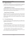
Figure 1-3. AMD SR5690/SP5100 Chipset:
System Block Diagram
Note: This is a general block diagram and may not exactly represent
the features on your motherboard. See the previous pages for the
actual specifications of your motherboard.
DIMM A2
DIMM A1
DIMM A0
DIMM A2
DIMM A1
DIMM A0
DIMM B2
DIMM B1
DIMM B0
AMD
Socket G34
CPU2
DIMM C2
DIMM C1
DIMM C0
DIMM D2
DIMM D1
DIMM D0
DIMM C2
DIMM C1
DIMM C0
HT3 Link
16/16-2.6 GHz
HT3 Link
16/16-3.2GHz
LAN3/4
INTEL
KAWELA
82576
RJ45
RJ45
DIMM B2
DIMM B1
DIMM B0
AMD
Socket G34
CPU1
HT3 Link
8/8-3.2GHz
PCI-E GEN2 X4
SR5690
LAN1/2
INTEL
KAWELA
82576
RJ45
RJ45
PCI-E GEN2 X4
DIMM D2
DIMM D1
DIMM D0
PCI-E GEN2 X4+X1+X1
Slot1
PCI-E GEN2 X16
Slot2
PCI-E GEN2 X8
Slot3
MUX
DDR2 SDRAM
64M x 16-bit
PSU I2C
A-Link
RMII
VGA
Clock Gen
PCI
BMC
VGA
WPCM450-R
SP5100
SMBus
IPMB
SATA x6
LPC
TPM
COM1
COM2
SPI Flash
HWM
W83795G
SIO
W83527
KB/MS
7xUSB
FE PHY
RTL8201N
RJ45
1-9
H8DGU-LN4F+ Serverboard User’s Manual
1-4
Chipset Overview
The H8DGU-LN4F+ serverboard is based on the AMD SR5690/SP5100 chipset. This
chipset functions as a Media and Communications Processor (MCP). Controllers for
the system memory are integrated directly into AMD Opteron processors.
AMD SR5690/SP5100 Chipset
The AMD SR5690/SP5100 are each a single-chip, high-performance HyperTransport
peripheral controller. It includes a 42-lane PCI Express interface, an AMD Opteron
16-bit Hyper Transport interface link, a six-port Serial ATA interface and a seven-port
USB 2.0 interface. This hub connects directly to the CPU.
HyperTransport Technology
HyperTransport technology is a high-speed, low latency point to point link that was
designed to increase the communication speed by a factor of up to 48x between
integrated circuits. This is done partly by reducing the number of buses in the
chipset to reduce bottlenecks and by enabling a more efficient use of memory
in multi-processor systems. The end result is a significant increase in bandwidth
within the chipset.
1-5
PC Health Monitoring
This section describes the PC health monitoring features of the H8DGU-LN4F+
serverboard. The serverboard has an onboard System Hardware Monitor chip that
supports PC health monitoring.
Onboard Voltage Monitors
The onboard voltage monitor will continuously scan crucial voltage levels. Once
a voltage becomes unstable, it will give a warning or send an error message to
the screen. Users can adjust the voltage thresholds to define the sensitivity of the
voltage monitor. Real time readings of these voltage levels are all displayed in BIOS.
Fan Status Monitor with Firmware/Software Speed Control
The PC health monitor can check the RPM status of the cooling fans. The onboard
fans are controlled by thermal management via BIOS.
1-10
Chapter 1: Introduction
CPU Overheat/Fan Fail LED and Control
This feature is available when the user enables the CPU overheat/Fan Fail warning
function in the BIOS. This allows the user to define an overheat temperature. When
this temperature is exceeded or when a fan failure occurs, the Overheat/Fan Fail
warning LED is triggered.
Auto-Switching Voltage Regulator for the CPU Core
The 5+1-phase-switching voltage regulator for the CPU core can support up to
AMD Opteron 6000SE series processors and auto-sense voltage IDs ranging from
0.8 V to 1.55V. This will allow the regulator to run cooler and thus make the system
more stable.
1-6
Power Configuration Settings
This section describes the features of your motherboard that deal with power and
power settings.
Microsoft OnNow
The OnNow design initiative is a comprehensive, system-wide approach to system
and device power control. OnNow is a term for a PC that is always on but appears
to be off and responds immediately to user or other requests.
Slow Blinking LED for Suspend-State Indicator
When the CPU goes into a suspend state, the chassis power LED will start blinking
to indicate that the CPU is in suspend mode. When the user presses any key, the
CPU will wake-up and the LED will automatically stop blinking and remain on.
BIOS Support for USB Keyboard
If a USB keyboard is the only keyboard in the system, it will function like a normal
keyboard during system boot-up.
1-11
H8DGU-LN4F+ Serverboard User’s Manual
Main Switch Override Mechanism
The power button can function as a system suspend button. When the user
depresses the power button, the system will enter a SoftOff state. The monitor
will be suspended and the hard drive will spin down. Depressing the power button
again will cause the whole system to wake-up. During the SoftOff state, the power
supply provides power to keep the required circuitry in the system alive. In case the
system malfunctions and you want to turn off the power, just depress and hold the
power button for 4 seconds. The power will turn off and no power will be provided
to the motherboard.
1-7
Power Supply
As with all computer products, a stable power source is necessary for proper and
reliable operation. It is even more important for processors that have high CPU
clock rates.
The H8DGU-LN4F+ serverboard requires the use of proprietary power supplies.
Please refer to the pinout information for the power connectors in Section 6 of
Chapter 2 for detailed information on power requirements.
In areas where noisy power transmission is present, you may choose to install a
line filter to shield the computer from noise. It is recommended that you also install
a power surge protector to help avoid problems caused by power surges.
Warning: To prevent the possibility of explosion, do not use the wrong type of
onboard CMOS battery or install it upside down.
1-8
Super I/O
The disk drive adapter functions of the Super I/O Winbond® BMC chip includes a
data separator, write pre-compensation circuitry, decode logic, data rate selection,
a clock generator, drive interface control logic and interrupt and DMA logic. The
wide range of functions integrated onto the Super I/O greatly reduces the number
of components required for interfacing with floppy disk drives.
The Super I/O provides two high-speed, 16550 compatible serial communication
ports (UARTs), one of which supports serial infrared communication. Each UART
includes a 16-byte send/receive FIFO, a programmable baud rate generator,
complete modem control capability and a processor interrupt system. Both UARTs
provide legacy speed with baud rate of up to 115.2 Kbps as well as an advanced
speed with baud rates of 250 K, 500 K, or 1 Mb/s, which support higher speed
modems.
1-12
Chapter 1: Introduction
The Super I/O provides functions that comply with ACPI (Advanced Configuration
and Power Interface), which includes support of legacy and ACPI power management
through a SMI or SCI function pin. It also features auto power management to reduce
power consumption.
The IRQs, DMAs and I/O space resources of the Super I/O can be flexibly adjusted
to meet ISA PnP requirements, which support ACPI and APM (Advanced Power
Management).
1-13
H8DGU-LN4F+ Serverboard User’s Manual
Notes
1-14
Chapter 2: Installation
Chapter 2
Installation
2-1
Standardized Warning Statements
About Standardized Warning Statements
The following statements are industry standard warnings, provided to warn the user
of situations which have the potential for bodily injury. Should you have questions
or experience difficulty, contact Supermicro's Technical Support department
for assistance. Only certified technicians should attempt to install or configure
components.
Read this section in its entirety before installing or configuring components in the
Supermicro chassis.
These warnings may also be found on our web site at http://www.supermicro.
com/about/policies/safety_information.cfm.
Battery Handling
Warning!
There is a danger of explosion if the battery is replaced incorrectly. Replace the
battery only with the same or equivalent type recommended by the manufacturer.
Dispose of used batteries according to the manufacturer's instructions
電池の取り扱い
電池交換が正しく行われなかった場合、破裂の危険性があります。交換する電池はメー
カーが推奨する型、
または同等のものを使用下さい。 使用済電池は製造元の指示に従
って処分して下さい。
警告
电池更换不当会有爆炸危险。请只使用同类电池或制造商推荐的功能相当的电池更
换原有电池。请按制造商的说明处理废旧电池。
警告
電池更換不當會有爆炸危險。請使用製造商建議之相同或功能相當的電池更換原有
電池。請按照製造商的說明指示處理廢棄舊電池。
2-1
H8DGU-LN4F+ Serverboard User's Manual
Warnung
Bei Einsetzen einer falschen Batterie besteht Explosionsgefahr. Ersetzen Sie die
Batterie nur durch den gleichen oder vom Hersteller empfohlenen Batterietyp.
Entsorgen Sie die benutzten Batterien nach den Anweisungen des Herstellers.
Attention
Danger d'explosion si la pile n'est pas remplacée correctement. Ne la remplacer
que par une pile de type semblable ou équivalent, recommandée par le fabricant.
Jeter les piles usagées conformément aux instructions du fabricant.
¡Advertencia!
Existe peligro de explosión si la batería se reemplaza de manera incorrecta.
Reemplazar la batería exclusivamente con el mismo tipo o el equivalente
recomendado por el fabricante. Desechar las baterías gastadas según las
instrucciones del fabricante.
!אזהרה
יש להחליף.קיימת סכנת פיצוץ של הסוללה במידה והוחלפה בדרך לא תקינה
.את הסוללה בסוג התואם מחברת יצרן מומלצת
.סילוק הסוללות המשומשות יש לבצע לפי הוראות היצרן
ﻫﻨﺎﻙ ﺧﻄﺮ ﻣﻦ ﺍﻧﻔﺠﺎﺭ ﻓﻲ ﺣﺎﻟﺔ ﺍﺳﺘﺒﺪﺍﻝ ﺍﻟﺒﻄﺎﺭﻳﺔ ﺑﻄﺮﻳﻘﺔ ﻏﻴﺮ ﺻﺤﻴﺤﺔ ﻓﻌﻠﻴﻚ
ﺍﺳﺘﺒﺪﺍﻝ ﺍﻟﺒﻄﺎﺭﻳﺔ
ﻓﻘﻂ ﺑﻨﻔﺲ ﺍﻟﻨﻮﻉ ﺃﻭ ﻣﺎ ﻳﻌﺎﺩﻟﻬﺎ ﻛﻤﺎ ﺃﻭﺻﺖ ﺑﻪ ﺍﻟﺸﺮﻛﺔ ﺍﻟﻤﺼﻨﻌﺔ
ﺗﺨﻠﺺ ﻣﻦ ﺍﻟﺒﻄﺎﺭﻳﺎﺕ ﺍﻟﻤﺴﺘﻌﻤﻠﺔ ﻭﻓﻘﺎ ﻟﺘﻌﻠﻴﻤﺎﺕ ﺍﻟﺸﺮﻛﺔ ﺍﻟﺼﺎﻧﻌﺔ
경고!
배터리가 올바르게 교체되지 않으면 폭발의 위험이 있습니다. 기존 배터리와
동일하거나 제조사에서 권장하는 동등한 종류의 배터리로만 교체해야 합니다.
제조사의 안내에 따라 사용된 배터리를 처리하여 주십시오.
Waarschuwing
Er is ontploffingsgevaar indien de batterij verkeerd vervangen wordt. Vervang de
batterij slechts met hetzelfde of een equivalent type die door de fabrikant aanbevolen
wordt. Gebruikte batterijen dienen overeenkomstig fabrieksvoorschriften afgevoerd
te worden.
2-2
Chapter 2: Installation
Product Disposal
Warning!
Ultimate disposal of this product should be handled according to all national laws
and regulations.
製品の廃棄
この製品を廃棄処分する場合、国の関係する全ての法律・条例に従い処理する必要が
あります。
警告
本产品的废弃处理应根据所有国家的法律和规章进行。
警告
本產品的廢棄處理應根據所有國家的法律和規章進行。
Warnung
Die Entsorgung dieses Produkts sollte gemäß allen Bestimmungen und Gesetzen
des Landes erfolgen.
¡Advertencia!
Al deshacerse por completo de este producto debe seguir todas las leyes y
reglamentos nacionales.
Attention
La mise au rebut ou le recyclage de ce produit sont généralement soumis à des
lois et/ou directives de respect de l'environnement. Renseignez-vous auprès de
l'organisme compétent.
סילוק המוצר
!אזהרה
.סילוק סופי של מוצר זה חייב להיות בהתאם להנחיות וחוקי המדינה
ﻋﻨﺪ ﺍﻟﺘﺨﻠﺺ ﺍﻟﻨﻬﺎﺋﻲ ﻣﻦ ﻫﺬﺍ ﺍﻟﻤﻨﺘﺞ ﻳﻨﺒﻐﻲ ﺍﻟﺘﻌﺎﻣﻞ ﻣﻌﻪ ﻭﻓﻘﺎ ﻟﺠﻤﻴﻊ ﺍﻟﻘﻮﺍﻧﻴﻦ ﻭﺍﻟﻠﻮﺍﺋﺢ ﺍﻟﻮﻁﻨﻴﺔ
경고!
이 제품은 해당 국가의 관련 법규 및 규정에 따라 폐기되어야 합니다.
Waarschuwing
De uiteindelijke verwijdering van dit product dient te geschieden in overeenstemming
met alle nationale wetten en reglementen.
2-3
H8DGU-LN4F+ Serverboard User's Manual
2-2
Static-Sensitive Devices
Electrostatic Discharge (ESD) can damage electronic components. To prevent
damage to your system board, it is important to handle it very carefully. The following
measures are generally sufficient to protect your equipment from ESD.
Precautions
•
•
•
•
•
•
•
Use a grounded wrist strap designed to prevent static discharge.
Touch a grounded metal object before removing the board from the antistatic
bag.
Handle the board by its edges only; do not touch its components, peripheral
chips, memory modules or gold contacts.
When handling chips or modules, avoid touching their pins.
Put the motherboard and peripherals back into their antistatic bags when not
in use.
For grounding purposes, make sure your computer chassis provides excellent
conductivity between the power supply, the case, the mounting fasteners and
the motherboard.
Use only the correct type of CMOS onboard battery as specified by the
manufacturer. Do not install the CMOS onboard battery upside down, which
may result in a possible explosion.
Unpacking
The motherboard is shipped in antistatic packaging to avoid static damage. When
unpacking the board, make sure the person handling it is static protected.
2-4
Chapter 2: Installation
2-3
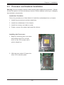
Processor and Heatsink Installation
Warning: Exercise extreme caution when handling and installing the processor. Always
connect the power cord last and always remove it before adding, removing or changing
any hardware components.
Installation Procedure
Follow the procedures as listed below to install the motherboard into a chassis.
1. Install the processor(s) and the heatsink(s).
2. Install the motherboard in the chassis.
3. Install the memory and add-on cards.
4. Finally, connect the cables and install the drivers.
Installing the Processors
1. Begin by removing the cover plate
that protects the CPU. Lift the
lever on the CPU socket until it
points straight up.
2. With the lever raised, lift open the
silver CPU retention plate.
2-5
H8DGU-LN4F+ Serverboard User's Manual
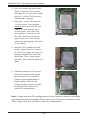
3. Use your thumb and your index
finger to hold the CPU. Locate
and align pin 1 of the CPU socket
with pin 1 of the CPU. Both are
marked with a triangle.
4. Align pin 1 of the CPU with pin
1 of the socket. Once aligned,
carefully place the CPU into the
socket. Do not drop the CPU
on the socket, move the CPU
horizontally or vertically or rub
the CPU against the socket or
against any pins of the socket,
which may damage the CPU and/
or the socket.
Triangle
5. With the CPU inserted into the
socket, inspect the four corners
of the CPU to make sure that it is
properly installed and flush with
the socket. Then, gently lower
the silver CPU retention plate into
place.
6. Carefully press the CPU socket
lever down until it locks into its
retention tab. For a dual-CPU
system, repeat these steps to
install another CPU into the
CPU#2 socket (and into CPU#2,
CPU#3 and #4 sockets for a
quad-CPU configuration).
Note: In single and dual-CPU configurations, memory must be installed in the DIMM
slots associated with the installed CPU(s). Memory is limited to a maximum of 384
GB for single CPU and 768 GB for dual CPU configurations.
2-6
Chapter 2: Installation
Installing the Heatsinks
We recommend the use of active type heatsinks (except for 1U systems). Use any
onboard fan header for the CPU's heatsink fan. To install the heatsink, please follow
the installation instructions that are included with your heatsink package.
Note: Make sure the heatsink is placed so that the fins of the heatsink are in the
direction of the airflow in your system.
2-4
Mounting the Motherboard into a Chassis
All motherboards have standard mounting holes to fit different types of chassis.
Make sure that the locations of all the mounting holes for both the motherboard
and the chassis match. Although a chassis may have both plastic and metal
mounting fasteners, metal ones are highly recommended because they ground
the motherboard to the chassis. Make sure that the metal standoffs click in or are
screwed in tightly.
Check the Compatibility of the Motherboard Ports and the I/O Shield
1. The H8DGU-LN4F+ serverboard requires a chassis that can support a board
of (LxW) 12.8" x 16.5" (325 x 419 mm) in size.
2. Make sure that the I/O ports on the motherboard align with their respective
holes in the I/O shield at the rear of the chassis.
Mounting the Motherboard onto the Tray in the Chassis
1. Carefully mount the motherboard onto the motherboard tray by aligning the
motherboard mounting holes with the raised metal standoffs in the tray.
2. Insert screws into all the mounting holes in the motherboard that line up with
the standoffs.
3. Then use a screwdriver to secure the motherboard to the mainboard
tray - tighten until just snug (if too tight you might strip the threads). Metal
screws provide an electrical contact to the motherboard ground to provide a
continuous ground for the system.
2-5
Installing Memory
Warning: Exercise extreme caution when installing or removing memory modules to
prevent any possible damage.
Installing Memory
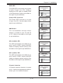
1. Insert each memory module vertically into its slot, paying attention to the
notch along the bottom of the module to prevent inserting the module
incorrectly (see Figure 2-1).
2-7
H8DGU-LN4F+ Serverboard User's Manual
2. Install to slots CPU1/DIMM1A, CPU1/DIMM2A, CPU1/DIMM3A and CPU1/
DIMM4A, etc. Always install in groups of four and in the numerical order of
the DIMM slots. See support information below.
3. Gently press down on the memory module until it snaps into place.
4. With four DIMMs installed, repeat step 2 to populate the CPU2 DIMM
slots. Always install four DIMMs to both CPU DIMM slots for more efficient
operation.
Note: 1 GB, 2 GB, 4 GB, 8 GB, 16 GB or 32 GB size memory modules are
supported. It is highly recommended that you remove the power cord from the
system before installing or changing memory modules. Please refer to our web site
for memory that has been tested on the H8DGU-LN4F+ serverboard.
Memory Support
The H8DGU-LN4F+ serverboard supports single/dual/tri/quad-channel DIMMs with
DDR3-1600/1333/1066 Mhz speed SDRAM.
Populating four adjacent slots at a time with memory modules of the same size and
type will result in interleaved (128-bit) memory, which is faster than non-interleaved
(64-bit) memory.
Maximum Memory
The H8DGU-LN4F+ serverboard supports up to128 GB of ECC/Non-ECC
Unbuffered or 768 GB of ECC Registered DIMM in 24 DIMM slots.
Figure 2-1. Installing DIMM into Slot
To Install: Insert
module vertically and
press down until it
snaps into place.
Pay attention to the
alignment notch at
the bottom.
Notch
To Remove: Use
your thumbs to gently Release Tab
push the release tabs
near both ends of the
module. This should
release it from the
slot.
Notch
Front View
Note: Notch should align with
the receptive key point on
the slot.
Release Tab
Top View of DDR3 Slot
2-8
Chapter 2: Installation
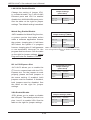
Memory Population for Optimal Performance
For a Motherboard with One CPU (CPU1) Installed
DIMM #
Channel 1
Channel 2
Channel 3
Channel 4
4 DIMMs
P1-1A
P1-2A
P1-3A
P1-4A
8 DIMMs
P1-1A
P1-1C P1-2A
P1-2C P1-3A
P1-3C P1-4A
12 DIMMs
P1-1A P1-1B P1-1C P1-2A P1-2B P1-2C P1-3A P1-3B P1-3C P1-4A P1-4B P1-4C
P1-4C
Memory Population for Optimal Performance
For a Motherboard with Two CPUs (CPU1 & CPU2) Installed
CPU
Channel 1
Channel 2
Channel 3
Channel 4
8 DIMMs
CPU1
P1-1A
P1-2A
P1-3A
P1-4A
CPU2
P2-1A
P2-2A
P2-3A
P2-4A
CPU1
P1-1A
P1-1C P1-2A
P1-2C P1-3A
P1-3C P1-4A
P1-4C
CPU2
P2-1A
P2-1C P2-2A
P2-2C P2-3A
P2-3C P2-4A
P2-4C
CPU1
P1-1A P1-1B P1-1C P1-2A P1-2B P1-2C P1-3A P1-3B P1-3C P1-4A P1-4B P1-4C
CPU2
P2-1A P2-1B P2-1C P2-2A P2-2B P2-2C P2-3A P2-3B P2-3C P2-4A P2-4B P2-4C
16 DIMMs
24 DIMMs
Note: Memory speed support is dependent on the type of CPU used on the board.
2-9
H8DGU-LN4F+ Serverboard User's Manual
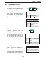
DIMM Module Population Configuration
For memory to work properly, follow the tables below for memory installation:
Per Channel DIMM Populations Options
DIMM Type
Unbuffered
DIMM
Registered
DIMM
LRDIMM
Max.
MHz, 1.5V
DIMMs
Max.
MHz, 1.35V
DIMMs
Max. GB/
Channel
DIMM A
DIMM B
DIMM C
SR or DR
Empty
Empty
1600 MHz
1333 MHz
8 GB
SR
Empty
SR
1600 MHz
1333 MHz
8 GB
16 GB
DR
Empty
DR
1333 MHz
1333 MHz
SR or DR
Empty
Empty
1600 MHz
1333 MHz
16 GB
SR
Empty
SR
1333 MHz
1333 MHz
16 GB
DR
Empty
DR
1333 MHz
1333 MHz
32 GB
SR
SR
SR
1066 MHz
1066 MHz
12 GB
Empty
QR
Empty
1066 MHz
1066 MHz
32 GB
DR
DR
DR
1066 MHz
800 MHz
48 GB
QR
Empty
Empty
1333 MHz
32 GB
QR
Empty
QR
1333 MHz
64 GB
QR
QR
QR
800 MHz
96 GB
Note 1: Due to OS limitations, some operating systems may not show more than
4 GB of memory.
Note 2: Due to memory allocation to system devices, the amount of memory that
remains available for operational use will be reduced when 4 GB of RAM is used.
The reduction in memory availability is disproportional.
Note 3: Quad-rank DIMM must be DIMM B.
2-10
Chapter 2: Installation
2-6
PCI Expansion Cards
A riser card is used to support one standard size (full height full length) PCI
expansion card.
Installing a PCI Expansion Card
1. Confirm that you have the correct riser card for your chassis model and the
add-on card includes a standard bracket.
2. Remove the chassis cover.
3. Install the riser card by sliding card into the appropriate slot in the
serverboard.
4. Choose the PCI slot shield in which to place the add-on card.
5. In that slot, open the PCI slot shield lever and slide the shield sideways.
6. From inside the chassis, remove the PCI slot shield.
7. Slide the add-on card into the riser card and attach the add-on card bracket
in place of the PCI slot shield.
8. Secure the add-on card by closing the PCI slot shield lever.
9. Connect cables to the add-on card as necessary.
Note: If the left side riser is with 2 or more x8 PCI-E slots, make sure an installed
card on the left side riser is detected. If it is not, then go to the system’s BIOS
Setup and in Advanced/ PCI/PnP Configuration /SXB1 Configuration BIOS setting
select the [2x8] option. Then save the BIOS setting changes and reboot the system.
2-11
H8DGU-LN4F+ Serverboard User's Manual
2-7
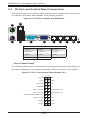
I/O Port and Control Panel Connections
The I/O ports are color coded to make setting up your system easier. See Figure
2-2 below for the colors and locations of the various I/O ports.
Figure 2-2. I/O Port Locations and Definitions
2
1
4
3
5
6
7
8
9
10
11
Rear I/O Ports
1. Keyboard
5. COM1
2. PS/2 Mouse
6. VGA Port
9. LAN3
10. LAN4
3. USB0/1
7. LAN1
11. UID
4. IPMI LAN
8. LAN2
Front Control Panel
JF1 contains header pins for various front control panel connectors. See Figure 2-3
for the pin definitions of the various connectors. Refer to Section 2-6 for details.
Figure 2-3. JF1: Front Control Panel Header (JF1)
20
19
Ground
NMI
x (key)
x (key)
Power LED
3.3V
HDD LED
Vcc
NIC1 (Link) LED
NIC1 (Activity) LED
NIC2 (Link) LED
NIC2 (Activity) LED
OH/PWR Fail/Fan Fail/UID LED
Vcc
Power Fail LED
3.3V
Ground
Reset
Ground
Power
2
2-12
1
Chapter 2: Installation
2-8
Connector Definitions
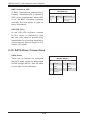
ATX Power 24-pin Connector
Pin Definitions
Power Connectors
Pin# Definition
Pin# Definition
A 24-pin main power supply
connector(JPW1) and two 8-pin CPU
PWR connectors (JPW2/JPW3) on the
motherboard. These power connectors
meet the SSI EPS 12V specification.
In addition to the 24-pin ATX power
connector, the 12V 8-pin CPU PWR
connectors at JPW2/JPW3 must also
be connected to your power supply.
See the table on the right for pin
definitions.
13
+3.3V
1
+3.3V
14
-12V
2
+3.3V
15
COM
3
COM
16
PS_ON
4
+5V
17
COM
5
COM
18
COM
6
+5V
19
COM
7
COM
20
Res (NC)
8
PWR_OK
21
+5V
9
5VSB
22
+5V
10
+12V
Warning: To prevent damage to the
power supply or motherboard, please
use a power supply that contains a 24pin and two 8-pin power connectors.
Be sure to connect these connectors
to the 24-pin (JPW1) and the two 8-pin
(JPW2,JPW3) power connectors on
the motherboard. Failure in doing so
will void the manufacturer warranty on
your power supply and motherboard.
23
+5V
11
+12V
24
COM
12
+3.3V
12V 8-pin PWR Connector
Pin Definitions
Pins
Definition
1 through 4
Ground
5 through 8
+12V
Required Connection
Power Connector
The Power Connector is located on
pins 1 and 2 of JF1. Momentarily
contacting both pins will power on/off
the system. This button can also be
confi gured to function as a suspend
button (with a setting in the BIOS - see
Chapter 4). To turn off the power when
set to suspend mode, press the button
for at least 4 seconds. Refer to the
table on the right for pin defi nitions.
2-13
Power Button
Pin Defi nitions
(JF1)
Pin# Definition
1
Power
2
Ground
H8DGU-LN4F+ Serverboard User's Manual
Reset Connector
Reset Button
Pin Definitions
(JF1)
The reset connector is located on
pins 3 and 4 of JF1 and attaches
to the reset switch on the computer
chassis. See the table on the right for
pin definitions.
Pin# Definition
3
Reset
4
Ground
Power Fail LED
PWR Fail LED
Pin Definitions
(JF1)
The Power Fail LED connection is
located on pins 5 and 6 of JF1. Refer to
the table on the right for pin definitions.
Overheat (OH)/Fan Fail/PWR Fail/
UID LED
Connect an LED cable to pins 7 and
8 of JF1 to use the Overheat/Fan Fail/
Power Fail and UID LED connections.
The Red LED on pin 8 provides
warnings of an overheat, fan failure
or power failure. The Blue LED on pin
8 works as the UID LED indicator for
the front panel UID switch. Refer to the
table on the right for pin definitions.
Pin# Definition
5
3.3V
6
Power Fail LED
OH/Fan Fail/ PWR Fail (Red) LED
and UID (Blue) LED
Pin Definitions (JF1)
Pin# Definition
7
Vcc
8
OH/Fan Fail/PWS Fail (Red) LED
and UID (Blue) LED
OH/Fan Fail/PWR Fail
LED Status (Red LED)
State
Indication
Off
Normal
On
Overheat
Flashing
Fan Fail
NIC2 (Link/Activity) LED
The LED connections for LAN2 link/
activity are on pins 9 and 10 of JF1.
Attach LAN LED cables to display
network activity. See the table on the
right for pin definitions.
NIC2 LED
Pin Definitions
(JF1)
Pin# Definition
9
Activity
10
Link
NIC1 (Link/Activity) LED
The LED connections for LAN1 link/
activity are on pins 11 and 12 of JF1.
Attach LAN LED cables to display
network activity. See the table on the
right for pin definitions.
2-14
NIC1 LED
Pin Definitions
(JF1)
Pin# Definition
11
Activity
12
Link
Chapter 2: Installation
HDD LED
The HDD LED connections are located
on pins 13 and 14 of JF1. Attach a
hard-drive LED cable to display HDD
or SATA activities. Refer to the table on
the right for pin definitions.
HDD LED
Pin Definitions
(JF1)
Pin# Definition
13
Vcc
14
HDD LED
Power LED Connector
The Power LED connector is on pins
15 and 16 of JF1. See the table on the
right for pin definitions.
Power LED
Pin Definitions
(JF1)
Pin# Definition
15
3.3V
16
Power LED
NMI Button
The non-maskable interrupt button
header is located on pins 19 and 20
of JF1. Refer to the table on the right
for pin definitions.
NMI Button
Pin Definitions
(JF1)
Pin# Definition
19
NMI
20
Ground
NIC4 (LAN4) LED
The LED connections for LAN4 are on
pins 1 and 2 of JPK1. Attach LAN LED
cables to display network activity. See
the table on the right for pin definitions.
NIC4 LED
Pin Definitions
(JPK1)
Pin# Definition
1
Activity
2
Link
NIC3 (LAN3) LED
The LED connections for LAN3 are on
pins 3 and 4 of JPK1. Attach LAN LED
cables to display network activity. See
the table on the right for pin definitions.
Chassis Intrusion
A Chassis Intrusion header is located
at JL1. Attach the appropriate cable to
inform you of a chassis intrusion.
2-15
NIC3 LED
Pin Definitions
(JPK1)
Pin# Definition
3
Activity
4
Link
Chassis Intrusion
Pin Definitions
(JL1)
Pin# Definition
1
Battery voltage
2
Intrusion signal
H8DGU-LN4F+ Serverboard User's Manual
Universal Serial Bus Ports
Two Universal Serial Bus ports (USB
2.0) are located beside the Keyboard
and Mouse PS2 ports (USB0/1).
One additional Type A port (USB6) is
included on the motherboard. See the
table on the right for pin definitions.
USB Headers
Four USB 2.0 headers (USB2/3 and
USB4/5) are also included on the
motherboard. These may be connected
to provide front side access. A USB
cable (not included) is needed for the
connection. See the table on the right
for pin definitions.
Universal Serial Bus Ports
Pin Definitions (USB 0/1, USB6)
USB0/1
Pin# Definition
USB6
Pin# Definition
1
+5V
1
+5V
2
PO-
2
PO-
3
PO+
3
PO+
4
Ground
4
Ground
Universal Serial Bus Headers
Pin Definitions
(USB2/3, USB4/5)
JUSB2, JUSB3
Pin#
Definition
Pin#
Definition
1
+5V
2
+5V
3
PO-
4
PO-
5
PO+
6
PO+
7
Ground
8
Ground
9
Key
10
NC
Note: NC indicates no connection.
SGPIO
The T-SGPIO1/ T-SGPIO2 (Serial
General Purpose Input/Output)
headers provide a bus between the
SATA controller and the backpane to
provide SATA enclosure management
functions. Connect the appropriate
cable from the backplane to the
T-SGPIO1 header to utilize SATA
management functions on your system.
Overheat LED
Connect an LED to the JOH1
header to provide warning of chassis
overheating. See the table on the right
for pin definitions.
2-16
SGPIO Header Pin Definitions
(T-SGPIO1/T-SGPIO2)
Pin# Definition
Pin# Definition
1
NC
2
3
Ground
4
Data
5
Load
6
Ground
7
CLK
8
NC
Data
Note: NC indicates no connection.
Overheat LED
Pin Definitions
(JOH1)
Pin# Definition
1
3.3V
2
OH Active
Chapter 2: Installation
Serial Ports
The COM1 serial port is located
beside the VGA port. Refer to the
motherboard layout for the location of
the COM2 header. See the table on the
right for pin definitions.
Serial Port Pin Definitions
(COM1/COM2)
Pin# Definition
Pin# Definition
1
DCD
6
DSR
2
RXD
7
RTS
3
TXD
8
CTS
4
DTR
9
RI
Ground
10
NC
5
Note: NC indicates no connection.
Power SMB (I2C)
The Power System Management Bus
( I2C) connector (JPI2C1) monitors
the power suppply, fan and system
temperatures. See the table on the
right for pin definitions.
Power SMB I2C
Pin Definitions
(JPI2C)
Pin# Definition
1
Clock
2
Data
3
PWR Fail
4
Ground
5
+3.3V
IPMB
A System Management Bus header
for the IPMI slot is located at JIPMB1.
Connect the appropriate cable here to
use the IPMB I2C connection on your
system.
Video Connector
A Vi d e o ( V G A 1 ) c o n n e c t o r i s
located below the COM Port on the
IO backplane. Another connector
(VGA2) is located on the serverboard
below the VGA1 connector. These
connectors are used to provide video
and CRT display.
2-17
JIPMB1
Pin Definitions
Pin# Definition
1
Data
2
Ground
3
Clock
4
No Connection
H8DGU-LN4F+ Serverboard User's Manual
Power LED/Speaker
PWR LED Connector
Pin Definitions
On the JD1 header, pins 1~3 are used
for power LED indication, and pins 4-7
are for the speaker. See the tables
on the right for pin definitions. If you
wish to use the onboard speaker, you
should close pins 6~7 with a jumper.
Connect a cable to pins 4~7 of JD1 to
use an external speaker.
Pin Setting
Definition
Pin 1
Anode (+)
Pin2
Cathode (-)
Pin3
NA
Speaker Connector
Pin Definitions
ATX PS/2 Keyboard and PS/2
Mouse Ports
Pin Setting
Definition
Pins 4~7
External Speaker
Pins 6~7
Internal Speaker
PS/2 Keyboard/Mouse Pin
Definitions
The ATX PS/2 keyboard and PS/2
mouse are located next to the
Back Panel USB Ports 0~3 on the
motherboard. See the table at right for
pin definitions.
PS2 Keyboard
Pin# Definition
PS2 Mouse
Pin# Definition
1
KB Data
1
Mouse Data
2
No Connection
2
No Connection
3
Ground
3
Ground
4
Mouse/KB
VCC (+5V)
4
Mouse/KB
VCC (+5V)
5
KB Clock
5
Mouse Clock
6
No Connection
6
No Connection
VCC: with 1.5A PTC (current limit)
Compact Flash Card PWR
Connector
A Compact Flash Card Power
Connector is located at JWF1. For the
Compact Flash Card to work properly,
you will need to enable with JCF1 and
connect a Compact Flash Card power
cable to JWF1 first.
2-18
Chapter 2: Installation
LAN1/2/3/4 (Ethernet Ports)
Four Gigabit Ethernet ports (designated
LAN1/LAN2/LAN3/LAN4) are located
beside the VGA ports. Additionally,
for the H8DGU-LN4F+ serverboard,
there is a dedicated LAN for IPMI on
top of the two rear USB ports. These
Ethernet ports accept RJ45 type
cables.
LAN Ports (LAN1/2/3/4)
Pin Definition
Pin# Definition
Pin# Definition
1
P2V5SB
10
2
TD0+
11
Act LED
3
TD0-
12
P3V3SB
4
TD1+
13
Link 100 LED
(Yellow, +3V3SB)
5
TD1-
14
Link 1000 LED
(Yellow, +3V3SB)
6
TD2+
15
Ground
7
TD2-
16
Ground
8
TD3+
17
Ground
9
TD3-
18
Ground
SGND
NC indicates no connection.
Unit Identifier Button
UID Button
Pin Definitions
There is a Unit Identifier (UID) button
on the rear I/O of the board. There is
also another UID button located on the
control panel. When you push either
UID button, both Rear UID and Front
Panel UID Indicators will illuminate.
Push either button again to turn off
both indicators. These UID indicators
provide easy identification of a system
unit that may be in need of service.
Fan Headers
This motherboard has eight fan
headers (Fan1 to Fan8). These 4-pin
fans headers are backward compatible
with 3-pin fans. However, fan speed
control is available for 4-pin fans only.
The fan speeds are controlled by
IPMI. See the table on the right for pin
definitions
2-19
Pin#
Definition
1
Ground
2
Ground
3
Button In
4
Ground
Fan Header
Pin Definitions
Pin#
Definition
1
Ground
2
+12V
3
Tachometer
4
PWR Modulation
H8DGU-LN4F+ Serverboard User's Manual
UIO Power Connector
A Universal I/O (UIO) Power connector
(UIOP) is located next to the UID
switch. Connect this connector to the
power supply to provide adequate
power to the UIO device installed
on the slot for this device to function
properly.
Trusted Platform Module Header
The JTPM1 header is used to connect
a Trusted Platform Module (TPM),
available separately from a third-party
vendor. A TPM is a security device
that allows encryption and authentication of hard drives, disallowing access
if the TPM associated with it is not
installed in the system. See the table
on the right for pin definitions.
2-20
UIO Power Connector
Pin Definitions (UIOP)
Pin#
Definition
Pin#
Definition
B1
5V_1
A1
3V3_1
B2
5V_2
A2
3V3_2
B3
5V_3
A3
3V3_3
B4
5V_4
A4
3V3_4
B5
5V_5
A5
3V3_5
B6
5V_6
A6
3V3_6
B7
5V_7
A7
3V3_7
B8
5V_8
A8
3V3_8
B9
5V_9
A9
3V3_9
B10
5V_10
A10
3V3_10
B11
N12V
A11
3V3
B12
3V3_STBY
A12
3V3
B13
3V3_STBY
A13
P12V_2
B14
GND
A14
P12V
B15
GND
A15
P12V
B16
GND_1
A16
P12V
B17
GND_2
A17
P12V
B18
GND_3
A18
GND_7
Trusted Platform Module Header
Pin Definitions (JTPM1)
Pin# Definition
Pin# Definition
1
LCLK
2
GND
3
LFRAME
4
No Pin
5
LRESET
6
VCC5
7
LAD3
8
LAD2
9
VCC3
10
LAD1
11
LAD0
12
GND
13
RSV0
14
RSV1
15
SB3V
16
SERIRQ
17
GND
18
CLKRUN
19
LPCPD
20
RSV2
Chapter 2: Installation
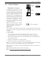
2-8
Jumper Settings
3
2
1
3
2
1
Connector
Pins
Explanation of Jumpers
To modify the operation of the
motherboard, jumpers can be used
to choose between optional settings.
Jumpers create shorts between two
pins to change the function of the
connector. Pin 1 is identified with a
square solder pad on the printed circuit
board. See the diagram at right for
an example of jumping pins 1 and 2.
Refer to the motherboard layout page
for jumper locations.
Note: On two-pin jumpers, "Closed"
means the jumper is on and "Open"
means the jumper is off the pins.
Jumper
Setting
JBT1 contact pads
CMOS Clear
JBT1 is used to clear CMOS, which will also clear any passwords. Instead of pins,
this jumper consists of contact pads to prevent accidentally clearing the contents
of CMOS.
To Clear CMOS
1. First power down the system and unplug the power cord(s). It is also
recommended that you remove the onboard battery from the serverboard.
2. With the power disconnected, short the CMOS pads with a metal object such
as a small screwdriver.
3. Remove the screwdriver (or shorting device).
4. Reconnect the power cord(s) and power on the system.
Note 1. For an ATX power supply, you must completely shut down the system,
remove the AC power cord, and then short JBT1 to clear CMOS.
Note 2. Be sure to remove the onboard CMOS Battery before you short JBT1 to
clear CMOS.
Note 3. Clearing CMOS will also clear all passwords.
Note 4: Do not use the PW_ON connector to clear CMOS.
2-21
H8DGU-LN4F+ Serverboard User's Manual
LAN1/2/3/4 Enable/Disable
LAN1/2/3/4 Enable/Disable
Jumper Settings
(JPL1/JPL2)
Change the setting of jumper JPL1
to enable/disable the LAN1/LAN2
Ethernet ports and JPL2 to enable/
disable the LAN3/LAN4 Ethernet ports.
See the table on the right for jumper
settings. The default setting is enabled.
Jumper Setting
Watch Dog Enable/Disable
JWD1 enables the Watch Dog function,
a system monitor that takes action
when a software application freezes
the system. Jumping pins 1-2 will have
WD reboot the system if a program
freezes. Jumping pins 2-3 will generate
a non-maskable interrupt for the
program that has frozen. See the table
on the right for jumper settings. Watch
Dog must also be enabled in BIOS.
Definition
Pins 1-2
Enabled
Pins 2-3
Disabled
Watch Dog
Jumper Settings (JWD1)
Jumper Setting
Definition
Pins 1-2
Reset
Pins 2-3
NMI
Open
Disabled
Note: when Watch Dog is enabled, the user must write
their own application software to disable the Watch Dog
Timer.
I2C to PCI-Express Slot
JI2C1/JI2C2 allows you to enable the
I2C bus to communicate with the PCIExpress slot. For the jumpers to work
properly, please set both jumpers to
the same setting. If enabled, both
jumpers must be enabled. If disabled,
both jumpers must be disabled. See
the table on the right for jumper
settings.
VGA Enable/Disable
JPG1 allows you to enable or disable
the VGA port. The default position is on
pins 1 and 2 to enable VGA. See the
table on the right for jumper settings.
2-22
I2C to PCI-Express Slot
Jumper Settings
(JI2C1/JI2C2)
Jumper Setting
Definition
Closed
Enabled
Open
Disabled
VGA Enable/Disable
Jumper Settings (JPG1)
Jumper Setting
Definition
Pins 1-2
Enabled
Pins 2-3
Disabled
Chapter 2: Installation
2-9
Onboard Indicators
GLAN LED
LAN1/LAN2/LAN3/LAN4 LEDs
The Ethernet ports (located beside the
Activity
LED
Link Speed
LED
VGA port) have two LEDs. On each Gb
LAN port, one LED blinks to indicate
GLAN Activity Indicator
(Right) LED Settings
activity while the other may be green,
amber or off to indicate the speed of
the connection. See the table on the
Color
Status
Definition
right for the functions associated with
Off
No Connections
the connection speed LED.
Yellow
Flashing
Active
LAN Connection Speed
Indicator (Left) LED Settings
LED Color
Definition
Off
10 MHz
Green
100 MHz
Amber
1 GHz
IPMI LAN
IPMI Dedicated LAN LEDs
In addition to LAN Ports 1/2, an IPMI
Dedicated LAN is also located on
the I/O Backplane. The amber LED
on the right indicates connection
and activity; while the green LED on
the left indicates the speed of the
connection. See the tables at right for
more information.
Link LED
Activity LED
IPMI LAN
Link/Speed LED (Left)
& Activity LED (Right)
Color
Status
Definition
Off
Off
No Connection
Green:
Solid
Link/
Speed
(Left)
100 Mb/s
Amber
Blinking
Activity
(Right)
Active
Power LED
Power LED (DP4)
DP4 is an Onboard Power LED.
When this LED is lit, it means power
is present on the serverboard. Be
sure to turn off the system and unplug
the power cord(s) before removing or
installing components.
2-23
State
System Status
On
Standby power present on
motherboard
Off
No power connected
H8DGU-LN4F+ Serverboard User's Manual
BMC Heartbeat LED
A BMC (Baseboard Management
Control) Heartbeat LED is located at
DP5 on the motherboard. When DP5
is on, the BMC Controller functions
normally. See the tables at right for
more information.
BMC Heartbeat (DP5)
LED Settings
Color
Status
Definition
Green
Blinking
BMC: Normal
Off
Off
Not functioning
normally
UID LED (LE1)
A rear UID LED Indicator, located
at LE1, works in conjunction with
the rear UID switch to provide easy
identification for a unit that might be in
need of service. Refer to Page 2-19 for
further UID details.
2-10 SATA Drive Connections
SATA Ports
There are no jumpers to configure
the SATA ports, which are designated
SATA0 through SATA5. See the table
on the right for pin definitions.
2-24
SATA Ports Pin Definitions
(SATA0-SATA3)
Pin# Definition
Pin# Definition
1
Ground
5
2
TXP
6
RXP
3
TXN
7
Ground
4
Ground
RXN
Chapter 2: Installation
2-11 Enabling SATA RAID
Now that the hardware is set up, you must install the operating system and the
SATA RAID drivers, if you wish to use RAID with your SATA drives. The installation
procedure differs depending on whether you wish to have the operating system
installed on a RAID array or on a separate non-RAID drive. See the instructions
below for details.
Serial ATA (SATA)
Serial ATA (SATA) is a physical storage interface that employs a single cable with a
minimum of four wires to create a point-to-point connection between devices. This
connection is a serial link that supports a SATA transfer rate from 150 MBps. The
serial cables used in SATA are thinner than the traditional cables used in Parallel
ATA (PATA) and can extend up to one meter in length, compared to only 40 cm for
PATA cables. Overall, SATA provides better functionality than PATA.
Installing the OS/SATA Driver
Before installing the OS (operating system) and SATA RAID driver, you must decide
if you wish to have the operating system installed as part of a bootable RAID array
or installed to a separate non-RAID hard drive. If on a separate drive, you may
install the driver either during or after the OS installation. If you wish to have the
OS on a SATA RAID array, you must follow the procedure below and install the
driver during the OS installation.
Building a Driver Diskette
You must first build a driver diskette from Supermicro drivers for your system.
Drivers can be found at ftp://ftp.supermicro.com. (You will have to create this disk
on a computer that is already running and with the OS installed.)
Building a Driver Diskette
1. Install your system drives from the FTP website. A display as shown in Figure
2-7 will appear.
2. Click on the icon labeled “Build Driver Diskettes and Manuals” and follow the
instructions to create a floppy disk with the drivers on it.
3. Once it’s been created, remove the floppy and insert the installation CD for
the Windows Operating System you wish to install into the CD-ROM drive of
the new system you are about to configure.
Note: You need to have an external USB floppy when building the driver diskette.
Window’s Vista, Windows 2008 or later Windows OS systems can use a USB stick
instead of a floppy.
2-25
H8DGU-LN4F+ Serverboard User's Manual
Enabling SATA RAID in the BIOS
Before installing the Windows operating system, you must change some settings
in the BIOS. Boot up the system and hit the <Delete> key to enter the BIOS Setup
Utlility. After the setup utility loads,
1. Use the arrow keys to move to the "Exit" menu. Scroll down using the arrow
keys to "Load Optimal Defaults" and press <Enter>. Select "OK" to confirm,
then <Enter> to load the default settings.
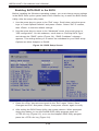
2. Use the arrow keys to move to the "Advanced" menu, then scroll down to
"IDE configuration". On this submenu, scroll down to "OnChip SATA Type"
and choose the "RAID" option (Figure 2-4). “RAID Codebase” submenu
appears. This setting allows you to select the codebase for your RAID setup.
Options are either Adaptec or DotHill.
Figure 2-4. BIOS Setup Screen
3. Press the <Esc> key twice and scroll to the "Exit" menu. Select "Save
Changes and Exit" and press <Enter>, then press <Enter> again to verify.
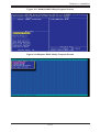
4. After exiting the BIOS Setup Utility, the system reboots. When prompted
during the startup, to use the DotHilll RAID Utility program press the
<CTRL+R> key (Figure 2-5), or to use the Adaptec RAID Utility program
press the <CTRL+A> key (Figure 2-6).
2-26
Chapter 2: Installation
Figure 2-5. DotHill RAID Utility Program Screen
Figure 2-6.Adaptec RAID Utility Program Screen
2-27
H8DGU-LN4F+ Serverboard User's Manual
Using the DotHill and Adaptec RAID Utility
The RAID Utility program allows you to define the drives you want to include in the
RAID array and the mode and type of RAID.
Installing the RAID Driver During OS Installation
You may also use the procedure below to install the RAID driver during the Windows
OS installation:
1. With the Windows OS installation CD-ROM in the CD drive, restart the
system.
2. Press <Enter> again to continue with the Windows setup.
3. When you see the prompt, hit the <F6> key to enter Windows setup.
4. Eventually a blue screen will appear with a message that begins “Windows
could not determine the type of one or more storage devices . . .” When you
see the screen, hit the <S> key to “Specify Additional Device”, then insert the
driver diskette you just created into the floppy drive.
5. Highlight “Manufuacturer Supplied Hardware Support Disk” and hit the
<Enter> key.
6. Highlight the first “Adaptec RAID” driver shown and press the <Enter> key to
install it.
2-28
Chapter 2: Installation
2-12 Installing Drivers
The Supermicro Website contains drivers and utilities for your system at ftp://ftp.
supermicro.com, some of which must be installed, such as the chipset driver. After
downloading and installing the drivers and utilities, the display shown in Figure 2-7
should appear.
Click the icons showing a hand writing on paper to view the readme files for each
item. Click the computer icons to the right of these items to install each item (from
top to the bottom) one at a time. After installing each item, you should reboot the
system before moving on to the next item on the list. The bottom icon with a CD
on it allows you to view the entire contents of the utilities.
Figure 2-7. Driver/Tool Installation Display Screen
2-29
H8DGU-LN4F+ Serverboard User's Manual
Supero Doctor III
The SuperDoctor® III program is a Web base management tool that supports remote
management capability. It includes Remote and Local Management tools. The local
management is called SD III Client. The SuperDoctor III program included on the
CD-ROM that came with your motherboard allows you to monitor the environment
and operations of your system. SuperDoctor III displays crucial system information
such as CPU temperature, system voltages and fan status. See the Figure below
for a display of the SuperDoctor III interface.
Note: The default User Name and Password for SuperDoctor III is ADMIN / ADMIN.
Note: When SuperDoctor is first installed, it adopts the temperature threshold
settings that have been set in BIOS. Any subsequent changes to these thresholds
must be made within SuperDoctor, as the SuperDoctor settings override the BIOS
settings. To set the BIOS temperature threshold settings again, you would first need
to uninstall SuperDoctor.
Figure 2-8. Supero Doctor III Interface Display Screen (Health Information)
2-30
Chapter 2: Installation
Figure 2-9. Supero Doctor III Interface Display Screen (Remote Control)
Note: The SuperDoctor III program and User’s Manual can be downloaded from the
Supermicro web site at http://www.supermicro.com/products/accessories/software/
SuperDoctorIII.cfm.For Linux, we recommend that you use the SuperoDoctor II
application instead.
2-31
H8DGU-LN4F+ Serverboard User's Manual
2-13 Serverboard Battery
Caution: There is a danger of explosion if the onboard battery is installed upside
down, which will reverse its polarites (see Figure 2-10). This battery must be replaced
only with the same or an equivalent type recommended by the manufacturer
(CR2032). Dispose of used batteries according to the manufacturer's instructions.
Figure 2-10. Installing the Onboard Battery
OR
Please handle used batteries carefully. Do not damage the battery in any way; a
damaged battery may release hazardous materials into the environment. Do not
discard a used battery in the garbage or a public landfill. Please comply with the
regulations set up by your local hazardous waste management agency to dispose
of your used battery properly.
2-32
Chapter 3: Troubleshooting
Chapter 3
Troubleshooting
3-1
Troubleshooting Procedures
Use the following procedures to troubleshoot your system. If you have followed all
of the procedures below and still need assistance, refer to the ‘Technical Support
Procedures’ and/or ‘Returning Merchandise for Service’ section(s) in this chapter.
Always disconnect the AC power cord before adding, changing or installing any
hardware components.
Before Power On
1. Check that the onboard power LED is lit (DP4 on the motherboard).
2. Make sure that the power connector is connected to your power supply.
3. Make sure that no short circuits exist between the motherboard and chassis.
4. Disconnect all cables from the motherboard, including those for the keyboard
and mouse.
5. Remove all add-on cards.
6. Install a CPU and heatsink (making sure it is fully seated) and connect the
internal (chassis) speaker and the power LED to the motherboard. Check all
jumper settings as well.
7. Use the correct type of onboard CMOS battery (CR2032) as recommended
by the manufacturer. To avoid possible explosion, do not install the CMOS
battery upside down.
No Power
1. Make sure that no short circuits exist between the motherboard and the
chassis.
2. Verify that all jumpers are set to their default positions.
3. Check that the 115V/230V switch on the power supply is properly set.
4. Turn the power switch on and off to test the system.
5. The battery on your motherboard may be old. Check to verify that it still
supplies ~3VDC. If it does not, replace it with a new one.
3-1
H8DGU-LN4F+ Serverboard User's Manual
No Video
1. If the power is on but you have no video, remove all the add-on cards and
cables.
2. Use the speaker to determine if any beep codes exist. Refer to Appendix A
for details on beep codes.
Note: If you are a system integrator, VAR or OEM, a POST diagnostics card is
recommended. For I/O port 80h codes, refer to App. B.
Memory Errors
1. Make sure that the DIMM modules are properly and fully installed.
2. You should be using registered ECC DDR-3 memory (see next page). Also,
it is recommended that you use the same memory type and speed for all
DIMMs in the system. See Section 2-5 for memory details.
3. Check for bad DIMM modules or slots by swapping modules between slots
and noting the results.
4. Check the power supply voltage 115V/230V switch.
Losing the System’s Setup Configuration
1. Make sure that you are using a high quality power supply. A poor quality
power supply may cause the system to lose the CMOS setup information.
Refer to Section 1-6 for details on recommended power supplies.
2. The battery on your motherboard may be old. Check to verify that it still
supplies ~3VDC. If it does not, replace it with a new one.
3. If the above steps do not fix the setup configuration problem, contact your
vendor for repairs.
3-2
Technical Support Procedures
Before contacting Technical Support, please take the following steps. Also, note
that as a motherboard manufacturer, we do not sell directly to end-users, so it is
best to first check with your distributor or reseller for troubleshooting services. They
should know of any possible problem(s) with the specific system configuration that
was sold to you.
1. Please review the ‘Troubleshooting Procedures’ and 'Frequently Asked
Questions' (FAQs) sections in this chapter or see the FAQs on our web site
before contacting Technical Support.
3-2
Chapter 3: Troubleshooting
2. BIOS upgrades can be downloaded from our web site.
Note: Not all BIOS can be flashed depending on the modifications to the boot
block code.
3. If you still cannot resolve the problem, include the following information when
contacting us for technical support:
•
•
•
Motherboard model and PCB revision number
BIOS release date/version (this can be seen on the initial display when your
system first boots up)
System configuration
An example of a Technical Support form is posted on our web site.
Distributors: For immediate assistance, please have your account number ready
when contacting our technical support department by e-mail.
3-3
Frequently Asked Questions
Question: What type of memory does my motherboard support?
Answer: The H8DGU-LN4F+ serverboard supports up to 128 GB of ECC/Non-ECC
Unbuffered or 768 GB of ECC Registered DIMM DDR3-1600/1333/1066 Mhz speed,
1 GB, 2 GB, 4 GB, 8 GB, 16 GB or 32 GB size SDRAM memory. See Section 2-4
for details on installing memory.
Question: How do I update my BIOS?
Answer: It is recommended that you not upgrade your BIOS if you are not
experiencing problems with your system. Updated BIOS files are located on our
web site. Please check our BIOS warning message and the information on how to
update your BIOS on our web site. Also, check the current BIOS revision and make
sure it is newer than your current BIOS before downloading.
Select your motherboard model on the web page and download the corresponding
BIOS file to your computer. Unzip the BIOS update file, in which you will find the
readme.txt (flash instructions), the afudos.exe (BIOS flash utility) and the BIOS
image (xxx.rom) files. Copy these files to a bootable floppy disk, insert the disk
into drive A and reboot the system. At the DOS prompt after rebooting, enter the
command "flash" (without quotation marks) then type in the BIOS file that you want
to update with (xxxx.rom).
Question: What's on the CD that came with my motherboard?
Answer: The supplied compact disc has quite a few drivers and programs that will
greatly enhance your system. We recommend that you review the CD and install the
applications you need. Applications on the CD include chipset drivers for Windows
and security and audio drivers.
3-3
H8DGU-LN4F+ Serverboard User's Manual
Question: Why can't I turn off the power using the momentary power on/off
switch?
Answer: The instant power off function is controlled in BIOS by the Power Button
Mode setting. When the On/Off feature is enabled, the motherboard will have instant
off capabilities as long as the BIOS has control of the system. When the Standby
or Suspend feature is enabled or when the BIOS is not in control such as during
memory count (the first screen that appears when the system is turned on), the
momentary on/off switch must be held for more than four seconds to shut down the
system. This feature is required to implement the ACPI features on the motherboard.
3-4
Returning Merchandise for Service
A receipt or copy of your invoice marked with the date of purchase is required before any warranty service will be rendered. You can obtain service by calling your
vendor for a Returned Merchandise Authorization (RMA) number. When returning to
the manufacturer, the RMA number should be prominently displayed on the outside
of the shipping carton, and mailed prepaid or hand-carried. Shipping and handling
charges will be applied for all orders that must be mailed when service is complete.
For faster service, RMA authorizations may be requested online (http://www.supermicro.com/support/rma/).
This warranty only covers normal consumer use and does not cover damages incurred in shipping or from failure due to the alteration, misuse, abuse or improper
maintenance of products.
During the warranty period, contact your distributor first for any product problems.
3-4
Chapter 4: BIOS
Chapter 4
BIOS
4-1
Introduction
This chapter describes the AMIBIOS™ Setup utility for the H8DGU-LN4F+
serverboard. The 16 Mb AMI BIOS® is stored in a flash chip and can be easily
upgraded using a floppy disk-based program.
Note: Due to periodic changes to the BIOS, some settings may have been added
or deleted and might not yet be recorded in this manual. Please refer to the Manual
Download area of our web site for any changes to BIOS that may not be reflected
in this manual.
Starting the Setup Utility
To enter the BIOS Setup Utility, hit the <Delete> key while the system is booting-up.
(In most cases, the <Delete> key is used to invoke the BIOS setup screen. There
are a few cases when other keys are used, such as <F1>, <F2>, etc.) Each main
BIOS menu option is described in this manual.
The Main BIOS screen has two main frames. The left frame displays all the options
that can be configured. “Grayed-out” options cannot be configured. The right frame
displays the key legend. Above the key legend is an area reserved for a text
message. When an option is selected in the left frame, it is highlighted in white. Often
a text message will accompany it. (Note that BIOS has default text messages built
in. We retain the option to include, omit, or change any of these text messages.)
Settings printed in Bold are the default values.
A " "indicates a submenu. Highlighting such an item and pressing the <Enter>
key will open the list of settings within that submenu.
The BIOS setup utility uses a key-based navigation system called hot keys. Most
of these hot keys (<F1>, <F10>, <Enter>, <ESC>, <Arrow> keys, etc.) can be used
at any time during the setup navigation process.
4-1
H8DGU-LN4F+ Serverboard User’s Manual
4-2
Main Menu
When you first enter AMI BIOS Setup Utility, you will see the Main Menu screen.
You can always return to the Main Menu by selecting the Main tab on the top of
the screen with the arrow keys.
The Main Menu screen provides you with a system overview, which includes the
version, built date and ID of the AMIBIOS, the type, speed and number of the
processors in the system and the amount of memory installed in the system.
System Time/System Date
You can edit this field to change the system time and date. Highlight System Time
or System Date using the <Arrow> keys. Enter new values through the keyboard.
Press the <Tab> key or the <Arrow> keys to move between fields. The date must
be entered in DAY/MM/DD/YYYY format. The time is entered in HH:MM:SS format.
Please note that time is in a 24-hour format. For example, 5:30 A.M. appears as
05:30:00 and 5:30 P.M. as 17:30:00.
4-3
Advanced Settings Menu
Boot Feature
Quick Boot
If Enabled, this option will skip certain tests during POST to reduce the time
needed for the system to boot up. The options are Enabled and Disabled.
Quiet Boot
If Disabled, normal POST messages will be displayed on boot-up. If Enabled,
this display the OEM logo instead of POST messages.
Add On ROM Display Mode
This option sets the display mode for Option ROM. The options are Force BIOS
or Keep Current.
Bootup Num Lock
This option selects the power-on state for the NUM lock to either On or Off.
PS/2 Mouse Support
Use this option to select support for the PS/2 mouse. Options are Disabled,
Enabled or Auto.
4-2
Chapter 4: BIOS
Wait for F1 if Error
This setting controls the system response when an error is detected during the
boot sequence. When enabled, BIOS will stop the boot sequence when an error
is detected, at which point you will need to press the F1 button to re-enter the
BIOS setup menu. The options are Enabled and Disabled.
Hit 'DEL' Message Display
Use this option to Enable or Disable the "Press DEL to run setup" message in
POST.
Watch Dog Function
Allows system to restart when system is inactive more than 5-minutes. The
options are Enabled and Disabled.
Power Button Function
This sets the function of the power button when you turn off the system. Options
include 4-second Overide and Instant Off.
Restore on AC Power Loss
This sets the action that occurs when an AC power loss occurs. Options include
Power Off, Power On and Last State.
Interrupt 19 Capture
Select Enabled to allow ROMs to trap Interrupt 19. The options are Enabled
and Disabled.
EUP Support
This setting allows you to enable or disable supplied standby power in S5. Set
to Enabled to for EUP requirements and set to Disabled for wakening capability.
Processor and Clock Options
CPU Configuration
This displays static information on the Module Version, Socket Count, Node
Count, Core Count for the system's processor(s)
CPU Information
The information for the installed processor includes Revision, Cache L1/L2/L3,
Speed, NB CLK, Able to Change Frequency and uCode Patch Level.
4-3
H8DGU-LN4F+ Serverboard User’s Manual
GART Error Reporting
This option should remain disabled for normal operation. The driver developer
may enable this option for testing purposes. Options are Enabled or Disabled.
Microcode Update
This setting Enables or Disables microcode updating.
Secure Virtual Machine Mode
This setting is used to Enable or Disable SVM.
Power Now
This setting is used to Enable or Disable the AMD Power Now feature.
Power Cap
This option can decide the highest P-state in the OS. Options include P-state
0 through P-state 4.
ACPI SRAT Table
This option Enables or Disables the building of the ACPI SRAT Table.
CPU Down Core
This option sets down core support for the CPU. Options include Disabled, 1
core through n cores in odd numbered increments. The value n depends upon
the number of cores per CPU node.
C1E Support
This option specifies C1E support. Options include Enabled and Disabled.
Advanced Chipset Control
NorthBridge Configuration
Memory Configuration
Bank Interleaving
Select Auto to automatically enable a bank-interleaving memory scheme
when this function is supported by the processor. The options are Auto
and Disabled.
4-4
Chapter 4: BIOS
Node Interleaving
This option enables node memory interleaving. Options include Auto or
Disabled.
Channel Interleaving
This option enables channel memory interleaving. Options include Auto
or Disabled.
CS Sparing
This setting will reserve a spare memory rank in each node when enabled.
Options are Enabled and Disabled.
Bank Swizzle Mode
This setting Enables or Disables the bank swizzle mode.
ECC Configuration
ECC Mode
This submenu affects the DRAM scrub rate based on its setting. Options
include Disabled, Basic, Good, Super, Max and User. Selecting User
activates the other options for user setting.
DRAM ECC Enable
This setting allows hardware to report and correct memory errors
automatically, maintaining system integrity. Options are Enabled or
Disabled. This is option is only active if ECC Mode above is set to User.
DRAM Timing Configuration
DRAM Timing Config
This option allows you to set the DRAM timing configuration for the system.
Options include Auto or Manual.
Memory Timing Parameters
This selects the which node's timing parameters to display. Options are CPU
Node 0, CPU Node 1, CPU Node 2 or CPU Node 3.
IOMMU
This setting is used to enable or disable or set the GART size in systems without
AGP. Options include Enabled and Disabled.
4-5
H8DGU-LN4F+ Serverboard User’s Manual
OHCI/EHCI HC Device Functions
These settings allow you to either Enable or Disable functions for OHCI or EHCI
bus devices.
USB 2.0 Controller Mode
Use this setting to configure the USB 2.0 Controller in either Hi-Speed (480
Mps) or Full Speed (12 Mps) mode. Options include Enabled (Hi-Speed Mode)
or Disabled (Full Speed Mode).
Legacy USB Support
Select "Enabled" to enable the support for USB Legacy. Disable Legacy support if
there are no USB devices installed in the system. "Auto" disabled Legacy support
if no USB devices are connected. The options are Disabled, Enabled and Auto.
IDE Configuration
Onboard PCI IDE Controller
This setting allows you to Enable or Disable the PCI IDE Controller.
OnChip SATA Channel
This setting allows you to Enable or Disable the OnChip SATA channel.
OnChip SATA Type
Use this setting to set the OnChip SATA type. Options include
Native IDE, RAID, AHCI and Legacy IDE.
RAID Codebase
This submenu appears when you choose "RAID" from the "OnChip SATA
Type" setting above. This setting allows you to select the codebase for using
your RAID setup. Options are either Adaptec or DotHill.
SATA IDE Combined Mode
This setting allows you to Enable or Disable the SATA IDE combined mode.
PATA Channel Configuration
This allows you to set PATA channel configuration. Options include SATA as
Primary or SATA as secondary.
4-6
Chapter 4: BIOS
Primary/Secondary/Third/Fourth IDE Master/Slave
This menu is available for each configuration of IDE Master/Slave device in the
system. IDE onfigurations include Primary, Secondary, Third and Fourth. Some of
the following menu options are not available for some of the IDE configurations.
Type
This setting allows you to set the type of device connected to the system.
Options include Not Installed, Auto, CD/DVD or ARMD.
LBA/Large Mode
LBA (Logical Block Addressing) is a method of addressing data on a disk
drive. The options are Disabled and Auto.
Block (Multi-Sector Transfer)
Block mode boosts IDE drive performance by increasing the amount of data
transferred. Only 512 bytes of data can be transferred per interrupt if block
mode is not used. Block mode allows transfers of up to 64 KB per interrupt.
Select "Disabled" to allow the data to be transferred from and to the device
one sector at a time. Select "Auto" to allows the data transfer from and to the
device occur multiple sectors at a time if the device supports it. The options
are Auto and Disabled.
PIO Mode
PIO (Programmable I/O) mode programs timing cycles between the IDE drive
and the programmable IDE controller. As the PIO mode increases, the cycle
time decreases.
The options are Auto, 0, 1, 2, 3, and 4. Select Auto to allow BIOS to auto
detect the PIO mode. Use this value if the IDE disk drive support cannot be
determined. Select 0 to allow BIOS to use PIO mode 0, which has a data
transfer rate of 3.3 MBs. Select 1 to allow BIOS to use PIO mode 1, which has
a data transfer rate of 5.2 MBs. Select 2 to allow BIOS to use PIO mode 2,
which has a data transfer rate of 8.3 MBs. Select 3 to allow BIOS to use PIO
mode 3, which has a data transfer rate of 11.1 MBs. Select 4 to allow BIOS
to use PIO mode 4, which has a data transfer rate of 16.6 MBs. This setting
generally works with all hard disk drives manufactured after 1999. For other
disk drives, such as IDE CD-ROM drives, check the specifications of the drive.
4-7
H8DGU-LN4F+ Serverboard User’s Manual
DMA Mode
Selects the DMA Mode. Options are Auto, SWDMA0, SWDMA1, SWDMA2,
MWDMA0. MDWDMA1, MWDMA2, UDMA0. UDMA1, UDMA2, UDMA3,
UDMA4 and UDMA5. (SWDMA=Single Word DMA, MWDMA=Multi Word
DMA, UDMA=UltraDMA.)
S.M.A.R.T.
Self-Monitoring Analysis and Reporting Technology (SMART) can help
predict impending drive failures. Select "Auto" to allow BIOS to auto detect
hard disk drive support. Select "Disabled" to prevent AMI BIOS from using
the S.M.A.R.T. Select "Enabled" to allow AMI BIOS to use the S.M.A.R.T.
to support hard drive disk. The options are Disabled, Enabled, and Auto.
32-Bit Data Transfer
Select "Enabled" to activate the function of 32-Bit data transfer. Select
"Disabled" to deactivate the function. The options are Enabled and Disabled.
IDE Detect Timeout (Sec)
Use the +/- keys to adjust and select the time out for detecting ATA/ATAPI
devices. The default value is 35.
PCI/PnP Configuration
Clear NVRAM
Select Yes to clear NVRAM during boot-up. The options are Yes and No.
Plug & Play O/S
Select Yes to allow the OS to configure Plug & Play devices. (This is not required
for system boot if your system has an OS that supports Plug & Play.) Select No
to allow AMIBIOS to configure all devices in the system.
PCI Latency Timer
This option sets the latency of all PCI devices on the PCI bus. Select a value
to set the PCI latency in PCI clock cycles. Options are 32, 64, 96, 128, 160,
192, 224 and 248.
PCI IDE Busmaster
Use this setting to Enable or Disable BIOS enabled uses of PCI Busmastering
for reading or writing to IDE drives.
4-8
Chapter 4: BIOS
ROM Scan Ordering
This setting determines which kind of option ROM activates prior to another.
Options include Onboard First and Addon First.
SBX1 Configuration
This sets SBX1 configuration in your system. Options include Auto, 1x16 and
2x8.
PCI Slot from SBX1/SBX2/SBX3
These settings allow you to Enable or Disable the PCI slots from SXB1 through
SXB3 in your system.
Onboard LAN Option ROM Select
This setting allows you to select the onboard LAN option ROM for iSCSI or PXE.
Note: You must enable ONLY LAN1 when the iSCSI support option is specified.
Load Onboard LAN 1 Option ROM
This option allows you to Enable or Disable the onboard LAN 1 option ROM.
Load Onboard LAN 2 Option ROM
This option allows you to Enable or Disable the onboard LAN 2 option ROM.
Load Onboard LAN 3 Option ROM
This option allows you to Enable or Disable the onboard LAN 2 option ROM.
Load Onboard LAN 4 Option ROM
This option allows you to Enable or Disable the onboard LAN 2 option ROM.
SuperIO Device Configuration
Serial 1 Address
This option specifies the base I/O port address and Interrupt Request address
of serial port 1. Select "Disabled" to prevent the serial port from accessing any
system resources. When this option is set to Disabled, the serial port physically
becomes unavailable. Select "3F8/IRQ4" to allow the serial port to use 3F8 as its
I/O port address and IRQ 4 for the interrupt address. Options include Disabled,
3F8/IRQ4, 3E8/IRQ4 and 2E8/IRQ3
4-9
H8DGU-LN4F+ Serverboard User’s Manual
Serial 2 Address
This option specifies the base I/O port address and Interrupt Request address
of serial port 2. Select "Disabled" to prevent the serial port from accessing any
system resources. When this option is set to "Disabled", the serial port physically
becomes unavailable. Select "2F8/IRQ3" to allow the serial port to use 2F8 as its
I/O port address and IRQ 3 for the interrupt address. Options include Disabled,
2F8/IRQ3, 3E8/IRQ4 and 2F8/IRQ3.
Serial Port 2 Attribute
This option allows you to set COM2 as a normal serial port or as virtual COM
for SOL. Options are SOL or COM.
Remote Access Configuration
Remote Access
Use this option to Enable or Disable Remote Access in your system. If enabled,
the settings below will appear.
Serial Port Number
Use this setting to select the serial port for console redirection. Options include
COM1, COM2*. The displayed base address and IRQ for the serial port changes
to reflect the selection you make.
Note: Make sure the selected port is enabled.
Serial Port Mode
Selects the serial port settings to use. Options are (115200 8, n, 1), (57600 8,
n, 1), (38400 8, n, 1), (19200 8, n, 1) and (09600 8, n, 1).
Flow Control
Selects the flow control to be used for console redirection. Options are None,
Hardware and Software.
Redirection After BIOS POST
Options are Disable (no redirection after BIOS POST), Boot Loader (redirection
during POST and during boot loader) and Always (redirection always active).
Note that some OS's may not work with this set to Always.
Terminal Type
Selects the type of the target terminal. Options are ANSI, VT100 and VT-UTF8.
4-10
Chapter 4: BIOS
VT-UTF8 Combo Key Support
Allows you to Enable or Disable VT-UTF8 combination key support for ANSI/
VT100 terminals.
Sredir Memory Display Delay
Use this setting to set the delay in seconds to display memory information.
Options are No Delay, 1 sec, 2 secs and 4 secs.
Hardware Health Configuration
CPU Overheat Alarm
This setting allows you to specify the type of alarm for CPU overheating. Options
include The Early Alarm and The Default Alarm.
Fan Speed Control
This feature allows the user to determine how the system will control the speed
of the onboard fans. The options are Full Speed/FS (Max Cooling), Performance/
PF (Better Cooling), Balanced/BL (Balance between performance and energy
saving), Energy Saving/ES (Lower Power and Noise).
Other items in the submenu are systems monitor displays for the following
information:
CPU1 Temperature, CPU2 Temperature, NB Temperature, VRD1 Temperature,
VRD2 Temperature, System Temperature, Air Temperature, Fan 1-8 Reading,
CPU1 Vcore, CPU2 Vcore, CPU1 Mem VTT, CPU2 Mem VTT, CPU1 Mem,
CPU2 Mem, 1.1V, 1.8V, 5V 12V, 5V Dual, 3.3 Vcc, 3.3 VSB, VBAT and HT
Voltage.
CPU Temperature Display (CTD)
CPU Temperature descriptions are defined as:
Low [Tctl Value = Lowest Value, Tctl Value = -45]
Medium [Tctl Value = -46, Tctl Value = 60]
High [Tctl Value = -61 and Above]
4-11
H8DGU-LN4F+ Serverboard User’s Manual
Note: Only CPU temperature (Low, Medium, High) and system temperature (RT1)
are required to be displayed in BIOS and in-system monitoring software. Other
Motherboard components such as memory, chipset, SAS and 10Gb controllers,
and others are not requried to display temperatures. For debugging and testing
purposes, BIOS and system monitoring software can show motherboard
components’ temperatures (such as memory, chipset, SAS and 10Gb controllers).
However for SMCI standard release version BIOS and system monitoring software,
motherboard components’ temperatures are NOT required to be displayed.
CPU Overheating Alarm (COA)
CPU Overheating Alarm (COA) has “Early Alarm” and “Default Alarm” (default)
options in the BIOS, and is required to be implemented in all fan speed control
modes.
The Early Alarm is enabled when the Tctl value = 65, and is disabled when the Tctl
value drops from 65 to 62.
The Default Alarm (default setting) is enabled when the Tctl value = 70, and is
disabled when the Tctl value drops from 70 to 67.
When COA (either Early or Default Alarm) is enabled, the following actions are
required to be executed:
•
•
•
•
System overheating LED is required to be ON and to solid red.
Onboard buzzer or speaker is required to be ON and to be a continuous sound.
All system fans are required to be operated at full speed.
System monitoring software (such as Super Doctor and IPMI if available) is
required to report and record CPU overheating events in the event logs.
When COA (either Early or Default Alarm) is disabled, the following actions are
required to be executed:
•
•
•
System overheating LED is required to be OFF.
Onboard buzzer or speaker is required to be OFF.
All system fans are required to be returned to a normal, non-CPU-overheating
LFSC condition.
4-12
Chapter 4: BIOS
Condition
When a CPU is overheating
Front Panel Overheating LED
On and Solid Red
Onboard Buzzer or Speaker
On and Continuous Sound
System Fan Speed Controls
Full Speed
BMC
Report PROCHOT
BMC Event Log
Record PROCHOT
Super Doctor
Report PROCHOT
Super Doctor Event Log
Record PROCHOT
ACPI Configuration
PS2 KB/MS Wakeup
This setting allows you to Enable or Disable PS2 keyboard and mouse wakeup.
ACPI Aware O/S
This setting Enables or Disables ACPI support for the system's operating system.
Options include Yes (enabled) or No (disabled).
ACPI APIC Support
Determines whether to include the ACPI APIC table pointer in the RSDT pointer
list. The available options are Enabled and Disabled.
Headless Mode
Use this setting to Enable or Disable headless operation mode through ACPI.
ACPI Version Features
Use this setting the determine which ACPI version to use. Options are ACPI
v1.0, ACPI v2.0 and ACPI v3.0.
IPMI Configuration
This menu shows static information about the IPMI firmware revision and status of
the BMC, as well as options for IPMI configuration.
4-13
H8DGU-LN4F+ Serverboard User’s Manual
View BMC System Event Log
Pressing the Enter key will open the following settings. Use the "+" and "-" keys to
navigate through the system event log.
Clear BMC System Event Log
Selecting this and pressing the Enter key will clear the BMC system event log.
Set LAN Configuration
Use the "+" and "-" keys to choose the desired channel number. This displays
Channel Number and Channel Number Status information.
This menu contains options for inputing settings for the SET LAN Configuration
Command. See IPMI 1.5 Specification, table 11.1 for details. Use the "+" and
"-" keys to choose the desired channel number.
Note: Each question in this group may take a considerable amount of time.
IP Address Source
Select the source of this machine's IP address. If Static is selected, you will
need to know and enter manually the IP address of this machine below.
If DHCP is selected, the BIOS will search for a DHCP (Dynamic Host
Configuration Protocol) server in the network it is attached to, and request
the next available IP address. The options are DHCP and Static.
The following items are assigned IP addresses automatically if DHCP is
selected under IP Address Source above:
IP Address
This submenu sets the IP address source as either Static or DHCP. Selecting
Static allows you to manually set the IP Address, Subnet Mask and Gateway
Address.
In the field provided here enter the IP address in the decimal form of xxx.xxx.
xxx.xxx with xxx having a value of less than 256 and in decimal form only The
IP address and current IP address in the BMC are shown.
Subnet Mask
In the field provided here enter the Subnet address in the decimal form of
xxx.xxx.xxx.xxx with xxx having a value of less than 256 and in decimal form
only. The current subnet address in the BMC is shown.
4-14
Chapter 4: BIOS
Gateway Address
In the field provided here enter the Gateway address in the decimal form of
xxx.xxx.xxx.xxx with xxx having a value of less than 256 and in decimal form
only. The current Gateway address in the BMC is shown.
MAC Address
In the field provided here enter the MAC address in the hex form of xx.xx.xx.xx.
xx.xx with xx in hex form only. The current MAC address in the BMC is shown.
BMC Watch Dog Timer Action
This setting is used to set the Watch Dog function, which allows the BMC to reset
or powerdown the system if the OS crashes or hangs. Options include Disabled,
Reset System, Power Down and Power Cycle.
Event Log Configuration
View Event Log
Pressing the Enter key will open the event log. Use the "" and "" keys to
navigate through the system event log.
Mark All Events as Read
Selecting this and pressing the Enter key marks all events as read in the event
log.
Clear Event Log
Selecting this and pressing the Enter key clears the system event log.
SR56x0 (RD890S) PCIE Error Log
This setting allows you set an error log ofr PCIE errors. Options include Yes
or No.
4-15
H8DGU-LN4F+ Serverboard User’s Manual
4-3
Security Menu
AMI BIOS provides a Supervisor and a User password. If you use both passwords,
the Supervisor password must be set first.
Change Supervisor Password
Select this option and press <Enter> to access the sub menu, and then type in
the password.
Change User Password
Select this option and press <Enter> to access the sub menu, and then type in
the password.
Boot Sector Virus Protection
This option is near the bottom of the Security Setup screen. Select "Disabled" to
deactivate the Boot Sector Virus Protection. Select "Enabled" to enable boot sector
protection. When "Enabled", AMI BIOS displays a warning when any program (or
virus) issues a Disk Format command or attempts to write to the boot sector of the
hard disk drive. The options are Enabled and Disabled.
4-4
Boot Menu
The Boot Menu is accessible only when the "Load Onboard LAN Option ROM"
setting (in the PCI/PnP Configuration menu) is enabled.
Boot Device Priority
This feature allows you to prioritize the boot sequence from the list of available
devices. A device that is in parenthesis has been disabled in the corresponding
type menu.
Hard Disk Drives
This feature allows you to specify the boot sequence from the list of available hard
disk drives. A device that is in parenthesis has been disabled in the corresponding
type menu.
4-16
Chapter 4: BIOS
CD/DVD Drives
This feature allows you to specify the boot sequence from the list of available CD/
DVD drives. A device that is in parenthesis has been disabled in the corresponding
type menu.
Retry Boot Devices
This option allows you to retry boot devices. Options include Enabled and Disabled.
4-5
Exit Menu
Select the Exit tab from AMI BIOS Setup Utility screen to enter the Exit BIOS Setup
screen.
Save Changes and Exit
When you have completed the system configuration changes, select this option
to leave BIOS Setup and reboot the computer, so the new system configuration
parameters can take effect. Select Save Changes and Exit from the Exit menu and
press <Enter>.
Discard Changes and Exit
Select this option to quit BIOS Setup without making any permanent changes to the
system configuration and reboot the computer. Select Discard Changes and Exit
from the Exit menu and press <Enter>.
Discard Changes
Select this option and press <Enter> to discard all the changes and return to AMI
BIOS Utility Program.
Load Optimal Defaults
To set this feature, select Load Optimal Defaults from the Exit menu and press
<Enter>. Then Select "OK" to allow BIOS to automatically load the Optimal Defaults
as the BIOS Settings. The Optimal settings are designed for maximum system
performance, but may not work best for all computer applications.
Load Fail-Safe Defaults
To set this feature, select Load Fail-Safe Defaults from the Exit menu and press
<Enter>. The Fail-Safe settings are designed for maximum system stability, but not
maximum performance.
4-17
H8DGU-LN4F+ Serverboard User’s Manual
Notes
4-18
Appendix A: BIOS Error Beep Codes
Appendix A
BIOS Error Beep Codes
During the POST (Power-On Self-Test) routines, which are performed each time
the system is powered on, errors may occur.
Non-fatal errors are those which, in most cases, allow the system to continue the
boot-up process. The error messages normally appear on the screen.
Fatal errors are those which will not allow the system to continue the boot-up
procedure. If a fatal error occurs, you should consult with your system manufacturer
for possible repairs.
These fatal errors are usually communicated through a series of audible beeps. The
numbers on the fatal error list (on the following page) correspond to the number
of beeps for the corresponding error. All errors listed, with the exception of Beep
Code 8, are fatal errors.
A-1 AMIBIOS Error Beep Codes
Beep Code
Error Message
Description
1 beep
Refresh
Circuits have been reset (Ready to power up)
5 shorts, 1 long beep
Memory error
No memory detected in system
1 long, 8 short
Video error
Video adapter disabled or missing
A-1
H8DGU-LN4F+ Serverboard User’s Manual
Notes
A-2
Appendix B: BIOS POST Checkpoint Codes
Appendix B
BIOS POST Checkpoint Codes
When AMIBIOS performs the Power On Self Test, it writes checkpoint codes to I/O
port 0080h. If the computer cannot complete the boot process, diagnostic equipment
can be attached to the computer to read I/O port 0080h.
B-1 Uncompressed Initialization Codes
The uncompressed initialization checkpoint codes are listed in order of execution:
Checkpoint
Code Description
D0h
The NMI is disabled. Power on delay is starting. Next, the initialization code checksum will be
verified.
D1h
Initializing the DMA controller, performing the keyboard controller BAT test, starting memory
refresh and entering 4 GB flat mode next.
D3h
Starting memory sizing next.
D4h
Returning to real mode. Executing any OEM patches and setting the Stack next.
D5h
Passing control to the uncompressed code in shadow RAM at E000:0000h. The initialization
code is copied to segment 0 and control will be transferred to segment 0.
D6h
Control is in segment 0. Next, checking if <Ctrl> <Home> was pressed and verifying the system
BIOS checksum. If either <Ctrl> <Home> was pressed or the system BIOS checksum is bad,
next will go to checkpoint code E0h. Otherwise, going to checkpoint code D7h.
B-1
H8DGU-LN4F+ Serverboard User’s Manual
B-2 Bootblock Recovery Codes
The bootblock recovery checkpoint codes are listed in order of execution:
Checkpoint
Code Description
E0h
The onboard floppy controller if available is initialized. Next, beginning the base 512 KB
memory test.
E1h
Initializing the interrupt vector table next.
E2h
Initializing the DMA and Interrupt controllers next.
E6h
Enabling the floppy drive controller and Timer IRQs. Enabling internal cache memory.
Edh
Initializing the floppy drive.
Eeh
Looking for a floppy diskette in drive A:. Reading the first sector of the diskette.
Efh
A read error occurred while reading the floppy drive in drive A:.
F0h
Next, searching for the AMIBOOT.ROM file in the root directory.
F1h
The AMIBOOT.ROM file is not in the root directory.
F2h
Next, reading and analyzing the floppy diskette FAT to find the clusters occupied by the
AMIBOOT.ROM file.
F3h
Next, reading the AMIBOOT.ROM file, cluster by cluster.
F4h
The AMIBOOT.ROM file is not the correct size.
F5h
Next, disabling internal cache memory.
FBh
Next, detecting the type of flash ROM.
FCh
Next, erasing the flash ROM.
FDh
Next, programming the flash ROM.
FFh
Flash ROM programming was successful. Next, restarting the system BIOS.
B-2
Appendix B: BIOS POST Checkpoint Codes
B-3 Uncompressed Initialization Codes
The following runtime checkpoint codes are listed in order of execution.
These codes are uncompressed in F0000h shadow RAM.
Checkpoint
Code Description
03h
The NMI is disabled. Next, checking for a soft reset or a power on condition.
05h
The BIOS stack has been built. Next, disabling cache memory.
06h
Uncompressing the POST code next.
07h
Next, initializing the CPU and the CPU data area.
08h
The CMOS checksum calculation is done next.
0Ah
The CMOS checksum calculation is done. Initializing the CMOS status register for date and
time next.
0Bh
The CMOS status register is initialized. Next, performing any required initialization before the
keyboard BAT command is issued.
0Ch
The keyboard controller input buffer is free. Next, issuing the BAT command to the keyboard
controller.
0Eh
The keyboard controller BAT command result has been verified. Next, performing any
necessary initialization after the keyboard controller BAT command test.
0Fh
The initialization after the keyboard controller BAT command test is done. The keyboard
command byte is written next.
10h
The keyboard controller command byte is written. Next, issuing the Pin 23 and 24 blocking and
unblocking command.
11h
Next, checking if <End or <Ins> keys were pressed during power on. Initializing CMOS RAM
if the Initialize CMOS RAM in every boot AMIBIOS POST option was set in AMIBCP or the
<End> key was pressed.
12h
Next, disabling DMA controllers 1 and 2 and interrupt controllers 1 and 2.
13h
The video display has been disabled. Port B has been initialized. Next, initializing the chipset.
14h
The 8254 timer test will begin next.
19h
Next, programming the flash ROM.
1Ah
The memory refresh line is toggling. Checking the 15 second on/off time next.
2Bh
Passing control to the video ROM to perform any required configuration before the video ROM
test.
2Ch
All necessary processing before passing control to the video ROM is done. Looking for the
video ROM next and passing control to it.
2Dh
The video ROM has returned control to BIOS POST. Performing any required processing after
the video ROM had control
23h
Reading the 8042 input port and disabling the MEGAKEY Green PC feature next. Making the
BIOS code segment writable and performing any necessary configuration before initializing the
interrupt vectors.
24h
The configuration required before interrupt vector initialization has completed. Interrupt vector
initialization is about to begin.
25h
Interrupt vector initialization is done. Clearing the password if the POST DIAG switch is on.
27h
Any initialization before setting video mode will be done next.
28h
Initialization before setting the video mode is complete. Configuring the monochrome mode and
color mode settings next.
B-3
H8DGU-LN4F+ Serverboard User’s Manual
Checkpoint
Code Description
2Ah
Bus initialization system, static, output devices will be done next, if present. See the last page
for additional information.
2Eh
Completed post-video ROM test processing. If the EGA/VGA controller is not found, performing
the display memory read/write test next.
2Fh
The EGA/VGA controller was not found. The display memory read/write test is about to begin.
30h
The display memory read/write test passed. Look for retrace checking next.
31h
The display memory read/write test or retrace checking failed. Performing the alternate display
memory read/write test next.
32h
The alternate display memory read/write test passed. Looking for alternate display retrace
checking next.
34h
Video display checking is over. Setting the display mode next.
37h
The display mode is set. Displaying the power on message next.
38h
Initializing the bus input, IPL, general devices next, if present. See the last page of this chapter
for additional information.
39h
Displaying bus initialization error messages. See the last page of this chapter for additional
information.
3Ah
The new cursor position has been read and saved. Displaying the Hit <DEL> message next.
3Bh
The Hit <DEL> message is displayed. The protected mode memory test is about to start.
40h
Preparing the descriptor tables next.
42h
The descriptor tables are prepared. Entering protected mode for the memory test next.
43h
Entered protected mode. Enabling interrupts for diagnostics mode next.
44h
Interrupts enabled if the diagnostics switch is on. Initializing data to check memory wraparound
at 0:0 next.
45h
Data initialized. Checking for memory wraparound at 0:0 and finding the total system memory
size next.
46h
The memory wraparound test is done. Memory size calculation has been done. Writing patterns
to test memory next.
47h
The memory pattern has been written to extended memory. Writing patterns to the base 640
KB memory next.
48h
Patterns written in base memory. Determining the amount of memory below 1 MB next.
49h
The amount of memory below 1 MB has been found and verified.
4Bh
The amount of memory above 1 MB has been found and verified. Checking for a soft reset and
clearing the memory below 1 MB for the soft reset next. If this is a power on situation, going to
checkpoint 4Eh next.
4Ch
The memory below 1 MB has been cleared via a soft reset. Clearing the memory above 1 MB
next.
4Dh
The memory above 1 MB has been cleared via a soft reset. Saving the memory size next.
Going to checkpoint 52h next.
4Eh
The memory test started, but not as the result of a soft reset. Displaying the first 64 KB memory
size next.
4Fh
The memory size display has started. The display is updated during the memory test.
Performing the sequential and random memory test next.
50h
The memory below 1 MB has been tested and initialized. Adjusting the displayed memory size
for relocation and shadowing next.
51h
The memory size display was adjusted for relocation and shadowing.
B-4
Appendix B: BIOS POST Checkpoint Codes
Checkpoint
Code Description
52h
The memory above 1 MB has been tested and initialized. Saving the memory size information
next.
53h
The memory size information and the CPU registers are saved. Entering real mode next.
54h
Shutdown was successful. The CPU is in real mode. Disabling the Gate A20 line, parity, and
the NMI next.
57h
The A20 address line, parity, and the NMI are disabled. Adjusting the memory size depending
on relocation and shadowing next.
58h
The memory size was adjusted for relocation and shadowing. Clearing the Hit <DEL> message
next.
59h
The Hit <DEL> message is cleared. The <WAIT...> message is displayed. Starting the DMA
and interrupt controller test next.
60h
The DMA page register test passed. Performing the DMA Controller 1 base register test next.
62h
The DMA controller 1 base register test passed. Performing the DMA controller 2 base register
test next.
65h
The DMA controller 2 base register test passed. Programming DMA controllers 1 and 2 next.
66h
Completed programming DMA controllers 1 and 2. Initializing the 8259 interrupt controller next.
67h
Completed 8259 interrupt controller initialization.
7Fh
Extended NMI source enabling is in progress.
80h
The keyboard test has started. Clearing the output buffer and checking for stuck keys. Issuing
the keyboard reset command next.
81h
A keyboard reset error or stuck key was found. Issuing the keyboard controller interface test
command next.
82h
The keyboard controller interface test completed. Writing the command byte and initializing the
circular buffer next.
83h
The command byte was written and global data initialization has completed. Checking for a
locked key next.
84h
Locked key checking is over. Checking for a memory size mismatch with CMOS RAM data
next.
85h
The memory size check is done. Displaying a soft error and checking for a password or
bypassing WINBIOS Setup next.
86h
The password was checked. Performing any required programming before WINBIOS Setup
next.
87h
The programming before WINBIOS Setup has completed. Uncompressing the WINBIOS Setup
code and executing the AMIBIOS Setup or WINBIOS Setup utility next.
88h
Returned from WINBIOS Setup and cleared the screen. Performing any necessary
programming after WINBIOS Setup next.
89h
The programming after WINBIOS Setup has completed. Displaying the power on screen
message next.
8Ch
Programming the WINBIOS Setup options next.
8Dh
The WINBIOS Setup options are programmed. Resetting the hard disk controller next.
8Fh
The hard disk controller has been reset. Configuring the floppy drive controller next.
91h
The floppy drive controller has been configured. Configuring the hard disk drive controller next.
95h
Initializing the bus option ROMs from C800 next. See the last page of this chapter for additional
information.
96h
Initializing before passing control to the adaptor ROM at C800.
B-5
H8DGU-LN4F+ Serverboard User’s Manual
Checkpoint
Code Description
97h
Initialization before the C800 adaptor ROM gains control has completed. The adaptor ROM
check is next.
98h
The adaptor ROM had control and has now returned control to BIOS POST. Performing any
required processing after the option ROM returned control.
99h
Any initialization required after the option ROM test has completed. Configuring the timer data
area and printer base address next.
9Ah
Set the timer and printer base addresses. Setting the RS-232 base address next.
9Bh
Returned after setting the RS-232 base address. Performing any required initialization before
the Coprocessor test next.
9Ch
Required initialization before the Coprocessor test is over. Initializing the Coprocessor next.
9Dh
Coprocessor initialized. Performing any required initialization after the Coprocessor test next.
9Eh
Initialization after the Coprocessor test is complete. Checking the extended keyboard, keyboard
ID, and Num Lock key next. Issuing the keyboard ID command next.
A2h
Displaying any soft errors next.
A3h
The soft error display has completed. Setting the keyboard typematic
A4h
The keyboard typematic rate is set. Programming the memory wait states next.
A5h
Memory wait state programming is over. Clearing the screen and enabling parity and the NMI
next.
A7h
NMI and parity enabled. Performing any initialization required before passing control to the
adaptor ROM at E000 next.
A8h
Initialization before passing control to the adaptor ROM at E000h completed. Passing control to
the adaptor ROM at E000h next.
A9h
Returned from adaptor ROM at E000h control. Performing any initialization required after the
E000 option ROM had control next.
Aah
Initialization after E000 option ROM control has completed. Displaying the system configuration
next.
Abh
Uncompressing the DMI data and executing DMI POST initialization next.
B0h
The system configuration is displayed.
rate next.
B1h
Copying any code to specific areas.
00h
Code copying to specific areas is done. Passing control to INT 19h boot loader next.
B-6