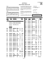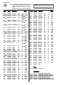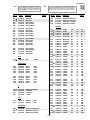
1
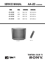
KV-32V68/35V68
SERVICE MANUAL
MODEL
AA-2D
DEST.
COMMANDER
KV-32V68
U.S.
RM-Y154
SCC-S07G-A
KV-32V68
CND
RM-Y154
SCC-S08J-A
KV-35V68
U.S.
RM-Y154
SCC-S07J-A
KV-35V68
CND
RM-Y154
SCC-S08L-A
CHASSIS
CHASSIS NO.
RM-Y154
KV-35V68
TRINITRON® COLOR TV
—1—
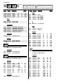
KV-32V68/35V68
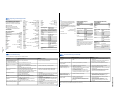
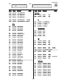
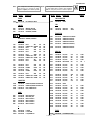
SPECIFICATIONS
KV-32V68
KV-35V68
120V, 60Hz
120V, 60Hz
3
2
3
1
1
1
3
1
10W x 2
3
2
3
1
1
1
3
1
10W x 2
200W
8W
230W
8W
821 x 675.3 x 587 mm
323/8 x 265/6 x 231/2 in
920 x 730.8 x 641.8 mm
361/4 x 283/4 x 251/4 in
70 kg
154 lbs
93 kg
205 lbs
Power requirements
Number of inputs/outputs:
Video 1)
S Video 2)
Audio 3)
Audio Out 4)
Monitor Out
TV Out 1) 3)
S-Link
G-Link (IR Blaster)
Speaker output (W)
Power Consumption (W):
In use (max.)
In standby
Dimensions (W/H/D):
(mm)
(in.)
Mass:
(kg.)
(lbs.)
Television system
American TV standard, NTSC
1)
2)
3)
Channel coverage
VHF:2-13 / UHF:14-69 / CATV:1-125
4)
1 Vp-p 75 ohms unbalanced, sync negative
Y: 1 Vp-p 75 ohms unbalanced, sync negative
C: 0.286 Vp-p (Burst signal), 75 ohms
500 mVrms (100% modulation), Impedance: 47 kilohms
More than 408 mVrms at the maximum volume setting (variable)
More than 408 mVrms (fix); Impedance (Output): 2 kilohms
Picture tube
Trinitron® tube
Visible screen size
32-inch picture measured diagonally (KV-32V68)
35-inch picture measured diagonally (KV-35V68)
Actual screen size
34-inch picture measured diagonally (KV-32V68)
37-inch picture measured diagonally (KV-35V68)
(l)
Antenna
75 ohm external antenna terminal for VHF/UHF
SRS (SOUND RETRIEVAL SYSTEM)
The ( l ) SRS (SOUND RETRIEVAL SYSTEM) is manufactured by Sony Corporation under license from SRS Labs,
Inc. It is covered by U.S. Patent No. 4,748,669. Other U.S.
and foreign patents pending.
Supplied accessories
Remote control RM-Y154
Battery size AA (R6) w/2
IR Blaster
The word ‘SRS’ and the SRS symbol ( l ) are registered
trademarks of SRS Labs, Inc.
Optional accessories
Connecting Cables:
RK-74A, RK-G69HG
VMC-10HG/30HG, VMC-720M,
VMC-810S/820S, YC-15V/30V,
TV Stand: SU-32A3, SU-35A3
VHF/UHF Mixer: EAC-66
BBE and BBE symbol are trademarks of BBE Sound, Inc.
and are licensed by BBE Sound, Inc. under U.S. Patent
No. 4,638,258 and 4,482,866.
Design and specifications are subject to change without notice.
—2—
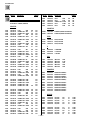
KV-32V68/35V68
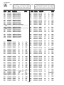
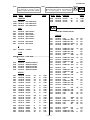
TABLE OF CONTENTS
Section
Title
Page
1. GENERAL
Connecting and Installing the TV ............................................
Setting Up the GuidePlus+™ Feature ...................................
Using the GuidePlus+™ Feature ...........................................
Operating Video Equipment ...................................................
Troubleshooting .....................................................................
5
7
8
13
13
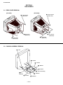
2. DISASSEMBLY
2-1. Rear Cover Removal ......................................................
2-2. Chassis Assembly Removal ...........................................
2-3. Service Position ..............................................................
2-4. Control Switch Removal .................................................
2-5. Picture Tube Removal/Anode Cap Removal ..................
14
14
15
15
16
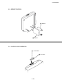
3. SET-UP ADJUSTMENTS
3-1. Beam Landing .................................................................
3-2. Convergence ...................................................................
3-3. Focus ..............................................................................
3-4. Screen (G2) .....................................................................
3-5. White Balance Adjustments ............................................
17
18
19
19
19
Section
Title
Page
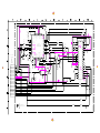
6. DIAGRAMS
6-1. Block Diagram ................................................................. 27
6-2. Block Diagram ................................................................. 31
6-3. Circuit Boards Location ................................................... 34
6-4. Printed Wiring Boards and Schematic Diagrams ............ 34
• A Board PWB (KV-32V68) .......................................... 35
• A Board PWB (KV-35V68) .......................................... 37
• A Board Schematic Diagram ....................................... 39
• AV Board ..................................................................... 43
• B Board ....................................................................... 43
• C Board ....................................................................... 45
• G Board ....................................................................... 47
• HS Board ..................................................................... 47
• HV Board ..................................................................... 47
• K Board ........................................................................51
• KG Board ..................................................................... 52
• P Board ........................................................................ 53
• UV Board ..................................................................... 55
• WA Board ................................................................... 59
• WB Board .................................................................... 59
6-5. Semiconductors ............................................................... 61
4. SAFETY RELATED ADJUSTMENTS ................................... 20
5. CIRCUIT ADJUSTMENTS ..................................................... 21
7. EXPLODED VlEWS
7-1. Chassis ............................................................................ 62
7-2. Picture Tube ..................................................................... 63
(KV-32V68)
7-3. Picture Tube ................................................................... 64
(KV-35V68)
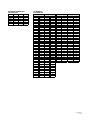
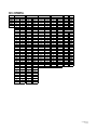
8. ELECTRICAL PARTS LIST
• Parts Listings ............................................................. 65
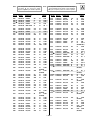
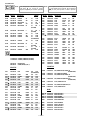
WARNINGS AND CAUTIONS
ATTENTION!
CAUTION!
AFTER REMOVING THE ANODE, SHORT CIRCUIT THE ANODE
OF THE PICTURE TUBE AND THE ANODE CAP TO THE METAL
CHASSIS, CRT SHIELD, OR CARBON PAINTED ON THE CRT.
APRES AVOIR DECONNECTE LE CAP DE L'ANODE, COURT-CIRCUITER L'ANODE
DU TUBE CATHODIQUE ET CELUI DE L'ANODE DU CAP AU CHASSIS METALLIQUE
DE L'APPAREIL, OU AU COUCHE DE CARBONE PEINTE SUR LE TUBE CATHODIQUE
OU AU BLINDAGE DU TUBE CATHODIQUE.
WARNING!!
ATTENTION!!
AN ISOLATION TRANSFORMER SHOULD BE USED DURING ANY
SERVICE TO AVOID POSSIBLE SHOCK HAZARD, BECAUSE OF
LIVE CHASSIS. THE CHASSIS OF THIS RECEIVER IS DIRECTLY
CONNECTED TO THE AC POWER LINE.
AFIN D'EVITER TOUT RESQUE D'ELECTROCUTION PROVENANT D'UN CHÁSSIS
SOUS TENSION, UN TRANSFORMATEUR D'ISOLEMENT DOIT ETRE UTILISÉ LORS
DE TOUT DÉPANNAGE. LE CHÁSSIS DE CE RÉCEPTEUR EST DIRECTEMENT
RACCORDÉ À L'ALIMENTATION SECTEUR.
SAFETY-RELATED COMPONENT WARNING!!
ATTENTION AUX COMPOSANTS RELATIFS A LA SECURITE!!
COMPONENTS IDENTIFIED BY SHADING AND MARK ¡ ON
THE SCHEMATIC DIAGRAMS, EXPLODED VIEWS AND IN THE
PARTS LIST ARE CRITICAL FOR SAFE OPERATION. REPLACE
THESE COMPONENTS WITH SONY PARTS WHOSE PART
NUMBERS APPEAR AS SHOWN IN THIS MANUAL OR IN
SUPPLEMENTS PUBLISHED BY
SONY. CIRCUIT
ADJUSTMENTS THAT ARE CRITICAL FOR SAFE OPERATION
ARE IDENTIFIED IN THIS MANUAL. FOLLOW THESE
PROCEDURES WHENEVER CRITICAL COMPONENTS ARE
REPLACED OR IMPROPER OPERATION IS SUSPECTED.
LES COMPOSANTS IDENTIFIES PAR UNE TRAME ET PAR UNE MARQUE ¡ SUR
LES SCHEMAS DE PRINCIPE, LES VUES EXPLOSEES ET LES LISTES DE PIECES
SONT D'UNEIMPORTANCE CRITIQUE POUR LA SECURITE DU FONCTIONNEMENT.
NE LES REMPLACER QUE PAR DES COMPOSANTS SONY DONT LE NUMERO DE
PIECE EST INDIQUE DANS LE PRESENT MANUEL OU DANS DES SUPPLEMENTS
PUBLIES PAR SONY. LES REGLAGES DE CIRCUIT DONT L'IMPORTANCE EST CRITIQUE POUR LA SECURITE DU FONCTIONNEMENT SONT IDENTIFIES DANS LE
PRESENT MANUEL. SUIVRE CES PROCEDURES LORS DE CHAQUE
REMPLACEMENT DE COMPOSANTS CRITIQUES, OU LORSQU'UN MAUVAIS
FONTIONNEMENT SUSPECTE.
—3—
KV-32V68/35V68
SAFETY CHECK-OUT
After correcting the original service problem, perform the
following safety checks before releasing the set to the
customer:
1. Check the area of your repair for unsoldered or poorlysoldered connections. Check the entire board surface
for solder splashes and bridges.
2. Check the interboard wiring to ensure that no wires
are “pinched” or contact high-wattage resistors.
3. Check that all control knobs, shields, covers, ground
straps, and mounting hardware have been replaced.
Be absolutely certain that you have replaced all the
insulators.
4. Look for unauthorized replacement parts, particularly
transistors, that were installed during a previous
repair. Point them out to the customer and
recommend their replacement.
5. Look for parts which, though functioning, show
obvious signs of deterioration. Point them out to
the customer and recommend their replacement.
6. Check the line cords for cracks and abrasion.
Recommend the replacement of any such line cord
to the customer.
7. Check the B+ and HV to see if they are specified
values. Make sure your instruments are accurate;
be suspicious of your HV meter if sets always have
low HV.
8. Check the antenna terminals, metal trim, “metallized"
knobs, screws, and all other exposed metal parts for
AC Leakage. Check leakage as described below.
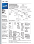
LEAKAGE TEST
The AC leakage from any exposed metal part to earth ground and
from all exposed metal parts to any exposed metal part having a
return to chassis, must not exceed 0.5 mA (500 microampere).
Leakage current can be measured by any one of three methods.
1. A commercial leakage tester, such as the Simpson 229 or
RCA WT-540A. Follow the manufacturers' instructions to
use these instructions.
2. A battery-operated AC milliammeter. The Data Precision
245 digital multimeter is suitable for this job.
3. Measuring the voltage drop across a resistor by means of
a VOM or battery-operated AC voltmeter. The "limit"
indication is 0.75 V, so analog meters must have an accurate
low voltage scale. The Simpson's 250 and Sanwa
SH-63Trd are examples of passive VOMs that are suitable.
Nearly all battery operated digital multimeters that have a
2V AC range are suitable. (See Fig. A)
HOW TO FIND A GOOD EARTH GROUND
A cold-water pipe is guaranteed earth ground; the cover-plate
retaining screw on most AC outlet boxes is also at earth ground.
If the retaining screw is to be used as your earth-ground, verify
that it is at ground by measuring the resistance between it and a
cold-water pipe with an ohmmeter. The reading should be zero
ohms. If a cold-water pipe is not accessible, connect a 60-l00 watts
trouble light (not a neon lamp) between the hot side of the receptacle and the retaining screw. Try both slots, if necessary, to
locate the hot side of the line, the lamp should light at normal
brilliance if the screw is at ground potential. (See Fig. B)
To Exposed Metal
Parts on Set
Trouble Light
AC Outlet Box
0.15µF
1.5k Ω
Ohmmeter
AC
Voltmeter
(0.75 V)
Cold-water Pipe
Earth Ground
Fig. B. Checking for earth ground.
Fig. A. Using an AC voltmeter to check AC leakage.
—4—
SECTION 1
GENERAL
The instructions mentioned here are partial abstracts from the Operating Instruction Manual. The page numbers shown reflect those of the Operating Instruction Manual.
Connecting and Installing the TV
Welcome!
—5—
Thank you for purchasing the Sony Trinitron®
Color TV. Before reading this manual, check the
model number located on the front of this
manual or on the rear of your TV.
The menus shown in this manual are for model
KV-35V68. Your menus may differ from the ones
illustrated.
The features you will enjoy include:
• The GUIDE Plus+ interactive program guide
system, which allows you to access program
information in an on-screen program guide,
sort programs by category, and to quickly
schedule programs for viewing or recording.
This service is yours with no monthly fee.
• Dual tuner PIP, which allows you to watch
two programs at once without having to
connect any additional equipment
• SRS, which allows you to listen to stereo
programs in dynamic three-dimensional
sound
• The FAVORITE CHANNEL feature, which
allows you to preview each of your chosen
favorite channels in a small window picture
before you choose to tune to a particular
station
• A front A/V input, for easy connection of
your camcorder or game equipment
• An S Video input, for enhanced picture
quality
Precautions
Using This Manual
Safety
• Operate the TV only with 120 V AC .
• The plug is designed, for safety purposes, to
fit in the wall outlet only one way. If you are
unable to insert the plug fully into the outlet,
contact your dealer.
• If any liquid or solid object should fall inside
the cabinet, unplug the TV immediately and
have it checked by qualified personnel before
operating it further.
• If you will not be using the TV for several
days, disconnect power by pulling the plug
itself. Never pull on the cord.
For details concerning safety precautions, see the
supplied leaflet “IMPORTANT SAFEGUARDS“.
Note
• After you plug the TV back in, you must wait 24
hours before information will be available in the
Program Guide.
Installing
• To prevent internal heat buildup, do not
block the ventilation openings.
• Do not install the TV in a hot or humid place,
or in a place subject to excessive dust or
mechanical vibration.
This manual is divided into five major sections.
We recommend that you review the contents of
each section in the order presented.
1
2
3
4
5
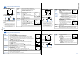
Making Connections
Refer to the table below, it will direct you to the diagram suitable to the components you will be
connecting.
Connecting and Installing the TV
This section guides you through your initial
set up.
Basic Set Up
This section teaches you the basic skills
needed to operate your new TV. It shows
you how to operate special functions of the
remote control and the GUIDE Plus+ feature.
Using your New TV
This section shows you how to use the Easy
Set Up Guide feature, and how to use your
remote control.
Using your Menus
This section teaches you how to access
on-screen menus and adjust your TV's
settings.
Troubleshooting
This section helps you to correct problems
you may encounter with your TV.
If you will be connecting
Instructions in this manual are written for the
remote control. Similar controls may be found on the
TV console.
* IMPORTANT
See page
Cable or antenna only
3
Cable and antenna
3
Cable box
4
Cable box and cable to view scrambled channels
4
VCR and cable or antenna
5
VCR and cable box
5
Direct Broadcast Satellite Receiver (DBS)
6
VCR and Direct Broadcast Satellite Receiver (DBS)
6
Digital Versatile Disc player (DVD)
7
Audio system
7
A/V receiver
8
Two VCR's for editing
8
Camcorder to view tapes
9
IR Blaster Cable* (G-Link)
9
S-Link connections
10
• You must connect the IR Blaster in
order to operate your VCR and/or
cable box with the GUIDE Plus+
feature.
Note
• When using the IR Blaster and a cable box, the
cable box must always be left ON to allow
GUIDE Plus+ to receive information about
upcoming television programs.
2
Connecting and Installing the TV (continued)
Cable Box Connections
VCR Connections
You must connect the IR Blaster in order to operate your
cable box with the GUIDE Plus+ feature. (see
“Connecting the IR Blaster” on page 9)
You must connect the IR Blaster in order to operate
your cable box with the GUIDE Plus+ feature.
Some pay cable TV systems use scrambled or encoded
signals that require a cable box to view all channels.
Cable box
1
2
Connect the coaxial connector from your cable to
the IN on your cable box.
Using a coaxial cable, connect OUT on your cable
box* to VHF/UHF on your TV.
(Rear of TV)
VHF/UHF
CATV cable
OUT
Notes
4
(Rear of TV)
AUX
scrambled
channels
TO CONVERTER
75-ohm coaxial cable
(not supplied)
CATV cable
(unscrambled channels)
(signal)
VHF/UHF
1
2
Attach your cable to IN on your cable box.**
Using a coaxial connector, connect OUT on your
cable box to IN on your VCR.
3 Using a coaxial connector, connect OUT on your
VCR to VHF/UHF on your TV.
4 Using A/V connectors, connect AUDIO and VIDEO
OUT on your VCR to AUDIO and VIDEO IN on
your TV.
** When using the IR Blaster and a cable box, the
cable box must be left ON at all times to allow
the GUIDE Plus+ feature to receive information
about upcoming television programs.
Notes
• To record programs using VCR Plus+, your VCR
must be set to channel 3 or 4, preferably the channel
which does not receive a broadcast channel in your
area.
AUDIO
MONITOR (VAR/FIX)
L
(MONO)
VHF/UHF
R
S-LINK
S-LINK
G-LINK
VCR
1
Cable
OUT
IN
S VIDEO
AUDIO R AUDIO L VIDEO
AUDIO-R (red)
AUDIO-L (white)
VIDEO (yellow)
LINE
OUT
2
VMC-810S/820S
(not supplied)
For optimum picture quality, use S VIDEO
instead of the yellow A/V cable. S Video does
not provide sound, your audio connectors
must still be connected.
(Rear of TV)
IN
VIDEO 1 VIDEO 3
AUX
3
Coaxial cable
TV
L
(MONO)
AUDIO
VHF/UHF
VCR
IN
AUDIO R AUDIO L VIDEO
1
S VIDEO
LINE
OUT
2
Cable box
Cable
4
AUDIO
MONITOR (VAR/FIX)
VIDEO
R
S-LINK
OUT
OUT
S VIDEO
TO
CONVERTER
G-LINK
S-LINK
AUDIO-R (red)
AUDIO-L (white)
VIDEO (yellow)
VMC-810S/820S
(not supplied)
OUT
IN
5
KV-32V68/35V68
• The GUIDE feature will not function for items
connected to the AUX input.
• When using PIP, you cannot view the AUX input
(scrambled channels) in the window picture.
• If you are using a cable box with the GUIDE Plus+
feature, when viewing PIP the same picture will be
displayed in the main and window picture. (see
page 25)
* When using the IR Blaster and a cable box, the
cable box must be left ON at all times to allow
the GUIDE Plus+ feature to receive information
about upcoming television programs.
Connecting a VCR and TV with a
cable box
TV
VIDEO
AUDIO
Coaxial cable
3
single white audio output to the left input on your TV.
If you are connecting a cable box through the AUX input and would like to switch
between the AUX and normal (CATV) input, you should consider using the CHANNEL
FIX feature discussed on page 31.
Cable box
Attach your cable or antenna to IN on your VCR.
Using A/V connectors, connect AUDIO and VIDEO
OUT on your VCR to AUDIO and VIDEO IN on
your TV.*
Using a coaxial connector, connect OUT on your
VCR to VHF/UHF on yourTV.
OUT
S VIDEO
TO
CONVERTER
* If you are connecting a monaural VCR, connect only the
Cable box
Cable box and cable
For this set up, you can switch between scrambled
channels (through your cable box*), and normal (CATV)
channels by pressing ANT on your remote control.
1
2
(Rear of TV)
IN
VIDEO 1 VIDEO 3
AUX
Connecting an antenna/cable TV
system with a VCR
3
IN
For superior picture quality, use an A/V cable
instead of the VHF/UHF connection.
KV-32V68/35V68
Connecting and Installing the TV (continued)
DBS Connections
For optimum picture quality, use
S VIDEO instead of the yellow A/V
cable. S Video does not provide sound,
your audio connectors must still be
connected.
Connecting a DBS (Direct Broadcast
Satellite) receiver
1
2
3
2
3
4
5
OUT
S VIDEO
2
TV
TO
CONVERTER
AUDIO
MONITOR (VAR/FIX)
L
(MONO)
AUDIO
R
1
S-LINK
SATELLITE IN
S-LINK
G-LINK
VHF/UHF
AUDIO R AUDIO L VIDEO
IN
S VIDEO
OUT
1
AUDIO-R (red)
AUDIO-L (white)
VIDEO (yellow)
LINE OUT
3
IN
2
(Rear of TV)
VIDEO 1 VIDEO 3
2
LINE OUT
AUDIO R AUDIO L VIDEO
Using audio connectors, connect AUDIO-R
and AUDIO-L OUT from LINE OUT on your
DVD to AUDIO-R and AUDIO-L IN from
VIDEO IN on your TV.
Connect S-Video from your DVD player to
your TV.
OUT
S VIDEO
TV
(Rear of DVD player)
Connecting a DVD Player
DBS receiver
Satellite
antenna
cable
Additional Connections
The following connections are for accessories
that will enhance your viewing options.
VIDEO
VHF/UHF
Connect the cable from your satellite antenna
to SATELLITE IN on your DBS receiver.
Connect your cable or antenna to VHF/UHF
on your TV.
Using A/V connectors, connect AUDIO and
VIDEO OUT on your DBS receiver to
AUDIO and VIDEO IN on your TV.
Connect the cable from your satellite antenna
to SATELLITE IN on your DBS receiver.
Connect your cable or antenna to VHF/UHF
IN on your VCR.
Using a coaxial connector, connect VHF/UHF
OUT on your VCR to VHF/UHF on your TV.
Using A/V connectors, connect AUDIO and
VIDEO OUT on your DBS receiver to AUDIO
and VIDEO IN on your VCR.
Using A/V connectors, connect AUDIO and
VIDEO OUT on your VCR to AUDIO and
VIDEO IN on your TV.
(Rear of TV)
VIDEO 1 VIDEO 3
AUX
Connecting a DBS (Direct Broadcast
Satellite) receiver and a VCR
1
IN
Cable/Antenna
AUDIO
MONITOR (VAR/FIX)
VIDEO
L
(MONO)
AUDIO
S VIDEO
R
1
S-LINK
S-LINK
G-LINK
AUDIO-R (red)
AUDIO-L (white)
S Video
Connection
VMC-810S/820S (not supplied)
VMC-810S/820S (not supplied)
For superior picture quality, use an A/V cable
instead of the VHF/UHF connection.
Cable/Antenna
VMC-810S/820S (not supplied)
1
(Rear of TV)
IN
VIDEO 1 VIDEO 3
AUX
4
TV
AUDIO
MONITOR (VAR/FIX)
VIDEO
VCR
L
1
(MONO)
AUDIO
SATELLITE IN
VHF/UHF
AUDIO R AUDIO L VIDEO
AUDIO R AUDIO L VIDEO
IN
S VIDEO
OUT
LINE OUT
2
S VIDEO
VHF/UHF
LINE IN
VHF/UHF
R
S-LINK
Connecting an audio system
For enhanced sound, connect your audio system
to your TV.
OUT
S VIDEO
TO
CONVERTER
S-LINK
G-LINK
IN
DBS receiver
AUDIO-R (red)
AUDIO-L (white)
VIDEO (yellow)
OUT
LINE OUT
3
2
IN
(Rear of TV)
VIDEO 1 VIDEO 3
1
OUT
S VIDEO
TV
Using AUDIO connectors, connect AUDIO
OUT on your TV to one of the unused line
inputs (e.g. TV, AUX, TAPE 2) on your stereo.
Set your stereo to the chosen line input. Refer
to page 29 of this manual for additional audio
setup instructions.
AUDIO
MONITOR (VAR/FIX)
AUDIO-L
(white)
VIDEO
L
R
S-LINK
AUDIO-R
(red)
S-LINK
G-LINK
5
Pressing TV/VIDEO on the
remote control will allow you
to view from the DBS or VCR.
RK-74A
(not supplied)
(MONO)
AUDIO
Line
input
2
HRD
VMC-810S/820S (not supplied)
—6—
6
7
Connecting and Installing the TV (continued)
Connecting a camcorder
Connecting an A/V receiver
2
1
Using A/V cables, connect TV OUT on your
TV to TV IN on your A/V receiver.
2 Using a single video connector, connect
MONITOR OUT on your A/V receiver to
VIDEO 1 IN on your TV.
Note
VMC-10HG/30HG (not supplied)
VIDEO (yellow)
IN
(Rear of TV)
VIDEO 1 VIDEO 3
A/V outputs
OUT
S VIDEO
TV
AUDIO
MONITOR (VAR/FIX)
VIDEO
• When you are in a video mode (VIDEO 1, 2, or 3),
you will not be able to access the GUIDE Plus+
feature.
L
(MONO)
A/V receiver
AUDIO
R
S-LINK
HRD
S-LINK
G-LINK
VIDEO (yellow)
AUDIO-L (white)
AUDIO-R (red)
A/V inputs
1
Connecting two VCRs for editing
MONITOR OUT gives you the ability to use a
second VCR to record a program being played
by the primary VCR or to perform tape editing
and dubbing.
1
2
You should not change video
inputs while editing using
MONITOR OUT.
1
2
OUT
S VIDEO
TV
AUDIO
MONITOR (VAR/FIX)
VIDEO
Connect the VCR intended for playback using
the setup instructions on page 5 of this
manual.
Using A/V connectors, connect AUDIO and
VIDEO IN on your VCR intended for
recording to MONITOR AUDIO and VIDEO
OUT on your TV.
L
(MONO)
VCR (for playback)
AUDIO
VCR (for recording)
R
AUDIO R AUDIO L VIDEO
AUDIO R AUDIO L VIDEO
OUT
LINE
OUT
S-LINK
1
OUT
S-LINK
G-LINK
LINE
IN
IN
IN
VIDEO (yellow)
AUDIO-L (white)
AUDIO-R (red)
2
S VIDEO VIDEO 2 INPUT
VIDEO L(MONO)-AUDIO-R
STAND BY
TIMER
STEREO
S VIDEO
VIDEO L(MONO)-AUDIO-R
VIDEO 2 INPUT
AUDIO-R (red)
AUDIO-L (white)
VIDEO (yellow)
AV output
VMC-810S/820S
(not supplied)
You must connect your IR Blaster to automatically
control your VCR and/or cable box with the GUIDE
Plus+ feature.
(Rear of TV)
IN
(Front of TV)
If you have an S VIDEO equipped
camcorder, you can use an S Video
cable for optimum picture quality.
Connecting the IR Blaster (G-Link)
VMC-810S/820S (not supplied)
VIDEO 1 VIDEO 3
VMC-810S/820S (not supplied)
8
This connection is convenient for viewing a picture
directly from your camcorder.
Using A/V connectors, connect AUDIO and VIDEO
OUT on your camcorder to AUDIO and VIDEO IN
on your TV.
Connection can also be made directly to your A/V
input located on the rear of your TV.
Note
• If you are connecting a monaural camcorder,
connect only the single white audio output to the
left input on your TV.
VMC-810S/820S (not supplied)
3
Connect the IR Blaster to the TV's G-Link
jack.
Place the IR Blaster on top of (or below) and
overhanging the front of the VCR and/or
cable box, about 1/2" to 1". For best results,
place the IR Blaster directly above (or below)
the VCR’s and/or cable box’s IR receiving
area.
Set the manufacturer and code type of your
VCR/cable box, using the GUIDE PLUS+
SET UP menu (see page 31). This code must
be set for the GUIDE Plus+ feature to
function properly.
(Rear of TV)
IN
1/2" to 1"
VIDEO 1 VIDEO 3
OUT
S VIDEO
TV
AUDIO
MONITOR (VAR/FIX)
VIDEO
L
(MONO)
VCR
AUDIO
R
OUT
S-LINK
G-LINK
S-LINK
IN
AUDIO R AUDIO L VIDEO
S VIDEO
LINE
OUT
Cable Box
IR Blaster
OUT
IN
9
Basic Set Up
Connecting and Installing the TV (continued)
S-Link connections
Inserting batteries
Connect to the CONTROL
S-IN on your VCR.
S-Link is designed to allow your Sony
components to “communicate.”
1
AUDIO-R (red)
AUDIO-L (white)
VIDEO (yellow)
Connecting S-Link to a VCR
S-Link will automatically power on the TV and
switch to the correct video input when a tape is
inserted in the VCR.
1 Using A/V connectors, connect AUDIO and
VIDEO OUT on your VCR to AUDIO and
VIDEO IN on your TV.
2 Using an S-Link connector (mini plug),
connect S-LINK/CONTROL S-IN on your
VCR to S-LINK on your TV.
Insert two size AA (R6) batteries (supplied) by
matching the + and – on the batteries to the
diagram inside the battery compartment.
VMC-810S/820S
(not supplied)
Using the remote control
move & select buttons
0
GUIDE
INFO
Move
TV/DBS
VCR
AUDIO R AUDIO L VIDEO
LINE
OUT
IN
CONTROL S
IN OUT
(Rear of TV)
VIDEO 1 VIDEO 3
S-LINK
RESET
OUT
S VIDEO
TV
MENU
VOL
AUDIO
MONITOR (VAR/FIX)
On-screen help/instructions
Several menu windows will provide prompts
and instructions to assist you in navigating
through the different functions.
When presented, use these to supplement the
instructions in this manual.
CH
Select
VIDEO
PAGE
L
(MONO)
RK-G69HG
(not supplied)
AUDIO
Connecting S-Link to a DBS
Notes
R
2
S-LINK
S-LINK
G-LINK
The S-Link connector must be in the
same VIDEO-IN jacks as the A/V cables
on your TV.
S-Link will automatically power on the TV and
switch to the correct video input when you
power on the DBS.
DBS Receiver
1
Using A/V connectors, connect AUDIO and
VIDEO OUT on your DBS to AUDIO and
VIDEO IN on your TV.
2 Using an S-Link connector (mini plug),
connect S-LINK on your DBS to
S-LINK on your TV.
Note
SATELLITE IN
Satellite
Antenna
Cable
S-LINK
AUDIO R AUDIO L VIDEO
• Remove the batteries to avoid damage from
possible battery leakage whenever you
anticipate that the remote control will not be
used for an extended period.
• Handle the remote control with care. Avoid
dropping it, getting it wet, or placing it in direct
sunlight, near a heater, or where the humidity is
high.
• Your remote control can be programmed to
operate most video equipment. (see page 34)
(Rear of TV)
IN
VIDEO 1 VIDEO 3
LINE
OUT
AUDIO-R (red)
AUDIO-L (white)
VIDEO (yellow)
CODE SET
The supplied remote control has ”arrow”
buttons (V, v, B, b) which allow for movement
of theon-screen selector. Pressing on the outer
buttons will cause the selector to move in the
corresponding direction. Pressing the center
button (
) will select the item.
Adjustment bars
When menu items present an adjustment bar
(
or
), use the arrow buttons to
change the setting.
OUT
S VIDEO
TV
AUDIO
MONITOR (VAR/FIX)
VIDEO
L
(MONO)
2
RK-G69HG
(not supplied)
• Do not connect S-Link to the G-Link jack on your
TV.
1
AUDIO
R
VMC-810S/820S (not supplied)
S-LINK
G-LINK
S-LINK
—7—
10
11
Using Your New TV
Setting up the TV automatically
The Easy Setup Guide allows you to set the onscreen language and set all receivable channels
in one step.
To set up the TV manually, refer to “Using the SET
menu” on page 31.
UP
Tips z
• Perform this function during the day, with the
antenna and/or cable properly connected, to ensure
that all available channels will be broadcasting and
receivable.
• The TV must be set to the TV input to execute
AUTO PROGRAM. Press TV/VIDEO until a
channel number appears.
• If your cable or antenna is connected to AUX, press
ANT until AUX appears next to the channel number.
Using the buttons on the top of the TV:
SET UP
O
TV/VIDE
– VOLUME +
– CHANNEL
+
POWE
R
1
Press POWER to turn on the TV.
The Easy Setup Guide screen appears.
POWER
[ CH+ ]
[ CH– ]
[ VOL+ ]
[ VOL– ]
[ TV/VIDEO ]
First please connect
cable/antenna.
Press [SET UP] to exit
2 Make your language selection by pressing
CH +, CH – or VOL +.
– CHANNEL
+
3 Press VOLUME – to continue or TV/VIDEO
for a DEMO of functions and menus.
To perform AUTO SET UP again
Press the SET UP button on the TV and follow
steps 2-3.
If you choose to set AUTO GUIDE to ON, the
program guide will appear each time you turn
the TV on using your remote control.
After you have set up your TV using the Easy
Setup Guide, you will be prompted to set up
your GUIDE Plus+ feature.
Several questions will appear on your screen.
You will be asked to enter specific information,
such as your location, zip or postal code,
whether you will be connecting cable, a cable
box, or a VCR, etc.
Notes
• To reset your TV to factory settings, turn the TV
on. Then, while pressing the RESET button on
your remote control, press the POWER key on
your TV. The TV will turn itself off, then back
on.
• When you perform AUTO PROGRAM, your
CHANNEL FIX, CHANNEL BLOCK, and ON/
OFF TIMER settings, as well as your GUIDE
Plus+ settings and program information will be
erased.
To answer each question, highlight the
appropriate answer, and press the
button
on the remote control. In some instances, like
when you are asked to enter your zip or postal
code, you will need to enter numerical
information using the V/v buttons on the remote
control.
After you have completed your GUIDE Plus+ set
up, you can choose to view a Demo of the
GUIDE Plus+ features. If you wish to view this
Demo again, after you have exited from GUIDE
Plus+ set up, you can re-enter GUIDE Plus+ set
up through the TV’s SET UP menu. (see GUIDE
PLUS+ SET UP on page 31)
Notes
• PIP must be OFF to allow the GUIDE Plus+
feature to receive program information.
• If you have connected a cable box to your TV,
the TV must be turned off, and the cable box left
on, in order to receive program information.
• If there is more than one cable company in your
area, you will be asked to choose a “Channel
Map” which matches yours (i.e., Fox =6,
NBC = 7, etc).
• The GUIDE Plus+ feature menus are only
available in English.
• The GUIDE Plus+ feature may not be available
in all areas. If the GUIDE Plus+ feature is not
available in your area, please contact the Sony
Direct Response Center at the number listed on
page 38 of this instruction manual.
WIthin 24 hours of your initial set up of the
GUIDE Plus+ feature, you will be able to view
program guides on your TV.
If you make a mistake during your set up, or
you would like to connect new components
to your TV, you can reenter the GUIDE Plus+
SET UP menu. (see “GUIDE PLUS+ SET UP”
on page 31)
13
KV-32V68/35V68
A message will appear, asking if you want to
continue to AUTO PROGRAM. Press CH+
to continue.
– VOLUME +
12
ENGLISH :
ESPAÑOL :
FRANÇAIS :
AUTO SET UP :
DEMO :
AUTO PROGRAM appears and the TV
starts scanning and presetting channels
automatically. If the TV receives cable TV
channels, CABLE is set ON automatically.
Setting up the GUIDE Plus+™
feature
KV-32V68/35V68
Using Your New TV (continued)
MUTING
POWER
DBS/
CABLE
VTR/
DVD
TV
FUNCTION
SYSTEM
OFF
Using the GUIDE Plus+ Feature
DBS/
CABLE
VTR/
DVD
TV
MTS
VCR+
FREEZE
SWAP
CH
POSITION
AUDIO
TV/VIDEO
SLEEP
DISPLAY
TV/VIDEO
ANT
TV/VTR
Using the GUIDE Plus+ Feature
+
–
The GUIDE Plus+ feature allows you to see local
TV programming, set your VCR to record
programs, sort programs by category, set your
TV to turn on and tune to a program, and receive
information about program content. All this can
be done while viewing your current channel in a
video window.
Press
to view the first screen, the Program
Grid.
Notes
Video
window
Channel
lock
Blue
Action
Button
(JUMP)
1
2
3
4
5
6
7
8
9
ENTER
JUMP
0
GUIDE
INFO
TV/DBS
RESET
MENU
VOL
CH
PAGE
Green
Action
Button
(ENTER)
CODE SET
RM-Y154
Video Window
The video window allows you to view a program while in the Program Grid. Pressing the
button while using the GUIDE Plus+
feature will lock/unlock the video window, so the picture will remain the same as you move through the Program Grid.
Channel Lock
button while using the GUIDE Plus+ feature will lock/unlock
This symbol indicates whether Channel Lock is on or off. Pressing the
the video window, so the picture will remain the same as you move through the Program Grid.
Blue Action Button
This symbol and corresponding text indicates what will happen when you press the Blue Action Button
JUMP
JUMP
on your remote control.
TV
GUIDE
Green Action Button
ENTER
Information
box
• When you press MENU, the highlight jumps to
the menu bar.
• The GUIDE Plus+ feature will not function when
your video source is from video equipment or
from the AUX input.
• Press the ANT button to return to the VHF/UHF
input before accessing the GUIDE Plus+ feature.
Info icon
Information Box
on your remote control.
This symbol and corresponding text indicates what will happen when you press the Green Action Button
Provides information regarding each program which is highlighted as you scroll through the Program Grid.
Info Icon
Icon appears if additional information about a program being described in the Information box is available. When the Info icon appears,
press the INFO button on the remote control to access additional information.
Menu Bar
Offers several options for setting up and using the GUIDE Plus+ feature. Menu items include GRID (see page 20), SORT (see page 21),
SCHEDULE (see page 21), MESSAGES (see page 22), EDITOR (see page 22), and SETUP (see page 22).
Last Channel Viewed
While in the grid, the last channel viewed will remain highlighted in gray.
Menu bar
Last
channel
viewed
ENTER
Display panels show information about future programming. After highlighting a display panel, you will be able to access expanded
for the program advertised, when this information is available.
program information
Display Panels
Display
panels
Channel Ads
After you have highlighted a display panel, you can press
recording.
JUMP
ENTER
to schedule the program for viewing, or
Sometimes, a channel ad will be displayed within the Program Grid.
After highlighting a channel ad, you will be able to access expanded information
information is available.
for the program or channel advertised, when this
ENTER
JUMP
Channel title
—8—
After you have highlighted a display panel, you can press
recording.
to schedule the program for
to schedule the program for viewing, or
14
to schedule the program for
15
Using Your New TV (continued)
REFER TO THE ILLUSTRATION
OF THE REMOTE CONTROL ON
THE INSIDE FRONT COVER OF
THIS MANUAL AS YOU
REVIEW THIS CHART
Using the GUIDE Plus+ Buttons
The GUIDE Plus+ feature offers on-screen
program information. Use the chart and
illustration on this page to learn how to access
and use the GUIDE Plus+ feature with your
remote control.
Use the Purple Labeled Buttons for the GUIDE Plus+ Feature Operations
Press to scroll V/v, a page at a time, while in the GUIDE Plus+ screen.
CH
PAGE
Use the Purple Labeled Buttons for the GUIDE Plus+ Feature Operations
VCR
Pressing the VCR+ button allows you to program your VCR to record TV programs
using the VCR Plus+ code system. You can find the PlusCode programming number
codes in your newspaper’s Program Guide.
You must have a VCR and an IR Blaster properly connected and set up in order to
record programs using the VCR Plus+ feature. Press VCR+ again to exit the VCR
Plus+ screen.
Once a program has been scheduled for recording using the VCR Plus+ system, you
can review your selection, change the frequency of recording, or cancel the recording
within the GUIDE Plus+ SCHEDULE screen. (see “SCHEDULE” on page 21)
MENU
Pressing the MENU button will move you between the grid and the menu bar.
Press the arrow keys (B, V, b, v) to scroll in any direction while using GUIDE Plus+
and press the select button
to choose the option.
Pressing the
button while using the GUIDE Plus+ feature will lock/unlock the
video window, so the picture will remain the same as you move through the Program
Grid.
JUMP
ENTER
Note
• You must connect your IR Blaster in order to
operate your VCR and/or cable box. This will
allow the GUIDE Plus+ feature to tune to and
record programs.
INFO
GUIDE
16
JUMP
Press the
button to choose the left (blue) action button (as displayed at the top of
the Program Grid).
ENTER
Press the
button to choose the right (green) action button (as displayed at the top
of the Program Grid).
Pressing the INFO button will show additional information about a selected program
or future programming on the selected channel, if available. An info icon
will
appear on the screen to indicate when information is available.
You must press the INFO button again to return to basic information.
Pressing the GUIDE button will activate the GUIDE Plus+ screen.
Pressing again will exit the GUIDE Plus+ screen.
17
Using Your New TV (continued)
Learning to view a program
using the GUIDE Plus+ feature
2
Press v to highlight the desired program (in
this case "Spin City").
3
Press
to select the program.
Use the GUIDE button to access the Program
Grid and use the arrow buttons (V or v) to select
a program. Use the following example, in which
we select a program to be viewed to learn how to
use the GUIDE Plus+ feature.
1
Learning to schedule viewing
and recording using the
GUIDE Plus+ feature
1
Press the GUIDE button.
The Program Grid appears.
3
4
JUMP
Press the blue action button
to select
WATCH.
Press GUIDE to return to the last channel
viewed.
To automatically schedule future
viewing:
JUMP
Press the blue action button
once, and the
program will automatically be scheduled for
viewing at the time indicated within the
Program Grid. The color of the highlight within
the Program Grid will change to red to indicate
that this program has been scheduled for
viewing.
Press the GUIDE button.
The Program Grid appears.
GUIDE
To enter the Schedule Menu to set
up future viewing:
JUMP
2
Use the V/v/B/b buttons to move to a future
program which you would like to schedule
for viewing.
Press the blue ENTER
action button , then the green
. Your scheduled viewing
action button
option will appear on the screen.
To change the frequency of your
scheduled viewing:
In the Schedule Menu, press the green action
to change your viewing option.
button
ENTER
As you press the green action button
, you
will cycle through the frequency viewing
ENTER
options (once, daily, or weekly).
Note
• You must connect your IR Blaster in order to
operate your VCR and/or cable box. This will
allow the GUIDE Plus+ feature to tune and
record programs.
To schedule recording
Follow the directions provided on this page for
scheduling viewing.
In step 3, press the green
ENTER
action button
instead of the blue action
button . This will schedule the chosen
program for recording. A program scheduled for
recording will appear highlighted in orange
within the Program Grid.
Note
JUMP
• The VCR must be set up correctly during GUIDE
Plus+ set up in order for scheduled recording to
function properly.
To cancel viewing or recording
—9—
If you wish to cancel viewing or recording of a
program, enter the schedule screen, highlight the
JUMP
program, and press .
19
18
Using Your New TV (continued)
GRID
The main viewing
screen
SORT
SORT allows you to organize, select and schedule programs to watch and record.
To watch/record
movies
While in the Program Guide:
1
Press MENU.
2
Press b to highlight SORT and press
. First level SORT appears on the screen,
displaying the last category selected (Movies, Sports or Children's).
3
4
Press b to choose a new category, then press
Press v to choose a new subcategory, then press
.
.
5
After choosing a subcategory, you will be able to view all programs available in that subcategory
JUMP
over an eight day period. To schedule a program to be watched, press the blue action button
.
ENTER
.
To schedule a program to be recorded, press the green action button
If expanded information about a program in the sort screen is available, the
will appear in the
Information Box. Press INFO to access this information.
Notes
• You must connect the IR Blaster in order to
operate your VCR and/or cable box with the
GUIDE Plus+ feature.
• When using the IR Blaster and a cable box, the
cable box must be left ON at all times to allow
GUIDE Plus+ to receive information about
upcoming television programs.
• The TIMER light on the front panel of your TV
will not light up when programs are scheduled
for viewing using the GUIDE Plus+ feature
“WATCH” function.
• If you have connected your TV to a cable box,
and are recording using the GUIDE Plus+
feature, you will not be able to change channels
during recording.
The display panels within SORT show information about future programming. After highlighting a display panel, you will be
for the program advertised, when this information is available.
able to access expanded program information
ENTER
JUMP
to schedule the program for viewing, or
After you have highlighted a display panel, you can press
to schedule the
program for recording.
SCHEDULE
SCHEDULE allows you to adjust viewing/recording times of programs.
To adjust program
scheduling
While in the Program Grid:
1
Press MENU.
2
3
.
Press b to get to SCHEDULE and press
A list of programs scheduled to be watched and/or recorded appears on the screen.
JUMP
To REMOVE a scheduled program, scroll to it and press the blue action button
.
ENTER
To CHANGE a scheduled program, scroll to it and press the green action button
.
Programs that have been scheduled for viewing will appear in red within the Program Grid.
Programs that have been scheduled for recording will appear in orange within the Program Grid.
21
KV-32V68/35V68
20
The program title of the last channel viewed is highlighted and basic
information for the program is displayed in the information box.
Use the V/v/B/b buttons to navigate to different program names, time slots
(through midnight of the following day), and channel ads within the grid.
To record a program:
To record a program, you must first connect the IR Blaster. (see "Connecting
the IR Blaster" on page 9)
JUMP
1
Highlight the program title and press the blue action button
.
ENTER
2
To change your scheduled recording, press the green action button
again. Once you enter the schedule screen, you can choose to record
the program once, repeatedly (daily, weekly), or to cancel recording.
To schedule to watch a program:
JUMP
1
Highlight the program title and press the blue action button
. ENTER
2
To change your scheduled viewing, press the green action button
.
Once you enter the schedule screen, you can choose to watch the
program once, repeatedly (daily, weekly), or to cancel scheduled
viewing.
To jump to a specific channel within the grid, enter the channel number on
the remote control’s keypad.
button. A lock icon
will
To lock/unlock the video window, press the
appear in the video window when the picture is locked.
Unlocked, the video window will display the current program as you
scroll through the channel listings.
Locked, the video window will not change as you scroll through the
channel listings. If you set the lock while in the grid, the video window
will remain locked to the channel you are on. If the lock is already set
when you enter the grid, the video window will be locked to the last
channel viewed.
KV-32V68/35V68
Using Your New TV (continued)
MESSAGES
To view messages
EDITOR
To turn channels
ON/OFF in the
MESSAGES allows you to view system messages.
While in the Program Guide:
1
Press MENU.
2
Press b to get to MESSAGES and press
. Messages related to the system will be displayed, if
none are available the GUIDE Plus+ ID number will be displayed. If messages remain unread for a
prolonged period, they will be automatically deleted.
Watching the TV
REFER TO THE ILLUSTRATION
OF THE REMOTE CONTROL ON
THE INSIDE FRONT COVER OF
THIS MANUAL AS YOU
REVIEW THIS CHART
The following chart will explain the function
of the buttons found on your remote control.
Using the White Labeled Buttons for TV Operations
EDITOR allows you to adjust channel availability within the grid while using the GUIDE Plus+ feature.
While in the Program Guide:
1
Press MENU.
2
Press b to get to EDITOR and press
. All channels available are listed.
JUMP
3
To CANCEL any further changes, press the blue action button
.
ENTER
4
To turn a channel ON/OFF, scroll to it and press the green action button
.
VTR/
DVD
POWER
DBS/
CABLE
TV
FUNCTION
VTR/
DVD
To reassign a channel number, highlight the channel within the EDITOR screen, and enter the new channel
number on the remote control’s keypad.
The order of channels within the Program Grid cannot be changed
The GUIDE Plus+ EDITOR functions independently of your TV’s CHANNEL SKIP/ADD feature.
(see page 31 for information on CHANNEL SKIP/ADD)
DBS/
CABLE
TV
0 - 9
and ENTER
CH
Press when you want to turn connected equipment on and off.
You can program your remote control to operate other video equipment. (see
"Operating Video Equipment" on page 34)
Press when you want to control connected equipment with your remote
control. (see pages 34-36 for instructions on programming your remote control)
Use for direct channel selection. Press 0-9 to select a channel, the channel will
change after 2 seconds, or you can press ENTER for immediate selection.
Press to scan through the channels.
Keeping the CH + or – pressed allows you to rapidly scan to the desired channel.
PAGE
SETUP
To use or program
the GUIDE Plus+
SETUP allows you to start/change the GUIDE Plus+ feature settings and to view a demonstration of its
features.
While in the Program Guide:
1
Press MENU.
2
Press b to get to SETUP and press
. The setup screen will appear.
3
To change your settings, select SETUP.
4
To view the demonstration, select DEMO.
JUMP
MUTING
SLEEP
Press to alternate or jump back and forth between two channels. You can jump
between the last two channels selected with the 0-9 keys.
This button can also be used to activate on-screen options while using the
GUIDE Plus+ feature.
Press to mute the sound (MUTING will appear on the screen). Press again or
press VOL + to restore sound.
— 10 —
Press repeatedly until the TV displays the approximate time in minutes (30, 60, or
90) that you want the TV to remain on before turning off automatically. Cancel by
pressing until SLEEP OFF appears.
22
23
Using Your New TV (continued)
Using the White Labeled Buttons for TV Operations
ENTER
MTS
DISPLAY
TV/VIDEO
ANT
(AUX input)
TV/VTR
+
SYSTEM
OFF
24
CAPTION VISION
(Closed Caption)
Use to activate a channel selected with the 0-9 buttons.
Use to activate on-screen options while using the GUIDE Plus+ feature.
Pressing the MTS button will cycle through the MTS options (STEREO, SAP,
MONO). (see the MTS section in “Using the AUDIO menu” on page 29)
Press repeatedly to cycle through the available displays:
Status
Channel number, current time, channel caption (if set) are displayed.
CAPTION VISION
Closed captioning will be displayed if the broadcaster offers this service.
(see right)
To cancel the display, press DISPLAY until DISPLAY OFF appears.
Press repeatedly to cycle through available video inputs:
TV, VIDEO 1, VIDEO 2 and VIDEO 3
When you are in a video mode (VIDEO 1, 2, or 3), you will not be able to access the
GUIDE Plus+ feature.
Press to change the VHF/UHF input to the AUX input.
Press to change from VIDEO input to TV input.
For detailed connection information, see “Cable and antenna” or "Cable box and
cable” on pages 5-6.
The GUIDE Plus+ feature cannot be accessed in AUX mode.
Press when you are finished using a VCR and you want to switch to the TV input
when your remote control is in VCR mode. Your VCR power will remain on.
The SYSTEM OFF button allows you to power off all Sony equipment at once.
B
SET UP
CHANNEL SET UP
GUIDE PLUS+ SET UP
AUTO GUIDE PLUS+: OFF
CHANNEL BLOCK
FAVORITE CHANNEL
VIDEO LABEL
CAPTION VISION: CC 1
LANGUAGE: ENGLISH
TILT CORRECTION: 0
MENU
Move
Select
Exit
Watching two programs at
one time - PIP
TV/VIDEO
REFER TO THE ILLUSTRATION
OF THE REMOTE CONTROL ON
THE INSIDE FRONT COVER OF
THIS MANUAL AS YOU
REVIEW THIS CHART
CAPTION VISION can be used for programs
that are broadcast with closed captioning.
TEXT1, 2, 3 or 4
Shows you network/station information
presented using either half or the whole screen.
XDS (Extended Data Service)
Shows a network name, program name,
program length, and time of the show if the
broadcaster offers this service.
Note
• Poor reception of TV programs can cause
errors in CAPTION VISION and XDS.
Captions may appear with a white box or
other errors instead of intended text.
Press once to display the window picture (1/9 size).
Press again to reduce the size of the window picture (1/16 size).
Press a third time to remove the window picture.
These models are equipped with dual tuners.
This means that PIP is “ready to use”.
MENU
CC1, 2, 3 or 4
Shows you a printed version of the dialog or
sound effects of a program. (The mode should
be set to CC1 for most programs)
Use the Yellow Labeled Buttons for PIP Operations
The sound of the main
picture is received
Main
picture
Press to alternate sound between the main picture and the window picture.
A will appear for a few seconds to indicate which picture is receiving sound.
TV/VTR
Press to change the TV channel in the window picture.
+
Main picture
received through
the TV
Window picture
received through
the second tuner
Window
picture
Notes
• You must press TV (FUNCTION) before you can
control PIP with the yellow labeled buttons.
• The AUX input cannot be viewed in the window
picture.
• If you have connected a cable box and activated
the GUIDE Plus+ feature, the same picture will
appear in both the main picture and window
picture.
Press repeatedly to cycle through available video inputs:
TV, VIDEO 1, VIDEO 2, VIDEO 3
AUDIO
CH
–
POSITION
FREEZE
SWAP
Press to move the location of the window picture (counterclockwise) around the
main picture.
Press to freeze the window picture. Great for copying down phone numbers,
addresses, recipes, etc.
Press FREEZE again to restore the picture.
Press to switch the audio and video of the main picture and the window picture.
Each time you press SWAP, the picture and sound of the two will be swapped.
25
Using Your Menus
3
Learning menu selection
Press V or v to move to the desired option.
Use the MENU button to access a menu and use
the arrow buttons (V or v) to alter settings. Use
the following example, in which we activate the
CABLE, to learn how to modify settings.
1
Press the MENU button.
The main menu appears.
B
Move
4
Move
Select
B
Exit
Exit
SET UP
CHANNEL SET UP
GUIDE PLUS+ SET UP
AUTO GUIDE PLUS+: OFF
CHANNEL BLOCK
FAVORITE CHANNEL
VIDEO LABEL
CAPTION VISION: CC 1
LANGUAGE: ENGLISH
TILT CORRECTION: 0
MENU
Move
Select
Exit
Quick start to the menus
The following will give you a quick start to the
options available for setting up your TV.
For detailed information on using the remote
control to modify menu settings, refer to
“Learning menu selection” on page 25.
To select a menu:
Display
Highlight
Select
MENU
MENU
Notes
• Pressing MENU on the remote control will allow
you to exit from the menus at any time.
Move
5
Select
Exit
B
Select
Move
Exit
MENU
AUDIO
TREBLE
BASS
BALANCE
AUTO VOLUME: OFF
EFFECT: OFF
MTS: STEREO
SPEAKER: ON
AUDIO OUT: VARIABLE
B
MENU
Select
Move
Exit MENU
B
Move
MENU
Press V or v to make your selection and press
.
B
CHANNEL SET UP
Move
The AUDIO menu offers enhanced audio options such as listening to
second audio programming (SAP), or customizing the EFFECT of the sound
on your TV.
The TIMER menu sets the clock on your TV and allows you to program your
TV for scheduled viewing using the ON/OFF TIMER.
SUN 12:00 AM
Select
Exit MENU
SET UP
CHANNEL SET UP
GUIDE PLUS+ SET UP
AUTO GUIDE PLUS+: OFF
CHANNEL BLOCK
FAVORITE CHANNEL
VIDEO LABEL
CAPTION VISION: CC 1
LANGUAGE: ENGLISH
TILT CORRECTION: 0
MENU
CABLE: ON
CHANNEL FIX: OFF
AUTO PROGRAM
CHANNEL SKIP/ADD
MENU
MENU
The VIDEO menu allows you to make adjustments to your picture settings.
It will allows you to customize the picture MODE based on the type of
program you are viewing.
VIDEO
MODE : VIVID
PICTURE
BRIGHTNESS
COLOR
HUE
SHARPNESS
MENU
TIMER
DAYLIGHT SAVING: NO
CURRENT TIME SET
ON/OFF TIMER
MENU
CABLE: OFF
CHANNEL FIX: OFF
AUTO PROGRAM
CHANNEL SKIP/ADD
MENU
MENU
SET UP
CHANNEL SET UP
GUIDE PLUS+ SET UP
AUTO GUIDE PLUS+: OFF
CHANNEL BLOCK
FAVORITE CHANNEL
VIDEO LABEL
CAPTION VISION: CC 1
LANGUAGE: ENGLISH
TILT CORRECTION: 0
MENU
Select
MENU
CHANNEL SET UP
Press V or v to highlight the desired menu
(in this case SET UP
) and press
to
select it.
Move
Exit
Press
.
Options for your selection will be
highlighted.
B
2
Select
When you are finished making changes to the
selected menu, choose MENU to return to the
main menu.
B
VIDEO
MODE : VIVID
PICTURE
BRIGHTNESS
COLOR
HUE
SHARPNESS
MENU
MENU
SET UP
CHANNEL SET UP
GUIDE PLUS+ SET UP
AUTO GUIDE PLUS+: OFF
CHANNEL BLOCK
FAVORITE CHANNEL
VIDEO LABEL
CAPTION VISION: CC 1
LANGUAGE: ENGLISH
TILT CORRECTION: 0
MENU
Select
Exit
MENU
The SET UP menu provides several options for setting
up your channels, labeling your TV/VIDEO inputs,
and selecting the LANGUAGE of your menus.
The CHANNEL SET UP menu is a sub-menu which
provides further options for setting up your TV.
— 11 —
Select
Exit
CABLE: ON
CHANNEL FIX: OFF
AUTO PROGRAM
CHANNEL SKIP/ADD
MENU
Move
Select
Exit
MENU
VIDEO MODE : VIVID
PICTURE :
AUDIO : EFFECT OFF
ADVANCED MENU
Select
Move
Exit
MENU
The Basic Menu provides quick access to frequently
used settings.
Escape to
Basic Menu
B
Move
CHANNEL SET UP
MENU
Move
Select
Exit
MENU
26
27
Using Your Menus (continued)
Using the VIDEO
menu
}
viewing
Adjustment
bars
B
Move
Select
MODE
Customized picture
VIDEO
MODE : VIVID
PICTURE
BRIGHTNESS
COLOR
HUE
SHARPNESS
MENU
Exit
PICTURE
Picture contrast
BRIGHTNESS
MENU
Picture adjustment
For detailed information on using the remote
control to modify menu settings, refer to
“Learning menu selection” on page 26.
To select the VIDEO
Display
Highlight
menu:
COLOR
Color saturation
HUE
Color tones
VIVID: Select for a vivid, bright picture for daytime viewing.
STANDARD: Select to receive a standard picture.
MOVIE: Select for night time movie viewing.
Adjust left to darken the picture.
Adjust right to brighten the picture.
Adjust left to decrease color intensity or saturation.
Adjust right to increase color intensity or saturation.
Adjust left to increase the red tones.
Adjust right to decrease the red tones.
SHARPNESS
Picture detail
Adjust left to soften the picture detail.
Adjust right to sharpen the picture detail.
menu
AUDIO
TREBLE
BASS
BALANCE
AUTO VOLUME: OFF
EFFECT: OFF
MTS: STEREO
SPEAKER: ON
AUDIO OUT: VARIABLE
B
MENU
Select
Move
Exit MENU
Adjust left to decrease picture contrast and soften the color.
Adjust right to increase picture contrast and create more vivid color.
Select
MENU
Using the AUDIO
} Adjustment
bars
Display
Highlight
Adjust left or right to decrease or increase higher pitched sound.
BASS
Adjust left or right to decrease or increase low pitched sounds.
BALANCE
Adjust left or right to emphasize right and left speaker volume.
AUTO VOLUME
ON: Select to stabilize the volume.
OFF: Select to turn AUTO VOLUME off.
Press
for direct selection of AUTO VOLUME settings.
Stabilizes volume
EFFECT
For detailed information on using the remote
control to modify menu settings, refer to
“Learning menu selection” on page 26.
To select the AUDIO
TREBLE
menu:
Select
Enhanced audio
options
MTS
Enjoy stereo,
bilingual and mono
programs
MENU
SPEAKER
28
Press RESET while the AUDIO menu is
displayed.
Custom selection of
audio output source
AUDIO OUT
Use to control the
TV's volume through
a stereo
MTS: Press V or v to select one of the following options:
STEREO: Select when viewing a broadcast in stereo.
SAP: Select to listen to bilingual broadcast. (Non-SAP programs will be muted
when this feature is selected)
MONO: Select to reduce noise during stereo broadcasts for areas of weak
reception.
Quick MTS access: Press MTS on your remote control to cycle through
the MTS options.
ON: Select to listen to the sound from the TV speakers with or without a
separate stereo system.
OFF: Select to turn off the TV speakers and listen to the TV's sound only through
external audio system speakers.
AUDIO OUT can only be set when SPEAKER is set to OFF.
VARIABLE: Sound output varies according to the TV settings.
Useful when you want to use your TV's remote control to adjust the output of a
separate audio system.
FIXED: Sound output is held at a fixed level through your stereo.
Use your A/V receiver's remote control to adjust the volume.
29
KV-32V68/35V68
To restore the factory VIDEO
settings
Press RESET while the VIDEO menu is
displayed.
To restore the factory AUDIO
settings
Press V or v to select one of these customized effects:
SIMULATED: Adds a stereo-like effect to mono programs.
SRS: Produces a dynamic three dimensional sound for stereo audio signals.
Using the TIMER
menu
B
CURRENT
TIME SET
SUN 12:00 AM
Select
Exit MENU
Move
For detailed information on using the remote
control to modify menu settings, refer to “Learning
menu selection” on page 26.
To select the TIMER
Display
Highlight
DAYLIGHT
SAVING
Automatically adjusts
the time
TIMER
DAYLIGHT SAVING: NO
CURRENT TIME SET
ON/OFF TIMER
MENU
Necessary for the
ON/OFF TIMER
menu:
Select
MENU
ON/OFF TIMER
To cancel the ON/OFF TIMER function
Wake up or
scheduled viewing
Press RESET while the ON/OFF TIMER menu is
displayed.
Note
• The GUIDE Plus+ feature will automatically set your
clock. If the DAYLIGHT SAVING and CURRENT
TIME SET options are grayed out, this is because the
clock has automatically been set.
• Your TV's ON/OFF TIMER will not function when
you are watching a program which has been scheduled
for viewing using the GUIDE Plus+ feature.
Set DAYLIGHT SAVING time before setting the clock.
Spring: Select YES to compensate for Daylight Saving Time.
The current time moves one hour ahead.
Fall: Select NO at the end of Daylight Saving Time.
The current time moves back one hour.
With the CURRENT TIME SET menu open:
1 Press
.
2 Press V or v until the current day is displayed.
Press
to select.
3 Press V or v until the current hour and
AM/PM is displayed. Press
to select.
4 Press V or v until the current minute is displayed,
.
press
The clock is set. Press MENU to exit.
Any loss of power will cause these settings to be erased.
Using the SET UP
CURRENT TIME SET
B
– – – – –:– – AM
MENU
Select
Move
Move
Exit
MENU
menu
SET UP
CHANNEL SET UP
GUIDE PLUS+ SET UP
AUTO GUIDE PLUS+: OFF
CHANNEL BLOCK
FAVORITE CHANNEL
VIDEO LABEL
CAPTION VISION: CC 1
LANGUAGE: ENGLISH
TILT CORRECTION: 0
MENU
Select
Exit
Display
With the ON/OFF TIMER menu open:
ON/OFF TIMER
1 Press
.
2 Press V or v until the desired day or range of days
––––––
– –:– – AM – h CH – – –
is displayed. Press
to select.
MENU
3 Indicate the time that you want the TV to turn on
by pressing V or v and then
.
SUN 12:00 AM
4 Set the time duration (maximum of 6 hours)
Select
Move
Exit MENU
by pressing V or v and then
.
5 Press V or v until you reach the desired channel.
to select.
Press
The ON/OFF TIMER is now set. Press MENU to exit.
When you perform AUTO PROGRAM, all ON/OFF TIMER settings will be erased.
menu:
Highlight
CHANNEL SET UP
With the CHANNEL SET UP menu open:
Press V or v to access a feature, then press
.
CABLE: ON
CHANNEL FIX: OFF
CABLE: Select ON if your TV is connected to a cable
AUTO PROGRAM
CHANNEL SKIP/ADD
system. After setting CABLE, you will need to run AUTO
MENU
PROGRAM
CHANNEL FIX: Press V or v to set the TV's input to one
Select
Move
Exit
of the following options:
2-6: When a cable box is connected to the VHF/UHF
input. Press DBS/CABLE (FUNCTION) and then CH +/– to change
channels through your cable box.
AUX 2-6: When a cable box is connected to AUX and a cable or antenna is
connected to VHF/UHF. You can alternate between the two inputs by
pressing ANTon the remote control.
VIDEO 1: When you have connected video equipment (e.g. A/V receiver) and
you want the TV input fixed to it. You will be able to alternate between
video sources using the A/V receiver.
OFF: When you want to turn CHANNEL FIX off.
AUTO PROGRAM: Instructs the TV to program all receivable channels.
CHANNEL SKIP/ADD: With the CHANNEL SKIP/ADD
window open:
CHANNEL SKIP/ADD
1 Select the desired channel.
33
SKIP
to SKIP or ADD (only one option will be
2 Press
ADD
MENU
available).If you SKIP or ADD a channel, the channel's
status within the Program Grid will not change. To
Use [0-9] or [CH +/-]
add or delete channels in the grid, you must use the
to select the channel
Select
Move
Exit
EDITOR function. (see page 22)
MENU
MENU
For detailed information on using the remote
control to modify menu settings, refer to
“Learning menu selection” on page 26.
To select the SET UP
CHANNEL
SET UP
Basic set up
options for
viewing
The functions
within the
CHANNEL SET
UP menu will not
be available if you
use a cable box
with the GUIDE
Plus+ feature.
Select
MENU
Notes
— 12 —
• Your remote control can be programmed to operate
your cable box. (see page 36)
• When using the GUIDE Plus+ feature with a cable
box, the CHANNEL FIX function will not be
available. Your TV is automatically fixed to the
appropriate channel using the GUIDE Plus+ feature.
• ON/OFF TIMER and CHANNEL BLOCK settings
will be erased when CHANNEL FIX is set.
• If you use the CHANNEL FIX feature, you will not
be able to tune to channels through the GUIDE
Plus+ Program Guide.
MENU
GUIDE PLUS+
SET UP
This activates the GUIDE PLUS+ set up screen. (see “SET UP” on page 13)
The GUIDE PLUS SET UP menu cannot be accessed when you are in AUX, or
VIDEO 1/2/3 mode.
AUTO GUIDE
PLUS+
ON: The GUIDE Plus+ feature automatically appears when the TV is turned on
using the remote control.
OFF: You must press the GUIDE button to access the GUIDE Plus+ feature.
30
31
Using Your Menus (continued)
CHANNEL
BLOCK
Prevent child access
to certain channels
FAVORITE
CHANNEL
Quick access to
favorite channels
With the CHANNEL BLOCK window open:
1 Choose 1 or 2 and press
.
2 Press V or v to display the channel you want to block, press
to activate.
When you select the blocked channel, BLOCKED will appear on the screen.
When you perform AUTO PROGRAM, your CHANNEL BLOCK settings will be erased.
To erase the CHANNEL BLOCK settings, press RESET while the CHANNEL BLOCK menu is displayed.
The CHANNEL BLOCK feature will not be available if you use a cable box with the GUIDE Plus+ feature.
Setting FAVORITE CHANNEL:
1 Press
and then V or v to select AUTO or MANUAL. (Selecting AUTO will display the last five channels
chosen with the remote control's 0-9 buttons.)
2 Press V or v to move the cursor to 1, 2, 3, 4 or 5 and press
.
3 Press V or v to access the desired channel and press
.
To preview your favorite channels in the window picture, set PREVIEW to ON.
If you are using a cable box with the GUIDE Plus+ feature, the PREVIEW function will not be available.
CHANNEL BLOCK
VIDEO LABEL
With the VIDEO LABEL window open:
1 Press V or v to access the input mode you want to label and press
.
.
2 Press V or v to choose the label and press
VIDEO LABEL Options:
VIDEO 1: VHS, 8mm, BETA, LD, GAME, DBS, DVD, WEB, RECEIVER, DTV.
VIDEO 2/3: VHS, 8mm, BETA, LD, GAME, DBS, DVD, WEB, RECEIVER, DTV, SKIP.
When VIDEO LABEL is set to WEB, the picture will darken, creating an ideal picture for WebTV viewing. If you
select SKIP, your TV will skip this connection when you cycle through video sources using the TV/VIDEO button.
LANGUAGE
Select from available languages to display all menus in your language of choice.
GUIDE Plus+ menus are only available in English.
TILT CORRECTION
(KV-35V68 only) Use this feature to correct any tilt of the picture.
Press V or v to select a correction between +5 and –5 and press
Adjust your picture
32
B
Menu
Select a position
Move
Select
Exit
Escape to
Basic Menu
MENU
FAVORITE CHANNEL
B
MODE : AUTO
PREVIEW : ON
1. 125 ESPN
2. 14 ABC
3. 48 CBS
4. 16 NBC
5.
5 CBC
MENU
Move
Select
Move
Exit
MENU
Select
FAVORITES
125 ESPN
14 ABC
48 CBS
16 NBC
5 CBC
Exit
Exit
MENU
For detailed information on using the remote
control to modify menu settings, refer to
“Learning menu selection” on page 26.
To select the Basic
Using FAVORITE CHANNEL:
1 Press
when in normal viewing mode. Your FAVORITE CHANNEL options will appear.
2 Press V or v to access the channel you want to watch, and press
.
If PREVIEW is ON, a window picture displays your favorite channels as you cycle through the options.
Channels selected through the AUX input will not appear in the FAVORITE CHANNEL menu.
Label connected
equipment for
easy recognition
Using the Basic
1. CH – – –
2. CH – – –
MENU
Display
B
Highlight B
Menu:
Select
Basic Menu
Quick access to
frequently used
settings
With the Basic Menu window open:
1 Press V or v to access the feature you want
to change.
VIDEO MODE : VIVID
to select.
2 Press
PICTURE :
VIDEO MODE: Press V or v to set the TV to one of
AUDIO : EFFECT OFF
ADVANCED MENU
the following settings:
Select
Move
Exit MENU
VIVID: Select for a vivid, bright picture for daytime
viewing.
STANDARD: Select to receive a standard picture.
MOVIE: Select for night time movie viewing. (see page 28)
PICTURE: Press V or v to adjust the picture contrast. (see page 28)
AUDIO: Press V or v to set your audio to one of the following settings:
SIMULATED: Adds a stereo-like effect to mono programs.
SRS: Produces a dynamic three dimensional sound for stereo audio signals.
(see page 29)
ADVANCED MENU: Select when you want to return to the main menus.
MENU
VIDEO LABEL
Note
VIDEO 1 : VHS
VIDEO 2 : GAME
VIDEO 3 : VIDEO 3
MENU
Move
Select
Exit
• The TV automatically displays the last menu
used when MENU is pressed.
MENU
.
33
KV-32V68/35V68
Using Your Menus (continued)
Oprating Video Equipment
Programming the remote
You can use the supplied remote control to
operate Sony or non-Sony video equipment.
1
2
3
Press CODE SET.
Press VTR/DVD (FUNCTION).
Use the 0-9 buttons to key in the
manufacturer's code number from the
following chart.
Press ENTER.
4
VCR code numbers
Manufacturer
— 13 —
Sony
Admiral (M. Ward)
Aiwa
Audio Dynamic
Broksonic
Canon
Citizen
Craig
Criterion
Curtis Mathes
Daewoo
DBX
Dimensia
Emerson
Fisher
Funai
General Electric
Go Video
Goldstar
Code
301, 302, 303
327
338, 344
314, 337
319, 317
309, 308
332
302, 332
315
304, 338, 309
341, 312, 309
314, 336, 337
304
319, 320, 316, 317, 318, 341
330, 335
338
329, 304, 309
322, 339, 340
332
Hitachi
306, 304, 305,338
Instant Replay
309, 308
JC Penney
309, 305, 304, 330, 314, 336, 337
JVC
314, 336, 337, 345, 346, 347
Kenwood
314, 336, 332, 337
LXI (Sears)
332, 305, 330, 335, 338
Magnavox
308, 309, 310
Marantz
314, 336, 337
Marta
332
Memorex
309, 335
Minolta
305, 304
Mitsubishi/MGA
323, 324, 325, 326
Multitech
325, 338, 321
NEC
314, 336, 337
Olympic
309, 308
Optimus
327
Panasonic
308, 309, 306, 307
Pentax
305, 304
Philco
308, 309
Philips
308, 309, 310
Pioneer
308
Quasar
308, 309, 306
RCA/PROSCAN
304, 305, 308, 309, 311,
312, 313, 310, 329
Realistic
309, 330, 328, 335, 324, 338
Sansui
314
Samsung
322, 313, 321
Sanyo
330, 335
Scott
312, 313, 321, 335, 323, 324, 325, 326
Sharp
327, 328
Shintom
315
Signature 2000 (M. Ward)
338, 327
SV2000
338
Sylvania
308, 309, 338, 310
Symphonic
338
Tashiro
332
Tatung
Teac
Technics
Toshiba
Wards
Yamaha
Zenith
314, 336, 337
314. 336, 338, 337
309, 308
312, 311
327, 328, 335, 331, 332
314, 330, 336, 337
331
Operating a VCR
Buttons on the
remote control
To turn on or off
To select a channel
directly
To change
channels
To record
Press VTR/DVD (POWER).
Press the 0 – 9 buttons.
To play
To stop
To fast forward
To rewind the tape
To pause
To scan
To change input
mode
Tips z
• In some rare cases, you may not be able to operate
your non-Sony video equipment with the supplied
remote control. In this case, please use the
equipment’s own remote control.
• When you remove the batteries, the code number may
revert to the factory setting.
• The code numbers for Sony VCR's are assigned at the
factory as follows:
VHS VCR
Press CH +/–.
301
(preset code for the
supplied remote control)
8 mm VCR
302
Beta, ED Beta VCRs
303
Press ( and r
simultaneously.
Press (.
Press p.
Press ).
Press 0.
Press P.
To resume normal playback,
press again or press (.
Press ) or 0 during
playback.
To resume normal playback,
release the button.
Press TV/VTR.
MDP (Multi Disc Player)
code numbers
DVD (Digital Versatile Disc)
code numbers
Manufacturer
Code
Sony
Panasonic
Pioneer
701
704, 710
702
Manufacturer
Code
Sony
Panasonic
Pioneer
RCA
Toshiba
751
753
752
755
754
Operating an MDP Buttons on the remote
control
To turn on or off
To play
To stop
To pause
To scan
To search the chapter
forward or backward
Press VTR/DVD (POWER).
Press (.
Press p.
Press P.
To resume normal playback,
press again or press (.
Press ) or 0 during
playback.
To resume normal playback,
press (.
Press CH +/–.
Tip z
If you will not be programming a DBS or cable box into
the DBS/CABLE input, you can use it to program other
video equipment (e.g. DVD, MDP, or second VCR).
(see page 36)
Operating a DVD
player
Buttons on the remote
control
To turn on or off
To play
To stop
To pause
Press VTR/DVD (POWER).
Press (.
Press p.
Press P.
To resume normal playback,
press again or press (.
Press ) or 0 during
playback.
To resume normal playback,
press (.
Press CH +/–.
To scan
To search the
chapter forward or
backward
To select chapters
directly
MENU
To move cursor in
menu
0–9 + ENTER.
Press to display DVD menu.
Use your arrow buttons
V, v, B, b.
35
34
Troubleshooting
Troubleshooting (continued)
Consult the table below; it suggests solutions to specific problems.
Problem
Problem
The TV does not turn on and a
red light keeps flashing on the TV
for more than a few seconds
TV makes a noise when turned
on
Screen is not lit and there is no
sound
Poor or no picture (screen lit),
good sound
Good picture, no sound
No color
Cannot receive upper channels
(UHF) when using an antenna
• Your TV may need service.
What you can do
• Call your local Sony service center.
• This is a normal function of your TV.
• Power cord may not be plugged in.
• Batteries may not have been placed with the correct
polarity.
• TV/VIDEO setting may be incorrect.
• VIDEO menu settings may not be adjusted correctly.
• Antenna/cable connections may be faulty.
• VIDEO LABEL inputs may be set to WEB. (This label
darkens the screen for ideal WebTV viewing)
• Sound may be set to MUTING.
• Your TV may be set to SAP.
• Speaker may not be set correctly.
• Color settings may not be adjusted correctly.
• CABLE may not be set correctly
in the SET UP menu.
• Antenna/cable connections may not be correct.
• TV may be set to AUX mode.
• CABLE setting may not be correct in the SET UP
menu.
• Press TV/VIDEO until you receive a channel.
•
•
•
•
Press MUTE.
Check the MTS setting in the AUDIO menu. (see page 29)
Check your SPEAKER settings. (see page 29)
Adjust the COLOR settings in the VIDEO menu.
(see page 28)
Ensure that you have selected the correct CABLE mode
in the SET UP menu. (see page 31)
Press ANT on your remote control to change the input
mode. (see page 24)
Ensure that CABLE is set to OFF in the SET UP menu.
(see page 31)
Use AUTO PROGRAM to add receivable channels that
are not presently in TV memory. (see page 31)
37
What you can do
• CABLE setting may not be set correctly in the SET UP
menu.
• Ensure that CABLE is set to ON in the SET UP menu.
(see page 31)
• Use AUTO PROGRAM to add receivable channels that
are not presently in TV memory. (see page 31)
Cannot gain enough volume when
using a cable box
• Volume may not be adjusted on your cable box.
• Press TV (FUNCTION) and adjust the TV’s volume.
TV is fixed to one channel
• CHANNEL FIX settings may not be correct.
• Check your CHANNEL FIX settings. (see page 31)
Program information is not
available in the Program Grid
•
•
•
•
•
• Cable box must be left on at all times.
• Position the IR Blaster directly in front of your Cable box’s
IR receiving area.
• If you have connected a cable box to your TV, you must
turn off the TV using the TV’s remote control. Do not
power the TV off using the cable box switch.
Channel numbers within the
GUIDE do not correspond to the
appropriate channel logos.
• GUIDE Plus+ feature is set incorrectly.
• Perform GUIDE Plus+ SET UP again, ensuring that the
appropriate Zip or Postal Code, Cable Setting, and
Channel Map are chosen. (see page 13)
Programs scheduled for recording
are not recorded.
• IR Blaster is positioned incorrectly.
• Your VCR was setup incorrectly.
• When VCR and cable box are used together, the VCR
must be set to channels 3 or 4, whichever the cable
box is set to
• Position the IR Blaster directly in front of your Cable
box’s IR receiving area.
• Reenter the GUIDE Plus+ SET UP screen and enter
correct VCR information. (see page 31)
• When the recording process begins, the VCR must be
turned off.
• Readjust your VIDEO menu settings. (see page 28)
• Check your VIDEO LABEL settings. (see page 32)
•
•
•
•
What it could be
Cannot receive any channels when
using cable
Cable box is not turned ON.
You have entered the wrong Zip Code during SET UP.
IR Blaster is positioned incorrectly.
Your reception could be poor.
PIP must be turned off to allow the GUIDE Plus+ to
download program information when the TV is turned on.
(see “Setting up the GUIDE Plus+ Feature” on page 13)
If, after reading these operating instructions, you have additional questions related to the use of your Sony television, please call our Direct Response Center at 1-800-222-SONY
(7669) (U.S. residents only) or (416) 499-SONY (7669) (customers in Canada only)
38
KV-32V68/35V68
Only snow and noise appear on
the screen
What it could be
KV-32V68/35V68
SECTION 2
DISASSEMBLY
2-1. REAR COVER REMOVAL
(KV-32V68)
(KV-35V68)
1 Eleven Screws
(BVTP 4x16)
1 Seven Screws
(BVTP 4x16)
2 Two Screws
(BVTP 3x10)
3 Four Screws
(BVTP 4x30)
2 Two Screws
(BVTP 3x10)
3 Four Screws
(BVTP 4x25)
2-2. CHASSIS ASSEMBLY REMOVAL
1 Claw
0 P Board
9 G Board
8 B Board
7 A Board
6 Chassis Assembly
2
KG Board
5 UV Board
3 K Board
4 AV Board
— 14 —
KV-32V68/35V68
2-3. SERVICE POSITION
2 G Board
1 A Board
2-4. CONTROL SWITCH REMOVAL
1 Control Switch
2 Four Claws
— 15 —
KV-32V68/35V68
2-5. PICTURE TUBE REMOVAL
WARNING -- Before removing
anode-cap:
Four screws
(Tapping screw 7)
G board
High voltage remains in the CRT even
after the power is disconnected.
Chassis
To avoid electrical shock, discharge CRT
before attempting to remove the anodecap. Short between anode and coated
earth ground strap of CRT.
Picture tube
shield assy
C board
Neck assy
K board
Deflection yoke
Picture tube
Anode-cap
Coated earth ground strap
Cushion
ANODE-CAP REMOVAL
WARNING: High voltage remains in the CRT even after the power is disconnected. To avoid electrical shock, discharge CRT before
attempting to remove the anode-cap. Short between anode and coated earth ground strap of CRT.
NOTE:
After removing the anode, short circuit the anode of the picture tube and the anode cap to either the metal chassis, CRT
shield, or carbon painted on the CRT.
REMOVAL PROCEDURES
Turn up one side of the rubber cap in
the direction indicated by arrow .
Use your thumb to pull the rubber cap
firmly in the direction indicated by
arrow .
HOW TO HANDLE AN ANODE-CAP
Do not use sharp objects which may cause damage to the surface of the anode-cap.
Do not squeeze the rubber covering too hard to avoid damaging
the anode-cap. A material fitting called a shatter-hook terminal is
built into the rubber.
Do not force turn the foot of the rubber cover. This may cause
the shatter-hook terminal to protrude and damage the rubber.
— 16 —
When one side of the rubber cap separates from the anode button, the anodecap can be removed by turning the rubber cap and pulling it in the direction of
arrow .
SECTION 3
SET-UP ADJUSTMENTS
The following adjustments should be made when a
complete realignment is required or a new picture
tube is installed.
KV-32V68/35V68
Perform the adjustments in order as follows:
1.
2.
3.
4.
These adjustments should be performed with rated
power supply voltage unless otherwise noted.
The controls and switch should be set as follows
unless otherwise noted:
Beam Landing
Convergence
Focus
Screen (G2)/White Balance
Note: Test Equipment Required
1.
2.
3.
4.
PICTURE control ................. normal
BRIGHTNESS control ......... normal
Color Bar Pattern Generator
Degausser
DC Power Supply
Digital Multimeter
3-1. BEAM LANDING
Preparation:
•
•
Input a white pattern signal.
Face the picture tube in an East or West direction to reduce the influence of geomagnetism.
NOTE: Do not use the hand degausser because it magnetizes the CRT .
1.
Input white pattern from pattern generator.
2.
Loosen the deflection yoke mounting screw, and set
the purity control to the center as shown below:
3.
Input green pattern from pattern generator.
4.
Move the deflection yoke backward, and adjust with
the purity control so that green is in the center and
red and blue are even on both sides.
B
5.
Move the deflection yoke forward, and adjust so that the
entire screen becomes green.
6.
Switch over the raster signal to red and blue and confirm
the condition.
7.
When the position of the deflection yoke is determined,
tighten it with the deflection yoke mounting screw.
8.
When landing at the corner is not right, adjust by using
the disk magnets.
R
Purity control
corrects this area.
b
a
c
d
Disk magnets or
rotatable disk
magnets correct
these areas(a-d).
G
Deflection yoke positioning
corrects these areas.
b
c
a
d
— 17 —
KV-32V68/35V68
3-2. CONVERGENCE
Preparation:
•
•
•
Before starting, perform FOCUS, V. LIN and V. SIZE adjustments.
Set BRIGHTNESS control to minimum.
Input dot pattern.
(1) Vertical and Horizontal Static Convergence
Operation of BMC (Hexapole) Magnet
1.
The respective dot positions resulting from moving each
magnet interact, so perform adjustment while tracking.
Adjust V. STAT magnet to converge red, green and blue
dots in the center of the screen. (Vertical movement)
Center dot
R
G
Use the VSTAT tabs to adjust the red, green, and blue dots
so they line up at the center of the screen (move the dots in
a horizontal direction.)
V.STAT
Magnet
B
R G
B
R
G
B
R
R
B
R
G
B
R
G
G B
G
B
Tilt the V. STAT magnet and adjust static convergence
to open or close the V. STAT magnet.
Y Separation Axis Correction Magnet Adjustment
2.
When the V. STAT magnet is moved in the direction of
arrow a and b, red, green, and blue dots move as
shown below:
1
a
b
a
b
1.
Input cross-hatch pattern, adjust PICTURE to
minimum and BRIGHTNESS to normal.
2.
Adjust the deflection yoke upright so it touches the
CRT.
3.
Adjust so that the Y separation axis correction magnet
on the neck assembly is symmetrical from top to
bottom (open state).
b
B
B
G
G
R
R
Purity
2
V. STAT
BMC (Hexapole)
a
a
R
G
B
b
b
B
3
G
R
a
b
4. Return the deflection yoke to its original position.
b
a
B
R
b
G
G
B
R
— 18 —
KV-32V68/35V68
( 2 ) Dynamic Convergence Adjustment
•
Before starting, perform Horizontal and Vertical
Static Convergence Adjustment.
1.
Slightly loosen deflection yoke screw.
2.
Remove deflection yoke spacers.
3.
Move the deflection yoke for best convergence as
shown below:
1.
Input dot pattern from the pattern generator.
2.
Set the PICTURE and BRIGHT controls at normal.
3.
Adjust S BRT, G CUT, B CUT in service mode with an
oscilloscope so that voltages on the red, green, and blue
cathodes are 170Vdc for 35" and 180Vdc for 32".
4.
Observe the screen and adjust SCREEN (G2) VR
to obtain the faintly visible background of dot signal.
B G R R G B
GND
R GB B GR
pedestal
N
170 Vdc/180 Vdc
N
N
R B GRB
G
G
B R GBR
3-4. SCREEN (G2)
3-5. WHITE BALANCE ADJUSTMENTS
B R GBR
G
G
R B GRB
4.
5.
Tighten the deflection yoke screw.
Install the deflection yoke spacers.
(3) Screen-corner Convergence
Affix a permalloy assembly corresponding to the
misconverged areas:
b
a
b
a
a-d : screen-corner
misconvergence
c
d
d
c
NO.
Disp.
Item
16
17
18
19
25
GDRV
BDRV
GCUT
BCUT
SBRT
Green Drive
Blue Drive
Green Cut-off
Blue Cut-off
Sub Bright
1.
2.
3.
4.
5.
6.
7.
8.
9.
10.
11.
12.
3-3. FOCUS
Adjust FOCUS control for best picture.
— 19 —
Avg/32" Avg/35"
22
30
5
7
26
Input an entire white signal.
Set to Service adjustment Mode.
Set DCOL to "0"
Set the PICTURE and BRIGHT to minimum.
Adjust with SBRT if necessary.
Select GCUT and BCUT with 1 and 4.
Adjust with 3 and 6 for the best white balance.
Set the PICTURE and BRIGHT to maximum.
Select GDRV and BDRV with 1 and 4.
Adjust with 3 and 6 for the best white balance.
Reset DCOL to "1".
Write into the memory by pressing
then
35
26
8
6
26
**.
KV-32V68/35V68
SECTION 4
SAFETY RELATED ADJUSTMENTS
R530, R531 CONFIRMATION METHOD (HOLD-DOWN CONFIRMATION) AND READJUSTMENTS
Always perform the following adjustments when replacing the following
components marked with a ] mark on the schematic diagram:
A BOARD:
IC351, IC501, D519, D520, D521, C531,
C532, R387, R529, R530, R531, R532,
R533, R550, T503
G BOARD:
IC643, R661
Step 1
dejital
digital
multimeter
multimeter
+
-
Preparation before Confirmation
R530
R531 R530
R531
T503
T503
FBT
FBT
TP85
TP85
Turn the POWER switch ON.
11
Input a white signal and set the PICTURE and BRIGHT
controls to maximum.
DC Power Supply
dc power supply
Confirm that, when the set is operating normally, the
voltage at the check terminal of TP85 is more than:
21.5 V DC (KV-32V68)
18.0 V DC (KV35V68)
At AC input: 120.0 ± 2.0 VAC
A BOARD - CONDUCTOR SIDE
Step 5
Confirm that a voltage appears betwen TP85 and ground,
of more than:
21.5 V DC (KV-32V68)
18.0 V DC (KV-35V68)
Input a white signal and verify that I ABL is within the
specified range: 2000 + 100 µ A (KV-32V68),
2160 + 100 µ A (KV-35V68).
At AC input: 120.0 ± 2.0 VAC
+B = 135.0 + 1.5 VDC .
T504
FBT
+
A
B+ VOLTAGE CONFIRMATION AND ADJUSTMENT
Always perform the following adjustments when replacing the
following components marked with ] on the schematic diagram:
ammeter
3.0 mA DC
range
ABL
A
+
1T40 -
Step 2
At AC input: 120.0 ± 2.0 VAC
ammeter
ammeter
3mA DC
dc range
3mA
range
+
-
G BOARD: IC643, R661
-
1) Using Variac, apply AC input voltage: 120.0 ± 2.0 VAC
I ABL
2) Input a monoscope signal.
Step 3
Record the voltage between TP85 and ground.
Step 4
Using an external DC power supply, apply voltage
between TP85 and ground.
Increase the voltage gradually and confirm that the
holdown works (raster disappears) at lower than the
voltage recorded in Step 3.
3) Set the PICTURE control and the BRIGHT control to
initial reset value.
4) Confirm the voltage of G Board CN641 between pin 1 to
ground on "G" PWB is less than 130.0 + 1.0 V DC.
5) If step 4 is not satisfied, replace the R661 and repeat the
above steps.
Lower than 26.95 + (-0.05) V DC (KV-32V68),
22.05 + (-0.05) V DC (KV-35V68).
At AC input: 120.0 ± 2.0 VAC
— 20 —
KV-32V68/35V68
SECTION 5
CIRCUIT ADJUSTMENTS
ELECTRICAL ADJUSTMENT BY REMOTE COMMANDER
Use Remote Commander (RM-Y154) to perform the following circuit adjustments:
NOTE : Test Equipment Required:
1. Pattern Generator
2. Frequency Counter
3. Digital Multimeter
4. Audio OSC
(1) Method of Setting the Service
Adjustment Mode
SERVICE
1000 0000
Carry out step 9) when adjusting
IDs 0 to 4 and when replacing and
adjusting IC102.
WRITE
SERVICE MODE PROCEDURE
1. Standby mode. (Power off)
Factory original setting
on
2.
the Remote Commander.
(Press each button within a second.)
10. Turn set off and on to exit.
SERVICE ADJUSTMENT MODE IN
(2) Memory Write Confirmation Method
Register Item
Device Item
Data Item
1. After adjustment, pull out the plug from the AC outlet, then
replace the plug in the AC outlet again.
2. Turn the power switch ON and set to Service Mode.
3. Call the adjusted items again to confirm they were adjusted.
SERVICE VP VPOS 30
1000
0
(3) Adjust Buttons and Indicator
3. The CRT displays the item being adjusted.
4. Press 2 or 5 on the Remote Commander to select the device
item.
5. Press 1 or 4 on the Remote Commander to select the item.
6. Press 3 or 6 on the Remote Commander to change the data.
MUTING
(Write into memory)
7. If you want to recover the latest values press - then
to read the memory.
8. Press
then
VTR/DVD DBS/CABLE
TV
MTS
TV/VTR
FREEZE
Device Item
Data Item
SERVICE VP VPOS 30
1000
0
DISPLAY
(Service mode)
8
(Initialize)
Green
TV
´
SWAP
CH
POSITION
AUDIO
TV/VIDEO
SLEEP
DISPLAY
TV/VIDEO
ANT
–
1
2
3
4
5
6
7
8
9
5
(Device item down)
ENTER
JUMP
0
GUIDE
INFO
ENTER
(Write into memory)
TV DBS
RESET
MENU
VOL
0
(Read out of memory)
CH
VOL (+)
(Service mode)
PAGE
RM-Y154
Red
then
TV
on the Remote Commander to reset.
RM-Y154
**WARNING: Do NOT turn off the power or AC immediately after pressing
— 21 —
then
3
(Data up)
6
(Data down)
CODE SET
9. Press
POWER
(Service mode)
+
4
(Item down)
Register Item
VTR/DVD DBS/CABLE
VCR+
2
(Device item up)
SERVICE ADJUSTMENT MODE MEMORY
FUNCTION
SYSTEM
OFF
1
(Item up)
to write into memory**.
POWER
MUTING
. Wait at least 10 seconds.
KV-32V68/35V68
(4) Service Data
No.
Register
Name
Description
Data
Adj/Fix
Range
Initial
Average Data**
Data
32"
35"
A
B
Comments
VP CXA2095S
VPOS
VSIZ
VCOM
VLIN
VSCO
HPOS
HSIZ
PAMP
UPIN
LPIN
PPHA
AFC
VBOW
VANG
REF
GDRV
BDRV
GCUT
BCUT
SCON
SHUE
1SHU
SCOL
1SCO
SBRT
SSHP
1SSP
GMMA
CDM2
EYSW
DPIX
Y-DC
ABLM
AXIS
NOTC
CROM
TOT
1TOT
PREL
1PRE
SHPF
1SPF
RON
GON
BON
DCOL
CDMD
HBSW
LBLK
RBLK
V-Position
V-Size
V-Compensation
V-Linearity
S-Correction
H-Position
H-Size
Pin Compensation
Upper Corner Pin
Lower Corner Pin
Pin Phase
AFC
AFC Bow
AFC Angle
Reference Line
Green Drive
Blue Drive
Green Cutoff
Blue Cutoff
Sub Contrast
Sub Hue (RF only)
Sub Hue (composite & S-video)
Sub Color (RF only)
Sub Color (composite & S-video)
Sub Brightness
Sub Sharpness (RF & Composite video)
Sub Sharpness (S-video only)
Gamma Correction
Countdown Mode 2
External Y Switch
Dynamic Picture
DC Transmission Ratio
ABL Mode
Color Demodulation Axis
Chroma Trap Filter
Chroma Trap Adjust
TOT Filter (RF only)
TOT Filter (Composite & S-video)
Pre/Overshoot Ratio (RF & Composite)
Pre/Overshoot Ratio (S-video only)
Sharpness fo (RF & Composite)
Sharpness fo (S-video only)
Red Off
Green Off
Blue Off
Dynamic Color
V Countdown Mode
H Blanking Switch
Left Blanking
Right Blanking
54
SVOL
SBAL
SBAS
STRE
Sub Volume
Sub Balance
Sub Bass
Sub Treble
55
AUSW
Audio Att Sw
1
2
3
4
5
6
7
8
9
10
11
12
13
14
15
16
17
18
19
20
21
22
23
24
25
26
27
28
29
30
31
32
33
34
35
36
37
38
39
40
41
42
43
44
45
46
47
48
49
50
0-63
0-63
0-3
0-15
0-15
0-15
0-63
0-63
0-15
0-15
0-15
0-3
0-15
0-15
0-3
0-63
0-63
0-15
0-15
0-15
0-15
0-15
0-15
0-15
0-63
0-15
0-15
0-3
0-1
0-1
0,1
0,1
0,1
0,1
0,1
0-15
0,1
0,1
0-3
0-3
0-3
0-3
0,1
0,1
0,1
0,1
0,1
0,1
0-15
0-15
Adj
Adj
Fix
Adj
Adj
Adj
Adj
Adj
Adj
Adj
Adj
Fix
Adj
Adj
Fix
Adj
Adj
Adj
Adj
Adj
Adj
Adj
Adj
Adj
Adj
Fix by model
Fix by model
Fix by model
Fix
Fix
Fix
Fix
Fix
Fix
Fix
Fix
Fix
Fix
Fix by model
Fix by model
Fix by model
Fix by model
Fix
Fix
Fix
Fix
Fix
Fix
Fix
Fix
20
20
1
7
7
7
20
31
7
7
7
2
7
7
2
31
31
7
7
7
7
7
7
7
31
7
7
1
0
0
1
1
1
1
0
7
1
1
3
3
2
2
1
1
1
0
0
0
0
0
23
27
33
52
2
22
35
30
26
5
8
7
6
10
8
7 (flat-1)
7
11 (flat+2)
9
26
10
10
0
0
0
1
1
1
0
0
7
1
0
1
3
1
3
1
1
1
1
0
0
7
7
0-15
0-15
0-15
0-15
Fix
Adj
Fix by model
Fix by model
0
7
7
7
6
7
10
7
0:-0 Volume steps, 15:-15 Volume steps
0: +Right, 15:+Left
0:-7 Steps, 15: +8 steps
0:-7 Steps, 15: +8 steps
0,1
Fix
1
1
0:-6dB, 1:0dB (Only for VIDEO input)
1
9
6
11
23
27
4
6
4
9
10
39
19
7
10
5
2
6
6
5
4
0:Down, 63:Up
0:Min, 63:Max
0:Min, 3:Max
0:Min, 15:Max
0:Min, 15:Max
0:Right, 15:Left
0:Min, 63:Max
0:Min, 63:Max
0:Min, 15:Max
0:Min, 15:Max
0:Min(small picture), 15:Max
0:Freerun, 1:Min, 3:Max
0:Right, 15:Left
0:Right, 15:Left
0:22H(Rch), 3:16H(Rch)
0:Min, 63:Max
0:Min, 63:Max
0:Min, 15:Max
0:Min, 15:Max
0:Min, 15:Max
0:+10deg, 15:-10deg (adjust flat - 1 step)
0:+10deg, 15:-10deg (same as SHUE adj. value)
0:Min, 15:Max (adjust flat + 2 steps)
0:Min, 15:Max
0:Min, 63:Max
0:Min, 15:Max
0:Min, 15:Max
0:Off, 1:Min, 3:Max
0: Normal 1: High Speed Countdown Response
0: Normal 1: EYin disabled
0:Off, 1:On
0:100%, 1:82%
0:PictureABL, 1:Picture/BrightnessABL
0:Japan, 1:US
0:Off, 1:On
0:+300kHz, 1:-300kHz
0:Off, 1:On
0:Off, 1:On
0: 2:1, 3: 5:1
0: 2:1, 3: 5:1
0:2.5MHz, 3:4.0MHz
0:2.5MHz, 3:4.0MHz
0:Off, 1:On
0:Off, 1:On
0:Off, 1:On
0:Off, 1:On
0:Auto, 1:Fix
0:Off, 1:On
0:Min, 15:Max
0:Min, 15:Max
AP CXA2021
51
52
53
AP MM1313
**AVERAGE DATA MODEL GROUPINGS:
32" A: KV-32V68
35" B: KV-35V68
— 22 —
KV-32V68/35V68
Service Data (cont.)
No.
Register
Name
Description
Data
Adj/Fix
Range
Initial
Average Data**
Data
32"
Comments
35"
A
B
PI SDA9288
PYSD
PIPH
PIPV
PYDL
PHDL
PMVD
PIVD
PCON
FRMY
CHRI
CHRO
IPER
IPEB
PCPS
PCPF
PSEL
PPLL
PVNR
56
57
58
59
60
61
62
63
64
65
66
67
68
69
70
71
72
73
Select Delay
PIP H-position
PIP V-position
PIP Y-delay
H-pulse delay
Main V-pulse delay
Inset V-pulse delay
Inset Contrast
Frame Y
Input Polarity
Output Polarity
Inset Pedestal R-Y
Inset Pedestal B-Y
CLPS Bit Control
CLPFIX Bit Control
SELDOWN Bit Control
PLL Filter Bits
VSPISQ VSP NR
0-15
0-127
0-63
0-7
0-15
0-31
0-31
0-15
0-15
0,1
0,1
0-15
0-15
0,1
0,1
0,1
0-3
0-1
Fix by P-bd
Fix
Fix
Fix
Fix by P-bd
Fix
Fix
Fix
Fix
Fix by P-bd
Fix
Fix
Fix
Fix
Fix
Fix by P-bd
Fix
Fix
3
78
18
0
3
16
22
7
7
1
1
0
0
0
0
1
0
0
3
78
18
0
0
16
22
6
7
1
1
0
0
0
0
1
0
1
0:Right, 15:Left
0:Right, 127:Left
0:Up, 63:Down
0:Right, 7:Left
0:Right, 15:Left
7-21: Available (1-6/22-31 Not Avail)
16-28 Available (1-15/29-31 Not Avail)
0:Min, 15:Max
0:Dark, 15:Bright
0:+(B-Y)+(R-Y), 1:-(B-Y)-(R-Y)
0:+(B-Y)+(R-Y), 1:-(B-Y)-(R-Y)
0:Center, 7:Max, 8:Min
0:Center, 7:Max, 8:Min
0:Depend on HSIDEL, 1:Not depend
0: 3Clamp line, 1: 2Clamp line
0:Open out, 1:TTL out
Fixed value only
SDA9288 IC bypass use 1
0-15
0-15
0-15
0-15
0,1
0-3
0,1
0-31
0-15
0-15
0-15
0-15
0-7
0-31
0,1
0-3
0-31
0,1
0-3
0-31
0-3
0-3
0-3
Fix
Fix
Fix
Fix
Fix
Fix
Fix
Fix
Fix
Fix
Fix
Fix
Fix
Fix
Fix
Fix
Fix
Fix
Fix
Fix
Fix
Fix
Fix
7
7
7
7
0
2
0
15
7
7
7
7
2
15
1
3
15
1
1
15
0
0
0
15
8
9
6
1
2
0
7
6
6
6
6
0
20
1
3
20
1
1
17
0
0
0
PiP sub contrast
PiP sharpness
PiP sub color
PiP sub hue
PiP TOT 0:Off, 1:On
0:Max, 2:Min, 3:Freerun
0:Standard, 1:Fast
PiP Y-drive gain
PiP V-ped DC
PiP U-ped DC
PiP V-ped DC (re-input)
PiP U-ped DC (re-input)
PiP DC transfer 0:Max, 7:Min
PiP RY Drive (re-input)
PiP ABL (RY-OUT) 0:On, 1:Off
PiP Pre/over shoot 0: 1:1, 1: 4:1
PiP RU-gain out 0:-6dB, 31:+3.3bD
PiP ABL gain 0:Std, 1:Min
PiP ABL Center 0:Min, 1:Max
PiP RY Drive (re-input)
PiP Y-delay 0:0ns, 1:60ns, 2:120ns, 3:180ns
PiP SCP riseup phase 0:+0.4us, 1:cent, 2:-0.8us
PiP SCP falldown phase 0:+0.4us, 1:cent, 2:-0.8us
0-15
0-15
0-7
0-7
0-3
0-3
0-7
0-255
0-31
0-31
0-63
0-255
Fix
Fix
Fix
Fix
Fix
Fix
Fix
Fix
Fix
Fix
Fix
Fix
2
5
3
4
1
3
4
142
8
9
42
136
2
5
3
4
1
3
4
142
8
9
42
136
7 Clock Run-In Lower Limit (field 1)
Fixed value only
Fixed value only
Fixed value only
Fixed value only
Fixed value only
Fixed value only
Fixed value only
Fixed value only
Fixed value only
Hmask
Hsyc
IC CXA2019
74
75
76
77
78
79
80
81
82
83
84
85
86
87
88
89
90
91
92
93
94
95
96
ISCO
ISHP
ISCL
ISHU
ITOT
IAFC
ICD2
IYDR
IVPE
IUPE
IRVP
IRUP
IDCT
IRYD
IABO
IPRE
IRUD
IABL
IABC
IRVD
IDLY
ISCR
ISCF
CDec Sub Contrast
CDec Sharpness
CDec Sub Color
CDec Sub Hue
CDec TOT on
CDec AFC
CDec Countdown Mode2
CDec Y drive
CDec V pedestal
CDec U pedestal
CDec RV pedestal
CDec RU pedestal
CDec DC transfer
CDec RY drive
CDec ABL off
CDec Pre/Over shoot
CDec RU Drive
CDec ABL
CDec ABL Cent
CDec RV drive
CDec Delay
CDec SCP BGR
CDec SCP BGF
CRIL
CFLD
CCDI
CRIP
CRIT
CSB1
CSB2
CREP
CDSD
CCDS
CHMK
CHSY
CC CRI count low
CC Caption Fixed Field Count
CC CCD int
CC CRI & polarity
CC CRI time constant
CC Sync Slice Bias 1
CC Synce Slice Bias 2
CC CRI signal end position
CC Data start delay
CC Caption data threshold
CC P8_HMASK
CC P8_HSYC
CC CXP8584a-011s
97
98
99
100
101
102
103
104
105
106
107
108
**AVERAGE DATA MODEL GROUPINGS:
32" A: KV-32V68
35" B: KV-35V68
— 23 —
KV-32V68/35V68
Service Data (cont.)
No. Register
Description
Name
Data
Adj/Fix
Initial
Average Data**
Data
32"
35"
A
B
Range
Comments
OP CXP85848A
109
110
111
112
113
114
115
116
DISP
RTCO
GPHP
GPVP
GHPO
GVPO
GHSZ
GVSZ
TV OSD H Position
Rotation Coil
Gemstar PiP H Position
Gemstar PiP V Position
Gemstar OSD H Position
Gemstar OSD V Position
Gemstar OSD H Size
Gemstar OSD V Size
0-63
0-63
0-127
0-63
0-31
0-32
16-143
175-255
Adj
Fix
Adj
Adj
Adj
Adj
Adj
Adj
1
32
78
13
18
12
102
202
0-255
0-255
0-255
0-255
0-255
0-255
0-255
0-255
Fix by model
Fix by model
Fix by model
Fix by model
Fix by model
Fix by model
Fix by model
Fix by model
89
55
175
0
155
141
6
0
23
32
75
13
17
12
101
175
0:Off, 1:Left, 63: Right
Fixed value only
Gemstar Micro only (-012)
Gemstar Micro only (-012)
Gemstar Micro only (-012)
Gemstar Micro only (-012)
Gemstar Micro only (-012)
Gemstar Micro only (-012)
ID MAP
117
118
119
120
121
122
123
124
ID-0
ID-1
ID-2
ID-3
ID-4
ID-5
ID-6
ID-7
ID-0 (Language/Color Systems)
ID-1 (Input/Output Conifguration)
ID-2 (Audio)
ID-3 (OSD/Timer/V-chip/Ch Fix)
ID-4 (CC/Spot Killer/etc)
ID-5 (V-series Features/etc)
ID-6 (PiP/Ant Sw related)
ID-7 (Special Models/etc)
refer to
NVM ID Chart
See ID map
See ID map
See ID map
See ID map
See ID map
See ID map
See ID map
See ID map
**AVERAGE DATA MODEL GROUPINGS:
32" A: KV-32V68
35" B: KV-35V68
SERVICE
IDO
25
Note: Items 1-124 show adjustment order
(5) Feature ID Map
KV-32V68
KV-35V68
ID 0
89
89
ID 1
55
55
ID 2
175
175
ID 3
10
10
— 24 —
ID 4
27
155
ID 5
141
141
ID 6
6
6
ID 7
0
0
KV-32V68/35V68
SUB BRIGHT ADJUSTMENT (SBRT)
10. Return the following back to normal after adjustment.
1. Set to Service adjustment Mode.
2. Input a gray scale pattern signal.
3. Set the PICTURE to minimum, and BRIGHT to normal.
4. Select SBRT with and .
5. Adjust SUB BRIGHT level with and
second from the right is faintly visible.
PICTURE . . . . . . . . . . . MAX
COLOR . . . . . . . . . . . CENTER
BRIGHT . . . . . . . . . . . CENTER
R ON
G ON
B ON
so that the stripe
then
6. Write into the memory by pressing
**.
. . . . . . . . . . . ON (1)
. . . . . . . . . . . ON (1)
. . . . . . . . . . . ON (1)
DISPLAY POSITION ADJUSTMENT (DISP)
white
1. Input a color-bar signal.
2. Set to Service adjustment Mode.
second from the right
3. Select DISP with and .
4. Adjust with and for adjustment of characters to center .
then
**.
5. Write into memory by pressing
black
SUB CONTRAST ADJUSTMENT (SCON)
SERVICE
1.
2.
3.
4.
AFC
0
Input a color-bar signal.
Set to Service adjustment Mode.
Select the item DCOL to "0" level.
Set the conditions as follows.
PICTURE . . . . . . . . . . .
COLOR . . . . . . . . . . .
BRIGHT . . . . . . . . . . .
MAX
MIN
CENTER
R ON
G ON
B ON
ON (1)
OFF (0)
OFF (0)
...........
...........
...........
SUB HUE, SUB COLOR ADJUSTMENT (SHUE, SCOL)
1. Input a color-bar signal.
2. Set to Service adjustment Mode.
3. Connect oscilloscope probe to C Board, CN1761 Pin 3
(BLUE OUT).
4. Select SHUE and SCOL with and .
5. Adjust with and for the V1 = V4 ± 0.1Vp-p (SCOL)
and V2 = V3 ± 0.1Vp-p (SHUE).
1: ON
0: OFF
SERVICE
RON
1
V1
V2 V3
V4
5. Connect an oscilloscope probe to C Board, CN1761 pin 1
(RED OUT).
6. Select SCON with
7. Adjust with and
6. Change data according to the following table:
and .
for: 2.10 ± 0.01 Vp-p.
SCOL
+2 steps
SHUE
-1 steps
n
32"/35"
White
2.10 ± 0.1 Vp-p
n
7. Write into the memory by pressing
Black
8. Reset the item DCOL to "1" level.
9. Write into memory by pressing
then
** .
**WARNING: Do NOT turn off the power or AC immediately after pressing
— 25 —
then
. Wait at least 10 seconds.
then
**.
KV-32V68/35V68
PIN AMP (PAMP)
V. SIZE ADJUSTMENT ( VSIZ)
1. Input a cross-hatch signal.
2. Set to Service adjustment mode.
3. Select VSIZ with and .
4. Adjust with and for the best vertical size.
5. Write into the memory by pressing
then
PIN PHASE (PPHA)
**.
V. SIZE
/
/
V ANGLE (VANG), V BOW (VBOW), UPPER PIN (UPIN)
AND LOW PIN (LPIN) ADJUSTMENTS
1. Input a cross hatch signal.
2. Set to Service adjustment Mode.
V. POSITION ADJUSTMENT (VPOS)
1. Input a cross-hatch signal.
2. Set to Service adjustment Mode.
3. Select VVANG, VBOW, UPIN, and LPIN with
4. Adjust with and for the best picture.
5. Write into memory by Pressing
then
3. Select VPOS with and .
4. Adjust with and for the best vertical center.
5. Write into the memory by pressing
then
and
.
** .
V ANGLE (VANG)
**.
V. POSITION
V BOW (VBOW)
H. POSITION ADJUSTMENT (HPOS)
1. Input a cross-hatch signal.
2. Set the Service adjustment Mode.
UPPER PIN (UPIN)
3. Select HPOS with and .
4. Adjust with and for the best horizontal center.
5. Write into the memory by pressing
then
**.
H. POSITION
LOW PIN (LPIN)
V LINEARITY (VLIN), V CORRECTION (VSCO), PIN AMP
(PAMP) AND PIN PHASE (PPHA) ADJUSTMENTS
P BOARD ADJUSTMENTS
1. Input a cross-hatch signal.
2. Set to Service adjustment Mode.
3. Select VLIN, VSCO, PAMP, and PPHA with
4. Adjust with and for the best picture.
5. Write the memory by Pressing
then
V LINEARITY(VLIN)
PIP V, POSITION (PIPV), PIP H. POSITION (PIPH)
and
.
** .
1.
2.
Input a color-bar signal.
Set to service adjustment mode.
3.
4.
5.
Select PIPV or PIPH with and .
Adjust with and for the best balanced positon at four
corner P in P display position.
Adjust P in P put at lower right position.
6.
Write the memory by Pressing
then
** .
VS CORRECTION (VSCO)
**WARNING: Do NOT turn off the power or AC immediately after pressing
— 26 —
then
. Wait at least 10 seconds.
6-3. CIRCUIT BOARDS LOCATION
KV-32V68
KV-35V68
C
C
B
B
HS
HS
WB
WA
HV
HV
G
P
A
KG
G
P
A
KG
UV
K
UV
K
AV
AV
6-4. PRINTED WIRING BOARDS AND SCHEMATIC DIAGRAMS
• All capacitors are in µF unless otherwise noted. pF : µµF 50WV or less are not
indicated except for electrolytics and tantalums.
• All electrolytics are in 50V unless otherwise specified.
• All resistors are in ohms.
K =1000 , M =1000k
• Indication of resistance, which does not have one for rating electrical power, is
as follows.
Pitch : 5mm
Rating electrical power : 1/ 4 W
• 1/ 4 W in resistance, 1/10 W and 1/ 8 W in chip resistance.
•
: nonflammable resistor.
•
•
•
•
•
•
•
•
•
•
•
: fusible resistor.
: internal component.
: panel designation and adjustment for repair.
All variable and adjustable resistors have characteristic curve B, unless otherwise noted.
The components identified by
in this basic schematic diagram have been
carefully factory-selected for each set in order to satisfy regulations regarding
X-ray radiation.
Should replacement be required, replace only with the value originally used.
When replacing components identified by
, make the necessary adjustments indicated. If results do not meet the specified value, change the component identified by
and repeat the adjustment until the specified value is
achieved. (Refer to R530 and R531 adjustment on Page 20.)
When replacing the part in below table, be sure to perform the related adjustment.
Readings are taken with a color-bar signal input.
Readings are taken with a 10M digital multimeter .
Voltages are DC with respect to ground unless otherwise noted.
Voltage variations may be noted due to normal production tolerances.
Part replaced( )
Adjustment(
IC351,IC501,D519,D520,D521
R530,R531
C531,C532,R387,R529,R530,R531,
R532,R533,R550,T503......A BOARD
IC643,R661.......................G BOARD
)
— 34 —
• All voltages are in V.
S : Measurement impossibility.
: B+line.
•
v : B-line.
•
(Actual measured value may be different).
•
: signal path. (RF)
• Circled numbers are waveform references.
Reference information
RESISTOR : RN
METAL FILM
: RC
SOLID
: FPRD NONFLAMMABLE CARBON
: FUSE NONFLAMMABLE FUSIBLE
: RW
NONFLAMMABLE WIREWOUND
: RS
NONFLAMMABLE METAL OXIDE
: RB
NONFLAMMABLE CEMENT
:
ADJUSTMENT RESISTOR
COIL
: LF-8L MICRO INDUCTOR
CAPACITOR : TA
TANTALUM
: PS
STYROL
: PP
POLYPROPYLENE
: PT
MYLAR
: MPS METALIZED POLYESTER
: MPP METALIZED POLYPROPYLENE
: ALB
BIPOLAR
: ALT
HIGH TEMPERATURE
: ALR
HIGH RIPPLE
The symbol
display is on the component side.
The components identified by shading and mark
are
critical for safety. Replace only with part number specified.
The symbol
indicates a fast operating fuse.
Replace only with fuse of same rating as marked.
Les composants identifiés per un tramé et une marque
sont critiques pour la sécurité. Ne les remplacer que par une
piéce portant le numéro spécifié.
Le symbole
indique une fusible a action rapide. Doit
etre remplacee par une fusible de meme yaleur, comme maque.
J1761
CN1765
(G2 FBT)
IC351
G2
1
5
G2
3
G4
Y/C JUNGLE
(
(1/2)
TU102
FV
)
MICON, Y/C JUNGLE, TUNER, VOL-CTL
PIN-MOD, V. DEF, H.DEF
(FROM FBT)
R
R OUT
20
G OUT
22
TUNING-MICON
IO-SDAT
53
SCL
55 IO-SCLKN
KGKB G2
CN1761
1
R
1
3
R IN
R OUT
7
12
R
2
G
2
2
G IN
G OUT
8
11
G
3
B
3
1
B IN
B OUT
9
10
B
4
9V
4
5
E
5
6
IK
6
1
H
1
Q301
H
BUFF
Q302
BUFF
O-OSD BLK
SDA
CN351
BUFF
IC001
42
YS
15
B OUT
24
Q303
O-DISP YM
TO
RF IN
A
AS
Q1103
RF AGC
OUT
BOARD
(1/2)
AGC MUTE
D014
9V
O-ALL YM
DAT
AFC FIL
9V
IK
CV KR G1 G4 HV
5
AFC BUFF
38
(FROM FBT)
Q358
51
CLK
IK IN
O-I
TUNER
1
32
O-MUTE
Q1790
CN1801
O-G
39
SAP
O-B
40
AFT
22
I-AFT
O-OSDBLK
42
3
R-O
57
G-O
2
56
G IN
G OUT
49
2
G-I
2
17
G IN
XTAL
1
X353
3.58MHz
1
B-O
1
55
B IN
B OUT
50
1
B-I
1
18
B IN
CERA
39
X354
500KHz
4
BLK-O
4
34
53
4
BLK-I
4
Q012
43
CN1803
AV
CN803
C-VID
7
CN101
GS RESET
I-HSYNC
5V
PIN 9
35
6
5V
6
AV
PINs 2&3
O-CHBLK
I-HP
13
I-VP
14
BOARD
VIDEO_IN
45
VIDEO_H_IN
46
VIDEO_L_IN
1
71
RESET_IN
B-CLK
5
70
SCL
4
B-DAT
4
69
SDA
2
HS
3
VS
2
3
8
TILTC
(
59
(
O-MUTE
TO WA BOARD PIN 6
CN941 KV-35V68
9
28
I-VIN
I-RESET
E
IC803
IC001
PIN
42
MEM
1
200V
(
2
3
4
IC806
6
10
14
PY
ERY IN
11
15
PRY
15
EBY IN
12
16
PBY
16
9
17
PYS
17
HSYNC_IN
36
VSYNC_IN
(CHASSIS)
14
12
SUB.V.P
12
INV
12
19
SEL
S.VSYNC
CN804
2
76
GLINK_OUT
E
)
CRT DRIVE
Q3302
YUV SW
EPROM
TO
39
ENABLER
R.G.B. DRIVE
CN3301
EY IN
14
UV
GLINK
1
E
7
VTIM
6
IC3303
8
PIP PROCESSOR
RUOUT RVOUT RYOUT
BOARD
9
CN1804
46
BGP
RESET
R OUT
CN1766
4
IC802
GSRESET
5
E
32
200V
CN3001
5V
1
8
L OUT
OVL_IN
OVL_OUT
CSYNC_IN
44
FROM
CN101
52
2
R IN
2
7
8
16
SW
BOARD
Q001
3
R-I
Q015
I-STEREO
H SYNC SEP
4
3
SW
BUFF
FROM
2
CN802
48
R OUT
CN1802
3
Q011
ST LED
R IN
)
GEMSTAR
Q014
BUFF
MONO
24
CN801
3
Q010
23
(
ASIC/CPU
SW
BUFF
38
MODE
F MONO
CN1764
CN503
O-R
IK-BUFF
41
IC801
MUTE
25
O-AGCMT
Q013
VIDEO
YM
14
D015
8 HEATER
IC1701
CRT AMP
B
43
1
MAIN.C
1
3
MAIN.Y
3
6
MAIN.BP
6
IC3304
CHROMA
DECODER
10 CPIN
SCP
16
20
VOUT
20
32
V IN
UOUT
19
30
U IN
YOUT
18
28
V IN
13
7
VOUT
U IN
12
9
UOUT
Y IN
11
8
YOUT
S.HSYNC
15
Q017
Y IN
CH BLK
O-2CHBLK
37
18
2CH BLK
XQ
4
18
Q3310
4
SCL
7
SDA
8
Y IN
5
11
C IN
TO
CN270
13
A
TV-R
12
TV-L
11
TV-V
9
FSC
13
P-MUTE
18
MAIN-Y
15
MAIN-C
17
CHBLK
20
9V
8
11
E
MUTE
64
O-OSC
17
O-SPKMT
43
VS IN
44
HS IN
13
CVBS/YIN
12MHz
CN461
I-OSC
18
8
9V
8
19
SDA
19
20
SCL
20
5
SUB.V
5
I
IC3302
5V REG
O
SCL
BOARD
9V
VM
TO
33
VTIM
PIN4
I-HP
13
I-VP
14
28
CLOCK
5
21 SDA
22 SCL
DATA
V PROT
11
IO-BDAT
I-BINTN
10
54
30
7
V DRIVE+
29
1
V DRIVE-
8
FRONT-Y
8
8
4
5
FRONT-C
5
5
FRONT-S.SW
5
4
FRONT-SW
4
4
9
4
31
6
5
B
A
BOARD
3
E
R
7
B OUT
6
R OUT
5
N.C
4
L
(2/2)
1
CN2101
S VIDEO
PIN DRIVE/OUT
Q511,512
CN1001
7
9
9
2
2
3
8
J2231
6
6
MAIN.V.P
9
17 M.VSYNC
10
MAIN.H.P
10
18 M.HSYNC
6
VDY+
6
5
VDY-
5
4
HDY-
4
3
HDY-
3
2
HDY+
2
H.DY
POWER ON
KEY
STBY 5V
7
50
20
9
2
FROM
I-POWERN
A
KEY
E
AL
35
Q502
5V
4
4
5
5
N.C
AR
3
TIMER LED
ST LED
4
60
O-TIMLED
36
ABL IN/
26
1
11
C
3
FRONT-L
3
3
L
7
2
FRONT-R
2
2
R
IC2003
SIRCS
1
AU +B
7
5
5
O-STLED
CN641
8
AU +B
5
AUDIO
7
-15V
9
+15V
1
+B
+B
2
+B
2
9V
5
9V
5
9V
6
9V
6
1
10
D645,646
11
ABL
1
CHKCA
1
1
RM CN
1
6
T601 T602
LFT
LFT
IC601
CONVERTER
B2
B1
PRT
8
8
T503
H PROT
2
+B
2
6
H
HEATER
H
1
4
7
3
HV
(TO CRT)
4
4
T504
NS MUTE
DGC
3
DGC
AC-RECT
9
A
2
3
GND
HV
1
C
C
FV
FV
(TO BOARD)
G2
G2
(TO BOARD CN1765)
DFT
BACK UP
9
AU-
Q621
T621
SRT
Q646
200V
10
+28V
STBY 5V
10
CONVERTER
PROTECT
Q621
Q622
3
STBY 5V
9
10
O
IC622
I
9
6
5V REG
LUMIPON
6
RELAY
62
11
DGC
61
12
DGC
RY601
4
CONTROL IC
6
TO
BOARD
(2/2)
CN1941
CN604
1
IC643
FBT
RELAY
DGC
RESET
SOFT.S
Q647
Q645
11
Q648
(MICON-CTL)
E2
5
I-RMCN
AC WHT
3
R
7
(1/2)
2
I
9V REG
1
E
1
T603
7
IC641
O
1
C2
PIT
D643,644
SW
7
D602
T605
+B
AC
AC IN
3
6
4
1
6
1
2
2
AC RECT
D641
8
ABL
IC501(2/2)
VCCOMP
13 DF
6
FRONT-R
HDY+
7
+B RECT
AFC PIN/HOFF
15V-P
V
FRONT-L
1
RECT
AUDIO+
1
2
8
V.DY
PIN CONTROL
(2/2)
3
V.DY
CN602
AUDIO+
D519
BOARD
5V
H.DY
H OUT
D2006
FRONT-V
)
PIP ENCODE
CHROMA DECODE
T502
7
H DRIVE
Q501
B INT
FROM
1
FRONT VIDEO 2
6
(
9
CN1641
7
3
4
T501
HD OUT
12
J2232
2
OUT
B DAT
CN2002
JW2001-JW2008
1
Q3314
2
E
4
PIN CONTROL
CN2102
FRONT-C
Q3301
2
CN501
B CLK
TO JIG FOR SERVICE
KEY
3
FRONT-Y
CN2941 KV-32V68
IC501(1/2)
56
8
CN1231
TO WB BOARD PIN 1
SYNC.SEP
V DRIVE-/
IC002
MEMORY
E/W DRIVE
IO-BCLKN
FRONT-V
39
CN1103
PANEL
JW2231-JW2237
CN941 KV-35V68
IC561
V OUT
C.T.
POWER ON
(
CN262
28
VTIM
V DRIVE+
6
BOARD
38
RM CN
CN1101
(
3.58MHz
CN271 PIN6
BOARD
14
TO WA BOARD PIN 1
VM OUT
O-BBE
(2/2)
19
BUFF
45
Q357
A
A
(
(
O-TVBLK
(
(
34
BOARD (2/2)
SUB-V
X3302
20.48MHz
5V
BUFFER
10
TV-BLK
3
(2/2)
TO
UV
X IN
SDA
A
16
TO/FROM
Q3312
TO/FROM
2
E
Q3306
VSYNC HSYNC
34
9V
HOOK-UP
X3304
26
X.NTSC
X001
BOARD
(2/2)
BUFFER
12
(
AC-RECT, DC-DC CONV.
LOW B REG.
)
DGC SW
Q644
(2/2)
B-SV6764<GEMSTAR>-BD(1/2)
DGC
IC3502
COMP.FILTER
IC3503
IC261
9V
I
O
5V
5V REG
CN261
V1-C
CIN
3
29
C IN
3
V1-Y
YIN
5
31
Y IN
FL3503
S VIDEO
1
VIDEO 1
E
1
2
FSC
ADIN
2-DET
1
DET OUT
3
2-L
3
DE-EM OUT
13
V3-V
L
14
V3-L
16
2H.SYNC
16
SDA
3
B-DAT
3
SCL
2
B-CLK
2
9
C IN
SUBL
25
14
2-L
14
SUBR
26
13
2-R
13
M-IN1
16
27
FIN
9
M-IN1
9
11
V1
V1-S
6
1
10
M-IN2
10
10
V3
V3-S
7
5
11
M-IN3
10
FRONT-C
M-OUT
9
2
E
2
11
M-OUT
11
SIRCS
13
TV OUT
11
12
3
7
M-BUS
6
I-RMCN
19
SIRCS
4
5V
8
STBY 5V
8
9V
12
9V
12
9V
30V
20
30V
20
30V
5V
V2-C
5V REG.
M-OUT
M-IN2
1
M-IN1
2
(
5V
Q101
SW2
TO/FROM
A
BOARD
(1/2)
SCL 15
6
S SCL
6
SCL
SDA 14
7
S SDA
7
SDA
13
ANT SW1
13
58
O-ANTAUX
14
ANT SW2
14
57
O-2ANTAUX
VIDEO 2
FRONT-V
36
15
E
V2-Y
9V
5
1
4
2
IC1901
DAC
7
FRONT-S.SW
SYSTEM
CONTROL
STATUS
(DIGITAL COMB.FILTER)
4
CN803
IC001(2/2)
5
19
4
9
BOARD
Q1901,1902
CN262
1
M-BUS-POW
15
V3-R
9
FRONT-Y
(
VIDEO 3
10
16
9
2-DET
TO
KG
COMP IN
SW
R
I-2HSYNC
7
IC1902
SIRCS I/O
15
4FSC OUT 14
11
VIDEO3 IN
2-DET
Q261
J232
V
15
I-2AFT
4
2-R
BUFFER
27
V1-R
21
11
Q105
1
4
V1-L
SUBV
4
17
2ENA
H SYNC SEP
CN102
CN3502
7
1
R
2-AFT
11
FSC OUT
12
12
L
5
IC3501
6
V1-V
7
17
4
4
6
V
AYO
Q3503
Q3501,3502
2
2
10
FL3501
1
V OUT
AFT OUT
Q3507
BUFFER
BUFFER
VOUT1 34
O-2MUTE
ACO
8
Q3510,3509,3555
SW1
31
BUFFER
5
1
6
18
(
3
2-MUTE
Q3504
BUFFER
4
SUB TUNER
BUFFER
FL3502
3
Q3505,3506,3516
2
18
TU101
CN3561
BUFFER
5
CN1101
MUTE
(
J231
VIDEO IN
CN101
A/V SW
J902
V2-V
SIRCS IN
CN103
S-LINK OUT
FRONT-L
6
8
ANT SW1
V2-L
ANT SW1
3
TO
9V
4
ANT SW
ANT SW2
1
E
2
Q103
9V
FRONT-R
7
10
J904
V2-R
ANT SW2
Q104
SIRCS OUT
(
S-LINK IN2
TV-V
9
41
MAIN V
2ND-TUNER
S-LINK
)
J903
TV-L
11
42
MAIN L
TUNER
SIRCS OUT
S-LINK OUT
CN270
12
40
IR BLASTER OUT
MAIN R
J901
CN1941
CN2941
VM AMP
MAIN-Y
15
37
1
GEMSTAR
YOUT1
VM
VM OUT
Q2965,2966
LINK
MAIN-C
SUB-V/IR BLASTER
17
39
19
23
COUT1
IC103
VOUT2
IC100
AUDIO
AUDIO
PROCESSOR
SRS/AUDIO
2
PROCESSOR
CN1804
1
2
E
10
16
9V
8
P.MUTE
18
CH BLK
20
TV-BLK
14
(
(2/2)
IC102
GLINK
E
(
FROM
KG
BOARD
CN804
(SYSTEM CONTROL)
FROM
A
BOARD
(1/2)
9V
33
3
L-IN
LOUT 1
1
L-IN
LOUT 7
22
L-IN
LOUT 14
ROUT1 32
2
R-IN
ROUT 28
20
R-IN
ROUT 14
1
R-IN
ROUT 9
LOUT1
3
E
VM DRIVE
1
Q2943-2945
(
BOARD
(1/2)
TV-R
(
A
(
Q2946,2947
3
VM
5
FBT 15V-P
5
FOR KV-32V68 ONLY
15V-P
9V
2
9V
2
9V
+B
4
+B
4
+B
1
VM OUT
1
(
)
VELOCITY MOD.
ROTATION, Q. P.
MUTE
Q233-Q234
FSC
CN941
CN1941
SCL
SDA
BBE
SCL
SDA
5
7
10
11
12
CN961
VM AMP
13
Q943,944,945
3
E
VM DRIVE
Q965,966
Q946,947
Q963
CN271
5
TV OUT
BBE-ON
O-BBE
6
L
SCLK
10
19
SCL
11
SDA
(
SDA
11
IC101
AUDIO AMP
(VAR/FIX)
MUTE
FROM
SCL
10
R
SDATA 20
(FROM IC001
A
BOARD
(1/2)
PIN 33)
(
6
(
FROM
A
BOARD
(1/2)
FBT 15V-P
5
2
9V
2
Q962
+B
FOR KV-35V68 ONLY
+B
4
+B
8
VM
8
1
Q.P-
1
2
Q.P-
2
3
Q.P+
3
4
Q.P+
4
5
E
5
6
E
6
QP
DQP OUT
1
+
VM
4
(
MUTE DRIVE
Q232,235,236
-
6
3
9V
7
2
-
5
VM
+
7
V
7
DQP DRIVE
IC961
HP BUFFER
CN264
VM OUT
3
J232
(
VELOCITY MOD.
ROTATION, Q. P.
)
CN981
Q243
6
1
N/S CORR
6
5
7
3
N/S COIL+
3
1
1
N/S COIL-
1
IC981
3
3
E
NS
3
7
N/S MUTE
N/S MUTE
7
N/S DRIVE
2
Q981
7
5
2
J233
L
1
VAR-L
1
R
2
VAR-R
2
N.C.
2
VAR OUT
CN461
(
MUTE
Q231
J232
FROM
A
BOARD
(1/2)
(
(
TO/FROM
AUDIO +B
CN1463
2
AUDIO +B
2
3
AUDIO +B
3
AUDIO +B
MUTE
1
SP MUTE
1
4
Q1461,1462
4
AUDIO -B
4
5
AUDIO -B
5
CN1462
8
OFF MUTE
5
+
2
-
Q1464
4
L
3
E
2
E
1
R
SP
(L)
V
MON OUT
L
CN1461
CN265
9V
5
9V
2
OFF MUTE
Q1465
Q1463
5
R
4
10
SWITCH
1
+
4
E
2
3
L
3
1
R
1
(SRS, AV-SW, AV-TERMINAL)
(
AUDIO AMP
)
B-SV6764<GEMSTAR>-BD(2/2)
SP
(R)
Q010
2SD601A
BUFF
A10
M-BUS
CAP
O-2MUTE
O-MUTE
GS
RESET
O-TVBLK
O-BBE
E
B
IK
G
R
BLK-1
R-I
G-I
B-I
9V
5
4
3
2
1
4
3
6
R066
220:CHIP
A51
R1356
A31
A52
R1357
:CHIP
100
:CHIP
100
:CHIP
100
C363
0.01
B:CHIP
C364
:CHIP
0.01
B:CHIP
C365
0.01
B:CHIP
C366
0.1
100
A101
100
R362
A68
R088
:CHIP
R089
220
:CHIP
G
C368
B
R363
100
:CHIP
47
46
45
44
42 43
38
AFCPIN/HOFF
14
HDOUT
13
YS
270
JVCC
RIN
GIN
BIN
RSH
ROUT
SAWOSC
12 VAGCSH
VDRIVE+
11
VDRIVE-/VPROT
GSH
GOUT
BSH
VTIM
1O
:CHIP
ABLFIL
0.1
8
ABLIN/VCCOMP
IKIN
BOUT
A14
0.0033
C386
0.01
B:CHIP
2.2
R389
5.6k
:CHIP
9
R013
4.7k
:CHIP
A19
A16
R014
4.7k
:CHIP
R093
3.3
:FPRD
A43
Q003
2SD601A
INV.BUFF
A38
A55
+B
DET OUT
30V
C003
0.047
B:CHIP
A13
A43
R001
680
:CHIP
A56
A17
C001
220p
CH:CHIP
R003
100k
:CHIP
R004
1M
:CHIP
Q001
D001
2SA1162-G 1SS133
H-SEP
C005
1
R007
10k
:CHIP
Q004
2SA1162-G
BUFF
R011
4.7k
:CHIP
R009
10k
:CHIP
R367
100k
:CHIP
R1115
680
:CHIP
Q016
2SD601A
A84
R1118
4.7k
R015
10k
:CHIP
A57
R016
10k
:CHIP
A16
R369
100k
:CHIP
C383
0.1
1k
0.1
C379
0.01
B:CHIP
C377
0.1
220
:CHIP
R381
220
R380
220
R379
220
C380
2200
16V
:CHIP
A49
A48
R1101
1k
:CHIP
A19
R366
47k
:CHIP
10
D002
RD5.6ESB2
9V
D007
RD10ESB2
PROTECT
D003
1SS133T
C369
47p
CH:CHIP
R373
10k
:CHIP
R372
470k
:CHIP
D008
RD10ESB2
PROTECT
2
9V
D562
1SS133T
A63
A58
+B
5
FBT 15V-P
6
NS CORR
7
NS MUTE
R574
0.47
2W
:RS
R578
1.2k
:CHIP
C566
47
25V
R576
10k
:CHIP
R388
47k
:CHIP
1
+B
2
+B
3
R577
100k
:CHIP
C1353
0.022
B:CHIP
R365
*
9V
9V
7
AUDIO(+)
8
AUDIO(+)
A70
D353
1SS133T
9V
Q551
2SA1162-G
R554
2.2k
:CHIP
A79
9
A15
A34
A17
A80
A33
A85
2
TO CRT
AUDIOGND
+B
H.PULSE
C511
0.022
1.2kV
R511
*
R512
100
3W
:RS
D503
ERC06-15S
FB501
0.45UH
PIN
H.DRIVE
A83
FBT
1
C517
2.2
250V
L501
C510
0.01
100V
L502
2.2mmH
R510
33
1W
:RS
6
5
R516
2.2k
:CHIP
C528
0.0022
B:CHIP
R523
*
:CHIP
R533
*
:RS
8
7
6
C530
0.0022
:PT
5
VCC-
AV-SW
VCC+
+B
H.DEF
IC501
NJM2903M-TE2
PIN-CONTROL
C534
47
V.DEF
1
2
13
FV
+15V
3
R541
*
G2
+28V
10
3
4
5
6
L541
*
4
C542
*
7
R525
D516
8.2k
1SS133T :CHIP
R563
1.5
1W
:RS
D518
1SS133
R528
22k
:CHIP
R565
470
2W
:RS
C561
47
C546
0.001
100V
:PT
D561
EL1Z
R567
2.2
E
3
N.C.
4
N.C.
5
200V
T504
*
7
TO C BOARD
6
CN1764
5
R550
0.47
21
1
H.DY(+)
2
H.DY(+)
3
H.DY(-)
4
H.DY(-)
5
V.DY(-)
6
V.DY(+)
-15V
C529
22
25V
JW233
12.5MM
L561
JW(5)
+12V
22
C571
47 25V
H.PRT
4
H
2
R569
10k
:CHIP
R568
10k
:CHIP
C568
0.22
:MPS
CN503
5P
C547
0.001
100V
:PT
8
3
2
TP96
:RS
L517
2.2mmH
R542
*
R549
4.7k
:RN
1
C565
220
R564
10
R524
10k
R551
1W
1
C545
0.068
200V
:PT
200V
R566
10k
:CHIP
FB502
1.1UH
R580
100k
11
ABL
DRIVE+
OUT
2
24
VCC-
1
23
TO C BOARD
12
E
JW501
5.0MM
1.1UH
AF C-P
R561
10k
:CHIP
C526
22
250V
IC561
TDA8172
V-OUT
TO C BOARD
9
4.7k
FB503
C525
220p
500V
Q512
Q511 2SC4159-E
2SD601A PIN-OUT
PIN DRV
C521
*
AUDIO-AMP
PIN-MOD
D515
EL1Z
C519
47p
500V
R519
330
R518
10k
:CHIP
JR501
0
:CHIP
VOL-CTL
DF
E
8
200V
R543
0.47
:FPRD
VCC+
R517
680
R515
*
-15V
7
R553
0.47
C516
2
200V
C515
0.001
100V
:PT
R509
680
1/2W
C540
33
160V
:HR
C541
22
100V
D534
EL1Z
8
D504
ERD29-08J
DRIVE-
R535
*
L511
15mmH
C520
*
C522
1
A11
D462
1SS133T-77
E
R547
33k
:RN
R506
47
1W
A9
H
6
5
R538
220k
V.DRIVE
R507
47
19
C518
0.15
200V
:PT
C514
*
T502
*
C513
*
12V
PIP
T503
*
+B
D531
EGP20G
R546
*
+12V
Y/C/J
TUNER
4
2
D506
GP08D
C1501
*
C527
680p
2kV
B
R513
JW(7.5)
D505
GP08D
Q502
2SC5148
H-OUT
6
C505
680p
500V
B
4
MICON
C
1
R537
0.47
:FPRD
+12V
C539
*
C507
680p 2kV
4
2
C504
820p
500V
B
D536
RGP10GPKG23
TP85
R529
CN501
6P
*
H.PROT
R531
*
:CHIP
C532
22
D520
1SS133
TEMP-CORR
A43
R101
1
:FPRD
R532
120
:RN-CP
A89
A55
C531
22
D519
EL1Z
PROT
B-#SV6764<GEM..>A..
R570
100k
:CHIP
D521
MTZJ-7.5B
Q561
2SD601A
NECK-PROT
R571
22k
:CHIP
Q562
2SD601A
NECK-PROT
C563
220
10V
R573
100k
:CHIP
R572
22k
:CHIP
C564
1
5
4
AUDIO
2
3
+B
H.DY
-
1
CN101
CN461
5P
WHT
:S-MICRO
+B
BOARD
MUTE
K
AUDIO
BOARD
AUDIO
TO
CN1463
AV
AUDIO
19
20
E
30V
18
16
17
15
14
E
2-AFT
2-MUTE
ANT.SW2
2H SYNC
13
CN1101
20P
:BTOB-P
TO
SP
A35
JW269
12
9V
2ENA
10
2VSYNC
R530
12k
:RN-CP
JW805
5.0MM
JW806
ANT.SW1
9
2-DET
A23
A22
A54
8
STBY5V
15.0MM
7
11
A99
6
5
S CLK
4
S DAT
3
2
E
1
B-DAT
B-CLK
RM CN
CN1103
11P
FOR CHECK
M-BUS POW
11
B CLK
7
B OUT
9
6
R OUT
8
5
N.C.
10
4
L
E
3
R
B DAT
2
B INT
1
ABL
BOARD
CN643
CHKCA
G
1
CN106
1P
TO
GND
JW241
A27
A19
A80
A16
A44
A103
A102
A25
A15
A34
A26
A36
A71
A72
A82
A81
A81
BOARD
CN
H.DY(+)
AF C-P
L461
*
C509
680p
2kV
C508
220p 500V
T501
C506
0.047
200V
R502
3.3k
:CHIP
R536
0.47
:FPRD
C537
*
TP98
D502
ERC06-15S
20
D501
RD5.6ESB2
1
C503
330p
B:CHIP
D530
EGP20G
S501
3
C478
220
16V
G
STBY 9V
E
200V
L503
10mmH
C501
220p
R508
6.8k
R503
5.6k
:FPRD
C461
*
-15V
D507 R505
1SS133 15k
18
D1263
RD10ESB2
TO
STBY 30
A82
A46
A56
A56
A45
A84
A56
A49
A48
A47
A79
A70
A20
1
-15V
+B
R504
470
3W
:RS
Q501
2SC3209
H-DRIVE
DGC
CN642
3P
HV
17
RELAY
12
C551
0.022
:CHIP
A54
TP99
C502
0.47
STBY 5V
11
A58
9V
R466
*
AUDIO(-)
A27
A24
Q552
2SD601A
3
C479
*
9V
6
10
A19
E
5
A89
A16
E
4
C1002
10
D1264
RD10ESB2
BOARD
CN1641
12P
R579
330k
:CHIP
Q563
2SA1330
O.C.P
R575
470k
:CHIP
D362
1SS133T
R552
6.8k
:CHIP
R521
470
3W
:RS
G
CN641
:CHIP
R364
150k :CHIP
R501
330
:CHIP
E
TO
A56
Q354
2SD601A
BUFF
D360
RD10ESB2
A43
+B
E
4
A83
A45
9V
C373
1
C371
0.001
:CHIP
R397
4.7k
32V)
A56
A46
R376
10k
:CHIP
C372
0.47
R374
*
C370
*
VM OUT
A57
R1359
100
:CHIP
R1358
100
BOARD
CN2941
R385
2.7k
R383
1k
:CHIP
WB
(FOR
1
8
C376
35V)
TO
R024
1
:FPRD
3
C381
330p
B:CHIP
BOARD
CN1941
*
:S-MICRO
A84
R387
:CHIP
WA
CN941
(FOR
A47
R375
100
:CHIP
C1351
100p
CH:CHIP
R368
100k
C053
0.01
B:CHIP
R1117
4.7k
Q358
2SD601A
TO
L352
A27
R096
1.5
1W
9V
R027
4.7
:FPRD
D356
1SS133
R382
E/WDRIVE
7
R394
2.7k
:CHIP
R395
3.3k
:CHIP
C392
100p
CH:CHIP
Q356
2SA1162
BUFF
C387
R390
:CHIP
C385
C378
:CHIP
C388
0.47
R384
330k
:CHIP
X354
500KHz
37
36
SGND
YM
0.1
C367
R
L2FIN
EBYIN
33
R1355
A50
A30
41
40
39
AFCFIL
34 35
C362
220 JW(5.0mm)
220
48
1
2
3
4
5
6
7
8
9
ERYIN
IREF
32
R1354
JW(5.0mm)
C361
R361
220
220
10
220
R090
:CHIP
R091
CERA
11
220
R360
R012
220 :CHIP
220
JGND
EYIN
12
R359
A41
A29
JW803
15.0MM
JW804
15.0MM
R065
220:CHIP
C039
47p
IC001
CXP85848A-012S
TUNING-MICON
STBY 5V
A40
IC002
CAT24WC08J-TE13
EPROM
A28
JW802
12.5MM
YUVSW
100
R396
1k
1
31
L003
JW801
20.0MM
C038 47p
R028
1k
A9
A10
DATA
R392
15k
R391
JW(5.0mm)
C360
220
R358
FIL
SDA
A53
R1352
A39 220
15
VS
C390
560
R393
30
O-R
O-2CHBLK
CLOCK
SCL
Q357
2SD601A
BUFF
R371
1.5k
:CHIP
C391
0.0047
B:CHIP
1k
R370
HSIN
VSIN
29
40
O-G
39
LFC1
5V
:CHIP
BGP
6
28
R087
220
C037 47p
LFC2
I-VIN
220
CIN
SVCC
13
48
O-B
38
GND
R356
A19
OUT
VM
16
27
C009
47
R040
220
A12
C013
:CHIP
:CHIP
B-Y
5
YIN
25 26
1m
C010
0.022
C014
0.0022
220
R1353
R064
220:CHIP
37
C075
0.47
16V
R026
0.1 25V
D004
RD10ESB2
C358
B:CHIP
0.01
C359
100 16V
R355
A16
BLHOLD
220
R1351
R067
470:CHIP
47p
36
R057
1k
R025
0.0012
B:CHIP
L001
1
2
C029
10p
CH:CHIP
R079
:CHIP
VCC
3
D014
1SS133T
D015
1SS133T
4.7
C356
15 14
C040
R080
4.7k
:CHIP
L002
C028
10p
CH:CHIP
C355
0.47
Y
C
R030
4.7k
C063
470 16V
C357
0.47
A37
16
O-I
SAP
220
100
R1362
0
:CHIP
APCFIL FSCOUT
17
O-OSDBLK
R078
1k
L004
C071
0.01
F:CHIP
XTAL
18
O-DISPYM
A14
100
R039
A27
IC351
CXA2095S
Y/C/J
R354
15k
:CHIP
19
I-AFT
MONO
A103
4
54
53
52
I-DOSC
I-2AFT
49 50
51
O-DOSC
47
KEY
R010
330
:CHIP
C1354
0
:CHIP
A19
A18
R095
R353
1.8k
:RN-CP
X353
3.579545
C354
470p
:CHIP
R1361
4.7k
:CHIP
100
R082
A26
R099
4.7k :CHIP
A27
C062
0.022
F:CHIP
46
19
5V
C353
15p
CH:CHIP
Q303
2SA1162-G
100
R086
:CHIP
45
5V
20
17
18
I-OSC
A16 A102
C051
0.1 25V
35
C012
220
:CHIP
R084
1k
GND
O-OSC
34
R083
10k
GND
4
Q302
2SA1162-G
R081
100 :CHIP
20
R055
100k :CHIP
O-ALLYM
I-POWERN
44
C072
B:CHIP
GND
O-CHBLK
R097
4.7k :CHIP
R073
:CHIP
220
R133
390
:CHIP
A25
R075
220 :CHIP
R076
220 :CHIP
R077
220 :CHIP
43
0.0022
IO-SDAT
LUMIPON
21
C030
0.001
IO-BDAT
Q301
2SA1162-G
A52
A22
A23
8
220
2
3
C069
*
:CHIP
7
220
57
220
R072
B
R131
:CHIP
6
61
60
58 59
A63
R041
4.7k
R042
4.7k
R069
*
R008
270
Q015
2SD601A
SW
5
63
62
3
5
6
9
10
11
12
I-RESET
R085
*
R006
220
R132
560k
:CHIP
C1352
100
16V
R1128
390
R1130
2.2k
:CHIP
A28
R068
220
C056 47p
A11
JW105
10.0MM
9V
I-VP
25
Q002
2SD601A
BUFF
A2
JR4120
0
:CHIP
REF
R058
220
C036
15p
A8
A14
I-HP
IO-SCLKN
41 42
A7
A12
D1103
RD5.6ESB2
5V
R044
1k
R045
220
R046
220
R047
1k
A43
AUDIO R
R1103
1.2k
:CHIP
C1106
10
C1104
47
16V
I-BINTN
IO-BCLKN
33
R1102
22k
2W
:RS
A61
O-CLKN
26
Q1102
2SC2785
5V-REG
+B
R1106
1k
:CHIP
C1108
1
MUTE
C1107
330p
B:CHIP
O-DAT
27
DET OUT
L1102
C1105
47
16V
A62
I-DAT
28
OUT
OUT
OUT
S
R
L
MONO
SMD
F
MODE
MUTE
IND
OUT
IND
ST
SAP
DET
DET OUT2
OUT
AFT
NC
9V
VCC
NC
OUT
IF
5V
AS
SDA
SCL
VCC
RF AGC
OUT
9V
30V
VCC
VCC
D1102
MTZJ-33A
C035
27p
R136
10k
:CHIP
A8
AUDIO L
R037
:CHIP
R038
:CHIP
C061
0.022
F:CHIP
X001
12MHZ/50PP
R019
4.7k
A7
ST LED
REF
MAIN V
30V
C1103
22
L1101
9V
R1105
39k
:CHIP
TILTC
O-2ANTAU
22
C023
220p
CH:CHIP
R092
10k
D011
MTZJ-T-77-4.3C
R1104
27k
:CHIP
C1101
2200
16V
R135
10k
R137
1k
:CHIP
TIMLED
O-ANTAUX
24 23
R036
:CHIP
1k
C1109
10
I-HSYNC
R1360
6.8k
:CHIP
Q014 :CHIP
2SD601A
SW
R1111
56
:CHIP
A24
A58
G
10p
R1127
560k
:CHIP
C1112
10p
CH:CHIP
R070
2.2k
R071
220
R074
1k
1k
TU102
WA411
I-2HSYNC
1
A36
Q017
2SA1162-G
O-STLED
I-RMCN
13
220
14
220
R032
16 15
R023
47k
:CHIP
R031
29
R029
100
:CHIP
R056
:CHIP
10k
R022
30
Q1103
2SD601A
AGC-MUTE
220
7
JR001
0
JW112
15.0MM
31
A35
A1
32
R1108
10k
:CHIP
DGC
8
A90
A44
I2VP
RELAY
C1111
Q012
2SD601A
BUFF
A20
64
O-SPKMT
56
I-STEREO
4
R021
220
:CHIP
55
1
O-AGCMT
2
R002
220
R049
1k
JW162
15.0MM
R
A67
21
A99
A27
A103
A102
A37
A14
A69
A67
A43
A57
A85
A39
A40
A41
A53
A17
A19
A16
A71
A72
A59
A60
A33
A12
A44
A54
A16
A19
A101
R048
1k
A50
R1123
390
:CHIP
Q013
2SD601A
SW
R1126
270 :CHIP
R1110
56 :CHIP
A51
A90
R020
4.7k
:CHIP
A1
BOARD
R1121
270
:CHIP
R1122
560k :CHIP
R1125
2.2k :CHIP
A29
A2
R1107
4.7k
:CHIP
R1109
56
:CHIP
10p
C1110
R054
3.3k
:CHIP
R094
1
:FPRD
C
CN1761
9V
R1120
2.2k
:CHIP
Q011
2SD601A
BUFF
R053
3.3k
:CHIP
TO
CN351
6P
22
JW245 5.0MM
10.0MM
JW246
0
0
C070
47
STBY 5V
A30
JR201
JR202
JR200 0
R052
3.3k
:CHIP
A31
B9
B11
B12
B8
B10
A13
A100
A62
A61
A68
A14
A37
A12
A18
A69
B9
B11
B12
B7
B10
B8
1
CN802 :S-MICRO
24 23
D368
1SS133T
C077
R386
1k
:CHIP
CN1802
4P
BOARD
1
TO
R-O
CN2001
G-O
BOARD
B-O
HV
CN1801
4P
:S-MICRO
BLK-O
CN2101
4
BOARD
3
HS
2
CN1001
9P
:S-MICRO
1
RM CN
E
STBY 5V
1
TIMER LED
2
3
4
KEY
N.C.
LUMIPON
ST LED
POWER ON
9
8
8
9
CN803
5
BOARD
6
KG
7
GND
C-VID
7
GND
STBY 5V
6
RESET
HS
VS
B-DAT
GS
B-CLK
5
4
3
2
1
E
SUB.V
MAIN.C
1
MAIN.Y
2
SUBCOL
STBY 5V
3
5
4
6
E
9V
SUB HUE
MAIN.V.P
TO
C076
1
C080
1000
16V
KG
CN801
CN1803
9P
2
TO
7
8
E
PY
MAIN.H.P
9
PRY
PBY
BOARD
10
11
12
PYS
P
CN3301
13
14
SDA
2CHBLK
15
17
16
18
19
E
SCL
VAR-R
VAR-L
20
MAIN-L
TO
CN3001
20P
:BTOB-P
1
3
2
4
MUTE
MAIN-R
RM CN
BBE-ON
5
FSC
BOARD
6
7
SCL
UV
CN264
8
9
10
E
2
SDA
FRONT-V
3
FRONT-Y
FRONT-C
4
11
FRONT-S.SW
5
1
FRONT-L
6
E
FRONT-R
7
9V
TO
CN271
11P
:BTOB-P
CN262
8
FSC
TV-L
TV-V
TV-R
TV BLK
9
MAIN-Y
BOARD
10
UV
11
13
TO
12
14
E
16
MODEL
P.MUTE
MAIN-C
17
15
18
CHBLK
E
FRONT Y
FRONT V
SUBV:PIP
8
7
6
20
CN270
20P
:BTOB-P
19
E
FRONT L
FRONT C
FRONT R
CN2102
FRONT SW
CN2231
BOARD
5
BOARD
HS
4
HV
TO
3
1
TO
2
CN1231
8P
H.DY
V.DY
V.DY
644
A BOARD WAVEFORMS
1
2
5.0 Vp-p (H)
4
3
5.3 Vp-p (H)
5
4.3 Vp-p (8MHz)
7
6
1.8 Vp-p (H)
8
4.0 Vp-p (H)
10
3.4 Vp-p (H)
6.0 Vp-p (H)
1.2 Vp-p (V)
5.7 Vp-p (H)
6.5 Vp-p (H)
1.8 Vp-p (H)
2.7 Vp-p (H)
50.3 Vp-p (H)
205 Vp-p (H)
21
1.08 KVp-p (H)
23
55.0 Vp-p (V)
1.8 Vp-p (H)
18
20
22
.8 Vp-p (H)
15
17
19
3.5 Vp-p (H)
12
14
16
1.0 Vp-p (H)
9
11
13
4.6 Vp-p (H)
140 Vp-p (H)
24
1.2 Vp-p (V)
55.0 Vp-p (V)
A BOARD IC VOLTAGE LIST
IC001
pin
volt
1
0
2
5.2
3
NC
4
NC
5
5.2
6
5.1
7
0.08
8
0.07
9
NC
10
NC
11
NC
12
5.2
13
4.2
14
1.2
15
5.2
16
GND
17
2.4
18
2.4
19
0
20
5.2
21
2.1
22
2.4
23
0
24
0
25
26
27
28
29
30
31
32
33
34
35
36
37
38
39
40
41
42
43
44
45
46
47
48
49
50
GND
1.9
2.7
2.5
5.2
0
0
0
0
0
5.2
0.1
0
0
0
0
0
0
0
2.9
3.0
5.2
5.2
GND
GND
5.2
51
52
53
54
55
56
57
58
59
60
61
62
63
64
0
0
4.8
4.8
4.8
4.8
5.2
0
0.1
3.7
0
5.0
NC
5.0
IC002
pin
volt
1
GND
2
GND
3
GND
4
GND
5
4.8
6
4.9
7
GND
8
5.2
IC351
pin
volt
1
2.2
2
5.7
3
4.1
4
4.6
5
4.0
6
9.1
7
4.9
8
4.8
9
0.1
10
6.6
11
6.3
12
6.3
13
GND
14
0
15
0
16
5.1
17
5.1
18
5.1
19
4.8
20
1.9
21
5.0
22
1.8
23
24
25
26
27
28
29
30
31
32
33
34
35
36
37
38
39
40
41
42
43
44
45
46
5.1
1.8
3.9
2.5
8.0
0.6
3.0
3.1
3.7
4.2
4.7
9.1
3.3
3.5
4.0
4.3
2.4
0
2.7
2.7
4.2
3.4
6.3
0.3
47
48
NC
NC
IC501
pin
1
2
3
4
5
6
7
8
volt
3.5
7.7
8.2
-16.1
2.2
3.0
-15.9
13.0
IC561
pin
volt
1
1.5
2
11.8
3
-14.0
4
-16.2
5
-0.7
6
12.8
7
1.5
All voltages are in V
A BOARD TRANSISTOR
VOLTAGE LIST
Q001
Q002
Q003
Q004
Q010
Q011
Q012
Q013
Q014
Q015
Q016
Q017
Q301
Q302
Q303
Q354
Q356
Q357
Q358
Q501
Q502
Q511
Q512
Q551
Q552
Q561
Q562
Q563
Q1102
Q1103
B
5.4
4.8
-0.4
0.6
0
0
0
0
0
0
5.7
4.6
3.8
3.8
3.8
0.3
5.0
3.7
1.7
-0.8
-0.2
-15.9
-16.4
3.8
0
0
-0.3
135
5.7
0
C
0.7
9.4
4.2
GND
9.1
9.1
9.1
0
0
0
9.4
5.2
GND
GND
GND
GND
GND
9.4
9.1
108
132
-12.4
18.0
0
3.8
3.0
0
0
8.6
4.5
All v
ABRDLOC .S SERIES
2/24/99
TO B BO
CN35
R102
27k
:CHIP
IC1902
NJM2145M-TE2
SIRCS/IO
1
L102
R117
4.7k
:CHIP
R2910
10k
:CHIP
D106
1SS133T
1
STATUS
TV OUT
NC
V1-S
V1
R116
10k
:CHIP
R115
10k
:CHIP
D103
1SS133T-77
7
2
D101
MTZJ-T77-5.6C
V3-S
V4-S
V3
D105
1SS133T
Q1901
2SB709A
SW
Q1902
2SB709A
SW
R1904
10k
:CHIP
R1905
10k
:CHIP
TP105
TP104
R118
0
:CHIP
C104
10
C103
22
16V
9V
9V
9V
9V
1
M-IN2
NCC
M-IN1
SCL
15
DAC4
SDA
14
DAC3
A2
DAC2
A1
12
DAC1
A0
11
R2913
10k
:CHIP
16
R105
330
2W
JW133
(10MM)
TU101
BTF-FA401
IC1901
CXA1315M-T4
DAC
2
VCC9V
VCC5V
VCC30V
AS
SCL
SDA
9V
VIF
RF AGC
NC
OUT
AFT
GND
CONT
VOL
AF IN
OUT
DE-EM
AF OUT
OUT
DET
MUTE
9V
3
100
4
C108
5
C101
1
D102
MTZJ-T-77-5.6C
30V
6
TP101
TP102
R2904
220 :CHIP
30V
R2914
10k
:CHIP
STBY 5V
Q103
2SB709A
ANT SW
STDBY 5V
I
Q104
2SB709A
ANT SW
9V
MBUS POW
M-OUT
SW3
GND
SW2
R2912
10k
:CHIP
C1904
0.01
B:CHIP
C1905
10
18
19
20
30V
16
17
15
E
14
2H.SYNC
2-AFT
13
E
2-MUTE
12
9V
ANT-SW1
ANT-SW2
9
11
2ENA
8
10
2-DET
7
2VSYNC
6
STBY 5V
5
SDA
S
4
SCL
S
3
SIRCS
E
2
POW 1
SDA
B-CLK
CN101
20P
TO ANT.SW
SCL
JR103
0
:CHIP
1
R109
22k
:CHIP
ANTSW2
2
3
4
CN263
E
9V
E
E
E
TO UV BOARD
ANTSW1
3
2
1
CN103
4P BLK
:S-MICRO
R2905
220 :CHIP
SIRCS
L104
JW(5)
CN106
3P WHT
:S-MICRO
R108
22k
:CHIP
B-DAT
S-LINK
M-BUS
2ND-TUNER
C149
47
25V
O
G
GND01
10
R107
22k
:CHIP
9
L103
JW(5mm)
C115
47
16V
IC101
BA09T
7
R106
22k
:CHIP
8
9V
13
STDBY 5V
B-#SV6764<GEM..>AV..
TO A BOARD
CN1101
2-R
E
5
M-IN1
6
M-IN3
7
M-OUT
8
9
10
11
E
E
STBY5
9V
CN102
11P
R121
1k
:CHIP
STDBY 5V
R101
4.7k
:CHIP
2-L
3
4
C1909
0.001
B:CHIP
V4
C106
47
25V
2-DET
2
16
15
C1908
0.001
B:CHIP
14
INH2
6
Q101
2SC3311A
SET5V
REG
R2909
10k
:CHIP
8
C113
220
16V
IN4
INH1
D104
1SS133T
C111
1
R114
1M
:CHIP
C109
220p
CH:CHIP
R104
680
:CHIP
SIRCS
13
L105
9V
2
C110
0.047
B:CHIP
R112
2.2k
:CHIP
Q105
2SB709A
SYNC SEP
R113
100k
:CHIP
4
R126
680
GND
5
R125
560
VCC
3
1
C1906
0.01
B:CHIP
12
C1907
10
STDBY 5V
11
Q106
2SD601A
10
R103
39k
:CHIP
9
C102
0.0022
B:CHIP
AV BOARD TRANSISTOR
VOLTAGE LIST
Q101
Q103
Q104
Q105
Q106
Q1901
Q1902
B
4.8
4.2
5.1
5.1
4.8
4.8
5.2
C
8.7
4.8
0
0.8
8.7
0
0
E
4.1
4.9
4.8
4.8
4.7
0
0
All voltages are in V
AV BOARD IC
VOLTAGE LIST
IC101
pin
volt
OUT
8.9
GND
GND
IN
11.0
IC1901
pin
volt
1
0
2
0
3
NC
4
NC
5
NC
6
NC
7
0.3
8
GND
9
NC
10
NC
11
8.9
12
GND
13
GND
14
4.8
15
4.8
16
8.9
IC1902
pin
volt
1
5.2
2
5.1
3
5.1
4
0.1
5
GND
6
0
7
0
8
NC.
9
0
10
0
11
0
12
NC.
13
0
14
0.3
15
0.3
16
GND
All voltages are in V
WA BRD VOLT
2/24/99
AV BOARD IC
VOLTAGE LIST
IC1902
pin
volt
1
4.9
2
4.6
3
-0.1
4
0.0
5
GND
6
0.0
7
0.0
8
NC
9
0.0
10
0.0
11
0.0
12
NC
13
0.0
14
0.5
15
0.5
16
GND
IC1901
pin
volt
1
0.0
2
0.0
3
NC
4
NC
5
NC
6
NC
7
0.4
8
GND
9
NC
10
NC
11
8.6
12
GND
13
GND
14
0.0
15
0.0
16
8.6
All voltages are in V
WA BRD VOLT
2/24/99
TO AV BOARD
CN102
VIDEO
VIDEO
CN3502
11P
FSC
1
2-DET
2
2-L
3
2-R
5V
VIDEO
IC3503
L7805CV
5V REG
L3504
FSC
9V
9V
9V
I
VIDEO
3
C3504
10
FL3501
BX1797-01
R3503
22
:CHIP
6
R3504
150
:CHIP
2
4
VIDEO
R3509
12k
:CHIP R3579
22k
:CHIP
CLPO
FIN
ADIN
TST1
ADV5
TST2
R3565
0
:CHIP
VIDEO
ADVD
C
VSS2
APC2 FILTER
R3516
330
:CHIP
E1
OSC.0
6
11
E2
0.22
C3515
4.7
C3516
6p
CH:CHIP
C3519
0.01
B:CHIP
C3536
10
C3521
47
25V
INIT
Q3504
2SB709A
BUFFER
R3518
5.6k
:CHIP
C3538
0.01
B:CHIP
R3540
1k
:CHIP
R3566
100
:CHIP
1
2
3
R3538
8.2k
:CHIP
6
C3539
0.01
B:CHIP
Y
C3551
0.01
B
:CHIP
R3597
2.2k
:CHIP
Q3505
2SD601A
BUFFER
R3543
270
:CHIP
C3537
15p
CH:CHIP
R3541
22k
:CHIP
Q3506
2SB709A
BUFFER
R3599
470
:CHIP
C
Q3516
2SB709A
BUFFER
C
R3542
470
:CHIP
4
R3547
47k
:CHIP
R3549
1k
:CHIP
R3568
100
:CHIP
C3542
0.01
B:CHIP
9V
9V
R3545
560 :CHIP
C3541
47
25V
Y
R3596
2.2k
:CHIP
C3549
10
Q3555
2SB709A
BUFFER
C3556
22
25V
Y
2
3
FL3503
BX1797-01
(DIGITAL COMB FILTER)
Q3509
2SB709A
Q3510
BUFFER
2SD601A
BUFFER
C3540
15p
CH:CHIP
1
6
4
R3546
8.2k
:CHIP
E
11
M-IN1
10
M-IN3
9
M-OUT
8
9V
7
FSC
22
C
9V
Q3507
2SB709A
BUFFER
2-R
E
Y
OUT
E
R3548
22k
:CHIP
R3551
180
:RN-CP
R3569
470
:CHIP
R3550
470
:RN-CP
5V
B-#SV6764<GEM..>B..
C
OUT
E
2
1
R3534
0
:CHIP
FL3502
BX1797-01
R3544
2.2k
:CHIP
2-L
13
3
VIDEO
R3539
47k
:CHIP
R3537
560 :CHIP
C
C3520
470p
CH:CHIP
2-DET
C
R3535
0 :CHIP
DSC R
5V
21
MOD2
9V
R3536
2.2k
:CHIP
15
4
20
VB
IRF
5V
14
6
19
MOD1
L3501
9
NC
10
7
8
VCC1
VG
L3503
C3518
470
25V
9V
Y
R3524
3.3k
:RN-CP
C3517
0.01
B:CHIP
VCC2
FSC
APCN
C3529
0.1 25V F:CHIP
Y
C3535
47
25V
C3528
25V F:CHIP
R3517
15k
:CHIP
12
X3501
3.5795MHz
5
C3510
12p
CH:CHIP
B:CHIP
VRF
18
XTAL
0.001
13
4
C3514
TST3
17
APC1
4FSC OUT
FSC
14
3
C3509
2.2
R3523
680
:RN-CP
C3513
390p
CH:CHIP
C3507
4.7
R3512
4.7k
:CHIP
15k :CHIP
9V
16
R3515
11
CN3561
15P
R3531
0
:CHIP
15
ACC FILTER
BG FILTER
15
C3508
0.01
B:CHIP
2
R3511
4.7k
:CHIP
C3527
0.1
25V
F:CHIP
R3522
470
:RN-CP
C
DAVS
11
C3512
470p
CH:CHIP
STBY
5
R3521
220
:RN-CP
12
R3513
470
:CHIP
VSS1
E
10
L3505
C3534
0.01
B:CHIP
3
AYO
13
CIN
COMP IN
R3514
1M
:CHIP
14
C3506
0.01
B:CHIP
1
C3505
390p
CH:CHIP
16
L3502
C3511
1
IC3501
MM1093ND
FSC OUT
10
Y
R3506
270
:CHIP
C3526
0.1 25V F:CHIP
VDD1
E
12
5V
DAVD
9
5V
VDD2
M-OUT
FSC
D GND
R3520
220
:RN-CP
C3544
47
25V
C3532
0.1
25V
B:CHIP
23
8
ACO
M-IN3
7
FSC
2
FSC
VIDEO
R3505
330
:CHIP
6
8
C3533
0.01
B:CHIP
C3524
47
25V
Q3502
2SB709A
BUFFER
M-IN1
TO UV BOARD
CN261
R3529
0
:CHIP
1
C3525
0.01
B:CHIP
R3510
1k
:CHIP
30
29
2
CKSL
C3553
470
25V
5
9
C3543
47
25V
26
R3502
22k
:CHIP
CLPEN
R3580
0
:CHIP
O
24
1
C3501
47
25V
Q3503
2SD601A
BUFFER
3
C3550
47
25V
CPO
4
C3502
15p
CH:CHIP
PLV5
5
Q3501
2SD601A
BUFFER
R3578
22k
:CHIP
6
R3501
56k
:CHIP
R3508
560
:CHIP
C3522
10
7
R3507
2.2k
:CHIP
VCV
28
1
PLVD
VIDEO
27
C3523
0.01
B:CHIP
5V
C3548
0.1
25V
B:CHIP
G
C3545
0.1
25V
B:CHIP
25
C3503
0.01
B:CHIP
IC3502
CXD2073S
COMB FILTER
E
4
V
OUT
AV BOARD WAVEFORMS
1
2
1.6 Vp-p (H)
4.6 Vp-p (H)
B BOARD WAVEFORMS
1
2
2.0 Vp-p (H)
3
1.3 Vp-p (H)
1.4 Vp-p (H)
C BOARD WAVEFORMS
1
2
148.0 Vp-p (H)
3
128.0 Vp-p (H)
123.1 Vp-p (H)
B BOARD IC VOLTAGE LIST
15
2.0
pin
IC3501
volt
pin
IC3502
volt
16
GND
pin
IC3503
volt
1
2
3
4
5
6
7
8
9
10
11
12
13
14
15
16
3.5
0.7
2.5
3.3
GND
GND
NC
NC
3.5
5.0
5.0
3.3
2.3
3.0
0.7
2.3
1
2
3
4
5
6
7
8
9
10
11
12
13
14
5.0
GND
0
1.5
1.5
GND
5.0
1.1
5.0
1.0
0
2.0
2.7
0.9
17
18
19
20
21
22
23
24
25
26
27
28
29
30
0
0
0
NC
GND
5.0
5.0
GND
NC
GND
2.4
0
NC
NC
OUT
GND
IN
5.0
GND
8.6
All voltages in V
B BOARD TRANSISTOR
VOLTAGE LIST
Q3501
Q3502
Q3503
Q3504
Q3505
Q3506
Q3507
Q3509
Q3510
Q3516
Q3555
B
2.1
1.4
4.1
1.1
2.6
7.6
1.0
7.6
2.7
3.0
2.7
C
8.6
GND
8.6
GND
7.6
3.0
GND
2.7
7.6
GND
GND
E
1.5
2.0
3.5
1.7
2.0
8.2
1.7
8.2
2.0
3.6
3.4
All voltages are in V
BBRD IC VOLT
2/24/99
KG KB
G2
H
CV
KR
G1
200V
D1795
JW(15MM)
R1788
1
1W
RS
L1790
:EL0607
8 H2
G1-2
KB
7 H1
KR
12
KG
10
R1790
*
200V
G1-1
SGG
CV
1
13
FV
3
G4
4
11
E
5
SCR
R1797
100k
1/2W
6 G1-1
1
CN1765
TAB
C1794
*
J1761
9
T503(FBT)
G2
R1796
*
C1799
0.0047
2kV
E
TO A BOARD
D1792
*
CN1766
TAB
R
1
R1763
1k 1/2W
D1791
GP08DPKG23
200V
CN503
2
NC
3
NC
4
200V
5
D1793
GP08DPKG23
R1773
1k 1/2W
D1794
GP08DPKG23
R1783
1k 1/2W
R1784
100
IC1701
TDA6108JF/N1B
CRT AMP
2
R1795
100
1/2W
B
R1764
100
3
IN
IN
IN
B
G
R
GND
IK
VDD
R
G
B
1
CN1764
5P
WHT
:S-MICRO
G
C1795
0.001
B
R1774
100
OUT
1
E
C1750
0.1
250V
:MPS
OUT
H
C1751
47
250V
OUT
TO A BOARD
R1794
*
1
2
3
4
5
6
7
8
9
B
G
R
TO A BOARD
200V
R OUT
CN351
TP47R
R
R
1
G
2
B
3
B OUT
G
+9V
9V
4
E
5
IK
6
CN1761
6P
WHT
:S-MICRO
TP47B
B
C1790
0.01
B
C1791
100
R1789
47k
R1792
220
Q1790
2SA1309A
IK-BUFFER
R1750
43k
D1790
1SS133T
PROTECTOR
R1793
30k
C1792
100p
R.G.B. DRIVE
CRT DRIVE
B-#SV6764<GEM..>C..
E
TAB(CONTACT)
G4
HV
AV BOARD WAVEFORMS
1
2
1.6 Vp-p (H)
4.6 Vp-p (H)
B BOARD WAVEFORMS
1
2
2.0 Vp-p (H)
3
1.3 Vp-p (H)
1.4 Vp-p (H)
C BOARD WAVEFORMS
1
2
148.0 Vp-p (H)
3
128.0 Vp-p (H)
123.1 Vp-p (H)
TO
HV
BOARD
JW2001-JW2008
TO
A
TO
BOARD
A
BOARD
CN1001
CN1231
E
1
1
1
1
SIRCS
STBY
FRONT
R
2
2
2
2
FRONT
L
3
3
3
3
E
FRONT-SW
4
4
4
4
TIMER
5
5
ST
5V
LED
LED
FRONT
C
5
5
FRONT
V
6
6
6
6
7
7
7
7
8
8
8
8
E
9
9
KEY
E
FRONT
Y
CN2102
8P
TO
HV
LUMIPON
POWER
BOARD
JW2231-JW2237
B-#SV6764<GEM..>HS..
CN2101
9P
:S-MICRO
ON
D641
D10SBS4F
AUDIO-RECT
R666
0.47
:FPRD
24V
TO
TO A BOARD
CN106
R603
2.2M
1/2W
GND
T605
PIT
JW607
12.5MM
1
1P
R670
0.47
:FPRD
R668
0.47
:FPRD
FB641
1.1UH
C616
0.001
250V
CN643
4
1
C605
0.22
AC
2
125V
F601
6.3A/125V
CN602
:AC
3
FB643
JW(5)
C604
0.22
4
7
1
2
2
R623
1
20W
R627
0.47
10W
RY600
DH5D1-0(M)
4
NC
D602
D4SB60L-F
AC-RECT
2
R607
0.1
1/2W
:RF
1
FB601
0.45UH
R625
470k
1/2W
R624
470k
1/2W
C606
560
250V
T603
PRT
DGC
DGC
7
3
E1
B1
THP601
DGC
3
CN604
*
TO DGC (FOR 32V)
Q645
2SA1309A
SOFT.S
C610
0.68
:MPS
+B
AU
+B
9
AU
-
10
STBY
D648
EZ0150AV1
PROTECT
5V
11
RELAY
12
DGC
CN641
12P
WHT
:S-MICRO
C653
10
160V
R660
10
:FPRD
5
R649
4.7k
:FPRD
C652
0.0022
200V
:PT
Q647
2SC3311A
RESET
C602
10
Q648
2SD2144S-TP-V
SW
R621
10k
R626
4.7k
C624
2.2
R620
4.7k
D614
1SS133
MAINSW
R622
22k
R619
4.7k
Q646
2SA1309A
BACKUP
R618
4.7k
R642
3.3k
Q644
2SC3311A-QRSTA
DGC SW
CONVERTER
4
5
R613
68k
2W
:RS
D601
1SS133T
PROTECT
R641
3.3k
STDBY
5V
STDBY
5V
STDBY
30V
TO A BOARD
CN642
FB621
JW(5)
C640
0.0047
250V
E
C628
0.0047
250V
E
D630
D1NL20U-TA2
D622
ERC04-06S
AC-RECT
C639
10
63V
T621
STDBY
1
D621
ERC04-06S
AC-RECT
C629
100
250V
C631
0.01
250V
R639
1.5
R640
220k
D623
ERA22-08TP3
SNUBBER
Q621
2SK2845-LB102
CONVERTER
R632
100
C630
0.001
:PT
S
R635
22
D606
1SS133T
D624
1SS133T-77
DETECT
C617
0.22
C634
470p
:PT
R637
1.5
1/2W
Q622
2SC3311A
-QRSTA
PROTECT
R645
4.7
NC
2
11
3
10
4
9
R633
10k
9V
STBY
30V
2
STBY
9V
3
CN644
3P
C638
220
25V
FB605
0.45
STDBY
FB606
0.45
5
8
C637
1000
25V
IC622
MC33269T
5V-REG
D626
MTZJ-T-77-5.6A
C636
22
O
G
6
R651
330
D627
D1N20R-TA2
GND
L641
I
C632
0.1
R638
470
C635
0.0022
D629
D1NL20U-TA2
1
5V
C642
0.1
D628
D2S6MTA1
R634
15k
R636
220
R644
220k
R628
22M
1/2W
D605
MTZJ-T-77-18B
0.001
DGC
2
R611
2W :RS
C614
1
R648
220k
D613
1SS133T
BACKUP
2.2
3
:PT
R659
10k
C611
0.33
R614
68k
2W
:RS
RY601
3
DGC
R647
JW(5)
NC
CN601
*
DGC
1
4
E2
C601
*
9V
AU
8
12V
C651
0.0022
6
C608
470p
500V
3
2
2
C612
0.33
DGC
1
8
R658
JW(5)
B2
9V
7
IC643
DM-58
CONTROL IC
D612
1SS133T
STOPPER
1
C2
IC601
MX0841AB-F
CONVERTER
GND
5
12V
C609
0.68
:MPS
R608
2.2
2W
:RS
4
+B
:LHL08
C643
220
160V
R661
1.5k
:FPRD
D604
D1NL40-TA2
CN603
*
DGC
D646
D2L20U-F
+B.RECT
D645
D2L20U-F
+B.RECT
GND
L642
+B
C657
680p
500V
C615
0.047
630V
:PP
TO DGC (FOR 35V)
DGC
FB647
1.1UH
C655
680p
500V
FB602
0.45UH
C1
2
FB645
1.1UH
NC
FB603
0.45UH
C656
680p
500V
R612
68k
2W
:RS
D603
D1NL40-TA2
JW601
5.0MM
1
C647
100
25V
12V
D644
D2L20U-F
+B.RECT
FB604
0.45UH
C607
560
250V
DGC
C654
680p
500V
11
C613
2200p
500V
R615
68k
2W
:RS
JW602
5.0MM
10
D643
D2L20U-F
+B.RECT
+B
3
6
O
R681
JW(5)
D600
1SS133T
PROTECT
+B
2
G
D647
D1NL20U-TA2
9
3
DGC
I
JW643
15.0MM
C660
1000
16V
FB644
JW(5)
R629
0.47
10W
9V
R680
JW(5)
BOARD
+B
IC641
PQ09RF21
9V-REG
12V
8
VDR602
1
D649
D1NS4-TA2
PROTECT
R672
0.47
:FPRD
D642
D10SC4M
LOWB-RECT
3
125V
VDR601
AC IN
AC WHT
R675
JW(5)
R643
3.3
:FPRD
GND01
6
T601
LFT
T602
LFT
D650
D1NS4-TA2
PROTECT
1
FB642
1.1UH
A
CN1641
R674
JW(5)
C641
2200
50V
R671
0.47
:FPRD
5
C603
0.001
250V
C691
1000p
500V
C690
1000p
500V
R667
0.47
:FPRD
R650
100
B-#SV6764<GEM..>G..
C650
47
25V
G BOARD TRANSISTOR
VOLTAGE LIST
G BOARD IC
VOLTAGE LIST
IC601
pin
C-1
C-2
B-1
B-2
E-1
E-2
volt
7.0
151
-153
5.6
-151
7.0
IC622
pin
volt
IN
7.0
OUT
5.4
G
GND
IC641
pin
volt
IN
11.1
OUT
9.5
G
GND
IC643
1
134
2
NC
3
2.4
4
8.2
5
GND
Q622
Q644
Q645
Q646
Q647
Q648
B
C
E
0.4
0
11.1
6.2
0
0.7
2.5
11.1
GND
6.9
11.1
0.09
0
GND
8.2
6.9
GND
GND
All voltages are in V
G BOARD TRANSISTOR
VOLTAGE LIST
Q621
D
147
G
2.5
S
0.1
All voltages are in V
All voltages are in V
G BRD LOC
2/24/99
VM OUT
1
9V
2
E
3
+B
4
FBT
15V-P
9V
C2941
470
16V
9V
L2944
JW(5mm)
Q2943
2D601A
BUFFER
R2943
100
:CHIP
5
CN2941
5P
WHT
:S-MICRO
R2949
1k
:CHIP
R2950
1k
:CHIP
R2979
47
:CHIP
C2975
220p
B:CHIP
C2944
0.01
B:CHIP
+B
R2953
68
:CHIP
CN1941
L2942
100
1W
:FPRD
Q2944
2D601A
AMP
R2951
1k
:CHIP
D2941
1SS133
TEMP-CORR
R2948
1k
:CHIP
TO A BOARD
R2955
820
:CHIP
R2952
330
:CHIP
+B
C2950
100
16V
R2954
220
:CHIP
C2951
33
160V
R4945
180
3W
:RS
Q2946
2SA1837
VM.DRIVE.1
C2949
0.0047
500V
E
C2952
0.1
200V
:PT
Q2947
2SC4793
VM.DRIVE.2
R4949
1.8
:FPRD
R2956
0
:CHIP
R2957
10k
:CHIP
R2958
0
:CHIP
Q2965
2SD601A
BUFFER
Q2966
2SB709A
BUFFER
Q2945
2D601A
AMP
R2959
68
:CHIP
C2946
100
16V
R4950
39
:FPRD
E
R4941
39
1/2W
R4946
1k
:FPRD
R4942
1.8
:FPRD
D2946
MTZJ-T-77-39
DC.BIAS
R4943
560
:FPRD
C2953
0.047
200V
:PT
VM
D2947
MTZJ-T-77-39
DC.BIAS
R4944
18k
C2958
100
16V
R4948
560
R4947
18k
C2954
0.001
:PT
C2955
2.2
160V
C2956
0.001
:PT
C2957
0.047
200V
:PT
<
VELOCITY
MOD
>
B-#SV6764<GEM..>WB..
TO A BOARD
CN1941
R949
1k
:CHIP
9V
1
9V
2
E
3
+B
4
FBT 15V-P
5
N/S CORR
6
N/S MUTE
7
L944
JW(5)
R943
100
:CHIP
C941
470
16V
R979
47
:CHIP
Q943
2SD601A
BUFFER
C945
220p
B:CHIP
R953
68
:CHIP
R952
330
:CHIP
Q946
2SA1837
VM.DRIVE.1
C949
0.0047
500V
E
R1945
180
3W
:RS
D946
MTZJ-T-77-39
DC.BIAS
C953
0.047
200V
:PT
R1944
18k
C955
2.2
160V
R1950
39
:FPRD
R1948
560
R1947
18k
C954
0.001
:PT
C946
100
16V
C958
100
16V
D947
MTZJ-T-77-39
DC.BIAS
+B
R1943
560
:FPRD
R1949
1.8
:FPRD
R1946
1k
:FPRD
R1942
1.8
:FPRD
R1941
39
1/2W
Q947
2SC4793
VM.DRIVE.2
C952
0.1
200V
:PT
R959
68
:CHIP
R954
220
:CHIP
C951
33
160V
C950
100
16V
L942
100
1W
Q966
2SB709A
BUFFER
Q945
2SD601A
AMP
D941
1SS133
TEMP-CORR
R948
1k
:CHIP
Q965
2SD601A
BUFFER
R957
10k
:CHIP
R958
0
:CHIP
Q944
2SD601A
AMP
R951
1k
:CHIP
C944
0.01
B:CHIP
8
CN941
8P
WHT
:S-MICRO
C957
0.047
200V
:PT
C956
0.001
:PT
QP
+B
R960
39k
:CHIP
9V
C981
470
25V
R988
0
:CHIP
R989
3.3
:CHIP
JW919
0.1MF
:MPS
R967
4.7k
:CHIP
JW921
5MM
R992
10k
:CHIP
7
6
4
1
2
R962
2.2k
:CHIP
3
4
R982
22k
:CHIP
C983
0.0022
:PT
R984
22k
:CHIP
Q981
2SD601A
N/S MUTE
1
R961
10k
:CHIP
Q963
2SB709A
HP BUFFER
C961
100p
CH:CHIP
6
7
R971
680k
8
R964
10k
:CHIP
R966
100k
:CHIP
R974
10k
:CHIP
S
C968
0.068
100V
:MPP
R976
27
1W
:RS
C965
0.047
F:CHIP
R970
220
:CHIP
D962
1SS133T-77
CLAMP
C966
0.001
B:CHIP
N/S
2
3
B-#SV6764<GEM..>WA..
COIL
+
COIL
-
1
(VELOCITY MOD, QUAD POLE, ROTATION)
CN981
3P
WHT
:S-MICRO
TO N/S COIL
VM
VM
C967
0.022
630V
:PP
D964
RGP10GPKG23
DAMPER
Q962
IRF614
DQP OUT
QP
CN961
8P
IC961
NJM2903M-TE2
DQP DRIVE
5
D961
MTZJ-T-77-5.6C
HP CLAMP
R985
JW(12.5)
2
R965
10k
:CHIP
C969
0.047
F:CHIP
R987
1k
:CHIP
R983
22k
:CHIP
3
R973
1M
:CHIP
R963
100k
:CHIP
R975
18
2W
:RS
L963
4.7mmH
5
IC981
M5216P
N/S DRIVE
R981
22k
:CHIP
L962
10mmH
R972
10k
:CHIP
R969
0
:CHIP
R968
27k
:CHIP
C962
0.01
B:CHIP
8
N/S
E
R956
0
:CHIP
9V
N.C
VM OUT
R955
820
:CHIP
R950
1k
:CHIP
1
Q.P.-
Q.P.-
1
2
Q.P.-
Q.P.-
2
3
Q.P.+
Q.P.+
3
4
Q.P.+
Q.P.+
4
5
E
E
5
6
E
E
6
7
VM
VM
7
8
VM
VM
8
TO AV BOARD
TO B BOARD
R266
0
:CHIP
E
E
E
3
E
V OUT
2
1
CN263
3P
WHT
1
E
C IN
4
3
E
Y IN
6
9V
5
M-OUT
9
8
FSC
M-IN3
7
E
M-IN1
12
11
10
2-L
2-R
13
2-DET
14
15
CN261
15P
2
CN106
CN3561
Q261
2SD601A
BUFFER
R267
680
C261
0.047
9V
C
Y
V1-Y
R AUDIO
D232
RD10ES-T1B
R131
1k
C155
4.7
R129
1.5k
R132
43k
9V
D244
RD10ES-T1B
R137
100
:CHIP
R215
470
R201
4.7k
:CHIP
C244
0.47
R251
470k
R203
6.8k
JW226
4.7
R204
6.8k
Q233
2SD601A
MUTE
3
Q237
2SB709A
BUFFER
R250
470k
R
R136
33k
:CHIP
L AUDIO
D238
MTZJ-T-77-3.3
LIMITER
Q234
2SD601A
MUTE
R AUDIO
VAR R
MON R
Q238
2SB709A
BUFFER
BUFFER
20
19
18
17
16
22
21
20
R101
220
:CHIP
R AUDIO
L AUDIO
R109
47k
:CHIP
TO K BOARD
R110
47k
:CHIP
R141
0
:CHIP
R111
100
:CHIP
R217
100
C172
0.47
R218
100
Q239
2SB709A
BUFFER
R202
1k
SDA
R100
220
:CHIP
CN1461
MON L
PIN JACK BLOCK
DET1
C166
JW(5)
C168
4.7
R103
33k
:CHIP
4
R259
4.7k
9V
C242
0.47
L
1
R105
47k
:CHIP
R216
100
R249
470k
MONITOR OUT
R274
470
VCC
2
R214
4.7k
R104
47k
:CHIP
C171
470
25V
AUDIO VAR/FIX
SCL
J234
3P
R213
4.7k
MON V
C165
10
IC101
R102
10k
:CHIP
SDA
C241
470
25V
R248
68
SCL
LOUT
10
C164
F:CHIP
0.1
MON L
MON R
V
DET2
PS
C160
R112
1M
:CHIP
R106
1k
:CHIP
ROUT
VRS
C162
0.0047
B:CHIP
C163
47 25V
Q100
2SD601A
MUTE
R107
1k
:CHIP
R142
0
:CHIP
R108
10k
:CHIP
BBE
R247
1k
MAIN.RO
R246
470k
:CHIP
C173
0.47
VAR L
VOL
C161
0.1
8
R
BASS
HPO
C158
4.7
TV V
TRE
CL-L
CH-L
7
VAR R
VAR. OR
FIX OUT
MON V
BAL
VCC
6
D243
RD10ES-T1B
CH-R
L-IN
HPI
C156
4.7
C105
0.47
25V
CL-R
19
C154
4.7
GND
18
C104
0.47
25V
C150
0.1
17
C195
0.0022
R128
33k
C153
0.0047
B:CHIP
16
R130
130k
R127
47k
R-IN
15
C103
0.0047
3.9k
14
R126
5
R245
1k
MAIN.LO
R244
470k
:CHIP
12
C101
0.1
C102
1
16V
FRONT Y
PIN JACK BLOCK
15
5
6
L AUDIO
IC100
CXA2021S
AUDIO PROCESSOR
C159
JW(5)
L
10
R AUDIO
VAR L
J233
2P
13 14
1
2
3
4
28
27
26
25
24
JR106
0
C100
1
16V
R261
22
:CHIP
FRONT C
C178
13
LOUT2
NETW1
C182
0.033
25V
12
ADR
NETW2
R116
22k
C199
0.1
1
VOUT2
220
D265
RD10ES-T1B
PS6
VREF
C180
0.0033
C177
10
2
TRAP2
SDATA
R276
4.7k
PS5
HP1
GND
3
SCLK
C194
0.015
PS4
HP2
BBE
VCC
4
R264
SUBL
SW3
TV R
PS3
JR107
0
C198
1
LO CONT
5
220
24
R265
4.7k
C193
0.1
PS2
C197
0.1
23
32
SUBR
VCC
HP3
C192
470p
C267
1
PS1
HP6
HP4
VREF
6
17
V3-C
SUBV
23
R227
82k
1
C191
0.0047
C266
1
AGND
LP1
HP5
C190
0.027
25V
TV L
R275
18
D264
RD10ES-T1B
V3-R
19
D242
MTZJ-T-77-10B
100
MUTE
20
C238
1
R293
21
R243
4.7k
:CHIP
R242
470k
:CHIP
C IN
2
SDA
R-OUT
R114
22k
R119
10k
C185
10p
C196
22
LPF
7
16
V3-Y
ADDR
10k
CR2
8
V3-R
R
V3-L
SCL
10k
R118
BPF
9
R291
100
:CHIP
R260
100
V3-R
DGND
R117
CR1
10
D241
MTZJ-T-77-10B
GND
R125
220
MAIN.R
25
C237
1
L AUDIO
R AUDIO
22
R241
4.7k
:CHIP
R240
470k
:CHIP
VIDEO3
3
V3-V
R124
220
MAIN.L
30 31
V3-L
L
PIN JACK BLOCK
Y IN
SW2
CREF
LIN
LP2
L AUDIO
29
:CHIP
ROUT
0.1
C262
47 25V
28
220
220
13 12
R226
V3-L
14
D240
MTZJ-T-77-10B
4
15
R281
C236
0.047
:MPS
R239
75
:CHIP
J232
3P
V2-Y
27
V3-V
26
9
V3-V
V
RIN
21 22
ROUT1
Y OUT
C189
R225
220
LOUT
0.1
20
V2-C
C188
25V
19
LOUT1
470
18
34
V2-R
5
C264
17
36
35
VOUT1
V2-L
R AUDIO
R269
:CHIP
C184
10p
16
BIAS
TRAP1
V2-V
Y OUT
100
15
VCC
YOUT1
1
6
2
SW1
L-OUT
PROC.
C187
10
3
V1-C
:CHIP
37
220
:CHIP
33
1k
5
R280
R277
C271
1
LPF
C181
0.033
25V
C176
10
HPF
11
COUT1
V1-C
C183
10p
IC103
TDA7467D013TR
SRS/AUDIO
CR2
7
V1-R
V1-R
C OUT
4
:CHIP
:CHIP
C270
1
R268
100 :CHIP
5
220
100
MAINR
MAINV
7
Q263
2SB709A
BUFFER
6
R230
R279
V1-Y
4
D236
RD10ES-T1B
C235
1
V1-L
V1-Y
R285
4.7k
:CHIP
BPF
R115
22k
7
:CHIP
6
R238
4.7k
:CHIP
40 41
100
R
MAINL
V1-V
39
R229
V1-L
Q265
2SB709A
BUFFER
R272
1k
38
:CHIP
R-IN
HPF
R113
22k
C179
0.0033
R284
4.7k
:CHIP
42
1
220
2
R228
L AUDIO
CR1
C OUT
3
V1-R
R237
470k
:CHIP
R290
220
V1-V
D235
RD10ES-T1B
C234
1
R289
220
7
R236
4.7k
:CHIP
8
R235
470k
:CHIP
R283
100
:CHIP
R282
100
:CHIP
8
R288
220
L
IC261
MM1313AD
AV-SWITCH
L-IN
R286
1k
:CHIP
9
V1-L
Q262
2SD601A
BUFFER
8
V
D234
RD10ES-T1B
10
VIDEO1
C233
0.047
:MPS
11
R234
75
:CHIP
R270
470
:CHIP
R271
680
9
V1-V
V
S TERMINAL BLOCK
10
J231
3P
IC102
NJM2150M
AUDIO PROCESSOR
C174
10
C263
0.047
:MPS
R212
82k
10
100p
D233
RD10ES-T1B
11
C276
CH:CHIP
FRONT V
R233
4.7k :CHIP
11
R232
:CHIP
12
75
13
2
C232
0.047
:MPS
14
1
D231
RD10ES-T1B
4
TV
3
C231
0.01
F:CHIP
R231
:CHIP
75
9V
V1-C
R133
3.3k
:CHIP
AS-2K
R256
6.8k
:CHIP
Q231
2SD601A
CHBLK
SCL
TV V
Q101
2SD601A
MUTE
R134
3.3k
:CHIP
AUX
R258
6.8k
:CHIP
R254
470k
:CHIP
C246
0.47
TV V
Q241
2SB709A
BUFFER
TV R
TV L
Q236
2SD601A
MUTE
R208
1k
:CHIP
R210
6.8k
:CHIP
Q240
2SB709A
BUFFER
TV R
1k
R207
0
:CHIP
D239
MTZJ-T-77-3.3
LIMITER
R294
:CHIP
Q243
2SB709A
MUTE DRIVE
JACK
TV R
VAR L
R920
100
R923
1k
:CHIP
D902
RD10ES-T1B
PROTECT
C
R924
1k
GND01
FRONT V
R901
100
JR112
0
Y
J901
3P
TV
L
OUT
SIRCS IN
S-LINK OUT
R919
0
OUT
R902
100
J902
3P
R
JACK
JR901
0
TV
SIRCS OUT
S-LINK IN2
TV L
R922
1k
:CHIP
J904
3P
JACK
VAR
R921
100
SIRCS OUT
S-LINK IN1
IR BLASTER OUT
SUB
TO AV BOARD
B-#SV6764<GEM..>UV..
R224
100
:CHIP
VAR R
J903
3P
MAIN
CN103
R135
100k
:CHIP
TO A BOARD
R223
100
:CHIP
R209
6.8k
:CHIP
Q235
2SD601A
MUTE
VHF/
UHR
Y OUT
C OUT
C247
0.47
TO
CONV
TO AV BOARD
R206
1k
R
R255
470k
:CHIP
R222
100
:CHIP
Q242
2SB709A
BUFFER
TV L
TV OUT
D100
MTZJ-T-77-3.3
TV V
L
PIN JACK BLOCK
R278
470
R221
470
R
C245
470
25V
R220
4.7k
L
R253
470k
:CHIP
R219
4.7k
:CHIP
VAR
V
J235
3P
D245
MTZJ-T-77-3.3
LIMITER
Q232
2SD601A
CHBLK
R252
56
:CHIP
SDA
D237
MTZJ-T-77-3.3
JACK
SIRCS OUT
D901
RD10ES-T1B
PROTECT
VAR L
VAR R
SRS
AV-SW
10
11
SCL
SDA
8
SIRCS
CN271
CN270
9
MUTE
TO A BOARD
TO A BOARD
FSC
5
6
7
MAIN-R
BBE-ON
4
MAIN-L
2
VAR-R
3
1
VAR-L
E
20
CHBLK
18
19
BLASTER
P.MUTE
V
IR
SUB
16
17
E
MAIN-C
14
15
FSC
MAIN-Y
12
13
TV-R
TV-BLK
10
11
E
TV-L
8
9
9V
TV-V
6
7
FRONT-L
FRONT-R
4
FRONT-C
FRONT-S.SW 5
1
2
3
E
CN262
20P
FRONT-Y
2
CN1804
2P
FRONT-V
CN804
E
TO KG BOARD
GLINK
1
AV-TERMINAL
CN264
11P
R
2
E
3
L
4
E
5
9V
CN265
5P
C275
47
25V
D246
MTZJ-T-77-3.3
LIMITER
1
UV BOARD
LOCATOR LIST
32
33
34
35
36
37
38
39
40
0
0.5
0.8
GND
0.5
2.1
1.5
2.1
GND
IC805
pin
volt
1
5.2
2
5.2
3
GND
IC806
pin
volt
1
GND
2
5.2
3
5.2
4
1.2
5
5.2
6
0
7
5.2
8
GND
9
NC
10
NC
11
5.2
12
GND
13
5.2
14
NC
15
GND
16
5.2
All voltages are in V
CONNECTOR
CN261
A-5
CN262
F-8
CN263
A-3
CN264
F-2
CN265
A-7
DIODE
D100
B-8
D231
B-5
D232
B-5
D233
B-5
D234
B-5
D235
B-5
D236
B-5
D237
E-3
D238
E-3
D239
E-3
D240
C-5
D241
C-5
D242
C-5
D243
F-3
D244
F-3
D245
E-3
D246
E-2
D264
F-1
D265
F-1
D902
B-1
IC
IC100
A-7
IC101
C-8
IC102
B-7
IC103
D-7
IC261
C-4
TRANSISTOR
Q100
B-8
Q101
B-8
Q231
D-3
Q232
C-2
Q233
E-3
Q234
D-3
Q235
C-2
Q236
C-3
Q237
C-3
Q238
C-3
Q239
C-3
Q240
B-2
Q241
B-3
Q242
A-3
Q243
F-5
Q261
A-4
Q262
A-4
Q263
B-3
Q265
B-4
UV/K BRD VOLT
2/24/99
UV BOARD WAVEFORMS
1
2
2.1 Vp-p (H)
1.0 Vp-p (H)
3
4
1.8 Vp-p (H)
2.1 Vp-p (H)
5
6
1.8 Vp-p (H)
1.0 Vp-p (H)
7
1.2 Vp-p (H)
P BOARD WAVEFORMS
1
2
2.6 Vp-p (H)
3
2.1 Vp-p (8MHz)
4
2.3 Vp-p (H)
5
3.2 Vp-p (H)
6
1.0 Vp-p (H)
7
3.9 Vp-p (V)
8
3.4 Vp-p (H)
9
4.0 Vp-p (V)
10
6.5 Vp-p (H)
6.2 Vp-p (V)
TDA7262
IC1461
AUDIO AMP
R1461
3.3k
:CHIP
R1482
10k
:CHIP
TO UV BOARD
CN265
R
R
2
L
3
E
4
9V
3
C1465
1
4
6
R1462
10k
:CHIP
C1467
47
25V
8
9
C1462
1
D1463
1SS133T
R1488
10k
:CHIP
D1464
1SS133T
9V
R1487
100
:CHIP
C1477
100
25V
N.C.
OUT
11
C1472
0.47
:MPS
R1478
22
R1479
1k
:FPRD
R
L
Q1463
DTC114EKA-T146
OFF MUTE
R1464
3.3k
:CHIP
AUDIO +B
AUDIO +B
C1478
220
R1465
4.7k
:CHIP
D1461 R1466
47k
1SS133T :CHIP
MUTE
R1471
47k
:CHIP
R1472
470 :CHIP
R1473
470k
:CHIP
Q1461
2SD601A
MUTE
C1463
2.2
R1474
15k
:CHIP
R1475
15k
:CHIP
1
R
2
E
3
E
4
L
SPEAKER BOX (R)
SPEAKER BOX (L)
R1476
22
L
CN1462
4P
WHT
:S-MICRO
R1480
2.2k
C1475
2200
L
R1477
1k
:FPRD
C1470
220
25V
R1483
10k
:CHIP
Q1465
2SB709A
:0B
10
C1464
220
25V
AUDIO +B
R1467
10k
:CHIP
Q1464
DTC114EKA-T146
OFF MUTE
5
R
VCC
OUT
L
7
TP1461
C1468
1
R
N.C.
GND
5
1
E
CN1461
5P
WHT
:S-MICRO
2
PS1461
1
C1461
1
L
L
R IN
IN
R
C1471
0.22
:MPS
R1469
2.2
:FPRD
D1465
1SS133T
L
C1476
2200
C1474
0.22
:MPS
D1462
EGP30DL-6085
VOLT DROP
C1473
2200
D1467
EGP30DL-6085
VOLT DROP
R1470
2.2
:FPRD
D1466
EGP30DL-6085
VOLT DROP
R1481
2.2k
1
SP MUTE
2
AUDIO +B
3
AUDIO +B
4
AUDIO -
5
AUDIO -
Q1462
2SB709A
MUTE
CN1463
5P
BLK
:S-MICRO
TO A BOARD
CN461
B-#SV6764<GEM..>K..
TO UV BOARD
CN1804
D2
4
5
6
7
8
I/O11
I/O4
I/O5
I/O6
13 12 11 10
18 17 16 15 14
R8009
100k
:CHIP
R8011
100k
:CHIP
A0
R8013
100k
:CHIP
A1
A2
R8015
100k
:CHIP
20 19
A3
A15
A16
I/O10
I/O9
I/O8
I/O7
NC
NC
-LCAS
NC
-UCAS
-WE
-OE
-RAS
A8
NC
A6
A7
A4
A5
A2
A3
A0
A1
VSS
VCC
1
2
R8032
10k
:CHIP
R8034
4.7k
:CHIP
ASIC
Q803
2SB709A
BUFFER
C816
100
10V
R810 R8051
100k
5.6k
:CHIP :CHIP
R811
560
C890 1/8W
:CHIP
1
A8
Q804
2SD601A
SW
R813
270 :CHIP
A7
R815
1.5k
:CHIP
A6
ASIC
R8046
220
:CHIP
C840
47
16V
C806
220p
B:CHIP
A8
R825 1M :CHIP
C8051
0.22
25V
D802
MA111-TX
R812
22
:CHIP
E
Q830
2SD601A
R8033
10k
:CHIP
5V
GLINK
CN804
2P
:S-MICRO
R824
1k
:CHIP
C805
68p
CH:CHIP
C803
68p
CH:CHIP
R8045
220
:CHIP
5V
D804
RD10ES-T1B
D805
RD10ES-T1B
X801
4.03MHz
R8035
3.3
:CHIP
A5
ASIC
5V
A4
C839
0.1
F:CHIP
C841
0.1
R8017
100k
:CHIP
TO A BOARD
CN1801
77
76
75
74
73
72
71
70
69
68
67
66
65
GLINK_OUT
GLINK_IN
IR_OUT
VDD4
TEST0
RESET_N
SDA
SCL
VSS3
OSCO
OSCI
VDD3
A4
A5
R_VCO
VCNT
PO
AVDD1
WREF_CAP
HSYNC_IN
VSS2
39
40
D7
VDD1
D6
D5
D4
D3
D2
D1
AVSS2
B-O
2
G-O
3
R-O
4
BLK-O
R
R8064
100
:CHIP
CN801
4P :S-MICRO
IN
TO A BOARD
IN
IN
R8037
100
:CHIP
C837
0.1 F:CHIP
C836
47 16V
B
G
R
R8038
100
:CHIP
OUT
OUT
R826
4.7k
:CHIP
Q802
2SB709A
BUFFER
IC805
S-80748AL-EC-X
C801
1
IN
1
R820
3.3k
:CHIP
2
C833 47 16V
5V
R835
100
:CHIP
H-SYNC
R-I
2
G-I
1
B-I
R806
560
:CHIP
R802
820
:CHIP
R822
4.7k
:CHIP
R814
56
:CHIP
CN802
4P :S-MICRO
5V
R801
0
:CHIP
C835
0.1 F:CHIP
OUT
BLK-I
3
R8040 100 :CHIP
5V
GND
4
R8039 100 :CHIP
OUT
C804
0.001
CH:CHIP
3
R803
6.8k
:CHIP
C810
0.1
F:CHIP
Q801
Q805
2SB709A
BUFFER 2SB709AR808
BUFFER 47k
TO A BOARD
:CHIP
R809
4.7k
:CHIP
R804
220k
:CHIP
CN1803
R807
22k
:CHIP
C802
100p
CH:CHIP
R8047
2.2k
:CHIP
C821
10
50V
C822
100p
CH:CHIP
H-SYNC
1
2
ASIC 5V
C834
0.1
F:CHIP
3
C850
47
16V
5V
L801
5V
C808
0.1
F:CHIP
R8030
0
:CHIP
DRAM
1
CN1802
B
D0
D1
D2
D3
D4
D6
D5
D7
R8063
100
:CHIP
R819
27k
:CHIP
G
GND01
R8028
10k
:CHIP
R8061
100
:CHIP
5V
R818
4.7k
:CHIP
50 51 52 53 54
AVDD2
C820
0.1
F:CHIP
C818
0.01 B:CHIP
C838
0.1 F:CHIP
45 46 47 48 49
CSYNC_IN
R823
330
:CHIP
R816
12k :CHIP
41 42 43 44
PDOWN_N
38
DATA3
X16DRAM-OE
DATA4
GND
37
DATA2
VSYNC_N
DATA5
VIDEO_IN
CS0_N
36
DATA6
DATA1
D7
VIDEO_H_IN
CS1_N
DATA0
C832
0.1
F:CHIP
A17
35
D7
DATA7
A17
OVL_IN
D6
R8026
100k :CHIP
CS
A0
A17
34
A0
A1
A10
A16
D0
A1
A0
R8025
100k :CHIP
DE
A10
VIDEO_L_IN
33
A1
A2
A16
TH_CAP
A15
VSS1
D5
A3
A15
A11
R_OUT
A14
32
A2
A11
A9
A13
VDD2
A3
A2
R8024
100k :CHIP
A14
31
A3
A13
A9
G_OUT
D1
D4
A9
A11
A8
A12
30
A4
A12
B_OUT
D2
A5
A4
R8023
100k :CHIP
A13
A13
A11
29
A4
A8
A11
AVDD0
D3
A5
A5
A14
A14
AVSS0
A10
28
6
A6
7
A6
D3
8
A6
R8022
100k :CHIP
A13
A10
OVL_OUT
VSS0
D4
A7
A10
TEST1
27
A7
A17
VDD0
D6
D2
A14
R878 0 :CHIP
B_IN
IC801
LC27016B-MF2
ASIC
D5
A12
A17
C830
47
16V
A9
25
A7
A12
R8021
100k :CHIP
A18/PGM
C831
0.1
F:CHIP
10
A15
A9
15 14 13 12 11
A12
A15
C843
0.1
F:CHIP
G_IN
A8
20 19 18 17 16
4
D1
24 25 26 27 28
3
A15
VCC
A16
19 20 21 22 23
2
A16
A16
R8020
100k :CHIP
C844
47
16V
A7
17 18
1
VPP
5
D0
29 30 31 32
R8019
100k :CHIP
A8
R_IN
24 23 22 21
IC802
MX23C2000PC-12
2MEGA-BIT EPROM
9
A7
A6
26
8
A6
C819
0.1
F:CHIP
55 56 57 58 59
AVSS1
WREF
A5
5V
R8062
100
:CHIP
R817
6.8k
:CHIP
60 61 62 63 64
78
RAS_N
5
A3
A4
79
4
A2
A3
MWE_N
3
A1
A2
80
2
AO
A1
C896
47
16V
CAS1_N
6
A0
VSS4
5V
1
DRAM
7
C897
0.1
F:CHIP
CAS0_N
A17
9
C851
1000
16V
V-SYNC
C807
0.1
F:CHIP
D803
D1NS4-TA2
5V
GSRESET
HS
VS
4
B-DAT
5
B-CLK
6
5V
7
C-VID
8
9
GND
GND
CN803
9P :S-MICRO
DRAM 5V
C889
100
R8041
150
:CHIP
V-SYNC
C895
0.22F
5.5V
R8044
27k
:CHIP
R834
100 :CHIP
R8043
1k
:CHIP
C888
0.0047
B:CHIP
6
5
4
3
2
1
QA
_
BA
AA
RESET
CX/RX
VSS
VSS
VDD
8
10 11 12 13 14
_
BB
QB
9
AB
_
RESET
IC806
MC14538BF-T2
CX/RX
7
VSS
_
QA
R8042
100
:CHIP
QB
R8018
100k
:CHIP
R8027
100k
:CHIP
A13
A14
R8016
100k
:CHIP
R8007
100k
:CHIP
14 13 12 11 10
R8014
100k
:CHIP
D7
A11
A12
VCC
D5
A9
A10
R8012
100k
:CHIP
D6
I/O3
VSS
A7
A8
R8010
100k
:CHIP
R8005
100k
:CHIP
A5
A6
R8008
100k
:CHIP
D4
A3
A4
R8006
100k
:CHIP
R8003
100k
:CHIP
I/O2
I/O12
A1
A2
R8004
100k
:CHIP
D3
16 15
R8002
100k
:CHIP
R8001
100k
:CHIP
9
A0
I/O13
38 39 40
I/O14
33 34 35 36 37
I/O1
D1
28 29 30 31 32
2
I/O0
3
D0
I/O15
23 24 25 26 27
VSS
VCC
D0
21 22
1
IC803
V53C16258SHK-50
MEMORY
5V
15 16
C887
47
16V
GEMSTAR
B-#SV6764<GEM..>KG..
KG BOARD TRANSISTOR
VOLTAGE LIST
Q801
Q802
Q803
Q804
Q805
Q830
B
2.5
5.6
5.2
0
1.8
5.2
C
0
0.7
0
0
0
4.9
E
3.1
5.2
5.2
0
2.5
5.2
All voltages are in V
KG BOARD IC
VOLTAGE LIST
IC801
pin
1
2
3
4
5
6
7
8
9
10
11
12
13
14
15
16
17
18
19
20
21
22
23
24
25
26
27
28
29
30
31
32
33
34
35
36
37
38
39
40
IC801
volt
2.8
2.1
2.2
2.2
2.4
2.4
2.4
2.4
2.4
2.4
2.4
2.4
GND
2.4
2.4
2.4
2.1
2.1
2.1
4.9
4.9
4.8
0
4.9
0
0
0
0
0
0
5.1
GND
0
0
NC
0
5.1
5.3
4.2
GND
pin
41
42
43
44
45
46
47
48
49
50
51
52
53
54
55
56
57
58
59
60
61
62
63
64
65
66
67
68
69
70
71
72
73
74
75
76
77
78
79
80
IC802
volt
GND
5.1
0.3
2.5
2.6
2.5
0
0.1
0.1
0.1
5.1
GND
0
GND
0
0
0
0
0.7
GND
5.1
0.1
0
5.3
5.1
4.6
5.1
GND
5.2
5.2
5.1
GND
5.1
1.0
0
0.1
0
0
0
GND
1
2
3
4
5
6
7
8
9
10
11
12
13
14
15
16
17
18
19
20
21
22
23
24
25
26
27
28
29
30
31
32
IC803
5.2
2.5
2.5
1.6
3.0
3.1
3.0
3.0
2.4
2.1
2.2
2.2
1.7
1.6
1.9
GND
1.4
1.2
1.7
1.6
2.0
GND
2.4
3.9
1.9
1.7
3.1
3.4
2.4
2.5
5.2
5.2
pin
1
2
3
4
5
6
7
8
9
10
11
12
13
14
15
16
17
18
19
20
21
22
23
24
25
26
27
28
29
30
31
volt
4.9
1.7
1.6
1.9
1.4
4.9
1.2
1.7
1.6
2.2
0
0
4.6
4.2
0
3.0
3.0
3.0
2.2
4.9
GND
1.3
0.4
3.5
1.7
1.9
0
4.8
4.6
0
0.5
UV/K BRD VOLT
2/24/99
KG G KG BOARD IC
VOLT VOLTAGE LIST
IC801
Q801
Q802
Q803
Q804
Q805
Q830
pin
1
2
3
4
5
6
7
8
9
10
11
12
13
14
15
16
17
18
19
20
21
22
23
24
25
26
27
28
29
30
31
32
33
34
35
36
37
38
39
40
IC801
volt
2.8
2.1
2.2
2.2
2.4
2.4
2.4
2.4
2.4
2.4
2.4
2.4
GND
2.4
2.4
2.4
2.1
2.1
2.1
4.9
4.9
4.8
0
4.9
0
0
0
0
0
0
5.1
GND
0
0
NC
0
5.1
5.3
4.2
GND
pin
41
42
43
44
45
46
47
48
49
50
51
52
53
54
55
56
57
58
59
60
61
62
63
64
65
66
67
68
69
70
71
72
73
74
75
76
77
78
79
80
IC802
volt
GND
5.1
0.3
2.5
2.6
2.5
0
0.1
0.1
0.1
5.1
GND
0
GND
0
0
0
0
0.7
GND
5.1
0.1
0
5.3
5.1
4.6
5.1
GND
5.2
5.2
5.1
GND
5.1
1.0
0
0.1
0
0
0
GND
1
2
3
4
5
6
7
8
9
10
11
12
13
14
15
16
17
18
19
20
21
22
23
24
25
26
27
28
29
30
31
32
IC803
5.2
2.5
2.5
1.6
3.0
3.1
3.0
3.0
2.4
2.1
2.2
2.2
1.7
1.6
1.9
GND
1.4
1.2
1.7
1.6
2.0
GND
2.4
3.9
1.9
1.7
3.1
3.4
2.4
2.5
5.2
5.2
pin
1
2
3
4
5
6
7
8
9
10
11
12
13
14
15
16
17
18
19
20
21
22
23
24
25
26
27
28
29
30
31
volt
4.9
1.7
1.6
1.9
1.4
4.9
1.2
1.7
1.6
2.2
0
0
4.6
4.2
0
3.0
3.0
3.0
2.2
4.9
GND
1.3
0.4
3.5
1.7
1.9
0
4.8
4.6
0
0.5
32
33
34
35
36
37
38
39
40
0
0.5
0.8
GND
0.5
2.1
1.5
2.1
GND
IC805
pin
volt
1
5.2
2
5.2
3
GND
IC806
pin
volt
1
GND
2
5.2
3
5.2
4
1.2
5
5.2
6
0
7
5.2
8
GND
9
NC
10
NC
11
5.2
12
GND
13
5.2
14
NC
15
GND
16
5.2
All voltages are in V
UV/K BRD VOLT
2/24/99
C3364
15p
:CHIP
X3304
3.579MHz
R3302
0 :CHIP
1
E
2
MAIN.Y
3
9
10
Q3306
2SB709A
BUF
C3357 0.1 25V :CHIP
R3376
8.2k
:CHIP
C3352
0.01
R3312
330
:CHIP
L3301
9V
R3352
1k
:CHIP
8
9
MAIN.H.P 10
E
11
SUB.V.P
12
E
13
PY
14
PRY
15
PBY
16
PYS
17
9V
C3355
470
10V
Q3301
2SD601A
BUF
C3348
47
16V
Q3310
2SD601A
CH-BLK
C3354
0.01
C3356
0.1
25V
:CHIP
1
IC3302
TA7805S
5V REG
5V
I
O
C3329
47
16V
3
2
BLK
32
SYS
Y OUT
HVI
U OUT
SW2
VDDA2
SW1
IREF
SCL
SEL
SDA
SELD S.HSYNC
31
30
5V
R3362
470 :CHIP
C3340
0.01
F:CHIP
R3364
470 :CHIP
R3358
820
:CHIP
C3330
0.01
F:CHIP
Q3312
2SB709A
HOOK UP
C3349
150p
CH:CHIP
:FLR50
C3331
47
16V
R3329
6.8k :CHIP
R3361
1.5k
:CHIP
C3328
47
16V
R3330
0
:CHIP
7
R3337
220
:CHIP
R3338
220
:CHIP
8
VBB
S.VSYNC
ADR
M.HSYNC
VSS
M.VSYNC
9
9V
R3305
2.2k
:CHIP
C3334
0.01
F:CHIP
Q3302
2SB709A :CHIP
10
R3339
2.2k
:CHIP
R3340
470
:CHIP
R3341
2.2k
:CHIP
R3342
2.2k
:CHIP
18
SDA
19
SCL
20
C3332
47
25V
R3363
470 :CHIP
INV
2CH
V OUT
C3323
0.01 F:CHIP
R3314
1k
:CHIP
9V
VSS
VDDA1
29
C3324
47
16V
R3360
1.5k
:CHIP
R3359
820
:CHIP
L3303
G
R3313
0
:CHIP
VSSA2
UIN
28
8
C3359
0.1 25V :CHIP
C3350
0.1
25V
6
C3322
15p CH:CHIP
27
ABLFILIN
CP
7
IN
OUT
OUT
RU
6
RY
5
5
7
MAIN.V.P
4
R3375
470
:CHIP
MAIN.BP 6
9V
3
R3323
4.7k
:CHIP
C3358
0.1 25V :CHIP
C3353
1
16V
4
SUB.V
2
:FLR50
R3377
10k :CHIP
MAIN.C
E
X3303
500KHz
1
4
VREFH
26
11
YIN
25
Y IN
VDD
24
C3369
100p
:CHIP
CN3301
20P
:BTOB-S
C3372
0.47
25V
:CHIP
R3385
330k
:CHIP
OUT
Q3314
2SB709A
SYNC-SEP
RV
CN3001
C3371
0.0047
:CHIP
JGND
R3384
220 :CHIP
JVCC
BOARD
IREF
A
AFC
TO
3
L3302
X3302
C3321
15p CH:CHIP 20.48MHz
23
12
22
VHOLD
CERA
R3395
3.3k
:CHIP
C3370
1
16V
XQ
21
40
U IN
R3393
100
:CHIP
C3361 0.1 25V
R3383
100
:CHIP
XIN
20
HSYNC
13
R3394
100
:CHIP
19
39
V IN
R3387 0 :CHIP
18
C3360
0.1 25V :CHIP
17
VSYNC
14
1
38
VTIM
2
2
SDA
VIN
C3320 1
R3381 100 :CHIP
37
3
15
VREFL
4
HTIM
VSSA1
5
16
5V
6
17
SCP
R3386 0 :CHIP
7
18
8
YOUT
C3347
1
9
19
10
UOUT
IC3303
SDA9288XE
PIP PROCESSOR
C3319
0.01
F:CHIP
11
B_YIN
R_YIN
X
20
12
SCL
VOUT
13
36
5
SGND2
IC3304
CXA2019AQ-T4
CHROMA DECODER
1
5V
14
ADRS
21
15
CVBS/YIN
35
22
16
34
23
R_YOUT
A PED
24
B_YOUT
33
25
NTSC
CIN
26
SVCC
32
27
X358
S GND
28
X443/358
29
SECAM
30
R3380 100 :CHIP
R3382
2.2k
C3336
0.1 25V F:CHIP
C3337
0.47 25V F:CHIP
31
C3367
4.7
R3388
0
:CHIP
C3335
0.1 25V F:CHIP
C3365
470p
C3366
0.47
25V
:CHIP
C3368
0.47
25V
:CHIP
R3301
0 :CHIP
C3363
0.01
9V
REF
R3379
15k
:CHIP
R3378
1.5k
:CHIP
APC
9V
C3362
470
10V
R3343
1k
:CHIP
PIP
ENCODE
CHROMA
DECODE
R3351
0
:CHIP
R3346
1k
:CHIP
C3346
100p
CH:CHIP
B-#SV6764<GEM..>P..
UV BOARD WAVEFORMS
1
2
2.1 Vp-p (H)
1.0 Vp-p (H)
3
4
1.8 Vp-p (H)
2.1 Vp-p (H)
5
6
1.8 Vp-p (H)
1.0 Vp-p (H)
7
1.2 Vp-p (H)
P BOARD WAVEFORMS
1
2
2.6 Vp-p (H)
3
2.1 Vp-p (8MHz)
4
2.3 Vp-p (H)
5
3.2 Vp-p (H)
6
1.0 Vp-p (H)
7
3.9 Vp-p (V)
8
3.4 Vp-p (H)
9
4.0 Vp-p (V)
10
6.5 Vp-p (H)
6.2 Vp-p (V)
TO
HS
BOARD
CN2102
PIN
E
7
FRONT C
JACL(L
TYPE)
FRONT
VIDEO2
JW2231
JUMPER (20MM)
JW2232
JUMPER (20MM)
STBY 5V
5
D2231
MTZJ-T-77-10B
JW2233
JUMPER (20MM)
FRONT Y
PROT
C2231
0.01
:CHIP
R2010
220
:CHIP
R2231
75
:CHIP
Y
C
4
8
D2232
FRONT-SW
JW2235
MTZJ-T-77-10B
JUMPER (20MM)
PROT
4
C2232
0.047
:CHIP
D2233
PROT
JW2234
JUMPER (20MM)
2
3
3
STEREO
LED
VV
TIMER
LED
TO
1
C2068
100
25V
JW2001
JUMPER (20MM)
R2237
4.7k
JW2238
JUMPER (20MM)
J2231
3P
C2072
0.01
JW2002
JUMPER (20MM)
SIRCS
STBY
5V
R2236
470k
D2236
C2235
1
R2239
4.7k
TIMER
LED
4
RR
MTZJ-T-77-10B
2
JW2006
JUMPER (20MM)
2
JW2007
JUMPER (20MM)
ST
LED
5
R2238
470k
JW2004
JUMPER (20MM)
JW2237
JUMPER (20MM)
POWER
ON
7
JW2003
JUMPER (20MM)
1
BOARD
LL
C2234
1
E
HS
CN2101
R2003
47
1
C2233
0.047
:CHIP
3
FRONT R
2
D2006
R2235
75
JW2236
JUMPER (20MM)
IC2003
REMOTE
SENSOR
1
6
FRONT L
C2070
0.1
SBX1981-51
J2232
S-VIDEO
R2233
4.7k
:CHIP
MTZJ-T-77-10B
FRONT V
R2232
75
R2009
220
:CHIP
KEY
9
JW2008
JUMPER (20MM)
E
3
POWER ON
1
E
2
KEY
3
CN2002
3P
:S-MICRO
TO
C.T
8
PANEL
B-#SV6764<GEM..>HV..
6-5. SEMICONDUCTORS
D1NL20U
D2L20U
EL1Z
EGP20G
EGP30G
ERA22-08
ERC06-15S
ERD29-08J
EZ0150AV1
GP08D
MTZJ-33A
1SS83
SBX1981
CATHODE
D1NS4
MTZJ-XXA
MTZJ-XXB
MTZJ-XXC
RDXXESB1
RDXXESB2
RDXXESB3
1SS119-25
1SS133T-77
ANODE
U05G
CATHODE
CATHODE
TDA8172
ANODE
1
B
ANODE
(XX = VALUE)
B
NJM78M05FA
PQ09RF21
TA7805S
BA05T
TDA2009A
TDA7262
2SC4834M
2SA1837
2SC4159-E
2SC4793
2SD2012
IC LINK
2A/90V
7
E
C E
2SK2845-LB102
2SC3209LK
D10SC4M
12
C
3
G
E C
B
D
S
TSC5148
(LE SONY)
2SA1175-HFE
2SA933AS-QRT
2SC2785-HFE
D10SBS4F
D6SB60L
D4SB60L
MA111
RD3.3SB
1SS355
S-80748AL
MX0841
LETTER SIDE
{
‘
ANODE
‘
|
B
CATHODE
C
B1
E1 C1
E
C2
E C
B
51
33
52
32
64
20
1
19
1
TOP VIEW
1
CXA2019Q
2SA1037K-T146-R
2SA1162-G
2SA1330-06
B
2SB709A
E
2SC1623-L5L6
2SD601A-Q
TOP VIEW
32 pin DIP
CXA1845Q - 64 pin
LC27016 - 80 pin
SAB9076AH
µPD6488GF-33A
TOP VIEW
40 pin
B2
E2
{
MX27C2000C
V53C16258SHK - 40 pin DIP
C
DM-58
8 pin SOP
NJM2903M
NJM2904M
ST24C02FM6TR
µPC4558G2
X24C04SB
1
1
TOP VIEW
1
N
MARKING SIDE VIEW
16 pin SOP
BU4053BCF-T2
CXA1315M
MC14052BF
MC14538B
NJM2145M-TE2
24 pin SOP
CXA2039M-T6
Epin
1‘N
EMt (one side, both sides)
TOP VIEW
14 pin DIP
40 pin DIP
NJM2902M
SDA9288XE
16 pin DIP
MM1093N
20 pin DIP
TA1226N
42 pin DIP
MM1311AD
MM1313AD
22 pin DIP
48 pin DIP
28 pin SOP
CXA2021S
MN47V76ST1
MN47V77ST1
28 pin DIP
CXA2025AS
CXA2095S
TDA7467
64 pin DIP
20 pin SOP
36 pin SOP
30 pin DIP
NJM2150M
µPC1862GS-E2
CXD2073S
CXP85856A-003S
CXP85840A
— 61 —
SECTION 7
EXPLODED VIEW
• Items with no part number and no description are not stocked
because they are seldom required for routine service.
The components identified by shading and " ! " are critical
for safety. Replace only with specified part number.
• The component parts of an assembly are indicated by the
reference numbers in the remarks column.
Les composants identifies per un trame et une marque ! sont
critiques pour la securite. Ne les remplacer que par une piece
portant le numero specifie.
• Items marked with an asterisk " * " are not stocked since they are
seldom required for routine service. Some delay should be
anticipated when ordering these items.
7-1. CHASSIS
•
•
•
7-685-663-91
7-685-648-79
7-685-647-91
7-685-665-71
7-685-666-79
7-685-661-14
SCREW +BVTP
SCREW +BVTP
SCREW +BVTP
SCREW +BVTP
SCREW +BVTP
SCREW +BVTP
4X16
3X12
3X10
4X25
4X30
4X12
(KV-32V68)
(KV-35V68)
(KV-32V68)
(KV-35V68)
(KV-32V68)
20
•
23
25
24
15
8
22
13
9
6
18
17
7
5
12
10
19
2
11
4
3
1
16
26
REF.NO. PART NO.
1
2
3
3
4
5
5
6
7
8
!
!
!
!
DESCRIPTION
REMARK
REF.NO. PART NO.
13
15
16
17
17
* A-1394-923-A
* A-1135-949-A
* A-1380-585-A
* A-1316-421-A
* A-1316-420-A
DESCRIPTION
UV BOARD, COMPLETE
B BOARD, COMPLETE
K BOARD, COMPLETE
G BOARD, COMPLETE
G BOARD, COMPLETE
REMARK
* A-1372-510-A
* A-1372-509-A
* A-1298-707-A
* A-1298-706-A
8-598-431-00
HS BOARD, COMPLETE
HV BOARD, COMPLETE
A BOARD, COMPLETE
A BOARD, COMPLETE
TUNER, FSS BTF-WA411
1-453-207-11
X-4034-797-1
* A-1195-138-A
* A-1298-708-A
8-598-430-00
FBT ASSY, NX2609//X4C (KV-32V68)
FBT ASSY, NX-3005//J1C (KV-35V68)
P BOARD, COMPLETE
AV BOARD, COMPLETE
TUNER, BTF-FA401
18 ! 1-751-059-11
19 * 4-052-905-01
20 4-053-766-21
20 4-052-903-11
22 4-374-745-31
CORD, POWER (WITH CONNECTOR) 10A/125V
V5/6 BRACKET
COVER, REAR (KV-32V68)
COVER, REAR (KV-35V68)
CUSHION (A)
(KV-32V68)
CABLE, P-P
CABLE, P-P
KG BOARD, COMPLETE
ANTENNA CHANGER AS-2F
23
24
25
26
BAFFLE ASSY, SPEAKER (KV-32V68)
SPEAKER (8CM) (KV-32V68)
COVER ASSY, SPEAKER (KV- 32V68)
SPEAKER UNIT, BOX TYPE (2WAY) (KV-35V68)
9 * 1-556-945-21
10 * 1-557-056-31
11 * A-1385-188-A
12 8-598-414-10
(KV-32V68)
(KV-35V68)
X-4035-400-1
1-503-326-21
X-4035-401-1
1-505-684-11
— 62 —
(KV-32V68)
(KV-35V68)
KV-32V68/35V68
Les composants identifies per un trame et une marque ¡ sont
critiques pour la securite. Ne les remplacer que par une piece
portant le numero specifie.
¡" mark are
The components identified by shading and "¡
critical for safety. Replace only with specified part number.
7-2. PICTURE TUBE (KV-32V68 only)
65
64
63
52
66
62
67
56
53
56
60
58
59
57
61
55
50
54
51
49
REF.NO. PART NO.
DESCRIPTION
REMARK
49 X-4035-593-1
50 4-046-160-01
51 4-052-906-11
52 3-704-372-31
53 1-473-549-21
54 * 4-052-897-01
BEZNET ASSY
50, 51
EMBLEM (NO. 9) SONY
DOOR, CONTROL
HOLDER, HV CABLE
SWITCH BLOCK, CONTROL
GUIDE, LED
55 ! 8-733-757-05
56 4-053-005-01
57 ! 8-451-482-11
58 ! 1-452-579-21
59 * A-1372-508-A
CRT 34FX2T(A80JYV52X)
SPACER, DY
DY Y34FXA2-V
NECK ASSY, CRT (NA322)
WB BOARD, MOUNTED
60 * A-1331-837-A
61 4-036-329-01
62 ! 1-402-952-11
63 * 4-371-629-01
64 4-033-681-01
C BOARD, COMPLETE
SPRING (B) TENSION
COIL, DEMAGNETIZATION
STOPPER, WIRE
HOLDER, LEAD
65
66
67
SCREW (7), TAPPING
MAGNET, LANDING
PIECE A (110),CONV CORRECT
4-041-268-01
1-452-885-11
4-062-047-01
— 63 —
KV-32V68/35V68
A
SECTION 8
ELECTRICAL PARTS LIST
Note:
The components identified by shading
and mark ! are critical for safety.
Replace only with part number specified.
• The components identified by [ in this
manual have been carefully factory-selected
for each set in order to satisfy regulations regarding X-ray radiation. Should replacement
be required, replace only with the value originally used.
Items marked " * " are not stocked since they
are seldom required for routine service. Some
delay should be anticipated when ordering
these items.
Note:
Les composants identifies per un trame
et une marque ! sont critiques pour la
securite. Ne les remplacer que par une
piece portant le numero specifie.
REF.NO.
PART NO.
All variable and adjustable resistors have
characteristic curve B, unless otherwise noted.
DESCRIPTION
REMARK
A
*A-1298-707-A A BOARD, COMPLETE (KV-32V68)
*A-1298-706 -A A BOARD, COMPLETE (KV-35V68)
4-382-854-11
SCREW (M3X10), P, SW (+)
CAPACITOR
C001
C003
C005
C009
C010
1-163-259-91
1-104-760-11
1-126-960-11
1-126-967-11
1-163-033-91
CERAMIC CHIP
CERAMIC CHIP
ELECT
ELECT
CERAMIC CHIP
220PF
0.047MF
1MF
47MF
0.022MF
5%
10%
20%
20%
50V
50V
50V
50V
50V
C012
C013
C014
C023
C028
1-216-033-00
1-216-121-91
1-164-161-11
1-163-259-91
1-163-227-11
RES, CHIP
RES, CHIP
CERAMIC CHIP
CERAMIC CHIP
CERAMIC CHIP
220
1M
0.0022MF
220PF
10PF
5%
5%
10%
5%
0.5PF
1/10W
1/10W
50V
50V
50V
C029
C030
C035
C036
C037
1-163-227-11
1-163-009-11
1-163-237-11
1-163-231-11
1-163-243-11
CERAMIC CHIP
CERAMIC CHIP
CERAMIC CHIP
CERAMIC CHIP
CERAMIC CHIP
10PF
0.001MF
27PF
15PF
47PF
0.5PF
10%
5%
5%
5%
50V
50V
50V
50V
50V
C038
C039
C040
C051
C053
1-163-243-11
1-163-243-11
1-163-243-11
1-164-004-11
1-163-021-91
CERAMIC CHIP
CERAMIC CHIP
CERAMIC CHIP
CERAMIC CHIP
CERAMIC CHIP
47PF
47PF
47PF
0.1MF
0.01MF
5%
5%
5%
10%
10%
50V
50V
50V
25V
50V
C056
C061
C062
C063
C069
1-163-243-11
1-163-033-91
1-163-033-91
1-126-935-11
1-126-964-11
CERAMIC CHIP
CERAMIC CHIP
CERAMIC CHIP
ELECT
ELECT
47PF
0.022MF
0.022MF
470MF
10MF
5%
50V
50V
50V
20%
16V
20%
50V
(KV-35V68 ONLY)
C070
C071
C072
C075
C076
1-126-967-11
1-164-096-11
1-164-161-11
1-107-823-11
1-126-960-11
ELECT
CERAMIC
CERAMIC CHIP
CERAMIC CHIP
ELECT
47MF
0.01MF
0.0022MF
0.47MF
1MF
20%
10%
10%
20%
50V
50V
50V
16V
50V
REF.NO.
RESISTORS
• All resistors are in ohms
• F: nonflammable
CAPACITORS
• MF = µF
INDUCTORS
• UH = µH, MMH = mH
When indicating parts by reference
number, please include the board name.
PART NO.
DESCRIPTION
C077
C080
C353
C354
C355
1-126-960-11
1-126-767-11
1-163-231-11
1-163-133-00
1-126-959-11
ELECT
ELECT
CERAMIC CHIP
CERAMIC CHIP
ELECT
1MF
1000MF
15PF
470PF
0.47MF
20%
20%
5%
5%
20%
50V
16V
50V
50V
50V
C356
C357
C358
C359
C363
1-126-963-11
1-126-959-11
1-163-021-91
1-126-933-11
1-163-021-91
ELECT
ELECT
CERAMIC CHIP
ELECT
CERAMIC CHIP
4.7MF
0.47MF
0.01MF
100MF
0.01MF
20%
20%
10%
20%
10%
50V
50V
50V
16V
50V
C364
C365
C366
C367
C368
1-163-021-91
1-163-021-91
1-130-495-00
1-130-495-00
1-130-495-00
CERAMIC CHIP
CERAMIC CHIP
FILM
FILM
FILM
0.01MF
0.01MF
0.1MF
0.1MF
0.1MF
10%
10%
5%
5%
5%
50V
50V
50V
50V
50V
C369
C370
1-163-243-11
1-163-037-11
CERAMIC CHIP 47PF
CERAMIC CHIP 0.022MF
C370
1-163-035-00
CERAMIC CHIP 0.047MF
C371
C372
1-163-141-00
1-126-959-11
CERAMIC CHIP 0.001MF
ELECT
0.47MF
5%
50V
10%
50V
(KV-32V68)
50V
(KV-35V68)
5%
50V
20%
50V
C373
C376
C377
C378
C379
1-126-960-11
1-126-964-11
1-130-495-00
1-130-495-00
1-163-021-91
ELECT
ELECT
FILM
FILM
CERAMIC CHIP
1MF
10MF
0.1MF
0.1MF
0.01MF
20%
20%
5%
5%
10%
50V
50V
50V
50V
50V
C380
C381
C383
C385
C386
1-126-768-11
1-163-003-11
1-130-495-00
1-164-182-11
1-163-021-91
ELECT
CERAMIC CHIP
FILM
CERAMIC CHIP
CERAMIC CHIP
2200MF
330PF
0.1MF
0.0033MF
0.01MF
20%
10%
5%
10%
10%
16V
50V
50V
50V
50V
C387
C388
C390
C391
C392
1-126-961-11
1-126-959-11
1-126-960-11
1-163-017-00
1-163-251-11
ELECT
ELECT
ELECT
CERAMIC CHIP
CERAMIC CHIP
2.2MF
0.47MF
1MF
0.0047MF
100PF
20%
20%
20%
10%
5%
50V
50V
50V
50V
50V
C461
1-126-966-11
ELECT
33MF
20%
16V
(KV-32V68)
— 65 —
REMARK
KV-32V68/35V68
A
Note:
REF. NO. PART NO.
DESCRIPTION
REMARK
C461
1-126-964-11
ELECT
10MF
C478
C479
1-126-934-11
1-126-964-11
ELECT
ELECT
220MF
10MF
C501
C502
1-163-259-91
1-126-959-11
CERAMIC CHIP 220PF
ELECT
0.47MF
20%
50V
(KV-35V68)
20%
16V
20%
50V
(KV-35V68 ONLY)
5%
50V
20%
50V
C503
C504
C505
C506
C507
1-163-003-11
1-102-212-00
1-102-002-00
1-106-383-00
1-162-116-00
CERAMIC CHIP
CERAMIC
CERAMIC
MYLAR
CERAMIC
330PF
820PF
680PF
0.047MF
680PF
10%
10%
10%
10%
10%
!
1-102-244-00
1-162-116-00
1-137-150-11
1-115-460-11
1-130-895-00
CERAMIC
CERAMIC
MYLAR
FILM
FILM
220PF
680PF
0.01MF
0.022MF
0.056MF
10%
500V
10%
2KV
10%
100V
3%
1.2KV
5%
400V
(KV-32V68)
C513
!
1-129-720-00
FILM
0.033MF
C514
!
1-104-844-11
FILM
0.62MF
C514
!
1-136-540-11
FILM
0.82MF
C515
C516
1-106-343-00
1-115-461-11
MYLAR
FILM
0.001MF
2MF
5%
630V
(KV-35V68)
5%
200V
(KV-32V68)
5%
200V
(KV-35V68)
10%
100V
5%
200V
C517
C518
C519
C520
1-107-649-11
1-106-395-00
1-162-815-11
1-164-645-11
ELECT
MYLAR
CERAMIC
CERAMIC
2.2MF
0.15MF
47PF
1000PF
C520
1-101-821-00
CERAMIC
C521
1-164-161-11
C521
1-164-182-11
C522
C525
C526
1-126-960-11
1-102-244-00
1-107-662-11
CERAMIC CHIP 0.0022MF 10%
50V
(KV-32V68)
CERAMIC CHIP 0.0033MF 10%
50V
(KV-35V68)
ELECT
1MF
20%
50V
CERAMIC
220PF
10%
500V
ELECT
22MF
20%
250V
C527
C528
C529
C530
C531
1-162-116-00
1-164-161-11
1-128-551-11
1-137-366-11
1-126-965-11
CERAMIC
CERAMIC CHIP
ELECT
FILM
ELECT
680PF
0.0022MF
22MF
0.0022MF
22MF
10%
10%
20%
5%
20%
C532
C534
C537
1-126-965-11
1-126-967-11
1-126-941-11
ELECT
ELECT
ELECT
22MF
47MF
470MF
C537
1-126-942-61
ELECT
1000MF
20%
50V
20%
50V
20%
25V
(KV-32V68)
20%
25V
(KV-35V68)
C508
C509
C510
C511
C513
!
!
Note:
The components identified by shading
and mark ! are critical for safety. Replace
only with par t number specified.
50V
500V
500V
200V
2KV
20%
250V
10%
200V
5%
500V
10%
500V
(KV-32V68)
0.0022MF
500V
(KV-35V68)
2KV
50V
25V
50V
50V
Les composants identifies per un trame et une marque
! sont critiques pour la securite. Ne les remplacer
que par une piece portant le numero specifie.
REF. NO. PART NO.
DESCRIPTION
REMARK
C539
!
1-126-935-11
ELECT
470MF
20%
16V
(KV-32V68)
20%
25V
(KV-35V68)
160V
20%
100V
10%
200V
(KV-35V68 ONLY)
C539
!
1-126-942-61
ELECT
1000MF
C540
C541
C542
1-123-024-21
1-128-560-11
1-106-383-00
ELECT
ELECT
MYLAR
33MF
22MF
0.047MF
C545
C546
C547
C551
C561
1-106-387-00
1-106-343-00
1-106-343-00
1-163-037-11
1-126-967-11
MYLAR
MYLAR
MYLAR
CERAMIC CHIP
ELECT
0.068MF
0.001MF
0.001MF
0.022MF
47MF
10%
10%
10%
10%
20%
200V
100V
100V
50V
50V
C563
C564
C565
C566
C568
1-126-934-11
1-126-960-11
1-126-969-11
1-104-664-11
1-136-169-00
ELECT
ELECT
ELECT
ELECT
FILM
220MF
1MF
220MF
47MF
0.22MF
20%
20%
20%
20%
5%
10V
50V
50V
25V
50V
C571
C1002
C1101
C1103
C1104
1-104-664-11
1-126-964-11
1-126-768-11
1-126-965-11
1-104-664-11
ELECT
ELECT
ELECT
ELECT
ELECT
47MF
10MF
2200MF
22MF
47MF
20%
20%
20%
20%
20%
25V
50V
16V
50V
16V
C1105
C1106
C1107
C1108
C1109
1-104-664-11
1-126-964-11
1-163-003-11
1-126-960-11
1-126-964-11
ELECT
ELECT
CERAMIC CHIP
ELECT
ELECT
47MF
10MF
330PF
1MF
10MF
20%
20%
10%
20%
20%
16V
50V
50V
50V
50V
C1110
C1111
C1112
C1351
C1352
1-163-227-11
1-163-227-11
1-163-227-11
1-163-251-11
1-126-933-11
CERAMIC CHIP
CERAMIC CHIP
CERAMIC CHIP
CERAMIC CHIP
ELECT
10PF
10PF
10PF
100PF
100MF
0.5PF
0.5PF
0.5PF
5%
20%
50V
50V
50V
50V
16V
C1353
C1354
C1501
1-163-037-11
1-216-295-91
1-115-462-11
CERAMIC CHIP 0.022MF
SHORT
FILM
0.12MF
10%
50V
5%
200V
(KV-32V68 ONLY)
CONNECTOR
CN106
CN270
CN271
CN351
CN461
* 1-508-784-00
1-573-298-11
1-573-978-21
* 1-564-509-11
* 1-564-508-11
PIN, CONNECTOR (5MM PITCH) 1P
CONNECTOR, BOARD TO BOARD 20P
CONNECTOR, BOARD TO BOARD 11P
PLUG, CONNECTOR 6P
PLUG, CONNECTOR 5P
CN501
CN503
CN642
CN1001
CN1101
* 1-580-798-11
* 1-564-508-11
* 1-564-506-11
* 1-564-512-11
1-573-298-11
CONNECTOR PIN (DY) 6P
PLUG, CONNECTOR 5P
PLUG, CONNECTOR 3P
PLUG, CONNECTOR 9P
CONNECTOR, BOARD TO BOARD 20P
— 66 —
KV-32V68/35V68
Note:
The components identified by shading
and mark ! are critical for safety. Replace
only with par t number specified.
REF. NO. PART NO.
CN1231
CN1641
CN1801
CN1802
CN1803
* 1-564-511-11
* 1-564-515-11
* 1-564-507-11
* 1-564-507-11
* 1-564-512-11
CN1941 * 1-564-508-11
CN1941 * 1-564-511-11
CN3001 1-573-298-11
DESCRIPTION
PLUG, CONNECTOR
PLUG, CONNECTOR
PLUG, CONNECTOR
PLUG, CONNECTOR
PLUG, CONNECTOR
Note:
Les composants identifies per un trame et une marque
! sont critiques pour la securite. Ne les remplacer
que par une piece portant le numero specifie.
REMARK
8P
12P
4P
4P
9P
PLUG, CONNECTOR 5P
(KV-32V68)
PLUG, CONNECTOR 8P
(KV-35V68)
CONNECTOR, BOARD TO BOARD 20P
DIODE
D001
D002
D003
D004
D007
8-719-991-33
8-719-109-89
8-719-991-33
8-719-110-17
8-719-110-17
DIODE 1SS133T-77
DIODE RD5.6ESB2
DIODE 1SS133T-77
DIODE RD10ESB2
DIODE RD10ESB2
D008
D011
D014
D015
D353
8-719-110-17
8-719-983-20
8-719-991-33
8-719-991-33
8-719-991-33
DIODE RD10ESB2
DIODE MTZJ-T-77-4.3C
DIODE 1SS133T-77
DIODE 1SS133T-77
DIODE 1SS133T-77
D356
D360
D362
D368
D462
8-719-991-33
8-719-110-17
8-719-991-33
8-719-991-33
8-719-991-33
DIODE 1SS133T-77
DIODE RD10ESB2
DIODE 1SS133T-77
DIODE 1SS133T-77
DIODE 1SS133T-77
D501
D502
D503
D504
D505
8-719-109-89
8-719-945-80
8-719-945-80
8-719-900-26
8-719-908-03
DIODE RD5.6ESB2
DIODE ERC06-15S
DIODE ERC06-15S
DIODE ERD29-08J
DIODE GP08D
D506
D507
D515
D516
D518
8-719-908-03
8-719-991-33
8-719-302-43
8-719-991-33
8-719-991-33
DIODE GP08D
DIODE 1SS133T-77
DIODE EL1Z
DIODE 1SS133T-77
DIODE 1SS133T-77
8-719-302-43
8-719-991-33
8-719-921-63
8-719-979-85
8-719-979-85
DIODE EL1Z
DIODE 1SS133T-77
DIODE MTZJ-7.5B
DIODE EGP20G
DIODE EGP20G
D534
D536
D561
D562
D1102
8-719-302-43
8-719-908-03
8-719-908-03
8-719-991-33
8-719-982-24
DIODE EL1Z
DIODE GP08D
DIODE GP08D
DIODE 1SS133T-77
DIODE MTZJ-33A
D1103
D1263
D1264
8-719-109-89
8-719-110-17
8-719-110-17
DIODE RD5.6ESB2
DIODE RD10ESB2
DIODE RD10ESB2
REF. NO. PART NO.
DESCRIPTION
A
REMARK
FERRITE BEAD
FB501
FB502
FB503
1-410-396-41
1-410-397-21
1-410-397-21
FERRITE
FERRITE
FERRITE
0.45UH
1.1UH
1.1UH
IC
IC001
IC002
IC351
IC501
IC561
8-752-897-19
8-759-562-42
8-752-082-73
8-759-700-07
8-759-980-58
IC
IC
IC
IC
IC
CXP85848A-012S
CAT24WC08J-TE13
CXA2095S
NJM2903M
TDA8172
CHIP CONDUCTOR
JR001
JR200
JR201
JR202
JR501
JR4120
1-216-295-91
1-216-295-91
1-216-295-91
1-216-295-91
1-216-295-91
1-216-29591
SHORT
SHORT
SHORT
SHORT
SHORT
SHORT
COIL
D519
D520
D521
D530
D531
!
L001
L002
L003
L004
L352
1-408-421-00
1-408-421-00
1-410-470-11
1-410-470-11
1-412-545-11
INDUCTOR
INDUCTOR
INDUCTOR
INDUCTOR
INDUCTOR
L461
L461
L501
L502
L503
1-408-612-31
1-408-617-31
1-411-976-11
1-412-552-11
1-406-677-11
INDUCTOR
56UH
(KV-32V68)
INDUCTOR
180UH
(KV-35V68)
COIL, HORIZONTAL LINEARITY
INDUCTOR
2.2MMH
INDUCTOR
10MMH
1-406-607-41
1-412-552-11
1-406-677-11
1-408-421-00
1-410-470-11
INDUCTOR
INDUCTOR
INDUCTOR
INDUCTOR
INDUCTOR
L511
L517
L541
L1101
L1102
!
100UH
100UH
10UH
10UH
470UH
15MMH
2.2MMH
10MMH
100UH
10UH
TRANSISTOR
Q001
Q002
Q003
Q004
Q010
8-729-216-22
8-729-422-27
8-729-422-27
8-729-216-22
8-729-422-27
TRANSISTOR
TRANSISTOR
TRANSISTOR
TRANSISTOR
TRANSISTOR
2SA1162-G
2SD601A-Q
2SD601A-Q
2SA1162-G
2SD601A-Q
Q011
Q012
Q013
Q014
Q015
Q016
8-729-422-27
8-729-422-27
8-729-422-27
8-729-422-27
8-729-422-27
8-729-422-27
TRANSISTOR
TRANSISTOR
TRANSISTOR
TRANSISTOR
TRANSISTOR
TRANSISTOR
2SD601A-Q
2SD601A-Q
2SD601A-Q
2SD601A-Q
2SD601A-Q
2SD601A-Q
— 67 —
(KV-35V68 ONLY)
KV-32V68/35V68
A
Note:
REF. NO. PART NO.
Note:
The components identified by shading
and mark !
are critical for safety.
Replace only with part number specified.
DESCRIPTION
REMARK
Les composants identifies per un trame et une marque
! sont critiques pour la securite. Ne les remplacer
que par une piece portant le numero specifie.
REF. NO. PART NO.
DESCRIPTION
REMARK
Q017
Q301
Q302
Q303
Q354
8-729-216-22
8-729-216-22
8-729-216-22
8-729-216-22
8-729-422-27
TRANSISTOR
TRANSISTOR
TRANSISTOR
TRANSISTOR
TRANSISTOR
2SA1162-G
2SA1162-G
2SA1162-G
2SA1162-G
2SD601A-Q
R036
R037
R038
R039
R040
1-216-049-91
1-216-049-91
1-216-049-91
1-247-807-31
1-247-815-91
RES, CHIP
RES, CHIP
RES, CHIP
CARBON
CARBON
1K
1K
1K
100
220
5%
5%
5%
5%
5%
1/10W
1/10W
1/10W
1/4W
1/4W
Q356
Q357
Q358
Q501
Q502
8-729-216-22
8-729-422-27
8-729-422-27
8-729-140-50
8-729-035-75
TRANSISTOR
TRANSISTOR
TRANSISTOR
TRANSISTOR
TRANSISTOR
2SA1162-G
2SD601A-Q
2SD601A-Q
2SC3209LK
2SC5148 (LBSONY)
R041
R042
R044
R045
R046
1-216-065-91
1-216-065-91
1-216-049-91
1-247-815-91
1-247-815-91
RES, CHIP
RES, CHIP
RES, CHIP
CARBON
CARBON
4.7K
4.7K
1K
220
220
5%
5%
5%
5%
5%
1/10W
1/10W
1/10W
1/4W
1/4W
8-729-422-27
8-729-809-29
8-729-216-22
8-729-422-27
8-729-422-27
TRANSISTOR
TRANSISTOR
TRANSISTOR
TRANSISTOR
TRANSISTOR
2SD601A-Q
2SC4159-E
2SA1162-G
2SD601A-Q
2SD601A-Q
R047
R048
R049
R052
R053
1-249-417-11
1-249-417-11
1-249-417-11
1-216-061-00
1-216-061-00
CARBON
CARBON
CARBON
RES, CHIP
RES, CHIP
1K
1K
1K
3.3K
3.3K
5%
5%
5%
5%
5%
1/4W
1/4W
1/4W
1/10W
1/10W
8-729-422-27
8-729-105-08
8-729-119-78
8-729-422-27
TRANSISTOR
TRANSISTOR
TRANSISTOR
TRANSISTOR
2SD601A-Q
2SA1330-06
2SC2785-HFE
2SD601A-Q
R054
R055
R056
R057
R058
1-216-061-00
1-216-097-91
1-216-033-00
1-249-417-11
1-216-033-00
RES, CHIP
RES, CHIP
RES, CHIP
CARBON
RES, CHIP
3.3K
100K
220
1K
220
5%
5%
5%
5%
5%
1/10W
1/10W
1/10W
1/4W
1/10W
R064
R065
R066
R067
R068
1-216-033-00
1-216-033-00
1-216-033-00
1-216-041-00
1-247-815-91
RES, CHIP
RES, CHIP
RES, CHIP
RES, CHIP
CARBON
220
220
220
470
220
5%
5%
5%
5%
5%
1/10W
1/10W
1/10W
1/10W
1/4W
Q511
Q512
Q551
Q552
Q561
!
!
!
Q562
Q563
Q1102
Q1103
RESISTOR
R001
R002
R003
R004
R006
1-216-045-00
1-247-815-91
1-216-097-91
1-216-121-91
1-247-815-91
RES, CHIP
CARBON
RES, CHIP
RES, CHIP
CARBON
680
220
100K
1M
220
5%
5%
5%
5%
5%
1/10W
1/4W
1/10W
1/10W
1/4W
R069
1-216-073-00
RES, CHIP
10K
R007
R008
R009
R010
R011
1-216-073-00
1-247-815-91
1-216-073-00
1-216-037-00
1-216-065-91
RES, CHIP
CARBON
RES, CHIP
RES, CHIP
RES, CHIP
10K
220
10K
330
4.7K
5%
5%
5%
5%
5%
1/10W
1/4W
1/10W
1/10W
1/10W
R070
R071
R072
R073
1-249-421-11
1-247-815-91
1-216-033-00
1-216-033-00
CARBON
CARBON
RES, CHIP
RES, CHIP
2.2K
220
220
220
5%
1/10W
(KV-35V68 ONLY)
5%
1/4W
5%
1/4W
5%
1/10W
5%
1/10W
R012
R013
R014
R015
R016
1-216-033-00
1-216-065-91
1-216-065-91
1-216-073-00
1-216-073-00
RES, CHIP
RES, CHIP
RES, CHIP
RES, CHIP
RES, CHIP
220
4.7K
4.7K
10K
10K
5%
5%
5%
5%
5%
1/10W
1/10W
1/10W
1/10W
1/10W
R074
R075
R076
R077
R078
1-216-033-00
1-216-033-00
1-216-033-00
1-216-033-00
1-249-417-11
RES, CHIP
RES, CHIP
RES, CHIP
RES, CHIP
CARBON
220
220
220
220
1K
5%
5%
5%
5%
5%
1/10W
1/10W
1/10W
1/10W
1/4W
R019
R020
R021
R022
R023
1-249-425-11
1-216-065-91
1-216-033-00
1-249-429-11
1-216-089-91
CARBON
RES, CHIP
RES, CHIP
CARBON
RES, CHIP
4.7K
4.7K
220
10K
47K
5%
5%
5%
5%
5%
1/4W
1/10W
1/10W
1/4W
1/10W
R079
R080
R081
R082
R083
1-216-033-00
1-216-065-91
1-216-025-91
1-216-025-91
1-249-429-11
RES, CHIP
RES, CHIP
RES, CHIP
RES, CHIP
CARBON
220
4.7K
100
100
10K
5%
5%
5%
5%
5%
1/10W
1/10W
1/10W
1/10W
1/4W
1-249-381-11
1-163-010-11
1-163-038-91
1-249-389-11
1-249-417-11
CARBON
CERAMIC
CERAMIC
CARBON
CARBON
1
0.0012MF
0.1MF
4.7
1K
5%
10%
R084
R085
1-216-049-91
1-216-073-00
RES, CHIP
RES, CHIP
1K
10K
5%
5%
1/4W F
50V
25V
1/4W F
1/4W
R086
R087
R088
1-247-807-31
1-247-815-91
1-216-033-00
CARBON
CARBON
RES, CHIP
100
220
220
5%
1/10W
5%
1/10W
(KV-35V68 ONLY)
5%
1/4W
5%
1/4W
5%
1/10W
1-216-025-91
1-249-425-11
1-247-815-91
1-247-815-91
RES, CHIP
CARBON
CARBON
CARBON
100
4.7K
220
220
5%
5%
5%
5%
1/10W
1/4W
1/4W
1/4W
R089
R090
R091
1-216-033-00
1-216-033-00
1-216-033-00
RES, CHIP
RES, CHIP
RES, CHIP
220
220
220
5%
5%
5%
R024
R025
R026
R027
R028
R029
R030
R031
R032
!
!
— 68 —
1/10W
1/10W
1/10W
KV-32V68/35V68
Note:
The components identified by shading
and mark !
are critical for safety.
Replace only with part number specified.
REF. NO. PART NO.
DESCRIPTION
Note:
REMARK
A
Les composants identifies per un trame et une marque
! sont critiques pour la securite. Ne les remplacer
que par une piece portant le numero specifie.
REF. NO. PART NO.
DESCRIPTION
REMARK
!
1-249-429-11
1-249-387-11
1-249-381-11
1-247-807-31
1-216-351-00
CARBON
CARBON
CARBON
CARBON
METAL OXIDE
10K
3.3
1
100
1.5
5%
5%
5%
5%
5%
1/4W
1/4W F
1/4W F
1/4W
1W F
R385
R386
R387
R388
R389
1-249-422-11
1-216-049-91
1-216-049-91
1-216-089-91
1-216-067-00
CARBON
RES, CHIP
RES, CHIP
RES, CHIP
RES, CHIP
2.7K
1K
1K
47K
5.6K
5%
5%
5%
5%
5%
1/4W
1/10W
1/10W
1/10W
1/10W
!
1-216-065-91
1-216-065-91
1-249-381-11
1-216-035-00
1-216-115-00
RES, CHIP
RES, CHIP
CARBON
RES, CHIP
RES, CHIP
4.7K
4.7K
1
270
560K
5%
5%
5%
5%
5%
1/10W
1/10W
1/4W F
1/10W
1/10W
R390
R391
R392
R393
R394
1-216-035-00
1-208-810-11
1-216-025-91
1-216-043-91
1-216-059-00
RES, CHIP
RES, CHIP
RES, CHIP
RES, CHIP
RES, CHIP
270
15K
100
560
2.7K
5%
0.50%
5%
5%
5%
1/10W
1/10W
1/10W
1/10W
1/10W
R133
R135
R136
R137
R353
1-216-039-00
1-216-073-00
1-216-073-00
1-216-049-91
1-208-788-11
RES, CHIP
RES, CHIP
RES, CHIP
RES, CHIP
RES, CHIP
390
10K
10K
1K
1.8K
5%
5%
5%
5%
0.50%
1/10W
1/10W
1/10W
1/10W
1/10W
R395
R396
R397
R466
1-216-061-00
1-249-417-11
1-249-425-11
1-249-382-11
RES, CHIP
CARBON
CARBON
CARBON
3.3K
1K
4.7K
1.2
R501
1-216-037-00
RES, CHIP
330
5%
1/10W
5%
1/4W
5%
1/4W
5%
1/4W F
(KV-32V68 ONLY)
5%
1/10W
R354
R355
R356
R358
R359
1-216-077-00
1-216-033-00
1-216-033-00
1-247-815-91
1-247-815-91
RES, CHIP
RES, CHIP
RES, CHIP
CARBON
CARBON
15K
220
220
220
220
5%
5%
5%
5%
5%
1/10W
1/10W
1/10W
1/4W
1/4W
R502
R503
R504
R505
R506
1-216-061-00
1-249-426-11
1-215-915-11
1-249-431-11
1-215-861-00
RES, CHIP
CARBON
METAL OXIDE
CARBON
METAL OXIDE
3.3K
5.6K
470
15K
47
5%
5%
5%
5%
5%
R360
R361
R362
R363
R364
1-247-815-91
1-216-025-91
1-216-025-91
1-216-025-91
1-216-101-00
CARBON
RES, CHIP
RES, CHIP
RES, CHIP
RES, CHIP
220
100
100
100
150K
5%
5%
5%
5%
5%
1/4W
1/10W
1/10W
1/10W
1/10W
!
1-249-401-11
1-249-427-11
1-247-750-11
1-215-860-11
1-215-885-00
CARBON
CARBON
CARBON
METAL OXIDE
METAL OXIDE
47
6.8K
680
33
68
R365
1-216-101-00
RES, CHIP
150K
R365
1-216-097-91
RES, CHIP
100K
!
1-215-886-11
METAL OXIDE
100
R366
R367
R368
1-216-089-91
1-216-097-91
1-249-441-11
RES, CHIP
RES, CHIP
CARBON
47K
100K
100K
5%
1/10W
(KV-32V68)
5%
1/10W
(KV-35V68)
5%
1/10W
5%
1/10W
5%
1/4W
5%
1/4W
5%
1/4W
5%
1/2W F
5%
1W F
5%
2W F
(KV-32V68)
1-215-911-11
1-216-083-00
METAL OXIDE
RES, CHIP
100
27K
R515
1-216-077-00
RES, CHIP
15K
R369
R370
R371
R372
R373
1-216-097-91
1-249-417-11
1-216-053-00
1-216-113-00
1-216-073-00
RES, CHIP
CARBON
RES, CHIP
RES, CHIP
RES, CHIP
100K
1K
1.5K
470K
10K
5%
5%
5%
5%
5%
R516
1-216-057-00
RES, CHIP
2.2K
5%
2W F
(KV-35V68)
5%
3W F
5%
1/10W
(KV-32V68)
5%
1/10W
(KV-35V68)
5%
1/10W
R374
1-216-125-00
RES, CHIP
1.5M
1-249-415-11
1-216-073-00
1-249-411-11
1-215-915-11
1-216-073-00
CARBON
RES, CHIP
CARBON
METAL OXIDE
RES, CHIP
680
10K
330
470
10K
R374
1-216-121-91
RES, CHIP
1M
5%
1/4W
5%
1/10W
5%
1/4W
5%
3W F
5%
1/10W
(KV-32V68)
R375
R376
R379
1-216-025-91
1-216-073-00
1-216-033-00
RES, CHIP
RES, CHIP
RES, CHIP
100
10K
220
5%
1/10W
(KV-32V68)
5%
1/10W
(KV-35V68)
5%
1/10W
5%
1/10W
5%
1/10W
R517
R518
R519
R521
R523
R523
1-216-071-00
RES, CHIP
8.2K
R380
R381
R382
R383
R384
1-247-815-91
1-247-815-91
1-216-033-00
1-216-049-91
1-216-109-00
CARBON
CARBON
RES, CHIP
RES, CHIP
RES, CHIP
220
220
220
1K
330K
5%
5%
5%
5%
5%
R524
R525
R528
R529
1-249-429-11
1-216-071-00
1-216-081-00
1-208-814-91
CARBON
RES, CHIP
RES, CHIP
RES, CHIP
10K
8.2K
22K
22K
R529
1-208-812-11
RES, CHIP
18K
5%
1/10W
(KV-35V68)
5%
1/4W
5%
1/10W
5%
1/10W
0.50% 1/10W
(KV-32V68)
0.50% 1/10W
(KV-35V68)
R092
R093
R094
R095
R096
R097
R099
R101
R131
R132
!
1/10W
1/4W
1/10W
1/10W
1/10W
1/4W
1/4W
1/10W
1/10W
1/10W
R507
R508
R509
R510
R511
R511
R512
R515
— 69 —
!
!
!
!
1/10W
1/4W F
3W F
1/4W
1W F
KV-32V68/35V68
A
Note:
REF. NO. PART NO.
[ R530
[ R531
DESCRIPTION
REMARK
!
1-208-808-11
1-208-826-11
RES, CHIP
RES, CHIP
12K
68K
[ R531
!
1-208-838-91
RES, CHIP
220K
R532
R533
!
1-208-760-11
1-215-902-11
RES, CHIP
METAL OXIDE
120
47K
R533
!
1-215-878-00
METAL OXIDE
33K
R535
1-216-101-00
RES, CHIP
150K
R535
1-216-103-00
RES, CHIP
180K
1-249-377-11
1-249-377-11
CARBON
CARBON
0.47
0.47
R538
R541
1-247-887-00
1-249-377-11
CARBON
CARBON
220K
0.47
R542
1-249-397-11
CARBON
22
1-249-377-11
1-215-453-00
CARBON
METAL
0.47
22K
R546
1-215-451-00
METAL
18K
R547
R549
R550
R551
1-215-457-00
1-215-437-00
1-249-377-11
1-215-873-00
METAL
METAL
CARBON
METAL OXIDE
33K
4.7K
0.47
4.7K
1%
1/4W
(KV-35V68)
1%
1/4W
1%
1/4W
5%
1/4W F
5%
1W F
1-216-069-00
1-249-377-11
1-216-057-00
1-216-073-00
1-216-351-00
RES, CHIP
CARBON
RES, CHIP
RES, CHIP
METAL OXIDE
6.8K
0.47
2.2K
10K
1.5
5%
5%
5%
5%
5%
1/10W
1/4W F
1/10W
1/10W
1W F
1-249-393-11
1-215-890-11
1-216-073-00
1-249-385-11
1-216-073-00
CARBON
METAL OXIDE
RES, CHIP
CARBON
RES, CHIP
10
470
10K
2.2
10K
5%
5%
5%
5%
5%
1/4W
2W F
1/10W
1/4W F
1/10W
1-216-073-00
1-216-097-91
1-216-081-00
1-216-081-00
1-216-097-91
RES, CHIP
RES, CHIP
RES, CHIP
RES, CHIP
RES, CHIP
10K
100K
22K
22K
100K
5%
5%
5%
5%
5%
1/10W
1/10W
1/10W
1/10W
1/10W
1-216-365-00
1-216-113-00
1-216-073-00
1-216-097-91
1-208-784-11
METAL OXIDE
RES, CHIP
RES, CHIP
RES, CHIP
RES, CHIP
0.47
470K
10K
100K
1.2K
5%
5%
5%
5%
0.50%
2W F
1/10W
1/10W
1/10W
1/10W
R536
R537
R543
R546
R552
R553
R554
R561
R563
R564
R565
R566
R567
R568
!
!
!
!
!
!
!
!
!
!
R569
R570
R571
R572
R573
R574
R575
R576
R577
R578
!
Note:
The components identified by shading
and mark !
are critical for safety.
Replace only with part number specified.
0.50% 1/10W
0.50% 1/10W
(KV-32V68)
0.50% 1/10W
(KV-35V68)
0.50% 1/10W
5%
1W F
(KV-32V68)
5%
1W F
(KV-35V68)
5%
1/10W
(KV-32V68)
5%
1/10W
(KV-35V68)
5%
1/4W F
5%
1/4W F
5%
1/4W
5%
1/4W F
(KV-35V68 ONLY)
5%
1/4W F
(KV-35V68 ONLY)
5%
1/4W F
1%
1/4W
(KV-32V68)
The components identified by [ in this manual have been
carefully factory-selected for each set in order to satisfy
regulations regarding X-ray radiation. Should replacement
be required, replace only with the value originally used.
REF. NO. PART NO.
DESCRIPTION
REMARK
R579
R580
R1101
R1102
R1103
1-208-842-11
1-249-441-11
1-216-049-91
1-215-900-11
1-216-051-00
RES, CHIP
CARBON
RES, CHIP
METAL OXIDE
RES, CHIP
330K
100K
1K
22K
1.2K
0.50%
5%
5%
5%
5%
1/10W
1/4W
1/10W
2W F
1/10W
R1104
R1105
R1106
R1107
R1108
1-216-083-00
1-216-689-11
1-216-049-91
1-216-065-91
1-216-073-00
RES, CHIP
RES, CHIP
RES, CHIP
RES, CHIP
RES, CHIP
27K
39K
1K
4.7K
10K
5%
5%
5%
5%
5%
1/10W
1/10W
1/10W
1/10W
1/10W
R1109
R1110
R1111
R1115
R1117
1-216-019-00
1-216-019-00
1-216-019-00
1-216-045-00
1-249-425-11
RES, CHIP
RES, CHIP
RES, CHIP
RES, CHIP
CARBON
56
56
56
680
4.7K
5%
5%
5%
5%
5%
1/10W
1/10W
1/10W
1/10W
1/4W
R1118
R1120
R1121
R1122
R1123
1-249-425-11
1-216-057-00
1-216-035-00
1-216-115-00
1-216-039-00
CARBON
RES, CHIP
RES, CHIP
RES, CHIP
RES, CHIP
4.7K
2.2K
270
560K
390
5%
5%
5%
5%
5%
1/4W
1/10W
1/10W
1/10W
1/10W
R1125
R1126
R1127
R1128
R1130
1-216-057-00
1-216-035-00
1-216-115-00
1-216-039-00
1-216-057-00
RES, CHIP
RES, CHIP
RES, CHIP
RES, CHIP
RES, CHIP
2.2K
270
560K
390
2.2K
5%
5%
5%
5%
5%
1/10W
1/10W
1/10W
1/10W
1/10W
R1351
R1352
R1353
R1354
R1355
1-247-815-91
1-247-815-91
1-247-815-91
1-216-033-00
1-216-025-91
CARBON
CARBON
CARBON
RES, CHIP
RES, CHIP
220
220
220
220
100
5%
5%
5%
5%
5%
1/4W
1/4W
1/4W
1/10W
1/10W
R1356
R1357
R1358
R1359
R1360
1-216-025-91
1-216-025-91
1-247-807-31
1-216-025-91
1-216-069-00
RES, CHIP
RES, CHIP
CARBON
RES, CHIP
RES, CHIP
100
100
100
100
6.8K
5%
5%
5%
5%
5%
1/10W
1/10W
1/4W
1/10W
1/10W
R1361
R1362
1-216-065-91
1-216-295-91
RES, CHIP
SHORT
4.7K
5%
1/10W
SWITCH
S501
1-572-707-11
SWITCH, LEVER
TRANSFORMER
T501
T502
T502
T503
T503
T504
— 70 —
!
!
!
!
1-437-210-11
1-424-545-11
1-429-408-11
1-453-207-11
X-4034-797-1
1-413-059-00
TRANSFORMER, HORIZONTAL DRIVE
TRANSFORMER, FERRITE (PMT) (KV-32V68)
TRANSFORMER, FERRITE (PMT) (KV-35V68)
FBT ASSY, NX-2609//X4C (KV-32V68)
FBT ASSY, NX-3005//J1C (KV-35V68)
TRANSFORMER, FERRITE (DFT) (KV-35V68 ONLY)
KV-32V68/35V68
Note:
The components identified by shading
and mark !
are critical for safety.
Replace only with part number specified.
REF. NO. PART NO.
DESCRIPTION
Note:
Les composants identifies per un trame et une marque
! sont critiques pour la securite. Ne les remplacer
que par une piece portant le numero specifie.
REMARK
REF. NO. PART NO.
!
8-598-431-00
JR103
FSS TUNER, BTF-WA411
1-216-295-91
1-578-774-11
1-567-505-11
1-577-611-11
REMARK
SHORT
COIL
CRYSTAL
X001
X353
X354
DESCRIPTION
CHIP CONDUCTOR
TUNER
TU102
A AV
L102
L105
VIBRATOR, CRYSTAL
OSCILLATOR, CRYSTAL
OSCILALTOR, CERAMIC
1-410-470-11
1-408-421-00
INDUCTOR
INDUCTOR
10UH
100UH
TRANSISTOR
AV
*A-1298-708-A AV BOARD, COMPLETE
CAPACITOR
Q101
Q103
Q104
Q105
Q106
8-729-119-78
8-729-216-22
8-729-216-22
8-729-216-22
8-729-422-27
TRANSISTOR
TRANSISTOR
TRANSISTOR
TRANSISTOR
TRANSISTOR
2SC2785-HFE
2SA1162-G
2SA1162-G
2SA1162-G
2SD601A-Q
8-729-216-22
8-729-216-22
TRANSISTOR 2SA1162-G
TRANSISTOR 2SA1162-G
C101
C102
C103
C104
C106
1-126-960-11
1-164-161-11
1-126-965-11
1-126-964-11
1-104-664-11
ELECT
CERAMIC CHIP
ELECT
ELECT
ELECT
1MF
0.0022MF
22MF
10MF
47MF
20%
10%
20%
20%
20%
50V
50V
50V
50V
25V
Q1901
Q1902
C108
C109
C110
C111
C113
1-126-933-11
1-163-259-91
1-104-760-11
1-126-960-11
1-126-934-11
ELECT
CERAMIC CHIP
CERAMIC CHIP
ELECT
ELECT
100MF
220PF
0.047MF
1MF
220MF
20%
5%
10%
20%
20%
16V
50V
50V
50V
16V
R101
R102
R103
R104
R105
1-216-065-91
1-216-083-00
1-216-689-11
1-216-045-00
1-215-889-00
RES, CHIP
RES, CHIP
RES, CHIP
RES, CHIP
METAL OXIDE
4.7K
27K
39K
680
330
5%
5%
5%
5%
5%
1/10W
1/10W
1/10W
1/10W
2W F
C115
C149
C1904
C1905
C1906
1-104-664-11
1-104-664-11
1-102-129-00
1-126-964-11
1-102-129-00
ELECT
ELECT
CERAMIC
ELECT
CERAMIC
47MF
47MF
0.01MF
10MF
0.01MF
20%
20%
10%
20%
10%
16V
25V
50V
50V
50V
R106
R107
R108
R109
R112
1-216-081-00
1-216-081-00
1-216-081-00
1-216-081-00
1-216-057-00
RES, CHIP
RES, CHIP
RES, CHIP
RES, CHIP
RES, CHIP
22K
22K
22K
22K
2.2K
5%
5%
5%
5%
5%
1/10W
1/10W
1/10W
1/10W
1/10W
C1907
C1908
C1909
1-126-964-11
1-163-009-11
1-163-009-11
ELECT
10MF
CERAMIC CHIP 0.001MF
CERAMIC CHIP 0.001MF
20%
10%
10%
50V
50V
50V
R113
R114
R115
R116
R117
1-216-097-91
1-216-121-91
1-216-073-00
1-216-073-00
1-216-065-91
RES, CHIP
RES, CHIP
RES, CHIP
RES, CHIP
RES, CHIP
100K
1M
10K
10K
4.7K
5%
5%
5%
5%
5%
1/10W
1/10W
1/10W
1/10W
1/10W
R118
R121
R125
R126
R1904
1-216-295-91
1-216-049-91
1-216-043-91
1-216-045-00
1-216-073-00
SHORT
RES, CHIP
RES, CHIP
RES, CHIP
RES, CHIP
1K
560
680
10K
5%
5%
5%
5%
1/10W
1/10W
1/10W
1/10W
R1905
R2904
R2905
R2909
R2910
1-216-073-00
1-216-033-00
1-216-033-00
1-216-073-00
1-216-073-00
RES, CHIP
RES, CHIP
RES, CHIP
RES, CHIP
RES, CHIP
10K
220
220
10K
10K
5%
5%
5%
5%
5%
1/10W
1/10W
1/10W
1/10W
1/10W
R2912
R2913
R2914
1-216-073-00
1-216-073-00
1-216-073-00
RES, CHIP
RES, CHIP
RES, CHIP
10K
10K
10K
5%
5%
5%
1/10W
1/10W
1/10W
CONNECTOR
CN101
CN102
CN103
CN106
1-573-301-21
1-573-979-21
* 1-564-507-11
* 1-564-506-11
CONNECTOR, BOARD TO BOARD 20P
CONNECTOR, BOARD TO BOARD 11P
PLUG, CONNECTOR 4P
PLUG, CONNECTOR 3P
RESISTOR
DIODE
D101
D102
D103
D104
D105
D106
8-719-109-89
8-719-982-24
8-719-991-33
8-719-991-33
8-719-991-33
8-719-991-33
DIODE
DIODE
DIODE
DIODE
DIODE
DIODE
RD5.6ESB2
MTZJ-33A
1SS133T-77
1SS133T-77
1SS133T-77
1SS133T-77
IC
IC101
IC1901
IC1902
8-759-394-36
8-752-058-68
8-759-470-63
IC BA09T
IC CXA1315M
IC NJM2145M-TE2
TUNER
TU101
— 71 —
!
8-598-430-00
FSS TUNER, BTF-FA401
KV-32V68/35V68
B
REF. NO. PART NO.
DESCRIPTION
REMARK
B
REF. NO. PART NO.
C3549
C3550
C3551
C3553
C3556
*A-1135-949-A B BOARD, COMPLETE
1-126-964-11
1-104-664-11
1-163-021-91
1-126-941-11
1-128-551-11
DESCRIPTION
REMARK
ELECT
ELECT
CERAMIC CHIP
ELECT
ELECT
10MF
47MF
0.01MF
470MF
22MF
20%
20%
10%
20%
20%
50V
25V
50V
25V
25V
CAPACITOR
CONNECTOR
C3501
C3502
C3503
C3504
C3505
1-104-664-11
1-163-231-11
1-163-021-91
1-126-964-11
1-163-131-00
ELECT
CERAMIC CHIP
CERAMIC CHIP
ELECT
CERAMIC CHIP
47MF
15PF
0.01MF
10MF
390PF
20%
5%
10%
20%
5%
25V
50V
50V
50V
50V
C3506
C3507
C3508
C3509
C3510
1-163-021-91
1-126-963-11
1-163-021-91
1-126-961-11
1-163-229-11
CERAMIC CHIP
ELECT
CERAMIC CHIP
ELECT
CERAMIC CHIP
0.01MF
4.7MF
0.01MF
2.2MF
12PF
10%
20%
10%
20%
5%
50V
50V
50V
50V
50V
FL3501
FL3502
FL3503
C3511
C3512
C3513
C3514
C3515
1-126-960-11
1-163-133-00
1-163-131-00
1-163-009-11
1-126-963-11
ELECT
CERAMIC CHIP
CERAMIC CHIP
CERAMIC CHIP
ELECT
1MF
470PF
390PF
0.001MF
4.7MF
20%
5%
5%
10%
20%
50V
50V
50V
50V
50V
IC3501
IC3502
IC3503
C3516
C3517
C3518
C3519
C3520
1-163-089-00
1-163-021-91
1-126-941-11
1-163-021-91
1-163-133-00
CERAMIC CHIP
CERAMIC CHIP
ELECT
CERAMIC CHIP
CERAMIC CHIP
6PF
0.01MF
470MF
0.01MF
470PF
0.5PF
10%
20%
10%
5%
50V
50V
25V
50V
50V
L3501
L3502
L3503
L3504
L3505
C3521
C3522
C3523
C3524
C3525
1-104-664-11
1-126-964-11
1-163-021-91
1-104-664-11
1-163-021-91
ELECT
ELECT
CERAMIC CHIP
ELECT
CERAMIC CHIP
47MF
10MF
0.01MF
47MF
0.01MF
20%
20%
10%
20%
10%
25V
50V
50V
25V
50V
C3526
C3527
C3528
C3529
C3532
1-163-038-91
1-163-038-91
1-164-222-11
1-163-038-91
1-164-004-11
CERAMIC CHIP
CERAMIC CHIP
CERAMIC CHIP
CERAMIC CHIP
CERAMIC CHIP
0.1MF
0.1MF
0.22MF
0.1MF
0.1MF
10%
25V
25V
25V
25V
25V
C3533
C3534
C3535
C3536
C3537
1-163-021-91
1-163-021-91
1-104-664-11
1-126-964-11
1-163-231-11
CERAMIC CHIP
CERAMIC CHIP
ELECT
ELECT
CERAMIC CHIP
0.01MF
0.01MF
47MF
10MF
15PF
10%
10%
20%
20%
5%
50V
50V
25V
50V
50V
C3538
C3539
C3540
C3541
C3542
1-163-021-91
1-163-021-91
1-163-231-11
1-104-664-11
1-163-021-91
CERAMIC CHIP
CERAMIC CHIP
CERAMIC CHIP
ELECT
CERAMIC CHIP
0.01MF
0.01MF
15PF
47MF
0.01MF
10%
10%
5%
20%
10%
50V
50V
50V
25V
50V
C3543
C3544
C3545
C3548
1-104-664-11
1-104-664-11
1-164-004-11
1-164-004-11
ELECT
ELECT
CERAMIC CHIP
CERAMIC CHIP
47MF
47MF
0.1MF
0.1MF
20%
20%
10%
10%
25V
25V
25V
25V
CN3502 1-573-978-21
CN3561 *1-691-616-21
CONNECTOR, BOARD TO BOARD 11P
CONNECTOR, BOARD TO BOARD 15P
FILTER
1-239-847-11
1-239-847-11
1-239-847-11
FILTER, LOW PASS
FILTER, LOW PASS
FILTER, LOW PASS
IC
8-759-065-82
8-752-385-80
8-759-231-53
IC MM1093ND
IC CXD2073S
IC TA7805S
COIL
1-410-470-11
1-410-466-41
1-410-470-11
1-410-470-11
1-410-470-11
INDUCTOR
INDUCTOR
INDUCTOR
INDUCTOR
INDUCTOR
10UH
4.7UH
10UH
10UH
10UH
TRANSISTOR
Q3501
Q3502
Q3503
Q3504
Q3505
8-729-422-27
8-729-216-22
8-729-422-27
8-729-216-22
8-729-422-27
TRANSISTOR
TRANSISTOR
TRANSISTOR
TRANSISTOR
TRANSISTOR
2SD601A-Q
2SA1162-G
2SD601A-Q
2SA1162-G
2SD601A-Q
Q3506
Q3507
Q3509
Q3510
Q3516
Q3555
8-729-216-22
8-729-216-22
8-729-216-22
8-729-422-27
8-729-216-22
8-729-216-22
TRANSISTOR
TRANSISTOR
TRANSISTOR
TRANSISTOR
TRANSISTOR
TRANSISTOR
2SA1162-G
2SA1162-G
2SA1162-G
2SD601A-Q
2SA1162-G
2SA1162-G
RESISTOR
R3501
R3502
R3503
R3504
R3505
1-216-091-00
1-216-081-00
1-216-009-91
1-216-029-00
1-216-037-00
RES, CHIP
RES, CHIP
RES, CHIP
RES, CHIP
RES, CHIP
56K
22K
22
150
330
5%
5%
5%
5%
5%
1/10W
1/10W
1/10W
1/10W
1/10W
R3506
R3507
R3508
R3509
R3510
1-216-035-00
1-216-057-00
1-216-043-91
1-216-075-00
1-216-049-91
RES, CHIP
RES, CHIP
RES, CHIP
RES, CHIP
RES, CHIP
270
2.2K
560
12K
1K
5%
5%
5%
5%
5%
1/10W
1/10W
1/10W
1/10W
1/10W
— 72 —
KV-32V68/35V68
Note:
The components identified by shading
and mark !
are critical for safety.
Replace only with part number specified.
REF. NO. PART NO.
Note:
DESCRIPTION
Les composants identifies per un trame et une marque
! sont critiques pour la securite. Ne les remplacer
que par une piece portant le numero specifie.
REMARK
R3511
R3512
R3513
R3514
R3515
1-216-065-91
1-216-065-91
1-216-041-00
1-216-121-91
1-216-077-00
RES, CHIP
RES, CHIP
RES, CHIP
RES, CHIP
RES, CHIP
4.7K
4.7K
470
1M
15K
5%
5%
5%
5%
5%
1/10W
1/10W
1/10W
1/10W
1/10W
R3516
R3517
R3518
R3520
R3521
1-216-037-00
1-216-077-00
1-216-067-00
1-208-766-11
1-208-766-11
RES, CHIP
RES, CHIP
RES, CHIP
RES, CHIP
RES, CHIP
330
15K
5.6K
220
220
5%
5%
5%
0.50%
0.50%
1/10W
1/10W
1/10W
1/10W
1/10W
R3522
R3523
R3524
R3529
R3531
1-208-774-11
1-208-778-11
1-208-794-11
1-216-295-91
1-216-295-91
RES, CHIP
RES, CHIP
RES, CHIP
SHORT
SHORT
470
680
3.3K
0.50%
0.50%
0.50%
1/10W
1/10W
1/10W
R3534
R3535
R3536
R3537
R3538
1-216-295-91
1-216-295-91
1-216-057-00
1-216-043-91
1-216-071-00
SHORT
SHORT
RES, CHIP
RES, CHIP
RES, CHIP
2.2K
560
8.2K
5%
5%
5%
1/10W
1/10W
1/10W
R3539
R3540
R3541
R3542
R3543
1-216-089-91
1-216-049-91
1-216-081-00
1-216-041-00
1-216-035-00
RES, CHIP
RES, CHIP
RES, CHIP
RES, CHIP
RES, CHIP
47K
1K
22K
470
270
5%
5%
5%
5%
5%
1/10W
1/10W
1/10W
1/10W
1/10W
R3544
R3545
R3546
R3547
R3548
1-216-057-00
1-216-043-91
1-216-071-00
1-216-089-91
1-216-081-00
RES, CHIP
RES, CHIP
RES, CHIP
RES, CHIP
RES, CHIP
2.2K
560
8.2K
47K
22K
5%
5%
5%
5%
5%
1/10W
1/10W
1/10W
1/10W
1/10W
R3549
R3550
R3551
R3565
R3566
1-216-049-91
1-208-774-11
1-208-764-11
1-216-295-91
1-216-025-91
RES, CHIP
RES, CHIP
RES, CHIP
SHORT
RES, CHIP
1K
470
180
5%
0.50%
0.50%
1/10W
1/10W
1/10W
100
5%
1/10W
R3568
R3569
R3578
R3579
R3580
1-216-025-91
1-216-041-00
1-216-081-00
1-216-081-00
1-216-295-91
RES, CHIP
RES, CHIP
RES, CHIP
RES, CHIP
SHORT
100
470
22K
22K
5%
5%
5%
5%
1/10W
1/10W
1/10W
1/10W
R3596
R3597
R3599
1-216-057-00
1-216-057-00
1-208-774-11
RES, CHIP
RES, CHIP
RES, CHIP
2.2K
2.2K
470
5%
5%
0.50%
1/10W
1/10W
1/10W
REF. NO. PART NO.
BC
DESCRIPTION
REMARK
C
* A-1331-837-A C BOARD, COMPLETE (KV-32V68)
* A-1331-843-A C BOARD, COMPLETE (KV-35V68)
4-382-854-11
SCREW (M3X10), P, SW (+)
CAPACITOR
C1750
C1751
C1790
C1791
C1792
1-137-528-11
1-107-655-11
1-102-129-00
1-126-968-11
1-102-106-00
FILM
ELECT
CERAMIC
ELECT
CERAMIC
0.1MF
47MF
0.01MF
100MF
100PF
C1794
1-107-651-11
ELECT
4.7MF
C1795
C1799
1-102-074-00
1-162-114-00
CERAMIC
CERAMIC
10%
20%
10%
20%
10%
250V
250V
50V
50V
50V
20%
250V
(KV-35V68 ONLY)
0.001MF 10%
50V
0.0047MF
2KV
CONNECTOR
CN1761 * 1-564-509-11
CN1764 * 1-564-508-11
CN1766 1-695-915-11
PLUG, CONNECTOR 6P
PLUG, CONNECTOR 5P
TAB (CONTACT)
DIODE
D1790
D1791
D1792
D1793
D1794
8-719-991-33
8-719-908-03
8-719-908-03
8-719-908-03
8-719-908-03
DIODE
DIODE
DIODE
DIODE
DIODE
1SS133T-77
GP08D
GP08D (KV-35V68 ONLY)
GP08D
GP08D
IC
IC1701
1-567-505-11
IC TDA6108JF/N1B
JACK
J1761
!
1-251-388-11
SOCKET, CRT
COIL
L1790
1-412-537-31
INDUCTOR
100UH
TRANSISTOR
Q1790
8-729-119-76
TRANSISTOR 2SA1175-HFE
RESISTOR
CRYSTAL
X3501
8-759-562-43
OSCILLATOR, CRYSTAL
R1750
R1763
R1764
R1773
R1774
— 73 —
1-247-870-11
1-260-099-11
1-247-807-31
1-260-099-11
1-247-807-31
CARBON
CARBON
CARBON
CARBON
CARBON
43K
1K
100
1K
100
5%
5%
5%
5%
5%
1/4W
1/2W
1/4W
1/2W
1/4W
KV-32V68/35V68
CG
Note:
REF. NO. PART NO.
The components identified by shading
and mark !
are critical for safety.
Replace only with part number specified.
DESCRIPTION
REMARK
R1783
R1784
R1788
R1789
R1790
1-260-099-11
1-247-807-31
1-216-349-00
1-249-437-11
1-216-378-11
CARBON
CARBON
METAL OXIDE
CARBON
METAL OXIDE
1K
100
1
47K
5.6
5%
1/2W
5%
1/4W
5%
1W F
5%
1/4W
5%
2W F
(KV-32V68)
R1790
1-216-369-00
METAL OXIDE
1
R1792
R1793
R1794
1-247-815-91
1-247-866-11
1-260-132-11
CARBON
CARBON
CARBON
220
30K
560K
R1795
1-260-087-11
CARBON
100
5%
2W F
(KV-35V68)
5%
1/4W
5%
1/4W
5%
1/2W
(KV-35V68 ONLY)
5%
1/2W
R1796
1-216-378-11
METAL OXIDE
5.6
R1796
1-216-369-00
METAL OXIDE
1
R1797
1-260-123-11
CARBON
100K
5%
2W
(KV-32V68)
5%
2W F
(KV-35V68)
5%
1/2W
G
* A-1316-421-A G BOARD, COMPLETE (KV-32V68)
* A-1316-420-A G BOARD, COMPLETE (KV-35V68)
1-533-223-11
4-382-854-11
HOLDER, FUSE
SCREW (M3X10), P, SW (+)
Note:
REF. NO. PART NO.
MYLAR
FILM
FILM
MYLAR
MYLAR
0.001MF
0.01MF
0.1MF
470PF
0.0022MF
5%
10%
5%
5%
5%
50V
250V
50V
50V
50V
C636
C637
C638
C639
C640
1-126-965-11
1-126-942-61
1-104-666-11
1-128-582-11
1-113-924-11
ELECT
ELECT
ELECT
ELECT
CERAMIC
22MF
1000MF
220MF
10MF
0.0047MF
20%
20%
20%
20%
20%
50V
25V
25V
63V
250V
C641
C642
C643
C647
C650
1-128-550-11
1-130-495-00
1-107-641-11
1-104-665-11
1-104-664-11
ELECT
FILM
ELECT
ELECT
ELECT
2200MF
0.1MF
220MF
100MF
47MF
20%
5%
20%
20%
20%
50V
50V
160V
25V
25V
C651
C652
C653
C654
C655
1-137-366-11
1-106-351-00
1-107-636-11
1-164-625-11
1-164-625-11
FILM
MYLAR
ELECT
CERAMIC
CERAMIC
0.0022MF
0.0022MF
10MF
680PF
680PF
5%
99%
20%
10%
10%
50V
200V
160V
500V
500V
C656
C657
C660
C690
C691
1-164-625-11
1-164-625-11
1-126-767-11
1-164-645-11
1-164-645-11
CERAMIC
CERAMIC
ELECT
CERAMIC
CERAMIC
680PF
680PF
1000MF
1000PF
1000PF
10%
10%
20%
10%
10%
500V
500V
16V
500V
500V
!
CONNECTOR
CN601
* 1-573-963-11
CN602
CN603
* 1-580-844-11
* 1-573-963-11
CN604
* 1-508-765-00
CN641
* 1-564-515-11
PIN, CONNECTOR (PC BOARD) 3P
(KV-35V68 ONLY)
PIN, CONNECTOR (POWER)
PIN, CONNECTOR (PC BOARD) 3P
(KV-35V68 ONLY)
PIN, CONNECTOR (5MM PITCH) 3P
(KV-32V68 ONLY)
PLUG, CONNECTOR 12P
CN643
CN644
* 1-508-784-00
* 1-564-506-11
PIN, CONNECTOR (5MM PITCH) 1P
PLUG, CONNECTOR 3P
1-136-346-21
FILM
0.22MF
C602
C603
C604
C605
1-126-964-11
1-113-903-11
1-136-346-21
1-136-346-21
ELECT
CERAMIC
FILM
FILM
10MF
0.001MF
0.22MF
0.22MF
20%
125V
(KV-35V68 ONLY)
20%
50V
20%
250V
20%
125V
20%
125V
1-117-894-11
1-117-894-11
1-165-127-11
1-136-175-00
1-136-175-00
ELECT
ELECT
CERAMIC
FILM
FILM
560MF
560MF
470PF
0.68MF
0.68MF
20%
20%
10%
5%
5%
250V
250V
500V
50V
50V
1-136-171-00
1-136-171-00
1-164-646-11
1-130-471-00
1-129-722-00
FILM
FILM
CERAMIC
MYLAR
FILM
0.33MF
0.33MF
2200PF
0.001MF
0.047MF
5%
5%
10%
5%
5%
50V
50V
500V
50V
630V
D600
D601
D602
D603
D604
1-113-903-11
1-136-169-00
1-126-961-11
1-113-924-11
1-107-656-11
CERAMIC
FILM
ELECT
CERAMIC
ELECT
0.001MF
0.22MF
2.2MF
0.0047MF
100MF
20%
5%
20%
20%
20%
250V
50V
50V
250V
250V
D605
D606
D612
D613
D614
C606
C607
C608
C609
C610
!
!
!
C611
C612
C613
C614
C615
C616
C617
C624
C628
C629
!
!
!
REMARK
1-130-471-00
1-137-605-11
1-130-495-00
1-130-467-00
1-130-475-00
C601
!
DESCRIPTION
C630
C631
C632
C634
C635
CAPACITOR
!
Les composants identifies per un trame et une marque
! sont critiques pour la securite. Ne les remplacer
que par une piece portant le numero specifie.
DIODE
— 74 —
!
!
8-719-991-33
8-719-991-33
8-719-510-53
8-719-052-90
8-719-052-90
DIODE
DIODE
DIODE
DIODE
DIODE
1SS133T-77
1SS133T-77
D4SB60L
D1NL40-TA2
D1NL40-TA2
8-719-110-49
8-719-991-33
8-719-991-33
8-719-991-33
8-719-991-33
DIODE
DIODE
DIODE
DIODE
DIODE
RD18ESB2
1SS133T-77
1SS133T-77
1SS133T-77
1SS133T-77
KV-32V68/35V68
Note:
The components identified by shading
and mark ! are critical for safety. Replace
only with par t number specified.
REF. NO. PART NO.
D621
D622
D623
D624
D626
!
!
DESCRIPTION
Note:
REMARK
8-719-911-55
8-719-911-55
8-719-948-45
8-719-991-33
8-719-109-88
DIODE
DIODE
DIODE
DIODE
DIODE
U05G
U05G
ERA22-08
1SS133T-77
RD5.6ESB1
8-719-510-48
8-719-018-84
8-719-063-70
8-719-063-70
8-719-052-92
DIODE
DIODE
DIODE
DIODE
DIODE
D1N20R
D2S6M
D1NL20U
D1NL20U
D10SBS4F
8-719-510-12
8-719-028-45
8-719-028-45
8-719-028-45
8-719-028-45
DIODE
DIODE
DIODE
DIODE
DIODE
D10SC4M
D2L20U
D2L20U
D2L20U
D2L20U
8-719-063-70
8-719-057-52
8-719-510-02
8-719-510-02
DIODE
DIODE
DIODE
DIODE
D1NL20U
EZ0150AV1
D1NS4
D1NS4
G
Les composants identifies per un trame et une marque
! sont critiques pour la securite. Ne les remplacer
que par une piece portant le numero specifie.
REF. NO. PART NO.
DESCRIPTION
Q645
Q646
Q647
Q648
TRANSISTOR
TRANSISTOR
TRANSISTOR
TRANSISTOR
8-729-119-76
8-729-119-76
8-729-119-78
8-729-922-39
REMARK
2SA1175-HFE
2SA1175-HFE
2SC2785-HFE
2SD2144S-V
RESISTOR
D627
D628
D629
D630
D641
D642
D643
D644
D645
D646
!
D647
D648
D649
D650
FUSE
F601
1-576-193-11
!
FUSE
6.3A/125V
FERRITE BEAD
FB601
FB602
FB603
FB604
FB605
1-410-396-41
1-410-396-41
1-410-396-41
1-410-396-41
1-410-396-41
FERRITE
FERRITE
FERRITE
FERRITE
FERRITE
0.45UH
0.45UH
0.45UH
0.45UH
0.45UH
FB606
FB641
FB642
FB645
FB647
1-410-396-41
1-410-397-21
1-410-397-21
1-410-397-21
1-410-397-21
FERRITE
FERRITE
FERRITE
FERRITE
FERRITE
0.45UH
1.1UH
1.1UH
1.1UH
1.1UH
IC
IC601
IC622
IC641
IC643
!
8-729-041-12
8-759-566-35
8-759-198-03
8-749-012-13
R603
R607
R608
R611
R612
1-219-776-11
1-202-933-61
1-216-373-11
1-216-373-11
1-215-903-11
CARBON
FUSIBLE
METAL OXIDE
METAL OXIDE
METAL OXIDE
2.2M
0.1
2.2
2.2
68K
10%
10%
5%
5%
5%
1/2W
1/2W
2W
2W
2W
R613
R614
R615
R618
R619
1-215-903-11
1-215-903-11
1-215-903-11
1-249-425-11
1-249-425-11
METAL OXIDE
METAL OXIDE
METAL OXIDE
CARBON
CARBON
68K
68K
68K
4.7K
4.7K
5%
5%
5%
5%
5%
2W F
2W F
2W F
1/4W
1/4W
R620
R621
R622
R623
R624
1-249-425-11
1-249-429-11
1-247-863-91
1-205-943-11
1-260-131-11
CARBON
CARBON
CARBON
CEMENTED
CARBON
4.7K
10K
22K
1
470K
5%
5%
5%
5%
5%
1/4W
1/4W
1/4W
20W
1/2W
1-260-131-11
1-249-425-11
1-220-797-11
1-240-205-91
1-220-797-11
CARBON
CARBON
CEMENTED
CARBON
CEMENTED
470K
4.7K
0.47
22M
0.47
5%
5%
5%
5%
5%
1/2W
1/4W
10W
1/2W
10W
R632
R633
R634
R635
R636
1-247-807-31
1-249-429-11
1-249-431-11
1-247-791-91
1-247-815-91
CARBON
CARBON
CARBON
CARBON
CARBON
100
10K
15K
22
220
5%
5%
5%
5%
5%
1/4W
1/4W
1/4W
1/4W
1/4W
R637
R638
R639
R640
R641
1-260-294-11
1-249-413-11
1-249-383-11
1-215-477-00
1-247-843-11
CARBON
CARBON
CARBON
METAL
CARBON
1.5
470
1.5
220K
3.3K
5%
5%
5%
1%
5%
1/2W
1/4W
1/4W F
1/4W
1/4W
R625
R626
R627
R628
R629
!
!
!
!
!
!
!
!
F
F
F
F
TRANSISTOR MX0841AB-F
IC MC33269T
IC PQ09RF21
IC DM-58
R642
R643
R644
R645
R648
1-247-843-11
1-249-387-11
1-215-477-00
1-249-389-11
1-247-887-00
CARBON
CARBON
METAL
CARBON
CARBON
3.3K
3.3
220K
4.7
220K
5%
5%
1%
5%
5%
1/4W
1/4W F
1/4W
1/4W F
1/4W
INDUCTOR
INDUCTOR
R649
R650
R651
R659
R660
1-249-425-11
1-215-397-00
1-215-409-00
1-249-429-11
1-249-393-11
CARBON
METAL
METAL
CARBON
CARBON
4.7K
100
330
10K
10
5%
1%
1%
5%
5%
1/4W F
1/4W
1/4W
1/4W
1/4W F
1-249-419-11
1-249-377-11
1-249-377-11
CARBON
CARBON
CARBON
1.5K
0.47
0.47
5%
5%
5%
1/4W F
1/4W F
1/4W F
COIL
L641
L642
1-412-537-31
1-412-529-11
100UH
22UH
TRANSISTOR
Q621
Q622
Q644
!
8-729-044-30
8-729-119-78
8-729-119-78
TRANSISTOR 2SK2845-LB102
TRANSISTOR 2SC2785-HFE
TRANSISTOR 2SC2785-HFE
R661
R666
R667
— 75 —
!
!
!
KV-32V68/35V68
G HS HV K
REF. NO. PART NO.
R668
R670
R671
R672
!
!
!
The components identified by shading
and mark ! are critical for safety.
Replace only with part number specified.
DESCRIPTION
1-249-377-11
1-249-377-11
1-249-377-11
1-249-377-11
!
Note:
CARBON
CARBON
CARBON
CARBON
REMARK
0.47
0.47
0.47
0.47
5%
5%
5%
5%
1/4W
1/4W
1/4W
1/4W
RELAY
RY600
RY601
1-755-266-11
1-755-146-11
!
!
1-426-717-11
1-426-717-11
1-429-992-21
1-431-467-11
1-433-409-11
!
!
!
!
!
!
1-809-539-11
!
!
1-801-074-41
1-801-074-41
REMARK
DIODE
D2006
D2231
D2232
D2233
D2236
IC2003
1-810-039-11
8-719-110-17
8-719-110-17
8-719-110-17
8-719-110-17
LED UNIT
DIODE RD10ESB2
DIODE RD10ESB2
DIODE RD10ESB2
DIODE RD10ESB2
8-742-014-11
HYB IC SBX1981-51
JACK
TRANSFORMER, LINE FILTER (LFT)
TRANSFORMER, LINE FILTER (LFT)
TRANSFORMER, CONVERTER (PRT)
TRANSFORMER, CONVERTER (PIT)
TRANSFORMER, CONVERTER
J2231
J2232
THERMISTOR, POSITIVE
R2003
R2009
R2010
R2231
R2232
1-216-017-91
1-216-033-00
1-216-033-00
1-216-022-00
1-216-022-00
RES, CHIP
RES, CHIP
RES, CHIP
RES, CHIP
RES, CHIP
47
220
220
75
75
5%
5%
5%
5%
5%
1/10W
1/10W
1/10W
1/10W
1/10W
R2233
R2235
R2236
R2237
R2238
R2239
1-216-065-91
1-216-022-00
1-216-113-00
1-216-065-91
1-216-113-00
1-216-065-91
RES, CHIP
RES, CHIP
RES, CHIP
RES, CHIP
RES, CHIP
RES, CHIP
4.7K
75
470K
4.7K
470K
4.7K
5%
5%
5%
5%
5%
5%
1/10W
1/10W
1/10W
1/10W
1/10W
1/10W
1-691-110-11
1-694-063-11
JACK, PIN 3P
TERMINAL, S
RESISTOR
VARISTOR
VDR601
VDR602
DESCRIPTION
IC
THERMISTOR
THP601
F
F
F
F
RELAY, AC POWER
RELAY, AC POWER
TRANSFORMER
T601
T602
T603
T605
T621
REF. NO. PART NO.
Les composants identifies per un trame et une marque
! sont critiques pour la securite. Ne les remplacer
que par une piece portant le numero specifie.
VARISTOR ERZV10D271
VARISTOR ERZV10D271
HS
*A-1372-510-A HS BOARD (VAR), COMPLETE
K
CONNECTOR
CN2101 1-564-524-11
CN2102 * 1-564-523-11
PLUG, CONNECTOR 9P
PLUG, CONNECTOR 8P
* A-1380-585-A K BOARD, COMPLETE
CAPACITOR
HV
* A-1372-509-A HV BOARD (VAR), COMPLETE
CAPACITOR
C2068
C2070
C2072
C2231
C2232
1-104-665-11
1-165-319-11
1-164-096-11
1-163-031-11
1-136-161-00
ELECT
CERAMIC CHIP
CERAMIC
CERAMIC CHIP
FILM
100MF
0.1MF
0.01MF
0.01MF
0.047MF
5%
25V
50V
50V
50V
50V
C2233
C2234
C2235
1-136-161-00
1-126-960-11
1-126-960-11
FILM
ELECT
ELECT
0.047MF
1MF
1MF
5%
20%
20%
50V
50V
50V
CONNECTOR
CN2002 * 1-564-518-11
PLUG, CONNECTOR 3P
20%
C1461
C1462
C1463
C1464
C1465
1-126-960-11
1-126-960-11
1-126-961-11
1-104-666-11
1-126-960-11
ELECT
ELECT
ELECT
ELECT
ELECT
1MF
1MF
2.2MF
220MF
1MF
20%
20%
20%
20%
20%
50V
50V
50V
25V
50V
C1467
C1468
C1470
C1471
C1472
1-104-664-11
1-126-960-11
1-104-666-11
1-136-169-00
1-137-194-81
ELECT
ELECT
ELECT
FILM
FILM
47MF
1MF
220MF
0.22MF
0.47MF
20%
20%
20%
5%
5%
25V
50V
25V
50V
50V
C1473
C1474
C1475
C1476
C1477
C1478
1-128-550-11
1-136-169-00
1-128-550-11
1-128-550-11
1-104-665-11
1-126-969-11
ELECT
FILM
ELECT
ELECT
ELECT
ELECT
2200MF
0.22MF
2200MF
2200MF
100MF
220MF
20%
5%
20%
20%
20%
20%
50V
50V
50V
50V
25V
50V
— 76 —
KV-32V68/35V68
Note:
The components identified by shading
and mark !
are critical for safety.
Replace only with part number specified.
REF. NO. PART NO.
DESCRIPTION
Note:
Les composants identifies per un trame et une marque
! sont critiques pour la securite. Ne les remplacer que
par une piece portant le numero specifie.
REMARK
CONNECTOR
CN1461 *1-564-508-11
CN1462 *1-564-507-11
CN1463 *1-564-508-11
REF. NO. PART NO.
R1483
R1487
R1488
PLUG, CONNECTOR 5P
PLUG, CONNECTOR 4P
PLUG, CONNECTOR 5P
1-216-073-00
1-216-025-91
1-216-073-00
K KG
DESCRIPTION
RES, CHIP
RES, CHIP
RES, CHIP
REMARK
10K
100
10K
5%
5%
5%
1/10W
1/10W
1/10W
KG
DIODE
D1461
D1462
D1463
D1464
D1465
8-719-991-33
8-719-979-50
8-719-991-33
8-719-991-33
8-719-991-33
DIODE
DIODE
DIODE
DIODE
DIODE
1SS133T-77
EGP30D
1SS133T-77
1SS133T-77
1SS133T-77
D1466
D1467
8-719-979-50
8-719-979-50
DIODE EGP30D
DIODE EGP30D
* A-1385-188-A KG BOARD, COMPLETE
CAPACITOR
C801
C802
C803
C804
C805
1-126-960-11
1-163-251-11
1-163-113-00
1-163-141-00
1-163-113-00
ELECT
CERAMIC CHIP
CERAMIC CHIP
CERAMIC CHIP
CERAMIC CHIP
1MF
100PF
68PF
0.001MF
68PF
20%
5%
5%
5%
5%
50V
50V
50V
50V
50V
C806
C807
C808
C810
C816
1-163-001-11
1-165-319-11
1-165-319-11
1-165-319-11
1-104-665-11
CERAMIC CHIP
CERAMIC CHIP
CERAMIC CHIP
CERAMIC CHIP
ELECT
220PF
0.1MF
0.1MF
0.1MF
100MF
10%
50V
50V
50V
50V
10V
C818
C819
C820
C821
C822
1-163-021-91
1-165-319-11
1-165-319-11
1-126-964-11
1-163-251-11
CERAMIC CHIP
CERAMIC CHIP
CERAMIC CHIP
ELECT
CERAMIC CHIP
0.01MF
0.1MF
0.1MF
10MF
100PF
C830
C831
C832
C833
C834
1-104-664-11
1-165-319-11
1-165-319-11
1-104-664-11
1-165-319-11
ELECT
CERAMIC CHIP
CERAMIC CHIP
ELECT
CERAMIC CHIP
47MF
0.1MF
0.1MF
47MF
0.1MF
C835
C836
C837
C838
C839
1-165-319-11
1-104-664-11
1-165-319-11
1-165-319-11
1-165-319-11
CERAMIC CHIP
ELECT
CERAMIC CHIP
CERAMIC CHIP
CERAMIC CHIP
0.1MF
47MF
0.1MF
0.1MF
0.1MF
C840
C841
C843
C844
C850
1-104-664-11
1-165-319-11
1-165-319-11
1-104-664-11
1-104-664-11
ELECT
CERAMIC CHIP
CERAMIC CHIP
ELECT
ELECT
47MF
0.1MF
0.1MF
47MF
47MF
20%
20%
20%
16V
50V
50V
16V
16V
C851
C887
C888
C889
C890
1-126-767-11
1-104-664-11
1-163-017-00
1-126-968-11
1-126-960-11
ELECT
ELECT
CERAMIC CHIP
ELECT
ELECT
1000MF
47MF
0.0047MF
100MF
1MF
20%
20%
10%
20%
20%
16V
16V
50V
50V
50V
C895
C896
C897
C8051
1-125-507-11
1-104-664-11
1-165-319-11
1-164-222-11
CAPACITOR
ELECT
CERAMIC CHIP
CERAMIC CHIP
0.22F
47MF
0.1MF
0.22MF
IC
IC1461
8-759-089-13
IC TDA7262
IC LINK
PS1461
!
1-532-984-11
TRANSISTOR
Q1461
Q1462
Q1463
Q1464
Q1465
8-729-422-27
8-729-216-22
8-729-900-53
8-729-900-53
8-729-216-22
20%
IC LINK, 2A/90V
TRANSISTOR
TRANSISTOR
TRANSISTOR
TRANSISTOR
TRANSISTOR
2SD601A-Q
2SA1162-G
DTC114EK
DTC114EK
2SA1162-G
RESISTOR
R1461
R1462
R1464
R1465
R1466
1-216-061-00
1-216-073-00
1-216-061-00
1-216-065-91
1-216-089-91
RES, CHIP
RES, CHIP
RES, CHIP
RES, CHIP
RES, CHIP
3.3K
10K
3.3K
4.7K
47K
5%
5%
5%
5%
5%
1/10W
1/10W
1/10W
1/10W
1/10W
R1467
R1469
R1470
R1471
R1472
1-216-073-00
1-249-385-11
1-249-385-11
1-216-089-91
1-216-041-00
RES, CHIP
CARBON
CARBON
RES, CHIP
RES, CHIP
10K
2.2
2.2
47K
470
5%
5%
5%
5%
5%
1/10W
1/4W F
1/4W F
1/10W
1/10W
R1473
R1474
R1475
R1476
R1477
1-216-113-00
1-216-077-00
1-216-077-00
1-247-791-91
1-249-417-11
RES, CHIP
RES, CHIP
RES, CHIP
CARBON
CARBON
470K
15K
15K
22
1K
5%
5%
5%
5%
5%
1/10W
1/10W
1/10W
1/4W
1/4W F
R1478
R1479
R1480
R1481
R1482
1-247-791-91
1-249-417-11
1-249-421-11
1-249-421-11
1-216-073-00
CARBON
CARBON
CARBON
CARBON
RES, CHIP
22
1K
2.2K
2.2K
10K
5%
5%
5%
5%
5%
1/4W
1/4W F
1/4W
1/4W
1/10W
— 77 —
10%
20%
5%
20%
20%
20%
20%
5%
50V
50V
50V
50V
50V
16V
50V
50V
16V
50V
50V
16V
50V
50V
50V
5.5V
16V
50V
25V
KV-32V68/35V68
KG
REF. NO. PART NO.
DESCRIPTION
REMARK
CONNECTOR
CN801
CN802
CN803
CN804
* 1-564-507-11
* 1-564-507-11
* 1-564-512-11
* 1-564-505-11
PLUG, CONNECTOR
PLUG, CONNECTOR
PLUG, CONNECTOR
PLUG, CONNECTOR
4P
4P
9P
2P
DIODE
D802
D803
D804
D805
8-719-404-50
8-719-510-02
8-719-110-17
8-719-110-17
DIODE
DIODE
DIODE
DIODE
MA111-TX
D1NS4
RD10ESB2
RD10ESB2
IC
IC801
IC802
IC803
IC805
IC806
8-759-535-81
8-759-546-20
8-759-557-47
8-759-546-18
8-759-009-51
IC
IC
IC
IC
IC
LC27016B-MF2
MX23C2000PC-12
V53C16258SHK-50
S-80748AL-EC-X
MC14538BF
COIL
L801
1-412-537-31
INDUCTOR
100UH
TRANSISTOR
Q801
Q802
Q803
Q804
Q805
Q830
8-729-216-22
8-729-216-22
8-729-216-22
8-729-422-27
8-729-216-22
8-729-422-27
TRANSISTOR
TRANSISTOR
TRANSISTOR
TRANSISTOR
TRANSISTOR
TRANSISTOR
2SA1162-G
2SA1162-G
2SA1162-G
2SD601A-Q
2SA1162-G
2SD601A-Q
REF. NO. PART NO.
DESCRIPTION
REMARK
R820
R822
R823
R824
R825
1-216-061-00
1-216-065-91
1-216-037-00
1-216-049-91
1-216-121-91
RES, CHIP
RES, CHIP
RES, CHIP
RES, CHIP
RES, CHIP
3.3K
4.7K
330
1K
1M
5%
5%
5%
5%
5%
1/10W
1/10W
1/10W
1/10W
1/10W
R826
R834
R835
R878
R8001
1-216-065-91
1-216-025-91
1-216-025-91
1-216-295-91
1-216-097-91
RES, CHIP
RES, CHIP
RES, CHIP
SHORT
RES, CHIP
4.7K
100
100
5%
5%
5%
1/10W
1/10W
1/10W
100K
5%
1/10W
R8002
R8003
R8004
R8005
R8006
1-216-097-91
1-216-097-91
1-216-097-91
1-216-097-91
1-216-097-91
RES, CHIP
RES, CHIP
RES, CHIP
RES, CHIP
RES, CHIP
100K
100K
100K
100K
100K
5%
5%
5%
5%
5%
1/10W
1/10W
1/10W
1/10W
1/10W
R8007
R8008
R8009
R8010
R8011
1-216-097-91
1-216-097-91
1-216-097-91
1-216-097-91
1-216-097-91
RES, CHIP
RES, CHIP
RES, CHIP
RES, CHIP
RES, CHIP
100K
100K
100K
100K
100K
5%
5%
5%
5%
5%
1/10W
1/10W
1/10W
1/10W
1/10W
R8012
R8013
R8014
R8015
R8016
1-216-097-91
1-216-097-91
1-216-097-91
1-216-097-91
1-216-097-91
RES, CHIP
RES, CHIP
RES, CHIP
RES, CHIP
RES, CHIP
100K
100K
100K
100K
100K
5%
5%
5%
5%
5%
1/10W
1/10W
1/10W
1/10W
1/10W
R8017
R8018
R8019
R8020
R8021
1-216-097-91
1-216-097-91
1-216-097-91
1-216-097-91
1-216-097-91
RES, CHIP
RES, CHIP
RES, CHIP
RES, CHIP
RES, CHIP
100K
100K
100K
100K
100K
5%
5%
5%
5%
5%
1/10W
1/10W
1/10W
1/10W
1/10W
R8022
R8023
R8024
R8025
R8026
1-216-097-91
1-216-097-91
1-216-097-91
1-216-097-91
1-216-097-91
RES, CHIP
RES, CHIP
RES, CHIP
RES, CHIP
RES, CHIP
100K
100K
100K
100K
100K
5%
5%
5%
5%
5%
1/10W
1/10W
1/10W
1/10W
1/10W
R8027
R8028
R8030
R8032
R8033
1-216-097-91
1-216-073-00
1-216-295-91
1-216-073-00
1-216-073-00
RES, CHIP
RES, CHIP
SHORT
RES, CHIP
RES, CHIP
100K
10K
5%
5%
1/10W
1/10W
10K
10K
5%
5%
1/10W
1/10W
R8034
R8035
R8037
R8038
R8039
1-216-065-91
1-216-304-11
1-216-025-91
1-216-025-91
1-216-025-91
RES, CHIP
RES, CHIP
RES, CHIP
RES, CHIP
RES, CHIP
4.7K
3.3
100
100
100
5%
5%
5%
5%
5%
1/10W
1/10W
1/10W
1/10W
1/10W
R8040
R8041
R8042
R8043
1-216-025-91
1-216-029-00
1-216-025-91
1-216-049-91
RES, CHIP
RES, CHIP
RES, CHIP
RES, CHIP
100
150
100
1K
5%
5%
5%
5%
1/10W
1/10W
1/10W
1/10W
RESISTOR
R801
R802
R803
R804
R806
1-216-295-91
1-216-047-91
1-216-069-00
1-216-105-91
1-216-043-91
SHORT
RES, CHIP
RES, CHIP
RES, CHIP
RES, CHIP
820
6.8K
220K
560
5%
5%
5%
5%
1/10W
1/10W
1/10W
1/10W
R807
R808
R809
R810
R811
1-216-081-00
1-216-089-91
1-216-065-91
1-216-097-91
1-216-192-00
RES, CHIP
RES, CHIP
RES, CHIP
RES, CHIP
RES, CHIP
22K
47K
4.7K
100K
560
5%
5%
5%
5%
5%
1/10W
1/10W
1/10W
1/10W
1/8W
R812
R813
R814
R815
R816
1-216-009-91
1-216-035-00
1-216-019-00
1-216-053-00
1-216-075-00
RES, CHIP
RES, CHIP
RES, CHIP
RES, CHIP
RES, CHIP
22
270
56
1.5K
12K
5%
5%
5%
5%
5%
1/10W
1/10W
1/10W
1/10W
1/10W
R817
R818
R819
1-216-069-00
1-216-065-91
1-216-083-00
RES, CHIP
RES, CHIP
RES, CHIP
6.8K
4.7K
27K
5%
5%
5%
1/10W
1/10W
1/10W
— 78 —
KV-32V68/35V68
KG P
REF. NO. PART NO.
DESCRIPTION
REMARK
REF. NO. PART NO.
DESCRIPTION
REMARK
R8044
R8045
R8046
R8047
R8051
1-216-083-00
1-216-033-00
1-216-033-00
1-216-057-00
1-216-067-00
RES, CHIP
RES, CHIP
RES, CHIP
RES, CHIP
RES, CHIP
27K
220
220
2.2K
5.6K
5%
5%
5%
5%
5%
1/10W
1/10W
1/10W
1/10W
1/10W
C3361
C3362
C3363
C3364
C3365
1-163-038-91
1-126-925-11
1-163-031-11
1-163-231-11
1-163-133-00
CERAMIC CHIP
ELECT
CERAMIC CHIP
CERAMIC CHIP
CERAMIC CHIP
0.1MF
470MF
0.01MF
15PF
470PF
R8061
R8062
R8063
R8064
1-216-025-91
1-216-025-91
1-216-025-91
1-216-025-91
RES, CHIP
RES, CHIP
RES, CHIP
RES, CHIP
100
100
100
100
5%
5%
5%
5%
1/10W
1/10W
1/10W
1/10W
C3366
C3367
C3368
C3369
C3370
1-164-005-11
1-126-963-11
1-164-005-11
1-163-251-11
1-164-346-11
CERAMIC CHIP
ELECT
CERAMIC CHIP
CERAMIC CHIP
CERAMIC CHIP
0.47MF
4.7MF
0.47MF
100PF
1MF
C3371
C3372
1-163-017-00
1-164-005-11
CERAMIC CHIP 0.0047MF 10%
CERAMIC CHIP 0.47MF
20%
5%
5%
20%
5%
25V
10V
50V
50V
50V
25V
50V
25V
50V
16V
CRYSTAL
X801
1-781-072-11
CRYSTAL, VIBRATOR
P
50V
25V
CONNECTOR
CN3301
1-573-301-21
CONNECTOR, BOARD TO BOARD 20P
* A-1195-138-A P BOARD, COMPLETE
IC
CAPACITOR
C3319
C3320
C3321
C3322
C3323
1-163-031-11
1-126-960-11
1-163-231-11
1-163-231-11
1-163-031-11
CERAMIC CHIP
ELECT
CERAMIC CHIP
CERAMIC CHIP
CERAMIC CHIP
0.01MF
1MF
15PF
15PF
0.01MF
C3324
C3328
C3329
C3330
C3331
1-104-664-11
1-104-664-11
1-104-664-11
1-163-031-11
1-104-664-11
ELECT
ELECT
ELECT
CERAMIC CHIP
ELECT
47MF
47MF
47MF
0.01MF
47MF
20%
20%
20%
C3332
C3334
C3335
C3336
C3337
1-104-664-11
1-163-031-11
1-163-038-91
1-163-038-91
1-164-005-11
ELECT
CERAMIC CHIP
CERAMIC CHIP
CERAMIC CHIP
CERAMIC CHIP
47MF
0.01MF
0.1MF
0.1MF
0.47MF
20%
C3340
C3346
C3347
C3348
C3349
1-163-031-11
1-163-251-11
1-126-960-11
1-104-664-11
1-163-121-00
CERAMIC CHIP
CERAMIC CHIP
ELECT
ELECT
CERAMIC CHIP
0.01MF
100PF
1MF
47MF
150PF
C3350
C3352
C3353
C3354
C3355
1-164-004-11
1-163-031-11
1-164-346-11
1-163-031-11
1-126-925-11
CERAMIC CHIP
CERAMIC CHIP
CERAMIC CHIP
CERAMIC CHIP
ELECT
0.1MF
0.01MF
1MF
0.01MF
470MF
C3356
C3357
C3358
C3359
C3360
1-163-038-91
1-163-038-91
1-163-038-91
1-163-038-91
1-163-038-91
CERAMIC CHIP
CERAMIC CHIP
CERAMIC CHIP
CERAMIC CHIP
CERAMIC CHIP
0.1MF
0.1MF
0.1MF
0.1MF
0.1MF
20%
5%
5%
20%
5%
20%
20%
5%
10%
20%
50V
50V
50V
50V
50V
16V
16V
16V
50V
16V
25V
50V
25V
25V
25V
50V
50V
50V
16V
50V
25V
50V
16V
50V
10V
25V
25V
25V
25V
25V
IC3302
IC3303
IC3304
8-759-231-53
8-759-533-89
8-752-086-80
IC TA7805S
IC SDA9288XE-GEG-B121
IC CXA2019AQ-T4
COIL
L3301
L3302
L3303
1-408-607-31
1-410-473-11
1-408-612-31
INDUCTOR
INDUCTOR
INDUCTOR
22UH
18UH
56UH
TRANSISTOR
Q3301
Q3302
Q3306
Q3310
Q3312
Q3314
8-729-422-27
8-729-216-22
8-729-216-22
8-729-422-27
8-729-216-22
8-729-216-22
TRANSISTOR
TRANSISTOR
TRANSISTOR
TRANSISTOR
TRANSISTOR
TRANSISTOR
2SD601A-Q
2SA1162-G
2SA1162-G
2SD601A-Q
2SA1162-G
2SA1162-G
RESISTOR
R3301
R3302
R3305
R3312
R3313
1-216-295-91
1-216-295-91
1-216-057-00
1-216-037-00
1-216-295-91
SHORT
SHORT
RES, CHIP
RES, CHIP
SHORT
R3314
R3323
R3329
R3330
R3337
1-216-049-91
1-216-065-91
1-216-069-00
1-216-295-91
1-216-033-00
R3338
R3339
R3340
1-216-033-00
1-216-057-00
1-216-041-00
— 79 —
2.2K
330
5%
5%
1/10W
1/10W
RES, CHIP
RES, CHIP
RES, CHIP
SHORT
RES, CHIP
1K
4.7K
6.8K
5%
5%
5%
1/10W
1/10W
1/10W
220
5%
1/10W
RES, CHIP
RES, CHIP
RES, CHIP
220
2.2K
470
5%
5%
5%
1/10W
1/10W
1/10W
KV-32V68/35V68
P UV
REF. NO. PART NO.
DESCRIPTION
REMARK
REF. NO. PART NO.
DESCRIPTION
REMARK
R3341
R3342
R3343
R3346
R3351
1-216-057-00
1-216-057-00
1-216-049-91
1-216-049-91
1-216-295-91
RES, CHIP
RES, CHIP
RES, CHIP
RES, CHIP
SHORT
2.2K
2.2K
1K
1K
5%
5%
5%
5%
1/10W
1/10W
1/10W
1/10W
C155
C156
C158
C160
C161
1-126-963-11
1-126-963-11
1-126-963-11
1-126-964-11
1-126-956-91
ELECT
ELECT
ELECT
ELECT
ELECT
4.7MF
4.7MF
4.7MF
10MF
0.1MF
20%
20%
20%
20%
20%
50V
50V
50V
50V
50V
R3352
R3358
R3359
R3360
R3361
1-216-049-91
1-216-047-91
1-216-047-91
1-216-053-00
1-216-053-00
RES, CHIP
RES, CHIP
RES, CHIP
RES, CHIP
RES, CHIP
1K
820
820
1.5K
1.5K
5%
5%
5%
5%
5%
1/10W
1/10W
1/10W
1/10W
1/10W
C162
C163
C164
C165
C168
1-163-017-00
1-104-664-11
1-165-319-11
1-126-964-11
1-126-963-11
CERAMIC CHIP
ELECT
CERAMIC CHIP
ELECT
ELECT
0.0047MF
47MF
0.1MF
10MF
4.7MF
10%
20%
20%
20%
50V
25V
50V
50V
50V
R3362
R3363
R3364
R3375
R3376
1-216-041-00
1-216-041-00
1-216-041-00
1-216-041-00
1-216-071-00
RES, CHIP
RES, CHIP
RES, CHIP
RES, CHIP
RES, CHIP
470
470
470
470
8.2K
5%
5%
5%
5%
5%
1/10W
1/10W
1/10W
1/10W
1/10W
C171
C172
C173
C174
C176
1-126-941-11
1-126-959-11
1-126-959-11
1-126-964-11
1-126-964-11
ELECT
ELECT
ELECT
ELECT
ELECT
470MF
0.47MF
0.47MF
10MF
10MF
20%
20%
20%
20%
20%
25V
50V
50V
50V
50V
R3377
R3378
R3379
R3380
R3381
1-216-073-00
1-216-655-11
1-216-077-00
1-216-025-91
1-216-025-91
RES, CHIP
RES, CHIP
RES, CHIP
RES, CHIP
RES, CHIP
10K
1.5K
15K
100
100
5%
0.50%
5%
5%
5%
1/10W
1/10W
1/10W
1/10W
1/10W
C177
C178
C179
C180
C181
1-126-964-11
1-126-964-11
1-164-182-11
1-164-182-11
1-163-989-11
ELECT
ELECT
CERAMIC CHIP
CERAMIC CHIP
CERAMIC CHIP
10MF
10MF
0.0033MF
0.0033MF
0.033MF
20%
20%
10%
10%
10%
50V
50V
50V
50V
25V
R3382
R3383
R3384
R3385
R3386
1-216-057-00
1-216-025-91
1-216-033-00
1-216-109-00
1-216-295-91
RES, CHIP
RES, CHIP
RES, CHIP
RES, CHIP
SHORT
2.2K
100
220
330K
5%
5%
5%
5%
1/10W
1/10W
1/10W
1/10W
C182
C183
C184
C185
C187
1-163-989-11
1-163-227-11
1-163-227-11
1-163-227-11
1-126-964-11
CERAMIC CHIP
CERAMIC CHIP
CERAMIC CHIP
CERAMIC CHIP
ELECT
0.033MF
10PF
10PF
10PF
10MF
10%
0.5PF
0.5PF
0.5PF
20%
25V
50V
50V
50V
50V
R3387
R3388
R3393
R3394
R3395
1-216-295-91
1-216-295-91
1-216-025-91
1-216-025-91
1-216-061-00
SHORT
SHORT
RES, CHIP
RES, CHIP
RES, CHIP
C188
C189
C190
C191
C192
1-126-956-91
1-126-956-91
1-163-986-00
1-163-017-00
1-163-005-11
ELECT
ELECT
CERAMIC CHIP
CERAMIC CHIP
CERAMIC CHIP
0.1MF
0.1MF
0.027MF
0.0047MF
470PF
20%
20%
10%
10%
10%
50V
50V
25V
50V
50V
C193
C194
C195
C196
C197
1-165-319-11
1-163-023-00
1-164-161-11
1-126-965-11
1-165-319-11
CERAMIC CHIP
CERAMIC CHIP
CERAMIC CHIP
ELECT
CERAMIC CHIP
0.1MF
0.015MF
0.0022MF
22MF
0.1MF
10%
10%
20%
50V
50V
50V
50V
50V
C198
C199
C231
C232
C233
1-126-960-11
1-165-319-11
1-163-031-11
1-136-161-00
1-136-161-00
ELECT
CERAMIC CHIP
CERAMIC CHIP
FILM
FILM
1MF
0.1MF
0.01MF
0.047MF
0.047MF
5%
5%
50V
50V
50V
50V
50V
C234
C235
C236
C237
C238
1-126-960-11
1-126-960-11
1-136-161-00
1-126-960-11
1-126-960-11
ELECT
ELECT
FILM
ELECT
ELECT
1MF
1MF
0.047MF
1MF
1MF
20%
20%
5%
20%
20%
50V
50V
50V
50V
50V
C241
C242
C244
C245
C246
1-126-941-11
1-126-959-11
1-126-959-11
1-126-941-11
1-126-959-11
ELECT
ELECT
ELECT
ELECT
ELECT
470MF
0.47MF
0.47MF
470MF
0.47MF
20%
20%
20%
20%
20%
25V
50V
50V
25V
50V
100
100
3.3K
5%
5%
5%
1/10W
1/10W
1/10W
CRYSTAL
X3302
X3303
X3304
1-760-095-21
1-577-611-11
1-567-505-11
VIBRATOR, CRYSTAL
OSCILALTOR, CERAMIC
OSCILLATOR, CRYSTAL
UV
* A-1394-923-A UV BOARD, COMPLETE
20%
CAPACITOR
C100
C101
C102
C103
C104
1-164-346-11
1-165-319-11
1-164-346-11
1-163-017-00
1-164-005-11
CERAMIC CHIP
CERAMIC CHIP
CERAMIC CHIP
CERAMIC CHIP
CERAMIC CHIP
1MF
0.1MF
1MF
0.0047MF 10%
0.47MF
16V
50V
16V
50V
25V
C105
C150
C153
C154
1-164-005-11
1-126-956-91
1-163-017-00
1-126-963-11
CERAMIC CHIP
ELECT
CERAMIC CHIP
ELECT
0.47MF
0.1MF
20%
0.0047MF 10%
4.7MF
20%
25V
50V
50V
50V
— 80 —
KV-32V68/35V68
UV
REF. NO. PART NO.
DESCRIPTION
REMARK
C247
C261
C262
C263
C264
1-126-959-11
1-136-161-00
1-104-664-11
1-136-161-00
1-126-941-11
ELECT
FILM
ELECT
FILM
ELECT
0.47MF
0.047MF
47MF
0.047MF
470MF
20%
5%
20%
5%
20%
50V
50V
25V
50V
25V
C266
C267
C270
C271
C275
C276
1-126-960-11
1-126-960-11
1-126-960-11
1-126-960-11
1-104-664-11
1-163-251-11
ELECT
ELECT
ELECT
ELECT
ELECT
CERAMIC CHIP
1MF
1MF
1MF
1MF
47MF
100PF
20%
20%
20%
20%
20%
5%
50V
50V
50V
50V
25V
50V
REF. NO. PART NO.
* 1-691-632-21
1-573-301-21
* 1-564-506-11
1-573-979-21
* 1-564-508-11
* 1-564-505-11
J231
J232
J233
J234
J235
1-750-515-11
1-750-517-11
1-750-516-11
1-750-517-11
1-750-517-11
TERMINAL BLOCK, S 3P
JACK BLOCK, PIN 3P
JACK BLOCK, PIN 2P
JACK BLOCK, PIN 3P
JACK BLOCK, PIN 3P
J901
J902
J903
J904
1-764-143-11
1-764-143-11
1-764-143-11
1-764-143-11
JACK BLOCK,
JACK BLOCK,
JACK BLOCK,
JACK BLOCK,
CONNECTOR, BOARD TO BOARD 15P
CONNECTOR, BOARD TO BOARD 20P
PLUG, CONNECTOR 3P
CONNECTOR, BOARD TO BOARD 11P
PLUG, CONNECTOR 5P
PLUG, CONNECTOR 2P
D100
D231
D232
D233
D234
8-719-981-99
8-719-110-17
8-719-110-17
8-719-110-17
8-719-110-17
DIODE
DIODE
DIODE
DIODE
DIODE
MTZJ-3.3
RD10ESB2
RD10ESB2
RD10ESB2
RD10ESB2
D235
D236
D237
D238
D239
8-719-110-17
8-719-110-17
8-719-981-99
8-719-981-99
8-719-981-99
DIODE
DIODE
DIODE
DIODE
DIODE
RD10ESB2
RD10ESB2
MTZJ-3.3
MTZJ-3.3
MTZJ-3.3
D240
D241
D242
D243
D244
8-719-110-17
8-719-110-17
8-719-110-17
8-719-110-17
8-719-110-17
DIODE
DIODE
DIODE
DIODE
DIODE
RD10ESB2
RD10ESB2
RD10ESB2
RD10ESB2
RD10ESB2
D245
D246
D264
D265
D901
D902
8-719-981-99
8-719-981-99
8-719-110-17
8-719-110-17
8-719-110-17
8-719-110-17
DIODE
DIODE
DIODE
DIODE
DIODE
DIODE
MTZJ-3.3
MTZJ-3.3
RD10ESB2
RD10ESB2
RD10ESB2
RD10ESB2
JR106
JR107
JR112
JR201
JR204
1-216-295-91
1-216-295-91
1-216-295-91
1-216-295-91
1-216-295-91
SHORT
SHORT
SHORT
SHORT
SHORT
JR205
JR269
JR270
JR272
JR273
1-216-295-91
1-216-295-91
1-216-295-91
1-216-295-91
1-216-295-91
SHORT
SHORT
SHORT
SHORT
SHORT
JR274
JR276
JR901
JR902
JR903
1-216-295-91
1-216-295-91
1-216-295-91
1-216-295-91
1-216-295-91
SHORT
SHORT
SHORT
SHORT
SHORT
JUMPER WIRE
JW226
IC
8-752-072-39
8-759-100-96
8-759-537-25
8-759-537-26
8-759-534-81
3P
3P
3P
3P
CHIIP CONDUCTOR
DIODE
IC100
IC101
IC102
IC103
IC261
REMARK
JACK
CONNECTOR
CN261
CN262
CN263
CN264
CN265
CN1804
DESCRIPTION
IC
IC
IC
IC
IC
CXA2021S
UPC4558G2
NJM2150M-TE2
TDA7467D013TR
MM1313AD/
1-249-389-11
CARBON
4.7
TRANSISTOR
Q100
Q101
Q231
Q232
Q233
8-729-422-27
8-729-422-27
8-729-422-27
8-729-422-27
8-729-422-27
TRANSISTOR
TRANSISTOR
TRANSISTOR
TRANSISTOR
TRANSISTOR
2SD601A-Q
2SD601A-Q
2SD601A-Q
2SD601A-Q
2SD601A-Q
Q234
Q235
Q236
Q237
Q238
8-729-422-27
8-729-422-27
8-729-422-27
8-729-216-22
8-729-216-22
TRANSISTOR
TRANSISTOR
TRANSISTOR
TRANSISTOR
TRANSISTOR
2SD601A-Q
2SD601A-Q
2SD601A-Q
2SA1162-G
2SA1162-G
Q239
Q240
Q241
Q242
Q243
8-729-216-22
8-729-216-22
8-729-216-22
8-729-216-22
8-729-216-22
TRANSISTOR
TRANSISTOR
TRANSISTOR
TRANSISTOR
TRANSISTOR
2SA1162-G
2SA1162-G
2SA1162-G
2SA1162-G
2SA1162-G
— 81 —
5%
1/4W
KV-32V68/35V68
UV
REF. NO. PART NO.
Q261
Q262
Q263
Q265
8-729-422-27
8-729-422-27
8-729-216-22
8-729-216-22
DESCRIPTION
TRANSISTOR
TRANSISTOR
TRANSISTOR
TRANSISTOR
REMARK
2SD601A-Q
2SD601A-Q
2SA1162-G
2SA1162-G
REF. NO. PART NO.
DESCRIPTION
REMARK
R209
R210
R212
R213
R214
1-216-069-00
1-216-069-00
1-249-440-11
1-216-065-91
1-216-065-91
RES, CHIP
RES, CHIP
CARBON
RES, CHIP
RES, CHIP
6.8K
6.8K
82K
4.7K
4.7K
5%
5%
5%
5%
5%
1/10W
1/10W
1/4W
1/10W
1/10W
R215
R216
R217
R218
R219
1-249-413-11
1-216-025-91
1-216-025-91
1-216-025-91
1-216-065-91
CARBON
RES, CHIP
RES, CHIP
RES, CHIP
RES, CHIP
470
100
100
100
4.7K
5%
5%
5%
5%
5%
1/4W
1/10W
1/10W
1/10W
1/10W
R220
R221
R222
R223
R224
1-216-065-91
1-249-413-11
1-216-025-91
1-216-025-91
1-216-025-91
RES, CHIP
CARBON
RES, CHIP
RES, CHIP
RES, CHIP
4.7K
470
100
100
100
5%
5%
5%
5%
5%
1/10W
1/4W
1/10W
1/10W
1/10W
R225
R226
R227
R228
R229
1-247-815-91
1-247-815-91
1-249-440-11
1-216-033-00
1-216-025-91
CARBON
CARBON
CARBON
RES, CHIP
RES, CHIP
220
220
82K
220
100
5%
5%
5%
5%
5%
1/4W
1/4W
1/4W
1/10W
1/10W
R230
R231
R232
R233
R234
1-216-033-00
1-216-022-00
1-216-022-00
1-216-065-91
1-216-022-00
RES, CHIP
RES, CHIP
RES, CHIP
RES, CHIP
RES, CHIP
220
75
75
4.7K
75
5%
5%
5%
5%
5%
1/10W
1/10W
1/10W
1/10W
1/10W
R235
R236
R237
R238
R239
1-216-113-00
1-216-065-91
1-216-113-00
1-216-065-91
1-216-022-00
RES, CHIP
RES, CHIP
RES, CHIP
RES, CHIP
RES, CHIP
470K
4.7K
470K
4.7K
75
5%
5%
5%
5%
5%
1/10W
1/10W
1/10W
1/10W
1/10W
R240
R241
R242
R243
R244
1-216-113-00
1-216-065-91
1-216-113-00
1-216-065-91
1-216-113-00
RES, CHIP
RES, CHIP
RES, CHIP
RES, CHIP
RES, CHIP
470K
4.7K
470K
4.7K
470K
5%
5%
5%
5%
5%
1/10W
1/10W
1/10W
1/10W
1/10W
R245
R246
R247
R248
R249
1-249-417-11
1-216-113-00
1-249-417-11
1-216-021-00
1-216-113-00
CARBON
RES, CHIP
CARBON
RES, CHIP
RES, CHIP
1K
470K
1K
68
470K
5%
5%
5%
5%
5%
1/4W
1/10W
1/4W
1/10W
1/10W
R250
R251
R252
R253
R254
1-216-113-00
1-216-113-00
1-216-019-00
1-216-113-00
1-216-113-00
RES, CHIP
RES, CHIP
RES, CHIP
RES, CHIP
RES, CHIP
470K
470K
56
470K
470K
5%
5%
5%
5%
5%
1/10W
1/10W
1/10W
1/10W
1/10W
R255
R256
R258
R259
1-216-113-00
1-216-069-00
1-216-069-00
1-216-065-91
RES, CHIP
RES, CHIP
RES, CHIP
RES, CHIP
470K
6.8K
6.8K
4.7K
5%
5%
5%
5%
1/10W
1/10W
1/10W
1/10W
RESISTOR
R100
R101
R102
R103
R104
1-216-033-00
1-216-033-00
1-216-073-00
1-216-085-00
1-216-089-91
RES, CHIP
RES, CHIP
RES, CHIP
RES, CHIP
RES, CHIP
220
220
10K
33K
47K
5%
5%
5%
5%
5%
1/10W
1/10W
1/10W
1/10W
1/10W
R105
R106
R107
R108
R109
1-216-089-91
1-216-049-91
1-216-049-91
1-216-073-00
1-216-089-91
RES, CHIP
RES, CHIP
RES, CHIP
RES, CHIP
RES, CHIP
47K
1K
1K
10K
47K
5%
5%
5%
5%
5%
1/10W
1/10W
1/10W
1/10W
1/10W
R110
R111
R112
R113
R114
1-216-089-91
1-216-025-91
1-216-121-91
1-216-081-00
1-216-081-00
RES, CHIP
RES, CHIP
RES, CHIP
RES, CHIP
RES, CHIP
47K
100
1M
22K
22K
5%
5%
5%
5%
5%
1/10W
1/10W
1/10W
1/10W
1/10W
R115
R116
R117
R118
R119
1-216-081-00
1-216-081-00
1-216-073-00
1-216-073-00
1-216-073-00
RES, CHIP
RES, CHIP
RES, CHIP
RES, CHIP
RES, CHIP
22K
22K
10K
10K
10K
5%
5%
5%
5%
5%
1/10W
1/10W
1/10W
1/10W
1/10W
R124
R125
R126
R127
R128
1-216-033-00
1-216-033-00
1-216-063-91
1-216-089-91
1-216-085-00
RES, CHIP
RES, CHIP
RES, CHIP
RES, CHIP
RES, CHIP
220
220
3.9K
47K
33K
5%
5%
5%
5%
5%
1/10W
1/10W
1/10W
1/10W
1/10W
R129
R130
R131
R132
R133
1-216-053-00
1-216-100-00
1-216-049-91
1-216-088-00
1-216-061-00
RES, CHIP
RES, CHIP
RES, CHIP
RES, CHIP
RES, CHIP
1.5K
130K
1K
43K
3.3K
5%
5%
5%
5%
5%
1/10W
1/10W
1/10W
1/10W
1/10W
R134
R135
R136
R137
R141
1-216-061-00
1-216-097-91
1-216-085-00
1-216-025-91
1-216-295-91
RES, CHIP
RES, CHIP
RES, CHIP
RES, CHIP
SHORT
3.3K
100K
33K
100
5%
5%
5%
5%
1/10W
1/10W
1/10W
1/10W
R142
R201
R202
R203
R204
1-216-295-91
1-216-065-91
1-216-049-91
1-216-069-00
1-216-069-00
SHORT
RES, CHIP
RES, CHIP
RES, CHIP
RES, CHIP
R206
R207
R208
1-216-049-91
1-216-295-91
1-216-049-91
RES, CHIP
SHORT
RES, CHIP
4.7K
1K
6.8K
6.8K
5%
5%
5%
5%
1/10W
1/10W
1/10W
1/10W
1K
5%
1/10W
1K
5%
1/10W
— 82 —
KV-32V68/35V68
UV WA
REF. NO. PART NO.
DESCRIPTION
REMARK
REF. NO. PART NO.
DESCRIPTION
REMARK
R260
R261
R264
R265
R266
1-247-807-31
1-216-009-91
1-247-815-91
1-247-815-91
1-216-295-91
CARBON
RES, CHIP
CARBON
CARBON
SHORT
100
22
220
220
5%
5%
5%
5%
1/4W
1/10W
1/4W
1/4W
C946
C949
C950
C951
C952
1-126-933-11
1-161-830-00
1-126-933-11
1-107-638-11
1-104-999-11
ELECT
CERAMIC
ELECT
ELECT
MYLAR
100MF
0.0047MF
100MF
33MF
0.1MF
20%
20%
10%
16V
500V
16V
160V
200V
R267
R268
R269
R270
R271
1-249-415-11
1-216-025-91
1-216-025-91
1-216-041-00
1-249-415-11
CARBON
RES, CHIP
RES, CHIP
RES, CHIP
CARBON
680
100
100
470
680
5%
5%
5%
5%
5%
1/4W
1/10W
1/10W
1/10W
1/4W
C953
C954
C955
C956
C957
1-106-383-00
1-130-471-00
1-107-667-11
1-130-471-00
1-106-383-00
MYLAR
FILM
ELECT
FILM
MYLAR
0.047MF
0.001MF
2.2MF
0.001MF
0.047MF
10%
5%
20%
5%
10%
200V
50V
160V
50V
200V
R272
R274
R275
R276
R277
1-249-417-11
1-249-413-11
1-249-425-11
1-249-425-11
1-216-049-91
CARBON
CARBON
CARBON
CARBON
RES, CHIP
1K
470
4.7K
4.7K
1K
5%
5%
5%
5%
5%
1/4W
1/4W
1/4W
1/4W
1/10W
C958
C961
C962
C965
C966
1-126-933-11
1-163-251-11
1-163-021-91
1-163-035-00
1-163-009-11
ELECT
CERAMIC CHIP
CERAMIC CHIP
CERAMIC CHIP
CERAMIC CHIP
100MF
100PF
0.01MF
0.047MF
0.001MF
20%
5%
10%
16V
50V
50V
50V
50V
R278
R279
R280
R281
R282
1-249-413-11
1-216-025-91
1-216-033-00
1-216-033-00
1-216-025-91
CARBON
RES, CHIP
RES, CHIP
RES, CHIP
RES, CHIP
470
100
220
220
100
5%
5%
5%
5%
5%
1/4W
1/10W
1/10W
1/10W
1/10W
C967
C968
C969
C981
C983
1-129-718-00
1-137-579-11
1-163-035-00
1-126-941-11
1-137-366-11
FILM
FILM
CERAMIC CHIP
ELECT
FILM
0.022MF
0.068MF
0.047MF
470MF
0.0022MF
5%
5%
R283
R284
R285
R286
R288
1-216-025-91
1-216-065-91
1-216-065-91
1-216-049-91
1-247-815-91
RES, CHIP
RES, CHIP
RES, CHIP
RES, CHIP
CARBON
100
4.7K
4.7K
1K
220
5%
5%
5%
5%
5%
1/10W
1/10W
1/10W
1/10W
1/4W
R289
R290
R291
R293
R294
1-247-815-91
1-247-815-91
1-216-025-91
1-216-025-91
1-216-049-91
CARBON
CARBON
RES, CHIP
RES, CHIP
RES, CHIP
220
220
100
100
1K
5%
5%
5%
5%
5%
1/4W
1/4W
1/10W
1/10W
1/10W
R901
R902
R919
R920
R921
1-249-405-11
1-249-405-11
1-216-295-91
1-249-405-11
1-249-405-11
CARBON
CARBON
SHORT
CARBON
CARBON
100
100
5%
5%
1/4W F
1/4W F
100
100
5%
5%
1/4W F
1/4W F
R922
R923
R924
1-216-049-91
1-216-049-91
1-216-049-91
RES, CHIP
RES, CHIP
RES, CHIP
1K
1K
1K
5%
5%
5%
1/10W
1/10W
1/10W
10%
20%
5%
630V
100V
50V
25V
50V
CONNECTOR
CN941
CN961
CN981
* 1-564-511-11
* 1-770-723-11
* 1-564-506-11
PLUG, CONNECTOR 8P
CONNECTOR, BOARD TO BOARD 8P
PLUG, CONNECTOR 3P
DIODE
D941
D946
D947
D961
D962
D964
8-719-991-33
8-719-110-88
8-719-110-88
8-719-109-89
8-719-991-33
8-719-302-43
DIODE
DIODE
DIODE
DIODE
DIODE
DIODE
1SS133T-77
RD39ESB2
RD39ESB2
RD5.6ESB2
1SS133T-77
EL1Z
IC
IC961
IC981
8-759-700-07
8-759-603-37
IC NJM2903M
IC M5216P
JUMPER WIRE
JW919
WA
20%
1-136-165-00
FILM
0.1MF
5%
50V
METAL OXIDE
INDUCTOR
INDUCTOR
100
10MMH
4.7MMH
5%
1W
COIL
* A-1372-462-A WA BOARD, COMPLETE (KV-35V68 ONLY)
4-382-854-11
L942
L962
L963
SCREW (M3X10), P, SW (+)
1-215-863-11
1-406-989-21
1-406-675-11
CAPACITOR
TRANSISTOR
C941
C944
C945
1-126-935-11
1-163-021-91
1-163-001-11
ELECT
470MF
CERAMIC CHIP 0.01MF
CERAMIC CHIP 220PF
20%
10%
10%
16V
50V
50V
Q943
Q944
— 83 —
8-729-422-27
8-729-422-27
TRANSISTOR 2SD601A-Q
TRANSISTOR 2SD601A-Q
F
KV-32V68/35V68
WA WB
REF. NO. PART NO.
Note:
The components identified by shading
and mark ! are critical for safety.
Replace only with part number specified.
DESCRIPTION
REMARK
Note: Les composants identifies per un trame et une marque
! sont critiques pour la securite. Ne les remplacer
que par une piece portant le numero specifie.
REF. NO. PART NO.
DESCRIPTION
REMARK
Q945
Q946
Q947
Q962
Q963
8-729-422-27
8-729-017-05
8-729-017-06
8-729-931-45
8-729-216-22
TRANSISTOR
TRANSISTOR
TRANSISTOR
TRANSISTOR
TRANSISTOR
2SD601A-Q
2SA1837
2SC4793
IRF614
2SA1162-G
R1941
R1942
R1943
R1944
R1945
1-260-311-51
1-249-384-11
1-249-414-11
1-249-432-11
1-216-476-11
CARBON
CARBON
CARBON
CARBON
METAL OXIDE
39
1.8
560
18K
180
5%
5%
5%
5%
5%
1/2W
1/4W F
1/4W F
1/4W
3W F
Q965
Q966
Q981
8-729-422-27
8-729-216-22
8-729-422-27
TRANSISTOR 2SD601A-Q
TRANSISTOR 2SA1162-G
TRANSISTOR 2SD601A-Q
R1946
R1947
R1948
R1949
R1950
1-249-417-11
1-249-432-11
1-249-414-11
1-249-384-11
1-249-400-11
CARBON
CARBON
CARBON
CARBON
CARBON
1K
18K
560
1.8
39
5%
5%
5%
5%
5%
1/4W F
1/4W
1/4W
1/4W F
1/4W F
RESISTOR
R943
R948
R949
R950
R951
1-216-025-91
1-216-049-91
1-216-049-91
1-216-049-91
1-216-049-91
RES, CHIP
RES, CHIP
RES, CHIP
RES, CHIP
RES, CHIP
100
1K
1K
1K
1K
5%
5%
5%
5%
5%
1/10W
1/10W
1/10W
1/10W
1/10W
R952
R953
R954
R955
R956
1-216-037-00
1-216-021-00
1-216-033-00
1-216-047-91
1-216-295-91
RES, CHIP
RES, CHIP
RES, CHIP
RES, CHIP
SHORT
330
68
220
820
5%
5%
5%
5%
1/10W
1/10W
1/10W
1/10W
R957
R958
R959
R960
R961
1-216-073-00
1-216-295-91
1-216-021-00
1-216-689-11
1-216-073-00
RES, CHIP
SHORT
RES, CHIP
RES, CHIP
RES, CHIP
10K
5%
1/10W
68
39K
10K
5%
5%
5%
1/10W
1/10W
1/10W
R962
R963
R964
R965
R966
1-216-057-00
1-216-097-91
1-216-073-00
1-216-073-00
1-216-097-91
RES, CHIP
RES, CHIP
RES, CHIP
RES, CHIP
RES, CHIP
2.2K
100K
10K
10K
100K
5%
5%
5%
5%
5%
1/10W
1/10W
1/10W
1/10W
1/10W
R967
R968
R969
R970
R971
1-216-065-91
1-216-083-00
1-216-295-91
1-216-033-00
1-247-899-11
RES, CHIP
RES, CHIP
SHORT
RES, CHIP
CARBON
4.7K
27K
5%
5%
1/10W
1/10W
220
680K
5%
5%
1/10W
1/4W
R972
R973
R974
R975
R976
1-216-073-00
1-216-121-91
1-216-073-00
1-216-446-00
1-216-423-11
RES, CHIP
RES, CHIP
RES, CHIP
METAL OXIDE
METAL OXIDE
10K
1M
10K
18
27
5%
5%
5%
5%
5%
1/10W
1/10W
1/10W
2W F
1W F
R979
R981
R982
R983
R984
1-216-017-91
1-216-081-00
1-216-081-00
1-216-081-00
1-216-081-00
RES, CHIP
RES, CHIP
RES, CHIP
RES, CHIP
RES, CHIP
47
22K
22K
22K
22K
5%
5%
5%
5%
5%
1/10W
1/10W
1/10W
1/10W
1/10W
R987
R988
R989
R992
1-216-049-91
1-216-295-91
1-216-304-11
1-216-073-00
RES, CHIP
SHORT
RES, CHIP
RES, CHIP
1K
5%
1/10W
3.3
10K
5%
5%
1/10W
1/10W
!
!
WB
*A-1372-508-A WB BOARD, COMPLETE (KV-32V68 ONLY)
4-382-854-11 SCREW (M3X10), P, SW (+)
CAPACITOR
C2941
C2944
C2946
C2949
C2950
1-126-935-11
1-163-021-91
1-126-933-11
1-161-830-00
1-126-933-11
ELECT
CERAMIC CHIP
ELECT
CERAMIC
ELECT
470MF
0.01MF
100MF
0.0047MF
100MF
20%
10%
20%
20%
16V
50V
16V
500V
16V
C2951
C2952
C2953
C2954
C2955
1-107-638-11
1-104-999-11
1-106-383-00
1-130-471-00
1-107-667-11
ELECT
MYLAR
MYLAR
FILM
ELECT
33MF
0.1MF
0.047MF
0.001MF
2.2MF
20%
10%
10%
5%
20%
160V
200V
200V
50V
160V
C2956
C2957
C2958
C2975
1-130-471-00
1-106-383-00
1-126-933-11
1-163-001-11
FILM
MYLAR
ELECT
CERAMIC CHIP
0.001MF
0.047MF
100MF
220PF
5%
10%
20%
10%
50V
200V
16V
50V
CONNECTOR
CN2941 * 1-564-508-11
PLUG, CONNECTOR 5P
DIODE
D2941
D2946
D2947
8-719-991-33
8-719-110-88
8-719-110-88
DIODE 1SS133T-77
DIODE RD39ESB2
DIODE RD39ESB2
COIL
L2942
1-215-863-11 METAL OXIDE 100 5% 1W F
TRANSISTOR
Q2943
Q2944
Q2945
Q2946
— 84 —
8-729-422-27
8-729-422-27
8-729-422-27
8-729-017-05
TRANSISTOR
TRANSISTOR
TRANSISTOR
TRANSISTOR
2SD601A-Q
2SD601A-Q
2SD601A-Q
2SA1837
KV-32V68/35V68
WB
REF. NO. PART NO.
Q2947
Q2965
Q2966
8-729-017-06
8-729-422-27
8-729-216-22
DESCRIPTION
REMARK
REF. NO. PART NO.
TRANSISTOR 2SC4793
TRANSISTOR 2SD601A-Q
TRANSISTOR 2SA1162-G
RESISTOR
R2943
R2948
R2949
R2950
R2951
1-216-025-91
1-216-049-91
1-216-049-91
1-216-049-91
1-216-049-91
RES, CHIP
RES, CHIP
RES, CHIP
RES, CHIP
RES, CHIP
100
1K
1K
1K
1K
5%
5%
5%
5%
5%
1/10W
1/10W
1/10W
1/10W
1/10W
R2952
R2953
R2954
R2955
R2956
1-216-037-00
1-216-021-00
1-216-033-00
1-216-047-91
1-216-295-91
RES, CHIP
RES, CHIP
RES, CHIP
RES, CHIP
SHORT
330
68
220
820
5%
5%
5%
5%
1/10W
1/10W
1/10W
1/10W
R2957
R2958
R2959
R2979
R4941
1-216-073-00
1-216-295-91
1-216-021-00
1-216-017-91
1-260-311-51
RES, CHIP
SHORT
RES, CHIP
RES, CHIP
CARBON
10K
5%
1/10W
68
47
39
5%
5%
5%
1/10W
1/10W
1/2W
R4942
R4943
R4944
R4945
R4946
1-249-384-11
1-249-414-11
1-249-432-11
1-216-476-11
1-249-417-11
CARBON
CARBON
CARBON
METAL OXIDE
CARBON
1.8
560
18K
180
1K
5%
5%
5%
5%
5%
1/4W
1/4W
1/4W
3W
1/4W
R4947
R4948
R4949
R4950
1-249-432-11
1-249-414-11
1-249-384-11
1-249-400-11
CARBON
CARBON
CARBON
CARBON
18K
560
1.8
39
5%
5%
5%
5%
1/4W
1/4W
1/4W F
1/4W F
F
F
F
F
ACCESSORIES AND PACKING MATERIALS
3-862-569-21
3-862-569-31
* 4-054-067-02
* 4-067-387-01
* 4-054-070-04
MANUAL, INSTRUCTION (ENGLISH)
MANUAL, INSTRUCTION (FRENCH)
CUSHION (UPPER) (ASSY)
(KV-32V68)
CUSHION (UPPER) (ASSY)
(KV-35V68)
CUSHION (LOWER) (ASSY) (KV-32V68)
* 4-067-388-01
* 4-041-259-01
* 4-053-658-01
* 4-054-073-01
* 4-065-458-01
CUSHION (LOWER) (ASSY)
BAG, PROTECTION
BAG, PROTECTION
CARTON, INDIVIDUAL
CARTON, INDIVIDUAL
(KV-35V68)
(KV-32V68)
(KV-35V68)
(KV-32V68)
(KV-35V68)
INFRARED BLASTER
1-782-913-21
IR BLASTER
REMOTE COMMANDER
1-475-930-11
4-978-977-01
REMOTE COMMANDER (RM-Y154)
BATTERY COVER (FOR REMOTE)
— 85 —
DESCRIPTION
REMARK
Sony Corporation
9-965-846-01
Sony Technology Center
Product Quality Division
Service Promotion Department
English
99CT74371-1
Printed in U.S.A.
© 1999.03