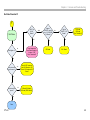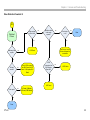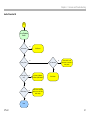
1
Training Manual KDL46S3000 WAX3 Direct-View LCD Television Chassis Circuit Description and Troubleshooting Guide MODELS: KDL-26S3000 KDL-32S3000 KDL-40S3000 KDL-46S3000 KDL-32XBR4 KDL-32SL130 KDL-40SL130 Course : CTV-41 Table of Contents Chapter 1 – Features and Circuit Descriptions ................. 2 BU1 Board Protection ........................................................ 19 Introduction ...................................................................... 2 Features .......................................................................... 2 Onboard Regulator Protect ................................................... 19 New Customer Menu .............................................................. 2 Internet Video Linking ............................................................. 2 HDMI 1.3 Support ................................................................... 2 Bravia™ Theater Sync ............................................................ 3 1080p Input ............................................................................. 3 Circuit Description ........................................................... 4 Overall Block Diagrams ................................................... 4 26 and 32-inch S-Line Models ............................................. 4 Panel Protect ........................................................................ 19 Audio Protect ........................................................................ 19 Communications Errors ..................................................... 20 Trident Video Process Failure ............................................... 20 BH Board Communication Error ........................................... 20 BU1 to Panel (S series models) or BU1 to BH (XBR4 and D3000 series) Communication Error .............................. 20 Protect Table ...................................................................... 22 BU1 Board .............................................................................. 4 Chapter 2 – Service and Troubleshooting ....................... 23 Overview........................................................................ 23 Circuit Board Locations ................................................. 23 40 and 46-inch S Line Models ............................................. 6 Protection........................................................................... 30 Backlight Power ...................................................................... 6 Diagnostics History ............................................................ 31 Backlight Inverter .................................................................... 4 Power Supply .......................................................................... 4 Power Supply .......................................................................... 6 32” XBR and 40D3000 Models ............................................ 6 Video Processing ........................................................... 10 New Trident Processor .......................................................... 10 Video Switching..................................................................... 10 Digital Tuner .......................................................................... 10 HDMI Inputs .......................................................................... 10 Audio Processing........................................................... 13 Analog Audio ......................................................................... 13 Digital Audio .......................................................................... 13 Power Supply and Protection ............................................ 15 CTV-41 Thermal Protect .................................................................... 19 Clearing the Diagnostics History ........................................... 31 Digital Signal Status........................................................... 32 New Remote Control Commands ...................................... 32 Service Mode................................................................. 34 Data Handling .................................................................... 34 Saving (Writing) Data ............................................................ 34 Reading Back of Data ........................................................... 34 Factory Reset ........................................................................ 34 White Balance Adjustments ............................................... 34 QM Service Page............................................................... 36 Troubleshooting ............................................................. 38 i Table of Contents (Continued) Triage Worksheets ............................................................. 38 Troubleshooting Flowcharts ............................................... 38 Initial Contact Flowchart A..................................................... 45 No Power Flowchart B .......................................................... 46 Protect ModeFlowchart C ..................................................... 47 26/32" Inverter Error Flowchart D ......................................... 48 40/46" Inverter Error Flowchart E.......................................... 49 No Video Flowchart F............................................................ 50 Video Distortion Flowchart G ................................................ 51 Audio Flowchart H ................................................................. 52 Service Test Points ........................................................ 53 Chapter 3 - Disassembly ................................................... 58 Overview........................................................................ 58 Inverter Board Removal (26 and 32” Models) ............... 58 26” LCD Panel Removal ................................................ 61 46” Panel Removal ........................................................ 67 CTV-41 ii Chapter 1 – Features and Circuit Descriptions Introduction New Customer Menu The WAX3 chassis is one of several LCD Flat Panel designs introduced for the Bravia™ 2007 model year. It provides for introductory and intermediate level televisions for the customer to choose from. The following models utilize the WAX3 chassis: The customer Graphics User Interface (GUI) has been improved to make navigation of the setup features easier. Icons (similar to those found on the PSP2) are used extensively. It is known as XMedia Bar™ (pronounced cross media bar) or XMB for short. KDL26S3000 Internet Video Linking KDL32S3000 KDL32SL130 KDL32XBR4 KDL40S3000 KDL40SL130 KDL40D3000 KDL46S3000 Features Yet another first for Sony, the Bravia™ model lineup will include a Digital Media Exchange (DMEX) interface. By attaching an optional interface device, known as Bravia Internet Video Link™, customers will have the ability to access internet video entertainment via a broad-band connection. Local news, weather and traffic along with access to selected digital media streaming can be viewed on the television independent of a computer. A special DMEX USB port on the rear of the television will allow bidirectional communication with the Bravia Internet Video Link™ device via the Xross Media Bar™ feature included in the television. Sony will partner with selected channels on the internet and these will automatically appear on the screen for the customer to select. LCD Panels All LCD panel sizes will be 1280 X 768 (WXGA) resolution. 32” and up utilizes the Wide Color Gamut Cold-Cathode Fluorescent (WCG-CCFL) backlighting for increased color uniformity and accurate grey-scales. The 26” model uses conventional fluorescent lights. The 26 and 32-inch models (with the exception of the 32XBR4) utilize 8-bit LCD panels. The 40 and 46-inch panels receive 10-bit RGB information. All panel sizes (except the 32” XBR) are 60FPS refresh rate. Exclusive to the KDL32XBR4 and KDL40D3000 is Sony’s introduction of Motionflow™. An additional circuit is included to double the 60HZ frame resolution from the video process circuits to 120HZ for clear picture reproduction during rapid moving scenes. In this manual this feature will be referred to as High Frame Rate (HFR). CTV-41 2 Chapter 1 - Features and Circuit Descriptions HDMI 1.3 Support HDMI version 1.3 has added several features to enhance picture and audio quality along with bi-directional communication between HDMI equipped devices. The added features that apply to display products are as follows: Speed: Single link bandwidth is increased from 4.9GBS to 10.2GBS Deep Color™: Increases RGB and component sample level from 24-bit to 30, 36, and 48 bit. xvYCC: Removes previous color space limitations to allow for the reproduction of every color perceivable by the human eye. CEC: Short for Consumer Electronics Control. Allows communication among HDMI devices for control. Uses the industry standard A/V link protocol. For example: Equipment can be set up so that when a DVD disc is inserted into a player, the television will turn on with the proper input setting along with the audio equipment turning on and being set for the proper input and audio format. The WAX3 model lineup only supports the CEC feature of HDMI 1.3. Bravia™ Theater Sync A feature incorporated within the television to utilize the CEC feature of HDMI 1.3 1080p Input Unit can receive 1080p source content via the HDMI inputs only. The 1080p signal is scaled to the WXGA panel resolution. NOTE: Only the 32” XBR and D3000 model will support 24-frame sources. The S series models support 30-frame only. CTV-41 3 Chapter 1 - Features and Circuit Descriptions Circuit Description Various differences in circuitry occur in the WAX3 chassis line based on panel size and display features. Virtually all video processing is the same among the different designs and centers around the BU1 board. From this point it becomes a matter of what LCD panel size is used, HDMI versus analog front video inputs and the design of the power supply dedicated to that model. The circuit descriptions to follow will differentiate between the models based primarily on LCD panel size since this will determine what type of power supply and backlight inverter boards will be used. The KDL32XBR4 and KDL40D3000 are the only models in this chassis line that has an upgrade in video features including a third HDMI input and High Frame Rate circuits and panel. This will be described in a separate block diagram. Overall Block Diagrams 26 and 32-inch S-Line Models In Figure 1-1 the overall block diagram of the circuit layout utilized in the KDL26A3000 and KDL32S3000 is shown. A brief description for each of the major circuit boards will be given. Backlight Inverter These smaller panels use a single inverter/balancer assembly that is part of the LCD panel in order to provide ballast control for the fluorescent backlights. 24VDC is provided by the power supply (G1D for the 26” or G1H for the 32”). This 24 volt source powers the individual inverters to generate the high voltage (4.5KV to 5KV) necessary to light the fluorescent backlight lamps. Additional lines for on/off control and inverter failure feedback are on the same DC voltage connector from the power supply and are routed to the BU1 board for control and monitoring by the Main Micro. The inverter board also contains circuits to monitor the current draw of CTV-41 each individual backlight lamp. If a lamp were to fail or weaken with age, or if one or more of the inverters were to fail, an error command will be detected by the Main Micro on the BU1 board and shut the unit down and blink the front power LED in groups of 6. Power Supply 2 power supplies reside on the G board. The 23” model power supplies are designated G1D whereas the 32” is G1H. Both supplies are relatively the same aside from current capacity and layout of their protect circuits. A standby supply runs constantly whenever AC power is applied to provide 12VDC for the main relay and power for the main switching supply. Standby 3.3 volts is also generated to power the Main Micro on the BU1 board and other circuits that are required to run constantly such as the remote IR receiver. The main switching regulator provides the majority of the voltages used within the unit. Further details of the power supplies will be discussed later in this chapter. BU1 Board This board has been redesigned to take on virtually all of the circuits that were found on 3 boards in last year’s chassis designs. The tuner and ATI Micro were on separate boards in previous designs but have now been integrated on the same board with the video process circuits. Other than the front video inputs applied to the U1 board, all analog and HDMI input connectors are part of the BU1 board. The Main TV Micro resides on this board and is responsible for virtually all of the operational functions of the unit. Audio switching, digital signal processing and amplification are also located here. The audio exits the BU1 board to drive the speakers, optical output, L/R analog out and headphones. Another important feature of the audio circuits is that all audio sources selected will be output from the optical transmitter. This was not true in previous Sony designs in which the optical out only functioned when a digital tuner signal was received. 4 Chapter 1 - Features and Circuit Descriptions VIDEO PROCESS A/V SWITCHING MAIN TV MICRO AUDIO PROCESS/AMP HDMI MICRO TUNER ATI MICRO OPTICAL OUT L/R AUDIO OUT HEADPHONES OUT VIDEO 1 COMPOSITE_Y/C IN VIDEO 3 COMPOSITE IN VIDEO 2 COMPOSITE IN ATSC/NTSC TUNER FRONT INPUTS COMPONENT 2 IN IC7300 ATI LCD PANEL (WXGA) U1 INVERTER COMPONENT 1 IN IC4500 TRIDENT VIDEO PROCESSOR COMPONENT 3 IN HDMI 1 IN IC3001 MAIN TV MICRO HDMI 2 IN PC IN USB FOR DMEX AND SOFTWARE UPGRADE IC2002 AUDIO SW AUDIO DSP L IC2009 AUDIO AMP R BU1 AC IN POWER SUPPLY G1D 26" G1H 32" FIGURE 1-1 26/32" WAX3 CHASSIS OVERALL BLOCK FIGURE 1-1 26/32” S SERIES OVERALL BLOCK DIAGRAM CTV-41 5 Chapter 1 - Features and Circuit Descriptions 40 and 46-inch S Line Models 32” XBR and 40D3000 Models In Figure 1-2 it is seen that most of the circuits found in the 26/32” models is the same. Therefore, only the differences will be explained here. All of the circuitry in these models are the same as their respective S series models except for the addition of the BH and U2 boards as illustrated in Figures 1-3 and 1-4. The circuitry on the BH board captures the 60HZ frame rate video exiting BU1 board, analyzes the difference between adjacent fields and generates additional fields in between to double the frame rate to 120HZ. The end result is a dramatic reduction of the smearing or “comet tailing” that is inherent to LCD displays during fast moving video content. Backlight Power Separate circuits are used to supply high voltage to the backlight lamps. These circuits only generate the high voltage needed. Balancer circuit boards are mounted on the panel to distribute the high voltage and monitor the current level to each lamp. The 40” model uses a single D1 board to generate high voltage of approxiamtely 4.5 to 5KV. The 46” however, requires the use of 2 high voltage boards due to the longer fluorescent tubes. In this case a D1 and D2 board is used to supply voltage to both ends of the fluorescent lamps. This is important to remember when troubleshooting a lamp protection shutdown problem. If one board fails you will notice that one side of the screen is lighter that the other before the unit shuts down. The side that is darker indicates which board is at fault. The front video input U2 board provides an additional HDMI input not found on the S series models. One analog component input was removed to accommodate the additional HDMI so only HDMI and composite video are accepted at these inputs. IMPORTANT: Even though the 40 and 46” models both use a D1 board, they are not interchangeable. The D1 board part numbers are different for the 40 and 46”. Power Supply A G3 board is used and uses a Power Factor Control circuit to generate the 390VDC required by the D1 and D2 circuits. The on-board protect circuits are slightly more sophisticated than the G1D and G1H boards but the end result is to stop the power supply if certain over voltage and current conditions arise. These items will be discussed later in this chapter. CTV-41 6 Chapter 1 - Features and Circuit Descriptions VIDEO PROCESS A/V SWITCHING MAIN TV MICRO AUDIO PROCESS/AMP HDMI MICRO TUNER ATI MICRO OPTICAL OUT L/R AUDIO OUT ATSC/NTSC TUNER HEADPHONES OUT VIDEO 1 COMPOSITE_Y/C IN VIDEO 3 COMPOSITE IN VIDEO 2 COMPOSITE IN BACKLIGHT POWER 46" ONLY IC7300 ATI D2 FRONT INPUTS COMPONENT 2 IN U1 IC4500 TRIDENT VIDEO PROCESSOR WXGA 60FPS LCD PANEL (WXGA) COMPONENT 1 IN COMPONENT 3 IN HDMI 1 IN IC3001 MAIN TV MICRO BACKLIGHT POWER 40/46" D1 HDMI 2 IN PC IN USB FOR DMEX AND SOFTWARE UPGRADE IC2002 AUDIO SW AUDIO DSP L IC2009 AUDIO AMP R BU1 POWER SUPPLY G3 AC IN FIGURE 1-2 FIGURE 1-2 OVERALL BLOCK 40/46"" WAX3 S MODEL CHASSIS 40/46” S SERIES OVERALL BLOCK DIAGRAM CTV-41 7 Chapter 1 - Features and Circuit Descriptions VIDEO PROCESS A/V SWITCHING MAIN TV MICRO AUDIO PROCESS/AMP HDMI MICRO TUNER ATI MICRO VIDEO 1 COMPOSITE_Y/C IN HDMI 2 IN L/R AUDIO OUT HEADPHONES OUT ATSC/NTSC TUNER VIDEO 3 COMPOSITE IN VIDEO 2 COMPOSITE IN OPTICAL OUT FRONT INPUTS IC7300 ATI HFR (High Frame Rate) U2 LCD PANEL (WXGA) INVERTER BH COMPONENT 1 IN COMPONENT 2 IN IC4500 TRIDENT VIDEO PROCESSOR HDMI 1 IN HDMI 3 IN IC3001 MAIN TV MICRO PC IN USB FOR DMEX AND SOFTWARE UPGRADE IC2002 AUDIO SW AUDIO DSP L IC2009 AUDIO AMP R BU1 POWER SUPPLY G1H AC IN FIGURE 1-3 FIGURE 1-3 32XBR4 WAX3 CHASSIS OVERALL BLOCK 32XBR4 OVERALL BLOCK DIAGRAM CTV-41 8 Chapter 1 - Features and Circuit Descriptions VIDEO PROCESS A/V SWITCHING MAIN TV MICRO AUDIO PROCESS/AMP HDMI MICRO TUNER ATI MICRO OPTICAL OUT L/R AUDIO OUT ATSC/NTSC TUNER HEADPHONES OUT VIDEO 1 COMPOSITE_Y/C IN VIDEO 3 COMPOSITE IN IC7300 ATI FRONT INPUTS U2 HFR IC4500 TRIDENT VIDEO PROCESSOR BH LCD PANEL (WXGA) COMPONENT 1 IN COMPONENT 3 IN HDMI 1 IN IC3001 MAIN TV MICRO BACKLIGHT POWER D1 HDMI 3 IN PC IN USB FOR DMEX AND SOFTWARE UPGRADE IC2002 AUDIO SW AUDIO DSP L IC2009 AUDIO AMP R BU1 POWER SUPPLY G3 AC IN FIGURE 1-4 FIGUREOVERALL 1-4 WAX3 40D3000 CHASSIS BLOCK 40D3000 OVERALL BLOCK DIAGRAM CTV-41 9 Chapter 1 - Features and Circuit Descriptions Video Processing An overall block diagram of the video process circuits is illustrated in Figure 1-5 for the S series models and in Figure 1-6 for the 32”XBR 40” D3000 models. Processing of the video is the same except for the additional HDMI input available via the U2 board and frame doubling on the BH board. Display Information Data (EDID) to provide display capability information to the device connected to the input. In the XBR model an additional EDID IC250 (not shown) is located on the U2 board. New Trident Processor IC4500 has been designed to handle many of the tasks once done by separate components. It has eliminated a separate CCP processor, HDMI Micro, DRC and Wega Engine. It is capable of handling video resolutions from 480i all the way up to 1080p (via the HDMI inputs only). All signals exit Trident as 720p 60FPS. Video Switching Only composite and Y/C signals are switched by IC4800. Component, HDMI, and PC inputs are routed directly to Trident IC4500 where they are selected internally. Only video input 1 accepts a Y/C signal source. Digital Tuner If a digital tuner source is selected, the signal is sent directly to the ATI Micro IC7300 where the signal will be demodulated and decoded to extract the audio and video information. The video digital stream is then sent to Trident video processor IC4500 and audio data is input to Audio DSP IC2002 (not shown). HDMI Inputs Note the lack of an HDMI Microprocessor. This is now integrated within the Trident processor IC4500. HDMI sources pass through HDMI EQ IC550 for impedance matching and into IC4500 for processing of the audio and video information. IC5501 and IC5502 contain the Enhanced CTV-41 10 Chapter 1 - Features and Circuit Descriptions DMEX USB ATSC/NTSC TUNER IC7300 ATI MICRO Y/C_COMPOSITE 1 COMPOSITE 3 IC4800 VIDEO SWITCH COMPOSITE 2 IC4500 TRIDENT VIDEO PROCESSOR U1 COMPONENT 2 WXGA 60FPS TO LCD PANEL COMPONENT 1 COMPONENT 3 PC IC5501 EDID HDMI 1 IC5500 HDMI EQ HDMI 2 IC5503 EDID BU1 FIGURE 1-5 S MODEL FIGURE VIDEO 1-5 PROCESS S SERIES VIDEO PROCESS BLOCK DIAGRAM CTV-41 11 Chapter 1 - Features and Circuit Descriptions DMEX USB ATSC/NTSC TUNER IC7300 ATI MICRO Y/C_COMPOSITE 1 COMPOSITE 3 IC4800 VIDEO SWITCH IC250 EDID IC4500 WXGA 60FPS TRIDENT VIDEO PROCESSOR U1 HFR WXGA 120FPS TO LCD PANEL BH COMPONENT 1 COMPONENT 3 PC IC5501 EDID HDMI 1 IC5500 HDMI EQ HDMI 3 IC5503 EDID BU1 FIGURE 1-6 XBR AND D SERIES VIDEO PROCESS BLOCK DIAGRAM CTV-41 12 Chapter 1 - Features and Circuit Descriptions Audio Processing Figure 1-7 illustrates the overall block diagram for the audio processing. All of this is accomplished on the BU1 board. Analog Audio If an ATSC compliant digital channel is received by cable TV (QAM) or terrestrial (8VSB) and a Digital Dolby® audio signal is embedded in the content, the optical out will pass this signal for use with a surround-sound amplifier that is compatible with Digital Dolby® 5.1 standards. Table 3-1 offers an overall view of what is output from the optical jack based on input selection. All analog audio sources are switched by the Audio DSP IC2002. The L/R audio signals are A/D converted within IC2002 for processing by DSP and exit as analog L/R to IC2009. The analog L/R audio is converted to PWM by IC2009 and amplified by the class-D amplifier within the IC. All selected analog sources are output in SPDIF format for the optical out transmitter. Analog L/R outputs are also provided for the audio output jacks on the rear of the unit and the headphone jack on the front input U1 board. On the 32” XBR series the front input board is the U2 board. Digital Audio Digital audio sources are available via the HDMI inputs or digital channels received by the tuner. HDMI audio is extracted by Trident IC4500 and sent to the ATI Micro. Digital audio from the tuner is sent directly to ATI. The audio information is then sent to Audio DSP IC2002 in digital format. At this point audio process is the same as analog signals. AUDIO SOURCE Optical Out DVD HDMI 5.1 2CH PCM The optical output jack at the rear of the unit will pass all selected audio sources except for Super Audio CD (SACD) or DVD audio sources hooked up to the HDMI inputs (for obvious copyright protection reasons). All analog sources (including that from the NTSC tuner) are output as 2-channel 48KHZ PCM. DVD players hooked up to the HDMI inputs will output 2-channel PCM regardless of what the HDMI audio output on the DVD player is set to. The internal speakers will output DVD audio regardless of what the HDMI audio of the DVD player is set to (unlike previous year’s models). ALL ANALOG AUDIO INPUTS 2CH PCM NTSC TUNER 2CH PCM CTV-41 DIGITAL TUNER 5.1 OPTICAL OUTPUT 5.1 OR 2CH PCM SACD VIA HDMI NO OUTPUT DVD AUDIO VIA HDMI NO OUTPUT TABLE 3-1 OPTICAL OUTPUT TRUTH TABLE 13 Chapter 1 - Features and Circuit Descriptions HDMI 1 HDMI 2 IC4500 TRIDENT ATSC/NTSC TUNER IC7300 ATI MICRO Y/C_COMPOSITE 1 COMPOSITE 3 COMPOSITE 2 COMPONENT 2 U1 COMPONENT 1 IC2002 AUDIO SW DSP L IC2009 CLASS D AUDIO AMP R OPTICAL OUT COMPONENT 3 L/R AUDIO OUT HEADPHONES OUT PC BU1 HDMI 1 ANALOG FIGURE 1-7 AUDIO PROCESS BLOCK DIAGRAM CTV-41 14 Chapter 1 - Features and Circuit Descriptions Protection would be no diagnostics indication from the power LED. Several circuits on the WAX3 chassis are utilized to monitor voltage and current conditions. Should a problem develop in any of these monitored circuits the unit will shut down in most cases and blink the power LED red in varying sets of sequences in order indicate what is likely causing the failure. Protect circuits are located on the power supply, BU1 board and the back light inverters. Power Supply and Protection 3 different power supplies are used in the WAX3 chassis and these are shown in Figures 1-8, 1-9, and 1-10. The 26” units use a G1D board, the 32” a G1H board and the 40/46” models use the G3 board. The G1D and G1H boards are very similar in design with current capacity being their primary difference and the presence of a PFC circuit on the G1H while one is not used on the G1D. They both generate 24VDC to supply the inverter circuits on the panel. The G3 board uses the PFC circuit to directly drive the D1 and D2 inverter boards for the 40 and 46” panels. All 3 power supplies contain overvoltage, under-voltage and over-current monitoring. The D3 power supply contains additiona circuits to monitor the temperature of the PFC switching transistors and the in-rush current limit resistor R6009 as shown in figure 1-10. If either of these circuits is activated the power supply will be turned off. The Main Micro located on the BU1 board monitors the regulated 12 volt line generated by all 3 boards. If this voltage is no longer generated the Main Micro will flash the power LED in sequences of 2 assuming the standby power supply is still operating. In figure 1-9, note the PFC detection line consisting of PH6301 and Q6403 which is unique to the 40/46” models. If the PFC circuit were to cease operating the DC voltage, which is normally around 390 volts, would drop to less than half (rectified AC only). This would put a strain on the D1 and D2 boards since they would attempt to keep the lamps lit but would require extra current due to the drastic voltage drop. In this event Q6403 will pull the control signal (which is normally high) low, turning off the inverter(s). The symptom would be a unit that has no backlights operating but there CTV-41 15 Chapter 1 - Features and Circuit Descriptions AC IN NTC1 340VDC T AC IN BD1 STANDBY POWER SUPPLY STBY 12V STBY 3.3V F1 4A AU 13V PRIMARY POWER SUPPLY RY6101 CN2 12V 6V 3 REG 12V 9 24V TO INVERTER 24V STBY 12V STBY 3.3V 12V OVP Q304 SCR LATCH 24V OVP Q902 IC305 Q901 Q302 TO CN4002 BU1 BOARD Q303 4 6V 7 AU GND 8 AU 13V 11 POWER_ON 13 STBY 3.3V TO CN4001 BU1 BOARD CN3 PFC G1D FIGURE 1-8 G1D BOARD PROTECTION (26” MODELS) CTV-41 16 Chapter 1 - Features and Circuit Descriptions F6102 4A AC IN PFC AC IN 343VDC D6101 STBY 12V STANDBY POWER SUPPLY STBY 3.3V AU 13V PRIMARY POWER SUPPLY CN6202 12V 6V 3 REG 12V 9 24V TO INVERTER 24V Q6202 Q6203 LATCH R6101 STBY 12V 12V OVP 24V OVP STBY 3.3V Q6108 PH6103 Q6201 Q6107 RY6101 PH6300 Q6105 Q6106 LATCH IC6103 PFC OVP 4 6V 7 AU GND 8 AU 13V 11 POWER_ON 13 STBY 3.3V TO CN4001 BU1 BOARD CN6201 ON = 3.3V PFC OCP TO CN4002 BU1 BOARD PFC G1H FIGURE 1-9 G1H BOARD PROTECTION (32” MODELS) CTV-41 17 Chapter 1 - Features and Circuit Descriptions CN6501 F6000 6.3A AC IN PFC AC IN 390VDC D6000 STANDBY POWER SUPPLY PRIMARY POWER SUPPLY 1 PFC OUT 3 PRI GND TO D1 BOARD CN6502 STBY 12V STBY 3.3V 1 PFC OUT 3 PRI GND TO D2 BOARD CN6004 AU 13V 6 REG 12V 3 BACK_LIGHT 4 INV_ERR 7 BALANCE_ERR 7 BALANCE_ERR 9 INV_ERR PH6301 10 BACKLIGHT_ON STBY 3.3V 3 6V 5 AU GND 12V 6V TO D1 BOARD CN6203 Q6403 PFC DET R6009 STBY 12V CN6202 Q6304 PH6300 Q6407 Q6303 RY6000 FROM BU1 BOARD 7 AU 13V 10 POWER_ON 12 STBY 3.3V TO BU1 BOARD 12V OVP PFC OCP PFC OTP R6009 OTP Q6300 Q6301 LATCH 1C6300 PFC OVP PFC G3 FIGURE 1-10 G3 BOARD PROTECTION (40” AND 46” MODELS) CTV-41 18 Chapter 1 - Features and Circuit Descriptions BU1 Board Protection The BU1 board has several protect monitoring circuits for its own DC voltage regulators. Monitoring of temperature, speaker protection and an inverter failure are also included. A block diagram of these protect circuits is illustrated in Figure 1-11 Onboard Regulator Protect The regulated 2.5 volts for Trident IC4500 is monitored. If this voltage fails A DC_ALERT 1 high will occur on pin 163 of the Main Micro IC3001. The unit will shut down and the power LED will flash in groups of 3. Similarly, if the D1.0V or D1.8V sources (generated on the BU1 board) fails a high will be placed on pin 153 and the unit will shut down generating groups of 4 blinks. The regulated 12V is the only outside voltage monitored. It sources from the power supply and will keep a specified high on pin 82 of the Main Micro. If the voltage fails or falls below this specified limit, the unit will shut down and blink the power LED in groups of 2. Note that this 12V line is also the source for the Panel 12V which is switched by the main micro. This voltage is also monitored by Main Micro at pin 154 (DC_ALERT_3). If the 12V from the power supply is OK but failed on the Panel_12V line, the unit will shut down and blink the power LED in groups of 5. Thermal Protect IC3007 is a digital thermometer that can be programmed to send data to the Main Micro when a specified temperature level is reached. The purpose of the thermal sensing is to monitor the unit for excessive temperature within the unit during operation. If the temperature rises above the specified threshold the unit will shut down and display groups of 6 blinks from the power LED. Note: IC3007 is constantly polled by the Main Micro. If the IC were to fail or the data line on the I²C to open the unit would shut down within approximately 10 seconds. It is important to beware of this. If a unit shuts down immediately, it can be safely assumed that the television is not CTV-41 running hot. Shutdowns after extended periods would warrant checking the location of the unit for proper ventilation. Panel Protect If the high voltage generated by the inverter were to fail, or if abnormal current conditions are detected on the balancer circuits, a high would be applied on pin 81 of the Main Micro. The unit will shut down and blink the power LED in groups of 6. Audio Protect If any DC is detected on the left or right speaker channels the unit will shut down and blink the power LED in groups of 8. This symptom is usually caused by a failed audio amp and would require the replacement of the BU1 board. Balancer Protect Along with a Panel Protect line, a Balancer Error line is connected to pin 81 of the Main Micro. Working in conjunction with panel protection, both lines connect to a voltage divider. The voltage at pin 81 is normally 3.3 volts. If an inverter error is detected, the line (normally low) will go high and the inverter transistor will pull the voltage down to zero. A balancer error would complete the divider network and pull the voltage down to about one-half (1.8 volts). This is how IC3001 is able to tell which type of error has occured. NOTE: The 26” and 32” models do not have a balancer error line from the inverter board. Only the 40” and 46” models have this feature. 19 Chapter 1 - Features and Circuit Descriptions Communications Errors Another feature of the WAX 3 chassis is the monitoring of communications between specific devices. Not shown on the previous block diagrams are the following protect events that could occur. Main Micro Communication Error The unit will shut down and the power LED will blink in groups of 10. The BU1 board must be replaced to rectify this. Trident Video Process Failure The unit will shut down and the power LED will blink in groups of 11 The BU1 board must be replaced to rectify this. BH Board Communication Error Unique to the KDL32XBR4 and KDL40D3000 that utilize frame rate doubling, the communication between the BH board and the LCD panel TCON is monitored and the unit will shut down if this communication fails. The power LED will blink in groups of 12. BU1 to Panel (S series models) or BU1 to BH (XBR4 and D3000 series) Communication Error If either of these events occurs, the power LED will blink at one-half second intervals continuously. The unit will not shut down. The backlights will be lit but there will be no video display (including OSD graphics). This can be caused by an unplugged LVDS cable or a failure of BU1 or BH board or a defective panel (TCON failure). CTV-41 20 Chapter 1 - Features and Circuit Descriptions Q4017 Q4016 TRIDENT DDR 2.5V CN4001 FROM CN3 (G1D) CN6201 (G1H) CN6202 (G3) Q4001 STBY 3.3V 1 POWER_ON 3 AU 13V 5 AU GND 7 Q4002 D1.0V Q4018 DC ALERT 1 (3X) DC ALERT 2 (4X) PANEL 12V TO LCD PANEL CN4002 REG 12V 1 Q4019 IC3001 MAIN MICRO IC3007 TEMP SENSE SCL Q2012 Q2017 DC_DET R POWER_3 CN4003 FROM INVERTER (26/32") OR G3 BOARD (40/46") 3.3V 1 BACKLIGHT 3 INV_ERR 5 BALANCER_ERR TEMP ERROR (7X) SDA 82 118 119 DC ALERT 3 (5X) PANEL 12V DETECT DIMMER 153 D1.8V MAIN POWER FAILURE (2x) FROM CN2 (G1d) CN6202 (G1H) CN6203 (G3) 163 154 SPEAKER PROT 8X Q2013 Q2018 DC_DET L 26 Q4014 81 INVERTER ERROR (6X) 7 Q4015 BALANCER ERROR (13X) BU1 FIGURE 1-11 FIGURE 1-11 BU1 BOARD PROTECT BU1 BOARD PROTECTION CTV-41 21 Chapter 1 - Features and Circuit Descriptions Protect Table The various protect alarms are shown in Table 1-1 # OF RED LED BLINKS EVENT POSSIBLE CAUSE NOTES 2 REG 12V FAILURE POWER SUPPLY BOARD PAGE 1 OF DIAGNOSTICS 3 2.5V FAILURE TO TRIDENT IC BU1 BOARD PAGE 1 OF DIAGNOSTICS 4 D 1.OV FAILURE BU1 BOARD PAGE 1 OF DIAGNOSTICS 5 PANEL 12V BU1 BOARD BU1 TO PANEL TCON 12V 6 INVERTER ERROR INVERTER (26/32") D1, D2 BOARDS (40/46") LISTED AS "BACK_LIGHT" IN DIAGNOSTICS PAGE 1 7 TEMPERATURE ERROR BU1 BOARD (S MODELS) BH BOARD (D/XBR MODELS) PAGE 2 OF DIAGNOSTICS 8 SPEAKER PROTECT BU1 BOARD PAGE 2 OF DIAGNOSTICS 9 FAN ERROR NOT USED NOT USED BUT APPEARS IN PAGE 2 OF DIAGNOSTICS 10 MAIN MICRO COM ERROR BU1 BOARD PAGE 2 OF DIAGNOSTICS 11 TRIDENT IC FAILURE BU1 BOARD PAGE 2 OF DIAGNOSTICS 12 BU1 TO BH COM ERROR BU1 BOARD OR BH BOARD (32XBR AND 40D3000 ONLY) PAGE 2 OF DIAGNOSTICS 13 BALANCER ERROR LCD PANEL NOT USED IN 26/32" MODELS PAGE 1 OF DIAGNOSTICS TABLE 1-1 WAX3 PROTECTION TABLE CTV-41 22 Chapter 2 – Service and Troubleshooting Overview Due to the reduced number of circuit boards and the requirement that repairs be performed at board level, troubleshooting the WAX3 chassis consists of observations of symptoms and customer information more than actual signal tracing and voltage checks. This chapter will assist in this process by providing illustrations of the circuit board locations, troubleshooting flowcharts and various tips on determining what failure may be causing the symptom. Circuit Board Locations The location of the major circuit boards is illustrated in Figures 2-1 through 2-4. They are as follows: Figure 2-1; KDL26/32S3000 and KDL32S30L1 Figure 2-2: KDL32XBR4 Figure 2-3: KDL40S3000 and KDL40S30L1 Figure 2-4: KDL46S3000 Figure 2-5: KDL40D3000 Note the left and right support brackets that are visible when the rear cover is removed. These may be removed at any time during service in order to remove circuit boards more easily. If both brackets are removed (necessary if LCD panel is replaced) attention must be paid as to which side of the units the brackets came from. Each bracket is marked “L” and “R”. These left and right markings are set when viewing the FRONT of the television, not the rear. Locater pins are also located at the tops of the brackets and are not in the same offset location. If the brackets are installed incorrectly they will not sit flush and cause problems when trying to install the screws for a wall mount bracket. Proper bracket installation is shown in Figure 2-6. CTV-41 23 Chapter 2 - Service and Troubleshooting TCON U1 INVERTER CTV-41 G1D 26" G1H 32" BU1 FIGURE 2-1 26” AND 32” S SERIES CIRCUIT BOARD LOCATIONS 26"/32" S SERIES CIRCUIT BOARD LOCATIONS 24 Chapter 2 - Service and Troubleshooting TCON BH INVERTER U2 BU1 G1H 32XBR CIRCUIT LOCATION FIGUREBOARD 2-2 32XBR CIRCUIT BOARD LOCATIONS CTV-41 25 Chapter 2 - Service and Troubleshooting TCON D1 U1 BALANCER BU1 G3 FIGURE 2-3 40S3000CIRCUIT CIRCUITBOARD BOARDLOCATIONS LOCATION 40S3000 CTV-41 26 Chapter 2 - Service and Troubleshooting BALANCER TCON D1 D2 U1 BALANCER BU1 G3 FIGURE 2-4LOCATION 46" CIRCUIT BOARD 46S3000 CIRCUIT BOARD LOCATIONS CTV-41 27 Chapter 2 - Service and Troubleshooting TCON D1 BH U2 BALANCER BU1 G3 FIGURE 2-5 46D3000 LOCATIONS CIRCUIT BOARD BOARD LOCATION 40D3000 CIRCUIT CTV-41 28 Chapter 2 - Service and Troubleshooting NOTE DIFFERENCE IN LOCATION OF PIN BOSSES BRACKETS ARE LABELED AS VIEWED FROM FRONT OF UNIT FIGURE 2-6 LEFT AND RIGHT2-6 BRACKETS FIGURE LEFT AND RIGHT WALL MOUNT BRACKETS CTV-41 29 Chapter 2 - Service and Troubleshooting Protection The protect circuits are described in detail in Chapter 1 of this manual. Table 2-1 lists the protect events that could possibly occur and suggested locations for their causes. Troubleshooting flowcharts are also located later in this chapter to assist the technician in isolating the cause of a protect event. Although the self-diagnostics feature is helpful in troubleshooting a unit, they are not 100% reliable and may be caused by more than 1 component. NOTE: Whenever the unit shuts down due to a protect event the remote commander will not function. In previous Sony chassis designs the remote could be used to cycle the unit back on. The unit would shut down again, of course, if the problem still existed. In the WAX3 chassis the power must be cycled by using the manual power button. # OF RED LED BLINKS EVENT POSSIBLE CAUSE NOTES 2 POWER SUPPLY BOARD PAGE 1 OF DIAGNOSTICS 3 REG 12V FAILURE 2.5V FAILURE TO TRIDENT IC BU1 BOARD PAGE 1 OF DIAGNOSTICS 4 D 1.OV FAILURE BU1 BOARD PAGE 1 OF DIAGNOSTICS 5 PANEL 12V BU1 TO PANEL TCON 12V 6 INVERTER ERROR BU1 BOARD INVERTER (26/32") D1, D2 BOARDS (40/46") 7 TEMPERATURE ERROR BU1 BOARD (S MODELS) BH BOARD (D/XBR MODELS) PAGE 2 OF DIAGNOSTICS 8 SPEAKER PROTECT BU1 BOARD PAGE 2 OF DIAGNOSTICS 9 NOT USED NOT USED BUT APPEARS IN PAGE 2 OF DIAGNOSTICS 10 FAN ERROR MAIN MICRO COM ERROR BU1 BOARD PAGE 2 OF DIAGNOSTICS 11 TRIDENT IC FAILURE 12 BU1 BOARD BU1 BOARD OR BH BU1 TO BH COM ERROR BOARD 13 BALANCER ERROR LCD PANEL LISTED AS "BACK_LIGHT" IN DIAGNOSTICS PAGE 1 PAGE 2 OF DIAGNOSTICS PAGE 2 OF DIAGNOSTICS NOT USED IN 26/32" MODELS PAGE 1 OF DIAGNOSTICS TABLE 2-2 SELF-DIAGNOSTICS TABLE CTV-41 30 Chapter 2 - Service and Troubleshooting Diagnostics History Certain protect events are monitored by the Main Micro on the BU1 board. Those that are monitored are stored into NVM for retrieval. Each time a monitored protect event occurs, a running count is kept and displayed. This feature is very useful in locating the cause of intermittent failures. The diagnostics history page is retrieved by turning the unit off and pressing the following buttons on the remote commander in sequence: “DISPLAY”, “5”, “VOL-”, and “POWER”. The unit will turn on and you may have to wait several seconds for the display to appear once the backlights have turned on. This feature is illustrated in Figure 2-7. Note also that due to the large number of diagnostic events monitored, there are 2 pages of lists. Toggling between the pages is performed using the 1 and 4 keys on the remote. Clearing the Diagnostics History Once the diagnostics page has been viewed for a history of protect events (and there are any present) the failure counts must be cleared to be useful at a later time. This is accomplished by pressing the “8” followed by the “0” key on the remote (not “8”, “ENTER” as in past models). USE “1” AND “4” KEY ON REMOTE COMMANDER TO TOGGLE BETWEEN PAGES FIGURE 2-7 FIGURE 2-7 WAX3 CHASSIS DIAGNOSTIC HISTORY PAGES DIAGNSTICS HISTORY PAGE CTV-41 31 Chapter 2 - Service and Troubleshooting New Remote Control Commands Digital Signal Status The button sequnces to perform read, write and initialize commands has changed. The table below shows the correct buttons to press for the various tasks. If the customer is experiencing intermittent picture loss, freezing, or tiling, the signal level of the cable or OTA signal can be checked in the service mode or within the customer menu. The customer menu is easier to access and is specific to those signal levels with pleasing graphics so it is suggested to use this feature as opposed to the pages located within the QM service graphics. OPERATION COMMAND BUTTONS "7" INITIALIZE DATA "MUTE" "0" "8" SERVICE PAGE DISPLAY INIINI-EXE INI-EXE "0" RSTRST-EXE RST-EXE READ NVM DATA "9" "0" READ READ WRITE DATA TO NVM "MUTE" "0" WRITE WRITE CUSTOMER SETTINGS RESET "MUTE" CTV-41 Figure 2-8 illustrates this feature. Signal readings can only be obtained for digital sources at the antenna inputs. Analog signals will only display the channel frequency and the fact that it is detected and locked. The two important items to view are the AGC and Signal-To-Noise ratio numbers. If the signal decreases, the numbers increase and vice versa. Acceptable ranges for AGC are 18 to 54. SNR ranges are 16 to 22 for ATSC and 29 to 38 for 256QAM. 32 Chapter 2 - Service and Troubleshooting QAM DIGITAL RECEPTION ATSC DIGITAL RECEPTION ACCEPTABLE DIGITAL SIGNAL READINGS PEAK LEVEL RESETS WHEN CHANNEL IS CHANGED AGC: 18-54 ATSC 16-22 SNR: QAM 256 MINIMUM 29 64 QAM MINIMUM 22 NTSC ANALOG RECEPTION FIGURE 2-8 SIGNAL LEVEL CHECK FIGURE 2-8 SIGNAL LEVEL CHECK CTV-41 33 Chapter 2 - Service and Troubleshooting Service Mode The service mode in the WAX3 chassis is accessed in the traditional way by starting with the unit turned off and pressing “DISPLAY”, “5”, “VOL+”, and “POWER” in sequence. The TV will power up and the initial service graphics shown in Figure 2-9 should appear. A white field from an external generator was input to the television to make the picture more printerfriendly and to keep the video input graphic from displaying. Service adjustment availability is extremely limited in this chassis as compared to other Sony television products. Note that the firmware versions of the Trident (Digital) and Main Micro (BE for back-end) are displayed for viewing to see if the unit is loaded with the latest version. Data Handling A couple of procedures have changed with the new software installed in the WAX3 chassis. Saving (Writing) Data The traditional method of saving data in Sony televisions was to press “MUTE”, followed by “ENTER” on the remote commander. This is now performed by pressing “MUTE” and then the “0” (zero) key. Just remember that the “0” key on the remote is now what used to be the “ENTER” key. If the key entry was successful, the word “WRITE” should appear on the upper right portion of the screen as soon as the mute button is pressed and turn red (indicating data writing) when the zero key is depressed. The method for returning the unit to “out of box” condition has changed. Traditionally, this was performed by pressing “8” followed by “ENTER” on the remote commander while in the service mode. The new procedure is to point the remote at the receiver while the unit is turned on. Press the joystick “UP” and hold it there while turning the unit off with the manual power button. The screen should go dark but the green power LED will remain lit. The unit will then cycle and should turn back on to channel 3 and ask what language you would like to use. White Balance Adjustments Note that the first service item is a white balance adjustment for the green drive. The only adjustments that can be performed in this group is white balance and there is a drive and background adjustment for each of the 3 colors. White balance adjustments will probably not be required even if the LCD panel or the BU1 board is replaced based on experience with the WAX2 chassis from last year. These adjustments will only be required if the customer requests it or if someone else has changed the values. TIP: If someone changes the white balance adjustments to where it is noticeable the white balance can be restored to a reasonable level (assuming the backlights have not aged to the point of significant color shift) by setting the data values for the red, green and blue drive to 100 and the background for each color to 200. Reading Back of Data When performing adjustments there comes a time where things may appear to be getting out of control or you may be trying an adjustment and forgot what the data value was. Pressing “9” followed by “0” will read back the last stored data from NVM. Unplugging the unit from AC power will also cause a read-back from NVM. Factory Reset CTV-41 34 Chapter 2 - Service and Troubleshooting FIGURE 2-9 MAIN MICRO SERVICE MODE PAGE FIGURE 2-9 MAIN TV MICRO SERVICE PAGE CTV-41 35 Chapter 2 - Service and Troubleshooting QM Service Page The QM service page is accessed by pressing the “JUMP” button on the remote commander once the service mode has been accessed. This switches service data to the ATI Micro also located on the BU1 board. Although various adjustments are available within this group most of them are related to customer graphics display properties and are not usually in need of adjustment. What is important is the availability of test pattern graphics that can be useful in troubleshooting video issues, especially those that involve distortion in the video signal. Once in the QM service group, the initial page will be labeled “INFO”. Use the “1” key to scroll to the next page labeled “TPNS”. The data value default is “zero”. By changing the data value with the “3” button, various test patterns in 4 different resolutions can be displayed on the screen with the initial color bar pattern shown in Figure 2-10. There are 20 sets of patterns for the 4 resolutions. They are as follows: 1-20 1080i 21-40 480i 41-60 480p 61-80 720p Since these patterns are generated by the ATI Micro which is located on the BU1 board along with the video process circuits, they do not provide much assistance in isolating video problems as past chassis designs in which the ATI Micro was located on a separate board. They do, however, provide a clean, stable video source to assist in closer examination of the screen display. This is especially useful when trying to determine if a distortion problem is being caused by the LCD panel. CTV-41 36 Chapter 2 - Service and Troubleshooting PAGE 1 BRINGS UP QM GRAPHICS DATA SETTING CHANGES GRAPHICS FIGURE 2-10 QM TEST PATTERN GRAPHICS FIGURE 2-10 QM (ATI MICRO) SERVICE GRAPHICS CTV-41 37 Chapter 2 - Service and Troubleshooting Troubleshooting The WAX3 chassis is serviced at board level. Warranty repairs require mandatory board level repair unless a specific bulletin is issued calling for the replacement of an individual component. Because of this, troubleshooting flowcharts will be utilized in this manual to assist in diagnosing and repairing the unit. The preferred method is to “triage” the unit by listening to the customer’s description of the symptoms when a service request is made. This can be done by technical or non-technical staff by utilizing the triage worksheet included in this section. Once the correct part (or parts) is identified during the triage procedure, the technician can use the flowcharts in the field to perform further diagnosis of the unit. This is especially useful when more than one part is suspected as being the cause. The flowcharts are designed to use visual checks, the use of internal graphic patterns, and in the worst case, the use of a DVM to check voltages or resistance levels. These quick checks are much quicker than trying to repair the unit using the “shotgun” method. the field on what part is more likely to repair the problem. Always visit the Sony service website to obtain the latest triage worksheet that will be constantly updated and to view any service bulletins or repair tips to assist in the repair. Troubleshooting Flowcharts The flowcharts in the remainder of this chapter are designed for the technician who is servicing the unit in the field. They are particularly useful when more than one part is brought to the location. Visual checks, use of internal graphics patterns and voltage checks will assist in determining which part is likely to complete the repair. As with the triage worksheet, please check the Sony service website to see if the flowcharts have been updated with new information to assist in the diagnosis of the unit. The triage worksheets on the website will always have the latest flowcharts included. Triage Worksheets The triage worksheets in the following pages are an example of a useful tool to aid in determining what part(s) may be needed to be brought to the repair site to complete a repair. Based on a description of the symptom by the customer, one can simply go down the column that best fits the description of the failure and locate what is needed for the repair. The part that is most likely to repair the failure is marked with a dot. In some cases there may be more than one part with a dot. In this situation it is highly recommended to bring both parts to the repair location. Parts marked with a triangle may also be the cause and the decision on whether to bring them will need to be determined based on various situations such as distance to the repair site and the size of the unit (can it easily be brought to the shop if needed). Bear in mind that the worksheet illustrated is updated with correct part numbers and suggested parts as of the writing of this manual but may be updated as part numbers change due to production changes in the product and the suggestion list may change as feedback is received from CTV-41 38 Chapter 2 - Service and Troubleshooting Sony KDL26S3000 Technical Triage Summary Sheet 1. Confirm the symptom from the customer. CHASSIS: 2. Select that symptom from the chart. WAX3 3. Bring all the boards listed for that symptom. 4. Follow the troubleshooting charts in the technical guides to isolate the board. 5. Chart Color Code RED DOT: Most likely defective part LAST UPDATED: BLUE Triangle: Possible defective part 7/16/07 BLACK TEXT: Board and Part # that may correct the symptom 7) The Troubleshooting Flowchart required to determine the actual defective part is listed for each column in the last row of each table. Symptoms - Shutdown. Power LED blinking red diagnostics sequences No Power Reference 2 3 4 5 BU1 BOARD ▲ G1D BOARD ▲ ▲ ▲ 6 7** 8 10 11 13 N/A ▲ N/A U1 BOARD Video - missing or distorted Stationary No Green colored Video 2 Power LED lines or 0nly (Dead Set) dots ▲ 1-789-780-11 LCD Panel N/A ▲ Problem ▲ C C C POWER POWER POWER POWER D C INV TEMP C C C AUDIO COMM COMM N/A A-1268-869-A A-1220-504-C N/A N/A C TCON LVDS CABLE Flowchart Reference Part # 1-474-056-21 N/A INVERTER No video No Audio all Inputs B F ▲ ▲ 1-834-155-11 1-802-368-11 F D H N/A **ONLY IF TEMPERATURE ERROR OCCURS IMMEDIATELY CTV-41 39 Chapter 2 - Service and Troubleshooting Sony KDL32S3000/SL130 Technical Triage Summary Sheet 1. Confirm the symptom from the customer. CHASSIS: 2. Select that symptom from the chart. WAX3 3. Bring all the boards listed for that symptom. 4. Follow the troubleshooting charts in the technical guides to isolate the board. 5. Chart Color Code RED DOT: Most likely defective part LAST UPDATED: BLUE Triangle: Possible defective part 7/19/07 BLACK TEXT: Board and Part # that may correct the symptom 7) The Troubleshooting Flowchart required to determine the actual defective part is listed for each column in the last row of each table. Symptoms - Shutdown. Power LED blinking red diagnostics sequences No Power Reference 2 3 4 5 BU1 BOARD ▲ G1H BOARD ▲ ▲ ▲ 6 7** 8 10 11 13 N/A ▲ N/A ▲ U1 BOARD LCD Panel ▲ B C C C POWER POWER POWER POWER No video No Audio all Inputs D C INV TEMP C C C AUDIO COMM COMM A-1257-244-A A-1220-504-C 1-789-780-11 N/A N/A ▲ N/A Part # 1-474-052-11 N/A TCON LVDS CABLE Problem ▲ N/A INVERTER Flowchart Reference Video - missing or distorted Stationary No Green colored Video 2 Power LED lines or 0nly (Dead Set) dots B G ▲ ▲ 1-834-157-11 1-802-380-11 F F H N/A **ONLY IF TEMPERATURE ERROR OCCURS IMMEDIATELY CTV-41 40 Chapter 2 - Service and Troubleshooting Sony KDL32XBR4 Technical Triage Summary Sheet 1. Confirm the symptom from the customer. CHASSIS: 2. Select that symptom from the chart. WAX3 3. Bring all the boards listed for that symptom. 4. Follow the troubleshooting charts in the technical guides to isolate the board. 5. Chart Color Code RED DOT: Most likely defective part LAST UPDATED: BLUE Triangle: Possible defective part 7/16/07 BLACK TEXT: Board and Part # that may correct the symptom 7) The Troubleshooting Flowchart required to determine the actual defective part is listed for each column in the last row of each table. Symptoms - Shutdown. Power LED blinking red diagnostics sequences No Power Reference BU1 BOARD 2 3 4 5 ▲ 6 BH BOARD G1H BOARD 7** 8 10 11 ▲ ▲ 12 13 N/A U2 BOARD ▲ ▲ N/A N/A ▲ Video - missing or distorted Stationary No Green colored Video 2 Power LED lines or 0nly (Dead Set) dots ▲ Part # A-1268-671-A A-1236-654-A 1-474-052-11 N/A INVERTER No video No Audio all Inputs A-1289-342-A N/A 1-789-795-11 BU1/BH LVDS CABLE N/A 1-833-964-11 BH/TCON LVDS N/A N/A ▲ LCD Panel Flowchart Reference Problem ▲ B C C C POWER POWER POWER POWER D C INV TEMP C C C AUDIO COMM COMM D N/A B G ▲ ▲ 1-834-188-21 1-802-411-11 F F H N/A **ONLY IF TEMPERATURE ERROR OCCURS IMMEDIATELY CTV-41 41 Chapter 2 - Service and Troubleshooting Sony KDL40S3000/SL130 Technical Triage Summary Sheet 1. Confirm the symptom from the customer. CHASSIS: 2. Select that symptom from the chart. WAX3 3. Bring all the boards listed for that symptom. 4. Follow the troubleshooting charts in the technical guides to isolate the board. 5. Chart Color Code RED DOT: Most likely defective part LAST UPDATED: BLUE Triangle: Possible defective part 7/16/07 BLACK TEXT: Board and Part # that may correct the symptom 7) The Troubleshooting Flowchart required to determine the actual defective part is listed for each column in the last row of each table. Symptoms - Shutdown. Power LED blinking red diagnostics sequences No Power Reference BU1 BOARD 2 3 4 5 ▲ D1 BOARD G3 BOARD ▲ 6 7** 8 10 11 13 Video - missing or distorted Stationary No Green colored Video 2 Power LED lines or 0nly (Dead Set) dots ▲ ▲ ▲ ▲ ▲ A-1220-504-C 1-789-771-11 LVDS CABLE LCD Panel ▲ B C C C POWER POWER POWER POWER ▲ E C INV TEMP C C C E A-1257-243-A A-1236-537-C INVERTER Problem Part # A-1236-528-A U1 BOARD Flowchart No video No Audio all Inputs ▲ ▲ 1-834-158-11 ▲ B G 1-802-410-11 F F H AUDIO COMM COMM PANEL **ONLY IF TEMPERATURE ERROR OCCURS IMMEDIATELY CTV-41 42 Chapter 2 - Service and Troubleshooting Sony KDL46S3000 Technical Triage Summary Sheet 1. Confirm the symptom from the customer. CHASSIS: 2. Select that symptom from the chart. WAX3 3. Bring all the boards listed for that symptom. 4. Follow the troubleshooting charts in the technical guides to isolate the board. 5. Chart Color Code RED DOT: Most likely defective part LAST MODIFIED: 716/2007 BLUE Triangle: Possible defective part BLACK TEXT: Board and Part # that may correct the symptom 7) The Troubleshooting Flowchart required to determine the actual defective part is listed for each column in the last row of each table. Symptoms - Shutdown. Power LED blinking red diagnostics sequences No Power Reference BU1 BOARD 2 3 4 5 ▲ 6 7** 8 10 11 13 ▲ D2 BOARD ▲ Stationary No Green colored Video 2 Power LED lines or 0nly (Dead Set) dots ▲ D1 BOARD G3 BOARD Video - missing or distorted ▲ A-1236-537-C INVERTER (LEFT)* ▲ C C C C POWER POWER POWER POWER ▲ E C INV TEMP C C C E A-1220-504-C 1-789-788-11 LVDS CABLE LCD Panel A-1257-242-A A-1247-497-A INVERTER (RIGHT)* Problem Part # A-1236-531-A U1 BOARD Flowchart Reference No video No Audio all Inputs ▲ 1-789-787-11 ▲ 1-834-159-11 ▲ B G 1-802-409-11 F F H AUDIO COMM COMM PANEL * AS VIEWD FROM REAR OF UNIT **ONLY IF TEMPERATURE ERROR OCCURS IMMEDIATELY CTV-41 43 Chapter 2 - Service and Troubleshooting Initial Contact Flowchart A A Start Does unit turn ON? No GO TO Power Supply Troubleshooting Flowchart B Is video distorted? Yes No Yes Is Timer LED Flashing Red? Yes GO TO Protection Mode Troubleshooting Flowchart C GO TO Video Distortion Troubleshooting Flowchart G Is audio present ? No GO TO Audio Troubleshooting Flowchart H Yes No Is video present ? Yes No GO TO No Video Troubleshooting Flowchart F Distorted Yes No Done CTV-41 44 WAX3 CHASSIS TRIAGE INITIAL CONTACT FLOWCHART A Chapter 2 - Service and Troubleshooting No Power Flowchart B B Unit Does Not Turn On Audio Present ? Yes Timer LED goes to Flashing Red? Video problem Go to flowchart D Yes Protection Go to Flowchart C No No Green Power LED Lit? Yes Remains Green ? No 3.3VDC CN4001 -1 on BU1 Board? No Standby Supply Failure G1D Board (26") G1H Board (32") G3 Board 40/46") CTV-41 Yes Video problem Go to flowchart D No Yes High (>2.5V) CN4001 -3 on BU1 Board? Yes G1D Board (26") G1H Board (32") G3 Board 40/46") No BU1 Board WAX3 NO POWER FLOWCHART B 45 Chapter 2 - Service and Troubleshooting Protect ModeFlowchart C C 12VDC CN4002 -1 on BU1 Board ? Red Standby LED Flashing No G1D Board (26") G1H Board (32") G3 Board (40/46") Immediately ? No Check for possible ventilation problem Yes Yes BU1 Board 2X 12V Main Yes 7X Temperature Yes BU1 Board No No 3X Trident 3.3V 8X Speaker Protect Yes BU1 Board No No 4X Reg 5V Yes Yes BU1 Board 10X or 11X? Yes No No 5X Panel 12V 12X HFR (32XBR Only) Yes CTV-41 BH Board No No 6X Inverter Fail Yes Yes Go To Inverter Troubleshooting Flowchart D (26/32") Flowchart E (40/46") 13X Balancer Yes Go To Inverter Troubleshooting Flowchart D (26/32") Flowchart E (40/46") 46 Chapter 2 - Service and Troubleshooting 26/32" Inverter Error Flowchart D D Inverter Error 6X (26/32") Backlights turn on before shutdown? Yes High at pins 3 or 5 of CN4003 BU1 Board ? No Yes Inverter or LCD Panel No BU1 Baord 24VDC CN001 pins 1~5 Inverter Board ? Yes Inverter No G1D Board G1H board CTV-41 47 Chapter 2 - Service and Troubleshooting 40/46" Inverter Error Flowchart E E Inverter Error 6X (40/46") 40" or 46" Model ? 40" Backlights turn on before shutdown? Yes LCD Panel 46" Screen lit evenly across ? Observe which side of screen is darker before shutdown No Check cable from G3 board . Replace G3 board if OK Yes CN6707 pin 3 D1 Board (high? D2 Board D1 Board LCD Panel 40" or 46" Model ? No Left Right Yes No 390VDC across pins 1 & 3 CN6600 D1 Board? Left or right side ? 40" Check LCD panel for damage . If OK replace D 1 Board 46" Unplug CN6707 from D1 Board No BU1 Board No CN6707 pin 3 or 7 still high? Yes CN6707 pin 3 or 7 high? No D2 Board Yes BU1 Board D1 Board Yes CTV-41 48 Chapter 2 - Service and Troubleshooting No Video Flowchart F F 26/32" or 40/46" Model? No Picture 26/32" Backlights on? No Check connection from Power Supply to Inverter. If OK Go to Flowchart D 40/46" Approx 390VDC across pins 1 & 3 CN6600 D1 Board? No G3 Board Yes High at CN6707 -3 D1 Board ? Yes D1 Board D2 Board See Flowchart E No BU1 Board Yes No picture all input sources ? Yes Check LVDS connector from BU1 Board to LCD Panel. If OK replace BU1 Board No No picture front inputs ? No U1 Board (S Models ) U2 Board (XBR Models) Yes Done CTV-41 49 Chapter 2 - Service and Troubleshooting Video Distortion Flowchart G G Single colored vertical line? Distorted Picture Yes Stationary lines or spots Yes No Multiple colored lines evenly spaced? No Pixel stuck on or off No Done Yes Yes Pixel Failure . Contact Technical Support for assistance LCD Panel No All input sources? Yes Check LVDS connector from BU1 Board to LCD Panel. If OK replace BU1 Board LVDS Connectors from BU1 Board to Panel OK ? No LVDS Cable Yes No LCD Panel Front inputs ? Yes U1 Board (S Models ) U2 Board (XBR Models) No Done CTV-41 50 Chapter 2 - Service and Troubleshooting Audio Flowchart H H No or Distorted Audio All Sources ? Yes BU1 Board No Analog Tuner ? Yes All Channels? No Front Inputs only? No Check “SAP” is not turned on in customer setup menu Yes Yes U1 Board (S Models ) U2 Board (XBR Models) BU1 Board No HDMI Only? Yes Check that connected device is set for PCM audio output No Done CTV-41 51 Chapter 2 - Service and Troubleshooting Service Test Points Due to heavy shielding of the BU1 board, voltage and signal test points are virtually inaccessible. Since all video processing is performed on this board it is not necessary to view signals. Video issues are resolved by observation of what appears (if anything) on the LCD screen. The important test points are located on the power supply boards. Inverter error test points for the 26/32” models are located on the inverter board. Inverter drive and error lines for the 40/46” models can be checked on the power supply board. Figures 2-11 through 2-14 provide illustrations of the voltage test points of the 3 different power supplies and inverter test points used in the WAX3 chassis. CTV-41 52 Chapter 2 - Service and Troubleshooting CN2 CN3 1~3 4,5 7,8 8,9 10 11 12 13 GROUND 6.5V AUDIO GROUND AUDIO 13.5V AC_OFF_DET (NORM LOW) (ON = 2.8V) POWER ON GROUND STBY 3.3V 1,2 3,4 5~8 9~12 GROUND 12V GROUND 24V FIGURE 2-11 2-11 FIGURE 26" G1D TEST POINTS 26” G1D BOARD TEST POINTS CTV-41 53 Chapter 2 - Service and Troubleshooting CN6201 1 – STBY 3.3V 2 – GROUND 3 – POWER ON 4 – AC DETECT 5,6 – AUDIO 13V 7,8 – AUDIO GROUND 9,10 – UNREG 6V CN6202 1~4 – REG 24V 5~8 – GROUND 9,10 – REG 12V 11,12 – GROUND FIGURE 2-12 G1H TEST POINTS FIGURE 2-12 32” G1H BOARD TEST POINTS CTV-41 54 Chapter 2 - Service and Troubleshooting CN001 (SHOWN WITH SHIELD REMOVED) 1~5 6~10 11 12 14 24V GROUND INV_ERROR (NORM LOW) BACKLIGHT ON (3.3V = ON) DIMMER (1.2~2.8VDC) FIGURE 2-13 FIGURE 2-13 26/32 INVERTER TEST POINTS 26/32” INVERTER TEST POINTS CTV-41 55 Chapter 2 - Service and Troubleshooting CN6501 , CN6502 ONE USED IN 40" BOTH USED IN 46" CN6004 1 – GROUND 2 – DIMMER 3 – BACKLIGHT ON 4 – INVERTER ERROR 6 – REG 12V 7 – BALANCER ERROR 1 – PFC 380 V 3 – PFC GND CN6203 1~3 – GROUND 4~6 – REG 12V 7 – BALANCER ERROR 6 – REG 12V 7 – BALANCER ERROR 9 – INVERTER ERROR 10 – BACKLIGHT ON 11 – DIMMER CN6202 1,2 – GROUND 3,4 – 6V 5,6 – AUDIO GROUND 7,8 – AUDIO 13V 9 – AC OFF DET 10 – POWER ON 12 – STBY 3.3V FIGURE 2-14 FIGURE 2-14POINTS G3 TEST 40/46" 40/46” G3 BOARD TEST POINTS CTV-41 56 Chapter 3 - Disassembly Overview Disassembly of the WAX3 chassis models is relatively straight forward. The rear cover is removed by locating and screws marked by an arrow. Most of the screws will be 4mm self-tap (particularly those around the perimeter of the cover) with a couple of smaller 3mm self-tap and machine screws in the area where the HDMI and A/V input jacks are located. The only large machine screws for the rear cover will be attached to the wall mount brackets. Once the rear cover is removed, the wall mount brackets may be removed (even while the unit is mounted to its pedestal) since they are not part of the panel bracing. This is illustrated in Figure 3-1 During the disassembly procedures described in this chapter, all references to right and left pertaining to the wall mount brackets will be made as viewing from the front of the unit. Inverter Board Removal (26 and 32” Models) Replacement of the inverter board begins with removal of the shield as shown in Figure 3-2. Once the shield is removed, the power and control connector is unplugged and the board pulled out from the lamp socket connectors. WARNING! Do not, under any circumstances, remove the screws securing the plastic strip holding the lamp socket connectors! This is a new design where the ends of the fluorescent backlight tubes are seated into the connectors. If this plastic strip is moved there is a high likelihood that one or more of the backlights will be damaged, requiring replacement of the LCD panel. This warning also applies to the 40” and 46” models that use a balancer board mounted to the panel. For demonstration purposes in this manual the disassembly all the way to LCD panel removal will be illustrated using a 32” and 46” model. Even though different boards are used with the various sizes, removal of the LCD panel is relatively the same. Any connectors that are attached to the panel (such as LVDS to TCON) or circuit boards attached to the bezel (IR receiver and function buttons) will need to be unplugged. The main screws securing the panel are located at the top and bottom of the wall mount brackets along with 2 to 4 additional screws along the bottom edge of the chassis. The wall mount brackets will be left intact to provide a gripping area for the removal. The panel can then be easily lifted out and transferred to another flat cushioned surface for removal of the circuit boards and additional hardware to transfer to the new panel. WARNING! When removing hardware from the old panel to the new panel, note any machine screws (large 4mm size) that are shorter than the ones used for the rear cover. These screws will mount hardware directly to the rear of the panel and are short so as to not penetrate deep into the panel and damage the polarizer or fluorescent backlight tubes. CTV41 57 Chapter 3. Disassembly WALL MOUNT BRACKETS FOR ALL MODELS CAN BE REMOVED FOR ACCESS TO CIRCUIT BOARDS. BOTTOM IS SECURED WITH MACHINE SCREW AND TOP HOOKS ONTO UPPER MOUNTS. OBSERVE LEFT AND RIGHT MARKINGS WHEN REINSTALLING WALL MOUNT BRACKETS. FIGURE 3-1 CIRCUITFIGURE BOARD3-1 ACCESS CIRCUIT BOARD ACCESS CTV41 58 Chapter 3. Disassembly WARNING! NEVER REMOVE THE SCREWS SECURING THE PLASTIC STRIP HOLDING THE LAMP SOCKETS. DAMAGE TO THE BACKLIGHT TUBES WILL OCCUR! REMOVE CONNECTOR AND PULL BOARD TO THE RIGHT REMOVE SCREWS SECURING SHIELD INVERTER BOARD REMOVAL SHIELD REMOVAL FIGURE 3-2 26/32" INVERTER FIGURE 3-1 REMOVAL CIRCUIT BOARD ACCESS CTV41 59 Chapter 3. Disassembly 26” LCD Panel Removal Figures 3-3 through 3-7 illustrate the necessary steps to remove the LCD panel. The pedestal base and wall mount brackets are removed first. The wall mount brackets are removed when a 26” or 32” panel is replaced, but not when changing out a 40’ or 46” panel since they will be needed grasp and lift the heavier panel. Always remove the speakers and set them on the sub-chassis assembly. The magnets on the speakers will stick to the sub-chassis or panel when they are lifted from the bezel and could cause damage to the panel or speakers. Note the location of all wire harnesses and any tape securing them. The routing of the wires into their original location is critical to minimize EMI. Use caution when unplugging connectors. Most have a locking mechanism that must be released before unseating them. This is especially true for the LVDS connector between the BU1 board and the LCD panel. Once the sub-chassis assemblies have been released by removing the indicated screws and all required cables unplugged, stack the components together and carefully lift them from the panel making sure that no cables or connectors get caught while removing the parts. Note any hardware that is still on the original panel and transfer to the replacement as needed. CTV41 60 Chapter 3. Disassembly STAND SCREWS STAND BRACKET COVER SCREWS FIGURE 3-3 FIGURE 3-3 26/32 PANEL REMOVAL (STEP 1) 26/32” PANEL REMOVAL (STEP 1) CTV41 61 Chapter 3. Disassembly REMOVE CN3008 FROM H4 BOARD LIFT RIGHT SPEAKER OUT AND REST ON POWER SUPPLY LIFT U1 BOARD AND LEFT SPEAKER OUT AND REST ON BU1 BOARD FIGURE 3-4 26/32 LCD PANEL REMOVAL (STEP 2) FIGURE 3-4 26/32” PANEL REMOVAL (STEP 2) CTV41 62 Chapter 3. Disassembly REMOVE SCREWS FROM INDICATED LOCATIONS ONCE BU1 BOARD IS LOOSE, MOVE IT TO THE RIGHT AND UNPLUG THE LVDS CABLE FROM THE PANEL FIGURE 3-5 26/32 LCD PANEL REMOVAL (STEP 3) FIGURE 3-5 26/32” PANEL REMOVAL (STEP 3) CTV41 63 Chapter 3. Disassembly CHECK THAT ALL CABLES ARE FREE AND SET SUB-CHASSIS, SPEAKERS AND BOARDS ASIDE. PANEL CAN NOW BE LIFTED FROM BEZEL ASSEMBLY FIGURE 3-6 FIGURE 3-6 REMOVAL (STEP 4) 26/32 LCD PANEL 26/32” PANEL REMOVAL (STEP 4) CTV41 64 Chapter 3. Disassembly TRANSFER BRACKET ASSEMBLY TO REPLACEMENT PANEL FIGURE 3-7 26/32 LCD PANEL REMOVAL (STEP 5) FIGURE 3-7 26/32” PANEL REMOVAL (STEP 5) CTV41 65 Chapter 3. Disassembly 46” Panel Removal Removal of a 46” panel is similar to the procedures for a 26’ or 32” panel and also applies to the 40” panel. The wall mount brackets will be left intact because the entire panel and sub-chassis with circuit boards will be lifted from the bezel. After this is done, the sub-chassis assemblies and circuit boards will be removed from the LCD panel and transferred to the replacement unit. The steps required to do this are shown in Figures 3-8 through 3-13. CTV41 66 Chapter 3. Disassembly DO NOT REMOVE THE WALL MOUNT BRACKET SCREWS AT THIS TIME REMOVE THE INDICATED SCREWS TO RELEASE THE PEDESTAL BASE AND REAR PLASTIC COVER FIGURE 3-8 40/46" PANEL REMOVAL (STEP 1) FIGURE 3-8 40/46” PANEL REMOVAL (STEP 1) CTV41 67 Chapter 3. Disassembly UNPLUG CN101 AND REMOVE H1 BOARD REMOVE 2 SCREWS SECURING TOP BRACKET FIGURE FIGURE3-9 3-9 40/46" PANEL REMOVAL 40/46” PANEL REMOVAL(STEP (STEP 2) 2) CTV41 68 Chapter 3. Disassembly REMOVE 2 SELFTAP SCREWS UNPLUG SPEAKER CONNECTORS AND REMOVE SPEAKER UNPLUG SPEAKER CONNECTORS AND REMOVE SPEAKER UNPLUG CN301 FROM H3 BOARD FIGURE 3-10 40/46" PANEL REMOVAL (STEP 3) FIGURE 3-10 40/46” PANEL REMOVAL (STEP 3) CTV41 69 Chapter 3. Disassembly GRASP WALL MOUNT BRACKETS LIFT PANEL FROM BEZEL FIGURE 3-11 40/46" PANEL REMOVAL (STEP 4) FIGURE 3-11 40/46” PANEL REMOVAL (STEP 4) CTV41 70 Chapter 3. Disassembly REMOVE 8 MACHINE SCREWS SECURING WALL MOUNT BRACKETS TO PANEL IMPORTANT! THESE SCREWS ARE VERY SHORT SO AS TO NOT PENETRATE DEEPLY INTO THE PANEL FIGURE FIGURE 3-12 3-12 40/46" 40/46” PANEL PANEL REMOVAL (STEP 5) CTV41 71 Chapter 3. Disassembly REMOVE INDICATED SCREWS AND CONNECTORS. LIFT CLOTH TAPE BUT LEAVE ATTACHED TO CABLES. NOTE ROUTING OF WIRING AND PLACEMENT OF MOUNTING TAPE. THIS IS IMPORTANT FOR MINIMIZING EMI. FIGURE 3-13 40/46" PANEL REMOVAL (STEP 6) FIGURE 3-13 40/46” PANEL REMOVAL (STEP 6) CTV41 72 and i.Link are trademarks of Sony Electronics CTV410507 2007 Sony Electornics, Inc. SEL Service Company 16530 Vill Esprillo National Training Dept. MZ3215 San Diego, CA 92127 Reproduction in whole or part without written permission is prohibited. All rights reserved 11/12/07