1
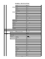
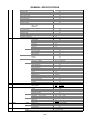
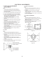
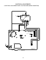
SERVICE MANUAL
COLOR TELEVISION RECEIVER
DTV2784
All the specifications and features are subject to change without notice.
ORIGINAL
VERSION (A)
S/M CODE NO. M3W4062ASM
DATE OF ISSUE 02/2006
IMPORTANT SERVICE SAFETY INFORMATION
Operating the receiver outside of its cabinet or with its
back removed involves a shock hazard. Work on
these models should only be performed by those who
are thoroughly familiar with precautions necessary
when working on high voltage equipment.
Exercise care when servicing this chassis with power
applied. Many B plus and high voltage RF terminals are
exposed which, if carelessly contacted, can cause
serious shock or result in damage to the chassis.
Maintain interconnecting ground lead connections
between chassis, escutcheon, picture tube dag and
tuner cluster when operating the chassis.
These receivers have a "polarized" AC line cord. The AC
plug is designed to fit into standard AC outlets in one
direction only. The wide blade connects to the "ground
side" and the narrow blade connects to the "hot side" of
the AC line. This assures that the TV receiver is properly
grounded to the house wiring. If an extension cord must
be used, make sure it is of the "polarized" type.
Since the chassis of this receiver is connected to one
side of the AC supply during operation, service should
not be attempted by anyone not familiar with the
precautions necessary when working on these types
of equipment.
When it is necessary to make measurements or tests with
AC power applied to the receiver chassis, an Isolation
Transformer must be used as a safety precaution and to
prevent possible damage to transistors. The Isolation
Transformer should be connected between the TV line
cord plug and the AC power outlet.
When removing springs or spring mounted parts from the
tuner, tuner cluster or chassis, shatterproof goggles must
be worn. Keep others without shatterproof goggles away.
Before returning the receiver to the user, perform the
following safety checks:
1. Inspect all lead dress to make certain that leads are
not pinched or that hardware is not lodged between
the chassis and other metal parts in the receiver.
2. Replace all protective devices such as nonmetallic
control knobs, insulating fishpapers, cabinet backs,
adjustment and compartment covers or shields,
isolation resistor-capacitor networks, mechanical
insulators, etc.
3. To be sure that no shock hazard exists, a check for
the presence of leakage current should be made at
each exposed metal part having a return path to the
chassis (antenna, cabinet metal, screw heads,
knobs and/or shafts, escutcheon, etc.) in the
following manner.
Plug the AC line cord directly into a 120V AC receptacle.
(Do not use an Isolation Transformer during these
checks.) All checks must be repeated with the AC line
cord plug connection reversed. (If necessary, a
nonpolarized adapter plug must be used only for the
purpose of completing these checks.)
If available, measure current using an accurate leakage
current tester. Any reading of 0.35mA or more is
excessive and indicates a potential shock hazard which
must be corrected before returning the receiver to the
owner.
If a reliable leakage current tester is not available, this
alternate method of measurement should be used.
Using two clip leads, connect a 1500 ohm, 10 watt
resistor paralleled by a 0.15µF capacitor in series with
a known earth ground, such as a water pipe or conduit
and the metal part to be checked. Use a VTVM or
VOM with 1000 ohms per volt, or higher, sensitivity to
measure this AC voltage drop across the resistor. Any
reading of 0.35 volt RMS or more is excessive and
indicates a potential shock hazard which must be
corrected before returning the receiver to the owner.
VT VM
AC SCALE
0.15K OHMS
10W
TO EXPOSED
METAL PARTS
A1-1
15µ F
TEST PROBE
TO KNOWN
EARTH GROUND
ABOUT LEAD FREE SOLDER (PbF)
Distinction of PbF PCB:
PCBs (manufactured) using lead free solder will have a PbF printing on the PCB.
(Please refer to figures.)
Caution:
• Pb free solder has a higher melting point than standard solder;
Typically the melting point is 86°F~104°F(30°C~40°C) higher.
Please use a soldering iron with temperature control and adjust it to 650°F ± 20°F (350°C ± 10°C).
•
•
In case of using high temperature soldering iron, please be careful not to heat too long.
Pb free solder will tend to splash when heated too high (about 1100°F/ 600°C).
All products with the printed circuit board with PbF printing must be serviced with lead free solder.
When soldering or unsoldering, completely remove all of the solder from the pins or solder area,
and be sure to heat the soldering points with the lead free solder until it melts sufficiently.
Recommendations
Recommended lead free solder composition is Sn-3.0Ag-0.5Cu.
A1-2
TABLE OF CONTENTS
IMPORTANT SERVICE SAFETY INFORMATION ........................................................................................... A1-1
ABOUT LEAD FREE SOLDER (PbF) ............................................................................................................... A1-2
TABLE OF CONENTS ...................................................................................................................................... A2-1
GENERAL SPECIFICATIONS .......................................................................................................................... A3-1~A3-4
DISASSEMBLY INSTRUCTIONS
1. REMOVAL OF ANODE CAP ................................................................................................................... B1-1
2. REMOVAL AND INSTALLATION OF FLAT PACKAGE IC .................................................................... B2-1, B2-2
SERVICE MODE LIST ....................................................................................................................................... C-1
WHEN REPLACING EEPROM (MEMORY) IC ................................................................................................. C-1, C-2
RE-WRITE FOR DIGITAL SOFT FIRMWARE ................................................................................................... C-3
ELECTRICAL ADJUSTMENTS ......................................................................................................................... D-1~D-6
TROUBLESHOOTING GUIDE ........................................................................................................................... E-1~E-5
IC DESCRIPION ................................................................................................................................................ F-1, F-2
SEMICONDUCTOR BASE CONNECTIONS ..................................................................................................... G-1
BLOCK DIAGRAM
MICON/CHROMA .......................................................................................................................................... H-1, H-2
SD DIGITAL MODULE ................................................................................................................................... H-3, H-4
PRINTED CIRCUIT BOARDS
MAIN/CRT ..................................................................................................................................................... I-1~I-4
DIGITAL ......................................................................................................................................................... I-5
SCHEMATIC DIAGRAMS
MICON ......................................................................................................................................................... J-1, J-2
CHROMA/IF............................................................................................................................................... ...... J-3, J-4
DEFLECTION ................................................................................................................................................ J-5, J-6
POWER ......................................................................................................................................................... J-7, J-8
TUNER ......................................................................................................................................................... J-9, J-10
AV/SOUND .................................................................................................................................................... J-11, J-12
CRT/SVM. ...................................................................................................................................................... J-13, J-14
COMB/FILTER ............................................................................................................................................... J-15, J-16
ASIC ............................................................................................................................................................... J-17, J-18
SDRAM ......................................................................................................................................................... J-19, J-20
FLASH ......................................................................................................................................................... J-21, J-22
FRONT END .................................................................................................................................................. J-23, J-24
AV OUT .................................................................... . .................................................................................. J-25, J-26
WAVEFORMS .................................................................................................................................................... K-1, K-2
MECHANICAL EXPLODED VIEW ..................................................................................................................... L-1
MECHANICAL REPLACEMENT PARTS LIST .................................................................................................. M1-1
ACCESSORY REPLACEMENT PARTS LIST................................................................................................. .... M1-1
ELECTRICAL REPLACEMENT PARTS LIST ................................................................................................... M2-1~M2-7
A2-1
GENERAL SPECIFICATIONS
G-1
TV
SYSTEM
CRT
CRT Size / Visual Size
CRT Type
Magnetic Field
BV/BH
Color System
Speaker
G-2
Tuning
System
Position
Size
Impedance
Sound Output
MAX
10%(Typical)
NTSC3.58+4.43 /PAL60Hz
Broadcasting System
Analog
Digital
Tuner and
System
Receive CH
Destination
Intermediate
Frequency
G-3
Power
Preset CH
Stereo/Dual TV Sound
Tuner Sound Muting
Power Source
CH Coverage
Digital
Analog
Picture(FP)
Sound(FS)
FP-FS
AC
DC
Power Consumption
Stand by (at AC)
Per Year
Power Fuse
Safety Circuit
IC Protector(Micro Fuse)
Safety
Radiation
X-Radiation
Operation
Storage
Protector
G-4
Regulation
G-5
Temperature
G-6
G-7
Operating Humidity
Menu
On Screen
Display
Menu1
at AC
27"
Menu Type
Picture
Mode(Picture preference)
Contrast
Brightness
Color
Tint
Sharpness
Color Temperature
Reset
Audio
MTS
Bass
Treble
Balance
BBE
Stable Sound
Speakers On/Off
Audio Language
Digital Output (PCM/Dolby Digital)
Surround
Reset
Setup
Language
Clock Set
TV/CABLE
Auto CH Memory
Add/ Delete
Closed Caption
CC Advanced (Size, Type, Edge,
Color, Background Color)
Signal Meter
Option
On/Off Timer
A3-1
27 inch / 676.0mmV
Normal
+0.45G/0.18G
NTSC
2Speaker
Front
2.0 x 3.5 Inch
8
ohm
1.0 + 1.0 W
W
No
US System M
ATSC(8VSB), QAM
1Tuner
USA(W/ CATV)
2 - 69, 4A, A-5 - A-1,
A - I, J - W, W+1 - W+84
44.00MHz
45.75MHz
41.25MHz
4.50MHz
No
Yes
Yes
120V AC 60Hz
110 W at AC 120 V 60 Hz
3 W at AC 120 V 60 Hz
-kWh/Year
Yes
Yes
No
UL
FCC
DHHS
+5oC ~ +40oC
-20oC ~ +60oC
Less than 80% RH
Yes
Icon
Yes
No
Yes
Yes
Yes
Yes
Yes
No
Yes
Yes
Yes
No
No
No
No
No
No
Yes
Yes
No
Yes
Yes
Yes
Yes
Yes
Yes
Yes
Yes
Yes
Yes
Yes
Yes
GENERAL SPECIFICATIONS
Favorite CH
CH Label
Video Label
No
Yes
No
Yes
Yes
Yes
Yes
Yes
Locks
Password
V-Chip
Video Lock
CH Lock
Game Timer
Front. Panel Lock
Control Level
Volume
Contrast
Brightness
Color
Tint
Sharpness
Bass
Treble
Balance
Signal Meter
Stereo, SAP, Mono
Video
Component
Channel(TV/Cable)
CH Label
Video Label
Clock
Game Timer
On/Off Timer
Sleep Timer
Reset
Sound Mute
Picture Size
V-chip Rating
G-8
OSD Language
G-9
Clock and
Timer
G-10
Remote
Control
No
Yes
Yes
Yes
Yes
Yes
Yes
Yes
Yes
No
No
No
Yes
Yes
Yes
Yes
Yes
Yes
No
Yes
No
Yes
Yes
Yes
Yes
Yes
Yes
English
Sleep Timer
Max Time
Step
On/Off Timer
Program(On Timer / Off Timer)
Timer Back-up (at Power Off Mode)
more than
Unit
Glow in Dark Remocon
Format
Remocon Format
Custom Code
Power Source
Voltage(D.C)
UM size x pcs
Total Keys
Keys
Power
1
2
3
4
5
6
7
8
9
0
100
CH Up
CH Down
Volume Up
Volume Down
TV/Caption/Text
CH1/CH2
TV/Video(TV/AV)
CH RTN/CH ENT(Quick View)
Sleep
Display(Call) / Reset
Menu
Enter
A3-2
French
120 Min
10 Min
Yes
-Min
RC-KL
No
NEC
Orion
86-05 h
3V
UM-4 x 2 pcs
27 Keys
Yes
Yes
Yes
Yes
Yes
Yes
Yes
Yes
Yes
Yes
Yes
No
Yes
Yes
Yes
Yes
Yes
No
Yes
Yes
Yes
Yes
Yes
Yes
Yes
Spanish
Sec
GENERAL SPECIFICATIONS
Multi Brand Keys
G-11
G-12
Features
Accessories
Mute
Exit
MTS(Audio Select)
Set +
Set Picture Size
CH Up(VCR)
CH Down(VCR)
Pause/Still
TV/VCR(VCR)
CH Enter
Code Set (Code)
FF
Rew
Rec
Play
Stop
TV
VCR
Cable
Yes
Yes
Yes
No
No
Yes
No
No
No
No
No
No
No
No
No
No
No
No
No
No
Auto Degauss
Auto Shut Off
Canal+
Cable(CATV)
Anti-theft
Rental
Memory(Last CH)
Memory(Last Volume)
V-Chip (Analog & Digital)
Type
BBE
Auto Search
CH Allocation
SAP
Tone Control
Just Clock Function
Game Position
CH Label
VM Circuit
Full OSD
Premiere
Comb Filter
Yes
Yes
No
Yes
No
No
Yes
Yes
Yes
USA, ORION Type
No
No
No
Yes
No
No
No
Yes
No
No
No
No
Lines
Yes
No
Yes
Yes
No
No
Yes
Yes
No
No
Yes
No
No
No
No
Yes
Yes
Yes
No
Yes
No
Yes
English / Spanish
Yes
Yes
No
Auto CH Memory
Hotel Lock
Closed Caption (Analog & Digital)
CC Advance
Stable Sound
Surround
CH Lock
Video Lock
Game Timer (Max Time:120 Min)
Energy Star
Power On Memory
Favorite CH
FBT Leak Test Protect
Mode(Picture Preference)
Variable Audio Out
Front Panel Lock
QAM
Digital Out
Dolby Digital
MPEG
PCM
DTS
Zoom
Owner's Manual
Language
w/Guarantee Card
Remote Control Unit
Rod Antenna
Poles
Terminal
Loop Antenna
Terminal
U/V Mixer
No
No
A3-3
GENERAL SPECIFICATIONS
DC Car Cord (Center+)
Guarantee Card
Warning Sheet
Circuit Diagram
Antenna Change Plug
Service Facility List
Important Safeguard
Dew/AHC Caution Sheet
AC Plug Adapter
Quick Set-up Sheet
Battery
No
No
No
No
No
No
No
No
No
No
Yes
UM-4 x 2pcs
OEM Brand
G-13
Interface
G-14
G-15
Set Size
Weight
G-16
Carton
G-17
Material
G-18
Environment
AC Cord
AV Cord (2Pin-1Pin)
Registration Card
Information Sheet
PTB Sheet
300 ohm to 75 ohm Antenna Adapter
Information Sheet(Return)
Switch
Front
Power
System Select
Main Power SW
Sub Power
Channel Up
Channel Down
Volume Up
Volume Down
Rear
AC/DC
TV/CATV Selector
Degauss
Main Power SW
Indicator
Power
Stand-by
On Timer
Terminals Front
Video Input = VIDEO2
Audio Input = VIDEO2
Other Terminal
Rear
Video Input(Rear1) = VIDEO1
Video Input(Rear2)
Audio Input(Rear1) = VIDEO1
Audio Input(Rear2)
Video Output
Audio Output
S-Input
Component Input2(w/ Analog Audio L/R)
Digital Audio Out
Diversity
Ext Speaker
DC Jack 12V(Center +)
VHF/UHF Antenna Input
AC Outlet
Approx.
W x D x H (mm)
Net (Approx.)
Gross (Approx.)
Master Carton
Content
Material
Dimensions
W x D x H(mm)
Description of Origin
Gift Box
Material
Dimensions
W x D x H(mm)
Description of Origin
Drop Test
Height (cm)
Container Stuffing
Cabinet
Cabinet Front
Cabinet Rear
PCB
Non-Halogen Demand
Eyelet Demand
Environmental standard requirement (by buyer)
Pb-free
A3-4
No
No
No
No
No
No
No
Yes
Yes
No
No
No
Yes
Yes
Yes
Yes
No
No
No
No
No
No
No
RCA
RCA x 2 (L/MONO,R)
No
RCA
No
RCA x 2 (L/MONO,R)
No
No
No
Yes
RCA x 5
Coaxial x 1
No
No
No
F Type
No
740 x 489.5 x 571.5
( 77.2 lbs)
35kg
38Kg
(83.8 lbs)
No
---Sets
-/--- x -- x -No
Double/White W/Photo Label
850 x 575 x 665
Yes
Natural Dropping At 1 Corner / 3 Edges / 6 Surfaces
31
192
Sets/40' container
PS 94V0 DECABROM
PS 94V0 DECABROM
No
No
Green procurement of ORION
Phase3(Phase3A)
DISASSEMBLY INSTRUCTIONS
3. After one side is removed, pull in the opposite direction to
remove the other.
1. REMOVAL OF ANODE CAP
Read the following NOTED items before starting work.
*
*
NOTE
After turning the power off there might still be a potential
voltage that is very dangerous. When removing the
Anode Cap, make sure to discharge the Anode Cap's
potential voltage.
Do not use pliers to loosen or tighten the Anode Cap
terminal, this may cause the spring to be damaged.
Take care not to damage the Rubber Cap.
INSTALLATION
1. Clean the spot where the cap was located with a small
amount of alcohol. (Refer to Fig. 1-3.)
REMOVAL
Location of Anode Cap
1. Follow the steps as follows to discharge the Anode Cap.
(Refer to Fig. 1-1.)
Connect one end of an Alligator Clip to the metal part of
a flat-blade screwdriver and the other end to ground.
While holding the plastic part of the insulated screwdriver,
touch the support of the Anode with the tip of the
screwdriver.
A cracking noise will be heard as the voltage is discharged.
Fig. 1-3
GND on the CRT
NOTE
Confirm that there is no dirt, dust, etc. at the spot where
the cap was located.
2. Arrange the wire of the Anode Cap and make sure the
wire is not twisted.
3. Turn over the Rubber Cap. (Refer to Fig. 1-4.)
Screwdriver
Support
CRT
Alligator Clip
GND on the CRT
Fig. 1-4
Fig. 1-1
4. Insert one end of the Anode Support into the anode button,
then the other as shown in Fig. 1-5.
2. Flip up the sides of the Rubber Cap in the direction of the
arrow and remove one side of the support.
(Refer to Fig. 1-2.)
Rubber Cap
CRT
CRT
Support
Support
Fig. 1-5
Fig. 1-2
5. Confirm that the Support is securely connected.
6. Put on the Rubber Cap without moving any parts.
B1-1
DISASSEMBLY INSTRUCTIONS
3. When IC starts moving back and forth easily after
desoldering completely, pickup the corner of the IC using
a tweezers and remove the IC by moving with the IC
desoldering machine. (Refer to Fig. 2-3.)
2. REMOVAL AND INSTALLATION OF
FLAT PACKAGE IC
REMOVAL
NOTE
1. Put Masking Tape (cotton tape) around the Flat Package
IC to protect other parts from any damage.
(Refer to Fig. 2-1.)
Some ICs on the PCB are affixed with glue, so be
careful not to break or damage the foil of each IC
leads or solder lands under the IC when removing it.
NOTE
Masking is carried out on all the parts located within
10 mm distance from IC leads.
Masking Tape
(Cotton Tape)
Blower type IC
desoldering
machine
IC
Tweezers
Fig. 2-1
IC
Fig. 2-3
2. Heat the IC leads using a blower type IC desoldering
machine. (Refer to Fig. 2-2.)
4. Peel off the Masking Tape.
NOTE
5. Absorb the solder left on the pattern using the Braided
Shield Wire. (Refer to Fig. 2-4.)
Do not rotate or move the IC back and forth until IC
can move back and forth easily after desoldering the
leads completely.
NOTE
Do not move the Braided Shield Wire in the vertical
direction towards the IC pattern.
Blower type IC
desoldering machine
Braided Shield Wire
Soldering Iron
IC
IC pattern
Fig. 2-2
B2-1
Fig. 2-4
DISASSEMBLY INSTRUCTIONS
INSTALLATION
4. When bridge-soldering between terminals and/or the
soldering amount are not enough, resolder using a Thintip Soldering Iron. (Refer to Fig. 2-8.)
1. Take care of the polarity of new IC and then install the
new IC fitting on the printed circuit pattern. Then solder
each lead on the diagonal positions of IC temporarily.
(Refer to Fig. 2-5.)
Thin-tip Soldering Iron
IC
Soldering Iron
Fig. 2-8
5. Finally, confirm the soldering status on four sides of the
IC using a magnifying glass.
Confirm that no abnormality is found on the soldering
position and installation position of the parts around the
IC. If some abnormality is found, correct by resoldering.
Solder temporarily
Solder temporarily
Fig. 2-5
2. Supply the solder from the upper position of IC leads
sliding to the lower position of the IC leads.
(Refer to Fig. 2-6.)
Solder
IC
NOTE
When the IC leads are bent during soldering and/or
repairing, do not repair the bending of leads. If the
bending of leads are repaired, the pattern may be
damaged. So, be always sure to replace the IC in this
case.
Soldering Iron
Supply soldering
from upper position
to lower position
Fig. 2-6
3. Absorb the solder left on the lead using the Braided
Shield Wire. (Refer to Fig. 2-7.)
NOTE
Do not absorb the solder to excess.
Soldering Iron
IC
Braided Shield Wire
Fig. 2-7
B2-2
SERVICE MODE LIST
This unit is provided with the following SERVICE MODES so you can repair, examine and adjust easily.
To enter the Service Mode, press both set key and remote control key for more than 2 seconds.
Set Key
Remocon Key
VOL. (-) MIN
0
Releasing of V-CHIP PASSWORD.
VOL. (-) MIN
1
Initialization of factory data.
NOTE: Do not use this for normal servicing.
If you set factory initialization, the memories are reset such as the channel
setting, and the POWER ON total hours.
VOL. (-) MIN
8
Check of the SUM DATA and MICON VERSION on the screen.
Refer to the "WHEN REPLACING EEPROM (MEMORY) IC".
VOL. (-) MIN
6
VOL. (-) MIN
9
Operations
Check for the firmware version.
Can be checked of the INITIAL DATA of MEMORY IC.
Refer to the "WHEN REPLACING EEPROM (MEMORY) IC".
Display of the Adjustment MENU on the screen.
Refer to the "ELECTRICAL ADJUSTMENT" (On-Screen Display Adjustment).
WHEN REPLACING EEPROM (MEMORY) IC
CONFIRMATION OF CHECK SUM, POWER ON TOTAL HOURS, MICON VERSION AND
DIGITAL TV MICON FIRMWARE VERSION
Initial total of MEMORY IC, POWER ON total hours, MICON VERSION and Digital TV MICON Firmware VERSION can be
checked on the screen. Total hours are displayed in 16 system of notation.
NOTE: If you set a factory initialization, the total hours is reset to "0".
Please refer to "CONFIRMATION OF INITIAL DATA" when SUM DATA is not corresponding.
1.
2.
3.
4.
Turn on the POWER, and set to the TV mode.
Set the VOLUME to minimum.
Press both VOL. DOWN button on the set and Channel button (8) on the remote control for more than 2 seconds.
After the confirmation of each check sum, power on total hours, micon version and Digital TV MICON Firmware version,
turn off the power.
ADDRESS
MICON Version
Digital TV MICON Firmware
Initial setting data check sum.
Rom correction data check sum.
AUDIO External terminal Volume.
DATA
CRT ON 0015
OEC7144A_039
DTV d-a5Z253
INIT
0D9B
ROM:
-4036
VOLUME: 0000
FIG. 1
C-1
POWER ON total hours.
= (16 x 16 x 16 x thousands digit value)
+ (16 x 16 x hundreds digit value)
+ (16 x tens digit value)
+ (ones digit value)
WHEN REPLACING EEPROM (MEMORY) IC
If a service repair is undertaken where it has been required to change the MEMORY IC, the following steps should be taken to
ensure correct data settings while making reference to TABLE 1.
INI
+0
+1
+2
+3
+4
+5
+6
+7
+8
+9
+A +B +C +D +E
+F
00
C1 A2 4D 1A
22
00
02
00
00
80
10
00
30
36
03
00
10
68
00
00
00
00
00
00
00
00
00
18
07
00
05
AA
00
20
79
00
00
73
00
00
00
00
00
00
00
00
00
00
00
00
30
70
B0
06
01
03
04
20
02
01
00
D0
02
B1
10
00
00
40
00
00
00
00
00
00
00
80
80
80
00
40
40
00
00
00
50
00
00
00
00
1E
00
0C
00
45
00
02
00
02
80
00
C0
60
00
00
00
00
00
84
00
00
C2
04
01
00
00
01
02
00
70
00
00
00
14
07
00
63
2F
00
00
00
00
00
00
00
00
80
00
00
00
00
00
00
00
00
00
00
00
00
00
00
00
00
90
00
00
00
00
00
00
00
00
00
00
00
00
00
00
00
00
A0
00
00
00
00
00
00
00
00
00
00
00
00
00
00
00
00
B0
00
00
00
00
00
00
00
00
00
00
00
00
00
00
00
00
C0
00
00
00
00
00
00
00
00
00
00
00
00
00
00
00
00
D0
00
00
00
00
00
00
00
00
00
00
00
00
00
00
00
00
E0
00
00
00
00
00
00
00
00
00
00
00
00
00
00
00
00
F0
00
---
---
---
---
---
---
---
---
---
---
---
---
---
---
---
Table 1
CONFIRMATION OF INITIAL DATA
1. Enter DATA SET mode by setting VOLUME to minimum.
2. Press both VOL. DOWN button on the set and Channel button (6) on the remote control for more than 2 seconds.
ADDRESS and DATA should appear as FIG 1.
3. ADDRESS is now selected and should "blink". Using the UP/DOWN button on the remote, step through the ADDRESS
until required ADDRESS to be changed is reached.
4. Press RIGHT/LEFT button to select DATA. When DATA is selected, it will "blink".
5. Again, step through the DATA using UP/DOWN button until required DATA value has been selected.
6. Pressing RIGHT/LEFT button will take you back to ADDRESS for further selection if necessary.
7. Repeat steps 3 to 6 until all data has been checked.
8. When satisfied correct DATA has been entered, turn POWER off (return to STANDBY MODE) to finish DATA input.
After the data input, set to the initializing of shipping.
9. Turn POWER on.
10. Press both VOL. DOWN button on the set and Channel button (1) on the remote control for more than 2 seconds.
11. After the finishing of the initializing of shipping, the unit will turn off automatically.
The unit will now have the correct DATA for the new MEMORY IC.
ADDRESS
DATA
INIT 000 C1
CRT ON 0015
OEC7144A_039
DTV d-a5Z253
INIT
0D9B
ROM:
-4036
VOLUME: 0000
FIG. 1
C-2
RE-WRITE FOR DIGITAL SOFT FIRMWARE
JG198
Serial Communication
Change JIG
Ref. No.
Part No.
JG199 Flash UP-Date Soft
Disc
JG176 USA SD DTV ROM
DISC
Remarks
Parts Name
JG198
APJG198000
Serial Communication
Change JIG
JG199
APJG199000
Flash UP-Date Soft Disc
Up-Date of the Firmware
JG176
APJG176093
USA SD DTV ROM
DISC
Up-Date of the Firmware
Connect the set to personal computer
1. Confirm that the AC cord is plugged out.
2. Using the Serial Communication Change JIG (JG198), connect the set to personal computer. (Refer to Fig. 1)
NOTE: It is possible to write only with the personal computer of WINDOWS.
Fig. 1
3. Using the Flash UP-Date Soft Disc (JG199) and USA SD DTV ROM DISC(JG176), please Re-write the DIGITAL SOFT
FIRMWARE.
The operating manual for Re-writing is included in Flash UP-Date Soft Disc (JG199).
C-3
ELECTRICAL ADJUSTMENTS
1. ADJUSTMENT PROCEDURE
NO.
00
01
02
03
04
05
06
07
08
09
10
11
12
13
14
15
16
17
18
19
Read and perform these adjustments when repairing the
circuits or replacing electrical parts or PCB assemblies.
CAUTION
•
•
•
•
Use an isolation transformer when performing any
service on this chassis.
Before removing the anode cap, discharge electricity
because it contains high voltage.
When removing a PCB or related component, after
unfastening or changing a wire, be sure to put the wire
back in its original position.
When you exchange IC and Transistor with a heat sink,
apply silicon grease on the contact section of the heat
sink. Before applying new silicon grease (YG6260M) ,
remove all the old silicon grease. (Old grease may
cause damages to the IC and Transistor.)
FUNCTION
OSD H
OSD C
CUT OFF
H.POSI
H BLK L
H BLK R
V. SIZE
V POSI
V.LIN
VS CORR
V COMP
R.BIAS
G.BIAS
B.BIAS
R.DRV
G.DRV
B.DRV
BRI.CENT
BRI.MAX
BRI.MIN
NO.
20
21
22
23
24
25
26
27
28
29
30
31
32
33
34
35
36
37
38
FUNCTION
CONT.CENT
CONT.MAX
CONT.MIN
COL.CENT
COL.MAX
COL.MIN
TINT CENT
SHARP.CENT
SHARP.MAX
SHARP.MIN
SUB BIAS
H.SIZE
PARABOLA
TRAPEZIUM
COR TOP
COR BTM
TEST STEREO
TEST AUDIO
H FREQ
Fig. 1-2
2. BASIC ADJUSTMENTS
Prepare the following measurement tools for electrical
adjustments.
2-1: CONSTANT VOLTAGE
1. Oscilloscope
2. Digital Voltmeter
3. Multi-sound Generator
4. Pattern Generator
1. Place the set in AV MODE without signal.
2. Connect the digital voltmeter to the TP003.
3. Adjust the VR502 until the digital voltmeter is 120 ± 0.5V.
On-Screen Display Adjustment
2-2: CUT OFF
1. In the condition of NO indication on the screen.
Press the VOL. DOWN button on the set and the Channel
button (9) on the remote control for more than 2 seconds
to appear the adjustment mode on the screen as shown in
Fig. 1-1.
1. Place the set in Aging Test for more than 15 minutes.
2. Place the set in AV MODE without signal.
3. Using the remote control, set the brightness and
contrast to normal position.
4. Activate the adjustment mode display of Fig. 1-1 and
press the channel button (02) on the remote control to
select "CUT OFF".
5. Adjust the Screen Volume until a dim raster is obtained.
TV-A
4:3
2-3: FOCUS
1. Receive the monoscope pattern.
2. Turn the Focus Volume fully counterclockwise once.
3. Adjust the Focus Volume until picture is distinct.
2-4: WHITE BALANCE
00 OSD H
10
NOTE: Adjust after performing CUT OFF adjustment.
1. Place the set in Aging Test for more than 15 minutes.
2. Receive the white 100% signal from the Pattern
Generator.
3. Using the adjustment control, set the brightness and
contrast to normal position.
4. Activate the adjustment mode display of Fig. 1-1 and
press the channel button (11) on the remote control to
select "R.BIAS".
5. Using the CH. UP/DOWN button on the remote control,
adjust the R.BIAS.
6. Press the VOL. UP/DOWN button on the remote control to
select the "R.DRIVE", "B.DRIVE", "G.BIAS" or "B.BIAS".
7. Using the CH. UP/DOWN button on the remote control,
adjust the R.DRIVE, B.DRIVE, G.BIAS or B.BIAS.
8. Perform the above adjustments 6 and 7 until the white
color is achieved.
Fig. 1-1
2. Use the VOL. UP/DOWN button or Channel button (0-9)
on the remote control to select the options shown in Fig.
1-2.
3. Press the MENU button on the remote control to end the
adjustments.
4. To display the adjustment screen for AV, CS and
DIGITAL mode, press the TV/VIDEO button on the
remote control to set to the AV, CS and DIGITAL mode.
Press the VOL.DOWN button on the set and the
channel (9) on the remote control for more than 2
seconds.
D-1
ELECTRICAL ADJUSTMENTS
2-5: BRIGHT CENT
1. Receive the monoscope pattern. (RF Input)
2. Set the screen mode to FULL.
3. Using the remote control, set the brightness and contrast
to normal position.
4. Activate the adjustment mode display of Fig. 1-1 and
press the channel button (17) on the remote control to
select "BRI CENT".
5. Press the CH. UP/DOWN button on the remote control
until the white 2.7% is starting to be visible
6. Receive the monoscope pattern. (Audio Video Input)
7. Press the TV/VIDEO button on the remote control to set
to the AV mode. Then perform the above adjustments
2~5.
8. Receive the monoscope pattern.
9. Press the TV/VIDEO button on the remote control to set
to the CS mode.Then perform the above adjustments
2~5.
“A”
Fig. 2-1
2-8: COLOR CENT
2-6: CONTRAST MAX
1. Receive an over 70dB color bar pattern. (RF Input)
2. Using the remote control, set the brightness and
contrast to normal position.
3. Activate the adjustment mode display of Fig. 1-1 and
press the channel button (21) on the remote control
to select "CONT.MAX".
4. Press the CH. UP/DOWN button on the remote
control until the contrast step No. becomes "100".
5. Receive a broadcast and check if the picture is normal.
6. Receive the color bar pattern. (Audio Video Input)
7. Press the TV/VIDEO button on the remote control to
set to the AV mode. Then perform the above
adjustments 2~5.
8. Receive a broadcast and check if the picture is normal.
Receive the monoscope pattern.
9. Press the TV/VIDEO button on the remote control to set to
the CS mode.Then perform the above adjustments 2~5.
1. Receive the color bar pattern. (RF Input)
2. Using the remote control, set the brightness, contrast,
color and tint to normal position.
3. Connect the oscilloscope to TP022.
4. Activate the adjustment mode display of Fig. 1-1 and
press the channel button (23) on the remote control to
select "COL.CENT".
5. Adjust the VOLTS RANGE VARIABLE knob of the
oscilloscope until the range between white 100% and
0% is set to 4 scales on the screen of the oscilloscope.
6. Press the CH. UP/DOWN button on the remote control
until the red color level is adjusted to 110 ± 5% of the
white level. (Refer to Fig. 2-2)
7. Receive the color bar pattern. (Audio Video Input)
8. Press the AV mode. Then perform the above
adjustments 2~6.
9. Receive the color bar pattern.
10. Press the TV/VIDEO button on the remote control to set
to the CS mode.Then perform the above adjustments
2~6.
11. Receive the digital color bar pattern.
12. Press the TV/VIDEO button on the remote control to set
to the DIGITAL mode.Then perform the above
adjustments 2~6.
2-7: TINT
1. Receive the color bar pattern. (RF Input)
2. Using the remote control, set the brightness and contrast
to normal position.
3. Connect the oscilloscope to TP024.
4. Activate the adjustment mode display of Fig. 1-1 and
press the channel button (26) on the remote control to
select "TINT".
5. Press the CH. UP/DOWN button on the remote control
until the section A becomes as straight line.
(Refer to Fig. 2-1)
6. Receive the color bar pattern. (Audio Video Input)
7. Press the TV/VIDEO button on the remote control to set
to the AV mode. Then perform the above adjustments
2~5.
8. Receive the color bar pattern.
9. Press the TV/VIDEO button on the remote control to set
to the CS mode.Then perform the above adjustments
2~5.
10. Receive the digital color bar pattern.
11. Press the TV/VIDEO button on the remote control to set
to the DIGITAL mode.Then perform the above
adjustments 2~5.
110%
white 100%
Fig. 2-2
2-9: HORIZONTAL POSITION
1. Receive the monoscope pattern.
2. Using the remote control, set the brightness and contrast
to normal position.
3. Activate the adjustment mode display of Fig. 1-1 and
press the channel button (03) on the remote control to
selec "H.POSI".
4. Press the CH. UP/DOWN button on the remote control
until the SHIFT quantity of the OVER SCAN on right and
left becomes minimum.
D-2
ELECTRICAL ADJUSTMENTS
2-10: HORIZONTAL SIZE
2-14: TRAPEZIUM
1. Receive the monoscope pattern.
2. Using the remote control, set the brightness and
contrast to normal position.
3. Activate the adjustment mode display of Fig. 1-1 and
press the channel button (31) on the remote control to
select "H.SIZE".
4. Press the CH. UP/DOWN button on the remote control
until the SHIFT quantity of the OVER SCAN on the right
and left becomes 8± 3%.
1. Receive the crosshatch signal from the Pattern Generator.
2. Using the remote control, set the brightness and contrast
to normal position.
3. Activate the adjustment mode display of Fig. 1-1 and
press the channel button (33) on the remote control to
select "TRAPEZIUM".
4. Press the CH. UP/DOWN button on the remote control
until both ends of the right and left vertical lines of the 4th
length lines screen become parallel.
2-11: VERTICAL LINEARITY
2-15: PALABOLA
1. Receive the monoscope pattern.
2. Using the remote control, set the brightness, contrast,
to normal position.
3. Activate the adjustment mode display of Fig. 1-1 and
press the channel button (08) on the remote control to
select "V.LIN".
4. Press the CH. UP/DOWN button on the remote control
until the SHIFT quantity of the OVER SCAN on upside
and downside becomes minimum.
1. Receive the crosshatch pattern.
2. Using the remote control, set the brightness and
contrast to normal position.
3. Activate the adjustment mode display of Fig. 1-1 and
press the channel button (32) on the remote control to
select "PALABOLA".
4. Press the CH. UP/DOWN button on the remote control,
so that the line becomes straight from the outside of
the right and left.
2-16: COR TOP/BTM
2-12: VERTICAL POSITION
1. Receive the crosshatch signal from the Pattern Generator.
2. Set the screen mode to FULL.
3. Using the remote control, set the brightness and contrast
to normal position.
4. Activate the adjustment mode display of Fig. 1-1 and
press the channel button (34) on the remote control to
select "COR. TOP".
5. Press the CH. UP/DOWN button on the remote control
until both ends of the vertical lines become straight.
6. Activate the adjustment mode display of Fig. 1-1 and
press the channel button (35) on the remote control to
select "COR. BTM".
7. Press the CH. UP/DOWN button on the remote control
until both ends of the vertical lines of the screen become
parallel.
1. Receive the monoscope pattern.
2. Using the remote control, set the brightness and contrast
to normal position.
3. Adjust the VR401 until the horizontal line becomes fit to
the notch of the shadow mask.
(Refer to Fig. 2-3)
horizontal line
,,
,,
,,
,
,,
,,
,,
,,
Notch
Shadow mask
2-17: OSD POSITION
1. Receive the monoscope pattern from the Pattern
Generator.
2. Using the remote control, set the brightness and
contrast to normal position.
3. Activate the adjustment mode display of Fig. 1-1 and
press the channel button (00) on the remote control to
select "OSD H".
4. Press the CH. UP/DOWN button on the remote control
until the difference of A and B becomes minimum.
(Refer to Fig. 2-4)
Fig. 2-3
2-13: VERTICAL SIZE
1.
the monoscope pattern.
1 Receive
2
2. Using the remote control, set the brightness and contrast
to normal position.
3. Activate the adjustment mode display of Fig. 1-1 and
press the channel button (06) on the remote control to
select "V. SIZE".
4. Press the CH. UP/DOWN button on the remote control
until the SHIFT quantity of the OVER SCAN on upside
and downside becomes 9 ± 2%.
TV-A
4:3
00 OSD H
A
D-3
10
B
Fig. 2-4
ELECTRICAL ADJUSTMENTS
2-18: Confirmation of Fixed Value (Step No.)
Please check if the fixed values of each adjustment
item is set correctly referring below.
NO.
1
4
5
9
10
18
19
20
22
24
25
27
28
29
30
36
37
38
FUNCTION
OSD C
H BLK L
H BLK R
VS CORR
V COMP
BRI.MAX
BRI.MIN
CONT.CENT
CONT.MIN
COL.MAX
COL.MIN
SHARP.CENT
SHARP.MAX
SHARP.MIN
SUB BIAS
TEST STEREO
TEST AUDIO
H FREQ
RF
02
06
02
11
00
120
30
55
20
120
20
35
50
20
00
00
00
07
AV
02
06
02
11
00
120
30
50
20
120
20
25
40
10
00
00
00
07
CS
02
06
02
11
00
120
30
50
20
120
20
25
40
10
00
00
00
07
DIGITAL
02
06
02
11
00
120
30
55
20
120
20
25
40
10
00
00
00
07
D-4
ELECTRICAL ADJUSTMENTS
3-3: STATIC CONVERGENCE
3. PURITY AND CONVERGENCE
ADJUSTMENTS
NOTE
Adjust after performing adjustments in section 3-2.
NOTE
1. Receive the crosshatch pattern from the color bar
generator.
2. Combine red and blue of the 3 color crosshatch
pattern on the center of the screen by adjusting the pair
of 4 pole magnets.
3. Combine red/blue (magenta) and green by adjusting the
pair of 6 pole magnets.
1. Turn the unit on and let it warm up for at least 30
minutes before performing the following adjustments.
2. Place the CRT surface facing east or west to reduce the
terrestrial magnetism.
3. Turn ON the unit and demagnetize with a Degauss Coil.
3-1: STATIC CONVERGENCE (ROUGH ADJUSTMENT)
1. Tighten the screw for the magnet. Refer to the adjusted
CRT for the position. (Refer to Fig. 3-1)
If the deflection yoke and magnet are in one body,
untighten the screw for the body.
2. Receive the green raster pattern from the color bar
generator.
3. Slide the deflection yoke until it touches the funnel side
of the CRT.
4. Adjust center of screen to green, with red and blue on
the sides, using the pair of purity magnets.
5. Switch the color bar generator from the green raster
pattern to the crosshatch pattern.
6. Combine red and blue of the 3 color crosshatch
pattern on the center of the screen by adjusting the pair
of 4 pole magnets.
7. Combine red/blue (magenta) and green by adjusting the
pair of 6 pole magnets.
8. Adjust the crosshatch pattern to change to white by
repeating steps 6 and 7.
3-4: DYNAMIC CONVERGENCE
NOTE
Adjust after performing adjustments in section 3-3.
1. Adjust the differences around the screen by moving the
deflection yoke upward/downward and right/left.
(Refer to Fig. 3-2-a)
2. Insert three wedges between the deflection yoke and
CRT funnel to fix the deflection yoke.
(Refer to Fig. 3-2-b)
RGB
RGB
R
G
B
R
G
B
UPWARD/DOWNWARD SLANT RIGHT/LEFT SLANT
3-2: PURITY
Fig. 3-2-a
NOTE
Adjust after performing adjustments in section 3-1.
1. Receive the green raster pattern from color bar generator.
2. Adjust the pair of purity magnets to center the color on
the screen.
Adjust the pair of purity magnets so the color at the ends
are equally wide.
3. Move the deflection yoke backward (to neck side)
slowly, and stop it at the position when the whole screen
is green.
4. Confirm red and blue color.
5. Adjust the slant of the deflection yoke while watching the
screen, then tighten the fixing screw.
WEDGE
WEDGE
WEDGE
WEDGE POSITION
DEFLECTION YOKE
DEFLECTION YOKE SCREW
MAGNET SCREW
PURITY MAGNETS
6 POLE MAGNETS
4 POLE MAGNETS
Fig. 3-1
D-5
Fig. 3-2-b
ELECTRICAL ADJUSTMENTS
4. ELECTRICAL ADJUSTMENT PARTS LOCATION GUIDE (WIRING CONNECTION)
CRT PCB
CD804
TP024 R805
CRT
CP804
S801
J801
CP802B
TP022 R803
CP801B
CD801
CD802
CP801A
SPEAKER
CD1001
CP401
TP003
VR401
W002
VR502
CP1001
CRT
CRT
CP802A
CP502
AC IN
CD501
S502
S501
J705 J706 J707
MAIN PCB
D-6
TU001
FB401
J702
DIGITAL PCB
J701
J708 J704
TROUBLESHOOTING GUIDE
NO POWER
Is the voltage at the point (A)
in the Figure DC159.4V ?
Yes
Is the voltage at pin G
of Q502 DC5V ?
No
Yes
Check Q514 and associated circuit.
No
Check Q502 and associated circuit.
T501
A
Is the voltage at the point (B)
in the Figure DC164V ?
Yes
5
Broken wire of R501 or short circuit
on GND.
D
No
G
Q502
R540
S
Is the voltage at the point (C)
in the Figure AC120V ?
Yes
8
IC504
3
Check the rectifying circuit.
R501
R539
B
Q514
No
D501~D504
Is the voltage at the point (E)
in the Figure AC120V ?
Yes
Broken wire of L501.
C
No
L501
Is the voltage on both
ends of S501 AC120V ?
Yes
Broken wire of F501.
E
No
F501
Broken wire of AC cord or check
S501.
S501
CD501
E-1
TROUBLESHOOTING GUIDE
NO RASTER
Does the RASTER
appear at maximum
BRIGHT/CONTRAST ?
Yes
Is the voltage of pin 1 of
CP801 DC180V ?
Yes
Check the output circuit and
associated circuit.
Yes
Contact defects of CRT or CRT
Socket.
No
No
Check the 180V line.
Is the high voltage of
ANODE 27KV~28KV ?
Yes
No
Is the heater voltage at
pin 10 of J801 AC6.4V ?
No
Check the HEATER circuit.
Is collector voltages
of Q405 DC115V and
Q402 DC17.3V ?
Yes
Check FB401 and associated circuit.
No
Is the waveform at base
of Q405 normal ?
Yes
Broken wire at pin 2 of T401.
No
Is the waveform at pin
23 of IC601 normal ?
Yes
Check the circuit from pin 23 of
IC601 to Q402.
No
Check IC601 and associated circuit.
E-2
TROUBLESHOOTING GUIDE
NO COLOR
Are the waveform at pins 6,
8 and 11 of J801 normal ?
Yes
Defect of CRT or contact defects
of J801.
Yes
Check the output circuit and
associated circuit.
No
Are the waveform at pins 3,
4 and 5 of CP802 normal ?
No
Are the waveform at
pins 14, 15 and 16 of
IC601 normal ?
Yes
Are the waveforms at the
input of Q801~Q805 and
Q806 normal ?
Yes
No
No
Check IC601 and associated circuit.
Is the pulse of crystal
X601 normal ?
Yes
Check the associated circuit of IC601.
No
Change X601.
E-3
Check Q801~Q806 and
associated circuit.
TROUBLESHOOTING GUIDE
NO VERTICAL
Is the waveform at pin
6 of CP401 normal ?
Yes
Check DY.
No
Is the waveform at pin
2 of IC401 normal ?
Yes
Check the circuit from pin 2 of
IC401 to CP401.
No
Is the waveform at pin 5
of IC401 normal ?
Yes
Is the voltage at pin 6
of IC401 25V ?
No
Yes
Check IC401 and check associated
circuit.
No
Check the 25V line.
Is the waveform at pin
19 of IC601 normal ?
Yes
Check the circuit from pin 19 of
IC601 to pin 5 of IC401.
No
Check the associated circuit of IC601.
E-4
TROUBLESHOOTING GUIDE
NO SOUND
Is sound setting appropriate ?
Yes
Is the waveform at pins 2,4,
10 and pin 12 of IC1001?
Yes
Check speaker.
No
Is the AUDIO signal at pins
11 and 15 of IC701?
Yes
Check IC701 and associated circuit .
No
Is the AUDIO signal input
at pins 1, 3, 5~9 and 13 of
IC701?
Yes
Check the pins 2, 4 of IC701 and
associated circuit .
No
Check J701, J706, J707, J708 and
at pins 19, 20 of CP2403 and
associated circuit.
E-5
IC DESCRIPTION
OEC7144A (IC101)
No.
Pin name
Symbol
Option
When unused
-
Condenser of slicer.
-
-
-
Filter of slicer.
-
-
O
1
IIC BUS(1) CLOCK output.
C-MOS
-
SDA1
I/O
1
IIC BUS(1) DATA I/O.
C-MOS
-
YUV-H
O
0
SW COMPONENT
C-MOS
OPEN
O
-
Not used.(L output)
C-MOS
OPEN
I
1
SYNC input for SD distinction.
C-MOS
PD
I
-
It connects it with VSS.
-
VSS
I/O
1
VHOLD
V.HOLD_MAIN
I
2
HLF
HLF_MAIN
I/O
3
P94/SCL3/RxD2
SCL1
4
P93/SDA3/TxD2
5
P92/TB2/DIGR0
6
P91/TB1
7
P90/TB0
HSYNC
8
BYTE
BYTE
9
CNVss
CNVss
Logic
Function
I
-
It connects it with VSS. When you write Flash "H"
-
PD
10 P87/XCIN/DIGG0
O
-
Not used.(32KHz IN)
C-MOS
OPEN
11 P86/XCOUT/DIGB0
O
-
Not used.(32KHz OUT)
C-MOS
OPEN
12 RESET
RESET
I
0
RESET input.
"L" ---> when Flash is written "H"
-
PU
13 XOUT
Xout
O
-
Main Oscillation.
-
-
14 VSS
VSS
Power
supply
-
GND
-
-
15 XIN
Xin
16 VCCI
VCC(3.3V)
17 OSC1/OSCHLF
OSCHLF
18 OSC2
I
-
Main Oscillation.
-
-
Power
supply
-
3.3V
-
-
I
-
External clock input for OSD.
-
-
O
-
Not used.(departure pendulum reserve for OSD)
-
OPEN
19 P83/INT1
REMOCON
I
0
REMOCON input.
C-MOS
PU
20 P82/INT0
P.FAIL
I
0
Power failure detection.
C-MOS
PU
21 OUT1
BLANK1
O
1
BLANK output for OSD/CCD(1)
-
-
22 OUT2
BLANK2
O
1
BLANK output for OSD/CCD(2)
-
-
O
-
Not used.
C-MOS
OPEN
23 P77/HC1
24 P76/TA3
O
-
Not used.
C-MOS
OPEN
25 P75/HC0
EXT A MUTE
O
1
Sound Mute for Audio out terminal
C-MOS
OPEN
26 P74/TA2
VOLUME
O
1
PWM output for Audio Volume
C-MOS
OPEN
O
-
Not used.
C-MOS
OPEN
AFT2
O
-
Detect Tuner AFT2 (analog)
C-MOS
OPEN
29 P71/SCL1/RxD2
O
-
Not used.
Nch-OD
OPEN
30 P70/SDA1/TxD2
O
-
Not used.
Nch-OD
OPEN
O
-
Detect Tuner AFT1 (analog)
C-MOS
OPEN
-
-
27 P73/CTS2,RTS2
28 P72/SCL2/CLK2
31 P67/SDA2
AFT1
32 R/DIGR1
RED R
O
1
RED output for OSD/CCD.
33 G/DIGG1
GREEN G
O
1
GREEN output for OSD/CCD.
-
-
34 B/DIGB1
BLUE B
O
1
BLUE output for OSD/CCD.
-
-
35 P63/TxD0
DTV Tx
O
0
Communication of Digital Module
C-MOS
PU
36 P62/RxD0
DTV Rx
I
0
Communication of Digital Module
C-MOS
PU
37 P61/CLK0
(CLK0)
O
-
Not used.
C-MOS
PU
38 P60/CTS0,RTS0
(PRT0)
O
-
Not used.
C-MOS
PU
O
-
Not used.(L output)
C-MOS
OPEN
O
0
Reset output of Digital Module
C-MOS
OPEN
41 P55/HOLD
O
-
Not used.
C-MOS
PD
42 P54/HLDA
O
-
Not used.
C-MOS
OPEN
43 P53/BCLK
O
-
Not used.
C-MOS
OPEN
44 P52/RD
O
-
Not used.
C-MOS
OPEN
45 P51/WRH/BHE
O
-
Not used.
C-MOS
OPEN
46 P50/WRL/WR
O
-
Not used.
C-MOS
PU
O
1
Detect Tuner SD (analog)
C-MOS
OPEN
39 P57,RDY/CLK
40 P56/ALE
47 P47/CS3
DTV RESET
SD
F-1
IC DESCRIPTION
OEC7144A (IC101)
No.
I/O
Logic
48 P46/CS2
Pin name
Option
When unused
O
-
49 P45/CS1
O
-
Not used.
C-MOS
OPEN
Not used.
C-MOS
50 P44/CS0
O
OPEN
-
Not used.
C-MOS
OPEN
O
1
Volume MUTE output.
C-MOS
OPEN
52 P42/A18
O
-
Not used.
C-MOS
OPEN
53 P41/A17
O
-
Not used.
C-MOS
OPEN
51 P43/A19
Symbol
AUDIO MUTE
Function
54 P40/A16
VIDEO MUTE
O
1
Image MUTE output.
C-MOS
OPEN
55 P37/A15
EEPROM_SCL
O
1
IIC CLOCK output for EEPROM.
C-MOS
PU
56 P36/A14
EEPROM_SDA
I/O
1
IIC DATA I/O for EEPROM.
C-MOS
PU
57 P35/A13
O
-
Not used.
C-MOS
OPEN
58 P34/A12
O
-
Not used.
C-MOS
OPEN
59 P33/A11
O
-
Not used.
C-MOS
OPEN
60 P32/A10
O
-
Not used.
C-MOS
OPEN
61 P31/A9
O
-
Not used.
C-MOS
OPEN
I
-
HSYNC input for OSD.
O
-
Not used.
I
-
VSYNC input for OSD.
62 Hsync
HD
63 P30/A8
64 Vsync
VD
-
-
C-MOS
OPEN
-
-
65 P27/A7
O
-
Not used.
C-MOS
-
66 P26/A6
O
-
Not used.
C-MOS
OPEN
67 P25/A5
O
-
Not used.
C-MOS
OPEN
68 P24/A4
O
-
Not used.
C-MOS
OPEN
69 P23/A3
O
-
Not used.
C-MOS
OPEN
70 P22/A2
O
-
Not used.
C-MOS
OPEN
71 P21/A1
O
-
Not used.
C-MOS
OPEN
72 P20/A0
O
-
Not used.
C-MOS
OPEN
73 P17/D15
O
-
Not used.
C-MOS
OPEN
74 P16/D14
O
-
Not used.
C-MOS
OPEN
75 P15/D13
O
-
Not used.
C-MOS
OPEN
76 P14/D12
O
-
Not used.
C-MOS
OPEN
77 P13/D11
O
-
Not used.
C-MOS
OPEN
I
0
S jacks input of distinction input.
C-MOS
PU
79 P11/D9
O
-
Not used.
C-MOS
PU
80 P10/D8
O
-
Not used.
C-MOS
PU
O
1
TV POWER control output.
C-MOS
OPEN
78 P12/D10
81 P07/D7
S
TV POWER
82 P06/D6
O
-
Not used.
C-MOS
OPEN
83 P05/D5
DTV POWER
O
1
Power SW of Digital Module
C-MOS
OPEN
84 P04/D4
STAND BY-L
O
0
SUB power supply control terminal.
C-MOS
OPEN
85 P03/D3
DEGAUSS
O
1
Degauss control output
C-MOS
OPEN
86 P02/D2
IIC_OFF
I
0
IIC BUS STOP input for adjustment.
C-MOS
PU
87 P01/D1
PROTECT
O
1
Control H Pulse
C-MOS
PU
88 P00/D0
H_CTL
O
1
Control H Pulse
C-MOS
PU
89 P107/AN5/DIGR2
E0-LEAK
I
1
E0 LEAK Detection
C-MOS
PD
O
-
Not used.(L output)
C-MOS
OPEN
90 P106/AN4/DIGG2
91 P105/AN3/DIGB2
AFT_MAIN
I
-
AFT voltage input for tuning in.
C-MOS
PU
92 P104/AN2
KEY B
I
-
Main unit key input.
Nch-OD
PU
Nch-OD
PU
Nch-OD
PD
-
PD
93 P103/AN1
KEY A
I
-
Main unit key input.
94 P102/AN0
X-RAY
I
1
X-RAY Detection
95 VHOLD2
VHOLD2
I
-
Condenser of slicer.
96 HLF2
HLF2
O
-
Filter of slicer.
-
PD
97 CVin2
CVIN2
I
-
Not used.
-
PU
98 TVSETB
TVSETB
I
-
It connects it with VSS.
-
VSS
99 VCCE
VCC(5V)
Power
supply
-
5V
-
-
100 CVin1
CVIN_MAIN
I
-
Video signal input
-
-
F-2
SEMICONDUCTOR BASE CONNECTIONS
DIODE
RD47FBD-3
1SS133T-77
AU02A-EIC
DSS-272M-S00B
ERD07-15L50
FE201-6L49
MTZJ10B-EIC
MTZJ15B-EIC
MTZJ18B-EIC
MTZJ2.2B-EIC
MTZJ3.3B-EIC
MTZJ3.9B-EIC
MTZJ33B-EIC
MTZJ5.6B-EIC
MTZJ6.2B-EIC
MTZJ8.2B-EIC
MTZJ9.1B-EIC
1N4002-PAN
1N4937-PAN
1N4005-EIC
21DQ09N-TA2B1
RM11C-EIC
SB140-EIC
RB085T-40
ENE271D-10A
IC
8
1
1
1
CAS-220/CS
LA76327M-MPB-E
5
HY5DU561622DTP-D43 CS4345-CZZ
NJM2750M(TE1)
1
AT24C128N-10SU-1.8
TC7W66FU(TE12L,F)
1
PST3229NR
1
5
1
LA7847-E
BA7810T-V5
1
OEC7144A
1
1
AN17822A
SST39VF1681-70-4C-EKE
TRANSISTOR
1
1
PS2561AL1-1-V(W) ZR39640BGCG-B1
E
C B
5
BA00BC0WFP-E2 2SA1371(D,E)-AE
2SC2909(S,T)-AA
KTA1266-AT(Y,GR)
KTA1271_Y-AT
1
E
C
B
B
CE
2SC3841-T1B_T63 2SD2499(LBOEC1)
KRA102SRTK
KRC102SRTK
KRC103SRTK
KRC104SRTK
KTA1504S_Y_RTK
KTC3875S_Y_RTK
KTC4075E-Y-RTK/P
E
CB
KTC4217(O,Y)
G-1
B
CE
KTC3198-AT(Y,GR)
KTC3199_Y-AT
KTC3203_Y-AT
KTC3209_Y-AT
KTC3227_Y-AT
MICON/CHROMA BLOCK DIAGRAM
CHROMA IC
IC601 LA76327M-MPB-E
3
5
FB401
COMB Y
J801
COMB C
Q802, Q806
BLUE OUT
B OUT 16
6
LINE1(REAR)
J701
3
2
11
Q803, Q805
VIDEO1
G OUT 15
AUDIO IN(L)
GREEN OUT
Q801, Q804
AUDIO IN(R)
RED OUT
R OUT 14
1
VIDEO IN1
2
9
VIDEO IN2
F
F
7
S
CRT
V801
8
19
Q402
H OUT 23
V-OUT IC
IC401 LA7847-E
5
Q405
H.DRIVE
HV
6
9
V OUT
FRONT -VIDEO
J705
1
2
DY
H.OUT
FBP IN 6
Y IN
2
29
V IN
OSD_R 57
32 OSD_R
3
28 U IN
OSD_G 56
33 OSD_G
OSD_B 55
34 OSD_B
3
44 S.VIDEO Y
OSD BLK1 54
21 BLANK1
4
40 S.VIDEO C
OSD BLK2 58
22 BLANK2
SYSTEM RESET
IC102 PST3229NR
OUT
1
IN
2
XTAL 3.58 35
12 RESET
D101
MICON_DATA
CP101
1 TX
2
BUSY
CLK
4
5
RX
6
CNVSS
RESET
7
FRONT-AUDIO.L
J706
37 (CLK0)
36 DTV Rx
AV SW
IC701 NJM2750M(TE1)
SOUND AMP
IC1001 AN17822A
9
15
6
6
11
8
3
7
AV2 AUDIO IN/COX OUT
J708
AUDIO YUV R
2
AUDIO YUV L
3
L
R
4
10
8
5
OS101
1
REMOCON 19
64 VD
62 HD
3 SCL1
KEYA 93
4
KEYB 92
SDA1
SDA1 51
VOL UP
CH UP
13 20 19 10
Tuner Audio (L)
Tuner Audio (R)
R
SPEAKER
SP1001
VOL DOWN
CH DOWN
TU001
L
POWER
X101
8MHz
X.OUT 13
36 35
2
12
13
6 SCL
TUNER CVBS 42
9 CNVss
2
5 SDA
X.IN 15
SCL1 50
INV.FBP OUT 59
38 (BUSY)
1
FRONT-AUDIO.R
J707
V PULE OUT 60
35 DTV Tx
2
X602
3.579545MHz
EEPROM_ 55
SCL
EEPROM_ 56
SDA
DTVTX
S-JACK
J702
30
DTVRX
YUV_IN
J704
MEMORY IC
IC199 AT24C128N-10SU-1.8
MICON
IC101 OEC7144A
5
9
EEP_DATA
CP102
SCL_EEP
SDA_EEP
SDA1
SCL1
2
3
6
7
CP4203B
TU I2C CLK
26
TU I2C DATA
IF OUT1
IF OUT2
TX
RX
AUDIO L
25
33
34
13
12
19
AUDIO R
20
C OUT
18
17
Y OUT
SPDIF OUT 24
6
H-1
R. SIGNAL
G. SIGNAL
B. SIGNAL
H-2
H-3
GND
+5V
+2.6V
2
1
GND
4
3
NC
7
ASIC+1.8V
GND
8
5
GND
9
NC
SD-H
TX
ASIC+1.8V
+3.3V
AFT(0)
L3
AFT(1)
U14 N1
RX
J17 H17
RESET
T3
Y OUT
C OUT
ADR
M15
DAT
RESET
+3.3V
ADR
IC2401 SD_DTV ASIC
DAT
K2
K15
ZR39640BGCG-B1
T2
R4
+2.6V
16
16
HY5DU561622DTP-D43
IC2404 256Mbit DDRSDRAM
U7
+2.6V
J1
6
AFT(0)
+3.3V
10
TX
4
AFT(1)
SCLK
1
11
NC
WS
ADATA
BCLK
3
12
RX
Y OUT
17
RESET
C OUT
18
AUDIO-L
AUDIO-R
9
R2
13
AUDIO-L
19
+5V
+3.3V
2
R6
14
AUDIO-R
20
NC
T4
NC
NC
80
T1
SD-H
GND
21
L15
16
GND
22
WS
15
SPDIF OUT
23
ADATA
24
TS_DVALID
SPDIF
TS_FRAME
TU I2C DATA
BCLK
RF_SW
TS_CLK
25
66
TS_DATA
SIF
63
F/E_RESET
RF_SW
65
I2C1_CLK
TU I2C CLK
CAS-220/CS
52
I2C1_DATA
26
IC2402 8VSB/QAM/BTSC DEMOD.
54
WP
27
56
F/E+1.8V
57
WE
28
79
29
14
GND
16
IF AGC
18
16
30
61
GND
11
31
20
IF OUT1
19
32
12
IF OUT2
TU I2C CLK
97
TU I2C DATA
11
SIF
SST39VF1681-70-4C-EKE
33
SIF AMP
IC2408 16Mbit NOR FLASH
34
CP2403
87760-3416
SIF
F/E+1.8V
93
IF AGC
94
IFP
IFN
X2402
25.000MHz
SD DIGITAL MODULE BLOCK DIAGRAM
X2401
24.576MHz
R3
R5
U1
K1 U17 N17
16
IC2501 AUDIO DAC
CS4345-CZZ
10 7
H-4