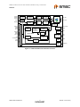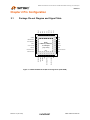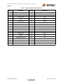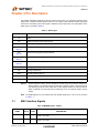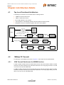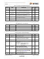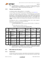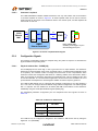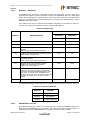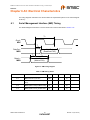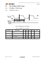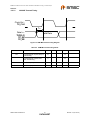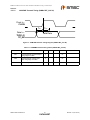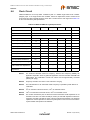
1
LAN8710/LAN8710i MII/RMII 10/100 Ethernet Transceiver with HP Auto-MDIX and flexPWR® Technology in a Small Footprint PRODUCT FEATURES Datasheet Highlights Single-Chip Ethernet Physical Layer Transceiver (PHY) Comprehensive flexPWR® Technology — — — — Key Benefits — — — — — — — — Flexible Power Management Architecture Power savings of up to 40% compared to competition LVCMOS Variable I/O voltage range: +1.6V to +3.6V Integrated 1.2V regulator with disable feature HP Auto-MDIX support Small footprint 32 pin QFN lead-free RoHS compliant package (5 x 5 x 0.9mm height) Set-Top Boxes Networked Printers and Servers Test Instrumentation LAN on Motherboard Embedded Telecom Applications Video Record/Playback Systems Cable Modems/Routers DSL Modems/Routers Digital Video Recorders IP and Video Phones Wireless Access Points Digital Televisions Digital Media Adaptors/Servers Gaming Consoles POE Applications Compliant with IEEE802.3/802.3u (Fast Ethernet) Compliant with ISO 802-3/IEEE 802.3 (10BASE-T) Loop-back modes Auto-negotiation Automatic polarity detection and correction Link status change wake-up detection Vendor specific register functions Supports both MII and the reduced pin count RMII interfaces Power and I/Os — — — — Various low power modes Integrated power-on reset circuit Two status LED outputs Latch-Up Performance Exceeds 150mA per EIA/JESD 78, Class II — May be used with a single 3.3V supply Target Applications High-Performance 10/100 Ethernet Transceiver Packaging — 32-pin QFN (5x5 mm) Lead-Free RoHS Compliant package with MII and RMII Environmental — Extended Commercial Temperature Range (0°C to +85°C) — Industrial Temperature Range (-40°C to +85°C) version available (LAN8710i) SMSC LAN8710/LAN8710i Revision 1.0 (04-15-09) DATASHEET MII/RMII 10/100 Ethernet Transceiver with HP Auto-MDIX and flexPWR® Technology in a Small Footprint Datasheet ORDER NUMBER(S): LAN8710A-EZK FOR 32-PIN, QFN LEAD-FREE ROHS COMPLIANT PACKAGE (0 TO +85°C TEMP) LAN8710Ai-EZK FOR 32-PIN, QFN LEAD-FREE ROHS COMPLIANT PACKAGE (-40 TO +85°C TEMP) LAN8710A-EZK-TR FOR 32-PIN, QFN LEAD-FREE ROHS COMPLIANT PACKAGE (0 TO +85°C TEMP) LAN8710Ai-EZK-TR FOR 32-PIN, QFN LEAD-FREE ROHS COMPLIANT PACKAGE (-40 TO +85°C TEMP) Reel Size is 4000 80 ARKAY DRIVE, HAUPPAUGE, NY 11788 (631) 435-6000, FAX (631) 273-3123 Copyright © 2009 SMSC or its subsidiaries. All rights reserved. Circuit diagrams and other information relating to SMSC products are included as a means of illustrating typical applications. Consequently, complete information sufficient for construction purposes is not necessarily given. Although the information has been checked and is believed to be accurate, no responsibility is assumed for inaccuracies. SMSC reserves the right to make changes to specifications and product descriptions at any time without notice. Contact your local SMSC sales office to obtain the latest specifications before placing your product order. The provision of this information does not convey to the purchaser of the described semiconductor devices any licenses under any patent rights or other intellectual property rights of SMSC or others. All sales are expressly conditional on your agreement to the terms and conditions of the most recently dated version of SMSC's standard Terms of Sale Agreement dated before the date of your order (the "Terms of Sale Agreement"). The product may contain design defects or errors known as anomalies which may cause the product's functions to deviate from published specifications. Anomaly sheets are available upon request. SMSC products are not designed, intended, authorized or warranted for use in any life support or other application where product failure could cause or contribute to personal injury or severe property damage. Any and all such uses without prior written approval of an Officer of SMSC and further testing and/or modification will be fully at the risk of the customer. Copies of this document or other SMSC literature, as well as the Terms of Sale Agreement, may be obtained by visiting SMSC’s website at http://www.smsc.com. SMSC is a registered trademark of Standard Microsystems Corporation (“SMSC”). Product names and company names are the trademarks of their respective holders. SMSC DISCLAIMS AND EXCLUDES ANY AND ALL WARRANTIES, INCLUDING WITHOUT LIMITATION ANY AND ALL IMPLIED WARRANTIES OF MERCHANTABILITY, FITNESS FOR A PARTICULAR PURPOSE, TITLE, AND AGAINST INFRINGEMENT AND THE LIKE, AND ANY AND ALL WARRANTIES ARISING FROM ANY COURSE OF DEALING OR USAGE OF TRADE. IN NO EVENT SHALL SMSC BE LIABLE FOR ANY DIRECT, INCIDENTAL, INDIRECT, SPECIAL, PUNITIVE, OR CONSEQUENTIAL DAMAGES; OR FOR LOST DATA, PROFITS, SAVINGS OR REVENUES OF ANY KIND; REGARDLESS OF THE FORM OF ACTION, WHETHER BASED ON CONTRACT; TORT; NEGLIGENCE OF SMSC OR OTHERS; STRICT LIABILITY; BREACH OF WARRANTY; OR OTHERWISE; WHETHER OR NOT ANY REMEDY OF BUYER IS HELD TO HAVE FAILED OF ITS ESSENTIAL PURPOSE, AND WHETHER OR NOT SMSC HAS BEEN ADVISED OF THE POSSIBILITY OF SUCH DAMAGES. Revision 1.0 (04-15-09) 2 DATASHEET SMSC LAN8710/LAN8710i MII/RMII 10/100 Ethernet Transceiver with HP Auto-MDIX and flexPWR® Technology in a Small Footprint Datasheet Table of Contents Chapter 1 Introduction . . . . . . . . . . . . . . . . . . . . . . . . . . . . . . . . . . . . . . . . . . . . . . . . . . . . . . . 9 1.1 1.2 1.3 General Terms and Conventions . . . . . . . . . . . . . . . . . . . . . . . . . . . . . . . . . . . . . . . . . . . . . . . . . . . 9 General Description . . . . . . . . . . . . . . . . . . . . . . . . . . . . . . . . . . . . . . . . . . . . . . . . . . . . . . . . . . . . . 9 Architectural Overview . . . . . . . . . . . . . . . . . . . . . . . . . . . . . . . . . . . . . . . . . . . . . . . . . . . . . . . . . . 10 1.3.1 Configuration . . . . . . . . . . . . . . . . . . . . . . . . . . . . . . . . . . . . . . . . . . . . . . . . . . . . . . . . . . 10 Chapter 2 Pin Configuration . . . . . . . . . . . . . . . . . . . . . . . . . . . . . . . . . . . . . . . . . . . . . . . . . 12 2.1 Package Pin-out Diagram and Signal Table. . . . . . . . . . . . . . . . . . . . . . . . . . . . . . . . . . . . . . . . . . 12 Chapter 3 Pin Description . . . . . . . . . . . . . . . . . . . . . . . . . . . . . . . . . . . . . . . . . . . . . . . . . . . . 14 3.1 3.2 3.3 3.4 3.5 3.6 3.7 MAC Interface Signals . . . . . . . . . . . . . . . . . . . . . . . . . . . . . . . . . . . . . . . . . . . . . . . . . . . . . . . . . . LED Signals . . . . . . . . . . . . . . . . . . . . . . . . . . . . . . . . . . . . . . . . . . . . . . . . . . . . . . . . . . . . . . . . . . Management Signals . . . . . . . . . . . . . . . . . . . . . . . . . . . . . . . . . . . . . . . . . . . . . . . . . . . . . . . . . . . General Signals . . . . . . . . . . . . . . . . . . . . . . . . . . . . . . . . . . . . . . . . . . . . . . . . . . . . . . . . . . . . . . . 10/100 Line Interface Signals . . . . . . . . . . . . . . . . . . . . . . . . . . . . . . . . . . . . . . . . . . . . . . . . . . . . . Analog Reference . . . . . . . . . . . . . . . . . . . . . . . . . . . . . . . . . . . . . . . . . . . . . . . . . . . . . . . . . . . . . . Power Signals. . . . . . . . . . . . . . . . . . . . . . . . . . . . . . . . . . . . . . . . . . . . . . . . . . . . . . . . . . . . . . . . . 14 16 17 17 17 18 18 Chapter 4 Architecture Details . . . . . . . . . . . . . . . . . . . . . . . . . . . . . . . . . . . . . . . . . . . . . . . . 19 4.1 4.2 4.3 4.4 4.5 4.6 4.7 Top Level Functional Architecture . . . . . . . . . . . . . . . . . . . . . . . . . . . . . . . . . . . . . . . . . . . . . . . . . 100Base-TX Transmit. . . . . . . . . . . . . . . . . . . . . . . . . . . . . . . . . . . . . . . . . . . . . . . . . . . . . . . . . . . 4.2.1 100M Transmit Data Across the MII/RMII Interface. . . . . . . . . . . . . . . . . . . . . . . . . . . . . 4.2.2 4B/5B Encoding . . . . . . . . . . . . . . . . . . . . . . . . . . . . . . . . . . . . . . . . . . . . . . . . . . . . . . . . 4.2.3 Scrambling. . . . . . . . . . . . . . . . . . . . . . . . . . . . . . . . . . . . . . . . . . . . . . . . . . . . . . . . . . . . 4.2.4 NRZI and MLT3 Encoding . . . . . . . . . . . . . . . . . . . . . . . . . . . . . . . . . . . . . . . . . . . . . . . . 4.2.5 100M Transmit Driver . . . . . . . . . . . . . . . . . . . . . . . . . . . . . . . . . . . . . . . . . . . . . . . . . . . 4.2.6 100M Phase Lock Loop (PLL) . . . . . . . . . . . . . . . . . . . . . . . . . . . . . . . . . . . . . . . . . . . . . 100Base-TX Receive . . . . . . . . . . . . . . . . . . . . . . . . . . . . . . . . . . . . . . . . . . . . . . . . . . . . . . . . . . . 4.3.1 100M Receive Input. . . . . . . . . . . . . . . . . . . . . . . . . . . . . . . . . . . . . . . . . . . . . . . . . . . . . 4.3.2 Equalizer, Baseline Wander Correction and Clock and Data Recovery . . . . . . . . . . . . . 4.3.3 NRZI and MLT-3 Decoding . . . . . . . . . . . . . . . . . . . . . . . . . . . . . . . . . . . . . . . . . . . . . . . 4.3.4 Descrambling. . . . . . . . . . . . . . . . . . . . . . . . . . . . . . . . . . . . . . . . . . . . . . . . . . . . . . . . . . 4.3.5 Alignment. . . . . . . . . . . . . . . . . . . . . . . . . . . . . . . . . . . . . . . . . . . . . . . . . . . . . . . . . . . . . 4.3.6 5B/4B Decoding. . . . . . . . . . . . . . . . . . . . . . . . . . . . . . . . . . . . . . . . . . . . . . . . . . . . . . . . 4.3.7 Receive Data Valid Signal . . . . . . . . . . . . . . . . . . . . . . . . . . . . . . . . . . . . . . . . . . . . . . . . 4.3.8 Receiver Errors . . . . . . . . . . . . . . . . . . . . . . . . . . . . . . . . . . . . . . . . . . . . . . . . . . . . . . . . 4.3.9 100M Receive Data Across the MII/RMII Interface . . . . . . . . . . . . . . . . . . . . . . . . . . . . . 10Base-T Transmit . . . . . . . . . . . . . . . . . . . . . . . . . . . . . . . . . . . . . . . . . . . . . . . . . . . . . . . . . . . . . 4.4.1 10M Transmit Data Across the MII/RMII Interface. . . . . . . . . . . . . . . . . . . . . . . . . . . . . . 4.4.2 Manchester Encoding . . . . . . . . . . . . . . . . . . . . . . . . . . . . . . . . . . . . . . . . . . . . . . . . . . . 4.4.3 10M Transmit Drivers . . . . . . . . . . . . . . . . . . . . . . . . . . . . . . . . . . . . . . . . . . . . . . . . . . . 10Base-T Receive . . . . . . . . . . . . . . . . . . . . . . . . . . . . . . . . . . . . . . . . . . . . . . . . . . . . . . . . . . . . . 4.5.1 10M Receive Input and Squelch . . . . . . . . . . . . . . . . . . . . . . . . . . . . . . . . . . . . . . . . . . . 4.5.2 Manchester Decoding . . . . . . . . . . . . . . . . . . . . . . . . . . . . . . . . . . . . . . . . . . . . . . . . . . . 4.5.3 10M Receive Data Across the MII/RMII Interface . . . . . . . . . . . . . . . . . . . . . . . . . . . . . . 4.5.4 Jabber Detection . . . . . . . . . . . . . . . . . . . . . . . . . . . . . . . . . . . . . . . . . . . . . . . . . . . . . . . MAC Interface. . . . . . . . . . . . . . . . . . . . . . . . . . . . . . . . . . . . . . . . . . . . . . . . . . . . . . . . . . . . . . . . . 4.6.1 MII . . . . . . . . . . . . . . . . . . . . . . . . . . . . . . . . . . . . . . . . . . . . . . . . . . . . . . . . . . . . . . . . . . 4.6.2 RMII . . . . . . . . . . . . . . . . . . . . . . . . . . . . . . . . . . . . . . . . . . . . . . . . . . . . . . . . . . . . . . . . . 4.6.3 MII vs. RMII Configuration . . . . . . . . . . . . . . . . . . . . . . . . . . . . . . . . . . . . . . . . . . . . . . . . Auto-negotiation . . . . . . . . . . . . . . . . . . . . . . . . . . . . . . . . . . . . . . . . . . . . . . . . . . . . . . . . . . . . . . . SMSC LAN8710/LAN8710i 3 DATASHEET 19 19 19 20 21 21 21 22 22 22 22 23 23 23 23 23 24 24 24 24 25 25 25 25 25 26 26 26 26 26 27 28 Revision 1.0 (04-15-09) MII/RMII 10/100 Ethernet Transceiver with HP Auto-MDIX and flexPWR® Technology in a Small Footprint Datasheet 4.8 4.9 4.10 4.11 4.12 4.13 4.14 4.7.1 Parallel Detection . . . . . . . . . . . . . . . . . . . . . . . . . . . . . . . . . . . . . . . . . . . . . . . . . . . . . . 4.7.2 Re-starting Auto-negotiation . . . . . . . . . . . . . . . . . . . . . . . . . . . . . . . . . . . . . . . . . . . . . . 4.7.3 Disabling Auto-negotiation. . . . . . . . . . . . . . . . . . . . . . . . . . . . . . . . . . . . . . . . . . . . . . . . 4.7.4 Half vs. Full Duplex . . . . . . . . . . . . . . . . . . . . . . . . . . . . . . . . . . . . . . . . . . . . . . . . . . . . . HP Auto-MDIX Support. . . . . . . . . . . . . . . . . . . . . . . . . . . . . . . . . . . . . . . . . . . . . . . . . . . . . . . . . . Internal +1.2V Regulator Disable . . . . . . . . . . . . . . . . . . . . . . . . . . . . . . . . . . . . . . . . . . . . . . . . . . 4.9.1 Disable the Internal +1.2V Regulator. . . . . . . . . . . . . . . . . . . . . . . . . . . . . . . . . . . . . . . . 4.9.2 Enable the Internal +1.2V Regulator . . . . . . . . . . . . . . . . . . . . . . . . . . . . . . . . . . . . . . . . nINTSEL Strapping and LED Polarity Selection . . . . . . . . . . . . . . . . . . . . . . . . . . . . . . . . . . . . . . . REGOFF and LED Polarity Selection . . . . . . . . . . . . . . . . . . . . . . . . . . . . . . . . . . . . . . . . . . . . . . . PHY Address Strapping . . . . . . . . . . . . . . . . . . . . . . . . . . . . . . . . . . . . . . . . . . . . . . . . . . . . . . . . . Variable Voltage I/O . . . . . . . . . . . . . . . . . . . . . . . . . . . . . . . . . . . . . . . . . . . . . . . . . . . . . . . . . . . . Transceiver Management Control . . . . . . . . . . . . . . . . . . . . . . . . . . . . . . . . . . . . . . . . . . . . . . . . . 4.14.1 Serial Management Interface (SMI). . . . . . . . . . . . . . . . . . . . . . . . . . . . . . . . . . . . . . . . . 30 30 30 30 30 31 31 31 32 32 33 33 33 33 Chapter 5 SMI Register Mapping . . . . . . . . . . . . . . . . . . . . . . . . . . . . . . . . . . . . . . . . . . . . . 35 5.1 5.2 5.3 SMI Register Format. . . . . . . . . . . . . . . . . . . . . . . . . . . . . . . . . . . . . . . . . . . . . . . . . . . . . . . . . . . . Interrupt Management . . . . . . . . . . . . . . . . . . . . . . . . . . . . . . . . . . . . . . . . . . . . . . . . . . . . . . . . . . 5.2.1 Primary Interrupt System . . . . . . . . . . . . . . . . . . . . . . . . . . . . . . . . . . . . . . . . . . . . . . . . . 5.2.2 Alternate Interrupt System . . . . . . . . . . . . . . . . . . . . . . . . . . . . . . . . . . . . . . . . . . . . . . . . Miscellaneous Functions . . . . . . . . . . . . . . . . . . . . . . . . . . . . . . . . . . . . . . . . . . . . . . . . . . . . . . . . 5.3.1 Carrier Sense . . . . . . . . . . . . . . . . . . . . . . . . . . . . . . . . . . . . . . . . . . . . . . . . . . . . . . . . . 5.3.2 Collision Detect . . . . . . . . . . . . . . . . . . . . . . . . . . . . . . . . . . . . . . . . . . . . . . . . . . . . . . . . 5.3.3 Isolate Mode . . . . . . . . . . . . . . . . . . . . . . . . . . . . . . . . . . . . . . . . . . . . . . . . . . . . . . . . . . 5.3.4 Link Integrity Test . . . . . . . . . . . . . . . . . . . . . . . . . . . . . . . . . . . . . . . . . . . . . . . . . . . . . . 5.3.5 Power-Down modes . . . . . . . . . . . . . . . . . . . . . . . . . . . . . . . . . . . . . . . . . . . . . . . . . . . . 5.3.6 Reset . . . . . . . . . . . . . . . . . . . . . . . . . . . . . . . . . . . . . . . . . . . . . . . . . . . . . . . . . . . . . . . . 5.3.7 LED Description. . . . . . . . . . . . . . . . . . . . . . . . . . . . . . . . . . . . . . . . . . . . . . . . . . . . . . . . 5.3.8 Loopback Operation . . . . . . . . . . . . . . . . . . . . . . . . . . . . . . . . . . . . . . . . . . . . . . . . . . . . 5.3.9 Configuration Signals . . . . . . . . . . . . . . . . . . . . . . . . . . . . . . . . . . . . . . . . . . . . . . . . . . . 39 47 47 48 48 48 49 49 49 49 50 50 50 52 Chapter 6 AC Electrical Characteristics . . . . . . . . . . . . . . . . . . . . . . . . . . . . . . . . . . . . . . . . 55 6.1 6.2 6.3 6.4 6.5 6.6 Serial Management Interface (SMI) Timing . . . . . . . . . . . . . . . . . . . . . . . . . . . . . . . . . . . . . . . . . . MII 10/100Base-TX/RX Timings . . . . . . . . . . . . . . . . . . . . . . . . . . . . . . . . . . . . . . . . . . . . . . . . . . . 6.2.1 MII 100Base-T TX/RX Timings . . . . . . . . . . . . . . . . . . . . . . . . . . . . . . . . . . . . . . . . . . . . 6.2.2 MII 10Base-T TX/RX Timings . . . . . . . . . . . . . . . . . . . . . . . . . . . . . . . . . . . . . . . . . . . . . RMII 10/100Base-TX/RX Timings (50MHz REF_CLK IN) . . . . . . . . . . . . . . . . . . . . . . . . . . . . . . . 6.3.1 RMII 100Base-T TX/RX Timings (50MHz REF_CLK IN). . . . . . . . . . . . . . . . . . . . . . . . . 6.3.2 RMII 10Base-T TX/RX Timings (50MHz REF_CLK IN). . . . . . . . . . . . . . . . . . . . . . . . . . RMII CLKIN Requirements . . . . . . . . . . . . . . . . . . . . . . . . . . . . . . . . . . . . . . . . . . . . . . . . . . . . . . . Reset Timing. . . . . . . . . . . . . . . . . . . . . . . . . . . . . . . . . . . . . . . . . . . . . . . . . . . . . . . . . . . . . . . . . . Clock Circuit . . . . . . . . . . . . . . . . . . . . . . . . . . . . . . . . . . . . . . . . . . . . . . . . . . . . . . . . . . . . . . . . . . 55 56 56 58 60 60 62 64 64 65 Chapter 7 DC Electrical Characteristics . . . . . . . . . . . . . . . . . . . . . . . . . . . . . . . . . . . . . . . . 66 7.1 DC Characteristics . . . . . . . . . . . . . . . . . . . . . . . . . . . . . . . . . . . . . . . . . . . . . . . . . . . . . . . . . . . . . 7.1.1 Maximum Guaranteed Ratings . . . . . . . . . . . . . . . . . . . . . . . . . . . . . . . . . . . . . . . . . . . . 7.1.2 Operating Conditions . . . . . . . . . . . . . . . . . . . . . . . . . . . . . . . . . . . . . . . . . . . . . . . . . . . . 7.1.3 Power Consumption . . . . . . . . . . . . . . . . . . . . . . . . . . . . . . . . . . . . . . . . . . . . . . . . . . . . 7.1.4 DC Characteristics - Input and Output Buffers . . . . . . . . . . . . . . . . . . . . . . . . . . . . . . . . 66 66 67 68 69 Chapter 8 Application Notes . . . . . . . . . . . . . . . . . . . . . . . . . . . . . . . . . . . . . . . . . . . . . . . . . . 73 8.1 Application Diagram . . . . . . . . . . . . . . . . . . . . . . . . . . . . . . . . . . . . . . . . . . . . . . . . . . . . . . . . . . . . 73 8.1.1 MII Diagram . . . . . . . . . . . . . . . . . . . . . . . . . . . . . . . . . . . . . . . . . . . . . . . . . . . . . . . . . . . 73 8.1.2 Power Supply Diagram . . . . . . . . . . . . . . . . . . . . . . . . . . . . . . . . . . . . . . . . . . . . . . . . . . 74 Revision 1.0 (04-15-09) 4 DATASHEET SMSC LAN8710/LAN8710i MII/RMII 10/100 Ethernet Transceiver with HP Auto-MDIX and flexPWR® Technology in a Small Footprint Datasheet 8.2 8.1.3 Twisted-Pair Interface Diagram . . . . . . . . . . . . . . . . . . . . . . . . . . . . . . . . . . . . . . . . . . . . 74 Magnetics Selection . . . . . . . . . . . . . . . . . . . . . . . . . . . . . . . . . . . . . . . . . . . . . . . . . . . . . . . . . . . . 75 Chapter 9 Package Outline . . . . . . . . . . . . . . . . . . . . . . . . . . . . . . . . . . . . . . . . . . . . . . . . . . . 76 SMSC LAN8710/LAN8710i 5 DATASHEET Revision 1.0 (04-15-09) MII/RMII 10/100 Ethernet Transceiver with HP Auto-MDIX and flexPWR® Technology in a Small Footprint Datasheet List of Figures Figure 1.1 Figure 1.2 Figure 2.1 Figure 4.1 Figure 4.2 Figure 4.3 Figure 4.4 Figure 4.5 Figure 4.6 Figure 4.7 Figure 4.8 Figure 5.1 Figure 5.2 Figure 5.3 Figure 6.1 Figure 6.2 Figure 6.3 Figure 6.4 Figure 6.5 Figure 6.6 Figure 6.7 Figure 6.8 Figure 6.9 Figure 6.10 Figure 8.1 Figure 8.2 Figure 8.3 Figure 8.4 Figure 8.5 Figure 9.1 Figure 9.1 Figure 9.2 Figure 9.3 LAN8710/LAN8710i System Block Diagram . . . . . . . . . . . . . . . . . . . . . . . . . . . . . . . . . . . . . LAN8710/LAN8710i Architectural Overview . . . . . . . . . . . . . . . . . . . . . . . . . . . . . . . . . . . . . LAN8710/LAN8710i 32-QFN Pin Assignments (TOP VIEW). . . . . . . . . . . . . . . . . . . . . . . . . 100Base-TX Data Path . . . . . . . . . . . . . . . . . . . . . . . . . . . . . . . . . . . . . . . . . . . . . . . . . . . . . Receive Data Path . . . . . . . . . . . . . . . . . . . . . . . . . . . . . . . . . . . . . . . . . . . . . . . . . . . . . . . . . Relationship Between Received Data and Specific MII Signals . . . . . . . . . . . . . . . . . . . . . . Direct Cable Connection vs. Cross-over Cable Connection . . . . . . . . . . . . . . . . . . . . . . . . . nINTSEL Strapping on LED2 . . . . . . . . . . . . . . . . . . . . . . . . . . . . . . . . . . . . . . . . . . . . . . . . . REGOFF Configuration on LED1. . . . . . . . . . . . . . . . . . . . . . . . . . . . . . . . . . . . . . . . . . . . . . MDIO Timing and Frame Structure - READ Cycle. . . . . . . . . . . . . . . . . . . . . . . . . . . . . . . . . MDIO Timing and Frame Structure - WRITE Cycle . . . . . . . . . . . . . . . . . . . . . . . . . . . . . . . . Near-end Loopback Block Diagram . . . . . . . . . . . . . . . . . . . . . . . . . . . . . . . . . . . . . . . . . . . . Far Loopback Block Diagram. . . . . . . . . . . . . . . . . . . . . . . . . . . . . . . . . . . . . . . . . . . . . . . . . Connector Loopback Block Diagram . . . . . . . . . . . . . . . . . . . . . . . . . . . . . . . . . . . . . . . . . . . SMI Timing Diagram . . . . . . . . . . . . . . . . . . . . . . . . . . . . . . . . . . . . . . . . . . . . . . . . . . . . . . . 100M MII Receive Timing Diagram . . . . . . . . . . . . . . . . . . . . . . . . . . . . . . . . . . . . . . . . . . . . 100M MII Transmit Timing Diagram. . . . . . . . . . . . . . . . . . . . . . . . . . . . . . . . . . . . . . . . . . . . 10M MII Receive Timing Diagram . . . . . . . . . . . . . . . . . . . . . . . . . . . . . . . . . . . . . . . . . . . . . 10M MII Transmit Timing Diagrams . . . . . . . . . . . . . . . . . . . . . . . . . . . . . . . . . . . . . . . . . . . . 100M RMII Receive Timing Diagram (50MHz REF_CLK IN). . . . . . . . . . . . . . . . . . . . . . . . . 100M RMII Transmit Timing Diagram (50MHz REF_CLK IN) . . . . . . . . . . . . . . . . . . . . . . . . 10M RMII Receive Timing Diagram (50MHz REF_CLK IN). . . . . . . . . . . . . . . . . . . . . . . . . . 10M RMII Transmit Timing Diagram (50MHz REF_CLK IN) . . . . . . . . . . . . . . . . . . . . . . . . . Reset Timing Diagram . . . . . . . . . . . . . . . . . . . . . . . . . . . . . . . . . . . . . . . . . . . . . . . . . . . . . . Simplified Application Diagram . . . . . . . . . . . . . . . . . . . . . . . . . . . . . . . . . . . . . . . . . . . . . . . High-Level System Diagram for Power . . . . . . . . . . . . . . . . . . . . . . . . . . . . . . . . . . . . . . . . . High-Level System Diagram for Power . . . . . . . . . . . . . . . . . . . . . . . . . . . . . . . . . . . . . . . . . Copper Interface Diagram . . . . . . . . . . . . . . . . . . . . . . . . . . . . . . . . . . . . . . . . . . . . . . . . . . . Copper Interface Diagram . . . . . . . . . . . . . . . . . . . . . . . . . . . . . . . . . . . . . . . . . . . . . . . . . . . LAN8710/LAN8710i-EZK 32 Pin QFN Package Outline, 5 x 5 x 0.9 mm Body (Lead-Free) . QFN, 5x5 Taping Dimensions and Part Orientation. . . . . . . . . . . . . . . . . . . . . . . . . . . . . . . . Reel Dimensions for 12mm Carrier Tape. . . . . . . . . . . . . . . . . . . . . . . . . . . . . . . . . . . . . . . . Tape Length and Part Quantity . . . . . . . . . . . . . . . . . . . . . . . . . . . . . . . . . . . . . . . . . . . . . . . Revision 1.0 (04-15-09) 6 DATASHEET 10 11 12 19 22 24 31 32 33 34 34 51 51 52 55 56 57 58 59 60 61 62 63 64 73 74 74 74 74 76 77 78 79 SMSC LAN8710/LAN8710i MII/RMII 10/100 Ethernet Transceiver with HP Auto-MDIX and flexPWR® Technology in a Small Footprint Datasheet List of Tables Table 2.1 LAN8710/LAN8710i 32-PIN QFN Pinout . . . . . . . . . . . . . . . . . . . . . . . . . . . . . . . . . . . . . . . . . Table 3.1 Buffer Types . . . . . . . . . . . . . . . . . . . . . . . . . . . . . . . . . . . . . . . . . . . . . . . . . . . . . . . . . . . . . . Table 3.2 MII/RMII Signals 32-QFN . . . . . . . . . . . . . . . . . . . . . . . . . . . . . . . . . . . . . . . . . . . . . . . . . . . . Table 3.3 LED Signals 32-QFN . . . . . . . . . . . . . . . . . . . . . . . . . . . . . . . . . . . . . . . . . . . . . . . . . . . . . . . . Table 3.4 Management Signals 32-QFN . . . . . . . . . . . . . . . . . . . . . . . . . . . . . . . . . . . . . . . . . . . . . . . . Table 3.5 General Signals 32-QFN . . . . . . . . . . . . . . . . . . . . . . . . . . . . . . . . . . . . . . . . . . . . . . . . . . . . Table 3.6 10/100 Line Interface Signals 32-QFN . . . . . . . . . . . . . . . . . . . . . . . . . . . . . . . . . . . . . . . . . . Table 3.7 Analog References 32-QFN . . . . . . . . . . . . . . . . . . . . . . . . . . . . . . . . . . . . . . . . . . . . . . . . . . Table 3.8 Power Signals 32-QFN . . . . . . . . . . . . . . . . . . . . . . . . . . . . . . . . . . . . . . . . . . . . . . . . . . . . . . Table 4.1 4B/5B Code Table . . . . . . . . . . . . . . . . . . . . . . . . . . . . . . . . . . . . . . . . . . . . . . . . . . . . . . . . . . Table 4.2 MII/RMII Signal Mapping . . . . . . . . . . . . . . . . . . . . . . . . . . . . . . . . . . . . . . . . . . . . . . . . . . . . . Table 4.3 Configuration . . . . . . . . . . . . . . . . . . . . . . . . . . . . . . . . . . . . . . . . . . . . . . . . . . . . . . . . . . . . . Table 5.1 Control Register: Register 0 (Basic) . . . . . . . . . . . . . . . . . . . . . . . . . . . . . . . . . . . . . . . . . . . . Table 5.2 Status Register: Register 1 (Basic) . . . . . . . . . . . . . . . . . . . . . . . . . . . . . . . . . . . . . . . . . . . . . Table 5.3 PHY ID 1 Register: Register 2 (Extended) . . . . . . . . . . . . . . . . . . . . . . . . . . . . . . . . . . . . . . . Table 5.4 PHY ID 2 Register: Register 3 (Extended) . . . . . . . . . . . . . . . . . . . . . . . . . . . . . . . . . . . . . . . Table 5.5 Auto-Negotiation Advertisement: Register 4 (Extended) . . . . . . . . . . . . . . . . . . . . . . . . . . . . . Table 5.6 Auto-Negotiation Link Partner Base Page Ability Register: Register 5 (Extended) . . . . . . . . . Table 5.7 Auto-Negotiation Expansion Register: Register 6 (Extended). . . . . . . . . . . . . . . . . . . . . . . . . Table 5.8 Register 15 (Extended) . . . . . . . . . . . . . . . . . . . . . . . . . . . . . . . . . . . . . . . . . . . . . . . . . . . . . . Table 5.9 Silicon Revision Register 16: Vendor-Specific. . . . . . . . . . . . . . . . . . . . . . . . . . . . . . . . . . . . . Table 5.10 Mode Control/ Status Register 17: Vendor-Specific . . . . . . . . . . . . . . . . . . . . . . . . . . . . . . . . Table 5.11 Special Modes Register 18: Vendor-Specific . . . . . . . . . . . . . . . . . . . . . . . . . . . . . . . . . . . . . Table 5.12 Register 24: Vendor-Specific . . . . . . . . . . . . . . . . . . . . . . . . . . . . . . . . . . . . . . . . . . . . . . . . . . Table 5.13 Register 25: Vendor-Specific . . . . . . . . . . . . . . . . . . . . . . . . . . . . . . . . . . . . . . . . . . . . . . . . . . Table 5.14 Symbol Error Counter Register 26: Vendor-Specific . . . . . . . . . . . . . . . . . . . . . . . . . . . . . . . . Table 5.15 Special Control/Status Indications Register 27: Vendor-Specific . . . . . . . . . . . . . . . . . . . . . . Table 5.16 Special Internal Testability Control Register 28: Vendor-Specific . . . . . . . . . . . . . . . . . . . . . . Table 5.17 Interrupt Source Flags Register 29: Vendor-Specific . . . . . . . . . . . . . . . . . . . . . . . . . . . . . . . Table 5.18 Interrupt Mask Register 30: Vendor-Specific . . . . . . . . . . . . . . . . . . . . . . . . . . . . . . . . . . . . . . Table 5.19 PHY Special Control/Status Register 31: Vendor-Specific . . . . . . . . . . . . . . . . . . . . . . . . . . . Table 5.20 SMI Register Mapping . . . . . . . . . . . . . . . . . . . . . . . . . . . . . . . . . . . . . . . . . . . . . . . . . . . . . . . Table 5.21 Register 0 - Basic Control . . . . . . . . . . . . . . . . . . . . . . . . . . . . . . . . . . . . . . . . . . . . . . . . . . . . Table 5.22 Register 1 - Basic Status . . . . . . . . . . . . . . . . . . . . . . . . . . . . . . . . . . . . . . . . . . . . . . . . . . . . . Table 5.23 Register 2 - PHY Identifier 1 . . . . . . . . . . . . . . . . . . . . . . . . . . . . . . . . . . . . . . . . . . . . . . . . . . Table 5.24 Register 3 - PHY Identifier 2 . . . . . . . . . . . . . . . . . . . . . . . . . . . . . . . . . . . . . . . . . . . . . . . . . . Table 5.25 Register 4 - Auto Negotiation Advertisement. . . . . . . . . . . . . . . . . . . . . . . . . . . . . . . . . . . . . . Table 5.26 Register 5 - Auto Negotiation Link Partner Ability . . . . . . . . . . . . . . . . . . . . . . . . . . . . . . . . . . Table 5.27 Register 6 - Auto Negotiation Expansion. . . . . . . . . . . . . . . . . . . . . . . . . . . . . . . . . . . . . . . . . Table 5.28 Register 16 - Silicon Revision . . . . . . . . . . . . . . . . . . . . . . . . . . . . . . . . . . . . . . . . . . . . . . . . . Table 5.29 Register 17 - Mode Control/Status . . . . . . . . . . . . . . . . . . . . . . . . . . . . . . . . . . . . . . . . . . . . . Table 5.30 Register 18 - Special Modes . . . . . . . . . . . . . . . . . . . . . . . . . . . . . . . . . . . . . . . . . . . . . . . . . . Table 5.31 Register 26 - Symbol Error Counter . . . . . . . . . . . . . . . . . . . . . . . . . . . . . . . . . . . . . . . . . . . . Table 5.33 Register 28 - Special Internal Testability Controls. . . . . . . . . . . . . . . . . . . . . . . . . . . . . . . . . . Table 5.34 Register 29 - Interrupt Source Flags . . . . . . . . . . . . . . . . . . . . . . . . . . . . . . . . . . . . . . . . . . . . Table 5.32 Register 27 - Special Control/Status Indications . . . . . . . . . . . . . . . . . . . . . . . . . . . . . . . . . . . Table 5.35 Register 30 - Interrupt Mask . . . . . . . . . . . . . . . . . . . . . . . . . . . . . . . . . . . . . . . . . . . . . . . . . . Table 5.36 Register 31 - PHY Special Control/Status . . . . . . . . . . . . . . . . . . . . . . . . . . . . . . . . . . . . . . . . Table 5.37 Interrupt Management Table . . . . . . . . . . . . . . . . . . . . . . . . . . . . . . . . . . . . . . . . . . . . . . . . . . Table 5.38 Alternative Interrupt System Management Table . . . . . . . . . . . . . . . . . . . . . . . . . . . . . . . . . . Table 5.39 Pin Names for Address Bits. . . . . . . . . . . . . . . . . . . . . . . . . . . . . . . . . . . . . . . . . . . . . . . . . . . Table 5.40 MODE[2:0] Bus . . . . . . . . . . . . . . . . . . . . . . . . . . . . . . . . . . . . . . . . . . . . . . . . . . . . . . . . . . . . Table 5.41 Pin Names for Mode Bits . . . . . . . . . . . . . . . . . . . . . . . . . . . . . . . . . . . . . . . . . . . . . . . . . . . . . SMSC LAN8710/LAN8710i 7 DATASHEET 13 14 14 16 17 17 17 18 18 20 28 32 35 35 35 35 36 36 36 36 36 37 37 37 37 37 38 38 38 38 38 39 40 40 41 41 41 42 43 43 43 44 44 45 45 45 46 46 47 48 52 53 53 Revision 1.0 (04-15-09) MII/RMII 10/100 Ethernet Transceiver with HP Auto-MDIX and flexPWR® Technology in a Small Footprint Datasheet Table 6.1 SMI Timing Values. . . . . . . . . . . . . . . . . . . . . . . . . . . . . . . . . . . . . . . . . . . . . . . . . . . . . . . . . . Table 6.2 100M MII Receive Timing Values . . . . . . . . . . . . . . . . . . . . . . . . . . . . . . . . . . . . . . . . . . . . . . Table 6.3 100M MII Transmit Timing Values . . . . . . . . . . . . . . . . . . . . . . . . . . . . . . . . . . . . . . . . . . . . . . Table 6.4 10M MII Receive Timing Values . . . . . . . . . . . . . . . . . . . . . . . . . . . . . . . . . . . . . . . . . . . . . . . Table 6.5 10M MII Transmit Timing Values . . . . . . . . . . . . . . . . . . . . . . . . . . . . . . . . . . . . . . . . . . . . . . . Table 6.6 100M RMII Receive Timing Values (50MHz REF_CLK IN). . . . . . . . . . . . . . . . . . . . . . . . . . . Table 6.7 100M RMII Transmit Timing Values (50MHz REF_CLK IN) . . . . . . . . . . . . . . . . . . . . . . . . . . Table 6.8 10M RMII Receive Timing Values (50MHz REF_CLK IN). . . . . . . . . . . . . . . . . . . . . . . . . . . . Table 6.9 10M RMII Transmit Timing Values (50MHz REF_CLK IN) . . . . . . . . . . . . . . . . . . . . . . . . . . . Table 6.10 RMII CLKIN (REF_CLK) Timing Values . . . . . . . . . . . . . . . . . . . . . . . . . . . . . . . . . . . . . . . . . Table 6.11 Reset Timing Values . . . . . . . . . . . . . . . . . . . . . . . . . . . . . . . . . . . . . . . . . . . . . . . . . . . . . . . . Table 6.12 LAN8710/LAN8710i Crystal Specifications . . . . . . . . . . . . . . . . . . . . . . . . . . . . . . . . . . . . . . . Table 7.1 Maximum Conditions . . . . . . . . . . . . . . . . . . . . . . . . . . . . . . . . . . . . . . . . . . . . . . . . . . . . . . . . Table 7.2 ESD and LATCH-UP Performance . . . . . . . . . . . . . . . . . . . . . . . . . . . . . . . . . . . . . . . . . . . . . Table 7.3 Recommended Operating Conditions . . . . . . . . . . . . . . . . . . . . . . . . . . . . . . . . . . . . . . . . . . . Table 7.4 Power Consumption Device Only . . . . . . . . . . . . . . . . . . . . . . . . . . . . . . . . . . . . . . . . . . . . . . Table 7.5 MII Bus Interface Signals. . . . . . . . . . . . . . . . . . . . . . . . . . . . . . . . . . . . . . . . . . . . . . . . . . . . . Table 7.6 LAN Interface Signals . . . . . . . . . . . . . . . . . . . . . . . . . . . . . . . . . . . . . . . . . . . . . . . . . . . . . . . Table 7.7 LED Signals . . . . . . . . . . . . . . . . . . . . . . . . . . . . . . . . . . . . . . . . . . . . . . . . . . . . . . . . . . . . . . . Table 7.8 Configuration Inputs. . . . . . . . . . . . . . . . . . . . . . . . . . . . . . . . . . . . . . . . . . . . . . . . . . . . . . . . . Table 7.9 General Signals . . . . . . . . . . . . . . . . . . . . . . . . . . . . . . . . . . . . . . . . . . . . . . . . . . . . . . . . . . . . Table 7.10 Internal Pull-Up / Pull-Down Configurations . . . . . . . . . . . . . . . . . . . . . . . . . . . . . . . . . . . . . . Table 7.11 100Base-TX Transceiver Characteristics . . . . . . . . . . . . . . . . . . . . . . . . . . . . . . . . . . . . . . . . Table 7.12 10BASE-T Transceiver Characteristics . . . . . . . . . . . . . . . . . . . . . . . . . . . . . . . . . . . . . . . . . . Table 9.1 32 Terminal QFN Package Parameters. . . . . . . . . . . . . . . . . . . . . . . . . . . . . . . . . . . . . . . . . . Revision 1.0 (04-15-09) 8 DATASHEET 55 56 57 58 59 60 61 62 63 64 64 65 66 66 67 68 69 70 70 70 70 71 71 72 76 SMSC LAN8710/LAN8710i MII/RMII 10/100 Ethernet Transceiver with HP Auto-MDIX and flexPWR® Technology in a Small Footprint Datasheet Chapter 1 Introduction 1.1 General Terms and Conventions The following is list of the general terms used in this document: BYTE 8-bits FIFO First In First Out buffer; often used for elasticity buffer MAC Media Access Controller MII Media Independent Interface RMIITM Reduced Media Independent InterfaceTM N/A Not Applicable X Indicates that a logic state is “don’t care” or undefined. RESERVED Refers to a reserved bit field or address. Unless otherwise noted, reserved bits must always be zero for write operations. Unless otherwise noted, values are not guaranteed when reading reserved bits. Unless otherwise noted, do not read or write to reserved addresses. SMI Serial Management Interface 1.2 General Description The LAN8710/LAN8710i is a low-power 10BASE-T/100BASE-TX physical layer (PHY) transceiver that transmits and receives on unshielded twisted-pair cable. A typical system application is shown in Figure 1.2. It is available in both extended commercial and industrial temperature operating versions. The LAN8710/LAN8710i interfaces to the MAC layer using a variable voltage digital interface via the standard MII (IEEE 802.3u). Support for RMII makes a reduced pin-count interface available. The digital interface pins are tolerant to 3.6V. The LAN8710/LAN8710i implements Auto-Negotiation to automatically determine the best possible speed and duplex mode of operation. HP Auto-MDIX support allows using a direct connect LAN cable, or a cross-over path cable. The LAN8710 referenced throughout this document applies to both the extended commercial temperature and industrial temperature components. The LAN8710i refers to only the industrial temperature component. SMSC LAN8710/LAN8710i 9 DATASHEET Revision 1.0 (04-15-09) MII/RMII 10/100 Ethernet Transceiver with HP Auto-MDIX and flexPWR® Technology in a Small Footprint Datasheet 10/100 Ethernet MAC MDI Transformer RJ45 LAN8710 MII or RMII Ethernet Transceiver MODE LED Status Crystal or Clock Osc Figure 1.1 LAN8710/LAN8710i System Block Diagram 1.3 Architectural Overview The LAN8710/LAN8710i is compliant with IEEE 802.3-2005 standards (MII Pins tolerant to 3.6V) and supports both IEEE 802.3-2005 compliant and vendor-specific register functions. It contains a fullduplex 10-BASE-T/100BASE-TX transceiver and supports 10-Mbps (10BASE-T) operation, and 100Mbps (100BASE-TX) operation. The LAN8710/LAN8710i can be configured to operate on a single 3.3V supply utilizing an integrated 3.3V to 1.2V linear regulator. An option is available to disable the linear regulator to optimize system designs that have a 1.2V power supply available. This allows for the use of a high efficiency external regulator for lower system power dissipation. 1.3.1 Configuration The LAN8710 will begin normal operation following reset, and no register access is required. The initial configuration may be selected with configuration pins as described in Section 5.3.9. In addition, register-selectable configuration options may be used to further define the functionality of the transceiver. For example, the device can be set to 10BASE-T only. The LAN8710 supports both IEEE 802.3-2005 compliant and vendor-specific register functions. Revision 1.0 (04-15-09) 10 DATASHEET SMSC LAN8710/LAN8710i MII/RMII 10/100 Ethernet Transceiver with HP Auto-MDIX and flexPWR® Technology in a Small Footprint Datasheet MODE0 MODE1 MODE2 nRST MODE Control AutoNegotiation 10M Tx Logic Reset Control SMI RMIISEL 10M Transmitter HP Auto-MDIX TXP / TXN Transmit Section 100M Tx Logic Management Control RXP / RXN 100M Transmitter MDIX Control TXD[0:3] TXEN TXER TXCLK CRS COL/CRS_DV RMII / MII Logic RXD[0:3] RXDV RXER RXCLK 100M Rx Logic MDC MDIO DSP System: Clock Data Recovery Equalizer Analog-toDigital XTAL1/CLKIN PLL XTAL2 Interrupt Generator nINT 100M PLL Receive Section LED Circuitry 10M Rx Logic Squelch & Filters 10M PLL LED1 LED2 Central Bias RBIAS PHY Address Latches PHYAD[0:2] Figure 1.2 LAN8710/LAN8710i Architectural Overview SMSC LAN8710/LAN8710i 11 DATASHEET Revision 1.0 (04-15-09) MII/RMII 10/100 Ethernet Transceiver with HP Auto-MDIX and flexPWR® Technology in a Small Footprint Datasheet Chapter 2 Pin Configuration RBIAS RXP RXN TXP TXN VDD1A RXDV TXD3 32 31 30 29 28 27 26 25 Package Pin-out Diagram and Signal Table VDD2A 1 24 TXD2 LED2/nINTSEL 2 23 TXD1 LED1/REGOFF 3 22 TXD0 21 TXEN 20 TXCLK 19 nRST 18 nINT/TXER/TXD4 17 MDC 14 15 16 CRS MDIO RXD2/RMIISEL COL/CRS_DV/MODE2 VSS 13 8 RXER/RXD4/PHYAD0 RXD3/PHYAD2 12 7 11 6 VDDIO VDDCR RXCLK/PHYAD1 RXD0/MDE0 5 10 4 RXD1/MODE1 XTAL2 XTAL1/CLKIN SMSC LAN8710/LAN8710i 32 PIN QFN (Top View) 9 2.1 Figure 2.1 LAN8710/LAN8710i 32-QFN Pin Assignments (TOP VIEW) Revision 1.0 (04-15-09) 12 DATASHEET SMSC LAN8710/LAN8710i MII/RMII 10/100 Ethernet Transceiver with HP Auto-MDIX and flexPWR® Technology in a Small Footprint Datasheet Table 2.1 LAN8710/LAN8710i 32-PIN QFN Pinout PIN NO. PIN NAME PIN NO. PIN NAME 1 VDD2A 17 MDC 2 LED2/nINTSEL 18 nINT/TXER/TXD4 3 LED1/REGOFF 19 nRST 4 XTAL2 20 TXCLK 5 XTAL1/CLKIN 21 TXEN 6 VDDCR 22 TXD0 7 RXCLK//PHYAD1 23 TXD1 8 RXD3/PHYAD2 24 TXD2 9 RXD2/RMIISEL 25 TXD3 10 RXD1/MODE1 26 RXDV 11 RXD0/MODE0 27 VDD1A 12 VDDIO 28 TXN 13 RXER/RXD4/PHYAD0 29 TXP 14 CRS 30 RXN 15 COL/CRS_DV/MODE2 31 RXP 16 MDIO 32 RBIAS SMSC LAN8710/LAN8710i 13 DATASHEET Revision 1.0 (04-15-09) MII/RMII 10/100 Ethernet Transceiver with HP Auto-MDIX and flexPWR® Technology in a Small Footprint Datasheet Chapter 3 Pin Description This chapter describes the signals on each pin. When a lower case “n” is used at the beginning of the signal name, it indicates that the signal is active low. For example, nRST indicates that the reset signal is active low. The buffer type for each signal is indicated in the TYPE column, and a description of the buffer types is provided in Table 3.1. Table 3.1 Buffer Types BUFFER TYPE DESCRIPTION I8 Input. O8 Output with 8mA sink and 8mA source. IOD8 Input/Open-drain output with 8mA sink. IPU Note 3.1 Input with 67k (typical) internal pull-up. IPD Note 3.1 Input with 67k (typical) internal pull-down. IOPU Note 3.1 Input/Output with 67k (typical) internal pull-up. Output has 8mA sink and 8mA source. IOPD Note 3.1 Input/Output with 67k (typical) internal pull-down. Output has 8mA sink and 8mA source. AI Analog input AIO Analog bi-directional ICLK Crystal oscillator input pin OCLK Crystal oscillator output pin P Power pin Note 3.1 Unless otherwise noted in the pin description, internal pull-up and pull-down resistors are always enabled. The internal pull-up and pull-down resistors prevent unconnected inputs from floating, and must not be relied upon to drive signals external to LAN8710/LAN8710i. When connected to a load that must be pulled high or low, an external resistor must be added. Note: The digital signals are not 5V tolerant.They are variable voltage from +1.6V to +3.6V, as shown in Table 7.1. 3.1 MAC Interface Signals Table 3.2 MII/RMII Signals 32-QFN SIGNAL NAME 32-QFN PIN # TYPE TXD0 22 I8 Transmit Data 0: The MAC transmits data to the transceiver using this signal in all modes. TXD1 23 I8 Transmit Data 1: The MAC transmits data to the transceiver using this signal in all modes Revision 1.0 (04-15-09) DESCRIPTION 14 DATASHEET SMSC LAN8710/LAN8710i MII/RMII 10/100 Ethernet Transceiver with HP Auto-MDIX and flexPWR® Technology in a Small Footprint Datasheet Table 3.2 MII/RMII Signals (continued) 32-QFN (continued) SIGNAL NAME 32-QFN PIN # TYPE TXD2 24 I8 Transmit Data 2: The MAC transmits data to the transceiver using this signal in MII Mode. This signal should be grounded in RMII Mode. TXD3 25 I8 Transmit Data 3: The MAC transmits data to the transceiver using this signal in MII Mode. This signal should be grounded in RMII Mode. nINT/ TXER/ TXD4 18 IOPU DESCRIPTION nINT – Active low interrupt output. Place an external resistor pull-up to VDDIO. See Section 4.10 for information on how nINTSEL is used to determine the function for this pin. TXER – MII Transmit Error: When driven high, the 4B/5B encode process substitutes the Transmit Error code-group (/H/) for the encoded data word. This input is ignored in 10Base-T operation. TXD4 – MII Transmit Data 4: In Symbol Interface (5B Decoding) mode, this signal becomes the MII Transmit Data 4 line, the MSB of the 5-bit symbol code-group. TXD4 is not used in RMII Mode. This signal is mux’d with nINT TXEN 21 IPD Transmit Enable: Indicates that valid data is presented on the TXD[3:0] signals, for transmission. In RMII Mode, only TXD[1:0] have valid data. TXCLK 20 O8 Transmit Clock: Used to latch data from the MAC into the transceiver. MII (100BT): 25MHz MII (10BT): 2.5MHz This signal is not used in RMII Mode. RXD0/ MODE0 11 IOPU RXD0 – Receive Data 0: Bit 0 of the 4 data bits that are sent by the transceiver in the receive path. MODE0 – PHY Operating Mode Bit 0: set the default MODE of the PHY. See Section 5.3.9.2 for information on the MODE options. RXD1/ MODE1 10 IOPU RXD1 – Receive Data 1: Bit 1 of the 4 data bits that are sent by the PHY in the receive path. MODE1 – PHY Operating Mode Bit 1: set the default MODE of the PHY. See Section 5.3.9.2 for information on the MODE options. RXD2/ RMIISEL 9 IOPD RXD2 – Receive Data 2: Bit 2 of the 4 data bits that are sent by the transceiver in the receive path. The RXD2 signal is not used in RMII Mode. RMIISEL – MII/RMII Mode Selection: Latched on the rising edge of the internal reset (nRESET) based on the following strapping: By default, MII mode is selected. Pull this pin high to VDDIO with an external resistor to select RMII mode, RXD3/ PHYAD2 8 IOPD RXD3 – Receive Data 3: Bit 3 of the 4 data bits that are sent by the transceiver in the receive path. This signal is not used in RMII Mode. This signal is mux’d with PHYAD2 PHYAD2 – PHY Address Bit 2: set the SMI address of the transceiver. See Section 5.3.9.1 for information on the ADDRESS options. SMSC LAN8710/LAN8710i 15 DATASHEET Revision 1.0 (04-15-09) MII/RMII 10/100 Ethernet Transceiver with HP Auto-MDIX and flexPWR® Technology in a Small Footprint Datasheet Table 3.2 MII/RMII Signals (continued) 32-QFN (continued) SIGNAL NAME 32-QFN PIN # TYPE DESCRIPTION RXER/ RXD4/ PHYAD0 13 IOPD RXER – Receive Error: Asserted to indicate that an error was detected somewhere in the frame presently being transferred from the transceiver. The RXER signal is optional in RMII Mode. RXD4 – MII Receive Data 4: In Symbol Interface (5B Decoding) mode, this signal is the MII Receive Data 4 signal, the MSB of the received 5-bit symbol code-group. Unless configured in this mode, the pin functions as RXER. This signal is mux’d with PHYAD0 PHYAD0 – PHY Address Bit 0: set the SMI address of the PHY. See Section 5.3.9.1 for information on the ADDRESS options. RXCLK/ PHYAD1 7 IOPD RXCLK – Receive Clock: In MII mode, this pin is the receive clock output. 25MHz in 100Base-TX mode. 2.5MHz in 10Base-T mode. This signal is mux’d with PHYAD1 PHYAD1 – PHY Address Bit 1: set the SMI address of the transceiver. See Section 5.3.9.1 for information on the ADDRESS options. RXDV 26 O8 Receive Data Valid: Indicates that recovered and decoded data is being presented on RXD pins. COL/ CRS_DV/ MODE2 15 IOPU COL – MII Mode Collision Detect: Asserted to indicate detection of collision condition. CRS_DV – RMII Mode CRS_DV (Carrier Sense/Receive Data Valid) Asserted to indicate when the receive medium is non-idle. When a 10BT packet is received, CRS_DV is asserted, but RXD[1:0] is held low until the SFD byte (10101011) is received. In 10BT, half-duplex mode, transmitted data is not looped back onto the receive data pins, per the RMII standard. MODE2 – PHY Operating Mode Bit 2: set the default MODE of the PHY. See Section 5.3.9.2 for information on the MODE options. CRS 3.2 14 IOPD Carrier Sense: Indicates detection of carrier. LED Signals Table 3.3 LED Signals 32-QFN SIGNAL NAME 32-QFN PIN # TYPE LED1/ REGOFF 3 IOPD DESCRIPTION LED1 – Link activity LED Indication. See Section 5.3.7 for a description of LED modes. REGOFF – Regulator Off: This pin may be used to configure the internal 1.2V regulator off. As described in Section 4.9, this pin is sampled during the power-on sequence to determine if the internal regulator should turn on. When the regulator is disabled, external 1.2V must be supplied to VDDCR. When LED1/REGOFF is pulled high to VDD2A with an external resistor, the internal regulator is disabled. When LED1/REGOFF is floating or pulled low, the internal regulator is enabled (default). Revision 1.0 (04-15-09) 16 DATASHEET SMSC LAN8710/LAN8710i MII/RMII 10/100 Ethernet Transceiver with HP Auto-MDIX and flexPWR® Technology in a Small Footprint Datasheet Table 3.3 LED Signals 32-QFN (continued) SIGNAL NAME 32-QFN PIN # TYPE LED2/ nINTSEL 2 IOPU DESCRIPTION LED2 – Link Speed LED Indication. See Section 5.3.7 for a description of LED modes. nINTSEL: On power-up or external reset, the mode of the nINT/TXER/TXD4 pin is selected. When LED2/nINTSEL is floated or pulled to VDDIO, nINT is selected for operation on pin nINT/TXER/TXD4 (default). When LED2/nINTSEL is pulled low to VSS through a resistor, TXER/TXD4 is selected for operation on pin nINT/TXER/TXD4. See Section 4.10 for additional information. 3.3 Management Signals Table 3.4 Management Signals 32-QFN SIGNAL NAME 32-QFN PIN # TYPE MDIO 16 IOD8 MDC 17 I8 3.4 DESCRIPTION Management Data Input/OUTPUT: Serial management data input/output. Management Clock: Serial management clock. General Signals Table 3.5 General Signals 32-QFN SIGNAL NAME 32-QFN PIN # TYPE XTAL1/ CLKIN 5 ICLK Clock Input: Crystal connection or external clock input. XTAL2 4 OCLK Clock Output: Crystal connection. Float this pin when an external clock is driven to XTAL1/CLKIN. nRST 19 IOPU External Reset: Input of the system reset. This signal is active LOW. 3.5 DESCRIPTION 10/100 Line Interface Signals Table 3.6 10/100 Line Interface Signals 32-QFN SIGNAL NAME 32-QFN PIN # TYPE TXP 29 AIO SMSC LAN8710/LAN8710i DESCRIPTION Transmit/Receive Positive Channel 1. 17 DATASHEET Revision 1.0 (04-15-09) MII/RMII 10/100 Ethernet Transceiver with HP Auto-MDIX and flexPWR® Technology in a Small Footprint Datasheet Table 3.6 10/100 Line Interface Signals (continued) 32-QFN (continued) SIGNAL NAME 32-QFN PIN # TYPE TXN 28 AIO Transmit/Receive Negative Channel 1. RXP 31 AIO Transmit/Receive Positive Channel 2. RXN 30 AIO Transmit/Receive Negative Channel 2. 3.6 DESCRIPTION Analog Reference Table 3.7 Analog References 32-QFN SIGNAL NAME 32-QFN PIN # TYPE DESCRIPTION RBIAS 32 AI External 1% Bias Resistor. Requires a 12.1k ohm (1%) resistor to ground connected as described in the Analog Layout Guidelines. The nominal voltage is 1.2V and the resistor will dissipate approximately 1mW of power. 3.7 Power Signals Table 3.8 Power Signals 32-QFN SIGNAL NAME 32-QFN PIN # TYPE VDDIO 12 P +1.6V to +3.6V Variable I/O Pad Power VDDCR 6 P +1.2V (Core voltage) - 1.2V for digital circuitry on chip. Supplied by the onchip regulator unless configured for regulator off mode using the LED1/REGOFF pin. A 1uF decoupling capacitor to ground should be used on this pin when using the internal 1.2V regulator. VDD1A 27 P +3.3V Analog Port Power to Channel 1. VDD2A 1 P +3.3V Analog Port Power to Channel 2 and to internal regulator. VSS FLAG GND Revision 1.0 (04-15-09) DESCRIPTION The flag must be connected to the ground plane with a via array under the exposed flag. This is the ground connection for the IC. 18 DATASHEET SMSC LAN8710/LAN8710i MII/RMII 10/100 Ethernet Transceiver with HP Auto-MDIX and flexPWR® Technology in a Small Footprint Datasheet Chapter 4 Architecture Details 4.1 Top Level Functional Architecture Functionally, the transceiver can be divided into the following sections: 100Base-TX transmit and receive 10Base-T transmit and receive MII or RMII interface to the controller Auto-negotiation to automatically determine the best speed and duplex possible Management Control to read status registers and write control registers TX _C LK (for M II only) MAC P LL E xt R ef_C LK (for R M II only) M II 25 M hz by 4 bits or R M II 50M hz by 2 bits 125 M bps S erial M II/R M II 25M H z by 4 bits 4B /5B E ncoder N R ZI C onverter N R ZI M LT -3 C onverter M LT -3 M LT-3 M agnetics M LT -3 25M H z by 5 bits R J45 S cram bler and P IS O Tx D river M LT-3 C A T-5 Figure 4.1 100Base-TX Data Path 4.2 100Base-TX Transmit The data path of the 100Base-TX is shown in Figure 4.1. Each major block is explained below. 4.2.1 100M Transmit Data Across the MII/RMII Interface For MII, the MAC controller drives the transmit data onto the TXD bus and asserts TXEN to indicate valid data. The data is latched by the transceiver’s MII block on the rising edge of TXCLK. The data is in the form of 4-bit wide 25MHz data. For RMII, the MAC controller drives the transmit data onto the TXD bus and asserts TXEN to indicate valid data. The data is latched by the transceiver’s RMII block on the rising edge of REF_CLK. The data is in the form of 2-bit wide 50MHz data. SMSC LAN8710/LAN8710i 19 DATASHEET Revision 1.0 (04-15-09) MII/RMII 10/100 Ethernet Transceiver with HP Auto-MDIX and flexPWR® Technology in a Small Footprint Datasheet 4.2.2 4B/5B Encoding The transmit data passes from the MII block to the 4B/5B encoder. This block encodes the data from 4-bit nibbles to 5-bit symbols (known as “code-groups”) according to Table 4.1. Each 4-bit data-nibble is mapped to 16 of the 32 possible code-groups. The remaining 16 code-groups are either used for control information or are not valid. The first 16 code-groups are referred to by the hexadecimal values of their corresponding data nibbles, 0 through F. The remaining code-groups are given letter designations with slashes on either side. For example, an IDLE code-group is /I/, a transmit error code-group is /H/, etc. The encoding process may be bypassed by clearing bit 6 of register 31. When the encoding is bypassed the 5th transmit data bit is equivalent to TXER. Note that encoding can be bypassed only when the MAC interface is configured to operate in MII mode. Table 4.1 4B/5B Code Table CODE GROUP SYM RECEIVER INTERPRETATION 11110 0 0 0000 01001 1 1 10100 2 10101 TRANSMITTER INTERPRETATION 0 0000 0001 1 0001 2 0010 2 0010 3 3 0011 3 0011 01010 4 4 0100 4 0100 01011 5 5 0101 5 0101 01110 6 6 0110 6 0110 01111 7 7 0111 7 0111 10010 8 8 1000 8 1000 10011 9 9 1001 9 1001 10110 A A 1010 A 1010 10111 B B 1011 B 1011 11010 C C 1100 C 1100 11011 D D 1101 D 1101 11100 E E 1110 E 1110 11101 F F 1111 F 1111 11111 I IDLE Sent after /T/R until TXEN 11000 J First nibble of SSD, translated to “0101” following IDLE, else RXER Sent for rising TXEN 10001 K Second nibble of SSD, translated to “0101” following J, else RXER Sent for rising TXEN 01101 T First nibble of ESD, causes de-assertion of CRS if followed by /R/, else assertion of RXER Sent for falling TXEN Revision 1.0 (04-15-09) DATA 20 DATASHEET DATA SMSC LAN8710/LAN8710i MII/RMII 10/100 Ethernet Transceiver with HP Auto-MDIX and flexPWR® Technology in a Small Footprint Datasheet Table 4.1 4B/5B Code Table (continued) CODE GROUP SYM 00111 R Second nibble of ESD, causes deassertion of CRS if following /T/, else assertion of RXER Sent for falling TXEN 00100 H Transmit Error Symbol Sent for rising TXER 00110 V INVALID, RXER if during RXDV INVALID 11001 V INVALID, RXER if during RXDV INVALID 00000 V INVALID, RXER if during RXDV INVALID 00001 V INVALID, RXER if during RXDV INVALID 00010 V INVALID, RXER if during RXDV INVALID 00011 V INVALID, RXER if during RXDV INVALID 00101 V INVALID, RXER if during RXDV INVALID 01000 V INVALID, RXER if during RXDV INVALID 01100 V INVALID, RXER if during RXDV INVALID 10000 V INVALID, RXER if during RXDV INVALID 4.2.3 RECEIVER INTERPRETATION TRANSMITTER INTERPRETATION Scrambling Repeated data patterns (especially the IDLE code-group) can have power spectral densities with large narrow-band peaks. Scrambling the data helps eliminate these peaks and spread the signal power more uniformly over the entire channel bandwidth. This uniform spectral density is required by FCC regulations to prevent excessive EMI from being radiated by the physical wiring. The seed for the scrambler is generated from the transceiver address, PHYAD[4:0], ensuring that in multiple-transceiver applications, such as repeaters or switches, each transceiver will have its own scrambler sequence. The scrambler also performs the Parallel In Serial Out conversion (PISO) of the data. 4.2.4 NRZI and MLT3 Encoding The scrambler block passes the 5-bit wide parallel data to the NRZI converter where it becomes a serial 125MHz NRZI data stream. The NRZI is encoded to MLT-3. MLT3 is a tri-level code where a change in the logic level represents a code bit “1” and the logic output remaining at the same level represents a code bit “0”. 4.2.5 100M Transmit Driver The MLT3 data is then passed to the analog transmitter, which drives the differential MLT-3 signal, on outputs TXP and TXN, to the twisted pair media across a 1:1 ratio isolation transformer. The 10BaseT and 100Base-TX signals pass through the same transformer so that common “magnetics” can be used for both. The transmitter drives into the 100Ω impedance of the CAT-5 cable. Cable termination and impedance matching require external components. SMSC LAN8710/LAN8710i 21 DATASHEET Revision 1.0 (04-15-09) MII/RMII 10/100 Ethernet Transceiver with HP Auto-MDIX and flexPWR® Technology in a Small Footprint Datasheet 4.2.6 100M Phase Lock Loop (PLL) The 100M PLL locks onto reference clock and generates the 125MHz clock used to drive the 125 MHz logic and the 100Base-Tx Transmitter. TX _C LK (for M II only) MAC P LL E xt R ef_C LK (for R M II only) M II 25 M hz by 4 bits or R M II 50M hz by 2 bits 125 M bps S erial M II/R M II 25M H z by 4 bits 4B /5B E ncoder N R ZI C onverter N R ZI M LT -3 C onverter M LT -3 M LT-3 M agnetics M LT -3 R J45 25M H z by 5 bits S cram bler and P IS O Tx D river M LT-3 C A T-5 Figure 4.2 Receive Data Path 4.3 100Base-TX Receive The receive data path is shown in Figure 4.2. Detailed descriptions are given below. 4.3.1 100M Receive Input The MLT-3 from the cable is fed into the transceiver (on inputs RXP and RXN) via a 1:1 ratio transformer. The ADC samples the incoming differential signal at a rate of 125M samples per second. Using a 64-level quanitizer it generates 6 digital bits to represent each sample. The DSP adjusts the gain of the ADC according to the observed signal levels such that the full dynamic range of the ADC can be used. 4.3.2 Equalizer, Baseline Wander Correction and Clock and Data Recovery The 6 bits from the ADC are fed into the DSP block. The equalizer in the DSP section compensates for phase and amplitude distortion caused by the physical channel consisting of magnetics, connectors, and CAT- 5 cable. The equalizer can restore the signal for any good-quality CAT-5 cable between 1m and 150m. If the DC content of the signal is such that the low-frequency components fall below the low frequency pole of the isolation transformer, then the droop characteristics of the transformer will become significant and Baseline Wander (BLW) on the received signal will result. To prevent corruption of the received data, the transceiver corrects for BLW and can receive the ANSI X3.263-1995 FDDI TP-PMD defined “killer packet” with no bit errors. The 100M PLL generates multiple phases of the 125MHz clock. A multiplexer, controlled by the timing unit of the DSP, selects the optimum phase for sampling the data. This is used as the received recovered clock. This clock is used to extract the serial data from the received signal. Revision 1.0 (04-15-09) 22 DATASHEET SMSC LAN8710/LAN8710i MII/RMII 10/100 Ethernet Transceiver with HP Auto-MDIX and flexPWR® Technology in a Small Footprint Datasheet 4.3.3 NRZI and MLT-3 Decoding The DSP generates the MLT-3 recovered levels that are fed to the MLT-3 converter. The MLT-3 is then converted to an NRZI data stream. 4.3.4 Descrambling The descrambler performs an inverse function to the scrambler in the transmitter and also performs the Serial In Parallel Out (SIPO) conversion of the data. During reception of IDLE (/I/) symbols. the descrambler synchronizes its descrambler key to the incoming stream. Once synchronization is achieved, the descrambler locks on this key and is able to descramble incoming data. Special logic in the descrambler ensures synchronization with the remote transceiver by searching for IDLE symbols within a window of 4000 bytes (40us). This window ensures that a maximum packet size of 1514 bytes, allowed by the IEEE 802.3 standard, can be received with no interference. If no IDLEsymbols are detected within this time-period, receive operation is aborted and the descrambler re-starts the synchronization process. The descrambler can be bypassed by setting bit 0 of register 31. 4.3.5 Alignment The de-scrambled signal is then aligned into 5-bit code-groups by recognizing the /J/K/ Start-of-Stream Delimiter (SSD) pair at the start of a packet. Once the code-word alignment is determined, it is stored and utilized until the next start of frame. 4.3.6 5B/4B Decoding The 5-bit code-groups are translated into 4-bit data nibbles according to the 4B/5B table. The translated data is presented on the RXD[3:0] signal lines. The SSD, /J/K/, is translated to “0101 0101” as the first 2 nibbles of the MAC preamble. Reception of the SSD causes the transceiver to assert the RXDV signal, indicating that valid data is available on the RXD bus. Successive valid code-groups are translated to data nibbles. Reception of either the End of Stream Delimiter (ESD) consisting of the /T/R/ symbols, or at least two /I/ symbols causes the transceiver to de-assert carrier sense and RXDV. These symbols are not translated into data. The decoding process may be bypassed by clearing bit 6 of register 31. When the decoding is bypassed the 5th receive data bit is driven out on RXER/RXD4/PHYAD0. Decoding may be bypassed only when the MAC interface is in MII mode. 4.3.7 Receive Data Valid Signal The Receive Data Valid signal (RXDV) indicates that recovered and decoded nibbles are being presented on the RXD[3:0] outputs synchronous to RXCLK. RXDV becomes active after the /J/K/ delimiter has been recognized and RXD is aligned to nibble boundaries. It remains active until either the /T/R/ delimiter is recognized or link test indicates failure or SIGDET becomes false. RXDV is asserted when the first nibble of translated /J/K/ is ready for transfer over the Media Independent Interface (MII mode). SMSC LAN8710/LAN8710i 23 DATASHEET Revision 1.0 (04-15-09) MII/RMII 10/100 Ethernet Transceiver with HP Auto-MDIX and flexPWR® Technology in a Small Footprint Datasheet CLEAR-TEXT J K 5 5 5 D data data data data T R 5 5 5 5 5 D data data data data Idle RX_CLK RX_DV RXD Figure 4.3 Relationship Between Received Data and Specific MII Signals 4.3.8 Receiver Errors During a frame, unexpected code-groups are considered receive errors. Expected code groups are the DATA set (0 through F), and the /T/R/ (ESD) symbol pair. When a receive error occurs, the RXER signal is asserted and arbitrary data is driven onto the RXD[3:0] lines. Should an error be detected during the time that the /J/K/ delimiter is being decoded (bad SSD error), RXER is asserted true and the value ‘1110’ is driven onto the RXD[3:0] lines. Note that the Valid Data signal is not yet asserted when the bad SSD error occurs. 4.3.9 100M Receive Data Across the MII/RMII Interface In MII mode, the 4-bit data nibbles are sent to the MII block. These data nibbles are clocked to the controller at a rate of 25MHz. The controller samples the data on the rising edge of RXCLK. To ensure that the setup and hold requirements are met, the nibbles are clocked out of the transceiver on the falling edge of RXCLK. RXCLK is the 25MHz output clock for the MII bus. It is recovered from the received data to clock the RXD bus. If there is no received signal, it is derived from the system reference clock (XTAL1/CLKIN). When tracking the received data, RXCLK has a maximum jitter of 0.8ns (provided that the jitter of the input clock, XTAL1/CLKIN, is below 100ps). In RMII mode, the 2-bit data nibbles are sent to the RMII block. These data nibbles are clocked to the controller at a rate of 50MHz. The controller samples the data on the rising edge of XTAL1/CLKIN (REF_CLK). To ensure that the setup and hold requirements are met, the nibbles are clocked out of the transceiver on the falling edge of XTAL1/CLKIN (REF_CLK). 4.4 10Base-T Transmit Data to be transmitted comes from the MAC layer controller. The 10Base-T transmitter receives 4-bit nibbles from the MII at a rate of 2.5MHz and converts them to a 10Mbps serial data stream. The data stream is then Manchester-encoded and sent to the analog transmitter, which drives a signal onto the twisted pair via the external magnetics. The 10M transmitter uses the following blocks: 4.4.1 MII (digital) TX 10M (digital) 10M Transmitter (analog) 10M PLL (analog) 10M Transmit Data Across the MII/RMII Interface The MAC controller drives the transmit data onto the TXD BUS. For MII, when the controller has driven TXEN high to indicate valid data, the data is latched by the MII block on the rising edge of TXCLK. The data is in the form of 4-bit wide 2.5MHz data. Revision 1.0 (04-15-09) 24 DATASHEET SMSC LAN8710/LAN8710i MII/RMII 10/100 Ethernet Transceiver with HP Auto-MDIX and flexPWR® Technology in a Small Footprint Datasheet In order to comply with legacy 10Base-T MAC/Controllers, in Half-duplex mode the transceiver loops back the transmitted data, on the receive path. This does not confuse the MAC/Controller since the COL signal is not asserted during this time. The transceiver also supports the SQE (Heartbeat) signal. See Section 5.3.2, "Collision Detect," on page 49, for more details. For RMII, TXD[1:0] shall transition synchronously with respect to REF_CLK. When TXEN is asserted, TXD[1:0] are accepted for transmission by the LAN8710/LAN8710i. TXD[1:0] shall be “00” to indicate idle when TXEN is deasserted. Values of TXD[1:0] other than “00” when TXEN is deasserted are reserved for out-of-band signalling (to be defined). Values other than “00” on TXD[1:0] while TXEN is deasserted shall be ignored by the LAN8710/LAN8710i.TXD[1:0] shall provide valid data for each REF_CLK period while TXEN is asserted. 4.4.2 Manchester Encoding The 4-bit wide data is sent to the TX10M block. The nibbles are converted to a 10Mbps serial NRZI data stream. The 10M PLL locks onto the external clock or internal oscillator and produces a 20MHz clock. This is used to Manchester encode the NRZ data stream. When no data is being transmitted (TXEN is low), the TX10M block outputs Normal Link Pulses (NLPs) to maintain communications with the remote link partner. 4.4.3 10M Transmit Drivers The Manchester encoded data is sent to the analog transmitter where it is shaped and filtered before being driven out as a differential signal across the TXP and TXN outputs. 4.5 10Base-T Receive The 10Base-T receiver gets the Manchester- encoded analog signal from the cable via the magnetics. It recovers the receive clock from the signal and uses this clock to recover the NRZI data stream. This 10M serial data is converted to 4-bit data nibbles which are passed to the controller across the MII at a rate of 2.5MHz. This 10M receiver uses the following blocks: 4.5.1 Filter and SQUELCH (analog) 10M PLL (analog) RX 10M (digital) MII (digital) 10M Receive Input and Squelch The Manchester signal from the cable is fed into the transceiver (on inputs RXP and RXN) via 1:1 ratio magnetics. It is first filtered to reduce any out-of-band noise. It then passes through a SQUELCH circuit. The SQUELCH is a set of amplitude and timing comparators that normally reject differential voltage levels below 300mV and detect and recognize differential voltages above 585mV. 4.5.2 Manchester Decoding The output of the SQUELCH goes to the RX10M block where it is validated as Manchester encoded data. The polarity of the signal is also checked. If the polarity is reversed (local RXP is connected to RXN of the remote partner and vice versa), then this is identified and corrected. The reversed condition is indicated by the flag “XPOL“, bit 4 in register 27. The 10M PLL is locked onto the received Manchester signal and from this, generates the received 20MHz clock. Using this clock, the Manchester encoded data is extracted and converted to a 10MHz NRZI data stream. It is then converted from serial to 4-bit wide parallel data. The RX10M block also detects valid 10Base-T IDLE signals - Normal Link Pulses (NLPs) - to maintain the link. SMSC LAN8710/LAN8710i 25 DATASHEET Revision 1.0 (04-15-09) MII/RMII 10/100 Ethernet Transceiver with HP Auto-MDIX and flexPWR® Technology in a Small Footprint Datasheet 4.5.3 10M Receive Data Across the MII/RMII Interface For MII, the 4 bit data nibbles are sent to the MII block. In MII mode, these data nibbles are valid on the rising edge of the 2.5 MHz RXCLK. For RMII, the 2bit data nibbles are sent to the RMII block. In RMII mode, these data nibbles are valid on the rising edge of the RMII REF_CLK. 4.5.4 Jabber Detection Jabber is a condition in which a station transmits for a period of time longer than the maximum permissible packet length, usually due to a fault condition, that results in holding the TXEN input for a long period. Special logic is used to detect the jabber state and abort the transmission to the line, within 45ms. Once TXEN is deasserted, the logic resets the jabber condition. As shown in Table 5.22, bit 1.1 indicates that a jabber condition was detected. 4.6 MAC Interface The MII/RMII block is responsible for the communication with the controller. Special sets of hand-shake signals are used to indicate that valid received/transmitted data is present on the 4 bit receive/transmit bus. The device must be configured in MII or RMII mode. This is done by specific pin strapping configurations. See Section 4.6.3, "MII vs. RMII Configuration," on page 27 for information on pin strapping and how the pins are mapped differently. 4.6.1 MII The MII includes 16 interface signals: transmit data - TXD[3:0] transmit strobe - TXEN transmit clock - TXCLK transmit error - TXER/TXD4 receive data - RXD[3:0] receive strobe - RXDV receive clock - RXCLK receive error - RXER/RXD4/PHYAD0 collision indication - COL carrier sense - CRS In MII mode, on the transmit path, the transceiver drives the transmit clock, TXCLK, to the controller. The controller synchronizes the transmit data to the rising edge of TXCLK. The controller drives TXEN high to indicate valid transmit data. The controller drives TXER high when a transmit error is detected. On the receive path, the transceiver drives both the receive data, RXD[3:0], and the RXCLK signal. The controller clocks in the receive data on the rising edge of RXCLK when the transceiver drives RXDV high. The transceiver drives RXER high when a receive error is detected. 4.6.2 RMII The SMSC LAN8710 supports the low pin count Reduced Media Independent Interface (RMII) intended for use between Ethernet transceivers and Switch ASICs. Under IEEE 802.3, an MII Revision 1.0 (04-15-09) 26 DATASHEET SMSC LAN8710/LAN8710i MII/RMII 10/100 Ethernet Transceiver with HP Auto-MDIX and flexPWR® Technology in a Small Footprint Datasheet comprised of 16 pins for data and control is defined. In devices incorporating many MACs or transceiver interfaces such as switches, the number of pins can add significant cost as the port counts increase. The management interface (MDIO/MDC) is identical to MII. The RMII interface has the following characteristics: It is capable of supporting 10Mb/s and 100Mb/s data rates A single clock reference is used for both transmit and receive. It provides independent 2 bit wide (di-bit) transmit and receive data paths It uses LVCMOS signal levels, compatible with common digital CMOS ASIC processes The RMII includes 6 interface signals with one of the signals being optional: 4.6.2.1 transmit data - TXD[1:0] transmit strobe - TXEN receive data - RXD[1:0] receive error - RXER (Optional) carrier sense - CRS_DV Reference Clock - (RMII references usually define this signal as REF_CLK) CRS_DV - Carrier Sense/Receive Data Valid The CRS_DV is asserted by the LAN8710/LAN8710i when the receive medium is non-idle. CRS_DV is asserted asynchronously on detection of carrier due to the criteria relevant to the operating mode. That is, in 10BASE-T mode, when squelch is passed or in 100BASE-X mode when 2 non-contiguous zeroes in 10 bits are detected, carrier is said to be detected. Loss of carrier shall result in the deassertion of CRS_DV synchronous to the cycle of REF_CLK which presents the first di-bit of a nibble onto RXD[1:0] (i.e. CRS_DV is deasserted only on nibble boundaries). If the LAN8710/LAN8710i has additional bits to be presented on RXD[1:0] following the initial deassertion of CRS_DV, then the LAN8710/LAN8710i shall assert CRS_DV on cycles of REF_CLK which present the second di-bit of each nibble and de-assert CRS_DV on cycles of REF_CLK which present the first di-bit of a nibble. The result is: Starting on nibble boundaries CRS_DV toggles at 25 MHz in 100Mb/s mode and 2.5 MHz in 10Mb/s mode when CRS ends before RXDV (i.e. the FIFO still has bits to transfer when the carrier event ends.) Therefore, the MAC can accurately recover RXDV and CRS. During a false carrier event, CRS_DV shall remain asserted for the duration of carrier activity. The data on RXD[1:0] is considered valid once CRS_DV is asserted. However, since the assertion of CRS_DV is asynchronous relative to REF_CLK, the data on RXD[1:0] shall be “00” until proper receive signal decoding takes place. 4.6.3 MII vs. RMII Configuration The LAN8710/LAN8710i must be configured to support the MII or RMII bus for connectivity to the MAC. This configuration is done through the RXD2/RMIISEL pin. MII or RMII mode selection is configured based on the strapping of the RXD2/RMIISEL pin as described in Section 5.3.9.3. Most of the MII and RMII pins are multiplexed. Table 4.2, "MII/RMII Signal Mapping" describes the relationship of the related device pins to the MII and RMII mode signal names. SMSC LAN8710/LAN8710i 27 DATASHEET Revision 1.0 (04-15-09) MII/RMII 10/100 Ethernet Transceiver with HP Auto-MDIX and flexPWR® Technology in a Small Footprint Datasheet Table 4.2 MII/RMII Signal Mapping LAN8710 PIN NAME MII MODE RMII MODE TXD0 TXD0 TXD0 TXD1 TXD1 TXD1 TXEN TXEN TXEN RXER/ RXD4/PHYAD0 RXER RXER Note 4.2 COL/CRS_DV/MODE2 COL CRS_DV RXD0/MODE0 RXD0 RXD0 RXD1/MODE1 RXD1 RXD1 TXD2 TXD2 Note 4.1 TXD3 TXD3 Note 4.1 nINT/TXER/TXD4 TXER/ TXD4 CRS CRS RXDV RXDV RXD2/RMIISEL RXD2 RXD3/PHYAD2 RXD3 TXCLK TXCLK RXCLK/PHYAD1 RXCLK XTAL1/CLKIN XTAL1/CLKIN REF_CLK Note 4.1 In RMII mode, this pin needs to tied to VSS. Note 4.2 The RXER signal is optional on the RMII bus. This signal is required by the transceiver, but it is optional for the MAC. The MAC can choose to ignore or not use this signal. The RMII REF_CLK is a continuous clock that provides the timing reference for CRS_DV, RXD[1:0], TXEN, TXD[1:0] and RXER. The LAN8710 uses REF_CLK as the network clock such that no buffering is required on the transmit data path. However, on the receive data path, the receiver recovers the clock from the incoming data stream, and the LAN8710 uses elasticity buffering to accommodate for differences between the recovered clock and the local REF_CLK. 4.7 Auto-negotiation The purpose of the Auto-negotiation function is to automatically configure the transceiver to the optimum link parameters based on the capabilities of its link partner. Auto-negotiation is a mechanism for exchanging configuration information between two link-partners and automatically selecting the highest performance mode of operation supported by both sides. Auto-negotiation is fully defined in clause 28 of the IEEE 802.3 specification. Once auto-negotiation has completed, information about the resolved link can be passed back to the controller via the Serial Management Interface (SMI). The results of the negotiation process are reflected in the Speed Indication bits in register 31, as well as the Link Partner Ability Register (Register 5). Revision 1.0 (04-15-09) 28 DATASHEET SMSC LAN8710/LAN8710i MII/RMII 10/100 Ethernet Transceiver with HP Auto-MDIX and flexPWR® Technology in a Small Footprint Datasheet The auto-negotiation protocol is a purely physical layer activity and proceeds independently of the MAC controller. The advertised capabilities of the transceiver are stored in register 4 of the SMI registers. The default advertised by the transceiver is determined by user-defined on-chip signal options. The following blocks are activated during an Auto-negotiation session: Auto-negotiation (digital) 100M ADC (analog) 100M PLL (analog) 100M equalizer/BLW/clock recovery (DSP) 10M SQUELCH (analog) 10M PLL (analog) 10M Transmitter (analog) When enabled, auto-negotiation is started by the occurrence of one of the following events: Hardware reset Software reset Power-down reset Link status down Setting register 0, bit 9 high (auto-negotiation restart) On detection of one of these events, the transceiver begins auto-negotiation by transmitting bursts of Fast Link Pulses (FLP). These are bursts of link pulses from the 10M transmitter. They are shaped as Normal Link Pulses and can pass uncorrupted down CAT-3 or CAT-5 cable. A Fast Link Pulse Burst consists of up to 33 pulses. The 17 odd-numbered pulses, which are always present, frame the FLP burst. The 16 even-numbered pulses, which may be present or absent, contain the data word being transmitted. Presence of a data pulse represents a “1”, while absence represents a “0”. The data transmitted by an FLP burst is known as a “Link Code Word.” These are defined fully in IEEE 802.3 clause 28. In summary, the transceiver advertises 802.3 compliance in its selector field (the first 5 bits of the Link Code Word). It advertises its technology ability according to the bits set in register 4 of the SMI registers. There are 4 possible matches of the technology abilities. In the order of priority these are: 100M Full Duplex (Highest priority) 100M Half Duplex 10M Full Duplex 10M Half Duplex If the full capabilities of the transceiver are advertised (100M, Full Duplex), and if the link partner is capable of 10M and 100M, then auto-negotiation selects 100M as the highest performance mode. If the link partner is capable of Half and Full duplex modes, then auto-negotiation selects Full Duplex as the highest performance operation. Once a capability match has been determined, the link code words are repeated with the acknowledge bit set. Any difference in the main content of the link code words at this time will cause auto-negotiation to re-start. Auto-negotiation will also re-start if not all of the required FLP bursts are received. The capabilities advertised during auto-negotiation by the transceiver are initially determined by the logic levels latched on the MODE[2:0] bus after reset completes. This bus can also be used to disable auto-negotiation on power-up. SMSC LAN8710/LAN8710i 29 DATASHEET Revision 1.0 (04-15-09) MII/RMII 10/100 Ethernet Transceiver with HP Auto-MDIX and flexPWR® Technology in a Small Footprint Datasheet Writing register 4 bits [8:5] allows software control of the capabilities advertised by the transceiver. Writing register 4 does not automatically re-start auto-negotiation. Register 0, bit 9 must be set before the new abilities will be advertised. Auto-negotiation can also be disabled via software by clearing register 0, bit 12. The LAN8710/LAN8710i does not support “Next Page” capability. 4.7.1 Parallel Detection If the LAN8710/LAN8710i is connected to a device lacking the ability to auto-negotiate (i.e. no FLPs are detected), it is able to determine the speed of the link based on either 100M MLT-3 symbols or 10M Normal Link Pulses. In this case the link is presumed to be Half Duplex per the IEEE standard. This ability is known as “Parallel Detection.” This feature ensures interoperability with legacy link partners. If a link is formed via parallel detection, then bit 0 in register 6 is cleared to indicate that the Link Partner is not capable of auto-negotiation. The controller has access to this information via the management interface. If a fault occurs during parallel detection, bit 4 of register 6 is set. Register 5 is used to store the Link Partner Ability information, which is coded in the received FLPs. If the Link Partner is not auto-negotiation capable, then register 5 is updated after completion of parallel detection to reflect the speed capability of the Link Partner. 4.7.2 Re-starting Auto-negotiation Auto-negotiation can be re-started at any time by setting register 0, bit 9. Auto-negotiation will also restart if the link is broken at any time. A broken link is caused by signal loss. This may occur because of a cable break, or because of an interruption in the signal transmitted by the Link Partner. Autonegotiation resumes in an attempt to determine the new link configuration. If the management entity re-starts Auto-negotiation by writing to bit 9 of the control register, the LAN8710/LAN8710i will respond by stopping all transmission/receiving operations. Once the break_link_timer is done, in the Auto-negotiation state-machine (approximately 1200ms) the autonegotiation will re-start. The Link Partner will have also dropped the link due to lack of a received signal, so it too will resume auto-negotiation. 4.7.3 Disabling Auto-negotiation Auto-negotiation can be disabled by setting register 0, bit 12 to zero. The device will then force its speed of operation to reflect the information in register 0, bit 13 (speed) and register 0, bit 8 (duplex). The speed and duplex bits in register 0 should be ignored when auto-negotiation is enabled. 4.7.4 Half vs. Full Duplex Half Duplex operation relies on the CSMA/CD (Carrier Sense Multiple Access / Collision Detect) protocol to handle network traffic and collisions. In this mode, the carrier sense signal, CRS, responds to both transmit and receive activity. In this mode, If data is received while the transceiver is transmitting, a collision results. In Full Duplex mode, the transceiver is able to transmit and receive data simultaneously. In this mode, CRS responds only to receive activity. The CSMA/CD protocol does not apply and collision detection is disabled. 4.8 HP Auto-MDIX Support HP Auto-MDIX facilitates the use of CAT-3 (10 Base-T) or CAT-5 (100 Base-T) media UTP interconnect cable without consideration of interface wiring scheme. If a user plugs in either a direct connect LAN cable, or a cross-over patch cable, as shown in Figure 4.4, the SMSC LAN8710/LAN8710i Auto-MDIX transceiver is capable of configuring the TXP/TXN and RXP/RXN pins for correct transceiver operation. Revision 1.0 (04-15-09) 30 DATASHEET SMSC LAN8710/LAN8710i MII/RMII 10/100 Ethernet Transceiver with HP Auto-MDIX and flexPWR® Technology in a Small Footprint Datasheet The internal logic of the device detects the TX and RX pins of the connecting device. Since the RX and TX line pairs are interchangeable, special PCB design considerations are needed to accommodate the symmetrical magnetics and termination of an Auto-MDIX design. The Auto-MDIX function can be disabled using the Special Control/Status Indications register (bit 27.15). Figure 4.4 Direct Cable Connection vs. Cross-over Cable Connection 4.9 Internal +1.2V Regulator Disable One feature of the flexPWR technology is the ability to configure the internal 1.2V regulator off. When the regulator is disabled, external 1.2V must be supplied to VDDCR. This makes it possible to reduce total system power, since an external switching regulator with greater efficiency than the internal linear regulator may be used to provide the +1.2V to the transceiver circuitry. 4.9.1 Disable the Internal +1.2V Regulator To disable the +1.2V internal regulator, a pullup strapping resistor is connected from LED1/REGOFF to VDD2A. At power-on, after both VDDIO and VDD2A are within specification, the transceiver will sample the LED1/REGOFF pin to determine if the internal regulator should turn on. If the pin is sampled at a voltage greater than VIH, then the internal regulator is disabled, and the system must supply +1.2V to the VDDCR pin. As described in Section 4.9.2, when the LED1/REGOFF pin is left floating or connected to VSS, then the internal regulator is enabled and the system is not required to supply +1.2V to the VDDCR pin. 4.9.2 Enable the Internal +1.2V Regulator The 1.2V for VDDCR is supplied by the on-chip regulator unless the transceiver is configured for regulator off mode using the LED1/REGOFF pin as described in Section 4.9.1. By default, the internal +1.2V regulator is enabled when the LED1/REGOFF pin is floating. As shown in Table 7.10, an internal pull-down resistor straps the regulator on if the LED1/REGOFF pin is floating. During VDDIO and VDDA power-on, if the LED1/REGOFF pin is sampled below VIL, then the internal +1.2V regulator will turn on and operate with power from the VDD2A pin. SMSC LAN8710/LAN8710i 31 DATASHEET Revision 1.0 (04-15-09) MII/RMII 10/100 Ethernet Transceiver with HP Auto-MDIX and flexPWR® Technology in a Small Footprint Datasheet 4.10 nINTSEL Strapping and LED Polarity Selection The nINT, TXER, and TXD4 functions share a common pin. There are two functional modes for this pin, the TXER/TXD4 mode and nINT (interrupt) mode. The nINTSEL pin is shared with the LED2 pin. The LED2 output will automatically change polarity based on the presence of an external pull-down resistor. If the LED pin is pulled high (by the internal pull-up resistor) to select a logical high for nINTSEL, then the LED output will be active low. If the LED pin is pulled low by an external pull-down resistor to select a logical low nINTSEL, the LED output will then be an active high output. To set nINTSEL without LEDs, float the pin to set nINTSEL high or pull-down the pin with an external resistor to GND to set nINTSEL low. See Figure 4.5. The LED2/nINTSEL pin is latched on the rising edge of the nRST. The default setting is to float the pin high for nINT mode. nINTSEL = 1 LED output = active low nINTSEL = 0 LED output = active high VDD2A LED2/nINTSEL 10K ~270 ohms ~270 ohms LED2/nINTSEL Figure 4.5 nINTSEL Strapping on LED2 4.11 REGOFF and LED Polarity Selection The REGOFF configuration pin is shared with the LED1 pin. The LED1 output will automatically change polarity based on the presence of an external pull-up resistor. If the LED pin is pulled high to VDD2A by an external pull-up resistor to select a logical high for REGOFF, then the LED output will be active low. If the LED pin is pulled low by the internal pull-down resistor to select a logical low for REGOFF, the LED output will then be an active high output. To set REGOFF without LEDs, pull-up the pin with an external resistor to VDDIO to disable the regulator. See Figure 4.6. Revision 1.0 (04-15-09) 32 DATASHEET SMSC LAN8710/LAN8710i MII/RMII 10/100 Ethernet Transceiver with HP Auto-MDIX and flexPWR® Technology in a Small Footprint Datasheet REGOFF = 0 LED output = active high REGOFF = 1 (Regulator OFF) LED output = active low VDD2A LED1/REGOFF 10K ~270 ohms ~270 ohms LED1/REGOFF Figure 4.6 REGOFF Configuration on LED1 4.12 PHY Address Strapping The PHY ADDRESS bits are latched into an internal register at the end of a hardware reset. The 3bit address word[2:0] is input on the PHYAD[2:0] pins. The default setting is 3'b000 as described in Section 5.3.9.1. 4.13 Variable Voltage I/O The Digital I/O pins on the LAN8710/LAN8710i are variable voltage to take advantage of low power savings from shrinking technologies. These pins can operate from a low I/O voltage of +1.8V-10% up to +3.3V+10%. The I/O voltage the System Designer applies on VDDIO needs to maintain its value with a tolerance of ± 10%. Varying the voltage up or down, after the transceiver has completed poweron reset can cause errors in the transceiver operation. 4.14 Transceiver Management Control The Management Control module includes 3 blocks: 4.14.1 Serial Management Interface (SMI) Management Registers Set Interrupt Serial Management Interface (SMI) The Serial Management Interface is used to control the LAN8710/LAN8710i and obtain its status. This interface supports registers 0 through 6 as required by Clause 22 of the 802.3 standard, as well as “vendor-specific” registers 16 to 31 allowed by the specification. Non-supported registers (7 to 15) will be read as hexadecimal “FFFF”. At the system level there are 2 signals, MDIO and MDC where MDIO is bi-directional open-drain and MDC is the clock. A special feature (enabled by register 17 bit 3) forces the transceiver to disregard the PHY-Address in the SMI packet causing the transceiver to respond to any address. This feature is useful in multi-PHY SMSC LAN8710/LAN8710i 33 DATASHEET Revision 1.0 (04-15-09) MII/RMII 10/100 Ethernet Transceiver with HP Auto-MDIX and flexPWR® Technology in a Small Footprint Datasheet applications and in production testing, where the same register can be written in all the transceivers using a single write transaction. The MDC signal is an aperiodic clock provided by the station management controller (SMC). The MDIO signal receives serial data (commands) from the controller SMC, and sends serial data (status) to the SMC. The minimum time between edges of the MDC is 160 ns. There is no maximum time between edges. The minimum cycle time (time between two consecutive rising or two consecutive falling edges) is 400 ns. These modest timing requirements allow this interface to be easily driven by the I/O port of a microcontroller. The data on the MDIO line is latched on the rising edge of the MDC. The frame structure and timing of the data is shown in Figure 4.7 and Figure 4.8. The timing relationships of the MDIO signals are further described in Section 6.1, "Serial Management Interface (SMI) Timing," on page 55. Read Cycle MDC MDI0 32 1's Preamble 0 1 Start of Frame 1 0 OP Code A4 A3 A2 A1 A0 R4 R3 R2 R1 R0 PHY Address Register Address D15 D14 Turn Around ... ... D1 D0 Data Data From Phy Data To Phy Figure 4.7 MDIO Timing and Frame Structure - READ Cycle Write Cycle MDC MDIO 32 1's Preamble 0 1 Start of Frame 0 1 OP Code A4 A3 A2 A1 A0 R4 R3 R2 R1 R0 PHY Address Register Address D15 Turn Around D14 ... ... D1 D0 Data Data To Phy Figure 4.8 MDIO Timing and Frame Structure - WRITE Cycle Revision 1.0 (04-15-09) 34 DATASHEET SMSC LAN8710/LAN8710i Table 5.1 Control Register: Register 0 (Basic) 15 14 13 12 11 10 9 8 7 6 Reset Loopback Speed Select A/N Enable Power Down Isolate Restart A/N Duplex Mode Collision Test 5 4 3 2 1 0 Reserved Table 5.2 Status Register: Register 1 (Basic) 14 13 12 11 100Base -T4 100Base -TX Full Duplex 100Base -TX Half Duplex 10BaseT Full Duplex 10BaseT Half Duplex 35 DATASHEET 15 10 9 8 7 6 Reserved 5 4 3 2 1 0 A/N Complete Remote Fault A/N Ability Link Status Jabber Detect Extended Capability 4 3 2 1 0 3 2 1 0 Table 5.3 PHY ID 1 Register: Register 2 (Extended) 15 14 13 12 11 10 9 8 7 6 5 PHY ID Number (Bits 3-18 of the Organizationally Unique Identifier - OUI) Table 5.4 PHY ID 2 Register: Register 3 (Extended) 15 14 13 12 11 10 SMSC LAN8710/LAN8710i PHY ID Number (Bits 19-24 of the Organizationally Unique Identifier - OUI) 9 8 7 6 Manufacturer Model Number 5 4 Manufacturer Revision Number MII/RMII 10/100 Ethernet Transceiver with HP Auto-MDIX and flexPWR® Technology in a Small Footprint Datasheet Revision 1.0 (04-15-09) Chapter 5 SMI Register Mapping 15 14 13 12 11 Next Page Reserved Remote Fault Reserved 10 Pause Operation 9 8 7 6 5 4 100BaseT4 100BaseTX Full Duplex 100BaseTX 10BaseT Full Duplex 10BaseT 3 2 1 0 IEEE 802.3 Selector Field Table 5.6 Auto-Negotiation Link Partner Base Page Ability Register: Register 5 (Extended) 14 13 12 Next Page Acknowledge Remote Fault 11 Reserved 10 9 8 7 6 5 4 Pause 100BaseT4 100Base-TX Full Duplex 100BaseTX 10Base-T Full Duplex 10BaseT 3 2 1 0 IEEE 802.3 Selector Field Table 5.7 Auto-Negotiation Expansion Register: Register 6 (Extended) 15 14 13 12 11 10 9 8 7 6 5 Reserved 4 3 2 1 0 Parallel Detect Fault Link Partner Next Page Able Next Page Able Page Received Link Partner A/N Able 36Revision 1.0 (04-15-09) DATASHEET 15 Table 5.8 Register 15 (Extended) 15 14 13 12 11 10 9 8 7 6 5 4 3 2 1 0 4 3 2 1 0 IEEE Reserved Table 5.9 Silicon Revision Register 16: Vendor-Specific 15 14 13 12 Reserved 11 10 9 8 7 Silicon Revision 6 5 Reserved SMSC LAN8710/LAN8710i Datasheet MII/RMII 10/100 Ethernet Transceiver with HP Auto-MDIX and flexPWR® Technology in a Small Footprint Table 5.5 Auto-Negotiation Advertisement: Register 4 (Extended) 1 5 14 RSVD 13 12 11 10 9 8 EDPWRDOWN RSVD LOWSQEN MDPREBP FARLOOPBACK 7 RSVD 6 5 ALTINT 4 RSVD 3 2 1 0 PHYADBP Force Good Link Status ENERGYON RSVD RSVD = Reserved Table 5.11 Special Modes Register 18: Vendor-Specific 15 14 13 Reserved MIIMODE 12 11 10 9 8 7 6 Reserved 5 4 3 2 MODE 1 0 PHYAD 37 DATASHEET Table 5.12 Register 24: Vendor-Specific 15 14 13 12 11 10 9 8 7 6 5 4 3 2 1 0 5 4 3 2 1 0 4 3 2 1 0 Reserved Table 5.13 Register 25: Vendor-Specific 15 14 13 12 11 10 9 8 7 6 Reserved SMSC LAN8710/LAN8710i Table 5.14 Symbol Error Counter Register 26: Vendor-Specific 15 14 13 12 11 10 9 8 7 Symbol Error Counter 6 5 MII/RMII 10/100 Ethernet Transceiver with HP Auto-MDIX and flexPWR® Technology in a Small Footprint Datasheet Revision 1.0 (04-15-09) Table 5.10 Mode Control/ Status Register 17: Vendor-Specific Datasheet 15 14 13 12 11 10 AMDIXCTRL Reserved CH_SELECT Reserved SQEOFF 9 8 7 6 5 4 Reserved 3 2 XPOL 1 0 Reserved Table 5.16 Special Internal Testability Control Register 28: Vendor-Specific 15 14 13 12 11 10 9 8 7 6 5 4 3 2 1 0 Table 5.17 Interrupt Source Flags Register 29: Vendor-Specific 15 14 13 12 11 10 9 8 Reserved 7 6 5 4 3 2 1 0 INT7 INT6 INT5 INT4 INT3 INT2 INT1 Reserved Table 5.18 Interrupt Mask Register 30: Vendor-Specific 15 14 13 12 11 10 9 8 7 6 5 Reserved 4 3 2 1 Mask Bits 38Revision 1.0 (04-15-09) DATASHEET Reserved 0 Reserved Table 5.19 PHY Special Control/Status Register 31: Vendor-Specific 15 14 Reserved 13 12 Autodone 11 10 Reserved 9 8 7 6 5 GPO2 GPO1 GPO0 Enable 4B5B Reserved 4 3 Speed Indication 2 1 0 Reserved Scramble Disable SMSC LAN8710/LAN8710i MII/RMII 10/100 Ethernet Transceiver with HP Auto-MDIX and flexPWR® Technology in a Small Footprint Table 5.15 Special Control/Status Indications Register 27: Vendor-Specific MII/RMII 10/100 Ethernet Transceiver with HP Auto-MDIX and flexPWR® Technology in a Small Footprint Datasheet The following registers are supported (register numbers are in decimal): Table 5.20 SMI Register Mapping REGISTER # 5.1 DESCRIPTION Group 0 Basic Control Register Basic 1 Basic Status Register Basic 2 PHY Identifier 1 Extended 3 PHY Identifier 2 Extended 4 Auto-Negotiation Advertisement Register Extended 5 Auto-Negotiation Link Partner Ability Register Extended 6 Auto-Negotiation Expansion Register Extended 16 Silicon Revision Register Vendor-specific 17 Mode Control/Status Register Vendor-specific 18 Special Modes Vendor-specific 20 Reserved Vendor-specific 21 Reserved Vendor-specific 22 Reserved Vendor-specific 23 Reserved Vendor-specific 26 Symbol Error Counter Register Vendor-specific 27 Control / Status Indication Register Vendor-specific 28 Special internal testability controls Vendor-specific 29 Interrupt Source Register Vendor-specific 30 Interrupt Mask Register Vendor-specific 31 PHY Special Control/Status Register Vendor-specific SMI Register Format The mode key is as follows: RW = Read/write, SC = Self clearing, WO = Write only, RO = Read only, LH = Latch high, clear on read of register, LL = Latch low, clear on read of register, NASR = Not Affected by Software Reset X = Either a 1 or 0. SMSC LAN8710/LAN8710i 39 DATASHEET Revision 1.0 (04-15-09) MII/RMII 10/100 Ethernet Transceiver with HP Auto-MDIX and flexPWR® Technology in a Small Footprint Datasheet Table 5.21 Register 0 - Basic Control ADDRESS NAME DESCRIPTION MODE DEFAULT 0.15 Reset 1 = software reset. Bit is self-clearing. For best results, when setting this bit do not set other bits in this register. The configuration (as described in Section 5.3.9.2) is set from the register bit values, and not from the mode pins. RW/ SC 0 0.14 Loopback 1 = loopback mode, 0 = normal operation RW 0 0.13 Speed Select 1 = 100Mbps, 0 = 10Mbps. Ignored if Auto Negotiation is enabled (0.12 = 1). RW Set by MODE[2:0] bus 0.12 AutoNegotiation Enable 1 = enable auto-negotiate process (overrides 0.13 and 0.8) 0 = disable auto-negotiate process RW Set by MODE[2:0] bus 0.11 Power Down 1 = General power down mode, 0 = normal operation RW 0 0.10 Isolate 1 = electrical isolation of transceiver from MII 0 = normal operation RW 0 0.9 Restart AutoNegotiate 1 = restart auto-negotiate process 0 = normal operation. Bit is self-clearing. RW/ SC 0 0.8 Duplex Mode 1 = Full duplex, 0 = Half duplex. Ignored if Auto Negotiation is enabled (0.12 = 1). RW Set by MODE[2:0] bus 0.7 Collision Test 1 = enable COL test, 0 = disable COL test RW 0 0.6:0 Reserved RO 0 MODE DEFAULT 1 = T4 able, 0 = no T4 ability RO 0 Table 5.22 Register 1 - Basic Status ADDRESS NAME 1.15 100Base-T4 1.14 100Base-TX Full Duplex 1 = TX with full duplex, 0 = no TX full duplex ability RO 1 1.13 100Base-TX Half Duplex 1 = TX with half duplex, 0 = no TX half duplex ability RO 1 1.12 10Base-T Full Duplex 1 = 10Mbps with full duplex 0 = no 10Mbps with full duplex ability RO 1 1.11 10Base-T Half Duplex 1 = 10Mbps with half duplex 0 = no 10Mbps with half duplex ability RO 1 1.10:6 Reserved 1.5 Auto-Negotiate Complete 1 = auto-negotiate process completed 0 = auto-negotiate process not completed RO 0 Revision 1.0 (04-15-09) DESCRIPTION 40 DATASHEET SMSC LAN8710/LAN8710i MII/RMII 10/100 Ethernet Transceiver with HP Auto-MDIX and flexPWR® Technology in a Small Footprint Datasheet Table 5.22 Register 1 - Basic Status (continued) ADDRESS NAME DESCRIPTION 1.4 Remote Fault 1.3 Auto-Negotiate Ability 1.2 Link Status 1.1 Jabber Detect 1.0 Extended Capabilities MODE DEFAULT 1 = remote fault condition detected 0 = no remote fault RO/ LH 0 1 = able to perform auto-negotiation function 0 = unable to perform auto-negotiation function RO 1 1 = link is up, 0 = link is down RO/ LL X 1 = jabber condition detected 0 = no jabber condition detected RO/ LH X 1 = supports extended capabilities registers 0 = does not support extended capabilities registers RO 1 Table 5.23 Register 2 - PHY Identifier 1 ADDRESS NAME DESCRIPTION MODE DEFAULT 2.15:0 PHY ID Number Assigned to the 3rd through 18th bits of the Organizationally Unique Identifier (OUI), respectively. OUI=00800Fh RW 0007h MODE DEFAULT Assigned to the 19th through 24th bits of the OUI. RW 30h Six-bit manufacturer’s model number. RW 0Fh Four-bit manufacturer’s revision number. RW DEVICE REV MODE DEFAULT RO 0 RO 0 1 = remote fault detected, 0 = no remote fault RW 0 00 = No PAUSE 01= Symmetric PAUSE 10= Asymmetric PAUSE toward link partner 11 = Both Symmetric PAUSE and Asymmetric PAUSE toward local device R/W 00 Table 5.24 Register 3 - PHY Identifier 2 ADDRESS NAME DESCRIPTION 3.15:10 PHY ID Number 3.9:4 Model Number 3.3:0 Revision Number Table 5.25 Register 4 - Auto Negotiation Advertisement ADDRESS NAME 4.15 Next Page 4.14 Reserved 4.13 Remote Fault 4.12 Reserved 4.11:10 Pause Operation SMSC LAN8710/LAN8710i DESCRIPTION 1 = next page capable, 0 = no next page ability This Phy does not support next page ability. 41 DATASHEET Revision 1.0 (04-15-09) MII/RMII 10/100 Ethernet Transceiver with HP Auto-MDIX and flexPWR® Technology in a Small Footprint Datasheet Table 5.25 Register 4 - Auto Negotiation Advertisement (continued) ADDRESS NAME 4.9 100Base-T4 4.8 100Base-TX Full Duplex 4.7 100Base-TX 4.6 10Base-T Full Duplex 4.5 4.4:0 DESCRIPTION MODE DEFAULT 1 = T4 able, 0 = no T4 ability This Phy does not support 100Base-T4. RO 0 1 = TX with full duplex, 0 = no TX full duplex ability RW Set by MODE[2:0] bus 1 = TX able, 0 = no TX ability RW 1 1 = 10Mbps with full duplex 0 = no 10Mbps with full duplex ability RW Set by MODE[2:0] bus 10Base-T 1 = 10Mbps able, 0 = no 10Mbps ability RW Set by MODE[2:0] bus Selector Field [00001] = IEEE 802.3 RW 00001 Table 5.26 Register 5 - Auto Negotiation Link Partner Ability ADDRESS NAME 5.15 Next Page 5.14 MODE DEFAULT 1 = “Next Page” capable, 0 = no “Next Page” ability This Phy does not support next page ability. RO 0 Acknowledge 1 = link code word received from partner 0 = link code word not yet received RO 0 5.13 Remote Fault 1 = remote fault detected, 0 = no remote fault RO 0 5.12:11 Reserved RO 0 5.10 Pause Operation 1 = Pause Operation is supported by remote MAC, 0 = Pause Operation is not supported by remote MAC RO 0 5.9 100Base-T4 1 = T4 able, 0 = no T4 ability. This Phy does not support T4 ability. RO 0 5.8 100Base-TX Full Duplex 1 = TX with full duplex, 0 = no TX full duplex ability RO 0 5.7 100Base-TX 1 = TX able, 0 = no TX ability RO 0 5.6 10Base-T Full Duplex 1 = 10Mbps with full duplex 0 = no 10Mbps with full duplex ability RO 0 5.5 10Base-T 1 = 10Mbps able, 0 = no 10Mbps ability RO 0 5.4:0 Selector Field [00001] = IEEE 802.3 RO 00001 Revision 1.0 (04-15-09) DESCRIPTION 42 DATASHEET SMSC LAN8710/LAN8710i MII/RMII 10/100 Ethernet Transceiver with HP Auto-MDIX and flexPWR® Technology in a Small Footprint Datasheet Table 5.27 Register 6 - Auto Negotiation Expansion ADDRESS NAME 6.15:5 Reserved 6.4 Parallel Detection Fault 6.3 DESCRIPTION MODE DEFAULT RO 0 1 = fault detected by parallel detection logic 0 = no fault detected by parallel detection logic RO/ LH 0 Link Partner Next Page Able 1 = link partner has next page ability 0 = link partner does not have next page ability RO 0 6.2 Next Page Able 1 = local device has next page ability 0 = local device does not have next page ability RO 0 6.1 Page Received 1 = new page received 0 = new page not yet received RO/ LH 0 6.0 Link Partner AutoNegotiation Able 1 = link partner has auto-negotiation ability 0 = link partner does not have auto-negotiation ability RO 0 MODE DEFAULT RO 0 RO 0001 RO 0 MODE DEFAULT Write as 0; ignore on read. RW 0 Enable the Energy Detect Power-Down mode: 0 = Energy Detect Power-Down is disabled 1 = Energy Detect Power-Down is enabled RW 0 Write as 0, ignore on read RW 0 Table 5.28 Register 16 - Silicon Revision ADDRESS NAME 16.15:10 Reserved 16.9:6 Silicon Revision 16.5:0 Reserved DESCRIPTION Four-bit silicon revision identifier. Table 5.29 Register 17 - Mode Control/Status ADDRESS NAME 17.15:14 Reserved 17.13 EDPWRDOWN 17.12 Reserved 17.11 LOWSQEN The Low_Squelch signal is equal to LOWSQEN AND EDPWRDOWN. Low_Squelch = 1 implies a lower threshold (more sensitive). Low_Squelch = 0 implies a higher threshold (less sensitive). RW 0 17.10 MDPREBP Management Data Preamble Bypass: 0 – detect SMI packets with Preamble 1 – detect SMI packets without preamble RW 0 17.9 FARLOOPBACK Force the module to the FAR Loop Back mode, i.e. all the received packets are sent back simultaneously (in 100Base-TX only). This bit is only active in RMII mode, as described in Section 5.3.8.2. This mode works even if MII Isolate (0.10) is set. RW 0 17.8:7 Reserved Write as 0, ignore on read. RW 00 SMSC LAN8710/LAN8710i DESCRIPTION 43 DATASHEET Revision 1.0 (04-15-09) MII/RMII 10/100 Ethernet Transceiver with HP Auto-MDIX and flexPWR® Technology in a Small Footprint Datasheet Table 5.29 Register 17 - Mode Control/Status (continued) ADDRESS NAME DESCRIPTION MODE DEFAULT 17.6 ALTINT Alternate Interrupt Mode. 0 = Primary interrupt system enabled (Default). 1 = Alternate interrupt system enabled. See Section 5.2, "Interrupt Management," on page 47. RW 0 17.5:4 Reserved Write as 0, ignore on read. RW 00 17.3 PHYADBP 1 = PHY disregards PHY address in SMI access write. RW 0 17.2 Force Good Link Status 0 = normal operation; 1 = force 100TX- link active; RW 0 ENERGYON – indicates whether energy is detected on the line (see Section 5.3.5.2, "Energy Detect Power-Down," on page 50); it goes to “0” if no valid energy is detected within 256ms. Reset to “1” by hardware reset, unaffected by SW reset. RO X Write as 0. Ignore on read. RW 0 MODE DEFAULT RW 0 Note: 17.1 ENERGYON 17.0 Reserved This bit should be set only during lab testing Table 5.30 Register 18 - Special Modes ADDRESS NAME DESCRIPTION 18.15 Reserved Write as 0, ignore on read. 18.14 MIIMODE MII Mode: set the mode of the digital interface, as described in Section 5.3.9.3: 0 – MII interface. 1 – RMII interface RW, NASR X 18.13:8 Reserved Write as 0, ignore on read. RW, NASR 000000 18.7:5 MODE Transceiver Mode of operation. Refer to Section 5.3.9.2, "Mode Bus – MODE[2:0]," on page 53 for more details. RW, NASR XXX 18.4:0 PHYAD PHY Address. The PHY Address is used for the SMI address and for the initialization of the Cipher (Scrambler) key. Refer to Section 5.3.9.1, "Physical Address Bus PHYAD[2:0]," on page 52 for more details. RW, NASR PHYAD Table 5.31 Register 26 - Symbol Error Counter ADDRESS NAME DESCRIPTION MODE DEFAULT 26.15:0 Sym_Err_Cnt 100Base-TX receiver-based error register that increments when an invalid code symbol is received including IDLE symbols. The counter is incremented only once per packet, even when the received packet contains more than one symbol error. The 16-bit register counts up to 65,536 (216) and rolls over to 0 if incremented beyond that value. This register is cleared on reset, but is not cleared by reading the register. It does not increment in 10Base-T mode. RO 0 Revision 1.0 (04-15-09) 44 DATASHEET SMSC LAN8710/LAN8710i MII/RMII 10/100 Ethernet Transceiver with HP Auto-MDIX and flexPWR® Technology in a Small Footprint Datasheet Table 5.32 Register 27 - Special Control/Status Indications ADDRESS NAME DESCRIPTION MODE DEFAULT 27.15 AMDIXCTRL HP Auto-MDIX control 0 - Auto-MDIX enable 1 - Auto-MDIX disabled (use 27.13 to control channel) RW 0 27.14 Reserved Reserved RW 0 27.13 CH_SELECT Manual Channel Select 0 - MDI -TX transmits RX receives 1 - MDIX -TX receives RX transmits RW 0 27.12 Reserved Write as 0. Ignore on read. RW 0 27:11 SQEOFF Disable the SQE (Signal Quality Error) test (Heartbeat): 0 - SQE test is enabled. 1 - SQE test is disabled. RW, NASR 0 27.10:5 Reserved Write as 0. Ignore on read. RW 000000 27.4 XPOL Polarity state of the 10Base-T: 0 - Normal polarity 1 - Reversed polarity RO 0 27.3:0 Reserved Reserved RO XXXXb MODE DEFAULT RW N/A MODE DEFAULT Ignore on read. RO/ LH 0 Table 5.33 Register 28 - Special Internal Testability Controls ADDRESS NAME 28.15:0 Reserved DESCRIPTION Do not write to this register. Ignore on read. Table 5.34 Register 29 - Interrupt Source Flags ADDRESS NAME 29.15:8 Reserved 29.7 INT7 1 = ENERGYON generated 0 = not source of interrupt RO/ LH X 29.6 INT6 1 = Auto-Negotiation complete 0 = not source of interrupt RO/ LH X 29.5 INT5 1 = Remote Fault Detected 0 = not source of interrupt RO/ LH X 29.4 INT4 1 = Link Down (link status negated) 0 = not source of interrupt RO/ LH X 29.3 INT3 1 = Auto-Negotiation LP Acknowledge 0 = not source of interrupt RO/ LH X 29.2 INT2 1 = Parallel Detection Fault 0 = not source of interrupt RO/ LH X SMSC LAN8710/LAN8710i DESCRIPTION 45 DATASHEET Revision 1.0 (04-15-09) MII/RMII 10/100 Ethernet Transceiver with HP Auto-MDIX and flexPWR® Technology in a Small Footprint Datasheet Table 5.34 Register 29 - Interrupt Source Flags (continued) ADDRESS NAME 29.1 INT1 29.0 Reserved DESCRIPTION MODE DEFAULT 1 = Auto-Negotiation Page Received 0 = not source of interrupt RO/ LH X Ignore on read. RO/ LH 0 MODE DEFAULT Table 5.35 Register 30 - Interrupt Mask ADDRESS NAME DESCRIPTION 30.15:8 Reserved Write as 0; ignore on read. RO 0 30.7:1 Mask Bits 1 = interrupt source is enabled 0 = interrupt source is masked RW 0 30.0 Reserved Write as 0; ignore on read RO 0 MODE DEFAULT Table 5.36 Register 31 - PHY Special Control/Status ADDRESS NAME DESCRIPTION 31.15:13 Reserved Write as 0, ignore on read. RW 0 31.12 Autodone Auto-negotiation done indication: 0 = Auto-negotiation is not done or disabled (or not active) 1 = Auto-negotiation is done RO 0 Note: This is a duplicate of register 1.5, however reads to register 31 do not clear status bits. 31.11:10 Reserved Write as 0, ignore on Read. RW XX 31.9:7 GPO[2:0] General Purpose Output connected to signals GPO[2:0] RW 0 31.6 Enable 4B5B 0 = Bypass encoder/decoder. 1 = enable 4B5B encoding/decoding. MAC Interface must be configured in MII mode. RW 1 31.5 Reserved Write as 0, ignore on Read. RW 0 31.4:2 Speed Indication HCDSPEED value: [001]=10Mbps Half-duplex [101]=10Mbps Full-duplex [010]=100Base-TX Half-duplex [110]=100Base-TX Full-duplex RO XXX 31.1 Reserved Write as 0; ignore on Read RW 0 31.0 Scramble Disable 0 = enable data scrambling 1 = disable data scrambling, RW 0 Revision 1.0 (04-15-09) 46 DATASHEET SMSC LAN8710/LAN8710i MII/RMII 10/100 Ethernet Transceiver with HP Auto-MDIX and flexPWR® Technology in a Small Footprint Datasheet 5.2 Interrupt Management The Management interface supports an interrupt capability that is not a part of the IEEE 802.3 specification. It generates an active low asynchronous interrupt signal on the nINT output whenever certain events are detected as setup by the Interrupt Mask Register 30. The Interrupt system on the SMSC The LAN8710 has two modes, a Primary Interrupt mode and an Alternative Interrupt mode. Both systems will assert the nINT pin low when the corresponding mask bit is set, the difference is how they de-assert the output interrupt signal nINT. The Primary interrupt mode is the default interrupt mode after a power-up or hard reset, the Alternative interrupt mode would need to be setup again after a power-up or hard reset. 5.2.1 Primary Interrupt System The Primary Interrupt system is the default interrupt mode, (Bit 17.6 = ‘0’). The Primary Interrupt System is always selected after power-up or hard reset. To set an interrupt, set the corresponding mask bit in the interrupt Mask register 30 (see Table 5.37). Then when the event to assert nINT is true, the nINT output will be asserted. When the corresponding Event to De-Assert nINT is true, then the nINT will be de-asserted. Table 5.37 Interrupt Management Table MASK INTERRUPT SOURCE FLAG INTERRUPT SOURCE EVENT TO ASSERT nINT EVENT TO DE-ASSERT nINT 30.7 29.7 ENERGYON 17.1 ENERGYON Rising 17.1 (Note 5.1) Falling 17.1 or Reading register 29 30.6 29.6 Auto-Negotiation complete 1.5 Auto-Negotiate Complete Rising 1.5 Falling 1.5 or Reading register 29 30.5 29.5 Remote Fault Detected 1.4 Remote Fault Rising 1.4 Falling 1.4, or Reading register 1 or Reading register 29 30.4 29.4 Link Down 1.2 Link Status Falling 1.2 Reading register 1 or Reading register 29 30.3 29.3 Auto-Negotiation LP Acknowledge 5.14 Acknowledge Rising 5.14 Falling 5.14 or Read register 29 30.2 29.2 Parallel Detection Fault 6.4 Parallel Detection Fault Rising 6.4 Falling 6.4 or Reading register 6, or Reading register 29 or Re-Auto Negotiate or Link down 30.1 29.1 Auto-Negotiation Page Received 6.1 Page Received Rising 6.1 Falling of 6.1 or Reading register 6, or Reading register 29 Re-Auto Negotiate, or Link Down. Note 5.1 SMSC LAN8710/LAN8710i If the mask bit is enabled and nINT has been de-asserted while ENERGYON is still high, nINT will assert for 256 ms, approximately one second after ENERGYON goes low when the Cable is unplugged. To prevent an unexpected assertion of nINT, the ENERGYON interrupt mask should always be cleared as part of the ENERGYON interrupt service routine. 47 DATASHEET Revision 1.0 (04-15-09) MII/RMII 10/100 Ethernet Transceiver with HP Auto-MDIX and flexPWR® Technology in a Small Footprint Datasheet Note: The ENERGYON bit 17.1 is defaulted to a ‘1’ at the start of the signal acquisition process, therefore the Interrupt source flag 29.7 will also read as a ‘1’ at power-up. If no signal is present, then both 17.1 and 29.7 will clear within a few milliseconds. 5.2.2 Alternate Interrupt System The Alternative method is enabled by writing a ‘1’ to 17.6 (ALTINT). To set an interrupt, set the corresponding bit of the in the Mask Register 30, (see Table 5.38). To Clear an interrupt, either clear the corresponding bit in the Mask Register (30), this will de-assert the nINT output, or Clear the Interrupt Source, and write a ‘1’ to the corresponding Interrupt Source Flag. Writing a ‘1’ to the Interrupt Source Flag will cause the state machine to check the Interrupt Source to determine if the Interrupt Source Flag should clear or stay as a ‘1’. If the Condition to DeAssert is true, then the Interrupt Source Flag is cleared, and the nINT is also de-asserted. If the Condition to De-Assert is false, then the Interrupt Source Flag remains set, and the nINT remains asserted. For example 30.7 is set to ‘1’ to enable the ENERGYON interrupt. After a cable is plugged in, ENERGYON (17.1) goes active and nINT will be asserted low. To de-assert the nINT interrupt output, either. 1. Clear the ENERGYON bit (17.1), by removing the cable, then writing a ‘1’ to register 29.7. Or 2. Clear the Mask bit 30.1 by writing a ‘0’ to 30.1. Table 5.38 Alternative Interrupt System Management Table MASK INTERRUPT SOURCE FLAG INTERRUPT SOURCE EVENT TO ASSERT nINT CONDITION TO DE-ASSERT BIT TO CLEAR nINT 30.7 29.7 ENERGYON 17.1 ENERGYON Rising 17.1 17.1 low 29.7 30.6 29.6 Auto-Negotiation complete 1.5 Auto-Negotiate Complete Rising 1.5 1.5 low 29.6 30.5 29.5 Remote Fault Detected 1.4 Remote Fault Rising 1.4 1.4 low 29.5 30.4 29.4 Link Down 1.2 Link Status Falling 1.2 1.2 high 29.4 30.3 29.3 Auto-Negotiation LP Acknowledge 5.14 Acknowledge Rising 5.14 5.14 low 29.3 30.2 29.2 Parallel Detection Fault 6.4 Parallel Detection Fault Rising 6.4 6.4 low 29.2 30.1 29.1 Auto-Negotiation Page Received 6.1 Page Received Rising 6.1 6.1 low 29.1 Note: The ENERGYON bit 17.1 is defaulted to a ‘1’ at the start of the signal acquisition process, therefore the Interrupt source flag 29.7 will also read as a ‘1’ at power-up. If no signal is present, then both 17.1 and 29.7 will clear within a few milliseconds. 5.3 Miscellaneous Functions 5.3.1 Carrier Sense The carrier sense is output on CRS. CRS is a signal defined by the MII specification in the IEEE 802.3u standard. The LAN8710 asserts CRS based only on receive activity whenever the transceiver is either Revision 1.0 (04-15-09) 48 DATASHEET SMSC LAN8710/LAN8710i MII/RMII 10/100 Ethernet Transceiver with HP Auto-MDIX and flexPWR® Technology in a Small Footprint Datasheet in repeater mode or full-duplex mode. Otherwise the transceiver asserts CRS based on either transmit or receive activity. The carrier sense logic uses the encoded, unscrambled data to determine carrier activity status. It activates carrier sense with the detection of 2 non-contiguous zeros within any 10 bit span. Carrier sense terminates if a span of 10 consecutive ones is detected before a /J/K/ Start-of Stream Delimiter pair. If an SSD pair is detected, carrier sense is asserted until either /T/R/ End–of-Stream Delimiter pair or a pair of IDLE symbols is detected. Carrier is negated after the /T/ symbol or the first IDLE. If /T/ is not followed by /R/, then carrier is maintained. Carrier is treated similarly for IDLE followed by some non-IDLE symbol. 5.3.2 Collision Detect A collision is the occurrence of simultaneous transmit and receive operations. The COL output is asserted to indicate that a collision has been detected. COL remains active for the duration of the collision. COL is changed asynchronously to both RXCLK and TXCLK. The COL output becomes inactive during full duplex mode. COL may be tested by setting register 0, bit 7 high. This enables the collision test. COL will be asserted within 512 bit times of TXEN rising and will be de-asserted within 4 bit times of TXEN falling. In 10M mode, COL pulses for approximately 10 bit times (1us), 2us after each transmitted packet (deassertion of TXEN). This is the Signal Quality Error (SQE) signal and indicates that the transmission was successful. The user can disable this pulse by setting bit 11 in register 27. 5.3.3 Isolate Mode The LAN8710 data paths may be electrically isolated from the MII by setting register 0, bit 10 to a logic one. In isolation mode, the transceiver does not respond to the TXD, TXEN and TXER inputs, but does respond to management transactions. Isolation provides a means for multiple transceivers to be connected to the same MII without contention occurring. The transceiver is not isolated on power-up (bit 0:10 = 0). 5.3.4 Link Integrity Test The LAN8710 performs the link integrity test as outlined in the IEEE 802.3u (Clause 24-15) Link Monitor state diagram. The link status is multiplexed with the 10Mbps link status to form the reportable link status bit in Serial Management Register 1, and is driven to the LINK LED. The DSP indicates a valid MLT-3 waveform present on the RXP and RXN signals as defined by the ANSI X3.263 TP-PMD standard, to the Link Monitor state-machine, using internal signal called DATA_VALID. When DATA_VALID is asserted the control logic moves into a Link-Ready state, and waits for an enable from the Auto Negotiation block. When received, the Link-Up state is entered, and the Transmit and Receive logic blocks become active. Should Auto Negotiation be disabled, the link integrity logic moves immediately to the Link-Up state, when the DATA_VALID is asserted. Note that to allow the line to stabilize, the link integrity logic will wait a minimum of 330 μsec from the time DATA_VALID is asserted until the Link-Ready state is entered. Should the DATA_VALID input be negated at any time, this logic will immediately negate the Link signal and enter the Link-Down state. When the 10/100 digital block is in 10Base-T mode, the link status is from the 10Base-T receiver logic. 5.3.5 Power-Down modes There are 2 power-down modes for the LAN8710 described in the following sections. SMSC LAN8710/LAN8710i 49 DATASHEET Revision 1.0 (04-15-09) MII/RMII 10/100 Ethernet Transceiver with HP Auto-MDIX and flexPWR® Technology in a Small Footprint Datasheet 5.3.5.1 General Power-Down This power-down is controlled by register 0, bit 11. In this mode the entire transceiver, except the management interface, is powered-down and stays in that condition as long as bit 0.11 is HIGH. When bit 0.11 is cleared, the transceiver powers up and is automatically reset. 5.3.5.2 Energy Detect Power-Down This power-down mode is activated by setting bit 17.13 to 1. In this mode when no energy is present on the line the transceiver is powered down, except for the management interface, the SQUELCH circuit and the ENERGYON logic. The ENERGYON logic is used to detect the presence of valid energy from 100Base-TX, 10Base-T, or Auto-negotiation signals In this mode, when the ENERGYON signal is low, the transceiver is powered-down, and nothing is transmitted. When energy is received - link pulses or packets - the ENERGYON signal goes high, and the transceiver powers-up. It automatically resets itself into the state it had prior to power-down, and asserts the nINT interrupt if the ENERGYON interrupt is enabled. The first and possibly the second packet to activate ENERGYON may be lost. When 17.13 is low, energy detect power-down is disabled. 5.3.6 Reset The LAN8710 registers are reset by the Hardware and Software resets. Some SMI register bits are not cleared by Software reset, and these are marked “NASR” in the register tables. The SMI registers are not reset by the power-down modes described in Section 5.3.5. For the first 16us after coming out of reset, the MII will run at 2.5 MHz. After that it will switch to 25 MHz if auto-negotiation is enabled. 5.3.6.1 Hardware Reset Hardware reset is asserted by driving the nRST input low. When the nRST input is driven by an external source, it should be held LOW for at least 100 us to ensure that the transceiver is properly reset. During a hardware reset an external clock must be supplied to the XTAL1/CLKIN signal. 5.3.6.2 Software Reset Software reset is activated by writing register 0, bit 15 high. This signal is self- clearing. The SMI registers are reset except those that are marked “NASR” in the register tables. The IEEE 802.3u standard, clause 22 (22.2.4.1.1) states that the reset process should be completed within 0.5s from the setting of this bit. 5.3.7 LED Description The LAN8710 provides two LED signals. These provide a convenient means to determine the mode of operation of the transceiver. All LED signals are either active high or active low as described in Section 4.10 and Section 4.11. The LED1 output is driven active whenever the LAN8710 detects a valid link, and blinks when CRS is active (high) indicating activity. The LED2 output is driven active when the operating speed is 100Mbit/s. This LED will go inactive when the operating speed is 10Mbit/s or during line isolation (register 31 bit 5). 5.3.8 Loopback Operation The LAN8710 may be configured for near-end loopback and far loopback. Revision 1.0 (04-15-09) 50 DATASHEET SMSC LAN8710/LAN8710i MII/RMII 10/100 Ethernet Transceiver with HP Auto-MDIX and flexPWR® Technology in a Small Footprint Datasheet 5.3.8.1 Near-end Loopback Near-end loopback is a mode that sends the digital transmit data back out the receive data signals for testing purposes as indicated by the blue arrows in Figure 5.1.The near-end loopback mode is enabled by setting bit register 0 bit 14 to logic one. A large percentage of the digital circuitry is operational near-end loopback mode, because data is routed through the PCS and PMA layers into the PMD sublayer before it is looped back. The COL signal will be inactive in this mode, unless collision test (bit 0.7) is active. The transmitters are powered down, regardless of the state of TXEN. TXD 10/100 Ethernet MAC X RXD Digital Analog X TX RX CAT-5 XFMR SMSC Ethernet Transceiver Figure 5.1 Near-end Loopback Block Diagram 5.3.8.2 Far Loopback This special test mode is only available when operating in RMII mode. When the the RXD2/RMIISEL pin is configured for MII mode, the SMI can be used to override this setting as described in Section 5.3.9.3. Far loopback is a special test mode for MDI (analog) loopback as indicated by the blue arrows in Figure 5.3. The far loopback mode is enabled by setting bit register 17 bit 9 to logic one. In this mode, data that is received from the link partner on the MDI is looped back out to the link partner. The digital interface signals on the local MAC interface are isolated. Far-end system 10/100 Ethernet MAC TXD RXD TX X X RX Digital XFMR CAT-5 Link Partner Analog SMSC Ethernet Transceiver Figure 5.2 Far Loopback Block Diagram SMSC LAN8710/LAN8710i 51 DATASHEET Revision 1.0 (04-15-09) MII/RMII 10/100 Ethernet Transceiver with HP Auto-MDIX and flexPWR® Technology in a Small Footprint Datasheet 5.3.8.3 Connector Loopback The LAN8710/LAN8710i maintains reliable transmission over very short cables, and can be tested in a connector loopback as shown in Figure 5.3. An RJ45 loopback cable can be used to route the transmit signals an the output of the transformer back to the receiver inputs, and this loopback will work at both 10 and 100. 10/100 Ethernet MAC TXD 1 2 3 4 5 6 7 8 TX RXD RX Digital XFMR Analog SMSC RJ45 Loopback Cable. Created by connecting pin 1 to pin 3 and connecting pin 2 to pin 6. Ethernet Transceiver Figure 5.3 Connector Loopback Block Diagram 5.3.9 Configuration Signals The hardware configuration signals are sampled during the power-on sequence to determine the physical address and operating mode. 5.3.9.1 Physical Address Bus - PHYAD[2:0] The PHYAD[2:0] bits are driven high or low to give each PHY a unique address. This address is latched into an internal register at the end of a hardware reset. In a multi-transceiver application (such as a repeater), the controller is able to manage each transceiver via the unique address. Each transceiver checks each management data frame for a matching address in the relevant bits. When a match is recognized, the transceiver responds to that particular frame. The PHY address is also used to seed the scrambler. In a multi-Transceiver application, this ensures that the scramblers are out of synchronization and disperses the electromagnetic radiation across the frequency spectrum. The LAN8710 SMI address may be configured using hardware configuration to any value between 0 and 7. The user can configure the PHY address using Software Configuration if an address greater than 7 is required. The PHY address can be written (after SMI communication at some address is established) using the 10/100 Special Modes register (bits18.[4:0]). The PHYAD[2:0] hardware configuration pins are multiplexed with other signals as shown in Table 5.39. Table 5.39 Pin Names for Address Bits ADDRESS BIT PIN NAME PHYAD[0] RXER/PHYAD0 PHYAD[1] RXCLK/PHYAD1 PHYAD[2] RXD3/PHYAD2 The LAN8710 may be configured to disregard the PHY address in SMI access write by setting the register bit 17.3 (PHYADBP). Revision 1.0 (04-15-09) 52 DATASHEET SMSC LAN8710/LAN8710i MII/RMII 10/100 Ethernet Transceiver with HP Auto-MDIX and flexPWR® Technology in a Small Footprint Datasheet 5.3.9.2 Mode Bus – MODE[2:0] The MODE[2:0] bus controls the configuration of the 10/100 digital block. When the nRST pin is deasserted, the register bit values are loaded according to the MODE[2:0] pins. The 10/100 digital block is then configured by the register bit values. When a soft reset occurs (bit 0.15) as described in Table 5.21, the configuration of the 10/100 digital block is controlled by the register bit values, and the MODE[2:0] pins have no affect. The LAN8710 mode may be configured using hardware configuration as summarized in Table 5.40. The user may configure the transceiver mode by writing the SMI registers. Table 5.40 MODE[2:0] Bus DEFAULT REGISTER BIT VALUES MODE[2:0] MODE DEFINITIONS REGISTER 0 REGISTER 4 [13,12,10,8] [8,7,6,5] 000 10Base-T Half Duplex. Auto-negotiation disabled. 0000 N/A 001 10Base-T Full Duplex. Auto-negotiation disabled. 0001 N/A 010 100Base-TX Half Duplex. Auto-negotiation disabled. CRS is active during Transmit & Receive. 1000 N/A 011 100Base-TX Full Duplex. Auto-negotiation disabled. CRS is active during Receive. 1001 N/A 100 100Base-TX Half Duplex is advertised. Autonegotiation enabled. CRS is active during Transmit & Receive. 1100 0100 101 Repeater mode. Auto-negotiation enabled. 100Base-TX Half Duplex is advertised. CRS is active during Receive. 1100 0100 110 Power Down mode. In this mode the transceiver will wake-up in Power-Down mode. The transceiver cannot be used when the MODE[2:0] bits are set to this mode. To exit this mode, the MODE bits in Register 18.7:5(see Table 5.30) must be configured to some other value and a soft reset must be issued. N/A N/A 111 All capable. Auto-negotiation enabled. X10X 1111 The MODE[2:0] hardware configuration pins are multiplexed with other signals as shown in Table 5.41. Table 5.41 Pin Names for Mode Bits 5.3.9.3 MODE BIT PIN NAME MODE[0] RXD0/MODE0 MODE[1] RXD1/MODE1 MODE[2] COL/CRS_DV/MODE2 MII/RMII Mode Selection MII or RMII mode selection is latched on the rising edge of the internal reset (nRESET) based on the strapping of the RXD2/RMIISEL pin. The default mode is MII with the internal pull-down resistor. To select RMII mode, pull the RXD2/RMIISEL pin high with an external resistor to VDDIO. SMSC LAN8710/LAN8710i 53 DATASHEET Revision 1.0 (04-15-09) MII/RMII 10/100 Ethernet Transceiver with HP Auto-MDIX and flexPWR® Technology in a Small Footprint Datasheet When the nRST pin is deasserted, the register bit 18.14 (MIIMODE) is loaded according to the RXD2/RMIISEL pin. The mode is then configured by the register bit value. When a soft reset occurs (bit 0.15) as described in Table 5.21, the MII or RMII mode selection is controlled by the register bit 18.14, and the RXD2/RMIISEL pin has no affect. Revision 1.0 (04-15-09) 54 DATASHEET SMSC LAN8710/LAN8710i MII/RMII 10/100 Ethernet Transceiver with HP Auto-MDIX and flexPWR® Technology in a Small Footprint Datasheet Chapter 6 AC Electrical Characteristics The timing diagrams and limits in this section define the requirements placed on the external signals of the Phy. 6.1 Serial Management Interface (SMI) Timing The Serial Management Interface is used for status and control as described in Section 4.14. T1.1 Clock MDC T1.2 Data Out MDIO Valid Data (Read from PHY) T1.3 Data In MDIO T1.4 Valid Data (Write to PHY) Figure 6.1 SMI Timing Diagram Table 6.1 SMI Timing Values PARAMETER DESCRIPTION MIN T1.1 MDC minimum cycle time 400 T1.2 MDC to MDIO (Read from PHY) delay 0 T1.3 MDIO (Write to PHY) to MDC setup 10 ns T1.4 MDIO (Write to PHY) to MDC hold 10 ns SMSC LAN8710/LAN8710i 55 DATASHEET TYP MAX UNITS NOTES ns 30 ns Revision 1.0 (04-15-09) MII/RMII 10/100 Ethernet Transceiver with HP Auto-MDIX and flexPWR® Technology in a Small Footprint Datasheet 6.2 MII 10/100Base-TX/RX Timings 6.2.1 MII 100Base-T TX/RX Timings 6.2.1.1 100M MII Receive Timing Clock Out RX_CLK T2.1 Data Out RXD[3:0] RX_DV RX_ER T2.2 Valid Data Figure 6.2 100M MII Receive Timing Diagram Table 6.2 100M MII Receive Timing Values PARAMETER DESCRIPTION MIN T2.1 Receive signals setup to RXCLK rising 10 ns T2.2 Receive signals hold from RXCLK rising 10 ns Revision 1.0 (04-15-09) TYP MAX UNITS RXCLK frequency 25 MHz RXCLK Duty-Cycle 50 % 56 DATASHEET NOTES SMSC LAN8710/LAN8710i MII/RMII 10/100 Ethernet Transceiver with HP Auto-MDIX and flexPWR® Technology in a Small Footprint Datasheet 6.2.1.2 100M MII Transmit Timing Clock Out TX_CLK T3.1 Data In TXD[3:0] TX_EN TX_ER Valid Data Figure 6.3 100M MII Transmit Timing Diagram Table 6.3 100M MII Transmit Timing Values PARAMETER DESCRIPTION MIN TYP MAX UNITS T3.1 Transmit signals required setup to TXCLK rising 12 ns Transmit signals required hold after TXCLK rising 0 ns TXCLK frequency 25 MHz TXCLK Duty-Cycle 50 % SMSC LAN8710/LAN8710i 57 DATASHEET NOTES Revision 1.0 (04-15-09) MII/RMII 10/100 Ethernet Transceiver with HP Auto-MDIX and flexPWR® Technology in a Small Footprint Datasheet 6.2.2 MII 10Base-T TX/RX Timings 6.2.2.1 10M MII Receive Timing Clock Out RX_CLK T4.1 Data Out RXD[3:0] RX_DV T4.2 Valid Data Figure 6.4 10M MII Receive Timing Diagram Table 6.4 10M MII Receive Timing Values PARAMETER DESCRIPTION MIN TYP MAX UNITS T4.1 Receive signals setup to RXCLK rising 10 ns T4.2 Receive signals hold from RXCLK rising 10 ns Revision 1.0 (04-15-09) RXCLK frequency 2.5 MHz RXCLK Duty-Cycle 50 % 58 DATASHEET NOTES SMSC LAN8710/LAN8710i MII/RMII 10/100 Ethernet Transceiver with HP Auto-MDIX and flexPWR® Technology in a Small Footprint Datasheet 6.2.2.2 10M MII Transmit Timing Clock Out TX_CLK T5.1 Data In TXD[3:0] TX_EN Valid Data Figure 6.5 10M MII Transmit Timing Diagrams Table 6.5 10M MII Transmit Timing Values PARAMETER DESCRIPTION MIN TYP MAX UNITS T5.1 Transmit signals required setup to TXCLK rising 12 ns Transmit signals required hold after TXCLK rising 0 ns TXCLK frequency 2.5 MHz TXCLK Duty-Cycle 50 % SMSC LAN8710/LAN8710i 59 DATASHEET NOTES Revision 1.0 (04-15-09) MII/RMII 10/100 Ethernet Transceiver with HP Auto-MDIX and flexPWR® Technology in a Small Footprint Datasheet 6.3 RMII 10/100Base-TX/RX Timings (50MHz REF_CLK IN) 6.3.1 RMII 100Base-T TX/RX Timings (50MHz REF_CLK IN) 6.3.1.1 100M RMII Receive Timing (50MHz REF_CLK IN) Clock In CLKIN T6.1 Data Out RXD[1:0] CRS_DV Valid Data Figure 6.6 100M RMII Receive Timing Diagram (50MHz REF_CLK IN) Table 6.6 100M RMII Receive Timing Values (50MHz REF_CLK IN) PARAMETER DESCRIPTION MIN T6.1 Output delay from rising edge of CLKIN to receive signals output valid 3 TYP CLKIN frequency Revision 1.0 (04-15-09) 50 60 DATASHEET MAX UNITS 10 ns NOTES MHz SMSC LAN8710/LAN8710i MII/RMII 10/100 Ethernet Transceiver with HP Auto-MDIX and flexPWR® Technology in a Small Footprint Datasheet 6.3.1.2 100M RMII Transmit Timing (50MHz REF_CLK IN) Clock In CLKIN T8.1 Data In TXD[1:0] TX_EN T8.2 Valid Data Figure 6.7 100M RMII Transmit Timing Diagram (50MHz REF_CLK IN) Table 6.7 100M RMII Transmit Timing Values (50MHz REF_CLK IN) PARAMETER DESCRIPTION MIN T8.1 Transmit signals required setup to rising edge of CLKIN 4 ns T8.2 Transmit signals required hold after rising edge of CLKIN 2 ns CLKIN frequency SMSC LAN8710/LAN8710i TYP 50 61 DATASHEET MAX UNITS NOTES MHz Revision 1.0 (04-15-09) MII/RMII 10/100 Ethernet Transceiver with HP Auto-MDIX and flexPWR® Technology in a Small Footprint Datasheet 6.3.2 RMII 10Base-T TX/RX Timings (50MHz REF_CLK IN) 6.3.2.1 10M RMII Receive Timing (50MHz REF_CLK IN) Clock In CLKIN T9.1 Data Out RXD[1:0] CRS_DV Valid Data Figure 6.8 10M RMII Receive Timing Diagram (50MHz REF_CLK IN) Table 6.8 10M RMII Receive Timing Values (50MHz REF_CLK IN) PARAMETER DESCRIPTION MIN T9.1 Output delay from rising edge of CLKIN to receive signals output valid 3 TYP CLKIN frequency Revision 1.0 (04-15-09) 50 62 DATASHEET MAX UNITS 10 ns NOTES MHz SMSC LAN8710/LAN8710i MII/RMII 10/100 Ethernet Transceiver with HP Auto-MDIX and flexPWR® Technology in a Small Footprint Datasheet 6.3.2.2 10M RMII Transmit Timing (50MHz REF_CLK IN) Clock In CLKIN T 10.2 T 10.1 Data In TXD[1:0] TX_EN Valid Data Figure 6.9 10M RMII Transmit Timing Diagram (50MHz REF_CLK IN) Table 6.9 10M RMII Transmit Timing Values (50MHz REF_CLK IN) PARAMETER DESCRIPTION MIN TYP T10.1 Transmit signals required setup to rising edge of CLKIN 4 ns T10.2 Transmit signals required hold after rising edge of CLKIN 2 ns CLKIN frequency SMSC LAN8710/LAN8710i 50 63 DATASHEET MAX UNITS NOTES MHz Revision 1.0 (04-15-09) MII/RMII 10/100 Ethernet Transceiver with HP Auto-MDIX and flexPWR® Technology in a Small Footprint Datasheet 6.4 RMII CLKIN Requirements Table 6.10 RMII CLKIN (REF_CLK) Timing Values PARAMETER DESCRIPTION MIN TYP CLKIN frequency 50 CLKIN Frequency Drift CLKIN Duty Cycle UNITS NOTES MHz ± 50 ppm 60 % 150 psec p-p – not RMS UNITS NOTES 40 CLKIN Jitter 6.5 MAX Reset Timing T 11.1 nRST T 11.2 T 11.3 Configuration Signals T 11.4 O utput drive Figure 6.10 Reset Timing Diagram Table 6.11 Reset Timing Values PARAMETER DESCRIPTION MIN TYP MAX T11.1 Reset Pulse Width 100 us T11.2 Configuration input setup to nRST rising 200 ns T11.3 Configuration input hold after nRST rising 10 ns T11.4 Output Drive after nRST rising 20 Revision 1.0 (04-15-09) 64 DATASHEET 800 ns 20 clock cycles for 25 MHz clock or 40 clock cycles for 50MHz clock SMSC LAN8710/LAN8710i MII/RMII 10/100 Ethernet Transceiver with HP Auto-MDIX and flexPWR® Technology in a Small Footprint Datasheet 6.6 Clock Circuit LAN8710/LAN8710i can accept either a 25MHz crystal or a 25MHz single-ended clock oscillator (±50ppm) input. If the single-ended clock oscillator method is implemented, XTAL2 should be left unconnected and XTAL1/CLKIN should be driven with a nominal 0-3.3V clock signal. See Table 6.12 for the recommended crystal specifications. Table 6.12 LAN8710/LAN8710i Crystal Specifications PARAMETER SYMBOL MIN NOM Crystal Cut MAX UNITS NOTES AT, typ Crystal Oscillation Mode Fundamental Mode Crystal Calibration Mode Parallel Resonant Mode Ffund - 25.000 - MHz Frequency Tolerance @ 25oC Ftol - - ±50 PPM Note 6.1 Frequency Stability Over Temp Ftemp - - ±50 PPM Note 6.1 Frequency Deviation Over Time Fage - +/-3 to 5 - PPM Note 6.2 - - ±50 PPM Note 6.3 Frequency Total Allowable PPM Budget Shunt Capacitance CO - 7 typ - pF Load Capacitance CL - 20 typ - pF Drive Level PW 300 - - uW Equivalent Series Resistance R1 - - 30 Ohm Operating Temperature Range Note 6.4 - Note 6.5 oC LAN8710/LAN8710i XTAL1/CLKIN Pin Capacitance - 3 typ - pF Note 6.6 LAN8710/LAN8710i XTAL2 Pin Capacitance - 3 typ - pF Note 6.6 Note 6.1 The maximum allowable values for Frequency Tolerance and Frequency Stability are application dependant. Since any particular application must meet the IEEE ±50 PPM Total PPM Budget, the combination of these two values must be approximately ±45 PPM (allowing for aging). Note 6.2 Frequency Deviation Over Time is also referred to as Aging. Note 6.3 The total deviation for the Transmitter Clock Frequency is specified by IEEE 802.3u as ±100 PPM. Note 6.4 0oC for extended commercial version, -40oC for industrial version. Note 6.5 +85oC for extended commercial version, +85oC for industrial version. Note 6.6 This number includes the pad, the bond wire and the lead frame. PCB capacitance is not included in this value. The XTAL1/CLKIN pin, XTAL2 pin and PCB capacitance values are required to accurately calculate the value of the two external load capacitors. The total load capacitance must be equivalent to what the crystal expects to see in the circuit so that the crystal oscillator will operate at 25.000 MHz. SMSC LAN8710/LAN8710i 65 DATASHEET Revision 1.0 (04-15-09) MII/RMII 10/100 Ethernet Transceiver with HP Auto-MDIX and flexPWR® Technology in a Small Footprint Datasheet Chapter 7 DC Electrical Characteristics 7.1 DC Characteristics 7.1.1 Maximum Guaranteed Ratings Stresses beyond those listed in may cause permanent damage to the device. Exposure to absolute maximum rating conditions for extended periods may affect device reliability. Table 7.1 Maximum Conditions PARAMETER CONDITIONS MIN TYP MAX UNITS VDD1A, VDD2A, VDDIO Power pins to all other pins. -0.5 +3.6 V Digital IO To VSS ground -0.5 +3.6 V VSS VSS to all other pins -0.5 +0.5 V Junction to Ambient (θJA) Thermal vias per Layout Guidelines. Junction to Case (θJC) COMMENT Table 7.5, “MII Bus Interface Signals,” on page 69 48.3 °C/W 10.6 °C/W Operating Temperature LAN8710-AEZG 0 +85 oC Extended commercial temperature components. Operating Temperature LAN8710i-AEZG -40 +85 oC Industrial temperature components. -55 +150 oC Storage Temperature Table 7.2 ESD and LATCH-UP Performance PARAMETER CONDITIONS MIN TYP MAX UNITS COMMENTS ESD PERFORMANCE All Pins Human Body Model ±5 kV Device System IED61000-4-2 Contact Discharge ±15 kV 3rd party system test System IEC61000-4-2 Air-gap Discharge ±15 kV 3rd party system test LATCH-UP PERFORMANCE All Pins EIA/JESD 78, Class II Revision 1.0 (04-15-09) 150 66 DATASHEET mA SMSC LAN8710/LAN8710i MII/RMII 10/100 Ethernet Transceiver with HP Auto-MDIX and flexPWR® Technology in a Small Footprint Datasheet 7.1.1.1 Human Body Model (HBM) Performance HBM testing verifies the ability to withstand the ESD strikes like those that occur during handling and manufacturing, and is done without power applied to the IC. To pass the test, the device must have no change in operation or performance due to the event. All pins on the LAN8710 provide +/-5kV HBM protection. 7.1.1.2 IEC61000-4-2 Performance The IEC61000-4-2 ESD specification is an international standard that addresses system-level immunity to ESD strikes while the end equipment is operational. In contrast, the HBM ESD tests are performed at the device level with the device powered down. SMSC contracts with Independent laboratories to test the LAN8710 to IEC61000-4-2 in a working system. Reports are available upon request. Please contact your SMSC representative, and request information on 3rd party ESD test results. The reports show that systems designed with the LAN8710 can safely dissipate ±15kV air discharges and ±15kV contact discharges per the IEC61000-4-2 specification without additional board level protection. In addition to defining the ESD tests, IEC 61000-4-2 also categorizes the impact to equipment operation when the strike occurs (ESD Result Classification). The LAN8710 maintains an ESD Result Classification 1 or 2 when subjected to an IEC 61000-4-2 (level 4) ESD strike. Both air discharge and contact discharge test techniques for applying stress conditions are defined by the IEC61000-4-2 ESD document. AIR DISCHARGE To perform this test, a charged electrode is moved close to the system being tested until a spark is generated. This test is difficult to reproduce because the discharge is influenced by such factors as humidity, the speed of approach of the electrode, and construction of the test equipment. CONTACT DISCHARGE The uncharged electrode first contacts the pin to prepare this test, and then the probe tip is energized. This yields more repeatable results, and is the preferred test method. The independent test laboratories contracted by SMSC provide test results for both types of discharge methods. 7.1.2 Operating Conditions Table 7.3 Recommended Operating Conditions PARAMETER CONDITIONS MIN TYP MAX UNITS VDD1A, VDD2A To VSS ground 3.0 3.3 3.6 V VDDIO To VSS ground 1.6 3.3 3.6 V COMMENT Input Voltage on Digital Pins 0.0 VDDIO V Voltage on Analog I/O pins (RXP, RXN) 0.0 +3.6V V TA LAN8710-AEZG 0 +85 oC For Extended Commercial Temperature TA LAN8710i-AEZG -40 +85 oC For Industrial Temperature Ambient Temperature SMSC LAN8710/LAN8710i 67 DATASHEET Revision 1.0 (04-15-09) MII/RMII 10/100 Ethernet Transceiver with HP Auto-MDIX and flexPWR® Technology in a Small Footprint Datasheet 7.1.3 Power Consumption 7.1.3.1 Power Consumption Device Only Power measurements taken over the operating conditions specified. See Section 5.3.5 for a description of the power down modes. Table 7.4 Power Consumption Device Only VDDA3.3 POWER PINS(MA) VDDCR POWER PIN(MA) VDDIO POWER PIN(MA) TOTAL CURRENT (MA) TOTAL POWER (MW) Max 27.7 20.2 5.2 53.1 175.2 Typical 25.5 18 4.3 47.8 157.7 Min 22.7 17.5 2.4 42.6 100.2 Note 7.1 Max 10.2 12.9 0.98 24.1 79.5 Typical 9.4 11.4 0.4 21.2 70 Min 9.2 10.9 0.3 20.4 44 Note 7.1 Max 4.5 3 0.3 7.8 25. Typical 4.3 1.4 0.2 5.9 19.5 Min 3.9 1.3 0 5.2 15.9 Note 7.1 Max 0.4 2.6 0.3 3.3 10.9 Typical 0.3 1.2 0.2 1.7 5.6 Min 0.3 1.1 0 1.4 2.4 Note 7.1 POWER PIN GROUP 100BASE-T /W TRAFFIC 10BASE-T /W TRAFFIC ENERGY DETECT POWER DOWN GENERAL POWER DOWN Note: The current at VDDCR is either supplied by the internal regulator from current entering at VDD2A, or from an external 1.2V supply when the internal regulator is disabled. Note 7.1 This is calculated with full flexPWR features activated: VDDIO = 1.8V and internal regulator disabled. Note 7.2 Current measurements do not include power applied to the magnetics or the optional external LEDs. Revision 1.0 (04-15-09) 68 DATASHEET SMSC LAN8710/LAN8710i MII/RMII 10/100 Ethernet Transceiver with HP Auto-MDIX and flexPWR® Technology in a Small Footprint Datasheet 7.1.4 DC Characteristics - Input and Output Buffers Table 7.5 MII Bus Interface Signals NAME VIH (V) VIL (V) IOH IOL VOL (V) VOH (V) TXD0 0.63 * VDDIO 0.39 * VDDIO TXD1 0.63 * VDDIO 0.39 * VDDIO TXD2 0.63 * VDDIO 0.39 * VDDIO TXD3 0.63 * VDDIO 0.39 * VDDIO TXEN 0.63 * VDDIO 0.39 * VDDIO TXCLK -8 mA +8 mA +0.4 VDDIO – +0.4 RXD0/MODE0 -8 mA +8 mA +0.4 VDDIO – +0.4 RXD1/MODE1 -8 mA +8 mA +0.4 VDDIO – +0.4 RXD2/RMIISEL -8 mA +8 mA +0.4 VDDIO – +0.4 RXD3/PHYAD2 -8 mA +8 mA +0.4 VDDIO – +0.4 RXER/RXD4/PHYAD0 -8 mA +8 mA +0.4 VDDIO – +0.4 RXDV -8 mA +8 mA +0.4 VDDIO – +0.4 RXCLK/PHYAD1 -8 mA +8 mA +0.4 VDDIO – +0.4 CRS -8 mA +8 mA +0.4 VDDIO – +0.4 COL/CRS_DV/MODE2 -8 mA +8 mA +0.4 VDDIO – +0.4 MDC 0.63 * VDDIO 0.39 * VDDIO MDIO 0.63 * VDDIO 0.39 * VDDIO -8 mA +8 mA +0.4 VDDIO – +0.4 nINT/TXER/TXD4 0.63 * VDDIO 0.39 * VDDIO -8 mA +8 mA +0.4 3.6 SMSC LAN8710/LAN8710i 69 DATASHEET Revision 1.0 (04-15-09) MII/RMII 10/100 Ethernet Transceiver with HP Auto-MDIX and flexPWR® Technology in a Small Footprint Datasheet Table 7.6 LAN Interface Signals NAME VIH VIL IOH IOL VOL VOH TXP TXN See Table 7.11, “100Base-TX Transceiver Characteristics,” on page 71 and Table 7.12, “10BASE-T Transceiver Characteristics,” on page 72. RXP RXN Table 7.7 LED Signals NAME VIH (V) VIL (V) IOH IOL VOL (V) VOH (V) LED1/REGOFF 0.63 * VDD2A 0.39 * VDD2A -12 mA +12 mA +0.4 VDD2A – +0.4 LED2/nINTSEL 0.63 * VDD2A 0.39 * VDD2A -12 mA +12 mA +0.4 VDD2A – +0.4 Table 7.8 Configuration Inputs NAME VIH (V) VIL (V) IOH IOL VOL (V) VOH (V) RXD0/MODE0 0.63 * VDDIO 0.39 * VDDIO -8 mA +8 mA +0.4 VDDIO – +0.4 RXD1/MODE1 0.63 * VDDIO 0.39 * VDDIO -8 mA +8 mA +0.4 VDDIO – +0.4 RXD2/RMIISEL 0.63 * VDDIO 0.39 * VDDIO -8 mA +8 mA +0.4 VDDIO – +0.4 RXD3/PHYAD2 0.63 * VDDIO 0.39 * VDDIO -8 mA +8 mA +0.4 VDDIO – +0.4 RXER/RXD4/PHYAD0 0.63 * VDDIO 0.39 * VDDIO -8 mA +8 mA +0.4 VDDIO – +0.4 RXCLK/PHYAD1 0.63 * VDDIO 0.39 * VDDIO -8 mA +8 mA +0.4 VDDIO – +0.4 COL/CRS_DV/MODE2 0.63 * VDDIO 0.39 * VDDIO -8 mA +8 mA +0.4 VDDIO – +0.4 IOH IOL VOL (V) VOH (V) -8 mA +8 mA +0.4 VDDIO – +0.4 Table 7.9 General Signals NAME VIH (V) VIL (V) nINT/TXER/TXD4 nRST 0.63 * VDDIO 0.39 * VDDIO XTAL1/CLKIN (Note 7.3) +1.40 V 0.39 * VDD2A XTAL2 - - Note 7.3 Revision 1.0 (04-15-09) These levels apply when a 0-3.3V Clock is driven into XTAL1/CLKIN and XTAL2 is floating. The maximum input voltage on XTAL1/CLKIN is VDD2A + 0.4V. 70 DATASHEET SMSC LAN8710/LAN8710i MII/RMII 10/100 Ethernet Transceiver with HP Auto-MDIX and flexPWR® Technology in a Small Footprint Datasheet Table 7.10 Internal Pull-Up / Pull-Down Configurations NAME PULL-UP OR PULL-DOWN nINT/TXER/TXD4 Pull-up TXEN Pull-down RXD0/MODE0 Pull-up RXD1/MODE1 Pull-up RXD2/RMIISEL Pull-down RXD3/PHYAD2 Pull-down RXER/RXD4/PHYAD0 Pull-down RXCLK/PHYAD1 Pull-down COL/CRS_DV/MODE2 Pull-up CRS Pull-down LED1/REGOFF Pull-down LED2/nINTSEL Pull-up MDIO Pull-up nRST Pull-up Table 7.11 100Base-TX Transceiver Characteristics PARAMETER SYMBOL MIN TYP MAX UNITS NOTES Peak Differential Output Voltage High VPPH 950 - 1050 mVpk Note 7.4 Peak Differential Output Voltage Low VPPL -950 - -1050 mVpk Note 7.4 Signal Amplitude Symmetry VSS 98 - 102 % Note 7.4 Signal Rise & Fall Time TRF 3.0 - 5.0 nS Note 7.4 Rise & Fall Time Symmetry TRFS - - 0.5 nS Note 7.4 Duty Cycle Distortion DCD 35 50 65 % Note 7.5 Overshoot & Undershoot VOS - - 5 % 1.4 nS Jitter Note 7.6 Note 7.4 Measured at the line side of the transformer, line replaced by 100Ω (± 1%) resistor. Note 7.5 Offset from 16 nS pulse width at 50% of pulse peak Note 7.6 Measured differentially. SMSC LAN8710/LAN8710i 71 DATASHEET Revision 1.0 (04-15-09) MII/RMII 10/100 Ethernet Transceiver with HP Auto-MDIX and flexPWR® Technology in a Small Footprint Datasheet Table 7.12 10BASE-T Transceiver Characteristics PARAMETER SYMBOL MIN TYP MAX UNITS NOTES Transmitter Peak Differential Output Voltage VOUT 2.2 2.5 2.8 V Note 7.7 Receiver Differential Squelch Threshold VDS 300 420 585 mV Note 7.7 Revision 1.0 (04-15-09) Min/max voltages guaranteed as measured with 100Ω resistive load. 72 DATASHEET SMSC LAN8710/LAN8710i MII/RMII 10/100 Ethernet Transceiver with HP Auto-MDIX and flexPWR® Technology in a Small Footprint Datasheet Chapter 8 Application Notes 8.1 Application Diagram The LAN8710 requires few external components. The voltage on the magnetics center tap can range from 2.5 - 3.3V. 8.1.1 MII Diagram MII MDIO MDC nINT LAN8710 10/100 PHY 32-QFN MII Mag RJ45 TXP TXD[3:0] TXN 4 TXCLK TXER TXEN RXP RXN RXD[3:0] 4 RXCLK RXDV XTAL1/CLKIN 25MHz LED[2:1] XTAL2 2 nRST Interface Figure 8.1 Simplified Application Diagram SMSC LAN8710/LAN8710i 73 DATASHEET Revision 1.0 (04-15-09) MII/RMII 10/100 Ethernet Transceiver with HP Auto-MDIX and flexPWR® Technology in a Small Footprint Datasheet 8.1.2 Power Supply Diagram Analog Supply 3.3V Power to magnetics interface. 6 LAN8710 32-QFN VDDCR VDD1A 27 CBYPASS 1uF VDDDIO Supply 1.8 - 3.3V 12 VDDIO VDD2A 1 CBYPASS CBYPASS CF R 19 RBIAS 32 nRST C 12.1k VSS Figure 8.2 High-Level System Diagram for Power 8.1.3 Twisted-Pair Interface Diagram LAN8710 32-QFN Analog Supply 3.3V VDD2A 49.9 Ohm Resistors Magnetic Supply 2.5 - 3.3V 1 CBYPASS VDD1A 27 CBYPASS Magnetics RJ45 TXP 29 1 2 3 4 5 6 7 8 75 TXN RXP 28 31 75 RXN 30 CBYPASS 1000 pF 3 kV Figure 8.4 Copper Interface Diagram Revision 1.0 (04-15-09) 74 DATASHEET SMSC LAN8710/LAN8710i MII/RMII 10/100 Ethernet Transceiver with HP Auto-MDIX and flexPWR® Technology in a Small Footprint Datasheet 8.2 Magnetics Selection For a list of magnetics selected to operate with the SMSC LAN8710, please refer to the Application note “AN 8-13 Suggested Magnetics”. http://www.smsc.com/main/appnotes.html#Ethernet%20Products SMSC LAN8710/LAN8710i 75 DATASHEET Revision 1.0 (04-15-09) MII/RMII 10/100 Ethernet Transceiver with HP Auto-MDIX and flexPWR® Technology in a Small Footprint Datasheet Chapter 9 Package Outline Figure 9.1 LAN8710/LAN8710i-EZK 32 Pin QFN Package Outline, 5 x 5 x 0.9 mm Body (Lead-Free) Table 9.1 32 Terminal QFN Package Parameters A A1 A2 A3 D D1 D2 E E1 E2 L e b ccc Notes: MIN 0.70 0 ~ 4.85 4.55 3.15 4.85 4.55 3.15 0.30 0.18 ~ NOMINAL ~ 0.02 ~ 0.20 REF 5.0 ~ 3.3 5.0 ~ 3.3 ~ 0.50 BSC 0.25 ~ MAX 1.00 0.05 0.90 5.15 4.95 3.45 5.15 4.95 3.45 0.50 0.30 0.08 REMARKS Overall Package Height Standoff Mold Thickness Copper Lead-frame Substrate X Overall Size X Mold Cap Size X exposed Pad Size Y Overall Size Y Mold Cap Size Y exposed Pad Size Terminal Length Terminal Pitch Terminal Width Coplanarity 1. Controlling Unit: millimeter. 2. Dimension b applies to plated terminals and is measured between 0.15mm and 0.30mm from the terminal tip. Tolerance on the true position of the leads is ± 0.05 mm at maximum material conditions (MMC). 3. Details of terminal #1 identifier are optional but must be located within the zone indicated. 4. Coplanarity zone applies to exposed pad and terminals. Revision 1.0 (04-15-09) 76 DATASHEET SMSC LAN8710/LAN8710i MII/RMII 10/100 Ethernet Transceiver with HP Auto-MDIX and flexPWR® Technology in a Small Footprint Datasheet Figure 9.1 QFN, 5x5 Taping Dimensions and Part Orientation SMSC LAN8710/LAN8710i 77 DATASHEET Revision 1.0 (04-15-09) MII/RMII 10/100 Ethernet Transceiver with HP Auto-MDIX and flexPWR® Technology in a Small Footprint Datasheet Figure 9.2 Reel Dimensions for 12mm Carrier Tape Revision 1.0 (04-15-09) 78 DATASHEET SMSC LAN8710/LAN8710i MII/RMII 10/100 Ethernet Transceiver with HP Auto-MDIX and flexPWR® Technology in a Small Footprint Datasheet Figure 9.3 Tape Length and Part Quantity Note: Standard reel size is 4000 pieces per reel. SMSC LAN8710/LAN8710i 79 DATASHEET Revision 1.0 (04-15-09)