1
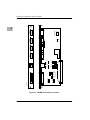
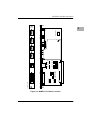
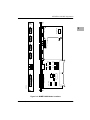
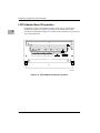
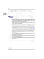
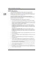
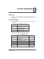
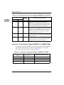
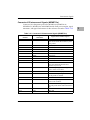
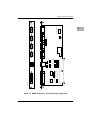
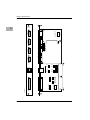
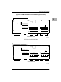
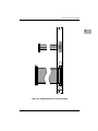
MVME712-12, MVME712-13,
MVME712A, MVME712AM,
and MVME712B
Transition Modules
and LCP2 Adapter Board
User’s Manual
(MVME712A/D3)
Notice
While reasonable efforts have been made to assure the accuracy of this
document, Motorola, Inc. assumes no liability resulting from any omissions in
this document, or from the use of the information obtained therein. Motorola
reserves the right to revise this document and to make changes from time to
time in the content hereof without obligation of Motorola to notify any person
of such revision or changes.
No part of this material may be reproduced or copied in any tangible medium,
or stored in a retrieval system, or transmitted in any form, or by any means,
radio, electronic, mechanical, photocopying, recording or facsimile, or
otherwise, without the prior written permission of Motorola, Inc.
It is possible that this publication may contain reference to, or information
about Motorola products (machines and programs), programming, or services
that are not announced in your country. Such references or information must
not be construed to mean that Motorola intends to announce such Motorola
products, programming, or services in your country.
Restricted Rights Legend
If the documentation contained herein is supplied, directly or indirectly, to the
U.S. Government, the following notice shall apply unless otherwise agreed to
in writing by Motorola, Inc.
Use, duplication, or disclosure by the Government is subject to restrictions as
set forth in subparagraph (c)(1)(ii) of the Rights in Technical Data and
Computer Software clause at DFARS 252.227-7013.
Motorola, Inc.
Computer Group
2900 South Diablo Way
Tempe, Arizona 85282
Preface
This manual provides general information, hardware preparation, installation
instructions and support information for the following transition modules:
MVME712-12
MVME712-13
MVME712A
MVME712AM
MVME712B
The manual also provides information about the LCP2 Adapter Board.
The transition modules are used as the interface between Motorola Single Board
Computer VMEmodule families, such as the MVME147S, MVME162, MVME167,
MVME187, and MVME197, and their peripheral devices. An LCP2 adapter module
and a cable are supplied for interconnection between the MVME712 family module
and the MVME1xx family module.
This manual is intended for anyone who wants to design OEM systems, supply
additional capability to an existing compatible system, or for use in a lab environment
for experimental purposes.
A basic knowledge of computers and digital logic is assumed.
To use this manual, you should be familiar with the publications listed in the section
Related Documentation.
Related Documentation
The following manuals are referenced in this document. If not shipped with this
product, manuals may be purchased by contacting your Motorola sales office.
Document Title
MVME147S MPU VMEmodule User's Manual
Motorola
Publication Number
MVME147S
MVME147 MPU VMEmodule UserÕs Manual
MVME147
MVME162 Embedded Controller User's Manual
MVME162
MVME167 Single Board Computer User's Manual
MVME167
MVME187 RISC Single Board Computer User's Manual
MVME187
MVME197DP and MVME197SP Single Board Computers
UserÕs Manual
MVME197
MVME197LE Single Board Computer UserÕs Manual
MVME197LE
N ote
Although not shown in the above list, each Motorola
Computer Group manual publication number is suffixed
with characters which represent the revision level of the
document, such as "/D2" (the second revision of a manual);
a supplement bears the same number as the manual but has
a suffix such as "/D1A1" (the first supplement to the
manual).
Manual Terminology
Unless otherwise specified, throughout this manual all address references are in
hexadecimal.
An asterisk (*) following the signal name for signals which are level significant denotes
that the signal is true or valid when the signal is low.
An asterisk (*) following the signal name for signals which are edge significant denotes
that the actions initiated by that signal occur on high to low transition.
Motorola¨ and the Motorola symbol are registered trademarks of Motorola, Inc.
VMEmodule is a trademark of Motorola, Inc.
All other products mentioned in this document are trademarks or registered
trademarks of their respective holders.
© Copyright Motorola 1989, 1993, 1994
All Rights Reserved
Printed in the United States of America
August 1994
Safety Summary
Safety Depends On You
The following general safety precautions must be observed during all phases of operation, service, and
repair of this equipment. Failure to comply with these precautions or with speciÞc warnings elsewhere in
this manual violates safety standards of design, manufacture, and intended use of the equipment. Motorola,
Inc. assumes no liability for the customer's failure to comply with these requirements.
The safety precautions listed below represent warnings of certain dangers of which Motorola is aware. You,
as the user of the product, should follow these warnings and all other safety precautions necessary for the
safe operation of the equipment in your operating environment.
Ground the Instrument.
To minimize shock hazard, the equipment chassis and enclosure must be connected to an electrical ground.
The equipment is supplied with a three-conductor ac power cable. The power cable must either be plugged
into an approved three-contact electrical outlet or used with a three-contact to two-contact adapter, with the
grounding wire (green) Þrmly connected to an electrical ground (safety ground) at the power outlet. The
power jack and mating plug of the power cable meet International Electrotechnical Commission (IEC) safety
standards.
Do Not Operate in an Explosive Atmosphere.
Do not operate the equipment in the presence of ßammable gases or fumes. Operation of any electrical
equipment in such an environment constitutes a deÞnite safety hazard.
Keep Away From Live Circuits.
Operating personnel must not remove equipment covers. Only Factory Authorized Service Personnel or
other qualiÞed maintenance personnel may remove equipment covers for internal subassembly or
component replacement or any internal adjustment. Do not replace components with power cable
connected. Under certain conditions, dangerous voltages may exist even with the power cable removed. To
avoid injuries, always disconnect power and discharge circuits before touching them.
Do Not Service or Adjust Alone.
Do not attempt internal service or adjustment unless another person, capable of rendering Þrst aid and
resuscitation, is present.
Use Caution When Exposing or Handling the CRT.
Breakage of the Cathode-Ray Tube (CRT) causes a high-velocity scattering of glass fragments (implosion).
To prevent CRT implosion, avoid rough handling or jarring of the equipment. Handling of the CRT should
be done only by qualiÞed maintenance personnel using approved safety mask and gloves.
Do Not Substitute Parts or Modify Equipment.
Because of the danger of introducing additional hazards, do not install substitute parts or perform any
unauthorized modiÞcation of the equipment. Contact your local Motorola representative for service and
repair to ensure that safety features are maintained.
Dangerous Procedure Warnings.
Warnings, such as the example below, precede potentially dangerous procedures throughout this manual.
Instructions contained in the warnings must be followed. You should also employ all other safety
precautions which you deem necessary for the operation of the equipment in your operating environment.
!
WARNING
!
WARNING
Dangerous voltages, capable of causing death, are present in
this equipment. Use extreme caution when handling,
testing, and adjusting.
This equipment generates, uses, and can radiate radio
frequency energy and if not installed and used in
accordance with the documentation for this product, may
cause interference to radio communications. It has been
tested and found to comply with the limits for a Class A
Computing Device pursuant to Subpart J of Part 15 of FCC
rules, which are designed to provide reasonable protection
against such interference when operated in a commercial
environment. Operation of this equipment in a residential
area is likely to cause interference in which case the user, at
the userÕs own expense, will be required to take whatever
measures necessary to correct the interference.
Contents
Introduction 1-1
Features of the MVME712 Family Modules 1-1
Features of the LCP2 Adapter Board 1-2
SpeciÞcations 1-2
Cooling Requirements 1-3
FCC Compliance 1-3
General Description 1-4
Introduction 2-1
Unpacking Instructions 2-1
MVME712x Module Preparation 2-1
DSR Line Pull Up Select Headers (J8, J9, J13, J14) 2-6
Serial Port 2/Modem Port 2 Select (J16, J17) 2-7
Serial Port Configuration 2-7
Modem Port Configuration 2-7
SCSI Termination 2-8
MVME712B Module Preparation 2-8
LCP2 Adapter Board Preparation 2-10
Installation Instructions 2-11
Installing for Use with Internal SCSI Devices 2-12
Installing the MVME712-13 and MVME712AM as a Modem 2-14
MVME712B Installation 2-16
Introduction 3-1
Interconnect Signals 3-1
Connector P2 Interconnect Signals (LCP2 Adapter) 3-2
Connectors J1, J3-J5 Interconnect Signals (MVME712x) 3-2
Connector J2 Interconnect Signals (LCP2 Adapter) 3-4
Connector J2 Interconnect Signals (MVME712-13, MVME712AM) 3-9
Connector J3 Interconnect Signals (LCP2 Adapter) Connector: 3-9
Connector SCSI INTERFACE Interconnect Signals (MVME712B) 3-11
Connector ETHERNET Interconnect Signals (MVME712B) 3-13
Connector J6 Interconnect Signals (MVME712-13, MVME712AM) 3-14
Connector J7 Interconnect Signals (MVME712-13, MVME712AM) 3-14
Connector J10 Interconnect Signals (MVME712x) 3-15
Connector P2 and J11 Interconnect Signals (MVME712x) 3-16
Connector J12 Interconnect Signals (MVME712-13, MVME712AM) 3-20
Connector J15 Interconnect Signals (MVME712x) 3-21
Parts Lists and Locations 3-22
Schematic Drawings 3-32
General Description A-1
Modem Features A-2
Technical SpeciÞcations A-3
List of Figures
MVME712-12 Header Locations 2-2
MVME712-13 Header Locations 2-3
MVME712A Header Locations 2-4
MVME712AM Header Locations 2-5
MVME712B Connector Locations 2-9
LCP2 Adapter Connector Locations 2-10
Internal SCSI and Serial Port Connections 2-13
Internal SCSI and Modem Connections 2-15
MVME712B External SCSI Connections 2-17
MVME712-12 Parts Location Drawing (Primary Side) 3-24
MVME712-13 Parts Location Drawing (Primary Side) 3-25
MVME712A Parts Location Drawing (Primary Side) 3-26
MVME712AM Parts Location Drawing (Primary Side) 3-27
MVME712x Parts Location Drawing (Secondary Side) 3-28
MVME712B Parts Location Drawing 3-30
LCP2 Adapter Module Parts Location Drawing 3-31
GENERAL INFORMATION
1
Introduction
This manual provides general information, hardware preparation, installation
instructions, and support information for the MVME712A, AM, -12, -13, and B
Transition Modules, as well as the LCP2 Adapter Board. The next table
defines the references you will see throughout the manual.
Collective Reference
Modules Referred To
MVME712 family
all of the MVME712
modules, including the
MVME712B
MVME712x
all MVME712 modules
MVME712-12
other than the MVME712B MVME712-13
MVME712-12
MVME712-13
MVME712A
MVME712AM
MVME712B
MVME712A
MVME712AM
The MVME712x modules are used as the interface between MVME1xx family
VMEmodules (such as the MVME167 and MVME197) and their internally
connected SCSI peripheral devices.
The MVME712B is designed to be used only in conjunction with an MVME712x
board for external SCSI and/or Ethernet connections.
An LCP2 adapter module and a cable are supplied for interconnection
between the MVME712 family module and the MVME1xx family
VMEmodule.
Features of the MVME712 Family Modules
The features of the MVME712 family modules include:
❏
Four 9-pin multiprotocol EIA-232D serial ports (through the LCP2
adapter) (MVME712x)
❏
One independent printer port (through the LCP2 adapter) (MVME712x)
❏
Small Computer Systems Interface (SCSI) shielded connector bus interface
(through the LCP2 adapter) for connection to external devices
(MVME712B)
MVME712A/D31-1
1
General Information
❏
External Ethernet interface (through the LCP2 adapter) (MVME712B)
❏
Built-in modem (refer to Appendix A) with front panel Telco modular jack
(MVME712-13 and MVME712AM)
❏
Electrostatic Discharge (ESD) protection on front panel
❏
Radio Frequency Interference (RFI) protection on front panel
Features of the LCP2 Adapter Board
The features of the LCP2 Adapter Board include:
❏
A 50-pin connector permits SCSI cable connection to other SCSI devices
and/or to the MVME712B through a flat ribbon cable
❏
SCSI terminating resistors mounted in sockets for end of cable or middle of
cable configuration
❏
Terminator power is developed on the LCP2 adapter from the +5 Vdc on
connector P2 and is fused (1 amp) on the LCP2 adapter
❏
A 64-pin connector interfaces the EIA-232D ports and printer port signals
to the MVME712x
Specifications
The MVME712 family module specifications are given in Table 1-1.
Table 1-1. MVME712 Family Specifications
Characteristics
Power requirements
I/O ports
SpeciÞcations
+ 5 Vdc, 281 mA maximum (255 mA typical)
+12 Vdc
- 12 Vdc
Serial
Four multiprotocol (connected through the
LCP2 adapter)
Parallel
Parallel printer port (connected through the
LCP2 adapter)
Operating temperature
0 degrees to 55 degrees C at point of entry of
forced air (approximately 5 CFM)
Storage temperature
- 40 degrees to 85 degrees C
Relative humidity
Physical characteristics
(excluding front panel
and MVME712B)
1-2
5% to 90% (non-condensing)
Height
Depth
Thickness
9.187 inches (233.35 mm)
3.200 inches (80.00 mm)
0.063 inches (1.60 mm)
MVME712-12/-13/A/AM/B Transition Modules and LCP2 Adapter Board UserÕs Manual
Specifications
Cooling Requirements
Motorola VMEmodules are specified, designed, and tested to operate reliably
with an incoming air temperature range from 0 degrees C to 55 degrees C (32
degrees F to 131 degrees F) with forced air cooling. Temperature qualification
is performed in a standard Motorola VMEsystem 1000 chassis. Twenty-five
watt load boards are inserted in the two card slots, one on each side, adjacent
to the board under test to simulate a high power density system configuration.
An assembly of three axial fans, rated at 71 CFM per fan, is placed directly
under the MVME card cage. The incoming air temperature is measured
between the fan assembly and the card cage where the incoming airstream first
encounters the module under test. Test software is executed as the module is
subjected to ambient temperature variations. Case temperatures of critical,
high power density integrated circuits are monitored to ensure component
vendors specifications are not exceeded.
While the exact amount of airflow required for cooling depends on the
ambient air temperature and the type, number, and location of boards and
other heat sources, adequate cooling can usually be achieved with 5 CFM
flowing over the module. Less air flow is required to cool the module in
environments having lower maximum ambients. Under more favorable
thermal conditions it may be possible to operate the module reliably at higher
than 55 degrees C with increased air flow. It is important to note that there are
several factors, in addition to the rated CFM of the air mover, which determine
the actual volume of air flowing over a module.
FCC Compliance
These MVME712 family VMEmodules were tested in an FCC-compliant
chassis, and meet the requirements for Class A equipment. FCC compliance
was achieved under the following conditions:
1.
Shielded cables on all external I/O ports.
2.
Cable shields connected to earth ground via metal shell connectors
bonded to a conductive module front panel.
3.
Conductive chassis rails connected to earth ground. This provides the path
for connecting shields to earth ground.
4.
Front panel screws properly tightened.
For minimum RF emissions, it is essential that the conditions above be
implemented; failure to do so could compromise the FCC compliance of the
equipment containing the modules.
MVME712A/D3
1-3
1
1
General Information
General Description
The MVME712 family modules are I/O transition modules for the MVME1xx
VMEmodule families. The LCP2 adapter assembly routes the I/O signals and
grounds from the P2 connector on the backplane at the MVME1xx
VMEmodule to the MVME712 family module. The MVME712 family module
routes the signals to the appropriate industry-standard connectors on its front
panel. The MVME712-13 and MVME712AM both have a built-in modem.
The MVME712x has four DB-9 connectors for the serial ports, one 25-pin
connector for the printer port, and a Telco modular jack on the front panel. The
serial ports are configured for use as to modem and cannot be changed without
null modem cables.
1-4
MVME712-12/-13/A/AM/B Transition Modules and LCP2 Adapter Board UserÕs Manual
HARDWARE PREPARATION
AND INSTALLATION
2
Introduction
This chapter provides unpacking instructions, hardware preparation, and
installation instructions for the MVME712 family modules and the LCP2
adapter.
Unpacking Instructions
N ote
If the carton is damaged upon receipt, request that carrier's
agent be present during unpacking and inspection of
equipment.
Unpack equipment from shipping carton. Refer to packing list and verify that
all items are present. Save packing material for storing and reshipping of
equipment.
MVME712x Module Preparation
To select the desired configuration and ensure proper operation of the
MVME712x module, certain changes may be made before installation. These
changes are made through jumper arrangements on the headers. The locations
of the headers and connectors for the MVME712x are illustrated in Figure 21 through Figure 2-4.
The modules have been factory tested and are shipped with factory-installed
jumper configurations that are shown in the following paragraphs with each
header description. The modules are operational with the factory-installed
jumpers. The modules are configured to provide the system functions
required for a VMEbus system. Changes may be made for the following
reasons:
❏
DSR Line Pull Up Select (J8, J9, J13, J14)
❏
Serial Port 2/Modem Port 2 Select (J16, J17)
❏
Hardwired as DTE (to modem). With the exception of the DSR line, no
headers are provided on the module to change this configuration. To use
the module as DCE (to terminal), a null modem cable must be attached.
MVME712A/D32-1
Hardware Preparation and Installation
MVME
712A/AM
2
1
J2
6
MODEM POWER
SERIAL PORT 1
5
9
1
1
6
J6
2
5
9
J7
J7
2
1
J4
5
9
SERIAL PORT 3
1
6
MODEM INTERCONNECT
20
19
J3
SERIAL PORT 2
J1
SERIAL PORT 1
TTY01
1
6
CONSOLE
J5
5
9
SERIAL PORT 4
1
6
SERIAL PORT 4
2
1
1
1
J10
3
3
1
1
J13
ETHERNET
A1
B1
C1
J9
J8
C1
J14
C2
20
19
3
3
MODEM PORT
2 4
1 3
J12
P2
+
CR1
U1
C3
13
25
CR2
2
1
A32
B32
C32
J17
J16
10
9
10
9
1
14
SERIAL PORT
2
1
MODEM PORT
J15
PRINTER PORT
PRINTER
1519 9408
MVME712-12/-13/A/AM/B Transition Modules and LCP2 Adapter Board UserÕs Manual
2-2
DTE
DTE
DCE
DCE
DTE
DTE
DCE
DCE
Figure 2-1. MVME712-12 Header Locations
MVME712x Module Preparation
1
J2
6
MODEM POWER
5
9
J3
20
19
5
9
J7
J7
2
1
J4
5
9
SERIAL PORT 3
1
6
MODEM INTERCONNECT
1 J6 2
1
6
SERIAL PORT 2
J1
SERIAL PORT 1
TTY01
1
6
SERIAL PORT 1
CONSOLE
1
6
J5
5
9
SERIAL PORT 4
1
2
1
1
A1
B1
C1
J10
3
3
1
1
J13
ETHERNET
J9
J8
J14
C2
2 4
1 3
J12
20
19
3
3
MODEM PORT
C1
DTE
DTE
DCE
DCE
DTE
DTE
DCE
DCE
P2
+
CR1
U1
C3
13
25
CR2
2
1
A32
B32
C32
J17
J16
10
9
10
9
1
14
SERIAL PORT
2
1
MODEM PORT
J15
PRINTER PORT
PRINTER
cb221 9408 (2-3)
2-3
MVME712A/D3
2
MVME
712A/12/13
Figure 2-2. MVME712-13 Header Locations
Hardware Preparation and Installation
MVME
712A/AM
J2
6
1
1
6
J6
2
5
9
J7
J7
1
6
J4
2
1
MODEM INTERCONNECT
20
19
J3
5
9
SERIAL PORT 3
J5
5
9
SERIAL PORT 4
1
6
SERIAL PORT 4
2
1
2
1
1
1
J10
3
3
1
1
J13
ETHERNET
J9
J8
J14
C2
2 4
1 3
J12
20
19
3
3
MODEM PORT
C1
DTE
DTE
DCE
DCE
DTE
DTE
DCE
DCE
1
MODEM POWER
5
9
SERIAL PORT 1
J1
SERIAL PORT 2
1
6
SERIAL PORT 1
TTY01
J11
+
CR1
U1
C3
13
25
CR2
2
1
J17
J16
64
63
10
9
10
9
1
14
SERIAL PORT
2
1
MODEM PORT
J15
PRINTER PORT
PRINTER
cb221 9408 (1-3)
MVME712-12/-13/A/AM/B Transition Modules and LCP2 Adapter Board UserÕs Manual
2-4
CONSOLE
2
Figure 2-3. MVME712A Header Locations
MVME712x Module Preparation
MVME
712A/12/13
1
J2
6
MODEM POWER
SERIAL PORT 1
5
9
1
6
1 J6
2
5
9
J7
J7
2
1
J4
5
9
SERIAL PORT 3
1
6
MODEM INTERCONNECT
20
19
J3
SERIAL PORT 2
J1
SERIAL PORT 1
TTY01
1
6
CONSOLE
1
6
J5
5
9
SERIAL PORT 4
2
1
2
1
1
1
J9
J8
DTE
3
3
J10
1
1
1
J13
J14
C2
4
3
J12
2
20
19
3
3
MODEM PORT
C1
DTE
J11
+
CR1
C3
U1
13
25
CR2
J15
1
2
J17
J16
64
63
9
10
9
10
MODEM PORT
1
2
1
14
SERIAL PORT
PRINTER PORT
PRINTER
1520 9407
2-5
MVME712A/D3
DCE
DCE
DTE
DTE
DCE
DCE
2
Figure 2-4. MVME712AM Header Locations
Hardware Preparation and Installation
DSR Line Pull Up Select Headers (J8, J9, J13, J14)
Headers J8, J9, J13, and J14 are used to pull up the external DSR lines of the
serial ports (J1, J3, J4, J5) to a high (+12 Vdc) level when terminals are
connected and DSR is to be used as a constantly activated output from the
MVME712x. The as-shipped configuration is shown below.
2
J8
1
2
J9
3
DTE
DCE
1
DCE
2
J13
3
DTE
1
DCE
2
3
DTE
J14
1
2
3
2-6
MVME712-12/-13/A/AM/B Transition Modules and LCP2 Adapter Board UserÕs Manual
MVME712x Module Preparation
Serial Port 2/Modem Port 2 Select (J16, J17)
Port 2 is shared between the front panel serial port connector and the internal
modem. Header J16 or J17 must be configured to select one or the other port for
proper operation.
N ote
Only one port function may be selected at any one time.
Otherwise, improper operation will result.
Serial Port Configuration
The MVME712-12 and MVME712A are shipped with port 2 configured for
connection as a serial port as shown below.
J17
J16
1
3
5
7
9
SERIAL PORT 2
1
3
5
7
9
MODEM PORT 2
Modem Port Configuration
The MVME712-13 and MVME712AM are shipped with port 2 configured for
connection as a modem port as shown below.
J16
1
3
5
J17
7
9
SERIAL PORT 2
MVME712A/D3
1
3
5
7
9
MODEM PORT 2
2-7
2
Hardware Preparation and Installation
SCSI Termination
Because the MVME712x has no provision for SCSI connection, you must
ensure that the SCSI bus is terminated properly. The LCP2 adapter has sockets
(R1, R2, R3) for terminating the SCSI lines using three 8-pin SIP resistors. Refer
to the Installation Instructions for use of the terminators.
2
MVME712B Module Preparation
No preparation of the MVME712B is necessary. The location of the connectors
is illustrated in Figure 2-5.
2-8
MVME712-12/-13/A/AM/B Transition Modules and LCP2 Adapter Board UserÕs Manual
MVME712B Module Preparation
MVME
712B
2
ETHERNET
SCSI INTERFACE
cb208 9212
Figure 2-5. MVME712B Connector Locations
MVME712A/D3
2-9
Hardware Preparation and Installation
LCP2 Adapter Board Preparation
Preparation of the LCP2 adapter consists of removing or replacing the
terminating resistors for SCSI. The location of the resistors, fuse, and
connectors is illustrated in Figure 2-6. Refer to the Installation Instructions for
use of the terminators.
2
2
64
J2
1
63
J3
2
50
1
49
1
R1
C1
R2
C2
E1
E2
R3
C3
F1
CR1
C32
B32
A32
C1
B1
A1
P2
cb206 9212
Figure 2-6. LCP2 Adapter Connector Locations
2-10
MVME712-12/-13/A/AM/B Transition Modules and LCP2 Adapter Board UserÕs Manual
Installation Instructions
Installation Instructions
The basic procedure for installation of the family of MVME712 modules and
the LCP2 adapter is as follows:
1.
Turn all equipment power OFF and disconnect the power cable from the
AC power source.
C aution
Connecting modules while the power is applied may result
in damage to components on the module.
!
Dangerous voltages, capable of causing death, are present in
this equipment. Use extreme caution when handling,
testing, and adjusting.
WARNING
2.
Remove the chassis cover as instructed in the equipment user's manual.
3.
Remove the Þller panel(s) from the appropriate card slot(s) at the rear of
the chassis (if the chassis has a rear card cage). Other modules in the unit
may have to be moved to allow space for the cables connected to the LCP2
adapter and the MVME712x family module.
4.
Continue with the speciÞc procedure for installation:
Installing for Use with Internal SCSI Devices
Installing the MVME712-13 and MVME712AM as a
Modem
MVME712B Installation
MVME712A/D3
2-11
2
Hardware Preparation and Installation
Installing for Use with Internal SCSI Devices
An MVME1xx VMEmodule can be connected through the LCP2 adapter to
internal SCSI devices as shown in Figure 2-7. This section describes the
procedure for connecting the MVME712x modules for use with internal SCSI
devices.
2
Because the MVME1xx VMEmodule is at one end of the cable, SCSI
terminators are required on the LCP2 adapter. The LCP2 adapter module is
shipped with SCSI terminators installed.
N ote
MVME712-13 and MVME712AM: perform the steps in this
procedure to connect to internal SCSI devices or the steps in
the next section to connect the modem or the steps in both
procedures.
1.
Verify that SCSI terminators are installed on the LCP2 adapter module.
2.
Install the LCP2 adapter module to the backplane directly in line with the
P2 connector on the MVME1xx VMEmodule. Be sure to orient pin 1 of the
adapter with pin 1 of the backplane connector.
3.
Connect a user-supplied cable with compatible pinouts from connector J3
on the LCP2 adapter to the internal SCSI devices.
4.
Verify that terminators are installed on the last SCSI device on the cable. If
they are not present, install terminators.
5.
MVME712-12 and MVME712-13: Attach the cable supplied with the
MVME712x module from LCP2 adapter connector J2 to connector P2 on
the MVME712x module. Be sure to orient cable pin 1 with connector pin 1.
See Figure 2-7.
MVME712A and MVME712AM: Attach the cable supplied with the
MVME712x module from LCP2 adapter connector J2 to connector J11 on
the MVME712x module. Be sure to orient cable pin 1 with connector pin 1.
See Figure 2-7.
2-12
6.
Insert the transition module into the selected slot and tighten the attaching
screws.
7.
After making sure you will not pinch cables with the cover, reinstall the
cover you previously removed.
8.
Connect the power cable to the AC power source and turn on the unit.
9.
If SCSI does not work properly, you may have to repair a defective cable
and/or replace a blown fuse.
MVME712-12/-13/A/AM/B Transition Modules and LCP2 Adapter Board UserÕs Manual
Installation Instructions
Check the fuse on the LCP2 adapter module and replace it, if necessary.
The fuse on the LCP2 adapter module is for SCSI terminator power.
The fuse on the MVME1xx VMEmodule is for Ethernet transceiver power.
2
The resistance of each fuse should be less than 1 Ohm.
MVME712X
TERMINATOR
MVME187
SCSI DEVICE
J1
J2
P1
J3
J7
J4
LC P2 ADAPTER
J5
J2
J12
P2
J10
P2
J15
J3
P2 OR J11
ENCLOSURE BOUNDARY
cb224 9408 (2-2)
Figure 2-7. Internal SCSI and Serial Port Connections
MVME712A/D3
2-13
Hardware Preparation and Installation
Installing the MVME712-13 and MVME712AM as a Modem
To install the MVME712-13 and MVME712AM with serial port 2 configured as
a modem, which is the as-shipped configuration, proceed as described in this
section. See also Figure 2-8.
2
N ote
If you have connected your module for use with internal
SCSI devices, you may already have performed some of
these steps.
1.
Install the LCP2 adapter module to the backplane directly in line with the
P2 connector on the MVME1xx VMEmodule. Be sure to orient pin 1 of the
adapter with pin 1 of the backplane connector.
2.
Verify that serial port 2 is conÞgured as a modem port (refer to the Serial
Port 2 Configuration paragraph).
3.
MVME712-13: Attach the cable supplied with the MVME712-13 module
from LCP2 adapter connector J2 to connector P2 on the MVME712-13
module. Be sure to orient cable pin 1 with connector pin 1. See Figure 2-8.
MVME712AM: Attach the cable supplied with the MVME712AM module
from LCP2 adapter connector J2 to connector J11 on the MVME712AM
module. Be sure to orient cable pin 1 with connector pin 1. See Figure 2-8.
2-14
4.
Connect a user-supplied cable from connector J2 on the MVME712-13 or
MVME712AM to backplane connections for +5, +12, and -12 Vdc for
modem power.
5.
Insert the MVME712-13 or MVME712AM module into the selected slot
and tighten the attaching screws.
6.
After making sure you will not pinch cables with the cover, reinstall the
cover you previously removed.
7.
Connect a user-supplied Telco modular cable to the Telco modular jack on
the front panel.
8.
Connect the power cable to the AC power source and turn on the unit.
MVME712-12/-13/A/AM/B Transition Modules and LCP2 Adapter Board UserÕs Manual
Installation Instructions
MVME712-13
MVME712AM
TERMINATOR
MVME167
2
SCSI DEVICE
J1
J2
J3
P1
J7
J4
MODEM
TELCO JACK
LC P2 ADAPTER
J5
J2
J12
P2
J10
P2
J15
J3
P2 OR J11
ENCLOSURE BOUNDARY
cb225 9408 (2-2)
Figure 2-8. Internal SCSI and Modem Connections
MVME712A/D3
2-15
Hardware Preparation and Installation
MVME712B Installation
The MVME712B is designed to be used in conjunction with one of the
MVME712x modules (MVME712A, MVME712AM, MVME712-12, or
MVME712-13). The MVME712x can be connected through the MVME712B to
external SCSI devices as shown in Figure 2-9.
2
Because the MVME1xx VMEmodule is at one end of the cable, SCSI
terminators are required on the LCP2 adapter. The LCP2 adapter module is
shipped with SCSI terminators installed.
To install the MVME712B in the system, proceed as follows:
1.
Verify that SCSI terminators are installed on the LCP2 adapter module.
2.
Install the LCP2 adapter module to the backplane directly in line with the
P2 connector on the MVME1xx VMEmodule. Be sure to orient pin 1 of the
adapter with pin 1 of the backplane connector.
3.
MVME712-12 and MVME712-13: Attach the cable supplied with the
MVME712x module from LCP2 adapter connector J2 to connector P2 on
the MVME712x module. Be sure to orient cable pin 1 with connector pin 1.
See Figure 2-9.
MVME712A and MVME712AM: Attach the cable supplied with the
MVME712x module from LCP2 adapter connector J2 to connector J11 on
the MVME712x module. Be sure to orient cable pin 1 with connector pin 1.
See Figure 2-9.
4.
Connect the SCSI INTERFACE cable on the MVME712B to connector J3 on
the LCP2 adapter.
5.
Connect the ETHERNET cable on the MVME712B to connector J10 on the
MVME712x.
6.
Insert the MVME712B module into the selected slot and tighten the
attaching screws.
7.
Connect a user-supplied cable with compatible pinouts from the SCSI
interface on the front panel of the MVME712B to the external SCSI devices.
8.
Verify that terminators are installed on the last SCSI device on the cable. If
they are not present, install terminators.
9.
After making sure you will not pinch cables with the cover, reinstall the
cover you previously removed.
10. Connect the power cable to the AC power source and turn the unit on.
11. If SCSI does not work properly, you may have to repair a defective cable
and/or replace a blown fuse.
2-16
MVME712-12/-13/A/AM/B Transition Modules and LCP2 Adapter Board UserÕs Manual
Installation Instructions
Check the fuse on the LCP2 adapter module and replace, if necessary. The
fuse on the LCP2 adapter module is for SCSI terminator power.
The fuse on the MVME1xx VMEmodule is for Ethernet transceiver power.
2
The resistance of each fuse should be less than 1 Ohm.
MVME712B
MVME712X
J1
J3
MVME147S
J2
J7
J4
P1
J5
J10
LC P2 ADAPTER
J12
J2
J3
J15
J11
P2
P2
ENCLOSURE BOUNDARY
cb226 9408 (2-2)
Figure 2-9. MVME712B External SCSI Connections
MVME712A/D3
2-17
Hardware Preparation and Installation
2
2-18
MVME712-12/-13/A/AM/B Transition Modules and LCP2 Adapter Board UserÕs Manual
SUPPORT INFORMATION
3
Introduction
This chapter provides the interconnection signals, parts lists, parts location
illustrations, and schematic diagrams for the MVME712 family modules and
LCP2 adapter.
Interconnect Signals
Table 3-1 describes the connections from the LCP adapter to the MVME712x
and VMEmodules:
Table 3-1. LCP2 and MVME712 Connectors
From
To
LCP2 adapter J2
J11 on the MVME712A
J11 on the MVME712AM
LCP2 adapter J2
P2 on the MVME712-12
P2 on the MVME712-13
LCP2 adapter P2
backplane at the MVME1xx
VMEmodule P2 connector
Table 3-2 lists the jumpers on the MVME712 modules.
Table 3-2. MVME712 Jumpers
Jumper
Description
Modules
J1 and J3-J5
9-pin EIA-232D serial port connectors
on the front panel
MVME712x
J15
25-pin printer port connector on the
front panel
MVME712x
J2
6-pin modem power connector
MVME712x
J6
2-pin modem TIP/RING connector
MVME712x
J7
20-pin modem interconnect connector
MVME712x
J10
20-pin Ethernet connector
MVME712x
J12
Telco modular jack on the front panel
MVME712-13
MVME712AM
MVME712A/D33-1
Support Information
All front panel connectors have metal shells and jack posts that are electrically
connected to the front panel. If the front panel is electrically connected to the
chassis ground, then the shells and jack posts are connected to chassis ground.
This allows shielded cable to be used for effective reduction of EMI and EMC
problems.
3
Connector P2 Interconnect Signals (LCP2 Adapter)
Connector P2 on the LCP2 adapter board is a standard DIN 41612 triple-row,
96-pin male connector. Each pin connection, signal mnemonic, and signal
characteristic for the connector rows A and C are the same pin-for-pin as
connector P2 on the MVME1xx VMEmodule. Row B has only +5 Vdc and
ground connected on the LCP2 adapter.
Connectors J1, J3-J5 Interconnect Signals (MVME712x)
Connectors J1 and J3-J5 are EIA-232D 9-pin front panel connectors. Each pin
connection, signal mnemonic, and signal characteristic for the connectors is
listed in Table 3-3.
.
Table 3-3. Connectors J1, J3-J5 Interconnect Signals (MVME712x)
Pin
Number
Signal
Mnemonic
Signal Name and Description
1
DCD
DATA CARRIER DETECT - Sent by the modem
to the terminal to indicate that a valid carrier is
being received. Not used by port 1 (J1).
2
RXD
RECEIVE DATA - data that is demodulated
from the receive line is presented to the terminal
by the modem.
3
TXD
TRANSMIT DATA - data to be transmitted is
furnished on this line to the modem from the
terminal.
4
DTR
DATA TERMINAL READY - A signal from the
terminal to the modem indicating that the
terminal is ready to send or receive data.
5
GND
GROUND
6
DSR
DATA SET READY - DSR is a function supplied
by the modem to the terminal to indicate that
the modem is ready to transmit data. This signal
can be held high or low through header J8, J9,
J13, J14.
3-2
MVME712-12/-13/A/AM/B Transition Modules and LCP2 Adapter Board UserÕs Manual
Interconnect Signals
Table 3-3. Connectors J1, J3-J5 Interconnect Signals (MVME712x) (Continued)
Pin
Number
Signal
Mnemonic
Signal Name and Description
7
RTS
REQUEST TO SEND - RTS is supplied by the
terminal to the modem when it is required to
transmit a message. With RTS off, the modem
carrier remains off. When RTS is turned on, the
modem immediately turns on the carrier.
8
CTS
CLEAR TO SEND - CTS is a function supplied
to the terminal by the modem, and indicates that
it is permissible to begin transmission of a
message. When using a modem, CTS follows the
off-to-on transition of RTS after a time delay.
9
MVME712A/D3
Not used.
3-3
3
Support Information
Connector J2 Interconnect Signals (LCP2 Adapter)
Connector J2 on the LCP2 adapter is a 64-pin connector. Each pin connection,
signal mnemonic, and signal characteristic for the connector is listed in Table
3-4.
3
Table 3-4. Connector J2 Interconnect Signals (LCP2 Adapter)
Pin
Number
Signal
Mnemonic
Signal Name and Description
1
C+
COLLISION + (Input) (Ethernet) - a signal to
indicate that multiple stations are contending
for access to the transmission medium.
2
C-
COLLISION - (Input) (Ethernet) - part of a
differential pair.
3
T+
TRANSMIT + (Output) (Ethernet) - this line is
intended to operate into terminated
transmission lines.
4
T-
TRANSMIT - (Output) (Ethernet) - part of a
differential pair.
5
R+
RECEIVE + (Input) (Ethernet) - a data input
sourced by the MAU.
6
R-
RECEIVE - (Input) (Ethernet) - part of a
differential pair.
7
PRSTB*
DATA STROBE (Printer) - an active low output
pulse used to clock data from the system to the
printer.
8
+12VF
+12 Vdc Power - fused on MPU board.
9
PRD00
DATA (bit 1) (Printer)
10
GND
GROUND
11
PRD02
DATA (bit 2) (Printer)
12
PRD01
DATA (bit 0) (Printer)
13
PRD04
DATA (bit 3) (Printer)
14
PRD03
DATA (bit 3) (Printer)
15
PRD06
DATA (bit 4) (Printer)
16
PRD05
DATA (bit 5) (Printer)
17
GND
GROUND
18
PRD07
DATA (bit 7) (Printer)
19
GND
GROUND
3-4
MVME712-12/-13/A/AM/B Transition Modules and LCP2 Adapter Board UserÕs Manual
Interconnect Signals
Table 3-4. Connector J2 Interconnect Signals (LCP2 Adapter) (Continued)
Pin
Number
Signal
Mnemonic
Signal Name and Description
20
PRACK*
DATA ACKNOWLEDGE (Printer) - a low level
input pulse indicating that the next character
may be sent.
21
PRPE
PAPER EMPTY (Printer) - out of paper.
22
PRBSY
BUSY (Printer) - an input signal indicating that
the printer cannot receive data.
23
INPRIME*
INPUT PRIME (Printer) - an output signal that
clears the printer buffer and initializes the logic.
24
PRSEL
SELECTED (Printer) - an input signal indicating
that the printer is selected.
25
GND
GROUND
26
PRFAULT*
FAULT (Printer) - an input signal that indicates
a printer fault condition.
27
GND
GROUND
28
TXD3
TRANSMIT DATA (serial port 3) - data to be
transmitted is furnished on this line to the
modem from the terminal.
29
GND
GROUND
30
RXD3
RECEIVE DATA (serial port 3) - data that is
demodulated from the receive line is presented
to the terminal by the modem.
31
CTS3
CLEAR TO SEND (serial port 3) - CTS is a
function supplied to the terminal by the modem,
and indicates that it is permissible to begin
transmission of a message. When using a
modem, CTS follows the off-to-on transition of
RTS after a time delay.
32
RTS3
REQUEST TO SEND (serial port 3) - RTS is
supplied by the terminal to the modem when it
is required to transmit a message. With RTS off,
the modem carrier remains off. When RTS is
turned on, the modem immediately turns on the
carrier.
33
DCD3
DATA CARRIER DETECT (serial port 3) - sent
by the modem to the terminal to indicate that a
valid carrier is being received.
MVME712A/D3
3-5
3
Support Information
Table 3-4. Connector J2 Interconnect Signals (LCP2 Adapter) (Continued)
Pin
Number
3
Signal
Mnemonic
Signal Name and Description
34
DTR3
DATA TERMINAL READY (serial port 3) - a
signal from the terminal to the modem
indicating that the terminal is ready to send or
receive data.
35
TXD1
TRANSMIT DATA (serial port 1) - data to be
transmitted is furnished on this line to the
modem from the terminal.
36
GND
GROUND
37
RXD1
RECEIVE DATA (serial port 1) - data that is
demodulated from the receive line is presented
to the terminal by the modem.
38
GND
GROUND
39
RTS1
REQUEST TO SEND (serial port 1) - RTS is
supplied by the terminal to the modem when it
is required to transmit a message. With RTS off,
the modem carrier remains off. When RTS is
turned on, the modem immediately turns on the
carrier.
40,41
GND
GROUND
42
CTS1
CLEAR TO SEND (serial port 1) - CTS is a
function supplied to the terminal by the modem,
and indicates that it is permissible to begin
transmission of a message. When using a
motmots follows the off-to-on transition of RTS
after a time delay.
43
GND
GROUND
44
TXD4
TRANSMIT DATA (serial port 4) - data to be
transmitted is furnished on this line to the
modem from the terminal.
45
GND
GROUND
46
RXD4
RECEIVE DATA (serial port 4) - data that is
demodulated from the receive line is presented
to the terminal by the modem.
47
GND
GROUND
3-6
MVME712-12/-13/A/AM/B Transition Modules and LCP2 Adapter Board UserÕs Manual
Interconnect Signals
Table 3-4. Connector J2 Interconnect Signals (LCP2 Adapter) (Continued)
Pin
Number
Signal
Mnemonic
Signal Name and Description
48
RTS4
49
GND
GROUND
50
TRXC4
TRANSMIT CLOCK (serial port 4) - this line can
be conÞgured to clock output data to the
modem from the terminal.
51
DTR4
DATA TERMINAL READY (serial port 4) - a
signal from the terminal to the modem
indicating that the terminal is ready to send or
receive data.
52
CTS4
CLEAR TO SEND (serial port 4) - CTS is a
function supplied to the terminal by the modem,
and indicates that it is permissible to begin
transmission of a message. When using a
modem, CTS follows the off-to-on transition of
RTS after a time delay.
53
GND
GROUND
54
DCD4
DATA CARRIER DETECT (serial port 4) - sent
by the modem to the terminal to indicate that a
valid carrier is being received.
55
GND
GROUND
56
RTXC4
RECEIVE CLOCK (serial port 4) - this line can
be conÞgured to clock input data from a
terminal to a modem.
57
GND
GROUND
58
TXD2
TRANSMIT DATA (serial port 2) - data to be
transmitted is furnished on this line to the
modem from the terminal.
59
GND
GROUND
60
RXD2
RECEIVE DATA (serial port 2) - data that is
demodulated from the receive line is presented
to the terminal by the modem.
MVME712A/D3
REQUEST TO SEND (serial port 4) - RTS is
supplied by the terminal to the modem when it
is required to transmit a message. With RTS off,
the modem carrier remains off. When RTS is
turned on, the modem immediately turns on the
carrier.
3-7
3
Support Information
Table 3-4. Connector J2 Interconnect Signals (LCP2 Adapter) (Continued)
Pin
Number
3
Signal
Mnemonic
Signal Name and Description
61
CTS2
CLEAR TO SEND (serial port 2) - CTS is a
function supplied to the terminal by the modem,
and indicates that it is permissible to begin
transmission of a message. When using a
modem, CTS follows the off-to-on transition of
RTS after a time delay.
62
RTS2
REQUEST TO SEND (serial port 2) - RTS is
supplied by the terminal to the modem when it
is required to transmit a message. With RTS off,
the modem carrier remains off. When RTS is
turned on, the modem immediately turns on the
carrier.
63
DCD2
DATA CARRIER DETECT (serial port 2) - sent
by the modem to the terminal to indicate that a
valid carrier is being received.
64
DTR2
DATA TERMINAL READY (serial port 2) - a
signal from the terminal to the modem
indicating that the terminal is ready to send or
receive data.
3-8
MVME712-12/-13/A/AM/B Transition Modules and LCP2 Adapter Board UserÕs Manual
Interconnect Signals
Connector J2 Interconnect Signals (MVME712-13, MVME712AM)
Connector J2 is a backplane modem power connector. Each pin connection,
signal mnemonic, and signal characteristic for the connector is listed in Table
3-5.
Table 3-5. Connector J2 Interconnect Signals (MVME712-13/AM)
Pin
Number
Signal
Mnemonic
Signal Name and Description
1
+5VMODEM
+5 Vdc Power - supplied by the backplane and
routed to J20.
2
+12VMODEM
+12 Vdc Power - supplied by the backplane and
routed to J20.
3
-12VMODEM
-12 Vdc Power - supplied by the backplane and
routed to J20.
4
GND
GROUND
5,6
Not used.
Connector J3 Interconnect Signals (LCP2 Adapter) Connector:
Connector J3 on the LCP2 adapter is the SCSI port. Each pin connection, signal
mnemonic, and signal characteristic for the connectors is listed in Table 3-6.
Table 3-6. Connector J3 Interconnect Signals (LCP2 Adapter)
Pin
Number
Signal
Mnemonic
Signal Name and Description
1
GND
GROUND
2
DB00*
DATA bus (bit 0) - least signiÞcant bit and the
lowest priority during the arbitration phase.
3
GND
GROUND
4
DB01*
DATA bus (bit 1)
5
GND
GROUND
6
DB02*
DATA bus (bit 2)
7
GND
GROUND
8
DB03*
DATA bus (bit 3)
9
GND
GROUND
MVME712A/D3
3-9
3
Support Information
Table 3-6. Connector J3 Interconnect Signals (LCP2 Adapter) (Continued)
Pin
Number
3
Signal
Mnemonic
Signal Name and Description
10
DB04*
DATA bus (bit 4)
11
GND
GROUND
12
DB05*
DATA bus (bit 5)
13
GND
GROUND
14
DB06*
DATA bus (bit 6)
15
GND
GROUND
16
DB07*
DATA bus (bit 7) - most signiÞcant bit and the
highest priority during the arbitration phase.
17
GND
GROUND
18
DBP*
DATA bus (parity) - data parity is odd. Use of
parity is a system option. Parity is not valid
during the arbitration phase.
19-24
GND
GROUND
25
Not used.
26
TERMPWR
TERMINATOR POWER
27-31
GND
GROUND
32
ATN*
ATTENTION - signal driven by the initiator.
Indicates the attention condition.
33-35
GND
GROUND
36
BSY*
BUS BUSY - OR-tied signal that indicates that
the bus is being used.
37
GND
GROUND
38
ACK*
ACKNOWLEDGE - signal driven by an initiator
to indicate an acknowledgment for a REQ/ACK
data transfer handshake.
39
GND
GROUND
40
RST*
RESET - OR-tied signal that indicates the RESET
condition.
41
GND
GROUND
42
MSG*
MESSAGE - signal driven by the target during
the message phase.
43
GND
GROUND
44
SEL*
SELECT - signal used by an initiator to select a
target or by a target to reselect an initiator.
45
GND
GROUND
3-10
MVME712-12/-13/A/AM/B Transition Modules and LCP2 Adapter Board UserÕs Manual
Interconnect Signals
Table 3-6. Connector J3 Interconnect Signals (LCP2 Adapter) (Continued)
Pin
Number
Signal
Mnemonic
Signal Name and Description
3
46
D/C*
DATA/COMMAND - signal driven by the
target. It indicates whether command or data
information is on the data bus. True (low)
indicates command.
47
GND
GROUND
48
REQ*
REQUEST - signal driven by a target to indicate
a request for a REQ/ACK data transfer
handshake.
49
GND
GROUND
50
O/I*
OUTPUT/INPUT - signal driven by a target that
controls the direction of data movement on the
bus. True (low) indicates input to the initiator.
False (high) indicates output from the initiator.
This signal is also used to distinguish between
selection and reselection phases.
Connector SCSI INTERFACE Interconnect Signals (MVME712B)
Each pin connection, signal mnemonic, and signal characteristic for the
connector is listed in Table 3-7.
Table 3-7. SCSI INTERFACE Interconnect Signals (MVME712B)
Pin
Number
Signal
Mnemonic
Signal Name and Description
1-25
GND
GROUND
26
DB00*
DATA bus (bit 0) - least signiÞcant bit and the
lowest priority during the arbitration phase.
27
DB01*
DATA bus (bit 1)
28
DB02*
DATA bus (bit 2)
29
DB03*
DATA bus (bit 3)
30
DB04*
DATA bus (bit 4)
31
DB05*
DATA bus (bit 5)
32
DB06*
DATA bus (bit 6)
MVME712A/D3
3-11
Support Information
Table 3-7. SCSI INTERFACE Interconnect Signals (MVME712B) (Continued)
Pin
Number
3
Signal
Mnemonic
Signal Name and Description
33
DB07*
DATA bus (bit 7) - most signiÞcant bit and the
highest priority during the arbitration phase.
34
DBP*
DATA bus (parity) - data parity is odd. Use of
parity is a system option. Parity is not valid
during the arbitration phase.
35-37
GND
GROUND
38
TERMPWR
TERMINATOR POWER
39,40
GND
GROUND
41
ATN*
ATTENTION - signal driven by the initiator.
Indicates the attention condition.
42
GND
GROUND
43
BSY*
BUS BUSY - OR-tied signal that indicates that
the bus is being used.
44
ACK*
ACKNOWLEDGE - signal driven by an initiator
to indicate an acknowledgment for a REQ/ACK
data transfer handshake.
45
RST*
RESET - OR-tied signal that indicates the RESET
condition.
46
MSG*
MESSAGE - signal driven by the target during
the message phase.
47
SEL*
SELECT - signal used by an initiator to select a
target or by a target to reselect an initiator.
48
D/C*
DATA/COMMAND - signal driven by the
target. It indicates whether command or data
information is on the data bus. True (low)
indicates command.
49
REQ*
REQUEST - signal driven by a target to indicate
a request for a REQ/ACK data transfer
handshake.
50
O/I*
OUTPUT/INPUT - signal driven by a target that
controls the direction of data movement on the
bus. True (low) indicates input to the initiator.
False (high) indicates output from the initiator.
This signal is also used to distinguish between
selection and reselection phases.
3-12
MVME712-12/-13/A/AM/B Transition Modules and LCP2 Adapter Board UserÕs Manual
Interconnect Signals
Connector ETHERNET Interconnect Signals (MVME712B)
Each pin connection, signal mnemonic, and signal characteristic for the
connector is listed in Table 3-8.
3
Table 3-8. ETHERNET Interconnect Signals (MVME712B)
Pin
Number
Signal
Mnemonic
1
Signal Name and Description
Not used.
2
C+
COLLISION + (Input) - a signal to indicate that
multiple stations are contending for access to the
transmission medium.
3
T+
TRANSMIT + (Output) - this line is intended to
operate into terminated transmission lines.
4
Not used.
5
R+
RECEIVE + (Input) - a data input sourced by the
MAU.
6
GND
GROUND
7,8
Not used.
9
C-
COLLISION - (Input) - part of a differential pair.
10
T-
TRANSMIT - (Output) - part of a differential pair.
11
Not used.
12
R-
RECEIVE - (Input) - part of a differential pair.
13
+12VF
+12 Vdc Power - fused on MPU board.
14,15
MVME712A/D3
Not used.
3-13
Support Information
Connector J6 Interconnect Signals (MVME712-13, MVME712AM)
Connector J6 is the modem RING and TIP from the Telco front panel jack on
the MVME712-13 and MVME712AM. Each pin connection, signal mnemonic,
and signal characteristic for the connector is listed in Table 3-9.
3
Table 3-9. Connector J6 Interconnect Signals (MVME712-13/AM)
Pin
Number
Signal
Mnemonic
Signal Name and Description
1
TIP
Tip side of telephone line.
2
RING
Ring side of telephone line.
Connector J7 Interconnect Signals (MVME712-13, MVME712AM)
Connector J7 is the onboard modem interconnect (refer to Appendix A for
details on the modem). Each pin connection, signal mnemonic, and signal
characteristic for the connector is listed in Table 3-10.
Table 3-10. Connector J7 Interconnect Signals (MVME712-13/AM)
Pin
Number
1
Signal
Mnemonic
MDMTXD2
2,3
TRANSMIT DATA - data to be transmitted is
furnished on this line to the modem from the
terminal.
Not used.
4
-12VMODEM
5
+5VMODEM
6
7
Signal Name and Description
-12 Vdc Power - used by the modem.
+5 Vdc Power - used by the modem.
Not used.
MDMDTR2
8,9
DATA TERMINAL READY - an active low
signal from the terminal to the modem
indicating that the terminal is ready to send or
receive data.
Not used.
10
GND
GROUND - modem circuit ground interface.
11
MDMCTS2
CLEAR TO SEND - an active low signal that the
modem maintains in the on state.
12
3-14
Not used.
MVME712-12/-13/A/AM/B Transition Modules and LCP2 Adapter Board UserÕs Manual
Interconnect Signals
Table 3-10. Connector J7 Interconnect Signals (MVME712-13/AM) (Continued)
Pin
Number
Signal
Mnemonic
Signal Name and Description
3
13
+12VMODEM
+12 Vdc Power - used by the modem.
14
+5VMODEM
+5 Vdc Power - used by the modem.
15
MDMRXD2
RECEIVE DATA - data that is demodulated
from the receive line is presented to the terminal
by the modem.
16
Not used.
17
MDMDCD2
DATA CARRIER DETECT - sent by the modem
to the terminal to indicate that a valid carrier is
being received.
18
GND
GROUND - modem circuit ground interface.
19
+5VMODEM
+5 Vdc Power - used by the modem.
20
GND
GROUND - modem circuit ground interface.
Connector J10 Interconnect Signals (MVME712x)
Connector J10 is the Ethernet interconnect on the MVME712x (MVME712A,
MVME712AM, MVME712-12, and MVME712-13). Each pin connection, signal
mnemonic, and signal characteristic for the connector is listed in Table 3-11.
Table 3-11. Connector J10 Interconnect Signals (MVME712x)
Pin
Number
Signal
Mnemonic
1
Signal Name and Description
Not used.
2
C-
COLLISION - (Output) - part of a differential
pair.
3
C+
COLLISION + (Input) - a signal to indicate that
multiple stations are contending for access to the
transmission medium.
4
T-
TRANSMIT - (Output) - part of a differential
pair.
5
T+
TRANSMIT + (Output) - this line is intended to
operate into terminated transmission lines.
6,7
8
MVME712A/D3
Not used.
R-
RECEIVE - (Input) - part of a differential pair.
3-15
Support Information
Table 3-11. Connector J10 Interconnect Signals (MVME712x) (Continued)
Pin
Number
3
Signal
Mnemonic
Signal Name and Description
9
R+
RECEIVE + (Input) - a data input sourced by the
MAU.
10
+12VF
+12 Vdc Power - fused on MPU board.
11-20
Not used.
Connector P2 and J11 Interconnect Signals (MVME712x)
Connector P2 on the MVME712-12 or MVME712-13, or connector J11 on the
MVME712A or MVME712AM, receives the signals from the LCP2 adapter.
Each pin connection, signal mnemonic, and signal characteristic for the
connectors is listed in Table 3-12.
Table 3-12. Connector P2, J11 Interconnect Signals (MVME712x)
Pin Number
P2
J11
Signal
Mnemonic
Signal Name and Description
C1
1
C+
COLLISION + (Input) (Ethernet) - a signal to
indicate that multiple stations are contending for
access to the transmission medium.
A1
2
C-
COLLISION - (Input) (Ethernet) - part of a
differential pair.
C2
3
T+
TRANSMIT + (Output) (Ethernet) - this line is
intended to operate into terminated transmission
lines.
A2
4
T-
TRANSMIT - (Output) (Ethernet) - part of a
differential pair.
C3
5
R+
RECEIVE + (Input) (Ethernet) - a data input sourced
by the MAU.
A3
6
R-
RECEIVE - (Input) (Ethernet) - part of a differential
pair.
C4
7
PRSTB*
DATA STROBE (Printer) - an active low output pulse
used to clock data from the system to the printer.
A4
8
+12VF
+12 Vdc Power - fused on MPU board.
C5
9
PRD00
DATA (bit 0) (Printer)
A5
10
GND
GROUND
3-16
MVME712-12/-13/A/AM/B Transition Modules and LCP2 Adapter Board UserÕs Manual
Interconnect Signals
Table 3-12. Connector P2, J11 Interconnect Signals (MVME712x) (Continued)
Pin Number
P2
J11
Signal
Mnemonic
Signal Name and Description
3
C6
11
PRD02
DATA (bit 2) (Printer)
A6
12
PRD01
DATA (bit 1) (Printer)
C7
13
PRD04
DATA (bit 4) (Printer)
A7
14
PRD03
DATA (bit 3) (Printer)
C8
15
PRD06
DATA (bit 6) (Printer)
A8
16
PRD05
DATA (bit 5) (Printer)
C9
17
GND
GROUND
A9
18
PRD07
DATA (bit 7) (Printer)
C10
19
GND
GROUND
A10
20
PRACK*
DATA ACKNOWLEDGE (Printer) - a low level input
pulse indicating that the next character may be sent.
C11
21
PRPE
PAPER EMPTY (Printer) - out of paper.
A11
22
PRBSY
BUSY (Printer) - an input signal indicating that the
printer cannot receive data.
C12
23
INPRIME*
INPUT PRIME (Printer) - an output signal that clears
the printer buffer and initializes the logic.
A12
24
PRSEL
SELECTED (Printer) - an input signal indicating that
the printer is selected.
C13
25
GND
GROUND
A13
26
PRFAULT* FAULT (Printer) - an input signal that indicates a
printer fault condition.
C14
27
GND
GROUND
A14
28
TXD3
TRANSMIT DATA (serial port 3) - data to be
transmitted is furnished on this line to the modem
from the terminal.
C15
29
GND
GROUND
A15
30
RXD3
RECEIVE DATA (serial port 3) - data that is
demodulated from the receive line is presented to the
terminal by the modem.
C16
31
CTS3
CLEAR TO SEND (serial port 3) - CTS is a function
supplied to the terminal by the modem, and
indicates that it is permissible to begin transmission
of a message. When using a modem, CTS follows the
off-to-on transition of RTS after a time delay.
MVME712A/D3
3-17
Support Information
Table 3-12. Connector P2, J11 Interconnect Signals (MVME712x) (Continued)
Pin Number
3
P2
J11
Signal
Mnemonic
Signal Name and Description
A16
32
RTS3
REQUEST TO SEND (serial port 3) - RTS is supplied
by the terminal to the modem when it is required to
transmit a message. With RTS off, the modem carrier
remains off. When RTS is turned on, the modem
immediately turns on the carrier.
C17
33
DCD3
DATA CARRIER DETECT (serial port 3) - sent by the
modem to the terminal to indicate that a valid carrier
is being received.
A17
34
DTR3
DATA TERMINAL READY (serial port 3) - a signal
from the terminal to the modem indicating that the
terminal is ready to send or receive data.
C18
35
TXD1
TRANSMIT DATA (serial port 1) - data to be
transmitted is furnished on this line to the modem
from the terminal.
A18
36
GND
GROUND
C19
37
RXD1
RECEIVE DATA (serial port 1) - data that is
demodulated from the receive line is presented to the
terminal by the modem.
A19
38
GND
GROUND
C20
39
RTS1
REQUEST TO SEND (serial port 1) - RTS is supplied
by the terminal to the modem when it is required to
transmit a message. With RTS off, the modem carrier
remains off. When RTS is turned on, the modem
immediately turns on the carrier.
A20,C21
40,41
GND
GROUND
A21
42
CTS1
CLEAR TO SEND (serial port 1) - CTS is a function
supplied to the terminal by the modem, and
indicates that it is permissible to begin transmission
of a message. When using a modem, CTS follows the
off-to-on transition of RTS after a time delay.
C22
43
GND
GROUND
A22
44
TXD4
TRANSMIT DATA (serial port 4) - data to be
transmitted is furnished on this line to the modem
from the terminal.
C23
45
GND
GROUND
3-18
MVME712-12/-13/A/AM/B Transition Modules and LCP2 Adapter Board UserÕs Manual
Interconnect Signals
Table 3-12. Connector P2, J11 Interconnect Signals (MVME712x) (Continued)
Pin Number
P2
J11
Signal
Mnemonic
Signal Name and Description
3
A23
46
RXD4
RECEIVE DATA (serial port 4) - data that is
demodulated from the receive line is presented to the
terminal by the modem.
C24
47
GND
GROUND
A24
48
RTS4
REQUEST TO SEND (serial port 4) - RTS is supplied
by the terminal to the modem when it is required to
transmit a message. With RTS off, the modem carrier
remains off. When RTS is turned on, the modem
immediately turns on the carrier.
C25
49
GND
GROUND
A25
50
C26
51
DTR4
DATA TERMINAL READY (serial port 4) - a signal
from the terminal to the modem indicating that the
terminal is ready to send or receive data.
A26
52
CTS4
CLEAR TO SEND (serial port 4) - CTS is a function
supplied to the terminal by the modem, and
indicates that it is permissible to begin transmission
of a message. When using a modem, CTS follows the
off-to-on transition of RTS after a time delay.
C27
53
GND
GROUND
A27
54
DCD4
DATA CARRIER DETECT (serial port 4) - sent by the
modem to the terminal to indicate that a valid carrier
is being received.
C28
55
GND
GROUND
A28
56
C29
57
GND
GROUND
A29
58
TXD2
TRANSMIT DATA (serial port 2) - data to be
transmitted is furnished on this line to the modem
from the terminal.
C30
59
GND
GROUND
A30
60
RXD2
RECEIVE DATA (serial port 2) - data that is
demodulated from the receive line is presented to the
terminal by the modem.
MVME712A/D3
Not used.
Not used.
3-19
Support Information
Table 3-12. Connector P2, J11 Interconnect Signals (MVME712x) (Continued)
Pin Number
3
P2
J11
Signal
Mnemonic
Signal Name and Description
C31
61
CTS2
CLEAR TO SEND (serial port 2) - CTS is a function
supplied to the terminal by the modem, and
indicates that it is permissible to begin transmission
of a message. When using a modem, CTS follows the
off-to-on transition of RTS after a time delay.
A31
62
RTS2
REQUEST TO SEND (serial port 2) - RTS is supplied
by the terminal to the modem when it is required to
transmit a message. With RTS off, the modem carrier
remains off. When RTS is turned on, the modem
immediately turns on the carrier.
C32
63
DCD2
DATA CARRIER DETECT (serial port 2) - sent by the
modem to the terminal to indicate that a valid carrier
is being received.
A32
64
DTR2
DATA TERMINAL READY (serial port 2) - a signal
from the terminal to the modem indicating that the
terminal is ready to send or receive data.
Connector J12 Interconnect Signals (MVME712-13, MVME712AM)
Connector J12 is an RJ-11 modular jack on the front panel of the MVME712-13
and MVME712AM. Each pin connection, signal mnemonic, and signal
characteristic for the connector is listed in Table 3-13.
Table 3-13. Connector J12 Interconnect Signals (MVME712-13/12AM)
Pin
Number
Signal
Mnemonic
1
Signal Name and Description
Not used.
2
TIP
Tip side of telephone line.
3
RING
Ring side of telephone line.
4
3-20
Not used.
MVME712-12/-13/A/AM/B Transition Modules and LCP2 Adapter Board UserÕs Manual
Interconnect Signals
Connector J15 Interconnect Signals (MVME712x)
Connector J15 is the printer port on the MVME712x (MVME712-12,
MVME712-13, MVME712A, and MVME712AM). Each pin connection, signal
mnemonic, and signal characteristic for the connector is listed in Table 3-14.
Table 3-14. Connector J15 Interconnect Signals (MVME712x)
Pin
Number
Signal
Mnemonic
Signal Name and Description
1
PRSTB*
DATA STROBE - an active low output
pulse used to clock data from the system
to the printer.
2
PRD0
DATA (bit 0)
3
PRD1
DATA (bit 1)
4
PRD2
DATA (bit 2)
5
PRD3
DATA (bit 3)
6
PRD4
DATA (bit 4)
7
PRD5
DATA (bit 5)
8
PRD6
DATA (bit 6)
9
PRD7
DATA (bit 7)
10
PRACK*
DATA ACKNOWLEDGE - a low level
input pulse indicating that the next
character may be sent.
11
PRBSY
BUSY - an input signal indicating that the
printer cannot receive data.
12
PRPE
PAPER EMPTY - out of paper.
13
PRSEL
SELECTED - an input signal indicating
that the printer is selected.
14
Not used.
15
PRFAULT*
FAULT - an input signal that indicates a
printer fault condition.
16
INPRIME*
INPUT PRIME - an output signal that
clears the printer buffer and initializes the
logic.
17
18-25
MVME712A/D3
Not used.
GND
GROUND
3-21
3
Support Information
Parts Lists and Locations
The following parts lists and parts location drawings reflect the latest issue of
hardware at the time of printing.
3
Parts locations are illustrated as follows:
Model
Parts List
Parts Location Drawing
MVME712x
Primary side - Figure
MVME712-12
MVME712A
MVME712AM
MVME712x
MVME712B
LCP2 adapter
3-1
3-2
Primary side - Figure 3-3
Primary side - Figure 3-4
Secondary side - Figure 3-5
Primary side - Figure
MVME712-13
Table 3-15
Table 3-16
Table 3-17
Figure 3-6
Figure 3-7
Table 3-15. MVME712x Module Parts List
Reference
Designation
Motorola
Part Number
Description
84-W8832B01A
Printed wiring board
(MVME712-12, MVME712-13)
84-W8838B01B
Printed wiring board
(MVME712A, MVME712AM)
CR1,CR2
48NW9607A20
RectiÞer, Schottky
CR3-CR29
48NW9644A01
Diodes, zener, 2V and 15V
C1,C2
21NW9604A81
Capacitor, Þxed, ceramic, 330 pF @ 1K Vdc
C3
23NW9618A33
Capacitor, electrolytic, 22 µF @ 25 Vdc
C4-C7
21NW9711A14
Capacitor, SMD, ceramic, 330 pF @ 50 Vdc
C8-C10
21NW9711A02
Capacitor, SMD, ceramic, 0.1 µF @ 50 Vdc
J1,J3-J5
29NW9802H73
Connector, subminiature, 9-pin plug
J2
28NW9802J57
Connector, 6-pin
J6
28NW9802H56
Connector, double row, 2-pin socket
J7
28NW9802H49
Connector, double row, 20-pin socket
J8,J9,J13,J14
J16,J17
29NW9805C07
Pin, autoinsert (32 required)
3-22
MVME712-12/-13/A/AM/B Transition Modules and LCP2 Adapter Board UserÕs Manual
Parts Lists and Locations
Table 3-15. MVME712x Module Parts List (Continued)
Reference
Designation
Motorola
Part Number
Description
J10
28NW9802G09
Connector, 20-pin IDC
J11
28NW9802J55
Connector, 64-pin IDC
(MVME712A, MVME712AM)
J12
09NW9803A52
Jack, modular, RJ-11
J15
28NW9802H21
Connector, 25-pin socket
P2
28NW9802E05
Connector, 64-Pin DIN
(MVME712-12, MVME712-13)
R1-3,R5,R11R16,R19-R24,
R27-R32
06SW-965A02
Resistor, SMD, 100 ohm, 5%, 1/8W
R4,R7,R10
R18,R26
06SW-965A02
Resistor, SMD, 100 ohm, 5%, 1/8W
(MVME712-12, MVME712-13)
R6,R8,R17
R25,R33
06SW-965A02
Resistor, SMD, 100 ohm, 5%, 1/8 W
(MVME712A, MVME712AM)
R9
06SW-967A15
Resistor, SMD, 39 ohm, 5%, 1/4W
R17,R25,R33
06SW-967A15
Resistor, SMD, 39 ohm, 5%, 1/4 W
(MVME712-12, MVME712-13)
R18,R26,R34
06SW-967A15
Resistor, SMD, 39 ohm, 5%, 1/4 W
(MVME712A, MVME712AM)
R6,R8,R34,
R42
06SW-967A46
Resistor, SMD, 750 ohm, 5%, 1/4 W
(MVME712-12, MVME712-13)
R7,R10,R38,
R46
06SW-967A46
Resistor, SMD, 750 ohm, 5%, 1/4 W
(MVME712A, MVME712AM)
R35-R37,R43R45
06SW-967A46
Resistor, SMD, 750 ohm, 5%, 1/4 W
R38,R46
06SW-967A57
Resistor, SMD, 2.2K ohm, 5%, 1/4 W
(MVME712-12, MVME712-13)
R39-41,R47-R49
06SW-967A57
Resistor, SMD, 2.2K ohm, 5%, 1/4 W
R42,R50
06SW-967A57
Resistor, SMD, 2.2K ohm, 5%, 1/4 W
(MVME712A, MVME712AM)
U1
51NW9615S83
I.C. MC145406P, 16 pin
29NW9805B17
Jumper, shorting, insulated
(use at J8, J9, J13, J14, J16, J17)
64-W6845B02A
Front panel (MVME712-12, MVME712-13)
64-W6845B01A
Front panel (MVME712A, MVME712AM)
MVME712A/D3
3
3-23
Support Information
Table 3-15. MVME712x Module Parts List (Continued)
Reference
Designation
3
Motorola
Part Number
01-W2368C01A
3-24
Description
Modem kit (MVME712-13 and MVME712AM)
MVME712-12/-13/A/AM/B Transition Modules and LCP2 Adapter Board UserÕs Manual
Parts Lists and Locations
1
6
1
1
6
J6
2
5
9
J7
J7
1
6
J4
2
1
MODEM INTERCONNECT
20
19
J3
5
9
SERIAL PORT 3
J5
5
9
SERIAL PORT 4
1
6
SERIAL PORT 4
2
1
1
1
J10
1
1
1
J13
J14
C2
4
3
J12
2
20
19
3
3
MODEM PORT
C1
3
3
ETHERNET
A1
B1
C1
J9
J8
DTE
DTE
J2
MODEM POWER
SERIAL PORT 1
5
9
SERIAL PORT 2
J1
SERIAL PORT 1
TTY01
1
6
CONSOLE
DCE
DCE
DTE
DTE
DCE
DCE
P2
+
CR1
C3
U1
13
25
CR2
J15
2
1
A32
B32
C32
J17
J16
10
9
10
9
MODEM PORT
2
1
1
14
SERIAL PORT
PRINTER PORT
PRINTER
1529 9408
3-25
MVME712A/D3
3
MVME
712A/AM
Figure 3-1. MVME712-12 Parts Location Drawing (Primary Side)
Support Information
MVME
712A/12/13
J2
6
1
6
1 J6 2
5
9
J7
J7
1
6
J4
2
1
MODEM INTERCONNECT
20
19
J3
5
9
SERIAL PORT 3
1
6
J5
5
9
SERIAL PORT 4
1
2
1
1
J9
J8
A1
B1
C1
J10
1
1
J13
ETHERNET
3
3
1
J14
C2
4
3
J12
2
3
20
19
3
MODEM PORT
C1
DTE
DTE
DCE
DCE
DTE
DTE
DCE
DCE
1
MODEM POWER
5
9
SERIAL PORT 1
J1
SERIAL PORT 2
1
6
SERIAL PORT 1
TTY01
P2
+
CR1
C3
U1
13
25
CR2
J15
2
1
A32
B32
C32
J17
J16
10
9
10
9
MODEM PORT
2
1
1
14
SERIAL PORT
PRINTER PORT
PRINTER
1530 9408
MVME712-12/-13/A/AM/B Transition Modules and LCP2 Adapter Board UserÕs Manual
3-26
CONSOLE
3
Figure 3-2. MVME712-13 Parts Location Drawing (Primary Side)
Parts Lists and Locations
MVME
712A/AM
1
J2
6
MODEM POWER
SERIAL PORT 1
5
9
1
1
6
J6
2
5
9
J7
J7
2
1
J4
5
9
SERIAL PORT 3
1
6
MODEM INTERCONNECT
20
19
J3
SERIAL PORT 2
J1
SERIAL PORT 1
TTY01
1
6
CONSOLE
J5
5
9
SERIAL PORT 4
1
6
SERIAL PORT 4
2
1
1
2
1
1
J9
J8
1
1
J13
ETHERNET
J10
1
J14
C2
4
3
J12
2
20
19
3
3
MODEM PORT
C1
3
3
DTE
DTE
J11
+
CR1
C3
U1
13
25
CR2
2
1
J17
J16
64
63
10
9
10
9
1
14
SERIAL PORT
2
1
MODEM PORT
J15
PRINTER PORT
PRINTER
1531 9408
3-27
MVME712A/D3
DCE
DCE
DTE
DTE
DCE
DCE
3
Figure 3-3. MVME712A Parts Location Drawing (Primary Side)
Support Information
MVME
712A/12/13
3
1
J6
2
J7
J7
1
6
5
9
1
6
J5
5
9
J4
1
2
2
1
1
1
2
6
5
9
J2
1
MODEM INTERCONNECT
20
19
J3
SERIAL PORT 4
1
1
6
SERIAL PORT 3
J9
J8
DTE
3
3
J10
1
1
1
J13
J14
C2
4
3
J12
2
20
19
3
3
MODEM PORT
C1
DTE
MODEM POWER
SERIAL PORT 1
5
9
SERIAL PORT 2
J1
SERIAL PORT 1
TTY01
1
6
CONSOLE
J11
+
CR1
C3
U1
13
25
CR2
J15
2
1
J17
J16
64
63
10
9
10
9
MODEM PORT
2
1
1
14
SERIAL PORT
PRINTER PORT
PRINTER
1532 9408
MVME712-12/-13/A/AM/B Transition Modules and LCP2 Adapter Board UserÕs Manual
3-28
DCE
DCE
DTE
DTE
DCE
DCE
Parts Lists and Locations
Figure 3-4. MVME712AM Parts Location Drawing (Primary Side)
C8
R6
CR3
CR6
CR4
CR9
CR8
CR5
CR7
C7
R35
R8
CR10 CR11
CR12 CR13
C5
CR14 CR15
CR16 CR17
CR18 CR19
CR22
CR20 CR21
C6
CR23 CR24
CR25 CR26
R34
R37
CR29
CR27 CR28
R36
R39
C4
R38
R41
R45
R40
R47
R43
R44
R42
R46
R49
C9
R9
R1
R2
R3
R4
R5
R7
R17
R10
R11
R12
R13
R14
R15
R16
R25
R18
R19
R20
R21
R22
R23
R24
R33
R26
R27
R28
R29
R30
R31
R32
R4
C8
R7
CR3
CR6
CR4
CR8
CR5
CR7
CR9
C4
CR10 CR11
R35
R42
R40
R38
R36
R10
CR12 CR13
CR14 CR15
C5
CR16
CR17 CR18
CR19 CR20
CR21 CR22
CR23
C6
CR24 CR25
CR26 CR27
CR28 CR29
R37
C7
R39
R46
R44
R48
R41
R45
R50
R43
R47
C9
R49
C10
R9
R1
R2
R3
R5
R6
R8
R18
R11
R12
R13
R14
R15
R16
R17
R26
R19
R20
R21
R22
R23
R24
R25
R34
R27
R28
R29
R30
R31
R32
R33
J1
J3
J4
J1
J3
J4
J5
J15
3-29
MVME712A/D3
R48
C10
64
63
2
1
J5
J15
3
P2
J12
SECONDARY SIDE
cb223 9310
MVME712-12 and MVME712-13
J11
J12
SECONDARY SIDE
cb227 9212
Support Information
MVME712A and MVME712AM
Figure 3-5. MVME712x Parts Location Drawing (Secondary Side)
3
Table 3-16. MVME712B Module Parts List
Reference
Designation
3-30
Motorola
Part Number
Description
64-W6846B01A
Front panel
30-W2348C01A
Cable Assembly, Ethernet
30-W2349C01A
Cable Assembly, SCSI
MVME712-12/-13/A/AM/B Transition Modules and LCP2 Adapter Board UserÕs Manual
Parts Lists and Locations
MVME
712B
3
ETHERNET
SCSI INTERFACE
cb208 9212
Figure 3-6. MVME712B Parts Location Drawing
MVME712A/D3
3-31
Support Information
Table 3-17. LCP2 Adapter Module Parts List
Reference
Designation
3
Motorola
Part Number
Description
84-W8570B01A
Printed wiring board
CR1
48NW9607A20
RectiÞer, 1N5817, 20 V
C1-C3
21NW9632A03
Capacitor, Þxed, ceramic, 0.1 µF @ 50 Vdc
F1
65NW9622A37
Fuse, axial, micro, 1 A, 125 V, Slo Blo
J2
28NW9802H59
Connector, 64-pin
J3
28NW9802F67
Connector, 50-pin
P2
28NW9802E71
Connector, 96-pin DIN
R1-R3
51NW9626C17
Terminator, resistor network, 6/220/330 ohm
28NW9802E08
Connector, single socket (use at F1)
09NW9811A90
Socket, SIL, 8-pin (use at R1-R3)
2
64
J2
1
63
J3
2
50
1
49
1
R1
C1
R2
C2
E1
E2
R3
C3
F1
CR1
C32
B32
A32
C1
B1
A1
P2
cb206 9212
Figure 3-7. LCP2 Adapter Module Parts Location Drawing
3-32
MVME712-12/-13/A/AM/B Transition Modules and LCP2 Adapter Board UserÕs Manual
Schematic Drawings
Schematic Drawings
This section includes the schematic drawings for the MVME712x Transition
Modules and the LCP2 Adapter Board, as follows:
Module
Board Part Number
Pages
MVME712-12
MVME712-13
63BW3832B0A
Pages 3-33 to 3-38
MVME712A
MVME712AM
63BW3838B0A
Pages 3-39 to 3-44
LCP2
63BW3570B0A
Pages 3-45 to 3-47
MVME712A/D3
3-33
3
Support Information
3
3-34
MVME712-12/-13/A/AM/B Transition Modules and LCP2 Adapter Board UserÕs Manual
MODEM
A
General Description
The UDS 2242980 modem installed on the MVME712-13 or MVME712AM
module provides full duplex operation over the 2-wire Public Switch
Telephone Network (PSTN). The unit operates asynchronously at data rates of
0 to 300, 600, 1200, or 2400 bps, and synchronously at data rates of 1200 and
2400 bps. The modem uses both LSI and surface mount technologies to fit an
auto dial 224 modem on just 9.6 square inches of board space.
The modem provides transmit and receive filtering, adaptive equalization,
and modulation and demodulation. Dual Tone Multi-Frequency (DTMF) tone
encoding is also provided. Circuitry is included to aid you in telephone call
progress monitoring for busy tone, reorder, and dial tone detection, and a
buffered audio output is also provided.
The modem provides command selection of either pulse or DTMF auto
dialing. Also included is automatic answer and automatic speed adjustment to
the speed of the originating modem. For applications requiring unattended
operation, these features make the 2242980 card an ideal solution. The auto
dialing command set is compatible with the popular ÒATÓ command set.
The modem also includes integral diagnostic test features which aid in
isolating communication faults to the phone line, the modem, or the data
terminal equipment. Tests that may be performed include Analog Loopback,
Analog Loopback Self Test, Digital Loopback, Remote Digital Loopback, and
Remote Digital Loopback Self Test.
MVME712A/D3A-1
A
Modem
Modem Features
Table A-1 lists the features of the modem.
Table A-1. Modem Features
Features
BeneÞts
0-300, 600, 1200, 2400 bps,
asynchronous; 1200 and 2400 bps,
synchronous.
Versatility. The modem can operate with either Bell
103J or 212A or CCITT V.22 bis modems.
Auto dial
Convenience. Saves time. With auto dial capability,
you can utilize telephone lines late at night when the
telephone rates are lower without the presence of an
operator.
Auto answer
Convenience. Automatic answer allows data to be
transferred to the terminal without the presence of
an operator.
Surface mount technology
Design space savings. Use of surface mount
technology allows the modem size to be reduced to
9.6 square inches. Increased reliability.
Call progress monitoring
Convenience. Allows an operator to monitor the
status of a call while it is being placed.
Audio output
Convenience. Speaker (user supplied) is noiseless
after call has been established.
Low power consumption
Energy savings. Low power consumption makes the
modem ideal for battery powered circuits.
Low power requirements
Cost savings. More efÞcient power usage for the end
user. Energy savings. Low power and compact size
allows easy integration within the equipment.
Integral test features
Convenience. Integral diagnostics permit easy
isolation of communication faults.
A-2
MVME712-12/-13/A/AM/B Transition Modules and LCP2 Adapter Board UserÕs Manual
Technical Specifications
Technical Specifications
Table A-2 lists the technical specifications of the manual and Table A-3 lists
the characteristics of the Autodialer.
Table A-2. Technical Specifications
Characteristic
SpeciÞcation
Operating mode
Full duplex on 2-wire PSTN.
Data rates
Low speed: 0-300 and 600 bps asynchronous.
Medium speed: 1200 bps (+1%, -2.5%),
character asynchronous and synchronous.
High speed: 2400 bps (+1%, -2.5%),
character asynchronous and synchronous.
Modulation
Low speed: Frequency Shift Keying (FSK).
Medium speed: Differentially Coherent Phase Shift
Keying (DPSK).
High speed: Quadrature Amplitude
Modulation (QAM).
Compatibility
WECO 103, 113, 212A, CCITT V.22, and
CCITT V.22 bis modems.
Digital interface
TTL/CMOS.
Transmit carrier frequency
Originate Answer
Low Speed: Mark: 1270 Hz
Space:1070 Hz
Medium speed:
1200 Hz
High speed:
1200 Hz
2225 Hz
2025 Hz
2400 Hz
2400 Hz
Transmitter output level
Permissive (-10.5 dBm +/- 1.5 dB).
Line impedance
600 Ohm +/- 10%, transformer coupled.
Line protection
Lightning and transient protection.
Receiver dynamic range
-10 dBm to -45 dBm.
Carrier detect hysteresis
No less than 2 dB.
Clamping
Mark hold upon loss of carrier.
Line disconnect
Abort timer (30 seconds, adjustable).
Loss of carrier (1.4 seconds, adjustable).
DTR disconnect (80 ms after DTR is dropped).
Scrambling/descrambling of
data bits
High speed only: self synchronizing using
polynomial (1 + X-14 + X-17) per CCITT v.22.
DTE connector
20-pin double row header.
MVME712A/D3
A-3
A
A
Modem
Table A-2. Technical Specifications (Continued)
Characteristic
SpeciÞcation
Input command format
Asynchronous; ASCII 10-bit or 11-bit upper- and
lowercase characters (including start, stop, and
parity bits). Accepts input gross start/stop
(switching) distortion up to 35%.
Output format
Same as input format; output character
distortion less than 3%.
Dimensions
L = 3.5 in.; W = 2.75 in.; H = .562 in.
Power requirements
+5 Vdc @ 100 mA maximum.
-12 Vdc @ 25 mA.
+12 Vdc @ 25 mA.
Environmental requirements
Operating: 0 to 65 degrees C.
Storage: -40 to 70 degrees C.
Relative humidity: 0 to 95% noncondensing.
CertiÞcation
FCC rules, part 68 certiÞed; DOC certiÞed for
Canadian use.
Table A-3. Autodialer Characteristics
Characteristic
A-4
SpeciÞcation
Dialer type
Command selection of pulse or DTMF.
Pulse dialing
Pulse rate: 10 pulses per second +/- 10%
Duty cycle: 61% +/- 3% or 67% +/- 3%.
DTMF dialing
Per Bell DTMF speciÞcations.
DTMF tone pair amplitude
difference
Less than 4 dB.
DTMF composite tone
transmit level
-3 dBm +/- 2 dB into 600 Ohm termination.
Input string storage
Up to 40 commands.
Answer back tone detector
Frequency 2100 or 2225 Hz, threshold:
-43 dBm +/- 3 dB.
Failed call timer
Delay: 30 +/- 1 second.
Start: from last digit dialed (adjustable).
Billing delay
2 seconds following off-hook upon answer.
Call progress messages
OK, connect, connect 600, connect 1200,
connect 2400, ring, no carrier, error,
no dial tone, busy, no answer.
MVME712-12/-13/A/AM/B Transition Modules and LCP2 Adapter Board UserÕs Manual
Index
A
D
asterisk (*) 4
backplane connector 3-1
data rates A-1
depth, MVME712x 1-2
documentation, related 3
DSR line pull up select headers 2-6
C
E
cables, user-supplied
on MVME712-12/12A 2-12
SCSI interface to MVME712B 2-16
Telco modular 2-14
caution 2-11
configuration
of modem port 2-7
serial port 2-7
connector
EIA-232D 3-2
EIA-232D serial port 3-1
Ethernet 3-1, 3-13, 3-15
modem 3-9, 3-14
modem interconnect 3-1
modem power 3-1
modem TIP/RING 3-1
P2 3-1, 3-2
SCSI 3-11
serial port 3-1
Telco modular jack 3-1
telephone 3-20, 3-21, 3-22
connector locations
on LCP2 adapter 2-10
on MVME712B 2-9
cooling requirements 1-3
EIA-232D
connectors 3-2
interconnect signals 3-2
serial ports 1-1
Electrostatic Discharge (ESD) protection
1-2
ETHERNET 3-13
Ethernet connector 3-1, 3-13, 3-15
Ethernet interface 1-2
B
F
FCC compliance 1-3
fuses
on LCP2 and MVME1xx 2-13, 2-17
G
general description 1-4
H
height, MVME712x 1-2
I
I/O ports 1-2
installation
of modules 2-1
of MVME712B 2-16
IN-5
Index
installation instructions 2-11
interconnect signals 3-1
internal SCSI
and modem connections (drawing)
2-15
connections (drawing) 2-13
J
J1, J3-J5 3-2
J10 3-15
J11 3-1, 3-16
J12 3-20, 3-21, 3-22
J16, J17 2-7
J2 3-1, 3-4, 3-9
J3 3-9
J6 3-14
J7 3-14
J8, J9, J13, J14 2-6
L
LCP2 adapter
connector locations 2-10
features of board 1-2
interconnect signals 3-2
J2 3-1
P2 connector 3-1
preparation of board 2-10
LCP2 signals 3-16
loopback tests A-1
M
I
N
D
E
X
modem
built-in 1-2
connector 3-9, 3-14
DTE or DCE 2-1
features of A-1
interconnect connector 3-1
power connector 3-1
specifications of A-2
TIP/RING connector 3-1
modem and SCSI internal connections
(drawing) 2-15
IN-6
modem port 2 select 2-7
modem port configuration 2-7
MVME1xx VMEmodules
definition of term 1-1
MVME712 family
definition of term 1-1
features of 1-1
module specifications 1-2
MVME712-12
P2 connector 3-1
MVME712-13
P2 connector 3-1
MVME712A
J11 3-1
MVME712AM
J11 3-1
MVME712B 1-1
connector locations on 2-9
module installation 2-16
preparation of 2-8
MVME712x
definition of term 1-1
preparation of 2-1
O
operating temperature 1-2
P
P2 3-1
P2 connector 2-12, 2-14, 2-16, 3-2
on MVME712x 3-1, 3-16
parts lists 3-22
ports, I/O 1-2
power requirements 1-2
preparation
of LCP2 adapter board 2-10
of MVME712B 2-8
of MVME712x 2-1
printer port 1-1
printer port connector 3-1
Public Switch Telephone Network
(PSTN) A-1
R
Radio Frequency Interference (RFI) protection 1-2
RF emissions, minimum 1-3
RING and TIP 3-14
RJ-11 jack 3-20, 3-21, 3-22
S
SCSI and modem internal connections
(drawing) 2-15
SCSI connector 3-9, 3-11
SCSI INTERFACE 3-11
SCSI termination 2-8
SCSI, internal connections 2-13
SCSI, problems 2-13, 2-17
serial port 2 select 2-7
serial port configuration 2-7
serial port connector 3-1
serial ports, EIA-232D 1-1
signals
edge significant symbol 4
interconnect 3-1
level significant symbol 4
size of MVME712x 1-2
Small Computer Systems Interface (SCSI) 1-1
specifications, MVME712 family 1-2
storage temperature 1-2
T
Telco jack 1-2, 2-14, 3-1, 3-14, 3-20, 3-21
temperature
operating 1-2
storage 1-2
termination, SCSI 2-8
terminology used in manual 4
thickness, MVME712x 1-2
I
N
D
E
X
U
UDS 2242980 modem A-1
unpacking instructions 2-1
IN-7