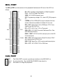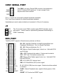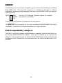
1
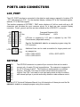
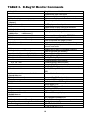
CME-12B/BC Development Board for Motorola 68HC12B32 and 68HC12BC32 Microcontrollers xiom anufacturing 2000 2813 Industrial Ln. • Garland, TX 75041 • (972) 926-9303 FAX (972) 926-6063 email: [email protected] • web: http://www.axman.com CONTENTS GETTING STARTED ............................................................................................3 Installing the Software..................................................................... 3 Board Startup .................................................................................. 3 Support Software ............................................................................ 4 Software Development .................................................................... 4 TUTORIAL............................................................................................................5 Creating source code ...................................................................... 5 Assembling source code ................................................................. 6 Running your application ................................................................ 7 Programming Flash EEPROM......................................................... 8 MEMORY MAP .....................................................................................................9 CONFIG SWITCH...............................................................................................10 MEM-SEL JUMPERS .........................................................................................10 PORTS AND CONNECTORS ............................................................................11 LCD_PORT ................................................................................... 11 KEYPAD........................................................................................ 11 MCU_PORT .................................................................................. 12 CAN_PORT................................................................................... 12 COM1 SERIAL PORT ................................................................... 13 J2 .................................................................................................. 13 BUS_PORT................................................................................... 13 BDM-IN ......................................................................................... 14 EVU Compatibility Jumpers........................................................... 14 TROUBLESHOOTING .......................................................................................15 Code Execution ...................................................................... 16 TABLES..............................................................................................................17 TABLE 1. LCD Command Codes ................................................. 17 TABLE 2. LCD Character Codes.................................................. 17 TABLE 3. D-Bug12 Monitor Commands....................................... 18 2 GETTING STARTED The Axiom CME-12B/BC single board computer is a fully assembled, fully functional development system for the Motorola 68HC12B32 and BC32 microcontrollers, complete with wall plug power supply and serial cable. Support software for this development board is provided for Windows 95 and NT operating systems and DOS. Follow the steps in this section to get started quickly and verify everything is working correctly. Installing the Software 1. Insert the Axiom 68HC12 support disk in your PC. If the setup program does not start, run the file called "SETUP.EXE" on the disk. 2. Follow the instructions on screen to install the support software onto your PC. 3. The flash programming utilities require you to specify the board you are using. You should select either “CME-12B32” or "CME-12B/BC" for this board. Board Startup Follow these steps to connect and power on the board. This assumes you're using the provided AXIDE or AX12 terminal program (installed in the previous section) or a similar communications terminal program on your PC. If you're using a different terminal program than the one provided, set it's parameters to 9600 baud, N,8,1. 1. Make certain the CONFIG SWITCH is set as follows: 1 ON 2 ON 3 ON 4 ON 5 OFF 6 ON 7 OFF 8 OFF 2. Connect one end of the supplied 9-pin serial cable to a free COM port on your PC. Connect the other end of the cable to the COM1 port on the CME-12B/BC board. 3. Apply power to the board by plugging in the power adapter that came with the system. 4. If everything is working properly, you should see a message to “PRESS KEY TO START MONITOR…” in your terminal window. Press the ENTER key and you should see: D-Bug12 v2.0.2 Copyright 1996 - 1997 Motorola Semiconductor For Commands type "Help" > _ 5. Your board is now ready to use! If you do not see this message prompt, or if the text is garbage, see the TROUBLESHOOTING section at the end of this manual. 3 Support Software There are many useful programs and documents on the included HC12 support disk that can make developing projects on the CME-12B/BC easier. You should browse the disk and copy anything you want to your hard drive. See the README.TXT file for a description of what is included. The flash programming utilities communicate with the board via its COM1 port and the supplied cable. These programs also include a simple Terminal for interfacing with other programs running on the CME-12B/BC, such as the D-Bug12 and information from your own programs that send output to the serial port. Also on the disk is a free assembler, example source code, and other tools to get you started. Software Development Software development on the CME12B32 can be performed using either the DBUG12 monitor utility installed in EPROM (sockets U6/U7), the DBUG12 monitor programmed into the internal Flash EPROM or a Background Debug Module (BDM) connected to the BDM-IN connector. Any of these tools can be used to assist in creating and debugging your program stored in either internal RAM ($800-$C00) or external RAM (U4/U5 see Memory Map). After satisfactory operation running under a debugger, your program can be written to the Internal Flash Memory by relocating its start address to $8000 and programming it using either the included programming utilities or a BDM. Your program will then run automatically whenever the board is powered on or RESET is applied. Option jumpers and switches on the board allow for easy transition from one memory type to another and restoring an operating monitor. 4 TUTORIAL This section was written to help you get started developing software with the CME-12B/BC board. Be sure to read the rest of this manual as well as the documentation on the disk if you need further information. The following sections take you through the complete development cycle of a simple "hello world" program, which sends the string "Hello World" to the serial port. Creating source code You can write source code for the CME-12B/BC board using any language that compiles to Motorola 68HC12 instructions. Included on the software disk is a free Assembler and also a freeware C compiler and Basic compiler. You can write your source code using any ASCII text editor. You can use the free EDIT or NOTEPAD programs that come with your computer. A better code editor can be downloaded at: http://www.winedit.com. Once your source code is written and saved to a file, you can assemble or compile it to a Motorola S-Record (hex) format. This type of output file usually has a .MOT, .HEX or .S19 file extension and is in a format that can be read by the programming utilities to be programmed into the CME-12B/BC board. It's important to understand your development board's use of Memory and Addressing when writing source code so you can locate your code at valid addresses. For example, when in debug mode, you should put your program CODE in External RAM. In assembly language, you do this with ORG statements in your source code. Any lines following an ORG statement will begin at that ORG location, which is the first number following the word ORG, for example: ORG $2000. You must start your DATA (or variables) in a RAM location unused by your program, for example: ORG $1000. When finished debugging, you must change these ORG statements so that your program is moved to a valid EEPROM area - somewhere after hex 8000. Do this by putting an ORG $8000 in front of your Program CODE. Data may remain where it is or be moved down to internal RAM starting at ORG $800. You must also program the STACK register somewhere at the top of your available RAM, for example hex BFF. Do this with this instruction as the first instruction in your program code: LDS #$0BFF. A look at the example programs on the disk can make all of this clearer. If you're using a compiler instead of an assembler, consult the compiler documentation for methods used to locate your code and data. Source code created to run under the D-bug12 monitor environment will be slightly different than code written for stand-alone operation. The monitor contains interrupt and RESET vectors that your code must provide when it's no longer running under the monitor. See the Programming Flash EEPROM section for more information on this. 5 Assembling source code An example program called “HELLO.ASM” is provided under the \EXAMPLE directory. You can assemble your source code using command line tools under a DOS prompt by typing: AS12 HELLO.ASM –LHELLO Most compilers and assemblers allow many command line options so using a MAKE utility or batch file is recommended if you use this method. Run AS12 without any arguments to see all the options, or see the AS12.TXT file on the disk. The programming utilities provided with this board also contain a simple interface to the free assembler. Use it by selecting "Build" or “Assembler” from the menu. This will prompt you for the file to be assembled. DO NOT use long path names (> 8 characters). The free assembler is an old DOS tool that does not recognize them. If there are no errors in your source code, 2 output files will be created: HELLO.S19 HELLO.LST a Motorola S-Record file that can be programmed into memory a common listing file which shows the relationship between source and output The listing file is especially helpful to look at when debugging your program. If your program has errors, they will be displayed and no output will be generated, otherwise the listing file will be displayed. If you prefer a windows integrated programming environment – try the Motorola MCU-EZ tools. Refer to the MCU-EZ documentation on the disk for more information. Also, a port for the free GNU C compiler and tools for the HC12 is in the works and may be finished as you read this. Check www.axman.com or : http://home.worldnet.fr/~stcarrez/m68hc11_port.html 6 Running your application After creating an S-Record file you can "upload" it to the development board for a test run. The provided example “HELLO.ASM” was created to run from RAM so you can use the DBug12 Monitor to test it without programming it into EEPROM. If you haven’t done so already, verify that the CME-12B/BC board is connected and operating properly by following the steps under “GETTING STARTED” until you see the D-Bug12 prompt, then follow these steps to run your program: 1. Press and release the RESET button on the CME-12B/BC board. You should see the PRESS ANY KEY message. Hit the return key ↵ to get the monitor prompt. 2. Type LOAD ↵ This will prepare D-Bug12 to receive a program. 3. Select Upload or Send and when prompted for a file name select your assembled program file in s-record format that was created in the previous section called: HELLO.S19 Your program will be sent to the board thru the serial port. 4. When finished loading you will see the > prompt again. Type CALL 1000 ↵ This tells D-Bug12 to execute the subroutine at address $1000, which is the start of our test program. 5. If everything is working properly you should see the message “Hello World” echoed back to your terminal screen then, since we return at then end of our program, a line containing the internal register status displayed by D-Bug12 and a message prompt. 6. If you do not get this message, try going thru this tutorial once more, then if still no go, see the TROUBLESHOOTING section in this manual You can modify the hello program to display other strings or do anything you want. The procedures for assembling your code, uploading it to the board and executing it remain the same. D-Bug12 has many powerful features such as breakpoints, assembly/disassembly, memory dump and modify and program trace. Type HELP at the D-Bug12 prompt for a listing of commands or consult the D-Bug12 documentation on the disk for more information. 7 Programming Flash EEPROM You can program your application into EEPROM so it executes automatically when you apply power to the board as follows: 1. Make a backup copy of HELLO.ASM then use a text editor to modify it. Change the start of the program to $8000 which is the beginning of the EEPROM. Do this by changing the ”ORG $1000” to ”ORG $8000”. 2. Remove the comment ; character from before the following line to initialize the stack pointer which is necessary when running outside of D-Bug12: LDS #$C00 ; initialize the stack pointer 3. Add a comment ; character to the beginning of the first RTS statement, which will cause the program to end gracefully with an endless loop: ; RTS bra ; return (use this only if called, from monitor ENDPROG ; endless loop 4. Remove the comment ; character from before the following 2 lines at the end, to set the reset vector to go to the beginning of the program (the label START) when powered on: org $fffe fdb reset vector START 5. Re-Assemble HELLO.ASM as described in the "Assembling Source Code" section. 6. Select “CME12BC” under AxIDE. 7. Select the “Program” option and when prompted for a file name, enter the new HELLO.S19 file then select [OK]. 8. Set the CONFIG SWITCH positions 1,2,3,4 and 6 to ON. 9. Press the RESET button on the board then select Continue or hit ENTER. A new utilities menu should be displayed. If you have trouble here, see the TROUBLESHOOTING section. 10. Set the CONFIG SWITCH position 5 ON. The red VPP light should come on. 11. When prompted to “Erase” choose Yes. 12. When finished programming, set the CONFIG SWITCH positions 1,2,3,4 and 5 OFF. The VPP light should turn off. 13. Cycle power or press RESET on the board. Your new program should start automatically and the “Hello World” prompt should be displayed in the terminal window. To return to the D-Bug12 monitor program, set the CONFIG SWITCH positions 1,2,3 and 4 back ON then press RESET. 8 MEMORY MAP Following is the default memory map for this development board. Consult the HC12 technical reference manual on the support disk for details of the internal memory map for the processor. FFFF FFFE - - - - - - - RESET Vector Address - - - - - - - CONFIG SWITCH 1 2 3 4 ON ON ON ON ON ON ON OFF OFF OFF OFF OFF - - - - - - External EPROM U6/7 (Debug12) External SRAM U4/5 Internal Flash EEPROM 8000 7FFF External RAM in U4/5 with CONFIG 1 - 4 ON 1000 FFF D00 CFF C00 BFF HC12 Internal EEPROM External RAM in U4/5 with CONFIG 1 - 4 ON Internal RAM 800 7FF 400 3FF External RAM in U4/5 with CONFIG 1 - 4 ON Peripheral Area Unused = 280-3FF LCD / CS7 = 270-27F CS6 = 260-26F 200 1FF 000 CS5 = 250-25F CS4 = 240-24F CS3 = 230-23F CS2 = 220-22F CS1 = 210-21F CS0 = 200-20F 68HC12 Internal Registers See 68HC12 Technical Reference Manual 9 - CONFIG SWITCH The CME-12B/BC board is shipped from the manufacturer with the following default CONFIG SWITCH settings: 1 ON 2 ON 3 ON 4 ON 5 OFF 6 ON 7 OFF 8 OFF The 8 position CONFIG SWITCH provides an easy method of configuring the CME-12B/BC32 board operation. Following are the configuration switch descriptions and HC12 I/O port usage: CONFIG SWITCH 1 2 3 4 5 6 7 8 OPERATION when in ON position MODE A selection (see Mode chart below) MODE B selection (see Mode chart below) EXT –External Memory enable (1) MON –Monitor Memory enable (2) VPP - Flash VPP voltage enable RXD - Serial Port RXD input enable PC0 –CAN Port RXCAN enable PC1 –CAN Port TX enable HC12 I/O PORT USED MODA / PE5 MODB / PE6 N/A N/A N/A PS0 / RXD PC0 PC2 (1) Enables memory bus operation for access to board memory. Expanded bus must be on for proper operation. (2) Enables monitor EPROM’s in memory map at 0x8000 – FFFF hex if CONFIG SWITCH position 3 is also on. When in off position memory space is SRAM for BDM use. MODE CHART Single Chip Mode Expanded Wide Mode A and B = OFF A and B = ON MEM-SEL JUMPERS Memory sockets U4/5 are shipped with 32K byte RAM devices. U6/7 are shipped with 32K byte EPROM devices programmed with the D-bug12 monitor. 1,3,4 1,3 2,4 IN: enables RAM or EEPROM, 32K devices to U6/7 IN: enables RAM or EEPROM, 8K devices in U6/7 IN: enables EPROM, 8K or 32K devices in U6/7 (Default) 10 PORTS AND CONNECTORS LCD_PORT The LCD_PORT interface is connected to the data bus and memory mapped to locations 270 – 27F hex assigned to CS7. For the standard display, address 270 is the Command register, address 271 is the Data register. The interface supports all OPTREX DMC series displays in 8 bit bus mode with up to 80 characters and provides the most common pinout for a dual row rear mounted display connector. Power, ground, and Vee are also available at the LCDPORT-1 connector. +5V A0 LCD1 D9 D11 D13 D15 2 1 GND Command Register:$270 4 3 LCD-Vee Data Register: $271 6 5 /RW 8 7 D8 LCD-Vee is supplied by U13 and is adjusted by the R18 10 9 D10 Potentiometer (adjustable resistor). 12 11 D12 See the file KEYLCD12.ASM for an example program using this 14 13 D14 LCD connector. LCD3 2 4 LCD2 1 3 LCD4 Additional lines can be used as enables for larger panels and are mapped as: LCD2 = $274 & $275 LCD3 = $278 & $279 LCD4 = $27C & $27D KEYPAD 1 2 3 4 5 6 7 8 PS4 PS5 PS6 PS7 PP4 PP5 PP6 PP7 The KEYPAD connector is a passive 8-pin connector that can be used to connect a 4 x 4 matrix (16 key) keypad device. The connector is mapped to the HC12 I/O ports S and P. This interface is implemented as a software keyscan. Pins PS4-7 are used as column drivers which are active low outputs. Pins PP4-7 are used for row input and provide an idle hi condition with internal pull-ups to provide active key detection under software control. See the HC12 Technical Reference Manual for a full description of these pins and the file KEYLCD12.ASM for an example program using this connector. 11 MCU_PORT The MCU_PORT provides access to the peripheral features and I/O lines of the HC12 as follows: A14 D0 D2 D4 D6 /XIRQ VFP VRH +5V PAD0 PAD2 PAD4 PAD6 PS0 / RXD PS2 PS4 PS6 PC6 PC4 PC2 PC0 / RXCAN PP6 PP4 PP2 PP0 PT0 PT2 PT4 PT6 +5V 1 3 5 7 9 11 13 15 17 19 21 23 25 27 29 31 33 35 37 39 41 43 45 47 49 51 53 55 57 59 2 4 6 8 10 12 14 16 18 20 22 24 26 28 30 32 34 36 38 40 42 44 46 48 50 52 54 56 58 60 A15 D1 D3 D5 D7 /DBE /LSTRB VRL GND PAD1 PAD3 PAD5 PAD7 PS1 / TXD PS3 PS5 PS7 PC5 PC3 PC1 / TXCAN PP7 PP5 PP3 PP1 PT1 PT3 PT5 PT7 GND GND D0 – D7 Low Byte of the Data Bus in Wide Expanded Mode. Port B in Single Chip Mode. /XIRQ HC12 XIRQ interrupt input . VFP Programming voltage, 12v, when VPP_EN jumper is on. /LSTRB HC12 LSTRB (PE3) output indicates 8 bit bus access. Should be enabled in software for bus use. PP0 – PP7 HC12 Port P I/O or PWM port. PP3-7 also used by the KEYPAD Port. PT0 – PT7 HC12 Port T I/O or Timer port. VRH / VRL HC12 A/D Converter Reference Pins. See A/D Reference Section. PAD0 – PAD7 HC12 Port AD is an input port or the A/D Converter inputs. PS0 – PS7 HC12 Port S I/O or Serial Port lines. PS4-7 also used by the KEYPAD Port. RXD / TXD Serial Port (SCI) receive and transmit pins. PC0 – PC7 HC12 PDLC I/O or CAN lines. CAN_PORT 1 2 3 4 GND CAN-H CAN-L +5V The CAN_PORT connector provides an interface to the MSCAN12 on the microcontroller. See the MC68HC912BC32 data sheet for information on using this peripheral. 12 COM1 SERIAL PORT 1 TXD0 2 RXD0 3 4 GND 5 The COM-1 port has a Female DB9 connector that interfaces to the HC12 internal SCI0 serial port. It uses a simple 2 wire asynchronous serial interface. 6 7 8 9 Pins 1, 4, and 6 are connected for default handshake standards. Pins 7 and 8 are connected for default handshake standards. Handshake pins can be easily isolated and connected to I/O ports if necessary. J2 1 2 3 4 T2IN R2OUT R2IN T2OUT The J2 connector (near COM1) contains spare RS232 translator inputs and outputs. It can be used for implementing hardware handshaking on COM1 if necessary. BUS_PORT The BUS_PORT supports off-board memory devices as follows: GND D10 D9 D8 A0 A1 A10 / OE A11 A9 A8 A12 / WE CS1 CS3 CS5 +5V /RW E GND 1 3 5 7 9 11 13 15 17 19 21 23 25 27 29 31 33 35 37 39 2 4 6 8 10 12 14 16 18 20 22 24 26 28 30 32 34 36 38 40 D11 D12 D13 D14 D15 A2 A3 A4 A5 A6 A7 A13 CS0 CS2 CS4 IRQ /P-SEL CS6 CS7 / RESET D8 - D15 High Byte Data Bus in Wide Expanded Mode and Peripheral 8 bit data bus. Port A in Single Chip Mode. A0 – A15 Memory Addresses 0 to 15. /OE Memory Output Enable signal, Active Low. Valid with ECLK and R/W high. CS0 – CS7 Peripheral chip selects, 16 bytes each located at $200 - $27F hex, 8 bit access (narrow bus). /WE Memory Write Enable signal, Active Low. Valid with ECLK high and R/W low. IRQ HC12 IRQ (PE1) Interrupt Input. /RW HC12 Read/Write (PE2) control signal. E HC12 ECLK (PE4) bus clock signal. Stretch should be enabled in software. /P-SEL Selects Peripheral area, register following space, 8 bits wide. /RESET HC12 active low RESET signal. 13 BDM-IN The BDM-IN port is a 6 pin header compatible in pinout with the Motorola Background Debug Mode (BDM) Pod. This allows the connection of a background debugger for software development, programming and debugging in real-time, since the BDM control logic does not reside in the CPU. BGND 1 2 GND 3 4 /RESET 5 6 +5V See the HC12 Technical Reference Manual for complete documentation of the BDM. A Background Debug Module is available from the manufacturer. The BDM-OUT port is provided on the board for Motorola MC68HC912B32 EVU Board compatibility. Consult the EVU board documentation for usage information. EVU Compatibility Jumpers The EVB-H3 and EVB-H4 jumpers provide backward compatibility with the Flash Options on the Motorola MC68HC912B32 EVU Board. These can be installed by the user and the Debug12.s19 file programmed into the Internal Flash EPROM for EVU similar operation of the development board. Normally this is not necessary due to the Utilities provided in the UTL12 EPROM's. 14 TROUBLESHOOTING The CME-12B/BC board is fully tested and operational before shipping. If it fails to function properly, inspect the board for obvious physical damage first. Ensure that all IC devices in sockets are properly seated. Verify the communications setup as described under GETTING STARTED and see the Tips and Suggestions sections following for more information. The most common problems are improperly configured communications parameters, and attempting to use the wrong COM port. 1. Verify that your communications port is working by substituting a known good serial device or by doing a loop back diagnostic. 2. Verify the jumpers on the board are installed correctly. 3. Verify the power source. You should measure approximately 9 volts between the GND and +9V test point pads on the board. 4. If no voltage is found, verify the wall plug connections to 115VAC outlet and the power connector. 5. Disconnect all external connections to the board except for COM1 to the PC and the wall plug. 6. Make sure that the RESET line is not being held low. Check for this by measuring the RESET pin on P4 for +5V. 7. Verify the presence of an 8MHz sine wave on the crystal, or 2MHz E clock signal if possible. 15 Tips and Suggestions Following are a number of tips, suggestions and answers to common questions that will solve many problems users have with the CME-12B/BC development system. You can download the latest software from the Support section of our web page at: www.axman.com Utilities • If you’re trying to program memory or start the HC12 Utilities, make sure all jumpers and CONFIG SWITCH settings are correct. • Be certain that the data cable you’re using is bi-directional and is connected securely to both the PC and the board. Also, make sure you are using the correct serial port. • Make sure the correct power is supplied to the board. You should only use a 9 volt, 300 mA adapter or power supply. If you’re using a power strip, make sure it is turned on. • Make sure you load your code to an address space that actually exists. Memory Map if you’re not sure. • Make sure you're not over-writing memory used by the monitor program. • If you’re running in a multi-tasking environment (such as Windows™) close all programs in the background to be certain no serial conflict occurs. See the Code Execution • Make sure the CONFIG SWITCH is set for the proper mode. If executing from the BDM, you should turn switches 1-4 OFF. If debugging from internal flash EEPROM, disable any reset macro’s. • If you’re using D-Bug12 breakpoints may not be acknowledged if you use the CALL command. You should use one of the GO command instead. • Check the HC12 reset vector located at FFFEh - FFFFh. These 2 bytes contain the address where execution will begin when the unit is powered on. • When running your code stand-alone, you must initialize ALL peripherals used by the micro, including the Stack, Serial Port, etc. • You must either reset the COP watchdog timer in the main loop of your code or disable it when not running under MBug or BDM mode. The micro enables this by default and if you don't handle it your code will reset every couple of ms. ImageCraft C • Your make or build should create a .MAP file. Some versions change this to a .MP file. At the top of this file should be a label __START. This is where you should CALL or GO to when debugging in D-Bug12. 16 TABLES TABLE 1. LCD Command Codes Command codes are used for LCD setup and control of character and cursor position. All command codes are written to LCD panel address $B5F0. The BUSY flag (bit 7) should be tested before any command updates to verify that any previous command is completed. A read of the command address $B5F0 will return the BUSY flag status and the current display character location address. Command Clear Display, Cursor to Home Cursor to Home Entry Mode: Cursor Decrement, Shift off Cursor Decrement, Shift on Cursor Increment, Shift off Cursor Increment, Shift on Display Control: Display, Cursor, and Cursor Blink off Display on, Cursor and Cursor Blink off Display and Cursor on, Cursor Blink off Display, Cursor, and Cursor Blink on Cursor / Display Shift: (nondestructive move) Cursor shift left Cursor shift right Display shift left Display shift right Display Function (default 2x40 size) Character Generator Ram Address set Display Ram Address set Code $01 $02 Delay 1.65ms 1.65ms $04 $05 $06 $07 40us 40us 40us 40us $08 $0C $0E $0F 40us 40us 40us 40us $10 $14 $18 $1C $3C $40-$7F $80- $FF 40us 40us 40us 40us 40us 40us 40us TABLE 2. LCD Character Codes $20 $21 $22 $23 $24 $25 $26 $27 $28 $29 $2A $2B $2C Space ! “ # $ % & ‘ ( ) * + , $2D $2E $2F $30 $31 $32 $33 $34 $35 $36 $37 $38 $39 . / 0 1 2 3 4 5 6 7 8 9 $3A $3B $3C $3D $3E $3F $40 $41 $42 $43 $44 $45 $46 : ; { = } ? Time A B C D E F $47 $48 $49 $4A $4B $4C $4D $4E $4F $50 $51 $52 $53 G H I J K L M N O P Q R S $54 $55 $56 $57 $58 $59 $5A $5B $5C $5D $5E $5F $60 17 T U V W X Y Z [ Yen ] ^ _ ` $61 $62 $63 $64 $65 $66 $67 $68 $69 $6A $6B $6C $6D a b c d e f g h i j k l m $6E $6F $70 $71 $72 $73 $74 $75 $76 $77 $78 $79 $7A n o p q r s t u v w x y z $7B $7C $7D $7E $7F { | } > < TABLE 3. D-Bug12 Monitor Commands ASM <Address> <CR> <.> BAUD <baudrate> BF <StartAddress> <EndAddress> [<data>] BR [<Address>] BULK CALL [<Address>] DEVICE [<DevName> [<Address>...<Address>]] EEBASE <Address> FBULK FLOAD [<AddressOffset>] G [<Address>] GT <Address> Single line assembler/disassembler Disassemble next instruction Exit assembly/disassembly Set communications rate for the terminal Fill memory with data Set/Display user breakpoints Erase entire on-chip EEPROM contents Call user subroutine at <Address> display/select/add target device Set base address of on-chip EEPROM Erase entire target FLASH contents Load S-Records into target FLASH Begin/continue execution of user code Set temporary breakpoint at <Address> & execute user code HELP Display this D-Bug12 command summary LOAD [<AddressOffset>] Load S-Records into memory MD <StartAddress> [<EndAddress>] Memory Display Bytes MDW <StartAddress> [<EndAddress>] Memory Display Words MM <StartAddress> Modify Memory Bytes <CR> Examine/Modify next location </> or <=> Examine/Modify same location <^> or <-> Examine/Modify previous location <.> Exit Modify Memory command MMW <StartAddress> Modify Memory Words (same subcommands as MM) MOVE <StartAddress> <EndAddress> Move a block of memory <DestAddress> NOBR [<address>] Remove One/All Breakpoint(s) RD Display all CPU registers REGBASE <Address> Set base address of I/O registers RESET Reset target CPU RM Modify CPU Register Contents STOP Stop target CPU T [<count>] Trace <count> instructions UPLOAD <StartAddress> S-Record Memory display <EndAddress> USEHBR Use Hardware Breakpoints VERF [<AddressOffset>] Verify S-Records against memory contents <Register Name> <Register Value> Set register contents Register Names: PC, SP, X, Y, A, B, D CCR Status Bits: S, XM, H, IM, N, Z, V, C 18