1
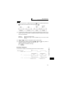
INVERTER
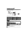
FR-A700
FR-A700
INVERTER
PLC FUNCTION
PROGRAMMING MANUAL
PLC FUNCTION
IB(NA)-0600262EG-A(0509)MEE
Printed in Japan
Specifications subject to change without notice.
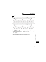
PLC FUNCTION PROGRAMMING MANUAL
HEAD OFFICE:MITSUBISHI DENKI BLDG MARUNOUCHI TOKYO 100-8310
A
Chapter 1
CC-Link
COMMUNICATION Chapter 2
SEQUENCE
PROGRAMMING
Chapter 3
ERROR CODE
LIST
Chapter 4
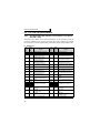
CONTENTS
1.1
1.2
1.3
1.4
1.5
Function Block Diagram ...........................................................2
PLC Function Specifications....................................................3
System Configuration ...............................................................4
Wiring of the Inverter and Personal Computer Using
GX Developer for RS-485 Communication..............................5
Prior to Sequence Program Creation ......................................6
1.5.1
1.5.2
1.5.3
1.5.4
1.5.5
1.6
1.7.4
1.7.5
1.7.6
Data that can be read at all times................................................................ 20
Data that are read by controlling (OFF to ON) the read command ............. 23
How to write data by controlling (OFF to ON) the write
command.................................................................................................... 25
Inverter operation status control.................................................................. 31
Inverter parameter access error (D9150) .................................................... 33
Inverter status (D9151)................................................................................ 33
Inverter Parameter Read/Write Method .................................34
1.8.1
1.8.2
1.9
I/O device map ............................................................................................ 10
Internal relay (M) device map...................................................................... 12
Data register (D) device map ...................................................................... 12
Special relays .............................................................................................. 12
Special registers.......................................................................................... 14
Inverter Status Monitoring, Special Registers for Control ..20
1.7.1
1.7.2
1.7.3
1.8
Precautions for sequence program creation ................................................. 6
Usable main GX Developer functions ........................................................... 6
Sequence program execution key................................................................. 7
Sequence program write ............................................................................... 8
Setting list of built-in PLC function parameter ............................................... 9
Device Map...............................................................................10
1.6.1
1.6.2
1.6.3
1.6.4
1.6.5
1.7
1
CONTENTS
1. PLC FUNCTION
Reading the inverter parameters................................................................. 34
Writing the inverter parameters ................................................................... 36
User Area Read/Write Method ................................................38
1.9.1
User parameter read/write method.............................................................. 38
1.10 Analog I/O function .................................................................39
1.10.1 Analog input ................................................................................................ 39
1.10.2 Analog output .............................................................................................. 39
1.11 Paluse train input function .....................................................40
1.12 PID control ...............................................................................41
1.13 Inverter Operation Lock Mode Setting ..................................43
I
2. CC-Link COMMUNICATION
2.1
System Configuration............................................................. 46
2.1.1
2.1.2
2.2
System configuration example.................................................................... 46
Function block diagram............................................................................... 47
CC-Link Parameters................................................................ 49
2.2.1
2.3
2.4
CC-Link Extended Setting (Pr. 544)............................................................ 49
CC-Link I/O Specifications ..................................................... 50
Buffer Memory......................................................................... 57
2.4.1
2.4.2
2.4.3
2.4.4
Remote output signals
(Master module to inverter(FR-A7NC))....................................................... 57
Remote input signals Pr.544=100
(Inverter(FR-A7NC) to master module)....................................................... 58
Remote registers Pr.544=100
(Master module to inverter(FR-A7NC))....................................................... 59
Remote registers Pr.544=100
(Inverter(FR-A7NC) to master module)...................................................... 60
3. SEQUENCE PROGRAMMING
3.1
BIN (Binary Code)....................................................................................... 73
HEX (HEX Decimal).................................................................................... 74
Description of devices............................................................ 75
3.9.1
3.9.2
3.9.3
3.9.4
II
What is refresh system? ............................................................................. 69
Response delay in refresh system.............................................................. 70
Scan Time ................................................................................ 71
Numerical Values Usable in Sequence Program ................. 72
3.8.1
3.8.2
3.9
Relay symbolic language (Ladder mode) ................................................... 65
Logic symbolic language (List mode).......................................................... 67
Operation Processing Method of PLC Function .................. 68
I/O Processing Method ........................................................... 69
3.6.1
3.6.2
3.7
3.8
Outline of Operation Processings ............................................................... 62
RUN and STOP Operation Processings................................ 64
Program Makeup ..................................................................... 64
Programming Languages....................................................... 65
3.4.1
3.4.2
3.5
3.6
61
Overview .................................................................................. 62
3.1.1
3.2
3.3
3.4
45
Device List .................................................................................................. 75
Inputs, Outputs X, Y.................................................................................... 76
Internal Relays M ........................................................................................ 79
Timers T...................................................................................................... 80
3.9.5
3.9.6
100ms, 10ms and 100ms retentive timers .................................................. 80
Timer processing method and accuracy ..................................................... 81
3.10.1 Count processing in refresh system ............................................................ 84
3.10.2 Maximum counting speed of counter .......................................................... 85
3.11
3.12
3.13
3.14
Data Registers D......................................................................86
Special Relays, Special Registers .........................................87
Function List ............................................................................89
How to RUN/STOP the Built-in PLC Function from Outside (Remote RUN/STOP) .....................................................................90
3.15 Watchdog Timer (Operation clog up monitor timer) ............92
3.16 Self-diagnostic Function ........................................................93
3.16.1 Error-time operation mode .......................................................................... 94
3.17 Keyword Registration .............................................................95
3.18 Setting of Output (Y) Status at Switching from STOP Status to
RUN Status...............................................................................96
3.19 Instruction Format...................................................................97
3.20 Bit Device Processing Method ...............................................99
3.20.1 1-bit processing ........................................................................................... 99
3.20.2 Digit designation processing ....................................................................... 99
3.21 Handling of Numerical Value................................................101
3.22 Operation Error......................................................................102
3.23 Instructions List ....................................................................103
3.23.1
3.23.2
3.23.3
3.23.4
How to use the instruction list.................................................................... 103
Sequence instruction................................................................................. 105
Basic instructions ...................................................................................... 107
Application instructions.............................................................................. 109
3.24 Description of the Instructions ............................................110
3.25 Sequence Instructions ..........................................................111
3.25.1 Contact Instructions :
Operation start, series connection, parallel connection ... LD, LDI, AND, ANI,
OR, ORI..................................................................................................... 111
3.25.2 Contact Instructions : Ladder block series connection, parallel connection ...
ANB, ORB ................................................................................................. 113
3.25.3 Connection Instructions :
Ladder block series connection, parallel connection ... ANB, ORB........... 117
3.25.4 Connection Instructions :
Operation result, push, read, pop ... MPS, MRD, MPP ............................. 120
3.25.5 Output Instructions : Bit device, timer, counter ... OUT ............................. 123
III
CONTENTS
3.10 Counters C ...............................................................................83
3.25.6 Output Instructions : Device set, reset ... SET, RST................................. 126
3.25.7 Output Instructions : Leading edge, trailing edge differential outputs ... PLS,
PLF ........................................................................................................... 129
3.25.8 Shift Instructions : Bit device shift ... SFT, SFTP ...................................... 131
3.25.9 Master Control Instructions : Master control set, reset ... MC, MCR......... 133
3.25.10End Instruction : Sequence program end ... END..................................... 137
3.25.11Other Instructions : No operation ... NOP ................................................. 138
3.26 Basic Instructions ................................................................. 140
3.26.1 Comparison Operation Instructions .......................................................... 140
3.26.2 Comparison Operation Instructions :
16-bit data comparison ... =, <>, >, <=, <, >=............................................ 142
3.26.3 Arithmetic Operation Instructions.............................................................. 144
3.26.4 Arithmetic Operation Instructions :
BIN 16-bit addition, subtraction ... +, +P, -, -P .......................................... 145
3.26.5 Arithmetic Operation Instructions :
BIN 16-bit multiplication, division ... *, *P, /, /P.......................................... 149
3.26.6 Data Transfer Instructions......................................................................... 153
3.26.7 Data Transfer Instructions :
16-bit data transfer ... MOV, MOVP .......................................................... 153
3.27 Application instructions ....................................................... 155
3.27.1 Logical Operation Instructions .................................................................. 155
3.27.2 Logical Operation Instructions :
16-bit Logical Product ... WAND, WANDP................................................ 156
3.27.3 Logical Operation Instructions :
16-bit Logical Add ... WOR, WORP .......................................................... 159
3.27.4 Logical Operation Instructions :
16-bit Exclusive Logical Add ... WXOR, WXORP ..................................... 162
3.27.5 Logical Operation Instructions :
16-bit NOT Exclusive Logical Add ... WXNR, WXNRP ............................. 165
3.27.6 Logical Operation Instructions :
BIN 16-bit 2’s complement ... NEG, NEGP............................................... 168
4. ERROR CODE LIST
4.1
171
How to Read the Error Code ................................................ 172
APPENDIX
175
Appendix1Instruction Processing Time ....................................... 176
IV
1. PLC FUNCTION
This manual describes the functions and devices necessary for programming.
1.1
1.2
1.3
1.4
1.5
1.6
1.7
1.8
1.9
1.10
1.11
1.12
1.13
Function Block Diagram ......................................
PLC Function Specifications...............................
System Configuration ..........................................
Wiring of the Inverter and Personal Computer
Using GX Developer for RS-485 Communication...
Prior to Sequence Program Creation .................
Device Map............................................................
Inverter Status Monitoring, Special Registers
for Control .............................................................
Inverter Parameter Read/Write Method ..............
User Area Read/Write Method .............................
Analog I/O function ..............................................
Paluse train input function ..................................
PID control ............................................................
Inverter Operation Lock Mode Setting ...............
2
3
4
5
6
10
20
34
38
39
40
41
43
Chapter 1
Chapter 2
Chapter 3
Chapter 4
1
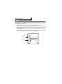
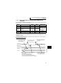
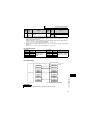
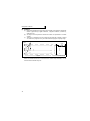
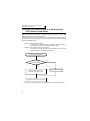
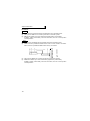
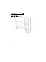
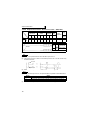
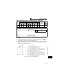
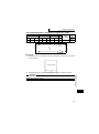
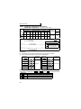
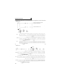
Function Block Diagram
1.1 Function Block Diagram
How I/O data are transferred to/from the inverter by the built-in PLC function is
explained using function blocks.
(1) I/O data read, write, etc. can be performed by accessing the inverter in the
predetermined method using special relays, special registers, etc.
(2) Operation, parameter read/write, etc. can be performed in accordance with the
created sequence programs (built in the inverter) using input data from the control
input terminals.
With the output signals, output data can be output to outside the inverter from the
control output terminals as not only the inverter's status signals but also pilot lamp
on/off, interlock and other control signals set freely by the user.
Output signal
2
I/O data
Special relays,
special registers,
etc.
Inverter CPU
Input signal
Built-in sequence program
Inverter
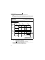
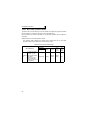
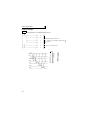
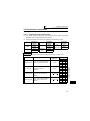
PLC Function Specifications
1.2 PLC Function Specifications
The following table indicates the program capacity and devices of the PLC function.
A700 Sequence Section
Control method
I/O control method
PLC instructions
Basic instructions
Repeated operation (by stored program)
Refresh
Relay symbolic language (ladder mode)
Logic symbolic language (list mode)
23
32
Application instructions
18
Number of
instruction
Programming language
PLC instruction 1.9µs to 12µs/step(*2)
128 (X: 64 points, Y: 64 points)
19 points installed, X: 12 points, Y: 7 points (*1)
Number of I/O points
FR-A7AX, X: 16 points
FR-A7AY, Y: 6 points
FR-A7AR, Y: 3 points
5 points installed, Input: 3 points, Output: 2 points
Number of analog I/O points
FR-A7AY output: 2 points
Watchdog timer
10 to 2000(ms)
Memory capacity
6k bytes used by sequence and parameters.
Program capacity
1k step
Internal relay (M)
64(M0 to M63)
Latch relay (L)
None (Can be set with parameters but will not latch)
Step relay (S)
None (Can be set with parameters but will operate as M)
Link relay (B)
None
Points
16
100ms timer: Set time 0.1 to 3276.7s (T0 to T15)
Timer (T)
Specifications
10ms timer: Set time 0.01 to 327.67s
100ms retentive timer: Set time 0.1 to 3276.7s
Points
16
Counter (C)
Normal counter: Setting range 1 to 32767 (C0 to C15)
Specifications
Interrupt program counter: None
Data device (D)
120(D0 to D119)
Link register (W)
None
Annunciator (F)
None
File register (R)
None
Accumulator (A)
None
Index register (Z, V)
None
Pointer (P)
None
Interrupt pointer (I)
None
Special relay (M)
256 (M9000 to 9255) with function limit
Special register (D)
256 (D9000 to 9255) with function limit
*1 These signals use the same terminals as used by the input and output signals given in the
common specifications of the inverter.
One point is always necessary for a sequence start (RUN/STOP).
*2 As inverter control is also performed actually, the scan time is approximately 40ms at 500 steps.
Devices
Processing speed
3
PLC FUNCTION
1
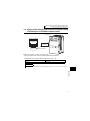
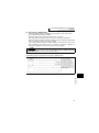
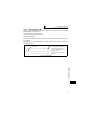
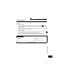
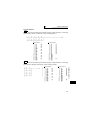
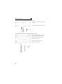
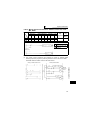
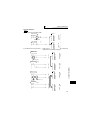
System Configuration
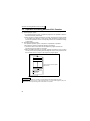
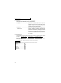
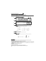
1.3 System Configuration
The following shows the system configuration for use of the PLC function.
<System configuration example>
GX Developer:
Programming tool
FR-A700
PU connector
RS-232C/
RS-485
converter
Motor
3-phase AC
power supply
Communication specifications
Set the following setting in communication parameters of the inverter.
Inverter Parameter
GX Developer Setting
Inverter initial setting
96 (9600bps)
0 (data length: 8 bits, stop
Pr.119 PU communication stop bit length
bit: 1 bit)
Pr.120 PU communication parity check 1 (with odd parity check)
Pr.122 PU communication check time
9999 (without
interval
communication check)
192 (19200bps)
1 (data length: 8 bits, stop
bit: 2 bit)
2 (with even parity check)
9999 (without
communication check)
Pr.118 PU communication speed
REMARKS
•For futher details, refer to the Inverter instruction manual (applied).
POINT
•Support GX Developer ver.8.0 or more
•GX Developer Setting
PLC series
PLC type
ACPU
A0J2H
[Project data list]→[Parameter]→[PLC parameter]→[A parameter]
→«Memory capacity» tab→"Program capacity"→"Sequence"→"main"
1k step
REMARKS
•Refer to the Inverter instruction manual (applied) for wiring.
•Refer to the GX Developer manuals for the specifications related to GX Developer and the
personal computer that uses GX Developer.
GX Developer Version xx Operating manual
GX Developer Version xx Operating manual (startup)
•The programming tool that can be used is GX Developer only. (The A6GPP, A7PHP, etc.
cannot be used.)
4
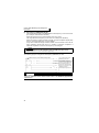
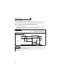
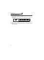
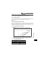
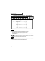
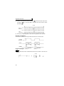
Wiring of the Inverter and Personal Computer Using
GX Developer for RS-485 Communication
1.4 Wiring of the Inverter and Personal Computer Using
GX Developer for RS-485 Communication
PU connector
Personal computer
GX Developer :
Programming tool
RS-232C-RS-485
converter
RS-232C connector
zPersonal computer - inverter connection cable
Make connection after conversion between RS-232C and RS-485.
Examples of commercially available products (as of Sep., '05)
Type
SC-FRPC
Maker
BEIJERS
REMARKS
When fabricating the cable on the user side, refer to the inverter instruction manual (applied).
PLC FUNCTION
1
5
Prior to Sequence Program Creation
1.5 Prior to Sequence Program Creation
1.5.1
Precautions for sequence program creation
POINT
•Online change of the sequence program and access to other stations are not
allowed.
In addition, program read/write from other stations and all PLC memory clear
cannot be performed.
•Back up the ladder configured with the protective function of GX Developer.
If any of the instructions (refer to page 103) and devices (refer to page 3) that cannot
be used with the built-in PLC function exists in a sequence program, an instruction
code error occurs at the execution of that instruction.
Error code
D9008=10
Operation error step
D9010
D9011
REMARKS
•Refer to page 22 for the error codes.
1.5.2
Usable main GX Developer functions
z Parameter or sequence program read/write
z Ladder monitor
z Device monitor
z Device test
z All device memory clear
z Remote RUN/STOP
CAUTION
Device test ([Online] - [Debug] - [Device test]) of GX Developer can be performed, but if
devices corresponding to control terminal (e.g. STF, STR) signals are tested, the
devices turn on in the sequence but the inverter does not perform the corresponding
operation.
6
Prior to Sequence Program Creation
1.5.3
Sequence program execution key
The sequence program execution key (STOP/RUN) of the PLC is switched by turning
off/on the SQ signal.
POINT
•For the terminal used for SQ signal input, set "50" in any of Pr.178 to Pr. 189 to
assign the function.
•SQ-SD must be shorted to execute the built-in PLC function.
CAUTION
If the SQ signal is not turned on, the start signal of the inverter is designed to
become valid by the factory setting of Pr.415 Inverter operation lock mode setting.
Open (STOP) the SQ signal-SD terminals when writing a sequence program, for
example.
When executing the sequence program, short (RUN) the SQ signal-SD terminals.
Remote run/stop of the built-in PLC function can be executed in any of the following
methods:
• Setting using the built-in PLC function parameter (contact)
• Using GX Developer
• Via CC-Link communication (refer to page 49)
REMARKS
•The validity limit of the SQ signal can be controlled using Pr.415 Inverter operation lock mode
setting. (Refer to page 43.)
CAUTION
1
PLC FUNCTION
The outputs (Y) are cleared by turning the SQ signal off (STOP) after sequence program
execution (SQ signal on).
The other devices retain the device data prior to STOP. When you want to clear the
remaining device data, power off or reset (short RES-SD for 0.1s, then open) the
inverter.
7
Prior to Sequence Program Creation
1.5.4
Sequence program write
POINT
Sequence program write can be performed in any operation mode.
When rewriting the PLC function parameters and sequence program using GX
Developer, check the following:
1) Check that the sequence program execution key is in the STOP position (SQ signal
is off) (refer to page 7).
2) Check that the inverter is at a stop.
3) Check that the communication specification setting parameters (Pr.117 to Pr.124) are
set correctly. If any of these parameters is set incorrectly, communication with GX
Developer cannot be made.
REMARKS
Check and set the communication specification parameter (Pr. 117 to Pr. 124) using
the parameter unit (FR-PU04/FR-PU07). (Refer to the FR-PU04/FR-PU07
instruction manual for the handling of the FR-PU04/FR-PU07.) GX Developer and
the FR-PU04/FR-PU07 cannot be connected and used simultaneously.
4) Check the PLC series and sequence program capacity in the GX Developer
parameters (refer to page 4).
5) Refer to the GX Developer manual and write the sequence program.
CAUTION
•A sequence program cannot be written with its steps specified. If written,
the sequence program does not run. (The program outside the specified
range is initialized.)
•Do not read the built-in PLC function parameters and sequence program
without writing them to the inverter once using GX Developer. Since the
inverter does not have normal data, always write the built-in PLC function
parameters and sequence program once.
•Since the built-in PLC function parameters and sequence program are
written to the flash ROM, there are restrictions on the number of write times.
(Approximately 100,000 times)
8
Function Block Diagram
1.5.5
Setting list of built-in PLC function parameter
The built-in PLC function parameters are designed to specify the ranges of using the
PLC function, e.g. program capacity, device assignment and various functions.
Item
Sequence program
capacity
File register capacity
Comment capacity
Status latch
Sampling trace
Microcomputer program
capacity
Latch range setting
Link range setting
I/O assignment
GX Developer Default
6k steps
Setting Range
<Usable device range>
1k step
None
None
None
None
Cannot be set (default)
Cannot be set (default)
Cannot be set (default)
Cannot be set (default)
None
Cannot be set (default)
L1000 to L2047
None
None
M0 to 999
L1000 to 2047
None for S
200ms
100ms: T0 to 199
10ms: T200 to 255
(100ms timers since only T0 to 7
are available)
Cannot be set (invalid if set)
Cannot be set (default)
Cannot be set (default)
L and S cannot be set.
Internal relay, latch relay,
(Operates as M if set)
step relay setting
<M0 to M63>
Watchdog timer setting
10 to 2000ms
16 points for 100ms, 10ms and
retentive timers. Timers have
Timer setting
consecutive numbers.
<T0 to T15>
Cannot be set (default)
Counter setting
Without interrupt counters
<C0 to C15>
Can be set using X0 to 1F.
Remote run/pause
None
Otherwise invalid. Pause does not
function.
Setting invalid (since there are no
Fuse blow: Continued
fuses)
Setting invalid
I/O verify error: Stop
(since there are no I/O modules)
Error-time operation mode
Operation error: Continued Stop/Continued
Special function module check Setting invalid (since there are no
error: Stop
special modules)
Operation status prior to
Prior to STOP/after operation
STOP → RUN output mode
STOP is re-output.
execution
Print title registration
None
Cannot be set
Online setting cannot be made but
Keyword registration
None
parameter setting is valid.
PLC FUNCTION
1
REMARKS
•The following functions are not supported.
1. Constant scan, 2. Latch (device data backup for power failure), 3. Pause,
4. Status latch, 5. Sampling trace, 6. Offline switch
•If parameter clear of the inverter is performed, the above built-in PLC function parameters are
not cleared.
•For the built-in PLC function parameter setting operation, refer to the GX Developer
Operating Manual.
9
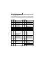
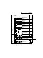
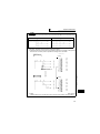
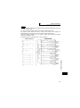
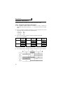
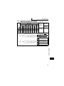
Device Map
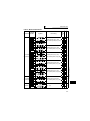
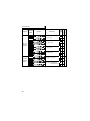
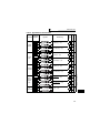
1.6 Device Map
1.6.1
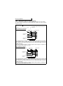
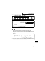
I/O device map
Plug in option I/O
External I/O
Device
No.
10
X00
X01
X02
X03
X04
X05
X06
X07
X08
X09
X0A
X0B
X0C
X0D
X0E
X0F
X10
X11
X12
X13
X14
X15
X16
X17
X18
X19
X1A
X1B
X1C
X1D
X1E
X1F
Name
STF terminal
STR terminal
RH terminal
RM terminal
RL terminal
JOG terminal
RT terminal
AU terminal
CS terminal
MRS terminal
STOP terminal
RES terminal
Remarks
External
terminal
Empty
X0 terminal
X1 terminal
X2 terminal
X3 terminal
X4 terminal
X5 terminal
X6 terminal
X7 terminal
X8 terminal
X9 terminal
X10 terminal
X11 terminal
X12 terminal
X13 terminal
X14 terminal
X15 terminal
16bit
digital
Input
FR-A7AX
Device
No.
Y00
Y01
Y02
Y03
Y04
Y05
Y06
Y07
Y08
Y09
Y0A
Y0B
Y0C
Y0D
Y0E
Y0F
Y10
Y11
Y12
Y13
Y14
Y15
Y16
Y17
Y18
Y19
Y1A
Y1B
Y1C
Y1D
Y1E
Y1F
Name
RUN terminal
SU terminal
OL terminal
IPF terminal
FU terminal
ABC1 terminal
ABC2 terminal
Remarks
External
terminal
Empty
DO0 terminal
DO1 terminal
DO2 terminal
DO3 terminal
DO4 terminal
DO5 terminal
DO6 terminal
RA1 terminal
RA2 terminal
RA3 terminal
Empty
Dgital
output
FR-A7AY
Relay
output
FR-A7AR
Device Map
X21
X22
X23
X24
System I/O
X25
X26
X27
X28
X29
X2A
CC-Link I/O remote I/O
X2B
X2C
X2D
X2E
X2F
X30
X31
X32
X33
X34
X35
X36
X37
X38
X39
X3A
X3B
X3C
X3D
X3E
X3F
Operation mode setting
read completion
Set frequency read
completion (RAM)
Set frequency read
completion (E2PROM)
Operation mode setting
write completion
Set frequency write
completion (RAM)
Set frequency write
completion (E2PROM)
Alarm definition batch
clear completion
Parameter clear
completion
Parameter read
completion (RAM)
Parameter write
completion (RAM)
Parameter read
completion (EEPROM)
Parameter write
completion (EEPROM)
Remarks
D9140
Y20
D9141
Y21
D9142
Y22
D9143
Y23
D9144
Y24
D9145
Y25
D9146
Y26
D9147
Y27
D9241,
D9242,
D9234
Y28
D9243,
D9244,
D9235
System area
RY0
RY1
RY2
RY3
RY4
RY5
RY6
RY7
RY8
RY9
RYA
RYB
RYC
RYD
RYE
RYF
Device
No.
FR-A7NC
Y29
Y2A
Y2B
Y2C
Y2D
Y2E
Y2F
Y30
Y31
Y32
Y33
Y34
Y35
Y36
Y37
Y38
Y39
Y3A
Y3B
Y3C
Y3D
Y3E
Y3F
Name
Operation mode setting
read command
Set frequency read
command (RAM)
Set frequency read
command (E2PROM)
Operation mode setting
write command
Set frequency write
command (RAM)
Set frequency write
command (E2PROM)
Alarm definition batch
clear command
Remarks
D9140
D9141
D9142
D9143
D9144
D9145
Device Map
X20
Name
D9146
Parameter clear command D9147
Parameter read request
(RAM)
Parameter write request
(RAM)
Parameter read request
(EEPROM)
Parameter write request
(EEPROM)
D9241,
D9242,
D9234
D9243,
D9244,
D9235
System area
RX0
RX1
RX2
RX3
RX4
RX5
RX6
RX7
RX8
RX9
RXA
RXB
RXC
RXD
RXE
RXF
1
PLC FUNCTION
Device
No.
FR-A7NC
11
Device Map
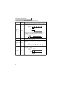
1.6.2
Internal relay (M) device map
Device No.
M0 to M63
1.6.3
Description
Use freely on user side.
Data register (D) device map
Data
Inverter Pr.
Register (D)
Number
Parameter Name
D0 to D99
Use freely on user side.
Pr.506 to
D100 to D119
User parameters. Use freely on user side.
Pr.515
1.6.4
Reference
Page
—
38
Special relays
The special relays are internal relays with special applications and therefore should
not be switched on-off in the program.
Number
Name
M9008
Self-diagnostic error
M9010
Operation error flag
M9011
Operation error flag
M9036
M9037
Normally ON
Normally OFF
On only for 1 scan after
RUN
Off only for 1 scan after
RUN
Inverter operation status
control flag (STF)
Inverter operation status
control flag (STR)
Inverter operation status
control flag (RH)
Inverter operation status
control flag (RM)
Inverter operation status
control flag (RL)
Inverter operation status
control flag (JOG)
Inverter operation status
control flag (RT)
Inverter operation status
control flag (AU)
Inverter operation status
control flag (CS)
Inverter operation status
control flag (MRS)
Inverter operation status
control flag (STOP)
M9038
M9039
M9200
M9201
M9202
M9203
M9204
M9205
M9206
M9207
M9208
M9209
M9210
12
Description
Turned on by self-diagnosed error.
Turned on by an instruction execution error.
Turned off when error is removed.
Turned on by an instruction execution error.
Remains on after normal status is restored.
M9036 and M9037 are turned on and off independently
of STOP or RUN.
M9038 and M9039 change depending on the STOP or
RUN status. In other than the STOP status, M9038 is on
for one scan only and M9039 is off for one scan only.
Control the STF terminal of the inverter from PLC
function
Control the STR terminal of the inverter from PLC
function
Control the RH terminal of the inverter from PLC
function
Control the RM terminal of the inverter from PLC
function
Control the RL terminal of the inverter from PLC function
Control the JOG terminal of the inverter from PLC
function
Control the RT terminal of the inverter from PLC function
Control the AU terminal of the inverter from PLC
function
Control the CS terminal of the inverter from PLC
function
Control the MRS terminal of the inverter from PLC
function
Control the STOP terminal of the inverter from PLC
function
Device Map
Name
Description
Inverter operation status
control flag (RES)
Inverter status (RUN)
Inverter status (FWD)
Inverter status (REV)
Inverter status (SU)
Inverter status (OL)
Inverter status (IPF)
Inverter status (FU)
Inverter status (ALM)
Inverter status (LF)
Inverter status (DO0)
Inverter status (DO1)
Inverter status (DO2)
Inverter status (DO3)
Inverter status (DO4)
Inverter status (DO5)
Inverter status (DO6)
Inverter status (RA1)
Inverter status (RA2)
Inverter status (RA3)
Control the RES terminal of the inverter from PLC
M9211
function
M9216
Inverter running
M9217
Forward running
M9218
Reverse running
M9219
Up to frequency
M9220
Overload alarm
M9221
Instantaneous power failure/undervoltage
M9222
Output frequency detection
M9223
Alarm output
M9224
Minor fault output
M9225
Status of output terminal function set in Pr. 313 is stored *1
M9226
Status of output terminal function set in Pr. 314 is stored *1
M9227
Status of output terminal function set in Pr. 315 is stored *1
M9228
Status of output terminal function set in Pr. 316 is stored *1
M9229
Status of output terminal function set in Pr. 317 is stored *1
M9230
Status of output terminal function set in Pr. 318 is stored *1
M9231
Status of output terminal function set in Pr. 319 is stored *1
M9232
Status of output terminal function set in Pr. 320 is stored *1
M9233
Status of output terminal function set in Pr. 321 is stored *1
M9234
Status of output terminal function set in Pr. 322 is stored *1
Select the inverter status control command from M9200
Inverter operation status to M9211 or D9148.
M9255
control selection
OFF: Special relay selection
ON : Special register selection
*1. Even if the FR-A7AY, FR-A7AR is not mounted, Pr. 313 to Pr. 322 are accessible during
PLC function operation, and status of output terminal functions are stored in each device.
(virtual output terminal)
Device Map
Number
PLC FUNCTION
1
13
Device Map
1.6.5
Special registers
The special registers are data registers with special applications and therefore data
should not be written to the special registers in the program.
Number
Name
D9008
Self-diagnostic
error
D9010
Operation error
step
D9011
Operation error
step
D9014
I/O control
method
Description
Page
Stores the self-diagnosed error number in BIN. (Refer
to page 22 for the error codes.)
Stores the step number in BIN, at which an instruction
execution error occurred. After that, data is updated
each time operation error occurs.
Stores the step number in BIN, at which an instruction
error occurred. Since data is stored into D9011 when
M9011 turns from off to on, D9011 data is not updated
unless M9011 is cleared by the user program.
3 (fixed): Both input and output refreshes
22
—
—
—
Special registers
Stores the operating status of the PLC function.
B15
D9015
CPU operating
status
B12B11
B8B7
B4B3
B0
Invalid Remote run/stop using
Remote run/stop
using GX Developer
sequence parameter setting
Shorting/
opening SQ-SD
0 RUN
0 RUN
0 RUN
1 STOP
1 STOP
1 STOP
Stores the number that indicates which sequence
Program number program is currently in execution.
1 (fixed): Main program (RAM)
Minimum scan
Stores the scan time at every END that is smaller than
D9017 time
D9017 data, i.e. stores the minimum scan time in BIN.
(10ms units)
Scan time
Stores and updates the scan time at every END in
D9018
(10ms units)
BIN.
Maximum scan
Stores the scan time at every END that is greater than
D9019 data, i.e. stores the maximum scan time in
D9019 time
(10ms units)
BIN.
D9062 to
Special registers for communication with the master
Remote registers
station in CC-Link.
D9093
D9016
14
—
—
—
—
—
50
Device Map
D9134
D9135
Special registers for control
D9136
D9137
D9138
D9139
D9140
D9141
D9142
D9143
D9144
D9145
D9146
D9147
Parameter clear
Description
Page
Stores the current output frequency.
0.01Hz units
Stores the current output current.
0.01A units
Stores the current output voltage.
0.1V units
20
Store the errors that occurred in the inverter in order
of occurrence.
21
Stores the current operation mode.
23
Reads and stores the set frequency (RAM).
24
Reads and stores the set frequency (EEPROM).
24
Sets a new operation mode.
26
Sets the running frequency (RAM).
27
Sets the running frequency (EEPROM).
28
Write H9696 to clear the error history.
29
H9696 write: Parameter clear
H9966 write: All clear
H5A5A write:Parameter clear except communication
parameters
H55AA write:All clear except communication
parameters
During GX Developer communication, perform
clearing by H5A5A or H55AA.
30
Device Map
D9133
Name
Output frequency
monitor
Output current
monitor
Output voltage
monitor
Error history 1, 2
Error history 3, 4
Error history 5, 6
Error history 7, 8
Operation mode
setting read
Set frequency
read (RAM)
Set frequency
read (E2PROM)
Operation mode
setting write
Set frequency
write (RAM)
Set frequency
write (E2PROM)
Alarm definition
batch clear
1
PLC FUNCTION
Number
15
Device Map
Number
Name
Description
Page
Turn on/off the corresponding bits to control the
inverter operation status.
The initial value: All "0". When M9255 is off, this
device does not function.
B15
D9148
Special registers for control
D9149
D9150
Inverter status
D9152
Frequency
setting
D9156
D9157
D9158
B4B3
B0
0:OFF
1:ON
STF
STR
RH
RM
RL
JOG
RT
AU
CS
MRS
STOP
RES
Enable/disable the inverter operation status control
Inverter operation
using D9148 and M9200 to M9211 by turning on/off
status control
the corresponding bits.
enable/disable
Bit image is the same as D9148.
setting
The initial value: All "0" (invalid)
Inverter
Stores the error No. when an error occurs because
parameter
the data stored in the parameter or special register is
access error
not reflected on the inverter.
Stores the running status and operating status of the
inverter.
D9151
D9155
B8B7
Invalid
B15
D9153
D9154
16
Inverter operation
status control
B12B11
Running speed
Motor torque
Converter output
voltage
Regenerative
brake duty
Electronic thermal
relay function load
factor
Output current
peak value
B8B7
B4B3
B0
31
32
33
0:OFF
1:ON
Inverter running(RUN)
Forward running
Reverse running
Up to frequency(SU)
Overload alarm(OL)
Instantaneous power failure
/undervoltage(IPF)
Output frequency
detection(FU)
Alarm output(ALM)
Minor fault output(LF)
33
0.01Hz units
—
1(0.1)r/min unit
0.1% units
—
—
0.1V units
—
0.1% units
—
0.1% units
—
0.01A/0.1A units
—
Device Map
Number
D9159
D9160
D9161
Name
Description
Page
Converter output
0.1V units
voltage peak value
Input power
0.01kW/0.1kW units
Output power
0.01kW/0.1kW units
—
—
—
Input terminal status details
D9162
B12B11
B8B7
B4B3
B0
0:OFF
1:ON
STF
STR
AU
RT
RL
RM
RH
JOG
MRS
STOP
RES
CS
Input terminal
status
—
Device Map
B15
Output terminal status details
D9163
D9164
D9165
D9166
D9167
D9169
D9170
D9171
D9172
D9179
D9180
D9181
D9182
D9197
D9198
D9199
D9200
D9201
B7
B4B3
Output terminal
status
Load meter
Motor excitation
current
Position pulse
Cumulative
energization time
—
Actual operation
time
Motor load factor
Cumulative power
Torque command
Torque current
command
Motor output
Feedback pulse
Power saving
effect
Cumulative
saving power
PID set point
PID measured
value
PID deviation
B0
0:OFF
1:ON
RUN
SU
IPF
OL
FU
ABC1
ABC2
—
0.1% units
—
0.01A/0.1A units *7
—
—
1h units
—
Always 0
—
1h unit
—
0.1% units
1kW unit
0.1% units
—
—
—
0.1% units
—
0.01kW units
1 unit
—
—
1
PLC FUNCTION
Special registers for control
B15
—
Variable according to parameters
—
0.1% units
—
0.1% units
—
0.1% units
—
17
Device Map
Number
Name
Description
Page
The input status of the FR-A7AX is stored.
All off (0) when an option is not fitted.
Special registers for control
B15
D9205
Option input
terminal status 1
D9206
Option input
terminal status 2
B8B7
B4B3
B0
0:OFF
1:ON
X0
X1
X2
X3
X4
X5
X6
X7
X8
X9
X10
X11
X12
X13
X14
X15
B15
B12B11
B8B7
B4B3
B0
D9206
—
—
0:OFF
1:ON
DY
The output status of the FR-A7AY, FR-A7AR is stored.
All off (0) when an option is not fitted.
B15
D9207
18
B12B11
D9205
Option output
terminal status
B12B11
B8B7
B4B3
B0
0:OFF
1:ON
Y0
Y1
Y2
Y3
Y4
Y5
Y6
RA1
RA2
RA3
—
Device Map
D9235
D9236
D9237
D9238
D9239
D9240
Special registers for control
D9241
D9242
D9243
D9244
D9245
Terminal 1 input
D9246
Terminal 2 input
D9247
Terminal 4 input
D9248
D9249
D9250
D9251
D9252
D9253
D9254
D9255
Description
When setting the calibration(bias/gain) parameters.
H00: Frequency(toruque)
H01: Parameter-set analog value
H02: Analog value input from terminal
Page
34, 36
The number of pulses counted in count cycle is
stored. (0 to 32767)
The cumulative value of the number of sampling
pulses is stored. (0 to 99999999)
40
The sampling pulses and cumulative count value are
cleared. Automatically changes to "0" after reset.
(1: count clear)
Start counting the sampling pulses and cumulative
count value. (0: count stop, 1: count start)
Set the number of parameter read or written of the
inverter.
The parameter description of the inverter (RAM value)
specified by D9241 is stored. Set the parameter
setting for parameter write.
Set the number of parameter read or written of the
inverter.
The parameter description of the inverter (EEPROM
value) specified by D9243 is stored. Set the
parameter setting for parameter write.
Analog input value of terminal 1 (0.1% increments) is
stored.
Analog input value of terminal 2 (0.1% increments) is
stored.
Analog input value of terminal 4 (0.1% increments) is
stored.
PID set point /
Set the PID set point or PID deviation (0.01% units)
PID deviation
PID
measurement
Set the PID measurement value (0.01% units)
value
PID manipulated
Stores the PID manipulated variable (0.01% units)
variable
When Pr. 54 is set to "70", pulse train can be output
Terminal FM
from terminal FM. High speed pulse train output can
output
be performed. (0.1% increments)
Terminal AM
When Pr. 158 is set to "70", analog output can be
output
performed from terminal AM. (0.1% increments)
AM0 output
Analog output can be performed from terminal AM0
and AM1 of the FR-A7AY. (0.1% increments)
AM1 output
PID operation
Setting 1 starts PID control.
control
Device Map
D9234
Name
Second
parameter
changing (RAM)
Second
parameter
changing
(EEPROM)
Pulse train input
sampling pulse
Pulse train input
cumulative count
value L
Pulse train input
cumulative count
value H
Reset request of
pulse train input
count
Count start of the
pulse train input
Parameter
number (RAM)
Parameter
description
(RAM)
Parameter
number
(EEPROM)
Parameter
description
(EEPROM)
34, 36
1
39
PLC FUNCTION
Number
41
39
41
19
Inverter Status Monitoring, Special Registers
for Control
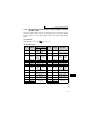
1.7 Inverter Status Monitoring, Special Registers for Control
You can assign the data for grasping and changing the inverter's operation status to
D9133 - D9147 and read/write them from the user sequence. (Refer to page 14 for the
list.)
1.7.1
Data that can be read at all times
The following data can always be read. They are automatically refreshed every time
the END instruction is executed.
(1) Operation monitor
The following data devices are always read-enabled (write-disabled) to allow you to
monitor the output frequency, output current and output voltage of the inverter. Note
the setting units.
Device
No.
D9133
D9134
D9135
Name
Output frequency
monitor
Output current
monitor
Output voltage
monitor
Setting
Unit
Data Example
0.01Hz
Device data 6000 → 60.00Hz
0.01A
Device data 200 → 2.00A
0.1V
Device data 1000 → 100.0V
Data Access Enable
Condition
Always
CAUTION
The frequency can be set in increments of 0.01Hz but actual operation is performed in
increments of 0.1Hz.
20
Inverter Status Monitoring, Special Registers
for Control
(2) Error history (error codes and error definitions)
The inverter stores the error codes of the errors that occurred.
The error codes of up to eight errors are stored in the order as shown below and are
always read-enabled (write-disabled).
<Error code storing method details>
b15 to b8
Error history 2
Error history 4
Error history 6
Error history 8
b7 to b0
Error history
Error history
Error history
Error history
1
3
5
7
Data
Description
H00
H10
H11
H12
H20
H21
H22
H30
H31
H40
H50
H51
H52
H60
H70
H80
H81
No alarm
E.OC1
E.OC2
E.OC3
E.OV1
E.OV2
E.OV3
E.THT
E.THM
E.FIN
E.IPF
E.UVT
E.ILF
E.OLT
E.BE
E.GF
E.LF
Newer
Older
Data
Description
Data
Description
H90
H91
HA0
HA3
HB0
HB1
HB2
HB3
HC0
HC1
HC2
HC4
HC5
HC6
HC7
HC8
HD0
HD1
E.OHT
E.PTC
E.OPT
E.OP3
E.PE
E.PUE
E.RET
E.PE2
E.CPU
E.CTE
E.P24
E.CDO
E.IOH
E.SER
E.AIE
E.USB
E.OS
E.OSD
HD2
HD3
HD5
HD6
HD7
HD8
HD9
HDA
HDB
HDC
HF1
HF2
HF3
HF6
HF7
HFB
HFD
E.ECT
E.OD
E.MB1
E.MB2
E.MB3
E.MB4
E.MB5
E.MB6
E.MB7
E.EP
E.1
E.2
E.3
E.6
E.7
E.11
E.13
1
PLC FUNCTION
D9136
D9137
D9138
D9139
Refer to the Inverter instruction manual (applied) for alarm definition details.
21
Inverter Status Monitoring, Special Registers
for Control
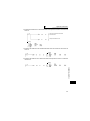
<Alarm definition read program example>
The following program reads the latest alarm definition of the inverter to D0.
Alarm definition read request
Stores only the lower 8 bits
of error history 1, 2 (D9136)
into D0.
(The latest error information
is stored into D0.)
<Regarding the error No. and details of the self-diagnostic errors>
During execution of a sequence program, any of the following error No. is stored into
D9008 due to an operation error.
At occurrence of a self-diagnostic error, the P.RUN indication (LED) flickers.
Error No.
Error Name
10
INSTRCT CODE ERR.
11
PARAMETER ERR
22
WDT ERR
24
END NOT EXECUTE
Details
There is an instruction code that cannot be decoded.
Unusable device is specified.
Main program capacity setting is over 1k step.
Unusable function is set.
Scan time is longer than the time that can be monitored
by the watchdog timer.
END instruction was not executed.
CAUTION
1. For the LD, AND, OR, logical comparison operation and OUT instructions,
device checks are always made. For the other instructions (SET, RST, MOV,
etc.), however, device checks are made when the execution condition holds.
2. Operation at error stop
The outputs (Y) are cleared.
The other devices hold the states prior to an error stop.
When you want to clear them, power off or reset (short RES-SD (0.1s), then
open) the inverter.
22
Inverter Status Monitoring, Special Registers
for Control
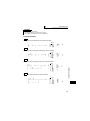
1.7.2
Data that are read by controlling (OFF to ON) the read
command
You can read the operation mode and set frequency of the inverter.
Device
No.
Name
D9140
D9141
D9142
Operation mode setting read
Set frequency read (RAM)
Set frequency read (EEPROM)
Read
Write
Data Access
Command Completion Enable Condition
Y20
Y21
Y22
X20
X21
X22
Always
Data are stored into the above data devices as soon as the read completion turns from
off to on after the read command has turned from off to on.
If the read command remains on, data is not refreshed. (Data is not updated.)
Turn the device off once, then on again to refresh data.
Data read timing chart
1) Read command is turned
on in user sequence.
3) In user sequence, ON of read completion
is confirmed and data is read from special
register and processed.
4) After completion of read,
read command is turned off.
Y2n(n=0 to 2)
Read command
X2n(n=0 to 2)
Read completion
D914n(n=0 to 2)
Read data
User sequence
processing
2) Inverter CPU stores inverter data
into special register and turns on
read completion.
5) Inverter CPU confirms that
read command is off and
turns off read completion.
(1) Operation mode setting read (D9140)
Operation Mode
H0000
H0001
H0002
NET operation mode
External operation mode
PU operation mode
1
REMARKS
When the Pr. 79 "operation mode selection" setting is other than "0", the operation mode is as
set. However, when Pr. 79 = "3" or "4", the operation mode is "H0002" (PU operation mode).
<Operation mode setting read program example>
The following program reads the operation mode data to D0.
Operation mode read setting request
Turns on operation mode
read request pulse.
Stores operation mode data to D0
when operation mode setting read
completion signal turns on.
Turns on operation mode setting
read command. (Until operation
mode setting read completion
signal turns on)
23
PLC FUNCTION
Data Setting
Inverter Status Monitoring, Special Registers
for Control
(2) Set frequency (RAM) (D9141)
The frequency set to the RAM is read to D9141. The unit is 0.01Hz.
(For example, 6000 indicates 60.00Hz.)
When the speed is set, the speed is either 1r/min or 0.1r/min.
<Set frequency (RAM) read program example>
The following program reads the set frequency (RAM) to D0.
Set frequency read (RAM) setting request
Turns on set frequency
read (RAM) request pulse.
Stores data to D0 when set
frequency read (RAM)
completion signal turns on.
Turns on set frequency read (RAM)
command. (Until set frequency read
(RAM) completion signal turns on)
REMARKS
The read frequency is not the command value of the external signal.
(3) Set frequency (EEPROM) (D9142)
The frequency set to the EEPROM is read to D9142. The unit is 0.01Hz.
(For example, 6000 indicates 60.00Hz.)
When the speed is set, the speed is either 1r/min or 0.1r/min.
<Set frequency read (EEPROM) program example>
The following program reads the set frequency (E2PROM) to D0.
The following program reads the set frequency (E2PROM) to D0.
Set frequency read
(E2PROM) setting request
Stores data to D0 when set frequency
read (E2PROM) completion signal
turns on.
Turns on set frequency read (E2PROM)
command. (Until set frequency read
(E2PROM) completion signal turns on)
REMARKS
The read frequency is not the command value of the external signal.
24
Inverter Status Monitoring, Special Registers
for Control
1.7.3
How to write data by controlling (OFF to ON) the write
command
You can write the operation mode and set frequency to the inverter, batch-clear the
alarm definitions, and clear all parameters.
Device
No.
Write
Write
Data Access
Command Completion Enable Condition
Name
D9143
D9144
Operation mode setting write
Set frequency write (RAM)
Y23
Y24
X23
X24
D9145
Set frequency write
(E2PROM)
Y25
X25
D9146
D9147
Alarm definition batch clear
All parameter clear
Y26
Y27
X26
X27
Pr.79 =0, 2
PU operation mode
(PU LED on) or CCLink operation mode
(PU and EXT LEDs
flicker slowly)
Always
As set in Pr. 77
The above data are written as soon as the write completion turns on after the write
command has turned from off to on.
(Alarm definition batch clear (D9146) and all parameter clear (D9147) turn on at
completion of clear.)
To write the data again, the write command must be turned off once, then on again.
Data write timing chart
1) In user sequence, user
data is stored into write
data area (D914n).
2) In user sequence, write
command is turned on.
4) After confirmation of write
completion, write command
is turned off.
Y2n(n=3 to 7)
Write command
X2n(n=3 to 7)
Write completion
1
PLC FUNCTION
D914n(n=3 to 7)
Write data
User data
3) Turns on when inverter CPU completes data
5) Inverter CPU confirms that
write to inverter.
write command is off and
Alarm definition clear and parameter
turns off write completion.
clear turn on at completion of clear.
0 written to D9150 indicates normal completion.
Any value other than 0 indicates abnormal completion.
25
Inverter Status Monitoring, Special Registers
for Control
(1) Operation mode setting write (D9143)
Data are as follows:
Data Setting
Operation Mode
NET operation mode
External operation mode
PU operation mode
The operation mode switching method is as shown below when the Pr.79
Operation mode selection value is "0".
H0000
H0001
H0002
NET mode H0001 External
(CC-Link)
operation mode
H0000
H0002 PU operation
mode
H0001
H0002
H0000
When Pr. 79 =2, switching is performed as shown below.
NET mode H0001 External
operation mode
(CC-Link)
H0000
REMARKS
When Pr. 79 is other than 0, the mode is fixed.
There are no restrictions on operation mode switching.
On normal completion of operation mode setting, the write completion signal
(X23) turns on, and at the same time, 0 is set to D9150.
If the value written is other than H0000 to H0002 or write is performed during
inverter operation, HFFFF is set to D9150 as soon as the write completion signal
(X23) turns on, resulting in abnormal completion.
If abnormal completion occurs, the operation mode is not changed.
<Operation mode setting write program example>
The following program changes the operation mode to the NET mode.
Operation mode write setting request
Turns on operation mode
setting write request pulse.
Check whether operation mode
Normal write setting write completion signal
turned on to judge whether write
Abnormal write was performed normally or not.
Stores 0 (CC-Link operation mode)
to D9143 and turns on operation
mode setting write command.
(Until completion signal turns on)
26
Inverter Status Monitoring, Special Registers
for Control
(2) Set frequency (RAM) (D9144)
The D9144 data is written to the RAM as a set frequency. The unit is 0.01Hz.
(For example, 6000 indicates 60.00Hz.)
When the speed is set, the speed is either 1r/min or 0.1r/min.
The range where the frequency can be set is 0 to 12000 (0 to 120.00Hz).
When the frequency setting is written normally, the write completion signal (X24)
turns on, and at the same time, 0 is set to D9150.
If any value outside the range is written, HFFFF is set to D9150 as soon as the
write completion signal (X24) turns on, resulting in abnormal completion. If
abnormal completion occurs, the set frequency is not changed.
POINT
• The frequency can be set in the PU operation mode and NET operation
mode. Refer to the inverter instruction manual (applied).
<Set frequency write (RAM) program example>
The following program changes the set frequency (RAM) to 30Hz.
Turns on set frequency
write (RAM) command pulse.
Check whether set frequency
Normal write write (RAM) completion signal
turned on to judge whether write
Abnormal write was performed normally or not.
Stores 3000 (30Hz) into D9144,
and turns on set frequency write
(RAM) command.
(Until completion signal turns on)
1
PLC FUNCTION
Set frequency write (RAM) setting request
27
Inverter Status Monitoring, Special Registers
for Control
(3) Set frequency (EEPROM) (D9145)
The D9145 data is written to the EEPROM as a set frequency. The unit is 0.01Hz.
(For example, 6000 indicates 60.00Hz.)
When the speed is set, the speed is either 1r/min or 0.1r/min.
The range where the frequency can be set is 0 to 12000 (0 to 120.00Hz).
When the frequency setting is written normally, the write completion signal (X25)
turns on, and at the same time, 0 is set to D9150.
If any value outside the range is written, HFFFF is set to D9150 as soon as the
write completion signal (X25) turns on, resulting in abnormal completion. If
abnormal completion occurs, the set frequency is not changed.
POINT
• Setting is enabled in the PU operation mode and NET operation mode.
(Refer to the Inverter instruction manual (applied).)
<Set frequency write (EEPROM) program example>
The following program changes the set frequency (EEPROM) to 10Hz.
Set frequency write (E2PROM) setting request
Turns on set frequency write
(E2PROM) request pulse.
Check whether set frequency
Normal write write (E2PROM) completion signal
turned on to judge whether write
Abnormal write was performed normally or not.
Stores 1000 (10Hz) into D9145,
and turns on set frequency write
1000
(E2PROM) command.
(Until completion signal turns on)
CAUTION
When rewriting the set frequency frequently, use device D9144 "set frequency (RAM)".
There are restrictions on the number of write times of the EEPROM. (Approximately
100,000 times)
28
Inverter Status Monitoring, Special Registers
for Control
(4) Alarm definition batch clear (D9146)
Writing H9696 to D9146 batch-clears the alarm definitions.
At completion of clear, the write completion signal (X26) turns on, and at the
same time, 0 is set to D9150. If any value outside the setting range is written or
write is performed during inverter operation, HFFFF is set to D9150 as soon as
the write completion signal (X26) turns on, resulting in abnormal completion.
If abnormal completion occurs, the alarm definitions are not cleared.
<Alarm definition batch clear program example>
The following program batch-clears the alarm history.
Turns on alarm definition
batch clear request pulse.
Check whether alarm definition
Normal write batch clear signal turned on to
judge whether write was
Abnormal write performed normally or not.
Stores H9696 (batch clear code)
to D9146 and turns on alarm
definition batch clear command.
(Until completion signal turns on)
1
PLC FUNCTION
Alarm definition batch clear request
29
Inverter Status Monitoring, Special Registers
for Control
(5) Parameter clear (D9147)
Writing H9696 or H9966 to D9147 clears all parameters. Writing H5A5A or
H55AA to D9147 clears the parameters other than the communication
parameters (Refer to the Inverter instruction manual (applied)).
Device No.
Setting
H9696
H9966
D9147
H5A5A
H55AA
Description
Details
Terminal functions are not
cleared.
All parameter clear
Terminal functions are
cleared.
Terminal functions are not
Parameters other than
cleared.
communication parameters
Terminal functions are
are cleared.
cleared.
At completion of clear, the write completion signal (X27) turns on, and at the
same time, 0 is set to D9150. If any value outside the setting range is written or
write is performed during inverter operation, HFFFF is set to D9150 as soon as
the write completion signal (X27) turns on, resulting in abnormal completion. If
abnormal completion occurs, the parameters are not cleared.
REMARKS
Check the terminal function parameters and communication-related parameters in the
parameter list (Refer to the Inverter instruction manual (applied)).
POINT
Setting is enabled in the PU operation mode and NET operation mode. Refer to
the inverter instruction manual (applied).
<All parameter clear program example>
The following program clears all parameters.
All parameter clear request
Turns on all parameter
clear request pulse.
Check whether all parameter
Normal write clear signal turned on to judge
whether write was performed
Abnormal write normally or not.
Stores H9696 (all parameter
clear code) to D9146 and turns
on alarm definition batch clear
command.
(Until completion signal turns on)
Related device
Device D9150: Parameter access error code (refer to page 33)
30
Inverter Status Monitoring, Special Registers
for Control
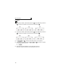
1.7.4
Inverter operation status control
Device No.
D9148
D9149
Name
Data Access Enable Condition
Inverter operation status control Always
Note that this function is enabled in
Inverter operation status control the external/NET operation mode.
(Not enabled in the PU
enable/disable
operation mode.)
(1) Inverter operation status control (D9148)
Device for inverter operation status control. The operation of the inverter can be
controlled by turning on/off (1, 0) bits b0 to b11 of D9148.
All bits are factory-set to "0".
Example: When 5 is set to D9148, bits b0 and b2 are 1 (ON), and STF and RH
therefore turn on to give a high-speed forward rotation command.
B15
B12B11
B8B7
B4B3
B0
0 0 0 0 0 0 0 0 0 1 0 1
Invalid
0:OFF
1:ON
STF (Pr.178)
STR (Pr.179)
RH (Pr.182)
RM (Pr.181)
RL (Pr.180)
JOG (Pr.185)
RT (Pr.183)
AU (Pr.184)
CS (Pr.186)
MRS (Pr.187)
STOP (Pr.188)
RES (Pr.189)
CAUTION
As in the external input terminals, functions can be assigned to the bits of
D9148 using Pr.178 to Pr.189. However, no function can be assigned to SQ
(sequence RUN setting: 50).
PLC FUNCTION
1
31
Inverter Status Monitoring, Special Registers
for Control
(2) Inverter operation status control enable/disable setting (D9149)
You can enable or disable D9148 "inverter operation status control". The controls
of the corresponding bits of D9148 are enabled by turning on/off (1, 0) bits b0 to
b11 of D9149. All bits are factory-set to "0".
Example: When H1F is set to D9149, bits b0 to b11 are 1 (ON), the external terminal
inputs are therefore all disabled, and operation control using the inverter
operation status control (D9148) can be performed.
B15
B12B11
B8B7
B4B3
B0
1 1 1 1 1 1 1 1 1 1 1 1
0:OFF
1:ON
Invalid
STF (Pr.178)
STR (Pr.179)
RH (Pr.182)
RM (Pr.181)
RL (Pr.180)
JOG (Pr.185)
RT (Pr.183)
AU (Pr.184)
CS (Pr.186)
MRS (Pr.187)
STOP (Pr.188)
RES (Pr.189)
CAUTION
•When D9148 "inverter operation status control" is enabled using D9149,
the control performed by external terminal inputs and the control
performed by CC-Link remote inputs are disabled for the enabled bits.
(Same as when "No functions" are set to Pr.178 to Pr.189.)
•When the terminal is made valid from PLC function, control from external
terminal is made invalid.
<Operation command setting program example>
The following program example runs the inverter at high speed in forward rotation
direction.
Operation start
Turns on operation start pulse.
HFFF
Enables all inverter operation status
control enable/disable bits, and
disables external terminal inputs.
Self-holds operation start, and turns
on bits 0 (STF) and 2 (RH) of inverter
operation status control, D9148.
Operation stop
32
At input of stop signal, clears inverter
operation status control, D9148,
to 0 and decelerates inverter to stop.
Inverter Status Monitoring, Special Registers
for Control
1.7.5
Inverter parameter access error (D9150)
Name
Data Access Enable
Condition
Inverter parameter access error
Always
Device No.
D9150
If any value outside the setting range is written during parameter write, set frequency
write, parameter clear, etc. from the sequence program of the inverter, or if write is
performed when write is disabled, a write alarm occurs and the corresponding alarm
code is stored into D9150.
<Parameter>
The parameter No. + H8000 is stored into D9150.
Example: If an error occurs during write of Pr.0 Torque boost, H8000 (H0 + H8000) is
stored into D9150.
If an error occurs during write of Pr.10 DC injection brake operation frequency,
H800A is stored into D9150.
<Operation mode, set frequency, alarm definition batch clear, all parameter
clear>
HFFFF is stored into D9150. (Normal 0)
POINT
If write is completed normally after error occurrence, D9150 is not cleared
(D9150 data is held at error occurrence). When using D9150 to stop operation,
etc., the user must clear it.
Inverter status (D9151)
Device No.
D9151
Name
Data Access Enable
Condition
Inverter status
Always
1
PLC FUNCTION
1.7.6
The running status and operating status of the inverter are stored.
The corresponding bits are set according to the inverter status.
B15
B8B7
B4B3
B0
0:OFF
1:ON
Inverter running(RUN)
Forward running
Reverse running
Up to frequency(SU)
Overload alarm(OL)
Instantaneous power failure
/undervoltage(IPF)
Output frequency
detection(FU)
Alarm output(ALM)
Minor fault output(LF)
33
Inverter Parameter Read/Write Method
1.8 Inverter Parameter Read/Write Method
1.8.1
Reading the inverter parameters
Device No.
Name
D9241
D9242
Parameter number (RAM)
Parameter description (RAM)
Second parameter changing
(RAM)
Parameter number (EEPROM)
Parameter description
(EEPROM)
Second parameter changing
(EEPROM
D9234
D9243
D9244
D9235
Command Completion
Data Access Enable
Condition
(Operation mode)
Y28
X28
Always
Y2A
X2A
PU, NET operation mode
(as in Pr.77)
When reading the parameter, the parameter description is stored to D9242(D9244) by
storing the parameter number to D9241(D9243) and turning Y28 (Y2A) on. When
reading is completed, X28 (X2A) turns ON to notify the completion. (The device
number within parentheses is used to read the parameter setting value from
EEPROM.)
When reading the calibration parameter (Pr. 902 to Pr. 939), set the following value to
D9234 (D9235) to read each calibration parameter value.
0: Setting value (Frequency/Toruque)
1: Parameter-set analog value
2: Analog value input from terminal
When access error occurs such as "parameter does not exist", value obtained by adding the
parameter number and 8000H is stored to D9150. (Refer to page 33)
34
Inverter Parameter Read/Write Method
Inverter parameter data read timing chart
3) In user sequence, ON of read completion
is confirmed and data are read from data
registers D9242(D9243) and processed.
1) Read command is turned
4) After completion of read,
on in user sequence.
read command is turned off.
Y28(Y2A)
Parameter read
command
X28(X2A)
Parameter read
completion
Inverter
parameter
D9242(D9243)
Parameter
read data
User sequence
processing
5) Inverter CPU confirms that read
command is off and turns off
read completion.
1
PLC FUNCTION
2) Inverter CPU stores inverter parameter
data into data registers D9242(D9243),
and turns on read completion.
35
Inverter Parameter Read/Write Method
1.8.2
Writing the inverter parameters
Device No.
Name
D9241
D9242
Parameter number (RAM)
Parameter description (RAM)
Second parameter changing
(RAM)
Parameter number (EEPROM)
Parameter description
(EEPROM)
Second parameter changing
(EEPROM
D9234
D9243
D9244
D9235
Command Completion
Data Access Enable
Condition
(Operation mode)
Y29
X29
Always
Y2B
X2B
PU, NET operation mode
(as in Pr.77)
Parameter writing is performed when the parameter number is stored to D9241
(D9243) and parameter writing value to D9242 (D9244), and turns ON the Y29 (Y2B).
When writing is completed, X29 (X2B) turns ON to notify the completion. (The device
number within parentheses is used to write the parameter setting value to EEPROM.)
When writing the calibration parameter (Pr. 902 to Pr. 939), set the following value to
D9234 (D9235) to write each calibration parameter value.
0: Setting value (Frequency/Toruque)
1: Parameter-set analog value
2: Analog value input from terminal
As soon as the inverter parameter write completion (X29 (RAM) or X2B (EEPROM))
turns on, 0 is set to D9150 on normal completion.
If an error occurs during access to the parameters, e.g. if any value outside the setting
range is written or write is performed during inverter operation, the value of parameter
No. + H8000 is set to D9150 as soon as the write completion signal (X29 (RAM) or
X2B (EEPROM)) turns on, resulting in abnormal completion. If abnormal completion
occurs, the parameters are not written. (For example, if an error occurs in the torque
boost, H8000 is written to D9150.)
For whether inverter parameter write can be performed or not, refer to Pr.77 Parameter
write selection .
POINT
Inverter parameter write must be performed in the PU operation mode or NET
operation mode. (Refer to the inverter instruction manual (applied).)
36
Inverter Parameter Read/Write Method
Inverter parameter data write timing chart
1) In user sequence, user data
are stored into parameter write 2) Write command is turned
data area (D9242(D9244)).
on in user sequence.
Y29(Y2B)
Parameter
write command
4) After confirmation of write
completion, write command
is turned off.
X29(X2B)
Parameter
write completion
Inverter parameter
D9242(D9244)
Parameter write
data
User sequence
data
5) Inverter CPU confirms
that write command is
off and turns off write
completion.
1
PLC FUNCTION
3) Turns on when inverter CPU completes inverter
parameter data write.
0 written to D9150 indicates normal completion.
Any value other than 0 indicates abnormal completion.
37
User Area Read/Write Method
1.9 User Area Read/Write Method
Inverter parameters Pr.506 to Pr.515 can be used as user parameters.
Since this parameter area and the devices used with the PLC function, D110 to D119,
are accessible to each other, the values set in Pr.506 to Pr.515 can be used in a
sequence program. The result of operation performed in the sequence program can
also be monitored using Pr.506 to Pr.515.
Inverter
Device
Parameter
No.
No.
D110 to
D119
506 to 515
Name
Initial
Value
Setting
Range
User
parameters
0
0 to
65535
Minimum Setting
Data Access
Unit
Always
enabled
1
PLC function devices
Inverter parameters
D110 to D119
Pr.506 to Pr.515
POINT
Example of using the user parameter area
When the timing is to be changed for machine adjustment using D110 that
stores the timer setting, setting Pr. 506 without modifying the program enters
the set data into D110, enabling adjustment.
1.9.1
User parameter read/write method
User parameter (Pr.506 to Pr.515) and device (D110 to D119) data can be read/written
freely. Data transfer between Pr.506 to Pr.515 and D110 to D119 is executed
automatically.
1) User parameter write processing
When values are written to Pr.506 to Pr.515 using the FR-PU04 or computer link
communication, they are written to the parameter storing RAM area and EEPROM
area, and further to D110 to D119 simultaneously.
2) User parameter read processing
When values are written to D110 to D119 from the PLC function side, they are
written to the parameter storing RAM area (Pr.506 to Pr.515) and read using the FRPU04/FR-PU07 or communication(RS-485 or communication option). (Since data
are not written to the EEPROM, making power-on reset returns the data to the
original values.)
3) Processing performed at inverter reset or power restoration
When the inverter is reset, the Pr.506 to Pr.515 values stored in the EEPROM are
transferred to the RAM area and D110 to D119.
1)
1)
FR-PU04 or RS-485
communication
Pr.506 to Pr.515
(RAM)
D110 to D119
2)
2)
3)
3)
1)
38
Pr.506 to Pr.515
(EEPROM)
1)
Analog I/O function
1.10 Analog I/O function
1.10.1 Analog input
Analog input value of termianl 1, 2, 4 can be read from D9245 to D9247.
Device
No.
D9245
D9246
D9247
Terminal Name
Terminal 1 input
Terminal 2 input
Terminal 4 input
Setting Data Access Enable
Unit
Condition
0.1%
0.1%
0.1%
Always
Actual read processing is performed at the END processing of the sequence.
REMARKS
Full-scale value of analog input is determined by the setting of Pr. 73 Analog input selection, Pr.
267 Terminal 4 input selection. Refer to the inverter instruction manual (applied).
1.10.2 Analog output
Analog output from each terminal can be performed by setting value on D9251 to
D9254.
Output from PLC function can be performed by setting "7" in output signal selection
parameters of each terminal (terminal FM: Pr. 54, terminal AM: Pr. 158, terminal AMO,
AM1: Pr. 306, Pr. 310).
D9251
D9252
D9253
D9254
Terminal Name
Terminal FM
Terminal AM
Terminal AM0
(FR-A7AY)
Terminal AM1
(FR-A7AY)
Setting Data Access Enable
Unit
Condition
0.1%
0.1%
0.1%
Always
0.1%
1
Actual read processing is performed at the END processing of the sequence.
REMARKS
High speed pulse train output (Pr. 291) from terminal FM can be performed. (Refer to the
inverter instruction manual (applied).)
39
PLC FUNCTION
Device
No.
Paluse train input function
1.11 Paluse train input function
Pulse train (the number of sampling pulses) from terminal JOG is stored to D9236.
When the sampling pulses overflow, make adjustment with the setting of Pr. 416 and
Pr. 417.
The number of sampling pulses
= the number of input pulses per count cycle x Pre-scale setting value (Pr. 417) x
increments scaling factor (Pr. 416)
Parameter
Name
Initial
Value
291
Pulse train input
selection
0
416
Pre-scale function
selection
0
417
Pre-scale setting
value
1
Device No.
D9236
D9237
D9238
D9239
D9240
40
Name
Pulse train input sampling
pulse
Pulse train input cumulative
count value L
Pulse train input cumulative
count value H
Reset request of pulse train
input count
Count start of the pulse train
input
Setting
Range
Description
0, 10,20
Terminal JOG
1,11,21,100 Pulse train input
Pre-scale function selection
(increments scaling factor)
0: No function
1: ×1
0 to 5
2: ×0.1
3: ×0.01
4: ×0.001
5: ×0.0001
Set the pre-scale value to calcute the
0 to 32767 number of sampling pulse when
inputting the pulse train.
Setting
Range
0 to 32767
0 to
99999999
0
1
0
1
Description
The number of pulses counted in
count cycle is stored.
The cumulative value of the number
of sampling pulses is stored.
Not clear
Count clear
Stop counting
Start counting
PID control
1.12 PID control
With PLC function, PID set point/PID deviation value, PID process value can be set by
setting Pr. 128.
Performing the PID operation using the value of D9248 and D9249 as PID set point/
PID deviation value, PID process value, manipulated variable is stored to D9250.
When performing PID control with PLC function, "1" is set on D9255 instead of X14
signal.
PID control
PID measurement
D9249
value
Parameter
128
Name
PID action
selection
Initial
Value
10
Setting
Range
PID manipulated variable D9250
or
Inverter frequency setting
Description
10
PID reverse action
11
PID forward action
20
PID reverse action
21
PID forward action
50
PID reverse action
51
PID forward action
60
PID reverse action
61
PID forward action
70
PID reverse action
71
PID forward action
80
PID reverse action
81
PID forward action
90
PID reverse action
91
PID forward action
100
PID reverse action
101
PID forward action
Deviation value
signal input
(terminal 1)
Measured value
(terminal 4)
Set point (terminal
2 or Pr. 133)
Deviation value
signal input
(LONWORKS ,
CC-Link
communication)
Measured value,
set point input
(LONWORKS ,
CC-Link
communication)
Deviation value
signal input
(PLC function)
Measured value,
Set point
(PLC function)
Deviation value
signal input
(PLC function)
Measured value,
Set point input
(PLC function)
41
1
PLC FUNCTION
PID set point /
D9248
PID deviation
PID control
Device No.
Name
D9248
PID set point / PID deviation
D9249
PID measurement value
D9250
PID manipulated variable
D9255
PID operation control
Setting
Range
Description
Set the PID set point or PID
deviation (0.01% units)
Set the PID measurement value
0 to 100%
(0.01% units)
Stores the PID manipulated
-100 to 100%
variable (0.01% units)
0
PID operation stop
1
PID operation start
-100 to 100%
CAUTION
• The PID set point/PID deviation value of D9248 automatically switches over
by Pr. 128 setting.
• If Pr. 128 is set to deviation input (70, 71, 90, 91), setting value of PID process
value (D9249) is made invalid.
• Operates in the maximum value (the minimum value) of the setting range if
the value outside the range is set.
42
Inverter Operation Lock Mode Setting
1.13 Inverter Operation Lock Mode Setting
You can disable a sequence program from being executed until the sequence program
execution key is set to RUN (SQ signal is turned on).
POINT
When you want to perform only inverter operation without using the PLC function,
set "0" (inverter start signal enable) in this parameter.
Parameter
Name
initial
Setting
Setting
Range
Minimum Setting
Unit
415
Inverter operation
lock mode setting
0
0, 1
1
0
1
Description
The inverter start signal is made valid regardless of the sequence program
execution key.
The inverter start signal is made valid only when the sequence program
execution key is set to RUN (SQ signal is turned on).
When the sequence program execution key is in the STOP position (SQ
signal is off), the inverter does not start if the inverter start signal STF or STR
is turned on. (If the key is switched from RUN to STOP during inverter
operation, the inverter is decelerated to a stop.)
CAUTION
•Independently of the Pr. 77 setting, this parameter value cannot be rewritten
during inverter operation.
•During automatic operation performed using D9148(or M9200 to M9211) in the
sequence program, the inverter comes to a stop when the sequence is set to a
STOP status with "1" set in Pr.415. However, when "0" is set in Pr.415, the
device data are held and the operation status does not change if the sequence
is set to a STOP status. (Inverter operation is continued.)
REMARKS
This parameter setting is also valid for the start signal from the operation panel or FRPU04/FR-PU07.
43
1
PLC FUNCTION
Setting
MEMO
44
2. CC-Link
COMMUNICATION
2.1
2.2
2.3
2.4
System Configuration ..........................................
CC-Link Parameters .............................................
CC-Link I/O Specifications...................................
Buffer Memory ......................................................
46
49
50
57
Chapter 1
Chapter 2
Chapter 3
Chapter 4
45
System Configuration
2.1 System Configuration
2.1.1
System configuration example
(1) PLC side
Mount the "Control & Communication Link system master/local module" on the
main base unit or extension base unit of the PLC CPU that will act as the master
station.
(2) Connect the PLC CC-Link module master station and inverters by CC-Link
dedicated cables.
Inverter
Inverter
Power supply
module
Master station
CPU
AJ61
BT11
Up to 42 inverters
can be connected
when only inverters
are connected.
Terminating
resistor
Power supply
CC-Link dedicated cable
Motor
Power
supply
Motor
REMARKS
Refer to the FR-A7NC indtruction manual for the CC-Link communication wiring and CC-Link
cables.
46
System Configuration
2.1.2
Function block diagram
How I/O data are transferred to/from the inverter in CC-Link will be described using
function blocks.
(1) Between the master station and inverter in the CC-Link system, link refresh is
always made at 3.5 to 18ms (512 points).
(2) I/O refresh and master station's sequence program are executed asynchronously.
(3) Data read from the inverter are read from the buffer memory of the CC-Link
system master/local module using the FROM instruction.
(4) Data to be written to the inverter are written to the buffer memory of the CC-Link
system master/local module using the TO instruction.
Inverter
2)
3)
4)
5)
5)
I/O
data
Input signal
Inverter CPU
4)
Built-in sequence program
CC-Link interface
Buffer
memory
3) CC-Link
dedicated
cable
Output signal
I/O signals assigned to the CC-Link system master/local module. These signals
are used to make communication between the PLC CPU and CC-Link system
master/local module.
Input data from the inverter can be read, and output data from the inverter can be
written. Buffer memory read/write is performed using the FROM/TO instruction of
the sequence program. Refer to page 57 for details of the buffer memory.
PLC link start is commanded from the sequence program. After PLC link has
started, link refresh is always made asynchronously with the sequence program
execution.
I/O data are transferred between the CC-Link system master/local module and
inverter CPU via the sequence program.
I/O data are transferred between the inverter CPU and sequence program. (5)
indicates the operation performed when CC-Link is not used, and is irrelevant to
1) to 4).)
REMARKS
Programs cannot be read/written via CC-Link communication.
2
CC-Link COMMUNICATION
1)
2) Buffer memory
read/write
CPU
CC-Link interface
PLC CPU
1) CC-Link module
I/O signals
Interface with PLC
CC-Link module
47
System Configuration
POINT
The difference between CC-Link communication (Pr. 544 = 100, 112, 114, 118)
with PLC function and normal CC-Link communication (Pr. 544 =1, 2, 12, 14, 18)
is indicated below.
I/O (RX, RY)
Inverter CPU
PLC CPU
CC-Link master module
Inverter
Pr.544=0,1,12,14,18
RWw RWr
Parameter read/write, monitor, operation commands,
etc. have been assigned in advance.
Inverter
I/O (RX, RY)
Built-in
sequence
program
RWw RWr
User
assignment
Inverter CPU
PLC CPU
CC-Link master module
Pr.544=100,112,114,118
Built-in CC-Link module
Using built-in sequence program, parameters,
monitor, etc. must be assigned.
Other data read/write, etc. can be assigned
freely as user areas.
*Operation and speed commands have
been assigned in advance.
48
CC-Link Parameters
2.2 CC-Link Parameters
2.2.1
CC-Link Extended Setting (Pr. 544)
Remote register function can be extended.
Parameter
Number
Name
Initial Setting CC-Link
Value Range
Ver.
0
1
1
12 *2
14 *2
544
CC-Link extended
setting
2
18 *2
0
100
1
112 *2
114 *2
118 *2
*1
*2
2
Description
Occupies one station
(FR-A5NC compatible) *1
Occupies one station
Occupies one station double
Occupies one station
quadrople
Occupies one station octuple
Occupies one station
(PLC function)
Occupies one station double
(PLC function)
Occupies one station
quadrople (PLC function)
Occupies one station octuple
(PLC function)
The program used for conventional series inverter (FR-A5NC) can be used.
When using double, quadruple and octuple settings of the CC-Link Ver.2, station data of
the master station must be set to double, quadruple and octuple also.
(If the master station is CC-Link Ver.1 compatible station, the above setting can not be
made.)
REMARKS
The setting change is reflected after an inverter reset.
CC-Link COMMUNICATION
2
49
CC-Link I/O Specifications
2.3 CC-Link I/O Specifications
2.3.1
I/O signal when CC-Link Ver.1 one station is occupied
(Pr. 544 = 100)
The device points usable in CC-Link communication are 32 input (RX) points (16
points are available for PLC function), 32 output (RY) points (16 points are available
for PLC function), 4 remote register (RWr) points and 4 remote register (RWw) points.
(1) Remote I/O
PLC
function
device
No.
Remote
output
device
No.
X30
X31
RYn0
RYn1
X32
RYn2
X33
RYn3
X34
RYn4
X35
RYn5
X36
RYn6
X37
RYn7
X38
RYn8
X39
RYn9
X3A
RYnA
X3B
RYnB
X3C
X3D
X3E
X3F
RYnC
RYnD
RYnE
RYnF
Remote
input
device
No.
Forward rotation command
Reverse rotation command
High-speed operation
command
(terminal RH function) *1
Middle-speed operation
command
(terminal RM function) *1
Low-speed operation
command
(terminal RL function) *1
Jog operation command
(terminal JOG function) *1
Second function selection
(terminal RT function) *1
Current input selection
(terminal AU function) *1
Selection of automatic restart after
instantaneous power failure
(terminal CS function) *1
X30
X31
RXn0
RXn1
Forward running
Reverse running
X32
RXn2
Running
(terminal RUN function) *2
X33
RXn3
Up to frequency
(terminal SU function) *2
X34
RXn4
Overload alarm
(terminal OL function) *2
X35
RXn5
X36
RXn6
X37
RXn7
X38
RXn8
Output stop
X39
RXn9
Start self-holding selection
(terminal STOP function) *1
Reset
(terminal RES function) *1
X3A
RXnA
X3B
RXnB
X3C
X3D
X3E
X3F
RXnC
RXnD
RXnE
RXnF
General-purpose remote input
available in PLC function
RY(n+1)0
to
Reserved
RY(n+1)7
RY(n+1)8 (initial data process
50
PLC
function
device
No.
Signal
Not used
completion flag)
Not used
RY(n+1)9 (initial data process request
flag)
RY(n+1)A Error reset request flag
Signal
Instantaneous power failure
(terminal IPF function) *2
Frequency detection
(terminal FU function) *2
Error
(terminal ABC1 function) *2
(terminal ABC2 function) *2
Pr. 313 assignment function
(DO0)
Pr. 314 assignment function
(DO1)
Pr. 315 assignment function
(DO2)
General-purpose remote input
available in PLC function
RX(n+1)0
to
Reserved
RX(n+1)7
RX(n+1)8 (initial data process request
Not used
flag)
Not used
RX(n+1)9 (initial data process
completion flag)
RX(n+1)A Error status flag
CC-Link I/O Specifications
Remote
output
device
No.
PLC
function
device
No.
Signal
RY(n+1)B
to
Reserved
RY(n+1)F
PLC
function
device
No.
Remote
input
Signal
device
No.
RX(n+1)B Remote station Ready
RX(n+1)C
to
Reserved
RX(n+1)F
("n" indicates a value determined according to the station number setting.)
*1 Signal names are initial values. Using Pr. 180 to Pr. 186, Pr. 188, and Pr .189, you can
change input signal functions.
Signals of the RYn0, RYn1, and RYn9 can not be changed. Even when changed using Pr.
178, Pr. 179, and Pr. 187, the settings are invalid.
Refer to the inverter manual (applied) for details of Pr. 178 to Pr.189.
*2 Signal names are initial values. Using Pr. 190 to Pr .196, you can change output signal
functions.
Refer to the inverter manual (applied) for details of Pr. 190 to Pr.196.
(2) Remote resister
PLC function
device No.
Address
D9062
D9063
D9064
D9065
RWwn
RWwn+1
RWwn+2
RWwn+3
Description
PLC function
device No.
Address
Description
Registers designed to
read data received
from the master
station
D9078
D9079
D9080
D9081
RWrn
RWrn+1
RWrn+2
RWrn+3
Registers designed to
write data to be sent
to the master station.
("n" indicates a value determined according to the station number setting.)
(3) Data I/O image
Devices in CC-Link (station No. 1)
FR-A700 series
Devices in built-in sequence
X30 to 3F
RX00 to 0F
Y30 to 3F
RWw0
RWw1
D9062
D9063
RWw2
RWw3
D9064
D9065
RWr0
D9078
RWr1
D9079
RWr2
D9080
RWr3
D9081
Automatically refreshed at every END.
REMARKS
Use the remote registers freely since they are all user areas.
2
CC-Link COMMUNICATION
Master station
RY00 to 0F
51
CC-Link I/O Specifications
2.3.2
I/O signal when CC-Link Ver.2 double setting is selected
(Pr. 544 = 112)
The device points usable in CC-Link communication are 32 input (RX) points (12
points are available for PLC function), 32 output (RY) points (12 points are available
for PLC function), 4 remote register (RWr) points and 4 remote register (RWw) points.
(1) Remote I/O
PLC
function
device
No.
Remote
output
device
No.
PLC
function
device
No.
Remote
input
device
No.
X30
X31
RYn0
RYn1
Forward rotation command
Reverse rotation command
High-speed operation
command
(terminal RH function) *1
Middle-speed operation
command
(terminal RM function) *1
Low-speed operation
command
(terminal RL function) *1
Jog operation command
(terminal JOG function) *1
Second function selection
(terminal RT function) *1
Current input selection
(terminal AU function) *1
Selection of automatic restart after
instantaneous power failure
(terminal CS function) *1
X30
X31
RXn0
RXn1
Forward running
Reverse running
X32
RYn2
X32
RXn2
Running
(terminal RUN function) *2
X33
RYn3
X33
RXn3
Up to frequency
(terminal SU function) *2
X34
RYn4
X34
RXn4
Overload alarm
(terminal OL function) *2
X35
RYn5
X35
RXn5
X36
RXn6
X37
RXn7
Instantaneous power failure
(terminal IPF function) *2
Frequency detection
(terminal FU function) *2
Error
(terminal ABC1 function) *2
X36
RYn6
X37
RYn7
X38
RYn8
X38
RXn8
X39
RYn9
Output stop
X39
RXn9
X3A
RYnA
Start self-holding selection
(terminal STOP function) *1
Reset
(terminal RES function) *1
Monitor command
Frequency setting command
(RAM)
Frequency setting command
(RAM, EEPROM)
Instruction code execution
request
X3A
RXnA
X3B
RYnB
RYnC
RYnD
RYnE
RYnF
RY(n+1)0
to
Reserved
RY(n+1)7
RY(n+1)8 (initial data process
52
Signal
Not used
completion flag)
Not used
RY(n+1)9 (initial data process request
flag)
RY(n+1)A Error reset request flag
RY(n+1)B
to
Reserved
RY(n+1)F
X3B
RXnB
RXnC
RXnD
RXnE
RXnF
Signal
(terminal ABC2 function) *2
Pr. 313 assignment function
(DO0)
Pr. 314 assignment function
(DO1)
Pr. 315 assignment function
(DO2)
Monitoring
Frequency setting completion
(RAM)
Frequency setting completion
(RAM, EEPROM)
Instruction code execution
completion
RX(n+1)0
to
Reserved
RX(n+1)7
RX(n+1)8 (initial data process request
Not used
flag)
Not used
RX(n+1)9 (initial data process
completion flag)
RX(n+1)A Error status flag
RX(n+1)B Remote station Ready
RX(n+1)C
to
Reserved
RX(n+1)F
CC-Link I/O Specifications
("n" indicates a value determined according to the station number setting.)
*1 Signal names are initial values. Using Pr. 180 to Pr. 186, Pr. 188, and Pr .189, you can
change input signal functions.
Signals of the RYn0, RYn1, and RYn9 can not be changed. Even when changed using Pr.
178, Pr. 179, and Pr. 187, the settings are invalid.
Refer to the inverter manual (applied) for details of Pr. 178 to Pr.189.
*2 Signal names are initial values. Using Pr. 190 to Pr .196, you can change output signal
functions.
Refer to the inverter manual (applied) for details of Pr. 190 to Pr.196.
(2) Remote resister
PLC function
device No.
Address
RWwn
RWwn+1
Description
Upper 8 Lower 8
Bits
Bits
Monitor
Monitor
code 2
code 1
Set frequency (0.01Hz
increments)
RWwn+2
Link
parameter
expansion
setting
RWwn+3
RWwn+4
RWwn+5
RWwn+6
RWwn+7
Write data
Registers designed to
read data received
from the master
station
D9062
D9063
D9064
D9065
Instruction
code
PLC function
device No.
Address
Description
RWrn
First monitor value
RWrn+1
Second monitor
value
RWrn+2
RWrn+3
RWrn+4
RWrn+5
RWrn+6
RWrn+7
D9078
D9079
D9080
D9081
Reply
code2
Reply
code1
Read data
Registers designed
to write data to be
sent to the master
station.
("n" indicates a value determined according to the station number setting.)
CC-Link COMMUNICATION
2
53
CC-Link I/O Specifications
2.3.3
I/O signal when CC-Link Ver.2 quadruple setting is selected
(Pr. 544 = 114)
The device points usable in CC-Link communication are 32 input (RX) points (12
points are available for PLC function), 32 output (RY) points (12 points are available
for PLC function), 8 remote register (RWr) points and 8 remote register (RWw) points.
(1) Remote I/O
Same as when Pr. 544 = 112 (
Refer to page 52)
(2) Remote resister
PLC function
device No.
Address
RWwn
RWwn+1
RWwn+2
RWwn+3
RWwn+4
RWwn+5
RWwn+6
RWwn+7
RWwn+8
RWwn+9
RWwn+A
RWwn+B
RWwn+C
RWwn+D
RWwn+E
RWwn+F
D9062
D9063
D9064
D9065
D9066
D9067
D9068
D9069
Description
Upper 8 Lower 8
Bits
Bits
Monitor
Monitor
code 2
code 1
Set frequency (0.01Hz
increments)
Link
parameter
expansion
setting
Instruction
code
Write data
Monitor code 3
Monitor code 4
Monitor code 5
Monitor code 6
Registers designed to
read data received
from the master
station
PLC function
device No.
Address
Description
RWrn
First monitor value
RWrn+1
Second monitor
value
RWrn+2
RWrn+3
RWrn+4
RWrn+5
RWrn+6
RWrn+7
RWrn+8
RWrn+9
RWrn+A
RWrn+B
RWrn+C
RWrn+D
RWrn+E
RWrn+F
D9078
D9079
D9080
D9081
D9082
D9083
D9084
D9085
("n" indicates a value determined according to the station number setting.)
54
Reply
code2
Reply
code1
Read data
Third monitor value
Fourth monitor value
Fifth monitor value
Sixth monitor value
Registers designed
to write data to be
sent to the master
station.
CC-Link I/O Specifications
2.3.4
I/O signal when CC-Link Ver.2 octuple setting is selected
(Pr. 544 = 118)
The device points usable in CC-Link communication are 32 input (RX) points (12
points are available for PLC function), 32 output (RY) points (12 points are available
for PLC function), 16 remote register (RWr) points and 16 remote register (RWw)
points.
(1) Remote I/O
Same as when Pr. 544 = 112 (
Refer to page 52)
(2) Remote resister
Address
RWwn
RWwn+1
PLC function
device No.
Address
Description
RWrn
First monitor value
RWrn+1
Second monitor
value
RWrn+2
RWrn+3
RWrn+4
RWrn+5
RWrn+6
RWrn+7
RWrn+8
RWrn+9
RWrn+A
RWrn+B
RWrn+C
RWwn+D
RWwn+E
H00 (Free)
RWwn+F
When Pr. 128 = "50, 51, 60, 61", they are valid.
RWrn+D
RWrn+E
RWrn+F
RWwn+2
RWwn+3
RWwn+4
RWwn+5
RWwn+6
RWwn+7
RWwn+8
RWwn+9
RWwn+A
RWwn+B
RWwn+C
*1
Description
Upper 8 Lower 8
Bits
Bits
Monitor
Monitor
code 2
code 1
Set frequency
(0.01Hz increments)
Link
parameter Instruction
expansion
code
setting
Write data
Monitor code 3
Monitor code 4
Monitor code 5
Monitor code 6
Alarm
definition
H00
No.
PID set point
(0.01% increments) *1
PID measured value
(0.01% increments) *1
PID deviation
(0.01% increments) *1
toruqe command / limit
(0.01% increments)
Reply
code2
Reply
code1
Read data
Third monitor value
Fourth monitor value
Fifth monitor value
Sixth monitor value
Alarm
Alarm
definition definition
No.
data
Alarm definition
(output frequency)
Alarm definition
(output current)
Alarm definition
(output voltage)
Alarm definition
(energization time)
H00 (Free)
2
CC-Link COMMUNICATION
PLC function
device No.
55
CC-Link I/O Specifications
PLC function
device No.
Address
D9062
D9063
D9064
D9065
D9066
D9067
D9068
D9069
D9070
D9071
D9072
D9073
D9074
D9075
D9076
D9077
RWwn+10
RWwn+11
RWwn+12
RWwn+13
RWwn+14
RWwn+15
RWwn+16
RWwn+17
RWwn+18
RWwn+19
RWwn+1A
RWwn+1B
RWwn+1C
RWwn+1D
RWwn+1E
RWwn+1F
Description
Upper 8 Lower 8
Bits
Bits
PLC function
device No.
Address
Registers designed to
read data received
from the master
station
D9078
D9079
D9080
D9081
D9082
D9083
D9084
D9085
D9086
D9087
D9088
D9089
D9090
D9091
D9092
D9093
RWrn+10
RWrn+11
RWrn+12
RWrn+13
RWrn+14
RWrn+15
RWrn+16
RWrn+17
RWrn+18
RWrn+19
RWrn+1A
RWrn+1B
RWrn+1C
RWrn+1D
RWrn+1E
RWrn+1F
("n" indicates a value determined according to the station number setting.)
56
Description
Registers designed
to write data to be
sent to the master
station.
Buffer Memory
2.4 Buffer Memory
2.4.1
Remote output signals
(Master module to inverter(FR-A7NC))
•Input states to the remote device station are stored.
•Two words are used for each station.
(Do not use address 16n (n = 2(X - 1) + 1, X = station No.))
FR-A700 series
Master Station
Remote device station
(Station No. 1: 1 station occupied)
Remote inputs (RY)
Addresses
For station 160H RY F to RY 0
No.1
161H RY 1F to RY 10
For station
No.2
For station
No.3
For station
No.4
For station
No.5
For station
No.6
For station
No.7
For station
No.8
For station
No.9
For station
No.63
For station
No.64
162H
163H
164H
165H
166H
167H
168H
169H
16AH
16BH
16CH
16DH
16EH
16FH
170H
171H
172H
to
1DBH
1DCH
1DDH
1DEH
1DFH
Inverter
X3F to X30
RY 0F to RY 00
RY 2F to RY 20
RY 3F to RY 30
RY 4F to RY 40
RY 5F to RY 50
RY 6F to RY 60
RY 7F to RY 70
RY 8F to RY 80
RY 9F to RY 90
RY AF to RY A0
RY BF to RY B0
RY CF to RY C0
RY DF to RY D0
RY EF to RY E0
RY FF to RY F0
RY10F to RY100
RY11F to RY110
to
RY7CF to RY7C0
RY7DF to RY7D0
RY7EF to RY7E0
RY7FF to RY7F0
Correspondences between Master Station Buffer Memory Addresses and Station
Numbers
Buffer
Memory
Address
Station
No.
Buffer
Memory
Address
Station
No.
Buffer
Memory
Address
Station
No.
Buffer
Memory
Address
1
2
3
4
5
6
7
8
9
10
11
12
13
14
15
16
160H
162H
164H
166H
168H
16AH
16CH
16EH
170H
172H
174H
176H
178H
17AH
17CH
17EH
17
18
19
20
21
22
23
24
25
26
27
28
29
30
31
32
180H
182H
184H
186H
188H
18AH
18CH
18EH
190H
192H
194H
196H
198H
19AH
19CH
19EH
33
34
35
36
37
38
39
40
41
42
43
44
45
46
47
48
1A0H
1A2H
1A4H
1A6H
1A8H
1AAH
1ACH
1AEH
1B0H
1B2H
1B4H
1B6H
1B8H
1BAH
1BCH
1BEH
49
50
51
52
53
54
55
56
57
58
59
60
61
62
63
64
1C0H
1C2H
1C4H
1C6H
1C8H
1CAH
1CCH
1CEH
1D0H
1D2H
1D4H
1D6H
1D8H
1DAH
1DCH
1DEH
2
CC-Link COMMUNICATION
Station
No.
57
Buffer Memory
2.4.2
Remote input signals Pr.544=100
(Inverter(FR-A7NC) to master module)
• Input states from the remote device station are stored.
• Two words are used for each station.
(Do not use address En (n = 2(X - 1) + 1, X = station No.))
FR-A700 series
Remote device station
(Station No. 1: 1 station occupied)
Master station
Addresses
Remote inputs (RX)
E0H RX F to RX 0
E1H RX 1F to RX 10
E2H RX 2F to RX 20
E3H RX 3F to RX 30
E4H RX 4F to RX 40
E5H RX 5F to RX 50
E6H RX 6F to RX 60
E7H RX 7F to RX 70
E8H RX 8F to RX 80
E9H RX 9F to RX 90
EAH RX AF to RX A0
EBH RX BF to RX B0
ECH RX CF to RX C0
EDH RX DF to RX D0
EEH RX EF to RX E0
EFH RX FF to RX F0
F0H RX10F to RX100
F1H RX11F to RX110
F2H
to
to
For station
No.1
For station
No.2
For station
No.3
For station
No.4
For station
No.5
For station
No.6
For station
No.7
For station
No.8
For station
No.9
For station
No.63
For station
No.64
15BH
15CH
15DH
15EH
15FH
RX 0F to RX 00
Inverter
Y3F to Y30
RX7CF to RX7C0
RX7DF to RX7D0
RX7EF to RX7E0
RX7FF to RX7F0
Correspondences between Master Station Buffer Memory Addresses and Station
Numbers
Station
No.
Buffer
Memory
Address
Station
No.
Buffer
Memory
Address
Station
No.
Buffer
Memory
Address
Station
No.
Buffer
Memory
Address
1
2
3
4
5
6
7
8
9
10
11
12
13
14
15
16
E0H
E2H
E4H
E6H
E8H
EAH
ECH
EEH
F0H
F2H
F4H
F6H
F8H
FAH
FCH
FEH
17
18
19
20
21
22
23
24
25
26
27
28
29
30
31
32
100H
102H
104H
106H
108H
10AH
10CH
10EH
110H
112H
114H
116H
118H
11AH
11CH
11EH
33
34
35
36
37
38
39
40
41
42
43
44
45
46
47
48
120H
122H
124H
126H
128H
12AH
12CH
12EH
130H
132H
134H
136H
138H
13AH
13CH
13EH
49
50
51
52
53
54
55
56
57
58
59
60
61
62
63
64
140H
142H
144H
146H
148H
14AH
14CH
14EH
150H
152H
154H
156H
158H
15AH
15CH
15EH
58
Buffer Memory
2.4.3
Remote registers Pr.544=100
(Master module to inverter(FR-A7NC))
• Data to be sent to the remote registers (RWW) of the remote device station are
stored.
• Four words are used for each station.
FR-A700 series
Remote device station
(Station No. 1: 1 station occupied)
Master station
Addresses
For station
No.1
For station
No.2
For station
No.3
For station
No.4
Remote registers (RWw)
RWW 0
1E0H
RWW 1
1E1H
RWW 2
1E2H
1E3H
RWW 3
RWW 4
1E4H
RWW 5
1E5H
RWW 6
1E6H
RWW 7
1E7H
RWW 8
1E8H
RWW 9
1E9H
RWW A
1EAH
1EBH
RWW B
RWW C
1ECH
1EDH
RWW D
RWW E
1EEH
RWW F
1EFH
1F0H
to
2DBH
2DCH
For station 2DDH
No.64
2DEH
2DFH
RWW
RWW
RWW
RWW
0
1
2
3
Inverter
D9062
D9063
D9064
D9065
to
RWW
RWW
RWW
RWW
FC
FD
FE
FF
Correspondences between Master Station Buffer Memory Addresses and Station
Numbers
Buffer
Memory
Address
Station
No.
Buffer
Memory
Address
Station
No.
Buffer
Memory
Address
Station
No.
Buffer
Memory
Address
1
2
3
4
5
6
7
8
9
10
11
12
13
14
15
16
1E0H to 1E3H
1E4H to 1E7H
1E8H to 1EBH
1ECH to 1EFH
1F0H to 1F3H
1F4H to 1F7H
1F8H to 1FBH
1FCH to 1FFH
200H to 203H
204H to 207H
208H to 20BH
20CH to 20FH
210H to 213H
214H to 217H
218H to 21BH
21CH to 21FH
17
18
19
20
21
22
23
24
25
26
27
28
29
30
31
32
220H to 223H
224H to 227H
228H to 22BH
22CH to 22FH
230H to 233H
234H to 237H
238H to 23BH
23CH to 23FH
240H to 243H
244H to 247H
248H to 24BH
24CH to 24FH
250H to 253H
254H to 257H
258H to 25BH
25CH to 25FH
33
34
35
36
37
38
39
40
41
42
43
44
45
46
47
48
260 H to 263H
264 H to 267H
268H to 26BH
26CH to 26FH
270 H to 273H
274 H to 277H
278H to 27BH
27CH to 27FH
280 H to 283H
284 H to 287H
288H to 28BH
28CH to 28FH
290 H to 293H
294 H to 297H
298H to 29BH
29CH to 29FH
49
50
51
52
53
54
55
56
57
58
59
60
61
62
63
64
2A0H to 2A3H
2A4H to 2A7H
2A8H to 2ABH
2ACH to 2AFH
2B0H to 2B3H
2B4H to 2B7H
2B8H to 2BBH
2BCH to 2BFH
2C0H to 2C3H
2C4H to 2C7H
2C8H to 2CBH
2CCH to 2CFH
2D0H to 2D3H
2D4H to 2D7H
2D8H to 2DBH
2DCH to 2DFH
2
CC-Link COMMUNICATION
Station
No.
59
Buffer Memory
2.4.4
Remote registers Pr.544=100
(Inverter(FR-A7NC) to master module)
• Data sent from the remote registers (RWR) of the remote device station are stored.
• Four words are used for each station.
FR-A700 series
Remote device station
(Station No. 1: 1 station occupied)
Master station
Remote registers (RWr)
RWR 0
2E0H
For station 2E1H
RWR 1
No.1
RWR 2
2E2H
2E3H
RWR 3
RWR 4
2E4H
H
RWR 5
2E5
For station
No.2
RWR 6
2E6H
RWR 7
2E7H
RWR 8
2E8H
RWR 9
For station 2E9H
No.3
RWR A
2EAH
2EBH
RWR B
RWR C
2ECH
For station 2EDH
RWR D
No.4
RWR E
2EEH
RWR F
2EFH
2F0H
Inverter
Addresses
to
3DBH
3DCH
For station 3DDH
No.64
3DEH
3DFH
RWR
RWR
RWR
RWR
0
1
2
3
D9078
D9079
D9080
D9081
to
RWR
RWR
RWR
RWR
FC
FD
FE
FF
Correspondences between Master Station Buffer Memory Addresses and Station
Numbers
Station
No.
Buffer
Memory
Address
Station
No.
Buffer
Memory
Address
Station
No.
Buffer
Memory
Address
Station
No.
Buffer
Memory
Address
1
2
3
4
5
6
7
8
9
10
11
12
13
14
15
16
2E0H to 2E3H
2E4H to 2E7H
2E8H to 2EBH
2ECH to 2EFH
2F0H to 2F3H
2F4H to 2F7H
2F8H to 2FBH
2FCH to 2FFH
300H to 303H
304H to 307H
308H to 30BH
30CH to 30FH
310H to 313H
314H to 317H
318H to 31BH
31CH to 31FH
17
18
19
20
21
22
23
24
25
26
27
28
29
30
31
32
320H to 323H
324H to 327H
328H to 32BH
32CH to 32FH
330H to 333H
334H to 337H
338H to 33BH
33CH to 33FH
340H to 343H
344H to 347H
348H to 34BH
34CH to 34FH
350H to 353H
354H to 357H
358H to 35BH
35CH to 35FH
33
34
35
36
37
38
39
40
41
42
43
44
45
46
47
48
360H to 363H
364H to 367H
368H to 36BH
36CH to 36FH
370H to 373H
374H to 377H
378H to 37BH
37CH to 37FH
380H to 383H
384H to 387H
388H to 38BH
38CH to 38FH
390H to 393H
394H to 397H
398H to 39BH
39CH to 39FH
49
50
51
52
53
54
55
56
57
58
59
60
61
62
63
64
3A0H to 3A3H
3A4H to 3A7H
3A8H to 3ABH
3ACH to 3AFH
3B0H to 3B3H
3B4H to 3B7H
3B8H to 3BBH
3BCH to 3BFH
3C0H to 3C3H
3C4H to 3C7H
3C8H to 3CBH
3CCH to 3CFH
3D0H to 3D3H
3D4H to 3D7H
3D8H to 3DBH
3DCH to 3DFH
60
3. SEQUENCE
PROGRAMMING
3.1
3.2
3.3
3.4
3.5
3.6
3.7
3.8
3.9
3.10
3.11
3.12
3.13
3.14
3.15
3.16
3.17
3.18
3.19
3.20
3.21
3.22
3.23
3.24
3.25
3.26
3.27
Overview ...............................................................
RUN and STOP Operation Processings .............
Program Makeup ..................................................
Programming Languages ....................................
Operation Processing Method of PLC Function...
I/O Processing Method ........................................
Scan Time..............................................................
Numerical Values Usable in Sequence Program ..
Description of devices .........................................
Counters C ............................................................
Data Registers D...................................................
Special Relays, Special Registers ......................
Function List .........................................................
How to RUN/STOP the Built-in PLC Function
from Outside (Remote RUN/STOP) .....................
Watchdog Timer (Operation clog up monitor
timer) .....................................................................
Self-diagnostic Function .....................................
Keyword Registration ..........................................
Setting of Output (Y) Status at Switching from
STOP Status to RUN Status .................................
Instruction Format................................................
Bit Device Processing Method ............................
Handling of Numerical Value ...............................
Operation Error.....................................................
Instructions List ...................................................
Description of the Instructions ...........................
Sequence Instructions .........................................
Basic Instructions ................................................
Application instructions ......................................
62
64
64
65
68
69
71
72
75
83
86
87
89
90
92
93
95
Chapter 1
96
97
99
101
102
103
110
111
140
155
Chapter 2
Chapter 3
Chapter 4
61
Overview
3.1 Overview
3.1.1
Outline of Operation Processings
This section outlines processings performed from when the inverter is powered on
until a sequence program is executed.
The built-in PLC function processings are roughly classified into the following three
types.
(1) Initial processing
Pre-processing for executing sequence operation. This processing is executed
only once when power is switched on or a reset is performed.
(a) The inputs/outputs are reset and initialized.
(b) The data memories are initialized (the bit devices are turned off and the word
devices are cleared to 0).
(c) Self-diagnostic checks are made on the built-in PLC function parameter
setting, operation circuit, etc.
REMARKS
The built-in PLC function parameters can be confirmed from GX Developer. (Refer
to the GX Developer Operating Manual.)
(2) Sequence program operation processing
The sequence program written to the built-in PLC function is executed from step 0
to an END instruction.
(3) END processing
Post-processing for terminating one sequence program operation processing and
return the sequence program execution to step 0.
(a) Self-diagnostic checks are performed.
(b) The present values of the timers are updated and their contacts are turned
on/off, and the present values of the counters are updated and their contacts
are turned on.
62
Overview
Power on
Initial processing
I/O initialization
Data memory initialization
Self-diagnostic checks
I/O refresh processing
Sequence program operation processing
Step 0
to
SEQUENCE PROGRAMMING
Until execution of END instruction
END processing
Self-diagnostic checks
Updating of timer and counter present values
and on/off of their contacts
Fig 3.1 Operation Processings of Built-in PLC function
3
63
RUN and STOP Operation Processings
3.2 RUN and STOP Operation Processings
The built-in PLC function has two different operation statuses: RUN status and STOP
status.
This section explains the operation processings of the built-in PLC function in each
operating status.
(1) Operation processing in RUN status
A RUN status indicates that a sequence program repeats its operation in order of
step 0 to END (FEND) instruction to step 0 when SQ-SD are shorted. (P.RUN is on)
When entering the RUN status, the function outputs the output status saved at STOP
according to the "STOP to (RUN-time output mode setting" (refer to page 96).
(2) Operation processing in STOP status
A STOP status indicates that a sequence program stops its operation when SQSD are opened or remote STOP is commanded. (P.RUN is off)
When entering the STOP status, the function saves the output status and turns off
all outputs. The contents of the data memories other than the outputs (Y) are
maintained.
POINT
In either the RUN or STOP status, the built-in PLC function is performing I/O refresh
processings. In the STOP status, therefore, I/O monitoring and test operation can be
performed from the peripheral device.
3.3 Program Makeup
(1) Program classification
The program that can be used by the built-in PLC function is a main sequence
program only. Microcomputer, interrupt and SFC programs cannot be used.
(2) Program capacity
A program capacity indicates the capacity of the program storage memory, and it
is 1k steps. Set the program capacity in the built-in PLC function parameter.
64
Programming Languages
3.4 Programming Languages
The built-in PLC function has two different programming methods: one that uses
ladders and the other that uses dedicated instructions.
• Programming that uses ladders is performed in the relay symbolic language. *1
• Programming that uses dedicated instructions is performed in the logic symbolic
language. *2
Whether the relay symbolic language or logic symbolic language is used, the same
program is created.
REMARKS
*1. When using GX Developer for programming, perform programming in the "ladder mode".
*2. When using GX Developer for programming, perform programming in the "list mode".
3.4.1
Relay symbolic language (Ladder mode)
The relay symbolic language is based on the concept of a relay control circuit.
You can perform programming in the representation close to the sequence circuit of
relay control.
(1) Ladder block
A ladder block is the minimum unit for performing sequence program operation. It
starts with the left hand side vertical bus and ends with the right hand side vertical
bus.
Left hand side vertical bus
Right hand
side vertical
bus
Step number
SEQUENCE PROGRAMMING
Ladder
blocks
* X0 to X5: Indicate inputs.
Y10 to Y14: Indicate outputs.
Fig 3.2 Ladder Blocks
3
65
Programming Languages
(2) Sequence program operation method
Sequence program operation repeats execution from a ladder block at step 0 to
an END instruction.
In a single ladder block, operation is performed from the left hand side vertical
bus to the right, and from the top to the bottom.
Operation from left to right
Beginning of one
ladder block
Operation
from top
to bottom
Beginning of
one ladder block
Execution
returns to
step 0 when
Operation
END
from top
instruction is
to bottom
executed.
1)
2)
3)
4)
7)
8)
10)
9)
5)
6)
11)
13)
14) Operation from left to right 15)
12)
16)
17)
END
* 1) to 17) indicate the sequence of program operation.
Fig 3.3 Operation Processing Sequence
66
End of one
ladder block
End of one
ladder block
Programming Languages
3.4.2
Logic symbolic language (List mode)
The logic symbolic language uses dedicated instructions for programming contacts,
coils, etc. instead of their symbols used by the relay symbolic language.
(1) Program operation method
Sequence program operation is executed from an instruction at step 0 to an END
instruction in due order. When the END instruction is executed, operation is
executed from the instruction at step 0 again.
Logic symbolic language
Relay symbolic language
Step number
Operation
sequence
1)
2)
3)
4)
5)
6)
7)
8)
9)
10)
11)
1)
2)
3)
4)
7)
8)
9)
10)
5)
6)
11)
Execution returns to step 0
when END instruction is executed.
SEQUENCE PROGRAMMING
Fig 3.4 Operation Processing Sequence
3
67
Operation Processing Method of PLC Function
3.5 Operation Processing Method of PLC Function
The operation processing method is the repeated operation of a stored program.
(1) Stored program system
1) In a stored program system, a sequence program to be operated is stored in
the internal memory beforehand.
2) When sequence program operation is executed, the sequence program stored
in the built-in PLC function is read to the CPU instruction by instruction to
execute the operation, and the corresponding devices are controlled according
to the results.
(2) Repeated operation system
In a repeated operation system, a sequence of operations is repeated.
The built-in PLC function repeats the following processings.
1) The built-in PLC function executes the sequence program stored in the
internal memory from step 0 in due order.
2) When the END instruction is executed, internal processings, such as timer/
counter present value updating and self-diagnostic checks, are performed, and
the execution returns to step 0 of the sequence program again.
Step 0
Step 1
Step 2
Built-in sequence function repeats
this operation.
END
Timer/counter present
value updating
Self-diagnostic
checks, etc.
Fig 3.5 Operation Processing Method of Built-in PLC Function
REMARKS
A processing from step 0 to next step 0 or from END to next END is called one scan.
Therefore, one scan is the sum of the processing time of a user-created program (step 0 to
END) and the internal processing time of the built-in PLC function.
68
I/O Processing Method
3.6 I/O Processing Method
The control system is a refresh system.
3.6.1
What is refresh system?
In the refresh system, control input terminal changes are batch-imported into the input
data memory of the CPU before execution of each scan, and the data of this input data
memory are used as the input data for operation execution.
Each program operation result of the output (Y) is output to the output data memory,
and after the END instruction is executed, the contents of the output data memory are
batch-output from the control output terminal.
PLC
CPU
(Central Processing Unit)
3)
X0
Input (X) data
memory
At input refresh
1)
Control input
terminal
4)
Y20
5)
Output (Y)
data memory
At output refresh Control output
terminal
2)
• Input refresh
Before execution of step 0, input data are batch-read from the input module (1))
and stored into the input (X) data memory.
• Output refresh
Before execution of step 0, the data of the output (Y) data memory (2)) are batchoutput to the output module.
• When input contact instruction is executed
Input data are read from the input (X) data memory (3)) and the sequence
program is executed.
• When output contact instruction is executed
Output data are read from the output (Y) data memory (4)) and the sequence
program is executed.
• When output OUT instruction is executed
The operation result (5) of the sequence program is stored into the output (Y) data
memory.
Fig 3.6 I/O Data Flows in Refresh System
69
SEQUENCE PROGRAMMING
Y22
3
I/O Processing Method
3.6.2
Response delay in refresh system
This section describes a delay of an output change in response to an input change.
An output change in response to an input change has a delay of up to two scans as
shown in Fig. 2.6.
Ladder example
In this ladder, output Y1E turns on when input
X5 turns on.
When Y1E turns on earliest
Input refresh
Input refresh
0
END
Output refresh
0 56
END
0
ON
OFF
Control input
terminal
OFF
X5
Y1E
Control output
terminal
ON
ON
OFF
ON
OFF
Delay
(Minimum 1 scan)
The Y1E output turns on earliest when the control input terminal turns from OFF to
ON immediately before a refresh. X5 turns on at an input refresh, Y1E turns on at
step 0, and the control output terminal turns on at an output refresh after execution of
the END instruction.
In this case, therefore, a delay of a control output terminal change in response to a
control input terminal change is one scan.
When Y1E turns on latest
Input refresh
Input refresh
0
END
0 56
Output refresh
END
0
ON
Control input
terminal
X5
Y1E
OFF
ON
OFF
ON
OFF
Control output OFF
terminal
ON
Delay
(Maximum 2 scans)
The Y1E output turns on latest when the control input terminal turns from OFF to ON
immediately after a refresh. X5 turns on at the next input refresh, Y1E turns on at
step 0, and the control output terminal turns on at an output refresh after execution of
the END instruction.
In this case, therefore, a delay of a control output terminal change in response to a
control input terminal change is two scans.
Fig 3.7 Output Y Change in Response to Input X Change
70
Scan Time
3.7 Scan Time
(1) Scan time
A scan time is a time from when sequence program operation is executed from
step 0 until step 0 is executed again.
The scan time of each scan is not equal, and changes depending on whether the
used instructions are executed or not.
Scan time
END
0
END
0
Sequence program
END processing
Timer/counter count processing
Self-diagnostic checks
2) Scan time accuracy
The accuracy of the scan time observed in the PLC is
10ms.
For example, when the D9018 data is 5, the actual scan time is 40ms to
60ms.
SEQUENCE PROGRAMMING
Fig 3.8 Scan Time
(2) Scan time confirmation
(a)The scan time from the END instruction to the next END instruction is timed in
the PLC, and stored into the special registers D9017 to D9019 in units of
10ms.
1) Data stored into special registers D9017 to D9019
• D9017 ........... Minimum value of scan time
• D9018 ........... Present value of scan time
• D9019 ........... Maximum value of scan time
3
71
Numerical Values Usable in Sequence Program
3.8 Numerical Values Usable in Sequence Program
The built-in PLC function represents numerical values, alphabets and other data in two
statuses: 0 (OFF) and 1 (ON).
The data represented by these 0s and 1s are called BIN (binary code).
The built-in PLC function can also use HEX (hexadecimal code) that represents BIN
data in blocks of four bits.
Table 2.1 indicates the numerical representations of BIN, HEX and decimal code.
Table 3.1 Numerical Representations of BIN,
HEX and Decimal Code
DEC
(Decimal Code)
HEX
(Hexadecimal Code)
BIN
(Binary Code)
0
1
2
3
0
1
2
3
0
1
10
11
•
•
•
•
•
•
•
•
•
•
•
•
•
•
•
•
•
•
9
10
11
12
13
14
15
16
17
9
A
B
C
D
E
F
10
11
1001
1010
1011
1100
1101
1110
1111
10000
10001
•
•
•
•
•
•
•
•
•
•
•
•
•
•
•
•
•
•
47
72
2F
101111
Numerical Values Usable in Sequence Program
3.8.1
BIN (Binary Code)
(1) Binary code
BIN is a numerical value represented by 0s (OFF) and 1s (ON).
In the decimal code, a number is incremented from 0 to 9, and at this point, a
carry occurs and the number is incremented to 10.
In BIN, 0, 1 are followed by a carry, and the number is incremented to 10 (2 in
decimal).
Table 2.2 indicates the numerical representations of BIN and decimal code.
Table 3.2 Differences between Numerical
Representations of BIN and Decimal Code
BIN (Binary Code)
0
1
2
3
4
5
6
7
8
9
10
11
0000
0001
0010
0011
0100
0101
0110
0111
1000
1001
1010
1011
Carry
Carry
Carry
(2) Numerical representation of BIN
1) Each register (e.g. data register) of the built-in PLC function consist of 16 bits.
Each bit of the register is assigned a 2n value.
However, the most significant bit is used to judge whether the value is positive
or negative.
• Most significant bit is 0 ..... Positive
• Most significant bit is 1 ..... Negative
The numerical representation of each register of the built-in PLC function is
shown in Fig. 2.8.
Most significant bit (for judgment of positive/negative)
24
23
22
21
20
=
=
=
=
=
=
=
=
Decimal value
-32768 16384 8192 4096 2048 1024 512 256 128 64
32
16
8
4
2
1
=
25
=
26
=
27
=
28
=
215 214 213 212 211 210
=
29
=
b15 b14 b13 b12 b11 b10 b9 b8 b7 b6 b5 b4 b3 b2 b1 b0
=
Bit name
SEQUENCE PROGRAMMING
DEC (Decimal Code)
3
Value is negative if most significant bit is 1.
Fig 3.9 Numerical Representation of Each Register of Built-in PLC Function
2) Numerical data usable with the built-in PLC function
In the numerical representation shown in Fig. 2.8, values can be represented in
73
Numerical Values Usable in Sequence Program
the range -32768 to 32767.
Therefore, each register of the built-in PLC function can store any value
between -32768 and 32767.
3.8.2
HEX (HEX Decimal)
(1) HEX
HEX represents four bits of BIN data as one digit.
Using four bits in BIN, you can represent 16 values from 0 to 15.
Since HEX represents any of 0 to 15 in a single digit, 9 is followed by alphabets A
(instead of 10), B (11)..., and F (15) is followed by a carry.
Refer to page 72 for the correspondences between BIN, HEX and decimal code.
(2) Numerical representation of HEX
Each register (e.g. data register) of the built-in PLC function consist of 16 bits.
Therefore, the value that can be stored into each register is represented as any of
0 to HFFFF in HEX.
74
Description of devices
3.9 Description of devices
3.9.1
Device List
The following table indicates the device names usable with the built-in PLC function
and their ranges of use.
Table 3.3 Device List
Latch relay (L)
Step relay (S)
Link relay (B)
Points
Timer (T)
Specifications
Points
Counter (C)
Data device (D)
Link register (W)
Annunciator (F)
File register (R)
Accumulator (A)
Index register (Z, V)
Pointer (P)
Interrupt pointer (I)
Special relay (M)
Special register (D)
Specifications
64 (X0 to X3F) <12 points installed>
64 (Y0 to Y3F) <7 points installed>
64 (M0 to M63)
None (Can be set with built-in PLC function parameters
but will not latch)
None (Can be set with built-in PLC function parameters
but will operate as M)
None
16(T0 to T15)
100ms timer: Set time 0.1 to 3276.7s
10ms timer: Set time 0.01 to 327.67s
100ms retentive timer: Set time 0.1 to 3276.7s
16(C0 to T15)
Normal counter: Setting range 1 to 32767
Interrupt program counter: None
120(D0 to D119)
None
None
None
None
None
None
None
256 (M9000 to 9255) with function limit
256 (D9000 to 9255) with function limit
SEQUENCE PROGRAMMING
Input (X)
Output (Y)
Internal relay (M)
3
75
Description of devices
3.9.2
Inputs, Outputs X, Y
Inputs and outputs are devices designed to transfer data between the inverter and
external devices.
Inputs provide ON/OFF data given to the corresponding control input terminals from
outside the inverter. In a program, they are used as contacts (normally open, normally
closed contacts) and the source data of basic instructions. Outputs are used when the
operation results of a program are output from the control output terminals to outside
the inverter.
Pushbutton switch
Inverter
Signal lamp
Select switch
Inputs (X)
Sequence
operation
Outputs (Y)
Digital switch
1
Fig 3.10 Inputs (X), Outputs (Y)
76
Contactor
Description of devices
(1) Inputs X
(a) Inputs are designed to give commands and data from external devices, such
as pushbuttons, select switches, limit switches and digital switches, to the
inverter (built-in PLC function).
(b) On the assumption that the PLC function contains a virtual relay Xn for one
input point, the normally open (N/O) or normally closed (N/C) contact of that
Xn is used in the program.
Virtual relay
PB1
X0
Sequence
function
X0
LS2
X1
X1
Input circuit (external devices)
Program
Fig 3.11 Concept of Inputs (X)
(c) There are no restrictions on the number of N/O and N/C contacts of Xn used
in the program.
Fig 3.12 Use of Contacts in Input (X) Program
When no external devices are connected to the control input terminals, "X" can be
used as the internal relay "M".
SEQUENCE PROGRAMMING
No restrictions
on the number
of used contacts.
3
77
Description of devices
(2) Outputs Y
(a) Outputs are designed to output the control results of a program to outside the
inverter (signal lamps, digital indicators, magnetic switches (contactors),
solenoids, etc.).
(b) An output can be exported to outside the inverter as equivalent to one N/O
contact.
(c) There are no restrictions on the number of N/O and N/C contacts of output
Yn used in the program, if they are used within the program capacity range.
Sequence
function
No restrictions on the number of used contacts.
Load
M11
Program
Output circuit (external devices)
Fig 3.13 Concept of Outputs (Y)
When no external devices are connected to the control output terminals, "Y" can
be used as the internal relay "M".
78
Description of devices
3.9.3
Internal Relays M
Internal relays are auxiliary relays that are used in the PLC function and cannot latch
data (backup for power failure).
All internal relays are turned off when:
• Power is switched from off to on; or
• Reset is performed.
There are no restrictions on the number of contacts (N/O and N/C contacts) used in
the program.
Use outputs (Y) when outputting the operation results of the sequence program to
outside the inverter.
No restrictions on the number of
used contacts.
When X0 turns from OFF to ON, M0
(internal relay) is set (turned on).
M0 may only be turned on in
sequence function and cannot be
output to outside.
ON/OFF data of M0 is output to
outside.
SEQUENCE PROGRAMMING
Fig 3.14 Internal Relay
3
79
Description of devices
3.9.4
Timers T
3.9.5
100ms, 10ms and 100ms retentive timers
The timers of the PLC function are count up timers.
The count up timer starts timing the present value when its coil turns on, and the
contact of that timer turns on when the present value reaches the setting (time-out).
(1) 100ms and 10ms timers
The timer starts timing the present value when its coil turns on, and the present
value is reset to 0 and the contact turns off when the coil turns off.
Ladder example
When input X5 turns on, T2 coil turns on
and timer times 5s. (T2 is 100ms timer.)
Timing chart
ON
X5
OFF
ON
OFF
T2 coil
OFF
OFF
ON
ON
OFF
OFF
Setting
Timer present
value
5s
ON
T2 contact
OFF
OFF
Fig 3.15 Timing Chart
REMARKS
100ms, 10ms and 100ms retentive timers can be changed using the built-in PLC function
parameter. (The default is a 100ms timer.)
Since the FR-C500 has 8 timers (T0 to T7), it can use only any one type of 100ms, 10ms and
100ms retentive timers.
80
Description of devices
(2) 100ms retentive timers
1) A 100ms retentive timer is designed to time the ON period of the timer coil.
When its coil turns on, the timer starts timing the present value and maintains
the present value and contact ON/OFF state if the coil turns off.
When the coil turns on again, the timer resumes timing from the maintained
present value.
2) Use the RST T instruction to clear the present value and turn off the contact.
Ladder example
Times ON of X5 for 20s.
Resets T5 contact and clears
present value when X6 turns on.
Timing chart
ON
X5
ON
OFF
OFF
T5 coil
OFF
ON
ON
OFF
OFF
OFF
Setting
Timer present
value
15s
5s
ON
T5 contact
OFF
OFF
Timer processing method and accuracy
(1) Timer processing method
The coil of the timer is turned on/off at execution of the OUT T instruction, and
the timer's present value is updated and its contact turned on/off at execution of
the END instruction.
1) When the coil of the timer turns on, the present value of that timer is updated
after execution of the END instruction, and when the timer times out, its contact
turns on.
(a) When the coil of the 10ms or 100ms timer turns off, the present value of
that timer is reset to 0 and the contact is also turned off after execution of
the END instruction.
(b) If its coil turns off, the 100ms retentive timer maintains the prevent value
and contact ON/OFF state.
2) When the timer is reset by the RST instruction, the present value of the timer is
reset to 0 and the contact turns off too at execution of the RST T instruction.
POINT
If the timer setting is "0", the setting becomes infinite and the timer does not time out.
81
SEQUENCE PROGRAMMING
Fig 3.16 Timing Chart
3.9.6
3
Description of devices
(2) Present value update timing and accuracy in refresh system
1) The timer accuracy is +2 scan times independently of the used timer and scan
time.
2) The following shows the present value update timing and accuracy when the
10ms timer is used in a program where the scan time is 10ms or more.
Ladder example
T3 contact turns on 6s after X0 turns
on. (T3 is 10ms timer.)
Timer timing method
Scan time 25ms
OUT
OUT
END OUT
T3
END T3
END T3
When external
25ms
25ms
25ms
input turns on
ON
in hatched
range
OFF
X0
ON
T3 coil
T3 contact
10ms timer
timing
END
OUT
END T3
END
25ms
OFF
ON
OFF
1
2
1
2
Timing set
at END
2
3
1
3
0 3 3
T3 present
value
*2
2
1
2
2
3 2 5
6000ms
1
2
2
3
3
597 2 599
599 3 602
*1
1 scan
0
1 scan
0
600 appears when monitored
on peripheral device.
Fig 3.17 Timer Timing Method
In Fig. 3.8, the time-out period of the 10ms timer T3 has the following errors.
*1 .......... 10ms timer error (+1 scan time)
*2 .......... Error produced by timer's input condition ON timing and OUT
T instruction's program position (+1 scan time)
The accuracy is +2 scan time (+0.05s in Fig. 3.8)
3) When the timer times out, its contact remains on until END even if the coil turns
off, and turns off at execution of the END instruction.
82
Counters C
3.10 Counters C
The counters of the built-in PLC function are up counters.
An up counter stops counting and its contact turns on when the count value reaches
the setting.
(1) Count processing
1) The coil of the counter is turned on/off at execution of the OUT C instruction,
and its present value is updated and its contact turns on after execution of the
END instruction.
2) The counter counts on detection of the leading edge (OFF to ON) of the coil. It
does not count if the coil remains on.
(2) Counter resetting
1) The count value is not cleared even if the coil turns off. Use the RST C
instruction to clear the count value and turn off the contact.
2) When the counter is reset by the RST instruction, the present value and
contact of the counter are cleared at execution of the RST instruction.
Ladder example
Input condition
C0 counts on leading edge (OFF to ON)
of input X5.
Resets C0 when input X6 turns on.
SEQUENCE PROGRAMMING
Fig 3.18 Count Ladder
3
83
Counters C
3.10.1 Count processing in refresh system
The counter counts on the leading edge of the input condition of the counter imported
at an input refresh.
Ladder example
When OFF to ON of X5 is counted
twice, C3 contact turns on.
Counting method
Input (X) refresh
Does not count since X5 remains on.
OUT
C3 END
END
OUT
C3 END
OUT
C3 END
OUT
C3 END
OUT
C3 END
ON
X5
X5
(Image)
C3 coil
C3 present
value
C3 contact
OFF
ON
OFF
ON
OFF
0
1
OFF
Fig 3.19 Counter Counting Method
REMARKS
Refer to page 85 for the maximum counting speed of the counter.
84
2
ON
Counters C
3.10.2 Maximum counting speed of counter
The maximum counting speed of the counter is determined by the scan time, and the
counter can count only when the ON/OFF period of the input condition is longer than
the scan time.
Maximum counting speed Cmax
n
100
1
[times/s] n: Duty (%)
ts
ts: Scan time [s]
REMARKS
The duty n is a percent (%) ratio of ON/OFF period to (ON + OFF period) of the count input
signal.
When T1
T2
n
When T1
T2
n
T1
T1
T2
T2
T1
T2
100[%]
100[%]
T1
T2
ON
OFF
SEQUENCE PROGRAMMING
Count input signal
3
85
Data Registers D
3.11 Data Registers D
(1) Data registers are memories that can store numerical data (-32768 to 32767 or
H0000 to HFFFF) in the built-in PLC function.
One point of data register consists of 16 bits and allows data to be read/written in
units of 16 bits.
D
Data register No.
b15
to
b0
16 bits
Fig 3.20 Data Register Structure
(2) The data stored once by the sequence program is maintained until other data is
stored.
(3) If more data registers are needed, the unused timers (T) and counters (C) can be
used as data registers.
86
Special Relays, Special Registers
3.12 Special Relays, Special Registers
Special relays and special registers are internal relays and data registers, respectively,
whose applications are predetermined by the built-in PLC functions.
They have the following main applications.
(1) Sequence operation check
The special relays and special registers can be used to:
(a)Check the operating status (RUN/STOP)
(b)Detect a fault by the self-diagnostic function
(c)Detect an operation error
(d)Check the scan time
(2) Timing contact
There are special relays that can be used in a sequence program and differ in
operating status.
(a)Normally ON/OFF flag
(b)RUN flag (OFF for 1 scan)
(c)Initial processing flag (ON for 1 scan)
REMARKS
SEQUENCE PROGRAMMING
For the special relays and special registers usable with the built-in PLC function,
refer to page 10.
3
87
Special Relays, Special Registers
Table3.4 Special Relay Application List
Item
Special
Relay
Application/Description
(1) This relay turns on for one scan when the built-in PLC function
switches from STOP to RUN.
Sequence 0
program
END/0 END/0 END/0 END/0
1 scan
Initial
processing
flag
(1 scan ON)
M9038
M9038
ON
OFF
Switching from STOP to RUN
(2) Using M9038, you can create a sequence program to be
executed only once without using the PLS instruction at
switching from STOP to RUN.
M9038
Initial processing program
Normal OFF
flag
M9037
Normally ON
M9036
flag
This relay remains off while power is on.
Can be used to temporarily disable execution for debugging, etc.
This relay is on while power is on.
Can be used to create a program to be executed only once after
power-on.
This relay turns on at the second scan of the sequence program
when SQ-SD are shorted.
RUN flag
M9039
Sequence 0
program
M9039
END/0
ON
OFF
RUN
88
Function List
3.13 Function List
Function
Description
• This function performs remote RUN/STOP from outside the
Remote RUN/STOP
Watchdog timer variable
(10 to 2000ms)
inverter when SQ-SD are shorted (PLC function in RUN
status (P.RUN lit)).
• The watchdog timer is an internal timer of the sequence
function designed to detect hardware or program faults and
can be changed in setting.
• The built-in PLC function itself diagnoses faults and performs
Self-diagnostic function
STOP to RUN-time output
setting
Keyword registration
fault detection, indication, built-in sequence
function stop, etc.
• This setting is made to determine the output (Y) state when
the function has switched from the STOP status to the RUN
status.
• This setting is made to inhibit read/interrupt of a program
(parameters and main/sub program) and comments.
CAUTION
SEQUENCE PROGRAMMING
The following functions are unavailable.
Constant scan, latch (backup for power failure), PAUSE, status latch, sampling trace,
step run, clock, interrupt processing, comment, microcomputer mode, print title
registration, annunciator display mode, ERROR LED priority setting
3
89
How to RUN/STOP the Built-in PLC Function
from Outside (Remote RUN/STOP)
3.14 How to RUN/STOP the Built-in PLC Function from
Outside (Remote RUN/STOP)
The built-in PLC function is RUN/STOPped by shorting/opening SQ-SD.
Remote RUN/STOP is to RUN/STOP the built-in PLC function from outside the
inverter with SQ-SD shorted (RUN status).
(1) Applications of remote RUN/STOP
In the following cases, the function can be RUN/STOPped by remote operation
using remote RUN/STOP.
1) When the inverter is out of reach.
2) When the inverter in a control box is RUN/STOPped from outside the control box.
(2) Operation performed at remote RUN/STOP
The operation of the sequence program for performing remote RUN/STOP is as
described below.
• Remote STOP....... The function enters the STOP status after the sequence
program is executed up to the END instruction.
• Remote RUN ........ When remote RUN is performed after the function has been
put in the "STOP status" by remote STOP, the function
enters the RUN status again and executes the sequence
program from step 0.
(3) Remote RUN/STOP method
There are the following remote RUN/STOP methods.
1) Setting using built-in PLC function parameter (using contact)
Remote RUN/STOP can be performed by turning the remote RUN contact off/on.
For example, this method can be used to STOP the PLC function with the
emergency stop contact.
• When the remote RUN contact turns off, the function enters the "RUN" status.
• When the remote RUN contact turns on, the function enters the "STOP"
status.
Step 0
SQ terminal
Remote RUN contact
(External input terminal)
Built-in sequence
function:
RUN/STOP status
END
Step 0
END
0
ON
OFF
STOP
RUN
STOP status
Fig 3.21 Timing Chart for RUN/STOP Using Remote RUN Contact
POINT
Setting of remote RUN contact built-in PLC function parameter
X0 to X1F can be set as the remote RUN contacts.
(Refer to the GX Developer manual for details.)
90
How to RUN/STOP the Built-in PLC Function
from Outside (Remote RUN/STOP)
2) Method using GX Developer
RUN/STOP can be performed by remote RUN/STOP operation from GX
Developer.
For example, this method can be used to STOP the function for sequence
program write in a place where the inverter is out of reach.
Step 0
END
Step 0
Remote STOP
command
GX Developer
Remote RUN
command
RUN/STOP
status
END
0
ON
OFF
ON
OFF
STOP
RUN
STOP status
Fig 3.22 Timing Chart for RUN/STOP Using GX Developer
(4) Instructions
Note the following points since the built-in PLC function gives priority to STOP.
• The built-in PLC function enters the STOP status when remote STOP is
performed from any of the remote RUN contact, GX Developer, etc.
• To place the built-in PLC function in the RUN status again after it has been put
in the STOP status by remote STOP, all external factors (remote RUN contact,
GX Developer, etc.) for remote STOP must be set to RUN.
What are RUN and STOP statuses?
• RUN status............. Status where a sequence program is repeating operation from step 0 to
END instruction.
• STOP status .......... Status where sequence program operation is at a stop and the outputs
(Y) are all off.
SEQUENCE PROGRAMMING
REMARKS
3
91
Watchdog Timer (Operation clog up monitor timer)
3.15 Watchdog Timer (Operation clog up monitor timer)
(1) Watchdog timer
A watchdog timer is the internal timer of the built-in PLC function designed to
detect hardware or sequence program faults.
Its default value is set to 200ms.
(2) Watchdog timer resetting
The built-in PLC function resets the watchdog timer before execution of step 0
(after execution of END processing).
When the built-in PLC function operates properly and the END instruction is
executed within the setting in the sequence program, the watchdog timer does
not time out.
If the hardware fault of the built-in PLC function occurs or the scan time of the
sequence program is too long to execute the END instruction within the setting,
the watchdog timer times out.
Sequence program
0
Internal
processing time
END
Excess of scan time over setting
results in watchdog timer error.
0
WDT resetting
(Internal processing)
Fig 3.23 Watchdog Timer Resetting
(3) Processing performed when watchdog timer times out
If the scan time exceeds the watchdog timer setting, a watchdog timer error
occurs and:
1) The built-in PLC function turns off all outputs.
2) The P.RUN LED goes off or flickers.
3) M9008 turns on and the error code is stored into D9008.
REMARKS
The watchdog timer setting can be changed by built-in PLC function parameter setting of GX
Developer. (Refer to the GX Developer manual for details.)
92
Self-diagnostic Function
3.16 Self-diagnostic Function
The self-diagnostic function diagnoses faults by the built-in PLC function itself.
(1) Self-diagnostic timing
The self-diagnostic function is performed at power-on, at reset, at execution of
any instruction, or at execution of the END instruction.
1) At power-on, at reset
Whether operation can be executed or not is diagnosed.
2) At execution of any instruction
An error occurs if the operation of any instruction in the sequence program is
not executed properly.
CAUTION
For the LD, AND, OR, logical comparison operation, and OUT instructions, the set
devices are always checked. For the other instructions (SET, RST, MOV, etc.), a
check is made as soon as the execution condition holds and the instruction is
ready to be executed.
2) If an operation continuation error is detected, only the faulty program part is not
executed and the program at the next step is executed.
(3) Error definition checking
When M9008 (self-diagnostic error) turns on at detection of an error, the error
code is stored into D9008 (self-diagnostic error). Especially in the continuation
mode, use it in the program to prevent a mechanical system malfunction.
For the errors detected by the self-diagnostic, refer to the error code list on page
172.
SEQUENCE PROGRAMMING
3) At execution of END instruction
Operation clog up monitor timer
(2) Operation mode at fault detection
There are two different PLC operation modes at detection of a fault by the selfdiagnostic: operation stop mode and operation continuation mode.
The operation continuation mode includes a fault that enables operation to be
stopped by built-in PLC function parameter setting. (Refer to page 94)
1) If an operation stop error is detected by the self-diagnostic, operation is
stopped and outputs (Y) are all turned off as soon as the error is detected. The
other devices maintain their states at occurrence of the error.
3
93
Self-diagnostic Function
3.16.1 Error-time operation mode
The built-in PLC function allows you to set whether the sequence program operation
will be stopped or continued at occurrence of an operation error.
Use the built-in PLC function parameter to set whether operation will be stopped or
continued.
z Default value of error-time operation mode
The following table indicates the default value (initial value) of the error-time
operation mode and the status of the built-in PLC function.
Table 3.5 Error-time Operation Mode
CPU Status
Error Definition
Operation
Default value
An error occurred in
the sequence
program, e.g. an
attempt was made to
Operation
make BCD
Continuation
error
conversion of any
value outside the
range 0 to 9999 (or 0
to 99999999).
94
P.RUN
LED
Special
relays
turned on
Special
registers
for data
storage
Selfdiagnostic
error No.
(D9008)
Flicker
M9010
M9011
D9010
D9011
50
Keyword Registration
3.17 Keyword Registration
SEQUENCE PROGRAMMING
The keyword is designed to inhibit the read and rewrite of the program and comments
in the built-in PLC function using GX Developer.
(1) Read/write from built-in PLC function where keyword has been registered
When the keyword has been registered, the built-in PLC function parameters,
main program and comments cannot be read/written from the built-in PLC
function to the GX Developer device unless the keyword registered to the built-in
PLC function is entered.
(2) Registration and cancel of keyword
A keyword of up to six digits can be set in hexadecimal (0 to 9, A to F).
Make built-in PLC function parameter setting to register or cancel the keyword.
3
95
Setting of Output (Y) Status at Switching from
STOP Status to RUN Status
3.18 Setting of Output (Y) Status at Switching from
STOP Status to RUN Status
When the RUN status is switched to the STOP status, the outputs (Y) in the RUN
status are stored into the built-in PLC function.
Using the built-in PLC function parameter, you can set whether the outputs (Y) will be
output again or will be output after execution of operation when the STOP status is
switched to the RUN status.
"Output (Y) status at STOP is output"
The sequence program operation is performed after the output (Y)
status at the time of entering the STOP status is output.
"Outputs (Y) are cleared (output one scan later)"
The outputs (Y) are all cleared, and after execution of the sequence
program operation, the outputs are provided.
STOP status to RUN status
Is output (Y) status at
NO
STOP to be output?
YES
Output (Y) status at the time of
Output (Y) status is cleared.
entering the STOP status is output.
Sequence program operation is executed.
Fig 3.24 Processing Performed when STOP Status Is Switched to RUN Status
96
Instruction Format
3.19 Instruction Format
(1) Many of the instructions can be divided into an instruction part and a device, and
their applications are as described below.
Instruction part ..... Indicates the function of that instruction.
Device ..... Indicates the data used with the instruction.
(2) The instruction format can be roughly classified as follows according to the
instruction part and device combinations.
1)
Instruction part .....This instruction does not change the device status and
mainly controls the program.
Example
2)
END
Instruction part + Device .....This instruction performs ON/OFF control of
the device, controls the execution condition
according to the ON/OFF status of the
device, and branches the program.
Example
LD
X0
3)
Instruction
Source
+
part
device
+
Destination
device
instruction
performs
...... This
operation using the data of the
destination and source, and
stores the operation result into
the destination.
Example
MOV K100 D0
Destination device
Source device
Instruction part
4) Others ............... Combinations other than the above 1) to 3).
SEQUENCE PROGRAMMING
Device
Instruction part
3
97
Instruction Format
(3) Source (S)
The source contains the data to be used for operation.
The data changes depending on the specified device.
• Constant .................................. Specify the numerical value to be used for
operation. Since this value is set at the time of
program creation, it is fixed and cannot be
changed during program execution.
• Bit device ................................. Specify the device that stores the data to be
Word device
used for operation. Therefore, the data must
have been stored into the specified device until
operation is executed. By changing the data
stored into the specified device during program
execution, the data used for that instruction can
be changed.
(4) Destination (D)
The destination stores the data resulting from operation. Note that if the format
consists of Instruction part + Source device + Destination device ,
the data to be used for operation must have been stored into the destination
before operation.
At the destination, always specify the device for storing data.
REMARKS
• In this manual, the source and destination are abbreviated as follows.
Source................................ S
Source 1............................. S1
Source 2............................. S2
Destination ......................... D
Destination 1 ...................... D1
98
Bit Device Processing Method
3.20 Bit Device Processing Method
As the processing method when the bit device (X, Y, M) is specified, 1-bit processing
and 16-bit processing using digit designation processing are available.
3.20.1 1-bit processing
When a PLC instruction is used, the device used as the target of operation processing
is one bit (one point) of bit device, and multiple bits cannot be specified.
Example
LD XO,OUT
3.20.2 Digit designation processing
When a basic or application instruction is used, the bit device used as the target of
operation processing may have to be specified by digit designation. When the
instruction whose processing unit is 16 bits is specified by this digit designation, up to
16 points can be specified in units of four points.
(1) 16-bit instruction: K1 to 4 (4 to 16 points)
Example Setting ranges of 16-bit data, X0 to F, by digit designation
Designation range
of K1
Designation range of K3
(12 points)
Designation range of K4
(16 points)
Fig 3.25 Digit Designation Setting Range for 16-bit Instruction
(a) When there is digit designation on the source (S) side, the numerical values
that can be handled as the source data are as indicated in Table 3.6.
Table 3.6 List of Designated Digits and Numerical
Values That Can Be Handled
Number of Designated Digits
16-bit Instruction
K1 (4 points)
K2 (8 points)
K3 (12 points)
K4 (16 points)
0 to 15
0 to 255
0 to 4095
-32768 to 32767
SEQUENCE PROGRAMMING
(4 points)
Designation range of K2
(8 points)
3
99
Bit Device Processing Method
Ladder Example
Processing
For 16-bit instruction
Turn to 0s.
Source (S) data
Fig 3.26 Ladder Example and Processing
(b) When there is digit designation on the destination (D) side, the number of
points specified by digit designation is the target on the destination side.
Ladder Example
Processing
When source (S) data
is numerical value
Destination (D) side
Remain unchanged.
When source (S) data
is word device
Destination (D) side
Remain unchanged.
Fig 3.27 Ladder Examples and Processingse
100
Handling of Numerical Value
3.21 Handling of Numerical Value
The built-in PLC function has instructions that handle numerical values indicated in 16
bits.
The most significant bit of the 16 bits is used to judge whether the value is positive or
negative. Therefore, the numerical values that can be handled as 16 bits are as
follows.
16 bits: -32768 to 32767
POINT
• Numerical value setting method
1) Decimal number
10 is stored into D10 in BIN.
-10 is stored into D10 in BIN.
2) Hexadecimal number
10 is stored into D10 in
hexadecimal.
Decimal Notation
Hexadecimal Notation
32767
to
5
4
3
2
1
0
-1
-2
-3
-4
-5
to
-32768
H7FFF
to
H0005
H0004
H0003
H0002
H0001
H0000
HFFFF
HFFFE
HFFFD
HFFFC
HFFFB
to
H8000
SEQUENCE PROGRAMMING
The decimal notation and hexadecimal notation correspond as indicated below.
3
101
Operation Error
3.22 Operation Error
When a basic instruction is used, an operation error will occur in the following
case.
(a) If any error described in the description of the corresponding instruction
occurs.
POINT
Note that if the device designation range is outside the corresponding device
range, an operation error does not occur and data is written to other than the
specified device.
M50 to M65 are the targets, but actual
setting range is M0 to M63, and error
occurs since M64 and M65 do not exist.
(1) Error processing
If an operation error occurred at execution of a basic instruction, the error flag
turns on and the error step number is stored into the error step storage register.
M9010 ... Turns on at an operation error and turns off if the next basic
instruction is normal.
Error flag
M9011.... Turns on at the first operation error.
Error step
storage register
D9010 .... Stores the first step number of the instruction where an operation
error occurred.
D9011 .... Stores the first step number of the instruction where an operation
error occurred first.
1) D9011 stores the step number of the instruction where an operation error occurred
when M9011 turned from OFF to ON. Therefore, D9011 data does not change if
M9011 remains on.
2) To reset M9011 and D9011, program as shown below.
Reset command
Reset command
Resets (turns off) M9011.
Resets D9011.
(Clears D9011 to 0.)
Fig 3.28 Special Relay and Register Resetting Ladder
3) Whether sequence processing will be stopped or continued at occurrence of an
operation error can be selected by built-in PLC function parameter setting. Refer to
page 94 for details.
102
Instructions List
3.23 Instructions List
3.23.1 How to use the instruction list
Classification
Instruction
Symbol
Symbol
MOV
MOV
MOVP
MOVP
S
Processing
Execution
Condition
D
(S) → (D)
Transfer
↑
1)
↑
2)
S
Number
of Steps
5
D
↑
3)
↑
4)
↑
5)
↑
6)
1)....... Classifies the instruction by application.
2)....... Indicates the instruction symbol used for programming.
The instructions are based on 16-bit data instructions.
Example
MOV
↓
16-bit transfer instruction
• Add P to the end of the instruction to define it as executed only on the
leading edge of the preceding condition.
Example
MOV
MOVP
↓
↓
Instruction executed continuously Instruction executed only on leading
while preceding condition is on
edge of preceding contact condition
MOV
S
D
WAND S1
S2
D
Indicates destination.
Indicates destination.
Indicates source.
Indicates instruction symbol.
Indicates source.
Indicates instruction symbol.
Destination:..............................................Indicates the destination of the
operation result.
Source: ....................................................Indicates the source of the data for
the operation.
103
SEQUENCE PROGRAMMING
3)....... Indicates the symbol used in the ladder diagram.
3
Instructions List
4) .......Indicates the operation.
(S)
(D)
Indicates 16 bits.
5) .......Indicates the condition of execution for each instruction as described
below:
Symbol
No entry
Execution Condition
The instruction is always executed independently of whether its preceding
condition is on or off. When the preceding condition is off, the instruction is
off.
The instruction is executed continuously only while its preceding condition
is on. When the preceding condition is off, the instruction is not executed
and not processed.
The instruction is executed once only when the preceding condition turns
from off to on. If the condition remains on after that, the instruction is not
executed and not processed.
The instruction is executed continuously only while its preceding condition
is off. When the preceding condition is on, the instruction is not executed
and not processed.
The instruction is executed once only when the preceding condition turns
from on to off. If the condition remains off after that, the instruction is not
executed and not processed.
6) .......Indicates the number of program steps required for each instruction.
The number of steps that changes depending on conditions is two.
104
Instructions List
Symbol
Logical operation start
(Operation start at N/O
contact)
Logical NOT operation start
(Operation start at N/C contact)
Logical product
(N/O contact series
connection)
Logical product NOT
(N/C contact series
connection)
Logical sum
(N/O contact parallel
connection)
Logical sum NOT
(N/C contact parallel
connection)
AND between logical blocks
(series connection between
blocks)
OR between logical blocks
(parallel connection between
blocks)
LD
LDI
AND
Contacts
ANI
OR
ORI
ANB
ORB
Connectio
n
MPS
MRD
Stores the operation result.
MPS
Reads the operation result
stored in MPS.
Reads and resets the
operation result stored in
MPS.
MRD
MPP
MPP
OUT
Outputs
Processing
Outputs device.
SET
SET
D
Sets device.
RST
RST
D
Resets device.
PLS
PLS
D
PLF
PLF
D
SFT
SFT
D
Shift
Produces a pulse lasting one
program scan time on the
leading edge of input signal.
Produces a pulse lasting one
program scan time on the
trailing edge of input signal.
Executi
on
Conditi
on
1
1
1
111
1
1
1
1
117
1
1
1 120
1
1
123
3
1
3
126
1
3
3
129
3
3
1-bit device shift
SFTP
SFTP
D
SEQUENCE PROGRAMMING
Instruction
Symbol
Reference page
Classification
Number of Steps
3.23.2 Sequence instruction
131
3
105
3
Master
control
Program
end
No
operation
106
Instruction
Symbol
Symbol
MC
MC
MCR
MCR
n
Processing
D
Executi
on
Conditi
on
Master control start
5
Master control reset
3
Reference page
Classification
Number of Steps
Instructions List
133
n
END
—
NOP
—
NOPLF
—
Must be written at the end of
sequence program to return to
step 0.
No operation
For program deletion or space
No operation
Line feed instruction for printer
output
1 137
1 138
1
-
Instructions List
16-bit data
comparison
Symbol
LD=
=
S1
S2
AND=
=
S1
S2
OR=
=
S1
S2
LD<>
<>
S1
S2
AND<>
<>
S1
S2
OR<>
<>
S1
S2
LD>
>
S1
S2
AND>
>
S1
S2
OR>
>
S1
S2
LD<=
<=
S1
S2
AND<=
<=
S1
S2
OR<=
<=
S1
S2
LD<
<
S1
S2
AND<
<
S1
S2
OR<
<
S1
S2
LD>=
>=
S1
S2
AND>=
>=
S1
S2
OR>=
>=
S1
S2
MOV
MOV
S
D
Processing
Continuity when (S1) = (S2)
Non-continuity when (S1) ≠ (S2)
Continuity when (S1) ¼ (S2)
Non-continuity when (S1) = (S2)
Continuity when (S1) > (S2)
Non-continuity when (S1) £ (S2)
Continuity when (S1) £ (S2)
Non-continuity when (S1) > (S2)
Continuity when (S1) < (S2)
Non-continuity when (S1) Š (S2)
Continuity when (S1) Š (S2)
Non-continuity when (S1) < (S2)
Executi
on
Conditi
on
5
7
5
7
5
7
5
7
5
7
5
7
5
7
5
140
7
5
7
5
7
5
7
5
7
5
7
5
7
5
7
5
7
5
140
7
5
7
5
(S) → (D)
Transfer
MOVP
MOVP
S
D
153
5
107
SEQUENCE PROGRAMMING
16-bit data
comparison
Instruction
Symbol
Reference page
Classification
Number of Steps
3.23.3 Basic instructions
3
Instruction
Symbol
Symbol
+
+
S
Processing
Executi
on
Conditi
on
Reference page
Classification
Number of Steps
Instructions List
5
D
(S) + (D) → (D)
+P
+
+P
S
+
5
D
S1 S2
7
D
(S1) + (S2) → (D)
BIN 16-bit
addition/
subtraction
+P
+P
145
-
S
D
-P
-P
S
D
5
(S) - (D) → (D)
5
-
S1 S2
-P
-P
S1 S2
D
∗
∗
S1 S2
D
∗P
7
D
(S1) - (S2) → (D)
7
7
(S1) x (S2) → (D+1, D)
∗P
S1 S2
7
D
149
/
/P
108
7
D
-
-
BIN 16bit
multiplication
/division
S1 S2
/
S1 S2
D
/P
S1 S2
D
(S1) / (S2) → Quotient (D)
,Remainder (D+1)
7
7
Instructions List
Instruction
Symbol
WAND
Symbol
WAND
S
Processing
Executi
on
Conditi
on
Reference page
Classification
Number of Steps
3.23.4 Application instructions
5
D
(D) AND (S) → (D)
Logical
product
WANDP
WANDP
S
5
D
156
WAND
WAND S1
S2
D
WANDP S1
S2
D
7
(S1) AND (S2) → (D)
WANDP
WOR
WOR
S
7
5
D
(D) OR (S) → (D)
Logical
sum
WORP
WORP
S
5
D
159
WOR
WOR S1 S2
D
WORP S1 S2
D
7
(S1) OR (S2) → (D)
WORP
WXOR
WXOR
S
7
5
D
(D) XOR (S) → (D)
Exclusive
logical sum
WXORP
WXORP
S
5
D
162
WXOR
WXOR S1 S2
WXORP
WXORP S1 S2
7
D
(S1) XOR (S2) → (D)
NOT
exclusive
logical
sum
S
5
D
(D) XOR (S) → (D)
WXNRP
WXNRP
S
5
D
165
WXNR
WXNR S1 S2
D
WXNRP S1 S2
D
7
(S1) XOR (S2) → (D)
WXNRP
2’s
complement
WXNR
NEG
NEG
7
3
D
0 - (D) → (D)
NEGP
NEGP
D
168
3
109
SEQUENCE PROGRAMMING
WXNR
7
D
3
Description of the Instructions
3.24 Description of the Instructions
In Chapter 6, the instructions are described in the following format.
3)
Output Instructions
1)
6.5.2
Usable Devices
Word (16-bit)
devices
Bit devices
2)
X
SET
RST
4)
Device set, reset ... SET, RST
D
Y
M
T
C
D
{
{
{
{
{
{
{
Constants
K
H
Level
Digit
Designation
N
Error
Flag
(M9010,
M9011)
SET input
5)
SET
RST input
D
RST
6)
Device number
to be set (turned
on)
Device number
to be reset
Functions
SET
(1) Turns on the specified device when the SET input turns on.
(2) The device turned on is held on if the SET input turns off. It can be turned off by
the RST instruction.
SET input
RST input
(3) When the SET input is off, the device status does not change.
7)
Execution Conditions
The SET and RST instructions are executed every scan.
8)
Program Examples
SET , RST
1) Program that sets (turns on) Y8 when X8 turns on and resets (turns off) Y8 when X9
turns on.
Coding
Description
1) Indicates the section number, instruction outlines and instruction symbols.
2) The devices usable with the instructions are marked.
3) The digit designation that can be set is indicated for the instruction that requires digit
designation when a bit device is used.
4) The instruction for which the error flag turns on at operation error occurrence is
marked.
5) Shows the format in the ladder mode.
6) Explains the instruction.
7) Indicates the execution conditions of the instructions.
8) Shows program examples in the ladder mode and list mode.
110
Sequence Instructions
3.25 Sequence Instructions
Sequence instructions are used for relay control circuits, etc.
3.25.1 Contact Instructions :
Operation start, series connection, parallel connection
... LD, LDI, AND, ANI, OR, ORI
Usable Devices
Bit devices
Word (16-bit) devices
X
Y
M
T
C
{
{
{
{
{
X1
D
Constants
K
H
Level
N
Digit
Error Flag
Desig
nation (M9010,M9011)
Device number
LD
X1
LDI
X2
AND
X2
ANI
OR
X3
ORI
SEQUENCE PROGRAMMING
X3
3
111
Sequence Instructions
Functions
LD, LDI
(1) LD is an N/O contact operation start instruction, and LDI is an N/C contact
operation start instruction. Each of them imports the ON/OFF data of the specified
device and uses it as an operation result.
AND, ANI
(1) AND is an N/O contact series connection instruction, and ANI is an N/C contact
series connection instruction. Each of them imports the ON/OFF data of the
specified device, ANDs it with the previous operation result, and uses the
resultant value as an operation result.
(2) There are no restrictions on the use of AND and ANI, but there are the following
conditions in the ladder mode.
1) Write......... When contacts are connected in series by AND or ANI, a ladder of
up to 21 contacts can be created.
2) Read......... When contacts are connected in series by AND or ANI, a ladder of
up to 24 contacts can be displayed. If the ladder has more than 24
contacts, up to 24 contacts are displayed.
OR, ORI
(1) OR is an N/O contact parallel connection instruction, and ORI is an N/C contact
parallel connection instruction. Each of them imports the ON/OFF data of the
specified device, ORs it with the previous operation result, and uses the resultant
value as an operation result.
(2) There are no restrictions on the use of OR and ORI, but there are the following
conditions in the ladder mode.
1) Write......... A ladder of up to 23 contacts connected consecutively by OR or
ORI can be created.
2) Read......... A ladder of up to 23 contacts connected consecutively by OR or
ORI can be displayed. If the ladder has more than 23 contacts, it
cannot be displayed properly.
Execution Conditions
Executed every scan independently of the device ON/OFF and preceding operation
result.
112
Sequence Instructions
Program Examples
LD
LDI
,
, AND ,
ANI
OR
,
,
ORI
・ Coding
・ Coding
ORB
ANB
3.25.2 Contact Instructions : Ladder block series connection,
parallel connection ... ANB, ORB
Usable Devices
Bit devices
X
Y
Word (16-bit) devices
M
T
C
D
Constants
K
H
Level
N
Digit
Error Flag
Desig
nation (M9010,M9011)
113
SEQUENCE PROGRAMMING
・ Coding
3
Sequence Instructions
Block A
Block B
Block A
Block B
Use OR or ORI to connect
contacts in parallel.
114
Sequence Instructions
Functions
ANB
(1) ANDs blocks A and B and uses the resultant value as an operation result.
(2) The symbol of ANB is not a contact symbol but a connection symbol.
(3) ANB can be written up to seven instructions (eight blocks) consecutively.
If ANB is written consecutively more than the above, the PLC cannot perform
normal operation.
ORB
(1) ORs blocks A and B and uses the resultant value as an operation result.
(2) ORB connects in parallel the ladder blocks of two or more contacts. Use OR or
ORI to connect in parallel the ladder blocks of only one contact.
Coding
SEQUENCE PROGRAMMING
(3) The symbol of ORB is not a contact symbol but a connection symbol.
(4) ORB can be written up to seven instructions (eight blocks) consecutively.
If ORB is written consecutively more than the above, the PLC cannot perform
normal operation.
3
115
Sequence Instructions
Program Examples
ANB
Though there are the following two different program coding methods for connecting
ladder blocks in series consecutively, use the coding example 1.
Coding example 1
Coding example 2
ORB
Though there are the following two different program coding methods for connecting
ladder blocks in parallel consecutively, use the coding example 1.
Coding example 1
116
Coding example 2
Sequence Instructions
3.25.3 Connection Instructions :
Ladder block series connection, parallel connection ...
ANB, ORB
Usable Devices
X
Y
Word (16-bit) devices
M
T
C
Block A
D
Constants
K
H
Level
N
Digit
Error Flag
Desig
nation (M9010,M9011)
Block B
Block A
Block B
Use OR or ORI to connect
contacts in parallel.
SEQUENCE PROGRAMMING
Bit devices
3
117
Sequence Instructions
Functions
ANB
(1) ANDs blocks A and B and uses the resultant value as an operation result.
(2) The symbol of ANB is not a contact symbol but a connection symbol.
(3) ANB can be written up to seven instructions (eight blocks) consecutively.
If ANB is written consecutively more than the above, the PLC cannot perform
normal operation.
ORB
(1) ORs blocks A and B and uses the resultant value as an operation result.
(2) ORB connects in parallel the ladder blocks of two or more contacts. Use OR or
ORI to connect in parallel the ladder blocks of only one contact.
Coding
(3) The symbol of ORB is not a contact symbol but a connection symbol.
(4) ORB can be written up to seven instructions (eight blocks) consecutively.
If ORB is written consecutively more than the above, the PLC cannot perform
normal operation.
118
Sequence Instructions
Program Examples
ANB
Though there are the following two different program coding methods for connecting
ladder blocks in series consecutively, use the coding example 1.
Coding example 1
Coding example 2
ORB
Though there are the following two different program coding methods for connecting
ladder blocks in parallel consecutively, use the coding example 1.
Coding example 2
SEQUENCE PROGRAMMING
Coding example 1
3
119
Sequence Instructions
3.25.4 Connection Instructions :
Operation result, push, read, pop ... MPS, MRD, MPP
Usable Devices
Bit devices
X
Y
Word (16-bit) devices
M
T
C
D
Constants
K
H
Level
N
Digit
Error Flag
Desig
nation (M9010,M9011)
MPS, MRD and MPP do not appear in ladder display.
Functions
MPS
(1) Stores the operation result (ON/OFF) immediately before itself.
(2) The MPS instruction can be used consecutively up to 12 times.
In the ladder mode, however, it can be used up to 11 times.
When the MPP instruction is used midway, the number of used MPS instructions
is decremented by 1.
MRD
(1) Reads the operation result stored by the MPS instruction, and continues
operation from the next step with that operation result.
MPP
(1) Reads the operation result stored by the MPS instruction, and continues
operation from the next step with that operation result.
(2) Clears the operation result stored by the MPS instruction.
120
Sequence Instructions
POINT
(1) Ladders differ as shown below between when MPS, MRD and MPP are used and when they
are not used.
Ladder using MPS, MRD and MPP
Ladder not using MPS, MRD and MPP
(2) Use the same number of MPS and MPP instructions. If they differ in the number of used
instructions, operation will be performed as described below.
1) If the MPS instructions are used more than MPP instructions, the ladder is changed and
the built-in PLC function performs operation according to the new ladder.
Before change
Coding
SEQUENCE PROGRAMMING
When MPP is replaced by NOP
After change
Coding
3
2) If the MPP instructions are used more than MPS instructions, that ladder block results in
a ladder creation error, and the built-in PLC function cannot perform normal operation.
121
Sequence Instructions
Program Example
MPS , MRD , MPP
1) Program using MPS, MRD and MPP
・ Coding
1)
1)
2)
3)
4)
2)
3)
5)
4)
6)
7)
8)
5)
6)
9)
10)
7)
8)
9)
10)
122
Sequence Instructions
3.25.5 Output Instructions : Bit device, timer, counter ... OUT
Usable Devices
Bit devices
X
Bit device
Timer
Counter
Y
M
{
{
Word (16-bit)
devices
T
C
Constants
D
K
{
{
{
{
H
Level
Digit
Designation
N
Error
Flag
(M9010,
M9011)
{
Device
Setting
{
Device
Setting
Y15
OUT
(Y, M)
Device number
K50
T0
OUT
T0
Setting Any of data register
contents 1 to 32767
is valid
Device number (T0 to 7)
K50
Setting Any of 1 to 32767 is
valid
D10
(T)
Setting Any of 1 to 32767 is
valid
Device number (T0 to 7)
C0
Device number (C0 to 7)
D10
C1
Setting Any of data register
contents 1 to 32767
is valid
Device number (C0 to 7)
SEQUENCE PROGRAMMING
OUT
(C)
Functions
OUT (Y, M)
(1) Outputs the operation result up to OUT instruction to the specified device.
Operation Result
OFF
ON
Coil
OFF
ON
OUT Instruction
Contacts
N/O contact
N/C contact
Not energize
Energize
Energize
Not energize
3
REMARKS
Three steps are used for the OUT instruction only when the following device is used.
• Special relay (M)
123
Sequence Instructions
OUT(T)
(1) When the operation result up to the OUT instruction is ON, the coil of the timer
turns on and the timer times up to the setting, and when the timer times out
(timing value ≥ setting), the contact operates as indicated below.
N/O contact
N/C contact
Energize
Not energize
(2) When the operation result up to the OUT instruction turns from ON to OFF, the
timer operates as indicated below.
Timer Type
100ms timer
10ms timer
100ms
retentive timer
Before Time-out
N/O
N/C
contact
contact
After Time-out
N/O
N/C
contact
contact
0
Not
energize
Energize
Not
energize
Energize
Maintained
Not
energize
Energize
Energize
Not
energize
Timer
Coil
Present
Value of
Timer
OFF
OFF
(3) After a time-out, the contact state of the retentive timer remains unchanged until
the RST instruction is executed.
(4) A negative number (-32768 to -1) cannot be specified for the setting.
(5) If the setting is 0, it is timed as infinity. Hence, the timer does not time out.
(6) Refer to page 81 for the timing method of the timer.
OUT(C)
(1) When the operation result up to the OUT instruction turns from OFF to ON, the
present value (count value) is incremented by 1, and when the counter stops
counting (present value = setting), the contact operates as indicated below.
N/O contact
N/C contact
Energize
Not energize
(2) The counter does not count if the operation result remains ON. (Count inputs
need not be converted into pulses.)
(3) After the counter has stopped counting, the count value and contact state remain
unchanged until the RST instruction is executed.
(4) A negative number (-32768 to -1) cannot be specified for the setting. If the setting
is 0, processing is the same as when the setting is 1.
(5) Refer to page 83 for the counting method of the counter.
Execution Conditions
Executed every scan independently of the operation result up to the OUT instruction.
124
Sequence Instructions
Program Examples
OUT
1) Program that outputs to the output module.
Coding
2) Program that turns on Y10 and Y14 10s after X0 has turned on.
Coding
3) Program that turns on Y0 when X0 turns on 10 times and turns off Y0 when X1 turns
on.
4) Program that changes the C0 setting to 10 when X0 turns on and to 20 when X1
turns on.
Stores 10 into D0 when X0 turns on.
Stores 20 into D0 when X1 turns on.
C0 counts data stored in D0 as setting.
When C0 stops counting, Y0 turns on.
Coding
SEQUENCE PROGRAMMING
Coding
3
125
Sequence Instructions
3.25.6 Output Instructions : Device set, reset ... SET, RST
Usable Devices
Word (16-bit)
devices
Bit devices
X
SET
RS
T
D
Y
M
{
{
{
{
T
C
D
{
{
{
Constants
K
H
Level
Digit
Designation
N
Error
Flag
(M9010,
M9011)
SET input
SET
RST input
D
RST
Device number
to be set (turned
on)
Device number
to be reset
Functions
SET
(1) Turns on the specified device when the SET input turns on.
(2) The device turned on is held on if the SET input turns off. It can be turned off by
the RST instruction.
SET input
RST input
(3) When the SET input is off, the device status does not change.
RST
(1) When the RST input turns on, the specified device operates as described below.
Device
Y, M
T, C
D
Status
The coil and contact are turned off.
The present value is reset to 0 and the coil and contact are turned off.
Cleared to 0.
(2) When the RST input is off, the device status does not change.
126
Sequence Instructions
(3) The function of RST (D) is the same as that of the following ladder.
RST input
RST input
Device number
(D)
Device number
(D)
Execution Conditions
The SET and RST instructions are executed every scan.
REMARKS
Three steps are used when the following device is used.
SET instruction ... Special relay (M)
RST instruction ... Special relay (M), all word devices
Program Examples
SET , RST
1) Program that sets (turns on) Y8 when X8 turns on and resets (turns off) Y8 when X9
turns on.
SEQUENCE PROGRAMMING
Coding
X8 (SET input)
X9 (RST input)
Operations of SET and RST instructions
3
127
Sequence Instructions
2) Program that resets the data register contents to 0.
Stores X10 to 1F contents into D8 when X0
turns on.
Resets D8 contents to 0 when X5 turns on.
Coding
3) Program that resets the 100ms retentive timer and counter.
When T5 is set as retentive timer, T5 turns on
when ON period of X4 reaches 30 minutes.
Counts the number of times T5 turned on.
Resets T5 when T5 turns on.
When C0 stops counting, Y5 turns on.
When X5 turns on, C0 is reset.
・ Coding
128
Sequence Instructions
3.25.7 Output Instructions : Leading edge, trailing edge
differential outputs ... PLS, PLF
Usable Devices
Bit devices
X
D
Word (16-bit) devices
Y
M
{
{
PLS command
T
C
D
Constants
K
Level
H
N
Digit
Designation
Error
Flag
(M9010,
M9011)
Set data
D
Device number whose data
will be converted into pulses
PLF command
Functions
PLS
When there is one PLS instruction for the device specified at D during one scan,
the specified device turns on for one scan.
Do not execute the PLS instruction for the same device more than once during
one scan.
1 scan
1 scan
(2) If the status is switched to STOP and switched to RUN again after execution of
the PLS instruction, the PLS instruction is not executed.
SEQUENCE PROGRAMMING
(1) Turns the specified device on when the PLS command turns from OFF to ON,
and turns it off except when the PLS command turns from OFF to ON.
3
129
Sequence Instructions
PLF
(1) Turns the specified device on one scan when the PLF command turns from ON to
OFF, and turns it off except when the PLF command turns from ON to OFF.
When there is one PLF instruction for the device specified at D during one scan,
the specified device turns on for one scan.
Do not execute the PLF instruction for the same device more than once during
one scan.
1 scan
1 scan
(2) If the status is switched to STOP and switched to RUN again after execution of
the PLF instruction, the PLF instruction is not executed.
Program Examples
PLS
Program that executes the PLS instruction when X9 turns on.
・ Coding
1 scan
PLF
Program that executes the PLF instruction when X9 turns off.
・ Coding
1 scan
130
Sequence Instructions
3.25.8 Shift Instructions : Bit device shift ... SFT, SFTP
Usable Devices
Bit devices
X
D
Word (16-bit) devices
Y
M
{
{
T
C
D
Constants
K
H
Level
N
Digit
Designation
Error
Flag
(M9010,
M9011)
SFT commands
Set data
D
Device number to which
data will be shifted
Functions
(1) Shifts the ON/OFF status of the device preceding the one specified at D to the
specified device, and turns off the preceding device.
(2) Use the SET instruction to turn on the first device from which data will be shifted.
(3) When using the SFT or SFTP instructions consecutively, program in order of
larger to smaller device numbers.
Shift range
1)
X02 ON
2)
After first shift input
3)
After second shift input
4)
X02 ON
5)
5)
After third shift input
6)
6)
After fourth shift input
7)
7)
After fifth shift input
SEQUENCE PROGRAMMING
Shift input
3
*At M8 to 15, 1 indicates ON and 0 indicates OFF.
131
Sequence Instructions
Program Example
SFT
1) Program that shifts the Y7 - B data when X8 turns on.
Executes shifts when X8 turns on.
Program in order of larger to smaller device
numbers.
Turns on Y7 when X7 turns on.
Coding
X8
X7
Y7
Y8
Y9
YA
YB
132
Sequence Instructions
3.25.9 Master Control Instructions : Master control set, reset ...
MC, MCR
Usable Devices
Bit devices
X
Y
Word (16-bit) devices
M
T
C
D
Constants
K
H
Level
N
Digit
Designation
Error
Flag
(M9010,
M9011)
{
n
{
D
{
MC ON/OFF command
Set data
n
Device
D
Nesting (N0 to 7)
Device number to be
turned on
Nesting (N0 to 7)
Functions
(1) The master control instructions are designed to create an efficient ladder
switching sequence program by switching on/off the common bus of the ladder.
The ladder that uses master control is as shown below.
Actual operation ladder
Y7
YF
Executed
only when
X0 is on
Y10
SEQUENCE PROGRAMMING
Display in ladder mode of GPP
3
133
Sequence Instructions
MC
(1) When the MC ON/OFF command is on at the start of master control, the
operation results between MC and MCR are as performed by the instructions
(ladder).
(2) If the MC instruction is off, the scan between the MC and MCR instructions is
executed, and therefore, the scan time does not become short.
When the MC instruction is off, the operation results between MC and MCR are
as described below.
100ms, 10ms timer
100ms retentive timer, counter
The count value is reset to 0 and both the coil and contact
turn off.
The coil turns off but both the count value and contact
maintain the current states.
All turn off.
Devices in OUT instruction
SET, RST,
SFT or
device in instruction Maintains the current state.
basic
(3) By changing the device at D , the MC instruction can use the same nesting (N)
number any number of times.
(4) When the MC instruction is on, the coil of the device specified at D turns on.
Since using the same device in the OUT instruction, etc. will result in double coils,
the device specified at D should not be used in any other instruction.
134
Sequence Instructions
MCR
(1) This instruction is designed to reset the master control and indicates the end of the
master control range.
(2) Do not provide a contact instruction in front of the MCR instruction.
The master control instructions can be nested. Their master control ranges are
differentiated by the nesting (N). The nesting can be used from N0 to N7.
Using the nesting structure, you can create a ladder that restricts the program
execution conditions in order.
The ladder using the nesting structure is as shown below.
A
ñ ˜H ƒ
‰
‚ in
[ ladder
ƒ
h Å
‚ Ì‚ •\ ¦Ž
Display
mode
Actual operation ladder
Executed
when A
turns on.
B
Executed
when A
and B
turn on.
Executed
when A, B
and C
turn on.
Executed
when A
and B
turn on.
Executed
when A
turns on.
Irrelevant
to A, B
and C.
SEQUENCE PROGRAMMING
C
3
135
Sequence Instructions
Note the following when nesting the instructions.
(1) The instructions can be nested to a level of eight (N0 to 7). When nesting them,
use MC from lower to higher nesting (N) numbers and MCR from higher to lower
numbers. In the opposite order, the PLC function cannot perform normal
operation since the instructions cannot be nested.
A
Display in ladder mode
Actual operation ladder
B
Nesting numbers of MCR are
opposite.
Since buses cross each other, normal
master control ladder cannot be created.
(2) When the MCR instructions are gathered in one place in the nesting structure, all
master controls can be terminated by one lowest nesting (N) number.
136
Sequence Instructions
3.25.10 End Instruction : Sequence program end ... END
Usable Devices
Bit devices
X
Y
Word (16-bit) devices
M
T
C
D
Constants
K
H
Level
N
Digit
Designation
Error
Flag
(M9010,
M9011)
END
Functions
(1) Indicates the end of a program. Execution terminates scanning at this step and
returns to step 0.
Sequence program
CAUTION
If the END instruction does not exist in the program, an operation error occurs and the
PLC function does not operate.
SEQUENCE PROGRAMMING
(2) The END instruction cannot be used halfway through the sequence program.
3
137
Sequence Instructions
3.25.11 Other Instructions : No operation ... NOP
Usable Devices
Bit devices
X
Y
Word (16-bit) devices
M
T
C
D
Constants
K
H
Level
N
Digit
Designation
Error
Flag
(M9010,
M9011)
{
NOP does not appear in ladder display.
Functions
NOP
(1) No-operation instruction that has no influence on the preceding operation.
(2) Use NOP to:
1) Provide space for debugging of a sequence program.
2) Delete an instruction without changing the number of steps. (Change the
instruction for NOP)
3) Delete an instruction temporarily.
138
Sequence Instructions
Program Examples
NOP
1) Contact short-circuit (AND, ANI)
Before change
Coding
Replaced by NOP.
After change
Coding
2) Contact short-circuit (LD, LDI).......Note that if LD or LDI is replaced by NOP, the
ladder will be completely changed.
Before change
Coding
Replaced by NOP.
Before change
Replaced
by NOP.
SEQUENCE PROGRAMMING
After change
Coding
Replaced by LD T3.
3
After change
139
Basic Instructions
3.26 Basic Instructions
The basic instructions can handle numerical data represented in 16 bits.
3.26.1 Comparison Operation Instructions
(1) The comparison operation instruction is handled as a contact, compares the
magnitudes of two pieces of data (e.g. =, >, <), and turns on when the condition
holds.
(2) Use the comparison operation instructions in the same manner as the contact
instructions of the PLC instructions as indicated below.
• LD, LDI ......... LD=
• AND, ANI ..... AND=
• OR, ORI ....... OR=
(3) There are the following 18 different comparison operation instructions.
Refer to page 142 for details.
Classification
Instruction
Symbol
=
AND=
Classification
Instruction
Symbol
>
AND>
LD=
Instruction
Symbol
<
AND<
LD>
OR=
LD<
OR>
OR<
LD<=
LD<>
≠
Classification
≤
AND<>
LD>=
≥
AND<=
AND>=
OR<=
OR<>
OR>=
(4) The conditions that the comparison operation instructions turn on are as follows.
98
140
99
100
101
102
Dn = K100
OFF
ON
OFF
Dn
K100
ON
OFF
ON
Dn
K100
OFF
ON
Dn
K100
ON
OFF
Dn
K100
ON
OFF
Dn
K100
OFF
ON
Basic Instructions
CAUTION
The comparison instruction regards the specified data as BIN values. Hence, if the value
whose most significant bit (b15) is 1 (8 to F) is specified for comparison of hexadecimal
data, it is regarded as a negative BIN value.
Example
Comparison of 4-digit HEX values
Regarded Regarded
as -32767 as 1384
in BIN.
in BIN.
SEQUENCE PROGRAMMING
Therefore, the result is -32767 < 1384 and Y10 does not turn on.
3
141
Basic Instructions
3.26.2 Comparison Operation Instructions :
16-bit data comparison ... =, <>, >, <=, <, >=
Usable Devices
Bit devices
Word (16-bit) devices
Constants
X
Y
M
T
C
D
K
H
S1
{
{
{
{
{
{
{
{
S2
{
{
{
{
{
{
{
{
Level
N
Digit
Designation
Error
Flag
(M9010,
M9011)
K1 to K4
{
Instruction symbol in
=, <>, >, <=, <, >=
S1 Compared data or head
numbers of devices that
S2 store compared data
Functions
(1) Handled as an N/O contact and performs 16-bit comparison operation.
(2) The comparison operation results are as indicated below.
Instruction
symbol in
Condition
=
Instruction
symbol in
Condition
S1 = S2
=
S1 ≠ S2
<>
S1 ≠ S2
<>
S1 = S2
>
S1 > S2
>
S1 ≤ S2
<=
S1 ≤ S2
<=
S1 > S2
<
S1 < S2
<
S1 ≥ S2
>=
S1 ≥ S2
>=
S1 < S2
Comparison
Operation
Result
Energize
Comparison
Operation
Result
Not energize
Execution Conditions
The execution conditions of LD
Instruction
, AND
and OR
are as indicated below.
Execution Condition
LD
Executed every scan.
AND
Executed only when the preceding contact instruction is on.
OR
Executed every scan.
142
Basic Instructions
REMARKS
Seven steps are used when:
• The digit designation of a bit device is not K4.
• The beginning of a bit device is not a multiple of 8.
Program Examples
=
1) Program that compares the X0-F data and D3 data.
Coding
<>
2) Program that compares the BCD value 100 and D3 data.
Coding
>
3) Program that compares the BIN value 100 and D3 data.
SEQUENCE PROGRAMMING
Coding
<=
4) Program that compares the D0 and D3 data.
Coding
3
143
Basic Instructions
3.26.3 Arithmetic Operation Instructions
The arithmetic operation instructions are instructions which perform the addition,
subtraction, multiplication, and division of two BIN data.
(1) Arithmetic operation with BIN (Binary)
• If the operation result of an addition instruction exceeds 32767 , the result
becomes a negative value.
• If the operation result of a subtraction instruction is less than - 32768 , the result
becomes a positive value.
• The operation of a positive value and a negative value is as follows:
5 + 8 →13
5 - 8 → -3
5 x 3 → 15
-5 x 3 → -15
-5 x (-3) → 15
-5 / 3 → -1 and remainder -2
5 / (-3) → -1 and remainder 2
-5 / (-3) → 1 and remainder -2
144
Basic Instructions
3.26.4 Arithmetic Operation Instructions :
BIN 16-bit addition, subtraction ... +, +P, -, -P
Usable Devices
Bit devices
Constants Level
X
Y
M
T
C
D
K
H
{
{
{
{
{
{
{
{
{
{
{
{
{
D
S1
{
{
{
{
{
{
{
{
S2
{
{
{
{
{
{
{
{
{
{
{
{
{
D1
Addition/subtraction commands
Digit
Designation
N
Error Flag
(M9010,
M9011)
K1 to K4
{
Instruction symbol in
+, Setting data
Addition/subtraction commands
Addend/subtrahend or
head device number
S storing addend/
subtrahend
Head device number
D storing augend/
minuend
Augend/minuend or
head device number
S1 storing augend/
minuend
Addend/subtrahend or
head device number
S2 storing addend/
subtrahend
Head device number
D1 which will store the
operation result
SEQUENCE PROGRAMMING
S
Word (16-bit)
devices
3
145
Basic Instructions
Functions
+
(1) Performs the addition of BIN data specifies at D and the BIN data specified at
S , and stores the addition result into the device specified at D .
(2) Performs the addition of BIN data specified at S1 and the BIN data specified at
S2 , and stores the addition result into the device specified at D1 .
(3) At S , S1 , S2 and D , -32768 to 32767 (BIN 16 bits) can be specified.
(4) The judgment of whether the data of S , S1 , S2 and D are positive or negative
is made at the highest bit (b15).
0 ...... Positive
1 ...... Negative
(5) When the 0th bit has underflown, the carry flag does not turn on.
When the 15th bit has overflown, the carry flag does not turn on.
146
Basic Instructions
Functions
(1) Performs the subtraction of BIN data specifies at D and the BIN data specified
at S , and stores the subtraction result into the device specified at D .
(2) Performs the subtraction of BIN data specified at S1 and the BIN data specified
at S2 , and stores the subtraction result into the device specified at D1 .
(4) The judgment of whether the data of S , S1 , S2 and D are positive or negative
is made at the highest bit (b15).
0 ...... Positive
1 ...... Negative
(5) When the 0th bit has underflown, the carry flag does not turn on.
When the 15th bit has overflown, the carry flag does not turn on.
SEQUENCE PROGRAMMING
(3) At S , S1 , S2 and D , -32768 to 32767 (BIN 16 bits) can be specified.
3
147
Basic Instructions
Execution Conditions
Addition/subtraction command.
Addition/subtraction
command
Executed every
scan.
Executed only once.
Executed every
scan.
Executed only once.
Program Examples
+
Program which adds the content of A0 to the content of D3 and outputs the result to
Y38 to 3F when X5 turns on.
Coding
Program which outputs the difference between the set value and present value
timer T3 to Y40 to 53 in BCD.
Coding
148
Basic Instructions
3.26.5 Arithmetic Operation Instructions :
BIN 16-bit multiplication, division ... *, *P, /, /P
Usable Devices
Word (16-bit)
devices
Constants Level
X
Y
M
T
C
D
K
H
S1
{
{
{
{
{
{
{
{
S2
{
{
{
{
{
{
{
{
{
{
{
{
{
D
Multiplication/division commands
Digit
Designation
N
K1 to K4
Error Flag
(M9010,
M9011)
{
Instruction symbol in
∗, /
Setting data
Multiplicand/dividend or
S1 head device number
S2
D
storing multiplier/dividend
Multiplicand/divider or
head device number
storing multiplier/divider
Head device number
which will store the result
SEQUENCE PROGRAMMING
Bit devices
3
149
Basic Instructions
Functions
∗
(1) Performs the multiplication of BIN data specified at S1 and the BIN data specified
at S2 , and stores the multiplication result into the device specified at D .
(2) When D is a bit device, specify the bits, beginning with the lower bits.
Example
K1: Lower 4 bits (b0 to 3)
K4: Lower 16 bits (b0 to 15)
(3) At S1 and S2 , -32768 to 32767 (BIN 16 bits) can be specified.
(4) The judgment of whether the data of S1 and S2 are positive or negative is made
at the highest bit (b15) and that of D , at (b31).
0 ...... Positive
1 ...... Negative
150
Basic Instructions
/
(1) Performs the division of BIN data specified at S1 and the BIN data specified at
S2 , and stores the result into the device specified at D .
Remainder
Quotient
(2) In regards to the operation result, the quotient and remainder are stored by use of
32 bits in the case of word device, and only the quotient is stored by use of 16 bits
in the case of bit device.
Quotient :
Remainder :
Stored to the lower 16 bits.
Stored to the upper 16 bits. (Storable only in the case of word
device)
(3) At S1 and S2 , -32768 to 32767 (BIN 16 bits) can be specified.
(4) The judgment of whether the data of S1 , S2 , D and D +1 are positive or
negative is made at the highest bit (b15).
(Both quotient and remainder have sign.)
0 ...... Positive
1 ...... Negative
SEQUENCE PROGRAMMING
Execution Conditions
The execution conditions of the transfer instructions are as shown below.
Multiplication/division
command
Executed every
scan.
Executed only once.
Executed every
scan.
Executed only once.
151
3
Basic Instructions
Operation Errors
In the following case, operation error occurs and the error flag turns on.
• A1 or V has been specified at D .
• The divisor S2 is 0.
Program Examples
∗
1) Program which stores the multiplication result of 5678 and 1234 in BIN to D3 and 4
when X5 turns on.
2) Program which outputs the multiplication result of the BIN data of X8 to F and the
BIN data of X10 to 1B to Y30 to 3F.
/
Program which outputs the quotient, obtained by dividing the data of X8 to F by 3.14,
to Y30 to 3F when X3 turns on.
152
Basic Instructions
3.26.6 Data Transfer Instructions
The data transfer instructions are designed to transfer data.
The data moved by the data transfer instruction is maintained until new data is transferred.
3.26.7 Data Transfer Instructions :
16-bit data transfer ... MOV, MOVP
Usable Devices
Bit devices
S
Word (16-bit)
devices
Constants Level
X
Y
M
T
C
D
K
H
{
{
{
{
{
{
{
{
{
{
{
{
{
N
Error
Flag
(M9010,
M9011)
K1 to K4
MOV
D
Digit
Designation
Transfer commands
S
MOV
D
{
Transfer source data or
head number of device
that stores that data
Head number of transfer
destination device
MOVP
Functions
MOV
SEQUENCE PROGRAMMING
Transfers the 16-bit data of the device specified at S to the device specified at D .
16 bits
Before
transfer
After
transfer
Transfer
Execution Conditions
The execution conditions of the transfer instructions are as shown below.
3
153
Basic Instructions
Transfer
command
MOV
MOVP
Executed every
scan.
Executed every
scan.
Executed only once.
Program Examples
MOV
1) Program that stores the input X0-B data into D8.
Coding
2) Program that stores 155 into D8 in binary when X8 turns on.
Coding
154
Executed only once.
Application instructions
3.27 Application instructions
Application instructions are used when special processing is required.
3.27.1 Logical Operation Instructions
(1) The logical operation instructions are instructions which perform the logical
operations such as logical add and logical product.
(2) The logical operation instructions are available in the following 10 types.
Classification
Instruction
Symbol
Logical
product
Logical add
WAND
WANDP
WOR
WORP
Classification
Exclusive OR
Exclusive
NOR
Instruction
Symbol
WXOR
WXORP
Classification
2’s
complement
(Sign reversal)
Instruction
Symbol
NEG
NEGP
WXNR
WXNRP
REMARKS
The logical operation instructions perform the following processings in units of one bit.
Processing
Operation
Expression
Logical product
Set to 1 only when both inputs A
and B are 1. Set to 0 otherwise.
Y=A•B
Logical add
Set to 0 only when both inputs A
and B are 0. Set to 1 to 1
otherwise.
Y=A+B
Exclusive OR
Set to 0 when inputs A and B are
equal. Set to 1 when they are
different.
Y=A•B+A•B
Exclusive NOR
Set to 1 when inputs A and B are
equal. Set to 0 when they are
different.
Y= (A+B) (A+B)
Example
A
B
Y
0
0
1
1
0
0
1
1
0
0
1
1
0
0
1
1
0
1
0
1
0
1
0
1
0
1
0
1
0
1
0
1
0
0
0
1
0
1
1
1
0
1
1
0
1
0
0
1
SEQUENCE PROGRAMMING
Classification
3
155
Application instructions
3.27.2 Logical Operation Instructions :
16-bit Logical Product ... WAND, WANDP
Usable Devices
Word (16-bit)
devices
Bit devices
S
X
Y
M
T
C
D
K
H
{
{
{
{
{
{
{
{
{
{
{
{
{
D
WAND
Constants Level
S1
{
{
{
{
{
{
{
{
S2
{
{
{
{
{
{
{
{
{
{
{
{
{
D1
Operation
commands
Digit
Designation
N
Error
Flag
(M9010,
M9011)
K1 to K4
{
S
WAND
S1 Data to be ANDed or
head numbers of
S2 devices that store data
WANDP
D
Operation
commands
Head number of device
D1 that will store result of
WAND
logical product.
WANDP
Functions
WAND
(1) ANDs the 16-bit data of the device specified at D and the 16-bit data of the
device specified at S on a bit-by-bit basis, and stores the result into the device
specified at D .
16 bits
Before
execution
After
execution
156
Application instructions
(2) ANDs the 16-bit data of the device specified at S1 and the 16-bit data of the
device specified at S2 on a bit-by-bit basis, and stores the result into the device
specified at D1 .
16 bits
Before
execution
After
execution
(3) More than the digit designation of a bit device is regarded as 0 for operation.
Execution Conditions
The execution conditions of the logical product instructions are as shown below.
Operation
command
WANDP
Executed every
scan.
Executed every
scan.
Executed only once.
Executed only once.
Program Examples
WAND
1) Program that masks the tenth digit (second place from the least significant digit)
with 0 among the four BCD digits of D10 when XA turns on.
(D10)=1234 →1204
Coding
SEQUENCE PROGRAMMING
WAND
3
157
Application instructions
2) Program that ANDs the X10-1B and D33 data and outputs the result to Y0-B when
XA turns on.
ANDs X10-1B data and D33 data
and stores result to D33.
Outputs D33 data to Y0-F.
Coding
b15 b14 b13 b12 b11 b10
b9
b8
b7
b6
b5
b4
b3
b2
b1
b0
D33
X1B X1A X19 X18 X17 X16 X15 X14 X13 X12 X11 X10
X1B to 10
Regarded as 0s.
D33
Turn to 0s.
3) Program that ANDs the X10-1B and D33 data and outputs the result to Y0-B when
XA turns on.
Coding
X1B X1A X19 X18 X17 X16 X15 X14 X13 X12 X11 X10
X1B to 10
Regarded as 0s.
b15
b14
b13
b12 b11 b10
b9
b8
b7
b6
b5
b4
b3
b2
b1
b0
YB
Y9
Y8
Y7
Y6
Y5
Y4
Y3
Y2
Y1
Y0
D33
YA
YB to Y0
Remain unchanged.
158
Application instructions
3.27.3 Logical Operation Instructions :
16-bit Logical Add ... WOR, WORP
Usable Devices
Bit devices
S
Constants Level
X
Y
M
T
C
D
K
H
{
{
{
{
{
{
{
{
{
{
{
{
{
D
WOR
Word (16-bit)
devices
S1
{
{
{
{
{
{
{
{
S2
{
{
{
{
{
{
{
{
{
{
{
{
{
D1
Operation
commands
Digit
Designation
N
Error
Flag
(M9010,
M9011)
K1 to K4
{
S
WOR
S1 Data to be ORed or
head numbers of
S2 devices that store data
WORP
D
Operation
commands
Head number of device
D1 that will store result of
WOR
logical add.
Functions
WOR
(1) ORs the 16-bit data of the device specified at D and the 16-bit data of the
device specified at S on a bit-by-bit basis, and stores the result into the device
specified at D .
16 bits
SEQUENCE PROGRAMMING
WORP
3
Before
execution
After
execution
159
Application instructions
(2) ORs the 16-bit data of the device specified at S1 and the 16-bit data of the device
specified at S2 on a bit-by-bit basis, and stores the result into the device
specified at D1 .
16 bits
Before
execution
After
execution
(3) More than the digit designation of a bit device is regarded as 0 for operation.
Execution Conditions
The execution conditions of the logical add instructions are as shown below.
Operation
command
WOR
WORP
Executed every
scan.
Executed only once.
Executed every
scan.
Executed only once.
Program Examples
WOR
1) Program that ORs the D10 and D20 data and stores the result into D10 when XA
turns on.
・ Coding
160
Application instructions
2) Program that ORs the X10-1B and D33 data and outputs the result to Y0-F when XA
turns on.
ORs X10-1B and D33 and stores
result into D33.
Outputs D33 data to Y0-F.
Coding
3) Program that ORs the D10 and D20 data and stores the result into D33 when XA
turns on.
Coding
4) Program that ORs the X10-1B and D33 data and outputs the result to Y0-B when
XA turns on.
SEQUENCE PROGRAMMING
Coding
3
161
Application instructions
3.27.4 Logical Operation Instructions :
16-bit Exclusive Logical Add ... WXOR, WXORP
Usable Devices
Word (16-bit)
devices
Bit devices
S
X
Y
M
T
C
D
K
H
{
{
{
{
{
{
{
{
{
{
{
{
{
D
WXOR
Constants Level
S1
{
{
{
{
{
{
{
{
S2
{
{
{
{
{
{
{
{
{
{
{
{
{
D1
Operation
commands
N
Error
Flag
(M9010,
M9011)
K1 to K4
S
WXOR
Digit
Designation
{
Data for which
S1 exclusive OR will be
performed or head
WXORP
S2 number of device which
D
Operation
commands
Head number of device
WXOR
WXORP
162
stores data
D1 which will store the
result of exclusive OR
Application instructions
Functions
WXOR
(1) Performs the exclusive OR of the 16-bit data of device specified at D and the
16-bit data of device specified at S per bit, and stores the result into the device
specified at D .
16 bits
Before
execution
After
execution
(2) Performs the exclusive OR of the 16-bit data of device specified at S1 and the
16-bit data of device specified at S2 per bit, and stores the result into the device
specified at D .
16 bits
After
execution
(3) When operation is performed, the digits of bit device higher than the specified are
regarded as 0.
Execution Conditions
The execution conditions of the exclusive logical add instructions are as shown below.
Operation
command
SEQUENCE PROGRAMMING
Before
execution
3
WXOR
Executed every
scan.
Executed every
scan.
WXORP
Executed only once.
Executed only once.
163
Application instructions
Program Examples
WXOR
1) Program which performs exclusive OR of the data of D10 and that of D20, and
stores the result to D10 when XA turns on.
2) Program which performs the exclusive OR of the data of X10 to 1B and data of D33,
and sends the result to the Y30 to 3B when XA turns on.
3) Program which performs exclusive OR of the data of D10 and that of D20, and
stores the result to D33 when XA turns on.
4) Program which performs exclusive OR of the data of X10 to 1B and the data of D33,
and sends the result to the Y30 to 3B when XA turns on.
164
Application instructions
3.27.5 Logical Operation Instructions :
16-bit NOT Exclusive Logical Add ... WXNR, WXNRP
Usable Devices
Word (16-bit)
devices
Bit devices
S
X
Y
M
T
C
D
K
H
{
{
{
{
{
{
{
{
{
{
{
{
{
D
N
S1
{
{
{
{
{
{
{
{
S2
{
{
{
{
{
{
{
{
{
{
{
{
{
D1
Operation
commands
WXNR
Digit
Designation
Error
Flag
(M9010,
M9011)
K1 to K4
S
{
Data for which
S1 exclusive NOR will be
performed or head
WXNRP
S2 number of device which
D
Operation
commands
stores data
Head number of device
WXNR
D1 which will store the
result of exclusive NOR
WXNRP
SEQUENCE PROGRAMMING
WXNR
Constants Level
3
165
Application instructions
Functions
WXNR
(1) Performs the exclusive NOR of the 16-bit data of device specified at D and the
16-bit data of device specified at S per bit, and stores the result into the device
specified at D .
16 bits
Before
execution
After
execution
(2) Performs the exclusive NOR of the 16-bit data of device specified at S1 and the
16-bit data of device specified at S2 per bit, and stores the result into the device
specified at D .
16 bits
Before
execution
After
execution
(3) When operation is performed, the digits of bit device higher than the specified are
regarded as 0.
Execution Conditions
The execution conditions of the not exclusive logical add instructions are as shown
below.
Operation
command
WXNR
Executed every
scan.
Executed every
scan.
WXNRP
Executed only once.
166
Executed only once.
Application instructions
Program Examples
WXNR
2) Program which compares the bit pattern of the 16-bit data of X30 to 3F and that of
the data of D99 and stores the result to D7 when X0 turns on.
SEQUENCE PROGRAMMING
1) Program which compares the bit pattern of the 16-bit data of X30 to 3F and that of
the 16-bit data of D99 and stores the number of the same bit patterns and the
number of different bit patterns to D7 and 8, respectively, when XC turns on.
3
167
Application instructions
3.27.6 Logical Operation Instructions :
BIN 16-bit 2’s complement ... NEG, NEGP
Usable Devices
Bit devices
X
NEG
D
Word (16-bit)
devices
Constants Level
Y
M
T
C
D
K
H
{
{
{
{
{
{
{
N
2's complement execution commands
D
NEG
Digit
Designation
K1 to K4
Error
Flag
(M9010,
M9011)
{
Head number of device
which stores data for
which 2’ complement
will be performed
NEGP
Functions
(1) Reverses the sign of the 16-bit data of device specified at D and stores the
result in device specified at D .
16 bits
Before
execution
Sign
conversion
After
execution
(2) Used to reverse the positive sign to the negative sign and vice versa.
168
Application instructions
Execution Conditions
2's complement
execution command
NEG
Executed every
scan.
Executed every
scan.
NEGP
Executed only once.
Executed only once.
Program Examples
NEG
SEQUENCE PROGRAMMING
1) Program which calculates "D10 - D20" when XA turns on, and obtains the absolute
value when the result is negative.
3
169
MEMO
170
4. ERROR CODE
LIST
4.1
How to Read the Error Code .............................. 172
Chapter 1
Chapter 2
Chapter 3
Chapter 4
171
How to Read the Error Code
When the built-in PLC function is in the RUN status or if an alarm occurs during RUN,
the self-diagnostic function displays the error and stores the error code and error step
into the special registers. This chapter describes the error definitions and corrective
actions.
4.1 How to Read the Error Code
When an error has occurred, the error code can be read with the peripheral device.
For the operation method, refer to the operating manual of the peripheral device.
The following table indicates the error names, error codes, definitions, causes and
corrective actions.
The error code and error step are stored into the following special registers.
Error code................. D9008
Error step.................. D9010, D9011
Table 4.1 Error Code List
Error Name
“INSTRCT
CODE ERR.”
[Checked at
instruction
execution]
“PARAMETER
ERROR”
[Checked at
power-on or
STOP to RUN]
“WDT ERROR”
[Checked at
END processing
execution]
“END NOT
EXECUTE”
[Checked at
END instruction
execution]l
172
Error
Code Status
(D9008)
10
Stop
11
Stop
22
Stop
24
Stop
Definition and Cause
The instruction code that
cannot be decoded is
included in the program.
• The memory contents
changed for some reason.
(1) Write to the CPU was
performed after the
capacity larger than the
memory capacity of the
CPU was set using GX
Developer.
(2) The parameter data of the
CPU memory changed
due to noise or memory
loading fault.
The scan time exceeds the
watchdog error monitor time.
• The user program scan
time has increased.
(1) The END instruction has
been read as another
instruction code due to
noise, etc.
(2) The END instruction has
changed into another
instruction code for some
reason.
Corrective Action
Read the error step using
GX Developer, and correct
that step in the program.
Check the memory capacity
of the CPU with the
memory capacity set using
GX Developer, and re-set
using GX Developer.
Calculate/check the user
program scan time and
reduce the scan time.
Reset and RUN again. If
the same error appears
again, the cause is a CPU
hardware fault. Consult the
Mitsubishi representative.
How to Read the Error Code
“OPERATION
ERROR”
[Checked at
instruction
execution]
Error
Code Status
(D9008)
Definition and Cause
Divided by zero
50
Run
(Stop)
Corrective Action
Read the error step by use
of peripheral device, and
check and correct the
program at that step.
ERROR CODE LIST
Error Name
4
173
MEMO
174
APPENDIX
Appendix1Instruction Processing Time .................... 176
175
Instruction Processing Time
Appendix1 Instruction Processing Time
Instruction
Condition Number Processing
(Device) of Steps Time (µs)
LD
LDI
AND
ANI
OR
ORI
ORB
ANB
MPS
MRD
MPP
MC
MCR
NOP
NOPLF
END
PLS
PLF
SFT
SFTP
OUT
SET
RST
MOV
MOVP
WAND
WANDP
WAND
WANDP
WOR
WORP
176
Y,M
Special M
T
C
Y,M
Special M
Y,M
Special M
T
C
D
1
1
1
1
1
1
1
1
1
1
1
5
3
1
1
1
3
3
3
3
1
3
1
1
1
3
1
3
3
3
3
5
5
5
5
7
7
5
5
2.6
2.7
2.8
2.8
2.7
2.8
2.0
2.0
1.9
1.9
2.0
3.7
2.4
2.1
2.1
1.3
3.6
3.5
3.6
4.1
2.5
3.2
2.5
2.6
2.5
3.1
2.6
3.3
3.8
3.8
3.2
7.7
8.5
10.3
10.7
10.1
10.7
10.3
10.7
Instruction
WOR
WORP
WXOR
WXORP
WXOR
WXORP
WXNR
WXNRP
WXNR
WXNRP
NEG
NEGP
LD=
LD=
LD<>
LD<>
LD>
LD>
LD<=
LD<=
LD<
LD<
LD>=
LD>=
AND=
AND=
AND<>
AND<>
AND>
AND>
AND<=
AND<=
AND<
AND<
AND>=
AND>=
OR=
OR=
OR<>
Condition Number Processing
(Device) of Steps Time (µs)
7
7
5
5
7
7
5
5
7
7
3
3
5
7
5
7
5
7
5
7
5
7
5
7
5
7
5
7
5
7
5
7
5
7
5
7
5
7
5
10.2
10.6
10.4
10.8
10.3
10.7
10.5
10.9
10.3
10.7
7.7
8.1
7.7
8.3
7.8
8.3
7.7
8.3
7.8
8.3
7.8
8.3
7.9
8.3
7.3
7.5
7.4
7.5
7.4
7.5
7.5
7.7
7.4
7.7
7.5
7.7
7.4
8.1
7.5
Instruction Processing Time
Instruction
Condition Number Processing
(Device) of Steps Time (µs)
OR<>
OR>
OR>
OR<=
OR<=
OR<
OR<
OR>=
OR>=
+
+P
+
+P
-P
-P
*
*P
/
/P
7
5
7
5
7
5
7
5
7
5
5
7
7
5
5
7
7
7
7
7
7
8.2
7.5
8.2
7.5
8.2
7.5
8.2
7.6
8.2
10.3
10.7
10.3
10.7
10.3
10.7
10.4
10.8
10.8
11.3
11.3
11.8
REMARKS
As inverter control is also performed actually, the scan time is approximately 40ms at 500
steps.
177
REVISIONS
Print Date
Sep., 2005
*The manual number is given on the bottom left of the back cover
*Manual Number
IB(NA)-0600262ENG-A First edition
Revision