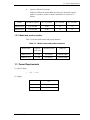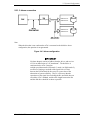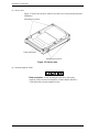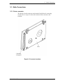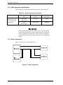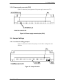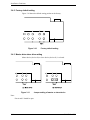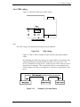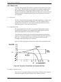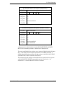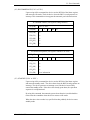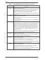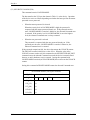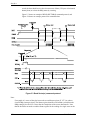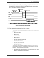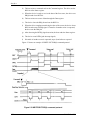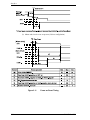
1
C141-E042-01EN MHA2021AT, MHA2032AT DISK DRIVES PRODUCT MANUAL FOR SAFE OPERATION Handling of This Manual This manual contains important information for using this product. Read thoroughly before using the product. Use this product only after thoroughly reading and understanding especially the section “Important Alert Items” in this manual. Keep this manual handy, and keep it carefully. FUJITSU makes every effort to prevent users and bystanders from being injured or from suffering damage to their property. Use the product according to this manual. IMPORTANT NOTE TO USERS READ THE ENTIRE MANUAL CAREFULLY BEFORE USING THIS PRODUCT. INCORRECT USE OF THE PRODUCT MAY RESULT IN INJURY OR DAMAGE TO USERS, BYSTANDERS OR PROPERTY. While FUJITSU has sought to ensure the accuracy of all information in this manual, FUJITSU assumes no liability to any party for any damage caused by any error or omission contained in this manual, its updates or supplements, whether such errors or omissions result from negligence, accident, or any other cause. In addition, FUJITSU assumes no liability with respect to the application or use of any product or system in accordance with the descriptions or instructions contained herein; including any liability for incidental or consequential damages arising therefrom. FUJITSU DISCLAIMS ALL WARRANTIES REGARDING THE INFORMATION CONTAINED HEREIN, WHETHER EXPRESSED, IMPLIED, OR STATUTORY. FUJITSU reserves the right to make changes to any products described herein without further notice and without obligation. The contents of this manual may be revised without prior notice. The contents of this manual shall not be disclosed in any way or reproduced in any media without the express written permission of Fujitsu Limited. All Rights Reserved, Copyright FUJITSU LIMITED 1997 C141-E042-01EN Revision History (1/1) Edition Date Revised section (*1) (Added/Deleted/Altered) Details 01 1997-07-15 — — *1 Section(s) with asterisk (*) refer to the previous edition when those were deleted. C141-E042-01EN Preface This manual describes the MHA2021AT and MHA2032AT, 2.5-inch hard disk drives. These drives have a built-in controller that is compatible with the ATA interface. This manual describes the specifications and functions of the drives and explains in detail how to incorporate the drives into user systems. This manual assumes that the reader has a basic knowledge of hard disk drives and their implementations in computer systems. This manual consists of seven chapters and sections explaining the special terminology and abbreviations used in this manual: Overview of Manual CHAPTER 1 Drive Overview This chapter gives an overview of the MHA2021AT and MHA2032AT and describes their features. CHAPTER 2 Drive Configuration This chapter describes the internal configurations of the MHA2021AT and MHA2032AT and the configuration of the systems in which they operate. CHAPTER 3 Drive Installation This chapter describes the external dimensions, installation conditions, and switch settings of the MHA2021AT and MHA2032AT. CHAPTER 4 Theory of Drive Operation This chapter describes the operation theory of the MHA2021AT and MHA2032AT. CHAPTER 5 Interface Specifications This chapter describes the interface specifications of the MHA2021AT and MHA2032AT. CHAPTER 6 Interface Operations This chapter describes the operations of the MHA2021AT and MHA2032AT. CHAPTER 7 Miscellaneous This chapter describes how to reformat the MHA2021AT and MHA2032AT. Terminology This section explains the special terminology used in this manual. C141-E042-01EN i Preface Abbreviation This section gives the meanings of the definitions used in this manual. Conventions for Alert Messages This manual uses the following conventions to show the alert messages. An alert message consists of an alert signal and alert statements. The alert signal consists of an alert symbol and a signal word or just a signal word. The following are the alert signals and their meanings: This indicates a hazarous situation could result in minor or moderate personal injury if the user does not perform the procedure correctly. This alert signal also indicates that damages to the product or other property, may occur if the user does not perform the procedure correctly. This indicates information that could help the user use the product more efficiently. In the text, the alert signal is centered, followed below by the indented message. A wider line space precedes and follows the alert message to show where the alert message begins and ends. The following is an example: (Example) Data corruption: Avoid mounting the disk drive near strong magnetic sources such as loud speakers. Ensure that the disk drive is not affected by external magnetic fields. The main alert messages in the text are also listed in the “Important Alert Items.” Operating Environment This product is designed to be used in offices or computer rooms. For details regarding the operating environment of use, refer to the (Cnnn-Xnnn) and the (Cnnn-Xnnn). Attention Please forward any comments you may have regarding this manual. ii C141-E042-01EN Preface To make this manual easier for users to understand, opinions from readers are needed. Please write your opinions or requests on the Comment at the back of this manual and forward it to the address described in the sheet. Liability Exception “Disk drive defects” refers to defects that involve adjustment, repair, or replacement. Fujitsu is not liable for any other disk drive defects, such as those caused by user misoperation or mishandling, inappropriate operating environments, defects in the power supply or cable, problems of the host system, or other causes outside the disk drive. C141-E042-01EN iii Important Alert Items Important Alert Messages The important alert messages in this manual are as follows: A hazardous situation could result in minor or moderate personal injury if the user does not perform the procedure correctly. Also, damage to the predate or other property, may occur if the user does not perform the procedure correctly. Task Normal Operation C141-E042-01EN Alert message Data corruption: Avoid mounting the disk near strong magnetic soures such as loud speakers. Ensure that the disk drive is not affected by extrnal magnetic fields. Page 3-6 v Contents CHAPTER 1 Device Overview ....................................................................... 1-1 1.1 1.1.1 1.1.2 1.1.3 1.2 1.2.1 1.2.2 CHAPTER 2 1-2 Functions and performance Adaptability 1-2 Interface 1-2 Device Specifications 1-2 1-4 Specifications summary 1-4 Model and product number 1-5 1.3 Power Requirements 1.4 Environmental Specifications 1.5 Acoustic Noise 1.6 Shock and Vibration 1.7 Reliability 1-8 1.8 Error Rate 1-9 1.9 Media Defects 1-5 1-7 1-7 1-8 1-9 Device Configuration ................................................................ 2-1 2.1 Device Configuration 2-2 2.2 System Configuration 2-4 2.2.1 2.2.2 2.2.3 C141-E042-01EN Features ATA interface 2-4 1 drive connection 2-4 2 drives connection 2-5 vii Contents CHAPTER 3 Installation Conditions ..............................................................3-1 3.1 Dimensions 3.2 Mounting 3.3 Cable Connections 3.3.1 3.3.2 3.3.3 3.3.4 3.4 3.4.1 3.4.2 3.4.3 3.4.4 CHAPTER 4 3-3 3-7 Device connector 3-7 Cable connector specifications Device connection 3-8 Power supply connector (CN1) Jumper Settings 3-8 3-9 3-9 Location of setting jumpers 3-9 Factory default setting 3-10 Master drive-slave drive setting 3-10 CSEL setting 3-11 Theory of Device Operation......................................................4-1 4.1 Outline 4.2 Subassemblies 4.2.1 4.2.2 4.2.3 4.2.4 4.2.5 4-2 4-2 Disk 4-2 Head 4-2 Spindle 4-3 Actuator 4-3 Air filter 4-3 4.3 Circuit Configuration 4.4 Power-on Sequence 4.5 Self-calibration 4.5.1 4.5.2 4.5.3 4.6 4.6.1 4.6.2 viii 3-2 4-4 4-6 4-7 Self-calibration contents 4-7 Execution timing of self-calibration 4-8 Command processing during self-calibration Read/write Circuit 4-9 4-9 Read/write preamplifier (PreAMP) Write circuit 4-10 4-9 C141-E042-01EN Contents 4.6.3 4.6.4 4.7 4.7.1 4.7.2 4.7.3 4.7.4 4.7.5 CHAPTER 5 Servo Control 4-13 4-14 Servo control circuit 4-14 Data-surface servo format 4-18 Servo frame format 4-18 Actuator motor control 4-19 Spindle motor control 4-20 Interface ..................................................................................... 5-1 5.1 5.1.1 5.1.2 5.2 5.2.1 5.2.2 5.2.3 5.3 5.3.1 5.3.2 5.3.3 5.4 5.4.1 5.4.2 5.4.3 5.4.4 5.4.5 5.5 5.5.1 5.5.2 5.5.3 5.5.4 C141-E042-01EN Read circuit 4-12 Time base generator circuit Physical Interface 5-2 Interface signals 5-2 Signal assignment on the connector Logical Interface 5-2 5-6 I/O registers 5-6 Command block registers 5-8 Control block registers 5-13 Host Commands 5-13 Command code and parameters Command descriptions 5-16 Error posting 5-67 Command Protocol 5-14 5-69 Data transferring commands from device to host Data transferring commands from host to device Commands without data transfer 5-73 Other commands 5-74 DMA data transfer commands 5-74 Timing 5-69 5-71 5-76 PIO data transfer 5-76 Single word DMA data transfer 5-78 Multiword DMA data transfer 5-79 Power-on and reset 5-79 ix Contents CHAPTER 6 Operations..................................................................................6-1 6.1 6.1.1 6.1.2 6.1.3 6.1.4 6.2 6.2.1 6.2.2 6.3 6.3.1 6.3.2 6.4 6.4.1 6.4.2 6.5 6.5.1 6.5.2 6.5.3 6.6 Glossary Device Response to the Reset 6-2 Response to power-on 6-2 Response to hardware reset 6-4 Response to software reset 6-5 Response to diagnostic command Address Translation 6-6 6-7 Default parameters 6-7 Logical address 6-8 Power Save 6-9 Power save mode Power commands Defect Management 6-9 6-11 6-11 Spare area 6-12 Alternating defective sectors Read-Ahead Cache 6-12 6-14 Data buffer configuration 6-14 Caching operation 6-14 Usage of read segment 6-16 Write Cache 6-22 ..................................................................................................GL-1 Acronyms and Abbreviations ........................................................................ AB-1 Index x ................................................................................................... IN-1 C141-E042-01EN Contents Illustrations Figures Figure 1.1 Current fluctuation (Typ.) at +5V when power is turned on Figure 2.1 Figure 2.2 Figure 2.3 Figure 2.4 Disk drive outerview 2-2 Configuration of disk media heads 1 drive system configuration 2-4 2 drives configuration 2-5 Figure 3.1 Figure 3.2 Figure 3.3 Figure 3.4 Figure 3.5 Figure 3.6 Figure 3.7 Figure 3.8 Figure 3.9 Figure 3.10 Figure 3.11 Figure 3.12 Figure 3.13 Figure 3.14 Dimensions 3-2 Orientation 3-3 Mounting frame structure 3-4 Surface temperature measurement points 3-5 Service area 3-6 Connector locations 3-7 Cable connections 3-8 Power supply connector pins (CN1) 3-9 Jumper location 3-9 Factory default setting 3-10 Jumper setting of master or slave device 3-10 CSEL setting 3-11 Example (1) of Cable Select 3-11 Example (2) of Cable Select 3-12 Figure 4.1 Figure 4.2 Figure 4.3 Figure 4.4 Figure 4.5 Figure 4.6 Figure 4.7 Figure 4.8 Head structure 4-3 Circuit Configuration 4-5 Power-on operation sequence 4-7 Read/write circuit block diagram 4-11 Frequency characteristic of programmable filter 4-12 Block diagram of servo control circuit 4-14 Physical sector servo configuration on disk surface 4-16 Servo frame format 4-18 2-3 Figure 5.1 Interface signals 5-2 Figure 5.2 Execution example of READ MULTIPLE command Figure 5.3 Read Sector(s) command protocol 5-70 Figure 5.4 Protocol for command abort 5-71 Figure 5.5 WRITE SECTOR(S) command protocol 5-72 C141-E042-01EN 1-6 5-20 xi Contents Figure 5.6 Figure 5.7 Figure 5.8 Figure 5.9 Figure 5.10 Figure 5.11 Protocol for the command execution without data transfer Normal DMA data transfer 5-75 Data transfer timing 5-77 Single word DMA data transfer timing (mode 2) 5-78 Multiword DMA data transfer timing (mode 2) 5-79 Power on Reset Timing 5-80 5-73 Figure 6.1 Figure 6.2 Figure 6.3 Figure 6.4 Figure 6.5 Figure 6.6 Figure 6.7 Figure 6.8 Figure 6.9 Response to power-on 6-3 Response to hardware reset 6-4 Response to software reset 6-5 Response to diagnostic command 6-6 Address translation (example in CHS mode) Address translation (example in LBA mode) Sector slip processing 6-12 Alternate cylinder assignment 6-13 Data buffer configuration 6-14 Table 1.1 Table 1.2 Table 1.3 Table 1.4 Table 1.5 Table 1.6 Specifications 1-4 Model names and product numbers 1-5 Current and power dissipation 1-6 Environmental specifications 1-7 Acoustic noise specification 1-7 Shock and vibration specification 1-8 Table 3.1 Table 3.2 Surface temperature measurement points and standard values Cable connector specifications 3-8 Table 4.1 Table 4.2 Table 4.3 Self-calibration execution timechart 4-9 Write precompensation algorithm 4-10 Write clock freqeuncy and recording density (BPI) of each zone 4-13 Table 5.1 Table 5.2 Table 5.3 Table 5.4 Table 5.5 Table 5.6 Table 5.7 Table 5.8 Table 5.9 Signal assignment on the interface connector 5-3 I/O registers 5-7 Command code and parameters 5-14 Information to be read by IDENTIFY DEVICE command 5-32 Features register values and settable modes 5-38 Diagnostic code 5-43 Features Register values (subcommands) and functions 5-54 Format of device attribute value data 5-56 Format of insurance failure threshold value data 5-57 6-8 6-9 Tables xii 3-5 C141-E042-01EN Contents Table 5.10 Contents of security password 5-59 Table 5.11 Contents of SECURITY SET PASSWORD data 5-64 Table 5.12 Relationship between combination of Identifier and Security level, and operation of the lock function 5-65 Table 5.13 Command code and parameters 5-67 Table 6.1 C141-E042-01EN Default parameters 6-7 xiii CHAPTER 1 Device Overview 1.1 Features 1.2 Device Specifications 1.3 Power Requirements 1.4 Environment Specifications 1.5 Acoustic Noise 1.6 Shock and Vibration 1.7 Reliability 1.8 Error Rate 1.9 Media Defects Overview and features are described in this chapter, and specifications and power requirement are described. The MHA2021AT and MHA2032AT are 2.5-inch hard disk drives with built-in disk controllers. These disk drives use the AT-bus hard disk interface protocol and are compact and reliable. C141-E042-01EN 1-1 Device Overview 1.1 Features 1.1.1 Functions and performance (1) Compact The disk has 1 or 2 disks of 65 mm (2.5 inches) diameter, and its height is 12.5 mm (0.492 inch). (2) Large capacity The disk drive can record up to 1,083 MB (formatted) on one disk using the (8/9) PRML recording method and 13 recording zone technology. The MHA2021AT and MHA2032AT have a formatted capacity of 2,167 MB and 3,251 MB respectively. (3) High-speed Transfer rate The disk drive has an internal data rate up to 8.92 MB/s. The disk drive supports an external data rate up to 16.6 MB/s. (4) Average positioning time Use of a rotary voice coil motor in the head positioning mechanism greatly increases the positioning speed. The average positioning time is 13 ms (at read). 1.1.2 Adaptability (1) Power save mode The power save mode feature for idle operation, stand by and sleep modes makes the disk drive ideal for applications where power consumption is a factor. (2) Wide temperature range The disk drive can be used over a wide temperature range (5°C to 55°C). (3) Low noise and vibration In Ready status, the noise of the disk drive is only about 30 dBA (measured at 1 m apart from the drive under the idle mode). 1.1.3 Interface (1) Connection to interface With the built-in ATA interface controller, the disk drive can be connected to an ATA interface of a personal computer. 1-2 C141-E042-01EN 1.1 Features (2) 128-KB data buffer The disk drive uses a 128-KB data buffer to transfer data between the host and the disk media. In combination with the read-ahead cache system described in item (3) and the write cache described in item (7), the buffer contributes to efficient I/O processing. (3) Read-ahead cache system After the execution of a disk read command, the disk drive automatically reads the subsequent data block and writes it to the data buffer (read ahead operation). This cache system enables fast data access. The next disk read command would normally cause another disk access. But, if the read ahead data corresponds to the data requested by the next read command, the data in the buffer can be transferred instead. (4) Master/slave The disk drive can be connected to ATA interface as daisy chain configuration. Drive 0 is a master device, drive 1 is a slave device. (5) Error correction and retry by ECC If a recoverable error occurs, the disk drive itself attempts error recovery. The ECC has improved buffer error correction for correctable data errors. (6) Self-diagnosis The disk drive has a diagnostic function to check operation of the controller and disk drive. Executing the diagnostic command invokes self-diagnosis. (7) Write cache When the disk drive receives a write command, the disk drive posts the command completion at completion of transferring data to the data buffer completion of writing to the disk media. This feature reduces the access time at writing. C141-E042-01EN 1-3 Device Overview 1.2 Device Specifications 1.2.1 Specifications summary Table 1.1 shows the specfications of the disk drive. Table 1.1 Specifications Format Capacity (*1) Number of Heads MHA2021AT MHA2032AT 2.16 GB 3.25 GB 4 6 Number of Cylinders (User) 6,372 Bytes per Sector 512 Recording Method (8/9) PRML Track Density 10,555 TPI Bit Density 157,422 BPI Rotational Speed 4,000 rpm ± 1% Average Latency 7.5 ms Positioning time (read and seek) • Minimum (Track to Track) • Average • Maximum (Full) 2.5 ms (typ.) Read: 13 ms (typ.) 23 ms (typ.) Start/Stop time • Start (0 rpm to Drive Read) • Stop (at Power Down) Interface Typ.: 5 sec, Max.: 10 sec Typ.: 5 sec, Max.: 15 sec (when the command is stopped) (when the power is off) ATA-3 (Max. Cable length: 0.46 m) Data Transfer Rate • To/From Media • To/From Host Data Buffer Size Physical Dimensions (Height × Width × Depth) Weight 1-4 4.93 to 8.92 MB/s 16.6 MB/s Max. (burst PIO mode 4, burst DMA mode 2) 128 KB 12.5 mm × 100.0 mm × 70.0 mm (0.49" × 3.94" × 2.75") 145 g C141-E042-01EN 1.3 Power Requirements *1: Capacity under the LBA mode. Under the CHS mode (normal BIOS specification), formatted capacity, number of cylinders, number of heads, and number of sectors are as follows. Model Formatted Capacity No. of Cylinder No. of Heads No. of Sectors MHA2021AT 2,167.60 MB 4,200 16 63 MHA2032AT 3,251.40 MB 6,300 16 63 1.2.2 Model and product number Table 1.2 lists the model names and product numbers. Table 1.2 Model names and product numbers Model Name Capacity (user area) Mounting screw Order No. MHA2021AT 2.16 GB M3, depth 3 CA01640-B040 MHA2032AT 3.25 GB M3, depth 3 CA01640-B060 1.3 Power Requirements (1) Input Voltage • +5V ±5% (2) Ripple +5 V C141-E042-01EN Maximum 100 mV (peak to peak) Frequency DC to 1 MHz 1-5 Device Overview (3) Current Requirements and Power Dissipation Table 1.3 lists the current and power dissipation. Table 1.3 Current and power dissipation Typical RMS Current Typical Power (*2) 1.0 A Watts 5.0 W 0.236 A T.B.D T.B.D 1.18 W R/W (*3) 0.5 A T.B.D T.B.D 2.5 W Standby 0.076 A T.B.D T.B.D 0.38 W 0.03 AT.B.D T.B.D 0.15 W Spin up (*1) Idle Sleep *1 Current at starting spindle motor. *2 Power requirements reflect nominal values for +5V power. *3 At 30% disk accessing. (4) Current fluctuation (Typ.) at +5V when power is turned on Figure 1.1 Current fluctuation (Typ.) at +5V when power is turned on (5) Power on/off sequence The voltage detector circuit monitors +5 V. The circuit does not allow a write signal if either voltage is abnormal. This prevents data from being destroyed and eliminates the need to be concerned with the power on/off sequence. 1-6 C141-E042-01EN 1.5 Acoustic Noise 1.4 Environmental Specifications Table 1.4 lists the environmental specifications. Table 1.4 Environmental specifications Temperature • Operating 5°C to 55°C (ambient) 5°C to 60°C (disk enclosure surface) • Non-operating –40°C to 65°C • Thermal Gradient 20°C/h or less Humidity • Operating 8% to 90% RH (Non-condensing) • Non-operating 5% to 95% RH (Non-condensing) • Maximum Wet Bulb 29°C Altitude (relative to sea level) • Operating –300 to 3,000 m (–200 to 10000 ft) • Non-operating –300 to 12,000 m (–200 to 40000 ft) 1.5 Acoustic Noise Table 1.5 lists the acoustic noise specification. Table 1.5 Acoustic noise specification Sound Pressure • Idle mode (DRIVE READY) C141-E042-01EN 30 dBA typical at 1 m 1-7 Device Overview 1.6 Shock and Vibration Table 1.6 lists the shock and vibration specification. Table 1.6 Shock and vibration specification Vibration (swept sine, one octave per minute) • Operating 5 to 500 Hz, 1.0G0-peak (without non-recovered errors) (9.8 m/s2 0-peak) • Non-operating 5 to 500 Hz, 5G0-peak (no damage) (49 m/s2 0-peak) Shock (half-sine pulse, 2 ms duration) • Operating 100G0-peak (without non-recovered errors) (980 m/s2 0-peak) • Non-operating 500G0-peak (no damage) (4,900 m/s2 0-peak) 1.7 Reliability (1) Mean time between failures (MTBF) The mean time between failures (MTBF) is 300,000 H or more (operation: 24 hours/day, 7 days/week). This does not include failures occurring during the first three months after installation. MTBF is defined as follows: Total operation time in all fields MTBF= (H) number of device failure in all fields “Disk drive defects” refers to defects that involve repair, readjustment, or replacement. Disk drive defects do not include failures caused by external factors, such as damage caused by handling, inappropriate operating environments, defects in the power supply host system, or interface cable. (2) Mean time to repair (MTTR) The mean time to repair (MTTR) is 30 minutes or less, if repaired by a specialist maintenance staff member. 1-8 C141-E042-01EN 1.9 Media Defects (3) Service life In situations where management and handling are correct, the disk drive requires no overhaul for five years when the DE surface temperature is less than 48°C. When the DE surface temperature exceeds 48°C, the disk drives requires no overhaul for five years or 20,000 hours of operation, whichever occurs first. Refer to item (3) in Subsection 3.2 for the measurement point of the DE surface temperature. (4) Data assurance in the event of power failure Except for the data block being written to, the data on the disk media is assured in the event of any power supply abnormalities. This does not include power supply abnormalities during disk media initialization (formatting) or processing of defects (alternative block assignment). 1.8 Error Rate Known defects, for which alternative blocks can be assigned, are not included in the error rate count below. It is assumed that the data blocks to be accessed are evenly distributed on the disk media. (1) Unrecoverable read error Read errors that cannot be recovered by maximum 126 times read retries without user’s retry and ECC corrections shall occur no more than 10 times when reading data of 1014 bits. Read retries are executed according to the disk drive’s error recovery procedure, and include read retries accompanying head offset operations. (2) Positioning error Positioning (seek) errors that can be recovered by one retry shall occur no more than 10 times in 107 seek operations. 1.9 Media Defects Defective sectors are replaced with alternates when the disk is formatted prior to shipment from the factory (low level format). Thus, the host sees a defect-free device. Alternate sectors are automatically accessed by the disk drive. The user need not be concerned with access to alternate sectors. C141-E042-01EN 1-9 CHAPTER 2 Device Configuration 2.1 Device Configuration 2.2 System Configuration This chapter describes the internal configurations of the hard disk drives and the configuration of the systems in which they operate. C141-E042-01EN 2-1 Device Configuration 2.1 Device Configuration Figure 2.1 shows the disk drive. The disk drive consists of a disk enclosure (DE), read/write preamplifier, and controller PCA. The disk enclosure contains the disk media, heads, spindle motors, actuators, and a circulating air filter. Figure 2.1 Disk drive outerview (1) Disk The outer diameter of the disk is 65 mm. The inner diameter is 20 mm. The number of disks used varies with the model, as described below. The disks are rated at over 50,000 start/stop operations. MHA2021AT: 2 disk MHA2032AT: 3 disks (2) Head The heads are of the contact start/stop (CSS) type. The head touches the disk surface while the disk is not rotating and automatically lifts when the disk starts. Figure 2.2 illustrates the configuration of the disks and heads of each model. In the disk surface, servo information necessary for controlling positioning and read/write and user data are written. Numerals 0 to 5 indicate read/write heads. 2-2 C141-E042-01EN 2.1 Device Configuration Head 0 Head 0 1 1 2 3 2 4 3 5 MHA2021AT MHA2032AT Figure 2.2 Configuration of disk media heads (3) Spindle motor The disks are rotated by a direct drive Hall-less DC motor. (4) Actuator The actuator uses a revolving voice coil motor (VCM) structure which consumes low power and generates very little heat. The head assembly at the edge of the actuator arm is controlled and positioned by feedback of the servo information read by the read/write head. If the power is not on or if the spindle motor is stopped, the head assembly stays in the specific CSS zone on the disk and is fixed by a mechanical lock. C141-E042-01EN 2-3 Device Configuration (5) Air circulation system The disk enclosure (DE) is sealed to prevent dust and dirt from entering. The disk enclosure features a closed loop air circulation system that relies on the blower effect of the rotating disk. This system continuously circulates the air through the circulation filter to maintain the cleanliness of the air within the disk enclosure. (6) Read/write circuit The read/write circuit uses a LSI chip for the read/write preamplifier. It improves data reliability by preventing errors caused by external noise. (7) Controller circuit The controller circuit consists of an LSI chip to improve reliability. The highspeed microprocessor unit (MPU) achieves a high-performance AT controller. 2.2 System Configuration 2.2.1 ATA interface Figures 2.3 and 2.4 show the ATA interface system configuration. The drive has a 44-pin PC AT interface connector and supports the PIO transfer at 16.6 MB/s (ATA-3, Mode 4), the DMA transfer at 16.6 MB/s (ATA-3, Multiword mode 2). 2.2.2 1 drive connection MHA2021AT MHA2032AT Figure 2.3 1 drive system configuration 2-4 C141-E042-01EN 2.2 System Configuration 2.2.3 2 drives connection (Host adaptor) MHA2021AT MHA2032AT MHA2021AT MHA2032AT Note: When the drive that is not conformed to ATA is connected to the disk drive above configuration, the operation is not guaranteed. Figure 2.4 2 drives configuration HA (host adaptor) consists of address decoder, driver, and receiver. ATA is an abbreviation of “AT attachment”. The disk drive is conformed to the ATA-3 interface. At high speed data transfer (PIO mode 3, mode 4, or DMA mode 2), occurence of ringing or crosstalk of the signal lines (AT bus) between the HA and the disk drive may be a great cause of the obstruction of system reliability. Thus, it is necessary that the capacitance of the signal lines including the HA and cable does not exceed the ATA-3 standard, and the cable length between the HA and the disk drive should be as short as possible. C141-E042-01EN 2-5 CHAPTER 3 Installation Conditions 3.1 Dimensions 3.2 Mounting 3.3 Cable Connections 3.4 Jumper Settings This chapter gives the external dimensions, installation conditions, surface temperature conditions, cable connections, and switch settings of the hard disk drives. C141-E042-01EN 3-1 Installation Conditions 3.1 Dimensions Figure 3.1 illustrates the dimensions of the disk drive and positions of the mounting screw holes. All dimensions are in mm. Figure 3.1 Dimensions 3-2 C141-E042-01EN 3.2 Mounting 3.2 Mounting (1) Orientation Figure 3.2 illustrates the allowable orientations for the disk drive. (a) Horizontal –1 (b) Horizontal –1 (c) Vertical –1 (d) Vertical –2 (e) Vertical –3 (f) Vertical –4 Figure 3.2 Orientation C141-E042-01EN 3-3 Installation Conditions (2) Frame The MR head bias of the HDD disk enclosure (DE) is zero. The mounting frame is connected to SG. Use M3 screw for the mounting screw and the screw length should satisfy the specification in Figure 3.3. The tightening torque must not exceed 3 kgcm. When attaching the HDD to the system frame, do not allow the system frame to touch parts (cover and base) other than parts to which the HDD is attached. (3) Limitation of side-mounting Do not use the center hole. For screw length, see Figure 3.3. 2.5 Bottom surface mounting 2.5 DE 2 Side surface mounting 2.5 PCA Frame of system cabinet A Frame of system cabinet 3.0 or less Screw 2.5 3.0 or less B Screw Details of A Details of B Figure 3.3 Mounting frame structure 3-4 C141-E042-01EN 3.2 Mounting (4) Ambient temperature The temperature conditions for a disk drive mounted in a cabinet refer to the ambient temperature at a point 3 cm from the disk drive. The ambient temperature must satisfy the temperature conditions described in Section 1.4, and the airflow must be considered to prevent the DE surface temperature from exceeding 60°C. Provide air circulation in the cabinet such that the PCA side, in particular, receives sufficient cooling. To check the cooling efficiency, measure the surface temperatures of the DE. Regardless of the ambient temperature, this surface temperature must meet the standards listed in Table 3.1. Figure 3.4 shows the temperature measurement point. 1 Figure 3.4 Surface temperature measurement points Table 3.1 Surface temperature measurement points and standard values No. Measurement point Temperature 1 DE cover 60°C max C141-E042-01EN 3-5 Installation Conditions (5) Service area Figure 3.5 shows how the drive must be accessed (service areas) during and after installation. Mounting screw hole Cable connection Mounting screw hole Figure 3.5 Service area (6) External magnetic fields Data corruption: Avoid mounting the disk drive near strong magnetic sources such as loud speakers. Ensure that the disk drive is not affected by external magnetic fields. 3-6 C141-E042-01EN 3.3 Cable Connections 3.3 Cable Connections 3.3.1 Device connector The disk drive has the connectors and terminals listed below for connecting external devices. Figure 3.6 shows the locations of these connectors and terminals. PCA Connector, setting pins Figure 3.6 Connector locations C141-E042-01EN 3-7 Installation Conditions 3.3.2 Cable connector specifications Table 3.2 lists the recommended specifications for the cable connectors. Table 3.2 Cable connector specifications ATA interface and power supply cable (44-pin type) Name Model Manufacturer Cable socket (44-pin type) 89361-144 BERG Cable (44-pin type) FV08-A440 Junkosha For the host interface cable, use a ribbon cable. A twisted cable or a cable with wires that have become separated from the ribbon may cause crosstalk between signal lines. This is because the interface is designed for ribbon cables and not for cables carrying differential signals. 3.3.3 Device connection Figure 3.7 shows how to connect the devices. Figure 3.7 Cable connections 3-8 C141-E042-01EN 3.4 Jumper Settings 3.3.4 Power supply connector (CN1) Figure 3.8 shows the pin assignment of the power supply connector (CN1). Figure 3.8 Power supply connector pins (CN1) 3.4 Jumper Settings 3.4.1 Location of setting jumpers Figure 3.9 shows the location of the jumpers to select drive configuration and functions. Figure 3.9 Jumper location C141-E042-01EN 3-9 Installation Conditions 3.4.2 Factory default setting Figure 3.10 shows the default setting position at the factory. Figure 3.10 Factory default setting 3.4.3 Master drive-slave drive setting Master device (device #0) or slave device (device #1) is selected. Figure 3.11 Jumper setting of master or slave device Note: Pins A and C should be open. 3-10 C141-E042-01EN 3.4 Jumper Settings 3.4.4 CSEL setting Figure 3.12 shows the cable select (CSEL) setting. Note: The CSEL setting is not depended on setting between pins Band D. Figure 3.12 CSEL setting Figure 3.13 and 3.14 show examples of cable selection using unique interface cables. By connecting the CSEL of the master device to the CSEL Line (conducer) of the cable and connecting it to ground further, the CSEL is set to low level. The device is identified as a master device. At this time, the CSEL of the slave device does not have a conductor. Thus, since the slave device is not connected to the CSEL conductor, the CSEL is set to high level. The device is identified as a slave device. Figure 3.13 C141-E042-01EN Example (1) of Cable Select 3-11 Installation Conditions Figure 3.14 3-12 Example (2) of Cable Select C141-E042-01EN CHAPTER 4 Theory of Device Operation 4.1 Outline 4.2 Subassemblies 4.3 Circuit Configuration 4.4 Power-on sequence 4.5 Self-calibration 4.6 Read/Write circuit 4.7 Servo Control This chapter explains basic design concepts of the disk drive. Also, this chapter explains subassemblies of the disk drive, each sequence, servo control, and electrical circuit blocks. C141-E042-01EN 4-1 Theory of Device Operation 4.1 Outline This chapter consists of two parts. First part (Section 4.2) explains mechanical assemblies of the disk drive. Second part (Sections 4.3 through 4.7) explains a servo information recorded in the disk drive and drive control method. 4.2 Subassemblies The disk drive consists of a disk enclosure (DE) and printed circuit assembly (PCA). The DE contains all movable parts in the disk drive, including the disk, spindle, actuator, read/write head, and air filter. For details, see Subsections 4.2.1 to 4.2.5. The PCA contains the control circuits for the disk drive. The disk drive has one PCA. For details, see Sections 4.3. 4.2.1 Disk The DE contains disks with an outer diameter of 65 mm and an inner diameter of 20 mm. The MHA2032 has three disks and MHA2021AT has two disks. The head contacts the disk each time the disk rotation stops; the life of the disk is 50,000 contacts or more. Servo data is recorded on top disk. Servo data is recorded on each cylinder (total 54). Servo data written at factory is read out by the read/write head. For servo data, see Section 4.7. 4.2.2 Head Figure 4.1 shows the read/write head structures. MHA2021AT has 4 read/write heads and MHA2032AT has 6 read/write heads. These heads are raised from the disk surface as the spindle motor the rated rotation speed. 4-2 C141-E042-01EN 4.2 Subassemblies Head Head 0 0 1 1 2 3 2 4 3 5 MHA2021AT MHA2032AT Figure 4.1 Head structure 4.2.3 Spindle The spindle consists of a disk stack assembly and spindle motor. The disk stack assembly is activated by the direct drive sensor-less DC spindle motor, which has a speed of 4,000 rpm ±1%. The spindle is controlled with detecting a PHASE signal generated by counter electromotive voltage of the spindle motor at starting. 4.2.4 Actuator The actuator consists of a voice coil motor (VCM) and a head carriage. The VCM moves the head carriage along the inner or outer edge of the disk. The head carriage position is controlled by feeding back the difference of the target position that is detected and reproduced from the servo information read by the read/write head. 4.2.5 Air filter There are two types of air filters: a breather filter and a circulation filter. The breather filter makes an air in and out of the DE to prevent unnecessary pressure around the spindle when the disk starts or stops rotating. When disk drives are transported under conditions where the air pressure changes a lot, filtered air is circulated in the DE. The circulation filter cleans out dust and dirt from inside the DE. The disk drive cycles air continuously through the circulation filter through an enclosed loop air cycle system operated by a blower on the rotating disk. C141-E042-01EN 4-3 Theory of Device Operation 4.3 Circuit Configuration Figure 4.2 shows the disk drive circuit configuration. (1) Read/write circuit The read/write circuit consists of two LSIs; read/write preamplifier (PreAMP) and read channel (RDC). The PreAMP consists of the write current switch circuit, that flows the write current to the head coil, and the voltage amplifier circuit, that amplitudes the read output from the head. The RDC is the read demodulation circuit using the partial response class 4 (PR4), and contains the Viterbi detector, programmable filter, adaptable transversal filter, times base generator, and data separator circuits. The RDC also contains the 8/9 group coded recording (GCR) encoder and decoder and servo demodulation circuit. (2) Servo circuit The position and speed of the voice coil motor are controlled by 2 closed-loop servo using the servo information recorded on the data surface. The servo information is an analog signal converted to digital for processeing by a MPU and then reconverted to an analog signal for control of the voice coil motor. The MPU precisely sets each head on the track according on the servo information on the media surface. (3) Spindle motor driver circuit The circuit measures the interval of a PHASE signal generated by counterelectromotive voltage of a motor at the MPU and controls the motor speed comparing target speed. (4) Controller circuit Major functions are listed below. 4-4 • Data buffer (128 KB) management • ATA interface control and data transfer control • Sector format control • Defect management • ECC control • Error recovery and self-diagnosis C141-E042-01EN 4.3 Circuit Configuration Figure 4.2 Circuit Configuration C141-E042-01EN 4-5 Theory of Device Operation 4.4 Power-on Sequence Figure 4.3 describes the operation sequence of the disk drive at power-on. The outline is described below. a) After the power is turned on, the disk drive executes the MPU bus test, internal register read/write test, and work RAM read/write test. When the self-diagnosis terminates successfully, the disk drive starts the spindle motor. b) The disk drive executes self-diagnosis (data buffer read/write test) after enabling response to the ATA bus. c) After confirming that the spindle motor has reached rated speed, the disk drive releases the heads from the actuator magnet lock mechanism by applying current to the VCM. This unlocks the heads which are parked at the inner circumference of the disks. d) The disk drive positions the heads onto the SA area and reads out the system information. 4-6 e) The disk drive executes self-seek-calibration. This collects data for VCM tarque and mechanical external forces applied to the actuator, and updates the calibrating value. f) The drive becomes ready. The host can issue commands. C141-E042-01EN 4.5 Self-calibration Figure 4.3 Power-on operation sequence 4.5 Self-calibration The disk drive occasionally performs self-calibration in order to sense and calibrate mechanical external forces on the actuator, and VCM tarque. This enables precise seek and read/write operations. 4.5.1 Self-calibration contents (1) Sensing and compensating for external forces The actuator suffers from torque due to the FPC forces and winds accompanying disk revolution. The torque vary with the disk drive and the cylinder where the head is positioned. To execute stable fast seek operations, external forces are occasionally sensed. The firmware of the drive measures and stores the force (value of the actuator motor drive current) that balances the torque for stopping head stably. This includes the current offset in the power amplifier circuit and DAC system. C141-E042-01EN 4-7 Theory of Device Operation The forces are compensated by adding the measured value to the specified current value to the power amplifier. This makes the stable servo control. To compensate torque varing by the cylinder, the disk is divided into 8 areas from the innermost to the outermost circumference and the compensating value is measured at the measuring cylinder on each area at factory calibration. The measured values are stored in the SA cylinder. In the self-calibration, the compensating value is updated using the value in the SA cylinder. (2) Compensating open loop gain Torque constant value of the VCM has a dispersion for each drive, and varies depending on the cylinder that the head is positioned. To realize the high speed seek operation, the value that compensates torque constant value change and loop gain change of the whole servo system due to temperature change is measured and stored. For sensing, the firmware mixes the disturbance signal to the position signal at the state that the head is positioned to any cylinder. The firmware calculates the loop gain from the position signal and stores the compensation value against to the target gain as ratio. For compensating, the direction current value to the power amplifier is multiplied by the compensation value. By this compensation, loop gain becomes constant value and the stable servo control is realized. To compensate torque constant value change depending on cylinder, whole cylinders from most inner to most outer cylinder are divided into 8 partitions at calibration in the factory, and the compensation data is measured for representive cylinder of each partition. This measured value is stored in the SA area. The compensation value at self-calibration is calculated using the value in the SA area. 4.5.2 Execution timing of self-calibration Self-calibration is executed when: • The power is turned on. • The disk drive receives the RECALIBRATE command from the host. • The self-calibration execution timechart of the disk drive specifies selfcalibration. The disk drive performs self-calibration according to the timechart based on the time elapsed from power-on. The timechart is shown in Table 4.1. After poweron, self-calibration is performed about every five or ten or fifteen minutes for the first 60 minutes or six RECALIBRATE command executions, and about every 30 minutes after that. 4-8 C141-E042-01EN 4.6 Read/write Circuit Table 4.1 Self-calibration execution timechart Time elapsed Time elapsed (accumulated) 1 At power-on Initial calibration 2 About 5 minutes About 5 minutes 3 About 5 minutes About 10 minutes 4 About 10 minutes About 20 minutes 5 About 10 minutes About 30 minutes 6 About 15 minutes About 45 minutes 7 About 15 minutes About 60 minutes 8 . . . . Every about 30 minutes 4.5.3 Command processing during self-calibration If the disk drive receives a command execution request from the host while executing self-calibration according to the timechart, the disk drive terminates self-calibration and starts executing the command precedingly. In other words, if a disk read or write service is necessary, the disk drive positions the head to the track requested by the host, reads or writes data, and restarts calibration. This enables the host to execute the command without waiting for a long time, even when the disk drive is performing self-calibration. The command execution wait time is about maximum 100 ms. 4.6 Read/write Circuit The read/write circuit consists of the read/write preamplifier (PreAMP), the write circuit, the read circuit, and the time base generator in the read channel (RDC). Figure 4.4 is a block diagram of the read/write circuit. 4.6.1 Read/write preamplifier (PreAMP) One PreAMP is mounted on the FPC. The PreAMP consists of an read preamplifier and a write current switch and senses a write error. Each channel is connected to each data head. The head IC switches the heads by the chip select signals (*CS) and the head select signals. The IC generates a write error sense C141-E042-01EN 4-9 Theory of Device Operation signal (WUS) when a write error occurs due to head short-circuit or head disconnection. 4.6.2 Write circuit The write data is output from the hard disk controller (HDC) with the NRZ data format, and sent to the encoder circuit in the RDC with synchronizing with the write clock. The NRZ write data is converted from 8-bit data to 9-bit data by the encoder circuit then sent to the PreAMP, and the data is written onto the media. (1) 8/9 GCR The disk drive converts data using the 8/9 (0, 4, 4) group coded recording (GCR) algorithm. This code format is 0 to 4 code bit “0”s are placed between “1”s. (2) Write precompensation Write precompensation compensates, during a write process, for write nonleneartiry generated at reading. Table 4.2 shows the write precompensation algorithm. Table 4.2 Write precompensation algorithm Bit Bit Bit Compensation n–1 n n+1 Bit n 0 1 1 None 1 1 0 Late 1 1 1 Late Late: Bit n is time shifted (delayed) from its nominal time position towards the bit n+1 time position. 4-10 C141-E042-01EN 4.6 Read/write Circuit Figure 4.4 Read/write circuit block diagram C141-E042-01EN 4-11 Theory of Device Operation 4.6.3 Read circuit The head read signal from the PreAMP is regulated by the automatic gain control (AGC) circuit. Then the output is converted into the sampled read data pulse by the programmable filter circuit and the adaptive equalizer circuit. This clock signal is converted into the NRZ data by the 8/9 GCR decoder circuit based on the read data maximum-likelihood-detected by the Viterbi detection circuit, then is sent to the HDC. (1) AGC circuit The AGC circuit automatically regulates the output amplitude to a constant value even when the input amplitude level fluctuates. The AGC amplifier output is maintained at a constant level even when the head output fluctuates due to the head characteristics or outer/inner head positions. (2) Programmable filter The programmable filter circuit has a low-pass filter function that eliminates unnecessary high frequency noise component and a high frequency boost-up function that equalizes the waveform of the read signal. Cut-off frequency of the low-pass filter and boost-up gain are controlled from each DAC circuit in read channel by an instruction of the serial data signal from MPU (M5). The MPU optimizes the cut-off frequency and boost-up gain according to the transfer frequency of each zone. Figure 4.5 shows the frequency characteristic sample of the programmalbe filter. -3 dB Figure 4.5 Frequency characteristic of programmable filter (3) Adaptive equalizer circuit This circuit is 3-tap sampled analog transversal filter circuit that cosine-equalizes the head read signal to the partial response class 4 (PR4) waveform. 4-12 C141-E042-01EN 4.6 Read/write Circuit (4) Viterbi detection circuit The sample hold waveform output from the adaptive equalizer circuit is sent to the Viterbi detection circuit. The Viterbi detection circuit demodulates data according to the survivor path sequence. (5) Data separator circuit The data separator circuit generates clocks in synchronization with the output of the adaptive equalizer circuit. To write data, the VFO circuit generates clocks in synchronization with the clock signals from a synthesizer. (6) 8/9 GCR decoder This circuit converts the 9-bit read data into the 8-bit NRZ data. 4.6.4 Time base generator circuit The drive uses constant density recording to increase total capacity. This is different from the conventional method of recording data with a fixed data transfer rate at all data area. In the constant density recording method, data area is divided into zones by radius and the data transfer rate is set so that the recording density of the inner cylinder of each zone is nearly constant. The drive divides data area into 13 zones to set the data transfer rate. Table 4.3 describes the data transfer rate and recording density (BPI) of each zone. Table 4.3 Write clock freqeuncy and recording density (BPI) of each zone Zone 0 1 2 3 4 5 Cylinder 0 to 295 296 to 445 446 to 809 810 to 1455 1456 to 2080 2081 to 2605 Transfer rate [MB/s] 8.92 8.92 8.71 8.29 7.88 7.54 6 7 8 9 10 11 12 Cylinder 2606 to 3137 3138 to 3888 3889 to 4238 4239 to 4823 4824 to 5400 5401 to 5873 5874 to 6371 Transfer rate [MB/s] 7.19 6.67 6.44 6.04 5.63 5.29 4.93 Zone The MPU transfers the data transfer rate setup data (SDATA/SCLK) to the RDC that includes the time base generator circuit to change the data transfer rate. C141-E042-01EN 4-13 Theory of Device Operation 4.7 Servo Control The actuator motor and the spindle motor are submitted to servo control. The actuator motor is controlled for moving and positioning the head to the track containing the desired data. To turn the disk at a constant velocity, the actuator motor is controlled according to the servo data that is written on the data side beforehand. 4.7.1 Servo control circuit Figure 4.6 is the block diagram of the servo control circuit. The following describes the functions of the blocks: Figure 4.6 Block diagram of servo control circuit (1) Microprocessor unit (MPU) The MPU includes the AD converter and DSP unit, etc., and the MPU starts the spindle motor, moves the heads to the reference cylinders, seeks the specified cylinder, and executes calibration according to the internal operations of the MPU. 4-14 C141-E042-01EN 4.7 Servo Control The major internal operations are listed below. a. Spindle motor start Starts the spindle motor and accelerates it to normal speed when power is applied. b. Move head to reference cylinder Drives the VCM to position the head at the any cylinder in the data area. The logical initial cylinder is at the outermost circumference (cylinder 0). c. Seek to specified cylinder Drives the VCM to position the head to the specified cylinder. d. Calibration Senses and stores the thermal offset between heads and the mechanical forces on the actuator, and stores the calibration value. C141-E042-01EN 4-15 Theory of Device Operation Figure 4.7 Physical sector servo configuration on disk surface 4-16 C141-E042-01EN 4.7 Servo Control (2) Servo burst capture circuit The servo burst capture circuit reproduces signals (position signals) that indicate the head position from the servo data on the data surface. SERVO A, SERVO B, SERVO C and SERVO D burst signals shown in Figure 4.8 followed the servo mark, cylinder gray and index information are output from the servo area on the data surface via the data head. The servo signals A/D-converts the amplitudes of the POSA, POSB, POSC and POSD signals at the peak hold circuit in the servo burst capture circuit at the timing of the STROB signal. At that time the AGC circuit is in hold mode. The difference between A/D-converted data is obtained in the MPU recognizes it as the position information. (3) A/D converter (ADC) The A/D converter (ADC) receives the peak-held servo signals, converts them to digital, and transfers the digital signal to the DSP unit. (4) D/A converter (DAC) The D/A converter (DAC) converts the VCM drive current value (digital value) calculated by the DSP unit into analog values and transfers them to the power amplifier. (5) Power amplifier The power amplifier feeds currents, corresponding to the DAC output signal voltage to the VCM. (6) Spindle motor control circuit The spindle motor control circuit controls the sensor-less spindle motor. This circuit detects number of revolution of the motor by the interrupt generated periodically, compares with the target revolution speed, then flows the current into the motor coil according to the differentation (abberration). (7) Driver circuit The driver circuit is a power amplitude circuit that receives signals from the spindle motor control circuit and feeds currents to the spindle motor. (8) VCM current sense resistor (CSR) This resistor controls current at the power amplifier by converting the VCM current into voltage and feeding back. C141-E042-01EN 4-17 Theory of Device Operation 4.7.2 Data-surface servo format Figure 4.7 describes the physical layout of the servo frame. The three areas indicated by (1) to (3) in Figure 4.7 are described below. (1) Inner guard band The head is in contact with the disk in this space when the spindle starts turning or stops, and the rotational speed of the spindle can be controlled on this cylinder area for head moving. (2) Data area This area is used as the user data area SA area. (3) Outer guard band This area is located at outer position of the user data area, and the rotational speed of the spindle can be controlled on this cylinder area for head moving. 4.7.3 Servo frame format As the servo information, the IDD uses the two-phase servo generated from the gray code and servo A to D. This servo information is used for positioning operation of radius direction and position detection of circumstance direction. The servo frame consists of 6 blocks; write/read recovery, servo mark, gray code, servo A to D, and PAD. Figure 4.8 shows the servo frame format. 5.0 µs 0.7 µs 4.3 µs 1.7 µs 1.3 µs 1.3 µs 1.3 µs 2.5 µs Figure 4.8 Servo frame format 4-18 C141-E042-01EN 4.7 Servo Control (1) Write/read recovery This area is used to absorb the write/read transient and to stabilize the AGC. (2) Servo mark This area gererates a timing for demodulating the gray code and positiondemodulating the servo A to D by detecting the servo mark. (3) Gray code (including index bit) This area is used as cylinder address. The data in this area is converted into the binary data by the gray code demodulation circuit (4) Servo A, servo B, servo C, servo D This area is used as position signals between tracks, and the IDD control at ontrack so that servo A level equals to servo B level. (5) PAD This area is used as a gap between servo and data. 4.7.4 Actuator motor control The voice coil motor (VCM) is controlled by feeding back the servo data recorded on the data surface. The MPU fetches the position sense data on the servo frame at a constant interval of sampling time, executes calculation, and updates the VCM drive current. The servo control of the actuator includes the operation to move the head to the reference cylinder, the seek operation to move the head to the target cylinder to read or write data, and the track-following operation to position the head onto the target track. (1) Operation to move the head to the reference cylinder The MPU moves the head to the reference cylinder when the power is turned. The reference cylinder is in the data area. When power is applied the heads are moved from the inner circumference shunt zone to the normal servo data zone in the following sequence: a) Micro current is fed to the VCM to press the head against the inner circumference. b) Micro current is fed to the VCM to move the head toward the outer circumference. c) C141-E042-01EN When the servo mark is detected the head is moved slowly toward the outer circumference at a constant speed. 4-19 Theory of Device Operation d) If the head is stopped at the reference cylinder from there. Track following control starts. (2) Seek operation Upon a data read/write request from the host, the MPU confirms the necessity of access to the disk. If a read/write instruction is issued, the MPU seeks the desired track. The MPU feeds the VCM current via the D/A converter and power amplifier to move the head. The MPU calculates the difference (speed error) between the specified target position and the current position for each sampling timing during head moving. The MPU then feeds the VCM drive current by setting the calculated result into the D/A converter. The calculation is digitally executed by the firmware. When the head arrives at the target cylinder, the track is followed. (3) Track following operation Except during head movement to the reference cylinder and seek operation under the spindle rotates in steady speed, the MPU does track following control. To position the head at the center of a track, the DSP drives the VCM by feeding micro current. For each sampling time, the VCM drive current is determined by filtering the position difference between the target position and the position clarified by the detected position sense data. The filtering includes servo compensation. These are digitally controlled by the firmware. 4.7.5 Spindle motor control Hall-less three-phase twelve-pole motor is used for the spindle motor, and the 3phase full/half-wave analog current control circuit is used as the spindle motor driver (called SVC hereafter). The firmware operates on the MPU manufactured by Fujitsu. The spindle motor is controlled by sending several signals from the MPU to the SVC. There are three modes for the spindle control; start mode, acceleration mode, and stable rotation mode. (1) Start mode When power is supplied, the spindle motor is started in the following sequence: a) After the power is turned on, the MPU sends a signal to the SVC to charge the charge pump capacitor of the SVC. The charged amount defines the current that flows in the spindle motor. b) When the charge pump capacitor is charged enough, the MPU sets the SVC to the motor start mode. Then, a current (approx. 0.7 A) flows into the spindle motor. c) 4-20 The SVC generates a phase switching signal by itself, and changes the phase of the current flowed in the motor in the order of (V-phase to U-phase), (Wphase to U-phase), (W-phase to V-phase), (U-phase to V-phase), (U-phase to W-phase), and (V-phase to W-phase) (after that, repeating this order). C141-E042-01EN 4.7 Servo Control d) During phase switching, the spindle motor starts rotating in low speed, and generates a counter electromotive force. The SVC detects this counter electromotive force and reports to the MPU using a PHASE signal for speed detection. e) The MPU is waiting for a PHASE signal. When no phase signal is sent for a sepcific period, the MPU resets the SVC and starts from the beginning. When a PHASE signal is sent, the SVC enters the acceleration mode. (2) Acceleration mode In this mode, the MPU stops to send the phase switching signal to the SVC. The SVC starts a phase switching by itself based on the counter electromotive force. Then, rotation of the spindle motor accelerates. The MPU calcurates a rotational speed of the spindle motor based on the PHASE signal from the SVC, and accelerates till the rotational speed reaches 4,000 rpm. When the rotational speed reaches 4,000 rpm, the SVC enters the stable rotation mode. (3) Stable rotation mode The MPU calcurates a time for one revolution of the spindle motor based on the PHASE signal from the SVC. The MPU takes a difference between the current time and a time for one revolution at 4,000 rpm that the MPU already recognized. Then, the MPU keeps the rotational speed to 4,000 rpm by charging or discharging the charge pump for the different time. For example, when the actual rotational speed is 3,800 rpm, the time for one revolution is 15.789 ms. And, the time for one revolution at 4,000 rpm is 15 ms. Therefore, the MPU discharges the charge pump for 0.789 ms × k (k: constant value). This makes the flowed current into the motor lower and the rotational speed down. When the actual rotational speed is later than 4,000 rpm, the MPU charges the pump the other way. This control (charging/discharging) is performed every 1 revolution. C141-E042-01EN 4-21 CHAPTER 5 Interface 5.1 Physical Interface 5.2 Logical Interface 5.3 Host Commands 5.4 Command Protocol 5.5 Timing This chapter gives details about the interface, and the interface commands and timings. C141-E042-01EN 5-1 Interface 5.1 Physical Interface 5.1.1 Interface signals Figure 5.1 shows the interface signals. Figure 5.1 Interface signals 5.1.2 Signal assignment on the connector Table 5.1 shows the signal assignment on the interface connector. 5-2 C141-E042-01EN 5.1 Physical Interface Table 5.1 Signal assignment on the interface connector Pin No. Signal Pin No. Signal A ENCSEL B GND C ENCSEL D MSTR E (KEY) F (KEY) 1 RESET– 2 GND 3 DATA7 4 DATA8 5 DATA6 6 DATA9 7 DATA5 8 DATA10 9 DATA4 10 DATA11 11 DATA3 12 DATA12 13 DATA2 14 DATA13 15 DATA1 16 DATA14 17 DATA0 18 DATA15 19 GND 20 (KEY) 21 DMARQ 22 GND 23 IOW– 24 GND 25 IOR– 26 GND 27 IORDY 28 CSEL 29 DMACK– 30 GND 31 INTRQ 32 IOCS16– 33 DA1 34 PDIAG 35 DA0 36 DA2 37 CS0– 38 CS1– 39 DASP– 40 GND 41 +5 VDC 42 +5 VDC 43 GND 44 unused [signal] ENCSEL [I/O] [Description] I This signal is used to set master/slave using the CSEL signal (pin 28). Pins A and C Open: Sets master/slave by the MSTR signal without using the CSEL signal. Short: Sets master/slave using the CSEL signal. The MSTR signal is ignored. C141-E042-01EN 5-3 Interface [signal] MSTR [I/O] I [Description] MSTR, I, Master/slave setting 1: Master RESETDATA 0-15 IOW- [signal] 0: Slave I Reset signal from the host. This signal is low active and is asserted for a minimum of 25 ms during power on. I/O Sixteen-bit bi-directional data bus between the host and the device. These signals are used for data transfer I [I/O] Write strobe signal. The rising edge of this signal gates DATA0 to DATA15 signals or DATA0 to DATA7 signals into a register or the data port on the device. [Description] IOR- I Read strobe signal. The falling edge of this signal enables DATA0 to DATA15 or DATA0 to DATA7 data from the device register or data port onto the data bus. The rising edge of this signal latches the data at the host. INTRQ O Interrupt signal to the host. This signal is negated in the following cases: − assertion of RESET- signal − Reset by SRST of the Device Control register − Write to the command register by the host − Read of the status register by the host − Completion of sector data transfer (without reading the Status register) The signal output line has a high impedance when no devices are selected or interruption is disabled. IOCS16- O This signal indicates 16-bit data bus is addressed in PIO data transfer. This signal is an open collector output. − When IOCS16- is not asserted: 8 bit data is transferred through DATA0 to DATA7 signals. − When IOCS16- is asserted: 16 bit data is transferred through DATA0 to DATA15 signals. 5-4 CS0- I Chip select signal decoded from the host address bus. This signal is used by the host to select the command block registers. CS1- I Chip select signal decoded from the host address bus. This signal is used by the host to select the control block registers. DA 0-2 I Binary decoded address signals asserted by the host to access task file registers. KEY - Key pin for prevention of erroneous connector insertion C141-E042-01EN 5.1 Physical Interface [signal] PIDAG- [I/O] I/O [Description] This signal is an input mode for the master device and an output mode for the slave device in a daisy chain configuration. This signal indicates that the slave device has been completed self diagnostics. This signal is pulled up to +5 V through 10 kΩ resistor at each device. DASP- I/O This is a time-multiplexed signal that indicates that the device is active and a slave device is present. This signal is pulled up to +5 V through 10 kΩ resistor at each device. IORDY O This signal requests the host system to delay the transfer cycle when the device is not ready to respond to a data transfer request from the host system. CSEL I This signal to configure the device as a master or a slave device. When CSEL signal is grounded,, the IDD is a master device. When CSEL signal is open,, the IDD is a slave device. This signal is pulled up with 240 kΩ resistor. DMACK- I The host system asserts this signal as a response that the host system receive data or to indicate that data is valid. DMARQ O This signal is used for DMA transfer between the host system and the device. The device asserts this signal when the device completes the preparation of DMA data transfer to the host system (at reading) or from the host system (at writing). The direction of data transfer is controlled by the IOR and IOW signals. This signal hand shakes with the DMACK-signal. In other words, the device negates the DMARQ signal after the host system asserts the DMACK signal. When there is other data to be transferred, the device asserts the DMARQ signal again. When the DMA data transfer is performed, IOCS16-, CS0- and CS1- signals are not asserted. The DMA data transfer is a 16-bit data transfer. +5 VDC I +5 VDC power supplying to the device. GND - Grounded Note: “I” indicates input signal from the host to the device. “O” indicates output signal from the device to the host. “I/O” indicates common output or bi-directional signal between the host and the device. C141-E042-01EN 5-5 Interface 5.2 Logical Interface The device can operate for command execution in either address-specified mode; cylinder-head-sector (CHS) or Logical block address (LBA) mode. The IDENTIFY DEVICE information indicates whether the device supports the LBA mode. When the host system specifies the LBA mode by setting bit 6 in the Device/Head register to 1, HS3 to HS0 bits of the Device/Head register indicates the head No. under the LBA mode, and all bits of the Cylinder High, Cylinder Low, and Sector Number registers are LBA bits. The sector No. under the LBA mode proceeds in the ascending order with the start point of LBA0 (defined as follows). LBA0 = [Cylinder 0, Head 0, Sector 1] Even if the host system changes the assignment of the CHS mode by the INITIALIZE DEVICE PARAMETER command, the sector LBA address is not changed. LBA = [((Cylinder No.) × (Number of head) + (Head No.)) × (Number of sector/track)] + (Sector No.) − 1 5.2.1 I/O registers Communication between the host system and the device is done through inputoutput (I/O) registers of the device. These I/O registers can be selected by the coded signals, CS0-, CS1-, and DA0 to DA2 from the host system. Table 5.2. shows the coding address and the function of I/O registers. 5-6 C141-E042-01EN 5.2 Logical Interface Table 5.2 I/O registers CS0– CS1– DA2 DA1 I/O registers DA0 Host I/O address Read operation Write operation Command block registers L H L L L Data Data X’1F0’ L H L L H Error Register Features X’1F1’ L H L H L Sector Count Sector Count X’1F2’ L H L H H Sector Number Sector Number X’1F3’ L H H L L Cylinder Low Cylinder Low X’1F4’ L H H L H Cylinder High Cylinder High X’1F5’ L H H H L Device/Head Device/Head X’1F6’ L H H H H Status Command X’1F7’ L L X X X (Invalid) (Invalid) — Control block registers H L H H L Alternate Status Device Control X’3F6’ H L H H H — — X’3F7’ Notes: 1. The Data register for read or write operation can be accessed by 16 bit data bus (DATA0 to DATA15). 2. The registers for read or write operation other than the Data registers can be accessed by 8 bit data bus (DATA0 to DATA7). 3. When reading the Drive Address register, bit 7 is high-impedance state. 4. H indicates signal level High and L indicates signal level Low. 5. The LBA mode is specified, the Device/Head, Cylinder High, Cylinder Low, and Sector Number registers indicate LBA bits 27 to 24, 23 to 16, 15 to 8, and 7 to 0. C141-E042-01EN 5-7 Interface 5.2.2 Command block registers (1) Data register (X’1F0’) The Data register is a 16-bit register for data block transfer between the device and the host system. Data transfer mode is PIO or LBA mode. (2) Error register (X’1F1’) The Error register indicates the status of the command executed by the device. The contents of this register are valid when the ERR bit of the Status register is 1. This register contains a diagnostic code after power is turned on, a reset , or the EXECUTIVE DEVICE DIAGNOSTIC command is executed. [Status at the completion of command execution other than diagnostic command] Bit 7 Bit 6 Bit 5 Bit 4 Bit 3 Bit 2 Bit 1 Bit 0 ICRC UNC X IDNF X ABRT TK0NF X X: Unused 5-8 - Bit 7: Interface CRC Error (ICRC). This bit indicates that a CRC error occurred during Ultra DMA transfer. - Bit 6: Uncorrectable Data Error (UNC). This bit indicates that an uncorrectable data error has been encountered. - Bit 5: Unused - Bit 4: ID Not Found (IDNF). This bit indicates an error except for bad sector, uncorrectable error and SB not found. - Bit 3: Unused - Bit 2: Aborted Command (ABRT). This bit indicates that the requested command was aborted due to a device status error (e.g. Not Ready, Write Fault) or the command code was invalid. - Bit 1: Track 0 Not Found (TK0NF). This bit indicates that track 0 was not found during RECALIBRATE command execution. - Bit 0: Address Mark Not Found (AMNF). This bit indicates that the SB Not Found error occurred. C141-E042-01EN 5.2 Logical Interface [Diagnostic code] X’01’: No Error Detected. X’02’: HDC Register Compare Error X’03’: Data Buffer Compare Error. X’05’: ROM Sum Check Error. X’80’: Device 1 (slave device) Failed. Error register of the master device is valid under two devices (master and slave) configuration. If the slave device fails, the master device posts X’80’ OR (the diagnostic code) with its own status (X’01’ to X’05’). However, when the host system selects the slave device, the diagnostic code of the slave device is posted. (3) Features register (X’1F1’) The Features register provides specific feature to a command. For instance, it is used with SET FEATURES command to enable or disable caching. (4) Sector Count register (X’1F2’) The Sector Count register indicates the number of sectors of data to be transferred in a read or write operation between the host system and the device. When the value in this register is X’00’, the sector count is 256. When this register indicates X’00’ at the completion of the command execution, this indicates that the command is completed succefully. If the command is not completed scuccessfully, this register indicates the number of sectors to be transferred to complete the request from the host system. That is, this register indicates the number of remaining sectors that the data has not been transferred due to the error. The contents of this register has other definition for the following commands; INITIALIZE DEVICE PARAMETERS, SET FEATURES, IDLE, STANDBY and SET MULTIPLE MODE. (5) Sector Number register (X’1F3’) The contents of this register indicates the starting sector number for the subsequent command. The sector number should be between X’01’ and [the number of sectors per track defined by INITIALIZE DEVICE PARAMETERS command. Under the LBA mode, this register indicates LBA bits 7 to 0. C141-E042-01EN 5-9 Interface (6) Cylinder Low register (X’1F4’) The contents of this register indicates low-order 8 bits of the starting cylinder address for any disk-access. At the end of a command, the contents of this register are updated to the current cylinder number. Under the LBA mode, this register indcates LBA bits 15 to 8. (7) Cylinder High register (X’1F5’) The contents of this register indicates high-order 8 bits of the disk-access start cylinder address. At the end of a command, the contents of this register are updated to the current cylinder number. The high-order 8 bits of the cylinder address are set to the Cylinder High register. Under the LBA mode, this register indicates LBA bits 23 to 16. (8) Device/Head register (X’1F6’) The contents of this register indicate the device and the head number. When executing INITIALIZE DEVICE PARAMETERS command, the contents of this register defines “the number of heads minus 1”. 5-10 Bit 7 Bit 6 Bit 5 Bit 4 Bit 3 Bit 2 Bit 1 Bit 0 X L X DEV HS3 HS2 HS1 HS0 - Bit 7: Unused - Bit 6: L. 0 for CHS mode and 1 for LBA mode. - Bit 5: Unused - Bit 4: DEV bit. 0 for the master device and 1 for the slave device. - Bit 3: HS3 CHS mode head address 3 (23). LBA bit 27. - Bit 2: HS2 CHS mode head address 3 (22). LBA bit 26. - Bit 1: HS1 CHS mode head address 1 (21). LBA bit 25. - Bit 0: HS0 CHS mode head address 3 (20). LBA bit 24. C141-E042-01EN 5.2 Logical Interface (9) Status register (X’1F7’) The contents of this register indicate the status of the device. The contents of this register are updated at the completion of each command. When the BSY bit is cleared, other bits in this register should be validated within 400 ns. When the BSY bit is 1, other bits of this register are invalid. When the host system reads this register while an interrupt is pending, it is considered to be the Interrupt Acknowledge (the host system acknowledges the interrupt). Any pending interrupt is cleared (negating INTRQ signal) whenever this register is read. Bit 7 Bit 6 Bit 5 Bit 4 Bit 3 Bit 2 Bit 1 Bit 0 BSY DRDY DF DSC DRQ CORR 0 ERR - Bit 7: Busy (BSY) bit. This bit is set whenever the Command register is accessed. Then this bit is cleared when the command is completed. However, even if a command is being executed, this bit is 0 while data transfer is being requested (DRQ bit = 1).When BSY bit is 1, the host system should not write the command block registers. If the host system reads any command block register when BSY bit is 1, the contents of the Status register are posted. This bit is set by the device under following conditions: (a) Within 400 ns after RESET- is negated or SRST is set in the Device Control register, the BSY bit is set. the BSY bit is cleared, when the reset process is completed. The BSY bit is set for no longer than 15 seconds after the IDD accepts reset. (b) Within 400 ns from the host system starts writing to the Command register. (c) Within 5 µs following transfer of 512 bytes data during execution of the READ SECTOR(S), WRITE SECTOR(S), or WRITE BUFFER command. Within 5 µs following transfer of 512 bytes of data and the appropriate number of ECC bytes during execution of READ LONG or WRITE LONG command. - Bit 6: Device Ready (DRDY) bit. This bit indicates that the device is capable to respond to a command. The IDD checks its status when it receives a command. If an error is detected (not ready state), the IDD clears this bit to 0. This is cleared to 0 at power-on and it is cleared until the rotational speed of the spindle motor reaches the steady speed. C141-E042-01EN 5-11 Interface - Bit 5: The Device Write Fault (DF) bit. This bit indicates that a device fault (write fault) condition has been detected. If a write fault is detected during command execution, this bit is latched and retained until the device accepts the next command or reset. - Bit 4: Device Seek Complete (DSC) bit. This bit indicates that the device heads are positioned over a track. In the IDD, this bit is always set to 1 after the spin-up control is completed. - Bit 3: Data Request (DRQ) bit. This bit indicates that the device is ready to transfer data of word unit or byte unit between the host system and the device. - Bit 2: Corrected Data (CORR) bit. This bit indicates that a correctable data error was encountered and the error has been corrected. This condition does not halt the data transfer. - Bit 1: Always 0. - Bit 0: Error (ERR) bit. This bit indicates that an error was detected while the previous command was being executed. The Error register indicates the additional information of the cause for the error. (10) Command register (X’1F7’) The Command register contains a command code being sent to the device. After this register is written, the command execution starts immediately. Table 5.3 lists the executable commands and their command codes. This table also lists the neccesary parameters for each command which are written to certain registers before the Command register is written. 5-12 C141-E042-01EN 5.3 Host Commands 5.2.3 Control block registers (1) Alternate Status register (X’3F6’) The Alternate Status register contains the same information as the Status register of the command block register. The only difference from the Status register is that a read of this register does not imply Interrupt Acknowledge and INTRQ signal is not reset. Bit 7 Bit 6 Bit 5 Bit 4 Bit 3 Bit 2 Bit 1 Bit 0 BSY DRDY DF DSC DRQ CORR 0 ERR (2) Device Control register (X’3F6’) The Device Control register contains device interrupt and software reset. Bit 7 Bit 6 Bit 5 Bit 4 Bit 3 Bit 2 Bit 1 Bit 0 X X X X X SRST nIEN 0 - Bit 2: SRST is the host software reset bit. When this bit is set, the device is held reset state. When two device are daisy chained on the interface, setting this bit resets both device simultaneously. The slave device is not required to execute the DASP- handshake. - Bit 1: nIEN bit enables an interrupt (INTRQ signal) from the device to the host. When this bit is 0 and the device is selected, an interruption (INTRQ signal) can be enabled through a tri-state buffer. When this bit is 1 or the device is not selected, the INTRQ signal is in the highimpedance state. 5.3 Host Commands The host system issues a command to the device by writing necessary parameters in related registers in the command block and writing a command code in the Command register. The device can accept the command when the BSY bit is 0 (the device is not in the busy status). The host system can halt the uncompleted command execution only at execution of hardware or software reset. C141-E042-01EN 5-13 Interface When the BSY bit is 1 or the DRQ bit is 1 (the device is requesting the data transfer) and the host system writes to the command register, the correct device operation is not guaranteed. 5.3.1 Command code and parameters Table 5.3 lists the supported commands, command code and the registers that needed parameters are written. Table 5.3 Command code and parameters (1 of 2) Command code (Bit) Command name Parameters used 7 6 5 4 3 2 1 0 FR SC SN CY DH READ SECTOR(S) 0 0 1 0 0 0 0 R N Y Y Y Y READ MULTIPLE 1 1 0 0 0 1 0 0 N Y Y Y Y READ DMA 1 1 0 0 1 0 0 R N Y Y Y Y READ VERIFY SECTOR(S) 0 1 0 0 0 0 0 R N Y Y Y Y WRITE MULTIPLE 1 1 0 0 0 1 0 1 N Y Y Y Y WRITE DMA 1 1 0 0 1 0 1 R N Y Y Y Y WRITE VERIFY 0 0 1 1 1 1 0 0 N Y Y Y Y WRITE SECTOR(S) 0 0 1 1 0 0 0 R N Y Y Y Y RECALIBRATE 0 0 0 1 X X X X N N N N D SEEK 0 1 1 1 X X X X N N Y Y Y INITIALIZE DEVICE PARAMETERS 1 0 0 1 0 0 0 1 N Y N N Y IDENTIFY DEVICE 1 1 1 0 1 1 0 0 N N N N D IDENTIFY DEVICE DMA 1 1 1 0 1 1 0 0 N N N N D SET FEATURES 1 1 1 0 1 1 1 1 Y N* N N D SET MULTIPLE MODE 1 1 0 0 0 1 1 0 N Y N N D EXECUTE DEVICE DIAGNOSTIC 1 0 0 1 0 0 0 0 N N N N D* READ LONG 0 0 1 0 0 0 1 R N Y Y Y Y WRITE LONG 0 0 1 1 0 0 1 R N Y Y Y Y READ BUFFER 1 1 1 0 0 1 0 0 N N N N D WRITE BUFFER 1 1 1 0 1 0 0 0 N N N N D IDLE 1 1 0 1 0 1 1 0 0 0 1 0 1 1 1 1 N Y N N D 5-14 C141-E042-01EN 5.3 Host Commands Table 5.3 Command code and parameters (2 of 2) Command code (Bit) Parameters used Command name 7 6 5 4 3 2 1 0 FR SC SN CY DH IDLE IMMEDIATE 1 1 0 1 0 1 1 0 0 0 1 0 0 0 1 1 N N N N D STANDBY 1 1 0 1 0 1 1 0 0 0 1 0 1 1 0 0 N Y N N D STANDBY IMMEDIATE 1 1 0 1 0 1 1 0 0 0 1 0 0 0 0 0 N N N N D SLEEP 1 1 0 1 0 1 1 0 1 0 0 1 0 1 1 0 N N N N D CHECK POWER MODE 1 1 0 1 0 1 1 0 1 0 0 1 0 0 0 1 N N N N D SMART 1 0 1 1 0 0 0 0 Y Y Y Y D SECURITY DISABLE PASSWORD 1 1 1 1 0 1 1 0 N N N N D SECURITY ERASE PREPARE 1 1 1 1 0 0 1 1 N N N N D SECURITY ERASE UNIT 1 1 1 1 0 1 0 0 N N N N D SECURITY FREEZE LOCK 1 1 1 1 0 1 0 1 N N N N D SECURITY SET PASSWORD 1 1 1 1 0 0 0 1 N N N N D SECURITY UNLOCK 1 1 1 1 0 0 1 0 N N N N D Notes: FR: Features Register CY: Cylinder Registers SC: Sector Count Register DH: Drive/Head Register SN: Sector Number Register R: Retry at error 1 = Without retry 0 = with retry Y: C141-E042-01EN Necessary to set parameters 5-15 Interface Y*: Necessary to set parameters under the LBA mode. N: Not necessary to set parameters (The parameter is ignored if it is set.) N*: May set parameters D: The device parameter is valid, and the head parameter is ignored. D*: The command is addressed to the master device, but both the master device and the slave device execute it. X: Do not care 5.3.2 Command descriptions The contents of the I/O registers to be necessary for issuing a command and the example indication of the I/O registers at command conpletion are shown as following in this subsection. Example: READ SECTOR(S) WITH RETRY At command issuance (I/O registers setting contents) Bit 7 6 5 4 3 2 1 0 1F7H(CM) 0 0 1 0 0 0 0 0 1F6H(DH) × L × DV Head No. / LBA [MSB] 1F5H(CH) Start cylinder address [MSB] / LBA 1F4H(CL) Start cylinder address [LSB] / LBA 1F3H(SN) Start sector No. / LBA [LSB] 1F2H(SC) Transfer sector count 1F1H(FR) xx At command completion (I/O registers contents to be read) Bit 1F7H(ST) 1F6H(DH) 5-16 7 6 5 4 3 2 1 0 Error information × L × DV Head No. / LBA [MSB] 1F5H(CH) End cylinder address [MSB] / LBA 1F4H(CL) End cylinder address [LSB] / LBA 1F3H(SN) End sector No. / LBA [LSB] 1F2H(SC) X’00’ 1F1H(ER) Error information C141-E042-01EN 5.3 Host Commands CM: Command register FR: Features register DH: Device/Head register ST: Status register CH: Cylinder High register ER: Error register CL: Cylinder Low register L: LBA (logical block address) setting bit SN: Sector Number register DV: Device address. bit SC: Sector Count register x, xx: Do not care (no necessary to set) Note: 1. When the L bit is specified to 1, the lower 4 bits of the DH register and all bits of the CH, CL and SN registers indicate the LBA bits (bits of the DH register are the MSB (most significant bit) and bits of the SN register are the LSB (least significant bit). 2. At error occurrance, the SC register indicates the remaining sector count of data transfer. 3. In the table indicating I/O registers contents in this subsection, bit indication is omitted. (1) READ SECTOR(S) (X’20’ or X’21’) This command reads data of sectors specified in the Sector Count register from the address specified in the Device/Head, Cylinder High, Cylinder Low and Sector Number registers. Number of sectors can be specified to 256 sectors in maximum. To specify 256 sectors reading, ‘00’ is specified. For the DRQ, INTRQ, and BSY protocols related to data transfer, see Subsection 5.4.1. If the head is not on the track specified by the host, the device performs a implied seek. After the head reaches to the specified track, the device reads the target sector. When the command is specified without retry (R bit = 1), the device reports an ID NOT FOUND error if the device attempts to read the target sector up to 8 times. When the command is specified with retry (R bit = 0), the device attempts to read the target sector up to 126 times. The DRQ bit of the Status register is always set prior to the data transfer regardless of an error condition. Upon the completion of the command execution, command block registers contain the cylinder, head, and sector addresses (in the CHS mode) or logical block address (in the LBA mode) of the last sector read. If an error occurs in a sector, the read operation is terminated at the sector where the error occured. C141-E042-01EN 5-17 Interface Command block registers contain the cylinder, the head, and the sector addresses of the sector (in the CHS mode) or the logical block address (in the LBA mode) where the error occurred, and remaining number of sectors of which data was not transferred. At command issuance (I/O registers setting contents) 1F7H(CM) 0 0 1 0 1F6H(DH) × L × DV 0 0 0 R Start head No. /LBA [MSB] 1F5H(CH) Start cylinder No. [MSB] / LBA 1F4H(CL) Start cylinder No. [LSB] / LBA 1F3H(SN) Start sector No. / LBA [LSB] 1F2H(SC) Transfer sector count 1F1H(FR) xx R = 0 →with Retry R = 1 →without Retry At command completion (I/O registers contents to be read) 1F7H(ST) 1F6H(DH) *1 Status information × L × DV End head No. /LBA [MSB] 1F5H(CH) End cylinder No. [MSB] / LBA 1F4H(CL) End cylinder No. [LSB] / LBA 1F3H(SN) End sector No. / LBA [LSB] 1F2H(SC) 00 (*1) 1F1H(ER) Error information If the command is terminated due to an error, the remaining number of sectors of which data was not transferred is set in this register. (2) READ MULTIPLE (X’C4’) This command operates similarly to the READ SECTOR(S) command. The device does not generate an interrupt (assertion of the INTRQ signal) on each every sector. An interrupt is generateed after the transfer of a block of sectors for which the number is specified by the SET MULTIPLE MODE command. 5-18 C141-E042-01EN 5.3 Host Commands The implementation of the READ MULTIPLE command is identical to that of the READ SECTOR(S) command except that the number of sectors is specified by the SET MULTIPLE MODE command are transferred without intervening interrupts. In the READ MULTIPLE command operation, the DRQ bit of the Status register is set only at the start of the data block, and is not set on each sector. The number of sectors (block count) to be transferred without interruption is specifed by the SET MULTIPLE MODE command. The SET MULTIPLE MODE command should be executed prior to the READ MULTIPLE command. When the READ MULTIPLE command is issued, the Sector Count register contains the number of sectors requested (not a number of the block count or a number of sectors in a block). Upon receipt of this command, the device executes this command even if the value of the Sector Count register is less than the defined block count (the value of the Sector Count should not be 0). If the number of requested sectors is not divided evenly (having the same number of sectors [block count]), as many full blocks as possible are transferred, then a final partial block is transferred. The number of sectors in the partial block to be transferred is n where n = remainder of (“number of sectors”/”block count”). If the READ MULTIPLE command is issued before the SET MULTIPLE MODE command is executed or when the READ MULTIPLE command is disabled, the device rejects the READ MULTIPLE command with an ABORTED COMMAND error. If an error occurs, reading sector is stopped at the sector where the error occurred. Command block registers contain the cylinder, the head, the sector addresses (in the CHS mode) or the logical block address (in the LBA mode) of the sector where the error occurred, and remaining number of sectors that had not transferred after the sector where the error occurred. An interrupt is generated when the DRQ bit is set at the beginning of each block or a partial block. Figure 5.2 shows an example of the execution of the READ MULTIPLE command. • Block count specified by SET MULTIPLE MODE command = 4 (number of sectors in a block) • READ MULTIPLE command specifies; Number of requested sectors = 9 (Sector Count register = 9) ↓ Number of sectors in incomplete block = remainder of 9/4 =1 C141-E042-01EN 5-19 Interface Figure 5.2 Execution example of READ MULTIPLE command At command issuance (I/O registers setting contents) 1F7H(CM) 1 1 0 0 1F6H(DH) × L × DV 0 1 0 0 Start head No. /LBA [MSB] 1F5H(CH) Start cylinder No. [MSB] / LBA 1F4H(CL) Start cylinder No. [LSB] / LBA 1F3H(SN) Start sector No. / LBA [LSB] 1F2H(SC) Transfer sector count 1F1H(FR) xx At command completion (I/O registers contents to be read) 1F7H(ST) 1F6H(DH) *1 5-20 Status information × L × DV End head No. /LBA [MSB] 1F5H(CH) End cylinder No. [MSB] / LBA 1F4H(CL) End cylinder No. [LSB] / LBA 1F3H(SN) End sector No. / LBA [LSB] 1F2H(SC) 00(*1) 1F1H(ER) Error information If the command is terminated due to an error, the remaining number of sectors for which data was not transferred is set in this register. C141-E042-01EN 5.3 Host Commands (3) READ DMA (X’C8’ or X’C9’) This command operates similarly to the READ SECTOR(S) command except for following events. • The data transfer starts at the timing of DMARQ signal assertion. • The device controls the assertion or negation timing of the DMARQ signal. • The device posts a status as the result of command execution only once at completion of the data transfer. When an error, such as an unrecoverable medium error, that the command execution cannot be continued is detected, the data transfer is stopped without transferring data of sectors after the erred sector. The device generates an interrupt using the INTRQ signal and posts a status to the host system. The format of the error information is the same as the READ SECTOR(S) command. In LBA mode The logical block address is specified using the start head No., start cylinder No., and first sector No. fields. At command completion, the logical block address of the last sector and remaining number of sectors of which data was not transferred, like in the CHS mode, are set. The host system can select the DMA transfer mode by using the SET FEATURES command. 1) Single word DMA transfer mode 0 to 2 2) Multiword DMA transfer mode 0 to 2 At command issuance (I/O registers setting contents) 1F7H(CM) 1 1 0 0 1F6H(DH) × L × DV 1 0 0 R Start head No. /LBA [MSB] 1F5H(CH) Start cylinder No. [MSB] / LBA 1F4H(CL) Start cylinder No. [LSB] / LBA 1F3H(SN) Start sector No. / LBA [LSB] 1F2H(SC) Transfer sector count 1F1H(FR) xx R = 0 → with Retry R = 1 → without Retry C141-E042-01EN 5-21 Interface At command completion (I/O registers contents to be read) *1 1F7H(ST) Status information 1F6H(DH) × 1F5H(CH) End cylinder No. [MSB] / LBA 1F4H(CL) End cylinder No. [LSB] / LBA 1F3H(SN) End sector No. / LBA [LSB] 1F2H(SC) 00 (*1) 1F1H(ER) Error information L × DV End head No. /LBA [MSB] If the command is terminated due to an error, the remaining number of sectors of which data was not transferred is set in this register. (4) READ VERIFY SECTOR(S) (X’40’ or X’41’) This command operates similarly to the READ SECTOR(S) command except that the data is not transferred to the host system. After all requested sectors are verified, the device clears the BSY bit of the Status register and generates an interrupt. Upon the completion of the command execution, the command block registers contain the cylinder, head, and sector number of the last sector verified. If an error occurs, the verify operation is terminated at the sector where the error occurred. The command block registers contain the cylinder, the head, and the sector addresses (in the CHS mode) or the logical block address (in the LBA mode) of the sector where the error occurred. The Sector Count register indicates the number of sectors that have not been verified. If a correctable error is found, the device sets the CORR bit of the Status register to 1 after the command is completed (before the device generates an interrupt). 5-22 C141-E042-01EN 5.3 Host Commands At command issuance (I/O registers setting contents) 1F7H(CM) 0 1 0 0 1F6H(DH) × L × DV 0 0 0 R Start head No. /LBA [MSB] 1F5H(CH) Start cylinder No. [MSB] / LBA 1F4H(CL) Start cylinder No. [LSB] / LBA 1F3H(SN) Start sector No. / LBA [LSB] 1F2H(SC) Transfer sector count 1F1H(FR) xx R = 0 →with Retry R = 1 →without Retry At command completion (I/O registers contents to be read) 1F7H(ST) 1F6H(DH) *1 Status information × L × DV End head No. /LBA [MSB] 1F5H(CH) End cylinder No. [MSB] / LBA 1F4H(CL) End cylinder No. [LSB] / LBA 1F3H(SN) End sector No. / LBA [LSB] 1F2H(SC) 00 (*1) 1F1H(ER) Error information If the command is terminated due to an error, the remaining number of sectors of which data was not transferred is set in this register. (5) WRITE SECTOR(S) (X’30’ or X’31’) This command writes data of sectors from the address specified in the Device/Head, Cylinder High, Cylinder Low, and Sector Number registers to the address specified in the Sector Count register. Number of sectors can be specified to 256 sectors in maximum. Data transfer begins at the sector specified in the Sector Number register. For the DRQ, INTRQ, and BSY protocols related to data transfer, see Subsection 5.4.2. If the head is not on the track specified by the host, the device performs a implied seek. After the head reaches to the the specified track, the device writes the target sector. If the command is specified with retry, the device attempts to retry up to 31 times. C141-E042-01EN 5-23 Interface The data stored in the buffer, and CRC code and ECC bytes are written to the data field of the corresponding sector(s). Upon the completion of the command execution, the command block registers contain the cylinder, head, and sector addresses of the last sector written. If an error occurs during multiple sector write operation, the write operation is terminated at the sector where the error occured. Command block registers contain the cylinder, the head, the sector addresses (in the CHS mode) or the logical block address (in the LBA mode) of the sector where the error occurred. Then the host can read the command block registers to determine what error has occurred and on which sector the error has occurred. At command issuance (I/O registers setting contents) 1F7H(CM) 0 0 1 1 1F6H(DH) × L × DV 0 0 0 R Start head No. /LBA [MSB] 1F5H(CH) Start cylinder No. [MSB] / LBA 1F4H(CL) Start cylinder No. [LSB] / LBA 1F3H(SN) Start sector No. / LBA [LSB] 1F2H(SC) Transfer sector count 1F1H(FR) xx R = 0 →with Retry R = 1 →without Retry At command completion (I/O registers contents to be read) 1F7H(ST) 1F6H(DH) *1 5-24 Status information × L × DV End head No. /LBA [MSB] 1F5H(CH) End cylinder No. [MSB] / LBA 1F4H(CL) End cylinder No. [LSB] / LBA 1F3H(SN) End sector No. / LBA [LSB] 1F2H(SC) 00 (*1) 1F1H(ER) Error information If the command is terminated due to an error, the remaining number of sectors of which data was not transferred is set in this register. C141-E042-01EN 5.3 Host Commands (6) WRITE MULTIPLE (X’C5’) This command is similar to the WRITE SECTOR(S) command. The device does not generate interrupts (assertion of the INTRQ) signal) on each sector but on the transfer of a block which contains the number of sectors for which the number is defined by the SET MULTIPLE MODE command. The implementation of the WRITE MULTIPLE command is identical to that of the WRITE SECTOR(S) command except that the number of sectors is specified by the SET MULTIPLE MODE command are transferred without intervening interrupts. In the WRITE MULTIPLE command operation, the DRQ bit of the Status register is required to set only at the start of the data block, not on each sector. The number of sectors (block count) to be transferred without interruption is specifed by the SET MULTIPLE MODE command. The SET MULTIPLE MODE command should be executed prior to the WRITE MULTIPLE command. When the WRITE MULTIPLE command is issued, the Sector Count register contains the number of sectors requested (not a number of the block count or a number of sectors in a block). Upon receipt of this command, the device executes this command even if the value of the Sector Count register is less than the defined block count the value of the Sector Count should not be 0). If the number of requested sectors is not divided evenly (having the same number of sectors [block count]), as many full blocks as possible are transferred, then a final partial block is transferred. The number of sectors in the partial block to be transferred is n where n = remainder of (“number of sectors”/”block count”). If the WRITE MULTIPLE command is issued before the SET MULTIPLE MODE command is executed or when WRITE MULTIPLE command is disabled, the device rejects the WRITE MULTIPLE command with an ABORTED COMMAND error. Disk errors encountered during execution of the WRITE MULTIPLE command are posted after attempting to write the block or the partial block that was transferred. Write operation ends at the sector where the error was encountered even if the sector is in the middle of a block. If an error occurs, the subsequent block shall not be transferred. Interrupts are generated when the DRQ bit of the Status register is set at the beginning of each block or partial block. The contents of the command block registers related to addresses after the transfer of a data block containing an erred sector are undefined. To obtain a valid error information, the host should retry data transfer as an individual request. C141-E042-01EN 5-25 Interface At command issuance (I/O registers setting contents) 1F7H(CM) 1 1 0 0 1F6H(DH) × L × DV 0 1 0 1 Start head No. /LBA [MSB] 1F5H(CH) Start cylinder No. [MSB] / LBA 1F4H(CL) Start cylinder No. [LSB] / LBA 1F3H(SN) Start sector No. / LBA [LSB] 1F2H(SC) Transfer sector count 1F1H(FR) xx At command completion (I/O registers contents to be read) 1F7H(ST) Status information × 1F6H(DH) L × DV End head No. /LBA [MSB] 1F5H(CH) End cylinder No. [MSB] / LBA 1F4H(CL) End cylinder No. [LSB] / LBA 1F3H(SN) End sector No. / LBA [LSB] 1F2H(SC) 00H 1F1H(ER) Error information (7) WRITE DMA (X’CA’ or X’CB’) This command operates similarly to the WRITE SECTOR(S) command except for following events. • The data transfer starts at the timing of DMARQ signal assertion. • The device controls the assertion or negation timing of the DMARQ signal. • The device posts a status as the result of command execution only once at completion of the data transfer or completion of processing in the device. • The device posts a status as the result of command execution only once at completion of the data transfer. When an error, such as an unrecoverable medium error, that the command execution cannot be continued is detected, the data transfer is stopped without transferring data of sectors after the erred sector. The device generates an interrupt using the INTRQ signal and posts a status to the host system. The format of the error information is the same as the WRITE SECTOR(S) command. 5-26 C141-E042-01EN 5.3 Host Commands A host system can select the following transfer mode using the SET FEATURES command. 1) Single word DMA transfer mode 0 to 2 2) Multiword DMA transfer mode 0 to 2 At command issuance (I/O registers setting contents) 1F7H(CM) 1 1 0 0 1F6H(DH) × L × DV 1 0 1 R Start head No. /LBA [MSB] 1F5H(CH) Start cylinder No. [MSB] / LBA 1F4H(CL) Start cylinder No. [LSB] / LBA 1F3H(SN) Start sector No. / LBA [LSB] 1F2H(SC) Transfer sector count 1F1H(FR) xx R = 0 →with Retry R = 1 →without Retry At command completion (I/O registers contents to be read) 1F7H(ST) 1F6H(DH) *1 Status information × L × DV End head No. /LBA [MSB] 1F5H(CH) End cylinder No. [MSB] / LBA 1F4H(CL) End cylinder No. [LSB] / LBA 1F3H(SN) End sector No. / LBA [LSB] 1F2H(SC) 00 (*1) 1F1H(ER) Error information If the command is terminated due to an error, the remaining number of sectors of which data was not transferred is set in this register. (8) WRITE VERIFY (X’3C’) This command operates similarly to the WRITE SECTOR(S) command except that the device verifies each sector immediately after being written. The verify operation is a read and check for data errors without data transfer. Any error that is detected during the verify operation is posted. C141-E042-01EN 5-27 Interface After all sectors are verified, the last interruption (INTRQ for command termination) is generated. At command issuance (I/O registers setting contents) 1F7H(CM) 0 0 1 1 1F6H(DH) × L × DV 1 1 0 0 Start head No. /LBA [MSB] 1F5H(CH) Start cylinder No. [MSB] / LBA 1F4H(CL) Start cylinder No. [LSB] / LBA 1F3H(SN) Start sector No. / LBA [LSB] 1F2H(SC) Transfer sector count 1F1H(FR) xx At command completion (I/O registers contents to be read) 1F7H(ST) 1F6H(DH) *1 Status information × L × DV End head No. /LBA [MSB] 1F5H(CH) End cylinder No. [MSB] / LBA 1F4H(CL) End cylinder No. [LSB] / LBA 1F3H(SN) End sector No. / LBA [LSB] 1F2H(SC) 00 (*1) 1F1H(ER) Error information If the command is terminated due to an error, the remaining number of sectors of which data was not transferred is set in this register. (9) RECALIBRATE (X’1x’, x: X’0’ to X’F’) This command performs the calibration. Upon receipt of this command, the device sets BSY bit of the Status register and performs a calibration. When the device completes the calibration, the device updates the Status register, clears the BSY bit, and generates an interrupt. This command can be issued in the LBA mode. 5-28 C141-E042-01EN 5.3 Host Commands At command issuance (I/O registers setting contents) 1F7H(CM) 0 0 0 1 1F6H(DH) × × × DV 1F5H(CH) xx 1F4H(CL) xx 1F3H(SN) xx 1F2H(SC) xx 1F1H(FR) xx x x x x xx At command completion (I/O registers contents to be read) 1F7H(ST) Status information 1F6H(DH) × × × 1F5H(CH) xx 1F4H(CL) xx 1F3H(SN) xx 1F2H(SC) xx 1F1H(ER) Error information DV xx Note: Also executable in LBA mode. (10) SEEK (X’7x’, x : X’0’ to X’F’) This command performs a seek operation to the track and selects the head specified in the command block registers. After completing the seek operation, the device clears the BSY bit in the Status register and generates an interrupt. The IDD always sets the DSC bit (Drive Seek Complete status) of the Status register to 1. In the LBA mode, this command performs the seek operation to the cylinder and head position in which the sector is specified with the logical block address. C141-E042-01EN 5-29 Interface At command issuance (I/O registers setting contents) 1F7H(CM) 0 1 1 1 1F6H(DH) × L × DV x x x x Head No. /LBA [MSB] 1F5H(CH) Cylinder No. [MSB] / LBA 1F4H(CL) Cylinder No. [LSB] / LBA 1F3H(SN) Sector No. / LBA [LSB] 1F2H(SC) xx 1F1H(FR) xx At command completion (I/O registers contents to be read) 1F7H(ST) 1F6H(DH) Status information × L × DV Head No. /LBA [MSB] 1F5H(CH) Cylinder No. [MSB] / LBA 1F4H(CL) Cylinder No. [LSB] / LBA 1F3H(SN) Sector No. / LBA [LSB] 1F2H(SC) xx 1F1H(ER) Error information (11) INITIALIZE DEVICE PARAMETERS (X’91’) The host system can set the number of sectors per track and the maximum head number (maximum head number is “number of heads minus 1”) per cylinder with this command. Upon receipt of this command, the device sets the BSY bit of Status register and saves the parameters. Then the device clears the BSY bit and generates an interrupt. When the SC register is specified to X’00’, an ABORTED COMMAND error is posted. Other than X’00’ is specified, this command terminates normally. The parameters set by this command are retained even after reset or power save operation regardless of the setting of disabling the reverting to default setting. In LBA mode The device ignores the L bit specification and operates with the CHS mode specification. An accessible area of this command within head moving in the LBA mode is always within a default area. It is recommended that the host system refers the addressable user sectors (total number of sectors) in word 60 to 61 of the parameter information by the IDENTIFY DEVICE command. 5-30 C141-E042-01EN 5.3 Host Commands At command issuance (I/O registers setting contents) 1F7H(CM) 1 0 0 1 1F6H(DH) × × × DV 1F5H(CH) xx 1F4H(CL) xx 1F3H(SN) xx 1F2H(SC) Number of sectors/track 1F1H(FR) xx 0 0 0 1 Max. head No. At command completion (I/O registers contents to be read) 1F7H(ST) Status information 1F6H(DH) × × × 1F5H(CH) xx 1F4H(CL) xx 1F3H(SN) xx 1F2H(SC) Number of sectors/track 1F1H(ER) Error infomation DV Max. head No. (12) IDENTIFY DEVICE (X’EC’) The host system issues the IDENTIFY DEVICE command to read parameter information (512 bytes) from the device. Upon receipt of this command, the drive sets the BSY bit of Status register and sets required parameter information in the sector buffer. The device then sets the DRQ bit of the Status register, and generates an interrupt. After that, the host system reads the information out of the sector buffer. Table 5.4 shows the arrangements and values of the parameter words and the meaning in the buffer. C141-E042-01EN 5-31 Interface At command issuance (I/O registers setting contents) 1F7H(CM) 1 1 1 0 1F6H(DH) × × × DV 1F5H(CH) xx 1F4H(CL) xx 1F3H(SN) xx 1F2H(SC) xx 1F1H(FR) xx 1 1 0 0 xx At command completion (I/O registers contents to be read) 1F7H(ST) Status information 1F6H(DH) × × × 1F5H(CH) xx 1F4H(CL) xx 1F3H(SN) xx 1F2H(SC) xx 1F1H(ER) Error information DV xx Table 5.4 Information to be read by IDENTIFY DEVICE command (1 of 3) Word Value Description 0 X’0c5a’ General Configuration *1 1 X’1068’ Number of cylinders X’189C’ MHA2021AT: X’1068’ MHA2032AT: X’189C’ 2 X’0000’ Reserved 3 X’0010’ Number of Heads 4 X’0000’ Undefined 5 X’0000’ Undefined 6 X’003F’ Number of sectors per track 7-9 X’000000000000’ 10-19 Set by a device 20 X’0000’ 5-32 Undefined Serial number (ASCII code) *2 Undefined C141-E042-01EN 5.3 Host Commands Word Value Description 21 X’0000’ Undefined 22 X’0004’ Number of ECC bytes transferred at READ LONG or WRITE LONG command 23-26 – Firmware revision (ASCII code) *3 27-46 – Model name (ASCII code) *4 47 X’8020’ Maximum number of sectors per interrupt on READ/WRITE MULTIPLE command 48 X’0000’ Reserved 49 X’0B00’ Capabilities *5 50 X’0000’ Reserved 51 X’0200’ PIO data transfer mode *6 52 X’0000’ Reserved 53 X’0003’ Enable/disable setting of words 54-58 and 64-70, 88 *7 54 (Variable) Number of current Cylinders 55 (Variable) Number of current Head 56 (Variable) Number of current sectors per track 57-58 (Variable) Total number of current sectors 59 *8 60-61 X’00409980’ Transfer sector count currently set by READ/WRITE MULTIPLE command *8 Total number of user addressable sectors (LBA mode only) X’0060E640’ MHA2021AT: X’00409980’ MHA2032AT: X’0060E640’ 62 X’0000’ Reserved 63 X’xx07’ Multiword DMA transfer mode *9 64 X’0003’ Advance PIO transfer mode support status *10 65 X’0078’ Minimum multiword DMA transfer cycle time per word : 120 [ns] 66 X’0078’ Manufacturer’s recommended DMA transfer cycle time : 120 [ns] 67 X’00F0’ Minimum PIO transfer cycle time without IORDY flow control : 240 [ns] 68 X’0078’ Minimum PIO transfer cycle time with IORDY flow control : 120 [ns] 69-79 X’00’ 80 X’000E’ C141-E042-01EN Reserved Major version number *11 5-33 Interface Word Value Description 81 X’0000’ Minor version number (not reported) 82 X’000B’ Support of command sets *12 83 X’4000’ Support of command sets (fixed) 84-87 X’00’ 88 X’0000’ 89-127 X’00’ 128 (Variable) 129-159 X’00’ Undefined 160-255 X’00’ Reserved Reserved Ultra DMA transfer mode *13 Reserved Security status *13 Table 5.4 Information to be read by IDENTIFY DEVICE COMMAND (2 of 3) *1 Word 0: General configuration Bit 15: 0 ATA device = 0, ATAPI device = 1 0 Bit 14-12: Undefined 0 Bit 11: Rotational speed tolerance is more than 0.5 %. 1 Bit 10: Disk-data transfer rate 10 Mbps. 1 Bit 9: Disk-data transfer rate is faster than 5 Mbps but 10 Mbps or slower 0 Bit 8: Disk-data transfer rate is 5 Mbps or slower. 0 Bit 7: Removable disk drive 0 Bit 6: Fixed drive. 1 Bit 5: Spindle motor control option implemented. 0 Bit 4: Head switching time is more than 15 microseconds. 1 Bit 3: Not MFM encoded. 1 Bit 2: Soft sectored. 0 Bit 1: Hard sectored. 1 Bit 0: Reserved 0 *2 Word 10-19: Serial number; ASCII code (20 characters, right-justified) *3 Word 23-26: Firmware revision; ASCII code (8 characters, Left-justified) 5-34 C141-E042-01EN 5.3 Host Commands *4 Word 27-46: Model name; ASCII code (40 characters, Left-justified), remainder filled with blank code (X’20’) One of two model names; MHA2021AT or MHA2032AT *5 Word 49: Capabilities Bit 15-14: Reserved Bit 13: Standby timer value. Factory default is 0. Bit 12: Reserved Bit 11: IORDY support 1=Supported Bit 10: IORDY inhibition 0=Disable inhibition Bit 9-0: Undefined Bit 9, 8: Always 1 Bit 7-0: Undefined *6 Word 51: PIO data transfer mode Bit 15-8: PIO data transfer mode Bit 7-0: Undefined X’02’=PIO mode 2 *7 Word 53: Enable/disable setting of word 54-58 and 64-70 Bit 15-3: Reserved Bit 2: Enable/disable setting of word 88 1=Enable Bit 1: Enable/disable setting of word 64-70 1=Enable Bit 0: Enable/disable setting of word 54-58 1=Enable *8 Word 59: Transfer sector count currently set by READ/WRITE MULTIPLE command C141-E042-01EN Bit 15-9: Reserved Bit 8: Multiple sector transfer 1=Enable Bit 7-0: Transfer sector count currently set by READ/WRITE MULTIPLE command without interrupt supports 2, 4, 8, 16 and 32 sectors. 5-35 Interface Table 5.4 Information to be read by IDENTIFY DEVICE COMMAND (3 of 3) *9 Word 63: Multiword DMA transfer mode Bit 15-8: Currently used multiword DMA transfer mode Bit 7-0: Supportable multiword DMA transfer mode Bit 2=1 Mode 2 Bit 1=1 Mode 1 Bit 0=1 Mode 0 *10 Word 64: Advance PIO transfer mode support status Bit 15-8: Reserved Bit 7-0: Advance PIO transfer mode Bit 1 = 1 Mode 4 Bit 0 = 1 Mode 3 *11 WORD 80 Bit 15-4: Reserved Bit 3: ATA-3 supported = 1 Bit 2: ATA-2 supported = 1 Bit 1: ATA-1 supported = 1 Bit 0: Undefined *12 WORD 82 Bit 15-4: Reserved Bit 3: Power Management feature set supported = 1 Bit 2: Removable feature set supported = 0 Bit 1: Security feature set supported = 1 Bit 0: SMART feature set supported = 1 *13 WORD 88 Bit 15-8: Currently used Ultra DMA transfer mode Bit 7-0: Supportable Ultra DMA transfer mode Bit 2 = 1 Mode 2 Bit 1 = 1 Mode 1 5-36 C141-E042-01EN 5.3 Host Commands Bit 0 = 1 Mode 0 *14 WORD 128 Bit 15-9: Reserved Bit 8: Security level. 0: High, 1: Maximum Bit 7-5: Reserved Bit 4: 1: Security counter expired Bit 3: 1: Security frozen Bit 2: 1: Security locked Bit 1: 1: Security enabled Bit 0: 1: Security supported (13) IDENTIFY DEVICE DMA (X’EE’) When this command is not used to transfer data to the host in DMA mode, this command functions in the same way as the Identify Device command. At command issuance (I/O registers setting contents) 1F7H(CM) 1 1 1 0 1F6H(DH) × × × DV 1F5H(CH) xx 1F4H(CL) xx 1F3H(SN) xx 1F2H(SC) xx 1F1H(FR) xx 1 1 1 0 xx At command completion (I/O registers contents to be read) 1F7H(ST) C141-E042-01EN Status information 1F6H(DH) × × × 1F5H(CH) xx 1F4H(CL) xx 1F3H(SN) xx 1F2H(SC) xx 1F1H(ER) Error information DV xx 5-37 Interface (14) SET FEATURES (X’EF’) The host system issues the SET FEATURES command to set parameters in the Features register for the purpose of changing the device features to be executed. For the transfer mode (Feature register = 03), detail setting can be done using the Sector Count register. Upon receipt of this command, the device sets the BSY bit of the Status register and saves the parameters in the Features register. Then, the device clears the BSY bit, and generates an interrupt. If the value in the Features register is not supported or it is invalid, the device posts an ABORTED COMMAND error. Table 5.5 lists the available values and operational modes that may be set in the Features register. Table 5.5 Features register values and settable modes Features Register Drive operation mode X’02’ Enables the write cache function. X’03’ Transfer mode depends on the contents of the Sector Count register. (Details are given later.) X’55’ Disables read cache function. X’66’ Disables the reverting to power-on default settings after software reset. X’82’ Disables the write cache function. X’AA’ Enables the read cache function. X’BB’ Specifies the transfer of 4-byte ECC for READ LONG and WRITE LONG commands. X’CC’ Enables the reverting to power-on default settings after software reset. At power-on or after hardware reset, the default mode is the same as that is set with a value greater than X’AA’ (except for write cache). If X’66’ is specified, it allows the seting value greater than X’AA’ which may have been modified to a new value since power-on, to remain the same even after software reset. 5-38 C141-E042-01EN 5.3 Host Commands At command issuance (I/O registers setting contents) 1F7H(CM) 1 1 1 0 1F6H(DH) × × × DV 1F5H(CH) xx 1F4H(CL) xx 1F3H(SN) xx 1F2H(SC) xx or transfer mode 1F1H(FR) [See Table 5.6] 1 1 1 1 xx At command completion (I/O registers contents to be read) 1F7H(ST) Status information 1F6H(DH) × × × 1F5H(CH) xx 1F4H(CL) xx 1F3H(SN) xx 1F2H(SC) xx 1F1H(ER) Error information DV xx The host sets X’03’ to the Features register. By issuing this command with setting a value to the Sector Count register, the transfer mode can be selected. Upper 5 bits of the Sector Count register defines the transfer type and lower 3 bits specifies the binary mode value. The IDD supports following values in the Sector Count register value. If other value than below is specified, an ABORTED COMMAND error is posted. PIO default transfer mode 00000 000 (X’00’) PIO default transfer mode (without IORDY) 00000 001 (X’01’) PIO flow control transfer mode X 00001 000 (X’08’: Mode 0) 00001 001 (X’09’: Mode 1) 00001 010 (X’0A’: Mode 2) 00001 011 (X’0B’: Mode 3) 00001 100 (X’0C’: Mode 4) C141-E042-01EN 5-39 Interface Single word DMA transfer mode X 00001 000 (X’10’: Mode 0) 00010 001 (X’11’: Mode 1) 00010 010 (X’12’: Mode 2) Multiword DMA transfer mode X 00001 000 (X’20’: Mode 0) 00100 001 (X’21’: Mode 1) 00100 010 (X’22’: Mode 2) (15) SET MULTIPLE MODE (X’C6’) This command enables the device to perform the READ MULTIPLE and WRITE MULTIPLE commands. The block count (number of sectors in a block) for these commands are also specified by the SET MULTIPLE MODE command. The number of sectors per block is written into the Sector Count register. The IDD supprots 2, 4, 8, 16 and 32 (sectors) as the block counts. Upon receipt of this command, the device sets the BSY bit of the Status register and checks the contents of the Sector Count register. If the contents of the Sector Count register is valid and is a supported block count, the value is stored for all subsequent READ MULTIPLE and WRITE MULTIPLE commands. Execution of these commands is then enabled. If the value of the Sector Count register is not a supported block count, an ABORTED COMMAND error is posted and the READ MULTIPLE and WRITE MULTIPLE commands are disabled. If the contents of the Sector Count register is 0 when the SET MULTIPLE MODE command is issued, the READ MULTIPLE and WRITE MULTIPLE commands are disabled. When the SET MULTIPLE MODE command operation is completed, the device clears the BSY bit and generates an interrupt. 5-40 C141-E042-01EN 5.3 Host Commands At command issuance (I/O registers setting contents) 1F7H(CM) 1 1 0 0 1F6H(DH) × × × DV 1F5H(CH) xx 1F4H(CL) xx 1F3H(SN) xx 1F2H(SC) Sector count/block 1F1H(FR) xx 0 1 1 0 xx At command completion (I/O registers contents to be read) 1F7H(ST) Status information 1F6H(DH) × × × 1F5H(CH) xx 1F4H(CL) xx 1F3H(SN) xx 1F2H(SC) Sector count/block 1F1H(ER) Error information DV xx After power-on or after hardware reset, the READ MULTIPLE and WRITE MULTIPLE command operation are disabled as the default mode. The mode established before software reset is retained if disable default (Features Reg. = 66h setting) has been defined by the SET FEATURES command. If disable default has not been defined after the software is the READ MULTIPLE and WRITE MULTIPLE commands are disabled. The parameters for the multiple commands which are posted to the host system when the IDENTIFY DEVICE command is issued are listed below. See Subsection 5.3.2 for the IDENTIFY DEVICE command. C141-E042-01EN 5-41 Interface Word 47 Bit 7-0 = 20: Maximum number of sectors that can be transferred per interrupt by the READ MULTIPLE and WRITE MULTIPLE commands are 32 (fixed). Word 59 = 0000: The READ MULTIPLE and WRITE MULTIPLE commands are disabled. = 01xx: The READ MULTIPLE and WRITE MULTIPLE commands are enabled. “xx” indicates the current setting for number of sectors that can be transferred per interrupt by the READ MULTIPLE and WRITE MULTIPLE commands. e.g. 0110 = Block count of 16 has been set by the SET MULTIPLE MODE command. (16) EXECUTE DEVICE DIAGNOSTIC (X’90’) This command performs an internal diagnostic test (self-diagnosis) of the device. This command usually sets the DRV bit of the Drive/Head register is to 0 (however, the DV bit is not checked). If two devices are present, both devices execute self-diagnosis. If device 1 is present: • Both devices shall execute self-diagnosis. • The device 0 waits for up to 5 seconds until device 1 asserts the PDIAGsignal. • If the device 1 does not assert the PDIAG- signal but indicates an error, the device 0 shall append X’80’ to its own diagnostic status. • The device 0 clears the BSY bit of the Status register and generates an interrupt. (The device 1 does not generate an interrupt.) • A diagnostic status of the device 0 is read by the host system. When a diagnostic failure of the device 1 is detected, the host system can read a status of the device 1 by setting the DV bit (selecting the device 1). When device 1 is not present: • The device 0 posts only the results of its own self-diagnosis. • The device 0 clears the BSY bit of the Status register, and generates an interrupt. Table 5.6 lists the diagnostic code written in the Error register which is 8-bit code. If the device 1 fails the self-diagnosis, the device 0 “ORs” X’80’ with its own status and sets that code to the Error register. 5-42 C141-E042-01EN 5.3 Host Commands Table 5.6 Diagnostic code Code Result of diagnostic X’01’ No error detected. X’03’ Data buffer compare error X’05’ ROM sum check error X’8x’ Failure of device 1 attention: The device responds normally to this command without excuting internal diagnostic test. At command issuance (I/O registers setting contents) 1F7H(CM) 1 0 0 1 1F6H(DH) × × × DV 1F5H(CH) xx 1F4H(CL) xx 1F3H(SN) xx 1F2H(SC) xx 1F1H(FR) xx 0 0 0 0 Head No. /LBA [MSB] At command completion (I/O registers contents to be read) 1F7H(ST) *1 Status information 1F6H(DH) × × × 1F5H(CH) xx 1F4H(CL) xx 1F3H(SN) 01H (*1) 1F2H(SC) 01H 1F1H(ER) Diagnostic code DV Head No. /LBA [MSB] This register indicates X’00’ in the LBA mode. (17) READ LONG (X’22’ or X’23’) This command operates similarly to the READ SECTOR(S) command except that the device transfers the data in the requested sector and the ECC bytes to the host system. The ECC error correction is not performed for this command. This C141-E042-01EN 5-43 Interface command is used for checking ECC function by combining with the WRITE LONG command. Number of ECC bytes to be transferred is fixed to 4 bytes and cannot be changed by the SET FEATURES command. The READ LONG command supports only single sector operation. At command issuance (I/O registers setting contents) 1F7H(CM) 0 0 1 0 1F6H(DH) × L × DV 0 0 1 R Head No. /LBA [MSB] 1F5H(CH) Cylinder No. [MSB] / LBA 1F4H(CL) Cylinder No. [LSB] / LBA 1F3H(SN) Sector No. / LBA [LSB] 1F2H(SC) 01 1F1H(FR) xx R = 0 →with Retry R = 1 →without Retry At command completion (I/O registers contents to be read) 1F7H(ST) Status information × 1F6H(DH) *1 L × DV Head No. /LBA [MSB] 1F5H(CH) Cylinder No. [MSB] / LBA 1F4H(CL) Cylinder No. [LSB] / LBA 1F3H(SN) Sector No. / LBA [LSB] 1F2H(SC) 00 (*1) 1F1H(ER) Error information If the command is terminated due to an error, this register indicates 01. (18) WRITE LONG (X’32’ or X’33’) This command operates similarly to the READ SECTOR(S) command except that the device writes the data and the ECC bytes transferred from the host system to the disk medium. The device does not generate ECC bytes by itself. The WRITE LONG command supports only single sector operation. The number of ECC bytes to be transferred is fixed to 4 bytes and can not be changed by the SET FEATURES command. 5-44 C141-E042-01EN 5.3 Host Commands This command is operated under the following conditions: • The command is issued in a sequence of the READ LONG or WRITE LONG (to the same address) command issuance. (WRITE LONG command can be continuously issued after the READ LONG command.) If above condition is not satisfied, the command operation is not guaranteed. At command issuance (I/O registers setting contents) 1F7H(CM) 0 0 1 1 1F6H(DH) × L × DV 0 0 1 R Head No. /LBA [MSB] 1F5H(CH) Cylinder No. [MSB] / LBA 1F4H(CL) Cylinder No. [LSB] / LBA 1F3H(SN) Sector No. / LBA [LSB] 1F2H(SC) 01 1F1H(FR) xx R = 0 →with Retry R = 1 →without Retry At command completion (I/O registers contents to be read) 1F7H(ST) 1F6H(DH) *1 Status information × L × DV Head No. /LBA [MSB] 1F5H(CH) Cylinder No. [MSB] / LBA 1F4H(CL) Cylinder No. [LSB] / LBA 1F3H(SN) Sector No. / LBA [LSB] 1F2H(SC) 00 (*1) 1F1H(ER) Error information If the command is terminated due to an error, this register indicates 01. (19) READ BUFFER (X’E4’) The host system can read the current contents of the sector buffer of the device by issuing this command. Upon receipt of this command, the device sets the BSY bit of Status register and sets up the sector buffer for a read operation. Then the device sets the DRQ bit of Status register, clears the BSY bit, and generates an interrupt. After that, the host system can read up to 512 bytes of data from the buffer. C141-E042-01EN 5-45 Interface At command issuance (I/O registers setting contents) 1F7H(CM) 1 1 1 1 1F6H(DH) × × × DV 1F5H(CH) xx 1F4H(CL) xx 1F3H(SN) xx 1F2H(SC) xx 1F1H(FR) xx 0 1 0 0 xx At command completion (I/O registers contents to be read) 1F7H(ST) Status information 1F6H(DH) × × × 1F5H(CH) xx 1F4H(CL) xx 1F3H(SN) xx 1F2H(SC) xx 1F1H(ER) Error information DV xx (20) WRITE BUFFER (X’E8’) The host system can overwrite the contents of the sector buffer of the device with a desired data pattern by issuing this command. Upon receipt of this command, the device sets the BSY bit of the Status register. Then the device sets the DRQ bit of Status register and clears the BSY bit when the device is ready to receive the data. After that, 512 bytes of data is transferred from the host and the device writes the data to the sector buffer, then generates an interrupt. 5-46 C141-E042-01EN 5.3 Host Commands At command issuance (I/O registers setting contents) 1F7H(CM) 1 1 1 1 1F6H(DH) × × ´ DV 1F5H(CH) xx 1F4H(CL) xx 1F3H(SN) xx 1F2H(SC) xx 1F1H(FR) xx 1 0 0 0 xx At command completion (I/O registers contents to be read) 1F7H(ST) Status information 1F6H(DH) × × × 1F5H(CH) xx 1F4H(CL) xx 1F3H(SN) xx 1F2H(SC) xx 1F1H(ER) Error information DV xx (21) IDLE (X’97’ or X’E3’) Upon receipt of this command, the device sets the BSY bit of the Status register, and enters the idle mode. Then, the device clears the BSY bit, and generates an interrupt. The device generates an interrupt even if the device has not fully entered the idle mode. If the spindle of the device is already rotating, the spin-up sequence shall not be implemented. By using this command, the automatic power-down function is enabled and the timer immediately starts the countdown. When the timer reaches the specified value, the device enters standby mode. Enabling the automatic power-down function means that the device automatically enters the standby mode after a certain period of time. When the device enters the idle mode, the timer starts countdown. If any command is not issued while the timer is counting down, the device automatically enters the standby mode. If any command is issued while the timer is counting down, the timer is initialized and the command is executed. The timer restarts countdown after completion of the command execution. The period of timer count is set depending on the value of the Sector Count register as shown below. C141-E042-01EN 5-47 Interface Sector Count register value Point of timer 0 [X’00’] 30 minutes 1 to 3 [X’01’ to X’03’] 15 seconds 4 to 240 [X’04’ to X’F0’] (Value ×5) seconds 241 to 251 [X’F1’ to X’FB’] 30 minutes 252 [X’FC’] 21 minutes 253 [X’FD’] 30 minutes 254 to 255 [X’FE’ to X’FF’] 21 minutes 15 seconds attention: The automatic power-down is excuted if no command is coming for 30 min. (default) At command issuance (I/O registers setting contents) 1F7H(CM) X’97’ or X’E3’ 1F6H(DH) × × × 1F5H(CH) xx 1F4H(CL) xx 1F3H(SN) xx 1F2H(SC) Period of timer 1F1H(FR) xx DV xx At command completion (I/O registers contents to be read) 1F7H(ST) 5-48 Status information 1F6H(DH) × × × 1F5H(CH) xx 1F4H(CL) xx 1F3H(SN) xx 1F2H(SC) xx 1F1H(ER) Error information DV xx C141-E042-01EN 5.3 Host Commands (22) IDLE IMMEDIATE (X’95’ or X’E1’) Upon receipt of this command, the device sets the BSY bit of the Status register, and enters the idle mode. Then, the device clears the BSY bit, and generates an interrupt. This command does not support the automatic power-down function. At command issuance (I/O registers setting contents) 1F7H(CM) X’95’ or X’E1’ 1F6H(DH) × 1F5H(CH) xx 1F4H(CL) xx 1F3H(SN) xx 1F2H(SC) xx 1F1H(FR) xx × × DV xx At command completion (I/O registers contents to be read) 1F7H(ST) Status information 1F6H(DH) × × × 1F5H(CH) xx 1F4H(CL) xx 1F3H(SN) xx 1F2H(SC) xx 1F1H(ER) Error information DV xx (23) STANDBY (X’96’ or X’E2’) Upon receipt of this command, the device sets the BSY bit of the Status register and enters the standby mode. The device then clears the BSY bit and generates an interrupt. The device generates an interrupt even if the device has not fully entered the standby mode. If the device has already spun down, the spin-down sequence is not implemented. By using this command, the automatic power-down function is enabled and the timer starts the countdown when the device returns to idle mode. When the timer value reaches 0 (a specified time has padded), the device enters standby mode. C141-E042-01EN 5-49 Interface Under the standby mode, the spindle motor is stopped. Thus, when the command involving a seek such as the READ SECTOR(s) command is received, the device processes the command after driving the spindle motor. attention: The automatic power-down is excuted if no command is coming for 30 min. (default) At command issuance (I/O registers setting contents) 1F7H(CM) X’96’ or X’E2’ 1F6H(DH) × × × 1F5H(CH) xx 1F4H(CL) xx 1F3H(SN) xx 1F2H(SC) Period of timer 1F1H(FR) xx DV xx At command completion (I/O registers contents to be read) 1F7H(ST) Status information 1F6H(DH) × × × 1F5H(CH) xx 1F4H(CL) xx 1F3H(SN) xx 1F2H(SC) xx 1F1H(ER) Error information DV xx (24) STANDBY IMMEDIATE (X’94’ or X’E0’) Upon receipt of this command, the device sets the BSY bit of the Status register and enters the standby mode. The device then clears the BSY bit and generates an interrupt. This command does not support the automatic power-down sequence. 5-50 C141-E042-01EN 5.3 Host Commands At command issuance (I/O registers setting contents) 1F7H(CM) X’94’ or X’E0’ 1F6H(DH) × 1F5H(CH) xx 1F4H(CL) xx 1F3H(SN) xx 1F2H(SC) xx 1F1H(FR) xx × × DV xx At command completion (I/O registers contents to be read) 1F7H(ST) Status information 1F6H(DH) × × × 1F5H(CH) xx 1F4H(CL) xx 1F3H(SN) xx 1F2H(SC) xx 1F1H(ER) Error information DV xx (25) SLEEP (X’99’ or X’E6’) This command is the only way to make the device enter the sleep mode. Upon receipt of this command, the device sets the BSY bit of the Status register and enters the sleep mode. The device then clears the BSY bit and generates an interrupt. The device generates an interrupt even if the device has not fully entered the sleep mode. In the sleep mode, the spindle motor is stopped and the ATA interface section is inactive. All I/O register outputs are in high-impedance state. The only way to release the device from sleep mode is to execute a software or hardware reset. C141-E042-01EN 5-51 Interface At command issuance (I/O registers setting contents) 1F7H(CM) X’99’ or X’E6’ 1F6H(DH) × 1F5H(CH) xx 1F4H(CL) xx 1F3H(SN) xx 1F2H(SC) xx 1F1H(FR) xx × × DV xx At command completion (I/O registers contents to be read) 1F7H(ST) Status information 1F6H(DH) × × × 1F5H(CH) xx 1F4H(CL) xx 1F3H(SN) xx 1F2H(SC) xx 1F1H(ER) Error information DV xx (26) CHECK POWER MODE (X’98’ or X’E5’) The host checks the power mode of the device with this command. The host system can confirm the power save mode of the device by analyzing the contents of the Sector Count and Sector registers. The device sets the BSY bit and sets the following register value. After that, the device clears the BSY bit and generates an interrupt. Power save mode Sector Count register • During moving to standby mode • Standby mode X’00’ • During returning from the standby mode 5-52 • Idle mode X’FF’ • Active mode X’FF’ C141-E042-01EN 5.3 Host Commands At command issuance (I/O registers setting contents) 1F7H(CM) X’98’ or X’E5’ 1F6H(DH) × 1F5H(CH) xx 1F4H(CL) xx 1F3H(SN) xx 1F2H(SC) xx 1F1H(FR) xx × × DV xx At command completion (I/O registers contents to be read) 1F7H(ST) Status information 1F6H(DH) × × × 1F5H(CH) xx 1F4H(CL) xx 1F3H(SN) xx 1F2H(SC) X’00’ ,X’80’ or X’FF’ 1F1H(ER) Error information DV xx (27) SMART (X’B0) This command performs operations for device failure predictions according to a subcommand specified in the FR register. If the value specified in the FR register is supported, the Aborted Command error is posted. It is necessary for the host to set the keys (CL = 4Fh and CH = C2h) in the CL and CH registers prior to issuing this command. If the keys are set incorrectly, the Aborted Command error is posted. In the default setting, the failure prediction feature is disabled. In this case, the Aborted Command error is posted in response to subcommands other than SMART Enable Operations (FR register = D8h). When the failure prediction feature is enabled, the device collects or updates several items to forecast failures. In the following sections, note that the values of items collected or updated by the device to forecast failures are referred to as attribute values. C141-E042-01EN 5-53 Interface Table 5.7 Features Register values (subcommands) and functions Features Resister X’D0’ Function SMART Read Attribute Values: A device that received this subcommand asserts the BSY bit and saves all the updated attribute values. The device then clears the BSY bit and transfers 512-byte attribute value information to the host. * For infomation about the format of the attribute value information, see Table 1.1. X’D1’ SMART Read Attribute Thresholds: This subcommand is used to transfer 512-byte insurance failure threshold value data to the host. * For infomation about the format of the insurance failure threshold value data, see Table 1.2. X’D2’ SMART Enable-Disable Attribute AutoSave: This subcommand is used to enable (SC register !!XX!! 00h) or disable (SC register = 00h) the setting of the automatic saving feature for the device attribute data. The setting is maintained every time the device is turned off and then on. When the automatic saving feature is enabled, the attribute values are saved before the device enters the power saving mode. However, if the failure prediction feature is disabled, the attribute values are not automatically saved. When the device receives this subcommand, it asserts the BSY bit, enables or disables the automatic saving feature, then clears the BSY bit. X’D3’ SMART Save Attribute Values: When the device receives this subcommand, it asserts the BSY bit, saves device attribute value data, then clears the BSY bit. X’D8’ SMART Enable Operations: This subcommand enables the failure prediction feature. The setting is maintained even when the device is turned off and then on. When the device receives this subcommand, it asserts the BSY bit, enables the failure prediction feature, then clears the BSY bit. X’D9’ SMART Disable Operations: This subcommand disables the failure prediction feature. The setting is maintained even when the device is turned off and then on. When the device receives this subcommand, it asserts the BSY bit, disables the failure prediction feature, then clears the BSY bit. 5-54 C141-E042-01EN 5.3 Host Commands Features Resister X’DA’ Function SMART Return Status: When the device receives this subcommand, it asserts the BSY bit and saves the current device attribute values. Then the device compares the device attribute values with insurance failure threshold values. If there is an attribute value exceeding the threshold, F4h and 2Ch are loaded into the CL and CH registers. If there are no attribute values exceeding the thresholds, 4Fh and C2h are loaded into the CL and CH registers. After the settings for the CL and CH registers have been determined, the device clears the BSY bit The host must regularly issue the SMART Read Attribute Values subcommand (FR register = D0h), SMART Save Attribute Values subcommand (FR register = D3h), or SMART Return Status subcommand (FR register = DAh) to save the device attribute value data on a medium. Alternative, the device must issue the SMART Enable-Disable Attribute AutoSave subcommand (FR register = D2h) to use a feature which regularly save the device attribute value data to a medium. The host can predict failures in the device by periodically issuing the SMART Return Status subcommand (FR register = DAh) to reference the CL and CH registers. If an attribute value is below the insurance failure threshold value, the device is about to fail or the device is nearing the end of it life . In this case, the host recommends that the user quickly backs up the data. At command issuance (I-O registers setting contents) C141-E042-01EN 1F7H(CM) 1 0 1 1 1F6H(DH) × × × DV 1F5H(CH) Key (C2h) 1F4H(CL) Key (4Fh) 1F3H(SN) xx 1F2H(SC) xx 1F1H(FR) Subcommand 0 0 0 0 xx 5-55 Interface At command completion (I-O registers setting contents) 1F7H(ST) 1F6H(DH) Status information × × × DV xx 1F5H(CH) Key-failure prediction status (C2h-2Ch) 1F4H(CL) Key-failure prediction status (4Fh-F4h) 1F3H(SN) xx 1F2H(SC) xx 1F1H(ER) Error information The attribute value information is 512-byte data; the format of this data is shown below. The host can access this data using the SMART Read Attribute Values subcommand (FR register = D0h). The insurance failure threshold value data is 512-byte data; the format of this data is shown below. The host can access this data using the SMART Read Attribute Thresholds subcommand (FR register = D1h). Table 5.8 Format of device attribute value data Byte 00 Item Data format version number 01 02 Attribute 1 03 Attribute ID Status flag 04 05 Current attribute value 06 Attribute value for worst case so far 07 to 0C Raw attribute value 0D 0E to 169 16A to 16F 170 Reserved Attribute 2 to attribute 30 (The format of each attribute value is the same as that of bytes 02 to 0D.) Reserved Failure prediction capability flag 171 172 to 181 Reserved 182 to 1FE Vendor specific 1FF 5-56 Check sum C141-E042-01EN 5.3 Host Commands Table 5.9 Format of insurance failure threshold value data Byte Item 00 Data format version number 01 02 Attribute 1 03 Attribute ID Insurance failure threshold 04 to 0D Threshold 1 (Threshold of attribute 1) Reserved 0E to 169 Threshold 2 to threshold 30 (The format of each threshold value is the same as that of bytes 02 to 0D.) 16A to 17B Reserved 17C to 1FE Unique to vendor 1FF • Check sum Data format version number The data format version number indicates the version number of the data format of the device attribute values or insurance failure thresholds. The data format version numbers of the device attribute values and insurance failure thresholds are the same. When a data format is changed, the data format version numbers are updated. • Attribute ID The attribute ID is defined as follows: Attribute ID C141-E042-01EN Attribute name 0 (Indicates unused attribute data.) 1 Read error rate 2 Throughput performance 3 Spin up time 4 Start/stop count 5 Re-allocated sector count 7 Seek error rate 8 Seek time performance 9 Power-on time 5-57 Interface Attribute ID Attribute name 10 Number of retries made to activate the spindle motor 12 Number of power-on-power-off times 13 to 199 200 Write error rate 201 to 255 • (Reserved) (Unique to vendor) Status flag Bit 0: If this bit is 1, the attribute is within the insurance range of the device when the attribute exceeds the threshold. If this bit is 0, the attribute is outside the insurance range of the device when the attribute exceeds the threshold. Bits 1 to 15: Reserved bits • Current attribute value The current attribute value is the normalized raw attribute data. The value varies between 01h and 64h. The closer the value gets to 01h, the higher the possibility of a failure. The device compares the attribute values with thresholds. When the attribute values are larger than the thresholds, the device is operating normally. • Attribute value for the worst case so far This is the worst attribute value among the attribute values collected to date. This value indicates the state nearest to a failure so far. • Raw attribute value Raw attributes data is retained. • Failure prediction capability flag Bit 0: The attribute value data is saved to a medium before the device enters power saving mode. Bit 1: The device automatically saves the attribute value data to a medium after the previously set operation. Bits 2 to 15: Reserved bits • Check sum Two’s complement of the lower byte, obtained by adding 511-byte data one byte at a time from the beginning. • 5-58 Insurance failure threshold C141-E042-01EN 5.3 Host Commands The limit of a varying attribute value. The host compares the attribute values with the thresholds to identify a failure. (28) SECURITY DISABLE PASSWORD (F6h) This command invalidates the user password already set and releases the lock function. The host transfers the 512-byte data shown in Table 1.1 to the device. The device compares the user password or master password in the transferred data with the user password or master password already set, and releases the lock function if the passwords are the same. Although this command invalidates the user password, the master password is retained. To recover the master password, issue the SECURITY SET PASSWORD command and reset the user password. If the user password or master password transferred from the host does not match, the Aborted Command error is returned. Issuing this command while in LOCKED MODE or FROZEN MODE returns the Aborted Command error. (The section about the SECURITY FREEZE LOCK command describes LOCKED MODE and FROZEN MODE.) Table 5.10 Contents of security password Word 0 Contents Control word Bit 0: Identifier 0 = Compares the user passwords. 1 = Compares the master passwords. Bits 1 to 15: Reserved 1 to 16 17 to 255 C141-E042-01EN Password (32 bytes) Reserved 5-59 Interface At command issuance (I-O register contents)) 1F7H(CM) 1 1 1 1 1F6H(DH) × × × DV 1F5H(CH) xx 1F4H(CL) xx 1F3H(SN) xx 1F2H(SC) xx 1F1H(FR) xx 0 1 1 0 xx At command completion (I-O register contents) 1F7H(CM) Status information 1F6H(DH) × × × 1F5H(CH) xx 1F4H(CL) xx 1F3H(SN) xx 1F2H(SC) xx 1F1H(ER) Error information DV xx (29) SECURITY ERASE PREPARE (F3h) The SECURITY ERASE UNIT command feature is enabled by issuing the SECURITY ERASE PREPARE command and then the SECURITY ERASE UNIT command. The SECURITY ERASE PREPARE command prevents data from being erased unnecessarily by the SECURITY ERASE UNIT command. Issuing this command during FROZEN MODE returns the Aborted Command error. 5-60 C141-E042-01EN 5.3 Host Commands At command issuance (I-O register contents) 1F7H(CM) 1 1 1 1 1F6H(DH) × × × DV 1F5H(CH) xx 1F4H(CL) xx 1F3H(SN) xx 1F2H(SC) xx 1F1H(FR) xx 0 0 1 1 xx At command completion (I-O register contents) 1F7H(CM) Status information 1F6H(DH) × × × 1F5H(CH) xx 1F4H(CL) xx 1F3H(SN) xx 1F2H(SC) xx 1F1H(ER) Error information DV xx (30) SECURITY ERASE UNIT (F4h) This command erases all user data. This command also invalidates the user password and releases the lock function. The host transfers the 512-byte data shown in Table 1.1 to the device. The device compares the user password or master password in the transferred data with the user password or master password already set. The device erases user data, invalidates the user password, and releases the lock function if the passwords are the same. Although this command invalidates the user password, the master password is retained. To recover the master password, issue the SECURITY SET PASSWORD command and reset the user password. If the SECURITY ERASE PREPARE command is not issued immediately before this command is issued, the Aborted Command error is returned. Issuing this command while in FROZEN MODE returns the Aborted Command error. C141-E042-01EN 5-61 Interface At command issuance (I-O register contents) 1F7H(CM) 1 1 1 1 1F6H(DH) × × × DV 1F5H(CH) xx 1F4H(CL) xx 1F3H(SN) xx 1F2H(SC) xx 1F1H(FR) xx 0 1 0 0 xx At command completion (I-O register contents) 1F7H(CM) Status information 1F6H(DH) × × × 1F5H(CH) xx 1F4H(CL) xx 1F3H(SN) xx 1F2H(SC) xx 1F1H(ER) Error information DV xx (31) ECURITY FREEZE LOCK (F5h) This command puts the device into FROZEN MODE. The following commands used to change the lock function return the Aborted Command error if the device is in FROZEN MODE. • SECURITY SET PASSWORD • SECURITY UNLOCK • SECURITY DISABLE PASSWORD • SECURITY ERASE UNIT FROZEN MODE is canceled when the power is turned off. If this command is reissued in FROZEN MODE, the command is completed and FROZEN MODE remains unchanged. Issuing this command during LOCKED MODE returns the Aborted Command error. The following medium access commands return the Aborted Command error when the device is in LOCKED MODE: 5-62 C141-E042-01EN 5.3 Host Commands • READ DMA • WRITE DMA • SECURITY DISABLE PASSWORD • READ LONG • WRITE LONG • SECURITY FREEZE LOCK • READ MULTIPLE • WRITE MULTIPLE • SECURITY SET PASSWORD • READ SECTORS • WRITE SECTORS • WRITE VETIF At command issuance (I-O register contents) 1F7H(CM) 1 1 1 1 1F6H(DH) × × × DV 1F5H(CH) xx 1F4H(CL) xx 1F3H(SN) xx 1F2H(SC) xx 1F1H(FR) xx 0 1 0 1 xx At command completion (I-O register contents) 1F7H(CM) C141-E042-01EN Status information 1F6H(DH) × × × 1F5H(CH) xx 1F4H(CL) xx 1F3H(SN) xx 1F2H(SC) xx 1F1H(ER) Error information DV xx 5-63 Interface (32) SECURITY SET PASSWORD (F1h) This command enables a user password or master password to be set. The host transfers the 512-byte data shown in Table 1.2 to the device. The device determines the operation of the lock function according to the specifications of the Identifier bit and Security level bit in the transferred data. (Table 1.3) Issuing this command in LOCKED MODE or FROZEN MODE returns the Aborted Command error. Table 5.11 Contents of SECURITY SET PASSWORD data Word 0 Contents Control word Bit 0 Identifier 0 = Sets a user password. 1 = Sets a master password. Bits 1 to 7 Reserved Bit 8 Security level 0 = High 1 = Maximum Bits 9 to 15 Reserved 1 to 16 17 to 255 5-64 Password (32 bytes) Reserved C141-E042-01EN 5.3 Host Commands Table 5.12 Relationship between combination of Identifier and Security level, and operation of the lock function Indentifier Level Description User High The specified password is saved as a new user password. The lock function is enabled after the device is turned off and then on. LOCKED MODE can be canceled using the user password or the master password already set. Master High The specified password is saved as a new master password. The lock function is not enabled. User Maximum The specified password is saved as a new user password. The lock function is enabled after the device is turned off and then on. LOCKED MODE can be canceled using the user password only. The master password already set cannot cancel LOCKED MODE. Master Maximum The specified password is saved as a new master password. The lock function is not enabled. At command issuance (I-O register contents) 1F7H(CM) 1 1 1 1 1F6H(DH) × × × DV 1F5H(CH) xx 1F4H(CL) xx 1F3H(SN) xx 1F2H(SC) xx 1F1H(FR) xx 0 0 0 1 xx At command completion (I-O register contents) 1F7H(CM) C141-E042-01EN Status information 1F6H(DH) × × × 1F5H(CH) xx 1F4H(CL) xx 1F3H(SN) xx 1F2H(SC) xx 1F1H(ER) Error information DV xx 5-65 Interface (33) SECURITY UNLOCK (F2h) This command cancels LOCKED MODE. The host transfers the 512-byte data shown in Table 1.1 to the device. Operation of the device varies as follows depending on whether the host specifies the master password or user password. • When the master password is selected When the security level in LOCKED MODE is high, the password is compared with the master password already set. If the passwords are the same, LOCKED MODE is canceled. Otherwise, the Aborted Command error is returned. If the security level in LOCKED MODE is set to the highest level, the Aborted Command error is always returned. • When the user password is selected The password is compared with the user password already set. If the passwords are the same, LOCKED MODE is canceled. Otherwise, the Aborted Command error is returned. If the password comparison fails, the device decrements the UNLOCK counter. The UNLOCK counter initially has a value of five. When the value of the UNLOCK counter reaches zero, this command or the SECURITY ERASE UNIT command causes the Aborted Command error until the device is turned off and then on, or until a hardware reset is executed. Issuing this command with LOCKED MODE canceled (in UNLOCK MODE) has no affect on the UNLOCK counter. Issuing this command in FROZEN MODE returns the Aborted Command error. At command issuance (I-O register contents) 5-66 1F7H(CM) 1 1 1 1 1F6H(DH) × × × DV 1F5H(CH) xx 1F4H(CL) xx 1F3H(SN) xx 1F2H(SC) xx 1F1H(FR) xx 0 0 0 1 xx C141-E042-01EN 5.3 Host Commands At command completion (I-O register contents) 1F7H(CM) Status information 1F6H(DH) × × × 1F5H(CH) xx 1F4H(CL) xx 1F3H(SN) xx 1F2H(SC) xx 1F1H(ER) Error information DV xx 5.3.3 Error posting Table 5.7 lists the defined errors that are valid for each command. Table 5.13 Command code and parameters (1 of 2) Command name Error register (X’1F1’) BBK UNC INDF ABRT READ SECTOR(S) V V V WRITE SECTOR(S) V READ MULTIPLE V WRITE MULTIPLE V READ DMA V WRITE DMA V WRITE VERIFY V READ VERIFY SECTOR(S) V Status register (X’1F7’) DRDY DWF CORR ERR V V V V V V V V V V V V V V V V V V V V V V V V V V V V V V V V V V V V V V V V V V V V V V INITIALIZE DEVICE PARAMETERS V V V V IDENTIFY DEVICE V V V V IDENTIFY DEVICE DMA V V V V V V RECALIBRATE V SEEK V V: Valid on this command *: See the command descriptioms. C141-E042-01EN TK0NF V V V V V V V V 5-67 Interface Table 5.13 Command code and parameters (2 of 2) Command name Error register (X’1F1’) BBK UNC INDF ABRT Status register (X’1F7’) TK0NF DRDY DWF CORR ERR SET FEATURES V V V V SET MULTIPLE MODE V V V V EXECUTE DEVICE DIAGNOSTIC * READ LONG WRITE LONG * * * V V V V V V V V V V V READ BUFFER V V V V WRITE BUFFER V V V V IDLE V V V V IDLE IMMEDIATE V V V V STANDBY V V V V STANDBY IMMEDIATE V V V V SLEEP V V V V CHECK POWER MODE V V V V V V V V SECURITY DISABLE PASSWORD V V V V SECURITY ERASE PREPARE V V V V SECURITY ERASE UNIT V V V V SECURITY FREEZE LOCK V V V V SECURITY SET PASSWORD V V V V Invalid command V V V V V SMART 5-68 V: Valid on this command *: See the command descriptioms. * V V C141-E042-01EN V 5.4 Command Protocol 5.4 Command Protocol The host should confirm that the BSY bit of the Status register of the device is 0 prior to issue a command. If BSY bit is 1, the host should wait for issuing a command until BSY bit is cleared to 0. Commands can be executed only when the DRDY bit of the Status register is 1. However, the following commands can be executed even if DRDY bit is 0. • EXECUTE DEVICE DIAGNOSTIC • INITIALIZE DEVICE PARAMETERS 5.4.1 Data transferring commands from device to host The execution of the following commands involves data transfer from the device to the host. • IDENTIFY DEVICE. • IDENTIFY DEVICE DMA • READ SECTOR(S) • READ LONG • READ BUFFER • SMART The execution of these commands includes the transfer one or more sectors of data from the device to the host. In the READ LONG command, 516 bytes are transferred. Following shows the protocol outline. a) The host writes any required parameters to the Features, Sector Count, Sector Number, Cylinder, and Device/Head registers. b) The host writes a command code to the Command register. c) The device sets the BSY bit of the Status register and prepares for data transfer. d) When one sector of data is available for transfer to the host, the device sets DRQ bit and clears BSY bit. The drive then asserts INTRQ signal. e) After detecting the INTRQ signal assertion, the host reads the Status register. The host reads one sector of data via the Data register. In response to the Status register being read, the device negates the INTRQ signal. f) The drive clears DRQ bit to 0. If transfer of another sector is requested, the device sets the BSY bit and steps d) and after are repeated. Even if an error is encountered, the device prepares for data transfer by setting the DRQ bit. Whether or not to transfer the data is determined for each host. In other C141-E042-01EN 5-69 Interface words, the host should receive the relevant sector of data (512 bytes of uninsured dummy data) or release the DRQ status by resetting. Figure 5.3 shows an example of READ SECTOR(S) command protocol, and Figure 5.4 shows an example protocol for command abort. Figure 5.3 Read Sector(s) command protocol Note: For transfer of a sector of data, the host needs to read Status register (X’1F7’) in order to clear INTRQ (interrupt) signal. The Status register should be read within a period from the DRQ setting by the device to 50 ms after the completion of the sector data transfer. Note that the host does not need to read the Status register for the reading of a single sector or the 5-70 C141-E042-01EN 5.4 Command Protocol last sector in multiple-sector reading. If the timing to read the Status register does not meet above condition, normal data transfer operation is not guaranteed. When the host new command even if the device requests the data transfer (setting in DRQ bit), the correct device operation is not guaranteed. Figure 5.4 Protocol for command abort 5.4.2 Data transferring commands from host to device The execution of the following commands involves Data transfer from the host to the drive. • WRITE SECTOR(S) • WRITE LONG • WRITE BUFFER • WRITE VERIFY • SECURITY DISABLE PASSWORD • SECURITY ERASE UNIT • SECURITY SET PASSWORD • SECURITY UNCLOK The execution of these commands includes the transfer one or more sectors of data from the host to the device. In the WRITE LONG command, 516 bytes are transferred. Following shows the protocol outline. a) C141-E042-01EN The host writes any required parameters to the Features, Sector Count, Sector Number, Cylinder, and Device/Head registers. 5-71 Interface b) The host writes a command code in the Command register. The drive sets the BSY bit of the Status register. c) When the device is ready to receive the data of the first sector, the device sets DRQ bit and clears BSY bit. d) The host writes one sector of data through the Data register. e) The device clears the DRQ bit and sets the BSY bit. f) When the drive completes transferring the data of the sector, the device clears BSY bit and asserts INTRQ signal. If transfer of another sector is requested, the drive sets the DRQ bit. g) After detecting the INTRQ signal assertion, the host reads the Status register. h) The device resets INTRQ (the interrupt signal). I) If transfer of another sector is requested, steps d) and after are repeated. Figure 5.5 shows an example of WRITE SECTOR(S) command protocol. Figure 5.5 WRITE SECTOR(S) command protocol 5-72 C141-E042-01EN 5.4 Command Protocol Note: For transfer of a sector of data, the host needs to read Status register (X’1F7’) in order to clear INTRQ (interrupt) signal. The Status register should be read within a period from the DRQ setting by the device to 50 µs after the completion of the sector data transfer. Note that the host does not need to read the Status register for the first and the last sector to be transferred. If the timing to read the Status register does not meet above condition, normal data transfer operation is not assured guaranteed. When the host issues the command even if the drive requests the data transfer (DRQ bit is set), or when the host executes resetting, the device correct operation is not guaranteed. 5.4.3 Commands without data transfer Execution of the following commands does not involve data transfer between the host and the device. • RECABLIBRATE • SEEK • READY VERIFY SECTOR(S) • EXECUTE DEVICE DIAGNOSTIC • INITIALIZE DEVICE PARAMETERS • SET FEATURES • SET MULTIPLE MODE • IDLE • IDLE IMMEDIATE • STANDBY • STANDBY IMMEDIATE • CHECK POWER MODE • SECURITY ERASE PREPARE • SECURITY FREEZE LOCK Figure 5.6 shows the protocol for the command execution without data transfer. Figure 5.6 Protocol for the command execution without data transfer C141-E042-01EN 5-73 Interface 5.4.4 Other commands • READ MULTIPLE • SLEEP • WRITE MULTIPLE See the description of each command. 5.4.5 DMA data transfer commands • READ DMA • WRITE DMA Starting the DMA transfer command is the same as the READ SECTOR(S) or WRITE SECTOR(S) command except the point that the host initializes the DMA channel preceding the command issurance. Interruption processing for DMA transfer does not issue interruptions in any intermediate sector when a multisector command is executed. The following outlines the protocol: The interrupt processing for the DMA transfer differs the following point. • The interrupt processing for the DMA transfer differs the following point. a) The host writes any parameters to the Features, Sector Count, Sector Number, Cylinder, and Device/Head register. b) The host initializes the DMA channel c) The host writes a command code in the Command register. d) The device sets the BSY bit of the Status register. e) The device asserts the DMARQ signal after completing the preparation of data transfer. The device asserts either the BSY bit or DRQ bit during DMA data transfer. f) When the command execution is completed, the device clears both BSY and DRQ bits and asserts the INTRQ signal. Then, the host reads the Status register. The host resets the DMA channel. Figure 5.7 shows the correct DMA data transfer protocol. 5-74 C141-E042-01EN 5.4 Command Protocol Figure 5.7 Normal DMA data transfer C141-E042-01EN 5-75 Interface 5.5 Timing 5.5.1 PIO data transfer Figure 5.8 shows of the data transfer timing between the device and the host system. 5-76 C141-E042-01EN 5.5 Timing Figure 5.8 Data transfer timing C141-E042-01EN 5-77 Interface 5.5.2 Single word DMA data transfer Figure 5.9 show the single word DMA data transfer timing between the device and the host system. Figure 5.9 Single word DMA data transfer timing (mode 2) 5-78 C141-E042-01EN 5.5 Timing 5.5.3 Multiword DMA data transfer Figure 5.10 shows the multiword DMA data transfer timing between the device and the host system. Figure 5.10 Multiword DMA data transfer timing (mode 2) 5.5.4 Power-on and reset Figure 5.11 shows power-on and reset (hardware and software reset) timing. (1) Only master device is present C141-E042-01EN 5-79 Interface (2) Master and slave devices are present (2-drives configulation) Figure 5.11 5-80 Power on Reset Timing C141-E042-01EN CHAPTER 6 Operations 6.1 Device Response to the Reset 6.2 Address Translation 6.3 Power Save 6.4 Defect Management 6.5 Read-Ahead Cache 6.6 Write Cache C141-E042-01EN 6-1 Operations 6.1 Device Response to the Reset This section describes how the PDIAG- and DASP- signals responds when the power of the IDD is turned on or the IDD receives a reset or diagnostic command. 6.1.1 Response to power-on After the master device (device 0) releases its own power-on reset state, the master device shall check a DASP- signal for up to 450 ms to confirm presence of a slave device (device 1). The master device recognizes presence of the slave device when it confirms assertion of the DASP- signal. Then, the master device checks a PDIAG- signal to see if the slave device has sucessfully completed the power-on diagnostics. If the master device cannot confirm assertion of the DASP- signal within 450 ms, the master device recognizes that no slave device is connected. After the slave device (device 1) releases its own power-on reset state, the slave device shall report its presence and the result of power-on diagnostics to the master device as described below: DASP- signal: Asserted within 400 ms. PDIAG- signal: Negated within 1 ms and asserted within 14 seconds. 6-2 C141-E042-01EN 6.1 Device Response to the Reset Figure 6.1 Response to power-on C141-E042-01EN 6-3 Operations 6.1.2 Response to hardware reset Response to RESET- (hardware reset through the interface) is similar to the power-on reset. Upon receipt of hardware reset, the master device checks a DASP- signal for up to 450 ms to confirm presence of a slave device. The master device recognizes the presence of the slave device when it confirms assertion of the DASP- signal. Then the master device checks a PDIAG- signal to see if the slave device has successfully completed the self-diagnostics. If the master device cannot confirm assertion of the DASP- signal within 450 ms, the master device recognizes that no slave device is connected. After the slave device receives the hardware reset, the slave device shall report its presense and the result of the self-diagnostics to the master device as described below: DASP- signal: Asserted within 400 ms. PDIAG- signal: Negated within 1 ms and asserted within 14 seconds. Figure 6.2 Response to hardware reset 6-4 C141-E042-01EN 6.1 Device Response to the Reset 6.1.3 Response to software reset The master device does not check the DASP- signal for a software reset. If a slave device is present, the master device checks the PDIAG- signal for up to 15 seconds to see if the slave device has completed the self-diagnosis successfully. After the slave device receives the software reset, the slave device shall report its presense and the result of the self-diagnostics to the master device as described below: PDIAG- signal: negated within 1 ms and asserted within 15 seconds When the IDD is set to a slave device, the IDD asserts the DASP- signal when negating the PDIAG- signal, and negates the DASP- signal when asserting the PDIAG- signal. Figure 6.3 Response to software reset C141-E042-01EN 6-5 Operations 6.1.4 Response to diagnostic command When the master device receives an EXECUTE DEVICE DIAGNOSTIC command and the slave device is present, the master device checks the PDIAGsignal for up to 6 seconds to see if the slave device has completed the selfdiagnosis successfully. The master device does not check the DASP- signal. After the slave device receives the EXECUTE DEVICE DIAGNOSTIC command, it shall report the result of the self-diagnostics to the master device as described below: PDIAG- signal: negated within 1 ms and asserted within 5 seconds When the IDD is set to a slave device, the IDD asserts the DASP- signal when negating the PDIAG- signal, and negates the DASP- signal when asserting the PDIAG- signal. Figure 6.4 Response to diagnostic command 6-6 C141-E042-01EN 6.2 Address Translation 6.2 Address Translation When the IDD receives any command which involves access to the disk medium, the IDD always implements the address translation from the logical address (a host-specified address) to the physical address (logical to physical address translation). Following subsections explains the CHS translation mode. 6.2.1 Default parameters In the logical to physical address translation, the logical cylinder, head, and sector addresses are translated to the physical cylinder, head, and sector addresses based on the number of heads and the number of sectors per track which are specified with an INITIALIZE DEVICE PARAMETERS command. This is called as the current translation mode. If the number of heads and the number of sectors are not specified with an INITIALIZE DEVICE PARAMETERS command, the default values listed in Table 6.1 are used. This is called sa the default translation mode. The parameters in Table 6.1 are called BIOS specification. Table 6.1 Default parameters MHA2021AT MHA2032AT 4,200 6,300 Number of heads 16 16 Number of sectors/track 63 63 2,167.6 3,251.4 Number of cylinders Parameters (logical) Formatted capacity (MB) As long as the formatted capacity of the IDD does not exceed the value shown on Table 6.1, the host can freely specify the number of cylinders, heads, and sectors per track. Generally, the device recognizes the number of heads and sectors per track with the INITIALIZE DEVICE PARAMETER command. However, it cannot recognizes the number of cylinders. In other words, there is no way for the device to recognize a host access area on logical cylinders. Thus the host should manage cylinder access to the device. The host can specify a logical address freely within an area where an address can be specified (within the specified number of cylinders, heads, and sectors per track) in the current translation mode. The host can read an addressable parameter information from the device by the IDENTIFY DEVICE command (Words 54 to 56). C141-E042-01EN 6-7 Operations 6.2.2 Logical address (1) CHS mode Logical address assignment starts from physical cylinder (PC) 0, physical head (PH) 0, and physical sector (PS) 1 and is assigned by calculating the number of sectors per track that is specified by the INITIALIZE DEVICE PARAMETERS command. If the last sector in a zone of a physical head is used, the track is switched and the next logical sector is placed in the initial sector in the same zone of the subsequent physical head. After the last physical sector of the last physical head is used in the zone, the subsequent zone is used and logical sectors are assigned from physical head 0 in the same way. Figure 6.5 shows an example of 4 heads configuration. (assuming there is no track skew). Figure 6.5 Address translation (example in CHS mode) 6-8 C141-E042-01EN 6.3 Power Save (2) LBA mode Logical address assignment in the LBA mode starts from physical cylinder 0, physical head 0, and physical sector 1. If the last sector in a zone of a physical head is used, the track is switched and the next LBA is assigned to the initial sector in the same zone of the subsequent physical head. After the last physical sector of the last physical head is used in the zone, the subsequent zone is used and LBA is assigned from physical head 0 in the same way. Figure 6.6 shows an example of 4 heads configuration (assuming there is no track skew). 216 217 218 215 216 214 215 215 216 430 431 216 Figure 6.6 Address translation (example in LBA mode) 6.3 Power Save The host can change the power consumption state of the device by issuing a power command to the device. 6.3.1 Power save mode There are four types of power consumption state of the device including active mode where all circuits are active. In the power save mode, power supplying to the part of the circuit is turned off. There are three types of power save modes: • C141-E042-01EN Idle mode 6-9 Operations • Standby mode • Sleep mode The drive moves from the Active mode to the idle mode by itself. Regardless of whether the power down is enabled, the device enters the idle mode. The device also enters the idle mode in the same way after power-on sequence is completed. And, the automatic power-down is executed if no command is coming for 30 min. (default) (1) Active mode In this mode, all the electric circuit in the device are active or the device is under seek, read or write operation. A device enters the active mode under the following conditions: • A command other than power commands is issued. • A reset command is received. (2) Idle mode In this mode, circuits on the device is set to power save mode. The device enters the Idle mode under the following conditions: • After completion of power-on sequence. • After completion of the command execution other than SLEEP and STANDBY commands. • After completion of the reset sequence (3) Standby mode In this mode, the VCM circuit is turned off and the spindle motor is stopped. The device can receive commands through the interface. However if a command with disk access is issued, response time to the command under the standby mode takes longer than the active or Idle mode because the access to the disk medium cannot be made immediately. The drive enters the standby mode under the following conditions: 6-10 • A STANDBY or STANDBY IMMEDIATE command is issued in the active or idle mode. • When automatic power down sequence is enabled, the timer has elapsed. • A reset is issued in the sleep mode. C141-E042-01EN 6.4 Defect Management When one of following commands is issued, the command is executed normally and the device is still stayed in the standby mode. • Reset (hardware or software) • STANDBY command • STANDBY IMMEDIATE command • INITIALIZE DEVICE PARAMETERS command • CHECK POWER MODE command (4) Sleep mode The power consumption of the drive is minimal in this mode. The drive enters only the standby mode from the sleep mode. The only method to return from the standby mode is to execute a software or hardware reset. The drive enters the sleep mode under the following condition: • A SLEEP command is issued. Issued commands are invalid (ignored) in this mode. 6.3.2 Power commands The following commands are available as power commands. • IDLE • IDLE IMMEDIATE • STANDBY • STANDBY IMMEDIATE • SLEEP • CHECK POWER MODE 6.4 Defect Management Defective sectors of which the medium defect location is registered in the system space are replaced with spare sectors in the formatting at the factory shipment. All the user space area are formatted at shipment from the factory based on the default parameters listed in Table 6.1. C141-E042-01EN 6-11 Operations 6.4.1 Spare area Following two types of spare area are provided for every physical head. 1) Spare cylinder for sector slip: used for alternating defective sectors at formatting in shipment (4 cylinders) 2) Spare cylinder for alternative assignment: used for automatic alternative assignment at read error occurrence. (2 cylinders) 6.4.2 Alternating defective sectors The two alternating methods described below are available: (1) Sector slip processing A defective sector is not used and is skipped and a logical sector address is assigned to the subsequent normal sector (physically adjacent sector to the defective sector). When defective sector is present, the sector slip processing is performed in the formatting. Figure 6.7 shows an example where (physical) sector 5 is defective on head 0 in cylinder 0. 1 2 3 4 5 6 7 8 214 215 216 0 1 2 3 (unused) 4 5 6 212 213 214 If an access request to physical sector 5 is specified, the device accesses physical sector 6 instead of sector 5. Figure 6.7 Sector slip processing 6-12 C141-E042-01EN 6.4 Defect Management (2) Alternate cylinder assignment A defective sector is assigned to the spare sector in the alternate cylinder. This processing is performed when the alternate assignment is specified in the FORMAT TRACK command or when the automatic alternate processing is performed at read error occurrence. Figure 6.8 shows an example where (physical) sector 5 is detective on head 0 in cylinder 0. Figure 6.8 Alternate cylinder assignment 2 alternate cylinders are provided for each head in zone 12 (inner side). When an access request to physical sector 5 is specified, the device accesses the alternated sector in the alternate cylinder instead of sector 5. When an access request to sectors next to sector 5 is specified, the device seeks to cylinder 0, head 0, and continues the processing. (3) Automatic alternate assignment The device performs the automatic alternate assignment when ECC correction performance is increased during read error retry, a read error is recovered. Before automatic alternate assignment, the device performs rewriting the corrected data to the erred sector and rereading. If no error occurs at rereading, the automatic alternate assignment is not performed. An unrecoverable write error occurs during write error retry, automatic alternate assignment is performed. C141-E042-01EN 6-13 Operations 6.5 Read-Ahead Cache After read command which involes read data from the disk medium is completed, the read-ahead cache function reads the subsequent data blocks automatically and stores the data to the data buffer. When the next command requests to read the read-ahead data, the data can be transferred from the data buffer without accessing the disk medium. The host can thus access data at higher speed. 6.5.1 Data buffer configuration The drive has a 128-KB data buffer. The buffer is used by divided into three parts; for read commands, for write commands, and for MPU work (see Figure 6.9). 128 MB (131,072 bytes) for read commands for write commands for MPU work 65,536 byte (128 sector) 49,152 byte (96 sector) 16,384 byte Figure 6.9 Data buffer configuration The read-ahead operation is performed at execution of the READ SECTOR(S), READ MULTIPLE, or READ DMA command, and read-ahead data is stored in the buffer for read commands. However, the lead sector specified in the read command is continued to the last sector specified in the previous read command, the read-ahead operation is not performed. 6.5.2 Caching operation Caching operation is performed only at issurance of the following commands. The device transfers data from the data buffer to the host system at issurance of following command if following data exist in the data buffer. • All sectors to be processed by the command • A part of data including load sector to be processed by the command When a part of data to be processed exist in the data buffer, remaining data are read from the medium and are transferred to the host system. (1) Commands that are object of caching operation Follow commands are object of caching operation. 6-14 C141-E042-01EN 6.5 Read-Ahead Cache • READ SECTOR (S) • READ MULTIPLE • READ DMA When caching operation is disabled by the SET FEATURES command, no caching operation is performed. (2) Data that are object of caching operation Follow data are object of caching operation. 1) Read-ahead data read from the medium to the data buffer after completion of the command that are object of caching operation. 2) Data transferred to the host system once by requesting with the command that are object of caching operation (except for the cache invalid data by some reasons). 3) Remaining data in the data buffer (for write command) transferred from the host system by the command that writes data onto the disk medium, such as the WRITE SECTOR (S), WRITE DMA, WRITE MULTIPLE. Followings are definition of in case that the write data is treated as a cache data. However, since the hit check at issurance of read command is performed to the data buffer for read command prioritily, caching write data is limited to the case that the hit check is missed at the data buffer for read command. • When all data requested by the read command are stored in the data buffer for write command (hit all), the device transfers data from the data buffer for write command. At this time, the read-ahead operation to the data subsequent to the requested data is not performed. • Even if a part of data requested by the read command are stored in the data buffer for write command (hit partially), all data are read from the disk medium without transferring from the data buffer for write command. (3) Invalidating caching data Caching data in the data buffer is invalidated in the following case. 1) Following command is issued to the same data block as caching data. − WRITE SECTOR(S) − WRITE DMA − WRITE MULTIPLE 2) Command other than following commands is issued (all caching data are invalidated) C141-E042-01EN − READ SECTOR (S) − READ DMA 6-15 Operations − READ MULTIPLE − WRITE SECTOR(S) − WRITE MULTIPLE − WRITE VERIFY SECTOR(S) 3) Caching operation is inhibited by the SET FEATURES command. 4) Issued command is terminated with an error. 5) Soft reset or hard reset occurs, or power is turned off. 6) The device enters the sleep mode. 7) Under the state that the write data is kept in the data buffer for write command as a caching data, new write command is issued. (write data kept until now are invalidated) 6.5.3 Usage of read segment This subsection explains the usage of the read segment buffer at following cases. (1) Mis-hit (no hit) A lead block of the read-requested data is not stored in the data buffer. The requested data is read from the disk media. The read-ahead operation is performed only when the last sector address of the previous read command and the lead sector address of this read command is sequential (see item (2)). 1) Sets the host address pointer (HAP) and the disk address pointer (DAP) to the lead of segment. HAP Segment only for read DAP 6-16 C141-E042-01EN 6.5 Read-Ahead Cache 2) Transfers the requested data that already read to the host system with reading the requested data from the disk media. Stores the read-requested data upto this point HAP Empty area Read-requested data DAP 3) After reading the requested data and transferring the requested data to the host system had been completed, the disk drive stops command execution without performing the read-ahead operation. HAP (stopped) Empty area Read-requested data (stopped) DAP 4) Following shows the cache enabled data for next read command. Empty area Cache enabled data Start LBA Last LBA (2) Sequential read When the disk drive receives the read command that targets the sequential address to the previous read command, the disk drive starts the read-ahead operation. a. Sequential command just after non-sequential command When the previously executed read command is an non-sequential command and the last sector address of the previous read command is sequential to the lead sector address of the received read command, the disk drive assumes the received command is a sequential command and performs the read-ahead operation after reading the requested data. C141-E042-01EN 6-17 Operations 1) At receiving the sequential read command, the disk drive sets the DAP and HAP to the start address of the segment and reads the requested data from the load of the segment. HAP Mis-hit data Empty area DAP 2) The disk drive transfers the requested data that is already read to the host system with reading the requested data. HAP Requested data Mis-hit data Empty area DAP 3) After completion of the reading and transferring the requested data to the host system, the disk drive performs the read-ahead operation continuously. HAP (Completion of transferring requested data) Requested data Read-ahead data Empty area DAP 4) The disk drive performs the read-ahead operation for all area of segment with overwriting the requested data. Finally, the cache data in the buffer is as follows. HAP Read-ahead data DAP Last LBA Start LBA 6-18 C141-E042-01EN 6.5 Read-Ahead Cache b. Sequential hit When the previously executed read command is the sequential command and the last sector address of the previous read command is sequential to the lead sector address of the received read command, the disk drive transfers the hit data in the buffer to the host system. The disk drive performs the read-ahead operation of the new continuous data to the empty area that becomes vacant by data transfer at the same time as the disk drive starts transferring data to the host system. 1) In the case that the contents of buffer is as follows at receiving a read command; HAP (Continued from the previous read request data) Read-ahead data Hit data DAP Last LBA Start LBA 2) The disk drive starts the read-ahead operation to the empty area that becomes vacant by data transfer at the same time as the disk drive starts transferring hit data. HAP Read-ahead data New read-ahead data Hit data DAP 3) After completion of data transfer of hit data, the disk drive performs the readahead operation for the data area of which the disk drive transferred hit data. HAP Read-ahead data DAP C141-E042-01EN 6-19 Operations 4) Finally, the cache data in the buffer is as follows. Read-ahead data Start LBA Last LBA (3) Full hit (hit all) All requested data are stored in the data buffer. The disk drive starts transferring the requested data from the address of which the requested data is stored. After completion of command, a previously existed cache data before the full hit reading are still kept in the buffer, and the disk drive does not perform the readahead operation. 1) In the case that the contents of the data buffer is as follows for example and the previous command is a sequential read command, the disk drive sets the HAP to the address of which the hit data is stored. Last position at previous read command HAP HAP (set to hit position for data transfer) Cache data Full hit data Cache data DAP Last position at previous read command 2) The disk drive transfers the requested data but does not perform the readahead operation. HAP (stopped) Cache data Full hit data Cache data 3) The cache data for next read command is as follows. Cache data Start LBA 6-20 Last LBA C141-E042-01EN 6.5 Read-Ahead Cache (4) Partially hit A part of requested data including a lead sector are stored in the data buffer. The disk drive starts the data transfer from the address of the hit data corresponding to the lead sector of the requested data, and reads remaining requested data from the disk media directly. The disk drive does not perform the read-ahead operation after data transfer. Following is an example of partially hit to the cache data. Cache data Start LBA Last LBA 1) The disk drive sets the HAP to the address where the partially hit data is stored, and sets the DAP to the address just after the partially hit data. HAP Partially hit data Lack data DAP 2) The disk drive starts transferring partially hit data and reads lack data from the disk media at the same time. However, the disk drive does not perform the read-ahead operation newly. Requested data to be transferred Partially hit data HAP (stopped) Lack data DAP (stopped) 3) The cache data for next read command is as follows. Cache data Start LBA C141-E042-01EN Last LBA 6-21 Operations 6.6 Write Cache The write cache function of the drive makes a high speed processing in the case that data to be written by a write command is physically sequent the data of previous command and random write operation is performed. When the drive receives a write command, the drive starts transferring data of sectors requested by the host system and writing on the disk medium. After transferring data of sectors requested by the host system, the drive generates the interrupt of command complete. Also, the drive sets the normal end status in the Status register. The drive continues writing data on the disk medium. When all data requested by the host are written on the disk medium, actual write operation is completed. The drive receives the next command continuously. If the received command is a “sequential write” (data to be written by a command is physically sequent to data of previous command), the drive starts data transfer and receives data of sectors requested by the host system. At this time, if the write operation of the previous command is still been executed, the drive continuously executes the write operation of the next command from the sector next to the last sector of the previous write operation. Thus, the latency time for detecting a target sector of the next command is eliminated. This shortens the access time. The drive generates an interrupt of command complete after completion of data transfer requested by the host system as same as at previous command. When the write operation of the previous command had been completed, the latency time occurs to search the target sector. If the received command is not a “sequential write”, the drive receives data of sectors requested by the host system as same as “sequential write”. The drive generates the interrupt of command complete after completion of data transfer requested by the host system. Received data is processed after completion of the write operation to the disk medium of the previous command. Even if a hard reset or soft reset is received or the write cache function is disabled by the SET FEATURES command during unwritten data is kept, the instruction is not enabled until remaining unwritten data is written onto the disk medium. The drive uses a cache data of the last write command as a read cache data. When a read command is issued to the same address after the write command (cache hit), the read operation to the disk medium is not performed. If an error occurs during the write operation, the device retries the processing. If the error cannot be recovered by retry, automatic alternate assignment is performed. For details about automate alternate assignment, see item (3) of Section 6.42. The write cache function is operated with the following command. 6-22 C141-E042-01EN 6.6 Write Cache • WRITE SECTOR(S) WITH RETRY • WRITE MULTIPLE • WRITE DMA WITH RETRY C141-E042-01EN 6-23 Glossary Actuator Head positioning assembly. The actuator consists of a voice coil motor and head arm. If positions the read-write (R-W) head. AT bus A bus between the host CPU and adapter board ATA (AT Attachment) standard The ATA standard is for a PC AT interface regulated to establish compatibility between products manufactured by different vendors. Interfaces based on this standard are called ATA interfaces. BIOS standard for drives The BIOS standard collectively refers to the parameters defined by the host, which, for example, include the number of cylinders, the number of heads, and the number of sectors per track in the drive. The physical specifications of the drive do not always correspond to these parameters. The BIOS of a PC AT cannot make full use of the physical specifications of these drivers. To make the best use of these drives, a BIOS that can handle the standard parameters of these drives is required. Command Commands are instructions to input data to and output data from a drive. Commands are written in command registers. Data block A data block is the unit used to transfer data. A data block normally indicates a single sector. DE Disk enclosure. The DE includes the disks, built-in spindle motor, actuator, heads, and air filter. The DE is sealed to protect these components from dust. Master (Device 0) The master is the first drive that can operate on the AT bus. The master is daisychained with the second drive which can operate in conformity with the ATA standard. C141-E042-01EN GL-1 Glossary MTBF Mean time between failures. The MTBF is calculated by dividing the total operation time (total power-on time) by the number of failures in the disk drive during operation. MTTR Mean time to repair. The MTTR is the average time required for a service person to diagnose and repair a faulty drive. PIO (Programmed input-output) Mode to transfer data under control of the host CPU Positioning Sum of the seek time and mean rotational delay Power save mode The power save modes are idle mode, standby mode, and sleep mode. In idle mode, the drive is neither reading, writing, nor seeking data. In standby mode, the spindle motor is stopped and circuits other than the interface control circuit are sleeping. The drive enters sleep mode when the host issues the SLEEP command. Reserved Reserved bits, bytes, and fields are set to zero and unusable because they are reserved for future standards. Rotational delay Time delay due to disk rotation. The mean delay is the time required for half a disk rotation. The mean delay is the average time required for a head to reach a sector after the head is positioned on a track. Seek time The seek time is the time required for a head to move from the current track to another track. The seek time does not include the mean rotational delay. Slave (Device 1) The slave is a second drive that can operate on the AT bus. The slave is daisychained with the first drive operating in conformity with the ATA standard. GL-2 C141-E042-01EN Glossary Status The status is a piece of one-byte information posted from the drive to the host when command execution is ended. The status indicates the command termination state. VCM Voice coil motor. The voice coil motor is excited by one or more magnets. In this drive, the VCM is used to position the heads accurately and quickly. C141-E042-01EN GL-3 Acronyms and Abbreviations HDD Hard disk drive A ABRT AIC AMNF ATA AWG Abored command Automatic idle control Address mark not found AT attachment American wire gage B BBK BIOS Bad block detected Basic input-output system C CORR CH CL CM CSR CSS CY Corrected data Cylinder high register Cylinder low register Command register Current sense register Current start/stop Cylinder register I IDNF IRQ14 L LED dB A-scale weighting Disk enclosure Device/head register Drive ready Ddata request bit Drive seek complete Drive write fault E ECC ER ERR Error checking and correction Error register Error F FR MB MB/S MPU HA Mega-byte Mega-byte per seconds Micro processor unit P PCA PIO Printed circuit assembly Programed input-output R RLL Run-lrnght-limited S SA SC SG SN ST System area Sector count register Signal ground Sector number register Status register T TPI Track per inches TRONF Track 0 not found Typ Typical U UNC Feature register H Light emitting diode M D dBA DE DH DRDY DRQ DSC DWF ID not found Interrupt request 14 Uncorrectable ECC error V VCM Voice coil motor Host adapter C141-E042-01EN AB-1 Index 1-drive connection 2-4 2-drive connection 2-5 8/8 GCR 4-10 8/9 GCR decoder 4-13 Blower 4-3 Blower effect 2-4 Breather filter 4-3 BSY 5-11 Buffer, data 1-3 A Acceleration mode 4-21 Acoustic noise 1-7 Acoustic noise specification 1-7 Active mode 6-10 Actuator 2-3, 4-3 Actuator motor control 4-19 Adaptability 1-2 Adaptive equalizer circuit 4-12 ADC 4-17 A/D converter 4-17 Address, logical 6-8 Address translation 6-7, 6-8 AGC circuit 4-12 Air circulation system 2-4 Air filter 4-3 Algorithm, write precompiled 4-10 Alternate assignment, automatic 6-13 Alternate cylinder assignment 6-13 Alternate Status register 5-13 Alternating, defective sector 6-12 Alternating defective sector 6-12 Ambient temperature 3-5 Amplifier, power 4-17 Area, data 4-18 Area, SA 4-18 Area, service 3-6 Area, spare 6-12 Assignment, alternate cylinder 6-13 ATA 2-5 ATA interface 2-4 Attribute ID 5-57 Attribute value, current 5-58 Attribute value, raw 5-58 Attribute value for worst case so far 5-58 Automatic alternate assignment 6-13 Average positioning time 1-2 B Block diagram, read/write circuit 4-11 Block diagram of servo control circuit 4-14 C141-E042-01EN C Cable connection 3-7, 3-8 Cable connector specification 3-8 Cache, write 1-3 Cache system, read-ahead 1-3 Caching operation 6-14 Calibration 4-15 Carriage, head 4-3 CHECK POWER MODE 5-52 Check sum 5-58 CHS mode 6-8 Circuit, adaptive equalizer 4-12 Circuit, AGC 4-12 Circuit, controller 2-4, 4-4 Circuit, data separator 4-13 Circuit, driver 4-17 Circuit, programmable filter 4-12 Circuit, read 4-12 Circuit, read/write 2-4, 4-4, 4-9 Circuit, servo 4-4 Circuit, servo burst capture 4-17 Circuit, servo control 4-14 Circuit, spindle motor control 4-17 Circuit, spindle motor driver 4-4 Circuit, time base generator 4-13 Circuit, viterbi detection 4-13 Circuit, write 4-10 Circuit configuration 4-4, 4-5 Circulation filter 2-4, 4-3 Code, command 5-14, 5-67 Code, diagnostic 5-9 Code, gray 4-19 Combination of Identifier and Security level 5-65 Command, data transferring 5-69, 5-71 Command, DMA data transfer 5-74 Command, host 5-13 Command, object of caching operation 6-14 Command, other 5-74 IN-1 Index Command, sequential 6-17 Command, without data transfer 5-73 Command block register 5-8 Command code 5-14, 5-67 Command description 5-16 Command processing 4-9 Command protocol 5-69 Command register 5-12 Command that is object of caching operation 6-14 Command without data transfer 5-73 Compact 1-2 Compensating open loop gain 4-8 Configuration, circuit 4-4, 4-5 Configuration, data buffer 6-14 Configuration, device 2-1 Configuration, sector servo 4-16 Configuration, system 2-4 Connection, 1-drive 2-4 Connection, 2-drive 2-5 Connection, cable 3-7, 3-8 Connection, device 3-8 Connection to interface 1-2 Connector, device 3-7 Connector, power supply 3-9 Connector location 3-7 Content, self-calibration 4-7 Content of security password 5-59 Content of SECURITY SET PASSWORD data 5-64 Control, actuator motor 4-19 Control, servo 4-14 Control, spindle motor 4-20 Control block register 5-13 Controller circuit 2-4, 4-4 Converter, A/D 4-17 Converter, D/A 4-17 CORR 5-12 Corruption, data 3-6 CSEL setting 3-11 Current attribute value 5-58 Current fluctuation 1-6 Current fluctuation when power is turned on 1-6 Current requirement 1-6 Cylinder High register 5-10 Cylinder Low register 5-10 D DAC 4-17 D/A converter 4-17 IN-2 Data, object of caching operation 6-15 Data area 4-18 Data assurance in event of power failure 1-9 Data buffer 1-3 Data buffer configuration 6-14 Data corruption 3-6 Data format version number 5-57 Data register 5-8 Data separator circuit 4-13 Data-surface servo format 4-18 Data that is object of caching operation 6-15 Data transfer, multiword DMA 5-79 Data transfer, PIO 5-76 Data transfer, single word DMA 5-78 Data transfer rate 4-13 Data transferring command 5-69, 5-71 Data transfer timing 5-77 DE 2-4 Decoder, 8/9 GCR 4-13 Default parameter 6-7 Defect management 6-11 Device configuration 2-1 Device connection 3-8 Device connector 3-7 Device Control register 5-13 Device/Head register 5-10 Device overview 1-1 Device response to reset 6-2 DF 5-12 Diagnostic code 5-9 Dimension 3-2 Disk 2-2, 4-2 Disk enclosure 2-4 Disk media 2-3 DMA data transfer command 5-74 DMA data transfer protocol 5-74 DRDY 5-11 Driver 4-17 Driver circuit 4-17 DRQ 5-12 DSC 5-12 E Effect, blower 4-3 Environmental specification 1-7 ERR 5-12 Error, positioning 1-9 Error, unrecoverable read 1-9 Error correction by ECC 1-3 C141-E042-01EN Index Error correction by retry 1-3 Error posting 5-67 Error rate 1-9 Error register 5-8 EXECUTE DEVICE DIAGNOSTIC 5-42 Execution example of READ MULTIPLE command 5-20 Execution timing of self-calibration 4-8 External magnetic field 3-6 F Factory default setting 3-10 Failure prediction capability flag 5-58 Feature register function 5-54 Feature register value 5-38, 5-54 Features 1-2 Features register 5-9 Filter, air 4-3 Filter, breather 4-3 Filter, circulation 2-4, 4-3 Flag, failure prediction capability 5-58 Flag, status 5-58 Fluctuation, current 1-6 Format, servo frame 4-18 Format of data, device attribute value 5-56 Format of data, insurance failure threshold value 5-57 Format of device attribute value data 5-56 Format of insurance failure threshold value data 5-57 Frame 3-4 Frequency characteristics of programmable filter 4-12 Full hit 6-20 Functions and performance 1-2 G Gray code 4-19 Guard band, inner 4-18 Guard band, outer 4-18 H HA 2-5 Head 2-2, 4-2 Head carriage 4-3 Head structure 4-3 High-speed transfer rate 1-2 Hit, full 6-20 Hit, no 6-16 Hit, partially 6-21 C141-E042-01EN Hit, sequential 6-19 Hit all 6-20 Host command 5-13 I ID, attribute 5-57 IDENTIFY DEVICE 5-31 IDENTIFY DEVICE DMA 5-37 IDLE 5-47 IDLE IMMEDIATE 5-49 Idle mode 6-10 INITIALIZE DEVICE PARAMETERS 5-30 Inner guard band 4-18 Input voltage 1-5 Installation condition 3-1 Insurance failure threshold 5-58 Interface 1-2, 5-1 Interface, ATA 2-4 Interface, logical 5-6 Interface, physical 5-2 Interface signal 5-2 Invalidating caching data 6-15 I/O register 5-6 J Jumper location 3-9 Jumper setting 3-9 L Large capacity 1-2 LBA mode 6-9 Limitation of side-mounting 3-4 Location, connector 3-7 Location, jumper 3-9 Logical address 6-8 Logical interface 5-6 M Magnetic field, external 3-6 Management, defect 6-11 Mark, servo 4-19 Master 1-3 Master drive setting 3-10 Master password 5-66 Mean time between failures 1-8 Mean time to repair 1-8 Media, disk 2-3 Media defect 1-9 Microprocessor unit 4-14 IN-3 Index Mis-hit 6-16 Mode, acceleration 4-21 Mode, active 6-10 Mode, CHS 6-8 Mode, idle 6-10 Mode, LBA 6-9 Mode, power save 1-2, 6-9 Mode, sleep 6-11 Mode, stable rotation 4-21 Mode, standby 6-10 Mode, start 4-20 Model and product number 1-5 Model name and product number 1-5 Motor, spindle 2-3 Motor, voice coil 4-3 Mounting 3-3 Move head to reference cylinder 4-15 MPU 4-14 MTBF 1-8 MTTR 1-8 Multiword DMA data transfer 5-79 Multiword DMA data transfer timing 5-79 Multiword mode 2 2-4 N NIEN 5-13 No hit 6-16 Noise and vibration 1-2 O Operation 6-1 Operation, caching 6-14 Operation, seek 4-20 Operation, track following 4-20 Operation sequence 4-7 Operation to move head to reference cylinder 4-19 Orientation 3-3 Other command 5-74 Outer guard band 4-18 Outerview 2-2 Outline 4-2 P PAD 4-19 Parameter 5-14, 5-67 Parameter, default 6-7 Partially hit 6-21 Password, master 5-66 Password, user 5-66 IN-4 Physical interface 5-2 PIO data transfer 5-76 PIO Mode 4 2-4 Positioning error 1-9 Power amplifier 4-17 Power commands 6-11 Power dissipation 1-6 Power-on 5-79 Power on/off sequence 1-6 Power-on sequence 4-6 Power on timing 5-80 Power requirement 1-5 Power save 6-9 Power save mode 1-2, 6-9 Power supply connector 3-9 PreAMP 4-9 Processing, command 4-9 Processing, sector slip 16-12 Product number, model name 1-5 Programmable filter 4-12 Programmable filter circuit 4-12 Protocol, command 5-69 Protocol, command execution without data transfer 5-73 Protocol, DMA data transfer 5-74 Protocol, for command abort 5-71 Protocol, READ SECTOR(S) command 5-70 Protocol, WRITE SECTOR(S) command 5-72 Protocol for command abort 5-71 Protocol for command execution without data transfer 5-73 R Rate, high-speed rate 1-2 Raw attribute value 5-58 Read, sequential 6-17 Read-ahead cache 6-14 Read-ahead cache system 1-3 READ BUFFER 5-45 Read circuit 4-12 READ DMA 5-21 READ LONG 5-43 READ MULTIPLE 5-18 READ SECTOR(S) 5-17 READ SECTOR(S) WITH RETRY 5-16 Read Sector(s) command protocol 5-70 READ VERIFY SECTOR(S) 5-22 Read/write circuit 2-4, 4-4, 4-9 Read/write circuit block diagram 4-11 C141-E042-01EN Index Read/write preamplifier 4-9 RECALIBRATE 5-28 Recovery, write/read 4-19 Register, command block 5-8 Register, control block 5-13 Register, I/O 5-6 Reliability 1-8 Requirement, power 1-5 Reset 5-79 Reset timing 5-80 Response to diagnostic command 6-6 Response to hardware reset 6-4 Response to power-on 6-2 Response to software reset 6-5 Ripple 1-5 S SA area 4-18 Sector Count register 5-9 Sector Number register 5-9 Sector servo configuration 4-16 Sector slip processing 6-12 SECURITY DISABLE PASSWORD 5-59 SECURITY ERASE PREPARE 5-60 SECURITY ERASE UNIT 5-61 SECURITY FREEZE LOCK 5-62 SECURITY SET PASSWORD 5-64 SECURITY UNLOCK 5-66 SEEK 5-29 Seek operation 4-20 Seek to specified cylinder 4-15 Self-calibration 4-7 Self-calibration content 4-7 Self-diagnosis 1-3 Sensing and compensating for external force 4-7 Sequence, operation 4-7 Sequence, power-on 4-6 Sequence, power on/off 1-6 Sequential command 6-17 Sequential hit 6-19 Sequential read 6-17 Service area 3-6 Service life 1-9 Servo A 4-19 Servo B 4-19 Servo burst capture 4-17 Servo burst capture circuit 4-17 Servo C 4-19 Servo circuit 4-4 Servo control 4-14 C141-E042-01EN Servo control circuit 4-14 Servo D 4-19 Servo format, data-surface 4-18 Servo frame format 4-18 Servo mark 4-19 SET FEATURES 5-38 SET MULTIPLE MODE 5-40 Setting, CSEL 3-11 Setting, factory default 3-10 Setting, jumper 3-9 Setting, master drive 3-10 Setting, slave drive 3-10 Shock 1-8 Signal, interface 5-2 Signal assignment on connector 5-2 Single word DMA data transfer 5-78 Single word DMA data transfer timing 5-78 Slave 1-3 Slave drive setting 3-10 SLEEP 5-51 Sleep mode 6-11 SMART 5-53 Spare area 6-12 Specification, acoustic noise 1-7 Specification, cable connector 3-8 Specification, environmental 1-7 Specification, interface 5-1 Specification summary 1-4 Spindle 4-3 Spindle motor 2-3 Spindle motor control 4-17, 4-20 Spindle motor control circuit 4-17 Spindle motor driver circuit 4-4 Spindle motor start 4-15 SRST 5-13 Stable rotation mode 4-21 Standard value, surface 3-5 STANDBY 5-49 STANDBY IMMEDIATE 5-50 Standby mode 6-10 Start, spindle motor 4-15 Start mode 4-20 Status at completion of command execution 5-8 Status flag 5-58 Status register 5-11 Structure, head 4-3 Subassembly 4-2 Surface standard value 3-5 IN-5 Index Surface temperature measurement point 3-5 System configuration 2-4 T Temperature, ambient 3-5 Temperature, range 1-2 Temperature measurement point, surface 3-5 Temperature range 1-2 Theory of device operation 4-1 Time, average positioning 1-2 Time base generator circuit 4-13 Time between failures, mean 1-8 Time to repair, mean 1-8 Timing 5-76 Timing, data transfer 5-77 Timing, execution of self-calibration 4-8 Timing, multiword DMA data transfer 5-79 Timing, power 5-80 Timing, reset 5-80 Timing, single word DMA data transfer 5-78 Track following operation 4-20 Transfer rate, data 4-13 IN-6 U Translation, address 6-7, 6-8 Unrecoverable read error 1-9 Usage of read segment 6-16 User password 5-66 V VCM 4-3 VCM current sense resistor (CSR) 4-17 Vibration 1-8 Viterbi detection circuit 4-13 Voice coil motor 4-3 W WRITE BUFFER 5-46 Write cache 1-3, 6-22 Write circuit 4-10 WRITE DMA 5-26 WRITE LONG 5-44 WRITE MULTIPLE 5-25 Write precompiled 4-10 Write precompiled algorithm 4-10 Write/read recovery 4-19 WRITE SECTOR(S) 5-23 WRITE SECTOR(S) command protocol 5-72 WRITE VERIFY 5-27 C141-E042-01EN Comment Form We would appreciate your comments and suggestions regarding this manual. Manual code C141-E042-01EN Manual name MHA2021AT, MHA2032AT DISK DRIVES PRODUCT MANUAL Please mark each item: E(Excellent), G(Good), F(Fair), P(Poor). General appearance Technical level Organization Clarity Accuracy ( ( ( ( ( ) ) ) ) ) Illustration Glossary Acronyms & Abbreviations Index ( ( ( ( ) ) ) ) Comments & Suggestions List any errors or suggestions for improvement. Page Line Contents Please send this form to the address below. We will use your comments in planning future editions. Address: Fujitsu Learning Media Limited 22-7 Minami-Ooi 6-Chome Shinagawa-Ku Tokyo 140 JAPAN Fax: 81-3-5762-8073 Organization: Name: C141-E042-01EN MHA2021AT, MHA2032AT DISK DRIVES PRODUCT MANUAL C141-E042-01EN MHA2021AT, MHA2032AT DISK DRIVES PRODUCT MANUAL C141-E042-01EN