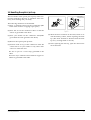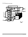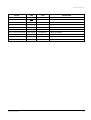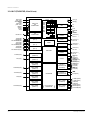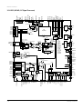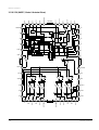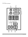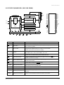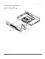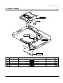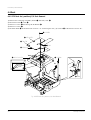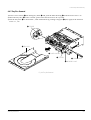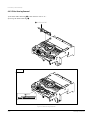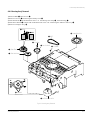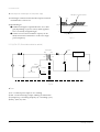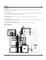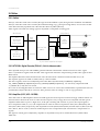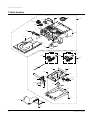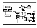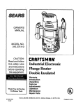
1
DVD PLAYER DVD-611/611B/615 DVD-511 SERVICE MANUAL SERVICE DVD-611/611B/615/511 ELECTRONICS Manual DVD PLAYER CONTENTS 1. Precautions 2. Reference Information 3. Product Specification 4. Disassembly and Reassembly OPEN/CLOSE 5. Circuit Descriptions DIGITAL VIDEO DIGITAL VIDEO STANDBY/ON PLAY/PAUSE STOP SKIP OPEN/ CLOSE 6. Troubleshooting DVD-611/611B/615 7. Exploded Views and Parts List 8. Electrical Parts List 9. Block Diagrams 10. PCB Diagrams 11. Wiring Diagram OPEN/CLOSE STANDBY/ON PLAY/PAUSE STOP SKIP OPEN/ CLOSE 12. Schematic Diagrams DVD-511 © Samsung Electronics Co., Ltd. APR. 2000 Printed in Korea AH68-00462A 1. Precautions 1-1 Safety Precautions 1) Before returning an instrument to the customer, always make a safety check of the entire instrument, including, but not limited to, the following items: (1) Be sure that no built-in protective devices are defective or have been defeated during servicing. (1)Protective shields are provided to protect both the technician and the customer. Correctly replace all missing protective shields, including any remove for servicing convenience. (2)When reinstalling the chassis and/or other assembly in the cabinet, be sure to put back in place all protective devices, including, but not limited to, nonmetallic control knobs, insulating fish papers, adjustment and compartment covers/shields, and isolation resistor/capacitor networks. Do not operate this instrument or permit it to be operated without all protective devices correctly installed and functioning. (2) Be sure that there are no cabinet openings through which adults or children might be able to insert their fingers and contact a hazardous voltage. Such openings include, but are not limited to, excessively wide cabinet ventilation slots, and an improperly fitted and/or incorrectly secured cabinet back cover. (3) Leakage Current Hot Check-With the instrument completely reassembled, plug the AC line cord directly into a 120V AC outlet. (Do not use a isolation transformer during this test.) Use a leakage current tester or a metering system that complies with American National Standards institute (ANSI) C101.1 Leakage Current for Appliances and Underwriters Laboratories (UL) 1270 (40.7). With the instrument’s AC switch first in the ON position and then in the OFF position, measure from a known earth ground (metal water pipe, conduit, etc.) to all exposed metal parts of the instrument (antennas, handle brackets, metal cabinets, screwheads, metallic overlays, control shafts, etc.), especially any exposed metal parts that offer an electrical return path to the chassis. Any current measured must not exceed 0.5mA. Reverse the instrument power cord plug in the outlet and repeat the test. See Fig. 1-1. Any measurements not within the limits specified herein indicate a potential shock hazard that must be eliminated before returning the instrument to the customer. (READING SHOULD NOT BE ABOVE 0.5mA) LEAKAGE CURRENT TESTER DEVICE UNDER TEST TEST ALL EXPOSED METER SURFACES 2-WIRE CORD ALSO TEST WITH PLUG REVERSED (USING AC ADAPTER PLUG AS REQUIRED) EARTH GROUND Fig. 1-1 AC Leakage Test (4) Insulation Resistance Test Cold Check-(1) Unplug the power supply cord and connect a jumper wire between the two prongs of the plug. (2) Turn on the power switch of the instrument. (3) Measure the resistance with an ohmmeter between the jumpered AC plug and all exposed metallic cabinet parts on the instrument, such as screwheads, antenna, control shafts, handle brackets, etc. When an exposed metallic part has a return path to the chassis, the reading should be between 1 and 5.2 megohm. When there is no return path to the chassis, the reading must be infinite. If the reading is not within the limits specified, there is the possibility of a shock hazard, and the instrument must be re-pared and rechecked before it is returned to the customer. See Fig. 1-2. Antenna Terminal Exposed Melal Part ohm ohmmeter Fig. 1-2 Insulation Resistance Test Samsung Electronics 1-1 Precautions 2) Read and comply with all caution and safety related notes non or inside the cabinet, or on the chassis. 3) Design Alteration Warning-Do not alter of add to the mechanical or electrical design of this instrument. Design alterations and additions, including but not limited to, circuit modifications and the addition of items such as auxiliary audio output connections, might alter the safety characteristics of this instrument and create a hazard to the user. Any design alterations or additions will make you, the service, responsible for personal injury or property damage resulting therefrom. 4) Observe original lead dress. Take extra care to assure correct lead dress in the following areas: (1) near sharp edges, (2) near thermally hot parts (be sure that leads and components do not touch thermally hot parts), (3) the AC supply, (4) high voltage, and (5) antenna wiring. Always inspect in all areas for pinched, out-of-place, or frayed wiring, Do not change spacing between a component and the printed-circuit board. Check the AC power cord for damage. 1-2 5) Components, parts, and/or wiring that appear to have overheated or that are otherwise damaged should be replaced with components, parts and/ or wiring that meet original specifications. Additionally, determine the cause of overheating and/or damage and, if necessary, take corrective action to remove any potential safety hazard. 6) Product Safety Notice-Some electrical and mechanical parts have special safety-related characteristics which are often not evident from visual inspection, nor can the protection they give necessarily be obtained by replacing them with components rated for higher voltage, wattage, etc. Parts that have special safety characteristics are identified by shading, an ( )or a ( )on schematics and parts lists. Use of a substitute replacement that does not have the same safety characteristics as the recommended replacement part might created shock, fire and/or other hazards. Product safety is under review continuously and new instructions are issued whenever appropriate. Samsung Electronics Precautions 1-2 Servicing Precautions CAUTION : Before servicing Instruments covered by this service manual and its supplements, read and follow the Safety Precautions section of this manual. Note : If unforseen circument create conflict between the following servicing precautions and any of the safety precautions, always follow the safety precautions. Remember: Safety First. 1-2-1 General Servicing Precautions (1) a. Always unplug the instrument’s AC power cord from the AC power source before (1) re-moving or reinstalling any component, circuit board, module or any other instrument assembly, (2) disconnecting any instrument electrical plug or other electrical connection, (3) connecting a test substitute in parallel with an electrolytic capacitor in the instrument. b. Do not defeat any plug/socket B+ voltage interlocks with which instruments covered by this service manual might be equipped. c. Do not apply AC power to this instrument and /or any of its electrical assemblies unless all solid-state device heat sinks are correctly installed. d. Always connect a test instrument’s ground lead to the instrument chassis ground before connecting the test instrument positive lead. Always remove the test instrument ground lead last. (4) An insulation tube or tape is sometimes used and some components are raised above the printed wiring board for safety. The internal wiring is sometimes clamped to prevent contact with heating components. Install such elements as they were. (5) After servicing, always check that the removed screws, components, and wiring have been installed correctly and that the portion around the serviced part has not been damaged and so on. Further, check the insulation between the blades of the attachment plug and accessible conductive parts. 1-2-2 Insulation Checking Procedure Disconnect the attachment plug from the AC outlet and turn the power ON. Connect the insulation resistance meter (500V) to the blades of the attachment plug. The insulation resistance between each blade of the attachment plug and accessible conductive parts(see note) should be more than 1 Megohm. Note : Accessible conductive parts include metal panels, input terminals, earphone jacks, etc. Note : Refer to the Safety Precautions section ground lead last. (2) The service precautions are indicated or printed on the cabinet, chassis or components. When servicing, follow the printed or indicated service precautions and service materials. (3) The components used in the unit have a specified flame resistance and dielectric strength. When replacing components, use components which have the same ratings. Components i-entified by shading, by( ) or by ( ) in the circuit diagram are important for safety or for the characteristics of the unit. Always replace them with the exact replacement components. Samsung Electronics 1-3 Precautions 1-3 ESD Precautions Electrostatically Sensitive Devices (ESD) Some semiconductor (solid state) devices can be damaged easily by static electricity. Such components commonly are called Electrostatically Sensitive Devices(ESD). Examples of typical ESD devices are integrated circuits and some field-effect transistors and semiconductor chip components. The following techniques should be used to help reduce the incidence of component damage caused by static electricity. (1) Immediately before handling any semiconductor component or semiconductor-equipped assembly, drain off any electrostatic charge on your body by touching a known earth ground. Alternatively, obtain and wear a commercially available discharging wrist strap device, which should be removed for potential shock reasons prior to applying power to the unit under test. (7) Immediately before removing the protective materials from the leads of a replacement ESD device, touch the protective material to the chassis or circuit assembly into which the device will be installed. CAUTION : Be sure no power is applied to the chassis or circuit, and observe all other safety precautions. (8) Minimize bodily motions when handling unpackaged replacement ESD devices. (Otherwise harmless motion such as the brushing together of your clothes fabric or the lifting of your foot from a carpeted floor can generate static electricity sufficient to damage an ESD device). (2) After removing an electrical assembly equipped with ESD devices, place the assembly on a conductive surface such as aluminum foil, to prevent electrostatic charge buildup or exposure of the assembly. (3) Use only a grounded-tip soldering iron to solder or unsolder ESD devices. (4) Use only an anti-static solder removal devices. Some solder removal devices not classified as “anti-static” can generate electrical charges sufficient to damage ESD devices. (5) Do not use freon-propelled chemicals. These can generate electrical charges sufficient to damage ESD devices. (6) Do not remove a replacement ESD device from its protective package until immediately before your are ready to install it.(Most replacement ESD devices are packaged with leads electrically shorted together by conductive foam, aluminum foil or comparable conductive materials). 1-4 Samsung Electronics Precautions 1-4 Handling the optical pick-up The laser diode in the optical pick up may suffer electrostatic breakdown because of potential static electricity from clothing and your body. WRIST-STRAP FOR GROUNDING 1M The following method is recommended. (1) Place a conductive sheet on the work bench (The black sheet used for wrapping repair parts.) (2) Place the set on the conductive sheet so that the chassis is grounded to the sheet. (3) Place your hands on the conductive sheet(This gives them the same ground as the sheet.) (4) Remove the optical pick up block (5) Perform work on top of the conductive sheet. Be careful not to let your clothes or any other static sources to touch the unit. THE UNIT 1M CONDUCTIVE SHEET Fig.1-3 (6) Short the short terminal on the PCB, which is inside the Pick-Up ASS’Y, before replacing the PickUp. (The short terminal is shorted when the PickUp Ass’y is being lifted or moved.) (7) After replacing the Pick-up, open the short terminal on the PCB. Be sure to put on a wrist strap grounded to the sheet. Be sure to lay a conductive sheet made of copper etc. Which is grounded to the table. Samsung Electronics 1-5 Precautions 1-5 Pick-up disassembly and reassembly 1-5-1 Disassembly 1-5-2 Assembly 1) Remove the power cable. 2) Switch SW3 on deck PCB to “OFF” before removing the FPC. ( Inserted into Main PCB DCN1. See Fig. 1-4) 3) Disassemble the deck. 4) Disassemble the deck PCB. 1) Replace the Pick-up. 2) Assemble the deck PCB. 3) Reassemble the deck. 4) Insert FPC into Main PCB DCN1 and switch SW3 on deck PCB to “ON”. (See Fig 1-4) Note : If the assembly and disassembly are not done in correct sequence, the Pick-up may be damaged. FPC TO MAIN PCB (DCN1) Fig. 1-4 1-6 Samsung Electronics 2. Reference Information 2-1 IC Descriptions 2-1-1 AIC1 (AK4393 ; Digital-to-Analog Converter) Left Channel De-emphasis Soft Mute Serial Input Control Left/Right Clock Bit Clock Double Speed Select Multi-bit ˘• Modulator Right Output + Right Output - Switched Capacitor Filter Serial Input Interface Serial Data Power Down Soft Mute 8X Interpolator De-emphasis Soft Mute 8X Interpolator Multi-bit ˘• Modulator Left Output + Left Output - Switched Capacitor Filter Right Channel Control Register De-emphasis Control Clock Divider Master Clock No. Pin Name I/O DVSS DVDD MCLK PD BICK SDATA LRCK SMUTE DFS DEM0 DEM1 DIF0 DIF1 DIF2 1 28 2 27 3 26 4 25 5 24 6 23 7 22 8 21 9 20 10 19 11 18 12 17 13 16 14 15 Clock Control Pin Function and Description 1 DVSS - Digital Ground. Digital ground is 0V. 2 DVDD - Digital Supply. 3 MCLK I Master Clock Input. 4 PD I Power-down and Reset. When low the AK4393 is in Power-down Mode and held in reset. The AK4393 should always be reset after power-up. 3.3V or 5.0V nominal. 5 BICK I Audio Serial Data Clock Input. 6 SDATA I Serial Data Input. 7 LRCK I Left/Right Clock Input. 8 SMUTE (or CS) I Soft Mute Input or Chip Select Input. If the P/S pin (pin 25) is high, SMUTE controls the soft mute function as follows: - When SMUTE goes high, the soft mute cycle is initiated. - When SMUTE goes low, the output mute is slowly released. If the P/S pin is low, SMUTE is the Chip Select Input for the Serial Control Mode. Chip select is active when SMUTE is low. 9 DFS I Double Sampling Speed Input. When low, this pin defines the Normal Speed Mode, and 128 x Fs oversampling is implemented. When high, the DFS pin defines the Double Speed Mode, implemented with 64 x Fs oversampling. This pin features an internal pull-down. 10 DEM0 (or CCLK) I De-emphasis Enable #0 or Control Data Clock Input. If the P/S pin (pin 25) is high, DEM0 is used to select the De-emphasis Mode according to Table 3. If the P/S pin os low DEM0 is the clock input for the Serial Control Mode. 11 DEM1 (or CDTI) I De-emphasis Enable #1 or Control Data Input. If the P/S pin (pin 25) is high, DEM1 is used to select the De-emphasis Mode according to Table 3. If the P/S pin is low, DEM1 is the control data input for the Serial Control Mode. A clock input of 64fs or more is recommended. Defines the sampling rate, Fs. 12 DIF0 I Digital Input Format Select #0. 13 DIF1 I Digital Input Format Select #1. 14 DIF2 I Digital Input Format Select #2. 15 BVSS - Substrate Ground Pin. 16 VREFL I Low Level Voltage Reference Input. Normally connected to analog ground. 17 VREFH I High Level Voltage Reference Input. Normally connected to analog supply. 18 AVDD - Analog Supply. Analog supply is 5V nominal. 19 AVSS - Analog Ground. Analog ground is 0V. 20 AOUTR- O Right Channel Negative Output. 21 AOUTR+ O Right Channel Positive Output. 22 AOUTL- O Left Channel Negative Output. 23 AOUTL+ O Left Channel Positive Output. 24 VCOM O Common Voltage Output. 25 P/S I Parallel/Serial Control Mode Select Input. If Low, the Serial Control Mode is implemented. If High, the Parallel Control Mode is selected. This pin has an internal pull-up. Master Clock Select #0. 26 CKS0 I 27 CKS1 I Master Clock Select #1. 28 CKS2 I Master Clock Select #2. Samsung Electronics CKS2 CKS1 CKS0 P/S VCOM AOUTL+ AOUTLAOUTR+ AOUTRAVSS AVDD VREFH VREFL BVSS Substrate ground is 0V. Common voltage output is 2.6V nominal. 2-1 2-2 M ON_OUT M DP_OUT M DS_OUT FSW _OUT PLLLOCK_ OUT SERLOCK_ OUT To S er vo (6) XTI_ IN XTO_ OUT CK33MI_IN CK33MO_ OUT X -t al (4) EFMI_IN PL CK_IN FG_ IN Fr om Servo (3) CD CLV/CAV VCO Tim ing Generator 7.3 5KHz= 4 .3 218M/588 17 .58KHz= 26 .1 6M/1 488 SUBCODE I/F 23BIT SR T o MICOM (15) M TES T0_IN, TES T1_IN, TES T2_IN M SQ-V CD DVDP, MICOM I/F T es t Pin (3 ) CD- G V-C D ,CD -D A Deinterleave & RAM Control (6,4,3) trans ID ECC EDC Descrambler MDAT[7:0]_BI , MRZA_IN, ZCS_IN, M W R_IN, MRD_IN, ZIRQZD_OUT, ZW AI T_OUT, ZRST_IN Pow er (34)=VDD(11)+GND(23) EFM DEMOD (32,28,5) (28,24,5) CIRC 7 5Hz 67 6.08Hz (208,192,17) (182,172,11) ECC Frame Sync DET/PROT/INS (7.35KHz) W FCK 17 .58/7.3 5KHz M VCO Tim ing Generator 26 .1 6MHz GFS_OUT, FRSY Z_ OUT, TX_OUT, EFM O_ OUT, W FCK_ OUT, RFCK_ OUT, CK1 6M_OUT, DEMPHA_ OUT CLVLOCK_ OUT Mon i tor (9) M DVD CLV/CAV RFCK 1 7.58/7 .3 5KHz X -tal & Tim ing Generator 16-8 DEMOD (6,4,3) Frame Sync DE T/PROT/INS ECSY efm wr ID ECC (17.57KHz) 32BIT S R PW MO[ 7:0]_OUT, BCARZ_IN T o RF (9) SDATA[ 0]_OUT/ CDATA SDATA[ 1]_OUT/L RCK SDATA[ 2]_OUT/B CLK SDATA[ 3]_OUT/C2PO SDATA[ 4]_OUT/S Q DT SDATA[ 5]_OUT/W FSY SDATA[ 6]_OUT/S 0 S1 SDATA[ 7]_BI /SQ CK DATREQ _ IN CSTROB E _ OUT DTER_OUT DATACK_OUT TOS _ OUT T o AV (13) DD[1 5:0]_BI DADR[8:0]_ OUT ZRAS _OUT ZUCAS _OUT ZLCAS _ OUT ZOE [ 1 :0 ]_OUT ZW E[ 1:0]_OUT (32) T o DRAM 256K*16 Reference Information 2-1-2 DIC1 (KS1453 ; Data Processor) Samsung Electronics 1 2 3 4 5 6 7 8 9 10 11 12 13 14 15 16 17 18 19 20 21 22 23 24 25 26 27 28 29 30 31 32 33 34 35 36 37 38 39 40 41 42 43 44 45 46 47 48 49 50 51 52 53 54 55 56 57 58 59 60 61 62 63 64 No. Pin Name DVSS ZCS_IN MRZA_IN DVSS MDAT7_BI MDAT6_BI MDAT5_BI MDAT4_BI MDAT3_BI MDAT2_BI MDAT1_BI MDAT0_BI DVDD XTI_IN XTO_OUT DVSS DD15_BI DD0_BI DD14_BI DD1_BI DVSS DD13_BI DD2_BI DD12_BI DD3_BI DVDD DD11_BI DD4_BI DD10_BI DD5_BI DVSS DD9_BI DD6_BI DD8_BI DD7_BI DVSS ZLCAS_OUT ZUCAS_OUT ZWE1_OUT ZWE0_OUT ZOE1_OUT DVDD ZOE0_OUT ZRAS_OUT DADR8_OUT DADR7_OUT DVSS DADR0_OUT DADR6_OUT DADR1_OUT DADR5_OUT DADR2_OUT DADR4_OUT DADR3_OUT DVSS DVSS TOS_OUT DATACK_OUT DVDD SDATA0_OUT SDATA1_OUT SDATA2_OUT SDATA3_OUT SDATA4_OUT Description Samsung Electronics DRAM Address Bus Digital GND (0 V) DRAM Address Bus DRAM Address Bus DRAM Address Bus DRAM Address Bus DRAM Address Bus DRAM Address Bus DRAM Address Bus Digital GND (0 V) Digital GND (0 V) Top of Sector Data Acknowledge Signal Output DIGITAL Power (+5 V) DVD Data/CD Data Bit Stream (CDATA) DVD Data/CD Data L/R Clock (LRCK) DVD Data/CD Data Bit Clock (BLCK) DVD Data/CD Data Error Flag (C2PO) DVD Data/Subcode Serial Data (SQDT) Digital GND (0 V) Chip Select (Active Low) Micom Register Select (L REGISTER H fi DATA) Digital GND (0 V) MICOM Data Bus MICOM Data Bus MICOM Data Bus MICOM Data Bus MICOM Data Bus MICOM Data Bus MICOM Data Bus MICOM Data Bus Digital Power (+5V) System Clock Input for 26.16 MHz System Clock Output for 26.16 MHz Digital GND (0 V) DRAM Data Bus DRAM Data Bus DRAM Data Bus DRAM Data Bus Digital GND (0 V) DRAM Data Bus DRAM Address Bus DRAM Data Bus DRAM Data Bus DRAM Data Bus Digital Power (+5 V) Digital Data Bus Digital Data Bus Digital Data Bus Digital Data Bus Digital GND (0 V) DRAM Data Bus DRAM Data Bus DRAM Data Bus DRAM Data Bus Digital GND (0 V) DRAM Low Column Address Strobe DRAM Upper Column Address Strobe DRAM Write Enable 1 (8M ONLY) DRAM Write Enable 0 (4M, 8M, 16M) DRAM Output Enable 1 (16M MODE DADR9) Digital Power (+5 V) DRAM Output Enable 0 DRAM Row Address Strobe MICOM MICOM MICOM MICOM MICOM MICOM MICOM MICOM XTAL XTAL DRAM DRAM DRAM DRAM DRAM DRAM DRAM DRAM DRAM DRAM DRAM DRAM DRAM DRAM DRAM DRAM DRAM DRAM DRAM DRAM DRAM DRAM DRAM DRAM DRAM DRAM DRAM DRAM DRAM DRAM DRAM DRAM AV Decoder AV Decoder AV AV AV AV AV B B B B B B B B I O B B B B B B B B B B B B B B B B O O O O O O O O O O O O O O O O O O O O O O O Decoder Decoder Decoder Decoder Decoder MICOM MICOM Notes I I I/O 65 66 67 68 69 70 71 72 73 74 75 76 77 78 79 80 81 82 83 84 85 86 87 88 89 90 91 92 93 94 95 96 97 98 99 100 101 102 103 104 105 106 107 108 109 110 111 112 113 114 115 116 117 118 119 120 121 122 123 124 125 126 127 128 No. Pin Name SDATA5_OUT SDATA6_OUT SDATA7_BI DVSS CSTROBE_OUT DATREQ_IN DTER_OUT DVSS PWMO7_OUT PWMO6_OUT PWMO5_OUT PWMO4_OUT DVDD PWMO3_OUT PWMO2_OUT PWMO1_OUT PWMO0_OUT DVSS DVSS DVSS DVDD DVDD DVSS DVSS DVSS DVSS FRSYZ_OUT TX_OUT GFS_OUT DVSS CK33MI_IN CK33MO_OUT DVDD TEST0_IN TEST1_IN TEST2_IN EFMO_OUT WFCK_OUT RFCK_OUT PLCK_IN DVSS PLLLOCK_OUT CLVLOCK_OUT SERLOCK_OUT MDP_OUT MDS_OUT DVSS DVSS MON_OUT FG_IN FSW_OUT EFMI_IN DVDD DVDD DVDD CK16M_OUT DEMPHA_OUT BCARZ_IN DVSS ZRST_IN ZWAIT_OUT ZIRQZD_OUT MRD_IN MWR_IN Description DVD Data/Subcode Frame Sync (WFSY) DVD Data/Subcode Block Sync (S0S1) DVD Data/Subcode Serial Clock (SQCK) Digital GND (0 V) Data Strobe (Clock) Output Data Request from A/V Decoder or ROM Decoder DVD Data Error Output Digital GND (0 V) PWM Output Signal PWM Output Signal PWM Output Signal PWM Output Signal Digital Power (+5 V) PWM Output Signal PWM Output Signal PWM Output Signal PWM Output Signal Digital GND (0 V) Digital GND (0 V) Digital GND (0 V) DIGITAL Power (+5 V) DIGITAL Power (+5 V) Digital GND (0 V) Digital GND (0 V) Digital GND (0 V) Digital GND (0 V) Frame Sync Out Digital Out Good Frame Sync Detection State Output (OK at H) Digital GND (0 V) System Clock Input for 33.8688 MHz System Clock Output for 33.8688 MHz Digital Power (+5 V) Test Mode Selection Terminal Test Mode Selection Terminal Test Mode Selection Terminal EFM Out Write Frame Pulse Reference Frame Pulse Phase Locked Clock Digital GND (0 V) Lock Signal for PLL Lock Signal for CLV Lock Signal for SERVO Spindle Motor Phase Control Signal (3-STATE) Spindle Motor Speed Control Signal (3-STATE) Digital GND (0 V) Digital GND (0 V) Spindle Motor Output Filter Switching Output Reference Signal for CAV Spindle Motor Output Filter Switching Output (3-STATE) EFM/EFM+ Signal Input Notes Digital Power (+5 V) Digital Power (+5 V) Digital Power (+5 V) CK33Ms 2 Division Clock / 16.9344 MHz HIGH , when on Deemphasis BCA Input Signal Digital GND (0 V) Hardware Reset (Active Low) Micom Read / Write Access Wait (Wait at L) Interrupt Request to Micom Micom Read Strobe (Active Low) Micom Write Strobe (Active Low) Notes I O O I I MICOM MICOM MICOM MICOM MICOM Monitor Monitor RF Servo Monitor Servo Servo Servo O O O O O O O I Monitor Monitor Monitor Servo I I I O O O I Servo Servo Servo Servo X-tal X-tal I O O I O I Monitor Monitor Monitor O O O RF RF RF RF RF RF RF RF O O O O O O O O AV Decoder AV Decoder AV Decoder AV Decoder AV Decoder AV Decoder O I O O O B I/O Reference Information 2-3 Reference Information 2-1-3 DIC2 (KM416C254D ; CMOS 4M DRAM) WE CASL CASH CAS DATA-IN BUFFER CONTROL LOGIC IO0 16 NO.2 CLOCK GENERATOR IO15 DATA-OUT BUFFER 9 D0 D1 D2 D3 D4 D5 D6 D7 D8 9 16 8 8 SENSE AMPLIFIERS VO GATING 512x16 9 9 ROW DECODER REFRESH COUNTER ROW. ADDRESS BUFFERS(9) OE COLUMN DECODER 512 REFRESH CONTROLLER 9 RAS COLUMN ADDRESS BUFFER 512 512x512x16 MEMORY ARRAY NO.1CLOCK GENERATOR Vcc Vss 2-4 Samsung Electronics Reference Information PIN NO. SYM. TYPE 16~19, 22~26 A0~A8 Input Address Input 14 RAS Input Row Address Strobe 28 CASH Input Column Address Strobe/Upper Byte Control 29 CASL Input Column Address Strobe/Lower Byte Control 13 WE Input Write Enable 27 OE Input Output Enable 2~5, 7~10, 31~34, 36~39 I/O0~I/O15 Input/Output 1, 6, 20 Vcc Supply Power, 5V 21, 35, 40 Vss Ground Ground 11, 12, 15, 30 NC - Samsung Electronics DESCRITION Data Input/Output No Connect 2-5 Reference Information 2-1-4 MIC1 (TMP95C265 ; Main Micom) AND~AN2 (PA0~PA2) AN3/ADTRG (PA3) AN4~AN7 (PA4~PA7) VREFH VREFL AVCC AV55 10BIT 8CH A/D CONVERTER DAOUT0,1 8BIT 2CH A/D CONVERTER 900/H XWA XBC XDE XHL XIX XIY XIZ XSP CPU W A B C D E H L IX IY IZ SP 32bit SR F VCC [3] VSS[3] OSC CLK AM8/16 EA RESET PORT0 (P00~P07) D0~D7 * PORT1 (P10~P17) D8~D15 PORT2 (P20~P27) A15~A23 * PORT3 (P30~P37) A8~A15 * PORT4 (P40~P47) A0~A7 * PC TxD0(P80) RxD0(P81) SCLK0/CT50(P82) TxD1(P83) RxD1(P84) SCLK1/CT51(P85) TxD2(P86) RxD2(P87) SCLK2/CT52(P57) T10/INT(P70) TO1(P71) SERIAL I/O (CH. 0) SERIAL I/O (CH. 1) WATCHDOG TIMER SERIAL I/O (CH. 2) 2KB ROM 8BIT TIMER (TIMER 0) 8BIT TIMER (TIMER 1) PORT5 8BIT TIMER (TIMER 2) TO3/INT2(P72) 8BIT TIMER (TIMER 3) T14/INT3(P73) 8BIT TIMER (TIMER 4) TO5(P74) CS/WAIT CONTROLLER (4-BLOCK) 64KB ROM 2-6 INTERRUPT CONTROLLER RD(P50)* WR(P51)* HWR(P52) BUSRQ(P53) BUSAK(P54) WAIT(P55) C50(P60) C51(P61) C52(P62) C53(P63) NIMI INTO(P56) 8BIT TIMER (TIMER 5) 16BIT TIMER (TIMER 8) 8BIT TIMER (TIMER 6) TO7/INT4(P75) X1 X2 8BIT TIMER (TIMER 7) Not included in TMP95C265 16BIT TIMER (TIMER 9) T18/INT5(P90) T19/INT6(P91) TO8(P92) TO9(P93) TIA/INT7(P94) TIB/INT8(P95) TOA/TOB(P96) Samsung Electronics NO 1 2 3 4 5 6 7 8 9 10 11 12 13 14 15 16 17 18 19 20 21 22 23 24 25 26 27 28 29 30 31 32 33 34 35 36 37 38 39 40 41 42 43 44 45 46 47 48 49 50 PORT NAME VREFL AVss AVcc DAOUT0 DAOUT1 /NMI P53 P54/BUSAK /WAIT P56 SCLK2 P80/TXD0 P81/RXD0 P82/SCLKO P83/TXD1 P84/RXD1 P85/SCLK1 TXD2 RXD2 CSO CS1 CS2 CS3 CLK Vcc Vss X1 X2 /EA /REST INT1 P71 P72 P73 P74 P75 INT5 P91 P92 P93 INT7 INT8 P96 Vcc D0 D1 D2 D3 D4 D5 ASSIGNED NAME DGND DGND 5D MTP1 MPT2 CSB MTP3 /MWAIT DVD/CD SCLK MD STB MC MTP5 MTP6 MTP4 RXD TXD /CSO /CS1 /DVD1CS /DSPCS CLK 5D GDND X1 X2 /EA /MRST SRQ RRQ SCL SDA OPEN CLOSE FGINT ACT MUTE M/D MUTE ZRST /DVDINT /DSPINT ZIVA_RST 5D HAD0 HAD1 HAD2 HAD3 HAD4 HAD5 Samsung Electronics Data 0 Data 1 Data 2 Data 3 Data 4 Data 5 GND High Frequency OSC in High frequency OSC out Internal ROM Less Mode Master reset from FRONT Interrupt from Front Micom Request to Front Micom EEPROM CLOCK EEPROM DATA I/O Tray Out Motor Control Output Tray In Motor Control Output Interrupt from Spindle Motor FG Driver IC MUTE(Actuator) Driver IC MUTE(Spindle) DSP H/W reset Interrupt from AV-DEC Interrupt from DSP AV Decoder Reset(Active H:4.0, L:4.1) Serial Data Output Serial Data Input EPROM(M27C801) Select SRAM(KM681000) Select AVDecoder(ZiVA4) Select Data Processor(KS1453) Select CLOCK OUTPUT (System Clock 2) /Wait(ZiVA, DSP) DVD/CD RF AGC Gain Select Serial Data Clock RF Contrl Data RF Data Latch RF Control Clock PULL-UP D. Servo IC Chip Select DESCRIPTION A/D Ref Input(L) A/D Ref Input A/D VCC Input I/0 I/0 I/0 I/0 I/0 I/0 TYPE I 0 0 I 0 0 I 0 I 0 I/0 0 0 0 0 0 I 0 0 0 0 0 I 0 I I I 0 0 0 0 0 I 0 0 0 I I 0 GND FRONT, IC FRONT FRONT KS24C020(6) KS24C020(5) DRIVER(0PIN-, 16) DRIVER(0PIN-, 17) DRIVER(FG, 2) DRIVER(MUTE4, 37) DRIVER(MUTE3, 38) KS1453(124) INV(ZiVA-4(51)) INV(KS1453(126)) ZiVA-4(52) 20MHz /MWait RF(KS1461) FRONT KS1461(69) KS1461(71) KS1461(70) NC NC NC FRONT FRONT EPROM(M27C801) SRAM(KM681000) AVDecoder(ZiVA4) Data Processor(KS1453) fc/2 VCC GND KS1452(10) REMARK DGND DGND 5D NC NC NO 51 52 53 54 55 56 57 58 59 60 61 62 63 64 65 66 67 68 69 70 71 72 73 74 75 76 77 78 79 80 81 82 83 84 85 86 87 88 89 90 91 92 93 94 95 96 97 98 99 100 PORT NAME D6 D7 P10 P11 P12 P13 P14 P15 P16 P17 AM8/16 Vss Vcc A23 P26/A22 P25/A21 P24/A20 A19 A18 A17 A16 A15 A14 A13 A12 A11 A10 A9 A8 A7 A6 A5 A4 A3 A2 A1 A0 /RD /WR P52 Vss PA0 PA1 PA2 PA3 PA4 PA5 PA6 PA7 VREFH ASSIGNED NAME HAD6 HAD7 CLSW OPSW MTP8 MTP9 MTP10 MTP11 MTP12 MTP13 AM8 DGND 5D HA23 MRP14 MRP15 MRP16 HA19 HA18 HA17 HA16 HA15 HA14 HA13 HA12 HA11 HA10 HA9 HA8 HA7 HA6 HA5 HA4 HA3 HA2 HA1 HA0 /RD /WR RSTB DGND RFRP TILTO MTP17 SENSE FR SLOCK FOKB RFO 5D Tracking Lock monitir from SERVO Monitor signal Reserved I SENSE monitor from SERVO Spindle direcrion from SP Driver LOCK monitor from DSP Focus lock monitor from RF RF sum signal (Analog Lnput) A/D Ref Input (H) SERVO /RD Strobe Mask Signal Reserved Address Port Reserved Address Port Reserved Address Port Address 19 Address 18 Address 17 Address 16 Address 15 Address 14 Address 13 Address 12 Address 11 Address 10 Address 9 Address 8 Address 7 Address 6 Address 5 Address 4 Address 3 Address 2 Address 1(SERVO DAB) Address 0(DSP DAB) /Read Strobe /Write Strobe RF&Servo IC Reset DESCRIPTION Data6 Data7 Close Switch Open Swithc Reserved I/0 Reserved I/0 Reserved I/0 Reserved I/0 Reserved I/0 Reserved I/0 Address Mode(H:8 BIT MODE) TYPE I/0 I/0 I I 0 0 0 0 0 0 I 0 0 0 0 0 0 0 0 0 0 0 0 0 0 0 0 0 0 0 0 0 0 0 0 0 0 0 I I I I I I I I I DECK DECK NC NC NC NC NC NC VCC GND VCC 74HCOO(5) NC NC NC EPROM, SRAM ADDRESS EPROM, SRAM ADDRESS EPROM, SRAM ADDRESS EPROM, SRAM ADDRESS EPROM, SRAM ADDRESS EPROM, SRAM ADDRESS EPROM, SRAM ADDRESS EPROM, SRAM ADDRESS EPROM, SRAM ADDRESS EPROM, SRAM, Zlva Adrs EPROM, SRAM, Zlva Adrs EPROM, SRAM, Zlva Adrs EPROM, SRAM ADDRESS EPROM, SRAM ADDRESS EPROM, SRAM ADDRESS EPROM, SRAM ADDRESS EPROM, SRAM ADDRESS EPROM, SRAM ADDRESS EPROM, SRAM ADDRESS EPROM, SRAM ADDRESS /Read /Write KS1461 (73), KS1452 (9) DGND KS1452 (7) KS1452 (69) NC KS1452 (22) BA6849FP (20) KS1453 (108) KS1461 (48) RFO 5D REMARK Reference Information 2-7 Reference Information 2-1-5 MIC2 (M27C801 ; 8Mbit (1Mbx8) UVEPROM and OTP EPROM) LOGIC DIAGRAM Vcc 8 20 A0-A19 A0-Q7 E GVpp Vss TOP VIEW 2-8 FUNCTION A19 1 32 Vcc NAME A16 2 31 A18 A0-A19 Address Inputs A15 3 30 A17 A12 29 A14 Q0-Q7 Data Outputs 4 A7 5 28 A13 A6 6 27 A8 A5 7 26 A9 A4 8 25 A11 A3 9 24 GVPP A2 10 23 A10 A1 11 22 E A0 12 21 Q7 Q0 13 20 Q6 Q1 14 19 Q4 Q2 15 18 Q4 Vss 16 17 Q3 E OVpp Chip Enable Output Enable/Program Supply Vcc Supply Voltage Vss Ground Samsung Electronics Reference Information 2-1-6 MIC3 (W24256A ; 32K x 8 High Speed CMOS Static RAM) BLOCK DIAGRAM V DD V SS A0 . . DECODER CORE ARRAY A14 CS OE CONTROL DATA I/O WE I/O1 . . I/O8 TOP VIEW A14 1 28 VDD SYMBOL A12 2 27 WE A0 - A14 A7 3 26 A13 A6 4 25 A8 A5 5 24 A9 A4 6 23 A11 A3 7 22 OE A2 8 21 A1 9 A0 I/O1 I/O2 I/O3 VSS I/O1 - I/O8 DESCRIPTION Address Inputs Data Inputs/Outputs CS Chip Select Input WE Write Enable Input A10 OE Output Enable Input 20 CS V DD Power Supply 10 19 I/O8 V SS Ground 11 18 I/O7 12 17 I/O6 13 16 I/O5 14 15 I/O4 Samsung Electronics 28-pin DIP 2-9 Reference Information 2-1-7 FIC1 (LC86P6232 ; Front Micom) IR PLA ROM Interrupt Control Stand-by Control CF RC BUS PC Clock Generator X’tal ACC Base Timer Bus Interface B Reg SIO 0 Port 1 C Reg SIO 1 Port 7 Timer 0 BUS Port 8 ALU Timer 1 Port 2 ADC Port 3 INT0-3 Noise Filter Real Time Service Port 4 PSW Port 5 PWM 1 RAR RAM XRAM (128 bytes) Stack Pointer VFD Controller PORT 0 High Voltage Output 2-10 Watch Dog Timer Samsung Electronics PORT NAME P52 PWM1 P20 P21 P22 P23 P24 P25 P26 P27 TEST1 *RES XT1 XT2 VSS CF1 CF2 VDD ANO/P8 0 AN1/P8 1 AN2/P8 2 AN3/P8 3 AN4/P8 4 AN5/P8 5 AN6/P8 6 AN7/P8 7 P70/IN TO P71/IN T1 P72/IN T2 P73/IN T3 S0/T0 S1/T1 S2/T2 S3/T3 S4/T4 S5/T5 S6/T6 S7/T7 S8/T8 S9/T9 S10/T10 S11/T11 S12/T12 S13/T13 S14/T14 S15/T15 VOD VP S16 S17 NO 1 2 3 4 5 6 7 8 9 10 11 12 13 14 15 16 17 18 Samsung Electronics 19 20 21 22 23 24 25 26 27 28 29 30 31 32 33 34 35 36 37 38 39 40 41 42 43 44 45 46 47 48 49 50 I I I I I I I 0 0 0 0 0 0 0 0 0 0 0 0 0 0 0 0 0 0 0 0 I I 0 - TYPE 0 0 0 0 0 0 0 SEG1 SEG2 SEG3 SEG4 +5V -28V SEG5 SEG6 ECHO_VR MIC_DET TP19 KEY0 KEY1 KEY2 NC NC RRQ TP25 TP26 REMOCON GRID11 GRID10 GRID9 GRID8 GRID7 GRID6 GRID5 GRID4 GRID3 GRID2 GRID1 VMUTE0 VMUTE1 TP4 *RES GND TP5 GND VDD ASSIGNED NAME MRST TP1 CS1 CCLK CDTI CS2 DARST DARST 1 MAIN MICOM NC NC REMOCON EYE FLT FLT FLT FLT FLT FLT FLT FLT FLT FLT FLT Request to Front Micom FLT FLT FLT FLT FLT FLT FLT SEGMENT CONTROL FLT SEGMENT CONTROL FLT SEGMENT CONTROL FLT SEGMENT CONTROL FLT SEGMENT CONTROL FLT SEGMENT CONTROL REMOCON data in FLT GRID CONTROL FLT GRID CONTROL FLT GRID CONTROL FLT GRID CONTROL FLT GRID CONTROL FLT GRID CONTROL FLT GRID CONTROL FLT GRID CONTROL FLT GRID CONTROL FLT GRID CONTROL FLT GRID CONTROL KEY SCAN KEY SCAN KEY SCAN KARAOKE KARAOKE NC TACT SW TACT SW TACT SW VIDEO(RESERVED) VIDEO(RESERVED) NC REMARK RESET NC AK4393 AK4393/AK4356 AK4393/AK4356 AK4356 AK4393 AK4356 ECHO volume A/D input MIC detect High Frequency OSC in High Frequency OSC out Reset Low Frequency OSC in Low Frequency OSC out BA7660 MUTE(VIC2) BA7660 MUTE(VIC1) Chip Select 1 Control Data Clock Control Data Chip Select 2 PD(Power Down) PD(Power Down) DESCRIPTION Front end reset PORT NAME S18 S19 S20 S21 S22 S23 S24 S25 S26 S27 S28 S29 S30 S31 P00 P01 P02 P03 P04 P05 P06 P07 P10/S0 0 P11/S1 0 P12/SC K0 P13/S0 1 P14/SI 1 P15/SC K1 P16/BU Z P17/PW MO P30 P31 P32 P33 P34 P35 P36 P37 VSS VDD P40 P41 P42 P43 P44 P45 P46 P47 P50 P51 NO 51 52 53 54 55 56 57 58 59 60 61 62 63 64 65 66 67 68 69 70 71 72 73 74 75 76 77 78 79 80 81 82 83 84 85 86 87 88 89 90 91 92 93 94 95 96 97 98 99 100 0 TYPE 0 0 0 0 0 0 0 0 0 0 0 I I I I I -0 I 0 I I I I I I I I 0 0 0 0 0 0 0 0 ON/OFF TXD RXD SCLK TP12 TP13 TP14 TP15 TP16 S1 S2 S3 S4 J1 J2 AT AD +5V GND RGBCTL SCON_B TP28 WIDE SRQ SAVE AMUTE1 AMUTE0 LED ASSIGNED NAME SEG7 SEG8 SEG9 SEG10 SEG11 SEG12 SEG13 SEG14 SEG15 SEG16 SEG17 SEG18 SEG19 SEG20 MODE4 MODE3 MODE2 MODE1 MODE0 TP10 TP11 POWER ON/OFF CONTROL SCART CONTROL request to main micom POWER SAVE MODE REAR MUTE FRONT MUTE STANDBY LED SCART CONTROL SCART CONTROL SHUTTLE DATA SHUTTLE DATA SHUTTLE DATA SHUTTLE DATA JOG DATA JOG DATA VIDEO OUT SEL. VIDEO OUT SEL. SERIAL DATA OUT SERIAL DATA IN SERIAL CLOCK DESCRIPTION FLT SEGMENT CONTROL FLT SEGMENT CONTROL FLT SEGMENT CONTROL FLT SEGMENT CONTROL FLT SEGMENT CONTROL FLT SEGMENT CONTROL FLT SEGMENT CONTROL FLT SEGMENT CONTROL FLT SEGMENT CONTROL FLT SEGMENT CONTROL FLT SEGMENT CONTROL FLT SEGMENT CONTROL FLT SEGMENT CONTROL FLT SEGMENT CONTROL HARDWARE MODE SELECT HARDWARE MODE SELECT HARDWARE MODE SELECT HARDWARE MODE SELECT HARDWARE MODE SELECT POWER SCART JACK SCART JACK NC SCART JACK NC POWER AUDIO AUDIO LED REMARK FLT FLT FLT FLT FLT FLT FLT FLT FLT FLT FLT FLT FLT FLT MARKET CODE MARKET CODE MARKET CODE MARKET CODE MARKET CODE NC NC NC SERIAL DATA OUT SERIAL DATA IN SERIAL CLOCK NC NC NC NC NC JOG/SHUTTLE JOG/SHUTTLE JOG/SHUTTLE JOG/SHUTTLE JOG/SHUTTLE JOG/SHUTTLE VIDEO SELECT(OPEN) VIDEO SELECT Reference Information 2-11 Reference Information 2-1-8 RIC1 (KS1461 ; RF Signal Processor) BCATH RFEQO 86 85 84 83 82 81 80 79 78 77 76 1 2 3 4 ADVD BDVD CDVD DDVD 5 6 7 8 AGC-HOLD(00 H) RFCT CB2 CP2 RFRP RFRPN MROFST CB1 CP1 MIRRI EQIN 87 EQVCC RFAGCO 88 AGCI AGCC 89 t o RF EQ TUNI NG BLOCK ACD BCD CCD DCD EQGND AGCLEVEL 95 94 93 92 91 90 AGCB AGCP RDPF EQG EQF PLLF VZOCTL 100 99 98 97 96 AGC_ D ET BCA BLOCK MUX RF MUX 74 BCAI + A B C D + RF Equalizer RF SUM & AGC + BCA RFRP + GAIN_ EQ(02 H) CDRSEL(00 H ) TE1RES DELAY _SE L(00H) PLLCTL TBA L(01H) DELAY_AB(07 H ) DELAY_C D(07 H) PLL CTL RREFBF 9 RREFEQ 10 RREF 11 DVCTL_SE L(02H) VREF GENERATOR DPDEQ1 g a_ R FSUM(08 H ) D + GCA EQ + D TEOFST(04H) MUX3 D TE1_LIMIT + + PD_LIMI T(08H) GA_PLL DN (09 H) GA_PLL DP(09 H ) VREFEQ 12 PDL IMITRES COM EQ GCA D HOLD_CTL(08H) DPDMUTE DPD_MUTE(02H) SEOFHOLD FLT_CTL(00H) CAL_ENDB(02H) PD,LPF DELAY COM DPDEQ2 Ab normal waveform FAUL TOUT Detectio n circu it EQ VC AMP GAIN_ TE3(02 H ) E 13 GCA F 14 GCA AUTO OFSTCTL RFCT & MIRR CD1 S12 DELAY _SE L(00H) PLLCTL CD1 S12 DVD1 DVD2 LDONB FLT_CTL CDRSE L TES E L AGCHOLD TB AL GAI N_TE 3 ENV_SE L DVCTL_SE L DPD_MUTE GAI N_EQ GAI N_FE GAI N_AB CD TE_OFST FE_OFST AB CD_OFST DELAY _CD DELAY _AB PDLIM I T ga_RFSUM HOLD_CTL ga_PLLDP ga_PLLDN ADVD1 BDVD1 CDVD1 DDVD1 15 16 17 18 ACD1 BCD1 CCD1 DCD1 19 20 21 22 68 RREFDLY DPD VC AMP 66 DPDGND t o DPD BLOCK + + + + - D1 B1 C1 SUB A1 RF MUX GAIN_ FE(03 H) FE_OFST(05 H ) + ALPC 65 TE1RES 64 PLLCTL 63 DPDMUTE 62 FAULTOUT 61 DPDEQ 2 60 DPDEQ 1 59 TE3OFST 58 BCA ENV_SEL(02 H) 57 MIRR MUX ABCD_ OFST(06 H ) 56 DPDVCC OFSTHOLD LDONB(00 H) FOFST 25 EQIN AB CD SUM OFSTHOLD FE CDRSEL(00 H ) ANALOG VC AMP 67 VREFDPD TE3B - CDR SEL(00 H) GAIN_ ABCD(00 H ) VREFA 24 72 OSC 69 DATA + AVCC 23 73 RESET 71 STB 70 CLOCK S/ I F BLOCK OFSTHOLD TEOFST(04 H ) TBAL(01 H) - 55 DFCT2 MUX TESEL(00 H ) ENVELOPE - FOK DEFECT + FOFST 54 DFCT1 53 DFCTTH1 52 DFCTTH2 51 DVCC 47 48 49 50 VREFLP_BGI AGND FE ABCDN PDLIMITRES ABCD ABCDI FOKB DFCT_CP1 CC2 CC1 DFCT_CP2 46 FOKTH 40 41 42 43 44 45 DGND 39 ENV ENVB 37 38 ENVP 33 34 35 36 TE TEN 32 FEN 27 28 29 30 31 PDCD LDOCD PDVD LDODVD 26 OFSTHOLD 2-12 75 BCAO Samsung Electronics Reference Information Pin No. Pin Name I/O Description Related Block Related Part 1 ACD I Optical main beam A, AC Coupling input terminals for CD of RF block PRE AMP P/U 2 BCD I Optical main beam B, AC Coupling input terminals for CD of RF block PRE AMP P/U 3 CCD I Optical main beam C, AC Coupling input terminals for CD of RF block PRE AMP P/U 4 DCD I Optical main beam D, AC Coupling input terminals for CD of RF block PRE AMP P/U 5 ADVD I Optical main beam A, AC Coupling input terminals for DVD of RF block PRE AMP P/U 6 BDVD I Optical main beam B, AC Coupling input terminals for DVD of RF block PRE AMP P/U Optical main beam C, AC Coupling input terminals for DVD of RF block PRE AMP 7 8 CDVD DDVD I I Optical main beam D, AC Coupling input terminals for DVD of RF block PRE AMP P/U P/U Pin No. Related Block Related Part 59 TE3OFST - Cap connection terminal (open) for 3B TE Offset 3B TE AMP - 60 DPDEQ1 O DPD EQ (A+C) output terminal DPD - 61 DPDEQ2 O DPD EQ (B+D) output terminal DPD - 62 FAULTOUT O DPD abnormal wave form output terminal (monitor) DPD - 63 DPDMUTE I DPD TE MUTE control terminal (H: Mute) DPD MICOM 64 PLLCTL I DPD TE PLL variable input terminal DPD SERVO 65 TE1RES I DPD TE PLL variable bias resistance DPD - 66 DPDGND P Power GND input terminal for DPD TE DPD - 67 VREFDPD O CAP connection terminal for DPD TE center voltage DPD VC AMP - 68 RREFDLY - Bias resistance connection terminal for Delay Block Delay Block - 69 DATA I Data input terminal Serial Interface MICOM 70 CLOCK I Clock input terminal Serial Interface MICOM 71 STB I Data Enable input terminal Serial Interface MICOM Input terminal for RC value of OSC, for Auto Offset Block Auto OFSTCTL - Pin Name I/O Description 9 RREFBF - RF AMP I/O buffer bias resistance connection terminal RF AMP - 72 OSC 10 RREFEQ - RF EQ BIAS resistance connection terminal RF EQ - 73 RESET I Reset input terminal (L: Reset) for Auto Offset Block Auto OFSTCTL MICOM 11 RREF - Analog Block bias resistance connection terminal ANALOG - 74 BCAI I BCA Filter1 BCA - 12 VREFEQ - CAP connection terminal for RF EQ Center voltage EQ VC AMP - 75 BCAO O BCA Filter2 BCA - 13 E I CD Optical sub beam E input terminal for Servos TE 3B P/U 76 RFCT O MIRROR DSSP 77 CB2 - 78 CP2 - 79 RFRP 80 81 14 F I CD Optical sub beam F input terminal for Servos TE 3B P/U 15 ADVD1 I Optical main beam A input terminal for DVD of Servo block SERVO AMP P/U 16 BDVD1 I Optical main beam B input terminal for DVD of Servo block SERVO AMP P/U 17 CDVD1 I Optical main beam C input terminal for DVD of Servo block SERVO AMP P/U 18 DDVD1 I Optical main beam D input terminal for DVD of Servo block SERVO AMP P/U 19 ACD1 I Optical main beam A input terminal for CD of Servo block SERVO AMP P/U 20 BCD1 I Optical main beam B input terminal for CD of Servo block SERVO AMP P/U 21 CCD1 I Optical main beam C input terminal for CD of Servo block SERVO AMP P/U 22 DCD1 I Optical main beam D input terminal for CD of Servo block SERVO AMP P/U 23 AVCC P 24 VREFA I/O Power voltage input terminal for Analog Part ANALOG - CAP connection terminal for Analog Part center voltage Uses an external block ANA VC AMP SERVO Related RF Ripple Center voltage output terminal for Mirror O CAP connection terminal of RC value of Bottom Hold, for RFCT MIRROR generation CAP connection terminal of RC value of Peak Hold, for RFCT gen- MIRROR eration RF Ripple Amp output terminal for Mirror MIRROR DSSP RFRPN I Input terminal for selecting RFRP Amp gain MIRROR - MROFST I RF Ripple Offset control terminal for Mirror MRROR - 82 CB1 - MRROR - 83 CP1 - MRROR - 84 MIRRI I RC connection terminal of RC value of Bottom Hold, for RFRP generation RC connection terminal of RC value of Peak Hold, for RFRP generation Input terminal for MIRR signal generation MRROR - 85 EQVCC P Power voltage input signal for RF EQ RF EQ - 86 RFEQ0 0 RF EQ output terminal RF EQ PLL BCATH I BCA Comparating Level control terminal BCA DSP - 25 FOFST - CAP connection terminal (open) for Focus Auto Offsets FE AMP - 87 26 OFSTHOLD I On/Off terminal for Auto Offset Block. (L: Auto Offset Adjustments, H: Serial Offset Adjustments) OFSTCTL MICOM 88 EQIN I RFAGCO input terminal for RF EQ RFEQ,RFENV DSSP 89 RFAGCO O RF AGC AMP output terminal RF AGC - 27 VREFLP_BGI I Band gap voltage input block for ALPC ALPC - 90 AGCC - CAP connection terminal for time constant of AGC RF AGC 28 LDODVD O Optical Laser Diodes operation voltage output terminal for DVD ALPC P/U 91 AGCI I AGC voltage input terminal while in AGC hold RF AGC - 29 PDDVD I Optical Laser Monitor Diode voltage input terminal for DVD ALPC P/U 92 EQGND P Power GND input terminal for RF EQ RF EQ - ALPC P/U 93 AGCLEVEL I ALPC P/U 94 AGCB - AGC Level control voltage input terminal (3.5 V) while in AGC hold RF AGC off RC connection terminal for RC value of Bottom Hold, for RF AGC RF AGC 95 AGCP - RC connection terminal for RC value of Peak Hold, for RF AGC 96 RDPF - Bias resistance connection terminal for selecting RF EQ frequency RF EQ - 97 EQG I RF EQ Boost Gain control voltage input terminal RF EQ DSSP 98 EQF I RF EQ Peak Frequency control voltage input terminal RF EQ DSSP 99 PLLF I DSSP 100 VZOCTL I Wide-band PLL compatible RF EQ Peak Frequency Control termi- RF EQ nal RF EQ zero control terminal RF EQ 30 LDOCD O Optical Laser Diode operating voltage output terminal for CD 31 PDCD I Optical Laser Monitor Diode voltage input terminal for CD 32 AGND P Power GND terminal for Analog Part ANALOG - 33 FE O FE AMP output terminal FE AMP DSSP 34 FEN I Input terminal for selecting FE AMP Gain FE AMP - 35 TEN I Input terminal for selecting TE AMP Gain TE AMP - 36 TE O TE AMP output terminal TE AMP DSSP 37 PDLIMTRES - Bias resistance terminal for PDLIMIT DPD - 38 ABCDN I ABCD AMP for selecting Gain (- ) input terminal ABCD AMP - 39 ABCD O ABCD AMP output terminal ABCD AMP - 40 ABCDI I ABCD AC Coupling input terminal for servo monitor SERVO MONIT - 41 ENVP - RF ENV - RF ENV - RF ENV DSSP 42 ENVB - 43 ENV O CAP connection terminal for selecting the RC value of Peak Hold for detecting RF Envelopes CAP connection terminal for selecting the RC value of Bottom Hold for detecting RF Envelopes RF Envelope Detect Output terminal 44 DGND P Power GND input terminal for digital circuits DIGITAL - 45 FOKTH I Focus OK comparating level input terminal FOKB - 46 FOKB O Focus OK comparator output terminal (L: Focus OK) FOKB DSSP DFCT - DFCT - DFCT - DFCT - 47 DFCT_CP1 - 48 DFCT_CP2 - 49 CC1 O 50 CC2 I Connection terminal for RC value of Peak Hold, for selecting the maximum time for Servo signal Connection terminal for RC value of Peak Hold, for selecting the minimum defect time for PLL Peak Hold Output terminal for selecting the minimum Defect time for Defect Peak Hold AC Coupling Input terminal for Defect 51 DVCC P Power voltage input terminal for digital circuit DIGITAL - 52 DFCTTH2 - - 53 DFCTTH1 - 54 DFCT1 O Resistance connection terminal for selecting the Defect Comparat- DEFECT ing Level for PLL Resistance connection terminal for selecting the Defect Comparat- DEFECT ing Level for Servo Defect output terminal for Servo DEFECT 55 DFCT2 O Defect output terminal for PLL DEFECT PLL - DPDVCC P Power voltage input terminal for DPD TE DPD MIRR O Mirror output terminal MIRR DSSP O BCA output terminal BCA DSP Samsung Electronics - DSSP DSSP 57 BCA - - 56 58 RF AGC - 2-13 XOUT XO XI RSTB TEST TILTO TILTI 2-14 EFM OA EFM ASY C D ASY D VD R FI EF M ASYMM ETR Y R OM D IGIT AL SER VO F OR D SP C OR E R ANGE PLL W ID E C APTU RE BLOC K IN TER FACE SYSC ON PS1 EFM I D VC T L TBA L BLOC K FBA L D /A C ON VER TER SPD SL D TRD TR ACK C OU NTER BLOC K C ON VER TER PHI1 FOD C OU T FE TE SM E TZC O GEN ER ATOR FOKB A/D DFCT EN V LOCK I/O IN TER FACE BLOC K SMON TIM IN G SSTOP/PS0 VR EF PL LHD IN T 0_224 FD C TL M AG I C 0 EQC TL VC TR L R VC O PL CK EFM R TD R PD R FD PL LLOC K M D OU T[3 :0 ] PSB SEN SE M D ATA[ 7 :0 ] MRDB MW RB C SB D AB L D ON B TL KB FL KB Reference Information 2-1-9 SIC1 (KS1452 ; Servo Processor) DIRC MIRR TZCA Samsung Electronics Samsung Electronics MDATA2 MDATA3 MDATA4 MDATA5 MDATA6 MDATA7 SENSE DVDD XI XO XOUT DVSS SQCK SQSI SCOR SMON LOCK DIRC FOKB FDCTL LDONB DFCT MIRR PLLHD INT0_224 17 18 19 20 21 22 23 24 25 26 27 28 29 30 31 32 33 34 35 36 37 38 39 40 DAB 11 MDATA1 CSB 10 16 RSTB 9 15 PSB 8 MDATA0 TLKB 7 14 FLKB 6 MWRB COUT 5 MRDB TEST 4 13 PS1 3 12 SSTOP/PS0PS1 2 Name MDOUT3 1 No O I I I O I I I I I I I O P O O I P O I/O I/O I/O I/O I/O I/O I/O I/O I I I I I I O O O I I I O I/O Description RFD 47 SVDD EQCTL EFMI EFMO LPFDVD LPFCD RFI SVSS AVSS SME VREF TE FE ENV 52 53 54 55 56 57 58 59 60 61 62 63 64 65 66 Servo interrupt monitor pin PLL hold signal from micom Mirror signal input pin Defect detection signal input pin Laser diode ON signal output pin PLL frequency detect control input pin 80 79 78 77 76 75 74 73 Focus OK signal input pin 72 Lock signal input pin 71 70 69 68 MDOUT2 MDOUT1 MDOUT0 TZCA TRD FOD SPD SLD FBAL TBAL DVCTL TILTO AVDD TILTI TZCO 51 67 MAGIC0 EFMOA 50 RPD RVCO 46 VCTL PVSS 45 49 EFMRTD 44 48 PLCK PLLLOCK 43 Name 42 PVDD 41 No Direct jump control (for 1 track jump) Motor ON signal input pin Timing detection input pin for subcode data read Subcode data input pin Clock output pin for subcode data read Servo logic & ROM VSS power supply pin Clock out (33.9688MHz) to DSP System clock signal output pin System clock signal input pin Servo logic & ROM VDD power supply pin Internal status monitor pin MICOM data pin7 MICOM data pin6 MICOM data pin5 MICOM data pin4 MICOM data pin3 MICOM data pin2 MICOM data pin1 MICOM data pin0 MICOM read clock signal input pin MICOM write clock signal input pin MICOM data/addrs select pin MICOM chip select pin System reset signal input pin 0: 1 Bit, 1: 8 Bit Tracking servo lock signal output pin Focus servo lock signal output pin Counter clock Test pin (L: normal H: test) Sled motor position sensor input pin1 Limit switch/sled position sensor input pin0 Mode data3 out controlled by micom O O O I O O O O O O O O P I I I I I I P P I I I O I O P O I I I I I I P O O O P I/O Description Mode data2 out controlled by micom Mode data1 out controlled by micom Mode data0 out controlled by micom TE signal for tracking zero cross input pin Tracking actuator drive signal output pin Focus actuator drive signal output pin Spindle motor drive signal output pin Sled motor drive signal output pin Focus balance signal output pin Tracking balance signal output pin Depth variation control signal output pin TILT out (reserved) Analog block VDD power supply pin TILT in (reserved) RF envelope input pin Focus error signal input pin Tracking error signal input pin Reference voltage input pin Spindle error input pin Analog block VSS power supply pin Servo CPU VSS power supply pin Rf input signal Asymmetric input signal for CD Asymmetric input signal for DVD EFM signal EFM signal for test EQ control signal Servo CPU VDD power supply pin Tracking zero cross output pin EFM offset adjustment pin Input for controlling hysteresis of the FD output (for testing) control voltage for VCO Gain adjust resister for phase detector Gain adjust resister for frequency detector Resistor pin for VCO gain PLL logic block VSS power supply pin Latched EFM output signal Frequency lock detect output (H: lock, L: unlock) PLCK PLL logic block VDD power supply pin Reference Information 2-15 Reference Information 7 Short vrake 4 3 2 1 Power Save Absolute Values +- Direction Detector + 44 H1+ 43 H1- 2P - 45 H2- - FIN (GND) OPIN - 18 46 H2+ Hall amp matrix Upper Distributor OPIN + 17 47 H3- Detector Direction select Lower Distributor A1 16 48 H3+ Hall bias + - A2 15 FIN (GND) 5 FG Comparator A3 14 6 TSD PWRGND 13 VH SIGGND 8 FG VM 9 ECR CS1 10 EC SS 11 VCC2 DIR 12 FIN (GND) PC1 SB 2-1-10 SIC4 (KA3017 ; Motor & Actuator Driver) + OPOUT 19 42 BTLSGND VCC1 20 41 BIAS - + - + - - + - + 10k - 10k AVM12 21 + + 10k - 10k + 40 AVM4 - + DI4 22 39 MUTE12 MUTE MUTE MUTE 37 MUTE4 DO1 - DO1 + DO2 - DO2 + BTLPGND1 31 FIN (GND) 32 33 34 35 36 DO4 + 30 DO4 - 29 AVM3 28 DO3 + 27 DO3 - 26 BTLPGND2 25 DI1 DI2 24 2-16 38 MUTE3 2P 2P 2P 2P 2P 2P 2P 2P DI3 23 Samsung Electronics Reference Information Samsung Electronics No. Symbol I/O 1 VH I Description 2 FG O FG SIGNAL OUTPUT 3 ECR I TORQUE CONTROL REFERENCE 4 EC I TORQUE CONTROL SIGNAL 5 VCC2 — SUPPLY VOLTAGE 6 PC1 — PHASE COMPENSATION CAPACITOR 7 SIGGND — SIGNAL GROUND 8 VM — MOTOR SUPPLY VOLTAGE 9 CS1 I CURRENT SENSOR HALL BIAS 10 S/S I START/STOP 11 DIR O 3-PHASE ROTATIONAL DIRECTION OUTPUT 12 SB I SHORT BRAKE 13 PWRGND — POWER GROUND 14 A3 O 3-PHASE OUTPUT 3 15 A2 O 3-PHASE OUTPUT 2 16 A1 O 3-PHASE OUTPUT 1 17 OPIN+ I OP AMP INPUT (+) 18 OPIN- I OP AMP INPUT (-) 19 OPOUT O OP AMP OUTPUT 20 VCC1 — SUPPLY VOLTAGE 21 AVM12 — BTL CH-1, 2 MOTOR SUPPLY VOLTAGE 22 DI4 I BTL DRIVE INPUT 4 23 DI3 I BTL DRIVE INPUT 3 24 DI2 I BTL DRIVE INPUT 2 25 DI1 I BTL DRIVE INPUT 1 26 DO1- O BTL DRIVE 1 OUTPUT (-) 27 DO1+ O BTL DRIVE 1 OUTPUT (+) 28 DO2- O BTL DRIVE 2 OUTPUT (-) 29 DO2+ O BTL DRIVE 2 OUTPUT (+) 30 BTLPGND1 — BTL POWER GROUND 1 31 BTLPGND2 — BTL POWER GROUND 2 32 DO3- O BTL DRIVE 3 OUTPUT (-) 33 DO3+ O BTL DRIVE 3 OUTPUT (+) 34 AVM3 — BTL CH3 MOTOR SUPPLY VOLTAGE 35 DO4- O BTL DRIVE 4 OUTPUT (-) 36 DO4+ O BTL DRIVE 4 OUTPUT (+) 37 MUTE4 I BTL DRIVE MUTE CH 4 38 MUTE3 I BTL DRIVE MUTE CH 3 39 MUTE12 I BTL DRIVE MUTE CH 1, 2 40 AVM4 — BTL CH 4 MOTOR SUPPLY VOLTAGE 41 BIAS — BTL BIAS VOLTAGE 42 BTLSGND — BTL DRIVE SIGNAL GROUND 43 H1- I HALL1(-) INPUT 44 H1+ I HALL1(+) INPUT 45 H2- I HALL2(-) INPUT 46 H2+ I HALL2(+) INPUT 47 H3- I HALL3(-) INPUT 48 H3+ I HALL3(+) INPUT 2-17 2-18 Host Interface DVD/CD Interface Host Interface Control Logic Bus Key Authentication (optional) SecureView CSS Descrambling Memory Controller SDRAM Interface Program Stream Decoder MPEG Audio Decoder Dolby Digital Audio Decoder CD-DA and LPCM Decoder MPEG Video Decoder Subpicture Decoder OSD Decoder Digital Audio Input Audio DSP Video Mixer Digital Audio Interface Digital Video Encoder Audio Interface Video Out Reference Information 2-1-11 ZIC1 (ZIVA 4.1 ; A/V Decoder) Samsung Electronics Samsung Electronics NC NC VDD_2.5 VSS NC NC NC NC VSS VDD_3.3 VDATA0 VDATA1 VDATA2 VDATA3 VDATA4 VDATA5 VDATA6 VDATA7 10 11 12 13 14 15 16 17 18 19 20 21 22 23 24 25 26 27 28 PIO0 VSS VDD_3.3 PIO1 PIO2 PIO3 45 46 47 48 RESERVED 42 44 RESERVED 41 43 RESERVED 37 40 VSS 36 RESERVED VDD_2.5 35 RESERVED RESERVED 34 39 RESERVED 33 38 VDD_3.3 RESERVED 32 VSS NC 9 31 NC 8 VSYNC INT 7 HSYNC VDD_3.3 6 30 VSS 5 29 WAIT RESET 4 R/W VDD_3.3 3 RD 1 2 Pin Name Pin No. I 3.3V I/O 3.3V 3.3V 3.3V 3.3V 3.3V GROUND 3.3V 3.3V 3.3V 3.3V 3.3V 3.3V GROUND 2.5V 3.3V 3.3V 3.3V 3.3V I/O I/O I/O I/O I I I I I I I I I/O 3.3V GROUND O O O 3.3V 3.3V 3.3V O O 3.3V O 3.3V O O O O O O O O O 3.3V 3.3V 3.3V 3.3V GROUND No Connect No Connect No Connect No Connect GROUND 2.5V No Connect No Connect No Connect O 96 95 94 93 92 91 90 89 88 87 86 85 84 83 82 81 80 79 78 77 76 75 74 73 72 71 70 69 68 67 66 65 64 63 62 61 60 59 58 57 56 No Connect 55 3.3V 54 53 52 51 50 49 Pin No. 3.3V O, OD, PU I 3.3V GROUND O, OD, PU 3.3V 3.3V I I/O Type 3.3V I/O Voltage SD-CS1/MADDR11 SD-CS0 SD-RAS VSS VDD_3.3 SD-CAS MWE MADDR4 VSS VDD_2.5 MADDR5 MADDR6 MADDR7 VSS VDD_3.3 MADDR8 MADDR9 CLKSEL SD-CLK LDQM MDATA8 VSS VDD_3.3 MDATA9 MDATA10 MDATA11 MDATA12 MDATA13 VSS VDD_2.5 MDATA14 VSS VDD_3.3 MDATA15 MDATA7 MDATA6 MDATA5 MDATA4 MDATA3 MDATA2 VSS VDD_3.3 MDATA1 MDATA0 PIO7 PIO6 PIO5 PIO4 Pin Name 3.3V 3.3V 3.3V GROUND 3.3V 3.3V 3.3V 3.3V GROUND 2.5V 3.3V 3.3V 3.3V GROUND 3.3V 3.3V 3.3V 3.3V 3.3V 3.3V 3.3V GROUND 3.3V 3.3V 3.3V 3.3V 3.3V 3.3V GROUND 2.5V 3.3V GROUND 3.3V 3.3V 3.3V 3.3V 3.3V 3.3V 3.3V 3.3V GROUND 3.3V 3.3V 3.3V 3.3V 3.3V 3.3V 3.3V I/O Voltage O O O O O O O O O O O I O O I/O I/O I/O I/O I/O I/O I/O I/O I/O I/O I/O I/O I/O I/O I/O I/O I/O I/O I/O I/O I/O I/O I/O Type RESERVED DAI-LRCK DAI-BCK 112 113 114 NC VSS_DAC 143 VDD_VIDEO 141 142 CVBS/G/Y VDD_DAC 138 140 VSS_DAC VSS_VIDEO 137 139 NC 135 136 VDD_DAC VDD_VIDEO 134 VSS_VIDEO CVBS + sync 132 133 NC VSS_DAC 131 VSS 130 VDD_2.5 129 DA-BCK 126 128 DA-XCK 125 DA-IEC VSS 124 127 VDD_3.3 123 120 DA-LRCK DA-DATA1 119 122 DA-DATA2 118 DA-DATA0 DA-DATA3 117 121 VSS DAI-DATA 116 VDD_3.3 RESERVED 115 RESERVED 111 NC 110 109 RESERVED NC 107 108 NC 106 RESERVED MADDR1 102 105 VSS 101 MADDR3 VDD_3.3 100 MADDR2 MADDR0 99 104 MADDR10 98 103 SD-BS Pin Name 97 Pin No. ANALOG GND No Connect 3.3V ANALOG 3.3V ANALOG 3.3V ANALOG ANALOG GND ANALOG GND No Connect 3.3V ANALOG 3.3V ANALOG 3.3V ANALOG ANALOG GND ANALOG GND No Connect GROUND 2.5V 3.3V 3.3V 3.3V GROUND 3.3V 3.3V 3.3V 3.3V 3.3V 3.3V 3.3V GROUND 3.3V 3.3V 3.3V 3.3V 3.3V ANALOG 3.3V No connect 3.3V No connect No connect ANALOG GND 3.3V 3.3V 3.3V GROUND 3.3V 3.3V 3.3V 3.3V I/O Voltage O O O O O O O O I/O O O O O O I/O I/O I/O I I O I O O O O O O O O I/O Type 190 189 188 187 186 185 184 183 182 181 180 179 178 177 176 175 174 173 172 171 170 169 168 167 166 165 164 163 162 161 160 159 158 157 156 155 154 153 152 151 150 149 148 147 146 145 144 Pin No. RESERVED VDD_2.5 VSS RESERVED RESERVED RESERVED HADDR2 HADDR1 HADDR0 NC NC NC VSS VDD_3.3 RESERVED VDD_3.3 ERROR VSTROBE VREQUEST VDACK DVD-DATA7/CDG-SCLK DVD-DATA6/CDG-S0S1 DVD-DATA5/CDG-VFSY VDD_3.3 VSS DVD-DATA4/CDG-SDATA DVD-DATA3/CD-C2P0 DVD-DATA2/CD-BCK DVD-DATA1/CD-LRCK DVD-DATA0/CD-DATA A_VDD VCLK SYSCLK A_VSS VDD_RREF RREF VSS_RREF VDD_VIDEO VDD_DAC C/R/V VSS_VIDEO VSS_DAC NC VDD_VIDEO VDD_DAC Y/B/U VSS_VIDEO Pin Name I/O Voltage 3.3V 2.5V GROUND 3.3V 3.3V 3.3V 3.3V 3.3V 3.3V No connect No connect No connect GROUND 3.3V GROUND 3.3V 3.3V 3.3V 3.3V 3.3V 3.3V 3.3V 3.3V 3.3V GROUND 3.3V 3.3V 3.3V 3.3V 3.3V 3.3V ANALOG 3.3V 3.3V GROUND 3.3V ANALOG 3.3V ANALOG ANALOG GND 3.3V ANALOG 3.3V ANALOG 3.3V ANALOG ANALOG GND ANALOG GND No Connect 3.3V ANALOG 3.3V ANALOG 3.3V ANALOG ANALOG GND I I I I I I I O O O I I O I I I I I I I I I I I O O O O I/O Type Reference Information 2-19 2-20 Pin Name VSS VDD_3.3 RESERVED RESERVED RESERVED RESERVED HDATA7 VSS Pin No. 191 192 193 194 195 196 197 198 GROUND 3.3V 3.3V 3.3V 3.3V 3.3V 3.3V GROUND I/O Voltage I/O I I I I I/O Type VSS HDATA1 HDATA0 CS 205 206 207 208 VDD_3.3 HDATA2 HDATA3 HDATA4 HDATA5 HDATA6 Pin Name 204 203 202 201 200 199 Pin No. I/O I 3.3V I/O I/O I/O I/O I/O I/O I/O Type 3.3V 3.3V 3.3V 3.3V 3.3V 3.3V 3.3V 3.3V 3.3V I/O Voltage Reference Information Samsung Electronics Reference Information 2-1-12 ZIC2/ZIC3 (KM416S1120D ; CMOS 16M SDRAM) I/O Control Data Input Register Bank Select Output Buffer 512K x 16 Sense AMP Row Decoder ADD Row Buffer Refresh Counter LDQM DQi Column Decoder Col. Buffer LCBR LRAS Address Register CLK 512K x 16 LWE Latency & Burst Length LCKE Programming Register LRAS LCBR LWE LCAS LWCBR LDQM Timing Register CLK CKE RAS CS Pin CAS Name WE VDD DQ0 DQ1 VSSQ DQ2 DQ3 VDDQ DQ4 DQ5 VSSQ DQ6 DQ7 VDDQ LDQM WE CAS RAS CS BA A10/AP A0 A1 A2 A3 VDD 1 2 3 4 5 6 7 8 9 10 11 12 13 14 15 16 17 18 19 20 21 22 23 24 25 50 49 48 47 46 45 44 43 42 41 40 39 38 37 36 35 34 33 32 31 30 29 28 27 26 VSS DQ15 DQ14 VSSQ DQ13 DQ12 VDDQ DQ11 DQ10 VSSQ DQ9 DQ8 VDDQ N.C/RFU UDQM CLK CKE N.C A9 A8 A7 A6 A5 A4 VSS L(U)DQM Input Function CLK System Clock Active on the positive going edge to sample all inputs. CS Chip Select Disables or enables device operation by masking or enabling all inputs except CLK, CKE and L(U)DQM CKE Clock Enable Masks system clock to freeze operation from the next clock cycle. CKE should be enabled at least one cycle prior to new command. Disable input buffers for power down in standby. A0 ~ A10/AP Address Row / column addresses are multiplexed on the same pins. Row address : RA0 ~ RA10, column address : CA0 ~ CA7 BA Bank Select Address Selects bank to be activated during row address latch time. Selects bank for read/write during column address latch time. RAS Row Address Strobe Latches row addresses on the positive going edge of the CLK with RAS low. Enables row access & precharge. CAS Column Address Strobe Latches column addresses on the positive going edge of the CLK with CAS low. Enables column access. WE Write Enable Enables write operation and row precharge. Latches data in starting from CAS, WE active. L(U)DQM Data Input/Output Mask Makes data output Hi-Z, tSHZ after the clock and masks the output. Blocks data input when L(U)DQM active. DQ0 ~ 15 Data Input/Output Data inputs/outputs are multiplexed on the same pins. VDD/VSS Power Supply/Ground Power and ground for the input buffers and the core logic. VDDQ/VSSQ Data Output Power/Ground Isolated power supply and ground for the output buffers to provide improved noise immunity. N.C/RFU No Connection/ Reserved for Future Use This pin is recommended to be left No Connection on the device. Samsung Electronics 2-21 Reference Information MEMO 2-22 Samsung Electronics 3. Product Specifications GENERAL Power Requirements AC 110 - 240V, 50/60Hz Power Consumption 17W Weight 3.1kg Dimensions Operating Temperature Range +5°C ~ +35°C Operating Humidity Range 10% to 75% DVD (Digital Versatile Disc) CD : 12Cm DISC W 430mm X D 280mm X 89mm (Compact Disc) CD : 8Cm (Compact Disc) VCD : 12Cm Composite Video Reading Speed : 3.49 m/sec Approx. Play Time (Single Sided, Single Layer Disc) : 135 min. Reading Speed : 1.2 to 1.4 m/sec Maximum Play Time : 74min. Reading Speed : 1.2to 1.4 m/sec. Maximum Play Time : 20min. Reading Speed : 1.2 to 1.4 m/sec. Maximum Play Time : 74min. (Video + Audio) 2 channel : 1.0Vp-p (75ohm load) R(Red) : 0.714 Vp-p (75ohm load) G(Green) : 0.714 Vp-p (75ohm load) Video Output Scart Jack B(Blue) : 0.714 Vp-p (75ohm load) Composite Video : 0.714 Vp-p (75ohm load) Color Signal : 0.286 Vp-p (75ohm load) S-Video Audio Output Luminance Signal : 1Vp-p (75ohm load) Color Signal : 0.286Vp-p (75ohm load) Scart Jack 2 Channel : L(1.L), R(2/R) 2 Channel L (1/L), R (2/R) * Frequency Response 48KHz Sampling : 4Hz to 22 KHz 96KHz Sampling : 4Hz to 44KHz * S/N Ratio 115dB * Dynamic Range 105dB * Total Harmonic Distortion 0.003% * : Nominal specification Samsung Electronics 3-1 Product Specification MEMO 3-2 Samsung Electronics 4. Disassembly and Reassembly 4-1 Cabinet and PCB Note : Reassembly in reverse order. 4-1-1 Top Cabinet Removal 1) Remove 3 Screws Œ on the back Top Cabinet. 2) Remove 2 Screws ´, ˇ on the left and right side. 3) Lift up the Top Cabinet in direction of arrow. Œ 3 SCREWS ´ 1 SCREW ˇ 1 SCREW Fig. 4-1 Top Cabinet Removal Samsung Electronics 4-1 Disassembly and Reaasembly 4-1-2 Door-Tray Removal 1) Supply power and open Tray Œ. 2) Disassemble the Door-Tray ´ in direction of arrow “A”. 3) Close Tray Œ and power off. Note : If Tray Œ doesn’t open, insert a Screw driver ¨ into the Emergency hole ˇ (as shown in detailed drawing) and then push it in the direction of arrow “B”. Open Tray manually. Œ TRAY ´ DOOR-TRAY "A" "B" ˇ EMERGENCY HOLE ¨ SCREW DRIVER <Side View> Fig. 4-2 Door-Tray Removal 4-2 Samsung Electronics Disassembly and Reaasembly 4-1-3 Ass’y Front-Panel, Key PCB Removal 1) Remove Ass’y Front-Panel Œ. 2) Remove 5 Screws ´ and Key PCB ˇ. ´ 5 SCREWS ˇ KEY PCB Œ ASS'Y FRONT-PANEL Fig. 4-3 Ass’y Front-Panel, Key PCB Removal Samsung Electronics 4-3 Disassembly and Reaasembly 4-1-4 Ass’y Deck Removal 1) Remove 4 Screws Œ from the Ass’y Deck and lift it up. CAUTIONS ; (1) When disassembling, switch the SW3 to “OFF” on the Deck PCB and remove the FPC connected to DCN1 on Main PCB. (2) When assembling, insert the FPC into the DCN1 on Main PCB and switch SW3 to “ON” on the Deck PCB. Œ 3 SCREWS DECK-ASS'Y FPC W3 S ON OFF MAIN PCB DCN1 Fig. 4-4 Ass’y Deck Removal 4-4 Samsung Electronics Disassembly and Reaasembly 4-1-5 Main PCB, Jack PCB Removal 1) Remove 1 Screw Œ. 2) Remove 2 Screws ´ and lift up the Jack PCB ˇ. 3) Remove 3 Screws ¨ and lift up the Main PCB ˆ. ´ 2 SCREWS ˇ JACK PCB ¨ 3 SCREWS ˆ MAIN PCB Œ 1 SCREW Fig. 4-5 Main PCB, Jack PCB Removal Samsung Electronics 4-5 Disassembly and Reaasembly 4-2 PCB Location JACK PCB MAIN PCB KEY PCB Fig. 4-6 PCB Location 4-6 Samsung Electronics Disassembly and Reaasembly 4-3 Connector Diagram DECK-ASS'Y CT3 ˆ CT4 JACK PCB ∏ CT2 ˇ ” MAIN PCB ¨ ´ Ø CT1 Œ KEY PCB NO. CONNECTOR NO. DIRECTION CONNECTOR NO. NO. Œ CON21 KEY PCB CT1 JACK PCB CN2 ´ ˇ PCNS1 JACK PCB CT2 MAIN PCB PCN1 ¨ ˆ FPC DECK-ASS'Y CT3 MAIN PCB DCN1 Ø ∏ CN1 JACK PCB CT4 MAIN PCB CN8 ” Fig. 4-7 Connector Diagram Samsung Electronics 4-7 Disassembly and Reaasembly 4-4 Deck 4-4-1 PCB Deck Ass’y and Ass’y P/U Deck Removal 1) Remove the soldering of SLED+, SLED- Œ and TM+, TM- ´. 2) Disconnect CN3 ˇ, CN2 ¨. 3) Remove 1 Screw ˆ and lift up the PCB Deck Ø. 4) Remove 1 Screw ∏. 5) Push the Hook ” in the direction of arrow “A” and lift up the Ass’y P/U Deck ’ in direction of arrow “B”. ˆ 1 SCREW Œ SLED+/SLED´ TM+/TM¨ CN2 Ø DECK PCB ˇ CN3 ’ ASS'Y P/U DECK ∏ 1 SCREW "B" <Assembly Point> "A" ” HOOK Fig. 4-8 PCB Deck Ass’y and Ass’y P/U Deck Removal 4-8 Samsung Electronics Disassembly and Reaasembly 4-4-2 Tray Disc Removal 1) Insert a Screw Driver Œ into Emergency Hole ´ and push the Sider Housing ˇ in the direction arrow “A”. 2) When the Tray Disc ¨ comes out little, pull it in the direction arrow “B” by hand. 3) Pull the Tray Disc ¨ to disassemble , while simultaneously pushing 2 Stoppers ˆ (left, right) in the direction arrow “C”, “D”. ˆ STOPPER "C" "A" "D" ¨ TRAY DISC "B" ˇ SLIDER HOUSING ˆ STOPPER Œ SCREW DRIVER ´ EMERGENCY HOLE Fig. 4-9 Tray Disc Removal Samsung Electronics 4-9 Disassembly and Reaasembly 4-4-3 Slider Housing Removal 1) Push the Slider Housing Œ in the direction arrow “A”. 2) Lift up the Slider Housing Œ. Œ SLIDER HOUSING "A" Assembly PUSH Fig. 4-10 Slider Housing Removal 4-10 Samsung Electronics Disassembly and Reaasembly 4-4-4 Housing Ass’y Removal 1) Remove Belt Œ and 1 Screw ´. 2) Remove 1 Screw ˇ and lift up the Pulley Gear ¨. 3) Push the Hook ˆ in the direction arrow “A” and lift up Gear Tray Ø, Gear Housing ∏. 4) Push the 4 Hooks ” bottom side in the direction arrow “B” and lift up the Motor Load Ass’y ’. 5) Remove Clamper Ass’y ˝. ˆ HOOK "A" ˝ CLAMPER ASS'Y Œ BELT ˇ 1 SCREW ¨ PULLEY GEAR ´ 1 SCREW Ø GEAR TRAY ∏ GEAR HOUSING "B" "B" "B" "B" ” 4 HOOKS <Bottom Side> ’ MOTOR LOAD ASS'Y Fig. 4-11 Housing Ass’y Removal Samsung Electronics 4-11 Disassembly and Reaasembly 4-4-5 Sub Chassis Removal 1) Remove the 4 Screws Œ. 2) Lift up the Ass’y Brkt Deck ´. Œ 4 SCREWS ´ ASSY-BRAK DECK Fig. 4-12 Sub Chassis Removal 4-12 Samsung Electronics Disassembly and Reaasembly 4-4-6 Ass’y Brkt Deck Removal 1) Remove Washer Œ. 2) Remove Gear Feed B ´ , Gear Feed A ˇ. 3) Remove 2 Screws ¨. 4) Remove Shaft Pick-Up ˆ and Pick-Up Assy Ø. 5) Remove 1 Screw ∏. 6) Remove 2 Screws ”. 7) Remove 3 Spring Spindle ’ and Motor Spindle Ass’y ˝. ˝ MOTOR SPINDLE Ø PICK-UP ASS'Y ˆ SHAFT PICK-UP ¨ 2 SCREW ’ SPRING SPINDLE Œ WASHER ´ GEAR FEED B ∏ 1 SCREW ” 2 SCREWS ˇ GEAR FEED A Fig. 4-13 Ass’y Brkt Deck Removal Samsung Electronics 4-13 Disassembly and Reaasembly MEMO 4-14 Samsung Electronics 5. Circuit Descriptions 5-1 S.M.P.S. 5-1-1 Comparsion between Linear Power Supply and S.M.P.S. 5-1-1 (a) Linear Vout Vreg REGULATOR + Vp (Np) – Common power (Ex.120/220V 50/60Hz) + Vs – (Ns) + Fig. 5-1 Linear Power Supply ◆ Waveform/Description Vs 0 t Input : Common power to transformer (Vp). Fig. 5-2 Vs 0 t The output Vs of transformer is determined by the ratio of 1st Np and 2nd Ns. Vs = (Ns/Np) x Vp Fig. 5-3 Vout 0 t Vout is output (DC) by diode and condensor. Fig. 5-4 Samsung Electronics 5-1 Circuit Descriptions ◆ Advantages and disadvantages of linear power supply Change by common power 1) Advantages : Little noise because the output waveform of transformer is sine wave. 2) Disadvantages : Œ Additional margin is required because Vs is changed (depending on power source). (The regulator loss is caused by margin design). ´ Greater core size and condensor capacity are needed, because the transformer works on a single power frequency. v Vout Vreg 0 t Regulator loss Fig. 5-5 5-1-1 (b) S.M.P.S. (Pulse width modulation method) Vout Transformer (Np) (Ns) + + (Vp) (Vs) – – REGULATOR + + Vin Switch ON/OFF Control + Vs switch – I switch Fig. 5-6 ◆ Terms 1) 1st : Common power input to 1st winding. 2) 2nd : Circuit followings output winding of transformer. 3) f (Frequency) : Switching frequency (T : Switching cycle) 4) Duty : (Ton/T) x 100 5-2 Samsung Electronics Circuit Descriptions 5-1-2 Circuit description (FLY-Back PWM (Plise Width Modulation) Control) 5-1-2 (a) AC Power Rectification/Smoothing Terminal 1) PDS01,PDS02,PDS03,PDS04 : Convert AC power to DC(Wave rectification) 2) PEF10 : Smooth the voltage converted to DC(Refer to VIN of Fig. 5-7) 3) PLF01, PLS01, PCF01, PCF02, PCD01, PCD03, PCS03 : Noise removal at power input/output 4) PVA1 : SMPS protection at power surge input (PVA1 pattern open is to remove noise) 5) PR10 : Rush current limit resistance at the moment of power cord insertion. Œ Rush current = (AC input voltage x 1.414 - Diode drop voltage) / Pattern resistance + PLF01, PLS01 resistance + PCD01 resistance + PRF10) (AC230V based : approx. 26A) ´ Without PRF10, the bridge diode might be damaged as the rush current increases. 5-1-2 (b) SNUBBER Circuit : PRS11, PRS12, PRD12, PCD12, PDS11, PCF11 1) Prevent residual high voltage at the terminals of switch during switch off/Suppress noise. High inverted power occurs at switch off, because of the 1st winding of transformer : (V= LI xdi/dt. LI : Leakage Induction) A very high residual voltage exists on both terminals of PICF1 because dt is a very short. Vswitch Inverted power by leakage inductance dt 2) SNUBBER circuit protects PICF1 from damage through leakage voltage suppression by RC, (Charges the leakage voltage to PDS11 and PCF11, and discharges to PRS11 and PRS12). 0 t Toff 3) PCD12, PRD12 : For noise removal Fig. 5-7 5-1-2 (c) PICF1 Vcc circuit 1) PCD11, PCF12, PCF13, PCF14 : PICF1 driving resistance (PICF1 works through driving resistance at power cord in) 2) PICF1 Vcc : PDF13, PRF16, PEF12 Œ Use the output of transformer as Vcc, because the current starts to flow into transformer while PICF1 is active. ´ Rectify to PDF13 and smooth to PEF12. ˇ Use the output of transformer as PICF1 Vcc : The loads are different before and after PICF1 driving. (Vcc of PICF1 decreases below OFF voltage, using only the resistance due to load increase after PICF1 driving.) Samsung Electronics 5-3 Circuit Descriptions 5-1-2 (d) Feedback Control Circuit Trans PDS33 PLS31 PES37 PES33 PICF1 5.8V OCP GND # DRAIN ! @ $ PRD32 % F/B VCC C A E K PICS1 PRD31 PCS32 PRS32 PRS33 K 1st GND P PICS2 2.5V A PRS34 2nd GND Fig. 5-8 1) F/B terminal of PICF1 determines output duty cycle. 2) C-E(Collector-Emitter) of PICS1 and F/B potential of PICF1 are same. Operation descriptions 1) Internal OP-Amp ‘+’ base potential of PICS2 is 2.5V and external “-” input potential is connected with PRS33 and PRS34 to maintain Vout of 5.8V. (Vout = ((PRS38 x PRS34) / PRS34) x 2.5V) 2) If load of 5.8 V terminal increases(or AC input voltage decreases) and Vout decreases below 5.8V, then : PICS2 “P” potential down below 2.5V --> PICS2 A-K of base current down --> PICS2 of A-K current down --> PICS1 Diode current down --> PICS1 C-E current down --> PICS1 C-E voltage up --> PICF1 F/B voltage up --> Out Duty up --> Transformer 1st current up --> Transformer 1st power up --> Vout up --> Maintain Vout 5.8V 3) If load of 5.8 V terminal decreases(or AC input voltage rises) and Vout rises above 5.8V, then : Reverse sequence of the above description --> Duty down --> Vout down --> Maintain 5.8V (i.e., the feedback to maintains 5.8V). Œ PRD31, PRD32 : Reduce 5.8V overshoot ´ PRS32, PCS32 : Prevent PICS2 oscillation(for phase correction) 5-4 Samsung Electronics Circuit Descriptions 5-1-3 Internal Block Diagram 5-1-3 (a) Internal Block Diagram of S.M.P.S. Circuit FLT Driving Circuit Smoothing Circuit Noise Removal (SNUBBER) Converter Rectified Circuit 3.3V Rectified VoltageCircuit 5V Rectified Smoothing Circuit 5V Rectified VoltageCircuit (x2) O U T P U T Motor 8V 1 Port PWM Control Circuit (STR-G6551) Line Filter 3.3V Rectified Smoothing Circuit Voltage Detection Circuit Power IN (85~265V) 8V Rectified Smoothing Circuit 8V Rectified VoltageCircuit -8V Rectified Smoothing Circuit -8V Rectified VoltageCircuit Fig. 5-9 5-1-3 (b) PICF1 (STR-G6551) Internal Block Diagram VIN 4 1 D 2 S 5 O.C.P/ 3 GND DRIVE START O.V.P LATCH REG. + _ T.S.D Vin Comp O.S.C Fig. 5-10 Samsung Electronics 5-5 Circuit Descriptions 5-2 RF 5-2-1 RIC1 (KS1461) KS1461 is combined with KS1452 and KS1453 as bipolar IC developed for DVD SERVO system. Main features include DVD waveform equalizing, CD waveform equalizing, focus error signal generation, 3-beam tracking error signal generation, DPD 1-beam tracking error, defect, envelope, MIRR output, etc. after receiving the pick-up output converted into I/V. 5-2-1 (a) Basic Potentiometer KS1461 uses a single power method and each circuit is based on V of 2.5V. V (Pin 12, 20, 24, 67) terminal is needed for IC, which uses the peripheral V. 5-2-1(b) RF signal Fig. 5-11 shows the flow of signal generated by the pick-up. A, B, C, D signals detected from pick-up are converted in to RF signal(A+B+C+D) via RF summing AMP. 104 MIRRI RFAGCO 474 EQIN ? . m A B C PICK-UP D PD LD F 104 % 104 ^ 104 & 104 * MIRR RE SUM & AGC RF EG G MIRR , TESEL E DPD TE Mhx y TE 3 4 TE 5 6 7 i ABCD SUM 8 ABCDI 103 ENV FOK DEFECT FE w E RFEQO I P [ F d T ABCD ENV FOKB DFCT2 DFCT1 FE ALPC Fig. 5-11 Fig. 5-12 shows the waveform-equalizing block diagram for the RF signal. It outputs to EQout (Pin 86) terminal by initially changing switching AMP gain of DVD and CD, and then adjusting the level in RF SUM & AGC. It controls RF SUM & AGC gain by means of Pin 89-95 and interfaces with PWM signal, (output from PWM terminal of KS1453, via low-pass filter to adjust boost gain and peak frequency. 5-6 Samsung Electronics Circuit Descriptions EQIN , VZOCTL ‚ RFEQO RFDVCC · VREFEQ PLLGF EQG PWM1 ° RF EQ EQF . ‡ REAGCO ? PWM2 474 Fig. 5-12 The control parameters of DVD EQ and CD EQ are as follows. 1) DVD CD EQ control parameter Œ EQG (Pin 97) : Changes the gain of peak frequency with EQ frequency characteristic. Convert PWM signal, output from KS1453, into DC via low-pass filter. ´ EQF (Pin 98) : Changes the peak frequency with EQ frequency characteristic. Convert PWM signal, output from KS1453, into DVD via low-pass filter. Samsung Electronics 5-7 Circuit Descriptions 5-3 System Control 5-3-1 Outline The main micom peripheral circuit is composed of 16bit Micom (MIC1 ; TMP95C265), 8M EPROM (MIC2 ; M27C801) for Microcode and data save, 256 byte EE-PROM (MIC4 ; KS24C020) for permanent storage of data needed at power off. The Micom (MIC1 ; TMP95C265) mounted in main board analizes the key commands of front panel or instructions of remote control through communication with Micom (FIC1 ; LC86P6232) of front and controls the devices on board to execute the corresponding commands after initializing the devices connected with micom on board at power on. 5-3-2 Block Diagram RIC1 RF AMP KS1461 SIC1 DIGITAL SERVO KS1452 DIC1 DATA PROCESSOR KS1453 FIC1 FRONT MICOM LC86P6232 ZIC1 A/V DECODER ZIVA4.1 AIC1 D/A CONVERTER AK4393 MIC1 MAIN MICOM TMP95C265 DATA BUS MICOM BLOCK MIC5 EEPROM KS24C020 MIC8 EPROM AT27C080 ADDRESS Fig. 5-13 5-8 Samsung Electronics Circuit Descriptions 5-3-3 Waveform Description When micom accesses each device sharing bus, it falls the chip select signal of corresponding chip to (/CS1:MIC322, /CS2:MIC2-22, /DSPCS:DIC1-2, /DVD1CS:ZIC1-208, CSB:SIC1-10) 0 (Low) before trial. So to speak, the bus is used by time-division as shown in Fig 5-14, 5-15, 5-16. Two and more devices can't be accessed simultaneously. /CS2 /DSPCS /DVD1CS /CSB /WR /RD Fig. 5-14 • CH1 : CS2 (MIC2-22, EPROM CHIP SELECT) • CH2 : DSPCS (DIC1-2, DATA PROCESSOR CHIP SELECT) • CH3 : DVD1CS (ZIC1-208, A/V DECODER CHIP SELECT) • CH4 : SRVCS (SIC1-10, DIGITAL SERVO CHIP SELECT) • CH5 : WR (MIC1-89, MICOM OUTPUT WRITE SIGNAL) • CH6 : RD (MIC1-88, MICOM OUTPUT READ SIGNAL) /CS2 /DSPCS /DVD1CS /CSB /WR /RD Fig. 5-15 DSP Access • CH1 : CS2 (MIC2-22, EPROM CHIP SELECT) • CH2 : DSPCS (DIC1-2, DATA PROCESSOR CHIP SELECT) • CH3 : DVD1CS (ZIC1-208, A/V DECODER CHIP SELECT) • CH4 : SRVCS (SIC1-10, DIGITAL SERVO CHIP SELECT) • CH5 : WR (MIC1-89, MICOM OUTPUT WRITE SIGNAL) • CH6 : RD (MIC1-88, MICOM OUTPUT READ SIGNAL) Samsung Electronics 5-9 Circuit Descriptions /CS2 /DSPCS /DVD1CS /CSB /WR /RD Fig. 5-16 Servo Access • CH1 : CS2 (MIC2-22, EPROM CHIP SELECT) • CH2 : DSPCS (DIC1-2, DATA PROCESSOR CHIP SELECT) • CH3 : DVD1CS (ZIC1-208, A/V DECODER CHIP SELECT) • CH4 : SRVCS (SIC1-10, DIGITAL SERVO CHIP SELECT) • CH5 : WR (MIC1-89, MICOM OUTPUT WRITE SIGNAL) • CH6 : RD (MIC1-88, MICOM OUTPUT READ SIGNAL) 5-10 Samsung Electronics Circuit Descriptions 5-4 Servo 5-4-1 Outline SERVO system of DVD is divided into Focusing SERVO, Tracking SERVO, SLED Linked SERVO and CLV SERVO (DISC Motor Control SERVO). 1) Focusing SERVO Focuses the optical spot output from object lens onto the disc surface. Maintains a uniform distance between object lens of Pick-up and disc (for surface vibration of disc). 2) Tracking SERVO Make the object lens follow the disc track in use of tracking error signal (created from Pick-up). 3) SLED Linked SERVO When the tracking actuator inclines outwardly as the object lens follows the track during play, the SLED motor moves slightly (and counteracts the incline). 4) CLV SERVO (DISC Motor Control SERVO) Controls the disc motor to maintain a constant linear velocity (necessary for RF signal). 5-4-2 Block Diagram DISC Fig. 5-17 Samsung Electronics 5-11 Circuit Descriptions 5-4-3 Operation 1) FOCUSING SERVO (1) FOCUS INPUT The focus loop is changed from open loop to closed loop, and the triangular waveform moves the object lens up and down (at pin 75 of SIC1 during Focus SERVO ON.) At that time, S curve is input to pin 65 of SIC1. ABAD (pin 39 of RIC1) signal, summing signal of PD A, B, C, D, is generated, and zero cross(2.5V) point occurs when S curve is focused and ABAD signal exceeds a preset,constant value. The focus loop is changed to closed loop, and the object lens follows the disc movement, maintaining a constant distance from the disc. (these operations are same in CD and DVD). Vref Pin75 of SIC1 (FOD) Pin65 of SIC1 (FEI) Vref Pin39 of RIC1 (ABCD) 1.5V Fig. 5-18 (2) PLAY When focus loop closes the loop during focus servo on, both pin 65 and pin 75 of SIC1 are controlled by VREF voltage (approx. 2.5V), and pin 26, 27 of SIC4 are approximately 4.5V. 2) TRACKING SERVO (1) NORMAL PLAY MODE Œ For DVD Composite : The signal output from PD A, B, C, D of Pick-up, the tracking error signal (pin36 of RIC1) uses the phase difference of A+C and B+D in RIC1, and inputs to terminal 64 of SIC1. Then, it is output to SIC1 pin 76 via digital equalizer, and applied to the tracking actuator through SIC4. Pins 76 of SIC1 is controlled by VREF(approx. 2.5V) during normal play. Meanwhile, DVD repeats the track jump from 1 to 4 in inner direction at normal play (because data- read speed from disc is faster than data output speed on screen). ´ For CD, VCD Receive the signal output through E, F of Pick-up, from RIC1. The tracking error signal is similar to DVD. 5-12 Samsung Electronics Circuit Descriptions (2) SEARCH Mode : Search mode : Fine seek,(Moving the tracking actuator slightly little below 255 track) and coarse search, moving much in use of sled motor. The coarse search will be described in sled linked servo and now, the fine seek is explained shortly. If the object lens is located near target, cut off the tracking loop and give the control signal as many as desired count to move the tracking actuator via SIC1 pin 76 terminal(TRD). 3) SLED LINKED SERVO • Normal play mode Move SLED motor slightly by means of PWM signal in SIC1 pin 73, as the tracking actuator moves along with track during play. Control to move the entire Pick-up as the tracking actuator moves. • Coarse serach mode In case of long-distance search (such as chapter serach), SIC1 uses MIRR and TZC signal of SIC1-38, 52. Then, read ID and compute the existing track count after input of next track. If the existing track count is within fine seek range, tracking begins using fine seek. 4) CLV SERVO(DISC MOTOR CONTROL SERVO) Input RF signal (from Pick-up) to SIC1 pin 59. Detect SYNC signal from RF in SIC1, and output PWM signal to SIC1 pin 55 for constant linear velocity. Samsung Electronics 5-13 Circuit Descriptions 5-5 DVD Data Processor 5-5-1 Outline DIC1(KS1453) performs Sync detection, EFM demodulation and error correction and Spindle motor control (CLV control) after inputting sliced EFM signal of RF signal at disc playback and EFM read clock (PLCK) signal generated from PLL. Outputs data which converted to the last audio and video from A/V decoder (ZIC1). KS1453 uses external memory(4M DRAM) as buffer as well as for error correction and carries out Variable Bit Rate transfer function. VBR function uses the external buffer as buffer to absorb the difference of transfer rate occurring because the transfer rate of disc playback is faster than data transfer rate demanded by A/V decoder(Video/Audio Signal Process Chip). In case of general disc refresh, the memory is almost filled up periodically. It is because Write rate to memory after disc playback and signal process is faster than Read of A/V decoder. When the memory is filled, this status is reported by interrupt to main micom, which controls the servo to kick back the pick-up to the previous track after memorizing the last data read from disc until now. It takes some times to jump to the previous track and return to the original(jump location) again. The memory will have an empty space because A/V decoder reads out data of memory. When the memory has an empty space, where data can be processed and written and the pick-up correctly gets to the original location(before kick back location) again, it reads data again avoids the interrupt of data read previously. The basic operation repeats to perform as described above. 5-5-2 Block Diagram DIC2 (KM416C254) [ D A D R 8. . 0 [ [ D D 1 5. . 0 [ MDP 109 MDS 110 [ R C A A S S Z R A S Z C A S W E CLOCK 27MHz CLOCK 33.8688MHz CLOCK 27MHz O E Z Z W O E E O O SDATA[7..0] CSTROBE DATREQ DIC1 DATACK (KS1453) DTER MDAT[7:0] MRZA(3) ZCS(2) MWR(128) MRD(127) ZIRQZD(126) 1WAIT 14 95 159 [ EFM 116 EFMI PLCK 104 PLCK A 8. . 0 [ [ D 1 5. . 0 173 172 171 174 69 70 58 71 zIC1 DVD-D[7..0] VSTROBE (ZiVA4.1) REQUEST HDATA[7..0] DACK HADDR[2..0] *ERR /CS /RD /WR /INT ZWAIT MAD[7..0] INT7(ZIRQZD) HA[10..8] INT8(/DVDINT) *RD(88) *WR(89) HA0 MIC1 TMP95C265F Fig. 5-19 5-14 Samsung Electronics Circuit Descriptions 5-5-3 Waveform Description It measures the timing that data processed in DIC1 at DVD playback. STROBE REQ DACK SDATA all 2 2 0 1 0 Fig. 5-20 • CH1 : STROBE (DIC1-69, CLOCK) • CH2 : REQ (DIC1-70, DATA REQUEST) • CH3 : DACK (DIC1-58, DATA ACKNOWLEDGE) • CH4 : SDATA (DIC1-60~67, DATA) Samsung Electronics 5-15 Circuit Descriptions 5-6 Video 5-6-1 Outline ZIC1(A/V decoder with video encoder) diverges from the 27MHz crystal, then generates VHSYNC and HSYNC. ZIC1(A/V decoder with video encoder) does RGB encoding,copy guard processing and D/A conversion of 8bit video data internally inputted from video decoder block by MIC1 (Micom). Video signal converted into analog signal is outputted via amplifier of analog part. (Main Board) ZIC1 A/V Decoder ZiVA-4 with Video Encoder (Output Board) Video data CVBS CVBS Y/B/U Y C/R/V Low Pass Filter (6MHz) CVBS VIC1 Amplifier BA7660 Y C C CVBS/G/Y CVBS R/C B G MIC1 Main Micom TMP95C265F SCART JACK Fig. 6-21 Video Output Block Diagram 5-6-2 NTSC/PAL Digital Encoder (ZIVA-4.1 ; Buit in video encode) ZIC1 inputted from pin 159 with 27MHz generates HSYNC and VSYNC which are based on video signal. ZIC1 is synchronous signals with decoded video signal and control the output timing of 8bit video signal of ITUR601 format. The inputted 8bit data which decoded from video decoder block is demuxed with each 8bit of R, G, B. The separate signal is encoded to NTSC/PAL by control of MIC1. The above signals, which are CVBS(Composite Video Burst Synchronized)/G(GREEN)/Y[PIN139], Y(S_VIDEO)/B(BRUE)/Pb[PIN145] and C(S_VIDEO)/R(RED)/Pr[PIN151], are selectively outputted CVBS +S_VIDEO, R, G, B by the rear switch. In Course of encoding,8bit data can extend to 10bit or more. To convert the extended data to quantization noise as possible,ZIC1 adopts 10bit D/A converter. ZIC1 perform video en-coding as well as copy protection. 5-6-3 Amplifier (VIC1, VIC2 : BA7660) VIC1 and VIC2 are 6dB amplifier. Based on CVBS signal, the final output level must be 2Vpp without 75ohm terminal resitance. Because the level of video encoder output is only 1.1Vpp, the level is adjusted with the special amplifier. When mute of pin 1 is high active, if the pin is floating and connecte to power, the output isgnal is never outputted. CVBS, Y, C, R, G, B outputted from video encoder are inputted to VIC1 (Pin 7,Pin2,Pin4), and VIC2 (Pin 7,Pin 4,Pin 2) respectively and outputted from VIC1(Pin15,Pin13,Pin10) and VIC2 (Pin 15,Pin 13,Pin 10). Pin 9, Pin 12, Pin 14 of VIC1, VIC2 are feedback pin to SAG compensation (DC characteristic compensation of siganl). The signal to which gain is adjusted by amplifier is outputted from jack via 75ohm Resistance (VR10~VR13, VR22~24). 5-16 Samsung Electronics Circuit Descriptions 5-6-4 Scart Jack Output The SCJ1 of scart jacks is used for connecting a TV. When the DVD player is turned on, the RGB, CVBS, or S-VIDEO is outputted to SCJ1. Switching of power on/off is controlled by SCIC3. The control signal (Pin 9,10,11) of SCIC3 is outputted from Pin 100 and pin 92 of FIC1 and the oin 9, 10 of SCIC3 is inverted again by SCQ8. According to the characteristics that SCART Jack is supplied same pins for the output of CVBS signal and Y signal and for the R signal and C signal, SCIC3 lets the user select two signals in setup menu. The signal selected by switch is amplified by SIC4 and SIC6 and outputted through the SCART jack. The scart jack has the function select signal (Pin 8 of SCJ1) that the TV can select automatically RF and the external video signal. SCQ3, SCQ7, SCQ18 and SCD4 are the circuit to point, FIC1 (Pin100, pin 94) controls. When the TV aspect ratio is 16:9 or 4:3, it is outputted 4.5 ~ 7V or 9.5 ~ 12V each. But, when the DVD video source is 16:9 and 16:9 wide is selected in setup menu, 4.5 ~ 7V is outputted. Otherwise, 9.5 ~ 12V is outputted. RGB control signal (Pin 16 of SCJ1) is outputted that the TV can select between RGB and CVBS. SCQ15, SCQ16 are for RGB control and controlled by FIC1 (Pin 91). DVD_Y DVD_CVBS SCIC3 (14053) Switch SCIC4 (NJM2267) Amplifier DVD_R/C DVD_G DVD_B CVBS/Y_TV_OUT R/C_TV_OUT G_TV_OUT SCJ1 TV B_TV_OUT R/C_TV_OUT SCIC6 G_TV_OUT (BA7660) Amplifier B_TV_OUT Fig. 5-22 1 Scart Output Block Diagrsm Samsung Electronics 5-17 Circuit Descriptions 5-7 Audio 5-7-1 Outline The four data (Data 0~3) outputted from A/V decoder (ZIC1 ; ZiVA4.1) are supplied to DATA 0 for 2-channel mixed audio output and to DATA 1~3 for Analog audio output (5.1-channel). The audio data (0~3) transmitted from A/V decoder (ZIC1 ; ZiVA4.1) are converted into analog signal via audio D/A converter and outputted via post filter and amplifier. CD and VCD are outputted with only 2 channels audio data and transmit them to Data 0 and Data 1. Front L/R channel is outputted in mixed audio output (L/R output) and analog audio output and surround L/R, center and subwoofer aren’t outputted. If DVD of 2 channels source disc is used, it is outputted by the same way with CD and VCD. If 5.1-channel source disc, front L/R channel is outputted in Data 1, Surround L/R in Data 2 and Center/Subwoofer in Data 3. At that time, 5.1 channel can be downmixed in 2 channel in Data 0. Mixed Audio Output (2-Channel) ZIC1 (ZiVA4.1) A/V Decoder DATA0 LRCK BCK AIC1 AK4324 D/A CONVERTER POST FILTER POST FILTER AMP L AMP R Fig. 5-23 Audio Output Block Diagram 5-18 Samsung Electronics Circuit Descriptions 5-7-2 DVD Audio Output Source Data Types : MPEG-1,-2, Dolby Digital, CD-DA, LPCM ZIC2, 3 (LOCAL DRAM) ZIC1 (ZiVA4.1 ; A/V DECODER) HOST or DVD/CD INTERFACE IEC-958/1937 OUTPUT PROCESS AUDIO INPUT BUFFER Compressed Data (MPEG, Dolby Digital), CD-DA, LPCM AUDIO DECODER (MPEG, DOLBY DIGITAL, CD-DA, LPCM AUDIO OUTPUT BUFFER IEC-958/1937 INTERFACE RECEIVER or DECODER (IEC-958/1937) 2-Channel LPCM, Decoder Dolby Digital, Decoded MPEG Uncompressed 16- or 24-bit LPCM camples at fs=44.1,48,96KHz 2-, 4, or 6CHANNEL OUTPUT PROCESS DIGITAL AUDIO INTERFACE AUDIO DAC Fig. 5-24 Audio Decoder and Output Interface Datapath 1) Compressed Data The audio data inputted to ZIC1 (ZiVA4.1) A/V decoder is divided into compressed data and uncompressed data. It is compressed data that is compressed with multi-channel audio data such as Dolby digital, MPEG, DTS, etc. The compressed data inputted to ZIC1 (ZiVA4.1) is converted into the uncompressed data of 2, 4, and 6 channels through ZiVA4.1 built-in audio decoder and is outputted to Data 0, 1, 2, and 3 through digital audio interface. The compressed data is transmitted to external AC-3 amplifier or MPEG/DTS amplifier as IEC-958/1937 transmission data format compressed by ZiVA4.1 built-in IEC-958 output process. 2) Uncompressed Data The uncompressed data is that data isn’t compressed, so it is called CD-DA, LPCM data. The 2 channels data is converted through audio decoder 2-channel data and Data 0 and Data 1 are outputted in digital audio interface.Via IEC-958 output process, they is transmitted to digital amplifier or AC-3/MPEG/DTS amplifier built in the external digital input source with IEC-958/1937 transmission format. Samsung Electronics 5-19 Circuit Descriptions MEMO 5-20 Samsung Electronics Samsung Electronics A No focus incoming and no disc occurs. Yes LD is outputted from object lens at play key input? No Disc recognition No B Check open state from DRIC4 to pick-up. Yes DRIC4-1, 2 output are normal? Yes FE in SIC1-65 is within specified range? A No focus incoming No No Check DRIC4 Check RIC1 and A, B, C, D input. 6. Troubleshooting 6-1 6-2 Check the Sled Motor and connection Yes LED+, SLEDSIC4-32, 33 output are normal? Yes SLD, SIC1-73 output is normal? No pick-up home positing No No Check SIC4 Check MIC1 Yes RIC1-28 is 5V? LD out pick-up replace. Yes Current exceeds 0.1A? Yes Divide RQ1 emitter terminal voltage and 5V real voltage difference into 10ohm. B NO LD ON No No Open check in related circuit. Check MIC1 Troubleshooting Samsung Electronics Samsung Electronics See "Fine Seek Check" Yes TE occurs in search range? Yes Actual velocity occurs at ISC4-32, 33 terminal? Yes Actual velocity occurs at SIC1-73 terminal? Yes MIRR, SIC1-38 output is nrmal? No Search Operation No No No No Focus On? Check SIC4 peripheral circuit. Check SIC1 peripheral circuit. Check RIC1 peripheral circuit. Yes RFAGCO, RIC1-89 output level is normal? No A Check pick-up. No Check SIC1 peripheral circuit. Yes Pick-up transfer smooth. Yes TE is within 2V and 3V? Yes Track incomming is delayed? Yes TZCO signal (SIC1-52) is occurs? No FINE SEEK MIRR signal (RIC1-57) is missing? FINE SEEK Check Check SIC1 Peripheral curcuit. Check RIC1 Peripheral curcuit. No Check RIC1-36 terminal. No Check SIC4 peripheral circuit. Check DCN1 and pick-up. Yes SIC4-28, 29 terminal outputs are normal? Yes SIC1-76 output is normal? Time out due to many jump counts. Check MECHA. No No No No Yes Troubleshooting 6-3 6-4 No No No No Yes RIC1-86 output are normal? Yes RIC1-88 output is normal? Check DRIC1 soldering and power. Check DIC1, MIC1. No Check RIC1 peripheral circuit and A, B, C, D. No Check RIC1 soldering and power. Check path to RIC1 and SIC1. After resoldering SIC1. Check or replace disc motor. Yes SIC4-9 signal MON is "H" ? Yes SIC4-2 output (FG) is normal? Yes SPD output is normal? (SIC1-74) Yes Input of RF signal is normal? (SIC1-59) Abnormal rotation of disc motor Check signal line state from SIC4-35, 36 to tray motor. Yes Check SIC4-35, 36 output at open/close Yes MIC1-84, 85 is Open ; "L", "L" ? Close ; "H", "H"? No Tray open/close No No Check SIC4. Micom (MIC1) error. Troubleshooting Samsung Electronics Samsung Electronics Check AVJ2 peripheral soldering shot. Yes Base terminal level of AQ1, AQ3 are "L"? Yes AOP1-1, 7 output is normal? Yes Analog output of AIC1-20, 21, 22, 23 is normal? Yes Normal DATA 0 is input in AIC1-6? CD/VCD/DVD L/R output error (Mixed Audio output) No No No No Check FIC1-47 mute. Check AOP1 peripheral circuit. Check ZIC1-125 (CD/VCD ; 16.9344MHz, DVD ; 18.432MHz) Check ZIC1-121 output. Check AVJ4, 5 peripheral soldering shot. Yes Output in AIC3-6, 8, 10 is normal? Yes Output in ZIC1-127 is normal? Digital output error No No Check AIC3. Check ZIC1 peripheral circuit. Troubleshooting 6-5 6-6 Replace PICF1. No Pulse is missing in PICF1-5? Yes Voltage exists in PICF1-4? Yes PICF1 Drain (pin 1) voltage is missing? Yes PDS01 voltage is missing? No PFD01 error? No Power (Standby LED OFF) Yes No No No Yes Replace PICF1. Check feed back. Check PRF11 ~ PRF14. Check 2d voltage. Check PRF10. Replace fuse. C Yes Play works? Yes /CS2, /RD, /WR signal occur? Yes All clocks (20MHz, 33.8688MHz, 27MHz) of main PCB oscillate normally? Yes All power is measured correctly and front cable is properly connected? Key operation or remote control error No No No Yes Check ZIC1 peripheral unit. Yes Check short pin out of micom common-bus (8-bit). Check short or operating of micom. Check soldering of micom and communication devices. Yes Check all clock oscillating parts. Yes Check A/V decoder signal process block. Troubleshooting Samsung Electronics Samsung Electronics Check eith article "No Front (SET) Operation" No MIC1-10, 19 waveform state (0, 1) changes whenever pressing front key? No MIC7-4, 5 pin is fixed to 0V? No MIC1-9 is fixed to 0V? C Yes Yes Yes Check MIC1 peripheral soldering. Check DVD signal process block. Check A/V decoder signal process block. If the problem persists ; Check after replacing Jack PCB, with another one. Check other parts for abnormal front operation persists. Yes Key of STOP, PLAY, OPEN work normally? No FIC1 soldering is OK? Yes Reset working in FIC1-12? Yes 12MHz oscillation (FY1)? Yes REF +/-, 5V-all, -28V power is supplied. No front (SET) operation No No No No No Check S/W interface. Check communication status with main micom (Check FIC1 pins 27, 73, 74, 75, 95) Check FIC1 soldering. Check reset peripheral circuit of FIC2. Check X-TAL peripheral circuit. Check power status. Troubleshooting 6-7 6-8 ZIC1 peripheral soldering and short check. Yes Signals are output from SIC1-42, 44? Yes 27MHz clock is input in DIC1-14? Yes No No Replace SIC1. Check 27MHz oscillating part. D Yes Pin 87 in FIC1 is high state? Yes VR121 of VSW1 is high state? Yes VSW1 video select switch is up position? Check DIC1, MIC1 peripheral short. 'NO DISK' appears after pick-up moves up and down twice at power on? No S-Video output error DVD play error No No No Check the connection between pin 87 in FIC1 and VR121. Check the soldering of VSW1. Move the select switch to up position. Troubleshooting Samsung Electronics D Samsung Electronics Check the RCA cable. Yes Video signal of about 1V appears at output jack? Yes Peak to peak voltage level of pin 10 in VIC1 is 2V? Yes Pin 1 in VIC1 is in low stste? Yes Power is normal at pin 16 in VIC1? Yes Analog signals are inputted normally pin 7 in VIC1? Yes Analog output is normal at pin 133 in ZIC1? Yes 27MHz clock input is normal at pin 159 in ZIC1? Yes Pin of VDD_2.5 & VDD-3.3 in Zic1 has normal level? CVBS output error No No No No No No No No Check the connection between VIC1 and output jack. Check the soldering of VIC1. Check the connection between pin 10 in FIC1 and pin 1 in VIC1. Check the connection betwen VIC1 and emitter of PQS58. Check the connection netween pin 133 in ZIC1 and VIC1. Check the soldering of ZIC1. Check the connection between pin 6 in ZIC4 and pin 129 in ZIC1. Check the connection between pin 1 in PCNS1 and pin 3 in ZIC5. Check the SCART cable. Yes RGB signal is outputed at pin 7, 11, 15 in SCJ1? Yes RGB signal is inputed at pin 2, 4, 7 in SCIC6? Yes R signal is outputed normally at pin 15 in SCIC3? Yes RGB signal is outputed at pin 139, 145, 151 in ZIC1? Yes Output voltage at pin in SCJ1 is in 1V ~ 3V? Change the SCART output in setup menu to RGB. RGB output error at SCJ1 No No No No No Check the connection with pin 10, 13, 15 in SCIC6. Check the connection with pin 2, 4, 7 in VIC1. Œ Check the connection between pin 151 in ZIC1 and pin 2 in SCIC3. ´ Check the pin 9, 10, 11 in SCIC3 --> "L" state. See "Video output error in RCA jacks" Check the pin 91 in FIC1 --> "H" state. Check SCQ 15, 16 circuit. Troubleshooting 6-9 Troubleshooting MEMO 6-10 Samsung Electronics 7. Exploded View and Parts List Page 7-1 Cabinet Assembly (DVD-611/611B/615) - - - - - - - - - - - - - - - - - - - - - - - - - - - 7-2 7-2 Cabinet Assembly (DVD-511) - - - - - - - - - - - - - - - - - - - - - - - - - - - - - - - - - - 7-4 7-3 Deck Assembly - - - - - - - - - - - - - - - - - - - - - - - - - - - - - - - - - - - - - - - - - - - 7-6 Samsung Electronics 7-1 7-2 2 1 602 (ASS'Y-PCB-JACK) 701 151 S.N.A. : Service Not Available 151 12 11 CN1A 151 12 151 101 13 152 610 S.N.A. (CABINET-BOTTOM) S.N.A. (CHASSIS-REAR) 152 601 (ASSY-PCB-MAIN) 150 S.N.A (DECK-DVD MECHA) l UT01 150 150 Exploded Views and Parts List 7-1 Cabinet Assembly (DVD-611) Samsung Electronics Exploded Views and Parts List Loc. No 1 2 11 12 13 101 150 151 152 601 602 610 701 CN1A UT01 Parts No. AH97-00359B AH97-00359E AH97-00359F AH97-00364B AH61-00301B AH64-80001E AH61-00303A AH64-00489B AH64-00489A 6003-000275 6003-000276 6003-000282 AH92-00337K AH92-00338B AC39-10019A AC39-12022K AH92-00583A 3809-001180 AH59-00056C Samsung Electronics Description ; Specification ASSY FRONT CABINET;DVD-611/XEF,ASSY,XEF ASSY FRONT CABINET;DVD-611B/XET ASSY FRONT CABINET;DVD-615/XET ASSY-DOOR;ASS’Y,DVD-611,XEF HOLDER-DECK;-,HIPS 94BH,-,GRY,-,DVD-811 FOOT-FRONT;-,ABS94,HB,T2,SIL,H/STAMP,DVD HOLDER-CORD POWER;-,ABS 94HB,-,BLK,-,DVD CABINET TOP;-,PCM T0.65,-,-,-,SIL,SV227, CABINET TOP SCREW-TAPTITE;BH,+,B,M3,L10,BLK,SWCH1018 SCREW-TAPTITE;BH,+,B,M3,L10,ZPC(YEL),SWC SCREW-TAPTITE;BH,+,B,M3,L8,ZPC(BLK),SWCH ASSY PCB-MAIN;DVD-511/XEF,MAIN PCB ASSY PCB-JACK;DVD-611/XEF,JACK PCB POWER CORD;KKP-419C,H03VVH2-F,VDE/KEMA-K POWER-CORD;Y352160,H03VVH2-F,-,BS6500,1. ASSY PCB-KEY;DVD-611/XAA,KEY PCB CABLE-FLAT;30V,-30to+80C,80mm,35P,1.25mm REMOCON-ASS’Y;DVD-611/XEF,SEF,-,-,-,-,-, Remark DVD-611 DVD-611B DVD-615 DVD-611/615 DVD-611B COMMON U.K. ONLY 7-3 7-4 2 1 602 (ASS'Y-PCB-JACK) 701 151 S.N.A. : Service Not Available 151 12 11 CN1A 151 12 151 101 13 152 610 S.N.A. (CABINET-BOTTOM) S.N.A. (CHASSIS-REAR) 152 601 (ASSY-PCB-MAIN) 150 S.N.A (DECK-DVD MECHA) l UT01 150 150 Exploded Views and Parts List 7-2 Cabinet Assembly (DVD-511) Samsung Electronics Exploded Views and Parts List Loc. No 1 2 11 12 13 101 150 151 152 601 602 610 701 CN1A UT01 Parts No. AH97-00360B AH97-00365B AH61-00301B AH64-80001E AH61-00303A AH64-00489B 6003-000275 6003-000276 6003-000282 AH92-00337K AH92-00338F AC39-10019A AC39-12022K AH92-00582A 3809-001180 AH59-00056C Samsung Electronics Description ; Specification ASSY FRONT CABINET;ASSY,DVD-511/XEF,XEF ASSY-DOOR;ASS’Y,DVD-511,XEF HOLDER-DECK;-,HIPS 94BH,-,GRY,-,DVD-811 FOOT-FRONT;-,ABS94,HB,T2,SIL,H/STAMP,DVD HOLDER-CORD POWER;-,ABS 94HB,-,BLK,-,DVD CABINET TOP;-,PCM T0.65,-,-,-,SIL,SV227, SCREW-TAPTITE;BH,+,B,M3,L10,BLK,SWCH1018A SCREW-TAPTITE;BH,+,B,M3,L10,ZPC(YEL),SWC SCREW-TAPTITE;BH,+,B,M3,L8,ZPC(BLK),SWCH ASSY PCB-MAIN;DVD-511/XEF,MAIN PCB ASSY PCB-JACK;DVD-511/XEF,JACK PCB POWER CORD;KKP-419C,H03VVH2-F,VDE/KEMA-K POWER-CORD;Y352160,H03VVH2-F,-,BS6500,1. ASSY PCB-KEY;DVD-511/XAA,KEY PCB CABLE-FLAT;30V,-30to+80C,80mm,35P,1.25mm REMOCON-ASS’Y;DVD-611/XEF,SEF,-,-,-,-,-, Remark COMMON U.K. ONLY 7-5 Exploded Views and Parts List 7-3 Deck Assembly H107 H103 H102 H100 900 H108 905 H105 H104 H109 H101 H110 H106 2 LD 1 LD H220 H220 H200 H203 900 901 900 906 H201 H206 H205 H207 H204 H208 H210 904 903 H209 900 H240 H241 900 7-6 Samsung Electronics Exploded Views and Parts List Loc. No 900 901 903 904 905 906 H100 H101 H102 H103 H104 H105 H106 H107 H108 H109 H110 H200 H201 H203 H204 H205 H206 H207 H208 H209 H210 H220 H240 H241 Parts No. 6003-001157 6001-001332 6001-001333 6001-001196 BG60-10020A AH60-00010A AH61-00391A AH61-00272A AH66-00111A AH66-00080A AH66-00074A AH66-00072A AH31-00015A AH66-00112A AH66-00073A AH66-00079A AH66-00081A AH97-00369A AH97-00369B AH97-00410A AH61-50327A AH66-00075A AH66-00076A AC60-30306A AH31-00017A AH61-00403A AH61-00273A AH31-00016A AH30-00008A AJ97-00014A AH92-00608A AH92-00609A 3809-001181 Samsung Electronics Description ; Specification SCREW-TAPTITE;PWH,+,B,M2,L6,ZPC(YEL),SWR SCREW-MACHINE;FH,+,M2,L8,ZPC(YEL),SWRCH1 SCREW-MACHINE;SOCKET,HEX,M2.6,L8,ZPC(YEL SCREW-MACHINE;BH,+-,M2,L4,ZPC(YEL),SWRCH SCREW-SP MOTOR;-,BHW TOOTH,-,-M1.7,L3SCREW-MACHINE-MOTOR;-,+SWCH18AK,M1.7,L2 HOUSING-ASSY;DP-5,ABS+POM,-,-,-,-,-,-,-, CHASSIS-HOUSING;-,ABS(SR-0320),-,-,-,-,B CLAMPER-ASSY;DP-5,POM+MAGNET,-,-,-,DP-5 LEVER-S/W;WHITE,-,-,-,-,-,-,GEAR-HOUSING;-,POM M90-44,-,-,-,-,-,-,-, PULLEY-GEAR;-,POM M90-44,-,-,MOTOR-LOAD ASSY;-,DP-5,-,BELT-PULLEY;-,CR,T1.5,ID30,-,-,DP-5 GEAR-TRAY;-,POM M90-44,-,-,-,-,-,-,-,SLIDER-HOUSING;DP-5,-,-,-,PBT #2002K,TRAY-DISC;-,ABS(GF) VG4820,-,BLK,-,DP-5 ASSY-P/U DECK;DP-5,-,ASSY-P/U DECK;2LD,DP-5,ASSY-BRKT-SUB;SECC+RUBBER+MOTOR,DP-5,SHAFT-P/U;DP,SUS420J2,OD3,L84.7,S/FINISH GEAR-FEED A;-,POM M90-44,-,-,-,-,-,-,-,GEAR-FEED B;-,POM M90-44,-,-,-,-,-,-,-,WASHER-SLIT;-,-,ID2.1,OD5.0,T0.5,-,POLYS MOTOR-SPINDLE ASSY;-,DP-5,-,SPRING-SPINDLE;-,SWPB,-,CS,PI4.9,PI0.7,CHASSIS-SUB;-,ABS(SR-0320),-,-,-,-,BLK,MOTOR-FEED ASSY;-,DP-5,-,PICK UP-ASSY;VALINO(1LD) ASSY-PICK-UP;SOH-D2A,-,ASSY PCB-DECK;VALINO DECK 1LD ASSY PCB-DECK;VALINO DECK 2LD CABLE-FLAT;30V,-30to+80C,80mm,40P,1.25mm Remark 1 LD (DVD-511) 2 LD (DVD-611/611B/615) 1 LD (DVD-511) 2 LD (DVD-611/611B/615) 1 LD (DVD-511) 2 LD (DVD-611/611B/615) 7-7 Exploded Views and Parts List MEMO 7-8 Samsung Electronics 8. Electrical Parts List Loc.No Part No 601 CN8 DC1 DC10 DC12 DC13 DC14 DC15 DC16 DC2 DC23 DC24 DC3 DC4 DC5 DC7 DCN1 DIC1 DIC2 DIC3 DR1 DR16 DR17 DR18 DR19 DR2 DR20 DR21 DR22 DR3 DR4 DR5 DR7 DR8 DR9 MC1 MC10 MC12 MC13 MC14 MC15 MC16 MC17 MC2 MC3 MC4 MC5 MC6 MC7 MC8 MC9 MIC1 MIC2 MIC3 MIC4 MIC5 MIC6 MIC7 MIC8A MR1 MR10 MR11 AH92-00337K 3708-001364 2203-005148 2203-000257 2203-000257 2203-000257 2203-000257 2203-001640 2203-000257 2203-005148 2203-000257 2203-000257 2203-000257 2203-000257 2203-000257 2203-000257 3708-001085 AH13-10030P 1105-001233 0801-002097 2007-000799 2007-000799 2007-000799 2007-000070 2007-000074 2007-000799 2007-000074 2007-000074 2007-000109 2007-000799 2007-000799 2007-000799 2007-000799 2011-000816 2011-000816 2203-000257 2203-000257 2203-000257 2203-000257 2203-000257 2203-000257 2203-000257 2203-000257 2203-000257 2203-000626 2203-000426 2203-000426 2203-000257 2203-000626 2203-000257 2203-000257 0903-001185 1102-001090 1106-000401 1103-001204 0801-002097 0801-000411 0801-002517 3704-000472 2007-000090 2007-000074 2007-000074 Samsung Electronics Description ; Specification ASSY PCB-MAIN;DVD-511/XEF,MAIN PCB CONNECTOR-FPC/FC/PIC;35P,1.25MM,STRAIGHT C-CERAMIC,CHIP;100nF,10%,16V,X7R,TP,1608 C-CERAMIC,CHIP;10nF,10%,50V,X7R,TP,1608 C-CERAMIC,CHIP;10nF,10%,50V,X7R,TP,1608 C-CERAMIC,CHIP;10nF,10%,50V,X7R,TP,1608 C-CERAMIC,CHIP;10nF,10%,50V,X7R,TP,1608 C-CERAMIC,CHIP;0.39nF,10%,50V,X7R,TP,160 C-CERAMIC,CHIP;10nF,10%,50V,X7R,TP,1608 C-CERAMIC,CHIP;100nF,10%,16V,X7R,TP,1608 C-CERAMIC,CHIP;10nF,10%,50V,X7R,TP,1608 C-CERAMIC,CHIP;10nF,10%,50V,X7R,TP,1608 C-CERAMIC,CHIP;10nF,10%,50V,X7R,TP,1608 C-CERAMIC,CHIP;10nF,10%,50V,X7R,TP,1608 C-CERAMIC,CHIP;10nF,10%,50V,X7R,TP,1608 C-CERAMIC,CHIP;10nF,10%,50V,X7R,TP,1608 CONNECTOR-FPC/FC/PIC;40P,1.25mm,STRAIGHT IC-ASIC;-,KS1453,TQFP,128P,DATA PRO. I IC-DRAM;416C256,256KX16BIT,SOJ,40P,400MI IC-CMOS LOGIC;7SET08,AND GATE,SOP,5P,110 R-CHIP;360ohm,5%,1/16W,DA,TP,1608 R-CHIP;360ohm,5%,1/16W,DA,TP,1608 R-CHIP;360ohm,5%,1/16W,DA,TP,1608 R-CHIP;0ohm,5%,1/16W,DA,TP,1608 R-CHIP;100ohm,5%,1/16W,DA,TP,1608 R-CHIP;360ohm,5%,1/16W,DA,TP,1608 R-CHIP;100ohm,5%,1/16W,DA,TP,1608 R-CHIP;100ohm,5%,1/16W,DA,TP,1608 R-CHIP;1Mohm,5%,1/16W,DA,TP,1608 R-CHIP;360ohm,5%,1/16W,DA,TP,1608 R-CHIP;360ohm,5%,1/16W,DA,TP,1608 R-CHIP;360ohm,5%,1/16W,DA,TP,1608 R-CHIP;360ohm,5%,1/16W,DA,TP,1608 R-NETWORK;100ohm,5%,63mW,L,CHIP,8P,TP R-NETWORK;100ohm,5%,63mW,L,CHIP,8P,TP C-CERAMIC,CHIP;10nF,10%,50V,X7R,TP,1608 C-CERAMIC,CHIP;10nF,10%,50V,X7R,TP,1608 C-CERAMIC,CHIP;10nF,10%,50V,X7R,TP,1608 C-CERAMIC,CHIP;10nF,10%,50V,X7R,TP,1608 C-CERAMIC,CHIP;10nF,10%,50V,X7R,TP,1608 C-CERAMIC,CHIP;10nF,10%,50V,X7R,TP,1608 C-CERAMIC,CHIP;10nF,10%,50V,X7R,TP,1608 C-CERAMIC,CHIP;10nF,10%,50V,X7R,TP,1608 C-CERAMIC,CHIP;10nF,10%,50V,X7R,TP,1608 C-CERAMIC,CHIP;0.022nF,5%,50V,NP0,TP,160 C-CERAMIC,CHIP;0.018nF,5%,50V,NP0,TP,160 C-CERAMIC,CHIP;0.018nF,5%,50V,NP0,TP,160 C-CERAMIC,CHIP;10nF,10%,50V,X7R,TP,1608 C-CERAMIC,CHIP;0.022nF,5%,50V,NP0,TP,160 C-CERAMIC,CHIP;10nF,10%,50V,X7R,TP,1608 C-CERAMIC,CHIP;10nF,10%,50V,X7R,TP,1608 IC-MICROCONTROLLER;95C265,16Bit,LQFP,100 IC-EPROM;27C081,1MX8BIT,DIP,32P,600MIL,1 IC-SRAM;681000,128Kx8BIT,SOP,32P,525MI IC-EEPROM;24C021,256x8Bit,SOP,8P,150MIL, IC-CMOS LOGIC;7SET08,AND GATE,SOP,5P,110 IC-CMOS LOGIC;74HC32,OR GATE,SOP,14P,150 IC-CMOS LOGIC;7SET00,NAND GATE,SOP,5P,63 SOCKET-IC;32P,DIP,SN,2.54mm R-CHIP;10Kohm,5%,1/16W,DA,TP,1608 R-CHIP;100ohm,5%,1/16W,DA,TP,1608 R-CHIP;100ohm,5%,1/16W,DA,TP,1608 Remark Loc.No COMMON MR12 MR14 MR15 MR2 MR3 MR4 MR5 MR6 MR7 MR8 MR9 MY1 PC1 PC2 PC3 PC4 PCN1 PE1 PE2 PE3 PE4 RC1 RC10 RC11 RC12 RC13 RC14 RC16 RC17 RC2 RC20 RC21 RC22 RC23 RC24 RC25 RC26 RC27 RC28 RC29 RC3 RC30 RC32 RC33 RC34 RC35 RC36 RC39 RC40 RC41 RC42 RC43 RC44 RC45 RC46 RC47 RC48 RC5 RC50 RC51 RC52 RC53 Part No 2007-000074 2007-000074 2007-000074 2007-000074 2007-000074 2007-000074 2007-000109 2007-000090 2007-000090 2007-000078 2007-000074 2801-000199 2203-000257 2203-000257 2203-000257 2203-000257 3711-003358 2401-002165 2401-002165 2401-002165 2401-002165 2203-005148 2203-000257 2203-005148 2203-000560 2203-000560 2203-005148 2203-005148 2203-005148 2203-005148 2203-005148 2203-000384 2203-005148 2203-005148 2203-001697 2203-005148 2203-005148 2203-005148 2203-001052 2203-005148 2203-005148 2203-005148 2203-005148 2203-005148 2203-005148 2203-000236 2203-000140 2203-000531 2203-000257 2203-005148 2203-005148 2203-005148 2203-000257 2203-001652 2203-001652 2203-005148 2203-001652 2203-005148 2203-005148 2203-005148 2203-005148 2203-005148 Description ; Specification Remark R-CHIP;100ohm,5%,1/16W,DA,TP,1608 R-CHIP;100ohm,5%,1/16W,DA,TP,1608 R-CHIP;100ohm,5%,1/16W,DA,TP,1608 R-CHIP;100ohm,5%,1/16W,DA,TP,1608 R-CHIP;100ohm,5%,1/16W,DA,TP,1608 R-CHIP;100ohm,5%,1/16W,DA,TP,1608 R-CHIP;1Mohm,5%,1/16W,DA,TP,1608 R-CHIP;10Kohm,5%,1/16W,DA,TP,1608 R-CHIP;10Kohm,5%,1/16W,DA,TP,1608 R-CHIP;1Kohm,5%,1/16W,DA,TP,1608 R-CHIP;100ohm,5%,1/16W,DA,TP,1608 CRYSTAL-UNIT;20MHz,50ppm,28-AAA,16pF,50o C-CERAMIC,CHIP;10nF,10%,50V,X7R,TP,1608 C-CERAMIC,CHIP;10nF,10%,50V,X7R,TP,1608 C-CERAMIC,CHIP;10nF,10%,50V,X7R,TP,1608 C-CERAMIC,CHIP;10nF,10%,50V,X7R,TP,1608 CONNECTOR-HEADER;BOX,8P,1R,2.5mm,STRAIGH C-AL;100uF,20%,16V,GP,TP,6.3x7,5 C-AL;100uF,20%,16V,GP,TP,6.3x7,5 C-AL;100uF,20%,16V,GP,TP,6.3x7,5 C-AL;100uF,20%,16V,GP,TP,6.3x7,5 C-CERAMIC,CHIP;100nF,10%,16V,X7R,TP,1608 C-CERAMIC,CHIP;10nF,10%,50V,X7R,TP,1608 C-CERAMIC,CHIP;100nF,10%,16V,X7R,TP,1608 C-CERAMIC,CHIP;220nF,+80-20%,25V,Y5V,TP, C-CERAMIC,CHIP;220nF,+80-20%,25V,Y5V,TP, C-CERAMIC,CHIP;100nF,10%,16V,X7R,TP,1608 C-CERAMIC,CHIP;100nF,10%,16V,X7R,TP,1608 C-CERAMIC,CHIP;100nF,10%,16V,X7R,TP,1608 C-CERAMIC,CHIP;100nF,10%,16V,X7R,TP,1608 C-CERAMIC,CHIP;100nF,10%,16V,X7R,TP,1608 C-CERAMIC,CHIP;0.015nF,5%,50V,NP0,TP,160 C-CERAMIC,CHIP;100nF,10%,16V,X7R,TP,1608 C-CERAMIC,CHIP;100nF,10%,16V,X7R,TP,1608 C-CERAMIC,CHIP;0.082nF,5%,50V,NP0,TP,160 C-CERAMIC,CHIP;100nF,10%,16V,X7R,TP,1608 C-CERAMIC,CHIP;100nF,10%,16V,X7R,TP,1608 C-CERAMIC,CHIP;100nF,10%,16V,X7R,TP,1608 C-CERAMIC,CHIP;0.56nF,10%,50V,X7R,TP,160 C-CERAMIC,CHIP;100nF,10%,16V,X7R,TP,1608 C-CERAMIC,CHIP;100nF,10%,16V,X7R,TP,1608 C-CERAMIC,CHIP;100nF,10%,16V,X7R,TP,1608 C-CERAMIC,CHIP;100nF,10%,16V,X7R,TP,1608 C-CERAMIC,CHIP;100nF,10%,16V,X7R,TP,1608 C-CERAMIC,CHIP;100nF,10%,16V,X7R,TP,1608 C-CERAMIC,CHIP;0.1nF,5%,50V,NP0,TP,1608 C-CERAMIC,CHIP;1.5nF,10%,50V,X7R,TP,1608 C-CERAMIC,CHIP;2.7nF,10%,50V,X7R,TP,1608 C-CERAMIC,CHIP;10nF,10%,50V,X7R,TP,1608 C-CERAMIC,CHIP;100nF,10%,16V,X7R,TP,1608 C-CERAMIC,CHIP;100nF,10%,16V,X7R,TP,1608 C-CERAMIC,CHIP;100nF,10%,16V,X7R,TP,1608 C-CERAMIC,CHIP;10nF,10%,50V,X7R,TP,1608 C-CERAMIC,CHIP;470nF,+80-20%,16V,Y5V,TP, C-CERAMIC,CHIP;470nF,+80-20%,16V,Y5V,TP, C-CERAMIC,CHIP;100nF,10%,16V,X7R,TP,1608 C-CERAMIC,CHIP;470nF,+80-20%,16V,Y5V,TP, C-CERAMIC,CHIP;100nF,10%,16V,X7R,TP,1608 C-CERAMIC,CHIP;100nF,10%,16V,X7R,TP,1608 C-CERAMIC,CHIP;100nF,10%,16V,X7R,TP,1608 C-CERAMIC,CHIP;100nF,10%,16V,X7R,TP,1608 C-CERAMIC,CHIP;100nF,10%,16V,X7R,TP,1608 8-1 Electrical Parts List Loc.No RC54 RC55 RC56 RC6 RC7 RC8 RC9 RD1 RD2 RD3 RD6 RE11 RE12 RE13 RE14 RE17 RE2 RE8 RE9 RIC1 RIC3 RL2 RL3 RL4 RL5 RQ1 RQ2 RQ3 RR1 RR10 RR11 RR12 RR13 RR14 RR15 RR16 RR17 RR18 RR19 RR2 RR20 RR21 RR22 RR23 RR24 RR25 RR28 RR29 RR3 RR30 RR31 RR32 RR33 RR34 RR35 RR36 RR37 RR38 RR39 RR4 RR40 RR41 RR43 RR44 RR45 RR46 8-2 Part No 2203-005148 2203-000888 2203-000626 2203-001052 2203-001640 2203-000384 2203-000257 0401-000008 0403-001079 0401-000008 0407-000114 2401-000913 2401-002144 2401-000414 2401-000913 2401-002144 2401-000414 2401-000414 2401-002144 AH13-10030Y 1202-000121 2703-000398 3301-000353 3301-000353 2703-000398 0501-000279 0504-000128 0501-000279 2007-000091 2007-001179 2007-000512 2007-000093 2007-001179 2007-000091 2007-000092 2007-000704 2007-000092 2007-000102 2007-000102 2007-000091 2007-000084 2007-000704 2007-000102 2007-000102 2007-000078 2007-000092 2007-000078 2007-000078 2007-000091 2007-000091 2007-001179 2007-000102 2007-000082 2007-000090 2007-000092 2007-000102 2007-000102 2007-000102 2007-000102 2007-000090 2007-000655 2007-000708 2007-000090 2007-000090 2007-000090 2007-000084 Description ; Specification C-CERAMIC,CHIP;100nF,10%,16V,X7R,TP,1608 C-CERAMIC,CHIP;4.7nF,10%,50V,X7R,TP,1608 C-CERAMIC,CHIP;0.022nF,5%,50V,NP0,TP,160 C-CERAMIC,CHIP;0.56nF,10%,50V,X7R,TP,160 C-CERAMIC,CHIP;0.39nF,10%,50V,X7R,TP,160 C-CERAMIC,CHIP;0.015nF,5%,50V,NP0,TP,160 C-CERAMIC,CHIP;10nF,10%,50V,X7R,TP,1608 DIODE-SWITCHING;DAN217,80V,100mA,SOT-23, DIODE-ZENER;UDZ3.9B,7%,200MW,SOD-323,TP DIODE-SWITCHING;DAN217,80V,100mA,SOT-23, DIODE-ARRAY;DAN202K,80V,100mA,CA2-3,SOTC-AL;22uF,20%,16V,GP,TP,5x11,5 C-AL;47uF,20%,16V,GP,TP,5x11,5 C-AL;10uF,20%,16V,GP,TP,4x7,5 C-AL;22uF,20%,16V,GP,TP,5x11,5 C-AL;47uF,20%,16V,GP,TP,5x11,5 C-AL;10uF,20%,16V,GP,TP,4x7,5 C-AL;10uF,20%,16V,GP,TP,4x7,5 C-AL;47uF,20%,16V,GP,TP,5x11,5 IC ASIC;-,KS1461,VQFP,100pin,RF IC IC-VOLTAGE COMP.;2903,SOP,8P,150MIL,DUAL INDUCTOR-SMD;10uH,10%,3.2x2.5x2.2mm CORE-FERRITE BEAD;AB,2.0x1.25x0.9mm,-,CORE-FERRITE BEAD;AB,2.0x1.25x0.9mm,-,INDUCTOR-SMD;10uH,10%,3.2x2.5x2.2mm TR-SMALL SIGNAL;KSA1182-Y,PNP,150mW,SOTTR-DIGITAL;-,NPN,200MW,22K/22K,SOT-23,TP TR-SMALL SIGNAL;KSA1182-Y,PNP,150mW,SOTR-CHIP;12Kohm,5%,1/16W,DA,TP,1608 R-CHIP;8.2Kohm,5%,1/16W,DA,TP,1608 R-CHIP;2.4Kohm,5%,1/16W,DA,TP,1608 R-CHIP;20Kohm,5%,1/16W,DA,TP,1608 R-CHIP;8.2Kohm,5%,1/16W,DA,TP,1608 R-CHIP;12Kohm,5%,1/16W,DA,TP,1608 R-CHIP;15Kohm,5%,1/16W,DA,TP,1608 R-CHIP;3.6Kohm,5%,1/16W,DA,TP,1608 R-CHIP;15Kohm,5%,1/16W,DA,TP,1608 R-CHIP;100Kohm,5%,1/16W,DA,TP,1608 R-CHIP;100Kohm,5%,1/16W,DA,TP,1608 R-CHIP;12Kohm,5%,1/16W,DA,TP,1608 R-CHIP;4.7Kohm,5%,1/16W,DA,TP,1608 R-CHIP;3.6Kohm,5%,1/16W,DA,TP,1608 R-CHIP;100Kohm,5%,1/16W,DA,TP,1608 R-CHIP;100Kohm,5%,1/16W,DA,TP,1608 R-CHIP;1Kohm,5%,1/16W,DA,TP,1608 R-CHIP;15Kohm,5%,1/16W,DA,TP,1608 R-CHIP;1Kohm,5%,1/16W,DA,TP,1608 R-CHIP;1Kohm,5%,1/16W,DA,TP,1608 R-CHIP;12Kohm,5%,1/16W,DA,TP,1608 R-CHIP;12Kohm,5%,1/16W,DA,TP,1608 R-CHIP;8.2Kohm,5%,1/16W,DA,TP,1608 R-CHIP;100Kohm,5%,1/16W,DA,TP,1608 R-CHIP;3.3Kohm,5%,1/16W,DA,TP,1608 R-CHIP;10Kohm,5%,1/16W,DA,TP,1608 R-CHIP;15Kohm,5%,1/16W,DA,TP,1608 R-CHIP;100Kohm,5%,1/16W,DA,TP,1608 R-CHIP;100Kohm,5%,1/16W,DA,TP,1608 R-CHIP;100Kohm,5%,1/16W,DA,TP,1608 R-CHIP;100Kohm,5%,1/16W,DA,TP,1608 R-CHIP;10Kohm,5%,1/16W,DA,TP,1608 R-CHIP;27Kohm,5%,1/16W,DA,TP,1608 R-CHIP;3.9Kohm,1%,1/16W,DA,TP,1608 R-CHIP;10Kohm,5%,1/16W,DA,TP,1608 R-CHIP;10Kohm,5%,1/16W,DA,TP,1608 R-CHIP;10Kohm,5%,1/16W,DA,TP,1608 R-CHIP;4.7Kohm,5%,1/16W,DA,TP,1608 Remark Loc.No RR47 RR48 RR49 RR50 RR51 RR52 RR53 RR57 RR58 RR59 RR6 RR62 RR65 RR68 RR69 RR7 RR70 RR72 RR8 RR80 RR81 RR82 RR83 RR85 RR86 RR87 RR9 SC1 SC10 SC11 SC14 SC15 SC16 SC17 SC18 SC19 SC2 SC20 SC26 SC29 SC3 SC30 SC31 SC32 SC33 SC36 SC38 SC40 SC41 SC44 SC49 SC50 SC51 SC52 SC53 SC55 SC57 SC58 SC59 SC6 SC60 SC61 SC62 SC64 SC65 SC66 Part No 2007-000102 2007-000102 2007-000084 2007-000084 2007-000134 2007-000077 2007-000312 2007-000090 2007-000092 2007-000082 2007-000092 2007-000084 2007-000082 2007-000130 2007-000091 2007-000072 2007-000134 2007-000103 2007-000077 2007-000074 2007-000074 2007-000074 2007-000074 2007-000108 2007-000092 2007-000084 2007-000312 2203-000257 2203-001222 2203-005148 2203-000491 2203-001052 2203-005148 2203-000560 2203-005148 2203-000140 2203-001573 2203-001640 2203-002398 2203-000372 2203-001573 2203-000372 2203-000491 2203-000491 2203-005148 2203-005148 2203-005148 2203-005148 2203-000560 2203-002398 2203-005148 2203-005148 2203-005148 2203-005148 2203-000257 2203-005148 2203-005148 2203-005148 2203-005148 2203-005148 2203-005148 2203-005148 2203-005148 2203-000626 2203-000626 2203-000257 Description ; Specification Remark R-CHIP;100Kohm,5%,1/16W,DA,TP,1608 R-CHIP;100Kohm,5%,1/16W,DA,TP,1608 R-CHIP;4.7Kohm,5%,1/16W,DA,TP,1608 R-CHIP;4.7Kohm,5%,1/16W,DA,TP,1608 R-CHIP;33Kohm,5%,1/16W,DA,TP,1608 R-CHIP;470ohm,5%,1/16W,DA,TP,1608 R-CHIP;10OHM,5%,1/8W,DA,TP,3216 R-CHIP;10Kohm,5%,1/16W,DA,TP,1608 R-CHIP;15Kohm,5%,1/16W,DA,TP,1608 R-CHIP;3.3Kohm,5%,1/16W,DA,TP,1608 R-CHIP;15Kohm,5%,1/16W,DA,TP,1608 R-CHIP;4.7Kohm,5%,1/16W,DA,TP,1608 R-CHIP;3.3Kohm,5%,1/16W,DA,TP,1608 R-CHIP;39Kohm,5%,1/16W,DA,TP,1608 R-CHIP;12Kohm,5%,1/16W,DA,TP,1608 R-CHIP;47ohm,5%,1/16W,DA,TP,1608 R-CHIP;33Kohm,5%,1/16W,DA,TP,1608 R-CHIP;120Kohm,5%,1/16W,DA,TP,1608 R-CHIP;470ohm,5%,1/16W,DA,TP,1608 R-CHIP;100ohm,5%,1/16W,DA,TP,1608 R-CHIP;100ohm,5%,1/16W,DA,TP,1608 R-CHIP;100ohm,5%,1/16W,DA,TP,1608 R-CHIP;100ohm,5%,1/16W,DA,TP,1608 R-CHIP;510Kohm,5%,1/16W,DA,TP,1608 R-CHIP;15Kohm,5%,1/16W,DA,TP,1608 R-CHIP;4.7Kohm,5%,1/16W,DA,TP,1608 R-CHIP;10OHM,5%,1/8W,DA,TP,3216 C-CERAMIC,CHIP;10nF,10%,50V,X7R,TP,1608 C-CERAMIC,CHIP;820pF,10%,50V,X7R,TP,1608 C-CERAMIC,CHIP;100nF,10%,16V,X7R,TP,1608 C-CERAMIC,CHIP;2.2nF,10%,50V,X7R,TP,1608 C-CERAMIC,CHIP;0.56nF,10%,50V,X7R,TP,160 C-CERAMIC,CHIP;100nF,10%,16V,X7R,TP,1608 C-CERAMIC,CHIP;220nF,+80-20%,25V,Y5V,TP, C-CERAMIC,CHIP;100nF,10%,16V,X7R,TP,1608 C-CERAMIC,CHIP;1.5nF,10%,50V,X7R,TP,1608 C-CERAMIC,CHIP;0.012nF,5%,50V,NP0,TP,160 C-CERAMIC,CHIP;0.39nF,10%,50V,X7R,TP,160 C-CERAMIC,CHIP;22nF,10%,50V,X7R,TP,1608 C-CERAMIC,CHIP;15nF,10%,50V,X7R,TP,1608, C-CERAMIC,CHIP;0.012nF,5%,50V,NP0,TP,160 C-CERAMIC,CHIP;15nF,10%,50V,X7R,TP,1608, C-CERAMIC,CHIP;2.2nF,10%,50V,X7R,TP,1608 C-CERAMIC,CHIP;2.2nF,10%,50V,X7R,TP,1608 C-CERAMIC,CHIP;100nF,10%,16V,X7R,TP,1608 C-CERAMIC,CHIP;100nF,10%,16V,X7R,TP,1608 C-CERAMIC,CHIP;100nF,10%,16V,X7R,TP,1608 C-CERAMIC,CHIP;100nF,10%,16V,X7R,TP,1608 C-CERAMIC,CHIP;220nF,+80-20%,25V,Y5V,TP, C-CERAMIC,CHIP;22nF,10%,50V,X7R,TP,1608 C-CERAMIC,CHIP;100nF,10%,16V,X7R,TP,1608 C-CERAMIC,CHIP;100nF,10%,16V,X7R,TP,1608 C-CERAMIC,CHIP;100nF,10%,16V,X7R,TP,1608 C-CERAMIC,CHIP;100nF,10%,16V,X7R,TP,1608 C-CERAMIC,CHIP;10nF,10%,50V,X7R,TP,1608 C-CERAMIC,CHIP;100nF,10%,16V,X7R,TP,1608 C-CERAMIC,CHIP;100nF,10%,16V,X7R,TP,1608 C-CERAMIC,CHIP;100nF,10%,16V,X7R,TP,1608 C-CERAMIC,CHIP;100nF,10%,16V,X7R,TP,1608 C-CERAMIC,CHIP;100nF,10%,16V,X7R,TP,1608 C-CERAMIC,CHIP;100nF,10%,16V,X7R,TP,1608 C-CERAMIC,CHIP;100nF,10%,16V,X7R,TP,1608 C-CERAMIC,CHIP;100nF,10%,16V,X7R,TP,1608 C-CERAMIC,CHIP;0.022nF,5%,50V,NP0,TP,160 C-CERAMIC,CHIP;0.022nF,5%,50V,NP0,TP,160 C-CERAMIC,CHIP;10nF,10%,50V,X7R,TP,1608 Samsung Electronics Electrical Parts List Loc.No SC68 SC7 SC9 SD2 SD3 SE1 SE2 SE3 SE5 SE53 SE54 SE55 SE56 SE63 SIC1 SIC3 SIC4 SIC8 SL2 SL4 SQ1 SQ2 SR1 SR10 SR11 SR12 SR14 SR15 SR16 SR17 SR18 SR19 SR2 SR20 SR21 SR22 SR23 SR24 SR25 SR26 SR3 SR32 SR33 SR34 SR35 SR36 SR37 SR38 SR39 SR4 SR40 SR41 SR42 SR43 SR44 SR45 SR47 SR5 SR52 SR53 SR6 SR60 SR67 SR68 SR7 SR70 Part No 2203-005148 2203-005148 2203-000560 0407-000114 0407-000114 2401-002165 2401-002144 2401-002165 2401-000913 2401-002144 2401-002075 2401-002075 2401-002075 2401-000414 AH13-10030N 0801-002097 1003-001298 AH14-10004T 3301-000353 3301-000353 0504-000128 0504-000156 2007-000090 2007-000084 2007-000107 2007-001235 2007-000450 2007-000102 2007-000131 2007-000081 2007-000093 2007-000092 2007-000109 2007-000092 2007-000070 2007-000070 2007-000130 2007-000070 2007-000074 2007-000091 2007-000090 2007-000080 2007-000080 2007-000124 2007-000124 2007-000124 2007-000124 2007-000092 2007-000090 2007-000090 2007-000101 2007-000084 2007-000090 2007-000106 2007-000098 2007-000655 2007-000070 2007-001179 2007-000704 2007-000123 2007-000098 2007-000097 2007-000034 2007-000034 2007-000799 2007-000090 Samsung Electronics Description ; Specification C-CERAMIC,CHIP;100nF,10%,16V,X7R,TP,1608 C-CERAMIC,CHIP;100nF,10%,16V,X7R,TP,1608 C-CERAMIC,CHIP;220nF,+80-20%,25V,Y5V,TP, DIODE-ARRAY;DAN202K,80V,100mA,CA2-3,SOTDIODE-ARRAY;DAN202K,80V,100mA,CA2-3,SOTC-AL;100uF,20%,16V,GP,TP,6.3x7,5 C-AL;47uF,20%,16V,GP,TP,5x11,5 C-AL;100uF,20%,16V,GP,TP,6.3x7,5 C-AL;22uF,20%,16V,GP,TP,5x11,5 C-AL;47uF,20%,16V,GP,TP,5x11,5 C-AL;4.7uF,20%,50V,GP,TP,5x11,5 C-AL;4.7uF,20%,50V,GP,TP,5x11,5 C-AL;4.7uF,20%,50V,GP,TP,5x11,5 C-AL;10uF,20%,16V,GP,TP,4x7,5 IC-ASIC;-,KS1452,QFP,80P,DSSP IC IC-CMOS LOGIC;7SET08,AND GATE,SOP,5P,110 IC-MOTOR DRIVER;KA3017,HQFP,48P,550MIL,1 IC-ANALOG M/PLEXER;MC14053BD,SOP,TAPE 16 CORE-FERRITE BEAD;AB,2.0x1.25x0.9mm,-,CORE-FERRITE BEAD;AB,2.0x1.25x0.9mm,-,TR-DIGITAL;-,NPN,200MW,22K/22K,SOT-23,TP TR-DIGITAL;DTA124EKA,PNP,200mW,22K-22K R-CHIP;10Kohm,5%,1/16W,DA,TP,1608 R-CHIP;4.7Kohm,5%,1/16W,DA,TP,1608 R-CHIP;470Kohm,5%,1/16W,DA,TP,1608 R-CHIP;910Kohm,5%,1/16W,DA,TP,1608 R-CHIP;180ohm,5%,1/16W,DA,TP,1608 R-CHIP;100Kohm,5%,1/16W,DA,TP,1608 R-CHIP;91Kohm,5%,1/16W,DA,TP,1608 R-CHIP;2.7Kohm,5%,1/16W,DA,TP,1608 R-CHIP;20Kohm,5%,1/16W,DA,TP,1608 R-CHIP;15Kohm,5%,1/16W,DA,TP,1608 R-CHIP;1Mohm,5%,1/16W,DA,TP,1608 R-CHIP;15Kohm,5%,1/16W,DA,TP,1608 R-CHIP;0ohm,5%,1/16W,DA,TP,1608 R-CHIP;0ohm,5%,1/16W,DA,TP,1608 R-CHIP;39Kohm,5%,1/16W,DA,TP,1608 R-CHIP;0ohm,5%,1/16W,DA,TP,1608 R-CHIP;100ohm,5%,1/16W,DA,TP,1608 R-CHIP;12Kohm,5%,1/16W,DA,TP,1608 R-CHIP;10Kohm,5%,1/16W,DA,TP,1608 R-CHIP;2Kohm,5%,1/16W,DA,TP,1608 R-CHIP;2Kohm,5%,1/16W,DA,TP,1608 R-CHIP;2.2Kohm,5%,1/16W,DA,TP,1608 R-CHIP;2.2Kohm,5%,1/16W,DA,TP,1608 R-CHIP;2.2Kohm,5%,1/16W,DA,TP,1608 R-CHIP;2.2Kohm,5%,1/16W,DA,TP,1608 R-CHIP;15Kohm,5%,1/16W,DA,TP,1608 R-CHIP;10Kohm,5%,1/16W,DA,TP,1608 R-CHIP;10Kohm,5%,1/16W,DA,TP,1608 R-CHIP;82Kohm,5%,1/16W,DA,TP,1608 R-CHIP;4.7Kohm,5%,1/16W,DA,TP,1608 R-CHIP;10Kohm,5%,1/16W,DA,TP,1608 R-CHIP;220Kohm,5%,1/16W,DA,TP,1608 R-CHIP;56Kohm,5%,1/16W,DA,TP,1608 R-CHIP;27Kohm,5%,1/16W,DA,TP,1608 R-CHIP;0ohm,5%,1/16W,DA,TP,1608 R-CHIP;8.2Kohm,5%,1/16W,DA,TP,1608 R-CHIP;3.6Kohm,5%,1/16W,DA,TP,1608 R-CHIP;1.5Kohm,5%,1/16W,DA,TP,1608 R-CHIP;56Kohm,5%,1/16W,DA,TP,1608 R-CHIP;47Kohm,5%,1/16W,DA,TP,1608 R-CHIP;1OHM,5%,1/8W,DA,TP,3216 R-CHIP;1OHM,5%,1/8W,DA,TP,3216 R-CHIP;360ohm,5%,1/16W,DA,TP,1608 R-CHIP;10Kohm,5%,1/16W,DA,TP,1608 Remark Loc.No SR71 SR73 SR74 SR75 SR76 SR77 SR80 SR81 SR82 SR83 SR84 SR85 SR9 SY1 VR1 ZC1 ZC10 ZC11 ZC12 ZC13 ZC14 ZC15 ZC16 ZC17 ZC18 ZC19 ZC2 ZC29 ZC3 ZC37 ZC38 ZC39 ZC4 ZC40 ZC41 ZC42 ZC43 ZC44 ZC45 ZC46 ZC47 ZC48 ZC49 ZC5 ZC50 ZC51 ZC58 ZC59 ZC6 ZC60 ZC61 ZC62 ZC63 ZC65 ZC66 ZC67 ZC68 ZC69 ZC7 ZC70 ZC71 ZC72 ZC73 ZC74 ZC75 ZC76 Part No 2007-000090 2007-000090 2007-000090 2007-000092 2007-000616 2007-001179 2007-000074 2007-000074 2007-000074 2007-000074 2007-000070 2007-000074 2007-000084 2801-000261 2104-001068 2203-000257 2203-000257 2203-000257 2203-000257 2203-000257 2203-000257 2203-000257 2203-000257 2203-000257 2203-000257 2203-000257 2203-000257 2203-005148 2203-000257 2203-005148 2203-000257 2203-000257 2203-000626 2203-000257 2203-000257 2203-000257 2203-001652 2203-000257 2203-000257 2203-000257 2203-000257 2203-000257 2203-000257 2203-000626 2203-000257 2203-000257 2203-000440 2203-005148 2203-000626 2203-000681 2007-000070 2203-000681 2203-000626 2203-000257 2203-000257 2203-000257 2203-000257 2203-000257 2203-000257 2203-000257 2203-000257 2203-000257 2203-000257 2203-000257 2203-000257 2203-000257 Description ; Specification Remark R-CHIP;10Kohm,5%,1/16W,DA,TP,1608 R-CHIP;10Kohm,5%,1/16W,DA,TP,1608 R-CHIP;10Kohm,5%,1/16W,DA,TP,1608 R-CHIP;15Kohm,5%,1/16W,DA,TP,1608 R-CHIP;24Kohm,5%,1/16W,DA,TP,1608 R-CHIP;8.2Kohm,5%,1/16W,DA,TP,1608 R-CHIP;100ohm,5%,1/16W,DA,TP,1608 R-CHIP;100ohm,5%,1/16W,DA,TP,1608 R-CHIP;100ohm,5%,1/16W,DA,TP,1608 R-CHIP;100ohm,5%,1/16W,DA,TP,1608 R-CHIP;0ohm,5%,1/16W,DA,TP,1608 R-CHIP;100ohm,5%,1/16W,DA,TP,1608 R-CHIP;4.7Kohm,5%,1/16W,DA,TP,1608 CRYSTAL-UNIT;33.8688MHZ,50PPM,28-AAA,12P VR-SMD;10Kohm,25%,1/20W,TOP C-CERAMIC,CHIP;10nF,10%,50V,X7R,TP,1608 C-CERAMIC,CHIP;10nF,10%,50V,X7R,TP,1608 C-CERAMIC,CHIP;10nF,10%,50V,X7R,TP,1608 C-CERAMIC,CHIP;10nF,10%,50V,X7R,TP,1608 C-CERAMIC,CHIP;10nF,10%,50V,X7R,TP,1608 C-CERAMIC,CHIP;10nF,10%,50V,X7R,TP,1608 C-CERAMIC,CHIP;10nF,10%,50V,X7R,TP,1608 C-CERAMIC,CHIP;10nF,10%,50V,X7R,TP,1608 C-CERAMIC,CHIP;10nF,10%,50V,X7R,TP,1608 C-CERAMIC,CHIP;10nF,10%,50V,X7R,TP,1608 C-CERAMIC,CHIP;10nF,10%,50V,X7R,TP,1608 C-CERAMIC,CHIP;10nF,10%,50V,X7R,TP,1608 C-CERAMIC,CHIP;100nF,10%,16V,X7R,TP,1608 C-CERAMIC,CHIP;10nF,10%,50V,X7R,TP,1608 C-CERAMIC,CHIP;100nF,10%,16V,X7R,TP,1608 C-CERAMIC,CHIP;10nF,10%,50V,X7R,TP,1608 C-CERAMIC,CHIP;10nF,10%,50V,X7R,TP,1608 C-CERAMIC,CHIP;0.022nF,5%,50V,NP0,TP,160 C-CERAMIC,CHIP;10nF,10%,50V,X7R,TP,1608 C-CERAMIC,CHIP;10nF,10%,50V,X7R,TP,1608 C-CERAMIC,CHIP;10nF,10%,50V,X7R,TP,1608 C-CERAMIC,CHIP;470nF,+80-20%,16V,Y5V,TP, C-CERAMIC,CHIP;10nF,10%,50V,X7R,TP,1608 C-CERAMIC,CHIP;10nF,10%,50V,X7R,TP,1608 C-CERAMIC,CHIP;10nF,10%,50V,X7R,TP,1608 C-CERAMIC,CHIP;10nF,10%,50V,X7R,TP,1608 C-CERAMIC,CHIP;10nF,10%,50V,X7R,TP,1608 C-CERAMIC,CHIP;10nF,10%,50V,X7R,TP,1608 C-CERAMIC,CHIP;0.022nF,5%,50V,NP0,TP,160 C-CERAMIC,CHIP;10nF,10%,50V,X7R,TP,1608 C-CERAMIC,CHIP;10nF,10%,50V,X7R,TP,1608 C-CERAMIC,CHIP;1nF,10%,50V,X7R,TP,1608,C-CERAMIC,CHIP;100nF,10%,16V,X7R,TP,1608 C-CERAMIC,CHIP;0.022nF,5%,50V,NP0,TP,160 C-CERAMIC,CHIP;0.027nF,5%,50V,NP0,TP,160 R-CHIP;0ohm,5%,1/16W,DA,TP,1608 C-CERAMIC,CHIP;0.027nF,5%,50V,NP0,TP,160 C-CERAMIC,CHIP;0.022nF,5%,50V,NP0,TP,160 C-CERAMIC,CHIP;10nF,10%,50V,X7R,TP,1608 C-CERAMIC,CHIP;10nF,10%,50V,X7R,TP,1608 C-CERAMIC,CHIP;10nF,10%,50V,X7R,TP,1608 C-CERAMIC,CHIP;10nF,10%,50V,X7R,TP,1608 C-CERAMIC,CHIP;10nF,10%,50V,X7R,TP,1608 C-CERAMIC,CHIP;10nF,10%,50V,X7R,TP,1608 C-CERAMIC,CHIP;10nF,10%,50V,X7R,TP,1608 C-CERAMIC,CHIP;10nF,10%,50V,X7R,TP,1608 C-CERAMIC,CHIP;10nF,10%,50V,X7R,TP,1608 C-CERAMIC,CHIP;10nF,10%,50V,X7R,TP,1608 C-CERAMIC,CHIP;10nF,10%,50V,X7R,TP,1608 C-CERAMIC,CHIP;10nF,10%,50V,X7R,TP,1608 C-CERAMIC,CHIP;10nF,10%,50V,X7R,TP,1608 8-3 Electrical Parts List Loc.No ZC77 ZC78 ZC8 ZC9 ZE30 ZE34 ZE35 ZE36 ZE37 ZIC1 ZIC2 ZIC3 ZIC4 ZIC5 ZL10 ZL11 ZL12 ZL2 ZL6 ZL7 ZL9 ZR1 ZR16 ZR17 ZR18 ZR23 ZR27 ZR28 ZR29 ZR30 ZR31 ZR32 ZR33 ZR34 ZR35 ZR37 ZR38 ZR68 ZR69 ZR70 ZR71 ZR72 ZR73 ZR75 ZR76 ZR77 ZR78 ZR79 ZR82 ZR84 ZR86 ZR88 ZR89 ZR90 ZR91 ZR92 ZR93 ZY1 8-4 Part No 2203-000426 2203-000626 2203-000257 2203-000257 2401-000414 2401-000414 2401-002144 2401-000414 2401-000414 1204-001673 1105-001268 1105-001268 AH14-10004R 0402-000309 2703-000398 3301-000353 2703-000398 3301-000353 3301-000353 3301-000353 3301-000353 2007-001164 2007-000074 2007-000074 2007-000074 2007-000078 2007-000084 2007-000084 2007-000078 2011-000475 2011-000475 2011-000475 2011-000475 2007-000113 2007-000070 2007-000113 2007-000074 2007-000078 2007-000070 2007-000070 2007-000070 2011-000816 2007-000078 2007-001164 2007-001164 2007-001164 2007-001164 2007-007332 2007-000799 2007-000078 2007-000078 2007-000078 2007-000109 2007-000070 2007-000074 2007-000074 2007-000074 2801-003554 Description ; Specification C-CERAMIC,CHIP;0.018nF,5%,50V,NP0,TP,160 C-CERAMIC,CHIP;0.022nF,5%,50V,NP0,TP,160 C-CERAMIC,CHIP;10nF,10%,50V,X7R,TP,1608 C-CERAMIC,CHIP;10nF,10%,50V,X7R,TP,1608 C-AL;10uF,20%,16V,GP,TP,4x7,5 C-AL;10uF,20%,16V,GP,TP,4x7,5 C-AL;47uF,20%,16V,GP,TP,5x11,5 C-AL;10uF,20%,16V,GP,TP,4x7,5 C-AL;10uF,20%,16V,GP,TP,4x7,5 IC-DECODER;ZIVA4.1,QFP,208P,1100MIL,PLAS IC-DRAM;3617161,16BIT,TSOP,50P,-,7NS,3 IC-DRAM;3617161,16BIT,TSOP,50P,-,7NS,3 IC;M74HCU04,SOP,TAPE 14P DIODE-RECTIFIER;1SR154-400,400V,1A,PSM INDUCTOR-SMD;10uH,10%,3.2x2.5x2.2mm CORE-FERRITE BEAD;AB,2.0x1.25x0.9mm,-,INDUCTOR-SMD;10uH,10%,3.2x2.5x2.2mm CORE-FERRITE BEAD;AB,2.0x1.25x0.9mm,-,CORE-FERRITE BEAD;AB,2.0x1.25x0.9mm,-,CORE-FERRITE BEAD;AB,2.0x1.25x0.9mm,-,CORE-FERRITE BEAD;AB,2.0x1.25x0.9mm,-,R-CHIP;75ohm,1%,1/16W,DA,TP,1608 R-CHIP;100ohm,5%,1/16W,DA,TP,1608 R-CHIP;100ohm,5%,1/16W,DA,TP,1608 R-CHIP;100ohm,5%,1/16W,DA,TP,1608 R-CHIP;1Kohm,5%,1/16W,DA,TP,1608 R-CHIP;4.7Kohm,5%,1/16W,DA,TP,1608 R-CHIP;4.7Kohm,5%,1/16W,DA,TP,1608 R-CHIP;1Kohm,5%,1/16W,DA,TP,1608 R-NETWORK;33ohm,5%,63mW,L,CHIP,8P,TP R-NETWORK;33ohm,5%,63mW,L,CHIP,8P,TP R-NETWORK;33ohm,5%,63mW,L,CHIP,8P,TP R-NETWORK;33ohm,5%,63mW,L,CHIP,8P,TP R-CHIP;33ohm,5%,1/16W,DA,TP,1608 R-CHIP;0ohm,5%,1/16W,DA,TP,1608 R-CHIP;33ohm,5%,1/16W,DA,TP,1608 R-CHIP;100ohm,5%,1/16W,DA,TP,1608 R-CHIP;1Kohm,5%,1/16W,DA,TP,1608 R-CHIP;0ohm,5%,1/16W,DA,TP,1608 R-CHIP;0ohm,5%,1/16W,DA,TP,1608 R-CHIP;0ohm,5%,1/16W,DA,TP,1608 R-NETWORK;100ohm,5%,63mW,L,CHIP,8P,TP R-CHIP;1Kohm,5%,1/16W,DA,TP,1608 R-CHIP;75ohm,1%,1/16W,DA,TP,1608 R-CHIP;75ohm,1%,1/16W,DA,TP,1608 R-CHIP;75ohm,1%,1/16W,DA,TP,1608 R-CHIP;75ohm,1%,1/16W,DA,TP,1608 R-CHIP;1.18KOHM,1%,1/10W,DA,TP,2012 R-CHIP;360ohm,5%,1/16W,DA,TP,1608 R-CHIP;1Kohm,5%,1/16W,DA,TP,1608 R-CHIP;1Kohm,5%,1/16W,DA,TP,1608 R-CHIP;1Kohm,5%,1/16W,DA,TP,1608 R-CHIP;1Mohm,5%,1/16W,DA,TP,1608 R-CHIP;0ohm,5%,1/16W,DA,TP,1608 R-CHIP;100ohm,5%,1/16W,DA,TP,1608 R-CHIP;100ohm,5%,1/16W,DA,TP,1608 R-CHIP;100ohm,5%,1/16W,DA,TP,1608 CRYSTAL-UNIT;27MHz,10ppm,28-AAM,12pF,40o Remark Loc.No 602 AC10 AC11 AC13 AC14 AC15 AC201 AC202 AC203 AC4 AC5 AC6 AC7 AC8 AC9 AD51 AD54 AD55 AD60 AE1 AE17 AE2 AE21 AE22 AE3 AE51 AE52 AE6 AE9 AIC1 AIC3 AL1 AL2 AL201 AOP1 AQ1 AQ3 AQ51 AQ52 AQ55 AQ56 AQ57 AR10 AR11 AR14 AR15 AR16 AR17 AR18 AR19 AR2 AR201 AR202 AR203 AR21 AR22 AR24 AR26 AR28 AR29 AR3 AR30 AR31 AR32 AR33 AR35 Part No AH92-00338B 2203-000192 2301-000423 2301-000423 2301-000402 2301-000402 2203-000192 2203-000260 2203-000260 2202-002037 2202-002037 2202-002037 2301-000402 2301-000402 2203-000192 0407-000114 0401-000101 0401-000101 0407-000116 2401-002042 2401-000598 2401-002042 2401-002144 2401-002144 2401-002042 2401-001969 2401-000302 2401-000414 2401-000414 1002-001213 AH14-10004R 3301-000353 3301-000353 2901-001125 1201-000163 0501-000341 0501-000341 0504-000128 0504-000156 0504-000118 0504-000118 0504-001003 2007-000267 2001-000258 2007-000468 2007-000468 2007-000468 2007-000468 2007-000221 2007-000221 2001-000258 2007-000766 2007-001247 2001-000515 2001-000290 2001-000515 2001-000515 2001-000429 2007-000468 2007-000468 2007-000468 2007-000468 2007-000468 2007-000221 2007-000221 2001-000290 Description ; Specification Remark ASSY PCB-JACK;DVD-611/XEF,JACK PCB DVD-611/611B/615 C-CERAMIC,CHIP;100nF,+80-20%,50V,Y5V,TP, C-FILM,PEF;3.3NF,5%,100V,TP,7X10X4.5MM,5 C-FILM,PEF;3.3NF,5%,100V,TP,7X10X4.5MM,5 C-FILM,PEF;1nF,5%,50V,TP,5x7x2.8mm,5mm C-FILM,PEF;1nF,5%,50V,TP,5x7x2.8mm,5mm C-CERAMIC,CHIP;100nF,+80-20%,50V,Y5V,TP, C-CERAMIC,CHIP;10nF,10%,50V,X7R,TP,2012 C-CERAMIC,CHIP;10nF,10%,50V,X7R,TP,2012 C-CERAMIC,MLC-AXIAL;100nF,80-20%,50V,Y5V C-CERAMIC,MLC-AXIAL;100nF,80-20%,50V,Y5V C-CERAMIC,MLC-AXIAL;100nF,80-20%,50V,Y5V C-FILM,PEF;1nF,5%,50V,TP,5x7x2.8mm,5mm C-FILM,PEF;1nF,5%,50V,TP,5x7x2.8mm,5mm C-CERAMIC,CHIP;100nF,+80-20%,50V,Y5V,TP, DIODE-ARRAY;DAN202K,80V,100mA,CA2-3,SOTDIODE-SWITCHING;1N4148,100V,200mA,DO-35, DIODE-SWITCHING;1N4148,100V,200mA,DO-35, DIODE-ARRAY;DAP202K,80V,100mA,CK2-3,SOTC-AL;220uF,20%,10V,GP,TP,6.3x11,5 C-AL;1uF,20%,50V,GP,TP,4x7,5 C-AL;220uF,20%,10V,GP,TP,6.3x11,5 C-AL;47uF,20%,16V,GP,TP,5x11,5 C-AL;47uF,20%,16V,GP,TP,5x11,5 C-AL;220uF,20%,10V,GP,TP,6.3x11,5 C-AL;470uF,20%,25V,GP,TP,10x12.5,5 C-AL;100uF,20%,25V,GP,TP,6.3x11,5 C-AL;10uF,20%,16V,GP,TP,4x7,5 C-AL;10uF,20%,16V,GP,TP,4x7,5 IC-D/A CONVERTER;AK4393VF,24BIT,SOP,28P, IC;M74HCU04,SOP,TAPE 14P CORE-FERRITE BEAD;AB,2.0x1.25x0.9mm,-,CORE-FERRITE BEAD;AB,2.0x1.25x0.9mm,-,FILTER-EMI ON BOARD;50V,0.5A,-,220pF,7x2 IC-OP AMP;4560,SOP,8P,173MIL,DUAL,100V/m TR-SMALL SIGNAL;KSC1623-L,NPN,200mW,SOTTR-SMALL SIGNAL;KSC1623-L,NPN,200mW,SOTTR-DIGITAL;-,NPN,200MW,22K/22K,SOT-23,TP TR-DIGITAL;DTA124EKA,PNP,200mW,22K-22K TR-DIGITAL;KSR1003,NPN,300MW,22K/22K,TOTR-DIGITAL;KSR1003,NPN,300MW,22K/22K,TOTR-DIGITAL;KSR2003,PNP,300MW,22K/22K,TOR-CHIP;1.8KOHM,5%,1/10W,DA,TP,2012 R-CARBON;1.8KOHM,5%,1/8W,AA,TP,1.8X3.2M R-CHIP;1KOHM,5%,1/10W,DA,TP,2012 R-CHIP;1KOHM,5%,1/10W,DA,TP,2012 R-CHIP;1KOHM,5%,1/10W,DA,TP,2012 R-CHIP;1KOHM,5%,1/10W,DA,TP,2012 R-CHIP;1.2KOHM,5%,1/10W,DA,TP,2012 R-CHIP;1.2KOHM,5%,1/10W,DA,TP,2012 R-CARBON;1.8KOHM,5%,1/8W,AA,TP,1.8X3.2M R-CHIP;330OHM,5%,1/10W,DA,TP,2012 R-CHIP;91OHM,5%,1/10W,DA,TP,2012 R-CARBON;220OHM,5%,1/8W,AA,TP,1.8X3.2MM R-CARBON;10KOHM,5%,1/8W,AA,TP,1.8X3.2MM R-CARBON;220OHM,5%,1/8W,AA,TP,1.8X3.2MM R-CARBON;220OHM,5%,1/8W,AA,TP,1.8X3.2MM R-CARBON;1KOHM,5%,1/8W,AA,TP,1.8X3.2MM R-CHIP;1KOHM,5%,1/10W,DA,TP,2012 R-CHIP;1KOHM,5%,1/10W,DA,TP,2012 R-CHIP;1KOHM,5%,1/10W,DA,TP,2012 R-CHIP;1KOHM,5%,1/10W,DA,TP,2012 R-CHIP;1KOHM,5%,1/10W,DA,TP,2012 R-CHIP;1.2KOHM,5%,1/10W,DA,TP,2012 R-CHIP;1.2KOHM,5%,1/10W,DA,TP,2012 R-CARBON;10KOHM,5%,1/8W,AA,TP,1.8X3.2MM Samsung Electronics Electrical Parts List Loc.No Part No AR36 AR38 AR4 AR40 AR5 AR51 AR54 AR55 AR56 AR6 AR7 AR8 AR9 AVJ2 AVJ4 AVJ5 AZD51 CN1 CN1A CN3 FC10 FC14 FC15 FC16 FC2 FC3 FC4 FC6 FC7 FD10 FD6 FD7 FD8 FD9 FE1 FE12 FE5 FE8 FIC1 FIC2 FIC4 FL2 FR1 FR10 FR101 FR102 FR103 FR104 FR105 FR106 FR11 FR12 FR13 FR16 FR17 FR18 FR19 FR20 FR21 FR24 FR25 FR26 FR2S FR31 FR32 FR33 2001-000515 2001-000515 2007-000468 2001-000429 2001-000429 2001-000429 2001-000281 2001-000241 2001-000281 2001-000429 2001-000429 2001-000429 2007-000267 3722-001467 3722-001053 3707-001005 0403-000551 3708-001364 3809-001180 AH39-00179A 2202-000797 2202-000797 2202-000797 2203-000444 2202-000162 2202-000162 2202-000797 2202-000797 2202-002037 0401-000101 0401-000101 0401-000101 0401-000101 0403-000551 2401-000922 2401-001475 2401-002144 2401-001507 AH09-00034A 1203-001252 AH59-00010A 2701-000114 2001-000273 2001-000281 2001-000273 2001-000273 2001-000273 2001-000273 2001-000273 2001-000273 2001-000281 2001-000281 2001-000281 2001-000027 2001-000027 2007-000493 2001-000449 2001-000449 2001-000435 2001-000281 2007-000029 2001-000281 2007-000029 2001-000273 2001-000273 2001-000273 Samsung Electronics Description ; Specification R-CARBON;220OHM,5%,1/8W,AA,TP,1.8X3.2MM R-CARBON;220OHM,5%,1/8W,AA,TP,1.8X3.2MM R-CHIP;1KOHM,5%,1/10W,DA,TP,2012 R-CARBON;1KOHM,5%,1/8W,AA,TP,1.8X3.2MM R-CARBON;1KOHM,5%,1/8W,AA,TP,1.8X3.2MM R-CARBON;1KOHM,5%,1/8W,AA,TP,1.8X3.2MM R-CARBON;100OHM,5%,1/8W,AA,TP,1.8X3.2MM R-CARBON;1.5KOHM,5%,1/8W,AA,TP,1.8X3.2M R-CARBON;100OHM,5%,1/8W,AA,TP,1.8X3.2MM R-CARBON;1KOHM,5%,1/8W,AA,TP,1.8X3.2MM R-CARBON;1KOHM,5%,1/8W,AA,TP,1.8X3.2MM R-CARBON;1KOHM,5%,1/8W,AA,TP,1.8X3.2MM R-CHIP;1.8KOHM,5%,1/10W,DA,TP,2012 JACK-RCA;3P,3.2mm,NI,BLK,JACK-RCA;1P,3.2mm,NI,BLK,CONNECTOR-OPTICAL;PLUG,SM,-,4.4/2.0MM DIODE-ZENER;MTZ3.9B,3.9V,3.89-4.16V,500m CONNECTOR-FPC/FC/PIC;35P,1.25MM,STRAIGHT CABLE-FLAT;30V,-30to+80C,80mm,35P,1.25mm CONNECT WIRE;-,-,-,-,#26,-,-,-,-,-,-,-,1 C-CERAMIC,MLC-AXIAL;10NF,30%,16V,Y5S,TP, C-CERAMIC,MLC-AXIAL;10NF,30%,16V,Y5S,TP, C-CERAMIC,MLC-AXIAL;10NF,30%,16V,Y5S,TP, C-CERAMIC,CHIP;1nF,10%,50V,X7R,TP,2012,C-CERAMIC,MLC-AXIAL;.015NF,5%,50V,SL,TP, C-CERAMIC,MLC-AXIAL;.015NF,5%,50V,SL,TP, C-CERAMIC,MLC-AXIAL;10NF,30%,16V,Y5S,TP, C-CERAMIC,MLC-AXIAL;10NF,30%,16V,Y5S,TP, C-CERAMIC,MLC-AXIAL;100nF,80-20%,50V,Y5V DIODE-SWITCHING;1N4148,100V,200mA,DO-35, DIODE-SWITCHING;1N4148,100V,200mA,DO-35, DIODE-SWITCHING;1N4148,100V,200mA,DO-35, DIODE-SWITCHING;1N4148,100V,200mA,DO-35, DIODE-ZENER;MTZ3.9B,3.9V,3.89-4.16V,500m C-AL;22uF,20%,16V,GP,TP,5x5,5 C-AL;47uF,20%,10V,GP,TP,6.3x5,5mm C-AL;47uF,20%,16V,GP,TP,5x11,5 C-AL;47uF,20%,16V,GP,TP,6.3x5,5 IC MICOM;LC866232A,SANYO,100PIN,QFP,QFP IC-VOL. DETECTOR;7545,TO-92,3P,-,PLASTIC MODULE-REMOCON;-,-,37.9KHZ,940NM,-,-,INDUCTOR-AXIAL;10uH,10%,2.5x3.4mm R-CARBON;100KOHM,5%,1/8W,AA,TP,1.8X3.2M R-CARBON;100OHM,5%,1/8W,AA,TP,1.8X3.2MM R-CARBON;100KOHM,5%,1/8W,AA,TP,1.8X3.2M R-CARBON;100KOHM,5%,1/8W,AA,TP,1.8X3.2M R-CARBON;100KOHM,5%,1/8W,AA,TP,1.8X3.2M R-CARBON;100KOHM,5%,1/8W,AA,TP,1.8X3.2M R-CARBON;100KOHM,5%,1/8W,AA,TP,1.8X3.2M R-CARBON;100KOHM,5%,1/8W,AA,TP,1.8X3.2M R-CARBON;100OHM,5%,1/8W,AA,TP,1.8X3.2MM R-CARBON;100OHM,5%,1/8W,AA,TP,1.8X3.2MM R-CARBON;100OHM,5%,1/8W,AA,TP,1.8X3.2MM R-CARBON;100OHM,5%,1/4W,AA,TP,2.4X6.4MM R-CARBON;100OHM,5%,1/4W,AA,TP,2.4X6.4MM R-CHIP;2.2KOHM,5%,1/10W,DA,TP,2012 R-CARBON;2.2KOHM,5%,1/8W,AA,TP,1.8X3.2M R-CARBON;2.2KOHM,5%,1/8W,AA,TP,1.8X3.2M R-CARBON;1MOHM,5%,1/8W,AA,TP,1.8X3.2MM R-CARBON;100OHM,5%,1/8W,AA,TP,1.8X3.2MM R-CHIP;0OHM,5%,1/10W,DA,TP,2012 R-CARBON;100OHM,5%,1/8W,AA,TP,1.8X3.2MM R-CHIP;0OHM,5%,1/10W,DA,TP,2012 R-CARBON;100KOHM,5%,1/8W,AA,TP,1.8X3.2M R-CARBON;100KOHM,5%,1/8W,AA,TP,1.8X3.2M R-CARBON;100KOHM,5%,1/8W,AA,TP,1.8X3.2M Remark Loc.No FR34 FR35 FR36 FR37 FR43 FR44 FR45 FR46 FR4S FR5 FR51 FR52 FR7 FY1 HC3 HC4 HE3 HE4 HOP2 HR10 HR15 HR16 HR9 JP266 JP281 JP347 JP383 JP385 JP58 JP80 JP81 JP91 PBD11 PBF11 PBS01 PCD01 PCD02 PCD03 PCD12 PCF01 PCF02 PCF11 PCF13 PCNS1 PCNS2 PCS03 PCS31 PCS32 PDD35 PDF01 PDF12 PDF13 PDL51 PDL52 PDL55 PDS01 PDS02 PDS03 PDS04 PDS11 PDS31 PDS32 PDS33 PDS34 PDS36 PDS51 Part No 2001-000273 2001-000273 2001-000273 2001-000273 2001-000793 2001-000429 2001-000429 2001-000273 2007-000029 2001-000325 2007-000029 2007-000029 2007-000282 2802-000108 2202-002037 2202-002037 2401-002075 2401-002075 1201-000163 2007-000282 2001-000515 2001-000515 2007-000282 2007-000033 2007-000033 2008-000141 2001-000780 2007-000033 2701-000114 2007-000033 2007-000033 2008-000141 3301-000297 3301-000297 3301-000297 2201-000916 2201-000812 2201-000812 2201-000129 2305-001021 2305-001021 2305-001029 2201-000376 AH39-00177A 3711-000178 2201-000916 2301-000381 2203-000192 0402-001195 0402-001196 0402-001195 0402-001195 0401-000101 0401-000101 0401-000101 0402-001196 0402-001196 0402-001196 0402-001196 0402-000276 0402-001195 0402-001194 0404-001097 0404-001097 0402-001195 0401-000101 Description ; Specification Remark R-CARBON;100KOHM,5%,1/8W,AA,TP,1.8X3.2M R-CARBON;100KOHM,5%,1/8W,AA,TP,1.8X3.2M R-CARBON;100KOHM,5%,1/8W,AA,TP,1.8X3.2M R-CARBON;100KOHM,5%,1/8W,AA,TP,1.8X3.2M R-CARBON;47OHM,5%,1/8W,AA,TP,1.8X3.2MM R-CARBON;1KOHM,5%,1/8W,AA,TP,1.8X3.2MM R-CARBON;1KOHM,5%,1/8W,AA,TP,1.8X3.2MM R-CARBON;100KOHM,5%,1/8W,AA,TP,1.8X3.2M R-CHIP;0OHM,5%,1/10W,DA,TP,2012 R-CARBON;120OHM,5%,1/8W,AA,TP,1.8X3.2MM R-CHIP;0OHM,5%,1/10W,DA,TP,2012 R-CHIP;0OHM,5%,1/10W,DA,TP,2012 R-CHIP;100KOHM,5%,1/10W,DA,TP,2012 RESONATOR-CERAMIC;12MHZ,0.5%,BK,10.0X5.0 C-CERAMIC,MLC-AXIAL;100nF,80-20%,50V,Y5V C-CERAMIC,MLC-AXIAL;100nF,80-20%,50V,Y5V C-AL;4.7uF,20%,50V,GP,TP,5x11,5 C-AL;4.7uF,20%,50V,GP,TP,5x11,5 IC-OP AMP;4560,SOP,8P,173MIL,DUAL,100V/m R-CHIP;100KOHM,5%,1/10W,DA,TP,2012 R-CARBON;220OHM,5%,1/8W,AA,TP,1.8X3.2MM R-CARBON;220OHM,5%,1/8W,AA,TP,1.8X3.2MM R-CHIP;100KOHM,5%,1/10W,DA,TP,2012 R-CHIP;0OHM,5%,1/8W,DA,TP,3216 R-CHIP;0OHM,5%,1/8W,DA,TP,3216 R-FUSIBLE;2.2ohm,5%,1/4W,AA,TP,2.6x6.7mm R-CARBON;470OHM,5%,1/8W,AA,TP,1.8X3.2MM R-CHIP;0OHM,5%,1/8W,DA,TP,3216 INDUCTOR-AXIAL;10uH,10%,2.5x3.4mm R-CHIP;0OHM,5%,1/8W,DA,TP,3216 R-CHIP;0OHM,5%,1/8W,DA,TP,3216 R-FUSIBLE;2.2ohm,5%,1/4W,AA,TP,2.6x6.7mm CORE-FERRITE BEAD;AA,3.6x1.2x5.7mm,1400, CORE-FERRITE BEAD;AA,3.6x1.2x5.7mm,1400, CORE-FERRITE BEAD;AA,3.6x1.2x5.7mm,1400, C-CERAMIC,DISC;100pF,10%,400V,Y5U,TP,10x C-CERAMIC,DISC;2.2nF,20%,400V,Y5U,BK,12. C-CERAMIC,DISC;2.2nF,20%,400V,Y5U,BK,12. C-CERAMIC,DISC;0.1nF,10%,1kV,Y5P,TP,7x4, C-FILM,MPEF;100nF,20%,275V,TP,17.5x7x13. C-FILM,MPEF;100nF,20%,275V,TP,17.5x7x13. C-FILM,MPEF;10nF,10%,630V,TP,12x9x12.5,5 C-CERAMIC,DISC;0.22nF,5%,50V,SL,TP,6.3x3 CONNECT WIRE;-,-,-,-,#24,-,-,-,-,-,-,-,1 CONNECTOR-HEADER;1WALL,2P,1R,3.96mm,STRA C-CERAMIC,DISC;100pF,10%,400V,Y5U,TP,10x C-FILM,PEF;10nF,5%,50V,TP,6.5x5.5x3mm,5m C-CERAMIC,CHIP;100nF,+80-20%,50V,Y5V,TP, DIODE-RECTIFIER;F1T4,400V,1.0A,TS-1,TP DIODE-RECTIFIER;1T5,600V,1A,TS-1,TP DIODE-RECTIFIER;F1T4,400V,1.0A,TS-1,TP DIODE-RECTIFIER;F1T4,400V,1.0A,TS-1,TP DIODE-SWITCHING;1N4148,100V,200mA,DO-35, DIODE-SWITCHING;1N4148,100V,200mA,DO-35, DIODE-SWITCHING;1N4148,100V,200mA,DO-35, DIODE-RECTIFIER;1T5,600V,1A,TS-1,TP DIODE-RECTIFIER;1T5,600V,1A,TS-1,TP DIODE-RECTIFIER;1T5,600V,1A,TS-1,TP DIODE-RECTIFIER;1T5,600V,1A,TS-1,TP DIODE-RECTIFIER;UF4007,1KV,1A,DO-41,TP DIODE-RECTIFIER;F1T4,400V,1.0A,TS-1,TP DIODE-RECTIFIER;UG2D,200V,2A,DO-204AC,TP DIODE-SCHOTTKY;SG45,45V,7500mA,TO-220A,B DIODE-SCHOTTKY;SG45,45V,7500mA,TO-220A,B DIODE-RECTIFIER;F1T4,400V,1.0A,TS-1,TP DIODE-SWITCHING;1N4148,100V,200mA,DO-35, 8-5 Electrical Parts List Loc.No Part No PDS52 PEF10 PEF12 PES31 PES32 PES33 PES34 PES35 PES36 PES37 PES51 PES52 PES53 PES54 PES56 PES57 PES58 PFD01 PICF1 PICS1 PICS2 PICS3 PICS4 PICS5 PLF01 PLS01 PLS31 POWER PQL51 PQL52 PQL53 PQL54 PQL55 PQL56 PQL57 PQL58 PQS55 PQS56 PQS57 PQS58 PRD31 PRD32 PRF10 PRF11 PRF12 PRF13 PRF14 PRF15 PRF16 PRF17 PRF19 PRF20 PRL51 PRL52 PRL53 PRL54 PRL55 PRL56 PRL57 PRL58 PRS11 PRS12 PRS31 PRS32 PRS33 PRS34 0402-000132 2401-001682 2401-002608 2401-000302 2401-000302 2401-000118 2401-000118 2401-003046 2401-001353 2401-002042 2401-002144 2401-000598 2401-000302 2401-002144 2401-000302 2401-000302 2401-001353 3601-001123 1203-001802 0604-000186 AC14-12006D 1203-000122 1203-001697 1203-001083 AC29-30050A AC29-30050C AC27-12001N 0601-001447 0504-000152 0501-000442 0504-000152 0501-000442 0501-000442 0504-000152 0504-000126 0501-000303 0504-000152 0504-000128 0501-000616 0501-000616 2007-000468 2007-000931 2006-000262 2001-000076 2001-000076 2001-000076 2001-000076 2001-000096 2001-000938 2001-000591 2001-000429 2003-000105 2001-000449 2001-000290 2001-000449 2001-000290 2001-000290 2001-000449 2001-000273 2001-000449 2003-000273 2003-000273 2001-000440 2007-000468 2004-000869 2004-000459 8-6 Description ; Specification DIODE-RECTIFIER;1N4004,400V,1A,DO-41,TP C-AL;82uF,20%,400V,GP,BK,22x25,10 C-AL;33uF,20%,35V,GP,TP,5x11,5 C-AL;100uF,20%,25V,GP,TP,6.3x11,5 C-AL;100uF,20%,25V,GP,TP,6.3x11,5 C-AL;1000uF,20%,10V,GP,TP,10x12.5,5 C-AL;1000uF,20%,10V,GP,TP,10x12.5,5 C-AL;47uF,20%,50V,WT,TP,6.3x11,2.5 C-AL;470uF,20%,10V,GP,TP,8x11.5,5 C-AL;220uF,20%,10V,GP,TP,6.3x11,5 C-AL;47uF,20%,16V,GP,TP,5x11,5 C-AL;1uF,20%,50V,GP,TP,4x7,5 C-AL;100uF,20%,25V,GP,TP,6.3x11,5 C-AL;47uF,20%,16V,GP,TP,5x11,5 C-AL;100uF,20%,25V,GP,TP,6.3x11,5 C-AL;100uF,20%,25V,GP,TP,6.3x11,5 C-AL;470uF,20%,10V,GP,TP,8x11.5,5 FUSE-CARTRIDGE;250V,1.6A,TIME-LAG,CERAMI IC-PWM CONTROLLER;STR-G6551,TO-220F,5P,PHOTO-COUPLER;TR,-,200mW,DIP-4,ST IC;KA431Z,TO-92,TAPING IC-NEGA.FIXED REG.;7908,TO-220,3P,-,PLAS IC-VOLTAGE REGULATOR;78R08,TO-220,4P,-,P IC-VOLTAGE REGULATOR;3RF23,TO-202,4P,12. FILTER-LINE NOISE;-,400UH,-,250V,FILTER-LINE NOISE;-,25MH,0.35A,AC250V,BS COIL-CHOKE;10UH-15%,RA,K-30,Q80,150KHZ,LED;ROUND,RED,3.1mm,650nm TR-DIGITAL;KSR2101,PNP,200MW,4.7K/4.7K,S TR-SMALL SIGNAL;KTC3203-Y,NPN,400MW,T0-9 TR-DIGITAL;KSR2101,PNP,200MW,4.7K/4.7K,S TR-SMALL SIGNAL;KTC3203-Y,NPN,400MW,T0-9 TR-SMALL SIGNAL;KTC3203-Y,NPN,400MW,T0-9 TR-DIGITAL;KSR2101,PNP,200MW,4.7K/4.7K,S TR-DIGITAL;KSR1101,NPN,200MW,4.7K/4.7K,S TR-SMALL SIGNAL;KSA733,PNP,250mW,TO-92,T TR-DIGITAL;KSR2101,PNP,200MW,4.7K/4.7K,S TR-DIGITAL;-,NPN,200MW,22K/22K,SOT-23,TP TR-SMALL SIGNAL;KSC2328A-Y,NPN,1W,TO-92L TR-SMALL SIGNAL;KSC2328A-Y,NPN,1W,TO-92L R-CHIP;1KOHM,5%,1/10W,DA,TP,2012 R-CHIP;470OHM,5%,1/10W,DA,TP,2012 R-CEMENT;2.7ohm,10%,2W,CB,TP,7.5x11x20. R-CARBON;47KOHM,5%,1/4W,AA,TP,2.4X6.4MM R-CARBON;47KOHM,5%,1/4W,AA,TP,2.4X6.4MM R-CARBON;47KOHM,5%,1/4W,AA,TP,2.4X6.4MM R-CARBON;47KOHM,5%,1/4W,AA,TP,2.4X6.4MM R-CARBON(S);1MOHM,5%,1/2W,AA,TP,2.4X6.4M R-CARBON;68OHM,5%,1/8W,AA,TP,1.8X3.2MM R-CARBON;3.3KOHM,5%,1/8W,AA,TP,1.8X3.2M R-CARBON;1KOHM,5%,1/8W,AA,TP,1.8X3.2MM R-METAL OXIDE;0.33ohm,5%,2W,AD,TP,6x16mm R-CARBON;2.2KOHM,5%,1/8W,AA,TP,1.8X3.2M R-CARBON;10KOHM,5%,1/8W,AA,TP,1.8X3.2MM R-CARBON;2.2KOHM,5%,1/8W,AA,TP,1.8X3.2M R-CARBON;10KOHM,5%,1/8W,AA,TP,1.8X3.2MM R-CARBON;10KOHM,5%,1/8W,AA,TP,1.8X3.2MM R-CARBON;2.2KOHM,5%,1/8W,AA,TP,1.8X3.2M R-CARBON;100KOHM,5%,1/8W,AA,TP,1.8X3.2M R-CARBON;2.2KOHM,5%,1/8W,AA,TP,1.8X3.2M R-METAL OXIDE;33Kohm,5%,2W,AA,TP,6x16mm R-METAL OXIDE;33Kohm,5%,2W,AA,TP,6x16mm R-CARBON;1OHM,5%,1/8W,AA,TP,1.8X3.2MM R-CHIP;1KOHM,5%,1/10W,DA,TP,2012 R-METAL;3Kohm,1%,1/8W,AA,TP,1.8x3.2mm R-METAL;2.2Kohm,1%,1/8W,AA,TP,1.8x3.2m Remark Loc.No PRS54 PRS55 PRS56 PTD1 PVA1 PZS51 SCC11 SCC12 SCC14 SCC3 SCC4 SCC7 SCC8 SCD1 SCD3 SCD4 SCE10 SCE11 SCE12 SCE13 SCE14 SCE15 SCE16 SCE17 SCE4 SCE5 SCE6 SCIC3 SCIC4 SCIC6 SCJ1 SCL1 SCL11 SCL2 SCQ15 SCQ16 SCQ18 SCQ3 SCQ7 SCQ8 SCR1 SCR15 SCR19 SCR20 SCR23 SCR24 SCR25 SCR35 SCR36 SCR37 SCR4 SCR46 SCR5 SCR60 SCR61 SCR63 SCR65 SCR76 SVJ1 SW1 VC1 VC10 VC106 VC11 VC12 VC13 Part No 2001-000449 2001-000062 2001-000429 AC26-00001M 1405-000186 0403-000717 2203-000192 2203-000192 2203-000192 2203-000239 2203-000239 2203-000239 2203-000239 0407-000114 0407-000114 0403-000297 2401-001479 2401-000913 2401-001479 2401-000913 2401-001479 2401-000913 2401-002042 2401-001353 2401-002075 2401-000913 2401-000369 AH14-10004T 1201-001063 1201-001419 3722-001359 2701-000181 3301-000353 2701-000181 0504-000156 0504-000128 0504-000128 0504-000128 0501-000314 0504-000128 2001-000734 2001-000969 2007-000030 2007-000030 2007-001201 2007-001201 2007-001166 2007-001166 2007-001166 2007-001166 2007-000981 2007-000290 2007-000686 2007-000029 2007-000029 2007-000029 2007-000029 2007-000468 3722-001375 3404-000160 2202-000205 2202-000791 2203-000260 2202-000851 2202-000231 2202-000791 Description ; Specification Remark R-CARBON;2.2KOHM,5%,1/8W,AA,TP,1.8X3.2M R-CARBON;470OHM,5%,1/4W,AA,TP,2.4X6.4MM R-CARBON;1KOHM,5%,1/8W,AA,TP,1.8X3.2MM TRANS-SWITCHING;-,-,-,100V-240V,DEMCO,EE VARISTOR;470V,4500A,17x12mm,TP DIODE-ZENER;MTZJ5.1B,5.1V,4.94-5.2V,500m C-CERAMIC,CHIP;100nF,+80-20%,50V,Y5V,TP, C-CERAMIC,CHIP;100nF,+80-20%,50V,Y5V,TP, C-CERAMIC,CHIP;100nF,+80-20%,50V,Y5V,TP, C-CERAMIC,CHIP;0.1nF,5%,50V,NP0,TP,2012 C-CERAMIC,CHIP;0.1nF,5%,50V,NP0,TP,2012 C-CERAMIC,CHIP;0.1nF,5%,50V,NP0,TP,2012 C-CERAMIC,CHIP;0.1nF,5%,50V,NP0,TP,2012 DIODE-ARRAY;DAN202K,80V,100mA,CA2-3,SOTDIODE-ARRAY;DAN202K,80V,100mA,CA2-3,SOTDIODE-ZENER;MTZ6.2B,6.2V,5.96-6.27V,500m C-AL;470uF,20%,10V,GP,TP,-,C-AL;22uF,20%,16V,GP,TP,5x11,5 C-AL;470uF,20%,10V,GP,TP,-,C-AL;22uF,20%,16V,GP,TP,5x11,5 C-AL;470uF,20%,10V,GP,TP,-,C-AL;22uF,20%,16V,GP,TP,5x11,5 C-AL;220uF,20%,10V,GP,TP,6.3x11,5 C-AL;470uF,20%,10V,GP,TP,8x11.5,5 C-AL;4.7uF,20%,50V,GP,TP,5x11,5 C-AL;22uF,20%,16V,GP,TP,5x11,5 C-AL;100uF,20%,6.3V,GP,-,6.3x11,5 IC-ANALOG M/PLEXER;MC14053BD,SOP,TAPE 16 IC-OP AMP;2267,SOP,8P,300MIL,DUAL,6.7dB, IC-VIDEO AMP;7660,SSOP,16P,173MIL,3,6DB, JACK-SCART;21P,-,SN,BLK,#20-28 INDUCTOR-AXIAL;33uH,5%,2.4x3.4mm CORE-FERRITE BEAD;AB,2.0x1.25x0.9mm,-,INDUCTOR-AXIAL;33uH,5%,2.4x3.4mm TR-DIGITAL;DTA124EKA,PNP,200mW,22K-22K TR-DIGITAL;-,NPN,200MW,22K/22K,SOT-23,TP TR-DIGITAL;-,NPN,200MW,22K/22K,SOT-23,TP TR-DIGITAL;-,NPN,200MW,22K/22K,SOT-23,TP TR-SMALL SIGNAL;KSA812,PNP,150mW,SOT-23, TR-DIGITAL;-,NPN,200MW,22K/22K,SOT-23,TP R-CARBON;4.7KOHM,5%,1/8W,AA,TP,1.8X3.2M R-CARBON;75OHM,5%,1/8W,AA,TP,1.8X3.2MM R-CHIP;560OHM,5%,1/10W,DA,TP,2012 R-CHIP;560OHM,5%,1/10W,DA,TP,2012 R-CHIP;820OHM,5%,1/10W,DA,TP,2012 R-CHIP;820OHM,5%,1/10W,DA,TP,2012 R-CHIP;75OHM,5%,1/10W,DA,TP,2012 R-CHIP;75OHM,5%,1/10W,DA,TP,2012 R-CHIP;75OHM,5%,1/10W,DA,TP,2012 R-CHIP;75OHM,5%,1/10W,DA,TP,2012 R-CHIP;5.6KOHM,5%,1/10W,DA,TP,2012 R-CHIP;100OHM,5%,1/10W,DA,TP,2012 R-CHIP;3.3KOHM,5%,1/10W,DA,TP,2012 R-CHIP;0OHM,5%,1/10W,DA,TP,2012 R-CHIP;0OHM,5%,1/10W,DA,TP,2012 R-CHIP;0OHM,5%,1/10W,DA,TP,2012 R-CHIP;0OHM,5%,1/10W,DA,TP,2012 R-CHIP;1KOHM,5%,1/10W,DA,TP,2012 JACK-DIN;4P,-,NI,BLK,SWITCH-TACT;12V,50mA,160gf+-50gf,6.55x7. C-CERAMIC,MLC-AXIAL;22pF,5%,50V,SL,TP,1. C-CERAMIC,MLC-AXIAL;150pF,10%,50V,Y5P,TP C-CERAMIC,CHIP;10nF,10%,50V,X7R,TP,2012 C-CERAMIC,MLC-AXIAL;270PF,10%,50V,Y5P,TP C-CERAMIC,MLC-AXIAL;330pF,10%,50V,Y5P,TP C-CERAMIC,MLC-AXIAL;150pF,10%,50V,Y5P,TP Samsung Electronics Electrical Parts List Loc.No VC14 VC16 VC17 VC18 VC19 VC21 VC22 VC3 VC4 VC5 VC6 VC8 VC9 VE5 VE6 VE7 VE8 VE9 VFD1 VIC1 VL1 VL112 VL2 VL3 VL4 VL5 VL6 VL7 VL8 VR10 VR10S VR11 VR12 VR121 VR122 VR123 VR7 VR8 VR9 VSW1 Part No 2202-000205 2202-002037 2203-000192 2202-000231 2202-000791 2202-000205 2202-000851 2202-000851 2202-000231 2202-000791 2202-000205 2202-000851 2202-000231 2401-001353 2401-000913 2401-001353 2401-000913 2401-002042 AH07-00024A 1201-001419 2701-000238 3301-000353 2701-000238 2701-000238 2701-000238 2701-000238 2701-000238 2701-000238 2701-000238 2001-000969 2001-001006 2001-000969 2001-000969 2001-000515 2007-000572 2001-000290 2001-001006 2001-001006 2001-001006 AH34-00010A Samsung Electronics Description ; Specification C-CERAMIC,MLC-AXIAL;22pF,5%,50V,SL,TP,1. C-CERAMIC,MLC-AXIAL;100nF,80-20%,50V,Y5V C-CERAMIC,CHIP;100nF,+80-20%,50V,Y5V,TP, C-CERAMIC,MLC-AXIAL;330pF,10%,50V,Y5P,TP C-CERAMIC,MLC-AXIAL;150pF,10%,50V,Y5P,TP C-CERAMIC,MLC-AXIAL;22pF,5%,50V,SL,TP,1. C-CERAMIC,MLC-AXIAL;270PF,10%,50V,Y5P,TP C-CERAMIC,MLC-AXIAL;270PF,10%,50V,Y5P,TP C-CERAMIC,MLC-AXIAL;330pF,10%,50V,Y5P,TP C-CERAMIC,MLC-AXIAL;150pF,10%,50V,Y5P,TP C-CERAMIC,MLC-AXIAL;22pF,5%,50V,SL,TP,1. C-CERAMIC,MLC-AXIAL;270PF,10%,50V,Y5P,TP C-CERAMIC,MLC-AXIAL;330pF,10%,50V,Y5P,TP C-AL;470uF,20%,10V,GP,TP,8x11.5,5 C-AL;22uF,20%,16V,GP,TP,5x11,5 C-AL;470uF,20%,10V,GP,TP,8x11.5,5 C-AL;22uF,20%,16V,GP,TP,5x11,5 C-AL;220uF,20%,10V,GP,TP,6.3x11,5 VF DISPLAY;HNV-11SS19,21SEG,74X9.0mm,DVD IC-VIDEO AMP;7660,SSOP,16P,173MIL,3,6DB, INDUCTOR-AXIAL;1.8uH,10%,2.5x3.4mm CORE-FERRITE BEAD;AB,2.0x1.25x0.9mm,-,INDUCTOR-AXIAL;1.8uH,10%,2.5x3.4mm INDUCTOR-AXIAL;1.8uH,10%,2.5x3.4mm INDUCTOR-AXIAL;1.8uH,10%,2.5x3.4mm INDUCTOR-AXIAL;1.8uH,10%,2.5x3.4mm INDUCTOR-AXIAL;1.8uH,10%,2.5x3.4mm INDUCTOR-AXIAL;1.8uH,10%,2.5x3.4mm INDUCTOR-AXIAL;1.8uH,10%,2.5x3.4mm R-CARBON;75OHM,5%,1/8W,AA,TP,1.8X3.2MM R-CARBON;82OHM,5%,1/8W,AA,TP,1.8X3.2MM R-CARBON;75OHM,5%,1/8W,AA,TP,1.8X3.2MM R-CARBON;75OHM,5%,1/8W,AA,TP,1.8X3.2MM R-CARBON;220OHM,5%,1/8W,AA,TP,1.8X3.2MM R-CHIP;220OHM,5%,1/10W,DA,TP,2012 R-CARBON;10KOHM,5%,1/8W,AA,TP,1.8X3.2MM R-CARBON;82OHM,5%,1/8W,AA,TP,1.8X3.2MM R-CARBON;82OHM,5%,1/8W,AA,TP,1.8X3.2MM R-CARBON;82OHM,5%,1/8W,AA,TP,1.8X3.2MM SWITCH SLIDE;-,50V DC,-,-,100MOHM,-,-,-, Remark Loc.No 602 AC10 AC11 AC13 AC14 AC15 AC201 AC202 AC203 AC4 AC5 AC6 AC7 AC8 AC9 AD51 AD54 AD55 AD60 AE1 AE17 AE2 AE21 AE22 AE3 AE51 AE52 AE6 AE9 AIC1 AIC3 AL1 AL2 AL201 AOP1 AQ1 AQ3 AQ51 AQ52 AQ55 AQ56 AQ57 AR10 AR11 AR14 AR15 AR16 AR17 AR18 AR19 AR2 AR201 AR202 AR203 AR21 AR22 AR24 AR26 AR28 AR29 AR30 AR31 AR32 AR33 AR35 AR36 Part No AH92-00338F 2203-000192 2301-000423 2301-000423 2301-000402 2301-000402 2203-000192 2203-000260 2203-000260 2202-002037 2202-002037 2202-002037 2301-000402 2301-000402 2203-000192 0407-000114 0401-000101 0401-000101 0407-000116 2401-002042 2401-000598 2401-002042 2401-002144 2401-002144 2401-002042 2401-001969 2401-000302 2401-000414 2401-000414 1002-001213 AH14-10004R 3301-000353 3301-000353 2901-001125 1201-000163 0501-000341 0501-000341 0504-000128 0504-000156 0504-000118 0504-000118 0504-001003 2007-000267 2001-000258 2007-000468 2007-000468 2007-000468 2007-000468 2007-000221 2007-000221 2001-000258 2007-000766 2007-001247 2001-000515 2001-000290 2001-000515 2001-000515 2001-000429 2007-000468 2007-000468 2007-000468 2007-000468 2007-000221 2007-000221 2001-000290 2001-000515 Description ; Specification ASSY PCB-JACK;DVD-511/XEF,JACK PCB C-CERAMIC,CHIP;100nF,+80-20%,50V,Y5V,TP, C-FILM,PEF;3.3NF,5%,100V,TP,7X10X4.5MM,5 C-FILM,PEF;3.3NF,5%,100V,TP,7X10X4.5MM,5 C-FILM,PEF;1nF,5%,50V,TP,5x7x2.8mm,5mm C-FILM,PEF;1nF,5%,50V,TP,5x7x2.8mm,5mm C-CERAMIC,CHIP;100nF,+80-20%,50V,Y5V,TP, C-CERAMIC,CHIP;10nF,10%,50V,X7R,TP,2012 C-CERAMIC,CHIP;10nF,10%,50V,X7R,TP,2012 C-CERAMIC,MLC-AXIAL;100nF,80-20%,50V,Y5V C-CERAMIC,MLC-AXIAL;100nF,80-20%,50V,Y5V C-CERAMIC,MLC-AXIAL;100nF,80-20%,50V,Y5V C-FILM,PEF;1nF,5%,50V,TP,5x7x2.8mm,5mm C-FILM,PEF;1nF,5%,50V,TP,5x7x2.8mm,5mm C-CERAMIC,CHIP;100nF,+80-20%,50V,Y5V,TP, DIODE-ARRAY;DAN202K,80V,100mA,CA2-3,SOTDIODE-SWITCHING;1N4148,100V,200mA,DO-35, DIODE-SWITCHING;1N4148,100V,200mA,DO-35, DIODE-ARRAY;DAP202K,80V,100mA,CK2-3,SOTC-AL;220uF,20%,10V,GP,TP,6.3x11,5 C-AL;1uF,20%,50V,GP,TP,4x7,5 C-AL;220uF,20%,10V,GP,TP,6.3x11,5 C-AL;47uF,20%,16V,GP,TP,5x11,5 C-AL;47uF,20%,16V,GP,TP,5x11,5 C-AL;220uF,20%,10V,GP,TP,6.3x11,5 C-AL;470uF,20%,25V,GP,TP,10x12.5,5 C-AL;100uF,20%,25V,GP,TP,6.3x11,5 C-AL;10uF,20%,16V,GP,TP,4x7,5 C-AL;10uF,20%,16V,GP,TP,4x7,5 IC-D/A CONVERTER;AK4393VF,24BIT,SOP,28P, IC;M74HCU04,SOP,TAPE 14P CORE-FERRITE BEAD;AB,2.0x1.25x0.9mm,-,CORE-FERRITE BEAD;AB,2.0x1.25x0.9mm,-,FILTER-EMI ON BOARD;50V,0.5A,-,220pF,7x2 IC-OP AMP;4560,SOP,8P,173MIL,DUAL,100V/m TR-SMALL SIGNAL;KSC1623-L,NPN,200mW,SOTTR-SMALL SIGNAL;KSC1623-L,NPN,200mW,SOTTR-DIGITAL;-,NPN,200MW,22K/22K,SOT-23,TP TR-DIGITAL;DTA124EKA,PNP,200mW,22K-22K TR-DIGITAL;KSR1003,NPN,300MW,22K/22K,TOTR-DIGITAL;KSR1003,NPN,300MW,22K/22K,TOTR-DIGITAL;KSR2003,PNP,300MW,22K/22K,TOR-CHIP;1.8KOHM,5%,1/10W,DA,TP,2012 R-CARBON;1.8KOHM,5%,1/8W,AA,TP,1.8X3.2M R-CHIP;1KOHM,5%,1/10W,DA,TP,2012 R-CHIP;1KOHM,5%,1/10W,DA,TP,2012 R-CHIP;1KOHM,5%,1/10W,DA,TP,2012 R-CHIP;1KOHM,5%,1/10W,DA,TP,2012 R-CHIP;1.2KOHM,5%,1/10W,DA,TP,2012 R-CHIP;1.2KOHM,5%,1/10W,DA,TP,2012 R-CARBON;1.8KOHM,5%,1/8W,AA,TP,1.8X3.2M R-CHIP;330OHM,5%,1/10W,DA,TP,2012 R-CHIP;91OHM,5%,1/10W,DA,TP,2012 R-CARBON;220OHM,5%,1/8W,AA,TP,1.8X3.2MM R-CARBON;10KOHM,5%,1/8W,AA,TP,1.8X3.2MM R-CARBON;220OHM,5%,1/8W,AA,TP,1.8X3.2MM R-CARBON;220OHM,5%,1/8W,AA,TP,1.8X3.2MM R-CARBON;1KOHM,5%,1/8W,AA,TP,1.8X3.2MM R-CHIP;1KOHM,5%,1/10W,DA,TP,2012 R-CHIP;1KOHM,5%,1/10W,DA,TP,2012 R-CHIP;1KOHM,5%,1/10W,DA,TP,2012 R-CHIP;1KOHM,5%,1/10W,DA,TP,2012 R-CHIP;1.2KOHM,5%,1/10W,DA,TP,2012 R-CHIP;1.2KOHM,5%,1/10W,DA,TP,2012 R-CARBON;10KOHM,5%,1/8W,AA,TP,1.8X3.2MM R-CARBON;220OHM,5%,1/8W,AA,TP,1.8X3.2MM Remark DVD-511 8-7 Electrical Parts List Loc.No Part No AR38 AR40 AR5 AR51 AR54 AR55 AR56 AR6 AR7 AR8 AR9 AVJ2 AVJ4 AVJ5 AZD51 CN1 CN1A CN3 FC10 FC14 FC15 FC16 FC2 FC3 FC4A FC6 FC7 FD10 FD6 FD7 FD8 FD9 FE1 FE12 FE5 FE8 FIC1 FIC2 FIC4 FL2 FR1 FR10 FR101 FR102 FR103 FR104 FR105 FR106 FR11 FR12 FR13 FR16 FR17 FR18 FR19 FR20 FR21 FR24 FR25 FR26 FR2S FR31 FR32 FR33 FR34 FR35 2001-000515 2001-000429 2001-000429 2001-000429 2001-000281 2001-000241 2001-000281 2001-000429 2001-000429 2001-000429 2007-000267 3722-001467 3722-001053 3707-001005 0403-000551 3708-001364 3809-001180 AH39-00179A 2202-000797 2202-000797 2202-000797 2203-000444 2202-000162 2202-000162 2203-000260 2202-000797 2202-002037 0401-000101 0401-000101 0401-000101 0401-000101 0403-000551 2401-000922 2401-001475 2401-002144 2401-001507 AH09-00034A 1203-001252 AH59-00010A 2701-000114 2001-000273 2001-000281 2001-000273 2001-000273 2001-000273 2001-000273 2001-000273 2001-000273 2001-000281 2001-000281 2001-000281 2001-000027 2001-000027 2007-000493 2001-000449 2001-000449 2001-000435 2001-000281 2007-000029 2001-000281 2007-000029 2001-000273 2001-000273 2001-000273 2001-000273 2001-000273 8-8 Description ; Specification R-CARBON;220OHM,5%,1/8W,AA,TP,1.8X3.2MM R-CARBON;1KOHM,5%,1/8W,AA,TP,1.8X3.2MM R-CARBON;1KOHM,5%,1/8W,AA,TP,1.8X3.2MM R-CARBON;1KOHM,5%,1/8W,AA,TP,1.8X3.2MM R-CARBON;100OHM,5%,1/8W,AA,TP,1.8X3.2MM R-CARBON;1.5KOHM,5%,1/8W,AA,TP,1.8X3.2M R-CARBON;100OHM,5%,1/8W,AA,TP,1.8X3.2MM R-CARBON;1KOHM,5%,1/8W,AA,TP,1.8X3.2MM R-CARBON;1KOHM,5%,1/8W,AA,TP,1.8X3.2MM R-CARBON;1KOHM,5%,1/8W,AA,TP,1.8X3.2MM R-CHIP;1.8KOHM,5%,1/10W,DA,TP,2012 JACK-RCA;3P,3.2mm,NI,BLK,JACK-RCA;1P,3.2mm,NI,BLK,CONNECTOR-OPTICAL;PLUG,SM,-,4.4/2.0MM DIODE-ZENER;MTZ3.9B,3.9V,3.89-4.16V,500m CONNECTOR-FPC/FC/PIC;35P,1.25MM,STRAIGHT CABLE-FLAT;30V,-30to+80C,80mm,35P,1.25mm CONNECT WIRE;-,-,-,-,#26,-,-,-,-,-,-,-,1 C-CERAMIC,MLC-AXIAL;10NF,30%,16V,Y5S,TP, C-CERAMIC,MLC-AXIAL;10NF,30%,16V,Y5S,TP, C-CERAMIC,MLC-AXIAL;10NF,30%,16V,Y5S,TP, C-CERAMIC,CHIP;1nF,10%,50V,X7R,TP,2012,C-CERAMIC,MLC-AXIAL;.015NF,5%,50V,SL,TP, C-CERAMIC,MLC-AXIAL;.015NF,5%,50V,SL,TP, C-CERAMIC,CHIP;10nF,10%,50V,X7R,TP,2012 C-CERAMIC,MLC-AXIAL;10NF,30%,16V,Y5S,TP, C-CERAMIC,MLC-AXIAL;100nF,80-20%,50V,Y5V DIODE-SWITCHING;1N4148,100V,200mA,DO-35, DIODE-SWITCHING;1N4148,100V,200mA,DO-35, DIODE-SWITCHING;1N4148,100V,200mA,DO-35, DIODE-SWITCHING;1N4148,100V,200mA,DO-35, DIODE-ZENER;MTZ3.9B,3.9V,3.89-4.16V,500m C-AL;22uF,20%,16V,GP,TP,5x5,5 C-AL;47uF,20%,10V,GP,TP,6.3x5,5mm C-AL;47uF,20%,16V,GP,TP,5x11,5 C-AL;47uF,20%,16V,GP,TP,6.3x5,5 IC MICOM;LC866232A,SANYO,100PIN,QFP,QFP IC-VOL. DETECTOR;7545,TO-92,3P,-,PLASTIC MODULE-REMOCON;-,-,37.9KHZ,940NM,-,-,INDUCTOR-AXIAL;10uH,10%,2.5x3.4mm R-CARBON;100KOHM,5%,1/8W,AA,TP,1.8X3.2M R-CARBON;100OHM,5%,1/8W,AA,TP,1.8X3.2MM R-CARBON;100KOHM,5%,1/8W,AA,TP,1.8X3.2M R-CARBON;100KOHM,5%,1/8W,AA,TP,1.8X3.2M R-CARBON;100KOHM,5%,1/8W,AA,TP,1.8X3.2M R-CARBON;100KOHM,5%,1/8W,AA,TP,1.8X3.2M R-CARBON;100KOHM,5%,1/8W,AA,TP,1.8X3.2M R-CARBON;100KOHM,5%,1/8W,AA,TP,1.8X3.2M R-CARBON;100OHM,5%,1/8W,AA,TP,1.8X3.2MM R-CARBON;100OHM,5%,1/8W,AA,TP,1.8X3.2MM R-CARBON;100OHM,5%,1/8W,AA,TP,1.8X3.2MM R-CARBON;100OHM,5%,1/4W,AA,TP,2.4X6.4MM R-CARBON;100OHM,5%,1/4W,AA,TP,2.4X6.4MM R-CHIP;2.2KOHM,5%,1/10W,DA,TP,2012 R-CARBON;2.2KOHM,5%,1/8W,AA,TP,1.8X3.2M R-CARBON;2.2KOHM,5%,1/8W,AA,TP,1.8X3.2M R-CARBON;1MOHM,5%,1/8W,AA,TP,1.8X3.2MM R-CARBON;100OHM,5%,1/8W,AA,TP,1.8X3.2MM R-CHIP;0OHM,5%,1/10W,DA,TP,2012 R-CARBON;100OHM,5%,1/8W,AA,TP,1.8X3.2MM R-CHIP;0OHM,5%,1/10W,DA,TP,2012 R-CARBON;100KOHM,5%,1/8W,AA,TP,1.8X3.2M R-CARBON;100KOHM,5%,1/8W,AA,TP,1.8X3.2M R-CARBON;100KOHM,5%,1/8W,AA,TP,1.8X3.2M R-CARBON;100KOHM,5%,1/8W,AA,TP,1.8X3.2M R-CARBON;100KOHM,5%,1/8W,AA,TP,1.8X3.2M Remark Loc.No Part No FR36 FR37 FR43 FR44 FR45 FR46 FR4S FR5 FR51 FR52 FR7 FY1 HC3 HC4 HE3 HE4 HOP2 HR10 HR15 HR16 HR9 JP266 JP281 JP347 JP383 JP385 JP58 JP80 JP81 JP91 PBD11 PBF11 PBS01 PCD01 PCD02 PCD03 PCD12 PCF01 PCF02 PCF11 PCF13 PCNS1 PCNS2 PCR01A PCS03 PCS31 PCS32 PDD35 PDF01 PDF12 PDF13 PDL51 PDL52 PDL55 PDS01 PDS02 PDS03 PDS04 PDS11 PDS31 PDS32 PDS33 PDS34 PDS36 PDS51 PDS52 2001-000273 2001-000273 2001-000793 2001-000429 2001-000429 2001-000273 2007-000029 2001-000325 2007-000029 2007-000029 2007-000282 2802-000108 2202-002037 2202-002037 2401-002075 2401-002075 1201-000163 2007-000282 2001-000515 2001-000515 2007-000282 2007-000033 2007-000033 2008-000141 2001-000780 2007-000033 2701-000114 2007-000033 2007-000033 2008-000141 3301-000297 3301-000297 3301-000297 2201-000916 2201-000812 2201-000812 2201-000129 2305-001021 2305-001021 2305-001029 2201-000376 AH39-00177A 3711-000178 2002-000121 2201-000916 2301-000381 2203-000192 0402-001195 0402-001196 0402-001195 0402-001195 0401-000101 0401-000101 0401-000101 0402-001196 0402-001196 0402-001196 0402-001196 0402-000276 0402-001195 0402-001194 0404-001097 0404-001097 0402-001195 0401-000101 0402-000132 Description ; Specification Remark R-CARBON;100KOHM,5%,1/8W,AA,TP,1.8X3.2M R-CARBON;100KOHM,5%,1/8W,AA,TP,1.8X3.2M R-CARBON;47OHM,5%,1/8W,AA,TP,1.8X3.2MM R-CARBON;1KOHM,5%,1/8W,AA,TP,1.8X3.2MM R-CARBON;1KOHM,5%,1/8W,AA,TP,1.8X3.2MM R-CARBON;100KOHM,5%,1/8W,AA,TP,1.8X3.2M R-CHIP;0OHM,5%,1/10W,DA,TP,2012 R-CARBON;120OHM,5%,1/8W,AA,TP,1.8X3.2MM R-CHIP;0OHM,5%,1/10W,DA,TP,2012 R-CHIP;0OHM,5%,1/10W,DA,TP,2012 R-CHIP;100KOHM,5%,1/10W,DA,TP,2012 RESONATOR-CERAMIC;12MHZ,0.5%,BK,10.0X5.0 C-CERAMIC,MLC-AXIAL;100nF,80-20%,50V,Y5V C-CERAMIC,MLC-AXIAL;100nF,80-20%,50V,Y5V C-AL;4.7uF,20%,50V,GP,TP,5x11,5 C-AL;4.7uF,20%,50V,GP,TP,5x11,5 IC-OP AMP;4560,SOP,8P,173MIL,DUAL,100V/m R-CHIP;100KOHM,5%,1/10W,DA,TP,2012 R-CARBON;220OHM,5%,1/8W,AA,TP,1.8X3.2MM R-CARBON;220OHM,5%,1/8W,AA,TP,1.8X3.2MM R-CHIP;100KOHM,5%,1/10W,DA,TP,2012 R-CHIP;0OHM,5%,1/8W,DA,TP,3216 R-CHIP;0OHM,5%,1/8W,DA,TP,3216 R-FUSIBLE;2.2ohm,5%,1/4W,AA,TP,2.6x6.7mm R-CARBON;470OHM,5%,1/8W,AA,TP,1.8X3.2MM R-CHIP;0OHM,5%,1/8W,DA,TP,3216 INDUCTOR-AXIAL;10uH,10%,2.5x3.4mm R-CHIP;0OHM,5%,1/8W,DA,TP,3216 R-CHIP;0OHM,5%,1/8W,DA,TP,3216 R-FUSIBLE;2.2ohm,5%,1/4W,AA,TP,2.6x6.7mm CORE-FERRITE BEAD;AA,3.6x1.2x5.7mm,1400, CORE-FERRITE BEAD;AA,3.6x1.2x5.7mm,1400, CORE-FERRITE BEAD;AA,3.6x1.2x5.7mm,1400, C-CERAMIC,DISC;100pF,10%,400V,Y5U,TP,10x C-CERAMIC,DISC;2.2nF,20%,400V,Y5U,BK,12. C-CERAMIC,DISC;2.2nF,20%,400V,Y5U,BK,12. C-CERAMIC,DISC;0.1nF,10%,1kV,Y5P,TP,7x4, C-FILM,MPEF;100nF,20%,275V,TP,17.5x7x13. C-FILM,MPEF;100nF,20%,275V,TP,17.5x7x13. C-FILM,MPEF;10nF,10%,630V,TP,12x9x12.5,5 C-CERAMIC,DISC;0.22nF,5%,50V,SL,TP,6.3x3 CONNECT WIRE;-,-,-,-,#24,-,-,-,-,-,-,-,1 CONNECTOR-HEADER;1WALL,2P,1R,3.96mm,STRA R-COMPOSITION;1Mohm,10%,1/2W,AA,TP,3.5x9 C-CERAMIC,DISC;100pF,10%,400V,Y5U,TP,10x C-FILM,PEF;10nF,5%,50V,TP,6.5x5.5x3mm,5m C-CERAMIC,CHIP;100nF,+80-20%,50V,Y5V,TP, DIODE-RECTIFIER;F1T4,400V,1.0A,TS-1,TP DIODE-RECTIFIER;1T5,600V,1A,TS-1,TP DIODE-RECTIFIER;F1T4,400V,1.0A,TS-1,TP DIODE-RECTIFIER;F1T4,400V,1.0A,TS-1,TP DIODE-SWITCHING;1N4148,100V,200mA,DO-35, DIODE-SWITCHING;1N4148,100V,200mA,DO-35, DIODE-SWITCHING;1N4148,100V,200mA,DO-35, DIODE-RECTIFIER;1T5,600V,1A,TS-1,TP DIODE-RECTIFIER;1T5,600V,1A,TS-1,TP DIODE-RECTIFIER;1T5,600V,1A,TS-1,TP DIODE-RECTIFIER;1T5,600V,1A,TS-1,TP DIODE-RECTIFIER;UF4007,1KV,1A,DO-41,TP DIODE-RECTIFIER;F1T4,400V,1.0A,TS-1,TP DIODE-RECTIFIER;UG2D,200V,2A,DO-204AC,TP DIODE-SCHOTTKY;SG45,45V,7500mA,TO-220A,B DIODE-SCHOTTKY;SG45,45V,7500mA,TO-220A,B DIODE-RECTIFIER;F1T4,400V,1.0A,TS-1,TP DIODE-SWITCHING;1N4148,100V,200mA,DO-35, DIODE-RECTIFIER;1N4004,400V,1A,DO-41,TP Samsung Electronics Electrical Parts List Loc.No Part No PEF10 PEF12 PES31 PES32 PES33 PES34 PES35 PES36 PES37 PES51 PES52 PES53 PES54 PES56 PES57 PES58 PFD01 PICF1 PICS1 PICS2 PICS3 PICS4 PICS5 PLF01 PLS01 PLS31 POWER PQL51 PQL52 PQL53 PQL54 PQL55 PQL56 PQL57 PQL58 PQS55 PQS56 PQS57 PQS58 PRD12 PRD31 PRD32 PRF10 PRF11 PRF12 PRF13 PRF14 PRF15 PRF16 PRF17 PRF19 PRF20 PRL51 PRL52 PRL53 PRL54 PRL55 PRL56 PRL57 PRL58 PRS11 PRS12 PRS31 PRS32 PRS33 PRS34 2401-001682 2401-002608 2401-000302 2401-000302 2401-000118 2401-000118 2401-003046 2401-001353 2401-002042 2401-002144 2401-000598 2401-000302 2401-002144 2401-000302 2401-000302 2401-001353 3601-001123 1203-001802 0604-000186 AC14-12006D 1203-000122 1203-001697 1203-001083 AC29-30050A AC29-30050C AC27-12001N 0601-001447 0504-000152 0501-000442 0504-000152 0501-000442 0501-000442 0504-000152 0504-000126 0501-000303 0504-000152 0504-000128 0501-000616 0501-000616 2003-000148 2007-000468 2007-000931 2006-000262 2001-000076 2001-000076 2001-000076 2001-000076 2001-000096 2001-000938 2001-000591 2001-000429 2003-000105 2001-000449 2001-000290 2001-000449 2001-000290 2001-000290 2001-000449 2001-000273 2001-000449 2003-000994 2003-000994 2001-000440 2007-000468 2004-000869 2004-000459 Samsung Electronics Description ; Specification C-AL;82uF,20%,400V,GP,BK,22x25,10 C-AL;33uF,20%,35V,GP,TP,5x11,5 C-AL;100uF,20%,25V,GP,TP,6.3x11,5 C-AL;100uF,20%,25V,GP,TP,6.3x11,5 C-AL;1000uF,20%,10V,GP,TP,10x12.5,5 C-AL;1000uF,20%,10V,GP,TP,10x12.5,5 C-AL;47uF,20%,50V,WT,TP,6.3x11,2.5 C-AL;470uF,20%,10V,GP,TP,8x11.5,5 C-AL;220uF,20%,10V,GP,TP,6.3x11,5 C-AL;47uF,20%,16V,GP,TP,5x11,5 C-AL;1uF,20%,50V,GP,TP,4x7,5 C-AL;100uF,20%,25V,GP,TP,6.3x11,5 C-AL;47uF,20%,16V,GP,TP,5x11,5 C-AL;100uF,20%,25V,GP,TP,6.3x11,5 C-AL;100uF,20%,25V,GP,TP,6.3x11,5 C-AL;470uF,20%,10V,GP,TP,8x11.5,5 FUSE-CARTRIDGE;250V,1.6A,TIME-LAG,CERAMI IC-PWM CONTROLLER;STR-G6551,TO-220F,5P,PHOTO-COUPLER;TR,-,200mW,DIP-4,ST IC;KA431Z,TO-92,TAPING IC-NEGA.FIXED REG.;7908,TO-220,3P,-,PLAS IC-VOLTAGE REGULATOR;78R08,TO-220,4P,-,P IC-VOLTAGE REGULATOR;3RF23,TO-202,4P,12. FILTER-LINE NOISE;-,400UH,-,250V,FILTER-LINE NOISE;-,25MH,0.35A,AC250V,BS COIL-CHOKE;10UH-15%,RA,K-30,Q80,150KHZ,LED;ROUND,RED,3.1mm,650nm TR-DIGITAL;KSR2101,PNP,200MW,4.7K/4.7K,S TR-SMALL SIGNAL;KTC3203-Y,NPN,400MW,T0-9 TR-DIGITAL;KSR2101,PNP,200MW,4.7K/4.7K,S TR-SMALL SIGNAL;KTC3203-Y,NPN,400MW,T0-9 TR-SMALL SIGNAL;KTC3203-Y,NPN,400MW,T0-9 TR-DIGITAL;KSR2101,PNP,200MW,4.7K/4.7K,S TR-DIGITAL;KSR1101,NPN,200MW,4.7K/4.7K,S TR-SMALL SIGNAL;KSA733,PNP,250mW,TO-92,T TR-DIGITAL;KSR2101,PNP,200MW,4.7K/4.7K,S TR-DIGITAL;-,NPN,200MW,22K/22K,SOT-23,TP TR-SMALL SIGNAL;KSC2328A-Y,NPN,1W,TO-92L TR-SMALL SIGNAL;KSC2328A-Y,NPN,1W,TO-92L R-METAL OXIDE;100OHM,5%,2W,AE,TP,6X16MM R-CHIP;1KOHM,5%,1/10W,DA,TP,2012 R-CHIP;470OHM,5%,1/10W,DA,TP,2012 R-CEMENT;2.7ohm,10%,2W,CB,TP,7.5x11x20. R-CARBON;47KOHM,5%,1/4W,AA,TP,2.4X6.4MM R-CARBON;47KOHM,5%,1/4W,AA,TP,2.4X6.4MM R-CARBON;47KOHM,5%,1/4W,AA,TP,2.4X6.4MM R-CARBON;47KOHM,5%,1/4W,AA,TP,2.4X6.4MM R-CARBON(S);1MOHM,5%,1/2W,AA,TP,2.4X6.4M R-CARBON;68OHM,5%,1/8W,AA,TP,1.8X3.2MM R-CARBON;3.3KOHM,5%,1/8W,AA,TP,1.8X3.2M R-CARBON;1KOHM,5%,1/8W,AA,TP,1.8X3.2MM R-METAL OXIDE;0.33ohm,5%,2W,AD,TP,6x16mm R-CARBON;2.2KOHM,5%,1/8W,AA,TP,1.8X3.2M R-CARBON;10KOHM,5%,1/8W,AA,TP,1.8X3.2MM R-CARBON;2.2KOHM,5%,1/8W,AA,TP,1.8X3.2M R-CARBON;10KOHM,5%,1/8W,AA,TP,1.8X3.2MM R-CARBON;10KOHM,5%,1/8W,AA,TP,1.8X3.2MM R-CARBON;2.2KOHM,5%,1/8W,AA,TP,1.8X3.2M R-CARBON;100KOHM,5%,1/8W,AA,TP,1.8X3.2M R-CARBON;2.2KOHM,5%,1/8W,AA,TP,1.8X3.2M R-METAL OXIDE(S);33Kohm,5%,2W,AF,TP,3.9x R-METAL OXIDE(S);33Kohm,5%,2W,AF,TP,3.9x R-CARBON;1OHM,5%,1/8W,AA,TP,1.8X3.2MM R-CHIP;1KOHM,5%,1/10W,DA,TP,2012 R-METAL;3Kohm,1%,1/8W,AA,TP,1.8x3.2mm R-METAL;2.2Kohm,1%,1/8W,AA,TP,1.8x3.2m Remark Loc.No Part No PRS54 PRS55 PRS56 PTD1 PVA1 PZS51 SCC100 SCC11 SCC12 SCC14 SCC3 SCC4 SCC7 SCC8 SCD1 SCD3 SCD4 SCE10 SCE11 SCE12 SCE13 SCE14 SCE15 SCE16 SCE17 SCE4 SCE5 SCE6 SCIC3 SCIC4 SCIC6 SCJ1 SCL1 SCL11 SCL2 SCQ15 SCQ16 SCQ18 SCQ3 SCQ7 SCQ8 SCR1 SCR15 SCR19 SCR20 SCR23 SCR24 SCR25 SCR35 SCR36 SCR37 SCR4 SCR46 SCR5 SCR60 SCR61 SCR63 SCR65 SCR76 SVJ1 SW1 VC1 VC10 VC106 VC11 VC12 2001-000449 2001-000062 2001-000429 AC26-00001M 1405-000186 0403-000717 2203-000444 2203-000192 2203-000192 2203-000192 2203-000239 2203-000239 2203-000239 2203-000239 0407-000114 0407-000114 0403-000297 2401-001479 2401-000913 2401-001479 2401-000913 2401-001479 2401-000913 2401-002042 2401-001353 2401-002075 2401-000913 2401-000369 AH14-10004T 1201-001063 1201-001419 3722-001359 2701-000181 3301-000353 2701-000181 0504-000156 0504-000128 0504-000128 0504-000128 0501-000314 0504-000128 2001-000734 2001-000969 2007-000030 2007-000030 2007-001201 2007-001201 2007-001166 2007-001166 2007-001166 2007-001166 2007-000981 2007-000290 2007-000686 2007-000029 2007-000029 2007-000029 2007-000029 2007-000468 3722-001375 3404-000160 2202-000205 2202-000791 2203-000260 2202-000851 2202-000231 Description ; Specification Remark R-CARBON;2.2KOHM,5%,1/8W,AA,TP,1.8X3.2M R-CARBON;470OHM,5%,1/4W,AA,TP,2.4X6.4MM R-CARBON;1KOHM,5%,1/8W,AA,TP,1.8X3.2MM TRANS-SWITCHING;-,-,-,100V-240V,DEMCO,EE VARISTOR;470V,4500A,17x12mm,TP DIODE-ZENER;MTZJ5.1B,5.1V,4.94-5.2V,500m C-CERAMIC,CHIP;1nF,10%,50V,X7R,TP,2012,C-CERAMIC,CHIP;100nF,+80-20%,50V,Y5V,TP, C-CERAMIC,CHIP;100nF,+80-20%,50V,Y5V,TP, C-CERAMIC,CHIP;100nF,+80-20%,50V,Y5V,TP, C-CERAMIC,CHIP;0.1nF,5%,50V,NP0,TP,2012 C-CERAMIC,CHIP;0.1nF,5%,50V,NP0,TP,2012 C-CERAMIC,CHIP;0.1nF,5%,50V,NP0,TP,2012 C-CERAMIC,CHIP;0.1nF,5%,50V,NP0,TP,2012 DIODE-ARRAY;DAN202K,80V,100mA,CA2-3,SOTDIODE-ARRAY;DAN202K,80V,100mA,CA2-3,SOTDIODE-ZENER;MTZ6.2B,6.2V,5.96-6.27V,500m C-AL;470uF,20%,10V,GP,TP,-,C-AL;22uF,20%,16V,GP,TP,5x11,5 C-AL;470uF,20%,10V,GP,TP,-,C-AL;22uF,20%,16V,GP,TP,5x11,5 C-AL;470uF,20%,10V,GP,TP,-,C-AL;22uF,20%,16V,GP,TP,5x11,5 C-AL;220uF,20%,10V,GP,TP,6.3x11,5 C-AL;470uF,20%,10V,GP,TP,8x11.5,5 C-AL;4.7uF,20%,50V,GP,TP,5x11,5 C-AL;22uF,20%,16V,GP,TP,5x11,5 C-AL;100uF,20%,6.3V,GP,-,6.3x11,5 IC-ANALOG M/PLEXER;MC14053BD,SOP,TAPE 16 IC-OP AMP;2267,SOP,8P,300MIL,DUAL,6.7dB, IC-VIDEO AMP;7660,SSOP,16P,173MIL,3,6DB, JACK-SCART;21P,-,SN,BLK,#20-28 INDUCTOR-AXIAL;33uH,5%,2.4x3.4mm CORE-FERRITE BEAD;AB,2.0x1.25x0.9mm,-,INDUCTOR-AXIAL;33uH,5%,2.4x3.4mm TR-DIGITAL;DTA124EKA,PNP,200mW,22K-22K TR-DIGITAL;-,NPN,200MW,22K/22K,SOT-23,TP TR-DIGITAL;-,NPN,200MW,22K/22K,SOT-23,TP TR-DIGITAL;-,NPN,200MW,22K/22K,SOT-23,TP TR-SMALL SIGNAL;KSA812,PNP,150mW,SOT-23, TR-DIGITAL;-,NPN,200MW,22K/22K,SOT-23,TP R-CARBON;4.7KOHM,5%,1/8W,AA,TP,1.8X3.2M R-CARBON;75OHM,5%,1/8W,AA,TP,1.8X3.2MM R-CHIP;560OHM,5%,1/10W,DA,TP,2012 R-CHIP;560OHM,5%,1/10W,DA,TP,2012 R-CHIP;820OHM,5%,1/10W,DA,TP,2012 R-CHIP;820OHM,5%,1/10W,DA,TP,2012 R-CHIP;75OHM,5%,1/10W,DA,TP,2012 R-CHIP;75OHM,5%,1/10W,DA,TP,2012 R-CHIP;75OHM,5%,1/10W,DA,TP,2012 R-CHIP;75OHM,5%,1/10W,DA,TP,2012 R-CHIP;5.6KOHM,5%,1/10W,DA,TP,2012 R-CHIP;100OHM,5%,1/10W,DA,TP,2012 R-CHIP;3.3KOHM,5%,1/10W,DA,TP,2012 R-CHIP;0OHM,5%,1/10W,DA,TP,2012 R-CHIP;0OHM,5%,1/10W,DA,TP,2012 R-CHIP;0OHM,5%,1/10W,DA,TP,2012 R-CHIP;0OHM,5%,1/10W,DA,TP,2012 R-CHIP;1KOHM,5%,1/10W,DA,TP,2012 JACK-DIN;4P,-,NI,BLK,SWITCH-TACT;12V,50mA,160gf+-50gf,6.55x7. C-CERAMIC,MLC-AXIAL;22pF,5%,50V,SL,TP,1. C-CERAMIC,MLC-AXIAL;150pF,10%,50V,Y5P,TP C-CERAMIC,CHIP;10nF,10%,50V,X7R,TP,2012 C-CERAMIC,MLC-AXIAL;270PF,10%,50V,Y5P,TP C-CERAMIC,MLC-AXIAL;330pF,10%,50V,Y5P,TP 8-9 Electrical Parts List Loc.No VC13 VC14 VC16 VC17 VC18 VC19 VC21 VC22 VC3 VC4 VC5 VC6 VC8 VC9 VE5 VE6 VE7 VE8 VE9 VFD1 VIC1 VL1 VL112 VL2 VL3 VL4 VL5 VL6 VL7 VL8 VR10 VR10S VR11 VR12 VR121 VR122 VR123 VR7 VR8 VR9 VSW1 8-10 Part No 2202-000791 2202-000205 2202-002037 2203-000192 2202-000231 2202-000791 2202-000205 2202-000851 2202-000851 2202-000231 2202-000791 2202-000205 2202-000851 2202-000231 2401-001353 2401-000913 2401-001353 2401-000913 2401-002042 AH07-00024A 1201-001419 2701-000238 3301-000353 2701-000238 2701-000238 2701-000238 2701-000238 2701-000238 2701-000238 2701-000238 2001-000969 2001-001006 2001-000969 2001-000969 2001-000515 2007-000572 2001-000290 2001-001006 2001-001006 2001-001006 AH34-00010A Description ; Specification C-CERAMIC,MLC-AXIAL;150pF,10%,50V,Y5P,TP C-CERAMIC,MLC-AXIAL;22pF,5%,50V,SL,TP,1. C-CERAMIC,MLC-AXIAL;100nF,80-20%,50V,Y5V C-CERAMIC,CHIP;100nF,+80-20%,50V,Y5V,TP, C-CERAMIC,MLC-AXIAL;330pF,10%,50V,Y5P,TP C-CERAMIC,MLC-AXIAL;150pF,10%,50V,Y5P,TP C-CERAMIC,MLC-AXIAL;22pF,5%,50V,SL,TP,1. C-CERAMIC,MLC-AXIAL;270PF,10%,50V,Y5P,TP C-CERAMIC,MLC-AXIAL;270PF,10%,50V,Y5P,TP C-CERAMIC,MLC-AXIAL;330pF,10%,50V,Y5P,TP C-CERAMIC,MLC-AXIAL;150pF,10%,50V,Y5P,TP C-CERAMIC,MLC-AXIAL;22pF,5%,50V,SL,TP,1. C-CERAMIC,MLC-AXIAL;270PF,10%,50V,Y5P,TP C-CERAMIC,MLC-AXIAL;330pF,10%,50V,Y5P,TP C-AL;470uF,20%,10V,GP,TP,8x11.5,5 C-AL;22uF,20%,16V,GP,TP,5x11,5 C-AL;470uF,20%,10V,GP,TP,8x11.5,5 C-AL;22uF,20%,16V,GP,TP,5x11,5 C-AL;220uF,20%,10V,GP,TP,6.3x11,5 VF DISPLAY;HNV-11SS19,21SEG,74X9.0mm,DVD IC-VIDEO AMP;7660,SSOP,16P,173MIL,3,6DB, INDUCTOR-AXIAL;1.8uH,10%,2.5x3.4mm CORE-FERRITE BEAD;AB,2.0x1.25x0.9mm,-,INDUCTOR-AXIAL;1.8uH,10%,2.5x3.4mm INDUCTOR-AXIAL;1.8uH,10%,2.5x3.4mm INDUCTOR-AXIAL;1.8uH,10%,2.5x3.4mm INDUCTOR-AXIAL;1.8uH,10%,2.5x3.4mm INDUCTOR-AXIAL;1.8uH,10%,2.5x3.4mm INDUCTOR-AXIAL;1.8uH,10%,2.5x3.4mm INDUCTOR-AXIAL;1.8uH,10%,2.5x3.4mm R-CARBON;75OHM,5%,1/8W,AA,TP,1.8X3.2MM R-CARBON;82OHM,5%,1/8W,AA,TP,1.8X3.2MM R-CARBON;75OHM,5%,1/8W,AA,TP,1.8X3.2MM R-CARBON;75OHM,5%,1/8W,AA,TP,1.8X3.2MM R-CARBON;220OHM,5%,1/8W,AA,TP,1.8X3.2MM R-CHIP;220OHM,5%,1/10W,DA,TP,2012 R-CARBON;10KOHM,5%,1/8W,AA,TP,1.8X3.2MM R-CARBON;82OHM,5%,1/8W,AA,TP,1.8X3.2MM R-CARBON;82OHM,5%,1/8W,AA,TP,1.8X3.2MM R-CARBON;82OHM,5%,1/8W,AA,TP,1.8X3.2MM SWITCH SLIDE;-,50V DC,-,-,100MOHM,-,-,-, Remark Loc.No Part No Description ; Specification Remark 701 CON21 FSW1 FSW2 FSW4 FSW5 FSW6 AH92-00583A AH39-00180A 3404-000165 3404-000165 3404-000165 3404-000165 3404-000165 ASSY PCB-KEY;DVD-611/XAA,KEY PCB DVD-611/611B/615 CONNECT WIRE;-,-,-,-,#26,-,-,-,-,-,-,-,1 SWITCH-TACT;12V,50mA,160gf,6x6mm,SPST SWITCH-TACT;12V,50mA,160gf,6x6mm,SPST SWITCH-TACT;12V,50mA,160gf,6x6mm,SPST SWITCH-TACT;12V,50mA,160gf,6x6mm,SPST SWITCH-TACT;12V,50mA,160gf,6x6mm,SPST 701 CON21 FSW1 FSW2 FSW4 FSW5 FSW6 AH92-00582A AH39-00180A 3404-000165 3404-000165 3404-000165 3404-000165 3404-000165 ASSY PCB-KEY;DVD-511/XAA,KEY PCB CONNECT WIRE;-,-,-,-,#26,-,-,-,-,-,-,-,1 SWITCH-TACT;12V,50mA,160gf,6x6mm,SPST SWITCH-TACT;12V,50mA,160gf,6x6mm,SPST SWITCH-TACT;12V,50mA,160gf,6x6mm,SPST SWITCH-TACT;12V,50mA,160gf,6x6mm,SPST SWITCH-TACT;12V,50mA,160gf,6x6mm,SPST H240 CN1 CN2 CN3 DC1 DC2 DC3 DC4 DC5 DD1 DD2 DR1 DR2 DR3 DR4 DR5 DR6 DR7 SW1 SW2 SW2 SW3 AH92-00609A 3708-001084 3708-001493 3708-001492 2202-000797 2202-000797 2202-000797 2202-000797 2202-000797 0401-000101 0401-000101 2001-000290 2001-000290 2001-000515 2001-000405 2001-000405 2001-000290 2001-000515 3409-001045 3409-001045 3409-000176 3408-000227 ASSY PCB-DECK;VALINO DECK 2L DVD-611/611B/615 CONNECTOR-FPC/FC/PIC;40P,1.25mm,ANGLE,SN CONNECTOR-FPC/FC/PIC;24P,1mm,SMD-A,SN CONNECTOR-FPC/FC/PIC;11P,1mm,ANGLE,SN C-CERAMIC,MLC-AXIAL;10NF,30%,16V,Y5S,TP, C-CERAMIC,MLC-AXIAL;10NF,30%,16V,Y5S,TP, C-CERAMIC,MLC-AXIAL;10NF,30%,16V,Y5S,TP, C-CERAMIC,MLC-AXIAL;10NF,30%,16V,Y5S,TP, C-CERAMIC,MLC-AXIAL;10NF,30%,16V,Y5S,TP, DIODE-SWITCHING;1N4148,100V,200mA,DO-35, DIODE-SWITCHING;1N4148,100V,200mA,DO-35, R-CARBON;10KOHM,5%,1/8W,AA,TP,1.8X3.2MM R-CARBON;10KOHM,5%,1/8W,AA,TP,1.8X3.2MM R-CARBON;220OHM,5%,1/8W,AA,TP,1.8X3.2MM R-CARBON;180OHM,5%,1/8W,AA,TP,1.8X3.2MM R-CARBON;180OHM,5%,1/8W,AA,TP,1.8X3.2MM R-CARBON;10KOHM,5%,1/8W,AA,TP,1.8X3.2MM R-CARBON;220OHM,5%,1/8W,AA,TP,1.8X3.2MM SWITCH-DETECTOR;30V,0.1A,1,36gf,SWITCH-DETECTOR;30V,0.1A,1,36gf,SWITCH-DETECTOR;30Vdc,100mA,SPST,-,SWITCH-SLIDE;30V,300mA,DPDT,- H240 CN1 CN2 CN3 DC1 DC2 DC4 DC5 DD2 DR1 DR4 DR5 DR6 DR7 SW1 SW2 SW3 AH92-00608A 3708-001084 3708-001494 3708-001492 2202-000797 2202-000797 2202-000797 2202-000797 0401-000101 2001-000290 2001-000405 2001-000405 2001-000290 2001-000924 3409-001045 3409-000176 3408-000227 ASSY PCB-DECK;DVD-611/XAA,VALINO DECK 1L CONNECTOR-FPC/FC/PIC;40P,1.25mm,ANGLE,SN CONNECTOR-FPC/FC/PIC;20P,1mm,SMD-A,SN CONNECTOR-FPC/FC/PIC;11P,1mm,ANGLE,SN C-CERAMIC,MLC-AXIAL;10NF,30%,16V,Y5S,TP, C-CERAMIC,MLC-AXIAL;10NF,30%,16V,Y5S,TP, C-CERAMIC,MLC-AXIAL;10NF,30%,16V,Y5S,TP, C-CERAMIC,MLC-AXIAL;10NF,30%,16V,Y5S,TP, DIODE-SWITCHING;1N4148,100V,200mA,DO-35, R-CARBON;10KOHM,5%,1/8W,AA,TP,1.8X3.2MM R-CARBON;180OHM,5%,1/8W,AA,TP,1.8X3.2MM R-CARBON;180OHM,5%,1/8W,AA,TP,1.8X3.2MM R-CARBON;10KOHM,5%,1/8W,AA,TP,1.8X3.2MM R-CARBON;680OHM,5%,1/8W,AA,TP,1.8X3.2MM SWITCH-DETECTOR;30V,0.1A,1,36gf,SWITCH-DETECTOR;30Vdc,100mA,SPST,-,SWITCH-SLIDE;30V,300mA,DPDT,- DVD-511 DVD-511 Samsung Electronics 9. Block Diagram DECK ASS'Y (DP-5) Remote Control MIC4 2K EEPROM MIC2 8M EPROM FLT Display FIC1 (LC86P6232) Front Controller MIC1 (TMP95C265F) Main Controller MIC3 1M SDRAM Spindle/Sied/Tray Motor ZIC2/3 SDRAM X 2 Pick-up & I/V Amp RIC1 (KS1461) RF Amp & DPD DIC2 4M DRAM SIC4 (KA3017) Actuator & Motor Driver Optical ZIC1 (ZiVA-4.1) A/V Decoder CSS INPUT FIFO & DEMUX Coaxial AUDIO DSP Down-L/R AIC1 (AK4393) 2-CH Audio DAC Post Filter Lt Rt DIC1 (KS1453) DVD & CD Processor A/V Decoder AC3 & MPEG 5.1 Y/B/Pb Video Encoder (4DAC) C/R/Pr Comp/G/Y Post Filter Post Filter CVBS VIC1 (BA7660) 6dB AMP Post Filter Post Filter SIC1 (BA7660) 6dB AMP Samsung Electronics Yout Cout SCART JACK Compo SIC1 (KS1452) Digital Servo 9-1 Block Diagram MEMO 9-2 Samsung Electronics 10. PCB Diagrams 10-1 Main - - - - - - - - - - - - - - - - - - - - - - - - - - - - - - - - - - - - - - - - - - - - - - - - 10-2 10-2 Jack - - - - - - - - - - - - - - - - - - - - - - - - - - - - - - - - - - - - - - - - - - - - - - - - 10-3 10-3 Key - - - - - - - - - - - - - - - - - - - - - - - - - - - - - - - - - - - - - - - - - - - - - - - - - 10-4 10-4 Deck - - - - - - - - - - - - - - - - - - - - - - - - - - - - - - - - - - - - - - - - - - - - - - - - 10-4 Samsung Electronics 10-1 PCB Diagrams 10-2 SOLDER SIDE COMPONENT SIDE 10-1 Main Samsung Electronics PCB Diagrams 10-2 Jack Samsung Electronics 10-3 PCB Diagrams 10-3 Key DVD-511 DVD-611 DVD-611B DVD-615 10-4 Deck 1 LD ; DVD-511 10-4 2 LD ; DVD-611 DVD-611B DVD-615 Samsung Electronics 11. Wiring Diagram Samsung Electronics 11-1 Wiring Diagram MEMO 11-2 Samsung Electronics 12. Schematic Diagrams Block Identification of PCB 12-1 Power - - - - - - - - - - - - - - - - - - - - - - - - - - - - - - - - - - - - - - - - - - - - - - - 12-2 12-2 Main-Micom - - - - - - - - - - - - - - - - - - - - - - - - - - - - - - - - - - - - - - - - - - - 12-3 12-3 Servo - - - - - - - - - - - - - - - - - - - - - - - - - - - - - - - - - - - - - - - - - - - - - - - - 12-4 12-4 Video - - - - - - - - - - - - - - - - - - - - - - - - - - - - - - - - - - - - - - - - - - - - - - - - 12-5 12-5 Audio- - - - - - - - - - - - - - - - - - - - - - - - - - - - - - - - - - - - - - - - - - - - - - - - 12-6 12-6 RF - - - - - - - - - - - - - - - - - - - - - - - - - - - - - - - - - - - - - - - - - - - - - - - - - - 12-7 12-7 ZiVA (A/V Decoder) - - - - - - - - - - - - - - - - - - - - - - - - - - - - - - - - - - - - - - 12-8 12-8 DSP - - - - - - - - - - - - - - - - - - - - - - - - - - - - - - - - - - - - - - - - - - - - - - - - - 12-9 12-9 Front-Micom/VFD Display - - - - - - - - - - - - - - - - - - - - - - - - - - - - - - - - - - 12-10 12-10 Key - - - - - - - - - - - - - - - - - - - - - - - - - - - - - - - - - - - - - - - - - - - - - - - - - 12-11 12-11 Deck - - - - - - - - - - - - - - - - - - - - - - - - - - - - - - - - - - - - - - - - - - - - - - - 12-12 12-12 Remote Control - - - - - - - - - - - - - - - - - - - - - - - - - - - - - - - - - - - - - - - - 12-13 Main PCB (Component Side) Jack PCB (Conductor Side) Samsung Electronics 12-1 Schematic Diagrams 12-1 Power 12-2 Samsung Electronics Schematic Diagrams 12-2 Main-Micom Samsung Electronics 12-3 Schematic Diagrams 12-3 Servo 12-4 Samsung Electronics Schematic Diagrams 12-4 Video Samsung Electronics 12-5 Schematic Diagrams 12-5 Audio 12-6 Samsung Electronics Schematic Diagrams 12-6 RF Samsung Electronics 12-7 Schematic Diagrams 12-7 ZiVA (A/V Decoder) 12-8 Samsung Electronics Schematic Diagrams 12-8 DSP Samsung Electronics 12-9 Schematic Diagrams 12-9 Front-Micom/VFD Display 12-10 Samsung Electronics Schematic Diagrams 12-10 Key Samsung Electronics 12-11 Schematic Diagrams 12-11 Deck 1 LD ; DVD-511 12-12 2 LD ; DVD-611/611B/615 Samsung Electronics Schematic Diagrams 12-12 Remote Control Samsung Electronics 12-13 Schematic Diagrams MEMO 12-14 Samsung Electronics