1
ADDvantage-32 PLUS
AC TO DC POWER CONVERTER
(For Use With Software Part Number 696xxx)
© 2011 Avtron Industrial Automation, Inc.
Cleveland, Ohio
October 1, 2011
PROPRIETARY NOTE
This document contains information PROPRIETARY to Avtron Industrial Automation, Inc. It is
furnished solely to provide information sufficient for instruction, operation, maintenance,
evaluation, and testing of the equipment herein disclosed; is not to be used for manufacturing or
procurement; and is not to be disclosed to anyone other than persons in the Division, or the
Company, or the Government, as the case may be, responsible for action relating to this
document without the express written permission of Avtron Industrial Automation, Inc.
WARRANTY
The last page of this document contains an express limited warranty. The provisions of this
warranty cover any and all rights extended to holders of Avtron Industrial Automation, Inc.,
equipment.
Created October 2011
ADDvantage-32 PLUS
AC TO DC POWER CONVERTER
TABLE OF CONTENTS
Section
Page
SAFETY SUMMARY
ii
I
INTRODUCTION AND GENERAL INFORMATION
1-1
II
KEYBOARD AND PARAMETER FUNCTIONS
2-1
III
CORE SOFTWARE OPERATION
3-1
IV
CONTROL BLOCK DESCRIPTION
4-1
V
SIGNAL ANALYZER
5-1
VI
PREPARATION FOR USE
6-1
VII
MAINTENANCE AND TROUBLESHOOTING
7-1
VIII
IEEE 802.3 ETHERNET COMMUNICATION
8-1
IX
SYSTEM DATA STRUCTURES
9-1
X
SERIAL LINK INSTALLATION AND TROUBLESHOOTING
10-1
XI
USB USAGE
11-1
XII
UPGRADE TO NEW CONTROL BOARD
12-1
SUPPLEMENTAL DATA
ADDvantage-32 PLUS
Appendices A thru D
ADDvantage-32 PLUS
Appendices F thru I - Ethernet Communication Protocol
Application Notes
ADDvantage-32 PLUS
Functional Block Diagram
Engineering Notes #26
Analog Tach Information
Engineering Note #30
SMARTach Application Examples
Installation Instructions
Avtron Rotary Pulse Generators
Flash Upgrade Utility
and A20227-2
Operation Instructions, Software Part Numbers A20227-1
-i-
ADDvantage-32 PLUS ● AC to DC Power Converter
Safety Summary
SAFETY SUMMARY
******************************************************
WARNING
HAZARDOUS VOLTAGES ARE USED IN THE
OPERATION OF THIS EQUIPMENT AND MAY CAUSE
SEVERE PERSONAL INJURY OR THE LOSS OF LIFE IF
PROPER PRECAUTIONS ARE NOT TAKEN.
THE
FOLLOWING PRECAUTIONS SHOULD BE TAKEN TO
REDUCE THE RISK OF INJURY OR DEATH.
******************************************************
WARNING
SEPARATE MOTOR OVERCURRENT, OVERLOAD, AND
OVERHEATING PROTECTION IS REQUIRED TO BE
PROVIDED IN ACCORDANCE WITH THE CANADIAN
ELECTRICAL CODE, PART I.
******************************************************
AVERTISSEMENT
LE MOTEUR DOIT ETRE MUNI D'UNE PROTECTION
DISTINCTE CONTRE LES SURINTENSITES, LA
SURCHARGE ET LA SURCHAUFFE CONFORMEMENT
AU CODE CANADIAN DE L'ELECTRICITIE, PREMIERE
PARTIE.
******************************************************
DANGER
HAZARDOUS VOLTAGE WILL CAUSE SEVERE INJURY
AND DEATH.
TURN OFF AND LOCK OUT ALL
SOURCES OF POWER BEFORE SERVICING.
******************************************************
DANGER
PRESENCE DE TENSIONS DANGEREUSES POUVANT ET
PERTE DE VIE. COUPER L'ALIMENTATION AVANT LE
DEPANNAGE DE CET EQUIPMENT.
******************************************************
ii
ADDvantage-32 PLUS ● AC to DC Power Converter
Safety Summary
******************************************************
WARNING
DO NOT OPERATE RADIO TRANSMITTERS or CELL
PHONES IN THE VICINITY OF THE ADD-32 PLUS. The
ADD-32 PLUS is an electronic device. Although it is designed to
operate reliably in typical industrial environments, the ADD-32
PLUS can be affected by radio and/or cell phone transmitters. It is
possible to cause drive faults, inappropriate/unintended drive I/O
activity, and unpredictable operation that could result in damage to
the ADD-32 PLUS, damage to other equipment, or serious injury
to personnel.
Radio transmitter interference is a site specific phenomena.
Generally, electrical wires connected to terminals on the ADD-32
PLUS are the conduits for radio interference. Interference can be
minimized by good wiring design and installation practice. It is
recommended that signs be posted in and around the drive system,
warning of the possibility of interference if the drive is in
operation. DO NOT USE radio transmitters or cell phones in the
area.
Absence of a radio interference problem is no guarantee that a
problem will never occur as conditions and environments can
change.
******************************************************
iii
ADDvantage-32 PLUS ● AC to DC Power Converter
Safety Summary
******************************************************
WARNING
System Safety Considerations
ADD-32 PLUS DOK Fault Contact
The ADD-32 PLUS is a sophisticated microprocessor device
incorporating many self-diagnostic tests. The function of its DOK
(Drive OK) fault contact is to detect a variety of faults in the ADD32 PLUS, but it cannot assure fault-free operation.
BE AWARE THAT NOT ALL ADD-32 PLUS FAULTS CAN BE
SELF DIAGNOSED AND/OR ALARMED. THEREFORE, THE
ADD-32 PLUS CANNOT BE CONSIDERED TO BE FAIL
SAFE NOR CAN ITS "DOK" CONTACT BE RELIED ON TO
RESPOND TO ALL POSSIBLE ADD-32 PLUS FAULT
CONDITIONS.
The “DOK” contact should be incorporated into system interlock
logic chains to ensure safe system response to a drive fault “DOK”
output contact opening. It is the responsibility of the system
designer to understand the system interlock logic chains and to
apply the “DOK” contact appropriately.
IN SAFETY SENSITIVE APPLICATIONS, IT IS STRONGLY
SUGGESTED THAT THE SYSTEM DESIGNER UTILIZE A
SEPARATE MONITORING DEVICE TO CHECK THE ADD-32
PLUS INPUTS AND OUTPUTS, AND OTHER OPERATING
CHARACTERISTICS, TO ENHANCE THE SAFETY OF
PERSONNEL AND PROPERTY.
******************************************************
1.
Only qualified personnel familiar with this equipment should be permitted to install,
operate, troubleshoot, or repair the apparatus after reading and understanding this manual.
2.
Installation of the equipment must be performed in accordance with the National
Electrical Code and any other state or local codes. Proper grounding, conductor sizing,
and short circuit protection must be installed for safe operation.
3.
During normal operation, keep all covers in place and cabinet doors shut.
iv
ADDvantage-32 PLUS ● AC to DC Power Converter
Safety Summary
4.
When performing hands-on inspections and maintenance, be sure the incoming AC feed
is turned off and locked out. The ADD-32 PLUS and motor may have hazardous
voltages present even if the AC feed is turned off. **NOTE** THE ARMATURE
CONTACTOR DOES NOT REMOVE HAZARDOUS VOLTAGES WHEN
OPENED.
5.
When necessary to take measurements with the power turned on, do not touch any
electrical connection points. Remove all jewelry from wrists and fingers. Make sure test
equipment is in safe operating condition.
6.
While servicing with the power on, stand on approved insulating material and be sure not
to be grounded.
7.
Follow the instructions in this manual carefully and observe all danger notices.
******************************************************
WARNING
ACCURACY OF CUSTOMER-INSTALLED CALIBRATION
AND CONFIGURATION DATA IS IMPERATIVE IN THE
OPERATION OF THIS EQUIPMENT. INCORRECT DATA
MAY CAUSE DAMAGE TO THE ADD-32 PLUS, MOTOR,
AND PROCESS EQUIPMENT.
******************************************************
8.
The National Electric Code requires that the end-use customer field mark all electrical
control panels and distribution equipment with an accurate: Arc Flash Hazard Boundary,
an Arc Flash Hazard Category, and the level of the required Personal Protective
Equipment (PPE).
The marking shall be per the requirements of the most current version of NFPA 70
(National Electric Code). The specific marking requirements can be found in the most
current version of NFPA 70 E (Standard for Electrical Safety Requirement for the
Employee Work Place).
v
ADDvantage-32 PLUS
AC TO DC POWER CONVERTER
(Includes AFM - Advanced Firing Module)
SECTION I
INTRODUCTION AND
GENERAL INFORMATION
1.1
DESCRIPTION
The ADDvantage-32 PLUS™ Digital AC to DC Power Converter (ADD-32 PLUS)
provides variable coordinated control, process communication, and on-line status
information. It provides digital control to DC motors with armature voltages up to 500
VDC and permanent magnet or shunt wound fields up to 300 VDC.
This manual includes information about the Avtron Advanced Firing Module (AFM),
which is used in retrofit applications that retain existing SCR power conversion. The
AFM incorporates all the control and diagnostic functions of the ADDvantage-32
PLUS™ up to and including pulse transformers to fire the existing SCRs.
STANDARD FEATURES INCLUDE:
●
Advanced dual 32-bit ARM processors
●
Fully digital controlled SCR armature bridge and field power converter
●
Remotable maintenance keypad with a 4-line alphanumeric digital display of
plain English messages and engineering units
●
11 status LED indicators (one user definable)
●
Integral 8-Channel, high speed memory signal analyzer
●
Fully digital, standard control loops which may include:
• armature current regulation
• field current regulation
• speed control regulation
• tension control regulation
• center driven winder regulation
1-1
ADDvantage-32 PLUS ● AC to DC Power Converter
Introduction and General Information
1.2
●
Tach loss and overspeed protection, configurable with automatic switchover to a
redundant digital tach or armature voltage feedback.
●
Heat sink overtemperature warning
●
DC motor temperature sensing with overtemperature protection
●
AC line fuses and a DC link fuse on regenerative units
(DC link fuse is only used on units rated 10 through 510 and 550 ADC)
●
Individual semiconductor fuses in each leg of SCR bridge (applies to units rated
at 850A and above)
●
Fully rated DC contactor with optional DB pole available
●
Chassis type construction
●
Instantaneous Over Current (IOC) protection
●
Phase loss/Phase sequence protection
●
Field current loss protection
●
Field economy
●
Low AC line voltage and frequency protection
●
16 event Fault FIFO
●
All drive information accessible by remote operator interface over a RS485
multidrop link or Ethernet via optional daughter board
●
USB interface to allow save/restore calibration data, store signal analyzer data,
and upgrade firmware
●
Single PC board controller design
●
Terminal block compatible with prior generation Add-32 drive
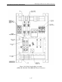
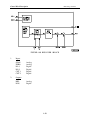
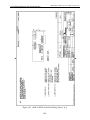
HARDWARE AND EQUIPMENT FEATURES
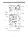
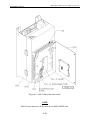
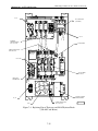
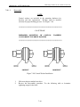
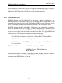
Figures 1-1, 1-2, and 1-3 illustrate the three typical hardware configurations of the
ADDvantage-32 PLUS Power Converters. Each hardware configuration contains a
microprocessor board, bridge interface board, and a power base. Hardware configuration
varies with the output rating of the ADDvantage-32 PLUS being used.
Figure 1-4 shows a typical Advanced Firing Module. The AFM hardware generally
includes the same items listed above except for the power base.
1-2
ADDvantage-32 PLUS ● AC to DC Power Converter
Introduction and General Information
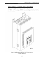
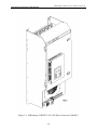
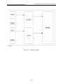
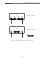
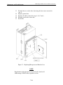
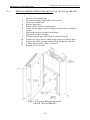
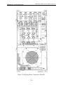
10 through 510 (Figure 1-1) and 550 ADC (Figure 1-2) Power Converters
ADDvantage-32 PLUS's rated for 10 through 510 and 550 ADC are packaged as a single
unit. “Brick style” or rectangular SCR's are mounted in the power base and allow for
convenient packaging.
Figure 1-1. ADDvantage-32 PLUS AC to DC Power Converter
(510 ADC and Below)
1-3
ADDvantage-32 PLUS ● AC to DC Power Converter
Introduction and General Information
Figure 1-2. ADDvantage-32 PLUS™ AC to DC Power Converter (550 ADC)
1-4
ADDvantage-32 PLUS ● AC to DC Power Converter
Introduction and General Information
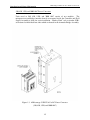
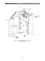
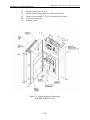
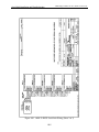
540, 850, 1550, and 3000 ADC Power Converters
Units rated at 540, 850, 1550, and 3000 ADC consist of two modules. The
microprocessor and bridge interface boards are mounted inside the Controller and Field
Supply Assembly to allow for easier installation. “Hockey Puck” style or circular SCR's
are mounted to individual heat sinks which are housed in the Armature Bridge Assembly.
Figure 1-3. ADDvantage-32 PLUS AC to DC Power Converter
(540, 850, 1550, and 3000 ADC)
1-5
ADDvantage-32 PLUS ● AC to DC Power Converter
Introduction and General Information
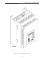
Figure 1-4. Advanced Firing Module (AFM)
1-6
ADDvantage-32 PLUS ● AC to DC Power Converter
Introduction and General Information
The following components are contained in most of the hardware configurations.
Hardware specific to a type will be indicated in the description. For example, power
converters rated at 10 through 510 ADC and 550 amps have the SCR snubbers located on
one board. Snubbers on units rated at 540, 850, 1550, and 3000 ADC are mounted
directly on the SCR assembly. Advanced Firing Modules do not include snubbers.
1.2.1
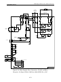
MICROPROCESSOR BOARD
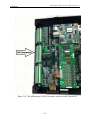
The MICROPROCESSOR BOARD (Figure 1-5) controls all functions including SCR
firing, diagnostics, communications, and control block functions. The microprocessor
board includes the following:
•
Two ARM 9 32 bit processors. One processor is dedicated to the application control
functions and associated user I/O. The second processor performs the functions
required to convert the three-phase AC input voltage into the DC voltages that are
supplied to motors.
•
Flash memory which stores all the drive firmware. The firmware may be upgraded
easily over the serial link, Ethernet interface (using the optional Ethernet daughter
board), or via the USB interface.
•
A USB interface to allow convenient and simple storage of drive calibration data,
signal analyzer data, and drive diagnostic data. In addition, the USB interface allows
for the loading of drive calibration data and updating of the drive flash memory.
•
The following user I/O:
(6) Analog Inputs
(4) Analog Outputs
(6) Digital Inputs
(4) Form C Digital Outputs
(2) Two-Phase Tachometer Inputs
(1) Buffered Tachometer Output
(1) RS485 Serial Link
•
Provides connections for all the user I/O via removable terminal blocks. The terminal
block spacing and layout are fully compatible with the spacing and layout of the
ADD-32 drive.
•
A serial interface to a Human Interface Module (HIM). The HIM is supplied
installed on the drive, but may be easily moved to a location remote from the drive.
•
Two daughter board sites to allow optional modules to be installed on the drive. The
option modules include an Ethernet communication module and an I/O expansion
module.
1-7
ADDvantage-32 PLUS ● AC to DC Power Converter
Introduction and General Information
1.2.2
REMOTABLE KEYPAD
The ADD-32 PLUS provides a remoteable keypad that has the following:
1.2.3
•
4 line x 20 character backlit LCD display. The top two lines of the display are
dedicated to messaging related to keypad use and is equivalent to the two line display
of the ADD-32. The lower two lines are dedicated to the display of fixed drive
operating data. Each line is configurable by the user to display analog, digital or fault
information.
•
6 button keypad. Four keys (up, down, left, right) allow the user to navigate through
the various drive menus and to select and edit the drive calibration and configuration
data. The ENTER key is used to accept changes to the calibration and configuration
data or to initiate an operation via the keypad. The RESET key allows the user to
easily reset any drive faults.
•
11 LEDs used to display drive operating status. One LED is dedicated to indicating
that power is present to the keypad. The remaining 10 LEDs are controlled by the
ADD-32 PLUS software and have display functions that provide operating and fault
information related to the specific functionality of the software installed on the drive.
The ADD-32 PLUS provides at least one of the LEDs to be user configurable to any
digital point in the drive.
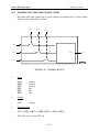
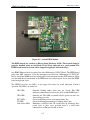
FAX-32 MODULE
The FAX-32 MODULE (Figure 1-5) is mounted onto one of the expansion sites of the
microprocessor board. Eight additional digital inputs are added to the ADD-32 PLUS
when the FAX-32 module is used. The FAX-32 module also provides a frequency output
of 200 - 20,200 Hz. This frequency output can be used to cascade references.
Figure 1-5. FAX-32 Module
1-8
ADDvantage-32 PLUS ● AC to DC Power Converter
Introduction and General Information
1.2.4
BRIDGE INTERFACE BOARD
The BRIDGE INTERFACE BOARD (Figure 1-6) is an interface between the
microprocessor board and the high power thyristor circuits. The main functional circuits
on this board are as follows:
•
•
•
•
•
•
•
Current Feedback Scaling and Isolation
SCR (thyristor) Firing Circuitry and Isolation
Power Supplies for all the Drive Boards
ESTOP and Drive OK Relays
SCR Heat Sink Temperature Feedback Circuitry
Gate Power Relay
Voltage Feedback Scaling and Isolation
1-9
ADDvantage-32 PLUS ● AC to DC Power Converter
Introduction and General Information
10 THROUGH 510 AND 550 ADC CONVERTERS
AFMs; 540, 850, 1550, AND 3000 ADC CONVERTERS
Figure 1-6. Bridge Interface Board (A3)
1-10
ADDvantage-32 PLUS ● AC to DC Power Converter
Introduction and General Information
1.2.5
SNUBBER PC BOARD (10 through 510 and 550 ADC Power Converters only)
The SNUBBER BOARD (Figure 1-7) contains resistor/capacitor circuits for protection of
the SCR's. They are placed on a board instead of across the SCR's so they are not
misapplied when replacing an SCR. In units rated 540, 850, 1550, and 3000 ADC, the
snubbers are mounted directly to the thyristor module assembly.
Figure 1-7. Snubber PC Board (A4)
1-11
ADDvantage-32 PLUS ● AC to DC Power Converter
Introduction and General Information
1.2.6
DRIVE BASE ASSEMBLY (POWER CONVERTERS ONLY, 10 THROUGH 510 and
550 ADC)
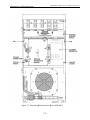
The DRIVE BASE ASSEMBLY (Figure 1-8) on power converters rated 10 through 510
and 550 ADC contains all of the high voltage components. Heat generated by the SCR's
is dissipated by the heat sinks included in the base assembly. The drive base assembly
for 510 ADC and below is shown in Figure 1-8, and for 550 ADC in Figure 1-9. The
base assemblies include the following:
Power Thyristor Bridge
The POWER THYRISTOR BRIDGE is a 6-pulse bridge which rectifies the incoming
3-phase voltage to DC. It permits the DC output voltage to be controlled, thereby
controlling the speed of the connected DC motor. In the 4-quadrant, regenerative drive,
two 6-pulse bridges are arranged in a back-to-back (non-circulating current)
configuration which controls voltage and current for motoring and regenerating in both
forward and reverse directions.
Shunt Field Supply
The SHUNT FIELD SUPPLY is a single phase thyristor/diode bridge which controls the
excitation current to the motor's shunt wound field.
The AC supply comes from the 3-phase main supply. AC line fuses protect the converter
against overcurrents caused by shorts.
Control Power Transformer
The control power transformer provides 115 VAC power for operation of the control
circuitry and cooling fans. The only jumper on the drive is the control transformer
configuration. Correctly jumper the transformer for 230 or 460 VAC incoming linevoltage.
The 550 amp drive base assembly includes optional configurations for 230, 460, or
575 VAC input. Refer to paragraph 6.6.4.
1-12
ADDvantage-32 PLUS ● AC to DC Power Converter
Introduction and General Information
Figure 1-8. Drive Base Assembly (510 ADC and Below)
1-13
ADDvantage-32 PLUS ● AC to DC Power Converter
Introduction and General Information
Figure 1-9. Drive Base Assembly (550 ADC)
1-14
ADDvantage-32 PLUS ● AC to DC Power Converter
Introduction and General Information
DC Contactor
A DC contactor is used to positively remove current from the motor armature. A
dynamic braking (DB) pole may be provided as an option on all drives. Power converters
may be purchased with or without contactors and with or without DB pole. The
510 ADC and above units have externally mounted contactors, while the 10-360 ADC
versions are available with contactors mounted within the drive base assembly.
Fusing (10 Through 510 and 550 ADC)
******************************************************
WARNING
Replace fuses only with same type and rating. Replacement with
fuses other than those recommended may result in damage to the
ADDvantage-32 PLUS and/or connected equipment, as well as
severe injury or death to personnel.
******************************************************
Fuses are located on the Drive Base Assembly for protection of the components. Refer to
Section VII, Tables 7-8 and 7-9, for additional fuse replacement information.
•
•
•
•
•
•
3 AC line fuses (F8, F9, F10)
1 DC link fuse on regenerative units (F11)
2 Control transformer primary fuses (F3, F4)
2 Field supply AC line fuses (F1, F2)
3 Control power fuses (on 10 through 510 ADC units): F5, F6, F7
5 Control power fuses (on 550 ADC units): F5, F6, F7, F12, F13
1-15
ADDvantage-32 PLUS ● AC to DC Power Converter
Introduction and General Information
1.2.7
FIELD CONTROLLER BASE ASSEMBLY (AFMs and 540, 850, 1550, and 3000 ADC
Power Converters)
The FIELD CONTROLLER BASE ASSEMBLY is used on power converters rated 540,
850, 1550, and 3000 ADC as well as all AFMs. It contains the field supply components
and the control electronics that operate the entire motor drive. (See Figure 1-10.) Heat
generated by the field SCR's is dissipated by the heat sink contained in the base
assembly. The base includes the Shunt Field Supply, fuses, bridge interface board and
microprocessor board.
Shunt Field Supply
The SHUNT FIELD SUPPLY is a single phase thyristor/diode bridge which controls the
excitation current to the motor's shunt wound field.
The AC supply comes from the 3-phase main supply. AC line fuses protect the converter
against overcurrents caused by shorts.
Fusing (Refer to Section VII, Table 7-10, for fuse replacement information.)
Fuses contained in the field controller base assembly include: Field Supply AC line (F3,
F4), Control Power Transformer Primary (rejection type) (F1, F2), Board Power (F5),
Contactor Coil (F6), Cooling Blower (F7), and Auxiliary Power (F8). Fuses F1, F2, F6,
and F7 are sized according to the external equipment that is being utilized with the
ADDvantage-32 PLUS (i.e., contactors, control transformers, relays, etc.). These fuses
must be supplied by the user or are provided in the optional auxiliary hardware kit which
is available in addition to the standard DC motor drive.
1-16
ADDvantage-32 PLUS ● AC to DC Power Converter
Introduction and General Information
Figure 1-10. Field Controller Base Assembly
(AFMs and 540, 850, 1550, 3000 ADC Power Converters)
1-17
ADDvantage-32 PLUS ● AC to DC Power Converter
Introduction and General Information
1.2.8
ARMATURE BRIDGE ASSEMBLY (540, 850, 1550, and 3000 ADC power converters
only)
The ARMATURE BRIDGE ASSEMBLY contains the high voltage armature control
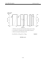
components as shown in Figure 1-11 and Figure 1-12. The chassis supports the thyristor
module assemblies, bus bars, fuses, and current transformers. Blowers on the top of the
unit generate airflow across the heatsinks for heat dissipation. The armature bridge
assembly contains the thyristor modules, firing circuitry, current sensing, blowers (on 540
and 850 amp drives), and fusing to protect the thyristors.
Figure 1-11. Armature Bridge Assembly
(540 and 850 Amp Power Converters Only)
1-18
ADDvantage-32 PLUS ● AC to DC Power Converter
Introduction and General Information
Figure 1-12. Armature Bridge Assembly
1-19
ADDvantage-32 PLUS ● AC to DC Power Converter
Introduction and General Information
(1550 Amp and 3000 Amp Power Converters Only)
1-20
ADDvantage-32 PLUS ● AC to DC Power Converter
Introduction and General Information
1.2.9
THYRISTOR MODULE ASSEMBLY (540 ADC, 850 ADC, 1550 ADC, and 3000 ADC
Power Converters)
The THYRISTOR MODULE ASSEMBLY contains the SCR(s), firing/ snubber board,
air baffle, and bus bars. (Refer to Figures 1-13 and 1-14.) The 540 amp and 850 amp
THYRISTOR MODULE ASSEMBLY contains one SCR for non-regenerative type
bridges or two SCR's for regenerative type bridges.
Figure 1-13. Thyristor Module Assembly
(540 and 850 Amp, Regen. Power Converters Only)
1-21
ADDvantage-32 PLUS ● AC to DC Power Converter
Introduction and General Information
Figure 1-14. Thyristor Module Assembly
(1550 Amp and 3000 Amp Power Converters Only)
1-22
ADDvantage-32 PLUS ● AC to DC Power Converter
Introduction and General Information
1-23
ADDvantage-32 PLUS ● AC to DC Power Converter
Introduction and General Information
1.3
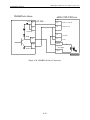
SOFTWARE FEATURES
The setup of an ADDvantage-32 PLUS is done through calibrating and configuring the
various parameters. No programming is necessary. The calibration parameters are
constant numbers that the user enters into the drive. An example would be the maximum
line speed or an analog input scaling factor. The configuration parameters direct where
an input comes from. An example would be the speed reference coming from the first
frequency input instead of a calibration number.
There are two real time data tables in the ADDvantage-32 PLUS. All ongoing
information is stored in these tables. The values can then be used for various functions or
be viewed or recorded. The first data table is for bit information such as a drive OK bit.
The second is for floating point data such as actual motor speed.
The software is also broken down into two parts. The first part is the core software which
consists of all low level routines including:
I/O scanning - SCR firing - Diagnostics Serial link communications - LAN communications Keypad protocol - Inner armature and field current loops
The core has its own calibration and configuration parameters and outputs its data to the
real time data tables. See Section III for a detailed description of the base software.
The second part of the software is the application code. This portion is programmed into
software control blocks. The blocks are then connected together to form a personality
such as speed/tension or center driven winder control. The inputs of the blocks can come
from the real time data tables, calibration parameter, or a configuration parameter. The
outputs of the blocks always go to the real time data tables where they can be viewed or
used as inputs to other blocks. Chapter IV describes the library of blocks that can be used
in a particular application. Appendices A through D explain all the interconnections
between the blocks to form the application for the software part number of this manual.
Other than the Appendices, this manual is the same for all ADDvantage-32 PLUS drives.
1-24
ADDvantage-32 PLUS ● AC to DC Power Converter
Introduction and General Information
Figure 1-15. Software Format
1-25
ADDvantage-32 PLUS ● AC to DC Power Converter
Introduction and General Information
1.4
IDENTIFICATION OF PART NUMBERS
The part numbering of the ADDvantage-32 PLUS consists of two separate numbers. The
hardware part number is located on nameplates found on both the inside and outside of
the unit and reflects the hardware configuration of the ADDvantage-32 PLUS. The
software part number, as well as the version number, identifies the application software
used with the ADDvantage-32 PLUS hardware.
HARDWARE PART NUMBER (EXAMPLE)
MODEL TYPE
ALWAYS DC
D
SYSTEM I.D. AND
AMP RATING
C
0
EXPANSION
BOARD CODE
0
3
0
-
A19722 FAX
MODULE
QUADRANTS/
AFM
FIELD
ADD32
PLUS
OPTION
1
OPTION
2
4
Z
0
0
-
A26494 ETHERNET
MODULE
B
--------------
--------------
D
INSTALLED
--------------
J
--------------
INSTALLED
L
INSTALLED
INSTALLED
SOFTWARE PART NUMBER (EXAMPLE)
6-DIGIT SOFTWARE PART NUMBER
6
9
6
0
0
VERSION NUMBER
2
.
V
Figure 1-16. Part Number Breakdown
1-26
1
Expansion
board code
0
B
ADDvantage-32 PLUS ● AC to DC Power Converter
Introduction and General Information
1.4.1
HARDWARE PART NUMBER BREAKDOWN
MODEL TYPE defines the type of armature voltage to be controlled (always DC).
SYSTEM I.D. AND AMP RATING
SELECTION
DESCRIPTION
0001
0002
Advanced Firing Module (AFM)
AFM Without Field Supply
0003
AFM for 24 SCR Firing
0004
AFM for 24 SCR Firing Without Field Supply
10
10 ADC Armature, 3 ADC Field Supply Power Converter
30
30 ADC Armature, 3 ADC Field Supply Power Converter
56
56 ADC Armature, 6 ADC Field Supply Power Converter
110
110 ADC Armature, 6 ADC Field Supply Power Converter
180
180 ADC Armature, 12 ADC Field Supply Power Converter
280
280 ADC Armature, 12 ADC Field Supply Power Converter
360
360 ADC Armature, 12 ADC Field Supply Power Converter
510
510 ADC Armature, 12 ADC Field Supply Power Converter
540
540 ADC Armature, 12 ADC Field Supply Power Converter
541
540 ADC Armature, 24 ADC Field Supply* Power Converter
542
540 ADC Armature, 48 ADC Field Supply* Power Converter
550
550 ADC Armature, 12 ADC Field Supply Power Converter
551
550 ADC Armature, 24 ADC Field Supply Power Converter
552
550 ADC Armature, 48 ADC Field Supply Power Converter
850
850 ADC Armature, 12 ADC Field Supply* Power Converter
851
850 ADC Armature, 24 ADC Field Supply* Power Converter
852
850 ADC Armature, 48 ADC Field Supply* Power Converter
1550
1550 ADC Armature, 12 ADC Field Supply* Power Converter
1551
1550 ADC Armature, 24 ADC Field Supply* Power Converter
1552
1550 ADC Armature, 48 ADC Field Supply* Power Converter
2500
2500 ADC Armature, 12 ADC Field Supply* Power Converter
2501
2500 ADC Armature, 24 ADC Field Supply* Power Converter
2502
2500 ADC Armature, 48 ADC Field Supply* Power Converter
3000
3000 ADC Armature, 12 ADC Field Supply* Power Converter
3001
3000 ADC Armature, 24 ADC Field Supply* Power Converter
3002
3000 ADC Armature, 48 ADC Field Supply* Power Converter
*Power converters rated 540 ADC, 850 ADC, 1550 ADC, and 3000 ADC include a control unit separate from the
armature bridge assembly. These units contain the motor field bridge and are available in various ratings.
1-27
ADDvantage-32 PLUS ● AC to DC Power Converter
Introduction and General Information
QUADRANTS/AFM FIELD
Power Converters
SELECTION
DESCRIPTION
2
Non-Regenerative Armature Bridge*. 240 or 500 VDC, selectable.
4
Regenerative Armature Bridge. 240 or 500 VDC, selectable, plus 650 VDC
on DC0550
A
Same as “2” except 700 VDC can also be selected on 1550 and 3000A units
B
Same as “4” except 700 VDC can also be selected on 1550 and 3000A units
N
Non-Regenerative Modular Design Armature Bridge**
M
Regenerative Modular Design Armature Bridge**
*Non-regenerative options are only available on units rated 540, 850, 1550, and 3000 ADC.
Software parameters allow reverse bridge operation to be disabled on all units.
**Available on 540, 850, 1550, and 3000 ADC.
Advanced Firing Modules (AFM)
SELECTION
DESCRIPTION
0
12 Amp Field
1
24 Amp Field
2
48 Amp Field
3
6 Amp Field
4
12 Amp Field (4 SCR)
5
24 Amp Field (4 SCR)
6
48 Amp Field (4 SCR)
OPTION 1
On AFM systems, this block identifies a customer-specific application.
SELECTION
DESCRIPTION
0
Non-listed
L
UL Listed
N
Modular design used in conjunction with Options 0, 2, and 3 of Option 2.
When specifying this feature, Option 2 must also be specified. It can only be
specified on units rated 10 through 510 and 550 ADC.
4
4 SCR Field Supply. Available on 540, 850, 1550, and 3000 ADC power
converters.
1-28
ADDvantage-32 PLUS ● AC to DC Power Converter
Introduction and General Information
OPTION 2
On AFM systems, this block identifies a customer-specific application.
SELECTION
DESCRIPTION
0
Right side AC input (540, 850, 1550, and 3000 ADC)
1
Left side AC input (540, 850, 1550, and 3000 ADC)
0
Specified with Option N of Option 1 with no contactor provided*
2
Specified with Option N of Option 1 for a contactor without DB pole*
3
Specified with Option N of Option 1 for a contactor with DB pole*
*Only available on units rated 10 through 510 ADC and 550 ADC.
1.4.2
SOFTWARE PART NUMBER BREAKDOWN
The software part number is a six-digit number which represents the application software
installed in the ADDvantage-32 PLUS. Several different types are available including a
standard speed regulator with tension (P/N 696002) and a center driven winder
(P/N 696003). Most applications can be covered by the two application programs
described. Other application software is available. To obtain a list or to discuss custom
software applications, consult the factory.
NOTE
A two-digit version number is also required. If a specific version
is not referenced, the latest version will be supplied.
1-29
ADDvantage-32 PLUS ● AC to DC Power Converter
Introduction and General Information
1.5
SPECIFICATIONS
Please note that some of the following specifications are not pertinent to all models.
TABLE 1-1. ADDvantage-32 PLUS SPECIFICATIONS
DESCRIPTION
SPECIFICATION*
Input Voltage to Transformer
3-Phase primary windings to standard voltages
(Phase rotation insensitive)
3-Phase, 230 or 460 VAC (nominal), except
550 ADC Drive only - 230, 460, or 575 VAC
(nominal)
Transformer Output to Drive**
Maximum Currents
Drive
P/N
DC0010
DC0030
DC0056
DC0110
DC0180
DC0280
DC0360
DC0510
DC0540
DC0541
DC0542
DC0550
DC0551
DC0552
DC0850
DC0851
DC0852
DC1550
DC1551
DC1552
DC3000
DC3001
DC3002
♦
♦♦
♦
♦♦
HP
240/500/700 VDC
2/5
7.5/15
15/30
30/60
50/100
75/150
100/200
150/300
150/300
150/300
150/300
150/300/400
150/300/400
150/300/400
250/500
250/500
250/500
500/1000/1250
500/1000/1250
500/1000/1250
900/1800/2500
900/1800/2500
900/1800/2500
Armature
Output
Input
Current
10 Amps DC
11 Amps AC
30 Amps DC
28 Amps AC
56 Amps DC
49 Amps AC
110 Amps DC
95 Amps AC
180 Amps DC
155 Amps AC
280 Amps DC
240 Amps AC
360 Amps DC
310 Amps AC
510 Amps DC♦♦ 416 Amps AC
540 Amps DC
440 Amps AC
540 Amps DC
440 Amps AC
540 Amps DC
440 Amps AC
550 Amps DC
459 Amps AC
550 Amps DC
470 Amps AC
550 Amps DC
488 Amps AC
850 Amps DC
700 Amps AC
850 Amps DC
700 Amps AC
850 Amps DC
700 Amps AC
1550 Amps DC
1265 Amps AC
1550 Amps DC
1265 Amps AC
1550 Amps DC
1265 Amps AC
3000 Amps DC
2460 Amps AC
3000 Amps DC
2470 Amps AC
3000 Amps DC
2490 Amps AC
Field
Output
3 Amps DC
3 Amps DC
6 Amps DC
6 Amps DC
12 Amps DC
12 Amps DC♦
12 Amps DC♦
12 Amps DC♦
12 Amps DC
24 Amps DC
48 Amps DC
12 Amps DC
24 Amps DC
48 Amps DC
12 Amps DC
24 Amps DC
48 Amps DC
12 Amps DC
24 Amps DC
48 Amps DC
12 Amps DC
24 Amps DC
48 Amps DC
Additional Specifications are located in the supplemental drawing package.
An isolation transformer or line reactor is required when applying each ADD-32 PLUS drive to a power distribution system.
A total impedance from the power distribution source to the drive input in the range of 3% to 6% is required. Total KVA
rating of transformer should not exceed 3 times the drive rating. If a drive isolation transformer is supplying power to multiple
drives, then each drive must have a line reactor. If a combination of isolation transformer and line reactor is used, the reactor
should contribute the majority of the line impedance (better than 2:1 ratio). Provided that each ADD-32 PLUS has the proper
source impedance, any number of drives or frame sizes can be connected to a common power source. Connection of any
power converter to a transformer with primary rating of 2300 VAC or more may require additional input line conditioning at
the power converter to prevent damage to electrical components. Contact Avtron Industrial Automation, Inc., for assistance
when this is required.
A 24 amp field option is available on drives with a 12 amp field.
Consult factory for overload rating.
1-30
ADDvantage-32 PLUS ● AC to DC Power Converter
Introduction and General Information
TABLE 1-1. ADDvantage-32 PLUS SPECIFICATIONS--Cont.
DESCRIPTION
Line Voltage Variation
Line Frequency Range
Armature Voltage Range
SPECIFICATION*
+/-10% of nominal
43 to 63 Hz
Drive P/N
Armature
Current
Voltage
DC0010-0510-XXXX
10 through 510 ADC
240, 500 VDC
DC054X-XXXX
540 ADC
240, 500 VDC
DC055X-XXXX
550 ADC
240, 500, 650 VDC
DC085X-XXXX
850 ADC
240, 500 VDC
DC155X - 2XXX
4XXX
1550 ADC
240, 500 VDC
DC155X - AXXX
BXXX
1550 ADC
240, 500, 700 VDC
DC300X - XXXX
3000 ADC
240, 500, 700 VDC
Armature Current Range
Armature Overload Capacity
Field Current Regulation
User I/O
33% to 100% drive rating (Below 50% bridge self
test may need to be disabled.)
150% for 60 seconds
Continuous throughout speed range
(6) analog inputs,
(4) analog outputs,
(6) digital inputs,
(4) digital outputs,
(2) two-phase tach inputs,
(1) buffered tach output,
(1) RS485 Serial Link or
* Additional Specifications are located in the supplemental drawing package.
1-31
ADDvantage-32 PLUS ● AC to DC Power Converter
Introduction and General Information
TABLE 1-1. ADDvantage-32 PLUS SPECIFICATIONS--Cont.
DESCRIPTION
FAX-32 Board
SPECIFICATION*
(8) digital inputs,
(2) identical frequency outputs,
200 - 20,200 Hz frequency range,
Duty cycle of 50% +1%,
50 mA Imax,
Vout of 5V differential,
+.017 commanded accuracy,
+.017 commanded resolution
Digital Input Ratings
Input Voltage (DC)
Common Mode
(Logic High)
(Logic Low)
MIN
10 VDC
-1 VDC
NOM
MAX
24 VDC
0 VDC
30 VDC
9 VDC
Common Mode Rejection
100 VDC
Input Impedance
Operating Current Required
Digital Output Ratings
Analog Input Ratings
Analog Output Ratings
2.4K Ohm
4 mA
60 mA
Output Voltage - 240 VAC Max.
Output Current - 2.5 Amps Max.
Form C relay contacts
Differential Input Voltage +10 VDC Max.
Common Mode Input Voltage 200 VDC Max.
Common Mode Noise Rejection 60 VDC Max.
Accuracy - 0.25% F.S. Max.
Drift - 0.12% F.S. Max.
Output Voltage +10 VDC Max.
Output Current 10 mADC Nom., 40 mADC Max.
Common Mode Noise Rejection 2 VDC Max.
Drift +1.2% F.S. Max.
Resolution - 0.025% F.S. Max.
Accuracy +1.8% F.S. Max.
* Additional Specifications are located in the supplemental drawing package.
1-32
ADDvantage-32 PLUS ● AC to DC Power Converter
Introduction and General Information
TABLE 1-1. ADDvantage-32 PLUS SPECIFICATIONS--Cont.
DESCRIPTION
Diagnostics
RS485 Serial Link
Pulse Generator Inputs: 2-Phase
Buffered Pulse Generator Outputs: 2-Phase
Auxiliary Power Supplies
SPECIFICATION*
40 fault messages w/corrective action
11 front panel LED annunciators
16 event fault memory
Signal Analyzer
Sampling Rate 360 Samples/Second Max.,
27.8 Seconds/Sample Min.
Recording Duration 61.7 hours Max.,
22.22 seconds Min.
Optically-isolated Self powered.
120V common mode noise rejection
3-30V peak-to-peak,
540 ohm impedance,
Optically isolated,
120V common mode rejection,
0-20,200 Hz frequency range,
50% +20% duty cycle
5V @ 50mA,
0-25 KHz frequency range
Digital I/O Supply
Voltage Output = 24 VDC Nom., 26 VDC Max.
Current Output = 80 mADC Max.
Auxiliary AC Supply
Voltage Output = 115 VAC Nom.
Power Output =
50 VA Max. (units 56A and under)
100 VA Max. (units 110A and above)
Safety Interlock Supply
Voltage Output = 24 VDC Nom., 26 VDC Max.
Current Output = 50 mADC Max.
Pulse Generator Supply
Voltage Output = 12 VDC Nom., 13.2 VDC Max.
Current Output = 300 mA Max. (Short circuit proof)
Pot Supplies
Voltage Output = ±10 VDC Max.
Current Output = 5 mA Max.
* Additional Specifications are located in the supplemental drawing package.
◘ Consult Avtron regarding UNIPULSERTM information for additional duty cycle applications.
1-33
ADDvantage-32 PLUS ● AC to DC Power Converter
Introduction and General Information
TABLE 1-1. ADDvantage-32 PLUS SPECIFICATIONS--Cont.
DESCRIPTION
Chassis Ambient Temperature
- Enclosed (See outline drawing for minimum
enclosure size.)
- Open Chassis
Storage Temperature***
Relative Humidity
Operational Altitude
SPECIFICATION*
0 to 40º C (32 to 104º F)
0 to 50º C (32 to 122º F) (50º C maximum
surrounding air temperature rating)
-20 to 55º C (-4 to 131º F)
95% non-condensing
0 to 3,300 feet above sea level –
no derating required.
Above 3,300 feet –
derated linearly by 1% per 300 ft.
Worst Case Power Loss
Drive P/N
DC0010
DC0030
DC0056
DC0110
DC0180
DC0280
DC0360
DC0510
DC054X
DC055X
DC085X
DC155X-4
DC155X-B
DC250X
DC300X-A
DC300X-B
Watts (approximate)
150
200
260
500
725
1000
1150
1400
1500
2050
2300
3900
4500
6100
7900
8300
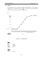
100
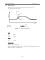
100%LOAD
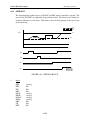
Power loss follows the approximate curve
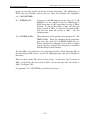
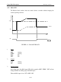
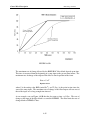
shown in Figure 1-17. Worst case power
loss (total) is at 100% speed, 100% load.
At other speeds and loads the percent loss
is greater, but the total loss is less.
EFFECIENCY
99
25%LOAD
98
97
96
95
25
50
75 100% SPEED
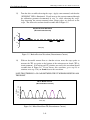
EFFICLAN
Figure 1-17. Efficiency vs. Speed
* Additional Specifications are located in the supplemental drawing package.
*** A space heater may be necessary if condensation or excessive moisture is expected.
1-34
ADDvantage-32 PLUS ● AC to DC Power Converter
Introduction and General Information
TABLE 1-1. ADDvantage-32 PLUS SPECIFICATIONS--Cont.
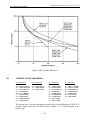
DESCRIPTION
SPECIFICATION*
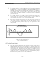
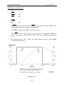
Power factor is highly dependent on
operating speed. The curve in Figure
1-18 approximates power factor.
POWER FACTOR (LAGGING)
Worst Case Power Loss (Continued)
.9
.8
.7
.6
.5
.4
.3
.2
.1
25
50
75
100% SPEED
PWRFACTLAN
Figure 1-18. Power Factor vs. Speed
* Additional Specifications are located in the supplemental drawing package.
1-35
ADDvantage-32 PLUS ● AC to DC Power Converter
Introduction and General Information
TABLE 1-1. ADDvantage-32 PLUS SPECIFICATIONS--Cont.
Bridge Interface Board
DRIVE PART NUMBER
DC0010-0510
and 0550
OUTPUT TO
ARMATURE
CIRCUIT
Outputs up to 12 SCR
firing signals, 6 forward
and 6 reverse. Contains
pulse shaping circuitry.
DC0540,
0850-3000
Outputs up to 12 SCR firing
signals, 6 forward and 6
reverse. Pulse shaping
circuitry provided on
armature bridge assembly.
DC0001 and
DC0002 AFMs
Outputs up to 12 SCR
firing signals, 6 forward
and 6 reverse.
DC0003, DC0004 and
DC0005 AFMs
Outputs up to 24 SCR
firing signals (12 forward,
12 reverse). Firing signal
control is configurable
through application
specific software. Consult
Avtron Industrial
Automation, Inc., for
information.
Requires external pulse
shaping circuitry for SCR
firing (available from
Avtron or others). Pulse
shaping circuitry can be
provided by an Avtron
Gate Pulse Amplifier unit,
P/N C23047. Consult
Avtron Industrial
Automation, Inc., for
application specific
information.
SCR gate power supplied
through internal 24 VDC
supply.
FIRING
SIGNAL T.B.S
J3 and J7
J2 and J3
J2 and J3
For DC0003 and DC0004
only: SCR gate power
should be supplied
externally.
J9 and J10
FIELD SUPPLY
See paragraph 1.2.6.
See paragraph 1.2.7.
See paragraph 1.2.7.
For DC0003 only: See
paragraph 1.2.7.
Also contains connection
(J6) to support optional
firing of an external
single-phase field bridge.
ARMATURE
CURRENT
FEEDBACK
0.66V = 100% Iarm
0.66V = 100% Iarm
0.66V = 100% Iarm
Selectable:
DC0003 and DC0005:
0.666V = 100% or
5.00V = 100%
DC0004:
0.666V = 100% or
3.33V = 100%
1-36
ADDvantage-32 PLUS ● AC to DC Power Converter
Introduction and General Information
TABLE 1-1. ADDvantage-32 PLUS SPECIFICATIONS--Cont.
Bridge Interface Board (Cont.)
DRIVE PART NUMBER
ARMATURE
VOLTAGE
FEEDBACK
DC0010-0510
and 0550
DC0540,
0850-3000
0 to 670 VAC
±10 VDC
Scaled by Avtronsupplied Voltage
Isolation Board provided
on armature bridge
assembly.
MISC.
DC0001 and
DC0002 AFMs
±10 VDC
Requires customersupplied external
scaling circuit.
DC0003, DC0004 and
DC0005 AFMs
DC0003 and DC0005:
±10 VDC
DC0004: ±38.3 VDC
Requires customersupplied external
scaling circuit.
The features below
apply to DC0003 only:
Auxiliary input is
provided to accept
+/-100mV input signal
which is filtered
(2 poles at 3.4mS) and
amplified to
+/-5.0 VDC full scale
and placed at an
auxiliary output on J11.
1-37
ADDvantage-32 PLUS ● AC to DC Power Converter
ADDvantage-32 PLUS ● AC to DC Power Converter
SECTION II
KEYBOARD AND
PARAMETER FUNCTIONS
******************************************************
WARNING
DO NOT OPERATE RADIO TRANSMITTERS or CELL
PHONES IN THE VICINITY OF THE ADD-32 PLUS. The
ADD-32 PLUS is an electronic device. Although it is designed to
operate reliably in typical industrial environments, the ADD-32
PLUS can be affected by radio and/or cell phone transmitters. It is
possible to cause drive faults, inappropriate/unintended drive I/O
activity, and unpredictable operation that could result in damage to
the ADD-32 PLUS, damage to other equipment, or serious injury
to personnel.
Radio transmitter interference is a site specific phenomenon.
Generally, electrical wires connected to terminals on the ADD-32
PLUS are the conduits for radio interference. Interference can be
minimized by good wiring design and installation practice. It is
recommended that signs be posted in and around the drive system,
warning of the possibility of interference if the drive is in
operation. DO NOT USE radio transmitters or cell phones in the
area.
Absence of a radio interference problem is no guarantee that a
problem will never occur as conditions and environments can
change.
******************************************************
2-1
ADDvantage-32 PLUS ● AC to DC Power Converter
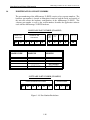
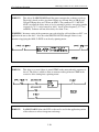
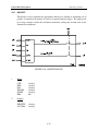
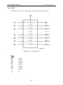
2.1
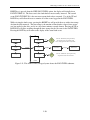
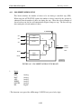
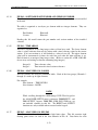
KEY FUNCTIONS
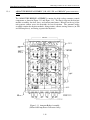
Information generated by the ADDvantage-32 PLUS can be accessed using the remotable
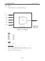
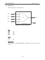
alphanumeric keypad and LCD display located on the front of the chassis (Figure 2-1).
The LCD display provides four rows of 20 alphanumeric characters. Editing of displayed
information is accomplished using the six keys located below the LCD display.
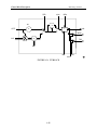
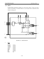
Figure 2-1. The keypad with directional arrows, reset, and enter functions
and LCD displays are features of the ADDvantage-32 PLUS.
2-2
ADDvantage-32 PLUS ● AC to DC Power Converter
2.1.1
KEYPAD BUTTONS
Six keys provide instructions to the ADD-32 PLUS. By pressing one of the keys, the
information is shown in the LCD display. Keystroke functions are as follows:
The down arrow key moves down through the loop of options in the menus,
submenus, and parameters.
The up arrow key moves up through the loop of options in the menus,
submenus, and parameters.
The right arrow key moves from menus to submenus to parameters.
The left arrow key moves from parameters to submenus to menus.
2.1.2
ENTER
The enter key accepts a change to a calibration or configuration parameter or
initiates an operation.
RESET
The reset key clears any ADD-32 PLUS drive faults.
LCD DISPLAY
The LCD display provides the user with ADD-32 PLUS operating and configuration
data. The data is provided on the LCD display in response to user input via the keypad.
The display consists of four rows of 20 alphanumeric characters. The line information is
as follows:
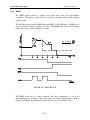
Line 1: MENU ITEM NAME when at the “menu level”. When at the menu level, the
lower line indicates that pressing the RIGHT KEY (----->) will cause entry into a sublevel as shown in Figure 2-2. When editing a calibration or configuration parameter, the
line shows the parameter group, the parameter number, and the parameter label.
Line 2: Submenu indicator when in a menu (Figure 2-2). When editing a calibration or
configuration parameter, the line shows actual information associated with the edit in
progress (Figure 2-3).
2-3
ADDvantage-32 PLUS ● AC to DC Power Converter
OPERATE
------>
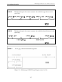
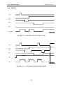
Figure 2-2. Lines 1 and 2 showing a MENU LEVEL display.
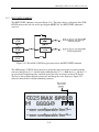
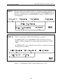
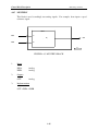
X001 MOTOR Iarm
V 10.00000 % DRV
Figure 2-3. Lines 1 and 2 of the LCD display showing a drive calibration parameter.
Lines 3 and 4: The lower two lines of the LCD display are dedicated to the display of
drive operating data. The operating data can be analog data, digital data, or fault data.
Each of the lines is configurable independently (Figure 2-4).
FIL SPEED
FIL ARM CUR
0.0
123.45
Figure 2-4. Lines 3 and 4 of the LCD display show drive analog data.
2.2
MENUS AND SUBMENUS
The ADDvantage-32 PLUS drive allows user access to all drive calibration, configuration
and operating data via the keypad and LCD display based on a menu/submenu syntax
structure.
A menu offers the user a list of options from which to select. The LCD display will
display one of the options at a time. The user may navigate through the list of options by
using the UP and DOWN keys. The ADDvantage-32 PLUS menus are looping menus
and the user may reach any option in the list using the UP or DOWN keys without regard
to the current menu option displayed.
A submenu is a secondary menu accessed from another menu. The user may enter a
submenu from a menu by pressing the RIGHT key. The display will indicate that a menu
option will lead to a submenu when the RIGHT key is pressed by displaying “------->” on
2-4
ADDvantage-32 PLUS ● AC to DC Power Converter
the second line of the LCD display, as shown in Figure 2-2. A submenu may be exited
by pressing the LEFT key. When the LEFT key is pressed, the LCD display will then
return to the menu option that was displayed prior to entry into the submenu.
The ultimate purpose of the ADDvantage-32 PLUS keypad and LCD display is to
provide the user with access to the calibration, configuration and operating data contained
within the drive. The menu/submenu syntax is designed to allow the user to navigate to
the desired information. The drive calibration, configuration and operating data is
presented at the final, lowest level submenu. The user will know that the lowest level
submenu has been reached when the second line of the LCD display shows a drive
calibration, configuration or operating parameter. An example of this is shown in Figure
2-3 displaying a drive calibration parameter. When the lowest level of submenu displays
drive calibration, configuration or operating information, the UP and DOWN keys will
allow the user to navigate through a series of parameters.
The user, after navigating the menus and submenus to a specific drive parameter, may
then edit the parameter by pressing the RIGHT key. If the parameter being displayed on
the LCD display is a calibration or configuration parameter, and if the drive is configured
to allow editing of the parameter, pressing the RIGHT key will enter the edit mode.
2.2.1
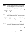
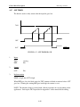
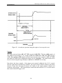
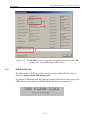
EXAMPLE OF MENUS AND SUBMENUS NAVIGATION
The following illustrates the navigation of the menus and submenus to display a signal
analyzer parameter:
Starting in the uppermost menu at the OPERATE option, the display is:
OPERATE
------>
Pressing the UP key three times will result in the ANALYZER MENU option appearing
on the display:
Analyzer Menu
------>
2-5
ADDvantage-32 PLUS ● AC to DC Power Converter
Pressing the RIGHT key will enter the ANALYZER submenu and show this display:
Analyzer 1 Setup
------>
Pressing the RIGHT key again will enter the ANALYZER 1 SETUP submenu and the
display will be as follows:
Z000 RESET 1
------>
Pressing the UP key will move to the ANALYZER 1 TRIGGER LEVEL display as
shown:
Z001 TRIG LEVEL1
V
0.0
Pressing the RIGHT key at this point will initiate the EDIT mode of ANALYZER 1
TRIGGER LEVEL. If the LEFT key is pressed instead of the RIGHT key, the display
will show the exit of the lowest level submenu as follows:
Analyzer 1 Setup
------>
Pressing the RIGHT key again will return from that submenu to the top level menu as
shown:
Analyzer Menu
------>
2-6
ADDvantage-32 PLUS ● AC to DC Power Converter
2.3
PARAMETER DEFINITION AND GROUPINGS
The ADDvantage-32 PLUS drive contains four distinct types of parameters, two that
define how the drive functions and two that provide user access to all the drive real-time
operating data.
The parameters are described as follows:
2.3.1
1.
Calibration Parameters are numeric data such as limits, setpoints, or ramp rates.
The calibration data is stored in non-volatile memory to ensure the calibration
parameters are not lost when the drive loses power. The calibration parameters
may be edited by the user via the keypad and LCD display.
2.
Configuration Parameters are non-numeric data that allow the user to select one
option out of a list of possible options for a particular function of the drive. An
example of a configuration parameter is Y002: 4Q OPERATE that allows the
user to select either ENABLE or DISABLE as the option to apply concerning four
quadrant operation of the drive. The configuration data is stored in non-volatile
memory to ensure the configuration parameters are not lost when the drive loses
power. The configuration parameters may be edited by the user via the keypad
and LCD display.
3.
Analog Data is real time numeric information contained in the ADDvantage-32
PLUS analog data table. This data represents the actual numeric operating data of
the drive: analog inputs, internal analog control signals and also the values of
analog drive outputs. The data is stored and presented in engineering units. This
data is updated by the core software, application blocks, over the serial link/LAN,
or the hardwired I/O. All analog data (with the exception of eight analog data
points configured to be non-volatile) is lost on power loss to the drive.
4.
Digital Data is real time digital bit information contained in the ADDvantage-32
PLUS digital data table. This data represents the actual binary/digital operating
data of the drive and has a value of ONE/TRUE or ZERO/FALSE. This data is
updated by the core software, application blocks, over the serial link/LAN, or the
hardwired I/O. All digital data is lost on power loss to the drive.
PARAMETER GROUPS
The ADDvantage-32 PLUS drive parameters are further broken down into logical groups
as an aid in identifying and locating the various parameters.
2-7
ADDvantage-32 PLUS ● AC to DC Power Converter
Parameters are defined by a four-digit code followed by a name or abbreviated
description. The letter used as the first digit represents the particular group to which a
parameter belongs. A typical parameter is shown as follows:
P000:JOG REF
Refer to Appendix C for specific parameter numbers and descriptions.
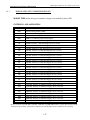
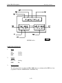
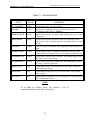
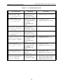
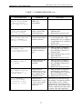
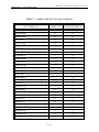
Table 2-1 lists the nine parameter groups that are defined for the ADDvantage-32 PLUS
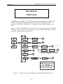
drive along with a brief description of the group.
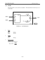
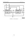
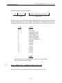
Parameters are organized as shown in Table 2-1 and Figure 2-5.
APPLICATION
SOFTWARE
DATA
TABLES
BLOCK
SOFTWARE
A***
C***
D***
P***
CORE
SOFTWARE
X***
Y***
Z***
Q***
PARAMLAYD105
Figure 2-5. Parameter Layout
2-8
T***
ADDvantage-32 PLUS ● AC to DC Power Converter
TABLE 2-1. PARAMETER ORGANIZATION
PARAMETER
GROUP
PARAMETER
TYPE
DESCRIPTION
X***
Calibration
X*** parameters calibrate the core software. Core
parameters perform tasks specific to the
ADDvantage-32 PLUS hardware being used.
Y***
Configuration
Y*** parameters configure the core software. These
parameters set up the functionality of the
ADDvantage-32 PLUS hardware.
C***
Calibration
C*** parameters calibrate the application block
software being used. These parameters can be
permanently fixed to specific blocks or can be
configured using P*** parameters.
P***
Configuration
P*** parameters configure the application block
software used with the ADDvantage-32 PLUS. P***
parameters allow the option to link specific blocks
together, or configure a C*** parameter to the input
blocks.
A***
Analog Data
A*** parameters are real time floating point data.
They represent all the information in the analog data
table.
D***
Digital Data
D*** parameters are real time bit data. They
represent all the values in the digital data table. A
D*** parameter has a value of either one or zero. A
one means the condition is true.
T***
Calibration
Points
T*** parameters calibrate the data for the
ADDvantage-32 PLUS function tables. The
ADDvantage-32 PLUS has four function tables, each
with 16 data points.
Z***
Calibration and
Configuration
Z*** parameters are a mix of configurable and
calibratable values used for the four built-in signal
analyzers. See Section V.
Q***
Data Value
Q*** values are read-only parameters used by the
Y*** and Z*** parameters. They represent
selections available for certain parameters.
Figure 2-5 (above) illustrates where the various parameter groups are used with the
ADDvantage-32 PLUS drive. The DATA TABLES contain all the real time analog and
digital data, portions of the data being written by the drive core software, portions written
by the drive block software, portions being read by the drive core software and portions
being read by the drive block software.
2-9
ADDvantage-32 PLUS ● AC to DC Power Converter
The drive core software is responsible for the basic functions of the drive, including
protective functions, control of the SCR firing, reading analog and digital inputs,
generating analog and digital outputs, measuring the tach feedback and communications.
In addition, the drive core software controls the signal analyzer and maintains the drive
table data. Below it can be seen that the X*** and Y*** parameters are associated with
the core software. The X*** calibration parameters define such things as feedback
scaling, analog input scaling, analog output scaling, firing angle limits and tach scaling,
to name a few. The Y*** configuration parameters define such things as the DRIVE
PART NUMBER, bridge self test mode, 2/4 quadrant bridge operation, tach type, sources
for the analog and digital outputs to name a few. All of the T*** table calibration data
and the Z*** signal analyzer calibration and configuration data is also associated with the
core software.
The block software consists of the all of the control blocks required to implement the
control scheme in the drive. The C*** calibration parameters and the P*** configuration
parameters allow the user to customize features and functions of the control blocks to
meet the needs of their unique applications.
2.4
LCD DISPLAY PARAMETER FORMAT
Through navigation of the ADDvantage32 PLUS menus and submenus, the user will
ultimately be able to locate a drive parameter of interest.
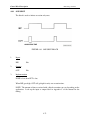
2.4.1
CALIBRATION, ANALOG, TABLE PARAMETERS
The LCD display of the parameter will be in one of two formats: the format for numeric
data such as calibration and real time data, or the format for configuration data.
The format for the numeric data is as follows:
1.
Parameter Group - Represents the type of data to be edited. (See Table 2-1.)
2.
Parameter Number - Each parameter within a data type has a unique parameter
number. (See Appendix A.)
3.
Label - Each parameter has a unique 11 character label. (See Appendix B.)
2-10
ADDvantage-32 PLUS ● AC to DC Power Converter
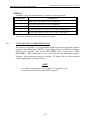
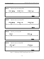
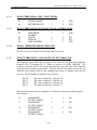
Figure 2-6. The first line of the four lines shown in the LCD display shows the parameter group,
the parameter number, and the parameter label.
4.
Bottom Left Character - Determines what type of value is displayed. The only
value which can be edited is “V” which represents current value.
5.
Value - Represents the value of a particular parameter to nine significant digits.
6.
Units - Represents the value's units of measure. This text can be edited using the
EDIT UNITS menu.
2-11
ADDvantage-32 PLUS ● AC to DC Power Converter
Figure 2-7. The second line of the four lines shown in the LCD display shows the data type,
parameter value, and parameter units.
2.5
EDITING A NUMERIC PARAMETER
After having used the menus and submenus to arrive at a parameter to be edited, pressing
the RIGHT key will enter the edit mode for the parameter as shown in Figure 2-8.
NOTE
If access to the parameter is locked out, the message “ACCESS
DENIED” will be displayed. To allow entry to the edit mode, the
proper parameter must be enabled in the ACCESS CODES menu.
2-12
ADDvantage-32 PLUS ● AC to DC Power Converter
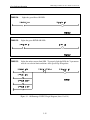
Figure 2-8. The LCD display at the start of the edit mode.
The display has the underline visible on the second line, immediately under the “V”. The
“V” indicates that the actual value of C025: MAX SPEED is currently being displayed.
The user may press the UP or DOWN keys to scroll through three other attributes of the
parameter, one of which is the MAXIMUM VALUE that the parameter may have as
indicated by the “V” being replaced by “H”. See Figure 2-9.
Figure 2-9. The LCD display in edit mode shows the maximum limit of the parameter being
edited. “H” stands for the high limit.
2-13
ADDvantage-32 PLUS ● AC to DC Power Converter
Pressing the UP or DOWN keys again will scroll through to the MINIMUM VALUE that
the parameter may have as indicated by an “L” (for low limit) replacing the “H”.
Continue pressing the UP or DOWN to scroll through to a “D”, which indicates the
default value of the parameter. The default value is the original value before any edits to
the parameter were made.
In order to perform an edit of the numeric value of the parameter, the left most character
must be the “V”.
When the actual value of the parameter is being displayed, the RIGHT key is used to
move the cursor to the right of the “V” and begin the edit of the actual parameter value.
The blank spaces and digits of the number may be edited.
When the cursor is at the location that is to be changed, pressing the UP or DOWN key
will scroll through the following character list:
BLANK SPACE, 0, 1, 2, 3, 4, 5, 6, 7, 8, 9, MINUS, DECIMAL POINT
Once a particular cursor location has been set to the desired value, pressing the RIGHT
key again will move the cursor to the next character to the right. By repeatedly pressing
the RIGHT key, the cursor will move from left to right and then loop back to the far left
of the editable field on the LCD display.
After completing the number change, pressing the ENTER key will then store the value,
assuming that the value displayed is a valid number and lies within the MINIMUMMAXIMUM limits of the parameter. Assuming the edited parameter is valid, the
updated value will also be stored into non-volatile memory when the edit is completed.
If the user wishes to discard the edit, the value may be disposed of by pressing the LEFT
key. No change will be made to the parameter in non-volatile memory, and the unedited
value of the parameter will be refreshed on the LCD display.
2.6
CONFIGURATION PARAMETERS
By navigating the ADDvantage-32 PLUS menus and submenus the user will ultimately
be able to locate a drive parameter of interest. The LCD display of the parameter will be
in one of two formats: the format for numeric data such as calibration and real time data,
or the format for configuration data.
2-14
ADDvantage-32 PLUS ● AC to DC Power Converter
The format for the configuration data is as follows:
1.
Parameter Group - Represents the type of data to be edited. (See Table 21.)
2.
Configuration Number - Each configuration parameter has a unique
number. (See Appendix A.)
3.
Configuration Label - Each configuration parameter has a unique label.
(See Appendix B.)
Figure 2-10. The first line of the four lines shown in the LCD displays shows the parameter
group, the configuration parameter number and the configuration parameter label.
4.
Choice Parameter Number - Represents data type and number of the
configuration choice.
5.
Configuration Choice Label - Each configuration parameter has a unique
11 character label.
2-15
ADDvantage-32 PLUS ● AC to DC Power Converter
Figure 2-11. The second line of the four line LCD display shows the configuration choice
parameter group and number and the parameter label for that choice.
2.7
EDITING A CONFIGURATION PARAMETER
After having used the menus and submenus to arrive at a configuration parameter to be edited,
pressing the RIGHT key will enter the edit mode for the parameter as shown in Figure 2-11.
NOTE
If access to the parameter is locked out, the message “ACCESS
DENIED” will be displayed. To allow entry to the edit mode, the
proper parameter must be enabled in the ACCESS CODES menu.
Once the cursor is visible indicating edit mode, pressing the UP or DOWN key
will cycle through the various choices that can be chosen for the configuration
parameter.
Pressing the ENTER key will save the edited value of the configuration parameter
to non-volatile memory.
2-16
ADDvantage-32 PLUS ● AC to DC Power Converter
******************************************************
CAUTION
ALL “P” PARAMETER AND CERTAIN “Y” PARAMETER
CHANGES WILL NOT BE IMPLEMENTED UNTIL
POWER IS CYCLED OR THE DRIVE IS RESET.
******************************************************
Pressing the LEFT key will abort the edit and discard any change made to the
configuration parameter.
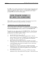
2.8
KEYPAD SYNTAX
The following sections describe the various menus and submenus of the ADDvantage-32 PLUS
keypad and LCD display.
2.8.1
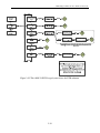
TOP LEVEL MENU
The TOP LEVEL menu is the initial menu that is visible when the drive has power applied. This
menu can be accessed from anywhere in the menu system by pressing the LEFT key up to a
maximum of seven times to ultimately reach the TOP LEVEL menu.
2-17
ADDvantage-32 PLUS ● AC to DC Power Converter
OPERATE
‐‐‐‐‐‐‐>
Left/Right
DRIVE OPERATING DATA SUBMENU
ALL Axxx parameters, ALL Dxxx parameters
Left/Right
USB FUNCTIONS SUBMENU
ALL USB load and store functions
Up/Down
USB
‐‐‐‐‐‐‐>
Up/Down
Edit Units
‐‐‐‐‐‐‐>
Spare Cal
‐‐‐‐‐‐‐>
Up/Down
Up/Down
Fault Fifo
‐‐‐‐‐‐‐>
Up/Down
Calibration 2
‐‐‐‐‐‐‐>
Up/Down
Up/Down
Tables
‐‐‐‐‐‐‐>
Calibration 1
‐‐‐‐‐‐‐>
Up/Down
Up/Down
Spare Bit Cfg
‐‐‐‐‐‐‐>
Up/Down
Drive Configure
‐‐‐‐‐‐‐>
Up/Down
Bit Config
‐‐‐‐‐‐‐>
Up/Down
Drive Calibrate
‐‐‐‐‐‐‐>
Up/Down
Up/Down
Spare Analog Cfg
‐‐‐‐‐‐‐>
Analyzer Menu
‐‐‐‐‐‐‐>
Up/Down
Up/Down
Analog Config
‐‐‐‐‐‐‐>
Diagnostics
‐‐‐‐‐‐‐>
Up/Down
Up/Down
EGD Config
‐‐‐‐‐‐‐>
Access Code
‐‐‐‐‐‐‐>
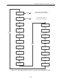
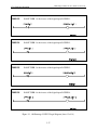
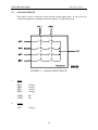
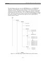
Figure 2-12. This ADD-32 PLUS keypad syntax shows the TOP LEVEL menu.
2-18
ADDvantage-32 PLUS ● AC to DC Power Converter
2.8.2
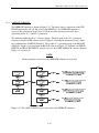
OPERATE SUBMENU
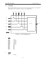
The OPERATE submenu is shown in Figure 2-13. The figure shows a subsection of the TOP
LEVEL menu on the left side. By pressing the RIGHT key, the OPERATE submenu is
accessed. This submenu provides access to all the real time operating data of the drive,
specifically all the A*** and D*** parameters.
The submenu subdivides the A** into two groups. The first group is the A*** parameters
associated with the CORE software (refer to Figure 2-5 showing the parameter layout), which
has a submenu title of DRIVE ANALOG. The second A*** parameter group is the BLOCKS
ANALOG, which is associated with the BLOCK software in Figure 2-5. Similarly, the DRIVE
DIGITAL and BLOCKS DIGITAL provide access to the CORE and BLOCK software shown in
Figure 2-5, respectively.
NOTE
All the parameters accessed via the OPERATE submenu are read-only.
Figure 2-13. This ADD-32 PLUS keypad syntax shows the OPERATE submenu.
2-19
ADDvantage-32 PLUS ● AC to DC Power Converter
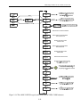
2.8.2
ACCESS CODE SUBMENU
The ACCESS CODE submenu is shown in Figure 2-14. The figure shows a subsection of the
TOP LEVEL menu on the left side. By pressing the RIGHT key, the user enters the ACCESS
CODE submenu. The ACCESS CODE submenu provides access to various special functions
and features of the drive, including security, tuning and drive reset functions.
Entry into the ACCESS CODE submenu may be protected with an optional access code. If the
access code feature is enabled, then a user must enter the correct access number before being
allowed into the submenu.
2-20
ADDvantage-32 PLUS ● AC to DC Power Converter
Figure 2-14. This ADD-32 PLUS keypad syntax shows the ACCESS CODE submenu.
2-21
ADDvantage-32 PLUS ● AC to DC Power Converter
2.8.2
DIAGNOSTICS SUBMENU
The DIAGNOSTICS submenu is shown in Figure 2-15. The figure shows a subsection of the
TOP LEVEL menu on the left side, and access into the DIAGNOSTICS submenu by pressing
the RIGHT key.
The DIAGNOSTICS submenu provides the user with information related to all the firmware
installed on the drive (part numbers and versions of all components), diagnostic information
related to the Ethernet LAN and diagnostic information intended for factory use.
2-22
ADDvantage-32 PLUS ● AC to DC Power Converter
Figure 2-15. This ADD-32 PLUS keypad syntax shows the DIAGNOSTICS submenu.
2-23
ADDvantage-32 PLUS ● AC to DC Power Converter
2.8.3
ANALYZER SUBMENUS
The ANALYZER submenus are shown in Figures 2-16 and 2-17. Figure 2-16 shows a
subsection of the TOP LEVEL menu on the left side and the first level of the ANALYZER
submenu, which is accessed by pressing the RIGHT key.
The ANALYZER submenu accesses all configuration and calibration data associated with the
eight channel signal analyzer. Refer to Section 5 for more information on the signal analyzer.
In addition to accessing the configuration and calibration data for each signal analyzer channel,
this submenu also offers the ability to view the status of each channel. When the data collection
is completed for a channel, this submenu allows the data collected to be viewed. Figure 2-17
shows the status/data display.
2-24
ADDvantage-32 PLUS ● AC to DC Power Converter
Figure 2-16. This ADD-32 PLUS keypad syntax shows the ANALYZER submenu that is
associated with the eight channel signal analyzer.
2-25
ADDvantage-32 PLUS ● AC to DC Power Converter
Figure 2-17. This ADD-32 PLUS keypad syntax shows the ANALYZER submenu that presents
status/data displays. It provides information associated with the eight channel signal analyzer.
2.8.4
DRIVE AND CONTROL BLOCK PARAMETERS SUBMENUS
The ADDvantage-32 PLUS provides access to the calibration and configuration parameters
directly from the TOP LEVEL menu as shown in Figure 2-18.
Figure 2-18 shows a subsection of the TOP LEVEL menu on the left and a description of the
calibration or configuration parameters that may be accessed via the various menu options.
2-26
ADDvantage-32 PLUS ● AC to DC Power Converter
Tables
‐‐‐‐‐‐‐>
Up/Down
Spare Bit Cfg
‐‐‐‐‐‐‐>
Left/Right
View and Edit a subset of Drive Application Configuration parameters: Pnnn through
Pmmm. These Application Configuration parameters are associated with digital input
selections to the SPARE BLOCKS contained in the application. Refer to Appendix C for a
listing of all Drive Application Configuration parameters
Left/Right
View and Edit a subset of Drive Application Configuration parameters: Pnnn through
Pmmm. These Application Configuration parameters are associated with digital input
selections to the control blocks contained in the application. Refer to Appendix C for a
listing of all Drive Application Configuration parameters
Left/Right
View and Edit a subset of Drive Application Configuration parameters: Pnnn through
Pmmm. These Application Configuration parameters are associated with the analog
input selections to the SPARE BLOCKS contained in the application. Refer to Appendix C
for a listing of all Drive Application Configuration parameters
Left/Right
View and Edit a subset of Drive Application Configuration parameters: Pnnn through
Pmmm. These Application Configuration parameters are associated with the analog
input selections to the control blocks contained in the application. Refer to Appendix C
for a listing of all Drive Application Configuration parameters
Up/Down
Bit Config
‐‐‐‐‐‐‐>
Up/Down
Spare Analog Cfg
‐‐‐‐‐‐‐>
Up/Down
Analog Config
‐‐‐‐‐‐‐>
Up/Down
EGD Config
‐‐‐‐‐‐‐>
Left/Right
View and Edit a subset of Drive Application Configuration parameters: Pnnn through
Pmmm. These Application Configuration parameters define the drive ANALOG data that
is made available for the ETHERNET EGD protocol. Refer to Appendix C for a listing of all
Drive Application Configuration parameters
Up/Down
Spare Cal
‐‐‐‐‐‐‐>
Left/Right
View and Edit a subset of Drive Application Calibration parameters: Cnnn through
Cmmm. These Application Calibration parameters are associated with the SPARE
BLOCKS contained in the application. Refer to Appendix C for a listing of all Drive
Application Calibration parameters
Left/Right
View and Edit a subset of Drive Application Calibration parameters: Cyyy through Czzz.
Refer to Appendix C for a listing of all Drive Application Calibration parameters
Left/Right
View and Edit a subset of Drive Application Calibration parameters: C000 through Cxxx.
Refer to Appendix C for a listing of all Drive Application Calibration parameters
Left/Right
View and Edit ALL Drive Core Configuration parameters: Y000 through Yxxx. Refer to
Appendix C for a listing of all Drive Core Configuration parameters
Up/Down
Calibration 2
‐‐‐‐‐‐‐>
Up/Down
Calibration 1
‐‐‐‐‐‐‐>
Up/Down
Drive Configure
‐‐‐‐‐‐‐>
Up/Down
Drive Calibrate
‐‐‐‐‐‐‐>
Left/Right
Up/Down
Analyzer Menu
‐‐‐‐‐‐‐>
Fig
ure 2-18. This ADD-32 PLUS keypad syntax shows the DRIVE CONFIGURE and DRIVE
CALIBRATE portion of the TOP LEVEL menu.
2-27
ADDvantage-32 PLUS ● AC to DC Power Converter
2.8.5
TABLES SUBMENU
The TABLES submenu is shown in Figure 2-19. The figure shows a subsection of the TOP
LEVEL menu on the left side and by pressing the RIGHT key, the TABLES submenu is
accessed.
Up
Fault Fifo
‐‐‐‐‐‐‐>
Table 1
‐‐‐‐‐‐‐>
Up/Down
Up/Down
Tables
‐‐‐‐‐‐‐>
Up/Down
Table 0
‐‐‐‐‐‐‐>
Left/Right
Left/Right
View and Edit TABLE 1 Calibration data: T032 to T063
Left/Right
View and Edit TABLE 0 Calibration data: T000 to T031
Up/Down
Spare Bit Cfg
‐‐‐‐‐‐‐>
Table 8
‐‐‐‐‐‐‐>
Left/Right
View and Edit TABLE 8 Calibration data: T256 to T287
Left/Right
View and Edit TABLE 7 Calibration data: T224 to T255
Left/Right
View and Edit TABLE 6 Calibration data: T192 to T223
Left/Right
View and Edit TABLE 5 Calibration data: T160 to T191
Left/Right
View and Edit TABLE 4 Calibration data: T128 to T159
Left/Right
View and Edit TABLE 3 Calibration data: T096 to T127
Left/Right
View and Edit TABLE 2 Calibration data: T064 to T095
Up/Down
Table 7
‐‐‐‐‐‐‐>
Up/Down
Table 6
‐‐‐‐‐‐‐>
Up/Down
Table 5
‐‐‐‐‐‐‐>
Up/Down
Table 4
‐‐‐‐‐‐‐>
Up/Down
Table 3
‐‐‐‐‐‐‐>
Up/Down
Table 2
‐‐‐‐‐‐‐>
DOWN
Figure 2-19. This ADD-32 PLUS keypad syntax shows the EDIT UNITS submenu
The TABLES submenu provides access to nine (9) general purpose tables that may be used for
various purposes by the drive software.
2-28
ADDvantage-32 PLUS ● AC to DC Power Converter
Each of the tables consists of sixteen (16) data points, and each of the sixteen (16) data points
consist of an “X” data point and a “Y” data point. Figure 2-20 shows a graphical representation
of the sixteen data points in a table, with the “X” data point representing the x-axis value, and
the “Y” data points representing the y-axis value.
X7,Y7
X9,Y9
X8,Y8
X6,Y6
X14,Y14
X15,Y15
X4,Y4
X axis
X11,Y11
X5,Y5
X3,Y3
X10,Y10
X2,Y2
X13,Y13
X12,Y12
X1,Y1
X0,Y0
Y axis
Figure 2-20. Example of a TABLE showing the sixteen (16) data points
See section 4.68 TABLE in this manual for the description of the TABLE CONTROL BLOCK
for further information on the tables.
2.8.6
FAULT FIFO SUBMENU
The FAULT FIFO submenu is shown in Figure 2-21. The figure shows a subsection of the TOP
LEVEL menu on the left side, and by pressing the RIGHT key, the FAULT FIFO submenu is
reached.
The FAULT FIFO submenu provides the ability to clear the drive fault status and take the drive
from a faulted to an unfaulted state. Note that if the underlying cause of the drive being in a
faulted state has not been resolved, the drive will clear, and then immediately reenter, the fault
state.
The FAULT FIFO submenu also provides the ability to clear all 16 entries in the FAULT FIFO.
After the FAULT FIFO is cleared, the FAULT FIFO will be empty.
Additionally, the submenu allows the user to view the contents of the FAULT FIFO. When the
2-29
ADDvantage-32 PLUS ● AC to DC Power Converter
RIGHT key is pressed from the VIEW FAULT FIFO option, the display will initially show
FAULT EVENT #1. The first event is the fault that has most recently occurred. The second
event (FAULT EVENT #2) is the next most recent fault to have occurred. Use of the UP and
DOWN keys will allow the user to examine all of the events logged in the FAULT FIFO.
While viewing the fault events, pressing the RIGHT key will provide the user with a time stamp
of when the fault occurred. The time stamp is the amount of time that has elapsed since power
was last applied to the drive, and is in a days:hours:minutes:seconds format. Pressing the UP or
DOWN key will allow scrolling through the time stamps for the 16 events in the FAULT FIFO.
Pressing the LEFT key will return to the display of the actual fault event.
Up
Edit Units
‐‐‐‐‐‐‐>
CLEAR FIFO
‐‐‐‐‐‐‐>
Up/Down
Up/Down
Fault Fifo
‐‐‐‐‐‐‐>
Up/Down
Tables
‐‐‐‐‐‐‐>
Left/Right
View Fault Fifo
‐‐‐‐‐‐‐>
LEFT
Clear
Fault
Fifo
From the “ CLEAR FIFO” pressing the left key
will cause all entries in the fault fifo to be
erased, emptying the fault fifo of all past faults.
Fault Event: xx
<< event label>>
Left/Right
Left/Right
Fault Event: xx
ddd:hh:mm:ss
Up/Down
CLEAR Faults
‐‐‐‐‐‐‐>
LEFT
Clear
FAULT
From the “ CLEAR Faults” pressing the left key
will generate a fault reset to the drive.
DOWN
Figure 2-21. This ADD-32 PLUS keypad syntax shows the FAULT FIFO submenu.
2-30
ADDvantage-32 PLUS ● AC to DC Power Converter
2.8.7
EDIT UNITS SUBMENU
The EDIT UNITS submenu is shown in Figure 2-22. The figure shows a subsection of the TOP
LEVEL menu on the left side and by pressing the RIGHT key, the EDIT UNITS submenu is
accessed.
Figure 2-22. This ADD-32 PLUS keypad syntax shows the EDIT UNITS submenu.
The ADDvantage-32 PLUS allows the user to specify the units of measure associated with the
real time analog data (A***) and the block calibration data (C***). Both the A*** and the C***
are presented in engineering units, and both specify the units of measure on the LCD display.
The user is able to define the units of measure and change the value displayed. Figure 2-23
shows the units field for a block calibration parameter.
2-31
ADDvantage-32 PLUS ● AC to DC Power Converter
Figure 2-23. The LCD display shows the units field in a calibration parameter.
2-32
ADDvantage-32 PLUS ● AC to DC Power Converter
When viewing a parameter from the EDIT UNITS submenu, the user can press the RIGHT key
to initiate the editing of the units field. The cursor will appear under the leftmost character of
the units field. Note that the character could be a blank space. Figure 2-24 shows the LCD
display after the RIGHT key has been pressed to begin an edit.
Figure 2-24. The LCD display of a calibration parameter shows the units field in edit mode.
The UP and DOWN keys will scroll through the full set of numbers and letters. The RIGHT key
will move the cursor to the next units field character to the right. The LEFT key will abort the
edit and the ENTER key will accept the change made to the units field and save the field in nonvolatile memory.
2.8.8
USB SUBMENU
The USB submenu is shown in Figure 2-25. The figure shows a subsection of the TOP LEVEL
menu on the left side and by pressing the RIGHT key, the user enters the USB submenu.
The USB submenu provides access to the USB functionality implemented on the ADDvantage32 PLUS. The USB functionality includes the ability to load and save all calibration and
configuration data to a USB memory stick, update drive firmware from files contained on the
USB memory stick, save signal analyzer data to the USB memory stick and save drive diagnostic
information to the USB memory stick.
Refer to Section 11 for a full description of the USB functions implemented on the drive.
2-33
ADDvantage-32 PLUS ● AC to DC Power Converter
Figure 2-25. This ADD-32 PLUS keypad syntax shows the USB submenu.
2-34
ADDvantage-32 PLUS ● AC to DC Power Converter
Core Software Operation
SECTION III
CORE SOFTWARE OPERATION
The core software performs the following fundamental functions of the ADDvantage-32 PLUS
hardware and software:
1.
2.
3.
4.
5.
6.
Hardware Setup and Diagnostics
I/O Configuration and Calibration
Input and Output Scanning
Individual Control Block Operation
Current Loop Operation
Eight Channel Signal Analyzer Operation
This section describes the capabilities and functions of the core software and the X***, Y***
parameters, as well as the corresponding A*** and D*** data table parameters. (The data table
parameters are shown for reference purposes only and are not explained in detail unless
required.) See Section V for the signal analyzer explanations.
NOTE
Because parameter numbers vary according to software part
number, specific parameter numbers are not shown. To locate a
specific parameter number, refer to Appendix D.
3.1
DEDICATED INPUTS
Dedicated inputs are inputs located on the bridge interface board which perform a
specific task. Each dedicated input is hard wired and operates independently of the
application software, allowing failsafe operation even if a software problem occurs.
3.1.1
Emergency Stop (ESTOP)
When the ESTOP input is removed, the main contactor opens immediately and the gate
firing is suppressed. The green EMERG STOP LED on the front of the ADDvantage-32
PLUS will also go out to indicate loss of the ESTOP.
3-1
ADDvantage-32 PLUS ● AC to DC Power Converter
Core Software Operation
After an ESTOP condition has occurred, the ESTOP and ESTOP RESET inputs must be
applied to reset the ESTOP circuit. The EMERG STOP LED will illuminate when the
ESTOP circuit is restored.
3.1.2
Emergency Stop Reset (ESTOP RESET)
A normally open pushbutton should be used for the ESTOP RESET. If the ESTOP input
is present, then pressing the pushbutton resets the circuit. A reset must also be performed
if a drive fault has occurred.
3.2
DEDICATED OUTPUTS
The following dedicated outputs are Form C contact outputs used for ADDvantage-32
PLUS status indication. Each output is hard wired and is not user programmable.
3.2.1
Drive O.K.
This Form C contact output signifies that there are no fault conditions in the
ADDvantage-32 PLUS. If a critical fault occurs, this output contact opens and remains
open until the fault is cleared.
3.2.2
Motor Auxiliary Contactor
This Form C contact output opens if the main contactor is open, or closes if the main
contactor is closed.
3.3
CONFIGURABLE DIGITAL INPUTS
D*** Parameters
D***:USER 1
thru
D***:USER 14
The 24 VDC digital inputs are represented by a value in the digital data table. Each input
is scanned by the core software to determine if it is in an ON or OFF state. Once this
state is determined, the corresponding D***:USER X parameter is set in the digital data
table. This bit can then be used by other areas of the application software to enable
specific functions.
Six digital inputs are located on microprocessor board and are represented by parameters
D:***USER 1 thru D***USER 6. Eight more inputs are available by adding the FAX-32
board. These inputs are represented by D***:USER 7 thru D***:USER 14 in the digital
3-2
ADDvantage-32 PLUS ● AC to DC Power Converter
Core Software Operation
data table. If the FAX-32 board is not used, the values for the additional eight parameters
are always indeterminate.
3.4
CONFIGURABLE DIGITAL OUTPUTS
Y*** Parameters
Y***:USER LED PT
Y***:DIG OUT 1
Y***:DIG OUT 2
Y***:DIG OUT 3
Y***:DIG OUT 4
The digital outputs are Form C contact outputs located on the microprocessor board.
Each output is configurable to a value in the digital data table. The state of the
NORMALLY OPEN contact of a digital output will always match the state of the bit in
the digital table to which it is configured. If the bit in the digital table is ONE/TRUE
then the NORMALLY OPEN contact will be closed. Otherwise if the bit in the digital
table is ZERO/FALSE then the NORMALLY OPEN contact will be open. Outputs are
always functional and can be disabled by configuring them to either D***:ZERO BIT or
D***:ONE BIT, which holds the output in a constant state.
For example, if a particular application requires that a contact output be closed when a
fault occurs, perform the following:
1.
Locate the value in the digital data table which signifies an ADDvantage-32
PLUS fault. (D***:FAULT)
2.
Configure Y***:DIG OUT 1 to D***:FAULT. Any time a fault occurs, the first
digital NORMALLY OPEN output closes.
The user LED is similar in that it is configured to a digital data bit. When the bit is
ONE/TRUE, the LED will light. The user LED is the first yellow LED on the drive.
3-3
ADDvantage-32 PLUS ● AC to DC Power Converter
Core Software Operation
3.5
LOGIC SEQUENCE
Y*** Parameters
D*** Parameters
Y***:RUN INPUT
Y***:JOG INPUT
Y***:THRD INPUT
Y***:CLR FLT INP
Y***:ILIM HI INP
Y***:ILIM LO INP
Y***:MC CLOSE
Y***:MC CLS ENA
Y***:FLD CNTL
Y***:FLD V-CMD
Y***USR LED PT
Y***:F-FIFO CLR
Y***:F-CLR ON M
D***:IOC PT
D***:ESTOP IN
D***:FWD BR ACT
D***:REV BR ACT
D***:FLD LOSS PT
D***:SPD MIN PT
D***:FLD ECON PT
D***:M TIMER PT
D***:PLL LOCK PT
D***:ARM ENABLE
D***:FLD ENABLE
D***:DOK OUT
D***:M CONTACTOR
D***:USER LED
D***:I-LIM LED
D***:FWD BR LED
D***:REV BR LED
D***:DFAULT LED
D***:F-LOSS LED
D***:IOC LED
D***:RUN LED
D***:RUN ENABLE
D***:JOG ENABLE
D***:THRD ENABLE
D***:FAULT
D***:RUNX
D***:RUN REQUEST
D***:MAX IARM
D***:MIN IARM
D***:CNTL INHIB
D***:USER 1
D***:USER 2
D***:USER 3
D***:USER 4
D***:USER 5
D***:USER 6
D***:NOT USER 1
D***:NOT USER 2
D***:NOT USER 3
D***:NOT USER 4
D***:NOT USER 5
3-4
ADDvantage-32 PLUS ● AC to DC Power Converter
Core Software Operation
D***:NOT USER 6
Y*** Parameters
D*** Parameters
D***:IARM MIN PT
D***:IA MIN DELY
D***:SCR ENABLE
D***:IA SEAL
D***:REV_LOCKOUT
D***:ONE BIT
D***:ZERO BIT
3.6
DRIVE SEQUENCE RUNG DESCRIPTIONS
Figure 3-1 (on the following 15 pages) is a ladder logic diagram of the internal interlocks
for the core software. These rungs determine when specific features are enabled and
disabled. D*** parameters listed are values found in the digital data table. See Section II
and Appendix C for parameter explanations. Figure 3-1 applies only to AC to DC
Converter software part number 696xxx.
RUNG 1
Any fault that shuts down the drive picks up this fault bit. The bit seals itself in
until CLEAR FAULT goes high. There are eight user definable faults
available: Y:USR FAULT 1 through Y:USR FAULT 8
Figure 3-1. ADDvantage-32 PLUS Logic Diagram (sheet 1 of 14)
3-5
ADDvantage-32 PLUS ● AC to DC Power Converter
Core Software Operation
RUNG 2
RUNG 3
RUNG 4
The drive OK output drops out when the D:FAULT bit goes high.
Ready for a run, jog or thread.
This bit picks up the drive motor contactor and enables the run reference to the
speed loop.
Figure 3-1. ADDvantage-32 PLUS Logic Diagram (sheet 2 of 14)
3-6
ADDvantage-32 PLUS ● AC to DC Power Converter
Core Software Operation
RUNG 5
This bit picks up the drive motor contactor and enables the jog reference to the
speed loop.
RUNG 6
This bit picks up the drive motor contactor and enables the thread reference to the
speed loop.
Figure 3-1. ADDvantage-32 PLUS Logic Diagram (sheet 3 of 14)
3-7
ADDvantage-32 PLUS ● AC to DC Power Converter
Core Software Operation
RUNG 8
D:RUNX picked up on a run, jog, or thread command is requested. It stays in
until the D:SPD MIN PT goes high or there is a fault or ESTOP. If you want the
contactor to open immediately after run removal, configure D:SPD MIN PT to
D:ONE BIT or else set it equal to D:AT ZERO SPD.
RUNG 9
Delay to hold in the motor contactor and SCR enable while armature current
magnitude is greater than a small minimum value. It allows a delay of up to half a
second.
RUNG 10
This sets the seal-in bit to keep the motor contactor in and the SCR's enabled
while the magnitude of armature current is greater than a small minimum value
or a half second after the contactor is commanded open.
Figure 3-1. ADDvantage-32 PLUS Logic Diagram (sheet 4 of 14)
3-8
ADDvantage-32 PLUS ● AC to DC Power Converter
Core Software Operation
RUNG 11
This is a time delay of 60 seconds after the motor contactor is commanded open.
(Used for the field economy bit.)
RUNG 12
Commands the motor contactor to close and enables the gate power to the SCR's.
This can be done automatically when RUNX is applied or by an external motor
contactor close command configured to Y:MC CLOSE. The output is held in
until armature current reaches near zero or after a half second after commanded
open. This is to prevent inverting faults.
Figure 3-1. ADDvantage-32 PLUS Logic Diagram (sheet 5 of 14)
3-9
ADDvantage-32 PLUS ● AC to DC Power Converter
Core Software Operation
RUNG 13
This delays D:ARM ENABLE until the motor contactor has a chance to pick up.
The delay is based on drive size from 150 ms on a 10 amp drive to 500 ms on a
510 and 550 amp drive and 750 ms on AFM’s. The parameter X***:MC DLY
ADJT can adjust the delay, more or less by entering a positive or negative number
respectively. X*** can be entered in “ticks,” based on line frequency (2.777 ms
on 60 Hz). Software will not allow delays less than 27 ms.
WARNING: Incorrect setting of the parameter can result in bridge self test failures or IOC’s on
application of runs to the drive. Also, the value SHOULD NOT be changed if there is any
intention of applying the ADD-32 PLUS to an already spinning motor.
RUNG 14
This delay is to sense if there is actual CEMF on the motor when the contactor is
closed. The delay is added to allow an accurate reading of motor CEMF in the
event of a drive starting into a spinning motor.
RUNG 15
D:ARM ENABLE allows the SCR's to fire and is used in the application portion
of the software to release integrators and ramps.
3-10
ADDvantage-32 PLUS ● AC to DC Power Converter
Core Software Operation
Figure 3-1. ADDvantage-32 PLUS Logic Diagram (sheet 6 of 14)
RUNG 16
RUNG 17
RUNG 18
Delay to check if the gate power has been removed two seconds after the
contactor is commanded open.
Gate error fault if the state of the sense signal is wrong for ten SCR firings. If
the contactor is opened for two seconds, the gate power should be off. If
D:ARM ENABLE is high, the gate power should be present already.
D:CNTL INHIB is the opposite of D:ARM ENABLE. It is used in the
application software to preset integrators and hold ramps.
Figure 3-1. ADDvantage-32 PLUS Logic Diagram (sheet 7 of 14)
3-11
ADDvantage-32 PLUS ● AC to DC Power Converter
Core Software Operation
RUNG 19
RUNG 20
The motor field can be enabled, disabled, or switched on or off by a digital bit. If
the field is commanded, then it stays picked up until D:ARM ENABLE drops out.
Field loss is enabled whenever D:FLD ENABLE is high or if Y:FIELD CNTL is
set to digital bit.
Field loss protection is enabled in the following two sequences:
If Y:FIELD CNTL is set to Q:ENABLED and the field voltage reference
Y:FLD V_CMD is configured to the output of the field current loop A:VFLD
CMD.
If Y:FIELD CNTL is set to a digital bit, then field loss is enabled at any time the
armature SCR's are enabled.
Figure 3-1. ADDvantage-32 PLUS Logic Diagram (sheet 8 of 14)
3-12
ADDvantage-32 PLUS ● AC to DC Power Converter
Core Software Operation
RUNG 21
Lights the amber forward bridge LED.
RUNG 22
Lights the amber reverse bridge LED.
RUNG 23
Lights the green running LED.
RUNG 24
Lights the amber user defined LED.
Figure 3-1. ADDvantage-32 PLUS Logic Diagram (sheet 9 of 14)
3-13
ADDvantage-32 PLUS ● AC to DC Power Converter
Core Software Operation
RUNG 25
RUNG 26
RUNG 27
Lights the red field loss LED and seals it in until the faults are cleared.
Lights the red instantaneous overcurrent LED and seals it in until the faults are
cleared.
Lights the red drive fault LED.
Figure 3-1. ADDvantage-32 PLUS Logic Diagram (sheet 10 of 14)
3-14
ADDvantage-32 PLUS ● AC to DC Power Converter
Core Software Operation
RUNG 28
Lights the green Drive OK LED.
RUNG 29
Lights the green ESTOP OK LED.
RUNG 30
Lights the amber current limit LED. To properly light the LED, the Y parameters
must be set to the in-limit conditions of the speed loop PI regulator.
Figure 3-1. ADDvantage-32 PLUS Logic Diagram (sheet 11 of 14)
3-15
ADDvantage-32 PLUS ● AC to DC Power Converter
Core Software Operation
RUNG 31
RUNG 32
The fault FIFO can be cleared from the keyboard or from a digital bit
configured to Y:F-FIFO CLR.
A drive fault can be cleared by the keyboard, digital bit configured to Y:CLR FLT
INP or on the next run, jog, or thread command if Y:F-CLR ON M is enabled.
Faults will also be cleared on a repower of the drive.
Figure 3-1. ADDvantage-32 PLUS Logic Diagram (sheet 12 of 14)
3-16
ADDvantage-32 PLUS ● AC to DC Power Converter
Core Software Operation
RUNG 33
D:NOT USER 1 is the inverse of the digital input D:USER 1.
RUNG 34
D:NOT USER 2 is the inverse of the digital input D:USER 2.
RUNG 35
D:NOT USER 3 is the inverse of the digital input D:USER 3.
RUNG 36
D:NOT USER 4 is the inverse of the digital input D:USER 4.
Figure 3-1. ADDvantage-32 PLUS Logic Diagram (sheet 13 of 14)
3-17
ADDvantage-32 PLUS ● AC to DC Power Converter
Core Software Operation
RUNG 37
RUNG 38
D:NOT USER 5 is the inverse of the digital input D:USER 5.
D:NOT USER 6 is the inverse of the digital input D:USER 6.
RUNG 39
D:ONE BIT is always high. Applications blocks can use this to always enable a
function.
RUNG 40
D:ZERO BIT is always low. Application blocks can use this to always disable a
function.
Figure 3-1. ADDvantage-32 PLUS Logic Diagram (sheet 14 of 14)
3-18
ADDvantage-32 PLUS ● AC to DC Power Converter
Core Software Operation
3.7
RUN, THREAD, AND JOG INPUTS
Y*** Parameters
Y***:RUN INPUT
Y***:JOG INPUT
Y***:THRD INPUT
These three parameters enable the control loops of the ADDvantage-32 PLUS. Each
parameter can be configured to a value in the digital data table which enables its
particular function. These three parameters are interlocked. Therefore, only one can be
enabled at a time. Consult the Logic Sequence description provided in this section for
specific interlock information.
Example: Assume the following inputs are being used to run, jog, or thread the section:
Digital Input 1 = Run Section
Digital Input 2 = Jog Section
Digital Input 3 = Thread Section
1.
The values for the three digital inputs in the Digital Data Table are: D***:USER
1 for digital input 1, D***:USER 2 for digital input 2, and D***:USER 3 for
digital input 3.
2.
Configure the parameters as follows:
Y***:RUN INPUT = D***:USER 1
Y***:JOG INPUT = D***:USER 2
Y***:THRD INPUT = D***:USER 3
3.8
ANALOG INPUTS
X*** Parameters
A*** Parameters
X***:INPT #1 CAL
X***:INPT 1 ZERO
X***:INPT #1 TC
X***:INPT #2 CAL
X***:INPT #2 ZERO
X***:INPT #2 TC
X***:INPT #3 CAL
X***:INPT #3 ZERO
X***:INPUT #3 TC
X***:INPUT #4 CAL
X***:INPUT #4 ZERO
A***:ANALOG IN 1
A***:ANALOG IN 2
A***:ANALOG IN 3
A***:ANALOG IN 4
A***:ANALOG IN 5
A***:ANALOG IN 6
3-19
ADDvantage-32 PLUS ● AC to DC Power Converter
Core Software Operation
X*** Parameters
A*** Parameters
X***:INPUT #4 TC
X***:INPUT #5 CAL
X***:INPUT #5 ZERO
X***:INPUT #5 TC
X***:INPT #6 CAL
X***:INPT #6 ZERO
X***:INPT #6 TC
There are six -10 to +10 VDC analog inputs located on the ADDvantage-32 PLUS
microprocessor board. Each input is scanned, calibrated, and written into the analog data
table to be used by the application software every SCR firing. The value of the input is
determined by the following equation:
A***:ANALOG IN 1 =
Input Volts (X***:INPT #1 CAL) + X***:INPT 1 ZERO
For example, to scale analog input #1 so that a -10 VDC to 10 VDC signal reads 0 to
2500 FPM in the analog data table, perform the following:
1.
Find A***:ANALOG IN 1 in the analog data table.
2.
Use this information in the following equations:
0 FPM = -10VDC (X***:INP #1 CAL) +X***:INPT 1 ZERO
2500 FPM = 10VDC (X***:INP #1 CAL) +X***:INPT 1 ZERO
Solving the above equations yields the following results:
X***:INPT #1 CAL = 125 FPM/VDC
X***:INPT 1 ZERO = 1250 FPM
NOTE
The zero value is limited to 150 times the CAL value. Erroneous
results will occur if this is exceeded.
3-20
ADDvantage-32 PLUS ● AC to DC Power Converter
Core Software Operation
3.9
ANALOG OUTPUT FUNCTIONS
X*** Parameters
Y*** Parameters
X***:OUTPT 1 CAL
X***:OUTPT 1 ZER
X***:OUTPT 2 CAL
X***:OUTPT 2 ZER
X***:OUTPT 3 CAL
X***:OUTPT 3 ZER
X***:OUTPT 4 CAL
X***:OUTPT 4 ZER
Y***:ANLG OUT 1
Y***:ANLG OUT 2
Y***:ANLG OUT 3
Y***:ANLG OUT 4
Analog outputs read information from the analog data table, scale it, and produce a
-10 VDC to +10 VDC output signal. Each analog output is configurable to any data table
value. The output is then scaled by the following function:
Output VDC = (Data Table Value + X***:OUTPUT 1 ZERO) X***:OUTPT 1 CAL
For example, to generate a -10 VDC to +10 VDC signal from the second analog output of
the ADDvantage-32 PLUS microprocessor board which represents actual speed
(0 - 2500 FPM), perform the following:
1.
Find A***:ACT SPEED in the analog data table.
2.
Configure Y***:ANLG OUT 2 to A***:ACT SPEED. This will send the output
to the second analog output.
3.
Find the calibration values as follows:
-10VDC=( 0 FPM+X***:OUTPUT 1 ZERO)(X***:OUTPT 1 CAL)
+10VDC=(2500 FPM+X***:OUTPUT 1 ZERO)(X***:OUTPT 1 CAL)
Solving the above equations yields the following:
X***:OUTPT 1 CAL = .008 VDC/FPM
X***:OUTPT 1 ZERO = -1250 FPM
3-21
ADDvantage-32 PLUS ● AC to DC Power Converter
Core Software Operation
3.10
FREQUENCY INPUTS
X*** Parameters
Y*** Parameters
A*** Parameters
X***:TACH 1 GRat
X***:TACH 1 RDia
X***:TACH 1 EPR
X***:TACH 1 ZERO
X***:TACH 2 GRat
X***:TACH 2 RDia
X***:TACH 2 EPR
X***:TACH 2 ZERO
Y***:TACH 1 TYPE
Y***:TACH 2 TYPE
A***:SPEED IN 1
A***:SPEED IN 2
Frequency inputs convert an incoming pulse train into an analog value by counting the
number of pulse edges and calibrating it into a user value. Counting the number of edges
allows for a more accurate representation of the incoming pulse train. The analog value
is then stored in the analog data table.
There are two methods used for counting the pulse train edges: the averaging method and
the direct count method. Configuring Y***:TACH 1 TYPE or Y***:TACH 2 TYPE
determines which method is used. Both methods measure one or two phase inputs and
one or two pulse edges.
3.10.1
AVERAGING METHOD (TWO PHASE, 1 PHASE 2X, 1 PHASE 1X)
When one of these options is selected for the TACH TYPE, the pulse train edges are
counted and averaged over an internal sample period. This averaging method allows for
smoother control but can lead to inaccuracies if the duty cycle of the pulse is not 50/50.
Selection of the 1 PHASE 1X (one edge) option eliminates these inaccuracies but
decreases the resolution. This method should be used when the frequency input is used
for speed feedback and the frequency being applied is fairly low. It should also be used
for feedback applications that have significant cyclical resonance on the feedback.
3.10.2
DIRECT COUNT METHOD (TWO PHASE-S, 1 PHASE-2XS, 1 PHASE-1XS)
If one of these options for TACH TYPE is selected, the exact number of edges that occur
in the same internal sample period are counted. This method leads to a more accurate
count of the pulse train input but is not quite as smooth as the above method. This
method should be used for all applications other than those stated for the averaging
method.
3-22
ADDvantage-32 PLUS ● AC to DC Power Converter
Core Software Operation
Calibrate the pulse train into a user value by using the following equation:
A***:SPEED IN 1=
[(INPUT FREQ) × (EDGE/PULSE) + (TACH 1 ZERO)] × (60) × (π) × (TACH 1 RDia)
(TACH 1 EPR) × TACH 1 GRat
EDGES/PULSE = 1 is used for one phase, one edge applications
2 is used for one phase, two edge applications
4 is used for two phase, two edge applications
For example, to calibrate the frequency input into feet per minute from the following
machine data:
2-phase, 240 PPR pulse generator mounted on the motor shaft
3.0 gear ratio from motor to roll
Roll diameter of 24 inches
3.11
1.
Select the tach type required by setting Y***:TACH 1 TYPE=Q***:2
PHASE-S or Q***:TWO PHASE.
2.
Set X***:TACH EPR = 960. Pulses per revolution of the pulse generator
times four edges per pulse.
3.
Set X***:TACH GRat = 3.0 per the given machine data.
4.
Set X***:TACH RDia = 2, which is the diameter of the roll in process
units (feet).
COUNTERS
X*** Parameters
Y*** Parameters
Analog Data Table
X***:COUNT 1 CAL
X***:COUNT 2 CAL
Y***:CTR 1 RESET
Y***:CTR 1 HOLD
Y***:CTR 2 RESET
Y***:CTR 2 HOLD
Y***:DIF-CTR RST
Y***:DIF-CTR HLD
A***:FOOTAGE 1
A***:FOOTAGE 2
A***:DIF FOOTAGE
The frequency inputs correspond to an associated counter. The counter increases one unit
for every pulse edge detected. The increment value is determined as follows:
A***:FOOTAGE 1 = (1, 2 or 4 Edges/Pulse) (Pulses) X***:COUNT 1 CAL
Where:
1 - Is used when the frequency input is set up for 1 PHASE,
3-23
ADDvantage-32 PLUS ● AC to DC Power Converter
Core Software Operation
one edge operation.
2 - Is used when the frequency input is set up for 1 PHASE,
two edge operation.
4 - Is used when the frequency input is set up for 2 PHASE,
two edge operation.
Each counter can be reset or held by configuring Y***:CTR 1 RESET and Y***:CTR 1
HOLD to the appropriate bit in the digital data table.
For example, a 2-phase tach is connected to frequency input number 2 and produces
750 pulses for every foot of product. A reset button is wired into the first digital input on
the microprocessor board. The counter is to be held any time the second digital input is
on. To calibrate and configure the counter to count inches of product, perform the
following:
1.
Locate D***:USER 1 and D***:USER 2, the parameters in the digital
data table which represent the two digital inputs being used.
2.
Configure Y***:CTR 2 RESET to D***:USER 1. Configure Y***:CTR
2 HOLD to D***:USER 2.
This will reset the counter when the first digital input turns on and will
hold the counter when the second input is on.
3.
To determine the calibration number for the counter, the length per pulse
must be found. It is given that 750 pulses = 1 foot. Converting this into
inches yields:
750 pulses / ft
12 inch / ft
=
62.5 pulses / inch
or
1 pulse = 1/(62.5 pulses/inch) = .016 inches
The increment value for the counter is .016 inches every pulse. To determine the
calibration parameter, set the equation up for one increment value as follows:
A***:FOOTAGE 2 = .016 inches/pulse = (4)*X***:COUNT 2 CAL/PULSE
X***:COUNT 2 CAL = .004
This value causes the counter to increment 0.016 inches for every pulse detected
at the frequency input.
The differential footage counter keeps track of the difference between the two
frequency inputs.
3-24
ADDvantage-32 PLUS ● AC to DC Power Converter
Core Software Operation
A***:DIF FOOTAGE =
(1, 2, or 4 EDGES/PULSE)(PULSES FREQ IN1)(X***:COUNT 1 CAL)
- (1, 2, or 4 EDGES/PULSE)(PULSES FREQ IN2)(X***:COUNT 2 CAL)
The above equation is modified every one million counts to prevent counter
overflows. This will cause a small floating point error at this event.
When Y***:DIF - CTR RST is high, the differential footage counter is reset.
When Y***:DIF - CTR HLD is high, the differential footage counter is held.
3.12
HARDWARE CONFIGURATION AND DIAGNOSTIC PARAMETERS
X*** Parameters
X***:ANLG FSCALE
Y*** Parameters
A*** Parameters
D*** Parameters
Y***:DRIVE P/N
Y***:BRG SELFTST
Y***:4Q OPERATE
Y***:LINK BAUD
Y***:ANLG DISPLY
A***:LINE VOLTS
A***:LINE FREQ
D***:REV LOCKOUT
D***:LINE IMBAL
D***:ABC ROTATE
D***:PHA LOSS PT
D***:PHB LOSS PT
D***:PHC LOSS PT
D***:LOW FREQ PT
D***:HI FREQ PT
D***:SCR ENABLE
Hardware configuration parameters are used to set up fundamental operations of the
ADDvantage-32 PLUS. Refer to Appendix C for an explanation of these parameter
functions.
3.13
USER FAULT INPUTS
Y*** Parameters
Y***:USR FAULT 1
Y***:USR FAULT 2
Y***:USR FAULT 3
Y***:USR FAULT 4
Y***:USR FAULT 5
Y***:USR FAULT 6
Y***:USR FAULT 7
Y***:USR FAULT 8
User fault inputs allow the user to enable fault conditions beyond those generated
internally by the ADDvantage-32 PLUS. When the fault condition occurs, the
3-25
ADDvantage-32 PLUS ● AC to DC Power Converter
Core Software Operation
ADDvantage-32 PLUS faults out and a message is stored in the FAULT FIFO. The
ADDvantage-32 PLUS must be reset before operating again.
For example, two of the most common user faults are overspeed and tach loss conditions.
To set up the ADDvantage-32 PLUS to fault on these two conditions, perform the
following:
1.
Find D***:OVER SPEED and D***:TACH LOSS, the two parameters in the
digital data table that represent overspeed and tach loss.
2.
Configure D***:OVER SPEED to Y***:USR FAULT 1. Configure
D***:TACH LOSS to Y***:USR FAULT 2.
When either one of these conditions occurs, the ADDvantage-32 PLUS faults out.
3.14
MOTOR PARAMETERS
X*** Parameters
Y*** Parameters
A*** Parameters
X***:MOTOR IARM
X***:MOTOR IFLD
X***:MFLD % SCALE
X***:MFLD ASCALE
X***:FLD RESIST
Y***:FIELD CNTRL
A***:FIL ARM CUR
A***:ARM CURRNT
A***:ARM CURRENT
A***:FLD CURRENT
A***:FLD CURRNT
A***:MOTOR CEMF
Motor parameters are used to determine the amount of armature and field current being
supplied to the motor. The ADDvantage-32 PLUS current is scaled to the motor current
using the following equations:
=
Rated Motor Armature Current
Rated ADDvantage 32 PLUS Current
× 100
X * ** : MOTOR IFLD =
Rated Motor Field Current
Rated ADDvantage 32 PLUS Current
× 100
X * ** : MOTOR IARM
Y***:FIELD CNTRL -
Enables the field bridge. If an external field supply is
used, disable this function.
3-26
ADDvantage-32 PLUS ● AC to DC Power Converter
Core Software Operation
******************************************************
WARNING
DISABLING THE FIELD CONTROL DISABLES THE ADD-32
PLUS FIELD LOSS PROTECTION. THIS MAY CAUSE THE
MOTOR TO OVERSPEED WHEN APPLYING THE ADD-32
PLUS ON A SEPARATELY EXCITED DC MOTOR.
EXTERNAL PROTECTION SHOULD BE PROVIDED TO
PROTECT AGAINST OVERSPEED AND/OR LOSS OF FIELD.
THE PROTECTION SHOULD CAUSE THE ADD-32 PLUS TO
FAULT WHEN ANY SUCH EXTERNAL PROTECTION
BECOMES ACTIVE.
******************************************************
For example, an ADDvantage-32 PLUS rated for 56 ADC will be used to operate a motor
with a 40 ADC armature and a 2 ADC field. Set up the parameters for this motor as
follows.
1.
Enable Y***:FIELD CNTRL.
2.
Calculate X***:MOTOR IARM as follows:
X * ** : MOTOR IARM =
40 ADC
× 100%
56 ADC
X***:MOTOR IARM = 71.43%
3.
An ADDvantage-32 PLUS rated at 56 ADC can provide a maximum of 6 ADC to
a motor field. Calculate X***:MOTOR IFLD as follows:
X * ** : MOTOR IFLD =
2 ADC
× 100%
6 ADC
X***:MOTOR IFLD = 33.33%
X***:MFLD %SCALE is a scaling factor for percentage field amps vs. feedback CT
voltage. The UL field supply for the 180 amp drive needs this changed to 1.0416.
(Chassis P/N D22976, included in all new drives). For AFM applications, the drive
expects 2 volts feedback equal to 100% field bridge current. Adjust this parameter to
correct the percentage; e.g., if 1 volt = 100%, enter (2 volts/1 volt) = 2.
3-27
ADDvantage-32 PLUS ● AC to DC Power Converter
Core Software Operation
X***:MFLD ASCALE is a scaling factor for full field amps vs. feedback CT voltage.
The UL field supplies for the 56 amp and 180 amp drive needs this changed to 2 and
2.083 respectively (Chassis P/N D22974 and D22976, included in all new drives). For
540, 850, and 1350 amp drives, a 12 amp field supply is expected. For 1550-3000 amp
drives, a 24 amp field supply is expected.
If a drive is equipped with a different amp field supply, this parameter needs to be
adjusted; e.g., if an 850 amp drive is equipped with a 24 amp field supply, enter
(24 amps/12 amps) = 2. (See Section 1.4 Identification of Part Numbers for full field
rating.)
For AFM applications, the drive expects 2 volts feedback equal to a 12 amp field supply.
Adjust to correct for proper amperage; e.g., if 2 volts = 48 amps, enter (48 amps/12 amps)
= 4.
If the field current required is greater than the ADDvantage-32 PLUS rating,
modifications can be made. Consult the factory for additional information.
3.15
MOTOR THERMAL SETTINGS
X*** Parameters
A*** Parameters
D*** Parameters
X***:THERMAL TC
X***:M-TEMP WARN
X***:RBRDF RATIO
A***:MOTOR TEMP
A***:HEATSK TEMP
A***:IIR INTEGR
D***:M-TEMP WARN
D***:HS TMP WARN
Thermal capacity of the ADDvantage-32 PLUS and motor is represented by two internal
counters called I2R (IIR, as shown in drive) integrators. Any time the ADDvantage-32
PLUS drive or the motor is operating over 110% of full load, its counter starts to count
up. If an integrator reaches 100, then the drive will fault and shut down. If the current
goes below its 110% rating, its counter will start to count down until it reaches zero.
There is a scaling factor for the drives thermal protection on the reverse bridge. On AFM
applications, the reverse bridge may only be used for jog reverse and be sized smaller
than the forward bridge. Set X***:RBRDG RATIO to the forward bridge capacity over
the reverse bridge capacity.
The hardware is also protected by a thermocouple that monitors the SCR heat sink
temperature. If the heat sink gets too hot, the ADDvantage-32 PLUS faults out.
Motor temperature can also be monitored by the ADDvantage-32 PLUS. This is done by
determining the present motor field resistance and comparing it to the original value. An
3-28
ADDvantage-32 PLUS ● AC to DC Power Converter
Core Software Operation
increase in resistance signifies an increase in motor temperature. The ADDvantage-32
PLUS takes the difference between the two values and calculates the temperature
(A***:MOTOR TEMP).
X***:THERMAL TC -
Used to set up the IIR integrator for the motor (A***:11R
INTEGR), it is the amount of time the ADDvantage-32
PLUS can operate at 150% rating before a value of 100 is
obtained. A value of 60 seconds at 150% will allow the
motor 8 seconds at 200%. A value of 425 seconds at 150%
will allow the motor 60 seconds at 200%. (See the
following chart.)
X***:M-TEMP WARN -
This parameter is used to generate the warning bit D***:MTEMP WARN. When the calculated motor temperature
goes above this value, D***:M-TEMP WARN turns on.
This bit could then be configured to a user fault or a digital
output to display a warning. This temperature is calculated
from the change in field resistance.
The drive IIR is not settable and is set to fault when the drive is R/A outputting 150% of
the rated bridge for 60 seconds. On non-UL AFM applications, this can be disabled by
the factory.
There are three possible IIT curves to choose from: one that trips after 8 seconds of
200%, one that trips after 10 seconds of 250%, and one that trips after 10 seconds of
300%. See Figure 3-2B.
Use parameter Y***: IIT CURVE to select the desired curve.
3-29
ADDvantage-32 PLUS ● AC to DC Power Converter
Core Software Operation
Figure 3-2A. Motor Temperature Overload Curve
3-30
ADDvantage-32 PLUS ● AC to DC Power Converter
Core Software Operation
Figure 3-2B. Selectable IIT Curves
3.16
CURRENT LOOP PARAMETERS
X*** Parameters
Y*** Parameters
A*** Parameters
D*** Parameters
X***:IARM CONTIN
X***:MAX ARM ALP
X***:MIN ARM ALP
X***:ARM RESIST
X***:Z-C CORRECT
X***:IARM PGAIN
X***:IARM IGAIN
X***:IARM D-BAND
X***:IARM R-LIM
Y***:IARM PI CTL
Y***:IARM FFWD
Y***:Ia RATE SEL
A***:VARM CMD
A***:ARM ALPHA
A***:PCNT DISCON
A***:IARM CMD
A***:IARM SETPT
A***:IARM ERROR
A***:IARM INTEG
A***:POS I LIMIT
A***:NEG I LIMIT
D***:MAX A ALPHA
D***:MIN A ALPHA
D***:IARM MIN PT
D***:IARM I HOLD
D***:IARM I RES
D***:MAX IARM
D***:MIN IARM
The current loop is the most fundamental control loop in the ADDvantage-32 PLUS. It
provides digital control for the SCR circuitry. Figure 3-3 is a block diagram of the
current loop.
3-31
ADDvantage-32 PLUS ● AC to DC Power Converter
Core Software Operation
Using the Self Tune function automatically tunes the current loop for the connected
motor. The five parameters tuned are as follows:
X***:IARM CONTIN -
This parameter represents the percent motor current at
which continuous conduction of the current occurs.
X***:Z-C CORRECT -
To fire the SCR's properly, the point at which the line
voltage crosses zero must be determined. Due to delays in
the sensing circuitry, an offset number must be entered.
X***:Z-C CORRECT is the value used to offset this delay.
X***:IARM PGAIN X***:IARM IGAIN
These are the proportional and integral gain constants for
the current loop. They determine how the current loop
reacts to disturbances.
X***:ARM RESIST -
This is the value of the armature resistance in ohms.
3-32
ADDvantage-32 PLUS ● AC to DC Power Converter
Core Software Operation
Figure 3-3. Current Loop Block Diagram
3-33
ADDvantage-32 PLUS ● AC to DC Power Converter
Core Software Operation
Several other parameters are provided for current loop operation. For most applications,
these parameters do not change.
3.17
Y***:IARM PI CTL -
Enables or disables the proportional and integral gain in the
current loop. (Normally enabled.)
Y***:IARM FFWD -
Enables or disables the feed forward gain in the current
loop. Feed forward gain enhances the response of the loop
(normally enabled) and enables the drive to start into a
spinning motor.
Y***:Ia RATE SEL -
Selects the value used for armature current rate of change
limit. Usually left = to X***:IARM R-LIM unless a nonlinear value is required.
X***:MAX ARM ALP -
Sets the maximum allowable angle at which the armature
SCR's fire. This parameter should never be changed
without first consulting the factory.
X***:MIN ARM ALP -
Sets the minimum allowable angle at which the armature
SCR's fire. This parameter should never be changed
without first consulting the factory.
X***:IARM D-BAND -
Dead band range entered in percent motor current is used in
situations where a motor is jittery at zero speed.
X***:IARM R-LIM -
This is the allowable rate at which the current reference
changes per sample time (2.77 ms on 60 Hz systems). This
value is entered in percent motor current and is normally
100%.
FIELD CURRENT LOOP PARAMETERS
X*** Parameters
Y*** Parameters
A*** Parameters
D*** Parameters
X***:MAX FLD ALP
X***:MIN FLD ALP
X***:FLD TX RAT
X***:FLD LOSS
X***:FLD PHASE
X***:IFLD PGAIN
X***:IFLD IGAIN
Y***:FLD B-TYPE
Y***:FLD V-CMD
A***:FLD CURRENT
A***:FLD CURRNT
A***:FLD VOLTS
A***:VFLD CMD
A***:FLD ALPHA
A***:IFLD CMD
D***:FLD LOSS PT
D***:FLD ECON PT
D***:FLD TIMER
D***:FLD OK PT
D***:FLD ENABLE
D***:FLD CTL LOS
3-34
ADDvantage-32 PLUS ● AC to DC Power Converter
Core Software Operation
The ADDvantage-32 PLUS comes supplied with a single phase motor field supply. See
drive rating for full rating of the supply. The standard hardware configuration is a two
SCR, two diode bridge. An optional four SCR bridge can be supplied.
The following parameters set up the field current loop control.
Y***:FLD B-TYPE -
Select to the hardware supplied, either two or four SCR
field bridge. Standard is two SCR bridge.
Y***:FLD V-CMD -
Defaulted to be the output of the field current loop. If field
voltage control is desired, reconfigure this to a field voltage
reference. Note field loss protection is disabled as soon as
this is changed from default.
X***:MAX FLD ALP -
Set to the maximum allowable angle at which the field
SCR's can fire. This parameter should never be changed
without first consulting the factory.
X***:MIN FLD ALP -
Set to the minimum allowable angle at which the field
SCR's can fire. This parameter should never be changed
without first consulting the factory.
X***:FLD TX RAT -
Set to the ratio of the field supply input voltage vs. the
armature supply input voltage. Used if a step down
transformer is needed to feed the field supply.
X***:FLD LOSS -
Set to the percentage of full field current used to trip the
drive out on field loss fault. Defaulted to 25% of full
rating.
X***:FLD PHASE -
Degree out of phase the field voltage is from the armature.
Consult Avtron Industrial Automation, Inc., if the field is
supplied from a separate source.
X***:IFLD PGAIN -
Proportional gain constant for the field current loop.
Default is adequate for most motors.
X***:IFLD IGAIN -
Integral gain constant for the field current loop. Default is
adequate for most motors. Gain is entered in seconds per
repeat.
3-35
ADDvantage-32 PLUS ● AC to DC Power Converter
Core Software Operation
3.18
MOTOR STALL PROTECTION
X*** Parameters
Y*** Parameters
D*** Parameters
X***:STALL SPEED
X***:STALL % AMP
X***:STALL TIME
Y***:STALL PROT
D***:MOTOR STALL
Motor stall is used to protect a motor that is frozen or overloaded.
condition, the motor can be permanently damaged.
If left in this
Motor stall will fault out the drive if parameter Y***:STALL PROT is enabled. A stall
condition is realized when:
Actual % Armature Current
Motor Speed (In Process Units)
Elapsed Time
> X***:STALL % AMP
< X***:STALL SPEED
> X***:STALL TIME
When a motor stall is determined, digital data bit D***:MOTOR STALL turns on
regardless of Y***:STALL PROT bit status. This bit can then be configured to a digital
output for run removal.
3.19
AVTRON FIRING MODULE (DC0001-XXXX-X) OPTION
3.19.1
General
X*** Parameters
X***:BRIDGE SIZE
X***:ARM CT OUT
X***:AC VT SCALE
X***:DC VT SCALE
When using the ADDvantage-32 PLUS AFM (DC0001-XXXX-X) module, several
parameters must be set so that the module can control the bridge current properly. The
existing bridge's rating must be known as well as the turns ratio of the feedback CT's, the
burden resistor value, and voltage feedback scaling. (Paragraph 3.19.3, AFM CURRENT
TRANSFORMER PHASING PROCEDURE, has steps to determine or calculate
necessary values, if unknown.) These values must be accurate or the bridge will not be
controlled properly.
When a standard ADDvantage-32 PLUS is being used (DC0010 through DC2500), these
parameters should be left at default.
3-36
ADDvantage-32 PLUS ● AC to DC Power Converter
Core Software Operation
The SCR Firing Adapter Module provides an interface to the existing power bridge.
Refer to paragraph 3.19.3, AFM CURRENT TRANSFORMER PHASING
PROCEDURE, for proper installation and setup. After completing the procedure,
continue with Core Software Operation as you would for a standard ADDvantage-32
PLUS Power Converter.
******************************************************
WARNING
Setting these parameters incorrectly can result in loss of life as
well as damage to equipment. Only qualified personnel should
attempt any changes with these values.
******************************************************
3.19.2
Example Parameter Settings
For example, an AFM module is going to be installed with an existing 540 ADC rated
bridge. The bridge has CT's with one turn on the primary and 4,000 turns on the
secondary. A burden resistor across the CT is rated at 5 OHMS, 5 WATTS.
FOR THESE CONDITIONS, the parameters are set as follows:
BRIDGE RATING
X***:BRIDGE SIZE=540 ADC
X***:ARM CT OUT
X * ** : ARM CT OUT
=
CT Secondary Turns
CT Pr imary Turns * Burden Re sistor
=
4000 Turns
1 Turn * 5 Ohms
= 800
3-37
ADDvantage-32 PLUS ● AC to DC Power Converter
Core Software Operation
X***:AC VT SCALE
Ratio between sensed AC voltage and actual AC voltage. Leave at default except
for high horsepower AFM applications. When 700 volts sense board P/N A22056
is used, set to 1.9926.
X***:DC VT SCALE
Ratio between sensed DC voltage and actual DC voltage. Leave at default except
for high horsepower AFM applications. When 700 volts sense board P/N A22056
is used, set to 1.9926.
3.19.3
AFM Current Transformer Phasing Procedure
(A20651 SCR Firing Adapter Module)
******************************************************
WARNING
As an initial operation of any AFM startup, it is important to insure
that the C.T.'s used to sense armature current are correctly phased.
******************************************************
1)
Before starting this procedure, the AFM wiring should be completely checked,
drive power up complete, and proper drive software loaded.
2)
Remove AFM power. Verify the correct part number and polarity of all current
transformer assemblies. CT P/N = ________________. Also document the
burden resistor values, R = _______________. If there is any question on the
correct values for the burden resistors, go to the burden resistor calculation
procedures starting at step 25.
3)
Have a millwright lock the motor rotor. Uncouple motor only if there are felts or
machinery sensitive to backward motion.
4)
Connect test fixture/switchbox to the AFM. Terminate E-Stop wires marked 19
and 20 to TB1(19) and (20) or in series with other E-Stop pushbuttons already
wired. Connect fixture Reset wires marked 17 and 18 to TB1(17) and (18).
5)
Apply power to the AFM. Test E-Stop and E-Stop Reset functionality.
3-38
ADDvantage-32 PLUS ● AC to DC Power Converter
Core Software Operation
6)
Enter the correct calibration values for the following parameters:
X***:MFLD %SCALE
X***:BRIDGE SIZE
X***:ARM CT OUT
●
= ________________
= ________________
= ________________
For AFM applications where the line voltage is above 600V, enter the correct scaling
factors for the voltage sense circuits.
X***:AC VT SCALE
X***:DC VT SCALE
7)
= ________________
= ________________
Configure the drive to have a current reference from a calibration parameter, and
disable the CURRENT LOOP FFWD and SPEED LOOP.
*
As an example, in the Speed Loop of 692002.V21 software, the TRQ REF SUM
and D/DT SPD FFWD blocks can be configured to accomplish both tasks:
Figure 3-4. 692002.V21 Software Block Excerpt
a)
To configure the drive to have a current reference from a calibration
parameter, (for this example), set P142:ALT TRQ EN = D086:ONE BIT.
The desired armature current value can be obtained by entering the value
into the calibration parameter C037:ALT TRQ STP.
Document Actual Calibration Parameter Used →
C____:________________ = 0
b)
To disable the CURRENT LOOP FFWD (for this example), set the D/DT
SPD FFWD gain to zero. C035: SPD FFWD GN = 0
c)
To disable the SPEED LOOP (for this example), set the BIT2 of the TRQ
REF summing block, parameter P141:SPD LP EN, to D087:ZERO BIT.
3-39
ADDvantage-32 PLUS ● AC to DC Power Converter
Core Software Operation
Document All Changes Made Completing Step 2:
PARAMETER
NEW VALUE
ORIGINAL VALUE
____:_____________ =________________ , ________________
____:_____________ =________________ , ________________
____:_____________ =________________ , ________________
8)
Set the following parameters:
PARAMETER
NEW VALUE
ORIGINAL VALUE
Y***:FIELD CNTL
Y***:BRG SLFTST
Y***:4Q OPERATE
X***:ARM Resist
X***:Iarm Contin
X***:Z-C CORRECT
X***:IARM PGAIN
X***:IARM IGAIN
= DISABLED
= DISABLED
= DISABLED
= 0.00
= 100
= -800
= 0.10
= 0.00
, ________________
, ________________
, ________________
, ________________
, ________________
, ________________
, _______________
, _______________
9) **** RESET DRIVE *****
10)
Connect a scope to measure the voltage across one of the CT burden resistors.
Remember to use an isolation plug on scopes with ground prong on power
cord. If the burden resistors are located in an inaccessible area, the scope may be
connected to the SCR Firing Adapter point to which the burden resistor/CT wiring
terminates. (See AFM's electrical drawing set for correct interconnections.) Set
the time sweep to 1ms per division, set the voltage scale to 0.5 volts per division,
and set the scope sync to the line.
11)
Observe the armature firing angle A016:ARM ALPHA under OPERATE →
DRIVE ANALOG and insure that it is approximately 120 degrees. If the firing
angle is significantly smaller, check that all analog values throughout the
ARMATURE CURRENT LOOP are all zero.
12)
Place a clamp-on ammeter on one of the armature leads. This meter will be used
to insure that excessive current is not applied to the motor while phasing the CT
feedback. Closely watch the ammeter current while performing the following
step. The armature current should not rise above 10% of the motor nameplate
armature current.
3-40
ADDvantage-32 PLUS ● AC to DC Power Converter
Core Software Operation
13)
Turn the drive on while observing the scope. Apply a run command, such that the
“RUNNING” LED is illuminated. Slowly increase the current command through
the calibration parameter documented in step 7-a, while observing the scope.
Stop increasing the current command when voltage pulses are observed on the
scope. The observed waveform should resemble that of Figure 3-5.
Burden Resistor Waveform
(Discontin uous Current)
1
Voltage
0.5
0
0
2.77
5.545
8.32
11.095
13.87
16.667
-0.5
-1
Time (ms)
DCAFMC5 LAN
Figure 3-5. Burden Resistor Waveform (Discontinuous Current)
14)
With an observable current flow at a burden resistor, move the scope probe to
measure the TP1 test point on the bottom of the microprocessor board (TP2 is
circuit common). If all wiring and CT polarities are correct, the waveform should
resemble that of Figure 3-6. If you observe this waveform, go to step 24, or
continue on to step 15 if you do not observe this waveform.
NOTE THAT THERE IS A 5X GAIN BETWEEN THE CT BURDEN RESISTOR AND
THIS POINT.
Voltage
Micro Board Iarm TP
(Discontinuous Current)
1.4
1.2
1
0.8
0.6
0.4
0.2
0
0
2.77
5.545
8.32
11.095
13.87
16.667
Tim e (ms)
DCAFMC6LAN
Figure 3-6. Micro Board Iarm TP (Discontinuous Current)
3-41
ADDvantage-32 PLUS ● AC to DC Power Converter
Core Software Operation
15)
If no current is indicated on the microprocessor board, then check to insure that
the PHASE A CT is connected to the PHASE A input on the FIRING MODULE,
PHASE B CT is connected to the PHASE B input, and PHASE C CT is connected
to the PHASE C input. Also check that the cables between the SCR Firing
Adapter and the Field Supply Assembly are in place and secured by tightening
screws on cable ends.
16)
If the voltage observed on the scope is negative, instead of the positive pulses
shown in Figure 3-6, reverse all CT polarities. If the CT leads are difficult to
reach, switch the wires for all CTs at J1 of the SCR Firing Adapter.
17)
If the voltage waveform observed on the scope has some positive segments and
some negative segments as shown in Figure 3-7, then follow either the 3-CT or
the 2-CT feedback phasing method, using the type your application has been
configured with.
Micro Board Iarm Tp
(One CT incorrectly Phased)
1.5
Voltage
1
0.5
0
-0.5 0
2.77
5.545
8.32
11.095
13.87
16.667
-1
-1.5
Time (ms)
DCAFMC7LAN
Figure 3-7. Micro Board Iarm TP
(One CT Incorrectly Phased)
3-CT Feedback Phasing Method:
18)
The 3-CT feedback configuration wiring diagram and jumper settings for the
A20651 SCR Firing Adapter are shown in Figure 3-8. Check the polarity of the
feedback pulses across each burden resistor with the polarities indicated for each
resistor in Figure 3-8. Example: Positive pulses (Figure 3-4) should be observed
for a burden resistor when the scope probe is connected to the resistor + and scope
ground to the resistor -. Confirm these pulses at J1 of the SCR Firing Adapter.
The burden resistor polarities are most easily identified here.
3-42
ADDvantage-32 PLUS ● AC to DC Power Converter
Core Software Operation
19)
If any of the pulses are negative, switch the leads on the CT for that phase. If the
CT leads are difficult to reach, switch the wires for this CT at J1 of the SCR
Firing Adapter.
20)
Return to step 14.
Figure 3-8. Firing Adapter 3-CT Configuration Diagram
2-CT Feedback Phasing Method:
21)
The 2-CT feedback configuration wiring diagram and jumper settings for the
A20651 SCR Firing Adapter are shown in Figure 3-9. Check the polarity of the
feedback pulses across each burden resistor with the polarities indicated for each
CT with the polarities indicated for each CT in Figure 3-8. Example: Positive
pulses (Figure 3-4) should be observed for a CT when the scope probe is
connected to the CT + and scope ground to the CT -. Confirm these pulses at J1
of the SCR Firing Adapter, points (13-11) for CT1 and J1(13-15) for CT2. The C
polarities are most easily identified here.
22)
Correct the CT polarities by switching the wire pair for the CT(s) whose feedback
pulses are inverted from those shown in Figure 3-5.
23)
Return to step 14.
3-43
ADDvantage-32 PLUS ● AC to DC Power Converter
Core Software Operation
Figure 3-9. Firing Adapter 2-CT Configuration Diagram
24)
Return the parameters changed in steps 7 and 8 back to their original values, reset
drive and begin normal, non-AFM drive startup procedure. Continue on to step
25 if there is concern of having the incorrect burden resistor values.
Calculating Burden Resistor Values:
25)
For both the 2CT and 3CT configurations (see Figures 1-5 and 1-6), the following
procedure applies to calculating burden resistor values. The value calculated
below corresponds to all three resistors R1 = R2 = R3.
26)
Obtain the current rating for the CT. This is usually given as a turns-ratio. This is
equivalent to a ratio of input current to output current (Inpt Amps/Oupt Amps).
Calculate and record the Output Amps of the CT for an input current equal to
300% full load motor current. As an example, for a CT with an 800A/1A rating,
and rated motor armature current of 140A, the output of the CT at 300% motor
current would be:
(1A/800A) * 140A * (300%/100) = 0.525 Amps_Out
Actual CT output current at 300% motor current = _________________ Amps.
3-44
ADDvantage-32 PLUS ● AC to DC Power Converter
Core Software Operation
27)
The CT and burden resistor series circuit must produce 2V output given the
current calculated in step 26. Calculate and document the resistance value that
will produce 2V given the current of step 26. For the example above:
2.0 Volts
= 3.81 Ohms
0.525 Amps
Actual Burden Resistor value = ________________ Ohms.
28)
Perform a calculation for the power dissipation rating of the burden resistor
(I*I*R). Use the current and resistance values calculated in steps 26 and 27. For
the example calculation:
(0.525 Amps) * (0.525 Amps) * (3.81 Ohms) = 1.05 Watts
As a precautionary measure, use a burden resistor with a power dissipation rating
of at least twice the power dissipation rating calculated in step 28.
3-45
ADDvantage-32 PLUS ● AC to DC Power Converter
Core Software Operation
AFM CT Ratio/Burden Resistor using Avtron stock CT's and “standard” burden values
Goal is to scale burden for 0.667 V @ FLA or 2.0V at 300% FLA (IOC trip)
600:1 CT p/n A18751
Enter
Drive
CT
FLA (DC)
Ratio
X061
(XXXX:1)
Pick &
Enter
Burden
(Ohms)
CT
Scale
(A/Volt)
X062
Actual
IOC @
2 VDC
(ADC)
Calc.
300%FLA
IOC
(ADC)
Actual
IOC
(%)
Burden
W@
100 %
Burden
W@
300 %
100
600
4
150
300
300
300%
0.11
1.00
150
600
2.5
240
480
450
320%
0.16
1.41
200
600
2
300
600
600
300%
0.22
2.00
250
600
2
300
600
750
240%
0.35
3.12
300
600
1
600
1200
900
400%
0.25
2.25
2500:1 CT p/n
Enter
Drive
FLA (DC)
X061
A18750
CT
Ratio
(XXXX:1)
Pick &
Enter
Burden
(Ohms)
CT
Scale
(A/Volt)
X062
Actual
IOC @
2 VDC
(ADC)
Calc.
300%FLA
IOC
(ADC)
Actual
IOC
(%)
Burden
W@
100 %
Burden
W@
300 %
200
2500
8
312
625
600
312%
0.05
0.46
300
2500
5
500
1000
900
333%
0.07
0.65
400
2500
4
625
1250
1200
312%
0.10
0.92
500
2500
3
833
1667
1500
333%
0.12
1.08
600
2500
2.5
1000
2000
1800
333%
0.14
1.30
700
2500
2.5
1000
2000
2100
286%
0.20
1.76
800
2500
2
1250
2500
2400
312%
0.20
1.84
4000:1 CT p/n
Enter
Drive
FLA (DC)
X061
A19489
CT
Ratio
(XXXX:1)
Pick &
Enter
Burden
(Ohms)
CT
Scale
(A/Volt)
X062
Actual
IOC @
2 VDC
(ADC)
Calc.
300%FLA
IOC
(ADC)
Actual
IOC
(%)
Burden
W@
100 %
Burden
W@
300 %
300
4000
9
444
889
900
296%
0.05
0.46
350
4000
8
500
1000
1050
286%
0.06
0.55
400
4000
7
571
1143
1200
286%
0.07
0.63
500
4000
5
800
1600
1500
320%
0.08
0.70
600
4000
4
1000
2000
1800
333%
0.09
0.81
700
4000
4
1000
2000
2100
286%
0.12
1.10
800
4000
3
1333
2667
2400
333%
0.12
1.08
900
4000
3
1333
2667
2700
296%
0.15
1.37
1000
4000
2.5
1600
3200
3000
320%
0.16
1.41
1100
4000
2.5
1600
3200
3300
291%
0.19
1.70
1200
4000
2
2000
4000
3600
333%
0.18
1.62
1300
4000
2
2000
4000
3900
308%
0.21
1.90
1400
4000
2
2000
4000
4200
286%
0.24
2.20
1500
4000
2
2000
4000
4500
267%
0.28
2.53
Notes:
1) X062=CT ratio/R burden
2) Actual IOC=2 VDC * X062
3) standard burdens are 9,8,7,6,5,4.5,4,3.5,3,2.5,2,& 1 Ohm--ref D27498-X Cur Fdbk Mod
3-46
ADDvantage-32 PLUS ● AC to DC Power Converter
Core Software Operation
3.20
RETENTIVE SETPOINTS
Y*** Parameters
Y***: RET SETPT 1
Y***: RET SETPT 2
Y***: RET SETPT 3
Y***: RET SETPT 4
Y***: RET SETPT 5
Y***: RET SETPT 6
Retentive setpoints allow the user to store values from the analog patchboard (A***) into
memory to protect them against power loss. If a value is configured to the retentive
parameter, it is copied into memory at power loss and then restored when power returns.
The two footage counter values are also stored (A***:FOOTAGE 1 and
A***:FOOTAGE 2).
For example, an exterior device is sending a setpoint to the ADDvantage-32 PLUS over
the RS485 link or 802.4 LAN to A***:LOCATION 1. If power is lost to the unit, the
setpoint must be saved so that the section can operate at the same point it was when the
power loss occurred. To achieve this, the following is required:
Configure Y***:RET SETPT 1 = A***:LOCATION 1
If a power loss occurs, the value will be stored and placed back into A***:LOCATION 1
when power is restored.
3-47
Control Block Description
ADDvantage-32 PLUS
SECTION IV
CONTROL BLOCK DESCRIPTION
Table of Contents
Page
4.1
4.2
4.3
4.4
4.5
4.6
4.7
4.8
4.9
4.10
4.11
4.12
4.13
4.14
4.15
4.16
4.17
4.18
4.19
4.20
4.21
4.22
4.23
4.24
4.25
4.26
4.27
4.28
4.29
4.30
4.31
4.32
4.33
4.34
4.35
4.36
2 AND...............................................................................................................4-1
2 OR ..................................................................................................................4-3
4 ANALOG SELECT .......................................................................................4-4
5 AND...............................................................................................................4-6
5 SUMMER ......................................................................................................4-7
8 BIT INVERT .................................................................................................4-9
ABSOLUTE VALUE (ABS)............................................................................4-10
ANALOG INVERT ..........................................................................................4-11
ANALOG SELECT ..........................................................................................4-12
ANALOG SWITCH .........................................................................................4-13
ASM AUTO SHEET MARKER ......................................................................4-14
BALANCE........................................................................................................4-16
BIT CONVERT ................................................................................................4-18
BIT INVERT ....................................................................................................4-20
BIT SELECT ....................................................................................................4-21
BUMPLESS SWITCH......................................................................................4-22
CDS COUNTS DURING STOP ......................................................................4-24
CLAMPING......................................................................................................4-26
COM LOSS.......................................................................................................4-28
COM WD..........................................................................................................4-29
COMPARATOR...............................................................................................4-30
COPY................................................................................................................4-31
CURRENT LIMIT............................................................................................4-32
DEADBAND ....................................................................................................4-36
DEMUX............................................................................................................4-37
DENSITY .........................................................................................................4-38
DERIVATIVE GAIN (D/DT) ..........................................................................4-40
DIFF TRIP ........................................................................................................4-41
DIGITAL IN .....................................................................................................4-43
DIGITAL OR....................................................................................................4-45
DIVIDE.............................................................................................................4-46
DROOP .............................................................................................................4-46
EIP TOUT.........................................................................................................4-48
ERROR .............................................................................................................4-50
FREQUENCY OUT ....................................................................................... 4-51
GAIN............................................................................................................... 4-52
i
Control Block Description
ADDvantage-32 PLUS
Table of Contents (Cont.)
4.37
4.38
4.39
4.40
4.41
4.42
4.43
4.44
4.45
4.46
4.47
4.48
4.49
4.50
4.51
4.52
4.53
4.54
4.55
4.56
4.57
4.58
4.59
4.60
4.61
4.62
4.63
4.64
4.65
4.66
4.67
4.68
4.69
4.70
4.71
4.72
4.73
4.74
4.75
4.76
Page
HI/LOW COMPARATOR ............................................................................. 4-53
IIT ................................................................................................................... 4-55
LATCH ........................................................................................................... 4-57
LEAD/LAG..................................................................................................... 4-59
LEAST WIN ................................................................................................... 4-61
LOWPASS FILTER ....................................................................................... 4-62
MOST WIN .................................................................................................... 4-63
MOV8 ............................................................................................................. 4-64
MULTIPLY .................................................................................................... 4-66
NOTCH FILTER ............................................................................................ 4-67
OFF TIMER.................................................................................................... 4-69
ON TIMER ..................................................................................................... 4-70
ONE SHOT..................................................................................................... 4-71
PEAK DETECT.............................................................................................. 4-72
PERCENT DIFFERENCE.............................................................................. 4-73
PERCENT MULTIPLY (Per Mult)................................................................ 4-74
PROPORTIONAL AND INTEGRAL CONTROL (PI) ................................ 4-75
PROPORTIONAL AND INTEGRAL CONTROL WITH
CASCADED HOLD BITS (PI2) .................................................................... 4-78
QUAD LTCH.................................................................................................. 4-81
RAMP ............................................................................................................. 4-82
RATE CHANGE ............................................................................................ 4-84
RATIO ............................................................................................................ 4-85
RECIPE........................................................................................................... 4-87
RESOLVER 1................................................................................................. 4-89
RMP2 .............................................................................................................. 4-91
RRAMP3......................................................................................................... 4-99
SDS SHEETS DURING STOP ...................................................................... 4-107
SETPOINT...................................................................................................... 4-109
SNAPAVG...................................................................................................... 4-112
SPLICER......................................................................................................... 4-114
SUMMING JUNCTION, SELECTABLE 3 INPUT...................................... 4-116
TABLE............................................................................................................ 4-117
TACH SELECT AND TACH SELECT-W.................................................... 4-119
TIMER ............................................................................................................ 4-123
TYPE 2 DIA ................................................................................................... 4-125
TYPE 3 DIA ................................................................................................... 4-127
UNITY SCALE .............................................................................................. 4-129
UV PROTECT ................................................................................................ 4-130
WINDER WK/D............................................................................................. 4-132
WINDOW COMPARE................................................................................... 4-134
ii
Control Block Description
ADDvantage-32 PLUS
SECTION IV
CONTROL BLOCK DESCRIPTION
The ADDvantage-32 PLUS application software control scheme is based on control blocks. A
control block is a software procedure which takes the inputs to the block, performs its function,
and outputs the results. The following control blocks are not used in all software applications.
They are a combination of all available control blocks. Refer to Appendix A for software
specific control block interconnections.
4.1
2 AND
This block implements a 2 input digital AND gate.
INPA
AND
INPB
2 INPUT LOGICAL AND
2AND
FIGURE 4-1. 2 AND BLOCK
4-1
OUT
Control Block Description
1.
Inputs
INPA:
INPB:
2.
Bit
Bit
Outputs
OUT:
3.
ADDvantage-32 PLUS
Bit
Implementation
OUT is set to one if both INPA and INPB are equal to one.
OUT is set to a zero bit if either INPA or INPB is equal to zero.
4-2
Control Block Description
4.2
ADDvantage-32 PLUS
2 OR
This block implements a 2 input digital OR gate.
FIGURE 4-2. 2 OR BLOCK
1.
Inputs
INPA:
INPB:
2.
Outputs
OUT:
3.
Bit
Bit
Bit
Implementation
OUT is set to one if either INPA or INPB is equal to one, else OUT = 0.
4-3
Control Block Description
4.3
ADDvantage-32 PLUS
4 ANALOG SELECT
This block is used to select one of four possible analog signal paths. It can be used to
control the application of multiple reference signals to a single input point.
FIGURE 4-3. 4 ANALOG SELECT BLOCK
1.
2.
Inputs
INPA:
INPB:
INPC:
INPD:
Analog
Analog
Analog
Analog
CNTL1:
CNTL2:
Bit
Bit
Output
OUT:
Analog
4-4
Control Block Description
3.
ADDvantage-32 PLUS
Implementation
One of the input signals will be directed to the block output by the following
combinations of control bits.
CNTL1
0
1
0
1
CNTL2
0
0
1
1
4-5
OUT
INPA
INPC
INPB
INPD
Control Block Description
4.4
ADDvantage-32 PLUS
5 AND
This block implements a 5 input digital AND gate.
INPA
INPB
INPC
AND
OUT
INPD
INPE
5 INPUT LOGICAL AND
FIGURE 4-4. 5 AND BLOCK
1.
Inputs
INPA:
INPB:
INPC:
INPD:
INPE:
2.
Outputs
OUT:
3.
Bit
Bit
Bit
Bit
Bit
Bit
Implementation
OUT = 1 if INPA, INPB, INPC, INPD, and INPE are equal to one.
OUT = 0 if any input is equal to zero.
4-6
5ANDD101
Control Block Description
4.5
ADDvantage-32 PLUS
5 SUMMER
The 5 Summer block selectively sums up to five analog input signals. The selection of
which inputs are to be summed is set using a series of digital bits.
BIT1
BIT2
BIT3
BIT4
BIT5
INPA
A
INPB
B
INPC
C
INPD
D
INPE
E
A+B+C+D+E
5SUMMER
FIGURE 4-5. FIVE SUMMER BLOCK
1.
Inputs
INPA:
INPB:
INPC:
INPD:
INPE:
BIT1:
BIT2:
BIT3:
BIT4:
BIT5:
2.
Analog
Analog
Analog
Analog
Analog
Bit
Bit
Bit
Bit
Bit
Output
OUT:
Analog
4-7
OUT
Control Block Description
3.
ADDvantage-32 PLUS
Implementation
OUT = (INPA × BIT1) + (INPB × BIT2) + (INPC × BIT3) + (INPD × BIT4) +
(INPE × BIT5)
If all 5 bits are low, then OUT = 0.
4-8
Control Block Description
4.6
ADDvantage-32 PLUS
8 BIT INVERT
The 8 BIT INVERT block takes the INP bit and the next seven and inverts them.
INP
OUT
INP+1
OUT+1
INP+7
OUT+7
8BITINVD101
FIGURE 4-6.
8 BIT INVERT BLOCK
1.
Inputs
INP:
2.
Outputs
OUT:
3.
Digital
Digital
Implementation
If INP is high (1), then OUT will be low (0).
If INP is low (0), then OUT will be high (1).
The same occurs for the next seven input bits. They are outputted to the next seven
output addresses.
4-9
Control Block Description
4.7
ADDvantage-32 PLUS
ABSOLUTE VALUE (ABS)
The Absolute Value block selectively takes the absolute value of an analog variable. The
state of EN BIT determines if the OUT value equals INP or the absolute value of the INP
value.
FIGURE 4-7. ABSOLUTE VALUE BLOCK
1.
Inputs
INP:
EN:
2.
Output
OUT:
3.
Analog
Bit
Analog
Implementation
If EN is low, then OUT = INP.
If EN is high, then OUT = the absolute value of INP.
4-10
Control Block Description
4.8
ADDvantage-32 PLUS
ANALOG INVERT
The Invert block is used to invert the value of an analog signal.
FIGURE 4-8. ANALOG INVERT BLOCK
1.
Inputs
INP:
EN:
2.
Outputs
OUT:
3.
Analog
Bit
Analog
Implementation
If EN is low, then OUT = INP.
If EN is high, then OUT = -INP.
4-11
Control Block Description
4.9
ADDvantage-32 PLUS
ANALOG SELECT
This block is used to select one of two different analog signal paths; for example,
switching from field current reference to field economy reference.
INPA
OUT
INPB
ANALOG SELECT
ANLOGSELLAN
FIGURE 4-9. ANALOG SELECT BLOCK
1.
Inputs
INPA:
INPB:
SELA:
2.
Outputs
OUT:
3.
Analog
Analog
Bit
Analog
Implementation
If SEL A bit is high (set at 1), the OUTPUT is equal to INPA. If SEL A bit is low (set
at 0), the OUTPUT is equal to INPB.
4-12
Control Block Description
4.10
ADDvantage-32 PLUS
ANALOG SWITCH
This block is used to switch in references to control the passage of an analog value or
signal between control blocks.
FIGURE 4-10. ANALOG SWITCH BLOCK
1.
Inputs
INP:
EN:
2.
Outputs
OUT:
3.
Analog
Bit
Analog
Implementation
If the EN bit is high, then OUT is equal to INP.
If the EN bit is low, OUT is equal to zero.
4-13
Control Block Description
4.11
ADDvantage-32 PLUS
ASM AUTO SHEET MARKER
This block sets an output bit high when the number of sheets cut equals an operatorentered setpoint (MARK STPT). The output bit also goes high when the number of
sheets cut equals integer multiples of the setpoint. Therefore, every nth sheet sets the
output bit high. The output bit remains high for the number of sheets entered in
calibration as MARK HOLD; then the bit goes low. The internal counter resets when the
MARK RESET bit is high.
NUMBER OF SHEETS CUT
MARK STPT * n
n=3
MARK STPT * n
n=2
MARK STPT * n
n=1
}
}
MARK
HOLD
MARK
HOLD
HIGH
AUTO MARK
BIT
LOW
ASMAUTO
FIGURE 4-11. ASM AUTO SHEET MARKER BLOCK
1.
Inputs
NUMBER SHTS:
MARK STPT:
MARK HOLD:
MARK RESET:
Analog
Analog
Analog
Bit
4-14
Control Block Description
2.
Outputs
AUTO MARK:
3.
ADDvantage-32 PLUS
Bit
Implementation
If NUMBER SHTS = MARK STPT, then AUTO MARK goes high. If NUMBER SHTS
= MARK STPT + MARK HOLD, then AUTO MARK goes low and n = n + 1. If
MARK RESET bit is high, then n = 1.
4-15
Control Block Description
4.12
ADDvantage-32 PLUS
BALANCE
MAGNITUDE
The Balance block switches from one control scheme to another without changing the
current operating reference.
FDBK
OUTPUT
REF
TIME
BAL
BALANCE
FIGURE 4-12. BALANCE BLOCK
1.
Inputs
REF:
FDBK:
BAL:
RET:
2.
Outputs
OUT:
DIF:
3.
Analog
Analog
Bit
Bit
Analog
Analog
Implementation
On a falling edge of the BAL input, DIF will be sampled as REF - FDBK. "DIF" will not
change until the next falling edge of the BAL input.
When the BAL input is low, OUT = REF - DIF.
4-16
Control Block Description
ADDvantage-32 PLUS
When the BAL input is high, OUT = REF.
Non-retentive Block
On powerup of the ADDvantage-32 PLUS, "err" = 0.
Retentive Block
On powerup of the ADDvantage-32 PLUS, DIF will be initialized under the following
conditions:
If RET = 0, DIF = 0.
If RET = 1, DIF is set to its last value. DIF must also be configured to a retentive
point (Y***:RET SETPT*) to be updated automatically on powerup.
4-17
Control Block Description
4.13
ADDvantage-32 PLUS
BIT CONVERT
The Bit Convert block converts 4 input bits into decimal numbers. The output changes
only when the ENABLE bit is high. This block can also be used as the X_IN value of a
Table block enabling 16 separate setpoints.
FIGURE 4-13. BIT CONVERT BLOCK
1.
Inputs
INPA:
INPB:
INPC:
INPD:
ENABLE:
2.
Outputs
OUT:
3.
Bit
Bit
Bit
Bit
Bit
Analog
Implementation
OUT latches only when the ENABLE input is low. OUT defaults to 0 on powerup.
When the ENABLE bit is high, refer to the following table to determine the value of
OUT.
4-18
Control Block Description
ADDvantage-32 PLUS
TABLE 4-13. Bit Convert Block OUT Values
INPA
INPB
INPC
INPD
0
0
0
0
0
1
0
0
0
1
0
1
0
0
2
1
1
0
0
3
0
0
1
0
4
1
0
1
0
5
0
1
1
0
6
1
1
1
0
7
0
0
0
1
8
1
0
0
1
9
0
1
0
1
10
1
1
0
1
11
0
0
1
1
12
1
0
1
1
13
0
1
1
1
14
1
1
1
1
15
4-19
OUT
Control Block Description
4.14
ADDvantage-32 PLUS
BIT INVERT
A Bit Invert block is used to provide an output bit which is always the opposite state of
the blocks input bit.
INP
OUT
BITINVRT
BIT INVERT
FIGURE 4-14. BIT INVERT BLOCK
1.
Inputs
INP:
2.
Outputs
OUT:
3.
Bit
Bit
Implementation
If INP bit is high, OUT bit is set low.
If INP bit is low, OUT bit is set high.
4-20
Control Block Description
4.15
ADDvantage-32 PLUS
BIT SELECT
This block is used to select one of two different bit signal paths.
FIGURE 4-15. BIT SELECT BLOCK
1.
Inputs
INPA:
INPB:
SEL A:
2.
Outputs
OUT:
3.
Bit
Bit
Bit
Analog
Implementation
If SEL A bit is high (set at 1), OUT is equal to INPA.
If SEL A bit is low (set at 0), OUT is equal to INPB.
4-21
Control Block Description
4.16
ADDvantage-32 PLUS
BUMPLESS SWITCH
This block is used to provide a smooth "BUMPLESS" transition when switching control,
reference, or feedback between two analog signals.
OUT
REF2
RAT1
RAT2
REF1
SW
DN1
DN2
BUMPSWLAN
FIGURE 4-16. BUMPLESS SWITCH BLOCK
1.
Inputs
REF1:
REF2:
RAT1:
RAT2:
SW:
HOLD:
Analog
Analog
Analog
Analog
Bit
Bit
4-22
Control Block Description
2.
Outputs
OUT:
DN1:
DN2:
3.
ADDvantage-32 PLUS
Analog
Bit
Bit
Implementation
The RAT1 input is the rate in units/second that the transfer takes place when switching
from REF2 to REF1. RAT2 is the rate used when switching from REF1 to REF2. If the
rate input = 0, the transfer is performed without ramping.
When SW goes high, the OUT ramps from REF2 to REF1 until OUT equals REF1, or
when REF1 - REF2 polarity switches from the starting polarity. When this condition
occurs, the DN1 bit goes high and the OUT follows REF1 without ramping.
When SW goes low, the OUT ramps from REF1 to REF2 in the same manner as
previously described. When OUT equals REF2, the DN2 bit goes high and the OUT
follows REF2 without ramping.
When the HOLD bit goes high, the OUT freezes at the current value. When deactivated,
the OUT ramps using the associated rate value to the input value selected by SW. If the
appropriate DONE BIT was set, it will be cleared at the removal of the hold bit until the
ramping is complete.
4-23
Control Block Description
4.17
ADDvantage-32 PLUS
CDS COUNTS DURING STOP
This block calculates the number of pulses that will be counted during a controlled stop.
It is used in turret applications to determine when the drive run should be removed so that
the turret will stop at the appropriate index position.
FIGURE 4-17. CDS COUNTS DURING STOP BLOCK
1.
Inputs
CDS REF:
STOP RT:
CDS ADJ:
GEAR RATIO:
PPR:
2.
Analog
Analog
Analog
Analog
Analog
Outputs
COUNT STOP:
Analog
4-24
Control Block Description
3.
ADDvantage-32 PLUS
Implementation
(CDS REF ) 2
STOPPING RT
CDS =
CDS ADJ
GR x PPR
=
(CDS REF ) 2 ⋅ GR ⋅ PPR
STOPPING RT ⋅ CDS ADJ
Where:
CDS REF = REFERENCE IN RPM
STOPPING RT = RATE IN RPM/SEC
CDS ADJ = 2 × 60 SEC/MIN
GEAR RATIO = NO UNITS
PPR = PULSES/REV
4-25
Control Block Description
4.18
ADDvantage-32 PLUS
CLAMPING
A Clamping block is used to restrict an analog signal to a value between user selectable
high (MAXL) and low (MINL) limits.
MAXL
MINL
MAX
MIN
CLAMPINGLAN
FIGURE 4-18. CLAMPING BLOCK
1.
Inputs
INP:
MAXL:
MINL:
2.
Outputs
OUT:
MAX:
MIN:
3.
Analog
Analog
Analog
Analog
Bit
Bit
Implementation
4-26
Control Block Description
ADDvantage-32 PLUS
If INP > MAXL, then
OUT = MAXL
MAX = high, MIN = low
If INP < MINL, then
OUT = MINL
MIN = high, MAX = low
If MINL < INP < MAXL, then
OUT = INP
MAX = low
MIN = low
4-27
Control Block Description
4.19
ADDvantage-32 PLUS
COM LOSS
The Com Loss block is used as a communication watchdog.
TIM
WDIN
EN
COM_LOSSLAN
FIGURE 4-19. COM LOSS
1.
Inputs
TIM:
EN:
WDIN:
2.
Bit
Bit
Bit
Outputs
WDOUT:
TRIP:
Bit
Bit
4-28
Control Block Description
4.20
ADDvantage-32 PLUS
COM WD
FIGURE 4-20. COM WD BLOCK
1.
Inputs
EN:
WD IP:
TOUT:
2.
Outputs
WDOUT
TRIP
3.
Bit
Bit
Analog
Bit
Bit
Implementation
When the EN input of the WD COM block is a logic level high (One Bit), the block
monitors the WDIN input and will set the TRIP output if the input fails to toggle
(transition from low to high or transition from high to low) within the time period
(seconds) defined by the TOUT input. The WD OUT bit equates to the bit inverted state
of the WDIN input. The TRIP output will be reset to a logic level low (Zero Bit) when
the EN input is set to a logic level low signal or if the WDIN begins to toggle at a rate
greater than the TOUT time period.
4-29
Control Block Description
4.21
ADDvantage-32 PLUS
COMPARATOR
Use this block to set an output bit when the input is greater than a setpoint. The HYS
input sets up hysteresis to debounce the output bit.
HYS
HYS
OUT
COMPARTRLAN
FIGURE 4-21. COMPARATOR BLOCK
1.
Inputs
INP+:
INP-:
HYS :
2.
Outputs
OUT:
3.
Analog
Analog
Analog
Bit
Implementation
If INP+ increases so:
INP+ - HYS > INP- then the OUT bit will go high.
If INP+ decreases so:
INP+ + HYS <
_ INP- then the OUT bit will go low.
4-30
Control Block Description
4.22
ADDvantage-32 PLUS
COPY
The Copy block takes the analog value at the input and copies the value to the output.
COPY BLOCK
INP
OUT
COPYD101
FIGURE 4-22. COPY BLOCK
1.
Inputs
INP:
2.
Outputs
OUT:
3.
Analog
Analog
Implementation
OUT = INP
4-31
Control Block Description
4.23
ADDvantage-32 PLUS
CURRENT LIMIT
This block provides the user with a feature for selecting an automatic taper back of the
drive current limits by two events or using fixed current limits.
The first event, if enabled by P***:BYPASS I2R = ZERO BIT (DEFAULT), prevents
the drive from faulting on a MOTOR (II) T fault. The current limit block accomplishes
this by lowering the current limit when A***:IIR INTEGR is > to 25 counts. The
MOTOR (II) T fault indicates a motor thermal overload condition where the motor
armature current was above 100% for more than the time specified by X***:Thermal TC.
The motor will be allowed to operate at 150% armature current for 60 seconds if the
Thermal TC is set to 60.0 (DEFAULT). The motor could operate up to 200% armature
current, but the MOTOR (II) T fault would occur much sooner than 60 seconds. The user
can increase the Thermal TC value up to a maximum of 3,000 seconds.
The drive will fault on a BRDGE (II) T fault when drive armature current is 150% of the
drive D.C. MAX CONT nameplate current for 60 seconds. This is an Underwriters
Laboratories (UL) mandated fault where the magnitude and time cannot be altered by
users.
When actual motor armature current rises above 110% motor nameplate, IIR INTEGR
will count up from zero when current is rising and count down when current falls below
110%. The IIR INTEGR is used to calculate motor temperature. The rate at which IIR
INTEGR counts is determined by the magnitude of armature current above 100% and the
thermal TC value.
The current limit taper feature can be disabled by setting P***:BYPASS I2R = ONE BIT.
In this nontaper mode, IIR INTEGR will continue counting when motor armature current
is above 110% until it reaches the maximum count of 100 and faults the drive on a
MOTOR (II) T fault.
The second event provides automatic taper back of the drive current limit to prevent
commutation faults due to overcurrenting the armature above base speed. The current
limit should be set below 150% at maximum motor speed to prevent flashovers.
The user can configure the motor current limits using parameters P***:MAX I LIMIT
and P***:MIN I LIMIT. These parameters are defaulted to C***:POS CUR LMT = 100
and C***:NEG CUR LMT = 100 respectively. The user can enter different current limits
by entering a new value for the "C" parameter corresponding to the POS CUR LMT or
NEG CUR LMT. The value is entered as a percentage of the motor nameplate armature
current. It is assumed the user has correctly scaled the motor armature current to the
drive D.C. MAX CONT nameplate current by setting X***:MOTOR IARM.
4-32
Control Block Description
ADDvantage-32 PLUS
Regardless of the POS I LIMIT or NEG I LIMIT values for the motor current limits,
actual armature current cannot exceed 200% of the drive D.C. MAX CONT nameplate
current.
1.
Inputs
POS I:
NEG I:
START PER:
END PER:
I2R TRIP:
BY I2R:
SFDBK:
START PER S:
END PER S:
BRK SPD:
MAX SPD:
BLOCK POS:
BLOCK NEG:
2.
0 - 300
0 - 300
100 - 200
0 - 200
0 - 100
Analog
Analog
0 - 200
0 - 200
0 - 200
0 - 200
Outputs
POS LIM:
NEG LIM:
3.
Analog
Analog
Analog
Analog
Analog
Bit
Analog
Analog
Analog
Analog
Analog
Bit
Bit
Implementation
The Current Limit block emulates the block diagram in Figure 4-21.
The POS I LIMIT and NEG I LIMIT outputs are usually configured to the MAXL and
MINL inputs on the speed loop PI Control block.
Non-Tapered Current Limits
If non-tapered current limits are desired, the BY I2R input must be high by configuring
P***:BYPASS I2R = ONE BIT. The current limit block constantly monitors the I2R
Trip input (A***:IIR INTEGR) to detect when the motor armature current rises above
110%. The IIR INTEGR value will count up as long as the current is above 110%.
Should the armature current fall below 110%, the IIR INTEGR will count down. IF the
armature current stays above 110% long enough for IIR INTEGR to accumulate 100
counts, the drive will fault on a MOTOR (II) T fault.
The POS I LIMIT and NEG I LIMIT outputs will equal the POS I and NEG I input
values respectively.
4-33
Control Block Description
ADDvantage-32 PLUS
Tapered Current Limits
If tapered current limits are desired, the BY I2R input must be low by configuring
P***:BYPASS I2R = ZERO BIT. The current limit block constantly monitors the I2R
Trip input (A***:IIR INTEGR) to detect when the motor armature current rises above
110%. A hidden I2R Trip table is created within the current limit block to limit the POS
LIM and NEG LIM outputs when the motor armature current rises above 110%. The
POS LIM and NEG LIM outputs will equal the smaller value of either the table output or
the POS I and NEG I inputs. The table output will equal the START PER (C***:START
PER S) when IIR INTEGR < 25 counts. When IIR INTEGR = 100 counts, the table
output will equal END PER (C***:END PER S) where the user should enter a value of
100% or less. When IIR INTEGR is between 25 to 100 counts, the table output is equal
to the interpolation between START PER and END PER.
The POS LIM and NEG LIM outputs are then checked against another hidden SFDBK
table within the block to check the current limits by the SFDBK input (A***:ABS ACT
SPD).
When SFDBK < BRK SPD, the speed table output will equal START PER S. IF SFDBK
> MAX SPD, the speed table output will equal END PER S where the user should enter a
value of 100% or less. When SFDBK is between BRK SPD and MAX SPD, the speed
table output will equal the interpolation between START PER S and END PER S. The
POS LIM and NEG LIM outputs will equal the smaller value of either the table output or
the POS I and NEG I inputs.
Block Positive Bridge
The Positive Bridge can be blocked by making the BLOCK POS input high by
configuring P***:BLOCK POS B = ONE BIT. The POS LIM output will equal zero
when BLOCK POS is set high.
If BLOCK POS is set low (zero bit), POS LIM output will equal the smallest value
between POS I input, the output of the I2R Trip table or the SFDBK table.
Block Negative Bridge
The Negative Bridge can be blocked by making the BLOCK NEG input high by
configuring P***:BLOCK NEG B = ONE BIT. The NEG LIM output will equal zero
when BLOCK NEG is set high.
If BLOCK NEG is set low (zero bit), NEG LIM output will equal the negative of the
smallest value between NEG I input, the output of the I2R Trip table or the SFDBK table.
4-34
4-35
FIGURE 4-23. CURRENT LIMIT BLOCK DIAGRAM
CURLIMITLAN
NEG I
I2R TRIP
START PER
END PER
POS I
INPB
INPA
ENPER
STPER
INPB
INPA
LEAST
WIN
25
LEAST
WIN
X
OUT
100
Y
BY I2R
INPA
INPB
INPB
INPA
BY I2R
OUT
SEL A
ANALOG
SELECT OUT
BREAK SPD
MAX SPD
SFDBK
START PER S
END PER S
ANALOG
SELECT
SEL A
INPA
LEAST
WIN
INPB
END PER
0
X
OUT
INPB
INPA
BLOCK NEG
BSPD MSPD
OUT
LEAST
WIN
ST PERS
INPB
INPA
0
SEL A
1
INP
OUT
SEL A
ANALOG
SELECT
ANALOG
SELECT OUT
INPB
INPA
BLOCK POS
INVERT
INV
POS I LIM
OUT
NEG LIM
Control Block Description
ADDvantage-32 PLUS
Control Block Description
4.24
ADDvantage-32 PLUS
DEADBAND
A Deadband block is used to reset an analog signal to zero when it is less than a user
selected value.
+DBAND
OUT
-DBAND
FIGURE 4-24. DEADBAND BLOCK
1.
Inputs
REF:
DBAND:
2.
Outputs
OUT:
3.
Analog
Analog
Analog
Implementation
If -DBAND < REF < DBAND then
OUT = 0
else
OUT = REF
4-36
Control Block Description
4.25
DEMUX
1.
Inputs
BIT1:
BIT2:
2.
Bit
Outputs
OUT3
3.
Bit
Bit
INP:
ADDvantage-32 PLUS
OUT0
OUT1
OUT2
Bit
Bit
Bit
Bit
Implementation
The output bits are set as follows:
If BIT1 = 0 and BIT2 = 0 and INP = 1 then OUT0 = 1,
else OUT0 = 0
If BIT1 = 1 and BIT2 = 0 and INP = 1 then OUT1 = 1,
else OUT1 = 0
If BIT1 = 0 and BIT2 = 1 and INP = 1 then OUT2 = 1,
else OUT2 = 0
If BIT1 = 1 and BIT2 = 1 and INP = 1 then OUT3 = 1,
else OUT3 = 0
BIT1
BIT2
0,0
OUT 0
1,0
OUT 1
0,1
OUT 2
1,1
OUT 3
DEMUX
EN
INP
FIGURE 4-25. DEMUX BLOCK
4-37
DEMUX
Control Block Description
4.26
ADDvantage-32 PLUS
DENSITY
This block is used to calculate the approximate density of a winding or unwinding reel of
product. It calculates the density of a roll over specific diameter ranges. The range needs
to be large enough to make the calculation accurately, taking into account error in the
diameter measurements.
FIGURE 4-26. DENSITY BLOCK
1.
Inputs
CNT:
PPR:
DIA:
WRAPS:
WGHT:
RES:
2.
Analog
Analog
Analog
Analog
Analog
Bit
Outputs
DENSITY:
AVG DIA:
Analog
Analog
4-38
Control Block Description
3.
ADDvantage-32 PLUS
Implementation
When RES is high or on power up, the outputs = 0.
When not RES, the following occurs:
The outputs do not change until the number of winder revolutions equals WRAPS.
(1 winder revolution = PPR amount of change in the CNT value.) When this occurs, the
following calculations are done.
DIA = DIA at start of wraps count
thick = (DIA - DIA)/(2 × WRAPS)
DEN = (WGHT/thick)
ADIA = (DIA + DIA)/2
The outputs do not change until the next time the number of winder evolutions equals
WRAPS or a RES occurs.
4-39
Control Block Description
4.27
ADDvantage-32 PLUS
DERIVATIVE GAIN (D/DT)
The D/DT block performs a derivative gain function.
compensation.
It can be used for inertia
GAIN
INP
OUT
TIME
DGAINDDT
FIGURE 4-27. DERIVATIVE GAIN BLOCK
1.
Inputs
INP:
GAIN:
LP:
2.
Outputs
OUT:
3.
Analog
Analog
Analog
Analog
Implementation
INP goes through a third order low pass filter with time constant LP in seconds. This
filters amplification of high frequency bounce.
OUT = (Rate of change of filtered INP) × GAIN
4-40
Control Block Description
4.28
ADDvantage-32 PLUS
DIFF TRIP
This block is a combination differential comparator and timer. It is used to detect alarm
or fault conditions.
FIGURE 4-28. DIFF TRIP BLOCK
1.
Inputs
INPA:
INPB:
TICS:
LMT:
2.
Outputs
OUT:
TRP:
3.
Analog
Analog
Analog
Analog
Analog
Bit
Implementation
OUT is equal to INPA - INPB.
If the absolute value of OUT is greater than LMT, then the internal timer will start to
count up each time the block is executed.
4-41
Control Block Description
ADDvantage-32 PLUS
When it counts up to the TICS input amount, the TRP output will go high. It will stay
high as long as the absolute value of OUT is greater than LMT.
As soon as the limit condition goes false, the timer is reset to zero and the TRP output
goes low.
NOTE: The amount of time associated with a block execution can vary depending on
the application. Look up the TICS input label in Appendix C of the manual for the
timing.
4-42
Control Block Description
4.29
ADDvantage-32 PLUS
DIGITAL IN
The Digital Input block enables the eight digital inputs (USER 7 through USER 14) from
the optional FAX-32 board to be mapped to eight consecutive digital data table board
addresses.
FIGURE 4-29. DIGITAL IN BLOCK
4-43
Control Block Description
1.
ADDvantage-32 PLUS
Inputs
Reference FAX-32 digital inputs on J2 of board.
2.
Outputs
START:
3.
BIT
Implementation
The digital input for USER 7 through USER 14 will equal ONE/ON when the input’s
corresponding FAX-32 J2 terminal is switched to +24 VDC.
The digital input for USER 7 through USER 14 will equal ZERO/OFF when the input’s
corresponding FAX-32 J2 terminal is switched to 0 VDC.
4-44
Control Block Description
4.30
ADDvantage-32 PLUS
DIGITAL OR
This block implements a 4 input digital OR.
INPA
INPB
OR
OUT
INPC
INPD
DIGITOR
4 INPUT LOGICAL OR
FIGURE 4-30. DIGITAL OR BLOCK
1.
Inputs
INPA:
INPB:
INPC:
INPD:
2.
Outputs
OUT:
3.
Bit
Bit
Bit
Bit
Bit
Implementation
OUT is set to one if either INPA, INPB, INPC, or INPD is equal to one; otherwise OUT
equals zero.
4-45
Control Block Description
4.31
ADDvantage-32 PLUS
DIVIDE
The Divide block is used to divide two numbers. The block checks for divide by zero to
avoid a fault.
INPB=0
DIV
A
INPA
OUT
INPB
B
0
INPB=0
DIVIDE
FIGURE 4-31. DIVIDE BLOCK
1.
Inputs
INPA:
INPB:
2.
Output
OUT:
3.
Analog
Analog
Analog
Implementation
If INPB = 0 then OUT = 0
INPA
Else: OUT =
INPB
4-46
DIVIDELAN
Control Block Description
4.32
ADDvantage-32 PLUS
DROOP
The Droop block modifies the speed reference to keep the drive armature current within a
particular range. This is useful for controlling a nipped roll where it is in contact with
another speed controlled section, or anywhere a "SOFT" speed regulator is required.
REF
-STPT
STPT
CUR
GAIN
FIGURE 4-32. DROOP BLOCK
1.
Inputs
CUR:
STPT:
GAIN:
REF:
ENABLE:
2.
Outputs
OUT:
3.
Analog
Analog
Analog
Analog
Bit
Analog
Implementation
If ENABLE bit low, OUT = REF.
If ENABLE bit high;
If ( - STPT) < CUR < STPT, then OUT = REF.
If STPT < CUR, then OUT = (STPT - CUR) × GAIN + REF
If STPT < - CUR, then OUT = - (STPT + CUR) × GAIN + REF
4-47
Control Block Description
4.33
ADDvantage-32 PLUS
EIP TOUT
FIGURE 4-33. EIP TOUT BLOCK
1.
Inputs
NONE:
2.
Outputs
EIP GENL TO
EIP IMPL TO
3.
Bit
Bit
Implementation
The EIP TOUT block resides in the ESBX module firmware, versions 682767v16 and
later. The outputs of this block are written from the ESBX module directly to the drive
application software, digital parameters D321:EIP GENL TO and D322:EIP IMPL TO.
The functionality of the block outputs is as follows:
D321:EIP GENL TO – This bit will remain low (Zero Bit) while there is at least one
CSP message transfer occurring to the ESBX board within 5 seconds. This bit will
transition from low to high, 5 seconds following the point where all CIP message
transfers are terminated. The bit will reset to a logic level low when CIP message
transfers resume. Refer to Appendix I for detailed information regarding the ESBX
module interface to Allen-Bradley CSP communication protocol.
D322:EIP IMPL TO - This bit will remain at a logic low while the Ethernet/IP Implicit
message connection to the ESBX board is active and messaging is taking place at a
period less than or equal to the R.P.I. (requested packet interval) time the implicit
4-48
Control Block Description
ADDvantage-32 PLUS
message is scheduled to occur. This bit will transition from low to high, if the implicit
communication becomes inactive for a time period greater than the R.P.I. time the
implicit message was scheduled to occur. The bit will reset to a logic level low when
Implicit messaging resumes. Refer to Appendix I for detailed information regarding the
ESBX module interface to Allen-Bradley Ethernet/IP communications protocol.
4-49
Control Block Description
4.34
ADDvantage-32 PLUS
ERROR
This block is used to generate an error signal such as speed error or current error.
SUB
INPA
A
OUT
(A - B)
INPB
B
ERRORD101
FIGURE 4-34. ERROR BLOCK
1.
Inputs
INPA:
INPB:
2.
Outputs
OUT:
3.
Analog
Analog
Analog
Implementation
OUT = INPA - INPB
4-50
Control Block Description
4.35
ADDvantage-32 PLUS
FREQUENCY OUT
The Frequency Out block is used to output a value to the frequency output located on the
optional FAX-32 board. For accuracy of the frequency output, the frequency cannot go
below 200 Hz. The full range of the frequency output is from 200 to 20,200 Hz. To use
the frequency as bidirectional reference, set the offset so 10,100 Hz equals zero; then
scale frequency from 20,200 to 200. The INP to the frequency block is user configurable
by P***:FREQUENCY.
FIGURE 4-35. FREQUENCY OUT BLOCK
1.
Inputs
INP:
SPAN:
OFF:
2.
Analog
Analog
Analog
Outputs
Not Applicable
3.
Implementation
The output frequency will be:
Frequency = (INP × SPAN) + OFF
Frequency is clamped so as not to go below 200 Hz.
4-51
Control Block Description
4.36
ADDvantage-32 PLUS
GAIN
The Gain block is used to scale and offset an analog signal.
FIGURE 4-36. GAIN BLOCK
1.
Inputs
INP:
GAIN:
OFF:
2.
Outputs
OUT:
3.
Analog
Analog
Analog
Analog
Implementation
OUT = INP × GAIN + OFF
4-52
Control Block Description
4.37
ADDvantage-32 PLUS
HI/LOW COMPARATOR
This block sets the appropriate output bits when the input goes out of limits. Corrective
action can be taken at this point. Overspeed and AT ZERO SPEED detection are
implemented using a HI/LOW Comparator. The user can enable overspeed protection by
configuring Y***:USR FAULT 2 = OVER SPEED.
FIGURE 4-37. HI/LO COMPARATOR BLOCK
1.
Inputs
HI:
LOW:
INP:
HYS:
STPT:
2.
Analog
Analog
Analog
Analog
Analog
Outputs
HI:
LOW:
Bit
Bit
4-53
Control Block Description
3.
ADDvantage-32 PLUS
Implementation
If INP increases so:
INP - (STPT × HYS/100) >
_ (STPT × HI/100), HI bit goes high.
If INP decreases so:
INP + (STPT × HYS/100) < (STPT × HI/100), HI bit goes low.
If INP increases so:
INP - (STPT × HYS/100) >
_ (STPT × LOW/100), LOW bit goes low.
If INP decreases so:
INP + (STPT × HYS/100) < (STPT × LOW/100), LOW bit goes high.
4-54
Control Block Description
4.38
IIT
1.
Inputs
IA
STPT
IGN
FST
WST
SQU
ZER
IRES
2.
Analog
Analog
Analog
Analog
Analog
Bit
Bit
Bit
Outputs
VAL
TRP
WRN
3.
ADDvantage-32 PLUS
Analog
Bit
Bit
Implementation
The IIT block is used to determine the current overload for a motor. It can be used when
more than one motor is used with the drive.
When IRES is high, the integrator is reset to zero (VAL = 0).
When IRES is low, the integrator starts integrating the error.
If ZER is low, then the internal error signal is equal to absolute value of INP minus the
STPT input quantity times 0.1.
If ZER is HIGH, the error is equal to -(STPT) × 0.1.
This error is fed into the integrator if the SQU input bit is low, giving an IIT function.
If the SQU input is high, then this error is squared (the sign of signal is kept after the
squaring) before it goes into the integrator.
The integrator works the same as the PI block with the IGN input as its gain value and
VAL as its output.
FST is the upper limit of the integrator output and 0 is the lower limit.
When VAL goes above the WST input, the WRN output bit will go high.
When VAL goes above the FST input, the TRP output bit will go high.
4-55
Control Block Description
ADDvantage-32 PLUS
SQU
ZER
-0.1
X
X
STPT
IRES
I
VAL
WRN
INP
+
X
TRP
0.1
IGN
FST
WST
FIGURE 4-38. IIT BLOCK
4-56
IIT
Control Block Description
4.39
ADDvantage-32 PLUS
LATCH
LTCH1
LTCH2
HLD1
HLD2
EDGE
OUT (LEVEL)
LATCHD101
FIGURE 4-39. LATCH BLOCK (EDGE INPUT LOW)
LTCH1
LTCH2
HLD1
HLD2
EDGE
OUT (
LATCHD101
FIGURE 4-39 A. LATCH BLOCK (EDGE INPUT HIGH)
4-57
Control Block Description
1.
Inputs
LTCH1:
LTCH2:
HLD1:
HLD2:
EDGE:
2.
Bit
Bit
Bit
Bit
Bit
Outputs
OUT:
3.
ADDvantage-32 PLUS
Bit
Implementation
If EDGE is low, then:
If either latch (LTCH1 or LTCH2) is high and both holds (HLD1 and HLD2) are high,
then OUT goes high and stays high, even if both latches later go low, as long as both
holds stay high.
When either hold (HLD1 or HLD2) is low, then OUT goes low no matter what the
state of the latch bits. The hold inputs have a higher priority than the latch bits. If the
hold bits later go high, the condition of OUT will be determined by the condition of
the latch bits at that time.
If EDGE is high, then:
If either latch (LTCH1 or LTCH2) transitions from low to high, the OUT goes high
and stays high, even if both latches later go low.
When either hold (HLD1 or HLD2) transitions from a high to low, the OUT goes low
no matter what the state of the latch bits.
If either latch (LTCH1 or LTCH2) transitions from low to high at the same time as
either hold (HLD1 or HLD2) transitions from a high to low, the hold will have priority
over the latch and the OUT goes low.
High to low transitions of either latch (LTCH1 or LTCH2) and low to high transitions
of either hold (HLD1 or HLD2) will not change the state of the OUT.
4-58
Control Block Description
4.40
ADDvantage-32 PLUS
LEAD/LAG
LEAD COMPENSATION is added to a control loop to improve rise time and the
damping. The disadvantage of LEAD COMPENSATION is that it adds instability to the
system by increasing high frequency closed loop gain.
LAG/LEAD is added to a control loop to improve overshoot and relative stability. The
disadvantage of LAG COMPENSATION is that it results in a lower rise time.
FIGURE 4-40. LEAD LAG BLOCK
1.
Inputs
INP:
LEAD:
LAG:
2.
Analog
Analog
Analog
Outputs
OUT:
Analog
4-59
Control Block Description
3.
ADDvantage-32 PLUS
Implementation
The LEAD/LAG block is implemented to simulate the following equation.
H(s) = LAG/LEAD × (s + LEAD) / (s + LAG)
Setting the LEAD value equal to LAG gives the block a unity gain.
4-60
Control Block Description
4.41
ADDvantage-32 PLUS
LEAST WIN
The block is used to select the lowest value of the inputs for a setpoint reference.
1.
Inputs
INPA:
INPB:
INPC:
2.
Analog
Analog
Analog
Outputs
OUT:
3.
Analog
Implementation
OUT will equal the lowest input value.
e.g.
If
INPA = 40
INPB = -20
INPC = -30
then
OUT = -30
4-61
Control Block Description
4.42
ADDvantage-32 PLUS
LOWPASS FILTER
MAGNITUDE
Use to filter out high frequency noise from analog signals, such as tension feedback.
1
FREQ
TIME C (SECONDS)
LOWPASS
BODE PLOT
FIGURE 4-42. LOWPASS FILTER BLOCK
1.
Inputs
INP:
TC:
2.
Outputs
OUT:
3.
Analog
Analog
Analog
Implementation
The lowpass filter takes the INP, filters it for high frequency, then outputs it to OUT.
The time constant in seconds for the filter is determined by TC. Limits of the time
constant are from 0.00277 to 2.5 seconds.
4-62
Control Block Description
4.43
ADDvantage-32 PLUS
MOST WIN
The block is used to select the highest value of the inputs for a setpoint reference.
1.
Inputs
INPA:
INPB:
INPC:
2.
Analog
Analog
Analog
Outputs
OUT:
3.
Analog
Implementation
OUT will equal the highest input value.
e.g.
If
INPA = 40
INPB = -20
INPC = -30
Then
OUT = 40
4-63
Control Block Description
4.44
ADDvantage-32 PLUS
MOV8
This block is used to move eight variables to another location when enabled.
FIGURE 4-44. MOV8 BLOCK
1.
Inputs
IN1:
IN2:
IN3:
IN4:
IN5:
IN6:
IN7:
IN8:
Analog
Analog
Analog
Analog
Analog
Analog
Analog
Analog
EN:
Bit
4-64
Control Block Description
2.
Outputs
OUT1:
3.
ADDvantage-32 PLUS
Analog
Implementation
If EN is low, the output does not change.
When EN is high,
OUT1 =
Next location
Next location
Next location
Next location
Next location
Next location
Next location
=
=
=
=
=
=
=
IN1
IN2
IN3
IN4
IN5
IN6
IN7
IN8
4-65
Control Block Description
4.45
ADDvantage-32 PLUS
MULTIPLY
This block is used to multiply two analog signals. For example, draw input × speed
reference signal.
MULT
A
INPA
OUT
(A X B)
B
INPB
MULTIPLY
FIGURE 4-45. MULTIPLY BLOCK
1.
Inputs
INPA:
INPB:
2.
Outputs
OUT:
3.
Analog
Analog
Analog
Implementation
OUT = INPA × INPB
4-66
MULTIPLY
Control Block Description
4.46
ADDvantage-32 PLUS
NOTCH FILTER
MAGNITUDE
The Notch Filter block is a band reject filter designed to damp out machine resonance. In
many cases this resonance is speed independent and occurs at approximately 5-7 Hz.
OUT
1.0
WD
fc =
NOTCHFLLAN
FIGURE 4-46. NOTCH FILTER BLOCK
1.
Inputs
INP:
WD:
DEPTH:
FREQ:
2.
Outputs
OUT:
3.
Analog
Analog
Analog
Analog
Analog
Implementation
The DEPTH parameter sets the depth of the notch. It can range from 0 to 100. Entering
a number less than 2 will yield a notch depth of 0. A depth of 3 will reduce the gain by
1/3 (33%) at frequency point.
The FREQ parameter is used to set the center frequency of the notch. The usable range is
from 2 to 15 Hz.
4-67
Control Block Description
ADDvantage-32 PLUS
The WD parameter sets the width of the notch and is a unitless quantity ranging from 0.1
to 5.0, where 0.1 is the narrowest and 5.0 is the widest.
For example, WD = 2 will reach approximately 90% of the input at 2 Hz from the
frequency point.
4-68
Control Block Description
4.47
ADDvantage-32 PLUS
OFF TIMER
The block is used to delay actions after the input bit goes low.
TICS
REF
OUT
OFFTIM
FIGURE 4-47. OFF TIMER BLOCK
1.
Inputs
TICS:
REF:
2.
Outputs
OUT:
3.
Analog
Bit
Bit
Implementation
If REF is high, then OUT is high.
When REF goes low, the block waits for TICS amount of block executions before OUT
goes low. If during the waiting REF goes back high, the counter is reset.
NOTE: The amount of time associated with a block execution can vary depending on the
application. Look up the TICS input label in Appendix C of the manual for the timing.
4-69
Control Block Description
4.48
ON TIMER
1.
Inputs
TICS:
REF:
2.
Analog
Bit
Outputs
OUT:
3.
ADDvantage-32 PLUS
Bit
Implementation
If REF is low, then OUT is low.
When REF goes high, the block waits for TICS amount of block executions before OUT
goes high. If during the waiting REF goes back low, the counter is reset.
FIGURE 4-48. ON TIMER BLOCK
4-70
Control Block Description
4.49
ADDvantage-32 PLUS
ONE SHOT
The block is used to initiate an action only once.
FIGURE 4-49. ONE SHOT BLOCK
1.
Inputs
INP:
2.
Outputs
OUT:
3.
Bit
Bit
Implementation
If INP is low, then OUT is low.
When INP goes high, OUT will go high for only one execution time.
NOTE: The amount of time associated with a block execution can vary depending on the
application. Look up the input or output label in Appendix C of the manual for the
timing.
4-71
Control Block Description
4.50
PEAK DETECT
1.
Inputs
INP
HLD
RES
POS
2.
Analog
Bit
Bit
Bit
Outputs
OUT
3.
ADDvantage-32 PLUS
Analog
Implementation
As long as the RES and HLD bits are low
OUT = the greater of Old OUT or INP (Greatest wins) if POS = 1
OUT = the least of Old OUT or INP (Greatest wins) if POS = 0
If the HLD bit is high, then OUT is held and INP is ignored.
If RES bit is high, OUT = 0.
RES and HLD are both level triggered bits.
RES has higher priority than HLD.
On powerup OUT = 0.
FIGURE 4-50. PEAK DETECT BLOCK
4-72
Control Block Description
4.51
ADDvantage-32 PLUS
PERCENT DIFFERENCE
The Percent Difference block indicates that the percent difference between the reference
and feedback is greater than the setpoint. It can be used to detect a web loss condition on
a center driven winder application.
FDBK
DIF
REF-FDBK
DIF=
100
REF
PER DIF<0
-1
REF
A
(A>B)
PER DIF<0
1
B
COMPARE
PERDIFD101
STPT
FIGURE 4-51. PERCENT DIFFERENCE BLOCK
1.
Inputs
REF:
FDBK:
STPT:
2.
Outputs
DIF:
TRIP:
3.
Analog
Analog
Analog
Analog
Bit
Implementation
DIF = (1 - FDBK/REF) × 100
TRIP = 1, when the ABSOLUTE | DIF | > STPT, else TRIP = 0
If REF = 0, then DIF = 0
4-73
TRIP
Control Block Description
4.52
ADDvantage-32 PLUS
PERCENT MULTIPLY (Per Mult)
The Percent Multiply block converts percentages entered using the keypad into actual
values to be used in other blocks. For example, convert percent current limit into actual
current limit.
(A x B)
INP
(A x B)
(A x B)
A
100
MULT
PER
DIV
B
100
PERCENT MULTIPLY
PERMULT
FIGURE 4-52. PERCENT MULTIPLY BLOCK
1.
Inputs
PER:
INP:
2.
Outputs
OUT:
3.
Analog
Analog
Analog
Implementation
OUT =
( PER × INP)
100
4-74
OUT
Control Block Description
4.53
ADDvantage-32 PLUS
PROPORTIONAL AND INTEGRAL CONTROL (PI)
The PI block performs a proportional and integral gain function on an error signal. It has
inputs for maximum and minimum limits which prevent the loop from overcompensating.
I
P
MAXL
MAX
+
OUT
ERR
ERR>0
+
MAX
MIN
+
MINL
ERR<0
MIN
+
IERR
PREL
PIBLOCK
PRE
FIGURE 4-53. PI BLOCK
1.
Inputs
Data Type
Description
ERR:
P:
I:
MAXL:
MINL:
PREL:
HOLD:
PRE:
Analog
Analog
Analog
Analog
Analog
Analog
Bit
Bit
Input Signal
Proportional Gain Value
Integral Gain Value
Output High Limit Value
Output Low Limit Value
Integrator Preload Value
Integrator Hold Enable
Integrator Preload Enable
4-75
Control Block Description
2.
3.
ADDvantage-32 PLUS
Outputs
Data Type
Description
OUT:
IERR:
MAX:
MIN:
Analog
Analog
Bit
Bit
Output Signal
Integral Error Value
Indication Output is Clamped at High Value
Indication Output is Clamped at Low Value
Implementation
If HOLD = LOW and PRE = LOW, then:
OUT = Proportional + Integral error values of block
where:
Proportional ERROR (PERR) = ERR × P
Integral Error (IERR) =
Old Integral Error Value +
ERR
Sample Time
I
1 Second
I is entered in seconds. If I is entered at less than 0.001 seconds, then I is set to zero. The
sample time is used to convert to the block execution rate where typically:
Armature Current Loop = 2.77 msec
Speed Loop
= 8 msec
Tension Loop
= 16 msec
If OUT > MAXL: The following sequence of events will occur:
The MAX bit = 1 (HIGH). The Proportional Error is set so OUT will not exceed
MAXL. If the Proportional Error = 0, the Integral Error will start to increase to
keep OUT below the MAXL limit.
If OUT < MINL: The following sequence of events will occur:
The MIN bit = 1 (HIGH). The Proportional error component is set so OUT will
not exceed MINL. If the Proportional Error = 0, the Integral Error component
will start to increase to keep OUT above the MINL limit.
4-76
Control Block Description
ADDvantage-32 PLUS
If HOLD = HIGH and PRE = LOW, then:
The Integral Error component is held at its present value until the HOLD input
goes low. The integrator hold input is used to hold the output value during major
process disturbances.
If PRE = HIGH, then:
The Integral Error component is set to the PREL value and the Proportional Error
component is set to zero so that:
OUT = IERR = PREL
The IERR output is equal to the integrator component and can be used for
diagnostic purposes.
4-77
Control Block Description
4.54
ADDvantage-32 PLUS
PROPORTIONAL AND INTEGRAL CONTROL WITH
CASCADED HOLD BITS (PI2)
The PI2 block performs a proportional and integral gain function on an error signal. It
has inputs for maximum and minimum limits which prevent the loop from
overcompensating as well as separate bits to hold the integrator in either the positive or
negative direction only.
I
P
MAXL
MAX
+
OUT
ERR
ERR>0
+
MAX
MIN
+
MINL
ERR<0
MIN
+
IERR
PREL
PIBLOCK
PRE
FIGURE 4-54. PI2 BLOCK
1.
Inputs
Data Type
Description
ERR:
P:
I:
MAXL:
MINL:
PREL:
H-UP:
H-DN:
PRE:
Analog
Analog
Analog
Analog
Analog
Analog
Bit
Bit
Bit
Input Signal
Proportional Gain Value
Integral Gain Value
Output High Limit Value
Output Low Limit Value
Integrator Preload Value
Integrator Positive Hold Enable
Integrator Negative Hold Enable
Integrator Preload Enable
4-78
Control Block Description
2.
3.
ADDvantage-32 PLUS
Outputs
Data Type
Description
OUT:
IERR:
MAX:
MIN:
CMX:
Analog
Analog
Bit
Bit
Bit
CMN:
Bit
Output Signal
Integral Error Value
Indication Output is Clamped at High Value
Indication Output is Clamped at Low Value
Indication Output is Clamped at High Value or is
Being Held in the Positive Direction.
Indication Output is Clamped at Low Value or is
Being Held in the Negative Direction.
Implementation
If H-UP = LOW, H-DN = LOW, and PRE = LOW, then:
OUT = Proportional + Integral error values of block
where:
Proportional ERROR (PERR) = ERR × P
Integral Error (IERR) =
Old Integral Error Value +
ERR
Sample Time
I
1 Second
I is entered in seconds. If I is entered at less than 0.001 seconds, then I is set to zero. The
sample time is used to convert to the block execution rate where typically:
Armature Current Loop = 2.77 msec
Speed Loop
= 8 msec
Tension Loop
= 16 msec
If OUT > MAXL: The following sequence of events will occur:
The MAX bit = 1 (HIGH). The Proportional Error is set so OUT will not exceed
MAXL. If the Proportional Error = 0, the Integral Error will start to increase to
keep OUT below the MAXL limit.
If OUT < MINL: The following sequence of events will occur:
The MIN bit = 1 (HIGH). The Proportional error component is set so OUT will
not exceed MINL. If the Proportional Error = 0, the Integral Error component
4-79
Control Block Description
ADDvantage-32 PLUS
will start to increase to keep OUT above the MINL limit.
If OUT > MAXL or H-UP = 1: The CMX bit = 1 (HIGH).
If OUT < MINL or H-DN = 1: The CMN bit = 1 (HIGH).
If H-UP = HIGH and PRE = LOW, then:
The Integral Error component cannot increase in the positive direction until the
H-UP input goes low. Positive ERR values are ignored by the integral error
component. The integrator hold up input is used to keep the integrator from
increasing in the positive direction during major process disturbances. Note that
the Proportional Error is not affected by the H-UP input.
If H-DN = HIGH and PRE = LOW, then:
The Integral Error component cannot increase in the negative direction until the
H-DN input goes low. Negative ERR values are ignored by the integral error
component. The integrator hold down input is used to keep the integrator from
increasing in the negative direction during major process disturbances. Note that
the Proportional Error is not affected by the H-DN input.
If PRE = HIGH, then:
The Integral Error component is set to the PREL value and the Proportional Error
component is set to zero so that:
OUT = IERR = PREL
The IERR output is equal to the integrator component and can be used for
diagnostic purposes.
4-80
Control Block Description
4.55
QUAD LTCH
1.
Inputs
BIT1:
BIT2:
BIT3:
BIT4:
EN:
2.
Bit
Bit
Bit
Bit
Bit
Outputs
OUT1
OUT2
OUT3
OUT4
3.
ADDvantage-32 PLUS
Bit
Bit
Bit
Bit
Implementation
On a low to high transition of the EN input, the following outputs are sampled.
If
If
If
If
BIT1 = 1
BIT2 = 1
BIT3 = 1
BIT4 = 1
then
then
then
then
OUT1 = 1
OUT2 = 1
OUT3 = 1
OUT4 = 1
else
else
else
else
OUT1 = 0
OUT2 = 0
OUT3 = 0
OUT4 = 0
If EN is low on powerup, then all outputs will equal 0.
If EN is high on powerup, then sample the bits.
FIGURE 4-55. QUAD LTCH BLOCK
4-81
Control Block Description
4.56
ADDvantage-32 PLUS
RAMP
The Ramp block provides a variable rate linear ramp with user programmable smoothing.
The purpose of this block is to provide a smooth reference from changing setpoint values.
FIGURE 4-56. RAMP BLOCK
1.
Inputs
REF:
UP:
DWN:
RND:
RES:
Analog
Analog
Analog
Analog
Bit
HLD :
Bit
ZERO :
Bit
4-82
Control Block Description
2.
Outputs
OUT:
RMP:
3.
ADDvantage-32 PLUS
Analog
Bit
Implementation
If ZERO bit is low, OUT = 0. When ZERO bit goes high, OUT ramps to REF by the
UP or DWN ramp rates. (Highest bit priority.)
If the RES bit is high, OUT = REF. (Second in priority.)
If the HLD bit is low, OUT is held at its present value. The rounding continues to
prevent a step response. When HLD goes high, OUT ramps to REF by the appropriate
rate.
The UP/DWN inputs are entered in units/second.
The following holds true while the HLD , ZERO bits are set high and the RES bit is low:
If REF is increasing faster than UP, the RMP bit is set high and OUT ramps at the UP
value. If UP is equal to zero, then the OUT ramps with the REF. If REF decreases faster
than DWN, the RAMP bit is set high and OUT ramps at the DWN value. If DWN is
equal to zero, then the OUT ramps with the REF. If neither of the preceding conditions
are true, the RMP bit is set low and OUT equals REF.
The RND input determines the amount of S-ramp to be applied to the OUT. This is
implemented as a low pass filter to the linear ramp. The RND value is entered as a time
constant in seconds. If RND < .005, no rounding will take place.
NOTE
On powerup, OUT = REF.
4-83
Control Block Description
4.57
ADDvantage-32 PLUS
RATE CHANGE
This block is used to restrict the rate of change of an analog signal to a user
programmable maximum rate limit.
INP
MAGNITUDE
OUT
RATE
TIME
INPUT
RATECHG
OUTPUT
FIGURE 4-57. RATE CHANGE BLOCK
1.
Inputs
INP:
RATE :
2.
Outputs
OUT:
3.
Analog
Analog
Analog
Implementation
RATE is scaled in units/second.
If INP is changing less than RATE, OUT is equal to INP. If INP is changing faster than
RATE, OUT changes at the RATE value.
4-84
Control Block Description
4.58
ADDvantage-32 PLUS
RATIO
The Ratio Block calculates the diameter of a center driven winder. It can be used for a
winder or an unwinder. The initial diameter is a preset input value to obtain the correct
diameter starting speed.
HLD
RT
UP
RES
RES
A
TACH1
A
XC
UP
B
TACH2
B
GAIN
RES
>
C
MAX
UN OUT
MIN
UP
RES
>
RES
MAX
BI OUT
RES
IDIAM
RATIO
FIGURE 4-58. RATIO BLOCK
1.
Inputs
IDIAM:
TACH1:
TACH2:
GAIN:
MAX:
MIN:
RT:
HLD:
Analog
Analog
Analog
Analog
Analog
Analog
Analog
Bit
4-85
MIN
Control Block Description
ADDvantage-32 PLUS
Inputs (Cont.)
UP:
Bit
RES:
Bit
RET:
Bit
2.
Outputs
BIOUT:
UNOUT:
3.
Analog
Analog
Implementation
[(TACH1/TACH2) × GAIN] = BIOUT if it is within MIN and MAX, else BIOUT will
equal the limit value. BIOUT is rate limited by the RT value. RT is entered in
units/second and should be set at maximum rate of change at core at max speed.
If the HOLD bit goes high, then BIOUT and UNOUT will be held at their current values.
Releasing this bit lets the block resume calculations.
If UP bit is high, then UNOUT equals the highest BIOUT since the last reset. If the UP
bit is low, then the UNOUT equals the lowest BIOUT since the last reset.
The RES bit is used to reset both BIOUT and UNOUT to the IDIAM value. It stays at
this value as long as the RES bit is high. The RES bit has a higher priority than the
HOLD bit.
Non-retentive Block
On powerup of the ADDvantage-32 PLUS, UNOUT = IDIAM
BIOUT = IDIAM
Retentive Block
On powerup of the ADDvantage-32 PLUS, BIOUT and UNOUT will be initialized under
the following conditions:
If RET = 0, then UNOUT = IDIAM and
BIOUT = IDIAM
If RET = 1, UNOUT and BIOUT are set to their last value. UNOUT and BIOUT
must also be configured to retentive points to be updated automatically on
powerup.
4-86
Control Block Description
4.59
RECIPE
1.
Inputs
RECA:
RECB:
RECC:
ENA:
ENB:
ENC:
EN:
2.
Analog
Analog
Analog
Bit
Bit
Bit
Bit
Outputs
OUT:
FLT:
3.
ADDvantage-32 PLUS
Analog
Bit
Implementation
RECA, RECB, RECC points to the first address of 10 consecutive calibration locations.
OUT points to the first address of 10 consecutive analog locations.
On powerup, the OUT locations (10 values) are set to the RECA values.
When the EN bit is high, the block will select which block of 10 values to output based
on the ENA, ENB, and ENC bits.
ENA transfers RECA data.
ENB transfers RECB data.
ENC transfers RECC data.
When EN is low, no transitions occur.
ENA has the highest priority and is also used when no enable is present.
ENB is the second highest priority.
On powerup, FLT output bit is low.
Whenever EN is enabled, the FLT output is checked. FLT will go high if no bits are selected or
if more than one is selected.
4-87
Control Block Description
ADDvantage-32 PLUS
FIGURE 4-59. RECIPE BLOCK
4-88
Control Block Description
ADDvantage-32 PLUS
ENA
ENB
ENC
ERR
EN
FLT
RECA
+1
+2
+9
RECB
+1
+2
OUT
+1
+2
+9
+9
RECC
+1
+2
+9
4.60
RECIPE
RESOLVER 1
The RESOLVER 1 block is only used in conjunction with the Avtron optional Resolver
board. The Resolver board mounts on the first SBX site on the Maxi system board. It
provides 16 digital inputs and two digital outputs. This block provides the software
interface to the board.
4-89
Control Block Description
ADDvantage-32 PLUS
FIGURE 4-60. RESOLVER 1 BLOCK
1.
Inputs
SPAN:
ZERO:
DO 1:
DO 2:
CNT 1:
CNT 2:
2.
Analog
Analog
Digital
Digital
Digital
Digital
Outputs
RES:
D IN:
Analog
Digital
4-90
Control Block Description
3.
ADDvantage-32 PLUS
Implementation
DO 1 and DO 2 bits control the two digital outputs on the resolver board. When they are
equal to one, the corresponding output is high.
CNT 1 and CNT 2 decide how many of the input bits are used in a BCD conversion for a
resolver as follows:
CNT 1
0
1
0
1
CNT 2
0
0
1
1
Number of bits used
4 bits
8 bits
12 bits
16 bits
The number of bits determined by the above table is then converted to a BCD number
and then scaled to the block's output value (RES) as follows:
(BCD number × SPAN) + ZERO = RES
EXAMPLE:
-CNT 1: LOW
-CNT 2: HIGH
–INPUT BITS
0100
0101
–BCD VALUE
4
5
0000
0
–SPAN = 2
–OFF = 100
–RES = (450 × 2) + 100 = 1,000
All 16 input bits are outputted as digital bits in consecutive order starting at D IN
location. Name the next 16 locations, but do not connect them to an output of another
block or unpredictable results will occur.
4-91
Control Block Description
4.61
ADDvantage-32 PLUS
RMP2
The RMP2 block provides a variable rate linear ramp with user programmable
smoothing. The purpose of this block is to provide a smooth reference from changing
setpoint values.
The difference between the RAMP block and RMP2 is the RND input. RAMP uses a
low-pass filter for rounding, causing a "J" curve. The RMP2 implements a rate of change
limit on the ramp, causing a uniform "S" curve.
FIGURE 4-61. RMP2 BLOCK
The RMP2 block can be divided internally into three components to aid in the
understanding of its operation. These components are a Ramp Change Block, a Rate of
Change Limit Block, and Additional Control I/O as can be seen in Figure 4-61A.
4-92
Control Block Description
ADDvantage-32 PLUS
FIGURE 4-61A
RAMP CHANGE BLOCK
1.
Inputs
UP:
DWN:
REF:
2.
Outputs
RP OUT:
RMP:
3.
Analog
Analog
Analog
Analog
Bit
Implementation
The following holds true while the HLD, ZERO bits are set high and the RES bit is low
(explained in detail in ADDITIONAL CONTROL I/O).
4-93
Control Block Description
ADDvantage-32 PLUS
If REF is increasing faster than UP, the RMP bit is set high and RP OUT ramps at the UP
value (time period t1 to t2 of Figure 4-61). If REF decreases faster than DWN, the RMP
bit is set high and RP OUT ramps at the DWN value (time period t3 to t4 of Figure 4-61).
If neither of the preceding conditions is true, the RMP bit is set low and RP OUT equals
REF.
RATE OF CHANGE LIMIT BLOCK
1.
Inputs
INP:
RND:
2.
Outputs
OUT:
3.
Analog (Internally connected to the Ramp Output)
Analog
Analog
Implementation
The rate of change limit block (ROC filter) is internal to the RMP2 Control Block. The
purpose of this stage of the RMP2 block is to round the corners created by the ramp
change block (Figure 4-61B). The ROC filter produces rounding by limiting the ramp
rate of the input to the output over time. The limiting occurs as a result of a calculated
value internal to the RMP2 called the Maximum Rate of Change. When the input is
greater than the Maximum Rate of Change value, the output equals the Maximum Rate of
Change value. When the Maximum Rate of Change equals the rate of the input, the ROC
stops limiting the output.
4-94
Control Block Description
ADDvantage-32 PLUS
FIGURE 4-61B
The maximum rate of change allowed by the RMP2 ROC filter block depends upon time.
This time is measured from the beginning of a ramp input to the present time instant. The
maximum rate of change of the output of this filter is time dependent of the form:
Rate = S × T
Equation 4-61.1
where S is the analog value RND (units/Sec.2), and T (Sec.) is the point in time since the
start of the ramp input. The maximum rate of change of the filter output will not exceed
that of the input over a long enough time interval.
As an example, note on Figure 4-61B that the plot starts at time t = 0 Sec. The rate of
change at the input of the filter block is a constant 20 FPM/S. The filter limits the rate of
change block to 5FPM/Sec2 thus:
4-95
Control Block Description
Exact Time
1 Sec.
2 Sec.
3 Sec.
4 Sec.
5 Sec.
ADDvantage-32 PLUS
ROC Filter (Slope) at OUT
5 FPM/SEC
10 FPM/SEC
15 FPM/SEC
20 FPM/SEC
20 FPM/SEC
Notice that since the input to the filter is 20.0 FPM/SEC, the rate from 4 to 5 Sec. of the
output does not increase past 20 FPM/SEC.
At 5 seconds, the Rate Change block reaches its final value (100 FPM) and the rate of
change becomes zero. The filter will now cause the output rate to decrease by
5 FPM/SEC2 from its maximum value of 20FPM/S while the input rate is zero, thus:
Exact Time
Maximum rate of change (Slope)
1 Sec.
2 Sec.
3 Sec.
4 Sec.
5 Sec.
6 Sec.
7 Sec.
8 Sec.
9 Sec.
10 Sec.
5 FPM/SEC
10 FPM/SEC
15 FPM/SEC
20 FPM/SEC
20 FPM/SEC
15 FPM/SEC
10 FPM/SEC
5 FPM/SEC
0 FPM/SEC
0 FPM/SEC
To accurately select an appropriate value for the RND input, apply Equation 4-61.1 in the
form:
S = Rate/T
Where:
S = Value of Analog input RND
Rate = Value of UP or DWN.
T = Desired time length for ROC to provide rounding
Equation 4-61.2
4-96
Control Block Description
ADDvantage-32 PLUS
ADDITIONAL CONTROL I/O
1.
Inputs
ZERO
HLD
2.
Bit
Bit
Outputs
RES
Bit
If ZERO bit is low, OUT = 0. When ZERO bit goes high, OUT ramps to REF by the
UP or DWN ramp rates in addition to the RND input.
If the RES bit is high, OUT = REF. (Second in priority)
If the HLD bit is low, OUT is held at its present value. The rounding continues to
prevent a step response. When HLD goes high, OUT ramps to REF by the appropriate
rate.
The following figures 4-61C, 4-61D, and 4-61E graphically represent various RMP2
Control block input results.
FIGURE 4-61C
4-97
Control Block Description
ADDvantage-32 PLUS
FIGURE 4-61D
4-98
Control Block Description
ADDvantage-32 PLUS
FIGURE 4-61E
4-99
Control Block Description
4.62
ADDvantage-32 PLUS
RRAMP3
The RRAMP3 block provides a variable rate linear ramp with user programmable
smoothing. The purpose of this block is to provide a smooth reference from changing
setpoint values.
The difference between the RRAMP3 block and RMP2 is the additional RAMP inputs.
The RRAMP3 block has four ramp rates instead of two. See below.
AF
DF
RND
AR
DR
RRAMP3
4-100
Control Block Description
ADDvantage-32 PLUS
FIGURE 4-62. RRAMP3 BLOCK
The RRAMP3 block can be divided internally into three components to aid in the
understanding of its operation. These components are a Ramp Change Block, a Rate of
Change Limit Block and Additional Control I/O as can be seen in Figure 4-62A.
FIGURE 4-62A. INTERNAL CONTROL BLOCKS
RAMP CHANGE BLOCK
1.
Inputs
REF:
AF:
DF:
AR:
DR:
RND:
RES:
Analog
Analog
Analog
Analog
Analog
Analog
Digital
HLD :
Digital
ZERO :
Digital
4-101
Control Block Description
2.
Outputs
RP OUT:
RMP:
3.
ADDvantage-32 PLUS
Analog
Bit
Implementation
The following holds true while the HLD, ZERO bits are set high and the RES bit is low
(explained in detail in ADDITIONAL CONTROL I/O).
If REF is increasing (positive) faster than AF, the RMP bit is set high and RP OUT ramps
at the AF value (time period t1 to t2 of Figure 4-61). If AF is equal to zero, then the RP
OUT ramps with REF. If REF decreases (but still positive) faster than DF, the RMP bit
is set high and RP OUT ramps at the DF value (time period t3 to t4 of Figure 4-62). If DF
is equal to zero, then the RP OUT ramps with REF. If neither of the preceding conditions
is true, the RMP bit is set low and RP OUT equals REF. AR and DR work the same as
AF and DF but are used when RP OUT becomes negative.
RATE OF CHANGE LIMIT BLOCK
The rest of section 4.62 RRAMP3 is similar to the corresponding part of section 4.61 RMP2.
4-102
Control Block Description
4.63
ADDvantage-32 PLUS
SDS SHEETS DURING STOP
This block calculates the number of sheets to be cut during a controlled stop (SDS).
When using the AUTO STOP* option, the number of sheets entered by the operator is
subtracted from the number of sheets cut during the stop. When the selected number of
sheets has been cut, the line will automatically begin to ramp to a stop. The line will stop
after cutting the selected number of sheets.
EN
REF
REF
2
RAT
RAT
A
0
SDS ADJ
ADJ
SDS
SHEETS
AXB
DURING
STOP
WEBS
WEBS
B
LNGTH
LNGTH
SDSSHT1D101
FIGURE 4-63. SDS SHEETS DURING STOP BLOCK
1.
Inputs
REF:
RAT:
ADJ:
WEBS:
LNGTH:
EN:
Analog
Analog
Analog
Analog
Analog
Digital
* This function is not part of the ADDvantage-32 PLUS but is part of relay logic.
4-103
Control Block Description
2.
Outputs
SDS:
3.
ADDvantage-32 PLUS
Analog
Implementation
If EN is high:
(REF2 ) × WEBS
SDS =
RAT × ADJ × LNGTH
Where:
RAT = line speed in units per second
ADJ =
( 2)(60) * *
= 10
(CUT LENGTH UNITS ÷ LINE SPEED UNITS )
Else:
SDS = 0
**
60 =
2=
60 seconds/1 minute to adjust stopping rate in seconds and line speed in minutes.
the factor used to obtain the integral number of sheets during the ramped stop.
4-104
Control Block Description
4.64
ADDvantage-32 PLUS
SETPOINT
The Setpoint block enables the use of the INC and DEC inputs to modify a setpoint. The
rates for the INC/DEC are adjustable along with the limits. The limits can be defined as
min/max difference or ratio draw. This block is used in the beginning of the speed loop
and tension loop.
REF
OUT
MAXL
OUT
REF
MINL
INC
DEC
RES
MAX
SETPOINT
FIGURE 4-64. SETPOINT BLOCK
1.
Inputs
REF:
RES:
INC:
DEC:
INCR:
DECR:
MAXL:
MINL:
ABS:
UP:
RET:
Analog
Bit
Bit
Bit
Analog
Analog
Analog
Analog
Bit
Bit
Bit
4-105
Control Block Description
2.
Outputs
OUT:
DIF:
MAX:
MIN:
3.
ADDvantage-32 PLUS
Analog
Analog
Bit
Bit
Implementation
When the INC bit is high, the OUT value starts to ramp up at INCR rate. INCR is a rate
entered in process units per second. The ramp continues until the INCR bit goes low or
the OUT value reaches a limit. Upon reaching the limit, the MAX bit goes high and stays
high until the OUT value goes below the limit. The limit is defined as follows.
If the ABS bit is low, the OUT value clamps at MAXL × REF.
If the ABS bit is high, the OUT value clamps at MAXL + REF.
The DEC, DECR and MIN operate in the same manner as the INC functions.
If the UP input is high and REF changes, OUT will reset to equal REF and the INC/DEC
changes will be negated.
If the UP input is low and REF changes, OUT changes depending on the ABS input. If
the ABS bit is low, the OUT value changes by the REF value multiplied by the ratio of
the INC/DEC change.
Example: ABS BIT = LOW
REF equals 100 and the INC bit is set high until OUT is increased to 150. Then if
REF is changed to 200, OUT will equal 300.
(150)
× 200 = 300
100
If the ABS bit is high, the OUT value changes by the REF plus the INC/DEC
change.
Example: ABS BIT = HIGH
REF equals 100 and the INC bit is set high until OUT is increased to 150. Then if
REF is changed to 200, OUT will equal 250.
(150-100) + 200 = 250
4-106
Control Block Description
ADDvantage-32 PLUS
On a low to high transition of the RES bit, OUT resets to the REF value.
DIF is equal to the change of the setpoint.
If ABS = 1, then DIF =
OUT - REF (within the limits)
OUT
If ABS = 0, then DIF = REF (within the limits)
RETENTIVE BLOCK
On powerup of the drive, OUT will be initialized under the following conditions:
If RET = 0 and ABS = 0,
then DIF = 1 (within limits)
If RET = 0 and ABS = 1,
then DIF = 0 (within limits)
If RET = 1, then DIF is not initialized.
If ABS = 0, then OUT = INP × DIF.
If ABS = 1, then OUT = INP + DIF.
If a retentive setpoint is desired, configure a retentive point Y***:RET SETPT* to DIF
so it updates automatically upon powerup. Configure the RES input to a zero bit to
prevent resetting the output to the REF value instead of the retentive value.
4-107
Control Block Description
4.65
SNAPAVG
1.
Inputs
INP:
TICS:
RES:
HLD:
RET:
2.
Analog
Analog
Bit
Bit
Bit
Outputs
OUT:
TTL:
CNT:
3.
ADDvantage-32 PLUS
Analog
Analog
Analog
Implementation
The SNAPAVG block is used to get an average of a value with a specific time frame.
The block has two internal count values to enable the block to function on short windows
or longer windows.
TICS is internally limited to positive whole numbers.
On power up if RET is High, then the internal Count2 and Sum2 is set equal to Outputs
CNT and TTL. Otherwise they are set equal to zero. Also, internal Count1 and Sum1 is
set to zero on powerup. All three outputs go to zero on powerup also.
When the RES bit is high, then both counters and sums are set equal to zero.
When the hold bit is high, both counters and sums are held at their current value.
If both RES and HLD are low, then:
Every time the block is executed, INP is added to the internal Sum1. Also, the
internal value Count1 is incremented.
When Count1 is greater than TICS, then:
Sum2 = Sum1 / Count1
Count2 is incremented
Sum1 and Count1 is reset to zero.
OUT = Sum2 / Count2
TTL = Sum2
CNT = Count2
4-108
Control Block Description
ADDvantage-32 PLUS
FIGURE 4-65. SNAPAVG BLOCK
4-109
Control Block Description
4.66
ADDvantage-32 PLUS
SPLICER
The Splicer block calculates two analog pulse count values, one for the pressure roll and
one for the knife. Each value equals the amount of pulses to be received from the
oncoming roll pulse generator before enabling the pressure roll and knife firing outputs.
PR T
KN T
TAIL
PR F
GR
PPR
LGTH
ON DIA
KN F
GL A
CL A
SPLICER
SPD R
FIGURE 4-66. SPLICER BLOCK
1.
Inputs
PR T:
KN T:
TAIL:
GR:
PPR:
LGTH:
ON DIA:
GL A:
CL A:
SPD R:
2.
Analog
Analog
Analog
Analog
Analog
Analog
Analog
Analog
Analog
Analog
Pressure Roll Reaction Time (Sec)
Knife Reaction Time (Sec)
Tail Length (Inches)
Gear Ratio for Oncoming Roll
Tach PPR for Oncoming Roll
Static Length (Inches)
Oncoming Roll Diameter (Inches)
Glue Line Angle (Degrees)
Clearance Angle (Degrees)
Speed Reference (FPM)
Analog
Analog
Pressure Roll Pulse Count Preset
Knife Pulse Count Preset
Outputs
PR F:
KN F:
4-110
SPLICER
Control Block Description
3.
ADDvantage-32 PLUS
Implementation
K = (PPR)(GR)
RPS =
(SPD R )
5π (ON DIA )
PPS = K (RPS)
ANGLE = (RPS)(PR T)(360º)
TMP = (GL A) - ANGLE
If TMP <0.1, TMP = TMP + 360º
Else: TMP = TMP + (CL A)
TMP
PR F = K
o
360
Pressure Roll Firing Count
TMP = PR F
TMP = TMP + [(PPS)(PR T)]
CL A
TMP = TMP + K 1 −
360 o
TMP = TMP - (PPS)(KN T)
TAIL − LGTH
TMP2 = K
π (ON DIA)
TMP = TMP + TMP2
If TMP <0, TMP = TMP + K
PR F = (PR F) + K
Else: KN F = TMP
Knife Firing Count
4-111
Control Block Description
4.67
ADDvantage-32 PLUS
SUMMING JUNCTION, SELECTABLE 3 INPUT
This block adds input signals such as speed reference and tension trim. It selects which
inputs to add using the bit select lines.
BIT1
BIT2
BIT3
INPA
A
INPB
B
INPC
C
A+B+C
OUT
SUMMING3
FIGURE 4-67. SUMMING BLOCK
1.
Inputs
INPA:
INPB:
INPC:
BIT1:
BIT2:
BIT3:
2.
Outputs
OUT:
3.
Analog
Analog
Analog
Bit
Bit
Bit
Analog
Implementation
OUT = [(INPA × BIT1) + (INPB × BIT2) + (INPC × BIT3)]
If all 3 bits are low, then OUT = 0.
4-112
Control Block Description
4.68
ADDvantage-32 PLUS
TABLE
The Table block is used to modify an analog variable "INP" by a factor which is
proportional to a second analog variable "X IN". An example of such an application
would be to taper a tension setpoint based on roll diameter.
f(X_IN)
Y15
Y6
Y5
Y4
Y3
Y0,Y1,Y2
X0
X1
TABLE
X2
X3
X4
X5
X6
X_IN
FIGURE 4-68. TABLE BLOCK
1.
Inputs
INP:
X_IN:
GAIN:
TABLE:
2.
Analog
Analog
Analog
0-3
Outputs
OUT:
Analog
4-113
X15
Control Block Description
3.
ADDvantage-32 PLUS
Implementation
The Table block is used to perform a non-linear look up operation y = f(X_IN), and
output a value using the following formula: OUT = f(X_IN) × GAIN × INP.
Where:
Y is calculated as a function of X IN by using the selected TABLE values.
A TABLE is defined as an array (2 × 16) in size, of x,y points where x values are
entered in ascending order. (Refer to section 6.3.4, Tables Menu, for additional
explanation.)
If X_IN is less than the first X value in the TABLE, then f(X_IN) = the first y0
value.
If X_IN is greater than the last X value in the TABLE, then f(X_IN) = the y15
point.
If X_IN equals an X value in the TABLE, then f(X_IN) = the y value associated
with that X point.
If X_IN falls between two X values in the TABLE, then f(X_IN) is the
interpolated between the two associated y values.
4-114
Control Block Description
4.69
ADDvantage-32 PLUS
TACH SELECT AND TACH SELECT-W
The blocks TACH SELECT and TACH SELECT-W are almost identical and behave as
described below. The difference between the two blocks is described in the SPECIAL
NOTE.
TACH 1
FAIL
1WARN
RES
1WARN
RED
SW2
TACH 2
2WARN
FAIL
RES
2WARN
1WARN
2WARN
1WARN
2WARN
SW1
RED
1 OR 2
RED
1 OR 2
RED
RES
SPDVOL
RED
TL
SWC
VRED
TL
1 OR 2
SW2
SWC
SW1
SWC
TACH 1
SW1
SPDVOL
1 OR 2
TACH 2
OUT
SW2
SPDVOL
CEMF
TACHSEL
SWC
FIGURE 4-69. TACH SELECT AND TACH SELECT-W BLOCK
4-115
Control Block Description
ADDvantage-32 PLUS
This block selects the type of speed feedback to be used by the speed loop. Either CEMF
or speed feedback may be employed. When tach feedback is selected, tach loss detection
can be used by configuring Y***:USR FAULT 1 = TACH LOSS.
This block also has the option of using redundant tach inputs. On a tach loss of the
primary tach, it can be specified to switch to a second tach feedback while still running
the drive. If the tachs fail, CEMF feedback can be selected for the speed feedback. The
tach inputs can be configured to either analog or digital feedbacks.
1.
Inputs
TACH1:
TACH2:
CEMF:
MXSPD:
GAIN:
SPDVOL:
1 OR 2:
V RED:
RED:
RES:
2.
Outputs
OUT:
1WARN:
2WARN:
TL:
3.
Analog
Analog
Analog
Analog
Analog
Bit
Bit
Bit
Bit
Bit
Analog
Bit
Bit
Bit
Implementation
The speed output of the TACH SELECT block is selected from CEMF, TACH1, or
TACH2 inputs, and scaled by the GAIN input. In order to work properly, the CEMF,
TACH1, and TACH2 inputs need to be properly scaled into the appropriate units. If
TACH feedback is scaled in FPM or other process units, the motor’s CEMF input will
need to be scaled into the identical units. Note: If frequency inputs are used as TACH
input, Section III gives details on how the scaling parameters need to be set in order to
get the proper units. The GAIN input can be used to scale all inputs into process units
that will match the Speed Reference. Typical operation of the TACH SELECT block is
described below.
4-116
Control Block Description
ADDvantage-32 PLUS
If SPDVOL = low, OUT = CEMF × GAIN.
If SPDVOL = high and 1 OR 2 = high, and no tach loss is detected,
OUT = TACH1 × GAIN.
If SPDVOL = high and 1 OR 2 = low, and no tach loss is detected,
OUT = TACH2 × GAIN.
Tach failure conditions are detected by comparing CEMF to TACH inputs as follows:
If CEMF × GAIN > 0.20 × MXSPD and
TACH × GAIN < 0.05 × MXSPD,
or
If CEMF × GAIN >0.20 and the polarity of CEMF
<> the polarity of TACH,
then tach failure will be detected regardless of whether the associated tach input is
selected or not. Therefore, if CEMF feedback is used as the speed feedback, TACH
LOSS should not be configured to a USR FAULT. Any time a tach failure is detected,
the associated WARN bit will turn on. (That is, if a TACH1 failure is detected, the
1WARN bit turns on; if a TACH2 failure is detected, the 2WARN bit is turned on.)
If tach feedback is used (SPDVOL = high), and if a tach failure is detected, then the
TACH SELECT block can be configured to automatically switch to the redundant tach or
to control in CEMF. The logic is described in Figure 4-68 and as follows:
If SPDVOL = high and RED = high, then if a tach failure is detected, the output will
switch from the failed tach to the redundant tach. For example, if 1 OR 2 = high, and the
TACH1 input fails, OUT will switch from TACH1 × GAIN to TACH2 × GAIN.
If SPDVOL = high and V RED = high, then if a tach failure is detected, the output will
switch from the failed tach feedback to CEMF feedback. For example, if 1 OR 2 = high,
and the TACH1 input fails, OUT will switch from TACH1 × GAIN to CEMF × GAIN.
If SPDVOL = high and both RED and V RED = high, then if a tach failure occurs, the
TACH SELECT block will switch first to the redundant tach; if the redundant tach fails,
the output will switch to CEMF feedback.
4-117
Control Block Description
ADDvantage-32 PLUS
******************************************************
WARNING
If SPDVOL = high and no redundancy is selected (both RED and
V RED = low), then if a tach failure is detected in the primary tach,
the TL bit will turn on, and the output will not switch from the
failed tach. Similarly, if RED = high, but V RED = low, and if
both tachs fail, the TL bit will turn on and the output will not
switch but will remain dependent on the failed tach. In such a
situation, a tach failure could cause equipment to "run away" and
damage machinery or injure personnel. For this reason, any time
V RED = low and SPDVOL = high, Avtron HIGHLY
RECOMMENDS configuring one of the USR FAULTS (described
in Section III) to the TL output of the TACH SELECT block.
******************************************************
Any time a tach failure is detected, the TACH SELECT block will set appropriate output
bits, and switch speed feedback as the logic requires. The outputs will remain in their
states until the RES turns on. If the RES input is maintained in the high state, the TACH
SELECT block will not switch to any redundant modes, and tach failures will not be
detected.
SPECIAL NOTE:
The TACH SELECT block differs from the TACH SELECT-W block in how the GAIN
input is used to scale input feedback. The TACH SELECT block scales all inputs
(TACH1, TACH2, and CEMF) and compares the scaled inputs to the MXSPD input to
determine tach failures (i.e., tach fail is sensed if CEMF × GAIN > 0.2 × MXSPD and
TACH × GAIN< 0.05 × MXSPD). The TACH SELECT-W block compares the unscaled
inputs to MXSPD in determining tach failures (i.e., tach fail is sensed if CEMF > 0.2 ×
MXSPD and TACH < 0.05 × MXSPD). All other block operation and logic are identical.
4-118
Control Block Description
4.70
ADDvantage-32 PLUS
TIMER
The Timer block is used to delay setting a bit until an appropriate count has occurred. It
can be used to buffer faults for FIFO logging or to shut the drive down if in maximum
tension for a period of time.
CNT
REF
RES
HLD
TIMERLAN
FIGURE 4-70. TIMER BLOCK
1.
Inputs
HLD:
RES:
REF:
RET:
CNT:
2.
Bit
Bit
Bit
Bit
Analog (1 - 1,000,000)
Outputs
SET:
ZERO:
VAL:
Bit
Bit
Analog
4-119
Control Block Description
3.
ADDvantage-32 PLUS
Implementation
When the RES bit equals zero, VAL is set to 0.
When VAL = 0, then ZERO bit = 1.
If VAL ≠ 0, then ZERO bit = 0.
When the HLD bit is high, VAL is frozen. The RES bit has higher priority than the HLD
bit.
If RES = 1 and HLD = 0, then the following occurs:
If REF = 1 and VAL < CNT, then VAL = VAL + 1.
If REF = 0 and VAL > 0, then VAL = VAL - 1.
If VAL = CNT, then SET = 1, else SET = 0.
When SET = 1, it latches until a reset occurs.
Non-retentive Block
On powerup of the ADDvantage-32 PLUS,
VAL = 0
Retentive Block
On powerup of the ADDvantage-32 PLUS, VAL will be initialized under the following
conditions:
If RET = 0, then VAL = 0
If RET = 1, VAL is set to its last value prior to power loss. VAL must be
configured to a retentive point Y***:RET SETPT* to be updated automatically
on powerup.
4-120
Control Block Description
4.71
ADDvantage-32 PLUS
TYPE 2 DIA
This block calculates the roll diameter of a center driven winder or unwinder section by
using operator entered material thickness value and counting the number of spindle
revolutions. This diameter calculation block can be used instead of the RATIO block. It
is as accurate as the value of THCK that is entered. THCK is the average thickness of the
material.
RES
LNTH
A
GAIN
B
THCK
C
UP/DWN
RES
IDIAM + 2(ABC)
+
+
2(ABC)
ADD
MULT
+
SUB
IDIAM - 2(ABC)
IDIAM
TYPE2DIALAN
FIGURE 4-71. TYPE 2 DIA BLOCK
1.
Inputs
THCK:
IDIAM:
LNTH:
MAX:
MIN:
GAIN:
UP/DWN:
RES:
2.
Analog
Analog
Analog
Analog
Analog
Analog
Bit
Bit
Outputs
DIA:
Analog
4-121
Control Block Description
3.
ADDvantage-32 PLUS
Implementation
If RES is high, then the output DIA = IDIAM.
If DIA is calculated to go beyond the MAX diameter or MIN diameter limits, then DIA
will be clamped at the limit.
When the RES bit is set low, the DIA is calculated by the following:
If UP/DWN is high, then:
DIA = (LNTH/GAIN × 2 × THCK) + IDIAM
If UP/DWN is low, then:
DIA = IDIAM - (LNTH/GAIN × 2 × THCK)
Length needs to be configured to the frequency counter from the winder tach. The
counter needs to be reset at new roll.
Length divided by Gain should be equal to roll revolutions for the block to work
properly.
4-122
Control Block Description
4.72
ADDvantage-32 PLUS
TYPE 3 DIA
This block calculates the roll diameter of a winder by counting the footage of the surface
roll section. The accuracy of this block is comparable to the value of THICK + DIA.
(THICK is the average thickness of the material.)
FIGURE 4-72. TYPE 3 DIA BLOCK
1.
Inputs
THICK:
IDIAM:
LENGTH:
MAX DIA:
MIN DIA:
UP/DWN:
RESET:
RET:
2.
Analog
Analog
Analog
Analog
Analog
Bit
Bit
Bit
Outputs
DIA:
IN MAX:
IN MIN:
Analog
Bit
Bit
4-123
Control Block Description
3.
ADDvantage-32 PLUS
Implementation
If RESET is set high, then DIA = IDIAM.
If DIA is calculated to exceed either the MAX DIA or MIN DIA limits, then DIA will be
clamped at the limit and its corresponding output bit will go high.
For a winder system, set the UP/DWN bit high. The DIA increases by 2X THICK each
time the following equation is true.
LENGTH (New) > π × DIA + Length (Old)
For an unwinder system, set the UP/DWN bit low. DIA increases by 2X THICK each
time the following equation is true.
LENGTH (New) > π × DIA + Length (Old)
NOTE
LENGTH = Footage value of material from tach counters.
THICK = Average thickness of material (Entered in process units).
Non-retentive Block
On powerup of the ADDvantage-32 PLUS,
DIA = IDIAM
Retentive Block
On powerup of the ADDvantage-32 PLUS, DIA will be initialized under the following
conditions:
If RET = 0, then DIA = IDIAM
If RET = 1, DIA is set to its last value prior to power loss. DIA must be
configured to a retentive point Y***:RET SETPT* to be updated automatically
on powerup.
4-124
Control Block Description
4.73
ADDvantage-32 PLUS
UNITY SCALE
The Unity Scale block rescales the minimum and maximum limits of a given value to 01.
INP
MIN-INP
=OUT
MIN
OUT
MIN-MAX
MAX
UNITYSCL
FIGURE 4-73. UNITY SCALE BLOCK
1.
Inputs
INP:
MIN:
MAX:
2.
Outputs
OUT:
3.
Analog
Analog
Analog
Analog
Implementation
If MIN - MAX =/ 0, then OUT = MIN - INP/MIN - MAX.
If MIN - MAX = 0, then OUT = 0.
4-125
Control Block Description
4.74
ADDvantage-32 PLUS
UV PROTECT
The block can be used to try to prevent a shoot through condition on a low AC voltage. It
does this by disabling the regenerating bridge current limit in a low voltage condition.
FIGURE 4-74. UV PROTECT BLOCK
1.
Inputs
POSI:
NEGI:
VAC:
LOW:
CEMF:
2.
Outputs
POSO:
NEGO:
3.
Analog
Analog
Analog
Analog
Analog
Analog
Analog
Implementation
If VAC is greater than the LOW input, then POSO = POSI and NEGO = NEGI.
Otherwise a low line condition is present and the following occurs.
4-126
Control Block Description
ADDvantage-32 PLUS
If CEMF is Positive
POSO = POSI
NEGO = 0.1%
If CEMF is Negative
POSO = -0.1%
NEGO = NEGI
In the application, execute the block between the current limit setpoints and the current
loop limit to protect the drive.
4-127
Control Block Description
4.75
ADDvantage-32 PLUS
WINDER WK/D
This block calculates the inertia of a winder/unwinder. The inertia of the material which
is essentially a hollow cylinder is equal to WK2 = const × width × ((dia4) - (core dia4)).
Therefore, total inertia of a roll of material is the result of the previous equation plus the
fixed inertia.
FIX
A
CDIA
B
(A+B)
VAR x WID x
VAR
4
SUM
4
(DIA - CDIA )
(A+B)
WID
(A+B)
DIA
DIA
DIA
WK
DIV
VDIA
WINDWKD
FIGURE 4-75. WINDER WK/D BLOCK
1.
Inputs
VAR:
WID:
DIA:
FIX:
CDIA:
VDIA:
2.
Outputs
WK:
3.
Analog
Analog
Analog
Analog
Analog
Analog
Analog
Implementation
WK =
( VAR )( WID )( DIA 4 − CDIA 4 ) + FIX
VDIA
4-128
Control Block Description
ADDvantage-32 PLUS
The torque required to accelerate a roll is equal to the WK2 of the body times the change
in RPM.
Torque = WK 2 ×
Change in RPM
Time
(For a Fixed Diameter)
Torque = WK 2 ×
Change in FPM
Time
(For a Variable Diameter)
The D/DT block is used for
Change in FPM
.
Time
Therefore, the amount of current needed to accelerate a roll should equal the output of the
WK/D block times the output of the D/DT block. This should be calculated for a core
first (DIA = CDIA) and then a full roll of material (CDIA = MAXIMUM DIAMETER).
4-129
Control Block Description
4.76
ADDvantage-32 PLUS
WINDOW COMPARE
The Window Compare takes an input and checks to see if it is between a high and low
setpoint. The block offers options for absolute value of the input and a complementary
output bit.
HI
LOW
INP
IN
OUT
WINCOMPD101
FIGURE 4-76. WINDOW COMPARE BLOCK
1.
Inputs
INP:
HI:
LOW:
ABS:
2.
Analog
Analog
Analog
Digital
Outputs
IN:
OUT:
Digital
Digital
4-130
Control Block Description
3.
ADDvantage-32 PLUS
Implementation
If ABS is Low (0), then
IN = 1 if (LOW <= INP <= HI)
Else: IN = 0.
If ABS is High (1), then
IN = 1 if (|LOW| <= |INP| <= |HI|)
Else: IN = 0.
If IN = 1
OUT = 0
Else: IN = 0
OUT = 1
4-131
ADDvantage-32 PLUS ● AC to DC Power Converter
Signal Analyzer
SECTION V
SIGNAL ANALYZER
The signal analyzer is an eight-channel memory recorder capable of recording both digital and
analog information. Each channel has separate setup and trigger parameters, allowing any
information in the analog and digital tables to be recorded. After the information is captured, it
can be displayed on the LCD display or uploaded to the human interface module.
Setup of the signal analyzer is accomplished using the Z*** parameters. These parameters
consist of both calibration and configuration parameters which perform the following functions:
1.
2.
3.
4.
5.
6.
Data Collection
Channel Triggering
Sample Rate
Preview
Channel Enable
Channel Reset
The signal analyzer has eight channels. Each channel has a maximum of 8,000 data point of
storage. If power is lost, all information captured by the analyzer is lost.
Specific parameter numbers have been omitted and replaced with asterisks due to differing
parameter numbers between software. Consult Appendices A-D for exact parameter numbers
and descriptions.
5-1
ADDvantage-32 PLUS ● AC to DC Power Converter
Signal Analyzer
5.1
DATA COLLECTION
The data stored in the recorder channels can be any analog information or digital bit
information located in the data tables. The recorder must be disabled to change the
parameter. Defaults:
RECORDER
CONFIGURATION
DEFAULT
CHANNEL
PARAMETER
VALUE
______________________________________________________________________
#1
Z***:INP1 A/D
Z***:INP1 ANALG
Z***:INP1 DIG
Q***:ANALOG
A***:IARM CMD
D***:I-LIM LED
#2
Z***:INP2 A/D
Z***:INP2 ANALG
Z***:INP2 DIG
Q***:ANALOG
A***:FLD CURRENT
D***:RUNX
#3
Z***:INP3 A/D
Z***:INP3 ANALG
Z***:INP3 DIG
Q***:ANALOG
A***:MOTOR CEMF
D***:FWD BR LED
#4
Z***:INP4 A/D
Z***:INP4 ANALG
Z***:INP4 DIG
Q***:ANALOG
A***:FLD CURRNT
D***:REV BR LED
#5
Z***:INP5 A/D
Z***:INP5 ANALG
Z***:INP5 DIG
Q***:ANALOG
A***:FLD CURRNT
D***:REV BR LED
#6
Z***:INP6 A/D
Z***:INP6 ANALG
Z***:INP6 DIG
Q***:ANALOG
A***:FLD CURRNT
D***:REV BR LED
#7
Z***:INP7 A/D
Z***:INP7 ANALG
Z***:INP7 DIG
Q***:ANALOG
A***:FLD CURRNT
D***:REV BR LED
#8
Z***:INP8 A/D
Z***:INP8 ANALG
Z***:INP8 DIG
Q***:ANALOG
A***:FLD CURRNT
D***:REV BR LED
5-2
ADDvantage-32 PLUS ● AC to DC Power Converter
Signal Analyzer
5.2
TRIGGER
Set for a rising edge or falling edge trigger, the recorder can be triggered from any analog
or digital bit information located in the data tables. The recorder must be disabled to
change these parameters. Default for all eight recorders:
RECORDER
CONFIGURATION
DEFAULT
CHANNEL
PARAMETER
VALUE
______________________________________________________________________
#1
Z***:TRIG1 A/D
Z***:TRIG1 ANALOG
Z***:TRIG1 DIG
Z***:TRIG R/F 1
Z***:TRIG LEVEL1
Q***:ANALOG
A***:ACT SPEED
D***:FAULT
Q***:RISING
0.5
#2
Z***:TRIG2 A/D
Z***:TRIG2 ANALOG
Z***:TRIG2 DIG
Z***:TRIG R/F 2
Z***:TRIG LEVEL2
Q***:ANALOG
A***:ACT SPEED
D***:FAULT
Q***:RISING
0.5
#3
Z***:TRIG3 A/D
Z***:TRIG3 ANALOG
Z***:TRIG3 DIG
Z***:TRIG R/F 3
Z***:TRIG LEVEL3
Q***:ANALOG
A***:ACT SPEED
D***:FAULT
Q***:RISING
0.5
#4
Z***:TRIG4 A/D
Z***:TRIG4 ANALOG
Z***:TRIG4 DIG
Z***:TRIG R/F 4
Z***:TRIG LEVEL4
Q***:ANALOG
A***:ACT SPEED
D***:FAULT
Q***:RISING
0.5
#5
Z***:TRIG5 A/D
Z***:TRIG5 ANALOG
Z***:TRIG5 DIG
Z***:TRIG R/F 5
Z***:TRIG LEVEL5
Q***:ANALOG
A***:ACT SPEED
D***:FAULT
Q***:RISING
0.5
#6
Z***:TRIG6 A/D
Z***:TRIG6 ANALOG
Z***:TRIG6 DIG
Z***:TRIG R/F 6
Z***:TRIG LEVEL6
Q***:ANALOG
A***:ACT SPEED
D***:FAULT
Q***:RISING
0.5
5-3
ADDvantage-32 PLUS ● AC to DC Power Converter
Signal Analyzer
RECORDER
CONFIGURATION
DEFAULT
CHANNEL
PARAMETER
VALUE
______________________________________________________________________
5.3
#7
Z***:TRIG7 A/D
Z***:TRIG7 ANALOG
Z***:TRIG7 DIG
Z***:TRIG R/F 7
Z***:TRIG LEVEL7
Q***:ANALOG
A***:ACT SPEED
D***:FAULT
Q***:RISING
0.5
#8
Z***:TRIG8 A/D
Z***:TRIG8 ANALOG
Z***:TRIG8 DIG
Z***:TRIG R/F 8
Z***:TRIG LEVEL8
Q***:ANALOG
A***:ACT SPEED
D***:FAULT
Q***:RISING
0.5
SAMPLE RATE
The sample rate determines the time span between the recording of each data point. The
rate is determined by specifying the number of 2.777 msec (for 60 Hz systems) time
increments required between samples. For example, the shortest and longest sample
times are:
Sample Time = Z***:RATE X * 2.777 msec
Range of Z***:RATE X = (1 to 99,999)
Shortest Sample Time = (1) * 2.777 msec = 2.777 msec
Longest Sample Time = (99,999) * 2.777msec = 277.7 sec
RECORDER
CONFIGURATION
DEFAULT
RANGE
CHANNEL
PARAMETER
VALUE
______________________________________________________________________
#1
#2
#3
#4
#5
#6
#7
#8
Z***:RATE 1
Z***:RATE 2
Z***:RATE 3
Z***:RATE 4
Z***:RATE 5
Z***:RATE 6
Z***:RATE 7
Z***:RATE 8
18 (50.00 ms).
18
18
18
18
18
18
18
5-4
1-99,999
1-99,999
1-99,999
1-99,999
1-99,999
1-99,999
1-99,999
1-99,999
ADDvantage-32 PLUS ● AC to DC Power Converter
Signal Analyzer
5.4
PREVIEW
Information recorded by the signal analyzer channels is broken into 8,000 individual
points. When a particular channel is triggered, a preview can be set to show a number of
samples before the trigger occurred. This allows information leading up to the trigger
point to be evaluated. For example, if the preview is set at 500, then 500 samples will be
recorded before the trigger point and 7,500 after.
Note that the preview specifies the MAXIMUM number of samples that may be collected
prior to the trigger event. In the event that a trigger event is detected before the number
of samples specified by the preview have been collected, the preview will be less than
what has been specified by the preview calibration factor. For example, if the preview
calibration factor is specified as 4,000 samples, but the trigger occurs after only 100
samples have been collected, the number of data samples recorded before the trigger will
be the 100 samples. The number of data samples recorded after the trigger will be the
8,000 maximum less the preview calibration factor, or 4,000 samples for this case. The
total number of data points collected by the analyzer in this case will be 4,100─100
before the trigger event and 4,000 after.
RECORDER
CONFIGURATION
DEFAULT
RANGE
CHANNEL
PARAMETER
VALUE
______________________________________________________________________
#1
#2
#3
#4
#5
#6
#7
#8
5.5
Z***:PREVIEW 1
Z***:PREVIEW 2
Z***:PREVIEW 3
Z***:PREVIEW 4
Z***:PREVIEW 5
Z***:PREVIEW 6
Z***:PREVIEW 7
Z***:PREVIEW 8
500
500
500
500
500
500
500
500
1-7999
1-7999
1-7999
1-7999
1-7999
1-7999
1-7999
1-7999
ENABLE
This bit enables or disables the recorder. The operator must disable the recorder for
adjustments such as trigger level or sample rate. Defaults are as follows:
5-5
ADDvantage-32 PLUS ● AC to DC Power Converter
Signal Analyzer
RECORDER
CONFIGURATION
DEFAULT
CHANNEL
PARAMETER
VALUE
______________________________________________________________________
#1
#2
#3
#4
#5
#6
#7
#8
5.6
Z***:ENABLE REC1
Z***:ENABLE REC2
Z***:ENABLE REC3
Z***:ENABLE REC4
Z***:ENABLE REC5
Z***:ENABLE REC6
Z***:ENABLE REC7
Z***:ENABLE REC8
Q***:DISABLED
Q***:DISABLED
Q***:DISABLED
Q***:DISABLED
Q***:DISABLED
Q***:DISABLED
Q***:DISABLED
Q***:DISABLED
RESET
Defined as a bit in the digital table which clears the done bit, it can be defined to reset on
a high or low level. The recorder can also be reset by a keyboard bit. Default for all
eight recorders:
RECORDER
CONFIGURATION
DEFAULT
CHANNEL
PARAMETER
VALUE
______________________________________________________________________
#1
#1
#2
#2
#3
#3
#4
#4
#5
#5
#6
#6
#7
#7
#8
#8
Z***:RESET BIT 1
Z***:RESET R/F 1
Z***:RESET BIT 2
Z***:RESET R/F 2
Z***:RESET BIT 3
Z***:RESET R/F 3
Z***:RESET BIT 4
Z***:RESET R/F 4
Z***:RESET BIT 5
Z***:RESET R/F 5
Z***:RESET BIT 6
Z***:RESET R/F 6
Z***:RESET BIT 7
Z***:RESET R/F 7
Z***:RESET BIT 8
Z***:RESET R/F 8
5-6
D***:ZERO BIT
Q***:RISING
D***:ZERO BIT
Q***:RISING
D***:ZERO BIT
Q***:RISING
D***:ZERO BIT
Q***:RISING
D***:ZERO BIT
Q***:RISING
D***:ZERO BIT
Q***:RISING
D***:ZERO BIT
Q***:RISING
D***:ZERO BIT
Q***:RISING
ADDvantage-32 PLUS ● AC to DC Power Converter
Signal Analyzer
5.7
ANALYZER EXAMPLE: CAPTURE OF AN OVERSPEED EVENT
The signal analyzer can trigger on an overspeed event and capture a recording of the
speed.
The following shows an example of how one channel of the signal analyzer may be
configured to capture a signal when an unusual or unexpected event occurs. In this
example the analyzer will capture the speed feedback when the speed exceeds a
predetermined speed.
The signal analyzer channel is configured as follows:
Input Data:
Trigger:
Sample Rate:
Total Time:
Preview:
Reset:
Enabled:
ABS ACT SPD
Rising at 1,050 of ABS ACT SPD
1 = 2.777 msec
8,000 events × 2.777 ms = 22.22 seconds
4,000 events
Zero bit
One bit
The analyzer will capture the speed feedback signal by recording the ABS ACT SPD
value. The trigger is also set to monitor the speed feedback signal. A trigger event will
be detected when the speed feedback signal as reported by the ABS ACT SPD value
passes through the value of 1,050 in a rising manner (the prior sample of ABS ACT SPD
was less than 1,050 and the current sample is greater than 1,050). After the trigger is
detected, the analyzer will collect an additional 4,000 samples of the ABS ACT SPD
signal, recording a sample every 0.00277 seconds.
Figure 5-1 shows the trigger and the actual data stored for an event in which the speed
feedback exceeds the 1,050 trigger level. Note that for this example the analyzer channel
had been enabled long enough prior to the trigger to allow the full 4,000 samples of pretrigger data to have been collected:
5-7
ADDvantage-32 PLUS ● AC to DC Power Converter
Signal Analyzer
Figure 5-1. An analyzer operation during the capture of an overspeed event.
Summary
The trigger activated when ABS ACT SPD exceeded 1,050 FPM. The first 4,000 samples of
data collected represent the 11.111 seconds of ABS ACT SPD before ABS ACT SPD exceeded
1,050. The remaining 4000 samples collected represent the 11.111 seconds of ABS ACT SPD
after ABS ACT SPD crossed through the trigger level of 1050 FPM. The signal analyzer data
may be viewed using the keypad display or uploaded to ADDAPT for viewing.
Note that in the above example, if the trigger event occurred within the first 11.111 seconds
after the signal analyzer channel was enabled, the preview time would be reduced to the actual
amount of time that had elapsed between the enable of the signal analyzer channel and
occurrence of the trigger. The signal analyzer would still collect the full 11.111 seconds of data
that occurred after the trigger event.
5-8
ADDvantage-32 PLUS ● AC to DC Power Converter
Signal Analyzer
5-9
ADDvantage-32 PLUS ● AC to DC Power Converter
Preparation for Use
SECTION VI
PREPARATION FOR USE
Preparation for use of the ADDvantage-32 PLUS AC to DC Power Converter System includes
unpacking, electrical interconnections, wiring instructions, and installation.
6.1
UNPACKING
Inspect all shipping containers for exterior damage. Notify the carrier of any damage
detected so that the carrier representative may inspect the equipment and shipping
containers.
When removing equipment from shipping containers, check carefully that loose items
such as connectors, nomenclature plates, cables, manuals, etc., are removed before
discarding packing materials. (Internal modules and connectors should be checked for
proper seating.)
If the ADD-32 PLUS will not be installed right away, refer to Storage and Installation
Specifications in Section 6.3 for storage instructions.
6.2
MECHANICAL INSTALLATION AND SPECIFICATIONS
Outline dimension drawings for the drive are found in the supplemental drawing manual
and provide mounting dimensions for physical installation as well as electrical
specifications, enclosure size specifications, grounding requirements, and wiring
information. Recommendations for pulse generator coupling and timing devices are
provided in the Avtron Rotary Pulse Generator Installation Instructions. Proper mounting
of the pulse generator (speed feedback device) is critical for achieving optimum
performance and reliability.
6-1
ADDvantage-32 PLUS ● AC to DC Power Converter
Preparation for Use
******************************************************
WARNING
WHEN CUTTING OR DRILLING INTO ANY ENCLOSURE
HOUSING, ALWAYS MAKE SURE THAT METAL
SHAVINGS DO NOT DROP ONTO THE COMPONENTS.
AVTRON TAPES LARGE SHEETS OF PLASTIC TO THE
PANEL AROUND THE COMPONENTS WHEN METAL
SHAVINGS ARE LIKELY TO BE PRODUCED.
WE
RECOMMEND THE SAME TO INSTALLERS OF OUR
EQUIPMENT.
******************************************************
TABLE 6-1. ADD-32 PLUS MECHANICAL SPECIFICATIONS
DRIVE PART NUMBER
WEIGHT
HEIGHT
WIDTH*
DEPTH
DC0010
55 lbs.
22.5"
12"
11.0"
DC0030
55 lbs.
22.5"
12"
11.0"
DC0056
55 lbs.
22.5"
12"
11.0"
DC0110
85 lbs.
28"
19"
11.75"
DC0180
130 lbs.
31"
16"
16.0"
DC0280
150 lbs.
34.5"
18"
17.25"
DC0360
150 lbs.
34.5"
18"
17.25"
DC0510
150 lbs.
34.5"
18"
17.25"
DC055X
250 lbs.
43.56"
21.12"
18.25"
35 lbs.
17.5"
12"
9.6"
DC054X ARMATURE BRIDGE
250 lbs.
33.3"
27.4"
17.66"
DC085X ARMATURE BRIDGE
250 lbs.
37.8"
27.4"
17.66"
DC155X-2 ARMATURE BRIDGE
400 lbs.
65.4"
24.1"
18.69"
DC155X-4 ARMATURE BRIDGE
600 lbs.
65.4"
24.1"
18.69"
DC155X-A ARMATURE BRIDGE
575 lbs.
66.5"
26.0"
19.50"
DC155X-B ARMATURE BRIDGE
750 lbs.
66.5"
26.0"
19.50"
DC250X ARMATURE BRIDGE
1,400 lbs.
67.1"
38.7"
23.00"
DC300X-A ARMATURE BRIDGE
1,050 lbs.
67.1"
38.7"
23.00"
DC300X-B ARMATURE BRIDGE
1,400 lbs.
67.1"
38.7"
23.00"
DCXXXX FIELD CONTROLLER
*Not including AC input power bus bars.
6-2
ADDvantage-32 PLUS ● AC to DC Power Converter
Preparation for Use
6.3
STORAGE AND INSTALLATION SPECIFICATIONS
If the ADD-32 PLUS is to be stored for an extended period of time prior to its
installation, the storage temperature should not fall below -20ºC and noncondensing
humidity should be no more than 95%. Installation conditions require an ambient
temperature of 0-40ºC when enclosed. Refer to the outline drawing provided in the
drawing package for enclosure size and cooling specifications. No derating is needed at
altitudes between 0-3,300 feet above sea level.
6.4
MOUNTING SPECIFICATIONS
All ADDvantage-32 PLUS models should be mounted vertically against a flat panel to
allow necessary cooling.
6.5
LOCATION
The equipment should be located where the operating ambient temperature does not
exceed 50ºC within an enclosure and where excessive shock and vibration are not
transmitted to the units. The equipment should be isolated from or protected against such
adverse environmental conditions as oil or water spray, and corrosive or conductive air
contaminants. Ideally, the equipment should be installed in an air-conditioned control
room. Refer to appropriate outline drawing for specific enclosure and ambient
temperature restrictions.
Location of Other Equipment
The ADD-32 PLUS Power Converter should be installed with sufficient distance from
other equipment so that the door may be opened during installation, maintenance, and
servicing without interfering with other equipment.
6.6
REMOTABLE KEYPAD
All ADDvantage-32 PLUS models come with a remotable keypad, which is supplied
installed on the drive. Refer to Remote Keypad Kit B39402 instructions for details on
how to remotely mount the keypad.
6-3
ADDvantage-32 PLUS ● AC to DC Power Converter
Preparation for Use
6.7
ELECTRICAL CONNECTIONS
******************************************************
WARNING
DO NOT OPERATE RADIO TRANSMITTERS or CELL
PHONES IN THE VICINITY OF THE ADD-32 PLUS. The
ADD-32 PLUS is an electronic device. Although it is designed to
operate reliably in typical industrial environments, the ADD-32
PLUS can be affected by radio and/or cell phone transmitters. It is
possible to cause drive faults, inappropriate/unintended drive I/O
activity, and unpredictable operation that could result in damage to
the ADD-32 PLUS, damage to other equipment, or serious injury
to personnel.
Radio transmitter interference is a site specific phenomena.
Generally, electrical wires connected to terminals on the ADD-32
PLUS are the conduits for radio interference. Interference can be
minimized by good wiring design and installation practice. It is
recommended that signs be posted in and around the drive system,
warning of the possibility of interference if the drive is in
operation. DO NOT USE radio transmitters or cell phones in the
area.
Absence of a radio interference problem is no guarantee that a
problem will never occur as conditions and environments can
change.
******************************************************
The following information is for assistance in wiring the ADDvantage-32 PLUS in
accordance with specifications set forth by the National Electrical Code. Always review
local building and electrical codes before making electrical connections to this device.
Refer to the appropriate outline drawing and rating nameplate for power requirements,
fault current interrupt rating, control power output rating, and field output and armature
output ratings. Wire units using copper wire with a minimum of 75ºC insulation.
6.7.1
510 ADC AND BELOW
Wire termination kits which provide necessary wire termination lugs for connection of
units rated at 510 ADC and below in accordance with the National Electrical Code and
Underwriters Laboratory are available. See Tables 6-2 and 6-2a to identify the part
number of the appropriate kit. The instructions included with these kits detail the correct
wire gauge used at each connection point and proper torque requirements.
6-4
ADDvantage-32 PLUS ● AC to DC Power Converter
Preparation for Use
TABLE 6-2. WIRE TERMINATION KIT GUIDE FOR PART NUMBERS
WITHOUT “N” IN THE NINTH POSITION
(Example: DC0056-4D02-C)
↑
Stud
Size
Recommended
Wire Size
Bolt
Size
Recommended
Wire Size
Bolt
Size
Recommended
Wire Size
Recommended
Wire Size
DC0010
A20741
1/4"
10 AWG
*
10 AWG
1/4-20
10 AWG
12 AWG
DC0030
A20742
1/4"
10 AWG
*
8 AWG
1/4-20
10 AWG
12 AWG
DC0056
A20743
1/4"
6 AWG
*
4 AWG
1/4-20
10 AWG
12 AWG
DC0110
A20744
1/4"
1/0 AWG
*
2/0 AWG
1/4-20
6 AWG
12 AWG
DC0180
A20745
3/8"
3/0 AWG
1/4-20
2 × 1/0 AWG
**
3/8-16
6 AWG
12 AWG
DC0280
A20746
3/8"
2 × 1/0 AWG
**
3/8-16
500 MCM
3/8-16
4 AWG
12 AWG
DC0360
A20747
3/8"
2 × 3/0 AWG
**
3/8-16
2 × 4/0 AWG
**
3/8-16
2 AWG
12 AWG
DC0510
A20748
3/8"
2 × 300 MCM
**
1/2"
STUD
2 × 400 MCM
**
3/8-16
1/0 AWG
12 AWG
DRIVE
PART NO.
*
**
***
AC INPUT (L1,L2,L3)
MOTOR ARMATURE
OUTPUT
(A1,A2,DB)
WIRE
TERMINATION
KIT
PART NO.
CHASSIS GROUND
MOTOR
FIELD***
Wire termination is made to lug attached to the drive contactor (K1).
Indicates two wires of the same size in parallel.
No lugs are required for these connections. Strip insulation 0.31" from end of wire. Make connections to TB1 on top
of the drive.
6-5
ADDvantage-32 PLUS ● AC to DC Power Converter
Preparation for Use
TABLE 6-2A. WIRE TERMINATION KIT GUIDE FOR PART NUMBERS
WITH “N” IN THE NINTH POSITION
(Example: DC0056-4DN2-C)
↑
Stud
Size
Recommended
Wire Size
Bolt
Size
Recommended
Wire Size
Bolt
Size
Recommended
Wire Size
Recommended
Wire Size
DC0010
A21560
1/4"
10 AWG
***
10 AWG
1/4-20
10 AWG
12 AWG
DC0030
A21561
1/4"
8 AWG
***
6 AWG
1/4-20
10 AWG
12 AWG
DC0056
A21562
1/4"
4 AWG
*
2 AWG
1/4-20
10 AWG
12 AWG
DC0110
A21563
1/4"
1/0 AWG
1/4"
STUD
2/0 AWG
1/4-20
6 AWG
12 AWG
DC0180
A21564
3/8"
4/0 AWG
3/8"
STUD
2 × 1/0 AWG
**
3/8-16
6 AWG
12 AWG
DC0280
A21565
3/8"
2 × 2/0 AWG
**
3/8"
STUD
2 × 3/0 AWG
**
3/8-16
4 AWG
12 AWG
DC0360
A21566
3/8"
2 × 3/0 AWG
**
3/8"
STUD
2 × 250 MCM
**
3/8-16
2 AWG
12 AWG
DC0510
A21567
3/8"
2 × 300 MCM
**
1/2"
STUD
2 × 400 MCM
**
3/8-16
1/0 AWG
12 AWG
DRIVE
PART NO.
*
**
***
AC INPUT (L1,L2,L3)
MOTOR ARMATURE
OUTPUT
(A1,A2,DB)
WIRE
TERMINATION
KIT
PART NO.
CHASSIS GROUND
MOTOR
FIELD***
Wire termination is made to lug attached to the drive contactor (K1).
Indicates two wires of the same size in parallel.
No lugs are required for these connections. Strip insulation 0.31" from end of wire. Make connections to TB1 on top
of the drive.
NOTE
Refer to rating nameplate for voltage and current ratings.
Recommended wire sizes are based on NEC TABLES 310-16 and
310-17 for copper wire. Conductor sizes are based on 60ºC table
for currents below 100A and 75ºC table for currents above 100A.
Derating factor of 0.82 for 60 degree wire used in 36-40 degree
ambient, 0.88 for 75 degree wire used in 36-40 degree ambient.
See N.E.C. Section 250-95 for grounding conductor sizing. Sizes
may also be adjusted to meet certain lug compatibility/
requirements. These sizes may differ from the drive internal and
panel wires. Always consult local building codes to determine the
requirements of your application.
The 3-phase AC input power connections (L1, L2, L3) are made to studs on top of the
drive base assembly. (Refer to Table 6-2 or 6-2a.) These connections require terminal
lugs for proper connection.
6-6
ADDvantage-32 PLUS ● AC to DC Power Converter
Preparation for Use
Motor armature (A1, A2) and dynamic braking (DB) connections are made to terminals
attached to the output contactor at the top of the drive. Drive sizes DC0010, DC0030,
and DC0056 provide lugs at these points. Drive sizes DC0110, DC0180, DC0280,
DC0360, and DC0510 provide bolts but require terminal lugs for proper connections.
Refer to Table 6-2 or appropriate outline drawing to determine correct wire terminations.
Motor field output connections are made to terminals 1 and 2 of terminal block TB1
located on top of the drive base assembly. No terminal lugs are required. Use #22 AWG
to #8 AWG wire. Strip insulation 0.59" from end of wire.
NOTE
Refer to appropriate outline drawing to determine voltage and
current ratings.
Optional auxiliary field excitation transformer connections are made directly to TB1
terminals 3, 4, 5 and 6. Use #22 AWG to #12 AWG wire. Strip insulation 0.39" from
end of wire.
Auxiliary control power connections are made directly to TB1 terminals 7 and 8. Use
#22 AWG to #12 AWG wire. Strip insulation 0.47" from end of wire.
M-Contactor auxiliary contact connections are made to TB1 terminals 14, 15, and 16.
These are rated to interrupt at a maximum of 5A, 300 V. Use #22 AWG to #14 AWG
wire. Strip insulation 0.39" from end of wire.
Additional control connections such as E-STOP, E-STOP RESET, and DOK OUT are
made to the quick connect plug connector at TB1 terminals 11, 12, 13, and 17, 18, 19,
and 20. Use #22 AWG to #14 AWG wire. Strip insulation 0.27" from end of wire.
System interconnections such as digital and analog inputs and outputs, tach, serial link,
etc., are made to the quick connect terminal blocks on the left side of the drive. No lugs
are required for these connections. Use #22 AWG to #14 AWG wire. Strip insulation
0.27" from the end of the wire.
For control power transformer configuration, see paragraph 6.7.4.
6.7.2
550 ADC
The 3-phase AC input power connections (L1, L2, L3) and the motor armature
connections (A1, A2) are made to terminals on top of the drive base assembly. These
connections require terminal lugs for proper connection. Drive size DC0550 has lugs
6-7
ADDvantage-32 PLUS ● AC to DC Power Converter
Preparation for Use
attached for each of the connection points. Refer to Table 6-3 for recommended wire
sizes.
Motor field output connections are made to terminals + and - of terminal block TB1
located at the bottom of the drive base assembly. No terminal lugs are required. Use
#12 AWG to #4 AWG wire. Strip insulation 0.59" from end of wire.
NOTE
Refer to appropriate outline drawing to determine voltage and
current ratings.
Optional auxiliary field excitation transformer connections are made directly to TB1
terminals 3, 4, 5 and 6. Use #12 AWG to #4 AWG wire. Strip insulation 0.39" from end
of wire.
Auxiliary control power connections are made directly to TB1 terminals 7 and 8. Use
#22 AWG to #12 AWG wire. Strip insulation 0.47" from end of wire.
M-Contactor auxiliary contact connections are made to TB1 terminals 14, 15, and 16.
These are rated to interrupt at a maximum of 5A, 300 V. Use #22 AWG to #14 AWG
wire. Strip insulation 0.39" from end of wire.
Additional control connections such as E-STOP, E-STOP RESET, and DOK OUT are
made to the quick connect plug connector at TB1 terminals 11, 12, 13, and 17, 18, 19,
and 20. Use #22 AWG to #14 AWG wire. Strip insulation 0.27" from end of wire.
System interconnections such as digital and analog inputs and outputs, tach, serial link,
etc., are made to the quick connect type terminal blocks on the left side of the drive. No
lugs are required for these connections. Use #22 AWG to #14 AWG wire. Strip
insulation 0.27" from the end of the wire.
For control power transformer configuration, see paragraph 6.7.4.
6-8
ADDvantage-32 PLUS ● AC to DC Power Converter
Preparation for Use
TABLE 6-3. RECOMMENDED WIRE SIZES
AC INPUT
(L1,L2,L3)
FIELD
SUPPLY
(L1,L2)
MOTOR
ARMATURE
(A1,A2)
MOTOR
FIELD
(+,-)
Recommended
Wire Size*
Recommended
Wire Size**
Recommended
Wire Size*
DC0540
2 × 300 MCM
10 AWG
DC0541
2 × 300 MCM
DC0542
CHASSIS GROUND
(ARMATURE BRIDGE)
CHASSIS GROUND
(FIELD SUPPLY)
Recommended
Wire Size**
Bolt
Size***
Recommended
Wire Size
Bolt
Size
Recommended
Wire Size
2 × 500 MCM
12 AWG
3/8-16
1/0 AWG
1/4-20
14 AWG
8 AWG
2 × 500 MCM
10 AWG
3/8-16
1/0 AWG
1/4-20
10 AWG
2 × 300 MCM
6 AWG
2 × 500 MCM
6 AWG
3/8-16
1/0 AWG
1/4-20
10 AWG
DC0550
2 × 350 MCM
N. A.
2 × 500 MCM
14 AWG
1/0 AWG
N. A.
N. A.
DC0551
2 × 350 MCM
N. A.
2 × 500 MCM
10 AWG
1/0 AWG
N. A.
N. A.
DC0552
2 × 350 MCM
N. A.
2 × 500 MCM
10 AWG
1/0 AWG
N. A.
N. A.
DC0850
3 × 350 MCM
10 AWG
3 × 500 MCM
12 AWG
3/8-16
2/0 AWG
1/4-20
14 AWG
DC0851
3 × 350 MCM
8 AWG
3 × 500 MCM
10 AWG
3/8-16
2/0 AWG
1/4-20
10 AWG
DC0852
3 × 350 MCM
6 AWG
3 × 500 MCM
6 AWG
3/8-16
2/0 AWG
1/4-20
10 AWG
DC1550
5 × 500 MCM
10 AWG
6 × 500 MCM
12 AWG
3/8-16
4/0 AWG
1/4-20
14 AWG
DC1551
5 × 500 MCM
8 AWG
6 × 500 MCM
10 AWG
3/8-16
4/0 AWG
1/4-20
10 AWG
DC1552
5 × 500 MCM
6 AWG
6 × 500 MCM
6 AWG
3/8-16
4/0 AWG
1/4-20
10 AWG
DC3000
****
6 × 1250 MCM
or
8 × 700 MCM
10 AWG
****
8 × 1000 MCM
12 AWG
1/2-13 × 1.25
400 MCM
1/4-20
14 AWG
8 AWG
****
8 × 1000 MCM
10 AWG
1/2-13 × 1.25
400 MCM
1/4-20
10 AWG
6 AWG
****
8 × 1000 MCM
6 AWG
1/2-13 × 1.25
400 MCM
1/4-20
10 AWG
DRIVE
PART NO.
DC3001
DC3002
****
6 × 1250 MCM
or
8 × 700 MCM
****
6 × 1250 MCM
or
8 × 700 MCM
*
**
One ground
connection.
No lugs
required.
Multiple conductors run in parallel. Lugs are supplied attached to input and output bus bars.
No lugs are required for these connections. Make connections to TB1 on top of the field supply assembly.
Strip insulation 0.59" from end of wire.
*** Ground lugs are provided attached to these bolts on both sides of the chassis. See outline drawings for
wire size range of these lugs.
**** These units are designed for direct bus bar connection. However, the multiple wire connections indicated
may be used.
6-9
ADDvantage-32 PLUS ● AC to DC Power Converter
Preparation for Use
6.7.3
540, 850, 1550, and 3000 ADC
Use the following information to wire units rated at 540, 850, 1550, and 3000 ADC in
accordance with the National Electrical Code. Always review local building and
electrical codes before making electrical connections to this device. Refer to Table 6-3
for recommended wire sizes.
System interconnections such as digital and analog inputs and outputs, tach, serial link,
etc., are made to the quick connect type terminal blocks on the left side of the drive. No
lugs are required for these connections. These terminals accept #22 to #16 AWG wire.
Strip insulation 0.27" from the end of the wire.
Auxiliary field excitation transformer, emergency stop, E-stop reset, M-contactor coil and
aux contacts, armature bridge blower, and aux control power transformer connections are
made to the rail-mounted terminal block (TB1) on top of the field supply and (TB2) on
the bottom. No lugs are required for these connections. These terminals accept #22 to
#14 AWG wire. Strip insulation 0.39" from the end of the wire.
6.7.4
CONTROL POWER TRANSFORMER CONFIGURATION
10-510 ADC Drives
The control transformer (T1) is located near the bottom of the base assembly. Refer to
Figure 6-1. Set the jumpers on T1 for the correct incoming AC line voltage (230 or
460 VAC).
550 ADC Drive
The control transformer (T1) is located near the right-center of the base assembly. This
model may be configured for 230, 460, or 575 VAC input. Transformer terminals H2,
H3, and H4 are used to set the transformer’s input voltage. Refer to Figure 6-3 (Block
Diagram, Power Connections, 550 ADC) or the drive schematic D26053 for
configuration connection points. If the unit is to be operated at 230 VAC, remove the
input wire from terminal H3 and connect it to terminal H2. For 575 VAC, remove the
input wire from terminal H3 and connect it to terminal H4. See step 7 of paragraph 7.7
for required fuse change information.
540, 850, 1550 and 3000 ADC Drives
The control transformer is mounted external to the drive.
6-10
ADDvantage-32 PLUS ● AC to DC Power Converter
Preparation for Use
T1
H4
H2
FOR 230 VAC INPUT
H3
H1
T1
H4
H2
FOR 460 VAC INPUT
H3
H1
JUMPCONLAN
Figure 6-1. T1 Jumper Configuration (10-510 ADC Drives)
6-11
ADDvantage-32 PLUS ● AC to DC Power Converter
Preparation for Use
AC LINE
240/480 VAC
3-PHASE
MOTOR ARMATURE
DB RESISTOR
TB1
6
5
4
3
L2
L1
+
A2
L3
DB1
A1
CT4
K1
F2
-
F1
F3
F8
F9
F10
F11
CR4
CR1
CR5
CR2
CR6
CR3
CT1
TB1
2
480/240
H4 H3
MOTOR
FIELD
CR8
+
F4
K1
H2 H1
CR7
TB1
1
T1
F5
CT3
INTERNAL
LINE
TB1
115 VAC
7
8
F6
COOLING
FAN
F7
LINE
NEUTRAL
TB1
11
DOK
12
DOK
13
14
MAUX
15
MAUX
16
E-STOP
24 V
20
19
RDY
18
E-STOP
RESET
E-STOP IN
17
M CONTACTOR
GATE
K1
MAUX
K4
G
K3
RDY
K2
DOK
DOK OUT
24 V
DOK OUT
510POWERLAN
Figure 6-2A. Block Diagram, Power Connections, 510 ADC and Below
Exception: See Figure 6-2B for 110A Drives Model DC0110-4L0-C.
6-12
ADDvantage-32 PLUS ● AC to DC Power Converter
Preparation for Use
Figure 6-2B. Block Diagram, Power Connections, 110 ADC
Used Only on DC0110-4L0-C
(External DC Contactor)
6-13
ADDvantage-32 PLUS ● AC to DC Power Converter
Preparation for Use
Figure 6-3. Block Diagram, Power Connections, 550 ADC
6-14
ADDvantage-32 PLUS ● AC to DC Power Converter
Preparation for Use
AC LINE
240/480 VAC,3-PHASE
L1
TO FIELD
BRIDGE
L2
L1
TO CONTROL
POWER
L2
MOTOR ARMATURE
K
L1
L2
L3
+
A2
A1
F4
GND
CABLE ASSY
P/N B21317-1
CT1
F1
A4
A1
F5
J2
F2
A5
A2
TO FIELD
SUPPLY ASSY
F6
CABLE ASSY
P/N B21317-1
CT3
A6
J3
B
540POWERLAN
1
2
3
Figure 6-4. Block Diagram, Armature Bridge Assembly
Power Connections (540, 850, 1550, 3000 ADC)
NOTE
Non-regenerative bridge assemblies will only have one SCR at A1A6 locations.
DC155X-A&B and DC300X units have parallel fuse assemblies in
the F1 through F6 positions.
6-15
F3
A3
ADDvantage-32 PLUS ● AC to DC Power Converter
Preparation for Use
SEE NOTE 1
480
240
H1
240
H2
H3
H4
L1
FROM AC
INPUT
L2
X1
X2
L1
FROM AC
INPUT
L2
TB1
L2
L1
2
1
2
1
TB2
4
3
FIELD SUPPLY ASSEMBLY
GND
F4
F2
F3
CABLE ASSY
P/N B21317-1
J2
F1
F5
F6
F7
FROM ARMATURE
BRIDGE ASSY
TB1
-
-
CABLE ASSY
P/N B21317-1
J3
MOTOR
FIELD
CR1
CR2
TB1
+
+
TB2
6
E-STOP IN
M CONTACTOR
K1
MAUX
K4
G
K3
RDY
K2
DOK
5
TO ARMATURE BRIDGE
ASSY BLOWER POWER
GATE
TB1
DOK OUT
24 V
7
DOK OUT
8
115 VAC
COIL
RDY
AUXILIARY 115 VAC
CONTROL POWER
DRIVE
(DOK)
TB1
11
12
13
14
15
16
17
18
19
20
TB2
7
8
9
10
11
12
13
RESET
NOTES:
AUX
K
AUX
K
E-STOP
K
1. CONNECT H2 TO H3 FOR 480 VAC PRIMARY.
2. CUSTOMER-SUPPLIED OR PART OF AUXILIARY
HARDWARE KIT.
DC CONTACTOR
SEE NOTE 2
Figure 6-5. Block Diagram, Field Supply Assembly
Power Connections (540, 850, 1550, 3000 ADC)
6-16
FLDPOWERLAN
ADDvantage-32 PLUS ● AC to DC Power Converter
Preparation for Use
Figure 6-6. Block Diagram, Microprocessor Board
6-17
ADDvantage-32 PLUS ● AC to DC Power Converter
Preparation for Use
USER SUPPLIED POWER SOURCE
(SEPARATE FROM POWER SOURCE)
+24VDC
FAX-32 I/O EXPANSION MODULE
P/N A19722
(SCHEMATIC D22136)
P/N 364909
COMMON
TB1
1
J2
J1
P2
P1
1
2.4K
14
14
2
2
15
15
USER IN 7
2.4K
USER IN 8
CABLE
P/N B21317-1
3
3
16
16
4
4
17
17
5
5
18
18
6
6
19
19
7
7
20
20
8
8
21
21
12
12
2.4K
USER IN 9
2.4K
USER IN 10
TYPICAL USER INPUTS
10mA SOURCE
CURRENT REQUIRED
PER INPUT
2.4K
USER IN 11
2.4K
USER IN 12
2.4K
USER IN 13
2.4K
USER IN 14
TO SLAVE
SECTION TACH 2,
PHASE A (INPUT)
REFERENCE
FREQUENCY OUTPUT
200HZ TO 20,200HZ
25
25
13
13
+
-
NOTE
CHASSIS
CABLE B21317-1 PROVIDES A POINT TO POINT
MAPPING BETWEEN J2 ON FAX-32 BOARD AND
TB1 OF D-SHELL CONNECTOR. FOR EXAMPLE,
J2 PIN 1 IS CONNECTED TO TB1 POINT 1.
10
10
23
23
+
FREQ OUT
BLKFAX32LAN
Figure 6-7. Block Diagram, FAX-32 Board
6-18
ADDvantage-32 PLUS ● AC to DC Power Converter
Preparation for Use
Figure 6-8. ADDvantage-32 PLUS System Interconnections
NOTE
System interconnections are the same for all ADD-32 PLUS units.
6-19
ADDvantage-32 PLUS ● AC to DC Power Converter
Preparation for Use
Figure 6-9. FAX-32 Board Interconnections
NOTE
FAX-32 interconnections are the same for all ADD-32 PLUS units.
6-20
ADDvantage-32 PLUS ● AC to DC Power Converter
Preparation for Use
6.8
ELECTRICAL INSTALLATION
Interconnection wiring and connection diagrams are provided in the supplemental
drawing manual and are identified in that Table of Contents. These drawings include part
numbers of the major assemblies, and corresponding Schematic/Interconnection Wiring
Diagrams.
WIRING PRACTICES AND NOTES
******************************************************
WARNING
THIS
EQUIPMENT
CONTAINS
HAZARDOUS
VOLTAGES. THE MAIN DISCONNECT DEVICE MAY
NOT REMOVE ALL HAZARDOUS VOLTAGE SOURCES.
TO AVOID LOSS OF LIFE, SEVERE PERSONAL INJURY,
OR
PROPERTY
DAMAGE,
FOLLOW
ALL
INSTRUCTIONS CONTAINED IN THIS MANUAL AS
WELL AS PROPER SAFETY PRACTICES.
HAZARDOUS VOLTAGES MAY ALSO BE PRESENT ON
EXTERNAL SURFACES OF THE CONTROLLER CASE, IF
NOT PROPERLY GROUNDED. AVOID LOSS OF LIFE,
SEVERE PERSONAL INJURY, OR SUBSTANTIAL
PROPERTY DAMAGE BY FOLLOWING SAFETY
PRACTICES.
******************************************************
NOTE
All conductor sizes referenced in this manual are for copper
conductors with a minimum insulation rating of 75ºC.
Before wiring units according to the Interconnection Diagrams, review the following
notes applying to routing and termination of interconnection cables.
It is recommended that power cables and signal cables be routed in separate conduit.
When using cable trays, route power lines in different trays and keep parallel power trays
at a maximum distance from signal wires to avoid possible “cross-talk”.
6-21
ADDvantage-32 PLUS ● AC to DC Power Converter
Preparation for Use
All pulse generator cables may be run in common conduit or cable trays because these
cables include an electromagnetic shield.
Use of conduit is generally recommended instead of cable trays because protection
against physical or chemical damage is provided and, if grounded, electromagnetic
shielding is provided.
Use the following guidelines to simplify wiring of the individual cables to respective
terminal boards in the drive and to minimize the possibility of electrical noise (“crosstalk”) between conductors in different cables.
1.
Avoid excessive lengths of cable or individual conductors.
2.
While preparing each cable for connection to the terminal strip, cut back and
remove the cable covering so that exposed insulated wires extend the length of the
terminal strip.
3.
Locate the terminal connection point for each wire. Trim the wire to length,
allowing just enough slack to avoid the wiring being pulled taut over terminal
strips or their wiring after harnessing. All terminals should be accessible. Strip
back the insulator approximately 3/8" on each conductor.
4.
Printed circuit board mounted terminal blocks have clamping type terminals for
interconnection of cables. Therefore, it is not necessary to tin and add lugs to the
wires before connection to the terminal board. The stripped wire ends are inserted
under a clamping plate, and a screw tightens the plate down over the wires,
securing the connection.
NOTE
Use caution in stripping the insulation from wires and tightening
terminals of terminal blocks. Incorrect stripping or tightening may
result in damage to equipment and/or injury to personnel.
NOTE
Do not bundle signal and power cables/wires in a common harness.
Separate power wires from signal wires as much as possible.
6-22
ADDvantage-32 PLUS ● AC to DC Power Converter
Preparation for Use
6.9
INSTALLATION CHECKOUT
After all equipment is mounted and wired, check over the entire installation to be sure
that all mounting hardware is secure, all pulse generators are properly aligned, and all
wiring interconnections are in accordance with the diagrams in this manual.
NOTE
Insure that ground cables are properly attached to the drive chassis.
Refer to the outline drawing (in drawing package) for location of
grounding points. Note that the 540 amp and above drives have
grounding lugs attached to both the armature bridge chassis and
the field supply chassis.
6.10
POWER UP AND START UP
Applying power and starting up the ADD-32 PLUS should be done only by trained and
qualified personnel. Familiarity with the hardware, the software, and the environment in
which the equipment is to be applied is critical to safe and efficient system operation.
6.11
PULSE GENERATOR INSTALLATION
Proper mechanical and electrical installation of the digital speed feedback device (Pulse
Generator) is critical for optimum performance and reliability. Follow the instructions
provided by the Pulse Generator manufacturer and system interconnection diagrams, if
applicable.
The Microprocessor Board Block Diagram, provided earlier in this section, shows pulse
generator (“Tach”) connection terminals. In addition, for Avtron SMARTach™ pulse
generators (models M285, M485, and M685), the following figure shows how the tach
alarm output should be connected to an ADD-32 PLUS drive.
Particular care should be exercised in selecting the shaft coupling. Use a zero backlash,
Thomas Miniature Flexible or equivalent. When axial endplay exceeds +/-0.020", use
Thomas CCX or equivalent. Do not use a helical spring type or rubber element type
coupling.
6-23
ADDvantage-32 PLUS ● AC to DC Power Converter
Preparation for Use
SMARTach Alarm
ADD-32 PLUS Drive
+Vin
6
+12 Vdc
5
P7
15
Tach 1 + 12Vdc
16
Tach 1 Com
13
+24 Vdc
+V(OUT)
ALM
14
10
Com
+User
1
User Input
Tach Com
-User
SMARTachLAN
Figure 6-10. SMARTach Alarm Connections
6-24
ADDvantage-32 PLUS ● AC to DC Power Converter
Preparation for Use
6-25
ADDvantage-32 PLUS ● AC to DC Power Converter
Maintenance and Troubleshooting
SECTION VII
MAINTENANCE AND
TROUBLESHOOTING
******************************************************
WARNING
THIS
EQUIPMENT
CONTAINS
HAZARDOUS
VOLTAGES.
AVOID LOSS OF LIFE, SEVERE
PERSONAL INJURY, OR PROPERTY DAMAGE BY
FOLLOWING THE INSTRUCTIONS CONTAINED IN
THIS MANUAL.
THE CONTROLLER PANEL CONTAINS HAZARDOUS
VOLTAGES WHEN THE MAIN DRIVE CONTACTOR IS
OPEN.
THE
POWER
COMPONENTS,
BRIDGE
INTERFACE, SNUBBER, FIRING, AND VOLTAGE
ISOLATION BOARDS HAVE CIRCUITS WHICH
CONTAIN HAZARDOUS VOLTAGES.
TURN OFF AND LOCKOUT ALL POWER SOURCES AT
THE FEEDER TO THE POWER CONVERTER BEFORE
PERFORMING MAINTENANCE OR REPAIR. BEWARE
OF “FOREIGN” EXTERNAL POWER SOURCES WHICH
MAY STILL BE LIVE ALTHOUGH THE MAIN AC FEED
IS OPENED.
ONLY QUALIFIED PERSONNEL SHOULD PERFORM
THE FOLLOWING PROCEDURES ON THIS EQUIPMENT
DUE TO THE COMPLEXITY OF THE ADD-32 PLUS
POWER CONVERTER.
PERSONNEL SHOULD BE
FAMILIAR
WITH
ALL
SAFETY
NOTICES,
INSTALLATION, OPERATION AND MAINTENANCE
PROCEDURES IN THE MANUAL PRIOR TO WORKING
ON THE ADD-32 PLUS.
******************************************************
7-1
ADDvantage-32 PLUS ● AC to DC Power Converter
Maintenance and Troubleshooting
7.1
MAINTENANCE REQUIREMENTS
Proper maintenance of the ADDvantage-32 PLUS and its associated motor and process
equipment is required. Refer to the instructions supplied with the motor and associated
process equipment for proper maintenance procedures.
PERIODIC MAINTENANCE
Under normal operating conditions, the ADDvantage-32 PLUS requires minimal periodic
maintenance. The unit should be checked periodically for dirt accumulation within the
enclosure. Regularly clean or replace filters on low pressure clean air source ventilation
openings. Wire terminations on the power converter should be checked periodically for
tightness.
To minimize downtime in the event of a component failure, spare parts should be stocked
at the installation site. Refer to the spare parts list in the supplemental drawing package
for recommendations on stocking of spare parts.
Use the following checklist for periodic maintenance.
1.
Keep unit free from dirt. Vacuum or use low pressure air to keep clean.
2.
If cabinet is equipped with filters, keep them free of dirt.
3.
Check for correct operation of heat sink fans.
4.
Check wire terminations for tightness.
******************************************************
WARNING
THE USE OF UNAUTHORIZED PARTS IN THE REPAIR
OF
THIS
EQUIPMENT,
OR
TAMPERING
BY
UNQUALIFIED
PERSONNEL
MAY
RESULT
IN
DANGEROUS CONSEQUENCES. AVOID LOSS OF LIFE,
SEVERE PERSONAL INJURY OR EQUIPMENT DAMAGE
BY FOLLOWING RECOMMENDED SAFETY AND
REPAIR PROCEDURES.
******************************************************
7-2
ADDvantage-32 PLUS ● AC to DC Power Converter
Maintenance and Troubleshooting
7.2
GENERAL DIAGNOSTIC FEATURES
The ADD-32 PLUS has an extensive fault and diagnostic check capability. Refer to Table
7-3 for a list of faults and warnings that can be detected.
The design of the ADD-32 PLUS also includes protective functions to insure that the
microprocessors are functioning as intended. The first protection is the use of a
watchdog reset circuit for each processor. The watchdog reset circuit will generate a
drive reset if the microprocessor has failed to perform a write operation to the watchdog
reset circuit for a period of time. A reset of either of the processors will cause the DOK
(Drive OK) contactor to be opened.
The second protective function involves each of the two microprocessors monitoring
basic operation of the other. In the event that one of the microprocessors detects a
problem with the other processor, the processor detecting the problem can fault the drive
and force the DOK contactor to open. The DOK circuit is designed such that both
microprocessors must provide a DOK signal before the DOK contactor will close, and
either microprocessor removing its DOK signal will open the DOK contactor.
Although fault and diagnostics checks frequently identify problems and signal the
occurrence of such problems by opening the DOK circuit, not all conditions will be
caught. Examples of fault conditions that cannot be detected by the ADD-32 PLUS itself
include, but are not limited to, the following:
I/O including digital and analog. A failure in the hardware associated with the
inputs or outputs can occur on a chip level and not be detected.
Broken or loose interconnection/wire. There are several connections inside the
ADD-32 PLUS including critical feedback signals and/or connections to I/O
external to the ADD-32 PLUS that could fail.
Memory failure after initial power up check. The ADD-32 PLUS checks
memory as part of initial power up diagnostics, but a subsequent failure may go
undetected and result in unpredictable operation. The watchdog timer is included
to guard against this, but cannot be guaranteed to catch all possible memory faults
once initial power up checks are completed successfully.
SCR failure during operation. The ADD-32 PLUS can be configured to check
proper SCR firing on the application of the RUN input. A subsequent failure of a
SCR to gate for any reason cannot be detected until the next time the RUN is
applied.
7-3
ADDvantage-32 PLUS ● AC to DC Power Converter
Maintenance and Troubleshooting
The ADDvantage-32 PLUS uses built-in diagnostics which constantly monitor for faults
which may occur in the controller, motor, or other external inputs. The diagnostic levels
used to assist in troubleshooting are as follows:
1.
INITIAL POWERUP CHECK
Upon powerup of the drive, the diagnostic test checks all boards, cables, and
incoming power. While the ADD-32 PLUS software initializes and performs the
powerup diagnostics, the lower 10 LED’s on the Human Interface Module (HIM)
will flash.
NOTE
Faults must be corrected to continue operation of the ADDvantage32 PLUS. There is a slight delay in operation while the powerup
check is performed.
7-4
ADDvantage-32 PLUS ● AC to DC Power Converter
Maintenance and Troubleshooting
TABLE 7-1. LED DEFINITIONS
TITLE
COLOR
DEFINITION
+5 V POWER ON
Green
Lights when power is present to keypad.
RUNNING
Green
Lights when a command is given to close the motor contactor.
Commands are RUN, JOG, or THREAD.
EMERG STOP OK
Green
Lights when emergency stop input is high and emergency stop reset has
been pressed.
DRIVE READY
Green
Lights when all internal faults have been cleared and fault reset has
been pressed. Drive ready and emergency stop inputs must be on to run
the unit.
USER LED
Amber
Can be set by user to illuminate when a digital bit in the data table goes
high.
CURRENT LIMIT
Amber
Lights during a positive or negative current limit. This is not a fault
condition; therefore, when the unit goes out of limit, the LED turns off.
FWD BRIDGE ON
Amber
Lights when forward bridge is being fired. Should light during forward
motoring or reverse regeneration.
REV BRIDGE ON
Amber
Lights when reverse bridge is being fired. Should light during reverse
motoring or forward regeneration.
DRIVE FAULT
Red
Lights when any fault occurs which shuts down the unit. Remains lit
until all faults are cleared.
FIELD LOSS
Red
Lights during an emergency stop on a field loss fault. Stays lit until
fault is cleared.
IOC FAULT
Red
Lights during an emergency stop on an instantaneous overcurrent fault.
Stays lit until fault is cleared.
NOTE
If all LEDs are flashing on/off, this indicates a loss of
communication between the drive and keypad.
7-5
ADDvantage-32 PLUS ● AC to DC Power Converter
Maintenance and Troubleshooting
TABLE 7-2. POWERUP MESSAGES
FAULT MESSAGE
SOFTWARE LOAD FAIL
invalid APPL SPACE
low level download
required
HARDWARE LOAD FAIL
fail to ld AT9 FPGA
reset required
SOFTWARE LOAD FAIL
missing AT9 FPGA IMG
low level download
required
SOFTWARE LOAD FAIL
missing STR FPGA IMG
low level download
required
-------WARNING------LOAD FAILURE
STR912 FPGA PROGRAM
cycle power to reset
LOAD FAILURE
BRG I/F FPGA PROGRAM
cycle power to reset
B-B Com Timeout
HWR VALID WAIT FAIL
cycle power to reset
-------WARNING------INVALID APPLICATION
perform DEFAULT?
UP=YES, DOWN=NO
PROBLEM
SOLUTION
Microprocessor board
detected invalid or
corrupt drive software.
a.
Replace microprocessor board.
Microprocessor unable
to load programming
into a field
programmable gate
array
Microprocessor board
detected invalid or
corrupt drive software.
a.
b.
Cycle power to drive
Replace microprocessor board
Microprocessor board
detected invalid or
corrupt drive software.
a. Replace microprocessor board
Microprocessor unable
to load programming
into a field
programmable gate
array
Microprocessor unable
to load programming
into a field
programmable gate
array
Communication failure
between
microprocessors.
Microprocessor board
detected invalid or
corrupt drive software.
a. Cycle power to drive
b. Replace microprocessor board
7-6
a. Replace microprocessor board
a. Cycle power to drive
b. Replace microprocessor board
a. Cycle power to drive
b. Replace microprocessor board
a. Cycle power to drive
b. Press UP key, then reload drive
firmware and calibration data
c. Replace microprocessor board
ADDvantage-32 PLUS ● AC to DC Power Converter
Maintenance and Troubleshooting
TABLE 7-2. POWERUP MESSAGES (cont.)
FAULT MESSAGE
PROBLEM
SOLUTION
-------WARNING------INVALID APPLICATION
DEFAULT FAILED
cycle power to reset
Application memory
unable to be
programmed.
a. Replace microprocessor board
-------WARNING------NULL APPLICATION
has been loaded
rload valid firmware
-------WARNING------APPLICATION DOES NOT
MATCH FIRMWARE ID
UP key to continue
Indication message,
result of a load of the
default application.
a. Reload drive firmware and
calibration data.
b. Replace microprocessor board
Incompatibility detected
between drive hardware
and drive firmware.
a.
-------WARNING------CAL/CONFIG DATA
is incompatible with
drive application
Incompatibility detected
between drive firmware
and drive calibration
data.
-------WARNING------CAL/CONFIG DATA is
corrupt
Invalid calibration and
configuration data
detecting.
-------WARNING------CAL/CONFIG Checksum
error detected:
ERROR CODE:
XX
Drive detected a
checksum error in one
or more sections of the
drive calibration and
configuration data.
Drive detected a
checksum error on one
or more of the retentive
values saved upon
power loss
-------WARNING------Retentive values
checksum is bad
zeroing out values
7-7
Insure that correct firmware has
been loaded into drive. This
warning will occur, for example, if
six pulse firmware is loaded into a
12 pulse drive.
b. Replace microprocessor board
a. When prompted to default the
cal/config data, press UP key to
allow defaulting. Then reload
calibration data.
b. Insure calibration data is correct
data for this drive
c. Replace microprocessor board
a. When prompted to default the
cal/config data, press UP key to
allow defaulting. Then reload
calibration data.
b. Replace microprocessor board.
a. When prompted to correct the
checksums press the UP key to
allow checksums to be corrected.
Then reload calibration data.
b. Replace microprocessor board
Pressing any key will acknowledge
this warning. Note that the retentive
values will be zeroed so extreme
caution must be exercised to insure
that the zeroing of the retentive value
will not compromise the safety and/or
operation of the drive application.
ADDvantage-32 PLUS ● AC to DC Power Converter
Maintenance and Troubleshooting
TABLE 7-2. POWERUP MESSAGES (cont.)
FAULT MESSAGE
PROBLEM
SOLUTION
-------WARNING------CONFIG P/N DOES NOT
MATCH HARDWARE ID
UP key to continue
The drive part number
in DRIVE CONFIG
(Y000: DRIVE PN) is
incorrect for the drive
hardware.
a.
-------WARNING------FAILURE TO TRANSFER
CAL and CONFIG
cycle power to reset
Failure to transfer
necessary calibration
and configuration data
between processors
Status message
indicating drive has not
been able to synchronize
to the AC line.
a. Cycle power to the drive.
b. Replace microprocessor board.
-------STATUS------ATTEMPTING
TO LOCK THE PLL
TO THE AC LINE
-------STATUS------ATTEMPTING TO
BRING UP THE FIELD
-------WARNING------USB INITIALIZATION
FAILED
UP key to continue
Status message
indicating that the drive
is starting the field.
Drive unable to
initialize the USB
subsystem.
Insure that Y000 is correct and
matches the part number of the
drive.
b. Replace the microprocessor board
c. Replace the bridge interface board.
d. Replace the ribbon cable between
the microprocessor board and the
bridge interface board
If good AC power is applied to the
drive and the status message persists:
a. Replace the microprocessor board
b. Replace the bridge interface board
c. Replace the ribbon cable between
the bridge interface and
microprocessor boards.
By holding down the UP, DOWN,
LEFT and RIGHT keys at the same
time, the drive will bypass the PLL
LOCK. The drive will not gate any
SCR’s while in the bypass mode.
Status indication only
a.
b.
Cycle power to drive
Replace microprocessor board
Note that by pressing the UP key the
drive will complete initialization. No
USB functions will be successful if the
initialization failed.
7-8
ADDvantage-32 PLUS ● AC to DC Power Converter
Maintenance and Troubleshooting
TABLE 7-2. POWERUP MESSAGES (cont.)
FAULT MESSAGE
PROBLEM
HARDWARE PROBLEM
MISSING CABLE
MICRO -> BRG BOARD
Drive detected a missing
ribbon cable between
the microprocessor and
bridge interface board
HARDWARE PROBLEM
MISSING THERMISTOR
CABLE ON
BRIDGE BOARD
Bad thermistor or
missing cable.
HARDWARE PROBLEM
OPEN ARMATURE
BRIDGE CABLE
DETECTED
Open circuit detected in
armature bridge
interlock loop.
(540 ADC and up only)
2.
SOLUTION
a.
Check cable between the
microprocessor board and bridge
board.
b. Replace bridge interface board
c. Replace microprocessor board
d. Replace ribbon cable
a. Check cables at J8 and J2 of bridge
interface board.
b. Replace thermistor RT1.
c. Replace microprocessor board.
Check interconnect cables to and
within armature bridge for loose
connections, etc.
FAULTS AND WARNINGS
The faults and warnings alert the user to the condition of the drive and motor.
Faults are conditions that can damage the motor or drive if the condition
continues. To protect against damage, the drive opens the DOK (Drive OK)
contact which in turn opens the motor contactor. All faults are level sensed and
must be rectified before FAULT RESET can be pressed. Warnings occur when
limits in the drive have been reached or when a fault is about to occur, allowing
the user to correct the condition before a drive fault occurs.
Fault Queue - The fault queue stores the last sixteen faults using a FIFO method
of data storage. The FIFO faults reside in RAM and if a power loss occurs, the
faults are saved in EEPROM. The FIFO stores all faults and issues a FLT
CLEARED message indicating that the operator cleared the fault but not the FIFO
memory.
The drive faults may be cleared in one of four ways:
1) The user may clear faults by using the RESET key on the HIM.
2) The user may clear faults by using the FAULT CLEAR syntax in the
FAULT menu.
3) The user may configure the drive to clear faults on the positive transition
of a bit in the digital table ( Y***:CLR FLT INP)
4) The user may configure the drive to clear faults on the close of the M
7-9
ADDvantage-32 PLUS ● AC to DC Power Converter
Maintenance and Troubleshooting
CONTACTOR (Y***:F-CLR ON M).
In addition to clearing the actual fault, the fault queue can also be cleared in one
of two ways:
1) The user may clear the fault FIFO by using the FAULT FIFO CLEAR
syntax in the FAULT menu.
2) The user may configure the drive to clear the fault fifo on the positive
transition of a bit in the digital table (Y***:F-FIFO CLR).
TYPES OF WARNINGS AND FAULTS
A. Hardcoded Faults and Warnings - Hardcoded faults are not userdefinable. Some hardcoded events are only valid when the motor
contactor is picked up. See Table 7-3 for a list of faults, warnings,
and motor contactor status. See Table 7-4 for fault messages and
corrective action.
B. User Defined Faults/Warnings - There are eight possible user
defined fault messages which may be configured to any digital
data point. The defined faults are Y***:USR FAULT 1 through
Y***:USR FAULT 8. The label of the digital data point the user
fault is configured for is shown in the fault FIFO.
7-10
ADDvantage-32 PLUS ● AC to DC Power Converter
Maintenance and Troubleshooting
TABLE 7-3. HARDCODED FAULTS AND WARNINGS
FAULT (F) OR
WARNING (W)
MOTOR CONTACTOR
MUST BE PICKED UP?
BRIDGE (II) T
F
Y
CNTL POWER
F
N
EEPRM WRITE
W
N
FIELD LOSS
F
N
FLD CTL LOS
W
N
FLT CLEARED
W
N
GATE POWER
F
N
IARM VOFFST
F
N
INST OVR CU
F
Y
L-FREQ HIGH
F
N
L-FREQ LOW
F
N
LINE VOLTAG
F
N
MOTOR (II) T
F
Y
MOTOR STALL
F
Y
OPEN ARM
F
Y
PHASE IMBAL
F
N
PHASE LOSS
F
N
PLL LOCK
F
N
SCR OPN A+F
F
Y
SCR OPN B+F
F
Y
SCR OPN C+F
F
Y
SCR OPN A-F
F
Y
SCR OPN B-F
F
Y
SCR OPN C-F
F
Y
SCR OPN A+R
F
Y
SCR OPN B+R
F
Y
SCR OPN C+R
F
Y
SCR OPN A-R
F
Y
SCR OPN B-R
F
Y
FAULT MESSAGE
7-11
ADDvantage-32 PLUS ● AC to DC Power Converter
Maintenance and Troubleshooting
TABLE 7-3. HARDCODED FAULTS AND WARNINGS (Cont.)
FAULT (F) OR
WARNING (W)
MOTOR CONTACTOR
MUST BE PICKED UP?
SCR OPN C-R
F
Y
SCR SHRT A+
F
N
SCR SHRT B+
F
N
SCR SHRT C+
F
N
SCR SHRT A-
F
N
SCR SHRT B-
F
N
SCR SHRT C-
F
N
SINK TEMP
F
N
TUNE FAULT
F
Y
TUNE PASS
F
Y
USER 1-8 FLT
F
-
SWR WTCHDOG
F
N
FAULT MESSAGE
7-12
ADDvantage-32 PLUS ● AC to DC Power Converter
Maintenance and Troubleshooting
TABLE 7-4. FAULT DESCRIPTIONS
FAULT MESSAGE
PROBLEM
SOLUTION
BRIDGE (II) T
Heatsink overtemperature.
a. Undersized motor.
b. Parameter X001: MOTOR IARM
scaled wrong.
c. Parameter X002: MOTOR IFLD scaled
wrong.
d. Check bearings.
e. Check gearbox oil.
f. Replace bridge interface board.
g. Replace micro board.
CNTL POWER
Loss of power to the unit.
a. If only fault, check plant power.
b. Check other faults.
NOTE: CNTL POWER will appear in
FIFO if power is cycled.
EEPRM WRITE
Noncritical fault. Check
calibration parameters for
bad data.
Replace microprocessor board.
FIELD LOSS
Field current feedback low or
missing.
a. Check parameter X***:MOTOR I FLD
for proper motor/drive ratio.
b. Check field wiring.
c. Check for field jumpers at TB1 (3-5)
and (4-6).
d. Check fuses F1 and F2.
e. Check FLD I ECON percentage. (50%
recommended)
f. Check field ohms. (100-300 ohms)
g. Replace bridge interface board.
h. Replace power module.
FLD CTL LOS
Field cannot reach setpoint.
a. Check for proper MOTOR IFLD value.
b. Check for low line voltage causing field
firing into MIN ALPHA LIMIT.
c. Check for proper FLD MAX LMT
value.
d. Replace bridge interface board.
e. Replace microprocessor board.
FLT CLEARED
Faults have been manually
cleared.
N/A
GATE POWER
No gate power available or
gate power present when it
should be inhibited.
7-13
a. Replace bridge interface board.
b. Replace microprocessor board.
ADDvantage-32 PLUS ● AC to DC Power Converter
Maintenance and Troubleshooting
FAULT MESSAGE
PROBLEM
SOLUTION
IARM VOFFST
The drive firmware has
detected that the zero offset
of the armature current
feedback exceeded allowable
limits.
a. Replace microprocessor board
INST OVR CU
Instantaneous OvercurrentArmature Current above
300%.
a.
b.
c.
d.
e.
f.
L-FREQ HIGH
Line frequency above 65 Hz.
a. Check plant power frequency.
b. Replace power supply board.
c. Replace microprocessor board.
L-FREQ LOW
Line frequency below 43 Hz.
a. Check plant power frequency.
b. Replace bridge interface board.
c. Replace microprocessor board.
LINE VOLTAG
Low line voltage.
Measure incoming voltage.
MOTOR (II) T
Motor overtemperature due
to armature current above
110% for too long.
a. Undersized motor.
b. Parameter X001: MOTOR IARM
scaled wrong.
c. Parameter X002: MOTOR IFLD scaled
wrong.
d. Check bearings.
e. Check gearbox oil.
f. Replace bridge interface board.
g. Replace micro board.
MOTOR STALL
Motor failed to move with
armature current.
a. Check setup of stall parameters.
b. Check for mechanical binding.
c. Check for correct armature and field
current scaling.
d. Check for correct speed feedback.
e. Replace motor.
MOTOR TEMP
Motor Thermal OverloadArmature Current above
100% for more than rated
time.
a. Enable P***:BYPASS I2R to auto
phase back current limits.
b. Check for proper field current.
c. Check for a mechanical problem
causing excess currents.
d. Check for proper current limit settings.
7-14
Retune unstable current loop.
Check for shorted motor armature.
Check for stable line voltage.
Replace bridge interface board.
Replace microprocessor board.
Replace base.
ADDvantage-32 PLUS ● AC to DC Power Converter
Maintenance and Troubleshooting
FAULT MESSAGE
PROBLEM
SOLUTION
OPEN ARM
No armature resistance
detected or more than four
SCR's failed.
a. Check armature wiring.
b. Check motor for open armature through
360º rotation.
c. Check fuse F11 for 4 quad drives.
d. Check for motor contactor closing.
e. Replace bridge interface board.
PHASE IMBAL
Line voltage unstable, varies
over 20%.
a.
b.
c.
d.
Check incoming line voltage.
Check line fuses.
Check for excessive line notching.
Replace bridge interface board.
PHASE LOSS
Line power missing.
a.
b.
c.
d.
Check fuses F8, F9, and F10.
Check incoming line voltage.
Check for excessive line notching.
Replace bridge interface board.
NOTE: PHASE LOSS will appear in FIFO
if power is cycled.
PLL LOCK
Cannot lock onto line
frequency.
a.
b.
c.
d.
e.
f.
g.
h.
Check line frequency.
Check for notching.
Check fuse F10.
Check cable J3 on bridge interface
board.
Check cable J1 on the snubber board.
Replace cable between bridge board J4
and micro board J2.
Replace bridge board.
Replace micro board.
NOTE: PLL LOCK will appear in FIFO if
power is cycled.
SCR OPN A+F
A + open SCR fault message.
SCR CR1 or fuse F8 for
510 amp and below.
SCR-A101 or fuse F1 for
540 amp and above bridges.
a. Check fuse.
b. Check cable assembly connected to J2
of microprocessor board and its
associated connectors.
c. Replace SCR or drive base assembly.
d. Replace bridge interface board.
e. Replace microprocessor board.
SCR OPN B+F
B + open SCR fault message.
SCR CR2 or fuse F9 for
510 amp and below.
SCR-A102 or fuse F2 for
540 amp and above bridges.
a. Check fuse.
b. Check cable assembly connected to J2
of microprocessor board and its
associated connectors.
c. Replace SCR or drive base assembly.
d. Replace bridge interface board.
e. Replace microprocessor board.
7-15
ADDvantage-32 PLUS ● AC to DC Power Converter
Maintenance and Troubleshooting
FAULT MESSAGE
PROBLEM
SOLUTION
SCR OPN C+F
C + open SCR fault message.
SCR CR3 or fuse F10 for 510
amp and below. SCR A103
or fuse F3 for 540 amp and
above bridges.
a. Check fuse.
b. Check cable assembly connected to J2
of microprocessor board and its
associated connectors.
c. Replace SCR or drive base assembly.
d. Replace bridge interface board.
e. Replace microprocessor board.
SCR OPN A-F
A - open SCR fault message.
SCR CR4 or fuse F8 for
510 amp and below. SCR
A104 or fuse F4 for 540 amp
and above bridges.
a. Check fuse.
b. Check cable assembly connected to J2
of microprocessor board and its
associated connectors.
c. Replace SCR or drive base assembly.
d. Replace bridge interface board.
e. Replace microprocessor board.
SCR OPN B-F
B - open SCR fault message.
SCR CR5 or fuse F9 for
510 amp and below. SCR
A105 or fuse F5 for 540 amp
and above bridges.
a. Check fuse.
b. Check cable assembly connected to J2
of microprocessor board and its
associated connectors.
c. Replace SCR or drive base assembly.
d. Replace bridge interface board.
e. Replace microprocessor board.
SCR OPN C-F
C - open SCR fault message.
SCR CR6 or fuse F10 for 510
amp and below. SCR A106
or fuse F6 for 540 amp and
above bridges.
a. Check fuse.
b. Check cable assembly connected to J2
of microprocessor board and its
associated connectors.
c. Replace SCR or drive base assembly.
d. Replace bridge interface board.
e. Replace microprocessor board.
SCR OPN A+R
Open SCR fault message.
SCR CR1 or fuse F8 for
510 amp and below. SCR
A101 or fuse F1 for 540 amp
and above bridges.
a. Check fuse.
b. Check cable assembly connected to J2
of microprocessor board and its
associated connectors.
c. Replace SCR or drive base assembly.
d. Replace bridge interface board.
e. Replace microprocessor board.
SCR OPN B+R
Open SCR fault message.
SCR CR2 or fuse F9 for
510 amp and below. SCR
A102 or fuse F2 for 540 amp
and above bridges.
a. Check fuse.
b. Check cable assembly connected to J2
of microprocessor board and its
associated connectors.
c. Replace SCR or drive base assembly.
d. Replace bridge interface board.
e. Replace microprocessor board.
7-16
ADDvantage-32 PLUS ● AC to DC Power Converter
Maintenance and Troubleshooting
FAULT MESSAGE
PROBLEM
SOLUTION
SCR OPN C+R
Open SCR fault message.
SCR CR3 or fuse F10 for 510
amp and below. SCR A103
or fuse F3 for 540 amp and
above bridges.
a. Check fuse.
b. Check cable assembly connected to J2
of microprocessor board and its
associated connectors.
c. Replace SCR or drive base assembly.
d. Replace bridge interface board.
e. Replace microprocessor board.
SCR OPN A-R
Open SCR fault message.
SCR CR4 or fuse F8 for
510 amp and below. SCR
A104 or fuse F4 for 540 amp
and above bridges.
a. Check fuse.
b. Check cable assembly connected to J2
of microprocessor board and its
associated connectors.
c. Replace SCR or drive base assembly.
d. Replace bridge interface board.
e. Replace microprocessor board.
SCR OPN B-R
Open SCR fault message.
SCR CR5 or fuse F9 for
510 amp and below. SCR
A105 or fuse F5 for 540 amp
and above bridges.
a. Check fuse.
b. Check cable assembly connected to J2
of microprocessor board and its
associated connectors.
c. Replace SCR or drive base assembly.
d. Replace bridge interface board.
e. Replace microprocessor board.
SCR OPN C-R
Open SCR fault message.
SCR CR6 or fuse F10 for 510
amp and below. SCR A106
or fuse for 540 amp and
above bridges.
a. Check fuse.
b. Check cable assembly connected to J2
of microprocessor board and its
associated connectors.
c. Replace SCR or drive base assembly.
d. Replace bridge interface board.
e. Replace microprocessor board.
SCR SHRT A+
Shorted SCR-CR1 or snubber
on 510 ADC and below units
or
Shorted SCR-A101 on
540 ADC and above units
a. Replace bridge interface board and
snubber board if applicable.
b. Replace SCR module.
c. Replace microprocessor board.
SCR SHRT B+
Shorted SCR-CR2 or snubber
on 510 ADC and below units
or
Shorted SCR-A102 on
540 ADC and above units
a. Replace bridge interface board and
snubber board if applicable.
b. Replace SCR module.
c. Replace microprocessor board.
SCR SHRT C+
Shorted SCR-CR3 or snubber
on 510 ADC and below units
or
Shorted SCR-A103 on
540 ADC and above units
a. Replace bridge interface board and
snubber board if applicable.
b. Replace SCR module.
c. Replace microprocessor board.
7-17
ADDvantage-32 PLUS ● AC to DC Power Converter
Maintenance and Troubleshooting
FAULT MESSAGE
PROBLEM
SOLUTION
SCR SHRT A-
Shorted SCR-CR4 or snubber
on 510 ADC and below units
or
Shorted SCR-A104 on
540 ADC and above units
a. Replace bridge interface board and
snubber board if applicable.
b. Replace SCR module.
c. Replace microprocessor board.
SCR SHRT B-
Shorted SCR-CR5 or snubber
on 510 ADC and below units
or
Shorted SCR-A105 on
540 ADC and above units
a. Replace bridge interface board and
snubber board if applicable.
b. Replace SCR module.
c. Replace microprocessor board.
SCR SHRT C-
Shorted SCR-CR6 or snubber
on 510 ADC and below units
or
Shorted SCR-A106 on
540 ADC and above units
a. Replace bridge interface board and
snubber board if applicable.
b. Replace SCR module.
c. Replace microprocessor board.
SINK TEMP
Heat sink > 65ºC.
a.
b.
c.
d.
TUNE FAULT
Self tune failed.
a. Self tune aborted by operator.
b. Run removed.
c. Motor/Drive not compatible; must
manually tune.
d. Iarm cont > 80%. Check Iarm feedback
wires at bridge board for correct
polarity. If correct, manually tune.
TUNE PASS
Self tune routine has passed.
Remove the run and clear the fault.
USER 1-8 FLT
Digital bit configured to
Y:XXX parameter. USER
FLT X has gone high (1).
Check configuration for USER FLT X.
XXXXXXXXXXX
DPB: Label configured to
USER FAULTS 1-8.
Check function of software block that
causes the output bit to go high.
SWR WTCHDOG
Problem detected by
microprocessor: portion of
the firmware not executing as
expected
a. Insure valid drive installation, including
good grounding, good signal routing,
proper cable shield terminations, etc
b. Replace microprocessor board
7-18
Allow drive to cool.
Replace thermistor RT1.
Replace bridge interface board.
Replace microprocessor board.
ADDvantage-32 PLUS ● AC to DC Power Converter
Maintenance and Troubleshooting
3.
SIGNAL ANALYZER
The Signal Analyzer (refer to Section V) also assists the user in diagnosing
failures. The analyzer can record eight parameters over a specified time period,
which is useful in detecting machine or system problems. For example, speed
feedback can be recorded to detect a bad gear tooth or out of balance roll. Refer
to Section V for setup and operation of the signal analyzer.
7.3
BOARD REPLACEMENT
******************************************************
CAUTION
THE ADDvantage-32 PLUS PC BOARDS CONTAIN
COMPONENTS WHICH MAY BE DAMAGED BY
ELECTROSTATIC DISCHARGE (ESD). EXERCISE CARE
DURING HANDLING/ REPAIR OF THESE BOARDS.
******************************************************
7.3.1
REPLACING MICROPROCESSOR BOARD IN ITS CASE (Refer to Figure 7-1.)
1.
2.
3.
4.
5.
6.
7.
8.
9.
10.
11.
12.
Record all calibration and configuration data.
Remove power from the unit.
Open front cover.
Remove cables connecting the bridge interface board to the
microprocessor board by unplugging at J1 and J2 of the microprocessor
board.
Remove all field wiring by unplugging the removable terminal blocks
from connectors J7, J8 and J9 on the microprocessor board.
If there is an Ethernet connection to the option Ethernet expansion module
plugged into J4, unplug the connection.
If the ADDvantage-32 PLUS drive is using the remote keypad option,
unplug the remote keypad cable from the bottom of the case.
If there is an optional FAX 32 plugged into J5, remove the I/O expansion
cable from the bottom of the case.
Remove ground wire.
Open the drive door to gain access to the four screws holding the case to
the drive door.
Remove the four screws. Separate the case from the drive door being
careful to feed the cables and ground wire through the slot in the case.
Carefully feed the cables and ground wire through the slot in the new case
containing the replacement microprocessor board.
7-19
ADDvantage-32 PLUS ● AC to DC Power Converter
Maintenance and Troubleshooting
13.
14.
15.
16.
17.
Reattach the case to the drive door using the four screws removed in
step 11.
Replace ground wire.
Replace all cables removed in steps 4, 5, 6, 7 and 8.
Reapply power and re-enter data.
Reset unit.
Figure 7-1. Replacing Microprocessor Board in Case
NOTE
Replacement of the microprocessor board is the same for all
ADDvantage-32 PLUS units, regardless of size.
7-20
ADDvantage-32 PLUS ● AC to DC Power Converter
Maintenance and Troubleshooting
7.3.2
REPLACING BRIDGE INTERFACE BOARD (A3) AND SNUBBER BOARD (A4)
(510 ADC and Below) (Refer to Figures 7-2 and 7-5.)
1.
2.
3.
4.
5.
6.
7.
8.
9.
10.
11.
12.
13.
7.3.3
Remove power from the unit.
Open base assembly door.
Remove cables on bridge interface board.
Loosen the two captive screws that secure the bridge interface assembly to
the chassis. Swing the assembly out on its hinges.
Remove ground wire.
Remove J1 from snubber board (A4).
Slide bridge interface assembly off the hinges by lifting upward.
Place new assembly on hinges.
Replace ground wire.
Reconnect J1 cable to snubber board.
Tighten two captive screws to hold bridge interface assembly in place.
Replace seven cables on bridge interface board and shut the base assembly
door.
Reapply power to the unit.
REPLACING BRIDGE INTERFACE BOARD (A3) AND SNUBBER BOARD (A4)
(550 ADC) (Refer to Figure 7-3.)
1.
2.
3.
4.
5.
6.
7.
8.
9.
10.
11.
12.
Remove power from the unit.
Open the main drive door.
Remove cables on bridge interface board.
Remove ground wire by pulling off the push-on terminal, located near J3.
Loosen the two captive screws that secure the bridge interface assembly to
the chassis. Carefully raise the assembly up about 1/4" and then away
from the base, so that the two tabs at the top separate from the slots.
Remove J1 from snubber board (A4).
Reconnect J1 cable to new snubber board.
Place the new bridge interface assembly in position and insert the two tabs
at the top into the slots on the base.
Tighten two captive screws to hold bridge interface assembly in place.
Replace ground wire.
Replace seven cables on bridge interface board and shut the main drive
door.
Reapply power to the unit.
7-21
ADDvantage-32 PLUS ● AC to DC Power Converter
Maintenance and Troubleshooting
Figure 7-2. Replacing Bridge Interface Board
(510 ADC and Below)
7-22
ADDvantage-32 PLUS ● AC to DC Power Converter
Maintenance and Troubleshooting
Figure 7-3. Replacing Bridge Interface Board (550 ADC)
7-23
ADDvantage-32 PLUS ● AC to DC Power Converter
Maintenance and Troubleshooting
7.3.4
REPLACING BRIDGE INTERFACE BOARD (A3) (540, 850, 1550, and 3000 ADC)
(Refer to Figure 7-4.)
1.
2.
3.
4.
5.
6.
7.
8.
9.
10.
11.
12.
13.
Remove power from the unit.
Disconnect armature bridge cables from J2 and J3.
Open base assembly door.
Remove ground wire.
Remove cables on bridge interface board.
Loosen the two captive screws holding the bridge interface assembly to
the base.
Slide bridge interface assembly off the hinges.
Install new assembly on hinges.
Reconnect ground wire to the bottom left of the front panel.
Tighten two captive screws to hold bridge interface assembly in place.
Replace four cables to bridge interface board and shut the drive door.
Connect armature bridge cables to J2 and J3.
Reapply power to the unit.
Figure 7-4. Replacing Bridge Interface Board
(540, 850, 1550, and 3000 ADC)
7-24
ADDvantage-32 PLUS ● AC to DC Power Converter
Maintenance and Troubleshooting
7.4
REPLACING DRIVE SUB-ASSEMBLY (510 ADC and Below)
(Refer to Figure 7-5.)
******************************************************
WARNING
HAZARDOUS VOLTAGES WHICH CAN CAUSE SEVERE
INJURY OR DEATH ARE PRESENT DURING THE
OPERATION OF THIS EQUIPMENT. TURN OFF AND
LOCK OUT ALL SOURCES OF POWER BEFORE
MAKING ANY REPAIRS.
******************************************************
This procedure covers replacement of the entire DC Drive Controller Base SubAssembly. To replace individual power components, such as thyristors and fuses, see
section 7.6.
1.
2.
3.
4.
5.
6.
7.
8.
9.
10.
11.
12.
13.
14.
15.
16.
17.
18.
19.
20.
21.
22.
Remove power from the unit.
Open front cover.
Remove system interconnections (J7, J8, J9) from the microprocessor
board, shown in Figure 7-1.
Close cover and open base assembly door.
Remove all cables from bridge interface board.
Remove ground wire from door.
Remove door with microprocessor board from the base assembly.
Release two captive screws holding bridge interface assembly to the
chassis. Swing assembly out on its hinges.
Remove ground wire from bridge interface assembly.
Remove snubber cable connector J1 located on back of bridge interface
assembly.
Slide bridge interface assembly up and off of hinges.
Remove high voltage wiring at L1, L2, L3, A1, A2, and DB1.
Remove wiring from TB1 and GND.
Detach unit from panel.
Mount spare base assembly to panel using existing hardware.
Reattach wiring to TB1 and GND.
Reapply high voltage wiring.
Slide bridge interface assembly onto its hinges.
Replace ground wire on bridge interface assembly.
Attach snubber cable at J1 on back of bridge interface assembly.
Tighten two captive screws holding bridge interface assembly to base.
Slide door on the base assembly.
7-25
ADDvantage-32 PLUS ● AC to DC Power Converter
Maintenance and Troubleshooting
23.
24.
25.
26.
27.
Replace ground wire on door.
Attach all seven bridge interface cables and shut door.
Open cover and attach J7, J8, J9 to microprocessor board.
Verify all connections.
Reapply power.
Figure 7-5. Replacing Power Components
(510 ADC and Below Units)
7-26
ADDvantage-32 PLUS ● AC to DC Power Converter
Maintenance and Troubleshooting
7.5
REPLACING DRIVE SUB-ASSEMBLY (550 ADC)
******************************************************
WARNING
HAZARDOUS VOLTAGES WHICH CAN CAUSE SEVERE
INJURY OR DEATH ARE PRESENT DURING THE
OPERATION OF THIS EQUIPMENT. TURN OFF AND
LOCK OUT ALL SOURCES OF POWER BEFORE
MAKING ANY REPAIRS.
******************************************************
This procedure covers replacement of the entire DC Drive Controller Base SubAssembly. To replace individual power components, such as thyristors and fuses, see
Section 7.7.
1.
2.
3.
4.
5.
6.
7.
8.
9.
10.
11.
12.
13.
14.
15.
16.
17.
18.
19.
20.
Remove power from the unit.
Open the front controller housing cover.
Refer to Figures 7-1, 7-3, and 7-6. Remove system interconnections from
the microprocessor board, shown in Figure 7-1. Close cover.
Open the main drive door.
Remove all cables from the bridge interface board (see Figure 7-3).
Remove ground wire from the door.
Remove the door, with microprocessor board board in the
controller attached, from the base assembly. Set aside for reuse later.
Remove the bridge interface, as instructed in paragraph 7.3.4. Set aside
for reuse later.
Remove high voltage wiring at L1, L2, L3, A1, and A2.
Remove wiring from TB1 and GND.
The complete sub-assembly may now be removed and replaced. Use
existing hardware.
Reattach wiring to TB1 and GND.
Reattach high voltage wiring at L1, L2, L3, A1, and A2.
Reinstall the bridge interface from step 8 (see paragraph 7.3.4).
Replace the door/controller from step 7.
Replace ground wire on door.
Attach all seven bridge interface cables and shut door.
Open cover and attach system connections to the microprocessor board.
Verify all connections.
Close cover and reapply power.
7-27
ADDvantage-32 PLUS ● AC to DC Power Converter
Maintenance and Troubleshooting
Figure 7-6. Replacing Power Components (550 ADC)
7-28
ADDvantage-32 PLUS ● AC to DC Power Converter
Maintenance and Troubleshooting
7.6
TEST PROCEDURE FOR LEAKING THYRISTORS/SCRs
An SCR might be leaky or shorted if a false Tach Loss and/or SCR SHRTX + fault
occurs when the DC contactor closes. To determine this, perform the following steps:
1.
2.
3.
4.
From the main keyboard/display menu, use the up and down arrow keys
until “OPERATE” is displayed.
Press the right arrow key and “DRIVE ANALOG” will be displayed.
Press the right arrow key again and “A000 FIL SPEED” will be displayed.
Press the up arrow key until “A012 ARM VOLTS” is displayed. Verify
that the section is stopped and the DC contactor is open. If the voltage is
above 10 or 20 volts, an SCR may be leaking. If an SCR is shorted
significantly, the drive diagnostics should fault out on power up. The
FAULT FIFO should indicate which SCR is bad.
The diagnostics may indicate a shorted SCR at drive power up that may actually be the
leaking SCR; it may be identified as follows:
SCR SHRT A+
CR1
SCR SHRT A-
CR4
SCR SHRT B+
CR2
SCR SHRT B-
CR5
SCR SHRT C+
CR3
SCR SHRT C-
CR6
On the other hand, the fault diagnostics may not be able to reliably determine exactly
which SCR is leaking. For a leaking SCR, the fault diagnostics are clearable and the drive
will run without blowing the 3-phase line fuses. A shorted SCR will cause one or two
3-phase line fuses to blow. The following test should be done to make sure FAULT
FIFO has correctly identified the shorted SCR or to identify a leaky SCR.
1.
2.
3.
4.
5.
6.
7.
8.
9.
10.
Power off the drive.
Open the drive to access the Bridge Interface board.
Disconnect all the removable connectors on the board and swing open the panel to
expose the snubber board.
Disconnect the snubber board by removing the connector P1 on the snubber
board. However, for large drives this may not be possible. Therefore, skip this
step for drives 540 amperes and above.
Clip a lead from a DVM to SCR bus A1 (BA1) located on main base assembly.
Reconnect all cables on bridge interface board.
Power up drive (run off). Measure and record AC volts between BA1 and
Phase A, Phase B, Phase C.
Turn power off to drive. Move clip lead from bus bar A1 to bus bar A2 (BA2) by
first removing all the cables on the bridge interface board.
Reconnect cables on the Bridge interface board.
Power up drive with run off. Measure and record the AC volts between bus bar
A2 and Phase A, Phase B, Phase C.
7-29
ADDvantage-32 PLUS ● AC to DC Power Converter
Maintenance and Troubleshooting
SCRTEST1LAN
Figure 7-7. SCR Module Layout
The measured voltage that is significantly lower than all the others measured indicates a
bad SCR and can be determined with the following table:
BA1
BA2
Phase A
CR1
CR4
Phase B
CR2
CR5
Phase C
CR3
CR6
Example: Measured AC voltages (snubber disconnected)
BA1
BA2
Phase A
285
230
Phase B
150
250
Phase C
327
243
The above table indicates CR2 is leaky.
NOTE
7-30
ADDvantage-32 PLUS ● AC to DC Power Converter
Maintenance and Troubleshooting
IF THE SNUBBER IS NOT DISCONNECTED, THE VOLTAGE
DIFFERENCE MAY BE VERY SMALL.
Leaky SCRs on older style drives may require burden resistors. There are RESISTOR
MODIFICATION KITS which are used as a burden on systems that have leaky SCRs.
The resistors are standard now on newer drives, but on older drives may need to be
added.
There are two different kits, the only differences being in the lugs provided. The resistors
are 25K ohms, 50W and are connected across the armature circuit. The resistors bleed
off SCR leakage so that false tach loss trips do not occur on the application of a run.
7.7
KIT P/N
INSTRUCTIONS
FOR USE ON
A22481
A22428
280, 360, and 510 Amp DC Drives
A22374
A22375
Most others. Check with factory.
INDIVIDUAL SCR MODULE TEST
An SCR module can be tested individually when removed from the drive. It is
recommended that the SCR module be cold for this test and should not have been in
operation for a considerable time preceding the test. Follow the steps below for each
SCR on the module.
USING AN ANALOG OHMMETER SET TO MEGOHM SCALE
1.
2.
3.
4.
Measure the resistance between the Cathode and Anode. It should be 1MΩ
or greater.
Reverse ohmmeter leads. It should again read 1MΩ or greater.
Connect positive lead of the ohmmeter to anode and negative lead to
cathode. Jumper anode to gate. The resistance should now read less than
1KΩ.
Removing the jumper should indicate a reading of 1MΩ or greater on the
ohmmeter.
Any variation of readings on the ohmmeter indicates a leaky, shorted, or open SCR.
7-31
ADDvantage-32 PLUS ● AC to DC Power Converter
Maintenance and Troubleshooting
NOTE
IN CASE OF A HOT SCR, THE READINGS MAY BE
SIGNIFICANTLY LOWER IN STEPS 1, 2, AND 4.
Figure 7-8. SCR Module Diagram
7-32
ADDvantage-32 PLUS ● AC to DC Power Converter
Maintenance and Troubleshooting
7.8
THYRISTOR/DIODE REPLACEMENT (510 ADC and Below)
******************************************************
WARNING
HAZARDOUS VOLTAGES WHICH CAN CAUSE SEVERE
INJURY OR DEATH ARE PRESENT DURING THE
OPERATION OF THIS EQUIPMENT. TURN OFF AND
LOCK OUT ALL SOURCES OF POWER BEFORE
MAKING ANY REPAIRS.
******************************************************
TABLE 7-5. SPECIAL TOOLS REQUIRED
QTY.
DESCRIPTION
USED ON
DRIVE SIZES
1
1/4" Drive Torque Wrench (0-75 in-lb)
ALL
1
5/32" Hex Head Socket with Allen wrench insert bit (1/4" drive)
ALL
1
Hex Head Socket with #2 Phillips screwdriver insert bit
(1/4" drive)
DC0010, DC0030,
DC0056, DC0110
1
Hex Head Socket with #3 Phillips screwdriver insert bit
(1/4" drive)
DC0180, DC0280,
DC0360, DC0510
1
1/2" Hex Head Socket (1/4" drive)
DC0280, DC0360,
DC0510
1
Thermally Conductive Compound (Avtron P/N 950010)
ALL
1
#2 Phillips screwdriver
ALL
7.8.1
REPLACING THE POWER THYRISTOR (CR1-6), FIELD THYRISTOR (CR7), AND
FIELD DIODE (CR8)
7.8.1.1
Disassembly
1.
2.
3.
4.
Remove all sources of power from the unit.
Remove microprocessor board per section 7.4, steps 1 through 7.
Remove bridge interface board per section 7.4, steps 8 through 11.
Remove the twisted pairs of wires from gate leads of thyristor to be
replaced.
7-33
ADDvantage-32 PLUS ● AC to DC Power Converter
Maintenance and Troubleshooting
NOTE
Each pair of wires is labeled with a single letter corresponding to a
letter silkscreened on the base.
5.
6.
7.
8.
7.8.1.2
Refer to Figure 7-9 and Table 7-5. Determine hardware size used to
mount bus bar assembly to the thyristors/ diode. Using the torque wrench
and the appropriate socket, remove the hardware as shown in Figure 7-9.
Remove bus bars from the thyristor.
Using the 5/32" Allen wrench socket, remove the mounting screws on
each end of the thyristor or diode.
Remove the damaged thyristor or diode.
Replacement and Reassembly
1.
2.
3.
4.
Apply a layer of thermally conductive compound to bottom of new
thyristor or diode and reinstall in base assembly.
Mount new thyristor or diode to heatsink using mounting screws located
on each end. Torque tighten the mounting screws to 38-50 in-lb.
Recheck torque after a minimum of 3 hours.
Replace the bus bars on the thyristor.
Replace the hardware mounting the bus bars to thyristor. Torque tighten
the screws per the following table.
TABLE 7-6. TORQUE SPECIFICATION
DRIVE SIZE
TORQUE
SPECIFICATION
HARDWARE TYPE
FIELD THYRISTOR AND DIODE
22-30 in-lb.
#2 Phillips screw
DC0010, DC0030, DC0056
22-30 in-lb.
#2 Phillips screw
DC0110, DC0180
38-50 in-lb.
#3 Phillips screw
DC0280, DC0360, DC0510
68-75 in-lb.
1/2" hex head bolt
7-34
ADDvantage-32 PLUS ● AC to DC Power Converter
Maintenance and Troubleshooting
A1
A2
F1, F2
L1
L2
DC CONTACTOR
(OPTIONAL)
L3
"+"
F8
F9
K1
F10
CT4
CT1
CT3
F3, F4
CURRENT
TRANSFORMERS
CT1, CT3, CT4
DC BUS BARS
POWER THYRISTORS
CR4, CR5, CR6
CR7 ONLY
CAUTION
J
K L
P
M N
BA2
CONNECT LEADS AS
SHOWN TO PREVENT
DAMAGE TO UNIT.
CR4
CR7, CR8
RT1
X1
X2
X3
CR1
CR2
F11
AC BUS BARS
X1, X2, X3
AB
D
H
F
GND
H3
X2
GND1
H1
C
HEAT SINK
THERIMISTOR
F5
H2
T1
H4
X1
B1
CONTROL POWER
TRANSFORMER
F6, F7
POWER THYRISTORS
CR1, CR2, CR3
FAN
Figure 7-9. Replacing Power Thyristors and Field Thyristor/Diode
(510 ADC and Below)
7-35
REPTHYDIDLAN
ADDvantage-32 PLUS ● AC to DC Power Converter
Maintenance and Troubleshooting
5.
Plug in all gate leads. Match letter designation of twisted wire pair to
corresponding letter silkscreened on the base.
NOTE
On thyristors without polarized connector housings, it is important
to keep the yellow wire of each pair on “outboard” side of device
and the red wire on the “inboard” side.
************************************************************
For DC0010 through DC0056 amp sizes, all SCR gate and cathode
leads are connected as shown. For DC0110 through DC0510 sizes,
only field SCR gate and cathode leads must be connected as
shown.
************************************************************
6.
7.
8.
9.
10.
11.
12.
13.
14.
Slide the bridge interface assembly back on the hinges.
Reconnect the J1 cable connection to the snubber assembly and replace
the ground wire on the terminal.
Attach the two captive screws holding the bridge interface assembly to the
base.
Slide door assembly onto the hinges.
Reconnect the seven cables (J1 thru J7) to the bridge interface board.
Replace the ground terminal lug connection on the back of the drive door.
Reconnect external microprocessor board connections.
Verify all connections.
Reapply power to the unit.
7-36
ADDvantage-32 PLUS ● AC to DC Power Converter
Maintenance and Troubleshooting
******************************************************
CAUTION
IT IS NECESSARY TO FOLLOW THE TORQUE
SPECIFICATIONS TO INSURE PROPER OPERATION
AND RELIABILITY OF THE UNIT.
******************************************************
7.9
THYRISTOR MODULE AND FUSE REPLACEMENT (550 ADC)
******************************************************
WARNING
HAZARDOUS VOLTAGES WHICH CAN CAUSE SEVERE
INJURY OR DEATH ARE PRESENT DURING THE
OPERATION OF THIS EQUIPMENT. TURN OFF AND
LOCK OUT ALL SOURCES OF POWER BEFORE
MAKING ANY REPAIRS.
******************************************************
1.
Remove all sources of power from the unit.
2.
Open the main drive door.
3.
Refer to Figures 7-3 and 7-6. Remove the bus bar support brace, which is
just above the bridge interface assembly, by removing the two quarter-turn
fasteners. The three AC fuses (F8-10), the motor armature fuse (F11), and
the AC field fuses (F1 and F2) lie behind this brace.
4.
Remove the bridge interface assembly, as instructed in section 7.3.4.
5.
To replace F8, 9, 10, or 11 fuses, perform the following steps in order:
a.
Remove the appropriate vertical bus bar.
b.
Remove the desired fuse with its adjacent bus bars (one at each
end) as an assembly. Do this by removing the two 5/16-18 hex
head screws that hold the inner adjacent bus bar in place. Use a
1/2" hex head socket wrench.
c.
Remove the 1/2-13 hex head screws to release the fuse.
7-37
ADDvantage-32 PLUS ● AC to DC Power Converter
Maintenance and Troubleshooting
6.
d.
Connect the new fuse to the adjacent bus bars using the 1/2-13
screw and 1/2" Belleville springs. Tighten to 335-365 in-lb. Be
certain to orient the bus bars properly to each other now, before
attaching to the base.
e.
Reattach the fuse to the base using the two 1/2-13 screws and
5/16" Belleville springs. Tighten to 120-140 in-lb.
f.
Reattach the vertical bus bar removed in step a.
To replace any of the six SCRs CR1-6, perform the following steps in
order:
a.
Remove the twisted pairs of wires from the gate leads of the
thyristor to be replaced.
NOTE
Each pair of wires is labeled with a single letter corresponding to a
letter silkscreened on the base.
7.
b.
Remove whatever bus bars are required to gain access to the
desired SCR.
c.
Using a 5/32" Allen wrench, remove the mounting screws on each
corner of the thyristor and remove the thyristor.
d.
Apply a layer of thermally conductive compound to bottom of new
thyristor and reinstall. Tighten the #10-24 socket head screws to
38-50 in-lb. Recheck torque after a minimum of 3 hours and apply
torque seal.
e.
Replace the bus bars on the thyristor, using the metric hardware
provided with the semiconductor module. Tighten the terminal
screws to 70-90 in-lb.
f.
Reattach the leads removed in step a, being certain to match the
letter designations.
The field thyristor (CR7) and field diode (CR8) are on the same panel as
CR1-6, near the bottom. They may be replaced by the following steps:
a.
Remove the four terminal screws in the thyristor and diode that
old the two bus bars in place, allowing the bus bars to be lifted.
7-38
ADDvantage-32 PLUS ● AC to DC Power Converter
Maintenance and Troubleshooting
b.
Remove the terminal screws that attach the remaining wire leads to
the device to be replaced.
c.
Using a 5/32" Allen wrench, remove the mounting screws on each
end of the device and remove the device.
d.
Apply a layer of thermally conductive compound to bottom of new
device and reinstall. Tighten the #10-24 socket head screws to 3850 in-lb. Recheck torque after a minimum of 3 hours and apply
torque seal.
e.
Replace the leads and the bus bars, using the metric hardware
provided with the semiconductor device. Tighten the terminal
screws to 22-30 in-lb., using a #2 Phillips screwdriver.
************************************************************
For 550 ADC models, this CAUTION applies to the field SCR
(CR7) only. It is important to keep the yellow wire of each pair on
the “outboard” side of the device and the red wire on the “inboard”
side.
************************************************************
8.
The control power fuses (F3-7, 12, and 13) are readily accessible just to
the right of the field SCR and diode.
7-39
ADDvantage-32 PLUS ● AC to DC Power Converter
Maintenance and Troubleshooting
NOTE
As the unit is shipped, fuses F3 and F4 are 3 amp, for
460/575 VAC operation. To use for 230 VAC input, F3 and F4
must be changed to 5 amp (see Table 7-8b). Fuses to make this
change are supplied in a bag attached to the drive. A label is also
included which must be affixed to the drive. See paragraph 6.6.4
for reconnection instructions.
9.
The AC field fuses, F1 and F2, are located to the right of the motor
armature fuse (F11) discussed in step 3. After replacement, F1 hardware
should be tightened to 120-140 in-lb. The hardware on F2 should be hand
tightened only.
10.
Reinstall the bridge interface from step 4 (see paragraph 7.3.4).
11.
Attach the bus bar support brace removed in step 3 (two quarter-turn
fasteners).
12.
Close the main drive door.
7-40
ADDvantage-32 PLUS ● AC to DC Power Converter
Maintenance and Troubleshooting
7.10
THYRISTOR/DIODE/FUSE REPLACEMENT (540, 850, 1550, 3000 ADC)
(Refer to Figures 7-11, 7-12, and 7-13.)
******************************************************
WARNING
HAZARDOUS VOLTAGES WHICH CAN CAUSE SEVERE
INJURY OR DEATH ARE PRESENT DURING THE
OPERATION OF THIS EQUIPMENT. TURN OFF AND
LOCK OUT ALL SOURCES OF POWER BEFORE
MAKING ANY REPAIRS.
******************************************************
TABLE 7-7. TOOLS REQUIRED
DESCRIPTION
USED ON ASSEMBLIES
1/4" Drive Torque Wrench (0-75 in-lb.)
Field Supply Subassembly
D21591 and D22716
5/32" Hex Head Socket with Allen wrench insert bit
(1/4" drive)
Field Supply Subassembly
D21591 and D22716
3/8" Drive Torque Wrench (0-500 in-lb.)
DC054X-DC300X
Armature Bridge Assembly
9/16" Open End Hex Head Wrench
DC054X-DC085X
Armature Bridge Assembly
5/8" Hex Head Socket (3/8" Drive)
DC054X-DC085X
Armature Bridge Assembly
Hex Head Socket with #2 Phillips screwdriver insert
bit (1/4" drive)
Field Supply Subassembly
D21591 and D22716
Thermally Conductive Compound
(Avtron P/N 950010)
Field Supply Subassembly
D21591 and D22716
#2 Phillips screwdriver
All assemblies
3/4" Open End Hex Head Wrench
DC155X-DC300X
Armature Bridge Assembly
3/4" Hex Head Socket
3/8" Drive
DC155X-DC300X
Armature Bridge Assembly
7-41
ADDvantage-32 PLUS ● AC to DC Power Converter
Maintenance and Troubleshooting
7.10.1
REPLACING THE POWER THYRISTOR MODULE ASSEMBLY (A101-106)
7.10.1.1
Disassembly
1.
Remove power from the drive.
2.
Remove the ground lead(s) located in the lower left corner or left center of
the back of the drive front panel.
3.
Loosen the front panel screws. Using the slotted openings, lift the panel
up and off.
4.
Unplug cable connector P1 and move the cable away from the module.
NOTE
All copper to copper bus work connections are assembled with a
thin film of anti-oxidant joint compound (Avtron P/N 905122)
between mating surfaces. We recommend using this during
reassembly to prevent corrosion at all conductive junctions.
DC0540-DC085X Only (Items 5 through 7 below):
5.
Remove the lower bolt holding fuse (F1-6) associated with the module to be
replaced to the bus bar. This is located on the left side of modules A101 thru
A103 or on the right side of modules A104 thru A106.
6.
Remove the bolt attaching the thyristor module assembly to the side bus bar. This
is found on the upper right side of modules A101-A103 and on the upper left side
of modules A104-A106.
7-42
ADDvantage-32 PLUS ● AC to DC Power Converter
Maintenance and Troubleshooting
7.
Using the fuse (F1-6) as a handle, slowly slide the assembly forward and lift out
as a single unit.
******************************************************
WARNING
THYRISTOR MODULES WEIGH APPROXIMATELY
25-60 LBS. AND COULD CAUSE PERSONAL INJURY IF
DROPPED.
******************************************************
DC155X-2 and DC155X-4 Only (Items 8a and 9a below):
8a.
Modules A101-A106: Remove the bolt that holds the top of the fuse to the
vertical bus link. Remove the bolt that holds the module to the side bus bar.
Using the fuse as a handle, slide the assembly forward and lift out as a single unit.
9a.
Modules A107-A112: Remove the bolts that attach the module to the bus bars on
both the left and right side. Loosen the bolt holding the vertical bus link to the
module directly below and rotate the bus link out of the way. Slide the module
forward and lift out.
DC155X-A and -B Versions, and DC300X (Items 8b and 9b below):
8b.
Modules A101-A106: If the fuse assemblies are equipped with indicator
switches, disconnect the wiring from these first. Remove the bolts that attach
both the top and bottom of the fuse assembly bus links to the AC bus bars and
thyristor modules. NOTE: Remove the fuses as an assembly, complete with their
attached bus work (and indicator switches, if so equipped). Slide the module
forward and lift out.
9b.
Modules A107-A112: Remove the bolts that attach the thyristor module to the
bus work on the left and right sides. Slide the module forward and lift out.
7-43
ADDvantage-32 PLUS ● AC to DC Power Converter
Maintenance and Troubleshooting
7.10.1.2
Reassembly
NOTE
Conical washers are included in the mounting hardware for
thyristor and fuse replacement. Washers must be installed
correctly for proper holding pressure. See Figure 7-10.
*******************************************************
CAUTION
IMPROPER MOUNTING OF CONICAL
COULD RESULT IN DRIVE FAILURE.
WASHERS
*******************************************************
CONICAL
WASHER
CONICAL
WASHER
CONICAL
WASHER
CORRECT
CONICAL
WASHER
INCORRECT
Figure 7-10. Conical Washer Installation
1.
2.
Slide new thyristor module into drive.
Reverse the disassembly procedure. Use the following table to determine
tightening torque for the bolts:
7-44
ADDvantage-32 PLUS ● AC to DC Power Converter
Maintenance and Troubleshooting
3.
4.
5.
6.
DC54X
DC85X
DC155X
-2, -4
DC155X
-A,-B/DC300X
165-185 in-lb.
335-365 in-lb.
390-420 in-lb.
Attach cable connector P1 on all modules.
Replace the front panel.
Reconnect the ground wire(s) to the front panel.
Reapply power to the unit.
******************************************************
CAUTION
IT IS NECESSARY TO FOLLOW THE TORQUE
SPECIFICATIONS TO INSURE PROPER OPERATION
AND RELIABILITY OF THE UNIT.
******************************************************
7.10.2
REPLACING THE FIELD THYRISTOR AND DIODE CR1, CR2
7.10.2.1
Disassembly
1.
2.
3.
4.
5.
6.
7.
8.
Remove power from field supply assembly.
Unlatch door of main assembly. (Latches are located on the right side of unit.)
Open the door. The bridge interface board (A3) will be exposed.
Remove the cables from connectors J2 and J3.
Disconnect cable connectors J5 and J6 on the bridge interface board and move the
cables out of the way.
Loosen the two captive screws holding the bridge interface assembly to the base
assembly.
Open the bridge interface assembly. The field thyristor (CR1) and field diode
(CR2) will be exposed.
Unplug the gate leads on the bottom of CR1. Note the connection placement.
Twisted pairs of gate lead wires are labeled with a single letter corresponding to a
letter silkscreened on the base.
7-45
ADDvantage-32 PLUS ● AC to DC Power Converter
Maintenance and Troubleshooting
************************************************************
For DC0010 through DC0056 drive sizes, all SCR gate and
cathode leads must be connected as shown. For DC0110 and
larger drive sizes, only field SCR gate and cathode leads must be
connected as shown.
************************************************************
9.
10.
11.
7.10.2.2
Remove the three Phillips head screws on CR1 and CR2 (six total). Note
connection placement.
Move the two bus bar links away from the thyristor and diode.
Remove the screws on each end of the device (CR1 or CR2) to be replaced.
Replacement and Reassembly
1.
2.
3.
4.
5.
6.
Apply a thin layer of thermally conductive compound to the bottom of new
thyristor or diode and reinsert in the field supply base.
Mount the new thyristor or diode using the screws located on each end. Torque
tighten the mounting screws to 38-50 in-lb. Recheck torque after a minimum of
3 hours.
Reinstall the wiring, bus bar connections and mounting hardware. Torque tighten
the screws to 22-30 in-lbs.
Plug in gate leads on CR1, observing correct polarity. The yellow leads should
face the “outboard” side of the device; the red leads should face the “inboard”
side.
Tighten the two captive screws holding the bridge interface assembly to the base.
Plug in connectors J5 and J6 to the bridge interface board (A3).
7-46
ADDvantage-32 PLUS ● AC to DC Power Converter
Maintenance and Troubleshooting
7.
8.
Plug in cables at J2 and J3.
Close the door of the field supply assembly and reapply power.
*******************************************************
CAUTION
IT IS NECESSARY TO FOLLOW THE TORQUE
SPECIFICATIONS TO INSURE PROPER OPERATION
AND RELIABILITY OF THE UNIT.
******************************************************
7-47
ADDvantage-32 PLUS ● AC to DC Power Converter
Maintenance and Troubleshooting
Figure 7-11. Armature Bridge Assembly (540 and 850 Amp)
7-48
ADDvantage-32 PLUS ● AC to DC Power Converter
Maintenance and Troubleshooting
Figure 7-12. Armature Bridge Assembly 155x-2 or -4 Only
7-49
ADDvantage-32 PLUS ● AC to DC Power Converter
Maintenance and Troubleshooting
1
2
J3
TB100
D
GN
P1
1
3
J1
TB1
2
J2
A113
1
VOLTAGE
ISOLATION
ASSEMBLY
3
NOTE: Fuses F1 through F6 are parallel fuse units on DC250X units.
3
TB100
A110
A107
A110P1
A107P1
A104P1
ARMATURE
BRIDGE FUSES
F1 THRU F6
A101P1
A101
A104
F4
THYRISTOR
MODULE
ASSEMBLIES
A101 THRU A112
F4
F1
F1
A111
A108
A111P1
A108P1
A105
AC INPUT
LUGS
A102
A105P1
A102P1
F5
F5
F2
F2
COVER
GROUND WIRE
A109
A112
A109P1
A106
A103
A106P1
A103P1
F6
F6
!
F3
DANGER
F3
"A1"
HEATSINKS MAY
BE ENERGIZED
DC OUTPUT
LUGS
ARMBR3LAN
7-50
ADDvantage-32 PLUS ● AC to DC Power Converter
Maintenance and Troubleshooting
Figure 7-13. Armature Bridge Assembly (155X-A & -B and 300X)
7-51
ADDvantage-32 PLUS ● AC to DC Power Converter
Maintenance and Troubleshooting
TABLE 7-8a. FUSE REPLACEMENT GUIDE (10-510 ADC)
(Refer to Figure 7-5 for fuse location.)
DRIVE
RATING
(AMPS)
F1,F2 RATING/
P/N
F3,F4 RATING/
P/N
F5 RATING/
P/N
F6 RATING/
P/N
F7 RATING/
P/N
F8,F9,F10 RATING/
P/N
F11 RATING/
P/N
10
5A, 500V/
324438
2A, 600V/
324452
3A, 250V/
324451
1A, 250V/
324195
0.6A, 250V/
324008
40A, 500V/
324442
50A, 700V/
324441
30
5A, 500V/
324438
2A, 600V/
324452
3A, 250V/
324451
1A, 250V/
324195
0.6A, 250V/
324008
40A, 500V/
324442
50A, 700V/
324441
56
10A, 500V/
324439
2A, 600V/
324452
3A, 250V/
324451
1A, 250V/
324195
0.6A, 250V/
324008
60A, 500V/
324444
80A, 700V/
324443
110
10A, 500V/
324439
3A, 600V/
324453
5A, 250V/
324184
1A, 250V/
324195
1.25A, 250V/
324019
175A, 500V/
324455
200A, 700V/
324459
180
20A, 500V/
324440
4A, 600V/
324454
5A, 250V/
324184
1A, 250V/
324195
1.25A, 250V/
324019
300A, 500V/
324456
300A, 700V/
324447
280
20A, 500V/
324440
5A, 600V/
324475
6.25A, 250V/
324154
1A, 250V/
324195
1.25A, 250V/
324019
400A, 500V/
324457
400A, 700V/
324460
360
20A, 500V/
324440
5A, 600V/
324475
6.25A, 250V/
324154
1A, 250V/
324195
1.25A, 250V/
324019
500A, 500V/
324458
500A, 700V/
324461
510
20A, 500V/
324440
5A, 600V/
324475
6.25A, 250V/
324154
1A, 250V/
324195
1.25A, 250V/
324019
600A, 500V/
324492
700A, 700V/
324704
******************************************************
WARNING
REPLACE FUSES WITH FUSE OF SAME TYPE AND
RATING.
IMPROPER FUSE REPLACEMENT MAY
RESULT IN DAMAGE TO THE ADDvantage-32 PLUS, A
FIRE HAZARD, AND SEVERE INJURY OR DEATH TO
PERSONNEL.
******************************************************
7-52
ADDvantage-32 PLUS ● AC to DC Power Converter
Maintenance and Troubleshooting
TABLE 7-8b. FUSE REPLACEMENT GUIDE (550 ADC)
DRIVE
RATING
F1,F2
RATING/
P/N
F3,F4
RATING/
P/N*
F5
RATING/
P/N
F6
RATING/
P/N
F7
RATING/
P/N
F8,F9,F10
RATING/
P/N
F11
RATING/
P/N
F12
RATING/
P/N
F13
RATING/
P/N
550 ADC
Armature,
12 ADC
Field
60A,
700V
324730
*
8A,
250 VAC/
324199
1A,
250 VAC/
324195
1.25A,
250 VAC/
324397
630A,
700V/
324808
700A,
1200V/
324807
3A,
250V/
324451
3A,
250V/
324451
550 ADC
Armature,
24 ADC
Field
60A,
700V
324730
*
8A,
250 VAC/
324199
1A,
250 VAC/
324195
1.25A,
250 VAC/
324397
630A,
700V/
324808
700A,
1200V/
324807
3A
250V/
324451
3A,
250V/
324451
550 ADC
Armature,
48 ADC
Field
60A,
700V
324730
*
8A,
250 VAC/
324199
1A,
250 VAC/
324195
1.25A,
250 VAC/
324397
630A,
700V/
324808
700A,
1200V/
324807
3A
250V/
324451
3A,
250V/
324451
*If unit is operated at 230 VAC input, F3 and F4 are 5A, 600V Class CC, P/N 324475.
If unit is operated at 460/575 VAC input, F3 and F4 are 3A, 600V, Class CC, P/N 324453.
See Section 6.6.2 for configuration instructions.
7-53
ADDvantage-32 PLUS ● AC to DC Power Converter
Maintenance and Troubleshooting
TABLE 7-9. VENDOR GUIDE
AVTRON P/N
FUSE RATING
BUSSMANN
P/N
LITTELFUSE
P/N
324008
324019
0.6A, 250V
1.25A, 250V
MDL-6/10
MDL-1 1/4
313-1 1/4
324154
6.25A, 250V
326-6 1/4
324184
5A, 250V
MDA-6 1/4
1/4
MDA-5
324195
1A, 250V
MDA-1
326-1
324199
8A, 250V
MDA-8
326-8
324267
1400A, 700V
324397
1.25A, 250V
MERSEN
USA
P/N
FERRAZ
P/N
326-5
A070URD33TTI1400
MDA-1 1/4
326-1 1/4
324438
5A, 500V
FWH-5A14F
324439
10A, 500V
FWH-10A14F
L50S-5
L50S-10
324440
20A, 500V
FWH-20A14F
L50S-20
A50P20-1
324441
50A, 700V
FWP-50B
L50S-50
A70P50-4
324442
40A, 500V
FWH-40B
L50S-40
A50P40-4
324443
80A, 700V
FWP-80B
L70S-80
A70P80-4
324444
60A, 500V
FWH-60B
L50S-60
A50P60-4
324447
300A, 700V
FWP-300A
A70P300-4
324451
3A, 250V
MDA-3
L70S-300
326-3
324452
2A, 600V
FNQ-R-2
KLDR-2
ATQR2
324453
3A, 600V
FNQ-R-3
KLDR-3
ATQR3
324454
4A, 600V
FNQ-R-4
KLDR-4
ATQR4
324455
175A, 500V
FWH-175A
L50S-175
A50P175-4
324456
300A, 500V
FWH-300A
L50S-300
A50P300-4
324457
400A, 500V
FWH-400A
L50S-400
A50P400-4
324458
500A, 500V
FWH-500A
L50S-500
A50P500-4
324459
200A, 700V
FWP-200A
L70S-200
A70P200-4
324460
400A, 700V
FWP-400A
L70S-400
A70P400-4
324461
500A, 700V
FWP-500A
5A, 600V
FNQ-R-5
L70S-500
KLDR-5
A70P500-4
324475
324492
600A, 500V
324776
1400A, 700V
324783
2000A, 1000V
324802
700A, 700V
324803
700A, 1300V
324806
900A, 1300V
Ref.
No. A300449
A130URD73TTI0700
Ref. No. G301053
A130URD73TTI0900
324807
700A, 1200V
Ref. No. J301055
D075GRB0700K3BI
324808
630A, 700V
A070URD33TII0630
A50P600-4
170M6767
A070URD33LI1400
A100URB2002PFBI
with one L91550
A070URD33TTI0700
7-54
ADDvantage-32 PLUS ● AC to DC Power Converter
Maintenance and Troubleshooting
7.11
FUSE REPLACEMENT (540, 850, 1550, 3000 ADC)
7.11.1
FUSE REPLACEMENT FOR ARMATURE BRIDGE ASSEMBLY
7.11.1.1
Disassembly
1.
Remove power from the drive.
2.
Disconnect the ground wire(s) located on the lower left corner or left/center on
the back of the front panel.
3.
Loosen the front panel screws. Using the slotted openings, lift the panel up and
off.
4a.
DC054X, DC085X, and DC155X-2 and -4 versions only:
Remove the two bolts holding the fuse to be replaced (F1-F6) between the bus
bars and thyristor module.
4b.
DC155X-A and -B, DC250X, and DC300X:
Remove the wires from the fuse indicator switch, if so equipped. Remove the
mounting bolts that attach the fuse bus links to the AC bus bars and the thyristor
module. NOTE: The fuses, indicator switches, and associated bus links should
be removed as an assembly. Once removed, the bus links can be detached from
the fuses. If replacing a fuse that is equipped with an indicator switch, remove the
two screws that attach the switch to the fuse.
7-55
ADDvantage-32 PLUS ● AC to DC Power Converter
Maintenance and Troubleshooting
7.11.1.2
Replacement and Reassembly
1.
2.
Refer to Figure 7-9 for proper hardware installation.
Install the new fuse(s) and torque tighten the bolts per the following table:
DC054X, DC085X
DC155X-2 and -4
165-185 In-lb.
335-365 In-lb.
3.
4.
5.
DC155X-A and -B
DC300X
(Bus Link to Bus Bar)
390-420 In-lb.
NOTE: The 1/2" bolts that attach the
bus links to the fuse ends should be
torque tightened to 335-365 In-lb.
Replace the front panel.
Reconnect the ground wire(s) to the front cover.
Reapply power.
7.11.2
FUSE REPLACEMENT - FIELD SUPPLY ASSEMBLY
7.11.2.1
Disassembly
1.
2.
3.
4.
5.
6.
7.11.2.2
Remove power from the field supply assembly.
Unlatch door of main assembly. (Latches are located on the right side of unit.)
Open the door. Bridge interface board (A3) will be exposed.
Remove cables from connectors J2 and J3.
Disconnect cable connectors J5 and J6 on bridge interface board and move cables
aside.
Open bridge interface assembly to expose the fuses.
Replacement and Reassembly
1.
2.
3.
4.
5.
6.
Fuses F3 and F4 are removed by removing the nuts from the studs to which the
fuses are mounted. The remainder of the fuses can be removed manually or by
using a screwdriver.
Install new fuse and tighten the nuts on the studs if necessary.
Tighten two captive screws holding bridge interface assembly to the base.
Plug connectors J5 and J6 onto bridge interface board (A3).
Plug cables into J2 and J3.
Close door of field supply assembly and reapply power.
7-56
ADDvantage-32 PLUS ● AC to DC Power Converter
Maintenance and Troubleshooting
TABLE 7-10. FUSE REPLACEMENT GUIDE
(Applies to Amp Ratings DC054X, DC085X, DC155X, DC300X)
ASSEMBLY/
REF. DES.
RATING/
AVTRON P/N
BUSSMANN
P/N
GOULD
P/N
FERRAZ
P/N
--
--
LITTELFUSE
P/N
Field Supply/
F5
1A, 250V/
324195
MDA-1
Field Supply/
F3,F4
60A, 500V/
324444
FWH60A
A50P60
A050F060
L50S-60
FWH600A
A50P600
A050F600
L50S-600
Field Supply/
F1,F2,F6,F7,F8
326-1
*
DC0540-DC085X
Armature Bridge/
F1-6
600A, 500V/
324492
DC155X-2 and -4
Armature Bridge/
F1-F6
1400A, 700V/
324776
DC155X-A
700A, 700V/
324802
DC155X-B
700A, 1300V/
324803
DC300X-A
1400A, 700V/
324267
DC300X-B
900A, 1300V/
324806
A070URD33LI1400
* Application specific fuses. Refer to applicable system drawings for current ratings of application
specific fuses. F1 and F2 must be 500V Class CC fuses rated at a maximum of 25A. F6 must be
rated at 5A or less, 250V minimum. F7 must be rated at 12A or less, 120V minimum. F8 must
be rated at 20A or less, 120V minimum.
7-57
ADDvantage-32 PLUS ● AC to DC Power Converter
Maintenance and Troubleshooting
7.12
THYRISTOR MODULE COOLING BLOWER REPLACEMENT (550 ADC)
1.
2.
3.
4.
5.
6.
7.
Remove power from the unit.
Open main drive door.
Refer to Figure 7-3. Remove the panel with the circular grill by removing eight
Phillips-head screws. The inlet ring is also attached to this panel.
With a long nut driver, remove the four #10-24 self-locking nuts that hold the
blower support and blower to the base.
With the blower partially removed, reach under the chassis and disconnect the
power cable connector from J100. The blower can now be removed.
Separate the blower support from the blower by removing four M6x12 screws.
Reverse the above steps to install the new blower.
7-58
ADDvantage-32 PLUS
IEEE 802.3 Ethernet Communication
SECTION VIII
IEEE 802.3 ETHERNET
COMMUNICATION
8.1
OVERVIEW
The Avtron ADDvantage-32 PLUS DC supports an 802.3 Ethernet star structured network. The
ADDvantage-32 PLUS supports both 100 base FX Fiber Optic and 10/100 base UTP Copper
Ethernet media. The Avtron Ethernet network is implemented using an Avtron ESBX Ethernet
board, P/N A26494 that can provide 100 Mbaud fiber full duplex IEEE 802.3 Ethernet
communications. One ESBX board is required for each ADDvantage-32 PLUS drive. The
ESBX board includes firmware to implement Ethernet protocols for GE, Modicon, and
Rockwell PLC interfaces. In addition, the firmware includes Avtron’s proprietary
communications protocol, Peer Primitive. The Peer Primitive protocol enables
Autoscan/Exchange communications among ADD-32 PLUS drives and provides the backbone
for high speed communications to Avtron’s Performance View Graphic Trending / Historical
Event Recorder and Avtron’s ADDAPT 2000 drive maintenance tool. The ESBX board can
communicate using up to four different Ethernet protocols simultaneously over the same
network cable which provides great flexibility in system design.
A managed high speed Ethernet Switch is usually provided with Avtron’s Ethernet based drive
systems. The Avtron provided Switch may include multiple 100 Mbaud fiber ports and
multiple 10/100 Mbaud copper ports. The managed Ethernet Switch is the central node of the
network and will guarantee deterministic communication to all nodes by providing one full
duplex 802.3 communication port for each device on the network. Full duplex operation of a
single device per port assures no data collisions can occur. Many of the provided Switches
have built in Switch diagnostic functions. These diagnostics greatly enhance network
maintenance capability by providing independent diagnostics for each port which can quickly
identify and localize a network problem.
Patch/Wic boxes may have been provided to manage excess fiber cable and provide a means to
connect each drive to the multi conductor field installed cable by way of an easily replaceable
fiber patch cord cable. In the event a fiber patch cable connected to an ADD-32 PLUS drive is
damaged, it is easy and inexpensive to replace the patch cable leaving the permanently installed
fiber cable undisturbed.
8-1
ADDvantage-32 PLUS
IEEE 802.3 Ethernet Communication
Avtron PDC-6 drive control systems using 802.3 Ethernet communications provide a high level
of reliability, performance, and diagnostics. Utilization of the 802.3 Ethernet requires
ADDvantage-32 PLUS hardware and firmware capable of Ethernet support.
8.1.1
ESBX Ethernet Board
The ESBX Ethernet board P/N A26494 Rev. D and higher is hardware configurable to use
either Fiber Optic or Twisted Pair UTP (Copper) media. This board is shipped from Avtron
configured for use with fiber optic media. To reconfigure ESBX board for twisted pair (copper)
media, move jumpers TP2 and TP3 on board from positions 1 and 2 to positions 2 and 3.
The ESBX Ethernet board P/N A26494 Rev. C and lower is pre-assembled to use fiber optic
media and cannot be modified to use copper. The RJ45 connector exists on this fiber version
simply for manufacturing simplicity. ESBX Ethernet board P/N A26495 is pre-assembled to
use twisted pair (Copper) media and cannot be modified to use fiber. This copper ESBX board
P/N A26495 has now been replaced with P/N A26494 Rev. D and higher.
P/N A26494 Rev D and higher = Fiber Optic or Twisted Pair UTP Copper Media
P/N A26494 Rev C and lower = Fiber Optic Media Only
P/N A26495 = Twisted Pair UTP Copper Media Only (Superseded by P/N A26494
Rev D and higher)
ESBX Physical Ethernet interface:
100 MHz Fiber, full duplex, MTRJ connector
10/100 Meg Copper UTP, half/full duplex,
RJ-45 connector
Each ESBX board has been assigned a unique MAC Address. The MAC Address is printed on
a label located on the component side of the ESBX board. The MAC Address has also been
programmed into ESBX firmware by Avtron.
8-2
ADDvantage-32 PLUS
IEEE 802.3 Ethernet Communication
Figure 8-1. Avtron ESBX Module
The ESBX boards are sensitive to Electro Static Discharge (ESD). These boards must be
properly handled using an Anti-Static Wrist Wrap connected to a good ground! The
ESBX boards must be carried and/or shipped in approved Anti Static bags!
One ESBX Ethernet board is required for each ADDvantage-32 PLUS Drive. The ESBX board
plugs into SBX connector J4 on the microprocessor board for ADDvantage-32 PLUS DC
Drives. Install the ESBX board by inserting the board connector into the SBX connector. Make
sure that both the top and bottom of the ESBX board are fully inserted. Screw down the ESBX
board using nylon screw.
The ESBX board has five LED’s in the upper left corner for visual indication of board
operation. The LED’s are defined as:
CR1 LED:
CR2 LED:
RCV LED:
TX LED:
Link Active LED:
Normally flashing amber about once per second. This LED
indicates communication between the drive and the ESBX board.
Normally off. This LED is controlled by the processor and is for
Avtron debug use only.
Green flash during receive of incoming frame data.
Green flash during transmitting of outgoing frame data.
Illuminates solid Red after 30 second boot up following drive
power cycle or drive reset, provided there is a valid cable
connection to an Ethernet Switch or device.
8-3
ADDvantage-32 PLUS
IEEE 802.3 Ethernet Communication
The following picture shows an overview of a typical Avtron Drive System utilizing Ethernet
communications.
8-4
ADDvantage-32 PLUS
IEEE 802.3 Ethernet Communication
8-5
ADDvantage-32 PLUS
IEEE 802.3 Ethernet Communication
8.2
ADDvantage-32 PLUS HARDWARE/SOFTWARE REQUIREMENTS
The following represents the hardware and software requirements for Ethernet Support:
Hardware Requirements
•
ESBX Ethernet Board P/N A26494 (Rev. D and higher) - Hardware configurable for Fiber
Optic or UTP Copper twisted pair media.
•
Compatible Managed Ethernet Switch for network.
•
Fiber Optic Cables and/or CAT 5 Cables.
Software Requirements
•
ADDvantage-32 PLUS Application Software P/N 696xxx for DC Drives.
•
ADDAPT 2000 must be used if the ADDvantage-32 PLUS Application Programming
Tools are required.
•
Performance View System must be used if Historical trending and logging of I/O events is
required as the DOS version of Event History Recorder does not support Ethernet.
8.3
ADDvantage-32 PLUS DRIVE ID/IP ADDRESS AND CONFIGURATION
8.3.1
DRIVE ID/IP Address
The ADDvantage-32 PLUS Drive ID is set by binary weighted inputs from hard-wired jumpers
on the Microprocessor Board J8 connector. This is the only place you can confirm that the
terminal blocks are wired as required to give you the desired Drive ID. The Drive’s ID applies
to the RS-485 Serial Link and the 802.3 Ethernet.
The ADDvantage-32 PLUS drive also has an Ethernet IP address which is relevant when the
drive has an ESBX Ethernet board installed and running application software P/N 696xxx. The
Ethernet IP address contains four numeric fields called “Octets” that are separated by a decimal
point between fields. An Octet is a numerical value made up of eight binary places (bits).
Octets can represent decimal numbers from zero (0000 0000) to 255 (1111 1111). Each of the
four fields can contain a number ranging from 0 to 255. An example IP address is 10.1.206.6
(referred to as, " ten point one point two zero six point six).
8-6
ADDvantage-32 PLUS
IEEE 802.3 Ethernet Communication
The Ethernet IP address can be assigned to the ADDvantage-32 PLUS drive by either the
“HARD SET” or “DRIVE ID BASED” method.
The “HARD SET” IP address method has all four fields of the IP address set by drive
calibration parameters in the “DRIVE CALIBRATE” menu. The four calibration parameters
that define the IP Address are “IP ADDR HI”, “IP ADDR HM”, “IP ADDR LM” and “IP
ADDR LO”. Note that IP ADDR LO must not be set to 256 for the “HARD SET” method. Be
aware that if the “HARD SET” IP method is used, the DRIVE ID is still required for ADDAPT
2000 operation.
The “DRIVE ID” BASED address method is the same as the HARD SET IP, with the
following exception: IP ADDR LO must be set to 256. The drive will then use the DRIVE ID
as set by the hard wired jumpers for the number in the lowest octet field of the IP ADDRESS.
The reason for the DRIVE ID BASED address is to allow the drive to have a default
ETHERNET IP address that will allow ETHERNET communications from an initial power up
without any edit of drive cal data. The default IP ADDRESS for any drive is: 10.1.206.LAN
ID. The ADDvantage-32 PLUS Drive reads the DRIVE ID jumper configuration on power up
and displays the DRIVE ID as “DRIVE COM ID” in the “DIAGNOSTICS” menu. Changes to
the DRIVE ID jumpers require a drive reset or power cycle before the new DRIVE ID takes
effect.
An example of a DRIVE ID BASED address:
DRIVE ID = 12
IP ADDR HI = 10
IP ADDR HM = 1
IP ADDR LM = 206
IP ADDR LO = 256
This would result in an actual drive IP ADDRESS = 10.1.206.12
8.3.2
ADDvantage-32 PLUS DRIVE ETHERNET CONFIGURATION
The ADDvantage-32 PLUS Application software P/N 696xxx support Ethernet. A valid IP
Address, Subnet Mask (MSK), and Gateway (GWY) Address must be entered for their
respective “X” parameters in the “Drive Calibrate” menu. These numbers will be the same for
all drives in a system except for the last octet (LO address) of the IP Address (if the 256
DRIVE ID address method is used, they can all match). It will be necessary to manually set the
IP Address, Subnet Mask, Default Gateway and Machine NO parameters of a spare drive or
Microprocessor board that is installed to replace a failed drive. Until these parameters are
correctly set for the replacement drive, the drive will not communicate correctly over
8-7
ADDvantage-32 PLUS
IEEE 802.3 Ethernet Communication
ETHERNET. You will not be able to download Calibration and Configuration data to the drive
via ADDAPT 2000 over ETHERNET until these parameters are correctly set.
Obtain unused IP addresses from your MIS or IT department when setting up drives on a
network so the ID jumper may be set accordingly (or set ADDR LO to the available last octet).
If you are unsure if an IP Address is already used, use the “PING” command at a DOS prompt
on a PC connected on the network. The “PING” command can be used to test the
communication between the PC and another network device over the network. To invoke the
PING command, go to a DOS prompt and type “ping xxx.xxx.xxx.yyy”, where xxx.xxx.xxx is
the 1st three octets of the other device’s IP address and yyy is the number you picked. If you
receive Request Timeouts, there is nothing currently on the network using that address.
However, if the drives are connected to your company’s network, and you don’t obtain an
address from your MIS Department, there could be a device that is currently off that could be
turned on at a later time resulting in problems. The following illustrates a return following a
PING command:
C:\>ping 10.1.207.213
Pinging 10 1.207.213 with 32 bytes of data:
Reply from 10.1.207.213: bytes=32 time<10ms TTL=128
Reply from 10.1.207.213: bytes=32 time<10ms TTL=128
Reply from 10.1.207.213: bytes=32 time<10ms TTL=128
Reply from 10.1.207.213: bytes=32 time<10ms TTL=128
Ping statistics for 10.1.207.213:
Packets: Sent = 4, Received = 4, Lost = 0 (0% loss),
Approximate round trip times in milliseconds:
Minimum = 0ms, Maximum = 0ms, Average = 0ms
“Request timed out” indicates the device is not present or not communicating.
“Destination host unreachable” indicates you are not on the correct network or are not
connected.
There are ESBX Ethernet configuration parameters contained in “DRIVE CALIBRATE”(X)
and “DRIVE CONFIGURE” (Y) menus of the ADDvantage-32 PLUS Drive. The parameter
numbers will vary depending on the ADDvantage-32 PLUS Application software being used
and will be noted below as “***”. Please reference Appendix C of your ADDvantage-32 PLUS
Drive manual that shows the parameter listing for your application software.
Drive Calibrate Menu – “X” Parameters
8-8
ADDvantage-32 PLUS
IEEE 802.3 Ethernet Communication
DRIVE IP ADDRESS:
X***: IP ADDR HI: Highest octet of the DRIVE IP ADDRESS. Range 1-255, default = 10
X***: IP ADDR HM: High Middle octet of the DRIVE IP ADDRESS. Range 1-255,
default = 1
X***: IP ADDR LM: Low Middle octet of the DRIVE IP ADDRESS. Range 1-255,
default = 206
X***: IP ADDR LO: Low octet of the DRIVE IP ADDRESS. Range 1-256, default = 256
Each ADDvantage-32 PLUS drive on the network must have a unique IP address assigned via
X parameters shown above. Parameter IP ADDR LO may be set to a special value of “256” that
indicates the LOW OCTET of the IP address should be set to the DRIVE ID ADDRESS. The
ADDvantage-32 PLUS drive IP address may need to be changed from default values to meet
your specific company’s requirements. If not specified by your MIS or IT Department, the IP
address can be left at the default values. Be aware that duplicate IP Addresses on the network
will cause communication problems and failures!
DRIVE SUBNET MASK:
X***: MSK ADDR HI:
X***: MSK ADDR HM:
X***: MSK ADDR LM:
X***: MSK ADDR LO:
Highest octet of the DRIVE SUBNET MASK – range 0-255,
default = 255
High Middle octet of DRIVE SUBNET MASK – range 0-255,
default = 255
Low Middle octet of DRIVE SUBNET MASK – range 0-255,
default = 0
Lowest octet of the DRIVE SUBNET MASK – range 0-255,
default = 0
The Drive Subnet Mask is defaulted to 255.255.0.0. The values of the Subnet Mask may need
altered to match the specifics of your company’s network. Your MIS Department may specify
the IP ADDRESS CLASS and subnet range. The Subnet Mask will be 255.255.255.0 or
255.255.0.0 depending on your network topology. A class A network would be 255.0.0.0, a
class B network would be 255.255.0.0, and a Class C would be 255.255.255.0. Be aware that
incorrect or inconsistent subnet mask values will cause communication problems and failures!
A subnet mask divides a network into sub networks. For example, we use 255.255.0.0, which
is a Class B network. 255.0.0.0 would be Class A, and 255.255.255.0 is Class C. The
255.255.0.0 means that any device on a local network with 10.1.xxx.xxx can communicate with
any other device on the local network with a similar 10.1.xxx.xxx IP address and a similar
255.255.0.0 subnet mask. That is over 64,000 devices. A Class C subdivides this into 254
different networks containing up to 254 each. In any given subnet, a person can only talk to
253 other devices. Computer 10.1.207.213 cannot see a drive at 10.1.206.1 on the Class C
network, but could on a Class B. This will normally be 255.255.0.0 unless the customer
specifies otherwise. A subnet could be further divided; for example, 255.255.255.128,
8-9
ADDvantage-32 PLUS
IEEE 802.3 Ethernet Communication
10.1.206.1-10.1.206.127 would be one subnet and 10.1.206.129-10.1.206.254 another, not
accessible by the other.
GATEWAY ADDRESS
X***: GWY ADDR HI:
X***: GWY ADDR HM:
X***: GWY ADDR LM:
X***: GWY ADDR LO:
Highest octet of the GATEWAY IP ADDRESS –
default = 10
High Middle octet of GATEWAY IP ADDRESS –
default = 1
Low Middle octet of GATEWAY IP ADDRESS –
default = 205
Lowest octet of the GATEWAY IP ADDRESS –
default = 3
range 0-255,
range 0-255,
range 0-255,
range 0-255,
The GATEWAY IP ADDRESS is defaulted to a value of 10.1.205.3. The Gateway IP Address
must be set to a valid address on your network and MUST be in the same subnet as the ADD32 PLUS . Failure to set the GATEWAY IP ADDRESS that is consistent with the DRIVE IP
ADDRESS and DRIVE SUBNET MASK will result in a total loss of communications. Also,
failure to set the GATEWAY IP ADDRESS to a valid address may result in failures in
communications to devices not on the drive’s Subnet or possibly even a total failure of the
ESBX Ethernet board. Your MIS Department may want to specify the GATEWAY IP
ADDRESS.
“Gateway” is a generic term for an internetworking system (a system that joins two networks
together). Gateways can be implemented completely in software, completely in hardware, or as
a combination of the two.
MACHINE NUMBER
X***: MACHINE NO: Range 0-7, default 1.
The MACHINE NO parameter is used for customer installations that have multiple
ADDvantage-32 PLUS based machines (process control systems) connected to and accessible
to the same ETHERNET NETWORK. The MACHINE NO parameter is only relevant to
ADDAPT 2000 (ADDvantage-32 PLUS Application Programming Tools) where a Channel #
from 201 to 208 must be entered in the ADDAPT configuration (ADDAPT.cfg) for each drive
section. The MACHINE NO is also used in the setup of ADDAPT Real Time Screens. The
ADDAPT Channel # is equal to the X***: MACHINE NO + 200. Typically, all ADDvantage32 PLUS drives on a specific machine/drive system would be set to the same Machine Number.
ADDAPT 2000 uses both the drive’s Machine Number and DRIVE ID for identifying and
establishing Ethernet communication to drives for each machine/drive system within your
facility.
WEB PASSWORD
8-10
ADDvantage-32 PLUS
IEEE 802.3 Ethernet Communication
X***: WEB passWrd:
PAGE>>>>>>
<<<<< FUTURE USE TO ENABLE ACCESS TO DRIVE’S WEB
Drive Configure Menu – “Y” Parameters
Y***: ETHRNET COM: DISABLE, ENABLE, AUTO-ENABLE, default = AUTO-ENABLE
This parameter determines if the drive will communicate via ETHERNET. If this parameter is
set to DISABLE or AUTO-ENABLE, then an ESBX Ethernet board is not required on the
drive for correct operation. If the parameter is set to ENABLE, then an ESBX Ethernet board
must be installed for the drive to operate. If there is no ESBX Ethernet board installed but the
ETHRNET COM parameter is set to ENABLE, the drive may operate erratically and/or reset
unexpectedly.
If ETHRNET COM is set to AUTO-ENABLE, then the drive will attempt to determine if the
ESBX Ethernet board is installed as part of the power-up sequence. If the ESBX Ethernet board
is detected and correctly initialized, its presence will be indicated under the DIAGNOSTICS
menu of the drive keyboard/display. The drive LCD display will show:
DRIVE COM ID:
xx (ETH)
where xx = Drive ID # and ETH indicates presence of ESBX Ethernet board.
Y083: ETH AUT-RST: DISABLE, ENABLE, default = DISABLE
MUST BE SET TO DISABLE
8.4
ESBX ZAP – DOWNLOADING FIRMWARE TO ESBX ETHERNET BOARDS
The ESBX Ethernet board firmware is stored in Flash Memory. Although not normally a field
requirement, this firmware can be Field upgraded via Ethernet using Avtron’s ESBX_Zap
program (PN 682937) from the source computer, usually the ADDAPT 2000 PC. Normal
operation of the ESBX Ethernet board will cease upon start of ESBX ZAP which will take up
to 3 minutes to complete. The ESBX board will provide indication of completion of the ZAP
program by an alternating flash of CR2 and CR3 LED’s. Use caution as a power cycle or drive
reset during the ZAP operation or before the ZAP is complete will render the ESBX board
inoperable and will require factory reprogramming at Avtron.
Zapping an ESBX board on a running drive is not totally risk free. However, there should not
be a problem unless the drive is configured to generate a fault on a COM LOSS, or you have
other ETHERNET devices attempting to communicate to the drive during and after the ZAP. If
8-11
ADDvantage-32 PLUS
IEEE 802.3 Ethernet Communication
you are attempting to download to a failed Ethernet board whose failure symptom was a total
loss in communication, then the procedure below for downloading ESBX software to the board
will not work as communication with board is required. Avtron’s factory can program the
ESBX board without communication but it is not available for field use at this time.
The IP ADDRESS that should be entered into the ESBX ZAP program is the IP ADDRESS
that is set in the “DRIVE CALIBRATION” menu. The IP ADDRESS is not programmed into
the ESBX board; the ESBX board obtains its IP ADDRESS from the ADDvantage-32 PLUS
drive on which it is mounted. The reason the ESBX ZAP program needs the board’s IP
ADDRESS is because the programming data is sent to the board via ETHERNET and the IP
ADDRESS is the board address.
MAC or Media Access Control address is a unique value associated with a network adapter.
MAC addresses are also known as hardware addresses or physical addresses. The MAC
address remains fixed and follows the network device, but the IP address changes as the
network device moves from one network to another. TCP/IP protocol is a higher level and
requires the IP address.
ESBX Ethernet Board Firmware Download Instructions:
1.
Record Target ADDvantage-32 PLUS drive information (Drive IP and Subnet mask
addresses). From the drive keypad, enter the “Drive Calibrate” menu and record the
following parameters: The “X” parameter numbers shown below are for drive
application software P/N 694012 V13. Please reference Appendix C of your
ADDvantage-32 PLUS Drive manual that shows the parameter listing for your specific
application software.
X090: IP ADDR HI
X091: IP ADDR HM
X092: IP ADDR LM
X093: IP ADDR LO
X094: MSK ADDR HI
X095: MSK ADDR HM
X096: MSK ADDR LM
X097: MSK ADDR LO
__________________
__________________
__________________
__________________
__________________
__________________
__________________
__________________
NOTE
Do not enter the number 256 for X093. Use the actual
DRIVE ID jumper settings on J8 as viewed for DRIVE
COM ID in the drive’s Diagnostic menu. If X093 does not
equal 256 then use the number in X093.
2.
Record the ESBX board MAC Address, located on label of U1 of the ESBX board.
8-12
ADDvantage-32 PLUS
IEEE 802.3 Ethernet Communication
MAC Address:
3.
____ - ____ - ____ - ____ - ____ - ____
Record the Source computer’s network settings information (Computer’s IP and Subnet
mask addresses). This information can usually be found under the Internet Protocol
(TCP/IP) properties found in the Local Area Connection properties of computers
Network and Dial Up Connections setup.
IP Address:
Subnet Mask:
______ : ______ : ______ : ______
______ : ______ : ______ : ______
NOTE
The drive and the computer’s network address settings
must be such that they are both capable of communicating
on the same network and have a physical communication
path established.
4.
Execute the ESBX_Zap program (PN 682937) from the source computer. Fill in the
following information:
Drive IP Address:
____.____.____.____
Drive Download Port: ___16726___
MAC Address:
____ - ____ - ____ - ____ - ____ - ____
5.
Click the “BROWSE” button and select the ESBX firmware file 682767 V12.bin or the
latest version.
8-13
ADDvantage-32 PLUS
IEEE 802.3 Ethernet Communication
6.
Click the “Send” button. A progress bar will indicate progression of file transfer. When
the transfer is complete, the following dialog will appear:
*****************************************************************
WARNING
DO NOT POWER DOWN THE DRIVE DURING AND AFTER
THE DOWNLOAD UNTIL THE GREEN AND AMBER LIGHTS
ON THE ESBX BOARD START TO BLINK BACK AND FORTH
AT A RATE OF ABOUT ONCE PER SECOND!!!!!!
*****************************************************************
8-14
ADDvantage-32 PLUS
IEEE 802.3 Ethernet Communication
7.
8.5
As indicated, once the LED’s on the ESBX module are alternately flashing, indicating
the firmware has been successfully transferred into non-volatile memory, perform a cold
restart of the drive by removing and then re-applying control power to the drive.
ETHERNET SWITCHES
A Switch is a network device that connects two or more separate network segments and allows
traffic to be passed between them when necessary. A Switch determines if a packet should be
blocked or transmitted, based on the destination address contained in that packet. A Switch is
like a hub which is an Ethernet (10BaseT or 100BaseT UTP/STP) repeater. However, a Switch
does not bombard all of the ports with all data. A Switch sends incoming data only to its
intended device so as to prevent collisions. Avtron provides Ethernet Switches from several
different manufacturers. Please reference your Switch manual for technical information specific
to your Switch model.
While most Switches do not require an IP Address assignment for operation, Avtron
recommends that Switches be assigned an IP Address so that Switch diagnostic information can
be obtained via Internet Explorer web pages. Avtron also normally uses the Switch’s IP
Address for the ADDvantage-32 PLUS drive’s Gateway Address as most users would know
this IP Address as being used by the Switch and would be less likely to use the address by
mistake for other devices.
Some Switches are factory set with an administrative account and can be accessed over the
serial link using a serial link cable provided with the Switch. The default Log In User Name
and Password for many Switches is:
User Name: admin
Password: admin
8-15
ADDvantage-32 PLUS
IEEE 802.3 Ethernet Communication
Be aware that some Switches do not have an administrative account or may use a different User
Name and Password than above. See your Switch manual for specific technical information. If
the User Name and Password are changed from their factory default, Avtron recommends
using:
User Name: avtron
Password: 64183
Once logged in via the provided serial cable, an IP address can be assigned to the Switch such
that the Web-based configuration can be utilized. Many Switch manufacturers allow creation of
separate user accounts with different privilege levels. In general, the default Switch
configuration settings are used. The 'admin' will usually always get you in. After the initial
setup of Switch IP Address via the serial cable, the Switch can be accessed by typing the IP
Address as the URL in Internet Explorer.
Switch ports labeled with an X are internally crossed over. When connecting two devices, a
straight through cable is used if only one device has an X. If both or neither device have an X, a
Crossover cable is required. Your computer network port is not internally crossed over. Straight
through CAT5 cables are used to connect your ADDAPT computer, X-link, PLC, HMI
Operator Displays, Performance View, etc., to a Switch, but not to each other. Crossover cables
are used to connect your computer directly to a PLC, Xlink, or even another computer or to
connect two or more Switches together. Two Switches should be connected by Fiber Optic
cable and simply swap connections at one end. This generally requires popping the halves of
one end out of a clip, swapping, and reattaching the clip.
Ethernet Switches can be provided with a combination of both 100 MHz base Fiber Optic and
10/100 MHz UTP Copper ports with the following specifications:
100baseTX, CAT5 cable, RJ45 connector (RJ21 for mini) max length 100m
100baseFX, fiber optic, 2km full duplex (multimode cable 412m half duplex,
singlemode 10km+)
For Switches that provide diagnostics using a web browser, start Internet Explorer from
Windows using the ADDAPT or PLC computer on the network. Type the Switch’s IP Address
on the Address Line. Enter User Name and Password if required for access to the Switch
Diagnostics. You may want to create a shortcut on your desktop for faster future access to the
Switch’s Diagnostics.
8.6
PLC’s AND ADDAPT 2000 VIA ETHERNET COMMUNICATION
8.6.1
PLC’s
The Avtron ADDvantage-32 PLUS is a high performance and highly configurable digital drive
with resident capability to perform drive control functions locally utilizing a PLC for operator
interface, process I/O, and permissive logic. The PLC is not burdened with time critical and
8-16
ADDvantage-32 PLUS
IEEE 802.3 Ethernet Communication
complex drive control functions yet retains the ability to communicate to the drives via a high
performance Ethernet network.
Based on high speed, open Ethernet communication protocols you get the most flexibility going
into the future. Avtron’s ESBX Ethernet board supports the following protocols that are
compatible with popular Programmable Logic Controllers (PLC’s):
•
Modicon: Modbus TCP
•
General Electric: Ethernet Global Data, (EGD) (drive-to-drive communication with or
without a PLC)
Includes GE 90/70, 90/30 PLC’s
•
Designed and interfaces with Rockwell: Ethernet IP
Type 1 (ControlLogix) Implicit Messaging
Type 3 ControlLogix, SLC, and PLC-5 (except 5/250)
Includes Allen Bradley Control Logix, PLC-5 and SLC PLC’s
•
Avtron Peer Primitive: Autoscan, ADDAPT, and other Avtron tool interfaces
All protocols are included with ADDvantage-32 PLUS software and all are active
simultaneously. These protocols allow high-speed communication from PLC’s, HMI Operator
Displays, ADDAPT 2000, Avtron Performance View Process Diagnostic System, and other
external devices to the ADD-32 PLUS drives as well as drive to drive. The benefits are
minimized system wiring and enhanced system reliability, while retaining maximum flexibility
through the life of your drive system. All Drive related system I/O (except E-Stop) can be
communicated over the Ethernet network. Detailed descriptions of these protocols can be rather
complex and lengthy for this user manual. Please reference the Ethernet Engineering Reports
and technical Application Notes for the most recent up-to-date list of supported Ethernet
protocols. This information can be obtained on Avtron’s web site at http://www.avtron.com/.
ADDAPT 2000 and PLC programming packages can operate simultaneously on the same
computer if required. It does not require two network cards inside the desktop computer to
communicate to two devices, unless the two devices exist on two totally isolated networks.
Note: In a Windows 2000 system, if you disable multiple network adapter (NIC) cards, then
re-enable them, they are re-assigned as ports in the order they are enabled. This means you can
accidentally swap the NIC’s used by eth0 & eth2.
8.6.2
ADDAPT 2000
ADDAPT 2000 Programming Tools must be used if communicating to drives over Ethernet.
ADDAPT 98 and the older ADDAPT DOS software do not support Ethernet communication.
ADDAPT DOS will not work using serial link or any form of communication when drive has
Ethernet Application software. Before communicating with ADDvantage-32 PLUS drives over
8-17
ADDvantage-32 PLUS
IEEE 802.3 Ethernet Communication
Ethernet using the ADDAPT 2000 Programming Tools/PC, you will need to obtain an available
IP address for your ADDAPT computer. Depending on who designed the Ethernet network,
you may need to get this information from the Avtron Project Engineer, your plant Project
Engineer or your MIS Department. If you arbitrarily pick an IP Address, make sure that it is not
used by the drives, PLC, Operator Displays, Performance View or any other device that may be
connected on the network. If you are unsure if an IP Address is used, use the PING command at
a DOS command prompt on a network PC.
To set your ADDAPT computer IP settings using a Win 2000 operating system, go to StartSettings-Control Panel-Network and Dial-up Connections. Right click the Local Area
Connection for the network board being used and select “Properties”. Highlight the “Internet
Protocol (TCP/IP)” and click on Properties. Check circle for “Use the following IP address”.
Enter the desired IP Address, Subnet Mask and Default Gateway. Click “Ok”, “Ok”, and Yes to
reboot if prompted. Note that Windows 2000 does require rebooting the computer when
changing IP settings. These IP setting instructions will be different if using a WIN 98, WIN NT
or WIN XP operating system. Refer to your computer/Windows documentation if required. To
see your computer’s own IP Address or MAC Address, type “IPCONFIG/ALL” from a DOS
command prompt.
To set up ADDAPT 2000 software for Ethernet communication, click on “Tools” – “Options”.
Inside the Ethernet tab are selections for Channels 201-208. The last digit of Channel number
corresponds to the drives X102: MACHINE NO setting. Set the ADDAPT Channel # equal to
the drive’s Machine NO + 200. All drives in a system for a specific machine should be given
the same MACHINE NO and Channel #. ADDAPT 2000 looks for all drives with the
MACHINE NO and DRIVE ID corresponding to the channel(s) that are enabled. IP Address
settings do not need entered into ADDAPT 2000. You must also set the Channel # for each
drive section when setting the ADDAPT configuration file for the first time.
Reference your ADDAPT 2000 manual on the ADDAPT CD or in the C:\Program Files\Avtron
Manufacturing\ADDAPT\Docs folder for further technical information.
8.7
ETHERNET COMMUNICATION TROUBLESHOOTING
In the event that you encounter any Ethernet communication problems, it will be necessary to
isolate the root cause of the problem. Follow the Ethernet Troubleshooting Checklist below in
the order presented. If the problem still cannot be resolved, call Avtron’s Industrial Automation
Field Service Department at (216) 642-1230 for further assistance. This checklist is a guide for
determining where problems exist. Jot down notes for each step and present this information to
the Avtron service engineer to help isolate the trouble area.
1. In what way did Ethernet board fail? Was there total loss of communication or intermittent
loss of communication?
2. Are there any ADD-32 PLUS drive faults or drive LED abnormalities that may indicate a
more serious drive problem? Refer to Section VII of the ADD-32 PLUS Drive Manual for
LED, Power Up, and Fault definitions.
8-18
ADDvantage-32 PLUS
IEEE 802.3 Ethernet Communication
3. Has the ADD-32 PLUS ESBX board completed its 45 second boot up cycle following a
power cycle?
4. Did Ethernet communication fail on one or more than one drive? If there is communication
loss to multiple drives, can the problem be traced to a common Switch blade or a common
Multi Fiber Cable? For communication loss to either single or multiple drives:
a.
Measure and verify that Switch power is applied.
b.
Is the Fiber or CAT5 Cable plugged in at both the Switch port and at the ESBX board
or device end? Check connections.
c.
Are Switch port LED’s turned “on” for the section(s) with communication problems?
d.
Temporarily move Fiber or CAT5 Cables from suspect ports to good ports. For
communication loss on multiple drives, use a port on a different Switch blade. If this
restores communication, the port may be bad or intermittent. Replace Switch blade or
Switch.
e.
If possible, run a temporary Fiber or CAT 5 Cable between drive(s) in question and
the Switch port. If this restores communication, the cable is bad. Replace the Fiber,
Multi Fiber or CAT 5 Cable.
f.
Does cycling power to the Switch restore port communications to the drive(s)? If
cycling Switch power restores communication, replace Switch blade or Switch.
5. Has the DRIVE COM ID connector been removed by mistake for connector J8 on
microprocessor board? If it has, re-install connector and Reset drive.
6. Has the ADD-32 PLUS drive’s IP Address, Subnet Mask, or Gateway Address been
changed by mistake in the “DRIVE CALIBRATE” menu? Has the drive’s calibration and
configuration data been defaulted by mistake? Verify all Ethernet Calibration and
Configuration parameters defined in Section 8.3.2.
7. Has the Ethernet communication problem occurred following replacement of the
microprocessor board? If it has, go in to the “DIAGNOSTICS” menu on the drive LCD
display. Verify the ESBX PN/VER numbers. If the part number appears to be invalid then
replace the ESBX board.
8. Observe and document the LED’s located on the drive’s ESBX board at the time of failure:
CR1 STATUS:
CR2 STATUS:
RCV LED:
TX LED:
8-19
ADDvantage-32 PLUS
IEEE 802.3 Ethernet Communication
LINK ACTIVE LED:
9. If ESBX board LINK ACTIVE LED is “off” and Switch port LED is “off”:
a.
Cycle power to ADD-32 PLUS drive and wait for the 45 second boot up to complete.
Did the LINK ACTIVE LED and Switch port LED turn “on”? If so, replace the ESBX
Board.
10. If ESBX LINK ACTIVE LED is “on” but communication problems still exist:
a.
Can ADDAPT 2000 and/or Performance View communicate to the drive(s)?
b.
Has another device come online in the network with a duplicate IP Address? Isolate
the drive network from any other company networks.
c.
Go to a DOS command prompt and attempt to “PING” the drive(s). Use ADDAPT or
PLC computer that is connected on the network. Can you ping the drive?
TYPE: ping <ip address>
EXAMPLE:
ping 10.1.206.6
d.
Start Internet Explorer from Windows using the ADDAPT or PLC computer on the
network. Attempt to WEB BROWSE the drive by typing the drive’s IP Address on the
Address Line. Did ADD-32 PLUS Web page come up?
e.
Replace ESBX board on drive if it was not already replaced in step 9 above.
f.
Replace Microprocessor. Setup IP Address, Subnet Mask, and Gateway Address. If
communication is now working, use ADDAPT 2000 to download drive Calibration
and Configuration data.
11. For Switches that can be accessed using a web browser, start Internet Explorer from
Windows using the ADDAPT or PLC computer on the network. Type the Switch’s IP
Address on the Address Line. Enter User Name and Password if required for access to the
Switch Diagnostics. Reference your Switch manual to confirm that the ports in question are
configured to be enabled, active, and configured for the proper bandwidth. Look for
diagnostics that may show port status such as errors for frame packets transmitted/received.
12. In the ADD-32 PLUS Diagnostic Menu, write down all the ETHERNET STATISTICS.
Wait 5 minutes and log the ones that have changed, then wait 5 more minutes and log the
ones that have changed again. You only need to write the non-zero’s as blanks will be
assumed to be zero. Most diagnostics should be zero. Note that the Ethernet Statistics are
found under DIAGNOSTICS/VIEW ETH HISTORY on the drive LCD interface. This data
may require interpretation and analysis by Avtron engineers.
8-20
ADDvantage-32 PLUS
IEEE 802.3 Ethernet Communication
DIAGNOSTIC
INIT VALUE 5 MIN
UDP Mpool Empty
UDP Mpool Err
UDP Good Receive
UDP Invalid Type
UDP Null
UDP Invalid Serv
PPR Cmd Buf Busy
PPR Cmd Buf Rclm:
PPR Respnse Time
PPR Reply
PPR Overrun
PPR Send Fail
PPR Xmit Fail
PPR No Reply
QRY Frames
QRY Responses
QRY Overrun
QRY Send Fail
QRY Xmit Fail
EXCHG Frames
EXCHG Busy
ASCAN Frames
ASCAN Overrun
ASCAN Send Fail
ASCAN Xmit Fail
BCAST Frames
BCAST Busy
BCAST Invalid
BCAST Overrun
BCAST Send Fail
Mb PP good rcv
Mb PP bad rcv
Mb PP err rcv,
Mb PP timeout
Mb PP good xmit
Mb pp bad xmit
MBus Connect Er
8-21
10 MIN
ADDvantage-32 PLUS
IEEE 802.3 Ethernet Communication
DIAGNOSTIC
MBus Max Connct
MBus R-Connt Er
MBus Disconncts
MBus Invld Hdr
MBus Rsp Snd Er
MBus Connct 1's
MBus Connct 2's
MBus Connct 3's
MBus Connct 4's
MBus Connct 5's
MBus Connct 6's
MBus Connct 7's
MBus Connct 8's
INIT VALUE 5 MIN
EGD SND errors
EGD RCV errors
EGD CNSM
Overrun
EGD CFG Con ERR
EGD CFG Con
Good
EGD RCV
EGD Consume
EGD No Match
EXTRA 13
EXTRA 14
EXTRA 15
EXTRA 16
EXTRA 17
EXTRA 18
IP packets rcvd
IP bad rcv chksm
IP too short rcv
IP too small rcv
IP hdr too short
IP hdr bad len
IP frag's rcv'd
IP frags dropped
IP frags timeout
IP pks fwrd'd
8-22
10 MIN
ADDvantage-32 PLUS
IEEE 802.3 Ethernet Communication
DIAGNOSTIC
IP can't forward
IP fwd same net
IP unknwn proto
IP sent up stack
IP local out
IP pks dropped
IP reassm OK
IP frag'd OK
IP out frg made
IP can't frag
IP bad options
IP no route
IP bad version
IP raw ip's
INIT VALUE 5 MIN
10 MIN
TCP Connect Init
TCP Connect Esbl
TCP Connect Drpd
TCP 25
TCP 26
TCP 27
TCP 28
TCP 29
TCP 30
TCP 31
TCP 32
ADDvantage-32 PLUS Drive Ethernet Diagnostics Definitions
UDP Mpool Empty: software error counter. Increments if a UDP frame is received and there
is no memory buffer available to hold the frame. This is an internal error.
Contact
Engineering if this counter is ever observed to be incrementing.
UDP Mpool Err: software error counter. Increments if the operating system returns an error in
response to a request for a memory buffer. Contact engineering if this counter is ever observed
to be incrementing.
8-23
ADDvantage-32 PLUS
IEEE 802.3 Ethernet Communication
UDP Good Receive: counter containing the number of valid UDP frames that have been
received by the drive. In order for the UDP frame to be valid, it must have a valid footprint.
UDP Invalid Type: counter containing the number of UDP frames that were not valid. A
frame will be considered invalid if it does not have a valid footprint. The probable cause of this
type error will be a programming error in the device transmitting the UDP frame.
UDP Null frame: counter containing the number of UDP frames received that had a zero data
length. The probable cause of this type error will be a programming error in the device
transmitting the UDP frame.
UDP Invalid Serv: counter containing the number of UDP frames received that had a valid
footprint but did not indicate a valid service. The probable cause of this type error will be a
programming error in the device transmitting the UDP frame.
PPR Cmd Buf Busy: counter containing the number of PEER PRIMITIVE commands that
were aborted due to the buffer between the ESBX and the drive being busy. This counter
incrementing indicates a communication error between the ESBX module and the drive and
should be reported to Engineering.
PPR Cmd Buf Rclm: counter containing the number of times that the ESBX had to reclaim the
PEER PRIMITIVE buffer from the ADD-32 PLUS. If this counter is incrementing, it indicates
a communication error between the ESBX module and the drive and should be reported to
Engineering.
PPR Respnse Time: number of 5 millisecond time ticks that the ESBX module waited for a
PEER PRIM response from the ADD-32 PLUS. Values of 1-3 are to be expected. Values in
excess of 10 should be reported to Engineering.
PPR Reply: number of valid PEER PRIM replies received from the ADD-32 PLUS. This
diagnostic incrementing indicates PEER PRIM communications activity to the ESBX.
PPR Overrun: counter containing the number of PEER PRIM commands that were discarded
due to an overflow of the PEER PRIM command queue. Increments of this counter indicate
that excessive volumes of PEER PRIM commands are being received by the ESBX module.
This indicates an application problem.
PPR Send Fail: counter containing the number of failures returned by the PEER PRIM socket
send operation. Increments of this counter indicate a probable network configuration problem,
most likely related to the drive IP address, subnet mask, or gateway address.
PPR Xmit Fail: counter containing the number of PEER PRIM RESPONSE frame transmit
failures. Increments of this counter could indicate a possible network configuration problem,
(possibly related to the drive IP address, subnet mask, or gateway address) or a software related
problem.
8-24
ADDvantage-32 PLUS
IEEE 802.3 Ethernet Communication
PPR No Reply: counter containing the number of times the ADD-32 PLUS did not reply to a
PEER PRIMITIVE transaction initiated by the ESBX module. Increments of this counter
indicate that the ADD-32 PLUS may not be responding to the ESBX and may be the result of a
hardware problem or a possible software problem. Contact Engineering if this counter is
incrementing.
QRY Frames: the number of QUERY frames received by the module.
QRY Responses: the number of QUERY RESPONSE frames generated by this drive. Note
that a response will be generated only if a QUERY frame is received and the DRIVE ID and
MACHINE number of the drive fall within the range specified by the QUERY frame.
QRY Overrun: counter containing the number of QUERY frames that were discarded due to
an overflow of the QUERY command queue. Increments of this counter indicate that excessive
volumes of QUERY frames are being received by the ESBX module. This indicates an
application problem.
QRY Send Fail: counter containing the number of failures returned by the QUERY response
socket send operation. Increments of this counter indicate a probable network configuration
problem, most likely related to the drive IP address, subnet mask, or gateway address.
QRY Xmit Fail: counter containing the number of QUERY RESPONSE frame transmit
failures. Increments of this counter could indicate a possible network configuration problem,
(possibly related to the drive IP address, subnet mask, or gateway address) or a software related
problem.
EXCHG Frames: number of EXCHANGE FRAMES received by the drive.
EXCHG Busy: counter containing the number of EXCHANGE commands that were aborted
due to the buffer between the ESBX and the drive being busy. This counter incrementing
indicates a communication error between the ESBX module and the drive and should be
reported to Engineering.
ASCAN Frames: number of EXCHANGE FRAMES received by the drive.
ASCAN Overrun: counter containing the number of ASCAN or EXCHANGE frames that
were discarded due to an overflow of the ASCAN/EXCHANGE command queue. Increments
of this counter indicate that excessive volumes of ASCAN and/or EXCHANGE frames are
being received by the ESBX module. This indicates an application problem.
ASCAN Send Fail: counter containing the number of failures returned by the ASCAN
response socket send operation. Increments of this counter indicate a probable network
configuration problem, most likely related to the drive IP address, subnet mask, or gateway
address.
8-25
ADDvantage-32 PLUS
IEEE 802.3 Ethernet Communication
8.8
ETHERNET COMMUNICATIONS PROTOCOLS FOR ADD-32 PLUS™
Ethernet communications with the ADD-32 PLUS drives are implemented using one of four
common protocols or proprietary Avtron Peer-Primitives such as Avtron's ADDvantage-32
PLUS Application Programming Tools (ADDAPT™). The supported protocols are:
•
•
•
•
Schneider Electric’s Modbus TCP/IP (MB-TCP)
GE-Fanuc’s Ethernet Global Data (GE-EGD)
Allen-Bradley’s Client Server Protocol (AB-CSP), sometimes referred to as
Programmable Controller Communication Commands (AB-PCCC)
Allen-Bradley’s Ethernet IP, Control/Internet Protocol (AB-CIP)
This section will describe the common concepts of Ethernet communications, network
addressing and the supported protocols with the exception of the Avtron Peer-Primitives which
are reserved for Avtron use such as ADDapt2000.
8-26
ADDvantage-32 PLUS
IEEE 802.3 Ethernet Communication
8.9
TRANSMISSION CONCEPTS
Most Ethernet communications use either the UDP or TCP formats as follows in 8.9.1 and
8.9.2.
The Requests for Comments (RFC) document series referenced below is a set of technical and
organizational notes about the Internet (originally the ARPANET), beginning in 1969. Memos
in the RFC series discuss many aspects of computer networking, including protocols,
procedures, programs, and concepts.
8.9.1
User Datagram Protocol (UDP)
UDP is a standard protocol described by RFC 768, “User Datagram Protocol”. UDP is an
application interface to IP. It adds no reliability, flow-control, or error recovery to IP. It simply
serves as a multiplexer/demultiplexer for sending and receiving datagrams, using ports to direct
the datagrams, as shown in the following diagram.
Figure 8.9.1
UDP - Demultiplexing based on ports
UDP provides a mechanism for one application to send a datagram to another. The UDP layer
can be regarded as being extremely thin and consequently has low overheads, but it requires
the application to take responsibility for error recovery and so on.
This format is used by the GE-Fanuc Ethernet Global Data (EGD) and Allen-Bradley Implicit
Messaging.
8-27
ADDvantage-32 PLUS
IEEE 802.3 Ethernet Communication
8.9.2
Transmission Control Protocol (TCP)
TCP is a standard protocol described by RFC 793, “Transmission Control Protocol”. TCP
provides considerably more facilities for applications than UDP, notably error recovery, flow
control, and reliability. TCP is a connection-oriented protocol, unlike UDP, which is
connectionless. Most of the user application protocols, such as Telnet and FTP, use TCP. The
two processes communicate with each other over a TCP connection (InterProcess
Communication - IPC), as shown in Figure 8.9.2.
Figure 8.9.2 TCP - Connection between processes –
(Processes 1 and 2 communicate over a TCP connection carried by IP datagrams.)
A typical set of transactions is shown in Figure 8.9.3.
Figure 8.9.3
TCP – Transactions
8-28
ADDvantage-32 PLUS
IEEE 802.3 Ethernet Communication
This format is used by Modbus TCP and Allen-Bradley’s Explicit and PCCC formats.
8.9.3
Network Addressing Concepts
The industry standard IP addressing definitions are as follows:
8.9.3.1 Class-based IP Addresses
The first bits of the IP address specify how the rest of the address should be separated into its
network and host part. The terms network address and netID are sometimes used instead of
network number, but the formal term, used in RFC 1166, “Internet Numbers” is network
number. Similarly, the terms host address and hostID are sometimes used instead of host
number. There are five classes of IP addresses. They are shown in Figure 8.9.3.1.
.
Figure 8.9.3.1
Sub-Net Classes
Where:
• Class A addresses: (1.x.x.x to 127.x.x.x), subnet mask 255.0.0.0
These addresses use 7 bits for the <network> and 24 bits for the <host> portion of the IP
address. This allows for 27-2 (126) networks each with 224-2 (16777214) hosts; a total of over
2 billion addresses.
• Loopback: The class A network 127.0.0.0 is defined as the loopback network. Addresses from
that network are assigned to interfaces that process data within the local system. These
loopback interfaces do not access a physical network.
8-29
ADDvantage-32 PLUS
IEEE 802.3 Ethernet Communication
• Class B addresses: (128.x.x.x to 191.x.x.x), subnet mask 255.255.0.0
These addresses use 14 bits for the <network> and 16 bits for the <host> portion of the IP
address. This allows for 214-2 (16382) networks each with 216-2 (65534) hosts; a total of over
1 billion addresses.
• Class C addresses: (192.x.x.x to 223.x.x.x), subnet mask 255.255.255.0
These addresses use 21 bits for the <network> and 8 bits for the <host> portion of the IP
address. That allows for 221-2 (2097150) networks each with 28-2 (254) hosts; a total of over
half a billion addresses.
• Class D addresses: (224.x.x.x to 239.x.x.x)
These addresses are reserved for multicasting (a type of broadcasting, but in a limited area, and
only to hosts using the same class D address).
• Class E addresses: (240.x.x.x to 245.x.x.x)
These addresses are reserved for future use.
8.9.3.2 Broadcast Addressing
An address with all bits one is interpreted as all networks or all hosts. For example,
128.2.255.255 means all hosts on the class B address network 128.2. This is called a directed
broadcast address because it contains both a valid <network address> and a broadcast <host
address>.
8.9.3.3 Multicast Addressing
Multicast devices use Class D IP addresses to communicate. These addresses are contained in
the range encompassing 224.0.0.0 through 239.255.255.255. For each multicast address, there
exists a set of zero or more hosts that listen for packets transmitted to the address. This set of
devices is called a host group. A host that sends packets to a specific group does not need to be
a member of the group. The host may not even know the current members in the group. There
are two types of host groups:
• Permanent: Applications that are part of this type of group have an IP address permanently
assigned by the IANA. Membership in this type of host group is not permanent; a host can join
or leave the group as required. A permanent group continues to exist even if it has no members.
The list of IP addresses assigned to permanent host groups is included in RFC 1700. These
reserved addresses include:
- 224.0.0.0: Reserved base address
- 224.0.0.1: All systems on this subnet
- 224.0.0.2: All routers on this subnet
8-30
ADDvantage-32 PLUS
IEEE 802.3 Ethernet Communication
8.9.4
Interconnect Issues and Notes
1)
2)
3)
4)
8.9.5
All devices should be connected via a Switch; the use of hubs is not recommended. For
more information on Switches vs. hubs, refer to RFC 0970, “On packet Switches with
infinite storage.” A non-managed Switch may be used if cost is the only issue, but the
management and diagnostic capabilities of a managed Switch make the additional cost a
good investment to ensure a dependable network.
The Switch port connected to an ADD-32 PLUS drive should be set to 100mb, fullduplex for best performance.
All Avtron supported protocols may be used separately or together in one system,
keeping in mind not to exceed 700 frames per second. Note that TCP/IP protocols use
twice the frames of UDP protocols.
The maximum data refresh rate at the drive is 8.33 mSec. In most cases, read/write
repetition rates should be expressed in multiples of 10 mSec, ie: 10, 20, 50, etc.
Avtron Supported Protocols
The following is a short overview of each of the implemented protocols. A more complete
explanation of their use and programming is included in the application notes.
8.9.5.1 Ethernet Communications Using EGD Protocol (GE-Fanuc’s Ethernet Global Data)
(GE-EGD)
The Ethernet Global Data (EGD) protocol is a protocol invented by GE-Fanuc. It may be used
to connect ADD-32 PLUS drives to GE-Fanuc PLCs and other EGD compliant hardware. This
protocol is an unsolicited UDP message format. Instead of a “Server” or “Client”, a node on
the network can be a Producer or a Consumer. The data passed between nodes on the network
are passed as lists known as Exchanges. The configuration of how these lists are produced and
consumed is discussed in Appendix F. The Avtron ADD-32 PLUS drives are configured using
Avtron’s EGDConfig program, Avtron P/N 683247. The internal data structure of the drive as
data is passed from the drive’s data tables is illustrated in Figure 8.9.5.1.
NOTE
Additional information on using EGD protocol is provided in Appendix F.
8-31
ADDvantage-32 PLUS
IEEE 802.3 Ethernet Communication
Figure 8.9.5.1
ADD-32 PLUS data transfers via EGD
8-32
ADDvantage-32 PLUS
IEEE 802.3 Ethernet Communication
EGD Exchanges are lists of data. Each node (each unique IP address) has its own list of
exchanges that it can produce -- up to 32 exchanges of data. How these data lists are built and
how they are interpreted at the consumer end are discussed in the Application Notes section.
These Exchanges maybe configured as either Uni-Cast (Producer to a single Consumer) or
Multi-Cast (Producer to a group of Consumers).
8.9.5.2 Schneider Electric’s Modbus TCP/IP (MB-TCP)
The Modbus TCP/IP protocol was developed by Schneider Electric (Modicon) as an open
standard for industrial ethernet communications. It is a Client/Server protocol of the
“Master/Slave” variety, implemented via TCP/IP. This protocol can be used to connect ADD32 PLUS drives to Modicon PLCs and other Modbus TCP/IP compliant hardware.
The Avtron implementation of Modbus TCP/IP (MB-TCP) supports the following Modbus
Function Codes (MFC’s):
1) Command Function Code= 03, Read Multiple Registers from ADD-32 PLUS. This
command is used to read a group of 1 to 63 consecutive registers (16 bit words) from a
given address.
2) Command Function Code= 16, Write Multiple Registers to ADD-32 PLUS. This
command is used to write a group of 1 to 63 consecutive registers (16 bit words) to a
given address.
3) Command Function Code= 01, Read Multiple Coils from ADD-32 PLUS. This
command is used to read a group of consecutive coils (bits) from a given address.
4) Command Function Code= 05, Write Coil to ADD-32 PLUS. This command is used to
write a single coil (1bit) to a given address.
NOTE
Additional information on Modbus TCP/IP is provided in Appendix G.
8.9.5.3 Allen-Bradley’s Client Server Protocol (AB-CSP)
Allen-Bradley CSP Ethernet communications encapsulates the PCCC message structure (DF-1
style) into a packet, and delivers this packet to the PLC (or ADD-32 PLUS). The CSP protocol
is used predominately to talk to ADD-32 PLUS drives from PLC5 and SLC500 PLCs,
programming typically done in RsLogix5 or RSLogix500. It may also be used from a
ControlLogix PLC using RSLogix5000, but this is not recommended; the use of EtherNet/IP is
suggested.
•
For the PLC-5, the PCCC protocol supports PLC-5 Typed Writes, PLC-5 Typed Reads,
and PLC-2 Unprotected Writes.
8-33
ADDvantage-32 PLUS
IEEE 802.3 Ethernet Communication
•
•
For the SLC, the PCCC protocol supports SLC Protected Typed Logical Writes with
three address fields available in the read and receive functions.
For the ControlLogix, the PCCC protocol supports PLC-5 Typed Writes and PLC-5
Typed Reads.
NOTE
Additional information on using AB-CSP protocol is provided in
Appendix H.
8.9.5.4 Ethernet Communications Using Allen-Bradley Ethernet IP, Control/Internet Protocol
(AB-CIP)
Ethernet Industrial Protocol (Ethernet/IP) is an open industrial networking standard that
supports implicit messaging (real-time I/O messaging) and explicit messaging (message
exchange). Ethernet/IP is a further development of Allen Bradley’s Common Industrial
Protocol (CIP). The EtherNet/IP protocol is used to talk to ADD-32 PLUS drives from
ControlNet or DeviceNet based PLCs, programming done with RSLogix5000.
Ethernet/IP consists of:
•
IEEE 802.3 Physical and Data Link standard.
•
Ethernet TCP/IP protocol suite (Transmission Control Protocol/Internet Protocol), the
Ethernet industry standard.
•
CIP, the protocol that provides real-time I/O messaging and information / peer-to-peer
messaging. ControlNet and DeviceNet networks also use CIP.
TCP/IP is the transport and network layer protocol used by Explicit Messaging.
The UDP/IP (User Datagram Protocol) is used by Implicit Messaging.
NOTE
Additional information on using AB-CIP protocol is provided in
Appendix I.
8-34
ADDvantage-32 PLUS ● AC to DC Power Converter
System Data Structures
SECTION IX
SYSTEM DATA STRUCTURES
This section details the data structures of all necessary tables and data inputs used to set
up and define operation of an ADDvantage-32 PLUS. Some parameters are write
protected, meaning the information is read only and cannot be written to. If a write is
attempted on a protected area, an error message appears. All parameters, regardless of
write-protect status, can be read over the serial link or Ethernet.
For additional information on communicating to an ADDvantage-32 PLUS, refer to
Avtron Engineering Report 14363-001 for the RS-485 serial link or the Avtron
ADDvantage-32 PLUS LAN Specification. These reports can be obtained upon request.
9.1
DATA TABLES
Information in the ADDvantage-32 PLUS is accessed using tables (Files). Each table
contains a specific group of parameters or information associated with those parameters.
For example, one table contains the numerical data for all the C*** parameters while a
second table contains the units for these parameters.
9.2
DATA TABLE STRUCTURES
Data tables for the ADDvantage-32 PLUS start at number 9. Each element referenced in
the table can be found by referencing its parameter number in Appendix C.
******************************************************
CAUTION
Data contained in the ADDvantage-32 PLUS data tables depends
on the software part number and version being used by the unit.
Each software part number uses different parameters and numbers.
To locate a particular parameter within a table, find the table
number that contains the parameter information required. Refer to
Appendix C to locate the parameter number and its position in the
table.
******************************************************
9-1
ADDvantage-32 PLUS ● AC to DC Power Converter
System Data Structures
******************************************************
WARNING
Particular locations have been set up for writing information to an
ADDvantage-32 PLUS. These locations are A***:LOCATION X
for analog values and D***:LOC BIT X for digital values. It is
highly recommended that all information written to an
ADDvantage-32 PLUS be written to these locations. These
parameters reside in regular system memory and can be written to
often. If information is written to parameters such as C***, it is
being written into the FLASH memory which has a limited number
of write cycles. Although writing to the FLASH can occur
thousands of times, it is not recommended.
******************************************************
Table 9-1 contains the data files (tables) available in the ADDvantage-32 PLUS. The
items listed in Table 9-1 are defined as follows:
1.
File Number - Number of the table containing the data.
2.
Table Name
- Name of the table containing the data.
3.
Structure
- Number of bytes required for one element of data in the table.
4.
Data Type
- Data format such as:
FP = Floating Point Numbers (Four bytes per data element)
I = Integer (Two bytes per data element)
LI = Long Integer (Four bytes per data element)
A = ASCII (One byte per data element)
5.
Data Mode
- Data in the table is either RO or R/W.
RO = Read Only (Write Protected)
R/W = Read or Write (No Protection)
6.
PAR
- Represents the parameter group covered by the table.
9-2
ADDvantage-32 PLUS ● AC to DC Power Converter
System Data Structures
TABLE 9-1. DATA FILES
File
Number
43
44
ANALOG IO
ADT LABELS
ADT UNITS
DEFAULT ADT UNITS
CAL TABLE UNITS
CAL TABLE DEFAULT
CAL TABLE LOW LIMITS
CAL TABLE HIGH LIMITS
CAL TABLE
CONTROL CAL LABELS
CONTROL CAL HIGH LIMITS
CONTROL CAL LOW LIMITS
CONTROL CAL DEFAULTS
CONTROL CONFIG LEGALS
CONTROL CONFIG LABELS
CONTROL CAL UNITS
CONTROL CONFIG
DEFAULT CONTROL CAL UNIT
CONTROL CAL
DIGITAL I/O
DDT LABELS
DRIVE CAL LABELS
DRIVE CAL UNITS
DRIVE CAL HIGH LIMITS
DRIVE CAL LOW LIMITS
DRIVE CAL DEFAULTS
DRIVE CONFIG LABEL
DRIVE CONFIG LEGALS
DRIVE CONFIG
DRIVE CAL
SELECT LIST
CHECK SUM
CAL VERSION
DRIVE SOFTWARE AND VERSION
NUMBER
TIME ARRAY
ANALYZER CAL LABELS
45
46
47
48
ANALYZER CAL HIGH LIM
ANALYZER CAL LOW LIMITS
ANALYZER CAL DEFAULTS
ANALYZER CAL
9
10
11
12
13
14
15
16
17
18
19
20
21
22
23
24
25
26
27
28
29
30
31
32
33
34
35
36
37
38
39
40
41
42
Structure
Bytes/
Element
Table
Name
9-3
Data
Type
Data
Mode
4
11
6
6
6
4
4
4
4
11
4
4
4
2
11
6
2
6
4
2
11
11
6
4
4
4
11
2
2
4
11
4
2
2
FP
A
A
A
A
FP
FP
FP
FP
A
FP
FP
FP
I
A
A
I
A
FP
I
A
A
A
FP
FP
FP
A
I
I
FP
A
LI
I
I
R/W
RO
R/W
RO
RO
RO
RO
RO
R/W
RO
RO
RO
RO
RO
RO
R/W
R/W
RO
R/W
R/W
RO
RO
RO
RO
RO
RO
RO
RO
RO
R/W
RO
RO
RO
RO
(A000-A***)
(A000-A***)
(A000-A***)
(A000-A***)
(T000-T127)
(T000-T127)
N/A
N/A
(T000-T127)
(C000-C***)
(C000-C***)
(C000-C***)
(C000-C***)
(P000-P***)
(P000-P***)
(C000-C***)
N/A
(C000-C***)
(C000-C***)
(D000-D***)
(D000-D***)
(X000-X***)
(X000-X***)
(X000-X***)
(X000-X***)
(X000-X***)
(Y000-Y***)
(Y000-Y***)
(Y000-Y***)
(X000-X***)
N/A
N/A
N/A
N/A
4
11
LI
A
R/W
RO
4
4
4
4
FP
FP
FP
FP
RO
RO
RO
R/W
N/A
(Z002-Z006)
(Z102-Z106)
(Z202-Z206)
(Z302-Z306)
N/A
N/A
N/A
N/A
(PAR)
ADDvantage-32 PLUS ● AC to DC Power Converter
System Data Structures
TABLE 9-1. DATA FILES (Cont.)
File
Number
9.3
Structure
Bytes/
Element
Table
Name
Data
Type
Data
Mode
49
ANALYZER CONFIG PROMPT
11
A
RO
50
51
ANALYZER CONFIG LEGALS
ANALYZER CONFIG
2
2
I
I
RO
R/W
52
53
54
55
56
57
58
59
60
61
62
63
64
65
66
67
68
69
70
71
72
73
74
75
76
77
78
79
DIAGNOSTIC STATUS CHAN-1
DIAGNOSTIC STATUS CHAN-2
DIAGNOSTIC STATUS CHAN-3
DIAGNOSTIC STATUS CHAN-4
DIAG. TRACE DATA CHAN-1
DIAG. TRACE DATA CHAN-2
DIAG. TRACE DATA CHAN-3
DIAG. TRACE DATA CHAN-4
RETURN FAULTS
FACTORY USE – do not access
2
2
2
2
4
4
4
4
2
2
1
2
2
2
2
2
2
-----2
2
2
4
4
4
4
4
4
4
I
I
I
I
FP
FP
FP
FP
I
I
A
I
I
I
I
I
I
--I
I
I
I
FP
FP
FP
FP
FP
FP
RO
RO
RO
RO
RO
RO
RO
RO
RO
R/W
R/W
R/W
R/W
R/W
RO
RO
R/W
----RO
RO
RO
RO
RO
RO
RO
RO
RO
RO
FACTORY USE – do not access
DOWNLOADING
RETURN FAULTS
ARM TRACE
TRACE
FTRACE
LINK CONTROL BITS
FACTORY USE – do not access
DIAGNOSTIC STATUS CHAN-5
DIAGNOSTIC STATUS CHAN-6
DIAGNOSTIC STATUS CHAN-7
DIAGNOSTIC STATUS CHAN-8
DIAG. TRACE DATA CHAN-5
DIAG. TRACE DATA CHAN-6
DIAG. TRACE DATA CHAN-7
DIAG. TRACE DATA CHAN-8
(PAR)
(Z002-Z006)
(Z102-Z106)
(Z202-Z206)
(Z302-Z306)
N/A
(Z007-Z0**)
(Z107-Z1**)
(Z207-Z2**)
(Z307-Z3**)
N/A
N/A
N/A
N/A
N/A
N/A
N/A
N/A
N/A
N/A
N/A
N/A
N/A
N/A
N/A
N/A
N/A
N/A
N/A
N/A
N/A
N/A
N/A
N/A
N/A
N/A
N/A
N/A
FILE NUMBER DESCRIPTION
The files listed in Table 9-1 are described as follows.
9.3.1
FILE 9 - ANALOG I/O
This file defines the analog data table where computed analog data values are stored in
9-4
ADDvantage-32 PLUS ● AC to DC Power Converter
System Data Structures
floating point format. This table contains application specific data where size and
definition are functions of the software part number and the drive application.
FILE 10 - ADT LABELS
Contains all of the predefined label definitions for each analog input listed in File 9.
9.3.2
Typical values could be:
First element - FIL_SPEED__
Next element - FIL_ARM_CUR
(spaces are shown as __ )
Reading the first element of File 10 would return the following data
..... 46H 49H 4CH 20H 53H 50H 45H 45H 44H 20H 20H ....
F
I
L
S
P
E E D
9.3.3
FILE 11 - ADT UNITS
Contains the units associated with each of the labels defined in File 10.
Typical values could be:
First element - __FPM_
Reading this element would return the following data
....... 20H 20H 46H 50H 4DH 20H .........
F P M
This file may be written to and used to modify the units display. Sending a write message
for this table and the first element of
........ 20H 20H 59H 50H 4DH 20H ......
Y P M
would modify the display units to be YPM instead of FPM.
9.3.4
FILE 12 - DEFAULT ADT UNITS
This file contains the default units for the corresponding analog input elements.
9.3.5
FILE 13 - CAL TABLE UNITS
This file contains all of the calibration unit definitions for the corresponding calibration
element of the X-Y taper tables. This table organization differs from the normal
organization. The corresponding calibration tables, File 14 and File 17, contain 128
elements total, but they are organized as four sub-tables of 32 elements each. (Refer to
Files 14 and 17.)
9-5
ADDvantage-32 PLUS ● AC to DC Power Converter
System Data Structures
9.3.6
FILE 14 - CAL TABLE DEFAULTS
This file contains all of the predefined default values for calibration.
The organization of this file differs in that the complete table is broken up into four subfiles. Each sub-file is organized as one floating point value grouped in sub-files of 32
elements each. For example:
Sub-File 0
element 0
1
.
element 31
Value
FP
FP
.
FP
Sub-File 1
element 32
.
.
element 63
Value
FP
.
.
FP
9.3.7
FILE 15 - CAL TABLE LOLIM
This file contains the one predefined low limit value for all calibration entries. The
element contains the value of -9999.0 as the low limit value. Any calibration entry must
be greater than this value.
9.3.8
FILE 16 - CAL TABLE HILIM
This file contains the one predefined high limit value for all calibration entries. The
element contains the value of +9999.0 as the high limit value. Any calibration entry
cannot exceed this maximum value.
9.3.9
FILE 17 - CAL TABLE
This file contains all of the calibration values for each entry in the calibration file. Before
writing any value to this file, check the value against the low and high limit values to
insure that it is within limits. The write procedures in the receiving station do not check
to see if a value is within limits. The organization of this file also differs in that the
complete file is broken up into four sub-files. Each sub-file is organized as one floating
point value grouped in 32 elements. For the file organization, refer to File 14.
On default initialization, the default values are copied from File 14 into this File. The
user may modify the values which will then be used at all future power up conditions,
unless the default power up is repeated.
9-6
ADDvantage-32 PLUS ● AC to DC Power Converter
System Data Structures
9.3.10
FILE 18 - CONTROL CAL LABELS
This file contains all predefined label definitions for the control calibration. One element
is used to produce one label. For example:
First element - ZERO_ANALOG
Next element - ONE_ANALOG_
(spaces are shown as __ )
Reading the first element returns the following data:
..... 5AH 45H 52H 4FH 20H 41H 4EH 42H 4CH 4FH 47H ....
Z E R O
A N A
L O G
9.3.11
FILE 19 - CONTROL CAL HI LIMS
This file contains all of the predefined high limit values for each control calibration
value.
9.3.12
FILE 20 - CONTROL CAL LO LIMS
This file contains all of the predefined low limit values for each control calibration value.
9.3.13
FILE 21 - CONTROL CAL DEFAULTS
This file contains all of the predefined default values for control calibration.
9.3.14
FILE 22 - CONTROL CONFIG LEGALS
This file contains the drive configuration legal and is organized as a two-dimensional
array of eight integer values per element with 139 elements maximum. Each element of
eight values represents the legal choices that may be selected for that particular element
of configuration in File 25.
9.3.15
FILE 23 - CONTROL CFG LABELS
This file contains the drive configuration labels. One element is used to produce one
label.
For example:
First element - JOG REF
Next element - MASTER REF
9.3.16
FILE 24 - CONTROL CAL UNITS
This file contains the units associated with each of the labels defined for the control
calibration values. One element is used to define one unit.
9.3.17
FILE 25 - CONTROL CONFIG
This file contains the control configuration data for the particular drive software version
and part number.
9-7
ADDvantage-32 PLUS ● AC to DC Power Converter
System Data Structures
9.3.18
FILE 26 - DEFAULT CONTROL CAL UNITS
This file contains all of the predefined default units for control calibration. One element
is used to define one unit definition.
For example:
First element - UNITS
Next element - UNITS
9.3.19
FILE 27 - CONTROL CAL
This file contains all of the calibration values for each control calibration entry. Each
element contains one calibration value in floating point format. This file will be loaded
with the contents of File 21 at initial power up, and if the drive is defaulted.
9.3.20
FILE 28 - DIG IO
This file defines the digital data table. Each bit in the structure represents real time
digital data. A bit set equal to one (1) indicates an “ON” condition, while a zero (0)
indicates an “OFF” condition.
9-8
ADDvantage-32 PLUS ● AC to DC Power Converter
System Data Structures
LEAST SIGNIFICANT BYTE
FIRST ELEMENT =
0
0
1
0
0
0
MOST SIGNIFICANT BYTE
0
1
0
0
0
1
0
0
0
1
D007
FWD BR ACT
D006
D005
D004
D003
MAX A ALPHA
D002
D001
D000
D015
FLD OK PT
D014
D013
D012
D011
SPD MIN PT
D010
D009
D008
FILE28LAN
The illustrated example for File 28 shows that the Forward Bridge is active and
maximum firing angle has been reached. Additionally, the motor field feedback is within
the 10% setpoint and the drive is configured for the contactor to remain sealed (upon
RUN removal) until ZERO SPEED.
9.3.21
FILE 29 - DDT LABELS
This file contains all predefined label definitions for the digital data table.
One element is used to produce one label. For example:
First element - MAX_A_ALPHA (spaces are shown as __ )
Next element - MIN_A_ALPHA
9.3.22
FILE 30 - DRIVE CAL LABELS
This file contains all predefined label definitions for the drive calibration. One element is
used to produce one label.
For example:
First element - I/O_V-REF
Next element - MOTOR_IARM
9.3.23
FILE 31 -DRIVE CAL UNITS
This file contains the units associated with each of the labels defined in Table 30 for drive
9-9
ADDvantage-32 PLUS ● AC to DC Power Converter
System Data Structures
calibration. One element is used to define the units for the associated label.
For example:
First element - VOLTS
Next element - %_DRIVE
9.3.24
FILE 32 - DRIVE CAL HI LIMS
This file contains all of the predefined high limit values for each drive calibration value.
Each element contains one high limit value.
9.3.25
FILE 33 - DRIVE CAL LO LIMS
This file contains all of the predefined low limit values for each drive calibration value.
Each element contains one low limit value.
9.3.26
FILE 34 - DRIVE CAL DEFAULTS
This file contains all of the predefined default values for drive calibration. Each element
contains one default drive calibration value.
For example:
First element - -7.00
Next element - 10.0
9-10
ADDvantage-32 PLUS ● AC to DC Power Converter
System Data Structures
9.3.27
FILE 35 - DRIVE CONFIG LABEL
This file contains the drive configuration labels displayed during drive configuration.
Each element contains one label.
For example:
First element - DRIVE_PN
Next element - BRIDGE_SELFTEST
9.3.28
FILE 36 - DRIVE CONFIG LEGALS
This file contains the drive configuration legal options.
The two bytes per element are grouped as shown:
bit
15 14 13 12
11 10 09 08 07 06 05 04 03 02 01 00
Type
Index Value
The upper four bits define the type assigned, while the lower 12 bits define the index into
the file elements defined by the type. For example, if the type bits were 03, then the
index value would be the offset into the drive calibration table. Examples of type bits are
as follows:
TYPE
0
1
2
3
4
5
6
9.3.29
File
Select List
Analog Data Table
Digital Data Table
Drive Calibration
Control Calibration
Drive Configuration
Control Configuration
FILE 37 - DRIVE CONFIG
This file contains the drive configuration settings. The file is organized the same as
File 36.
For example:
First element - DRIVE_PN
Next element - BRIDGE_SELFTEST
9-11
ADDvantage-32 PLUS ● AC to DC Power Converter
System Data Structures
9.3.30
FILE 38 - DRIVE CAL
This file contains all of the calibration values for each drive calibration entry. At initial
power up, or a power up with default conditions request, the default values in File 34 will
be written into this file.
For example:
First element - AD_REF
Next element - IARM_SPAN
9.3.31
FILE 39 - SELECT LIST LABELS
The select list table contains ASCII data that may be read, but not written to.
Each element in this table contains generic alpha labels that may be displayed for a
number of different variables. Some examples are as follows:
First element __DISABLED__
Next element __ENABLED__
9.3.32
FILE 40 - CHECKSUM AREA
This file contains the checksum values for each of the six calibration and configuration
areas.
Each element is an unsigned long integer value. (Refer to section 6.2 of ER 14363-001
for recovery of long integers.) The checksum and element assignment are as follows:
CHECKSUM AREA
Drive Calibration
Control Calibration
Drive Configuration
Control Configuration
Calibration
Analyzer Calibration
Analyzer Configuration
9.3.33
ELEMENT NUMBER
0
1
2
3
4
5
6
FILE 41 - CAL VERSION
This file consists of one integer element containing the version number of the calibration
data.
9-12
ADDvantage-32 PLUS ● AC to DC Power Converter
System Data Structures
9.3.34
FILE 42 - SOFTWARE PART NUMBER AND VERSION NUMBER
This file contains the part number and version number for the particular version installed
in the unit.
The table is organized as two bytes per element with two integer elements. They are
organized as:
Part Number
Version
Element 0
Element 1
Reading this file would return the part number and version number of the installed
software.
9.3.35
FILE 43 - TIME ARRAY
This file is organized as two long integer values of four bytes each. The lower element
value is a time reference that may be written with a time reference value by the master
station. If it is not written to, it will default to a value of zero (0). The upper element
value will be incremented six times for each line cycle after the time reference is set.
Each element is an unsigned long integer value. (Refer to section 6.2 of ER 14363-001
for recovery and writing to elements containing long integers.)
Integer 0 Integer 1 -
9.3.36
Time reference value
Time intervals since last time reference.
FILE 44 - ANALYZER CAL LABELS
This file contains the analyzer calibration labels. Each of the four groups (Channels 1
through 4) is made up of eight elements.
For example:
First element - TRIG LEVEL 1
Next element - RATE 1
NOTE
While scrolling through the ADDvantage-32 PLUSTM keypad in
the ANALYZER SETUP menu, parameters Z000:RESET 1 and
Z001:OUTPUT 1 appear. Z000, Z001, Z100, Z101, Z200, etc., are
not included elements in this file. The RESET and OUTPUT
functions are only available when executed on the keypad.
9.3.37
FILE 45 - ANALYZER CAL HI LIMS
This file contains the analyzer calibration high limit values. This file contains eight
floating point values for each of the four channels in File 44. Data limits for each
9-13
ADDvantage-32 PLUS ● AC to DC Power Converter
System Data Structures
channel are identical. Elements 0-4 correspond to (Z002-Z006).
correspond to (Z102-Z106), etc.
EXAMPLE:
ANALYZER CAL HI LIMS - FILE 45
Analyzer 1
Element
0
9999.0
1
9999.0
2
2999.0
3
9999.0
4
9999.0
5
0.0
6
0.0
7
0.0
Analyzer 2
Element
8
9999.0
9
9999.0
10
2999.0
11
9999.0
12
9999.0
13
0.0
14
0.0
15
0.0
Analyzer 3
Element
16
9999.0
17
9999.0
18
2999.0
19
9999.0
20
9999.0
21
0.0
22
0.0
23
0.0
Analyzer 4
Element
24
9999.0
25
9999.0
26
2999.0
27
9999.0
28
9999.0
29
0.0
30
0.0
31
0.0
Elements 8-12
9.3.38
FILE 46 - ANALYZER CAL LO LIMS
This file contains the analyzer calibration low limit values for each of the four channels
in File 44. Data limits for each channel are identical. See Section V.
9.3.39
FILE 47 - ANALYZER CAL DEFAULTS
This file contains the analyzer calibration default values for each of the four channels in
File 44 that will be loaded into calibration on initial power up. Data values for each
channel are identical. See Section V.
9.3.40
FILE 48 - ANALYZER CAL
This file contains the actual calibration values used for each of the four channels in File
44 to process the collected analyzer data. The default values initially used for each
channel are identical. On default initialization, the default values from File 47 are copied
into this file. The user may modify the values which will then be used at all future power
up conditions unless the default initialization is repeated. See Section V.
9.3.41
FILE 49 - ANALYZER CONFIG LABEL
This file contains the analyzer configuration prompts. (Refer to File 51.)
9.3.42
FILE 50 - ANALYZER CONFIG LEGALS
This file contains analyzer configuration legal data.
9-14
ADDvantage-32 PLUS ● AC to DC Power Converter
System Data Structures
This file contains the legal references that may be used to configure control for each
channel. This table must be used to generate configuration data changes. Any data
reference not contained in this table will be invalid, and control action will be undefined.
The table is organized as a two-dimension array with eight (8) by nineteen (19) unsigned
short integer values for each of the four channels. Each of the tables consists of a
maximum of eight choices for each of the nineteen variables.
NOTE
See Appendix A of Serial Link Specification, ER 14363-001 Table 50 for valid values, and note that some are unused.
Channel 1:
choice 0
choice 1 ..........................choice 8
VARIABLE
Element 0
Element 1
.
.
.
.
Element 18
9.3.43
(SELECT_TYPE + RISING),...............,EOLST
.
.
.
.
.
.
.
.
.
.
.
.
.
.
.
(SELECT_TYPE + FALLING),............,EOLST
FILE 51 - ANALYZER CONFIG
This file contains analyzer configuration data. Writing to this table changes the
configuration of the channel being monitored and the control variables for each of the
four channels. The valid control configuration data is contained in File 50. This file is
organized as 19 unsigned short integer values for each of the four channels, for a total of
76 elements.
Channel 1:
VARIABLE
First element - ENABLE_REC1
Next element - INP1_A/D
.
.
.
Last element
Channels 2 through 4 are identical in form.
9-15
ADDvantage-32 PLUS ● AC to DC Power Converter
System Data Structures
9.3.44
FILES 52 THROUGH 55 - DIAGNOSTIC STATUS TABLES
The diagnostic status tables allow recovery of the status of each of the four diagnostic
channels, Files 56 through File 59. Refer to section 8.19 of ER 14363-001. The
complete status data must be recovered to determine the status and state of the diagnostic
data table before reading any data table. The data from the data tables may not be read
until the status indicates that the data sampling and storage is complete and ready for
recovery. The file number assignments are as follows:
File 52
File 53
File 54
File 55
-
The status of channel 1 - Data file 56
The status of channel 2 - Data file 57
The status of channel 3 - Data file 58
The status of channel 4 - Data file 59
Each of the four status files are organized as a collection of integers and floating point
data elements.
52
53
54
55
9.3.45
2
I
RO
2
I
RO
2
I
RO
2
I
RO
FILES 56 THROUGH 59 - DIAGNOSTIC TRACE DATA TABLES
56
57
58
59
9.3.46
DIAGNOSTIC
STATUS- CHAN 1
DIAGNOSTIC
STATUS- CHAN 2
DIAGNOSTIC
STATUS- CHAN 3
DIAGNOSTIC
STATUS- CHAN 4
DIAGNOSTIC
TRACE DATA- CHAN 1
DIAGNOSTIC
TRACE DATA- CHAN 2
DIAGNOSTIC
TRACE DATA- CHAN 3
DIAGNOSTIC
TRACE DATA- CHAN 4
4
FP
RO
4
FP
RO
4
FP
RO
4
FP
RO
FILE 60 - FAULT TABLE
This file contains the drive fault FIFO and is organized as 16 short integer elements.
Each element may contain one fault value detected by the drive.
60
RETURN FAULTS
2
9-16
I
RO
ADDvantage-32 PLUS ● AC to DC Power Converter
System Data Structures
Each table element is defined as follows:
bit
15 14 13 12
11 10 09 08 07 06 05 04 03 02 01 00
Type
Index Value
The upper four bits define the type assigned, while the lower 12 bits define the index into
the table defined by the type. For example, if the type bits were 00, then the index value
would be the offset into the Select List table. The defined types and tables are as follows:
TYPE
TABLE
0
1
2
3
4
5
6
7
8
9
10
11
12
13
14
15
Select List
Analog Data Table
Digital Data Table
Drive Calibration
Control Calibration
Drive Configuration
Control Configuration
Reserved
Unused
Unused
Unused
Unused
Unused
Unused
Unused
Unused
NOTE
For File 60, the type bits must be set at 00 to view faults. Faults
only reside in the Select List table.
9.3.47
FILE 61 THROUGH 62 - RESERVE FOR FACTORY USE
Files 61 and 62 are reserved for factory use and should not be accessed.
9-17
ADDvantage-32 PLUS ● AC to DC Power Converter
System Data Structures
9.3.48
FILE 63 THROUGH 64 _MISC. STATUS FILES
63
64
9.3.49
DOWNLOADING
RETURN FAULTS
I
I
R/W
R/W
FILE 65 THROUGH 68 DIAGNOSTIC TRACE CONTROL FILES
65
ARM TRACE
ENABLE
TRACE
FTRACE
LINK CONTROL
66
67
68
9.3.50
2
2
2
I
R/W
2
2
2
I
I
I
RO
RO
R/W
FILE 69 – RESERVED FOR FACTORY USE
File 69 is reserved for factory use and should not be accessed.
9.3.51
FILES 70 THROUGH 73 - DIAGNOSTIC STATUS TABLES USE
The diagnostic status tables allow recovery of the status of each of the four diagnostic
channels, Files 70 through File 73. Refer to section 8.19 of ER 14363-001. The
complete status data must be recovered to determine the status and state of the diagnostic
data table before reading any data table. The data from the data tables may not be read
until the status indicates that the data sampling and storage is complete and ready for
recovery. The file number assignments are as follows:
File 70
File 71
File 72
File 73
-
The status of channel 1 - Data file 74
The status of channel 2 - Data file 75
The status of channel 3 - Data file 76
The status of channel 4 - Data file 77
Each of the four status files are organized as a collection of integers and floating point
data elements.
70
71
72
73
DIAGNOSTIC
STATUS- CHAN 1
DIAGNOSTIC
STATUS- CHAN 2
DIAGNOSTIC
STATUS- CHAN 3
DIAGNOSTIC
STATUS- CHAN 4
9-18
2
I
RO
2
I
RO
2
I
RO
2
I
RO
ADDvantage-32 PLUS ● AC to DC Power Converter
System Data Structures
9.3.52
FILES 74 THROUGH 77 - DIAGNOSTIC TRACE DATA TABLES
74
75
76
77
DIAGNOSTIC
TRACE DATA- CHAN 1
DIAGNOSTIC
TRACE DATA- CHAN 2
DIAGNOSTIC
TRACE DATA- CHAN 3
DIAGNOSTIC
TRACE DATA- CHAN 4
9-19
4
FP
RO
4
FP
RO
4
FP
RO
4
FP
RO
ADDvantage-32 PLUS ● AC to DC Power Converter
System Data Structures
9-20
ADDvantage-32 PLUS ● AC to DC Power Converter
Serial Link Installation and Troubleshooting
SECTION X
SERIAL LINK INSTALLATION
AND TROUBLESHOOTING
This section contains drawings and tables useful when installing and troubleshooting a serial
link.
Drawing B35141 sheets 1, 2, and 3 show ADD-32 PLUS serial link wiring.
Table 10-1 provides a list of RS232 pin assignments for connectors DB9 and DB25.
Table 10-2 provides a list of potential problems along with possible causes and remedies.
SERIAL DATA FORMAT
1.
2.
3.
4.
One Start Bit (logic level low)
Eight Data Bits, least significant bit first (Bit 0)
One Parity Bit (even parity)
One Stop Bit (logic level high)
10-1
ADDvantage-32 PLUS ● AC to DC Power Converter
Serial Link Installation and Troubleshooting
Figure 10-1. ADD-32 PLUS Serial Link Wiring (Sheet 1 of 3)
10-2
ADDvantage-32 PLUS ● AC to DC Power Converter
Serial Link Installation and Troubleshooting
10-3
ADDvantage-32 PLUS ● AC to DC Power Converter
Serial Link Installation and Troubleshooting
Figure 10-1. ADD-32 PLUS Serial Link Wiring (Sheet 2 of 3)
10-4
ADDvantage-32 PLUS ● AC to DC Power Converter
Serial Link Installation and Troubleshooting
Figure 10-1. ADD-32 PLUS Serial Link Wiring (Sheet 3 of 3)
10-5
ADDvantage-32 PLUS ● AC to DC Power Converter
Serial Link Installation and Troubleshooting
TABLE 10-1. RS-232C PIN ASSIGNMENTS
The following table is a complete list of RS232 pin assignments for DB25 and DB9 connectors.
(* REPRESENTS MOST USED PINS)
DB25
DB9
1 *
FUNCTION
DEFINITION
DIRECTION
Ground
Chassis Ground
NA
2 *
3
Data Xfer
Transmit Data
from DTE to DCE
3 *
2
Data Xfer
Receive Data
from DCE to DTE
4 *
7
Control
Request to send (RTS)
from DTE to DCE
5 *
8
Control
Clear to send (CTS)
from DCE to DTE
6 *
6
Control
Data set ready (DSR)
from DCE to DTE
7 *
5
Ground
Signal ground
NA
8 *
1
Control
Data carrier detect (DCD)
from DCE to DTE
9
Test
Data set testing
NA
10
Test
Data set testing
NA
11
-
Not assigned
NA
12
Control
Secondary DCD
from DCE to DTE
13
Control
Secondary CTS
from DCE to DTE
14
Control
Secondary transmit data
from DTE to DCE
15
Timing
Transmit on signal element timing
from DCE to DTE
16
Control
Secondary receive data
from DCE to DTE
17
Timing
Received signal element timing
from DCE to DTE
18
-
Not assigned
NA
19
Control
Secondary RTS
from DTE to DCE
Control
Data terminal ready (DTR)
from DTE to DCE
Control
Signal quality detector
from DCE to DTE
Control
Ring indicator (RI) modem
from DCE to DTE
23
Timing
Data signal rate selector
either
24
Timing
Transmission signal element timing
from DTE to DCE
25
-
Not assigned
NA
20 *
4
21
22 *
9
10-6
ADDvantage-32 PLUS ● AC to DC Power Converter
Serial Link Installation and Troubleshooting
TABLE 10-2. PROBLEMS WITH THE SERIAL LINK
SYMPTOM
PROBLEM/SOLUTION
Xmit light on 485 card
does not blink 6 times
while ADDapt attempts to
connect.
Computer/485 card configuration is not compatible. To fix, see 485 card
instructions and computer setup instructions. The 485 card must have its
CTS DISABLED. An internal 485 card must have its defined COM port
(usually a jumper on the card) DISABLED in the computer's setup. For an
external 485 card, the computer must have its serial port ENABLED. The
proper COM port must be defined in CONFIG also.
Xmit light on 485 card is
on all the time.
Check receive wires to J8, pins 1, 2.
Xmit light on 485 card
flashes 6 times but does
not connect.
Baud rates are incompatible: Change LINK BAUD in drive and reset. If
that does not solve the problem, when entering ADDapt, type ADDAPT bxxxx, where xxxx is either 4800 or 9600. This will override the default
computer baud rate. If that does not solve the problem, change default baud
rate in CONFIG.SYS by adding BAUD=xxxx and reboot.
Serial link addresses are incompatible. Change in CONFIG; if that does not
solve the problem, change jumpers on system board.
Software part no. and version no. of flash prom do not match CONFIG.
If the above is OK and the receive LED on 485 card flashes, replace the 485
card or replace the Microprocessor board.
ADDapt will not link
reliably and/or loses the
link spontaneously.
If all configuration is good, then either EMI noise or hardware is the
problem. Check for loose wiring or change out the microprocessor board,
485 card or CPU. Cable should be two twisted, shielded pairs. Shields
should be grounded at transmit end only. Do not run wiring in high voltage
raceway or parallel to any high voltage or AC wiring.
10-7
ADDvantage-32 PLUS ● AC to DC Power Converter
USB Usage
SECTION XI
USB USAGE
The ADDvantage-32 PLUS AC to DC Power Converter System includes a USB interface
to allow easy upgrade and programming of the system. The USB interface allows
operators to save/restore calibration data, store signal analyzer, upgrade firmware, and
more.
Figure 11-1 shows the USB keypad syntax and how to navigate around to perform USB
operations. The operator uses the keypad to access USB functionality, perform
operations, and upload and download data.
Figure 11-1. The overview of the ADDvantage-32 PLUS USB Keypad Syntax.
11-1
ADDvantage-32 PLUS ● AC to DC Power Converter
USB Usage
The ADDvantage-32 PLUS performs read-to-read information previously stored on the
USB memory stick and performs write operations to store information to a USB memory.
All information on the USB memory stick may also be accessed with any personal
computer that has a USB port. The USB memory stick will appear as a file directory
structure when installed and viewed on a personal computer.
All read to and write from operations performed with the USB memory stick are executed
from or to specific directories on the memory stick. Figure 11-2 shows the directory
structure the user can expect to see. As shown, there must be an ADD-32 PLUS
subdirectory located at the root level of the USB memory stick.
Under the ADD-32 PLUS subdirectory, there will be one or more additional
subdirectories. Those subdirectories will have a name of DRIVE###, where the ###
represents the LAN ID of the drive as set by jumpers on connector J8 of the drive (refer
to Figure 11-3). A memory stick will have only one ADD-32 PLUS subdirectory, but
that subdirectory may contain more than one DRIVE### subdirectory.
The DRIVE### subdirectory will contain additional files and subdirectories that contain
information that is specific to the drive that has a LAN ID of ###. For example, a
directory of DRIVE001 will contain files and subdirectories for the drive with a LAN ID
of 001.
The DRIVE### may contain three additional subdirectories. One of the subdirectories
will contain drive calibration and configuration files that may be read to and/or written
from the memory stick. The name of the subdirectory will be the part number and
version number of the software contained on the drive, and will be in the form of
696xxxVyy, where 696xxx is the software part number and yy is the version number of
the software. The drive will only read calibration and configuration files from the
directory that matches the software part number and version. For example, the drive
with a LAN ID of 001 and a software part number of 696002 version 11 will only read
and write calibration and configuration files from the directory ADD-32
PLUS/DRIVE001/696002V11. All the calibration and configuration files must have the
file extension of “.add”. Note that if this directory does not exist on the USB memory
stick (i.e., the memory stick is new and has no ADD-32 PLUS files or directories on it),
the first calibration and configuration USB store operation will create the directories and
subdirectories.
The DRIVE### may also contain a SIGNAL subdirectory. The drive will use this
directory to store signal analyzer data files in response to a keyboard command
prompting storage of the files to the USB memory stick. Only the signal analyzer files
for DRIVE### will be stored to this directory. Note that if this directory does not exist
on the USB memory stick (i.e., the memory stick is new and has no ADD-32 PLUS files
or directories on it), the first signal analyzer USB store operation will created the
directories and subdirectories.
11-2
ADDvantage-32 PLUS ● AC to DC Power Converter
USB Usage
The final subdirectory that may exist in the DRIVE### directory is the FIRMWARE
subdirectory. This subdirectory, if it exists, holds the files necessary for firmware
downloads to the drive. The firmware file must have a “.dld” extension, and only ONE
such file may exist in the subdirectory. When a USB firmware upgrade is commanded
from the keypad, the drive will read the “.dld” file ONLY from this directory. In addition
to the “.dld” file, the directory may contain an optional file named FLASHKEY.txt. This
file provides the ability to specify that a four digit access code is required before a
firmware upgrade is allowed.
Figure 11-2. The ADDvantage-32 PLUS USB directory and file structure.
11-3
ADDvantage-32 PLUS ● AC to DC Power Converter
USB Usage
Figure 11-3: The ADDvantage-32 PLUS electronics enclosure shows connector J8.
11-4
ADDvantage-32 PLUS ● AC to DC Power Converter
USB Usage
11.1
USB SIGNAL ANALYZER STORE
The ADDvantage-32 PLUS drive allows the user to save drive SIGNAL ANALYZER
data to an installed USB memory stick.
To perform a store of signal analyzer data to the USB memory stick, navigate the USB
submenu until reaching the ANALYZR STORE option as shown below:
USB ANALYZR STORE
------>
Pressing the right arrow will show:
USB ANALYZR STORE
FILE:DRIVE###_NN
The second line of the LCD display indicates a file name to which the signal analyzer
information will be stored. The drive automatically generates the file name and there is
no provision to allow the user to edit the file name.
Pressing ENTER will initiate the storing of any signal analyzer channels that have
completed data collection.
When files are stored on the USB memory stick, they will be placed in the ADD-32
PLUS/DRIVE###/SIGNAL directory. Note that “###” represents the drive ID as set by
jumpers on connector J8.
The drive will automatically create the directory structure on the first analyzer store
operation if the directory does not already exist.
The drive creates the name of the file or files to which the signal analyzer data is stored.
The file naming convention is shown in the following figure:
11-5
ADDvantage-32 PLUS ● AC to DC Power Converter
USB Usage
Figure 11-4. This illustrates the USB signal analyzer file naming convention.
When a USB store of the signal analyzer data is requested, and if the signal analyzer
directory does not exist or contains no files with the appropriate naming conventions, the
drive will write the analyzer data to a file or files with the storage sequence number of
zero (00). If the directory already includes signal analyzer data files with the appropriate
naming conventions, the drive automatically uses a number sequence that is one greater
than the highest storage sequence number listed in the directory.
The drive will indicate an ANALYZR STORE error if the largest sequence number is 99.
EXAMPLE
A drive has a drive ID of 22 on which 4 prior stores of analyzer data have been
performed. Channels 1, 2, and 5 of the signal analyzer have completed storage of data.
This will result in the following files being created:
DRIVE022_04_CH1.ALZ
DRIVE022_04_CH2.ALZ
DRIVE022_04_CH5.ALZ
NOTES
The time stamp of the files will always be 1/1/2001 12:00 PM.
The maximum number of files that are allowed in the SIGNAL subdirectory is 100 files.
The operation will fail with an analyzer store error if a signal analyzer store operation
would result in more than 100 files in the directory. The results of the storage operation
that attempts to store in excess of 100 files in the directory are unpredictable and if any
files are created by the signal analyzer store operation in excess of the 100, the contents
of those files are likely to be invalid.
11-6
ADDvantage-32 PLUS ● AC to DC Power Converter
USB Usage
11.1.1
ANALYZER STORE COMPLETION MESSAGES
After the user has initiated the operation to store the signal analyzer information to the
USB memory stick, one of the following messages will be displayed to indicate the
results of the requested operation:
Message
---ALYZR SAVED-ALZR SAVE ERROR
ALZR SAVE CANCEL
NO USB DEV PRSNT
NO ANLR CHN DONE
11.1.2
Meaning
Operation completed successfully
Error resulted during the attempt to save
analyzer files
Operator cancelled SAVE by hitting LEFT
ARROW key
No USB memory stick is detectable in the
drive
No analyzer data is available to be stored
ADDAPT PROPERTIES VIEW OF USB ANALYZER FILES
As noted previously, files written to the USB memory stick may be viewed on any
personal computer equipped with a USB port. Specifically, the signal analyzer files may
be read by the ADDAPT maintenance tool.
When viewing the files using ADDAPT, Figure 11-5 shows the PROPERTY view of an
analyzer file that has been saved to the USB stick. Several of the properties of an
analyzer file stored by the drive to the USB memory stick are set to specific values:
• AREA 1-The date and time of an analyzer file stored to the USB stick will always
show as 01-01-01 (or January 01, 2001) at 12:00:00.
• AREA 2-The source name will be “USB_DRV” with the three digit drive ID as set by
jumpers on connector J8.
• AREA 3- The comment section will always be “Analyzer file stored to USB.”
11-7
ADDvantage-32 PLUS ● AC to DC Power Converter
USB Usage
Figure 11-5. The PROPERTY view of an analyzer file that has been saved to the USB
memory stick by an ADDvantage-32 PLUS drive.
11.2
USB FLASH LOAD
The ADDvantage-32 PLUS drive allows the user to update ADD-32 PLUS firmware
from files contained on the USB memory stick.
To perform a USB flash load of drive firmware from the USB memory stick, navigate the
USB submenu until reaching the USB FLASH LOAD option as shown below:
USB FLASH LOAD
------>
11-8
ADDvantage-32 PLUS ● AC to DC Power Converter
USB Usage
Pressing the right arrow will show:
USB FLASH LOAD
FILE:69400210.DL
The second line of the LCD display will show the first 11 characters of the file that will
be used to update the drive firmware. In this case, the drive firmware will be updated
with the contents of the file 69400110.DLD. The “.DLD” extension on the file indicates
that it is an ADDvantage-32 PLUS download file.
The drive will look for the firmware download file in the ADD-32
PLUS/DRIVE###/FIRMWARE directory. Note that “###” represents the drive ID as set
by jumpers on connector J8.
The drive will indicate an error if 1) the firmware directory is not found, 2) the firmware
directory does not contain a firmware download file with the “.DLD” extension or 3) the
firmware directory contains more than one firmware download file.
Before the drive can successfully update firmware from the USB memory stick, the user
must create the ADD-32 PLUS/DRIVE###/FIRMWARE directory structure on the
memory stick and place the appropriate firmware download file into the firmware
directory.
After confirming that the file displayed is the one to use for the firmware update, the user
presses the ENTER key. Once ENTER is pressed, the drive will then show one of two
messages on the LCD display. The first message is displayed when no authorization
code is required. This message instructs the user to press the UP key to confirm the
firmware update operation.
USB FLASH LOAD
UP KEY TO CONFIRM
If an authorization code is required before the firmware update operation may be
initiated, a different message is displayed. Then, the following is seen on the LCD
display:
USB FLASH LOAD
ENTER CODE: 0000
11-9
ADDvantage-32 PLUS ● AC to DC Power Converter
USB Usage
The “0000” on the second line of the display is the initial value that is shown and must be
changed to the appropriate authorization code. Use the UP, DOWN and RIGHT key to
change the numbers in the display. Once the correct authorization code is reached,
pressing ENTER will result in the following display:
USB FLASH LOAD
UP KEY TO CONFIRM
When the UP key is pressed, the firmware is updated. If any other key is pressed, the
update will be cancelled and no change will be made to the firmware.
11.2.1
AUTHORIZATION CODE TO BEGIN FIRMWARE UPGRADE
The user controls whether an authorization code is required before a firmware upgrade
occurs. If an authorization code is required, a specific file must be placed in the ADD-32
PLUS/DRIVE###/FIRMWARE directory and must be named FLASHKEY.TXT.
The authorization code will be read from the FLASHKEY.TXT file. The ADDvantage32 PLUS reads the FLASHKEY.TXT file and from the characters in the file generates
the authorization code using the algorithm as follows:
1)
2)
3)
4)
5)
Set initial authorization code to a value of 0.
The drive only recognizes ASCII numbers ranging from 0 to 9. If the first
character in the file is in the range of ASCII 0-9, then set the authorization code to
that value. If the character is not a valid ASCII number, then terminate the
algorithm and use 0 as the authorization code.
If the second character in the file is in the range of ASCII 0-9, then multiply
authorization code by 10 and add that value to the product. If the character is not
a valid ASCII number, then terminate the algorithm and use the authorization
code computed in step 2 above.
If the third character in the file is in the range of ASCII 0-9, then multiply
authorization code by 10 and add that value to the product. If the character is not
a valid ASCII number, then terminate the algorithm and use the authorization
code computed in step 3 above.
If the fourth character in the file is in the range of ASCII 0-9, then multiply
authorization code by 10 and add that value to the product. If the character is not
11-10
ADDvantage-32 PLUS ● AC to DC Power Converter
USB Usage
a valid ASCII number, then terminate the algorithm and use the authorization
code computed in step 4 above.
EXAMPLE
Use the five steps above to interpret a FLASHKEY.TXT file that has the first four
characters “1234”.
1)
2)
3)
4)
5)
The authorization code = 0
First character is “1”. Set the authorization code equal to 1.
Second character is “2”. Multiply the authorization code by 10 and then add 2.
The authorization code = 10 * 1 + 2, or 12.
Third character is “3”. Multiply the authorization code by 10 and then add 3. The
authorization code = 10 * 12 + 3, or 123.
Fourth character is “4”. Multiply the authorization code by 10and then add 4.
The authorization code = 10 * 124 + 4, or 1234.
The user would be required to enter an authorization code of 1234 before a firmware
update would be allowed.
EXAMPLE
Another example would be a FLASHKEY.TXT file that has the first four characters
“54ab”.
1)
2)
3)
4)
The authorization code = 0
First character is “5”. Set the authorization code equal to 5.
Second character is “4”. Multiply the authorization code by 10 and then add 4.
The authorization code = 10 * 5 + 4, or 54.
Third character is “a”. The character is not a valid ASCII number and thus, the
scan is terminated with an authorization code of 54 as computed in step 3.
EXAMPLE
A final example would be a FLASHKEY.TXT file that has the first four characters
“A111”.
1)
2)
The authorization code = 0
First character is “A”. The character is not a valid ASCII number and the scan is
terminated with an authorization code of 0.
11-11
ADDvantage-32 PLUS ● AC to DC Power Converter
USB Usage
NOTES
Drive will cease normal operation upon initiation of the flash load.
Drive will require that power be cycled upon completion of the flash load.
Drive will not allow a flash load to occur when the drive is running.
The operator must take great care to insure that the correct file is being downloaded into
the drive.
11.2.2
FLASH LOAD COMPLETION MESSAGES
After the user has initiated the operation to update the drive firmware from the USB
memory stick, one of the following messages will be displayed to indicate the results of
the requested operation.
Message
No Directory Found
NO FILE FOUND
MULT FILES FOUND
NO USB DEV PRSNT
>>>>LOADING<<<<
Meaning
Drive did not find an ADD-32
PLUS/DRIVE###/FIRMWARE directory. The
user is responsible for creation of the directory
and placing the appropriate download file in
the directory.
Drive did not find a “.DLD” file in the ADD32 PLUS/DRIVE###/FIRMWARE directory.
The user is responsible for placing the
appropriate download file in the directory.
More than one “.DLD” file is found in the
ADD-32 PLUS/DRIVE###/FIRMWARE
directory. The user is responsible for placing
ONLY ONE download file in the directory.
No USB memory stick is detectable in the
drive.
Message indicates a flash load is currently in
progress. DO NOT REMOVE POWER while
this message is being displayed.
11-12
ADDvantage-32 PLUS ● AC to DC Power Converter
USB Usage
Message
AT9 PROCESSOR FIRMWARE
UPDATE SUCESSFUL
Meaning
Message displays upon completion of flash
load.
CYCLE PWR to RESET
INVALID CODE
>>LOAD ABORTED
ABORTED-RUN ON
>>LOAD FAILURE
11.3
Message indicates an invalid
AUTHORIZATION CODE is entered by the
user. The AUTHORIZATION CODE must
match the code contained in the
FLASHKEY.TXT file.
The user is cancelling the flash load operation.
No flash update is performed.
The flash load operation is not allowed when
drive is running. No flash update performed.
The flash load operation is cancelled if an
internal software error is detected.
USB DIAGNOSTIC STORE
The ADDvantage-32 PLUS drive provides the ability to store a file of internal diagnostic
information to the USB memory stick. The diagnostic information provides a history of
key internal drive operating parameters and may be used by the factory to diagnose
unusual problems or events.
To perform a USB flash load of drive firmware from the USB memory stick, navigate the
USB submenu until reaching the USB DGNOST STORE option as shown below:
USB DGNOST STORE
------>
Pressing the RIGHT key at this point causes the drive to save internal operating and
historical data to the USB memory stick.
When the store operation is completed, a file named DIAGNOSTIC.DAT will have been
written to the ADD-32 PLUS/DRIVE### directory.
11-13
ADDvantage-32 PLUS ● AC to DC Power Converter
USB Usage
NOTES
Each diagnostic store will overwrite the DIAGNOSTIC.DAT data file on the USB
memory stick, so exercise care to only initiate the diagnostic store at the appropriate time
after a drive fault has occurred and as directed by the factory.
Upon completion of the diagnostic store, the drive will resume collecting diagnostic data.
When a fault is detected by the drive, diagnostic data collection will again be suspended.
If the diagnostic store completes and the drive is faulted at that time, the collection of
data will start and then be immediately suspended, resulting in no diagnostic data being
collected.
The time stamp of the DIAGNOSTIC.DATA will always be 1/1/2001 12:00 PM.
11.3.1
USB DIAGNOSTIC STORE COMPLETION MESSAGES
After the user has initiated the operation to save the diagnostic data to the USB memory
stick, one of the following messages will be displayed to indicate the results of the
requested operation:
Message
DIAGNOSTIC SAVED
D-INFO SAVE ERR
NO USB DEV PRSNT
NO DATA AVAILABL
Meaning
The diagnostic data is successfully saved to the
USB memory stick.
An internal software error is detected during a
diagnostic store operation.
No USB memory stick is detectable in the
drive.
The diagnostic data collection is still in
progress so no data is available to be stored.
Data collection is initiated upon power up of
the drive. Data collection is terminated upon
drive fault. Data collection is restarted upon
completion of the diagnostic store operation.
11-14
ADDvantage-32 PLUS ● AC to DC Power Converter
USB Usage
11.4
USB DRIVE INFORMATION STORE
The ADDvantage-32 PLUS drive allows the user to save a text file to the USB memory
stick that documents basic drive information such software part numbers and versions for
all firmware installed on the drive; the checksums for the various calibration and
configuration data; current fault information; LAN diagnostic information (if the drive is
equipped with an Ethernet expansion module), and limited operating data.
To perform a USB flash load of drive firmware from the USB memory stick, navigate the
USB submenu to reach the USB FLASH LOAD option as shown below:
USB D-INFO SAVE
------>
Press the RIGHT key to save the drive information to the USB memory stick.
Upon completion of the store operation, a file named DRIVE_INFO.TXT will have been
written to the ADD-32 PLUS/DRIVE### directory.
NOTES
Each drive information store operation will overwrite the text file on the USB memory stick, so
only the results of the most recent drive information store operation will be contained on the
USB memory stick.
The time stamp of the DRIVE_INFO.TXT file will always be 1/1/2001 12:00 PM.
The DRIVE_INFO.TXT file is an ASCII text data file that may be read with WINDOWS
NOTEPAD or a similar program. Figure 11-6 shows an example of a
DRIVE_INFO.TXT file.
11-15
ADDvantage-32 PLUS ● AC to DC Power Converter
USB Usage
Figure 11-6. An example of the DRIVE INFORMATION store operation during which
the drive saves a snapshot of relevant drive information.
11-16
ADDvantage-32 PLUS ● AC to DC Power Converter
USB Usage
11.4.1
DRIVE INFORMATION STORE COMPLETION MESSAGES
After the user has initiated the operation to save the drive information to the USB
memory stick, one of the following messages will be displayed to indicate the results of
the requested operation:
Message
DRIVE INFO SAVED
D-INFO SAVE ERR
NO USB DEV PRSNT
11.5
Meaning
The drive information successfully saved to the
USB memory stick.
An internal software error is detected during
the writing of the drive information.
No USB memory stick is detectable in the
drive.
USB CALIBRATION/CONFIGURATION LOAD
The ADDvantage-32 PLUS drive allows the user to load the drive calibration and
configuration information from a file located on the USB memory stick.
To perform a USB flash load of calibration and configuration information from the USB
memory stick, navigate the USB submenu until reaching the USB CAL LOAD option as
shown below:
USB CAL LOAD
------>
Pressing the RIGHT key will then display the following:
USB CAL LOAD
FILE:xxxxxxxxxxx
The second line of the display will show the first 11 characters of the first calibration and
configuration file found on the USB memory stick. Files with an extension of “.add” are
considered to be ADDvantage-32 PLUS calibration/configuration files.
11-17
ADDvantage-32 PLUS ● AC to DC Power Converter
USB Usage
The drive will look in a specific directory for the calibration/configuration files based on
both the drive ID as set by jumpers on connector J8 and the part number and version of
the firmware installed on the drive. The directory will be ADD-32
PLUS/DRIVE###/69pppp.Vnn. The ### represents the drive ID as set by jumpers on
connector J8. The 69pppp.Vnn represents the part number and version of the drive
firmware. For example, a drive with the drive ID of 22, firmware part number of 696002
and version of 14 will only look in the ADD-32 PLUS/DRIVE022/696002.V14 directory
for calibration/configuration files that may be loaded into this drive.
If more than one calibration/configuration file with an extension of “.add” exists in the
ADD-32 PLUS/DRIVE###/69pppp.Vnn directory, use the UP and DOWN keys to scroll
through the files. Again note that only the first 11 characters of the file are shown in the
display. If two or more files exist in the directory that share the same 11 characters in the
first part of their file names, the user will be unable to distinguish one from the other
when viewing the file names on the display.
Once the desired calibration/configuration file has been located and is displayed, the user
then presses the ENTER key. The display then shows:
USB CAL LOAD
UP Key to Confrm
Pressing the UP key will confirm that the selected calibration/configuration data load
should be performed.
NOTES
The drive will not allow a USB CAL LOAD when the run is active.
After performing the USB CAL LOAD, a drive reset is required to ensure the drive is
using the updated calibration and configuration data.
The first 11 characters of the calibration file name should be unique to ensure that the
files can be distinguished from each other on the drive display.
11-18
ADDvantage-32 PLUS ● AC to DC Power Converter
USB Usage
A calibration file that has been saved using the ADDAPT program can be loaded by the
drive via the USB memory stick. Any calibration file that has been saved in the
ADDAPT program will be loaded into the drive in its entirety. The drive ignores the
“MARKED”/“UNMARKED” attribute of individual drive calibration and configuration
parameters that ADDAPT includes in the “.add” file.
11.5.1
CAL LOAD COMPLETION MESSAGES
Once the loading of calibration and configuration data from the USB memory stick is
initiated, one of the following messages will be displayed:
Message
>>LOAD FAILED
LD FAIL
NO CAL FOUND
NO USB DEV PRSNT
>>LOAD ABORTED
>>LOAD COMPLETE
11.6
Meaning
An internal software error is detected during a
cal load operation. Drive calibration/
configuration data is considered invalid.
An attempt to load drive cal/config while the
drive is running failed. No changes are made to
drive cal/configuration.
No file is found in the appropriate USB
memory stick directory with the “.add” file
extension.
No USB memory stick is detectable in the
drive.
The CAL LOAD operation is aborted by the
user. No changes are made to drive cal/
configuration.
The operation is successfully completed.
USB CALIBRATION/CONFIGURATION STORE
The ADDvantage-32 PLUS drive allows the user to store the drive calibration and
configuration information to a file located on the USB memory stick.
To perform a USB flash store of calibration and configuration information to the USB
memory stick, navigate the USB submenu to reach the USB CAL STORE option as
shown below:
USB CAL STORE
------>
11-19
ADDvantage-32 PLUS ● AC to DC Power Converter
USB Usage
Press the RIGHT key to display the following:
USB CAL STORE
FILE:CAL_SAVE_01
The display will show a file name of CAL_SAVE_01, which is the default file name.
A flashing cursor will appear under the “C” of CAL_SAVE_01 to indicate that the file
name may be edited. The UP and DOWN keys may be used to scroll through the choices
of characters at the indicated cursor position. The RIGHT key may be used to move the
cursor to select any of the 11 characters in the file name. Note that if the cursor is under
the right most character and the RIGHT key is pressed, it will wrap around to the left
most character.
Once the user has edited the 11 characters to the desired file name, pressing the ENTER
key will initiate a save of the drive calibration and configuration data to that file. The file
name to which the drive calibration and configuration data is saved will consist of the 11
characters shown on the display with a file extension of “.add” appended to the end. For
example, saving to the default file name of CAL_SAVE_01 will result in the data being
saved as CAL_SAVE_01.add.
The drive will save the calibration/configuration data to a specific directory based on
both the drive ID as set by jumpers on connector J8 and the part number and version of
the firmware installed on the drive. The directory will be ADD-32
PLUS/DRIVE###/69pppp.Vnn. The ### represents the drive ID as set by jumpers on
connector J8. The 69pppp.Vnn stands for the part number and version of the drive
firmware. For example, a drive with the drive ID of 22, firmware part number of 696002
and version of 14 will result in the file being saved in the ADD-32
PLUS/DRIVE022/696002.V14 directory.
NOTES
A calibration file that has been saved using the USB CAL STORE mode may only be
loaded by the drive via the USB memory stick. The calibration file will not be able to be
read by the ADDAPT 2000 program.
The drive will not overwrite an existing file. A unique file name must be selected each
time a USB CAL STORE operation is initiated.
11-20
ADDvantage-32 PLUS ● AC to DC Power Converter
USB Usage
The maximum number of files that may exist in a subdirectory is 100 files. Any attempt
to store a calibration/configuration file to a directory that contains 100 files or more will
result in an error and the file will not be saved.
11.6.1
CAL STORE COMPLETION MESSAGES
After the user has initiated the operation to save calibration and configuration data to the
USB memory stick, one of the following messages will be displayed:
Message
---CAL STORED
CAL STORE ERROR
CAL STORE CANCEL
NO USB DEV PRSNT
---FILE EXISTS--
Meaning
The operation is completed successfully.
An internal software error is detected during a
CAL STORE operation. If the file exists on the
USB memory stick, it should be considered
invalid.
The CAL STORE operation is aborted by the
user and no file is written.
No USB memory stick is detected in the drive.
The specified cal file already exists and no file
is written.
11-21
ADDvantage-32 PLUS ● AC to DC Power Converter
Upgrade to New Control Board
SECTION XII
UPGRADE TO NEW CONTROL
BOARD
The ADDvantage-32 can be upgraded to an ADDvantage-32 PLUS by replacing the
ADDvantage-32 microprocessor and system boards with an ADDvantage-32 PLUS
microprocessor board. In addition to replacement of hardware, the ADDvantage-32
calibration and configuration data may be upgraded for use on the ADDvantage-32
PLUS. Prior to performing the upgrade, consult Section 6 for information about safety
instructions and preparations for use.
******************************************************
WARNING
THIS
EQUIPMENT
CONTAINS
HAZARDOUS
VOLTAGES. THE MAIN DISCONNECT DEVICE MAY
NOT REMOVE ALL HAZARDOUS VOLTAGE SOURCES.
TO AVOID LOSS OF LIFE, SEVERE PERSONAL INJURY,
OR
PROPERTY
DAMAGE,
FOLLOW
ALL
INSTRUCTIONS CONTAINED IN THIS MANUAL AS
WELL AS PROPER SAFETY PRACTICES.
HAZARDOUS VOLTAGES MAY ALSO BE PRESENT ON
EXTERNAL SURFACES OF THE CONTROLLER CASE, IF
NOT PROPERLY GROUNDED. AVOID LOSS OF LIFE,
SEVERE PERSONAL INJURY, OR SUBSTANTIAL
PROPERTY DAMAGE BY FOLLOWING SAFETY
PRACTICES.
******************************************************
12-1
ADDvantage-32 PLUS ● AC to DC Power Converter
Upgrade to New Control Board
12.1
INSTALLATION OF HARDWARE
The ADDvantage-32 microprocessor board and system board are contained in an
enclosure that is mounted to the front of the drive as shown in Figure 12-1 A. The
hardware upgrade process involves the replacement of that enclosure with a new one that
contains the ADDvantage-32 PLUS microprocessor board. The new ADD-32 PLUS is
shown in Figure 12-1 B.
12-2
ADDvantage-32 PLUS ● AC to DC Power Converter
Upgrade to New Control Board
Figure 12-1 A. The older ADDvantage-32 shows the electronics enclosure, which
features a maintenance keypad with a two-line alphanumeric digital display and 12-status
LED indicators.
12-3
ADDvantage-32 PLUS ● AC to DC Power Converter
Upgrade to New Control Board
Figure 12-1 B. The ADDvantage-32 PLUS shows the electronics enclosure, which
includes a remotable maintenance keypad with a four-line alphanumeric display and 11status LED indicators.
12-4
ADDvantage-32 PLUS ● AC to DC Power Converter
Upgrade to New Control Board
12.1.1
PROCEDURE TO UPGRADE THE HARDWARE DRIVE
The upgrading of a drive from the ADDvantage-32 to the ADDvantage-32 PLUS can be
accomplished by performing the following steps:
1.
2.
3.
Use the ADDAPT maintenance tool to upload and save the existing drive calibration
and configuration data.
Shut off all power to the drive.
Remove all field wiring and field connectors from the ADDvantage-32 electronics
enclosure as shown in Figure 12-2. The field wiring can include the Ethernet cable
(either fiber optic or copper-twisted pair wiring) to the Ethernet expansion module,
the DB25 connector at the bottom of the electronics enclosure providing connections
to the FAX32, and/or the removable terminal blocks (J7, J8 and J9) on the system
board. Note that all wiring that is removed will directly connect to the ADDvantage32 PLUS without any change or modification.
12-5
ADDvantage-32 PLUS ● AC to DC Power Converter
Upgrade to New Control Board
Figure 12-2. ADDvantage-32 electronics enclosure shows the field wiring to be
disconnected.
12-6
ADDvantage-32 PLUS ● AC to DC Power Converter
Upgrade to New Control Board
4.
Remove the two ribbon cables that provide connections between the electronics
enclosure and the bridge interface board. The two cables have the part numbers
B20726-1 and B20727. The cables that are shown in Figure 12-3 below are plugged
into connectors on the printed circuit boards within the ADDvantage-32 electronics
enclosure. The B20726-1 cable will be reused with the ADDvantage-32 PLUS and
should be retained. The B20727 cable will not be reused.
Figure12-3. The ADDvantage-32 electronics enclosure shows the two cables to be
removed.
12-7
ADDvantage-32 PLUS ● AC to DC Power Converter
Upgrade to New Control Board
5.
Close and latch the ADDvantage-32 electronics enclosure door. Open the drive
cover. Remove the four screws attaching the electronics enclosure to the drive
cover. This is illustrated in Figure 12-4.
Figure 12-4. The ADDvantage-32 drive cover shows the four screws that hold the
electronics enclosure in place.
12-8
ADDvantage-32 PLUS ● AC to DC Power Converter
Upgrade to New Control Board
6.
Reuse the four screws removed in step 5 to install the ADDvantage-32 PLUS
electronics enclosure as shown in Figure 12-5.
Figure 12-5. Install the ADD-32 PLUS electronics enclosure to the drive cover with the
four screws.
12-9
ADDvantage-32 PLUS ● AC to DC Power Converter
Upgrade to New Control Board
5
After attaching the new electronics enclosure, a ribbon cable supplied as part of the
upgrade kit will be installed. The cable is part number B33178, which is visible on
the ribbon cable. One side of the cable plugs into connector J2 on the bridge interface
board. The cable will then be routed across the back of the drive cover and through
the slot into the electronics enclosure. The position and routing of the B33178 cable
is shown in Figure 12-6. Note that the connector on one end of the B33178 cable is
keyed and cannot be plugged into the J2 connector on the bridge interface board.
Figure 12-6. The B33178 ribbon cable plugs into connector J2 on the bridge interface
board and routes across the drive cover.
12-10
ADDvantage-32 PLUS ● AC to DC Power Converter
Upgrade to New Control Board
6
The B20726-1 ribbon cable removed in step 4 will be reinstalled. One side of the
cable plugs into connector J4 on the bridge interface board and routes across the back
of the drive cover and through the slot into the electronics enclosure. The position
and routing of the B20726-1 cable is shown in Figure 12-7.
Figure 12-7. The B20726-1 ribbon cable is installed in connector J4 of the bridge
interface board and is routed across the drive cover.
12-11
ADDvantage-32 PLUS ● AC to DC Power Converter
Upgrade to New Control Board
7
Close the drive cover and open the electronics enclosure door. Install the connectors
on the other ends of cables B33178 and B20726-1 as follows:
• Cable B33178 plugs into connector J1 on the ADDvantage-32 PLUS
microprocessor board.
• Cable B20726-1 fits into connector J2 on the ADDvantage-32 PLUS
microprocessor board.
Figure 12-8 shows both connectors J1 and J2, as well as the installed cables.
Figure 12-8. The ADDvantage-32 PLUS electronics enclosure shows where and how the
ribbon cables B33178 and B20726-1 are installed into connectors on the printed circuit
board.
12-12
ADDvantage-32 PLUS ● AC to DC Power Converter
Upgrade to New Control Board
8
Reinstall all field wiring connectors that were removed in step 3 as shown below in
Figure 12-9.
Figure 12-9. The field wiring to be reconnected are shown in this ADDvantage-32 PLUS
electronics enclosure image.
12-13
ADDvantage-32 PLUS ● AC to DC Power Converter
Upgrade to New Control Board
9
Upgrade the ADDvantage-32 drive calibration and configuration file that was saved
in step 1 to begin using ADD-32 PLUS files. Refer to the section on software
conversion below for instructions on the upgrade procedure.
10 Turn on power to the ADDvantage32 PLUS drive.
11 After the drive has completed initialization, download the drive calibration and
configuration file that was upgraded in step 9. The ADDAPT maintenance tool may
be used to download the file via Ethernet or the calibration file may be placed on a
USB memory stick and downloaded. For instructions using the USB memory stick,
see chapter 11.
12 Reset the drive by cycling power after the calibration and configuration data has been
loaded into the drive.
13 The drive is now ready to run.
14 Note that there are several drive configuration parameters that have been added to the
ADDvantage-32 PLUS drive. These parameters are listed in Table 12.1. After
following the upgrade procedure, these parameters will be set to their default values.
The parameters can be edited to suit user preferences for the data displayed on lines 3
and 4 of the LCD display.
12-14
ADDvantage-32 PLUS ● AC to DC Power Converter
Upgrade to New Control Board
TABLE 12-1. NEW DRIVE CONFIGURATION PARAMETERS
CONFIGURATION
PARAMETERS
FUNCTIONALITY
Y059: DPY L3 MODE
Sets the data type to be displayed on line 3 of the
LCD display. Choices are: ANALOG, DIGITAL,
DIGITAL BIT or FAULT. If Y059 is set to
FAULT, then the top entry of the Fault FIFO will be
shown on line 3.
Y060: DPY L3 ANLG
If line 3 display mode is set to ANALOG, this is the
analog value to display.
Y061: DPY L3 DGTL
If line 3 display mode is set to DIGITAL, this is the
starting bit of 10 bits to display – in a 0/1 format. If
line 3 mode is set to DIGITAL BIT, then line 3 will
show the label of the digital point and indicate ON
or OFF.
Y062: DPY L4 MODE
Sets the data type to be displayed on line 4 of the
LCD display. Choices are: ANALOG, DIGITAL,
DIGITAL BIT or FAULT. If Y062 is set to FAULT,
then the top entry of the Fault FIFO will be shown
on line 4.
Y063: DPY L4 ANLG
If line 4 display mode is set to ANALOG, this is the
analog value to display.
Y064: DPY L4 DGTL
If line 4 display mode is set to DIGITAL, this is the
starting bit of 10 bits to display – in a 0/1 format. If
line 4 mode is set to DIGITAL BIT, then line 3 will
show the label of the digital point and indicate ON
or OFF.
Y065: ADD32 COMPT
When set to DISABLE, the signal analyzer will be
able to collect a maximum of 8000 data points.
When set to ENABLE, the operation of the signal
analyzer will be restricted to collect a maximum of
only 1000 points of data.
12-15
ADDvantage-32 PLUS ● AC to DC Power Converter
Upgrade to New Control Board
12.2
ADDVANTAGE-32 TO ADDVANTAGE-32 PLUS CAL/CONFIG UPGRADE
In addition to upgrading the hardware of an ADDvantage-32 drive to convert it into an
ADDvantage-32 PLUS drive, the calibration and configuration files that had been saved
also require an upgrade before they can be used in the ADDvantage-32 PLUS.
A software program, ConvertToAdd32PLUS (Avtron part number 686149), performs the
upgrade, processing the ADDvantage-32 calibration and configuration file into the format
required for the ADDvantage-32 PLUS. The software program ensures that all
calibration and configuration data saved in the ADDvantage-32 file is fully compatible
with and functions exactly like the ADDvantage-32 PLUS. If the program detects an
incompatibility, then the file upgrade will not be performed and the user will be notified
of the compatibility issue.
NOTE
The ConvertToAdd32PLUS software utility program may be used on a computer with the
Windows 7, Windows Vista, Windows XP or Windows NT operating systems.
12.2.1
INSTALLATION OF CONVERTTOADD32PLUS SOFTWARE UTILITY PROGRAM
The ConvertToADD32Plus utility must first be installed on a computer before it can be
used. All files necessary for the installation can be found on the software CD provided
with the drive in the ConvertToADD32Plus subdirectory. A listing of the contents of
the ConvertToADD32Plus subdirectory is shown in Figure 12-10.
Figure 12-10. The software CD shows the location of the batch procedure for the
ConvertToADD32Plus utility installation.
To install the ConvertToADD32Plus Utility, simply double-click on the
InstallConvertToADD32PlusUtility.bat file located in the ConvertToADD32Plus
subdirectory on the software CD.
The installation software will detect the operating system of the computer and will install
the necessary software components required for the operating system detected.
12-16
ADDvantage-32 PLUS ● AC to DC Power Converter
Upgrade to New Control Board
Follow all prompts as they appear during the installation process. The installation may
require a reboot of the computer and the user will be prompted to initiate the reboot if it is
required.
On some computers the installation may fail if the user does not having sufficient
administrative privileges. Figure 12-12 shows the typical message displayed when the
installation cannot proceed due to insufficient administrative privileges. Enlist your
corporate information technology (IT) department to resolve any installation issues
related to insufficient administrative privileges.
Figure 12-11 shows a screen snapshot of what will be observed initially during the
installation process if the install program determines that the Microsoft Framework
software must be installed.
Figure 12-11. This screen snapshot shows the installation of the Microsoft Framework
software which might appear. The installation of the Microsoft Framework may not be
required on all computers.
12-17
ADDvantage-32 PLUS ● AC to DC Power Converter
Upgrade to New Control Board
Figure 12-12. This screen snapshot shows the message indicating insufficient
administrative privileges.
During the installation procedure, the user will typically receive an installation security
warning as shown in Figure 12-13. Ignore the warning and click on the Install button to
proceed with the installation.
Figure 12-13. A screen snapshot of the installation security warning that will usually
appear. The user should ignore this and click on the Install button.
When the ConvertToADD32Plus software utility program is successfully installed, it can
be found and launched in the Start Menu. It will appear as follows:
All Programs Avtron Industrial Automation ConvertToADD32Plus Utility
12-18
ADDvantage-32 PLUS ● AC to DC Power Converter
Upgrade to New Control Board
12.2.2
THE CONVERTTOADD32PLUS SOFTWARE UTILITY PROGRAM
Once installed and started, the ConvertToADD32PLUS utility will appear as shown in
Figure 12-14.
Figure 12-14. A screen snapshot of the ConvertToADD32Plus utility.
The user must enter information as detailed in the following sections before the utility
can convert an ADDvantage-32 calibration and configuration file into an ADDvantage-32
PLUS calibration and configuration file.
12.2.2.1
THE ADD-32 CONFIGURATION FILE FIELD
The top-most entry in the ConvertToADD32Plus utility specifies the existing
ADDvantage-32 calibration and configuration file that will be converted for use with the
ADDvantage-32 PLUS. The user may directly enter the full path and file name or may
use the BROWSE button to select a file using the Windows file open dialog box.
12-19
ADDvantage-32 PLUS ● AC to DC Power Converter
Upgrade to New Control Board
If the BROWSE button is used, a dialog box like the one shown in Figure 12-15 will
open and show all the configuration files to be converted.
Figure 12-15. All the configuration files that will be converted appear in the Open
Configuration File dialog box.
12-20
ADDvantage-32 PLUS ● AC to DC Power Converter
Upgrade to New Control Board
12.2.2.2
ADD-32 PART AND VERSION NUMBERS
Once a valid ADDvantage-32 calibration and configuration file has been specified, the
utility displays the software part number and software version number of the drive.
Figure 12-16. The ConvertToADD32Plus utility screen shows the location of the
ADDvantage-32 calibration and configuration file software part number and software
version number.
12.2.2.3
THE TEMPLATE FILE DIRECTORY FIELD
The second field that must be entered in the ConvertToADD32PLUS utility is the
Template File Directory field. The user may either type in the directory path where the
drive template files are located or use the BROWSE button to specify the template file
directory. Figure 12-17 shows the dialog box that opens in response to the BROWSE
button.
12-21
ADDvantage-32 PLUS ● AC to DC Power Converter
Upgrade to New Control Board
Figure 12-17. This is the dialog box for the Template Open Directory field.
The template files contain information on all of the calibration and configuration data for
a particular part number and version of drive software. Although the template files are
typically used by the ADDAPT program, the ConvertToADD32Plus utility uses
information contained in the template files to evaluate if a particular file conversion may
be performed. The template files for both the ADDvantage-32 drive and the
ADDvantage-32 PLUS must exist in the specified template file directory or the utility
will be unable to perform a file conversion.
If the ADDAPT2000 software has been installed on the computer, the template file
directory will default to the template subdirectory used by ADDAPT2000.
12.2.2.4
THE ADD-32 PLUS CONFIGURATION FILE FIELD
The third field that must be entered specifies the location and name of the file that is
created as a result of the conversion. As with the other two fields, the user may either
type in the path and file name or use the BROWSE button to set the file path and name.
If the user enters the path and name of a file that already exists, the program will generate
a warning when the conversion is initiated, indicating that an existing file will be
overwritten with the new configuration result. The user will then be able to accept or
cancel the conversion. Accepting will cause the file to be overwritten, cancelling will
abort the conversion and allow the user to enter a different and unique file name.
12-22
ADDvantage-32 PLUS ● AC to DC Power Converter
Upgrade to New Control Board
12.2.2.5
ADD-32 PLUS PART AND VERSION NUMBERS
The final two entries specify the ADDvantage-32 PLUS drive software part number and
software version to which the input configuration file (see section 12.2.2.1) will be
converted. Figure 12-18 shows the locations of the part and version numbers.
Figure 12-18. ConvertToADD32Plus Utility screen shows the location of the
ADDvantage-32 PLUS calibration and configuration file software part number and
software version number entry fields.
Once all the required fields have been entered, pressing the CONVERT button will
initiate the conversion of the ADDvantage-32 calibration and configuration file into a
new calibration and configuration file that is compatible with the ADDvantage-32 PLUS
drive.
If the conversion process completes successfully, a dialog box will be displayed to
indicate that the conversion is successful. Figure 12-19 shows the dialog box.
12-23
ADDvantage-32 PLUS ● AC to DC Power Converter
Upgrade to New Control Board
Figure 12-19. A screen snapshot shows a successful conversion of the ADDvantage-32
calibration and configuration file to ADDvantage-32 PLUS drive.
If the conversion fails for any reason, a dialog box will be displayed to indicate the
conversion failed and provide an error message with information about the cause of the
failed conversion. Table 12-2 provides the complete list of error messages.
TABLE 12-2. ERROR MESSAGES SEEN IN THE CONVERTTOADD32PLUS SOFTWARE
UTITLITY PROGRAM
ERROR MESSAGE
Cannot verify location of ADD32
template file: <ADD32 template
filename> for ADD32 configuration
file <ADD32 configuration
filename>
Cannot verify location of
ADD32Plus template file:
<ADD32Plus template filename>
for ADD32Plus configuration file
<ADD32Plus configuration
filename>
File Exception encountered while
converting ADD32 configuration file
<ADD32 configuration filename> <exception message>
DESCRIPTION
The corresponding template file for the selected
configuration file could not be found. The
template file is based upon the configuration’s
part and version.
The corresponding template file for the ADD32 PLUS configuration file could not be found.
The template file is based upon the
configuration’s part and version.
The conversion process encountered a
Windows exception. This exception is
displayed as part of the error message.
12-24
ADDvantage-32 PLUS ● AC to DC Power Converter
Upgrade to New Control Board
ERROR MESSAGE
Successfully converted
<configuration filename> to <new
configuration file>
Cannot convert ADD32
configuration file <{ADD32
configuration filename>. ADD32
template: <ADD32 part><ADD32
version>, ADD32Plus Template
<ADD32Plus part><ADD32Plus
version> are unequal in CFG section
at position <byte>
Cannot convert ADD32
configuration file <{ADD32
configuration filename>. ADD32
template: <ADD32 part><ADD32
version>.tem, ADD32Plus Template
<ADD32Plus part><ADD32Plus
version>.tem are unequal in CAL
section at position <byte>
ADD32 Drive Configuration
<ADD32 configuration file> does
not exist in the ADD32Plus template
file: <ADD32Plus
part><ADD32Plus version>.tem
ADD32 Drive Calibration <ADD32
calibration file> does not exist in the
ADD32Plus template file:
<ADD32Plus part><ADD32Plus
version>.tem
Template File Error! - <Detail
message>
DESCRIPTION
The original configuration file <filename> to
the new configuration file <filename> is
successfully converted.
For the original configuration file to
successfully convert, the configuration data of
the ADDvantage-32 PLUS must exactly match
the original ADDvantage-32 configuration data
in the template files. Otherwise the upgrade is
not possible.
For the original configuration file to
successfully convert, the calibration data of the
ADDvantage-32 PLUS must exactly match the
original ADDvantage-32 calibration data in the
template files. Otherwise the upgrade is not
possible.
For the original configuration file to
successfully convert, each drive configuration
from the original configuration file’s template
file must exist in the new configuration file’s
template file.
For the original configuration file to
successfully convert, each drive calibration
from the original calibration file’s template file
must exist in the new calibration file’s template
file.
Either the ADD-32 or ADD-32 PLUS template
file could not be accessed. See the message for
further details.
Configuration File Error! - <Detail
Either the ADD-32 or ADD-32 PLUS
message>
configuration file could not be accessed. See
the message for further details.
ADD32 configuration file <ADD32 The ADD-32 configuration – as entered or
filename> does not exist or proper
selected from the Open File Dialog box – does
privileges are not granted to read the not exist. If the file does exist – can be seen
file
through the Windows Explorer – but cannot be
accessed by this utility, please check that that
your account has read access to the selected
file.
12-25
ADDvantage-32 PLUS ● AC to DC Power Converter
Upgrade to New Control Board
ERROR MESSAGE
ADD32Plus configuration file
<ADD32Plus filename> does not
exist or proper privileges are not
granted to read the file
Exception encountered while
checking for existence of ADD32
configuration file <ADD32
filename> - <exception message>
Cannot find registry key <key> and
value <registry value>. Using
default <default value>.
Exception encountered for ADD32
configuration file <ADD32
configuration file> while comparing
ADD32 template file <ADD32
part><ADD32 version>.tem and
ADD32Plus template file
<ADD32Plus part><ADD32Plus
version>.tem - <Exception message>
Cannot access windows registry to
retrieve configuration and template
file folder locations - <exception
message>
DESCRIPTION
The ADD-32 PLUS configuration – as entered
or selected from the Open File Dialog box –
does not exist. If the file does exist – can be
seen through the Windows Explorer – but
cannot be accessed by this utility, please check
that your account has read access to the
selected file.
A software error was encountered while
accessing the ADD-32 configuration file. This
exception is displayed as part of the error
message.
The registry key and look-up value is not found
in the local computer’s registry.
A software error was encountered while
comparing the template files. This exception is
displayed as part of the error message.
A software error was encountered while
accessing the local computer’s registry. This
exception is displayed as part of the error
message.
12-26