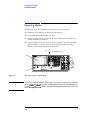
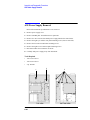
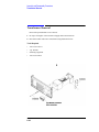
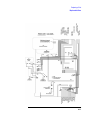
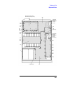
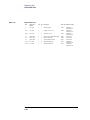
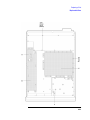
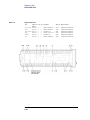
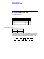
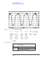
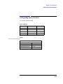
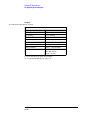
1
Assembly Level Repair
HP/Agilent Technologies
8922 Series GSM Test Set
Agilent Part No. 08922-90213
Printed in UK
January 1998
© Copyright 1998, Agilent Technologies. All rights reserved. Reproduction, adaptation, or translation without prior
written permission is prohibited, except as allowed under the copyright laws.
Introduction
Introduction
The HP/Agilent 8922 product family uses an assembly level repair service strategy. The
HP/Agilent 8922 may be sent to an Agilent Technologies Sales and Service office or may
be repaired on site. This book is used for both Agilent Technologies service and owner
service.
The HP/Agilent 8922 product family currently contains the HP/Agilent 8922A, HP/
Agilent 8922B, HP/Agilent 8922E, HP/Agilent 8922F, HP/Agilent 8922G, HP/
Agilent 8922H, HP/Agilent 8922M and HP/Agilent 8922S. There are differences in both
the hardware and in the operation. In examples and task sequences this book presents
general usage, and graphical instrument representations may not exactly match the HP/
Agilent 8922 that you are servicing.
Repairing the HP/Agilent 8922
To repair the HP/Agilent 8922, follow the chapters in this book starting at the beginning
and following the “where to go next” guidelines.
Book Organization
This book contains problem identification sections, assembly replacement sections,
reference information and concept information. The chapters are sectioned in three parts;
Service Procedures, Reference Information and Theory. This sectioning helps to identify
the type of information found in a group of chapters.
i
Introduction
ii
Contents
Introduction
i
1 Localizing the Problem
Introduction 1-2
Localizing the Problem - Flow Chart (Power-Up)
Power-Up Checks 1-4
If Power-Up Checks FAILED 1-5
If Power-Up Happened Correctly 1-10
1-3
2 Running Diagnostics
Introduction 2-2
Running Memory Card or ROM Based Diagnostics
Loading and Running the Ram Test 2-7
2-3
3 Verifying Performance
Introduction
3-2
Installing and Operating the Software
3-2
Using the Compatibility Switch for the HP/Agilent 8922F/
H or M/S 3-3
4 Using the HP/Agilent 83210A Service Kit
Introduction
4-2
Configuring the RF Extender
Extending Modules
4-3
4-5
Making Measurements
4-6
5 Troubleshooting the Controller/Display
Introduction
5-2
Parallel Bus
5-3
Serial Bus
Display
Keyboard
5-4
5-5
5-6
Contents-1
Contents
6 Troubleshooting the Power Supply
Introduction
6-2
Power Cord Verification
6-3
Line Voltage Selection / Line Fuse Replacement
Transformer / Power Switch
A28 Power Supply
6-7
Where To Go Next
6-8
6-6
7 Adjustments and Calibration
Introduction
7-2
Timebase Adjustments
Periodic Calibrations
7-3
7-5
Sum Loop Adjustment Procedure
7-6
8 Assembly and Disassembly Procedures
Introduction
8-2
Top and Bottom Cover Removal
Inside Protective Covers
8-3
8-4
AF, Digital and RF Assemblies Removal
A1 Front Panel Removal
8-7
A10 Power Supply Regulator Removal
A11 Receiver Mixer Removal
8-10
A12 Pulse Attenuator Removal
A21 GPIB Interface Removal
A22 Display Removal
A23 Input Section Removal
8-19
8-22
Transformer Removal
Contents-2
8-14
8-18
A28 Power Supply Removal
Fan Removal
8-12
8-16
A24 Attenuator Removal
8-5
8-24
8-20
8-9
6-5
Contents
9 Replacing a Part
Introduction
9-2
Replaceable Parts
9-3
Firmware Upgrades
9-29
10 Service Screen
Introduction
10-2
11 Self-Test Error Messages
Introduction
11-2
12 Module I/O Specifications
Introduction
12-2
A2 Audio Analyzer 2
12-3
A3 Audio Analyzer 1
12-5
A4 Modulation Distribution
12-8
A5 Premodulation Filter and NSM
A6 Signaling Source/Analyzer
A9 Global Test and Demod
A11 Receiver Mixer
A13 Output
12-10
12-13
12-15
12-19
12-22
A14 Pulse Driver
A15 Reference
A16 Receiver
12-24
12-26
12-32
A18 Spectrum Analyzer
A19 Measurement
12-36
12-38
A23 Input (HP/Agilent 8922A.B,E,F,G,H) Only
A23 Input (Agilent 8922M/S Only)
A25 Sum Loop
12-43
12-47
12-50
A17, A26 Step Loop
A27 DAC/Upconverter
12-53
12-56
Contents-3
Contents
A28 Power Supply
12-58
A33 Hop Controller
12-59
13 Instrument Block Diagrams
Introduction
13-2
14 Block Diagram Theory of Operation
Introduction
14-2
Technical Discussion
14-3
Block Diagram 1
14-4
Block Diagram 2
14-9
Block Diagram 3
HP/Agilent 8922B Only
Block Diagram 4
14-17
Block Diagram 5
14-18
14-15
15 Diagnostics Theory
Introduction
15-2
AF_DIAGS
15-3
RF_DIAGS
15-5
MS_DIAGS
15-11
GSM and DCS Diagnostic Tests
Interpreting Results
Contents-4
15-13
15-12
Contents
16 Measurement Theory
Introduction
16-2
17 GSM Theory
Introduction
17-2
The GSM System
17-3
E-GSM, DCS1800 and PCS1900 Systems
17-4
Index 1
Contents-5
Contents
This Page Intentionally Left Blank
Contents-6
1
Localizing the Problem
1-1
Localizing the Problem
Introduction
Introduction
This chapter helps to determine if a problem actually exists and which section of the
instrument has a problem.
This chapter comprises of four sections.
❒ Localizing the Problem Flow Chart (Power-Up)
❒ Power-Up Checks
❒ If Power-Up Failed
•
Power-Up Self Test Diagnostics
❒ If Power-Up Happened Correctly
1-2
•
Checking the RF Analyzer using the RF Generator
•
Checking the RF Analyzer using the AF Generator
Localizing the Problem
Localizing the Problem - Flow Chart (Power-Up)
Localizing the Problem - Flow Chart (Power-Up)
See "Power Up Checks", in this Chapter, for details of the steps given in the flow chart
below.
Power On
NO
Fan On?
Goto;
"Troubleshooting the
Power Supply"
YES
NO
Beep after
6 seconds?
YES
Goto;
"Power-Up Self Test
Diagnostics"
NO
Messages
OK?
YES
NO
Keys &
Controls OK?
YES
Failure
Reported by
Diagnostics ?
NO
Goto;
"If Power-Up
Happened Correctly"
YES
Goto the relevant trouble shooting section;
•
•
•
Figure 1-1
"Trouble Shooting The Controller/Display" - Chapter 5.
"Trouble Shooting The Power Supply" - Chapter 6.
"Running Diagnostics" - Chapter 2
Localizing the Problem - Flow Chart
1-3
Localizing the Problem
Power-Up Checks
Power-Up Checks
The following checks show whether the instrument is powering up correctly.
(a) Depress the power button on the front panel (see diagram).
(b) Check that the fan on the rear panel is working.
(c) Listen for a single “beep” after pressing the power switch. This can be from 6 to 20
seconds, depending on model type.
(d) Check the display on the front panel for any error messages. (The normal message
which will appear is “All host processor self-tests passed.” and/or "Frequency
Reference Cal lost. Perform Reference Calibration".)
(b)
(Rear Panel Vent)
(d)
(c)
"Beep"
(a)
Figure 1-2
Power-Up Checks - Agilent 8922x
NOTE
If an error message appears after power up it may not be the only message
which has appeared. Only the last message will be shown on this message line.
Press SHIFT , TESTS (MSG) to access the message screen for a list of all the
error messages.
1-4
Localizing the Problem
If Power-Up Checks FAILED
If Power-Up Checks FAILED
If the power up checks failed, continue with this section.
❒ If the fan did not start, see "Troubleshooting the Power Supply", Chapter 6.
❒ If the fan started, but any of the other power-up checks failed, see "Power-Up Self Test
Diagnostics".
❒ If an error message occurs, refer to the Agilent 8922x Users Guide for additional
information.
Error Message Numbers
If the error message refers to a self test error it will be of the form:
One or more self tests failed: Error Code XXXX
Where xxxx corresponds to the error message number shown in the table below.
Table 1-1
Error Message Numbers
Failure
Error
Number
Suspect Assembly
Fatal Error - Host Processor Failure
0002
A7 Controller
Fatal Error - ROM Checksum Failure
0004
A8 Memory
Fatal Error - RAM Failure
0008
A8 Memory
Fatal Error - RAM Failure
0010
A8 Memory
Fatal Error - Timer Failure
0020
A7 Controller
Real Time Clock Failure
0040
A8 Memory
Keyboard Failure
0080
A1 Keyboard
Serial I/O Failure
0100
A21 GPIB
Internal Serial Bus Communication Failure
0200
Serial Bus
CRT Failure
0400
A19 CRT Drive
Miscellaneous Hardware Failure
0800
Miscellaneous H/W
1-5
Localizing the Problem
If Power-Up Checks FAILED
Power-Up Self Test Diagnostics
If the power-up sequence failed, the power-up self-tests can be re-run with the covers off.
The LED’s on the controller board give the results of the power-up self-test.
(a) Remove the instrument covers. Refer to the section "Top and Bottom
Covers", Chapter 8, for details.
(b) Power up the instrument.
(c) Read the LED sequence given on the controller board. These LED’s can be
read with the shields in place (refer to the diagram below)
Location of LED’s
3
2
1
0
Front Panel
(View from top)
Figure 1-3
Self Test LED Location
NOTE
For multiple failures, the patterns for each failure will appear in sequence.
1-6
Localizing the Problem
If Power-Up Checks FAILED
The following conventions are used to represent the LED’s throughout this chapter.
Table 1-2
LED Conventions
LED shown in tables
Represnts
A ’lit’ LED
An ‘off’ LED
A flashing LED
LED Sequences
The LED error sequence will show two states, pass or fail, which are outlined below. The
suspect assembly is given in the following tables, before moving on consult the section
"Self-Test Diagnostic Result".
No Failures
Detected
The LED’s will light for approximately 10 seconds, then all will turn
off.
3
2
1
0
Lit for 10 seconds.
Failure Detected
1 The LED’s will initially all light.
2 The next pattern blinks rapidly, and shows that an assembly has
failed.
3 The third sequence flashes twice and gives further information on
the area of the board that has failed.
4 The LED’s will light then go out.
1-7
Localizing the Problem
If Power-Up Checks FAILED
Table 1-3
Sequence of LED Patterns
3
2
1
0
3
2
1
0
1
2
Assembly failure.
3
2
1
0
3
2
1
0
3
2
1
0
3
2
1
0
3
4
NOTE
Serial Bus
Communication
Failures
No more errors.
1. The third patterns are only documented for a serial bus communication failure. This is
represented by the two outside LED’s flashing.
2. The second and third patterns will be the same. It will appear as if the same pattern has
flashed twice.
For more than one error in the Agilent 8922x the LED’s will flash in the same sequence for
each assembly that is faulty.
1-8
Localizing the Problem
If Power-Up Checks FAILED
Where to Go Next
❒ If the LED’s did not light at all, go to Chapter 6, "Troubleshooting the Power Supply".
❒ If an error messgae occurs, use it in Chapter 2, "Running Diagnostics" to choose which
diagnostic test to run. See also Chapter 11 "Self Test Error Messages".
❒ If this section is used due to display problems, go to Chapter 5 "Troubleshooting the
Controller/Display" before the error messages are repaired.
GPIB/
1-9
Localizing the Problem
If Power-Up Happened Correctly
If Power-Up Happened Correctly
If power-up happened correctly and no problem is indicated, this section is used to functionally check most of the hardware. The generators are checked first with external measurements, then the analyzers are checked with the generator. The RF Generator is
checked at 935 MHz and 10 dBm. The AF Generator is checked at 1 kHz and 1 V. These
checks are for indication only, performance tests in Chapter 3, “Verifying Performance”,
will test specifications.
NOTE
If you possess an Agilent 8922S or Agilent 8922M, you should first re-configure your
instrument as an HP/Agilent 8922E or HP/8922G. To do this, select the following keys:
• CONFIG (this is accessible from the Cell Control screen in the bottom right-hand
corner).
• Compatible, select (HP 8922E or HP 8922G)
PRESET
•
Referring to Figure 1-4, ensure the connections are made.
AUDIO RF OUT
AUDIO OUT
AF To Oscilloscope
RF To Spectrum Analayzer
Figure 1-4
Front Panel Connections
Press
NOTE
RF GEN/RF ANL
.
On the HP/Agilent 8922A/B, press RF GEN/RF ANL .
On the HP/Agilent 8922E/F/G/H/M/S, press SHIFT ,
1-10
CELL CNTL
(RFG/RFA).
Localizing the Problem
If Power-Up Happened Correctly
Highlight the RF Output field (1).
Select AUX RF OUT from the list of choices.
Set the RF Generator Amplitude field to 10 dBm (2).
Set the AF Generator Amplitude field to 1 V (3).
1
2
3
Figure 1-5
RF Analyzer Settings
Where to Go Next
•
•
If the generators are within specifications, go to the next section, “Checking the RF
Analyzer Using the RF Generator”.
If one or both of the generators appear to be faulty, go to Chapter 2, “Running
Diagnostics” and run the appropriate tests.
1-11
Localizing the Problem
If Power-Up Happened Correctly
Checking the RF Analyzer Using the RF Generator
This section tests the RF Analyzer using the RF Generator as a signal source. This task
assumes the same setting used in the previous section.
•
Figure 1-6
Connect the RF In/Out to the Aux RF Out.
Front Panel Connections for the RF Analyzer
Press
NOTE
RF GEN RF ANL
.
On the HP/Agilent 8922A/B, press RF GEN RF ANL .
On the HP/Agilent 8922E/F/G/H/M/S, press SHIFT ,
1-12
CELL CNTL
(RF GEN RF ANL).
Localizing the Problem
If Power-Up Happened Correctly
•
•
•
•
Set the RF Analyzer Frequency field to 935 MHz (1).
Set the RF Analyzer Amplitude field to 10 dBm (2).
Set the Mod Source GMSK field to Off (3).
Select More in the bottom right-hand corner of the screen (4).
1
2
3
4
Figure 1-7
RF Generator/Analyzer Settings
1-13
Localizing the Problem
If Power-Up Happened Correctly
•
Select CW/AF ANL from the list of choices, and read the CW Freq (5) and CW Power
(6) fields.
5
Figure 1-8
6
CW Readings
Where to Go Next
• If the analyzer measurement was within the specification, go to the next section,
“Checking the AF Analyzer using the AF Generator”.
• If the measurement was faulty, go to Chapter 2, “Running Diagnostics”, and run the test
related to the RF Analyzer.
1-14
Localizing the Problem
If Power-Up Happened Correctly
Checking the AF Analzyer Using the AF Generator
This section tests the AF Analyzer with the AF Generator as a source. The AF Generator
settings are the same as the first task, and displays the CW MEAS/AF ANL screen.
•
Figure 1-9
Connect the AUDIO OUT to the AUDIO IN.
Front Panel Connections for the Audio Check
•
•
•
Select More and from the list, select CW MEAS/AF ANL.
Highlight AF Anl In and select AUDIO IN (1).
Read the AC Level (2) and the AF Freq (3) reading.
2
3
1
Figure 1-10
Audio Measurements
1-15
Localizing the Problem
If Power-Up Happened Correctly
Where to go next
• If the analyzer measurement was within specification, go to Chapter 2, “Running
Diagnostics” and run all the tests.
• If the analyzer measurement was faulty, go to Chapter 2, “Running Diagnostics” and
run the tests relating to the AF Analyzer.
1-16
2
Running Diagnostics
2-1
Running Diagnostics
Introduction
Introduction
There are two types of diagnostics for the HP/Agilent 8922: diagnostic tests and the HP/
Agilent 8922B specific “RAM Test”. The latter is appropriate for the HP/Agilent 8922B
only. The diagnostic tests are contained either on the memory card, part number 0892210003 or in ROM memory for instruments with firmware revision code A.03.00 and
above. The HP/Agilent 8922B specific “RAM Test” is contained on the “08922-10001,
8922B Driver” disk supplied with the HP/Agilent 8922B.
Most of the diagnostic tests relate to a fault in a specific instrument section. Therefore, if
chapter 1 identified a specific section of the instrument, only those tests need to be run.
The diagnostic tests whose names begin with E or G are specifically for the HP/Agilent
8922E/G. The other tests are for any HP/Agilent 8922.
This chapter comprises two sections. The first section, “Running Memory Card or RAM
Based Diagnostics”, shows how to load and run the memory card based or ROM based
diagnostics. The second section, “Loading and Running the RAM Test”, shows how to
load and run the HP/Agilent 8922B RAM test. Equipment requirements and installation
procedures are given in the HP/Agilent 8922B User’s Guide, Part Number 08922-90020.
This chapter uses the diagnostic test names from an early memory card revision. ROM
based diagnostic test names may differ from the names used in this chapter.
2-2
Running Diagnostics
Running Memory Card or ROM Based Diagnostics
Running Memory Card or ROM Based Diagnostics
Do these steps in the order shown
1 - Press
3 Press
PRESET
TESTS
2 - Insert Memory Card (Optional)
2-3
Running Diagnostics
Running Memory Card or ROM Based Diagnostics
6
4
Move cursor here and
press knob.
For Memory Cards:
If CARD is displayed, go to step 6, if not move the cursor to this field, press knob and continue at step 5.
8
Move cursor here and
press knob. Follow the
instructions to start.
5 Select CARD
7
Select,
AF_DIAGS,
RF_DIAGS1,
MS_DIAGS1,
CAL_REV,
LOOP_BACK
To select another test;
•
To select another tests from the same program use
the RESUME user key.
•
To select a test from another program press
TESTS key and begin at step 6.
2-4
Running Diagnostics
Running Memory Card or ROM Based Diagnostics
Reading Memory Card Diagnostic Test Results
Test Results
Probability Indicator
Assemblies suspected to be defective
Troubleshoot the assembly with the highest
probability first and re-run test. Continue this
process with all assemblies listed until the defect is
found. See also Chapter 15 "Diagnostic Theory'.
2-5
Running Diagnostics
Running Memory Card or ROM Based Diagnostics
Selecting Memory Card Diagnostic Test Execution Conditions
BEFORE RUNNING A TEST
WHILE RUNNING A TEST
Specifies whether to run measurements continuously or
stop after completion of each measurement. This choice
can be modified when a diagnostic program is running.
Specifies whether to stop
testing or continue when a
failure occurs. This choice
can be modified when a
diagnostic program is
running.
This feature is not used by
the diagnostic program.
Specifies whether to print diagnostic test results.
These options are used for controlling various
parts of the tests. These options can be changed
depending on the test program. They are
selected by using the cursor and knob.
Where to Go Next:
If any high-probability failures occurred, those assemblies can be replaced and the test rerun. When the tests pass, the performance tests can be run to verify performance (refer to
Chapter 3). If low-probability failures occur, the performance tests can be run for further
indication or measurements can be made to individual assemblies using Chapters 4, 12
and 13.
2-6
Running Diagnostics
Loading and Running the Ram Test
Loading and Running the Ram Test
Your HP/Agilent 8922B comes with software to test the Data Buffer.
Loading the RAM Test
1
Locate the floppy disk labeled “08922-10001, 8922B Driver.”
2
Insert the disk into the drive.
3
Type MSI A: (substitute your drive specifier for A: if your drive is not drive A) and
press ENTER .
4
Type LOAD “DRIVER22B”,1 and press
ENTER
.
The Data Buffer Driver will now be loaded and will begin to run.
K3, "Test RAM
5
Press
6
Use the cursor to select the output device.
7
Select the area of RAM to test and Press
8
Repeat selection for each area of RAM.
K0, "Accept
.
Where to go next
•
If any of the RAM areas tested bad go to chapters 8 and 9.
Selecting from a List
Use
and
of the list.
⇓
⇓
•
Use
SHIFT
•
Use
SHIFT
•
Use ENTER
screen.
•
Use
to scroll through the list. A beep will sound when you reach an end
or
PG UP
⇓
or
PG DOWN
or
⇓
⇓
⇓
•
to move to the first item in the list.
to move to the last item in the list.
to select the current item and move to the next field on the
to select the current item and move to the previous field on the screen.
2-7
Running Diagnostics
Loading and Running the Ram Test
This Page Intentionally Left Blank
2-8
3
Verifying Performance
3-1
Verifying Performance
Introduction
Introduction
Because of the specialized nature of the HP/Agilent 8922 and the equipment required to
support it, it is recommended that calibration and repair be performed only by specially
equipped Agilent Technologies service centers.
A list of specifications and verfication tests can be found in the HP/Agilent 8922x User’s
Guide.
Verification
Performance Test Software provided with the product is used to verify the electrical
performance of the HP/Agilent 8922 GSM Test Set. If the instrument passes this
verification, its operation and specifications are assured within the measurement
uncertainties provided in the performance test print out.
Installing and Operating the Software
Performace Test Software
This is supplied on a 3.5-inch, double-sided floppy disk and is written to run with BASIC
5.0 and later. Modifications to the program should be limited to changing the default
addresses and storing copies for back-up purposes.
Understanding the Tests
Test Descriptions contains a description of each test that is performed by the Performance
Test software. This description is intended to help locate problems if the software fails to
execute properly or to help users understand the test methodology that is used in each
performance test. The descriptions are not step by step procedures for manual
performance tests.
3-2
Verifying Performance
Using the Compatibility Switch for the HP/Agilent 8922F/H or M/S
To Load the Program in the Agilent 8922M/S.
To verify the performance of the HP/Agilent 8922H/M you need to convert the instrument
back from an HP/Agilent 8922G, or convert the HP/Agilent 8922F/S to an HP/Agilent
8922E.
You are now ready to run the Performance Test Software.
1) Put the disk in the disk drive.
2) Type ``LOAD "PT_8922"'', press ENTER.
After you have completed the Performance Tests, return the instrument back to the
HP/Agilent 8922F/S or HP/Agilent 8922H/M using the same process in reverse.
Using the Compatibility Switch for the
HP/Agilent 8922F/H or M/S
Back Conversion
To turn the instrument from the HP/Agilent 8922H/M or HP/Agilent 8922F/S back to an
HP/Agilent 8922G or an HP/Agilent 8922E, select the following keys:
❒ CONFIG (this is accessible from the Cell Control screen in the bottom right-hand
corner).
❒ Compatible, select HP 8922G or HP 8922E
❒ HP-IB Adrs (22)
❒ PRESET
The instrument is now set up as an HP/Agilent 8922G or HP/Agilent 8922E and ready for
Performance Verification testing.
Forward Conversion
To return the instrument from an HP/Agilent 8922G back to an HP/Agilent 8922H/M or
an HP/Agilent 8922E to an HP/Agilent 8922F/S, select the following keys:
❒ More (this is accessible from the Cell Control screen in the bottom right-hand corner).
Scroll down the list and select CONFIG.
❒ Compatible, select HP 8922H/M or HP 8922F/S
❒ HP-IB Adrs (14)
❒ PRESET
The instrument is returned to an HP/Agilent 8922H/M or HP/Agilent 8922F/S.
3-3
Verifying Performance
Using the Compatibility Switch for the HP/Agilent 8922F/H or M/S
To Configure the GPIB Addresses
1) With the program loaded, type ``EDIT DEFAULT_ADDRESS'', press ENTER.
2) Modify each line to indicate the proper instrument address (700-730).
It is now possible to re-store the program as "PT_8922" or store it under a different name.
To Run the Program
1) Type ``RUN'', press ENTER.
2) Follow the directions as they appear on the screen.
Notes on Running the Program.
The first screen which appears is the GPIB status of each piece of test equipment that is
supported. It is only necessary to have the instruments responding that will be used in each
particular test. Make certain that each instrument you will be using is responding at the
proper address. Duplicate addresses may make an instrument appear to be responding but
this is not allowed. Press "I" (for Ignore) to continue past this screen.
The second screen prompts you for the instrument model. If you have disk 08922-10006,
select HP 8922G (for HP/Agilent 8922H/M performance testing) or HP 8922E (for
HP/Agilent 8922F/S performance testing). The third screen which will appear is the main
Performance Tests selection menu. Three options are available on this screen:
❒ Select the performance test to run, remember the test instruments and UUT must be
responding over GPIB.
❒ Turn the printer function ON or OFF. If the printer function is turned on it must be
responding over GPIB or the program will lock up.
❒ Exit from the program.
Press the key corresponding to the option that you would like to perform.
The other screens that appear are connection instructions, error messages and output
results.
3-4
4
Using the HP/Agilent 83210A Service Kit
4-1
Using the HP/Agilent 83210A Service Kit
Introduction
Introduction
This section is a supplement to the diagnostics program for troubleshooting the
HP/Agilent 8922 to the assembly level. The extender boards should be used when the
diagnostics cannot correctly isolate a defective assembly, or when it is necessary to verify
the module level performance of the HP/Agilent 8922.
The section provides the information necessary to extend and troubleshoot the input and
output signals for most RF, audio, and digital assemblies.
4-2
Using the HP/Agilent 83210A Service Kit
Configuring the RF Extender
Configuring the RF Extender
To extend RF modules, it is necessary to use the RF extender board (08922-60129) with
the correct coax jumper cables. These cables route the RF signals to and from the module
and allow the signal path to be accessed for measurements. The following table and
diagram shows the coax jumpers that are required for each RF module.
Table 4-1
Coax Jumpers for RF Extender Board
On PLUG 1 Connect Pin Number
On PLUG 3 Connect Pin Numbers
Assembly
Number
3
3
ForA13
X
For A14
X
For A15
X
ForA16
X
For A17
X
For A18
X
For A25
X
X
For A26
X
X
ForA27
7
9
13
17
9
X
X
X
X
X
X
X
X
13
15
17
20
X
X
X
X
X
X
X
X
X
X
X
X
X
X
X
X
X
X
X
4-3
Using the HP/Agilent 83210A Service Kit
Configuring the RF Extender
The following example shows how to interpret table 4-2 and install the coax jumpers on
the extender board. This example shows the configuration for the A13 assembly.
Figure 4-1
RF Extender Board
4-4
Using the HP/Agilent 83210A Service Kit
Extending Modules
Extending Modules
The modules shown in the following table can be extended using the appropriate extender
boards from the HP/Agilent 83210A Service Kit. Assemblies that cannot be extended can
usually be accessed directly while the assembly is installed in the instrument.
Table 4-2
Extender Board Part Numbers
REF #
DESCRIPTION
EXTENDER
A2
Audio Analyzer 2
08920-60142
A3
Audio Analyzer 1
08920-60142
A4
Modulation Distribution
08920-60141
A5
Premod Filter and NSM
08922-60132
A6
Signaling Source / Analyzer
08920-60140
A7
Controller
08920-60133
08920-90135
A8
Memory
08922-60132
A9
Global Test and Demod
08922-60133
A13
Output
08922-60129
A14
GSM Timing Gen
08922-60129
A15
Reference
08922-60129
A16
Receiver
08922-60129
A17
Step Loop B
08922-60129
A18
Spectrum Analyzer
08922-60129
A19
Measurement
08920-60138
A20
CRT Driver
08920-60135
A25
Sum Loop
08922-60129
A26
Step Loop A
08922-60129
A27
DAC / Upconverter
08922-60129
A33
Hop Controller
08920-60133
4-5
Using the HP/Agilent 83210A Service Kit
Making Measurements
Making Measurements
Audio / Digital Assemblies
The extender boards for the audio and digital assemblies allow the boards to be extended
above the instrument. This provides better access to signals going to and from these
assemblies. Refer to the “Block Diagrams” (chapter 13) or “Module I/O Specs”
(chapter 12) for pin numbers and typical I/O characteristics for each assembly. Use the
extender board shown.
RF ASSEMBLIES
The extender boards for the RF assemblies extend the modules above the instrument. This
allows better access to control signals and allows the RF input and output signal paths to
be opened for making measurements. The following procedure outlines the steps
necessary to make measurements on the RF modules with the RF extender board.
1. Configure the RF extender card with the proper coax jumpers. Refer to table 4-2 and
figure 4-1.
2. Decide the signal path that needs to be measured. Find the correct plug number and pin
number on the “Block Diagrams” (chapter 13) or “Module I/O Specs” (chapter 12).
4-6
Using the HP/Agilent 83210A Service Kit
Making Measurements
3. Remove the correct coax jumper and connect a measurement instrument as shown in
the following diagram. To measure signals going TO the module, measurements should
be made on the lower row of connectors on the extender module. Outputs coming
FROM the modules (going into the instrument) are measured on the top row of
connectors on the extender board.
4. Turn off the instrument’s power switch. Remove the module from the instrument.
Install the module onto the extender board and install the extender board into the
instrument.
5. Power on the instrument and make the measurements.
4-7
Using the HP/Agilent 83210A Service Kit
Making Measurements
This Page Intentionally Left Blank
4-8
5
Troubleshooting the Controller/Display
5-1
Troubleshooting the Controller/Display
Introduction
Introduction
This chapter helps isolate problems in the control sections of the instrument, the sections
are:
•
A1 Keyboard
•
A7 Controller
•
A8 Memory
•
A20 CRT Driver
•
A21 HP-IB Interface
•
A33 Hop Controller
Problems in the Control sections can be broken into four types, these types are:
•
Parallel Bus
•
Serial Bus
•
Display
•
Keyboard
This chapter addresses each category in a separate section. This chapter assumes that
Chapter 13, Instrument Block Diagram will be used as a reference.
5-2
Troubleshooting the Controller/Display
Parallel Bus
Parallel Bus
The parallel bus is at the center of the control section. The parallel bus is defined as direct
connections to the A7 Controller. These connections include the data bus, address bus and
dedicated parallel control lines.
The assemblies on the parallel bus are:
•
A1 Keyboard
•
A6 Signalling Source/Analyzer
•
A7 Controller
•
A8 Memory
•
A9 Global Test/Demod
•
A19 Measurement Board
•
A20 CRT Driver
•
A21 GPIB Interface
•
A32 GSM Controller
•
A33 Hop Controller
Most problems with the parallel bus are accounted for in the power-up self-tests. The selftests check the A7 Controller first, then the A8 Memory. If these two tests pass, the
instrument will beep once after approximately 10 seconds. If these tests do not pass, the
problem is probably on one of the two boards or something is pulling down the parallel
bus.
The assemblies that are not directly checked by the power-on self-tests are the A1
Keyboard and the A21 GPIB Interface.
5-3
Troubleshooting the Controller/Display
Serial Bus
Serial Bus
The serial bus controls many of the assemblies through individual serial control lines. The
serial control lines are generated at the A33 Hop Controller.
The A33 Hop Controller takes parallel data from the A7 Controller and de-multiplexes the
data for the assemblies on the serial bus. In the power-up self-tests, the A33 Hop
Controller and the assemblies on the serial bus are tested. If a power-up self-test serial bus
failure occurs and no A33 failures have occurred, the problem could be between the A33
Hop Controller and the assembly identified in the failure.
5-4
Troubleshooting the Controller/Display
Display
Display
The display section contains the A22 CRT, and the A20 CRT Drive. The A20 CRT Drive
receives parallel data from the A7 Controller and generates the drive signals for the A22
CRT. The A20 CRT Drive is tested during the power-up self-tests for the ability to receive
data and to respond back to the A7 Controller. If the A20 CRT Drive passes the power-up
self-tests and the display does not respond the signals going to the A22 CRT can be
checked at J6 on the A29 Motherboard.
Line Name
Pin Number
Description
INTHIGH
J6(1)
CRT intensity reference high. Up to 100 V with
respect to INTLOW. Floating with respect to
ground. From the A22 CRT to bias the intensity
drive circuit at the A20 CRT Drive.
INTW
J6(2)
CRT intensity control voltage. Up to 100 V with
respect to INTLOW. Floating with respect to ground.
From the A20 CRT Drive to the A22 CRT to vary the
intensity of the display.
INTLOW
J6(3)
CRT intensity reference low. Floats with respect to
ground. From the A22 CRT to the low side of the
intensity drive circuit at the A20 CRT Drive.
HSYNC
J6(4)
Horizontal sync pulse for the A22 CRT. A TTL
pulse at approximately 19 kHz. From the A20 CRT
Drive to the A22 CRT. The HP/Agilent 8922F/H/M/S
use a 15 kHz PAL signal.
+12CRT
J6(5)
Filtered +12AUX for the A22 CRT. There is a 20
kHz low pass filter on the A29 Motherboard to filter
the +12AUX for the A22 CRT.
VID
J6(6)
Video signal for the A22 CRT. A TTL signal to turn
the signals off and on. The rate is approximately
6.25 MHz. From the A20 CRT Drive to the A20
CRT.
VSYNC
J6(7)
Vertical sync pulse for the A22 CRT. A TTL signal
from the A20 CRT Drive to the A22 CRT at a rate of
approximately 60 Hz.
GND
J6(8)
5-5
Troubleshooting the Controller/Display
Keyboard
Keyboard
The A1 Keyboard assembly contains both the keys and the knob. The keyboard is
configured in a matrix with the rows being scanned with pulses from the A7 Controller
and the columns being read by the controller. The column lines are pulled up through
resistors and are pulled low when a key is pressed. The A7 Controller determines which
key is being pressed by reading which column line is pulled low and which row the
column line is being pulled low through. Since the row outputs are tri-state, the low-going
pulses are not seen on the output until a key is pressed and the current path is completed.
The keyboard can be checked with an oscilloscope by disconnecting the ribbon cable from
the keyboard and checking for the pull-up voltages on the column pins. Then with the
keyboard connected, check that the lines are being pulled low at the A7 Controller
connector J4. The pin numbers on A7-J4 are the same as those on A1-J1. The ribbon cable
connector has a mark to indicate to pin 1. Pin 2 is directly opposite pin 1.
Table 5-1
HP/Agilent 8922E/F/G/H/M/S Keyboard (HP/Agilent 8922 A/B keys shown in
parenthesis)
Column 0
Pin 9
Column 1
Pin 10
Column 2
Pin 11
Column 3
Pin 12
Column 4
Pin 13
Column 5
Pin 14
CELL
CONFIG
(RF GEN/
RF ANL)
ORGCALL
(K1)
RCVCALL
(K2)
ENDCALL
(K3)
L1(K4)
L2(K5)
CELL
CNTL
(HOP
CNTRL)
INCR÷10
down arrow
not used
SHIFT
CANCEL
MEAS
SYNC
INCRSET
PRESET
not used
not used
not used
PREV
INCR×10
up arrow
not used
not used
leftarrow
TESTS
7
4
1
0
ON/OFF
MEAS
ARM
8
5
2
.
ppm W
RECALL
9
6
3
+/-
% dBµV
LOCAL
ENTER
GHZ dBm
MHz V
kHzmV
Hz µV
5-6
Troubleshooting the Controller/Display
Keyboard
If the pull-up voltages are present at the end of the ribbon cable and the voltages are not
pulled down when a key is pressed, the problem is most likely on the A1 Keyboard
assembly. If the pull up voltages are present and are pulled down when a key is pressed but
the controller does not respond, the problem is most likely at the A7 Controller assembly.
The knob can be checked with an oscilloscope at the J4 connector on the A7 Controller.
When the knob is turned, pulses should be present on A7-J4 pins 19 and 21. When the
knob is pushed the level at A7-J4 pin 23 should change states. The A1 Keyboard end of
the ribbon cable should also be checked for +5 V on pins 15 and 16. If the signals are
getting to the A7 Controller the problem is most likely at the A7 Controller assembly.
Where to Go Next
If either the A1 Keyboard or A7 Controller assemblies measured in-correctly, go to
chapters 8 and 9.
5-7
Troubleshooting the Controller/Display
Keyboard
This Page Intentionally Left Blank
5-8
6
Troubleshooting the Power Supply
6-1
Troubleshooting the Power Supply
Introduction
Introduction
This chapter helps verify that the power supply is at fault when no indication for power is
present upon power-up. If the power supply appears defective, the problem can be
localized to the line module, mains (line) fuse, transformer, power supply, regulator,
motherboard, or power switch. This chapter is arranged to check each section of the power
supply. The views of the instrument in this chapter are both top and bottom views with the
covers removed. Refer to chapter 8 “Assembly/Disassembly” for help in removing the
covers.
NOTE
The mains (line) fuses and power supply DC fuses in the HP/Agilent 8922 are all fast-blow
fuses (not “slow-blow”).
6-2
Troubleshooting the Power Supply
Power Cord Verification
Power Cord Verification
Use this diagram to verify that the correct line cord is being used.
Table 6-1
Line Cords
PlugType
Cable
Agilent C
Plug Description
Part
D
Number
Length,
Cable
inches
Color
(mm)
For Use In
Country
8120-1351
8120-1703
0
4
90/Straight BS1363Aa
90
90 (229)
90 (229)
Mint
Gray
Mint
Gray
United Kingdom,
Cyprus, Nigeria,
Rhodesia,
Singapore
8120-1369
8120-0696
0
4
Straight
a
NZSS198/ASC112
Straight/90
79 (201)
87 (221)
Gray
Gray
Australis,
Argentina,
New Zealand,
Mainland China
8120-1689
8120-1692
7
2
Straight
90
79 (201)
79 (201)
Mint
Gray
Mint
Gray
East and West
Europe, Central
African Republic,
Arabia, Egypt
8120-1378
8120-4753
8120-1521
8120-4754
1
6
Straight NEMA5-15P
Straight
90
90
80 (203)
90 (230)
80 (203)
90 (230)
Jade
Gray
Jade
Gray
United States,
Canada, Mexico,
Phillipines, Taiwan,
Japan
1
a
Jade
Gray
8120-1348
8120-1538
2
3
Straight
90
80 (203)
80 (203)
Dark
Gray
Dark
Gray
8120-2104
3
79 (201)
Gray
8120-2296
8120-3997
4
4
Straight SEV 1011
1959-24507, Type 12
Straight/90
Straight/90
79 (201)
177 (402)
Gray
Gray
8120-0698
6
Straight/NEMA6-15P
90 (230)
Black
Switzerland
United States,
Canada
Continued Over
6-3
Troubleshooting the Power Supply
Power Cord Verification
Table 6-1
Line Cords
PlugType
Cable
Agilent C
Plug Description
Part
D
Number
8120-2956
8120-2957
8120-3997
3
4
4
90/Straight
90/90
Straight/Straight
8120-4211
8120-4600
7
8
8120-1860
6
8120-1575
8120-2191
8120-4379
0
8
8
Length,
Cable
inches
Color
(mm)
For Use In
Country
79 (201)
Gray
Gray
Gray
Denmark
Straight IEC83-B1
Straight/90
79 (201)
79 (201)
Black
Gray
South Africa, India
Straight CEE22-V1
(Systems Cabinet Use)
Straight/Straight
Straight/90
90/90
59 (150)
Jade
Gray
a
31 (79)
59 (150)
80 (203)
Jade
Gray
Jade
Gray
Jade
Gray
a.Part number shown for plug is industry identifier for plug only. Number shown for cable is Agilent Part Number
for complete cable including plug. E = Earth Ground; L = Line; N = Neutral.
6-4
Troubleshooting the Power Supply
Line Voltage Selection / Line Fuse Replacement
Line Voltage Selection / Line Fuse Replacement
Use this diagram to verify that the line module is set to the correct line voltage, that the
fuse is not blown, and that it is the correct value.
6-5
Troubleshooting the Power Supply
Transformer / Power Switch
Transformer / Power Switch
Use this diagram to verify that the correct voltages are present when the instrument’s
power cord is connected. The table shows the expected values and pin numbers.
6-6
Troubleshooting the Power Supply
A28 Power Supply
A28 Power Supply
Use this diagram to verify that the regulated voltages are present and correct at the output
of the power supply board, and at the mother board connection to the regulator. Use this
diagram also to check the fuses on the fuse board. The tables show the voltages,
connectors, pin numbers, and fuse values.
6-7
Troubleshooting the Power Supply
Where To Go Next
Where To Go Next
If any part of the power supply is defective refer to chapter 8 “Assembly/Disassembly”
and chapter 9 “Replacing a Part” for removal and replacement. After the power supply is
repaired, go to chapter 1 “Localizing the Problem” to verify that no other problems exist.
6-8
7
Adjustments and Calibration
7-1
Adjustments and Calibration
Introduction
Introduction
This chapter contains information to perform the necessary calibrations and adjustments
for periodic maintenance or following repairs. Each year the timebase and periodic
calibration adjustments should be performed. Also, the overall performance of the
instrument should be verified each year with the automated performance tests in chapter 3
“Running Performance Tests”.
The calibrations and adjustments covered in this chapter are divided into three sections:
❒ Timebase Adjustments
•
Standard Timebase
•
Optional High Stability Timebase
❒ Periodic Calibrations (ROM based)
•
Voltmeter Reference
•
Audio Frequency Generator Gain
•
External Modulation Path Gain
•
Audio Analyzer 1 Offset
❒ Sum Loop Adjustment Procedure
7-2
Adjustments and Calibration
Timebase Adjustments
Timebase Adjustments
Standard Timebase Adjustment Procedure (Reference Calibration)
NOTE
This procedure should only be performed after the instrument has warmed up at least 30
minutes. It should be performed after replacement of the reference section A15, or if the
instrument gives an error message “Frequency reference cal lost. Perform reference
calibration.”
1. Connect a 10 MHz source to the rear panel REF IN connector.
2. On the configuration screen, select the “Calibrate” field.
3. Wait approximately 15 seconds; the reference will be calibrated.
7-3
Adjustments and Calibration
Timebase Adjustments
Option 001 High Stability Timebase Adjustment Procedure
1. Remove the instrument top cover. Power up the instrument and let it warm up for
approximately 1 hour.
2. Remove the rear-panel cable between the Opt. 001 REF OUT and REF IN connectors
(if present).
3. Attach a high accuracy frequency counter to the rear panel OPT 001 REF OUT. The
frequency counter resolution and accuracy should be at least 1 Hz at 10 MHz.
4. Adjust the high stability timebase (see figure 7-1) until the frequency counter reads 10
MHz.
NOTE
After performing this calibration, it is necessary to install a cable from the OPT 001 REF
OUT to the REF IN connector for the instrument to use the high stability timebase as the
reference.
Adjust to
10 Mhz
Figure 7-1
High Stability Timebase Adjustment
7-4
Adjustments and Calibration
Periodic Calibrations
Periodic Calibrations
To Run the Periodic Self-Calibration Program
1. Press
TESTS
to access the TESTS screen.
2. Select the field to the right of the colon under Procedure.
3. Select ROM under the Choices: menu.
4. Select the field to the left of the colon under Procedure.
5. Select PER_CAL under the Choices: menu.
6. Select
RUN TEST
.
7. Follow the instructions on the screen.
7-5
Adjustments and Calibration
Sum Loop Adjustment Procedure
Sum Loop Adjustment Procedure
This procedure should be performed whenever Step Loop A Assembly (A26) or Sum
Loop Assembly (A25) is replaced. It is not necessary to perform this adjustment for a
periodic calibration.
A spectrum analyzer is required to measure the instrument’s output during these
procedures. It is recommended to use a synthesized spectrum analyzer if possible.
Procedure:
1. Turn off the HP/Agilent 8922.
2. Remove the instrument top cover and the DAC/Upconverter Module (A27). (It is
necessary to remove the RF Cover plate that holds the module in the instrument.)
3. Power up the instrument, select the RF GENERATOR/RF ANALYZER screen, and set
the RF Gen Amplitude to −20 dBm at the RF IN/OUT connector.
4. Prepare the spectrum analyzer. Set the reference level to −10 dBm. Connect the HP/
Agilent 8922 RF IN/OUT to the spectrum analyzer input.
First Adjustment
5. Again from the RF GENERATOR screen, set the HP/Agilent 8922 frequency to 800
MHz.
6. Set the spectrum analyzer center frequency to 786.6 MHz. (The output from the HP/
Agilent 8922 is 13.4 MHz lower than was entered because the DAC/Upconverter is
gone).
7. Set the spectrum analyzer span to 10 MHz per division. ADJUST R32 “OFFSET” on
top of Sum Loop (A25) until the signal on the spectrum analyzer is between 776.6 and
796.6 MHz.
8. Reduce the spectrum analyzer span to 1 MHz per division and adjust R32 again until
the signal on the spectrum analyzer is centered within 2 divisions (2 MHz).
NOTE
Some modules (prefix 3050A and lower) only need to be centered within 10 MHz for all
of these adjustments.
7-6
Adjustments and Calibration
Sum Loop Adjustment Procedure
Second Adjustment
9. Now set the HP/Agilent 8922 frequency to 502 MHz.
10. Set the spectrum analyzer center frequency to 488.6 MHz with a span of 10 MHz per
division.
11. Adjust R180 “GAIN” on top of Sum Loop (A25) until the signal on the spectrum
analyzer is centered within 10 MHz.
12. Reduce the spectrum analyzer span to 1 MHz per division, and adjust R180 again until
the signal on the spectrum analyzer is centered within 2 divisions (2 MHz).
Final Adjustment
13. Set the HP/Agilent 8922 frequency to 1000 MHz.
14. Set the spectrum analyzer frequency to 986.6 MHz, then set the span to 10 MHz per
division.
15. Adjust R160 “KNEE GAIN” on top of Sum Loop (A25) until the signal on the spectrum
analyzer is centered within 1 division (10 MHz).
16. Reduce the spectrum analyzer span to 1 MHz per division, then adjust R160 again until
the signal on the spectrum analyzer is centered within 2 divisions (2 MHz).
Final Check
17. Repeat the above procedures until all three adjustments pass without any further fine
tuning.
18. Turn the instrument power off and reinstall the DAC/Upconverter Module. The
adjustment is now complete.
7-7
Adjustments and Calibration
Sum Loop Adjustment Procedure
This Page Intentionally Left Blank
7-8
8
Assembly and Disassembly Procedures
8-1
Assembly and Disassembly Procedures
Introduction
Introduction
Removing and replacing assemblies is straightforward. This chapter contains tool lists,
hints and drawings to help you do it effectively. Detailed step-by-step procedures are not
given for all assemblies.
After replacing certain assemblies you will need to load new calibration data into the HP/
Agilent 8922 or perform adjustments. The calibration data is supplied on a Memory Card
that is included with the replacement assembly.
Refer to chapter 9, “Replacing a Part”, for information about adjustments that are required
after replacing certain assemblies.
CAUTION
Perform the following procedures only at a static safe work station. The printed circuit
assemblies in this instrument are very sensitive to STATIC ELECTRICITY DAMAGE.
Wear an anti-static wrist strap that is connected to earth ground.
Recommended Torque
1. Screws: Tighten until just snug.
2. RF connectors (SMC SMA): 62 N-cm (5.5 lb-in.)
3. Nuts holding semi-rigid coax: 51 N-cm (4.5 lb-in.)
Further Information
For further information, refer to chapter 9. This chapter contains more information about:
•
Part numbers for replaceable parts.
•
Ordering information.
•
Adjustments required after assemblies are replaced.
8-2
Assembly and Disassembly Procedures
Top and Bottom Cover Removal
Top and Bottom Cover Removal
1. Remove four 2-pt. Pozidriv top bumper mounting screws.
2. Remove four 2-pt. Pozidriv side mounting screws and bumpers.
3. Remove four 2-pt. Pozidriv screws and standoffs.
4. Remove fourteen TX-10 screws and top cover.
5. Remove two TX-10 screws and bottom foot.
6. Remove two TX-15 screws and bottom cover.
Tools Required
•
TX-15 screw driver
•
TX-10 screw driver
•
2-pt. Pozidriv screw driver
SIDE VIEW
1
3
2
4
(Both Sides)
(Both Sides)
To remove covers, pull sides
slightly apart, slide them back a
few inches and lift off.
6
(Both Sides)
8-3
Assembly and Disassembly Procedures
Inside Protective Covers
Inside Protective Covers
All covers can be removed with a TX-15 screw driver. Screws shown circled only require
loosening.
492 Top Cover (B, E and G)
505 Bottom Plate (B,E and G)
252
240 GPIB
Mounting
Bracket and
241-242
Screws
493498
506521
244
499501
Washer
458
(Opt. 001)
502504
Nut
114 Regular
Mounting
Bracket and
115-118
Screws
(Not Shown)
416421,
427456
424
3
12 CRT Bracket
8-4
426
Assembly and Disassembly Procedures
AF, Digital and RF Assemblies Removal
AF, Digital and RF Assemblies Removal
A27
A28
A25
A13
A15
A11
A20
A16
A18
A17
A19
A14
A32
A2
A3
A4
A5
A6
A9
A8
A7
A33 A34, (A,G) A31, (G)
A36, (B)
A37 (B)
8-5
Assembly and Disassembly Procedures
AF, Digital and RF Assemblies Removal
This can only be done once the top cover and inside protective covers have been
removed.
RELEASE LEVERS
PULL
RING
CAUTION
Before pulling ring on the A8 Memory Board loosen the securing screw.
Use a TX-10 Torx head screwdriver to loosen.
8-6
Assembly and Disassembly Procedures
A1 Front Panel Removal
A1 Front Panel Removal
Done with top, bottom, and inside protective covers removed.
Removing Modules
1. Remove RF cover.
2. Remove RF modules.
Disconnecting Cables
3. Disconnect RF cable on mixer assembly. (1/4-inch SMA connector)
4. Disconnect cable from connector J77 on motherboard.
5. Disconnect top cable from pulse switch.
6. Disconnect cable from connector J6 on motherboard.
7. Disconnect cable from connector J5 on motherboard.
8. Disconnect ribbon cable from front panel.
Detaching Front Panel
9. Remove TX-15 top CRT mounting screw.
10. Remove 2 TX-15 side CRT mounting screws.
11. Remove 8 TX-10 front panel mounting screws. (both sides)
NOTE
Steps 12 and 13 are necessary only when complete removal of the front panel is desired.
Most repairs can be made without completing these steps.
12. Remove 15 5/8-inch hex nuts.
13. Pull front panel assembly away from chassis until speaker assembly is visible. Remove
3 TX-10 mounting screws and disconnect the speaker cable from J7 on motherboard.
Tools Required
•
TX-15 screw driver
•
TX-10 screw driver
•
2-pt. Pozidriv
•
5/8-inch wrench
•
1/4-inch wrench
8-7
Assembly and Disassembly Procedures
A1 Front Panel Removal
7-11
(A1 Mounting Screws)
47
35
A1
6
(Trim)
548
27-30
546
(Trim)
49-52,
54-63,
66
37
38-43,
45, 46,
65
36
547
(Trim)
34
W31
Power
Switch
70
J1
32
33
48
1
31
(Panel
(Nut under
volume knob) Dress)
2
(Frame)
RFI Gaskets
Top 532
Bottom 533
Right Side 528, 529
Left Side 530,531
8-8
Assembly and Disassembly Procedures
A10 Power Supply Regulator Removal
A10 Power Supply Regulator Removal
Done with top cover removed.
1. Remove Digital cover.
2. Remove A33 Hop Controller to expose A10 screw.
3. Loosen TX-15 screw.
4. Disconnect attached cable and remove power regulator.
Tools Required
•
TX-15 screw driver
•
TX-10 screw driver
•
1/4-inch wrench
TOP VIEW
3
2
1
8-9
Assembly and Disassembly Procedures
A11 Receiver Mixer Removal
A11 Receiver Mixer Removal
Done with top cover removed.
1. Remove RF cover.
2. Remove at least three RF modules.
3. Remove three TX-10 screws.
4. Disconnect all cables and remove the A11 Receiver Mixer assembly.
Tools Required
•
TX-15 screw driver
•
TX-10 screw driver
•
1/4-inch wrench
8-10
Assembly and Disassembly Procedures
A11 Receiver Mixer Removal
1
2
TOP VIEW
MIXER
3
SIDE VIEW
8-11
Assembly and Disassembly Procedures
A12 Pulse Attenuator Removal
A12 Pulse Attenuator Removal
Done with top cover removed.
1. Remove RF cover.
2. Remove at least three RF modules.
3. Remove two TX-10 screws.
4. Disconnect all cables and remove A12.
Tools Required
•
TX-15 screw driver
•
TX-10 screwdriver
•
1/4-inch wrench
8-12
Assembly and Disassembly Procedures
A12 Pulse Attenuator Removal
1
2
TOP VIEW
PULSE
SWITCH
3
SIDE VIEW
8-13
Assembly and Disassembly Procedures
A21 GPIB Interface Removal
A21 GPIB Interface Removal
Done with top cover removed.
1. Remove four TX-15 power supply cover screws.
2. Remove two 7mm bolts.
3. Remove one TX-10 screws.
4. Disconnect ribbon cable.
Tools Required
•
TX-15 screw driver
•
TX-10 screw driver
•
7mm wrench
8-14
Assembly and Disassembly Procedures
A21 GPIB Interface Removal
1
TOP VIEW
2
3
4
8-15
Assembly and Disassembly Procedures
A22 Display Removal
A22 Display Removal
Done with instrument top and bottom covers removed.
1. Do steps 1 through 11 of the A1 Front Panel removal instructions.
NOTE
The front panel assembly must be separated from the main chassis. Considerable pulling
force is required to pull the front panel from the chassis.
2. Disconnect RF cable. (5/16-inch SMC connector.)
3. Remove front bezel. (Slide a flat-blade screw driver under the left bottom corner of the
bezel and pry it forward until it pops loose.)
4. Remove four TX-15 front panel mounting screws.
5. Remove two 5/18-inch hex nuts.
6. Pull the CRT assembly and the front panel apart. (Be careful not to damage RF cabling.)
7. Remove four TX-15 CRT bracket mounting screws.
8. Loosen two TX-15 input mounting screws.
9. Slide the monitor out of the CRT shield.
Tools Required
•
TX-15 screw driver
•
TX-10 screw driver
•
2-pt. Pozidriv
•
5/8-inch wrench
•
1/4-inch wrench
•
5/16-inch wrench
•
flat blade screw driver
8-16
Assembly and Disassembly Procedures
A22 Display Removal
3
2
CRT
4
(4 places)
5
7
CRT SIDE VIEW
6
8
8-17
Assembly and Disassembly Procedures
A23 Input Section Removal
A23 Input Section Removal
Done with instrument top and bottom cover removed.
1. Do steps 1 through 11 of the A1 Front Panel removal instructions.
NOTE
The front panel assembly must be separated from the main chassis. Considerable pulling
force is required to pull the front panel from the chassis.
2. Remove two 5/8-inch hex nuts.
3. Remove two TX-15 side mounting screws.
4. Remove one TX-15 bottom mounting screw.
5. Disconnect all cabling and remove input section assembly.
Tools Required
•
TX-15 screw driver
•
TX-10 screw driver
•
2-pt. Pozidriv
•
5/8-inch wrench
•
1/4-inch wrench
1/4" SMC CONNECTOR
RIBBON
CABLE
A22 Display
1/4" SMC
CONNECTOR
FRONT PANEL
AND SIDE VIEW
2 (2 places)
3
8-18
4
BOTTOM VIEW
Assembly and Disassembly Procedures
A24 Attenuator Removal
A24 Attenuator Removal
Done with instrument top and bottom covers removed.
1. Do steps 1 through 11 of the A1 Front Panel removal instructions.
NOTE
The front panel assembly must be separated from the main chassis. Considerable pulling
force is required to pull the front panel from the chassis.
2. Remove two TX-15 attenuator mounting screws.
3. Disconnect two RF cables. (5/16-inch SMA connectors.)
4. Push the top of the attenuator firmly away from the CRT until it becomes free.
Tools Required
•
TX-15 screw driver
•
TX-10 screw driver
•
2-pt. Pozidriv
•
5/8-inch wrench
•
1/4-inch wrench
•
5/16-inch wrench
2
3 (5/16" SMA)
4
8-19
Assembly and Disassembly Procedures
A28 Power Supply Removal
A28 Power Supply Removal
Done with instruments top and bottom covers removed.
1. Remove power supply cover.
2. Remove standard plate. If installed remove option 001.
3. Remove five TX-10 screws that attach power supply board to the main chassis.
4. Remove the eight 2-pt. Pozidriv rear panel mounting screws (four on each side).
5. Remove the four TX-10 transformer mounting screws.
6. Remove the eight TX-10 connector plate mounting screws.
7. Disconnect cables from connectors J1 and J2.
8. Carefully slide power supply away from instrument.
Tools Required
•
TX-15 screw driver
•
TX-10 screw driver
•
2-pt. Pozidriv
1
TOP VIEW
8-20
2
3
BOTTOM VIEW
Assembly and Disassembly Procedures
A28 Power Supply Removal
8-21
Assembly and Disassembly Procedures
Fan Removal
Fan Removal
Done with top cover removed.
1. Remove four TX-15 power supply cover screws and remove cover.
2. Remove four 2-pt. fan mounting Pozidriv screws.
3. Disconnect cable and remove fan.
Tools Required
•
TX-15 screw driver
•
2-pt. Pozidriv
8-22
Assembly and Disassembly Procedures
Fan Removal
8-23
Assembly and Disassembly Procedures
Transformer Removal
Transformer Removal
Done with top and bottom covers removed.
1. Do steps 1 through 8 of the A28 Power Supply Removal instructions.
2. Disconnect cables and remove transformer using illustration below.
Tools Required
•
TX-15 screw driver
•
2-pt. Pozidriv
•
Soldering equipment
•
TX-10 screwdriver
8-24
9
Replacing a Part
9-1
Replacing a Part
Introduction
Introduction
To order parts contact your local Agilent Technologies Sales and Service office.
Assembly Replacements
For most parts, you can either order a new assembly or an exchange assembly. Exchange
assemblies are factory-repaired, inspected, and tested. If you order an exchange assembly
you must return the defective assembly for credit.
With some assemblies you will receive a Memory Card that contains factory-generated
calibration data for the assembly. There will also be an instruction sheet for loading the
calibration data into the instrument after you replace the defective assembly. With
exchange assemblies, you must return the Memory Card with the defective assembly to
receive full credit.
Adjustments after Replacing Assemblies
The following table shows which adjustments should be performed after replacing
assemblies. The adjustments and calibrations are described in chapter 8, “Assembly/
Disassembly”.
Table 9-1
Adjustments After Replacement
Assembly
Replaced
Calibration or Adjustment
Required
A3
Periodic Self Cal
A4
Periodic Self Cal
A15
Timebase Adjustment (standard)
A19
Periodic Self Cal
A25
Sum Loop Adjustment
A26
Step Loop Adjustment
9-2
Replacing a Part
Replaceable Parts
Replaceable Parts
The following tables and figures list part numbers for replaceable parts. For more
information or details of replaceable parts, contact your local Agilent Technologies Sales
and Service Office.
9-3
Replacing a Part
Replaceable Parts
Table 9-2
Replaceable Parts
Item
Agilent Part
Number
C
D
Qty. Description
A1
08920-60201
3
1
BD AY KEY
28480
08920-60201
J1
1250-1811
5
1
ADAPT FN F SMA (CONN, TP N)
00000
ORDER BY
DESCRIPTION
W31
08922-61037
8
1
SWITCH/SPKR HARNESS ASSY (G/H/M Only)
28480
08922-61037
W31
08922-61085
1
SWITCH/SPKR HARNESS ASSY (E/F/S Only)
28480
08922-61085
1
08922-00009
1
PANEL DRESS (A/B Only)
28480
08922-00009
1
08922-00079
1
PANEL DRESS (E/F/S Only)
28480
08922-90079
1
08922-00053
0
1
PANEL DRESS (G/H/M Only)
28480
08922-00053
2
08922-21002
2
1
MACH FRAME (FRONT DIE)
28480
08922-21001
6
08922-40002
3
1
KEY PAD (A/B Only)
28480
08922-40002
6
08922-40003
4
1
KEY PAD (E/F/G/H/M/S Only)
28480
08922-40003
7-11
0515-2126
8
5
SMM3.0 6SEMPNTX
28480
ORDER BY
DESCRIPTION
27-30
0515-0380
2
4
SMM4.0 10SEMPNTX
00000
ORDER BY
DESCRIPTION
31
2950-0196
2
1
NUT HEX 1/4-36
00000
ORDER BY
DESCRIPTION
32,33
2950-0054
1
2
NUT HEX 1/2-28 THD
00000
ORDER BY
DESCRIPTION
34
08922-00056
3
1
CLIP WINDOW
28480
08922-00056
35
08922-40001
2
1
BEZEL - CRT
28480
08922-40001
36
0370-2110
2
1
KNOB BASE .250 JG
00000
ORDER BY
DESCRIPTION
37
08920-21023
4
1
CRT WINDOW
00000
ORDER BY
DESCRIPTION
38-43,
0515-1940
45,46,65
2
9
SMM2.5 6PCHPNTX
00000
ORDER BY
DESCRIPTION
47
08922-00041
6
1
NAME PLATE (A Only)
28480
08922-00041
47
08922-00042
7
1
NAME PLATE (B Only)
28480
08922-00042
47
08922-00080
1
NAME PLATE (E Only)
28480
08922-00080
47
08922-00082
1
5
NAME PLATE (F Only)
28480
08922-00082
47
08922-00038
1
1
NAME PLATE (G Only)
28480
08922-00038
47
08922-00083
1
6
NAME PLATE (H Only)
28480
08922-00083
47
08922-00086
1
6
NAME PLATE (M Only)
28480
08922-00086
47
08922-00085
1
6
NAME PLATE (S Only)
28480
08922-00085
48
0370-1001
8
1
KNOB RND .125 GY
00000
ORDER BY
DESCRIPTION
49-52,
54-63,
66
2950-0035
8
15
NUT-HEX 15/32-32 THD.
00000
ORDER BY
DESCRIPTION
70
5041-0944
4
1
KEY CAP “POWER”
00000
ORDER BY
DESCRIPTION
546-547 5001-0540
2
2
TRIM SIDE, 177H
00000
ORDER BY
DESCRIPTION
548
9
1
TRIM, TOP FM
00000
ORDER BY
DESCRIPTION
9-4
5041-8802
6
Mfr. Code Mfr.Part
Number
Replacing a Part
Replaceable Parts
7-11
(A1 Mounting Screws)
47
35
A1
6
(Trim)
548
27-30
546
(Trim)
49-52,
54-63,
66
37
38-43,
45, 46,
65
36
547
(Trim)
34
W31
Power
Switch
70
J1
32
33
48
1
31
(Panel
(Nut under
volume knob) Dress)
2
(Frame)
RFI Gaskets
Top 532
Bottom 533
Right Side 528, 529
Left Side 530,531
9-5
Replacing a Part
Replaceable Parts
Table 9-3
Replaceable Parts
Item
Agilent Part
Number
C D Qty. Description
Mfr.
Code
Mfr.Part
Number
A2
08920-60212
7
1
AUDIO ANALYZER 2 (Order 08920-61812)
A3
08920-60171
6
1
AUDIO ANALYZER 1
A4
08920-60209
1
1
MODULATION DISTRIBUTION (Order 08920-61809)
28480
08920-60209
A5
08922-60105
9
A6
08920-60208
2
1
PREMOD FILTER / NSM BOARD
28480
08922-60105
1
SIGNAL SOURCE/ANALY (Order 08920-61849)
A7
08920-60307
0
1
CONTROLLER (DCU) (A,B,E,F,G) (Order 08922-61811)
A7
A7
08920-60395
5
1
CONTROLLER (DCU) (H) (Order 08922-61812)
08920-60395
5
1
CONTROLLER (DCU) (S) (Order 08922-61813)
A7
08920-60395
5
1
CONTROLLER (DCU) (M) (Order 08922-61814)
A7U65
08920-87168
Order this BOOT ROM with above DCU (M only)
Note: New HOST Firmware must be downloaded to the Agilent 8922M DCU Assembly by an external controller. Contact your
local Agilent Technologies Sales and Service Office for more information
A8
08922-60156
1
8922A/B MEMORY (Order 08922-60175)
A8
08922-60163
9
1
8922E MEMORY (Order 08922-60175)
28480
08922-60163
A8
08922-60158
2
1
8922G MEMORY (Order 08922-60175)
28480
08922-60158
A8
08922-60165
2
1
8922F MEMORY (Order 08922-60175)
28480
08922-60165
A8
08922-60166
2
1
8922H MEMORY (Order 08922-60279)
28480
08922-60166
A8
08920-60279
1
8922H/S/M MEMORY Without EPROM’s
28480
A8
08922-60175
1
8922A/E/F/G MEMORY BOARD Without EPROM’s
28480
08922-60175
A9
08922-60121
9
1
GLOBAL TEST/DEMOD BOARD (A,B,E,F,G,H,M,S)
28480
08922-60121
A10
08920-60256
8
1
POWER SUPPLY REGULATOR (Order 08920-61856)
A11
08922-61007
2
1
RECEIVER MIXER (Order 08922-61807)
A12
08922-61044
7
1
PULSE ATTENUATOR (Order 08922-61844)
A13
08920-61031
0
1
OUTPUT (Order 08920-61831)
A14
08922-61023
2
1
GSM TIMING GEN / PULSE DRIVER
28480
08922-61023
9-6
Replacing a Part
Replaceable Parts
9-7
Replacing a Part
Replaceable Parts
Table 9-4
Replaceable Parts
Item Agilent Part C
Number
D
Qty. Description
Mfr. Mfr.Part
Code Number
A15
08922-61019 6
1
MOD-PCB REF SECTION
28480 08922-61019
A16
08922-61004 9
1
RECEIVER (Order 08922-61804)
A17
08922-61013 0
1
STEP LOOP B MOD
A18
08922-61045 8
1
SPECTRUM ANALYZER (Order Replacement Below)
A18
08922-61845 6
1
SPECTRUM ANALYZER Replacement (New)
28480 08922-61845
A18
08922-69845 6
2
SPECTRUM ANALYZER Replacement (Exchange)
28480 08922-69845
A19
08920-60331 0
1
MEASUREMENT BD (Order 08920-61836)
A20
08920-60224 1
1
CRT DRIVER (New A/B/E/G Only)
A20
08920-60192 2
1
CRT DRIVER (New F/H/M/S Only)
A21
08922-60259 3
1
GPIB INTERFACE
28480 08922-61859
A22
08920-61005 8
1
DISPLAY Assembly
28480 08920-61005
44
08922-00096 6
1
CRT SHIELD
28480 08922-00096
A23
08922-61001 6
1
INPUT SECTION (Order Replacement Below) (A,B,E,G,F,H)
A23
08922-61801 4
1
INPUT SECTION Replacement (New) (A,B,E,G,F,H)
28480 08922-61801
A23
08922-69001 2
1
INPUT SECTION Replacement(Exchange) (A,B,E,G,F,H)
28480 08922-69001
A23
08922-61133 6
1
INPUT SECTION (Order Replacement Below) (M,S)
A23
08922-61897 4
1
INPUT SECTION Replacement (New)(M,S)
28480 08922-61801
A23
08922-69097 4
1
INPUT SECTION Exchange (M,S)
28480 08922-61801
A24
08920-61010 5
1
HIGH POWER ATTENUATOR (Order Replacement Below)
A24
08920-61810 3
1
HIGH POWER ATTENUATOR Replacement (New)
28480 08920-61810
A24
08920-69010 2
1
HIGH POWER ATTENUATOR Replacement (Exchange)
28480 08920-69010
High Power
Attn. for:
28480 08922-61013
A, B, E, G, G option R10, G option R11
A24
08922-61101 2
1
8dB LOW POWER ATTENUATOR (Order Replacement Below)
28480 08922-61101
A24
08922-61808 2
1
8dB LOW POWER ATTENUATOR Replacement (New)
28480 08922-61808
A24
08922-69101 2
1
8dB LOW POWER ATTENUATOR Replacement (Exchange)
28480 08922-69101
Low Power
Attn. for:
E option R71, E option R73, G option R72, G option R74, F, H, M, S
A25
08922-61010 7
1
SUM LOOP (Refer to ADJUSTMENT, Chapter 7)
A26
08922-61013 0
1
STEP LOOP A (Refer to ADJUSTMENT, Chapter 7)
28480 08922-61013
A27
08922-61006 1
1
DAC/UPCONVERTER
28480 08922-61006
9-8
28480 08922-61010
Replacing a Part
Replaceable Parts
9-9
Replacing a Part
Replaceable Parts
Table 9-5
Replaceable Parts
Item Agilent Part
Number
C D Qty. Description
A28 08922-61043
6
1
POWER SUPPLY
28480
08922-61043
08645-60132
6
1
BD AY-PWR S STBD
28480
08645-60132
08645-60133
7
1
BD AY-FUSE
28480
08645-60133
0515-1860
5
4
SCREW 1.5FM 3.5 TX
00000
ORDER BY DESCRIPTION
08645-60134
0
1
BD AY-PWR Q PORT
28480
08645-60134
08645-61155
7
1
FAN ASSY 2 CKT
28480
08645-61115
08645-61122
6
1
PWR LN MDL ASSY
28480
08645-61122
08922-60141
3
1
BD AY-POWER SPLY
28480
08922-60141
0515-1137
9
8
SMM3.0 50 PN TX
00000
ORDER BY DESCRIPTION
0515-1851
4
2
SMM3.0 6SEMPTX
00000
ORDER BY DESCRIPTION
0515-1960
6
4
SMM4.0127 PN TX
00000
ORDER BY DESCRIPTION
0590-1794
2
4
NUT-SHMET U 6-32
00000
ORDER BY DESCRIPTION
2110-0010
9
1
FUSE 5A 250V F
00000
ORDER BY DESCRIPTION
2190-0584
0
8
WSHR-LK HLCL
00000
ORDER BY DESCRIPTION
2190-0585
1
4
WSHR LK 3.5ID
00000
ORDER BY DESCRIPTION
2190-0586
2
4
WSHR LK M4.OID
00000
ORDER BY DESCRIPTION
2360-0229
1
4
SM 632 .562PNPD
00000
ORDER BY DESCRIPTION
3050-0686
8
8
WSHR FL .156ID 6
00000
ORDER BY DESCRIPTION
3050-0892
8
4
WSHR FL M3.5 ID
00000
ORDER BY DESCRIPTION
9100-4757
5
1
XFMR PWR100/240V
00000
08645-21005
0
1
PANEL REAR MCHND 28480
08645-21005
08645-21031
2
8
WSHR-SHLDR, INSUL 28480
08645-21031
08645-21032
3
4
WSHR-SHLDR, INSUL 28480
08645-21032
9-10
Mfr. Code Mfr.Part Number
ORDER BY DESCRIPTION
Replacing a Part
Replaceable Parts
9-11
Replacing a Part
Replaceable Parts
Table 9-6
Replaceable Parts
Item
Agilent Part
Number
C
D
Qty. Description
Mfr. Mfr.Part Number
Code
A31
08922-60247 9
1
MGSM / CODEC (E/F/G/H/M/S Only)
28480 08922-60147
A32
08922-60146 8
1
GSM CONTROLLER (Order 08922-60176)
28480 08922-60146
A32
08922-60162 8
1
GSM CONTROLLER (Order 08922-60176)
28480 08922-60162
A32
08922-60167 8
1
GSM CONTROLLER (Order 08922-60176)
28480 08922-60167
A32
08922-60176 8
1
GSM CONTROLLER Without EPROMS
28480 08922-60167
A33
08922-60202 7
1
HOP CONTROLLER
28480 08922-60202
A34
08922-60142 4
1
RTI BYPASS 8922 (A Only)
28480 08922-60142
A34
08922-60244 6
1
GSM RTI 8922 (E/F/G/H/M/S Only)
28480 08922-60144
A35
08922-60160 6
1
PROTOCOL INTERFACE (G/H Opt 003 Only)
28480 08922-60160
A35
08922-60152 6
1
”B” REFERENCE (B Only)
28480 08922-60152
A36
08922-60154 8
1
FIFO GPIO 8922B (B Only)
28480 08922-60154
A37
08922-60151 5
1
SEQ CONTROLLER (B Only)
28480 08922-60151
A38
08645-60137 1
1
BD-AY-TIMEBASE (Opt.001 Only)
28480 08645-60137
457
08922-00017 6
1
BRACKET-TIMEBASE
28480 08922-00017
458
08922-00018 7
1
COVER-TIMEBASE
28480 08922-00018
459,460 2360-0195
0
2
SM 632 .312PNPD
00000 ORDER BY
DESCRIPTION
461
2190-0102
8
1
WSHR LK .472ID
00000 ORDER BY
DESCRIPTION
462
2950-0035
8
1
NUT-HEX 15/32-32
00000 ORDER BY
DESCRIPTION
W27
08922-61056 1
1
CX F SMC-BNC (CABLE)
28480 08922-61056
W100
08645-61089 4
1
CA MCNDCT 6CKT (RIBBON CABLE)
28480 08645-61089
Y1
10811D
1
XTAL OSC-10 MHZ
28480 10811D
9-12
4
Replacing a Part
Replaceable Parts
9-13
Replacing a Part
Replaceable Parts
Table 9-7
Replaceable Parts
Item
Agilent Part
Number
C D Qty. Description
Mfr.
Code
Mfr.Part Number
A22-W1 08920-61020
7
1
CABLE (RIBBON) CRT-MBOARD
28480
08920-61020
W1
08920-61012
7
1
CABLE RF OUT ATTEN
28480
08920-61012
W2
08922-61028
7
1
CABLE M-BD J14 TO SCOPE IN
28480
08922-61028
W3
08920-61016
1
1
CABLE (RIBBON) INPUT CONTROL
28480
08920-61016
W4
08920-61013
8
1
CABLE ATTEN INPUT/HEATSINK
28480
08920-61013
W5
08922-61027
6
1
CABLE M-BD J11 TO MOD AM
28480
08922-61027
W6
08922-61033
4
1
CABLE M-BD J58 TO MOD DATA
28480
08922-61033
W7
08922-61035
6
1
CABLE MBD J83 TO MEAS TRIG
28480
08922-61035
W8
08922-61036
5
1
CABLE M-BD J84 TO MOD PL5
28480
08922-61036
W9
08922-61034
5
1
CABLE M-BD J59 TO MOD CLK
28480
08922-61034
W10
08922-61024
3
1
CABLE M-BD J2 TO AUD IN H
28480
08922-61024
W11
08922-61016
6
1
FM DEMOD CABLE
28480
08922-61016
W12
08922-61018
5
1
DEMOD DATA CABLE
28480
08922-61018
W13
08922-61026
5
1
CABLE M-BD J3 TO AUD IN L
28480
08922-61026
W14
08922-61017
4
1
PULSE DEMOD CABLE
28480
08922-61017
W15
08922-61020
9
1
DEMOD CLOCK CABLE
28480
08922-61020
W16
08922-61025
4
1
CABLE M-BD J4 TO AUD OUT
28480
08922-61025
W17
08922-61022
1
1
MONITOR CABLE
28480
08922-61022
W18
08922-61021
0
1
DEMOD VALID CABLE
28480
08922-61021
W19
08922-61015
2
1
CABLE M-BD J61 TO 10M OUT
28480
08922-61015
W20
08922-61032
3
1
CABLE M-BD J85 TO AM IN
28480
08922-61032
W21
08922-61008
3
1
CABLE M-BD J63 TO E LO OUT
28480
08922-61008
W22
08922-61014
1
1
CABLE M-BD J62 TO 13M OUT
28480
08922-61014
W23
08922-61031
2
1
CABLE M-BD J78 TO MONITOR
28480
08922-61031
W24
08922-61009
4
1
CABLE M-BD J60 TO REF IN
28480
08922-61009
W25
08922-61029
8
1
CABLE M-BD J68 TO AUX IF
28480
08922-61029
W26
08922-61030
1
1
CABLE M-BD J64 TO VIDEO
28480
08922-61030
W27
08922-61056
1
1
CABLE SMC TO BNC OPT. 001
28480
08922-61056
W28
08922-61057
2
1
CABLE SMC TO BNC
28480
08922-61057
W29
08922-61059
4
1
CABLE SMC TO SMC
28480
08922-61059
W30
08922-61058
3
1
CABLE SMC TO SMC 8
28480
08922-61058
W31
08922-61037
8
1
SPEAKER HARNESS ASSY
28480
08922-61037
W32
08922-61061
8
1
RIBBON CBL 26 CONDUCTOR
28480
08922-61061
W33
08922-61055
0
1
RIBBON CBL 16 CONDUCTOR
28480
08922-61055
W34
08922-61041
4
1
SR CABLE PULSE TO OUT
28480
08922-61041
W35
08922-61040
3
1
SR CABLE M-BD TO PULSE
28480
08922-61040
W36
08922-61054
9
1
POWER SUPPLY CABLE
28480
08922-61054
W37
08922-61039
0
1
RIBBON CBL 37 CONDUCTOR
28480
08922-61039
W38
08922-61060
7
1
RIBBON CBL 34 CONDUCTOR
28480
08922-61060
W39
08922-61005
0
1
POWER SUPPLY CABLE ASSY
28480
08922-61005
W40
08922-61067
4
1
COAX SMC-BNC (B Only)
28480
08922-61067
W41
08922-61068
5
1
COAX SMC-BNX (B Only)
28480
08922-61068
W42
08922-61069
6
1
COAX SMC-BNC (B Only)
28480
08922-61069
W43
08922-61051
6
1
RIBBON CABLE 50 CND (B Only)
28480
08922-61051
W44
08922-61052
7
1
B REF RIBBON 16 CND (B Only)
28480
08922-61052
W45
08922-61053
8
1
COAX SMC-SMC (B Only)
28480
08922-61053
9-14
Replacing a Part
Replaceable Parts
Table 9-7
Replaceable Parts
Item
Agilent Part
Number
C D Qty. Description
Mfr.
Code
Mfr.Part Number
W46
08922-61050
5
1
EMMI CABLE (G Only)
28480
08922-61050
W47
08922-61077
6
1
RIBBON 16 CND
28480
08922-61077
W48
08922-61078
7
1
RIBBON 26 CND
28480
08922-61078
W49
08922-61080
1
1
CABLE
28480
08922-61080
W50
08922-61081
2
1
CABLE
28480
08922-61081
W51
08922-61082
3
1
CABLE SMC TO SMC
28480
08922-61081
W52
08922-61077
6
1
RIBBON CABLE 16 CND
28480
08922-61077
9-15
Replacing a Part
Replaceable Parts
9-16
Replacing a Part
Replaceable Parts
9-17
Replacing a Part
Replaceable Parts
Table 9-8
Replaceable Parts
Item
Agilent Part
Number
C Qty. Description
D
1
5040-3881
2
1
TOP FLANGE
00000
ORDER BY DESCRIPTION
3
5060-4475
4
2
SIDE FLANGE
00000
ORDER BY DESCRIPTION
6
5001-8663
6
1
INTERNAL LID
00000
ORDER BY DESCRIPTION
9
0515-1114
2
4
SCREW (M4X10)
00000
ORDER BY DESCRIPTION
11
0535-0023
2
1
NUT + HEX DBL-CHAN
00000
ORDER BY DESCRIPTION
522
08645-40015
2
1
FOOT-REAR
28480
08645-40015
523,524 0515-1860
5
2
SCREW 1.5 FM 3.5TX
00000
ORDER BY DESCRIPTION
525
08922-00065
08922-00065
Mfr.
Code
Mfr.Part Number
4
1
COVER BOTTOM
28480
537-540 0515-1232
5
4
SCREW, MM 3.5 X 6.8 MM
00000
ORDER BY DESCRIPTION
549-552 5041-8821
2
4
STNDOFF-REAR PNL
00000
ORDER BY DESCRIPTION
554
08922-00066
5
1
TOP COVER
28480
08922-00066
5041-8801
8
4
FOOT FULL MOD
00000
ORDER BY DESCRIPTION
569-572 0515-1444
1
4
SCR-MACH 3.5 X .60
00000
ORDER BY DESCRIPTION
573-576 08922-40004
5
4
BUMPER
28480
08922-40004
577-580 0515-0419
8
4
SMM5.0 16PN P2
00000
ORDER BY DESCRIPTION
581-584 0515-0380
2
4
SMM4.0 10SEMPNTX
00000
ORDER BY DESCRIPTION
585
7
1
POUCH ACCESORY
00000
ORDER BY DESRIPTION
586-589 0590-0025
0
4
NUT HEX
00000
ORDER BY DESCRIPTION
589-592 3050-0894
0
4
WSHR FL MS.OID
00000
ORDER BY DESCRIPTION
593
01650-84502
5060-4479
8
1
COVER-ASSY KIT
00000
ORDER BY DESCRIPTION
595-598 0515-0899
8
4
SMM4.0 20PL PNPD
00000
ORDER BY DESCRIPTION
604-605 08922-61076
5
2
Order 08922-21008
28480
08922-61076
607
5062-3990
0
1
FRONT HANDLE KIT
00000
ORDER BY DESCRIPTION
08922-21008
5
2
HANDLE ASSY (Option 002)
28480
08922-61076
9-18
Replacing a Part
Replaceable Parts
9-19
Replacing a Part
Replaceable Parts
Table 9-9
Replaceable Parts
Item
Agilent Part
Number
C D Qty. Description
Mfr. Code Mfr.Part Number
3
08922-61011
8
1
AY-FRAME, (CHASSIS).
28480
08922-61011
12
08922-00004
1
1
CRT BRACKET
28480
08922-00004
114
08922-00030
3
1
BRACKET-REG, PCA
28480
08922-00030
115-117 0515-1950
4
3
SCREW MACH M3 X .5
00000
ORDER BY DESCRIPTION
118
0515-0380
2
1
SMM4.0 10SEMPNTX
00000
ORDER BY DESCRIPTION
240
08922-00028
9
1
BRACKET HP-IB
28480
08922-00028
241,242 0515-1950
4
2
SCREW M3 X .5
00000
ORDER BY DESCRIPTION
244
08922-00055
2
1
PLATE STANDARD
28480
08922-00055
252
08922-00007
4
1
COVER, POWER SUPPLY
28480
08922-00007
416-421 0515-0380
2
6
SMM4.0 10SEMPNTX
00000
ORDER BY DESCRIPTION
424
08922-00032
5
1
RF COVER
28480
08922-00032
425
08922-00015
4
1
COVER, AIR DIGITAL
28480
08922-00015
426
08922-00031
4
1
COVER-AIR,AUDIO
28480
08922-00031
427-456 0515-0380
2
29
SMM4.0 10SEMPNTX
00000
ORDER BY DESCRIPTION
458
08922-00018
7
1
TIMEBASE COVER (Opt. 001)
28480
08922-00018
492
08922-00044
9
1
COVER (B Only)
28480
08922-00044
492
08922-00072
3
1
COVER (G/H Opt. 003 Only)
28480
08922-00072
493-498 0515-1950
4
6
SCREW MACH M3 X .5
00000
ORDER BY DESCRIPTION
499-501 2190-0124
4
3
WSHR-LK .1941D
00000
ORDER BY DESCRIPTION
502-504 2950-0078
9
3
NUT-HEX 10-32
00000
ORDER BY DESCRIPTION
505
8
1
PLATE
28480
08922-00043
4
15
SCREW MACH M3 X .5
00000
ORDER BY DESCRIPTION
08922-00043
506-521 0515-1950
9-20
Replacing a Part
Replaceable Parts
492 Top Cover (B, E and G)
505 Bottom Plate (B,E and G)
252
240 GPIB
Mounting
Bracket and
241-242
Screws
493498
506521
244
499501
Washer
458
(Opt. 001)
502504
Nut
114 Regular
Mounting
Bracket and
115-118
Screws
(Not Shown)
416421,
427456
424
3
12 CRT Bracket
426
9-21
Replacing a Part
Replaceable Parts
Table 9-10
Replaceable Parts
Item
Agilent Part
Number
C D Qty. Description
Mfr. Code Mfr.Part Number
21
0515-0456
3
1
SMM4.0 20MML
00000
ORDER BY
DESCRIPTION
91-95
0515-1860
5
1
SCREW 1.5 FM 3.5 TX
00000
ORDER BY
DESCRIPTION
96-100
3050-0227
3
5
WASHER .375 OD
00000
ORDER BY
DESCRIPTION
119
08922-00014
3
1
RF COVER (ON MOTHERBOARD)
28480
08922-00014
120
08922-00022
3
1
MBD COVER-DGTL
28480
08922-00022
121
08922-00050
7
1
COVER-MTHR, SYS BUS
28480
08922-00050
122-153
0515-0380
2
32
SMM4.010SEMPNTX
00000
ORDER BY
DESCRIPTION
196-201
0515-0380
2
6
SMM4.010SEMPNTX
00000
ORDER BY
DESCRIPTION
9-22
Replacing a Part
Replaceable Parts
9-23
Replacing a Part
Replaceable Parts
Table 9-11
Replaceable Parts
Item
Agilent Part C D Qty. Description
Number
Mfr. Code Mfr.Part Number
22,23, 112,113 0515-0380
2
4
SMM4.0 10SEMPNTX
00000
24,25
0515-2126
8
2
SMM3.0 6SEMPNTX
00000
ORDER BY DESCRIPTION
83-86, 104-107 0515-1331
5
8
SCREW M4 X 6
00000
ORDER BY DESCRIPTION
87-90
0515-1860
5
4
SCREW 1.5 FM 3.5 TX
00000
ORDER BY DESCRIPTION
268-270
0515-1950
3
4
SCREW M3 X .5
00000
ORDER BY DESCRIPTION
560
0515-0380
2
1
SMM4.0 10SEMPNTX
00000
ORDER BY DESCRIPTION
9-24
ORDER BY DESCRIPTION
Replacing a Part
Replaceable Parts
Table 9-12
Replaceable Parts
Item
Agilent Part
Number
C D Qty. Description
Mfr. Code Mfr.Part Number
79-82, 108-111 0515-1331
1
8
SCREW M4 X 6
00000
ORDER BY DESCRIPTION
203,204
0515-0380
2
2
SMM4.0 10SEMPNTX 00000
ORDER BY DESCRIPTION
561
0515-0380
2
1
SMM4.0 10SEMPNTX 00000
ORDER BY DESCRIPTION
9-25
Replacing a Part
Replaceable Parts
Table 9-13
Replaceable Parts
Item
Agilent Part
Number
C Qty. Description
D
Mfr.
Code
Mfr.Part Number
209
08922-00005
2 1
PLATE REAR PANEL (A Only)
28480
08922-00005
209
08922-00073
4 1
PLATE REAR PANEL (A Only)
28480
08922-00073
211,212
0380-2079
3 2
CONN SCREWLOCK
00000
ORDER BY
DESCRIPTION
213-221
2950-0035
8 9
NUT-HEX (A/G Only)
00000
ORDER BY
DESCRIPTION
222-230
2190-0102
8 9
WASHER LK.
00000
ORDER BY
DESCRIPTION
231-237, 239,243 0515-1950
4 9
SCREW M3 X .5
00000
ORDER BY
DESCRIPTION
245-246
0380-0644
4 2
STANDOFF, METRIC (For G/H Opt.003 Only)
00000
ORDER BY
DESCRIPTION
247,249
2190-0577
4 2
WSHR LK .1941D
00000
ORDER BY
DESCRIPTION
461
2190-0102
8 1
WASHER LK.(A/G/H Only)
00000
ORDER BY
DESCRIPTION
462
2950-00035
8 1
NUT HEX (A/G/H Only)
00000
ORDER BY
DESCRIPTION
482
08922-00048
3 1
PLATE-REAR PANEL (B Only)
28480
08922-00048
Serial Prefix 3216A and Below
Serial Prefix 3217A and Above
Serial Prefix 3216A and Below
Serial Prefix 3217A and Above
482
08922-00074
5 1
PLATE-REAR PANEL (B Only)
28480
08922-00074
483,485
2190-0102
8 2
WASHER LK (A/G/H Only)
00000
ORDER BY
DESCRIPTION
486-488
2950-0035
8 3
NUT-HEX
00000
ORDER BY
DESCRIPTION
489
1251-0218
6 1
POST CONNECTOR, LOCK (B Only)
00000
ORDER BY
DESCRIPTION
28480
08922-00075
28480
08922-00049
Serial Prefix 3235A and Below
8922E All Prefixes
541
08922-00075
6 1
PLATE REAR PANEL (E/F/G/H/M/S Only)
8922G Prefix 3240A00250 and Above
541
9-26
08922-00049
4 1
PLATE REAR PANEL (G Only)
Replacing a Part
Replaceable Parts
(
9-27
Replacing a Part
Replaceable Parts
Table 9-14
Miscellaneous Replaceable Parts
Item
C D Qty. Description
Mfr. Code Mfr.Part Number
26,205-207 1400-0249
0
4
CABLE TIE
00000
53
08590-80007
0
1
LBL WARNING-CRT
00000
ORDER BYDESCRIPTION
64,208
1400-1391
5
3
CLAMP CABLE
00000
ORDER BY DESCRIPTION
67-69,78
5041-7250
9
4
CABLE CLIPS
00000
ORDER BY DESCRIPTION
71-77
0400-0112
5
7
GROMMET, SNAP-IN
00000
ORDER BY DESCRIPTION
238
08920-00063
0
1
CAUTION LABEL
28480
08920-00063
534-536
1400-0249
0
3
CABLE TIE
00000
ORDERBY DESCRIPTION
490
0400-0112
5
1
GROMMET, SNAP-IN
00000
ORDER BY DESCRIPTION
491
1400-0611
0
1
CLAMP CABLE
00000
ORDER BY DESCRIPTION
210
6960-0132
1
9
PLUG
00000
ORDER BY DESCRIPTION
544
2110-0083
9
1
FUSE 2.5A MED
00000
ORDER BY DESCRIPTION
544
2110-0055
2
1
FUSE 4A MED
00000
ORDER BY DESCRIPTION
545
9230-0260
2
1
ENV VOLT WARNING
00000
ORDER BY DESCRIPTION
553
08642-00138
3
1
LBL-2 PERSONLIFT
28480
08642-00138
654,661
08922-00076
7
1
PLATE BLOCK
28480
08922-00076
5180-1871
2
2
LBL-BLK SERIAL
00000
ORDER BY DESCRIPTION
9-28
Agilent Part
Number
ORDERBY DESCRIPTION
Replacing a Part
Firmware Upgrades
Firmware Upgrades
In The Agilent 8922M
HOST and GSM Firmware are upgraded using an external controller or Personnal
Computer.
In The HP/Agilent 8922A, B, E, G, F, H, S
The firmware for the HP/Agilent 8922A,B,E,G,F,H,S is grouped in single ROM sets.
These sets are listed below. It is recommended that a complete set is used each time a
firmware upgrade needs to be made.
HP Part Number
Description
08922-61087
8922A/B ROM Upgrade
08922-61088
8922E ROM Upgrade
08922-61089
8922G ROM Upgrade
08922-61116
8922F ROM Upgrade
08922-61117
8922H ROM Upgrade
08922-61149
8922S ROM Upgrade
9-29
Replacing a Part
Firmware Upgrades
This Page Intentionally Left Blank
9-30
10
Service Screen
10-1
Service Screen
Introduction
Introduction
This chapter describes the fields on the service screen. The service screen is intended to
support component level repair and the features are of greatest use with component level
documentation. Component level documentation is beyond the scope of this book and
Agilent Technologies does not currently support component level support for the HP/
Agilent 8922 product family outside of the factory.
1. Voltage
This field displays the voltage measured at the selected voltmeter connection.
2. Frequency
This field displays the frequency measured at the selected counter connection.
3. Voltmeter Connection
This field selects the voltage test point. The voltage will be measured and displayed in the
voltage field.
10-2
Service Screen
Introduction
4. Counter Connection
This field selects the frequency test point. The frequency will be counted and displayed in
the frequency field.
5. Gate Time
This field selects the gate time used by the frequency counter.
6. Latch
This field selects the data latch to be read or written to.
7. Value
This field displays the present value of the selected latch. This field is also used to set the
latch value of writable latches.
8. RAM Initialize
This field clears all RAM memory. RAM memory contains recall registers and test programs.
A quick RAM initialize can be carried out by holding in the LOCAL and Hz keys while
powering on the HP/Agilent 8922. Release the keys after the self test beep.
10-3
Service Screen
Introduction
This Page Intentionally Left Blank
10-4
11
Self-Test Error Messages
11-1
Self-Test Error Messages
Introduction
Introduction
This chapter lists the error messages that appear on the status line of the display and on the
message screen when the self-tests are run on power-up. This list does not include all of
the messages that can appear under all circumstances.
”Battery Backed RAM Initialized. Structures corrupt.”
”Battery Backed RAM Initialized. Option RAM not maintained.”
”Battery Backed RAM Initialized.Optional RAM not found.”
”Battery Backed RAM Initialized. Standard RAM not maintained.”
”All host processor self-tests passed.”
”PANIC - UNKNOWN ERROR OCCURRED.”
”Attempt to write EEPROM failed.”
”Communication failure with the Rcvr Step Loop Board.”
A serial communications failure occurred with the A17 Step Loop assembly.
”Communication failure with the Sig Gen Step Loop Board.”
A serial communications failure occurred with the A26 Step Loop A assembly.
”Communication failure with the NSM/PMF Board.”
A serial communications failure occurred with the A5 Premod Filter and NSM assembly.
”Hop Controller communication channel Failure.”
”Self-test failure in Hop Controller.”
The A33 Hop Controller assembly failed its self-test.
”Hop Controller did not post self-test results.”
”DSP Analyzer communication Channel Failure.”
”Self-test failure in DSP Analyzer.”
The A9 Global Test and Demod assembly failed its self-test
”DSP Analyzer did not post self-test results.”
”Protocol Processor Communication Channel Failure.”
”Self-test failure in Protocol Processor.”
The A32 GSM Controller assembly failed its self-test.
11-2
12
Module I/O Specifications
12-1
Module I/O Specifications
Introduction
Introduction
This chapter contains tables of module input/output specifications.
These do not include tables for some of the digital boards due to complexity. In most cases
it will be quicker to verify digital failures using board swap than to verify through
measurement.
This chapter is used with the Using the Service Kit, Instrument Block Diagram and Block
Diagram Theory chapters to verify a specific module or assembly failure when diagnostics
and performance tests do not provide a high level of certainty.
12-2
Module I/O Specifications
A2 Audio Analyzer 2
A2 Audio Analyzer 2
Use extender card 08920-60142
Power Supplies
+5 V
J1(21,22)
200 mA
+12 V
J1(19)
80 mA
-12 V
J1(20)
80 mA
GND (Analog)
J1(6,7,10,13,14,17,18)
GND (Digital)
J1(23,24,25,27)
Inputs
AUDIO INPUT MUX
From A3 Audio Analyzer 1
Selected Input — FIL_AUD J1(12)
Input Z
1 M Ω DC Coupled
Voltage Range
± 5 Vp
From Modulation Distribution Board
Selected Input — MOD_MON J1(16)
Input Z
100 kΩ DC Coupled
DC AUDIO INPUT
From A3 Audio Analyzer 1
DC_AUD J1(15)
Input Z
100 kΩ
Voltage range
± 5.0 Vp
12-3
Module I/O Specifications
A2 Audio Analyzer 2
Outputs
AUDIO OUT MEAS MUX
To A19 Measurement Board
AUD2_VM J1(11)
Selected path = POS/NEG peak detectors. Input = FILT_AUD
Response Time
< 1 ms
(Rise time)
DC Offset
< ± 15 mV
Detector Range
0.424 to 5 V Peak
Selected path = Pre Notch RMS detectors. Input=FILT_AUD
Specified Meas. Range
0.296 to 1.67 Vrms
Selected path = Post Notch RMS detectors. Input FILT_AUD
RMS detector settling time
Slow (<= 200 Hz) < 673 µs
Fast (> 200 Hz) < 93 µs
Specified Meas. Range
0.200 to 1.67 Vrms Gain < 40 dB
0.095 to 1.67 Vrms Gain = 40 dB
3 dB Bandwidth
> 160 kHz 70 dB total Gain
Notch Attenuation
> 40 dB 1 kHz ± 20 Hz
> 65 dB 1 kHz ± 5 Hz
Selected path = DC_AUDIO Input =FILT_AUD
Input Impedance
100 kΩ
DC Offset
16 mV Over Temp
Selected path = Pre Notch Audio Input = FILT_AUD
DC Offset
< ± 16 mV Over Temp
Available Gain
30 dB
Selected path = Post Notch Audio Input = FILT_AUD
DC Offset
< ± 16 mV Over Temp
Available Gain
70 dB
SPEAKER
SPK1 J1(2)
Max Output (8 Ω)
250 mW Input = FILT_AUD
Amp Gain Adjust Range
0 to 20
ALC circuit output level
0.25 Vp ALC Mode
12-4
Module I/O Specifications
A3 Audio Analyzer 1
A3 Audio Analyzer 1
Use extender card 08920-60142.
The Primary function of Audio Analyzers 1 and 2 is to provide oscilloscope functions.
Power Supplies
+5 V
J1(21,22)
20 mA
+12 V
J1(19)
60 mA
-12 V
J1(20)
60 mA
GND (Analog)
J1(3,4,8,12,13,17,18)
GND (Digital)
J1(23,24,26,27)
Inputs
AUDIO INPUT MUX
DEMOD_AUD J1(6)
MOD_MON J1(10)
EXT_SCOPE J1(11)
AUX_IN2 J1(5)
DET_LO J1(7)
AUD_IN_HI J1(1)
AUD_IN_LO J1(2)
Input Z
From A16 Receiver
From Mod Distribution
From Front Panel
From Input Section
From Front Panel
From Front Panel
1MΩ
DEMOD_AUD, MOD_MON
100 k Ω
EXT_SCOPE, AUX_IN2, DET_LO
=1MΩ
AUD_IN_HI
< 65 pF to GND. (NonFloating GND input).
Ground AUD_IN_LO
Floating
=1MΩ
65 pF to GND.
GND
< 200 Ω
Maximum Input
(Hardware Limit)
12 Vp
DEMOD_AUD, MOD_MON
9.8 Vp
EXT_SCOPE, AUX_IN2, DET_LO
98 Vp
AUD_IN_HI,AUD_IN_LO
12-5
Module I/O Specifications
A3 Audio Analyzer 1
Outputs
To Audio Analyzer 2
FIL_AUD J1(15)
Output Z
<1Ω
Unit Gain Opamp
Selected Inputs (DEMOD_AUD,MOD_MON,EXT_SCOPE, AUX_IN2, DET_LO)
Total Path Accuracy
0.02 to 10 kHz ± 0.45 %
0.02 to 25 kHz ± 1.05 %
0.02 to 75 kHz ± 7.7 %
0,20,40 dB, No Filters
DC Offset
< 13 mV
0 dB Gain
< 1.3 V
40 dB Gain
< .07%
1 kHz Rate, 15 kHz BW.
THD + Noise
Selected Inputs (AUD_IN_HI,AUD_IN_LO)
Total Path Accuracy
.02 to 12 kHz ± 0.704 %
.02 to 25 kHz ± 1.3 %
.02 to 75 kHz ± 7.95 %
-20,0,20 dB, No Filters
3 dB Freq, Thru Path
-20 dB
0.0 dB
+20 dB
< 1 Hz and > 200 kHz
< 1 Hz and > 200 kHz
< 1 Hz and > 100 kHz
12-6
Module I/O Specifications
A3 Audio Analyzer 1
To A19 Measurement Board
AUD1_VM J1(16)
Output Z
>1Ω
DC Offset
< ± 9 mV
Unity Gain buffer
Selected input =Range/Over-voltage detector
Response Time
< 1 ms (Rise time)
DC Offset
± 15 mV
Specified input range
.29 to 5 Vp
± 2%
Accuracy
20 Hz to 50kHz
B.W. (3 dB)
20 Hz to >200 kHz.
Selected input = DC Audio Path
Filter 3 dB BW
2.1 Hz
Step Response (1%)
<400 ms
DC Offset
± 21 mV
Uncalibrated
DC Offset
± .1 mV
Calibrated
DC Offset drift
± 3 mV
OverTemperature
DC path gain accuracy
To Audio Analyzer 2
DC_AUDIO J1 (14)
DC Offset
Front Panel Input
± 15 mV
Other Inputs
± 6.3 mV
12-7
Module I/O Specifications
A4 Modulation Distribution
A4 Modulation Distribution
Use extender card 08920-60141
Power Supplies
+12 V
J1(29)
120 mA + Audio Output Drive
+5 V
J1(33,34)
12 mA
-12 V
J1 (30)
120 mA + Audio Output Drive
GND (Analog)
J1(27,28)
GND (Digital)
J1(35,36,37)
Inputs
From Front Panel BNC input
EXT_MOD J1(1)
Input Z
600 Ω
Max Input Level
15 Vp
Full Scale Input
1 Vp
From A6 Signal Source/Analyzer
AFG1 J1(11), AFG2 J1(13), AFG_GND J1(12)
Input Z
13.36 k Ω
GND Input Z
46.7 k Ω
Full Scale Input
3.5 Vp
1.3 Vrms
AFG1 and AFG2 are both sine wave signals with the audio frequency set on the RF
Generator page, the attenuation takes place on the modulation distribution board. To
obtain a signal for measuring AFG2, select TEST MENU, then AF_diags. From the AF
diags submenu, select MODULATION DISTRIBUTION INTERNAL TEST, using single
step, stop on test #1. AFG1 will measure at >500 mVrms and > 1.8 Vp-p
12-8
Module I/O Specifications
A4 Modulation Distribution
Outputs
To Front Panel BNC
AUDIO_OUT_HI J1(7)
Output Z
<1 Ω
Maximum Output Voltage
5 Vrms
OpenCircuit
Max Output Current
40 mA Peak
Hardware spec.
20 mA peak
Spur Requirements
Full Scale Gain (Uncal)
5.953 ± 1.51%
LFS1/2 to FP, DAC=255, 600 Ω Load.
Attenuator Accuracy
±.02 dB
(DC) (20,40,60 dB)
The output of AUDIO_OUT_HI can be set on the RF Analyzer page.
AM_MOD J1(20)
AM MOD Ouptut Z
< 400 Ω
Full Scale output
4 Vp
Uncalibrated Path Gain
2.37 ± 1.5%
DAC=255, 1 kHz Gain (AFG1 Path)
Gain (F.P. Input)
5.12 ± 2.5%
DAC=255 , 1 kHz
Attenuator Accuracy
± 0.02 dB
( 1 kHz) (20 dB)
High Freq roll off
< 3 dB
150 kHz
Low Freq roll off
< 1 dB
20 Hz AM port EXT AC Standard AM load.
Load 100 kΩ/4000 pF
To route the input signal AFG1 to the output AM_MOD, access the SERVICE Screen.
Select the latch ’dstr_mod_destination’ and change the value to any odd number (for
example ’3’). Select ’dstr_afg1_to_mod’ and change the value to any even number (for
example ’2’) and measure.
MOD_MON J1(18)
Output Z
<1kΩ
MOD_MON can also be accessed using the SERVICE Screen. Use latch
’dstr_monitor_select’.
’2’ signal at un-attenuated values of AFG1.
’3’ use external source connected to ’Modulation_In_AmSpeech’
’4’ signal at levels set up at RF Generator page.
12-9
Module I/O Specifications
A5 Premodulation Filter and NSM
A5 Premodulation Filter and NSM
Use extender card 08922-60132.
Power Supplies
+15 V
J1(12) J2(20)
TP 2
15 mA
-15 V
J1(11) J2(23,24)
TP 3
15 mA
+5 V
J1(15,16) J2(23,34)
TP 1
1.1 A
-5 V
J1(19)
TP 4
5 mA
Ground J1(2-4,6-10,13-14,17-18,20-21,23-40)
J2(2-4,17-18,21-22,25-26,28-32,34-37)
TP 5
Inputs
From A34 GSM-RTI Assembly
PMF_CLK J1(5)
Level:
TTL
Frequency:
270.833 ±2 kHz
Clock signal input is a square wave of duty cycle 50% and approximately 4.4Vp-p when
measured on an oscilloscope. To view on a spectrum analyzer, set centre frequency to
270 kHz and span to 540 kHz, the peak marker should read approximately +12dBm.
4 Vp-p
12-10
Module I/O Specifications
A5 Premodulation Filter and NSM
From A34 GSM-RTI Assembly
PMF_DATA J1(1)
Level:
TTL
Rate:
270.833 kbps
Format:
Non-differential data encoded
The PMF_DATA signal is difficult to measure accurately without a high speed
oscilloscope or logic analyzer. Using a Spectrum Analyzer, an increased noise floor can be
seen when probed about the centre frequency of 270 kHz. Using an oscilloscope, the
signal can be measured at 4.4 Vp-p. On a DVM, 2.25 Vdc.
From A15 Reference GSM-RTI Assembly
10 MHz Ref B J2(33)
Frequency:
10 MHz ± 500 Hz
Wave Shape:
Sine
Level:
>10 dBm
Harmonics:
< −25 dBc
The 10 MHz Reference signal can be measured on an oscilloscope at 880 mVrms and
2.6 Vp-p. On a Spectrum Analyzer, the marker will be approximately +10dBm.
NOTE:
The Premodulation Filter and NSM assembly are used to convert User Digital Data and
clock signals into GMSK.
Outputs
To A27 DAC/Upconverter
NSM_IF_CLK J2(1)
Frequency:
17.3333 MHz ± 250 Hz
Level:
TTL
The NSM_CLK signal can be sensed on the SERVICE Screen using the
’nsm_pmf_clk_pres_int_sense’ latch, a value of 1 for lock and ’0’ for OOL (Out Of Lock)
state. An OOL condition can cause high phase and frequency error problems. See
Figure 4-1 on page 12-12 for typical oscilloscope readings. On a Spectrum Analyzer, the
peak marker should be >+6 dBm.
12-11
Module I/O Specifications
A5 Premodulation Filter and NSM
Figure 4-1
Typical Oscilloscope Display
Channel 1
= 500.0 mvolts/div
Timebase
=
Ch. 1 Parameters
Rise Time
=
Frequency
=
+ Width
=
Overshoot
=
RMS Volts
=
20.0 ns/div
13.660 ns
17.3310 MHz
32.710 ns
250.0 mvolts
2.343 volts
Offset
= 1.810 volts
Trigger mode:
Delay
P-P Volts
Fall Time
Period
- Width
Preshoot
Duty Cycle
=
=
=
=
=
=
=
Trigger Levels
Chan1
= 1.810 volts
Holdoff
= 70.000 ns
0.000 s
3.187 volts
7.540 ns
57.700 ns
24.990 ns
187.5 mvolts
56.68%
Serial I/O
From A34 RTI Assembly
Hop Control
E/I_NSM J2(38)
CLK_NSM J2(39)
DAT_NSM J2(40)
Levels:
TTL
Clock Rate:
≅ 100 kHz (bursted) non-hopping generator
≅ 1 MHz (bursted) hopping generator
The HOP CONTROL lines can be measured at +5Vdc
12-12
Edge on positive
edge on Chan1
Module I/O Specifications
A6 Signaling Source/Analyzer
A6 Signaling Source/Analyzer
Use extender card 08920-60140.
Power Supplies
+12 V
J1(9)
21 mA
+5 V
J1(37,39,40)
650 mA
-12 V
J1(10)
41 mA
D_Ground
J1(13,14,31,32)
A_Ground
J1(2,7)
Inputs
From A2 Audio Ananlyzer 2
PROC_AUD J1(11)
Input Impedance
41.6 k
Minimum Input Level
0.2 Vpk
Maximum Input Level
5 Vpk
Analyzer timebase
12 MHz ± 0.01%
12-13
Module I/O Specifications
A6 Signaling Source/Analyzer
Outputs
To A4 Modulation Distribution Assembly
AFG1 J1(3), AFG2 J1(5)
Freq Range
DC to 25 kHz
Freq Resolution
0.1 Hz
Freq Accuracy
0.01 % of setting
Output level (Max)
2.5 Vpk
Output Lvl Resolution
12 Bits (LSB = 5V/4096)
Output Lvl Acc (Uncal)
± 0.0183% F.S.
Output Channel Clock
838.8608 kHz
Output Impedance
1.336 k Ω (680 pF Shunt )
THD+Noise (Sine)
0.10% (Output = 2.5 Vpk)
(Meas BW 80 kHz)
(20 Hz to 25 kHz)
For levels and setting up signals for measuring,
see “A4 Modulation Distribution”, page 12-8.
12-14
Module I/O Specifications
A9 Global Test and Demod
A9 Global Test and Demod
Use extender card 08922-60133.
Power Supplies
+15 V
J2(29,30) - TP 15
140 mA
-15 V
J2(25,26)
80 mA
+5 V
J2(23,24)
1.0 A
-5 V
J2(21,22)
20 mA
Ground
J1(1,33,4,17,18,20)
J3(1-4,6-14,16-20) - TP 14/16
Inputs
From A16 Receiver
10.7M_IF J1(7)
Frequency:
10.7 MHz ± 50 kHz
Level:
3 dBm ± 1 dB
Harmonics:
<- 40 dBc
The 10.7 MHz is orginated from the A16 Receiver. It is down converted to 700 kHz
± 50 kHz within the Global Test and Demod assembly. To obtain a reading either with an
oscilloscope (See Figure 4-2 on page 12-16) or spectrum analyzer, the signal needs to be
looped back. This can be done using the RF diagnostics and pausing on test #1 for
Receiver Down converters (with spectrum analyzers).
If the generator path is in doubt, use a known working reference signal into a port,
remembering to check settings on RF analyzer page for frequency and port settings.
12-15
Module I/O Specifications
A9 Global Test and Demod
Figure 4-2
Expected Output
Channel 1
= 500.0 mvolts/div
Timebase
=
Ch. 1 Parameters
Rise Time
=
Frequency
=
+ Width
=
Overshoot
=
RMS Volts
=
12-16
20.0 ns/div
27.540 ns
10.6998 MHz
46.790 ns
31.25 mvolts
482.0 volts
Offset
= -50.00 volts
Trigger mode:
Delay
P-P Volts
Fall Time
Period
- Width
Preshoot
Duty Cycle
=
=
=
=
=
=
=
Trigger Levels
Chan1
= -50 mvolts
Holdoff
= 70.000 ns
0.0000 s
1.468 volts
27.000 ns
93.460 ns
46.670 ns
93.75 mvolts
50.06%
Edge on positive
edge on Chan1
Module I/O Specifications
A9 Global Test and Demod
From A15 Reference Section
20M_REF_A J1(11)
Wave Shape:
Sine
Frequency:
20 MHz ± 1 ppm Requires Ext Ref of 1 ppm
Level: >
0 dBm (500 mVrms)
Harmonics:
< -25 dBc
Spurs (> 5 kHz offsets):
< -110 dBc
Figure 4-3 on page 12-17 shows the expected oscilloscope reading. This signal can also
be clearly seen on a spectrum analyzer.
Figure 4-3
Expected Display
Channel 1
= 200.0 mvolts/div
Timebase
=
Ch. 1 Parameters
Rise Time
=
Frequency
=
+ Width
=
Overshoot
=
RMS Volts
=
10.0 ns/div
14.810 ns
20.2347 MHz
25.510 ns
0.0000 mvolts
290.6 mvolts
Offset
= -24.00 volts
Trigger mode:
Delay
P-P Volts
Fall Time
Period
- Width
Preshoot
Duty Cycle
=
=
=
=
=
=
=
Trigger Levels
Chan1
= -24.00 mvolts
Holdoff
= 70.000 ns
0.0000 s
887.5 volts
16.770 ns
49.420 ns
23.880 ns
50.00 mvolts
51.67%
Edge on positive
edge on Chan1
12-17
Module I/O Specifications
A9 Global Test and Demod
Output to Rear Panel System Bus
F_CNT J1(21)
Waveshape:
Sine
Levels:
100 mV minimum, +5 dBm
Frequency:
700 kHz
To set up this signal for measuring, follow the same procedure as for "10.7M_IF J1(7)",
page 12-15, by running the RF Diagnostics. The signal can be seen on a spectrum analyzer
or measured on an oscilloscope, see Figure 4-4 on page 12-18 for a typical reading.
Figure 4-4
Typical Display
Channel 1
= 1.000 volts/div
Timebase
=
Ch. 1 Parameters
Rise Time
=
Frequency
=
+ Width
=
Overshoot
=
RMS Volts
=
12-18
2000 ns/div
423.590 ns
699.580 kHz
740.980 ns
0.0000 mvolts
1.617 volts
Offset
= -280.0 mvolts
Trigger mode:
Delay
P-P Volts
Fall Time
Period
- Width
Preshoot
Duty Cycle
=
=
=
=
=
=
=
Trigger Levels
Chan1
= -280.00 mvolts
Holdoff
= 70.000 ns
0.0000 s
4.625 volts
423.660 ns
1.42943 ns
688.450 ns
62.49 mvolts
51.83%
Edge on positive
edge on Chan1
Module I/O Specifications
A11 Receiver Mixer
A11 Receiver Mixer
No extender card required.
Power Supplies
+5 V
PC1
GND
Chassis
70 mA
Inputs
From A23 Input Section
1st_MIX_IN J2
NOTE:
Frequency Range
0.4 to 1000 MHz
Level - using known reference
connected to RF IN/OUT
-20 dB compared to reference
setting
Ensure the reference setting and RF Analyzer are set to the same frequency.
From A17 Step Loop B
EXT_REF_IN J1
Frequency Range
500 to 1000 MHz
Input Level
3 ± 3 dBm
LO (Local Oscillator) Frequency will be 114.3 MHz or 614.3 MHz away from frequency
set on RF Analyzer page depending on which one is furthest away from chosen analyzer
frequency. See Figure 4-5 on page 12-20 for a typical display.
12-19
Module I/O Specifications
A11 Receiver Mixer
Figure 4-5
Typical Display
Channel 1
= 130.0 mvolts/div
Timebase
=
Ch. 1 Parameters
Rise Time
=
Frequency
=
+ Width
=
Overshoot
=
RMS Volts
=
12-20
875 ps/div
410 ps
714.286 MHz
690 ps
0.0000 volts
135.7 mvolts
Offset
= 0.000 volts
Trigger mode:
Delay
P-P Volts
Fall Time
Period
- Width
Preshoot
Duty Cycle
=
=
=
=
=
=
=
Trigger Levels
Chan1
= 0.000 volts
Holdoff
= 70.000 ns
0.0000 s
387.5 mvolts
420 ps
1.40 ns
710 ps
0.000 volts
49.28%
Edge on positive
edge on Chan1
Module I/O Specifications
A11 Receiver Mixer
Outputs
To A16 Receiver
RCVR_IN J3
Typical Output Levels
Normal
−27 to −37 dBm
Underrange
−37 to −60 dBm
Conversion Gain
−10 ± 2 dB Temp, .4 to 1000 MHz In.
Flatness Uncal (± 5 Mhz) (Referenced from I.F.center )
614 MHz I.F.
± 1.5 dB
114.3 MHz I.F.
± 1.5 dB
IF Filter 114.3 MHz
Center
114.3 ± 5 MHz
B.W. (1 dB)
40 MHz ± 5 MHz
Rejection
> 35 dB +885 MHz
IF Filter 614.3 MHz
NOTE:
Center
614.3 ± 0.1 MHz Adjustable.
B.W. (1 dB)
10 MHz ± 0.1 MHz
Rejection
> 50 dB + 885 MHz
To measure RCVR_IN, the connection must T’ed and a DC blocking capacitor used on the
measurement cable. This is to maintain the DC controlling voltage from A16 Receiver,
which controls the filters within the receiver mixer. It also the blocking capacitor prvents
the controlling voltage being loaded by measurement equipment.
Use a known working reference into RF IN/OUT port, or if in doubt, directly into RF
socket on receiver mixer. Ensure frequency and port settings are correct on the RF
Analyzer page. Reduce expected input level if oscilloscope or spectrum analyzer do not
show a signal.
12-21
Module I/O Specifications
A13 Output
A13 Output
Use extender card 08922-90129.
Use coax jumpers on Plug 1, pins 3, 17 and Plug 3, pin 13.
Power Supplies
+5 V
J2(4)
50 mA
+12 V
J2(2)
310 mA
−12 V
J2(3)
80 mA
+38 V
J2(1)
10 mA
GND
J1(1,2,4,5,6,7,8,9,10,11,12,13,14,15,16,18,19,20)
J3(1,2,3,4,5,6,7,8,9,10,11,12,14,15,16,17,18,19,20)
Inputs2
From Sum Loop A25 (Change frequency on RF Generator page)
(Coax jumper connection) SGS_500_10000M J1(17)
Freq Range
480 - 1015 MHz
Input Level required
0 dBm ± 2 dB
Spectral Purity required
Harmonics
2nd < -10 dBc 3rd - 5th < -15 dBc
Spurs
< -70 dBc
From A15 Reference Assembly
(Coax jumper connection) OUT_1G_REF J1(3)
Input Level
1 dBm ± 3 dB
Harmonics
< -10 dBc
Spurs
< -80 dBc > 5 kHz offsets 500-1500 MHz
< -40 dBc < 500 MHz and > 1500 MHz.
OUT_1G_REF only present for RF Generator frequencies from 0 to 291 MHz, used for
frequency translation.
12-22
Module I/O Specifications
A13 Output
From A4 Modulation Distribution
AM_MOD J2(7)
Input Z
25 k Ω
Sensitivity
25% AM / V
5000 pF parallel shunt.
See "A4 Modulation Distribution", page 12-8 for measurement procedure.
Outputs
To A12 Pulse Attenuator
(Coax jumper connection) MAIN_RF_OUT J3(13)
Freq
Main Band
501 to 1000 MHz
Divide Band
249 to 500 MHz
Heterodyne Band
0.25 to 248.9999999 MHz
0.25 - 249 MHz
> 13 dBm
249 - 500 MHz
> 15 dBm
500 - 1000 MHz
> 16 dBm
1 to 8 dBm
Normal
0 tp 16 dBm
Overrange
< −40 dBm
Modulator Rangefor AM.
Output Level
Maximum Output Power
Calibrated vernier rng
Minimum Output Lvl(Off)
Spectral Purity — (Only contributions of the outputmodule)
Spurs
< -65 dBc
> 5 kHz Offset 5x4,3x2,RF
D feed, and L.O. feedthrough.
Harmonics
< -36 dBc
Ampl < +1 dBm + atten loss
(atten loss = 9 dB worst case)
12-23
Module I/O Specifications
A14 Pulse Driver
A14 Pulse Driver
Use extender card 08922-60129.
Use coax jumpers on Plug 1, pins 3, 13 and 17. Plug 3, pins 3, 9 and 17.
Power Supplies
+15 V
J2(2)
-15 V
J2(3)
+5 V
J2(4)
Ground
J3(1-2,4-8,10-16,18-20)
J1(1,4,6-12,14,16,18-19)
Inputs
From A15 Reference Section
1M_REF_C P3(3)
Frequency:
1 MHz ± 5 Hz
Levels:
CMOS
Duty Cycle:
800 ns high, 200 ns low
Waveshape
Square Wave (Not a true square wave)
Duty Cycle
25%
Amplitude
4.4 Vp-p
Level
> 7 dBm
Vp-p
225 ns
12-24
775 ns
Module I/O Specifications
A14 Pulse Driver
Outputs
To 13 MHz output on Rear Panel
13M_REF_OUT_A P3(17)
Waveshape:
Sine
Level:
>7.5 dBm
Nominal Output Impedance:
50 Ω
Amplitude
3.75 Vp-p
1.7 Vrms
To A34 RTI Assembly
13M_REF_OUT_B
Waveshape:
Frequency and
Harmonics
Level:
>7.5 dBm
Amplitude
5.3 Vp-p
HP/Agilent 8922E,G,H,
M Only
To A12 Pulse Attenuator
ATTEN_SELECT
P1 (11, 13, 15, 17, 20)
Level
Pin 20
+5 vdc
Pins 11-17
-12 Vdc
12-25
Module I/O Specifications
A15 Reference
A15 Reference
Use extender card 08922-60129.
Use coax jumpers on Plug 1, pins 3, 9, 13 and 17. Plug 3, pins 9, 13 and 17.
Power Supplies
+15 V
J2(2)
90 mA
-15 V
J2(3)
60 mA
+5 V
J2(4)
400 mA
Ground
J3(3,6-8,10-12,14-16,18-19)
J1(1-2,4-8,10-12,14-16,18-20)
Inputs
From Rear Panel
EX_REF_IN J1(9)
Frequency:
1,2,5,10, or 13 MHz ±5 ppm to phase lock
± 1 ppm for accurate global phase measurements.
Nominal Impedance:
50 Ω
Signal Level:
Between -2.5 dBm and +23 dBm
Max DC voltage:
±15 V
From A14 Pulse Driver
13M_OUT_LOCK J2(7)
High Level:
(PLL is locked)
Low Level:
(PLL is unlocked)
To test, check for presence of 13 MHz out on BNC Rear Panel.
12-26
Module I/O Specifications
A15 Reference
Hop Control
To A33 Hop Controller
J2(5,8,9)
Levels:
TTL
Clock Rate:
≅ 180 kHz (bursts)
Amplitude
+5 Vdc
Outputs
To Rear Panel
EX_10M_REF_OUT J1(13)
Waveshape:
Sine
Harmonics:
<-25 dBc
Signal Level:
>+7.5 dBm
Spurious at >5 kHz offsets:
<-110 dBc
Nominal Output Impedance:
50 Ω
To A26 Step Loop A
1M_REF_A P3(4)
Frequency:
1 MHz ± 5 Hz
Levels:
CMOS
Duty Cycle:
800 ns high, 200 ns low
Amplitude
+4 Vdc
Waveshape
square wave (not a true square wave)
Duty Cycle
80%
See
Figure 4-6 on
page 12-28
To A17 Step Loop B
1M_REF_B P3(1)
Frequency:
1 MHz ± 5 Hz
Levels:
CMOS
Duty Cycle:
800 ns high, 200 ns low
Amplitude
+4 Vdc
Waveshape
square wave (not a true square wave)
Duty Cycle
80%
See
Figure 4-6 on
page 12-28
12-27
Module I/O Specifications
A15 Reference
4.8 Vp-p
200 ns
Figure 4-6
800 ns
Typical Display
To A14 Pulse Driver
1M_REF_C J3(2)
Frequency:
1 MHz ± 5 Hz
Levels:
CMOS
Duty Cycle:
800 ns low, 200 ns high
Amplitude
≅ 1 Vdc
Waveshape
square wave (not a true square wave)
Duty Cycle
20%
See Figure 4-7 on
page 12-28
5.0 Vp-p
200 ns
Figure 4-7
Typical Display
12-28
800 ns
Module I/O Specifications
A15 Reference
To A18 Spectrum Analyzer
SA_20M_REF J3(5)
Frequency:
20 MHz ± 100 Hz
Waveshape:
Sine
Harmonics:
<-25 dBc
Subharmonics:
<-30 dBc
Signal Level:
>+3 dBm (+10 dBm typical)
Spurious at >5 kHz offsets:
<-70 dBc
Amplitude
1 Vrms
2.8 Vp-p
To A19 Measure Assembly (Readings same as SA_20M_REF)
MEAS_20M_REF J3(13)
Frequency:
20 MHz ± 100 Hz
Waveshape:
Sine
Harmonics:
<-25 dBc
Subharmonics:
<-30 dBc
Signal Level:
>+5 dBm
Spurious at >5 kHz offsets:
<-70 dBc
To A27 DAC Upconverter
10M_REF_C J3(9)
Frequency:
10 MHz ± 50 Hz
Waveshape:
Sine
Signal Level:
>+10 dBm
Harmonics:
<-25 dBc
Spurious at >5 kHz offsets:
<−70 dBc
Amplitude
1.2 Vrms
3.75 Vp-p
12-29
Module I/O Specifications
A15 Reference
To A5 Premodulation Filter and NSM
10M_REF_B J3(17)
Frequency:
10 MHz ± 50 Hz
Waveshape:
Sine
Signal Level:
>+10 dBm
Harmonics:
<-25 dBc
Spurious at >5 kHz offsets:
<-70 dBc
For measurement procedure and waveform, refer to "A5 Premodulation Filter and NSM",
page 12-10.
To A9 Global Test and Demod Assembly
20M_REF_A J3(20)
Frequency:
20 MHz ± 20 Hz Requires 1 ppm reference in
Waveshape:
Sine
Signal Level:
>+5 dBm
Harmonics:
<−25 dBc
Subharmonics:
<−30 dBc
Spurious at >5 kHz offsets:
<−70 dBc
Refer to "A9 Global Test and Demod", page 12-15, for measurement procedure and
waveform.
To A13 Output
OUT_1G_REF J1(3)
Frequency:
1 GHz ± 5kHz
Waveshape:
Sine
Signal Level:
1 dBm ± 2 dB
Harmonics:
<−25 dBc
Spurious at >5 kHz offsets 500 MHz to 1500 MHz:
<−60 dBc
Phase Noise At 20 kHz offset:
<−105 dBc
12-30
Module I/O Specifications
A15 Reference
OUT_1G_REF is only present for RF Generator settings up to 291 MHz. Used for
frequency translation. Refer to "A13 Output", page 12-22, for readings.
To A16 Receiver Assembly
500M_REF J1(17)
Frequency:
500 MHz ± 2.5 kHz
Waveshape:
Sine
Signal Level:
0 dBm ± 2 dB
Harmonics:
<-25 dBc
Spurious at >5 kHz offsets:
<−60 dBc
Residual FM 0.3 to 3 kHz BW:
<3 Hz
Phase Noise At 20 kHz offset:
<−110 dBc
Amplitude
164 mVrms
500 mVp-p
To A19 Measurement Assembly, Voltmeter MUX
1G_DIAG J2(1)
Level if present:
>0.20 V
Level if not present or turned off:
<0.10 V
To A19 Measurement Assembly, Voltmeter MUX
500M_DIAG J2(6)
Level if present:
0.20 V
Level if not present or turned off:
<0.10 V
12-31
Module I/O Specifications
A16 Receiver
A16 Receiver
Use extender card 08922-60129.
Use coax jumpers on Plug 1, pins 3, 7 and 13. Plug 3, pins 3, 9 and 13.
Power Supplies
+15 V
-15 V
+5 V
Ground
J2(2)
J2(3)
J2(4)
J1(1-2,4-6,8,10-12,15-20)
J3(1-2,4-8,10-12,14-20)
380 mA
80 mA
100 mA
Inputs
From A33 Hop Controller
Hop Control P(2,5,8)
Levels:
Clock Rate:
TTL
≅ 180 kHz (bursted)
From A15 Reference
500M_REF P3(3)
Freq:
500 MHz ± 2.5 kHz
Input Level:
0 ± 2 dBm
Spurs at >5 kHz offsets:
<−110 dBc
Waveshape
Amplitude
sine
164 mVrms
500 mVp-p
From A11 Receiver Mixer
RCVR_IN J1(3)
Frequency:
114.3 MHz or 614.3 MHz ± 5 MHz
Input Level:
−14 dBm to −53 dBm
CAUTION
Connection must be T’ed and measurement line must have DC blocking
capacitor. Refer to "A11 Receiver Mixer", page 12-19, for full measurement
procedure.
12-32
Module I/O Specifications
A16 Receiver
Outputs
To A9 Global Test and Demod
UNMUTED_FM J1(14)
20 µV/Hz
Sensitivity into ≥ 100 k Ω load:
Max Deviation:
Amplitude
Figure 4-8
100 kHz peak
1.8 Vdc
See Figure 4-8 on
page 12-33
Typical Display
To Front Panel
PULSE_DEMOD J1(7)
Level Pulse ON into open circuit:
+2 V
Level Pulse OFF:
0V
Output Impedance:
600 Ω
10-90% Rise/Fall time:
<2.5 µs
To test Pulse Demod apply RF Carrier with AM modulation to RF Input, measure Pulse
Demod Out on oscilloscope ≅ 180 mV x %MOD
NOTE:
Ensure correct settings on RF Analyzer page (frequency/amplitude). If the RF Input level
is greater than 5 dBm below RF Analyzer setting, the measurement will not register.
12-33
Module I/O Specifications
A16 Receiver
To Front Panel
FM_DEMOD J1(13)
Sensitivity into open circuit:
20 µV/Hz
Output Impedance:
600 Ω
Max Deviation:
100 kHz peak
Accuracy DC to 270 kHz:
± 5%
Sensitivity into oscilloscope
325 µV/Hz
To test FM Demod apply RF Carrier with FM modulation to RF Input, measure FM
Demod on oscilloscope.
NOTE:
Ensure correct settings on RF Analyzer page (frequency/amplitude). If the RF Input level
is greater than 5 dBm below RF Analyzer setting, the measurement will not register.
To A3 Audio Analyzer
DEMOD_AUD J2(6)
Output impedance:
<10 Ω
Maximum Voltage Output:
12 Vp
DC coupled AM
Depth:
0 to 95%
Sensitivity:
0.01 V/% AM
DC coupled FM
Max Deviation:
100 kHz
Sensitivity:
20 µV/Hz
To A9 Global Test and Demod
10.7M_IF J3(9)
Freq:
10.7 MHz ± 50 kHz
Level:
+3 dBm ± 0.2 dB
Output Impedance:
50 Ω
Global Phase Error:
< 0.8° RMS
< 1.5° Peak
Global Freq Error:
< 1.5 Hz
Harmonics:
< −40 dBc
Refer to "A9 Global Test and Demod", page 12-15, for measurement procedure.
12-34
Module I/O Specifications
A16 Receiver
To A18 Spectrum Analyzer
SA_114.3_M J3(13)
Frequency:
114.3 MHz ± 5 MHz
Level
-20 dBm
To A19 Measurement Assembly Voltmeter MUX
AUX7_VM J2(7)
Voltage range:
±5V
12-35
Module I/O Specifications
A18 Spectrum Analyzer
A18 Spectrum Analyzer
Use extender card 08922-60129.
Use coax jumpers on Plug 1, pins 3 and 17. Plug 2, pin 17.
Power Supplies
+12 V
J2(2)
165 mA
-12 V
J2(3)
300 mA
+5 V
J2(4)
225 mA
Ground
J1(1,2,4-20) J3(1-16,18-20)
Inputs
From A16 Receiver (Needs Reference Input to obtain a reading)
SA_114.3M P3(17)
Frequency:
114.3 MHz ± 5 MHz
Max Ref Level -12 dBm
(Corresponds to -23 dBm input at 8922 Aux RF In with
20 dB RF attenuation and 20 dB Step Gain.) -20 dBm on
Spectrum Analyzer with Reference signal connected, and
expected input level set to same as reference signal on RF
analyzer page
Max second harmonic:
< -48 dBc
.1 dB Compression:
> -12 dBm
From A15 Reference
SA_20MREF J1(3)
Waveshape:
Sine
Level:
> +3 dBm on spectrum analyzer = +10 dBm Typical
Nominal input impedance:
50 Ω
Amplitude
1 Vrms
2.8 Vp-p
12-36
Module I/O Specifications
A18 Spectrum Analyzer
From A19 Measurement Assembly
SWP_STRT J1(6)
Levels:
CMOS
High =
Sweep Start
Low =
Sweep Stop
CLK_REF_SA J2(8) Serial Bus
E/I_SA J2(9) to/from A33
DAT_REF_SA J2(5) Hop Controller
Levels:
TTL
Clock Rate:
≅ 80 kHz (bursts)
Outputs
To A19 Measurement Assembly
SA_SCPT J1(7)
Output Impedance:
100 Ω
Detector Output (Max, Top of Screen):
1.532 V
Input:
-12 dB
Res BW:
100 kHz
Step Gain:
0 dB
Variable Gain
0 dB
Sensitivity:
17.6 mV/dB typical
Det Dynamic Range:
>80 dB
Det Linearity (Uncal):
± 1.5 dB
Log Amp output with no RF applied:
120 mV Typical
12-37
Module I/O Specifications
A19 Measurement
A19 Measurement
Use extender card 08920-60138.
Power Supplies
+5 V
J1(15,16) J2(21,24)
420 mA
+12 V
J2(26)
120 mA
-12 V
J2(25)
120 mA
+38 V
J3(17)
< 1 mA
+12 V Aux
J2(28)
0 mA
12-38
Module I/O Specifications
A19 Measurement
Inputs
Voltmeter Multiplexer
+5 J2(24,21) J1(15,16)
+12 J2(26) - FM Motherboard
+38 J3(17) - FM Motherboard
-12 J2(25)
+12 AUX J2(28)
IN_TEMP J3(4)
IN_VOLT J3(5)
DET_LO J3(7)
DET_HI J3(6)
AUD1_VM J3(8) - FM Audio Analyzer 1
AUD2_VM J3(3) - FM Audio Analyzer 2
RI_VM_ID J3(10)
RI_VM J2(12)
RSYN_DIAG J3(9)
1G_DIAG J3(11) - From Reference Section A15
500M_DIAG J3(13) - From Reference Section A15
LFS1_VM J3(21) - FM SIG Source/Analyzer A6
LFS2_VM J3(20) - FM SIG Source/Analyzer A6
OUT1_DIAG J3(15) - FM Output Section A13
PS_VM Internal
CURRENT_SEN_VM J2(30)
SGND Internal
AUX1_VM J3(8) - From Step Loop A A26
AUX2_VM J3(30) - From Step Loop B A17
AUX3_VM J3(14) - From Sum Loop A25
AUX4_VM J3(16) - From DAC/Up Convertor A27
AUX5_VM J3(18) - FM Motherboard
AUX6_VM J3(19) - FM Motherboard
SCOPE_1 Internal
SCOPE_2 Internal
+VREF Internal
-VREF Internal
Input Z
> 1 M Ω // 1000 pF
Full scale input
±5V
DC Offset
< 100 mV Uncalibrated
Vref (-)
5 V ± 3 mV Env (± .15 mV)
Vref (+)
-5V ± 3 mV Env (± .15 mV)
Vref Aging
± 0.125 mV/1000 hrs
12-39
Module I/O Specifications
A19 Measurement
Scope Multiplexer
PROC_AUD J3(24) - FM Audio Analyzer 2 A2
SA_SCP J3(23) - From Spectrum Analyzer A18
RI_SCP J3(26) - From Spectrum Analyzer A18
AUX_SCP J3(21)
DET_LO Internal
DET_HI Internal
GROUND Internal
CALIBRATION REFERENCE Internal
No Minimum Input
Max Input
10 V
Input Z
> 1 M Ω (No capacitance)
DC Offset
< 100 mV Uncalibrated
AD Ref Voltage
2 ± .10 V (Full 8 Bits)
Sample Rate
10 Mega Samples/S — in bursts
Max Input Voltage
10.0 V
3 dB Bandwidth
500 kHz
12-40
Module I/O Specifications
A19 Measurement
Counter Inputs
AUDIO1_CNT J1(6) - FM Audio Analyzer 1 A3
RI_CNT J1(8)
IN_CNT J1(5) - From Input Section A23
IF_CNT J1(9) - From Global Board A9
TIME BASE REF 20 MHz J3(29)
MIXED_IF Internal
STRIG Internal
GND Internal
20 MHz Time Base Standard
The 20 MHz Sine wave drives a divide by 2 circuit
which provides the 10 MHz reference for the counter.
Input Impedance
50 Ω
Input Level
> +5 dBm Sinewave
2nd Harmonics
< -25 dBc
IN_CNT
Input module prescaler count signal
Input Z
2.35 kΩ — .1 uF AC Coupling
Minimum input
100 mV Peak
Freq Range
10 kHz to 4 MHz
IF_CNT
Receiver Module I.F. Count
Input Z
2.35 kΩ — 100 pF AC Coupling
Minimum input
100 mV Peak
Freq
10.7 MHz
AUD1_CNT
HCMOS Vih > 4 V, Vil < 1 V
RI_CNT
HCMOS Vih > 4 V, Vil < 1 V
Maximum Count Time
25.6 µS x 216 = 1.6777216 S
Minimum Count Time
25.6 µS
Count time step size
25.6 µS
Accuracy
same as 10 MHz Ref
Gate Time Jitter
< ± 10 nS
Resolution
0.01 ppm/gate time
100 mV Input
12-41
Module I/O Specifications
A19 Measurement
Trigger Input
Scope Trigger Internal
SIGN_SCP_TRIG J1(10)
RI_SCP_TRIG J1(7)
EXT_TRIG J1(4)
INTERNAL TRIGGER Internal
Trigger Logic
SIGN_SCP_TRIG
HCMOS (Vih > 4 V, Vil < 1 V)
RI_SCP_TRIG
HCMOS
EXT_TRIG
HCMOS
Maximum Input
± 15 V EXT_TRIG
12-42
Module I/O Specifications
A23 Input (HP/Agilent 8922A.B,E,F,G,H) Only
A23 Input (HP/Agilent 8922A.B,E,F,G,H) Only
NOTE:
Applies to Mechanical Attenuator only.
No extender card required.
Power Supplies
+12 V
J6(9)
215 mA
+5 V
J6(12)
15 mA
-12 V
J6(10)
190 mA
+12 V Aux
J6(5)
206
No relays
220 mA
With relays
360 mA
+ Prescaler
460 mA
20 mA
J6 (11)
43.5
Inputs
From Front Panel
AUX RF INPUT J3
Freq Range
.4 to 1000 MHz
Max Meas Level
.10 Watts (+20 dBm)
Trip Level
+25 < Level < +28 dBm
From A12 Pulse Attenuator
SG IN J4
Freq Range
.4 to 1000 MHz
To avoid removing bottom cover and motherboard covers, measure MAIN_RF_OUT on
A13 output section.
12-43
Module I/O Specifications
A23 Input (HP/Agilent 8922A.B,E,F,G,H) Only
From Front Panel
RF IN/OUT Output J1
Freq Range
.4 to 1000 MHz
Outputs
From Front Panel
AUX RF OUT J2
Freq Range
.4 to 1000 MHz
Relative path loss with respect to siggen input,thru path (0 dB).
.4 MHz
Loss < 1 dB
1000 MHz
Loss < 6 dB
Relative path loss with respect to siggen input,atten 5 to 125 dB.
.4 MHz
Loss < 3 dB
1000 MHz
Loss < 10 dB
To A19 Measurement Assembly
DET LO J6(14)
Meas Freq Range
.4 to 1000 MHz
Output level (Uncal)
OFFSET VOUT (LOW)
100 mV +- 50 mV No input Power.
VOUT (LOW)
280 mV +- 50 mV + OFFSET (+10 dBm, 50 MHz)
VOUT (HIGH)
.53 * V(LOW)
12-44
Module I/O Specifications
A23 Input (HP/Agilent 8922A.B,E,F,G,H) Only
To A11 Receiver Mixer
1st_MIX_IN J5
Freq Range
.4 to 1000 MHz
Output Level Normal
−12 dBm to −22 dBm
Underrange
−22 dBm to −50 dBm
Measure using known reference signal, refer to "A11 Receiver Mixer", page 12-19, for
procedure.
12-45
Module I/O Specifications
A23 Input (HP/Agilent 8922A.B,E,F,G,H) Only
To A19 Measurement Assembly
IN_VOLT J6(15)
AUTO_RNG_DET
Output Level
AUTO_RNG_ALC
Range
TEMP_DET
Prescaler AGC RF peak detector voltage.
4.71 ± .5 V When AGC has active control.
Prescaler AGC modulator control voltage.
0 to + 4 V
Temperature sensor voltage.
Nominal Output
2.98 ± .1 Volts @ 25 Deg C
Sensivitity
10 mV / C
DUPLEX_DET
Duplex port RF peak detector Voltage.
Nominal
100 mV ± 20 mV @ +10 dBm
Trip Level
400 mV ± 10 mV with relay closed.
785 mV ± 10 mV with relay opened.
ANT_DET
Antenna port RF peak detector voltage.
Nominal
100 mV ± 20 mV @ +10 dBm
Trip Level
400 mV ± 10 mV
FILTER_OUT_DET
Nominal
DET_HIGH
Output
GND
Nominal
12-46
Receiver Output Port RF peak det. Voltage.
10 mV ± 5 mV @ -10 dBmOutput.
RF Power peak detector high level voltage.
See DET HI/LO specs (RF Power Detector).
Input Section Analog Ground.
± 10 mV
Module I/O Specifications
A23 Input (Agilent 8922M/S Only)
A23 Input (Agilent 8922M/S Only)
NOTE:
Applies to Electronic Attenuator only.
No extender card required.
Power Supplies
+12 V
J6(9)
226 mA max
+5 V
J6(12)
15 mA
-12 V
J6(10)
286 mA max
+12 V Aux
J6(5)
360 mA max
43.5
20 mA
J6 (11)
Inputs
From Front Panel
AUX RF INPUT J3
Freq Range
20 to 1000 MHz
Max Meas Level
.10 Watts (+20 dBm)
Trip Level
+25 < Level < +28 dBm
From A12 Pulse Attenuator
SG IN J4
Freq Range
20 to 1000 MHz
To avoid removing bottom cover and motherboard covers, measure MAIN_RF_OUT on
A13 output section.
From Front Panel
RF IN/OUT Output J1
Freq Range
20 to 1000 MHz
12-47
Module I/O Specifications
A23 Input (Agilent 8922M/S Only)
Outputs
From Front Panel
AUX RF OUT J2
Freq Range
20 to 1000 MHz
Relative path loss with respect to siggen input,thru path (0 dB).
20 MHz
Loss < 6 dB
1000 MHz
Loss < 8 dB
Relative path loss with respect to siggen input,atten 5 to 125 dB.
20 MHz
Loss < 3 dB
1000 MHz
Loss < 3 dB
To A19 Measurement Assembly
DET LO J6(14)
Meas Freq Range
90 to 1000 MHz
Output level (Uncal)
OFFSET VOUT (LOW)
100 mV +- 50 mV No input Power.
VOUT (LOW)
280 mV +- 50 mV + OFFSET (+10 dBm, 50 MHz)
VOUT (HIGH)
.53 * V(LOW)
To A11 Receiver Mixer
1st_MIX_IN J5
Freq Range
20 to 1000 MHz
Output Level Normal
−12 dBm to −22 dBm
Underrange
−22 dBm to −50 dBm
Measure using known reference signal, refer to "A11 Receiver Mixer", page 12-19, for
procedure.
12-48
Module I/O Specifications
A23 Input (Agilent 8922M/S Only)
To A19 Measurement Assembly
IN_VOLT J6(15)
TEMP_DET
Temperature sensor voltage.
Nominal Output
2.98 ± .1 Volts @ 25 Deg C
Sensivitity
10 mV / C
DUPLEX_DET
Duplex port RF peak detector Voltage.
Nominal
100 mV ± 20 mV @ +10 dBm
Trip Level
785 mV ± 10 mV
ANT_DET
Antenna port RF peak detector voltage.
Nominal
150 mV ± 50 mV @ +10 dBm
Trip Level
400 mV ± 10 mV
FILTER_OUT_DET
Receiver Output Port RF peak det. Voltage.
DET_HIGH
RF Power peak detector high level voltage.
Output
GND
Nominal
See DET HI/LO specs (RF Power Detector).
Input Section Analog Ground.
± 10 mV
12-49
Module I/O Specifications
A25 Sum Loop
A25 Sum Loop
Use extender card 08922-60129.
Use coax jumpers on Plug 1, pin 3. Plug 3, pins 3, 17.
Power Supplies
+15 V
J2(2)
300 mA
-15 V
J2(3)
70 mA
+5 V
J2(4)
100 mA
Ground
J1(1-2,4-20)
J3(1-2,4-16,18-20)
Inputs
From A27 DAC/Upconverter
DAC_UP_OUT J3(3)
Frequency:
13.4 MHz ± 50 kHz + Modulation
Level:
0 dBm ± 3dB - measured on spectrum analyzer
Waveshape
sine (no modulation)
Amplitude
4 Vrms
≅ 12 Vp-p
From A26 Step Loop A
SUM_LP_PTUNE J2(7)
Voltage
12-50
-12 Vdc to +12 Vdc - measured on
spectrum analyzer 0 ± 3 dBm at
RF Generator frequency
Module I/O Specifications
A25 Sum Loop
From A26 Step Loop A
STEP_LP_OUT/A J3(17)
Frequency:
486 - 1015 MHz
Resolution:
100 kHz
Level:
3 dB ± 3 dB - on spectrum
analyzer
Waveshape
sine
If difficulty is found measuring STEP_LP_OUT, set RF Generator to 250 MHz and use
oscilloscope settings from list shown below.
Channel 1
= 200.0 mvolts/div
Timebase
=
Ch. 1 Parameters
Rise Time
=
Frequency
=
+ Width
=
Overshoot
=
RMS Volts
=
500 ps/div
590 ps
483.092 MHz
1.060 ns
0.0000 mvolts
1.617 volts
Offset
= -24.00 mvolts
Trigger mode:
Delay
P-P Volts
Fall Time
Period
- Width
Preshoot
Duty Cycle
=
=
=
=
=
=
=
Trigger Levels
Chan1
= -24.00 mvolts
Holdoff
= 70.000 ns
0.0000 s
1.1 volts
620 ps
2.070 ns
1.010 ns
12.50 mvolts
51.20%
Edge on negative
edge on Chan2
Outputs
To A26 Step Loop A
SUM_LOCK J2(1)
Level:
TTL (High = Out of Lock)
High
Typically + 7 Vdc
Low
Typically < 0.3 Vdc
To A19 Measurement Board
AUX3_VM J2(6)
Level:
-5 V to +5
12-51
Module I/O Specifications
A25 Sum Loop
To A13 Output
SGS_500_1000M J1(3)
Frequency:
500 to 1015 MHz
Level:
0 dBm ± 2 dB
Harmonics:
< -20 dBc
Spurious >5 kHz offset:
< -60 dBc
Change frequency on RF Generator page. Select modulation types on or off. On spectrum
analyzer, GMSK Modulation can be seen between centre frequency and first harmonics by
level of increased noise floor.
12-52
Module I/O Specifications
A17, A26 Step Loop
A17, A26 Step Loop
Use extender card 08922-60129.
Use coax jumpers on Plug 1, pin 3. Plug 3, pin 3.
Power Supplies
+15 V
J2(2)
250 mA
-15 V
J2(3)
100 mA
+5 V
J2(4)
450 mA
Ground
J1(1-2,4-20)
J3(1-2,4-20)
Inputs
From A15 Reference
1M_REF_A/B P3(3)
Frequency:
1 MHz ± 5 Hz
Level:
CMOS
For measurement procedure refer to "A15 Reference", page 12-26.
From A25 Sum Loop for A26 (Step Loop A) only
SUM_LOCK J2(1)
Level:
TTL (High = Out of Lock)
High
Typically + 7 Vdc
Low
Typically < 0.3 Vdc
12-53
Module I/O Specifications
A17, A26 Step Loop
From A33 Hop Controller
Hop Control
J2(5,8,9)
Levels:
TTL
Clock Rate:
1 MHz (bursted)
Levels
Pin 5
Pin 8
Pin 9
5 Vdc
-1.25 Vdc
0 Vdc
Outputs
To A25 Sum Loop Assembly
SUM_LP_PTUNE J2(7)
Level:
-12 Vdc to +12 Vdc
See "A25 Sum Loop", page 12-50, for measurement procedure.
To A25 Sum Loop (A26 Step Loop A), To A11 Receiver Mixer (A17 Step Loop B)
STEP_LP_OUT J1(3)
Frequency:
486 - 1015 MHz
Resolution:
100 kHz
Level:
3 dB ± 3 dB
Harmonics:
< -20 dBc
Spurs (>5 kHz offsets):
< -60 dBc
Waveshape
sine
Levels
350 Vrms
1 Vp-p
Step Loop B(A17) To achieve lowest frequency from available range (to compensate for
digital oscilloscope frequency range to measure higher RF frequencies), select 380.8 MHz
from RF analyzer page (This uses 495.1 MHz from step loop and 114.3 MHz IF).
Step Loop A(A26) Levels same as Step Loop B, except for set frequency on RF Generator
page. To obtain lowest frequency at step loop A, output set to 249.1 MHz.
12-54
Module I/O Specifications
A17, A26 Step Loop
To A19 Measurement Board
AUX1/2_VM J2(6)
Voltage Range:
-5 V to +5 V - typically +5 Vdc
for default/Preset settings
12-55
Module I/O Specifications
A27 DAC/Upconverter
A27 DAC/Upconverter
Use extender card 08922-60129.
Use coax jumpers on Plug 1, pins 7, 9 and 13. Plug 3, pin 15.
Power Supplies
+15 V
J2(2)
20 mA
-15 V
J2(3)
50 mA
+5 V
J2(4)
25 mA
-5 V
J2(1)
150 mA
Ground
J1(1,3,4,17,18,20)
J3(1-4,6-14,16-20)
Inputs
From A5 Premod Filter and NSM
NSM_IF_CLK J1(2)
Frequency:
17.3333 MHz ± 250 Hz
Level:
TTL
See "A5 Premodulation Filter and NSM", page 12-10, for measurement procedure.
NSM_IF_DATA J1(5-16)
Level:
TTL
The NSM_IF_DATA can be probed on SMC connectors Plug 1 (pins 7, 9 and 13). The
NSM Data Stream is difficult to measure on a digital oscilloscope.
The Table shown are typical settings for an oscilloscope. To obtain a reading the display
persistance must be increased. Typically 1 bit of the data stream will be ≅60 ns.
12-56
Module I/O Specifications
A27 DAC/Upconverter
Channel 2
= 500.0 mvolts/div
Offset
= 1.450 volts
Trigger mode:
Timebase
= 50.0 ps/div
Delay
= 0.0000 s
Delta T
Start
Delta V
Vmarker1
=
=
=
=
Trigger Levels
Chan1
= 1.450 volts
Holdoff
= 70.000 ns
Stop
= -246.500 ns
Vmarker2
= 2.890 volts
1.880 ps
-248.380 ns
2.470 volts
420.0 mvolts
Edge on negative
edge on Chan2
From A15 Reference
10 MHz Ref C J1(19)
Waveshape:
Sine
Level:
>10 dBm
Harmonics:
< -25 dBc
Frequency:
10 MHz
See "A15 Reference", page 12-26, for measurement procedure.
Outputs
To A19 Measurement Board
AUX4-VM J2(6)
13.4 MHz present level:
0.3 to 0.5 Vdc into 1M Ω
13.4 MHz not present level:
-0.3 to -0.5 Vdc into 1M Ω
To A25 Sum Loop A
DAC_UP_OUT J3(15)
Frequency:
13.4 MHz ± 50 kHz + Modulation
Resolution:
1 Hz
Level:
0 dBm ± 3 dB
Harmonics:
< -30 dBc
Spurs >5 kHz offsets:
< -60 dBc
See "A25 Sum Loop", page 12-50, for measurement procedure.
12-57
Module I/O Specifications
A28 Power Supply
A28 Power Supply
This spec is for the complete assembly which includes the transformer and plug-in boards.
Input
Nominal Line Voltages:
100, 120, 22, 240
Tolerance:
+7%, -14%
Frequency Range:
48 to 440 Hz
❒ Overvoltage protected.
❒ +21 Volts and +25 Volt supplies always on, all other supplies controlled with front
panel power switch.
❒ Short circuit protected.
❒ Thermal shutdown capability.
❒ Two supply short protection (shorting +25 unregulated is protected only by fuse).
❒ Fan turns off with power down.
❒ Fan speed is a function of temperature.
Outputs
Supply
Voltage
Tolerance
incl. load
limit
Line Rel.
Ripple RMS
Total noise 20 Noise nV/√Hz
Max CW
a RMS Hz-20 MHz
@20 kHz
Spur
+38 V
1%
.3A
.1 mV
1 µV
1mV
400
+15 V
1%
4.2 A
.1 mV
1 µV
.3 mV
150
-15 V
1%
2.6 A
.1 mV
1 µV
.3 mV
150
+5.2 V
1%
12.8 A .1 mV
1 µV
.1 mV
50
-5/2 V
4%
3.0 A
.1 mV
1 µV
.1 mV
50
+12 Aux V 1%
2.0 A
.1 mV
1 µV
.2 mV
100
+25 Unreg -10%
+60%
3A fuse
1V
10 µV
+21 V
1A
Three terminal regulator
a.
1%
This is the spec for rates greater than 60 kHz. For rates less then 60 kHz the spec increases
by 6 dB per octave until we reach a maximim of 100 µV at rates less than 600 Hz.
12-58
Module I/O Specifications
A33 Hop Controller
A33 Hop Controller
Power Supplies
+15 V
J21(100)
< 5 mA
-15 V
J21(40,59,60,61,91,92)
0 mA (not used)
+5 V
J21(99)J2(1)
<1A
Ground
J21(17,18,42,43,56,69,87,93,94)
Inputs
Hop Control Input Bus
HOP_ADDR J21(5-15)
Amplitude:
TTL levels
High drive requirement:
100 µA
Low drive requirement:
-1 mA
Format:
unsigned binary, high = 1
From Rear Panel
TX_HOP J21(4)
Amplitude:
TTL levels
High drive requirement:
100 µA
Low drive requirement:
-2 mA
Triggered by:
Rising edge
12-59
Module I/O Specifications
A33 Hop Controller
From Rear Panel
RX_HOP J21(3)
Amplitude:
TTL levels
High drive requirement:
100 µA
Low drive requirement:
-2 mA
Triggered by:
Rising edge
From Rear Panel
SEQ_HOP J21(2)
Amplitude:
TTL levels
High drive requirement:
100 µA
Low drive requirement:
-2 mA
Triggered by:
Rising edge
From Rear Panel
SEQ_HOP_RESET J21(1)
Amplitude:
TTL levels
High drive requirement:
100 µA
Low drive requirement:
-2 mA
Active Level:
Low
RESET_SELECT J21(19)
Amplitude:
TTL levels
High drive requirement: 100 µA
Low drive requirement: -1 mA
Format:
high = reset to zero
low = reset to table location specified by the HOP_ADDRESS
12-60
Module I/O Specifications
A33 Hop Controller
Front Panel Input
PULSE_MOD_IN J21(68)
ON latency:
≅ 25 µS
OFF latency:
≅ 10 µS
Amplitude:
TTL levels
High:
No attenuation of sig gen output
Low:
Attenuate sig gen output
High drive requirement:
100 µA
Low drive requirement:
-1 mA
Host Processor Interface
GADDR
J21(57,58,62-66,80,81,78,79)
GDATA
J21(83-86,88-90,95)
GLDS
J21(76)
G-R/W
J21(77)
IO_INT
J21(97)
Outputs
SEQ_TRIG_OUT J21(21)
Amplitude:
TTL levels
EA60_SW0/2 J21(71,72,73)
Amplitude:
TTL levels
12-61
Module I/O Specifications
A33 Hop Controller
Fast Hop Busses I/O
Clock, Data, and Enable
INPUT SECTION J21(40,46,44)
STEP LOOP/A J21(29,27,30)
STEP LOOP/B J21(37,35,36)
PREMOD FILTER & NSM
J21(25,23,26)
Amplitude:
TTL Levels
Clock Rate:
1 MHz (bursted)
Slow Busses
Clock, Data, and Enable
RECEIVER J21(41,39,34)
OUTPUT SECTION J21(41,39,28) (Clock and data shared with Rcvr)
REFERENCE SECTION J21(31,33,32)
SPECTRUM ANALYZER J21(31,33,38) (Clk & data shared with ref)
MODULATION DISTRIBUTION J21(53,54,52)
AUDIO 1 J21(53,54,49)
AUDIO 2 J21(53,54,50)
INPUT SECTION J21(53,54,51)
(Clk & data shared between MOD, AUD1,AUD2, INPUT2)
Amplitude:
TTL Levels
Clock Rate:
Approximately 180 kHz (bursted)
12-62
13
Instrument Block Diagrams
13-1
Instrument Block Diagrams
Introduction
Introduction
This chapter contains the block diagrams for the HP/Agilent 8922A/B/E/F/G/H/M/S.
Additional information for troubleshooting to the block diagram level can be found in the
following chapters.
Chapter 4, Using the Service Kit, explains how to use the HP/Agilent 83210A Service Kit
to extend the modules and make signal measurements.
Chapter 5, Troubleshooting the Controller/Display, gives procedures for troubleshooting
display problems or problems with the HP/Agilent 8922 Controllers.
Chapter 6, Troubleshooting the Power Supply, contains information about the power
supply and regulator circuits as well as test points and power distribution.
Chapter 12, Module I/O Specs, contains detailed descriptions of the input and output
signal characteristics for most RF and Audio modules.
Chapter 14, Block Diagram Theory, has a detailed technical discussion of the function of
each assembly in the block diagrams.
Reading the Pin Numbers
The signal names and pin numbers are shown on the diagrams, the pin numbers are
numbered according to the plug number found on the module, the jack number found on
the mother board, and the pin number.
For example: P2/J23(14)
P2 indicates that the signal is found on the module at Plug 2.
J23 indicates the signal is found on the mother board on Jack 23.
(14) indicates that pin number 14 (On plug 2 and Jack 23) carries the signal.
Block Diagram 1
Block Diagram 1 contains the RF and Audio Analyzer circuits in the HP/Agilent 8922.
These are the primary circuits used to make measurements. The Spectrum Analyzer is an
option in the HP/Agilent 8922F/H/M/S. The 14 dB input attenuator is replaced with an 8
dB attenuator in the HP/Agilent 8922F/H/M/S.
Block Diagram 2
Block Diagram 2 contains the RF and Audio Generator circuits. This block diagram
contains the generator hardware that is common to all three models of HP/Agilent 8922.
13-2
Instrument Block Diagrams
Introduction
Block Diagram 3
Block Diagram 3 contains circuits found only in the HP/Agilent 8922B. These circuits are
used with the RF Generator circuits (BD2) to generate GSM signals. These circuits can
only be controlled with the rear-panel GPIO connector on the HP/Agilent 8922B.
Block Diagram 4
Block Diagram 4 illustrates the modules that are primarily digital and are used to generate
the digital information and control signals required to set up a call with a GSM mobile
radio. These are not found in the the HP/Agilent 8922A or B.
Block Diagram 5
Block Diagram 5 is an overall block diagram. It illustrates the interconnecting control
signals and busses between the modules. This block diagram also shows detailed pin
labels for the A19 Measurement board and A33 Hop Controller. The A19 board measures
voltages and frequencies from most of the analog modules. It is the primary tool used for
the internal diagnostic measurements and many other measurements. The A33 Hop
Controller contains the circuits that communicate with the analog analyzer and generator
modules.
13-3
Instrument Block Diagrams
Introduction
This Page Intentionally Left Blank
13-4
14
Block Diagram Theory of Operation
14-1
Block Diagram Theory of Operation
Introduction
Introduction
The HP/Agilent 8922 is a specialized instrument designed to test GSM and PCN mobile
radios and base station transmitters. The HP/Agilent 8922A contains the analog audio and
RF hardware necessary to generate 0.3 Gaussian Minimum Shift Key (GMSK) signals.
Digital hardware has been added to the HP/Agilent 8922B to allow it to buffer digital data
from a computer and properly format it for the GSM protocol. The HP/Agilent 8922E/F/
G/H/M/S adds complete digital control and allows it to test a mobile radio by simulating a
calibrated base station. For more information on the capabilities of the HP/Agilent 8922
family of test sets, refer to the appropriate technical data sheets.
The complexity of the HP/Agilent 8922 circuits combined with the convenient modular
architecture, allows the HP/Agilent 8922 to be repaired more quickly and economically
with Assembly Level Repair (ALR). This is the recommended repair strategy, and this
manual is focused to support this type of repair. The block diagram discussion provides
sufficient technical detail to understand the overall hardware of the HP/Agilent 8922 and
allows in-depth troubleshooting to isolate failures to a single assembly.
The primary troubleshooting method for the HP/Agilent 8922 is to use the memory card
diagnostics supplied with this manual. This section is important reading for anyone trying
to understand the overall hardware of the HP/Agilent 8922, and should be used as a
tutorial or when the diagnostics cannot correctly locate a faulty assembly.
14-2
Block Diagram Theory of Operation
Technical Discussion
Technical Discussion
The HP/Agilent 8922 can be divided into two instruments, a signal generator and a signal
analyzer. This discussion is intended to follow the block diagrams in chapter 13. The
assemblies in Block Diagrams 1 and 2 are covered first. These are the primary assemblies
where it is possible to do assembly level measurement and troubleshooting. All the
hardware in Block Diagrams 1 and 2 are common to all HP/Agilent 8922 instruments.
Block Diagrams 3 and 4 illustrate hardware that is unique to the HP/Agilent 8922B and
HP/Agilent 8922E/F/G/H respectively. Because these modules are primarily digital, the
discussion on this hardware is limited to a high level functional description. Often
troubleshooting these boards is difficult at the module level without sophisticated logic or
signature analysis. Module swap is the fastest way to troubleshoot hardware problems for
these assemblies. The final discussion focuses on the modules in Block Diagram 5. More
information about troubleshooting display and controller problems is also included in
chapter 5.
When important, the input and output specifications for most assemblies are tabulated in
chapter 12, Module I/O Specs. For additional details on the exact signal levels and
frequencies for assembly inputs and outputs, refer to chapter 12, Module I/O Specs.
14-3
Block Diagram Theory of Operation
Block Diagram 1
Block Diagram 1
RF Analyzer
Audio Analyzer
Spectrum Analyzer
A23 Input
A24 High Power Attenuator
The A23 Input assembly is both the input for the RF Analyzer section and the final output
from the RF Generator section. Additional information on how the A23 Input assembly is
used in the signal generator is covered in the Block Diagram 2 discussion.
The RF input signal is input to the HP/Agilent 8922 using either the RF IN/OUT
connector (for high power applications > 20 dBm) or using the AUX RF IN connector for
lower power input signals. The input signal on the front panel RF IN/OUT connector is
first sent to the A24 High Power Attenuator. This attenuates the signal by approximately
14 dB (8 dB on the HP/Agilent 8922F,H,M,S) where it can be directly used by the A23
Input assembly.
The A23 Input assembly has an RF power detector that converts the power on the RF IN/
OUT connector to a dc voltage. This dc signal is sent to the A19 Measurement assembly
where it is measured. These dc signals are sent to the A19 Measurement assembly using
the det_lo and det_hi inputs to the A19 Measurement assembly. The det_lo signal is lower
sensitivity (for the highest power signals) and det_hi is high sensitivity (for lower power
signals). Accurate RF power measurement can only be made using the RF IN/OUT
connector on the HP/Agilent 8922. These circuits are used to measure both CW and
Pulsed RF power. For accurate RF power measurements it is necessary to zero the power
meter and enter the frequency of the RF input signal. These two functions will cause the
power meter to use the proper correction factors to compensate for temperature changes
and frequency losses.
After the power detector, the RF IN/OUT connector is routed to a power splitter and then
an RF switch. This switch selects between the RF IN/OUT signal or the AUX RF IN
signal.
Selectable input attenuators in the A23 Input assembly are switched in and out, manually
or automatically. This keeps the input level within a range that works best for the mixers,
IF amplifiers, and detector in the remainder of the HP/Agilent 8922. Filters are
automatically switched in to remove images and other interfering signals. The frequency
ranges of the 4 different filters are shown on Block Diagram 1.
The A23 Input assembly contains a voltage multiplexer (mux) to route internal diagnostic
voltages to the A19 Measurement assembly. Diagnostics individually check that all the
input attenuator switches provide attenuation, although the accuracy of this measurement
14-4
Block Diagram Theory of Operation
Block Diagram 1
is limited. The diagnostics also verify the input filters and a connectivity check is provided
to verify the connections going into and out of the A23 Input assembly. This section is a
likely cause of power measurement problems, especially if the diagnostics pass indicating
that the measurement board is responding correctly.
A17 StepLoop B
This assembly creates RF reference signals from 500 to 1000 MHz. These signals are
derived from a 1 MHz output from the A15 Reference section assembly and digital inputs
from the A33 Hop Controller assembly. The HP/Agilent 8922 has the ability to change RF
frequencies very quickly; to “frequency Hop”. This is necessary because the radios and
base stations change frequencies and the HP/Agilent 8922 must be able to change along
with them. The A33 Hop Controller assembly controls which frequency the A17 Step
Loop assembly will create. Most radio and base station testing is done at carrier
frequencies near 900 MHz. For these frequencies, A17 STEP LOOP B is approximately
114.3 MHz lower than the RF input signal that was entered. Unlike some RF analyzers,
the HP/Agilent 8922 cannot automatically “tune” to the RF input signal. This information
must be entered for the 8922 to set up the proper filters and LO frequencies.
A26 Step Loop A assembly and A17 Step Loop B assembly have exactly the same
hardware and can be interchanged if necessary. IMPORTANT: The A25 Sum Loop
assembly is adjusted to match the Step Loop A assembly. If either the A25 Sum Loop or
A26 Step Loop A assembly is changed, it is necessary to readjust the A25 Sum Loop
assembly using the instructions in chapter 7 section of this manual.
Early versions of the HP/Agilent 8922 provided the A17 Step Loop B assembly output to
the rear panel, which was then normally routed back into the instrument using an external
coax cable. Newer instruments now route the signal directly from the A17 Step Loop B
assembly to the A11 Receiver Mixer assembly.
The diagnostic procedures check the A17 Step Loop B assembly at various frequencies
but can only verify operation during static (non-hopped) operations. If the instrument
meets its specifications during static operation but fails during frequency hopping, it may
be that the A17 Step Loop B assembly is slow to lock-up to the correct new frequency. The
error would appear as a high phase or frequency error at the beginning of the frequency
hop.
A11 Receiver Mixer
This modules mixes the input signal from the A23 Input assembly with the LO signal from
the A17 Step Loop B assembly (or rear panel signal on early versions). The sum or
difference signal will always be within ± 50 kHz of 114.3 MHz or 614.3 MHz. This signal
is then filtered by the A11 Receiver Mixer assembly and passed onto the receiver section.
The control voltage to select the filter is provided by the A16 Receiver assembly. This
control voltage is fed into the A11 Receiver Mixer assembly (as a dc voltage) on the same
cable that is used for the RF output to the A16 Receiver assembly.
14-5
Block Diagram Theory of Operation
Block Diagram 1
To measure this signal it is necessary to “tee” the connection so that the dc control voltage
is always available to the A11 Receiver Mixer assembly from the A16 Receiver assembly.
It is then possible to measure the dc voltages with an external voltmeter or using a
blocking capacitor, a spectrum analyzer can be connected to view the RF signal from the
mixer. Failure to use a blocking capacitor will cause the switch in the A11 Receiver Mixer
assembly to be indeterminate and accurate measurements cannot be made. Although the
A11 Receiver Mixer assembly does not contain any diagnostic test points, it is used
extensively during diagnostics to route RF test signals into the A16 Receiver and A18
Spectrum Analyzer assemblies.
A16 Receiver
The A16 Receiver assembly input signal from the A11 Receiver Mixer assembly is either
114.3 MHz or 614.3 MHz. If the signal is 614.3 MHz it is immediately downconverted to
an IF of 114.3 MHz by a 500 MHz reference signal from A15 Reference assembly.
This signal at 114.3 MHz is then filtered and split. It is routed to the A18 Spectrum
Analyzer assembly and to another mixer where it is further downconverted for
demodulation. The LO for the next downconversion is 125 MHz which is derived from the
same 500 MHz reference signal that was used earlier. The signal is now at 10.7 MHz ± 50
kHz. This signal is a duplicate of the input signal except the frequency has been translated.
It still contains the pulse and modulation information. The primary signal path for this
signal is to the A9 Global Test and Demod assembly where frequency and phase accuracy
are measured.
The 10.7 MHz signal also drives an FM discriminator and pulse detector that demodulate
the signal. The demodulated waveforms are then routed to the front panel, A3 Audio
Analyzer 1 assembly, or A9 Global Test and Demod assembly depending on the switch
settings. These connections are detailed in Block Diagram 1.
The A16 Receiver assembly has extensive diagnostics which test the internal filters,
switches, and demodulators. The most critical signals from the A16 Receiver assembly are
the 114.3 MHz signal for the A18 Spectrum Analyzer assembly and the 10.7 MHz to the
A9 Global Test and Demod assembly. The signal to the A9 Global Test and Demod
assembly should be near +3 dBm for good signal to noise ratio (and no compression) in
the A9 Global Test and Demod assembly.
A9 Global Test and Demod
The first function of the A9 Global Test and Demod assembly is to downconvert the 10.7
MHz signal from the receiver to 700 kHz ± 50 kHz. This signal is then routed to a counter
on the A19 Measurement assembly. The frequency of this signal is measured and is used
to calculate the RF input signal frequency. Measuring an RF input signal frequency is a
good method of determining if the frequency translation hardware up to the A9 Global
Test and Demod assembly is functioning properly.
14-6
Block Diagram Theory of Operation
Block Diagram 1
The primary measurements of the A9 Global Test and Demod assembly are phase,
frequency, and amplitude information of the 0.3 GMSK modulation signals. The A9
Global Test and Demod assembly measures these by digitizing the 700 kHz IF signal and
using high speed DSP hardware and algorithms. The DSP hardware must be “armed” and
then “triggered” to synchronize with the incoming modulation signal. These various
trigger signals are shown on Block Diagram 1 and the operation of these is described in
the HP/Agilent 8922 Users Guide.
The results of these measurements are displayed using the DSP ANL screen on the HP/
Agilent 8922. The digital data information is also used by the HP/Agilent 8922E/F/G/H to
setup and maintain a call with a GSM mobile phone. This is done in “real time” as the HP/
Agilent 8922E/F/G/H and mobile phone simultaneously send and receive from each other.
A18 Spectrum Aanalyzer
The A18 Spectrum Analyzer assembly receives the 114.3 MHz signal from the A16
Receiver assembly. The analyzer can only view frequency spans up to 4 MHz due to the
bandwidth of this input signal. A phase lock loop inside the spectrum analyzer is used to
downconvert the 114.3 MHz signal which is then amplified, filtered, and detected. The
synchronization signal for the display is controlled by the A19 Measurement assembly.
This causes the PLL signal to sweep across the frequency span selected. In addition to
normal spectrum analysis, the HP 8922 spectrum analyzer is used to help measure the
amplitude profile of the pulsed GSM signal. The upper 30 dB of the pulse envelope is
accurately determined by the A9 Global Test and Demod assembly, however, the lower
level portions of the pulse amplitude is measured with the wide dynamic range of the A18
Spectrum Analyzer assembly.
This internal spectrum analyzer is a useful tool to view the incoming RF signal and verify
that the A23 Input and A11 Receiver Mixer assemblies are working correctly. The A18
Spectrum Analyzer assembly contains diagnostic test points to verify gain, attenuation,
and bandwidth controls. Because of the wide dynamic range of the A18 Spectrum
Analyzer assembly it is used by the diagnostics to measure pulse on/off ratio of the A12
Pulse Attenuator assembly.
A2 Audio Analyzer 2 A3 Audio Analyzer 1
These modules are leveraged from an earlier product, the HP/Agilent 8920A, which is
primarily an analog communications test set. Many of the audio circuits in these
assemblies are not used by the HP/Agilent 8922 and will not be covered in this discussion.
Refer to the HP/Agilent 8920A Assembly Level Repair manual if further detail on these
modules is required.
For the HP/Agilent 8922, the primary function of these assemblies is to provide the
oscilloscope functions. The HP/Agilent 8922 contains no specialized oscilloscope
module, only these two analyzer assemblies and the A19 Measurement assembly. These
14-7
Block Diagram Theory of Operation
Block Diagram 1
two analyzer modules provide gain, attenuation, and distribution functions of the audio
signals. The A19 Measurement assembly does the actual voltage measurement. The
interconnection of these modules is shown on Block Diagram 1.
The diagnostics for these modules are extensive. Like the hardware, the diagnostics have
been leveraged from the HP/Agilent 8920A and test more of the circuits than are actually
used in the HP/Agilent 8922. The diagnostic output from these modules documents the
exact circuits in the modules which are tested.
14-8
Block Diagram Theory of Operation
Block Diagram 2
Block Diagram 2
RF Generator
AF Generator
A15 Reference
The A15 Reference assembly contains the circuits necessary to generate reference signals
for the other assemblies in the HP/Agilent 8922. The A15 Reference assembly can be
locked to an external signal of 1, 2, 5, 10 or 13 MHz or can operate without an external
reference by using its own 10 MHz TCXO.
An optional high stability oscillator (Option 001) is available for the HP/Agilent 8922 that
provides a more accurate and stable reference. The output from this oscillator is routed to
the rear panel, where it must be connected to the Reference Input for the HP/Agilent 8922
to lock onto this signal. The frequency of the (optional) high stability timebase is adjusted
with a screwdriver while the (standard) internal Temperature-Compensated Crystal
Oscillator (TCXO) is adjusted by setting internal DAC values. Both of these adjustments
are thoroughly explained in chapter 7, Adjustments and Calibration.
If the A15 Reference assembly is replaced, an error message “Frequency Reference
Calibration Lost” will be seen during instrument power-up. It is necessary to perform the
adjustment for the internal TCXO to remove the error message and restore calibrated
operation.
A special feature of the A15 Reference assembly is the ability to offset all reference
signals in the HP/Agilent 8922. The amount of offset can be set by the user by changing
the A15 Reference assembly DAC value. The primary screen to control operation of the
A15 Reference assembly is the Configure Screen; refer to the Users Guide for a more
complete discussion on the operation of the Reference section.
Diagnostic procedures for the A15 Reference assembly check lock detectors to make sure
that the internal loops are locked, and level detectors to check if RF power is available on
key reference signals. The diagnostics cannot check the frequency accuracy of the internal
oscillators.
A5 Premod Filter and NSM
The A5 Premod Filter and NSM assembly contains the necessary circuits to convert the
user’s digital input data and clock signals into a GMSK waveform. The inputs to the
module are a very accurate 270.833 kHz clock signal and digital TTL level data. On the
HP/Agilent 8922A these two signals are provided directly by the user at the front panel;
on the other HP/Agilent 8922’s, these signals are generated by other assemblies.
14-9
Block Diagram Theory of Operation
Block Diagram 2
Compared to common modulation formats like AM, FM, and phase modulation, the 0.3
GMSK format is more complex and requires special equipment (like the HP/Agilent
8922) to generate and analyze signals. A brief explanation is included here as an overview
of the format of 0.3 GMSK.
The 0.3 GMSK format was chosen because it is very efficient in terms of the amount of
information that can be transmitted in a given amount of frequency spectrum. To
understand 0.3 GMSK, it is necessary to first understand MSK (Minimum Shift Keying).
MSK is phase modulation where the carrier is shifted + or - 90 degrees as each data bit is
received. This instantaneous phase shift causes “splatter” in the frequency domain and
appears as noise spikes on a spectrum analyzer. This is not a good system for digital
communications because it would cause noise in adjacent communication channels. To
eliminate this noise, the digital signals are first low-pass filtered to eliminate the
instantaneous phase shifts. The filter cut-off frequency chosen was 0.3 times the data rate
270.833 kHz = 81.25 kHz. The shape of the filter chosen was Gaussian, which explains
where the “G” in “0.3 GMSK” was derived. The effect of the 0.3 Gaussian filter is to
smooth out the sharp digital transitions and causes a more continuous phase modulation
that has low spectral splatter.
To further reduce the frequency splattering in the frequency spectrum, the digital input
data is “Differentially Encoded”. This means that the modulation (either + or - 90 degrees)
is determined by examining the current data input (1 or 0) and deciding if it is the same or
different than the previous data bit. If the current data bit is different than the previous bit,
the carrier is modulated -90 degrees; if the current data is the same as the previous bit, the
carrier is modulated +90 degrees. For example, a series of data…01010101.…, would
cause the carrier to be continuously modulated -90 degrees each clock period. Similarly, a
series of all 1’s or all 0’s would cause the carrier to be continuously modulated +90
degrees each clock period. This can be seen by viewing the HP/Agilent 8922 output with
constant 1 or 0 data input. With modulation turned on, the carrier is “offset” +67.7 kHz.
This is caused because the carrier is modulated at +90 degrees times 270.833 kHz = 67.7
kHz. This also explains the common misunderstanding about why the carrier seems
“offset” when no data is being applied.
Because of ISI (Inter Symbol Interference) caused by the low-pass filtering, the effects of
previous data bits can be seen on the RF output. To generate this complex signal, the A5
Premod Filter and NSM uses a shift register to hold the current data bit, as well as the
previous 6 data bits. These seven bits are used along with a look-up ROM to find the exact
phase output that the HP/Agilent 8922 should generate, given the effects of ISI and 0.3
Gaussian filtering.
This information is given digitally to the NSM (Numerical Synthesis Machine) chip. This
IC is a digital synthesizer that converts the digital input data into a digitally coded analog
waveform that can be used to directly drive the A27 DAC/Upconverter assembly to get the
correct analog waveform.
The diagnostics program checks the A5 Premod Filter and NSM assembly by making sure
the internal loop can lock to an external 270.833 kHz signal. Since the HP/Agilent 8922B
and HP/Agilent 8922G clock signals are generated internally in other modules, it may be
14-10
Block Diagram Theory of Operation
Block Diagram 2
necessary to do manual troubleshooting to find out if the A5 Premod Filter and NSM
assembly is correctly locking to these other clock signals. By using the service screen and
viewing the latch (NSM_PMF_CLK), it can be determined if the loop is locked. A “1” on
the latch indicates lock, while a “0” indicates no lock. If for some reason the loop is not
locked, the generator will exhibit a high frequency and phase error.
A27 DAC/Upconverter
This assembly contains the circuits necessary to create a 0.3 GMSK waveform at 13.4
MHz. The inputs to this module are the digital signals from the A5 Premod Filter and
NSM assembly, as well as a 10 MHz reference signal from the A15 Reference assembly.
These two are combined together as shown in Block Diagram 2, to produce the output
signal at 13.4 MHz.
An important characteristic of this signal is extremely low phase and frequency error. The
output from this module can be accessed using the extender boards in the service kit and
measured with either another HP/Agilent 8922 or a downconverter and HP/Agilent
11836A software. The HP/Agilent 11836A software method is recommended if it is
necessary to have a highly accurate measurement.
The diagnostics procedure for this module only checks that an RF signal is present on the
output. This output is fed into the A25 Sum Loop assembly where the signal is translated
up to the RF frequency that was selected on the front panel.
A26 Step Loop A
This assembly creates RF reference signals from 486.6 MHz to 1016.6 MHz spaced 100
kHz apart. These signals are derived from a 1 MHz output from the A15 Reference
assembly and digital inputs from the A33 Hop Controller assembly. The HP 8922 has the
ability to change RF frequencies very quickly. This is necessary because the radios and
base stations change frequencies and the HP/Agilent 8922 must be able to change along
with them. The A33 Hop Controller assembly controls which frequency the A26 Step
Loop A assembly will create. Most radio and base station testing is done at carrier
frequencies near 900 MHz. For these frequencies, the A26 Step Loop A assembly output
is approximately 13.4 MHz lower than the RF output that was selected.
A26 Step Loop A and A17 Step Loop B assemblies have exactly the same hardware and
can be interchanged if necessary.
IMPORTANT
The A25 Sum Loop assembly is adjusted to match the A22 Step Loop A
assembly. If either the A25 Sum Loop or A26 Step Loop A assembly is changed,
it is necessary to readjust the A25 Sum Loop using the instructions in chapter 7,
Adjustments and Calibration.
14-11
Block Diagram Theory of Operation
Block Diagram 2
To speed up the operation during frequency changes, a Sum Loop pretune line is provided
by the A26 Step Loop A assembly and drives the A25 Sum Loop assembly. This pretunes
the VCO in the A25 Sum Loop assembly to allow it to lock more quickly as the A26 Step
Loop A and A27 DAC/Upconverter assemblies change frequencies.
The diagnostics procedures check the A26 Step Loop A assembly at various frequencies
but can only verify operation during static (non-hopped) operations. If the instrument
meets its specifications during static operation but fails during frequency hopping, it may
be that the A25 Sum Loop or A26 Step Loop A assemblies are slow to lock-up to the
correct new frequency. The error might appear as a high phase or frequency error at the
beginning of a new frequency hop, or the instrument may occasionally lose lock during a
frequency hop. These might be symptoms of a mis-adjusted A25 Sum Loop or possibly a
faulty A26 Step Loop A or A25 Sum Loop assembly.
A25 Sum Loop
This assembly contains the circuity to add together the CW signal from the A26 Step Loop
A assembly and the modulated signal from the A27 DAC/Upconverter assembly. A
pretune line is provided from the A26 Step Loop A assembly to speed up the ability of the
A25 Sum Loop A assembly to phase lock. The output from this assembly is a 0.3 GMSK
modulated signal at 500 to 1000 MHz, depending on the frequency that was selected.
The A25 Sum Loop assembly is adjusted to match the tuning characteristics of the A26
Step Loop A assembly. Whenever either of these two assemblies are changed, it is
necessary to re-adjust the A25 Sum Loop assembly using the procedures in chapter 7.
The diagnostic program checks the A25 Sum Loop assembly at various frequencies but
can only verify operation during static (non-hopped) operations. Measurements are made
to determine if the A25 Sum Loop assembly can phase lock and that RF power is available
on the output. If the instrument meets its specifications during static operation but fails
during frequency hopping, refer to the previous discussion about the A26 Step Loop A
assembly.
A13 Output
The main purpose of this assembly is to provide the ability to translate the RF signal from
the A25 Sum Loop assembly to different frequency bands and to amplify the RF level. For
frequencies between 500 MHz and 1000 MHz, the path through the A13 Output assembly
is “straight through” and the RF frequency remains constant. A “divide by 2” is used to
create output frequencies from 250 MHz to 500 MHz. For frequencies below 250 MHz, a
heterodyne section is used to mix the frequencies down to the desired output frequency.
In addition to frequency translation and level correction, the A13 Output assembly
provides AM modulation capabilities. The connections into and out of the A13 Output
assembly are shown on Block Diagram 2.
The diagnostic procedures verify the tracking filters, ALC loop controls and, DAC values,
and measure RF output power at various frequency and power settings.
14-12
Block Diagram Theory of Operation
Block Diagram 2
A12 Pulse Attenuator
In addition to 0.3 GMSK modulation, the RF signals must also be pulse modulated
because the GSM system uses TDMA (time division multiplexing). The function of the
A12 Pulse Attenuator assembly is to pass the RF output signal with 0 dB, 30 dB or > 80
dB of attenuation. The A12 Pulse Attenuator assembly allows “straight through” operation
to simulate the RF carrier ON or it provides >80 dB of attenuation to turn the RF carrier
OFF. In addition to these two functions, the A12 Pulse Attenuator assembly can provide a
calibrated 30 dB of attenuation. This is used to test a radios ability to recover a weak
signal with other high power signals in adjacent time slots.
The diagnostics procedures check this assembly by using the internal RF spectrum
analyzer. The pulse attenuator itself is solid state and highly reliable. Diagnosing the
attenuator requires many other assemblies in the HP/Agilent 8922. Diagnostic failures of
the Pulse Attenuator could also be caused by the A23 Input, A11 Receiver Mixer, A16
Receiver, A17 Step Loop B, or A18 Spectrum Analyzer assemblies, or a missing LO cable
on the rear panel (early instruments).
A23 Input
A24 High Power Attenutor
The A23 Input assembly is both the input for the Signal Analyzer section and the final
output from the Signal Generator section. For additional information on how the A23
Input assembly is used in the signal analyzer, refer to the Block Diagram 1 discussion.
The RF output signal is received from the A12 Pulse Attenuator assembly. The A23 Input
assembly has a step attenuator (5 dB/step) that can attenuate the RF signal up to 125 dB.
The A23 Input assembly also contains a switch to select the proper output port. For high
output levels, the port AUX RF OUT is available. For most operations, the RF signal is
routed to the RF IN/OUT port and connected directly to a radio or transmitter. The radios
are “duplex”, meaning they simultaneously transmit and receive at different frequencies.
The most common setup is to have the HP/Agilent 8922 Signal Generator routed to the RF
IN/OUT connector to simulate a base station and is “transmitting” to the radio-under-test.
At the same time, the radio-under-test is “transmitting” to the HP/Agilent 8922 Signal
Analyzer at a frequency offset by 45 MHz. This signal comes in the HP/Agilent 8922 RF
IN/OUT connector and is routed to the Signal Analyzer section.
The 14 dB (8 dB with the HP/Agilent 8922F,H,M,S) A24 High Power Attenuator
assembly is shown on Block Diagram 1 inside the A23 Input block. It is actually external
to the Input Module and provides 14 dB attenuation of all signals going into or coming out
of the RF IN/OUT connector on the front panel.
Diagnostic procedures individually check that all the step attenuator switches provide
attenuation, although the accuracy of this measurement is limited. A connectivity check is
provided with the diagnostics to verify the connections going into and out of the A23
Input assembly. This section is the most likely cause of output level accuracy problems,
especially “hard failures” where the output is incorrect by 5 to 20 dB (indicating an
attenuator pad has failed).
14-13
Block Diagram Theory of Operation
Block Diagram 2
A4 Modulation Distribution
A6 Signaling Source/Analyzer
These modules are leveraged from an earlier product, the HP/Agilent 8920A, which is
primarily an analog communications test set. Many of the audio circuits in these
assemblies are not used by the HP/Agilent 8922 and will not be covered in this discussion.
Refer to the HP/Agilent 8920A Assembly Level Repair manual if further detail on these
modules is required.
For the HP/Agilent 8922, the function of the A6 Signaling Source/Analyzer is simply to
create sinusoidal audio signals. The analyzer capabilities of this module are not used in the
HP/Agilent 8922. The A4 Modulation Distribution assembly provides gain, attenuation,
and distribution functions of these audio signals as well as the AM/Speech input from the
front panel. The interconnection of these modules is shown on Block Diagram 2.
The diagnostic procedures for these modules are extensive. Like the hardware, the
diagnostics have been leveraged from the HP/Agilent 8920A and test more of the circuits
than are actually used in the HP/Agilent 8922. The diagnostic output from these modules
documents the exact circuits in the modules which are tested.
14-14
Block Diagram Theory of Operation
Block Diagram 3 HP/Agilent 8922B Only
Block Diagram 3
HP/Agilent 8922B Only
The HP/Agilent 8922B contains 3 modules: A35 “B” Reference; A36 FIFO/GPIO; and
A37 Sequence Controller assemblies that are not used in either the HP/Agilent 8922A or
HP/Agilent 8922G. The function of these three modules can only be controlled using the
rear panel GPIO connector (found only on the HP/Agilent 8922B) and the special control
software that is supplied with the HP/Agilent 8922B. At power-up, the HP/Agilent 8922B
appears to be an “A” version and should respond exactly the same as an HP/Agilent
8922A. The overall operation of the HP/Agilent 8922B is to buffer and synchronize data
from an external computer. This data is then transmitted by the HP/Agilent 8922
Generator hardware. The internal connections of this hardware are illustrated in Block
Diagram 3.
To the user at the front panel and for the memory card diagnostics, the instrument appears
to be an HP/Agilent 8922A. Any signals that are generated by the HP/Agilent 8922B
hardware appear as “external” for the control settings.
For diagnosing problems with these modules, it is necessary to use the HP/Agilent 8922B
software. The software contains testing routines that load the buffers with data and read
the data back. The software is also necessary to control the switches and circuits within the
modules.
A35 “B” Reference
This module contains the VCO and divider circuits necessary to lock to most common
reference frequencies used for GSM radio testing. These include 1, 2, 5, 10, and 13 MHz,
as well as 270.833 kHz data rate clock and 216.667 kHz frame rate clock. The frequency
must be selected using the software provided with the HP/Agilent 8922B.
This module provides a 10 MHz signal to the rear panel and a 270.833 kHz signal to the
A37 Sequence Controller assembly.
A36 FIFO/GPIO
The A36 FIFO/GPIO assembly has 2 primary functions. The first is to communicate
through the GPIO bus to an external controller and relay these control signals to the other
HP/Agilent 8922B modules. To control any of the HP/Agilent 8922B modules it is
necessary that the A36 FIFO/GPIO assembly communications are working correctly. The
second function of the A36 FIFO/GPIO assembly is to store and send the digital data
information that is “transmitted” by the RF Generator portion of the HP/Agilent 8922. The
diagnostic software has a FIFO RAM test to verify that the hardware can send and receive
data from the external computer.
14-15
Block Diagram Theory of Operation
Block Diagram 3 HP/Agilent 8922B Only
A37 Sequence Controller
The A37 Sequence Controller assembly contains the switches which cause an HP/Agilent
8922B to function like an HP/Agilent 8922B instead of an HP/Agilent 8922A. Activating
the switches causes the Clock, Data, Pulse Modulation, and Frequency Hop data to be
generated using the HP/Agilent 8922B modules.
The 270.833 kHz clock and data signals, which are normally routed from the front panel,
are now received from the A36 FIFO/GPIO assembly with the clock and data all properly
synchronized. The pulse modulation and frequency hop information from the external
computer is stored in the A37 Sequence Controller assembly, where it is synchronized and
routed to the signal generator portion of the HP/Agilent 8922B to be transmitted.
Like the A36 FIFO/GPIO assembly, the HP/Agilent 8922B software also contains a Frame
Control RAM test, and a HOP RAM test, to verify the ability of the external computer to
read and write to the A37 Sequence Controller assembly.
14-16
Block Diagram Theory of Operation
Block Diagram 4
Block Diagram 4
This block diagram illustrates the assemblies that are unique to the HP/Agilent 8922E/F/
G/H. These modules are primarily digital and represent the hardware necessary to create
the digital protocol to set up and maintain a phone call with a GSM mobile phone. A
special diagnostics “loopback” program is included on the diagnostic memory card. This
program causes the HP/Agilent 8922E/F/G/H to set up a phone call to itself (loopback),
and measure the bit error rate. This exercises most of the digital hardware and gives a high
confidence that the A31 CODEC, A32 GSM Controller, and A34 GSM RTI assemblies are
operating correctly.
A31 CODEC
A32 GSM Controller
A34 GSM RTI
The A31 CODEC assembly provides the speech processing (coding and decoding) to
convert the analog speech to and from the GSM format. This assembly also provides many
of the real time channel processing functions that keeps the HP/Agilent 8922G
synchronized with the mobile radio.
Overall control of the A31 CODEC, A32 GSM Controller, and A34 GSM RTI assemblies
is provided by the A32 GSM Controller assembly. This A32 assembly interfaces with the
main controller (A7) for communication with the remainder of the instrument. The A32
GSM Controller assembly also communicates with the Option 003 A35 Protocol Interface
assembly.
The A34 GSM RTI (Real Time Interface) assembly provides the logic and switches to
interface the data, clock and synchronization signals into the analog RF generator and RF
analyzer hardware. This assembly replaces a jumper board (A34 in the HP/Agilent 8922A
instrument) which allows it to access external signals from the front and rear panel, as well
as provide key signals to the A33 Hop Controller assembly and A5 Premod Filter/NSM
assembly.
A35 Protocol Interface (HP/Agilent 8922F/HM/S Option 003 Only)
This assembly buffers the digital signal from the A32 GSM Controller assembly to the
rear panel where it can be connected to a protocol analyzer. This option allows a user to
view the messages that are passed over the communication channel between the radio and
the HP/Agilent 8922F/H.
14-17
Block Diagram Theory of Operation
Block Diagram 5
Block Diagram 5
This block diagram illustrates the busses that interconnect the instrument controllers (A7
Controller, A32 GSM Controller, A34 GSM RTI, and A37 Sequence Controller) with the
other assemblies. Chapter 5 “Troubleshooting the Controller/Display” contains
information about troubleshooting and an explanation of the serial and parallel busses that
interconnect the assemblies.
A19 Measurement
The A19 Measurement assembly contains the circuits necessary to measure voltage and
count frequency. These circuits are interconnected throughout the instrument with a series
of multiplexers. The measurement board also synchronizes the measurements for the
spectrum analyzer and the oscilloscope display. The block diagram shows the pin numbers
and signal names of most voltage and counter inputs to this assembly.
While there are no specific diagnostics for the A19 Measurement assembly, it is used
extensively to diagnose other parts of the instrument. If the diagnostics incorrectly
indicate a faulty assembly, the measurement board may be a likely cause. Use the pin
number information to verify that the voltages and frequencies are properly transferred
from the modules to the A19 Measurement assembly.
A33 Hop Controller
The A33 Hop Controller assembly controls the I/O to most analog and RF hardware in the
instrument. Problems with this assembly will usually appear as multiple failures during
the power up diagnostics (as indicated on the A7 LED’s). The A33 Hop Controller
assembly communicates to the main controller (A7 Controller) with a parallel bus, and
through a serial bus to the other analog hardware. This illustration is included with pin
numbers to allow troubleshooting the serial busses and communication failures to the
modules. Again, no specific memory card diagnostics exist for this module. It is unlikely
that memory card programs could be executed if the A33 Hop Controller assembly is
defective.
To understand more about the serial and parallel busses connected to the A33 Hop
Controller assembly, refer to the chapter 5 discussion.
14-18
15
Diagnostics Theory
15-1
Diagnostics Theory
Introduction
Introduction
This chapter describes what is tested by the memory card based or ROM based diagnostics
and how to interpret the level of certainty that is attached to failure reports. This chapter is
broken into sections for each of the diagnostic tests and a section for how to interpret
results.
This chapter uses the current diagnostic test names for firmware revision code A.03.00 and
above. Memory card based diagnostic test names may differ from the current names.
15-2
Diagnostics Theory
AF_DIAGS
AF_DIAGS
Audio Frequency Generators 1 and 2
This test checks the A6 Signaling Source/Analyzer assembly. As a test signal, a digital “1”
exercises DACs on the output of the A6 Signaling Source/Analyzer assembly to verify
voltage range, using the voltmeter at the LFS1_VM and LFS2_VM outputs.
Preliminary Audio Paths
This test checks the A4 Modulation Distribution assembly. The 9 possible paths through
the A4 Modulation Distribution assembly are checked using signals from the A6
Signaling Source/Analyzer assembly, routing the signals to the voltmeter through the A3
Audio Analyzer 1 assembly at AUD1_VM, or the A2 Audio Analyzer 2 assembly at
AUD2_VM, for path 9.
Modulation Distribution Internal Paths
This test checks the A4 Modulation Distribution assembly. Using the two inputs from the
A6 Signaling Source/Analyzer assembly, the same paths as the Preliminary Audio Paths
test are checked again. During the test the gain and attenuation of the paths are varied.
Modulation Distribution External Paths
This test checks the A4 Modulation Distribution assembly. Using the AFG1 output from
the A6 Signaling Source/Analyzer assembly, the external MODULATION IN AM/
SPEECH path through the A4 Modulation Distribution assembly is checked. The AFG1
input is checked first to verify that it can be used as a test signal. An external connection is
used to route the AUDIO OUT connector on the front panel to the MODULATION IN
AM/SPEECH connector. The gain and coupling of the path are varied. The signals are
routed from the MOD_MON output of the A4 Modulation Distribution assembly to the
A3 Audio Analyzer 1 assembly for routing to the voltmeter through the AUD1_VM
output.
15-3
Diagnostics Theory
AF_DIAGS
Audio Analyzer 1 Internal Paths
This test checks the A3 Audio Analyzer 1 assembly. Using the AFG1 output of the A6
Signaling Source/Analyzer assembly (through the A4 Modulation Distribution assembly),
the 12 internal paths of the A3 Audio Analyzer 1 are checked. Two of the paths are not
used in the HP/Agilent 8922 and will be shown as “No optional high(low)-pass filter
sensed”. (Ignore this error message on this test.) Paths 1 through 4 are routed directly to
the voltmeter through the AUD1_VM output, while paths 5 through 12 are routed to the
peak detector in the A2 Audio Analyzer 2 assembly before being routed to the voltmeter
through the AUD2_VM output. The gain and coupling are varied and each path is
checked.
Audio Analyzer 1 External Paths
This test checks the A3 Audio Analyzer 1 assembly. The front panel AUDIO IN path is
selected and de-selected while using an external connection from the front panel AUDIO
OUT connector (which uses the AFG1 output from the A6 Signaling Source/Analyzer
routed through the A4 Modulation Distribution assembly). The signal is routed to the
voltmeter through the AUD1_VM output.
Audio Analyzer 2
This test checks the A2 Audio Analyzer 2 assembly. Using the AFG1 output from the A6
Signaling Source/Analyzer assembly routed through the A4 Modulation Distribution
assembly to the MOD_MON output, the 14 paths through the A2 Audio Analyzer 2 are
checked. Each of the measurements go directly to the voltmeter through the AUD2_VM
output.
15-4
Diagnostics Theory
RF_DIAGS
RF_DIAGS
Reference
This test checks the A15 Reference Section assembly.
10 MHz Lock Detector State
The 10 MHz VCO is measured using the counter; however, the counter uses the reference
so the measurement is an indication that the counter is working. This verifies that both the
reference and the count signal are reaching the counter.
1 GHz Oscillator Lock Detector State
The 1 GHz VCO lock detector is checked for lock.
1 GHz and 500 MHz Level Detectors
The 1 GHz and 500 MHz level detectors are checked to test for signals from these outputs.
10 MHz Fine and Coarse DACs State
The 10 MHz VCO is checked for locks at both ends of the tune DAC range.
NSM and Pre-Modulation Filter
This test checks the A5 Premod Filter and NSM assembly.
NSM Clock Detector State
The presence of a clock is checked.
Pre-Modulation Filter Clock Detector State
The Premod filter clock is checked for lock with both a clock present and not present. The
front panel AUDIO OUT is used as a test clock. It is connected to the front panel
MODULATION CLOCK input.
DAC and Up-Converter
This test checks the A27 DAC/Upconverter assembly.
Detector Output Level
This test checks for an output at several frequencies using the voltmeter at the AUX4_VM
output.
15-5
Diagnostics Theory
RF_DIAGS
RF Generator Step Loop
This test checks the A26 Step Loop A assembly.
RF Generator Loop 1 MHz Reference Detector
This test checks for the presence of a reference.
RF Generator Loop Lock Detector State
The lock detector is checked at several frequencies.
RF Generator Loop Output Detector
The level detector is checked at several frequencies.
Sum Loop
This test checks the A25 Sum Loop assembly.
RF Generator Sum Loop Lock Detector State
This test checks the lock detector at several frequencies.
RF Generator Sum Loop VCO Tuning Level
This test checks the VCO tune voltage at several frequencies.
Output Section
This test checks the A13 Output assembly.
Power Supplies and Amplifier Bias
The +8 Vdc supply generated by the A13 Output assembly is measured by the voltmeter at
the OUT_POS_8V output. The -6 Vdc supply generated by the A13 Output assembly is
measured by the voltmeter at the OUT_NEG_6V output. The bias voltage on the output
amplifier is measured by the voltmeter at the OUT_AMP_BIAS output.
Carrier Level DAC
The carrier level DAC is checked first by turning on each bit one at a time and then with all
the bits on, measuring with the voltmeter at the OUT_LEVEL_REF output. The limits are
based on the value of the -6 Vdc measurement.
Filter Tune DAC
The filter tune DAC is checked the same way the carrier level DAC is checked at the
OUT_TUNE_FILTER output.
15-6
Diagnostics Theory
RF_DIAGS
Open Loop ALC Drive
This test opens the ALC loop and checks the voltage that appears on the output of the
modulator with the DAC at full scale, measured at the OUT_ALC_DRIVE using the
voltmeter referenced to the -6 Vdc measurement.
Output Detector, Detector Caps
The output capacitors are switched in and out and the output level is measured by the
voltmeter at the OUT_OUTPUT_LEVEL output.
Output Detector, Low Level
When the carrier level DAC is set to 0, there should be no RF output detected by the
voltmeter measuring at the OUT_OUTPUT_LEVEL output.
Output Frequency Range, Loop Closed
The frequency is varied and the detector voltage is measured by the voltmeter at the
OUT_OUTPUT_LEVEL output.
Bandwidth Control
The bandwidth control bits are varied and the detected output is measured by the voltmeter
at the OUT_OUTPUT_LEVEL output.
Tracking Filter Rejection
The ALC loop is opened and the tracking filters are checked by setting the RF frequency
to the center of the two bands while changing the filter DAC to below the RF frequency
and measuring the detected level with the voltmeter at the OUT_OUTPUT_LEVEL
output.
Pulse Attenuator and Drive
This test checks the A14 Pulse Driver assembly.
Pulse Attenuator and Drive Test
A reference measurement is made and the signal is pulsed using the front panel AUDIO
OUT to drive the front panel MODULATION IN PULSE input.
13 MHz Oscillator Lock Detector
The 13 MHz VCO lock detector is measured to check the 13 MHz VCO.
Input Section
This test checks the A23 Input assembly.
15-7
Diagnostics Theory
RF_DIAGS
RF Detectors 1
The low and high sensitivity detectors are checked both with and without a signal present.
Step Attenuator
The step attenuator is checked by switching in one pad at a time.
RF Detectors 2
The filter output detector is checked with no signal present.
Filter Output Detector, Signal Present
The filter output detector is checked with a signal present at different frequencies.
Output Filter Rejection
Each filter is checked to see that it rejects frequencies outside its passband.
Output Variable Attenuator
The variable attenuator is checked by programming the DAC to full scale, then reading the
voltage on the output detector. Then the DAC is programmed to values which turn on the 5
most significant bits one at a time, starting with the MSB and measuring the detector
output each time.
Autorange Attenuator
The autorange attenuator is programmed to each of its possible values and the output
detector is measured each time.
Counter With TTL Dividers
The signal from the RF generator is routed to the counter TTL prescalers. The frequency
of the signal is set to all values between 10 and 250 MHz in 5 MHz steps.
Counter With ECL Dividers
The signal from the RF generator is routed to the counter ECL prescalers. The frequency
of the signal is set to all values between 50 and 1000 MHz in 50 MHz steps.
Temperature Sensor
The temperature sensor produces a DC voltage proportional to the internal temperature.
RF Analyzer Step Loop
This test checks the A17 Step Loop B assembly.
15-8
Diagnostics Theory
RF_DIAGS
RF Analyzer Loop 1 MHz Reference Detector
This test checks for the presence of the 1 MHz reference.
RF Analyzer Loop Lock Detector
This test checks the loop for lock at several frequencies.
Loop B Output Detector
This test checks the level detector at several frequencies.
Spectrum Analyzer
This test checks the A18 Spectrum Analyzer assembly.
Detector Output
The RF generator is routed externally to the spectrum analyzer through the AUX RF OUT
and AUX RF IN front panel connectors. The level is set to a very low level (-100 dBm),
and the spectrum analyzer detector is measured.
Stepped Gain
The stepped gain amplifiers are check using a 0 dB measurement as a reference. The steps
are then measured one at a time using the detector.
IF Bandwidth
The IF bandwidth is set to all possible values and the voltage is measured by the detector.
Filter Rejection
The LO frequency is set at 10 times the bandwidth away from the center frequency of each
filter, then the detector is read.
Variable Gain IF Amplifier
The variable IF gain amplifier is checked by turning on one bit of the control DAC at a
time, starting with the LSB. The detector is checked as each bit is turned on.
RF Input Signal
With the internal calibration signal disabled, the RF generator and RF analyzer are set to
100 MHz for an IF of 114.3 MHz at the input of the spectrum analyzer. The signal is
routed internally through the coupler on the RF IN/OUT port of the A23 Input assembly
and the level is measured.
Receiver
This test checks the A16 Receiver assembly.
15-9
Diagnostics Theory
RF_DIAGS
Down Converters (With Spectrum Analyzer) Test
The RF generator is fed to the receiver IF through the A23 Input and A11 Receiver Mixer
assemblies to the second mixer in the receiver. The signal is measured by the spectrum
analyzer at three frequencies at the SA_114.3M output.
IF Counter Test
The signal is measured again after the third mixer and FM discriminator at the IF_CNT
output by the counter.
AGC Open Loop (At AM Output) Test
The AGC open loop operation is checked at both high and low levels at three DAC level
settings. The signal is measured after the pulse detector at the DEMOD_AUD output. This
DC level represents the IF level.
AGC Closed Loop (At AM Output) Test
The AGC loop is closed and the level at the DEMOD_AUD output is measured again with
both AM and Pulse selected.
AGC Reference DAC Test
The AGC loop is opened and the closed loop level DAC is measured by the voltmeter at
the AUX7_VM output.
AGC Open-Loop Drive DAC Test
The AGC loop is opened and the open loop level DAC is measured by the voltmeter at the
AUX7_VM output.
Temperature Test
The temperature sensor is measured by the voltmeter at the AUX7_VM output.
AM Demodulator Test
The AUDIO OUT source is routed to the MODULATION IN AM/SPEECH connector
externally to produce an AM signal and the demodulated AM is measured at the
DEMOD_AUD output by the voltmeter through the A3 Audio Analyzer 1 assembly.
FM Demodulator Test
The FM demodulator is measured statically by changing the RF generator frequency by a
small amount and measuring the DC voltage change at the output of the FM demodulator
at the DEMOD_AUD output by the voltmeter through the A3 Audio Analyzer 1 assembly.
15-10
Diagnostics Theory
MS_DIAGS
MS_DIAGS
External Reference
Ext Reference Present Detector
The external reference detector is read.
Ext Reference Lock Detector
The 10 MHz loop lock detector is read. Ext Reference Lock Out; the external reference
lock out is checked by locking out the external reference and checking the external
reference lock detector.
RF Input/Output
RF In/Out to Aux RF Out Test
Using an external connection, the power is measured using the CW/AF Analyzer.
Aux RF Out to Aux RF In
Using an external connection, the filter output detector level is measured by the voltmeter
through the voltmeter multiplexer.
Instrument Self Test
The power-up self tests are invoked internally.
Power Supplies On Measurement Board
The power supply sense points on the A19 Measurement assembly are read.
15-11
Diagnostics Theory
GSM and DCS Diagnostic Tests
GSM and DCS Diagnostic Tests
Each of these tests performs a functional check on the instrument by generating a test
signal and looping the signal back to the measurement hardware.
The tests with titles beginning with E are for use with an HP/Agilent 8922E. Tests with
titles beginning with G are for use with an HP/Agilent 8922G. Tests without an E or G
prefix are used with the HP/Agilent 8922F/H/M/S.
The HP/Agilent 8922E/G DCS tests, EDCSDIAG and GDCSDIAG check instruments
that have an HP/Agilent 83220A installed. The HP/Agilent 8922E/G GSM tests
EGSMDIAG and GGSMDIAG are used for instruments without an HP/Agilent 83220A
installed. The HP/Agilent 8922F/H/M/S diagnostic test are also in two forms. GSMDIAG
checks the HP/Agilent 8922F/H/M/S. The diagnostic test DCSDIAG tests either the HP/
Agilent 83220A or the HP/Agilent 83220E, which ever instrument is installed.
Using internal routing and generation, a known bit pattern is modulated and sent to the
AUX RF OUT port of either the HP/Agilent 8922E/F/G/H or the HP/Agilent 83220A.
With an external connection made to the RF IN/OUT port the instrument demodulates the
signal and performs a BER measurement and DSP measurement. This test provides a
functional test of the assemblies that can not be checked directly as with the other
diagnostic tests. The assemblies checked include the A31 CODEC, the A32 GSM
CONTROLLER, and the A34 GSM RTI. The HP/Agilent 83220A can be further verified
for failure by disconnecting it and running the appropriate GSM test on the HP/Agilent
8922E/F/G/H/M/S. This will show whether the instrument still fails without the HP/
Agilent 83220A. The HP/Agilent 83220E diagnostic tests are less extensive.
15-12
Diagnostics Theory
Interpreting Results
Interpreting Results
When a failure occurs, a message is displayed showing the number of failures and the
probability that the failure is caused by the assembly being tested. If the probability is not
high, more measurements may be necessary to verify the failure.
The probability assigned is based on the following criteria:
Low: A failure occurred, but the signal being used for the measurement originates in
another assembly and has not been previously tested on this assembly. Low probability is
also assigned for the first measurement made to an assembly.
Medium: A failure occurred and the signal being used for the measurement originates in
another assembly and has already been measured good, but the measurement mux
(multiplex) point or digital detector has not previously been used.
High: A failure occurred and the signal being used for the measurement originated in
another assembly and has already been measured good, and the measurement mux point
or digital detector has already been used.
The RF diagnostics assign probability based on the first failure that occurs. The audio
diagnostics assign probability based on a series of measurements.
15-13
Diagnostics Theory
Interpreting Results
This Page Intentionally Left Blank
15-14
16
Measurement Theory
16-1
Measurement Theory
Introduction
Introduction
This chapter describes which blocks of the instrument are used in the various
measurements. The measurements described include the following:
•
BIT ERROR
•
DSP ANL
•
OUT RF SP
•
PULSE
•
CW MEAS/AF ANL
•
SCOPE
•
SPEC ANL
The descriptions are given in terms of which path the signal under test takes from the front
panel to the measurement point. This chapter does not describe how a radio under test is
stimulated to output the signals that are being measured.
BIT ERROR
•
A23 Input
•
A11 Receiver Mixer
•
A16 Receiver
•
A9 Global Test and Demod
•
A31 CODEC
The bit error test is a test where a known data pattern is sent to the radio under test and is
looped back to measure how many errors are generated by the radio under test through
receiving and transmitting the same data. The Bit Error test signal is routed through the
front-panel and through the RF hardware. The signal is demodulated at the A9 Global Test
and Demod assembly. After the signal is demodulated the recovered clock and data signals
are routed to the A31 CODEC assembly. The A31 CODEC assembly both generates the
test data pattern and does the comparison after the data is recovered after being transmitted
and received. After the measurement is done the measurement numbers are sent to the A7
controller to be sent to the display section.
16-2
Measurement Theory
Introduction
DSP ANL
•
A23 Input
•
A11 Receiver Mixer
•
A16 Receiver
•
A9 Global Test and Demod
The DSP analyzer measurements digitally analyze the signal under test. The signal is
leveled and converted to a 10.7 MHz IF and routed to the A9 Global Test and Demod
assembly where the signal is digitized and the actual measurements are made. After the
measurement is done the measurement numbers are sent to the A7 Controller to be sent to
the display section.
OUT RF SP
•
A23 Input
•
A11 Receiver Mixer
•
A16 Receiver
•
A18 Spectrum Analyzer
•
A19 Measurement
The output RF spectrum is a GSM required measurement that is a zero span spectrum
analyzer measurement at specific offsets from the carrier frequency. Refer also to the
SPEC ANL description.
PULSE
•
A23 Input
•
A11 Receiver Mixer
•
A16 Receiver
•
A18 Spectrum Analyzer
•
A19 Measurement
The pulse measurement is used to measure the −70 dB point of a GSM pulse because the
DSP analyzer will only measure to −30 dB. This is a spectrum analyzer measurement.
Refer also to the SPEC ANL description.
16-3
Measurement Theory
Introduction
CW MEAS/AF ANALYZER
•
A23 Input
•
A19 Measurement
•
A11 Receiver Mixer
•
A16 Receiver
•
A3 Audio Analyzer 1
•
A2 Audio Analyzer 2
•
A4 Modulation Distribution
The CW measurements are power and frequency. For the power measurement, the detector
is in the A23 Input assembly and is measured by the voltmeter in the A19 Measurement
assembly. The AF analyzer measurements are either demodulated signals that pass
through the A23 Input, A11 Receiver Mixer, and A16 Receiver assemblies or internal and
external audio signals that pass through the A4 Modulation Distribution assembly before
being routed to the A3 Audio Analyzer 1 assembly. The A3 Audio Analyzer assembly
either passes the signals to the A19 Measurement assembly or to the A2 Audio Analyzer 2
assembly before routing to the A19 Measurement assembly. After the measurement is
done the measurement numbers are sent to the A7 Controller to be sent to the display
section.
SCOPE
The oscilloscope has the AF analyzer as a front end so the routing configurations that can
be done for the AF ANALYZER are also possible for oscilloscope measurements. The
A19 Measurement assembly makes the oscilloscope measurements. After the
measurement is done the measurement numbers are sent to the A7 Controller to be sent to
the display section.
SPEC ANL
•
A23 Input
•
A11 Receiver Mixer
•
A16 Receiver
•
A18 Spectrum Analyzer
•
A19 Measurement
The spectrum analyzer signal receives its signal from the RF input stages after the signal is
converted to a 114.3 MHz IF in the A16 Receiver assembly. The A18 Spectrum Analyzer
assembly works together with the A19 Measurement assembly. The A18 Spectrum
Analyzer receives sweep and trigger signals from the A19 Measurement assembly and
returns analog level signals to the A19 Measurement assembly. The A19 Measurement
16-4
Measurement Theory
Introduction
assembly digitizes the signals from the A18 Spectrum Analyzer assembly. After the
measurement is done the measurement numbers are sent to the A7 Controller to be sent to
the display section.
16-5
Measurement Theory
Introduction
This Page Intentionally Left Blank
16-6
17
GSM Theory
17-1
GSM Theory
Introduction
Introduction
The HP/Agilent 8922 product family is designed to measure and generate signals for the
GSM digital cellular telephone system. The HP/Agilent 8922 is both a signal generator
and a measuring receiver.
This chapter describes GSM system signals that are generated and received by the HP/
Agilent 8922. The GSM system is not described in detail due to complexity. This chapter
is intended only to describe the system as it relates to servicing the HP/Agilent 8922,
meaning the need to know the character of the signals generated and received.
17-2
GSM Theory
The GSM System
The GSM System
The GSM system uses two frequency bands ranging from 890 to 915 MHz and
935 to 960 MHz. The bands are broken into 125 channels spaced 200 kHz apart.
The GSM system uses one band to transmit and one to receive. The lower frequency band
(890-915 MHz) is used for the Mobile telephone to Base station link; the upper band is for
Base to Mobile.
Channels from each band are used in uplink/downlink channel pairs. The channels in the
channel pair are spaced 45 MHz apart.
The GSM system is time multiplexed, meaning that it is pulsed to allow multiple users
access to the same channel. On each channel there are eight timeslots so that eight users
can be on a channel at the same time. The pulses or timeslots are 576.9 µS long.
The GSM system has the capability of being frequency hopped within the frequency
bands. This allows the system to hop the telephone to another channel and possibly
another timeslot during a telephone call.
The GSM system uses a 0.3 Gaussian Minimum Shift Keying modulation scheme to
modulate the digital data onto the pulsed carrier.
The digital data for one pulse is made up of both voice data and predefined data that is
used for synchronization. The voice data is coded to maximize speech quality and
minimize errors.
For most of the characteristics mentioned above the GSM system contains many variables.
These variables account for the many screens and fields in the HP/Agilent 8922.
17-3
GSM Theory
E-GSM, DCS1800 and PCS1900 Systems
E-GSM, DCS1800 and PCS1900 Systems
GSM900 is the original GSM system, using frequencies in the 900 MHz band and
designed for wide area cellular operation. Mobiles with output powers from 1 to 8W are
typical. DCS1800 is an adaptation of GSM900. The term GSM can be used collectively
to describe the GSM900 and DCS1800 standards. Creating DCS1800 involved widening
the bands assigned to GSM and moving them up to 1.8 GHz. The DCS1800 standard was
created to allow PCN (Personal Communications Networks) to form.
To avoid confusion, the channel numbers (ARFCN) used for DCS run from 512 to 885.
GSM900 channels run from 1 to 124. With wider frequency allocation, leading to more
channels, DCS1800 is able to cope with higher user densities. DCS1800 mobiles are also
designed for lower output powers (up to 1W), so cell sizes have to be smaller, meaning
even higher densities. In all other respects, GSM900 and DCS1800 are the same.
The GSM phase 2 specifications brings the two systems even closer. GSM900 gets
additional bandwidth and channels, called E-GSM (Extended band GSM) and lower
power control levels for mobiles, allowing micro-cell operation. These two features allow
increased user densities in GSM systems.
PCS1900 is in the band around 2 GHz for a PCS (Personal Communications System).
This version of GSM is variously called DCS1900 or PCS1900. In technical terms
PCS1900 is identical to DCS1800 except for frequency allocation.
17-4
Index
Symbols
”B” Reference
theory, 14-15
Numerics
1 GHz and 500 MHz Level Detectors
theory, 15-5
1 GHz Oscillator Lock Detector State
theory, 15-5
10 MHz Fine and Coarse DACs State
theory, 15-5
10 MHz Lock Detector State
theory, 15-5
13 MHz Oscillator Lock Detector
theory, 15-7
A
A1
part number, 9-4, 9-5
troubleshooting, 5-2
A1 Front Panel removal, 8-7
A10
part location, 9-7
A10 Power Supply Regulator Removal,
8-9
A11
part location, 9-7
part number, 9-6
specs, 12-19
theory, 14-5
A12
part location, 9-7
part number, 9-6
theory, 14-13
A12 Pulse Attenuator Removal, 8-12
A13
part location, 9-7
Service Kit, 4-5
specs, 12-22
theory, 14-12
A13 Output
diagnostics, 15-6
A14
part location, 9-7
part number, 9-6
Service Kit, 4-5
specs, 12-24
A14 Pulse Driver
diagnostics, 15-7
A15
part location, 9-9
part number, 9-8
Service Kit, 4-5
specs, 12-26
A15 Reference Section
diagnostics, 15-5
A16
part location, 9-9
part number, 9-8
Service Kit, 4-5
specs, 12-32
theory, 14-6
A16 Receiver
diagnostics, 15-9
A17
part location, 9-9
part number, 9-8
Service Kit, 4-5
theory, 14-5, 14-11
A17 Step Loop B
diagnostics, 15-8
A17,25
specs, 12-53
A18
part location, 9-9
part number, 9-8
Service Kit, 4-5
specs, 12-36
theory, 14-7
A18 Spectrum Analyzer
diagnostics, 15-9
A19
part location, 9-9
part number, 9-8
Service Kit, 4-5
specs, 12-38
theory, 14-18
A2
part location, 9-7
part number, 9-6
Service Kit, 4-5
specs, 12-3
theory, 14-7
A2 Audio Analyzer 2
diagnostics, 15-4
A20
part location, 9-9
part number, 9-8
Service Kit, 4-5
troubleshooting, 5-2
A21
part location, 9-9
part number, 9-8
troubleshooting, 5-2
A21 HP-IB Interface Removal, 8-14
A22
part location, 9-9
part number, 9-8
A22 Display Removal, 8-16
A23
part location, 9-9
part number, 9-8
theory, 14-4, 14-13
troubleshooting, 5-2
A23 (A,B,E,F,G,H)
specs, 12-43
A23 (M,S)
specs, 12-47
A23 Input
diagnostics, 15-7
A23 Input Section Removal, 8-18
A24
part location, 9-9
part number, 9-8
theory, 14-4, 14-13
A24 Attenuator Removal, 8-19
A25
part location, 9-9
part number, 9-8
Service Kit, 4-5
specs, 12-50
theory, 14-12
A25 Sum Loop
diagnostics, 15-6
A26
part location, 9-9
part number, 9-8
Service Kit, 4-5
theory, 14-11
A26 Step Loop A
diagnostics, 15-6
A27
part location, 9-9
Index-1
Index
part number, 9-8
Service Kit, 4-5
specs, 12-56
theory, 14-11
A27 DAC/Upconverter
diagnostics, 15-5
A28
part location, 9-9
part number, 9-8, 9-10
specs, 12-58
A28 Power Supply Removal, 8-20
A29
part location, 9-13
part number, 9-12
A3
part number, 9-6
Service Kit, 4-5
specs, 12-5
theory, 14-7
A3 Audio Analyzer 1
diagnostics, 15-4
A31
part location, 9-13
part number, 9-12
theory, 14-17
A32
part location, 9-13
part number, 9-12
theory, 14-17
A33
part location, 9-13
part number, 9-12
Service Kit, 4-5
specs, 12-59
theory, 14-18
A34
part location, 9-13
part number, 9-12
theory, 14-17
A35
part location, 9-13
part number, 9-12
theory, 14-15, 14-17
A36
part location, 9-13
part number, 9-12
theory, 14-15, 14-16
A37
Index-2
part location, 9-13
part number, 9-12
A38
part location, 9-13
part number, 9-12
A4
part location, 9-7
part number, 9-6
Service Kit, 4-5
specs, 12-8
theory, 14-14
A4 Modulation Distribution
diagnostics, 15-3
A5
part location, 9-7
part number, 9-6
Service Kit, 4-5
specs, 12-10
theory, 14-9
A5 Premod Filter and NSM
diagnostics, 15-5
A6
part location, 9-7
part number, 9-6
Service Kit, 4-5
specs, 12-13
theory, 14-14
A6 Signaling Source/Analyzer
diagnostics, 15-3
A7
part location, 9-7
part number, 9-6
Service Kit, 4-5
theory, 14-18
troubleshooting, 5-2
A7 Step Loop B
theory, 14-5
A8
part location, 9-7
Service Kit, 4-5
troubleshooting, 5-2
A9
part location, 9-7
part number, 9-6
Service Kit, 4-5
specs, 12-15
theory, 14-6
Adjustments, 9-1
adjustments, 7-2
AF Generator
theory, 14-9
AF_DIAGS
theory, 15-3
AGC Closed Loop (At AM Output) Test
theory, 15-10
AGC Open Loop (At AM Output) Test
theory, 15-10
AGC Open-Loop Drive DAC Test
theory, 15-10
AGC Reference DAC Test
theory, 15-10
All Receiver Mixer Removal, 8-10
AM Demodulator Test
theory, 15-10
Assembly and Disassembly Procedures,
8-2
Audio Analyzer
theory, 14-4
Audio Analyzer 1
Service Kit, 4-5
specs, 12-5
theory, 14-7
Audio Analyzer 1 External Paths
theory, 15-4
Audio Analyzer 1 Internal Paths
theory, 15-4
Audio Analyzer 2
Service Kit, 4-5
specs, 12-3
theory, 14-7, 15-4
Audio Frequency Generators 1 and 2
theory, 15-3
Autorange Attenuator
theory, 15-8
Aux RF Out to Aux RF In
theory, 15-11
B
Bandwidth Control
theory, 15-7
BIT ERROR
theory, 16-2
Block Diagram 1
theory, 14-4
Block Diagram 2
Index
theory, 14-9
Block Diagram 3
theory, 14-15
Block Diagram 4
theory, 14-17
Block diagram 5
theory, 14-18
Block Diagram Theory of Operation, 142
block diagrams, 13-2
C
calibration data, 8-2
Calibration Lost, 14-9
calibrations, 7-2
Carrier Level DAC
theory, 15-6
CODEC Assembly
theory, 14-17
Controller
Service Kit, 4-5
troubleshooting, 5-2
controller
theory, 14-18
counter
theory, 14-18
Counter With ECL Dividers
theory, 15-8
Counter With TTL Dividers
theory, 15-8
CRT Driver
troubleshooting, 5-2
CRT Drives
Service Kit, 4-5
CW MEAS/AF ANALYZER, 16-4
CW MEAS/AF ANL
theory, 16-2
D
DAC and Up-Converter
theory, 15-5
DAC/Upconverter
Service Kit, 4-5
specs, 12-56
theory, 14-11
DCS1800, 17-4
DCS1900, 17-4
Detector Output
theory, 15-9
Detector Output Level
theory, 15-5
Differentially Encoded
theory, 14-10
Display
troubleshooting, 5-2, 5-5
Down Converters (With
Analyzer) Test
theory, 15-10
DSP ANL
theory, 14-6, 16-2, 16-3
Spectrum
E
E-GSM, 17-4
error message, 14-9
error messages, 11-2
Ext Reference Lock Detector
theory, 15-11
Ext Reference Present Detector
theory, 15-11
External Reference
theory, 15-11
F
FIFO/GPIO
theory, 14-15
Filter Output Detector, Signal Present
theory, 15-8
Filter Rejection
theory, 15-9
Filter Tune DAC
theory, 15-6
Firmware Location, 9-29
Flash Upgrades, 9-29
FM Demodulator Test
theory, 15-10
Frequency Reference, 14-9
fuse, 6-5
fuse board, 6-7
fuseboard, 6-7
G
Global Test and Demod
Service Kit, 4-5
specs, 12-15
theory, 14-6
GMSK, 14-2
theory, 14-6, 14-9
GPIB Interface
troubleshooting, 5-2
GSM, 14-2
theory, 17-2
GSM Controller
theory, 14-17
GSM Phase 2, 17-4
GSM RTI Assembly
theory, 14-17
GSM Timing
Service Kit, 4-5
GSM900, 17-4
H
High Power Attenuator
theory, 14-4, 14-13
Hop Controller
specs, 12-59
theory, 14-18
troubleshooting, 5-2
Hop controller
Service Kit, 4-5
HP/Agilent 83201A Service Kit, 4-1
HP/Agilent 8922B
diagnostics, 2-7
theory, 14-15
HP/Agilent 8922G
theory, 14-17
HP/Agilent 8922M Memory Upgrade, 929
HP/Agilent 8922S Memory Upgrade, 929
I
IF Bandwidth
theory, 15-9
IF Counter Test
theory, 15-10
Input
theory, 14-4, 14-13
Input (A,B,E,F,G,H)
specs, 12-43
Input (M,S)
Index-3
Index
specs, 12-47
Input Section
theory, 15-7
Instrument Block Diagrams, 13-2
K
Keyboard
troubleshooting, 5-2, 5-6
L
line cord, 6-3
Line Fuse, 6-5
line module, 6-5
Line Voltage, 6-5
Loop B Output Detector
theory, 15-9
M
Measurement
Service Kit, 4-5
specs, 12-38
theory, 14-18
Memory
Service Kit, 4-5
memory card, 8-2
diagnostics, 2-1
Modulation Distribution
Service Kit, 4-5
specs, 12-8
theory, 14-14
Modulation Distribution External Paths
theory, 15-3
Modulation Distribution Internal Paths
theory, 15-3
Module I/O Specs, 12-2
MS_DIAGS
theory, 15-11
N
NSM
theory, 14-10
NSM and Pre-Modulation Filter
theory, 15-5
NSM Clock Detector State
theory, 15-5
Index-4
O
Open Loop ALC Drive
theory, 15-7
Option 001, 7-4
theory, 14-9
Option 003
theory, 14-17
oscillator, 14-9
oscilloscope
theory, 14-18
OUT RF SP
theory, 16-2, 16-3
Output
Service Kit, 4-5
specs, 12-22
theory, 14-12
Output Detector, Detector Caps
theory, 15-7
Output Detector, Low Level
theory, 15-7
Output Filter Rejection
theory, 15-8
Output Frequency Range, Loop Closed
theory, 15-7
Output Section
theory, 15-6
Output Variable Attenuator
theory, 15-8
Power Supplies and Amplifier Bias
theory, 15-6
Power Supply
specs, 12-58
Power Switch, 6-6
Power-up, 1-3
Preliminary Audio Paths
theory, 15-3
Premod Filter and NSM
Service Kit, 4-5
Premod filter and NSM, 14-9
Premodulation Filter and NSM
specs, 12-10
Pre-Modulation Filter Clock Detector
State
theory, 15-5
Protocol Interface (Option 003
theory, 14-17
PULSE
theory, 16-2, 16-3
Pulse Attenuator
theory, 14-13
Pulse Attenuator and Drive
theory, 15-7
Pulse Attenuator and Drive Test
theory, 15-7
Pulse Driver
specs, 12-24
P
R
Parallel Bus
troubleshooting, 5-3
Parallel bus
troubleshooting, 5-2
parallel bus
theory, 14-18
PCN, 14-2, 17-4
PCS, 17-4
PCS1900, 17-4
performance tests, 3-1
performance verification, 3-1
periodic calibration, 7-2
periodic maintenance, 7-2
Power Supplies
specs, 12-53
Power supplies
specs, 12-50
Receiver
Service Kit, 4-5
specs, 12-32
theory, 14-6, 15-9
Receiver Mixer
specs, 12-19
theory, 14-5
Reference
Service Kit, 4-5
specs, 12-26
theory, 15-5
Replacing a Part, 9-1
RF Analyzer
theory, 14-4
RF Analyzer Loop 1 MHz Reference
Detector
theory, 15-9
Index
RF Analyzer Loop Lock Detector
theory, 15-9
RF Analyzer Step Loop
theory, 15-8
RF Detectors 1
theory, 15-8
RF Detectors 2
theory, 15-8
RF Generator
theory, 14-9
RF Generator Loop 1 MHz Reference
Detector
theory, 15-6
RF Generator Loop Lock Detector State
theory, 15-6
RF Generator Loop Output Detector
theory, 15-6
RF Generator Step Loop
theory, 15-6
RF Generator Sum Loop Lock Detector
State
theory, 15-6
RF Generator Sum Loop VCO Tuning
Level
theory, 15-6
RF In/Out to Aux RF Out Test
theory, 15-11
RF Input Signal
theory, 15-9
RF Input/Output
theory, 15-11
RF_DIAGS
theory, 15-5
Running Memory Card Diagnostics, 2-1,
2-3
S
SCOPE
theory, 16-2, 16-4
self-tests, 11-2
Sequence Controller
theory, 14-16
Serial Bus
troubleshooting, 5-2
Serial bus
troubleshooting, 5-3
serial bus
theory, 14-18
Service Screen, 10-2
Signaling Source/Analyzer
Service Kit, 4-5
specs, 12-13
theory, 14-14
SPEC ANL
theory, 16-2, 16-4
Special Option H03, 14-17
Spectrum Analyzer
Service Kit, 4-5
specs, 12-36
theory, 14-4, 14-7, 15-9
Step Attenuator
theory, 15-8
Step Loop A
Service Kit, 4-5
theory, 14-11
Step Loop A Assembly (A26), 7-5
Step Loop B
Service Kit, 4-5
theory, 14-11
Stepped Gain
theory, 15-9
Sum Loop
theory, 14-12, 15-6
Sum Loop Assembly (A25), 7-5
Summ Loop
Service Kit, 4-5
verifying performance, 3-1
Voltmeter
theory, 14-18
T
Temperature Sensor
theory, 15-8
Temperature Test
theory, 15-10
theory of Operation, 14-2
Timebase Adjustments, 7-2
Top and Bottom Cover Removal, 8-3
torque, 8-2
Tracking Filter Rejection
theory, 15-7
Transfomer, 6-6
Transformer, 6-6
V
Variable Gain IF Amplifier
theory, 15-9
Index-5
Index
Index-6