1
MOTOROLA INC••
Communications
Sector
DIAGNOSTIC METERING PANEL
MODEL TLN2419A
FAEPS-48002-0
(f80S)
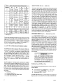
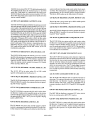
Figure~.
Diagnostic Metering Panel - Front Vlew
1. DESCRIPTION
1.1 GENERAL
The Diagnostic Metering Panel (DMP) is a service option
designed specifically for the MSF 5000 series of base and
repeater stations. The DMP includes a 5-watt audio am©Motorola, Inc. 1990
All Rights Reserved
Printed in U.S.A.
plifier (and speaker), and a meter used to monitor the station transmitter and receiver circuits. The meter circuit
provides five selected metering positions, as well as a
Ill-volt or a 25-volt full scale de voltmeter selected position. The DMP also provides a station parameter status
display matrix, which permits the service technician to simultaneously monitor the status of up to 64 different station operating parameters (bits), as shown in Table 1.
technical writing services
1301 E. Algonquin Road, Schaumburg, IL 60196
68P81114E03-D
7/15/90-
UP
Table l.
ADDRESS
D3
D2
D1
DO
TALM
DS
LOCPTT
SALM
DS
INTCOM
0
SPXMr
SCAN
1
RPTPTT
2
TXPLDS
LIN PTT
TX
ACT··
RX2ACT
RXIACT
3
RXPLDS
Rl PLDT
Rl SO LV
4
R2MUTE
R2PLDT
R2S0LV
5
GDTN
DT
ACC
DIS··
AUXDET
RPTKD
RIUN
SO··
R2UN
SO··
RPT
USO··
EXDA
DT
DVPSEL
AUXC4
AUXC4
AUXC2
AUXC2
6
..
7
8
TXRXC8
9
AUXC8
10
11
12
RW40VG
13
RWC8
14
FWC4
15
FWC8
currently unassigned
.•• status only bits
.
..
.
SELECT AUDIO (Pin 32) - Audio line
Station Parameter Status Display Matrix
..
..
..
..
..
RW3.SYN
RWC7
FWC3
FWC7
RW2PA
RWC6
FWC2
FWC6
DVPC/C
Baud Rate
AUXCI
AUXCl
..
..
RWIBAT
RWC5
FWCl
FWC5
The Select Audio signal, originating on the station control
module, is the audio input for the local speaker amplifier
circuit in the DMP. Any of the following audio signals will
be present on the select audio line when it is properly
gated by the control circuits in the station: primary receiver audio, secondary receiver audio, transmit audio from
the remote wire line, and automatic station LD. and
alarm tone audio. The Select.Andio line is connected to
the wiper of the VOLUMpcontrol on the control tray
front panel. Therefore, the debias level and ac level on
the line vary depending onthe VOLUME control setting.
The DMP employs an audio power amplifier circuit to
provide up to 5 watts of local service audio from the Select
Audio signal, through the DMP internal 4-ohm speaker.
The audio power amplifier circuit can be disabled with
SPEAKER ON/OFF switch S121O,located on the face of
the DMP. By connecting an optional microphone
(HMN1001) to CONTROL Jack J812 on the front panel
of the station control tray, the transmitter can be locally
keyed and modulated, or intercom with the remote control.console operator can be accomplished.
EXPANSION RE5ET (Pin 12) - Dedicated Logic line
11Ie.EXPANSION RESET signal is a shared logic line
These same operatingparameters may also be selectively
altered using various control switches located-on the
DMP. Also, two separate 7-segment display units indicate
(in hexadecimal notation =-$#) the current auxiliary
primary operating station channels ($1 through $F
Channell through 15, and $0 Channell).
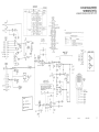
1.2 DMP 4O-CONDUCTOR
INTERFACE
CABLE
The DMP comes with a separate 40-conductor ribbon interface cable, a separate 8-conductor metering cable with
"modular" connectors, two separate voltage probes and
a set of housing rods that may be extended and inserted
into the mounting rails inside the station cabinet. Refer
to Figure 2 for the locations of the connectors used for
the CONTROL (11201), METER (11202), + voltage
probe (11203), and - voltage probe (11204). Refer to
Figure 3 for a view of the DMP with its front panel removed.
The 40-conductor interface cable connects the station
EXPANSION connector J800 (located on the top of the
control tray housing) to the DMP CONTROL connector
J1201. This cable provides interface lines which connect
power, audio and digital signals between the station control board, other control modules within the station, and
the DMP. There are four types of signal lines provided,
as follows:
•• audio line
., dedicated logic line
., multiplexed logic (MUXbus) lines
., power and ground lines
2
whiCh allows a clean, coordinated start up of the station
co:fltro1module and any other interconnected modules or
e~t~rnal equipment (such as the DMP). The EXPAN~QN RESET signal is active low at power-up, or when
station control module switch S801 is put into the TEST
position, or when t~ station control module is reset by
its watchdog timer circuit, or when another control module receives a command to reset the station. Also, normal
MUXbus operation is suspended while the watchdog timer circuit generated RESET signal is active low. The
MUXbus data strobe line DS, is held inactive and the
MUXbus address and data lines do not follow their normal patterns.
IMPORTANT
While the EXPANSION RESET line is
active low, no module except the station
control module should write to the MUXbus data lines. Otherwise, the station control module may fail its self diagnostic
tests, and remain reset indefinitely.
Multiplexed Logic (MUXbus) lines
The multiplexed logic (MUXbus) lines consist of the following signals:
*
••
••
Four Address lines (BAO-BA3) - Pins 13-16
Four Data lines (BDO-BD3) - Pins 17-20
Data strobe (DS) - Pin 22
All DMP MUXbus lines are referenced to audio ground
(logic ground is not used). The four address and the four
68P81114E03
7/15/90
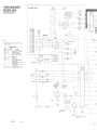
METER
CONNECTOR
(J1202)
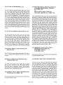
Figure 2.
Diagnostic Metering Panel - Edge View
FAEPS-36238-A
(1624)
3.
Diagnostic Metermg Panel - Internal View
data lines define 16 words of 4~bits each, or 64 total bits
as shown in Table 1. These bits form a multi-directional
digital communications path. The bus is multiplexed to
conserve interconnections (64 connections reduced to 9)
and to increase future expansion capability. The data
strobe and the four address lines are driven by the
control module. The data lines are.inverted and open collector driven in both the station control module and the
DMP. This allows the station control module and the
DMP to drive the same bit in a nondestructive, wired
"OR" fashion.
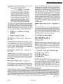
The MUXbus timing diagram is shown in Figure 4. The
address lines are incremented once, approximately every
310 microseconds. The address changes when data strobe
is inactive CDS = 1). The data must be valid for 1 micro-
7/15/90
",AllH,d\!,
edge of DS. The data must be valthe rising edge of DS. At certhe MUXbus may be momentarily halted (e.g.,
halt is, in effect, an extended
strobe. The address lines will be
Uti, WIn remam at the address of the MUXbus
to the halt. The data lines are in a "don't
a halt and may be random.
any module other than the
control
does not change the state
of the station is called a "status only" bit. As an example
of a "status
Transmitter Activity (IX ACT) is
activated
station control module whenever the
transmitter
keyed. But, if the DMP
activates TX
the transmitter will not key. Thus, TX
68P81114E03
3
ACT is a "status only" MUXbus bit. All "status only"
MUXbus bits are signified in Table 1 by a double
asterisk (**).
Aoprox.
I
I
~.
I
:
~
65 usee
Pulse Width
~
:
----tV:
55
I
BAO-BA3
I
,~~~~
I
usee
X
A'o
I
i
I
At,
:
I
I
I
:
: :
X
I
tos is Data Set Up Time:
1 mi~rosecond prio~ to
I
:
! Valid X Don't: ea,.
I
~
i~
I
~i~~secI+-
Data =:)(Dto!
iill1l-m53
310
:'"
I
i i
Address
Approx.
The proper indications are the same as those obtained using a Motorola Portable Test Set or TEK-5F Meter Panel,
as described in the MSF5000 Base Station and Repeater
Instruction Manual. A specific meter position is selected
by using the METER selector switch S1208 on the face of
the DMP. When METER selector switch S1208 is in the
"10 V" or "25 V" position, the meter monitors the voltage probes and is calibrated to read full-scale voltage (instead of full-scale microamperes).
IMPORTA.NT
When measuringthe.power
amplifier circuits, via J503, meter REVERSING switch
S1209 must be placed in the "-" (or reverse) position. METER REVERSING
switch S1209 is normally in the" +" (or
forward) position when the DMP is connected to either J413 or J210 (TX or RX
Metering, respectively).
Ft':V"id ><=
I
Data must be valid at least
edqe
valid at least
I
1:5S rising
tOH
IS
AEPS-35788-0
Data Hold Time: Data must be
15 microseconds
after
the rising
edge of
5S.
Ato is any address and At 1 is the next address
Dt 0 is the data corresponding to At 0' etc.
Figure 4.
MUXbus Timing Diagram
1.3 DMP 8-CONDUCTOR
METERING
CABLE
The 8-conductor metering cable connects the DMP METER Jack J1202 to either the station TX Metering or station RX Metering Jack. The TX and RX Metering Jacks
(J413 and J21O, respectively) are both located on the station RF Tray front panel. The PAMetering Jack (J503) is
located on the PA Distribution Board, within the station
Power Amplifier Deck. This cable provides interface lines
which connect five metering lines and a meter common
line to the DMP, as shown in Table 2.
1.4 VOLTAGE PROBES
The two voltage
the bottom edge
BLK = "-" =
with a reversible
2.
probes plug into two jacks provided on
of the DMP: RED = "+" = J1203;
J1204. Each of the probes is equipped
blunt or pointed tip.
METERING FACILITIES
The DMP provides a measured indication for the signals
listed in Table 2 on a 0-50 J.l.A full-scale meter (MI201).
Table 2.
Line
1
2
3
4
5
6
7
8
4
DMP Meter JI202
Meter 1
Meter 2
Meter 3
Meter 4
Meter 5
Not Used
Meter Common
Not Used
3.
DIAGNOSTIC FACILITIES
3.1
GENERAL
The right hand portion of the DMP contains the switches
and displays required to monitor and manipulate the operating parameters of the station. These functions are
made possible by connecting circuits of the DMP to the
MUXbus of the station EXPANSION connector (J800).
3.2
CHANNEL DISPLAY
The CHANNEL display consists of two 7-segment LED
packages that are used to display the station's current auxiliary operating channel (left-most unit) and its current
primary operating channel (right-most unit). The primary
operating channel is the channel currently selected for
the station transmitter and primary receiver. The auxiliachannel may have several uses, one of which is that it
would be the selected channel of the secondary receiver
in a 2-receiver station. The operating CHANNEL display
changes each time the station changes operating channel,
or the operating channel is changed via the channel select
switch on the station control tray. The auxiliary CHANNEL display changes only when a change of operating
channel occurs.
ry
DMP Metering Cable Interface Lines
TX Metering J413
Forward Voltage
Not Used
Control Voltage
Not Used
XMTR Synthesizer Steering Line
GND
GND
GND
68P81114E03
RX Metering J210
Quadrature Detector
I-F Level
Mixer Output
Reference Oscillator
RCVR Synthesizer Steering Line
GND
GND
GND
PA Metering J503
Final Stage 1
Final Stage 2
Final Stage 3
Predriver Stage
Driver Stage
Factory Test
A + Meter Reference
Factory Test
7/15/90
DI~GNOSrrIC MErrEBING P~NEL.;
3.3
STATUS DISPLAY
The Station Parameter Status Display Matrix consists of
eight 8 element LED packages located behind the recessed sceened panel of the DMP. The screening identifies each of 641vlUXbus bits, via a specific mnemonic designation, as shown in Thole 1.
The STATUS DisplaY.Pl"()vides a visible indication of the
major portion of the main control related activities that
are occurring at any timejn. the station. These include various push-to-talk signals, the state of the squelch circuits,
the presence of properly coded squelch signals, the station channel, the station-level
alarms and "wild" card
functions, as well as specialized activities such as Channel-Scan or DVP operation.
NOTE
To check to see if all the LEDs in this section of DMP are functional, momentarily
switch the ENIER DATA-TEST switch to
the TEST position. AU 64 LEDs in the
STATUS display area should light, and the
two-digit CHANNEL display should indicate $FF.
The STATUS Display indicates the active control conditions within the station with a corresponding illuminated
LED. The absence of an expected condition can be readily
observed as the station is operated, leading to rapid identification of a defective area.
To simulate an active condition in the station using the
DMP, select the address or row in the display containing
the particular signal with the ADDRESS switch. Next, set
one of the data switches DO through D3 corresponding to
the column in the display containing the signal. Momentarily switch the ENTER DATA-TEST switch to the ENTER DATA position and the condition will become active. To clear the condition, return the data switch to the
OFF position and flip the switch to the ENTER DATA
position once again.
CAUTION
It is recommended
that the DMP be disconnected from the control tray (via J8oo)
during station power up. This prevents the
station from being initially activated in a
possible undesirable function. However, if
the station is powered up with the DMP
connected, and an undesirable condition
does occur, place the four DATA switches
to the OFF position, and then toggle the
ENTER DATA switch. This will deactivate
the four DMP data bits applied to the
MUXbus Data Line and remove the undesirable condition
7/15/90
An active condition is also cleared when the ADDRESS
switch is moved to a different address, and the ENTER
DATA switch is used to activate a MUXbus bit at the new
address.
For example, suppose it is desired to verify that the proper
alarm tones would be sent by the station in the event of
a PA failure. To simulate this alarm condition using the
DMP, set the ADDRESS switch to 12 (the row containing
the PA alarm signal) and flip the data switch up (for the
column containing this signal (D1). Flip the ENfER
DATA switch, illuminating the LED in the status display
for PA alarm and activating a simulated PA failure alarm.
If the station is working properly, two beeps will be heard.
If the Dl switch is turned to the OFF position and the ENTER DATA switch is activated, the PA alarm LED will
tum off, and the alarm beeps will cease. Likewise, if the
ADDRESS switch is moved to address 1, and the D1
switch is left in the up position, then when the ENTER
DATA switch is activated, the PA alarm LED will turn off,
the alarm beeps will cease, the LOCal PTf LED will illuminate, and the station will key up.
NOTE
"Status only" bits, when activated by the
DMP, will cause their corresponding LED
to light, but will not affect a change in station operation. The station causes these
LEDs to light when it has successfully accomplished a certain function.
4.
MUXBUS BIT DEFINITIONS
4.1
INTRODUCTION
The following paragraphs provide definitions for each of
the 64 operating parameters (MUXbus Bits) displayed by
the DMP. Each of these bits may have their state changed
by the DMP. Each paragraph title gives the MUXbus Bit
mnemonic, definition, and row-column address required
for access (in the form: #, D#), respectively.
4.2
SP XMIT (SPECIAL TRANSMIT)
0, D3
The SP XMIT bit indicates that the deviation and/or the
rf PA power should be either boosted or cut, defined by
information in the station control module code plug. The
default condition in the station control module code plug,
upon activation of this MUXbus bit, is deviation control.
This bit will only have an effect during a PIT. The activation of this bit, by itself, will not key the station.
4.3
SCAN (SCAN ENABLE) 0, D2
The SCAN bit forces the station control module to enable
the primary receiver as a scanning receiver. The station
must be ordered with the Channel-Scan option in order
for this feature to operate. Only the primary receiver can
scan.
68P81114E03
5
4.4
T ALM DS (TOTAL ALARM DISABLE) 0, Dl
The T ALM DS bit mutes all alarm tones until this bit is
deactivated. This bit will deactivate the station control
module alarm bits on the Reverse "Wild Card" bits 1
through 4, but will not affect the other Reverse "Wild
Card" bits on the MUXbus. Pulsing T ALM DS for 25
msec or longer will release S ALM DS, if active.
4.5
S ALM DS (SELECTIVE
ALARM DISABLE) O,DO
The S ALM DS bit is meant to support a "nuisance avoidance" alarm feature. The console operator can mute inprogress alarm tones without fear of missing any new
alarms. For example, initially all alarm bits (Reverse
"Wild Card" bits, addresses 12 & 13) and S ALM DS are
inactive. An alarm condition activates an alarm bit, and
alarm tones are heard. The wireline control pulses
S ALM DS active for 25 msec or longer in response to a
remote control console command, and the alarm tones
are muted. If the alarm condition were to disappear, the
corresponding alarm bit would be deactivated, S ALM DS
would be cleared, and no alarm tones would be heard
since no alarm bit is active. If, instead, a second alarm bit
were activated while the first alarm was active, S ALM DS
would be deactivated and alarm tones for both alarms
would be heard. The wireline control could re-enable
S ALM DS, then alarm tones for both alarms would be
muted. S ALM DS does not deactivate the MUXbus
alarm bits, but merely mutes the alarm tones.
4.6
RPT PTT (REPEATER
PUSH-TO-TALK)
1, D3
The RPT PTT bit keys the transmitter, modulating with
RX 1 Audio if no higher-priority PTT is active. If a higher -priority PTT is active, the station control module deactivates RPT P1T. If the repeater PTT time-out timer
(TOT) times out, RPT PTT will be deactivated, and the
transmitter will dekey. If repeater knock down (RPT KD)
goes active while RPT PTT is active, RPT PTT will be
deactivated, PL reverse burst or DPL turn off code (RBI
TOC) will be encoded if appropriate, and the transmitter
will dekey. RPT PTT is active during repeater drop-out
delay. RPT PTT is inactive when RBITOC is encoded.
The station control module turns on RPT P1T, if repeater
audio activity exists on Receiver 1, and if RPT KD is inactive, and if no higher-priority
PTT is active. "Repeater
audio activity" is set for each channel by station control
module code plug qualifiers. These qualifiers determine
what combination of the four MUXbus bits RX P L DS,
Rl PL DT, RPT USQ, and AUX DET are ANDed to obtain RPT PTf. Line, Local, and Repeater PTT priorities
are set for each channel by station control module code
plug qualifiers.
4.7
LIN PTT (LINE PUSH-TO-TALK)
I,D2
4.8
LOC PTT (LOCAL PVSH- TO-TALK)
1, Dl
The LOC PTT bit keys the transmitter, modulating with
Local Audio if no higher priority PTT is active. LOC PTT
says active if a higher priority PTT is active. LOC PTT is
inactive when RBITOC is encoded, unless the RBIT OC
is caused by the Local PTT TOT timing out. If the station
is so equipped, LO C PTT switches the antenna switch to
its transmit state. LOC PTT is active if the PTT switch is
depressed on the local microphone plugged into the station control module front panel CONTROL connector
J812. Line, Local, and Repeater PTT priorities are set for
each channel by station control module code plug qualifiers. The front panel XMIT switch on the station control
module will activate TX PL DS and key the station without activating the LOC PTT bit on the MUXbus. This key
will be without PL, DPL, or audio (silent carrier). As
thusly defined, it is not a true P1T, and can be overridden
by any other PTT
4.9
INTCOM (INTERCOM)
1, DO
The INTCOM bit is active if the remote control module
INTERCOM switch is actuated. When INTCOM is active, the station control module treats LOC PTT as an Intercom P1T. Local Audio is gated to the wireline (outbound wireline) when a local PTT is generated, but the
transmitter is not keyed. When LOC PTT is not active,
remote control console audio (inbound wireline) is gated
to the 112-watt local audio amplifier.
4.10 TX PL DS (TRANSMIT PLIDPL DISABLE) 2, D3
The TX PL DS bit mutes encoded PL or DPL. The Transmit PL Strip wireline option utilizes this bit. If PL or DPL
is being encoded when TX PL DS goes active, then RBI
TOC will be generated before muting PL or DPL. This
bit will also be set active whenever PLI DPL encoding is
disabled, such as during an auto ID transmission, or if the
front panel XMIT switch on station control module is activated.
4.11 TX ACT (TRANSMITTER
ACTMTY)
2, D2
The TX ACT is a status only bit, and indicates that the
transmit rf channel (outbound) is ready. TX ACT goes active after a keyup, when the transmitter power output has
stabilized. In the event of a PA failure on keyup, TX ACT
stays inactive (doesn't glitch). TX ACT goes inactive
when the station control module dekeys the PA. TX ACT
is inactive during RBITOC.
4.12 RX2 ACT (RECEIVER 2 ACTMTY)
The LIN PTT bit keys the transmitter, modulating with
TX Audio (inbound wireline) if no higher-priority PTT is
6
active. LIN PTT stays active if a higher-priority PTT is active. LIN PTT is inactive when RBITOC is encoded, unless the RBITOC is caused by the Line PT T TOT timing
out. If the station is so equipped, LIN PTT switches the
antenna switch to its transmit state. Line, Local, and Repeater PTT priorities are set for each channel by station
control module code plug qualifiers
2,
m
The RX2 ACT bit indicates whether second receiver audio should be used. The second receiver control module
68P81114E03
7/15/90
responds to an active RX2 ACT by gating deemphasized,
PL-stripped audio from the second receiver to the RX2
audio line. From there, it is mixed with line audio (outbound wireline) by the station control module. RX2 Audio is also mixed with select audio (local speaker) by the
station control module.
audio (outbound wireline) and select audio (local speaker) lines. The attenuation is accomplished by means of a
potentiometer
on the second receiver control module.
Therefore, RX2 audio can be fully muted, if desired.
4.13 RX1 ACT (RECEIVER
The R2 PL DT is active when PL or DPL coded squelch
is being detected via Receiver 2.
1 ACTMTY)
2, DO
The RXI ACT bit indicates whether the primary receiver
has audio present with the proper qualifiers to unmute receiver audio. This condition is set for each channel by four
qualifiers in the station control module code plug. These
qualifiers determine what combination of the four MUXbus bits RX PL DS, Rl PL DT, Rl UN SQ, and AUX DET
are ANDed to obtain RXI ACf. The station control module responds to an active RXI ACT by opening the RXI
audio gate. This gates RXI audio to both the line audio
(outbound wireline) and select audio (local speaker) lines.
RXI audio is also gated to the station control module repeater audio gate. If the station is transmitting due to a
RPT PTT, then the repeater audio gate will be open and
RXI audio will be gated, via the IDC circuit, to the TX
modulation audio line.
4.14 RX PL DS (RECEIVE PLIDPL
4.19 R2 PL DT (RECEIVER 2 PLlDPL
DETECT) 4, D2
4.20 R2 SQ LV (RECEIVER 2 SQUELCH LEVEL) 4, D1
The R2 SQ LV bit changes the carrier squelch threshold.
When R2 SQ LV is active, the second receiver is operating with "loose" squelch.
4.21 R2 UN SQ (RECEIVER
2 UNSQUELCH)
4, DO
The R2 UN SQ bit is a status only bit, and is active when
the Receiver 2 audio carrier squelch circuit on the second
receiver control module detects activity. R2 UN SQ is
used for audio gating (refer to RX2 ACT). The second receiver can neither key the repeater (activate RPT PIT),
nor modulate the transmitter.
DISABLE) 3, D3
4.22 GD TN DT (GUARD TONE DETECT) 5, D3
The RX PL DS bit causes the station to revert to carrier
squelch only operation for purposes of determining status
of RXI ACT and RX2 ACf. The Monitor and Receiver
Squelch OnlOff wireline functions utilize RX PL DS.
Also, the station control module front panel PL Disable
switch activates RX PL DS.
4.15 Rl PL DT (RECEIVER 1 PLlDPL
DETECT) 3, D2
The Rl PL DT bit is active when PL or DPL coded
squelch is being detected via Receiver 1.
nt
4.16 Rl SQ LV (RECEIVER 1 SQUELCH LEVEL) 3,
The R 1 SQ LV bit changes the carrier squelch threshold.
When Rl SQ LV is active, the primary receiver is operating with "loose" squelch.
4.17 Rl UN SQ (RECEIVER
1 UNSQUELCH)
The GD TN DT bit becomes active whenever high level
guard tone is detected from the TX Audio signal (inbound
wireline) by the tone remote control module. In stations
with an antenna switch, the station control module responds to an active GD TN DT by switching the antenna
switch to its transmit state. The TX Audio signal is muted
(on the station control module) while GD TN DT is active, in order to prevent remote control tones from being
transmitted.
4.23 AUX DET (AUXILIARY DETECT)
The AUX DET bit indicates that an optional decoder is
detecting. The optional decoder may be connected to either Receiver 1 or Receiver 2 audio. AUX DET can be
used to activate TXl ACT , RX2 ACT, and RPT PIT in
a manner similar to the Rl PL DT and Rl UN SQ qualifiers.
3, DO
4.24 RPT KD (REPEATER
The Rl UN SQ bit is a status only bit, and is active when
the Receiver 1audio carrier squelch circuit on the station
control module detects activity. Rl UN SQ is used for audio gating (refer to RX 1ACT), not for repeater keying
(refer to RPT PIT).
4.18 R2 MUTE (RECEIVER 2 MUTE) 4, D3
The R2 MUfE bit causes the second receiver control
module to attenuate the audio driving the RX2 audio line,
so that Local or RXI audio can be heard on both the line
7/15/90
5, D2
KNOCK-DOWN)
5, Dl
The RPT KD bit disallows a repeater PTT. Also, this bit
forces an existing active RPT PIT inactive.
4.25 RPT USQ (REPEATER
UN SQUELCH)
5, DO
The RPT USQ bit is a status only bit, and is active when
the Receiver 1repeater carrier squelch circuit, located on
the station control module, detects activity. This bit is
used to key the repeater, not to gate audio (refer to RPT
PTT).
68P81114E03
7
4.26 ACC DIS (ACCESS DISABLE) 6, D3
The ACC DIS bit is a status only bit, and is active when
the Access Disable station control module switch is actuated. ACC DIS active indicates that the following five
functions are inhibited: 1) Auto ID; 2) Alarm tones; 3)
Time-out timers; 4) Repeater PIT initiated from the primary receiver; and, 5) Wire line commands including Line
P1T. When Access Disabled, the station operating channel is selected with the CHANNEL select switch, located
on the front panel of the remote control module. The previous station operating channel is "remembered"
by the
station control module and reinstated when the Access
Disable switch is deactivated. If there is no remote control
module connected as part of the station (repeater only operation) the DMP channel display will show $0, but the
station control module will equate this with Channell operation.
4.27 EX DA DT (EXTERNAL
DATA DETECT)
6, D2
The EX DA DT bit, when active, can cause the station
control module to mute TX, and/or local, and/or RXI
(Repeater) audios, under code plug programming control. This bit can allow or disallow selected mixing of these
audios with TX data audio onto the TX modulation audio
line. Which of the three audios is muted depends on
which PTT is keying the transmitter. The intent is to optionally prevent audio from mixing with TX Data audio.
Whether or not mixing occurs is determined by a qualifier
for each channel in the station control module code plug.
The DVP SEL bit selects either the primary DVP code 1,
or the secondary DVP subcode from the DVP control
module.
10 and 11, BITS 3 THRU 0
FOR FUTURE USE)
10, DO and
11, DO
These parameter bits are reserved for future applications
or special customer needs.
4.33 REVERSE "WILD CARD" PARAMETER
4.29 DW C/C (DIGITAL VOICE PROTECTION
CODED/CLEAR) 6, DO
The DVP C/C bit, when active, enables the encryption
and decryption functions of the DVP control module.
Therefore, voice is transmitted "coded". When inactive,
this bit disables the encryption and decryption functions.
Therefore, voice is transmitted "clear".
FOR
These parameter bits are reserved for future applications,
or special customer needs.
8
These eight bits determine up to two sets of channels for
the station. A channel is a station state which chooses predefined groups of station parameters such as transmit and
receive frequencies and coded squelch code. The channel
parameters are defined in the station control module
code plug. Also, the station control module code plug
contains the transmit, primary receive, and Channel-Scan
parameters. The (second receiver control module) code
plug contains the second receiver parameters. The TX/
RX Channel occupies Address 8, Bits 3-0. The Auxiliary
Channel (Second Receiver and Channel-Scan)
occupies
Address 9, Bits 3-0. Optionally, the bits making up the
two channels can be re-grouped to form two different
channels, in which one channel has more. than four bits.
In this optional configuration, the TX/RX Channel least
significant bit (LSB) is at Address 8, Bit O. If more than
four bits are required to form the TX/RX channel representation, then those bits are taken from the auxiliary
channel assignments beginning with bit 0 of address 9.
The Auxiliary Channel then starts (LSB) with the next
available bit after the last defined TX/RX channel bit and
continues to bit 3 of address 9. If the two channels are to
be independent,
then they cannot share any bits. This
means that the sum of the numbers of bits for the two independent channels must be eight or less.
4.32 ADDRESSES
(RESERVED
10, D3 THRU
11, D3 TURU
4.28 DW SEL (DIGITAL VOICE PROTECTION
SELECT) 6, Dl
4.30 ADDRESS 7, BITS 3 THRU 0 (RESERVED
FUTURE USE) 7, D3 THRU 7, DO
4.31 TX RX C8, TX RX C4, TX RX C2, & TX RX Cl
(TRANSMITTER/RECEIVER
1 CHANNEL)
8, D3 TURU 8, DO
and
AUX C8, AUX C4, AUX C2, & AUX Cl
(AUXILIARY CHANNEL) 9, D3 TURU 9, DO
BITS
Use of the reverse "wild card" bits (8 bits total, addresses
12 & 13) requires the "wild card" module which resides
in the Control Option Tray. The "wild card" inputs (four
per card) activate or deactivate the appropriate Reverse
"wild card" MUXbus bit in response to a status signal external to the station. The eight reverse "wild card" MUXbus bits also have an additional definition. They are considered alarms which, when activated, translate to alarm
tones and are sent to the remote control console via the
outbound wireline. Optionally, the alarm tones may also
be transmitted. The alarms are tone bursts (beeps). The
four bits in Address 12 are normally defined as internal
alarms and do not require the "wild card" equipment.
Station conditions which the station control module mon-
68P81114E03
7/15/90
DIAGNOSTIC
itors cause the station control module to write to these
bits which, in tum, send the alarm tones.
NOTE
If the four internal alarm bits of address 12
are activated by the DMP, or some other
control module connected to the MUXbus, then the alarm beeps will be activated,
but the actual internal alarm condition will
not be simulated. For example, if the PA
Fail alarm bit (RW2 PA) were to be activated, two alarm beeps would be sent, but
the PA itself would not be forced to dekey.
The station control module code plug contains information
which determines whether an internal alarm gets written to
the MUXbus, and also if all of the reverse "wild card"
MUXbus bits will be enabled to activate alarm tones. Thus,
all 8 bits can be configured as external alarm inputs, if desired. The maximum number of internal alarms is four.
5.
5.1
INTERNAL I EXTERNAL STATION
ALARMS
failed. A successful keyup or a station control module reset
is required to clear the alarm. The alarm may be active when
the transmitter is de-keyed, due to a prior failure. PA Fail
means that one or both of the station control module PA
status lines (pA On or PA Full Power) are inactive 30-45
msec after the start of a keyup, or for 30-45 msec continuously during keyup, thereafter. RW2 PA is not activated by
the station control module if the PA is not keyed at full power due to the station control module personality EPROM
rf power cut option. If the station control module service
jumper (JUB01) is installed, the station control module will
activate RW2 PA regardless of the PA status lines. This is
a reminder that the rf power amplifier is operating in a nonstandard manner.
RWl BAT (Reverse "Wild Card" Bit 1 - Bauery Revert) 12,
DO
This bit is the battery revert internal station alarm parameter activated by the station control module. RWI BAT is active when the station battery charger power supply indicates
that the station has lost ac power and has switched to emergency battery backup. RWI BAT becomes inactive as soon
as proper ac power is restored to the station.
5.2
INTERNAL STATION ALARMS
RW4 OVG (Reverse "Wild Card" Bit 4 - Bauery Overvoltaze) 12, D3
The RW4 OVG bit is the battery overvoltage internal station alarm parameter, and is activated by the station control
module. RW4 OVG is active when the station battery charger power supply indicates that the external (customer
supplied) station emergency batteries are providing too
much voltage (e.g., are overcharged).
RW3 SYN (Reverse "Wild Card" Bit 3 - Synthesizer Unlock) 12, D2
The RW3 SYN bit is the transmit or primary receiver synthesizer unlocked internal station alarm parameter, and is
activated by the station control module. RW3 SYN is active
when either the transmit, primary receive, or both synthesizers are unlocked.
RW2 PA (Reverse "Wild Card" Bit 2 - PA Rlil) 12, Dl
The RW2 PA bit is the rf power amplifier fail internal station
alarm parameter, and is activated by the station control
module. RW2 PA is active when the rf power amplifier has
COMPUTER
METERING PANEL.
EXTERNAL STATION ALARMS
RWC 5, RWC 6, RWC 7, & RWC 8
(Reverse "Wild Card" Bits 5 thru 8)
13, D3 thru 13, DO
Reserved for those reverse "wild card" applications which
provide an interface between external station inputs and the
MUXbus. These parameters can also provide additional
alarm input capability thru information contained in the station control module code plug, which allows these bits to be
identified as alarm inputs.
5.3
FORWARD "WILD CARD" PARAMETER BITS
FWC 1, FWC 2, FWC 3 & FWC 4
(14, D3 THRU 14, DO) and
FWC 5, FWC 6, FWC 7, & FWC 8
(15, D3 THRU D, DO)
Use of the Forward "Wild Card" bits (up to 8 bits on addresses 14 & 15) require the "wild card" module (four outputs per card) which resides in the Control Option Tray. Remote wireline control activates these bits. The "wild card"
control module responds by activating a relay closure or an
open collector output. These closures and/or outputs can
then be used to control equipment external to the station.
SOfTWARE
COPYRIGHTS
The Motorola products described in this instruction manual may include copyrighted Motorola computer programs stored in semiconductor
memories or other media. Laws in the United States and other countries preserve for Motorola certain exclusive rights for copyrighted computer
programs, including the exclusive right to copy or reproduce in any form the copyrighted computer program. Accordingly, any copyrighted
Motorola computer programs contained in the Motorola products described in his instruction manual may not be copied or reproduced in any
manner without the express written permission of Motorola. Furthermore. the purchase of Motorola products shall not be deemed to grant either
directly or by implication. estoppel. or otherwise, any license under the copyrights. patents. or patent applications of Motorola. except tor the
normal non-exclusive, royalty free license to use that arises by operation of law in the sale of a product.
EPS-34440-B
7/15/90
68P81114E03
9
parts list
TRN5174A
Diagnostic
REFERENCE
SYMBOL
C1201
C1202,
C1204
C1205
C1206,
C1208
C1209,
C1211
C1212
C1215,
C1217
C1218
C1219
C1220
C1221
C1222
C1223
C1229
C1230
C1236
C1237
C1240,
C1242
C1243
C1244
C1245
C1246
C1247
C1248,
C1250
1203
1207
1210
Board
PL-8196'C
MOTOROLA
PART NO.
8·11017A02
8·11017A17
21·11022K50
23-84665F17
23-84665F32
8·11017A17
23·11019A09
8·11017A20
8·11017A17
21·11022K50
8·11019A02
capacitor,
fixed; uF ± 5%;
unless otherwise
stated
.0015
0.1
220 pF
1500 + 100·10%; 16 V
330 ± 20%; 10 V
0.1
21·11021G07
CR1201,1202
CR1203
CR1204
48-11034A01
48-84616A09
48·11034A01
diode: (see nole)
silicon
hot carrier
silicon
DS1201 thru
1208
DS1209, 1210
48-84329N01
display:
lED ARRAY; 4-position
23-11019MO
thru
1228
thru
1235
thru 1239
1241
23-83210A24
23-11019MO
21-11021G07
21·11021G07
8-11051A16
21-11021G07
21-11022K50
21-11022K25
8-11017A10
2H1022K25
21·11015809
1249
50 V:
1.0 ±20%
.0015
0.1
220 pF
.0015
NOT USED
47 ±20%;
25 V
NOT USED
1000;20V
47 ± 20%; 20 V
.01 + 100·0%
NOT USED
0.1 +100-0%
0.33
NOT USED
.01 + 100·0%
220 pF
NOT USED
20 pF
.018
20 pF
470 pF ± 10%; 100 V
NOT USED
.01 +100·0%
thru 1214
1216
REFERENCE
SYMBOl
DESCRIPTION
S1201
S1202 thru
S1208
S1209
S1210
S1211
(2 used)
65·82408R01
J1201
J1202
J1203
J1204
J1205
28·83835N01
9·831112N02
9·88254C03
9·88254C01
28·83143M05
connector,
receptacle:
male; 40·contact
female; 8·contact
female; slnqle-contact:
female; single-contact;
male; 4·contact
25·82786N01
coil, audio:
choke, 600 uH
48-869649
48·869706
48-869653
transistor:
(see note)
PN P; type M9649
NPN; Darlington;
type M9706
FET, N-channel;
type M9643
R1201 thru 1204
R1205
R1206 thru 1212
R1213 thru 1216
R1217,1218
R1219 thru 1222
R1223 thru 1226
R1227
R1228
R1229
R1230, 1231
R1232
R1233
R1234
R1235
R1236
R1237
R1238,1239
R1240
R1241,1242
R1243
R1244
R1245, 1246
R1247
R1248
R1249
R1250
R1251
R1252
R1253 thru 1268
6·11009A89
6·11009A62
6·11009A89
6·11009A89
6·11009A56
6·11009A23
6·11009A56
6·11009805
6·11009814
6·11009M2
6-11009A84
6-11009A62
6-11009A97
6-11009A56
6-11009A34
6·11009A10
6·1100942
6·125870
6-10621C56
6·10621C53
6-11009814
6-11009805
6·11009814
6·11009A76
6·11009A69
6·11009A23
6-11009A76
switch:
rotary: 16-position
toggle; spdt
rotary; 7-position;
toggle; dpdt
toggle; spdt
toggle; spdt
U1201
U1202
U1203
U1204,1205
51-82884l32
51-82884 L28
51-82609M73
51-83548N18
U1206
U1207, 1208
U1209
U1210
U1211
U1213,1214
U1215
U1216
U1217
U1218
51-82884 l02
51-82884l15
51-82884L49
51-82609M61
51-84371 K83
51-83629M86
51-82609M05
51-84320A47
51-83627M88
51-84561 L86
TKN8914A
Diagnostic
REFERENCE
SYMBOL
F1201
1204
1220
40-84226N01
40-83685N04
40-84449N01
40·83685N06
40-83685N04
40-83685N08
display
P1203
P1204
P1205
coded
coded
resistor,
fixed; ± 5%; 114 W:
unless otherwise
stated
47k
3.6k
47k
NOT USED
47k
2k
82
2k
220k
470k
NOT USED
510
30k
3.6k
100k
2k
240
24
510
1;1/2W
4.32k ± 1%
4.02k ± 1%
470k
200k
470k
NOT USED
13k
6.8k
82
13k
Cabling
2 pole
integrated
circuit: (see nole)
4-bit latch & 4-to-16 line decoder
dual monostable
multivibrator
quad D-type tllp-flop with clear
BCD-to-HEX
7-segment
latch-decoderdriver
hex inverter buffer
quad latch
quad exclusiveOft
gate
dual 5-input NOH gate
quad 2-input NAND gate
audio power amplifier
operational
amplifier
5-voll regulator
level shifter
5-volt regulator
parts
2 used
KNOB, control;
FUSE, holder
note: For optimum
performance,
diodes,
be ordered by Motorola
part numbers.
luse:
3A; 32 V
thru
thru
6-11009A84
6·11009A49
6-11009A89
6-11009A76
mechanical
7-segment
01210
01205
01221
1205
D~SCRIPTION
NOT USED
47k
13k
NOT USED
30k
1k
36-83144N01
9-82425R01
48·82771 l03
l1201
R1269 thru 1285
R1286 thru 1289
R1290, 1291
R1292
R1293
R1294
MOTOROLA
PART NO_
transistors,
and integrated
circuits
must
PL·8430-0
Kit
MOTOROLA
PART NO.
DeSCRIPTION
connector,
plug:
male; sinqle contact
single contact
4-contact
28-84751 N01
28-84751 N02
15-83142M08
(RED)
(8lK)
1·80766D37
RED
BlK
receptacle;
39-82717MOI
1-80766047
4 used
(RED);
includes
10-82465802
29-82676C02
1-80766D48
eludes:
P1204,
WIRE,
PROBE,
10-82465801
29-82676COI
THN6486A
SYMBOL
and Hardware
36" used
Kit
Pl-8197-8
PART NO.
DESCRIPTION
50-84450N01
speaker:
4 ohm; 5
M1201
72-83319GOI
meter:
50 uA
W1201
W1202
30-83941 N02
30-84225N02
40-conductor;
includes: connectors
8-conductor;includes:
connectors
lS1201
W; 3"
cable, assembly:
mechanical
2·10101A91
3-10907A10
3-83498N03
3-83498N12
3·83938N01
4-84180C01
7-83830N01
14-83022POl
14-84268AOI
15-83826N01
15-83827N02
42-10128A14
42-10217 A02
42-82143C09
47-84568N01
47-84568N02
75·82230B 14
75-84215A03
paris
NUT, spring; 4 used
SCREW, machine; M2.5 x 0.45 X 6mm;
2 used
SCREW, tapping; M3.5 x 0.6 x 13mm;
4 used
SCREW, tapping; slotted star; 3 used
SCREW, self retaining;
10-32 x 1-1/8";
2 used
WASH ER, shoulder; 3 used
BRACKET, meter
INSULATOR,
board
INSULATOR, transistor;
3 used
HOUSING, top
HOUSING,
bottom
RING, screw retaining;
rubber; 2 used
STRAp, tie; .091 X 3.62 (WHT); 2 used
cable
mounting;
right hand
mounting;
left hand
rubber; 2 used
4 used
REVISIONS
TLN2419 DIAGNOSTIC
METERING PANEL
PEPS-36253
REE
ISSUE
CI233
thru
WERE: 0.1 uF;
21-11021G04
1236
JI204
WERE:
1210
R1219 thru
R1243,
El
JI203
PROBE-t-V
Rt248
RI293
470K
30K
THN6486A
WERE:
1244
ffi]
~
ADDED
36-83144NOl;
F1201
ADDED
5
METER 4
4
METER 3
3
I
2
METER 2
METER
r
14-83022POl;
2-DELETED
RING
WAS: 42-82234GOI
IMETER I
1
POSITION
SWITCH
I
NOT
USED
6
N.C.
NOT
USED
8
N.C.
METER
REVERSING
SWITCH
•
•
•
6
8 } AUDIO GND
10
N.C. II
••
12
EXPANSION
••
14
BAI
BA2
••
16
BA3
18
B5I
20
BD3
15
~
17
••
tlm
19
•
•
22
OS
24
N.C
••
26
N. C.
••
28
N. C.
CI247
•
RESET
NOTE:
1.
••
N.C. 25
N.C. 27
N.C. 29
••
30
N. C.
N C. 31
•
•
32
SELECT
N:C. 33
"
•
34
N.C.
N.C. 35
••
U1213
U1214
U1215
U1218
AUDIO
51210
RI229
470K
EJ
ISPEAKER
N.C.
•
•
38
N. C.
N. C. 39
•
•
40
AUDIO GND
lOOK
Jt201
CI214
RI233
0.1
30K
AUDIO
32
4
3A
600UH
5
ICI221
1000
5-VOLT
1--
10
LOGIC GND
21
N,C.
-+
~----
INTERCONNECT
JACK
METER +
f!lll
METER -
IIIi
CI215
f
Cf205
RI237
.~B
+f5~
RI238
24
RI239
24
.• ~~II~~~--~
BLK
,J
l1li
~
LSI201
5W, 4 OHMS
IMETERI
JACK
RED
P1205-4
Jf205-4
PROTECTION CIRCUIT WILL LIMIT SPEAKER
OUTPUT TO LESS THAN 7W BY ATTENUATING
INPUT SIGNAL. CIRCUIT WILL NOT BEGIN
ATTENUATING UNTIL AFTER
5 WATTS OUTPUT
HAS BEEN ACHIEVED.
./'f
4
J1202
lFRONT VIEW)
240
OUTPUT LIMIT
PROTECT CIRCUIT
FUSED A++
TO DIAGNOSTIC
AND CONTROL
SECTION
RI244
4.02K
4
CI210
1+
~1_-2-+II----~
J
CRf203
5
I
2
3 4 5
Rf242
I
CI20B
0.1
C
6
NOT
USED
METER
A+
METER 5
METER 4
METER
AUDIO
GNo
RI243
01221
M9653
--..-
-Q
AUDIO SIGNAL
D
PATH
G
CI246
20PF
CRI204
RI246
470K
THEORY
S
NOTE
C1209
+
3
METER 2
4.32K
RI250
COMMON
NOT USED
CI213
0.1
-::1:-
CIRCUITS
RI241
I
1220PF
+±CI222
47
REGULATOR
UNUSED
JI205
(PIN VIEW)
4
0.1
RI232
510
VB
LATCH
IiII
SPEAKER -
I
9
4
CI203
RI236
7
8
AUDIO GND{
=
Description
Power Amplifier
Power Amplifier
OuadDiffere
ntial-Input Operational
Amplifier
5-Volt Regulator: Pin 1 = 5 V; Pin 2 = Audio
Gnd; Pin 3
Fixed A +
SPEAKER +
2
H'~
Vc
3
3
11
ffiJ
CI245
5V
-::1:-2
+
5
5
and all capacitor
~~_
RI234
2K
1--_-+-~/3~.8~V'__'\.FI:.=2:=0:.1
_ .•••. _~L~12~O~I::-..,.:-'"
+ ..•. A+
A
Audio
Gnd
A+
PIO
3
are in ohms.
BRIDGE POWER
AMPLIFIER
!
I
ICONTROLI
UI218
values
=
36
AUDIO GND 37
JI201
lPIN VIEW)
3.6K
3
all resistor
-----'I
...
n,,'e:=gratedCircui~'O-"-~~h-"_r'
Ref.
Desig.
RI235
I
Unless otherwise
specified,
values are in microfarads.
_--::-c:-
N_C. 23
470PF
1
SELECT
•
•
•
}A++
BAlli 13
I
SW1209A
SWI209B
SELECT
AUDIO
7
9
LOGIC GND 21
I
[]I
SWi208B
2
4
LIST
1
7
METER COMMON
..
LIST
81
SWi20BA
•
•
PARTS
ADDED
KNOB
AND PARTS LISTS
I
PARTS
BUFFER
AMPLIFIER
I
l--~-----------;:-'OJ
I
2-ADDED
B
JI202
METER 5
3
AUDIO GND{
R1294
RI247
I METER I
1
3.6k; 6-1 1009A62
KNOB
DIAGRAM
JACK
WAS: 6.8k; 6-1 1009A69
INSULATOR
200K
I CONTROL
48-82771LOI
WERE: 510 OHMS;
6-11009A42
1222
R1227
PROBE-V
SCHEMATIC
WAS: 48-1 1034AOI
CR1203
DS1209,
B
SCHEMATIC,
PARTS LIST &
PCB
DELETED
C1229
TRN5174A
A
LOCATION
CHANGE
SYMBOL
KIT
METER
1
VB
13K
RI245
470K
C1211
-e-
VB
.0015
-=
C1242
220PFI
DEPS-35229-A
4-22-88
68P81114E03
13
r-::bUS
TLN2419A DIAGNOSTIC
METERING PANEL
WRITE
DATA SELECT
SWITCHES
CIRCUITRY
+5V
SELECTED
DATA LATCH
SELECTED
REGISTER
SCHEMATIC DIAGRAM
DATA
CIRCUIT
S 1202
U1Z18
I JO"----!'l~-----''''''-
~
i5?l
-
01
I
~
I
B
I
6
~
I
S 1204
~
ADDRESS
PQS
I
I T I ON
0
I
NOTES:
1.
Unless otherwise
specified,
values are in microfarads.
all resistor
Integrated
Ref.
Desig.
5V
Logic
Gnd
U1201
U1202
U1203
U1204, 5
24
16
16
16
12
8
8
8
U1206
U1207, 8
U1209
U1210
16
16
14
14
8
8
7
7
U1211
14
7
U1216
-
U1217
1,13,16
Circuii
values
are in ohms
and ali capacitor
Description
Driver
8
I
Data Chart
4-Bit Latch & 4·Line·to·16·Line
Decoder
Dual Monostable
Multivibrator
Quad D-Type Flip-Flop
With Clear
BCD-to-Hex
7-Segment
Latch-DecoderInverting
Hex Buffer
Quad Latch
Quad Exclusive-OR
Gate
Dual 5-lnput
Positive-NOR
Gates,
With
Totem-Pole
Outputs
Quad 2-lnput Positive-NAND
Gates, With
Open-Coli ector Outputs
5-Volt RegUlator: Pin 1 = Fused A +; Pin 2
= Logic Gnd; Pin 3 = 5 V
TTL-or CMOS-to-CMOS
Hex Level Shifter
01
I
L
TRUTH
Art
o a
o 0
0
0
0
I
0
0
0
I
0
o
I
o
a
a
a
I
o a
I
0
I
I
I
a
I
I
10
I
II
I
IADDRESS
12
03
I.
o¢
01
01
U1207
02
02
03
03
ID
SOl
O¢
II
S02
01
12
S D3
13
eLK
I
I
0
I
I
I
I
a
15
I
I
I
I
0A01-''-£>---
o
o
AI
o
0
RI204
47K
o
o
02
03
eLK
Whon swlfch S1
Dat« Display LIl
(Q1201 thru Q1;'
ena operatlnQ (,
Simultaneously,
U1201 (1.lp&0Ied
Chf§S (01205
tnr
LED's of the s
(D$1201 thru D$
+ 5V
RIZ03
47K
RIZ02
47K
2
0[;]
o
~o
A2
0
0
0
[8]
14
10
031-'-"5'--[0>----_
+ 5V
IT]
100
13
II
14
00
Q2
eLR
B
Refer to Address Truth Table
'for switch output states.
Bo
EJo
I9
+5V
51205
S1201
6
011-'--~[O>-----
sOjj
[D2J
I
SELECT
SWITCH
a a a
a a I
a I a
a I
I
13
00
TABLE
A3 A2 AI
I
02
03
U1Z03
POL
o¢
Ul211AI
j!)"----!'l~----f!""-
0-
S1203
02
0
A3
4
COM
5
R1255
13K
SA3
FUSED A+
From
+
>---~'-1
BA3
U1209C:»,,1
O'------B~-
mo,,,lng, euato and power section.
I
4- BIT
LATC H B\
4- LINE - TO-16LINE
DECODER
PIO
J1201
13
MUXlw/>
Address
Lines
o
r
EXPANSION RESET
10
14
SA¢
SA
A0
47K
15
47K
16
3
AI
S2
10
JJ
53
14
IS
SA2
BA2
21
A2
54
U1217F
RI211
11
12
BA3
8A3
t>-
S5
22
U1217E
R1207
47K
SAl
BAI
U12178
47K
12
II
51
R1209
Rt210
5¢
U1217D
47K
B8AA~
BA3
R1208
EXPANSION
RESET
15
14
EXPANSION
0
U1217C
A3
S6
S7
RESET
58
18
+ SV
U1201
R1212
59
17
47K
SID
RI263
20
13K
-0
U12028
,,,,,.o {
12
Q
10
23
INHI BIT
51j
37
40
>4.9
I
MS
Rt266
MONOSTABLE
OS
R1206
D5
22
47K
L
U1217A
3.4
MONOSTABLE
lelch
14
68P81114E03
2-12-88
MUXbus
and
into
4
leered data} of Dala
s $1202 thru 51205
3) is entered
into
SE LECTED DATA
CIRCUIT
REGISTER
V
r--~~~~----B>-~~~---"--r-")
~
i~a~c:'u~::~7fOW~~~
U121B
1)c"'---;:>-~~~--!!l1l!.
Qi3r--+----------------------------------------+------------
osition. The/arched
n on the MUXbus
vnen U1210B·6 goes
Qll--"-~__j)>-~~~~~~~~~~~~~~~~~~~~~~~~~~~~~~~~~~~~~~~~~~~~~-+-------------,
Q2
Q3
U1203
10
01
Ul211C
lO''--t>-~~~~
Q3
01
13
12
U12110
»"-'-'-t>-~~~_~~
13
S
+5V
9
14
QOfL-__j)>-----------------------------------------------,
Ql!--!--__j)>--------------~-----------------------___,
LED 5-VOLT
SWITCHES
(Q1201-QI204)
02 10
O¢
12
11
15
[}
02
03
ClK
ClR
PfO
J120!
17
When .wltch S1211 Ja actuated to TEST position, MUXbu' ~
Dat. Display Latch U1203 forces 811 LED 5-voft swItches
(01201 thru Q12CU) on, lind causes thct auxiliary (DS1210)
and o".,atlng
(DS1209) channel displays to Indlc,t.
$F.
SimultaneouSly,
4-blt 'slch & 4·Lln8-fo-16-Llne
Decod.,
U120f fePHt&dly ripples through the LED ground switch •• (01205 th,u QI220). Theso two actfons ceuse all 64
LED's of the station parameter status display matrix
(D51201 thru 051208) to light.
'"J
18
0
R1219
Q1201
M9649
RI220
Q1202
M9649
RI221
2K
2K
2K
Rt224
82
R1223
82
Q1203
M9649
Q1204
M9649
R1222
19
SOl
'802
20
803
2K
R1225
82
¢
IAUXbu.
O.t.•
Un.!
R1226
82
+5V
R1218
47K
o
LEGEND:
RI289
47K
U1203 Decodes and latches
MUXbus data lines
RESS COMPARATOR CIRCUIT
R1286
4':"K
R12B7
47K
R1288
47K
R1253
09~"-~-t>-~___,
THEORY
NOTE
LOGIC
GND
13K
---&>--
Q1207
M9706
10 9
03
6
02 0\
6
5
5
o¢
03 C2 01
O¢
SIGNAL
BCD-TO- HEX
7-SEGMENT
LATCH-DECODER DRIVER
R1255
13K
CONTROL
R1256
U1205
UI204
13K
ABC'
ABCOEFG
09C;'JC>,,,,0~--£;>---l
12 13 14
J
A~
8¢
3
Al
82
21
13K
Q1210
M9706
22
A3
G
2
CHANNEL
DISPLAY
3
-
DS1209
DS12iO
AUXILIARY
CHANNEL
DISPLAY
R1260
13K
LED
GROUND
SWITCHES
(Q1205 - Q1220)
86
V!
I
11
10
I
~_A~_
13K
!
I'
LOAD
I
LATCH
DATA
DATA
OPERATING
CHANNEL
DISPLAY
UNUSED
CIRCUITS
COM
COM
87
8B
R1261
IB
~
13K
+5V
~
U1201
RI212
47K
89
810
17
+ 5V
+ 5V
CR120!
CR1202
R1290
R1291
R1263
20
13K
When HI, all
outputs low
Q1215
M9706
13K
13K
0
23
INHIBIT
811
R1264
19
13K
U1206A
CLOCK
PULSE
CLOCK
PULSE
"
CD
U1202A
Q
7
I
813
1-
814
STROBE
13
R1266
16
13K
15
C1240
.01
Q1218
M9706
I
!
89
I
13K
Latches and
decodes MUXbus
address lines
.,
R1268
12
I
13K
U1206E
88
10
U1206D
J
11
Provides pulse to latch
U1201sndU1203.
STATION
AWXbus Addrfflss end Data Into
PARAMETER
STATUS
DI SPLAY
MATRIX
89
89
88
Clock Pulse generating circuitu,sed
to latch operating Channel number
data into U1205, See Channel Display
Timing Diagram
C1241
.01
I
R1267
17
015
Clock Pulse generating
Circuit used to latch aux
iliary
channel
number
data into U1204, See
Channel Display Timing
Diagram
88
U12068
7"'--.6
14
3
DIAGRAM
LLs--
ClOCK~~.
PULSE'
10985423
TIMING
I I
ABCoEFG
R1259
85
BA3
F
S80RS9~
84
A2
E
15 1
SB OR 89
83
BA2
0
12 13 \4
3
-
81
SAl
2
R1258
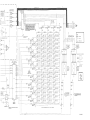
4-81T
LATCH SO
4- LINE - TO -16- LINE
DECODER
SA
15 1
TLN2419A DIAGNOSTIC
METERING PANEL
CIRCUIT BOARD DETAIL
C1206
.....jf-:;:<> ..
C1207
~~.
ui213
UI214
+
CI205
C1221
+
51208
(NOTE I)
J1204
BLK
-v
COMPONEI
SIDE SHOWN FROM COMPON ENT
12
68P81114E03
2-12-88
SIDE
SOLD!
JI2105
METER
A++
2
METER-
3
SPKR-
4
SPKR +
m
A++
3
A++ 5
AUDIO GND 7
+
AUDIO GND 9
NOT USED 11
BASE ~ETAILS
RESET
TOP VIEWS
BAIll 13
BA2 15
16 BA3
BDIll 17
18 SOl
BD2 19
20 BD3
LOGIC GND 21
22
24 NOT USED
NOT USED 25
26 NOT USED
NOT USED 27
28 NOT USED
NOT USED 29
30 NOT USED
NOT USED 31
32 SELECT AUDIO
NOT USED 33
34 NOT USED
NOT USED 35
36 NOT USED
NOT USED 39
U
~
Q1201 THRU Q1220
Z
o
I-
Z
:::>
3 2 1
~
(K)
U1218
051201 TH
(SEE DETAI~U SELOW)
051208
38 NOT USED
40
AUDIO GND
NOT USED
METER 1 OJ 1202 2 METER
METER 3
3
METER 5 5
METER COM
MON 7
Q1221
OS
NOT USED 23
AUDIO GND 37
C B E
COM K
4 METER 4
6
8
DS1209.DS1210
NOT USED
NOT USED
0
NOTES'
L THE BOXED
SCHEMATIC ~,~~BERS CORRESPOND
TO SWITCH
RAM.•••••• AND "a" TO THE
RESPECTIV~yEGMENT
S120SA AND CORRESPOND
.
S1208S.
COMPONENT SIDE
SOLDER SIDE
BD-EEPS
BD-EEPS -36182-B
OL_EEPS-36183-B
-36184- B
U1213.U1214
GND
A+
§[J
GND
4
3
2
OUT
GND
IN-
1
IN+
I 2 3
OUT
IN
~
GND
UI216