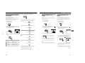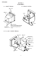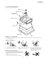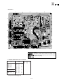
1
CPD-200GS SERVICE MANUAL Australian Model Chinese Model Chassis No. SCC-L07A-A D-1H CHASSIS SPECIFICATIONS Picture tube 0.25 mm aperture grille pitch 17 inches measured diagonally 90-degree deflection Viewable image size Approx. 327 × 243 mm (w/h) (12 7/8 × 9 5/8 inches) 16.0” viewing image Resolution Horizontal: Max. 1280 dots Vertical: Max. 1024 lines Standard image area Approx. 312 × 234 mm (w/h) (12 3/8 × 9 1/4 inches) or Approx. 293 × 234 mm (w/h) (11 5/8 × 9 1/4 inches) Deflection frequency Horizontal: 30 to 85 kHz Vertical: 50 to 120 Hz Audio output 0.5W (mono) Headphones jack Stereo minijack Accepts impedance of 8 Ω or more AUDIO IN jack Stereo minijack AC input voltage/current 100 to 240 V, 50 – 60 Hz, 1.9 – 1.1 A Power consumption Max. 120 W Dimensions 406 × 432 × 420 mm (w/h/d) (16 × 17 1/8 × 16 5/8 inches) Mass Approx. 18 kg (39 lb 11 oz) Supplied accessories See page 6 Design and specifications are subject to change without notice. TRINITRON COLOR COMPUTER DISPLAY ® MICROFILM CDP-200GS POWER SAVING FUNCTION DIAGNOSIS This monitor has three modes of reduced power consumption. By sensing the absence of video signal coming from the computer, it reduces power consumption as follows. This monitor is equipped with a self-diagnosis function. Use this function if there is a problem with your monitor or computer. 1 Power consumption mode Power consumption Recovery time u indicator 1 Disconnect the video input cable or turn off the connected computer. Normal operation ≤ 120 W (CPD-200GS) — Green 2 Turn the monitor off and on. 3 Press and hold the >/ button for 2 seconds. ≤ 110 W (CPD-100GS) 2 Standby (1st mode) ≤ 15 W Approx. 5 sec. Green and orange alternate 3 Suspend (2nd mode) ≤ 15 W Approx. 5 sec. Green and orange alternate 4 Active-off (3rd mode) ≤8W Approx. 15 sec. Orange 5 Power-off 0W — Off If all four color bars appear (white, red, green, blue) after a few seconds, the monitor is working properly but there might be a problem with your computer. Contact your computer’s manufacturer. If the color bars do not appear, there is a potential monitor failure. Inform your authorized Sony dealer of the monitor’s condition. Note If the video signal cable is not connected, the “NO INPUT SIGNAL” message (page 18) appears. After 30 seconds, the power saving function automatically puts the monitor into the active-off mode and the u indicator lights up orange. Once the horizontal and vertical sync signals are detected, the monitor automatically resumes its normal operation mode. TIMING SPECIFICATION MODE AT PRODUCTION RESOLUTION CLOCK MODE 1 MODE 2 MODE 3 MODE 4 MODE 5 MODE 6 MODE 7 MODE 8 MODE 9 640 X 480 800 X 600 800 X 600 832 X 624 1024 X 768 1024 X 768 1024 X 768 720 X 400 640 X 480 MODE 10 MODE 11 25.175 MHZ 49.500 MHz 56.250 MHz 57.283 MHz 78.750 MHz 80.000 MHz 94.500 MHz 28.322 MHz 36.000 MHz 135.000 MHz 108.000 MHZ 31.469 kHz 46.875 kHz 53.674 kHz 49.725 kHz 60.024 kHz 60.241 kHz 68.677 kHz 31.469 kHz 43.269 kHz 79.976 kHz usec usec usec usec usec usec usec usec usec usec usec 31.778 21.333 18.631 20.111 16.66 16.6 14.561 31.777 23.111 12.504 15.63 1280 X 1024 1280 X 1024 -- HORIZONTAL -H-FREQ H. TOTAL 63.981 kHz H. BLK 6.356 5.172 4.409 5.586 3.657 3.8 3.725 6.355 5.333 3.022 3.778 H. FP 0.636 0.323 0.569 0.559 0.203 0.4 0.508 0.636 1.556 0.119 0.444 H. SYNC 3.813 1.616 1.138 1.117 1.219 1.2 1.016 3.813 1.556 1.067 1.037 H. BP 1.907 3.232 2.702 3.91 2.235 2.2 2.201 1.907 2.222 1.837 2.296 H. ACTIV 25.422 16.162 14.222 14.524 13.003 12.8 10.836 25.422 17.778 9.481 11.852 59.940 Hz 75.000 Hz 85.061 Hz 74.550 Hz 75.030 Hz 74.927 Hz 84.997 Hz 70.087 Hz 85.008 Hz 75.025 Hz 60.020 Hz lines lines lines lines lines lines lines lines lines lines lines 525 625 631 667 800 804 808 449 509 1066 1066 V. BLK 45 25 31 43 32 36 40 49 29 42 42 V. FP 10 1 1 1 1 3 1 12 1 1 1 V. SYNC 2 3 3 3 3 3 3 2 3 3 3 V. BP 33 21 27 39 28 30 36 35 25 38 38 V. ACTIV 480 600 600 624 768 768 768 400 480 1024 1024 -- VERTICAL -V. FREQ(HZ) V. TOTAL -- SYNC -INT(G) EXT(H/V)/POLARITY EXT(CS)/POLARITY INT/NON INT NO NO NO NO NO NO NO NO NO NO NO YES -/- YES +/+ YES +/+ YES -/- YES +/+ YES -/- YES +/+ YES -/+ YES +/+ YES +/+ YES +/+ NO NO NO NO NO NO NO NO NO NO NO NON INT NON INT NON INT NON INT NON INT NON INT NON INT NON INT NON INT NON INT NON INT 97. 11. 14 Ver. –2– CPD-200GS TABLE OF CONTENTS Section Title Page 1. GENERAL ................................................................. 1-1 2. DISASSEMBLY 2-1. 2-2. 2-3. 2-4. Cabinet Removal ................................................ Service Position ................................................. D, A and J Boards Removal ............................... Picture Tube Removal ....................................... 2-1 2-1 2-1 2-2 3. SAFETY RELATED ADJUSTMENT ........... 3-1 4. ADJUSTMENTS .................................................... 4-1 5. DIAGRAMS 5-1. 5-2. 5-3. Block Diagram .................................................... Circuit Boards Location ...................................... Schematic Diagrams and Printed Wiring Boards ................................................................. (1) Schematic Diagrams of D and J Boards ............ (2) Schematic Diagram of A Board ......................... 5-4. Semiconductors ............................................................ 5-1 5-4 5-4 5-5 5-12 5-16 6. EXPLODED VIEWS 6-1. 6-2. Chassis ............................................................... 6-1 Packing Materials .............................................. 6-2 7. ELECTRICAL PARTS LIST .......................... 7-1 WARNING!! NEVER TURN ON THE POWER IN A CONDITION IN WHICH THE DEGAUSS COIL HAS BEEN REMOVED. SAFETY-RELATED COMPONENT WARNING!! COMPONENTS IDENTIFIED BY SHADING AND MARK ¡ ON THE SCHEMATIC DIAGRAMS, EXPLODED VIEWS AND IN THE PARTS LIST ARE CRITICAL FOR SAFE OPERATION. REPLACE THESE COMPONENTS WITH SONY PARTS WHOSE PART NUMBERS APPEAR AS SHOWN IN THIS MANUAL OR IN SUPPLEMENTS PUBLISHED BY SONY. CIRCUIT ADJUSTMENTS THAT ARE CRITICAL FOR SAFE OPERATION ARE IDENTIFIED IN THIS MANUAL. FOLLOW THESE PROCEDURES WHENEVER CRITICAL COMPONENTS ARE REPLACED OR IMPROPER OPERATION IS SUSPECTED. –3– The operating instructions mentioned here are partial abstracts from the Operating Instruction Manual. The page numbers of the Operating Instruction Manual remain as in the manual. SECTION 1 GENERAL Getting started Started Getting Started Getting Started Warningonpowerconnection Precautions Installation • Prevent internal heat build-up by allowing adequate air circulation. Do not place the monitor on surfaces (rugs, blankets, etc.) or near materials (curtains, draperies) that may block the ventilation holes. • Do not install the monitor near heat sources such as radiators or air ducts, or in a place subject to direct sunlight, excessive dust, mechanical vibration or shock. • Do not place the monitor near equipment which generates magnetism, such as a transformer or high voltage power lines. Maintenance 1-1 • Clean the cabinet, panel and controls with a soft cloth lightly moistened with a mild detergent solution. Do not use any type of abrasive pad, scouring powder or solvent, such as alcohol or benzine. • Do not rub, touch, or tap the surface of the screen with sharp or abrasive items such as a ballpoint pen or screwdriver. This type of contact may result in a scratched picture tube. • Clean the screen with a soft cloth. If you use a glass cleaning liquid, do not use any type of cleaner containing an anti-static solution or similar additive as this may scratch the screen’s coating. Transportation • Use an appropriate power cord for your local power supply. For the customers in the U.S.A. If you do not use the appropriate cord, this monitor will not conform to mandatory FCC standards. Identifying Parts and Controls See the pages in parentheses for further details. Front Rear 1 MUTING button (page 7) 8 AC IN connector Examples of plug types: for 100 to 120 V AC for 200 to 240 V AC • Before disconnecting the power cord, wait at least 30 seconds after turning off the power to allow the static electricity on the CRT display surface to discharge. • After the power has been turned on, the CRT is demagnetized (degaussed) for about 5 seconds. This generates a strong magnetic field around the metal frame, which may affect the data stored on magnetic tapes and disks near the bezel. Place magnetic recording equipment, tapes and disks away from this monitor. The outlet should be installed near the equipment and be easily accessible. Mutes the sound. 2 RESET button (page 15) Resets the adjustments to the factory settings. Provides AC power to the monitor. Inputs RGB video signals and SYNC signals. F 3 GPE button (page 16) Selects the Graphic Picture Enhancement (GPE) mode. Side ES 4 MENU button (pages 7 -15, 17) C Displays the MENU OSD. 5 > (contrast) (?//) buttons (pages 7 – 15, 20) Adjust the contrast. When you transport this monitor for repair or shipment, use the original carton and packing materials. EN 9 Video input connector (HD15) AUDIO IN Function as the (?//) buttons when adjusting other items. 6 ¨ (brightness) (./>) buttons (pages 7 – 15) Use of the Tilt-Swivel Adjust the picture brightness. With the tilt-swivel, this monitor can be adjusted to the desired angle within 180° horizontally and 20° vertically. To turn the monitor vertically and horizontally, hold it at the bottom with both hands as illustrated below. Function as the (./>) buttons when adjusting other items. 7 u (power) switch and indicator (pages 17, 20) Turns the monitor on or off. The indicator lights up in green when the monitor is turned on, and lights up in orange when the monitor is in power saving mode. 15° 90° !º AUDIO IN jack Inputs audio signals when connected to the computer’s audio out jack. !¡ 2 Headphones jack Outputs audio signals to headphones (not supplied). 90° 5° 4 5 Getting Started Getting Started Getting Started About the supplied Macintosh adapter Setup Before using this monitor, check that the following items are included in your carton: • Monitor (1) • Power cord (1) • Macintosh adapter (1) • Windows® 95 Monitor Information Disk and its manual (1) • Warranty card (1) • These operating instructions (1) • Audio miniplug cord (1) This monitor works with any IBM or compatible system equipped with VGA or greater graphics capability. Although this monitor works with other platforms running at horizontal frequencies between 30 and 70 kHz (CPD100GS), 30 and 85 kHz (CPD-200GS), including Macintosh and Power Macintosh systems, a cable adapter is required. Please consult your dealer for advice on which adapter is suitable for your needs. The supplied Macintosh adapter is compatible with Macintosh LC, Performa, Quadra and Power Macintosh series computers. Macintosh II series and some older versions of Power Book models may need an adapter with micro switches (not supplied). Note Do not short the pins of the video signal cable. You can listen to music, sounds, and other audio files using the speaker in your monitor. Connect the AUDIO IN jack to the audio out jack of your computer’s sound card using the miniplug cord (supplied). To mute the sound AUDIO IN AUDIO IN jack to a power outlet Adjustingthesound 1 1-2 MENU to video output 2 F To cancel, press the MUTING button again. MENU Note For customers using Windows 95 EN Press the MENU button. The MENU OSD appears. Step 3: Turn on the monitor and computer Install the new model information from the “Windows 95 Monitor Information Disk” into your PC. (Refer to the attached Windows 95 Monitor Information Disk manual.) Macintosh or compatible computer 2 Headphones jack MUTING If “OUT OF SCAN RANGE” or “NO INPUT SIGNAL” appears on the screen, see “Warning Messages” on page 18. to video output Press the MUTING button. No sound comes from the speaker. The mark appears at the bottom of the screen. to AC IN The installation of your monitor is complete. IBM PC/AT or compatible computer The OSD automatically disappears after about 30 seconds. To close the OSD, press the MENU button again. To reset, press the RESET button while the OSD is on. With the monitor switched off, connect one end of the power cord to the monitor and the other end to a power outlet. Step 1: Connect the monitor to the computer With the computer switched off, connect the video signal cable to the computer’s video output. Press the >?// buttons to adjust the volume. Step 2: Connect the power cord Power cord (supplied) Connecting to an IBM PC/AT, Macintosh or compatiblecomputer 3 ConnectingYourMonitor’s Speaker COLOR OK ES MENU CENTER SCREEN GEOM EXIT ZOOM SOUND SIZE OPTION Press the ¨./> and >?// buttons to select “™ SOUND,” and press the MENU button again. The SOUND OSD appears. Usingtheheadphonesjack C You can listen to the audio signals from your computer using headphones (not supplied). The speaker turns off when headphones are connected to the headphones jack. Adjust the volume using the SOUND OSD. Note If the volume from the speaker is too low, increase the output level (average of 500 mv) of the computer. SOUND This monitor complies with the “VESA DDC” Plug&Play standard. If your PC/graphics board complies with DDC, select “Plug and Play Monitor (VESA DDC)” as “Monitor type” from “Control Panel” in Windows 95. Some PCs/graphics boards do not comply with DDC. Even if your computer complies with DDC, it may have some problems connecting with this monitor. In this case, select this monitor‘s model name (CPD-100GS or CPD-200GS) as “Monitor type” in Windows 95. Macintosh adapter (supplied) 26 Note While muting the sound, the mark appears in the SOUND OSD instead of the Á mark. Increase the volume to cancel the mark and activate the speaker. Selecting the On-screen Display Language If you need to change the OSD language, see “Selecting the on-screen display language” on page 15. The default setting is English. 6 7 Customizing Your Monitor Getting Started Customizing Your Monitor Before adjusting • Connect the monitor and the computer, and turn them on. • Select “ (LANGUAGE)” in the OPTION OSD, then select “ENG” (English) (see page 15). AdjustingthePictureBrightness andContrast Once the setting is adjusted , it will be stored in memory for all input signals received. 1 IntroducingtheOn-screen DisplaySystem Using the CENTER On-screen Display Most adjustments are made using the MENU OSD. The CENTER settings allow you to adjust the centering of the picture. Once the setting is adjusted, it will be stored in memory for the current input signal. MENU OSD Press the MENU button to display the MENU OSD. This MENU OSD contains links to the other OSDs described below. 1 Using the SIZE On-screen Display The SIZE settings allow you to adjust the size of the picture. Once the setting is adjusted, it will be stored in memory for the current input signal. 1 Press the MENU button. The MENU OSD appears. MENU MENU Press the ¨ (brightness) ./> or > (contrast) ?// buttons. The BRIGHTNESS/CONTRAST OSD appears. MENU OK 2 MENU MENU COLOR BRIGHTNESS/CONTRAST 26 CENTER SCREEN GEOM EXIT ZOOM SOUND SIZE OPTION 2 26 60.0kHz/ 85Hz Horizontal Frequency* Press the ¨./> and >?// buttons to select “ CENTER,” and press the MENU button again. The CENTER OSD appears. 1-3 > . . . for more brightness . . . . for less brightness For contrast adjustment Press the >?// buttons. / . . . for more contrast ? . . . for less contrast 1 73 26 2 3 The horizontal and vertical frequencies for the received input signal appear in the BRIGHTNESS/CONTRAST OSD. / . . . to move the picture right ? . . . to move the picture left For vertical adjustment Press the ¨./> buttons. ZOOM Displays the ZOOM OSD for enlarging and reducing the picture. OPTION Displays the OPTION OSD for adjusting the OSD position, degaussing the screen, selecting the OSD language, etc. 6 For horizontal adjustment Press the >?// buttons. SCREEN Displays the SCREEN OSD for adjusting the vertical and horizontal convergence, etc. 4 3 CENTER Displays the CENTER OSD for adjusting the centering of the picture. The OSD automatically disappears after about 3 seconds. * COLOR Displays the COLOR OSD for adjusting the color temperature. 5 To reset, press the RESET button while the OSD is on. The brightness and contrast are both reset to the factory settings. SIZE 73 Vertical Frequency* For brightness adjustment Press the ¨./> buttons. Press the ¨./> and >?// buttons to select “ SIZE,” and press the MENU button again. The SIZE OSD appears. CENTER 26 2 Press the MENU button. The MENU OSD appears. SIZE Displays the SIZE OSD for adjusting the picture size. 7 ™ SOUND > . . . to move the picture up . . . . to move the picture down The OSD automatically disappears after about 30 seconds. To close the OSD, press the MENU button again. To reset, press the RESET button while the OSD is on. The horizontal and vertical centerings are both reset to the factory settings. 3 EN For horizontal adjustment Press the >?// buttons. F ES / . . . to increase picture size ? . . . to decrease picture size C For vertical adjustment Press the ¨./> buttons. > . . . to increase picture size . . . . to decrease picture size The OSD automatically disappears after about 30 seconds. To close the OSD, press the MENU button again. To reset, press the RESET button while the OSD is on. The horizontal and vertical sizes are both reset to the factory settings. Displays the SOUND OSD for adjusting the sound. 8 GEOM Displays the GEOMETRY OSD for adjusting the picture rotation and pincushion, etc. 9 EXIT Closes the MENU OSD. 8 9 Customizing Your Monitor Getting Started Customizing Your Monitor UsingtheGEOM(Geometry)OnscreenDisplay The GEOM (geometry) settings allow you to adjust the shape and orientation of the picture. Once the rotation is adjusted, it will be stored in memory for all input signals received. All other adjustments will be stored in memory for the current input signal. 1 4 Press the >?// buttons to adjust the settings. For Press ROTATION / . . . to rotate the picture clockwise UsingtheZOOMOn-screen Display Using the COLOR On-screen Display The ZOOM settings allow you to enlarge or reduce the picture. Once the setting is adjusted, it will be stored in memory for the current input signal. You can change the monitor’s color temperature. For example, you can change the colors of a picture on the screen to match the actual colors of the printed picture. Once the setting is adjusted, it will be stored in memory for all input signals received. 1 Press the MENU button. The MENU OSD appears. Press the MENU button. The MENU OSD appears. ? . . . to rotate the picture counterclockwise 1 MENU MENU MENU 2 PINCUSHION Press the ¨./> and >?// buttons to select “ GEOM,” and press the MENU button again. The GEOMETRY OSD appears. / . . . to expand the picture sides 2 ? . . . to contract the picture sides Press the MENU button. The MENU OSD appears. Press the ¨./> and >?// buttons to select “ ZOOM,” and press the MENU button again. The ZOOM OSD appears. 2 Press the ¨./> and >?// buttons to select “ COLOR,” and press the MENU button again. The COLOR OSD appears. ZOOM GEOMETRY COLOR PIN BALANCE / . . . to move the picture sides to the right 26 1-4 3 Press the ¨./> buttons to select the item you want to adjust. KEYSTONE To ROTATION adjust the picture rotation PINCUSHION adjust the picture sides PIN BALANCE adjust the picture side balance KEYSTONE adjust the picture width KEY BALANCE adjust the picture shape balance F KEY BALANCE / . . . to move the top of the picture to the right ES Press the >?//buttons to adjust the picture zoom. / . . . to increase the picture width at the top ? . . . to decrease the picture width at the top Select 26 73 ? . . . to move the picture sides to the left ROTATION 3 EN 9300K 5000K H V / . . . to enlarge the picture ? . . . to reduce the picture If you are using Graphic Picture Enhancement (GPE) If you are in one of the GPE modes, the following COLOR OSD appears when “ COLOR” is selected. COLOR The OSD automatically disappears after about 30 seconds. To close the OSD, press the MENU button again. 26 To reset, press the RESET button while the OSD is on. Note ? . . . to move the top of the picture to the left The OSD automatically disappears after about 30 seconds. To close the OSD, press the MENU button again. The picture zoom adjustment will stop as soon as either the horizontal or vertical size reaches its maximum or minimum value. This OSD allows you to reduce the color temperature from 11,000K to 9,300K. Press the >?// buttons to adjust the color temperature. For more information on using GPE, see “Selecting the Graphic Picture Enhancement (GPE) Mode” on page 16. (continued) To reset, press the RESET button while the OSD is on. The selected item is reset to the factory setting. 10 11 C Customizing Your Monitor 3 Getting Started Customizing Your Monitor Press the ¨./> buttons to select the color temperature. Using the SCREEN On-screen Display There are two color temperature modes in the OSD. The preset adjustments are 9,300K and 5,000K. Selecting your own color temperature between 9,300K and 5,000K Press the ¨./> buttons to select “ (VARIABLE)” and adjust by pressing the >?// buttons. Adjust convergence settings to eliminate red or blue shadows that may appear around objects on the screen. Adjust the CANCEL MOIRE function to eliminate wavy or elliptical lines that may appear on the screen. Once the setting is adjusted, it will be stored in memory for all input signals received. 4 Press the >?// buttons to adjust the settings. The OPTION OSD allows you to manually degauss the screen and adjust settings such as the OSD position and OSD language. It also allows you to lock the controls. For H CONVERGENCE 1 Press the MENU button. The MENU OSD appears. Press / . . . to shift red shadows to the right and blue shadows to the left ? . . . to shift red shadows to the left and blue shadows to the right MENU COLOR 50 2 Degaussingthescreen The monitor screen is automatically degaussed (demagnetized) when the power is turned on. You can also manually degauss the monitor. 1 9300K 5000K VARIABLE Using the OPTION On-screen Display Press the ¨./> and >?// buttons to select “ SCREEN,” and press the MENU button again. The SCREEN OSD appears. / . . . for a higher temperature (bluish) ? . . . for a lower temperature (reddish) V CONVERGENCE / . . . to shift red shadows up and blue shadows down ? . . . to shift red shadows down and blue shadows up SCREEN The OSD automatically disappears after about 30 seconds. To close the OSD, press the MENU button again. Press the MENU button. The MENU OSD appears. MENU 2 Press the ¨./> and >?// buttons to select “ OPTION,” and press the MENU button again. The OPTION OSD appears. / . . . to turn CANCEL MOIRE “ON” 26 CANCEL MOIRE EN F OPTION ON OFF 1-5 H CONVERGENCE To reset, press the RESET button while the OSD is on. The selected color temperature is reset to the factory settings. ES ON ? . . . to turn CANCEL MOIRE “OFF” 3 Press the ¨./> buttons to select the item you want to adjust. ON OFF / . . . to increase the moire cancellation MOIRE ADJUST C MANUAL DEGAUSS 3 Press the ¨./> buttons to select “ DEGAUSS).” 4 Press the > / button. The screen is degaussed for about 5 seconds. effect (MANUAL 50 Select ? . . . to decrease the moire cancellation effect To adjust the horizontal convergence 0 H CONVERGENCE adjust the vertical convergence V CONVERGENCE CANCEL MOIRE * MOIRE ADJUST * 12 eliminate elliptical or wavy lines on the screen adjust the degree of moire cancellation CANCEL MOIRE must be “ON” for “ to appear on the screen. (MOIRE ADJUST)” The OSD automatically disappears after about 30 seconds. To close the OSD, press the MENU button again. To reset, press the RESET button while the OSD is on. The selected item is reset to the factory setting. If you need to degauss the screen a second time, wait for at least 20 minutes before repeating the steps above. The OPTION OSD automatically disappears after about 30 seconds. To close the OSD, press the MENU button again. 13 Customizing Your Monitor Getting Started Customizing Your Monitor Changingtheon-screendisplayposition Lockingthecontrols Selecting the on-screen display language You can change the OSD position (for example, when you want to adjust the picture behind the OSD). The control lock function disables all of the buttons on the front panel except the u (power) switch and MENU button. English, French, German, Spanish and Japanese versions of the OSDs are available. 1 1 1 Press the MENU button. The MENU OSD appears. MENU 2 Press the MENU button. The MENU OSD appears. 2 Press the MENU, ¨./> and >?//buttons to select the OSD containing the item you want to reset. MENU Press the ¨./> and >?// buttons to select “ OPTION,” and press the MENU button again. The OPTION OSD appears. OPTION Resettinganadjustmentitem 1 Press the MENU button. The MENU OSD appears. MENU MENU Press the ¨./> and >?// buttons to select “ OPTION,” and press the MENU button again. The OPTION OSD appears. ResettingtheAdjustments 2 Press the ¨./> and >?// buttons to select “ OPTION,” and press the MENU button again. The OPTION OSD appears. 2 Press the ¨./> buttons to select the item you want to reset. 3 Press the RESET button. OPTION OPTION ON ON ON MANUAL DEGAUSS 3 MANUAL DEGAUSS MANUAL DEGAUSS 1-6 Press the ¨./> buttons to select “ (OSD H POSITION)” or “ (OSD V POSITION).” (OSD H POSITION)” to adjust the horizontal Select “ position. 3 Press the ¨./> buttons to select “ LOCK).” (LANGUAGE).” F OPTION ENG DEU JPN ON CONTROL LOCK OSD H POSITION (OSD V POSITION)” to adjust the vertical Press the ¨./> buttons to select “ ES OFF Select “ position. EN 3 OPTION OPTION RESET (CONTROL 4 Press the >?// buttons to select “ON.” FRA ESP Resetting all of the adjustment data for the current input signal C LANGUAGE 4 Press the >?// buttons to select the desired language. OPTION When there is no OSD displayed, press the RESET button. All of the adjustments data for the current input signal is reset to the factory settings. Note that adjustment data not affected by changes in input signal (OSD language , OSD position and the control lock function) is not reset to the factory settings. RESET OSD V POSITION 4 Press the >?// buttons to move the OSD to the desired position. The OPTION OSD automatically disappears after about 30 seconds. To close the OSD, press the MENU button again. Once you select “ON,” you cannot select any items except “EXIT” and ” OPTION” in the MENU OSD. If you press any button other than the u (power) switch and MENU button, the mark appears on the screen. The OPTION OSD automatically disappears after about 30 seconds. To close the OSD, press the MENU button again. To reset, press the RESET button while the OSD is on. 14 To cancel the control lock Repeat steps 1 through 3 above and press the >?// buttons to select “OFF.” ENG: English, FRA: French, DEU: German, ESP: Spanish, or JPN: Japanese. The OPTION OSD automatically disappears after about 30 seconds. To close the OSD, press the MENU button again. To reset to English, press the RESET button while the OSD is on. Resetting all of the adjustment data for all inputsignals Press and hold the RESET button for more than two seconds. All of the adjustment data, including the brightness and contrast, is reset to the factory settings. RESET 15 Technical Features Customizing Your Monitor Selecting the Graphic Picture Enhancement(GPE)Mode The Graphic Picture Enhancement (GPE) button allows you to automatically change the characteristics of the picture on the screen to match the use of your monitor. Simply press the GPE button to scroll between the three modes. 1 Turn on the monitor and computer. 2 Press the GPE button to set the mode. GPE Getting Started Technical Features Preset and User Modes The monitor has factory preset modes for the 9 (CPD100GS) or 10 (CPD-200GS) most popular industry standards for true “plug and play” capability. Recommended horizontal and vertical timing conditions Horizontal sync width duty should be 1.0 µsec of total horizontal time. Horizontal blanking width should be ≥3.0 µsec for CPD-200GS. Horizontal blanking width should be ≥3.6 µsec for CPD-100GS. Vertical blanking width should be ≥500 µsec for both CPD-100GS and CPD-200GS. Displayingthemonitor’s information You can display the model name, serial number and year of manufacture using the monitor‘s INFORMATION OSD. Press and hold the MENU button for 5 seconds. The INFORMATION OSD appears. Example: INFORMATION MENU MODEL : CPD 100GS SER NO : 1234567 MANUFACTURED : 1997 Note for Windows® users Each time you press the GPE button, the mode appears on the screen and changes as follows. n n STANDARD MODE PRESENTATION MODE n GRAPHICS/VIDEO MODE 1-7 The STANDARD MODE is ideal for spreadsheets, word processing, and other text oriented applications. The PRESENTATION MODE is useful for presentation programs that require vivid colors. The GRAPHICS/VIDEO MODE gives movies and games enhanced visual appeal by increasing the sharpness and brightness. The selected mode indication appears on the screen for about 3 seconds. If the screen appears too white, adjust the color temperature as explained in “Using the COLOR On-screen Display” on page 11. Note The PRESENTATION MODE and GRAPHICS/VIDEO MODE may produce ghost images when displaying text oriented applications. These modes change the brightness of the picture dynamically according to changes in moving pictures. If ghost images appear, set the GPE to STANDARD MODE. 16 For Windows users, check your video board manual or the utility program which comes with your graphic board and select the highest available refresh rate to maximize monitor performance. CPD-100GS Resolution Horizontal Vertical No. (dots × lines) Frequency Frequency Graphics Mode 1 640 × 480 31.5 kHz 60 Hz VGA Graphic 2 640 × 480 43.3 kHz 85 Hz VESA 3 720 × 400 31.5 kHz 70 Hz VGA Text 4 800 × 600 46.9 kHz 75 Hz VESA 5 800 × 600 53.7 kHz 85 Hz VESA 6 832 × 624 49.7 kHz 75 Hz Macintosh 16” Color 7 1024 × 768 60.0 kHz 75 Hz VESA 8 1024 × 768 68.7 kHz 85 Hz VESA 9 1280 × 1024 64.0 kHz 60 Hz VESA Damper wire Approx. 6cm (CPD-200GS only) The INFORMATION OSD includes the model name, serial number and manufactured year. The OSD automatically disappears after about 30 seconds. Approx. 6cm PowerSavingFunction 1 EN F This monitor has three modes of reduced power consumption. By sensing the absence of video signal coming from the computer, it reduces power consumption as follows. Power consumption mode Power consumption Recovery time u indicator Normal operation ≤ 120 W (CPD-200GS) — Green ≤ 110 W (CPD-100GS) CPD-200GS Graphics Mode 2 Standby (1st mode) ≤ 15 W Approx. 5 sec. Green and orange alternate 1 640 × 480 31.5 kHz 60 Hz VGA Graphic 3 ≤ 15 W Approx. 5 sec. Green and orange alternate 2 640 × 480 Suspend (2nd mode) 43.3 kHz 85 Hz VESA 4 31.5 kHz 70 Hz VGA Text Approx. 15 sec. Orange 720 × 400 Active-off (3rd mode) ≤8W 3 4 800 × 600 46.9 kHz 75 Hz VESA 5 Power-off 0W — Off 5 800 × 600 53.7 kHz 85 Hz VESA 6 832 × 624 49.7 kHz 75 Hz Macintosh 16” Color 7 1024 × 768 60.0 kHz 75 Hz VESA 8 1024 × 768 60.2 kHz 75 Hz Macintosh 19” Color 9 1024 × 768 68.7 kHz 85 Hz VESA 10 1280 × 1024 80.0 kHz 75 Hz VESA Resolution Horizontal Vertical No. (dots × lines) Frequency Frequency DamperWires When viewing a white background, very thin horizontal lines are visible on the screen as shown below. These lines are damper wires. The Trinitron tube has a vertically striped aperture grille inside. The aperture grille allows more light to pass through to the screen giving the Trinitron CRT more color and brightness. These damper wires are attached to the aperture grille to prevent vibration of the aperture grille and keep the screen image constantly stable. ES Plug & Play This monitor complies with the DDC1 and DDC2B Display Data Channel (DDC) standards of VESA. When a DDC1 host system is connected, the monitor synchronizes with the V. CLK in accordance with the VESA standards and outputs the EDID (Extended Display Identification Data) to the data line. When a DDC2B host system is connected, the monitor automatically switches to the appropriate standard. DDC is a trademark of the Video Electronics Standard Association. Note If the video signal cable is not connected, the “NO INPUT SIGNAL” message (page 18) appears. After 30 seconds, the power saving function automatically puts the monitor into the active-off mode and the u indicator lights up orange. Once the horizontal and vertical sync signals are detected, the monitor automatically resumes its normal operation mode. 17 C Additional Information The input signal condition WarningMessages If there is something wrong with the input signal, one of the following messages appears. INFORMATION Input signal condition Getting StartedInformation Additional “OUT OF SCAN RANGE” indicates that the input signal is not supported by the monitor’s specifications. Symptom Check these items Screen image is not centered or sized properly • Adjust the size or centering (page 9). • Some video modes do not fill the screen to the edges. This problem tends to occur with certain video boards. Edges of the image are curved • Adjust the geometry (page 10). White lines show red or blue shadows at edges • Adjust the convergence (pages 12 – 13). Picture is fuzzy • Adjust the contrast and brightness (page 8). • Degauss the monitor (page 13). If you place equipment which generates a magnetic field, such as a loudspeaker, near the monitor, or you change the direction of the monitor, color may lose uniformity. The degauss function demagnetizes the metal frame of the CRT to obtain a neutral field for uniform color reproduction. If a second degauss cycle is needed, allow a minimum interval of 20 minutes for the best result. • If red or blue shadows appear along the edges of images, adjust the convergence (pages 12 – 13). • If the moire is cancelled, the picture may become fuzzy. Decrease the moire cancellation effect (pages 12 – 13). Picture bounces or has wavy oscillations • Isolate and eliminate any potential sources of electric or magnetic fields. Common causes for this symptom are electric fans, fluorescent lighting or laser printers. • If you have another monitor close to this monitor, increase the distance between them to reduce the interference. • Try plugging the monitor into a different AC outlet, preferably on a different circuit. • Try the monitor on a different computer in a different room. “NO INPUT SIGNAL” indicates that no signal is input. To solve these problems, see “Troubleshooting” below. OUT OF SCAN RANGE Troubleshooting This section may help you isolate the cause of a problem and as a result, eliminate the need to contact technical support. Symptom Check these items No picture 1-8 If the u indicator is not lit • Check that the power cord is properly connected. • Check that the u (power) switch is in the “on” position. If the “NO INPUT SIGNAL” message appears on the screen, or if the u indicator is either orange or alternating between green and orange • Try pressing any key on the computer keyboard. • Check that your computer power switch is in the “on” position. • Check that the video signal cable is properly connected and all plugs are firmly seated in their sockets. • Ensure that no pins are bent or pushed in the HD15 video input connector. • Check that the video board is completely seated in the proper bus slot. • Check that the video frequency range is within that specified for the monitor. If the “OUT OF SCAN Horizontal: 30 – 70 kHz (CPD-100GS), 30 – 85 kHz (CPD-200GS) RANGE” message appears on Vertical: 50 – 120 Hz the screen Refer to your computer’s instruction manual to adjust the video frequency range. • If you are using a video signal cable adapter, check that it is the correct one. If no message is displayed and the u indicator is green or flashing orange Picture is scrambled Color is not uniform You cannot adjust the monitor with the buttons on the front panel 18 • Degauss the monitor (page 13). If you place equipment which generates a magnetic field, such as a loudspeaker, near the monitor, or you change the direction of the monitor, color may lose uniformity. The degauss function demagnetizes the metal frame of the CRT to obtain a neutral field for uniform color reproduction. If a second degauss cycle is needed, allow a minimum interval of 20 minutes for the best result. F Picture is flickering • Set the refresh rate on the computer to obtain the best possible picture by referring to your computer’s manual. ES Picture appears to be ghosting • Eliminate the use of video cable extensions and/or video switch boxes if this symptom occurs. Excessive cable length or a weak connection can produce this symptom. C Wavy or elliptical (moire) pattern is visible • Cancel the moire (pages 12 – 13). The moire may be modified depending on the connected computer. • Due to the relationship between resolution, monitor dot pitch and the pitch of some image patterns, certain screen backgrounds sometimes show moire. Change your desktop pattern. Two fine horizontal lines (wires) are visible • These wires stabilize the vertically striped aperture grille (page 17). This aperture grille allows more light to pass through to the screen giving the Trinitron CRT more color and brightness. Hum is heard right after the power is turned on • When the power is turned on, the auto-degauss cycle is activated. While the autodegauss cycle is activated, a hum may be heard. The same hum is heard when the monitor is manually degaussed. This is not a malfunction. • See “Self-diagnosis Function” (page 20). • Check your graphics board manual for the proper monitor setting. • Check this manual and confirm that the graphics mode and the frequency you are trying to operate at is supported. Even if the frequency is within the proper range, some video boards may have a sync pulse that is too narrow for the monitor to sync correctly. EN • If the problem persists, call your authorized Sony dealer from a location near your monitor. • Note the model name and the serial number of your monitor. Also note the make and name of your video board. • If the control lock function is set to on, set it to off using the OPTION OSD (page 14). 19 CPD-200GS SECTION 2 DISASSEMBLY 2-1. CABINET REMOVAL 2-2. SERVICE POSITION 3 Two claws PUSH 4 Cabinet A board PUSH 1 3 D board 2 Two audio jacks 1 Two screws (+BVTP 4 x 16) 2 Caution: To avoid breakage, gently pull sides of cabinet out and over the audio jacks when removing cabinet from chassis. 2-3. D, A AND J BOARDS REMOVAL 1 Two claws 3 A board 8 Four screws (+BVTP 3 x 12) 4 Screw (+BVTT 4 x 8) 5 Cable stopper 6 Two screws (+BVTP 3 x 12) 2 J board 7 Cable bracket 10 D board 9 Five claws 2-1 CPD-200GS 2-4. PICTURE TUBE REMOVAL • Remove the D, A and J boards (Refer to 2-3.) 2 Neck assy 3 Deflection yoke 4 Four screws (Tapping screw 5) 5 Picture tube shield 1 Anode cup 6 Picture tube Cushion • REMOVAL OF ANODE-CAP NOTE: Short circuit the anode of the picture tube and the anode cap to the metal chassis, CRT shield or carbon painted on the CRT, after removing the anode. • REMOVING PROCEDURES c b a Anode Button 1 Turn up one side of the rubber cap in the direction indicated by the arrow a. 2 Using a thumb pull up the rubber cap firmly in the direction indicated by the arrow b. • HOW TO HANDLE AN ANODE-CAP 1 Don’t hurt the surface of anode-caps with shartp shaped material! 2 Don’t press the rubber hardly not to hurt inside of anode-caps! A material fitting called as shatter-hook terminal is built in the rubber. 3 Don’t turn the foot of rubber over hardly! The shatter-hook terminal will stick out or hurt the rubber. 2-2 3 When one side of the rubber cap is separated from the anode button, the anode-cap can be removed by turning up the rubber cap and pulling up it in the direction of the arrow c. CPD-200GS SECTION 3 SAFETY RELATED ADJUSTMENT When replacing parts shown in the table below, the following operational chacks must be performed as a safety precaution against X-ray emissions from the unit. b) HV Hold-Down Check 1) Using an external DC Power supply, apply the voltage shown below between cathode of D517 on “D” Board and GND, and confirm that the HV HoldDown circuit works. (Raster disappears) Apply DC Voltage: 31.4 ± 0.01 VDC D BOARD Part Replaced ([) RV501 (HV ADJ) Part Replaced (]) Check Condition • Input voltage : 120 ± 2 VAC • Input signal :(fH = 64 kHz), White Cross Hatch • Controls : CONT (max) & BRT (center) • B+ Voltage : 182.5 ± 3.0 VDC IC501, IC605, IC901, D517, C535, C540, C541, C542, C544, C553, C554, C555, C558, C561, R545, R546, R547, R548, R549, R550, R552, R564, R567, RV501, T501 (FBT) * Allow the unit to warm up for one minute prior to checking the following conditions: c) Beam Protector Check (Software logic) 1) Using an external DC power supply, apply the voltage 8.8 ± 0.01 VDC between pin !¡ of FBT (T501) and GND, and confirm that the voltage across C541 is 3.7 VDC or less. a) HV Regulator Check 1) 2) 3) 4) 5) Input white cross hatch signal. (fH = 64 kHz) Minimum CONT and BRT controls. Cut off Screen VR (G2). Input voltage: 120 ± 2 VAC Confirm that the voltage is within the voltage range shown below. Standard voltage: 25.0 ± 0.5KVDC 6) When replacing components identified by ], make sure to recheck the High Voltage. 7) Verify the High Voltage as shown above (25 ± 0.5KVDC) is within specification. If not, set H. SIZE data at minimum (–127) and then adjust RV501 on “D” Board. 8) After adjusting the High Voltage within specification, put the RV cover on RV501 as shown below and apply sufficient amount of RTV around RV501. Check Condition • Input voltage : 120 ± 2 VAC • Input signal :(fH = 64 kHz), White Cross Hatch • Controls : CONT (max) & BRT (center) d) B+ MAX. Check 1) Input white cross hatch (fH = 64 kHz) signal. 2) CONT (max) & BRT (center) 3) Input voltage: 120 ± 2 VAC Note: Use NF power supply or make sure that distortion factor is 3% or less. 4) Confirm that the B+ voltage is within the voltage range shown below. Standard voltage: 182.5 ± 3.0 VDC 104 RV501 3-1 CPD-200GS SECTION 4 ADJUSTMENTS Adjust the green of corners 1 to 4, and center 6 to ±5 µm, and red and blue to within ±7 µm of green, and the difference between red and blue to within ±10 µm. Adjust the green of 5 and 7 to within ±10 µm, and red and blue to within ±7 µm of green, and the difference between red and blue to within ±10 µm. ● Landing Rough Adjustment 1. Enter the full white signal. 2. Set the contrast to “CONT”=255. 3. Make the screen monogreen. Note: Off the outputs from R ch and B ch of SG. 4. Reverse the DY, and adjust coarsely the purity magnet so that a green raster positions in the center of screen. 5. Moving the DY forward, adjust so that an entire screen becomes monogreen. 6. Adjust the tilt of DY, and fix lightly with a clamp. Note: "TILT" shall be set at 0. (Set each corner to 1st frame of the crosshatch.) 7. For the up/down and left/right swing, swing the DY and insert a wedge so that the up and down pins are equal at the top and bottom and the horizontal trapezoid is equal at the left and right. Insert the wedge firmly so that the DY does not shake. Signals: Inverted crosshatch signal (monochrome G) and crosshatch signals (B and R) ● Landing Fine Adjustment 1. Put the set inside the Helmholtz coil. 2. Input the single green signal and set the CONT control to MAX. Note: Set to Σ 1k=300 µA with the signal green signal, and after aging for about 30 minutes, adjust so that it is exactly this value. 3. Demagnetize the CRT surface with the hand degausser , and perform auto degaussing. Note: Adjust in s non-magnetic field. 4. Attach the wobbling coil to the designated part of the CRT neck. 5. Attach the sensor of the landing adjustment unit on the CRT surface. 6. Adjust the DY position and purity, and the DY tilt, and landing of the center and 4 corners with the landing checker. Purity A a c d “a” and “b” must be equal, and “c” and “d” must be almost equal. b B R R B or A’ A and B, or A’ and B’ must be almost equal. B’ or C and D, or C’ and D’ must be almost equal. A B RB BR C B D C’ D’ <How to drive in wedges> Drive in wedges as shown in the left figure, and apply RTV as shown with hatched lines. A=B ← As viewed from a neck side <Specification> 1 5 8. Check the landing of each corner, and if they do not satisfy the specification, paste a Disk-Mg onto the funnel and adjust. Note: (1) Do not paste more than 2 magnets to one corner. (2) Paste within 80 to 100 mm from the DY on the diagonal line of the magnet. (3) If using the magnet, be sure to demagnetize with the hand degausser and check. 9. Remove the sensor and wobbling coil. 10. Switch the signal to R.G.B., and check that each color is pure. 11. Check that the DY is not tilting, and fix the purity Mg with a white pen. 12. Fasten DY with screw. Note: Torque 20 ±2kg·cm 2 6 3 7 4 4-1 CPD-200GS Connect the communication cable of the computer to the connector located on the D board on the monitor. Run the service software and then follow the instruction. 1 1-690-391-21 2 A-1500-819-A Interface Unit 3 3-702-691-01 Connector Attachment IBM AT Computer as a Jig To BUS CONNECTOR D-sub (9 Pin [female]) mini Din (8Pin) 4 Pin 4 Pin 4 Pin *The parts above ( 1 ~ 3 ) are necessary for DAS adjustment. ● Convergence Specification ● Convergence Rough Adjustment 1. Enter the white crosshatch signal (white lines on black). 2. Adjust roughly the horizontal and vertical convergence at four-pole magnet. 3. Adjust roughly HMC and VMC at six-pole magnet. Standard: ± 0.1mm (In the center of screen) 4. Make rough adjustment of the H direction convergence by usig H. STAT VR (RV001 of A board). XCV B MODE All mode A 0.30 mm B 0.30 mm A Purity 4-pole Mg 4-pole Mg 6-pole Mg ● White Balance Adjustment Specification (1) 9300K x = 0.283 ± 0.005 y = 0.298 ± 0.005 (2) 5000K x = 0.345 ± 0.005 y = 0.358 ± 0.005 YCH TLV TLH Fig. 1 XBV Fig. 2 R B ● Vertical and Horizontal Position and Size Specification H. TILT XCV B B B R R A b R YBH TLV MODE YCH R B R R B B B a B All mode A 312 mm B 234 mm a ≤ 3.0 mm b ≤ 2.5 mm R <6 Pole Magnet> ● Focus adjustment Adjust the focus volume 1 and 2 for the optimun focus. Tab A Tab B Adjust HMC Fig. 3 Fig. 4 FOCUS 1 FOCUS 2 Adjust VMC Fig. 5 4-2 SECTION 5 DIAGRAMS 5-1. BLOCK DIAGRAMS 5 15 10 4 14 9 3 13 8 2 12 7 1 11 6 SIGNAL IN HD15 PIG-TAIL CN311 3P WHT :S-MICRO DDC SCL DDC SDA HOST GND CN307 9P WHT :S-MICRO HD VD GND RED R GND GREEN G GND BLUE B GND CN309 7P WHT :S-MICRO C BLK SHRP1 BPCLP C SYNC V SYNC GND H SYNC 1 2 3 4 1 2 3 CN310 4P WHT :S-MICRO NC DDC SCL DDC SDA HOST GND CN305 8P WHT :S-MICRO +180V +80V 9 8 7 6 5 4 3 2 1 IC006 RGB PRE AMP IC001 OSD MIX IC002 RGB-OUT R1_IN 6 25 R_OUT R_IN 8 5 R_OUT 7 4 R_OUT R_IN 2 G1_IN 19 8 17 10 G_OUT G_IN 22 9 18 11 3 G_OUT B1_IN R2_IN 7 1 2 3 4 5 6 7 B_OUT B_IN B_OUT R_BLK G_BLK 2 B_BLK SCL 1 SDA G2 R_OSD 16 BLK G_OSD B_OSD 11 CLAMP OSD_BLK 12 T_SW & LEVEL 13 CLAMP 14 SIGNAL_SW 1 2 3 4 5 6 INV. Q004 CN301 9 10 4 5-2. CIRCUIT BOARDS LOCATION 5 28 IC005 G2 CUT OFF IC004 RGB CUT OFF CONT 12 13 6 14 5 Note: The components identified by shading and mark ¡ are critical for safety. Replace only with part number specified. 7 5 15 1 3 9 R_OUT G_OUT B_OUT RIN G_IN B_IN 8 7 SOFT KILLER Q001 VFLB OSD_BLK 13 SDA B_OSD 14 SCL G_OSD 15 R_OSD HFLB 8 1.2KV G2 B_OUT B_IN 12 7 1 KG 1 3 2 10 +180V NC +80V GND H1 +12V GND STBY+5V 8 G_OUT G_IN KB 5 STBY+5V H1 KR IC003 OSD CN306 6P WHT :S-MICRO VRTRC HRTRC GND IIC SCL GND IIC SDA J001 +12V 21 1 1 2 3 4 5 6 7 8 1 2 3 4 5 6 7 8 A(VIDEO) IC701 CONVERGENCE CONTROL CN701 8P WHT :S-MICRO CY1 + CY1 CY2 + CY2 CY3 + CY3 CY4 + CY4 - J J(AUDIO) 16 RY601 SDA SCL RELAY DRIVE Q601 17 SDA SCL 6 2 1 5 6 11 10 14 1 2 15 H_CONV OUT 14 IC702 CY AMP 7 V_CONV OUT HD.IN IC801 AUDIO OUT 5 DGC CN601 3P DGC2 NC DGC1 3 TH601 2 1 2 3 4 VPOSIN V_SIN H_STATIC OUT VREF OUT V_STATIC OUT 8 6 3 5 4 12 LF602 LFT F601 L S601 D651 AC RECT T601 SRT IN 2 IC501 PWM CONT AC IN 9 8 15 13 VC1 VC2 OUT1- 1 2 3 4 5 6 CN802 6P WHT :S-MICRO RET R OUT L OUT R IN -R OUT L IN CN1001 6P RET R OUT L OUT R IN -R OUT L IN 1 2 3 4 5 6 24 Device 23 +180V J1002 AUDIO IN D613 8 IC605 5V/12V REG 11 +80V +15V 12 D614 13 Q602 3 D615 SWITCHING CONVERTER IC601 INPUT1,2 OUTPUT1 OUTPUT2 DISABLE +12V +5V +5V-2 7 8 5-3. SCHEMATIC DIAGRAMS AND PRINTED WIRING BOARDS L902 HEATER 4 20 19 18 D616 3 IC503 H CENT AMP 15 4 OUTPUT -15V L510 D617 7 5 16 3 CUR SENSE IN D610 D611 5 LED DRV (RED) Q902 FOLD BACK IN OVP DEMAGIN 6 OUT +IN -IN 1 17 2 Note: 4 VDD 3 18 VSS D654 LED DRV (GREEN) Q901 IC603 13 5 1 4 2 H CENT Q506 E/A OUT IC604 SENSOR 3 REG SW Q604 1 D912 H CENT Q518 L509 HLC1 H CENT SW Q517 2 HV OUT Q510 T505 HST 1 5 1 IC901 CPU 1 HV 2 7 DEGAUSS KEY SCAN LED R 47 LED G 15 REMOTE ON/OFF H CENT H CENT SW L501 IC902 SYNC PROCESS 9 T503 DFT BUFFER Q505 DF AMP Q504 1 RV501 HV ADJ 2 11 X902 THERMAL L503 10 27 9 29 X5 TH501 FV FOCUS S CAP CHANGE Q512-516 8 9 2 15 5 14 E/W D515 5 3 SDA SCL 4 SDA SCL 7 11 5 2 1 2 3 4 5 6 LOCK IC900 1,2 SYNC BUFFER 4 30 IC905 EEPROM 45 X901 24MHz 5 6 1 2 3 4 HV REG Q503 12 V.DIV 10 V.SIN 17 C BLK 5 SHRP1 22 CLP 28 CSI 20 VSI1 H REG OUT Q520 L502 12 V.DF 46 1 2 3 4 5 6 7 16 4 48 CN903 7P WHT :S-MICRO C BLANK SHRP1 BP CLAMP C SYNC V SYNC GND H SYNC CN901 4P WHT D GND +5V RXD TXD SDA SCL HSI1 OSC IN 44 OSC OUT +5V 32 14 27 26 T504 HDT H.FLY HFB 17 H.OUT HSO PD3 VSO CN902 10P WHT :S-MICRO DDC SCL 1 DDC SDA 2 HOST GND 3 4 NC IIC DATA 5 6 GND IIC CLK 7 8 GND 9 HRTRC 10 VRTRC +5V-2 3 IN 4 6 1 8 H OUT Q507 D524 26 H BLK Q508 IC401 V OUT 28 +12V CN501 6P :DY H DY + H DY + H DY H DY V DY V DY + H DY V DY V.IN 5 V.SAW AUDIO VFB H DRIVE OUT Q511 H DRIVE Q501,502 H.IN 8 IC904 RESET 1 INV. Q903 25 38 RDI 39 TDO • All resistors are in ohms. • f : nonflammable resistor. • 5 : fusible resistor. ¢ : internal component. • • p : panel designation, and adjustment for repair. • All variable and adjustable resistors have characteristic curve B, unless otherwise noted. e : earth-ground. • E : earth-chassis. • • The components identified by [ in this basic schematic diagram have been carefully factory-selected for each set in order to satisfy regulations regarding X-ray radiation. Should replacement be required, replace only with the value originally used. • When replacing components identified by ] , make the necessary adjustments indicated. (See page 3-1) • When replacing the part in below table, be sure to perform the related adjustment. 13 2 4 19 7 2 -IN OUT +IN PUMP UP OUT 54 OUT RESET 49 34 35 33 DDC SCL DDC SDA HOST GND 37 SDA 36 SCL PA4 PA0-PA3 50-53 +180V MUTE Q522,523 23 ITA HV ABL HEATER ROTATION D517 HEATER +80V 18 16 HEATER SW Q605,606 24 3 +12V +5V-2 SDA SCL 2 IC502 ROTATION DRIVE 1 2 3 4 5 6 7 8 9 CN502 9P WHT :S-MICRO +180V NC +80V NC GND H1 +12V GND +5V 4 D 5-2 9 0 !¡ Emitter Cathode Anode Cathode Diode Anode (NC) Cathode Diode Anode (NC) Common Diode Anode Diode Cathode Common Anode Cathode Common Diode Anode Anode Common Diode Anode Anode Common Diode Cathode Cathode Common Diode Diode !£ Transistor (FET) Cathode Anode Anode Cathode Drain Cathode Cathode Anode Anode Source Gate D Source Gate !¢ Transistor (FET) !∞ Transistor (FET) Source Drain Gate Transistor Emitter Collector Base – Drain D IC501, IC605, IC901, D517, C535, C540, C541, C542, C544, C553, C554, C555, C558, C561, R545, R546, R547, R548, R549, R550, R552, R564, R567, RV501, T501 (FBT) 5-4 G S S D D G G S S Discrete semiconductot (Chip semiconductors that are not actually used are included.) Part Replaced (]) 5-3 Base !™ !§ RV501 (HV ADJ) POWER DEFLECTION Emitter Collector G Part Replaced ([) B-SS3431<AUS>-B/D 5-1 8 D BOARD CN503 2P 2 ROTATION 1 ROTATION + Diode 7 3 L508 HLC2 3 6 TO CRT RELAY DRIVE Q519 6 Base Transistor 5 Pitch: 5 mm Rating electrical power 1/4 W (CHIP : 1/10 W) T501 FBT BUFFER Q521 RY500 FUNCTION SW CN510 1P :MINI 1.2KV Circuit Terminal name Collector Transistor 2 4 • All capacitors are in µF unless otherwise noted. (pF: µµF) Capacitors without voltage indication are all 50 V. • Indication of resistance, which does not have one for rating electrical power, is as follows. 2 D618 8 1 D REF 6 14 5 * Printed symbol 2 1,2 7 2 1 Terminal name of semiconductors in silk screen printed circuit ( ) 3 10 TH600 N J1001 HEADPHONE 14 12 CN602 2P THP600A THP600 • • • • SPEAKER All voltages are in V. Readings are taken with a 10 M digital multimeter. Readings are taken with a color-bar signal input. Voltage variations may be noted due to normal production tolerances. * : Can not be measured. Circled numbers are waveform references. s : B + bus. S : B – bus. OUT D612 9 G 16 OUT1 OUT2 13 9 IC802 +5V REG CN600 VP VI(1) VI(2) CN1002 2P SPEAKER + SPEAKER - • • • • A Ver.1.5 (1) Schematic Diagrams of D and J Boards • D BOARD WAVEFORMS IC801 TDA7053A 5 1 2 3 4 5 6 7 8 9 10 11 12 Q903 0.1 0.5 B C 0.4 5.6 DDC 5VDET IIC CLK Q902 2SC3311A LED DRIVE R925 R927 4.7k 0 :CHIP :CHIP C935 C908 0.47 0.01 25V B:CHIP F:CHIP C910 0.1 :PT 2 3 3 2 1 M C618 100p B C615 0.001 :PT R614 0.22 3W :RS TH600 5.1 300V C606 0.0047 250V E R600 1 10W 3 D617 EGP20D C623 1000 25V C624 1000 16V D618 EGP20D C633 1000 16V 16 R624 0.12 17 1/4W :RF 1 5 1 4 2 3 FB611 0UH FB610 0UH R604 560k 1/2W :RC F601 4A 250V FB609 0UH 35V R581 C574 R454 C409 Q520 10 10k 0.01 10k IRFI9620GSLF35 1/4W 250V :RN 25V H REG OUT :HDT L606 0µH 1 8 2 7 C575 100 250V FB506 0UH 3 Q511 IRFU110 H DRIVE R513 R508 D501 220 100 RD12ES 2W 1/4W C510 470p 500V B S R509 22k 1/4W 6 R522 R517 47 2.2 1W :RS 1/4W D525 HSS82 D516 3DL41A FB504 0UH C521 100p 2kV :SL C522 0.0022 100V :PT 4 :RS C502 0.01 :PT C518 4300p 1.8kV R518 2.2 1W :RS D506 PG124S15 R586 2.2k 1/2W 1 5 2 4 3 180V D605 HSS82 R626 220 1/4W :RN C607 470p :PT IC604 TL431CLP SENSOR R627 100k 1/4W R635 1k 1/4W R628 270k 1/4W :RN R636 1k 1/4W Q606 DTC114ESA HEATER SW C625 0.022 :PT R637 2.2 1W :RS C508 100 T505 25V :HST R516 100 1W :RS R577 12 2W :RS R698 3.9k :RN D623 1SS119 R630 4.7k 1/4W :RN FB656 0UH R629 16k :RN R592 15 D512 2W 1SS119 :RS 12V R502 R505 180k 10k :RN-CP :CHIP RV601 3.9k :RN Q604 DTC114ESA REG SW R511 1 1/4W :FPRD C644 47 25V Q504 2SC3941A DF AMP Q505 2SA1309A BUFFER 1 2 5V-2 12V FB615 0UH R595 100 1W :RS C517 0.01 :PT 80V 180V D521 RGP02-17PKG23 FB613 0UH G CN502 9P WHT :S-MICRO C503 0.01 B:CHIP R507 2.7k 1/4W :RN S C577 0.01 2kV F D509 RD10ES Q503 2SJ449(1) HV REG R520 22 C519 1/4W 0.001 :FPRD 2kV :PP C526 2200p 500V 10 9 R534 100 1/4W :FPRD C583 0.1 R576 47k 1/4W C573 4.7 250V :HT R565 330k 1/4W :RN L502 0µH C569 0.1 :PT D504 MTZJ-T-77-18 R578 27 1W :RS C514 0.91 200V :PP L506 470µH 3 10 HV C532 0.47 100V 4 9 5 8 C505 22p 2kV CN501 6P :DY 20 19 A0 VCC A1 A2 WC B1 17 16 15 14 13 R DP1 B4 R CP1 CP2 R R CP3 R R R R R B4 REF R SAW GEN1 AGC TYPE SAW GEN2 NON AGC TYPE 2 3 4 5 6 7 9 8 10 11 C554 0.1 25V B R557 C548 18k :CHIP 0.001 :PT 12 C561 0.001 B C576 R583 47p 10k CH :CHIP R584 4.7k :CHIP 13 16 C539 0.022 100V R541 1k 1/4W :RN L510 3.3mH H FLY 5 7 R538 10 3W C580 :RS 0.01 :PT 4 10 C556 220p :CHIP CN512 1P :TUB R544 1M 1/4W :RN K R560 15k 1/4W :RN FV 3 R579 SG501 14 13 C571 10 R575 68 1/2W :FPRD R574 10k 1/4W R572 47k 1/4W R594 1M :RN D511 RD6.2ES B2 L505 2.2mH C570 100 25V C516 0.36 250V :PP C531 0.068 250V :PP 12 12 R543 4.7 1/4W :FPRD C559 0.0047 :PT R570 1k 1/4W R571 33k 3W :RS D514 HSS82 FB503 0UH R545 47k :RN-CP R546 33k 1/4W :RN D515 EGP10GPKG R550 1.8k 1/4W :RN 2 C540 0.01 630V :PP R510 22k :CHIP C529 0.047 400V :PP R549 82k 1/4W :RN 4 R558 10k 1/4W :RN R559 2.7k 1/4W R552 56k 1/4W :RN 1 3 CN503 2P 2 1 L ROTATIONROTATION+ R563 1.5 1/4W :FPRD IC502 LA6500-FA ROTATION DRIVE C544 0.01 :PT C542 10 C525 0.082 200V :PP C523 0.12 200V 5V-2 D517 RD27ES Q517 2SC2611 H CENT C547 1 :HT R566 22 1W :RS C549 0.068 :PT C541 4.7 R547 560k 1/4W :RN Q518 R562 12k 1/4W :RN R548 1.8k :RN-CP C535 0.01 :PT 7 5 C566 0.1 25V F:CHIP R573 220k 1/4W RV501 100k HV ADJ 11 11 5 C565 0.47 25V B:CHIP R540 200k 1/4W :RN FOCUS 15 4 220k 3 J R568 47k 1/4W 9 8 R539 10 3W :RS H BLK I 12V 15V 5 M C513 10 :HT ROTATION -15V D(POWER,DEFLECTION) B-SS3431<AUS>-D.. 12V R515 1k 1/4W :FPRD R521 1k 1/4W :FPRD C512 0.01 B:CHIP C507 0.3 400V S R525 1k 1/4W :FPRD R519 47k :CHIP Q514 IRLI530GLF33 S CAP CHANGE C515 0.01 B:CHIP S R524 47k :CHIP Q513 IRLI540GLF33 S CAP CHANGE S C520 0.01 B:CHIP R533 1k 1/4W :FPRD R523 47k :CHIP Q512 IRLI520GLF33 S CAP CHANGE S C536 0.01 B:CHIP R536 1k 1/4W :FPRD R535 47k :CHIP Q515 IRLI520GLF33 S CAP CHANGE R528 22k 1/4W S C538 0.01 B:CHIP R537 47k :CHIP Q516 IRLI520GLF33 S CAP CHANGE N TH501 10K R532 2.2 1/4W :FPRD GT001 GT002 O CN510 1P :MINI TO A BOARD CN301 H DY D(j)boards l 5-6 18 B3 V DY 5-5 C557 22 B2 TO A BOARD CN305 Schematic diagrams H 5V 7 T503 D510 RGP02-17PKG23 21 C564 R553 C563 0.47 100k 16V :RN-CP 470p B:CHIP R551 B:CHIP 22k 1/4W C550 L507 :RN 100 100µH C551 16V 0.01 B:CP 1k 1/4W :RN 10 9 Q519 2SC3311A RELAY DRIVE C530 0.12 200V C511 0.3 200V :PP D508 2.2K :RN C543 100p R591 :CH 22k :RN-CP C585 470p 50V 16 14 FB502 0.45UH R580 2SC3209LK 18k H CENT :RN-CP R512 4.7 1/4W D529 MA111 8 6 D513 MUR160 R587 1k :CHIP 6 22 R569 C552 0 0.01 :CHIP B:CP TO PICTURE TUBE R542 12 6 C528 0.01 2kV R564 R567 C558 10k 47k 1 :CHIP :CHIP S IC503 LA6500-FA H CENT AMP C572 4.7 250V D503 4.7K :RN HV 2 2 Q508 2SC3311A BUFFER 23 D531 D530 R593 1 33k MA111 MA111:RN-CP T501 :FBT 1 1 12V D527 RD5.1ES-TIB2 D519 1SS119 L508 HLC2 1 F D520 RGP02-17EL-6433 C555 0.1 :PT D523 D522 1SS119 1SS119 C527 0.01 250V Q510 STP5NA80F1 HV OUT D507 RD5.1ES Q521 2SA1309A HS OUT R506 330k 1/4W :RN C504 330p 500V 12V ROTATION THERMAL C524 100 250V R455 270k :RN 1 2 R585 1.0k 1/2W C582 MUTE 10 10k 1/4W L501 0µH 1 R590 22k :RN -15V C578 0.001 2kV -15V :R 3 CN600 AC INLET C560 0.36 250V :PP R530 82 3W :RS R531 82 3W :RS 12V :DFT N MUTE 180V C506 1 :HT RY500 R589 4.7k C501 10 R503 10k :RN-CP R501 100 1/4W 4 FB612 0UH L G 5.6 C604 0.47 250V :PP FB614 0UH Q523 2SA1309A R527 H CENT 6 4 L509 HCL1 6 R500 0.47 1/4W C509 :FPRD 100p 500V B D404 1SS119 4 5 R526 4.7k 1/4W Q522 2SA1309A R561 82 3W :RS 2 R620 22k 1/4W C584 0.47 C562 25V 100 F:CHIP 16V C546 220p :CH 24 ABL R410 12k 1/4W :RN C407 0.022 :PT C579 22p 2kV :SL D518 RD10ES FB505 JW(5) D502 SB340L -15V R631 220 1/4W :RN C553 0.001 B R556 47k :RN-CP ROTATION D917 UDZ-5.6B 3 H CENT V FLY 2 C545 0.022 B IC501 µPC5021-109 PWM CONTROL H BLK R407 2.2k 1/4W D403 1SS119 D402 RD4.7ES S VA601 FB608 0UH VSS 4 C533 0.01 B:CHIP Q506 D526 D528 1SS119JW(5) 2SA1309A H CENT R514 R408 10k :CHIP C405 0.047 :PT R411 R409 47k 6.8k :RN-CP:RN-CP R582 56 R453 10k 1/4W L503 :RN :FPRD 0mH C408 4.7 LF602 :LFT N G R554 150k :RN-CP 22k :CHIP C404 C403 470 220 :HT 25V :HT R452 3.9k :RN 180V T504 7 D622 MTZJ-T-77- 8.2B C637 0.1 C643 4700p 250V C605 1 250V :PP S601 F TO A BOARD CN309 R952 3.3k :CHIP ABL R402 330 1W :RS R529 10k 1/4W :FPRD 11 C642 0.0047 250V E FB655 0UH SCL R937 C937 1k 47p :CHIP CH:CHIP C912 100 16V CBLANK SHRP1 BPCLAMP CSYNC VSYNC GND HSYNC H-SYNC THERMAL R403 1.5 1/2W :RN 6 D401 EGP10G REMOTE ON/OFF 7 6 5 3 5 R451 15k :RN 18 R625 0.12 D654 1/4W RD3.6ES :RF 4 R404 8.2k :RN-CH R406 :RN 12k 1/4W :RN R405 1.5 C406 1/2W 0.0047 :RN :PT 1 2 4 V.DF 80V R623 0.12 1/2W :RF D611 HSS82 IC603 MOC8106TV C612 0.0047 250V E 15V 15 2 0.47 :FPRD C401 470 25V R401 :HT 1.5 1/4W :FPRD 14 4 3 C402 0.22 100V :PT L604 100µH D610 EGP20D R616 R619 2.2k 1/4W R601 JW(7.5) C620 100 L60515V 0.12 D613 100V 0µH 1/2W EGP10G :HT 12 C622 D614 470 FMN-G12S 25V R622 R621 C621 :HT 13 0.12 0.12 1000 C632 R641 1/2W 1/2W 25V 470 10k :FPRD :RF :HT 16V :FPRD :HT D615 UG4DL D616 UG4DL 2 15V 2 R617 1k 1/4W C617 0.0022 :PT 8 STBYLSET DEMAGIN R618 270 1/4W :RN R634 15k 1/4W R633 10k 1/4W 1 CT D601 GBU4JL AC-RECT CN602 2P FB607 R615 0UH 180k 1/4W 1 -15V 5 4 3 6 SFTSTRT FB619 0UH THP600 1 THP600A 2 C613 10000p 630V :PP INPUT2 D505 ERB91-02TP1 3 D609 RB441QT CLAMP E/AIN IC601 MC44604 SW REG CONT RY601 S C627 470 16V :HT C628 100 25V Q605 2SB1375 HEATER SW D602 1SS119 R612 10 1/4W D607 UF4007G23 GND CUR SENSE IN 9 C616 470p :PT 12V VA600 1 2 3 4 5 6 7 C936 0.01 :PT 5V-2 H SYNC BUFFER H CENT SW 11 R639 DISABLE INPUT1 C626 470 16V :HT IC401 LA7840L V OUT H BLK 8 5 C611 150p 2kV 4 E/AOUT 7 10 R603 68 1/4W TH601 300V :POS FB902 100 IC904 PST600C RESET E CN903 7P WHT :S-MICRO R919 1k 1/4W R935 100 1/4W R938 100 1/4W R936 100 1/4W E/W H FLY 10 FB605 0UH 5 13 12 E/AIN OUTPUT OVP DGC2 1 NC 2 DGC1 3 8 ABL C934 100 16V 1 D524 HSS82 9 6 R613 10k 1/4W 2 15 STBYMNG FOLDBACK IN 11 C614 1 :MPS FB618 0UH 7 5V-2 Q507 BU2527AX H OUT R609 47k 3W Q602 FB604 2SK1507 0.45UH VC 14 R638 3.9k C635 1/4W 0.01 :RN :PT R642 C619 L603 100k 220 100µH 1W 250V :RS FB601 0.45UH C634 330 35V RREF VCC K CN601 3P 6 IC900 TC7SET08FTE85L 12V OUTPUT1 NC 180V C654 100p 2kV C636 0.47µF 50V 1 16 R611 10k 1/4W HEATER D621 FMC-26UA 7 DGC 12V 5V OUTPUT2 GND T601 :SRT FB603 0.45UH C630 0.1 :PT FB616 0UH C629 470p 250V B C610 390 400V JW601 10MM :CHIP J L 5 IC905 CAT24C08P EEPROM V FLY C932 0.1 25V B:CHIP DEGAUSS R605 0.1 1/2W :RF Q601 DTC143ESA-TP RELAY DRIVE 1 SDA SHRP1 21 20 19 18 17 16 Q901 2SC3311A LED DRIVE 27 26 25 24 23 8 9 10 11 12 D928 UDZ-5.6B 29 28 2 3 4 5 6 7 V.DF H BLK E/W V SAW R730 33 1W :RS IC702 STK392-910A CY AMP C640 0.0047 250V E D606 RB441QT 2 S4 B E D914 D916 1SS119 1SS119 C931 470p :CHIP S0 4.5 3.8 13 14 15 13 12 11 9 8 JR801 0 :CHIP I R610 33k 3W :RS 3 SHRP1 S1 B E 15 S2 15.5 16.1 16.2 14 S3 B C E 13 S4 11.0 90.5 0.2 H-SYNC IC901 CXD8692S-CXH CPU H BLK 3 G D S 12 L902 100µH JW602 10MM :CHIP 4 C911 0.01 :PT V FLY 6.5 6.9 4.9 0 CSI E/W 3.5 0 B C 11 IC605 TDA8138A 5V/12V REG 4.8 5.3 1.6 385.0 0.1 VSS HSO DEGAUSS 0.4 11.8 G D S D H FLY REMOTE ON/OFF 4.9 72.2 4.3 0 11.9 HSI1 H-USYNC C CN902 10P WHT :S-MICRO R911 470 1/4W H BLK C909 2200 10V TO A BOARD CN306 D909 RD5.6ES HOST GND HEATER 0 72.0 B C VDD B D910 RD5.6ES R729 2.2 1W :RS 10 10 D930 UDZ-5.6B D929 UDZ-5.6B 30 17 16 14 13 12 11 10 9 16 15 14 1 2 3 4 5 6 7 9 H O E 8 1.2KV 1 Q902 7 C711 0.1 :PT 1 2 3 4 5 6 Q901 6 DY+ DY+ DYDYDYDY+ Q652 5 H H H H V V Q651 VC2 0.4 24.9 5.3 5.8 B C 4 HFB VSO TO A BOARD CN310 V-SYNC R805 R806 R801 C907 2.4k 47k 10k 10 :RN-CP :RN-CP :RN-CP 0.4 24.9 B E B C 3 PC1 PD3 1k :CHIP Q502 2SA1309A H OUT 5 OUT2+ 0.4 26.2 182.2 74.7 B E 2 5.0 0 G D R728 100 1W :RS C710 470 25V 1 Q606 B C 1 PGND2 2 Q605 B C E SGND 9 8 7 6 5 4 3 2 1 5.6 Q604 B C D804 MA111 D805 MA111 R632 PD4 V-USYNC D925 MA111 R727 15k 1/4W 15V -15V R922 10k :CHIP DDCSCL DDCSDA HOST GND NC IICDATA GND IICCLK GND HRTRC VRTRC CSYNC BPCLAMP R719 15k 1/4W C708 0.1 :PT Q501 2SC3311A H OUT OUT2V1(2) N.C. +5V GND +12V H1 GND NC +80V NC +180V B Q602 G D D803 MA111 VP L 4.6 4.3 Q601 G D R724 27 1W C709:RS 470 25V OUT1- N 5 6 Q523 G D R803 100k :CHIP V1(1) HEATER 29 Q501 5.0 Q522 0.4 25.5 C802 0.47 :MPS R717 2.2 1W :RS R504 0.47 1/4W :FPRD DDC CLK 30 IC905 3 Q520 G D C803 0.47 :MPS R718 100 1W :RS PGND1 C801 2200 10V :HT TO J BOARD CN1001 N.C. C567 100 16V DDCSCL R918 1k 1/4W DDC CLK CBLANK D924 MA111 C568 0.01 B:CHIP ITA FB901 JW(5) D908 1SS119 R917 15k :CHIP R916 15k :CHIP R958 47 :CHIP LOCK C918 10 R713 0.68 1W :RS DDC DATA 31 IC904 Q519 -10.9 -0.3 R802 100k :CHIP C707 100p CH IIC CLK DDCSDA 32 0 2.4 5.0 5.0 2.5 0.1 0.6 3.8 5.0 5.0 3.8 0.1 Q518 G D D802 MA111 D801 MA111 N.C. C706 100p CH SCL CLP 33 1 2 3 4 5 6 10 11 12 13 14 15 4.7 4.6 4.4 3.9 5.9 5.0 4.4 4.9 6.5 4.6 0.5 0.4 5.4 10.4 1.9 0 5.0 4.5 4.0 4.6 5.0 0 0.4 Q517 8.8 73.5 1 2 3 4 5 6 VC1 R711 0.56 1W :RS VSI2 34 5.0 5.0 5.0 4.9 4.9 4.8 5.0 4.3 4.9 5.0 3.8 4.6 4.4 2 3 4 6 7 8 9 10 11 12 14 17 18 20 21 22 23 24 25 26 27 28 29 Q516 G D G O 3 G 1 OUT1 IIC DATA 35 2 3 5 6 7 8 9 11 12 13 14 16 17 IC902 Q515 -0.6 74.6 -0.1 11.9 2 I C804 0.1 25V B:CHIP N.CC VSI1 R954 10k :CHIP D912 SPB-26MVWF 36 0 1.3 17.6 2.5 0.2 11.1 17.3 Q514 RET R OUT L OUT R IN -R OUT L IN 3.7 4.9 B E G D 1W :RS V-REF VFB IIC CLK D907 1SS119 R953 10k :CHIP R910 330 1/4W FB904 0UH 37 1 2 3 5 7 8 10 1.0 0 0 Q513 B C IC801 TDA7053A AUDIO OUT IC802 R804 µPC2405AHF 0.47 V-REF R710 10k 1/4W R716 33 1W :RS RXD SDA V FLY S3 R914 100 1/4W R957 47 :CHIP D922 MA111 Q903 D923 2SC3311A D603 H OUT MA111 RB441QT C933 0.47 16V B:CHIP RDI PB1 C904 0.47 16V B:CHIP C926 1000 16V C925 0.01 B:CHIP SYNC PROCESS R707 10k 1/4W R709 10k 1/4W R712 33 1W :RS VCC H.GND IC902 CXA8071P R708 10k 1/4W TXD HV V-SYNC 12V TDO 38 1 3 4 Q512 B E R933 1.5k 1/4W F CN802 6P WHT :S-MICRO H.OUT C927 0.01 B:CHIP C924 22 NC 39 4.7 Q511 0.6 1.3 H.FLY C921 470 16V R931 2.2k :RN-CP C920 0.01 B:CHIP C916 22 C917 0.01 B:CHIP NC 40 3 Q510 B E AFC2 PB3 PB2 C928 0.01 B:CHIP C923 470p CH:CHIP NC 41 2.4 6.1 Q508 1.3 * 0.7 H.DF C922 1.0 C913 0.1 :PT CLKOUT PB4 42 1 3 4.7 1.5 2.8 3.6 0 4.7 0 0 0 4.7 3.9 2.2 3.8 -0.6 4.2 0.1 4.7 4.9 0 0 4.7 0.2 4.7 0.5 4.9 4.5 * 4.5 4.6 4.9 4.9 2.3 2.1 1.0 4.5 0.1 0.4 5.0 0.4 0.4 0.4 4.9 Q507 B C E 9V D918 RD5.6ES D919 RD5.6ES 43 IC702 7.2 6.1 1.8 1 2 3 4 5 6 7 9 14 15 16 17 18 19 20 22 23 24 25 26 27 28 30 32 33 34 35 36 37 38 39 44 45 46 47 48 49 50 51 52 53 54 Q506 183.0 73.1 V.DF DELAY CAP R934 10k 1/4W S2 C915 22p CH PB5 28 IC701 1 2 5 IC901 Q505 G D E H.AGC R.F/V X901 24MHz 27 IC651 1.6 1.2 1.3 0.1 0.3 2.6 2.4 1.8 0 2.5 4.0 4.0 4.7 Q504 5.6 5.6 V.SIN OSCOUT R913 100 1/4W D905 1SS119 S1 1 2 3 4 5 6 7 8 9 10 R912 1k 1/4W IIC DATA 44 R929 4.7k :CHIP PB6 26 IC606 V.SIN D902 MTZJT-775.6B C930 0.01 :PT OSCIN R920 1k :CHIP 45 VCO.FI E/W V-REF PB7 25 IC605 3 5 6 7 8 10 11 13 14 16 1 2 4 Q503 B E 46 REF V.SAW C914 22p CH 24 IC604 73.6 74.1 74.2 5.0 7.3 IC900 1.0 1.0 -1.6 1 2 4 IN OUT Q502 CBLK 23 IC603 1 2 4 IC802 0.8 2.3 4.9 2.3 0.8 2.4 2.4 2.5 VDD2 22 IC601 11.9 4.3 4.3 5.8 8.8 5.1 0.1 8.3 4.5 5.8 5.8 5.8 6.0 11.3 7.7 8.9 7.0 4.3 4.3 4.3 2 4 5 6 8 9 13 16 LED GREEN 21 IC503 1 2 3 4 5 6 8 10 11 12 13 14 15 16 18 19 20 22 23 24 IC801 PA6 20 IC502 * 14.2 1.6 1.6 -13.8 Pin No. Voltage [V] VSS2 19 IC501 2 3 4 5 7 Pin No. Voltage [V] Ref. Ref. LED RED 18 IC401 Pin No. Voltage [V] PA5 17 Ref. DA8 16 V.SIN 8 7 6 5 4 3 2 1 PA4 15 E/W CN701 8P WHT :S-MICRO CY4CY4+ CY3CY3+ CY2CY2+ CY1CY1+ DA7 47 AFC1 V.AGC L901 100µH C715 470 16V 10 • D BOARD VOLTAGE LIST D GND +5V RXD TXD CN901 4P WHT R906 10k :CHIP R909 2.2k :CHIP R908 2.2k :CHIP S0 S4 7 MP R948 33k 1/4W :RN PA3 5V-2 C905 0.068 :PP V SAW R706 4.7k 1/4W DA6 14 R947 6.8k :RN-CP S907 D H-USYNC 12V C705 0.1 :PT A_VCC H.PH.FI PA2 13 V_STATICOUT RESET V.OSC C906 1.0 :MPS D704 1SS119 C704 220p CH C703 0.22 :MPS H-AGC_CAP H.IN PA1 DA5 V-USYNC DEGAUSS V.GND DA4 12 R946 2.7k 1/4W :RN H_STATICOUT V.DIV SHRP1 48 R705 4.7k 1/4W MUTE 9 R704 10k 1/4W :RN H-SAW_CAP SCL R951 100 :CHIP 49 C714 390pF CH:CHIP V_REFIN V.CONVOUT V.IN X902 D934 UDZ-5.6B D933 UDZ-5.6B D932 UDZ-5.6B D931 UDZ-5.6B 11 H_CONVOUT R945 1.5k 1/4W :RN S906 R904 1k 1/4W D901 1SS119 D906 1SS119 RESET 10 HD.IN C702 10 MENU S905 C713 2200 10V SDA PA0 9 R944 1k :RN-CP S904 AUDIO IN C903 0.01 B:CHIP IIC CLK RESET DA3 8 FB1007 0 5V X5 LOCK DA2 50 C712 0.1 :PT D_VCC VREF OUT J1002 SPEAKER 15 4 CONT- 1 1 V_DF R915 4.7k :CHIP IIC DATA C902 470 16V H.CENT D920 RB441QT-77 6 R703 270 1/2W C701 0.1 25V B:CHIP SDL FB1006 0 SPEAKER+ 1 SPEAKER- 2 D701 RD5.6ES VPOSIN ROTATION 51 S903 SCL C938 100p CH D.GND D VCC IR 52 C1003 JW(5) R1003 R1004 120 120 FB1005 0 R907 100 1/2W DA1 53 FB1004 0 D_GND V_SIN 2 BRIGHT 3 HEADPHONE AUDIO 54 R941 470 :RN-CP R942 470 1/4W :RN R943 680 :RN-CP J1001 LOCK C901 0.47 16V B:CHIP TEST 55 A_GND DA0 7 FB1003 0 C1002 R1002 100 68 16V R924 3.6k :RN-CP 6 S902 8 14 1 2 3 4 CXA8070P CONVERGENCE CONTROL CONT+ 18 FB1002 0 CN1002 2P 6.0 Vp-p (24MHz) 12 22 IC701 5 7 S901 4 4.0 Vp-p (H) FB1001 0 3 TEMPERATURE PROTECTION 8.0 Vp-p (H) R1001 68 5V-2 56 B C1001 100 16V 1 2 3 4 5 6 B-SS3430<J..>-J.. 1 3 11 15 R903 1k 1/4W TXD R940 2.7k 1/4W :RN 2 R ET R OUT L OUT R IN -R OUT L IN TO D BOARD CN802 2.0 Vp-p (V) 7 21 RXD DDC 5VDET 5V (AUDIO IN , HEADPHON) 1 6 5 13 1+1 20 5V 5V-2 C929 0.001 B:CHIP J CN1001 6P 5 50.0 Vp-p (V) C 6 19 IIC DATA 6 120 Vp-p (H) 4 1-1 18 KEY SCAN 7 2 + STABILAZER 17 IIC CLK 800 Vp-p (H) Vref 16 3 2 16 1-1 15 A 8 4 14 A KEY SCAN 1+1 13 22 • D BOARD 1 5-7 5-8 J — J BOARD — AUDIO IN HEADPONE • D BOARD SEMICONDUCTOR LOCATION IC IC401 IC501 IC502 IC503 IC601 IC603 IC604 IC605 IC701 IC702 IC801 IC802 IC900 IC901 IC902 IC904 IC905 Q901 Q902 Q903 C–3 E–1 A–2 C–5 B–4 B–3 B–3 C–3 E–2 E–4 B–1 A–1 C–1 C–1 D–1 C–1 B–1 D–1 D–1 C–6 E–6 E–2 A–1 D–5 C–4 C–7 C–6 D–2 E–3 D–3 D–2 D–2 A–2 A–2 D–2 C–4 D–3 E–2 E–1 C–5 A–4 B–2 B–2 B–2 A–5 – – – DIODE TRANSISTOR Q501 Q502 Q503 Q504 Q505 Q506 Q507 Q508 Q510 Q511 Q512 Q513 Q514 Q515 Q516 Q517 Q518 Q519 Q520 Q521 Q522 Q523 Q601 Q602 Q604 Q605 Q606 Q652 C–2 C–2 D–1 * – – – – – – – – – – – – – – – – – – – – – – – – – – – 1 D401 D402 D403 D404 D501 D502 D504 D505 D506 D507 D509 D510 D511 D512 D513 D514 D515 D516 D517 D518 D519 D520 D521 D522 D523 D524 D525 D526 D527 D529 D530 D531 D601 D602 D603 D605 D606 D607 D609 D610 D611 D613 D614 D615 C–3 C–3 C–2 C–3 C–6 D–5 C–7 D–4 D–5 B–1 C–6 D–6 C–4 D–3 C–6 E–5 E–7 D–6 E–7 C–4 D–3 D–7 D–7 E–1 E–1 C–4 C–4 A–1 C–4 E–1 E–2 E–1 B–6 B–5 D–2 B–2 B–5 A–4 B–4 B–4 B–4 B–3 A–3 A–3 * – – – – – – – – – – – – – – – – – – – – – – – – – – – – – 3 3 3 – – – – – – – – – – – – D616 D617 D618 D621 D622 D623 D654 D704 D801 D802 D803 D804 D805 D901 D902 D905 D906 D907 D908 D909 D910 D912 D914 D916 D917 D918 D919 D920 D922 D923 D924 D925 D928 D929 D930 D931 D932 D933 D934 POWER DEFLECTION — D BOARD — A–3 A–2 A–3 B–3 B–3 B-2 B–3 E–2 A–1 A–1 A–1 A–1 A–1 B–1 C–2 B–1 B–1 B–1 B–1 B–1 B–1 A–1 D–2 C–1 C–1 B–1 D–1 D–2 D–1 D–1 C–2 C–1 C–2 C–2 C–2 C–2 C–2 C–2 C–2 – – – – – – – – 3 3 3 3 3 – – – – – – – – – – – 3 – – – 3 3 3 3 3 3 3 3 3 3 3 VARIABLE RESISTOR RV501 (d) 1 2 3 4 5 6 7 A B C E–7 CRYSTAL X901 X902 C–1 D–2 *: Refer to Terminal name of semiconductors in silk screen printed circuit (see page 5-4) D E NOTE: The circuit indicated as left contains high voltage of over 600 Vp-p. Care must be paid to prevent an electric shock in inspection or repairing. 5-9 Schematic diagram A 5-10 5-11 board l 8 9 10 11 12 A(VIDEO) 14 15 1 3 5 8 9 10 11 51.6 51.0 48.0 2.3 2.3 11.8 2.2 1 2 3 5 7 8 10 11 0.4 1.5 1.5 4.4 4.6 4.4 0 0.1 IC005 5 6 7 3.7 3.7 10.6 1 3 5 7 12 13 14 17 19 21 3.5 3.5 3.5 3.4 0 0.1 0.2 1.8 1.7 1.7 B C E 11.4 526.0 10.9 Q004 B C -1.8 4.4 J001 KR KG KB G2 H1 65.0 65.0 65.0 525.0 6.2 IC006 Q001 B_IN VBIAS G_IN R_IN GND3 VCC R_OUT GND2 G_OUT GND1 B_OUT 1 C104 0.1 25V B:CHIP R211 47 :FPRD R111 47 :FPRD FB101 0UH C014 47 100V :HT C204 0.1 25V B:CHIP 11 G2 10 8 9 R311 47 :FPRD FB201 0UH 9 C035 470p 2kV B FB301 0UH D304 HSS82 D104 HSS82 G D305 HSS82 C304 0.1 25V B:CHIP 16 TO D BOARD CN902 5 - 10 PIN H D306 HSS82 D206 HSS82 D106 HSS82 FB310 0UH B_OUT G_OUT R_OUT 4 VIP 3 VCC B_IN GND G_IN 2 FB003 22UH L201 0.47µH R133 470 R251 100 1/2W :RC 17FRSM [EQ model] FB210 0UH 5 6 7 8 9 FB110 0UH C054 0.1 250V :MPS 7 L101 R309 0.47µH 1M :CHIP R151 100 1/2W :RC MCLK R209 1M :CHIP R109 1M :CHIP 11 SS R207 5.6k :CHIP R307 5.6k :CHIP R029 120k :CHIP R045 2.2k :CHIP STBY+5V R014 100 :CHIP C092 0.1 25V B:CHIP C305 0.1 25V B:CHIP C022 47 25V C205 0.1 25V B:CHIP C105 0.1 25V B:CHIP R053 22M :RN R208 6.8k :CHIP C029 0.1 25V B:CHIP Q001 2SC5022 SPOT KILLER R108 6.8k :CHIP R308 6.8k :CHIP IC005 NJM4558M G2 CUT-OFF CONTROL OUT VCC GND 4 1 9 STBY+5V FB011 0UH FB006 0UH C016 470 16V FB012 0UH R046 100k :CHIP R047 10k :CHIP FB013 0 :CHIP C001 1000p 500V C002 0.1 200V 8 7 6 5 4 3 2 1 STBY+5V R021 100 :CHIP CHARACTER ROM(240+16) 12×18 MATRIX 7 12×3 HORD E CHAR CWS PWM CLK 10 BITS SHIFT REGISTERS BSEN SHADOW X32B X64 54 BACKGROUND GENERATOR STBY+5V GND +12V H1 GND +80V NC +180V W 3 WCOLOUR and CONTROL 15 CCOLOURS and SELECT 13 COLOUR ENCODER 14 13 12 F 11 • A BOARD WAVEFORMS 1 G 3 2 H TO D BOARD CN502 Q004 2SC2412K BUFFER R052 10k :CHIP 4 LP CN305 8P WHT :S-MICRO C027 0.01 B:CHIP FL002 0UH R051 1k :CHIP HORIZONTAL CONTROL and PLL SC CCLK CHS CRADDR 8 15 R031 1k :CHIP +12V 3 2 5 D 16 C090 0.01 B:CHIP EMI + R049 100k :CHIP C028 47 25V CHS 8 VERD 6 CH CCOLOURS and SELECT CWS VERTICAL CONTROL CIRCUIT HPOL FB005 0UH FB001 0UH FB004 0UH 12 R107 5.6k :CHIP OSD_BLK 13 NROW 10 Z 32 ROW BUFFER R 4 CN303 1P :TUB D014 1SS119 CH OSD EN SHADOW BSEN X32B X64 VPOL HPOL WADDR WCOLOUR and CONTROL 54 32 Y C VERD 6 15 RDATA 8 BUS ARBITATION LOGIC VPOL CN302 1P :TUB R033 15k :CHIP R210 220k :RN R110 220k :RN HORD 8 and DATA MANAGEMENT 8 DATA 9 AOR 9 ADDRC DATA RECEIVER MBUS/SPI RFG 3 R032 C053 3.9k 0.1 :CHIP 25V B:CHIP R310 220k :RN IC003 CXD8688P DISPLAY MEMORY 7 8 6 2 4 HFLB VFLB R006 100 :CHIP 17FRFM [AUS model] *V901 CONTOLR REGISTORS 1 R106 10k :CHIP B_OSD R018 100 :CHIP R351 100 1/2W :RC 5 R206 10k :CHIP 13 VDDA SCL R020 100 :CHIP TO D BOARD CN510 • A BOARD 6 R306 10k :CHIP G_OSD C047 47 25V FB009 0UH B 1.2KV SG201 SG101 7 15 R_OSD RP C046 R005 0.01 470k B:CHIP :CHIP R025 4.7k :CHIP 1 C018 10 200V 14 R003 5.6k :CHIP VDD FB010 0UH 1 R048 2.2M 1W :RN 7 R009 100k 1W L301 0.47µH R233 470 C106 0.1 250V :MPS D105 HSS82 IC004 TDA6103Q RGB CUT-OFF CONTROL 10 C044 R004 0.068 1.8k 25V :CHIP B FB007 JW(5) 6 5 4 3 2 1 5 8 C031 C206 0.1 250V :MPS D205 HSS82 VSS VCO R017 100 :CHIP IICSDA GND IICSCL GND HRTRC VRTRC CN301 16 VSSA SDA CN306 6P WHT :S-MICRO HV KR 4 R333 470 INT TO D BOARD CN903 KR R064 10k 1/2W :RC SG301 C013 47 16V IC003 CXD8688P OSD C042 0.1 R002 25V 1.5k B:CHIP :CHIP F 7 6 5 4 3 2 1 7 KG 6 KB KR G2 G4 KG G1 GM H3 6 +80V C306 0.1 250V :MPS R_IN C050 0.1 25V B:CHIP L002 470µH HSYNC GND VSYNC CSYNC BPCLP SHRP1 CBLK 8 7 MCLK OSD.BLK B_OSD D204 HSS82 C011 0.1 100V 15 13 R054 2.2k :CHIP STBY+5V CLAMP 14 B2_IN T_SW&LEVEL BLK G_OSD 1 GND R043 0 :CHIP EMI CN309 7P WHT :S-MICRO 3 4 5 9 G2 WADDR B_GND 6 2.5 2.5 2.5 2.5 87.4 91.5 91.1 28 R_OSD 7 1 2 3 5 7 8 9 2 27 B_OUT 2 10 G2_IN SIGNAL_SW C051 47 25V 3 GND C049 0.01 B:CHIP 9 IC004 0.2 0.1 0.1 0 26 24 23 CLAMP SYNC_CAP 6 FL001 0UH 12 13 14 15 3 8 C004 0.01 B:CHIP 8 IC003 4 22 20 19 DEFF. S/H_B 18 VCC2 B_IN 17 R2_IN VCC 9 B_OUT C302 0.1 25V B:CHIP 5 IC003 4.6 4.5 1.8 1.8 2.1 3.4 3.4 2.9 3.4 0.1 0 0.1 0.1 0.2 1.0 2.3 8.7 2.3 8.6 2.2 8.7 1.0 3.8 5 21 G_GND G_IN 10 VCC 8 IC002 1 2 3 4 5 6 8 9 10 11 12 13 14 15 16 18 19 22 23 25 26 27 28 6 PICTURE TUBE H 1 G1 H1 2 1.0 Vp-p (H) 4 4.0 Vp-p (H) 1.2 Vp-p (H) 6 5 H C005 1000p B:CHIP H 4.0 Vp-p (H) TO D BOARD CN902 1 - 4 PIN I HOSTGND DDCSDA DDCSCL NC 4 3 2 1 B-SS3430<J..>-A.. 7 4.0 Vp-p (H) 1.0 Vp-p (H) 8 9 I CN310 4P WHT :S-MICRO 50.0 Vp-p (H) CN311 3P WHT :S-MICRO 50.0 Vp-p (H) 50.0 Vp-p (H) DDCSCL 1 DDCSDA 2 HOSTGND 3 IC001 7 25 1 2 4 G_OUT +5V 11 VCC R007 100 :CHIP Pin No. Voltage [V] 8 C009 47 25V R024 4.7k :CHIP Ref. S/H_G 12 B1_IN 11 C019 0.1 9 +12V 5 9 D Pin No. Voltage [V] R_IN 8 G_OUT 18 C311 15p CH:CHIP C048 0.01 B:CHIP Ref. R_GND 7 C202 0.1 25V B:CHIP 19 GND 17 R312 47 :CHIP 10 J001 1 13 KB 4 R026 10k :CHIP • A BOARD VOLTAGE LIST 5 22 21 GND 20 G1_IN 3 D003 RD5.6ES E R_OUT B_BKG 6 3 R212 47 :CHIP D001 RD5.6ES G_BKG 2 4 SIGNAL IN HD15 PIG-TAIL R_OUT C102 0.1 25V B:CHIP 1 C211 10p CH:CHIP R016 10k :CHIP 6 C D101 1SS226 FL101 C101 0.1 JW(5) 25V B:CHIP GND R112 47 :CHIP GND 16 11 EMI S/H_R R_BKG 11 C055 R204 0.1 68 R304 C015 :CHIP R104100V 68 0.1 :CHIP 68 25V :CHIP B:CHIP 19 * V901 12 G3 SG001 R1_IN 15 7 1 R101 75 :RN C111 15p CH:CHIP FL201 JW(5) 14 12 EMI IC006 CXA2093S RGB INPUT SELECT 13 2 R201 75 :RN D201 1SS226 C201 0.1 25V B:CHIP C_SYNC SCL RCV 12 13 8 EMI 3 3 R301 75 :RN 1 14 9 5 4 1 2 3 4 5 6 7 8 9 2 BGND BLUE GGND GREEN RGND RED GND VD HD 6 B 15 10 7 5 D301 1SS226 C301 0.1 25V B:CHIP FL301 JW(5) G2 SDA 18 RCV 11 10 CN307 9P WHT :S-MICRO 17 A IC002 LM2405T RGB OUT IC001 CXA2055P RGB PRE-AMP 16 +80V A 13 BLACKEDGE 7 LUMINANCE 6 OSD EN 5 DHQR 4 +180V 3 +12V (2) Schematic Diagram of A Board 2 4 1 J J 5-12 5-13 5-14 A VIDEO — A BOARD — 1 2 3 A B C NOTE: The circuit indicated as left contains high voltage of over 600 Vp-p. Care must be paid to prevent an electric shock in inspection or repairing. • A BOARD SEMICONDUCTOR LOCATION IC IC001 IC002 IC003 IC004 IC005 IC006 DIODE B–1 A–2 C–2 A–3 B–3 C–1 TRANSISTOR Q001 Q004 C–3 C–2 * – 1 D001 D003 D014 D101 D104 D105 D106 D201 D204 D205 D206 D301 C–2 C–1 C–3 C–1 A–2 A–2 A–2 C–1 A–2 A–2 A–2 C–1 * D304 D305 D306 A–2 A–2 A–3 – – – – – – 6 – – – 6 – – 6 6 *: Refer to Terminal name of semiconductors in silk screen printed circuit (see page 5-4) 5-15 5-4. SEMICONDUCTORS 5-16 5-17 CPD-200GS SECTION 6 EXPLODED VIEWS • Items with no part number and no description are not stocked because they are seldom required for routine service. • The construction parts of an assembled part are indicated with a collation number in the remark column. • Items marked " * " are not stocked since they are seldom required for routine service. Some delay should be anticipated when ordering these items. The components identified by shading and mark ¡ are critical for safety. Replace only with part number specified. 6-1. CHASSIS r p p 7-685-648-79 7-685-663-71 7-685-881-09 +BVTP 3X12 +BVTP 4X16 +BVTT 4X8 19 15 32 14 13 33 23 12 34 35 11 6 4 13 8 10 22 9 25 26 5 24 7 21 17 20 27 18 3 2 1 16 28 29 36 30 31 REF.NO. PART NO. 1 2 3 4 4 DESCRIPTION REMARK REF.NO. PART NO. X-4035-266-1 3-653-339-01 4-061-991-01 ¡ 8-738-728-81 BEZEL ASSY 2, 3 SPRING, COMPRESSION BUTTON, POWER ITC ASSY (17FRFM-RS2) [AUS model] 5-8 ¡ 8-738-735-81 ITC ASSY (17FRSM-R1) [CH model] 5 5 6 7 8 ¡ 8-738-728-05 PICTURE TUBE (17FRFM) [AUS model] ¡ 8-738-735-05 PICTURE TUBE (17FRSM) [CH model] 9 10 11 12 13 * 8-933-301-00 * 4-050-329-01 * 4-047-316-01 ¡ 1-416-282-11 * 4-056-260-01 A BOARD, COMPLETE CUSHION (A) SPRING, TENSION COIL, DEMAGNETIC SPACER, DEGAUSSER COIL 14 15 16 17 4-365-808-01 4-061-989-01 * 8-933-309-00 ¡ X-4035-481-1 SCREW (5), TAPPING CABINET D BOARD, COMPLETE TRANSFORMER ASSY, FLYBACK (NX-4400//J1L4) 4-040-897-01 SPACER, DY ¡ 8-451-490-11 DEFLECTION YOKE (Y17FRJ3-M) ¡ 1-452-912-11 NECK ASSY, PICTURE TUBE (NA-2914) 6-1 DESCRIPTION REMARK 18 19 19 20 21 1-543-793-11 * 4-062-773-01 * 4-064-769-01 * 4-045-130-01 * 4-045-131-01 FILTER, CLAMP (FERRITE CORE) LABEL, INFORMATION [AUS model] LABEL, INFORMATION [CH model] BRACKET, CABLE STOPPER, CABLE 22 23 24 25 26 * 1-782-837-11 3-704-372-01 1-505-755-11 * 8-933-303-00 4-061-988-01 CABLE ASSY (15P D SUB CONNECTOR) HOLDER, HV CABLE SPEAKER (4.5CM) J BOARD, COMPLETE COVER, CABLE 27 28 29 30 31 4-061-987-01 4-060-340-01 4-061-994-01 X-4035-088-1 * 4-061-996-01 CHASSIS, BRACKET STOPPER (A) SLIDER BASE ASSY, STAND CUSHION 32 33 34 35 36 4-308-870-00 1-452-032-00 1-452-094-00 4-059-493-01 * 4-045-471-01 CLIP, LEAD WIRE MAGNET, DI SC; 10mmφ MAGNET, ROTATABLE DISK;15mmφ PERMALLOY (90), CONV. CORRECT LABEL, ENERGY STAR 31 CPD-200GS 6-2. PACKING MATERIALS The components identified by shading and mark ¡ are critical for safety. Replace only with part number specified. 55 56 57 58 51 52 54 53 REF.NO. PART NO. 51 52 53 54 54 * 4-061-802-01 * 4-041-927-31 * 4-061-803-01 * 4-062-113-01 * 4-061-801-01 DESCRIPTION REMARK REF.NO. PART NO. CUSHION (UPPER)(ASSY) BAG, POLYETHYLENE CUSHION (LOWER)(ASSY) INDIVIDUAL CARTON [AUS model] INDIVIDUAL CARTON [CH model] 55 56 57 58 6-2 DESCRIPTION REMARK ¡ 1-558-481-12 CORD, POWER (10A/125V) 3-861-541-11 MANUAL, INSTRUCTION 1-778-967-21 ADAPTOR, CONVERSION (for MAC) 4-056-722-08 MONITOR INFORMATION DISK (WINDOWS 95, 3.5") CPD-200GS SECTION 7 A ELECTRICAL PARTS LIST REF.NO. PART NO. NOTE: REMARK identified REF.NO. NO. The components byPART [ in this manual have been carefully factoryselected for each set in order to satisfy regulations regarding X-ray radiation. Should replacement be required, replace only with the value originally used. DESCRIPTION The components identified by shading and mark ¡ are critical for safety. Replace only with part number specified. When indicating parts by reference number, please include the board name. REF.NO. PART NO. • All variable and adjustable resistors have characteristic curve B, unless otherwise noted. DESCRIPTION The components identified by shading and mark ¡ are critical for safety. Replace only with part number specified. DESCRIPTION RESISTORS • All resistors are in ohms • F : nonflammable • Items marked " * " are not stocked since they are seldom required for routine service. Some delay should be anticipated when ordering these items. • CAPACITORS MF : µF • COILS UH : µH REF.NO. PART NO. DESCRIPTION REMARK * 8-933-301-00 A BOARD, COMPLETE **************************** 4-382-854-11 SCREW (M3X10), P, SW (+) (IC002, IC004) <CAPACITOR> REMARK C111 C201 C202 C204 1-102-937-00 CERAMIC 4PF 1-164-004-11 CERAMIC CHIP 0.1MF 1-164-004-11 CERAMIC CHIP 0.1MF 1-164-004-11 CERAMIC CHIP 0.1MF 0.25PF 50V 10% 25V 10% 25V 10% 25V C205 C206 C301 C302 C304 1-164-004-11 CERAMIC CHIP 0.1MF 1-137-528-11 FILM 0.1MF 1-164-004-11 CERAMIC CHIP 0.1MF 1-164-004-11 CERAMIC CHIP 0.1MF 1-164-004-11 CERAMIC CHIP 0.1MF 10% 10% 10% 10% 10% C305 C306 C311 1-164-004-11 CERAMIC CHIP 0.1MF 1-137-528-11 FILM 0.1MF 1-102-937-00 CERAMIC 4PF 10% 25V 10% 250V 0.25PF 50V C001 C002 C004 C005 C009 1-162-318-11 1-104-999-11 1-164-232-11 1-163-009-11 1-104-664-11 CERAMIC 0.001MF MYLAR 0.1MF CERAMIC CHIP 0.01MF CERAMIC CHIP 0.001MF ELECT 47MF 10% 10% 10% 10% 20% 500V 200V 50V 50V 25V C011 C013 C014 C015 C016 1-106-220-00 1-107-909-11 1-107-932-11 1-164-004-11 1-128-528-11 MYLAR 0.1MF ELECT 47MF ELECT 47MF CERAMIC CHIP 0.1MF ELECT 470MF 10% 20% 20% 10% 20% 100V 16V 100V 25V 16V C018 C019 C022 C027 C028 1-107-652-11 1-137-399-11 1-104-664-11 1-164-232-11 1-104-664-11 ELECT 10MF FILM 0.1MF ELECT 47MF CERAMIC CHIP 0.01MF ELECT 47MF 20% 5% 20% 10% 20% 200V 50V 25V 50V 25V C029 C031 C035 C042 C044 1-164-004-11 1-517-499-21 1-162-134-11 1-164-004-11 1-164-344-11 CERAMIC CHIP 0.1MF GAP, SPARK CERAMIC 470PF CERAMIC CHIP 0.1MF CERAMIC CHIP 0.068MF 10% 25V 10% 2KV 10% 25V 10% 25V C046 C047 C048 C049 C050 1-164-232-11 1-104-664-11 1-164-232-11 1-164-232-11 1-164-004-11 CERAMIC CHIP 0.01MF ELECT 47MF CERAMIC CHIP 0.01MF CERAMIC CHIP 0.01MF CERAMIC CHIP 0.1MF 10% 20% 10% 10% 10% 50V 25V 50V 50V 25V D001 D003 D014 D101 D104 8-719-109-89 ZENER DIODE RD5.6ESB2 8-719-109-89 ZENER DIODE RD5.6ESB2 8-719-911-19 DIODE 1SS119-25 8-719-800-76 DIODE 1SS226 8-719-970-83 DIODE HSS82 C051 C053 C054 C055 C090 1-104-664-11 1-164-004-11 1-137-528-11 1-104-503-12 1-164-232-11 ELECT 47MF CERAMIC CHIP 0.1MF FILM 0.1MF CERAMIC CHIP 0.1MF CERAMIC CHIP 0.01MF 20% 10% 10% 10% 10% 25V 25V 250V 100V 50V D105 D106 D201 D204 D205 8-719-970-83 DIODE HSS82 8-719-970-83 DIODE HSS82 8-719-800-76 DIODE 1SS226 8-719-970-83 DIODE HSS82 8-719-970-83 DIODE HSS82 C092 C101 C102 C104 C105 1-164-004-11 1-164-004-11 1-164-004-11 1-164-004-11 1-164-004-11 CERAMIC CHIP 0.1MF CERAMIC CHIP 0.1MF CERAMIC CHIP 0.1MF CERAMIC CHIP 0.1MF CERAMIC CHIP 0.1MF 10% 10% 10% 10% 10% 25V 25V 25V 25V 25V D206 D301 D304 D305 D306 8-719-970-83 DIODE HSS82 8-719-800-76 DIODE 1SS226 8-719-970-83 DIODE HSS82 8-719-970-83 DIODE HSS82 8-719-970-83 DIODE HSS82 C106 1-137-528-11 FILM 0.1MF REMARK 25V 250V 25V 25V 25V <CONNECTOR> CN301 1-506-108-41 PIN, CONNECTOR (TERMINAL PIN) CN302 1-695-915-11 TAB (CONTACT) CN303 1-695-915-11 TAB (CONTACT) CN305*1-564-511-11 PLUG, CONNECTOR 8P CN306*1-564-509-11 PLUG, CONNECTOR 6P CN307*1-564-512-11 PLUG, CONNECTOR 9P CN309*1-564-510-11 PLUG, CONNECTOR 7P CN310*1-564-507-11 PLUG, CONNECTOR 4P CN311*1-564-506-11 PLUG, CONNECTOR 3P <DIODE> 10% 250V 7-1 CPD-200GS The components identified by shading and mark ¡ are critical for safety. Replace only with part number specified. REF.NO. PART NO. A DESCRIPTION REMARK REF.NO. PART NO. <FERRITE BEAD> FB001 FB003 FB004 FB005 FB006 1-412-911-11 1-412-529-11 1-412-911-11 1-412-911-11 1-412-911-11 FERRITE INDUCTOR FERRITE FERRITE FERRITE 0UH 22UH 0UH 0UH 0UH FB009 FB010 FB011 FB012 FB101 1-412-911-11 1-412-911-11 1-412-911-11 1-412-911-11 1-500-104-21 FERRITE FERRITE FERRITE FERRITE FERRITE 0UH 0UH 0UH 0UH 0UH FB110 FB201 FB210 FB301 FB310 1-412-911-11 1-500-104-21 1-412-911-11 1-500-104-21 1-412-911-11 FERRITE FERRITE FERRITE FERRITE FERRITE 0UH 0UH 0UH 0UH 0UH FERRITE FERRITE FERRITE FERRITE FERRITE 0UH 0UH 0UH 0UH 0UH <FILTER> FL001 FL002 FL101 FL201 FL301 1-412-911-11 1-412-911-11 1-412-911-11 1-412-911-11 1-412-911-11 <IC> IC001 IC002 IC003 IC004 IC005 8-752-076-89 8-759-435-33 8-759-478-65 8-759-434-40 8-759-100-96 IC CXA2055P IC LM2405T IC CXD8688P IC TDA6103Q/N3,112 IC UPC4558G2 IC006 8-752-082-65 IC CXA2093S DESCRIPTION REMARK R007 R014 R016 R017 R018 1-216-025-91 1-216-025-91 1-216-073-00 1-216-025-91 1-216-025-91 RES,CHIP RES,CHIP RES,CHIP RES,CHIP RES,CHIP 100 100 10K 100 100 5% 5% 5% 5% 5% 1/10W 1/10W 1/10W 1/10W 1/10W R020 R021 R024 R025 R026 1-216-025-91 1-216-025-91 1-216-065-00 1-216-065-00 1-216-073-00 RES,CHIP RES,CHIP RES,CHIP RES,CHIP RES,CHIP 100 100 4.7K 4.7K 10K 5% 5% 5% 5% 5% 1/10W 1/10W 1/10W 1/10W 1/10W R029 R031 R032 R033 R043 1-216-099-00 1-216-049-91 1-216-063-91 1-216-077-00 1-216-295-91 RES,CHIP RES,CHIP RES,CHIP RES,CHIP SHORT 120K 1K 3.9K 15K 0 5% 5% 5% 5% 1/10W 1/10W 1/10W 1/10W R045 R046 R047 R048 R049 1-216-057-00 1-216-097-91 1-216-073-00 1-211-885-21 1-216-097-91 RES,CHIP RES,CHIP RES,CHIP METAL RES,CHIP 2.2K 100K 10K 2.2M 100K 5% 5% 5% 5% 5% 1/10W 1/10W 1/10W 1W 1/10W R051 R052 R053 R054 R064 1-216-049-91 1-216-073-00 1-219-621-91 1-216-057-00 1-202-830-00 RES,CHIP RES,CHIP METAL RES,CHIP SOLID 1K 10K 22M 2.2K 10K 5% 5% 10% 5% 20% 1/10W 1/10W 1/4W 1/10W 1/2W R101 R104 R106 R107 R108 1-215-394-00 1-216-021-00 1-216-073-00 1-216-067-00 1-216-069-00 METAL RES,CHIP RES,CHIP RES,CHIP RES,CHIP 75 68 10K 5.6K 6.8K 1% 5% 5% 5% 5% 1/4W 1/10W 1/10W 1/10W 1/10W R109 R110 R111 R112 R133 1-216-121-91 1-215-477-00 1-249-405-11 1-216-027-00 1-247-807-31 RES,CHIP METAL CARBON RES,CHIP CARBON 1M 220K 100 120 100 5% 1% 5% 5% 5% 1/10W 1/4W 1/4W F 1/10W 1/4W R151 R201 R204 R206 R207 1-202-549-00 1-215-394-00 1-216-021-00 1-216-073-00 1-216-067-00 SOLID METAL RES,CHIP RES,CHIP RES,CHIP 100 75 68 10K 5.6K 20% 1% 5% 5% 5% 1/2W 1/4W 1/10W 1/10W 1/10W R208 R209 R210 R211 R212 1-216-069-00 1-216-121-91 1-215-477-00 1-249-405-11 1-216-033-00 RES,CHIP RES,CHIP METAL CARBON RES,CHIP 6.8K 1M 220K 100 220 5% 5% 1% 5% 5% 1/10W 1/10W 1/4W 1/4W F 1/10W R233 R251 R301 R304 R306 1-247-807-31 1-202-549-00 1-215-394-00 1-216-021-00 1-216-073-00 CARBON SOLID METAL RES,CHIP RES,CHIP 100 100 75 68 10K 5% 20% 1% 5% 5% 1/4W 1/2W 1/4W 1/10W 1/10W R307 R308 R309 R310 R311 1-216-067-00 1-216-069-00 1-216-121-91 1-215-477-00 1-249-405-11 RES,CHIP RES,CHIP RES,CHIP METAL CARBON 5.6K 6.8K 1M 220K 100 5% 5% 5% 1% 5% 1/10W 1/10W 1/10W 1/4W 1/4W F R312 1-216-029-00 RES,CHIP 150 5% 1/10W <JACK> J001 ¡ 1-251-598-11 SOCKET, PICTURE TUBE <COIL> L002 L101 L201 L301 1-410-682-31 1-410-750-41 1-410-750-41 1-410-750-41 INDUCTOR INDUCTOR INDUCTOR INDUCTOR 470UH 0.47UH 0.47UH 0.47UH <TRANSISTOR> Q001 Q004 8-729-032-61 TRANSISTOR 2SC5022-02 8-729-120-28 TRANSISTOR 2SC1623-L5L6 <RESISTOR> R002 R003 R004 R005 R006 1-216-053-00 1-216-067-00 1-216-055-00 1-216-113-00 1-216-025-91 RES,CHIP RES,CHIP RES,CHIP RES,CHIP RES,CHIP 1.5K 5.6K 1.8K 470K 100 5% 5% 5% 5% 5% 1/10W 1/10W 1/10W 1/10W 1/10W 7-2 CPD-200GS The components identified by shading and mark ¡ are critical for safety. Replace only with part number specified. AD REF.NO. PART NO. R333 R351 DESCRIPTION 1-247-807-31 CARBON 1-202-549-00 SOLID REMARK 100 100 REF.NO. PART NO. 5% 1/4W 20% 1/2W <SPARK GAP> SG001 SG101 SG201 SG301 1-519-422-11 1-517-499-21 1-517-499-21 1-517-499-21 GAP, SPARK GAP, SPARK GAP, SPARK GAP, SPARK ******************************************************************************** * 8-933-309-00 D BOARD, COMPLETE **************************** 2-371-561-00 3-710-578-01 4-051-602-11 4-061-982-01 4-382-854-11 BUSHING (P), INSULATING (IC503) COVER, VOLUME, 6 MOLD SHEET, RADIATION (IC503) HOLDER, LED (D912) SCREW (M3X10), P, SW (+) (IC401, IC503, IC605, Q503, Q510, Q507, Q602, D506, D614, D621) 4-382-854-21 4-389-025-01 7-685-647-79 7-685-659-71 SCREW (M3X14), P, SW (+) (IC702) SCREW (M4) (EXT TOOTH WASHER) SCREW +BVTP 3X10 TYPE2 SCREW +BVTP 4X8 TYPE2 IT-3 DESCRIPTION REMARK C520 C521 1-164-232-11 CERAMIC CHIP 0.01MF 1-107-444-11 CERAMIC 100PF 10% 50V 5% 2KV C522 C523 C524 C525 C526 1-136-481-11 MYLAR 1-115-511-11 FILM 1-107-965-11 ELECT 1-119-860-11 FILM 1-164-646-11 CERAMIC 0.0022MF 0.12MF 100MF 0.082MF 2200PF 10% 5% 20% 5% 10% C527 C528 C529 C530 C531 1-117-879-91 CAPACITOR 1-115-349-51 CERAMIC 1-136-060-00 FILM 1-115-511-11 FILM 1-115-509-11 FILM 0.01MF 0.01MF 0.047MF 0.12MF 0.068MF 10% 250V 2KV 5% 400V 5% 250V 5% 250V C532 C533 C535 C536 C538 1-137-426-11 FILM 0.47MF 1-164-232-11 CERAMIC CHIP 0.01MF 1-137-370-11 FILM 0.01MF 1-164-232-11 CERAMIC CHIP 0.01MF 1-164-232-11 CERAMIC CHIP 0.01MF 10% 10% 5% 10% 10% 100V 50V 50V 50V 50V C539 C540 C541 C542 C543 1-137-418-11 FILM 1-136-203-11 FILM 1-126-963-11 ELECT 1-126-960-11 ELECT 1-102-973-00 CERAMIC 0.022MF 10000PF 4.7MF 1MF 100PF 10% 5% 20% 20% 5% 100V 630V 50V 50V 50V C544 C545 C546 C547 C548 1-137-370-11 FILM 0.01MF 1-163-037-11 CERAMIC CHIP 0.022MF 1-163-259-91 CERAMIC CHIP 220PF 1-107-902-11 ELECT 1MF 1-137-364-11 FILM 0.001MF 5% 10% 5% 20% 5% 50V 50V 50V 50V 50V C549 C550 C551 C552 C553 1-137-375-11 FILM 0.068MF 1-126-933-11 ELECT 100MF 1-164-232-11 CERAMIC CHIP 0.01MF 1-164-232-11 CERAMIC CHIP 0.01MF 1-163-009-11 CERAMIC CHIP 0.001MF 5% 20% 10% 10% 10% 50V 16V 50V 50V 50V C554 C555 C556 C557 C558 1-164-004-11 CERAMIC CHIP 0.1MF 1-137-399-11 FILM 0.1MF 1-163-259-91 CERAMIC CHIP 220PF 1-126-965-11 ELECT 22MF 1-126-960-11 ELECT 1MF 10% 5% 5% 20% 20% 25V 50V 50V 50V 50V C559 C560 C561 C562 C563 1-137-368-11 FILM 0.0047MF 1-117-206-21 FILM 0.36MF 1-163-009-11 CERAMIC CHIP 0.001MF 1-126-933-11 ELECT 100MF 1-163-005-11 CERAMIC CHIP 470PF 5% 5% 10% 20% 10% 50V 250V 50V 16V 50V C564 C565 C566 C567 C568 1-107-823-11 CERAMIC CHIP 0.47MF 1-164-005-11 CERAMIC CHIP 0.47MF 1-164-004-11 CERAMIC CHIP 0.1MF 1-126-933-11 ELECT 100MF 1-164-232-11 CERAMIC CHIP 0.01MF 10% 16V 25V 10% 25V 20% 16V 10% 50V C569 C570 C571 C572 C573 1-137-399-11 FILM 1-104-665-11 ELECT 1-126-964-11 ELECT 1-107-651-11 ELECT 1-107-960-11 ELECT 5% 20% 20% 20% 20% C574 C575 C576 C577 1-117-879-91 CAPACITOR 0.01MF 1-107-965-11 ELECT 100MF 1-163-243-11 CERAMIC CHIP 47PF 1-115-349-51 CERAMIC 0.01MF 100V 250V 250V 200V 500V <CAPACITOR> C401 C402 C403 C404 C405 1-128-528-11 ELECT 1-106-228-00 MYLAR 1-107-911-11 ELECT 1-128-528-11 ELECT 1-137-374-11 FILM 470MF 0.22MF 220MF 470MF 0.047MF 20% 10% 20% 20% 5% 25V 100V 50V 25V 50V C406 C407 C408 C409 C501 1-137-368-11 FILM 1-137-372-11 FILM 1-107-713-11 ELECT 1-107-698-11 ELECT 1-126-964-11 ELECT 0.0047MF 0.022MF 4.7MF 10MF 10MF 5% 5% 20% 20% 20% 50V 50V 35V 25V 50V C502 C503 C504 C505 C506 1-137-370-11 1-164-232-11 1-164-645-11 1-109-879-11 1-107-902-11 5% 10% 10% 5% 20% 50V 50V 500V 2KV 50V C507 C508 C509 C510 C511 1-117-964-11 FILM 1-104-665-11 ELECT 1-162-117-00 CERAMIC 1-102-228-00 CERAMIC 1-119-862-11 FILM 0.3MF 100MF 100PF 470PF 0.3MF 5% 20% 10% 10% 5% 400V 25V 500V 500V 200V C512 C513 C514 C515 C516 1-164-232-11 CERAMIC CHIP 0.01MF 1-107-906-11 ELECT 10MF 1-119-861-71 FILM 0.91MF 1-164-232-11 CERAMIC CHIP 0.01MF 1-117-206-21 FILM 0.36MF 10% 20% 5% 10% 5% 50V 50V 200V 50V 250V C517 C518 C519 1-137-370-11 FILM 1-117-954-11 FILM 1-136-538-11 FILM 5% 3% 3% 50V 1.8KV 2KV FILM 0.01MF CERAMIC CHIP 0.01MF CERAMIC 1000PF CERAMIC 22PF ELECT 1MF 0.01MF 4300PF 0.001MF 7-3 0.1MF 100MF 10MF 4.7MF 4.7MF 50V 25V 50V 250V 250V 10% 250V 20% 250V 5% 50V 2KV CPD-200GS The components identified by shading and mark ¡ are critical for safety. Replace only with part number specified. REF.NO. PART NO. DESCRIPTION C578 1-117-214-11 CERAMIC C579 C580 C582 C583 C584 1-109-879-11 1-137-370-11 1-126-964-11 1-137-399-11 1-164-005-11 C604 ¡ 1-104-708-51 C605 ¡ 1-107-533-51 C606 ¡ 1-117-703-51 C607 1-130-467-00 C610 1-109-984-11 (d) REMARK 0.001MF 5% 5% 20% 5% 2KV 50V 50V 50V 25V FILM 0.47MF FILM 1MF CERAMIC 0.0047MF FILM 470PF ELECT(BLOCK) 390MF 20% 20% 99% 5% 20% 250V 250V 250V 50V 400V C611 1-162-129-00 CERAMIC C612 ¡ 1-117-703-51 CERAMIC C613 1-136-203-11 FILM C614 1-136-177-00 FILM C615 1-137-364-11 FILM 150PF 0.0047MF 10000PF 1MF 0.001MF 10% 99% 5% 5% 5% 2KV 250V 630V 50V 50V C616 C617 C618 C619 C620 1-130-467-00 1-137-366-11 1-102-106-00 1-107-966-51 1-107-933-11 470PF 0.0022MF 100PF 220MF 100MF 5% 5% 10% 20% 20% 50V 50V 50V 250V 100V C621 C622 C623 C624 C625 1-107-914-11 ELECT 1-128-528-11 ELECT 1-126-942-61 ELECT 1-126-767-11 ELECT 1-137-372-11 FILM 1000MF 470MF 1000MF 1000MF 0.022MF 20% 20% 20% 20% 5% 25V 25V 25V 16V 50V C626 C627 C628 C629 C630 1-128-528-11 1-128-528-11 1-104-665-11 1-113-900-11 1-137-399-11 ELECT ELECT ELECT CERAMIC FILM 470MF 470MF 100MF 470PF 0.1MF 20% 20% 20% 10% 5% 16V 16V 25V 250V 50V C632 C633 C634 C635 C636 1-128-528-11 1-126-767-11 1-126-940-11 1-137-370-11 1-137-378-11 ELECT ELECT ELECT FILM FILM 470MF 1000MF 330MF 0.01MF 0.22MF 20% 20% 20% 5% 5% 16V 16V 25V 50V 50V C637 1-137-399-11 C640 1-113-912-11 C642 ¡ 1-117-703-51 C643 ¡ 1-117-703-51 C644 1-104-664-11 FILM CERAMIC CERAMIC CERAMIC ELECT 0.1MF 0.0047MF 0.0047MF 0.0047MF 47MF 5% 20% 99% 99% 20% 50V 250V 250V 250V 25V C654 C701 C702 C703 C704 1-162-558-11 1-164-004-11 1-126-964-11 1-136-169-00 1-163-259-91 CERAMIC 100PF CERAMIC CHIP 0.1MF ELECT 10MF FILM 0.22MF CERAMIC CHIP 220PF 10% 10% 20% 5% 5% 2KV 25V 50V 50V 50V C705 C706 C707 C708 C709 1-137-399-11 1-102-973-00 1-102-973-00 1-137-399-11 1-126-941-11 FILM CERAMIC CERAMIC FILM ELECT 5% 5% 5% 5% 20% 50V 50V 50V 50V 25V C710 C711 C712 C713 C714 1-126-941-11 1-137-399-11 1-137-399-11 1-126-927-11 1-163-131-00 ELECT 470MF FILM 0.1MF FILM 0.1MF ELECT 2200MF CERAMIC CHIP 390PF 20% 5% 5% 20% 5% 25V 50V 50V 10V 50V 0.1MF 100PF 100PF 0.1MF 470MF DESCRIPTION REMARK 10% 2KV CERAMIC 22PF FILM 0.01MF ELECT 10MF FILM 0.1MF CERAMIC CHIP 0.47MF FILM FILM CERAMIC ELECT ELECT REF.NO. PART NO. C715 C801 C802 C803 C804 1-126-935-11 1-126-933-11 1-136-173-00 1-136-173-00 1-164-004-11 ELECT 470MF ELECT 100MF FILM 0.47MF FILM 0.47MF CERAMIC CHIP 0.1MF 20% 20% 5% 5% 10% 16V 16V 50V 50V 25V C901 C902 C903 C904 C905 1-107-823-11 1-126-935-11 1-164-232-11 1-107-823-11 1-136-500-11 CERAMIC CHIP 0.47MF ELECT 470MF CERAMIC CHIP 0.01MF CERAMIC CHIP 0.47MF FILM 0.068MF 10% 20% 10% 10% 5% 16V 16V 50V 16V 50V C906 C907 C908 C909 C910 1-136-177-00 1-126-964-11 1-164-232-11 1-126-927-11 1-137-399-11 FILM 1MF ELECT 10MF CERAMIC CHIP 0.01MF ELECT 2200MF FILM 0.1MF 5% 20% 10% 20% 5% 50V 50V 50V 10V 50V C911 C912 C913 C914 C915 1-137-370-11 1-126-933-11 1-137-399-11 1-102-514-11 1-102-514-11 FILM ELECT FILM CERAMIC CERAMIC 0.01MF 100MF 0.1MF 22PF 22PF 5% 20% 5% 5% 5% 50V 16V 50V 50V 50V C916 C917 C918 C920 C921 1-126-965-11 1-164-232-11 1-126-964-11 1-164-232-11 1-126-935-11 ELECT 22MF CERAMIC CHIP 0.01MF ELECT 10MF CERAMIC CHIP 0.01MF ELECT 470MF 20% 10% 20% 10% 20% 50V 50V 50V 50V 16V C922 C923 C924 C925 C926 1-126-960-11 1-163-133-00 1-126-965-11 1-164-232-11 1-126-767-11 ELECT 1MF CERAMIC CHIP 470PF ELECT 22MF CERAMIC CHIP 0.01MF ELECT 1000MF 20% 5% 20% 10% 20% 50V 50V 50V 50V 16V C927 C928 C929 C930 C931 1-164-232-11 1-164-232-11 1-163-009-11 1-137-370-11 1-163-133-00 CERAMIC CHIP 0.01MF CERAMIC CHIP 0.01MF CERAMIC CHIP 0.001MF FILM 0.01MF CERAMIC CHIP 470PF 10% 10% 10% 5% 5% 50V 50V 50V 50V 50V C932 C933 C934 C935 C936 1-164-004-11 1-107-823-11 1-126-933-11 1-164-005-11 1-137-370-11 CERAMIC CHIP 0.1MF CERAMIC CHIP 0.47MF ELECT 100MF CERAMIC CHIP 0.47MF FILM 0.01MF 10% 25V 10% 16V 20% 16V 25V 5% 50V C937 C938 1-102-852-91 CERAMIC 1-102-973-00 CERAMIC 47PF 100PF 5% 5% 50V 50V <CONNECTOR> CN501*1-580-798-11 CONNECTOR PIN (DY) 6P CN502*1-564-512-11 PLUG, CONNECTOR 9P CN510*1-900-802-12 CONNECTOR, 1P MINI CN512 1-695-915-11 TAB (CONTACT) CN600¡1-251-457-21INLET, AC CN601 1-691-960-11 CN602*1-506-371-00 CN701*1-564-511-11 CN802*1-564-509-11 CN901*1-508-879-11 7-4 PIN, CONNECTOR (PC BOARD) 3P PIN, CONNECTOR 2P PLUG, CONNECTOR 8P PLUG, CONNECTOR 6P BASE POST CPD-200GS The components identified by shading and mark ¡ are critical for safety. Replace only with part number specified. D REF.NO. PART NO. DESCRIPTION REMARK REF.NO. PART NO. CN902 1-564-513-11 PLUG, CONNECTOR 10P CN903*1-564-510-11 PLUG, CONNECTOR 7P DESCRIPTION REMARK D623 D654 D704 D801 8-719-911-19 DIODE 1SS119-25 8-719-109-69 ZENER DIODE RD3.6ESB2 8-719-911-19 DIODE 1SS119-25 8-719-404-49 DIODE MA111 D802 D803 D804 D805 D901 8-719-404-49 DIODE MA111 8-719-404-49 DIODE MA111 8-719-404-49 DIODE MA111 8-719-404-49 DIODE MA111 8-719-911-19 DIODE 1SS119-25 1/4W D902 D905 D906 D907 D908 8-719-923-38 ZENER DIODE MTZJ-T-77-5.6B 8-719-911-19 DIODE 1SS119-25 8-719-911-19 DIODE 1SS119-25 8-719-911-19 DIODE 1SS119-25 8-719-911-19 DIODE 1SS119-25 1/4W D909 D910 D912 D914 D916 8-719-109-89 ZENER DIODE RD5.6ESB2 8-719-109-89 ZENER DIODE RD5.6ESB2 8-719-045-19 DIODE SPB-26MVWF 8-719-911-19 DIODE 1SS119-25 8-719-911-19 DIODE 1SS119-25 D917 D918 D919 D920 D922 8-719-158-15 ZENER DIODE RD5.6SB 8-719-109-89 ZENER DIODE RD5.6ESB2 8-719-109-89 ZENER DIODE RD5.6ESB2 8-719-986-73 DIODE RB441Q 8-719-404-49 DIODE MA111 D923 D924 D925 D928 D929 8-719-404-49 DIODE MA111 8-719-404-49 DIODE MA111 8-719-404-49 DIODE MA111 8-719-158-15 ZENER DIODE RD5.6SB 8-719-158-15 ZENER DIODE RD5.6SB D930 D931 D932 D933 D934 8-719-158-15 ZENER DIODE RD5.6SB 8-719-158-15 ZENER DIODE RD5.6SB 8-719-158-15 ZENER DIODE RD5.6SB 8-719-158-15 ZENER DIODE RD5.6SB 8-719-158-15 ZENER DIODE RD5.6SB <DIODE> D401 D402 D403 D404 D501 8-719-979-58 8-719-109-81 8-719-911-19 8-719-911-19 8-719-110-31 DIODE EGP10D ZENER DIODE RD4.7ESB2 DIODE 1SS119-25 DIODE 1SS119-25 ZENER DIODE RD12ESB2 D502 D503 D504 D505 D506 8-719-975-77 1-215-437-00 8-719-110-49 8-719-941-74 8-719-061-21 DIODE SB340 METAL 4.7K 1% ZENER DIODE RD18ESB2 DIODE ERB91-02 DIODE FMQ-G5FMS D507 D508 D509 D510 D511 8-719-109-85 1-215-429-00 8-719-110-17 8-719-028-72 8-719-109-93 ZENER DIODE RD5.1ESB2 METAL 2.2K 1% ZENER DIODE RD10ESB2 DIODE RGP02-17EL-6433 ZENER DIODE RD6.2ESB2 D512 D513 D514 D515 D516 8-719-911-19 8-719-066-40 8-719-970-83 8-719-979-58 8-719-051-97 DIODE 1SS119-25 DIODE MUR160 DIODE HSS82 DIODE EGP10D DIODE 3DL41A(LC6-15) D517 D518 D519 D520 D521 8-719-110-67 8-719-110-17 8-719-911-19 8-719-028-72 8-719-028-72 ZENER DIODE RD27ESB2 ZENER DIODE RD10ESB2 DIODE 1SS119-25 DIODE RGP02-17EL-6433 DIODE RGP02-17EL-6433 D522 D523 D524 D525 D526 8-719-911-19 8-719-911-19 8-719-970-83 8-719-970-83 8-719-911-19 DIODE 1SS119-25 DIODE 1SS119-25 DIODE HSS82 DIODE HSS82 DIODE 1SS119-25 D527 8-719-109-85 D529 8-719-404-49 D530 8-719-404-49 D531 8-719-404-49 D601 ¡ 8-719-025-88 ZENER DIODE RD5.1ESB2 DIODE MA111 DIODE MA111 DIODE MA111 DIODE GBU4JL-6088 D602 D603 D605 D606 D607 8-719-911-19 8-719-986-73 8-719-970-83 8-719-986-73 8-719-053-19 DIODE 1SS119-25 DIODE RB441Q DIODE HSS82 DIODE RB441Q DIODE UF4007G23 D609 D610 D611 D613 D614 8-719-986-73 8-719-979-84 8-719-970-83 8-719-979-58 8-719-058-38 DIODE RB441Q DIODE EGP20DPKG23 DIODE HSS82 DIODE EGP10D DIODE FMN-G12S D615 D616 D617 D618 D621 8-719-048-63 8-719-048-63 8-719-979-84 8-719-979-84 8-719-067-68 DIODE UG4DL-6506 DIODE UG4DL-6506 DIODE EGP20DPKG23 DIODE EGP20DPKG23 DIODE FMC-26UA D622 8-719-110-08 ZENER DIODE RD8.2ESB2 <FUSE> F601 ¡ 1-576-231-11 FUSE (H.B.C.) (4A/250V) 1-533-223-11 HOLDER, FUSE ; F601 <FERRITE BEAD> FB502 FB503 FB504 FB506 FB601 7-5 1-410-396-41 FERRITE 1-412-911-11 FERRITE 1-412-911-11 FERRITE 1-412-911-11 FERRITE 1-410-396-41 FERRITE 0.45UH 0UH 0UH 0UH 0.45UH FB603 1-410-396-41 FERRITE FB604 1-410-396-41 FERRITE FB605 1-412-911-11 FERRITE FB607 1-412-911-11 FERRITE FB608¡1-412-911-21 FERRITE 0.45UH 0.45UH 0UH 0UH 0UH FB609¡1-412-911-21 FERRITE FB610¡1-412-911-21 FERRITE FB611¡1-412-911-21 FERRITE FB612¡1-412-911-21 FERRITE FB613¡1-412-911-21 FERRITE 0UH 0UH 0UH 0UH 0UH CPD-200GS The components identified by shading and mark ¡ are critical for safety. Replace only with part number specified. REF.NO. PART NO. D DESCRIPTION REMARK FB614¡1-412-911-21 FERRITE FB615¡1-412-911-21 FERRITE FB616 1-412-911-11FERRITE FB618¡1-412-911-21 FERRITE FB619¡1-412-911-21 FERRITE 0UH 0UH 0UH 0UH 0UH FB654 1-412-911-11 FERRITE FB655¡1-412-911-21 FERRITE FB656¡1-412-911-21 FERRITE FB801 1-412-911-11 FERRITE FB802 1-412-911-11 FERRITE 0UH 0UH 0UH 0UH 0UH FB902 1-247-807-31 CARBON FB904 1-543-961-11 FERRITE 100 0UH 5% REF.NO. PART NO. 1/4W DESCRIPTION REMARK JR011 JR013 JR014 JR015 1-216-296-91 1-216-296-91 1-216-296-91 1-216-296-91 SHORT SHORT SHORT SHORT 0 0 0 0 JR016 JR017 JR018 JR019 JR020 1-216-296-91 1-216-296-91 1-216-296-91 1-216-296-91 1-216-296-91 SHORT SHORT SHORT SHORT SHORT 0 0 0 0 0 JR021 JR022 JR023 JR024 JR025 1-216-296-91 1-216-296-91 1-216-296-91 1-216-296-91 1-216-296-91 SHORT SHORT SHORT SHORT SHORT 0 0 0 0 0 JR026 JR027 JR028 JR029 JR030 1-216-296-91 1-216-296-91 1-216-296-91 1-216-296-91 1-216-295-91 SHORT SHORT SHORT SHORT SHORT 0 0 0 0 0 JR801 1-216-295-91 SHORT 0 <TERMINAL> GT001* 1-537-738-21 TERMINAL, EARTH GT002* 1-537-738-21 TERMINAL, EARTH <IC> IC401 8-759-444-83 IC501¡ 8-759-478-76 IC502 8-759-803-42 IC503 8-759-803-42 IC601¡ 8-759-482-46 IC LA7840L IC UPC5021-109 IC LA6500-FA IC LA6500-FA IC MC44604 IC603 IC604 IC605 IC701 IC702 8-759-472-87 8-759-908-15 8-759-072-98 8-759-478-66 8-749-014-32 IC MOC8106TV IC TL431CLP IC TDA8138A IC CXA8070P IC STK392-910A IC801 IC802 IC900 IC901 IC902 8-759-478-64 8-759-390-57 8-759-525-10 8-759-525-67 8-759-478-68 IC TDA7053A IC UPC2405AHF IC TC7SET08F(TE85L) IC CXD8692S-CXH IC CXA8071P <COIL> IC904 8-759-165-80 IC PST600C-T IC905 8-759-370-34 IC ST24C08FB6 L501 L502 L503 L505 L506 1-406-662-11 1-406-662-11 1-411-594-11 1-412-552-11 1-412-545-11 COIL, CHOKE COIL, CHOKE COIL, CHOKE INDUCTOR INDUCTOR 33UH 33UH 5MMH 2.2MMH 470UH L507 L508 L509 L510 L603 1-412-537-31 1-416-393-11 1-416-394-11 1-416-367-11 1-412-537-31 INDUCTOR 100UH COIL, HORIZONTAL LINEARITY COIL, HORIZONTAL LINEARITY COIL, HORIZONTAL CENTER INDUCTOR 100UH L604 L605 L606 L901 L902 1-412-537-31 1-406-665-11 1-406-665-11 1-412-537-31 1-412-537-31 INDUCTOR COIL, CHOKE COIL, CHOKE INDUCTOR INDUCTOR 100UH 100UH 100UH 100UH 100UH <CHIP CONDUCTOR> <FILTER> JR31 JR32 JR33 JR34 JR35 1-216-296-91 1-216-295-91 1-500-104-21 1-216-295-91 1-216-296-91 SHORT SHORT FERRITE SHORT SHORT 0 0 0UH 0 0 JR36 JR001 JR002 JR003 JR004 1-216-295-91 1-216-296-91 1-216-296-91 1-216-296-91 1-216-296-91 SHORT SHORT SHORT SHORT SHORT 0 0 0 0 0 Q501 Q502 Q503 Q504 Q505 8-729-119-78 8-729-119-76 8-729-035-54 8-729-031-89 8-729-119-76 TRANSISTOR 2SC2785-HFE TRANSISTOR 2SA1175-HFE TRANSISTOR 2SJ449 TRANSISTOR 2SC3941A-Q(TA) TRANSISTOR 2SA1175-HFE JR005 JR006 JR007 JR008 JR009 1-216-296-91 1-216-296-91 1-216-296-91 1-216-296-91 1-216-296-91 SHORT SHORT SHORT SHORT SHORT 0 0 0 0 0 Q506 Q507 Q508 Q510 Q511 8-729-119-76 8-729-041-64 8-729-119-78 8-729-042-45 8-729-042-34 TRANSISTOR 2SA1175-HFE TRANSISTOR BU2527AX-ON5020 TRANSISTOR 2SC2785-HFE TRANSISTOR STP5NA80FI TRANSISTOR IRFU110A JR010 1-216-296-91 SHORT 0 Q512 8-729-043-16 TRANSISTOR IRLI520GLF33 LF602¡1-429-180-11 TRANSFORMER, LINE FILTER <TRANSISTOR> 7-6 CPD-200GS The components identified by shading and mark ¡ are critical for safety. Replace only with part number specified. D REF.NO. PART NO. DESCRIPTION REMARK Q513 Q514 Q515 Q516 8-729-041-95 8-729-041-93 8-729-043-16 8-729-043-16 TRANSISTOR IRLI540GLF33 TRANSISTOR IRLI530GLF33 TRANSISTOR IRLI520GLF33 TRANSISTOR IRLI520GLF33 Q517 Q518 Q519 Q520 Q521 8-729-326-11 8-729-140-50 8-729-119-78 8-729-042-23 8-729-119-76 TRANSISTOR 2SC2611 TRANSISTOR 2SC3209LK TRANSISTOR 2SC2785-HFE TRANSISTOR IRFI9620GSLF35 TRANSISTOR 2SA1175-HFE Q522 Q523 Q601 Q602 Q604 8-729-119-76 8-729-119-76 8-729-029-92 8-729-041-06 8-729-029-66 TRANSISTOR 2SA1175-HFE TRANSISTOR 2SA1175-HFE TRANSISTOR DTC143ESA TRANSISTOR 2SK1507-91MR-F119 TRANSISTOR DTC114ESA Q605 Q606 Q901 Q902 Q903 8-729-141-83 8-729-029-66 8-729-119-78 8-729-119-78 8-729-119-78 TRANSISTOR 2SB1094-LK TRANSISTOR DTC114ESA TRANSISTOR 2SC2785-HFE TRANSISTOR 2SC2785-HFE TRANSISTOR 2SC2785-HFE REF.NO. PART NO. <RESISTOR> R401 R402 R403 R404 R405 1-249-383-11 CARBON 1-215-866-11 METAL OXIDE 1-214-796-00 METAL 1-215-443-00 METAL 1-214-796-00 METAL 1.5 330 1.5 8.2K 1.5 5% 5% 1% 1% 1% 1/4W F 1W F 1/2W 1/4W 1/2W R406 R407 R408 R409 R410 1-215-447-00 METAL 1-249-421-11 CARBON 1-216-073-00 RES,CHIP 1-216-671-11 METAL CHIP 1-215-447-00 METAL 12K 2.2K 10K 6.8K 12K 1% 1/4W 5% 1/4W 5% 1/10W 0.50%1/10W 1% 1/4W R411 R451 R452 R453 R454 1-216-691-11 METAL CHIP 1-215-449-00 METAL 1-215-435-00 METAL 1-215-445-00 METAL 1-215-445-00 METAL 47K 15K 3.9K 10K 10K 0.50%1/10W 1% 1/4W 1% 1/4W 1% 1/4W 1% 1/4W R455 R500 R501 R502 R503 1-215-479-00 METAL 1-249-377-11 CARBON 1-247-807-31 CARBON 1-218-758-11 METAL CHIP 1-216-675-11 METAL CHIP 270K 0.47 100 180K 10K 1% 1/4W 5% 1/4W F 5% 1/4W 0.50%1/10W 0.50%1/10W R504 R505 R506 R507 R508 1-249-377-11 CARBON 1-216-073-00 RES,CHIP 1-215-481-00 METAL 1-215-431-00 METAL 1-247-807-31 CARBON 0.47 10K 330K 2.7K 100 5% 5% 1% 1% 5% 1/4W F 1/10W 1/4W 1/4W 1/4W R509 R510 R511 R512 R513 1-247-863-91 CARBON 1-216-081-00 RES,CHIP 1-249-381-11 CARBON 1-249-389-11 CARBON 1-215-888-00 METAL OXIDE 22K 22K 1 4.7 220 5% 5% 5% 5% 5% 1/4W 1/10W 1/4W F 1/4W 2W F R514 R515 R516 R517 R518 1-216-081-00 RES,CHIP 1-249-417-11 CARBON 1-215-863-11 METAL 1-216-393-00 METAL OXIDE 1-216-393-00 METAL OXIDE 22K 1K 100 2.2 2.2 5% 5% 1% 5% 5% 1/10W 1/4W F 1W 3W F 3W F 7-7 DESCRIPTION REMARK R519 R520 R521 R522 R523 1-216-089-91 RES,CHIP 1-249-397-11 CARBON 1-249-417-11 CARBON 1-249-401-11 CARBON 1-216-089-91 RES,CHIP 47K 22 1K 47 47K 5% 5% 5% 5% 5% 1/10W 1/4W F 1/4W F 1/4W 1/10W R524 R525 R526 R527 R528 1-216-089-91 RES,CHIP 1-249-417-11 CARBON 1-249-425-11 CARBON 1-249-429-11 CARBON 1-247-863-91 CARBON 47K 1K 4.7K 10K 22K 5% 5% 5% 5% 5% 1/10W 1/4W F 1/4W 1/4W 1/4W R529 R530 R531 R532 R533 1-249-429-11 CARBON 1-216-474-11 METAL OXIDE 1-216-474-11 METAL OXIDE 1-249-385-11 CARBON 1-249-417-11 CARBON 10K 82 82 2.2 1K 5% 5% 5% 5% 5% 1/4W 3W 3W 1/4W 1/4W R534 R535 R536 R537 R538 1-249-405-11 CARBON 1-216-089-91 RES,CHIP 1-249-417-11 CARBON 1-216-089-91 RES,CHIP 1-215-905-11 METAL OXIDE 100 47K 1K 47K 10 5% 5% 5% 5% 5% 1/4W F 1/10W 1/4W F 1/10W 3W F R539 R540 R541 R542 R543 1-215-905-11 METAL OXIDE 1-215-476-00 METAL 1-215-421-00 METAL 1-215-421-00 METAL 1-249-389-11 CARBON 10 200K 1K 1K 4.7 5% 1% 1% 1% 5% 3W F 1/4W 1/4W 1/4W 1/4W F R544 R545 R546 R547 R548 1-215-493-00 METAL 1-216-691-11 METAL CHIP 1-215-457-00 METAL 1-215-487-00 METAL 1-216-657-11 METAL CHIP 1M 47K 33K 560K 1.8K 1% 1/4W 0.50%1/10W 1% 1/4W 1% 1/4W 0.50%1/10W R549 R550 R551 R552 R553 1-215-467-00 METAL 1-215-427-00 METAL 1-215-453-00 METAL 1-215-465-00 METAL 1-216-699-11 METAL CHIP 82K 1.8K 22K 68K 100K 1% 1/4W 1% 1/4W 1% 1/4W 1% 1/4W 0.50%1/10W R554 R556 R557 R558 R559 1-218-756-11 METAL CHIP 1-216-691-11 METAL CHIP 1-216-079-00 RES,CHIP 1-215-445-00 METAL 1-215-431-00 METAL 150K 47K 18K 10K 2.7K 0.50%1/10W 0.50%1/10W 5% 1/10W 1% 1/4W 1% 1/4W R560 R561 R562 R563 R564 1-215-449-00 METAL 1-216-474-11 METAL OXIDE 1-215-447-00 METAL 1-249-383-11 CARBON 1-216-089-91 RES,CHIP 15K 82 12K 1.5 47K 1% 5% 1% 5% 5% 1/4W 3W F 1/4W 1/4W F 1/10W R565 R566 R567 R568 R569 1-215-481-00 METAL 1-215-859-00 METAL OXIDE 1-216-073-00 RES,CHIP 1-249-437-11 CARBON 1-216-295-91 SHORT 330K 22 10K 47K 0 1% 5% 5% 5% 1/4W 1W F 1/10W 1/4W R570 R571 R572 R573 R574 1-249-417-11 CARBON 1-215-926-00 METAL OXIDE 1-249-437-11 CARBON 1-247-887-00 CARBON 1-249-429-11 CARBON 1K 33K 47K 220K 10K 5% 5% 5% 5% 5% 1/4W 3W F 1/4W 1/4W 1/4W R575 1-260-314-11 CARBON 68 5% 1/2W F F F F F CPD-200GS The components identified by shading and mark ¡ are critical for safety. Replace only with part number specified. REF.NO. PART NO. D DESCRIPTION REMARK REF.NO. PART NO. R576 R577 R578 R579 1-249-437-11 CARBON 1-216-445-11 METAL OXIDE 1-216-423-11 METAL OXIDE 1-247-887-00 CARBON 47K 12 27 220K 5% 5% 5% 5% R580 R581 R582 R583 R584 1-216-681-11 METAL CHIP 1-249-429-11 CARBON 1-249-397-11 CARBON 1-216-073-00 RES,CHIP 1-216-065-00 RES,CHIP 18K 10K 22 10K 4.7K 0.50%1/10W 5% 1/4W 5% 1/4W F 5% 1/10W 5% 1/10W R585 R586 R587 R589 R590 1-260-099-11 CARBON 1-260-103-11 CARBON 1-216-049-91 RES,CHIP 1-249-425-11 CARBON 1-215-453-00 METAL 1K 2.2K 1K 4.7K 22K 5% 5% 5% 5% 1% R591 R592 R593 R594 R595 1-216-683-11 METAL CHIP 1-215-881-11 METAL OXIDE 1-216-687-11 METAL CHIP 1-215-493-00 METAL 1-215-863-11 METAL 22K 15 33K 1M 100 0.50%1/10W 5% 2W F 0.50%1/10W 1% 1/4W 1% 1W R600 ¡ 1-205-998-11 CEMENTED R603 1-249-403-11 CARBON R604 1-202-847-00 SOLID R605 1-202-933-61 FUSIBLE R609 1-215-927-00 METAL OXIDE 1 68 560K 0.1 47K 5% 5% 20% 10% 5% 10W 1/4W 1/2W 1/2W F 3W F R610 R611 R612 R613 R614 1-215-926-00 METAL OXIDE 1-215-445-00 METAL 1-215-373-31 METAL 1-249-429-11 CARBON 1-216-381-11 METAL OXIDE 33K 10K 10 10K 0.22 5% 1% 1% 5% 5% 3W F 1/4W 1/4W 1/4W 3W F R615 R616 R617 R618 R619 1-247-885-00 1-249-377-11 1-249-417-11 1-215-407-00 1-249-421-11 CARBON CARBON CARBON METAL CARBON 180K 0.47 1K 270 2.2K 5% 5% 5% 1% 5% 1/4W 1/4W F 1/4W 1/4W 1/4W R620 1-247-863-91 R621 ¡ 1-211-874-21 R622 ¡ 1-211-874-21 R623 ¡ 1-211-874-21 R624 ¡ 1-219-154-21 CARBON FUSIBLE FUSIBLE FUSIBLE FUSIBLE 22K 0.12 0.12 0.12 0.12 5% 10% 10% 10% 10% 1/4W 1/2W 1/2W 1/2W 1/4W R625 ¡ 1-219-154-21 FUSIBLE R626 1-215-405-00 METAL R627 1-249-441-11 CARBON R628 1-215-479-00 METAL R629 1-215-450-00 METAL 0.12 220 100K 270K 16K 10% 1% 5% 1% 1% 1/4W 1/4W 1/4W 1/4W 1/4W R630 R631 R632 R633 R634 4.7K 220 1K 10K 15K 1% 1% 5% 5% 5% 1/4W 1/4W 1/10W 1/4W 1/4W 1K 1K 2.2 3.9K 0.12 5% 5% 5% 1% 10% 1/4W 1/4W 1W F 1/4W 1/2W 5% 5% 1/4W F 1W F 1-215-437-00 METAL 1-215-405-00 METAL 1-216-049-91 RES,CHIP 1-249-429-11 CARBON 1-249-431-11 CARBON R635 1-249-417-11 CARBON R636 1-249-417-11 CARBON R637 1-216-353-00 METAL OXIDE R638 1-215-435-00 METAL R639 ¡ 1-211-874-21 FUSIBLE R641 R642 1-249-429-11 CARBON 10K 1-218-642-11 METAL OXIDE 100K 1/4W 2W F 1W F 1/4W 1/2W 1/2W 1/10W 1/4W 1/4W 7-8 DESCRIPTION REMARK R698 R703 R704 1-215-435-00 METAL 1-260-092-11 CARBON 1-215-445-00 METAL 3.9K 270 10K 1% 5% 1% 1/4W 1/2W 1/4W R705 R706 R707 R708 R709 1-249-425-11 1-249-425-11 1-249-429-11 1-249-429-11 1-249-429-11 CARBON CARBON CARBON CARBON CARBON 4.7K 4.7K 10K 10K 10K 5% 5% 5% 5% 5% 1/4W 1/4W 1/4W 1/4W 1/4W R710 R711 R712 R713 R716 1-249-429-11 1-216-346-00 1-215-860-11 1-216-347-11 1-215-860-11 CARBON METAL OXIDE METAL OXIDE METAL OXIDE METAL OXIDE 10K 0.56 33 0.68 33 5% 5% 5% 5% 5% 1/4W 1W 1W 1W 1W R717 R718 R719 R724 R727 1-216-353-00 1-215-863-11 1-249-431-11 1-216-423-11 1-249-431-11 METAL OXIDE METAL OXIDE CARBON METAL OXIDE CARBON 2.2 100 15K 27 15K 5% 5% 5% 5% 5% 1W F 1W F 1/4W 1W F 1/4W R728 R729 R730 R801 R802 1-215-863-11 1-216-353-00 1-215-860-11 1-216-675-11 1-216-097-91 METAL OXIDE METAL OXIDE METAL OXIDE METAL CHIP RES,CHIP 100 2.2 33 10K 100K 5% 1W F 5% 1W F 5% 1W F 0.50%1/10W 5% 1/10W R803 R804 R805 R806 R903 1-216-097-91 1-216-345-11 1-216-660-11 1-216-691-11 1-249-417-11 RES,CHIP METAL OXIDE METAL CHIP METAL CHIP CARBON 100K 0.47 2.4K 47K 1K 5% 1/10W 5% 1W F 0.50%1/10W 0.50%1/10W 5% 1/4W R904 R906 R907 R908 R909 1-249-417-11 1-216-073-00 1-260-087-11 1-216-057-00 1-216-057-00 CARBON RES,CHIP CARBON RES,CHIP RES,CHIP 1K 10K 100 2.2K 2.2K 5% 5% 5% 5% 5% 1/4W 1/10W 1/2W 1/10W 1/10W R910 R911 R912 R913 R914 1-249-411-11 1-249-413-11 1-249-417-11 1-247-807-31 1-247-807-31 CARBON CARBON CARBON CARBON CARBON 330 470 1K 100 100 5% 5% 5% 5% 5% 1/4W 1/4W 1/4W 1/4W 1/4W R915 R916 R917 R918 R919 1-216-065-00 1-216-077-00 1-216-077-00 1-249-417-11 1-249-417-11 RES,CHIP RES,CHIP RES,CHIP CARBON CARBON 4.7K 15K 15K 1K 1K 5% 5% 5% 5% 5% 1/10W 1/10W 1/10W 1/4W 1/4W R920 R922 R924 R925 R927 1-216-049-91 1-216-073-00 1-216-664-11 1-216-065-00 1-216-295-91 RES,CHIP RES,CHIP METAL CHIP RES,CHIP SHORT 1K 10K 3.6K 4.7K 0 5% 1/10W 5% 1/10W 0.50%1/10W 5% 1/10W R929 R931 R933 R934 R935 1-216-065-00 1-216-659-11 1-249-419-11 1-249-429-11 1-247-807-31 RES,CHIP METAL CHIP CARBON CARBON CARBON 4.7K 2.2K 1.5K 10K 100 5% 1/10W 0.50%1/10W 5% 1/4W 5% 1/4W 5% 1/4W R936 R937 R938 1-247-807-31 CARBON 1-249-417-11 CARBON 1-247-807-31 CARBON 100 1K 100 5% 5% 5% 1/4W 1/4W 1/4W F F F F The components identified by [ in this manual have been carefully factoryselected for eachset in order to satisfy regulations regarding X-ray radiation. Should replacement be required, replace only with the value originally used. CPD-200GS DJ REF.NO. PART NO. DESCRIPTION REMARK R940 R941 1-215-431-00 METAL 1-216-643-11 METAL CHIP 2.7K 470 1% 1/4W 0.50%1/10W R942 R943 R944 R945 R946 1-215-413-00 METAL 1-216-647-11 METAL CHIP 1-216-651-11 METAL CHIP 1-215-425-00 METAL 1-215-431-00 METAL 470 680 1K 1.5K 2.7K 1% 1/4W 0.50%1/10W 0.50%1/10W 1% 1/4W 1% 1/4W R947 R948 R951 R952 R953 1-216-671-11 METAL CHIP 1-215-457-00 METAL 1-216-025-91 RES,CHIP 1-247-843-11 CARBON 1-216-073-00 RES,CHIP 6.8K 33K 100 3.3K 10K 0.50%1/10W 1% 1/4W 5% 1/10W 5% 1/4W 5% 1/10W R954 R957 R958 RV601 1-216-073-00 1-216-017-91 1-216-017-91 1-215-435-00 10K 47 47 3.9K 5% 5% 5% 1% REF.NO. PART NO. The components components identified identified by by shading shading The ¡ are are critical critical for for safety. safety. and mark mark ¡ and Replace only only with with part part number number specified. specified. Replace DESCRIPTION REMARK <THERMISTOR> TH501 1-807-796-11 THERMISTOR TH600¡1-810-990-11THERMISTOR TH601¡1-809-827-21THERMISTOR, POSITIVE <VARISTOR> VA600 1-810-622-11 VARISTOR VA601 1-810-271-21 VARISTOR ZNR-14DK471U <CRYSTAL> RES,CHIP RES,CHIP RES,CHIP METAL 1/10W 1/10W 1/10W 1/4W <VARIABLE RESISTOR> [ RV501¡1-241-767-21RES, ADJ, CERMET X901 X902 1-767-641-11 VIBRATOR, CRYSTAL 1-577-611-11 OSCILALTOR, CERAMIC ******************************************************************************** 100K (HV ADJ) * 8-933-303-00 J BOARD, COMPLETE **************************** <RELAY> <CAPACITOR> RY500 1-755-137-11RELAY RY601¡1-755-031-11RELAY C1001 1-124-455-00 ELECT C1002 1-124-455-00 ELECT 100MF 100MF 20% 16V 20% 16V <SWITCH> S601 ¡ 1-571-433-31 S901 1-692-431-21 S902 1-762-816-11 S903 1-692-431-21 S904 1-692-431-21 <CONNECTOR> SWITCH, PUSH (AC POWER) SWITCH, TACTILE (CONT+) SWITCH, TACTILE (BRIGHT) SWITCH, TACTILE (CONT-) SWITCH, TACTILE (MENU) CN1001*1-564-509-11PLUG, CONNECTOR 6P CN1002 1-564-517-11PLUG, CONNECTOR 2P <FERRITE BEAD> S905 S906 S907 1-692-431-21 SWITCH, TACTILE (MUTE) 1-692-431-21 SWITCH, TACTILE (RESET) 1-692-431-21 SWITCH, TACTILE (MP) FB1001 FB1002 FB1003 FB1004 FB1005 <SPARK GAP> SG501 1-519-422-11 GAP, SPARK 1-216-295-91 1-216-295-91 1-216-295-91 1-216-295-91 1-216-295-91 SHORT SHORT SHORT SHORT SHORT 0 0 0 0 0 FB1006 1-216-295-91 FB1007 1-216-295-91 SHORT SHORT 0 0 <TRANSFORMER> T501 ¡ X-4035-481-1 TRANSFORMER ASSY, FLYBACK (NX-4400//J1L4) T503 1-429-109-11 TRANSFORMER, FERRITE (DFT) T504 1-429-103-11 TRANSFORMER, FERRITE (HDT) T505 1-426-998-11 TRANSFORMER, FERRITE (HST) T601 ¡ 1-431-772-11 TRANSFORMER, CONVERTER (SRT) <JACK> J1001 1-568-267-11 JACK (HEAD PHONE) J1002 1-568-267-21 JACK (AUDIO IN) <RESISTOR> R1001 1-249-403-11 CARBON R1002 1-249-403-11 CARBON Sony Corporation 9-978-612-01 Display Company Computer Display Dept. – 44 – 68 68 5% 5% 1/4W 1/4W English 98BL05210-1 Printed in Japan 1998. 2