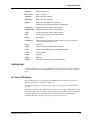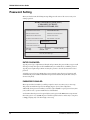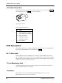
1
RAS96 RASCard
User Guide
RAS96 RASCard User Guide
P/N 82064002, Revision C
Copyright © 1997 by Multi-Tech Systems, Inc.
All rights reserved. This publication may not be reproduced, in whole or in part, without prior expressed
written permission from Multi-Tech Systems, Inc.
Multi-Tech Systems, Inc. makes no representation or warranties with respect to the contents hereof and
specifically disclaims any implied warranties of merchantability or fitness for any particular purpose.
Furthermore, Multi-Tech Systems, Inc. reserves the right to revise this publication and to make changes
from time to time in the content hereof without obligation of Multi-Tech Systems, Inc., to notify any
person or organization of such revisions or changes.
Revision
Date
A
3/31/97
Manual released.
Description
B
5/27/97
Model number change; new T1 and connector information.
C
11/17/97
Manual revised to incorporate new Dual T1, PRI information.
This product is covered by one or more of the following U.S. Patent Numbers: 5,301,274; 5,355,365;
5,546,448; 5,450,425. Other patents pending.
Multi-Tech, CommPlete, RASExpress, MultiExpress, MultiExpress Fax MultiModem, MultiModemZDX,
MultiCommManager, and the Multi-Tech logo are trademarks of Multi-Tech Systems, Inc. AMD is a
trademark of Advanced Micro Devices, Inc. Award is a trademark of Award Software International, Inc.
Cyrix is a trademark of Cyrix Corp. Pentium is a trademark of Intel Corp. Other trademarks and trade
names mentioned in this publication belong to their respective owners.
Multi-Tech Systems, Inc.
2205 Woodale Drive
Mounds View, Minnesota 55112
(612) 785-3500 or (800) 328-9717
Fax (612) 785-9874
Technical Support (800) 972-2439
BBS (612) 785-3702 or (800) 392-2432
Fax Back (612) 717-5888
Internet Address: http://www.multitech.com
Federal Communications Commission Statement
This equipment has been tested and found to comply with the limits for a Class A digital device,
pursuant to Part 15 of the FCC Rules. These limits are designed to provide reasonable protection against
harmful interference when the equipment is operated in a commercial environment. This equipment
generates, uses, and can radiate radio frequency energy, and if not installed and used in accordance with
the instruction manual, may cause harmful interference to radio communications. Operation of this
equipment in a residential area is likely to cause harmful interference, in which case the user will be
required to correct the interference at his own expense.
Warning: The use of shielded cables for connection of a monitor to the RASCard is required to assure
compliance with FCC regulations. Changes or modifications to this unit not expressly approved by the
party responsible for compliance could void the user’s authority to operate the equipment.
Exhibit J (Consumer Instructions)
This equipment complies with part 68 of the Federal Communications Commision Rules. On the
outside surface of this equipment is a label that contains, among other information, the FCC registration
number. This information must be provided to the telephone company.
As indicated below, the suitable jack (Universal Service Order Code connecting arrangement) for this
equipment is shown. If applicable, the facility interface codes (FIC) and service order codes (SOC) are
shown.
A FCC-compliant telephone cord and modular plug is provided with this equipment. This equipment is
designed to be connected to the telephone network or premises wiring using a compatible modular jack
which is Part 68 compliant. See installation instructions for details.
If this equipment causes harm to the telephone network, the telephone company will notify you in
advance that temporary discontinuance of service may be required. But, if advance notice is not
practical, the telephone company will notify the customer as soon as possible. Also, you will be advised
of your right to file a complaint with the FCC if you believe it is necessary.
The telephone company may make changes in its facilities, equipment, operations, or procedures that
could affect the operation of the equipment. If this happens, the telephone company will provide
advance notice in order for you to make necessary modifications in order to maintain uniterrupted
service.
If trouble is experienced with this equipment (the model of which is indicated below) please contact
Multi-Tech Systems, Inc. at the address shown below for details of how to have repiars made. If the
equipment is causing harm to the network, the telephone company may request you to remove the
equipment from the network until the problem is resolved.
No repairs are to be made by you. Repairs are to be made only by Mult-Tech Systems or its licensees.
Unauthorized repairs void registration and warranty.
Manufacturer:
Multi-Tech Systems, Inc.
Trade Name:
CommPlete
Model Number:
CC2400, CC9600
FCC Registration Number:
CommPlete Communications Server
AU7USA-31090-DE-E
iii
Facility Interface Code:
Service Order Code:
04DU9-BN
6.0N
Modeular Jack (USOC):
RJ48G
Service Center in USA:
Multi-Tech Systems, Inc.
2205 Woodale Drive
Mounds View, MN 55112
(612) 785-3500 Fax (612) 785-9874
Important Safety Instructions
Caution: Danger of explosion if battery is incorrectly replaced. Replace only with the same or equivalent
type recommended by the manufacturer. Dispose of used batteries according to the manufacturer’s
instructions.
The RAS96 RASCard circuit board includes a battery that maintains the RASCard’s setup information
when it is turned off or disconnected from power. The battery can maintain the setup information for
approximately 10 years with no external power, and longer when the RASCard is turned on and operating
normally. This battery is soldered onto the circuit board and cannot be replaced by the user.
Note: There is a possibility of excessive battery drain if the RASCard is set on a metal table or stored in an
anti-static bag.
If, for some reason, the RASCard’s battery should fail, please contact Multi-Tech Technical Support at
(800) 972-2439 for replacement instructions.
iv
CommPlete Communications Server
Table of Contents
1 Introduction
Introduction ...................................................................................................................................................... 2
Manual Organization......................................................................................................................................... 2
Technical Specifications.................................................................................................................................... 3
2 RASCard Description
Introduction ...................................................................................................................................................... 6
Memory Banks................................................................................................................................................... 6
Jumpers.............................................................................................................................................................. 7
Internal Connectors........................................................................................................................................... 8
External Connectors .......................................................................................................................................... 9
Front Panel .......................................................................................................................................................10
LED Indicators.............................................................................................................................................10
Switches........................................................................................................................................................11
3
Installation
Introduction .....................................................................................................................................................14
Safety Warnings................................................................................................................................................14
Pre-Installation Notes ......................................................................................................................................14
Installation Procedure......................................................................................................................................14
4
BIOS Setup Utility
Introduction .....................................................................................................................................................18
Starting Setup...............................................................................................................................................18
Using Setup ..................................................................................................................................................18
Getting Help .................................................................................................................................................19
In Case of Problems .....................................................................................................................................19
Main Menu........................................................................................................................................................20
Standard CMOS Setup ......................................................................................................................................24
BIOS Features Setup .........................................................................................................................................27
Chipset Features Setup .....................................................................................................................................30
Power Management Setup................................................................................................................................33
PCI Configuration Setup...................................................................................................................................35
Password Setting ..............................................................................................................................................38
5 T1 Daughter Cards
Introduction .....................................................................................................................................................40
Specifications....................................................................................................................................................40
T1 Overview ......................................................................................................................................................41
T1 Glossary...................................................................................................................................................41
T1 Basics.......................................................................................................................................................42
T1 Frame Formats .......................................................................................................................................43
T1 Line Coding Options...............................................................................................................................44
FXS Signaling Options .................................................................................................................................44
Dial-In Address............................................................................................................................................44
CommPlete Communications Server
v
Trunk Pulsing ..............................................................................................................................................45
DID (Direct Inward Dialing) .......................................................................................................................45
T1 Facility Termination...............................................................................................................................46
PCB Description ...............................................................................................................................................46
RJ-11 Alarm Jack .........................................................................................................................................46
T1 Line Monitoring Jack..............................................................................................................................46
Test Modes...................................................................................................................................................46
T1 Bus Descriptions.....................................................................................................................................47
2-Pin Jumper (S1)........................................................................................................................................47
Configuration of the T1 Daughter Card...........................................................................................................47
Ordering a T1 Line.......................................................................................................................................47
To Configure the T1 Daughter Card............................................................................................................48
Functional Description ....................................................................................................................................52
Operation..........................................................................................................................................................52
Parallel Port .................................................................................................................................................53
Control Registers .........................................................................................................................................53
Local Loopback............................................................................................................................................53
Remote Loopback........................................................................................................................................53
Payload Loopback .......................................................................................................................................53
Framer Loopback ........................................................................................................................................54
Loop Code Generation.................................................................................................................................54
Pulse Density Enforcer ................................................................................................................................54
Loop Up/Down Code Detection ..................................................................................................................55
Error Count Registers ......................................................................................................................................55
Line Code Violation Count Register............................................................................................................55
Path Code Violation Count Register (PCVCR) ...........................................................................................55
Multiframes Out of Sync Count Register ....................................................................................................56
FDL/FS Extraction and Insertion ................................................................................................................56
Signaling Operation..........................................................................................................................................56
Special Transmit-Side Registers ......................................................................................................................56
Elastic Stores Operation ..............................................................................................................................57
Transmit Waveshaping and Line Driving...................................................................................................57
Recommended Operating Conditions ........................................................................................................57
6 Solving Problems
Introduction .....................................................................................................................................................59
Troubleshooting...............................................................................................................................................59
The RASCard has no video ..........................................................................................................................59
The RASCard does not boot correctly, or hangs after the video appears.......................................................59
The COM1 port does not respond correctly................................................................................................60
The keyboard does not respond to key strokes ..........................................................................................60
Invalid time, date or setup ..........................................................................................................................60
Memory Upgrade .............................................................................................................................................60
Diagnostic Tests ...............................................................................................................................................62
Calling Technical Support................................................................................................................................62
vi
CommPlete Communications Server
Appendixes ......................................................................................................................................65
Appendix A Connector Pinouts ...........................................................................66
Appendix BPOST Messages ....................................................................................71
Appendix CPOST Codes................................................................................................74
Appendix DApproved Memory ..............................................................................77
Index..........................................................................................................................................................79
CommPlete Communications Server
vii
viii
CommPlete Communications Server
1
CommPlete Communications Server
Introduction
1
RAS96 RASCard User Guide
Introduction
This manual describes the field installation and configuration of a Multi-Tech RAS96 series RASCard into
a CommPlete Communications Server. It also describes the optional T1 daughter cards that are required
for use with the MT5634HD8 and MT5634HD16 modem cards.
The RASCard is a single board Pentium computer that serves as a remote access server (RAS) for the
CommPlete Communications Server system. Up to four RASCards, one per segment, can be installed in
one CommPlete Communications Server. Each RASCard has PCI/ISA bus architecture, a 100-, 133-, 166-,
or 200-MHz Intel® Pentium® processor, up to 128 megabytes (MB) of fast page mode or EDO RAM, a 512K
L2 cache, 1 MB of on-board video RAM, floppy disk and IDE hard disk controllers, a watchdog timer for an
automatic reset, and an 800 MB, 1.2 GB, 1.6 GB, or 2.1 GB on-board hard disk. One optional T1 daughter
card provides a T1 interface for up to three MT5634HD8 eight-modem cards. Two optional T1 daughter
cards provide a Dual T1 interface for three MT5634HD16 sixteen-modem cards.
Each RASCard comes with MS-DOS and RASExpress remote access server management software preinstalled on the hard disk. For software operating instructions, refer to the applicable software manual that
was shipped with your software.
Manual Organization
Chapter 1
Introduction
This chapter introduces the RAS96, gives its technical specifications, and provides a guide to the
organization of the manual.
Chapter 2
RASCard Description
This chapter describe the RAS96’s layout, memory banks, jumpers, connectors, and front panel.
Chapter 3
Installation
This chapter describes how to install the RAS96 into the CommPlete chassis.
Chapter 4
BIOS Setup Utility
This chapter describes the options in the Award BIOS Setup utility.
Chapter 5
T1 Daughter Card
This chapter describes the optional T1 daughter cards that mount on the RAS96.
Chapter 6
Solving Problems
This chapter describes how to solve typical problems that you might encounter when running the
RASCard.
Appendix A Connector Pinouts
This appendix provides technical information about the connectors used on the RAS96.
2
CommPlete Communications Server
1 Introduction
Appendix B POST Messages
This appendix describes error messages that might be encountered during the RAS96’s power-on self-test
(POST).
Appendix C
POST Codes
This appendix describes codes generated by the BIOS during POST.
Appendix D
Approved Memory
This appendix lists memory SIMMs that are known to work with the RAS96.
Technical Specifications
• Intel 430FX Triton chipset
• Supports 100 MHz, 133 MHz, 166 MHz, and 200 MHz Intel® Pentium® processors.
• PCI/ISA bus architecture for full PCI bus support.
• On-board PCI-bus SVGA video controller with 1 MB of video DRAM supports resolutions to 1024 by
768 pixels by 256 colors.
• Supports 72-pin SIMMs of 4 MB, 8 MB, 16 MB, or 32 MB to form a memory size between 8 MB and 128
MB. Memory type can be fast page or EDO, 60 ns or 70 ns, parity or non-parity.
• 512K of L2 cache memory.
• One parallel port and two RS-232C serial ports with 16550 UARTs (DB-9P connector for COM1; COM2
is for T1 cards).
• 1.44 MB floppy disk controller.
• IDE hard disk interface.
• 2.5-inch on-board hard disk. Available disk sizes include 800 MB, 1.2 GB, 1.6 GB, and 2.1 GB.
• Keyboard and speaker interfaces.
• Real-time clock with battery backup.
• Award BIOS with custom features.
• Watchdog timer.
• T1 frame format: ESF (AT&T and ANSI), D4 (SF), G.704.ITU-T section 2.1.3.2 and section 2.1.3.1.
• T1 line coding: AMI, B8ZS, ZBTSI.
• T1 signal start method: E&M Wink start conversion, E&M Immediate start conversion, Ground start
standard, Loop start standard.
• T1 dial-in address: No address, DNIS, ANI-DNIS, ANI.
• Switches: Power switch and reset switch on front panel.
• Indicators: Front panel LEDs for monitoring network and T1 operations.
• Dimensions: 23.4 × 4.32 × 29.2 cm (9.22 × 1.70 × 11.5 in.) H × W × D.
• Weight: 1.0 kg (2.2 lb).
• Operating temperature: 0° to 40° C (32° to 104° F).
CommPlete Communications Server
3
RAS96 RASCard User Guide
• Humidity range: 20–90% (noncondensing).
• Power consumption:
4.5 A @ +5 VDC.
• Limited warranty: Two years.
4
CommPlete Communications Server
2 RASCard Description
CommPlete Communications Server
5
RAS96 RASCard User Guide
Introduction
The RAS96 assembly consists of a Pentium computer card to which is mounted a 2.5-inch hard disk drive,
up to two optional T1 cards, and a front panel. Figure 1 shows the layout of the RAS96 card. The RAS96
assembly plugs into bus connectors on the inside of the CC9600 chassis that supply power and support
data communications among the various components of the CommPlete Communications Server. The
remainder of this chapter describes the RASCard’s memory banks, configuration jumpers, connectors,
and front panel switches and indicators.
Figure 1. RAS96 RASCard.
Memory Banks
The RASCard is shipped from the factory with 512K of L2 cache memory, which is the maximum amount
that can be installed.
Two memory banks (Bank 1 and Bank 2) with two SIMM sockets per bank (M1 through M4) are provided
on the RASCard. The standard configuration has 16 MB of EDO DRAM in Bank 1. The RASCard supports
four 72-pin SIMMs of 4 MB, 8 MB, 16 MB, or 32 MB DRAM to form a memory size from 8 MB to 128 MB.
The DRAM can be 60 ns or 70 ns, fast page mode or EDO, 32-bit non-parity or 36-bit. For a list of approved
SIMMs, see Appendix D.
Note: Each bank must have the same size memory installed in pairs. Always fill Bank 1 first.
Table 1. Memory Configurations.
6
CommPlete Communications Server
2 RASCard Description
Bank 1
Bank 2
TOTAL
None
None
0 MB
2 × 4 MB
None
8 MB
2 × 4 MB
2 × 4 MB
16 MB
2 × 8 MB
None
16 MB
2 × 8 MB
2 × 4 MB
24 MB
2 × 8 MB
2 × 8 MB
32 MB
2 × 16 MB
None
32 MB
2 × 16 MB
2 × 8 MB
48 MB
2 × 16 MB
2 × 16 MB
64 MB
2 × 32 MB
None
64 MB
2 × 32 MB
2 × 16 MB
96 MB
2 × 32 MB
2 × 32 MB
128 MB
Jumpers
The RASCard has five configuration jumpers. One is used for the watchdog timer; the other four are used
to select the CPU frequency and the CPU-to-bus frequency ratio.
J17
Watchdog Timer
Jumper pins 1 and 2 to enable the watchdog timer. Jumper pins 2 and 3 to disable the watchdog timer. The
watchdog timer is enabled by default, as shown in Figure 1.
J14, J15, J16, J18
CPU Frequency Selection
Jumper J14, J15, J16, and J18 to select the CPU frequency and CPU-to-bus frequency ratio for the installed
CPU, as shown in the following table. In Figure 1, the jumpers are shown configured for a 166 MHz
Pentium.
Warning: The RASCard supports only the following Intel Pentium CPUs. Do not replace the original CPU
with a Pentium Pro, MMX, AMD, or Cyrix CPU.
Intel Pentium
100 MHz
J14 J15 J16 J18
Out Out
In
In
133 MHz
In
Out
In
In
166 MHz
In
In
In
In
200 MHz
Out
In
In
In
CommPlete Communications Server
7
RAS96 RASCard User Guide
Internal Connectors
The RASCard has several internal connectors, which are described from front to back.
J20
CPU Fan
This is the 5 VDC power connector for the CPU’s cooling fan.
J12
Power Switch
This is the connector for the power switch.
J8
Speaker
This connector can be used to connect a speaker to the RASCard. However, it is normally not used when
more than one RASCard is installed in the CommPlete chassis.
J10
T1 Card 1
This connector provides power, ground, and data connections for the optional T1 daughter card. It is not
used on a RASCard with a PRI card.
J1
T1 Card 2
This connector provides power, ground, and data connections for the second optional T1 daughter card. It
is only used on a RASCard with Dual T1.
J6
Internal Hard Disk Drive
This IDE connector provides control and data signals, power, and ground for the RASCard’s 2.5-inch hard
disk drive. The control and data lines are shared with J21. Therefore, if you connect a second hard disk
drive or an IDE CD-ROM drive to J21, you must configure it to slave mode by setting its jumper
accordingly.
J21
IDE Drive
This connector can be used to connect a second IDE hard disk drive or a CD-ROM drive to the RASCard.
The IDE control and data lines are shared with J6. There is no secondary IDE controller; if you install two
hard disk drives, you must configure the second one to slave mode by setting its jumper accordingly.
J27
Floppy Drive
This connector can be used to connect a floppy disk to the RASCard, e.g., for software updates. Normally,
it is not used.
J13
Drive Power
This connector can be used to supply standard voltages to a disk drive or CD-ROM drive. Normally, it is
not used.
8
CommPlete Communications Server
2 RASCard Description
J4, J7
Bus Connectors
These two connectors connect the RASCard to the CommPlete chassis’ control, data, T1, and Ethernet
busses.
J2
Power Connector
This connector supplies power and ground to the RASCard.
External Connectors
The RASCard has four connectors that are accessible from the rear of the
CommPlete chassis.
J22
T1 Alarm
This RJ-11 jack can be used to connect an external alarm system (not supplied
by Multi-Tech) to monitor the online or alarm condition of the T1 link.
J3
COM1
COM1, a male DB-9 connector, is the RASCard’s serial port. It can be used to
connect a dumb terminal to the RASCard for configuration, or to connect a
pointing device such as a mouse or trackball.
J35
Video
This female DB-15 connector provides video output for a standard VGA or
SVGA display monitor.
J11
Keyboard
This female 6-pin mini DIN connector can be used to connect a keyboard to
the RASCard.
Figure 2. External
connectors.
CommPlete Communications Server
9
RAS96 RASCard User Guide
Front Panel
LED Indicators
Ethernet Status LEDs
The RASCard front panel contains three indicators that show the
status of the RASCard’s Ethernet port.
LED Indicator
Color
Indication
XMT Transmit
Green
On during Ethernet transmit.
RCV Receive
Green
On during Ethernet receive.
LINK Link Integrity Yellow
On during a good link.
T1-1 and T1-2 Status LEDs
The RASCard front panel contains fourteen indicators (seven for each
T1 port) that show the status of the RASCard’s optional T1 ports.
LED Indicator
Color
Indication
ONLINE
Green
On indicates that the T1 card is
online and no errors are detected.
Off indicates that the T1 card is
offline due to one of the following
errors.
RED ALARM
Red
On indicates that a loss of T1
signal has been detected.
Off indicates that the T1 card is
detecting an incoming T1 signal.
YELLOW
ALARM
Red
On indicates that the remote T1
channel bank or network is in red
alarm and transmitting a yellow
frame pattern.
Off indicates that the remote
channel bank or network is not
transmitting a yellow alarm.
SYNC LOSS
Red
On indicates that the T1 card
has lost synchronization with the
receive T1 line.
Off indicates that the T1 card is
synchronized with the receive T1
line.
BPV VIOLATION Red
On indicates that a received
bipolar violation (BPV) is being
detected.
Off indicates that no BPV is
being detected.
Figure 3. RAS96 front panel.
10
CommPlete Communications Server
2 RASCard Description
LED Indicator
Color
Indication
BLUE ALARM
Red
Also known as AIS (ALARM INDICATION SIGNAL).
On indicates that the T1 card is receiving unframed all 1s,
indicating disconnection or attached device failure.
Off indicates that the attached device is operating correctly.
TEST MODE
Red
On indicates that the T1 card is in one of several possible test
modes.
Off indicates that the T1 card is not in a test mode.
Switches
Power Switch
The power switch turns the RASCard on and off. An LED indicator in the switch lights when the RASCard
is on.
Reset Switch
The reset switch is a momentary push-button that is recessed behind a small hole in the front panel. It
provides a hardware reset (hard boot) for the CPU should it become locked up. Use a straightened paper
clip or similar device to activate it.
CommPlete Communications Server
11
RAS96 RASCard User Guide
12
CommPlete Communications Server
3
CommPlete Communications Server
Installation
13
RAS96 RASCard User Guide
Introduction
This chapter describes how to install the RAS96 RASCard into a CommPlete Communication Server
chassis (either CC9600 or CC2400). This equipment should be installed only by a qualified service person.
Safety Warnings
• Never install telephone wiring during a lightning storm.
• Never install telephone jacks in wet locations unless the jacks are specifically designed for wet
locations.
• Never touch uninsulated telephone wires or terminals unless the telephone line has been disconnected
at the network interface.
• Use caution when installing or modifying telephone lines.
• Avoid using a telephone (other than a cordless type) during an electrical storm. There may be a remote
risk of electrical shock from lightning.
• Do not use the telephone to report a gas leak in the vicinity of the leak
• Ports that are connected to other apparatus are defined as SELV. To ensure conformity to EN 41003,
ensure that these ports are only connected to the same type on the other apparatus.
Pre-Installation Notes
Warning: Interconnection directly, or by way of other apparatus, of ports marked “SAFETY WARNING
see instructions for use” with ports marked or not so marked may produce hazardous conditions on the
network. Advice should be obtained from a competent engineer before such a connection is made.
• All installation must be done by a qualified service person.
• To reduce emissions, be sure to use blanking plates to cover empty slots in the CommPlete chassis.
Installation Procedure
14
1.
Unpack the RAS96 RASCard assembly from its packaging and save the packaging for possible future
use. Perform a visual inspection of the RASCard. If you are concerned about its condition, call
Technical Support for instructions.
2.
The RASCard must be installed in slot 1, 5, 9, or 13 of the CC9600 chassis, or in slot 1 of the CC2400
chassis (counting left to right). Remove a blank RASCard panel or previous RASCard from that slot.
3.
Replace the back cover plate with one that has openings for the RASCard.
4.
Make sure the power switch on the RASCard is off.
5.
Supporting the RASCard by the front panel and the bottom edge of the card, place it into the open
slot. Make sure the edges of the RASCard card mate properly with the metal guides in the
CommPlete chassis.
CommPlete Communications Server
3 Installation
6.
Slide the RASCard into the CommPlete chassis until you feel the RASCard’s connectors mate with
the chassis’s bus connectors.
7.
Tighten the RASCard’s retaining screws.
8.
If the RASCard has a T1 daughter card installed, connect the daughter card to the T1 line.
Note: Any cable connected to the RASCard should be shielded to reduce interference.
9.
Connect a monitor to the video connector, and a keyboard to the keyboard connector.
10.
Turn on the PS9600 power supplies, if they are off.
11.
Turn on the RASCard by pressing the switch on the front panel.
12.
Run the BIOS Setup Utility to check the configuration (see Chapter 4).
Note: A self-test runs each time the CommPlete Communications Server is turned on. Refer to the
MultiCommManager User Guide for more details about the power-on self-test.
CommPlete Communications Server
15
RAS96 RASCard User Guide
16
CommPlete Communications Server
4
CommPlete Communications Server
BIOS Setup Utility
17
RAS96 RASCard User Guide
Introduction
This chapter describes the Award Setup utility, which is built into the RASCard’s BIOS. The Setup utility
allows users to modify the basic system configuration. This special information is then stored in batterybacked CMOS RAM that retains the setup information when the power is turned off.
The Award BIOS installed in your computer system’s read-only memory (ROM) is a custom version of the
standard Award BIOS. This means that it supports Intel Pentium processors in a standard ISA/PCI
input/output system. The BIOS provides critical low-level support for standard devices such as disk drives
and serial and parallel ports.
The Award BIOS has been customized by adding special support for fine-tuning the 430FX Triton chipset
that controls the system.
Award Software, Inc
System Configuartions
CPU Type
Co-Processor
CPU Clock
: PENTIUM-S
: Installed
: 133MHz
Base Memory
Extended Memory
Cache Memory
: 640K
: 31744K
: 512K
Diskette Drive A
Diskette Drive B
Pri. Master Disk
Pri. Slave Disk
Sec. Master Disk
Sec. Slave Disk
: 1.44M, 3.5 in.
: None
: LDA, Mode 3, 427MB
: None
: None
: None
Display Type
:
Serial Port(s)
:
Parallel Port(s)
:
Bank0 EDO DRAM :
Bank 1 EDO DRAM :
L2 Cache SRAM Type:
EGA/VGA
3F8,2F8
378
Yes
Yes
Pipeline
Starting Setup
When you turn on the RASCard, the BIOS reads the system information contained in the CMOS and begins
the process of checking out and configuring the system. When it finishes, the BIOS looks for an operating
system on the hard disk, then launches and turns control over to the operating system.
To run Setup, press the DELETE key when the following message appears during the power-on self-test
(POST).
TO ENTER SETUP BEFORE BOOT PRESS DEL KEY
If the message disappears before you respond, and you still wish to enter Setup, restart the system to try
again by turning it off and on or pressing the recessed reset button on the front panel. If you do not press
the key at the correct time and the system does not boot, an error message will be displayed and you will be
asked to...
PRESS F1 TO CONTINUE OR DEL TO ENTER SETUP
Using Setup
In general, use the arrow keys to highlight items, press ENTER to select, use the PAGE UP and PAGE DOWN
keys to change entries, press F1 for help, and press ESC to quit. The following table lists the keys that can be
used to navigate the Setup utility.
18
CommPlete Communications Server
4
Up arrow
Move to previous item.
Down arrow
Move to next item.
Left arrow
Move to the item on the left.
Right arrow
Move to the item on the right.
Esc key
Main Menu—Quit without saving changes.
BIOS Setup Utility
Submenu—Exit current page and return to Main Menu
Page Up key
Increase the numeric value or make changes
Page Down key
Decrease the numeric value or make changes
+ key
Increase the numeric value or make changes
- key
Decrease the numeric value or make changes
F1 key
General help
F2, Shift+F2
Change color from a total of 16 colors. Press F2 to select the next color,
SHIFT+F2 to select the previous color.
F4 key
Reserved.
F5 key
Restore the previous CMOS value from CMOS.
F6 key
Load the default CMOS value from BIOS default table.
F7 key
Load the default.
F8 key
Reserved.
F9 key
Reserved.
F10 key
Save all the CMOS changes, only for Main Menu.
Getting Help
For help in making a selection, press F1. A small help window opens that describes the appropriate keys to
use and the possible selections for the highlighted item. To exit the Help window, press ESC or the F1 key
again.
In Case of Problems
The Award BIOS supports an override that loads default CMOS settings, should you discover that your
RASCard is no longer able to boot after you change Setup.
You can restart by using the power switch, the reset button, or by pressing CTRL, ALT, and DELETE at the
same time.
Only change settings that you thoroughly understand. To this end, we strongly recommend that you avoid
making any changes to the chipset defaults. These defaults have been carefully chosen by both Award and
your systems manufacturer to provide the absolute maximum performance and reliability. Even a
seemingly small change to the chipset setup may require you to use the override.
CommPlete Communications Server
19
RAS96 RASCard User Guide
Main Menu
When you run the Award BIOS CMOS Setup Utility, the main menu appears first on the screen. The main
menu allows you to select from several setup pages and two exit choices. Use the arrow keys to select
among the items, then press ENTER to go to the selected page.
ROM PCI/ISA BIOS (2A59CMNC)
CMOS SETUP UTILITY
AWARD SOFTWARE, INC.
STANDARD CMOS SETUP
PASSWORD SETTING
BIOS FEATURES SETUP
IDE HDD AUTO DETECTION
CHIPSET FEATURES SETUP
SAVE & EXIT SETUP
POWER MANAGEMENT SETUP
EXIT WITHOUT SAVING
PCI CONFIGURATION SETUP
LOAD BIOS DEFAULTS
LOAD SETUP DEFAULTS
↑↓→← : Select Item
(Shift)F2 : Color
ESC:Quit
F10 :Save & Exit Setup
Time, Date, Hard Disk Type...
Note that a brief description of each highlighted selection appears at the bottom of the screen.
The main menu includes the following setup categories.
Standard CMOS Setup
This setup page includes all the items in a standard BIOS setup. See page 24.
BIOS Features Setup
This setup page includes all the Award special features. See page 27.
Chipset Features Setup
This setup page includes all chipset special features. See page 30.
Power Management Setup
This setup page supports Green PC power management standards. See page 33.
PCI Configuration Setup
This setup page allows you to set up your computer for efficient energy levels. See page 35.
20
CommPlete Communications Server
4
BIOS Setup Utility
Password Setting
Change, set, or disable the password. The password allows you to limit access to the system and the Setup
Utility, or just to the Setup Utility. See page 38.
Load BIOS Defaults
The BIOS defaults have been set by the manufacturer. They provide settings that provide the minimum
requirements for your system to operate.
ROM PCI/ISA BIOS (2A59CMNC)
CMOS SETUP UTILITY
AWARD SOFTWARE, INC.
STANDARD CMOS SETUP
PASSWORD SETTING
BIOS FEATURES SETUP
IDE HDD AUTO DETECTION
CHIPSET FEATURES SETUP
SAVE & EXIT SETUP
POWER MANAGEMENT SETUP
EXIT WITHOUT SAVING
PCI CONFIGURATION SETUP
Load BIOS Defaults (Y/N)? N
LOAD BIOS DEFAULTS
LOAD SETUP DEFAULTS
ESC:Quit
F10 :Save & Exit Setup
↑↓→← : Select Item
(Shift)F2 : Color
Time, Date, Hard Disk Type...
CommPlete Communications Server
21
RAS96 RASCard User Guide
Load Setup Defaults
The chipset defaults are optimized settings for regular use.
ROM PCI/ISA BIOS (2A59CMNC)
CMOS SETUP UTILITY
AWARD SOFTWARE, INC.
STANDARD CMOS SETUP
PASSWORD SETTING
BIOS FEATURES SETUP
IDE HDD AUTO DETECTION
CHIPSET FEATURES SETUP
SAVE & EXIT SETUP
POWER MANAGEMENT SETUP
EXIT WITHOUT SAVING
PCI CONFIGURATION SETUP
Load SETUP Defaults (Y/N)? N
LOAD BIOS DEFAULTS
LOAD SETUP DEFAULTS
↑↓→← : Select Item
(Shift)F2 : Color
ESC:Quit
F10 :Save & Exit Setup
Time, Date, Hard Disk Type...
IDE HDD Auto Detection
Automatically detects and configures hard disk parameters. The Award BIOS includes this ability in case
you are uncertain of your hard disk’s parameters. See also “Standard CMOS Setup.”
ROM PCI/ISA BIOS (2A59CMNC)
CMOS SETUP UTILITY
AWARD SOFTWARE, INC.
HARD DISKS
TYPE SIZE CYCLS HEAD PRECOMP LANDZ SECTOR MODE
Primary Master :
Primary Slave :
427
414
Select Primary Slave
OPTIONS
1(Y)
32
0
898
63
LBA
Option (N=Skip) : N
SIZE CYLS HEAD PRECOMP LANDZ SECTOR MODE
0
0
0
0
0
0
NORMAL
Note: Some OSes (like SCO-UNIX) must use "NORMAL" for installation
ESC : Skip
22
CommPlete Communications Server
4
BIOS Setup Utility
Save and Exit Setup
Save changes to CMOS and exit Setup.
ROM PCI/ISA BIOS (2A59CMNC)
CMOS SETUP UTILITY
AWARD SOFTWARE, INC.
STANDARD CMOS SETUP
PASSWORD SETTING
BIOS FEATURES SETUP
IDE HDD AUTO DETECTION
CHIPSET FEATURES SETUP
SAVE & EXIT SETUP
POWER MANAGEMENT SETUP
EXIT WITHOUT SAVING
PCI CONFIGURATION SETUP
SAVE to CMOS and EXIT (Y/N)? N
LOAD BIOS DEFAULTS
LOAD SETUP DEFAULTS
↑↓→← : Select Item
(Shift)F2 : Color
ESC:Quit
F10 :Save & Exit SEtup
Time, Date, Hard Disk Type...
Exit Without Saving
Abandon all CMOS changes and exit Setup.
ROM PCI/ISA BIOS (2A59CMNC)
CMOS SETUP UTILITY
AWARD SOFTWARE, INC.
STANDARD CMOS SETUP
PASSWORD SETTING
BIOS FEATURES SETUP
IDE HDD AUTO DETECTION
CHIPSET FEATURES SETUP
SAVE & EXIT SETUP
POWER MANAGEMENT SETUP
EXIT WITHOUT SAVING
PCI CONFIGURATION SETUP
Quit Without Saving (Y/N)? N
LOAD BIOS DEFAULTS
LOAD SETUP DEFAULTS
ESC:Quit
F10 :Save & Exit Setup
↑↓→← : Select Item
(Shift)F2 : Color
Time, Date, Hard Disk Type...
CommPlete Communications Server
23
RAS96 RASCard User Guide
Standard CMOS Setup
The items in the Standard CMOS Setup menu are divided into several categories. Use the arrow keys to
highlight the item you want to change, then use the PAGE UP or PAGE DOWN key to select the value you want
for the item.
ROM PCI/ISA BIOS (2A59CMNC)
STANDARD CMOS SETUP
AWARD SOFTWARE, INC.
Date (mm:dd:yy) : Thu, Jul 18 1996
Time (hh:mm:ss : 16 : 14: 6
HARD DISKS
Primary Master
Primary Slave
Secondary Master
Secondary Slave
TYPE SIZE CYCLS HEAD PRECOMP LANDZ SECTOR MODE
:
:
:
:
User
None
None
None
52
0
0
0
751
0
0
0
8
0
0
0
Drive A : 1.44M, 3.5 in.
Drive B : None
750
0
0
0
17
0
0
0
NORMAL
-------------------
Base Memory:
640K
Extended Memory: 15360K
Other Memory:
384K
Video : EGA/VGA
Halt On : All, But Disk/Key
ESC:Quit
F1 :Help
65535
0
0
0
Other Memory: 16384K
↑↓→← : Select Item
(Shift)F2 : Color
PU/PD/+/-:Modify
Date
The date format is day, month, date, and year.
Day
The day of the week, determined by the BIOS, is display-only.
Month
The month, Jan through Dec. Valid values are 1 through 12.
Date
The day of the month. Valid values are 1 through 31.
Year
The year. Valid values are 1900 through 2099.
Time
The time format is hour, minute, and second. Hours are entered and displayed in a 24-hour format. For
example, 1:00 p.m. is entered and displayed as 13:00:00.
Hard Disks
The fields in this category contain specifications for the hard disk drives that have been installed in the
computer. In the TYPE field you can select from 46 predefined drive types, User, Auto, and None. All the
predefined types are obsolete. The User option allows you to enter drive specifications manually. Selecting
Auto in both the TYPE and the MODE fields enables automatic detection of IDE hard drives during bootup (the default selection). This feature allows you to change hard drives (with the power off) and reboot
without having to reconfigure your hard drive type. Secondary master and slave categories are not
available; there is no connector for secondary drives.
24
CommPlete Communications Server
4
BIOS Setup Utility
You can use the IDE HDD Auto Detection option in the main menu to automatically enter the
specifications for your hard disk. If you wish to configure your drive manually, press PAGE UP or PAGE
DOWN to select User. Enter your drive’s specifications in the drive table. The hard disk will not work
properly if you enter improper information.
If you select User, you will need to know the following information. Enter the information directly from
the keyboard and press ENTER. This information should be included in the documentation from your hard
disk vendor or the system manufacturer.
CYLS
Number of cylinders
HEAD
Number of heads
PRECOMP
Write precompensation
LANDZ
Landing zone
SECTORS
Number of sectors
MODE
IDE mode: Normal, for drives under 528 MB; LBA, for larger drives that support
Logical Block Addressing (most IDE drives over 528 MB); Large, for drives over 528
MB that do not support LBA (uncommon); and Auto, for auto selection on boot-up
(default).
If a hard disk has not been installed, select None and press ENTER.
Drive A Type / Drive B Type
This category identifies the types of floppy disk drives that have been installed in the computer.
None
No floppy drive installed
360K, 5.25 in
5.25-inch PC-type standard drive, 360-kilobyte capacity
1.2M, 5.25 in
5.25-inch AT-type high-density drive, 1.2-megabyte capacity
720K, 3.5 in
3.5-inch drive, 720-kilobyte capacity
1.44M, 3.5 in
3.5-inch drive, 1.44-megabyte capacity (default—drive A)
2.88M, 3.5 in
3.5-inch drive, 2.88-megabyte capacity
Video
The category selects the type of video adapter used for the primary system monitor. Although secondary
monitors are supported, you do not have to select the type in Setup.
EGA/VGA
Enhanced Graphics Adapter/Video Graphics Array. For EGA, VGA, SEGA, SVGA or
PGA monitor adapters (default).
CGA 40
Color Graphics Adapter, power-up in 40 column mode
CGA 80
Color Graphics Adapter, power-up in 80 column mode
MONO
Monochrome adapter, includes high resolution monochrome adapters
CommPlete Communications Server
25
RAS96 RASCard User Guide
Halt On
The category determines whether the computer will stop if an error is detected during power up.
All errors
Whenever the BIOS detects a non-fatal error, the system will be stopped and you will
be prompted.
No errors
The system boot will not be stopped for any error that may detected.
All, But
Keyboard
The system boot will not stop for a keyboard error, it will stop for all other errors.
All, But
Diskette
The system boot will not stop for a disk error; it will stop for all other errors.
All, But
Disk/Key
The system boot will not stop for a keyboard or disk error; it will stop for all other
errors (Default).
Memory
The category is display-only. Values are determined by the BIOS power-on self-test (POST).
26
Base Memory
The POST determines the amount of base (or conventional) memory installed in the
system. The value of the base memory is typically 640K for systems with 640K or
more memory installed on the motherboard.
Extended
Memory
The BIOS determines how much extended memory is present during the POST. This
is the amount of memory located above 1MB in the CPU’s memory address map.
Expanded
Memory
Expanded Memory is memory defined by the Lotus/Intel/Microsoft (LIM) standard as
EMS. While most standard DOS applications cannot access memory above 640K, the
Expanded Memory Specification (EMS) provides an interface allowing access to all
system memory. Though still in use by some DOS applications, EMS is rapidly declining in importance, since new processors and operating systems prefer extended
memory. A special, expanded memory device driver is required to use memory as
Expanded Memory.
Other Memory
This refers to the memory located in the 640K to 1024K address space. This is memory
that can be used for different applications. DOS uses this area to load device drivers in
an effort to keep as much base memory free for application programs. The BIOS is the
most frequent user of this RAM area since this is where it shadows RAM.
CommPlete Communications Server
4
BIOS Setup Utility
BIOS Features Setup
This menu allows you to configure your system for basic operation. You have the opportunity to select the
system’s default speed, boot-up sequence, keyboard operation, shadowing and security.
ROM PCI/ISA BIOS (2A59CMNC)
BIOS FEATURES SETUP
AWARD SOFTWARE, INC.
Virus Warning
CPU Internal Cache
External Cache
Quick Power On Self Test
Boot Sequence
Swap Floppy Drive
Boot Up Floppy Seek
Boot Up NumLock Status
Boot Up System Speed
Gate A20 Option
Memory Parity Check
Typematic Rate Setting
Typematic Rate (Chars/Sec)
Typematic Dealy (Msec)
Security Option
PCI/VGA Palette Snoop
: Disabled
: Enabled
: Enabled
: Disabled
: A,C
: Disabled
: Enabled
: On
: High
: Fast
: Enabled
: Disabled
:6
: 250
: Setup
: Disabled
Video BIOS Shadow
C8000-DBFF Shadow
CC000-CFFF Shadow
D0000-D3FFF Shadow
D4000-D7FFF Shadow
D8000-D8FFF Shadow
DC000-DFFFF Shadow
ESC
F1
F5
F6
F7
:
:
:
:
:
: Enabled
: Disabled
: Disabled
: Disabled
: Disabled
: Disabled
: Disabled
Quit
↑ ↓ →← : Select Item
Help
PU/PD/+/- : Modify
Old Values (Shift)F2 : Color
Load BIOS Defaults
Load Setup Defaults
Virus Warning
When this item is enabled, the Award BIOS will monitor the boot sector and partition table of the hard
disk drive for any attempt at modification. If an attempt is made, the BIOS will halt the system and the
following error message will appear. Afterwards, if necessary, you will be able to run an anti-virus program
to locate and remove the problem before any damage is done.
! WARNING !
Disk boot sector is to be modified
Type Y to accept write or N to abort write
Award Software, Inc.
Enabled
Activates automatically when the system boots up, causing a warning message to appear
when anything attempts to access the boot sector or hard disk partition table.
Disabled
No warning message will appear when anything attempts to access the boot sector or
hard disk partition table. (Default.)
Note: Many disk diagnostic programs that attempt to access the boot sector table can cause the above
warning message. If you will be running such a program, we recommend that you first disable Virus
Protection beforehand. This feature when enabled can cause problems when installing Windows 95.
CPU Internal Cache/External Cache
These two categories speed up memory access when enabled.
Enabled
CommPlete Communications Server
Enable cache (Default)
27
RAS96 RASCard User Guide
Disabled
Disable cache
Quick Power On Self Test
This category speeds up the power-on self-test (POST) after you power up the computer. If it is set to
Enable, BIOS will shorten or skip some check items during POST.
Enabled
Enable quick POST
Disabled
Normal POST (Default)
Boot Sequence
This category determines which drive to search first for the disk operating system (i.e., DOS). Default value
is A, C.
C, A
System will first search for hard disk drive, then floppy disk drive.
A, C
System will first search for floppy disk drive, then hard disk drive.
Boot Up Floppy Seek
During POST, BIOS will determine if the floppy disk drive installed is 40 or 80 tracks. 360K type is 40
tracks, while 760K, 1.2M and 1.44M are all 80 tracks.
Enabled
BIOS searches the floppy disk drive to determine if it is 40 or 80 tracks. Note that BIOS can
not differentiate the 720K, 1.2M and 1.44M drive types, as they are all 80 tracks (Default).
Disabled
BIOS will not search for the type of floppy disk drive by track number. Note that there will
not be any warning message if the drive installed is 360K.
Boot Up NumLock Status
This allows you to determine the default state of the numeric keypad. By default, the system boots up with
Num Lock on.
On
Keypad is number keys
Off
Keypad is arrow keys
Boot Up System Speed
Selects the default system speed—the normal operating speed at power-up. This category no longer has a
function and should be left at the default setting of High.
High
Set the speed to high (Default)
Low
Set the speed to low
Gate A20 Option
This entry allows you to select how the gate A20 is handled. The gate A20 is a device used to address
memory above 1 MB. Initially, the gate A20 was handled via a pin on the keyboard. Today, though
keyboards still provide this support, it is more common, and much faster, for the system chipset to
provide support for gate A20.
28
Normal
Keyboard
Fast
Chipset (Default)
CommPlete Communications Server
4
BIOS Setup Utility
Memory Parity Check
Parity is a method of checking for errors in system memory. There are both parity and non-parity memory
types. At boot, the Award BIOS both sizes and tests all memory. Normally, when a parity error is detected,
the BIOS will display a message describing the problem as well as the problem’s location, if possible. The
boot process will then terminate and you will not be able to continue until the bad SIMM is located and
replaced.
Disabling the Memory Parity Check allows the system to by-pass the test and allow your system to boot.
You then have a choice of continuing to operate your system or attempting to remedy the problem.
Enabled
Normal memory parity check (Default)
Disabled
Ignore memory parity check
Typematic Rate Setting
This determines if the typematic rate is to be used. When it is disabled, continually holding down a key on
your keyboard will generate only one character. In other words, the BIOS will only report that the key is
down. When the typematic rate is enabled, the BIOS will report as before, but it will then wait a moment
and, if the key is still down, it will begin to report that the key has been depressed repeatedly. For example,
you would use such a feature to accelerate cursor movements with the arrow keys.
Enabled
Enable typematic rate
Disabled
Disable typematic rate (Default)
Typematic Rate (Chars/Sec)
When the typematic rate is enabled, this item allows you select the rate at which the system registers
repeated keystrokes.
6
6 characters per second
8
8 characters per second
10
10 characters per second
12
12 characters per second
15
15 characters per second
20
20 characters per second
24
24 characters per second
30
30 characters per second
Typematic Delay (Msec)
When the typematic rate is enabled, this selection allows you to select the delay between the first and
second characters.
250
250 ms (Default)
500
500 ms
750
750 ms
1000
1000 ms
Security Option
This category allows you to limit access to the system and to Setup, or just to Setup.
CommPlete Communications Server
29
RAS96 RASCard User Guide
System
The system will not boot and access to Setup will be denied if the correct password is not
entered at the prompt.
Setup
The system will boot, but access to Setup will be denied if the correct password is not
entered at the prompt (Default).
Note: To disable security, select PASSWORD SETTING from the main menu. You will be asked to enter a
password. Do not type anything; just press ENTER to disable security. Once security is disabled, the system
will boot and you can enter Setup freely.
Video BIOS Shadow
Determines whether video BIOS will be copied to RAM. However, it is optional, depending on chipset
design. Video Shadow will increase the video speed.
Enabled
Video shadow is enabled (Default)
Disabled
Video shadow is disabled
C8000 - CFFFF Shadow/DC000 - DFFFF Shadow
These categories determine whether option ROMs will be copied to RAM. An example of such an option
ROM would be support of on-board SCSI.
Enabled
Optional shadow is enabled
Disabled
Optional shadow is disabled (Default)
Chipset Features Setup
This section allows you to configure the system based on the specific features of the installed chipset. The
chipset manages bus speeds and access to system memory resources, such as DRAM and the L2 external
cache. It also coordinates communications between the conventional ISA bus and the PCI bus. These items
should never need to be altered. The default settings have been chosen because they provide the best
operating conditions for your system. The only time you might consider making any changes would be if
you discovered that data was being lost while using your system.
30
CommPlete Communications Server
4
BIOS Setup Utility
ROM PCI/ISA BIOS (2A59CMNC)
CHIP FEATURES SETUP
AWARD SOFTWARE, INC.
DRAM Timing
: 60 ns
System BIOS Cacheable
Video BIOS Cacheable
8 Bit I/O Recovery Time
16 Bit I/O Recovery Time
Memory Hole At 15M-16M
IDE HDD Block Mode
IDE Primary Master PI0
IDE Primary Slave PI0
: Disabled
: Disabled
: 1
: 1
: Disabled
: Enabled
: Auto
: Auto
PCI Concurrency
PCI Streaming
PCI Bursting
: Enabled
: Enabled
: Enabled
Onboard FDC Controller
Onboard Serial Port 1
Onboard Serial Port 2
Onboard Parallel Port
Parallel Port Mode
EPP Version
InfraRed Duplex Type
: Enabled
: COM1/3F8
: CPM2/2F8
: 378H/IRQ7
: Compatible
: 1.7
: Disabled
On-Chip Primary PCI IDE : Enabled
ESC
F1
F5
F6
F7
:
:
:
:
:
Quit
↑ ↓ →← : Select Item
Help
PU/PD/+/- : Modify
Old Values (Shift)F2 : Color
Load BIOS Defaults
Load Setup Defaults
DRAM Timing
The first chipset settings deal with CPU access to dynamic random access memory (DRAM). The DRAM
timing should match the speed of the slowest installed memory. For instance, if 60 ns SIMMs are installed
on the RASCard, you should set this item to 60 ns. But if you install both 60 ns and 70 ns SIMMs, you
should change it to 70 ns.
System BIOS Cacheable
When this item is enabled, accesses to the system BIOS ROM addressed at F0000H-FFFFFH are cached,
provided that the cache controller is enabled.
Enabled
BIOS access cached.
Disabled
BIOS access not cached. (Default.)
Video BIOS Cacheable
As with caching the System BIOS above, enabling the Video BIOS cache will cause access to video BIOS
addressed at C0000H to C7FFFH to be cached, if the cache controller is also enabled.
Enabled
Video BIOS access cached.
Disabled
Video BIOS access not cached. (Default.)
8-Bit I/O Recovery Time
The recovery time is the length of time, measured in CPU clocks, which the system will delay after the
completion of an input/output (I/O) request. This delay takes place because the CPU is operating so much
faster than the I/O bus that the CPU must be delayed to allow for the completion of the I/O.
This item allows you to determine the recovery time allowed for 8-bit I/O. Choices are from 1 through 8
CPU clocks. The default is 1 clock.
CommPlete Communications Server
31
RAS96 RASCard User Guide
16-Bit I/O Recovery Time
This item allows you to determine the recovery time allowed for 16 bit I/O. Choices are from 1 through 4
CPU clocks. The default is 1 clock.
Memory Hole At 15M-16M
In order to improve performance, certain memory space can be reserved for ISA cards. This memory must
be mapped into the memory space below 16 MB.
Enabled
Memory hole supported.
Disabled
Memory hole not supported. (Default.)
IDE HDD Block Mode
This allows your hard disk controller to use the fast block mode to transfer data to and from your hard
disk drive (HDD).
Enabled
IDE controller uses block mode. (Default.)
Disabled
IDE controller uses standard mode.
IDE Primary Master PIO / IDE Primary Slave PIO
IDE hard disk controllers can support two separate hard disks. These drives have a master/slave
relationship which are determined by jumpers on the hard disk drives. Your system supports one IDE
controller, so you have the ability to install up to two separate hard disks. The secondary IDE controller
has been disabled.
PIO means Programmed Input/Output. Rather than have the BIOS issue a series of commands to effect a
transfer to or from the disk drive, PIO allows the BIOS to tell the controller what it wants and then let the
controller and the CPU perform the complete task by themselves. This is simpler, more efficient, and
faster.
Your system supports five modes, numbered from 0 (default) through 4, which differ primarily in timing.
When Auto is selected, the BIOS will select the best available mode.
On-Chip Primary PCI IDE
As stated above, your system includes a built-in primary IDE controller, which operates on the PCI bus.
This setup item allows you to either enable or disable the primary controller.
Enabled
Primary IDE controller used. (Default.)
Disabled
Primary IDE controller not used.
PCI Concurrancy
PCI concurrency means that more than one PCI device can be active at a time.
32
Enabled
Multiple PCI devices can be active. (Default.)
Disabled
Only one PCI device can be active at a time.
CommPlete Communications Server
4
BIOS Setup Utility
PCI Streaming
Data is typically moved to and from memory and between devices in discrete chunks of limited sizes. This
is because the CPU is being used in the exchange. On the PCI bus, data can be streamed, that is, much
larger chunks can be moved without the use or intervention of the CPU.
Enabled
Streaming allowed on the PCI bus. (Default.)
Disabled
Streaming off for the PCI bus.
PCI Bursting
The PCI bus supports a mode by which large amounts of data is moved in short intense bursts. This item
allows you to turn this feature on or off.
Enabled
Bursting allowed on the PCI bus. (Default.)
Disabled
Bursting off for the PCI bus.
Power Management Setup
The Power Management Setup allows you to configure your system to most effectively save energy while
operating in a manner consistent with your own style of computer use.
ROM PCI/ISA BIOS (2A59CMNC)
POWER MANAGEMENTSETUP
AWARD SOFTWARE, INC.
Power Management
PM Control by APM
Video Off Method
: Disable
: Yes
: V/H SYNC+Blank
Doze Mode
Standby Mode
Suspend Mode
HDD Power Down
: Disable
: Disable
: Disable
: Disabled
IRQ3 (Wake-Up Event)
IRQ4 (Wake-Up Event)
IRQ8 (Wake-Up Event)
IRQ12(Wake-Up Event)
:
:
:
:
ON
ON
ON
ON
IRQ3 (COM2)
IRQ4 (COM1)
IRQ5 (LPT2)
IRQ6 (Floppy Disk)
IRQ7 (LPT1)
IRQ8 (RTC Alarm)
IRQ9 (IRQ2 Redir)
IRQ10 (Reserved)
IRQ11 (Reserved)
IRQ12 (PS/2 Mouse)
IRQ13 (Coprocessor)
IRQ14 (Hard Disk)
IRQ15 (Reserved)
:OFF
:OFF
:OFF
:OFF
:OFF
:OFF
:OFF
:OFF
:OFF
:OFF
:OFF
:OFF
:OFF
Power Down Activities
COM Ports Accessed
LPT Ports Accessed
Drive Ports Accessed
: ON
: ON
: ON
ESC
F1
F5
F6
F7
:
:
:
:
:
Quit
↑ ↓ →← : Select Item
Help
PU/PD/+/- : Modify
Old Values (Shift)F2 : Color
Load BIOS Defaults
Load Setup Defaults
Power Management
This item allows you to select the type (or degree) of power saving and is directly related to the following
modes:
• Doze Mode
• Standby Mode
• Suspend Mode
CommPlete Communications Server
33
RAS96 RASCard User Guide
• HDD Power Down
There are four selections for Power Management, three of which have fixed mode settings.
Disabled
No power management. Disables all four modes. (Default.)
Min Power
Saving
Minimum power management. Doze Mode = 1 hour, Standby Mode = 1 hour, Suspend
Mode = 1 hour, and HDD Power Down = 15 minutes.
Max Power
Saving
Maximum power management—only available for SL CPUs. Doze Mode = 1 minute,
Standby Mode = 1 minute, Suspend Mode = 1 minute, and HDD Power Down = 1 minute.
User Define
Allows you to set each mode individually. Each mode can be disabled. When not disabled,
each mode can be set from 1 minute through 1 hour, except for HDD Power Down, which
can be set from 1 minute through 15 minutes.
PM Control by APM
When this item is enabled, Advanced Power Management device will keep the system time updated when
the computer enters suspend mode activated by the BIOS power management.
If Max Power Saving is not enabled, this will be preset to No.
Yes
APM enabled.
No
APM disabled.
Video Off Method
This determines the manner in which the monitor is blanked.
V/H SYNC+Blank
The system turns off the vertical and horizontal synchronization ports and
writes blanks to the video buffer
Blank Screen
The system only writes blanks to the video buffer. Use for monitors that do not
have a power management feature.
Doze Mode
When enabled, and after the set time of system inactivity, the CPU clock runs at a slower speed while all
other devices still operate at full speed. This mode can be disabled or set from 1 minute through 1 hour.
Configurable only when User Defined Power Management has been selected.
Standby Mode
When enabled, and after the set time of system inactivity, the fixed disk drive and the video are shut off
while all other devices still operate at full speed. This mode can be disabled or set from 1 minute through 1
hour. Configurable only when User Defined Power Management has been selected.
Suspend Mode
When enabled, and after the set time of system inactivity, all devices except the CPU are shut off. This
mode can be disabled or set from 1 minute through 1 hour. Configurable only when User Defined Power
Management has been selected.
34
CommPlete Communications Server
4
BIOS Setup Utility
HDD Power Down
When enabled, and after the set time of system inactivity, the hard disk drive is powered down while all
other devices remain active. This mode can be disabled or set from 1 minute through 15 minutes.
Configurable only when User Defined Power Management has been selected.
Power Down Activities
Power Down Activities events are I/O events whose occurrence can prevent the system from entering a
power saving mode or can awaken the system from such a mode. In effect, the system remains alert for
anything that occurs to a device that is configured as ON, even when the system is in a power down mode.
COM Ports Accessed
When set to ON (default), any event occurring at a COM (serial) port awakens a system that has been
powered down. This includes mouse activity if a mouse is connected to COM1.
LPT Ports Accessed
When set to ON (default), any event occurring at an LPT (printer) port awakens a system that has been
powered down.
Drive Ports Accessed
When set to ON (default), any event occurring at a hard or floppy drive port awakens a system that has
been powered down.
IRQs
The following interrupt requests (IRQs) can be used to waken a system much as the COM ports and LPT
ports can. When an I/O device wants to gain the attention of the operating system, it signals this by causing
an IRQ to occur. When the operating system is ready to respond to the request, it interrupts itself and
performs the service.
The choices are ON and OFF. OFF is the default. When an IRQ is set to ON, activity will neither prevent the
system from going into a power management mode nor awaken it. IRQ8 (Real Time Clock Alarm) should
always be set to OFF so that any software alarm or event calendar can awaken the system.
IRQ3 (COM 2 )
IRQ8 (RTC Alarm)
IRQ13 (Coprocessor)
IRQ4 (COM 1)
IRQ9 (IRQ2 Redir)
IRQ14 (Hard Disk)
IRQ5 (LPT 2)
IRQ10 (Reserved)
IRQ15 (Reserved)
IRQ6 (Floppy Disk)
IRQ11 (Reserved)
IRQ7 (LPT 1)
IRQ12 (PS/2 Mouse)
PCI Configuration Setup
This section describes how to configure the PCI bus system. The PCI bus allows I/O devices to operate at
speeds near the speed the CPU itself uses to communicate with its own special components. It is strongly
recommended that only experienced users should make any changes to the default settings.
CommPlete Communications Server
35
RAS96 RASCard User Guide
ROM PCI/ISA BIOS (2A59CMNC)
PCI CONFIGURATION SETUP
AWARD SOFTWARE, INC.
PnP BIOS Auto-Config : Disabled
Slot 1 Using INT#
Slot 2 Using INT#
Slot 3 Using INT#
: AUTO
: AUTO
: AUTO
1st Available IRQ
2nd Available IRQ
3rd Available IRQ
4th Available IRQ
PCI IRQ activated by
PCI IDE IRQ Map To
Primary IDE INT#
Secondary IDE INT#
:
:
:
:
:
:
:
:
9
11
10
5
Level
PCI-AUTO
A
B
ESC
F1
F5
F6
F7
:
:
:
:
:
Quit
↑ ↓ →← : Select Item
Help
PU/PD/+/- : Modify
Old Values (Shift)F2 : Color
Load BIOS Defaults
Load Setup Defaults
Slot (x) Using INT#
Some PCI devices use interrupts to signal that they need to use the PCI bus. Some devices, notably most
graphics adapters, may not need an interrupt service at all. Each PCI slot is capable of activating up to four
interrupts, INT# A, INT# B, INT# C, and INT# D.
INT# A
Assign if the device in the slot requires one interrupt service.
INT# B
Assign only if the device in the slot requires two interrupt services rather than just one.
INT# C
Assign only if the device in the slot requires three interrupt services.
INT# D
Assign only if the device in the slot requires four interrupt services.
AUTO
Allows the PCI controller to automatically allocate the interrupts (default).
1st/2nd/3rd/4th Available IRQ
An INT# is an interrupt request that is signaled to and handled by the PCI bus. However, since the
operating system usually has the final responsibility for handling I/O, an INT# can be mapped to an IRQ if
the device occupying a given slot requires an IRQ service. By default, IRQs 9 and 10 are mapped to PCI
devices, but any unused IRQ can be used.
You can select which INT# is associated with each PCI slot and which conventional IRQ is associated with
one of the two available INT#s.
A setting of NA means the IRQ has been assigned to the ISA bus and is not available to any PCI slot.
PCI IRQ Activated by
This item sets the method by which the PCI bus recognizes that an IRQ service is being requested by a
device. Under all circumstances, you should retain the default configuration unless advised otherwise by
Multi-Tech.
Choices are Level (default) and Edge.
36
CommPlete Communications Server
4
BIOS Setup Utility
PCI IDE IRQ Map to
This allows you to configure your system to the type of IDE disk controller in use. By default, Setup
assumes that your controller is an ISA (Industry Standard Architecture) device rather than a PCI
controller.
If you have equipped your system with a PCI controller, changing this allows you to specify which slot has
the controller and which PCI interrupt (A, B, C, or D) is associated with the connected hard disks.
Remember that this setting refers to the hard disk drive itself, rather than individual partitions. Since each
IDE controller supports two separate hard disks, you can select the INT# for each. Again, you will note that
the primary has a lower interrupt than the secondary as described in Slot x Using INT# above.
Selecting PCI-AUTO allows the system to automatically determine how your IDE disk system is
configured.
CommPlete Communications Server
37
RAS96 RASCard User Guide
Password Setting
When you select this item, the following message will appear at the center of the screen to assist you in
creating a password.
ROM PCI/ISA BIOS (2A59CMNC)
CMOS SETUP UTILITY
AWARD SOFTWARE, INC.
STANDARD CMOS SETUP
PASSWORD SETTING
BIOS FEATURES SETUP
IDE HDD AUTO DETECTION
CHIPSET FEATURES SETUP
SAVE & EXIT SETUP
POWER MANAGEMENT SETUP
EXIT WITHOUT SAVING
PCI CONFIGURATION SETUPEnter Password:
LOAD BIOS DEFAULTS
LOAD SETUP DEFAULTS
ESC:Quit
F1 :Help
↑↓→← : Select Item
(Shift)F2 : Color
PU/PD/+/-:Modify
Time, Date, Hard Disk Type...
ENTER PASSWORD:
Type the password, up to eight characters in length, and press ENTER. The password that you type now will
clear any previously entered password from CMOS memory. You will be asked to confirm the password.
Type the password again and press ENTER. You may also press ESC to abort the selection and not enter a
password.
To disable a password, just press ENTER when you are prompted to enter the password. A message will
confirm that the password will be disabled. Once the password is disabled, the system will boot and you
can enter Setup freely.
PASSWORD DISABLED.
When a password has been enabled, you will be prompted to enter it every time you try to enter Setup.
This prevents an unauthorized person from changing any part of your system configuration.
Additionally, when a password is enabled, you can also require the BIOS to request a password every time
your system is booted, to prevent unauthorized use of the RASCard.
You determine when the password is required by the Security option in the BIOS Features Setup menu. If
the Security option is set to System, the password will be required both at boot and at entry to Setup. If set
to Setup, prompting only occurs when trying to enter Setup.
38
CommPlete Communications Server
5
CommPlete Communications Server
T1 Daughter Cards
39
RAS96 RASCard User Guide
Introduction
The T1 Daughter Cards mount on the RAS96 RASCard to provide a T1 interface for up to three
MT5634HD8 eight-modem cards (T1) or three MT5634HD16 sixteen-modem cards (Dual T1). This
chapter documents the operating characteristics of the T1 card.
T1 Line Monitoring
Bantam Jack (J2)
RJ-48 T1 Line
Jack (J1)
U9
U1
32-Pin Header (J3)
U7
2-Pin Jumper (S1)
Figure 4. T1 Daughter Card.
Specifications
The T1 Daughter Card was designed to meet the following specifications:
•
•
•
•
•
•
•
•
•
•
•
•
•
•
•
•
•
•
40
Complete DS-1 transceiver functionality.
Line interface can handle both long and short haul trunks.
32–bit or 128–bit jitter attenuator.
Generates DSX–1 and CSU line build outs.
Frames to D4, ESF, and G.704 formats.
Dual onboard two–frame elastic store slip buffers.
8–bit parallel control port.
Extracts and inserts Robbed–Bit signaling.
Detects and generates yellow and blue alarms.
Programmable output clocks for Fractional T1.
Fully independent transmit and receive functionality.
Onboard FDL support circuitry.
Generates and detects CSU loop codes.
Contains ANSI one’s density monitor and enforcer.
Large path and line error counters, including BPV, CV, CRC6, and framing bit errors.
5V supply; low power CMOS.
Flash-upgradeable 128Kx8 FEPROM
Meets ANSI T1.403–199X, AT&T TR 62411 (12–90), and ITU G.703, G.704, G.706, G.823, and I.431
specifications
CommPlete Communications Server
5 T1 Daughter Card
T1 Overview
This section provides introductory T1 information, including a short glossary of terms and acronyms, and
general information on T1 voice and data transmission concepts, and T1 frame format, line coding, and
signaling. If you are familiar with T1 installations, you may want to skip to the section on T1 Daughter
Card configuration and control (page 47). If you are somewhat familiar with T1 in general, you may want
to briefly review this section before proceeding to configuration and control. If you are unfamiliar with T1,
you can use this section by itself or with an off-the-shelf T1 networking book, video tutorial, or off-site
training class.
T1 Glossary
ADPCM: Adaptive Differential Pulse Coded Modulation; a form of voice compression, typically at 32K
bps.
AIS: Alarm Indication Signal (also called a blue alarm); a field of all ones used as a “keep-alive” signal.
AMI: Alternate Mark Inversion; a type of line coding for T1 spans.
B channel: “Bearer” channel; a DS0 for user traffic.
B8ZS: Binary 8-Zero Suppression; a line coding option that uses a substitution scheme to maintain ones
density.
bps: Bits per second; the serial digital stream’s data rate (e.g., 1.544M bps equals 1,544,000 bits per
second).
BPV: Bipolar Violation (two pulses of the same polarity in a row).
CEPT: Conference on European Posts and Telecommunications (a body that sets telecommunications
service and interface policies).
CFA: Carrier Failure Alarm; detection of a red (local) or yellow (remote) alarm.
CO: Central office (the telephone company switch; the other end of a local loop from the CP).
CP: Customer premises (user or customer-related operations, as opposed to telephone company-related
operations).
CPE: Customer premises equipment (user’s communications equipment, as opposed to telephone
company-related equipment).
CSU: A communications device that terminates the local loop and provides a digital interface to the T1
line.
D4: A type of T1 frame format; also known as “SuperFrame” or “SF”.
D-Channel: The 16K bps (BRI) or 64K bps (PRI) signaling channel.
DID: Direct Inward Dialing, where the CO directs calls to specific extensions on a PBX.
DS1 Frame: A group of data bits with 193 bit positions. The first bit is the frame overhead bit (start flag),
followed by 192 bits of data, divided into 24 blocks (“channels”) of 8 bits each.
DS-0: Digital Signal, level 0 (the 64K bps worldwide standard speed for PCM digitized voice channels).
With early T1, 1.544M bps was about the top rate that could be reliably maintained at the 1-mile distance
between the manhole covers that were used for cable splicing and signal regeneration in large cities.
DS-1: Digital Signal, level 1 (the standard speed for PCM digitized voice channels; 1.544M bps in North
America; 2.048M bps in ITU standards).
CommPlete Communications Server
41
RAS96 RASCard User Guide
DS-2: Digital Signal, level 2 (the standard speed of four T1s used in Japan).
DS-3: Digital Signal, level 2 (the standard speed of 28 T1s; 44.736M bps).
DSL: Digital Subscriber Line (an ISDN BRI line).
DSU: The digital communications device used to convert an RS-232 to DSX-1 interface.
E-1: The European digital signal level 1; 2.048M bps.
E&M: Ear and Mouth (the signaling leads on a voice tie line).
ESF: Extended Superframe Format (the T1 frame format also known as Fe).
ESS: Electronic Switching System (a CO switch).
Frame: A method of error control where bits are inserted into the data stream for the receiving device to
identify the time slots allocated to each sub-channel.
FXO: Foreign Exchange, Office; an interface at the end of a private line connected to a switch that, along
with FXS, allows the phones to act as if connected locally to the main PBX, but without the cost.
FXS: Foreign Exchange, Subscriber; the customer premises interface that, along with FXO, allows the
phones to act as if connected locally to the main PBX, but without the cost.
G.704: A series of ITU standards for T1 frame formatting. (e.g., section 2.1.3.1).
GS: Ground Start; a T1 signaling method. Contrast with “Loop Start.”
ITU: (International Telecommunications Union) a United Nations standards agency.
IXC: Interexchange Carrier; a long-distance phone carrier, such as AT&T, MCI, or Sprint.
LBO: Line Build Out; the insertion of loss in a short transmission to make it act like a longer line.
LS: Loop Start; a T1 signaling method. A method of starting (“seizing”) a phone line or trunk by giving it a
supervisory signal, which typically takes your phone off hook. Contrast with “Ground Start.”
Ones Density: The T1 requirement that eight consecutive zeros (indicating no voltage, no pulse) cannot
exist in any digital data transmission.
PBX: A small, privately-owned switch within a company.
POP: Point of Presence; the inter-exchange carrier’s central office (CO).
RBS: Robbed-Bit Signaling. A signaling method in which the A and B bits are taken from voice data and
used by each voice channel in a T1 circuit for signaling.
Signaling: The use of electrical wave forms or conditions in transmitting information between the user’s
premises and the telco CO (e.g., off hook, dialing, on hook signals).
Wink Start: an FXS signaling option using an off-hook signal of short duration .
Yellow Alarm: a type of carrier failure indicating a remote alarm condition.
ZBTSI: Zero Byte Time Slot Interchange; a T1 line coding method for maintaining ones density.
T1 Basics
In North America, T1 service provides a two-way digital telecommunications connection at 1.544M bps.
The equivalent service in Europe, Mexico and the UK, called “E1,” is a 2.048M bps service. Most T1 circuits
in the U.S. are copper wire pairs, called “local loops,” that are provided by the local telephone company
(telco). Outside the U.S., the local PTT (the country’s national Postal, Telephone and Telegraph agency)
provides the entire circuit within a country, and interconnects with one or more other circuits for
international network connections.
42
CommPlete Communications Server
5 T1 Daughter Card
T1’s higher equipment and leased line costs are more than offset by its inherent advantages: reduced
phone bills (payback in months); increased control of the network; improved reliability; quick, cheap,
change implementation; vastly increased speed; and improved voice quality due to the nature of digital vs.
analog lines.
The North American T1 speed of 1.544 M bps is derived from 24 channels at 64K bps each, plus an
overhead of 8K bps for synchronization. The CEPT E1 speed of 2.048M bps is derived from 30 channels at
64K bps each, plus 8K bps for synchronization. T1 transmissions are most economic when voice
(telephone analog signals) and data (computer digital signals) are combined. But to be transmitted
effectively, the normally incompatible voice and data must be “mixed” for compatibility. When digitizing
the analog voice signal, there is a question of the number of bits that can be transmitted economically, and
how to best represent the “smooth variation” in loudness. “Best” typically implies maximum voice quality,
but there can also be tradeoffs for cost, circuit availability, bandwidth, and reliability. The current worldwide standard for digital voice is PCM (Pulse Coded Modulation). A “codec” (coder-decoder) selects the
value closest to the true analog signal, minimizing the distortion, and making the voice transmission
acceptable to the human ear. Technologies like aliasing (voice signal filtering) and non-linear sampling are
used to overcome problems in performing PCM voice compression. The method of non-linear sampling
used in North America and Japan is called mu-law. (A-law is used in other parts of the world.) Similar
technology is used at the sending and receiving ends (i.e., analog-to-digital conversion at one end, and
then digital-to-analog conversion at the other end).
The frequencies around 1000 Hz convey most of the information in a person’s voice. Several methods of
non-linear sampling are available, including Pulse Code Modulation (PCM), Differential PCM (DPCM),
Adaptive DPCM (ADPCM), CVSD, VQC, and HCV. Each has its own associated data transfer rate, cost, and
quality factors.
Historically, vendors used several forms of ADPCM. Now, the T1 data stream from a private T1 network
must:
• represent 8-bit data words of PCM,
• present 24 channels in order from channel 1 to channel 24,
• use a form of robbed-bit signaling, and
• insert the proper framing bit sequence every 193rd bit (i.e., between channel 24 of a frame and channel
1 of the next frame within a superframe).
T1 Frame Formats
Framing is the way T1 equipment formats bits on the T1 line for encoding digital voice. Selecting the
method of framing is a major T1 network design issue. There are five options for T1 frame formatting:
• A D4 Frame carries 24 time slots containing an 8 bit digital “word”, (representing the loudness of a
voice signal) plus a framing bit to mark the start of the sequence.
• A D4 Super Frame contains 12 D4 frames. An F bit separates the frames from each other; the F bit has a
fixed pattern format to identify the start of the frame and the start of the superframe.
• ANSI Extended Super Frame uses 24 frames. The F bit series becomes 24 bits long, identifying every
sixth frame for robbed-bit signaling. The added bits allow support of newer telco features.
• ITU-T G.704 section 2.1.3.1
• ITU-T G.704 section 2.1.3.2
CommPlete Communications Server
43
RAS96 RASCard User Guide
T1 Line Coding Options
Line coding is the method that the T1 Daughter Card uses to maintain a sufficient density of ones in the bit
stream, which is required for clock synchronization.
Line coding options include B8ZS (Binary 8 Zero Substitution), AMI (Alternate Mark Inversion), and
ZBTSI (Zero Byte Time Slot Interchange).
• B8ZS (Binary 8 Zero Substitution) substitutes a known pattern for eight consecutive zeros to maintain
ones density while staying transparent (not confused with data). Note that B8ZS doesn’t work with
certain older T1 regenerators.
• AMI (Alternate Mark Inversion) inverts, or changes the polarity, of successive ones (marks) to
maintain ones density.
• ZBTSI (Zero Byte Time Slot Interchange) uses AMI without bipolar violation to ensure compatibility
with newer T1 repeaters and newer spans; however, ZBTSI requires a lot of processing time and power
to ensure ones density, which may add unacceptable delay time to the transmission.
FXS Signaling Options
The FXS signaling option defines how the T1 Daughter Card signals the telco switch when starting
(“seizing”) the phone line or trunk line. FXS signaling options include E&M Wink Start, E&M Immediate
Start, Ground Start, and Loop Start.
• E&M Wink Start uses a short duration on-hook to off-hook to on-hook signal to initiate the
handshaking routine between the user’s premises and the telco CO before making a call. The use of
Wink Start avoids glare, which is the simultaneous seizure of both ends of a two-way trunk.
• E&M Immediate Start does not return a wink in response to trunk seizure. Although it can result in
slightly faster call setup, the trunk integrity is not checked; therefore, it is recommended only when
customer premises equipment does not support Wink Start.
• Loop Start seizes the line by bridging through a resistance both wires (the tip and ring) of your
telephone line. To initiate a call, you take your phone off hook, forming a loop ring through the
telephone to the tip. (The CO rings the phone by sending an AC voltage to the phone’s ringer.) When
your phone goes off hook, a DC current loop is formed. The telco CO detects the loop and, knowing that
it is drawing DC current, stops sending the ringing voltage. The Loop Start trunk is very common in
residential telephone installations. However, since Loop Start lines are very susceptible to glare, they
should be used only for one-way lines. Loop Start trunks require DTMF signaling; therefore they do not
support DNIS or ANI address information that might be sent by the telco CO on dial-in calls.
• Ground Start is a somewhat more robust handshaking routine performed between a CO and a PBX.
Because it can detect whether the tip and ring have been grounded, it provides additional signals for
alerting, starting, and ringing. Ground Start trunks require DTMF signaling; therefore they do not
support DNIS or ANI address information that might be sent by the telco CO on dial-in calls.
Dial-In Address
The CommPlete Communications Server can support DNIS (Dialed Number Identification Service), ANI
(Automatic Number Identification), both methods of address identification, or neither.
• DNIS is offered by most telcos. If DNIS is enabled, at the beginning of a call the telco provides the
number that was dialed
• ANI is similar to DNIS, except that it identifies the phone number from which the call is being made.
44
CommPlete Communications Server
5 T1 Daughter Card
Trunk Pulsing
The CommPlete Communications Server can support either DTMF dialing or MF dialing. Pulse dialing is
not an option.
• DTMF (Dual-Tone Multi-Frequency) dialing is the same as Touch Tone. It uses 12 two-frequency
signals for addressing information.
• MF (Multi-Frequency) dialing uses 15 two-frequency signals, which allows it to support KP (Key Pulse)
and ST (Stop) control signals, which facilitate the transmission of ANI and DNIS digits.
DID (Direct Inward Dialing)
Direct Inward Dialing allows direct access to a PBX from an outside line. It requires the telco CO to
transmit the address of the station being dialed. Most DID trunks are E&M types, and use Wink Start with
DTMF signaling.
CommPlete Communications Server
45
RAS96 RASCard User Guide
T1 Facility Termination
The T1 facility termination typically enters the customer’s premises as two wire pairs for data. Figure 5
shows the RJ-48C connector, and Table 2 shows its pin configuration.
1
8
Figure 5. RJ-48C connector.
Table 2. RJ-48C Pin Configuration
Pin
Signal
1
Tip 1 (Receive from network)
2
Ring 1 (Receive from network)
3, 6
Ring 1 Connection
4
(Transmit to network)
5
(Transmit to network)
7, 8
No connection
PCB Description
The T1 Daughter Card has two external jacks: an RJ-48 T1 line jack, and a T1 line monitoring Bantam jack.
Connection to the RAS96 RASCard is via a 32-pin header (J3 in Figure 4).
RJ-11 Alarm Jack
The RJ-11 Alarm jack, located on the RASCard, is for connection to an external alarm system, such as a
relay, warning light or bell. It contains two wire pairs: one normally closed pair, pins 4 and 6, that opens in
an alarm condition, and one normally open pair, pins 5 and 6, that closes in an alarm condition. If an error
condition occurs, contact your local service provider.
T1 Line Monitoring Jack
The T1 Line Monitoring jack is for phone company testing purposes, and should only be used by a telco
service representative using telco test equipment.
Test Modes
T1 Daughter Card test modes are controlled by the MultiCommManager software; refer to the
MultiCommManager User Guide for more information.
46
CommPlete Communications Server
5 T1 Daughter Card
T1 Bus Descriptions
The T1 uses two buses: a T1 PCM bus and a T1 Control bus. The T1 PCM bus provides intrasegment
transfer of PCM (Pulse Code Modulation) data for analog-to- digital conversion control. The T1 Control
bus provides intrasegment transfer of call control (OH and rings) information.
2-Pin Jumper (S1)
This jumper can be used to select a typical T1 line or a T1 line that requires a DC path between the
Transmit and Receive circuits. S1 is unjumpered by default for operation with a typical T1 line. Place a
shorting plug over pins 1 and 2 of S1 for operation with a T1 line that requires a DC path between the
transmit and receive circuits.
Configuration of the T1 Daughter Card
The T1 Daughter Card is configured through the MR9600 Controller. Before you configure it, you should
know how your T1 line was set up by the telephone company when you ordered it.
Ordering a T1 Line
There are many choices to make when ordering a T1 line. The following list shows options that are
supported by the CommPlete Communications Server. Factory defaults for the CommPlete
Communications Server are marked by a check mark. For definitions of the options, see the T1 overview
starting on page 41.
Channelized T1 line with 24 DS-0 channels
T1 Frame Format
DS1 AT&T Extended Super Frame (ESF—non-ANSI))
DS1 AT&T D4 format (SF)
DS1 ANSI Extended Super Frame (ESF—ANSI))
DS1 ITU-T G.704, section 2.1.3.1
DS1 ITU-T G.704, section 2.1.3.2
Line Coding
B8ZS (Binary 8 Zero Substitution)—“Clear Channel”
AMI (Alternate Mark Inversion)
ZBTSI (Zero Byte Time Slot Interchange)
Not supported: B8ZS without transcoders
CommPlete Communications Server
47
RAS96 RASCard User Guide
FXS Signaling
E&M Wink Start Conversion
E&M Immediate Start Conversion
Ground Start Standard
Loop Start Standard
Not supported: DLY (Delay)
Dial-In Address
No address
DNIS (Dialed Number Identification Service)
ANI-DNIS (Automatic Number Identification and Dialed Number Identification Service)
ANI (Automatic Number Identification)
Trunk Pulsing
DTMF (Dual Tone Multi-Frequency)
MF (Multi-Frequency)
Not supported: Dial Pulse (pulse dialing)
Acknowledgment Wink
Disabled
Enabled
Transmit Level
-0.0 dB
-7.5 dB
-15 dB
-22.5 dB
DID (Direct Inward Dialing)
Yes
No
Authentication Support
Merit-compliant RADIUS
TACACS+
3rd Party PAP
3rd Party CHAPS
PPP (Point-to-Point Protocol)
Two common T1 line types:
Extended Superframe – B8ZS – E&M Immediate Start (recommended)
D4 – AMI – Loop Start.
To Configure the T1 Daughter Card
1.
Turn on power to the segment containing the T1 Card to be configured.
2.
Log in to the controller as supervisor, supervisor and type the command t1status 1b (5b, 9b, or
13b) for T1-1, or t1status 1c (5c,9c,or 13c) for T1-2, at the A:# prompt. The T1 Card Status screen is
displayed.
3.
If the line settings do not match the line settings of your T1 line, type the command t1setup 1b (5b,
9b, or 13b) for T1-1, or t1setup 1c (5c,9c,or 13c) for T1-2,at the A:# prompt.
4.
The T1 setup will take you through a series of menus where you will enter the information that was
gathered in the Installation Overview.
Factory Defaults:
48
CommPlete Communications Server
5 T1 Daughter Card
Framing:
Line Coding:
FXS Signaling Options:
Transmit Level:
5.
DS1 AT&T Extended Super Frame (ESF)
Binary 8 Zero Substitution (B8ZS)
E&M Immediate Start
-0.0 dB
When you save the changes at the end, the T1 parameters are then sent to the T1 card for
configuration. You can manually send the T1 configuration by using the t1cfg command.
T1 Commands
Three T1 commands are available (some that result in a displayed menu) for displaying and changing T1
provisioning parameters. An example of using the T1STATUS, T1SETUP, T1CFG commands to correct a
T1 problem is provided below. Note that you can use the hyphen key to back up to change a selection, or
use the 'Q' key to quit at any time.
Command Example
1.
Enter the T1STATUS xy command to check on the status and settings for the T1 Daughter Card. At
the A:# prompt type t1status xy and hit Enter. (xy is the CC9600 slot number. For example, type
t1setup 5b to re-provision the T1-1 card, or t1setup 5c for the T1-2 card, in slot 5.) The T1 Card
Status screen is displayed as shown below. (Note that the LED Information line indicates an error
(Red Alarm, Sync Loss), meaning that the provisioning information must be changed.)
T1 Card Status:
Framing Format:
Line Coding:
FXS Signaling Options:
Transmit Level:
Receive Level:
LED Information:
Firmware Version:
2.
DS1 AT&T Extended Super Frame (ESF)
Binary 8 Zero Substitution (B8ZS)
E&M Wink Start
- 0.0dB
- 3.0dB
Red Alarm, Sync Loss
1.01p
Enter the T1SETUP command to change the provisioning information. (Refer to the Installation
Overview and Quick Start Guide manual.) At the A:# prompt type t1setup xy and hit Enter (xy is
the CC9600 slot number. For example, type t1setup 5b to re-provision the T1-1 card, or t1setup 5c
for the T1-2 card, in slot 5). The T1 Card Status screen is displayed as shown below.
CommPlete Communications Server
49
RAS96 RASCard User Guide
T1 Card Status:
Framing Format:
Line Coding:
FXS Signaling Options:
Transmit Level:
Receive Level:
LED Information:
Firmware Version:
DS1 AT&T Extended Super Frame (ESF)
Binary 8 Zero Substitution (B8ZS)
E&M Wink Start
- 0.0dB
- 3.0dB
Red Alarm, Sync Loss
1.01p
From the displayed menus (shown below), re-provision the Framing Format, Line Coding,
Transmit Level, FXS Signaling, Dial-in Address, and/or Acknowledgement Wink parameters as
necessary to match your site requirements.
Framing Format
1.
2.
3.
4.
5.
DS1 AT&T Extended Super Frame (ESF)
DS1 AT&T D4 Super Frame (SF)
DS1 ANSI Extended Super Frame
G.704.ITU-T section 2.1.3.2
G.704.ITU-T section 2.1.3.1
Enter Selection (<1>,2,3,4,5, q, -): 2
Line Coding
1. B8ZS
2. AMI
3. ZBTSI
Enter Selection (<1>,2,3, q, -): 1
Transmit Level
1.
0.0 dB
2. -7.5 dB
3. -15.0 dB
4. -22.5 dB
Enter Selection (<1>,2,3,4, q, -): FXS Signaling Options
1.
2.
3.
4.
E&M Wink Start Conversion
E&M Immediate Start Conversion
Ground Start Standard
Loop Start Standard
Enter Selection (<1>,2,3,4, q, -): 2
50
CommPlete Communications Server
5 T1 Daughter Card
3.
Use the T1CFG command to send the new configuration information to the T1 Daughter Card.
4.
Enter the T1SETUP command again to check the status of the T1 Daughter Card.
T1 Card Status:
Framing Format:
Line Coding:
FXS Signaling Options:
Transmit Level:
Receive Level:
LED Information:
Firmware Version:
AT&T D4 Super Frame (SF)
Alternate Mark Inversion (AMI)
Ground Start
- 0.0dB
- 0.0dB
Online
1.01p
Note that the LED Information line now indicates that the T1 card is online with no faults registered.
The A:\ # prompt is displayed. You can select Q to quit re-provisioning, or enter another T1
command.
T1 Command Messages
The system can display the following T1 command messages:
Message:
Meaning:
Recovery:
T1 Settings have not been changed
Either the T1SETUP command parameters were not changed, or the T1CFG command was
not entered.
Start over at step 1 of the command example, re-provision the appropriate menu(s), and
enter the T1CFG command to implement the changes to the T1 Daughter Card
configuration.
Message:
Meaning:
Recovery:
ERROR: Illegal command.
The command was typed incorrectly, or an unsupported command was entered.
Re-check the command syntax and start over at step 1 of the command example.
Message:
Meaning:
Recovery:
Missing device specifier (e.g., 1A) or missing devices.
The slot number entered in the T1STATUS xy command was incorrect.
Re-check the slot number of the T1 Daughter Card and start over at step 1 of the command
example.
CommPlete Communications Server
51
RAS96 RASCard User Guide
T1 Status LEDs
The RASCard front panel contains fourteen indicators (seven for each optional port) that show the status
of the RASCard’s optional T1 port. If you only have one T1 daughter card, the bottom set of LEDs will not
light.
LED Indicator
Color
Indication
ONLINE
Green
On indicates that the T1 card is online and no errors are detected.
Off indicates that the T1 card is offline due to one of the following
errors.
RED ALARM
Red
On indicates that a loss of T1 signal has been detected.
Off indicates that the T1 card is detecting an incoming T1 signal.
YELLOW
ALARM
Red
On indicates that the remote T1 channel bank or network is in red
alarm and transmitting a yellow frame pattern.
Off indicates that the remote channel bank or network is not
transmitting a yellow alarm.
SYNC LOSS
Red
On indicates that the T1 card has lost synchronization with the
frame boundaries on the receive T1 line.
Off indicates that the T1 card is synchronized with the receive T1
line.
BPV VIOLATION Red
On indicates that a received bipolar violation (BPV) is being
detected.
Off indicates that no BPV is being detected.
BLUE ALARM
Red
Also known as AIS (ALARM INDICATION SIGNAL).
On indicates that the T1 card is receiving unframed all 1s,
indicating disconnection or attached device failure.
Off indicates that the attached device is operating correctly.
TEST MODE
Red
On indicates that the T1 card is in one of several possible test
modes.
Off indicates that the T1 card is not in a test mode.
Functional Description
The on-board Single–Chip Transceiver (SCT) provides the connection to T1 lines
(DS–1 long haul or DSX–1 short haul). The clock recovery circuitry automatically adjusts to T1 lines from
0 feet to over 6000 feet in length. The device can generate both DSX–1 line build outs and CSU build outs of
–7.5 dB, –15 dB, and –22.5 dB. The onboard jitter attenuator (selectable to either 32 bits or 128 bits) can be
placed in either the transmit or receive data paths. The framer locates the frame and multiframe
boundaries and monitors the data stream for alarms. It is also used for extracting and inserting Robbed–
Bit signaling data and FDL data. The device contains a set of 64 eight bit internal registers which the user
can access and control the operation of the unit. Quick access via the parallel control port allows a single
micro to handle many T1 lines. The device fully meets all of the latest T1 specifications including ANSI
T1.403–199X, AT&T TR 62411 (12–90), and ITU G.703, G.704, G.706, G.823, and I.431.
Operation
The analog AMI waveform from the T1 line is transformer coupled into the RRING and RTIP pins of the
DS2151Q. The device recovers clock and data from the analog signal and passes it through the jitter
attenuation mux to the receive side framer where the digital serial stream is analyzed to locate the framing
52
CommPlete Communications Server
5 T1 Daughter Card
pattern. If needed, the receive side elastic store can be enabled in order to absorb the phase and frequency
differences between the recovered T1 data stream and an asynchronous backplane clock which is provided
at the SYSCLK input.
The transmit side of the SCTis totally independent from the receive side in both the clock requirements
and characteristics. Data can be either provided directly to the transmit formatter or via an elastic store.
The transmit formatter will provide the necessary data overhead for T1 transmission. Once the data
stream has been prepared for transmission, it is sent via the jitter attenuation mux to the wave shaping
and line driver functions. The SCT drives the T1 line from the TTIP and TRING pins via a coupling
transformer.
Parallel Port
The SCT is controlled via a multiplexed bi-directional address/data. The address information and data
information share the same signal paths. The addresses are presented to the pins in the first portion of the
bus cycle and data will be transferred on the pins during second portion of the bus cycle.
Control Registers
The operation of the SCT is configured via a set of eight registers. Typically, the control registers are only
accessed when the system is first powered up. Once the SCT has been initialized, the control registers will
only need to be accessed when there is a change in the system configuration. There are two Receive Control
Registers, two Transmit Control Registers, a Line Interface Control Register, and three Common Control
Registers.
Local Loopback
The SCT can be forced into Local Loopback (LLB). In this loopback, data will continue to be transmitted as
normal through the transmit side of the SCT. Data being received at RTIP and RRING will be replaced with
the data being transmitted. Data in this loopback will pass through the jitter (programmed to be in the
transmit path). LLB is primarily used in debug and test applications.
Remote Loopback
The SCT can be forced into Remote Loopback (RLB). In this loopback, data recovered off the T1 line from
the RTIP and RRING pins will be transmitted back onto the T1 line (with any BPVs that might have
occurred intact) via the TTIP and TRING pins. Data will continue to pass through the receive side of the
SCT as it would normally and the data at the TSER input will be ignored. Data in this loopback will pass
through the jitter attenuator. RLB is used to place the SCT into “line” loopback which is a requirement of
both ANSI T1.403 and AT&T TR62411.
Payload Loopback
The SCT can be forced into Payload Loopback (PLB). Normally, this loopback is only enabled when ESF
framing is being performed. In a PLB situation, the SCT will loop the 192 bits of payload data (with BPVs
corrected) from the receive section back to the transmit section. The FPS framing pattern, CRC6
calculation, and the FDL bits are not looped back, they are reinserted by the SCT. When PLB is enabled, the
following will occur:
1.
Data is transmitted from the TTIP and TRING pins synchronous with RCLK instead of TCLK.
CommPlete Communications Server
53
RAS96 RASCard User Guide
2.
All of the receive side signals will continue to operate normally.
3.
The TCHCLK and TCHBLK signals are forced low.
4.
Data at the TSER pin is ignored.
5.
The TLCLK signal will become synchronous with RCLK instead of TCLK.
Framer Loopback
When CCR1.0 is set to a one, the SCT will enter a Framer Loopback (FLB) mode. This loopback is useful in
testing and debugging applications. In FLB, the SCT will loop data from the transmit side back to the
receive side. When FLB is enabled, the following will occur:
1.
Unless the RLB is active, an unframed all one’s code are transmitted at TTIP and TRING.
2.
Data off the T1 line at RTIP and RRING will be ignored.
3.
The RCLK output will be replaced with the TCLK input.
Loop Code Generation
When either the CCR3.1 or CCR3.2 bits are set to one, the SCT will replace the normal transmitted pay-load
with either the Loop Up or Loop Down code respectively. The SCT will overwrite the repeating loop code
pattern with the framing bits. The SCT will continue to transmit the loop codes as long as either bit is set. It
is an illegal state to have both CCR3.1 and CCR3.2 set to one at the same time.
Pulse Density Enforcer
The SCT always examines both the transmit and receive data streams for violations of the following rules
which are required by ANSI T1.403–199X:
• No more than 15 consecutive zeros.
• At least N ones in each and every time window of 8 x (N +1) bits where N=1–23.
Violations for the transmit and receive data streams are reported in the RIR2.2 and RIR2.1 bits
respectively.
The SCT can force the transmitted stream to meet this requirement no matter the content of the
transmitted stream. When running B8ZS, the CCR3.3 bit should be set to zero since B8ZS encoded data
streams cannot violate the pulse density requirements.
Table 3. SCT Alarm SET And CLEAR Criteria
ALARM
SET CRITERIA
CLEAR CRITERIA
Blue Alarm (AIS) (see note)
when over a 3 ms window,
five or less zeros are
received
when over a 3 ms window,
six or more zeros are
received
1. D4 bit 2 mode
(RCR2.2=0)
when bit 2 of 256
consecutive channels is set
to zero for at least 254
occurrences
when bit 2 of 256
consecutive channels is set
to zero for less than 254
occurrences
2. D4 12th F-bit mode
when the 12th framing bit is
when the 12th framing bit is
Yellow Alarm
54
CommPlete Communications Server
5 T1 Daughter Card
(RCR2.2=1; this mode is
also referred to as the
“Japanese Yellow Alarm”)
set to one for two
consecutive occurrences
set to zero for two
consecutive occurrences
3. ESF Mode
when 16 consecutive
patterns of 00FF hex
appear in the FDL
when 14 or less patterns of
00FF hex out of 16 possible
appear in the FDL
Red Alarm (RCL) (this
alarm is also referred to as
Loss of Signal)
when 192 consecutive
zeros are received
when 14 or more ones out of
112 possible bit positions are
received starting with the first
one received
Note: The definition of Blue Alarm (or Alarm Indication Signal) is an unframed all ones signal. Blue alarm
–3
detectors should be able to operate properly in the presence of a 10 error rate, and they should not falsely
trigger on a framed all ones signal. The blue alarm criteria in the SCT has been set to achieve this performance. It is recommended that the RBL bit be qualified with the RLOS status bit in detecting a blue alarm.
Loop Up/Down Code Detection
Bits SR1.7 and SR1.6 will indicate when either the standard “loop up” or “loop down” codes are being
received by the SCT. When a loop up code has been received for 5 seconds, the CPE is expected to loop the
recovered data (without correcting BPVs) back to the source. The loop down code indicates that the
loopback should be discontinued. See the AT&T publication TR 62411 for more details. The SCT will detect
–2
the loop up/down codes in both framed and unframed circumstances with bit error rates as high as 10 .
Error Count Registers
There are three counters in the SCT that record bipolar violations, excessive zeros, errors in the CRC6 code
words, framing bit errors, and number of multiframes that the device is out of receive synchronization.
Each of these three counters are automatically updated on one-second boundaries as determined by the
one second timer. Hence, these registers contain performance data from the previous second. All three
counters will saturate at their respective maximum counts and they will not rollover (note: only the Line
Code Violation Count Register has the potential to overflow).
Line Code Violation Count Register
Line Code Violation Count Register 1 (LCVCR1) is the most significant word and LCVCR2 is the least
significant word of a 16–bit counter that records code violations (CVs). CVs are defined as Bipolar
Violations (BPVs) or excessive zeros. If the B8ZS mode is set for the receive side, then B8ZS code words are
not counted. This counter is always enabled; it is not disabled during receive loss of synchronization
conditions.
Path Code Violation Count Register (PCVCR)
When the receive side of the SCT is set to operate in the ESF framing mode, a 12–bit counter that will
automatically record errors in the CRC6 code words. When set to operate in the D4 framing mode, errors
will automatically be counted in the Ft framing bit position. The SCT can be programmed to also report
errors in the Fs framing bit position.
CommPlete Communications Server
55
RAS96 RASCard User Guide
Multiframes Out of Sync Count Register
Normally this counter is used to count the number of multiframes that the receive synchronizer is out of
sync. This number is useful in ESF applications needing to measure the parameters Loss Of Frame Count
(LOFC) and ESF Error Events as described in AT&T publication TR54016. In this mode, it is not disabled
during receive loss of synchronization conditions. In the alternate operating mode, it will count either
errors in the Ft framing pattern (in D4 mode) or errors in the FPS framing pattern (in ESF mode). In this
mode, it is disabled during receive loss of synchronization conditions.
Table 4. Multiframes Out-Of-Sync Counting Arrangements
FRAMING
MODE (CCR2.3)
COUNT MOS OR F–BIT
ERRORS? (RCR2.0)
WHAT IS COUNTED IN THE
REGISTER
D4
MOS
Number of multiframes out of sync
D4
F–Bit
Errors in the Ft pattern
ESF
MOS
Number of multiframes out of sync
ESF
F–Bit
Errors in the FPS pattern
FDL/FS Extraction and Insertion
The SCT can extract/insert data from/ into the Facility Data Link (FDL) in the ESF framing mode, and
from/into Fs bit position in the D4 framing mode.
Signaling Operation
The Robbed–Bit signaling bits embedded in the T1 stream can be extracted from the receive stream and
inserted into the transmit stream by the SCT. There is a set of 12 registers for the receive side and 12
registers on the transmit side .
Each Receive Signaling Register reports the incoming Robbed–Bit signaling from eight DS0 channels. In
ESF framing mode, there can be up to four signaling bits per channel (A, B, C, and D). In D4 framing
mode, there are only two framing bits per channel (A and B). The Receive Signaling Registers are frozen
and not updated during a loss of sync condition. They will contain the most recent signaling information
before the “OOF” occurred.
Each Transmit Signaling Register contains the Robbed–Bit signaling for eight DS0 channels that will be
inserted into the outgoing stream if enabled. In ESF framing mode, there can be up to four signaling bits
per channel (A, B, C, and D). On multiframe boundaries, the SCT loads the values present in the Transmit
Signaling Register into an outgoing signaling shift register. In the ESF framing mode, the interrupt is
received every 3 ms. In D4 framing mode, there are only two framing bits per channel (A and B). However
in D4 framing mode, the SCT uses the C and D bit positions as the A and B bit positions for the next
multiframe.
Special Transmit-Side Registers
There is a set of seven registers in the SCT that can be used to custom tailor the data that is to be
transmitted onto the T1 line, on a channel-by-channel basis. Each of the 24 T1 channels can be either
forced to be transparent or to have an idle code inserted into them.
56
CommPlete Communications Server
5 T1 Daughter Card
Each of the bit positions in the Transmit Transparency Registers represent a DS0 channel in the outgoing
frame. When these bits are set to a one, the corresponding channel is transparent (or clear). If a DS0 is
programmed to be clear, no Robbed– Bit signaling is inserted and the channel will not have Bit 7 stuffing
performed. However, in D4 framing mode, bit 2 will be overwritten by a zero when a Yellow Alarm is
transmitted.
Each of the bit positions in the Transmit Idle Registers represents a DS0 channel in the out-going frame.
Robbed–Bit signaling and Bit 7 stuffing occurs over the programmed Idle Code unless the DS0 channel is
made transparent by the Transmit Transparency Registers.
Elastic Stores Operation
The SCT has two onboard two–frame elastic stores. These elastic stores have two main purposes. First,
they can be used to rate convert the T1 data stream to 2.048 Mbps (or a multiple of 2.048 Mbps) which is
the E1 rate. Secondly, they can be used to absorb the differences in frequency and phase between the T1
data stream and an asynchronous (i.e., not frequency locked) backplane clock. The elastic stores can be
forced to a known depth via the Elastic Store Reset bit.
Transmit Wave Shaping and Line Driving
The SCT uses a set of laser–trimmed delay lines along with a precision Digital–to–Analog Converter (DAC)
to create the waveforms that are transmitted onto the T1 line. The waveforms created by the SCT meet the
latest ANSI, AT&T, and CCITT specifications.
Recommended Operating Conditions
Recommended Operating Conditions
Operating Temperature
0° C to +70° C
Absolute Maximum Operating Conditions*
Operating Temperature
0° C to +70° C
Storage Temperature
–55° C to +125° C
* This is a stress rating only and functional operation of
the device at these or any other conditions above those
indicated in the operation sections of this specification
is not implied. Exposure to absolute maximum rating
conditions for extended periods of time may affect
reliability.
CommPlete Communications Server
57
RAS96 User Guide
6
58
Solving Problems
CommPlete Communications Server
6 Solving Problems
Introduction
This chapter describes steps you can take in the event of a RASCard failure. As with any microcomputer
product, start with simple hardware and software tests, and work toward more complex tests or operating
system/application software tests.
Be sure to check the cable connections to the RASCard. Also, check the Setup utility configuration settings
for your particular site (Chapter 4).
Troubleshooting
The following troubleshooting procedures address typical problems and recommend some basic
solutions. If a problem arises while you are in an application, refer to the software documentation.
The RASCard has no video
` Verify that the monitor is plugged in and turned on, and that video cable is connected to the video
connector on the RASCard.
` Verify that the RASCard is turned on.
` Verify that system power is on.
` Verify that the RASCard is seated properly in its slot. Note: Make sure to turn power off before
reseating cards.
` Verify that the memory SIMMs are seated properly on the RASCard. If two or four SIMMs are installed,
they must be the same brand, size and speed. Fill Bank 1 first.
` Remove any other device cards from the segment and turn on the RASCard. If the RASCard has video
now, then there is a conflict with one of the device cards. Check the configuration of each device card.
` Remove all connectors from the RASCard except the video connector, then turn on the RASCard. If the
RASCard now has video, then there is a problem with one of the cables or one of the peripherals. Try
each cable, one at a time, to isolate the bad cable or peripheral.
` Try the RASCard in a different segment (if CC9600) or CommPlete chassis. If this works, there is a
problem with the segment or chassis previously used.
` If the problem persists, contact Multi-Tech’s Technical Support Department.
The RASCard does not boot correctly, or hangs after the video appears
` Run the BIOS Setup utility to verify that you have the correct configuration for the system and drives
(press DEL as system boots).
` Verify that the RASCard and device cards are seated properly in the CC9600 chassis. Note: Make sure to
turn power off before reseating cards.
` Verify that the fan on the CPU heat sink is working. The CPU may be overheating.
` The hard disk or floppy drive cables are not connected properly, or their parameters are not set
properly in Setup.
CommPlete Communications Server
59
RAS96 RASCard User Guide
` Verify that enough memory is installed to load the intended applications.
` Verify that the memory SIMMs are seated properly on the RASCard. If two or four SIMMs are installed,
they must be the same brand, size and speed. Fill Bank 1 first.
` If the problem persists, contact Multi-Tech’s Technical Support Department.
The COM1 port does not respond correctly
` Check the Setup configuration to verify that the ports are enabled.
` Check that cables are connected properly and peripherals are turned on and configured properly.
` If the problem persists, contact Multi-Tech’s Technical Support Department.
The keyboard does not respond to key strokes
` Connect the keyboard cable to bottom round connector on the RASCard.
` If a cable converter is used to connect a large 5-pin DIN connector to the small 6-PIN PS/2 DIN
connector on the RASCard, the converter could be bad or of the wrong type.
` Verify that the keyboard works on a different system.
` If the problem persists, contact Multi-Tech’s Technical Support Department.
Invalid time, date or setup
` The battery is failing.
` The last system boot was incomplete. Verify in Setup that the configuration is correct, and reboot the
system.
` If the problem persists, contact Multi-Tech’s Technical Support Department.
Memory Upgrade
Two memory banks (Bank 1 and Bank 2) with two SIMM sockets per bank (M1 through M4) are provided
on the RASCard. The standard configuration has 16 MB of EDO DRAM in Bank 1. The RASCard supports
four 72-pin SIMMs of 4 MB, 8 MB, 16 MB, or 32 MB DRAM to form a memory size from 8 MB to 128 MB.
The DRAM can be 60 ns or 70 ns, fast page mode or EDO, 32-bit non-parity or 36-bit parity. For a list of
approved SIMMs, see Appendix D.
Note: Each bank must have the same size memory installed in pairs. Always fill Bank 1 first.
60
CommPlete Communications Server
6 Solving Problems
Table 5. Memory Configurations.
Bank 1
Bank 2
TOTAL
None
None
0 MB
2 × 4 MB
None
8 MB
2 × 4 MB
2 × 4 MB
16 MB
2 × 8 MB
None
16 MB
2 × 8 MB
2 × 4 MB
24 MB
2 × 8 MB
2 × 8 MB
32 MB
2 × 16 MB
None
32 MB
2 × 16 MB
2 × 8 MB
48 MB
2 × 16 MB
2 × 16 MB
64 MB
2 × 32 MB
None
64 MB
2 × 32 MB
2 × 16 MB
96 MB
2 × 32 MB
2 × 32 MB
128 MB
1.
Turn the power off on the segment to be upgraded.
2.
Remove the connectors on the back of the RASCard and loosen the screws that hold the RASCard in
place.
3.
Use the ejector lever to remove the RASCard from the CommPlete rack and set the card flat on a
table.
4.
The standard configuration has two 8 MB EDO DRAM SIMMs in bank 1. If you plan to leave this
memory installed and add memory to Bank 2, jump to Step 8.
5.
Remove the SIMMs in Bank 1 by bending the metal tab on each side of the SIMM socket until the
SIMM falls sideways.
6.
Place the new SIMMs into Bank 1 starting with the SIMM socket farthest from the board edge.
Notice that each SIMM has a notch cut out on one edge next to the gold fingers. Place the SIMM into
the SIMM socket so the notch in the SIMM is on the side closest to the front bracket of the RASCard.
The SIMM will go into the socket at a 45 degree angle. Once the gold fingers of the SIMM are inside
the pin contacts of the sockets, use your fingers to bend the SIMM upright until it is held in place by
the metal tabs.
7.
Follow the same process for the second SIMM in Bank 1.
8. Select the memory SIMMs for Bank 2 and follow the same procedure as in Step 6.
Note: The front bracket of the RASCard may have to be removed to install SIMM 2 of Bank 2. When
finished, replace the bracket.
9.
Install the RASCard into the proper segment on the CommPlete and reconnect all cables.
10.
Power-up the segment and verify that the memory count displayed is correct.
11.
If the RASCard does not see the proper amount of memory, verify that the SIMMs are seated
properly and call Multi-Tech’s Technical Support.Department. If you wish to upgrade the memory
and use the two SIMMs that came with the RASCard you have three options:
CommPlete Communications Server
61
RAS96 RASCard User Guide
a)
Replace two 8 MB SIMMs in Bank 1 with two 4 MB SIMMs and add two 8 MB SIMMs to Bank 2
for 24 MB total.
b)
Keep the 8 MB SIMMs in Bank 1 and add two 8 MB SIMMs to Bank 2 for 32 MB total.
c)
Keep two 8 MB SIMMs in Bank 1 and add two 16 MB SIMMs to Bank 2 for 48 MB total.
Diagnostic Tests
The RASCard operates like a stand-alone PC, so it can run almost any off-the-shelf diagnostic program.
These programs are available at any software reseller and can quickly help isolate component failures or
adapter conflicts.
Calling Technical Support
For immediate help in finding and fixing RASCard problems, record the error condition and call MultiTech’s Technical Support Department at (800) 972-2439.
62
CommPlete Communications Server
6 Solving Problems
CommPlete Communications Server
63
Appendixes
CommPlete Communications Server
65
RAS96 RASCard User Guide
Appendix A
Connector Pinouts
Keyboard Connector (J11)
6
5
4
3
2
1
Figure A-1. 6-pin mini-DIN keyboard connector.
Pin
Description
Pin
Description
1
+Keyboard Data
4
+5 VDC
2
NC
5
+ Keyboard Clock
3
GND
6
NC
Video Connector (J35)
This connector provides video analog data and horizontal and vertical synchronization signals for IBM
PS/2 and VGA monitors.
5
1
10
6
15
11
Figure A-2. DB-15 video connector.
66
Pin
Description
Pin
Description
1
Analog Red
9
2
Analog Green
10
Digital Ground
3
Analog Blue
11
VESA Monitor Status Bit 0
4
VESA Monitor Status Bit 2
12
VESA Monitor Status Bit 1
5
Digital Ground
13
Horizontal Sync
6
Digital Ground
14
Vertical Sync
7
Digital Ground
15
NC
8
Digital Ground
NC
CommPlete Communications Server
A Connector Pinouts
COM1 Connector (J3)
This serial port connector can be used to configure the RASCard or to connect a mouse to the RASCard.
1
5
6
9
Figure A-3. DB-9 COM1 connector.
Pin
Description
Pin
Description
1
DCD
6
DSR
2
RX Data
7
RTS
3
TX Data
8
CTS
4
DTR
9
RI
5
Ground
T1 Alarm Connector (J22)
Figure A-5. T1 alarm connector.
Pin
Description
Notes
1
Close 2
2
Open 2
Alarm signals for
second T1 card
(future upgrade)
3
Common 2
4
Close 1
5
Open 1
6
Common 1
CommPlete Communications Server
Alarm signals for
first T1 card
(default)
67
RAS96 RASCard User Guide
34-Pin Floppy Disk Drive Connector (J27)
This connector provides signal and data connection between the floppy drive and the RASCard.
Figure A-4. Floppy disk connector.
Pin
Description
Pin
Description
Pin
Description
1
Ground
13
Ground
25
Ground
2
RPM/RWC
14
Drive Select 1
26
Track 0
3
Ground
15
Ground
27
Ground
4
Not Used
16
Motor Enable 2
28
Write Protect
5
Ground
17
Ground
29
Ground
6
Not Used
18
Direction (Stepper Motor)
30
Read Data
7
Ground
19
Ground
31
Ground
8
Index
20
Step Pulse
32
Select Head
9
Ground
21
Ground
33
Ground
10
Motor Enable 1
22
Write Data
34
/DCHNG
11
Ground
23
Ground
12
Drive Select 2
24
Write Enable
Drive Power Connector (J13)
This connector supplies power and ground for an optional disk drive or CD-ROM drive.
Figure A-5. Drive power connector.
Pin
68
Description
1
12 VDC
2
Ground
3
Ground
4
5 VDC
CommPlete Communications Server
A Connector Pinouts
Hard Disk Drive Connector (J6)
This connector supplies IDE data and signals and power and ground for the RASCard’s on-board hard disk
drive.
Figure A-6. IDE connector.
Pin
Description
Pin
Description
Pin
Description
1
/Reset
16
Data Bit 14 (SD14)
31
IRQ14
2
Ground (GND)
17
Data Bit 0 (SD0)
32
/IOCS16
3
Data Bit 7 (SD7)
18
Data Bit 15 (SD15)
33
Address Bit 1 (SA1)
4
Data Bit 8 (SD8)
19
Ground (GND)
34
NC
5
Data Bit 6 (SD6)
20
NC
35
Address Bit 0 (SA0)
6
Data Bit 9 (SD9)
21
NC
36
Address Bit 2 (SA2)
7
Data Bit 5 (SD5)
22
Ground (GND)
37
Chip Select 0 (-CS0)
8
Data Bit 10 (SD10)
23
-I/O Write (-IOW)
38
Chip Select 1 (-CS1)
9
Data Bit 4 (SD4)
24
Ground (GND)
39
/HDLED
10
Data Bit 11 (SD11)
25
-I/O Read (-IOR)
40
Ground (GND)
11
Data Bit 3 (SD3)
26
Ground (GND)
41
+5 VDC
12
Data Bit 12 (SD12)
27
IOCHRDY
42
+5 VDC
13
Data Bit 2 (SD2)
28
ALE\
43
Ground (GND)
14
Data Bit 13 (SD13)
29
NC
44
NC
15
Data Bit 1 (SD1)
30
Ground (GND)
CommPlete Communications Server
69
RAS96 RASCard User Guide
IDE Connector (J21)
This connector supplies IDE data and signals for an IDE CD-ROM drive or a second hard disk.
Figure A-7. IDE connector.
Pin
70
Description
Pin
Description
Pin
Description
1
/Reset
15
Data Bit 1 (SD1)
29
NC
2
Ground (GND)
16
Data Bit 14 (SD14)
30
Ground (GND)
3
Data Bit 7 (SD7)
17
Data Bit 0 (SD0)
31
IRQ14
4
Data Bit 8 (SD8)
18
Data Bit 15 (SD15)
32
/IOCS16
5
Data Bit 6 (SD6)
19
Ground (GND)
33
Address Bit 1 (SA1)
6
Data Bit 9 (SD9)
20
NC
34
NC
7
Data Bit 5 (SD5)
21
NC
35
Address Bit 0 (SA0)
8
Data Bit 10 (SD10)
22
Ground (GND)
36
Address Bit 2 (SA2)
9
Data Bit 4 (SD4)
23
-I/O Write (-IOW)
37
Chip Select 0 (-CS0)
10
Data Bit 11 (SD11)
24
Ground (GND)
38
Chip Select 1 (-CS1)
11
Data Bit 3 (SD3)
25
-I/O Read (-IOR)
39
/HDLED
12
Data Bit 12 (SD12)
26
Ground (GND)
40
Ground (GND)
13
Data Bit 2 (SD2)
27
IOCHRDY
14
Data Bit 13 (SD13)
28
ALE\
CommPlete Communications Server
B POST Messages
Appendix B POST Messages
Introduction
During the power-on self-test (POST), if the BIOS detects an error, it will sound a beep code or display a
message.
If a message is displayed, it will be accompanied by the following instruction:
PRESS F1 TO CONTINUE OR DEL TO ENTER SETUP
POST Beep
There is currently only one beep code in BIOS. It consists of a single long beep followed by two short beeps.
This code indicates that a video error has occurred and that the BIOS cannot initialize the video screen to
display additional information.
Error Messages
One or more of the following messages may be displayed if the BIOS detects an error during the POST.
CMOS BATTERY HAS FAILED
CMOS battery is no longer functional. It should be replaced.
CMOS CHECKSUM ERROR
Checksum of CMOS is incorrect. This can indicate that CMOS has become corrupt. This error may have
been caused by a weak battery. Check the battery and replace if necessary.
DISK BOOT FAILURE, INSERT SYSTEM DISK AND PRESS ENTER
No boot device was found. This could mean that either a boot drive was not detected or the drive does not
contain proper system boot files. Insert a system disk into Drive A: and press ENTER. If the system should
have booted from the hard disk, make sure that the controller is inserted correctly and all cables are
properly attached. Also, make sure that the disk is formatted as a boot device. Then reboot the system.
DISKETTE DRIVES OR TYPES MISMATCH ERROR - RUN SETUP
The type of floppy drive installed in the system is different from the CMOS definition. Run Setup to
reconfigure the drive type correctly.
DISPLAY TYPE HAS CHANGED SINCE LAST BOOT
The display adapter has been changed since the system was last turned off. You must configure the system
for the new display type.
CommPlete Communications Server
71
RAS96 RASCard User Guide
ERROR ENCOUNTERED INITIALIZING HARD DRIVE
The hard disk cannot be initialized. Make sure the adapter is installed correctly and all cables are correctly
and firmly attached. Also, make sure the correct hard disk type is selected in Setup.
ERROR INITIALIZING HARD DISK CONTROLLER
Cannot initialize controller. Make sure that the correct hard disk type is selected in Setup. Also check to see
if a jumper needs to be set correctly on the hard disk.
FLOPPY DISK CNTRLR ERROR OR NO CNTRLR PRESENT
Cannot find or initialize the floppy drive controller. If there are no floppy drives installed, be sure the
Diskette Drive selection in Setup is set to NONE.
KEYBOARD ERROR OR NO KEYBOARD PRESENT
Cannot initialize the keyboard. Make sure the keyboard is attached correctly, and no keys are being
pressed during the boot.
If you are purposely configuring the system without a keyboard, set the error halt condition in Setup to
HALT ON ALL, BUT KEYBOARD. This will cause the BIOS to ignore the missing keyboard and continue
the boot.
Memory Address Error at ...
Indicates a memory address error at a specific location. You can use this location along with the memory
map for your system to find and replace the bad memory chips.
Memory parity Error at ...
Indicates a memory parity error at a specific location. You can use this location along with the memory
map for your system to find and replace the bad memory chips.
MEMORY SIZE HAS CHANGED SINCE LAST BOOT
Memory has been added or removed since the last boot. Enter Setup and enter the new memory size in the
memory fields.
Memory Verify Error at ...
Indicates an error verifying a value already written to memory. Use the location along with your system’s
memory map to locate the bad chip.
OFFENDING ADDRESS NOT FOUND
This message is used in conjunction with the I/O CHANNEL CHECK and RAM PARITY ERROR messages
when the segment that has caused the problem cannot be isolated.
OFFENDING SEGMENT:
This message is used in conjunction with the I/O CHANNEL CHECK and RAM PARITY ERROR messages
when the segment that has caused the problem has been isolated.
72
CommPlete Communications Server
B POST Messages
PRESS A KEY TO REBOOT
This will be displayed at the bottom screen when an error occurs that requires you to reboot. Press any key
and the system will reboot.
PRESS F1 TO DISABLE NMI, F2 TO REBOOT
If BIOS detects a non-maskable interrupt (NMI) during boot, this will allow you to disable the NMI and
continue to boot, or you can reboot the system with the NMI enabled.
RAM PARITY ERROR - CHECKING FOR SEGMENT ...
Indicates a parity error in random access memory.
CommPlete Communications Server
73
RAS96 RASCard User Guide
Appendix C POST Codes
EISA power-on self-test (POST) codes are typically output to port address 300h. ISA POST codes are
output to port address 80h.
74
Code
Name
Description
C0
Turn Off
Initialize standard devices with default values.
1
Processor Test 1
Processor Status (1FLAGS) Verification. Tests the following
processor status flags carry, zero, sign, and overflow. The
BIOS will set each of these flags, verify that they are set,
then turn each flag off and verify that it is off.
2
Processor Test 2
Read/Write/Verify with data patterns FF and 00 all CPU
registers except SS, SP, and BP.
3
Initialize Chips
Disable NMI, PIE, AIE, UEI, SQWV. Disable video, parity
checking, and DMA. Reset math coprocessor. Clear all
page registers, CMOS shutdown byte. Initialize timers 0, 1,
and 2, and set EISA timer to a known state. Initialize DMA
controllers 0 and 1. Initialize interrupt controllers 0 and 1.
Initialize EISA extended registers.
4
Test Memory Refresh
Toggle
RAM must be periodically refreshed to keep the memory
from decaying. This function assures that the memory
refresh function is working properly.
5
Blank Video, Initialize
Keyboard
Keyboard controller initialization.
6
Reserved
7
Test CMOS Interface
and Battery Status
Verifies CMOS is working correctly, detects a bad battery.
BE
Chipset Default
Initialization
Program chipset registers with power-on BIOS defaults.
C1
Memory Presence Test OEM-specific. Test to size on-board memory.
C5
Early Shadow
OEM-specific. Early Shadow enable for fast boot.
C6
Cache Presence
External cache size detection test
8
Setup Low Memory
Early chipset initialization, memory presence test, OEM
chipset routines, clear low 64K of memory, test first 64K of
memory.
9
Early Cache Initialization Cache initialization.
A
Setup Interrupt Vector
Table
Initialize first 120 interrupt vectors with
SPURIOUS_INT_HDLR and initialize INT 00h-1Fh
according to INT_TBL
B
Test CMOS RAM
Checksum
Test CMOS RAM checksum; if bad, or if insert key pressed,
load defaults. Verify real time clock.
C
Initialize keyboard
Detect type of keyboard controller (optional). Set
NUM_LOCK status.
D
Initialize Video Interface Detect CPU clock. Read CMOS location 14h to detect type
of video in use. Detect and initialize video adapter.
E
Test Video Memory
Test video memory, write sign-on message to screen. Set
up shadow RAM. Enable shadow according to Setup.
F
Test DMA Controller 0
BIOS checksum test. Keyboard detect and initialization.
10
Test DMA Controller 1
CommPlete Communications Server
C POST Codes
Code
Name
Description
11
Test DMA Page
Registers
Test DMA page registers.
12–13
Reserved
14
Test Timer Counter 2
Test 8254 Timer 0 Counter 2.
15
Test 8259-1 Mask Bits
Verify 8259 Channel 1 masked interrupts by alternately
turning the interrupt lines off and on.
16
Test 8259-2 Mask Bits
Verify 8259 Channel 2 masked interrupts by alternately
turning the interrupt lines off and on.
17
Test Stuck 8259’s
Interrupt Bits
Turn off interrupts, then verify no interrupts mask register is
on.
18
Test 8259 Interrupt
Functionality
Force an interrupt and verify that the interrupt occurred.
19
Test Stuck NMI Bits
(Parity/IO Check)
Verify NMI can be cleared.
1A
Display CPU clock
1B–1E Reserved
1F
Set EISA Mode
If EISA nonvolatile memory checksum is good, execute
EISA initialization. If not, execute ISA tests and clear EISA
mode flag. Test EISA Configuration Memory Integrity
(checksum and communication interface).
20
Enable Slot 0
Initialize slot 0 on the system board.
21–2F Enable Slots 1-15
Initialize slots 1 through 15 on the system board.
30
Size Base and Extended Size base memory from 256K to 640K and extended
Memory
memory above 1MB.
31
Test Base and Extended Test base memory from 256K to 640K and extended
Memory
memory above 1MB using various patterns. Note: This will
be skipped in EISA mode and can be skipped with the ESC
key in ISA mode.
32
Test EISA Extended
Memory
If EISA Mode flag is set, then test EISA memory found in
slots initialization. Note: This will be skipped in ISA mode
and can be skipped with the ESC key in EISA mode.
33–3B Reserved
3C
Setup Enabled
3D
Initialize and Install
Mouse
3E
Set Up Cache Controller Initialize cache controller.
3F
Reserved
BF
Chipset Initialization
40
Detect if mouse is present, initialize mouse, install interrupt
vectors.
Program chipset registers with Setup values.
Display virus protect disable or enable
41
Initialize Floppy Drive
Controller
42
Initialize Hard Disk and Initialize hard disk controller and any hard disks.
Controller
43
Detect and Initialize
Initialize any serial and parallel ports (also game port).
Serial and Parallel Ports
44
Reserved
CommPlete Communications Server
Initialize floppy disk drive controller and any floppy drives.
75
RAS96 RASCard User Guide
Code
Name
Description
45
Detect and Initialize
Math Coprocessor
Initialize math coprocessor.
46–4D Reserved
4E
Manufacturing POST
Loop or Display
Messages
Reboot if Manufacturing POST Loop pin is set. Otherwise
display any messages (i.e., any non-fatal errors that were
detected during POST) and enter Setup.
4F
Security Check
Ask password security (optional).
50
Write CMOS
Write all CMOS values back to RAM and clear screen.
51
Pre-Boot Enable
Enable parity checker. Enable NMI. Enable cache before
boot.
52
Initialize Option ROMs
Initialize any option ROMs present from C8000h to EFFFFh.
Note: When FSCAN option is enabled, will initialize from
C8000h to F7FFFh.
53
Initialize Time Value
Initialize time value in 40h BIOS area.
60
Setup Virus Protect
Set up virus protect according to Setup
61
Set Boot Speed
Set system speed for boot
62
Setup NumLock
Set NumLock status according to Setup
63
Boot Attempt
Set low stack boot via INT19h.
B0
Spurious
If interrupt occurs in protected mode.
B1
Unclaimed NMI
If unmasked NMI occurs, display Press F1 to disable NMI,
F2 reboot.
E1–EF Setup Pages
FF
76
E1, page 1; E2, page 2; etc.
Boot
CommPlete Communications Server
D
Approved Memory
Appendix D Approved Memory
The following memory SIMMs have been tested with the RAS96 and are known to work with it. This is not
to imply that other SIMMs may not work as well with the RAS96, only that they have not been tested with
it.
Capacity
Speed
1 × 32
60 ns
Mitsubishi
MH1M32BNYJ-6
4 MB
1 × 32
70 ns
Mitsubishi
MH1M32BNYJ-7
4 MB
1 × 36
70 ns
Mitsubishi
MH1M36BNYJ-7
4 MB
2 × 32
60 ns
Mitsubishi
MH2M325CNYJ-6
8 MB
2 × 32
60 ns
Mitsubishi
MH2M32CNYJ-6
8 MB
2 × 32
70 ns
Mitsubishi
MH2M32CNYJ-7
8 MB
2 × 32
60 ns
EDO
Mitsubishi
MH2M325BNXJ-6
8 MB
2 × 32
70 ns
EDO
Mitsubishi
MH2M325BNXJ-7
8 MB
2 × 36
70 ns
Mitsubishi
MH2M36BNYJ-7
8 MB
4 × 32
70 ns
Mitsubishi
MH4M32BNYJ-7
16 MB
4 × 36
70 ns
Mitsubishi
MH4M36BNYJ-7
16 MB
8 × 32
70 ns
Mitsubishi
MH8M32BNJ-7
32 MB
8 × 36
70 ns
Mitsubishi
MH8M36BNJ-7
32 MB
2 × 32
60 ns
LGS
GM71C18160BJ6
8 MB
4 × 32
60 ns
LGS
GM71C17403BJ6
16 MB
2 × 32
60 ns
Toshiba
TC5118160BJ-60
8 MB
2 x 36
70 ns
PNY
36200070-18G
8 MB
1 x 36
70 ns
PNY
38541000
4 MB
CommPlete Communications Server
Type
EDO
Manufacturer
Part Number
Usable MB
77
RAS96 RASCard User Guide
78
CommPlete Communications Server
Index
CommPlete Communications Server
79
RAS96 RASCard User Guide
B
M
BBS, Multi-Tech, 68
manual organization, 2
memory, 6, 61, 83
monitor, 9
mouse, 9
MultiCommManager software, 15
Multi-Tech BBS, 68
C
cache memory, 6
CC9600 chassis, 6, 14, 15
COM1, 9
CompuServe, 69
connectors, 8, 9, 72
CPU frequency selection, 7
P
diagnostic tests, 63
POST codes, 80
POST error messages, 77
power supplies, 15
problem-solving, 60
PS9600 power supplies, 15
E
R
error messages, 77
Ethernet indicators, 10
resetting the RASCard, 11
D
F
fax-back service, 70
front panel, 6
I
indicators, 10, 52
installation, 14
Internet, 2
J
jumpers, 7
K
keyboard, 9
L
L2 cache, 6
80
S
safety, 14
self-test, 15
serial port, 9
service, 66
Setup utility, 18
specifications, 3
T
T1 alarm jack, 9
T1 indicators, 10, 52
technical specifications, 3
technical support, 67, 69
troubleshooting, 60
W
warranty, 40, 66
watchdog timer, 7
World Wide Web, 70
CommPlete Communications Server
P/N 82064002