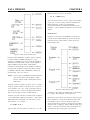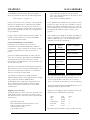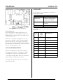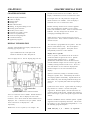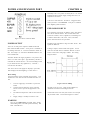
1
RPC-2350 USER'S MANUAL NOTICE TO USER Copyr ight 2001 - Re mote P rocessing Cor poration. All rights reserved. However, any part of this document may be reproduc ed with Remote Proce ssing cited as the source. The infor mation co ntained in this m anual is believe d to be correct. However, Remote Pr ocessing assumes no responsibility for any of the circuits described herein, conveys no license under any patent or other right, and make no repre sentations that the circuits are free from patent infringement. Rem ote Processing makes no representation or warr anty that such applications will be suitable for the use specified without further testing or modification. The user must decide fitness for a particular use. The con tents of this ma nual and the sp ecifications her ein may change without notice. TRADEMARKS CAM BASIC™ and PC Sm artLINK™ are trademar ks of Octagon Systems Corpor ation. Remote Pr ocessing Corporation' s general policy does not recomm end the use of its products in life support or applications where the failure or malfunction of a board may threaten life or injury. Install redundant or backup safety systems as appropriate to the application. Microsoft® BASIC is a trademark of M icrosoft Corpor ation. Microsoft® Windows®, Windows 95® , and Windows 98® are trademar ks of Microsoft Corpor ation. FCC AND EMI NOTICE Windows Ter minal is registered with Microsoft Corpor ation. The RPC-2350 and RPC-2350G is intended as an OEM product in an industrial environment. It was not tested for E MI r adiation. When op erated o utside a suitable enclosure, the board and any cables com ing from the board w ill radiate har mful signals th at interfer e with consumer and industrial radio frequencies. It is your responsibility properly to shield the RPC-2350/ 2350G and cables coming from it to prevent such interference. Hyper Ter m is copyr ight by Hilgr aeve Inc. and is developed for Microsoft Cor poration. Procomm is copyright by Datastorm Technologies, part of Symantec Corpor ation Remote Pr ocessing Corporation 7975 E. Har vard Ave. Denver, Co 80231 Ph. : (303) 690 1588 Fax: (303) 690 1875 www. rp3.c om [email protected] P/N 1761 Revision: 1.4 i TABLE OF CONTENTS OVER VI E W MANUAL ORGANIZATION . MANUAL CONVENTIONS . . Symbols and Term inology DEM ONSTR ATION DISK . . TECHNICA L SUPPORT . . . . . . . . . . . . . . . . . . . . . . . . CHAPTER 1 . . . . . . . . 1 . . . . . . . . 1 . . . . . . . . 2 . . . . . . . . 2 . . . . . . . . 2 SETUP AND OPERATION CHAPTER 2 INTRODUCTION . . . . . . . . . . . . . . . . . . . . 1 OPERATING PRECAUTIONS . . . . . . . . . . . . 1 EQUIPMENT . . . . . . . . . . . . . . . . . . . . . . . 2 COMMUNICATION PROGRAM . . . . . . . . . . 2 Windows mode . . . . . . . . . . . . . . . . . . . 2 FIRST TIME OPERATION . . . . . . . . . . . . . . 2 UPLOADING AND DOWNLOADING P R OG R AM S . . . . . . . . . . . . . . . . . . . . 4 Uploading - Windows . . . . . . . . . . . . . . . 4 Uploading - SmartLink . . . . . . . . . . . . . . 4 Downloading - Windows . . . . . . . . . . . . . 4 Downloading program s - SmartLink . . . . . . 4 Other communications software . . . . . . . . . 4 DE VE L OPI N G P RO G RA M S IN WIN D O W S . . . 5 EDITING PROGRAMS AND HINTS . . . . . . . . 5 Writing with line numbers . . . . . . . . . . . . 6 Writing without line numbers . . . . . . . . . . 6 PROGRAMMING TIPS . . . . . . . . . . . . . . . . 7 Finding v ariables, keywor ds, a nd labels . . . . 7 Faster, shorter IF-THEN's . . . . . . . . . . . . 7 Use par enthesis (or brack ets) . . . . . . . . . . 7 WHERE TO G O FROM H ERE . . . . . . . . . . . . 8 TROUBLESHOOTING . . . . . . . . . . . . . . . . . 8 SAVING AND LINKIN G PRO GRAM S CHAPTER 3 SAVING A PROGRAM . . . . . . . . . . . . . . . . 1 AUTORUNNING . . . . . . . . . . . . . . . . . . . . . 2 PREVENTING AUTORUN . . . . . . . . . . . . . . 2 L O A DI N G P R OG R AM S . . . . . . . . . . . . . . . . 2 INSTAL LING 128K O R 512K FLA SH . . . . . . . 3 L I NK IN G P RO G RA M S . . . . . . . . . . . . . . . . . 3 Program size . . . . . . . . . . . . . . . . . . . . . 3 Multi-tasking . . . . . . . . . . . . . . . . . . . . . 3 DAT A statem ents . . . . . . . . . . . . . . . . . . 3 Linking within the program . . . . . . . . . . . 3 Declare variables . . . . . . . . . . . . . . . . . . 4 Program Re-entry . . . . . . . . . . . . . . . . . . 4 SAVING PROGRAMS VS SAVING DATA . . . 4 COMMANDS . . . . . . . . . . . . . . . . . . . . . . . 4 ii SERIAL PORT S CHAPTER DESCRIPTION . . . . . . . . . . . . . . . . . . . . . . COM1 SERIAL PORT . . . . . . . . . . . . . . . . . COM2 SERIAL PORT . . . . . . . . . . . . . . . . . Comm unication flow control . . . . . . . . . . . X O N /X O FF . . . . . . . . . . . . . . . . . . . . . RS-232 . . . . . . . . . . . . . . . . . . . . . . . . . RS-422 . . . . . . . . . . . . . . . . . . . . . . . . . RS-485 . . . . . . . . . . . . . . . . . . . . . . . . . RS-422/485 Termination network . . . . . . . . Two- and four- wir e RS-485 . . . . . . . . . . . RS-485 Transm itter turn-off . . . . . . . . . . . Two-wire R S-485 . . . . . . . . . . . . . . . . . . Network r esponse time considerations . . . . . Multi-drop Network . . . . . . . . . . . . . . . . ACCESSING SERIAL BUFFERS . . . . . . . . . . DISABLING PROGRAM BREAK . . . . . . . . . . SPI PORT . . . . . . . . . . . . . . . . . . . . . . . . . SPI Port connector type inform ation . . . . . . SERIAL PORT FILE NU MBERS . . . . . . . . . . COMMANDS . . . . . . . . . . . . . . . . . . . . . . . SERIAL CABLE PIN OUT . . . . . . . . . . . . . . 4 1 1 1 2 2 2 2 2 3 3 3 3 3 4 4 5 5 6 6 6 7 DATA MEMORY CHAPTER BATTERY BACKUP . . . . . . . . . . . . . . . . . . Alternate battery . . . . . . . . . . . . . . . . . . . STORING VARIABLES IN RAM . . . . . . . . . . CAM BASIC memory m ap . . . . . . . . . . . . Flash Memory . . . . . . . . . . . . . . . . . . . . Saving and In itializing Ar rays and data . . . . Mapp ing your sto red data . . . . . . . . . . . . . Considera tions for saving to Flash . . . . . . . Using L OAD to transfer data . . . . . . . . . . . INSTALLING 512K RAM . . . . . . . . . . . . . . . CORRUPTED VARIABLES . . . . . . . . . . . . . ASSEMBLY LANGUAGE INTERFACE . . . . . E X A M PL E P RO G RA M S . . . . . . . . . . . . . . . COMMANDS . . . . . . . . . . . . . . . . . . . . . . . 5 1 1 1 1 2 3 3 4 5 5 5 6 7 7 DIGITA L LINE S CHAPTER DIGITAL I/O PORT . . . . . . . . . . . . . . . . . . Pull up resistors . . . . . . . . . . . . . . . . . . . High curr ent output at J3 . . . . . . . . . . . . . High current output at P2 . . . . . . . . . . . . . Interfacing to an opto-module rack . . . . . . . Configuring digital I/O lines . . . . . . . . . . . Digital I/O progra mming . . . . . . . . . . . . . Connector pin out . . . . . . . . . . . . . . . . . . Connector pin out - J3 . . . . . . . . . . . . . . . COMMANDS . . . . . . . . . . . . . . . . . . . . . . . DIGITAL I/O WORKSHEET . . . . . . . . . . . . . 6 1 2 2 2 2 3 3 4 4 5 5 RPC-2350 USER'S MANUAL CHAPTER 7 . . . . . . . . 8 . . . . . . . . 8 . . . . . . . . 8 . . . . . . . .9 INTER RUPT S CHA PTER INTER RUPT HAN DLIN G BY CA MBASIC . . HARDWARE INTERRUPTS . . . . . . . . . . . . SOFTWARE INTERRUPTS . . . . . . . . . . . . . COMMANDS . . . . . . . . . . . . . . . . . . . . . . 13 . 1 . 1 . 2 .2 ANALOG I/O CHAPTER 8 C ONNE C T IN G A N A L OG I/O . . . . . . . . . . . . 1 Initializing Inputs . . . . . . . . . . . . . . . . . . 2 Differential Mode . . . . . . . . . . . . . . . . . . 2 Examples using CON FIG AIN . . . . . . . . . 2 ACQUIRING ANALOG DATA . . . . . . . . . . . 3 Data logging on a timer tick . . . . . . . . . . . 3 MEASURING HIGHER VOLTAGES . . . . . . . . 3 CONVERTING ANALOG MEASUREMENTS TO REAL WORLD UNITS . . . . . . . . . . . . . . 3 oise Notes . . . . . . . . . . . . . . . . . . . . . . 4 CALIBRATION . . . . . . . . . . . . . . . . . . . . . . 4 ANALOG OUTPUT . . . . . . . . . . . . . . . . . . . 5 IC Installation . . . . . . . . . . . . . . . . . . . . 5 Program ming voltage output . . . . . . . . . . . 5 Output Current . . . . . . . . . . . . . . . . . . . 6 Noise . . . . . . . . . . . . . . . . . . . . . . . . . 6 mA. OUTPUT . . . . . . . . . . . . . . . . . . . . . . 6 IC Installation . . . . . . . . . . . . . . . . . . . . 6 Current loop power . . . . . . . . . . . . . . . . . 7 POWER SUPPLY . . . . . . . . . . . . . . . . . . . . 7 COMMANDS . . . . . . . . . . . . . . . . . . . . . . . 7 MULTI-MOD E COUNT ER CHA PTER COUNTER INPUTS AND OUTPUTS . . . . . . Interrupt selection . . . . . . . . . . . . . . . . . HIGH VOLTAGE INPUT . . . . . . . . . . . . . . PROGRAMMING . . . . . . . . . . . . . . . . . . . Program E xamples . . . . . . . . . . . . . . . . CAM BASIC resolution lim it . . . . . . . . . . MEASURING PULSE WIDTH . . . . . . . . . . . J10 Pin out . . . . . . . . . . . . . . . . . . . . . COMMANDS . . . . . . . . . . . . . . . . . . . . . . 14 . 3 . 3 . 4 . 4 . 4 . 5 . 5 . 6 .6 CALE NDAR /CLO CK S E TT I NG D A TE A N D T I M E YEAR 2000 AND BEYOND CLOCK INTERRUPTS . . . . COMMANDS . . . . . . . . . . . . . . . . . . . . . . KEYPAD PORT PROGRAMMING THE KEYPAD Program Explanation . . . . . . Keypad Comm ands . . . . . . . KEYP AD P ORT P IN OU T - J5 . . COMMANDS . . . . . . . . . . . . . . . . . . . . . . . . . . . . . . . CHAPTER 9 . . . . . . . . 1 . . . . . . . . 2 . . . . . . . . 2 . . . . . . . . 2 . . . . . . . .2 DISPLA Y POR TS CHA PTER 10 LCD CHA RAC TER P ORT J6 . . . . Configuring J6 for a display . . USING TWO DISPLAYS . . . . . . DISPLAY CONNECTOR PIN OUT COMMANDS . . . . . . . . . . . . . . . . . . . . . . . . . . . . . . . . . . . . . . . . . . . . . . . . . . . . . . . . . . . GRAPHIC DISPLAY PORT CHA PTER 15 DISPLAY INFORMATION . . . . . . . . . . . . . . 1 Display sno w or sp arkle . . . . . . . . . . . . . . 1 CONNECTING A DISPLAY . . . . . . . . . . . . . 2 LCD D isplay . . . . . . . . . . . . . . . . . . . . . 2 EL Display . . . . . . . . . . . . . . . . . . . . . . 2 Verify operation - both display types . . . . . . 2 DISPLAY LAYERS . . . . . . . . . . . . . . . . . . . 2 CONTRAST ADJUSTMENT . . . . . . . . . . . . . 3 Mechanical Contrast Adjustment . . . . . . . . 3 Software Contrast C ontrol . . . . . . . . . . . . . 3 PRINTING TEXT . . . . . . . . . . . . . . . . . . . . 3 Positioning text . . . . . . . . . . . . . . . . . . . 4 Printing normal and reverse characters . . . . . 4 The s emi-c olon (;) . . . . . . . . . . . . . . . . . 4 Scrolling . . . . . . . . . . . . . . . . . . . . . . . . 4 CHANGING AND LOADING FONTS . . . . . . . 5 CLEAR, FILL, AND XOR AREAS . . . . . . . . . 5 LOAD AND SAVE SCREENS . . . . . . . . . . . . 6 Calcula ting graph ic mem ory r equirem ents . . 6 Making and saving custom graphics . . . . . . 6 ADDITIONAL SCREEN CONTROLS . . . . . . . 7 Changing cursor size or form . . . . . . . . . . 7 Sc re e n fla shing and sc ree n ON /O FF . . . . . . 7 Screen overlay . . . . . . . . . . . . . . . . . . . . 8 D ispla y pow er O N /O FF . . . . . . . . . . . . . . 8 Display mapping . . . . . . . . . . . . . . . . . . . 8 PRINT AND DISPLAY TIMES . . . . . . . . . . . 9 EL DISPLAY . . . . . . . . . . . . . . . . . . . . . . . 9 CABLE PIN OUTS . . . . . . . . . . . . . . . . . . 10 COMMANDS . . . . . . . . . . . . . . . . . . . . . . 11 1 1 1 2 2 SOUND/TIMER OUTPUT CHA PTER 11 CONNECTING TO A SPEAKER . . . . . . . . . . 1 WATCHD OG TIMER CHA PTER 12 PROGRAM EXAMPLES . . . . . . . . . . . . . . . . 1 iii TABLE OF CONTENTS POWER & EXPANSION PORT POWER INPUT . . . . . . . POWER OUTPUT . . . . . . Heat sinking . . . . . . . EXPANSION PORT P1 . . . CHA PTER . . . . . . . . . . . . . . . . . . . . . . . . . . . . 16 . 1 . 1 . 1 . 2 RESOU RCES CHA PTER RESOURCE LISTING . . . . . . . . . . . . . . . . Part distributors . . . . . . . . . . . . . . . . . . VF displays . . . . . . . . . . . . . . . . . . . . LCD ’s . . . . . . . . . . . . . . . . . . . . . . . . Stepper Motor C ontrol . . . . . . . . . . . . . . OPTO m odules . . . . . . . . . . . . . . . . . . Isolated RS-485 and communications . . . . Temperature sensors and transmitters . . . . 17 . 1 . 1 . 1 .1 . 1 . 1 . 2 . 2 TECHNICAL INFORMATION ELECTRICAL . . . . . . . . . . MECHANICAL . . . . . . . . . . MEMORY AND I/O MAP . . . JUMPER DESCRIPTIONS . . CONNECTOR DESCRIPTION BOARD OUTLINE . . . . . . . 18 . 1 . 2 . 2 . 3 . 4 . 5 . . . . . . . . . . . . . . . . . . . . . . . . . . . . . . . . . . . . . . . . . . . . . . . . CHA PTER . . . . . . . . . . . . . . . . . . . . . . . . . . . . . . . . . . . . . . . . . . iv CHAPTER 1 OVERVIEW is supporte d by Basic com mands. A com plete description of CAMBA SIC comm ands is in the CAMBASIC Programming Guide. CHAPTER SYNOPSIS OVERVIEW CHA PTER 1 Brief description of the RPC-2350 and RPC-2350G How this manual is organized How to get technical support Application disk Program development can take place on your PC, using your word processor, or on the RPC-2350. Programs from your P C can be downloaded using PC SmartLink or other serial communication program. DESCRIPTION Customization We can customize the RPC -2350 for your production needs. Some exam ples include latching connectors, installing a specific combination of memory, soldering IC’s directly to the board (where practical), and remov ing components for cost reductions. You must purchase at least 25 boards and allow for extra lead time. We can provide you with a firm quote ahead of time. The RP C-2350 is an embe dded contr oller with a built in Basic language. The RP C-2350G also includes a graphics display interface. Other features include: Built in CAMBASIC pr ogramm ing language autoruns at power up. On card Flash EPROM program mer save s program s. Eight single e nded or 4 differen tial analog inputs MANUAL ORGANIZATION convert voltage inputs to a digital value using a 12 bit (4096 count) A/D converter. Two 12-bit analog or 4-20 mA. outputs also available. This m anual pro vides all the infor mation r equired to install, configure, and use the features on the RPC -2350. The manual is organized by function. T he first section deals with getting the board operational. Other sections address on boar d I/O and capabilities. Keypad port for an operator interface. The 16 position keypad is automatically scanned and is read using the KEYPAD command. This manual makes refer ences to the RPC-2350. The RPC -2350 and RP C-2350G are very similar. Unless otherwise noted, ever ything that applies to the RPC-2350 also applies to the RPC-2350G. Two RS-232 serial ports are pr ogramm able for baud rate, par ity, length, and stop bits. Both inputs and outputs have a 256-byte buffer. A watchdog timer resets the card if the program This manual assumes you are fam iliar with some type of BASIC progr amming software. The syntax used by CAM BASIC is similar to Microsoft' s GW or QuickBASIC. If you are not experienced with BASIC software, you may want to refer to books and training programs available through your local software store. The CAMBA SIC Programming Manual has information and examples for all command s. "crashes. ” T he timer is enabled and disabled by software. 48 general purpose digital I/O lines, 8 of which are high curr ent outputs. These lines can connec t to another opto rack. 128K of battery backed RAM is standard. A 512K RAM optionally available. NOTE: Built in EPROM pr ogramm er save program s for autorun on power up or r eset. The RP C-2350 uses a Z 8S180 C PU o perating d ouble clocked at 18 MH Z. Double c locked oper ation mak es it twice as fast as its equivalent 64180 CPU. The board operates stand alone or on an RS-485 network. Its 5.0" x 8.0" size makes it easy to mount in a NEMA box. The RPC -2350 uses a Zilog Z8S180 processor. Additional information can be obtained from Zilog at www .zilog. com or your local representative. MANUAL CONVENTIONS The RPC-2350 and RPC-2350G are very similar. Unless otherw ise noted, r eferences to the RP C-2350 also apply to the RPC-2350G. The primary differences between the two boards are power input and graphics display capability. CAM BASIC progr amm ing language is standard . T his language is similar to Microsoft GW Basic. All hardware 1-1 OVERVIEW CHAPTER 1 The hexadecimal notation used in this manual and by CAM BASIC is the ampersand charac ter (&) before the number. A &8C stands for 8C hexadecimal Information appearing on your screen is shown in a different type. Example: DEMONSTRATION DISK CAM BASIC (tm) V1.4 © 1985-94 Octagon Systems Corporation © 1999 Remote Processing Corporation All rights reserved - free 32434 A disk with many sa mple pr ogram s is included w ith this manual. T his manual references progr ams on the disk. You may use the code on these disks in your own CAM BASIC progr am. These program s are for demonstration purposes only and there is a good probability you will modify them to suit your needs (i.e., safety checks). Symbols and Term inology NOTE: Text under this heading is helpful information. It is intended to act as a reminder of some interaction with another part of the manual or device that may not be obviou s. TECHNICAL SUPPORT If you have a question about the RPC-2350 or CAM BASIC used on it and ca nnot find it in this ma nual, call us and ask fo r technica l support. WARNING: Information under this heading warns you of situations that might cause catastrophic or irreversible damage. Wn[-] When you call, please have your R PC-2350 and CAM BASIC manuals ready. Sometimes knowing what the RPC-2350 is used for is helpful, so please be ready to describe its application and the problem. Denotes jump er block pins. < xxx> Paired angle brackets are used to indicate a specific key o n your ke yboard . F or exam ple < esc> means the escape key. Phone: 303-690-1588 FAX: 303-690-1875 E-mail: info@r p3.com BASIC uses decimal convention for designating addresses and data. There are times, however, when hexadecimal notation is more convenient to use. 1-2 CHAPTER 2 SETUP AND OPERATION CHAPTER SYNOPSIS SETUP AND O PERATION CHA PTER 2 Running the RPC-2350 for the first time How to run und er D OS and W indows env ironm ents Uploading and downloading programs Handy pr ogram ming techniques Developing in Windows Troubleshooting if it does not work right away INTRODUCTION The RPC -2350 and RPC-2350G are very similar. The major difference is the RPC -2350G has graphics control software and hardwar e. The m emory m aps between the two boar ds are diff erent. This manua l will refer to the RP C-2350. Unless otherwise expressed, the same information applies to the RPC-2350G. The RP C-2350 is ready to p rogr am w hen you con nect it to a terminal or PC and apply power. This chapter describes what is needed to get a sign on message and begin programm ing. 2-1 SETUP AND OPERATION CHAPTER 2 EQUIPMENT Requirements for uploading and downloading programs are discussed. A " Where to go from here" section directs you to the chapters to read to use the various capabilities of the RPC-2350 F inally, a troubleshooting section helps on the most com mon pro blems. You will need the following equipment to begin using the RPC-2350: RPC-2350 embedded controller A PC with a serial port and communications program VTC -9 serial ca ble + 5, 300 m A. pow er supply or 7 to 30V applied to “7-30V” terminal on P2. OPERATING PRECAUTIONS The RPC-2350 is designed to handle a wide temperature range and operating conditions. These characteristics requir e using CM OS com ponents. CM OS ar e static sensitive. T o avoid damaging these c omponents, observe the following precautions before handling the RPC-2350. 1. 2. Do not connect any a ccessory com ponents, suc h as a display or keypad, to the board until you are sure the board w orks in you r envir onmen t. Ground yourself before handling the RPC -2350 or plugging in cables. Static electricity can easily arc through cables and to the card. Simply touching a metal part on your PC can greatly reduce static. The CAMBA SIC Programming Manual is strongly recommended. It can be downloaded free at our web site (www. rp3.c om). Refer to Chapter 4 Se rial Ports for wiring information to make your own cable. COMMUNICATION PROGRAM Do not insert or remove components when power is applied. While the ca rd is a + 5 volt only system, other voltages are generated on the card. A terminal progr am is used to talk with the RPC-2350 2-2 CHAPTER 2 SETUP AND OPERATION download time. board. All programm ing and initial communication between the RPC-2350 and outside wor ld is done through RS-232. DOS mode Start your serial communication program (PC Smar tLink, Proc omm , or other). Set the CO M por t to the one you will be using. The terminal progr am you use depends upon the operating environment. The vast majority of environments are PC ’s operating either DOS or Microsoft Windows. If you are using another operating environm ent, then just r ead “ All terminal pr ogram s” below and set up your terminal program accordingly. Windows mode You may use either Windows 3.1 Terminal or Windows 95 Hyper Term commu nication progra ms. For a fast setup, use on e of the following files: All terminal programs Set communication parameter s to Baud rate: Data length: Parity: Stop bits CAMBASIC.TRM CAMBASIC.HT 19200 8 none 1 Windows terminal Hyper terminal Make sure you set the COM port number under “P roperties. ” See “ Develo ping prog ram s in Window s” late r in this section for more information on wr iting and editing program s. The RP C-2350 does not send a CTS signal on its communication port. If your terminal or comm unications software requires this or other signals (DCD , D SR), you may have to tie them to the appropriate levels. You can probably ignore these lines in software. Windows Term inal and Hyper Ter minal, P C Smar tLink, or Procomm does not need them. FIRST TIME OPERATION Make sure your terminal is set up as described above. Become familiar with the locations of the connectors before getting started. See Figure 2-1. Set “handshake” control to “none” or O FF as appropriate. RPC -2350 jum pers hav e been set at the factory to operate the system immediately. For first time operation, do not install any connectors or parts unless specified belo w. Jumper s should be kep t in default positions. Default communication method between the RP C-2350 and PC is RS-232 ASC II. This includes file upload and download. O ther protocols such as XMOD EM ar e not used. A terminal program should be able to recognize a ‘prom pt’ chara cter. A prom pt chara cter is used to control a transfer when sending a file (as is done during a program download). W hen the RPC-2350 sends a ‘> ’ prompt character , it is saying “OK to send the next line.” Standard Windows Hyper Term does not allow this. Windows Te rminal, Procom m and PC SmartLink do. 1. The RPC-2350 requires + 5 ±0.25 VDC at 300 mA. The RPC-2350G can use + 5V or 6.5 to 30 VDC at 150 to 320 m A. (Cur rent dr aw depe nds upon supp ly voltage. Mor e voltage = less current). Make sure pow er is off. Connec t the power supply to the appropriately marked terminals on the RPC2350 or RPC-2350G. If your terminal program does not allow for prompt charac ters dur ing text trans fers, next best is to put a delay between sending lines (as is done in HyperTerm and Terminal). How much depends upon what you are sending. If you are downloading a small progr am (< 1000 lines), then 1/10 second is plenty of time. If you are downloading data files, then you may need more time, depending upon the complexity. The major penalty when downloading with delays is increased + 5V is connected to P2, “+ 5V”. Make sure jumper W8 is not installed. 7 to 30 VDC is connected to P2, “7-30V” (RPC2350G only). M ake sure jumper W 8 is installed. 2-3 SETUP AND OPERATION CHAPTER 2 Figure 2-2 Pow er connector detail Ground is connected to “GND” “+ 5V” can be pow er input or output. When W 8 is installed on the RPC-2350G, it is power output. When W8 is not installed, it is power input. See Chapter 16 for more inform ation. Figure 2-3 Pow er and jumper location detail “SWP WR” is a high current switch to ground. See Chapter 6, High current output at P2 for more information. 2. Connect one end of the VTC -9 connector to the 10 pin COM 1 (programm ing) port on the RPC-2350. Refer to Figure 2-1 for conne ctor location. 3. Start your terminal progr am (if not running already). 4. Turn on your pow er supply. On pow er up a copyright message is printed. CAMBASIC (tm) V1.4 (c)1985-94 Octagon Systems Corporation (c)1999 Remote Processing Corporation All rights reserved - free 32434 Connect the VTC-9 serial cable to the PC' s COM1 or C OM 2 port . If a nonsense message appears, your terminal or PC may not be set to the appropriate communication parameters. If the system still does not respond, refer to "T ROU BLESH OOT ING" later in this chapter. 4. The system is now in the " imme diate mod e" and is ready for you to start program ming. T ype the following program (in upper or lower case: 10 20 30 40 FOR X = 0 TO 2 PRINT " Hello "; NEXT PRINT Now type RUN The system will display: Hello Hello Hello 2-4 CHAPTER 2 SETUP AND OPERATION Depending upon the program (Terminal or HyperTerm) you will see progr ess on your scr een in different way s. UPLOADING AND DOWNLOADING PROGRAMS You may need to change the amount of delay between lines. This is set under “P roperties”, ”A SCII Setup”. 1/10 second is usually ade quate for all progr am sizes. You can set it to 10 milli-seco nds if your progr am is small (unde r 500 lines) . A s the progr am gets lar ger, this time should increase . A result of a sh ort delay tim e is missing or gar bled progra m lines. Downloading program s means transferring them fr om your computer to RA M on the RPC -2350. Uploading means transferring pr ograms from RAM back to your computer . T his section explains how to do both of these procedures using PC SmartLink and both Windows terminal programs. Gener alized instructions for other terminal programs are given at the end of this chapter. Downloading programs - SmartLink To practice downloading a program , type Uploading - Windows In the previous section, you wrote a test program. To upload that progr am to a PC and save it to disk, first type “list” but do not hit the < Enter> key. NEW<return> Perform the following when using PC SmartL ink: Select “Tr ansfer” then “ Capture to disk”. Enter the name you w ant to save it as. After that window closes, hit the enter key. The program will be listed and captured by the terminal program. To stop capture, select “Transfer” then “Capture to disk” again. Then select stop transfer. Your progr am is now saved. Uploading - SmartLink In the previous section, you wrote a test program. To upload that program to a PC and save it to disk: 1. Pre ss the < F1> key. A windo w with the main menu will appear. 2. Press the letter U (upper or lower case). Your program will begin to transfer from RAM to the PC. When m enu appears. 3. 4. 1. Press the < F1> key to view the main menu. 2. Smar tLink has a b uffer w hich is used to tem porar ily store the progr am. If you followed these instructions without exiting SmartLink, the previously uploaded program is in the buffer and may be dow nloaded. Howeve r, lets assume you just started SmartLink. Press the L key to get the program from the disk. 3. Enter the filename to get the file. 4. Press D to download the program. 5. Press the < F2> key to return to the program. You can list the program by typing: list To save a program to disk, type the letter S. You are prompted for a file name. Enter the file name you want the program saved under. or / Press < F2> to return to the immediate mode. Other communications software The following is general information when using another terminal emulation program (Procomm , etc. ). NOTE: Some ve rsions of P C Sm artLin k have pull down menus or will operate differently. Refer to the SmartLink manual for the version you are using. When uploading or downloading files, select ASCII text format. Other forma ts are not used. Downloading - Windows Select “Tr ansfer” then “ Send Text file”. Select the program . D ownloading begins. CAM BASIC does not know when you are typing in a progr am or if something else (laptop or mainfr ame) is sending it char acters. The uploa d and dow nload file does not conta in any special c ontrol cod es, it is sim ply ASCII cha racters. For test purposes, select one of the programs on the RPC-2350 dem o disk. 2-5 SETUP AND OPERATION CHAPTER 2 The following setup files are on the 2350 applications disk. Use these to quickly set up yo ur ter minal. Uploading programs is simply a process of receiving an ASCII file. Y ou or your progr am simply needs to send "LIST" to receive the entire program. CAMBASIC.TRM CAMBASIC.HT Downloading a program requires transmitting an ASCII file. CAMBASIC is an incremental line compiler. As you type in (or download) a line, CAMBASIC com piles that line. The tim e to comp ile a line depend s upon its complexity and how many line of code have been entered. Windows terminal Hyper terminal You may have to change the CO M port to match your system. T hese set up files put the terminal in the following configuration: Baud: Parity: Data: Stop: Flow: Line delay: CAM BASIC must finish compiling a line before starting the next one. When a line is compiled, a "> " character is sent by the card. This should be your terminal program s pacing character when downloading a program. 19200 none 8 bits 1 bit None 0.01 sec Do NOT use FIFO buffers in HyperTerm. If your communications program cannot look for a pacing prompt, set it to delay transmission after each line is sent. A 100 ms delay is usually adequate, but your CAM BASIC progr am may be long and complex and requir e mor e time. A resu lt of a short de lay time is missing or gar bled progra m lines. Editing, downloading, and pasting are easy using Notepa d or W ordpad . T hese pro gram s allow you to e dit a program, save it, then download it using HyperTerm. Download code using text transfers. To change a portion of code, you can m ake the change then copy the new line. In HyperTerm , select Edit, then Paste to Host and the new line will be sent. Terminal does not have this feature. If you are writing code without line num bers, be sure to p ut the line num ber in first. In all cases, you will have to hit < Enter > to finish the line. COM 1 on the RPC-2350 does not recognize the CT S or RTS lines. The CTS line is pulled high on the RPC2350. The effect of not recognizing these lines is your PC or terminal cannot hold off the RPC-2350' s transmission. C onverse, the RP C-2350 cannot hold off the host from sending it data. D E V EL O P IN G P RO G R A M S I N W IN D O W S When you save a program , be sure to save it as a text file. Wordpad tends to be a little more annoying than Notepa d because it alw ays asks you w hat kind of file to save it as. Notepad does not. These program s may append a .txt extension to the file name. This is OK. Programs can be completely written and downloaded using programs norm ally available in Microsoft Windows. The two program s you need are a terminal program (HyperTer m or Ter minal) and an editing progr am (N otepad, Wor dpad, Wor d, e tc.). Both program s can be open at the same time, ma king editing and changing just that much easier. Just switch between the two programs (using < Alt> -< Tab> or clicking the task bar). When using the line edit feature in CAMBASIC you may see some extra characters and num bers on the display. Try to ignore them as best you can. EDITING PROGRAMS AND HINTS Versions of Word will not let the terminal program open the file you are wor king on. Y ou actually have to close the file in Wo rd befor e you can do wnload it. Files uploaded or downloaded are simply ASCII DOS text files. No special characters or control codes are used. You m ay create and edit programs using your favorite word processor or editor. Just be sure to save files in DO S text form at. There are tw o ways you can write CA MBASIC progr ams: With or without line num bers. Even this is not hard and fast as you can write using a mixture. 2-6 CHAPTER 2 SETUP AND OPERATION You can wr ite a program in lower case cha racters. CAM BASIC translates them to upper case. from 1500 to 2500. The program mer m ust determine the number of lines required for each section. Some program mers put "N EW" as the first line in the file. During debugging, it is common to insert "temporary" lines. Adding NEW ensures that these lines are gon e. D ownloadin g time is incr eased wh en the old progr am is still pre sent. When replacing a program or section, downloading time is increased. Blocks of line numbers cannot be renumber ed by CAM BASIC when other par ts of the program are installed. However , if a particular section is the only program downloaded, then line renumbering in that range is possible. Refer to the CAM BASIC RENU M comm and. Instead of uploading and downloading programs, you can save them to the on car d Flash E PRO M. This is useful if you are using a terminal to write programs. Make sure the 'A utorun' jumper is installed (See Chapter 3 SAVING PROGRAMS). To prevent automatic program execution on power up, inser t the STOP statement at the beginning of the program (such as line 1). When you power up the RP C-2350 , the progr am is tra nsferr ed into RAM and executed. Delete the progr am line with the STOP statement to norm ally start progr ams. CAM BASIC automatically formats a line for minimum code space and increased readability. For example, you could download the following line of code: 10 fora=0to5 When you listed this line, it would appear as: 10 FOR A = 0 TO 5 Writing with line numbers You can manually enter line nu mber s. T he prob lem is when you have to add another line. It is quite common for program s to grow and run out of line numbers. You can execute the RE RUM comma nd to renum ber lines. Spaces are initially displayed but not stored. The following line: 10 for a = 0 to 5 would be compressed and displayed as in the second example above. Spaces ar e removed. A technique used to further program documentation and reduce code space is the use of comments in a downloaded file. For example, you could have the following in a file written on your editor: Writing without line numbers Many progr amming languages such as C and versions of BASIC and do not use line numbers. CA MBASIC uses line numbers simply because you can edit them through a serial ter minal. 'Check VAT temperature 'Read the output from the RTD and ' calculate the temperature 2200 a = ain(0) :'Get temp You can write and edit CAM BASIC progr ams without using line num bers. This ma kes for m uch mor e reada ble code. The first 3 comments downloaded to the RPC -2350 are ignored. Similarly, the empty lines between comm ents are a lso ignored . L ine 2200, with its comment, is a part of the program and could be listed. The m ajor pena lty by wr iting a progr am this w ay is increased download time. The demo program NOLINES.BAS is such a program. (Other program demos may also not use line numbers. ) The key is to use the AUTO com mand. This command automatic ally assigns a num ber to eac h progr am line as it is entered. NOTE: Some ve rsions of P C Sm artLin k may op tionally strip comments before downloading. Check your manual to see if this option is available. There are a few things you have to keep in mind. 1. Put the N EW statement at the start of the program file. This removes old code. If you like to write programs in separate modules, you can download them separately. M odules are assigned blocks of line numbers. Start up code might be from 1 to 999. Interrupt handling (keypad, serial ports) might be from lines 1000 to 1499. Display output might be 2. You must use the remark statement (') in lines that do not have any code. This is because AUTO 2-7 SETUP AND OPERATION CHAPTER 2 stops giving line numbers when two < CR> 's are received. GOT O or GOS UB. 3. U se labels after GO TO and G OSUB statem ents. Do not assign line numbers (except as noted in 4 below) since they will change. Use parenth esis (or brackets) When IF-T HEN statements do not execute properly (and formulas too), break it up using parens. For exam ple: IF A - B*C AND D = C*B - D/8 OR 15 THEN ... 4. O N GO TO and O N GO SUB cannot use labels. The tr ick here is to assign a line num ber w ay high in the program count. Then, at these lines, use GOTO .. label. NOLIN ES.BAS shows how this is done. The question the compiler asks is "What are you doing here?" True, there is an order of precedence, but often times the assumptions made by the programm er vs compiler order will differ. Use parens as shown below. Use the AUTO statement to segment your program. AUT O can num ber star ting at any location . T his is useful to place ON G OTO and ON G OSUB locations. IF A-(B*(C AND D))=C*B-((D/8)OR15) THEN Generally, you can go 7 levels of parens without reachin g the com pilers lim it. AUTO is terminated when two sequential < CR> ’s are received. PROGRAMMING TIPS Manuals can be full of information. Som etimes it’s overwhelming. This section presents a few tips our customers ha ve given us over the past 15 ye ars. Finding variables, keywor ds, and labels The F IND statem ent will search for program labels, variable names, or even comm and keyw ords. Look in the CAMBA SIC Programming Manual for more information. Fa st e r, shor t er IF-THE N 's IF-THEN statements are based on zero and non-zero flags. Consider the following program fragment a= 5 if a then ..there executes quicker than a= 5 if a < > 0 then goto ..there Notice 2 eleme nts are missing F irst is the inequality test < > . Next is GOTO . The progr am line is an implied GOTO. Another var iation is a= 5 if a goto ..there The THEN is implied but you must supply the keyword 2-8 CHAPTER 2 SETUP AND OPERATION TROUBLESHOOTING WHERE TO GO FROM HERE If you w ant to do th is Go to chapter Save a program 3 Autorun a program 3 Know m ore abo ut serial por ts 4 Use the SPI port 4 Using RAM to save variables 5 Storing variables in F lash 5 Configure digital I/O lines 6 Read switch status 6 Use high c urre nt outputs 6 Connect an external opto rack 6 Using calendar/clock 7 Reading vo ltages (Ana log input) 8 Analog output 8 Using a keypad 9 Character display port 10 Sound or timer output 11 Using inter rupts 13 Using high speed counter 14 Graphics display 15 Power input and output 16 Expansion port 16 You pr obably tur ned to this section b ecause you could not get the sign on message. The following are troubleshooting hints: 1. Check the power on the RP C-2350 . A good place is C13+ and -. If it is below 4.65 volts, the RPC2350 will be r eset. Powe r is 5 ±0. 25 volts. If it dips intermittently to 4.65 volts (due to switching noise or ripple), the card w ill reset for about 100 ms. If the noise is frequent enough, the car d will be in permanent reset. Check U14, pin 6. If it is low (about 0 volts), then it is in reset. This line shou ld be high (about + 5 volts). If you are using a 6-15V supply, make sure it does not dip below 6V even intermittently. Use a scope to make sure it does not. A voltmeter m ay not be good enough. The same can be said for the 5V supply. Make sure it does not dip below 4.8V using an oscilloscope. 2. Check the COM1 port. COM 1 is also known as console port J1. Rem ove the connector from COM 1. R efer to the outline dra wing ear lier in this chapter. Connect an oscilloscope (preferred) or a voltmeter to pin 3 (Txd ) and gro und. Pin 3 should be -6 volts or more negative. (Pin 1 is designated by the ^ sym bol on the conn ector. Pin 3 is next to it, nearer the key opening.) If you have -6 volts or more, press the reset switch. If you have a scope attached, you should see a burst of activity. If you have a volt m eter, you should see a change in voltage. Using a Fluke 8060A set to measure AC, you should see a mom entary rea ding above 2 volts. Pre ss reset sev eral tim es to make sure it captu res it. 3. Install the cable and make sure the voltages and output activity are still there. Output is from pin 3 on the VT C-9. Check to make su re som ething is not shorting the output. 4. Check the serial pa ram eters on y our P C or termin al. They should be set to: Also, r efer to the table of contents for a listing of major functions. 19200 baud, no parity, 8 data bits, 1 stop If all of this fails, call technical support listed at the front of the book. 2-9 CHAPTER 3 SAVING AND LINKING PROGRAMS CHAPTER SYNOPSIS and can be modified. The y can be saved to EPROM for execution later. The RPC -2350 is set to autorun on power up or reset by installing a jumper (W 11). W hen autorun is on, the progr am in E PRO M is loade d into RAM and begins to execute immediately. Saving progr ams to Flash Retrieving pr ogram s from F lash Load and run two programs Autorun on reset or power up Installing 128K or 512K F lash The EP ROM is write-protected w ith a software lock, so accidental writes on pow er-on or -off are almost impossible. You cannot disable the lock except when executing the SAVE comm and. DESCRIPTION SAVING AND LINKING PROGRA MS CHAPTE R 3 Two to 8 programs can be stored in socket U3. U3 normally has a 29C010A Flash type EPROM, which stores 2 progr ams. Its capacity is 128K bytes. U3 sock et can acce pt a 29C0 40A type E PRO M. This type has 512K byte capacity and can store up to 8 program s. You can store two to eight programs up to a maxim um size of about 33 K bytes each . A genera l rule to determine progr am storage requirem ents is one line requires 40 bytes. 32K bytes would store over 800 lines of code. Your application could be significantly more or less, depending upon the number of commands / line, comments, and print statements. Another indication of program size is to use the file length as saved on a PC disk. Figure 3-1 Flash location and jumpers The 29C 010A (12 8K) Flas h can stor e 2 progr ams w hile the 29C040A (512K) stores up to 8 pr ogram s. SAVING A PROGRAM Despite the fact you have 128K or 512K RAM installed, the maxim um pr ogram size CA MBA SIC can run is about 33K (leaving room for variable storage). Programs can be chained, however. When programs are chained, variables from one prog ram can be used in another. To save a program , set jumper W 11. You m ay set the jumper even if the power is on. Remember to discharge any static electricity before installing or removing the jumper. For this example, assume you wanted to save the following program: 10 20 30 40 Data can be saved to and retrieved from this device using the SAVE and LOA D comm ands. The m aximum amount of data that can be accessed is limited by the size of your program less the Flash size. FOR N = 0 TO 2 PRINT "Hello "; NEXT PRINT If this progr am is not alr eady in, type it in now (o r, if you prefer, use your own progr am). The Flash EPROM is non-volatile (retaining data even when power is disconnected), having an unlimited numbe r of re ad cycles an d a limited nu mber of write cycles (about 1, 000 to 10,0 00). U sing 1,000 c ycles as a limit, you can w rite to F lash once a da y for abo ut 3 years before “wearing out” the device. You can save your program to any one of two locations: 0 or 1. Prog ram s saved to location 0 will autom atically run at power up. Syntaxes to save a program are: SAVE SAVE program A pro gram is not run fr om E PRO M. It is transfer red to RAM and run from there . Pr ograms in RAM are run 3-1 SAVING AND LINKING PROGRAMS CHAPTER 3 any static electricity before installing or removing the jumper. Where ‘program’ is 0 or 1 for 128K Flash or 0 to 7 for 512K Flash installed. “SA VE” and “ SAVE 0" ar e the same . Both sa ve to program location 0. Another way to prevent autorun is to rem ove the signature bytes from Flash. This is done by writing &FF ’s into Flash address 0 and 1, segment 8. Use the following steps to do this. Type in the following command for this example: SAVE dpoke &8000,&ffff save 8,0,0,0,&8000,2 CAM BASIC will compile the program , progr am the EPR OM, and verify its contents. This will overwrite the first 128 to 256 bytes of code and prevent autorun. Compile...Write...Verify LOADING PROGRAMS The time it takes to do all of this depends upon the length and co mplexity of the progr am. Gener ally, it w ill be from 1 to 20 second s. T he read y prom pt (> ) will appear when the p rogr am has b een succes sfully saved to the EPROM . If the program does not write to the EPROM, an error message will appear: Ther e are tim es when y ou may w ish to tempor arily modify or otherwise test out a change to a program. Since the program is loaded into RAM, modifications can be made without affecting the program in EPROM. If you find out tha t modification s are not de sirable or did not work, you can restore the original program to RAM using the LOAD com mand. Fail @ xxxx Saving a pr ogram overw rites the pr evious one. Ther e is no way to recover it since both occupy the same space. This version of CAM BASIC can link and run 2 program s with a 128K or 8 with 512K flash. Because of this linking ability, you should do some things during development to limit problems. Before loading a new progr am, enter the fo llowing com mand fir st: AUTORUNNING The pr ogram stored using SAVE or SAV E 0 will autorun. To autorun a program: new 1. 2. Make sure there is a program in EP ROM (from above) stored by using SAVE or SA VE 0. If you are loading one pr ogram through F lash, saving it, stopping, then loading an other pr ogram and runn ing it, you may notice som e oddities, like incorr ect varia ble values or syntax er rors to lines not in your code. This oddity is probably due to the program size difference. If you do not type in NEW to start with, LOA Ding w ill clobber what is in m emor y and nothing w ill be right. Make sure the autorun jumpe r W11 is installed. If you push the reset button, the program should run. If there are any err ors, the pr ogram will stop (assuming you have not trapped them with ON E RROR) and display the error message. If you are using multitasking routines, such as ON BIT or ON TIC K, then it is best to reset the board and then load the pr ogram during de velopme nt. PREVENTING AUTORUN When troubleshooting or maintaining a program , it' s not always co nvenient for an autoexec ute file to run. This is especially tr ue if the pro gram has been co nfigured to ignore the < ESC> key. To pr event autorun, re move jumper W11. The othe r (and be st) way to take care of th is problem is to reset the board, then load the program. Use LOAD 0 to retrieve programs saved using SAVE 0 or SAVE and use LOAD n to retrieve programs saved using SAVE n. ‘n’ is 0 or 1 for 128K Flash and 0 to 7 for 512K. Later, if you wish to SAVE or LOAD a program, reinstall this jumper. You may do so even if the power is on and a program is running. Remember to discharge 3-2 CHAPTER 3 SAVING AND LINKING PROGRAMS When developing program s and testing for linking, make sure you save any changes to Flash before running. Any changes in program length, especially the first (autorun) one, c an have adver se, str ange, or disastrous r esults. When you have saved the changes, pr ess the reset button to simulate an autorun. NEVER start with program 1 (LOAD 1) then have it load program 0. SAVING DATA TO FLASH EPROM Additional data, such as strings and constants, can be saved to U3 using a variation of the SAVE comm and. Exactly how much m emory you have depends upon how many and how large of program(s) you have. Flash sector size must be considered when saving. The sector size determines the minimum write ar ea. Thus, if you were to save just 1 byte, 128 (29C010A type) or 256 (29C04 0A) bytes w ill be written . A ll unwritten data is saved as FFH. There are other do’s and don’ts, precautions and limitations to linking. They are discussed below. Program size The first (autorun) program run MUST be larger than the second, linked program. This is because variables and data are stored above the program . If the second progr am w as longer , it w ould wipe the m out. To simp ly increase pr ogram size, add co mmen ts. Font are stored starting at address &A C00, segment 9. This is above program area 1. If space is tight, consider using a 512K Flash. Chapter 5 treats saving data to RAM and Flash more extensively. Multi-tasking All multitasking (ON BIT, ON COM $, CO UNT, etc.) and interrupts are disabled and multi-tasking data cleared (hash table is zeroed out) when a program is linked. You must re-enable them in your code. The reason for this is the operating system stores the address (not line number ) to execute. When you chan ge progr ams, addresses change. INSTALLING 128K OR 512K FLASH Socket U3 can hold a 128K or 512K Flash EPROM. Perform the following steps to install a a new Flash: 1) 2) 3) Remove power from board and r emove existing EPRO M from U3. Orient the new Flash so pin 1 is near the edge of the board. Install the IC. Set jumper W2 according to memory size: W2[4-5] 128K (29C010A, 29C010) W2[5-6] 512K (29C040A) You can save some selected data by writing it to a variable. For example, the current count can be saved just before you LOAD 1 RUN. You will need to reenable the count when you enter the program. DATA statements Use RESTOR E to reset the DATA statement pointer every time you enter a program (if you are using DATA statements). LINKING PROGRAMS One CAMBASIC program can load and run another. For example , the autorun p rogr am can , at so me point, run the program in Flash area 1, which can then call the original one. Using this technique, you can have program sizes of nearly 70K bytes using a 128K Flash or 245K using a 512K Flash.. Linking within the program To link to ano ther pr ogram , ex ecute LOAD n RUN on its own line. Do not put any other code after it. Do not make it as part of a c onditional statem ent, as in This linking is inten ded to be called occasionally (although we have run programs that have linked millions of tim es). For example , the second pr ogram is a set up and ca libration r outine. This will fr ee up ma in program RAM for variables. IF A = N THEN LOAD 1 RUN If you link within a subroutine, DO. .U NTIL, or FOR..NEXT, execute EXIT CLEAR before LOAD. Linking in CAMBASIC is not threaded code. It does replace one program with another while keeping variables. . . 2250 3-3 GOSUB 7000 SAVING AND LINKING PROGRAMS . . 7000 . . 7100 7110 CHAPTER 3 SAVING PROGRAMS VS SAVING DATA IF A = 0 THEN 7100 A program number and F lash segment are related by the following formula: EXIT CLEAR LOAD 1 RUN Flash segment = program number + 8 The above example shows how to link to another program within a subroutine. If you do not use EXIT CLEAR, you will eventually end up with an <Out of memory> error. If you intend to save data to Flash, m ake sure you do not write to a program area. P rograms are always saved starting at address 0 and continue until end of program. You can save data above a program. Declare variables All variables, dimensioned arrays, and string variables should be declared in the first program. These variables are accessible to both pr ogram s. The important thing here is to remem ber that saving program s to Flash and saving data to Flash are related. Program Re-entry There is a good chance you will have declared a dimensioned array or made room for strings in the autorun progr am. If you do a C LEA R again, all variables will be cleared. The following is a list of CAM BASIC commands used for saving and loading pr ogram s. COMMANDS Command What you m ust do when you enter a progra m is to test for a re-entry flag at the start. If it is 0, then the progr am know s to go and do va riable initializa tion. If it is not 0, then it skips around it. For example: 10 20 30 40 IF FLAG <> 0 THEN 100 CLEAR 500 :’Clear space DIM WEIGHT(100) DIM B$(20) . . More initialization code . 100 FLAG = 1:’Signal initialized 110 ON ERR GOTO 10000 120 CONFIG COM$ 2,0,8,0,1 130 ON COM$ 2 GOSUB 2000 LOAD Transfers program from U3 to RAM for editing or running. LOAD n Transfers pr ogram of specified area of U 3 to RA M . LOAD data Multi-part syntax command that moves data from F lash to RAM or RAM to RAM. Refer to Chapter 5 or the CAMBASIC manual for more information. SAVE Saves a program fr om RAM to U3 for Autorun SAVE n SAVE data The code will not skip around the multitasking statements when it is first Autorun. This is because, by default, all Basic variables are reset to 0. When you link progr ams, variables rem ain intact. 3-4 Function Save a program fr om RAM to a program area of Flash. Multi-part syntax command that saves data from RAM to Flash. Refer to Chapter 5 or the CAMBASIC manual for more inform ation CHAPTER 4 SERIAL PORTS CHAPTER SYNOPSIS SERIAL PORTS CHAPTE R 4 Overview of RPC-2350 serial capabilities Using RS-422/485 Networking with RS-485 Preven ting program stops (breaks) SPI port information DESCRIPTION The RPC -2350 has two serial ports that can be used for interfacing to a printer , ter minal, or other ser ial devices. A SPI p ort is also pr ovided. This chap ter descr ibes their characteristics and how to use them. F requent references are m ade to commands listed in the CAMBA SIC Programming Manual . P lease ref er to this manual for mor e information. Figure 4-1 Serial por t connector location statement, it will accept ASCII character values from 0 to 127. When used with the INKEY$ and COM$ functions, it returns ASCII values from 0 to 255. No control lines (like CTS or RT S) are available on COM 1. A pull up resistor is on the CTS output should a communication program or device require a positive indication the port is alive. Serial por ts are num bered C OM 1 and CO M2. COM 1 is used for program development. It is RS-232 only. During run time, it can be used for other functions such as writing to a printer or serial display. COM 2 is a general purpose serial port. Its outputs can be RS-232, RS-422, or RS-485 level compatible. COM2 SERIAL PORT COM 2 is an RS-232, RS-422, or RS-485 por t. It also uses a VTC-9F serial cable to connect to PC’s and other serial devices. CO M2 is identical to COM1 except that it has 2 hardware handshaking lines, CT S and RTS. Both ports sup port XO N/ XOF F pr otocol to contr ol data transmission. Each por t has a 256 character interrupt driven inp ut and output bu ffer. This allow s charac ters to be sent out (using PRINT) without slowing down program execution. Howeve r, if the PRINT buffer fills, program execution is suspended until the buffer em pties. Both ports have a 256 character input buffer. When more than 256 characters have been received, extra ones are ignored. NOTE: The CT S output line is low on power up or reset. This is to prevent the RS-485 transmitter from turning on and adversely affecting network communication. RS-232 communication may be affected by holding off the sender from sending data. You must enable the CT S output as described below under “ Comm unication flow control” . The baud rate, parity, data length, stop bits, and com port type are changed using the CONFIG BAUD command. Jumper W 4 determines if COM 2 receive is RS-232 or RS-422/485. COM1 SERIAL PORT COM 1 is J1 and is called the Console port on the card. This port uses a VTC-9F serial cable to connect to a PC and other external serial devices. The cable is wired one-to-one, with pin 1 on the 10 pin connector lining up to pin 1 on the D B-9. T he connec tor plugs dir ectly into a 9 pin serial port connector on a PC. W4[1-2] W4[2-3] RS-422/485 RS-232 Use CO NFIG BAUD to tell the system the type and characteristics of this port. Default is RS-232, 19, 200 baud, 8 data, 1 stop bit. . This port is normally used for program ming. D uring run tim e it may be u sed as a gene ral pur pose seria l port. When used for programming or with the INPUT 4-1 SERIAL PORTS CHAPTER 4 character (ASCII value 13H or < Ctrl-S> ) to the RPC2350 will stop transmission until an XON (A SCII value 11H or < Ctrl-Q> ) is received. This does not over-ride the RTS input line when RTS is low. Comm unication flow control There are tw o methods to control transmission: Hardware and software. Both are discussed below. When RTS line in goes low, the RPC-2350 is held off from transm itting out CO M2. The status of this port is read by the BIT statement. T he example below returns the status of the RTS line: RS-232 The most comm on communication interface is RS-232. Quite simply, RS-232 defines only ‘0' and ‘1' voltage levels and transient speeds. It does not define baud rate, start and stop bit length, parity or the pr otocol. RS-232 is available at J1(COM1) and J4 (COM 2). 100 B = BIT(130,5) If B = 1, transm ission is held off. Usually, when people speak of RS-232, they mean something that is compatible with a PC. H owever, you must make sure the baud rate, parity, and stop bits are proper for your device. These ar e set in the CONFIG BAUD com mand. You should check this line before executing a PRINT #2 statement. If transmission is held off, the print buffer can becom e full. PRIN T #2 com mand w ill ‘hang’ until the buffer accepts all characters in the program line. This may give the appearance of the program locking up or running very slowly. This could also result in a “de adly emb race” situation wher e the rec eiving device is expecting some other condition before it will receive character s. RS-232 is used in point-to-point communication. That is, one device talks to one other device. Schemes have been devised to network RS-232. The maximum baud rate RS-232 supports depends upon the distance and cable characteristics. As a rule of thumb, 9600 baud w ill work r eliably to 50 feet. The CT S line may be set high or low to control comm unication fr om a dev ice when using RS-232 . T his line is also used in RS-422/485 comm unication at P3 or J3 to contro l transm itter output. RS-422 RS-422 is used for long distance (1000 meter s) comm unication. It is similar to R S-232 in that it is point-to-point and the communication “ protocol” is the same. When u sing RS-232 comm unications, you may have to initialize the CT S output to high to allow the sender to transmit. The examples below show how this is done. Line 400 sets CTS low and 500 sets it high. The RS-485 port is used for RS-422 comm unication. The transmitter is always on. If, for some reason, you want to shut the transmitter off, execute 400 BIT 128,4,1 500 BIT 128,4,0 A low condition is supposed to hold off a device. Some devices do not recognize CTS output so this may be a mute poin t. BIT 128,4,0 in your co de. To turn the transm itter back o n, e xecute CTS is used for RS-422/485 communications to turn on/off the transm itter. Use C ONF IG BAU D to not only set the baud rate but also the type of communication protocol. C AMBASIC takes care of the CTS line for RS-422 and RS-485. BIT 128,4,1 in your code. RS-485 RS-485 is a popular networking system. T echnically, RS-485 only defines electrical specifications, not protocols. (See M ulti-drop Network below. ) In RS485, the transm itter is turne d on only long e nough to send a message, then it turns off. Thus, RS-485 allows multiple units to be put on a single set of wires. The CO NFIG BAUD statement sets both serial ports for baud rate and type (RS-232, RS-422, and RS-485) for COM 2. XON/XOFF The so-called XON/XOFF protocol is a software scheme to e n ab le a nd d isab le trans m itting . S en d in g an X O FF 4-2 CHAPTER 4 SERIAL PORTS RS-485 mode in the CON FIG BAU D 2 comm and. RS-485 operates in one of two modes: 2 wir e and 4 wire. ( An extr a wire is actually neede d as signal reference. ) There are pr o’s and con’s to 2-wire vs 4wire systems and they are not discussed here. During two wire mode and W6[1-2] is set, the receiver is turned of f when the transm itter is turne d on. This keeps the RPC-2350 from receiving what was just sent out. Mechanically, to make a 2-wire system, simply connect T+ to R+ and T- to R- on P3. NOTE: Do not ope rate RS -485 at 150 ba ud. Autom atic turn off is not adequate. Contact RP C for sugg estions. When you connect the RPC -2350 to another device, the T+ ,T-, R+ and R- signal lines may be reversed. That is, yo u may ne ed to connec t T+ to T- and so on. This is due to naming convention confusion when RS-485 was first introduced. RS-422/485 OPERATING INFORMATION RS-422/485 Termination network When the RPC -2350 is the last physical unit on a network (RS-485), or it is the only unit (RS-422), the receiver must be terminated to prevent ringing. Insert jumpers in W5[1-2][3-4] to install the network terminator. See figure 4-2 below. Figur e 4-3 Jum per W 4 & W 6 detail Two-wire RS-485 Mechanically, to make a 2- wire system, simply connect T+ to R+ and T- to R -. M ake sure CON FIG BAUD is set up for RS-485 m ode. Se t jumper W 6[1-2]. T his prevents data transmitted from getting received. Network response time considerations When the last chara cter is sent ou t, an internal tim er is activated. When the timer is done, the RS-485 transmitter is turned off. The tim er shuts off the transmitter a bout 1/4 to ½ char acter time after the last charac ter is sent out. The differ ence is due to sto p bit and parity requirements and to allow for line settling. Figure 4-2 Only one slave device on a RS-485 network should have a terminator installed. The host transmitter shou ld also have a 100 ohm resistor in series with a 0.1 m fd capacitor across its T+ and T- terminals. The term inator on the RPC -2350 include s pull up and pull down resistors to prevent lines from floating and generating er roneous char acters. Normally, this is not a problem. However, if a very high speed sys tem is contr olling the netw ork, it is possible two transmitters can be on simultaneously, garbling data. Any responding systems on the network should wait at least ½ character time before sending a message packet. W hen using other 2350' s on a network, this will not be a pr oblem at 1 9200 baud a nd proba bly will not be one at lower r ates. Two- and four- wire R S-485 The RS-485 port on the RPC -2350 is set up for 2- or 4wire mode through jumper W6. This jumper either always en ables rec eive (W6 [2-3]) or enables it only when the transmitter is off(W6[1-2]). W6[1-2] W6[2-3] Multi-drop Network You can use the RPC-2350 in a m ulti-drop network by using CO M2' s RS-422/ 485 port. You can c onnect up to at least 32 units (including other RPC-2350's) over a 4,000 foot range. Receive off while transmitting (2-wire) Receive always on (4-wire mode) RS-485 Transmitter turn-off The RS-485 transmitter is automatically turned on and off by CAM BASIC operating system. You must specify The host transmits data packets to all of the devices, or nodes, in the network. A data packet includes an 4-3 SERIAL PORTS CHAPTER 4 40 UNIT$ = ">05" . . . address, com mand, data, and a checksum. See figure 44. The packe t is received by all devices, and ignored by all except the one addressed. 1000 PACKET$ = COM$(2) 1010 A = INSTR(0,PACKET$,UNIT$) 1020 IF A = 0 THEN RETURN . . Line 20 sets up ON CO M$ to interrupt on a < CR> and branch to line 1000. Line 40 sets up this card' s address. Figure 4-4 Data packet Line 1010 checks to see if the rece ived mess age = this card's address. If not, the subroutine ends. When there is a match, further processing is performed. The relationship described below between nodes and the host is a maste r-slave. The host dir ects all co mm u ni ca ti on . N o des " d o n o t s peak u n less sp o ke n to". Peer to peer com munication, while possible with the RPC-2350, is not discussed here. An application program, 485TST. BAS, filters out control codes (such as < LF> and < CR> ) at the start of the message. Since CO NFIG COM $ set up a communication interrupt on a < CR> , your sending de vice c an a ls o s end a < LF> . Ther e are m any com municatio n protoco ls. F or this example, a protocol might look som ething like this: > 22M B1 485TST .BA S also checks for com municatio n err ors. Its main pur pose is to detect co mmu nication er rors but it also acts as a good foundation for a comm unication program. The pr otocol starts w ith the < cr> charac ter. This character synchronizes all units and alerts them that the next few characters coming down are address and data. In this case, "> 22" is the units address. "M " is the comm and and " B1" is the ch ecksum . T he comm and is terminated with a < cr> character. 485NE T. BAS is a simple networ king progra m. To test it out, jumper W4[2-3] temporarily. After the program is running, connect your terminal to J4. Instructions are printed when the program is first run. Response depends upon the nature of the command. S u pp o se th e co m m an d M means " return a d ig ital I/O port status". T he RPC-2350 could rea d the port and respond with AA2< cr> . The first A is an acknowledge, that is no error s were detected in the message. The data, A2, can be broken do wn as follows: Bit/line Status ACCESSING SERIAL BUFFERS You can access C OM1 and COM 2 buffers in three w ays: 1. 76543210 1 0 1 0 0 0 1 0 = A2 INP UT sta tement. This re moves a ll charac ters in the buffer up to the term inator cha racter and puts them into a variable. When using the INPUT statement, program execution is susp ended until a < cr> (Enter key) is received. W hether this is a problem depends on your particular application. Lines 1, 5 and 7 are high while the others are low. The following program fragment uses ON C OM$ in a network environment. ON C OM$ gener ates an interrupt when a < CR> is received. The interr upt program uses INSTR function to determine if the data packet was addressed to this card. INPU T strips bit 7 on the COM1 por t. This means ASCII character s from 0 to 127 are received. The INPU T statement can return a maxim um string length of about 150 chara cters. 10 CONFIG BAUD 2,7,4,0,2 20 CONFIG COM$ 2,13,0,0,1 30 ON COM$ 2 GOSUB 1000 2. 4-4 INKEY$(n) function. Characters ar e removed one at a time. A null string is returned when the buffer CHAPTER 4 SERIAL PORTS use as a basis to read and w rite to other SP I devices. is empty. In this mode, you have access to the full 256 bytes. If you don' t read the b uffer an d the buffer fills, all subsequent characters are discarded. INKEY$(n) may be used anywhere in the program. 3. Comm and form at is: a = SPI(channel,out_length,data, delay,in_length) Where: channel = 0 to 2, the SPI channel number. COM$(n) retrieves all characters in the buffer, including < cr> ' s and other control co des. This function is commonly used with ON COM$ multitasking statement. You can retrieve 128 of the 256 bytes in the serial buffer at one time. out_length = 0 to 16, data outpu t length in bits. When z ero, no data is shifted ou t. data can be any value but must be included. DISABLING PROGRAM BREAK data = 0 to 65,535, command/data to send to SPI device. Program execution can be interrupted by pressing the < Esc> key. To disable this recognition so the program does not terminate, put the following command in your program: delay = time to wait before retrieving information from SPI port. T ime in micro-seconds is calculated as follows: time = delay * 1.1 + 4. If 0 , the re is no delay. Use 0 if there is no data to retrieve (i.e. sending to D/A). 1000 CONFIG BREAK port,1 Where port is 1 (J1) or 2 (J4 or P3). in_length = 0 to 16, data input length in bits. W ill return a number from 0 to 65535. SPI PORT The table below sho ws the location of SPI device selects. A device is selected when a line goes low. A software SPI port is provided at J11. SPI (Serial Peripheral Interface) is used to communicate with a number of IC’s. These include D /A’s, A/D ’s, U ART’s, and other devices. J11 provides two chip selec ts. SPI port number The optional touch screen interface uses SPI port 1. The SPI function is used to read and write data. Unfor tunately, SPI has a v ariety of da ta form ats. D ata to send and receive from a device can be anywher e from 8 to 24 bits. The clock polarity an d data phase c an idle high or low when data is latched. CAM BASIC SPI func tion suppor ts the following f orm at: Clock idle polarity: low Clock-data phase: low This format supports the Maxim MAX186/188 and BurrBrown ADS7843 IC’s. The program SPIDEMO1.BAS uses t he MAX18 6/1 8 8 to retu rn the res ult o f an A/D calculation. Functionally, it is the same as the AIN command. If your form at needs are differ ent, ther e is a CAM BASIC program (SPIDE MO2. BAS) that you can 4-5 Location 0 Analog input (U10) 1 J11-4 2 J11-5 SERIAL PORTS CHAPTER 4 COM1 is J1, the console port. COM2 is J4, the primary port. The table below is the pin out for SPI port J11. Pin No. Description 1 Clock output to device 2 Serial data to external device 3 Serial data from external device 4 SPI 1 select (active low). Used for touch screen select. COMMANDS The following is a list of CAM BASIC commands used for serial I/O. Some variations are not listed here. Refer to the CAMBA SIC Programming Manual for more information. Command Function 5 SPI 2 select (active low) C L E AR C O M $ Clears serial input buffer 6 + 5V supply COM$ Returns string from buffer 7 Ground CONFIG BREAK Prevents < ESC> from stopping the program CONFIG BAUD Sets serial port parameters C O N F IG C O M $ Configures port for ON COM $(n) interrupt INKEY$ Returns a character fr om the serial buffer INPUT Receives string or number from port LIST Outputs program listing O N C OM $ Calls subroutine on serial input PRINT Outputs data in various fo rma ts SPI Serial I/O for exter nal IC’s TAB Tabs to predetermined positions SPI Port connector type information The SPI port connector header is a Molex-Waldom type. Its part number is 22-23-2071. This is a 0.1" center, 0.025 post connector. The m ating connec tor (ter minal hou sing) part n umber is 22-01-3077. Cr imp terminal part number s are 08-500114 (tin plate) or 08-55-0102 (go ld). A low cost crimping tool is 63811-1000. Parts and tools are available from Digi-Key (800 344 4539 or www.digikey.com) Other housings and terminals are available (such as high pressure). Refer to a Molex data book for more information. A MP M T connectors (such as 87499-1) can also be used. They fit, but ar e not polarized. SERIAL PORT FILE NUMBERS CAM BASIC refer ences the ser ial I/O ports by file numbers. The following table lists the corresponding file numbe r to ser ial I/O port and h ow they ar e used with the various ports. Description COM1 COM2 File 1 2 Examples PRINT "Hello" PRINT #1," Hello" INPUT A$ A$ = INKEY$(1) PRINT #2," Hello" INPUT #2,A$ A$ = INKEY$(2) 4-6 CHAPTER 4 SERIAL PORTS SERIAL CABLE PIN OUT The following is the pin out between the IDC connector for the RPC-2350 and the D B-9 connector to the PC or term inal. IDC pin # DB-9 pin # Description 1 nc 2 nc Direction from 2350 3 2 Tra nsmit Out 4 7 RTS In 5 3 Receive In 6 8 CTS Out 7 nc 8 nc 9 5 Ground 10 na + 5V Out Note that CTS and RT S are not available on J1. The VTC -9 serial cable is a simple one-to-one connection b etween a 10-pin ID C conn ector an d 9-pin IDC DSU B. 4-7 CHAPTER 5 DATA MEMORY The problem with calculating battery life are variables beyond our reasonable control. First, memory manufacturers specify a ‘typical’ current of 1 to 2 microamps and a maximum of 100 (high temperature operation). Other factors affecting battery life include operating temperature, clock chip, and time the RPC2350 has power applied to it. You can expect the battery to last between 3 to 5 years for operation at 25°C. At 50°C, life is about half as much. This is due to battery deterioration and CMOS leakage increases at higher tempera tures. CHAPTER SYNOPSIS Battery backup description Where and how to store va riables Saving and retr ieving data from F lash Installing 512K RAM Discussion about cor rupted da ta DESCRIPTION DATA ME MORY CHAP TER 5 The RP C-2350 is usually installed w ith 128K of RA M in socket U 2. A n optional 512K can be installed. RAM is battery backed on bo th models. Hum idity also affects ba ttery life. Very high humid ity (in conjunction with a dirty environment) increases leakage. Low hu midity dr ys out the batter y seal, allowing contaminates to enter. This chapter discusses saving and retrieving variables from RAM and Fla sh EP ROM and runn ing assem bly language progr ams. The point of this explanation is to give you the factors affecting battery life. Under the best of conditions, life is 7 years. Unde r worse conditions, it could be as low as 3 months. You can add a larger battery as described below. If program and data are battery backed, the UNNEW command may be used to try to restore the program. Variables used by the Basic program are clear ed, howeve r. Cer tain variab les are pr eserve d and data POKEd into RA M is saved. Existing battery voltage is measured across W14. Alternate battery A larg er 3. 0V batter y can be installed by connectin g it to W14. Be sure to remove the existing battery. Note the polarity marked on the board. STORING VARIABLES IN RAM The term "var iables" in this context includes numb ers, strings, arr ays, recipes, and formulas as applied to your application. CAMBASIC provides 26 “protected” variables, A%Z%, that are not erased on power up. These are accessed like other BAS IC variables. Figure 5-1 M emory location BATTERY BACKUP The Flash EP ROM may be used to store variables or constants, such as text strings, to help reduce the size of the main program. Battery life is about 3 years (27,000 hours). See additional information a few paragraphs below. Battery B1 is used to back up the RAM and real time clock CAM BASIC m emory map The following diagram is a memory map for the RPC2350. The installed battery is rated for 190 mA-hours. RAM (any size) typically requires 1-2 micro-am ps in standby. The clock r equires typically 3 micro-amps. Assuming 7 micro-Amps of current draw, you could expect 3 years life from the battery (assuming the board was off the whole time.) 5-1 DATA MEMORY CHAPTER 5 PEEK statement to retrieve the variable: 50 B = PEEK(12,1) You can store and retrieve arrays, strings, and variables in this way. There ar e many variations of PEE K and POKE statements. Refer to the CAMBA SIC Programming Manual for additional information and examp les. A list of comm ands appea rs at the end of this chapter. Flash Memory Programs are stored in Flash EPROM. Programs are transferred from Flash to RAM at run time or LOAD. Data may also be stored in Flash. Below shows the Flash memor y map. Figure 5-2 2350 system memory map Program s and CAM BASIC variables reside in segment 0, between addr ess 00000H and 0FF FFH . Your variable s (as defined a bove) ar e stored fr om 1000 0H to 1FFF FH (w ith 128K RAM), which is called segment 1, address 0000H to FF FF H. When 5 12K RA M is installed, the useful range is from 10000H to 7FFFFH. A seg m en t h a s a n ad d ress ran g e from 0 00 0 to F F FFH (or & 0000 to &F FF F using C AM BASIC notation) (in decimal terms, this is 0 to 65535). NOTE: Do not use the CAM BASIC SOU ND statement when the boar d has 512K of RAM or Flash memory. Sound output is multiplexed with an address line. Program and basic variables (A, B(15), C $, etc. ) always reside in segment 0 and are cleared on reset. A special set of variables, A% - Z%, reside is segment 0 and are not cleared on reset. These are floating point numbers and can be used like any other variable in Basic. Figure 5-3 Flash memory map A 128K or 512K F lash type EP ROM may be in stalled in U3. Jumper W2 configures U3 for Flash size. Variables you peek and poke to should reside in segment 1 with 128K RAM installed or segments 1-7 with 512K. PEEK and PO KE commands store and retrieve values from memor y. For example: Data may be stored above the progr am in Flash using the SAVE comm and. The SA VE co mma nd transfe rs data from RAM to Flash. Fonts for the RPC-2350G are stored in Flash abo ve progr am 1 starting at F lash address &1AC 00 (this is segment 9, address &AC 00 when using SAVE). This will not interfere with your program but will affect any data storage plans you may have. 20 POKE 12,A,1 puts the value of A into segment 1, address 12. U se the 5-2 CHAPTER 5 DATA MEMORY How simple do you want to keep the program How secure does the data have to be (where to store data - Flash or RAM) How often is information updated A CAM BASIC progr am number and Flash segment when using SAVE are related by the following formula: SAVE segment = program + 8 Keep track of where you are writing to. Most programs will only use program area 0. Addresses above &9000 are alw ays available in any prog ram area. How ever, if you have many program s, you will have to keep track of where you are saving data to make sure a program does not get clobbered. Every application has a different set of priorities. Some program s are large, but only a few variables are stored. Others, some data is critical and some are not. Start off by determining what your storage requirements are (that is, floating point numbers, integers, strings, screen graphics.. .). LOAD is used to transfer data from Flash to RAM. An example of data include arrays used in CAMBASIC. This is explained further below. 64K to 448K bytes of RAM are available, depending on how U2 is popu lated. E ach data element type r equires a differen t number of bytes. Use the follo wing table to determine yo ur storage r equireme nts: Saving and Initializing Arrays and data Sometimes it is convenient to save an array of information to battery backed RAM and/or F lash for retrieval later . T his is a handy way of storing “ recipes” or tables of information for each job, customer , or process. Type Arrays are initialized and filled by the basic program. Then, they are saved to either RAM or Flash EPROM. The num ber and size of arr ays that can be saved is limited only by available memory. The saved arrays can be retrieved at any time. How arrays are saved and retrieved depends upon what kind of memory you ar e saving to and loading from. If arra ys are sav ed to Flash , use SAVE . U se LOA D to both save to and retrieve from RAM. Bytes of storage BASIC Commands Byte 1 POKE & PEEK Word 2 DPOKE & DPEEK Float 4 FPOKE & FPEEK String 1+ maximum string length POKE$ & P EEK$ Grap hic 32 - 9600 bytes DISPLAY LOAD Program Size 1-32K SYS(0) An exam ple of saving ar rays to R AM is shown in ARRAY 1.BAS pr ogram, on the application disk. Saving arrays to Flash is shown in ARRA Y2.BA S. FL ASH .BA S shows str ings, bytes, and wor d saves to Flash. ARRAY3.BAS is similar to ARRAY1.BAS except it uses LOAD to transfer arrays. This makes transfers faster. The mathematics for keeping track of addresses can get quite messy. It all depends upon your data structure. If you are trying em ulate a struc ture in C or vector s in JAVA, you will have some math to access the right data. Mapping your stored data A frequent question is “Wher e do I store my data?” and “How much do I have?” You have two places to store data: RAM or Flash. How much you have depe nds upon several factor s: Suppose you are logging a process and need to store the following types of information periodically: The demonstration program LOGGE R.BAS logs at over 2000 points using the structure below. Name Date Time Temperature Tick time Level Expected program size How much RAM and/or Flash memor y is free Will you need a second program? Amount of data to store Type of data to store Type String String Float Float word Bytes 9 9 4 4 2 First a dd up the total num ber of by tes needed. For this 5-3 DATA MEMORY CHAPTER 5 program size. As a practical fact, no m ore than about 34K of program can r un at one time. This leaves about 30K in the fir st Flash seg ment and at least this amo unt in the 2nd. Use the SA VE co mma nd to transf er data to Flash. structure it is 28. Next, assign variable names to the offsets in memory data begins. Name DSET TSET TPSET PSET LSET Pointing to Date string Time string Temperature Tick time Level Value 0 9 18 22 26 You can start saving at address &8400 and not interfere with the first program. If you SAVE to segment 9 and are using graphics on the RPC-2350G, larger fonts are stored starting at address &AC00. P ut a limit check at this addres s. W hen a 512K F lash is installed, segmen ts 2-7 are available, if there are no other programs in them. This is simply done by making a variable equal to a number. F or example, The SYS(0) function returns your progr am size. Y ou can use this figure to determine where you can start saving in Flash. Be sure to round up to the next page boundary (last two bytes of the address) to &00 when determ ining your data start of a ddress. This is to account for the Flash block size. PSET = 22 NOTE: The word “ SET” does not have any significance other than naming the variable. You w ill need a pointer to track the n umber of data sets (structur es) saved. You will also have to chec k this pointer to make sure you are not exceeding the maximum amount of memory. Use one of the protected variables (A%-Z% ) as the pointer. This way, if power disappears, the pointer is still in tact. Protected variables can also be used to keep track of the segment used to store data in. All cases limit maximum address to &F FFF in any one segmen t. Be sur e to read “ Conside rations for saving to Flash” below for more inform ation. Since each situation is unique, call Remote Pr ocessing technical support at 303 690 1588 to discuss your problem further. Considerations f or saving to Flash The RPC-2350G uses &5A00 bytes in the Flash EPROM to store gr aphics fonts. The fonts a re stor ed starting in segmen t 9, ad dress & AC0 0. T his is high enough in mem ory so no CAM BASIC progr am w ill interfer e with it. Only if you use medium and large size fonts on the RPC-2350G will you have to consider this as an upper memor y limit for storing data. Consider installing a 512K byte flash and saving to segments 2-7. A sample C AMBA SIC line to store data is: FPOKE A%*28TPSET,value,B% This example uses A% as the pointer and B% to track the segment number. ‘TPSET ’ and B% could just as easily be constants. This structure will save 2340 elements in 64K of RAM. Therefore, you should test A% for a limit of 2340 once each loop. Flash EPR OM is wr itten to in blocks, or sectors of 128 (29C010A installed) or 256 (29C040A installed) bytes each. T his means if you want to save just 1 byte, 128 or 256 bytes are used. You m ust pay attention to sector size for two reasons. F irst, a sector is the minimum number of bytes written. If a program r equires only 35 bytes to be saved, a full sector is written. If you had the following in your code: A 512K RAM can store up to 7 segments. Therefore, B% is checked fo r a value o f 8 or m ore at the e nd of this loop. If your data requirements are more than available RAM, you can stor e some in F lash. You will ha ve to first w rite the data to RAM first, then save to flash. 1000 SAVE 1,5,1,&1000,35 . . . 2000 SAVE 1,42,1,&1025,35 Flash is also used to save critical information. However, Flash will “ wear out” after 1, 000 to 10,0 00 writes. You will probably have to make an initial guess at your 5-4 CHAPTER 5 DATA MEMORY severa l things happen. Data save d at line 1000 is overwritten by the data in line 2000, even though different write addresses were specified. This brings us to the second r eason sector size is impor tant. You are now ready to power up the board. You can now PEE K and POKE data into segments 1-7. CAM BASIC forces the requeste d Flash a ddress do wn to an even sec tor addr ess. In both cases a bove, data is written to the Flash starting at address 0, not at 5 or 42. When y our app lication must r ely on the acc uracy o f data after power up, corrupted variables become a possibility. CORRUPTED VARIABLES The nature of RAM is it is easily written to. Any POK E' d data is susceptib le to corr uption. This is especially true when the board is powered down. U26 monitor s the supply voltag e and turn s off wr iting when it is below about 4.65 volts. How ever, when POKE ing long data, such as strings and floating point numbers, or writing to Flash, a pow er down could interrupt a saving process. T he result is information is corrupted. A scenario is explained below. The eas iest way to m ake an eve n sector a ddress is to “A ND ” the Flash ad dress w ith &F F80 (as is done in ARRAY 2.BAS pr ogram exam ple) when using a 128K flash or &FF00 with a 512K. Another consideration is the number of times Flash can be wr itten to. A tmel specifie s anywhe re fr om 1000 to 10, 000 or m ore w rites. Com pared to R AM , this is qu ite limiting. Flash sho uld be used to stor e default cons tants or data that changes only occasionally. A program is running and saving data. During this time a reset occur s. A reset can occur due to power loss, someone pushing the reset button, or a watchdog timer time out. The data is c orru pted becaus e the com plete value was not saved. Writing takes about 90 ms/1000 bytes. During SAVE time, interrupts (ON COM$, ON KEYPAD, ON BIT, etc.. ) are rec ognized but not serviced. If these comm ands mu st be servic ed quicker , w rite data in smaller blocks. Since it is impossible to predict or delay a reset, a work around is to duplicate or triplicate values. That is, you would have to save the same information in two or three different places. Usually you only need to save the pointers to data structur es. Using LOAD to transfer data The LOA D comm and can be used to transfer data from Flash to RAM or RAM to RAM. Use SAVE to transfer from RA M to Flash. When y ou are w riting ar rays of da ta (such as show n in LOG GER .BA S), th e sequence your pr ogram should follow is this: Write data to RAM. Update the pointer. This pointer could be in dup licate or tr iplicate. This way, you only loose one set of data. LOAD transfers up to 64K blocks of memory at a time. Use it to transfer an entire data structure containing recipes, formulas, constants, etc. The sample progr am ARR AY3. BAS shows how to move data from extended mem ory RAM into CAMBASIC and back. When you are saving only one set of data, the following applies. INSTALLING 512K RAM For purpose s of discussion, data varia bles are c alled sets because it can consist of a mixture of variables, strings and arra ys. A 512K R AM (part num ber 103 9) can be installe d in U2. The addition al RAM allows you to in crease data storage, not program size. On power up, your program would compare values from one set to the other one or two. If the two (or three) agreed, then there was no corruption and the program can reliably use the values. In practice, you would read information from set 1, but would save data to all two or three. Follow these steps to install RAM. 1. 2. 3. 4. Turn off power to the board. Remove existing IC from U 2. Install the 512K R AM . M ake sure pin 1 is oriented towards the board edge. Pin 1 will be marked with a dot or notch on top. Move jumper W2[1-2] to [2-3]. The use of duplicate or triplicate sets depends upon what the system must or can do if data is corrupted. W hen using a duplicate set, a corrupted set indicates that 5-5 DATA MEMORY CHAPTER 5 memory has been allocated before running these SYS comm ands. F ailure to do so may r esult in address returned that are not really free for assem bly language program s. default values (from the program) should be used, since it is uncertain if the first or second set is corrupted. Both data sets would then be re-initialized. A triplica te set is used to r ecover the last set or ind icate that the data in the first set is valid. The pr ocedure and logic is as follows. There are sever al ways to put a program in mem ory, depending upon your application. Data is written to each element in a set in a specific and consistent order (data to an entire set does not have to be written to, just that element). For example, a calibration constant is saved (POK E' d) in three different place s. Assume that the constant was assigned address 0, 100, and 200 in segment 1. The data is PO KEd to addr ess 0 first, then 100, then 200. Upon reset, the calibration value is checked. If the value at address 0 agrees with address 100 and 200, then no corruption occurred. When address 0 and 100 agree but not 200, then this indicates tha t a reset occ urre d while updating the third set. The first data set can be trusted. The third data set simply needs to be updated. When the first two sets do not agree, then you know that the first data is corrupted. If the second and third set agree, then, depe nding upon the system r equireme nts, the first set could be "corrected" using the old data. The user or other device could be alerted that a calibration (or other ) must be pe rfor med aga in. W hen all thre e sets disagree, then you must take action appropriate to the situation. Another technique to ch eck for v alid mem ory is checksum s. Sim ply write a progr am to add the values in RAM and compare it against a number is a good check. However, you cannot tell which data element was corrupted. 1. Use D ATA statements a nd PO KE the co de into segment 0 RAM. 2. Write a program to download code. Some applications are connected to a larger system which "initializes" its systems. Using INKEY $ or COM $, code is received and then poked into memory using POKE$. 3. Read the code from the EPROM (U3) (using INP) and transfer it to RAM (using PO KE). 4. Some space is available in the CAMBASIC ROM. Space fr om abou t 6B00H to 6F FF H is availab le in version 1.4 of the 2350G boar d. The star ting address will proba bly change in the future w ith different CAMBASIC versions. You may burn your assembly language program in U1 and CALL in from BASIC. 5. Space is available in the Flash EPROM. In theory you can run directly from Flash. This involves running in sectored areas unique to the Z180. However , this is probably more effort. Use the Flash to stor e the prog ram and then tr ansfer it to RAM segment 0. In all cases, it is best to load code into RAM from a "secure" source, such as F lash EPROM . Even though RAM is battery ba cked, over tim e there is the possibility it could be corrupted. Instances of data corr uption are rar e. T hey do increase as the boar d power is cycled or reset. Below is an exa mple of loa ding and r unning an asse mbly language program. ASSEMBLY LANGUAGE INTERFACE 100 110 120 130 900 910 Assembly language programs (including compiled C) must start from segment 0. Use the CAMBASIC CALL statement to execute an assembly language program. A specific area of RAM should be reserved for the program . This is to prevent strings and variables from corrupting that area of RAM . U se the SYS(1) and SYS(2) statements to do this. SYS(1) retur ns the lowest memory location while SYS(2) returns the upper location. Run the pr ogram first to ma ke sure v ariable FOR N = &FB00 TO &FB0C READ A POKE N,A NEXT DATA &DB, 2, &47, &E6, &FE, &D3 DATA 2, &78, &F6, 1, &D3, 2, &C9 2000 CALL &FB00 Lines 100 to 130 load the program into RAM. DATA statements may be entered manually. 5-6 CHAPTER 5 DATA MEMORY COMMANDS Line 2000 calls the pro gram listed below . It toggles J2 line 13. IN LD AND OUT LD OR OUT RET The following is a list of CAM BASIC commands used w it h R A M . A,(2) B,A 0FEH (2),A A,B 1 (2),A Command EXAMPLE PROGRAMS The follow ing is a list of CA MBA SIC pr ogram s used to save and load data to and from RAM and Flash. Name Function ARRAY1.BAS Move s floating point ar ray data a r ou nd RA M . ARRAY2.BAS Reads and writes array data to and from R AM a nd Flash Function CALL Calls an assembly language routine CLEAR Clears and allocates string space PEEK Return s a byte DPEEK Returns a 16 bit value PEEK$ Returns a string FPEEK Returns a floating point number POKE Stores a by te DPOKE Stores a 16 bit value POKE$ Stores a string FPOKE Stores a floating point number FLASH.BAS Writes to and reads data from Flash LOAD Move data from Flash to RAM or RAM to RAM LOGGER.BAS Data logs to RAM, prints out results. SAVE Save data to Flash from RAM 5-7 CHAPTER 6 DIGITAL LINES On power-up or software reset ( or CAMBASIC CALL 0), all digital ports ar e reset to inputs. CHAPTER SYNOPSIS Overview of the digital lines How to program Using high current port Interfacing to opto racks DIGITAL I/O PORT Digital I/O lines on the RPC-2350 are supplied by an 82C55 chip. The chip's lines primarily go to connectors J2 and J3. Lines to J3 also go to J5 and J6. This part assumes you will be using all lines at J3 for digital I/O. DESCRIPTION DIGITAL LINES CHAPT ER 6 Digital I/ O lines ar e used to inter face with op to-module racks, switches, low current LED's, and other TTL devices. The RP C-2350 has 48 of these lines available through J2 and J3. The lines on J2 and J3 ar e divided into 3 eig ht bit groups. P orts A and B can be configured as all inputs or outputs. Port C can be programm ed as one group of 8 inputs or outputs or as two groups of four lines (upper and lower C). T he four lines in upper and lower C can each be progr amme d as all inputs or outputs. Configuration is done in CAMBA SIC using CON FIG PIO comm and. J3 is shared with other connectors and functions. Eight lines are hig h curr ent outputs, capable of sink ing 75 to 200 ma. Another 8 lines on J3 are shared by the keypad connector, J5. Still another 8 lines are used by the LCD charac ter por t J6. A table at the end o f this chapter lists line use at J3. When a line is configured as an output, it can sink a maximum of 2. 5 mA. at 0.4V and can sourc e over 2.5 mA.at 2.4V. Outputs sink 15 mA.at 1.0V. Eight, 16, or 24 position opto racks are connected to J2 or J3. These opto rac ks accept G4 ser ies opto modules. G4 series opto modules are used to sense the presence of AC or D C voltages or switch them. Maximum switching curr ent is 3 ampere s. J2 and J3 are accessed using CAMBASIC LINE, OPTO, INP, and OUT statements. LINE r eads or writes to a port base d on the conne ctor num ber. LINE is genera lly used with the STB-26 boa rd. OPT O rea ds or w rites to an opto m odule based o n its position in an M PS opto rack. INP a nd OU T acces s a byte of data a t a port. Refer to the tables at the end of this chapter for pin outs, OPT O, and LINE referen ces. The base I/O addr ess for J2 is 0 and J3 is 64 when using INP, OUT, and CON FIG PIO statements. CO NFIG PIO statement is used to configure the 8255 lines for inputs and outputs. Upon reset, watchdog time out, or a CAM BASIC C ALL 0, lines ar e configured for inputs. J2 and J3 ar e accessed using LIN E or O PTO statements according to the table below. Figure 6-1 Digital I/O connectors WARNING: Apply power to the RPC -2350 before applying a voltage to the digital I/O lines to prevent current from flowing in and damaging devices. If you cannot apply power to the RPC-2350 first, contact technical support for suggestions appropriate to your application. Connector designation LINE # terminal OPTO rack position J2 1-25 0-23 J3 101 - 125 100 - 123 LINE #' s access the corresponding pin number on J2 or J3. L INE # 2 or 102 are not va lid. T his is a + 5 volt supply. A high voltage (±15 volts) input is available at J10-10. This input is intended for the counter. However, it can be used as a digital input. Connect jumper block W9-2 to a digital input at J2 or J3. 6-1 DIGITAL LINES CHAPTER 6 include those that overlap even for a few milliseconds. J3, port A is shared with the LCD character display port J6. If you are using J6, then these 8 lines at J3 are not available. Incandesc ent lamps h ave a " cold" c urre nt of 11 times its operating current. Lamps requiring more than 50 mA. should not be used. J3, port B is connected to a high current sink through U20. See High current output later in this chapter. Two lines are connected to the keypad port. They are active only when scanning a 24 position keypad. Protection diodes m ust be used with inductive loads. Refer to figure 6-2. J3 port C is shared with the keypad port J5. If you are using a keypa d through J5, the se 8 lines are not available at J3. Pull up resistors Digital I/ O lines at J2 an d J3 are p ulled up to + 5 volts through a 10K resistor pack. These pull ups makes interfacing to switches and "open collector" TTL devices easy . See "Inter facing to Switches and other devices" below. High cu rrent ou tput at J3 Eight lines at J3 can be used as high cur rent driver s. These outputs switch loads to ground. Outputs are controlled by Port B on the 82C55. Its address is 65. Figure 6-2 Inductive load protection Do not pa rallel outputs f or higher drive. This could result in damage since outputs do not share current equally. Logic outputs from this port are inverted. That is, when a 1 is writte n to the high cur rent por t, the o utput is switched on and goes low. High current output at P2 The P2 term inal marked “ SWPW R” is a 2 Am p, 50V FET switch to ground. ON resistance is about 1 ohm. It is intended to switch back light power for the LCD graphics display. However , it can be used for any other purpose. The output driver chip, U 20, can be replaced w ith a DIP shunt jumper so it is like the other lines at J3. NOTE: Outputs at the high current lines are not compa tible with TT L logic leve ls and should not be used to drive other logic devices. The switch is contr olled by software as follow s: Each of the high current outputs can sink 100 mA.at 50V. OUT &E7,1 OUT &E7,0 Two lines from the high curr ent port (Port B, 0 and 1) are used wh en the keypad is scanning 24 keys. These lines (at J3-8 and -10) may not be used for control purposes. :’Turns on switch :’Turns off switch The switch is turned OFF when only on a hardware reset or wa tchdog time out. Use the circuit in Figure 6-2 when switching inductive loads. WARNING: External supplies using the high cu rrent outputs m ust be tied to J3, pin 26 and NOT the power connector. Failure to do so can produce a ground loop and cause erratic operation. Interfacing to an opto-module rack J2 and J3 I/O lines interface to an MPS-8, 16, or 24 position opto m odule rac k. L ines not going to an opto module connect to a screw terminal on the MPS-XX series boards. This feature allows you to connect s w itche s or othe r TTL type de vic e s to the digit al I/ O The thermal time constant of U20 is very short, so the numbe r of outputs th at are on a t any one tim e should 6-2 CHAPTER 6 DIGITAL LINES lines. The MPS-XX series boards accept OPTO-22 G4 series or Grayhill G5 modules. See Chapter 18, RESOURCES , for a list of suppliers. shunt jumper. This keeps logic com patible with ports B and C. If opto channels 8-15 are used as inputs, then U20 must be replaced by a DIP shunt jumper. Use the O PTO comm and to acces s and contr ol opto modules. The LIN E comm and is used to access individual lines on the STB-26 or MPS-X X rack. Configuring digital I/O lines Lines are configured during progr am execution using the CONF IG PIO command. On power up or reset, all lines are inputs. A CM A-26 connects J2 and J3 on the RPC-2350 to the MPS-XX board. Cable length should be less than 2 feet for the 8 position rack and 18 inches for the 16 and 24 positions. Excessive cable lengths cause a high voltage drop an d conseque ntly unreliab le opera tion. Be su re to supply + 5V and ground to the appropriately marked terminals. When a line is configured as an output, it can sink a maximum of 2. 5 mA. at 0.4V and can sour ce a minimum of 2.5 mA .at 2. 4V. W hen driving opto modules, the outputs sink 15 mA.at 1.0V. You must configure the 8255 ports for outputs before using them. Use the following table to determine the corr esponding op to channel for a particula r 82C 55 port: Opto channe ls 82C55 port Connector Digital I/ O prog ramm ing exam ple The follow ing exam ple read s a switch at po rt A, bit 3 (J2-25), reads an opto module at channel 1 and writes an opto module at channel 5. A LE D is controlled at J2-10 (port B, bit 0). Addr. M 0 -M 3 Lower C J2 2 M 4 -M 7 Upper C J2 2 M8-M 15 A J2 0 M16-M 23 B J2 1 M100-M 103 Lower C J3 66 M104-M 107 Upper C J3 66 M108-M 115 A J3 64 M116-M 123 B J3 65 200 D = BIT(0,3) :'Get status port A 210 F = OPTO(101) :'Read opto module, ch. 1 220 OPTO 103,ON :'write module 3 230 BIT 1,0,0 :'turn on J2-10 240 BIT 1,0,1 :'turn off J2-10 250 A = LINE(103) :'Reads pin 3 at J2 260 LINE 4,1 :’Set line # 4 to 1 "Opto channel" is the position as marked on the MP S-xx board. The channel number is preceded by a ' M' character on the MPS board. W hen connecting J3 to an opto rack, add 100 to the number on the rack. J3 has a high current output on port A (channels M8-M 15). Replace U20 with a shunt jumper to operate norm ally. Figure 6-3 IDC pin out viewed from top To turn on an opto module, an output line must be low. A mod ule is turned off by wr iting a ' 1' to a channel. The logic a t J3 port A , w ith the high cur rent outpu ts installed is just the reverse. A ' 1' at a line causes the module to turn ON. High cur rent outpu ts at J3 port A are option ally configurable as TTL I/ O by replacing U20 with a DIP 6-3 DIGITAL LINES CHAPTER 6 Conne ctor pin ou t - J3 Conne ctor pin ou t - J2 J2 Pin # 82C55 Port/bit Description Opto Channel J3 Pin # 82C55 Port/Bit Alternate function Opto Channel 19 A/0 8 19 A/0 LCD port J6 8 21 A/1 9 21 A/1 LCD port J6 9 23 A/2 10 23 A/2 LCD port J6 10 25 A/3 11 25 A/3 LCD port J6 11 24 A/4 12 24 A/4 LCD port J6 12 22 A/5 13 22 A/5 LCD port J6 13 20 A/6 14 20 A/6 LCD port J6 14 18 A/7 15 18 A/7 LCD port J6 15 10 B/0 16 10 B/0 High curr. /Keypad 16 8 B/1 17 8 B/1 High curr. /keypad 17 4 B/2 18 4 B/2 High curr ent 18 6 B/3 19 6 B/3 High curr ent 19 1 B/4 20 1 B/4 High curr ent 20 3 B/5 21 3 B/5 High curr ent 21 5 B/6 22 5 B/6 High curr ent 22 7 B/7 23 7 B/7 High curr ent 23 13 C/0 Lower C 0 13 C/0 Shared w/J5 keypad 0 16 C/1 Lower C 1 16 C/1 Shared w/J5 keypad 1 15 C/2 Lower C 2 15 C/2 Shared w/J5 keypad 2 17 C/3 Lower C 3 17 C/3 Shared w/J5 keypad 3 14 C/4 Upper C 4 14 C/4 Shared w/J5 keypad 4 11 C/5 Upper C 5 11 C/5 Shared w/J5 keypad 5 12 C/6 Upper C 6 12 C/6 Shared w/J5 keypad 6 9 C/7 Upper C 7 9 C/7 Shared w/J5 keypad 7 26 Ground Ground 26 Ground Ground 2 + 5V + 5V 2 + 5V 6-4 CHAPTER 6 DIGITAL LINES COMMANDS The following table lists CAMBASIC commands used for digital I/O. Command Function BIT Function returns status of bit at an I/O add ress BIT Comm and sets a bit at an I/O add ress CON FIG PIO Configures J3 I/O port INP Returns a byte fr om an I/ O address LINE Returns status of an opto line OPTO Sets an opto module output OUT Writes a byte to an I/ O address PUL SE Reads or writes a pulse at a por t. See also ON BIT, ON C OUNT , ON INP, and related statements. DIGITAL I/O WORKSHEET Use the following tables to help you plan how digital lines will be used and refe renced in your de sign. It will also help you spot potential conflicts with multiple use lines (such as keypad port on J3). Copy these pages if necessary. The follow ing are the addresse s for eac h of the 8 bit digital ports. Connector J2. Addresses 0-2. Port A = 0 Por t B = 1 Port C = 2 Connector J3. Addresses &40-&42. Port A = &40 Port B = &41 Port C = &42 6-5 DIGITAL LINES J2 Pin # 82C55 Port/ bit Opto Channel 19 A/O Exam ple 19 A/ 0 8 21 A/ 1 9 23 A/ 2 10 25 A/ 3 11 24 A/ 4 12 22 A/ 5 13 20 A/ 6 14 18 A/ 7 15 10 B/0 16 8 B/1 17 4 B/2 18 6 B/3 19 1 B/4 20 3 B/5 21 5 B/6 22 7 B/7 23 13 C/0 0 16 C/1 1 15 C/2 2 17 C/3 3 14 C/4 4 11 C/5 5 12 C/6 6 9 C/7 7 26 Ground 2 + 5V CHAPTER 6 Description/ use Start switch Associated CAMBASIC variable, function, or task number ON BIT 0,0,0 GOSUB ..START 6-6 CHAPTER 6 DIGITAL LINES J3 Pin # 82C55 Port/ Bit Other use for line Opto Channel 4 B/2 Exam ple Exam ple 19 A/ 0 LCD port J6 8 21 A/ 1 LCD port J6 9 23 A/ 2 LCD port J6 10 25 A/ 3 LCD port J6 11 24 A/ 4 LCD port J6 12 22 A/ 5 LCD port J6 13 20 A/ 6 LCD port J6 14 18 A/ 7 LCD port J6 15 10 B/0 High curr./ Keypad 16 8 B/1 High curr./ keypad 17 4 B/2 High current 18 6 B/3 High current 19 1 B/4 High current 20 3 B/5 High current 21 5 B/6 High current 22 7 B/7 High current 23 13 C/0 Shared w/J5 keypad 0 16 C/1 Shared w/J5 keypad 1 15 C/2 Shared w/J5 keypad 2 17 C/3 Shared w/J5 keypad 3 14 C/4 Shared w/J5 keypad 4 11 C/5 Shared w/J5 keypad 5 12 C/6 Shared w/J5 keypad 6 9 C/7 Shared w/J5 keypad 7 26 Ground Ground 2 + 5V What line is used for Solenoid 1 on/off 6-7 Associated CAMBASIC variable, function, or task number SOL1 = status, BIT &41,2,SOL1 CALENDAR/CLOCK CHAPTER 7 The clock will roll over on December 31, 1999 at 23:59: 59 to January 1, 2000 with no problem s. CHAPTER SYNOPSIS Initializing and using the RTC Y2K and Y2.4K issues Using clock interr upts CAM BASIC operating system does not use or need any real time clock values for its operation. A clock is not needed in order for CAMBASIC to operate. DESCRIPTION The cloc k compe nsates for leap year in 2000. Should you expec t this produc t to work into the 22nd ce ntury, it will add a leap day in the year 2100 also. This, of course, is not supposed to happen until the year 2400. If you think your program will be working in the year 2100, you will have to compensate for this by resetting the date when read as Februa ry 29, 2100 to M arch 1, 2100. CALEND AR/CLOC K CHAPTER 7 The RPC -2350 has a battery backed Calendar/clock. When used in conjunction with the DATE$ and TIME$ commands, the current date and time can be set and read. It is accurate to 1 minute/month at 25°C and is not adjustable. The clock data sheet is in the applications disk. See RTC 72 4 12 . PDF. CLOCK INTERRUPTS SETTING DATE AND TIME The RT C m ay be pr ogram med to ge nerate inte rrup ts at 1 second, 1 minute, or 1 hour intervals. L onger interrupt intervals are convenient especially when ON TICK interrupts are running. The clock must be turned on before it is used. This need be done only once. To turn on the clock, type: CONFIG CLOCK 1 An interrupt is generated when the real time clock counters increment the unit of time selected for the interrupt interval. M ost of the time, the first interrupt will be shorter than the interval period selected. For example, suppose you w ant to interrupt every minute. If the real time clock' s seconds wer e at 45 , the fir st interrupt will occur in 15 seconds. Interrupts will then occur e very m inute. Oper ation is similar for hour ly interrupts. The date and time can be set while running a program or in the immediate mode. Date and time are treated as strings and not numbers. T o set the date and time: date$="04-19-99" time$="13:56:00" To retrieve date and time as part of a program: The cloc k is progr amm ed to interr upt at specific intervals in so ftware . Se e CL OCK 1.BA S for exa mple program. 2000 DA$ = DATE$(0) 2010 TI$ = TIME$(0) You can also print the d ate and time in the imm ediate mode: Jumper W 10 to enable interrup ts. pr time$(0) 13:56:03 YEAR 2000 AND BEYOND The clock on the RPC-2350G is year 2000 compliant under the following condition: Date is always returned as the last two digits of the year. The first two digits, “19" or “20" must be progr amm ed into your system. As of the tim e this manual was wr itten, this required a quick check on the year . If it w as not “ 99", then you assum ed it was some tim e in the 20' s. 7-8 CHAPTER 7 CALENDAR/CLOCK COMMANDS The following is a list of CAMBASIC com mands for the calendar/clock. Command Figure 7-1 RT C interrupt jumper W10 Use the following table to set clock inter rupt periods. “Value” is written to I/O port &14E. Interrupt interval Value 1 second 6 1 minute 10 1 hour 14 Write these values to address &14E to set the interrupt period. OUT &14E,10 :’Set interrupt period to 1 minute Write a 0 to addr ess &14D to clear an y interr upts before executing ON ITR 0 and while in the interrupt subroutine. OUT &14D,0 :’Clear interrupt 7-9 Function CONFIG CLOCK Turns clock on or off DATE$ Sets date DAT E$(0) Return s date TIME$ Sets time TIME $(0) Returns time ON ITR 0 Responds to interrupt CHAPTER 8 ANALOG I/O protected to ±12V. Readings on other channels are affected when one channel is over range. CHAPTER SYNOPSIS Brief description of analog input capabilities Acquir ing analog da ta High voltage interfacing Conve rting analo g reading s to real w orld units Calibration Analog output discussion 4-20 mA output Analog po wer su pply Conve rsion tim e is under 500 micr o-seconds/ channel. AIN function is used to return a voltage while AOT writes an output voltage. This chapter begins with basic hook-up information, then proceeds to initialization, data reading, and calibration. Analog output option is discussed near the end. DESCRIPTION Analog output 1 (AOT 1) may optionally provide software contrast control for the LCD graphics display. When it is used for this purpose, 4-20 Ma output or other voltage output may not be used. ANALOG I/O CH APTER 8 The RPC-2350 has eight single ended or four differential analog input channels than can be interfaced to external analog devices. These channels can be used to measure voltages from tr ansducers, 4-20 mA. current loops, thermistors, etc. The conver ter reads a voltage and retur ns a 12 bit (4096 count) num ber in und er a m illisecond. Inputs are progr ammable for 0 to + 5 or ±2.5 volt, single ended or differential mode. CONNECTING ANALOG I/O Analog I/O interface via J7. The STB-20 terminal board may be used to br ing signals to terminal blocks. The following table defines the signal pin out from analog I/O port J7. Additionally, 2 analog outpu t channels w ith 12 bit accuracy are optionally available. Output voltage is 05V, 0-10V , or ±5V. Outputs can drive optional 4-20 mA. current loops. J7 Pin # Figure 8-1 Analog connectors and jumpers Filter capacitors may be added to pads designated as W13. T his can reduce noise on analog inputs. Values are app lication depend ent. 0.01 mfd is a goo d value to start fro m. Higher values ma y be used in ex trem ely noisy envir onmen ts or wh en time be tween sam ples is long (> 100 ms). Input impedance is 100K ohm to ground. Inputs are 8-1 Signal 1 CH0 input 2-16 Ground (e ven pins) 3 CH1 input 5 CH2 input 7 CH3 input 9 CH4 input 11 CH5 input 13 CH6 input 15 CH7 input 17 DAC 0 output 18 + 12V 19 DAC 1 output (also gr aphics contr ast) 20 -12V ANALOG I/O CHAPTER 8 Differential Mode When d ifferential m ode is specified , inpu ts are actu ally pseudo-differential. What this means is that a ground reference is needed. For example, you cannot place a battery be tween ch annel 0 and 1 and get an ac curate reading. T he (-) input must be referenced to ground. An example of where pseudo-differential works is an output from a bridge network. Initializing Inputs The RP C-2350 can ha ve up to eight single-ended inputs, four differential, or a m ixture of single ended and differential inputs. On a reset, inputs are configured for 0-5V, single ended. Initialization is performed using the CON FIG AIN comm and. T he syntax is: A pseudo-differential input subtracts the DC component from an input. T he IC maker recomm ends the (-) input remain stable within 1 count with respect to ground for best results. Connecting a 0. 1 uF capacitor from the (-) input to grou nd wor ks well. CONFIG AIN channel, input, range Where: channel is from 0 to 7 for single-ended or differential. Differential inputs require 2 lines and are spec ially paired as shown b elow. The cha nnels you specify in a "mixed" application depends upon what lines ar e used for single ended a nd differe ntial. When operating in differential mode, r elative + and voltages must be connected to specific inputs. When inputs are reversed, a conversion returns a 0. When the relative voltage changes, perform a conversion on the alternate channel. CO NFIG AIN must be perfor med on both channels to be valid. Differential inputs operate in a special way. Use the following two tables for differ ential inputs. Pairs of channels c an be differ ential while oth ers single ended. Thus, if channel 0 and 1 are differ ential inputs, channels 2-7 may be single ended. When channe l = odd Ch # 0 1 2 3 4 5 6 7 Examples u sing CON FIG AIN Polar ity - + - + - + - channel 1 1 3 3 5 5 7 7 J7 pin # 1 3 5 7 11 13 15 9 + Below are sample syntaxes for the CON FIG AIN command: 1. Single ended mode, 0-5V input CONFIG AIN chan,1,1 When channe l = even Ch # 0 1 2 3 4 Polar ity + - + - + channel 0 0 2 2 4 J7 pin # 1 3 5 7 5 6 7 - + - 4 6 6 11 13 15 The input voltage is from 0 to 5 volts. The result from the AIN function is 0 for 0.000V and 4095 for + 4.9988V. chan may range from 0 to 7, if no other channels are used for differential inputs. 2. D ifferential mode, 0 to + 5V input 9 CONFIG AIN chan,0,1 For example , if yo u wanted o ne differ ential input, channel 0 w ould use J7 pin nu mber s 1 and 3. Single ended inputs 2-7 are available. chan can be 0, 2, 4, or 6. The input may range from 0 to + 5V. H owever, if the (-) input is more positive than the (+ ) input, the result w ill always be ze ro. The r esult from the AIN function is 0 for a difference of 0.000V and 4095 for a difference of 4.9988V. input specifies single ended or differential. 0 = differential, 1 = single ended. 3. Single ended, ±2.5V input range is voltage input. 0 = ±2.5V and 1 = 0 to + 5V. CONFIG AIN chan,1,0 8-2 CHAPTER 8 ANALOG I/O 70 INC I 80 IF I = 100 THEN ON TICK 10 GOSUB 90 RETURN The input range is -2.5V to + 2.5V. The result from an AIN function is 0 for -2.500V , 2048 for 0. 000V, and 4095 for + 2.4998V. Line 80 shuts off interr upts after 100 sam ples. 4. D ifferential, ±2.5V input CONFIG AIN chan,0,0 MEASURING HIGHER VOLTAGES The input r anges fr om -2. 5V to + 2.5 V. The r esult is the difference of the two voltages. AIN will return 0 for a difference of -2.500V , 2048 for a difference of 0.000V, and 4095 for a difference of 2.498V. Input voltages higher than 5V are measured by placing a resistor in series with the input. Use the following formula to determine the required series resistance: Rs = Vi * 20,000 - 100, 000 Rs = Vi * 40,000 - 100, 000 ACQUIRING ANALOG DATA Once the analog input is initialize d, the AIN fu nction is used to acquire data. The syntax is: 0-5V range 0-2.5V r ange Rs is the re sistor value in ohms in ser ies with the inpu t. Vi is the maximum input voltage. If the result of your calculation is 0 or negative, a series resistor is not necessary. S = AIN(ch) Where: ch = channel number, 0-7 NOTE: When an input voltage exceeds its voltage range, other channels values are affected. This command reads the voltage and returns a number from 0 to 4095 to the variable S. The number returned corresponds to the voltage input and the type the channel was configured for. The 100K ohm re sistor is R15. This is a 2% part. Y ou may w ant to add a tr im res istor in ser ies with a fixed to obtain higher accuracy. To convert the returned num bers to a voltage, use the following form ulas: 5V ±2.5 Unipolar: Bipolar: Since input impedance is higher , noise incr eases. A capacitor at the appropriate channel at W13 will reduce noise. A = 0.0 0122 * AI N(chan nel) A = 0.00244 * AIN (channel) - 5 CONVERTING ANALOG MEASUREMENTS TO REAL WORLD UNITS The A IN func tion requir es about 500 m icro-Sec onds to conver t a channel of d ata. Additional tim e is needed to store the data. Saving data to a single dimension array takes 500 m icro-sec onds longer than saving to a sim ple variable. Inputs are converted to engineering units of measurement by performing scaling calculations in the program. The AIN function returns values from 0 to 4095. To change these numbers into something more m eaningful, use the following formula: Data logging on a timer tick Some application require that data be taken at fixed intervals. The O N TIC K construct can be used to take data in intervals from 0.01 to 655. 35 seconds. The program below takes 100 samples on 2 channels every 10 seconds. 10 20 30 40 50 60 var = K * AIN(n) n is the analog constant. K is in the range of var result is in volts, etc.) DIM F(100,2) ON TICK 10 GOSUB 50 ..this is a dummy loop GOTO 30 F(I,0) = AIN(0) F(I,1) = AIN(1) channel to read. K is the scaling obtained by dividing the highest number units by the maximum AIN count (4095). real wor ld units (PSI, p ounds, inch es, Example 1: To mea sure the res ults of an A /D conversion in volts and the voltage range is 0 to 5V, 8-3 ANALOG I/O CHAPTER 8 samples, in theory, cancels out any effects of noise. A problem with this is noise tends to group together. Taking 7 readings at one time might show no change from the norm . Another 7 readings might be all high. If possible, try to spread out readings over a period of time (several seconds if possible). divided 5 by 4095 to obtain K. K = 5/4095 K = .001221 Your program could look something like: 1000 C = .001221 * AIN(N) Jumper b lock W13 is used to install filter capacitor s. Generally, the higher the source impedance, the lower the capacitor you will need. A 0.1 µF capacitor filters noise nicely when impedance is 100K. While installing capacitors filters noise, it also reduces the frequency response. How m uch depends upon your source impedance and capacitor values. Example 2: Y ou want to measure a 0 to 200 PSI pressure transducer w ith a 0 to + 5V output. Divide 200 by 4095 to obtain the constant K. K = 200 / 4095 K = .0488 Noise is, by definition, random . If you wer e to plot out the deviations from a norm, it would roughly resemble a bell shaped curve. Exper iments on the RPC-2350 have sho wn tha t ov er 99% of th e r ead ing s ar e w ithi n th e ±3 count rea ding. Noise r eadings w ere m ade with all inp uts shorted to ground and with no cable connected to J7. The result is in PSI w hen used as follows: 1000 B = .0488*AIN(0) Noise Notes An input channel can appear to be noisy (change reading s at rando m) if unuse d inputs are allowed to floa t. To m inimize noise (and incr ease accur acy), connect all unused inputs to ground. CALIBRATION The A/D converter is calibrated using an external voltmeter. For 12 bit accuracy, you must use a voltmeter with an accuracy of 0.02% or better. A high impedance input is sensitive to voltage pickup. Noise is minimized by running wires away from AC power lines. To calibrate the RPC-2350: NOTE: Avoid running the cable over inductor L1. This can increase noise when using 7-30V input. . 1. Connect the digital voltmeter ground to U10, pin 14. (Alternate ground pins are J7-2, 4, 6, 8, 10, 12 or 14). A low impe dance voltage sourc e helps to reduce noise pick up. Shielded cable can help reduce noise from high impedance sources. Make sure the shield is not used for power ground. Using the shield for power ground defeats its purpose. Try connecting the shield to ground at only one poin t, not a t both ends. You m ay need to run a separate ground wire. 2. Connect the digital voltmeter '+ ' lead to U9, pin 6. 3. Adjust trim pot R19 for 5.000VDC. You may increase the reference voltage to a higher value, up to 5.12V. This will allow you to detect if an input device is at or above its 5V output range. Wire pairs can also be twisted. 5-6 twists/foot provides a reasonable amount of noise cancellation. Noise is defined in this section as any random change from a known input. The amount of noise you can exp ect und er nor ma l op er atin g ci rc um sta nce s is ±3 counts for any input ra nge. U nder ideal conditions, noise contr ibutes less than a c ount. One way to compensate for noise is to take a number of samples and average the results. Taking 7 or more 8-4 CHAPTER 8 ANALOG I/O Figure 8-2 Calibr ation Figure 8-3 Analog output IC’s, jumper, and connector Analog output IC’s are Analog Devices AD7248 type. This part may be ordered under Remote Processing Part number 1454. ANALOG OUTPUT Two o ptional analog o utput channe ls are indep endently configured for three voltage ranges. These ranges are jumpered in hardwar e. Refer to the following table for jumper settings. See Figu re 8-4 for W12 de tail. Range (Volts) J7-17 (AOT 0) Follow these steps to install analog output IC ’s. 1. 2. J7-19 (AOT 1) 0 to + 5 W12[2-4] W12[1-3] 0 to + 10 W12[8-10] W12[7-9] -5 to + 5 W12[6-8] W12[5-7] 3. 4. Turn off power to the board. Orien t board as shown ab ove. Orient IC so pin 1 (notch on IC) is towards the top of the board. Install IC into appropriate socket. U11 for channel 0, U12 for channel 1. Set jumper W12 for desired output voltage. You are now r eady to power up the board. Programming voltage output The AOT command is used to send data to an analog output. T he syntax is: Chann el 0 output is J7, pin 17 and cha nnel 1 is J7, pin 19. Analog output 1 may optionally be used for software contrast adjustment for the LCD graphics display. When it is used for this purpose, analog output 1 may not be used for o ther pur poses, including 4-20 M a output. IC Installation The figure below shows wher e D/A IC’s are installed. Figure 8-4 Jumper W12 detail AOT channel, value Where: channel specifies the an alog channe l to write da ta to 8-5 ANALOG I/O CHAPTER 8 The following table lists J12 pin number, DAC , and curr ent output. and can be either 0 or 1. channel 0 is on pin 17 and 1 is on pin 19. value is the value to output from 0 to 4095. Output No. Use the following table to convert from a desired voltage to a value. Range Form ula J12 pin DAC driver Current IC 0 2 U11 (AOT 0) U30 1 10 U12 (AOT 1) U31 The follow ing table is J12 pin ou t. 0 to 5V value= V * 819 0 to 10V value= V * 409.5 Pin No. -5 to + 5V value= V * 409.5 + 2047.5 1 . + 12V, 40 m A. supply from RPC-2350 2 Curr ent loop 0 output 3,5, 6,9 Ground 4 Curr ent loop 0 voltage power input 6 7-30V input from P2 8 Curr ent loop 1 voltage power input 10 Curr ent loop 1 output The result of the formula produces a number which can be used in place of value. Output Current D/ A output im pedance is 0. 5 ohms. Short cir cuit curr ent is 40 mA . T he analog po wer su pply limits this current to something a little less. Practical maximum output current from a D/A is 10 mA. Noise Analog outputs generate noise in the 100KHz + freque ncy ran ge. Many devices ar e not affected by this noise. How ever, if noise is a problem, put a capacitor (1 µF or so) on the output. Pads are provided at C23 and C24 near J7. C23 filters output 0 and C24 filters output 1. Function Jumper W12 for 0-10V ou tput for eac h channel yo u will use as current output. See table in Analog Output above for jumper instructions. IC Installation Current output IC’s are installed in U30 and U31. See Figure 8-5 for location. The notch in the IC designates the top. Pin 1 is the upper left of the chip. Orient the board as shown in Figure 8-5 and install the chips in U30 for chan nel 0 and/ or U 31 for ch annel 1, keeping pin 1 to the upper left. 4-20 mA. OUTPUT Two 4-20 mA. outputs are optionally available. Interface is at J12. Curr ent outputs are driven by the voltage DAC' s. Configur e each DAC used for 0-10V output to driv e the curr ent output. Analog output 1 may be optionally used for software contrast c ontrol on the LCD graphics display. When it is used for this purpose, 4-20 mA output may not be used for th is channel. When you use a DAC to drive a current output, it cannot be used for voltage output. Curr ent output is proportional to the DAC voltage driving it. To progr am a curre nt, you progr am a voltage using the AOT comma nd. T hus, 0 V output supplies 4 mA. output while 10V output supplies 20 mA. 8-6 CHAPTER 8 ANALOG I/O COMMANDS The following is a list of CAMBASIC com mands for analog input an d output. Command Figure 8-5 Cur rent loop IC’s & connector Function CON FIG AIN Configures analog input for voltage range and mode. AIN Returns result of reading for a channel AOT Sends value to D/A converter Use the table below to allocate input channels for your application. Current loop power The cur rent outpu t IC' s requir e at least 12V DC to operate . T he interna l + 12V supp ly may be used. It is available at J12 -1. C onnect J12-1 to J12-4 and/ or -8 to use the internal supply. Analog input channel J7 Pin # When runs are long using small gauge wire you may need to use an externa l + 18V to + 30V D C supply to power the curr ent loop. If this supply is also use d to power the board, you can optionally connect current loop input power pins CLP 0 and/or C LP1 (J12-4 and J12-8) to J12-6. This pin also goes to P2-4. ANALOG POWER SUPPLY x n 1 0 3 1 5 2 7 3 9 4 The RPC -2350 generates its own power for RS-232, LCD display, and analog I/O. Unregulated ± voltages are available at J7, pins 18 (+ 12V) and 20 (-12V). 11 5 13 6 + 12V outpu t can supply ab out 45 mA . of c urre nt total. Subtrac t 20 mA . for each 4-20 m A. output. 15 7 -12V output can supply about 15 m A. The D/ A’s use some current (1 mA.) 8-7 Description/ use 0-5V, pressure CHAPTER 9 KEYPAD PORT CHAPTER SYNOPSIS PROGRAMMING THE KEYPAD Operating information Multiple us e note Sixteen and 24 position keypads use all of port C at U19. The 24 position keypad use and additional 2 lines from port B. Por t B drives the high current sink, U20. If you are using the high cur rent dr iver, or have replace d it with a DIP shunt jumper, lines at J3-8 and J3-10 are not usable with a 24 position keypad only. DESCRIPTION KEYPAD PORT C HAPTER 9 16 position keypads are plugged into keypad port J5. Keys ar e arr anged in a 4 x 4 to 6 x 4 matr ix form at. A key is rec ognized w hen a ro w and a co lumn con nect. Up to 24 keys can be scanned. U19 (keypad port IC) m ust be configured using the CON FIG PIO c omm and. Some po rts are optional, depending upon what you want to connect to it. Use the table below to help determine what a port should be (input or output) when using a keypad. CAMBASIC scans and debounces the keypad every debounce time. Debounce time is fixed at 40 ms. A key is debounced when it is down for two scans (80 ms). Keypad presses may be returned either as a num ber from 1 to 16 (1-24 in 24 position scan mode)or as an ASCII charac ter. The A SCII cha racter retur ned cor respond s to those on Remote Processing's KP-1 keypad. Char acter assignments are changed using the SYS(8) function. Port Configuration A LCD char acter driver G e ne ral purpose TTL I/O Output Output or input B High current sink When using 24 keypad Use 16 position keypad or ge ne ral purpose TTL I/O Output Output Output or input LC Keypad row (inputs) Input UC Keypad column Output Keypads from Rem ote Processing simply plug into J5. Keypad ca ble length should be limited to 5 fe et. If the keypad port is not used, it may be used as a genera l purpose digital I/O port. Function Check the table above to determine what you will be using. The Configuration column describes what that port should be set to. The ON K EYPA D$ multitasking statement initializes the operating system to use the keypad. It tells the system what size of keypad to scan and what line to execute on a key press. W hen this command is executed, the scanning process beg ins. INPU T KEYP AD$ allow you to input data from the keypad and echo the data to an LCD chara cter or graphics display. Input can be a string or floating point number. Refer to INPU T KEYP AD$ com mand in the CAMBASIC manual. Use 8 for echo port. Only smaller characters can be echoed back to the display. Figure 9-1 J5 keypad connector location When 24 keys are scanned, U19 port B bits 0 and 1 are used for scanning. These lines also go to the high current buffer U 20, and on to J3, pins 8 and 10. If you are using the high current port also, do not use these two lines. The KEYPA D$(n) function returns either the keypad character (as an ASCII value) or its position. When getting a character, keep in mind the difference between an ASCII value vs real. An ASCII ‘1' is not the same as the number 1 used for calculations. 9-1 KEYPAD PORT CHAPTER 9 The table b elow lists J5' s pin out, 82C55 p ort and bit, and its intended function. The following example sets up CAM BASIC to scan a 16 position keypa d. P orts A a nd B are set fo r outputs (presumably to drive the LCD display and high current port) The results are echo' ed to the display. Pin 10 CONFIG PIO 1,0,0,1,0,64 20 'Optionally change keypad char 'B' 30 ' to the letter 'M' 40 POKE SYS(8)+7,77 60 ON KEYPAD$ 16 GOSUB 500 70 PRINT " Enter a number"; 100 'loop for this example 110 GOTO 100 500 510 520 530 540 560 A$ = KEYPAD$(0) IF A$ = "C" THEN ..clear_beep IF A$ = CHR$(13) THEN ..enter PRINT A$; B$ = B$+A$ RETURN 600 610 630 650 660 ..clear_beep B$="" DELAY .4 PRINT CHR$(12); “ RETURN ” CAR$(12); 82C55 Port/bit @ U19 Function 1 C /0 Row 1 2 C /6 Column 3 3 C /5 Column 2 4 C /1 Row 2 5 C /2 Row 3 6 C /4 Column 1 7 C /7 Column 4 8 C /3 Row 4 9 B/0 Column 5 10 B/1 Column 6 Ground is not used. 700 ..enter 710 FL = 1 730 RETURN COMMANDS The following is a list of CAMBASIC com mands for the keypad. Program Explanation Lines 10-80 set up the parameters for the keypad. Lines 500 to 730 process the key press. If a "C " or " #" is pressed, it is an exception and is handled that way. Otherwise, the character is displayed and stored. Command Lines 700 to 730 process the "enter" key. The enter flag, FL , is set to a 1 to indicate to another part of the program that B$ has complete data. The KEYPA D$(0) function returns a single character string that has been assigned to a particular key. Char acters ar e assigned usin g the SYS(8 ) statemen t. Keypad Commands There are several keypad commands. See the table at the end of this chapter. KEYPAD PORT PIN OUT - J5 The keypad port uses port C from an 82C55. Lower port C is configured as an input. Upper port C are outputs. 9-2 Function CON FIG PIO Configures digital I/O port INPUT KEYPAD$ Input data from a keypad KEYPA D$(n) Returns last key from keypad port. ON KE YPAD $ 16 ON KE YPAD $ 24 Causes a program branch when a key is pressed SYS(8) Returns keypad string address to modify char acters. CHAPTER 10 DISPLAY PORT Simply plug these displays into J6. A contrast adjustmen t pot, R 13, controls the viewing an gle. This pot is adjusted after J6 is properly configured. CHAPTER SYNOPSIS Differences between RP C-2350 and RPC -2350G Programm ing for a display Multiple use note Any number of other LCD displays may be used. See the table at the en d of this sub-section for cable pin out. DESCRIPTION Configuring J6 for a display Two lines of CAM BASIC code must be executed in the proper o rder befo re J6 is ready for displays. DISPLA Y POR TS CHA PTER 10 A display, in conjunction with a keypad, can give an operator feedback on operation status and some level of control over the p rocess. First, you must configure the digital I/O port using the CONF IG PIO command. Port A must be configured as an output. If you are using a keypad, then set port C as shown in the example below. Port B is usually set to an output to drive the high current sinks. Refer to Chapter 6, D IG ITAL I/O, for m ore information on port B and general program ming information. There are tw o display ports on the RPC-2350G: J6 is for LCD char acter displays and J9 or J13 are for graphics displays. The RPC -2350 has only J6, used for LC D and VF character displays. This chapter discusses J6. See Chapte r 15 for graphics display por t. The L CD charac ter and gr aphic por ts operate independently of each other. The LCD character port uses port A fr om an 82C 55 PIO chip. These lines at J6 are shared with some on J3 also. The graphics port has its own driver and mem ory. Put the following line of code in your program: CONFIG PIO 1,0,x,x,x,64 ‘X’ parameter is 0 or 1 as needed in your application. Refer to the CAMBA SIC Programming Manual for more information about CONFIG PIO. The address for the display PIO chip is 64. CAM BASIC comm ands are provided to position and write characters to each display. A dditional commands are provided to draw lines, turn pixels on and off, and print large characters on the graphics display. Next, deter mine the type of display you will be using. Refer to the CAMBA SIC Programming Manual for a list of types under CONFIG DISPLAY. The following example configures J6 for a LC D 4 x 20 display: CONFIG DISPLAY 64,4,1 The cursor w as selected as blinking. There are tw o LCD character display demonstration program s that show how to position and write to the dis play: Figure 10-1 LCD character connector and contrast adjust LCD440.BAS LCD420.BAS LCD CHARACTER PORT J6 Writes to LCD 4 x 40 Writes to LCD 4 x 20 USING TWO DISPLAYS You can use Liquid Crystal Displays (LC D) or vacuum fluorescent displays at J6. Display sizes range from 1 line by 8 character s to 4 lines by 40 character s. The RPC-2350G is not intended to use both character and graphics displays simultaneously. There is no provision for switching the software between two displays. The pin ou t at J6 is designed to plu g directly into Remo te Processing L CD 4 x 4 0 and LC D 4 x 20 displays. 10-1 DISPLAY PORTS CHAPTER 10 It is possible to write a LCD character driver in Basic. This routine will be slow and take up some space. J6 Pin 82C55 Port/Line DISPLAY CONNECTOR PIN OUT The displa y port uses an 82C5 5 for data and contr ol. The table below lists a pin number and its intended function. A display may not use all lines even though they are available. 1 + 5V supply* 2 Ground* 3 A /4 4 J6 Pin 82C55 Port/Line Function WR T display (LCD d isplays) 1 + 5V supply 2 Ground 3 A/ 4 4 ~RS Contrast Voltage 5 A/ 6 E1 6 A/ 5 R /~W 7 No connect 8 No connect 9 No connect 10 A/ 7 E2 11 A/ 1 DB5 12 A/ 0 DB4 13 A/ 3 DB7 14 A/ 2 DB6 15-20 Function WR T display (VF displays) D4 No connect 5 A /6 D6 6 A /5 D5 7 No connect 8 No connect 9 No connect 10 A /7 Strobe 11 A /1 D1 12 A /0 D0 13 A /3 D3 14 A /2 D2 15-20 No connect VF c haracte r display co nnector table. Displays op erate in 8 bit mode. Bring bit 7 on display to ground. Display bit 7 is not used. *NOTE: Due to hig h display cur rent dem and, it is recomm ended that separate + 5 and ground lines be brought to the display. No connect COMMANDS The following is a list of commands used to control the displays. The ~ character designates a logical NOT. LCD char acter displays operate in 4 bit mode. D isplay lines DB0-DB3 are not connected. Command 10-2 Function CONFIG DISPLAY Tells system type of display and initialize s it. DISPLAY Cor e comm and to wr ite to display for printing and positioning. CON FIG PIO Initializes digital port CHAPTER 11 SOUND/TIMER OUTPUT CHAPTER SYNOPSIS Uses and limitations of sound/timer output Connecting to a speaker DESCRIPTION SOUN D/T IMER OUTP UT CH APTE R 11 Sound may be used to drive a speaker or generate square wave pulses. Sound timer an d output line is used for other pur poses. Do NO T use SOUN D when using any of the following: RS-485 communication 512K RAM memor y(installed) 512K Flash memory Figure 11-1 Sound/pulse output connector CONNECTING TO A SPEAKER RS-485 uses the same timer as sound. C PU addr ess line A18 is used to address RAM and F lash or provide the pulse output for SOUND. Refer to figure 11-2 below for circuit connections to a speaker. T he series resistor determines the volume. the Capacitor sets the lower frequency limit. Generally, values from 100 uF to 470 uF ar e adequate. The speaker may be any value but those with 50 ohms or greater produc e higher d b output. SOUN D Syntax is: SOUND frequency frequency is from about 15 Hz to over 20,000 Hz. Output is ava ilable only dur ing run tim e. It is sh ut off in the immediate mode (i.e. Entering code.) Frequency accuracy is dependent upon the CPU crystal of 18.432 MHZ . The factor that determines frequency accuracy and resolution is the basic timer frequency of 921.6 kHz. The timer is a 16 bit, meaning that there are 65,536 possible frequencies within the 921.6 KHz window. What this means is that while you might request a frequency, say 10,000 Hz, you will get something else. This is especially true at higher frequencies. Figure 10-2 Speaker interface Sound output is available from J10-3. This output can go to a speaker or the counter at J10. 11-1 CHAPTER 12 WATCHDOG TIMER Watchdog time is determined by jumper W 1. U se the following tab le to set a timeo ut. CHAPTER SYNOPSIS Uses for a watchdog timer Cautions using watchdog W1 Pins Typical timeout Range DESCRIPTION WAT CHD OG TIM ER CH APTE R 12 A watchdog timer is used to reset the RPC -2350 if the program or C PU "cr ashes". When enabled, the program must write to I/O addr ess &E8 to avoid a reset. T he timeout is adjustable for 150 ms, 600 ms, or 1.2 seconds. [1-2] 1.2 sec. 500 mS to 2 Sec. no jumper 600 ms 250 mS to 1000 mS 2-3 150 ms 62.5 to 250 mS WARNING: Once the watchdog timer is enabled, it can only be disabled by a BIT &E4, 0,0 in the program . If the watchdog timer is running and the program stops for any reason (program error or < Esc> key hit), the card will reset. Y ou can recover the progr am by typing UN N EW . The watchdog should be disabled when using INPUT statements. Also, loops which do not end quickly or are of indeterminate du ration should be avoided unless a timer reset pulse is included. An example of an indeterminate loop is one that waits for a port condition to change. PROGRAM EXAMPLES The watchdog is enabled by writing a 1 to address &E4, bit 0 and disabled by writing a 0 to the same location. Th e t im e r is r eset by any access (read o r w rite) to I/O address &E8. The following program fragments enable the watchdog timer, reset it while the program is running, and then disables it. The A IN com mand, in conjunction w ith the SPI po rt, access this address. Thus, executing either an AIN or SPI function also resets the watchdog timer, if enabled. 100 OUT &E4,1 :'Turn on watchdog . . . 5000 OUT &E8,0 :'Reset timer 7000 A = AIN(N) :’Reset timer . . . 10000 OUT &E4,0 :'Turn off watchdog The watchdog timer is part of a voltage monitor and reset chip U14. Figure 11-1 Watchdog timer jumper 12-1 CHAPTER 13 INTERRUPTS There is an order of pr iority: CHAPTER SYNOPSIS INT 0 INT 1 ON BIT 0 to ON BIT 7 ON KEYPAD ON T ICK 0 to ON TIC K 2 ON C OM$ 1 ON C OM$ 0 ON C OUN T 0 to ON COUNT 7 ON INP 0 to ON INP 7 Discusses types of inter rupts Interr upt prior ity DESCRIPTION INTER RUPT S CHAP TER 13 Interrupts on the RPC-2350 can be broken down into two general groups: Hardware and software. Hardware interr upts are IN T 0 and IN T 1. Softwar e interr upts include ON CO M$, ON TIC K, ON KEYPA D, and others that require software to execute. Technically, timer and com munications are also hardware interr upts. These are suppor ted through software, and are consider ed software inter rupts. If two interrupts happen simultaneously, they will be checked and started in this order. U nless you use the LOC K command, the next interrupt will not be processed for 8 commands. This means you can have an interrupt processing routine interrupt another, which can interrupt another. Since these are all subroutines, the numbe r you ca n have active at one time is lim ited only by the amount of available RAM. The NM I hardware interr upt is brought out to the expansion connector. It is not supported by CAM BASIC. It is accessible by assembly language. INTERRUPT HANDLING BY CAMBASIC Interrupt generating and handling is a bit complex. First, the gener al rule is exp lained then the e xceptions to the rules are given. Interrupt service routines should be written as short as possible. Only those lines necessary to stop or start something should be processed. Heavy duty analysis and process ing should be do ne in a non-tim e critical loop , if at all possible. When INT 0 and INT 1 lines go low, a CPU hardware interrupt is generated. Softwar e responds by setting a flag. When the current CAM BASIC line is finished executing, the line num ber spec ified in ON INT is executed as a subroutine. Latency depends upon the complexity of the current CAM BASIC line being processed and when the interrupt occurr ed while the line was processed. Typical latency is about 1 mS. Software interrupts such as ON BIT, ON KEY PAD , and ON INP require software processing. These routines scan I/O lines every system tick time (0.005 seconds). If a condition is met (keypad press, line changes status) a flag is set. Now, here is w here thing s get a bit complicated. The above interrupt tasks are checked every 8 program line statements (typically 0.005 seconds). T his means that respon se to a line chang e could take a n additional 5 milli-seconds from the time the event took place. Hardw are interrupts are the exception. T he operating system is forced to process these interrupts on the next statemen t. Figure 13-1 J10 and INT 1 location HARDWARE INTERRUPTS Hardware interrupts supported by CAMBASIC are INT 0 and INT 1. The r eal time clock uses INT 0, jumpered via W10. (See Chapter 7). The counter/quadrature encoder uses INT 1 (See Chapter 14). INT 1 also goes to J10-2 for external interrupts. Be sure to rem ove any What happens when interrupts occur simultaneously? 13-1 INTERRUPTS CHAPTER 13 SOFTWARE INTERRUPTS jumper s from W7 if using e xternal inte rrup ts. IN T1 is tied to a 10K ohm pull up resistor. Software inter rupts are all other “O N” types. T hese interrupts look for an interrupt condition in software. The ON BIT, ON INP, ON KEYPAD$, ON COUNT, and ON TICK r outines either scan or count first then determine if an interrupt should be declared. A ll of the above routines oper ate on a 5 mS interv al. T hat is, every 5 m S lines are scanned, counters checked , and so on. The O N IT R n GO SUB line/label tasking statem ent is used to initialize interrupts 0 and 1. INT 0 and INT 1 are level sensitive. As long as the line is low, an interrupt is generated. This can be a blessing and curse, depending upon the application. Make sure you turn off or reset your external hardw are interrupt source before executing a RET URN IT R n. Commands that look at digital I/O lines, such as ON BIT, requir e a stable input co ndition for a t least 5 ms in order to be recognized. Hardware service routines require a RETUR N ITR n at the end of the subroutine. This will re-enable the particular interrupt. If, for some reason you do not want the interrupt again, you can just RETURN. Some applications may actually require a delayed RETURN ITR. This is true if you are monitoring a slow moving pulse at the counter. When an interrupt is generated, the low signal output may not go away by the time the interrupt is finished. You can simply set a flag to let the main routine know later to re-enable the interrupt when the condition is gone. See CNTR2. BAS for an example. All of the subroutines use a simple RETURN to continue execution from where it was interrupted from. See the examples in the CAMBASIC manual for more information on using these tasking statements. COMMANDS The follow ing comm ands are used for in terru pts in CAMBASIC. Later you can exe cute RE TUR N ITR n to re-en able it. The C LOC K1. BAS rou tine shows ho w interr upt 0 is used. Command INT1 is available at J10-2. It is active low, level sensitive, and is used in conjunction with the counter carr y or bor row o utput or an externa l signal applied to J10. NOTE: Interr upts are fr equently tur ned off wh ile CAM BASIC runs certain time critical code. Times when interr upts are turned off include graphic display writing (when sparkle is on), brief periods when servicing comm unication interrupts, and wr iting to Flash. Norm ally a pulse 10 micro-Seconds wide can cause an interrupt. Howeve r, if you are saving to flash or to the graphics screen, the pulse should be 100 micro-Seconds to ensure capture. NOTE: Interrupt 0 and 1 are level sensitive. As long as the line is low, another interrupt will be called as soon as RETURN ITR is executed. Make sure you clear the sour ce of the interrupt before executing RETURN ITR. 13-2 Function ON BIT Interrupt on line change O N C OM $ Interr upt on seria l data ON COUNT Interrupt when count reached ON INP Interrupt on bit m ask ON ITR Hardw are interrupt ON KEYPAD$ Interrupt on key press ON TICK Per iodic interr upts RETURN ITR Return from hardware interr upt. CHAPTER 14 MULTI-MODE COUNTER CHAPTER SYNOPSIS COUNTER INPUTS AND OUTPUTS The counter chip has four inputs and two o utputs. Reference is made to the LS7166 counter reg isters. These registers are in Appendix A at the end of this manua l. Brief description of the counter High voltage input and level sensing adjustment Use in program Measu ring pulse w idth Measure frequency Two of the inputs, designated as A and B, are counter inputs. The ICR (input control register) controls the function of these inputs. Encoders, switches, and other such device s are con nected to these inputs. These inpu ts are very high speed. If you are going to use a mechanical sw itch, it is best to debounce it first or use the high voltage input described below. DESCRIPTION MUL TI-MO DE C OUN TER CH APTE R 14 The RPC-2350 has a programm able high speed counter or quad ratur e encoder . T he 24-bit coun ters ar e capable of up/dow n, binar y, divide-by-n , and qu adrature inpu ts. Count frequency is DC to 20 MHZ. The type of counter is an LSI C omputer Systems L S7166. Its data sheet is in Appendix A and on disk as LS7166.PDF The ‘A’ input (J10-9 or J10-10 through buffer) operates as up and dow n count input an d a quadr ature inpu t. COUNT(8) is used to read the counter. The OUT command is used to write and progr am the chip. The ‘B’ inpu t (J10-8) can a ct as a down count input, direction c ontrol for input A, or a quad ratur e input. An interrupt, using ON ITR 1, may be detected on a carry or borrow. Another input is LCTR (J10-6). It can load the counter or output latch. The ICR register controls the function of this line. If using it to control the output latch, you must read each register individually and not transfer the counter to the output latch as is done by COUN T(8). See CNT R5.BAS. A high voltag e input, such as a signa l from a proxim ity sensor, may be connec ted to one of the inputs. Signals connect via J10. All input lines are pulled high through 10K input resistors. A quadrature encoder may be connected directly to J10. The ABGT input (J10-4) enables/disables A/B inputs or resets the counter. The IC R regsiter controls the function of this line. Nor mally, it does not have to be accessed. A count is incremented when the signal at the ‘A’ input goes from low to high. The two outputs, C Y and BW are counter ca rry and borrow signals. They are use to generate an interrupt (INT1) when the counter goes either through 0 or a preset. These outputs are controlled by the OCCR register. Status is read at the OSR register. Interrupt selection Jumper W 7 can be used to interrupt the CPU on a counter carry, borr ow, or external interrupt. Jumper W7[1-2] to interrupt on a carry (counter overflows). Set jumper W7[2-3] to interrupt on a borrow (counter underflow). Leave W7 open if using an external interrupt. INT1 goe s to J10-2 for externa l interrupts. See Fig ure 14-2 for W 7 jumper pin out. Figure 14-1 Counter and jumper location 14-3 MULTI-MODE COUNTER CHAPTER 14 Specifically, CAMBASIC writes a 2 to the MCR (Master Control Register), reads the 3 counter bytes from the OL (Output latch), and converts it to the proper internal BA SIC for mat. The LS7166 has several count related registers. The PR (Pre set register ) is a kind of holding register . A bit in the MCR (Master control register) transfer s the inform ation to the C NTR (counter ). T he PR is u sed to pre-load the counter . T his pre-loa d value can b e put into the main counter by setting a bit in the MCR or bringing the LCTR (J10-6) line low momentarily. Figure 14-2 W7 and W9 jumper detail HIGH VOLTAGE INPUT Connector J10, pin 10 can accept a ±15V signal. As shipped from the factory, it detects a high input level (output goes low) at about + 3 volts and a low input (output goes hig h) at about + 2 volts. This level is program mable by changing R28. The CN TR is read by first setting another bit in the MCR to transfer CNT R to OL (Output latch). CAM BASIC C OUN T(8) function does this. The counter is capable of generating an interrupt every time CNT R equal PR, or when CN TR passes through 0 while counting up or down. Lowe r the value of R28 to incr ease the “ high” level. For exam ple, changing R28 to 23K raises the high input level thresh old to about 4. 2 volts and the low level to about 3.2 volts. T he thresholds are approximate and change fr om lot to lot. NOTE: Pulses from the LS7166 C Y and BW pins m ust be long enough for the RPC2350 to recognize an interrupt. C ounting speed is limited to about 100 KHz when interrupts are desired. Even these can be missed as CAM BASIC shuts off interr upts at points in the pr ogram , esp ecially when writing to the graphics screen or F lash. The outpu t of the buffer connects to a c ounter inp ut via jumper W9. When W9 is jumper ed it will goto the counter’s “A ” input and to J10-9. The buff er inver ts the input signal. A count incr ements when a sign al goes “ high to “ low” on this input. WARNING: Do not use the CY or BW pulses to generate an interrupt in quadrature mode. The pulses are far too short and are easily missed by hardware. Contact Remote P rocessing for solutions. This line is usef ul for con necting pr oximity sw itches to the counter. It may be used to filter switch contact closures by tying a capacitor from its input to ground. A 10K pull-up r esistor is con nected to the inp ut. Program Examples This code, in CN TR1. BAS, r esets the counter and enables the inp uts. If d esired, connect J2-1 9 to J10-9 to see the count increment. The count is printed once a second. If desired, you can bring J10-9 to another device. PROGRAMMING The LS7166 is capable of several operating modes, all of which cannot be discussed. See Appendix A for this chips operating modes. W hat are shown are exam ple of how to program this chip and some common operating modes. . 10 pr "Counter test / demo program" 20 pr "Uses J2-19 to generate pulses." 30 pr "Connect to J10-9 (counter input)" 40 print "Count continues until there is an error. (about 16 million) 50 pr "Current count is printed every second." 100 config pio 0,0,1,1,1,0 :'make port A output 110 out &f1,32 :'reset counter to 0 120 out &f1,72 :'Enable counter A/B The counter chip must be initialized before using the COU NT function. You need to write to the ICR (Input control register), O CCR (Output control register), and possibly QR (Quadrature register) in order to set up the counter. E xamples are given below for different operating mo des. The COU NT function returns the current counter value. 14-4 CHAPTER 14 MULTI-MODE COUNTER inputs to count 130 on tick 0,1 gosub 1000 140 c = 1 :'initialize loop counter 200 bit 0,0,0 210 bit 0,0,1 :'rising edge increments count 220 a=count(8) 230 if a <> c then print "Count error" : end 240 inc c 250 goto 200 1000 print count(8) :'show current count 1010 return CNT R3.BAS interfaces to a quadratur e encoder in x1 mode. The counter is pre-loaded to 100. NOTE: See CAMBASIC resolution limit below. CAM BASIC resolution lim it CAM BASIC stores num bers to 7 dig its + exponent. The counter outputs numbers to 8 digits. This means that when the counter counts down from 0 to 1677215, CAM BASIC will store it as 1 .67 721E+ 7. T he last digit is dropped. You can compensate for this easily by introducing an offset. Preload the counter to some number, say 100,000. This becomes the zero point. W hen the count is below this number, the counter is in “negative” territory. See CNTR4.BAS The following example returns a frequency. Input signal is at J2-9 (A inpu t) 10 OUT &F1,32 :’RESET COUNTER 20 OUT &F1,72 :’ENABLE INPUTS 30 ON TICK 0,1 GOSUB 1000 40 GOTO 40 1000 1010 LAST 1020 1030 1040 Program CNT R5.BAS r eads the counter in Basic (not using CO UN T(8) and prints the va lue in hex for mat. This routine can be useful when an external device triggers the LCT R line (J10-6) to transfer the count to a latch. The count at that time can be read. :’HANG OUT HERE A = COUNT(8) :’GET COUNT C = A-B :’FIGURE CHANGE FROM TIME PRINT “Frequency = “;a B = A RETURN MEASURING PULSE WIDTH You can measure pulse widths with 217 nano-Second precision. W idths can be as long as 3.64 Seconds using the counter input at J10. The first frequency read w ill be off, due to initialization. Accuracy is increased by stretching reading to every 10 seconds. Other factors affecting accuracy include serial communications and other interrupt processing. There are lim itations to measuring pulse widths. Below lists the major ones. The pulse repetition r ate must be slower than the time it takes CAM BASIC to respond to it. As a guide, the pulse repetition rate should be less than 100 Hz. Meas uring a 50 micro -second signa l every se cond is easy. Measu ring a 500 micro -second signa l every m illisecond is difficult, if not impossible. The counter will not miss counts. Due to interrupt latency, some co unts will be lar ger than o thers. It is several counts off at about 8 kHz. If you average the counts it will be accurate. Another problem w ith this routine is periodically, a large negative number is returned. This is because the counter has rolled o ver. This is cor rected b y periodic ally resetting the CNTR. Only logic low pulses ar e measur ed. If a high pu lse width is desired, invert the input signal. See figure below. Program C NTR2. BAS sets up the LS7166 to cause an interrupt when a preset number of counts is reached. W7[2-3] is jumpered to interrupt on a borrow. To reload the count, bring the LDCTR line (J10-6) low. When the count is 0 again, another in terru pt is generated. Y ou can also count up provided you bring counter line ‘B’ (J10-8) low while coun ter line ‘A ’ is high. 14-5 MULTI-MODE COUNTER CHAPTER 14 J10 Pin out The following is the pin out for J10. J10 pin Signal levels are all TTL logic (0 to 5V). The following signals at J10 ar e used to measur e pulse widths: J10 pin Description Function 1 Ground 2 4.608 M HZ clock output 3 Sound output 4 Gate input 5 + 5V 6 Load counter 4 Counter gate. Measures when low. 7 INT 1 input 7 4.608 M HZ clock output. Tie to J10-9 8 B counter input 9 Clock input. Tie to J10-7 9 A counter input 10 High voltage input The L S7166 IC R registe r is pro gram med so inp ut A (J10-9) is up cou nt input and G ATE input (J10-9) ac ts to enable inputs A/B when low. COMMANDS If desired, LO AD input (J10-6) can be used to reset the counter . If this is de sired, make su re the O L reg ister is program med for 0. The following commands ar e used with the multi-mode counter. Command See the demonstration program CNTR6.BAS for a working example. Basic operation is a follows: Set the counter to 0 Read the counter and wait until it stops changing after it star ts Read the counter Multiply result by 2.170139E-7 The result is the actual time. 14-6 Function COU NT(8) Reads multi-mode counter ON ITR 1 Interrupt tasking INP I/O port read OUT Write to I/O port CHAPTER 15 GRAPHIC DISPLAY PORT printable ASCII characters are available. This set displays a maximum of 15 rows x 32 characters wide. CHAPTER SYNOPSIS GRAP HIC D ISPLAY PORT CHAP TER 15 General display information Connect a display Display modes Printing text Make and load fonts Making, saving and loading screens Drawing points and lines ancillary screen control Load and save graphic screens Touch screen positioning Cable and wiring diagrams Command summary Application programs The lar gest size is 32 x 48 p ixels (0. 5" heig ht). A ll ASCII cha racters ar e available. T his set displays a maximum of 6 rows x 10 characters wide. Medium and large char acters are tr eated as graphics. They can be displayed in normal or rever se (light border, black character ) mode. Fonts are stor ed in Flash EPROM . You may change fonts as desired. See "Changing and loading fonts" later. Small character cursor position starts in the screen’s upper left corner. Row, Column coordinates start at 0,0 and end at 45,29. DISPLAY INFORMATION The contro ller is progra mmed for two planes. The first plane is sma ll charac ters only. The seco nd plane is larger character s and graphics. Each plane can be independently turned on or off or flashed. The RPC -2350 initializes the display controller for the following type on power up: Optrex DMF50174 320 x 240 pixel LCD Planar EL320.240.36 320 x 240 pixel EL Display sn ow or spa rkle Snow, or sparkle, were defined in the PC world as extrane ous flashes of ligh t on the scre en. Sparkle appeared during updates on PC’s. A similar phenomenon can manifest itself on the RPC-2350G. Instead of flashes of light, there are black or grey bars randomly running around an LCD screen. These are most noticeable in reverse character display mode. Flashes of light are even more noticeable on EL displays. The LC D plugs into J9. The EL display plugs into J13. Sparkle is reduced by writing to controller memory during the “up date” time. Unfor tunately this tends to slow display updates considerably. Sparkle affects the RPC-2350G only when drawing medium and large size charac ters. It is especially notice able whe n printing in reverse. Update time can be critical. Typical times for pr inting 5 large ch aracter s is about 0. 1 second w ith sparkle suppression. Without sparkle, the same characters are printed in about 0.020 seconds. Medium size characters take 2 times longer to print with sparkle suppression than without. Figure 15-1 LC D and EL connector location There are 3 character sizes available. Default character set is 5 x 7 pixels. This set displays 30 rows of 40 characters / line. Most American ASCII characters are displayed. The ‘\’ char acter is the yen symbol. ASC II values 126 and 127 ar e displayed as 6 and 7 respectively. Default C AM BASIC mode is m inimum sparkle. Sparkle suppression can be temporarily turned off. This is done by writing a 1 to the spar kle flag (using SYS(14) ). Use the following progr am exam ples. Mediu m size is 10 x 16 pixels (0. 175" h eight). All POKE SYS(15),1,0 15-1 :'Fast- w/ sparkle GRAPHIC DISPLAY PORT POKE SYS(15),0,0 CHAPTER 15 Initially connect th e Back light inver ter gr ound lead to “G ND” on P2 or your pow er supply. :'Slow- no sparkle Ther e is an unfor tunate par adox beca use of this. Sparkle is most noticea ble when d isplays are updated fr equently (5 times/second). The problem is when you want them updated without sparkle, it takes more time. NOTE: Orient the display so the back light cable (2 wire) and lamp are on the right side, when viewing the display from the front. When y ou power up the boar d, the graphics controller is initialized to display a blinking cursor in the upper left corner. You should see a white light coming from the back light lamp on the right side. Sparkle suppression (default CAMBASIC mode) c an be a pr oblem w hen wr iting lots of text and when performing multitasking. Writing text for 1/10 second means dur ing this time, all other interrupts are put on hold for that time (interrupt latency). You may have to sacrifice screen clarity for speed. The bac k light requir es some w arm up time (ab out a minute) in order for the display to be read able. A djust contrast po t R30 for optimal view ing contra st. EL Display The E L display co nnects to J13. Connec tion is one to one using a 2 mm ribbon cable. Sparkle may not be objectionable in your application. It is most noticeable on EL displays and when updating a LCD screen w ith reverse (white block with black lettering) character s. External + 12V power must be applied to P2 terminal marked “ ELPW R”. This is necessary for display power. You can connect this same + 12V power to the “7-30V” terminal to power the board, if desired. Sparkle suppression is not completely eliminated when enabled. You w ill still see random bars flickering around the screen. When y ou power up the boar d, the graphics controller is initialized to display a blinking cursor in the upper left corner CONNECTING A DISPLAY Operating a display is as simple as plugging the display cable into the appropriate connector. See F igure 15-1 above for connector locations. The R PC-2350G automatically initializes the controller on power up. A blinking cursor is displayed in the upper left corner of the screen. Verify operation - both display types Chances are if you have the blinking cursor, the display is going to wor k. A quick way to verify op eration is to type the following line in the immediate mode. DISPLAY “Hello world” Make sure the board w orks as described in Chapter 2, Setup and Operation, befor e connecting any display. The message should be displayed on the top line. The cursor should be blinking on the next line down. LCD Display The L CD display plugs into J9 . Back light inverter is connected separately to the + 5V and GND terminals on P2. You can execute any of the display commands in the imme diate mod e as well w hile runnin g. F or exam ple, if you want to draw a lighted box, execute: Th e B ac k li gh t i nv erter m ay b e po w ered O N o r OFF under software control by connecting its ground to P2 terminal marked “ SWPW R” (P 2-1). This is a high current switch to ground. By default, it is off. To turn on, execute the BA SIC statem ent: DISPLAY F(100,100),(120,120) A list of gra phics pro gram s is shown at the end of this chapter. D ownload them to see how they display and are program med. OUT &E7,1 DISPLAY LAYERS To tur n the inver ter off, execute There are two display layers: graphics and character. Each lay er is ‘OR ’ed’ with the o ther, meaning that a OUT &E7,0 15-2 CHAPTER 15 GRAPHIC DISPLAY PORT lighted pixel (or block) on one layer ca n obliterate another. This CAM BASIC can display 3 character sizes. T he 2 larger sizes are considered a graphic. Each layer can be turned on, off, or flashed. CONTRAST ADJUSTMENT Figure 15-2 Jumper W3 detail There are two contrast adjustment methods for LC displays. Both use the BIAS pot R30. After the board is powered up, execute the following CAM BASIC statement: Jumper W3 determines if contrast is set only by BIAS pot R30 or can be also modified in software. Software control is handy if the display is subjected to wide tempera ture variations. AOT 1,2048 This sets the D/ A output to 0V. This code should also be placed in the initialization section of your program. Softwar e control u ses analog ou tput channel 1. If this channel is used for contrast adjustment, then analog output voltage a nd 4-20 m A. curr ent are no t available for this cha nnel. The D/ A has 12 bit resolution. This translates to 4096 possible voltages from -5 to + 5V, or about 2.4 mV /step. This re solution is far to o fine to be notice d. N oticeable changes in contrast start in steps of 200 counts. Using the AOT comma nd, you can step up or dow n to increase or decre ase screen br ightness. Mechanical Contrast Adjustment Contr ast set by R30 is fa ctory def ault. W 3[2-3] sets this condition. See figure 15-2 below for jum per deta il. Adjust R30 BIAS pot for optimal viewing. The following examples show a relative screen change for different voltage va lues. Software Contrast Control Contrast can be controlled by software using analog output channel 1. AOT 1,3000 AOT 1,2000 Decre ase brightness Increase br ightness At some point an increase in brightness swamps out the contrast. The con trast should a djusted ma nually at first. Simply power up the display and run one of the display program s. Adjust R30 contrast for optimal display. Then turn off the power and set the jumpers shown below. (Contr ast voltage at displa y connector J9-5 is about -18 volts.) PRINTING TEXT The GRA PDE MO. BAS program shows the different ways of printing all text characters and graphics. Run this program to see how it work s. Set the following jumper s: NOTE: Medium and large characters use Flash EPROM in U3 to store fonts. Make sur e W11 is installed. W3[1-2] W12[5-7] There are 3 text sizes: Sm all ( 2.88 mm or 0.11" tall), medium ( 5.76 mm or 0.22" tall) and large (17.28 mm or 0.68" tall) (sizes are based on 0.36 mm dot pitch). Standard is small. This font is built into the graphics controller. Jumper W 3 is set for software control. See F igure 15-2 below for jumper detail. Jumper W12 is set for + /-5V output from the D/A. All fonts are fixed space, not proportional. Sm allest font is 8 x 8 pixels. Medium font is 10 wide by 16 tall. The 15-3 GRAPHIC DISPLAY PORT CHAPTER 15 starts pr inting the char acter on the 3rd pixe l to the right, and 4th pixel down from the top (coordinates start at 0,0). largest fon t is 32 pixels wide by 48 tall. Small charac ters are pr inted on its own plane. Thus, small text can be turned off if desired. The larger sizes are considered graphics and are printed on the graphics plane. The largest character is positioned based on pixel and small character resolution. T he X position starts on the column based on the small character set. Its range is 034. The Y position sets the top of the chara cter. Its range is 0 to 192. Thus, you have 19 2 vertical p oints and 35 horizontal points to position a large character. Printing small characters is much like printing to a terminal. U nless there is a semi-colon (;) at the end of a PRIN T or D ISPL AY state ment, the curso r advan ces to the beginning of the next line simulating a < CR> < LF> sequence. Medium and large char acters are d rawn as gr aphics. This m eans they app ear on the graphics layer. The fonts for these characters are stored in F lash EPROM , U 3. If this EPROM is missing or W11 is removed, the larger characters will display garbage. Fonts can be modified as desired . Se e "C hanging and loading fonts" later in this chapter. Text is printed using a number of CAM BASIC commands. Some of them are listed below. PRIN T #10, ”T ext” PR I NT # 10 , U S IN G “# #. # # ## ”;A DISP LAY “T ext” DISP LAY (Row, Colum n); ” Text” DISP LAY L (Row , C olumn); ”T ext” ; DISP LAY M (Ro w, Colum n);” Text” ; DI SPL AY M, R(R o w , Colum n );" T ext" ; Printing normal and reverse characters Medium and large characters may be printed in normal (white on bla ck backgr ound) and r everse (black on w hite background). This is done by specifying the "R" parameter in the DISP LAY com mand. PRINT #10 can write formatted number s and text in the same way as PRINT. PRINT uses small text. Larger characters must use DISP LAY. PRINT USING is not available for large r chara cters. DISPLAY M,R(0,0)"REVERSE"; DISPLAY M(0,16)"NORMAL"; The semi-colon (;) You may (or may not) notice a semi-colon (;) after some, but not all DISPL AY and P RINT #10 statements. A (;) suppresses a < CR> < LF> sequence to the display (and serial ports). A comm a (,) wor ks in a similar fashion except a number of spaces are printed while it tabs to the next location.. Medium and large char acters are form ed in CAM BASIC and are treated as graphics . P rinting these charac ters is much the same as sm all ones. The m ajor differ ence is CAM BASIC does not re -position text on the next line if you run out of room on the current line. Positioning text Small character text is positioned using the DISPLAY command. Text begins in the upper left corner at (0,0). The lower r ight corner is (29,39). Text is autoincremented to the next position. When small text is at the end of the line, it is positioned at the next line. An entire screen of small text will scroll up one line when the b ot to m li ne is printed fo llow ed b y a < L F > character. The displa y driver was design ed so whe n printing sm all characters, the screen acted like a terminal display. Thus, a < CR> < LF> sequence simply moved the cursor down one line. Medium and large char acters do not operate this way. A < CR> or < LF> are simply tr eated as spaces. Unless you include a ";" at the end of a DISPLAY M or DISPLAY L type line, you will effectively print two mor e blocks of ch aracter s. T his is especially notic eable in the reverse display mode. Medium sized character s are positioned based on graphical X and Y pixel position. When printing a string, character s automatically advance to the right by 10 pixels. Scrolling Small text automatically scrolls up 1 line when it reaches the bottom of the screen. Thus, the display acts like a term inal. The X, Y coordinates in the DISPLA Y comm and for medium character s specify the upper right corner of the character block. Thus, a D ISPLAY M(2, 3) command 15-4 CHAPTER 15 GRAPHIC DISPLAY PORT Scroll up time may be an important factor. It takes about 65 mS to move all 1160 characters of the text up one line. CHANGING AND LOADING FONTS Mediu m and lar ge size char acter fon ts are stor ed in Flash EPR OM U 3. You can change or customize the fonts using the supplied programs and a Windows bitmap graphics program (such as PC Paint Brush). If U3 is missing, damaged or W11 is removed, garbage characters will be displayed. Figure 15-2 The demo progr am CIRC LE. BAS draws a circle using point set (DISPLAY P (x,y)). You can change and load fonts using the programs supplied in the demo disk. They are under the FONT director y. Su pplied are all of the . BMP files used to create each character. They are name d as Lxxx.BM P or Mxxx.BM P. A n ‘L’ prefix specifies a large character and an ‘M’ prefix is for medium . The num ber following this letter is the ASCII value. Thus, M65. BMP is a medium sized letter ‘A’ Minimal range checking is performed. If a point does not show up or is in the wrong place, chances are either the X or Y param eter is wrong. CLEAR, FILL, AND XOR AREAS Modification instructions are in a READM E file in the directory. Read this if you want to modify the character s.. You can clear (erase), fill, or XOR (toggle) a rectangular area using one of the display com mands. DISPLA Y F(x1, y1),(x2, y2) DISPLA Y F, C(x1, y1),(x2, y2) DISPLA Y F, X(x1,y1), (x2,y2) Characters sizes are fixed at 10 x 16 for medium and 32 x 48 for large. Fills an area Clears an area Toggles an area DRAWING POINTS AND LINES This com mand is use ful when yo u want to sele ctively clear or fill an area (graphics, for example) without clearing the entire screen. F illing an area is useful for displaying a bar gra ph. It is faster than drawing lines. There are two basic commands used for drawing lines and points: DISPLAY LINE DISPLAY P XOR is useful when you want to highlight an area. The data is reversed in whatever area is selected. Both commands have a counter part to clear lines and points: The fill com mand tak es time to exe cute, especially in large areas. This is important if you are running multitasking (ON COM , ON BIT, etc. ). CLEAR DISPLAY LINE CLEAR DISPLAY P Display fill ope rates faste st when X is on an 8 bit boundary. For exam ple, filling an area bounded by (0,y), (96,y) is 20% faster than (1,y), (97,y), even though the area is the same. XOR requires an extra 20% more time to exec ute. Turn ing off spar kle (see ear lier in this chapter) reduces write time by about ½. Drawing range is from 0,0 to 329,239. Coordinates are shown in the figure below. Executio n time dep ends upon the size of the ar ea to fill. Larger areas obviously take m ore time than sm all ones. 15-5 GRAPHIC DISPLAY PORT CHAPTER 15 DISPLA Y SAVE works only when seg is to RAM. To save a screen to flash, you must use SAVE. LOAD AND SAVE SCREENS Two com mands load and save screen gr aphics. You will have to calculate the address, especially if you have more than one screen. DISPLAY LOAD (x1, y1),( x2, y2), seg, address DISPLAY SAVE (x1, y1),( x2, y2), seg, address Calculating graphic memory requirem ents The fir st syntax, DISP LAY LOA D, transfer s graphic information from RA M or F lash to the screen. The second syntax, DISP LAY SA VE, transfers graphic from the display to RAM only. Use (x1, y1),( x2, y2) parameters in DISP LAY L OAD and SAVE to calculate the number of bytes needed. bytes = ((X2 - X1) / 8) * (Y2-Y1) address r a ng e is & 0 to & F F F F . The equation above assume X2 > X1 and Y2 > Y1. Round UP the result of (X2-X1)/8 if it is a fraction. See the following example. Use D ISPL AY L OAD to bring up p re-gen erated g raphic icons (such as buttons), prompts, com pany logos, or process symbols. When us ed in conjunc tion with DISPLA Y SAVE , it can be used to recall a graph Suppose you want to save screen d ata from (0,1 20) to (203,239). DISPLA Y LOA D does not save any small text info. bytes = ((203 - 0) / 8) * (239 - 120) bytes = 25.375 * 119 (Round UP 25. 375 to 26) bytes = 26 * 119 bytes = 3094 Param eters (x1, y1),( x2, y2) specify the rectangular area on the display where the graphic will be placed. To save multiple screens, assign each screen a number (assuming they are all the same size). When saving, multiply the screen number by the number of bytes/screen. This becomes the address. Making and saving custom graphics A program in the applications disk, BMP-GPH.EXE, translates a .BMP file into a hex file readable by the RPC-2350. BMP-GP H converts a black and white, single layer (no transparent background color) BM P file generated by any number of PC graphics program s. Width and height attributes of the BMP graphic are in pixels. Limits are 320 pixels for width and 24 0 pixels for height. Figure 15-3 Graphic coordinates correspond to those used to draw lines, pixels, and fill areas. The seg param eter spec ifies what m emor y segme nt to save or load. Memory type & size Some BM P graphics a re provide d for your use . T hese are in the GRAP HICS director y of the application disk. Range of seg parameter 128K RAM 1 512K RAM 1-7 128K Flash 8 -9 Graphics are transfer red to the RPC-2350 using the HEXLOAD.BAS program, located in the FONT directory. Every download saves the graphic to the same location in RAM (segment 1, starting address 0). You must move the graphic to a predeter mined location either in Flash or RAM. 512K Flash 8-15 Use the table at the end of this section to help map your 15-6 CHAPTER 15 GRAPHIC DISPLAY PORT to &FF FF. If you use one font, but not the other, you can write in the unused area. graphics. When saving to Flash, you m ust round UP the amount stored to the next Flash sector size. A 128K flash sector size is 128. A 512K flash sector size is 256. If you are unsure w hat you will use in the future , use the 256 byte sector size. ADDITIONAL SCREEN CONTROLS The display is capable of other display modes. Some are listed here, others are in the SED1335 technical manual (File:M 133XF. PDF ). This is a complicated chip, and capable of many operating modes. We do not support progr amm ing this chip exce pt as explained in this manua l. The following example shows how to determine the number of bytes to store to a sector into Flash. Assume you have calculated your graphic memory requirement. For this example, we will use 3094 (from the previous example). D ivide this number by 256 Changing cursor size or form Default cursor type is a block type. This can be changed to an underline or smaller size. 3094 / 256 = 12.085 Execute the following code to change the cursor width, height, and form. Rounding up 12.085 gives us 13. T his is the number of sectors needed for saving to flash. OUT OUT OUT The num ber of by tes is determ ined by m ultiplying this number by sector size. &F9,&5D &F8,width &F8,height OR form width is in the range of 0 to 6. 0 gives a 1 pixel width. 13 * 256 = 3328 form determ ines if it is an under line or bloc k. L ogically OR &80 to height for a block cursor. This graphic will use 3328 bytes of flash memory. If you are saving multiple graphics of the same size, you can use this number as an offset for each graphic, or picture, in the SAVE command. height is in the range of 0 to 6. 0 gives a 1 pixel he ight. SAVE s,3328 * PIC,1,0,3328 Screen flashing and screen ON/OFF CAM BASIC sets the cursor flash rate at 1/second. It can flash faster, but it is not as visible on the LCD display. You can also flash the character and graphics screens. For the above example, s is the segment number (8 or 9 or 8 to 15, depending on mem ory size), PIC is the picture number. Since each segment = 65.536, you can hold 19 pictures in 1 segme nt. DISPLAY ON and DISPLAY OFF control the entire display or graphics and character screens individually. Since cursor and screen flashing are controlled by the same byte, you will have to control them as described below if you want to flash scr eens. Wher e you save graph ics depends upon sever al factors, one of them being how you intend to use graphics. The second factor is the size of the gr aphics. The par ameter by te is made up of sever al components. Refer to the SED1335 P DF file, section 3.3.1, for detailed information. The following are parameter information you may need to know. The section number and name are given first, followed by an explanation. You will have to make a mem ory map of what you want to save to RAM and FLASH. Start by determining what you want to save. If you want to data log, set aside some mem ory for that. If you need to store a second progr am, allow for that. D on’t forge t that graph ic fonts are stored in segment 9, address &AC00. If you are using the supplied fonts, you should not save data there. 3.3.1.1 D This is bit 0 of the c omm and. Writing a &58 to address &F9 tur ns off the display. Medium sized fonts are stored in segm ent 9 from ad dress &AC 00 - &B7FF. Large fonts are stored from &B800 The following make up the parameter byte following the 15-7 GRAPHIC DISPLAY PORT CHAPTER 15 DISPLAY ON command. The comm and byte value is &59. 3.3 . 1. 2 FC FC1 and FC 0 set the character cursor flash rate. NOTE: Display ON/OFF does not control its power. See DISPLAY POWER ON/OFF below. 3.3 . 1. 3 FP Set the attributes of each screen. FP0 and FP1 are the character screen. FP2 and FP 3 are the graphics layer, or screen. F P4 and FP 5 are not used. Setting a flash rate at 16 Hz does a poor job of a half tone effect. A flash rate of 2 Hz does get attention. You can turn on or off graphics and character displays by ente ring the appropriate lette r afte r O N or OFF. DISPLAY OFF G turns off the graphics screen. NOTE: The cursor w ill continue to blink even if you turn off the display. Execute a CONFIG DISPLAY 0,8,0 before writing to the display to turn off the cursor . Y ou can m anually control the cursor and screens. See “ Screen flashing and screen ON/OF F” above. Com mand ex ample be low sets the tex t layer to flash at a 2 Hz rate. OUT &F9,&59 OUT &F8,10 This command turns on both the character and graphics layer. Display power ON/OFF The display can enter a power off mode ( the controller manual calls it “Sleep In”). This mode shuts off the controller signals. Bias power to the display is supposed to be removed. However, it is not on the RPC-2350. Bias power cannot be r emove d since is supplies p ower to RS-232, analog input and outputs. Ther efore, do not enter a display power OFF mode. OUT &F9,&59 OUT &F8,&17 This is equivalent to executing a DISPLAY ON command. Since text and graphics are or’ed (by default), you will see both. Some power can be saved by turning off the LCD back light. The ground lead must be connected to P2 terminal marked “ SWPW R:. On/off control is perform ed by executing the following command: These commands turn off the blinking cursor. OUT &F9,&59 OUT &F8,&14 OUT &E7,1 Screen overlay This command selects how screen are displayed. There are two screens available. Layer 1 is character and layer 2 is graphics. To tur n the inver ter off, execute Pixels on each layer can be OR’ed, XOR’ed, AND ’ed, and Priority-OR’ed. See Figure 44 in the SED1335 technical m anual for mor e inform ation. By default, all text and graphics are OR’ed. Display mapping The following information is for program mers who understa nd how the SED 1335 chip w orks and want to put it into modes not supported by CAMBASIC. Turn screens ON and OFF The entire display, graphics, or small character screen display is turn ed off (blanke d) by execu ting certain comm ands. This is useful w hen you w ant to alterna te graphics and sm all character scr een displays. The following is the memory map sent to SCROLL register in the SED1335. . OUT &E7,0 Layer 1 (character) Layer 2 (graphics) Layer 3 (graphics) DISPLAY OFF blanks the display. It is turned on by executing 15-8 SAD SAD SAD SAD 1 2 3 4 &0000 &2000 &6000 &A 000 CHAPTER 15 GRAPHIC DISPLAY PORT PRINT AND DISPLAY TIMES Times shown are what it took to execute the entire DISPLA Y comm and. Execution times for a command (not character) shown below. Reverse medium and large characters does not add a significant amount of time. Comm and Time (in milli-Sec) Condition DISPLAY A$;C HR$(13); 1.255 A$ is 20 characters long DISPLA Y (x,y) A$; 1.2 A$ is 20 characters long DISPLAY A$ 62 Timed when cur sor was at bottom of screen . T his is scroll up time. DISPLAY F(x1, y1),(x2, y2) 80 EL DISPLAY An EL display from Planar (Model EL320. 240.36) may be connected to the RPC-2350G. + 5V and + 12V power must be available. + 12V is connected to P2, “ELPWR” pin. + 5V is taken from the board. + 12V m ay also be use d to supply the bo ard. Simply connect “ ELP WR” on P2 to “ 7-30V” on P2. Install jumper W8. To use your own + 5V supply, connect it to the “+ 5V” pin on P2. M ake sure jumper W 8 is removed. Do not connect “EL PWR” to any other pin on P2. Area to clear or fill is 96 x 96, on even boundar y, sp arkle off. DI SPL AY F, X(x1,y1), (x2,y2) 100 XOR ar ea is 96 x 96, sparkle off. DISPLAY M (x,y) A$; 40 A$ is 10 characters long, no spark le mode. DISPLAY M (x,y) A$; 16 A$ is 10 characters long, allow spar kle DISPLAY L (x,y) A$; 80 A$ is 5 number long, no spark le mode DISPLAY L (x,y) A$; 10 A$ is 5 numbers long, allow spar kle DISPLA Y P(x, y) 0.425 Same x, y point DISPLAY LINE (0,0), (10,10) 8 14 points in line The EL display has very fast pixel on/off time. Conseq uently, sparkle is m ore notice able even w hen it is off (default). Sparkle is m ore notice able whe n an are a is illuminated. Programming the EL display is the same as LCD. EL display connects to J13. Connection is one to one using a 2 mm ribbon cable. Cable is available from Samtec (www. samtec.com or 812 944 6733), part number TC SD-10-D-12. 00-01-F Times wer e calculated in CAMBASIC by dividing executing time by the number of loops. General program was in the form of: 10 20 30 40 50 CLEAR TICK(0) FOR N = 0 TO 999 DISPLAY test NEXT PRINT TICK(0)/1000 15-9 GRAPHIC DISPLAY PORT CHAPTER 15 CABLE PIN OUTS J13 Pin # The following tables are cable pin outs for LCD and EL displays. J9 is the 20 pin display connector on the board. J9 Pin # Description Description EL pin # 1 Display + 12V 1 2 Display + 12V 2 LCD pin # 3 Sef test (no conn ect) 3 1 FLM 1 4 Reserved 4 2 LP 2 5 + 5V power 5 3 CP 3 6 Ground 6 4 WF 4 7 FLM/VS 7 5 Contrast adjust 5 8 Ground 8 6 + 5V 6 9 LP/HS 9 7 Ground 7 10 Ground 10 8 Minus bias ( . -22V) 8 11 CP/VCLK 11 9 XD0 9 12 Ground 12 10 XD1 10 13 XD0 13 11 XD2 11 14 Ground 14 12 XD3 12 15 XD1 15 13 Display on/~off 13 16 Ground 16 14 no connection 14 17 XD2 17 15-20 no connection 18 Ground 18 19 XD3 19 20 Ground 20 15-10 CHAPTER 15 GRAPHIC DISPLAY PORT COMMANDS The following commands are used with the graphics display: Command Description CLEAR DISPLAY Clear graphics and character displays. CLEAR DISPLAY C Clear character screen only. CLEAR DISPLAY G Clear graphics screen only. CLEAR DISPLAY LINE Clear small text line at current cursor row. CLEAR DISPLAY LINE (x1, y1),(x2, y2) Clear graphics line from (x1,y1) to (x2,y2) CLEAR DISPLAY P(x,y) Clear graphics point CONFIG DISPLAY Configure display and cursor type DISP LAY “tex t” Print a nd optionally format text and nu mbers. DISP LAY (row, col) Position cursor for wr iting small charac ters. Graphics memory map table. Description Sample Size 3100 Start address 1:0 End address 1:&c0D00 15-11 GRAPHIC DISPLAY PORT Command CHAPTER 15 Description DISPLAY F(x1, y1),(x2, y2) Fill area bounded by (x1,y1) to (x2,y2) DISPLAY F, C(x1, y1),(x2, y2) Clear area bounded by (x1,y1) to (x2,y2) DISPLAY F, X(x1,y1), (x2,y2) XOR ar ea bounded by (x1,y1) to (x2,y2) DISPLAY ON [type] Turn character, graphic, or both screens on DISPLAY OFF [type] Turn character, graphic, or both screens off DISPLA Y P(x, y) Turns a graphic point on or off DISPLAY LINE Draw s or erases a graphic line. DISPLA Y M (x, y)text Print medium characters DISPLA Y M, R(x,y)text Print medium characters in reverse video DISPLA Y L (x, y)text Print large character s. DISPLA Y L, R(x,y)text Print lar ge char acters in reverse video 15-12 CHAPTER 16 POWER & EXPANSION PORT CHAPTER SYNOPSIS POW ER & E XPAN SION PO RT Power input options Power output options Expansion port description Expansion port pin out CH APTE R 16 POWER INPUT There are differ ent power I/O options for the RPC-2350 and RPC-2350G. Read this carefully to determine which one applies to your board. The RPC -2350 and RPC-2350G have different input power options. T he RPC-2350 oper ates from + 5, ±0.25VDC only. The RPC-2350G operates from either + 5, ±0.25VDC or + 6.5 to + 30V DC. To operate from 6.5 to 30V, make sure jumper W8 is installed. This connects + 5V regulated output to the board. If you intend on using + 5V power out, be sure to read "Heat sinking" below for related information. + 5V input current, for budgetary purposes, is about 250 Ma. The RPC-2350 uses slightly less power. Both models generate voltages for RS-232 and analog outputs are generated on card. The RPC -2350G generates a regulated negative bias voltage for the LCD display. Power is applied at P2. See Figure 16-1 for location. Figure 16-1 Pow er, Expansion, and jumper locations 16-1 POWER AND EXPANSION PORT CHAPTER 16 Norm ally U23 is very warm to touch (40°C). As current deman d increa ses and/ or supply v oltage decr eases, its tempera ture increase s. U23 uses a heat sink for a TO-220 IC. Suggested heat sink by Aav id is: 5772 02B00000. This par t is available from DigiKey (800 344 4539). EXPANSION PORT P1 The expansion port brings out address, data, and control lines for an external board. This external board can consist of counters, timers, digital I/O, and analog I/O. 6 address and 8 data, read, write, select, and other power and control lines are provided. Figure 16-2 Pow er connector detail POWER OUTPUT Expansio n port I/ O addr ess range is &100 - & 13F. This equals 64 addresses. Ther e are sev eral pow er outputs a vailable fr om both RPC-2350 and RPC-2350G. ±12V power is available at the analog connector J7. Cur rent is limited to about 40 Ma. See Chapter 8, “AN ALOG POW ER SUP PLY” for more inform ation. Timing is simple, based on Z80 I/O signals. Access times for external devices should be 200 nS. or faster. Data is read on the rising edge of IRD. See timing diagram below. The RPC -2350G can supply regulated + 5V power at P2, with 6. 5 to 30V at the input. Appr oximately 750 Ma . is available for external devices. See "H eat sinking" below if you intend to draw any significant (> 200 mA.) current from the board. This extra cur rent can supply E L displays, opto racks, LED displays and back lighting, o r other device s. Heat sinking A heat sink under U23 is normally not necessary. You should use a heat sink when all 4 conditions below are met: 1. 2. 3. 4. Figure 16-2 I/O timing You are supplying 6 to 30VDC to power the board. Current from the board (to power external devices such as opto racks) approaches 750 mA. The ambient temperatur e will be more than 60° C. Supply voltage is usually less than 9 volts. A ll logic le vels a re TTL. H igh spe ed C M O S I C; s should be used when inter facing to this bus. Conne ction betwe en P1 an d your bo ard is via a sim ple 26 pin ribbon cable. Limit cable length to 3 inches. WARNING: U23 ca n get VERY HOT, ex ce ed ing 10 0°C (ho tte r than boiling water) and still operate normally. DO NOT TOUC H U23! 16-2 CHAPTER 16 POWER & EXPANSION PORT Expansion port connector pin out is listed below. P1 pin # Description 1 Data 0 2 Expansion port address select 3 Data 1 4 6.5 to 30V pow er (P2 “ 7-30V” pin) 5 Data 2 6 NMI 7 Data 3 8 + 5V power 9 Data 4 10 Reset (active low) 11 Data 5 12 Ground 13 Data 6 14 Ground 15 Data 7 16 Address 4 17 Address 0 18 + 5V power 19 Address 1 20 Address 5 21 Address 2 22 Push button reset (low) 23 Address 3 24 nc 25 I/O read (active low) 26 I/O write (active low) 16-3 CHAPTER 17 RESOURCES List sour ces of acce ssory com ponents VF displays IEE displays, C alifornia. Ph: 818 787 0311 www. ieeinc.com The RP C-2350 can be used in a number of applications. We provide comm on accessories. H owever, your application probably requires something we do not stock. Makes vacuum florescent and LCD displays. Some products available from Allied Electronics. Century series ar e driven th rough a serial por t. Below is a listing of so me com ponents you m ay use with the RPC-2350. This is not an extensive listing by any means. Pr eference is given to companies that you can order pa rts from distributors. Alternative LCD’s IEE displays, C alifornia. www. ieeinc.com CHAPTER SYNOPSIS RESOU RCES CHA PTER 17 Ph: 818 787 0311 Makes large size (0. 75") and extended temperature range (to -20°C) displays. Some available from Allied Electronics. NOTE: The following list is provided as a service. REMOTE PROCESSING MAKES NO WARRANTY AS TO FITNESS FOR A PARTIC ULAR U SE. W e have not even touched most of these products, so we don’t know if it will work w ith ours. Apollo Displays in New York supplies a wide range of Optrex displays. PH : 516 654 1143 www. apollodisplays.com PWM motor drivers Solutions Cube d in Ca liforn ia mak es the M otor M ind B. It features a serial interface to adjust DC motor speed and direction. Cur rent draw is 2A continuous, 30V maximum. Ph: 530 891 8045 Fax: 530 891 1643 www. solutions-cubed.com We w ill work w ith you for w hat we dee m a r easonable amoun t of time to get a p articular produc t to work with our boar d. W e have a limited know ledge of these produc ts so we can ’t prom ise you good su pport. RESOURCE LISTING The following list was compiled in May, 1999. Companies phone numbers (such as area codes) may have changed, pr oducts discontinued, or the company stopped operations since this time. Stepper Motor Control and Driver There a re a num ber of mo tor controller suppliers. Below are ones available through distribution. Part distributors The following distributors are mentioned as potential suppliers of parts listed below. Web addresses and phone numbers are believed accurate as of October, 2004. Modern T echnology provides one through Digi-key. Digi-key part number MTSD-V1-ND Gallial makes an extensive line of motor contr ollers. Contact factory at 650 967 1700 Didi-key: www. digikey.com 800-344-4539 CyberP ack Co. Makes stepper motor driver. 630 493 0954 www. cyberpakco. com Haydon Switch & Instrum ent Inc. Stepper motor s and drivers. 203 756 7441 www. hsi-inc.com Allied Electronics: www.alliedelec.com/ 800-433-5700 OPTO m odules The MPS-XX series boards accept OPTO-22 G4 series or Grayhill G5 modules. Please keep in mind our boards are designed to plug straight into the RPC-2350 board with a sim ple ribbon cable. Both Opto-22 a nd Gr ayhill supply boards to plug their modules into but they will not easily work w ith ours. 17-1 RESOURCES CHAPTER 17 Opto-22 G4 modules are available from Allied Electronics. Grayhill G5 modules are available from D igi-key. Isolated RS-485 and communications B&B Electronics in Illinois. Ph: 815 433 5100 Makes seve ral comm unication and isolation products. RS-232 to RS-485 converters B&B Electronics in Illinois. Ph: 815 433 5100 Makes seve ral conver ter produc ts. Octagon Systems, C olorado Ph: 303 430 1500. The MTB-485 takes RS-232 from your PC and outputs RS485. Ver y easy to use. Have used this product on our boards. We suppor t the MTB-485 w ith our boards. Temperature sensors and transmitters Minco, Minnesota Ph: 612 571 3121 Assortm ent of RTD ’s, ther mocouples, and transmitter s. 17-2 TECHNICAL INFORMATION ELECTRICAL Settling time: TEC HNIC AL INF ORM ATION CHA PTER 18 CPU Z8S180, 18. 432 MHZ clock ELECTRICAL Memory CAMBASIC, 32K ROM (U1). Mapped per below. 4-20 mA. output(option) Channels: 2 (each requires its own D/A ), non-isolated Input voltage: 12V to 30V or use on c ard supp ly ( . 15V available) Keypad input 10 lines accept a 16 to 24 position matrix keypad. Scanning and debounce performed in CAMBASIC. Uses 8 lines from J3. 24 position uses additional 2 lines from J3. Prog ram ming and data is 128K R AM (U2). Expand able to 512K by installing part number 1039. Program s are stored in 128K Flash type EPRO M (U3). Expandable to 512K by installing part number 1301. Serial ports Two RS-232D serial ports. COM1 has TxD and RXD only. C OM2 also has RTS and C TS lines. Prog ram mable ba ud rates fr om 600 to 3 8.4 K, 7 or 8 data bits, par ity even, odd , or none, 1 or 2 stop bits. Digi ta l I/ O The RPC-2350 has 48 digital I/O lines from 82C55 IC. 24 are from J2, which is a general purpose port. The other 24 are from J3. J3 has 8 high curre nt outputs, which may be jumpered for inputs. Keypad port J5 uses 8 of the 24 lines. LCD display port J6 uses another 8. Flash EPROM Accepts Atmel 29C010A , 29C 040A or equivalent P E PR O M. Size:128K (29C010A) or 512K (29C040A) Speed:120ns or faster. The specifications below are for all digital I/O except for the eight high current lines at J3. Drive curr ent Output low voltage Output high v olts 2 micro-seconds 2.5 mA . maximum per line, sink or source. TTL compatible. 0.45V m ax at 2.5 mA , 1V max at 15 mA. for opto rack. 2.4V m inimum, sink or source at rated cu rren t. Watchdog timer, reset Watch dog timer resets card for 150 ms minimum when enabled. Push button reset included. Input power + 5VDC ±5% at 375 ma. + 12V at 250 mA. (RPC-2350G) All digital input lines are TTL compatible. Current draw for 7-30V input depends upon applied voltage. 7V supply draws more current (about 420 mA) than 12V (about 200 ma). High cu rrent ou tput at J3 8 of the 24 lines can drive up to 500 mA. at 50V. Refer to CHAPTER 6, D IGITAL AND OPTO PORTS for limitations. Current consumption does not include any opto-modules or other acc essories. Analog input(A/D) Channels: 8 Ranges: 0-5V, ±2. 5V Resolution: 12 bits (4096 counts) Accuracy: ±3 counts + 3 counts offset Type: Single ended or pseudo differential Conversion time: 500 m icro-seconds in CAM BASIC Output power + 5V at P2: 750 mA. with 7 to 30V input at “7-30V” terminal on P2, W8 jumpered. ±12V at J7 Up to 40 mA. @ + 12, 20 mA. @ -12V Note: Subtract any curr ent used by analog outputs. Analog voltage output(D/A) (option) Channels: 2 Ranges: 0-5V, ±5V, 0-10V Resolution: 12 bits (4096 counts) Accuracy: ±3 counts + 3 counts offset Cur rent outpu t: 5 mA. for accuracy 18-1 TECHNICAL INFORMATION MEMORY AND I/O MAP Environmental Temperature range: -20°C to 70°C. T emperature can go slightly higher if air flows across board. Memor y maps are with respect to the CP U, not CAMBASIC. Humidity: 0% to 95% , non-condensing. For increase d battery life , som e humidity sh ould be pr esent. Vibration: Memory Description 5 g’s maximu m, 5Hz to 500 H z, eac h axis. Address CAM BASIC U1 &00000 - &06FFF (RPC-2350G) &00000 - &05F FF (R PC-2350) Size: 5.0" x 8.0" Maximum height: 0.6" , with ribbon cable installed, no strain relief. RAM, U2 &07000 - &1FFFF (RPC-2350G) &06000 - &1F FFF (RPC-2350) - &7FFF F all w/ 512K Mounting holes: 4 each corner. Hole size is 0.175" dia. See drawing at end of this chapter. Flash U3 &80000 - &9F FFF all w/128K &80000 - &F FFF F all w/ 512K MECHANICAL I /O Description 18-2 Address J2 Digital &000 - &003 J3 Digital &040 - &043 J5 Keypad &042 Internal processor &008 0 - &00 BF Analog ou tput 0 &0C0 - &0CF Analog ou tput 1 &0D0 - &0DF Watchdog &0E4 - &0E4 Counter &0F0 - &0F7 Graphics display &0F8 - &0FF Expansion port &100 - &13F SPI port &E0 &E1 &E5 &E6 &E8 SCLK SPI in (to device) Select 1 Select 2 SPI out (from dev.) TECHNICAL INFORMATION JUMPER DESCRIPTIONS Jumper A * after a jumper position indicates factory default and is jumpered. Jumper Description Description W7[1-2]* INT1 to counter carry W7[2-3] INT1 to counter borr ow W8[1-2] Regulated + 5V output to board + 5V layer. W9[1-2] High voltage interface to counter W10[1-2] Real time clock inter rupt outpu t to INT0 W1[2-3]* Watchdog timer 1. 2 Seconds W1 open Watchdog timer 150 mS W1[1-2] Watchdog timer 1. 2 seconds W2[1-2]* 128K RAM. Flash not affected W11[1-2]* Enable a utorun an d graph ics fonts W2[4-5]* 128K Flash. RAM not affected W12[2-4]* D/A output 0 to 0-5V W2[2-3] 512K RAM. Flash not affected W12[1-3]* D/A output 1 to 0-5V W2[5-6] 512K Flash. RAM not affected W12[8-10] D/A output 0 to 0-10V W3[2-3]* Manual contrast control for Graphic LCD display W12[7-9] D/A output 1 to 0-10V W12[6-8] D/A output 0 to ±5V W3[1-2] Software contrast control for Graphic LCD display W12[5-7] D/A output 1 to ±5V W4[2-3]* COM 2 RS-232/485 select at RS232 W4[1-2] COM 2 RS-232/485 select at RS485 W5[1-2][3-4]* RS-485 network terminator. W6[1-2]* RS-485 in 2 wire mode (Receive off when transmitting) W6[2-3] RS-485 is 4 wire mode (Receive always on) W13 pr ovides pads for D /A input filter ca pacitors. 18-3 TECHNICAL INFORMATION CONNECTOR DESCRIPTION The following table provides a brief function description for each connector and the chapter number where you can find information. Connector Desg. Function Chapter(s) for more info. P1 Expansion port 16 P2 Po w er I/O 6,16 P3 RS-422/485 port 4 J1 COM 1 RS-232 4 J2 Digital I/O 6 J3 Digital I/O (shared) 6 J4 COM 2 RS-232 4 J5 Keypad 6,9 J6 LCD char acter display 6,10 J7 A/D and D /A 8 J8 RS-422/485 port 4 J9 LCD gr aphic display 15 J10 Counter and interrupt input, pulse outputs 11,13, 14 J11 SPI port 4 J12 4-20 mA output 8 J13 EL graphic display 15 18-4 TECHNICAL INFORMATION BOARD OUTLINE RPC-2350 board outline and mounting hole locations 18-5