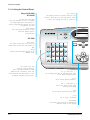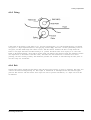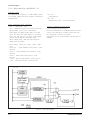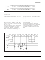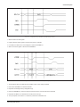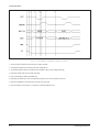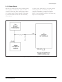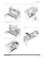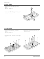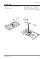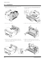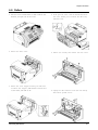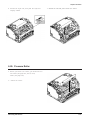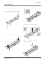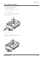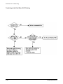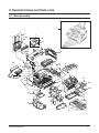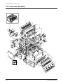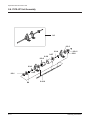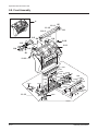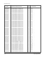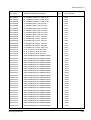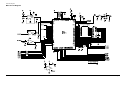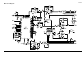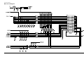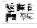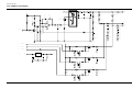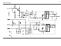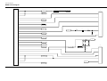
1
SAMSUNG FACSIMILE
Msys 5150/5200
SF-5800/5800P
SERVICE
FACSIMILE
MANUAL
CONTENTS
1. Precautions
2. Specification
3. Setup and Installing
4. Theory of Operation
5. Circuit Description
6. Repair Information
7. Maintenance & Troubleshooting
8. Exploded Views and Parts List
9. Electrical Parts List
10. Block Diagram
11. Connection Diagram
12. Schematic Diagrams
1.
Precautions
Follow these safety, ESD, and servicing precautions to prevent personal injury and equipment damage.
1-1 Safety Precautions
1. Be sure that all built-in protective devices are in
place. Restore any missing protective shields.
2. Make sure there are no cabinet openings through
which people- particularly children- might insert
fingers or objects and contact dangerous voltages.
3. When re-installing chassis and assemblies, be
sure to restore all protective devices, including
control knobs and compartment covers.
4. Design Alteration Warning:
Never alter or add to the mechanical or electrical
design of this equipment, such as auxiliary
connectors, etc. Such alterations and
modifications will void the manufacturer’s
warranty.
7. Product Safety Notice:
Some electrical and mechanical parts have special
safety-related characteristics which might not be
obvious from visual inspection. These safety
features and the protection they provide could be
lost if a replacement component differs from the
original. This holds true, even though the
replacement may be rated for higher voltage,
wattage, etc.
Components critical for safety are indicated in
the parts list with symbols
. Use only
replacement components that have the same
ratings, especially for flame resistance and
dielectric specifications. A replacement part that
does not have the same safety characteristics as
the original may create shock, fire, or other safety
hazards.
5. Components, parts, and wiring that appear to
have overheated or are otherwise damaged
should be replaced with parts which meet the
original specifications. Always determine the
cause of damage or overheating, and correct any
potential hazards.
6. Observe the original lead dress, especially near
sharp edges, AC, and high voltage power
supplies. Always inspect for pinched, out-ofplace, or frayed wiring. Do not change the
spacing between components and the printed
circuit board.
Samsung Electronics
1-1
Precautions
1-2 ESD Precautions
Certain semiconductor devices can be easily
damaged by static electricity. Such components are
commonly called “Electrostatically Sensitive (ES)
Devices”, or ESDs. Examples of typical ESDs are:
integrated circuits, some field effect transistors, and
semiconductor “chip” components.
The techniques outlined below should be followed
to help reduce the incidence of component damage
caused by static electricity.
CAUTION: Be sure no power is applied to the
chassis or circuit, and observe all other safety
precautions.
1. Immediately before handling a semiconductor
component or semiconductor-equipped assembly,
drain off any electrostatic charge on your body
by touching a known earth ground. Alternatively,
employ a commercially available wrist strap
device, which should be removed for your personal
safety reasons prior to applying power to the unit
under test.
2. After removing an electrical assembly equipped
with ESDs, place the assembly on a conductive
surface, such as aluminum or copper foil, or
conductive foam, to prevent electrostatic charge
buildup in the vicinity of the assembly.
3. Use only a grounded tip soldering iron to solder
or desolder ESDs.
4. Use only an “anti-static” solder removal device.
Some solder removal devices not classified as
“anti-static” can generate electrical charges
sufficient to damage ESDs.
5. Do not use Freon-propelled chemicals. When
sprayed, these can generate electrical charges
sufficient to damage ESDs.
6. Do not remove a replacement ESD from its
protective packaging until immediately before
installing it. Most replacement ESDs are
packaged with all leads shorted together by
conductive foam, aluminum foil, or a comparable
conductive material.
7. Immediately beforeremoving the protective
shorting material from the leads of a replacement
ESD, touch the protective material to the chassis
or circuit assembly into which the device will be
installed.
8. Maintain continuous electrical contact between
the ESD and the assembly into which it will be
installed, until completely plugged or soldered
into the circuit.
9. Minimize bodily motions when handling
unpackaged replacement ESDs. Normal motions,
such as the brushing together of clothing fabric
and lifting one’s foot from a carpeted floor, can
generate static electricity sufficient to damage an
ESD.
1-3 Lithium Battery Precautions
1. Exercise caution when replacing a Lithium
battery. There could be a danger of explosion and
subsequent operator injury and/or equipment
damage if incorrectly installed.
3. Lithium batteries contain toxic substances and
should not be opened, crushed, or burned for
disposal.
2. Be sure to replace the battery with the same or
equivalent type recommended by the
manufacturer.
1-2
Samsung Electronics
2.
Specification
2-1 Facsimile
Machine type :
Desk Top
Applicable line :
Public Switched Telephone Network (PSTN) or behind PA B X
Compatibility :
CCITT Group 3
Data coding :
MH/MR/MMR
Modem speed :
14400/12000/9600/7200/4800/2400 bps
Transmission speed :
Approx. 6 sec.
Effective scanning width :
8.3 inches (210 mm)
Effective printing width :
8.2 inches (208 mm : LTR)
Scanning method :
Sheet-fed scanning using a Contact Image Sensor (CIS)
Memory :
Msys 5150 1 MByte/Msys 5200 2 MByte
SF-5800 1 MByte/SF-5800P 2 MByte
Halftone :
64 levels
Printing speed :
8 PPM (Letter size)
Automatic document feeder :
30 pages (75g/m )
Documents size :
W idth : 148 to 216 mm
2
Length : 128 to 1500mm (Single Page)
279 to 297mm (Multi Pages)
2
W eight : 50 to 100 g/m (Single Page)
2
50 to 90 g/m (20 Pages)
2
75 g/m (30 Pages)
One-touch dial :
20 locations
LCD :
16 characters x 2 lines
2-2 SCANNER
Scanning Method :
Sheet-fed scanning by CIS and feeding of the document by a
stepping motor
Resolution
Horizontal
11.8 lines/mm (300 dpi)
Vertical
STANDARD : 3.85 lines/mm (98 Lpi)
FINE : 7.7 lines/mm (196 Lpi)
SUPER FINE : 11.8 lines /mm (300 Lpi)
Photo Scale :
256 shades
Scanning period :
STANDARD : 2.5 ms/line
FINE : 2.5 ms/line
SUPER FINE : 2.5 ms/line
Samsung Electronics
2-1
Specification
2-3 Printer
Print Speed
8 PPM (A4 Size, 5% Charcter Pattern)
Resolution
600 X 600 DPI
Source of Light
Laser Diode(LSU)
Print Method
Non-impact Electrophotography,
Feed Method
Multi-Purpose Feeder and Manual
Feed Reference
Center Reference Loading
Paper
Size
At Copy Mode
Laser Beam
Bin Type
Normal Paper : A4,Letter,Legal,B5,
Executive, A5
Envelope : Normal Envelope
Length
: 149 ~ 356mm
W idth
: 100 ~ 216mm
W eight : For MPF,
60 ~ 90g/m
For Manual,
Paper Capacity
2
60 ~163g/m
2
MPF : 150 Sheets (based on 75g/m )
Manual Slot :
Paper Stacker Capacity
2
Face up
:
1 Sheet
2
100 Sheets (75g/m ,20 lb)
W arming up Time
First Printing Time
Stand-By : 20 Sec
Power Save Mode : 30 Sec
Power Rating
AC 110V ~127V ± 15% 50/60Hz ± 3Hz,
AC 220V ~ 240V ± 15% 50/60Hz ± 3Hz
Power Consumption
Avr. 170Wh
Power Saving Consumption
Avg. 13Wh
Certification & Compliance
FCC,UL,CSA,CE,CB
Acoustic Noise
Standby : Less than 36dB
Sleeping Mode
Sleep Mode : Less than 29dB
Operating : Less than 50dB
2-2
Samsung Electronics
Specification
Reliability
2
MTBJ : 2,000 Sheets(75g/m )
MTBF : 50,000 Sheets
Toner Cartridge
One-Cartridge type
Expected Life Span
50,000 Sheets
Operating Environment
Temperature : 10 ~ 32°C
Humidity
Storage Environment
Temperature : -20 ~ 40°C
Humidity
W eight
: 20 ~ 80%
: 10 ~ 95%RH
Net : Max. 9kg
Gross : Max. 14kg
External Dimension
355(W) X 415(D) x 238(H)mm (without Handset)
424(W) X 415(D) x 238(H)mm (with Handset)
Developer
.Life Span : 5% Pattern,Min. 5,000 Sheets
.Developing : Non-magnetic
Contact Developing
.Charging : Conductive Roller Charging
.Density Adjustment : Dark, Medium
.Toner Supply Method : Exchanging
Toner Cartridge
.New Developer Checkable
.Transfer System : Pre-transfer By LED &
Conductive Roller Transfer
.Fusing System : Temperature & Pressure
OZONE Emission : Max. 0.1 PPM(8 Hours)
Samsung Electronics
2-3
Specification
2-4 Quality
Conditions
Paper
Normal Paper
Environment
Temperature : 20 ~ 25°C
Humidity
: 40 ~ 60%
Print Quality
Image Density
Background
Uniformity
Fusing
Start Position
Skew
Orthogonality
Horizontal Scan
Special Paper Exception
Paper Jam
Paper Curl
Reliability
Insulation Resistance
Dielectric Strength
Ground Continuous
Voltage DIP
AC Impulse Noise
Leakage Current
Surge
OZONE Emission
Top Cover Open
Overcurrent Protect
Fusing System
Trouble Sensing
Overheat Sensing
75g/m
2
Min. 1.3
Min. 1.0(Temperature : 10 ~ 15°C)
Max. 0.2
Max. 0.2(Including Continuous Print)
Min. 75% (All Black)
Top : x ± 4.23mm, Side : y ± 4 m m
Top : Max. ± 1.5mm/200mm
Side : Max. ± 2.0mm/250mm
± 1.0mm
± 0.6mm/208mm
(Bowed Line Skew : Pattern 1)
Image Density : Min 1.0 (Envelope)
Fusing : Min. 70% (All Black)
(Envelope/OHP/Postcard)
From Left
2
Less than 1/1,000(75g/m Paper)
First : Less than 16mm (10 Sheets, 75g/m2 Paper)
After Cooling : Less than 16mm (10 Sheets, 75g/m2 Paper)
Less than 10 MΩ (at DC 500V)
AC 1000V (DC 1420V), 10mA
Less than 0.1Ω
Rated Voltage ± 15%
AC 1000V 10, 100, 200, 400, 1000ns
Less than 3.5mA
6 KV, 500A
Less than 0.1 ppm (8 Hours)
Isolating the input power of the LSU,
High Voltage Part, and Fuser
Fuse inside the Engine Controller
.The temperature doesn’t rise to the specific
temperature in the specific time.
.The temperature is too high.
240 ~ 250°C (The thermostat cuts off the Fuser
Rated Power
Indicate the
Fuser error
from the power.
)
Thermistor Open Sensing : W ithout the initial
temperature change of the Fuser
2-4
Samsung Electronics
Specification
2-5 SMPS (Switching Mode Power Supply)
Input (AC)
AC Input Voltage
Minimum
Typical
Maximum
Max. AC Input Current
Max. Inrush Current
European
198V
230V
264V
2.5Amps
Ap-p (at 20°C)
Line Regulation
24V ± 10%
12V ± 5 %
-12V ± 5 %
5V ± 5%
24V : Peak 500mV
12V : Peak 500mV
-12V : Peak 500mV
5V : Peak 300mV
24V : 2.7A ± 10% (by Circuit)
5V : 3A ± 10% (by Circuit)
24V : 33VDC
5V : 5.6VDC
American
90V
120V
135V
3Amps
Output (DC)
Road Regulation
Ripple Noise
Over Current Protect
Over Voltage Protect
Samsung Electronics
2-5
Specification
Memo
2-6
Samsung Electronics
Setup and Installing
3-8 System Data Set-up
There are system data settings that are set by the user in the user-mode, and system data settings set by the
technician in the tech mode.
3-8-1 System Data Settings in Usermode
The fax machine has various user-selectable
functions. These functions are usually selected
during the initial setup of the machine, and there
should be little need to change them there after.
Note : Before you begin, print out the system data
list to see the current settings. To print the system
data list, press Menu, and ‘System Data’ on the
one-touch keypad.
3-8-2 User-Selectable Options
These instructions assume you’ve followed the steps
under ‘System Data Settings in User-mode’ and the
machine is asking if you want to change one of the
options listed here.
•Paper Size-Select the paper size you will use for
the recording paper.
Press 1 for letter (LTR), 2 for A4, or 3 for legal
(LGL) size paper.
1. Press Menu, then press ‘System Data’ on the
one-touch keypad.
The LCD displays user-selectable options.
2. Scroll to the options by pressing „ or
repeatedly.
3. When the option you want appears in the
display, enter the number for the desired status.
You can use ˆ or ¤ button and press Enter to
select the desired status.
•Message Confirmation Report-A confirmation
report shows whether the transmission was
successful or not, how many pages were sent, etc.
Press 1 to print out journal automatically each time
you send a fax.
Press 2 to print only when an error occurs and the
transmission was not successful.
•Auto Print Journal-A journal report shows specific
information concerning transmission and reception
activities, the time and dates up to 50 of the most
recent transmission and reception.
Press 1 to print journal automatically after every 50
transmission and receptions.
Press 2 to print journal manually.
•Remote Receive Start Code-The remote receive
code allows you to initiate fax receive from an
extension phone plugged into the EXT.TEL jack. If
you pick up the extension phone and hear fax
tones, enter the remote receive code and the fax
will start receiving. The password is preset to
* 9 * at factory.
Enter the desired code 0 to 9 on the number
keypad.
3-20
Samsung Electronics
Setup and Installing
• Power Saving Mode (SF-5800P only) -The power
saving menu item lets you reduce power usage
when the printer is idle.
Press 1 to turn the feature ON. The display asks
you to determine the length of time the printer
waits after a job is printed before it goes to a
reduced power state:
Press 1 for 10 minutes, 2 for 15 minutes, 3 for 30
minutes, 4 for 45 minutes, or 5 for 60 minutes.
If your printer is used constantly,press 2 to turn
the feature OFF. It keeps the printer ready to print
with the minimum warm-up time.
• ECM Mode (Error Correction Mode)-This mode
compensates for poor line quality and ensures
accurate, error-free transmission with any other
ECM-equipped facsimile machine. If the line
quality is poor, transmission time may be
increased when ECM is enabled.
• H.(Horizontal) Reduction-If you turn the RX
reduction feature on, you are allowed to set the
horizontal reduction feature on or off. When you
set the horizontal reduction to be on, the machine
will reduce an incoming page containing overflow
data only in vertical as shown below.
If you want to reduce both in vertical and horizontal
at the same rate in order to maintain height to width
relationships, turn the horizontal reduction feature
off. If you turn off this feature, the machine reduces
the data as shown below.
Press 1 to turn the Error Correction mode on.
Press 2 to turn the Error Correction mode off.
Press 1 to turn this feature on.
Press 2 to turn this feature off.
• RX Reduction-When receiving a document as
long as or longer than the paper installed in your
machine, the machine can reduce the data in the
document to fit into your recording paper size.
Turn on this feature if you want to reduce an
incoming page that may otherwise need to be
divided into two pages with only a few
centimeters on the second page. If the fax machine
cannot reduce the data to fit into one page with
the feature enabled, the data is divided and
printed in actual size on two or more sheets if
needed.
Press 1 to turn this feature on. Note that this
feature does not apply to the copy mode.
Press 2 to turn this feature off. The overflow data
will be printed out on a second page.
• Discard Size-When receiving or copying a
document as long as or longer than the paper
installed in your fax machine, you can set the fax
machine to discard any excess image at the
bottom of the page to fit into the recording paper
size.
If the received page is outside the margin you set,
it will be printed on two sheets of paper at the
actual size.
If the data is within the margin, and the Auto
Reduction feature is turned on, it will be reduced
to fit into the appropriate size paper (Discard does
not take place). If the Auto Reduction featureis
turned OFF or fails, the data within the margin
will be discarded.
Enter the desired discard size using the number
keypad, and press Enter.
Samsung Electronics
3-21
Setup and Installing
• Redial interval-Your machine can automatically
redial a remote fax machine if it was busy or does
not answer the first call.
Enter the number of minutes (from 01 to 15) using
the number keypad.
Detection, you will need another telephone line at
your location, or someone available to dial your
FAX number from outside.
Press 1 to turn this feature on.
Press 2 to turn this feature off
.
• Redials-Enter the number of attempts (from 0 to
9) to redial the number before giving up.
If you enter 0, the machine will not redial.
• Answer Rings-You can select the number of times
your machine rings before answering an incoming
call. If you are using your machine as both a
telephone and a fax machine, we suggest you set
the ring count to at least 4 to give you time to
answer.
Enter a number from 1 through 7 on the number
keypad.
• DRPD (Distinctive Ring Pattern Detection)
Mode-’Distinctive Ring’ is a telephone company
service which enables a user to use a single
telephone line to answer several different
telephone numbers. The particular number
someone uses to call you on is identified by
different ringing patterns, which consist of various
combinations of long and short ringing sounds.
This feature is often used by answering services
who answer telephones for many different clients
and need to know which number someone is
calling in on to properly answer the phone.
Using the Distinctive Ring Pattern Detection
feature, your fax machine can ‘learn’ the ring
pattern you designate to be answered by the FA X
machine. Unless you change it, this ringing
pattern will continue to be recognized and
answered as a FAX call, and all other ringing
patterns will be forwarded to the extension
telephone or answering machine plugged into the
EXT.LINE jack.
Press 3 to setup the Distinctive Ring Pattern
Detection. The LCD displays ‘WAITING RING’.
Call your fax number from another telephone. It is
not necessary to place the call from a fax machine.
When your machine begins to ring, do not answer
the call. The machine requires several rings to
learn the pattern.
When the machine completes ‘learning’, the LCD
displays ‘END DRPD SETUP’.
W ith the DRPD feature active, ‘DRPD’ appears in
the display and the previously set reception mode
is ignored. If you turn DRPD off, the machine
returns to any previously set reception mode.
Notes:
• DRPD must be set up again if you re-assign
your fax number, or connect the machine to
another telephone line.
• After DRPD has been set up, call your fax
number again to verify that the machine
answers with a fax tone, then have a call placed
to a different number assigned to that same line
to be sure the call is forwarded to the extension
telephone or answering machine plugged into
the EXT.LINE jack.
• Send from Memory-If you are annoyed that you
have to wait until documents in the feeder are
sent out when you try to send or reserve another
fax, turn this feature on. This feature enables all
transmission documents are automatically
scanned into memory before transmission.
Press 1 to turn this feature on.
Press 2 to turn this feature off.
You can easily suspend or change Distinctive Ring
Pattern Detection at any time.
Before using the Distinctive Ring Pattern
Detection option, Distinctive Ring service must be
installed on your telephone line by the telephone
company.To setup Distinctive Ring Pattern
3-22
Samsung Electronics
Setup and Installing
3-8-3 Confiming System Data Settings
• Local ID-This feature allows the machine to
automatically print the page number, and the date
and time of the reception at the bottom of each
page of a received document.
Confirm the system data settings by printing out a
system data list.
Press 1 to turn this feature on.
1. If not in the tech mode, press Menu,#,1,9,3,4
in sequence to initiate the tech mode.
Press 2 to turn this feature off
.
2. Press Menu.
• Priority Term (Msys 5150/5200, SF-5800P) -When
you want to print a PC document while the
machine prints a received fax on the recording
paper, you can interrupt the printing and print the
PC document. Press the PRINT PRIORITY button
to enable the feature. The LCD displays ‘PP’ on
the lower line, right corner. The interrupted fax
data will be stored in memory.To disable, press
the PRINT PRIORITY button again. ‘PP’ on the
LCD disappears.
You can set your machine to turn the feature off
automatically if there is no further data printed
within 30 minutes or 8 hours after PC printing.
3. Press one of the one-touch PRINT keys. The LCD
displays the lists you can print out.
4. Press „ or
LIST’.
until you find ‘SYSTEM DATA
5. Press Enter. The machine prints the system data
list.
The system data list printed in the tech mode
contains the system data set in the tech mode as
well as in the user mode. The model number and
software version will be printed at the bottom of
the system data list
Press 1 to select 8 hours. The machine turns off
automatically 8 hours after PC printing is
completed.
Press 2 to select 30 minutes. The machine turns off
automacally 30 minutes after PC Printing is
completed.
• Dial Mode (SF-5800/5800P Tech mode) -Select the
type of dial system your fax machine is connected
to.
Press 1 if the fax machine is connected to a tone
(Touch Tone) dial line.
Press 2 if the fax machine is connected to a pulse
(Rotary) dial line.
Samsung Electronics
3-23
Setup and Installing
3-8-4 System Data Settings in Techmode
Various technical features of fax machine are
provided with optional parameters. Set the features
to the user’s need according to the following
procedure.
1. If not in the tech mode, press Menu,#,1,9,3,4
in sequence to initiate the tech mode.
2. Press Menu, and press ‘System Data’ on the
one-touch keypad.
The LCD displays ‘TECH MODE SYSTEM
D ATA?’.
3. To set the system data available in tech mode,
press Enter.
4. The LCD displays the options you can choose. In
tech mode, the LCD displays the technicianselectable options as well as all the userselectable options.
5. Scroll to the options by pressing „ or
repeatedly.
6. When the option you want appears in the
display, enter the number for the desired status.
You can use ‹ or ¤ button and press Enter to
select the desired status.
You can exit from setup mode at any time by
pressing Stop. When you press Stop, the
machine stores the options you’ve already
changed and returns to Standby mode.
If you want to set the system data available in the
user mode, press Stop. The LCD displays ‘USER
MODE SYSTEM DATA?’. Press Enter to set the
system data available in the user mode.
FEATURE
PARAMETER
Modem Speed
14400/12000
9600/7200
4800/2400 bps
The maximum Tx speed can be limited to 14400, 12000, 9600, 7200, 4800 or
2400 bits per second. When the Tx speed is set to 14400, 12000 the Rx speed
can be either V.33 or V.17 speed. When the Tx speed is set to 9600 or 7200,
the Rx speed can be either V.29 or V.27ter speed. When the Tx speed is set
to 4800 or 2400, the Rx speed can be any V.27ter speed.
Error Rate
5%, 10%
If the error rate exceeds the chosen rate, fall back occurs which will lower
the baud rate automatically down to as low as 2400 baud until the error
rate is less than the chosen rate.
Tx Level
-4 ~ -15 dBm
You can set the level of transmission signal. Typically, Tx level should be
under -12 dBm. The level within the range of -4 dBm to -15 dBm is
acceptable. Enter the desired value using the dial keypad.
Receive
Sensitivity
High/Normal
High sensitivity is between -5 and -49 dBm. Normal sensitivity is -43 dBm.
Super Fine Scan
to Memory
200/300 dpi
This feature allows the machine to scan documents in super fine resolution
(200 x 400 dpi, 300 x 300 dpi). The other machine can receive super fine
image. If the remote machine is not capable of receiving super fine data, your
machine fails to send documents and displays ‘INCOMPABLE ERROR’.
Silence Time
12sec/Unlimit
3-24
FUNCTION
Samsung Electronics
Setup and Installing
3-9 LCD Display
3-9-1 During Communication
In user mode, the LCD shows the remote machine’s
TTI number, TX or RX communication type,
(modem speed), and page number.
In service mode, the display shows the
communication type, abbreviations for the CCITT
Group 3 T.30 protocol as they occur, the protocol
type (G3), baud rate in kbps, and line time.
3-9-2 If a Communication Problem
Occurs:
In user mode, the display shows one of the
following:
PAPER JAM, COMM.ERROR, LINE ERROR.
In service mode, the display shows all error
messages available in user mode, as plus additional
error messages available only in Service Mode.
Error messages shown in service mode only are as
follows:
PRE-MESSAGE ERROR : problem occurred during
phase B of session.
POST-MESSAGE ERROR : problem occurred during
phase D of session.
MESSAGE ERROR : problem occurred during phase
C of session.
LINE ERROR : machine cannot connect or has lost
connection with the remote machine.
Additional messages, not shown above, will appear
in the TX/RX journal printed in service mode.
Samsung Electronics
3-25
Setup and Installing
Memo
3-26
Samsung Electronics
3.
Setup and Installing
3-1 Control Locations and Functions
Take a moment to familiarize yourself with the main components and understand their functions.
Paper Extension
3-1-1 Front View
Paper Guides
Automatic Paper Feeder
Manual Paper Feeder
Document Tray
Control Panel
Document Guides
Document Exit Tray
Note: Your machine may look slightly
different than the illustration.
Print Exit Tray
3-1-2 Rear View
3-2-3 Inside
Cover
Image
Cartridge
TEL LINE
Jack
EXT. LINE Jack
Power Cord
Connector
Printer
Connector
Samsung Electronics
Cover Release Buttons
(right and left)
3-1
Setup and Installing
3-1-4 Using the Control Panel
Msys 5150/5200
SF-5800P
On/Off Line and Lamp
Turn your machine On-line or Off-line.
The lamp lights while the machine is
on-line, indicating the machine is ready
for printing a PC file.
LCD Display
The display shows the current status of your
machine and guides you through various tasks
using a menu system for each of operation.
Print Priority
Use to give print priority to PC file
while the machine prints
areceived fax.
On/Off Line
Print Priority
Multifunction LASER Facs
SF-5800
Power Save
The power saving menu item lets you
reduce power usage when the printer is
idle.
Menu
01
02
System Data
06
Reset
Restores user-selectable options to the
default value.
System ID
07
Delay TX
11
Memory TX
12
Add/Cancel
16
TX Confirm
03
04
05
Date & Time
System Setup
Memory Clear
08
09
10
Priority TX
13
Group Dial
17
18
Schedule Job
Phone Book
Stop
Polling
14
Maintenance
15
Journal
19
Help List
20
System List
Copy
One-Touch Dial and
Special Function Buttons
Use to call most frequently used
numbers with one button. Also, use
these buttons with Menu button to set
up special functions or print lists.
Up („ ) and Down ( )
Use to display the next or last menu item. Also,
use to adjust audible volume.
Menu
Use to choose special functions.
Left (ˆ ) and Right (¤ )
Use to move cursor left or right
through the display.
Stop
Use to stop an operation at any time.
Copy
Use to copy a document.
Start/Enter
Use to start a job. Also use to activate the
selection shown in the display.
3-2
Volume
Samsung Electronics
Setup and Installing
Search/Delete
Use to search for numbers in memory. Or use to delete
digits in the edit mode.
Rcv.Mode (Receive Mode)
Use to choose the receive mode you want to use.
The selected mode is displayed.
Search/Delete
Rcv.Mode
Resolution
ABC
Contrast
DEF
Speed/Status
Redial/Pause
Flash
1
2
3
GHI
JKL
MNO
4
5
6
PQRS
TUV
WXYZ
7
8
9
Resolution
Use to choose the resolution of copied or transmitted
documents.
Contrast
Use to choose the contrast of copied or transmitted
documents.
Number Keypad
Use to dial numbers manually or to enter letters.
OHD/V.Req.
t/
r
0
Speed/Status
Use to dial calls and send fax documents by entering a 2-digit number.
Also use to switch the LCD while performing dual jobs.
Redial/Pause
Use to redial the last phone number called. You can also use it to add a pause when storing a number in
memory.
Flash (R/Recall)
Use to perform a switch-hook operation such as call waiting.
O H D (On-Hook Dial) / V.Req. (Voice Request)
Use to dial numbers without picking up the handset. Also use it
to make a voice call after sending or receiving a fax.
Samsung Electronics
3-3
Setup and Installing
3-2 Setting Up Your Machine
3-2-1 Document Tray
3-2-2 Document Exit Tray
Insert two tabs on the tray into the slots as shown.
Fold out the extender on the tray, if necessary.
Insert the two tabs on the document exit tray into
the slots on the front of your machine. Fold out the
extender, if necessary.
Insert one end first, then the other end by pulling
this leg inward to make the tray easy to insert.
Extender
3-4
Samsung Electronics
Setup and Installing
3-2-3 Handset and Handset Cradle
(only for SF-5800/5800P equipped with handset)
1. Plug one end of the coiled cord into the jack on
the handset. Then plug the other end into the
modular jack on the bottom of the handset
cradle.
Note: If you want to remove the handset, pushing
A in the bottom, slide it down, then take it out.
Handset
Cradle
2. Plug the cradle’s modular cords into the modular
jacks on the left side of your machine.
Attach the handset cradle to the main body.
Insert the three tabs of the cradle into the slots on
the left side of the main body as shown, and
push it up.
Black cord
Route the excess cord so that it could be
inserted into the cradle.
Samsung Electronics
3-5
Setup and Installing
3-2-4 Printer Exit Tray
Holding the flexible side end, insert two tabs on the side ends into the corresponding slots. Fold out the
extender, if necessary.
Extender
3-6
Samsung Electronics
Setup and Installing
3-2-5 Telephone Line
Plug one end of the telephone line cord into the TEL LINE jack and the other end into a standard phone wall
jack.
To a standard
phone wall jack
Extension Phone
If you want to use a regular phone or answering machine with your machine, connect the phone into the
EXT.LINE jack.
Plug the cord of your extension phone or answering machine into the socket marked EXT.LINE on the back of
the machine.
To a regular phone
Samsung Electronics
3-7
Setup and Installing
3-2-6 Printer Cable
Your Msys 5150/5200, SF-5800P has a parallel interface port, which allows you to use it with IBM PCs and
compatible computers. You have to purchase a Centronics parallel interface cable that supports bi-directional
communications (IEEE standard 1284). Ask your dealer for assistance if you need help selecting the right cable.
To connect the printer to the computer, follow the steps below:
1. Make sure that both the Msys 5150/5200, SF-5800P and the computer are turned off
.
2. Plug the cable into the connector on the back of the printer. Push the metal clips down to fit inside the
notches on the cable plug.
3. Connect the other end of the cable to the parallel interface port on your computer. See your computer
documentation if you need help.
3-8
Samsung Electronics
Setup and Installing
3-2-7 AC Power Cord
Plug one end of the cord into the back of the machine and the other end into a standard AC power outlet.
The machine turns on. If there is no cartridge installed, or no paper, the display shows ‘DOOR OPEN or NO
TONER!!!’ or [NO PAPER].
To AC
outlet
If you want to turn it off, unplug the power cord.
Samsung Electronics
3-9
Setup and Installing
3-2-8 Installing the Image Cartridge
1. Pulling the cover release button toward you,
open the cover.
3. Shake the cartridge from side to side 5 or 6 times
to distribute the toner evenly inside the
cartridge.
4. Find the cartridge slots inside the printer, one on
each side.
2. Unpack the image cartridge, then carefully
remove the sealing tape.
3-10
Samsung Electronics
Setup and Installing
5. Grasp the handle and slide the cartridge down
between the cartridge slots, until it drops into
place.
6. Close the cover. Make sure that the cover is
securely closed.
Samsung Electronics
3-11
Setup and Installing
3-3 System Setup
In Tech mode (press Menu # 1 9 3 4), you can access the following setup menu function :
•Ringer Volume
•Default settings
To access system setup menu function.
1. Press Menu in tech mode.
•Sound control
•Remote Diagnosis Protection
•Select Language
•Econo Mode Setting
2. Press System setup on the one-touch keypad.
The first setup menu ‘RINGER VOLUME?’
appears in the display.
•Page Count Clear
•Flash Download
3. Press „ or
repeatedly to choose the desired
setup menu.
4. When the desired setup item is displayed, use ˆ
or ¤ to select the desired status, and press Enter.
To change the status, you can also press the
number of the status in the display.
5. The display shows the next setup menu. If you
return to Standby mode, press Stop.
3-12
Samsung Electronics
Setup and Installing
Function
Description
Value
Ringer Volume
You can adjust the volume of the
ringer.
The display shows the loudness level with
> symbol. The more, the louder.
Default Setting
The print resolution and contrast can
be set to their most frequently used
modes. Whenever a document is sent
or copied, the home contrast and
resolution mode will be activated
unless otherwise changed by using
Resolution or Contrast button on the
control panel.
Home Resolution
•Resolution
•Contrast
•STA N D A R D –use with most documents.
•FINE–use for documents with fine detail,
such as small print.
•SUPER FINE–use for documents that
have extremely fine detail.
Home Contrast
• N O R M A L –use with documents of
average or normal contrast.
•DARKEN–use with documents with low
contrast or light images.
•LIGHTEN–use with documents with
high contrast or dark images.
•P H O TO–for obtaining maximum image
quality with documents that
contain pictures or photographs
with shades of gray.
Sound Control
•Alarm Sound
•Key Sound
You can choose an alarm tone to
sound when an error occurs
(ALARM SOUND) or any key is
pressed (KEY SOUND).
1: ON
Remote Diagnosis
Protection
Remote diagnosis feature allows
your machine to be checked out by
service company at a remote place
through phone line.
1: ON
2: OFF
2: OFF
If you do not want to use the remote
diagnosis feature and want to
protect your machine from being
open by an unauthorized person,
you can enable this remote
diagnosis protection feature.
Select Language
Samsung Electronics
You can select the LCD display
language between English, German,
etc.
1: English
2: German
3-13
Setup and Installing
Function
Description
Econo Mode
Setting
To get the most from your toner
supply, set the Econo mode to On. If
set to On, you can preserve the toner
supply. The print quality may be
reduced.
Page Count clear
You can reset the page counter to zero
(0). Toreset the counter, passcode is
required. Enter 1934.
Flash Download
This function allows you to download
newly updated ROM into the
machine.
3-14
Value
1: ON
2: OFF
1: ON
2: OFF
Samsung Electronics
Setup and Installing
3-4 Setting the Date and Time
3-5 Setting the System ID
(Your Number and Name)
The current date and time are shown in the display
when the machine is on and ready for use (Standby
mode). The date and time are printed on all faxes
you send.
1. Press Menu, then press Date & Time on the onetouch keypad.
The display shows the currently set date and
time.
The System ID will be printed at the top of each
page sent from your machine.
1. Press Menu, then press System ID on the
one-touch keypad. The display asks you to enter
the telephone number.
If there is a number previously registered, the
number appears.
11-27-1998
08:36 (PM)
e.g. 12 HOURS format
11-27-1998
20:36
e.g. 24 HOURS format
2. Enter the correct date and time using the
number keypad.
DD (Day)
MM (Month)
Y Y (Year)
HH (Hour)
= 01~31
= 01~12
= four digits (1990~2089)
= 00~23 (24 HOURS format)
= 01~12 (12 HOURS format)
MM (Minute)
= 00~59
AM (Ante Meridiem)
PM (Post Meridiem)
3. Press Enter when the date and time in the
display is correct.
If you enter an invalid number, the machine beeps
and doesn’t proceed to the next step. If this
happens, just reenter the correct number.
The display shows the date and time you have
set, then returns to Standby mode.
2. Enter the telephone number (up to 20 digits)
which your machine is connected to. You can
include the space using Pause button.
If you make a mistake, press ˆ or ¤ to move the
cursor under the wrong digit, then enter the
correct number to change or press Delete to
delete the number.
3. Press Enter when the number in the display is
correct. The display asks you to enter your ID
name.
4. Enter your ID name (up to 20 characters).
You can enter alphanumeric characters using the
number keypad, and include special symbols
such as + by pressing 0 repeatedly.
If you want to enter the same letter or number in
succession (e.g. SS, AA, 777), enter one digit, then
move the cursor by pressing Right, and enter the
next digit.
If you want to insert a space in the name, you can
also use ¤ button to move the cursor to skip the
position.
5. Press Enter when the name in the display is
correct.
Samsung Electronics
3-15
Setup and Installing
3-6 Installing Software
3-6-1 Printer Driver
3-6-3 Installation Procedure
Before you can use any printer with your computer,
you must install a printer driver. The printer driver
tells the computer what kind of a printer you are
using, and also controls the various settings, such as
print quality and paper type. You define these
settings within the printer driver, which then
communicates the settings to both the computer and
the printer.
Before you start, make sure your computer meets or
exceeds the system requirement for the driver and
application program you want to install.
To use the Msys 5150/5200, SF-5800P as your
printer, you must install the printer driver supplied
with your machine in your computer.After
installing the printer driver, make sure the Msys
5150/5200, SF-5800P is selected as the default
printer to use the machine as your printer.
IN WINDOWS 95
1. Make sure the Msys 5150/5200, SF-5800P is
plugged in and connected to your computer.
See page 3-8.
2. Start your Windows.
3. Insert the setup diskette #1 into the floppy disk
drive A (or B).
3-6-2 System Requirement
Before you start, make sure that you have the
following minimum computer setup:
• IBM or compatible, with 486SX 33MHz or higher
processor
4. From the Start menu, select Run.
5. Type a:\setup (or b:\setup), and click OK.
• Free disk space of at least 4MB
• 8MB or higher RAM for Windows 3.1x, or 16MB
for Windows 95 and Windows 98.
• Windows 3.1x, Windows 95, Windows 98
6. Follow the instructions on the screen. After
installing, the Msys 5150/5200, SF-5800P is
automatically selected as the default printer.
If you do not select this printer as the default
printer when you install it, you must select it
before attempting to print a document using your
Msys 5150/5200, SF-5800P.
3-16
Samsung Electronics
Setup and Installing
IN WINDOWS 3.1X
IN WINDOWS 98
1. Make sure the Msys 5150/5200, SF-5800P is
plugged in and connected to your computer.
1. Make sure the Msys 5150/5200, SF-5800P is
plugged in and connected to your computer.
2. Start your Windows.
2. Start your Windows.
3. Insert the setup disk 1 into your floppy drive A
(or B).
3. If Update Device Driver Wizard box is displayed,
insert the setup diskette 1 into your floppy drive
A (or B), and then click Next.
4. From the Program Manager, select Run from the
File menu. The Run dialog box appears.
Msys 5150/5200
5. In the command line, type a:\setup (or b:\setup)
,
and then click OK.
6. Follow the instructions on the screen. After
installing, the Msys 5150/5200, SF-5800P is
automatically selected as the default printer.
If you do not select this printer as the default
printer when you install it, you must select it
before attempting to print a document using your
Msys 5150/5200, SF-5800P.
When you get the screen looking like this, click
Other Locations.
4. In the command line, type a:\setup (or b:\setup)
,
and then click OK.
5. Follow the instructions on the screen. After
installing, the Msys 5150/5200, SF-5800P is
automatically selected as the default printer.
If you do not select this printer as the default
printer when you install it, you must select it
before attempting to print a document using your
Msys 5150/5200, SF-5800P.
Samsung Electronics
3-17
Setup and Installing
3-6-4 Uninstalling
Uninstall is only required if you are upgrading from an older software, or updating the software, or if your
installation fails.
IN WINDOWS 95/98
IN WINDOWS 3.1X
1. Start Windows if not already started.
1. Start Windows if not already started.
2. From the Start menu, select Programs.
3. Choose Msys 5150/5200 or SF-5800P.
4. Choose Uninstall. The Uninstall dialog box
appears. Follow the instructions on the screen to
complete uninstallation.
3-18
2. From the Program Manager, double click the
Msys 5150/5200 or SF-5800P icon.
3. Double click the Uninstall icon. The Uninstall
dialog box appears.
4. Follow the instructions on the screen to complete
uninstallation.
Samsung Electronics
Setup and Installing
3-7 Memory Clear
3-7-1 Memory Clear in User Mode
3-7-2 Memory Clear in Tech Mode
In the user mode, you can selectively clear
information stored in this machine’s memory. The
list of data you can clear is as follows:
Memory clear, contained in the tech mode, is used
for clearing all the user’s data in memory and
setting to default status.
1: SYSTEM ID : your terminal ID number and name
are erased from the machine’s memory.
2: SYSTEM DATA :restores user-selectable options
to the default value.
3: P H O N E B K / D E L AY : clears the One-Touch,
Speed Dial, or Group Dial numbers stored in
memory. In addition, all the delayed time
operations you have reserved are also canceled.
4: TX-RX JOURNAL : clears all records of
transmissions & receptions.
1. If not in the tech mode, Press Menu,#,1,9,3,4
in sequence to initiate the tech mode.
1. If the machine is in the tech mode, return to the
user mode by pressing Menu,#,1,9,3,4 in
sequence.
2. Press Menu, and ‘Memory Clear’ on the
one-touch keypad.
2. Press Menu, and ‘Memory Clear’ on the
one-touch keypad.
Depending on country, you may be asked to
select the country before clearing memory. Select
the country when the display prompts to.
Then, the LCD displays ‘M E M O RY ALL CLEAR’
on the one-touch keypad.
3. Press 1 to clear all memory.
If you want to cancel, press 2. The machine
returns to Standby Mode.
The LCD displays the type of memory you can
choose.
3. Scroll to the options by pressing „ or
until
you find the one you want to clear. When the
cursor blinks under the memory you want to
clear,press Enter.
Otherwise, you can enter the number of the
memory.
4. The LCD prompts you to confirm your selection.
Press 1 to choose ‘YES’.
Samsung Electronics
3-19
4.
Theory of Operation
4-1 Engine Configuration
4-1-1 Video Controller Board
4-1-6 LSU(Laser Scanner Unit)
Video Controller Board receives image data from the
host computer and converts them to a
bitmap(binary) image, which is sent to the
Engine(Controller) Board.
Under control of the Engine, controls the laser beam
and the OPC Drum exposure and rotation. The OPC
Drum is synchronized and rotating with the same
speed as the paper. When laser beam reaches the
position of the Scanning Mirror,itcreates a line.
Synchronization Signal(HSYNC), which is sent to
the Engine Board which transfers image data to LSU
and synchronizes the vertical scanning line with the
printed page.
4-1-2 Engine Controller Board
Engine Board receives the video data from the
Controller Board, and then that sends current image
to LSU and controls the electrophotography process
for printing.
4-1-3 HVPS Board
HVPS board generates THV/MHV/BIAS high
voltages, apply it to Developer unit. And LSU,
Cover Open Sensor interface signals connect via this
board from Engine Control Board to each units.
4-1-7 Transfer
It constitutes the PTL(Pre-transfer Lamp) and the
Transfer Roller. The PTL exposes the light to the
OPC drum and lowers the OPC drum surface
potential, and transfer efficiency become higher. The
Transfer Roller transfers Toner on the OPC Drum to
the paper.
4-1-8 Fuser
4-1-4 Joint Board
Joint Board Contains Main Motor and Clutch and
Pre-Transfer Lamp driving circuit, New Developer
and Paper Empty, Paper Exit Sensing circuit, and
connects with Engine Controller Board.
It constitutes the Heat Lamp, Heat Roller,Pressure
Roller and Thermistor, thermostat, and causes the
Toner to adhere to the paper.
4-1-5 Developer Cartridge
Developer (Cartridge) creates the image via the
electrophotography process. The Charge Roller,
OPC Drum, Developer Roller, Supply Roller and
Toner constitute a single unit.
Samsung Electronics
4-1
Theory of Operation
4-2
Samsung Electronics
Theory of Operation
4-2 Development Processing
4-2-1 Charging
A negative voltage is applied to the surface of the OPC Drum. This is the first step in creating an
electrophotograph. The high voltage section of the Engine Board supplies (-)1.4KV to the Charge Roller and
transfers a charge of approximately (-)800 V to the OPC Drum.
4-2-2 Exposure
LSU receives the transferred bitmap image data from the Engine Board and turns the LSU’s laser diode on and
off, exposing the OPC Drum. If there is no data to print the Laser Diode remains off and the OPC Drum is not
exposed. Portions of the OPC Drum exposed charged to approximately (-)50V by the laser beam while
unexposed portions charge to (-)800V. The image formed by the exposed laser beam is invisible, and is called a
latent image.
Samsung Electronics
4-3
Theory of Operation
4-2-3 Development
Surface moves between the DEV Roller and the OPC Drum. Negatively charged Toner is attracted to the high
voltage(-50V) of the exposed portions of the OPC Drum and is exposed more easily than the more negative
(-800V) surface voltage of unexposed areas of the OPC Drum, resulting in a latent image.
4-2-4 Transfer
OPC
1.4KV
T/R
GND
Toner moves from the surface of the OPC Drum to the paper via the Transfer Roller.Toner on the surface of the
OPC DRUM will be attracted by the Transfer Roller, which is charged to approximately + 1.5 kV (600 ~ 2800V),
depending upon temperature, and humidity.Toner then moves from the OPC DRUM to the paper.
4-4
Samsung Electronics
Theory of Operation
4-2-5 Fixing
Toner image on the surface of the paper is in a low state electronically, so it can be scattered easily. By heating
the paper to a high temperature(180°C) and applying pressure(4Kg), the Toner becomes permanently fixed to
the paper, and this fixed image will remain forever. The Heat Roller transfers the heat of Lamp within the
Roller to the paper. The effect of Teflon-coating is to prevent the melted toner from staying on it. The lower
Roller is the Pressure Roller, and is made of silicon resin. Its surface is also Teflon-coated. The thermistor senses
the temperature of the surface of the heat roller, and feeds back the information to maintain 180°C while
printing, and 135°C during standby. The thermostat prevents the overheat as disconnecting the main power if
the Heat lamp was overheated.
4-2-6 Exit
Printed paper passes through the Exit Sensor after the electrophotography process is completed. The paper also
contacts an Actuator during printing out. This signal is transferred to the Engine Board and indicates paper
position. The Actuator and Exit Sensor must report the correct position information, or a Paper Jam error will
be indicated.
Samsung Electronics
4-5
Theory of Operation
Memo
4-6
Samsung Electronics
Circuit Description
5-3 OPE PBA
5-3-1 SUMMARY
5-3-2
OPE Board is separated functionally from the main
board and operated by the micom(Z8601) in the
board. OPE and the main use UART (universal
asynchronous receiver/transmitter) channel to
exchange information. OPE reset can be controlled by
the main. OPE micom controls key-scanning and LCD
and LED display, detects documents and
senses SCAN position. If there occurs an event in OPE
(such as key touch and sensor level change), it sends
specific codes to the main to respond to the situation
and the main analyzes these codes and operates the
system. For example, if the main is to display
messages in OPE, the main transmits data through
U A RT line to OPE according to the
designated format and OPE displays this on LCD,
LED. OPE’s sensing is also transmitted to the main
through UART line and then the main drives
necessary operation.
OPE PBA consists of U1 (MICOM, Z8601), LCD, key
matrix, LED indicators, SCAN position sensor and the
document detect sensor. Refer to OPE Schematic
Diagram and Wiring Diagram sections of this manual.
• Signals from the key matrix are delivered to U1X/Y
input pin group (P1-x).
• U1 pin 4 (TX D ATA) is the UART code sent to
MAIN PBA.
• Display from the controller is received at U1 pin 5
(RX DATA).
• LCD drive signals are sent from U1 P2-x pin group,
P3-4~P3-6 pins.
• Machine status LED drive signals are sent from U1
P0-x pin group.
• Document detect sensor output is received at U1
pin 33 (P3-3).
• Scan position sensor output is received at U1 pin 43
(P3-1).
OPE BLOCK DIAGRAM
5-26
Samsung Electronics
Circuit Description
5-4 LIU PBA
5-4-1 Summary
5-4-4 Dialer
LIU(Line Interface Unit) circuit added only to
Msys 5200,Msys 5150, SF-5800, SF-5800P is
controlled by the main circuit.
It monitors telephone line and helps interface between
the system and the telephone line. It uses
1-LIU(STI9510) to control the whole LIU,
MODEM/LINE INTERFACE, RING SIGNAL
DETECTOR, DIALER, LINE CURRENT
DETECTOR, and SERIAL INTERFACE.
5-4-4-1. MF DIAL
• Default mode it is set in DP.You can change it to
MF mode by control of MFP controller.
• MF signal can be measured at (tone level of low
group: typical - 14dBm) U3-4 MFO(DTMF
Generator Output). The signal is adjustable by R40,
R41 and C29. The adjusted signal enters U3-9 MFI
(DTMF Amplifier Input) and is amplified to be
transmitted on telephone line.
• U3-39 LS(Line Current Sense Input) terminals show
the final signals transmitted to telephone line.
5-4-2 Modem/Line Interface
This is the path through which transmitted and
received data of modem is put in and out.
• CML1 Relay: It divides telephone line into
external telephone and fax.
• U3-3 TIT(Transformer Input from Transformer):
This single ended input receives image signals fro m
modem through transformer T2 and
transmits them on telephone line.
• U3-40 ROT(Receive Output Transformer): This
output transformer receives signals on telephone
line and delivers them to modem through
transformer T1. It has AC impedance of 10Kohm or
over.
• AC impedance: Normal operation range of
U3(STI9510) is from 15mA to 100mA. DC
characteristics depend on the voltage of U3-37
LI(Line Input) terminal and the voltage of
resistance R48 between U3-37 LI(Line Input)
terminal and U3-39 LS terminal.
5-4-3 Ring Signal Detector
5-4-4-2. DP DIAL
• If U3-2(DMS) is made Vcc by R42, it is set at 33:67
D P signal. If it is made Vss by R43, it is set at DP
signal. This product is set at DP signal.
• D P signal is made by U3-27(DPn) terminals. This
signal turns on/off Q1. The signal made at that time
turns on/off Q2, which interrupts DC
current on telephone line and puts out pulse
signal on telephone line.
• U3-35 CS terminals : It makes Make Resistance by
shorting telephone line with Vss during Make
period of DP dial.
5-4-5 Line Current Detector
• When CML1 relay connects telephone line, U3
(STI9510) of LIU board and MFP controller of the
main board (U16) start communication through
U A RT. U3 of LIU board sends signal that includes
information of line current value, whenever it
receives orders or data from U16 of the main board.
• U3-28(MO) terminals are ring signal output
terminals. Q4 and Q5 put out ring signals and drive
Piezzo, but Msys 5200,Msys 5150, SF-5800,
SF-5800P does not use Piezzo. It has only the
functions related to ring detection such as driving
the photocoupler of U4 and delivering ring signals
to MFP
controller of the main.
Samsung Electronics
5-27
Circuit Description
5-4-6 Serial Interface
• This part does serial communication with MFP
controller of the main board (MAIN PBA:U16) that
controls the whole system. It controls LIU by giving
and taking all control orders and line
status.
• U3-11 RxD : Schmitt Trigger input, Receiving
terminal.
• U3-29 TxD : Open Drain output terminal
• Standard UART communication
- Baud Rate : 9600bps
- Start, Stop bit : 1bit each
- Data bits : 8 bit
- Parity bit : none
5-4-7
MAJOR FUNCTIONS OF PARTS
1) U3 : STI9510
-Key part of LIU board. Speech Network,
Dialer, Ringer and UART are built in one IC
package.
2) U5 : PC817
-Photo coupler. It enables UART of
U3(STI9510) to receive control signal or
dialing information from MFP controller of
the main board (U15).
-Insulation Detween prinary and secondany
circuit part.
3) U6 : PC817
-Photo coupler. It enables UART(U3-29:TxD)
of U3(STI9510) to deliver telephone line
status or response signal about control
signal or dialing information from LIU MFP
controller of the main board (U15).
-Insulation Detween prinary and secondany
circuit part.
5-28
4) U4 : PC817
-It senses and delivers ring signal to the main
board.
-Insulation Detween prinary and secondany
circuit part.
5) U2 : PC814
-It senses hook-off (Line connection) of the
external telephone and delivers it to the main
board.
-Insulation Detween prinary and secondany
circuit part.
6) BD1 : BRIDGE DIODE
-Regardless of the polarity of DC power
from telephone line, the voltage put out on
Pin.1 has always + polarity against pin
Pin.2. So DC loop forms always in the same
direction regardless of the polarity of the
telephone line.
7) T2,T3 : TRANSFORMER
-It delivers signals from the telephone line
to modem or signals from modem to the
telephone
line.
-Insulation Detween prinary and
secondany circuit part.
Samsung Electronics
Circuit Description
5-5 SMPS (Switching Mode Power Supply)
5-5-1 AC Input Stage
5-5-3 Fuser Drive
AC Input power path is the Fuse(F201) for A C
current limit, the Varistor(TNR201) for by-passing
high voltage surge, the discharge resistor(R201), the
AC Impulse Noise Filtering
Circuit(C201/L201/C202), the Common Mode
Grounding Circuit(C203/C204), the 2’nd noise
filter(L202), and the thermistor(TH201). When
power is turned on, TH201 limits Power-On-InlushCurrent by it’s high resistance, and when it’s
temperature rise, it’s resistance become about zero
ohm.
Fuser is drived by the Triac(Q201) that AC input
power is applied directly and the Phototriac(PC251) that is controlled by Engine controller.
The Thermistor resistance changes according to
Heat Roller in Fuser, the voltage in temperature
sensing circuit changes according to this resistance
change, and this feedbacks to Engine Controller,it
controls temperature by PID method.
5-5-2 SMC (Switched Mode Control)
The AC input voltage is rectified and filtered by
DB201 and C207 to create the DC high voltage
applied to the primary winding of T201. T201 pin #1
is driven by the SMPS device TOP226(U201). U201
auto-starts and chops the DC voltage. The U201 is
PWM SMPS IC and has internally a SMC(switched
mode control) IC and a MOSFET output stage. The
SMC IC has a Auto-restart without a Power Supply
for the IC and a Thermal Shutdown function and so
on. C208/R208/D202 clamp leading- edge voltage
spikes caused by transformer leakage inductance.
The power secondary winding(pin #11-12) is
rectified and filtered by D252,C251,L251, and C255,
C259 to create the 5V output voltage. The bias
winding(pin #4-5) is rectified and filtered by D203
and C213 to create U201 bias voltage. The secondary
output 5V is regulated through the path of the
voltage divide by R253/R254 - U251 switching PC252 - the bias voltage of U201 - U201 PWM duty
cycle - T201 secondary voltage. C209 filters internal
pin, determines the auto-restart frequency, and
together with R251 and R210, compensates the
control loop. Q251 of the secondary stage 24V is the
Low Power-loss Regulator with built-in overcurrent
protection function and overheat protection
function, and consists a control IC and a drive
transistor. It switches the input DC voltage and the
switched DC voltage is filtered by C257. D204 and
D205 clamp impulse noises.
Samsung Electronics
5-29
Circuit Description
5-6 Engine Controller
5-6-1 Power On Reset
5-6-6 NVRAM Control
The reset circuit initializes the CPU(U3) at power on
and prevents unstable operation due to power
fluctuations. It consists of LM393(U5) - voltage
comparator-, and RC for reset timing.When a DC
3.8V or higher are applied to LM393’s pin #3, the ‘
RESET’ signal goes ‘HIGH’ and the CPU begins the
initialization procedure, ‘RESET’ is active for
approximately 122ms.
The NVRAM(U1) stores “Used Sheet Count” for
SET and Developer unit. To control it, it is selected
by “CS”, and “DI”/”DO” synchronizes with “SK”
clock writes in/reads out the serial data to/from the
NVRAM.
5-6-7 Motor Driving(+24V)
5-6-2 CPU(+5V)
The used CPU is a 8bit microprocessor, SAMSUNG
KS88C4316(U3). This is operated at 6.944MHz and
controls all ICs. The shape is a 64pin DIP type.
The Motor Driver, SLA7029M(U207), is used to
drive the Main Stepping Motor.A n
SLA7029M(U207) receives Motor Drive Enable and
two phase signals from the CPU. It then generates a
constant-current unipolar pulsed signal for Motor
driving, applied to the Motor through R5(1Ω, 5%,
3W) and R6(1Ω, 5%, 3W).
5-6-3 EPROM (+5V)
5-6-8 Solenoid Clutch(+24V)
The EPROM, 27C256(U2), has the storage capability
of 256KBits and the access time is 150ns. The
EPROM stores the program data that controls the
Engine part.
The Solenoid controls the paper Pick-up Clutch. The
Solenoid receives control signal from U12 Q0.
KSC1008-Y(Q4) is the driving transistor, and
1N4003(D1) protects KSC1008-Y(Q4) from the noise
pulse generated by deenergizing the Solenoid
5-6-4 Address Latch
There contain Address and Data in CPU
port[1.7:1.0] signals. This signals are applied to
LS574(U4) and Addresses synchronize with
“AS”(Address Strobe) and output to EPROM(U2).
5-6-5 Extended Output Ports
HC259(U12) is composed of 3-to-8 Decoder and
Output Latch. Address x8000 to x8007 are mapped
Output Port, the D0 value is latched ports. This
outputs control the clutch, LSU, HVPS.
5-30
5-6-9 Fuser Control(+24V, AC Power)
The Fuser Temperature Control circuit reads the
Heat Roller’s Thermistor voltage at CPU port 5.0,
and turns the Fuser unit on and off via CPU port 6.4
and KSC1008 (Q3). If CPU port 6.4 or LM393(U5)
pin #7 are ‘LOW’, KSC1008 is off and the Fuser
Lamp is off. LM393’s pin #5 is proportional to fixing
unit’s temperature. LM393 pin #6 is the
‘OVERHEAT’ signal. If LM393 pin #5 is less than its
pin #6, its pin #7 output is ‘LOW’, keeping the
fixing unit off. The ‘Fuser on’ signal of Q3 turns the
Triac through the Photo LED on inside the Photo
Coupler(PC251). And PC151 trigger input signal
supplies into the Triac Thyristor(Q201), then the
Fuser’s Heat Lamp turns on.
Samsung Electronics
Circuit Description
5-6-10 Cover Open Sensing(+24V)
5-6-13 Toner Check
“Cover Open Sensor” is placed on the left top of
Printer. If the front cover is open or Developer unit
is placed in, the Printer does not operate.
Toner sensor is placed in the rear of Developer unit
to check the toner supply. During warming up and
printing, the controller checks the output signal of
toner sensor. If toner is sufficient, the output signal
of †oner sensor is High, and if not, the output signal
is Low. When the output signal of toner sensor
remains low for more than 5 seconds, controller
judges. Toner is insufficient, and displays ‘Toner
low’. In toner low condition, the printer prints
approximately 300 sheets. Then the controller
displays ‘Toner Empty.
’
5-6-11 Paper Sensing(+5V)
There are three Sensors for the paper in the Printer:
1) Paper Empty Sensing
It is placed in Paper Cassette, and senses if there
are papers in Cassette.
2) Paper Feed Sensing
It is placed before Transfer process, and senses if
the paper is feeding. When the paper feeding is
sensed by it, Printer image data is output to LSU.
3) Paper Check
It is placed on the side of paper path. When
narrow paper(width is more than ???mm) is
feeding, the paper don’t touch the actuator, and it
is sensed the narrow paper. The Printer Engine
check resistance of Transfer Roller and the
feeding paper, if the feeding paper width is
narro w, THV according to the resistance outputs
higher voltage than wide paper.
4) Exit Sensing
It is placed in the exit of Printer, and senses the
paper exit.
5-6-12 LSU Control
LSU is composed of a polygon mirror motor and a
laser gun part. The polygon mirror motor starts
rotation by ‘PMOTOR” signal and reaches the
constant speed, “LREADY” signal outputs “High”
from LSU. And when video image signal fro m
Video Controller is applied to Laser Gun, it fire the
laser beam. And the polygon mirror reflects and
scans the beam horizontally. When the scanned laser
beam reaches at the side of LSU, “HSYNC” outputs
one pulse. Video controller synchronizes this signal,
and outputs the left edge of image.
Samsung Electronics
5-31
Circuit Description
5-7 H.V.P.S. (High Voltage Power Supply)
5-7-1 Output Specifications
Item
Printing/Initial
DCU On
Supply Voltage
-500V
-500V
Bias Voltage
-300V
-300V
THV(Transfer High Voltage) (-)
-1KV
-1KV
-1.4KV
-1.4KV
THV(Transfer High Voltage) (+)
MHV(Main High Voltage)
5-7-2 Transfer High Voltage(THV)
THV output is a series circuit of positive and negative voltage generation part. Negative output is for cleaning
the OPC Drum and positive output is for drawing the Toner on the paper. High voltage is generated by DCDC Converter that is composed of a PWM Control Circuit, a Blocking Oscillator and 4 times voltage rectifying
circuit. the “THV-EA” goes to “low” positive and negative parts operate. And this state, THV positive output is
controlled by “THV-PWM” duty cycle, when it goes to “High”, positive part outputs 0V, and negative part only
output -1000V. When some duty cycle is applied to the PWM input of H.V.circuit, THV terminal outputs
positive voltage.
5-7-3 Main and Bias High Voltage(MHV,SUPPLY,DEV)
MHV generation part is composed of blocking oscillator and double voltage rectifying circuit. When “MHVEA” signal goes to “High”, the MHV outputs, and this state, when “SUPPLY-EA” or “DEV-EA” input goes to
“Low”, SUPPLY or DEV terminal corresponding it outputs the voltage that is generated by dropping MHV.
DEV output voltage is selectable 300V or 350V.
5-32
Samsung Electronics
5.
Circuit Description
5-1 Main PBA
5-1-1 Summary
The main circuit that consists of CPU, MFP controller (built-in 32bit RISC processor core: ARM7TDMI)
including various I/O device drivers, system memory, scanner, printer, motor driver, PC I/F, and FA X
transceiver controls the whole system. The entire structure of the main circuit is as follows:
Fig.5-1. Entire Structure of Main Circuit for Each Key Signal
Samsung Electronics
5-1
Circuit Description
5-1-2 MFP Controller (KS32C6100 : U1)
SYSTEM CLOCK
The internal clock frequency is 33MHz 66MHz system
clock (MCLK) supplied from the outside is used being
divided inside.
• D0 - D31
- 32bit data bus
• A0 - A23
-ADDRESS BUS (A22 - A23 arereserved.)
D ATA & ADDRESS BUS CONTROL
• /RD & /FMEM_WR, /WR
/RD & /FMEM_WR signals are synchronized with
MCLK(33MHz) and become LOW ACTIVE.
These signals are strobe signals used to read and
write data when each CHIP SELECT is connected
with /RD and /WR pin of RAM, ROM, MODEM
and the outside devices and becomes active.
/WR is strobe signal used only write signal for
SCAM image processor.
SERIAL C O M M U N I C ATION PA RT
U A RT (Universal Asynchronous
Receiver/Transmitter) at KS32C6100 enables the main
and LIU, main and OPE to transmit serial data. The
block diagram of UART is as follows:
KS32C6100 has two UART channels. The baud rate is
9600bps.
• CHIP SELECT (/SDIP_CS, /RCS0, /RCS2, /MCS,
/SCS
-/SDIP_CS : SCAN MEMORY CHIP SELECT (LOW
ACTIVE)
-/RCS0 : FLASH MEMORY CHIP SELECT (LOW
ACTIVE)
-/RCS2 : MASK ROM CHIP SELECT (LOW
ACTIVE)
- /MCS : MODEM CHIP SELECT (LOW ACTIVE)
- /SCS : SRAM CHIP SELECT (LOW ACTIVE)
Fig.5-2. Uart Block Diagram
5-2
Samsung Electronics
Circuit Description
Fig.5-3. Uart Data Format
EXTERNAL D M A
It brings data from an external device (SCAN_IP:U31)
through EXTDMA channel 1. When the DMA
REQUEST is sent from an external device to
KS32C6100, DMA ACKNOWLEDGE signal is
activated and DMA channel 1 is driven to produce
CHIP SELECT and READ STROBE (/RD) and data is
brought from the external device. It generates the
address, CHIP SELECT and WRITE STROBE (/WR)
in order to move this data to destination memory, and
then stores the data.
In other words, when the external DMA isrequested
by an external device, KS32C6100 drives internal
D M A controller, DMA channel 1 is assigned to
external channel, the data is sent from memory to
memory or from external device to memory.
Following timing shows that when DMA REQUEST
(/XDREQ) is generated, DMA A C K N O W L E D G E
(/XDACK) is sent after 2 cycles and the 2 Word Data
isread from external device, and is written into
memory.After that if the DMA REQUEST is
maintained continuously, DMA A C K N O W L E D G E
signal is generated after 4 cycles and the same
operation is repeated.
Following diagram shows one DMA cycle. The
external device (SCAN_IP) using the DMA maintains
continuously DMA request to be activated until
second DMA is performed, so one request brings 2
W ord.
Fig.5-4. External DMA Timing Diagram
Samsung Electronics
5-3
Circuit Description
DRAM CONTROLLER
PARALLEL PORT INTERFA C E
As KS32C6100 has DRAM controller, DRAM can be
connected with external memory.
The control mode of DRAM controller can access
EARLY WRITE, NORMAL READ, PAGE MODE, and
BYTE/HALF, and supports EDO DRAM as well as
normal DRAM.
DRAM READ/WRITE signals use /DWE signal to
control system buses. It supports CAS BEFORE RAS
for DRAM REFRESH. Connected with common
/CAS(0-3), /RAS(1:0), it consists of 2 banks and each
may be connected with up to 2M - 8M halfword, the
default setting of this system is 8MB.
The field of DRAM is in figure 5-1 (Entire Structure of
Main Circuit for Each Key Signal), related timing
diagram is in figure 5-4.
KS32C6100 has parallel port interface enabling
parallel interface with PC. This part connected with
the computer through the centronics connector makes
possible parallel interface with the computer.It
generates control signal and consists of /ERROR, PE,
BUSY, /ACK, SLCT, /INIT, /SLCTIN, /AUTOFD,
and /STB.
Data is transmitted according to the standard of IEEE
P1284 (http://www.fapo.com/ieee 1284.html). The
controller supports compatibility mode which is the
traditional way to transmit print data, nibble mode
(4bit data) to upload data to the computer, and ECP
(Extended Capabilities Port: 8bit data transmission)
duplex high-speed transmission with the computer.
Compatibility mode, called as Centronics mode, is
protocol which used to transmit data from PC to
printer. ECP mode is protocol which supports rapid
bidirectional communication with input/output
device such as printer, scanner. ECP mode supports 2
cycles for bidirectional communication: Data cycle
and Command cycle. Command cycle is formed runlength count and channel addressing. RLE (Run
Length Encoding) mode can compress data, and be
used to transmit raster image to printer or scanner.
RTC (REAL TIME CLOCK)
RTC circuit maintains current time information, and it
operates in both primary power mode and battery
back-up mode. As RTC does not in MFP controller,
RTC IC is needed separately. This circuit (RTC-4513)
receives clock source from an internal 32.768 kHz
crystal, and divides it into hours, minutes, seconds,
year, month, and day.RTC_EN, DATA and CLK
control the RTC IC. RTC_EN is CHIP SELECT signal,
D ATA is bidirectional signal and used to select mode,
write address, read/write data. CLK reads or output
data in rising edge.
5-4
This system uses RLE method for high-speed
transmission. It enables data to be printed, uploaded,
and downloaded. It also monitors system.
Samsung Electronics
Circuit Description
Fig.5-5 Compatibility Hardware handshaking Timing
1. Write the data to the data register.
2. Program reads the status register to check that the printer is not BUSY.
3. If not BUSY, then Write to the Control Register to assert the STROBE line.
4. Write to the Control register to de-assert the STROBE line.
Fig.5-6 ECP Hardware Handshaking Timing (forward)
1. The host places data on the data lines and indicates a data cycle by setting nAUTOFD.
2. Host asserts nSTROBE low to indicate valid data.
3. Peripheral acknowledges host by setting BUSY high.
4. Host sets nSTROBE high. This is the edge that should be used to clock the data into the Peripheral.
5. Peripheral sets BUSY low to indicate that it is ready for the next byte.
6. The cycle repeats, but this time it is a command cycle because nAUTOFD is low.
Samsung Electronics
5-5
Circuit Description
Fig.5-7 ECP Hardware Handshaking Timing (reverse)
1. The host request a reverse channel transfer by setting nINIT low.
2. The peripheral signals that it is OK to proceed by setting PE low.
3. The peripheral places data on the data lines and indicates a data cycle by setting BUSY high.
4. Peripheral asserts nACK low to indicate valid data.
5. Host acknowledges by setting nAUTOFD high.
6. Peripheral sets nACK high. This is the edge that should be used to clock the data into the host.
7. Host sets nAUTOFD low to indicate that it is ready for the next byte.
8. The cycle repeats, but this time it is a command cycle because BUSY is low.
5-6
Samsung Electronics
Circuit Description
ENGINE CONTROLLER
• Message Communication
The print interface uses CnPMSG and CnEMSG to
transmit and receive 8-bit message, CnPBSY and
CnEBSY to indicate the direction of data transfer and
COMCLK to pace data transmissions. PIFC does not
employ handshaking, but asserts CnPBSY and
CnEBSY before the actual data transmission to
provide sufficient time for the logic to prepare for the
subsequent data.
COMCLK remains inactive until either CnPBSY or
CnEBSY is asserted and then goes through eight
periods for 8-bit data transmission or reception.
Samsung Electronics
Three registers, TBR (Transmit Buffer Register), RBR
(Receive Buffer Register), are used for message
communication. The TBR and RBR contain the 8-bit
command to be transmitted to the printer engine
through the CnEMSG pin and the 8-bit engine
message received for the printer engine through the
Cnemsg pin, respectively. The CMOD contain a
transmit enable bit (TX) to make CnPSBY signal
active, a read-only status bit (RX) to indicate the
Cnebsy signal status and 5-bit prescaler value used to
generate COMCLK clock. In message reception, the
RX bit is cleared when a low-to-high transition occurs
on CnEBSY, and at the meantime an interrupt signal
INT_BUSY is posted to indicate that one-byte engine
message has been received by PIFC.
5-7
Circuit Description
<Command Message Transfers from KS32C6100 to Printer Engine>
<Engine Message transfers from Engine to KS32C6100>
5-8
Samsung Electronics
Circuit Description
GENERAL PURPOSE I/O PORT OF KS32C6100
PIN NAME
CIRCUIT NAME
I/O
STATE
DESCRIPTION
GPI00/EXTDRQ0
/OPE_RST
O
L
Z8201 OPE MICOM RESET OUTPUT
GPI01/EXTDRQ1
/SDREQ
I
L
SDIP D M A REQUEST SIGNAL INPUT
GPI02/EXTDRQ2
RY/BY
O
H
SET FLASH MEMORY WRITE MODE
L
SET FLASH MEMORY READ MODE
GPI03/EXTA C K 0
/RST_OUT
O
L
EXTERNAL I/O RESET OUTPUT
GPI04/EXTA C K 1
/SDACK
O
L
SDIP D M A ACKNOWLEDGE SIGNAL O U T P U T
GPI05/EXTA C K 2
RTC_CE
O
L
RTC-4513 CHIP SELECT OUTPUT
GPI06/EXTIREQ0
TX_INT
I
H
SDIP M O TOR INTERRUPT REQUEST INPUT
GPI07/EXTIREQ1
/MIRQ
I
L
MODEM INTERRUPT REQUEST INPUT
GPI08/EXTIACK0
RTC_CLK
O
GPI09/EXTIACK1
RTC_DATA
I/O
/WR_FLASH
O
GPI010/PPDOE
RTC-4513 CLOCK OUTPUT
RTC-4513 DATA INPUT/OUTPUT
L
FLASH MEMORY WRITE
C O N T R O L SIGNAL O U T P U T
GPI011/nCPUPWR
TONER CNT
GPI012/nENGPWR
/E-RST
GPI013/TECLK
/EXITP
GPI014
GPI015/TIMEOUT0
Samsung Electronics
O
L
TONER SENSOR VCC CONTROL
UNUSED
O
L
/TONER_DET
I
L
KEYCLICK
O
TONER CHECK INPUT
K E Y CLICK OUTPUT SIGNAL
5-9
Circuit Description
SIGNAL DESCRIPTIONS
Table 1-1 KS32C6100 Signal Descriptions
SIGNAL
PIN No.
Type
MCLK
206
I
External master clock input. It has a 50% duty cycle and an operating
frequency up to 33MHz.
CLKSEL
201
I
Clock select. When CLKSEL is “1” (High level), MCLK is used as
internal master clock directly. When CLKSEL is “0” (Low level),
the external MCLK frequency is divided by two and then used as
the internal master clock.
nRSTO
194
O
Reset signal output from watch dog timer.
nRESET
195
I
Not reset. nRESET is the global reset input for the KS32C6100.
Toreset system, nRESET must be held to Low level
for at least 65 machine cycles.
nBK0HW
198
I
Bank 0 data bus width select. When nB0HW is “0”,
the bank 0 data bus is recognized as 16-bit wide.
When nB0HW is “1”, the bank 0 data bus is recognized as 32-bit wide.
TMODE
197
I
Test pin. For normal operation, this pin should be connected to GND.
TCK
208
I
TA P controller clock.
TMS
204
I
TA P controller mode select.
TDI
202
I
TA P controller data input.
TDO
203
O
TA P controller data output.
TnRST
196
I
TA P controller reset signal.
XA[23:0]/
ExtMA[23:0]
40~45
47~51
54~60
63~68
I/O
The 24-bit address data bus, XA[23:0], acts as an output
when the ARM core or DMA is accessing the chip-select banks and
covers the full 16M-word (32-bit) address range of each ROM and
SRAM bank, and 64K-byte external I/O address range; or it acts as an
input in external master mode and corresponds to ExtMA[23:0],
the lower 24 bits out of 28-bit external master address bus
ExtMA[27:0].
XD[31:0]
75~79
81~87
89~94
96~102
106~112
I/O
External bi-directional three-state 32-bit data bus. The KS32C6100 data
bus supports external 8-bit, 16-bit, and 32-bit bus connection.
nRCS[3:0]
69
72~74
O
Not ROM chip select. The KS32C6100 can access up to four external
ROM banks. nRCS0 corresponds to ROM bank 0, nRCS1 to bank 1,
and so on.
nSCS
28
O
Not RSAM chip select. Selection to access external SRAM bank.
nECS[3:0]
29~32
O
Not external chip select. Four I/O banks are provided for memorymapped external I/O operations, each of which contains up to 16K
bytes. The four nECS signals are used to select the four I/O banks
respectively.
nOE
37
O
Not data output enable for ROM/SRAM/External IO.
Whenever a memory access for ROM/SRAM/External IO occurs,
the nOE output controls the output enable port of the specific device.
5-10
Description
Samsung Electronics
Circuit Description
Table 1-1 KS32C6100 Signal Descriptions (Cont.)
SIGNAL
PIN No.
Type
Description
nWE[3:0]/
ExtMnDB[3:0]
33~36
O
Not data write enable for SRAM/External IO. Whenever a memory
access for SRAM/External IO occurs, the four nWE outputs indicate
the byte selections and control the write enable port of the specific
devices.
In external bus master mode, it acts as ExtMnDB[3:0] to indicate the
byte latch for external master accessing memory.
DA[12:0]
/
128~133
135~141
I/O
ExtMA[27:24]
ExtMBST
ExtMAS[1:0]
ExtMRnW
128~131
138
139~140
141
DA[12:0] acts as an output for the 13-bit DRAM address bus. In
external master mode, it acts as an input, in which ExtMA[27:24]
corresponds to the higher 4 bits out of 28-bit external master address
bus ExtMA[27:0]; ExtMBST is burst mode selection signal; ExtMRnW
is R/W control signal; and ExtMAS[1:0] is memory access size control
signal which is used to inform KS32C6100’s memory controller
that the external master will access memory in byte (00), halfword (10).
Note the state (11) for ExtMAS [1:0] is not used.
nRAS[5:0]
122~127
O
Not row address strobes for DRAM banks. The KS32C6100 supports
up to six DRAM banks. One nRAS output is provided for each bank.
nCAS[3:0]
116~118
121
O
Not column address strobes for DRAM. The four nCAS outputs
indicate the byte selections whenever a DRAM bank is accessed.
nDOE
115
O
Not output enable for DRAM. Whenever a DRAM access occurs,
the nOE output controls the output enable port of the specific DRAM.
nDWE
114
O
Not write enable for DRAM. Whenever a DRAM access occurs, the
nWE output controls the write enable port of the specific DRAM.
nSRD[1:0]
144, 146
O
Not special I/O read strobe with address latch.
nSWR[1:0]
145, 147
O
Not special I/O write strobe with address latch.
ExtMREQ
23
I
External master request. The ExtMREQ input signal indicates that
the external master requests to hold KS32C6100 system bus.
ExtMACK
24
O
Acknowledge for external master holding request. This output signal
indicates that the external master holding request has been accepted.
ExtMnDL
25
I/O
External master data latch signal.
UCLK
156
I
The external UART clock source input. Usually, MCLK is used as the
U A RT clock source.
RXD
151
I
Receive data input for the UART. RXD is the UART’s input signal for
receiving serial data.
DTR
149
I
Data terminal ready. DTR input signals the KS32C6100 that the
peripheral (or host) is ready to transmit or receive serial data.
TXD
150
O
Transmit data output for the UART. TXD is the UART’s output for
transmitting serial data.
DSR
148
O
Data set ready. DSR output signals the host (peripheral) that the
KS32C6100 UART is ready to transmit or receive serial data.
Samsung Electronics
5-11
Circuit Description
Table 1-1 KS32C6100 Signal Descriptions (Cont.)
SIGNAL
PIN No.
Type
SIO_RXD
153
I
Receive data input for the serial I/O. Rxd is the SIO’s input signal for
receiving serial data.
SIO_TXD
152
O
Transmit data input for the serial I/O. TXD is the SIO’s output for
transmitting serial data.
nSELECTIN
11
I
Not select information. This input signal is used by parallel port
interface to request “on-line” status information.
nSTROBE
12
I
Not strobe. The nSTROBE input indicates when valid data is present on
the parallel port data bus, PPD[7:0].
n A U TO F D
13
I
Not autofeed. The nAUTOFD input indicates whether data on the
parallel port data bus, PPD[7:0], is an autofeed command.
Otherwise, the bus signal are interpreted as data only.
nINITIAL
14
I
Not initialization.
This input signal initializes the parallel port’s input control.
nACK
15
O
Not parallel port acknowledge. The nACK output signal is issued
whenever a transfer on the parallel port data bus is completed.
BUSY
16
O
Parallel port busy. The BUSY output signal indicates
that the KS32C6100 parallel port is currently busy.
SELECT
17
O
Parallel port select. The SELECT output signal indicates
whether the device connected to the KS32C6100 parallel port is
“on-line” or “off-line”.
PERROR
18
O
Parallel port paper error. PERROR output indicates that a problem exists
with the paper in the laser printer. It could indicate that the printer has a
paper jam or that the printer is out of paper.
nFA U LT
19
O
Not fault. The nFA U LT output indicates that an error condition exists
with the laser printer. This signal can be used to indicate that the printer
is out of toner or to inform the user that the printer is not turned on.
PPD[7:0]
3~10
I/O
COMCLK
158
O
Command clock. COMCLK is used to synchronize command data that
the KS32C6100 sends to the printer engine, as well as the status
messages that the KS32C6100 receives from the printer engine.
Whenever the KS32C6100 receives status data, it selects itself
(COMCLK) as the source of the synchronization signal. Whenever the
KS32C6100 sends a command, the data is synchronized with COMCLK.
CnPBSY
160
O
Not command busy. This output signal indicates that the KS32C6100 is
sending command data to the printer engine. When CnPBSY goes active,
the command data, which is COMCLK, is sent to the engine.
CnPMSG
161
O
Not command message. The CnPMSG output is used to send a one-byte
command, synchronized with COMCLK, to the printer engine.
The command data from the KS32C6100 is sent MSB-first.
CnEBSY
162
I
Not engine busy. This signal indicates whether or not the laser printer
engine ready to send a 1-byte status message in response to a command
from the KS32C6100. When CnEBSY is active, the STA TUS data is sent,
synchronized with COMCLK.
5-12
Description
Parallel port data bus. This 8-bit, tri-state bus is used to exchange data
between the KS32C6100 and an external host (peripheral).
Samsung Electronics
Circuit Description
Table 1-1 KS32C6100 Signal Descriptions (Cont.)
SIGNAL
PIN No.
Type
CnEMSG
163
I
Not engine message. This input signal is used by the printer engine to
send a 1-byte status message in response to a command from the
KS32C6100. When CnEBSY is active, the STA TUS data is sent,
synchronized with COMCLK.
VCLK[1:0]
164, 165
I
Video shift clock. The VCLK input is a free-running signal that is used to
drive transfers of video data. The two VCLK signals can supplied by the
laser printer engine or by an on-board oscillator.
nENGPRQ
166
I
Not page synchronize signal request.
The nENGPRQ input informs the KS32C6100 that the LBP engine is
ready to receive the nCPUPSYNC signal. When the printer engine
receives the nCPUPRINT command from the KS32C6100, it enables
nENGPRQ within a preset time interval. nENGPRQ is disabled
whenever the nCPUPSYNC level goes active Low.
nENGHSYNC
169
I
Not engine horizontal synchronize. The nENGHSYNC input is used to
synchronize signals with the horizontal scanning line of a printer engine.
A new line starts with each nENGHSYNC pulse. When nENGHSYNC
goes active, the KS32C6100 sends one row of data to the engine, thereby
maintaining synchronization with video out (VIDEO_OUT).
nCPUPSYNC
170
O
Not page synchronize. The nCPUPSYNC output is used to synchronize
signals with the print of one page. The printer engine waits until
nCPUPSYNC goes active. After a predetermined time interval has
elapsed, the KS32C6100 must send image data synchronized with
nENGHSYNC.
nENGREADY
171
I
Not engine print ready. This nENGREADY input signal indicates that
the printer engine is ready to print. nENGREADY goes active when
certain status conditions in the printer engine are met.
nCPUPRINT
172
O
Not start print. The nCPUPRINT output is a print command issued by
the KS32C6100. When nCPUPRINT goes active, the printer engine starts
printing. the KS32C6100 must then hold nCPUPRINT to its active state
until nCPUPSYNC becomes inactive.
VIDEO_OUT
173
O
Video data output. The VIDEO-OUT signal carries the actual image data
to be printed by the laser printer. VIDEO-OUT must be synchronized
with nCPUPSYNC for vertical scanning and with nENGHSYNC for
horizontal scanning.
GPIO[15:0]
175~182
185~192
I/O
Programmable I/O ports. Each of the sixteen I/O ports can be
mapped to a specific signal name (to external interrupts, for example).
The port assignments that follow are used as one example of such an
I/O port map.
GPIO[15]:
TIMEOUT0
192
O
Timer 0 output. When a timer 0 time-out occurs, the TIMEOUT0 pulse
is output in predefined time intervals.
GPIO[13]:
TECLK
190
I
External timer clock input.
GPIO[12]:
nENGPWR
189
I
Engine power ready. nENGPWR is a status signal from the printer
engine. Actually, any I/O port pin can be mapped to input nENGPWR
without any modifications.
Samsung Electronics
Description
5-13
Circuit Description
Table 1-1 KS32C6100 Signal Descriptions (Cont.)
SIGNAL
PIN No.
Type
Description
GPIO[11]:
nCPUPWR
188
O
KS32C6100 power ready. nCPUPWR is a status nCPUPWR signal
that is output to the laser printer engine. Actually, any I/O port pin
can be mapped to output this signal without any modifications.
GPIO[10]:
PPDOE
187
O
Parallel data output enable. When PPDOE is PPDOE “1”, the
parallel port data bus, PPD[7:0], is in output mode. Otherwise it is
in input mode.
GPIO[9]:
ExtlACK1
186
O
Interrupt acknowledge for external ExtiACK1 interrupt request
ExitREQ1.
GPIO[8]:
ExtlACK0
185
O
Interrupt acknowledge for external interrupt ExtiACK0 request
ExitREQ0.
GPIO[7]:
ExtlREQ1
182
I
External interrupt request input 1. For a valid ExtiREQ1 request,
this signal must be held active for at least four machine cycles.
GPIO[6]:
ExtlREQ0
181
I
External interrupt request input 0. For a valid request, this
signal must be held active for at least four machine cycles.
GPIO[5]:
ExtDACK2
180
O
D M A acknowledge for external DMA2 request . The active
output signal is generated whenever a DMA transfer on GDMA1 is
completed.
GPIO[4]:
ExtDACK1
179
O
D M A acknowledge for external DMA1 request . The active
output signal is generated whenever a DMA transfer on GDMA0 is
completed.
GPIO[3]:
ExtDACK0
178
O
D M A acknowledge for external DMA0 request . The active
output signal is generated whenever a DMA transfer on GDMA is
completed.
GPIO[2]:
ExtDREQ2
177
I
External DMA2(GDMA1) request. ExtDREQ2 is asserted by a
peripheral device to request a data transfer using GDMA1. This
signal must be held active for at least four machine cycles.
GPIO[2]:
ExtDREQ1
176
I
External DMA1(GDMA0) request. ExtDREQ1 is asserted by a
peripheral device to request a data transfer using GDMA0. This
signal must be held active for at least four machine cycles.
GPIO[2]:
ExtDREQ0
175
I
External DMA0(GDMA) request. ExtDREQ0 is asserted by a
peripheral device to request a data transfer using GDMA. This
signal must be held active for at least four machine cycles.
NOTE: The I/O port pin assignments described in this table are presented as only one example.
You can modify the port map as necessary in order to meet the requirements of a specific application.
5-14
Samsung Electronics
Circuit Description
5-1-3 Reset Circuit
Reset circuit consists of power reset including primary
reset (/F_POR), secondary reset (/POR) and reset
(/RSTO) by watch dog timer. Primary reset is used to
initialize flash memory when the system power turn
on, secondary reset is used to initialize all the system
by initializing MFP controller (U1) after initializing
flash memory.
In primary reset, flash memory is read mode enabling
to fetch program code, in secondary reset, MFP
controller (KS32C6100) is waked up and external
peripheral is initialized, the system is activated.
Figure 5-2 is block diagram related all the system reset,
figure 5-4 is timing diagram.
Fig.5-8 Power Reset Block Diagram
Samsung Electronics
5-15
Circuit Description
Fig.5-9 Power Reset Timing Diagram
Main power (+5V) drops to +4.5, power monitor (U103) perceive this condition and output changes low (0V) to high
(+5). The reset signal inputs into reset pin of flash memory built in booting program. Flash memory switches read
mode by this signal, the signal will access in MFP controller.
After that reset signal inputs into MFP controller (KS32C6100) and MFP controller wakes up. Reset signal to MFP
controller (U16) inputs into internal circuit (after 65MCLK) by internal filter. Reset is completed after 256 MCLK, then
program access is started. Reset of external device is dissolved in initial booting program.
5-16
Samsung Electronics
Circuit Description
5-1-4 Power Monitor (U35: KIA7045AP)
5-1-6 Memory
If 5V power to KIA7045F drops to between +4.65V and
+4.35V (typically 4.5V), power failure will be indicated
and the output of KIA7045F will go ‘low’. This cause
the flash memory (U27M28) and KS32C6100 (U1) to
became active (‘low’=reset). The flash memory and
KS32C6100 reset causes the SCAN-IP connected to
/RST_OUT terminal, modem, print controller to be
reset. The output terminal of KIA7045AP is an opendrain configuration, output through a 5.1K pull-up
resistor.
S U M M A RY
System memory consists of 2MB flash memory, 32KB
SRAM, 8MB DRAM. MASKROM is selected optional.
M E M O RY STRUCTURE
Flash memory and DRAM are selected by chip select
(/RCSO-1, /FMEM_CS, /RASO-1, /SCS, /CASO-3)
lines, and data is accessed by the units position of the
word.
5-1-5 Watch Dog Output (/RSTO)
W atch dog timer is programmable counter in the
KS32C6100. As initial state is enable, set the state to be
disable. After system switches to initialize mode, set the
state to be enable. If the watch dog reset and power on,
according to default setting,
Samsung Electronics
5-17
Circuit Description
5-1-7 Modem and TX-and RX Related
Circuits
MODEM
TRANSMIT CIRCUIT
These circuits control signal transmission between the
internal modem and the LIU or a remote modem. The
KS16117 modem is a signal-chip fax-modem having
features to detect and generate DTMF tones. TX OUT
(pin44) is the modem output port, and RXIN (pin45) is
the input port. /PORI (pin67) from KS32C6100 is the
signal which enables modem initialization at system
power on.
D0~D7 (pin8-15) are the data bus RS0-RS4 (pin56~60)
are internal resister select signals which determine the
mode.
/CS (pin54) is chip select, /RD (pin55), /WR (pin53)
areread and write control signals. /IRQ (pin52) is
modem interrupt output signal. The transmission
speed of KS16117 is maximum 14.4 Kbps.
This circuit controls transmission of analog signals
from the modem (KS16117).
Output voltage from the modem (TXOUT:44)is
buffered through LIU board and OP-AMP after signal
smoothing and filtering, and finally output to the line.
RECEIVE CIRCUIT
Inreceive mode, analog signals from the LIU board are
amplified and transferred to RXIN:45 through the
smoothing filter.
Fig.5-10 TX and RX Part
5-18
Samsung Electronics
Circuit Description
H A R D WARE INTERFACE SIGNALS DESCRIPTIONS
Table 2-1 Hardware Interface Signal Descriptions
SIGNAL
PIN No.
Type
Description
RS4
RS3
RS2
RS1
RS0
56
57
58
59
60
I
Register select bus
These lines are used to address interface memory registers within the
modem. When CS is active, the modem decodes RS0 through RS4 to
address one of its 32 internal interface memory registers. RS4 is the most
significant bit. In a typical design, RS0-RS4 are connected to A0-A4
address lines of the host microprocessor.
D7
D6
D5
D4
D3
D2
D1
D0
8
9
10
11
12
13
14
15
I/O
Data bus
These bi-directional data bus lines provide parallel data transfer between
the modem and the host microprocessor. D7 is the most signification bit.
The direction of the D0-D7 data bus is controlled by the READ-φ2 and
WRITE-R/W signals. When not being written into or read from, D0-D7
assume the high impedance state.
CS
54
I
Chip select
The modem is selected and decodes RS0-RS4 when CS becomes active at
which time data transfer between the modem and the host can take
place over the parallel data bus. Typically, CS is driven by address
decode logic.
READ-φ2
55
I
Read enable (bus mode) or phase2 (6500 bus mode)
If 8085 bus mode is selected (EN85 is connected to ground), this
signal acts as the READ input. If 6500 bus mode is selected (EN85
is pulled-up to +5V), this signal acts as the Phase 2 clock input.
WRITE-R/W
53
I
W rite enable (bus mode) or R/W (6500 bus mode)
If 8085 bus mode is selected (EN85 is connected to ground), this
signal acts as the WRITE input. If 6500 bus mode is selected (EN85
is pulled-up to +5V), this signal acts as the R/W strobe.
IRQ
52
O
Interrupt request
The modem can use IRQ to interrupt the host microprocessor program
execution.IRQ can be enabled in the modem interface memory to be
asserted in response to a specified change of conditions in the modem
status.IRQ is an open drain output and must be connected to an
external pull up resistor of suitable value (typically, a 5.6KW, 1/4 watt,
5% resistor is adequate).
TXDI
79
I
Transmit data input
TXDI is the modem’s transmit data serial input. When configured for
serial data mode (PDME bit is reset) the modem accepts data bits for
transmission via this input. When transmitting data, the modem reads
the TXDI pin on the rising edge of DCLK. When the modem is
configured for parallel data mode (PDME bit is set), the TXID pin is
ignored and transmit data is accepted by the modem via the DBFR
register.
RXDO
95
O
Receive data output
RXDO is the modem receive data output. Received data is output to the
DTE via the RXDO pin in both serial and parallel data modes (PDME bit
set or reset). When receiving data, the modem outputs a data bit on the
falling edge of DCLK. The center of RXDO bits coincides with the rising
edge of DCLK, thus, the DTE should read RXDO on the rising edge of
DCLK.
Samsung Electronics
5-19
Circuit Description
Table 2-1 Hardware Interface Signal Descriptions (Cont.)
SIGNAL
PIN No.
Type
RTS
64
I
Request to send
When the RTS input is forced low, the transmitter starts transmitting the
modem training sequence has been transmitted (signaled by the CTS pin
and CTSB bit becoming active), data present at either the TXDI input pin
in serial mode (PDME bit is reset) or written into the DBFR register in
parallel mode (PDME bit is set) is modulated and transmitted. The RTS
input pin is logically ORed with the RTSB bit in the interface memory.
CTS
78
O
Clear to send
CTS is used to indicate of that the transmission training sequence has
been completed and the modem is ready to transmit any data present at
either the TXID input pin in serial mode (PDME bit is reset) or in DBFR
in parallel mode (PDME bit is set).
RLSD
79
O
Received line signal detector
RLSD becomes active at the end of the reception of the training sequence
indicating the beginning of data reception. If no training is detected but
the received energy level is above the RLSD off-to-on threshold, RLSD
will become active.
XTALI
XTALO
68
69
I
O
Oscillator In/Out
An external 24.00014MHz (KS16116) or 38.00053 MHz (KS16117) crystal
and two capacitors are connected to the XTALI and XTALO.
Alternatively, an external crystal oscillator of the appropriate frequency
can be connected to the XTALI input leaving XTALO unconnected.
In order to minimize electromagnetic emissions and ensure proper
oscillator start up and operation, the crystal and the capacitors should be
placed as close as possible to the XTALI and XTALO pins. Further, the
circuit board traces connecting the crystal and capacitors to XTALI and
XTALO should be as short as possible. The use of circuit board bias
should be avoided in the crystal oscillator circuitry and circuit board
traces should be routed using curved turns.
PORI
67
I
Power On reset In
When power is first applied to the modem, PORI is held low for
approximately 350ms. The modem is turn ready for normal operation
15ms after the low to high transition of PORI.
VD D
22, 72
Power
Description
+5V Digital voltage supply
This pin nust be connected to +5V
5% supply. The +5V Digital power
supply voltage ripple should not exceed 100mVp-p.
V cc
46
Power
+5V Analog voltage supply
This pin nust be connected to +5V
5% supply. The +5V Analog power
supply voltage ripple should not exceed 100mVp-p.
GNDD
6, 7, 16,
23, 50, 66,
77, 80, 81,
89, 92, 97
GND
Digital ground
These pins must be connected to digital ground.
GNDA
17, 21,
30, 43, 47
GND
Analog ground
These pins must be connected to analog ground.
5-20
Samsung Electronics
Circuit Description
Table 2-1 Hardware Interface Signal Descriptions (Cont.)
SIGNAL
PIN No.
Type
Description
EN85
65
I
Enable 8085 bus mode
When EN85 is connected to ground, 8085 bus mode is selected and the
modem can interface directly to an 8085 compatible microprocessor bus
using READ and WRITE. When EN85 is pulled-up to +5V, 6500 bus
mode is selected and the modem can interface directly to a 6500
compatible micro-processor using φ2 and R/W.
XCLKO
70
O
XCLKO output
This output pin is a 12 MHz (KS16116) or 19 MHz (KS16117) square wave
output derived from XTALI.
YCLKO
71
O
YCLKO output
This output pin is a 6 MHz (KS16116) or 9.5 MHz (KS16117) square wave
output derived from XTALI.
SEPXO
SEPYO
86
90
O
Serial eye pattern bit data
These two outputs provide two serial bit streams containing eye pattern
display data for the oscilloscope X and Y axis. The data words are 9 bits
long with the sigh bit shifted out first and the bits clocked by the rising
edge of SEPCLK.
SEPCLKX
84
O
Serial eye pattern bit clock
SEPCLK is a 230.4 KHz clock used to shift the eye pattern data into the
serial-to-parallel converters. SEPXO and SEPYO are shifted out by the
modem on the rising edge of SEPCLKX.
SEPWCLK
83
O
Serial eye pattern word clock
SEPWCLK (9600Hz) provides SEPXO and SEPYO 9-bit word timing and
its rising edge is used for copying the output of the serial to parallel
converters into the X and Y digital-to-analog converters.
TXAO
44
O
Transmitter analog output
The TXAO can supply a maximum of 2.5
.015 volts into a load
resistance of 10KΩ (minimum). An external analog smoothing filter with
transfer function 28735.63/(S+11547.34) is required.
RXAI
45
I
Receiver analog input
The input impedance of RXAI is greater than 1MΩ.An external analog
anti-aliasing filter with transfer function 21551.72/(S+11547.34) is
required between the line interface and the modem RAXI input.
The maximum input signal level into the anti-aliasing filter should not
exceed 0 dBm.
SEPCLK
85
O
ECLKIN1
25
I
RCVO
98
O
SWGAINO
99
O
Samsung Electronics
Digital Loopback
Over-sampling Clock Output. 2.304MHz clock output. Normally tied to
ECLKIN1.
Over-sampling Clock Input. Input to the AFE’s over-sampling clock
input pin. Normally connected to SEPCLK.
Disable Transmitter Output. “1” on this pin disables AFE’s transmitter.
Normally connected to RCVI.
Externally connected to SWGAINI pin.
5-21
Circuit Description
Table 2-1 Hardware Interface Signal Descriptions (Cont.)
SIGNAL
PIN No.
Type
T X ATT[3:1]
38, 39, 40
I
Description
Auxiliary Signals
Analog Transmit Attenuation.
The host can cause the modem to attenuate the transmit analog output in
steps of 2dB from 0dB by using the three encoded TXATT[3:1] inputs as
follows:
TXATT3
TXATT2
0
0
0
0
1
1
1
1
BYPASS
GP13, GP11
GP[7:2]
GP[21:19]
GP[17:16]
NC
36
61, 63
5, 4, 3, 2
1, 100
91, 93, 94
76, 75
I
I/O
I
19, 20, 27
28, 29, 31
32, 33, 41
51, 62, 73
0
0
1
1
0
0
1
1
TXATT1
0
1
0
1
0
1
0
1
Attenuation (dB)
0
2
4
6
8
10
12
14
The TXATT[3:1] lines may be connected directly to 0V or 5V, or to three
GPIO lines used as outputs to select the attenuation under the host
program control.
Receiver Highpass Filter Bypass Enable.
The state of this pin does not have any effect on the operation of the
modem, but it should tied to either +5V or ground.
General Purpose I/O
General Purpose Input/Output
General Purpose Input
Unbonded Pins (These are not connected to the internal logic)
No Connection
SYNCIN1
SYNCIN2
26
74
I
I
VC
RCVI
48
37
O
I
RXAMPI
18
I
SWGAINI
VREFN
24
42
I
O
Analog Interface
Center Voltage. 2.5V output and it needs an external capacitor.
Transmitter Disable. When tied to “1”, it disables the transmitter side of
AFE.
Receiver Amplifier Input. This internally tied to pin17 which is Analog
Ground.
Externally connected to SWGAINI pin.
Negative Reference Voltage
AOUT
49
O
Externally connected to bypass capacitor to ground.
ADIN
ADOUT
DAIN
DAOUT
87
35
34
88
I
O
I
O
Analog Loopback Interface
Analog-to-digital Data In. 1-bit input to the internal decimation filter.
Analog-to-digital Data Out. 1-bit input to the internal AFE’s RXPA TH.
Digital-to-analog Data In. 1-bit input to the internal AFE’s RXPA TH.
Digital-to-analog Data Out. 1-bit output from the internal digital
interpolation filter.
5-22
Eye Sync Input 1, connect to SEPWCLK.
Eye Sync Input 2, connect to SEPWCLK.
Samsung Electronics
Circuit Description
5-1-8 SCAN_IP Block Diagram
SCAN_IP internal consists of A/D converter, scanner controller, and image processor.A/D converter changes image
signal to digital signal. Scanner controller supplies interface signal between host controller, and CIS driver signal.
Image processor performs shading correction of image signal, gamma correction, and logic.
Fig.5-11 SCAN_IP Block Diagram
Samsung Electronics
5-23
Circuit Description
I/O PORT OF SCAN_IP
SIGNAL
PIN No.
Type
Circuit Name
Description
H
L
GIP 0
23
I
Reserved
GIP 1
28
I
Reserved
GIP 2
37
I
Reserved
GIP 3
43
I
Reserved
GIP 4
48
I
Reserved
GIP 5
84
I
/RING_DET
GIP 6
92
I
/HOOK_OFF
GIP 7
113
I
Reserved
GOP 0
26
O
Reserved
GOP 1
31
O
RX_CTL
Connected remote path.
GOP 2
40
O
SOUND_CTL
Connected modem TX
path to speaker path.
GOP 3
46
O
SPK_CTL
Sound on.
GOP 4
51
O
CLED_CTL
CIS LED on.
GOP 5
87
O
CML1
C M L relay on.
GOP 6
103
O
Reserved
GOP 7
116
O
Reserved
GPIO 0
24
O
VOL_C
Adjust speaker volume.
GPIO 1
25
O
VOL_B
Adjust speaker volume.
GPIO 2
29
O
VOL_A
Adjust speaker volume.
GPIO 3
30
GPIO 4
38
GPIO 5
39
GPIO 6
44
GPIO 7
45
GPIO 8
49
GPIO 9
50
GPIO 10
85
GPIO 11
86
GPIO 12
93
GPIO 13
95
GPIO 14
114
GPIO 15
115
5-24
Ring detection from
tel line.
External phone hook on.
External phone hook off
.
Connected modem RX path.
Connected modem RX path
to speaker path.
Sound off
.
CIS LED off
.
CML relay off
.
Samsung Electronics
Circuit Description
PIN Name
PIN No.
Description
XCLK
35
IP_CLK(30MHz) input from OSC.3
/RESET
2
/RST_OUT input from U1-178
SI
89
From line scanning to start signal output at 2.5mS intervals
CLKI
91
Supply 1MHz to CIS clock output
/TRDREQ
118
External DMA request signal output
/TRDACK
117
External DMA acknowledge input
VREKDAC
97
Top standard voltage (+Vref) input of A/D converter
ADCIN
96
Analog signal input of CIS
VREFA D C
102
Bottom standard voltage (-Vref) input of A/D converter
TX_A1
105
Scan motor driver control signal, TMIA0 output
TX_B1
106
Scan motor driver control signal, TMIA1 output
TX_A2
107
Scan motor driver control signal, TMIB0 output
TX_B2
108
Scan motor driver control signal, TMIB1 output
TX_EN1
109
Scan motor driver control signal, TMPHA output
TX_EN2
110
Scan motor driver control signal, TMPHB output
TX_INT
111
Scan motor interrupt output
5-2 Scanner Part
5-2-1 Summary
5-2-2 CIS Driver, Input Processor
Scanner part consists of image sensor which input
graphic signal using CIS (Contact Image Sensor),
scanner control signal, image processing by using
image processor, SCAN_IP. Data flow of scanner part,
block diagram of SCAN_IP, I/O port and circuit
description are as follows.
CIS driver consists of /LED_GND1, 2, 3, CIS_CLK,
CIS_SH. CIS driver power supply is 12V, LED driver
power supply is 5V. Especially, /LED_GND1, 2, 3
are enable to control voltage from U18 using Q1 in
CLED signal.
As CIS input signal, minimum (-Vref)values supply
about 0, Maximum (+Vref)values supply about 1.5V
to voltage divider (R70, R71) through OP-AMP
(U16-3, 1).
Image signal from CIS supply to U31-96 through
CN3-1, U5-5, U5-7, and R75.
Fig.5-12 CIS Driver Clock Timing
Samsung Electronics
5-25
6.
Repair Information
6-1. Removal Procedures
Cautions:
• Be sure to unplug the power cord whenever you are working on the machine with one of the covers
removed.
• Be sure to remove the toner cartridge before you repair parts.
• The close proximity of cables to moving parts makes proper routing a must. If components areremoved or
replaced, any cables disturbed by the procedure must be replaced as close as possible to their original
positions. Beforeremoving any component from the machine, note the cable routing that will be affected.
• If the machine is equipped with handset, remove the handset and cradle.
Releasing Plastic Latches
Many of the parts are held in places with plastic latches.
The latches break easily; release them carefully.Toremove
such parts, press the hook end of the latch away from
the part to which it is latched.
6-2. White Roller
1. Lift the control panel using hand.
2. Push the bushing on both ends of the roller
slightly inward, then rotate it until it reaches the
slot. Then lift the roller out.
Note : Check the roller for any dirt. If dirty, wipe it
off with soft cloth dampened with water.If
the roller is heavily worn, replace it with a
new one.
white roller
Samsung Electronics
6-1
Repair Information
6-3. OPE Cover
1. Pull the cover release button on both sides of the
machine, and open the front cover.
3. Remove the cover stopper securing the OPE unit.
Toremove the stopper, slide it until it reaches the
slot at the center, then pull it out.
2. Remove the duct cover.
4. W ide open the cover. Pull the bottom left end of
the cover toward you to unlatch the OPE cover,
and take it out.
6-2
Samsung Electronics
Repair Information
5. Remove two screws, then remove the scan cover.
8. Remove the stopper holding the OPE cover.
6. Unplug the OPE connector from the scan board,
and remove ground scre w.
9. Unlatch the bottom ends, then remove the OPE
cover.
7. Lift the control panel using hand.
Samsung Electronics
6-3
Repair Information
6-4. ADF Rubber
1. Before you remove the rubber, you should
remove:
-OPE cover (see page 6-3)
2. Push the ADF stopper up from the bottom side of
the scan frame. When the stopper is released,
remove the ADF rubber.
6-5. OPE Board
1. Before you remove the board, you should
remove:
-OPE Cover (see page 6-3)
3. Remove eleven screws securing the board, then
remove the board.
2. Remove five screws, then remove the scan upper
frame.
6-4
Samsung Electronics
Repair Information
6-6. Roll Pinch
1. Before you remove the roll pinch, you should
remove:
-OPE Cover (see page 6-3)
2. Remove five screws, then remove the scan upper
frame.
Samsung Electronics
3. Turn the scan upper frame over, and remove
three screws. Then, remove the sensor bracket,
pinch spring, and roll pinch. When you remove
the spring pinch, make sure that the spring pinch
is properly latched. For the roll pinch, push it up
from the bottom side.
6-5
Repair Information
6-7. Scan Board
1. Pull the cover release button on both sides of the
machine, and open the front cover.
4. W ide open the cover. Pull the bottom left end of
the cover toward you to unlatch the OPE cover,
and take it out.
2. Remove the duct cover.
5. Remove two screws, then remove the scan cover.
3. Remove the cover stopper securing the OPE unit.
Toremove the stopper, slide it until it reaches slot
at the center, then take it out.
6. Unplug all connectors from the scan board,
remove one scre w, then remove the board. and
remove ground scre w.
6-6
Samsung Electronics
Repair Information
6-8. Rollers
1. Pull the cover release button on both sides of the
machine, and open the front cover.
4. W ide open the cover. Pull the bottom left end of
the cover toward you to unlatch the OPE cover,
and take it out.
2. Remove the duct cover.
5. Remove two screws, then remove the scan cover.
3. Remove the cover stopper securing the OPE unit.
Toremove the stopper, slide it until it reaches slot
at the center, then take it out.
Samsung Electronics
6. Unplug the OPE connector from the scan board,
and remove ground scre w.
6-7
Repair Information
7. Lift the control panel using hand.
10. Open the control panel using hand, then remove
four screws.
11. Lift the scan lower frame up.
8. Remove the stopper holding the OPE cover.
12. Remove three rollers. Use extreme caution when
you remove rollers to prevent the gears on the
right end of the rollers from being damaged.
9. Unlatch the bottom ends, then remove the OPE
cover.
6-8
Samsung Electronics
Repair Information
6-9. Scan Motor
1. Remove the scan lower frame by following the
instructions on page 6-7 ‘Rollers’.
2. Remove two screws securing the motor, unplug
the motor connector from the scan board, then
remove the motor.
6-10. CIS
1. Remove the scan lower frame by following the
instructions on page 6-7 ‘Rollers’.
2. Remove one scre w, unplug one connector, then
remove the CIS.
Samsung Electronics
6-9
Repair Information
6-11. Front Cover
1. Pull the cover release button on both sides of the
machine, and open the front cover.
3. Remove the cover stopper securing the OPE unit.
Toremove the stopper, slide it until it reaches slot
at the center, then take it out.
2. Remove the duct cover.
4. W ide open the cover. Pull the bottom left end of
the cover toward you to unlatch the OPE cover,
and take it out.
6-10
Samsung Electronics
Repair Information
5. Remove two screws, then remove the scan cover.
6. Remove one ground scre w, unplug one connector
from the scan board, then remove the front cover.
6-12. Rear Cover
1. Remove three screws.
Samsung Electronics
2. Unlatch the bottom ends, then remove the rear
cover.
6-11
Repair Information
6-13. Top Cover
1. Before you remove the cover, you should remove:
-Rear cover (see page 6-11)
3. Remove two screws.
2. Pull the cover release button on both sides of the
machine, and open the front cover.
6-14. LSU
1. Before you remove the LSU, you should remove:
-Top cover (see above)
-Rear cover (see page 6-11)
2. Remove four screws, unplug all connectors fro m
the LSU, then remove the LSU.
6-12
Samsung Electronics
Repair Information
6-15. Side Covers
1. Before you remove the left and right side covers,
you should remove:
-Top cover (see page 6-12)
-Rear cover (see page 6-11)
-Front cover (see page 6-10)
3. Spread the rear bottom to unlatch the rear side,
then pull the covers in the direction of arro w.
2. Remove two screws.
6-16. Transfer Roller
1. Pull the cover release button on both sides of the
machine, and open the front cover.
2. Hold the cap at the both end of the roller, then
remove the roller.
Samsung Electronics
6-13
Repair Information
6-17. SMPS/Engine Control Board Removal
1. Turn the machine over.
4. Remove two screws, unplug all connectors fro m
the LIU board, then remove the LIU board.
Remove one ground scre w.
2. Remove three screws securing the shield, then
remove the shield.
5. Remove two screws, unplug all connectors fro m
the main board, then remove the main board.
3. Remove seven screws, and unplug two
connectors.
6. Unplug four connectors, then remove the SMPS
and the engine board.
6-14
Samsung Electronics
Repair Information
6-18. LIU Board
1. Turn the machine over.
3. Remove two screws, unplug all connectors fro m
the board, then remove the board. Remove one
ground scre w.
2. Remove three screws securing the shield, then
remove the shield.
Samsung Electronics
6-15
Repair Information
6-19. Main Board
1. Before you remove the main board, you should
remove:
-LIU board (see page 6-15)
3. Remove two screws securing the printer
connector.
2. Remove two screws from the board.
4. Unplug all connectors from the main board, then
remove the board.
6-16
Samsung Electronics
Repair Information
6-20. Joint Board
1. Before you remove the board, you should
remove:
-SMPS/Engine control board (see page 6-14)
2. Unplug all connectors from the board,remove
three screws, then remove the board.
6-21. Sensor Board
1. Before you remove the board, you should
remove:
-SMPS/Engine control board (see page 6-14)
2. Remove two screws, unplug one connector fro m
the joint board, then remove the sensor board.
Samsung Electronics
6-17
Repair Information
6-22. Gear Bracket
1. Before you remove the gear bracket, you should
remove:
-All covers (see pages 6-2, 6-10 to 6-13)
2. Remove six screws securing the gear bracket,
unplug the connector from the motor, then
remove the gear bracket.
6-23. Motor
1. Before you remove the motor, you should
remove:
-All covers (see pages 6-2, 6-10 to 6-13)
-Gear bracket (see above)
2. Remove three screws, then remove the motor.
6-18
Samsung Electronics
Repair Information
6-24. HVPS Board
1. Before you remove the HVPS board, you should
remove:
-All covers (see pages 6-2, 6-10 to 6-13)
3. Unplug all connector from the HVPS board, then
remove the board.
2. Remove five screws from the HVPS board.
Note: When you reassemble the HVPS board, make
sure that the high voltage electrodes are
placed correctly.
Samsung Electronics
6-19
Repair Information
6-25. Fuser
1. Before you remove the fuser, you should remove:
-All covers (see pages 6-2, 6-10 to 6-13)
4. Remove four screws.
2. Remove the exit guide.
5. Unlatch the fuser using a proper tool.
3. Unlatch the wire cap, then remove the cap at
the left side of the frame.
6-20
Samsung Electronics
Repair Information
6. Unlatch the right end, then push the right end
slightly inward.
7. Release the left end, then remove the fuser.
6-26. Pressure Roller
1. Before you remove the roller, you should remove:
-All covers (see pages 6-2, 6-10 to 6-13)
-Fuser (see page 6-20)
2. Remove the roller.
Samsung Electronics
6-21
Repair Information
6-27. Upper Frame
1. Before you remove the upper frame, you should
remove:
-All covers (see pages 6-10 to 6-13)
-HVPS board (see page 6-19)
2. Remove eleven screws.
3. Unlatch the front end, then lift the upper frame up.
6-22
Samsung Electronics
Repair Information
6-28. Pickup Roller
1. Before you remove the pickup roller, you should
remove:
-All covers (see pages 6-2, 6-10 to 6-13)
-HVPS Board (see page 6-19)
-Upper Frame (see page 6-22)
-Gear Bracket (see page 6-18)
4. Remove E-ring at the right end of the roller, then
remove the gear.
2. Remove the pickup cap.
5. Pull the shaft to left to view a pin at the right
end, and remove the pin passing through the
shaft. Then pull the roller shaft to right, and lift
it up.
3. Remove one scre w, then rotate the pick-up
bushing at the left end of the roller clock-wise.
Samsung Electronics
6-23
Repair Information
6-29. Halogen Lamp
1. Before you remove the lamp, you should remove:
-Fuser assembly (see page 6-20)
4. Remove the halogen lamp.
2. Remove two screws from the fuser assembly.
3. Remove the heat roller.
6-24
Samsung Electronics
Repair Information
6-30. Thermistor
1. Before you remove the thermistor, you should
remove:
-Fuser assembly (see page 6-20)
4. Remove two screws, then remove the thermistat.
2. Remove two screws from the fuser assembly.
5. Unlatch the fuser cover, then take it out.
3. Remove the heat roller.
6. Remove one screw securing the thermistor, then
remove the thermistor.
Samsung Electronics
6-25
Repair Information
6-31. Exit Guide Assembly
1. Pull the cover release button on both sides of the
machine, and open the front cover.
3. Unlatch the guide, then take it out.
2. Remove the duct cover.
6-26
Samsung Electronics
Repair Information
6-32. Exit-Lower Unit
1. Before you remove the exit-lower assembly, you
should remove:
-All covers (see pages 6-2, 6-10 to 6-13)
4. Unlatch the fuser using a proper tool.
2. Unlatch the wire cap, then remove the cap at the
left side of the frame.
5. Remove one scre w, then remove the exit-lower
assembly.
3. Remove four screws.
Samsung Electronics
6-27
Repair Information
6-33. Speaker Assembly
1. Before you remove the speaker, you should remove:
-All covers except for left side cover
(see pages 6-2, 6-10 to 6-13)
-SMPS/Engine control board (see page 6-14)
2. Remove two screws from the speaker bracket,
then remove the speaker.
Speaker
6-28
Samsung Electronics
Repair Information
6-34. Solenoid or Fan Motor
1. Before you remove them, you should remove:
-All covers except for left side cover
(see pages 6- 2, 6-10 to 6-13)
- SMPS/Engine control board (see page 6-14)
To remove the solenoid:
Remove two screws securing the solenoid,
unplug one connector from the joint board, then
remove the solenoid.
To remove the fan motor:
Remove two screws securing the fan, unplug
one connector from the joint board, then remove
the fan.
Samsung Electronics
6-29
Repair Information
6-35. Frame Unit, P-Empty Assembly, Paper Separator, P-Empty Actuator
1. Before you remove them, you should remove:
-All covers (see pages 6-2, 6-10 to 6-13)
- SMPS and Engine board (see page 6-14)
To remove the P-Empty actuator:
Unlatch the P-Empty actuator, then take it out.
2. Remove two screws, unplug one connector fro m
the joint board, then remove the sensor board.
3. To remove the paper empty assembly:
Remove two screws, unplug one connector fro m
the joint board, then remove the frame unit.
To remove the paper separator:
Unlatch the paper separator, then take it out.
Then, unlatch the paper empty assembly, and
take it out.
6-30
Samsung Electronics
Repair Information
6-36. Knockup Spring, Spring Holder, Separate Unit, Knockup Unit
1. Before you remove them, you should remove:
-All covers (see pages 6-2, 6-10 to 6-13)
- Gear bracket (see page 6-18)
- HVPS board (see page 6-19)
- Upper frame (see page 6-22)
- Pickup roller (see page 6-23)
4. Remove the separate unit.
2. Release the springs at both sides of the unit, then
remove the knockup unit.
5. Remove the holder spring k-up.
3. Remove the knockup spring.
Samsung Electronics
6-31
Repair Information
6-37. Paper Separate Units (Left, Right)
1. Before you remove them, you should remove:
-All covers (see pages 6-2, 6-10 to 6-13)
- Gear bracket (see page 6-18)
- HVPS board (see page 6-19)
- Upper frame (see page 6-22)
2. Unlatch the separate units, then take them out.
6-38. Gear Feed
1. Before you remove the gear feed, you should
remove:
-All covers (see pages 6-2, 6-10 to 6-13)
- Gear bracket (see page 6-18)
2. Remove two screws, then remove the gear feed.
6-32
Samsung Electronics
Repair Information
6-39. PTL Unit
1. Before you remove PTL unit, you should remove:
-All boards (see pages 6-14 to 6-17)
- Rear cover (see page 6-11)
-Top cover (see page 6-12)
2. Remove one scre w.
3. Unlatch the PTL unit, then take it out.
Samsung Electronics
6-33
Repair Information
6-40. Fuse Sensor
1. Before you remove the fuse sensor, you should
remove:
-All covers (see pages 6-2, 6-10 to 6-13)
- HVPS board (see page 6-19)
4. Remove one scre w, then remove the fuse sensor.
2. Turn the machine over, then remove the main
board. See page 6-29.
3. Unplug the connector from the joint board.
6-34
Samsung Electronics
7.
Maintenance & Troubleshooting
7-1 Preventative Maintenance
The cycle period outlined below is a general guideline for maintenance. The example list is for an average
usage of 50 transmitted and received documents per day. Environmental conditions and actual use will vary
these factors. The cycle period given below is for reference only.
COMPONENT
SCANNER
CLEANING CYCLE
ADF Rubber
6 Months
10,000 Pages
ADF Roller
1 Year
20,000 Pages
Drive Roller
1 Year
50,000 Pages
White Roller
6 Months
50,000 Pages
CIS
6 Months
Cartridge
PRINTER
REPLACEMENT CYCLE
SOLUTION
5,000 Pages
Pickup Roller
1 Year
50,000 Pages
Feed Roller
1 Year
50,000 Pages
Transfer Roller
50,000 Pages
Fuser
30,000 Pages
Driver
50,000 Pages
7-2 Diagnostics
This section describes methods and procedures to isolate the cause of a malfunction in the machine. This
machine displays diagnostic information on the LCD. In addition, it can perform a series of tests that allow the
machine to observe individual machine functions.
7-2-1 Error Messages
Error Message
Description
Solution
BUSY! REDIAL?
The machine is waiting the programmed
interval to automatically redial.
You can press STA RT to immediately
redial, or STO P to cancel the redial
operation.
COMM. ERROR
A problem with the facsimile
communications has occurred.
Try again.
DOCUMENT JAM
Loaded document has Jammed
in the feeder
Clear the document Jam.
Samsung Electronics
7-1
Maintenance & Troubleshooting
Error Message
Description
Solution
DOOR OPEN or
NO TO N E R
The top cover is not securely latched.
Replace the cover firmly until it clicks in
place.
No toner cartridge in the fax machine.
The machine stops.
Install the toner cartridge in place
properly.
GROUP N O T
AVAILABLE
You have tried to select a group location
where only a single location number can be
used, such as when adding locations for a
multi-dial operation.
Try again, check location for group.
LINE ERROR
Your unit cannot connect with the remote
machine, or has lost contact because of a
problem on the phone line.
Try again. If failure persists, wait an hour
or so for the line to clear then try again.
L O A D D O C U M E N T You have attempted to set up a sending
operation with no document loaded.
Load a document and try again.
M E M O RY FULL
The memory has become full.
Either delete unnecessary documents, or
retransmit after more memory becomes
available, or split the transmission into
more than one operation.
NO A N S W E R
The remote machine was not answered after
all the redial attempts.
Try again.
Make sure the remote machine is OK.
NO. NOT
ASSIGNED
The one-touch or speed dial location you
tried to use has no number assigned to it.
Dial the number manually with the
keypad, or assign the number.
NO PAPER
The recording paper has run out. The printer
system stops.
Load the recording paper in the paper
feeder.
O V E R H E AT
The printer part has overheated.
Your unit will automatically return to the
standby mode when it cools down to
normal operating temperature. If failure
persists, call service.
PAPER JAM 0
Recording paper has jammed in paper
feeding area.
Press STO P and clear the jam.
PAPER JAM 1
Recording paper has jammed inside the unit.
Clear the jam.
7-2
Samsung Electronics
Maintenance & Troubleshooting
Error Message
Description
Solution
PAPER JAM 2
The jammed paper still remains inside the
unit.
Clear the jam.
POLL CODE ERROR When setting up to poll another fax
machine, you have used an incorrect poll
code.
Enter the correct poll code.
POLLING ERROR
The remote fax machine you want to poll is
not ready to respond to your poll.
The remote operator should know in
advance that you are polling and have
their fax unit loaded with the original
document.
POWER FAILURE
A power failure has occurred.
If there has been documents stored in
memory. Power failurereport will be
printed automatically when the power is
restored.
PLEASE WAIT
The machine is warming up and is offline.
W ait until the machine is on-line.
FUSER ERROR
There is a problem in the Fuser unit.
Refer to troubleshooting “FUSER
ERROR”.
ENGINE ERROR
There is a problem in the LSU (Laser
scanning unit)
Refer to troubleshooting “ENGINE
ERROR”.
Samsung Electronics
7-3
Maintenance & Troubleshooting
7-2-2 Test Mode
The test mode is used to test certain functions of the
machine. The available tests are:
waveform in the pattern. It is best when the wave
form is level. If there are many points sharply
broken, perform the Make shading procedure
several times until you get a level waveform.
SWITCH TEST
•User mode : Self Test
•Tech mode : Switch Test → Modem Test →
Memory Test → ROM Test →
DRAM Test → Pattern Test
This test checks the operation of the LCD display
and the LED indicators that interface the switches
on the operation panel.
MODEM TEST
To enter the Test Mode:
1. Get into the Tech mode by pressing Menu,#,1,
9,3,4.
This test causes the machine to generate a particular
frequency to verify the operation of the modem
control circuits and the modem.
2. In Tech mode, press Menu, and ‘Maintenance’ on the MEMORY TEST
one-touch keypad.
This test is used for checking the Random Access
Memory (RAM) on the main PBA. If all memory is
3. Scroll to the options by pressing „ or
working normally, the LCD shows TESTING OK!.
repeatedly until you find the one you want.
When this testing is carried out, any picture data
stored in memory is erased.
4. Press Enter to initiate the test mode.
CLEANING FUSER
ROM TEST
This procedureremoves excess toner on the OPC
drum.
This test mode will display and check the current
ROM level in your machine.
1. Make sure that paper is loaded in the automatic
feeder.
FLASH VER. : 1.0.0
ENGINE VER : 1.0.1
2. Press Menu, and Self-Test on the one-touch
keypad.
DRAM TEST
3. Press Enter. The machine automatically pulls in a
sheet of paper, and prints out. The toner particles
on the OPC drum surface is fixed to the paper.
This test checks the DRAM memory status and
shows if it is functioning properly
MAKE SHADING
PATTERN TEST
This procedure is needed to set (make) a new
shading reference value. The reference value is
preset at factory. However, when the CIS or the
main board is replaced with new one, the reference
value must be set again.
Load the white, letter-sized paper into the feeder
and perform the test mode (MENU+ONE-TO U C H
04 ‘SYSTEM SETUP’). Follow the next steps as
instructed through the LCD window.After the
shading value is newly set, the shading value
pattern is automatically printed. The shading value
pattern shows the value of the white reference level
of the Contact Image Sensor. Check for the
1. Pattern Test ?
2. Pattern 1 ? - There are 4 different pattern tests.
Scroll to the options by pressing „ or
repeatedly until you find the one you want.
3. Press STA RT key.
4. Key in the number of pages.
5. Press STA RT key.
7-4
Samsung Electronics
Maintenance & Troubleshooting
7-2-3 Maintenance List
A number of reports can be printed from the fax
machine within the test mode. The protocol list and
memory dump list all contain detailed information
which may be required when contacting technical
support.
To printout the protocol and memory dump lists:
2. In Tech mode, press Menu, and ‘Tx. Confirm’ on
the one-touch keypad.
3. Press „ or
repeatedly until you find the
Protocol Dump List. When you find ‘PROTO C O L
REPORT?’, press ENTER. SAMPLE OF A
PROTO C O L D U M P LIST
1. Get into the Tech mode by pressing Menu,#,1,
9,3,4.
SAMPLE OF A PROTOCOL DUMP LIST
Samsung Electronics
7-5
Maintenance & Troubleshooting
7-3 Print Quality
Error Status
Check
Solution
Vertical black line and band
1. Bad blade of Toner cartridge
2. LSU
1. Change Toner cartridge
2. Replace LSU
Vertical white line
1. LSU window contamination
2. Toner cartridge
1. Clean LSU window
2. If not LSU, change Toner cartridge
No image
1.
2.
3.
4.
5.
6.
1. Removing seal tipe
2. Measure the resistance between frame
ground and the ground spring attached
frame. Confirm stable ground. Unless
bad ground, detach cabinet, check where
is bad point
3.Adjust LSU or replace it
4. Normal Dev bias = -300V
5. Shake toner cartridge and print.If a liitke
good, toner is empty
6. Test engine test pattern with DCU,
replace Video board
Light image
Dark image
Background
Ghost
7-6
Seal tape is removed?
GND OPC is well grounded?
LSU running well?
Biss voltage is normal?
Lower toner?
Is there video data from controller?
1.
2.
3.
4.
5.
6.
Check seal tape removing
LSU light power normal?
Enough toner?
High charger voltage?
Lower bias voltage
Contamination of high voltage
contact
7. Transfer volatge and roller
1. Check and remove tape
2. LSU light power check is difficult.
Compare with new one and check.
3. Check toner and developer counter
4~5. Measure all high voltage output
6. Leakage toner cause bad contact and
increase contact resistance. Clean
contaminated area.
1. LSU light power normal?
2. Bias voltage output is high?
3. Video data is always supplied?
1. Check the rated level and replace
2. Set to power rating
3. Replace defected board
1. High voltage output is normal?
2. C/R of Toner cartridge is
contaminated?
1. Adjust to the rated status
2. Replace Toner cartridge
1. High voltage output
2. Pre-Transfer Lamp
3. Bad high voltage contact
1. Check every high voltage
2. Check the turn-on PTL, LED crash
3. Clean the inside machine or replace
toner cartridge
Samsung Electronics
Maintenance & Troubleshooting
Error Status
Check
Solution
Stains on back of
paper
1. Contamination of transfer roller
2. Stains of paper path
3. Pressure roller’s contamination
1. Clean the transfer roller with vaccum
cleaner
2. Clean the area of paper path with cloth
or air cleaner.
3. Remove fuser and replace it
Poor Fusing
1. Use recommended paper?
2. Check fusing temperature
3. The machine was under the low
temperature for a long time?
1. Should use recommended paper
2. Check engine controller board.
If you have not thermometer, measure
the thermistor voltage to CPU, If
2.98V±5% in printing CPU works well.
Then, disassemble fuser and check the
thermistor contact and thermistor.
3. Re-check after putting the machine in the
warm place for certain period.
Partial blank image
(not periodic)
1. Toner is low?
2. The toner cartridge is out of
position?
1. Replace Toner cartridge
2. Checkand adjust
Partial blank image
(periodic)
1. Develope roller scar or particle
2. Scar or particle (94 mm)
3. Transfer roller scar or particle
(47 mm)
1~2. Replace toner cartridge
3. Replace transfer roller
1. Charge roller’s pressure force
unbalance
2. Dev. roller and OPC or Dev. roller
and blade’s pressure force
unbalance
3. Transfer roller’s pressure force
unbalance of each side
1~2. Change toner cartridge
3. Check left and right spring of transfer
roller and the spring pressing the
developer inside the machine
1.
2.
3.
4.
1. Clean each contact and check good
contact
2. Clean charge roller
3. Replace fuser unit
4. Check engine controller
Different image density
(left and right)
Horizonral band
Samsung Electronics
Unstable high voltage contact
Charge roller’s contamination
Contamination of heat roller
Malfunction of LSU
7-7
Maintenance & Troubleshooting
7-8
No
Roller
Abnormal image period
Kind of abnormal image
1
OPC Drum
96.2mm
White spot
2
Charge Roller
37.7mm
Black spot
3
Supply Roller
31.3mm
Horizontal density band
4
Develope Roller
46.1mm
Horizontal density band
5
Transfer Roller
47.1mm
Black side contamination/transfer fault
6
Heat Roller
56.4mm
Black spot, White spot
7
Pressure Roller
56.5mm
Black side contamination
Samsung Electronics
Maintenance & Troubleshooting
No Image
Samsung Electronics
7-9
Maintenance & Troubleshooting
7-10
Samsung Electronics
Maintenance & Troubleshooting
All Black
Samsung Electronics
7-11
Maintenance & Troubleshooting
Vertical White Line (Band)
7-12
Samsung Electronics
Maintenance & Troubleshooting
Dark Image
Samsung Electronics
7-13
Maintenance & Troubleshooting
Background
7-14
Samsung Electronics
Maintenance & Troubleshooting
Ghost
Samsung Electronics
7-15
Maintenance & Troubleshooting
Black Dot
7-16
Samsung Electronics
Maintenance & Troubleshooting
Horizontal Band
Samsung Electronics
7-17
Maintenance & Troubleshooting
Irregular Density
7-18
Samsung Electronics
Maintenance & Troubleshooting
White Spot
Samsung Electronics
7-19
Maintenance & Troubleshooting
Trembling at the End When OHP Printing
7-20
Samsung Electronics
Maintenance & Troubleshooting
Poor Fusing Grade
Samsung Electronics
7-21
Maintenance & Troubleshooting
7-4 Malfunction
Error Status
Check
Solution
No power
1. Check power is supplying
2. Check fuse F1 open
1. If supplying power differs from machine’s
power rating, replace the machine.
2. Replace it.
Fuser Error
1. Thermostat open
2. AC wire open
3. Thermistor wire open
4. Engine Controller
1. Detach AC connector and measure the
resistane between pin 1 and 2. If it is megohm,
thermostat is open, Replace it.
2. Check bad connector contact or wire is cut.
3. Check thermistor wire and its connection.
4. Replace Engine Control board
Cover open
1. When close Top cover, check the
lever is pressed
2. Micro switch’s contact
3. CPU and related circuit
1. Open top cover and press the lever with pen. If
Controller detects cover close, there is some
mechanical trouble in top cover and lever’s
assembly. If not so there is electrical problem.
Jam 0
Check where Jam 0 happens
1. Paper is not picked up
2. Paper is located in feed sensor
3. Happened when inserting specific
papers such as envelope into the
MPF (Multipurpose Paper Feeder)?
4. Happened when inserting specific
papers such as envelope into the
Manual Feeder?
5. Is the Stacker Extender is folded out?
6. Does not the Guide Adjust distort the
papers
1. Check whether solenoid is working or not by
using DCU mode #6 (Acoustic judgement)
2. Check feed sensor malfunction.
Check if it is misplaced with paper width
sensor.
3. Re-try inserting a fewer papers.
•fan the papers and align
•take out the loaded papers and insert
them reverse direction
4. Take out the loaded papers and insert them
reverse direction
•inserted papers as recommended for
Manual Feeding?
•When loading, tap the papers until paper
detect sensor senses loading
5. When using long papers, use the Stacker
Extender
6. Adjust Guide to fit the paper width
Jam 1
Paper is stopped in just after of fuser
unit.
1. It is mostly resulted from double feeding.
Check paper is well stocked in feeder.
2. Check feed actuator position and actuator’s
operating. There may be stiff movind or double
reflection. If not so, check the operation of feed
sensor by DCU mode #8.
3. Check exit lever operation. Remore jam and
check actuator moving by hand. If actuator is
too stiff, paper is wrapped around the heat
roller. Remove obstacles or replace.
7-22
Samsung Electronics
Maintenance & Troubleshooting
Error Status
Check
Solution
Jam 2
Check where Jam 2 happens
1. Paper is curled and cannot exit.
2. Paper is curled in the exit cover?.
1. Remove paper using pinset or some tool and
watch if separate claws have any troble. Clean
around fuser.
2. Check locking works wells. Watch whether the
ribs of exit cover hace any burr or resisitive
edge. If they do, remove obstacles or replace.
Jam 2 at face-up
tray
1. Tried to print and stack pages which
are not allowed for specific paper
type?
2. Does the too thin paper, which
passed through the fuser, touch the
Cover Fornt?
1. When using the thick paper such as envelope,
card stock, label and OHP, one-sheet printing
is recommended
2. To use thin paper, face-down is recommended
Jam 2 at face-down
tray
1. Then paper is not drawn in because
of the stack of papers in the Out tray
2. Does it curl while coming out?
1. Load recommended quantity of papers
2. Open the Cover Front and check whether roller
or spring, which are related to paper out, is not
out of position. If so, re-locate or replace.
Cutch error
1. Check the spring of solenoid
2. Check the armature
assembly/cushion
3. Electrical check
1. Check whether the spring is expanded or not.
2. Check armature is well installed. It may be
unstable assemble.
3. Remove the Joint board.
High voltage error
1. Check the terminal output voltage
2. Check HVPS
1. Remove the Toner cartridge and open the
cover and press cover open switch lever and
measure the voltage with high voltage probe
and sending printing data. If the voltage is
normal, change the toner cartridge.
2. Disassemble the left side cover, and check HV
of the solder side of HVPS and change it.
Feeding obstacles
1. Does the black film in MPF prevent
the paper loading?
2. Does the Plate-knockup prevent the
paper loading?
1. Re-insert the film neatly into the front. When
inserting it, the Plate-knockup needs to be
aligned to the front.
2. Turn the power off and on. Open and close the
Top cover to return to the original state.
Skew
Is the Guide adjust set to the paper
width?
Fit the paper width using the Guide adjust.
Samsung Electronics
7-23
Maintenance & Troubleshooting
Error Status
Check
Solution
Stacking
1. Took out the Stacker extender to
support long papers?
2. Stacked too many papers more than
Stacker can hold?
3. Face-up stacker does not neatly
stack the papers and stack not in
order.
1. Use extender as per the paper length.
2. The Face-up stacker normally can hold 100
2
pages when using 75g/m , however, stacking
capacity can be lowered depending on the type
of papers.
3. Face-down stacking is recommended for
specific papers and one-sheet feed. So, the
multiple page stacking is not guaranteed.
Engine Error
1. Check CBF Harness_5P/6P.
(HVPS B’D to LSU)
2. Check CBF Harness-24P.
(ENGINE B’D to HVPS B’D)
3. Check CBF Harness-20P.
(ENGINE B’D to JOINT B’D)
Refer to troubleshooring “ENGINE ERROR”.
7-24
Samsung Electronics
Maintenance & Troubleshooting
No Power (LCD NO display LED Off)
Samsung Electronics
7-25
Maintenance & Troubleshooting
Fuser Error
7-26
Samsung Electronics
Maintenance & Troubleshooting
Paper Jam (Mis-feeding)
Samsung Electronics
7-27
Maintenance & Troubleshooting
Paper Jam (Jam1)
7-28
Samsung Electronics
Maintenance & Troubleshooting
Engine Error
Samsung Electronics
7-29
Maintenance & Troubleshooting
Memo
7-30
Samsung Electronics
8. Exploded Views and Parts Lists
8-1. Main Assembly
0
6
1
6-1
1-1
6-2
1-2
3
16
2
7
4
24
8
9
9-1
9-2
27
5
23
11
26
25
12
10
12-1
17
12-2
21
14
18
22
13
13-3
19
20
15
Samsung Electronics
13-1
13-2
8-1
Exploded Views and Parts Lists
Main Assembly Parts Lists
Location No.
Description
0
SEC. Code
Q'ty
Remark
SF-5800PI/XAR
SF-5800PIR/XAR
8-2
1
MEA UNIT-CHUTE ASSY
JC97-01187B
1
1-1
PMO-DUMMY CHUTE
JG72-40931B
1
1-2
PMO-CHUTE
JG72-40932B
1
2
PMO-SIDER R COVER
JC72-41297B
1
3
PM0-TOP COVER
JC72-41298B
1
4
PMO-SIDE L COVER
JC72-41296B
1
5
PMO-DUMMY SIDE
JC72-41342B
1
6
MEA UNIT-COVER REAR
JC97-01153C
1
6-1
PMO-TRAY TX
JC72-41095C
1
6-2
PMO-COVER REAR
JC72-41085C
1
7
PRA ETC-DEVE ASSY
JC96-00938B
1
8
ELA HOU-OPE ASS’Y
JC96-00978A
1
9
ELA HOU-FRAME LOWER
JC96-00966B
1
9-1
ELA UNIT-MOTOR
JC96-01200A
1
9-2
ELA UNIT-FRAME UPPER
JC96-01199A
1
10
PMO-COVER BOTTOM
JC72-41089C
1
11
ELA HOU-FRONT ASSY(S)
JC96-01252B
1
12
MEA UNIT-TX STACKER
JC97-01185B
1
12-1
PMO-STACKER TX(B)
JC72-41331B
1
12-2
PMO-STACKER TX(A)
JC72-41308B
1
13
MEA UNIT-RX STACKER
JC97-01186B
1
13-1
PMO-STACKER RX(A)
JC72-41309B
1
13-2
PMO-STACKER RX(B)
JC72-41310B
1
13-3
PMO-STACKER FLIP
JG72-40812A
1
14
PMO-SCAN COVER
JC72-41299B
1
15
MEA UNIT-DUCT ASS’Y
JC97-01188B
1
16
MEA-UNIT TRAY
JC97-01135E
1
17
IPR-SHIELD EMI
JC70-11013A
1
18
PBA MAIN CTRL-MAIN
JC92-01036C
1
19
PBA MAIN-LIU
JC92-01040F
1
20
PBA SUB-JOINT_LICOH
JC92-01001B
1
21
PBA MAIN-ENGINE
JC92-01037B
1
22
SMPS-ORION(110V), AC/DC, 50W
JC44-10504A
1
23
TELEPHONE CRADLE
JB96-00959A
1
OPTION
24
TELEPHONE
JB96-00960A
1
OPTION
25
TELEPHONE COILED CORD
JG39-60504A
1
OPTION
26
LIU-CRADLE HARNESS
JC39-40593A
1
OPTION
27
UNIT-LSU
JC59-10505A
1
Samsung Electronics
Exploded Views and Parts Lists
8-2. OPE Unit Assembly
8-1
8-18
8-3
8-4
8-16
8-17
8
8-6
8-19
8-7
8-5
8-9
8-11
8-10
8-8
8-12
8-13
8-14
8-15-1
8-15
8-15-2
8-15-3
S1
S2
8-2-1
8-2
8-2-16
8-2-3
8-2-2
8-2-4
S3
8-2-5
8-2-6
S2
8-2-7
8-2-11
8-2-12
S2
8-2-8
8-2-9
8-2-10
8-2-13
8-2-14
8-2-15
Samsung Electronics
8-3
Exploded Views and Parts Lists
OPE Unit Assembly Parts Lists
Location No.
8-4
Description
SEC. Code
Q'ty
8
ELA HOU-OPE ASS’Y
JC96-00978A
1
8-1
PMO-WINDOW LCD
JC72-00020A
1
8-2
ELA HOU-SCAN UPPER
JC96-01250A
1
8-2-1
ICT-SPRING COIL
JG70-40514A
1
8-2-2
PMO-SUPPORT ADF
JG72-41083A
1
8-2-3
PMO-ROLL PINCH
JG72-40663A
2
8-2-4
ICT-SHAFT PINCH
JF70-40521B
1
8-2-5
PMO-LEVER SENSOR
JC72-41322A
1
8-2-6
PMO-TIE STOPPER
JG72-40717A
1
8-2-7
PMO-SCAN UPPER
JC72-41313A
1
8-2-8
RPR-RUBBER ADF
JG73-10003A
1
8-2-9
PPR-SHEET ADF
JB72-10908A
1
8-2-10
PMO-HOLDER ADF
JG72-40044A
1
8-2-11
NPR-BRKT SENSOR
JC71-10907A
1
8-2-12
CBF HARNESS-GROUND
JC39-40611A
1
8-2-13
MEC-PINCH
JG75-10015A
1
8-2-14
PMO-ROLLER PINCH
JG72-40663A
1
8-2-15
MEC-BRUCH ANTISTATIC
JG75-10004A
1
8-3
MPR-COVER ADDRESS
JG74-10543A
1
8-4
MPR-PAPER ADDRESS
JC74-10912E
1
8-5
PMO-KEY OHD
JG72-41056A
1
8-6
PMO-KEY SCROLL
JC72-00023A
1
8-7
PMO-KEY MODE(B)
JC72-41320B
1
8-8
PMO-KEY OT
JG72-41059A
1
8-9
PMO-KEY STOP
JC72-00018A
1
8-10
PMO-KEY COPY
JC72-00016A
1
8-11
PMO-KEY START
JC72-00017A
1
8-12
RMO-RUBBER TEL
JC73-40911A
1
8-13
RMO-RUBBER SCROLL
JC73-00004A
1
8-14
RMO-RUBBER ONE TOUCH
JC73-40912A
1
8-15
PBA MAIN-OPE
JC92-01038B
1
8-15-1
DISPLAY LCD
JG07-20001A
1
8-15-2
CBF HARNESS-LCD
JG39-40012A
1
8-15-3
PCB MAIN-OPE
JC41-10544B
1
8-16
PMO-KEY MODE(A)
JC72-41319B
1
8-17
PMO-KEY TEL
JC72-41402B
1
8-18
PMO-COVER OPE
JC72-00019A
1
S1
SCREW-TAPTITE BH,+,B,M3,L5
6003-000114
1
Remark
Samsung Electronics
Exploded Views and Parts Lists
Location No.
Description
SEC. Code
Q'ty
S2
SCREW-TAPTITE BH+,B,M3,L8
6003-000119
14
S3
SCREW-TAPTITE PWH,+,B,M3,L6
6003-000264
1
8-19
PPR-JACK DUMMY
JF72-10619A
1
8-2-16
RPR-SHEET OPE
JC73-00005A
1
Samsung Electronics
Remark
8-5
Exploded Views and Parts Lists
8-3. Frame Lower Assembly
9
9-6-1
9-6
9-6-2
9-8
9-8-1
9-6-3
9-8-2
9-36
9-37
9-36-1
9-12-1
9-38
9-38-1
9-38-2
9-36-2
9-12-2
9-6-4
9-40
9-40-1
9-40-2
9-39
9-17 9-7
9-12-3
9-7-1
9-7-2
9-40-3
9-40-5
9-12
9-8-3
9-9
9-40-4
9-7-3
9-7-4
9-41
9-42-4
9-42-3
9-42-2
9-42-1
9-3
9-42
9-43
S2
9-11-1 9-11-2
9-12-4
9-11
9-12-10
9-29
9-10-1
9-10
9-44-1
9-13
9-12-9
9-30
9-10-2
9-12-5
9-4
9-14
9-44-2
9-4-1
9-4-2
9-12-6
9-4-3 9-44
S2
9-12-11
9-12-7
9-4-4
9-12-8
9-45
9-47
9-46
9-4-5
9-15
9-19
9-16
9-33
9-12-12
9-18
9-16
9-24
9-31
9-12-13
9-26
9-32
9-12-14
9-20
9-24
9-23
9-32-1
9-25
9-32-4
9-22
9-27
9-21
9-31-1
9-31-2
9-31-3
9-32-2
9-5
9-32-3
9-5-17-1
9-5-17-2
9-5-17
9-28
9-32-5
9-35
9-5-17-3
9-35-5
9-35-2
9-35-4
9-35-3
9-35-1
8-6
Samsung Electronics
Exploded Views and Parts Lists
Frame Lower Assembly Parts Lists
Location No.
Description
SEC. Code
Q'ty
9
ELA HOU-FRAME LOWER
JC96-01257A
1
9-4
MEA UNIT-FRAME SUP
JC97-01128A
1
9-4-1
RPR-RUBBER FEED
JC73-10931A
2
9-4-2
PMO-SHAFT IDLE FEED
JC72-41157A
1
9-4-3
PMO-BEARING SHAFT, FE
JC72-41160A
1
9-4-4
SPRING-SPRING FEED
JC61-70959A
1
9-4-5
PMO-SUPPORT FR/FEED
JC72-41158A
1
9-5
ELA HOU-FUSER ASS’Y
JC96-00967A
1
9-5-17
ELA UNIT-FUSE SENSOR
JC96-00976A
1
9-5-17-1
PMO-CAP PLATE FU L
JC72-41136A
1
9-5-17-2
IPR-PLATE FUSER DEVE
JC70-11004A
3
9-5-17-3
PMO-CAP PLATE FU U
JC72-41137A
1
9-6
ELA UNIT-PTL
JC96-01190A
1
9-6-1
IPR-GROUND PLT PAPER
JC70-11012A
1
9-6-2
PMO-COVER QUENCHING
JC72-41176A
1
9-6-3
LED
0601-001234
16
9-6-4
CBF HARNESS-2P
JC39-40557A
1
9-7
MEA UNIT-HOLDER TR L
JC97-01160A
1
9-7-1
PMO-BUSHING TR
JC72-41142A
1
9-7-2
SPRING-TR
JC61-70958A
1
9-7-3
PMO-TRANSFER HOLDER
JC72-41145B
1
9-7-4
IPR-PLATE TR
JC70-11053A
1
9-8
MEA UNIT-HOLDER TR
JC97-01112A
1
9-8-1
PMO-BUSHING TR
JC72-41142A
1
9-8-2
SPRING-TR R
JC61-70967A
1
9-8-3
PMO-TRANSFER HOLDER
JC72-41145A
1
9-9
MEC-ROLLER TRANSFER
JC75-10963A
1
9-10
MEA UNIT-SEPERATE(L)
JC97-01133B
1
9-10-1
PMO-HOLDER PAD, L
JC72-41245B
1
9-10-2
RPR-PAD SEPERATE PA
JC73-10929A
1
9-11
MEA UNIT-SEPERATE(R)
JC97-01134B
1
9-11-1
PMO-HOLDER PAD, R
JC72-41246B
1
9-11-2
RPR-SEPERATE(R)
JC73-10938A
1
9-12
MEA UNIT-FRAME LOWER
JC97-01238A
1
9-12-1
PMO-HOLDER PLATE SAW
JC72-41144A
1
9-12-2
IPR-PLATE SAW
JC70-10232A
1
9-12-3
IPR-GUIDE TRANSFER
JC70-11063A
1
9-12-4
PMO-DUMMY JACK
JC72-41304A
1
Samsung Electronics
Remark
8-7
Exploded Views and Parts Lists
Location No.
8-8
Description
SEC. Code
Q'ty
9-12-5
IPR-GROUND MOTOR
JC70-11008A
1
9-12-6
IPR-GROUND G PAPER
JC70-11007A
1
9-12-7
IPR-GROUND OPC
JC70-11010A
1
9-12-8
IPR-GROUND FU
JC70-11006A
1
9-12-9
PMO-CAP TR
JC72-41292A
1
9-12-10
PMO-GUIDE BOSS DEVE
JC72-41243A
1
9-12-11
PMO-HOLDER SPRING
JC72-41156A
2
9-12-12
IPR-GROUND HVPS
JC70-11009A
1
9-12-13
IPR-GROUND PLATE SAW
JC70-11011A
1
9-12-14
PMO-FRAME BASE LOWER
JC72-41140A
1
9-13
SOLENOID-UNIT
JC33-10004A
1
9-14
FAN-DC FAN MOTOR
JC31-30502A
1
9-15
SPRING-STOPPER R
JC61-70971A
1
9-16
PMO-STOPPER COVER
JC72-41305A
2
9-17
GEAR-TRANSFER(24)
JC66-40943A
1
9-18
SPRING-STOPPER L
JC61-70970A
1
9-19
PMO-CAP PICK UP
JC72-41244A
1
9-20
PMO-ACTUATOR_EXIT
JC72-41130A
1
9-21
PBA SUB-SENSOR
JC92-01017A
1
9-22
RPR-RUBBER FOOT
JC73-10926A
2
9-23
SPRING-HV LARGE
JC61-70929A
1
9-24
ICT-SHAFT HV LARGE
JC70-40912A
1
9-25
PMO-COVER WIRE FU
JC72-41138A
1
9-26
SPRING-HV SMALL
JC61-70930A
1
9-27
PBA SUB-HVPS
JC92-01002B
1
9-28
IPR-SHIELD SIMM
JC70-11015A
1
9-29
IPR-BRKT SPEAKER
JC70-11061A
1
9-30
ELA HOU-SPK ASS’Y
JC96-01300A
1
9-31
MEA ETC-HOLDER P/R
JC97-01204A
2
9-31-1
BEARING-PRESSURE R
JC66-10205A
1
9-31-2
SPRING-CS, BEARING PR
JC61-70972A
1
9-31-3
PMO-HOLDER_P/R BEARI
JC72-41129A
1
9-32
MEA UNIT-EXIT(LOWER)
JC97-01205A
1
9-32-1
GEAR-EXIT
JC66-40209A
1
9-32-2
PMO-GEAR EXIT(18)
JC66-40956A
1
9-32-3
PMO-EXIT SHAFT
JC72-41343A
1
9-32-4
RMO-RUBBER EXIT
JC73-40915A
6
9-32-5
PMO-SUPPORT EXIT
JC72-41315A
1
9-32-6
PMO-SHAFT EXIT F/DO
JC72-41133A
1
Remark
Samsung Electronics
Exploded Views and Parts Lists
Location No.
Description
SEC. Code
Q'ty
9-35
ELA HOU-EXIT ASS’Y
JC96-01254A
1
9-35-1
PMO-GUIDE EXIT
JC72-41314A
1
9-35-2
PMO-EXIT_DOWN_S
JC72-41179A
4
9-35-3
PMO-EXIT_DOWN_L
JC72-41178A
4
9-35-4
PMO-HOLDER EXIT P/D
JC72-41401A
4
9-35-5
SPRING-HV SMALL
JC61-70930A
4
9-36
HOLDER K/SPRING ASS’Y
JC97-01169A
1
9-36-1
PMO-HOLDER SPR P/UP
JC72-41153A
1
9-36-2
IPR-GND KNOCKUP
JC70-11016A
1
9-37
SPRING-KNOCK, UP
JC61-70934A
1
9-38
MEA UNIT-SEPERATE
JC97-01132A
1
9-38-1
PMO-HOLDER SEP P/UP
JC72-41152A
1
9-38-2
RPR-PAD SEPERATE P/U
JC73-10930A
1
9-39
SPRING-SEPERATE P/UP
JC61-70935A
1
9-40
MEA UNIT-KNOCK UP
JC97-01127A
1
9-40-1
PMO-HOLDER K/UP, R
JC72-41166A
1
9-40-2
IPR-BRKT HOLDER K UP
JC70-11055A
2
9-40-3
RPR-PAD KNOCK, UP
JC73-10928A
1
9-40-4
PMO-HOLDER K/UP, L
JC72-41165A
1
9-40-5
IPR-PLATE KNOCKUP
JC70-11017A
1
9-41
SPRING-EXTENSION
JC61-70950A
2
9-42
MEA UNIT-CLUTCH
JC97-01129A
1
9-42-1
PMO-HUB CLUTCH
JC72-41167A
1
9-42-2
PMO-COLLAR CLUTCH
JC72-41293A
1
9-42-3
SPRING-SPRING CLUTCH
JC61-70960A
1
9-42-4
GEAR-PICK UP(41)
JC66-40944A
1
9-43
PMO-BUSHING SHAFT
JG72-40849A
1
9-44
MEA UNIT-GEAR FEED
JC97-01131A
1
9-44-1
GEAR-FEED(24)
JC66-40941A
1
9-44-2
PMO-BRKT FEED GEAR
JC72-41159A
1
9-45
PMO-SEPERATE PAPER
JC72-41155A
2
9-46
ASS’Y-P. EMPTY
JC92-01044A
1
9-47
PMO-ACTUATOR EMPTY
JC72-41151A
1
S2
SCREW-TAPTITE, BH, +, M3, L8
6003-000119
6
Samsung Electronics
Remark
8-9
Exploded Views and Parts Lists
8-4. Motor Assembly
9-1
9-1-1
S8
9-1-2
9-1-7
9-1-14
9-1-3
9-1-6
9-1-13
9-1-4
9-1-8
9-1-9
9-1-11
9-1-5
9-1-10
9-1-12
8-10
Samsung Electronics
Exploded Views and Parts Lists
Motor Assembly Parts Lists
Location No.
Description
SEC. Code
Q'ty
9-1
ELA UNIT-MOTOR
JC96-01200A
1
9-1-1
IPR-BRKT GEAR
JC60-11019A
1
9-1-2
GEAR-DRIVE FEED
JC66-40937A
1
9-1-3
GEAR-OPC DRIVE
JC66-40372A
1
9-1-4
GEAR-IDLE1(31)
JC66-40942A
1
9-1-5
GEAR-DRIVE FUSER
JC66-40938A
1
9-1-6
GEAR-OPC DRV2
JC66-40010A
1
9-1-7
GEAR-DRIVE2
JC66-40940A
1
9-1-8
GEAR-DRIVE1
JC66-40939A
1
9-1-9
IPR-BRKT MOTOR
JC70-11020A
1
9-1-10
MOTOR-STEP, 7.5 deg, 24 V
3101-001130
1
9-1-11
WASHER-PLAIN, M3, ID2.5, OD6
6031-000005
1
9-1-12
PMO-AIRFOIL
JC72-41174A
1
9-1-13
CBF HARNESS-6 P
JC39-40556A
1
9-1-14
WASHER-PLAIN, M3, ID3.2, OD5.0
6031-000006
1
S8
SCREW-MACHINE, BH, +, M3, L6
6001-000131
3
Samsung Electronics
Remark
8-11
Exploded Views and Parts Lists
8-5. Frame Upper Unit Assembly
9-2
27
9-2-1
S2
9-2-2
9-2-3
S7
9-2-4
9-2-9
9-2-5
9-2-6
9-2-8
9-2-10
9-2-7
8-12
Samsung Electronics
Exploded Views and Parts Lists
Frame Upper Unit Assembly Parts Lists
Location No.
Description
SEC. Code
Q'ty
9-2
ELA UNIT-FRAME UPPER
JC96-01199A
1
9-2-1
CBF HARNESS-3P, 2WIRE
JC39-40551A
1
9-2-2
PCB-SWITCH_B’D
JC41-10539A
1
9-2-3
SWITCH-MICRO, 125V, 5A
3405-000125
1
9-2-4
PMO-COVER CO
JC72-41139A
1
9-2-5
SPRING-COVER OPEN
JC61-70931A
1
9-2-6
PMO-ACTUATOR C/O
JC72-41134A
1
9-2-7
PMO-CAP PLTE G/DEV L
JC72-41173A
1
9-2-8
SPRING-GUIDE DEVE
JC61-70932A
2
9-2-9
PMO-FRAME BASE UPPER
JC72-41141A
1
9-2-10
PMO-CAP PLATE G/DEV R
JC72-41135A
1
S2
SCREW-TAPTITE BH,+,B,M3,L8
6003-000119
2
S7
SCREW-TAPTITE, BH, +, B, M4, L10
6003-000003
1
27
UNIT-LSU
JC59-10505A
1
Samsung Electronics
Remark
8-13
Exploded Views and Parts Lists
8-6. PICK-UP Unit Assembly
9-3
9-3-3
9-3-4
9-3-7
9-3-11
9-3-2
9-3-9
9-3-8
9-3-6
9-3-5
9-3-1
S6
8-14
9-3-10
Samsung Electronics
Exploded Views and Parts Lists
Pick-up Unit Assembly Parts Lists
Location No.
Description
SEC. Code
Q'ty
9-3
MEA UNIT-PICK UP
JC97-01130A
1
9-3-1
PMO-CAM KNOCKUP, L
JC72-41161A
1
9-3-2
ICT-PIN P/UP SHAFT
JC70-40914A
3
9-3-3
PMO-GUIDE ROLL PA, LA
JC72-41169A
2
9-3-4
IPR-SHAFT FEED IDLER
JC70-10230A
2
9-3-5
PMO-GUIDE PAPER, FEED
JC72-41164A
2
9-3-6
PMO-ROLLER FEED L
JC72-40261A
2
9-3-7
PMO-GUIDE ROLL, PAPER
JC72-41163A
2
9-3-8
PMO-HOUSING PICK UP
JC72-41154A
1
9-3-9
RPR-RUBBER PICK/UP
JC73-10932A
1
9-3-10
ICT-SHAFT PICK UP
JC70-40915A
1
9-3-11
PMO-CAM KNOCKUP, 4
JC72-41162A
1
S6
RING-C, ID5, OD11, 50.6
6044-000156
2
Samsung Electronics
Remark
8-15
Exploded Views and Parts Lists
8-7. Fuser Assembly
9-5
9-5-2
9-5-3
9-5-7
9-5-4
9-5-8
9-5-9
9-5-5
9-5-10
S2
9-5-6
9-5-11
9-5-14
9-5-12
9-5-13
9-5-15
9-5-20
9-5-16
9-5-18
9-5-22
9-5-19
S9
9-5-23
9-5-21
9-5-24
S2
9-5-1
8-16
Samsung Electronics
Exploded Views and Parts Lists
Fuser Assembly Parts Lists
Location No.
Description
SEC. Code
Q'ty
9-5
ELA HOU-FUSER ASS’Y
JC96-00967A
1
9-5-1
BEARING-H/R L
JC66-10203A
1
9-5-2
LABEL(4)-CAU_HOT_FU
JC68-30928A
1
9-5-3
PMO-COVER FUSER
JC72-41131A
1
9-5-4
NPR-ELECTRODE_R, AC
JC71-10904A
1
9-5-5
THERMOSTAT, 125/250V, 15/7.5A
4712-000001
1
9-5-6
NPR-ELECTRODE_L, AC
JC71-10903A
1
9-5-7
IPR-BRKT HOLDER, FU
JC70-11056A
1
9-5-8
GEAR-IDLE2(19)
JC66-40945A
1
9-5-9
GEAR-IDLE3(14)
JC66-40946A
1
9-5-10
IPR-GROUND PLATE
JC70-11003A
1
9-5-11
PMO-GUIDE CLAW
JC72-41128A
4
9-5-12
PEX-ROLLER EXIT F_UP
JC72-20901A
2
9-5-13
IEX-SHAFT IDLE, F/UP
JC70-20901A
2
9-5-14
SPRING-EXIT, F_UP
JC61-70936A
2
9-5-15
SPRING-ES, GUIDE CLAW
JC61-70962A
4
9-5-16
NPR-TERMINAL, LAMP
JC71-10905A
1
9-5-18
PMO-FRAME FUSER
JC72-41127A
1
9-5-19
THERMISTOR-NTC, 2.11 Kohm, 5%
1404-001128
1
9-5-20
CBF HARNESS-3P, 2WIRE
JC39-40600A
1
9-5-21
LAMP-HALOGEN, 115V, 400W
4713-001081
1
9-5-22
BEARING-H/R R
JC66-10207A
1
9-5-23
GEAR-FUSER
JC66-40379A
1
9-5-24
NEX-ROLLER HEAT
JC71-20903A
1
S2
SCREW-TAPTITE, BH, +, M3, L8
6003-000119
2
Samsung Electronics
Remark
8-17
Exploded Views and Parts Lists
8-8. Front Assembly
11
11-1-1
11-1-2
S5
11-1
11-1-3
11-2
11-7
11-8
S4
11-10
S3
11-3
11-6
11-11
11-9
11-4
11-5
S1
11-10
11-3
11-12-1
11-12-3
11-12-4
11-12-20
11-12-19 11-13
11-12-18
11-12-2
11-12-11
11-12-13
11-12-15
11-12-12
11-12-8
11-12-7
S2
11-12-9
11-12-10 11-12-6-3
11-12-6-4
11-12-21
11-12-14
S3
11-12-6
11-12-6-1
11-12-6-2
S6
11-12-5
11-12-6-5
S5
11-12-5-1
11-12-5-2
11-12
11-12-16
11-12-17
8-18
Samsung Electronics
Exploded Views and Parts Lists
Front Assembly Parts Lists
Location No.
Description
SEC. Code
Q'ty
11
ELA HOU-FRONT ASSY
JC96-01252B
1
11-1
MEC-WHITE ROLLER 6000
JG75-10538A
1
11-1-1
PMO-GEAR DRIVE (B4)
JG72-40740A
1
11-1-2
PMO-BUSHING WHITE
JF72-41036A
2
11-1-3
MEC-ROLLER CIS
JG75-10535A
1
11-2
PMO-GUIDE DOC(R)
JC72-41336B
1
11-3
IPR-WASHER SPRING CU
JF70-10616A
3
11-4
PMO-GUIDE DOC(L)
JC72-41335B
1
11-5
GEAR-PINION
JG66-40003A
1
11-6
PMO-LOCKER L
JC72-41301A
1
11-7
PMO-LOCKER R
JC72-41302A
1
11-8
SPRING-LOCKER R
JC61-70969A
1
11-9
SPRING-LOCKER L
JC61-70968A
1
11-10
PMO-OPEN BUTTON
JC72-41303B
2
11-11
PMO-COVER FRONT
JC72-41311B
1
11-12
ELA HOU-SCAN LOWER
JC96-01251B
1
11-12-1
CONTACT IMAGE SENSOR
0609-001103
1
11-12-2
SPRING-CIS(CANON)
JG61-70533A
2
11-12-3
PPR-SHEET CIS
JG72-10542A
1
11-12-4
PMO-SHAFT EXIT
JG72-40042A
1
11-12-5
MEC-DRIVE ROLLER6000
JG75-10537A
1
11-12-5-1
PMO-GEAR DRIVE (B4)
JG72-40740A
1
11-12-5-2
MEC-ROLLER DRIVE 6000
JG75-10536A
1
11-12-6
MEA ETC-ADF ROLLER
JC97-01249A
1
11-12-6-1
PMO-GEAR ADF
JG72-40659A
1
11-12-6-2
ICT-SPRING CLUTCH
JG70-40534A
1
11-12-6-3
ICT-SHAFT ADF
JG70-40547A
1
11-12-6-4
MEC-ROLLER ADF
JG75-10016A
1
11-12-6-5
PMO-BUSHING
JG72-40732A
1
11-12-7
PMO-GEAR TRANS(B4)
JG72-40741A
1
11-12-8
GEAR-IDLE4920
JG66-40040A
1
11-12-9
GEAR-IDLE3315
JG66-40041A
1
11-12-10
GEAR-SPUR
JG66-40001A
3
11-12-11
IPR-GROUND DRIVE
JG70-10006A
1
11-12-12
LCOKER-TX
JG64-30001A
2
11-12-13
CBF HARNESS, CIS-SCAN
JG39-40145A
1
11-12-14
PMO-SCAN LOWER
JC72-41312A
1
11-12-15
PBA MAIN-SCAN
JC92-01039B
1
Samsung Electronics
Remark
8-19
Exploded Views and Parts Lists
Location No.
8-20
Description
SEC. Code
Q'ty
11-12-16
NPR-GROUND-CIS
JG71-10001A
1
11-12-17
CBF HARNESS-FG, SCAN-FG
JC39-40587A
1
11-12-18
IPR-BRKT MOTER
JC70-11060A
1
11-12-19
PMO-BUSHING TX(B4)
JG72-40744A
9
11-12-20
MOTOR-STEP, 75 DEG, 24V
3101-001146
1
11-12-21
WASHER-PLAIN, M4, ID4.1, OD7.0
6031-001051
5
11-13
GEAR-PINION
JG66-40003A
1
S1
SCREW-TAPTITE BH, +, B, M3, L5
6003-000114
2
S2
SCREW-TAPTITE, BH, +, B, M3, L8
6003-000119
9
S3
SCREW-TAPTITE, PWH, +, B, M3, L6
6003-000264
4
S4
SCREW-TAPTITE PWH,+,B,M3,L10
6003-000196
4
S5
RING-C, ID3, OD7, T0.6
6044-000159
1
S6
RING-C, ID5, OD11, T0.6
6044-000156
1
Remark
OK
Samsung Electronics
Exploded Views and Parts Lists
8-9. Tray Unit Assembly
16
S3
16-2
16-1
16-5
16-3
S3
16-1
16-4
16-2
16-8
16-6
16-10
16-9
16-7
Samsung Electronics
8-21
Exploded Views and Parts Lists
Tray Unit Assembly Parts Lists
Location No.
Description
SEC. Code
Q'ty
16
MEA-UNIT TRAY
JC97-01135E
1
16-1
GEAR-ADJUST RACK
JC66-40934A
4
16-2
GEAR-PINION
JG66-40003A
2
16-3
PMO-TRAY AUTO PAPER
JC72-41150C
1
16-4
PMO-ADJUST AUTO L
JC72-41148C
1
16-5
PMO-ADJUST AUTO R
JC72-41149C
1
16-6
RPR-FILM SUPPORT PAPER
JC73-00006A
2
16-7
RPR-GUIDE FILM SHEET
JC73-10948A
1
16-8
PMO-TRAY MANUAL PAPER
JC72-41168A
1
16-9
PMO-ADJUST MANUAL L
JC72-41147C
1
16-10
PMO-ADJUST MANUAL R
JC72-41146C
1
S3
SCREW-TAPTITE, PWH, +, B, M3, L6
6003-000264
6
8-22
Remark
Samsung Electronics
9. Electrical Parts List
SEC CODE
DESCRIPTION/SPECIFICATION
JC44-10504A
SMPS-ORION(110V);SF-5805P,AC/D
1
JC59-10505A
UNIT-LSU;ML-5000,LSBL68DL6ARCD
1
0609-001103
CONTACT IMAGE SENSOR;216mm,(DYNA)
1
JG39-40145A
CBF HARNESS-;SF6000,-,UL1061,1
1
3101-001146
MOTOR-STEP;7.5deg,24V,1200ppc,
1
JC31-30502A
FAN-DC FAN MOTOR;ML-5000,24V,2
1
FAN
JC33-10004A
SOLENOID-UNIT;ML-5000A,ESD2430
1
SOLENOID
JC39-40548A
CBF HARNESS-24P;ML-5000A,FLAT,
1
ENGINE-MAIN
JC39-40564A
CBF HARNESS-20P;ML-5000A,FLAT,
1
ENGINE-JOINT
JC39-40566A
CBF HARNESS-5P/6P;ML-5000A,*,U
1
LSU
JC39-40572A
CBF HARNESS-RING_TER;ML-5000A,
1
LSU GND
JC39-40587A
CBF HARNESS-FG;SF-5805P,CBF,UL
1
SCAN-FG
JC39-40612A
CBF HARNESS-SCAN_20P;SF-5805P,
1
SCAN-MAIN(20P)
JC39-40591A
CBF HARNESS-LIU;SF-5805P,CBF,U
1
LIU
JC39-40592A
CBF HARNESS-JACK;SF-5805P,CBF,
1
MODULAR JACK
JC39-40607A
CBF HARNESS-SCAN,GND;SF-5805P,
1
MAIN-SCAN GND
JC39-40613A
CBF HARNESS-MAIN_20P;SF-5805P,
1
MAIN-SCAN(20P)
JC39-40611A
CBF HARNESS-OPE_GND;SF-5805P,C
1
OPE-SCAN-MAIN GND
JC39-30002A
CBF-INTERFACE;-,-,UL/CSA,1800M
1
JF39-40692A
CBF-HARNESS;-,POWER CORD,-,2.5
1
JF39-50094B
CBF LINE CORD-;MINI FAX,-,-,IV
1
Samsung Electronics
Q’TY
LOCATION NO.
CIS-SCAN
9-1
Electrical Parts List
9-1 Main Part List
SEC CODE
DESCRIPTION/SPECIFICATION
Q’TY
LOCATION NO.
JC92-01036C
PBA MAIN CTRL-MAIN;SF-5800P,US
1
MAIN PBA
1203-000495
IC-RESET;7045,T0-92,3P,-,PLAST
1
U35
2801-003330
CRYSTAL-UNIT;38.00053MHz,15ppm
1
X2
2804-000349
OSCILLATOR-CLOCK;66MHz,100ppm,
1
OSC1
2804-001176
OSCILLATOR-CLOCK;28.6925MHz,10
1
OSC2
3301-000344
CORE-FERRITE BEAD;ZZ,3.5x6.5mm
1
BD2
3301-000344
CORE-FERRITE BEAD;ZZ,3.5x6.5mm
1
BD3
3702-000118
CONNECTOR-RIBBON;36P,FEMALE,AN
1
CN1
3711-000411
CONNECTOR-HEADER;3WALL,12P,1R,
1
CN4
3711-000443
CONNECTOR-HEADER;3WALL,2P,1R,2
1
CN5
3711-000452
CONNECTOR-HEADER;BOX,3P,1R,2mm
1
CN7
3711-000524
CONNECTOR-HEADER;3WALL,9P,1R,2
1
CN6
3711-002001
CONNECTOR-HEADER;-,20P,2R,2mm,
1
CN3
3711-003204
CONNECTOR-HEADER;BOX,24P,2R,2m
1
CN2
4301-000108
BATTERY-LI;3V,210mAH,BUTTON,20
1
BAT1
4302-001005
BATTERY-NIH(2ND);4.8V,60mAh,CY
1
BAT2
0401-000116
DIODE-SWITCHING;MMSD914T1,100V
1
D7
0401-000116
DIODE-SWITCHING;MMSD914T1,100V
1
D8
0401-000116
DIODE-SWITCHING;MMSD914T1,100V
1
D4
0404-000112
DIODE-SCHOTTKY;RB420D,25V,100m
1
D2
0404-000112
DIODE-SCHOTTKY;RB420D,25V,100m
1
D6
0404-000112
DIODE-SCHOTTKY;RB420D,25V,100m
1
D5
0404-000112
DIODE-SCHOTTKY;RB420D,25V,100m
1
D3
0501-000338
TR-SMALL SIGNAL;2SC2812,NPN,20
1
Q1
0501-000279
TR-SMALL SIGNAL;2SC2812,NPN,20
1
Q3
0801-000379
IC-CMOS LOGIC;74HC00,NAND GATE
1
U33
0801-001055
IC-CMOS LOGIC;74VHC08,AND GATE
1
U40
0801-001055
IC-CMOS LOGIC;74VHC08,AND GATE
1
U41
0803-000274
IC-TTL;74F32,OR GATE,SOP,14P,1
1
U32
0803-003058
IC-TTL;74F1071,ESD,SOP,20P,-,-
1
U34
0903-001126
IC-MICROCONTROLLER;32C6100,32B
1
U1
0909-000101
IC-REAL TIME CLOCK;4513,-,SOP,
1
U30
1001-000170
IC-ANALOG SWITCH;MC14051BD,SPD
1
U19
1001-000171
IC-ANALOG SWITCH;MC14053BD,SPD
1
U13
1105-000191
IC-DRAM;416C120,-,-,-,-,70nS,5
1
U22
1105-000191
IC-DRAM;416C120,-,-,-,-,70nS,5
1
U21
1105-000191
IC-DRAM;416C120,-,-,-,-,70nS,5
1
U20
1105-000191
IC-DRAM;416C120,-,-,-,-,70nS,5
1
U23
1106-000197
IC-SRAM;62256,32Kx8BIT,SOP,28P
1
U26
1106-001012
IC-SRAM;68257,32KX8BIT,SOJ,28P
1
U29
1107-001077
IC-FLASH MEMORY;29F800,512Kx16
1
U27
9-2
Samsung Electronics
Electrical Parts List
SEC CODE
DESCRIPTION/SPECIFICATION
1107-001077
IC-FLASH MEMORY;29F800,512Kx16
1201-000114
IC-AUDIO AMP;386,SOP,8P,150MIL
1
U18
1201-000167
IC-OP AMP;358,SOP,8P,150MIL,DU
1
U16
1201-000423
IC-OP AMP;4558,SOP,8P,150MIL,D
1
U12
1201-000423
IC-OP AMP;4558,SOP,8P,150MIL,D
1
U11
1201-000423
IC-OP AMP;4558,SOP,8P,150MIL,D
1
U10
1201-001052
IC-OP AMP;14577,SOP,8P,150,DUA
1
U5
1205-001134
IC-MODEM;KS16117Q,QFP,100P,-,P
1
U17
2007-000002
R-CHIP;75KOHM,5%,1/10W,DA,TP,2
1
R92
2007-000011
R-CHIP;200ohm,1%,1/10W,DA,TP,2
1
R75
2007-000029
R-CHIP;0OHM,5%,1/10W,DA,TP,201
1
R209
2007-000029
R-CHIP;0OHM,5%,1/10W,DA,TP,201
1
R45
2007-000029
R-CHIP;0OHM,5%,1/10W,DA,TP,201
1
R107
2007-000029
R-CHIP;0OHM,5%,1/10W,DA,TP,201
1
R226
2007-000029
R-CHIP;0OHM,5%,1/10W,DA,TP,201
1
R156
2007-000029
R-CHIP;0OHM,5%,1/10W,DA,TP,201
1
R177
2007-000029
R-CHIP;0OHM,5%,1/10W,DA,TP,201
1
R207
2007-000029
R-CHIP;0OHM,5%,1/10W,DA,TP,201
1
R44
2007-000241
R-CHIP;1.5KOHM,5%,1/10W,DA,TP,
1
R165
2007-000282
R-CHIP;100KOHM,5%,1/10W,DA,TP,
1
R105
2007-000282
R-CHIP;100KOHM,5%,1/10W,DA,TP,
1
R85
2007-000282
R-CHIP;100KOHM,5%,1/10W,DA,TP,
1
R91
2007-000282
R-CHIP;100KOHM,5%,1/10W,DA,TP,
1
R40
2007-000290
R-CHIP;100OHM,5%,1/10W,DA,TP,2
1
R12
2007-000290
R-CHIP;100OHM,5%,1/10W,DA,TP,2
1
R11
2007-000290
R-CHIP;100OHM,5%,1/10W,DA,TP,2
1
R10
2007-000290
R-CHIP;100OHM,5%,1/10W,DA,TP,2
1
R176
2007-000290
R-CHIP;100OHM,5%,1/10W,DA,TP,2
1
R8
2007-000290
R-CHIP;100OHM,5%,1/10W,DA,TP,2
1
R7
2007-000290
R-CHIP;100OHM,5%,1/10W,DA,TP,2
1
R180
2007-000290
R-CHIP;100OHM,5%,1/10W,DA,TP,2
1
R181
2007-000290
R-CHIP;100OHM,5%,1/10W,DA,TP,2
1
R224
2007-000290
R-CHIP;100OHM,5%,1/10W,DA,TP,2
1
R9
2007-000290
R-CHIP;100OHM,5%,1/10W,DA,TP,2
1
R179
2007-000290
R-CHIP;100OHM,5%,1/10W,DA,TP,2
1
R178
2007-000300
R-CHIP;10KOHM,5%,1/10W,DA,TP,2
1
R193
2007-000300
R-CHIP;10KOHM,5%,1/10W,DA,TP,2
1
R220
2007-000300
R-CHIP;10KOHM,5%,1/10W,DA,TP,2
1
R221
2007-000300
R-CHIP;10KOHM,5%,1/10W,DA,TP,2
1
R222
2007-000300
R-CHIP;10KOHM,5%,1/10W,DA,TP,2
1
R101
2007-000300
R-CHIP;10KOHM,5%,1/10W,DA,TP,2
1
R228
2007-000300
R-CHIP;10KOHM,5%,1/10W,DA,TP,2
1
R229
Samsung Electronics
Q’TY
1
LOCATION NO.
U28
9-3
Electrical Parts List
SEC CODE
DESCRIPTION/SPECIFICATION
2007-000300
R-CHIP;10KOHM,5%,1/10W,DA,TP,2
1
R231
2007-000300
R-CHIP;10KOHM,5%,1/10W,DA,TP,2
1
R232
2007-000300
R-CHIP;10KOHM,5%,1/10W,DA,TP,2
1
R233
2007-000300
R-CHIP;10KOHM,5%,1/10W,DA,TP,2
1
R234
2007-000300
R-CHIP;10KOHM,5%,1/10W,DA,TP,2
1
R100
2007-000300
R-CHIP;10KOHM,5%,1/10W,DA,TP,2
1
R189
2007-000300
R-CHIP;10KOHM,5%,1/10W,DA,TP,2
1
R190
2007-000300
R-CHIP;10KOHM,5%,1/10W,DA,TP,2
1
R191
2007-000300
R-CHIP;10KOHM,5%,1/10W,DA,TP,2
1
R38
2007-000300
R-CHIP;10KOHM,5%,1/10W,DA,TP,2
1
R192
2007-000300
R-CHIP;10KOHM,5%,1/10W,DA,TP,2
1
R94
2007-000300
R-CHIP;10KOHM,5%,1/10W,DA,TP,2
1
R96
2007-000300
R-CHIP;10KOHM,5%,1/10W,DA,TP,2
1
R97
2007-000300
R-CHIP;10KOHM,5%,1/10W,DA,TP,2
1
R98
2007-000300
R-CHIP;10KOHM,5%,1/10W,DA,TP,2
1
R39
2007-000300
R-CHIP;10KOHM,5%,1/10W,DA,TP,2
1
R41
2007-000300
R-CHIP;10KOHM,5%,1/10W,DA,TP,2
1
R42
2007-000300
R-CHIP;10KOHM,5%,1/10W,DA,TP,2
1
R93
2007-000300
R-CHIP;10KOHM,5%,1/10W,DA,TP,2
1
R99
2007-000308
R-CHIP;10OHM,5%,1/10W,DA,TP,20
1
R174
2007-000308
R-CHIP;10OHM,5%,1/10W,DA,TP,20
1
R175
2007-000308
R-CHIP;10OHM,5%,1/10W,DA,TP,20
1
R24
2007-000308
R-CHIP;10OHM,5%,1/10W,DA,TP,20
1
R25
2007-000308
R-CHIP;10OHM,5%,1/10W,DA,TP,20
1
R170
2007-000308
R-CHIP;10OHM,5%,1/10W,DA,TP,20
1
R171
2007-000308
R-CHIP;10OHM,5%,1/10W,DA,TP,20
1
R155
2007-000308
R-CHIP;10OHM,5%,1/10W,DA,TP,20
1
R157
2007-000308
R-CHIP;10OHM,5%,1/10W,DA,TP,20
1
R167
2007-000308
R-CHIP;10OHM,5%,1/10W,DA,TP,20
1
R168
2007-000308
R-CHIP;10OHM,5%,1/10W,DA,TP,20
1
R169
2007-000325
R-CHIP;118KOHM,1%,1/10W,DA,TP,
1
R114
2007-000392
R-CHIP;150KOHM,1%,1/10W,DA,TP,
1
R103
2007-000395
R-CHIP;150KOHM,5%,1/10W,DA,TP,
1
R112
2007-000395
R-CHIP;150KOHM,5%,1/10W,DA,TP,
1
R84
2007-000401
R-CHIP;150OHM,5%,1/10W,DA,TP,2
1
R150
2007-000409
R-CHIP;15KOHM,5%,1/10W,DA,TP,2
1
R89
2007-000409
R-CHIP;15KOHM,5%,1/10W,DA,TP,2
1
R83
2007-000435
R-CHIP;17.4KOHM,1%,1/10W,DA,TP
1
R102
2007-000468
R-CHIP;1KOHM,5%,1/10W,DA,TP,20
1
R235
2007-000468
R-CHIP;1KOHM,5%,1/10W,DA,TP,20
1
R240
2007-000468
R-CHIP;1KOHM,5%,1/10W,DA,TP,20
1
R122
2007-000468
R-CHIP;1KOHM,5%,1/10W,DA,TP,20
1
R130
9-4
Q’TY
LOCATION NO.
Samsung Electronics
Electrical Parts List
SEC CODE
DESCRIPTION/SPECIFICATION
2007-000468
R-CHIP;1KOHM,5%,1/10W,DA,TP,20
1
R139
2007-000468
R-CHIP;1KOHM,5%,1/10W,DA,TP,20
1
R138
2007-000468
R-CHIP;1KOHM,5%,1/10W,DA,TP,20
1
R137
2007-000468
R-CHIP;1KOHM,5%,1/10W,DA,TP,20
1
R121
2007-000468
R-CHIP;1KOHM,5%,1/10W,DA,TP,20
1
R124
2007-000468
R-CHIP;1KOHM,5%,1/10W,DA,TP,20
1
R125
2007-000468
R-CHIP;1KOHM,5%,1/10W,DA,TP,20
1
R123
2007-000468
R-CHIP;1KOHM,5%,1/10W,DA,TP,20
1
R127
2007-000468
R-CHIP;1KOHM,5%,1/10W,DA,TP,20
1
R128
2007-000468
R-CHIP;1KOHM,5%,1/10W,DA,TP,20
1
R129
2007-000468
R-CHIP;1KOHM,5%,1/10W,DA,TP,20
1
R120
2007-000468
R-CHIP;1KOHM,5%,1/10W,DA,TP,20
1
R115
2007-000468
R-CHIP;1KOHM,5%,1/10W,DA,TP,20
1
R132
2007-000468
R-CHIP;1KOHM,5%,1/10W,DA,TP,20
1
R119
2007-000468
R-CHIP;1KOHM,5%,1/10W,DA,TP,20
1
R118
2007-000468
R-CHIP;1KOHM,5%,1/10W,DA,TP,20
1
R117
2007-000468
R-CHIP;1KOHM,5%,1/10W,DA,TP,20
1
R116
2007-000468
R-CHIP;1KOHM,5%,1/10W,DA,TP,20
1
R133
2007-000468
R-CHIP;1KOHM,5%,1/10W,DA,TP,20
1
R126
2007-000468
R-CHIP;1KOHM,5%,1/10W,DA,TP,20
1
R134
2007-000468
R-CHIP;1KOHM,5%,1/10W,DA,TP,20
1
R135
2007-000468
R-CHIP;1KOHM,5%,1/10W,DA,TP,20
1
R136
2007-000468
R-CHIP;1KOHM,5%,1/10W,DA,TP,20
1
R131
2007-000477
R-CHIP;1MOHM,5%,1/10W,DA,TP,20
1
R90
2007-000477
R-CHIP;1MOHM,5%,1/10W,DA,TP,20
1
R227
2007-000477
R-CHIP;1MOHM,5%,1/10W,DA,TP,20
1
R236
2007-000572
R-CHIP;220OHM,5%,1/10W,DA,TP,2
1
R69
2007-000572
R-CHIP;220OHM,5%,1/10W,DA,TP,2
1
R65
2007-000572
R-CHIP;220OHM,5%,1/10W,DA,TP,2
1
R217
2007-000572
R-CHIP;220OHM,5%,1/10W,DA,TP,2
1
R63
2007-000572
R-CHIP;220OHM,5%,1/10W,DA,TP,2
1
R64
2007-000572
R-CHIP;220OHM,5%,1/10W,DA,TP,2
1
R216
2007-000572
R-CHIP;220OHM,5%,1/10W,DA,TP,2
1
R68
2007-000586
R-CHIP;22KOHM,5%,1/10W,DA,TP,2
1
R109
2007-000603
R-CHIP;240KOHM,5%,1/10W,DA,TP,
1
R82
2007-000653
R-CHIP;27KOHM,5%,1/10W,DA,TP,2
1
R106
2007-000668
R-CHIP;2KOHM,1%,1/10W,DA,TP,20
1
R71
2007-000703
R-CHIP;3.6KOHM,5%,1/10W,DA,TP,
1
R162
2007-000728
R-CHIP;300OHM,5%,1/10W,DA,TP,2
1
R80
2007-000757
R-CHIP;330KOHM,5%,1/10W,DA,TP,
1
R81
2007-000774
R-CHIP;33KOHM,5%,1/10W,DA,TP,2
1
R108
2007-000774
R-CHIP;33KOHM,5%,1/10W,DA,TP,2
1
R86
Samsung Electronics
Q’TY
LOCATION NO.
9-5
Electrical Parts List
SEC CODE
DESCRIPTION/SPECIFICATION
2007-000781
R-CHIP;33OHM,5%,1/10W,DA,TP,20
1
R147
2007-000781
R-CHIP;33OHM,5%,1/10W,DA,TP,20
1
R148
2007-000781
R-CHIP;33OHM,5%,1/10W,DA,TP,20
1
R152
2007-000781
R-CHIP;33OHM,5%,1/10W,DA,TP,20
1
R153
2007-000781
R-CHIP;33OHM,5%,1/10W,DA,TP,20
1
R154
2007-000781
R-CHIP;33OHM,5%,1/10W,DA,TP,20
1
R158
2007-000781
R-CHIP;33OHM,5%,1/10W,DA,TP,20
1
R159
2007-000781
R-CHIP;33OHM,5%,1/10W,DA,TP,20
1
R187
2007-000781
R-CHIP;33OHM,5%,1/10W,DA,TP,20
1
R160
2007-000781
R-CHIP;33OHM,5%,1/10W,DA,TP,20
1
R151
2007-000781
R-CHIP;33OHM,5%,1/10W,DA,TP,20
1
R149
2007-000781
R-CHIP;33OHM,5%,1/10W,DA,TP,20
1
R140
2007-000781
R-CHIP;33OHM,5%,1/10W,DA,TP,20
1
R141
2007-000781
R-CHIP;33OHM,5%,1/10W,DA,TP,20
1
R142
2007-000781
R-CHIP;33OHM,5%,1/10W,DA,TP,20
1
R143
2007-000781
R-CHIP;33OHM,5%,1/10W,DA,TP,20
1
R144
2007-000781
R-CHIP;33OHM,5%,1/10W,DA,TP,20
1
R145
2007-000781
R-CHIP;33OHM,5%,1/10W,DA,TP,20
1
R146
2007-000844
R-CHIP;3KOHM,5%,1/10W,DA,TP,20
1
R88
2007-000872
R-CHIP;4.7KOHM,5%,1/10W,DA,TP,
1
R70
2007-000872
R-CHIP;4.7KOHM,5%,1/10W,DA,TP,
1
R212
2007-000872
R-CHIP;4.7KOHM,5%,1/10W,DA,TP,
1
R237
2007-000872
R-CHIP;4.7KOHM,5%,1/10W,DA,TP,
1
R238
2007-000920
R-CHIP;47.5KOHM,1%,1/10W,DA,TP
1
R113
2007-000941
R-CHIP;47KOHM,5%,1/10W,DA,TP,2
1
R214
2007-000941
R-CHIP;47KOHM,5%,1/10W,DA,TP,2
1
R213
2007-000947
R-CHIP;47OHM,5%,1/10W,DA,TP,20
1
R197
2007-000947
R-CHIP;47OHM,5%,1/10W,DA,TP,20
1
R196
2007-000947
R-CHIP;47OHM,5%,1/10W,DA,TP,20
1
R195
2007-000947
R-CHIP;47OHM,5%,1/10W,DA,TP,20
1
R199
2007-000947
R-CHIP;47OHM,5%,1/10W,DA,TP,20
1
R200
2007-000947
R-CHIP;47OHM,5%,1/10W,DA,TP,20
1
R201
2007-000947
R-CHIP;47OHM,5%,1/10W,DA,TP,20
1
R202
2007-000947
R-CHIP;47OHM,5%,1/10W,DA,TP,20
1
R203
2007-000947
R-CHIP;47OHM,5%,1/10W,DA,TP,20
1
R194
2007-000947
R-CHIP;47OHM,5%,1/10W,DA,TP,20
1
R198
2007-000964
R-CHIP;5.1KOHM,5%,1/10W,DA,TP,
1
R185
2007-000964
R-CHIP;5.1KOHM,5%,1/10W,DA,TP,
1
R186
2007-000964
R-CHIP;5.1KOHM,5%,1/10W,DA,TP,
1
R225
2007-001039
R-CHIP;56KOHM,5%,1/10W,DA,TP,2
1
R87
2007-001092
R-CHIP;620OHM,5%,1/10W,DA,TP,2
1
R104
2007-001100
R-CHIP;62OHM,5%,1/10W,DA,TP,20
1
R67
9-6
Q’TY
LOCATION NO.
Samsung Electronics
Electrical Parts List
SEC CODE
DESCRIPTION/SPECIFICATION
2007-001133
R-CHIP;68OHM,5%,1/10W,DA,TP,20
1
R183
2007-001133
R-CHIP;68OHM,5%,1/10W,DA,TP,20
1
R184
2007-001133
R-CHIP;68OHM,5%,1/10W,DA,TP,20
1
R29
2007-001201
R-CHIP;820OHM,5%,1/10W,DA,TP,2
1
R62
2007-001220
R-CHIP;86.6KOHM,1%,1/10W,DA,TP
1
R110
2007-001220
R-CHIP;86.6KOHM,1%,1/10W,DA,TP
1
R111
2007-001289
R-CHIP;20OHM,5%,1/4W,DA,TP,322
1
R79
2011-001094
R-NETWORK;39ohm,5%,1/16W,L,CHI
1
RA2
2011-001094
R-NETWORK;39ohm,5%,1/16W,L,CHI
1
RA3
2011-001094
R-NETWORK;39ohm,5%,1/16W,L,CHI
1
RA10
2011-001094
R-NETWORK;39ohm,5%,1/16W,L,CHI
1
RA11
2011-001094
R-NETWORK;39ohm,5%,1/16W,L,CHI
1
RA12
2011-001094
R-NETWORK;39ohm,5%,1/16W,L,CHI
1
RA13
2011-001094
R-NETWORK;39ohm,5%,1/16W,L,CHI
1
RA5
2011-001094
R-NETWORK;39ohm,5%,1/16W,L,CHI
1
RA4
2011-001094
R-NETWORK;39ohm,5%,1/16W,L,CHI
1
RA7
2011-001094
R-NETWORK;39ohm,5%,1/16W,L,CHI
1
RA1
2011-001094
R-NETWORK;39ohm,5%,1/16W,L,CHI
1
RA9
2011-001094
R-NETWORK;39ohm,5%,1/16W,L,CHI
1
RA8
2011-001094
R-NETWORK;39ohm,5%,1/16W,L,CHI
1
RA6
2203-000192
C-CERAMIC,CHIP;100nF,+80-20%,5
1
C193
2203-000192
C-CERAMIC,CHIP;100nF,+80-20%,5
1
C185
2203-000192
C-CERAMIC,CHIP;100nF,+80-20%,5
1
C186
2203-000192
C-CERAMIC,CHIP;100nF,+80-20%,5
1
C156
2203-000192
C-CERAMIC,CHIP;100nF,+80-20%,5
1
C113
2203-000192
C-CERAMIC,CHIP;100nF,+80-20%,5
1
C188
2203-000192
C-CERAMIC,CHIP;100nF,+80-20%,5
1
C187
2203-000192
C-CERAMIC,CHIP;100nF,+80-20%,5
1
C192
2203-000192
C-CERAMIC,CHIP;100nF,+80-20%,5
1
C215
2203-000192
C-CERAMIC,CHIP;100nF,+80-20%,5
1
C208
2203-000192
C-CERAMIC,CHIP;100nF,+80-20%,5
1
C207
2203-000192
C-CERAMIC,CHIP;100nF,+80-20%,5
1
C204
2203-000192
C-CERAMIC,CHIP;100nF,+80-20%,5
1
C107
2203-000192
C-CERAMIC,CHIP;100nF,+80-20%,5
1
C51
2203-000192
C-CERAMIC,CHIP;100nF,+80-20%,5
1
C50
2203-000192
C-CERAMIC,CHIP;100nF,+80-20%,5
1
C59
2203-000192
C-CERAMIC,CHIP;100nF,+80-20%,5
1
C54
2203-000192
C-CERAMIC,CHIP;100nF,+80-20%,5
1
C53
2203-000192
C-CERAMIC,CHIP;100nF,+80-20%,5
1
C36
2203-000192
C-CERAMIC,CHIP;100nF,+80-20%,5
1
C43
2203-000192
C-CERAMIC,CHIP;100nF,+80-20%,5
1
C42
2203-000192
C-CERAMIC,CHIP;100nF,+80-20%,5
1
C40
Samsung Electronics
Q’TY
LOCATION NO.
9-7
Electrical Parts List
SEC CODE
DESCRIPTION/SPECIFICATION
2203-000192
C-CERAMIC,CHIP;100nF,+80-20%,5
1
C39
2203-000192
C-CERAMIC,CHIP;100nF,+80-20%,5
1
C191
2203-000192
C-CERAMIC,CHIP;100nF,+80-20%,5
1
C103
2203-000192
C-CERAMIC,CHIP;100nF,+80-20%,5
1
C104
2203-000192
C-CERAMIC,CHIP;100nF,+80-20%,5
1
C112
2203-000192
C-CERAMIC,CHIP;100nF,+80-20%,5
1
C189
2203-000192
C-CERAMIC,CHIP;100nF,+80-20%,5
1
C190
2203-000192
C-CERAMIC,CHIP;100nF,+80-20%,5
1
C61
2203-000192
C-CERAMIC,CHIP;100nF,+80-20%,5
1
C60
2203-000192
C-CERAMIC,CHIP;100nF,+80-20%,5
1
C65
2203-000192
C-CERAMIC,CHIP;100nF,+80-20%,5
1
C89
2203-000192
C-CERAMIC,CHIP;100nF,+80-20%,5
1
C92
2203-000192
C-CERAMIC,CHIP;100nF,+80-20%,5
1
C91
2203-000192
C-CERAMIC,CHIP;100nF,+80-20%,5
1
C90
2203-000192
C-CERAMIC,CHIP;100nF,+80-20%,5
1
C216
2203-000192
C-CERAMIC,CHIP;100nF,+80-20%,5
1
C217
2203-000192
C-CERAMIC,CHIP;100nF,+80-20%,5
1
C46
2203-000192
C-CERAMIC,CHIP;100nF,+80-20%,5
1
C93
2203-000192
C-CERAMIC,CHIP;100nF,+80-20%,5
1
C109
2203-000192
C-CERAMIC,CHIP;100nF,+80-20%,5
1
C45
2203-000192
C-CERAMIC,CHIP;100nF,+80-20%,5
1
C62
2203-000192
C-CERAMIC,CHIP;100nF,+80-20%,5
1
C37
2203-000192
C-CERAMIC,CHIP;100nF,+80-20%,5
1
C52
2203-000192
C-CERAMIC,CHIP;100nF,+80-20%,5
1
C106
2203-000192
C-CERAMIC,CHIP;100nF,+80-20%,5
1
C63
2203-000192
C-CERAMIC,CHIP;100nF,+80-20%,5
1
C64
2203-000192
C-CERAMIC,CHIP;100nF,+80-20%,5
1
C94
2203-000192
C-CERAMIC,CHIP;100nF,+80-20%,5
1
C101
2203-000192
C-CERAMIC,CHIP;100nF,+80-20%,5
1
C108
2203-000192
C-CERAMIC,CHIP;100nF,+80-20%,5
1
C202
2203-000192
C-CERAMIC,CHIP;100nF,+80-20%,5
1
C194
2203-000192
C-CERAMIC,CHIP;100nF,+80-20%,5
1
C195
2203-000192
C-CERAMIC,CHIP;100nF,+80-20%,5
1
C196
2203-000192
C-CERAMIC,CHIP;100nF,+80-20%,5
1
C201
2203-000192
C-CERAMIC,CHIP;100nF,+80-20%,5
1
C102
2203-000192
C-CERAMIC,CHIP;100nF,+80-20%,5
1
C95
2203-000192
C-CERAMIC,CHIP;100nF,+80-20%,5
1
C99
2203-000192
C-CERAMIC,CHIP;100nF,+80-20%,5
1
C98
2203-000192
C-CERAMIC,CHIP;100nF,+80-20%,5
1
C97
2203-000192
C-CERAMIC,CHIP;100nF,+80-20%,5
1
C96
2203-000192
C-CERAMIC,CHIP;100nF,+80-20%,5
1
C110
2203-000192
C-CERAMIC,CHIP;100nF,+80-20%,5
1
C105
9-8
Q’TY
LOCATION NO.
Samsung Electronics
Electrical Parts List
SEC CODE
DESCRIPTION/SPECIFICATION
2203-000192
C-CERAMIC,CHIP;100nF,+80-20%,5
1
C100
2203-000239
C-CERAMIC,CHIP;100pF,5%,50V,NP
1
C221
2203-000239
C-CERAMIC,CHIP;100pF,5%,50V,NP
1
C211
2203-000239
C-CERAMIC,CHIP;100pF,5%,50V,NP
1
C139
2203-000239
C-CERAMIC,CHIP;100pF,5%,50V,NP
1
C140
2203-000239
C-CERAMIC,CHIP;100pF,5%,50V,NP
1
C141
2203-000239
C-CERAMIC,CHIP;100pF,5%,50V,NP
1
C142
2203-000239
C-CERAMIC,CHIP;100pF,5%,50V,NP
1
C143
2203-000239
C-CERAMIC,CHIP;100pF,5%,50V,NP
1
C144
2203-000239
C-CERAMIC,CHIP;100pF,5%,50V,NP
1
C117
2203-000239
C-CERAMIC,CHIP;100pF,5%,50V,NP
1
C134
2203-000239
C-CERAMIC,CHIP;100pF,5%,50V,NP
1
C135
2203-000239
C-CERAMIC,CHIP;100pF,5%,50V,NP
1
C136
2203-000239
C-CERAMIC,CHIP;100pF,5%,50V,NP
1
C137
2203-000239
C-CERAMIC,CHIP;100pF,5%,50V,NP
1
C138
2203-000239
C-CERAMIC,CHIP;100pF,5%,50V,NP
1
C145
2203-000239
C-CERAMIC,CHIP;100pF,5%,50V,NP
1
C146
2203-000239
C-CERAMIC,CHIP;100pF,5%,50V,NP
1
C210
2203-000239
C-CERAMIC,CHIP;100pF,5%,50V,NP
1
C209
2203-000239
C-CERAMIC,CHIP;100pF,5%,50V,NP
1
C160
2203-000239
C-CERAMIC,CHIP;100pF,5%,50V,NP
1
C155
2203-000239
C-CERAMIC,CHIP;100pF,5%,50V,NP
1
C151
2203-000239
C-CERAMIC,CHIP;100pF,5%,50V,NP
1
C147
2203-000239
C-CERAMIC,CHIP;100pF,5%,50V,NP
1
C148
2203-000239
C-CERAMIC,CHIP;100pF,5%,50V,NP
1
C149
2203-000239
C-CERAMIC,CHIP;100pF,5%,50V,NP
1
C150
2203-000260
C-CERAMIC,CHIP;10nF,10%,50V,X7
1
C218
2203-000260
C-CERAMIC,CHIP;10nF,10%,50V,X7
1
C219
2203-000316
C-CERAMIC,CHIP;120pF,5%,50V,NP
1
C128
2203-000389
C-CERAMIC,CHIP;15pF,5%,50V,NPO
1
C121
2203-000389
C-CERAMIC,CHIP;15pF,5%,50V,NPO
1
C120
2203-000444
C-CERAMIC,CHIP;1nF,10%,50V,X7R
1
C71
2203-000444
C-CERAMIC,CHIP;1nF,10%,50V,X7R
1
C88
2203-000444
C-CERAMIC,CHIP;1nF,10%,50V,X7R
1
C87
2203-000444
C-CERAMIC,CHIP;1nF,10%,50V,X7R
1
C86
2203-000444
C-CERAMIC,CHIP;1nF,10%,50V,X7R
1
C85
2203-000444
C-CERAMIC,CHIP;1nF,10%,50V,X7R
1
C84
2203-000444
C-CERAMIC,CHIP;1nF,10%,50V,X7R
1
C83
2203-000444
C-CERAMIC,CHIP;1nF,10%,50V,X7R
1
C82
2203-000444
C-CERAMIC,CHIP;1nF,10%,50V,X7R
1
C78
2203-000444
C-CERAMIC,CHIP;1nF,10%,50V,X7R
1
C79
2203-000444
C-CERAMIC,CHIP;1nF,10%,50V,X7R
1
C80
Samsung Electronics
Q’TY
LOCATION NO.
9-9
Electrical Parts List
SEC CODE
DESCRIPTION/SPECIFICATION
2007-000029
R-CHIP;0OHM,5%,1/10W,DA,TP,201
1
C72
2203-000444
C-CERAMIC,CHIP;1nF,10%,50V,X7R
1
C75
2203-000444
C-CERAMIC,CHIP;1nF,10%,50V,X7R
1
C76
2203-000444
C-CERAMIC,CHIP;1nF,10%,50V,X7R
1
C77
2203-000444
C-CERAMIC,CHIP;1nF,10%,50V,X7R
1
C81
2203-000634
C-CERAMIC,CHIP;22pF,5%,50V,NPO
1
C174
2203-000634
C-CERAMIC,CHIP;22pF,5%,50V,NPO
1
C180
2203-000634
C-CERAMIC,CHIP;22pF,5%,50V,NPO
1
C179
2203-000634
C-CERAMIC,CHIP;22pF,5%,50V,NPO
1
C173
2203-000634
C-CERAMIC,CHIP;22pF,5%,50V,NPO
1
C172
2203-000634
C-CERAMIC,CHIP;22pF,5%,50V,NPO
1
C181
2203-000634
C-CERAMIC,CHIP;22pF,5%,50V,NPO
1
C15
2203-000634
C-CERAMIC,CHIP;22pF,5%,50V,NPO
1
C178
2203-000634
C-CERAMIC,CHIP;22pF,5%,50V,NPO
1
C184
2203-000634
C-CERAMIC,CHIP;22pF,5%,50V,NPO
1
C175
2203-000634
C-CERAMIC,CHIP;22pF,5%,50V,NPO
1
C16
2203-000634
C-CERAMIC,CHIP;22pF,5%,50V,NPO
1
C182
2203-000858
C-CERAMIC,CHIP;39pF,5%,50V,NPO
1
C74
2203-000938
C-CERAMIC,CHIP;470pF,5%,50V,NP
1
C164
2203-000938
C-CERAMIC,CHIP;470pF,5%,50V,NP
1
C166
2203-000938
C-CERAMIC,CHIP;470pF,5%,50V,NP
1
C167
2203-000938
C-CERAMIC,CHIP;470pF,5%,50V,NP
1
C170
2203-000938
C-CERAMIC,CHIP;470pF,5%,50V,NP
1
C171
2203-000938
C-CERAMIC,CHIP;470pF,5%,50V,NP
1
C169
2203-000938
C-CERAMIC,CHIP;470pF,5%,50V,NP
1
C168
2203-000938
C-CERAMIC,CHIP;470pF,5%,50V,NP
1
C165
2203-000989
C-CERAMIC,CHIP;47nF,10%,50V,X7
1
C213
2203-000989
C-CERAMIC,CHIP;47nF,10%,50V,X7
1
C124
2203-001143
C-CERAMIC,CHIP;68nF,10%,50V,X7
1
C129
2203-001158
C-CERAMIC,CHIP;68pF,5%,50V,NPO
1
C214
2203-001158
C-CERAMIC,CHIP;68pF,5%,50V,NPO
1
C159
2203-001158
C-CERAMIC,CHIP;68pF,5%,50V,NPO
1
C158
2203-001158
C-CERAMIC,CHIP;68pF,5%,50V,NPO
1
C116
2402-000135
C-AL,SMD;22uF,20%,16V,GP,TP,5.
1
C123
2402-000168
C-AL,SMD;100uF,20%,16V,-,TP,8x
1
C205
2402-000168
C-AL,SMD;100uF,20%,16V,-,TP,8x
1
C67
2402-000168
C-AL,SMD;100uF,20%,16V,-,TP,8x
1
C125
2402-000170
C-AL,SMD;1uF,20%,50V,GP,TP,4.3
1
C203
2402-000172
C-AL,SMD;33uF,20%,35V,-,-,8.3x
1
C163
2402-000172
C-AL,SMD;33uF,20%,35V,-,-,8.3x
1
C157
2402-000173
C-AL,SMD;4.7uF,20%,35V,GP,TP,4
1
C126
2402-000176
C-AL,SMD;10uF,20%,16V,GP,TP,4.
1
C131
9-10
Q’TY
LOCATION NO.
Samsung Electronics
Electrical Parts List
SEC CODE
DESCRIPTION/SPECIFICATION
2402-000176
C-AL,SMD;10uF,20%,16V,GP,TP,4.
1
C133
2402-000176
C-AL,SMD;10uF,20%,16V,GP,TP,4.
1
C162
2402-000176
C-AL,SMD;10uF,20%,16V,GP,TP,4.
1
C132
2402-000176
C-AL,SMD;10uF,20%,16V,GP,TP,4.
1
C130
2402-000176
C-AL,SMD;10uF,20%,16V,GP,TP,4.
1
C122
2404-000151
C-TA,CHIP;1uF,20%,16V,-,TP,321
1
C127
2404-000308
C-TA,CHIP;33uF,20%,10V,-,TP,73
1
C220
2703-000125
INDUCTOR-SMD;10uH,10%,1.25x2x1
1
L2
2804-001232
OSCILLATOR-CLOCK;30MHz,50ppm,1
1
OSC3
2901-000229
FILTER-EMI SMD;50V,300mA,-,22n
1
LF3
2901-000229
FILTER-EMI SMD;50V,300mA,-,22n
1
LF4
2901-000229
FILTER-EMI SMD;50V,300mA,-,22n
1
LF1
2901-000229
FILTER-EMI SMD;50V,300mA,-,22n
1
LF2
4701-001020
FREQ-ATTENUATOR;5-80MHz,15dB,-
1
U14
JC41-10546B
PCB-MAIN;SF-5805P,FR-4,4L,T1.6
1
MAIN PCB
JG13-10062A
IC ASIC-IMAGE CHIP;SF4400,STOA
1
U31
Samsung Electronics
Q’TY
LOCATION NO.
9-11
Electrical Parts List
9-2 Engne Part List
SEC CODE
DESCRIPTION/SPECIFICATION
JC92-01037B
PBA MAIN-ENGINE;SF-5800P,USA,U
1
ENGINE PBA
0604-001033
PHOTO-INTERRUPTER;TR,-,150mW,D
1
OP1
0801-000528
IC-CMOS LOGIC;74HCT574,D FLIP-
1
U2
0801-000722
IC-CMOS LOGIC;74HC245,TRANSCEI
1
U1
0803-001039
IC-TTL;74LS14,SCHIMITT INVERTE
1
U4
0803-001097
IC-TTL;7407,BUFFER/DRIVER,DIP,
1
U3
0903-000219
IC-MICROCOMPUTER;88C4316,8BIT,
1
U6
1103-001045
IC-EEPROM;27E512,64Kx8BIT,DIP,28P,600
1
U5
1103-000178
IC-EEPROM;9346,1Kx1BIT,DIP,8P,
1
U8
1202-000103
IC-VOLTAGE COMP.;393,DIP,8P,30
1
U7
2801-000002
CRYSTAL-UNIT;6.94407MHz,50ppm,
1
X1
3704-000235
SOCKET-IC;28P,DIP,SN,2.54mm
1
U5(SOCKET)
3711-000428
CONNECTOR-HEADER;3WALL,15P,1R,
1
CN4
3711-000814
CONNECTOR-HEADER;BOX,2P,1R,2.5
1
CN2
3711-002001
CONNECTOR-HEADER;-,20P,2R,2mm,
1
CN5
3711-003204
CONNECTOR-HEADER;BOX,24P,2R,2m
1
CN1
3711-003204
CONNECTOR-HEADER;BOX,24P,2R,2m
1
CN6
3711-003205
CONNECTOR-HEADER;BOX,4P,1R,2.0
1
CN3
0401-000116
DIODE-SWITCHING;MMSD914T1,100V
1
D4
0401-000116
DIODE-SWITCHING;MMSD914T1,100V
1
D3
0401-000116
DIODE-SWITCHING;MMSD914T1,100V
1
D2
0401-000116
DIODE-SWITCHING;MMSD914T1,100V
1
D1
0401-000116
DIODE-SWITCHING;MMSD914T1,100V
1
D5
0501-000010
TR-SMALL SIGNAL;KSC1008,NPN,80
1
Q3
0501-000010
TR-SMALL SIGNAL;KSC1008,NPN,80
1
Q2
0501-000010
TR-SMALL SIGNAL;KSC1008,NPN,80
1
Q1
2001-000362
R-CARBON;150OHM,5%,1/8W,AA,TP,
1
R45
2001-000429
R-CARBON;1KOHM,5%,1/8W,AA,TP,-
1
R25
2001-000660
R-CARBON;33KOHM,5%,1/8W,AA,TP,
1
R5
2004-000699
R-METAL;3.3Kohm,1%,1/8W,AA,TP,
1
R27
2007-000223
R-CHIP;1.2KOHM,5%,1/8W,DA,TP,3
1
R3
2007-000293
R-CHIP;100OHM,5%,1/8W,DA,TP,32
1
R11
2007-000293
R-CHIP;100OHM,5%,1/8W,DA,TP,32
1
R18
2007-000293
R-CHIP;100OHM,5%,1/8W,DA,TP,32
1
R28
2007-000293
R-CHIP;100OHM,5%,1/8W,DA,TP,32
1
R34
2007-000293
R-CHIP;100OHM,5%,1/8W,DA,TP,32
1
R36
2007-000293
R-CHIP;100OHM,5%,1/8W,DA,TP,32
1
R43
2007-000359
R-CHIP;12KOHM,5%,1/8W,DA,TP,32
1
R33
2007-000359
R-CHIP;12KOHM,5%,1/8W,DA,TP,32
1
R16
2007-000412
R-CHIP;15KOHM,5%,1/8W,DA,TP,32
1
R44
2007-000412
R-CHIP;15KOHM,5%,1/8W,DA,TP,32
1
R40
9-12
Q’TY
LOCATION NO.
Samsung Electronics
Electrical Parts List
SEC CODE
DESCRIPTION/SPECIFICATION
2007-000412
R-CHIP;15KOHM,5%,1/8W,DA,TP,32
1
R37
2007-000472
R-CHIP;1KOHM,5%,1/8W,DA,TP,321
1
R42
2007-000472
R-CHIP;1KOHM,5%,1/8W,DA,TP,321
1
R31
2007-000472
R-CHIP;1KOHM,5%,1/8W,DA,TP,321
1
R22
2007-000472
R-CHIP;1KOHM,5%,1/8W,DA,TP,321
1
R21
2007-000575
R-CHIP;220OHM,5%,1/8W,DA,TP,32
1
R41
2007-000656
R-CHIP;27KOHM,5%,1/8W,DA,TP,32
1
R39
2007-000768
R-CHIP;330OHM,5%,1/8W,DA,TP,32
1
R30
2007-000768
R-CHIP;330OHM,5%,1/8W,DA,TP,32
1
R12
2007-000768
R-CHIP;330OHM,5%,1/8W,DA,TP,32
1
R1
2007-000861
R-CHIP;4.3KOHM,5%,1/8W,DA,TP,3
1
R24
2007-000875
R-CHIP;4.7KOHM,5%,1/8W,DA,TP,3
1
R23
2007-000875
R-CHIP;4.7KOHM,5%,1/8W,DA,TP,3
1
R6
2007-000944
R-CHIP;47KOHM,5%,1/8W,DA,TP,32
1
R29
2007-000944
R-CHIP;47KOHM,5%,1/8W,DA,TP,32
1
R35
2007-000984
R-CHIP;5.6KOHM,5%,1/8W,DA,TP,3
1
R2
2007-000984
R-CHIP;5.6KOHM,5%,1/8W,DA,TP,3
1
R19
2007-000984
R-CHIP;5.6KOHM,5%,1/8W,DA,TP,3
1
R17
2007-000984
R-CHIP;5.6KOHM,5%,1/8W,DA,TP,3
1
R8
2007-000984
R-CHIP;5.6KOHM,5%,1/8W,DA,TP,3
1
R4
2007-000984
R-CHIP;5.6KOHM,5%,1/8W,DA,TP,3
1
R38
2007-000984
R-CHIP;5.6KOHM,5%,1/8W,DA,TP,3
1
R10
2007-000984
R-CHIP;5.6KOHM,5%,1/8W,DA,TP,3
1
R26
2007-000984
R-CHIP;5.6KOHM,5%,1/8W,DA,TP,3
1
R20
2007-000984
R-CHIP;5.6KOHM,5%,1/8W,DA,TP,3
1
R9
2007-000984
R-CHIP;5.6KOHM,5%,1/8W,DA,TP,3
1
R46
2007-000984
R-CHIP;5.6KOHM,5%,1/8W,DA,TP,3
1
R7
2007-000984
R-CHIP;5.6KOHM,5%,1/8W,DA,TP,3
1
R13
2007-000984
R-CHIP;5.6KOHM,5%,1/8W,DA,TP,3
1
R14
2007-000984
R-CHIP;5.6KOHM,5%,1/8W,DA,TP,3
1
R15
2007-001041
R-CHIP;56KOHM,5%,1/8W,DA,TP,32
1
R32
2203-000208
C-CERAMIC,CHIP;100nF,10%,50V,X
1
C14
2203-000208
C-CERAMIC,CHIP;100nF,10%,50V,X
1
C13
2203-000208
C-CERAMIC,CHIP;100nF,10%,50V,X
1
C12
2203-000208
C-CERAMIC,CHIP;100nF,10%,50V,X
1
C1
2203-000208
C-CERAMIC,CHIP;100nF,10%,50V,X
1
C9
2203-000208
C-CERAMIC,CHIP;100nF,10%,50V,X
1
C31
2203-000208
C-CERAMIC,CHIP;100nF,10%,50V,X
1
C28
2203-000208
C-CERAMIC,CHIP;100nF,10%,50V,X
1
C32
2203-000208
C-CERAMIC,CHIP;100nF,10%,50V,X
1
C26
2203-000208
C-CERAMIC,CHIP;100nF,10%,50V,X
1
C25
2203-000208
C-CERAMIC,CHIP;100nF,10%,50V,X
1
C18
Samsung Electronics
Q’TY
LOCATION NO.
9-13
Electrical Parts List
SEC CODE
DESCRIPTION/SPECIFICATION
2203-000208
C-CERAMIC,CHIP;100nF,10%,50V,X
1
C8
2203-000208
C-CERAMIC,CHIP;100nF,10%,50V,X
1
C36
2203-000208
C-CERAMIC,CHIP;100nF,10%,50V,X
1
C33
2203-000242
C-CERAMIC,CHIP;100pF,5%,50V,NP
1
C21
2203-000242
C-CERAMIC,CHIP;100pF,5%,50V,NP
1
C22
2203-000242
C-CERAMIC,CHIP;100pF,5%,50V,NP
1
C7
2203-000242
C-CERAMIC,CHIP;100pF,5%,50V,NP
1
C35
2203-000262
C-CERAMIC,CHIP;10nF,10%,50V,X7
1
C3
2203-000262
C-CERAMIC,CHIP;10nF,10%,50V,X7
1
C23
2203-000262
C-CERAMIC,CHIP;10nF,10%,50V,X7
1
C15
2203-000262
C-CERAMIC,CHIP;10nF,10%,50V,X7
1
C10
2203-000457
C-CERAMIC,CHIP;1nF,5%,50V,NPO,
1
C19
2203-000457
C-CERAMIC,CHIP;1nF,5%,50V,NPO,
1
C11
2203-000457
C-CERAMIC,CHIP;1nF,5%,50V,NPO,
1
C6
2203-000457
C-CERAMIC,CHIP;1nF,5%,50V,NPO,
1
C2
2203-000457
C-CERAMIC,CHIP;1nF,5%,50V,NPO,
1
C38
2203-000457
C-CERAMIC,CHIP;1nF,5%,50V,NPO,
1
C37
2203-000457
C-CERAMIC,CHIP;1nF,5%,50V,NPO,
1
C34
2203-000457
C-CERAMIC,CHIP;1nF,5%,50V,NPO,
1
C39
2203-000457
C-CERAMIC,CHIP;1nF,5%,50V,NPO,
1
C4
2203-000457
C-CERAMIC,CHIP;1nF,5%,50V,NPO,
1
C41
2203-000457
C-CERAMIC,CHIP;1nF,5%,50V,NPO,
1
C42
2203-000457
C-CERAMIC,CHIP;1nF,5%,50V,NPO,
1
C5
2203-000636
C-CERAMIC,CHIP;22pF,5%,50V,NPO
1
C17
2203-000636
C-CERAMIC,CHIP;22pF,5%,50V,NPO
1
C16
2401-001197
C-AL;33uF,20%,50V,GP,TP,6.3x7,
1
C24
2401-001476
C-AL;47uF,20%,10V,GP,TP,6.3x5m
1
C29
2401-001476
C-AL;47uF,20%,10V,GP,TP,6.3x5m
1
C40
2401-002075
C-AL;4.7uF,20%,50V,GP,TP,5x11,
1
C30
2401-002075
C-AL;4.7uF,20%,50V,GP,TP,5x11,
1
C27
3301-000344
CORE-FERRITE BEAD;ZZ,3.5x6.5mm
1
FB5
3301-000344
CORE-FERRITE BEAD;ZZ,3.5x6.5mm
1
FB4
3301-000344
CORE-FERRITE BEAD;ZZ,3.5x6.5mm
1
FB3
3301-000344
CORE-FERRITE BEAD;ZZ,3.5x6.5mm
1
FB2
3301-000344
CORE-FERRITE BEAD;ZZ,3.5x6.5mm
1
FB1
JC41-10548B
P.C.B-ENGINE;SF-5800P,FR-1,2L,
1
9-14
Q’TY
LOCATION NO.
Samsung Electronics
Electrical Parts List
9-3 LIU Part List
SEC CODE
DESCRIPTION/SPECIFICATION
Q’TY
LOCATION NO.
JC92-01040F
PBA MAIN-LIU
1
LIU PBA
0402-000339
DIODE-BRIDGE;W06G,600V,1.5A,-,
1
BD1
0502-000133
TR-POWER;2SA1156,PNP,1W,TO-126
1
Q2
0604-000118
PHOTO-COUPLER;TR,20-300%,200mW
1
U2
0604-000119
PHOTO-COUPLER;TR,200-400%,200m
1
U6
0604-000237
PHOTO-COUPLER;TR,50-600%,200mW
1
U4
0604-000237
PHOTO-COUPLER;TR,50-600%,200mW
1
U5
1405-000170
VARISTOR;82V,1200A,9x3.6mm,-
1
VAR1
1405-000226
VARISTOR;-,25A,5mm,TP
1
VAR4
2001-001004
R-CARBON;82ohm,5%,1/4W,AA,TP,2
1
R5
2305-000378
C-FILM,MPEF;4.7nF,10%,400V,BK,
1
C8
2305-000566
C-FILM,MPEF;1uF,10%,250V,BK,25
1
C3
2802-001029
RESONATOR-CERAMIC;3.58MHz,0.5%
1
X1
3501-001025
RELAY-MINIATURE;12Vdc,280mW,2A
1
CML1
3711-002806
CONNECTOR-HEADER;BOX,5P,1R,2mm
1
P3
3711-002813
CONNECTOR-HEADER;BOX,12P,1R,2m
1
P1
4715-000119
SURGE ABSORBER;400V,15%,500A,-
1
ARS1
4715-000119
SURGE ABSORBER;400V,15%,500A,-
1
ARS2
4715-000119
SURGE ABSORBER;400V,15%,500A,-
1
ARS4
0401-000005
DIODE-SWITCHING;1N4148,75V,200
1
D1
0401-000005
DIODE-SWITCHING;1N4148,75V,200
1
D8
0403-000139
DIODE-ZENER;1N4734A,5.6V,5%,1W
1
ZD8
0403-000155
DIODE-ZENER;1N4748A,22V,5%,1W,
1
ZD5
0403-000532
DIODE-ZENER;1N4740A,10V,5%,1W,
1
ZD7
0403-000537
DIODE-ZENER;1N4749A,24V,5%,1W,
1
ZD9
0403-000716
DIODE-ZENER;MTZJ4.7B,4.7V,4.55
1
ZD1
0403-000716
DIODE-ZENER;MTZJ4.7B,4.7V,4.55
1
ZD2
0501-000242
TR-SMALL SIGNAL;BC547B,NPN,500
1
Q5
0501-000500
TR-SMALL SIGNAL;KSP45,NPN,625m
1
Q1
0501-000550
TR-SMALL SIGNAL;BC327-16,PNP,6
1
Q6
0501-000550
TR-SMALL SIGNAL;BC327-16,PNP,6
1
Q7
0505-000123
FET-SILICON;BS170,N,60V,500mA,
1
Q4
2001-000065
R-CARBON;10KOHM,5%,1/4W,AA,TP,
1
R6
2001-000294
R-CARBON;10Mohm,5%,1/4W,AA,TP,
1
R7
2001-000626
R-CARBON;300ohm,5%,1/4W,AA,TP,
1
R49
2001-000637
R-CARBON;30OHM,5%,1/2W,AA,TP,-
1
R48
2001-000643
R-CARBON;330Kohm,5%,1/4W,AA,TP
1
R9
2001-001004
R-CARBON;82ohm,5%,1/4W,AA,TP,2
1
R4
2007-000002
R-CHIP;75KOHM,5%,1/10W,DA,TP,2
1
R1
2007-000029
R-CHIP;0OHM,5%,1/10W,DA,TP,201
1
R26
2007-000029
R-CHIP;0OHM,5%,1/10W,DA,TP,201
1
R27
Samsung Electronics
9-15
Electrical Parts List
SEC CODE
DESCRIPTION/SPECIFICATION
2007-000029
R-CHIP;0OHM,5%,1/10W,DA,TP,201
1
R43
2007-000029
R-CHIP;0OHM,5%,1/10W,DA,TP,201
1
R57
2007-000033
R-CHIP;0OHM,5%,1/8W,DA,TP,3216
1
R35
2007-000033
R-CHIP;0OHM,5%,1/8W,DA,TP,3216
1
R36
2007-000033
R-CHIP;0OHM,5%,1/8W,DA,TP,3216
1
R50
2007-000033
R-CHIP;0OHM,5%,1/8W,DA,TP,3216
1
J26
2007-000033
R-CHIP;0OHM,5%,1/8W,DA,TP,3216
1
J27
2007-000033
R-CHIP;0OHM,5%,1/8W,DA,TP,3216
1
J28
2007-000033
R-CHIP;0OHM,5%,1/8W,DA,TP,3216
1
J29
2007-000033
R-CHIP;0OHM,5%,1/8W,DA,TP,3216
1
J30
2007-000033
R-CHIP;0OHM,5%,1/8W,DA,TP,3216
1
J31
2007-000033
R-CHIP;0OHM,5%,1/8W,DA,TP,3216
1
J20
2007-000033
R-CHIP;0OHM,5%,1/8W,DA,TP,3216
1
J21
2007-000033
R-CHIP;0OHM,5%,1/8W,DA,TP,3216
1
J22
2007-000033
R-CHIP;0OHM,5%,1/8W,DA,TP,3216
1
J23
2007-000033
R-CHIP;0OHM,5%,1/8W,DA,TP,3216
1
J24
2007-000033
R-CHIP;0OHM,5%,1/8W,DA,TP,3216
1
J25
2007-000033
R-CHIP;0OHM,5%,1/8W,DA,TP,3216
1
J14
2007-000033
R-CHIP;0OHM,5%,1/8W,DA,TP,3216
1
J32
2007-000033
R-CHIP;0OHM,5%,1/8W,DA,TP,3216
1
J33
2007-000033
R-CHIP;0OHM,5%,1/8W,DA,TP,3216
1
J15
2007-000033
R-CHIP;0OHM,5%,1/8W,DA,TP,3216
1
J16
2007-000033
R-CHIP;0OHM,5%,1/8W,DA,TP,3216
1
J17
2007-000033
R-CHIP;0OHM,5%,1/8W,DA,TP,3216
1
J18
2007-000033
R-CHIP;0OHM,5%,1/8W,DA,TP,3216
1
J19
2007-000033
R-CHIP;0OHM,5%,1/8W,DA,TP,3216
1
J3
2007-000033
R-CHIP;0OHM,5%,1/8W,DA,TP,3216
1
J4
2007-000033
R-CHIP;0OHM,5%,1/8W,DA,TP,3216
1
JJ8
2007-000033
R-CHIP;0OHM,5%,1/8W,DA,TP,3216
1
J10
2007-000033
R-CHIP;0OHM,5%,1/8W,DA,TP,3216
1
J11
2007-000033
R-CHIP;0OHM,5%,1/8W,DA,TP,3216
1
J12
2007-000033
R-CHIP;0OHM,5%,1/8W,DA,TP,3216
1
J13
2007-000282
R-CHIP;100KOHM,5%,1/10W,DA,TP,
1
R3
2007-000282
R-CHIP;100KOHM,5%,1/10W,DA,TP,
1
R33
2007-000282
R-CHIP;100KOHM,5%,1/10W,DA,TP,
1
R101
2007-000300
R-CHIP;10KOHM,5%,1/10W,DA,TP,2
1
R12
2007-000300
R-CHIP;10KOHM,5%,1/10W,DA,TP,2
1
R38
2007-000355
R-CHIP;12KOHM,5%,1/10W,DA,TP,2
1
R47
2007-000409
R-CHIP;15KOHM,5%,1/10W,DA,TP,2
1
R30
2007-000465
R-CHIP;1KOHM,1%,1/10W,DA,TP,20
1
R11
2007-000468
R-CHIP;1KOHM,5%,1/10W,DA,TP,20
1
R13
2007-000468
R-CHIP;1KOHM,5%,1/10W,DA,TP,20
1
R17
9-16
Q’TY
LOCATION NO.
Samsung Electronics
Electrical Parts List
SEC CODE
DESCRIPTION/SPECIFICATION
Q’TY
LOCATION NO.
2007-000493
R-CHIP;2.2KOHM,5%,1/10W,DA,TP,
1
R18
2007-000498
R-CHIP;2.2MOHM,5%,1/10W,DA,TP,
1
R22
2007-000498
R-CHIP;2.2MOHM,5%,1/10W,DA,TP,
1
R24
2007-000572
R-CHIP;220OHM,5%,1/10W,DA,TP,2
1
R45
2007-000572
R-CHIP;220OHM,5%,1/10W,DA,TP,2
1
R46
2007-000615
R-CHIP;24KOHM,5%,1/10W,DA,TP,2
1
R41
2007-000757
R-CHIP;330KOHM,5%,1/10W,DA,TP,
1
R10
2007-000757
R-CHIP;330KOHM,5%,1/10W,DA,TP,
1
R21
2007-000757
R-CHIP;330KOHM,5%,1/10W,DA,TP,
1
R23
2007-000774
R-CHIP;33KOHM,5%,1/10W,DA,TP,2
1
R40
2007-000931
R-CHIP;470OHM,5%,1/10W,DA,TP,2
1
R44
2007-000964
R-CHIP;5.1KOHM,5%,1/10W,DA,TP,
1
R32
2007-001001
R-CHIP;510OHM,5%,1/10W,DA,TP,2
1
R39
2007-001071
R-CHIP;6.8KOHM,5%,1/10W,DA,TP,
1
R2
2007-001141
R-CHIP;7.5KOHM,5%,1/10W,DA,TP,
1
R51
2203-000206
C-CERAMIC,CHIP;100nF,10%,50V,X
1
C37
2203-000260
C-CERAMIC,CHIP;10nF,10%,50V,X7
1
C11
2203-000260
C-CERAMIC,CHIP;10nF,10%,50V,X7
1
C40
2203-000374
C-CERAMIC,CHIP;15nF,10%,50V,X7
1
C19
2203-000374
C-CERAMIC,CHIP;15nF,10%,50V,X7
1
C23
2203-000429
C-CERAMIC,CHIP;18pF,5%,50V,NPO
1
C27
2203-000455
C-CERAMIC,CHIP;1nF,5%,50V,NPO,
1
C1
2203-000455
C-CERAMIC,CHIP;1nF,5%,50V,NPO,
1
C6
2203-000455
C-CERAMIC,CHIP;1nF,5%,50V,NPO,
1
C12
2203-000455
C-CERAMIC,CHIP;1nF,5%,50V,NPO,
1
C22
2203-000595
C-CERAMIC,CHIP;220pF,5%,50V,NP
1
C13
2203-000595
C-CERAMIC,CHIP;220pF,5%,50V,NP
1
C14
2203-000595
C-CERAMIC,CHIP;220pF,5%,50V,NP
1
C15
2203-000595
C-CERAMIC,CHIP;220pF,5%,50V,NP
1
C16
2203-000595
C-CERAMIC,CHIP;220pF,5%,50V,NP
1
C17
2203-000595
C-CERAMIC,CHIP;220pF,5%,50V,NP
1
C20
2203-000595
C-CERAMIC,CHIP;220pF,5%,50V,NP
1
C21
2203-000802
C-CERAMIC,CHIP;33nF,10%,50V,X7
1
C46
2203-000891
C-CERAMIC,CHIP;4.7nF,10%,50V,X
1
C29
2203-001143
C-CERAMIC,CHIP;68nF,10%,50V,X7
1
C4
2203-001143
C-CERAMIC,CHIP;68nF,10%,50V,X7
1
C18
2401-000042
C-AL;100uF,20%,16V,GP,TP,6.3x7
1
C24
2401-000217
C-AL;100nF,20%,50V,GP,TP,4x7mm
1
C45
2401-000486
C-AL;10uF,20%,50V,GP,TP,6.3x7m
1
C25
2401-000486
C-AL;10uF,20%,50V,GP,TP,6.3x7m
1
C28
2401-000486
C-AL;10uF,20%,50V,GP,TP,6.3x7m
1
C38
2401-000597
C-AL;1uF,20%,50V,GP,TP,4x7mm,1
1
C34
Samsung Electronics
9-17
Electrical Parts List
SEC CODE
DESCRIPTION/SPECIFICATION
2401-000597
C-AL;1uF,20%,50V,GP,TP,4x7mm,1
1
2401-000597
C-AL;1uF,20%,50V,GP,TP,4x7mm,1
1
2401-000911
C-AL;22uF,20%,16V,GP,TP,5x7,5
2401-001363
C-AL;470uF,20%,16V,GP,TP,10x12
1
C32
2401-001509
C-AL;47uF,20%,16V,GP,TP,5x7,2.
1
C39
2401-001775
C-AL;470nF,20%,50V,GP,TP,4x7,5
1
C31
2403-000124
C-TA,DIPPED;10uF,20%,16V,WT,TP
1
C36
2404-000151
C-TA,CHIP;1uF,20%,16V,-,TP,321
1
C10
JB41-10508A
PCB-LIU;MJ-715S,FR-4,1L,T1.6mm
1
LIU PCB
JC39-40511A
CBF-HARNESS;ML-80,JUMPER,AWG22
1
JP11
JC39-40511A
CBF-HARNESS;ML-80,JUMPER,AWG22
1
JP13
JC39-40511A
CBF-HARNESS;ML-80,JUMPER,AWG22
1
JP14
JC39-40511A
CBF-HARNESS;ML-80,JUMPER,AWG22
1
JP15
JC39-40511A
CBF-HARNESS;ML-80,JUMPER,AWG22
1
JP16
JC39-40511A
CBF-HARNESS;ML-80,JUMPER,AWG22
1
JP4
JC39-40511A
CBF-HARNESS;ML-80,JUMPER,AWG22
1
JP6
JC39-40511A
CBF-HARNESS;ML-80,JUMPER,AWG22
1
JP7
JC39-40511A
CBF-HARNESS;ML-80,JUMPER,AWG22
1
JP8
JC39-40511A
CBF-HARNESS;ML-80,JUMPER,AWG22
1
JP9
JC39-40511A
CBF-HARNESS;ML-80,JUMPER,AWG22
1
JP10
JC39-40511A
CBF-HARNESS;ML-80,JUMPER,AWG22
1
JP1
JC39-40511A
CBF-HARNESS;ML-80,JUMPER,AWG22
1
JP2
JC39-40511A
CBF-HARNESS;ML-80,JUMPER,AWG22
1
JP3
JC39-40511A
CBF-HARNESS;ML-80,JUMPER,AWG22
1
JP5
JF13-10073A
IC ASIC-ILIU;SF2900M,STI9510,D
1
U3
JF27-60051A
COIL-FILTER;CF5400,60uH,50mOHM
1
FLT1
JF27-60051A
COIL-FILTER;CF5400,60uH,50mOHM
1
FLT2
JG26-50001A
TRANS MATCHING-;SF6000,-,600/6
1
T2
JG26-50001A
TRANS MATCHING-;SF6000,-,600/6
1
T3
JG26-50002A
TRANS-MATCHING;SF6000,500V,600
1
T1
JG39-41013A
CBF HARNESS-LIU GND;SF4400,WIR
1
LIU GND
9-18
Q’TY
LOCATION NO.
C42
C43
1C44
Samsung Electronics
Electrical Parts List
9-4 LIU(EU) Part List
SEC CODE
DESCRIPTION/SPECIFICATION
JB92-00956B
PBA SUB I/F-XEROX(A);SF4500C,XEROX,EU(A),220V,-9/-1
-
-
0401-000005
DIODE-SWITCHING;1N4148,75V,200MA,DO-35,TP
2
D1,D8
0401-000116
DIODE-SWITCHING;MMSD914T1,100V,200mA,225mW,4nS
2
D6,D7
0402-000339
DIODE-BRIDGE;W06G,600V,1.5A,-,BK
1
BD1
0403-000139
DIODE-ZENER;1N4734A,5.6V,5%,1W,DO-41,TP
1
ZD8
0403-000142
DIODE-ZENER;1N4736A,6.8V,5%,1W,DO-41,TP
1
ZD2
0403-000153
DIODE-ZENER;1N4746A,18V,5%,1W,DO-41,TP
1
ZD1
0403-000532
DIODE-ZENER;1N4740A,10V,5%,1W,DO-41,TP
1
ZD7
0501-000242
TR-SMALL SIGNAL;BC547B,NPN,500mW,TO-92,TP,200-
1
Q10
0501-000500
TR-SMALL SIGNAL;KSP45,NPN,625mW,TO-92,TP,50-20
1
Q2
0501-000500
TR-SMALL SIGNAL;KSP45,NPN,625mW,TO-92,TP,50-20
1
Q9
0501-000550
TR-SMALL SIGNAL;BC327-16,PNP,625mW,TO-92,TP,10
2
Q3,Q7
0502-000133
TR-POWER;2SA1156,PNP,1W,TO-126,-,40-80
1
Q1
0502-000133
TR-POWER;2SA1156,PNP,1W,TO-126,-,40-80
1
Q8
0505-000123
FET-SILICON;BS170,N,60V,500mA,5ohm,350mW,T
1
Q11
0604-000119
PHOTO-COUPLER;TR,200-400%,200mW,DIL-4,ST
3
U2,U3,U4
1405-000108
VARISTOR;120V,1200A,9x4.5mm,TP
1
VAR2
1405-001008
VARISTOR;400V,500A,7.0x3.3mm,TP
1
ARS1
1405-001009
VARISTOR;600V,500A,7.0x3.3mm,TP
3
ARS2,ARS3,ARS4
2001-000027
R-CARBON;100OHM,5%,1/4W,AA,TP,-
1
R38
2001-000070
R-CARBON;15KOHM,5%,1/4W,AA,TP,-
1
R1
2001-000078
R-CARBON;56KOHM,5%,1/4W,AA,TP,-
1
R3
2001-000294
R-CARBON;10MOHM,5%,1/4W,AA,TP,-
1
R2
2001-000395
R-CARBON;180KOHM,5%,1/4W,AA,TP,-
1
R39
2001-000626
R-CARBON;300OHM,5%,1/4W,AA,TP,-
1
R7
2001-000637
R-CARBON;30OHM,5%,1/2W,AA,TP,-
1
R6
2001-000643
R-CARBON;330KOHM,5%,1/4W,AA,TP,-
1
R16
2003-000538
R-METAL OXIDE(S);1Kohm,5%,2W,AA,TP,4x12mm
1
R36
2004-001773
R-METAL;12ohm,1%,1/4W,AA,TP,2.4x7mm
1
R37
2007-000029
R-CHIP;0OHM,5%,1/10W,DA,TP,2012
3
R18,R19,R20
2007-000029
R-CHIP;0OHM,5%,1/10W,DA,TP,2012
1
R35
2007-000282
R-CHIP;100KOHM,5%,1/10W,DA,TP,2012
2
R8,R29
2007-000290
R-CHIP;100OHM,5%,1/10W,DA,TP,2012
2
R4,R5
2007-000300
R-CHIP;10KOHM,5%,1/10W,DA,TP,2012
3
R12,R21,R32
2007-000409
R-CHIP;15KOHM,5%,1/10W,DA,TP,2012
1
R13
2007-000468
R-CHIP;1KOHM,5%,1/10W,DA,TP,2012
1
R34
2007-000498
R-CHIP;2.2MOHM,5%,1/10W,DA,TP,2012
2
R14,R15
2007-000572
R-CHIP;220OHM,5%,1/10W,DA,TP,2012
1
R31
2007-000615
R-CHIP;24KOHM,5%,1/10W,DA,TP,2012
1
R25
2007-000757
R-CHIP;330KOHM,5%,1/10W,DA,TP,2012
2
R10,R17
2007-000798
R-CHIP;360OHM,5%,1/10W,DA,TP,2012
1
R27
Samsung Electronics
Q’TY
LOCATION NO.
9-19
Electrical Parts List
SEC CODE
DESCRIPTION/SPECIFICATION
Q’TY
LOCATION NO.
2007-000804
R-CHIP;36KOHM,5%,1/10W,DA,TP,2012
1
R26
2007-000844
R-CHIP;3KOHM,5%,1/10W,DA,TP,2012
1
R24
2007-000931
R-CHIP;470OHM,5%,1/10W,DA,TP,2012
1
R30
2007-001001
R-CHIP;510OHM,5%,1/10W,DA,TP,2012
1
R33
2007-001071
R-CHIP;6.8KOHM,5%,1/10W,DA,TP,2012
1
R9
2007-001141
R-CHIP;7.5KOHM,5%,1/10W,DA,TP,2012
1
R11
2203-000206
C-CERAMIC,CHIP;100nF,10%,50V,X7R,TP,2012,-
2
C21,C24
2203-000260
C-CERAMIC,CHIP;10nF,10%,50V,X7R,TP,2012,-
4
C5,C8,C12,C13
2203-000374
C-CERAMIC,CHIP;15nF,10%,50V,X7R,TP,2012,-
1
C15
2203-000429
C-CERAMIC,CHIP;18pF,5%,50V,NPO,TP,2012,-
1
C22
2203-000455
C-CERAMIC,CHIP;1nF,5%,50V,NPO,TP,2012,-
1
C11
2203-000495
C-CERAMIC,CHIP;2.2nF,10%,50V,X7R,TP,2012,-
1
C10
2203-000802
C-CERAMIC,CHIP;33nF,10%,50V,X7R,TP,2012,-
1
C7
2203-000891
C-CERAMIC,CHIP;4.7nF,10%,50V,X7R,TP,2012,-
1
C17
2203-001143
C-CERAMIC,CHIP;68nF,10%,50V,X7R,TP,2012,2mm
1
C14
2305-000583
C-FILM,MPEF;470nF,10%,250V,BK,20x7x14,17.5
1
C2
2305-001024
C-FILM,MPEF;33nF,10%,250V,BK,10.5x3.5x6.5,
1
C3
2401-000217
C-AL;100nF,20%,50V,GP,TP,4x7mm,1.5m
1
C25
2401-000486
C-AL;10uF,20%,50V,GP,TP,6.3x7mm,5
2
C20,C23
2401-000597
C-AL;1uF,20%,50V,GP,TP,4x7mm,1.5mm
1
C9
2401-000899
C-AL;22uF,20%,100V,GP,TP,8x11mm,5mm
1
C26
2401-001363
C-AL;470uF,20%,16V,GP,TP,10x12.5,5
1
C19
2401-001509
C-AL;47uF,20%,16V,GP,TP,6.3x7mm,2.5
1
C18
2403-000124
C-TA,DIPPED;10uF,20%,16V,WT,TP,5.5x8.9mm,2
1
C6
2404-000151
C-TA,CHIP;1uF,20%,16V,-,TP,3216,-
1
C16
2802-001029
RESONATOR-CERAMIC;3.58MHz,0.5%,BK,10x4.5x7.5mm
1
X1
3501-001025
RELAY-MINIATURE;12Vdc,280mW,2A,2FormC,5mS,3mS
1
CML1
3710-000104
CONNECTOR-SHUNT;2P,1R,2.54mm,STRAIGHT,AUF
3
P2-1,P4-1,P5-1
3711-001422
CONNECTOR-HEADER;NOWALL,2P,1R,2.54mm,STRAIGHT,S
1
P5
3711-001479
CONNECTOR-HEADER;NOWALL,3P,1R,2.54mm,STRAIGHT,S
2
P2,P4
3711-002809
CONNECTOR-HEADER;BOX,8P,1R,2mm,STRAIGHT,SN
1
P3
3711-002813
CONNECTOR-HEADER;BOX,12P,1R,2mm,STRAIGHT,SN
1
P1
JB41-10508C
PCB-XEROX;SF4500C,FR-4,2L,T1.6mm,110X90m
1
JB92-00956B(LIU)
JF13-10067A
IC HYB-;SF800,HFS113F017A1,DIP,7P,-
1
HYB1
JF13-10073A
IC ASIC-ILIU;SF2900M,STI9510,DIP,40P,600MIL
1
U1
JF27-30055A
COIL RF-;SF2900M,3mH,6OHM,-
2
L1,L2
JF27-60051A
COIL FILTER-;CF5400,60uH,50mOHM,18T
4
FLT1,FLT2,FLT3,FLT4
JG26-50001A
TRANS MATCHING-;SF6000,-,600/600
2
T2,T3
JG39-41013A
CBF HARNESS-LIU GND;SF4400,WIRE,UL1007,145mm,GRN/Y
1
F.GND
9-20
Samsung Electronics
Electrical Parts List
9-5 OPE Part List
SEC CODE
DESCRIPTION/SPECIFICATION
JC92-01038B
PBA MAIN-OPE;SF-5800P,USA,USA,
0604-000167
PHOTO-INTERRUPTER;TR,-,-,-,BK
0604-001006
PHOTO-INTERRUPTER;TR,-,-,DIP-4
1
S2
JC39-40589A
CBF HARNESS-OPE;SF-5805P,CBF,U
1
OPE-SCAN
JG07-20001A
DISPLAY LCD-;SF4000,UC-162937-
1
JG39-40012A
CBF HARNESS-LCD;SF4000,-,UL287
1
0401-000116
DIODE-SWITCHING;MMSD914T1,100V
1
D1
0404-000112
DIODE-SCHOTTKY;RB420D,25V,100m
1
D5
0404-000112
DIODE-SCHOTTKY;RB420D,25V,100m
1
D4
0404-000112
DIODE-SCHOTTKY;RB420D,25V,100m
1
D2
0404-000112
DIODE-SCHOTTKY;RB420D,25V,100m
1
D3
0404-000112
DIODE-SCHOTTKY;RB420D,25V,100m
1
D6
0404-000112
DIODE-SCHOTTKY;RB420D,25V,100m
1
D7
0404-000112
DIODE-SCHOTTKY;RB420D,25V,100m
1
D8
0601-000570
LED;CHIP,GREEN,-,660nm
1
LED1
2007-000033
R-CHIP;0OHM,5%,1/8W,DA,TP,3216
1
J4
2007-000033
R-CHIP;0OHM,5%,1/8W,DA,TP,3216
1
J3
2007-000033
R-CHIP;0OHM,5%,1/8W,DA,TP,3216
1
J2
2007-000033
R-CHIP;0OHM,5%,1/8W,DA,TP,3216
1
J19
2007-000033
R-CHIP;0OHM,5%,1/8W,DA,TP,3216
1
J7
2007-000033
R-CHIP;0OHM,5%,1/8W,DA,TP,3216
1
J8
2007-000033
R-CHIP;0OHM,5%,1/8W,DA,TP,3216
1
J9
2007-000033
R-CHIP;0OHM,5%,1/8W,DA,TP,3216
1
R10
2007-000033
R-CHIP;0OHM,5%,1/8W,DA,TP,3216
1
J5
2007-000033
R-CHIP;0OHM,5%,1/8W,DA,TP,3216
1
J13
2007-000033
R-CHIP;0OHM,5%,1/8W,DA,TP,3216
1
J6
2007-000033
R-CHIP;0OHM,5%,1/8W,DA,TP,3216
1
J12
2007-000033
R-CHIP;0OHM,5%,1/8W,DA,TP,3216
1
J11
2007-000033
R-CHIP;0OHM,5%,1/8W,DA,TP,3216
1
J10
2007-000033
R-CHIP;0OHM,5%,1/8W,DA,TP,3216
1
J1
2007-000033
R-CHIP;0OHM,5%,1/8W,DA,TP,3216
1
J18
2007-000033
R-CHIP;0OHM,5%,1/8W,DA,TP,3216
1
J17
2007-000033
R-CHIP;0OHM,5%,1/8W,DA,TP,3216
1
J16
2007-000033
R-CHIP;0OHM,5%,1/8W,DA,TP,3216
1
J15
2007-000033
R-CHIP;0OHM,5%,1/8W,DA,TP,3216
1
J14
2007-000303
R-CHIP;10KOHM,5%,1/8W,DA,TP,32
1
R14
2007-000303
R-CHIP;10KOHM,5%,1/8W,DA,TP,32
1
R7
2007-000403
R-CHIP;150OHM,5%,1/8W,DA,TP,32
1
R6
2007-000403
R-CHIP;150OHM,5%,1/8W,DA,TP,32
1
R9
2007-000542
R-CHIP;200OHM,5%,1/8W,DA,TP,32
1
R15
2007-000542
R-CHIP;200OHM,5%,1/8W,DA,TP,32
1
R1
Samsung Electronics
Q’TY
1
LOCATION NO.
OPE PBA
1
S1
9-21
Electrical Parts List
SEC CODE
DESCRIPTION/SPECIFICATION
2007-000542
R-CHIP;200OHM,5%,1/8W,DA,TP,32
1
R3
2007-000575
R-CHIP;220OHM,5%,1/8W,DA,TP,32
1
R5
2007-000589
R-CHIP;22KOHM,5%,1/8W,DA,TP,32
1
R17
2007-000589
R-CHIP;22KOHM,5%,1/8W,DA,TP,32
1
R16
2007-000589
R-CHIP;22KOHM,5%,1/8W,DA,TP,32
1
R18
2007-000589
R-CHIP;22KOHM,5%,1/8W,DA,TP,32
1
R19
2007-000589
R-CHIP;22KOHM,5%,1/8W,DA,TP,32
1
R2
2007-000589
R-CHIP;22KOHM,5%,1/8W,DA,TP,32
1
R23
2007-000589
R-CHIP;22KOHM,5%,1/8W,DA,TP,32
1
R22
2007-000589
R-CHIP;22KOHM,5%,1/8W,DA,TP,32
1
R21
2007-000589
R-CHIP;22KOHM,5%,1/8W,DA,TP,32
1
R20
2007-000824
R-CHIP;390OHM,5%,1/8W,DA,TP,32
1
R8
2007-000875
R-CHIP;4.7KOHM,5%,1/8W,DA,TP,3
1
R13
2007-000944
R-CHIP;47KOHM,5%,1/8W,DA,TP,32
1
R4
2007-000944
R-CHIP;47KOHM,5%,1/8W,DA,TP,32
1
R12
2203-000208
C-CERAMIC,CHIP;100nF,10%,50V,X
1
C5
2203-000208
C-CERAMIC,CHIP;100nF,10%,50V,X
1
C10
2203-000208
C-CERAMIC,CHIP;100nF,10%,50V,X
1
C1
2203-000208
C-CERAMIC,CHIP;100nF,10%,50V,X
1
C12
2203-000208
C-CERAMIC,CHIP;100nF,10%,50V,X
1
C8
2203-000208
C-CERAMIC,CHIP;100nF,10%,50V,X
1
C7
2203-000242
C-CERAMIC,CHIP;100pF,5%,50V,NP
1
C2
2203-000583
C-CERAMIC,CHIP;220pF,5%,50V,NP
1
C6
2203-000583
C-CERAMIC,CHIP;220pF,5%,50V,NP
1
C11
2203-000583
C-CERAMIC,CHIP;220pF,5%,50V,NP
1
C9
2203-001005
C-CERAMIC,CHIP;47pF,5%,50V,NPO
1
C4
2203-001005
C-CERAMIC,CHIP;47pF,5%,50V,NPO
1
C3
2402-000176
C-AL,SMD;10uF,20%,16V,GP,TP,4.
1
C13
2802-001069
RESONATOR-CERAMIC;7.37MHz,0.5%
1
OSC1
JC41-10544B
PCB-OPE;SF-5800P,FR-1,1L,1.6T,
1
JG09-10050A
IC MICRO COMPUTER-;SF5500,Z086
1
9-22
Q’TY
LOCATION NO.
U1
Samsung Electronics
Electrical Parts List
9-6 SCAN Part List
SEC CODE
DESCRIPTION/SPECIFICATION
Q’TY
LOCATION NO.
JC92-01039A
PBA MAIN-SCAN
0501-000385
TR-SMALL SIGNAL;KSC5019-MTA,NP
1
SCAN PBA
1003-000243
IC-MOTOR DRIVER;PBL3717A,DIP,1
1
Q1
1003-000243
IC-MOTOR DRIVER;PBL3717A,DIP,1
1
U2
2001-000202
R-CARBON;0.5ohm,5%,1/2W,AA,TP,
2
U1
2401-000032
C-AL;100uF,20%,50V,GP,TP,8x12,
1
R5,R10
1
2401-003420
C-AL;2200UF,20%,6.3V,-,TP,10X1
1
C25
3711-000398
CONNECTOR-HEADER;BOX,10P,1R,2m
1
C15
3711-000470
CONNECTOR-HEADER;3WALL,4P,1R,2
1
CN2
3711-000484
CONNECTOR-HEADER;3WALL,5P,1R,2
1
CN7
3711-002001
CONNECTOR-HEADER;-,20P,2R,2mm,
1
CN3
2007-000245
R-CHIP;1.5KOHM,5%,1/8W,DA,TP,3
1
R1
2007-000303
R-CHIP;10KOHM,5%,1/8W,DA,TP,32
1
R7
2007-000472
R-CHIP;1KOHM,5%,1/8W,DA,TP,321
1
R4
2007-000472
R-CHIP;1KOHM,5%,1/8W,DA,TP,321
1
R9
2007-000705
R-CHIP;3.6KOHM,5%,1/8W,DA,TP,3
1
R2
2007-001041
R-CHIP;56KOHM,5%,1/8W,DA,TP,32
1
R8
2007-001041
R-CHIP;56KOHM,5%,1/8W,DA,TP,32
1
R3
2007-001159
R-CHIP;750OHM,5%,1/8W,DA,TP,32
1
R6
2203-000208
C-CERAMIC,CHIP;100nF,10%,50V,X
1
C5
2203-000208
C-CERAMIC,CHIP;100nF,10%,50V,X
1
C1
2203-000208
C-CERAMIC,CHIP;100nF,10%,50V,X
1
C2
2203-000208
C-CERAMIC,CHIP;100nF,10%,50V,X
1
C10
2007-000033
R-CHIP;0OHM,5%,1/8W,DA,TP,3216
1
C17
2203-000242
C-CERAMIC,CHIP;100pF,5%,50V,NP
1
C24
2203-000242
C-CERAMIC,CHIP;100pF,5%,50V,NP
1
C16
2203-000242
C-CERAMIC,CHIP;100pF,5%,50V,NP
1
C20
2203-000242
C-CERAMIC,CHIP;100pF,5%,50V,NP
1
C4
2203-000242
C-CERAMIC,CHIP;100pF,5%,50V,NP
1
C21
2203-000242
C-CERAMIC,CHIP;100pF,5%,50V,NP
1
C22
2203-000242
C-CERAMIC,CHIP;100pF,5%,50V,NP
1
C23
2203-000242
C-CERAMIC,CHIP;100pF,5%,50V,NP
1
C18
2203-000242
C-CERAMIC,CHIP;100pF,5%,50V,NP
1
C19
2203-000636
C-CERAMIC,CHIP;22pF,5%,50V,NPO
1
C9
2203-000636
C-CERAMIC,CHIP;22pF,5%,50V,NPO
1
C14
2203-001501
C-CERAMIC,CHIP;820pF,5%,50V,NP
1
C11
2203-001501
C-CERAMIC,CHIP;820pF,5%,50V,NP
1
C13
2203-001501
C-CERAMIC,CHIP;820pF,5%,50V,NP
1
C6
2203-001501
C-CERAMIC,CHIP;820pF,5%,50V,NP
1
C8
3301-000325
CORE-FERRITE BEAD;AB,3.2x2.5x1
1
L1
JC41-10545A
PCB-SCAN;SF-5800P,FR-2,2L,T1.6
1
SCAN PCB
Samsung Electronics
9-23
Electrical Parts List
9-7 Joint Part List
SEC CODE
DESCRIPTION/SPECIFICATION
JC92-01001B
PBA SUB-JOINT
1
JOINT
1003-001165
IC-MOTOR DRIVER;SMA7029M,ANGLE
1
U401
2003-000547
R-METAL OXIDE(S);1ohm,5%,3W,AA
1
R416
2003-000547
R-METAL OXIDE(S);1ohm,5%,3W,AA
1
R418
3711-000961
CONNECTOR-HEADER;BOX,4P,1R,2.5
1
CN401
3711-002001
CONNECTOR-HEADER;-,20P,2R,2mm,
1
CN406
3711-002807
CONNECTOR-HEADER;BOX,6P,1R,2mm
1
CN405
3711-003408
CONNECTOR-HEADER;BOX,2P,1R,2mm
1
CN402
3711-003408
CONNECTOR-HEADER;BOX,2P,1R,2mm
1
CN407
3711-003968
CONNECTOR-HEADER;BOX,3P,1R,2.5
1
CN403
3711-003968
CONNECTOR-HEADER;BOX,3P,1R,2.5
1
CN408
0401-000005
DIODE-SWITCHING;1N4148,75V,200
1
D403
0401-000005
DIODE-SWITCHING;1N4148,75V,200
1
D404
0402-000129
DIODE-RECTIFIER;1N4003,200V,1A
1
D401
0402-000129
DIODE-RECTIFIER;1N4003,200V,1A
1
D405
0501-000010
TR-SMALL SIGNAL;KSC1008,NPN,80
1
Q401
0501-000010
TR-SMALL SIGNAL;KSC1008,NPN,80
1
Q402
0501-000010
TR-SMALL SIGNAL;KSC1008,NPN,80
1
Q404
0501-000010
TR-SMALL SIGNAL;KSC1008,NPN,80
1
Q405
0501-000010
TR-SMALL SIGNAL;KSC1008,NPN,80
1
Q406
0501-000010
TR-SMALL SIGNAL;KSC1008,NPN,80
1
Q407
0501-000010
TR-SMALL SIGNAL;KSC1008,NPN,80
1
Q408
2001-000006
R-CARBON;2.4Kohm,5%,1/8W,AA,TP
1
R408
2001-000006
R-CARBON;2.4Kohm,5%,1/8W,AA,TP
1
R413
2001-000281
R-CARBON;100OHM,5%,1/8W,AA,TP,
1
R450
2001-000281
R-CARBON;100OHM,5%,1/8W,AA,TP,
1
R451
2001-000281
R-CARBON;100OHM,5%,1/8W,AA,TP,
1
R452
2001-000281
R-CARBON;100OHM,5%,1/8W,AA,TP,
1
R407
2001-000362
R-CARBON;150OHM,5%,1/8W,AA,TP,
1
R430
2001-000429
R-CARBON;1KOHM,5%,1/8W,AA,TP,-
1
R403
2001-000429
R-CARBON;1KOHM,5%,1/8W,AA,TP,-
1
R417
2001-000429
R-CARBON;1KOHM,5%,1/8W,AA,TP,-
1
R420
2001-000429
R-CARBON;1KOHM,5%,1/8W,AA,TP,-
1
R432
2001-000786
R-CARBON;47KOHM,5%,1/8W,AA,TP,
1
R414
2001-000786
R-CARBON;47KOHM,5%,1/8W,AA,TP,
1
R421
2001-000812
R-CARBON;5.6Kohm,5%,1/8W,AA,TP
1
R415
2001-000812
R-CARBON;5.6Kohm,5%,1/8W,AA,TP
1
R419
2001-000812
R-CARBON;5.6Kohm,5%,1/8W,AA,TP
1
R423
2001-000812
R-CARBON;5.6Kohm,5%,1/8W,AA,TP
1
R431
2001-000812
R-CARBON;5.6Kohm,5%,1/8W,AA,TP
1
R401
2001-000812
R-CARBON;5.6Kohm,5%,1/8W,AA,TP
1
R404
9-24
Q’TY
LOCATION NO.
Samsung Electronics
Electrical Parts List
SEC CODE
DESCRIPTION/SPECIFICATION
Q’TY
LOCATION NO.
2001-000812
R-CARBON;5.6Kohm,5%,1/8W,AA,TP
1
R412
2001-000832
R-CARBON;510OHM,5%,1/8W,AA,TP,
1
R402
2001-000832
R-CARBON;510OHM,5%,1/8W,AA,TP,
1
R406
2201-000326
C-CERAMIC,DISC;2.2nF,10%,50V,Y
1
C408
2201-000326
C-CERAMIC,DISC;2.2nF,10%,50V,Y
1
C411
2201-000469
C-CERAMIC,DISC;330pF,10%,500V,
1
C405
2201-000469
C-CERAMIC,DISC;330pF,10%,500V,
1
C406
2201-000558
C-CERAMIC,DISC;470pF,10%,50V,Y
1
C409
2201-000558
C-CERAMIC,DISC;470pF,10%,50V,Y
1
C415
2202-000002
C-CERAMIC,MLC-AXIAL;10nF,0.05,
1
C412
2202-000002
C-CERAMIC,MLC-AXIAL;10nF,0.05,
1
C401
2202-000002
C-CERAMIC,MLC-AXIAL;10nF,0.05,
1
C403
2202-000002
C-CERAMIC,MLC-AXIAL;10nF,0.05,
1
C404
2202-000002
C-CERAMIC,MLC-AXIAL;10nF,0.05,
1
C410
2202-000630
C-CERAMIC,MLC-AXIAL;100nF,10%,
1
C402
2401-001476
C-AL;47uF,20%,10V,GP,TP,6.3x5m
1
C407
2401-001476
C-AL;47uF,20%,10V,GP,TP,6.3x5m
1
C413
2401-002300
C-AL;47uF,20%,50V,GP,TP,6.3x11
1
C416
JC39-40511A
CBF-HARNESS;ML-80,JUMPER,AWG22
1
JP434
JC39-40511A
CBF-HARNESS;ML-80,JUMPER,AWG22
1
JP435
JC39-40511A
CBF-HARNESS;ML-80,JUMPER,AWG22
1
JP436
JC39-40511A
CBF-HARNESS;ML-80,JUMPER,AWG22
1
JP417
JC39-40511A
CBF-HARNESS;ML-80,JUMPER,AWG22
1
JP418
JC39-40511A
CBF-HARNESS;ML-80,JUMPER,AWG22
1
JP419
JC39-40511A
CBF-HARNESS;ML-80,JUMPER,AWG22
1
JP420
JC39-40511A
CBF-HARNESS;ML-80,JUMPER,AWG22
1
JP421
JC39-40511A
CBF-HARNESS;ML-80,JUMPER,AWG22
1
JP422
JC39-40511A
CBF-HARNESS;ML-80,JUMPER,AWG22
1
JP444
JC39-40511A
CBF-HARNESS;ML-80,JUMPER,AWG22
1
JP445
JC39-40511A
CBF-HARNESS;ML-80,JUMPER,AWG22
1
JP446
JC39-40511A
CBF-HARNESS;ML-80,JUMPER,AWG22
1
JP438
JC39-40511A
CBF-HARNESS;ML-80,JUMPER,AWG22
1
JP439
JC39-40511A
CBF-HARNESS;ML-80,JUMPER,AWG22
1
JP440
JC39-40511A
CBF-HARNESS;ML-80,JUMPER,AWG22
1
JP441
JC39-40511A
CBF-HARNESS;ML-80,JUMPER,AWG22
1
JP442
JC39-40511A
CBF-HARNESS;ML-80,JUMPER,AWG22
1
JP449
JC39-40511A
CBF-HARNESS;ML-80,JUMPER,AWG22
1
JP450
JC39-40511A
CBF-HARNESS;ML-80,JUMPER,AWG22
1
JP429
JC39-40511A
CBF-HARNESS;ML-80,JUMPER,AWG22
1
JP430
JC39-40511A
CBF-HARNESS;ML-80,JUMPER,AWG22
1
JP424
JC39-40511A
CBF-HARNESS;ML-80,JUMPER,AWG22
1
JP426
JC39-40511A
CBF-HARNESS;ML-80,JUMPER,AWG22
1
JP427
Samsung Electronics
9-25
Electrical Parts List
SEC CODE
DESCRIPTION/SPECIFICATION
JC39-40511A
CBF-HARNESS;ML-80,JUMPER,AWG22
1
JP407
JC39-40511A
CBF-HARNESS;ML-80,JUMPER,AWG22
1
JP408
JC39-40511A
CBF-HARNESS;ML-80,JUMPER,AWG22
1
JP411
JC39-40511A
CBF-HARNESS;ML-80,JUMPER,AWG22
1
JP412
JC39-40511A
CBF-HARNESS;ML-80,JUMPER,AWG22
1
JP413
JC39-40511A
CBF-HARNESS;ML-80,JUMPER,AWG22
1
JP414
JC39-40511A
CBF-HARNESS;ML-80,JUMPER,AWG22
1
JP415
JC39-40511A
CBF-HARNESS;ML-80,JUMPER,AWG22
1
JP416
JC39-40511A
CBF-HARNESS;ML-80,JUMPER,AWG22
1
JP401
JC39-40511A
CBF-HARNESS;ML-80,JUMPER,AWG22
1
JP402
JC39-40511A
CBF-HARNESS;ML-80,JUMPER,AWG22
1
JP403
JC39-40511A
CBF-HARNESS;ML-80,JUMPER,AWG22
1
JP404
JC39-40511A
CBF-HARNESS;ML-80,JUMPER,AWG22
1
JP405
JC39-40511A
CBF-HARNESS;ML-80,JUMPER,AWG22
1
JP406
JC41-10534A
PCB-ENG B’D(JOINT);ML-5000A,FR
1
JOINT PCB
9-26
Q’TY
LOCATION NO.
Samsung Electronics
Electrical Parts List
9-8 ETC. Part List
SEC CODE
DESCRIPTION/SPECIFICATION
Q’TY
JC96-01190A
ELA UNIT-PTL
1
0601-001234
LED;ROUND,RED,3mm,660nm
6
2001-000903
R-CARBON;620ohm,5%,1/4W,AA,TP,
2
JC39-40557A
CBF HARNESS-2P;ML-5000A,FLAT,U
1
JC41-10535A
PCB-PTL;ML-5000A,FR-1,1L,T1.6m
1
3405-000125
SWITCH-MICRO;125V,5A,50gf,SPDT
1
JC39-40551A
CBF HARNESS-3P,2WIRE;ML-5000A,
1
JC41-10539A
PCB-SWITCH_B’D;ML-5000A,*,*,T1
1
JC96-01200A
ELA UNIT-MOTOR;ML5000,XR,USA,-
1
3101-001130
MOTOR-STEP;7.5deg,24V,701pps,1
1
JC92-01017A
PBA SUB-SENSOR
1
0604-000165
PHOTO-INTERRUPTER;TR,-,-,-,BK
2001-000362
R-CARBON;150OHM,5%,1/8W,AA,TP,
2
JC39-40565A
CBF HARNESS-4P;ML-5000A,FLAT,U
1
JC41-10540A
PCB-SENSOR_B’D;ML-5000A,*,*,T1
1
JC92-01044A
PBA SUB OPTIC-PE
1
0604-001033
PHOTO-INTERRUPTER;TR,-,150mW,D
1
JC39-40561A
CBF HARNESS-3P;ML-5000A,FLAT,U
1
JC41-10547A
PCB-P-EMPTY;ML-5000A,*,*,T1.6m
1
LOCATION NO.
PTL
2
R1,R3
OP3
FUSER ASS’Y
JC96-00967A
ELA HOU-FUSER ASSY;SF-5805PI/X
1
1404-001128
THERMISTOR-NTC;2.11Kohm,5%,410
1
4712-000001
THERMOSTAT-150C;125/250V,15/7.
1
4713-001081
LAMP-HALOGEN;115V,-,400W,YEL,-
1
JC39-40600A
CBF HARNESS-3P,2WIRE;SF-5805P,
1
SPK ASS’Y
JC96-01300A
ELA HOU-SPK ASS’Y
1
3001-001044
SPEAKER;1W,8ohm,83dB,500Hz
1
JC39-40590A
CBF HARNESS-SPK;SF-5805P,CBF,U
1
JC92-01002B
PBA PWR-HVPS;MLE-5000,LEXMARK,
1
Samsung Electronics
9-27
Electrical Parts List
9-28
Samsung Electronics
10. Block Diagram
MAIN CON T R O L
KS 3 2 C 6 1 00
CENTRONICS
CABLE
PC
ENG I NE CON T R OL
ARM7T-33
GEU
RTC
+5V
+12V
-12V
+24V
POW ER CORD
SMPS
HEAT
LAMP
Back-up Part
P1284
D OC
S EN S O R
ITU
JOI NT
SRAM
CON T R OL
L CD
CACHE(6K)
DMAC
O PE
PAPER
SENSOR
B’D
(32KB)
I/ O I/F
Engine Control
FLA S H M
Video Signal
LSU
UNIT
(1MB)
PVC
MICOM
UART*2
- LCD Drive
- Key Scan
MEMOR
Y I/F
RX
MOTOR
HVPS
DRAM
COVER
OPEN
S.W
(8MB)
CARTRIDGE
DRAM
LI U
(Optional)
TRANSFORMER
SIO PORT
SCAN
SDI P4
M OD EM
600//600
Tx:Rx
8BIT ADC
TX
MOTOR
DRIVER
SCAN CNTR
FAST SRAM
(256Kbit)
14400bps
I P
I/ O PORT
LINE
PART
I-L IU
UART PORT
MODE
M Tx:Rx
DIALER
RINGER
UART
MOTOR CONTROL
EXTERNAL
PHONE
DETECTION
PART
EXTERNAL
PHONE
CIS
CIS INTERFACE
PART
Samsung Electronics
SEPERATING
SPEEC
H PART
DMA
TX
MOT OR
MODE
M&
EXT_PHONE
AUDIO
PART
10-1
11. Connection Diagram
Samsung Electronics
11-1
12. Schematic Diagrams
12-1 Main Circuit Diagram
Samsung Electronics
12-1
Schematic Diagrams
Main Circuit Diagram
12-2
Samsung Electronics
Schematic Diagrams
Main Circuit Diagram
Samsung Electronics
12-3
Schematic Diagrams
Main Circuit Diagram
12-4
Samsung Electronics
Schematic Diagrams
Main Circuit Diagram
Samsung Electronics
12-5
Schematic Diagrams
Main Circuit Diagram
12-6
Samsung Electronics
Schematic Diagrams
Main Circuit Diagram
Samsung Electronics
12-7
Schematic Diagrams
12-2 HVPS Circuit Diagram
T401
C404
D401
3K
470pF
4KV
24VS
MHV
7
18V
1
R403
200K
1/8W
MF
R401
33K
1/6W
VR401
20K
C402
104J
50V
R407
100K
1/6W
C405
68pF
2KV
5
D402
4KV
C406
470PF
3K
R413
4M,1/2W
MF
Q402
2
MF
4
R415
4M,1/2W
MF
13
14
R408
R409
4
U1
+
12
KA324
47K
1/6W
#3
430
1/6W
C403
50V
333Z
R402
MHV-EA
DEV
R423
4M,1/2W
MF
SUPPLY
ZD401
100V
ZD405
100V
R417
2M,1/2W
MF
R410
10
ZD402
1/2W
33K
1/6W
R425
4M,1/2W
4M,1/2W
MF
24VS
-
R424
4M,1/2W
MF
R422
KSD526Y
R405
93.1K
1/8W,MF
R420
4M,1/2W
MF
R426
100K
1/2W
MF
100V
ZD406
100V
ZD403
100V
ZD407
100V
R411
Q401
C401
50V
333Z
KSC1008
R406
16.2K
1/8W
MF
4M,1/2W
MF
R418
4.7M,1/2W
MF
ZD408
100V
ZD404
R419
4.7M,1/2W
MF
51V
ZD409
100V
24VS
#4
SUPPLY-EA
#5
DEV-EA-A
#9
DEV-EA-B
R111
33K,1/4W
9
R107
33K
1/6W
8
24VS
IN
+18V
OUT
R106
10K
1/6W
R110
2.2K
1/6W
Q105
A1379
C106
1KV/100PF
R109
10K
1/6W
R112
2K
1/6W
U3
#1.2
R108
3.3K
1/6W
Q104
C3198
GND
R118
C1
50V
104J
C2
50V
104J
33K,1/4W
C3
35V
47uF
R114
33K
1/6W
R115
3.3K
1/6W
R113
10K
1/6W
R116
2.2K
1/6W
Q107
A1379
C107
1K/100PF
R117
10K
1/6W
R119
2K
1/6W
Q106
C3198
R132
33K,1/4W
R127
33K
1/6W
R128
R130
2.2K
1/6W
3.3K
1/6W
R129
2K
1/6W
12-8
R126
10K
1/6W
Q109
A708-Y
C108
1K/100pF
R131
10K
1/6W
Q110
C3198
Samsung Electronics
Schematic Diagrams
HVPS Circuit Diagram
5V
C5
18V
R201
10K
1/6W
50V/103J
1
#11
2
3
4
THV-PWM
R202
1.8K
1/6W
R206
100
1/6W
R205
1.8K
1/6W
5V
18V
Q203
A708-Y
24VS
D201
1N4148
R208
30K
1/6W
24VS
C206
3KV/470PF
5
Q201
C1008-Y
C101
35V/47uF
T201
R203
100
1/6W
R204
C201
50V
103J
VR201
503
6
C202
50V
121
5
R213
2.2K
1/6W
KA324
D204
4KV
D205
4KV
6
Q204
D526
C207
3KV
470PF
R211
R210
1/8W
800K
MF
1/8W
1M
MF
D202
1N4148
2
R215
390
R212
C203
D203
ZD201
ZD202
680K
50V
472J
1N4148
5.6V
BSB
7.5V
BM
1/6W
R214
1/6W
R216
BR
30M
4
C204
1/6W
THV
50V
333Z
18V
24VS
R3
560
1/2W
18V
ZD1
5.6V
BSB
5
THV-EA
C4
50V
103J
C7
50V
104J
D301
1N4148
R312
MOF1W,56
R309
2.2K
1/6W
6
T301
C307
D304
4KV
3KV/470PF
Q301
R307
A708-Y
33K
6
R313
MOF1W,56
1
R315
BR,30M
1/6W
5
4
10
+
8
#24
R218
2M
R217
BR
200M
2.2K
5V
#15
C205
2KV
68pF
U1
100
1/6W
#19
7
7
R209
100K
1/6W
Q202
C1008-Y
1
4
+
R207
1K
1/6W
U1
THV-READ
R302
R303
33K
1/6W
100K
1/6W
MF
R310
2.2K
R304
389K
1/8W
MF
9
R301
#13
D-GND
470K
1/6W
C301
50V
222J
C302
50V
102J
D302
1N4148
C303
50V
103J
R305
10K
1/8W
MF
R306
26.1K
1/8W
MF
1/6W
Q302
A708-Y
7
C306
2KV
68pF
Q303
D526
D303
4KV
C308
3KV
470PF
2
R308
33K
R311
VR302
202
R314
4
1/6W
C304
500V
103Z
100K
1/8W
MF
2.2K
1/6W
C305
50V/333Z
VR301
502
#21,22,23
A-GND
Samsung Electronics
12-9
Schematic Diagrams
HVPS Circuit Diagram
CN1
CN2
1
24V
2
24VS
3
2
1
CN4
24VS
NC
6
3
5
4
5
MHV-EA
4
6
7
SUPPLY-EA
3
8
9
DEV-EA-A
R1
L1
R2
2
5VS
10
11
1/2W,0.5
1.2uH
1/2W,0.5
C6
1NF/50V
THV-PWN
1
12
13
D-GND
5VS
14
15
THV-EA
16
D-GND
17
DEV-EA-B
CN3
5V
24VS
D1
1N4003
18
19
5
4
20
3
21
A-GND
22
2
23
24VS
24
12-10
1
THV-READ
Samsung Electronics
Schematic Diagrams
12-3 Sensors Circuit Diagram
Samsung Electronics
12-11
Schematic Diagrams
12-4 Switch Circuit Diagram
12-12
Samsung Electronics
Schematic Diagrams
12-5 Joint Circuit Diagram
Samsung Electronics
12-13
Schematic Diagrams
12-6 OPE Circuit Diagram
IF Active HIGH Logic
IF Active LOW Logic
12-14
Samsung Electronics
Schematic Diagrams
12-7 PTL Circuit Diagram
Samsung Electronics
12-15
Schematic Diagrams
12-8 SCAN Circuit Diagram
12-16
Samsung Electronics
Schematic Diagrams
12-9 Engin Circuit Diagram
Samsung Electronics
12-17
Schematic Diagrams
Engin Circuit Diagram
12-18
Samsung Electronics
Schematic Diagrams
12-10 LIU Circuit Diagram
Samsung Electronics
12-19
Schematic Diagrams
12-11 LIU(EU) Circuit Diagram
(SUNT PIN CONNECTION)
1. CTR21 APPROVAL
2. PTT APPROVAL
P4
3. DIAL PULSE MODE
P5
P2
*C4
22UF
50V
12-20
Samsung Electronics
ELECTRONICS
©Samsung Electronics Co., Ltd. Mar. 1999
Printed in Korea
P/N. JC68-00097A Rev.1.00