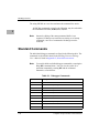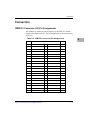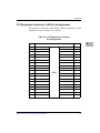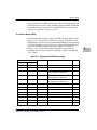
1
MVME5100
Single Board Computer
Installation and Use
V5100A/IH4
July 2003 Edition
© Copyright 2003 Motorola, Inc.
All rights reserved.
Printed in the United States of America.
Motorola and the Motorola logo are registered trademarks and AltiVec is a trademark of
Motorola, Inc.
PowerPC and the PowerPC logo are registered trademarks; and PowerPC 750 is a
trademark of International Business Machines Corporation and are used by Motorola, Inc.
under license from International Business Machines Corporation.
All other products mentioned in this document are trademarks or registered trademarks of
their respective holders.
Safety Summary
The following general safety precautions must be observed during all phases of operation, service, and repair of this
equipment. Failure to comply with these precautions or with specific warnings elsewhere in this manual could result
in personal injury or damage to the equipment.
The safety precautions listed below represent warnings of certain dangers of which Motorola is aware. You, as the
user of the product, should follow these warnings and all other safety precautions necessary for the safe operation of
the equipment in your operating environment.
Ground the Instrument.
To minimize shock hazard, the equipment chassis and enclosure must be connected to an electrical ground. If the
equipment is supplied with a three-conductor AC power cable, the power cable must be plugged into an approved
three-contact electrical outlet, with the grounding wire (green/yellow) reliably connected to an electrical ground
(safety ground) at the power outlet. The power jack and mating plug of the power cable meet International
Electrotechnical Commission (IEC) safety standards and local electrical regulatory codes.
Do Not Operate in an Explosive Atmosphere.
Do not operate the equipment in any explosive atmosphere such as in the presence of flammable gases or fumes.
Operation of any electrical equipment in such an environment could result in an explosion and cause injury or damage.
Keep Away From Live Circuits Inside the Equipment.
Operating personnel must not remove equipment covers. Only Factory Authorized Service Personnel or other
qualified service personnel may remove equipment covers for internal subassembly or component replacement or any
internal adjustment. Service personnel should not replace components with power cable connected. Under certain
conditions, dangerous voltages may exist even with the power cable removed. To avoid injuries, such personnel
should always disconnect power and discharge circuits before touching components.
Use Caution When Exposing or Handling a CRT.
Breakage of a Cathode-Ray Tube (CRT) causes a high-velocity scattering of glass fragments (implosion). To prevent
CRT implosion, do not handle the CRT and avoid rough handling or jarring of the equipment. Handling of a CRT
should be done only by qualified service personnel using approved safety mask and gloves.
Do Not Substitute Parts or Modify Equipment.
Do not install substitute parts or perform any unauthorized modification of the equipment. Contact your local
Motorola representative for service and repair to ensure that all safety features are maintained.
Observe Warnings in Manual.
Warnings, such as the example below, precede potentially dangerous procedures throughout this manual. Instructions
contained in the warnings must be followed. You should also employ all other safety precautions which you deem
necessary for the operation of the equipment in your operating environment.
Warning
To prevent serious injury or death from dangerous voltages, use extreme
caution when handling, testing, and adjusting this equipment and its
components.
Flammability
All Motorola PWBs (printed wiring boards) are manufactured with a flammability rating
of 94V-0 by UL-recognized manufacturers.
EMI Caution
!
Caution
This equipment generates, uses and can radiate electromagnetic energy. It
may cause or be susceptible to electromagnetic interference (EMI) if not
installed and used with adequate EMI protection.
Lithium Battery Caution
This product contains a lithium battery to power the clock and calendar circuitry.
!
Caution
!
Attention
!
Vorsicht
Danger of explosion if battery is replaced incorrectly. Replace battery only
with the same or equivalent type recommended by the equipment
manufacturer. Dispose of used batteries according to the manufacturer’s
instructions.
Il y a danger d’explosion s’il y a remplacement incorrect de la batterie.
Remplacer uniquement avec une batterie du même type ou d’un type
équivalent recommandé par le constructeur. Mettre au rebut les batteries
usagées conformément aux instructions du fabricant.
Explosionsgefahr bei unsachgemäßem Austausch der Batterie. Ersatz nur
durch denselben oder einen vom Hersteller empfohlenen Typ. Entsorgung
gebrauchter Batterien nach Angaben des Herstellers.
CE Notice (European Community)
Motorola Computer Group products with the CE marking comply with the EMC Directive
(89/336/EEC). Compliance with this directive implies conformity to the following
European Norms:
EN55022 “Limits and Methods of Measurement of Radio Interference Characteristics
of Information Technology Equipment”; this product tested to Equipment Class B
EN55024 “Information technology equipment—Immunity characteristics—Limits and
methods of measurement”
Board products are tested in a representative system to show compliance with the above
mentioned requirements. A proper installation in a CE-marked system will maintain the
required EMC performance.
In accordance with European Community directives, a “Declaration of Conformity” has
been made and is available on request. Please contact your sales representative.
Notice
While reasonable efforts have been made to assure the accuracy of this document,
Motorola, Inc. assumes no liability resulting from any omissions in this document, or from
the use of the information obtained therein. Motorola reserves the right to revise this
document and to make changes from time to time in the content hereof without obligation
of Motorola to notify any person of such revision or changes.
Electronic versions of this material may be read online, downloaded for personal use, or
referenced in another document as a URL to the Motorola Computer Group website. The
text itself may not be published commercially in print or electronic form, edited, translated,
or otherwise altered without the permission of Motorola, Inc.
It is possible that this publication may contain reference to or information about Motorola
products (machines and programs), programming, or services that are not available in your
country. Such references or information must not be construed to mean that Motorola
intends to announce such Motorola products, programming, or services in your country.
Limited and Restricted Rights Legend
If the documentation contained herein is supplied, directly or indirectly, to the U.S.
Government, the following notice shall apply unless otherwise agreed to in writing by
Motorola, Inc.
Use, duplication, or disclosure by the Government is subject to restrictions as set forth in
subparagraph (b)(3) of the Rights in Technical Data clause at DFARS 252.227-7013
(Nov. 1995) and of the Rights in Noncommercial Computer Software and Documentation
clause at DFARS 252.227-7014 (Jun. 1995).
Motorola, Inc.
Computer Group
2900 South Diablo Way
Tempe, Arizona 85282
Contents
About This Manual
Summary of Changes ................................................................................................xvii
Overview of Contents ...............................................................................................xvii
Comments and Suggestions .......................................................................................xix
Conventions Used in This Manual.............................................................................xix
Terminology......................................................................................................... xx
CHAPTER 1
Hardware Preparation and Installation
Introduction................................................................................................................1-1
Getting Started ...........................................................................................................1-1
Overview and Equipment Requirements ............................................................1-1
Unpacking Instructions .......................................................................................1-2
Preparation .................................................................................................................1-3
Hardware Configuration .....................................................................................1-3
Jumper Settings...................................................................................................1-5
PMC/SBC (761/IPMC) Mode Selection .....................................................1-6
Installation Considerations .................................................................................1-6
Installation..................................................................................................................1-8
PMC Modules ...................................................................................................1-10
Primary PMCspan.............................................................................................1-12
Secondary PMCspan.........................................................................................1-14
MVME5100 ......................................................................................................1-16
CHAPTER 2
Operation
Introduction................................................................................................................2-1
Switches and Indicators .............................................................................................2-1
ABT/RST Switch................................................................................................2-1
Abort Function.............................................................................................2-1
Reset Function .............................................................................................2-1
Status Indicators..................................................................................................2-2
RST Indicator (DS1)....................................................................................2-2
CPU Indicator (DS2) ...................................................................................2-2
Connectors ..........................................................................................................2-2
10/100 BASE T Ports ..................................................................................2-3
vii
DEBUG Port ............................................................................................... 2-3
System Powerup ........................................................................................................ 2-3
Initialization Process .......................................................................................... 2-4
CHAPTER 3
PPCBug Firmware
Introduction ............................................................................................................... 3-1
PPCBug Overview..................................................................................................... 3-1
Implementation and Memory Requirements ...................................................... 3-3
Using PPCBug ........................................................................................................... 3-3
Hardware and Firmware Initialization ............................................................... 3-4
Default Settings ......................................................................................................... 3-6
CNFG - Configure Board Information Block .................................................... 3-7
ENV - Set Environment ..................................................................................... 3-7
Configuring the PPCBug Parameters.......................................................... 3-8
LED/Serial Startup Diagnostic Codes .............................................................. 3-16
Configuring the VMEbus Interface .................................................................. 3-17
Firmware Command Buffer ............................................................................. 3-21
Standard Commands................................................................................................ 3-22
Diagnostics ....................................................................................................... 3-26
CHAPTER 4
Functional Description
Introduction ............................................................................................................... 4-1
Features Summary ..................................................................................................... 4-1
Features Descriptions ................................................................................................ 4-3
General ............................................................................................................... 4-3
Processor ............................................................................................................ 4-5
System Memory Controller and PCI Host Bridge.............................................. 4-5
Memory .............................................................................................................. 4-5
Flash Memory ............................................................................................. 4-5
ECC SDRAM Memory ............................................................................... 4-6
P2 Input/Output (I/O) Modes ............................................................................. 4-7
Input/Output Interfaces....................................................................................... 4-7
Ethernet Interface ........................................................................................ 4-7
VMEbus Interface ....................................................................................... 4-8
Asynchronous Communications ................................................................. 4-8
Real-Time Clock & NVRAM & Watchdog Timer..................................... 4-8
Timers ......................................................................................................... 4-8
Interrupt Routing ......................................................................................... 4-8
IDSEL Routing............................................................................................ 4-9
viii
CHAPTER 5
Pin Assignments
Introduction................................................................................................................5-1
Summary.............................................................................................................5-1
Jumper Settings ..........................................................................................................5-2
Connectors .................................................................................................................5-3
IPMC761 Connector (J3) Pin Assignments........................................................5-3
Memory Expansion Connector (J8) Pin Assignments........................................5-4
PCI Expansion Connector (J25) Pin Assignments .............................................5-7
PCI Mezzanine Card (PMC) Connectors..........................................................5-10
VMEbus Connectors P1 & P2 Pin Assignments (PMC mode) ........................5-23
VMEbus P1 & P2 Connector Pin Assignments (SBC Mode) ..........................5-25
10 BaseT/100 BaseTx Connector Pin Assignments .........................................5-29
COM1 and COM2 Connector Pin Assignments...............................................5-30
CHAPTER 6
Programming the MVME51xx
Introduction................................................................................................................6-1
Memory Maps ............................................................................................................6-1
Processor Bus Memory Map...............................................................................6-2
Default Processor Memory Map..................................................................6-2
Processor Memory Map...............................................................................6-3
PCI Memory Map ........................................................................................6-5
VME Memory Map .....................................................................................6-5
PCI Local Bus Memory Map..............................................................................6-5
VMEbus Memory Map .......................................................................................6-6
Programming Considerations.....................................................................................6-6
PCI Arbitration ...................................................................................................6-6
Interrupt Handling...............................................................................................6-9
DMA Channels .................................................................................................6-11
Sources of Reset................................................................................................6-11
Endian Issues ....................................................................................................6-13
Processor/Memory Domain .......................................................................6-13
PCI Domain ...............................................................................................6-13
VMEbus Domain .......................................................................................6-14
APPENDIX A
Specifications
General Specifications ..............................................................................................A-1
Power Requirements .................................................................................................A-2
Cooling Requirements ..............................................................................................A-3
ix
EMC Compliance ..................................................................................................... A-3
APPENDIX B
Troubleshooting
Solving Startup Problems ......................................................................................... B-1
APPENDIX C
Related Documentation
Motorola Computer Group Documents .................................................................... C-1
Manufacturers’ Documents ...................................................................................... C-2
Related Specifications .............................................................................................. C-4
APPENDIX D
RAM500 Memory Expansion Module
Overview .................................................................................................................. D-1
Features..................................................................................................................... D-1
Functional Description ............................................................................................. D-2
RAM500 Description ........................................................................................ D-2
SROM................................................................................................................ D-5
Host Clock Logic............................................................................................... D-5
RAM500 Module Installation................................................................................... D-5
RAM500 Connectors ................................................................................................ D-7
Bottom Side Memory Expansion Connector (P1)............................................. D-7
Top Side Memory Expansion Connector (J1) ................................................. D-10
RAM500 Programming Issues ............................................................................... D-13
Serial Presence Detect (SPD) Data ................................................................. D-13
APPENDIX E
Thermal Analysis
Thermally Significant Components...........................................................................E-1
Component Temperature Measurement.....................................................................E-6
Preparation..........................................................................................................E-6
Measuring Junction Temperature .......................................................................E-6
Measuring Case Temperature .............................................................................E-6
Measuring Local Air Temperature .....................................................................E-9
x
List of Figures
Figure 1-1. MVME5100 Layout ................................................................................1-9
Figure 1-2. MVME5100 Installation and Removal From a VMEbus Chassis ........1-11
Figure 1-3. Typical PMC Module Placement on an MVME5100 ...........................1-11
Figure 1-4. PMCspan-002 Installation on an MVME510 .......................................1-13
Figure 1-5. PMCspan-010 Installation on a PMCspan-002/MVME5100 ...............1-15
Figure 2-1. Boot-Up Sequence ..................................................................................2-5
Figure 4-1. MVME5100 Block Diagram...................................................................4-4
Figure 6-1. VMEbus Master Mapping.......................................................................6-8
Figure 6-2. MVME510x Interrupt Architecture ......................................................6-10
Figure D-1. RAM500 Block Diagram .....................................................................D-4
Figure D-2. RAM500 Module Placement on MVME5100 .....................................D-6
Figure E-1. Thermally Significant Components on the MVME5100 Single
Board Computer - Primary Side ............................................................................. E-4
Figure E-2. Thermally Significant Components on the IPMC761 Module Primary Side ............................................................................................................. E-5
Figure E-3. Mounting a Thermocouple Under a Heatsink ....................................... E-8
Figure E-4. Measuring Local Air Temperature ....................................................... E-9
xi
xii
List of Tables
Table 1-1. Manually Configured Headers/Jumpers ...................................................1-4
Table 3-1. Debugger Commands .............................................................................3-22
Table 3-2. Diagnostic Test Groups...........................................................................3-27
Table 4-1. MVME5100 General Features..................................................................4-1
Table 5-1. Jumper Switches and Settings...................................................................5-2
Table 5-2. IPMC761 Connector Pin Assignments .....................................................5-3
Table 5-3. Memory Expansion Connector Pin Assignments .....................................5-4
Table 5-4. PCI Expansion Connector
Pin Assignments.........................................................................................................5-7
Table 5-5. PMC Slot 1 Connector (J11) Pin Assignments.......................................5-10
Table 5-6. PMC Slot 1 Connector (J12) Pin Assignments.......................................5-12
Table 5-7. PMC Slot 1 Connector (J13) Pin Assignments.......................................5-13
Table 5-8. PMC Slot 1 Connector (J14)
Pin Assignments.......................................................................................................5-15
Table 5-9. PMC Slot 2 Connector (J21) Pin Assignments.......................................5-17
Table 5-10. PMC Slot 2 Connector (J22) Pin Assignments.....................................5-18
Table 5-11. PMC Slot 2 Connector (J23) Pin Assignments.....................................5-20
Table 5-12. PMC Slot 2 Connector (J24) Pin Assignments.....................................5-21
Table 5-13. VMEbus Connector P2 Pin Assignments
(PMC Mode) ............................................................................................................5-23
Table 5-14. VMEbus P2 Connector Pinouts with IPMC761SBC Mode................................................................................................................5-25
Table 5-15. VMEbus Connector P2 Pinout with IPMC712.....................................5-27
Table 5-16. 10 BaseT/100 BaseTx Connector Pin Assignment...............................5-29
Table 5-17. COM1 (J19) Connector Pin Assignments ............................................5-30
Table 5-18. COM2 (J5) Connector Pin Assignments ..............................................5-30
Table 6-1. Default Processor Memory Map...............................................................6-2
Table 6-2. Suggested CHRP Memory Map ...............................................................6-3
Table 6-3. Hawk PPC Register Values for Suggested Memory Map.........................6-4
Table 6-4. PCI Arbitration Assignments....................................................................6-9
Table A-1. MVME5100 Specifications ...................................................................A-1
Table A-2. Power Consumption ..............................................................................A-2
Table B-1. Troubleshooting Problems ..................................................................... B-1
Table C-1. Motorola Computer Group Documents ................................................. C-1
Table C-2. Manufacturers’ Documents .................................................................... C-2
xiii
Table C-3. Related Specifications ........................................................................... C-4
Table D-1. RAM500 Feature Summary .................................................................. D-1
Table D-2. RAM500 SDRAM Memory Size Options ............................................ D-3
Table D-3. RAM500 Bottom Side Connector (P1)
Pin Assignments ...................................................................................................... D-8
Table D-4. RAM500 Top Side Connector (J1)
Pin Assignments .................................................................................................... D-10
Table E-1. Thermally Significant Components on the MVME5100 Single
Board Computer .......................................................................................................E-2
Table E-2. Thermally Significant Components on the IPMC761 Module ..............E-3
xiv
About This Manual
The MVME51xx Single Board Computer Installation and Use provides the
information you will need to install and configure your MVME51xx
Single Board Computer. It provides specific preparation and installation
information and data applicable to the board.
The MVME51xx is a high-performance VME single board computer
featuring the Motorola Computer Group (MCG) PowerPlus II architecture
with a choice of processors—either Motorola’s MPC7410 with AltiVec™
technology for algorithmic intensive computations or the low-power
MPC755 or MPC750.
As of the printing date of this manual, the MVME51xx is available in the
configurations shown below. Note: all models of the MVME51xx are
available with either VME Scanbe front panel (-xxx) or IEEE 1101
compatible front panel (-xxx3) handles.
Part Number
Description
450 MHz MPC750 Commercial Models
MVME5100-016x
450 MHz MPC750, 512MB ECC SDRAM, 17MB Flash and 1MB L2 cache
400 MHz MPC755 Extended Temperature Models
MVME5106-114x
400 MHz MPC755, 128MB ECC SDRAM, 17MB Flash and 1MB L2 cache
MVME5106-115x
400 MHz MPC755, 256MB ECC SDRAM, 17MB Flash and 1MB L2 cache
MVME5106-116x
400 MHz MPC755, 512MB ECC SDRAM, 17MB Flash and 1MB L2 cache
400 and 500 MHz MPC7410 Commercial Models
MVME5110-216x
400 MHz MPC7410, 512MB ECC SDRAM, 17MB Flash and 2MB L2 cache
MVME5110-226x
500 MHz MPC7410, 512MB ECC SDRAM, 17MB Flash and 2MB L2 cache
500 MHz MPC7410 Extended Temperature Models
MVME5107-214x
500 MHz MPC7410, 128MB ECC SDRAM, 17MB Flash and 2MB L2 cache
MVME5107-215x
500 MHz MPC7410, 256MB ECC SDRAM, 17MB Flash and 2MB L2 cache
MVME5107-216x
500 MHz MPC7410, 512MB ECC SDRAM, 17MB Flash and 2MB L2 cache
MVME712M Compatible I/O
IPMC712-001
Multifunction rear I/O PMC module; 8-bit SCSI, Ultra Wide SCSI, one
parallel port, three async and one sync/async serial port
xv
Part Number
Description
MVME712M
Transition module connectors: One DB-25 sync/async serial port, three DB25 async serial ports, one AUI connector, one D-36 parallel port, and one 50pin 8-bit SCSI; includes 3-row DIN P2 adapter module and cable.
MVME761 Compatible I/O
IPMC761-001
Multifunction rear I/O PMC module; 8-bit SCSI, one parallel port, two async
and two sync/async serial ports
MVME761-001
Transition module: Two DB-9 async serial port connectors, two HD-26
sync/async serial port connectors, one HD-36 parallel port connector, and one
RJ-45 10/100 Ethernet connector; includes 3-row DIN P2 adapter module and
cable (for 8-bit SCSI).
MVME761-011
Transition module: Two DB-9 async serial port connectors, two HD-26
sync/async serial port connectors, one HD-36 parallel port connector, and one
RJ-45 10/100 Ethernet connector; includes 5-row DIN P2 adapter module and
cable (for 16-bit SCSI); requires backplane with 5-row DIN connectors.
SIM232DCE or
DTE
EIA-232 DCE or DTE Serial Interface Module
SIM530DCE or
DTE
EIA-530 DCE or DTE Serial Interface Module
SIMV35DCE or
DTE
V.35 DCE or DTE Module
SIMX21DCE or
DTE
X.21 DCE or DTE Serial Interface Module
Related Products
PMCSPAN1-002
PMCSPAN-002 with original VME Scanbe ejector handles
PMCSPAN1-010
PMCSAN-010 with original VME Scanbe ejector handles
RAM500-004
Stackable (top) 64MB ECC SDRAM mezzanine
RAM500-006
Stackable (top) 256MB ECC SDRAM mezzanine
RAM500-016
Stackable (bottom) 256MB ECC SDRAM mezzanine
xvi
Summary of Changes
The following changes were made for the 4th revision of this manual.
Date
Doc. Rev
Changes
08/2001
V5100A/IH2
A correction was made on page 1-5 to change the
explanation of the jumper settings for Flash Bank A
and B. Flash Bank B (0) is the factory setting.
Memory Map information was also added to
Chapter 6, Programming Information. Appendix
B, Specifications was updated, and Appendix D,
RAM500 Memory Expansion Module was added.
Other corrections were made throughout the
manual. This section titled "About this Manual"
was also added.
02/2003
V5100A/IH3
Changes were made to pages 1-4 and 5-2
respectively to clarify the explanation for J16 to
state that the setting of jumpers 2 and 3 only write
protect the upper 64KB of Flash memory.
Additional corrections were made to Table 5-15 to
duplicate information in Rows Z and D from Table
5-14 and to add note below Table 5-15.
07/2003
V5100A/IH4
Changes were made to this section to update model
numbers and descriptions to coincide with the
MVME5100 Datasheet. Changes were also made to
correct the address of the DS1621 from $A6 to $96.
Changes were also made to specifications for
additional power ratings and additions were made
to a new thermal rating chart.
Overview of Contents
The following paragraphs briefly describe the contents of each chapter.
Chapter 1, Hardware Preparation and Installation, provides a description
of the MVME5100 and its main integrated PMC and IPMC boards. The
remainder of the chapter includes an explanation of the installation
procedure, including preparation and jumper setting information.
xvii
Chapter 2, Operation, provides a description of the operational functions
of the MVME5100 including tips on applying power, a description of the
switch settings, the status indicators, I/O connectors, and system power up
information.
Chapter 3, PPCBug Firmware, provides an explanation of the debugger
firmware, PPCBug, on the MVME5100. The chapter includes an overview
of the firmware, a section on how to use PPCBug, a listing of the
initialization steps, a brief explanation of the two main configuration
commands CNFG and ENV, and a description of the standard
configuration parameters. A listing of the basic commands are also
provided.
Chapter 4, Functional Description, provides a summary of the
MVME5100 features, a block diagram, and a description of the major
functional areas.
Chapter 5, Pin Assignments, provides a listing of all connector and header
pin assignments for the MVME5100.
Chapter 6, Programming the MVME51xx, provides a description of the
memory maps on the MVME5100 including tables of default processor
memory maps, suggested CHRP memory maps, and Hawk PPC register
values for suggested memory maps. The remainder of the chapter provides
some programming considerations.
Appendix A, Specifications, provides the standard specifications for the
MVME5100, as well as some general information on cooling.
Appendix B, Troubleshooting, provides a brief explanation of the possible
resolutions for basic error conditions.
Appendix C, Related Documentation, provides a listing of related
documentation for the MVME5100, including vendor documentation and
industry related specifications.
Appendix D, RAM500 Memory Expansion Module, provides a description
of the RAM500 Memory Expansion Module, a list of features, a block
diagram of the module, a table of memory size allocations, an installation
procedure, and pinouts of the module’s top and bottom side connectors.
xviii
Comments and Suggestions
Motorola welcomes and appreciates your comments on its documentation.
We want to know what you think about our manuals and how we can make
them better. Mail comments to:
Motorola Computer Group
Reader Comments DW164
2900 S. Diablo Way
Tempe, Arizona 85282
You can also submit comments to the following e-mail address:
[email protected]
In all your correspondence, please list your name, position, and company.
Be sure to include the title and part number of the manual and tell how you
used it. Then tell us your feelings about its strengths and weaknesses and
any recommendations for improvements.
Conventions Used in This Manual
The following typographical conventions are used in this document:
bold
is used for user input that you type just as it appears; it is also used for
commands, options and arguments to commands, and names of
programs, directories and files.
italic
is used for names of variables to which you assign values. Italic is also
used for comments in screen displays and examples, and to introduce
new terms.
courier
is used for system output (for example, screen displays, reports),
examples, and system prompts.
<Enter>, <Return> or <CR>
xix
<CR> represents the carriage return or Enter key.
CTRL
represents the Control key. Execute control characters by pressing the
Ctrl key and the letter simultaneously, for example, Ctrl-d.
Terminology
A character precedes a data or address parameter to specify the numeric
format, as follows (if not specified, the format is hexadecimal):
0x
%
&
Specifies a hexadecimal number
Specifies a binary number
Specifies a decimal number
An asterisk (*) following a signal name for signals that are level significant
denotes that the signal is true or valid when the signal is low.
An asterisk (*) following a signal name for signals that are edge significant
denotes that the actions initiated by that signal occur on high to low
transition.
In this manual, assertion and negation are used to specify forcing a signal
to a particular state. In particular, assertion and assert refer to a signal that
is active or true; negation and negate indicate a signal that is inactive or
false. These terms are used independently of the voltage level (high or low)
that they represent. Data and address sizes are defined as follows:
xx
Byte
8 bits, numbered 0 through 7, with bit 0 being the least significant.
Half word
16 bits, numbered 0 through 15, with bit 0 being the least significant.
Word
32 bits, numbered 0 through 31, with bit 0 being the least significant.
Double word
64 bits, numbered 0 through 63, with bit 0 being the least significant.
1Hardware Preparation
and Installation
1
Introduction
This chapter provides information on hardware preparation and
installation for the MVME5100 Series of Single Board Computers.
Note
Unless otherwise specified, the designation “MVME5100” refers
to all models of the MVME5100-series Single Board Computers.
Getting Started
The following subsections include information helpful in preparing your
equipment. It includes and overview of the MVME5100, any equipment
needed to complete the installation, and unpacking instructions.
Overview and Equipment Requirements
The MVME5100 interfaces to a VMEbus system via its P1 and P2
connectors and contains two IEEE 1386.1 PCI Mezzanine Card (PMC)
Slots. The PMC Slots are 64-bit and support both front and rear I/O.
Additionally, the MVME5100 is user configurable by setting on-board
jumpers. Two I/O modes are possible: PMC mode or SBC mode (also
called 761 or IPMC mode). The SBC mode uses the IPMC712 I/O PMC
and the MVME712M Transiton Module, or the IPMC761 I/O PMC and
the MVME761 Transition Module. The SBC mode is backwards
compatible with the MVME761 transition card and the P2 adapter card
(excluding PMC I/O routing) used on the MVME2600/2700 product. This
mode is accomplished by configuring the on-board jumpers and by
attaching an IPMC761 PMC in PMC slot 1. Secondary Ethernet is
configured to the rear.
PMC mode is backwards compatible with the MVME2300/MVME2400
and is accomplished by simply configuring the on-board jumpers.
1-1
1
Hardware Preparation and Installation
The following equipment list is appropriate for use in an MVME5100
system:
❏
PMCspan PCI expansion mezzanine module (mates with
MVME5100)
❏
Peripheral Component Interconnect (PCI) Mezzanine Cards
(PMCs) (installed on an MVME5100 board)
❏
RAM500 memory mezzanine modules (installed on an MVME5100
board)
❏
VME system enclosure
❏
System console terminal
❏
Disk drives (and/or other I/O) and controllers
❏
Operating system (and/or application software)
Unpacking Instructions
Avoid touching areas of integrated circuitry; static discharge can damage
these circuits.
Caution
Note
Use ESD
Wrist Strap
1-2
If the shipping carton(s) is/are damaged upon receipt, request that
the carrier's agent be present during the unpacking and inspection
of the equipment.
Motorola strongly recommends that you use an antistatic wrist strap and a
conductive foam pad when installing or upgrading a system.
Electronic components, such as disk drives, computer boards, and memory
modules, can be extremely sensitive to electrostatic discharge (ESD).
After removing the component from its protective wrapper or from the
system, place the component on a grounded, static-free, and adequately
Computer Group Literature Center Web Site
Preparation
protected working surface. Do not slide the component over any surface.
In the case of a Printed Circuit Board (PCB), place the board with the
component side facing up.
If an ESD station is not available, you can avoid damage resulting from
ESD by wearing an antistatic wrist strap (available locally) that is attached
to an active electrical ground.
Note
A system chassis may not be a suitable grounding source if it is
unplugged.
Preparation
This section includes subsections on hardware configuration that may need
to be performed immediately before and after board installation. It
includes a brief reminder on setting bits in control registers, setting
jumpers for the appropriate configuration, and other VME data
considerations.
Hardware Configuration
To produce the desired board configuration and to ensure proper operation
of the MVME5100, it may be necessary to perform certain modifications
before and after installation. The following paragraphs discuss the
preparation of the MVME5100 hardware components prior to installing
them into a chassis and connecting them.
The MVME5100 provides software control over most of its options by
setting bits in control registers. After installing it in a system, you can
modify its configuration. For additional information on the board’s
control registers, refer to the MVME5100 Single Board Computer
Programmer's Reference Guide listed in Appendix C, Related
Documentation.
http://www.motorola.com/computer/literature
1-3
1
1
Hardware Preparation and Installation
It is important to note that some options are not software-programmable.
These specific options are controlled through manual installation or
removal of jumpers, and in some cases, the addition of other interface
modules on the MVME5100. The following table lists the manually
configured jumpers on the MVME5100, and their default settings.
If you are resetting the board jumpers from their default settings, it is
important to verify that all settings are reset properly. For example,
the SBC mode requires setting jumpers 4, 10 and 17 for rear Ethernet
functions, but it also requires resetting jumpers J6 and J20.
Neglecting to reset J6 and J20 could damage or destroy subsequent
PMCs or PrPMCs installed on the base board at power-up.
Table 1-1. Manually Configured Headers/Jumpers
Jumper
Description
Setting
Default
J1
RISCWatch Header
None (Factory Use Only)
N/A
J2
PAL Programming Header
None (Lab Use Only)
N/A
J4
Ethernet Port 2 Selection
(see also J10/J17)
For P2 Ethernet Port 2:
Pins 1,2; 3,4; 5,6; 7,8 (set when in SBC
mode, also called 761 mode)
For Front Panel Ethernet Port 2:
No Jumpers Installed
J6, J20
J7
Operation Mode
(Set Both Jumpers)
Pins 1, 2 for PMC Mode
Flash Memory Selection
Pins 1, 2 for Soldered Bank A
Pins 2, 3 for SBC Mode*
Pins 2, 3 for Socketed Bank B
J10, J17
Ethernet Port 2 Selection
(see also J4)
For Front Panel Ethernet Port 2:
Pins 1, 3 and 2,4 on Both Jumpers
For P2 Ethernet Port 2:
Pins 3, 5 and 4, 6 on Both Jumpers (set
for SBC mode)
1-4
No
Jumper
Installed
(front
panel)
PMC
Mode
Socketed
Bank B
Front
Panel
Ethernet
Port 2
Computer Group Literature Center Web Site
Preparation
Table 1-1. Manually Configured Headers/Jumpers (Continued)
Jumper
Description
Setting
J15
System Controller (VME)
Pins 1, 2 for No SCON
Pins 2, 3 for Auto SCON
No Jumper for ALWAYS SCON
J16
Soldered Flash Protection
Pins 1, 2 Enables Programming of
Flash
Pins 2, 3 Disables Programming of the
upper 64KB of Flash
Default
Auto
SCON
Flash
Prog.
Enabled1
Refer to the section titled Jumper Settings on the next page for additional
information.
Note
1. Write protects only outer two 8K boot sectors. Refer to Flash
Memory on page 4-5 for an complete explanation.
Jumper Settings
Prior to performing the installation instructions, you must ensure that the
jumpers are set properly for your particular configuration. For example, if
you are using an IPMC761/MVME761 or IPMC712/MVME712
combination in conjunction with the MVME5100, you must reset the
jumpers for the SBC mode (jumpers J4, J6, J10, J17 and J20). These are
factory configured for the PMC mode. Verify all settings according to the
previous table and follow the instructions below if applicable.
http://www.motorola.com/computer/literature
1-5
1
1
Hardware Preparation and Installation
PMC I/O Mode
2 4 6
SBC I/O Mode
J10
2
4
6
1
3
5
2
4
6
1
3
5
J10
1
3
5
2
4
6
1
3
5
J17
J17
J4
J4
123456 7 8
123456 7 8
For rear panel LAN, jumper
entire 8 pin header on J4
PMC/SBC (761/IPMC) Mode Selection
There are five headers associated with the selection of the PMC or SBC
mode: J4, J6 J10, J17 and J20. Three of these headers are responsible for
secondary Ethernet I/O (J4, J10 and J17) to either the front panel (PMC
mode), or to the P2 connector via J4 (SBC mode). The other two headers
(J6 and J20) ensure proper routing of +/- 12V signal routing. The
MVME5100 is set at the factory for front panel I/O: PMC mode (see Table
1-1). The SBC mode should only be selected when using one of the IPMC7xx modules in conjunction with the corresponding MVME7xx transition
module.
Installation Considerations
The MVME5100 draws power from the VMEbus backplane connectors P1
and P2. Connector P2 is also used for the upper 16 bits of data in 32-bit
transfers, and for the upper 8 address lines in extended addressing mode.
The MVME5100 will not function properly without its main board
connected to VMEbus backplane connectors P1 and P2.
1-6
Computer Group Literature Center Web Site
Preparation
Whether the MVME5100 operates as a VMEbus master or as a VMEbus
slave, it is configured for 32 bits of address and 32 bits of data (A32/D32).
However, it handles A16 or A24 devices in the appropriate address ranges.
D8 and/or D16 devices in the system must be handled by the processor
software.
If the MVME5100 tries to access off-board resources in a nonexistent
location and if the system does not have a global bus time-out, the
MVME5100 waits indefinately for the VMEbus cycle to complete. This
will cause the system to lock up. There is only one situation in which the
system might lack this global bus time-out; that is when the MVME5100
is not the system controller and there is no global bus time-out elsewhere
in the system.
Note
Software can also disable the bus timer by setting the appropriate
bits in the Universe II VMEbus interface.
Multiple MVME5100 boards may be installed in a single VME chassis;
however, each must have a unique VMEbus address. Other MPUs on the
VMEbus can interrupt, disable, communicate with, and determine the
operational status of the processor(s).
http://www.motorola.com/computer/literature
1-7
1
1
Hardware Preparation and Installation
Installation
This section discusses the installation of PMCs onto the MVME5100,
installation of PMCspan modules onto the MVME5100, and the
installation of the MVME5100 into a VME chassis.
Note
1-8
If you have ordered one or more of the optional RAM500
memory mezzanine boards for the MVME5100, ensure that they
are installed on the board prior to proceeding. If they have not
been installed by the factory, and you are installing them
yourself, please refer to Appendix D, RAM500 Memory
Expansion Module, for installation instructions. It is
recommended that the memory mezzainine modules be installed
prior to installing other board accessories, such as PMCs, IPMCs,
or transition modules.
Computer Group Literature Center Web Site
J1
P1
J22
J24
J12
XU1
S1
J11
XU2
J23
L1
J4
J3
J5
U8
HAWK
ASIC
PCI MEZZANINE CARD
J14
J6
J13
J7
J8
J16
J15
LAN 2
J10 J17
BFL CPU
P2
LAN 1
ABT/RST 10/100 BASE T10/100 BASE T
J20
J25
DEBUG
2788 0700
2788 0700
1-9
http://www.motorola.com/computer/literature
J21
L2
PCI MEZZANINE CARD
Figure 1-1. MVME5100 Layout
1
Installation
1
Hardware Preparation and Installation
PMC Modules
PMC modules mount on top of the MVME5100. Perform the following
steps to install a PMC module on your MVME5100.
Dangerous voltages, capable of causing death, are present in this
equipment. Use extreme caution when handling, testing, and adjusting.
Warning
Caution
Inserting or removing modules with power applied may result in damage
to module components. Avoid touching areas of integrated circuitry, static
discharge can damage these circuits.
Note
This procedure assumes that you have read the user’s manual that
came with your PMCs.
1. Attach an ESD strap to your wrist. Attach the other end of the ESD
strap to an electrical ground. Note that the system chassis may not
be grounded if it is unplugged. The ESD strap must be secured to
your wrist and to ground throughout the procedure.
2. Perform an operating system shutdown. Turn the AC or DC power
off and remove the AC cord or DC power lines from the system.
Remove chassis or system cover(s) as necessary for access to the
VME modules.
3. If the MVME5100 has already been installed in a VMEbus card slot,
carefully remove it as shown in Figure 1-2 and place it with
connectors P1and P2 facing you.
4. Remove the filler plate(s) from the front panel of the MVME5100.
5. Align the PMC module’s mating connectors to the MVME5100’s
mating connectors and press firmly into place.
6. Insert the appropriate number of Phillips screws (typically 4) from
the bottom of the MVME5100 into the standoffs on the PMC
module and tighten the screws (refer to Figure 1-3).
1-10
Computer Group Literature Center Web Site
Installation
Figure 1-2. MVME5100 Installation and Removal From a VMEbus Chassis
Figure 1-3. Typical PMC Module Placement on an MVME5100
http://www.motorola.com/computer/literature
1-11
1
1
Hardware Preparation and Installation
Primary PMCspan
To install a PMCspan-002 PCI expansion module on your MVME5100,
perform the following steps while referring to the figure on the next page:
Dangerous voltages, capable of causing death, are present in this
equipment. Use extreme caution when handling, testing, and adjusting.
Warning
Caution
Inserting or removing modules with power applied may result in damage
to module components. Avoid touching areas of integrated circuitry, static
discharge can damage these circuits.
Note
This procedure assumes that you have read the user’s manual that
was furnished with your PMCspan and that you have installed the
selected PMC modules on to your PMCspan according to the
instructions provided in the PMCspan and PMC manuals.
1. Attach an ESD strap to your wrist. Attach the other end of the ESD
strap to an electrical ground. Note that the system chassis may not
be grounded if it is unplugged. The ESD strap must be secured to
your wrist and to ground throughout the procedure.
2. Perform an operating system shutdown. Turn the AC or DC power
off and remove the AC cord or DC power lines from the system.
Remove chassis or system cover(s) as necessary for access to the
VME modules.
3. If the MVME5100 has already been installed in a VMEbus card slot,
carefully remove it as shown in Figure 1-2 and place it with
connectors P1and P2 facing you.
4. Attach the four standoffs to the MVME5100. For each standoff:
– Insert the threaded end into the standoff hole at each corner of
the MVME5100.
– Thread the locking nuts into the standoff tips and tighten.
1-12
Computer Group Literature Center Web Site
Installation
5. Place the PMCspan on top of the MVME5100. Align the mounting
holes in each corner to the standoffs and align PMCspan connector
P4 with MVME5100 connector J25.
PMCspan
MVME5100
2081 9708
Figure 1-4. PMCspan-002 Installation on an MVME5100
6. Gently press the PMCspan and MVME5100 together and verify that
P4 is fully seated in J25.
http://www.motorola.com/computer/literature
1-13
1
1
Hardware Preparation and Installation
7. Insert four short screws (Phillips type) through the holes at the
corners of the PMCspan and into the standoffs on the MVME5100.
Tighten screws securely.
Secondary PMCspan
The PMCspan-010 PCI expansion module mounts on top of a
PMCspan-002 PCI expansion module. To install a PMCspan-010 on your
MVME5100, perform the following steps while referring to the figure on
the next page:
Dangerous voltages, capable of causing death, are present in this
equipment. Use extreme caution when handling, testing, and adjusting.
Warning
Caution
Inserting or removing modules with power applied may result in damage
to module components. Avoid touching areas of integrated circuitry, static
discharge can damage these circuits.
Note
This procedure assumes that you have read the user’s manual that
was furnished with the PMCspan, and that you have installed the
selected PMC modules on your PMCspan according to the
instructions provided in the PMCspan and PMC manuals.
1. Attach an ESD strap to your wrist. Attach the other end of the ESD
strap to an electrical ground. Note that the system chassis may not
be grounded if it is unplugged. The ESD strap must be secured to
your wrist and to ground throughout the procedure.
2. Perform an operating system shutdown. Turn the AC or DC power
off and remove the AC cord or DC power lines from the system.
Remove chassis or system cover(s) as necessary for access to the
VME module
3. If the Primary PMC Carrier Module and MVME5100 assembly is
already installed in the VME chassis, carefully remove it as shown
in Figure 1-2 and place it with connectors P1 and P2 facing you.
1-14
Computer Group Literature Center Web Site
Installation
PMCspan-010
P3
MVME5100 and
PMCspan-002
Assembly
J3
2065 9708
Figure 1-5. PMCspan-010 Installation on a PMCspan-002/MVME5100
4. Remove four screws (Phillips type) from the standoffs in each
corner of the primary PCI expansion module.
5. Attach the four standoffs from the PMCspan-010 mounting kit to
the PMCspan-002 by screwing the threaded male portion of the
standoffs in the locations where the screws were removed in the
previous step.
6. Place the PMCspan-010 on top of the PMCspan-002. Align the
mounting holes in each corner to the standoffs and align
PMCspan-010 connector P3 with PMCspan-002 connector J3.
http://www.motorola.com/computer/literature
1-15
1
1
Hardware Preparation and Installation
7. Gently press the two PMCspan modules together and verify that P3
is fully seated in J3.
8. Insert the four screws (Phillips type) through the holes at the corners
of PMCspan-010 and into the standoffs on the primary
PMCspan-002. Tighten screws securely.
Note
The screws have two different head diameters. Use the screws
with the smaller heads on the standoffs next to VMEbus
connectors P1 and P2.
MVME5100
Before installing the MVME5100 into your VME chassis, ensure that the
jumpers are configured properly. This procedure assumes that you have
already installed the PMCspan(s) and any PMCs that you have selected.
Perform the following steps to install the MVME5100 in your VME
chassis:
Dangerous voltages, capable of causing death, are present in this
equipment. Use extreme caution when handling, testing, and adjusting.
Warning
Caution
Inserting or removing modules with power applied may result in damage
to module components. Avoid touching areas of integrated circuitry, static
discharge can damage these circuits
1. Attach an ESD strap to your wrist. Attach the other end of the ESD
strap to an electrical ground. Note that the system chassis may not
be grounded if it is unplugged. The ESD strap must be secured to
your wrist and to ground throughout the procedure
2. Perform an operating system shutdown. Turn the AC or DC power
off and remove the AC cord or DC power lines from the system.
Remove chassis or system cover(s) as necessary for access to the
VME module
1-16
Computer Group Literature Center Web Site
Installation
3. Remove the filler panel from the VMEbus chassis card slot where
you are going to install the MVME5100. If you have installed one
or more PMCspan PCI expansion modules onto your MVME5100,
you will need to remove filler panels from one additional card slot
for each PMCspan, above the card slot for the MVME5100.
– If you intend to use the MVME5100 as system controller, it must
occupy the left-most card slot (slot 1). The system controller
must be in slot 1 to correctly initiate the bus-grant daisy-chain
and to ensure proper operation of the IACK daisy-chain driver.
– If you do not intend to use the MVME5100 as system controller,
it can occupy any unused card slot.
4. Slide the MVME5100 (and PMCspans if used) into the selected
card slot(s). Verify that the module or module(s) seated properly in
the P1 and P2 connectors on the chassis backplane. Do not damage
or bend connector pins.
5. Secure the MVME5100 (and PMCspans if used) in the chassis with
the screws in the top and bottom of its front panel and verify proper
contact with the transverse mounting rails to minimize RF
emissions.
Note
Some VME backplanes (such as those used in Motorola Modular
Chassis systems) have an auto-jumpering feature for automatic
propagation of the IACK and BG signals. The step immediately
below does not apply to such backplane designs.
6. On the chassis backplane, remove the INTERRUPT ACKNOWLEDGE
(IACK) and BUS GRANT (BG) jumpers from the header for the card
slots occupied by the MVME5100 and any PMCspan modules.
7. If you intend to use PPCbug interactively, connect the terminal that
is to be used as the PPCbug system console to the DEBUG port on
the front panel of the MVME5100.
Note
In normal operation, the host CPU controls MVME5100
operation via the VMEbus Universe registers.
http://www.motorola.com/computer/literature
1-17
1
1
Hardware Preparation and Installation
8. Replace the chassis or system cover(s) and cable peripherals to the
panel connectors as required.
9. Reconnect the system to the AC or DC power source and turn the
system power on.
10. The MVME5100’s green CPU LED indicates activity as a set of
confidence tests is run, and the debugger prompt PPC6-Bug>
appears.
1-18
Computer Group Literature Center Web Site
2Operation
2
Introduction
This chapter provides operating instructions for the MVME5100 Single
Board Computer. It includes necessary information about powering up the
system along with the functionality of the switches, status indicators, and
I/O ports on the front panels of the board.
Switches and Indicators
The front panel of the MVME5100 as shown in Figure 1-1, incorporates
one dual function toggle switch (ABT/RST) and two Light-Emitting Diode
(LED) status indicators (BFL, CPU) located on the front panel.
ABT/RST Switch
The ABT/RST switch operates in the following manner: if pressed for less
than 5 seconds, the ABORT function is selected, if pressed for more than 5
seconds, the RESET function is selected. Each function is described below.
Abort Function
When toggled to ABT, the switch generates an interrupt signal to the
processor. The interrupt is normally used to abort program execution and
return control to the debugger firmware located in the processor and flash
memory.
The interrupt signal reaches the processor via ISA bus interrupt line IRQ8.
The interrupter connected to the ABORT switch is an edge-sensitive circuit,
filtered to remove switch bounce.
Reset Function
When toggled to RST, the switch resets all onboard devices. To generate a
reset, the switch must be depressed for more than five seconds.
2-1
Operation
The on-board Universe ASIC includes both a global and a local reset
driver. When the ASIC operates as the System Controller, the reset driver
provides a global system reset by asserting the SYSRESET# signal.
2
Additionaly, when the MVME5100 is configured as a System Controller
(SCON), a SYSRESET# signal may be generated by toggling the ABT/RST
switch to RST, or by a power-up reset, or by a watchdog timeout, or by a
control bit in the Miscellaneous Control Register (MISC_CTL) in the
Universe ASIC.
Note
SYSRESET# remains asserted for at least 200 ms, as
required by the VMEbus specification.
Status Indicators
There are two Light-Emitting Diode (LED) status indicators located on the
MVME5100 front panel. They are labeled BFL and CPU.
RST Indicator (DS1)
The yellow BFL LED indicates board failure; this indicator is also
illuminated during reset as an LED test. The BFL is set if the MODFAIL
Register or FUSE Register is set. Refer to the MVME5100 Single Board
Computer Programmer’s Reference Guide (V5100A/PG) for information
on these registers.
CPU Indicator (DS2)
The green CPU LED indicates CPU activity.
Connectors
There are three connectors on the front panel of the MVME5100. Two are
bottom-labeled 10/100BASE T and one is labeled DEBUG.
2-2
Computer Group Literature Center Web Site
System Powerup
10/100 BASE T Ports
2
The two RJ-45 ports labeled 10/100 BASE T provide the
10BaseT/100BaseTX Ethernet LAN interface. These connectors are toplabeled with the designation LAN1 and LAN2.
DEBUG Port
The RJ-45 port labeled DEBUG provides an RS232 serial communications
interface, based on TL16C550 Universal Asynchronous
Receiver/Transmitter (UART) controller chip. It is asynchronous only.
For additional information on pin assignments, refer to Chapter 5, Pin
Assignments.
The DEBUG port may be used for connecting a terminal to the MVME5100
to serve as the firmware console for the factory installed debugger,
PPCBug. The port is configured as follows:
❏
8 bits per character
❏
1 stop bit per character
❏
Parity disabled (no parity)
❏
Baud rate = 9600 baud (default baud rate at power-up)
After power-up, the baud rate of the DEBUG port can be reconfigured by
using the debugger’s Port Format (PF) command.
System Powerup
After you have verified that all necessary hardware preparation is done,
that all connections were made correctly, and that the installation is
complete, you can power up the system.
http://www.motorola.com/computer/literature
2-3
Operation
2
Initialization Process
The MPU, hardware, and firmware initialization process is performed by
the PPCBug firmware upon system powerup or system reset. The firmware
initializes the devices on the MVME5100 in preparation for booting an
operating system.
The firmware is shipped from the factory with an appropriate set of
defaults. Depending on your system and specific application, there may or
may not be a need to modify the firmware configuration before you boot
the operating system. If it is necessary, refer to Chapter 3, PPCBug
Firmware for additional information on modifying firmware default
parameters.
The following flowchart in Figure 2-1 shows the basic initialization
process that takes place during MVME5100 system start-ups.
For further information on PPCBug, refer to the following:
2-4
❏
Chapter 3, PPCBug Firmware
❏
Appendix B, Troubleshooting
❏
Appendix C, Related Documentation
Computer Group Literature Center Web Site
System Powerup
2
Powerup/reset initialization
STARTUP
Initialize devices on the MVME5100
INITIALIZATION
POST
PowerOn Self-Test diagnostics
Firmware-configured boot mechanism,
BOOTING
if so configured. Default is no boot.
MONITOR
Interactive, command-driven on-line PPC
debugger, when terminal connected.
Figure 2-1. Boot-Up Sequence
http://www.motorola.com/computer/literature
2-5
3PPCBug Firmware
3
Introduction
The PPCBug firmware is the layer of software just above the hardware.
The firmware provides the proper initialization for the devices on the
MVME5100 upon powerup or reset.
This chapter describes the basics of the PPCBug and its architecture. It also
describes the monitor (interactive command portion of the firmware), and
provides information on using the PPCBug debugger and the special
commands. A complete list of PPCBug commands is also provided.
For full user information about PPCBug, refer to the PPCBug Firmware
Package User’s Manual and the PPCBug Diagnostics Manual, listed in
Appendix C, Related Documentation.
PPCBug Overview
The PPCBug debugger firmware is a powerful evaluation and debugging
tool for systems built around Motorola microprocessor. Facilities are
available for loading and executing user programs under complete
operator control for system evaluation. The PPCBug provides a high
degree of functionality, user friendliness, portability, and ease of
maintenance.
The PPCBug also achieves its portability because it was written entirely in
the C programming language, except where necessary to use assembler
functions.
PPCBug includes commands for:
❏
Display and modification of memory
❏
Breakpoint and tracing capabilities
❏
A powerful assembler and disassembler useful for patching
programs
3-1
PPCBug Firmware
❏
A self-test at powerup feature which verifies the integrity of the
system
PPCBug consists of three parts:
3
❏
A command-driven, user-interactive software debugger, described
in the PPCBug Firmware Package User’s Manual, listed in
Appendix C, Related Documentation (hereafter referred to as
“debugger” or “PPCBug”).
❏
A command-driven diagnostics package for the MVME5100
hardware (hereafter referred to as “diagnostics”). The diagnostics
package is described in the PPCBug Diagnostics Manual, listed in
Appendix C, Related Documentation.
❏
A user interface or debug/diagnostics monitor that accepts
commands from the system console terminal.
When using PPCBug, you operate out of either the debugger directory or
the diagnostic directory.
❏
If you are in the debugger directory, the debugger prompt
PPC6-Bug> is displayed and you have all of the debugger
commands at your disposal.
❏
If you are in the diagnostic directory, the diagnostic prompt
PPC6-Diag> is displayed and you have all of the diagnostic
commands at your disposal as well as all of the debugger
commands.
Because PPCBug is command-driven, it performs its various operations in
response to user commands entered at the keyboard. When you enter a
command, PPCBug executes the command and the prompt reappears.
However, if you enter a command that causes execution of user target code
(for example, GO), then control may or may not return to PPCBug,
depending on the outcome of the user program.
3-2
Computer Group Literature Center Web Site
Using PPCBug
Implementation and Memory Requirements
PPCBug is written largely in the C programming language, providing
benefits of portability and maintainability. Where necessary, assembly
language has been used in the form of separately compiled program
modules containing only assembler code.
3
Physically, PPCBug is contained in two socketed 32-pin PLCC Flash
devices that together provide 1MB of storage. The executable code is
checksummed at every power-on or reset firmware entry. The result
(which includes a precalculated checksum contained in the flash devices),
is verified against the expected checksum.
PPCBug requires a maximum of 768KB of read/write memory. The
debugger allocates this space from the top of memory. For example, a
system containing 64MB (0x04000000) of read/write memory will place
the PPCBug memory locations 0x03F40000 to 0x3FFFFFF. Additionally,
the first 1MB of DRAM is reserved for the exception vector table and
stack.
Using PPCBug
PPCBug is command-driven; it performs its various operations in response
to commands that you enter at the keyboard. When the PPC6-Bug> prompt
appears on the screen, the debugger is ready to accept debugger
commands. When the PPC6-Diag> prompt appears on the screen, the
debugger is ready to accept diagnostics commands. To switch from one
mode to the other, enter SD.
What you enter is stored in an internal buffer. Execution begins only after
you press the Return or Enter key. This allows you to correct entry errors,
if necessary, with the control characters described in the PPCBug
Firmware Package User’s Manual, listed in Appendix C, Related
Documentation.
After the debugger executes the command, the prompt reappears.
However, depending on what the user program does, if the command
causes execution of a user target code (that is, GO), then control may or
may not return to the debugger.
http://www.motorola.com/computer/literature
3-3
PPCBug Firmware
For example, if a breakpoint has been specified, then control returns to the
debugger when the breakpoint is encountered during execution of the user
program. Alternately, the user program could return to the debugger by
means of the System Call Handler routine RETURN (described in the
PPCBug Firmware Package User’s Manual). For more about this, refer to
the GD, GO, and GT command descriptions in the PPCBug Firmware
Package User’s Manual, listed in Appendix C, Related Documentation .
3
A debugger command is made up of the following parts:
❏
The command name, either uppercase or lowercase (for example,
MD or md)
❏
Any required arguments, as specified by command
❏
At least one space before the first argument. Precede all other
arguments with either a space or comma.
❏
One or more options. Precede an option or a string of options with
a semicolon (;). If no option is entered, the command’s default
option conditions are used.
Hardware and Firmware Initialization
The debugger performs the hardware and firmware initialization process.
This process occurs each time the MVME5100 is reset or powered up. The
steps listed below are a high-level outline; be aware that not all of the
detailed steps are listed.
1. Sets MPU.MSR to known value.
2. Invalidates the MPU's data/instruction caches.
3. Clears all segment registers of the MPU.
4. Clears all block address translation registers of the MPU.
5. Initializes the MPU-bus-to-PCI-bus bridge device.
6. Initializes the PCI-bus-to-ISA-bus bridge device.
7. Calculates the external bus clock speed of the MPU.
3-4
Computer Group Literature Center Web Site
Using PPCBug
8. Delays for 750 milliseconds.
9. Determines the CPU base board type.
3
10. Sizes the local read/write memory (that is, DRAM).
11. Initializes the read/write memory controller. Sets base address of
memory to 0x00000000.
12. Retrieves the speed of read/write memory.
13. Initializes the read/write memory controller with the speed of
read/write memory.
14. Retrieves the speed of read only memory (that is, Flash).
15. Initializes the read only memory controller with the speed of read
only memory.
16. Enables the MPU's instruction cache.
17. Copies the MPU's exception vector table from 0xFFF00000 to
0x00000000.
18. Verifies MPU type.
19. Enables the superscalar feature of the MPU (superscalar processor
boards only).
20. Verifies the external bus clock speed of the MPU.
21. Determines the debugger's console/host ports and initializes the
PC16550A.
22. Displays the debugger's copyright message.
23. Displays any hardware initialization errors that may have occurred.
24. Checksums the debugger object and displays a warning message if
the checksum failed to verify.
25. Displays the amount of local read/write memory found.
26. Verifies the configuration data that is resident in NVRAM and
displays a warning message if the verification failed.
http://www.motorola.com/computer/literature
3-5
PPCBug Firmware
27. Calculates and displays the MPU clock speed, verifies that the MPU
clock speed matches the configuration data, and displays a warning
message if the verification fails.
3
28. Displays the BUS clock speed, verifies that the BUS clock speed
matches the configuration data, and displays a warning message if
the verification fails.
29. Probes PCI bus for supported network devices.
30. Probes PCI bus for supported mass storage devices.
31. Initializes the memory/IO addresses for the supported PCI bus
devices.
32. Executes Self-Test, if so configured. (Default is no Self-Test).
33. Extinguishes the board fail LED, if Self-Test passed, and outputs
any warning messages.
34. Executes boot program, if so configured. (Default is no boot.)
35. Executes the debugger monitor (that is, issues the PPC6-Bug>
prompt).
Default Settings
The following sections provide information pertaining to the firmware
settings of the MVME5100. Default (factory set) Environment (ENV)
commands are provided to inform you on how the MVME5100 was
configured at the time it left the factory.
3-6
Computer Group Literature Center Web Site
Default Settings
CNFG - Configure Board Information Block
Use this command to display and configure the Board Information Block,
which is resident within the NVRAM. This data block contains various
elements detailing specific operational parameters of the MVME5100.
The structure for the board is shown in the following example:
Board (PWA) Serial Number
= MOT00xxxxxxx
Board Identifier
= MVME5100
Artwork (PWA) Identifier
= 01-W3518FxxB
MPU Clock Speed
= 450
Bus Clock Speed
= 100
Ethernet Address
= 0001AF2A0A57
Primary SCSI Identifier
= 07
System Serial Number
= nnnnnnnn
System Identifier
= Motorola MVME5100
License Identifier
= nnnnnnnn
The Board Information Block parameters shown above are left-justified
character (ASCII) strings padded with space characters.
The Board Information Block is factory-configured before shipment.
There is no need to modify block parameters unless the NVRAM is
corrupted.
Refer to the PPCBug Firmware Package User's Manual, listed in
Appendix C, Related Documentation for a description of CNFG and
examples.
ENV - Set Environment
Use the ENV command to view and/or configure interactively all PPCBug
operational parameters that are kept in Non-Volatile RAM (NVRAM).
http://www.motorola.com/computer/literature
3-7
3
PPCBug Firmware
Refer to the PPCBug Firmware Package User's Manual for a description
of the use of ENV. Additional information on registers in the Universe
ASIC that affect these parameters is contained in your MVME5100
Programmer’s Reference Guide, listed in Appendix C, Related
Documentation.
3
Listed and described below are the parameters that you can configure
using ENV. The default values shown were those in effect when this
publication went to print.
Configuring the PPCBug Parameters
The parameters that can be configured using ENV are:
Bug or System environment [B/S] = B?
B
Bug is the mode where no system type of support is
displayed. However, system-related items are still
available. (Default)
S
System is the standard mode of operation, and is the
default mode if NVRAM should fail. System mode is
defined in the PPCBug Firmware Package User's
Manual listed in Appendix C, Related
Documentation.
Maximum Memory Usage (MB,0=AUTO) = 1?
This parameter specifies the maximum number of megabytes the bug is
allowed to use. Allocation begins at the top of physical memory and
expands downward as more memory is required until the maximum value
is reached.
If a value of zero is specified, memory will continue to be increased as
needed until half of the available memory is consumed (that is, 32MB in a
64MB system). This mode is useful for determining the full memory
required for a specific configuration. Once this is determined, a hard value
may be given to the parameter and it is guaranteed that no memory will be
used over this amount.
The default value for this parameter is one.
3-8
Computer Group Literature Center Web Site
Default Settings
Note:
The bug does not automatically acquire all of the memory it is
allowed. It accumulates memory as necessary in one megabyte
blocks.
3
Field Service Menu Enable [Y/N] = N?
Y
Display the field service menu.
N
Do not display the field service menu. (Default)
Remote Start Method Switch [G/M/B/N] = B?
The Remote Start Method Switch is used when the MVME5100 is crossloaded from another VME-based CPU in order to start execution of the
cross-loaded program.
G
Use the Global Control and Status Register to pass
and start execution of the cross-loaded program.
M
Use the Multiprocessor Control Register (MPCR) in
shared RAM to pass and start execution of the crossloaded program.
B
Use both the GCSR and the MPCR methods to pass
and start execution of the cross-loaded program.
(Default)
N
Do not use any Remote Start Method.
Probe System for Supported I/O Controllers [Y/N] = Y?
Y
Accesses will be made to the appropriate system
buses (for example, VMEbus, local MPU bus) to
determine the presence of supported controllers.
(Default)
N
Accesses will not be made to the VMEbus to
determine the presence of supported controllers.
http://www.motorola.com/computer/literature
3-9
PPCBug Firmware
Auto-Initialize of NVRAM Header Enable [Y/N] = Y?
Y
NVRAM (PReP partition) header space will be
initialized automatically during board initialization,
but only if the PReP partition fails a sanity check.
(Default)
N
NVRAM header space will not be initialized
automatically during board initialization.
3
Network PReP-Boot Mode Enable [Y/N] = N?
Y
Enable PReP-style network booting (same boot image
from a network interface as from a mass storage
device).
N
Do not enable PReP-style network booting. (Default)
Negate VMEbus SYSFAIL* Always [Y/N] = N?
Y
Negate the VMEbus SYSFAIL∗ signal during board
initialization.
N
Negate the VMEbus SYSFAIL∗ signal after
successful completion or entrance into the bug
command monitor. (Default)
SCSI Bus Reset on Debugger Startup [Y/N] = N?
Y
Local SCSI bus is reset on debugger setup.
N
Local SCSI bus is not reset on debugger setup.
(Default)
Primary SCSI Bus Negotiations Type [A/S/N] = A?
3-10
A
Asynchronous SCSI bus negotiation. (Default)
S
Synchronous SCSI bus negotiation.
N
None.
Computer Group Literature Center Web Site
Default Settings
Primary SCSI Data Bus Width [W/N] = N?
W
Wide SCSI (16-bit bus).
N
Narrow SCSI (8-bit bus). (Default)
3
Secondary SCSI identifier = 07?
Select the identifier. (Default = 07.)
NVRAM Bootlist (GEV.fw-boot-path) Boot Enable [Y/N] = N?
Note
Y
Give boot priority to devices defined in the fw-bootpath global environment variable (GEV).
N
Do not give boot priority to devices listed in the fwboot-path GEV. (Default)
When enabled, the GEV boot takes priority over all other boots,
including Autoboot and Network Boot.
NVRAM Bootlist (GEV.fw-boot-path) Boot at power-up only [Y/N] = N?
Y
Give boot priority to devices defined in the fw-bootpath GEV at powerup reset only.
N
Give powerup boot priority to devices listed in the fwboot-path GEV at any reset. (Default)
NVRAM Bootlist (GEV.fw-boot-path) Boot Abort Delay = 5?
The time (in seconds) that a boot from the NVRAM boot list will delay
before starting the boot. The purpose for the delay is to allow you the
option of stopping the boot by use of the BREAK key. The time value is
from 0-255 seconds. (Default = 5 seconds)
Auto Boot Enable [Y/N]
= N?
Y
The Autoboot function is enabled.
N
The Autoboot function is disabled. (Default)
http://www.motorola.com/computer/literature
3-11
PPCBug Firmware
Auto Boot at powerup only [Y/N] = N?
3
Y
Autoboot is attempted at powerup reset only.
N
Autoboot is attempted at any reset. (Default)
Auto Boot Scan Enable [Y/N]
= Y?
Y
If Autoboot is enabled, the Autoboot process attempts
to boot from devices specified in the scan list (for
example, FDISK/CDROM/TAPE/HDISK). (Default)
N
If Autoboot is enabled, the Autoboot process uses the
Controller LUN and Device LUN to boot.
Auto Boot Scan Device Type List = FDISK/CDROM/TAPE/HDISK?
This is the listing of boot devices displayed if the Autoboot Scan option is
enabled. If you modify the list, follow the format shown above (uppercase
letters, using forward slash as separator).
Auto Boot Controller LUN
= 00?
Refer to the PPCBug Firmware Package User's Manual for a listing of
disk/tape controller modules currently supported by PPCBug. (Default =
0x00)
Auto Boot Device LUN
= 00?
Refer to the PPCBug Firmware Package User's Manual listed in
Appendix C, Related Documentation for a listing of disk/tape devices
currently supported by PPCBug. (Default = 0x00)
Auto Boot Partition Number = 00?
Identifies which disk “partition” is to be booted, as specified in the
PowerPC Reference Platform (PReP) specification. If set to zero, the
firmware will search the partitions in order (1, 2, 3, 4) until it finds the first
“bootable” partition. That is then the partition that will be booted. Other
acceptable values are 1, 2, 3, or 4. In these four cases, the partition
specified will be booted without searching.
3-12
Computer Group Literature Center Web Site
Default Settings
Auto Boot Abort Delay = 7?
The time in seconds that the Autoboot sequence will delay before
starting the boot. The purpose for the delay is to allow you the option
of stopping the boot by use of the BREAK key. The time value is from
0-255 seconds. (Default = 7 seconds)
Auto Boot Default String [NULL for an empty string] = ?
You may specify a string (filename) which is passed on to the code
being booted. The maximum length of this string is 16 characters.
(Default = null string)
ROM Boot Enable [Y/N] = N?
Y
The ROMboot function is enabled.
N
The ROMboot function is disabled. (Default)
ROM Boot at power-up only [Y/N] = Y?
Y
ROMboot is attempted at power-up only. (Default)
N
ROMboot is attempted at any reset.
ROM Boot Enable search of VMEbus [Y/N] = N?
Y
VMEbus address space, in addition to the usual areas
of memory, will be searched for a ROMboot module.
N
VMEbus address space will not be accessed by
ROMboot. (Default)
ROM Boot Abort Delay = 5?
The time (in seconds) that the ROMboot sequence will delay before
starting the boot. The purpose for the delay is to allow you the option of
stopping the boot by use of the BREAK key. The time value is from 0-255
seconds. (Default = 5 seconds)
ROM Boot Direct Starting Address = FFF00000?
The first location tested when PPCBug searches for a ROMboot module.
(Default = 0xFFF00000)
http://www.motorola.com/computer/literature
3-13
3
PPCBug Firmware
ROM Boot Direct Ending Address = FFFFFFFC?
The last location tested when PPCBug searches for a ROMboot module.
(Default = 0xFFFFFFFC)
3
Network Auto Boot Enable [Y/N] = N?
Y
The Network Auto Boot (NETboot) function is
enabled.
N
The NETboot function is disabled. (Default)
Network Auto Boot at power-up only [Y/N] = N?
Y
NETboot is attempted at powerup reset only.
N
NETboot is attempted at any reset. (Default)
Network Auto Boot Controller LUN = 00?
Refer to the PPCBug Firmware Package User's Manual, listed in
Appendix C, Related Documentation for a listing of network controller
modules currently supported by PPCBug. (Default = 0x00)
Network Auto Boot Device LUN = 00?
Refer to the PPCBug Firmware Package User's Manual, listed in
Appendix C, Related Documentation for a listing of network controller
modules currently supported by PPCBug. (Default = 0x00)
Network Auto Boot Abort Delay = 5?
The time in seconds that the NETboot sequence will delay before starting
the boot. The purpose for the delay is to allow you the option of stopping
the boot by use of the BREAK key. The time value is from 0-255 seconds.
(Default = 5 seconds)
Network Auto Boot Configuration Parameters Offset (NVRAM) =
00001000?
The address where the network interface configuration parameters are to
be saved/retained in NVRAM; these parameters are the necessary
parameters to perform an unattended network boot. A typical offset might
be 0x1000, but this value is application-specific. (Default = 0x00001000)
3-14
Computer Group Literature Center Web Site
Default Settings
!
Caution
If you use the NIOT debugger command, these parameters need to be
saved somewhere in the offset range 0x00001000 through 0x000016F7.
The NIOT parameters do not exceed 128 bytes in size. The setting of this
ENV pointer determines their location. If you have used the same space for
your own program information or commands, they will be overwritten and
lost.
You can relocate the network interface configuration parameters in this
space by using the ENV command to change the Network Auto Boot
Configuration Parameters Offset from its default of 0x00001000 to the
value you need to be clear of your data within NVRAM.
Memory Size Enable [Y/N] = Y?
Y
Memory will be sized for SelfTest diagnostics.
(Default)
N
Memory will not be sized for SelfTest diagnostics.
Memory Size Starting Address = 00000000?
The default Starting Address is 0x00000000.
Memory Size Ending Address = 02000000?
The default Ending Address is the calculated size of local memory. If the
memory start is changed from 0x0x00000000, this value will also need to
be adjusted.
DRAM Speed in NANO Seconds = 15?
The default setting for this parameter will vary depending on the speed of
the DRAM memory parts installed on the board. The default is set to the
slowest speed found on the available banks of DRAM memory.
ROM Bank A Access Speed (ns) = 80?
This defines the minimum access speed for the Bank A Flash Device(s) in
nanoseconds.
http://www.motorola.com/computer/literature
3-15
3
PPCBug Firmware
ROM Bank B Access Speed (ns) = 70?
This defines the minimum access speed for the Bank B Flash
Device(s) in nanoseconds.
3
DRAM Parity Enable [On-Detection/Always/Never - O/A/N] = O?
Note
O
DRAM parity is enabled upon detection. (Default)
A
DRAM parity is always enabled.
N
DRAM parity is never enabled.
This parameter also applies to enabling ECC for DRAM.
L2 Cache Parity Enable [On-Detection/Always/Never - O/A/N] = O?
O
L2 Cache parity is enabled upon detection. (Default)
A
L2 Cache parity is always enabled.
N
L2 Cache parity is never enabled.
PCI Interrupts Route Control Registers (PIRQ0/1/2/3) = 0A0B0E0F?
Initializes the PIRQx (PCI Interrupts) route control registers in the IBC
(PCI/ISA bus bridge controller). The ENV parameter is a 32-bit value that
is divided by 4 fields to specify the values for route control registers
PIRQ0/1/2/3. The default is determined by system type as shown:
PIRQ0=0A, PIRQ1=0B, PIRQ2=0E, PIRQ3=0F.
LED/Serial Startup Diagnostic Codes
These codes can be displayed at key points in the initialization of the
hardware devices. The codes are enabled by an ENV parameter.
Serial Startup Code Master Enable [Y/N]=N?
Should the debugger fail to come up to a prompt, the last code displayed
will indicate how far the initialization sequence had progressed before
stalling.
3-16
Computer Group Literature Center Web Site
Default Settings
Serial Startup Code LF Enable [Y/N]=N?
A line feed can be inserted after each code is displayed to prevent it from
being overwritten by the next code. This is also enabled by an ENV
parameter:
The list of LED/serial codes is included in the section on MPU, Hardware,
and Firmware Initialization found in Chapter 1 of the PPCBug Firmware
Package User’s Manual, listed in Appendix C, Related Documentation.
Configuring the VMEbus Interface
ENV asks the following series of questions to set up the VMEbus interface
for the MVME5100. To perform this configuration, you should have a
working knowledge of the Universe ASIC as described in your
MVME5100 Programmer’s Reference Guide. Also, refer to the Tundra
Universe II Users Manual, as listed in Appendix C, Related
Documentation for a detailed description of VMEbus addressing. In
general, the PCI slave images describe the VME master addresses, while
the VMEbus slave describes the VME slave addresses.
VME3PCI Master Master Enable [Y/N] = Y?
Y
Set up and enable the VMEbus Interface. (Default)
N
Do not set up or enable the VMEbus Interface.
PCI Slave Image 0 Control = 00000000?
The configured value is written into the LSI0_CTL register of the Universe
chip.
PCI Slave Image 0 Base Address Register = 00000000?
The configured value is written into the LSI0_BS register of the Universe
chip.
PCI Slave Image 0 Bound Address Register = 00000000?
The configured value is written into the LSI0_BD register of the Universe
chip.
PCI Slave Image 0 Translation Offset = 00000000?
http://www.motorola.com/computer/literature
3-17
3
PPCBug Firmware
The configured value is written into the LSI0_TO register of the Universe
chip.
PCI Slave Image 1 Control = C0820000?
3
The configured value is written into the LSI1_CTL register of the Universe
chip.
PCI Slave Image 1 Base Address Register = 81000000?
The configured value is written into the LSI1_BS register of the Universe
chip.
PCI Slave Image 1 Bound Address Register = A0000000?
The configured value is written into the LSI1_BD register of the Universe
chip.
PCI Slave Image 1 Translation Offset = 80000000?
The configured value is written into the LSI1_TO register of the Universe
chip.
PCI Slave Image 2 Control = C0410000?
The configured value is written into the LSI2_CTL register of the Universe
chip.
PCI Slave Image 2 Base Address Register = A0000000?
The configured value is written into the LSI2_BS register of the Universe
chip.
PCI Slave Image 2 Bound Address Register = A2000000?
The configured value is written into the LSI2_BD register of the Universe
chip.
PCI Slave Image 2 Translation Offset = 500000000?
The configured value is written into the LSI2_TO register of the Universe
chip.
PCI Slave Image 3 Control = C0400000?
The configured value is written into the LSI3_CTL register of the Universe
chip.
PCI Slave Image 3 Base Address Register = AFFF0000?
3-18
Computer Group Literature Center Web Site
Default Settings
The configured value is written into the LSI3_BS register of the Universe
chip.
PCI Slave Image 3 Bound Address Register = B0000000?
The configured value is written into the LSI3_BD register of the Universe
chip.
PCI Slave Image 3 Translation Offset = 50000000?
The configured value is written into the LSI3_TO register of the Universe
chip.
VMEbus Slave Image 0 Control = E0F20000?
The configured value is written into the VSI0_CTL register of the
Universe chip.
VMEbus Slave Image 0 Base Address Register = 00000000?
The configured value is written into the VSI0_BS register of the Universe
chip.
VMEbus Slave Image 0 Bound Address Register = (Local DRAM Size)?
The configured value is written into the VSI0_BD register of the Universe
chip. The value is the same as the Local Memory Found number already
displayed.
VMEbus Slave Image 0 Translation Offset = 00000000?
The configured value is written into the VSI0_TO register of the Universe
chip.
VMEbus Slave Image 1 Control = 00000000?
The configured value is written into the VSI1_CTL register of the
Universe chip.
VMEbus Slave Image 1 Base Address Register = 00000000?
The configured value is written into the VSI1_BS register of the Universe
chip.
VMEbus Slave Image 1 Bound Address Register = 00000000?
The configured value is written into the VSI1_BD register of the Universe
chip.
http://www.motorola.com/computer/literature
3-19
3
PPCBug Firmware
VMEbus Slave Image 1 Translation Offset = 00000000?
The configured value is written into the VSI1_TO register of the Universe
chip.
3
VMEbus Slave Image 2 Control = 00000000?
The configured value is written into the VSI2_CTL register of the
Universe chip.
VMEbus Slave Image 2 Base Address Register = 00000000?
The configured value is written into the VSI2_BS register of the Universe
chip.
VMEbus Slave Image 2 Bound Address Register = 00000000?
The configured value is written into the VSI2_BD register of the Universe
chip.
VMEbus Slave Image 2 Translation Offset = 00000000?
The configured value is written into the VSI2_TO register of the Universe
chip.
VMEbus Slave Image 3 Control = 00000000?
The configured value is written into the VSI3_CTL register of the
Universe chip.
VMEbus Slave Image 3 Base Address Register = 00000000?
The configured value is written into the VSI3_BS register of the Universe
chip.
VMEbus Slave Image 3 Bound Address Register = 00000000?
The configured value is written into the VSI3_BD register of the Universe
chip.
VMEbus Slave Image 3 Translation Offset = 00000000?
The configured value is written into the VSI3_TO register of the Universe
chip.
PCI Miscellaneous Register = 10000000?
The configured value is written into the LMISC register of the Universe
chip.
3-20
Computer Group Literature Center Web Site
Default Settings
Special PCI Slave Image Register = 00000000?
The configured value is written into the SLSI register of the Universe chip.
Master Control Register = 80C00000?
3
The configured value is written into the MAST_CTL register of the
Universe chip.
Miscellaneous Control Register = 52060000?
The configured value is written into the MISC_CTL register of the
Universe chip.
User AM Codes = 00000000?
The configured value is written into the USER_AM register of the
Universe chip.
Firmware Command Buffer
Firmware Command Buffer Enable = N?
Y
Enables Firmware Command Buffer execution.
N
Disables Firmware Command Buffer execution
(Default).
Firmware Command Buffer Delay = 5?
Defines the number of seconds to wait before firmware begins executing
the startup commands in the startup command buffer. During this delay,
you may press any key to prevent the execution of the startup command
buffer.
The default value of this parameter causes a startup delay of 5 seconds.
Firmware Command Buffer:
['NULL' terminates entry]?
The Firmware Command Buffer contents contain the BUG commands
which are executed upon firmware startup.
BUG commands you place into the command buffer should be typed just
as you enter the commands from the command line.
http://www.motorola.com/computer/literature
3-21
PPCBug Firmware
The string 'NULL' on a new line terminates the command line entries.
All PPCBug commands, except for the following, may be used within
the command buffer: DU, ECHO, LO, TA, VE.
3
Note
Interactive editing of the startup command buffer is not
supported. If changes are needed to an existing set of startup
commands, a new set of commands with changes must be
reentered.
Standard Commands
The individual debugger commands are listed in the following table. The
commands are described in detail in the PPCBug Firmware Package
User’s Manual, listed in Appendix C, Related Documentation.
Note
You can list all the available debugger commands by entering the
Help (HE) command alone. You can view the syntax for a
particular command by entering HE and the command
mnemonic, as listed below.
Table 3-1. Debugger Commands
3-22
Command
Description
AS
Assembler
BC
Block of Memory Compare
BF
Block of Memory Fill
BI
Block of Memory Initialize
BM
Block of Memory Move
BS
Block of Memory Search
BR
Breakpoint Insert
BV
Block of Memory Verify
CACHE
Modify Cache State
CM
Concurrent Mode
Computer Group Literature Center Web Site
Standard Commands
Table 3-1. Debugger Commands (Continued)
Command
Description
CNFG
Configure Board Information Block
CS
Checksum a Block of data
CSAR
PCI Configuration Space READ Access
CSAW
PCI Configuration Space WRITE Access
DC
Data Conversion and Expression Evaluation
DE
Detect Errors
DS
Disassembler
DU
Dump S-Records
ECHO
Echo String
ENV
Set Environment to Bug/Operating System
FORK
Fork Idle MPU at Address
FORKWR
Fork Idle MPU with Registers
G
“Alias” for “GO” Command
GD
Go Direct (Ignore Breakpoints)
GEVBOOT
Global Environment Variable Boot - Bootstrap Operating
System
GEVDEL
Global Environment Variable Delete
GEVDUMP
Global Environment Variable(s) Dump (NVRAM Header +
Data)
GEVEDIT
Global Environment Variable Edit
GEVINIT
Global Environment Variable Initialize (NVRAM Header)
GEVSHOW
Global Environment Variable Show
GN
Go to Next Instruction
GO
Go Execute User Program
GT
Go to Temporary Breakpoint
HE
Help on Command(s)
IBM
Indirect Block Move
IDLE
Idle Master MPU
IOC
I/O Control for Disk
http://www.motorola.com/computer/literature
3
3-23
PPCBug Firmware
Table 3-1. Debugger Commands (Continued)
3
3-24
Command
Description
IOI
I/O Inquiry
IOP
I/O Physical to Disk
IOT
I/O “Teach” for Configuring Disk Controller
IRD
Idle MPU Register Display
IRM
Idle MPU Register Modify
IRS
Idle MPU Register Set
LO
Load S-Records from Host
M
“Alias” for “MM” Command
MA
Macro Define/Display
MAE
Macro Edit
MAL
Enable Macro Expansion Listing
MAR
Macro Load
MAW
Macro Save
MD
Memory Display
MDS
Memory Display (Sector)
MENU
System Menu
MM
Memory Modify
MMD
Memory Map Diagnostic
MMGR
Access Memory Manager
MS
Memory Set
MW
Memory Write
NAB
Automatic Network Bootstrap Operating System
NAP
Nap MPU
NBH
Network Bootstrap Operating System and Halt
NBO
Network Bootstrap Operating System
NIOC
Network I/O Control
NIOP
Network I/O Physical
NIOT
I/O “Teach” for Configuring Network Controller
NOBR
Breakpoint Delete
Computer Group Literature Center Web Site
Standard Commands
Table 3-1. Debugger Commands (Continued)
Command
Description
NOCM
No Concurrent Mode
NOMA
Macro Delete
NOMAL
Disable Macro Expansion Listing
NOPA
Printer Detach
NOPF
Port Detach
NORB
No ROM Boot
NOSYM
Detach Symbol Table
NPING
Network Ping
OF
Offset Registers Display/Modify
PA
Printer Attach
PBOOT
Bootstrap Operating System
PF
Port Format
PFLASH
Program FLASH Memory
PS
Put RTC into Power Save Mode
RB
ROMboot Enable
RD
Register Display
REMOTE
Remote
RESET
Cold/Warm Reset
RL
Read Loop
RM
Register Modify
RS
Register Set
RUN
MPU Execution/Status
SD
Switch Directories
SET
Set Time and Date
SROM
SROM Examine/Modify
ST
Self Test
SYM
Symbol Table Attach
SYMS
Symbol Table Display/Search
T
Trace
http://www.motorola.com/computer/literature
3
3-25
PPCBug Firmware
Table 3-1. Debugger Commands (Continued)
3
!
Caution
Command
Description
TA
Terminal Attach
TIME
Display Time and Date
TM
Transparent Mode
TT
Trace to Temporary Breakpoint
VE
Verify S-Records Against Memory
VER
Revision/Version Display
WL
Write Loop
Although a command (PFLASH) to allow the erasing and reprogramming
of Flash memory is available to you, keep in mind that reprogramming any
portion of Flash memory will erase everything currently contained in
Flash, including the PPCBug debugger, if the target address addresses the
bank in which it resides.
Diagnostics
The PPCBug hardware diagnostics are intended for testing and
troubleshooting the MVME5100.
In order to use the diagnostics, you must switch to the diagnostic directory.
You may switch between directories by using the SD (Switch Directories)
command. You may view a list of the commands in the directory that you
are currently in by using the HE (Help) command.
If you are in the debugger directory, the debugger prompt PPC6-Bug> is
displayed, and all of the debugger commands are available. Diagnostics
commands cannot be entered at the PPC6-Bug> prompt.
If you are in the diagnostic directory, the diagnostic prompt PPC6-Diag> is
displayed, and all of the debugger and diagnostic commands are available.
PPCBug’s diagnostic test groups are listed in Table 3-2. Note that not all
tests are performed on the MVME5100. Using the HE command, you can
list the diagnostic routines available in each test group. Refer to the
3-26
Computer Group Literature Center Web Site
Standard Commands
PPCBug Diagnostics Manual, listed in Appendix C, Related
Documentation for complete descriptions of the diagnostic routines and
instructions on how to invoke them.
3
Table 3-2. Diagnostic Test Groups
Test Group
Description
EPIC
EPIC Timers Test
PHB
PCI Bridge Revision Test
RAM
RAM Tests (various)
HOSTDMA
DMA Transfer Test
RTC
MK48Txx Real Time Clock Tests
UART
Serial Input/Output Tests (Register, IRQ, Baud, & Loopback)
Z8536
Z8536 Counter/Timer Tests*
SCC
Serial Communications Controller (Z85C230) Tests*
PAR8730x
Parallel Interface (PC8730x) Test*
KBD8730x
PC8730x Keyboard/Mouse Tests*
ISABRDGE
PCI/ISA Bridge Tests (Register Access & IRQ)
VME3
VME3 Tests (Register Read & Register Walking Bit)
DEC
DEC21x43 Ethernet Controller Tests
CL1283
Parallel Interface (CL1283) Tests*
Notes 1. You may enter command names in either uppercase or
lowercase.
2. Some diagnostics depend on restart defaults that are set up only
in a particular restart mode. Refer to the documentation on a
particular diagnostic for the correct mode.
3. Test Sets marked with an asterisk (*) are not available on the
MVME5100 (unless an IPMC712 or IPMC761 is mounted). The
ISABRDGE test is only performed if an IPMC761 is mounted on
the MVME5100. If the MVME5100 is operating in PMC mode
(IPMC761 is not mounted), then the test suite is bypassed.
http://www.motorola.com/computer/literature
3-27
4Functional Description
4
Introduction
This chapter provides a functional description for the MVME5100 Single
Board Computer. The MVME5100 is a high-performance product
featuring Motorola’s PowerPlus II architecture with a choice of PowerPC
processors—either Motorola’s MPC7410 with AltiVec™ technology for
algorithmic intensive computations or the low-power MPC755 or
MPC750.
The MVME5100 incorporates a highly optimized PCI interface and
memory controller enabling up to 582MB memory read bandwidth and
640MB burst write bandwidth.
The optimization of the memory bus is as important as optimization of the
system bus in order to achieve maximum system performance. The
MVME5100’s advanced PowerPlus II Architecture supports full PCI
throughput of 264MB without starving the CPU of its memory.
Additional features of the MVME5100 include dual Ethernet ports, dual
serial ports, and up to 17MB of Flash.
Features Summary
The table below lists the general features for the MVME5100. Refer to
Appendix A, Specifications, for additional product specifications and
information.
Table 4-1. MVME5100 General Features
Feature
Microprocessors and
Bus Clock Frequency
Specification
MPC7410 @400 or 500 MHz Internal Clock Frequency
MPC755 @400 MHz Internal Clock Frequency
MPC750 @450 MHz Internal Clock Frequency
Bus Clock Frequency up to 100 MHz
4-1
Functional Description
Table 4-1. MVME5100 General Features (Continued)
Feature
L2 Cache (Optional)
1MB (MPC750 or MPC755) or 2MB (MPC7410) using
burst-mode SRAM modules.
Memory
EEPROM, on-board programmable
1MB via two 32-pin PLCC/CLCC sockets;
16MB Surface Mount
Main Memory
(SDRAM)
PC100 ECC SDRAM with 100 MHz bus
32MB to 512MB on board, expandable to
1GB via RAM500 memory mezzanine
NVRAM
32KB (4KB available for users)
Memory Controller
Hawk System Memory Controller (SMC)
PCI Host Bridge
Hawk PCI Host Bridge (PHB)
Interrupt Controller
Hawk Multi-Processor Interrupt Controller (MPIC)
Peripheral Support
Dual 16550-Compatible Asynchronous Serial Port’s Routed
to the Front Panel RJ45 Connnector (COM1) and On-Board
Header (COM2)
Dual Ethernet Interfaces, one routed to the Front Panel
RJ45, One Routed to the Front Panel RJ45 or Optionally
Routed to P2, RJ45 on MVME761
VMEbus
Tundra Universe Controller, 64-bit PCI
Programmable Interrupter & Interrupt Handler
Programmable DMA Controller With Link List Support
Full System Controller Functions
PCI/PMC/Expansion
Two 32/64-bit PMC Slots With Front-Panel I/O Plus,
P2 Rear I/O (MVME2300 Routing)
One PCI Expansion Connector (for the PMCSpan)
Miscellaneous
Combined RESET and ABORT Switch
Status LEDs
Form Factor
6U VME
4
4-2
Specification
Computer Group Literature Center Web Site
Features Descriptions
Features Descriptions
General
As stated earlier, the MVME5100 is a high-performance VME based
Single Board Computer featuring Motorola’s PowerPlus II architecture
with a choice of processors. The board can be equipped with either the
Motorola MPC7410 processor with AltiVec™ technology for algorithmic
intensive computations or with the low-power MPC755 or MPC750 for
low-power or field applications.
Designed to meet the needs of OEMs servicing the military and aerospace,
industrial automation, and semiconductor process equipment market
segments, the MVME5100 is available in both commercial grade (0° to
55° C) and industrial grade (–20° to 71° C) temperatures.
The MVME5100 has two Input/Output (I/O) modes of operation: PMC
and SBC (also called 761 mode or IPMC mode). In PMC mode, it is fully
backwards compatible with previous generation dual PMC products such
as the MVME2300 and MVME2400.
In the SBC mode, the MVME5100 is backwards compatible with the
corresponding Motorola MVME712 or MVME761 transition board
originated for use with previous generation single-board computer
products, such as the MVME2600 and MVME2700.
It is important to note that MVME712 and MVME761 compatibility is
accomplished with the addition of the corresponding IPMC712 or
IPMC761 (an optional add-on PMC card). The IPMC712 and IPMC761
provides rear I/O support for one single-ended ultra-wide SCSI device, one
parallel port, four serial ports (two synchronous for 761 and one for 712,
and two asynchronous/synchronous for 761 and three for 712), and I2C
functionality through the Hawk ASIC. This multi-function PMC card is
offered with the MVME5100 as a factory bundled configuration.
http://www.motorola.com/computer/literature
4-3
4
Functional Description
The following diagram illustrates the architecture of the MVME5100
Single Board Computer.
100 MHz MPC604 Processor Bus
L2 Cache
1M,2M
4
Processor
MPC7410
MPC755
MPC750
Clock
Generator
Mezzanine SDRAM
32MB to 512MB
System
Registers
SDRAM
32MB to 512MB
TL16C550
UART/9pin
planar
Hawk Asic
System Memory Controller (SMC)
and PCI Host Bridge (PHB)
FLASH
1MB to 17MB
RTC/NVRAM/WD
M48T37V
PCI Expansion
TL16C550
UART
Ethernet 1
10/100TX
10/100TX
RJ45
Ethernet 2
10/100TX
VME Bridge
Universe 2
Buffers
Front Panel
PMC Front I/O
SLot1
PMC FrontI/O
Slot2
HDR
IPMC761 RECEPTACLE
DEBUG
RJ45
33MHz 32/64-bit PCI Local Bus
10/100TX
RJ45
2,64-bit PMC Slots
Hawk X-bus
VME P2
712/761 or PMC
VME P1
Figure 4-1. MVME5100 Block Diagram
4-4
Computer Group Literature Center Web Site
Features Descriptions
Processor
The MVME5100 incorporates a BGA foot print that supports both the
MCP7410 and the MCP75x processors. The maximum external processor
bus speed is 100 MHz.
Note
The MCP7410 is configured to operate only with the PowerPC
60xbus interface.
System Memory Controller and PCI Host Bridge
The on-board Hawk ASIC provides the bridge function between the
processor’s bus and the PCI bus. It provides 32-bit addressing and 64-bit
data; however, 64-bit addressing (dual address cycle) is not supported. The
ASIC also supports various processor external bus frequencies up to
100 MHz.
There are four programmable map decoders for each direction to provide
flexible address mappings between the processor and the PCI bus. The
ASIC also provides an Multi-Processor Interrupt Controller (MPIC) to
handle various interrupt sources. They are: four MPIC timer interrupts,
interrupts from all PCI devices, and two software interrupts.
Memory
The following subsections describe various memory capabilities on the
MVME5100 including Flash memory and ECC SDRAM memory.
Flash Memory
The MVME5100 contains two banks of Flash memory. Bank B consists of
two 32-pin devices which can be populated with 1MB of Flash memory
(only 8-bit writes are supported for this bank). Refer to the application note
following for more write-protect information on this product.
Bank A has 4 16-bit Smart Voltage FLASH SMT devices. With 32Mbit
flash devices, the flash memory size is 16MB. Note that only 32-bit writes
are supported for this bank of flash memory.
http://www.motorola.com/computer/literature
4-5
4
Functional Description
Application Note: For Am29DL322C or Am29DL323C, 32Megabit
(4M x 8-Bit/2M x 16-bit) CMOS 3.0 Volt-only Flash Memory.
The Write Protect function provides a hardware method of protecting
certain boot sectors. If the system asserts V IL (low signal) on the
WP#/ACC pin, the device disables the program and erase capability,
independently of whether those sectors were protected or unprotected
using the method described in the Sector/Sector Block Protection and
Unprotection of the AMD datasheet. The two outermost 8Kbyte boot
sectors are the two sectors containing the lowest addresses in a bottomboot-configured device, or the two sectors containing the highest addresses
in a top-boot-configured device.
4
The aforementioned Motorola implemented device (at the time of this
printing is the only Motorola qualified Flash device used on this product)
is a top-boot device, and as such, the write protected area is in the upper
16KB of each device. And, since Motorola is using 4 devices for the
soldered Flash bank, the write protected region corresponds to the upper
64KB of the soldered Flash memory map. Thus the address range of
$F4FF 0000 to F4FF FFFF is the write protected region when the J16
header is jumpered across pins 2 and 3.
If PPCBug tries to write to those write-protected address areas when
pins 2-3 on J16 are set, the command will simply not finish (i.e., erase
sector function stops at $F4FF 0000).
ECC SDRAM Memory
The MVME5100’s on-board memory and optional memory mezzanines
allow for a variety of memory size options. Memory size can be 64 or
512MB for a total of 1GB on-board and mezzanine ECC memory. The
memory is controlled by the hardware which provides single-bit error
correction and double-bit error detection (ECC is calculated over 72-bits).
Either 1 or 2 mezzanines can be installed. Each mezzanine will add 1 bank
of SDRAM memory of 256MB. A total of 512MB of mezzanine memory
can be added. Refer to Appendix D, RAM500 Memory Expansion Module
for more information.
4-6
Computer Group Literature Center Web Site
Features Descriptions
P2 Input/Output (I/O) Modes
The MVME5100 has two P2 I/O modes (SBC and PMC) that are userconfigurable with jumpers on the board (J6 and J20). The jumpers route
the on-board Ethernet port 2 to row C of the P2 connector. Ethernet
jumpers (J4, J10, and J17) should also be configured.
The SBC mode (also called 761 or IPMC mode) are backwards compatible
with the corresponding MVME712 and MVME761 transition cards and
the P2 adapter card (excluding PMC I/O routing) used on the
MVME2600/2700. The SBC mode is accomplished by configuring the onboard jumpers and attaching an IPMC712 or IPMC761 PMC in PMC slot
1 of the MVME5100.
PMC mode is backwards compatible with the MVME2300/MVME2400.
PMC mode is accomplished by simply configuring the on-board jumpers.
Note
Refer to Chapter 5, Pin Assignments for P2 Input/Output Mode
jumper settings.
Input/Output Interfaces
The following subsections describe the major I/O interfaces on the
MVME5100 including Ethernet, VMEbus, asynchronous communications
ports, real-time clock/NVRAM/Watchdog Timer, other timer interfaces,
interrupt routing capabilities and IDSEL routing capabilities.
Ethernet Interface
The MVME5100 incorporates dual Ethernet interfaces (Port 1 and Port 2)
via two Fast Ethernet PCI controller chips.
The Port 1 10BaseT/100BaseTX interface is routed to the front panel. The
Port 2 Ethernet interface is routed to either the front panel or the P2
connector as configured by jumpers. The front panel connectors are of the
RJ45 type.
http://www.motorola.com/computer/literature
4-7
4
Functional Description
Every board is assigned two Ethernet Station Addresses. The address is
$0001AFXXXXX where XXXXX is the unique number assigned to each
interface. Each Ethernet Station Address is displayed on a label attached to
the PMC front-panel keep-out area.
In addition, LAN 1 Ethernet address is stored in the configuration area of
the NVRAM specified by the Boot ROM and in SROM.
4
VMEbus Interface
The VMEbus interface is provided by the Universe II ASIC. Refer to the
Universe II User’s Manual, as listed in Appendix C, Related
Documentation, for additional information.
Asynchronous Communications
The MVME5100 provides dual asynchronous debug ports. The serial
signals COM1 and COM2 are routed through appropriate EIA-232 drivers
and receivers to an RJ45 connector on the front panel (COM1) and an onboard connector (COM2). The external signals are ESD protected.
Real-Time Clock & NVRAM & Watchdog Timer
The MVME5100’s design incorporates 32KB of non-volatile static RAM,
along with a real-time clock and a watchdog function an integrated device.
Refer to the M48T37V CMOS 32Kx8 Timekeeper SRAM Data Sheet, as
referenced in Appendix C, Related Documentation for additional
programming and engineering information.
Timers
Timers and counters on the MVME5100 are provided by the board’s
hardware (Hawk ASIC). There are four 32-bit timers on the board that may
be used for system timing or to generate periodic interrupts.
Interrupt Routing
Legacy interrupt assignment for the PCI/ISA Bridge is maintained to
ensure software compatibility between the MVME5100 and the
MVME2700 while in SBC mode.
4-8
Computer Group Literature Center Web Site
Features Descriptions
This is accomplished by using the corresponding on-board IPMC712 or
IPMC761 connector to route the PCI/ISA Bridge interrupt signal to the
external interrupt 0 of the Hawk ASIC (MPIC).
Note
The SCSI device on either the IPMC712 or IPMC761 uses the
standard INTA# pin J11-04 of PMC Slot 1.
IDSEL Routing
Legacy IDSEL assignment for the PCI/ISA Bridge is also maintained to
ensure software compatibility between MVME5100 and the MVME2700
while in SBC mode (also called 761 or IPMC mode).
This is accomplished by using either the on-board IPMC712 or IPMC761
connector to route IDSEL (AD11) to the PCI/ISA Bridge on the IPMC712
or IPMC761.
Note
The SCSI device on the IPMC712 and IPMC761 uses the
standard IDSEL pin J12-25 connected to AD16.
When a standard PMC card (not the IPMC712 or IPMC761) is plugged
into slot 1, its IDSEL assignment corresponds to the standard IDSEL pin
J12-25 and shall be connected to AD16.
http://www.motorola.com/computer/literature
4-9
4
5Pin Assignments
5
Introduction
This chapter provides information on pin assignments for various jumpers
and connectors on the MVME5100 Single Board Computer.
Summary
The following tables summarize all of the jumpers and connectors:
Jumper
Description
Connector
Description
J1
RISCWatch Header
J3
IPMC761 Interface
J2
PAL Programming Header
J8
Memory Expansion
J4
Ethernet Port 2
Configuration
J25
PCI Expansion Interface
J11 - J14
PMC Interface (Slot 1)
J6, J20
Operation Mode Jumpers
J21 - J24
PMC Interface (Slot 2)
J7
Flash Memory Selection
P1, P2
VMEbus Interface
J10, J17
Ethernet Port Selection
J9
J18
Ethernet Interface (LAN1)
Ethernet Interface (LAN2)
J15
System Controller (VME)
J19
COM1 Interface
J16
Soldered Flash Protection
J5
COM2 Interface
5-1
Pin Assignments
Jumper Settings
The following table provides information about the jumper settings
associated with th MVME5100 Single Board Computer. The table below
provides a brief description of each jumper and the appropriate setting(s)
for proper board operation.
Table 5-1. Jumper Switches and Settings
5
Jumper
Description
Setting
Default
J1
RISCWatch Header
None (Factory Use Only)
N/A
J2
PAL Programming Header
None (Lab Use Only)
N/A
J4
Ethernet Port 2 Selection
(set in conjunction with
jumpers J10 and J17)
For “P2” Ethernet Port 2:
Pins 1,2; 3,4; 5,6; 7,8 (set for 712/761)
Operation Mode
(Set Both Jumpers)
Pins 1,2 for PMC Mode
Flash Memory Selection
at Boot
Pins 1,2 for Soldered Bank A
Ethernet Port 2 Selection
(set in conjunction with
jumper J4)
For “Front Panel” Ethernet Port 2:
Pins 1,3 and 2,4 on Both Jumpers
System Controller (VME)
Pins 1,2 for No SCON
J6, J20
J7
J10, J17
J15
For “Front Panel” Ethernet Port 2:
No Jumpers Installed
Pins 2,3 for SBC Mode (761 Mode)
Pins 2,3 for Socketed Bank B
For “P2” Ethernet Port 2:
Pins 3,5 and 4,6 on Both Jumpers (set
for 712/761)
Pins 2,3 for Auto SCON
No Jumper for ALWAYS SCON
J16
Soldered Flash Protection
Pins 1,2 Enables Programming of
Flash
Pins 2,3 Disables Programming of the
upper 64KB of Flash
5-2
No
Jumper
Installed
(front
panel)
PMC
Mode
Socketed
Bank B
Front
Panel
Ethernet
Port 2
Auto
SCON
Flash
Prog.
Enabled
Computer Group Literature Center Web Site
Connectors
Connectors
IPMC761 Connector (J3) Pin Assignments
This connetor is used to provide an interface to the IPMC761 module
signals and is located near J11. The pin assignments for this connector are
as follows:
Table 5-2. IPMC761 Connector Pin Assignments
Pin
Assignment
Pin
1
I2CSCL
I2CSDA
2
3
GND
GND
4
5
DB8#
GND
6
7
GND
DB9#
8
9
DB10#
+3.3V
10
11
+3.3V
DB11#
12
13
DB12#
GND
14
15
GND
DB13#
16
17
DB14#
+3.3V
18
19
+3.3V
DB15#
20
21
DBP1#
GND
22
23
GND
LANINT2_L
24
25
PIB_INT
+3.3V
26
27
+3.3V
PIB_PMCREQ#
28
29
PIB_PMCGNT#
GND
30
31
GND
+3.3V
32
33
+5.0V
+5.0V
34
35
GND
GND
36
37
+5.0V
+5.0V
38
39
GND
GND
40
http://www.motorola.com/computer/literature
5
5-3
Pin Assignments
Memory Expansion Connector (J8) Pin Assignments
This connector is used to provide memory expansion capability. A single
memory mezzanine card provides a maximum of 256MB of memory.
Attaching another memory mezzanine to the first mezzanine provides an
additional 512MB of expansion memory. The pin assignments for this
connector are as follows:
Table 5-3. Memory Expansion Connector Pin Assignments
5
Pin
5-4
Assignment
Pin
1
GND
GND
2
3
DQ00
DQ01
4
5
DQ02
DQ03
6
7
DQ04
DQ05
8
9
DQ06
DQ07
10
11
+3.3V
+3.3V
12
13
DQ08
DQ09
14
15
DQ10
DQ11
16
17
DQ12
DQ13
18
19
DQ14
DQ15
20
21
GND
GND
22
23
DQ16
DQ17
24
25
DQ18
DQ19
26
27
DQ20
DQ21
28
29
DQ22
DQ23
30
31
+3.3V
+3.3V
32
33
DQ24
DQ25
34
35
DQ26
DQ27
36
37
DQ28
DQ29
38
39
DQ30
DQ31
40
41
GND
GND
42
43
DQ32
DQ33
44
45
DQ34
DQ35
46
Computer Group Literature Center Web Site
Connectors
Table 5-3. Memory Expansion Connector Pin Assignments (Continued)
Pin
Assignment
Pin
47
DQ36
DQ37
48
49
DQ38
DQ39
50
51
+3.3V
+3.3V
52
53
DQ40
DQ41
54
55
DQ42
DQ43
56
57
DQ44
DQ45
58
59
DQ46
DQ47
60
61
GND
GND
62
63
DQ48
DQ49
64
65
DQ50
DQ51
66
67
DQ52
DQ53
68
69
+3.3V
+3.3V
70
71
DQ54
DQ55
72
73
DQ56
DQ57
74
75
DQ58
DQ59
76
77
DQ60
DQ61
78
79
GND
GND
80
81
DQ62
DQ63
82
83
CKD00
CKD01
84
85
CKD02
CKD03
86
87
CKD04
CKD05
88
89
+3.3V
+3.3V
90
91
CKD06
CKD07
92
93
BA1
BA0
94
95
A12
A11
96
97
A10
A09
98
99
GND
GND
100
101
A08
A07
102
103
A06
A05
104
http://www.motorola.com/computer/literature
5
5-5
Pin Assignments
Table 5-3. Memory Expansion Connector Pin Assignments (Continued)
Pin
5
Pin
105
A04
A03
106
107
A02
A01
108
109
+3.3V
+3.3V
110
111
A00
CS_C0_L
112
113
CS_E0_L
GND
114
115
CS_C1_L
CS_E1_L
116
117
WE_L
RAS_L
118
119
GND
GND
120
121
CAS_L
+3.3V
122
123
+3.3V
DQMB0
124
125
DQMB1
SCL
126
127
SDA
A1_SPD
128
129
A0_SPD
MEZZ1_L
130
131
MEZZ2_L
GND
132
133
GND
SDRAMCLK1
134
135
SDRAMCLK3
+3.3V
136
137
SDRAMCLK4
SDRAMCLK2
138
139
GND
GND
140
Note
5-6
Assignment
PIN 130, 131, MEZZ1_L, MEZZ2_L, configures the board’s
local bus frequency. If a single mezzanine is attached to the
board, MEZZ1_L will be pulled down on the board. If a second
mezzanine is attached on-top to the first, MEZZ2_L will be
pulled down on the board. This may cause the clock generation
logic to set the local bus frequency to 83.33 MHz if necessary.
Computer Group Literature Center Web Site
Connectors
PCI Expansion Connector (J25) Pin Assignments
This connector is used to provide PCI/PMC expansion capability. The pin
assignments for this connector are as follows:
Table 5-4. PCI Expansion Connector
Pin Assignments
Pin
Assignment
1
+3.3V
+3.3V
2
3
PCICLK
PMCINTA#
4
5
GND
PMCINTB#
6
7
PURST#
PMCINTC#
8
9
HRESET#
PMCINTD#
10
11
TDO
TDI
12
13
TMS
TCK
14
15
TRST#
PCIXP#
16
17
PCIXGNT#
PCIXREQ#
18
19
+12V
-12V
20
SERR#
22
GND
21
PERR#
23
LOCK#
SDONE
24
25
DEVSEL#
SBO#
26
27
GND
GND
28
29
TRDY#
IRDY#
30
31
STOP#
FRAME#
32
33
GND
GND
34
35
ACK64#
Reserved
36
37
REQ64#
Reserved
38
http://www.motorola.com/computer/literature
5
Pin
5-7
Pin Assignments
Table 5-4. PCI Expansion Connector
Pin Assignments (Continued)
Pin
5
5-8
Assignment
Pin
39
PAR
PCIRST#
40
41
C/BE1#
C/BE0#
42
43
C/BE3#
C/BE2#
44
45
AD1
AD0
46
47
AD3
AD2
48
49
AD5
AD4
50
51
AD7
AD6
52
53
AD9
AD8
54
55
AD11
AD10
56
57
AD13
AD12
58
59
AD15
AD14
60
61
AD17
AD16
62
63
AD19
AD18
64
65
AD21
AD20
66
67
AD23
AD22
68
69
AD25
AD24
70
71
AD27
AD26
72
73
AD29
AD28
74
75
AD31
AD30
76
+5V
Computer Group Literature Center Web Site
Connectors
Table 5-4. PCI Expansion Connector
Pin Assignments (Continued)
Pin
Assignment
Pin
77
PAR64
Reserved
78
79
C/BE5#
C/BE4#
80
81
C/BE7#
C/BE6#
82
83
AD33
AD32
84
85
AD35
AD34
86
87
AD37
AD36
88
89
AD39
AD38
90
91
AD41
AD40
92
93
AD43
AD42
94
95
AD45
AD44
96
97
AD47
AD46
98
99
AD49
AD48
100
101
AD51
AD50
102
103
AD53
AD52
104
105
AD55
AD54
106
107
AD57
AD56
108
109
AD59
AD58
110
111
AD61
AD60
112
113
AD63
AD62
114
http://www.motorola.com/computer/literature
GND
5
5-9
Pin Assignments
PCI Mezzanine Card (PMC) Connectors
These connectors provide 32/64-bit PCI interfaces and P2 I/O for two
optional add-on PCI Mezzanine Cards (PMC). The pin assignments for
these connectors are as follows.
Table 5-5. PMC Slot 1 Connector (J11) Pin Assignments
Pin
5
5-10
Assignment
Pin
1
TCK
-12V
2
3
GND
INTA#
4
5
INTB#
INTC#
6
7
PMCPRSNT1#
+5V
8
9
INTD#
Not Used
10
11
GND
Not Used
12
13
CLK
GND
14
15
GND
PMCGNT1#
16
17
PMCREQ1#
+5V
18
19
+5V (Vio)
AD31
20
21
AD28
AD27
22
23
AD25
GND
24
25
GND
C/BE3#
26
27
AD22
AD21
28
29
AD19
+5V
30
31
+5V (Vio)
AD17
32
33
FRAME#
GND
34
35
GND
IRDY#
36
37
DEVSEL#
+5V
38
39
GND
LOCK#
40
41
SDONE#
SBO#
42
43
PAR
GND
44
45
+5V (Vio)
AD15
46
47
AD12
AD11
48
Computer Group Literature Center Web Site
Connectors
Table 5-5. PMC Slot 1 Connector (J11) Pin Assignments (Continued)
Pin
Assignment
Pin
49
AD09
+5V
50
51
GND
C/BE0#
52
53
AD06
AD05
54
55
AD04
GND
56
57
+5V (Vio)
AD03
58
59
AD02
AD01
60
61
AD00
+5V
62
63
GND
REQ64#
64
http://www.motorola.com/computer/literature
5
5-11
Pin Assignments
Table 5-6. PMC Slot 1 Connector (J12) Pin Assignments
Pin
5
5-12
Assignment
Pin
1
+12V
TRST#
2
3
TMS
TDO
4
5
TDI
GND
6
7
GND
Not Used
8
9
Not Used
Not Used
10
11
Pull-up to +3.3V
+3.3V
12
13
RST#
Pull-down to GND
14
15
+3.3V
Pull-down to GND
16
17
Not Used
GND
18
19
AD30
AD29
20
21
GND
AD26
22
23
AD24
+3.3V
24
25
IDSEL1
AD23
26
27
+3.3V
AD20
28
29
AD18
GND
30
31
AD16
C/BE2#
32
33
GND
Not Used
34
35
TDRY#
+3.3V
36
37
GND
STOP#
38
39
PERR#
GND
40
41
+3.3V
SERR#
42
43
C/BE1#
GND
44
45
AD14
AD13
46
47
GND
AD10
48
49
AD08
+3.3V
50
51
AD07
Not Used
52
53
+3.3V
Not Used
54
55
Not Used
GND
56
57
Not Used
Not Used
58
Computer Group Literature Center Web Site
Connectors
Table 5-6. PMC Slot 1 Connector (J12) Pin Assignments (Continued)
Pin
Assignment
Pin
59
GND
Not Used
60
61
ACK64#
+3.3V
62
63
GND
Not Used
64
5
Table 5-7. PMC Slot 1 Connector (J13) Pin Assignments
Pin
Assignment
Pin
1
Reserved
GND
2
3
GND
C/BE7#
4
5
C/BE6#
C/BE5#
6
7
C/BE4#
GND
8
9
+5V (Vio)
PAR64
10
11
AD63
AD62
12
13
AD61
GND
14
15
GND
AD60
16
17
AD59
AD58
18
19
AD57
GND
20
21
+5V (Vio)
AD56
22
23
AD55
AD54
24
25
AD53
GND
26
27
GND
AD52
28
29
AD51
AD50
30
31
AD49
GND
32
33
GND
AD48
34
http://www.motorola.com/computer/literature
5-13
Pin Assignments
Table 5-7. PMC Slot 1 Connector (J13) Pin Assignments (Continued)
Pin
5
5-14
Assignment
Pin
35
AD47
AD46
36
37
AD45
GND
38
39
+5V (Vio)
AD44
40
41
AD43
AD42
42
43
AD41
GND
44
45
GND
AD40
46
47
AD39
AD38
48
49
AD37
GND
50
51
GND
AD36
52
53
AD35
AD34
54
55
AD33
GND
56
57
+5V (Vio)
AD32
58
59
Reserved
Reserved
60
61
Reserved
GND
62
63
GND
Reserved
64
Computer Group Literature Center Web Site
Connectors
Table 5-8. PMC Slot 1 Connector (J14)
Pin Assignments
Pin
Assignment
Pin
1
Jumper Configurable
PMC1_2 (P2-A1)
2
3
Jumper Configurable
PMC1_4 (P2-A2)
4
5
Jumper Configurable
PMC1_6 (P2-A3)
6
7
Jumper Configurable
PMC1_8 (P2-A4)
8
9
PMC1 _9 (P2-C5)
PMC1_10 (P2-A5)
10
11
PMC1_11 (P2-C6)
PMC1_12 (P2-A6)
12
13
PMC1_13 (P2-C7)
PMC1_14 (P2-A7)
14
15
PMC1_15 (P2-C8)
PMC1_16 (P2-A8)
16
17
PMC1_17 (P2-C9)
PMC1_18 (P2-A9)
18
19
PMC1_19 (P2-C10)
PMC1_20 (P2-A10)
20
21
PMC1_21 (P2-C11)
PMC1_22 (P2-A11)
22
23
PMC1_23 (P2-C12)
PMC1_24 (P2-A12)
24
25
PMC1_25 (P2-C13)
PMC1_26 (P2-A13)
26
27
PMC1_27 (P2-C14)
PMC1_28 (P2-A14)
28
29
PMC1_29 (P2-C15)
PMC1_30 (P2-A15)
30
31
PMC1_31 (P2-C16)
PMC1_32 (P2-A16)
32
33
PMC1_33 (P2-C17)
PMC1_34 (P2-A17)
34
35
PMC1_35 (P2-C18)
PMC1_36 (P2-A18)
36
37
PMC1_37 (P2-C19)
PMC1_38 (P2-A19)
38
39
PMC1_39 (P2-C20)
PMC1_40 (P2-A20)
40
41
PMC1_41 (P2-C21)
PMC1_42 (P2-A21)
42
43
PMC1_43 (P2-C22)
PMC1_44 (P2-A22)
44
45
PMC1_45 (P2-C23)
PMC1_46 (P2-A23)
46
47
PMC1_47 (P2-C24)
PMC1_48 (P2-A24)
48
49
PMC1_49 (P2-C25)
PMC1_50 (P2-A25)
50
51
PMC1_51 (P2-C26)
PMC1_52 (P2-A26)
52
http://www.motorola.com/computer/literature
5
5-15
Pin Assignments
Table 5-8. PMC Slot 1 Connector (J14)
Pin Assignments (Continued)
Pin
5
Assignment
Pin
53
PMC1_53 (P2-C27)
PMC1_54 (P2-A27)
54
55
PMC1_55 (P2-C28)
PMC1_56 (P2-A28)
56
57
PMC1_57 (P2-C29)
PMC1_58 (P2-A29)
58
59
PMC1_59 (P2-C30)
PMC1_60 (P2-A30)
60
61
PMC1_61 (P2-C31)
PMC1_62 (P2-A31)
62
63
PMC1_63 (P2-C32)
PMC1_64 (P2-A32)
64
Jumper configuration is dependent upon P2 I/O mode chosen
(PMC or SBC Mode, also known as 761 or IPMC mode).
5-16
Computer Group Literature Center Web Site
Connectors
Table 5-9. PMC Slot 2 Connector (J21) Pin Assignments
Pin
Assignment
Pin
1
TCK
-12V
2
3
GND
INTA#
4
5
INTB#
INTC#
6
7
PMCPRSNT2#
+5V
8
9
INTD#
Not Used
10
11
GND
Not Used
12
13
CLK
GND
14
15
GND
PMCGNT2#
16
17
PMCREQ2#
+5V
18
19
+5V (Vio)
AD31
20
21
AD28
AD27
22
23
AD25
GND
24
25
GND
C/BE3#
26
27
AD22
AD21
28
29
AD19
+5V
30
31
+5V (Vio)
AD17
32
33
FRAME#
GND
34
35
GND
IRDY#
36
37
DEVSEL#
+5V
38
39
GND
LOCK#
40
41
SDONE#
SBO#
42
43
PAR
GND
44
45
+5V (Vio)
AD15
46
47
AD12
AD11
48
http://www.motorola.com/computer/literature
5
5-17
Pin Assignments
Table 5-9. PMC Slot 2 Connector (J21) Pin Assignments (Continued)
Pin
5
Assignment
Pin
49
AD09
+5V
50
51
GND
C/BE0#
52
53
AD06
AD05
54
55
AD04
GND
56
57
+5V (Vio)
AD03
58
59
AD02
AD01
60
61
AD00
+5V
62
63
GND
REQ64#
64
Table 5-10. PMC Slot 2 Connector (J22) Pin Assignments
Pin
5-18
Assignment
Pin
1
+12V
TRST#
2
3
TMS
TDO
4
5
TDI
GND
6
7
GND
Not Used
8
9
Not Used
Not Used
10
11
Pull-up to +3.3V
+3.3V
12
13
RST#
Pull-down to GND
14
15
+3.3V
Pull-down to GND
16
17
Not Used
GND
18
19
AD30
AD29
20
21
GND
AD26
22
Computer Group Literature Center Web Site
Connectors
Table 5-10. PMC Slot 2 Connector (J22) Pin Assignments (Continued)
Pin
Assignment
Pin
23
AD24
+3.3V
24
25
IDSEL2
AD23
26
27
+3.3V
AD20
28
29
AD18
GND
30
31
AD16
C/BE2#
32
33
GND
Not Used
34
35
TDRY#
+3.3V
36
37
GND
STOP#
38
39
PERR#
GND
40
41
+3.3V
SERR#
42
43
C/BE1#
GND
44
45
AD14
AD13
46
47
GND
AD10
48
49
AD08
+3.3V
50
51
AD07
Not Used
52
53
+3.3V
Not Used
54
55
Not Used
GND
56
57
Not Used
Not Used
58
59
GND
Not Used
60
61
ACK64#
+3.3V
62
63
GND
Not Used
64
http://www.motorola.com/computer/literature
5
5-19
Pin Assignments
Table 5-11. PMC Slot 2 Connector (J23) Pin Assignments
Pin
5
5-20
Assignment
Pin
1
Reserved
GND
2
3
GND
C/BE7#
4
5
C/BE6#
C/BE5#
6
7
C/BE4#
GND
8
9
+5V (Vio)
PAR64
10
11
AD63
AD62
12
13
AD61
GND
14
15
GND
AD60
16
17
AD59
AD58
18
19
AD57
GND
20
21
+5V (Vio)
AD56
22
23
AD55
AD54
24
25
AD53
GND
26
27
GND
AD52
28
29
AD51
AD50
30
31
AD49
GND
32
33
GND
AD48
34
35
AD47
AD46
36
37
AD45
GND
38
39
+5V (Vio)
AD44
40
41
AD43
AD42
42
43
AD41
GND
44
45
GND
AD40
46
Computer Group Literature Center Web Site
Connectors
Table 5-11. PMC Slot 2 Connector (J23) Pin Assignments (Continued)
Pin
Assignment
Pin
47
AD39
AD38
48
49
AD37
GND
50
51
GND
AD36
52
53
AD35
AD34
54
55
AD33
GND
56
57
+5V (Vio)
AD32
58
59
Reserved
Reserved
60
61
Reserved
GND
62
63
GND
Reserved
64
5
Table 5-12. PMC Slot 2 Connector (J24) Pin Assignments
Pin
Assignment
Pin
1
PMC2_1 (P2-D1)
PMC2_2 (P2-Z1)
2
3
PMC2_3 (P2-D2)
PMC2_4 (P2-D3)
4
5
PMC2_5 (P2-Z3)
PMC2_6 (P2-D4)
6
7
PMC2_7 (P2-D5)
PMC2_8 (P2-Z5)
8
9
PMC2_9 (P2-D6)
PMC2_10 (P2-D7)
10
11
PMC2_11 (P2-Z7)
PMC2_12 (P2-D8)
12
13
PMC2_13 (P2-D9)
PMC2_14 (P2-Z9)
14
15
PMC2_15 (P2-D10
PMC2_16 (P2-D11)
16
17
PMC2_17 (P2-Z11)
PMC2_18 (P2-D12)
18
19
PMC2_19 (P2-D13)
PMC2_20 (P2-Z13)
20
21
PMC2_21 (P2-D14)
PMC2_22 (P2-D15)
22
23
PMC2_23 (P2-Z15)
PMC2_24 (P2-D16)
24
http://www.motorola.com/computer/literature
5-21
Pin Assignments
Table 5-12. PMC Slot 2 Connector (J24) Pin Assignments (Continued)
Pin
5
5-22
Assignment
Pin
25
PMC2_25 (P2-D17)
PMC2_26 (P2-Z17)
26
27
PMC2_27 (P2-D18)
PMC2_28 (P2-D19)
28
29
PMC2_29 (P2-Z19)
PMC2_30 (P2-D20)
30
31
PMC2_31 (P2-D21)
PMC2_32 (P2-Z21)
32
33
PMC2_33 (P2-D22
PMC2_34 (P2-D23)
34
35
PMC2_35 (P2-Z23)
PMC2_36 (P2-D24)
36
37
PMC2_37 (P2-D25)
PMC2_38 (P2-Z25
38
39
PMC2_39 (P2-D26)
PMC2_40 (P2-D27)
40
41
PMC2_41 (P2-Z27)
PMC2_42 (P2-D28)
42
43
PMC2_43 (P2-D29)
PMC2_44 (P2-Z29)
44
45
PMC2_45 (P2-D30)
PMC2_46 (P2-Z31)
46
47
Not Used
Not Used
48
49
Not Used
Not Used
50
51
Not Used
Not Used
52
53
Not Used
Not Used
54
55
Not Used
Not Used
56
57
Not Used
Not Used
58
59
Not Used
Not Used
60
61
Not Used
Not Used
62
63
Not Used
Not Used
64
Computer Group Literature Center Web Site
Connectors
VMEbus Connectors P1 & P2 Pin Assignments (PMC mode)
The VMEbus connector P1 provides power and VME signals for 24-bit
address and 16-bit data. The pin assignments for the connector are
specified by the IEEE P1014-1987 VMEbus Specification and the VME64
Extension Standard.
Row B of connector P2 provides power to the MVME5100, and to the
upper eight VMEbus address lines, and additional 16 VMEbus data lines.
Rows A, C, Z, and D provide power and interface signals to the
MVME762 transition module. The pin assignments for connector P2 in
PMC mode are as follows:
Table 5-13. VMEbus Connector P2 Pin Assignments
(PMC Mode)
Pin
Row Z
Row A
Row B
Row C
Row D
1
PMC2_2 (J24-2)
PMC1_2 (J14-2)
+5V
PMC1_1 (J14-1)
PMC2_1 (J24-1)
2
GND
PMC1_4 (J14-4)
GND
PMC1_3 (J14-3)
PMC2_3 (J24-3)
3
PMC2_5 (J24-5)
PMC1_6 (J14-6)
RETRY#
PMC1_5 (J14-5)
PMC2_4 (J24-4)
4
GND
PMC1_8 (J14-8)
VA24
PMC1_7 (J14-7)
PMC2_6 (J24-6)
5
PMC2_8 (J24-8)
PMC1_10 (J14-10)
VA25
PMC1_9 (J14-9)
PMC2_7 (J24-7)
6
GND
PMC1_12 (J14-12)
VA26
PMC1_11 (J14-11)
PMC2_9 (J24-9)
7
PMC2_11(J24-11)
PMC1_14 (J14-14)
VA27
PMC1_13 (J14-13)
PMC2_10 (J24-10)
8
GND
PMC1_16 (J14-16)
VA28
PMC1_15 (J14-15)
PMC2_12 (J24-12)
9
PMC2_14 (J24-14)
PMC1_18 (J14-18)
VA29
PMC1_17 (J14-17)
PMC2_13 (J24-13)
10
GND
PMC1_20 (J14-20)
VA30
PMC1_19 (J14-19)
PMC2_15 (J24-15)
11
PMC2_17 (J24-17)
PMC1_22 (J14-22)
VA31
PMC1_21 (J14-21)
PMC2_16 (J24-16)
12
GND
PMC1_24 (J14-24)
GND
PMC1_23 (J14-23)
PMC2_18 (J24-18)
13
PMC2_20 (J24-20)
PMC1_26 (J14-26)
+5V
PMC1_25 (J14-25)
PMC2_19 (J24-19)
http://www.motorola.com/computer/literature
5-23
5
Pin Assignments
Table 5-13. VMEbus Connector P2 Pin Assignments
(PMC Mode) (Continued)
Pin
5
Row Z
Row A
Row B
Row C
Row D
14
GND
PMC1_28 (J14-28)
VD16
PMC1_27 (J14-27)
PMC2_21 (J24-21)
15
PMC2_23 (J24-23)
PMC1_30 (J14-30)
VD17
PMC1_29 (J14-29)
PMC2_22 (J24-22)
16
GND
PMC1_32 (J14-32)
VD18
PMC1_31 (J14-31)
PMC2_24 (J24-24)
17
PMC2_26 (J24-26)
PMC1_34 (J14-34)
VD19
PMC1_33 (J14-33)
PMC2_25 (J24-25)
18
GND
PMC1_36 (J14-36)
VD20
PMC1_35 (J14-35)
PMC2_27 (J24-27)
19
PMC2_29 (J24-29)
PMC1_38 (J14-38)
VD21
PMC1_37 (J14-37)
PMC2_28 (J24-28)
20
GND
PMC1_40 (J14-40)
VD22
PMC1_39 (J14-39)
PMC2_30 (J24-30)
21
PMC2_32 (J24-32)
PMC1_42 (J14-42)
VD23
PMC1_41 (J14-41)
PMC2_31 (J24-31)
22
GND
PMC1_44 (J14-44)
GND
PMC1_43 (J14-43)
PMC2_33 (J24-33)
23
PMC2_35 (J24-35)
PMC1_46 (J14-46)
VD24
PMC1_45 (J14-45)
PMC2_34 (J24-34)
24
GND
PMC1_48 (J14-48)
VD25
PMC1_47 (J14-47)
PMC2_36 (J24-36)
25
PMC2_38 (J24-38)
PMC1_50 (J14-50)
VD26
PMC1_49 (J14-49)
PMC2_37 (J24-37)
26
GND
PMC1_52 (J14-52)
VD27
PMC1_51 (J14-51)
PMC2_39 (J24-39)
27
PMC2_41 (J24-41)
PMC1_54 (J14-54)
VD28
PMC1_53 (J14-53)
PMC2_40 (J24-40)
28
GND
PMC1_56 (J14-56)
VD29
PMC1_55 (J14-55)
PMC2_42 (J24-42)
29
PMC2_44 (J24-44)
PMC1_58 (J14-58)
VD30
PMC1_57 (J14-57)
PMC2_43 (J24-43)
30
GND
PMC1_60 (J14-60)
VD31
PMC1_59 (J14-59)
PMC2_45 (J24-45)
31
PMC2_46 (J24-46)
PMC1_62 (J14-62)
GND
PMC1_61 (J14-61)
GND
32
GND
PMC1_64 (J14-64)
+5V
PMC1_63 (J14-63)
VPC
5-24
Computer Group Literature Center Web Site
Connectors
VMEbus P1 & P2 Connector Pin Assignments (SBC Mode)
The VMEbus connector P1 provides power and VME signals for 24-bit
address and 16-bit data. The pin assignments for the connector are
specified by the IEEE P1014-1987 VMEbus Specification and the VME64
Extension Standard.
Row B of connector P2 provides power to the MVME5100 and to the
upper 8 VMEbus address lines and additional 16 VMEbus data lines.
Rows A, C, Z, and D provide power and interface signals to the
MVME712 or MVME761 transition module in SBC mode (also called 761
mode and IPMC mode).
It is important to note that the PMC I/O routing to row D and Z are not the
same as MVME2600/2700. The PMC I/O routing for row D and row Z is
the same as the PMC mode with the exception of pins Z1, 3, 5, 7, 9, 11, 13,
15, and 17 which are used for extended SCSI.
Note
A PMC card installed in slot 2 of an MVME5100 in SBC
mode MUST NOT connect to J24-2, 5, 8, 11, 14, 17, 20, 23,
and 26 since they are connected to the extended SCSI signals
of the MVME5100.
The pin assignments for the P2 connector using the IPMC761 or the
IPMC712 are listed in the following two tables:
Table 5-14. VMEbus P2 Connector Pinouts with IPMC761SBC Mode
Pin
Row Z
Row A
1
DB8#
DB0#
+5V
RD- (10/100)
PMC2_1 (J24-1)
2
GND
DB1#
GND
RD+ (10/100)
PMC2_3 (J24-3)
3
DB9#
DB2#
RETRY#
TD- (10/100)
PMC2_4 (J24-4)
4
GND
DB3#
VA24
TD+ (10/100)
PMC2_6 (J24-6)
5
DB10#
DB4#
VA25
Not Used
PMC2_7 (J24-7)
6
GND
DB5#
VA26
Not Used
PMC2_9 (J24-9)
http://www.motorola.com/computer/literature
Row B
Row C
Row D
5-25
5
Pin Assignments
Table 5-14. VMEbus P2 Connector Pinouts with IPMC761SBC Mode (Continued)
Pin
5
Row Z
Row A
7
DB11#
DB6#
VA27
+12VF
PMC2_10 (J24-10)
8
GND
DB7#
VA28
PRSTB#
PMC2_12 (J24-12)
9
DB12#
DBP#
VA29
PRD0
PMC2_13 (J24-13)
10
GND
ATN#
VA30
PRD1
PMC2_15 (J24-15)
11
DB13#
BSY#
VA31
PRD2
PMC2_16 (J24-16)
12
GND
ACK#
GND
PRD3
PMC2_18 (J24-18)
13
DB14#
RST#
+5V
PRD4
PMC2_19 (J24-19)
14
GND
MSG#
VD16
PRD5
PMC2_21 (J24-21)
15
DB15#
SEL#
VD17
PRD6
PMC2_22 (J24-22)
16
GND
D/C#
VD18
PRD7
PMC2_24 (J24-24)
17
DBP1#
REQ#
VD19
PRACK#
PMC2_25 (J24-25)
18
GND
O/I#
VD20
PRBSY
PMC2_27 (J24-27)
19
PMC2_29 (J24-29)
AFD#
VD21
PRPE
PMC2_28 (J24-28)
20
GND
SLIN#
VD22
PRSEL
PMC2_30 (J24-30)
21
PMC2_32 (J24-32)
TXD3
VD23
INIT#
PMC2_31 (J24-31)
22
GND
RXD3
GND
PRFLT#
PMC2_33 (J24-33)
23
PMC2_35 (J24-35)
RTXC3
VD24
TXD1_232
PMC2_34 (J24-34)
24
GND
TRXC3
VD25
RXD1_232
PMC2_36 (J24-36)
25
PMC2_38 (J24-38)
TXD3
VD26
RTS1_232
PMC2_37 (J24-37)
26
GND
RXD3
VD27
CTS1_232
PMC2_39 (J24-39)
27
PMC2_41 (J24-41)
RTXC4
VD28
TXD2_232
PMC2_40 (J24-40)
28
GND
TRXC4
VD29
RXD2_232
PMC2_42 (J24-42)
29
PMC2_44 (J24-44)
VD30
RTS2_232
PMC2_43 (J24-43)
30
GND
-12VF
VD31
CTS2_232
PMC2_45 (J24-45)
31
PMC2_46 (J24-46)
MSYNC#
GND
MDO
GND
32
GND
MCLK
+5V
MDI
VPC
5-26
Row B
Row C
Row D
Computer Group Literature Center Web Site
Connectors
Note
Rows A and C and Z’s (Z1, 3, 5 , 7, 9, 11, 13, 15, and 17)
functionality is provided by the IPMC761 in slot 1 and the
MVME5100 Ethernet port 2.
Table 5-15. VMEbus Connector P2 Pinout with IPMC712
Pin
Row Z
Row A
Row B
Row C
Row D
1
DB8#
DB0#
+5V
C- (10/100)
PMC2_1 (J24-1)
2
GND
DB1#
GND
C+ (10/100)
PMC2_3 (J24-3)
3
DB9#
DB2#
N/C
T- (10/100)
PMC2_4 (J24-4)
4
GND
DB3#
VA24
T+ (10/100)
PMC2_6 (J24-6)
5
DB10#
DB4#
VA25
R-
PMC2_7 (J24-7)
6
GND
DB5#
VA26
R+
PMC2_9 (J24-9)
7
DB11#
DB6#
VA27
+12V (LAN)
PMC2_10 (J24-10)
8
GND
DB7#
VA28
PRSTB#
PMC2_12 (J24-12)
9
DB12#
DBP#
VA29
P DB0
PMC2_13 (J24-13)
10
GND
ATN#
VA30
P DB1
PMC2_15 (J24-15)
11
DB13#
BSY#
VA31
P DB2
PMC2_16 (J24-16)
12
GND
ACK#
GND
P DB3
PMC2_18 (J24-18)
13
DB14#
RST#
+5V
P DB4
PMC2_19 (J24-19)
14
GND
MSG#
VD16
P DB5
PMC2_21 (J24-21)
15
DB15#
SEL#
VD17
P DB6
PMC2_22 (J24-22)
16
GND
D/C#
VD18
P DB7
PMC2_24 (J24-24)
17
DBP1#
REQ#
VD19
P ACK#
PMC2_25 (J24-25)
18
GND
I/O#
VD20
P BSY
PMC2_27 (J24-27)
19
PMC2_29 (J24-29)
TXD#
VD21
P PE
PMC2_28 (J24-28)
20
GND
RXD3#
VD22
P SEL
PMC2_30 (J24-30)
21
PMC2_32 (J24-32)
RTS3
VD23
P IME
PMC2_31 (J24-31)
22
GND
CTS3
GND
P FAULT#
PMC2_33 (J24-33)
23
PMC2_35 (J24-35)
DTR3
VD24
TXD1_232
PMC2_34 (J24-34)
24
GND
DCD3
VD25
RXD1
PMC2_36 (J24-36)
http://www.motorola.com/computer/literature
5-27
5
Pin Assignments
Table 5-15. VMEbus Connector P2 Pinout with IPMC712 (Continued)
Pin
5
Row Z
Row A
Row B
Row C
Row D
25
PMC2_38 (J24-38)
TXD4
VD26
RTS1
PMC2_37 (J24-37)
26
GND
RXD4
VD27
CTS1
PMC2_39 (J24-39)
27
PMC2_41 (J24-41)
RTS4
VD28
TXD2
PMC2_40 (J24-40)
28
GND
TRXC4
VD29
RXD2
PMC2_42 (J24-42)
29
PMC2_44 (J24-44)
CTS4
VD30
RTS2
PMC2_43 (J24-43)
30
GND
DTR4
VD31
CTS2
PMC2_45 (J24-45)
31
PMC2_46 (J24-46)
DCD4
GND
DTR2
GND
32
GND
RTXC4
+5V
DCD2
VPC
Note
Since the P2 adaptor card for the MVmE712M is a three (3)
row connector, signals on Rows Z and D are not routed to the
MVME712M. Thus
(a) although the IPMC712 controller is capable of 16-bit
(wide) SCSI operations only 8-bit (narrow) transfers are
supported through the MVME712M
(b) PMC I/O from site two (2) is not available through the
MVME712M
(c) Please remember the caution stated on page 5-25 that a
PMC located at site two (2) may not connect to pins J24-2, 5,
8, 11, 14, 17, 20, 23 and 26.
5-28
Computer Group Literature Center Web Site
Connectors
10 BaseT/100 BaseTx Connector Pin Assignments
The board’s dual 10 BaseT/100 BaseTx RJ45 connectors (J9 and J18) are
located on the front plate. The connections provide two LAN connections
(LAN1-J18 and LAN2-J9). The pin assignments for these connector’s are
as follows:
Table 5-16. 10 BaseT/100 BaseTx Connector Pin Assignment
Pin
5
Assignment
1
TD+
2
TD-
3
RD+
4
AC Terminated
5
AC Terminated
6
RD-
7
AC Terminated
8
AC Terminated
http://www.motorola.com/computer/literature
5-29
Pin Assignments
COM1 and COM2 Connector Pin Assignments
A standard RJ45 connector located on the front panel and a 9-pin header
located near the bottom edge of the MVME5100 provides the interface to
the serial debug ports. The RJ45 connector is for COM1 and the 9-pin
header is for COM2.
The pin assignments for these connectors are as follows:
5
Table 5-17. COM1 (J19) Connector Pin Assignments
Pin
Assignment
1
DCD
2
RTS
3
GNDC
4
TXD
5
RXD
6
GNDC
7
CTS
8
DTR
Table 5-18. COM2 (J5) Connector Pin Assignments
Pin
5-30
Assignment
1
DCD
2
DSR
3
RXD
4
RTS
5
TXD
6
CTS
7
DTR
8
RI
9
GND
Computer Group Literature Center Web Site
6Programming the MVME51xx
6
Introduction
This chapter provides basic information useful in programming the
MVME51xx. This includes a description of memory maps, control and
status registers, PCI arbitration, interrupt handling, sources of reset, and
big/little-endian issues.
For additional programming information about the MVME510x, refer to
the MVME5100-Series Single Board Computer Programmer’s Reference
Guide.
For programming information about the PMCs, refer to the applicable
user’s manual furnished with the PMCs.
Memory Maps
There are multiple buses on the MVME510x and each bus domain has its
own view of the memory map. The following sections describe the
MVME510x memory organization from the following three points of
view:
❏
The mapping of all resources as viewed by the MPU (processor bus
memory map)
❏
The mapping of onboard resources as viewed by PCI local bus
masters (PCI bus memory map)
❏
The mapping of onboard resources as viewed by VMEbus masters
(VMEbus memory map)
Additional, more detailed memory maps can be found in the MVME5100Series Single Board Computer Programmer’s Reference Guide.
6-1
Programming the MVME51xx
Processor Bus Memory Map
The processor memory map configuration is under the control of the PHB
and SMC portions of the Hawk ASIC. The Hawk adjusts system mapping
to suit a given application via programmable map decoder registers. At
system power-up or reset, a default processor memory map takes over.
Default Processor Memory Map
The default processor memory map that is valid at power-up or reset
remains in effect until reprogrammed for specific applications. Table 6-1
defines the entire default map ($00000000 to $FFFFFFFF).
6
Table 6-1. Default Processor Memory Map
Processor Address
Start
Size
End
Definition
0000 0000
7FFF FFFF
2GB
Not Mapped
8000 0000
8080 FFFF
8M+64K
Zero-based PCI/ISA I/O Space
8081 0000
FEF7 FFFF
2GB-24MB-576KB
Not Mapped
FEF8 0000
FEF8 FFFF
64KB
System Memory Controller Registers
FEF9 0000
FEFE FFFF
384KB
Not Mapped
FEFF 0000
FEFF FFFF
64KB
PCI Host Bridge (PHB) Registers
FF00 0000
FFEF FFFF
15MB
Not Mapped
FFF0 0000
FFFF FFFF
1MB
ROM/FLASH Bank A or Bank B (See
Note)
Note
6-2
The first 1MB of ROM/FLASH Bank A (soldered Flash up
to 8MB) appears in this range after a reset if the rom_b_rv
control bit in the SMC’s ROM B Base/Size register is
cleared. If the rom_b_rv control bit is set, this address range
maps to ROM/FLASH Bank B (socketed 1MB Flash).
Computer Group Literature Center Web Site
Memory Maps
For an example of the CHRP memory map, refer to the following table. For
detailed processor memory maps, including suggested CHRP- and PREPcompatible memory maps, refer to the MVME5100-Series Single Board
Computer Programmer’s Reference Guide.
Processor Memory Map
The following table describes a suggested CHRP Memory Map from the
point of view of the processor. This memory map is an alternative to the
PREP memory map. Note: in all recommended CHRP maps, the beginning
of PCI Memory Space is determined by the end of DRAM rounded up to
the nearest 256MB-boundry as required by CHRP. For example, if
memory was 1G on the baseboard and 192MB on a mezzanine, the
beginning of PCI memory would be rounded up to address 0x50000000
(1G + 256M).
Table 6-2. Suggested CHRP Memory Map
Processor Address
Start
Size
Definition
Notes
End
0000 0000
top_dram
dram_size
top_dram
8000 0000
variable
PCI Memory Space
8100 0000
9FFF FFFF
512MB
A32/D32 space mapped to VMEbus
starting address of 0100 0000
A000 0000
A1FF FFFF
32MB
A24/D16 space mapped to VMEbus
starting address of F000 0000
AFFF 0000
AFFF FFFF
64KB
A16/D16 space mapped to VMEbus
starting address of FFFF 0000
F400 0000
F7FF FFFF
64MB
FLASH Bank A (optional)
1, 2
F800 0000
FBFF FFFF
64MB
FLASH Bank B (optional)
1, 2
FC00 0000
FDFF FFFF
32MB
Reserved
FE00 0000
FE7F FFFF
8MB
PCI/ISA I/O Space
FE80 0000
FEF7 FFFF
7.5MB
Reserved
FEF8 0000
FEF8 FFFF
64KB
System Memory Controller Registers
FEF9 0000
FEFE FFFF
384KB
Reserved
FEFF 0000
FEFF FFFF
64KB
Processor Host Bridge Registers
http://www.motorola.com/computer/literature
System Memory (onboard DRAM)
1
1, 5
1
4
6-3
6
Programming the MVME51xx
Table 6-2. Suggested CHRP Memory Map (Continued)
Processor Address
Start
Size
Definition
Notes
End
FF00 0000
FF7F FFFF
8MB
FLASH Bank A (preferred)
1, 2
FF80 0000
FF8F FFFF
1MB
FLASH Bank B (preferred)
1, 2
FF90 0000
FFEF FFFF
6MB
Reserved
FFF0 0000
FFFF FFFF
1MB
Boot ROM
3
Notes
6
1. Programmable via Hawk ASIC.
2. The actual Power Plus II size of each ROM/FLASH bank may vary.
3. The first 1MB of ROM/FLASH Bank A appears at this range after
a reset if the rom_b_rv control bit is cleared. If the rom_b_rv control
bit is set, this address maps to ROM/FLASH Bank B.
4. The only method to generate a PCI Interrupt Acknowledge cycle
(8259 IACK) is to perform a read access to the Hawks PIACK
Register at 0xFEFF0030.
5. VME should be placed at the top of PCI memory space.
The following table shows the programmed values for the associated
Hawk PCI Host Bridge Registers for the suggested Processor Memory
Map.
Table 6-3. Hawk PPC Register Values for Suggested Memory
Map
Address
6-4
Register Name
Register Name
FEFF 0040
MSADD0
X000 F3FF [X:1..8]
FEFF 0044
MSOFF0 & MSATT0
0000 00C2
FEFF 0048
MSADD1
FE00 FE7F
FEFF 004C
MSOFF1 & MSATT1
0200 00C0
Computer Group Literature Center Web Site
Memory Maps
Table 6-3. Hawk PPC Register Values for Suggested Memory
Map (Continued)
Address
Register Name
Register Name
FEFF 0050
MSADD2
0000 0000
FEFF 0054
MSOFF2 & MSATT2
0000 0000
FEFF 0058
MSADD3
0000 0000
FEFF 005C
MSOFF3 & MSATT3
0000 0000
PCI Memory Map
Following a reset, the Hawk ASIC disables all PCI slave map decoders.
The MVME5100 is fully capable of supporting both PREP and CHRP PCI
Memory Maps with RAM size limited to 2GB.
VME Memory Map
The MVME5100 is fully capable of supporting both the PREP and the
CHRP VME Memory Maps examples with RAM size limited to 2GB.
PCI Local Bus Memory Map
The PCI memory map is controlled by the MPU/PCI bus bridge controller
portion of the Hawk ASIC and by the Universe PCI/VME bus bridge
ASIC. The Hawk and Universe devices adjust system mapping to suit a
given application via programmable map decoder registers.
No default PCI memory map exists. Resetting the system turns the PCI
map decoders off, and they must be reprogrammed in software for the
intended application.
For detailed PCI memory maps, including suggested CHRP- and PREPcompatible memory maps, refer to the MVME5100-Series Single Board
Computer Programmer’s Reference Guide.
http://www.motorola.com/computer/literature
6-5
6
Programming the MVME51xx
VMEbus Memory Map
The VMEbus is programmable. Like other parts of the MVME510x
memory map, the mapping of local resources as viewed by VMEbus
masters varies among applications.
The Universe PCI/VME bus bridge ASIC includes a user-programmable
map decoder for the VMEbus-to-local-bus interface. The address
translation capabilities of the Universe enable the processor to access any
range of addresses on the VMEbus.
Recommendations for VMEbus mapping, including suggested CHRP- and
PREP-compatible memory maps, can be found in the MVME5100-Series
Single Board Computer Programmer’s Reference Guide. Figure 6-1
shows the overall mapping approach from the standpoint of a VMEbus
master.
6
Programming Considerations
Good programming practice dictates that only one MPU at a time have
control of the MVME510x control registers. Of particular note are:
❏
Registers that modify the address map
❏
Registers that require two cycles to access
❏
VMEbus interrupt request registers
PCI Arbitration
There are seven potential PCI bus masters on the MVME510x:
6-6
❏
Hawk ASIC (MPU/PCI bus bridge controller)
❏
Winbond W83C554 PIB (PCI/ISA bus bridge controller)
❏
DECchip 21143 Ethernet controller
❏
Universe II ASIC (PCI/VME bus bridge controller)
❏
PMC Slot 1 (PCI mezzanine card)
Computer Group Literature Center Web Site
Programming Considerations
❏
PMC Slot 2 (PCI mezzanine card)
❏
PCI Expansion Slot
The Winbond W83C554 PIB device supplies the PCI arbitration support
for these seven types of devices. The PIB supports flexible arbitration
modes of fixed priority, rotating priority, and mixed priority, as
appropriate in a given application. Details on PCI arbitration can be found
in the MVME5100-Series Single Board Computer Programmer’s
Reference Guide.
6
http://www.motorola.com/computer/literature
6-7
Programming the MVME51xx
PROCESSOR
VMEBUS
PCI MEMORY
ONBOARD
MEMORY
PROGRAMMABLE
SPACE
6
NOTE 2
PCI MEMORY
SPACE
NOTE 1
VME A24
VME A16
NOTE 3
VME A24
VME A16
NOTE 1
VME A24
PCI/ISA
MEMORY SPACE
VME A16
PCI
I/O SPACE
VME A24
VME A16
MPC
RESOURCES
NOTES:
1. Programmable mapping done by Hawk ASIC.
2. Programmable mapping performed via PCI Slave images in Universe ASIC.
3. Programmable mapping performed via Special Slave image (SLSI) in Universe ASIC.
11553.00 9609
Figure 6-1. VMEbus Master Mapping
6-8
Computer Group Literature Center Web Site
Programming Considerations
The arbitration assignments for the MVME510x are shown in Table 6-4.
Table 6-4. PCI Arbitration Assignments
PCI Bus Request
PCI Master(s)
PIB (Internal)
PIB
CPU
Hawk ASIC
Request 0
PMC Slot 2
Request 1
PMC Slot 1
Request 2
PCI Expansion Slot
Request 3
Ethernet
Request 4
Universe ASIC (VMEbus)
6
Interrupt Handling
The Hawk ASIC, which controls the PHB (PCI Host Bridge) and the
MPU/local bus interface functions on the MVME510x, performs interrupt
handling as well. Sources of interrupts may be any of the following:
❏
The Hawk ASIC itself (timer interrupts, transfer error interrupts, or
memory error interrupts)
❏
The processor (processor self-interrupts)
❏
The PCI bus (interrupts from PCI devices)
❏
The ISA bus (interrupts from ISA devices)
Figure 6-2 illustrates interrupt architecture on the MVME510x. For details
on interrupt handling, refer to the MVME5100-Series Single Board
Computer Programmer’s Reference Guide.
http://www.motorola.com/computer/literature
6-9
Programming the MVME51xx
INT
INT_
PIB
(8529 Pair)
Processor
6
MCP_
Hawk MPIC
SERR_& PERR_
PCI Interrupts
ISA Interrupts
11559.00 9609
Figure 6-2. MVME510x Interrupt Architecture
6-10
Computer Group Literature Center Web Site
Programming Considerations
The MVME510x routes the interrupts from the PMCs and PCI expansion
slots as follows:
PMC Slot 1
INTA# INTB# INTC# INTD#
PMC Slot 2
INTA# INTB# INTC# INTD#
PCIX Slot
INTA# INTB# INTC# INTD#
6
IRQ9 IRQ10 IRQ11 IRQ12
Hawk MPIC
DMA Channels
The PIB supports seven DMA channels. They are not functional on the
MVME510x.
Sources of Reset
The MVME510x has nine potential sources of reset:
1. Power-on reset
2. RST switch (resets the VMEbus when the MVME510x is system
controller)
3. Watchdog timer Reset function controlled by the SGS-Thomson
MK48T559 timekeeper device (resets the VMEbus when the
MVME510x is system controller)
4. ALT_RST∗ function controlled by the Port 92 register in the PIB
(resets the VMEbus when the MVME510x is system controller)
http://www.motorola.com/computer/literature
6-11
Programming the MVME51xx
5. PCI/ISA I/O Reset function controlled by the Clock Divisor register
in the PIB
6. The VMEbus SYSRESET∗ signal
7. VMEbus Reset sources from the Universe ASIC (PCI/VME bus
bridge controller): the System Software reset, Local Software Reset,
and VME CSR Reset functions.
Note
6
On the MVME5100, Watchdog Timer 2 is a source of reset
only if component R206 is installed on the board. Consult
your local Motorola Computer Group (MCG) sales
representative if this feature needs to be enabled.
Table 6-5 shows which devices are affected by the various types of resets.
For details on using resets, refer to the MVME5100-Series Single Board
Computer Programmer’s Reference Guide.
Device Affected
Reset Source
Hawk
ASIC
PCI
Devices
ISA
Devices
VMEbus
(as system
controller)
Power-On reset
√
√
√
√
√
Reset switch
√
√
√
√
√
Watchdog reset
√
√
√
√
√
VME SYSRESET∗signal
√
√
√
√
√
VME System SW reset
√
√
√
√
√
VME Local SW reset
√
√
√
√
VME CSR reset
√
√
√
√
Hot reset (Port 92)
√
√
PCI/ISA reset
6-12
Processor
√
√
√
√
Computer Group Literature Center Web Site
Programming Considerations
Endian Issues
The MVME510x supports both little-endian (e.g., Windows NT) and bigendian (e.g., AIX) software. The PowerPC processor and the VMEbus are
inherently big-endian, while the PCI bus is inherently little-endian. The
following sections summarize how the MVME510x handles software and
hardware differences in big- and little-endian operations. For further
details on endian considerations, refer to the MVME5100-Series Single
Board Computer Programmer’s Reference Guide.
Processor/Memory Domain
The MPC750 processor can operate in both big-endian and little-endian
mode. However, it always treats the external processor/memory bus as bigendian by performing address rearrangement and reordering when
running in little-endian mode. The MPC registers in the Hawk MPU/PCI
bus bridge controller, SMC memory controller, as well as DRAM, Flash,
and system registers, always appear as big-endian.
Role of the Hawk ASIC
Because the PCI bus is little-endian, the PHB portion of the Hawk
performs byte swapping in both directions (from PCI to memory and from
the processor to PCI) to maintain address invariance while programmed to
operate in big-endian mode with the processor and the memory subsystem.
In little-endian mode, the PHB reverse-rearranges the address for PCIbound accesses and rearranges the address for memory-bound accesses
(from PCI). In this case, no byte swapping is done.
PCI Domain
The PCI bus is inherently little-endian. All devices connected directly to
the PCI bus operate in little-endian mode, regardless of the mode of
operation in the processor’s domain.
PCI and Ethernet
Ethernet is byte-stream-oriented; the byte having the lowest address in
memory is the first one to be transferred regardless of the endian mode.
Since the PHB maintains address invariance in both little-endian and big-
http://www.motorola.com/computer/literature
6-13
6
Programming the MVME51xx
endian mode, no endian issues should arise for Ethernet data. Big-endian
software must still take the byte-swapping effect into account when
accessing the registers of the PCI/Ethernet device, however.
Role of the Universe ASIC
Because the PCI bus is little-endian while the VMEbus is big-endian, the
Universe PCI/VME bus bridge ASIC performs byte swapping in both
directions (from PCI to VMEbus and from VMEbus to PCI) to maintain
address invariance, regardless of the mode of operation in the processor’s
domain.
6
VMEbus Domain
The VMEbus is inherently big-endian. All devices connected directly to
the VMEbus must operate in big-endian mode, regardless of the mode of
operation in the processor’s domain.
In big-endian mode, byte-swapping is performed first by the Universe
ASIC and then by the PHB. The result is transparent to big-endian
software (a desirable effect).
In little-endian mode, however, software must take the byte-swapping
effect of the Universe ASIC and the address reverse-rearranging effect of
the PHB into account.
For further details on endian considerations, refer to the MVME5100Series Single Board Computer Programmer’s Reference Guide.
6-14
Computer Group Literature Center Web Site
ASpecifications
A
This appendix lists general specifications and power characteristics for the
MVME5100 Single Board Computer. It also provides information on
cooling requirements.
A complete functional description of the MVME5100 Single Board
Computer appears in Chapter 4, Functional Description. Specifications for
the optional PMC modules can be found in the documentation for those
modules.
General Specifications
The following table lists general specifications for MVME5100 Single
Board Computer.
Table A-1. MVME5100 Specifications
Characteristic
Specification
Operating Temperature
0° C to 55° C (commercial) and - 20° C to 71° C (industrial) inlet
air temperature with forced air cooling.
400 LFM (Linear Feet per Minute) of forced air cooling is
recommended for operation in the upper temperature range.
Storage Temperature
- 40° C to +85° C
Relative Humidity
5% to 90% Non-Condensing
Physical Dimensions
Height
233.4 mm (9.2 in.)
Depth
160 mm (6.3 in.)
Front Panel Height
261.8 mm (10.3 in.)
Width
19.8 mm (0.8 in.)
Max. Component
Height
14.8 mm (0.58 in.)
A-1
A
Specifications
Power Requirements
Power requirements for the MVME5100 Single Board Computer depend
on the configuration of the board. The table below lists the typical and
maximum power consumption of the board using an MVME761
Transition Module.
Table A-2. Power Consumption
Model
+5V +/-5%
+12V +/-10%
-12V +/-10%
MVME5100
3.8A max
3.0A typ.
8.0 mA typ.
2.0 mA typ.
MVME5106
3.8A max
2.6A typ
8.0 mA typ
2.0 mA typ.
MVME5107
4.7 A max.
3.5 A typ.
8.0 mA typ
2.0 mA typ
MVME5110-21xx
3.8 A max.
3.1 A typ.
8.0 mA typ.
2.0 mA typ
MVME5110-22xx
4.7 A max.
3.5 A typ.
8.0 mA typ.
2.0 mA typ.
Note
A-2
The power requirements for the MVME5100 include the power
requirements for a PMC or IMPC Modules. The PMC
specification allows for 7.5 watts per PMC slot. The 15 watts
total can be drawn from any combination of the three voltage
sources provided by the MVME5100: +5V, +12V,
and -12V.
Computer Group Literature Center Web Site
Cooling Requirements
Cooling Requirements
Refer to Appendix E, "Thermal Requirements" for more information.
EMC Compliance
The MVME5100 was tested in an EMC-compliant chassis and meets the
requirements for EN55022 Class B equipment. Compliance was achieved
under the following conditions:
❏
Shielded cables on all external I/O ports
❏
Cable shields connected to earth ground via metal shell connectors
bonded to a conductive module front panel
❏
Conductive chassis rails connected to earth ground. This provides
the path for connecting shields to earth ground.
❏
Front panel screws properly tightened.
For minimum RF emissions, it is essential that the conditions above be
implemented. Failure to do so could compromise the EMC compliance of
the equipment containing the module.
http://www.motorola.com/computer/literature
A-3
A
BTroubleshooting
B
Solving Startup Problems
In the event of difficulty with your MVME5100, perform the simple
troubleshooting steps listed in the table below before calling for help or
sending the board back for repair.
Some of the procedures will return the board to the factory debugger
environment. It is important to note that the Board was tested under these
conditions before it left the factory. The self-tests may not run in all usercustomized environments.
Table B-1. Troubleshooting Problems
Condition
I. Nothing works;
no display on the
terminal.
Possible Problem
Possible Resolution:
A. If the LEDs are not 1. Make sure the system is plugged in.
lit, the board may 2. Check that the board is securely installed in its
not be getting
backplane or chassis.
power.
3. Check that all necessary cables are connected to the
board.
4. Review the Installation and Startup procedures in this
manual. They include a step-by-step powerup routine.
B. If the LEDs are lit, 1. The MVME5100 should be in the first (leftmost) slot.
the board may be 2. Check if the “system controller” function on the board
in the wrong slot.
is enabled per the instructions this manual.
Configure the system console terminal per the instructions
C. The “system
console” terminal this manual.
may be configured
incorrectly.
B-1
Solving Startup Problems
Table B-1. Troubleshooting Problems (Continued)
B
Condition
Possible Problem
II. There is a display A. The keyboard or
on the terminal;
mouse may be
however, keyboard
connected
and/or mouse input
incorrectly.
has no effect.
B. Board jumpers
may be configured
incorrectly.
Possible Resolution:
Recheck the keyboard connections and power.
Verify correct configuration of RS232 interface.
Check the board jumpers per the instructions in this
manual.
C. You may have
Press the HOLD or PAUSE key again.
invoked flow
If this does not free up the keyboard, type in:
control by pressing <CTRL>-Q
a HOLD or PAUSE
key, or by typing:
<CTRL>-S
III. Debug prompt
A. Debugger Flash
may be missing
PPC6-Bug> does
not appear at
B. The board may
powerup; the
need to be reset.
board does not
autoboot.
IV. Debug prompt
PPC6-Bug>
appears at
powerup; the
board does not
autoboot.
B-2
1. Disconnect all power from your system.
2. Check that the proper debugger devices are installed.
3. Reconnect power.
4. Restart the system using the ABT/RST switch (press and
hold switch down, approximately 3 - 5 seconds).
5. If the debug prompt appears, go to step IV or step V, as
indicated. If the debug prompt does not appear, go to
step VI.
A. The initial
1. Start the onboard calendar clock and timer. Type:
debugger
set mmddyyhhmm <CR> where the characters indicate
environment
the month, day, year, hour, and minute. The date and
parameters may be
time will be displayed.
set incorrectly.
CAUTION: Performing the next step (env;d) will
B. There may be some
change some parameters that may affect your system’s
fault in the board
operation.
hardware.
Computer Group Literature Center Web Site
Troubleshooting
Table B-1. Troubleshooting Problems (Continued)
Condition
IV. Debug prompt
PPC6-Bug>
appears at
powerup; the
board does not
autoboot
(Continued)
Possible Problem
B
Possible Resolution:
2. At the command line prompt, type in:
env;d <CR>
(this sets up the default parameters for the debugger
environment).
3. When prompted to Update Non-Volatile RAM, type in:
y <CR>
4. When prompted to Reset Local System, type in:
y <CR>
5. After clock speed is displayed, immediately (within five
seconds) press the Return key:
<CR>
-orBREAK
to exit to the System Menu. Then enter a 3 for “Go to
System Debugger” and Return: 3 <CR>
Now the prompt should be: PPC6-Diag>
6. You may need to use the cnfg command (see your
board Debugger Manual) to change clock speed and/or
Ethernet Address, and then later return to:
env <CR>
and step 3.
7. Run the selftests by typing in:
st <CR>
The tests take as much as 10 minutes, depending on
RAM size. They are complete when the prompt returns.
(The onboard selftest is a valuable tool in isolating
defects.)
8. The system may indicate that it has passed all the
selftests. Or, it may indicate a test that failed. If neither
happens, enter: de <CR>
Any errors should now be displayed. If there are any
errors, go to step VI. If there are no errors, go to step V.
http://www.motorola.com/computer/literature
B-3
Solving Startup Problems
Table B-1. Troubleshooting Problems (Continued)
B
Condition
Possible Problem
V. The debugger is in A. No apparent
system mode; the
problems —
board autoboots,
troubleshooting is
or the board has
done.
passed self tests.
Possible Resolution:
No further troubleshooting steps are required.
VI. The board has
A. There may be
1. Document the problem and return the board for service.
failed one or more
some fault in the
2. Phone 1-800-222-5640.
of the tests listed
board hardware or
above; cannot be
the on-board
corrected using
debugging and
the steps given.
diagnostic
firmware.
TROUBLESHOOTING PROCEDURE COMPLETE
B-4
Computer Group Literature Center Web Site
CRelated Documentation
C
Motorola Computer Group Documents
The Motorola publications listed below are referenced in this manual. You
can obtain paper or electronic copies of Motorola Computer Group
publications by:
❏
Contacting your local Motorola sales office
❏
Visiting Motorola Computer Group’s World Wide Web literature
site, http://www.motorola.com/computer/literature
Table C-1. Motorola Computer Group Documents
Document Title
Motorola
Publication Number
MVME5100 Single Board Computer Programmer’s
Reference Guide
V5100A/PG
MVME761 Transition Module Installation and Use
VME761A/IH
MVME762 6-Channel Serial Transition Module Installation
and Use
VME762A/UM
MVME762 6-Channel Serial Transition Module Installation
and Use Supplement
VME762A/UM1A1
IPMC712/761 I/O Module Installation and Use
VIPMCA/IH
PMCspan PMC Adapter Carrier Module Installation
and Use
PMCSPANA/IH
PPCBug Firmware Package User’s Manual, Part 1 of 2
PPCBUGA1/UM
PPCBug Firmware Package User’s Manual, Part 2 of 2
PPCBUGA2/UM
PPCBug Diagnostics Manual
PPCDIAA/UM
To obtain the most up-to-date product information in PDF or HTML
format, visit http://www.motorola.com/computer/literature.
C-1
Manufacturers’ Documents
Manufacturers’ Documents
For additional information, refer to the following table for manufacturers’
data sheets or user’s manuals. As an additional help, a source for the listed
document is provided. Please note that while these sources have been
verified, the information is subject to change without notice.
C
Table C-2. Manufacturers’ Documents
Publication
Number
Document Title
MPC750 RISC Microprocessor Users Manual
Motorola Literature Distribution Center
Telephone: (800) 441-2447 or (303) 675-2140
MPC750UM/AD
MPC7400 RISC Microprocessor Users Manual
Motorola Literature Distribution Center
Telephone: (800) 441-2447 or (303) 675-2140
MPC7400UM/D
Universe II User Manual
Tundra Semiconductor Corporation
603 March Road, Kanata, ON, Canada K2K 2M5
1-800-267-7231, (613) 592-0714, Fax: (613) 592-1320
C-2
9000000.MD303.01
Dallas Semiconductor
DS1621 Digital Thermometer and Thermostat
Dallas Semiconductor
http://www.dalsemi.com
DS1621
LEVEL ONE LXT970 Fast Ethernet Transceiver Data Sheet
LEVEL ONE
9750 Goethe Road
Sacramento, CA 95827
LXT970
Texas Instruments TL16C550C UART Data Sheet
Texas Instruments
P.O. Box 655303
Dallas, TX 75265
TL16550
M48T37V CMOS 32Kx8 Timekeeper SRAM Data Sheet
SGS Thomson Microelectronics
tap//.us.st.com
M48T37V
Computer Group Literature Center Web Site
Related Documentation
Table C-2. Manufacturers’ Documents (Continued)
Document Title
2-Wire Serial CMOS EEPROM Data Sheet
Atmel Corporation
San Jose, CA
Intel GD82559ER Fast Ethernet PCI Controller Datasheet
Intel Corporation
http://www.motorola.com/computer/literature
Publication
Number
C
AT24C04
714682-001
Rev. 1.0
March 1999
C-3
Related Specifications
Related Specifications
For additional information, refer to the following table for related
specifications. As an additional help, a source for the listed document is
provided. Please note that, while these sources have been verified, the
information is subject to change without notice.
C
Table C-3. Related Specifications
Publication
Number
Document Title and Source
Peripheral Component Interconnect (PCI) Interface
Specification, Revision 2.1
PCI Special Interest Group
P.O. Box 14070
Portland, Oregon 97214-4070
Marketing/Help Line:
Telephone: (503) 696-6111
Document/Specification Ordering:
Telephone: 1-800-433-5177or (503) 797-4207
FAX: (503) 234-6762
C-4
PCI Local Bus
Specification
Common Mezzanine Card Specification
IEEE Standards Department
445 Hoes Lane, P.O Box 1331
Piscataway, NJ 08855-1331
P1386
Draft 2.0
PCI Mezzanine Card Specification
IEEE Standards Department
445 Hoes Lane, P.O Box 1331
Piscataway, NJ 08855-1331
P1386.1
Draft 2.0
Computer Group Literature Center Web Site
DRAM500 Memory Expansion
Module
D
Overview
The RAM500 memory expansion module can be used on the MVME5100
as an option for additional memory capability. Each expansion module is
a single bank of SDRAM with up to 256MB of available ECC memory.
Currently, two expansion modules can be used in tandum to produce an
additional expanded memory capability of 512MB. There are two
configurations of the board to accommodate tandum usage. The bottom
expansion module has both a bottom and top connector: one to plug into
the base board, and one to mate with the second RAM500 module. The top
expansion module is designed with just a bottom connector to plug into the
lower RAM500 module. The RAM500 incorporates a Serial ROM for
system memory Serial Presence Detect (SPD) data.
A maximum of two expansion modules are allowed: one bottom and one
top. If only one module is used, the RAM500 module with the top
configuration is recommended.
Features
The following table lists the features of the RAM500 memory expansion
module:
Table D-1. RAM500 Feature Summary
Form Factor
Dual sided mezzanine, with screw/post attachment to host board
SROM
Single 256x8 I2C SROM for Serial Presence Detect Data
SDRAM
Double-Bit-Error detect, Single-Bit-Error correct across 72 bits
64MB or 256MB mezzanine memory @ 100MHz as a goal
Memory Expansion
Flexibility
Any RAM500 memory size can be attached to the host board followed
by any secondary RAM500 memory size for maximum memory
expansion flexibility.
D-1
Functional Description
Functional Description
The following sections describe the physical and electrical structure of the
RAM500 memory expansion module.
D
RAM500 Description
The RAM500 is a memory expansion module that is used on the
MVME5100 Single Board Computer, and will be used on other Motorola
products in the future. The RAM500 is based on a single memory
mezzanine board design with the flexibility of being populated with
different sized SDRAM components and SPD options to provide a variety
of memory configurations. The design of the RAM500 allows any memory
size module to connect to and operate with any other available memory
size module.
The optional RAM500 memory expansion module is currently available in
two sizes: 64MB and 256MB, with a total added capacity of 512MB. The
SDRAM memory is controlled by the Hawk ASIC, which provides singlebit error correction and double-bit error detection. ECC is calculated over
72-bits. Refer to the MVME5100 Single Board Computer Programmer’s
Reference Guide (V5100A/PG) for more information.
The RAM500 consists of a single bank/block of memory. The memory
block size is dependent upon the SDRAM devices installed. Refer to Table
D-2 for memory options.
The RAM500 memory expansion module is connected to the host board
with a 140-pin AMP 0.6mm Free Height plug connector. If the expansion
module is designed to accommodate another RAM500 module, the bottom
expansion module will have two 140-pin AMP connectors installed: one
on the bottom side of the module, and one on the top side of the module.
The RAM500 memory expansion module draws +3.3V through this
connector.
D-2
Computer Group Literature Center Web Site
RAM500 Memory Expansion Module
When populated, the optional RAM500 memory expansion memory
blocks should appear as Block C and Block E to the Hawk ASIC. Block C
and E are used because each of the module’s SPD is defined to correspond
to two banks of memory each: C and D for the first SPD and E and F for
the second SPD.
The RAM500 SPD uses the SPD JEDEC standard definition and is
accessed at address $AA or $AC. Refer to the following section on SROM
for more details.
Table D-2. RAM500 SDRAM Memory Size Options
RAM500 Memory
Size
Device Size
Device Organization Number of Devices
32 Mbytes
64 Mbit
4Mx16
5*
64 Mbytes
128 Mbit
8Mx16
5*
128 Mbytes
256 Mbit
16Mx16
5*
64 Mbytes
64 Mbit
8Mx8
9
128 Mbytes
128 Mbit
16Mx8
9
256 Mbytes
256 Mbit
32Mx8
9
http://www.motorola.com/computer/literature
D-3
D
Functional Description
A,
BA,
WE_L,
RAS_L,
CAS_L,
DQ,
CKD
DQMB0
CS_C_L
SCL
SDA
A0_SPD
CLK1,2
Top-side MVME5100-MEZ Connector
D
CLK3,4
DQMB1
CS_E_L
CLK1,2
1 Bank of 9 (x8)
SDRAMS
SROM
SPD
Buffer
LVTH162244
A,
BA,
WE_L,
RAS_L,
CAS_L,
DQMB0
CS_C_L
DQMB1
CS_E_L
DQ,
CKD
SCL A1_SPD
SDA
CLK1,2,3,4
Bottom-side MVME5100-MEZ Connector
Note: DQMB1, CS_E_L, A1_SPD,CLK3,4 from Bottom
Connector is routed to Top connector
at the DQMB0, CS_C_L and A0_SPD,CLK1,2 pins.
Figure D-1. RAM500 Block Diagram
D-4
Computer Group Literature Center Web Site
RAM500 Memory Expansion Module
SROM
The RAM500 memory expansion module contains a single 3.3V, 256 x 8,
Serial EEPROM device (AT24C02). The Serial EEPROM provides Serial
Presence Detect (SPD) storage of the module memory subsystem
configuration. The RAM500 SPD is software addressable by a unique
address as follows: The first RAM500 attached to the host board has its
SPD addressable at $AA. The second RAM500 attached to the host board
has its SPD addressable at $AC. This dynamic address relocation of the
RAM500 SPD shall be done using the bottom-side connector signal
A1_SPD and A0_SPD.
Host Clock Logic
The host board provides four SDRAM clocks to the memory expansion
connector. The frequency of the RAM500 CLKS is the same as the host
board.
RAM500 Module Installation
One or more RAM500 memory expansion modules can be mounted on top
of the MVME5100 for additional memory capacity. To upgrade or install
a RAM500 module, refer to Figure D-2 and proceed as follows:
1. Attach an ESD strap to your wrist. Attach the other end of the ESD
strap to the chassis as a ground. The ESD strap must be secured to
your wrist and to ground throughout the procedure.
2. Perform an operating system shutdown. Turn the AC or DC power
off and remove the AC cord or DC power lines from the system.
Remove the chassis or system cover(s) as necessary for access to the
CompactPCI boards.
3. Carefully remove the MVME5100 from its VME card slot and lay
it flat, with connectors P1 and P2 facing you.
4. Inspect the RAM500 module that is being installed on the
MVME5100 host board (bottom configuration if two are being
installed, top configuration if only one is being installed) to ensure
http://www.motorola.com/computer/literature
D-5
D
RAM500 Module Installation
that standoffs are installed in the three mounting holes on the
module.
5. With standoffs installed in the three mounting holes on the
RAM500 module, align the standoffs and the P1 connector on the
module with the three holes and the J16 connector on the
MVME5100 host board and press the two connectors together until
they are firmly seated in place.
D
Figure D-2. RAM500 Module Placement on MVME5100
6. (Optional step) If a second RAM500 module is being used, align the
top connector on the bottom RAM500 module with the bottom
connector on the top RAM500 module and press the two connectors
together until the connectors are seated in place.
7. Insert the three short Phillips screws through the holes at the corners
of the RAM500 and screw them into the standoffs.
D-6
Computer Group Literature Center Web Site
RAM500 Memory Expansion Module
8. Turn the entire assembly over, and fasten the three nuts provided to
the standoff posts on the bottom of the MVME5100 host board.
9. Reinstall the MVME5100 assembly in its proper card slot. Be sure
the host board is well seated in the backplane connectors. Do not
damage or bend connector pins.
10. Replace the chassis or system cover(s), reconnect the system to the
AC or DC power source, and turn the equipment power on.
RAM500 Connectors
RAM500 memory expansion modules are populated with one or two
connectors. If the module is to be used in tandum with a second RAM500
module, the “bottom” module will have two connectors: one to mate with
the MVME5100 host board (P1), and one to mate with the “top” RAM500
module (J1). The “top” RAM500 module has only one connector, since it
needs to mate only with the RAM500 module directly underneath it and
because an added connector on a tandum RAM500 configuration would
exceed the height limitations in some backplanes. If only one RAM500
module is being used, a top module, single connector configuration is used.
A 4H plug and receptacle are used on both boards to provide a 4 millimeter
stacking height between dual RAM500 cards and the host board.
The following subsections specify the pin assignments for the connectors
on the RAM500.
Bottom Side Memory Expansion Connector (P1)
The bottom side connector on the RAM500 is a 140-pin AMP 0.6mm Free
Height mating plug. This plug includes common ground contacts that mate
with standard AMP receptacle assemblies or AMP GIGA assemblies with
ground plates. A single memory expansion module will have 1 bank of
SDRAM for a maximum of 256Mbytes of memory. Attaching a second
memory module to the first module will provide 2 banks of SDRAM with
a maximum of 512Mbytes.
http://www.motorola.com/computer/literature
D-7
D
RAM500 Connectors
Table D-3. RAM500 Bottom Side Connector (P1)
Pin Assignments
D
D-8
1
GND*
GND*
2
3
DQ00
DQ01
4
5
DQ02
DQ03
6
7
DQ04
DQ05
8
9
DQ06
DQ07
10
11
+3.3V
+3.3V
12
13
DQ08
DQ09
14
15
DQ10
DQ11
16
17
DQ12
DQ13
18
19
DQ14
DQ15
20
21
GND*
GND*
22
23
DQ16
DQ17
24
25
DQ18
DQ19
26
27
DQ20
DQ21
28
29
DQ22
DQ23
30
31
+3.3V
+3.3V
32
33
DQ24
DQ25
34
35
DQ26
DQ27
36
37
DQ28
DQ29
38
39
DQ30
DQ31
40
41
GND*
GND*
42
43
DQ32
DQ33
44
45
DQ34
DQ35
46
47
DQ36
DQ37
48
49
DQ38
DQ39
50
51
+3.3V
+3.3V
52
53
DQ40
DQ41
54
55
DQ42
DQ43
56
57
DQ44
DQ45
58
59
DQ46
DQ47
60
61
GND*
GND*
62
Computer Group Literature Center Web Site
RAM500 Memory Expansion Module
Table D-3. RAM500 Bottom Side Connector (P1)
Pin Assignments (Continued)
63
DQ48
DQ49
64
65
DQ50
DQ51
66
67
DQ52
DQ53
68
69
+3.3V
+3.3V
70
71
DQ54
DQ55
72
73
DQ56
DQ57
74
75
DQ58
DQ59
76
77
DQ60
DQ61
78
79
GND*
GND*
80
81
DQ62
DQ63
82
83
CKD00
CKD01
84
85
CKD02
CKD03
86
87
CKD04
CKD05
88
89
+3.3V
+3.3V
90
91
CKD06
CKD07
92
93
BA1
BA0
94
95
A12
A11
96
97
A10
A09
98
99
GND*
GND*
100
101
A08
A07
102
103
A06
A05
104
105
A04
A03
106
107
A02
A01
108
109
+3.3V
+3.3V
110
111
A00
CS_C0_L
112
113
CS_E0_L
GND*
114
115
CS_C1_L
CS_E1_L
116
117
WE_L
RAS_L
118
119
GND*
GND*
120
121
CAS_L
+3.3V
122
123
+3.3V
DQMB0
124
http://www.motorola.com/computer/literature
D
D-9
RAM500 Connectors
Table D-3. RAM500 Bottom Side Connector (P1)
Pin Assignments (Continued)
125
D
DQMB1
SCL
126
127
SDA
A1_SPD
128
129
A0_SPD
MEZZ1_L
130
131
MEZZ2_L
GND
132
133
GND
SDRAMCLK1
134
135
SDRAMCLK3
+3.3V
136
137
SDRAMCLK4
SDRAMCLK2
138
139
GND*
GND*
140
*Common GND pins mate to a GIGA assembly with a ground plate. The
GIGA assembly is an enhanced electrical performance receptacle and plug
from AMP that includes receptacles loaded with contacts for grounding
circuits at 9 or 10 signal circuits. These ground contacts mate with
grounding plates on both sides of the plug assemblies.
Top Side Memory Expansion Connector (J1)
The top side memory expansion connector is a 140-pin AMP 0.6mm Free
Height receptacle. This receptacle includes common ground contacts that
mate with standard AMP plug assemblies or AMP GIGA assemblies with
ground plates. A single memory module will have one bank of SDRAM
for a maximum of 256MB of memory. The pin assignments for this
connector are as follows:
Table D-4. RAM500 Top Side Connector (J1)
Pin Assignments
D-10
1
GND*
GND*
2
3
DQ00
DQ01
4
5
DQ02
DQ03
6
7
DQ04
DQ05
8
9
DQ06
DQ07
10
11
+3.3V
+3.3V
12
Computer Group Literature Center Web Site
RAM500 Memory Expansion Module
Table D-4. RAM500 Top Side Connector (J1)
Pin Assignments (Continued)
13
DQ08
DQ09
14
15
17
DQ10
DQ11
16
DQ12
DQ13
18
19
DQ14
DQ15
20
21
GND*
GND*
22
23
DQ16
DQ17
24
25
DQ18
DQ19
26
27
DQ20
DQ21
28
29
DQ22
DQ23
30
31
+3.3V
+3.3V
32
33
DQ24
DQ25
34
35
DQ26
DQ27
36
37
DQ28
DQ29
38
39
DQ30
DQ31
40
41
GND*
GND*
42
43
DQ32
DQ33
44
45
DQ34
DQ35
46
47
DQ36
DQ37
48
49
DQ38
DQ39
50
51
+3.3V
+3.3V
52
53
DQ40
DQ41
54
55
DQ42
DQ43
56
57
DQ44
DQ45
58
59
DQ46
DQ47
60
61
GND*
GND*
62
63
DQ48
DQ49
64
65
DQ50
DQ51
66
67
DQ52
DQ53
68
69
+3.3V
+3.3V
70
71
DQ54
DQ55
72
73
DQ56
DQ57
74
http://www.motorola.com/computer/literature
D
D-11
RAM500 Connectors
Table D-4. RAM500 Top Side Connector (J1)
Pin Assignments (Continued)
75
D
DQ58
76
77
DQ60
DQ61
78
79
GND*
GND*
80
81
DQ62
DQ63
82
83
CKD00
CKD01
84
85
CKD02
CKD03
86
87
CKD04
CKD05
88
89
+3.3V
+3.3V
90
91
CKD06
CKD07
92
93
BA1
BA0
94
95
A12
A11
96
97
A10
A09
98
99
GND*
GND*
100
101
A08
A07
102
103
A06
A05
104
105
A04
A03
106
107
A02
A01
108
109
+3.3V
+3.3V
110
111
A00
CS_E0_L
112
GND*
114
113
115
CS_E1_L
117
WE_L
RAS_L
118
119
GND*
GND*
120
121
CAS_L
+3.3V
122
123
+3.3V
DQMB1
124
SCL
126
125
127
SDA
129
A1_SPD
131
D-12
DQ59
116
128
MEZZ2_L
130
GND
132
Computer Group Literature Center Web Site
RAM500 Memory Expansion Module
Table D-4. RAM500 Top Side Connector (J1)
Pin Assignments (Continued)
133
GND
SDRAMCLK3
134
135
+3.3V
136
137
SDRAMCLK4
138
GND*
140
139
GND*
D
*Common GND pins mate to GIGA assemblies with ground plates.
RAM500 Programming Issues
The RAM500 contains no user programmable registers, other than the
Serial Presence Detect (SPD) Data.
Serial Presence Detect (SPD) Data
This register is partially described for the RAM500 within the MVME5100
Single Board Computer Programmer’s Reference Guide. The register is
accessed through the I2C interface of the Hawk ASIC on the host board
(MVME5100). The RAM500 SPD is software addressable by a unique
address as follows: The first RAM500 attached to the host board has has
an SPD address of $AA. The second RAM500 attached to the top of the
first RAM500 has an SPD address of $AC.
http://www.motorola.com/computer/literature
D-13
EThermal Analysis
E
Ambient temperature, air flow, board electrical operation, and software
operation affect board component temperatures. To evaluate the thermal
performance of a circuit board assembly, you should test the board under
actual operating conditions. These operating conditions vary depending on
system design.
Motorola Computer Group performs thermal analysis in a representative
system to verify operation within specified ranges. Refer to Specifications,
Table A-1. You should evaluate the thermal performance of the board in
your application.
This appendix gives systems integrators the information necessary to
conduct thermal evaluations of the board in their specific system
configuration. It identifies thermally significant components and lists the
corresponding maximum allowable component operating temperatures. It
also provides example procedures for component-level temperature
measurements.
Thermally Significant Components
Table E-1 summarizes components that show significant temperature rises.
You should monitor these components to assess thermal performance.
Table E-1 also supplies the component reference designator and the
maximum allowable operating temperature.
You can find components on the board by their reference designators.
Refer to Figure E-1 and Figure E-2.
E-1
Thermal Analysis
The preferred temperature measurement location for a component may be:
E
❏
junction - refers to the temperature measured by an on-chip thermal
device
❏
case - refers to the temperature at the top, center surface of the
component
❏
air - refers to the ambient temperature near the component
Table E-1. Thermally Significant Components on the MVME5100 Single
Board Computer
Reference
Designator?
1
Generic Description
Maximum
Allowable
Component
Temperature
(degrees C) 1
Measurement
Location
U8
Hawk ASIC
105
Junction
U9
ECC DRAM (NEC D4564841G5)
70
Ambient
U4
Intel 82559ER
85
Case
U5
Intel 82559ER
85
Case
U3
Universe 2
125
Junction
U29
L2 cache 512K (MCM69P7377P)
70
Ambient
U30
L2 cache 512K (MCM69P7377P)
70
Ambient
U31
MPC952
125
Junction
U32
MPC972
125
Junction
U21
ECC DRAM (NEC D4564841G5)
70
Ambient
U16
ECC DRAM (NEC D4564841G5)
70
Ambient
U19
PPC7400@400 MHz (Max)
105
Junction
U53
Pulse H0009.2 9942-C
85
Ambient
maximum temperature for reliable operation specified by the component manufacturer.
E-2
Computer Group Literature Center Web Site
Thermally Significant Components
Table E-2. Thermally Significant Components on the IPMC761 Module
Reference
Designator?
1
Generic Description
Maximum
Allowable
Component
Temperature
(degrees C) 1
Measurement
Location
U6
Super I/O National Semiconductor
70
Ambient
U3
Zilog (Z0853606 VSC)
70
Ambient
U11
LSI Symbios LSA0564 609-0393602
70
Ambient
U12
Winbond W83C554F
70
Ambient
U14
Lattice ispLSI 1032E 70LT D935B14
125
Case
E
maximum temperature for reliable operation specified by the component manufacturer.
Note
An MVME5100 Single Board Computer and an IPMC761 I/O
board was tested in a Motorola lab environment, and it was
verified that the reliability of the components would not be
compromised when operating in a maximum ambient
temperature of 55 degrees C, if the required airflow of 400 LFM
is provided. Customer findings my differ based on specific
environmental and operational characteristics.
http://www.motorola.com/computer/literature
E-3
Thermal Analysis
J1
P1
J6
J14
J5
J12
J3
J24
J13
J4
J22
J11
XU1
S1
J23
XU2
J21
L1
U8
HAWK
ASIC
PCI MEZZANINE CARD
J8
J7
J16
J15
LAN 2
J10 J17
BFL CPU
P2
LAN 1
ABT/RST 10/100 BASE T10/100 BASE T
J20
J25
DEBUG
2788 0700
Computer Group Literature Center Web Site
E-4
L2
PCI MEZZANINE CARD
E
Figure E-1. Thermally Significant Components on the MVME5100 Single
Board Computer - Primary Side
Thermally Significant Components
P15
P14
P12
P13
P11
E
C10
C8
C7
S1
C9
U12
U11
U7
J3
C5
U6
U5
J2
U4
U3
U19
Y2
U2
Y1
C4
Y3
C2
j1
DS2
DS1
IPMC761
PIB BUSY SCSI BUSY
2844 1100
IPMC761
Figure E-2. Thermally Significant Components on the IPMC761 Module Primary Side
http://www.motorola.com/computer/literature
E-5
Thermal Analysis
Component Temperature Measurement
This section outlines general temperature measurement methods. For the
specific types of measurements required for thermal evaluation of this
board, see Table E-1.
Preparation
We recommend 40-gage thermocouples for all thermal measurements.
Larger gage thermocouples can wick heat away from the components and
disturb air flowing past the board.
E
Allow the board to reach thermal equilibrium before taking measurements.
Most circuit boards reach thermal equilibrium within 30 minutes. After the
warm up period, monitor a small number of components over time to
assure that equilibrium is reached.
Measuring Junction Temperature
Some components have an on-chip thermal measuring device such as a
thermal diode. For instructions on measuring temperatures using the onboard device, refer to the MVME5100 component manufacturer’s
documentation listed in Appendix C, Related Documentation.
Measuring Case Temperature
Measure the case temperature at the center of the top of the component.
Make sure there is good thermal contact between the thermocouple
junction and the component. We recommend you use a thermally
conductive adhesive such as Loctite 384.
If components are covered by mechanical parts such as heatsinks, you need
to machine these parts to route the thermocouple wire. Make sure that the
thermocouple junction contacts only the electrical component. Also make
sure that heatsinks lay flat on electrical components. Figure E-3 shows one
method of machining a heatsink base to provide a thermocouple routing
path.
E-6
Computer Group Literature Center Web Site
Component Temperature Measurement
Note
Machining a heatsink base reduces the contact area between the
heatsink and the electrical component. You can partially
compensate for this effect by filling the machined areas with
thermal grease. The grease should not contact the thermocouple
junction.
E
http://www.motorola.com/computer/literature
E-7
Thermal Analysis
Machined groove for
thermocouple wire
routing
E
Thermocouple
junction bonded
to component
ISOMETRIC VIEW
Machined groove for
thermocouple wire
routing
Through hole for thermocouple
junction clearance (may require
removal of fin material)
Also use for alignment guidance
during heatsink installation
Thermal pad
Heatsink base
HEATSINK BOTTOM VIEW
Figure E-3. Mounting a Thermocouple Under a Heatsink
E-8
Computer Group Literature Center Web Site
Component Temperature Measurement
Measuring Local Air Temperature
Measure local component ambient temperature by placing the thermocouple
downstream of the component. This method is conservative since it includes
heating of the air by the component. Figure E-4 shows one method of
mounting the thermocouple.
Tape thermocouple wire to
top of component
E
Thermocouple
junction
Air flow
PWB
Figure E-4. Measuring Local Air Temperature
http://www.motorola.com/computer/literature
E-9
Index
A
Abort (interrupt) signal 2-1
ABT switch (S1) 2-1
AltiVec™ technology 4-3
assembly language 3-3
Asynchronous Communications 4-8
Auto Boot Abort Delay 3-13
Auto Boot Controller 3-12
Auto Boot Default String 3-13
Auto Boot Device 3-12
Auto Boot Partition Number 3-12
Autoboot enable 3-11, 3-12
B
backplane
connectors, P1 and P2
as power source 1-6
jumpers 1-17
baud rate 2-3
BFL
LED 2-2
BG and IACK signals 1-17
bit size
data/address (MVME5100) 1-7
bits per character 2-3
board information block 3-6, 3-7
board placement 1-17
board structure 3-6, 3-7
Boot ROM 4-8
bridge function
as provided by Hawk ASIC 4-5
bug
basics 3-1
Bus Clock Frequency 4-1
buses, standard 6-1
C
case temperature
measuring E-6
CNFG 3-6, 3-7
COM1 Interface 5-1
COM2 Interface 5-1
commands
PPCBug 3-3
commands, debugger 3-22
component temperature measurement E-6
configurable items, MVME510x base board
1-4
configurations
MVME51xx xv
configure
PPC1Bug parameters 3-8
VMEbus interface 3-17
configuring the hardware 1-3
connector
on RAM500 D-2
cooling requirements A-3
CPU
LED 2-2
D
DEBUG port 1-17
debugger
directory 3-26
prompt 3-2
debugger commands 3-22
IN-1
Index
DECchip 21143 LAN controller 6-6
diagnostics
directory 3-26
hardware 3-26
prompt 3-2
test groups 3-27
dimensions, MVME5100 A-1
directories, debugger and diagnostic 3-26
DMA channels 6-11
DRAM speed 3-15
E
I
N
D
E
X
ECC memory 4-6
ECC SDRAM Memor 4-6
EEPROM 4-2
endian issues
function of Hawk ASIC 6-13
function of Universe ASIC 6-14
PCI domain 6-13
processor/memory domain 6-13
VMEbus domain 6-14
ENV
Auto Boot Abort Delay 3-13
Auto Boot Controller 3-12
Auto Boot Default String 3-13
Auto Boot Device 3-12
Auto Boot Partition Number 3-12
L2 Cache Parity Enable 3-16
Memory Size 3-15
Negate VMEbus SYSFAIL* Always
3-10
Network Auto Boot Controller 3-14
NVRAM Bootlist 3-11
Primary SCSI Bus Negotiations 3-10
Primary SCSI Data Bus Width 3-11
ROM Boot Enable 3-13
SCSI bus reset on debugger startup 3-10
Secondary SCSI identifier 3-11
ENV command
parameters 3-7
equipment, required 1-2
Ethernet controller 6-6
IN-2
Ethernet Interface 4-7, 5-1
Ethernet Interfaces 4-2
Ethernet PCI controller chips 4-7
Ethernet Port 2 Configuration 5-1
Ethernet Port Selection 5-1
Ethernet ports 4-1
expansion memory
RAM500 D-1
F
Features Description 4-3
firmware initialization 3-3
firmware, PPCBug 3-1
Flash
ap note 4-6
FLASH Memory 4-2
Flash memory 4-5
Flash Memory Selection 5-1
FLASH SMT devices 4-5
Form Factor 4-2
front panel
controls 2-1
front panels, using 2-1
G
global bus timeout 1-7
H
hardware
configuration 1-3
diagnostics 3-26
initialization 3-3
Hawk
as MPU/PCI bus bridge controller ASIC
6-6, 6-9, 6-13, 6-14
Hawk ASIC
as bridge 4-5
PHB/SMC parts 6-2
Hawk System Memory Controller 4-2
HE (Help) command 3-26
help command 3-26
humidity A-1
Computer Group Literature Center Web Site
I
I/O modes
described (PMC and SBC) 4-3
IACK and BG signals 1-17
IDSEL routing 4-9
initialization
performed by PPCBug 2-4
initialization process
as performed by firmware 3-4
Input/Output Interface 4-7
installation
RAM500 D-5
installation considerations 1-5
installing
multiple MVME510x boards 1-7
MVME510x 1-16
MVME510x hardware 1-8
MVME510x into chassis 1-16
PCI mezzanine cards 1-10
PMCs 1-10
PMCspan 1-12, 1-14
primary PMCspan 1-12
secondary PMCspan 1-14
Internal Clock Frequency 4-1
interrupt
from ABORT switch 2-1
interrupt architecture, MVME510x 6-10
Interrupt Controller 4-2
interrupt routing 4-8
interrupt signals 2-1
interrupt support 6-9
IPMC761
pin assignments (J3) 5-3
IPMC761 Interface 5-1
ISA bus 2-1, 6-6, 6-9
J
jumper headers 1-4
jumper settings
MVME5100 5-2
jumpers and connectors 5-1
jumpers, backplane 1-17
http://www.motorola.com/computer/literature
junction temperature
measuring E-6
L
L2 Cache 4-2
L2 Cache Parity Enable 3-16
LED/serial startup diagnostic codes 3-16
LEDs (light-emitting diodes), MVME510x
2-1
local air temperature
measuring E-9
lowercase 3-27
M
Main Memory 4-2
Memory 4-5
memory
Flash and SDRAM 4-5
RAM500 D-1
Memory Controller 4-2
Memory Expansion 5-1
memory map
CHRP 6-3
PCI local bus 6-2, 6-5
processor (default) 6-2
memory maps
MVME510x 6-1
VMEbus 6-6
memory size 3-15
Memory Size Enable 3-15
Miscellaneous 4-2
MPU initialization 3-3
mvme5100
description 1-1
MVME510x
installing 1-16
programming 6-1
N
Negate VMEbus SYSFAIL* Always 3-10
NETboot enable 3-14
Network Auto Boot Controller 3-14
IN-3
I
N
D
E
X
Index
P1 and P2 1-6
P2 Input/Output (I/O) Mod 4-7
Pal Programming Header 5-1
parallel port 6-11
parity 2-3
PC100 ECC 4-2
PC16550 2-3
PCI bus 6-5, 6-9
PCI Expansion Connector 4-2
PCI Expansion Interface 5-1
PCI expansion slot
arbiter 6-7
PCI Host Bridge 4-2
PCI throughput 4-1
PCI/PMC/Expansion 4-2
Peripheral Support 4-2
PHB/SMC
of Hawk ASIC 6-2
PIB controller 6-6
pin assignments
IPMC761 (J3) 5-3
pinouts
J1/P1, RAM500 D-7
PMC
slot 1 arbiter 6-6
slot 2 arbiter 6-7
PMC Carrier Board Placement on
MVME510x 1-15
PMC Interface (Slot 1) 5-1
PMC Interface (Slot 2) 5-1
PMC mode 4-3, 4-7
jumper settings 1-6
PMC Module Placement on MVME510x
1-11
PMC power requirements A-2
PMC slots 2-5
PMCs
installing 1-10
PMCspan-002
Installation
on
an
MVME510x 1-13
power
requirements A-2
power needs
mvme5100 1-6
power requirements
exclusions A-2
PowerPlus II architecture 4-1
IN-4
Computer Group Literature Center Web Site
Network Auto Boot enable 3-14
NIOT debugger command
using 3-15
Non-Volatile RAM (NVRAM) 3-7
non-volatile static RAM 4-8
NVRAM 4-2
NVRAM Bootlist 3-11
O
operation
parameter (Auto Boot Abort Delay) 3-13
parameter (Auto Boot Controller) 3-12
parameter (Auto Boot Default String)
3-13
parameter (Auto Boot Device) 3-12
parameter (Auto Boot Partition Number)
3-12
parameter (L2 Cache Parity Enable)
3-16
parameter (Memory Size) 3-15
parameter (Negate VMEbus SYSFAIL*
Always) 3-10
parameter (Network Auto Boot Controller) 3-14
parameter (NVRAM Bootlist) 3-11
parameter (Primary SCSI Bus Negotiations) 3-10
parameter (Primary SCSI Data Bus
Width) 3-11
parameter (ROM Boot Enable) 3-13
parameter (SCSI bus reset on debugger
startup) 3-10
parameter (Secondary SCSI identifier)
3-11
Operation Mode Jumpers 5-1
I
N
D
E
X
P
PPC6-Bug> 3-2, 3-26
PPC6-Diag> 3-2, 3-26
PPCBug
as initialization firmware 2-4
basics 3-1
commands 3-3
location/size requirements 3-3
overview 3-1
prompt 3-2
PPCBug commands
uses of 3-1
primary PMCspan
installing 1-12
Primary SCSI Bus Negotiations 3-10
Primary SCSI Data Bus Width 3-11
Processor 4-5
product specifications 4-1
programming the MVME510x 6-1
prompt, debugger 3-26
prompts
PPCBug 3-2
R
RAM500
bottom side connector D-7
connectors D-2, D-7
described D-2
expansion module D-1
features D-1
install instructions D-5
memory blocks D-3
SPD addresses D-5
top side connector D-10
Real-Time Clock & NVRAM & Watchdog
Timer 4-8
required equipment 1-2
reset 6-11
RESET and ABORT Switc 4-2
resetting the system 2-1, 6-11
restart mode 3-27
Riscwatch Header 5-1
rogrammable DMA Controller 4-2
http://www.motorola.com/computer/literature
ROM Boot Enable 3-13
ROMboot enable 3-13, 3-16
S
SBC mode 4-3
jumper settings 1-6
SCSI bus 3-10
SCSI bus reset on debugger startup 3-10
SD command 3-26
SDRAM clocks for RAM500 D-5
secondary PMCspan
installing 1-14
Secondary SCSI identifier 3-11
set environment to bug/operating system
(ENV) 3-7
setup terminal 1-17
SGS-Thomson MK48T559 timekeeper device 6-11
Soldered Flash Protection 5-1
sources of reset 6-11
SPD D-13
SPD addresses
for RAM500 D-5
specifications
MBX board A-1
MVME510x A-1
SRO 4-8
stop bit per character 2-3
switch
abort 2-1
reset 2-1
switches 2-1
switches, MVME510x front panel 2-1
SYSFAIL* 3-10
system console, connecting 1-17
system controller 1-17
System Controller (VME) 5-1
system controller function 2-2
System Memory Controller and PCI Host
Bridge 4-5
system reset signal 2-1
IN-5
I
N
D
E
X
Index
T
temperature
operating A-1
storage A-1
terminal setup 1-17
testing the hardware 3-26
thermal analysis E-1
thermally significant components E-2, E-3
timeout, global 1-7
timers 4-8
transition modules
compatible with MVME5100 4-3
troubleshooting procedures B-1
troubleshooting the MVME510x 3-26
Tundra Universe Controller 4-2
Typical Single-width PMC Module Placement on MVME510x 1-11
U
Universe VMEbus interface ASIC 2-2, 6-5,
6-6, 6-12, 6-14
uppercase 3-27
using the front panels 2-1
V
VMEbus 4-2
memory map 6-6
memory maps 6-6
VMEbus Interface 4-8, 5-1
VMEbus interface 3-17
W
Winbond PCI/ISA bus bridge controller 6-6
Winbond W83C553
as PCI arbiter support 6-7
I
N
D
E
X
IN-6
Computer Group Literature Center Web Site