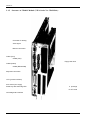
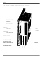
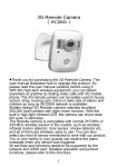
1
Manual
CP 486
Order No.: HB73e
Rev. 00/14
____________________________________________________________________________________________
Subject to changes for the purposes of technical progress.
The statements of this manual are subject to changes and without guarantee. Changes
of contents can result at each time without preliminary announcement. Hardware and
software described in this manual is underlying the conditions of a general or specific
licence agreement (single user licence) and may only be used or copied in agreement
with the conditions of this licence agreement. Violation obligates to compensation.
© Copyright 2000 VIPA, Gesellschaft für Visualisierung und Prozeßautomatisierung
mbH,
Ohmstaße 4, D-91074 Herzogenaurach,
Tel.:
+49 (91 32) 744-0
Fax.:
+49 (91 32) 744-144
EMail:
[email protected]
http://www.vipa.de
Hotline:
+49 (91 32) 744-114
All rights reserved
------------------------------------------------------------------------------------------------VIPAâ
is a registered trademark of VIPA Gesellschaft für
Visualisierung und Prozeßautomatisierung mbH
â
MS-DOS
is a registered trademark of Microsoft Corp.
â
QUADTEL
is a registered trademark of Quadtel Corp.
CENTRONICSâ is a registered trademark of Centronics Inc.
SIMATICâ
is a registered trademark of Siemens AG.
â
STEP 5
is a registered trademark of Siemens AG.
VIPA GmbH
CP486 ⋅ 00/14
Contents
Contents
Page
7
7
8
8
9
10
1.
Introduction
1.1
General
1.2
Application Area
1.3
Structure and Operation
1.4
Block Diagram of CP486
1.5
Special Components
2.
Hardware
2.1
Structure of Modules
2.1.1
Structure of the Base Module
2.1.2
Structure of CP486S Module
2.1.3
Structure of CP486M Module
2.1.4
Structure of CP486ML Module
2.1.5
Structure of CP486L Module
2.1.6
Structure of CP486XL Module
2.1.7
Diagram of DIP Switches, Jumpers and Plug Connectors
2.2
Setting of DIP Switches
2.3
Configuration of 24V Power Supply
2.4
Installation of Chip Silicon Disk
2.5
Installation of Memory Card Silicon Disk
2.6
Installation of an Additional Silicon Disk Board
2.7
Numeric Processor Installation (FPU)
2.8
Interface Installation for VGA Flat Display
2.9
Setting of AT Additional Boards
2.10
Slots for CP486 in the PC
12
12
12
14
16
18
20
22
24
26
28
30
32
32
32
33
33
34
3.
Assignment of Sockets and Plugs
3.1
15-pin SubD-Socket for Connecting the Monitor
3.2
9-pin SubD-Plug with V24 Interface (COM1 and COM3)
3.3
9-pin SubD-Plug with 20mA Interface (COM2)
3.4
9-pin SubD-Plug with RS422/485 Interface (COM4)
3.4.1
Operation as RS422 Interface
3.4.2
Operation as RS485 Interface
3.5
5/8-pin DIN Socket for Keyboard
3.6
25-pin SubD-Socket with Centronics Interface (LPT1)
3.7
2-pin Plugin Socket for external 24V Supply
3.8
15-pin SubD-Socket with VIPA Diagnostic Interface
3.9
Two-Part Clip Connector with AT Bus
3.10
PLC Base Plug (48-pin Male Connectors)
3.10.1 Base Plug X1
3.10.2 Base Plug X2
37
37
38
39
40
40
40
42
43
44
44
45
47
47
47
CP486 ⋅ 00/14
VIPA GmbH
1
Contents
3.11
3.12
3.13
3.14
3.15
3.16
3.17
3.18
3.19
3.20
4.
2
Memory Card Plug (Panasonic Memory Card)
Slot for Interface Modules
30/34-pin Pin Header for Floppy Disk Drive (X13)
50-pin Socket (X12) with TFI Interface for Hard Disk
50-pin Socket (X11) with AT Bus Signals for Special Use
26-pin Pin Header (X27) with Centronics Interface (LPT 2)
20-pin Pin Header (X22) for Flat Display Connection
16/24-pin Pin Header (X21) for Front Display and Keyboard
2-pin Pin Header (X4) for Speaker Connection
Fuses for External Current Consumers
48
49
50
51
52
53
54
55
56
56
BIOS Description and System Programming
57
4.1
System Structure
57
4.2
BIOS-SETUP
58
4.2.1
VIPA-BIOS-SETUP
58
4.2.2
QUADTEL-BIOS Selection Menue
60
4.2.3
QUADTEL-BIOS-Setup
61
4.2.4
Extended BIOS-Features
62
4.2.5
AT ROM Diagnostics
63
4.3
System Register
64
4.3.1
CP Status Register
64
4.3.2
PLC Status Register
64
4.3.3
Control Register
65
4.3.4
Watchdog
66
4.3.5
Interrupt Management
67
4.3.6
CMOS-RAM Status Byte
69
4.3.7
ROM-SETUP
70
4.3.8
Bank Interface
71
4.3.8.1 Operating Modes of Bank Interface
71
4.3.8.2 Bank Interface Register
72
4.3.8.3 Configuration Example: Standard CP Bank Operation (8 Banks with 1KB)75
4.3.8.4 Configuration Example: Bank Operation (4 Banks with each 64Byte)
76
4.3.8.5 Configuration Example: Bank Operation via Highest Bank Address
77
4.3.8.6 Configuration Example: Linear Operation
78
4.4
Address Assignment, Interrupts and DMA Channels
79
4.4.1
Memory Address Assignment
79
4.4.2
I/O Address Assignment
80
4.4.3
Interrupt Assignment
81
4.4.4
Assignment of DMA Channels
82
VIPA GmbH
CP486 ⋅ 00/14
Contents
5.
6.
Utility Software for MS-DOS
5.1
MS-DOS Utilities for Silicon Disk Operation
5.1.1
Silicon Disk Driver
5.1.2
Formatting Program for SRAM-DISK
5.1.3
Silicon Disk Generator
5.1.4
Silicondisk-Loader
5.1.5
Examples for Applying the Silicon Disk
5.1.5.1 Example for Generating a SRAM-Disk
5.1.5.2 Example for Generating a FLASH-PROM-Silicon Disk
5.1.5.3 Example for Generating a Program Memory with EPROMs
5.1.5.4 Example for Generating a ROM-Silicon Disk with FLASH-PROMs
by Means of the MS-DOS-RAM-Disk
5.2
VGA Configuration Program
5.3
CPLINK Program for Computer Link
5.4
Program for Visualizing the PLC Process Image
5.5
EMS Driver
5.6
System Test Program
96
99
100
101
102
102
Linkage with PLC
6.1
General Description
6.2
Installation of Bank Software for Linking PLC and CP486
6.2.1
PLC Side: Handling Modules
6.2.2
CP486: MS-DOS Driver Program
6.2.3
Different Data Representation in Memory
6.3
PLC Jobs for CP486 (Functions for Bank 0 and 1)
6.3.1
Overview
6.3.2
Parameterization of PLC Handling Modules
6.3.2.1
Handling Module SEND (FB3, Relative Bank Number: 1)
6.3.2.2
Handling Module CONTROL (FB4, Rel. Bank Number: 0/1)
6.3.2.3
Handling Module FETCH (FB5, Relative Bank Number: 0)
6.3.2.4
Handling Module RECEIVE (FB6, Rel. Bank Number: 0)
6.3.2.5
Parameterization of File Accesses via Handles
6.3.2.6
File Names
6.3.3
Funtion Description
6.3.3.1
Disk Reset
6.3.3.2
Select Disk
6.3.3.3
Get Disk
6.3.3.4
Create Directory
6.3.3.5
Delete Directory
6.3.3.6
Set Current Directory
6.3.3.7
Get Current Directory
6.3.3.8
Create File/Rewrite Existing File
6.3.3.9
Create New File
103
103
104
104
106
108
109
109
113
113
115
117
119
122
123
124
124
124
125
126
126
127
128
129
130
CP486 ⋅ 00/14
VIPA GmbH
83
84
84
87
88
89
91
91
92
94
3
Contents
6.3.3.10
6.3.3.11
6.3.3.12
6.3.3.13
6.3.3.14
6.3.3.15
6.3.3.16
6.3.3.17
6.3.3.18
6.3.3.19
6.3.3.20
6.3.3.21
6.3.3.22
6.3.3.23
6.3.3.24
6.3.4
6.4
6.4.1
6.4.2
6.4.2.1
6.4.2.2
6.4.2.3
6.4.2.4
6.4.2.5
6.4.2.6
6.4.2.7
6.4.2.8
6.4.2.9
6.4.2.10
6.4.3
6.4.3.1
6.4.3.2
6.4.3.3
6.4.3.4
6.4.3.5
6.4.3.6
6.4.3.7
6.4.3.8
6.4.3.9
6.4.3.10
4
Open File
Commit File
Close File
Delete File
Rename File
Set File Pointer
Get File Pointer
Read File or Device
Write File or Device
Get Date
Get Time
Program Execute
Get MS-DOS Version
Get Detailed Error Information
General Interrupt
Demo Program: Get Time of CP486 from PLC
CP486 Jobs for PLC (Functions for Bank 2, 3 and 7)
Overview
Driver Functions via Software Interrupt
CP Status Call
Read a Single Element from the PC
Read a Block from the PC
Write a Variable to the PC
Write a Block to the PC
Read Job Status
Abort All Jobs of a Bank
Read Status of Process Image
Read Area of Process Image
Error Numbers of CP for Banks 2, 3 and 7
Interface for Turbo-Pascal (from Version 4.0)
Function CP Status Call
Read a Single Element from the PC
Read a Block from the PC
Write a Single Element to the PC
Write a Block into the PC
Read Job Status
Abort All Jobs of a Bank
Read Status of Process Image
Read Area of Process Image
Constants
VIPA GmbH
131
131
132
132
133
134
134
135
136
137
137
138
139
140
143
144
145
145
146
146
147
148
149
150
151
153
154
155
156
157
157
158
159
160
161
162
163
164
164
165
CP486 ⋅ 00/14
Contents
6.4.4
6.4.4.1
6.4.4.2
6.4.4.3
6.4.4.4
6.4.4.5
6.4.4.6
6.4.4.7
6.4.4.8
6.4.4.9
6.4.4.10
6.4.5
6.5
7.
Interface to Turbo-C (2.0 and C++ from 1.0), Microsoft-C 6.0
Function CP Status Call
Read a Single Element from the PC
Read a Block from the PC
Write a Single Element into the PC
Write a Block into the PC
Read Job Status
Abort All Jobs of a Bank
Read Status of Process Image
Read Area of Process Image
Constants
Storage of Process Images to Bank 7
Access on the CP386COM from WINDOWS
170
170
171
172
173
174
175
176
176
176
177
182
183
Technical Data
7.1
Base Module
184
184
7.2
7.3
186
186
CP486 ⋅ 00/14
Option Hard Disk
Option Floppy Disk Drive
VIPA GmbH
5
Contents
6
VIPA GmbH
CP486 ⋅ 00/14
Introduction
1.
1.1
Introduction
General
This manual describes the handling with CP486 modules CP4-BG61, -BG62, -BG63, -BG64,
and BG65 of VIPA GmbH started with revision level 1. The revision level 1 comprises the
SYSTEMBIOS versions V18 and the VGA-BIOS V13. The CP486 modules are applicable to all
automation systems (PLC-115U ...PLC-155U). The CPU486SLC has an internal cache of 1 KB. At
the whole, the CP486 with 25Mhz runs faster by an factor 2.5-3 than the CP386 with 16Mhz. The
CP486 module is compatible downwards to the CP386 module. The CP386 functions are further
available. Addresses and parameters of the particular periphery elements has not been changed. The
software for the link with the PLC runs without changes.
The manual is arranged as follows:
Introduction
The information in this introduction is intended for application fields of the CP486 module,
structure and functioning of CP486, and moreover, specific components of the CP486 are described
enhancing the conventional AT standard.
Hardware:
First, the different CP486 versions and each of their special features are described. The modules are
differing in the number of interfaces, main memory capacity and mass storage, number of AT-bus
slots and the mounting dimension. This overview is followed by the hardware configuration before
installing in the PLC.
Plugs and Sockets:
All CP486 interfaces are described in this chapter including interconnection proposals and wiring
instructions.
BIOS- and System Programming:
This section contains the description of the CP486 firmware, firmware presettings and the module
programming on system oriented level. The standard user should attach importance thereof at most
to the description of firmware presetting - the SYSTEM-SETUP.
MS-DOS Utilities:
This chapter is concerned with different drivers and programs especially created and compiled for
CP486.
CP 486 ⋅ 00/14
VIPA GmbH
7
Introduction
Linkage with PLC:
This chapter describes detailed how to proceed with the linkage between PLC and CP486, that is
from the PLC point of view as well as from CP486 point of view.
1.2
Application Area
CP486 application within an automation system can be extended to many areas. Feasible application
areas are visualisation, measured value processing, production data acquisition, network servicing
up to the process control system and management computer. Hereto are added the most different
scope of duties with trade-specific standard software. Only the following aspects are important for
using the CP486:
- direct hardware linkage to the back plane bus via a standard CP interface with eight banks
enables a very fast communication with the PLC.
- linkage between PLC and CP486 is assisted by a system software supporting MS-DOS
programmers without STEP5 experience as well as STEP5 programmers without MS-DOS
experience (STEP5 from Siemens).
- CP486 is an PC-AT486 compatible computer.
- The enormous MS-DOS software world is made accessible for the PLC. Software packages are
directly applicable.
1.3
Structure and Operation
- Dualport-RAM:
The AT is directly interfaced to the back plane bus via a Dual Port RAM. This Dual Port RAM is
available on the PLC as standard CP interface with 8 banks. Data can be interchanged via
handling modules which also transfer synchronous to cycles the complete image of inputs,
outputs, markers, timers and counters to the AT. For every cycle you can exchange 4x127
variables in different directions. Communication is realized by polling or interrupt controlled.
- Communication Software
For communication between AT and PLC there are handling modules available providing the
data interchange element-oriented. Thus, several data elements (bit, byte, word, doubleword,
block) can be transferred per cycle at the same time. There is a continuously updated software
reference list for the standard software whose driver is adapted and loadable to CP486.
8
VIPA GmbH
CP486 ⋅ 4/94
Introduction
1.4
Block Diagram of CP486
CP 486 ⋅ 00/14
VIPA GmbH
9
Introduction
1.5
Special Components
Interface Modules
The four serial interfaces are configurable by plugin modules. As a standard, the following
assignment is supplied: COM1 and COM3 as V24 interface, COM2 as 20mA interface and COM4
as RS422/485 interface.
Diagnostic Interface
All serial communications can be acquired by menas of the diagnostic terminal UPI-FOX via the
diagnostic interface. This interface makes available sending and receiving signals of the individual
interfaces as TTL signals.
Keyboard Extension
The module is equipped with special electronics enabling a keyboard cable extension up to 250m.
VGA Mode with Industrial RGB Monitors
The module includes in addition to the standard VGA signal an RGB signal for monitor connections
up to a distance of 250m.
Battery Backup
CP486 data are buffered by means of the battery in the PC (programmable controller). It has a
supplementary Lithium accumulator protecting the CP486 against overrun in removed mode
approx. 1/2 year.
Silicon Disk
Silicon disk is a storage medium without flexible components. It is suitable to application in rough
environment. Silicon disk is fixed installed and exchangeable only for servicing purposes. There are
following silicon disk versions:
- Chip Silicon Disk (IC3, IC4):
The module avails of two IC slots (IC3 and IC4) for the chip silicon disk. Different memory
modules (EPROMs, SRAMs or PEROMs) can be inserted into these slots. This chip silicon disk
has a capacity of 256KB or 1 MB respectively.
- Memory Card Silicon Disk
There is a plugin slot for the memory card silicon disk. The memory card is contrary to the
silicon disk an exchangeable medium based upon the cheque card memory. Memory cards have a
capacity of 128KB, 512KB and 1MB. OTP-ROM and SRAM memory cards are available.
10
VIPA GmbH
CP486 ⋅ 4/94
Introduction
- Silicon Disk Additional Board
The different additional boards are plugged into the slot for the PC bus and thus, have a capacity
of up to 7MB. These silicon disk boards are available with FLASH-, SRAM- and EPROM
assembly.
The different types EPROM, SRAM, FLASH-PROM and OTP-ROM of the silicon disks differ
as follows:
- OTPROM-Disk is a read-only memory medium in the builtin mode comparable to a disk with
write protection. The OTPROM disk has to be programmed with a specific programming device.
The OTPROM card can be programmed only once and cannot be deleted again.
- EPROM disk is a read-only memory medium in the builtin mode comparable to a disk with
write protection. EPROMs of this disk are generated with an additional program and
programmed, before inserting into the base, with an EPROM program available on the market.
EPROMs can be deleted by means of UV light.
- FLASH-PROM-Disk is a read-only and recordable memory medium in the builtin mode. The
FLASH-PROM-DISK can be deleted and recorded agian in the builtin mode. The FLASH
memory can only be completely deleted and recorded again (with 12V erase voltage). This
memory can be recorded anew approximately 10000 times.
- PEROM disk is a read-only and recordable memory medium in the builtin mode. PEROM
modules can be deleted and recorded again in the buitin mode. Note: the PEROM meory can
only be completely deleted and recorded again (with 5V erase voltage). Only up to 1000 write
cycles are permitted.
- SRAM disk is a read-only able and recordable memory medium in the buitin mode comparable
to a recordable disk. But the read and write access is much more faster to the SRAM disk than to
a normal disk. The data remain backed up. The chip silicon disk is backed up approx. 100 days
by means of the accu of the CP486. The SRAM memory cards avail of an integrated,
exchangeable battery for approx. 100 days. So they can also be used as transportable me-mories.
The silicon disk additional boards have an own battery for nearly the same buffer time.
CP 486 ⋅ 00/14
VIPA GmbH
11
Hardware
2.
2.1
2.1.1
12
Hardware
Structure of Modules
Structure of the Base Module
VIPA GmbH
CP486 ⋅ 00/14
Hardware
Structure of the Base Module
The module contains a PC-AT486 with:
-
CPU80486SLC and FPU80387SX base
main memory up to 4MB
keyboard interface connection
VGA graphics
slot for interfacing flat displays
up to 4 slots for serial interface modules (COM1, COM2,
COM3, COM4)
up to 2 parallel interfaces (LPT1, LPT2)
interface for floppy disk drive
interface for hard disk
base for silicon disk (2 memory chips)
slot for silicon disk (memory card)
removable 16bit AT bus
8K Dual Port RAM for PLC as CP interface
CP 486 ⋅ 00/14
VIPA GmbH
13
Hardware
2.1.2
Structure of CP486S Module (VIPAOrder-No. CP4-BG61):
Controller for analog
video signal
Monitor connection
COM1 (V24 interface)
COM2 (20mA interface)
Keyboard connection
LPT1 (printer interface)
24V socket (ext. supply)
Reset key with watchdog-LED
VIPA diagnostic interface
14
VIPA GmbH
CP486 ⋅ 00/14
Hardware
Structure of CP486S (VIPA Order-No. CP4-BG61):
-
CPU80486SLC and base for FPU80387SX
main memory 4MB (CP4-BG61)
keyboard interface connection
VGA graphics
2 serial interfaces COM1 (V24), COM2 (20mA) (see also chapter 1.5)
1 parallel interface (LPT1)
slot for hard disk
base for silicon disk (2 memory chips)
slot for silicon disk (memory card)
8K Dual Port RAM to PLC as CP interface
Operation and display elements on the front panel:
-
one 15-pin HD Cannon socket for monitor connection
two 9-pin Cannon sockets for COMl (V24), COM2 (20mA)
one DIN socket for standard AT keyboard and sym. line driver up to 250m
parallel interface LPT1, Centronics-compatible with 25-pin Cannon socket
plug clamp for external 24V DC power supply for an EL display or using the
keyboard extension
LED display (red) for displaying an accumulated error (can be deleted by
pressing a RESET key)
RESET key
one 15-pin HD Cannon socket for diagnostic interface
CP 486 ⋅ 00/14
VIPA GmbH
15
Hardware
2.1.3
Structure of CP486M Module (VIPA Order-No. CP4-BG62):
Controller for analog
video signal
Monitor connection
COM1 (V24)
COM3 (V24)
COM2 (20mA)
COM4 (RS422/485)
Keyboard connection
LPT1 (printer interface)
Floppy disk drive
24V socket (ext. supply)
Reset key with watchdog-LED
VIPA diagnostic interface
16
VIPA GmbH
CP486 ⋅ 00/14
Hardware
Structure of CP486M (VIPA Order-No. CP4-BG62):
-
CPU80486SLC and base for FPU80387SX
main memory 4MB (CP4-BG62)
keyboard interface connection
VGA graphics
slot for interface to flat displays
4 serial interfaces COM1 (V24), COM2 (20mA),
COM3 (V24), COM4(RS422/RS485) (see also chapter 1.5)
1 parallel interface (LPT1)
slot for hard disk
base for silicon disk (2 memory chips)
slot for silicon disk (memory card)
3,5" floppy disk drive (720KB/1,44MB)
8K Dual-Port-RAM to PLC as CP interface
Operation and display elements on the front panel:
-
one 15-pin HD Cannon socket for monitor connectionn
four 9-pin Cannon sockets for COM1 (V24), COM2 (20mA),
COM3 (V24) and COM4 (RS422/485)
one DIN socket for standard AT keyboard and sym. line driver up to 250m
parallel interface LPT1, Centronics-compatible with 25-pin Cannon socket
plug clamp for external 24V DC power supply for an EL display or using the
keyboard extension
LED display (red) for displaying an accumulated error (can be deleted by
pressing a RESET key)
RESET key
one 15-pin HD Cannon socket for diagnostic interface
one 3,5" floppy disk drive
CP 486 ⋅ 00/14
VIPA GmbH
17
Hardware
2.1.4
Structure of CP486ML Module (VIPA Order-No. CP4-BG63):
Controller for analog
video signal
Monitor connection
Floppy disk drive
COM1 (V24)
COM2 (20mA)
Keyboard connection
LPT1 (printer interface)
Opening for AT card
24V socket (ext. supply)
Reset key with watchdog-LED
VIPA diagnostic interface
18
VIPA GmbH
CP486 ⋅ 00/14
Hardware
Structure of CP486ML (VIPA Order-No. CP4-BG63):
-
CPU80486SLC and base for FPU80387SX
main memory 4MB (CP4-BG63)
keyboard interface connection
VGA graphics
slot for interface to flat displays
2 serial interfaces COM1 (V24), COM2 (20mA) (see also chapter 1.5)
3,5" floppy disk drive (720KB/1,44MB)
1 parallel interface (LPT1)
slot for hard disk
base for silicon disk (2 memory chips)
slot for silicon disk (memory card)
removable 16bit AT bus with 1 slot
8K Dual-Port-RAM to PLC as CP interface
Operation and display elements on the front panel:
-
one 15-pin HD Cannon socket for monitor connectionn
two 9-pin Cannon sockets for COM1 (V24), COM2 (20mA),
one DIN socket for standard AT keyboard and sym. line driver up to 250m
parallel interface LPT1, Centronics-compatible with 25-pin Cannon socket
plug clamp for external 24V DC power supply for an EL display or using the
keyboard extension
LED display (red) for displaying an accumulated error (can be deleted by
pressing a RESET key)
RESET key
one 15-pin HD Cannon socket for diagnostic interface
one 3,5" floppy disk drive
an opening for AT cards
CP 486 ⋅ 00/14
VIPA GmbH
19
Hardware
2.1.5 Structure of CP486L Module (VIPA Order No. CP4-BG64):
Controller for analog
video signal
Monitor connection
COM1 (V24)
COM3 (V24)
Floppy disk drive
COM2 (20mA)
COM4 (RS422/485)
Keyboard connection
LPT1 (printer interface)
24V socket (ext. suppy)
Reset key with watchdog-LED
2 openings
for AT cards
VIPA diagnostic interface
20
VIPA GmbH
CP486 ⋅ 00/14
Hardware
Structure of CP486L (VIPA Order No. CP4-BG64):
-
CPU80486SLC and base for FPU80387SX
main memory 4MB (CP4-BG64)
keyboard interface connection
VGA graphics
slot for interface to flat displays
4 serial interfaces COM1 (V24), COM2 (20mA),
COM3 (V24), COM4(RS422/RS485) (see also chapter 1.5)
1 parallel interface (LPT1)
3,5" floppy disk drive (720KB/1,44MB)
slot for hard disk
base for silicon disk (2 memory chips)
slot for silicon disk (memory card)
removable 16bit AT bus with 2 slots
8K Dual-Port-RAM to PLC as CP interface
Operation and display elements on the front panel:
-
one 15-pin HD Cannon socket for monitor connectionn
four 9-pin Cannon sockets for COM1 (V24), COM2 (20mA),
COM3 (V24) and COM4 (RS422/485)
one DIN socket for standard AT keyboard and sym. line driver up to 250m
parallel interface LPT1, Centronics-compatible with 25-pin Cannon socket
plug clamp for external 24V DC power supply for an EL display or using the
keyboard extension
LED display (red) for displaying an accumulated error (can be deleted by
pressing a RESET key)
RESET key
a 15-pin HD Cannon socket for diagnostic interface
a 3,5" floppy disk drive
two openings for AT cards
CP 486 ⋅ 00/14
VIPA GmbH
21
Hardware
2.1.6 Structure of CP486XL Module (VIPA Order No. CP4-BG65):
Controller for analog
video signal
Monitor connection
COM1 (V24)
COM3 (V24)
Floppy
disk drive
COM2 (20mA)
COM4 (RS422/485)
Keyboard connection
LPT1 (printer interface)
24V socket (ext. suppy)
Reset key with watchdog-LED
3 openings
for AT cards
VIPA diagnostic interface
22
VIPA GmbH
CP486 ⋅ 00/14
Hardware
Structure of CP486XL (VIPA Order No. CP4-BG65):
-
CPU80486SLC and base for FPU80387SX
main memory 4MB (CP4-BG65)
keyboard interface connection
VGA graphics
slot for interface to flat displays
4 serial interfaces COM1 (V24), COM2 (20mA),
COM3 (V24), COM4(RS422/RS485) (see also chapter 1.5)
1 parallel interface (LPT1)
3,5" floppy disk drive (720KB/1,44MB)
slot for hard disk
base for silicon disk (2 memory chips)
slot for silicon disk (memory card)
removable 16bit AT bus with 3 slots
8K Dual-Port-RAM to PLC as CP interface
Operation and display elements on the front panel:
-
one 15-pin HD Cannon socket for monitor connectionn
four 9-pin Cannon sockets for COM1 (V24), COM2 (20mA),
COM3 (V24) and COM4 (RS422/485)
one DIN socket for standard AT keyboard and sym. line driver up to 250m
parallel interface LPT1, Centronics-compatible with 25-pin Cannon socket
plug clamp for external 24V DC power supply for an EL display or using the
keyboard extension
LED display (red) for displaying an accumulated error (can be deleted by
pressing a RESET key)
RESET key
a 15-pin HD Cannon socket for diagnostic interface
a 3,5" floppy disk drive
three openings for AT cards
CP 486 ⋅ 00/14
VIPA GmbH
23
Hardware
2.1.7
Diagram of DIP Switches, Jumpers and Plug Connectors
PCB 5012V14:
24
VIPA GmbH
CP486 ⋅ 00/14
Hardware
PCBs 5012V15, 5012V16 and 5012V17
CP 486 ⋅ 00/14
VIPA GmbH
25
Hardware
2.2
Setting of DIP Switches
Setting of DIP Switch S1:
1
PC type selection
2
3
vacant
PLC-signal BASP
4
PLC-signal CPKL
5
6
7
8
PLC-interrupt IRD
PLC-interrupt IRC
PLC-interrupt IRB
PLC-interrupt IRA
Delivery status:
OFF
ON
PLC-115
(NAU/BAU-Signal of X1)
PLC-135/PLC-155
(NAU/BAU-Signal of X2)
will not be
evaluated
triggers an interrupt
on the CP486vacant
will not be
evaluated
off
off
off
off
triggers a RESET
on the CP486
on
on
on
on
1-2:ON, 3:ON, 8:OFF, 5-8:OFF
Remarks:
The DIP-switch S1/4 must be set to ON, if the module is used in the ZG188.
The DIP-switch S1/3 is not used on the boards (PCB-No.) 5012V14, 5012V15, 5012V16, 5012V17.
The described functions of this switch are available on the boards (PCB-No.) 5012V13, 5012V31....
26
VIPA GmbH
CP486 ⋅ 00/14
Hardware
Setting of DIP Switch S2:
DIP switches 1-3 determine the system configuration if the system SETUP has been lost. The
system configuration is backed up by a Lithium accumulator approx. 6 months. If the module is
stored more than 6 months, then the battery is empty and the filed configuration lost. In this case, a
configuration can be set by means of switches 1-3 to ensure a module startup. The exact
configuration can be loaded by software after the startup.
An empty battery is recharged after approx. 3 days operating time.
4
3
2
1
DIP-switch (default setting in the case of default system configuration)
(battery failure):
off
off
on
on
off
on
off
on
off
on
boot from silicon disk at address C00000 (hex)
reserved
boot from silicon disk at address 800000 (hex)
boot from floppy disk drive A:
no bank visible towards PLC
active bank area: bank 32-39
off
on
reserved
reserved
8
7
6
5
DIP-switch (PCB no. 5012V15, 5012V16, 5012V17):
off
off
off
off
off
off
off
off
on
on
on
off
off
off
off
on
on
on
on
on
on
on
off
off
on
on
off
off
on
on
off
on
on
off
on
off
on
off
on
off
on
on
off
on
VGA monitor with separate Syncs
RGB monitor (up to VGA-BIOS V11 only graph mode)
RGB monitor (up to VGA-BIOS V11 only HSync positive)
RGB monitor (up to VGA-BIOS V11 only HSync negative)
Finlux-EL display (640*350)
Hercules, EGA monochrome
EGA monitor (640*350)
CGA monitor (80*25)
CGA monitor (40*25)
EGA monitor (640*200)
flat display via additional adapter
6
5
off
on
DIP-switch (PCB no. 5012V30, 5012V31, ...)
VGA monitor with separate Syncs
RGB monitor
color (default setup witchout monitor)
monochrome (default setup witchout monitor)
off
on
Delivery status:
CP 486 ⋅ 00/14
1-3:ON, 4-8:OFF
VIPA GmbH
27
Hardware
2.3
Configuration of 24V Power Supply
CP486 must be supplied with 24 Volt DC in following cases:
- for running an active 20mA interface
- for using the optional keyboard extension
- when connecting a flat display
24 Volt power supply is set up via the jumper field X3:
Jumper X3:
1
O
O
O
O
Supply via 24 Volt socket at the front
O
O
O
O
and delivered connecting cable
P24
Jumper X3:
1
O
O
O
O
P24
Jumper X3:
1
M24
O
O
O
O
M24
O
O
O
O
O
O
O
O
P24
Suppy from upper back plane bus plug
Supply from lower back plane bus plug
M24
Attention:
Pay attention to limit data of the supply unit used!
When using the keyboard extension or flat display, a potential interface for 24 Volt and 5 Volt
voltage source must be enabled in the case of external 24 Volt supply (supply via 24 Volt socket at
module front), e.g. by connecting the 5 Volt mass with 24 Volt mass at the central mass point.
28
VIPA GmbH
CP486 ⋅ 00/14
Hardware
Overview of the Circuit Diagram of the 5V and 24V Power Supply:
+24V
VGA
socket
+5V
+5V
M5
M5
PLC
S5
F2
upper
bus
plug
+24V
keyboard
socket
+24V
M24
+5V
M5
X3
F1
M24
1
+24V
diagnostic
socket
M24
+5V
M5
+ 24V
M24
PLC
S5
lower
bus
socket
+ 5V
ext.
24V
supply
CP 486 ⋅ 00/14
M5
VIPA GmbH
29
Hardware
2.4
Installation of Chip Silicon Disk
The module contains 2 bases (IC3 and IC4) for special memory chips. The bases for the silicon disk
must be respectively assembled and the jumpers set up.
Jumper setup differs for the various base PCB (printed circuit board) versions.
Battery Backup of the Chip Silicon Disk SRAM:
The silicon disk SRAM can be operated battery backed-up. The battery back-up is adjusted via a
solder board (below DIP switch S1) for the modules 7458V24/7459V24 (PCB 5012V14):
PCB 5012V14
Setting:
1-2 closed
2-3 open
Silicon disk is battery-backed
(permitted only for silicon disk SRAM)
1-2 open
2-3 closed
Silicon disk is not battery-backed (standard setting)
For the modules 7458V25/7459V25 (PCB 5012V15) , 7458V26/7459V26 (PCB 5012V16) and the
modules 7458V27/7459V27 (PCB 5012V17) the battery back-up is set up via jumper Y23 (in the
bases of the silicon disk chips IC3 and IC4):
RAM
SD
Y23
ROM
UBAT
O
O
O
O
O
O
RAM
BUS
VCC
Chip silicon disk is not battery backed-up
SD
Y23
ROM
UBAT
O
O
O
O
O
O
BUS
VCC
Chip silicon disk is battery backed-up
Started with the PCB 5012V17, the pin X16/B29 can be switched over from 5V power supply (in
VCC position) to battery supply (in position UBAT) additionally via the jumper "BUS". Standard
adjustment is in position VCC!. The position UBAT is required only to run special VIPA memory
modules (e.g. 7MB silicon disk module).
Attention: A wrong configuration can cause malfunctions and defects.
30
VIPA GmbH
CP486 ⋅ 00/14
Hardware
Base board 7458V24/7459V24 (PCB 5012V14), base board 7458V25/7459V25
(PCB 5012V15), base board 7458V26/7459V26 (PCB 5012V16),
base board 7458V27/7459V27 (PCB 5012V17):
Jumper fields X38 and X39 are placed onto sockets of silicon disk chips IC3/IC4.
EPROM 256KB:
X38
X39
RAM
O
O
O
O
O
O
O
O
O
O
O
O
O
O
O
O
O
O
1
4
7
10 13 16
256
1024
O
O
O
O
O
O
1
4
O
O
O
O
O
O
1
4
O
O
O
O
O
O
1
4
O
O
O
O
O
O
1
4
O
O
O
O
O
O
1
4
PEROM
EPROM / RAM
EPROM / PEROM
EPROM 1MB
X38
X39
RAM
O
O
O
O
O
O
O
O
O
O
O
O
O
O
O
O
O
O
1
4
7
10 13 16
256
1024
PEROM
EPROM / RAM
EPROM / PEROM
PEROM 256KB:
X38
X39
RAM
O
O
O
O
O
O
O
O
O
O
O
O
O
O
O
O
O
O
1
4
7
10 13 16
256
1024
PEROM
EPROM / RAM
EPROM / PEROM
SRAM 256KB:
X38
X39
RAM
O
O
O
O
O
O
O
O
O
O
O
O
O
O
O
O
O
O
1
4
7
10 13 16
256
1024
PEROM
EPROM / RAM
EPROM / PEROM
SRAM 1MB:
X38
X39
RAM
O
O
O
O
O
O
O
O
O
O
O
O
O
O
O
O
O
O
1
4
7
10 13 16
256
1024
PEROM
EPROM / RAM
EPROM / PEROM
CP 486 ⋅ 00/14
VIPA GmbH
31
Hardware
2.5
Installation of the Memory Card Silicon Disk
The memory card is installed by inserting the memory card into the provided plugin socket.The
memory card silicon disk is always set up to address 800000.
2.6
Installation of an Additional Silicon Disk Board
Various additional silicon disk boards are available or in progress. These are provided essentially
for the CP486S and CP486M. They are to be plugged into the PC/AT extension bus /X10, X16 - see
page 20, 21).
The different additional boards can be set up according to the enclosed documentation.
2.7
Numeric Processor Installation (FPU)
The numeric processor is installed by inserting the module into the respective base (IC19)
(Attention: consider module positioning when inserting). Installation should be realized by VIPA or
skilled personnel.
(Note the instructions how to handle with electrostatic sensitive components).
At the system startup the numeric processor is automatically identified. Detailed information you
get in the manual and from the disk (included in the scope of supply). The disk contains also the test
software for the numeric processor.
Factual use of the numeric processor must be configured possibly in the applications software (see
documentation for the applications software).
32
VIPA GmbH
CP486 ⋅ 00/14
Hardware
2.8.
Interface Installation for VGA Flat Displays
A module (optional) can be plugged into the pin header X22 having a 15-pin SUBD socket at the
module front. VGA flat display with 16 grey levels (EL display, 640*480 pixel) or a color TFT
display (640*480 pixel, max. 64 colors) can be connected to this 15-pin SUBD socket.
2.9
Setting of AT Additional Boards
The extension bus corresponds to the IBM PC/AT extension bus with following restrictions:
-
+12V,-12V and -5V can be loaded together with approx. 1 Watt
EGA/VGA controller, FDD controller, HDD/TFI controller, COM1-4 and
LPT1 are already integrated in the motherboard and can no more be plugged in.
For reasons of space only a short 8/16Bit AT card can be plugged in. The
cards are allowed to have a max. dimension of 108mm (incl. gold reed) * 158mm.
Before installing, remove the metal angle at the front of the AT card. After the card has been
inserted, mount again the angle from outside.
Attention: please set up the card configuration (i.e. address assignment, interrupt assignment and
DMA-assignment) before installing it, in such a way to avoid collision with the CP486. Dual
assignments can damage and destroy the CP486 as well as the additional card.
CP 486 ⋅ 00/14
VIPA GmbH
33
Hardware
2.10
Slots for CP486 in the PC
Following surveys show the possible installation places (signed by x) for the CP486 in the different
PLC card cages.
Slots in PLC-115U
Slots
Power supply module
X
X
Central module
X
X X X X
XXXXXX X
VIPA-CP486 (in CR 700-1)
VIPA-CP486 (in CR 700-2)
VIPA-CP486 (in CR 700-3)
X
X
X
X
CP486 has to be run in the adaptation case in PLC-115.
Slots in PLC-135U
Slots
Coordinator
R-, S-, M-processor
Communication processors
X
XXXX
XXXXXXXX
X
XXXX
Interfaces 300-5, 301-5
Interfaces 300-3, 301-3, 302
VIPA-CP486
34
XXXXXXX
VIPA GmbH
CP486 ⋅ 00/14
Hardware
Slots in PLC-150U
Slots
XXXX
Central module
X
Marshalling module 756
XXXXXX
Main memory 340, 350
XX
XXXX
Interfaces 300-5, 301-5
Interfaces 300-3, 301-3
XX
PG-interface connections
VIPA-CP486
XXX
XXXXXXX
Slots 3, 11 and 19 are of use for the CP486 only if the marshalling module 756
or the VIPA economy memory are inserted to slot 27.
Slots in PLC-155U
Slots
Coordinator
Central modules
Communication processors
X
XXX
XXXXXXXXXXXXX
XX
XXXX
Interfaces 300-5, 301-5
Interf. 300-3, 301-3, 301-5, 308-3
VIPA-CP486
XXXXXXXXXXXXX
CP 486 ⋅ 00/14
VIPA GmbH
35
Hardware
Slots in EG-185U
Slots
X
Interfaces 300
Interfaces 314, 318
VIPA-CP486
36
X
XXXXXXXXXXXXXXXX
VIPA GmbH
CP486 ⋅ 00/14
Assignment of Plugs and Sockets
3.
Assignment of Sockets and Plugs
The figures show plugs or sockets when regarding the module in the card cage. The top in the figure
is also the top on the plug.
3.1
15-pin SubD-Socket for Connecting the Monitor
15
5
10
14
4
9
13
3
8
12
2
7
11
1
6
Socket assignment is specified by the DIP switch SW2 (5,6,7,8), (section 2.2).
Mode
Cab.length
PIN-NO.
01
02
03
04
05
06
07
08
09
10
11
11
13
14
15
*:
**:
--------------------- analog modes ------------------------VGAcolor
VGAmono
RGB
BAS
5-10m
5-10m
250m
250m
------------- digital modes** ---------------EGA/CGA
EGA mono
EGA-EL
1.5m
1.5m
1.5m
red
red
red
clock
green
video
green+sync
int.+sync
green
intensity
el-hsync
blue
blue
blue
video
intensity
------ not used------------------------------------------------------------------------------------------------------------------------------------------- Gnd-------------------------------------------------------------------------------------------------------------------------------------------------- Gnd red--------------------------------------------------------------------------------------------------------------------------------------------- Gnd green------------------------------------------------------------------------------------------------------------------------------------------ Gnd blue------------------------------------------------------------------------------------------------------------------------------------------- +24V supply voltage protected for external consumers (via micro fuse F1 (2A)-------------------------------------- Gnd sync-------------------------------------------------------------------------------------------------------------------------------------------- not used-------------------------------------------------------------------------------------------------------------------------------------------- not used------------------------------------------------------------------------------------------------------------------------------------------- Hsync----------------------------------------------------------------------------------------------------------------------------------------------- Vsync----------------------------------------------------------------------------------------------------------------------------------------------- +5V supply voltage protected for external consumers (via micro fuse F2 (2A)*-----------------------------------
not connected on PCB 5012V17 and following
not available on PCB 5012V30 and following
Analog video voltage can be set between approx. 0.5V and 1.5V by means of the trimmer R1
(accessible from the front side of the module). Thus long cable dissipations can be compensated. As
a standard 0.7V are set. Attention: voltages over 0.7V can damage the connected monitor!
The 15-pin high-density DSUB socket is used to connect the monitor. The socket is assigned similar
to the socket of an original VGA monitor. All other monitors must be connected via special
connection cables.
CP 486 ⋅ 00/14
VIPA GmbH
37
Assignment of Plugs and Sockets
3.2
9-pin SubD-Plug with V24 Interface (COM1 and COM3)
DSR-
6
O
RTS-
7
O
CTS-
8
O
RI
9
O
O
1
DCD
O
2
RXD
O
3
TXD
O
4
DTR-
O
5
GND
The interface contains both types of handshake-signals (RTS/CTS and DSR/DTR). Which type of
signals is to be used depends on wiring and programming of the interface.
38
VIPA GmbH
CP486 ⋅ 00/14
Assignment of Plugs and Sockets
3.3
9-pin SubD-Plug with 20mA Interface (COM2)
This interface can be operated as an active and passive 20mA-interface. The active operation
requires a module supply of 24V. The 24V supply is configured by means of the jumper field X3
(cf. section 2.3)
TXD-
6
O
S1-
7
O
RXD-
8
O
S2-
9
O
O
1
O
2
TXD+
O
3
S1+
O
4
RXD+
O
5
S2+
Passive 20mA-interface:
Passive interface operation uses 4 interface signals.
Active 20mA-interface:
The active operation avails of power sources at S-signals that are to be connected respectively to the
data lines. In this case the module must be supplied with 24V.
CP 486 ⋅ 00/14
VIPA GmbH
39
Assignment of Plugs and Sockets
3.4
9-pin SubD-Plug with RS422/485 Interface (COM4)
This interface can be operated as RS422-interface, i.e. for point-to-point circuit with separate sendreceive lines, as well as RS485-interface for a bus system with send-receive function at the same
line. For this purpose, the operating mode is switched over via a bus master by appropriate attending
the SEL-signal.
TxD lines and RxD lines require for all cases each in pairs twisted and in pairs shielded lines.
3.4.1
Operation as RS422 Interface:
TxDRxD-
6
7
8
9
O
1
-
O
2
TxD+
O
3
-
O
4
RxD+
O
5
-
O
O
O
O
Pins signed with "-" are not used for the RS422 operation. They are not allowed to be connected!
40
VIPA GmbH
CP486 ⋅ 00/14
Assignment of Plugs and Sockets
3.4.2
Operation as RS485 Interface:
DTR
RxD-/TxDRTS
6
7
8
9
O
1
-
O
2
-
O
3
SEL
O
4
RxD+/TxD+
O
5
-
O
O
O
O
For RS485 operation only a two-wire line is terminated. The SEL-signal is used to switch over
among send and receive. A logic 1 (5V) switches to transmission and a logic 0 (0V) to receive.
SEL-signal can be controlled via DTR, via RTS or externally. This is selected via a jumper in the
plug. Pins signed with "-" are not used for the RS485 operation. They are not allowed to be
connected!
CP 486 ⋅ 00/14
VIPA GmbH
41
Assignment of Plugs and Sockets
3.5
5/8-pin DIN Socket for Keyboard
8
7
3
5
O
O
O
O
O
O
O
6
1
4
O
2
Pinno. Signal
1
2
3
4
5
KBCLK
KBDATA
GND (24V)
GND (5V)
+5V
6
7
8
-KBDATA
-KBCLK
+24V
(for option keyboard extension)
current voltage for keyboard
(protected by micro fuse F2 (2A))
(for option keyboard extension)
(for option keyboard extension)
(current voltage for option keyboard extension,
protected by micro fuse F1 (2A))
The module has to be supplied with 24V for the operation of the optional keyboard extension.
24Volt power supply is configured via the jumper field X3. (cf. section 2.3)
Note:
AT-keyboards with automatical switchover between XT and AT mode are not supported by the
CP486. Such keyboards are not identified and output a keyboard error. If possible, such keyboards
should be set up to forced AT mode.
42
VIPA GmbH
CP486 ⋅ 00/14
Assignment of Plugs and Sockets
3.6
25-pin SubD-Socket with Centronics Interface (LPT1)
/AFD
14
O
/ERR
15
O
/INIT
16
O
/SLCTIN
17
O
GND
18
O
GND
19
O
GND
20
O
GND
21
O
GND
22
O
GND
23
O
GND
24
O
GND
CP 486 ⋅ 00/14
25
O
13
SLCT
O
12
PE
O
11
BUSY
O
10
/ACK
O
9
PD7
O
8
PD6
O
7
PD5
O
6
PD4
O
5
PD3
O
4
PD2
O
3
PD1
O
2
PD0
O
1
STB-
O
VIPA GmbH
43
Assignment of Plugs and Sockets
3.7
2-pin Plugin Socket for External 24V Supply
CP486 delivery includes a 1m long connecting cable with plug. M24 (mass of 24V) and P24 (+24V)
is are supplied via the two pins. Both pins are optionally assigned. Polarity is of no importance.
Attention:
Concerning the 24V supply via this socket it must be ensured that the 24V supply of back plane bus
is deactivated via the jumper field X3 (cf. section 2.3)!
3.8
15-pin SubD-Socket with VIPA Diagnostic Interface
15 TxD COM1
5 GND
10 RxD COM1
14 TxD COM2
4 +5V
9 RxD COM2
3 -
13 TxD COM3
8 RxD COM3
12 TxD COM4
2 7 RxD COM4
11 +24V
1 screen
6 M24
VIPA diagnostic interface disposes of send and receive data lines (RxD and TxD) of the four
present COM interfaces for listening as TTL-signals. Evaluation can be carried out by means of
UPI-FOX of VIPA.
Supply voltages 5V and 24V are made available for external consumers.
5V supply is protected by the micro fuse F2 (2A).
24V supply is protected by the micro fuse F1 (2A).
44
VIPA GmbH
CP486 ⋅ 00/14
Assignment of Plugs and Sockets
3.9
Two-Part Clip Connector with AT Bus
CP 486 ⋅ 00/14
B
A
GND
SA0
31
OSC
SA1
30
+5V
SA2
29
BALE
SA3
28
T/C
SA4
27
DACK2-
SA5
26
IRQ3
SA6
25
IRQ4
SA7
24
IRQ5
SA8
23
IRQ6
SA9
22
IRQ7
SA10
21
CLK
SA11
20
RFSH
SA12
19
DRQ1
SA13
18
DACK1
SA14
17
DRQ3
SA15
16
DACK3
SA16
15
IOR-
SA17
14
IOW-
SA18
13
SMEMR-
SA19
12
SMEMW-
AEN
11
GND
IOCHRDY
10
+12V-
SD0
9
0WS
SD1
8
-12V
SD2
7
DRQ2
SD3
6
-5V
SD4
5
IRQ9
SD5
4
+5V
SD6
3
RESET
SD7
2
GND
IOCHK
1
VIPA GmbH
45
Assignment of Plugs and Sockets
46
D
C
GND
SD15
18
MASTER-
SD14
17
+5V
SD13
16
DRQ7
SD12
15
DACK7-
SD11
14
DRQ6
SD10
13
DACK6-
SD9
12
DRQ5
SD8
11
DACK5-
MEMW-
10
DRQ0
MEMR-
9
DACK0-
LA17
8
IRQ14
LA18
7
IRQ15
LA19
6
IRQ12
LA20
5
IRQ11
LA21
4
IRQ10
LA22
3
IOCS16-
LA23
2
MEMCS16-
SBHE
1
VIPA GmbH
CP486 ⋅ 00/14
Assignment of Plugs and Sockets
3.10
3.10.1
3.10.2
PLC Base Plug (48-pin Male Connectors)
Base Plug X1
d
b
z
nc
UBAT
ADB12
ADB13
ADB14
ADB15
IRA
IRB
IRC
IRD
/BAU115
/NAU115
nc
DSI
+24V
nc
M
PESP
ADB00
ADB01
ADB02
ADB03
ADB04
ADB05
ADB06
ADB07
ADB08
ADB09
ADB10
ADB11
BASP
M
+5V
nc
/CPKL
/MEMR
/MEMW
/RDY
DBO
DB1
DB2
DB3
DB4
DB5
DB6
DB7
M24V
nc
d
b
z
nc
nc
nc
nc
nc
nc
nc
nc
nc
nc
/TxDSN
nc
nc
nc
nc
nc
M
nc
nc
nc
nc
nc
nc
nc
nc
nc
nc
nc
/RxDSN
nc
nc
M
+5V
nc
nc
nc
nc
nc
/NAU
/BAU
nc
nc
nc
nc
nc
nc
M24V
+24V
2
4
6
8
10
12
14
16
18
20
22
24
26
28
30
32
Base Plug X2
CP 486 ⋅ 00/14
VIPA GmbH
2
4
6
8
10
12
14
16
18
20
22
24
26
28
30
32
47
Assignment of Plugs and Sockets
3.11
48
Memory Card Plug (Panasonic Memory Card)
1
+5V
A14
2
3
A12
WE-
4
5
A7
A13
6
7
A18
A19
8
9
A6
A8
10
11
A5
A9
12
13
A4
A11
14
15
A3
OE-
16
17
A2
A10
18
19
A1
CE-
20
21
A17
A15
22
23
A16
A0
24
25
D7
D0
26
27
D6
D1
28
29
D5
D2
30
31
D4
D3
32
33
-
GND
34
VIPA GmbH
CP486 ⋅ 00/14
Assignment of Plugs and Sockets
3.12
Slot for Interface Modules
DCD
SubD1
SubD6
SubD2
SubD7
SubD3
SubD8
SubD4
SubD9
SubD5
RI
CP 486 ⋅ 00/14
1
3
5
7
9
11
13
15
17
19
21
O
O
2
+5V
O
4
+24V
O
6
DSR
O
8
DTR
O
10
RxD
O
12
CTS-
O
14
RTS-
O
16
TxD
O
18
M24
O
20
GND
O
O
O
O
O
O
O
O
O
O
VIPA GmbH
49
Assignment of Plugs and Sockets
3.13
30/34-pin Pin Header for Floppy Disk Drive (X13)
34
+12V (input)
-12V (input)
33
30
Side Select 0
Signal GND
29
28
Read Data
Signal GND
27
26
Write Protect
Signal GND
25
24
Track 00
Signal GND
23
22
Write Gate
Signal GND
21
20
Write Data
Signal GND
19
18
Step
Signal GND
17
16
Direction
-
15
14
Motor On 0
-
13
12
Ready
VCC 5V
11
10
Disk Change
VCC 5V
9
8
Drive Select 0
VCC 5V
7
6
Index
VCC 5V
5
4
GND
GND
3
2
Drive Select 1
Motor On 1
1
The pins 33 and 34 are existing started with PCB 5012V16 and are used to supply +/-12Volt for the
AT-bus.
50
VIPA GmbH
CP486 ⋅ 00/14
Assignment of Plugs and Sockets
3.14
50-pin Socket (X12) with TFI Interface for Hard Disk
CP 486 ⋅ 00/14
2
-
-
1
4
-
-
3
6
-
-
5
8
GND
RESET-
7
10
D8
ID7
9
12
D9
D6
11
14
D10
D5
13
16
D11
D4
15
18
D12
D3
17
20
D13
D2
19
22
D14
D1
21
24
D15
D0
23
26
-
GND
25
28
GND
-
27
30
GND
IOW-
29
32
GND
IOR-
31
34
ALE
-
33
36
GND
-
35
38
IOCS16-
INT
37
40
-
A1
39
42
A2
A0
41
44
CS1-
CS0-
43
46
GND
LED-
45
48
+5V
+5V
47
50
-
-
49
VIPA GmbH
51
Assignment of Plugs and Sockets
3.15
50-pin Socket (X11) with AT Bus Signals for Special Use
2
IOCHRDY-
SA3
1
4
AEN
SA4
3
6
MEMR-
SA5
5
8
MEMW-
SA6
7
10
SBHE-
SA7
9
12
MASTER-
SA8
11
14
IOCS16-
SA9
13
16
MEMCS16-
SA10
15
18
BALE
SA11
17
20
T/C
SA12
19
22
-5V
SA13
21
24
REFRESH-
SA14
23
26
SMEMR-
SA15
25
28
SMEMW-
SA16
27
30
CSMCARD-
SA17
29
32
IDENH-
SA18
31
34
IDENL-
SA19
33
36
IRQ9
+12V
35
38
SYSCLK
LA17
37
40
IRQ11
LA18
39
42
IRQ10
LA19
41
44
DACK6-
LA20
43
46
DRQ6-
LA21-
45
48
-12V
LA22
47
50
OSC
LA23
49
Both plugin connectors X11 and X12 have a full 16Bit AT bus excepted some interrupt and DMA
channels. Special adapters (of the H1 adapter) can be connected via this bus. In this case, the hard
disk drive has to be removed from the motherboard and is to be installed onto the additional board.
52
VIPA GmbH
CP486 ⋅ 00/14
Assignment of Plugs and Sockets
3.16
26-pin Pin Header (X27) with Centronics Interface (LPT 2)
26
-
SLCT
25
24
GND
PE
23
22
GND
BUSY
21
20
GND
ACK-
19
18
GND
PD
17
16
GND
PD6
15
14
GND
PD5
13
12
GND
PD4
11
10
GND
PD3
9
8
SLCTIN-
PD2
7
6
INIT-
PD1
5
4
ERR-
PD0
3
2
AFD-
STB-
1
This interface can be made available at the module front via an optional connection cable with cover
sheet. Then there is the LPT2:-Centronics interface on the 25-pin SubD socket having the following
assignment:
CP 486 ⋅ 00/14
/AFD
14
O
/ERR
15
O
/INIT
16
O
/SLCTIN
17
O
GND
18
O
GND
19
O
GND
20
O
GND
21
O
GND
22
O
GND
23
O
GND
24
O
GND
25
O
O
13
SLCT
O
12
PE
O
11
BUSY
O
10
/ACK
O
9
PD7
O
8
PD6
O
7
PD5
O
6
PD4
O
5
PD3
O
4
PD2
O
3
PD1
O
2
PD0
O
1
STB-
VIPA GmbH
53
Assignment of Plugs and Sockets
3.17
20-pin Pin Header (X22) for Flat Display Connection
up to PCB 5012V15:
from PCB 5012V16 on:
1
ACDCLK
GND
2
3
V7
V0
4
5
CLKX
V1
6
7
SCLK
V2
8
9
WGTCLK
GND
10
11
V6
V3
12
13
+5V VCC
V4
14
15
BLANK-
V5
16
17
HSYNC
GND
18
19
VSYNC
+24V
20
1
ROT
BLANK
2
3
+24V VCC
VS
4
5
+5V VCC
HS
6
7
GND
PCLK
8
9
V7
V3
10
11
V6
V2
12
13
V5
V1
14
15
V4
V0
16
17
-
-
18
19
-
CLK-EXT
20
Supply voltages 5V and 24V are made available for external consumers.
5V supply is protected by the micro fuse F2 (2A).
24V supply is protected by the micro fuse F1 (2A).
54
VIPA GmbH
CP486 ⋅ 00/14
Assignment of Plugs and Sockets
3.18
16/24-pin Pin Header (X21) for Front Display and Keyboard
up to PCB 5012V15:
from PCB 5012V16 on:
16
COM4 RxD
COM4 TxD
15
14
COM3 RxD
COM3 TxD
13
12
COM2 RxD
COM2 TxD
11
10
COM1 RxD
COM1 TxD
9
8
HDD-LED
Out D4
7
6
Turbo-LED
Out D5
5
4
GND
Out D6
3
2
+5V VCC
Out D7
1
24
-KBCLK
COM4 RxD
COM4 TxD
22
21
GND (24V)
COM3 RxD
COM3 TxD
19
18
+5V
COM2 RxD
COM2 TxD
16
15
KBDATA
COM1 RxD
COM1 TxD
13
12
+24V
HDD-LED
Out D4
10
9
GND
UBAT
Out D5
7
6
KBCLK
GND
Out D6
4
3
-KBDATA
+5V VCC
Out D7
1
UBAT (PIN 8) is available started with PCB 5012V17.
CP 486 ⋅ 00/14
VIPA GmbH
55
Assignment of Plugs and Sockets
3.19
2-pin Pin Header (X4) for Speaker Connection
Pinno. Signal
1
5V VCC
2
VF (voice-frequency) signal
3.20
Fuses for External Current Consumers
F1
F2
Fuse for 24V outputs (2A)
Fuse for 5V outputs (2A)
These plugin fuses protect the 5V- and 24V connections for external consumers against
overloading.
56
VIPA GmbH
CP486 ⋅ 00/14
BIOS and System Programming
4.
4.1
BIOS Description and System Programming
System Structure
CP486 has a firmware with basic functions for the present hardware - so called BIOS. The BIOS of
the CP486 consists of several utilities:
QUADTEL-BIOS: This part has usual functions for servicing of standard components of an ATcompatible computer.
VIPA-BIOS:
VIPA has supplemented some additional functions as initialization and
servicing of the linkage hardware to the PLC, additional drivers for silicon disk
and memory card including the boot functions and functions for a secure
startup also after loss of system configuration.
C&T-VGA-BIOS: This BIOS incorporates functions for operating the connected monitor.
Some BIOS utilities can be parameterized. For this purpose, the firmware contains a SETUP
function. System Setup is set by VIPA appropriate to system configuration and remains stored in the
module battery backed approx. 1500 hours in the OFF-mode. In the case of battery discharge a
default setup is used to ensure the module start. Certain setups of the system configuration can be
realized by the user via the SETUP.
CP 486 ⋅ 00/14
VIPA GmbH
57
BIOS and System Programming
4.2
BIOS-SETUP
At the system startup the active terminal displays the BIOS version. First BIOS runs a test with
different system components and then a memory test. After test completion the system tries to boot
from the disk drive A, if existent, and then from disk drive C, if existent.
The SETUP can be invoked only during the system startup by pressing the <F2> key. This input
ensues as soon as the respective message is displayed on the screen. This is the case started with
BIOS version V18. Up to the BIOS version V17, the SETUP is invoked by concurrently pressing
"CTRL", "ALT" and "s" during system startup.
4.2.1
VIPA-BIOS-SETUP
First the VIPA-SETUP appears with the module series number (hexadecimal) and the fields
password input, bank parameterization and silicon disk selection. This window shows moreover a
system configuration (if battery is discharged) being lost. In the lower part of the screen are
displayed information about the key assignment for operating the SETUP:
(The text in brackets is the translation of the displayed!)
(VIPA-Setup for bank interface and silicon disk V0.3)
VIPA-Setup für Kachelinterface und Silikondisk V0.3
---------------------------------------------------------------------------------------------------(Serial number of the module:)
Seriennummer der Baugruppe:
0305
(Change password:)
Passwort ändern:
(Current bank number:)
Aktuelle Kachelnummer:
(Disk drive A:)
Laufwerk A:
32-39
FLOPPY-Disk
---------------------------------------------------------------------------------------------------éê Cursor bewegen
F5,F6 auswählen
F10 übernehmen
ESC Setup verlassen
Move Cursor)
(Select)
(Take over)
(Leave setup)
A password (8 ASCII-characters) can be entered in the password-field of the SETUP. No password
is specified, as long as the SETUP-field is displayed as a white block. In this case you select other
SETUP options. A password is entered by an input of an ASCII-sequence up to 8 characters in the
password field, which has to be finished by pressing the ENTER key. As soon as a password is
entered the password field will not be displayed as a white but a black field. In this case the user can
enter the SETUP in order to change the password or resp. the system setup only if the stored
password is specified. If the ENTER key is pressed instead of entering an ASCII character in the
password field, the password will be deleted.
58
VIPA GmbH
CP486 ⋅ 00/14
BIOS and System Programming
In the bank field the base address of the PLC bank can be set from 0 ... 248 in steps of 8. The
specified area is activated immediately at the start up of the CP486 and is available at the PLC side.
By means of the SETUP field "disk drive A" the user is able to specify further drive types (also a
silicon disk) as boot drive for drive A. In order to take an effect, a floppy disk drive for A has to be
selected in the second part of the SETUP.
Different silicon disks can be installed at the CP486, whereby the chip silicon disk and the memory
card silicon disk are available directly on the module (optional):
- The chip silicon disk (IC3,IC4) is set hardware-specific to the address C00000 hex. It can be
assembled with SRAMs, EPROMs or PEROMs.
- The memory card silicon disk (memory card plugin socket) is set hardware-specific to the
address 800000 hex. Memory cards are available as SRAM cards and OTP cards.
- Further silicon disks are available as additional plugin boards. The addresses of these silicon
disks can be specified on the additional boards.
One of these silicon disks can be used for booting the system. The user has to specify the address
and the storage type - RAM or ROM - of the requested boot drive:
- ROM on base address 80 0000 hex
- RAM on base address 80 0000 hex
- ROM on base address C0 0000 hex
- RAM on base address C0 0000 hex
memory card silicon disk or add. silicon disk board
memory card silicon disk or add. silicon disk board
chip silicon disk or add. silicon disk board
chip silicon disk or add. silicon disk board
If in addition a floppy disk drive is to be used, it must be redirected to the second floppy disk drive.
For this purpose, the jumper field A/B on the disk interface board must be set to B and the disk
drive B in the BIOS-Setup.
Examples:
VIPA-SETUP
Quadtel-SETUP
Boot from 1.44MB disk:
Disk
1.44MB
Boot from EPROM chip silicon disk
ROM on C00000
1.44MB
Boot from SRAM memory card silicon disk
RAM on 800000
1.44MB
However, precondition for boot from silicon disk is the existence of a bootable silicon disk. When
leaving this SETUP window with the <ESC> key, all settings will be stored (attention: the password
will immediately be taken over and stored, if the ENTER key is pressed).
CP 486 ⋅ 00/14
VIPA GmbH
59
BIOS and System Programming
4.2.2
QUADTEL-BIOS Selection Menue
After leaving the VIPA-BIOS-Setup you select a menue:
Modifications of the system setups in the different windows "Setup" and "Extended BIOS-Features"
should be carried out only by experienced appliers. Normally, it is not necessary to modify any
system setups. The menue item "System Information" informs about the applied QUADTEL-BIOS.
In the menue item "System Security" a second password can be entered as a boot protection. If a
password is specified at this item, the system does not boot before this password is entered. The
menue item "Park Fixed Disks" is not required for the hard disks used. With the menue item
"Diagnostics" particular system components can be tested. The menue item "Format Fixed Disk"
offers the formatting of the hard disk, which is not allowed in the moment with the hard disks
currently used.
60
VIPA GmbH
CP486 ⋅ 00/14
BIOS and System Programming
4.2.3
QUADTEL-BIOS-Setup
The BIOS Setup has the following setup possibilities (shown are the default setups):
In the BIOS-Setup the following system parameters can be set up:
- date
- time
- password for system startup
- type of floppy disk drive 1 (360KB, 720KB, 1.2MB, 1.44MB)
- type of floppy disk drive 2 (360KB, 720KB, 1.2MB, 1.44MB)
- type of the hard disk 1 (1 .. 47)
- type of the hard disk 2 (1 .. 47)
- type of the video interface
- size, type and system memory segmentation
- shadow-RAM for system-BIOS
- shadow-RAM for VGA-BIOS
The setup should be modified only by experienced users. Normally, it is not necessary to intervene
in the system setup.
The control keys for the SETUP are displayed in the lower part of the screen. By pressing the <F1>
key you get help information. The displayed configuration is stored with the <F10> key, you return
from the BIOS Setup to the menue with the <ESC> key.
CP 486 ⋅ 00/14
VIPA GmbH
61
BIOS and System Programming
4.2.4
Extended BIOS-Features
The Extended BIOS has the following additional features (shown are the default setups):
Further system parameter can be set up in the window Extended BIOS Features. The setup should
be modified only by experienced users. Normally, it is not necessary to intervene.
The control keys are displayed in the lower part of the screen. By pressing the <F1> key you get
help information. The displayed configuration is stored with the <F10> key, you return to the menue
with the <ESC> key.
62
VIPA GmbH
CP486 ⋅ 00/14
BIOS and System Programming
4.2.5
AT ROM Diagnostics
Almost all system components can be tested via the integrated AT ROM Diagnostics:
The individual system components can be tested in the menue item "Diagnostics". The control keys
are displayed in the lower part of the screen. By pressing the <F1> key you get help information.
You leave the diagnostics window and return to the menue with the <ESC> key.
CP 486 ⋅ 00/14
VIPA GmbH
63
BIOS and System Programming
4.3
4.3.1
Bit 0
Bit 1
Bit 2
System Register
CP-Status Register (I/O-Address 280 hex - read only)
/PLC bank interrupt
0
1
/WD reset
0
1
/PFO (accu supervision) 0
1
Bit 3
reserved
status
INT 12 was triggered via PLC-access to
element 1023 in the current bank
no access to bank element 1023 via PLC
error: watchdog has announced
no error
CP accu voltage under 2.5V (accu empty
or defective)
CP accu voltage over 2.5V (accu ok)
reserved
Bits 4 - 7 indicate settings of DIP switch S2 (boot defaults at accu failure) :
Bit 4
DIP switch S2 position 1 0
1
DIP switch S2 position 2 0
1
DIP switch S2 position 3 0
1
no boot from floppy disk drive
boot from floppy disk drive A
boot from silicon disk as disk drive A
boot from memory card as disk drive A
bank on PLC side not visible
8 banks on PLC side (32-39) visible
Bit 7
DIP switch S2 position 4
reserved
4.3.2
PLC-Status Register (I/O-Address 281 hex - read only)
Bit 0
CPKL
Bit 1
BASP
Bit 2
BAU
Bit 3
NAU
Bit 4
PC type (of DIP-SW)
Bit 5
Bit 6
Bit 7
reserved
reserved
reserved
Bit 5
Bit 6
64
0
1
0
1
0
1
0
1
0
1
PLC has started
PLC in RESET mode (approx. 1.6sec)
outputs are conducted
outputs are deactivated
PLC battery is ok
PLC battery has failed
power supply connected to PLC
power supply for PLC is off
PLC-135/PLC-155 set up
PLC-115 set up
VIPA GmbH
CP486 ⋅ 00/14
BIOS and System Programming
4.3.3
Control Register (I/O-Address 282 hex - write only)
The bit 0 and bit 1 control the system reset:
bit 1
bit 0
0
0
1
1
0
1
0
1
reset by
watchdog
on
off
off
on*
reset by
RES key
off
on
off
on*
* The mode bit1 = 1 and bit0 = 1 can be used with the CP486 modules with level 2 or higher
(PCB board 5012V30 or higher)
Status
Bit 2
Bit 3
interrupt to PLC
bank reset off
(from PCB 5012V17 on)
Bit 4
LED 1
Bit 5
LED 2
Bit 6
LED 3
Bit 7
LED 4
CP 486 ⋅ 00/14
0
1
0
connected to interrupt line on back plane bus
bank reset at system reset
bank reset off (bank can be responded
by the PLC)
LED off
LED on
LED off
1
0
1
0
1
LED on
LED off
LED on
LED off
LED on
0
1
VIPA GmbH
65
BIOS and System Programming
4.3.4
Watchdog (I/O-Address Area 270-277)
The watchdog is deactivated after system startup and after reset, and can be set on and off by means
of software.
The watchdog must be triggered every 1.6 seconds after enabling. This triggering is realized by
programming a flank. If it is not re-triggered within these 1.6 seconds, the watchdog calls a system
reset (depending on CONTROL register bit 0). The watchdog mode can be inquired by software at
any time in the CP-STATUS register.
The watchdog register is responded by I/O address 270H with following values:
watchdog on :
load 40H to address 270H
watchdog off :
load 50H to address 270H
trigger watchdog:
load 60H to address 270H and finally
load 70H to address 270H
66
VIPA GmbH
CP486 ⋅ 00/14
BIOS and System Programming
4.3.5
Interrupt-Management
Interrupt Initiation in the CP
The hardware interrupt IRQ12 (software interrupt 74) on the CP486 can be initiated by
PLC access to element 1023 of respectively active bank
BASP activation on back plane bus
The appertaining interrupt vector is filed to address 1D0 - 1D3 (hex). The initiated interrupt must be
reset by accessing the interrupt reset register (address: C000:9F8E) in the interrupt service routine.
Example: Pascal Program for Evaluation of Interrupt 12
PROGRAM INT_74_TEST;
USES CRT, DOS;
CONST EOI
PIC_1
PIC_2
: BYTE
: BYTE
: BYTE
= $20;
= $20;
= $A0;
TYPE
BITARRAY
= ARRAY[0..7] OF BYTE;
VAR
OLD_VEC
I
STATUS,S5_STATUS,CP_STATUS
S5_STATUSBIT,CP_STATUSBIT
INT_AKTIVBIT
{$F+}
PROCEDURE INT_74; INTERRUPT;
{$F-}
BEGIN
i:=i+1;
INT_AKTIVBIT:=TRUE;
{ End of Interrupt acknowledgement }
{ Address of first Int-Controller }
{ Address of second Int-Controller }
:
:
:
:
:
POINTER;
INTEGER;
BYTE;
BITARRAY;
BOOLEAN;
{ ***** INTERRUPT - Routine ************}
{ Increase interrupt counter
{ Set flag for the processing
{ in the main program
S5_STATUS:=PORT[$281];
CP_STATUS:=PORT[$280];
{ Buffer S5- and CP-register }
PORT[PIC_1]:=EOI;
PORT[PIC_2]:=EOI;
END;
{ Interrupt acknowledgement to
{ both interrupt controllers
}
}
}
}
}
PROCEDURE HEX2BIN(STATUS:BYTE;VAR STATUSBIT:BITARRAY); { Conversion HEX --> BIN }
VAR
I
H1
: INTEGER;
: BYTE;
BEGIN
FOR I:=0 TO 7 DO
BEGIN
H1:=STATUS MOD 2;
IF H1<>0 THEN
STATUSBIT[I]:=1
ELSE
STATUSBIT[I]:=0;
STATUS:=STATUS DIV 2
END;
END;
PROCEDURE FEHLER;
CP 486 ⋅ 00/14
VIPA GmbH
67
BIOS and System Programming
BEGIN
GOTOXY(1,10);
WRITE('INTERRUPT 12 was not initiated by PLC
END;
')
PROCEDURE BASP_INT;
BEGIN
GOTOXY(1,10);
WRITE('INTERRUPT 12 was not initiated by BASP
END;
PROCEDURE KACHEL_INT;
BEGIN
MEM[$C000:$9F8E]:=0;
')
{ Reset interrupt by accessing }
{ the interrupt reset register }
GOTOXY(1,10);
WRITE('INTERRUPT 12 was initiated by PLC via bank access
END;
')
PROCEDURE INT_ANZAHL;
BEGIN
GOTOXY(1,1);
WRITE('Number of initiated INTERRUPTs :',I);
END;
PROCEDURE INT_AKTIV;
BEGIN
INT_AKTIVBIT:=FALSE;
HEX2BIN(S5_STATUS,S5_STATUSBIT);
HEX2BIN(CP_STATUS,CP_STATUSBIT);
IF (S5_STATUSBIT[1]<>0) THEN
BASP_INT
ELSE BEGIN
IF (CP_STATUSBIT[0]=0) THEN
KACHEL_INT
ELSE
FEHLER;
END;
END;
BEGIN
{ HEX --> BIN - conversion }
{ INT via BASP signal }
{ INT via S5-bank access }
{ another hardware interrupt }
{*********** MAIN ******************}
CLRSCR;
I:=0;
{ Preset counter }
INT_AKTIVBIT:=FALSE;
PORT[PIC_2+1]:=PORT[PIC_2+1] and $EF;
{ Enable interrupt 12 }
GETINTVEC($74,OLD_VEC);
{ Save old IRQ 12-vector, }
SETINTVEC($74,@INT_74);
{ and refer to own Int-routine }
gotoxy(1,24);
write('
Interruption with optional key ');
REPEAT
INT_ANZAHL;
IF INT_AKTIVBIT THEN INT_AKTIV
UNTIL KEYPRESSED;
{ Output current Int-number }
{ Is there an Interrupt ?
}
SETINTVEC($74,OLD_VEC);
PORT[PIC_2+1]:=PORT[PIC_2+1] or $10;
{ Recover old Int-vector }
{ Disable interrupt 12
}
END.
68
VIPA GmbH
CP486 ⋅ 00/14
BIOS and System Programming
4.3.6
CMOS-RAM Statusbyte (CMOS-RAM Address 4E)
CMOS-RAM used contains additional memory areas from 40 to 4F. These memory areas are used
by VIPA for BIOS-extensions and for the VIPA-SETUP, and are protected by a checksum. The user
is not allowed to make any changes in this RAM area.
Byte 4E - the VIPA-CMOS status byte - is excepted herefrom. It is assigned as follows:
Bit 0
0
1
system date and system time are ok
system date and system time are lost
Bit 1
0
1
system configuration is ok
system configuration lost, default table was loaded
Bit 2-6
Bit 7
vacant
0
must be set to 0
Procedure:
CP486 always boots also in the case of lost system configuration (discharged battery) because of the
extensions in the VIPA-BIOS. The exact system configuration can be reloaded by DOS, excepted
date and time. These two parameters must be input by the operator in any case if the configuration is
lost. For this purpose, bit 0 in the VIPA-CMOS status register is used. This bit can be inquired and
set by the operator also on standard language level.
The operator is allowed to access to bit 0 and to set this bit to 1 if he has corrected date and time.
This byte is not supervised by the checksum control.
CP 486 ⋅ 00/14
VIPA GmbH
69
BIOS and System Programming
4.3.7
ROM-SETUP
VIPA-BIOS enables an ROM-SETUP. In this case, CMOS-RAM is only used to buffer date and
time. The proper system SETUP is filed in the system EPROM.
Table for ROM-SETUP is stored in the BIOS-EPROM in the addresses F000:7800 to F000:784E
(hex). This table contains as a standard the SETUP table in case of battery failure.
Address F000:784F (hex) includes a control flag having following functions:
FF
For system startup, SETUP from CMOS-RAM is used. Only in the
case of a battery failure the SETUP in ROM is used together with
the settings of the DIP-switch S2
00
ROM-SETUP is always used to start up the system. A SETUP change
is possible then only by exchanging the BIOS-EPROM.
(For customer's specific SETUPs please ask VIPA)
70
VIPA GmbH
CP486 ⋅ 00/14
BIOS and System Programming
4.3.8
Bank Interface
4.3.8.1 Operating Modes of Bank Interface
The bank interface on the CP486 consists of a 8 KByte RAM memory, which can be written or read
from the PLC as well as from the CP side. Memory access and memory size are adjusted via
registers on the CP486 side. Following operating modes are available:
Operating Banks via Bank Selection Register:
In this mode of operation the individual banks are selected via the bank select register on the PLC
side. The bank select register (address 0FEFF(hex)), has a width of 8 bytes and this way supports
256 bank numbers. In this mode the interrupt to the CP3/4 is released, as soon as a write access to
the highest bank byte from the SPS ensues. (Annotation: This mode can only be utilized in address
area 0Fxxx(hex) on the PLC side.)
Operating Banks via the Highest Bank Address:
In this mode of operation the individual banks are selected each via the highest bank byte of the
current bank on the PLC side. So the highest byte of each bank has two functions in this mode of
operation: If the data bit 7 equals 0 during writing, a bank 0..127 (corresponding to the data bits
0..6) will be selected. If bit 7 is set to 1, the bank will not be switched but the value will be stored in
the highest bank byte and an interrupt on the CP486 will be released. When the highest bank byte is
read, always the contents will be returned (annotation: in this mode of operation only 128 bank
numbers are available).
Linear Operation
In linear mode of operation a bank is available to th PLC. A selection of banks is not possible. In
this mode of operation the ident register must have a value of 0 and the number of banks has to be
set to 1. In this mode of operation an interrupt will also be initiated during write access of the PLC
to the highest bank address.
During starting up of the system the BIOS adjusts the default bank operating. In this adjustment 8
banks with a size of 1KByte each are available on the PLC side. The 8 banks are located directly
one after another and will be selected from the PLC via the bank select register. The bank numbers
can be adjusted in the SETUP of the CP486. These 8 banks are available as large continuous
8 KByte memory area on the CP486 side.
For different configurations the registers have to be reparameterized on the CP486 side
correspondingly. These registers are set up the following way:
CP 486 ⋅ 00/14
VIPA GmbH
71
BIOS and System Programming
4.3.8.2 Bank Interface Registers
The registers must be written in the following order:
Ident register
Bank initial register 1
Bank initial register 2
Configuration register
Interrupt reset register
(C800:1F80)
(C800:1F84)
(C800:1F86)
(C800:1F82)
(C800:1F8E)
Ident Register (Address 0C9F80H):
By means of this register the bank numbers are set up to which the bank interface on PLC side is
responding. If using more than a bank, the entered value must correspond to the each highest bank
number. During the linear operation the value 0 must be transferred.
The register has a width of 8 Bit.
Example 1:
eight banks
07 (hex) programming on bank 00 .. 07 (hex)
27 (hex) programming on bank 20 .. 27 (hex)
Example 2:
two banks
01 (hex) programming on bank 00 .. 01 (hex)
85 (hex) programming on bank 84 .. 85 (hex)
72
VIPA GmbH
CP486 ⋅ 00/14
BIOS and System Programming
Bank Initial Register 1 / 2 (Address 0C9F84H / 0C9F86H)
The start address of the bank on the SPS side is set via the bank start register. The bank start address
must be a multiple of the bank size. Moreover it has to be checked, whether the address area is
available resp. free at the back plane bus. For the PLC-135 only addresses in the area Fxxx(hex) are
possible. For operation of the banks with the bank select register FEFF(hex) the start address must
be located in the area of F000(hex)-FFFF(hex). The start address is adjusted via the bank start
register 1 and 2 in the following way:
Bank initial address register 1:
Bit
Comparing address bit
7
6
5
4
3
2
1
0
A11
A10
A9
A8
A7
A6
A5
A4
3
2
1
0
Bank initial address register 2:
Bit
7
6
5
4
Comparing address bit
0
0
0
0
/A15
/A14
/A13
A12
Attention:
A15, A14, A13 must be input inverted (/Axx).
Example:
For the bank initial address F400(hex) following values are required:
- bank initial register 1: value = 40(hex)
- bank initial register 2: value = 01(hex)
CP 486 ⋅ 00/14
VIPA GmbH
73
BIOS and System Programming
Configuration Register (Address 0C9F82H)
The configuration register is used to configure the number of banks, bank size and mode of the bank
operation. Programming of this register approves the bank inerface for implementation towards PLC
side.
Assignment:
Bit
7
6
5
4
3
2
L2
L1
L0
CP Lin K2 K1 K0
0
0
0
0
1
1
1
1
0
0
1
1
0
0
1
1
0
1
0
1
0
1
0
1
0
bank length
64 KByte
16 Byte
32 Byte
64 Byte
128 Byte
256 Byte
1 KByte
8 KByte
0
0
1
1
0
1
0
1
0
0
0
1
Annotation:
1
0
0
1
1
0
1
1
1
bank-operated
linear, no bank addressing
bank-operated via upper bank address
CP bank-operated via address D7DFEH
not allowed
number of banks
1 bank
2 banks
4 banks
8 banks
The maximal RAM-size on the CP486 amounts to 8KByte.
For linear operation the number of banks must be set to 1.
Reset Interrupt Register (Address 0C9F8EH)
An PLC access to the last bank byte (in the case of 1KByte bank size at element 1023) triggers the
hardware interrupt 12 (software interrupt 74) at the CP486. The appropriate vector is filed in the
addresses 1D0-1D3. Concerning the operating mode bank operation via highest bank address it has
to be noted that bit 7 of the written date must have the value 1in order to address the bank byte (see
also section 4.3.8.1)
The interrupt has to be reset in the corresponding interrupt service routine by a write access to the
interrupt reset register (address C800:1F8E (hex)). The interrupt is automatically reset in the case of
a hardware reset.
74
VIPA GmbH
CP486 ⋅ 00/14
BIOS and System Programming
4.3.8.3 Configuration Example: Standard CP BankOperation (8 Banks with each 1KByte)
Configuration:
Number of banks:
Bank capacity:
PLC initial address of the bank:
Specified bank numbers:
Bank selection in the PLC:
8
1024 Byte
F400(hex) (Note: the initial address must be
in the Fxxx(hex) range)
8 .. 15 (Note: first number must be a multiple
of the number of banks.)
Bank select register FEFF(hex)
Register parameterization:
Ident register
(C800:1F80):
Bank initial register 1
(C800:1F84):
Bank initial register 2
(C800:1F86):
Configuration register
(C800:1F82):
Interrupt reset register
(C800:1F8E):
0Fhex
40hex
01hex
D7hex
00hex
Interrupt in the CP486:
In the CP486 an interrupt is initiated by an PLC write access to the highest
bank element at address F7FF(hex).
Address assignment:
Bank
PLC address
CP486 address
8
F400 - F7FF
C800:3C00 - C800:3FFF
9
F400 - F7FF
C800:3800 - C800:3BFF
10
F400 - F7FF
C800:3400 - C800:37FF
11
F400 - F7FF
C800:3000 - C800:33FF
12
F400 - F7FF
C800:2C00 - C800:2FFF
13
F400 - F7FF
C800:2800 - C800:2BFF
14
F400 - F7FF
C800:2400 - C800:27FF
15
F400 - F7FF
C800:2000 - C800:23FF
CP 486 ⋅ 00/14
VIPA GmbH
75
BIOS and System Programming
4.3.8.4 Configuration Example: Bank Operation (4 Banks with each 64 Byte)
Configuration:
Number of banks:
Bank capacity:
PLC initial address of the bank:
Specified bank numbers:
Bank selection in the PLC:
4
64 Byte
F500(hex) (Note: the initial address must be
in the Fxxx(hex) range)
16..19 (Note: the first number must be multiple
of the number of banks.)
Bank select register FEFF(hex)
Register parameterization:
Ident register
(C800:1F80):
Bank initial register 1
(C800:1F84):
Bank initial register 2
(C800:1F86):
Configuration register
(C800:1F82):
Interrupt reset register
(C800:1F8E):
13(hex) (corresponds to the highest bank number)
50(hex)
01(hex)
73(hex)
00(hex)
Interrupt in the CP486:
In the CP486 an interrupt is initiated by an PLC write access to the highest
bank element at address F53F(hex).
Address assignment:
Bank
PLC address
CP486 address
16
F500 - F53F
C800:3C00 - C800:383F
17
F500 - F53F
C800:3800 - C800:383F
18
F500 - F53F
C800:3400 - C800:343F
19
F500 - F53F
C800:3000 - C800:303F
76
VIPA GmbH
CP486 ⋅ 00/14
BIOS and System Programming
4.3.8.5 Configuration Example: Bank Operation via Highest Bank Address
Configuration:
Number of banks:
Bank capacity:
PLC initial address of the bank:
Specified bank numbers:
Bank selection in the PLC:
8
256 Byte
0000(hex)
80 .. 87 (Note: the first number must be a multiple
of the number of banks.)
highest bank byte 00FF(hex) with data bit 7 to 0 (If data
bit 7is set to 1, the bank element itself is responded)
Register parameterization:
Ident register
(C800:1F80):
Bank initial register 1
(C800:1F84):
Bank initial register 2
(C800:1F86):
Configuration register
(C800:1F82):
Interrupt reset register
(C800:1F8E):
57(hex) (corresponds to the highest bank number)
00(hex)
0E(hex)
AF(hex)
00(hex)
Interrupt in the CP486:
In the CP486 an interrupt is initiated by an PLC write access to the highest
bank element at address 00FF(hex).
Address assignment:
Bank
PLC address
CP486 address
80
0000 - 00FF
C800:3C00 - C800:3CFF
81
0000 - 00FF
C800:3800 - C800:38FF
82
0000 - 00FF
C800:3400 - C800:34FF
83
0000 - 00FF
C800:3000 - C800:30FF
84
0000 - 00FF
C800:2C00 - C800:2CFF
85
0000 - 00FF
C800:2800 - C800:28FF
86
0000 - 00FF
C800:2400 - C800:24FF
87
0000 - 00FF
C800:2000 - C800:20FF
CP 486 ⋅ 00/14
VIPA GmbH
77
BIOS and System Programming
4.3.8.6 Configuration Example: Linear Operation
Configuration:
Number of banks:
Bank capacity:
PLC initial address of the bank:
Specified bank numbers:
Bank selection in the PLC:
Registerinhalte:
Ident register
Bank initial register 1
Bank initial register 2
Configuration register
Interrupt reset register
1 (In the linear operation only 1 bank is possible)
8 KByte
8000(hex)
0 (Note: for linear operation the bank number must be 0)
not possible
(C800:1F80):
(C800:1F84):
(C800:1F86):
(C800:1F82):
(C800:1F8E):
00(hex) (corresponds to the highest bank number)
00(hex)
06(hex)
E0(hex)
00(hex)
Interrupt in the CP486:
In the CP486 an interrupt is initiated by an PLC write access to the highest
bank element at address 9FFF(hex).
Address assignment:
Bank
PLC address
CP486 address
0
8000 - 9FFF
C800:2000 - C800:3FFF
78
VIPA GmbH
CP486 ⋅ 00/14
BIOS and System Programming
4.4
4.4.1
Address Assignment, Interrupts and DMA Channels
Memory Address Assignment
000000 0A0000 0C0000 0C8000 -
09FFFF
0BFFFF
0C7FFF
0C9FFF
640KB
128KB
32KB
8KB
0CA000 - 0CBFFF
0CC000 - 0CFFFF
0D0000 - 0D7FFF
8KB
16KB
64KB
0E0000 -
0FFFFF
100000 -
15FFFF
45FFFF
..
128KB
- 7FFFFF
800000 - BFFFFF
C00000 - DFFFFF
FE0000 - FFFFFF
CP 486 ⋅ 00/14
4MB
2MB
128KB
DRAM main memory
screen memory
VGA-BIOS
bank interface register area
ident register:
C9F80
conf. register:
C9F82
bank register 1:
C9F84
bank register 2:
C9F86
reset int-register:
0C9F8E
bank interface data area
reserved
usable for
- EMS
- AT-bus additional modules
- special functions
diagnostic, SETUP, AT-BIOS, Vipa-Utilities,
driver
expanded memory
for 1Megabyte modules
for 4Megabyte modules
usable for
- additional silicon disk board
- AT-bus additional modules
memory card silicon disk (optional up to 4MB)
chip silicon disk (optional up to 2MB)
diagnostic, SETUP, AT-BIOS, Vipa-Utilities,
driver
VIPA GmbH
79
BIOS and System Programming
4.4.2
I/O Address Assignment
000-01F
DMA controller 1
020-03F
interrupt controller 1
040-05F
timer 8254
060
keyboard controller
061
port B register, PPI, 8255
062-06F
keyboard controller
070-07F
real time clock and CMOS-RAM, NMI mask
080-08F
DMA page register
090-091
DMA map register
092
alternate gate A20 and hot reset
093-09F
DMA map register
0A0-0BF
interrupt controller 2
0C0-0DF
DMA controller 2
0F0
clear math coprocessor busy
0F1
reset math coprocessor
0F8-0FFmath coprocessor
102-104
VGA controller
1EC-1EF
HT21 EMS- and control register
1F0-1F8
hard disk
270-277
backup logic and watchdog
80
278-27F
280
281
282
283-28F
2E8-2EF
2F8-2FF
378-37B
3B0-3BB
3BC-3BF
3C0-3DF
3E8-3EF
3F0-3F7
3F8-3FF
LPT2
VIPA CP status register
VIPA-PLC status register
VIPA control register
reserved for VIPA register
COM4
COM2
LPT1 (applicable after corresp. conf. of Combo)
VGA controller
LPT1
VGA controller
COM3
FD controller
COM1
46E8
VGA controller
VIPA GmbH
CP486 ⋅ 00/14
BIOS and System Programming
4.4.3
Interrupt Assignment
IRQ0
IRQ1
IRQ2
IRQ3
IRQ4
IRQ5
IRQ6
IRQ7
IRQ8
IRQ9
IRQ10
IRQ11
IRQ12
IRQ13
IRQ14
IRQ15
CP 486 ⋅ 00/14
timer output 0
keyboard (output buffer full)
interrupt of interrupt controller 2 (IRQ8-IRQ15)
COM2
COM1
COM3
FD controller
LPT1
real time clock
VGA / VIPA additional board
reserved for VIPA additional board
reserved for VIPA additional board
interrupt from PLC (bank interrupt and BASP interrupt)
coprocessor
hard disk
COM4
VIPA GmbH
81
BIOS and System Programming
4.4.4
Assignment of DMA Channels
CH0
CH1
CH2
CH3
CH4
CH5
CH6
CH7
82
FD controller
cascading for controller 1
reserved for VIPA additional board
-
VIPA GmbH
CP486 ⋅ 00/14
Utility Software for MS-DOS
5.
Utility Software for MS-DOS
It is recommended to use MS-DOS 4.01 or MS-DOS 5.0 as operating system. Setting up and further
description for this operating system is described in the accompanying manuals of Microsoft resp. in
supplementary documentation of the publishing house MARKT UND TECHNIK and DATA
BECKER. Informations concerning internal system functions can be
found in the book PC INTERN of the publishing house DATA BECKER.
Concerning the operation systems MS-DOS 3.3, MS-DOS 4.01 and MS-DOS 5.0 VIPA developped
utilities and tools for the operation of the CP486. Software described in chapters 5.1 up to 5.4 is
included on VIPA disk CP3-SW593. The QUADTEL software (chap. 5.5 and 5.6) is part of disk
CP3-SW583.
CP 486 ⋅ 00/14
VIPA GmbH
83
Utility Software for MS-DOS
5.1
MS DOS Utilities for Silicon Disk Operation
5.1.1
Silicon Disk Driver
The BIOS contains driver functions for operating and usage of standard hardware components.
Additional or modified hardware has also to be operated by drivers. For fear that every small system
change requires to set up a new BIOS, MS-DOS offers the possibility to couple additional drivers to
the BIOS. This happens by means of an entry in the file CONFIG.SYS.
For the CP486 there are several silicon disks available:
chip silicon disk (IC3, IC4):
The chip silicon disk has a capacity of 256KB resp. 1MB. The chip silicon disk can be
assembled with SRAM, EPROM and PEROM.
memory card silicon disk
memory cards have a capacity of 128KB, 512KB and 1MB. There are OTP-ROM- and SRAM
memory cards available.
silicon disk addtional board
The different additional boards have a capacity up to 7MB and are available with the
component parts FLASH-, SRAM- and EPROM.
In order to respond to the silicon disks as drives, the corresponding driver has to be entered in the
system configuration file CONFIG.SYS.
Several drivers are available:
SDRAM.SYS
driver for SRAM silicon disk
The driver enables to read or write silicon disks.
SDROM.SYS
driver for EPROM-, FLASH-PROM- and OTP-ROM silicon disks
This driver enables nothing but read.
SDPEROM.SYS
driver for silicon disks with EEPROM modules
(This silicon disk can be read and written. However the durability of
EEPROMs depends strongly on the number of write cycles (1000 up to 10000
according to type). Therefore it is recommended to install this driver just shortterm to fill the EEPROMs with data, or modify data. Following the driver
SDROM.SYS should be used to prevent write accesses.
84
VIPA GmbH
CP486 ⋅ 00/14
Utility Software for MS-DOS
The corresponding driver is installed in the file CONFIG.SYS by the following command:
device=[d:][path]SDxxx.SYS [remark][/bb][remark][/llll][remark][/pp]
The particular parameters have the following function:
[c:][path]
drive and path specification with driver SDxxx.SYS, whereby xxx
indicates the memory type being used for the silicon disk. The three
described drivers SDRAM, SDROM and SDPEROM are available.
[remark]
optional text excluded the slash "/" and entry key
/bb
base address of the silicon disk (step ratio = 64 kByte)
(e.g. /C0 corresponds to the physical start address C00000hex)
/llll
capacity of the silicon disk (step ratio = 1 KByte)
(e.g. /256 corresponds to a disk capacity of 256 KByte = 262144 Byte)
/pp
parameter for SDPEROM.SYS: block size of PEROMS
64 for AT29MC010 module
128 for AT29C010 and for AT29MC040 module
256 for AT29MC040 module
Examples:
Chip Silicon Disk with 1MB EPROM:
DEVICE = \DEVICE\sdrom.sys base address=/c0 size=/1024
Explanation: The driver is in the subdirectory "DEVICE" on the boot drive. The silicon disk
consists of a read-only memory. Therefore, the driver SDROM.SYS is taken. The
base address of the silicon disk lies at C00000H. The silicon disk has a capacity of
256 KByte.
Chip Silicon Disk with 256KB SRAM:
DEVICE = \DEVICE\sdram.sys base address=/c0 size=/256
Explanation: The driver is in the subdirectory "DEVICE" on the boot drive. The silicon disk
consists of a write-only memory. Therfore, the driver SDRAM.SYS is taken. The
base address of the silicon disk lies at C00000H. The silicon disk has a capacity of
1024 KByte = 1 MByte
CP 486 ⋅ 00/14
VIPA GmbH
85
Utility Software for MS-DOS
Memory Card Silicon Disk with 1MB ROM:
DEVICE = \DEVICE\sdrom.sys base address=/80 size=/1024
Explanation: The driver is in the subdirectory "DEVICE" on the boot drive. The silicon disk
consists of a read-only memory. Therefore, the driver SDROM.SYS is taken. The
base address of the memory card slot is 800000H. The silicon disk has a capacity of
1024 KByte = 1MB.
Memory Card Silicon Disk with 128KB SRAM:
DEVICE = \DEVICE\sdram.sys base address=/80 size=/128
Explanation: The driver is in the subdirectory "DEVICE" on the boot drive. The silicon disk
consists of a write-only memory. Therefore, the driver SDRAM.SYS is taken. The
base address of the memory card slot is 800000H. The silicon disk has a capacity of
128 KByte.
Annotation:
If the silicon disk has already been activated in the VIPA-SETUP, an entry in the CONFIG.SYS file
is not necessary! In this case, the disk has already been assigned the drive identification A:. An
additional entry in the CONFIG.SYS file would assign a second disk drive identification.
Several silicon disks can be installed by repeating the statement in the file CONFIG.SYS with the
corresponding changes of the parameters. In this manner a physically coherent address area can be
seperated in several logical silicon disk drives.
The operating system installs all drivers in the file CONFIG.SYS. On this occasion a drive
specification is assigned to every storage media (e.g. D: oder E: and so on). This drive specification
will be displayed on the screen during start up as a message.
Every virtual drive will expand the resident part of DOS at about 600 bytes for the driver.
SRAM silicon disks have to be intitialized by the program FORMATSD. If the RAM disk is battery
or accumulator buffered, this has to take place just once, otherwise after every start of the system.
On buffered RAM disks data will be maintained even after switching off the system for a certain
period (see specification).
Buffered RAM disks are bootable, if an operating system is installed on the disk.
86
VIPA GmbH
CP486 ⋅ 00/14
Utility Software for MS-DOS
5.1.2
Formatting Program for SRAM Silicon Disk
Similar to a disk SRAM silicon disks have to be formatted before they are usable as storage media
under DOS. The program FORMATSD.EXE serves to format the silicon disk. Under MS-DOS the
program is called as follows:
[c:][path]FORMATSD d:[/D:xx][/S]
The particular parameters have the following function:
[c:][path]
d:
/D:xx
/S
specification of drive and path with the FORMATSD-command file
specification of the silicon disk drive, which is to be formatted
this parameter specifies, how much space is to be reserved for directory entries.
xx can take values between 1 and 99. If this parameter is missing, space for 64
directory entries will be reserved.
by means of this parameter the operating system files of the MS-DOS boot
drive will be copied to the new silicon disk. This is necessary, if the new silicon
disk should be bootable.
Attention:
This program deletes all data on the specific drive!
The program FORMATSD has to be executed before other programs or system commands (e.g.
DIR) access the silicon disk drive to be formatted. If this is disregarded, it might happen that the
silicon disk drive will not be formatted with the desired size.
CP 486 ⋅ 00/14
VIPA GmbH
87
Utility Software for MS-DOS
5.1.3
Silicon Disk Generator
With the program SDGEN binary files for the EPROMs, FLASH-PROMS and PEROMS of the
program storage are generated. The program is called in the following way:
[c:][path] SDGEN
The program requires the following parameters:
EPROM size in bit(0,512,1M,2M,4M,8M):
The size of the EPROMs is to be specified (e.g. 1M for
EPROM 27C010). Files of the appropriate size will be generated for a
EPROM programming device. If a value of 0 is entered, one single file
will be created, in the way SDLOAD needs.
split (Y/N)
Split files are required for 16 bit silicon disks. The silicon disk of the
CP486 has a width of 16 bit, the memory card has a width of 8Bit. In the
silicon disk with a width of 16 bit 2 EPROMS (odd and even byte) are
always parallel.
source drive
created mother drive for the silicon disk
target file name
file name for the binary files for EPROM programming
Corresponding to the EPROM size several binary files are generated with the specified target file
name. The extension of single files is provided with a subsequent number (target file name.xxx). In
the case of splitted files, ODD- and EVEN files are marked by an O or an E in the first character of
the extension (target file name.Oxx or target file name.Exx).
Attention:
If a bootable silicon disk is to be generated by means of MS-DOS-Ramdisk RAMDRIVE.SYS, first
the label must be removed from this RAM-disk by means of the system program LABEL.
Accordingly, the operating system files (IO.SYS, MSDOS.SYS and COMMAND.COM) must be
copied to the empty RAM-disk before the other files of the user. Then SDGEN must be applied. If
the data are to be transmitted via SDLOAD, a large file has to be generated with SDGEN which is
loaded then with SDLOAD. Direct transfer of the MS-DOS-Ramdisk with SDLOAD does not
function in this case. The temporary file is always required!
88
VIPA GmbH
CP486 ⋅ 00/14
Utility Software for MS-DOS
5.1.4
Silicon Disk Loader
The program SDLOAD.EXE is used to load the silicon disk with the prepared data records. This
loader must be applied for FLASH-PROMs and for PEROMs. FLASH-PROMs can only be deleted
complete and are also completely written again with this program. For PEROMs the number of
write cycles is very restricted. When transferring files with a standard DOS copy program, certain
sectors, especially in the directory area, would be very often re-written, through which the durability
of the components would be reduced very. Also in this case a complete data transfer, where every
sector is written only once, is efficient.
The program SDLOAD is called in MS-DOS as follows:
[c:][path]SDLOAD
whereby in [c:][path] are included the drive and the path of the SDLOAD program.
After the program call, the following list of components is displayed on the screen.
Following FLASH-PROMs or EEPROMs/PEROMs can be programmed:
1 Am28F010-150,P28F010-150
2 Am28F020-150,P28F020-150
3 Am28F040-150,P28F040-150
4 AT28C010-150
5 AT28C040-150
6 AT29C010-150
7 AT29C040-150
8 AT29MC010-150
9 AT29MC040-150
Please give the number of the ROM type used by you:
The inserted components must be selected by entering the number and pressing the enter key.
Following, the number of components involved is inquired:
Please enter the number of modules shown above (2, 4, 6 or 8):
The corresponding number of pieces must be input and the enter key actuated.
CP 486 ⋅ 00/14
VIPA GmbH
89
Utility Software for MS-DOS
Then the base address is inquired where the silicon disk board is to be applied. This address is
entered as hexadecimal address:
Possible input values are:
800000
840000
880000
...
FC0000
Either the file contents generated with SDGEN or the contents of of a logical drive can be
transferred now to the silicon disk. If the contents of a file has to be transferred, the file name must
be entered. If the contents of a drive has to be transferred, only the drive label is specified.
File names are specified in the following format: [d:][path]file name
Drive labels are entered in the following format: d:
When specifying a file, this must have been generated with SDGEN in such a manner that the
complete drive contents is stored to only one file. The file is named then e.g.: SDISK.000
The drive to be programmed must have the same or larger capacity than the source file or the source
drive.
Attention:
SDLOAD copies the drive or the specified file without any changes. A drive being not bootable is
also non-bootable after it has been copied with SDLOAD. Concerning one case, a file must first be
created with SDGEN.
90
VIPA GmbH
CP486 ⋅ 00/14
Utility Software for MS-DOS
5.1.5
Examples for Applying the Silicon Disk
5.1.5.1 Example for Generating a SRAM-Disk:
Goal:
On the base address C0 0000hex, an SRAM silicon disk with a capacity of 256KB
(consisting of two 128KByte SRAMs (1MBit SRAMs)) should be generated.
The base board is to be assembled with 2 SRAMs each of 128KByte-chips and the jumpers set up
adequate (see HW-description of the base board).
The system is booted from hard disk (drive C:). The programs SDRAM.SYS, FORMATSD.EXE
(in the subdirectory C:\SD) and a text editor are required for the generation.
The following lines are input at the end into the file C:\CONFIG.SYS via the text editor:
DEVICE = C:\SD\SDRAM.SYS base=/C0 size=/256
The system is re-started by pressing at the same time the keys <CTRL>, <ALT> and <DEL>.
At the runup, the system outputs i.a. the following messages:
SILICON DISK installed as drive D: . Vx.x date
RAMDISK STARTED WITH ADDRESS C0 0000H
Thus, the drive is present and has to be formatted by means of the following call:
C:\SD\FORMATSD D: /D:32 /S
The program FORMATSD.EXE sets up now a DOS-structure at the drive D: (SRAM-disk). In
doing so, space for 32 main directory entries is reserved. If the program has formatted the data
memory without error messages, this can be responded as MS-DOS drive. The system files are
transferred to the SRAM-disk by means of the parameter /S. Thus the SRAM-disk can be used as
boot drive.
CP 486 ⋅ 00/14
VIPA GmbH
91
Utility Software for MS-DOS
5.1.5.2 Example for Generating a FLASH-PROM Silicon Disk
Goal:
On the base address C0 0000hex, an FLASH-PROM silicon disk with a capacity of
1MByte (consisting of four 256KByte FLASH-PROMs (2MBit FLASH-PROMs))
should be generated.
A silicon disk board with four 256KByte FLASH-PROMs (2MBit FLASH-PROMs) and two
512KByte SRAMs (4MBit SRAMs) is used. The base address of the FLASH-PROM disk is set to
C0 0000 hex and to a length of 1MB. The base address of the SRAM-disk is set to 80 0000 hex and
also to a length of 1 MB.
The system is booted from hard disk (drive C:). The programs SDROM.SYS, SDRAM.SYS,
FORMATSD.EXE and SDLOAD.EXE (in the subdirectory C:\SD) and a text editor are required for
the generation.
The following lines are input at the end into the file C:\CONFIG.SYS via the text editor:
DEVICE = C:\SD\SDRAM.SYS base=/80 size=/1024
DEVICE = C:\SD\SDROM.SYS base=/C0 size=/1024
The system is re-started by pressing at the same time the keys <CTRL>, <ALT> and <DEL>.
At the runup, the system outputs i.a. the following messages:
SILICON DISK installed as drive D: . Vx.y date
RAMDISK STARTED WITH ADDRESS 80 0000H
SILICON DISK installed as drive E: . Vx.y date
ROMDISK STARTED WITH ADDRESS C0 0000H
In drive D: (SRAM disk) a master for the program memory is generated. For this purpose, the
SRAM-disk must first be formatted by means of the following command:
SD\FORMATSD D: /D:32 /S
Following all the files required on the FLASH-PROM disk are copied to this drive D:. Thus, the
master for the FLASH-PROM disk generated and can also be tested. For this, the silicon disk must
be selected on base address 80 0000H in the Setup.
92
VIPA GmbH
CP486 ⋅ 00/14
Utility Software for MS-DOS
For transferring purposes of this master to the FLASH-PROM disk, the program SDLOAD is called
and the following parameters are entered:
C:\SD\SDLOAD
Following FLASH-PROMs or EEPROMs/PEROMs resp. can be programmed:
1 Am28F010-150,P28F010-150
2 Am28F020-150,P28F020-150
3 Am28F040-150,P28F040-150
4 AT28C010-150
5 AT28C040-150
6 AT29C010-150
7 AT29C040-150
8 AT29MC010-150
9 AT29MC040-150
Please enter the number of the ROM type used by you: 2
Please enter the number of modules specified above
(2,4,6,8): 4
Please enter which base address you have set up on the silicon disk board.
Entry as hexadecimal value: C00000
Either the contents of a file generated with SDGEN or the contents of a
logic drive can be transferred to the silicon disk.
Please enter the file name or the drive label:
D:
The contents of drive D: is transferred now to the FLASH-PROMs. If the program has finished
without errors, the FLASH-PROM disk can be responded as drive E:. The contents of drive D: and
E: is the same. But the drive E: is write-protected. If the silicon disk is set to address
C0 0000hex as drive A: in the BIOS-Setup, then this silicon disk can also be used for booting.
CP 486 ⋅ 00/14
VIPA GmbH
93
Utility Software for MS-DOS
5.1.5.3 Example for Generating a Program Memory with EPROMs:
Goal:
An EPROM silicon disk is to be generated using two 512KByte EPROMs.
For this purpose, an SRAM disk with two 512KByte SRAMs (4MBit SRAMs) is installed on the
base board. The base board is to be assembled correspondingly and the jumpers set up accordingly
(see HW-description of the base board). C0 0000hex is set up as base address.
The system is booted from hard disk (drive C:). The programs SDROM.SYS, SDRAM.SYS,
FORMATSD.EXE (in the subdirectory C:\SD) and a text editor are required for the generation.
The following lines are input at the end into the file C:\CONFIG.SYS via the text editor:
DEVICE = SD\SDRAM.SYS base=/C0 size=/1024
The system is re-started by pressing at the same time the keys <CTRL>, <ALT> and <DEL>.
At the runup, the system outputs i.a. the following messages:
SILICON DISK installed as drive D:. Vx.y date
RAMDISK STARTED WITH ADDRESS C00000H
In drive D: (SRAM disk) a master for the program memory is generated. For this purpose, the
SRAM-disk must first be formatted by means of the following command:
SD\FORMATSD D: /D:32 /S
Following all the files required on the EPROM disk are copied to this drive D:. Thus, the master for
the EPROM disk is generated and can also be tested. For this, the silicon disk ROM must be
selected on address C00000 in the Setup and the line
DEVICE = SD\SDRAM.SYS base=/C0 size=/1024
must be deleted in the file CONFIG.SYS.
94
VIPA GmbH
CP486 ⋅ 00/14
Utility Software for MS-DOS
From this master now files for the two EPROMs must be generated. Therfor the program SDGEN is
called up and the following parameters are entered:
C:\SD\SDGEN
EPROM-SIZE in Bit (0,512,1M,2M,4M,8M): 4M
SPLITTED IN ODD-EVEN
(Y/N): Y
SOURCE DRIVE (A: .... F:)
: D:
TARGET-FILE NAME (max. 8 char.)
: EPROM
The program generates the files EPROM.O00 and EPROM.E00. Hereby it refers to binary files for
the EPROM programming device. Every file belongs to an EPROM. These EPROMs are to be
programmed. Accordingly the SRAMs are removed from the silicon disk bases, and the
programmed EPROMs installed into the silicon disk bases as follows:
EPROM.E00 in IC4 (even)
EPROM.O00 in IC3 (odd)
After the restart and boot, the storage media generated in the moment is available as drive E:.
If the silicon disk ROM is set to address C0 0000hex as drive A: in the BIOS-Setup, then this
program memory can also be used for booting.
CP 486 ⋅ 00/14
VIPA GmbH
95
Utility Software for MS-DOS
5.1.5.4 Example for Generating a ROM-Silicon Disk with FLASH-PROMs
by Means of the MS-DOS-RAM-Disk:
Goal:
On the silicon disk board, an FLASH-PROM silicon disk with a capacity of 2MByte
(consisting of eight 256KByte FLASH-PROMs (2MBit FLASH-PROMs) should be
generated started with the base address C0 0000hex.
A silicon disk board with eight 256KByte FLASH-PROMs (2MBit FLASH-PROMs) is used.
The base address is set to C0 0000 hex and to a length of 2MB.
The system is booted from hard disk (drive C:). The programs SDROM.SYS, SDGEN.EXE and
SDLOAD.EXE (in the subdirectory C:\SD) and a text editor are required for the generation.
The following lines are input at the end into the file C:\CONFIG.SYS via the text editor:
DEVICE = C:\DOS\RAMDRIVE.SYS 2024 512 64 /E
DEVICE = C:\SD\SDROM.SYS base=/C0 size=/2048
The system is re-started by pressing at the same time the keys <CTRL>, <ALT> and <DEL>.
At the runup, the system outputs i.a. the following messages:
Microsoft RAMDrive Version x.y - virtual drive D:
disk size: 2042K
sector size: 512 Byte
block size: 1 sector
directory entries: 64
ROM SILICON DISK installed as drive E:. Vx.y date
The drive D: is used as master for the ROM silicon disk. For this purpose, first the label must be
removed as this occupies a space required by the operating system. The respective command is:
LABEL D:
Then the following message is displayed:
data medium in drive D is MS-RAMDRIVE
data medium label (11 characters, ENTRY KEY for none)?
96
VIPA GmbH
CP486 ⋅ 00/14
Utility Software for MS-DOS
No data medium label is entered but only the enter key is actuated. Then the question appears:
Delete current data medium label (Y/N)?
This question is acknowledged with "Y" and the enter key.
After this the program LABEL is finished (MS-DOS-Prompt). Next, all required files are copied to
the drive D: (adhere following order if the drive should be bootable):
1. Io.sys
2. Msdos.sys
3. command.com
4. remaining files and directories in optional order
Attention: The files Io.sys and Msdos.sys are hidden files and thus, cannot be transferred via the
DOS-command COPY. It is possible to transfer them e.g. by mean of DOSSHELL or the Norton
Commander. Thus the master for the program memory is generated, and the program SDGEN is
called up next with following parameters:
C:\SD\SDGEN
EPROM-SIZE in Bit (0,512,1M,2M,4M,8M): 0
SPLITTED IN ODD-EVEN
(Y/N): N
SOURCE DRIVE (A: .... F:)
: D:
TARGET FILE NAME (max. 8 char.)
: EPROM
The program generates the file EPROM.000. (Note for insider: During generation of this file the
boot sector and the double FAT will be created. With it the silicon disk will be bootable).
Subsequently, this file can be transferred with the program SDLOAD to the program memory . The
program SDLOAD is called with the following parameters:
CP 486 ⋅ 00/14
VIPA GmbH
97
Utility Software for MS-DOS
C:\SD\SDLOAD
FLASH-PROMs resp. EEPROMs/PEROMs can be programmed:
1 Am28F010-150,P28F010-150
2 Am28F020-150,P28F020-150
3 Am28F040-150,P28F040-150
4 AT28C010-150
5 AT28C040-150
6 AT29C010-150
7 AT29C040-150
8 AT29MC010-150
9 AT29MC040-150
Please indicate the number of the ROM-type you used: 2
Please indicate the number of modules specified above
(2,4,6,8): 8
Please indicate the base address, you specified on the silicon disk board.
Input as Hex value: C00000
The contents of a file generated by SDGEN or the contents of a logical drive can be trasferred in
the silicon disk. Indicate the file name or the drive specification:
C:\EPROM.000
The contents of the file C:\EPROM.000 will now be transferred to the FLASH-PROMs. If the
program terminates without error, the FLASH-PROM disk is to be accessed as drive E:. The
contents of drive D: and drive E: are the same. However drive E: is write-protected. If the silicon
disk is specified as drive A: at address C00000hex in the BIOS-Setup, this program memory can be
used for booting as well.
98
VIPA GmbH
CP486 ⋅ 00/14
Utility Software for MS-DOS
5.2
VGA-Configuration Program
in preparation
CP 486 ⋅ 00/14
VIPA GmbH
99
Utility Software for MS-DOS
5.3
Program CPLINK for Computer Link
With this program files can be loaded to the CP486 or read from the CP486 via the serial interface.
This way CP486 modules without floppy disk drive or without alternate memory
cards can be supplied with data and programs or recorded data can be read out.
100
VIPA GmbH
CP486 ⋅ 00/14
Utility Software for MS-DOS
5.4
Program for Visualizing the PLC Process Image
The program S5KOP serves in the current version to visualize the process image in the processor of
the automation system.
The MS-DOS program S5KOP.EXE in the version 1.0 from 4-19-1991 has a capacity of 75645
bytes. VIPA handling modules for the CP486 must be included in the PLC.
Calling from MS-DOS is realized via the command "S5KOP<Return>". A title screen is displayed
which is cleared after pressing an optional key. Now you are in the main menu.
The menu "process image"is activated by pressing <F1>. There you can select via function keys
what is to be cyclically displayed:
<F1>
<F2>
<F3>
<F4>
<F5>
<F6>
<F8>
Display of inputs
Display of outputs
Display of markers 0..127
Display of markers 128..255
Display of timers
Display of counters
Display of bank
The cyclic display can be interrupted by pressing the pause key <F7> until the next key press.
After pressing a selection key F1 .. F6 or F8, the respective process image is cyclically displayed
until you choose alternative.
By pressing the <F7> key ("pause") the current status is frozen until the next key press.
By pressing <ESC> you exit the menu process image and return back to the main menu and from
there again with <ESC> back to the DOS command prompt.
CP 486 ⋅ 00/14
VIPA GmbH
101
Utility Software for MS-DOS
5.5
EMS Driver
Driver for the EMS memory on CP486 is contained on the optionally available disk with original
QUADTEL software (software package CP4-SW583 (MS-DOS diskette, 3.5", 720KB) included the
manual CP4-HB72). This software is only sold as simplex capability, i.e. every system where this
driver is utilized requires a licence.
This package contains inter alia the following programs and drivers (cf. also section 5.8):
- Expanded Memory Manager (EMS)
- high memory loader
- printer spooler
- disk cache driver
- Ramdisk driver (for virtual disk in DRAM memory)
Installation is supported by the program INSTALL on the disk.
5.6
System Test Program
This system test program is contained on the optionally available disk with original QUADTEL
software (software package CP4-SW583 (MS-DOS diskette, 3.5", 720KB) included the manual
CP4-HB72). This software is only sold as simplex capability, i.e. every system where this driver is
utilized requires a licence.
This package contains inter alia a diagnostic program for the CP486 (cf. also section 5.5). The
diagnostic program can be loaded under MS-DOS and offers a list of tests of all important system
components. These tests can be run single or also as package.
102
VIPA GmbH
CP486 ⋅ 00/14
Linkage with PLC
6.
Linkage with PLC
6.1
General Description
Data transfer between CP486 and PLC is supported by handling modules on PLC side and by
software interrupts on CP side. Following routines are available:
Bank 0
Bank 1
Bank 2
Bank 3
Operation on PLC side
Operation on CP side
PLC job: read data from CP
Handling module
Interrupt service routine
(PLC active)
(FB3)
PLC job: send data to CP
Handling module
(PLC active)
(FB3)
CP job: read data from PLC
Cyclically called han-
(CP486 active)
dling module (FB1)
CP job: send data to PLC
Cyclically called han-
(CP486 active)
dling module (FB1)
Bank 4
reserved
Bank 5
reserved
Bank 6
reserved for standard CP
Interrupt service routine
Software interrupt
Software interrupt
operation
(Send, Receive, Control, ..)
Bank 7
Transfer process image to CP
Cyclically called han-
Software interrupt or direct
dling module (FB1)
access to bank
Following data structures in the PLC can be accessed on CP side:
- single elements in format byte, words and doublewords
DB, DX, markers, inputs, outputs, timer, counter, flag word
- data blocks
DB, DX, FB, FX, OB, PB, SB, BA, BB, BT, BS
Following PLC accesses to CP are possible:
the linkage supports all types of MS-DOS device-oriented accesses.
all jobs issued by the PLC are based on MS-DOS device functions.
Functions described below are available upward for CP386COM version 1.00 (Software CP4SW593 version 2.00) and handling module version 2.00 (CP4-SW977 and CP4-SW978 version
2.00). The program CP386COM is named in the following description as COM-driver.
CP 486 ⋅ 00/14
VIPA GmbH
103
Linkage with PLC
6.2
Installation of Bank Software for Linking PLC and CP486
6.2.1
PLC Side: Handling Modules
handling modules FB1 and FB2 have to be loaded in the PLC to enable communication with the
CP486. Handling module FB1 is called up in OB1 and handling module FB2 in the restart modules
(OB21 and OB22).
Example for calling up FB1 in OB1:
0000
0005
Module#OB1
BIB
;SPA FB 1
NAME
#CP-L/S
ANSS
=KY 2,32
PAA
=KF +1
PAFE
=MB 99
;BE
Transfer parameters:
ANSS:
KY
AN
SS
Number of jobs to be at most processed on the bank
when calling up a handling module
Number of basic bank
PAA:
KF
Update ident of process images on the bank when
calling up the handling module
>< 0 Process images are updated
= 0 Process images are not updated
PAFE:
MB
Error acknowledgement message of handling module
= 0 no error occurred
>< 0 error occurred. Error number is sent in PAFE-byte
Error number:
1
Number of jobs to be at most processed when calling up
a handling module is 0.
2
Number of jobs to be at most processed when calling up
a handling module is higher than 127.
3
Basic bank number is not divisible by 8
5
Bank is not synchronized yet by CP.
6
For a block job being the first call, no further job is allowed
to be in the bank.
7
A further block job is only allowed to be the first job in the bank.
Scratch markers used:
104
MB200-MB255
VIPA GmbH
CP486 ⋅ 00/14
Linkage with PLC
Example for calling up FB2 in OB21:
0000
0005
Module#OB21
BIB
;SPA FB 2
NAME
#SYNCHRON
SSNR
=KY +32
WART
=KF +0
PAFE
=MB 98
;BE
Transfer parameters:
SSNR:
KF
WART:
PAFE:
Number of basic bank
=0
FB-SYNCHRON does not wait until every single bank is
synchronized by CP
>< 0 FB-SYNCHRON waits at every single bank until the CP
has synchronized this bank
BY
Scratch markers used:
CP 486 ⋅ 00/14
Error acknowledgement message of handling module
= 0 no error occurred
>< 0 error occurred:
3
basic bank number is not divisible by 8.
MB200-MB255
VIPA GmbH
105
Linkage with PLC
6.2.2
CP486: MS-DOS Driver Program
For communication via banks between PC and CP a specific communication driver must be loaded
in the CP486. This driver is specific for the communication with the VIPA handling modules. The
driver supplies functions which are easy to handle. The user needs no detailed information
concerning structure and operation of the banks. The driver contains software to control all banks.
At the moment it currently supports: banks 0 and 1 (PC active, CP passive). banks 2 und 3 (PC
passive, CP active) and bank 7 (process image). The driver automatically supports all functions for
all banks, no further configuration is necessary for particular banks.
Driver Installation:
It is recommended to load the driver at the best during the start of the CP486, that means already in
AUTOEXEC.BAT. As well a later call is possible. Notice, that as a rule , the handling modules for
synchronization are called during the restart. They just wait for a fixed time for a reaction of the CP.
Therefore PC and CP remain unsynchronized if the driver is not started within this time and no
communication is possible.
Call:
CP386com.exe [/ini] [/txx] [/ixx] [/notsr] [/?] [/h]
The driver is a resident program (TSR-Utility) and allocates about 26 KByte of main memory
(program and data). The driver can be loaded only once at a time. Any further call causes a message,
that the driver has already been installed. A removal of the driver from main memory (deinstallation) is not pssible, thereto the CP has to be rebooted.
Driver options (Revision 2.6 and following):
/INI or /ini
With this option-switch the communication bank is initialized, pending jobs are stopped and the
whole bank is cleared. The driver is not installed. This initialization can be as often as necessary.
/Txx or /txx
This option specifies the timeout in seconds for the driver. The default timeout value is 10seconds.
Possible values for the timeout time are 1sec .. xx 30sec
/Ixx or /ixx
This option specifies the number of the software-interrupt for the communication via bank 2 and 3
(CP active mode). The default value is 78h. Possible values are 78h, 7Ah .. 7Fh.
/NOTSR or /notsr
Using this option when calling the driver in the command line causes the program to be installed
nonresident. The program will not be finished, no further DOS-commands can be entered or
106
VIPA GmbH
CP486 ⋅ 00/14
Linkage with PLC
programs can be started subsequently. This option is only meaningful, if communication ensues
exclusively via banks 0 and 1 (CP passive). By pressing the F10-key and subsequent confirmation
with "j" the driver will be removed again.
/?, /H or /hxx
This option shows a list of all possible options of the driver.
Attention:
The COM-driver is designed to work with CP486-modules of the VIPA GmbH exclusively and can
be installed on these systems solely. Loading the driver on different AT-systems, even on i386 or
i486 processor, causes an immediate system-hang-up.
Reserved interrupts:
The driver uses several software interrupts for operation and communication with the applications
software of theCP-module:
- INT 1Ch Timer-Interrupt and INT 28 DOS-Idle-Interrupt
The so called ticker-interrupt with number 1Ch, as well as the so called DOS-idle interrupt are used
for routine and cyclical check of the bank. By this, it is regularly checked, whether the PC tries to
synchronize the banks recently. After executing the CP-specific functions, the initial interrupt
service routine is called.
- INT 74h (IRQ 12):
The CP486 uses the hardware-IRQ 12, which occupies software-interrupt 74h. This interrupt will be
triggered, if BASP is active in PC, or if the highest memory location of every bank (byte1023) is
written by the PC. The usage of the interrupt permits fast reaction of the CP to a request by the PLC.
After processing the CP-specific functions the initial interrupt service routine is called. In this
manner, different devices can use IRQ 12.
- INT 78h Service-Interrupt:
This interrupt is to be used by applications software in the CP to call functions of the driver, for
example data exchange with the PC via banks 2 and 3. Different functions can be triggered by
corresponding assigment of the processor registers. If INT 78 is called with register values, which
are invalid for the CP486 communication, the initial interrupt service routine is called.
CP 486 ⋅ 00/14
VIPA GmbH
107
Linkage with PLC
6.2.3
Different Data Representation in Memory:
For the transfer of data between CP and PC, the different representation of words and doublewords
(extended words) on AT and PC (programmable controllers) has to be taken into account.
Unlike AT´s the PLC stores the datatype word in a different form in memory, High-Byte and LowByte are stored reverse. In doublewords all 4 bytes are stored in exact reverse order. If data of type
word, doubleword is exchanged between PC and CP, it´s quite natural that an interchange has to be
undertaken, otherwise data is wrong after transmission. As far this is possible in a meaningful way
the COM-driver processes this adaptation automatically.
For data exchange via banks 0/1 the user has to execute the interchange on its own, either on the CP
or on the PC. The driver processes the interchange automatically for the banks 2/3 and bank 7 in all
cases.
Operation:
During transmission of bytes no interchange takes place.
During transmission of words High- Byte and Low-Byte are interchanged.
During transmission of extended words all 4 bytes are reversed according to their order.
Data representation in PC (programmable controller):
Address n
Byte
Representation Byte
Address n
Address n+1
High-Byte
Low-Byte
Representation Word
Address n
Address n+1
Address n+2
Address n+3
High-Byte High-Word
Low-Byte High-Word
High-Byte Low-Word
Low-Byte Low-Word
Repres. Doubleword
Data representation in AT
Address n
Byte
Representation Byte
Address n
Address n+1
Low-Byte
High-Byte
Representation Word
Address n
Address n+1
Address n+2
Address n+3
Low-Byte Low-Word
High-Byte Low-Word
Low-Byte High-Word
HighByte High-Word
108
Repres. Doubleword
VIPA GmbH
CP486 ⋅ 00/14
Linkage with PLC
6.3
PLC-Jobs for CP486 (Functions for Bank 0 and 1)
6.3.1
Overview
All PLC-jobs are transacted via banks 0 and 1. In this way the CPU can use series of MS-DOSfunctions.
Die PLC-instructions are processed in background via interrupts, as soon as this driver is being
installed. In this way no additional software for the CP486 is necessary to operate the PLC-jobs.
The driver permits to call several MS-DOS system functions from the PC. Hereby all parameters
and information are exchanged transparent between PC and MS-DOS. The AT-driver software is
solely useful, to record the passed parameters correctly in the processor-register and to transfer the
returned values in a suitable form to the PC. The only fundamental restriction is, that only one part
of the MS-DOS system functions can be called by the PC. It´s not recommendable to call all
functions by the PC, because a great number of functions cannot be used meaningful by the PLC at
all. For further reasons a breakdown of the operating system can occur if a series of functions is
used in a non-adequate way. Therefore the driver software only supports such functions, which can
be used meaningful by the PLC. As function numbers for calling, exactly these function numbers of
the MS-DOS system function are to be specified.
CP 486 ⋅ 00/14
VIPA GmbH
109
Linkage with PLC
Bank no.
110
Function no.
hex
dec
Function
1
1
0
$0D
$0E
$19
13
14
25
reset all disk drives
select disk drive
determine current disk drive
1
1
1
0
$39
$3A
$3B
$47
57
58
59
71
set up directory
delete directory
change directory
determine current directory
1
1
1
1
1
1
1
$3C
$5A
$3D
$68
$3E
$41
$56
60
90
61
104
62
65
86
create file
create file without overwriting
open file
write file physically to disk (without close)
close file
delete file
rename file
1
0
$42
$C2
66
194
set file pointer
read file pointer (no MS-DOS system function) !!
0
1
$3F
$40
63
64
read from file or device
write to file or device
0
0
$2A
$2C
42
44
read date
read time
1
$4B
75
execute program
0
0
$30
$59
48
89
determine MS-DOS version
read detailed error information
1
$FF
255
optional interrupt
VIPA GmbH
CP486 ⋅ 00/14
Linkage with PLC
Interface concept for banks 0 and 1
These two banks serve for reading and writing of data from or to the CP486 respectively. If the PLC
tries to read data from the CP or write data, it has to call the suitable handling module (SEND or
FETCH and RECEIVE). As a result these handling modules provide a job unit in bank 0 or bank 1.
A maximum of one job can be entered in the banks 0 und 1 at a time. The size of the data to be
transferred ranges from one word up to 504 words. The structure of the job unit inside bank 0 and
bank 1 is absolutely identical. The distinction reading or writing is only due to the bank number.
On the CP486-side, there is a job catalog deposit. As soon as the CP registers a job in bank 0 or in
bank 1, it takes the job number from the job unit and searches for the respective parameter block on
its side of the job catalog. In this catalog it is deposit, what should happen with the data, which e.g.
will be transferred from the PLC to the CP. The same happens for reading correspondingly, that
means, the CP searches in the bank by means of the job number, whether a catalog is filed on its
side. If yes, it makes the requested data available corresponding to its catalog.
Processing a Write Job:
The applications software calls the handling module SEND. At this point the programmer sets the
parameter for the job number, the transmission length in words, as well as the source of data in the
PC. The handling module checks these specifications. If the specifications are correct, it verifies,
whether the bank is unassigned. Unassigned means, whether the bank reports a running job. In this
case the send job would be rejected. If the bank is available the handling module creates a job unit
and stores the data to be written subsequent to the job unit in the bank and sets the job status to 'job
is running'. This is the identification for the CP, that a new job to be executed is waiting in the bank.
Accordingly, if the job is executable, the CP resets after executing the job, the identification 'job is
running' and sets instead of one of the identifications 'job finished with error' or 'job finished
without error'. If an error occurred, The CP reports a corresponding error code. With the handling
module CONTROL the user gets information about the status of the running job or the last job.
CP 486 ⋅ 00/14
VIPA GmbH
111
Linkage with PLC
Processing a Read Job:
With the handling module FETCH the applications software passes a read job to the CP. This
handling module verifies as well as the handling module SEND the specified parameters, creates a
job unit in bank 0 and sets the status to 'job is running'. By this the CP detects the existence of a new
job and executes this job, as already described under 'Write'. If the CP is able to supply these data, it
stores the data subsequent to the job unit in bank 0 and sets the status to 'finished without error'.
Additionally it sets the identification to 'data for receive available'. With the handling module
CONTROL the applications software allows reading the status instantly. If the data is prepared by
the CP, it can be transmitted to the PC via handling module RECEIVE. If this was successful, the
handling module RECEIVE resets the identification 'data for receive available'. From this time a
new receive job can be entered by the software.
In the case, that the applications software tries to access a new write or read job, while a write or
read job is still running, the applications software receives the identification 'interface busy". This
identifications are placed only by handling modules, they are of no account for the communication
with the CP.
Multiprocessor Operation:
The interface (data structured in banks) is not suitable in the current version for multiprocessor
operation in PC. Only one and the same CPU is allowed to access at any time to a CP implemented
in the PC !!
112
VIPA GmbH
CP486 ⋅ 00/14
Linkage with PLC
,6.3.2
Parameterization of Handling Modules:
The handling modules SEND (FB3), CONTROL (FB4), FETCH (FB5) and RECEIVE (FB6) are
parameterized as follows:
6.3.2.1 Handling Module SEND (FB3, Relative Bank Number: 1):
This handling module transfers a data block of up to 504 words from a DB to the CP486. For
identification purposes a job number is also sent to the CP486. The handling module supplies the
result by means of a display word in a marker word to the application program. Parameterization
errors are signalled via a marker byte. The handling module is directly and indirectly
parameterizable:
Module#FB3
BSTNAME #SEND
BIB
BEZ
#INSS
BEZ
#A-NR
BEZ
#DOSP
BEZ
#ANZW
BEZ
#QT/N
BEZ
#QANF
BEZ
#QLAE
BEZ
#PAFE
D:KY
D:KY
D:KY
D:KY
D:KY
D:KF
D:KF
A:BY
Transfer parameters:
INSS:
D
KY
IN
SS
Code if direct or indirect parameterization
= 0 direct parameterization via formal operands
>< 0 indirect parameterization - transfer parameters are filed
in opened DB
number of basic bank (must be divisible by 8)
A-NR:
D
KY
If direct parameterization left byte has the job number
(1..127) and right byte the function number for CP-driver.
If indirect parameterization, A-NR has the DW-no, from which
on the parameters are in the open DB. Thereby the content
of the parameter is evaluated as word.
DOSP:
D
KY
DOS-parameter which is also transferred at certain functions.
It can be a handle, an access or a drive-number.
ANZW: D
KY
left byte:
reserve
right byte:
contains the MW-no. where the display word is
to be stored (permitted are MW0..MW198)
Display word can have following information at SEND status:
Bit
.0 =0
.1 job runs (job transferred without errors)
.2 =0
.3 job finished with error
4 F-Nr.
2 raised to 0
2 raised to 1
2 raised to 2
2 raised to 3
CP 486 ⋅ 00/14
VIPA GmbH
113
Linkage with PLC
Error numbers are dual encoded.
Error number
1 interface occupied by PLC (job runs)
6 interface occupied by CP
QT/N:
D
KY
left byte:
reserve
right byte:
source module no. (2...255), DB-no. of
the module with data to be transferred is specified
QANF:
D
KF
Initial address in DB (0...32761), the DW-no. is specified from
which on the data to be transferred are filed in the DB.
QLAE:
D
KF
Number of data words to be transferred (1...504)
PAFE:
A
BY
Markerbyte, in which the PAFE-message is transferred to
PLC program (permitted 0...255)
Error acknowledge message of handling module:
= 0 no error occurred
><0 error occurred, error number in PAFE-Byte:
3
basic bank number is not divisible by 8
5
bank is not synchronized yet by the CP
10
invalid job number (out of 1...127)
12
no DB open for indirect parameterization
13
source module is not existent
14
source module too short
15
QLAE is invalid (out of 1...504)
16
DB for indirect parameterization too short
18
invalid source module no. (out of 2...255)
19
invalid source initial address (out of 0...32761)
20
invalid marker word no. for ANZW (out of 0...198)
Attention:If the bank number of the CP does not coincide with the number parameterized
this module, the CPU goes in stop with QVZ!
in
Parameter storage in a DB if parameterization is indirect:
DL
DR
INSS
A-NR points to the beginning
A-NR
F-NR
DOSP
ANZW
QT/N
QANF
QLAE
PAFE is not parameterizable indirectly
0 can be parameterized at all other formal operands (SS, DOSP, ANZW, QT/N, QANF, QLAE)
because these are not evaluated at indirect parameterization.
Scratch markers used: MB200-255
114
VIPA GmbH
CP486 ⋅ 00/14
Linkage with PLC
6.3.2.2 Handling Module CONTROL (FB4, Relative Bank Number: 0/1):
This handling module outputs the status of a write or read job. For identification purposes a job
number is also sent to the CP486. The handling module supplies the result by means of a display
word in a marker word to the application program. Parameterization errors are signalled via a
marker byte. The handling module is directly and indirectly parameterizable:
Module#FB4
BSTNAME #CONTROL
BIB
BEZ
#INSS
BEZ
#A-NR
BEZ
#DOSP
BEZ
#RWAW
BEZ
#PAFE
D:KY
D:KF
D:KY
D:KY
A:BY
Transfer parameters:
INSS:
D
KY
IN
SS
Code if direct or indirect parameterization
= 0 direct parameterization via formal operands
>< 0 indirect parameterization - transfer parameters are filed
in opened DB
number of basic bank (must be divisible by 8)
A-NR:
D
KF
If direct parameterization right byte has the job number (0..127)
If indirect parameterization, A-NR has the DW-No, from which
on the parameters are in the open DB. Thereby the content
of the parameter is evaluated as word.
For job number 1...127, the status of the suitable job is read.
For job number 0, the status of the actually running or
finally executed job is read.
DOSP:
D
KY
left byte:
right byte:
is to be stored.
RWAW: D
KY
RW
AW
PAFE:
A
CP 486 ⋅ 00/14
BY
reserve
contains MW-no., where DOS-parameter
= Control for read job in bank 0
= Control for write job in bank 1
contains the MW-no. where the display word is
to be stored (permitted are MW0..MW198)
Display word can have following information:
Bit
.0 receive meaningful
.1 job runs (job transferred without errors)
.2 finished without error
.3 job finished with error
4 F-Nr.
2 raised to 0
2 raised to 1
2 raised to 2
2 raised to 3
Error number is dual encoded.
Error number
4 not defined job status on the CP
5 no job under this job number
6 interface occupied by CP
Bits 8-15 contain a probable error number of the CP486
Markerbyte, in which the PAFE-message is transferred to
VIPA GmbH
115
Linkage with PLC
PLC program (permitted 0...255)
Error acknowledge message of handling module:
= 0 no error occurred
><0 error occurred, error number in PAFE-Byte:
3
basic bank number is not divisible by 8
4
bank is not existent (acknowledgement delay at bank access)
5
bank is not synchronized yet by the CP
10
invalid job number (out of 1...127)
12
no DB open for indirect parameterization
16
DB for indirect parameterization too short
20
invalid marker word no. for ANZW (out of 0...198)
21
invalid marker word no. for DOSP (out of 0...198)
Parameter storage in a DB if parameterization is indirect:
DL
A-NR points to the beginning
DR
INSS
A-NR
DOSP
RWAW
PAFE is not parameterizable indirectly
0 can be parameterized at all other formal operands (SS, RWAW) because these are not evaluated at
indirect parameterization.
Scratch markers used:
116
MB200-255
VIPA GmbH
CP486 ⋅ 00/14
Linkage with PLC
6.3.2.3 Handling Module FETCH (FB5, Relative Bank Number: 0):
This handling module transfers the read job to the CP486. For identification purposes a job number
is also sent to the CP486. The handling module supplies the result by means of a display word in a
marker word to the application program. Parameterization errors are signalled via a marker byte.
The handling module is directly and indirectly parameterizable:
Module#FB5
BSTNAME #FETCH
BIB
BEZ
#INSS
BEZ
#A-NR
BEZ
#DOSP
BEZ
#LAE
BEZ
#ANZW
BEZ
#PAFE
D:KY
D:KY
D:KY
D:KF
D:KY
A:BY
Transfer parameters:
INSS:
D
KY
IN
SS
Code if direct or indirect parameterization
= 0 direct parameterization via formal operands
>< 0 indirect parameterization - transfer parameters are filed
in opened DB
Number of basic bank (must be divisible by 8)
A-NR:
D
KY
If direct parameterization left byte has the job number
(1..127) and right byte the function number for CP-driver.
If indirect parameterization, A-NR has the DW-No, from which
on the parameters are in the open DB. Thereby the content
of the parameter is evaluated as word.
DOSP:
D
KY
DOS-parameter which is also transferred at certain functions.
It can be a handle, an access or a drive-number.
LAE:
D
KF
Number of data words to be read (corresponding to the passed
function no. for the DOS-driver, e.g. number of data which are
to be read from a file
ANZW: D
KY
left byte:
reserve
right byte:
contains the MW-no. where the display word is
to be stored (permitted are MW0..MW198)
Display word can have following information at FETCH status:
Bit
.0 =0
.1 job runs (job transferred without errors)
.2 =0
.3 job finished with error (job was not transferred)
4 F-Nr.
2 raised to 0
2 raised to 1
2 raised to 2
2 raised to 3
Error numbers are dual encoded.
Error number
1 interface occupied by PLC (job runs)
6 interface occupied by CP
PAFE:
BY
Markerbyte, in which the PAFE-message is transferred to
PLC program (permitted 0...255)
A
CP 486 ⋅ 00/14
VIPA GmbH
117
Linkage with PLC
Error acknowledge message of handling module:
= 0 no error occurred
><0 error occurred, error number in PAFE-Byte:
3
basic bank number is not divisible by 8
5
bank is not synchronized yet by the CP
10
invalid job number (out of 1...127)
12
no DB open for indirect parameterization
16
DB for indirect parameterization too short
20
invalid marker word no. for ANZW (out of 0...198)
Attenttion:
If the bank number of the CP does not coincide with the number parameterized in this module, the
CPU goes in stop with QVZ!
Parameter storage in a DB if parameterization is indirect:
DL
DR
INSS
A-NR points to the beginning
A-NR
F-NR
DOSP
LAE
ANZW
PAFE is not parameterizable indirectly
0 can be parameterized at all other formal operands (SS, DOSP, LAE, ANZW) because these are
not evaluated at indirect parameterization.
Scratch markers used:
118
MB200-255
VIPA GmbH
CP486 ⋅ 00/14
Linkage with PLC
6.3.2.4 Handling Module RECEIVE (FB6, Relative Bank Number: 0):
This handling module transfers a data block of up to 504 words from the CP486 to a DB. Before
calling the RECEIVE module, the CP486 must be informed by means of the FETCH handling
module about data which it requires. For identification purposes a job number is also sent to the
CP486. This job number is returned together with the data.
The handling module supplies the result by means of a display word in a marker word to the
application program. Parameterization errors are signalled via a marker byte. The handling module
is directly and indirectly parameterizable:
Module#FB6
BSTNAME #RECEIVE
BIB
BEZ
#INSS
BEZ
#A-NR
BEZ
#ANZW
BEZ
#ZT/N
BEZ
#ZANF
BEZ
#ZLAE
BEZ
#PAFE
D:KY
D:KF
D:KY
D:KY
D:KF
D:KF
A:BY
Transfer parameters:
INSS:
D
KY
IN
SS
A-NR:
Code if direct or indirect parameterization
= 0 direct parameterization via formal operands
>< 0 indirect parameterization - transfer parameters are filed
in opened DB
number of basic bank (must be divisible by 8)
D
KF
If direct parameterization, A-NR has the job number (0..127).
For a number 1...127 it is checked whether data being prepared
by the CP, have the same job number. Data are taken over
only if they have the same job number. In case of job number 0,
data are taken over by the CP in any case.
If indirect parameterization, A-NR has the DW-No, from which
on the parameters are in the open DB. Thereby the content
of the parameter is evaluated as word.
ANZW: D
KY
left byte:
reserve
right byte:
contains the MW-no. where the display word is
to be stored (permitted are MW0..MW198)
Display word can have following information at SEND status:
Bit
.0 =0
.1 job runs (still no data received from the CP)
.2 job finished without error (data are in DB)
.3 job finished with error (error no. in Bit 4...7)
4 F-Nr.
2 raised to 0
2 raised to 1
2 raised to 2
2 raised to 3
Error numbers are dual encoded.
Error number
2 no data existent
3 no data present for this job
4 not defined job status on the CP
6 interface occupied by the CP
CP 486 ⋅ 00/14
VIPA GmbH
119
Linkage with PLC
ZT/N:
D
KY
left byte:
reserve
right byte:
target module no. (2...255), DB-no. of
the module with data to be transferred is specified
ZANF:
D
KF
Initial address in DB (0...32761), the DW-no. is specified from
which on the data to be transferred are filed in the DB.
ZLAE:
D
KF
Number of data words (1...504) at least to be transferred,
CP passes only so many data words as it also supplies.
PAFE:
A
BY
Markerbyte, in which the PAFE-message is transferred to
PLC program (permitted 0...255)
Error acknowledge message of handling module:
= 0 no error occurred
><0 error occurred, error number in PAFE-Byte:
3
basic bank number is not divisible by 8
4
bank not existent (acknowl. delay at access)
5
bank is not synchronized yet by the CP
10
invalid job number (out of 1...127)
12
no DB open for indirect parameterization
13
source module is not existent
14
source module too short
15
ZLAE is invalid (out of 1...504)
16
DB for indirect parameterization too short
18
invalid target module no. (out of 2...255)
19
invalid target initial address (out of 0...32761)
20
invalid marker word no. for ANZW (out of 0...198)
Attention: error number 4 in PAFE is dedicated for future improvements. In the moment, it is generally not
possible to recognize QVZ via software in the CPUs for the PLC-115. In this version, the CPU goes in QVZ in
stop, if the bank number of the CP does not coincide with the number being parameterized in this module.
Parameter storage in a DB if parameterization is indirect:
DL
A-NR points to the beginning
DR
INSS
A-NR
ANZW
ZT/N
ZANF
ZLAE
PAFE is not parameterizable indirectly
0 can be parameterized at all other formal operands (SS,, ANZW, ZT/N, ZANF, ZLAE) because
these are not evaluated at indirect parameterization.
120
VIPA GmbH
CP486 ⋅ 00/14
Linkage with PLC
Data storage in a DB:
ZANF points to the beginning
DL
DR
A-Nr
F-Nr
No. of word being read
Data being read by the CP are
filed from here on
...
...
Scratch markers used: MB200-255
CP 486 ⋅ 00/14
VIPA GmbH
121
Linkage with PLC
6.3.2.5 Parameterization of File Accesses via Handles
The COM-driver allows full access to all drives of the CP and supports access to directories. For
every file access a drive and/or directory name can be specified and the same rules are valid, as
known from MS-DOS.
To access files under MS-DOS numbers, the so called handles are used. The amount of available
handles and herewith the maximum number of open files at the same time is specified by the entry
FILES = n in the CONFIG.SYS. We recommend to set the FILES-parameter at a minimum of 20,
better however to 25 or 30.
By means of handles not only files on a mass storage, like hard disk, RAM disk or disk can be
accessed. MS-DOS offers the opportunity to access via handles so called devices as well, like
printer and serial interfaces. For a series of devices standard handles have already been defined.
These devices need not to be opened before they are accessed. By direct read or write functions data
can be read or output. Thus the PC can in easy way directly access printer, screen and keyboard of
the CP486.
Predefined Standard-Handles
Handle
00
01
02
03
04
122
Device
standard-input (keyboard),
standard-output (screen),
standard-error (screen too),
standard-auxiliary (V24-interface),
standard-printer (auxiliary),
access mode
read only
write only
write only
read and write
write only
VIPA GmbH
CP486 ⋅ 00/14
Linkage with PLC
6.3.2.6 File Names
Like already mentioned, file names can be specified as well with drive and/or path specification.
The CP486 software does not affect this. Directories are to be assigned, as usual, with a backslash
(ASCII-Code 92, 5C hex). The character can also be entered correctly with the PG. The maximum
length of a path specification is up to 64 characters. A file specification can consist of a maximum
of 2 characters for the disk drive specification, up to 64 characters for the path specification as well
as 8 characters for the file name and 3 characters for the extension, at the whole up to 78 characters.
Ist also possible to use a fixed form for a file name, consisting of 8 characters, a point, and 3
characters for the extension. If the file name is shorter than 8 characters or the extension shorter
than 3 characters, it is possible to preset the positions not used with blanks (ASCII-Code 32, 20
hex).
For MS-DOS system functions, which need a file name as parameter, the file name must be closed
up with the character ASCII zero (ASCII-code 0). For this reason the file name should be terminated
with character ASCII-zero when a file name is passed from the PC to the CP486. If the file name is
odd-numbered, this is unconditionally required. As the handling modules can enter only a block of
words into a bank, it is necessary to fill up the file name with ASCII zero to an even-numbered
length to achieve a block of words. If a file name is specified without terminating ASCII zero, the
CP software completes the missing zero.
CP 486 ⋅ 00/14
VIPA GmbH
123
Linkage with PLC
6.3.3
Function Description
6.3.3.1 Reset All Disk Drives (Disk Reset)
This functon enables to store all modified and non-saved file buffers physically to the drives.
Parameterization of FB3:
F-Nr
13 ($0D hex)
Parameterization of FB3:
F-Nr
DOSP
14 ($0E hex)
Number of requested disk drive
Drive number
A:
B:
C:
6.3.3.2 Select Disk
0
1
2
Attention:
For this function drive number 0 corresponds to drive A:, composite to other functions like "get
current directory".
124
VIPA GmbH
CP486 ⋅ 00/14
Linkage with PLC
6.3.3.3 Get Disk
The function outputs the number of the current (default) disk drive. The corresponding disk
drive character "A", "C", ... is filed to byte 6.
Parameterization of FB5:
F-Nr
25 ($19 hex)
Parameterization of FB6:
ZT/N
ZANF
ZLAE
no. of DB for disk drive data
position of data word in DB
length of drive data in the DB in words (1)
Content of DB:
DW1
DW2
DW3
A-NR
F-Nr
number of words being read
drive character drive number
Parameter
Disk drive no.:
0
1
..
A:
B:
..
Attention:
For this function drive number 0 corresponds to drive A:, composite to other functions like "get
current directory".
CP 486 ⋅ 00/14
VIPA GmbH
125
Linkage with PLC
6.3.3.4 Create Directory
Parameterization of FB3:
F-Nr
QT/N
QANF
QLAE
57 ($39 hex)
no. of DB with directory name
position of directory name in the DB
length of directory name in the DB in words
Content of DB:
DW1
DW2
DW3
...
directory name
...
...
Note:
The directory name must be terminated with 0-byte, if it is of odd-numbered length (is not necessary
for even-numbered length).
6.3.3.5 Delete Directory
Parameterization of FB3:
F-Nr
QT/N
QANF
QLAE
58 ($3A hex)
no. of the DB with directory name
position of directory name in DB
length of directory name in the DB in words
Content of DB:
DW1
DW2
DW3
...
directory name
...
...
Note:
The directory name must be terminated with 0-byte, if it is of odd-numbered length (is not
necessary for even-numbered length).
Specifying a disk drive in the directory name allows to delete a directory also in a not
logged-on drive.
This function is finished with an error if the specified directory is the current directory or if the
specified directory contains files.
126
VIPA GmbH
CP486 ⋅ 00/14
Linkage with PLC
6.3.3.6 Set Current Directory
Parameterization of FB3:
F-Nr
QT/N
QANF
QLAE
59 ($3B hex)
no. of DB with the directory name
position of directory name in DB
length of directory name in the DB in words
Content of DB:
DW1
DW2
DW3
...
directory name
...
...
Note:
The directory name must be terminated with 0-byte, if it has an odd-numbered length (is not
necessary for even-numbered length).
Regard that the current drive cannot be changed by means of this function. The directory can
be, of course, affixed with a drive specification, but the current directory remains adjusted
on the previous value on the drive logged-on. Only when the directed drive is accessed e.g.
by the function "Select Disk", then the required drive is set.
CP 486 ⋅ 00/14
VIPA GmbH
127
Linkage with PLC
6.3.3.7 Get Current Directory
Parameterization of FB5:
F-Nr
DOSP
71 ($47 hex)
disk drive number
Parameterization of FB6:
ZT/N
ZANF
ZLAE
no. of DB with the directory name
position of directory name in DB
length of directory name in the DB in words
Content of DB:
DW1
DW2
DW3
DW4
...
A-NR F-Nr
number of words being read
directory name
...
128
VIPA GmbH
CP486 ⋅ 00/14
Linkage with PLC
6.3.3.8 Create File/Rewrite Existing File
Parameterization of FB3:
F-Nr
DOSP
QT/N
QANF
QLAE
60 ($3C hex)
attribute of new file
no. of DB with the file name
position of file name in DB
length of file name in the DB in words
Content of DB:
DW1
DW2
DW3
...
file name
...
...
Parameter:
Attribute:
00
01
02
04
normal
read-only
hidden
system
File attributes can be added up:
e.g. attribute 03 => file is read-only and hidden.
Return of FB3:
DOSP
Handle of the new file
Note:
Does a file with the specified name already exist, then it is cut to zero length, i.e. all present data are
deleted.
CP 486 ⋅ 00/14
VIPA GmbH
129
Linkage with PLC
6.3.3.9 Create New File
Parameterization of FB3:
F-Nr
DOSP
QT/N
QANF
QLAE
90 ($5A hex)
attribute of the new file
no. of DB with the file name
position of file name in DB
length of file name in the DB in words
Content of DB:
DW1
DW2
DW3
...
file name
...
...
Parameter:
Attribute:
Return of FB3:
00
normal
01
read-only
02
hidden
04
system
File attributes can be added up:
e.g. attribute 03 => file is read-only and hidden.
DOSP
Handle of the new file
Note:
Does a file with the specified name already exist, then it is cut to zero length, i.e. all present data are
deleted.
130
VIPA GmbH
CP486 ⋅ 00/14
Linkage with PLC
6.3.3.10 Open File
Parameterization of FB3:
F-Nr
DOSP
QT/N
QANF
QLAE
61 ($3D hex)
access mode
no. of DB with file name
position of file name in DB
length of file name in DB in words
Content of DB:
DW1
DW2
DW3
...
file name
...
...
Parameter:
Access mode:
00
01
02
Return of FB3:
open file for reading
open file for writing
open file for reading and writing
DOSP
handle of the new file
Note:
After opening the file, the access mode can no more be changed, just after closing and renewed
opening it is possible to apply another access mode. Net accesses are possible for this function but
are not taken into account.
(SHARE.EXE must be loaded)
6.3.3.11 Write Physically a File to Disk (Commit File)
This function ensures a physical transfer of all modified internal data buffers of a CP486 file to the
drive and updating of date and time of the last modification in the directory and updating of the file
size. This function is equivalent to file closing and renewed opening.
Parameterization of FB3:
F-Nr
DOSP
104 ($68 hex)
handle number of file to be written
This function does not transfer any data from the PC to the CP486.
CP 486 ⋅ 00/14
VIPA GmbH
131
Linkage with PLC
6.3.3.12 Close File
Parameterization of FB3:
F-Nr
DOSP
62 ($3E hex)
handle number of file to be closed
This function does not transfer any data from the PC to the CP486.
6.3.3.13 Delete File
This function deletes a file on a CP486 drive. The file needs not to be open before deletion. It is
even possible to delete a file without error message which is open somewhere else and is still
processed. The user has to take care that no files being in the moment accessed are deleted. This
task is realized for networks by the network management software.
Parameterization of FB3:
F-Nr
QT/N
QANF
QLAE
65 ($41 hex)
no. of DB with file name
position of file name in DB
length of file name in the DB in words
Content of DB:
DW1
DW2
DW3
...
file name
...
...
132
VIPA GmbH
CP486 ⋅ 00/14
Linkage with PLC
6.3.3.14 Rename File
Parameterization of FB3:
F-Nr
QT/N
QANF
QLAE
86 ($56 hex)
no. of DB with file name
position of file names in DB
length of file names in the DB in words
Content of DB:
DW1
DW2
DW3
...
original file name, zero character, new
file name
...
The file must not be opened before renaming.
As data both file names are to be transferred connected, first the original file name and then
the new file name. Both names must be separated by at least an ASCII-zero character. As
data length must be defined the length of both file names including all zero characters.
This function can be used to move a file into another directory (move file). Therefore, only
the name of the required target directory must be specified in the new file name. Regard that
moving a file is possible only within a disk drive.
CP 486 ⋅ 00/14
VIPA GmbH
133
Linkage with PLC
6.3.3.15 Set File Pointer
Parameterization of FB3:
F-Nr
DOSP
QT/N
QANF
QLAE
66 ($42 hex)
POS (high-order byte), handle (low-order byte)
no. of DB with file pointer
position of file pointer in DB
length of data record (2 words)
Content of DB:
DW1
DW2
high-order word of file pointer
low-order word of file pointer
Parameter:
POS:
0
1
2
abs. position of file start
rel. position from current position (signed)
rel. position from file end (signed)
Note:
Note that the value of the file pointer is always to be regarded as the specification of a byteposition.
Length of a file can be detected by means of this function if 02 is entered as function code
and 0 as new relative position of file end. Finally, the position being at the same time the
number of data can be achieved via "get file pointer".
6.3.3.16 Get File Pointer
Parameterization of FB5:
F-Nr
DOSP
194 ($C2 hex)
handle
Parameterization of FB6:
ZT/N
ZANF
ZLAE
no. of DB for required data
target position in DB
2
Content of DB:
DW1
DW2
DW3
DW4
A-NR
F-Nr
number of words being read
high-order word of file pointer
low-order word of file pointer
The file pointer is returned again as a doubleword. Thus, the digit 2 is also to be specified as
number of data. Note that the value of the file pointer is always to be regarded as the
specification of a byte-position.
134
VIPA GmbH
CP486 ⋅ 00/14
Linkage with PLC
6.3.3.17 Read File or Device
Parameterization of FB5:
F-Nr
DOSP
63 ($3F hex)
handle of the file
Parameterization of FB6:
ZT/N
ZANF
ZLAE
no. of DB for data to be read
target position in DB
number of data words to be read (2)
Content of DB:
DW1
DW2
DW3
DW4
...
A-NR
F-Nr
number of words being read
data word 1
data word 2
The number of words to be read from the file is not allowed to be higher than 504, otherwise the
function is aborted with errors.
An exchange of bytes in a data word or doubleword is not provided in this function. All data are
transferred unchanged from the CP486 to the PC. In most of the cases it is delt with ASCII-files
where an exchange is proved anyway to be not necessary. If required, the exchange must be done on
the AT or PLC side, depending on the demands.
CP 486 ⋅ 00/14
VIPA GmbH
135
Linkage with PLC
6.3.3.18 Write File or Device
Parameterization of FB3:
F-Nr
DOSP
QT/N
QANF
QLAE
64 ($40 hex)
handle of file
no. of DB with data to be written
position of data in DB
length of data record to be written in words
The number of words to read from the file is not allowed to be higher than 504, otherwise the
function is aborted with errors.
An exchange of bytes in a data word or doubleword is not provided in this function. All data are
transferred unchanged from the PC to the CP486. In most of the cases it is delt with ASCII-files
where an exchange is proved anyway to be not necessary. If required, the exchange must be done on
the AT or PLC side, depending on the demands.
If the function was terminated without errors but the written number is lower than the required, then
a partial write error has probably occurred during the execution, or the character ^Z ASCII-code 26,
1A hex has been written to a character device (standard output).
136
VIPA GmbH
CP486 ⋅ 00/14
Linkage with PLC
6.3.3.19 Get Date
Parameterization of FB5:
F-Nr
42 ($2A hex)
Parameterization of FB6:
ZT/N
ZANF
ZLAE
no. of DB for the date to be read
target position in DB
number of data words to be read (3)
Content of DB:
DW1
DW2
DW3
DW4
DW4
A-NR
F-Nr
number of words being read
year
month
day
week-day
-----
Parameter:
Year
Month
Day
Week-day
1980 ... 2099
1 ... 12
1 ... 31
0 ... 6, (0=Sunday, 1= Monday, ...)
6.3.3.20 Get Time
Parameterization of FB5:
F-Nr
44 ($2C hex)
Parameterization of FB6:
ZT/N
ZANF
ZLAE
no. of DB for the time to be read
target position in DB
number of data words to be read (2)
Content of DB:
DW1
DW2
DW3
DW4
A-NR
F-Nr
number of words being read
hour
minutes
seconds
hundredth seconds
Parameter:
Hour
Minute
Second
Hundredth second
0 ... 23
0 ... 59
0 ... 59
0 ... 99
The function returns after an error-free termination two words as number of data.
All values are to be interpreted as bytes.
CP 486 ⋅ 00/14
VIPA GmbH
137
Linkage with PLC
6.3.3.21 Program Execute
Direct commands can be passed to the CP486 via this function.
Parameterization of FB3:
F-Nr
QT/N
QANF
QLAE
75 ($4B hex)
no. of DB with the MS-DOS-command line
position of command line in DB
length of command line in DB in words
MS-DOS is no Multi-Tasking operating system enabling concurrent execution of several programs.
As a rule, the main memory of a personal computer is too much limited as to load a series of
resident programs with extensive data areas. This function can be called in the moment only if no
other program is running on the CP486 apart from the COM-driver and other resident utilities. The
COM-driver CP386COM.EXE must be started hereto in non-resident operation (option /NOTSR
when calling CP386COM.EXE).
This function is finished when the called program is terminated with or without errors.
Consequently, the bank stays disabled for other jobs during the program run. This must be
considered when calling another function!
138
VIPA GmbH
CP486 ⋅ 00/14
Linkage with PLC
6.3.3.22 Get MS-DOS Version
Parameterization of FB5:
F-Nr
48 ($30 hex)
Parameterization of FB6:
ZT/N
ZANF
ZLAE
no. of DB for data to be read
target position in DB
number of data words to be read (3)
Content of DB:
DW1
DW2
DW3
DW4
DW5
A-NR
F-Nr
number of words being read
main number
subnumber
OEM-number user number
serial number
The function returns 3 words as data number after an error-free completion. The version main
number is entered to data byte 0, version subnumber to data byte 1 and the OEM identification is
entered to data byte 2. The bytes 3 and 5 return a 24 bit application serial number. Thereof the
highest-order byte is filed to byte 3 and the low-order bytes to byte 4 and 5.
CP 486 ⋅ 00/14
VIPA GmbH
139
Linkage with PLC
6.3.3.23 Get Detailed Error Information
Parameterization of FB5:
F-Nr
89 ($59 hex)
Parameterization of FB6:
ZT/N
ZANF
ZLAE
no. of the DB for data to be read
target position in DB
number of data words to be read (3)
Content of DB:
DW1
DW2
DW3
DW4
DW5
A-NR
F-Nr
number of words being read
error code
error class remedy
error location
------
The function outputs MS-DOS error codes in the data record after an error-free completion. Error
code (see table) is entered in data byte 0 and 1, in data byte 2 the error class (see table), in data byte
3 the remedy and in data byte 4 the error position (see table).
140
VIPA GmbH
CP486 ⋅ 00/14
Linkage with PLC
Table with error codes:
01
02
03
04
05
06
07
08
09
10 (0A)
11 (0B)
12 (0C)
13 (0D)
14 (0E)
15 (0F)
16 (10)
17 (11)
18 (12)
19 (13)
20 (14)
21 (15)
22 (16)
23 (17)
24 (18)
25 (19)
26 (1A)
27 (1B)
28 (1C)
29 (1D)
30 (1E)
31 (1F)
32 (20)
33 (21)
34 (22)
35 (23)
36 (24)
80 (50)
82 (52)
83 (53)
invalid function number
file not found
path (directory) not found
too many open files, remedy: increase number of files in CONFIG.SYS
access refused
attempt to modify a write-protected file
invalid handle, there is no opened file for the specified handle
memory control blocks destroyed
MS-DOS inoperable, system must be rebooted
no memory existent
invalid memory control block
invalid environment
invalid program format
program is incorrect structured or file has no program
invalid access code, wrong access mode input when opening file
invalid data
invalid unit
invalid disk drive, a non-existing disk drive has been responded
invalid command
not the same device
no more files can be created, directory is full
disk is write protected
unknown device
disk drive not ready. No disk inserted
unknwn command
data error (CRC-error)
checksum of disk/hard disk sector wrong; sector probably defect
length of request structure wrong
seek error, positioning error, file pointer was positioned beyond end of file
unknown media type, (disk is not in MS-DOS format)
sector not found
printer reports paper out
write error
read error
general error
file sharing violation
file locking violation
invalid disk change
FCB not available
file sharing buffer overflow
file already exists
directory cannot be created
Int 24 error (handling of critical errors)
Attention: for special error conditions the CP486 reports two specific error
codes, which are not defined under MS-DOS.
112 (70)
113 (71)
CP 486 ⋅ 00/14
size error, invalid number of data
(e.g. trial to read or write more than 504 words)
time exceeded during communication.
For about 10 sec the CP was unable to access the bank.
VIPA GmbH
141
Linkage with PLC
Code table for error classes:
01
02
03
04
05
06
07
08
09
0A
0B
0C
no resources available (memory or handles)
no error, but actual status (disabled region in a file),
which is expected to disappear.
authorisation problem
internal error in system software
hardware error
system software error, no error of active process
(as missing configuration files)
application program error
file or element not found
file or element has a faulty type or format
file or element access disabled
wrong disk in disk drive,
faulty data sectors or error of storage medium
other error
Code table for recommended measures
01
02
03
04
05
06
07
function repeat several times.Then ask user whether to abort
or to ignore the error.
function repeat several times time-delayed between single attempts.
Then ask the user whether to abort or to ignore the error.
correct information by user input
(usually caused by invalid file name or disk drive specification).
abort application correctly
(close opened files, disable file locking)
stop application immediately without 'ordering'.
ignore error
repeat after the user is prompted to correct the error.
Code table for error locations
01
02
03
04
05
142
unknown
block device or disk drive emulation (RAM disk)
network
serial device
memory
VIPA GmbH
CP486 ⋅ 00/14
Linkage with PLC
6.3.3.24 General Interrupt
The function enables to call general interrupts of the AT, e.g. VGA-BIOS-interrupts, keyboard
interrupt, mouse interrupt etc. Because of various parameterization opportunities it is not possible to
supply all registers with parameters. Four data words are passed to this function which are loaded
correspondingly in registers AX, BX, CD and DX. The interrupt number is to be stored to the
DOSP-parameter. All interrupt numbers are permitted.
After the function is executed, the value returned to register AX is entered in DOSP-parameter.
Parameterization of FB3:
F-Nr
DOSP
QT/N
QANF
QLAE
255 ($FF hex)
interrupt number
no. of DB with data to be written
data position in DB
length of data record to be written in words
DB content:
DW1
DW2
DW3
DW4
data word for register AX
data word for register BX
data word for register CX
data word for register DX
Return of FB3:
DOSP
data word from register AX
Attention:
This call should only be used by experienced DOS-programmers because this
call enables arbitrary DOS-accesses.
CP 486 ⋅ 00/14
VIPA GmbH
143
Linkage with PLC
6.3.4
144
Demo Program: Get Time of CP486 from PLC
VIPA GmbH
CP486 ⋅ 00/14
Linkage with PLC
6.4
CP486 Jobs for PLC (Functions for Bank 2, 3 and 7)
6.4.1
Overview
The driver program CP386COM serves jobs initiated by the PLC, as well as jobs initiated by the
CP386. The driver supplies a series of functions for the banks 2, 3 and 7. With these functions data
can be read from the PC or written to the PC respectively from a running application on the CP486.
All functions are called by means of software interrupt 78h.
Tranfer and return of parameters is realized exclusively in the processor registers when calling the
interrupt. Register assignment is included in the description of functions. Interfaces are
implemented for Turbo-Pascal, Turbo-C and C++, as well as Microsoft-C. Also functions for
reading and writing of data to the PC, status call and abort functions are realized. Functios are
differed by exchanging single elements and data blocks when data are transmitted. Functios are
handled as "jobs". When calling a function, a job number is returned which is used to call the
processing status. Up to 127 jobs can processed at the same time in each of banks 2 and 3.
Following functions are available:
Bank
used
Function
number
Function
none
$00
status call
2
2
2
2
$21
$21
$20
$28
read a single element from the PC
read a block from the PC
status call of read job
abort all read jobs
3
3
3
3
$31
$31
$30
$38
write a single element into the PC
write a block into the PC
status call of write job
abort all write jobs
7
7
$70
$71
status call for process image
read a process image area
CP 486 ⋅ 00/14
VIPA GmbH
145
Linkage with PLC
6.4.2
Driver Functions via Software Interrupt
6.4.2.1 CP-Status Call
This function outputs various arbitrary status information via the CP486. Moreover, it can be used
by the applications software to check whether the CP486 software driver is loaded. Further
information returned is the output status of hard and software, CPU identification etc.
AX
BH
BL
CH
CL
DH
DL
Register
IN
AX
BX
CX
DX
$00
high
OUT
low
$C386
VGA-Bios
CP
CP-Status
Bios
CPU
PC-Status
C386 hex code for CP software is loaded
output status of CP486 VGA-BIOS
output status of CP486-BIOS
output status of driver software (CP)
code of CPU in PC (valid if banks are synchronised)
CP status register (IO-address 280h)
PC status register (IO-address 281h)
Codes of the output statuses (version numbers) for BIOS, VGA and driver are BCD-coded in one
byte. That is, the value 10 (hex) is equivalent to version 1.0; 15 (hex) is equivalent to version
number 1.5 and 1A (hex) is equivalent to version 1.10.
This function does not execute any initializations in the banks.
146
VIPA GmbH
CP486 ⋅ 00/14
Linkage with PLC
6.4.2.2 Read a Single Element from the PC
With this function a single data type (bit, byte, word,...) can be read from the PC. The function is
just starting the job and does not wait for the PC to execute it, but returns immediately, to where it
was called. Therefore the data can be read not before the function 'status call' was executed (see
there).
Register
high
AX
BX
CX
DX
typ
size
bst
In
$21
size
low
Out
typ
bst
status
adr
-
bit
adr
bit
element area (type) of data for single element in PC (DB, MB, ...)
code of data size (bit, byte, ...)
module number, is to be set only for data area (type) DB or DX
if data area (type) is absolute, the higher order bits of adr are here.
initial address in area
Bit-number if element size is bit or semaphore.
status
<0
1..127
error code because of an error
error numbers of PC are summed up with FFF0h
job number to call status
Note:
This function does not return data! If the job status is 'finished without error', the data can be passed
by calling the function status call.
To ensure, that a finished reading job will not be overwritten with a new job before data are passed,
the job is blocked. After starting a job, its status is to be checked as long as the job is finished with
or without error. If the status of the job is 'finished without error', data will be copied to the AT with
the address specified. If no status call is executed, the job remains blocked, and possibly no further
read jobs can be started, even if all jobs in the bank are finished.
CP 486 ⋅ 00/14
VIPA GmbH
147
Linkage with PLC
6.4.2.3 Read a Block from the PC
With this function a whole block of data can be read from the PC. The function is just starting the
job, and does not wait until the PC is executing it, but returns immediately to where it was called.
Therefore the data can be read not before the function 'status call' was executed (see there).
Register
high
AX
BX
CX
DX
typ
size
bst
adr
len
status
In
$21
size
low
Out
typ
bst
status
adr
len
element area (type) of data for single element in the PC (DB, MB, ...)
data size of block data (ident. whether single bytes are to be exchanged)
0F(hex) data block of bytes (no exchange)
1F(hex) data block of words
(exchange of high- and low-byte)
2F(hex) data block of doublewords (exchange of all 4 bytes)
module number, is to be set for element areas (type) DB, DX , FX ...
if element area (type) is absolute, then here are high-order bits of adr.
initial address in the area
number of data in words !! (also if size is byte or doubleword)
<0
=0
error number because of error
job number to call status
Note:
For reasons of executing an automatical adjustment of data during the transmission, the type of the
data in a block (bytes, words, doublewords) has to be specified. One block can only contain data of
the same type. Concernig words and doublewords for every single data an exchange of the bytes is
executed correspondingly.
This function does not return data! If the job status is 'finished without error', the data can be passed
by calling the function status call.
A block read job can only be started, if bank 2 is empty, that means, no variable read jobs and no
block read job may be in processing status.
To enable, that a finished reading job will not be overwritten with a new job before data are passed,
the job is blocked. After starting a job, its status is to be checked as long as the job is finished with
or without error. If the status of the job is 'finished without error', data will be copied to the AT with
the address specified. If no status call is executed, the job remains blocked, and possibly no further
read jobs can be started.
148
VIPA GmbH
CP486 ⋅ 00/14
Linkage with PLC
6.4.2.4 Write a Variable to the PC
This function enables to write single data (bit, byte, word,...) to the memory of the PC. When
calling, the address of a variable to be written must be specified. The function transmits its value to
the bank and does not wait for the PC to read the data, but returns immediately to where it was
called.
Register
high
AX
BX
CX
DX
SI
DS
In
$31
size
low
Out
typ
bst
status
adr
-
bit
offset
segment
typ
size
bst
element area (type) of data for single element in PC (DB, MB, ...)
code of data size (Bit, Byte, ...)
module number, is to be set only for element area (type) DB or DX
if element area (type) is absolute, here are the high-order bits of adr.
adr
initial address in area
bit
bit number if data size is bit or semaphor.
offset
offset of variable address (in AT)
segment segment of variable address (in AT)
status
<0
error number because of error
129-255 job number to call status
Note:
Different to read jobs, a write job is not being blocked, nevertheless the job status as well should be
as long called as the job is finished with or without error.
Depending on the element size, the pointer to the data in the AT is to interpreted differently:
bit or semaphore:
pointer is the address of a byte, the bit is read by bit number 0.
Byte, left byte, right byte: the pointer is the address of a byte. The byte is
read from the memory cell.
Word:
the pointer is the address of a word. High- and low-byte are exchanged
at the transmission.
Doubleword/extended word:
the pointer is the address of a extended word, the extended word is read and
the order of all 4 bytes is reverse.
CP 486 ⋅ 00/14
VIPA GmbH
149
Linkage with PLC
6.4.2.5 Write a Block to the PC
With this functions a whole data block can be transmitted to the PC. When calling, a pointer to the
data block is to be specified. The function writes the data to the bank and returns immediately to
where it was called. There is no delay for the PC to read the data. Subsequently the data block is
competely available in the CP and could be overwritten for example.
Register
high
AX
BX
CX
DX
SI
DS
In
$31
size
low
Out
typ
bst
status
adr
len
offset
segment
typ
size
data type of data for block element in PC (DB, MB, ...)
data size of block data
0F(hex) data block of bytes
1F(hex) data block of words
2F(hex) data block of doublewords
bst
module number where DB, DX, FB is relevant,
contains at typ = absolute the high-bits of adr
adr
initial address in the area
len
number of data in words !!
offset
offset of block address (in AT)
segment segment of block address (in AT)
status
<0
128
error number because of error
job number to call status
Note:
For reasons of executing an automatical adjustment of data during the transmission, the type of the
data in a block (bytes, words, doublewords) has to be specified. One block can only contain data of
the same type. Concernig words and doublewords for every single data, an exchange of the bytes is
executed correspondingly.
A block write job can only be started, if bank 3 is empty, that means, no variable write jobs and no
block write job may be in processing status.
A block write job is blocking the bank. After starting a job, its status is to be checked as long as the
job is finished with or without error. If the status of the job is 'finished without error', data will be
copied to the PC with the address specified. If no status call is executed, the job remains blocked,
and possibly no further read jobs can be started.
150
VIPA GmbH
CP486 ⋅ 00/14
Linkage with PLC
6.4.2.6 Read Job Status
With this function, the status of an earlier started job can be called. For read jobs, variable and block
read jobs, this function copies data to a specified address to the CP, if the job status is 'finished
without error'.
Register
high
AX
SI
DS
In
$20/$30
low
Out
a_nr
status
offset
segment
fn
function number for status call
$20 for read jobs
$30 for write jobs
a_nr
job number
offset
offset of data address (in AT)
to be specified only for read jobs (variables and block).
segment segment of data address (in AT)
to be specified only for read jobs (variables and block).
status
<0
1
2
3
job finished with error
error messages of PC are added with FF00h.
job still in process
job status not defined
job finished without error
The following procedure is advisable for the status call:
If the job is still "in processing", the status function has to be called as long as the status
changes.
-
Concerning write jobs (bank 3): if the job was "finished without error", then the data were
written to the PC. For block elements, the bank has been released.
-
Concerning read jobs (bank 2): If the job is 'finished without error', and a pointer was
specified for the data, the data will be copied to the specified address in the AT. Depending on
the specified data size, an exchange of bytes will be executed, if neccessary. The job block
will be released, in order to enable the execution of new jobs. If the address NULL (0:0) is
specified as a pointer, no data will be copied, but the job will be released as well.
-
If the job status is 'not defined' the job was already finished earlier, but was not overwritten by
a new job. If this job was a read job and a pointer unequal to NULL was specified, the data
will be copied to the specified destination address.
-
If the job is "finished with error", then the job block was enabled if a read job or a block job is
concerned.
CP 486 ⋅ 00/14
VIPA GmbH
151
Linkage with PLC
-
For a read job for single variables, the pointer is to be interpreted differently, depending on the
element size:
Bit or semaphore:
The pointer is the address of a byte, the bit will be written to bit number 0, the whole
byte will be overwritten.
Byte, left byte, right byte:
The pointer is the address of a byte. The byte will be written to the storage cell.
Word:
The pointer is the address of a word. High and low-byte will be interchanged during
transmission.
Doubleword/extended word:
The pointer is the address of a exetended word, the order of all 4 bytes will be
interchanged and be written to the extended word.
-
For a read job for a data block, the pointer is to be interpreted differently, depending on the
element size:
Byte:
The pointer is the address of a block of bytes, the individual bytes will be transmitted
unchanged from the PC.
Word:
The pointer is the address of a block of words. High and low byte will be interchanged
for every individual word during transmission.
Doubleword/extended word:
The pointer is the address of a block of exetended words. All 4 bytes of every individual
exetended word will be interchanged during transmission.
152
VIPA GmbH
CP486 ⋅ 00/14
Linkage with PLC
6.4.2.7 Abort All Jobs of a Bank
Register
high
AX
In
low
Out
fn
fn
function number for status call
$28 abort all read jobs
$38 abort all write jobs
status
<0
0
status
error number because error occurred
all jobs were aborted.
All not yet finished write or read jobs can be aborted by means of this function. It must not be
differed between variable and block jobs. Also if there were no jobs active in the bank, the function
answers with the return value 0.
CP 486 ⋅ 00/14
VIPA GmbH
153
Linkage with PLC
6.4.2.8 Read Status of Process Image
Register
high
AX
status
In
$70
0
1..255
low
Out
-
status
no process image available
current process image counter
The current value of the process image counter (bank 7 address 3FEh) can be read by means of this
function. If the value is 0 then no process image is available.
154
VIPA GmbH
CP486 ⋅ 00/14
Linkage with PLC
6.4.2.9 Read Area of Process Image
Register
high
AX
BX
CX
SI
DS
In
$71
low
Out
typr
status
adr
len
offset
segment
typ
adr
len
offset
segment
data type of process image (EB, MB)
initial address in area
number of data in bytes or words (depending on TYPE)!!
offset of data address (in AT)
segment of data address (in AT)
status
<0
=0
>0
error number because of error
process image not available
counter for process image (as for status function)
This function is used to read an area of the current process image. When accessing single areas, then
the length of the area is supervised, e.g. cannot be read from EB126 with the length of 4 bytes
because only 128 byte EB are available.
The length is input in words for timer and counter access, and in bytes for all other types. For timer
and counter the high- and low byte of every word is exchanged also at the transfer, so that the data
in the AT can be correctly processed as words.
By setting the type ABSOLUT, an optional process image sector can be read, also affecting other
areas. The length is given in bytes, also if it is read from timer or counter range. If a range of timer
or counter is read, then high- and low byte is changed again, too !!
Tab. Data types for process image:
06
07
08
09
0A
0F
counter (length in words)
timer (length in words)
marker (length in bytes)
EB (length in bytes)
AB (length in bytes)
absolute access to process image (length in bytes)
CP 486 ⋅ 00/14
VIPA GmbH
155
Linkage with PLC
6.4.2.10 Error Numbers of CP for Banks 2, 3 and 7:
hex
dec.
description
FFFF
-1
invalid data type
FFFE
-2
length error (e.g. address too big, bit number too high)
FFFD
-3
invalid data size (wrong value at single or block job)
FFFC
-4
data type for this CPU not possible
FFFB
-5
bank full, 127 single jobs in the bank, or at least 1 single elementand a block job are to be started.
FFFA
-6
bank access disabled for 10 sec (PC stop probably)
FFF9
-7
job/bank is still blocked (job status was not checked
in order to de-block the job).
FFF8
-8
wrong job number for status function (e.g. job no > 255)
FFF7
-9
faulty source data pointer (address NULL was entered in write job)
FFF6
-10
job not in process (not used !!!!)
FF
255
invalid function call
EE
238
job stopped during initialization
156
VIPA GmbH
CP486 ⋅ 00/14
Linkage with PLC
6.4.3
Interface for Turbo-Pascal (from Version 4.0)
To facilitate calling functions of COM-driver from Pascal programs, a Turbo-Pascal-Unit has been
created which makes available all functions of the service interrupt INT 78 to be easy called. For
every driver function an adequate Pascal-procedure is defined which supplies registers, calls
interrupts and returns values. Thus, also users being not familiar with system-oriented programming
on AT, are able to utilize fully all driver feasibilities.
All required functions, data types and constants are included in the Unit CP386LIB. This has to be
entered with "USES CP386Lib" into the application program if it should be used in a Pascalprogram. It must be ensured that the compiled Unit CP386LIB.TPU is contained in the directory
where Turbo-Pascal traces for units. Setting occurs via the menu items "Options| Directories| EXE
& TPU-directory" (cf. Manual or Help-Functions for Turbo-Pascal).
Following sections show only a survey of the individual functions. For a detailed description
including all important information see function descriptions of the previously described sections.
6.4.3.1 Function CP-Status Call
FUNCTION CP_Info(VAR inforec : CP386InfoRec) : INTEGER;
Data structures:
TYPE CP386InfoRec =
RECORD
CP_id : WORD;
VGA_ver, BIOS_ver : BYTE;
DRV_ver: BYTE;
CPU_AG : BYTE;
CP_reg, S5_reg : BYTE;
END;
(* identification: CP386 value= $C386 *)
(* version numbers: VGA-BIOS and BIOS *)
(* identification: software version *)
(* identification CPU in PC *)
(* CP- and PLC-status register *)
Data structure for the general status info function and the components are defined corresponding to
CP486 values.
This function calls the driver function "general status information", but previously it is checked
whether the driver is installed. If not, the function returns the value -1. If the COM-driver is
installed, value 0 is returned and the components of info-structure inforec are set adequate. The
component CP_id is always identified with the value $C386.
CP 486 ⋅ 00/14
VIPA GmbH
157
Linkage with PLC
6.4.3.2 Read a Single Element from the PC
FUNCTION CP_read_AG(size, typ, bst : BYTE; adr : longint; bit : BYTE) : INTEGER;
size:
typ:
bst:
adr:
bit:
data size of single elements (see Tab. 1)
data type for single elements (see Tab. 2)
module number
address in the module or absolute address
bit number
Return:
job number or negative number if there is an error
This function calls the driver function "read a single element from the PC". The registers are preset
according to the transferred parameters when calling up. Meaning of the parameters is described in
the section of driver function. If the driver has detected an error during the execution, then the
respective error message (negative number) is returned as function value. If the function can be
executed without errors, the job number is returned as function value.
Recommended calling method
To process correctly driver functions, the following scheme should be adhered when executing
functions. Otherwise the bank, for example, can be blocked (cf. sections about driver functions).
VAR
a_nr,
stat : INTEGER;
wert : BYTE;
(* job number for read job *)
(* momentaneous job status *)
(* value read from the PC *)
BEGIN
(* start job *)
a_nr := CP_read_AG(LBYTE_ELM, DB_SNG, 10, 1, 0);
IF a_nr < 0
(* error occurred *)
THEN WriteLn('job finished with error: ', a_nr);
ELSE BEGIN
(* a_nr contains job number *)
REPEAT
stat := CP_stat_AG(a_nr, Addr(value)); (* job status/fetch data *)
UNTIL stat <> REQ_WRKN;
(* as long as job is ready with or without errors *)
CASE stat OF
REQ_NO_ERR:
REQ_UNDEF:
ELSE
END;
WriteLn('date: ', value, ' has been read');
WriteLn('job status nondefined,date: ',value, ' read');
WriteLn('job is ready with error: ', stat);
END;
158
VIPA GmbH
CP486 ⋅ 00/14
Linkage with PLC
6.4.3.3 Read a Block from the PC
FUNCTION CP_readn_AG(size, typ, bst:BYTE; adr:longint; len:WORD):integer;
size:
typ:
bst:
adr:
len:
data size of block elements (see Tab.4)
data type of block elements (see Tab. 3)
module number
address in module or absolute address
number of data in words
Return:
job number or negative number if there is an error
This function calls the driver function "read a block from the PC". The registers are preset according
to the transferred parameters when calling up. Meaning of the parameters is described in the section
of driver function. If the driver has detected an error during the execution, then the respective error
message (negative number) is returned as function value. If the function can be executed without
errors, the job number 0 is returned as function value.
Recommended calling method
To process correctly driver functions, the following scheme should be adhered when executing
functions. Otherwise the bank, for example, can be blocked (cf. sections about driver functions).
VAR
a_nr,
stat : INTEGER;
buff : ARRAY[1..50 ] OF INTEGER
(* job number for read job*)
(* momentaneous job status *)
(* data read from the PC *)
BEGIN
(* start job *)
a_nr := CP_readn_AG(W_BLOCK, DB_BLK, 5, 10, 100);
IF a_nr < 0
(* error occurred *)
THEN WriteLn('job finished with error: ', a_nr);
ELSE BEGIN
(* a_nr contains job number *)
REPEAT
stat := CP_stat_AG(a_nr, Addr(buf)); (* job status/fetch data *)
UNTIL stat <> REQ_WRKN; (* as long as job is ready with or without errors *)
CASE stat OF
REQ_NO_ERR:
REQ_UNDEF:
ELSE
END;
WriteLn(buffer was read');
WriteLn('job status nondefined, buffer was read');
WriteLn('job is ready with error: ', stat);
END;
CP 486 ⋅ 00/14
VIPA GmbH
159
Linkage with PLC
6.4.3.4
Write a Single Element to the PC
FUNCTION CP_write_AG(size, typ, bst : BYTE; adr: longint; bit: BYTE; p: POINTER)
: integer;
size:
typ:
bst:
adr:
bit:
p:
data size (see Tab. 1)
data type single elements (see Tab. 2)
module number
address in module or absolute address
bit number
pointer to date to be written
for data type bit, semaphore or byte:
for data type word:
for data type doubleword:
Return:
pointer to a byte
pointer to a word
pointer to a doubleword
job number or negative number if there is an error
This function calls the driver function "write a single element into the PC". The registers are preset
according to the transferred parameters when calling up. Meaning of the parameters is described in
the section of driver function. If the driver has detected an error during the execution, then the
respective error message (negative number) is returned as function value. If the function can be
executed without errors, the job number is returned as function value.
Recommended calling method
VAR
a_nr,
stat : INTEGER;
wert : BYTE;
(* job number for read job*)
(* momentaneous job status *)
(* value to be written *)
BEGIN
...
(* start job *)
wert := $7E;
a_nr := CP_write_AG(BYTE_ELM, DB_SNG, 10, 1, 0, Addr(value));
IF a_nr < 0
(* error occurred *)
THEN WriteLn('job finished with error: ', a_nr);
ELSE BEGIN
(* a_nr contains job number *)
REPEAT
stat := CP_stat_AG(a_nr, NIL);
(* read job status *)
UNTIL stat <> REQ_WRKN; (* as long as job is ready with or without errors *)
CASE stat OF
REQ_NO_ERR:
WriteLn('date: ', value, ' was written');
REQ_UNDEF: WriteLn('job status nondefined.');
ELSE
WriteLn('job is ready with error: ', stat);
END;
END;
160
VIPA GmbH
CP486 ⋅ 00/14
Linkage with PLC
6.4.3.5
Write a Block into the PC
FUNCTION CP_writen_AG(size, typ, bst : BYTE; adr : longint; len : word;
p : POINTER) : integer;
size:
typ:
bst:
adr:
len:
p:
data size of block elements (see Tab.4)
data type block elements (see Tab. 3)
module number
address in module or absolute address
number or data in words
pointer to the data block to be written
Return: job number or negative number if there was an error
This function calls the driver function "write a block into the PC". The registers are preset according
to the transferred parameters when calling up. Meaning of the parameters is described in the section
of driver function. If the driver has detected an error during the execution, then the respective error
message (negative number) is returned as function value. If the function can be executed without
errors, the job number $80 (hex) is returned as function value.
Recommended calling method
VAR
a_nr,
stat : INTEGER;
i : INTEGER;
buff : ARRAY[1..100 ] OF BYTE;
(* job number for read job*)
(* momentaneous job status *)
(* data to be written *)
BEGIN
...
FOR i := 1 TO 100 DO
buff[i] := i;
(* preset data buffer *)
(* start job *)
a_nr := CP_writen_AG(B_BLOCK, DB_BLK, 5, 10, 100, Addr(buff));
IF a_nr < 0
(* error occurred *)
THEN WriteLn('job finished with error: ', a_nr);
ELSE BEGIN
(* a_nr contains job number *)
REPEAT
stat := CP_stat_AG(a_nr, NIL);
(* read job status *)
UNTIL stat <> REQ_WRKN; (* as long as job is ready with or without errors *)
CASE stat OF
REQ_NO_ERR:
REQ_UNDEF:
ELSE
END;
END;
CP 486 ⋅ 00/14
WriteLn('buffer was written');
WriteLn('job status nondefined.');
WriteLn('job is ready with error: ', stat);
VIPA GmbH
161
Linkage with PLC
6.4.3.6
Read Job Status
FUNCTION CP_stat_AG(a_nr : INTEGER; p: POINTER): INTEGER;
a_nr:
p:
job number of the job to be tested
pointer to date or data block in AT-memory
(to be preset only for read jobs with single and block element)
for data type bit, semaphore or byte pointer to a byte
for data type word, pointer to a word
for data type doubleword, pointer to a doubleword
for data type block, pointer to buffer for data block
Return:
job status or negative number if there is an error
This function calls the driver function "read job status". The registers are preset according to the
transferred parameters when calling up. Meaning of the parameters is described in the section of
driver function. If there was an error during the job execution, then the respective error message
(negative number) is returned as function value. If the function can be executed without errors, the
job status (see tab. 5) is returned.
162
VIPA GmbH
CP486 ⋅ 00/14
Linkage with PLC
6.4.3.7
Abort all Jobs of a Bank
FUNCTION CP_cncl_AG(a_nr : BYTE): INTEGER;
a_nr:
identification for bank 2 or 3
$00 abort all still active jobs of bank 2
$80 abort all still active jobs of bank 3
Return:
0 or negative number if there is an error
This function calls the driver function "abort all jobs of a bank". The registers are preset according
to the transferred parameters when calling up. Meaning of the parameters is described in the section
of driver function. If there was an error during the job execution, then the respective error message
(negative number) is returned as function value. If the function can be executed without errors, i.e.
all jobs have been aborted, then 0 is returned.
CP 486 ⋅ 00/14
VIPA GmbH
163
Linkage with PLC
6.4.3.8
Read Status of Process Image
FUNCTION CP_stat_PA : BYTE;
Return: process image counter
This function calls the driver function "status call process image". This function returns the process
image counter.
6.4.3.9
Read Area of Process Image
FUNCTION CP_read_PA(typ : BYTE; adr, len : WORD; p : POINTER) : INTEGER;
typ:
adr:
len:
p:
data type process image (see Tab. 6)
address in the area or absolute address
number of data (bytes or words) depending on the type
pointer to a data buffer in the storage
Return:
process image counter
This function calls the driver function "read a process image area". The registers are preset
according to the transferred parameters when calling up. Meaning of the parameters is described in
the section of driver function. If the driver has detected an error during the execution, then the
respective error message (negative number) is returned as function value. If the function can be
executed without errors, the current value of the process image counter is returned.
164
VIPA GmbH
CP486 ⋅ 00/14
Linkage with PLC
6.4.3.10 Constants
Following constants are already predefined. It is recommended to use these constants also in the
program text for reasons of clearness and better readability. Moreover, adaptations attended to
possible later changes of the COM-driver can be easier carried out.
Tab. 1 predefined constants for data sizes:
CONST
BIT_ELM
SEMA_ELM
BYTE_ELM
LBYTE_ELM
RBYTE_ELM
WORD_ELM
DWORD_ELM
BLOCK_ELM
= $00;
= $01;
= $02;
= $02;
= $03;
= $04;
= $05;
= $07;
(* bit *)
(* bit as semaphore *)
(* byte *)
(* left byte of a word *)
(* right byte of a word *)
(* word *)
(* doubleword *)
(* block *)
Tab. 2 predefined constants for data types for single elements
CONST
DB_SNG
DX_SNG
BA_SNG
BB_SNG
BS_SNG
BT_SNG
Z_SNG
T_SNG
MB_SNG
EB_SNG
AB_SNG
PB_SNG
QB_SNG
ABS_SNG
CP 486 ⋅ 00/14
= $00;
= $01;
= $02;
= $03;
= $04;
= $05;
= $06;
= $07;
= $08;
= $09;
= $0A;
= $0B;
= $0C;
= $0F;
(* DB *)
(* DB in external memory *)
(* BA *)
(* BB *)
(* BS *)
(* BT *)
(* counter*)
(* timer *)
(* marker *)
(* input area *)
(* output area *)
(* P-periphery *)
(* Q-periphery *)
(* absolute memory *)
VIPA GmbH
165
Linkage with PLC
Tab. 3 predefined constants for data types for block elements
CONST
DB_BLK
DX_BLK
BA_BLK
BB_BLK
BS_BLK
BT_BLK
FB_BLK
FX_BLK
OB_BLK
PB_BLK
SB_BLK
MB_BLK
ABS_BLK
= $00;
= $01;
= $02;
= $03;
= $04;
= $05;
= $06;
= $07;
= $08;
= $09;
= $0A;
= $0B;
= $0F;
(* data module *)
(* DB in external memory *)
(* BA *)
(* BB *)
(* BS *)
(* BT *)
(* FB *)
(* FB in external memory *)
(* OB *)
(* PB *)
(* SB *)
(* MB *)
(* absolute memory *)
Tab. 4 predefined constants for the data type for block elements:
CONST
B_BLOCK
W_BLOCK
D_BLOCK
= $0F;
= $1F;
= $2F;
(* type: block of bytes *)
(* type: block of words *)
(* type: block of doublewords)
Tab. 5 identifications for job status
CONST
REQ_WRKN
REQ_UNDEF
REQ_NO_ERR
= $01;
= $02;
= $03;
(* job in process *)
(* job status undefined *)
(* job ready without error *)
Tab. 6 predefined constants for data types for process image
CONST
Z_PA
T_PA
MB_PA
EB_PA
AB_PA
ABS_PA
166
= $06;
= $07;
= $08;
= $09;
= $0A;
= $0F;
(* counter *)
(* timer *)
(* marker *)
(* input area *)
(* output area *)
(* absolute block in PA (process image) *)
VIPA GmbH
CP486 ⋅ 00/14
Linkage with PLC
Tab. 7 predefined constants for error messages: bank 2, 3 and 7
CONST
ERR_S5_TYP
= $01;
(* invalid element type *)
With a single-element access with the element type DX_SNG,
BA_SNG, BB_SNG, BT_SNG or QB_SNG or with a block element
access with element type DX_BLK, BA_BLK, BB_BLK, BT_BLK or
FX_BLK the programme tried to access data in a programmable
controller of the type 115U. However, these element types do not exist
in this programmable controller type.
Correction:
ERR_S5_BST
= $02;
To correct the parameter „typ“ in the function call
of the PC user software.
(* module not available *)
With a single-element access with element type DB_SNG or with a
block element type DB_BLK the programme tried to access a not
existing module.
Correction:
ERR_S5_ELM
= $03;
To create data block in the programmable
controller or to correct parameter „bst“ in the
function call of the PC-user software.
(* element not available *)
With a single-element access with element type DB_SNG or with a
block element access with element type DB_BLK the programme tried
to access data in a data block which are not available.
Correction:
To extend the data block in the programmable
controller correspondingly or to correct the
parameter „adr“ or „len“ in the function call of the
PC user software.
With a single-element access with element type Z_SNG or T_SNG the
programme tried to access timer or counter with a number > 127.
Correction:
To correct the parameter „adr“ in the function call
of the PC user software.
With a single-element access with element type MB_SNG the
programme tried to access flags with a number > 199 with the size of
element Byte, with number > 198 with the size of element word or with
number > 196 with the size of ement douple word.
Correction:
To check the parameter „adr“ in the function call of
the PC user software for valence.
With a single-element access with element type EB_ - or AB_SNG the
programme tried to access the process image of the I/O range with
number > 127 with the element size Byte, with number > 126 with
element size word or with number > 124 with element size douple
word.
Correction:
To check the parameter „adr“ in the function call of
the PC user software for valence.
With a single-element access with element type PB_SNG the
programme tried to access elements of the P-peripherals with number
> 255 with element size Byte, with number > 254 with element size
word or with number > 252 with element size douple word.
CP 486 ⋅ 00/14
VIPA GmbH
167
Linkage with PLC
Correction:
ERR_S5_SIZE
= $04;
To check the parameter „adr“ in the function call of
the PC user software for valence.
(* invalid element size *)
With a single-element access with element type Z_SNG or T_SNG the
programme tried to access timer or counter, whereas the parameter
element size was not set to word access (WORD_ELM).
Correction:
To correct the parameter „size“ in the function call
of the PC user software.
With a single-element access with element type MB_SNG or
ABS_SNG the programme tried to access flags or absolute addresses
with the parameter element size RBYTE_ELM.
Correction:
To correct the parameter „size“ in the function call
of the PC user software.
With a single-element access with element type EB_SNG or AB_SNG
the programme tried to access inputs or outputs in the process image
with the parameter element size SEMA_ELM or RBYTE_ELM.
Correction:
To correct the parameter „typ“ in the function call of
the PC user software.
With a single-element access with element type PB_SNG the
programme tried to access the P-peripherals with the parameter
element size BIT_ELM, SEMA_ELM or RBYTE_ELM.
Correction:
To correct the parameter „typ“ in the function call of
the PC user software.
With a reading single-element access with element type ABS_SNG
the programme tried to read absolute addresses with element size
SEMA_ELM. This type of access is only possible in writing under
absolute addressing! When single bits are to be read then the element
size BIT_ELM has to be used.
Correction:
ERR_S5_BIT
= $05;
To correct the parameter „typ“ in the function call of
the PC user software.
(* Bit-number too high *)
With a single-element access with element type MB_SNG or
ABS_SNG and the element size BIT_ELM or SEMA_ELM the
programme tried to access a flag bit or an absolute address bit with a
bit number > 7 (15).
Correction:
To correct the parameter „bit“ in the function call of
the PC user software.
With a single-element access with element type EB_SNG or AB_SNG
the programme tried to access an I/O-BIT with a bit number > 7.
Correction:
ERR_S5_STRT
= $06;
To correct the parameter „bit“ in the function call of
the PC user software.
(* invalid starting address *)
With a block element access with element type „module“_BLK the
programme tried to transfer blocks via modules whereas the relative
starting address in the block is> 32767.
168
VIPA GmbH
CP486 ⋅ 00/14
Linkage with PLC
Correction:
ERR_S5_LEN
= $07;
To correct the parameter „adr“ in the function call
of the PC user software.
(* invalide block length *)
With a block element access under all element types the programme
tried to transfer blocks with a length > 504.
Correction:
ERR_S5_ADR
= $08;
To correct the parameter „len“ in the function call of
the PC user software.
(* Address too big *)
With a single- or block element access with element type ABS_SNG
the programme tried to addess an address
> FFFFh in a programmable controller of the typee 115U. However,
the CPUs (up to CPU 944) have an address range of only 64 KB.
Correction:
ERR_S5_QVZ
To correct the parameter „adr“ in the function call
of the PC user software.
= $09; (* QVZ/ADF in the programmable controller with reading/writing *)
The programme tried to access an address range which is physically
not available.
The programmable controllers of the type 135 and 155 make this error
message available. A programmable controller of the type 115U would
be set to STOP in this case.
Correction:
ERR_S5_944
To correct the parameters „typ“ or „adr“ in the
function call of the PC user software.
= $0A; (* CPU 944: module in prog.bank *)
With a block element access with element type „module“_BLK the
programme tried to access a module which is not in the data block.
(This only concerns the CPU 944 form the programmable controller
type 115U)
Correction:
CP 486 ⋅ 00/14
To create a module in the programmable controller
in the data block bank (via BIB-Nr. 19285) or to
correct the function call in the PC user software.
VIPA GmbH
169
Linkage with PLC
6.4.4
Interface to Turbo-C (2.0 and C++ from 1.0), Microsoft-C 6.0
To facilitate calling functions of COM-driver from C-programs, a library file has been created
which makes available all functions of the service interrupt INT 78 to be easy called. For every
driver function a respective C-function is defined which supplies registers, calls interrupts and
returns values. Thus, also users being not familiar with system-oriented programming on AT, are
able to utilize fully all driver feasibilities.
Data types and constants for element sizes, element types and error numbers as well as function
prototypes of of functions in ANSI-C-style described in the following are defined in the Include File
"CP386DEF.H". The Include-File must be quoted in the application program.
All required functions are implemented in the CP386LIB.C file. The CP386LIB.O file is also to be
implemented if it is to be used in a program. Depending on the programming environment and
version, the file is to be packed into the project file (Turbo-C) or Depencie List (Microsoft-C) or
into the Make-File. For detailed information see the respective manuals.
Reference: in "CP386LIB.H" is
byte defined as unsigned char
word defined as unsigned short.
6.4.4.1 Function CP Status Call
Data structures:
typedef struct {
word CP_id;
byte VGA_ver, BIOS_ver;
byte DRV_ver;
byte CPU_AG;
byte CP_reg, S5_reg;
} CP386_InfoBlk;
/* identification: CP386 value = $C386 */
/* version numbers: VGA-BIOS and BIOS */
/* identification: software version */
/* identification CPU in PC */
/* CP- and PLC-status registers */
/* info-block */
Data structure for the general status info function, the components are preset according to values of
the CP486.
170
VIPA GmbH
CP486 ⋅ 00/14
Linkage with PLC
6.4.4.2 Read a Single Element from the PC
int CP_read_AG(byte size, byte typ, byte bst, unsigned long adr, byte bit);
size:
typ:
bst:
adr:
bit:
data size (see Tab. 1)
data type single elements (see Tab. 2)
module number
address in module or absolute address
bit number
Return: job number or negative number if there is an error
This function calls the driver function "read a single element from the PC". The registers are preset
according to the transferred parameters when calling up. Meaning of the parameters is described in
the section of driver function. If the driver has detected an error during the execution, then the
respective error message (negative number) is returned as function value. If the function can be
executed without errors, the job number is returned as function value.
Recommended calling method
To process correctly driver functions, the following scheme should be adhered when executing
functions. Otherwise the bank, for example, can be blocked (cf. sections about driver functions).
int a_nr;
int stat;
int time_count=4000;
byte wert ;
/*
/*
/*
/*
job number for read job*/
momentaneous job status */
timeout counter (4 seconds) */
value read from the PC */
/* start job */
a_nr = CP_read_AG(LBYTE_ELM, DB_SNG, 10, 1, 0);
if(a_nr < 0)
/* error occurred */
printf("job finished with error: %d\n", a_nr);
else {
/* a_nr contains job number */
do {
stat = CP_stat_AG(a_nr, &wert);
/* job status/fetch data */
} while((time_count > 0)&&(stat == REQ_WRKN));
/* as long as job is ready with or without errors*/
switch(stat) {
case REQ_NO_ERR:
case REQ_UNDEF:
default:
printf("date: %d was read\n", wert);
break;
printf("job status nondefined, date: %d read\n", wert);
break;
printf("job is ready with error: %d\n", stat);
}
}
CP 486 ⋅ 00/14
VIPA GmbH
171
Linkage with PLC
6.4.4.3 Read a Block from the PC
int CP_readn_AG(byte size, byte typ, byte bst, unsigned long adr, word len);
size:
typ:
bst:
adr:
len:
data size of block elements (see Tab.4)
data type block elements (see Tab. 3)
module number
address in module or absolute address
number of data in words
Return: job number 0 or negative number if there is an error
This function calls the driver function "read a block from the PC". The registers are preset according
to the transferred parameters when calling up. Meaning of the parameters is described in the section
of driver function. If the driver has detected an error during the execution, then the respective error
message (negative number) is returned as function value. If the function can be executed without
errors, the job number 0 is returned as function value.
Recommended calling method
To process correctly driver functions, the following scheme should be adhered when executing
functions. Otherwise the bank, for example, can be blocked (cf. sections about driver functions).
int
int
int
int
a_nr;
stat;
time_count=4000;
buff[100] ;
/* job number for read job*/
/* momentaneous job status */
/* timeout counter (4 seconds) */
/* value read from the PC */
/* start job */
a_nr = CP_readn_AG(W_BLOCK, DB_BLK, 5, 10, 100);
if(a_nr < 0)
/* error occurred */
printf("job finished with error: %d\n", a_nr);
else {
/* a_nr contains job number */
do {
stat = CP_stat_AG(a_nr, &buff);
/* job status/fetch data */
} while((time_count > 0)&&(stat == REQ_WRKN));
/* as long as job is ready with or without errors */
switch(stat) {
case REQ_NO_ERR:
case REQ_UNDEF:
default:
printf("Data have been readed\n", value);
break;
printf("job status nondefined\n");
break;
printf("job is ready with error: %d\n", stat);
}
}
172
VIPA GmbH
CP486 ⋅ 00/14
Linkage with PLC
6.4.4.4
Write a Single Element into the PC
int CP_write_AG(byte size, byte type, byte bst, unsigned long adr, byte bit,
void far *p);
size:
typ:
bst:
adr:
bit:
p:
data size (see Tab. 1)
data type single elements (see Tab. 2)
module number
address in module or absolute address
bit number
pointer to the date to be written in the AT-memory
for data type bit, semaphore or byte pointer to a byte
for data type word
pointer to a word
for data type doubleword
pointer to a doubleword
Return
job number or negative number is there is an error
This function calls the driver function "write a single element into a PC". The registers are preset
according to the transferred parameters when calling up. Meaning of the parameters is described in
the section of driver function. If the driver has detected an error during the execution, then the
respective error message (negative number) is returned as function value. If the function can be
executed without errors, the job number is returned as function value.
Recommended calling method
To process correctly driver functions, the following scheme should be adhered when executing
functions. Otherwise the bank, for example, can be blocked (cf. sections about driver functions).
int a_nr;
int stat;
int time_count=4000;
byte wert = 0x5A;
/* job number for read job*/
/* momentaneous job status */
/* timeout counter (4 seconds) */
/* value read from the PC */
/* start job */
a_nr = CP_write_AG(LBYTE_ELM, DB_SNG, 10, 1, 0, &wert);
if(a_nr < 0)
/* error occurred */
printf("job finished with error: %d\n", a_nr);
else {
/* a_nr contains job number */
do {
stat = CP_stat_AG(a_nr, NULL);
/* read job status */
} while((time_count > 0)&&(stat == REQ_WRKN));
/* as long as job is ready with or without errors */
switch(stat) {
case REQ_NO_ERR:
case REQ_UNDEF:
default:
printf("date: %d was written\n", value);
break;
printf("job status nondefined\n");
break;
printf("job is ready with error: %d\n", stat);
}
}
CP 486 ⋅ 00/14
VIPA GmbH
173
Linkage with PLC
6.4.4.5
Write a Block into the PC
int CP_writen_AG(byte size, byte typ, byte bst, unsigned long adr, word len,
void far *p);
size:
typ:
bst:
adr:
len:
p:
data size of block elements (see Tab.4)
data type block elements (see Tab. 3)
module number
address in module or absolute address
number of data in words
pointer to the data block to be written in the AT-memory
Return:
job number $80 or negative number if there is an error
This function calls the driver function "write a block into a PC". The registers are preset according
to the transferred parameters when calling up. Meaning of the parameters is described in the section
of driver function. If the driver has detected an error during the execution, then the respective error
message (negative number) is returned as function value. If the function can be executed without
errors, the job number $80 (hex) is returned as function value.
Recommended calling method
To process correctly driver functions, the following scheme should be adhered when executing
functions. Otherwise the bank, for example, can be blocked (cf. sections about driver functions).
int a_nr;
int stat;
int time_count=4000;
int i;
byte buff[100];
for(i = 0; i< 100; i++)
buff[i] = (byte)i;
/* job number for read job*/
/* momentaneous job status */
/* timeout counter (4 seconds) */
/* data to be written */
/* preset data buffer */
/* start job */
a_nr = CP_writen_AG(B_BLOCK, DB_BLK, 5, 10, 100, &buff);
if(a_nr < 0)
/* error occurred */
printf("job finished with error: %d\n", a_nr);
else {
/* a_nr contains job number */
do {
stat = CP_stat_AG(a_nr, NULL);
/* read job status */
} while(stat == REQ_WRKN); /* as long as job is ready with or without errors */
switch(stat) {
case REQ_NO_ERR:
case REQ_UNDEF:
default:
printf("data have been written\n", value);
break;
printf("job status nondefined\n");
break;
printf("job is ready with error: %d\n", stat);
}
}
174
VIPA GmbH
CP486 ⋅ 00/14
Linkage with PLC
6.4.4.6
Read Job Status
int CP_stat_AG(int r, void far *p);
a_nr:
p:
job number of the job to be tested
pointer to date or data block in AT-memory
(only for read jobs with single and block element
pointer to a byte for data variables bit, semaphore or byte
pointer to a word for data type word
pointer to a doubleword for data type doubleword
pointer to buffer for data block for data type block
Return:
job status or negative number if error
This function calls the driver function "status call for job". The registers are preset according to the
transferred parameters when calling up. Meaning of the parameters is described in the section of
driver function. If there was an error during the job execution, then the respective error message
(negative number) is returned as function value. If the function can be executed without errors, the
job status (see tab. 5) is returned.
CP 486 ⋅ 00/14
VIPA GmbH
175
Linkage with PLC
6.4.4.7
Abort All Jobs of a Bank
int CP_cncl_AG(int a_nr);
a_nr:
code for bank 2 or 3
$00 abort all still active jobs of bank 2
$80 abort all still active jobs of bank 3
This function calls the driver function "abort all jobs of a bank". The registers are preset according
to the transferred parameters when calling up. Meaning of the parameters is described in the section
of driver function. If there was an error during the job execution, then the respective error message
(negative number) is returned as function value. If the function can be executed without errors, i.e.
all jobs have been aborted, then 0 is returned.
6.4.4.8
Read Status of Process Image
byte CP_stat_PA();
Return:
process image counter
This function calls the driver function "status call process image". The function returns the process
image counter.
6.4.4.9
Read Area of Process Image
int CP_read_PA(byte typ, word adr, word len, void far *p);
typ:
bst:
adr:
len:
p:
data type single elements (see Tab. 5)
module number
address in module or absolute address
number of data (bytes or words) depending on the type
pointer to data buffer in AT-memory
Return:
process image counter
This function calls the driver function "read an area of process image". The registers are preset
according to the transferred parameters when calling up. Meaning of the parameters is described in
the section of driver function. If there was an error during the job execution, then the respective
error message (negative number) is returned as function value. If the function can be executed
without errors, the current value of the process image counter is returned.
176
VIPA GmbH
CP486 ⋅ 00/14
Linkage with PLC
6.4.4.10 Constants
Following constants are already predefined. It is recommended to use these constants also in the
program text for reasons of clearness and better readability. Moreover, adaptations attended to
possible later changes of the COM-driver can be carried out easier.
Tab. 1 predefined constants for data sizes
#define BIT_ELM 0x00
#define SEMA_ELM 0x01
#define BYTE_ELM 0x02
#define LBYTE_ELM 0x02
#define RBYTE_ELM 0x03
#define WORD_ELM 0x04
#define DWORD_ELM 0x05
#define BLOCK_ELM 0x07
/* bit */
/* bit as semaphore */
/* byte */
/* left byte of a word */
/* right byte of a word */
/* word */
/* doubleword */
/* block */
Tab. 2 predefined constants for data types for single elements
#define DB_SNG 0x00
#define DX_SNG 0x01
#define BA_SNG 0x02
#define BB_SNG 0x03
#define BS_SNG 0x04
#define BT_SNG 0x05
#define Z_SNG 0x06
#define T_SNG 0x07
#define MB_SNG 0x08
#define EB_SNG 0x09
#define AB_SNG 0x0A
#define PB_SNG 0x0B
#define QB_SNG 0x0C
#define ABS_SNG0x0F
CP 486 ⋅ 00/14
/* DB */
/* DB in external memory */
/* BA */
/* BB */
/* BS */
/* BT */
/* counter */
/* timer */
/* marker */
/* input area */
/* output area */
/* P-peripherals */
/* Q-peripherals */
/* absolute memory */
VIPA GmbH
177
Linkage with PLC
Tab. 3 predefined constants for data types for block elements
#define DB_BLK 0x00
#define DX_BLK 0x01
#define BA_BLK 0x02
#define BB_BLK 0x03
#define BS_BLK 0x04
#define BT_BLK 0x05
#define FB_BLK 0x06
#define FX_BLK 0x07
#define OB_BLK 0x08
#define PB_BLK 0x09
#define SB_BLK 0x0A
#define MB_BLK 0x0B
#define ABS_BLK 0x0F
/* data module */
/* DB in external memory */
/* BA */
/* BB */
/* BS */
/* BT */
/* FB */
/* FB in external memory */
/* OB */
/* PB */
/* SB */
/* MB */
/* absolute memory */
Tab. 4 predefined constants for data type for block elements
#define B_BLOCK 0x0F
/* type: block with bytes */
#define W_BLOCK 0x1F /* type: block with words */
#define D_BLOCK 0x2F
/* type: block with extended words */
Tab. 5 identifications for job status
#define REQ_WRKN 0x01
#define REQ_UNDEF 0x02
#define REQ_NO_ERR 0x03
/* job in processing */
/* job status not defined */
/* job ready without errors */
Tab. 6 predefined constants for data types for process image
#define Z_PA 0x06
#define T_PA 0x07
#define MB_PA 0x08
#define EB_PA 0x09
#define AB_PA 0x0A
#define ABS_PA0x0F
178
/* counter*/
/* timer */
/* marker */
/* input area */
/* output area */
/* absolute block in PA */
VIPA GmbH
CP486 ⋅ 00/14
Linkage with PLC
Tab. 7 predefined constants for error messages: bank 2, 3 and 7
CONST
ERR_S5_TYP
= $01;
(* invalid element type *)
With a single-element access with the element type DX_SNG,
BA_SNG, BB_SNG, BT_SNG or QB_SNG or with a block element
access with element type DX_BLK, BA_BLK, BB_BLK, BT_BLK or
FX_BLK the programme tried to access data in a programmable
controller of the type 115U. However, these element types do not exist
in this programmable controller type.
Correction:
ERR_S5_BST
= $02;
To correct the parameter „typ“ in the function call
of the PC user software.
(* module not available *)
With a single-element access with element type DB_SNG or with a
block element type DB_BLK the programme tried to access a not
existing module.
Correction:
ERR_S5_ELM
= $03;
To create data block in the programmable
controller or to correct parameter „bst“ in the
function call of the PC-user software.
(* element not available *)
With a single-element access with element type DB_SNG or with a
block element access with element type DB_BLK the programme tried
to access data in a data block which are not available.
Correction:
To extend the data block in the programmable
controller correspondingly or to correct the
parameter „adr“ or „len“ in the function call of the
PC user software.
With a single-element access with element type Z_SNG or T_SNG the
programme tried to access timer or counter with a number > 127.
Correction:
To correct the parameter „adr“ in the function call
of the PC user software.
With a single-element access with element type MB_SNG the
programme tried to access flags with a number > 199 with the size of
element Byte, with number > 198 with the size of element word or with
number > 196 with the size of ement douple word.
Correction:
To check the parameter „adr“ in the function call of
the PC user software for valence.
With a single-element access with element type EB_ - or AB_SNG the
programme tried to access the process image of the I/O range with
number > 127 with the element size Byte, with number > 126 with
element size word or with number > 124 with element size douple
word.
Correction:
To check the parameter „adr“ in the function call of
the PC user software for valence.
With a single-element access with element type PB_SNG the
programme tried to access elements of the P-peripherals with number
> 255 with element size Byte, with number > 254 with element size
word or with number > 252 with element size douple word.
CP 486 ⋅ 00/14
VIPA GmbH
179
Linkage with PLC
Correction:
ERR_S5_SIZE
= $04;
To check the parameter „adr“ in the function call of
the PC user software for valence.
(* invalid element size *)
With a single-element access with element type Z_SNG or T_SNG the
programme tried to access timer or counter, whereas the parameter
element size was not set to word access (WORD_ELM).
Correction:
To correct the parameter „size“ in the function call
of the PC user software.
With a single-element access with element type MB_SNG or
ABS_SNG the programme tried to access flags or absolute addresses
with the parameter element size RBYTE_ELM.
Correction:
To correct the parameter „size“ in the function call
of the PC user software.
With a single-element access with element type EB_SNG or AB_SNG
the programme tried to access inputs or outputs in the process image
with the parameter element size SEMA_ELM or RBYTE_ELM.
Correction:
To correct the parameter „typ“ in the function call of
the PC user software.
With a single-element access with element type PB_SNG the
programme tried to access the P-peripherals with the parameter
element size BIT_ELM, SEMA_ELM or RBYTE_ELM.
Correction:
To correct the parameter „typ“ in the function call of
the PC user software.
With a reading single-element access with element type ABS_SNG
the programme tried to read absolute addresses with element size
SEMA_ELM. This type of access is only possible in writing under
absolute addressing! When single bits are to be read then the element
size BIT_ELM has to be used.
Correction:
ERR_S5_BIT
= $05;
To correct the parameter „typ“ in the function call of
the PC user software.
(* Bit-number too high *)
With a single-element access with element type MB_SNG or
ABS_SNG and the element size BIT_ELM or SEMA_ELM the
programme tried to access a flag bit or an absolute address bit with a
bit number > 7 (15).
Correction:
To correct the parameter „bit“ in the function call of
the PC user software.
With a single-element access with element type EB_SNG or AB_SNG
the programme tried to access an I/O-BIT with a bit number > 7.
Correction:
ERR_S5_STRT
= $06;
To correct the parameter „bit“ in the function call of
the PC user software.
(* invalid starting address *)
With a block element access with element type „module“_BLK the
programme tried to transfer blocks via modules whereas the relative
starting address in the block is> 32767.
180
VIPA GmbH
CP486 ⋅ 00/14
Linkage with PLC
Correction:
ERR_S5_LEN
= $07;
To correct the parameter „adr“ in the function call
of the PC user software.
(* invalide block length *)
With a block element access under all element types the programme
tried to transfer blocks with a length > 504.
Correction:
ERR_S5_ADR
= $08;
To correct the parameter „len“ in the function call of
the PC user software.
(* Address too big *)
With a single- or block element access with element type ABS_SNG
the programme tried to addess an address
> FFFFh in a programmable controller of the typee 115U. However,
the CPUs (up to CPU 944) have an address range of only 64 KB.
Correction:
ERR_S5_QVZ
To correct the parameter „adr“ in the function call
of the PC user software.
= $09; (* QVZ/ADF in the programmable controller with reading/writing *)
The programme tried to access an address range which is physically
not available.
The programmable controllers of the type 135 and 155 make this error
message available. A programmable controller of the type 115U would
be set to STOP in this case.
Correction:
ERR_S5_944
To correct the parameters „typ“ or „adr“ in the
function call of the PC user software.
= $0A; (* CPU 944: module in prog.bank *)
With a block element access with element type „module“_BLK the
programme tried to access a module which is not in the data block.
(This only concerns the CPU 944 form the programmable controller
type 115U)
Correction:
CP 486 ⋅ 00/14
To create a module in the programmable controller
in the data block bank (via BIB-Nr. 19285) or to
correct the function call in the PC user software.
VIPA GmbH
181
Linkage with PLC
6.4.5
Storage of Process Images to Bank 7
The process image can also be directly read out by the user. Following survey shows how bank 7 is
structured. Direct access is very fast:
Address in the
bank (hex)
Byte
Byte
Byte
Byte
Byte
Byte
Byte
Byte
Byte
Byte
Byte
Byte
0 process image EB 0
-+
.
¦
.
¦
.
¦
127 process image EB 127
-+
128 process image AB 0
-+
.
¦
.
¦
.
¦
255 process image AB 127
-+
256 marker Byte 0
-+
.
¦
.
¦
.
¦
511 marker Byte 255
-+
512/513 Timer 0
(high/low)
-+
.
¦
.
¦
.
¦
766/767 timer 127 (high/low)
-+
768/769 counter 0 (high/low)
-+
.
¦
.
¦
.
¦
1020/1021 counter 126 (high/low)-+
1022 count byte 1)
1023 trigger interrupt on CP
128 byte PAE 0-127
128 byte PAA 0-127
256 byte marker 0-255
128 words timer 0-127
127 words counter 0-126
+
count byte
Annotation:
All values of this bank are refreshed when the handling module CP L/S is called up (if this is
enabled on the formal operand of the handling module). After every data refreshing in the bank 7
the handling module increments the count byte by 1. CP recognizes by this count byte whether data
are valid and how often they have been refreshed since the last reading. Data are then valid when the
count byte content is involved in the range dual 1...255. iegt. In the case of overflow the count byte
starts again with 1.
The handling module Synchron sets the current counter, address 3FE in bank 7 to 0. By that the CP
recognizes that the data in bank 7 are not valid in the moment.
This bank needs not to be deleted by the CP if 0 is contained in the count byte (address 3FE of
bank).
This bank can only be write accessed by the handling module.
The handling module for refreshing data of bank 7 does not trigger any interrupt.
182
VIPA GmbH
CP486 ⋅ 00/14
Linkage with PLC
6.5
Access on the CP386COM from WINDOWS
From the tool disk version 2.2 onwards a programme library for MS-WINDOWS 3.1 with the
following data is available:
The header file CP386WIN.H and the OBJ-file CP386WIN.OBJ.
The file CP386WIN.H contains the necessary definitions for an operation on WINDOWS.
The file CP386WIN.OBJ contains the communication functions on WINDOWS. The functions
have to be called as described in chapter 6.4 for DOS (exception: CP_stat_AG)
Changes in the function call:
CP_stat_AG:
CP_stat_AG(byte r) with r = Order number.
New functions:
Note:
CP_init(void):
Creates a data area for the communication on Dual Port RAM and
returns a pointer on this area.
CP_exit(void):
Sets free the data area. This command has to be called at the end of the
programme.
In the SYSTEM.INI under the section [386Enh] the Dual Port RAM area has to be
excluded with the command EMMExclude = ... from the WINDOWS memory
management in addition to the entry in the CONFIG.SYS!
(This is valid for all cases where the CP486 runs on WINDOWS 3.1 because WINDOWS
does not exclude the Dual Port RAM independently!)
Tool disk 2.2 contains an example for the operation under Windows.
CP 486 ⋅ 00/14
VIPA GmbH
183
Technical Data
7.
Technical Data
7.1
Base Module
Power supply
Power assumption (without options)
Loading voltage for options
Processor
Clock frequency
Main memory
Video-interface
Option: EL-display
Option: TFT-display
Keyboard
Serial interfaces
Diagnostic interface
Parallel interfaces
Floppy disk drive
Hard disk interface
Chip silicon disk
Memory card silicon disk
CP-interface
Watchdog
Write protection
AT-bus
System-Bios
VGA-Bios
184
+5V +/-5%
1.4 A (CP486S)
1.6 A (CP486M, CP486ML, CP486L, CP486XL)
24V DC +/-10%
CPU80486SLC
25MHz/33MHz
1 MB / 4 MB with parity
VGA, 16Bit, 256KB, max. 800*600 pixel resolution
connection to TTL-, EGA-, VGA-, BAS-, RGBmonitor (cable length for BAS and RGB: 250m)
connection for EL display (EGA, mono, 640*350 pixel)
VGA 640*480 pixel, 16 grey levels
(only CP486M, CP486L and CP486XL)
VGA 640*480 pixel, 16 or 64 colors
(only CP486M, CP486L and CP486XL)
Standard-AT (symmetrically up to 250 m)
COM 1/3: V.24
COM2: TTY
COM4: RS422/485
Send and receive data with TTL level
LPT1 (Centronics)
LPT2 (Centronics via pin header)
3.5" (720KB / 1.44MB)
IDE standard
Slot for 2 DIP-ICs, 32-pin
Panasonic interface
8 banks each of 1K*8
triggerable, LED display, reset key
Serial number and write protection logic
ISA-96-Bus, 16Bit, short card
+/-12V/200mA, -5V/50mA
QUADTEL acc. to VIPA specification
C&T acc. to VIPA specification
VIPA GmbH
CP486 ⋅ 00/14
Technical Data
Dimensions
Height
Depth
233.4mm
160,0mm
Memory requirements
1 slot (CP486S)
2 slots (CP486M, CP486ML)
3 slots (CP486L)
4 slots (CP486XL)
Environmental conditions (without options)
Operation
Storage/Transport
Temperature
0°C to 55°C
-20°C to 70°C
Temperature variation
20°C/h
20°C/h
Air humidity
95% at 25°C
95% at 25°C
Altitude above sea level
-300m to 3300m
-300m to 13000m
CP 486 ⋅ 00/14
VIPA GmbH
185
Technical Data
7.2
Option Hard Disk
Environmental Conditions:
Operation
Storage/Transport
Temperature
5°C to 50°C
-40°C to 70°C
Temperature variation
20°C/h
20°C/h
Air humidity
10% to 90%
10% to 90%
Altitude above sea level
-300m to 3300m
-300m to 13000m
5G
100G
1G
5G
Shock
1/2 Sine, 11ms
Vibration
1 Octave/Min., 10-400Hz
7.3
Option Floppy Disk Drive
Environmental conditions :
Operation
Storage/Transport
Temperature
4°C to 46°C
-20°C to 60°C
Temperature variation
20°C/h
30°C/h
Air humidity
20% to 80%
10% to 90%
Altitude above sea level
-300m to 3300m
-300m to 13000m
5G
15G
0.5G
2G
Shock
1/2 Sine, 10ms
Vibration
1 Octave/Min., 10-100Hz
186
VIPA GmbH
CP486 ⋅ 00/14
Technical Data
CP 486 ⋅ 00/14
VIPA GmbH
187
Technical Data
188
VIPA GmbH
CP486 ⋅ 00/14