1
SHARP
SERVICE MANUAL
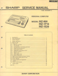
Personal Computer
MZ-80K
r
DC 6 PS
Ernst Helms
Te!. O~534 / i441
SIE:ndamm 3
~u3 1
Lasbek
r
!FEATURES !
•
The MZ-80K is a full·fledged persona l microcomputer equipped with 8-bit microprocessor (2·80 )
and it can meet a variety of applications li ke hobbies, educat ions, office wor ks, controls (of
apparatus In every industrial fie ld), etc .
•
It is a compact desk·top type, Itself a simplified unit including CPU board, CAT display, cassette
-tape recorder and
ke),) r. ~rd
all
togethc ~ .
•
Speaker (3 octaves) and c;ock function are bu i' t in .
•
Applicable Laguage, (BASIC, MACHINE LANGUAGE, ASSEMB L ER etc.) are changed eas ily wi t h
variations of tape mode : a free se lection of t r,e m is possibl e acco rding to the pu rposes of use rs.
•
Memory extension is allo wed U!J to 48K I;ytes in the board.
r
SHARP CORPORATION
MZ 80K
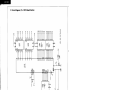
~------Contents---------..,
Page
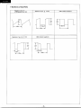
Specifications . . . . . . . . . . . . .
Precautions on Handling LSI's and IC's
3
Trouble shooting guide
4
CPU board section. .
5
Power supply section
12
Display section
17
'"
Cassette tape recorder section
21
Keyboard section . . . . .
24
Circuit diagram of MZ·80K
25
Replacement Parts List
43
..
Caution in Service
* Maintain the safety and protecting ability of the apparatus
after service.
* High voltage shall not be rised to excess voltage so as to prevent
this apparatus from the extra X-ray radiation.
MZ-80K
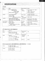
SPECIFICATIONS
• General
•
CPU
Z-80
Clock Function:
Built in
Memory
Monitor ROM; 4K bytes
RAM; 20K bytes
(dynamic RAM)
Memory extension; 48K bytes
(max.)
Editor
function
Cursor control; "up", "down",
"right", "left",
"home", "cleary home"
Edit key, Delete key
Display
10" CRT (black/white).
8 x 8 dot matrix,
Characters; 1000
(40 characters x 25 lines)
Power supply
AC 220V ±10%, 50 Hz
AC 240V ±10%, 50 Hz (for UK)
Power
consumption
Approx.45W
Cassette
Standard audio cassette tape
Data transfer speed; 1200 bits/sec .
Data transfer system; SHARP PWM
Sound output
Keys layout
Temperature
Operating temp.; O°C to 35°C
Storage temp.; -15°C to 60°C
400mW (max.)
Humidity
Lower than 80° during operation
Number; 78 keys
ASC II standard
(alphabet capital letter, figures).
Small letter, Graphic
Weight
Approx. 13 kg
Dimensions
410(W) x 270(H) x 470(D)mm
Music function
Built in
Programmable
counter
1 pc.
Programmable
peripheral
interface
1 pc.
Other ICs
53 pcs.
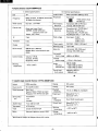
• CPU Board Section (DCPU-0006PAZZ)
CPU
Z-80; 1 pc.
ROM
Monitor; 1 pcs. (4K bytes)
Character generator; 1 pcs.
(2K bytes)
RAM
Standard;
16K dynamic RAM; 8 pcs.
(16K bytes)
4K dynamic RAM; 8 pcs.
(4K bytes)
Video RAM; 2 pcs. (1 K bytes)
_.
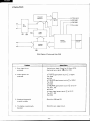
• Power Supply Section (DBOXD0004PAZZ), (DBOX0005PAZZ ----- for UK)
Input
AC 220V ±10%, 50Hz
AC 240V ±10%, 50Hz (for UK)
Output
DC 12V, 1.6A max.
DC 5V, 1.6A max.
DC -5V, 0.2A max.
-1-
MZ 80K
• Display Section (DUTT0004PAZZ)
I. General specifications
11. Electrical specifications
Video output
40Vp-p standard (35Vp-p limit)
Resolution
Horizontal
Size
10"
Frequency
60Hz (vertical), 15.75kHz (horizontal)
15.75kHz (horizontal)
Power source
DC 12V, 1.1A±10%
Non-linearity
distortion
Horizontal; ±8% (±14% max.)
Vertical; ±8% (±12% max.)
Quick start type (3 sec.)
240NB4; 10"90° deflection
explosion proof type
Heater; 12V. 75mA
Geometrical
distortion
Pincushion dist.; 1% (2% max.)
Barrel dist.; 1% (2% max.)
Trapezoidal dist.; 1% (2% max.)
Parallelogram dist.; 1° (2.5° max.)
IC
2 pcs.
High voltage
Transistor
5 pcs.
Zero beam; 11.0kV
(10.0kV, min.,
12.0kV, max.)
Diodes
9 pcs.
Power supply
DC12.0V, 1.05A O.2A max.)
Working range
12V ±10%
Sound output
400mW max. (400 Hz)
Speaker Bcm, round dynamic type
(32Q)
Scan size
Horizontal; 10% (15% max.)
Vertical; 10% (15% max.)
Picture tube
Control knobs
Working
temperature
Volume, V-Hold,
Contrast, H-Hold,
Brightness, Focus
-lO°C to 50°C
11
These patterns must
be clear-cut.
Horizontal
lock-in range
±300 Hz (±100Hz)
Vertical
lock-in range
-12 Hz (-6 Hz limit)
Audio
fri4uency
characteristic
400 Hz (OdB)
-10dB ±4dB at 100 Hz
-12dB ±4dB at 10kHz
Sound maximum output
400mW at 400 Hz
(350mW min.)
• Cassette tape recorder Section (KTRC-0004PAZZ)
System
PWM recording
Biasing
DC system
Power source
5V ±0.25V (rated)
Erasing
DC system
Rated amperage
Wait; 2mA
Record; 70mA (TEAC test tape)
Playback; 7mA (TEAC test tape)
Playback
sensitivity
1m sec. to 500J.L sec. (standard)
Semiconductors
4 transistors
1 IC
4 diodes
Applied tape
From C30 to C120
Tape speed
4.75 cm/sec.
Track
2-track monaural type
Motor
Electronic governor motor (12V)
Input level
Input
impedance
Output level
Below O.4V ("L")
Over 2.0V ("H")
Over 10kn (record jack)
Below O.4V ("L")
Over 2.0V ("H")
Working
temperature
-lO°C to 50°C
Storage.
temperature
-25°C to 70°C
* Specifications subject to change without prior notice.
-2-
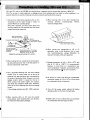
•
LSI's and IC's used in the MZ-80K are semiconductor integrated circuits whose basic element is MOS FET.
The IC's, so poor in static electricity or leakage current from soldering tool, are liable to suffer breakdown. It is
essential therefore to read the following instructions carefully and handle them properly.
Cl)
@ When inserting LSI's or IC.s, don't mistake their
Ground your body before handling LSI's or IC's.
Grounding must be made through a resistor of
serveral Mohms for avoiding danger.
Note that if possible, you wear cotton gloves and
working clothes, but not chemical fiber ones easily
charged with static electricity.
inserting
direction
unconditionally.
insertion damages them.
Ground on water
pipe or connect·
to ground
terminal.
Reverse
® When
storing and transporting an LSI or IC
separately, wrap it with aluminum foil or insert
into electroconductive sponge (Mos-Mat) to
maintain terminals at the same potential.
Electroconductive LS I storage
sponge (Mos-Mat), or grounded
aluminum foil or the like
Method of working and handling LSI:s and IC's
(2) When putting LSl's on a work bench during repair,
(]) Storage temperature of LSI is -20 to +70°C, and
that of IC -40 to +125°C. It is recommended,
however, to store them at a temperature near
room temperature if possible. Avoid storing them
on a place extremely
or low in humidity.
lay grounded aluminum foil or the like superior in
electric conductivity under them.
hjh
(~Use
a grounded soldering tool free from leakage
current. Even if current leaks out to the tip of
soldering tool, gate insulation layer is protected by
the action of protective doide. However, too much
leakage current, which is caused by the tip in
direct. contact with power supply, for instance,
may break the protective diode itself. Therefore,
never fail to use a soldering tool free from leakage
current.
A low-voltage soldering tool (6V, 12W) is optimal.
®
Be careful to refrain from giving an unreasonable
mechanical impact to LSI's or IC's, or from giving
an unreasonable force to lead wires.
® Turn
off the power switch without fail before
detaching LSI's or IC's from the main body.
@ When inserting LSI's or IC's into the printed
wiring board, avoid touching their pins directly,
but hold their black plastic packages.
@ Solder LSI's or IC's in a short time so as to prevent
an unseasonable thermal impact to them.
-3-
MZ-80K
I
•
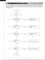
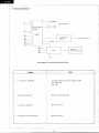
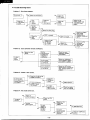
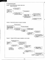
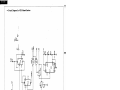
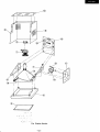
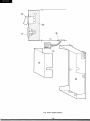
The machine comprises five main units, CPU board, display, cassette tape recorder, keyboard, and power supply
circuits. For a quick solution to most operating difficulties, first consult the chart below to find which section of
the machine is subjected to the trouble, and next to do the checkings according to more detailed instructions given in
the succeeding pages.
C___
S-,ta_rt_ _)
No
Check for the power
supply circuit.
No
Check for the CRT
display.
No
Check for the cassette
recorder.
Yes
Yes
Is the cassette
recorder normal?
Yes
No
Check for the keyboard.
Yes
No
Yes
End
-4-
Check for the CPU board.
f
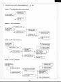
MZ-80K
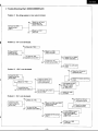
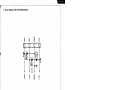
CPU BOARD SECTION
The CPU board is composed of the following six blocks. When it gets in trouble, first locate which block is
concerned with the trouble, and next try to check for its corresponding circuits; the wiring diagrams of every block
will be shown separately.
CPU in trouble
Display
block
Yes
Check for video
RAM circuit.
No
Yes
Check for IC5
(8255) and its
peripheral parts.
Yes
Check for IC5
(8255) and its
peripheral parts.
Audio
block
Yes
Check for IC18
(8253) and its
peripheral parts.
Clock
block
Yes
Check for IC18
(8253) and its
peripheral parts.
Cassette
recorder
block
No
Keyboard
block
No
No
Program
block
Yes
Gets in
trouble instantly
with power
on .
Yes
Memory circuit and
its peripheral parts.
• Checking methods of each circuit
1. By touching IC insulating parts by fingers:
• If they seem too hot by heat generation;
IC is defective, IC load is heavy or components are touching each other - ROM and V-RAM are
exempted from this checking, however.
• If a circuitry state is changed to another; Soldering is poor, socket contact is improper, or printedwiring is erroneous.
2. By using a synchroscope:
• If the relation between input and output of TillC is iltogical, this means defective IC gate.
• Check if the voltage level of TTllC is as specified: High level; over 2.4V, Low level; below O.5V.
-5-
MZ-80K
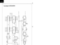
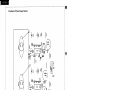
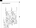
Display Block
Character
generator
DO
-
~
M
"
Shift
register
Video signal
7"- H-BLANK
<~/~
7"- V-BLANK
~ Sync signal
Bus
driver
L-L--
D7 -
I
-'RD
~
--
Video
RAM
WR-
CSD
L--
~
AO
~
-/
A9
1r V
Address
selector
I
I----- Oscillator
Display
controller
circuit
~
Block Diagram of Parts around Video RAM
,
Problem
1. Sync. signal is not
produced.
2. Video signal is not
produced.
,
C.... P_
Vertical sync. signal: Check for IC15 and IC16.
Horizontal sync. signal: ~ck for IC1O.
Is V-GATE signal present at pinQ)of IC24?
Yes; IC24
No; IC5
Is V-BLANK signal present at pin@of IC24?
Yes; IC24
No; IC20
Is H-BLANK signal present at pin @ of ICll?
Yes; IC17, IC3
No; IC15
Is output signal present at pin '21 of ICll?
Yes; IC17, IC3
No; IC29
~
3. Displayed character{s)
is partly invisible.
Check for IC29 and CG.
4. The display is positionally
deviated.
Check for sync. signal circuit.
-6-
,
,
MZ-80K
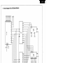
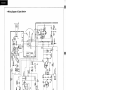
• Cassette recorder/Keyboard Block
D7
~
DO
PC5
PC4
PC3
-\
l'
I
I
I
READ
I
I Cassette
SENSE
I
I
I
I
L
~
I
l
L
N
~
WRITE
~
ill
Lt)
-/
-------,
[
PC1
I
I
MOTOR
______
-1I
Motor
controller
Q)
u
~
RD ------I
~
--c:
Q;
'"
.c
-
WR
~
a.
CS -
.;:
Q)
D.
Q)
:c
A1
AO
-
)
Decoder
I
I
~
I
E
E
PAO
~o
Cl
PB7
l, H
'"
-
------,
~9
PA3
I
~
0
.t
RESET -
I
)
Keyboard
)
I
I
.J" A
I
L _______ J
PBO
Block diagram of Parts around Cassette recorder/Keyboard.
1. "LOAD" operation is
impossible.
I s output signal present at
pi~ of
IC4?
Yes; IC5
No; IC4
@
2. "SAVE" operation is
impossible.
Is output signal present at pin
Yes; IC4
No; IC5
3. Motor doesn't rotate.
Is voltage at pin@ of IC2 at "Iow" level?
Yes; IC3, 01, 02
No; IC2, IC24, IC4, IC5
4. Motor doesn't stop.
Is voltage at pin@of IC2 at "high" level?
Yes; IC3, 01, 02
No; IC2, IC24, IC4, IC5
5. Key input is ineffective.
Check for IC5 and IC6.
-7-
of IC5?
MZ-80K
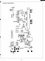
• Audio/Clock Block
07
DO
-\
--I
~
31.25KHz
--
'1
J Clock function
INT
Programmable
counter
(8253)
RO
1/2 frequency
division
WR
J> Au dio output
2MHz
CS
A1
AO
--
I
WR
--
Oscillator
circuit for Tempo
Latch
CS
--
RO
I
DO
Block Diagram of Parts around Audio/Clock Block
Check
Problem
1. No sound is produced.
Is output signal present at pin
Yes; IC12, IC3
No; IC18
2. Sound is distorted.
Check for IC12 and IC18.
3. Tempo is abnormal.
Check for IC13.
4. Clock fu nction is abnormal.
Check for IC18.
-8-
@ of IC18?
MZ-80K
• Memory Circuit Block
AO
~ ____
A13
A15
~
\
A12
Chip select
A4
circuit
\
A2
Data selector
WR
Driver
RAM block
D7
ROM
DO
AO~A11
Block Diagram of Parts around Memory Circuit
Problem
1. Reproduced pictur shows
"panic".
Ch&ek Point
Check for the following:
ROM, IC46, CG, IC43
Address bus line; AO to A15 (IC44, IC45)
Data bus line; DO to D7 (IC36, IC37, IC50)
Control line; IC35
RAM (by using RAM checker*),
IC52, IC53, IC56
2. Error display or
misoperation is caused
as a resu It of program
execution.
RAM
3. Cursol disappears.
IC46,IC1
4. Returns to "MONITOR
SP-1 002."
RAM
5. Error is caused after
a long operation.
RAM
-9-
11'
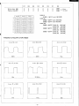
* How to Use RAM Checker
Remove monitor ROM from the socket ("M-ROM" marked on the PWB) and insert RAM checker into the
socket and turn on the power switch (the picture gets "panic" for about 1 second): then the following RAM
TEST-1 and RAM TEST-2 will be automatically carried out from the address $1000 to the maximum address
and the tested results will be displayed: the maximum address refers to $5FFF in the case of the standard set.
The following is an example of the testing performed with the standard set (with RAMs being all normal).
Note: RAM (I) block, 16K bytes; RAM (11) block, 4K bytes
RAM. TE$Tc1 .
RAM l:EST,-,
1)
t~ ...~t<:, . .~~~KIOOOOt<:,
~4IJoo.oo.1F, .>
·OOFf 00· .fF ·FI •..
RAM TEST-'
In the range from the address $1000 to the maximum address, data $00 and $FF are subjected to automatic write/read test; if error is caused, "ER" mark is indicated in the unit of 4K bytes.
In the above table,
3000-0K: this means write/read operation has been normal from the address $3000 to $3F FF.
6000-ER-6000-00,7F: this means there exists error somewhere from the address $6000 to $6FFF;
this error is because the standard set is provided with up to $5FFF but with no more address, so it
doesn't show a malfunction of RAM itself.
An example showing an error really caused:
2OOO-ER·23&8.oo)~01·
]
An error is caused in the addresses $2000s; namely, although data $00 has been written in the address
$235B, its read-out data is $01.
2)
RAM TEST-2
Write/read test is carried out with the following data.
(a)
Write-in data $00 (from the address $1000 to the maximum address)
(b) Write-in data $FF (from the address $1000 to the maximum address)
(c)
Write-in data $00 (from the maximum address to the address $1000)
(d) Write-in data $FF (from the maximum address to the address $1000)
(e)
Write-in data $FO and $OF to be entered alternately (from the address $1000 to the maximum
address and vice versa).
The above table (RAM TEST-2) shows all the items (a) thru (e) are normal - the indications "00",
"FF", "00", "FF" and "FO" correspond to (a) thru (e) respectively.
An example showing an error really caused:
FF
ER.-23FF..Q1
From the above, it can be seen that the tests (a) and (b) are both normal and that although data
$00 in the test (c) has been written in the address $23F F, its read-out data is $01, which means
that an error has been caused.
In this way, which RAM block (I,ll or Ill) has been subjected to the error is first located, and then so does
which RAM component having undergone the error, by the respective information given by the RAM tester.
In the above example, the display of "$23FF" means RAM (I) block is in trouble, and the display of read-out
data "$01" (with respect to write-in data "$00") shows RAM 1 of the block (I) is defective.
L-_~
_______ ----------------------------------------------------'
-10-
.'
MZ-80K
~
•
Write-in data $00
Read-out data $01
07
06
05
04
03
02
01
DO
0
0
0
0
0
0
0
0
0
0
0
0
0
0
IT]
11
I
I
I
3
20
12
I
4
13
I
5
DO
17
01
18
02
19
03
I
I
9
10
RAM(l)
$1000
RAM (II)
$5000
$5000
RAM (Ill)
$9000
RAM( I)
RAM(ll)
RAM,][i
1
2
04
I
21
05
I
22
14
I
6
I
06
I
I
23
15
7
24
16
I
I
I
I
07
8
~
Error
to occur
$4FFF (with 16KRAM)
~$8FFF
~$5FFF
(with 16KRAM)
(with 4KRAM)
~$9FFF (RAM
RAM
$9000~$CFFF (RAM
RAM
$6000 ~$6FFF (RAM
RAM
~
_
(11)
(III)
16KRAM)
4KRAM
(11)
(1II)
16KRAM)
16KRAM
(11)
(Ill)
4KRAM)
4KRAM
• Waveform of Each Pin of CPU Board
At pin
®
®
At pin
of IC7
(2)
At pin
2MHz
8MHz
At pin
of ICg
At pin
of IC10
@
CD
of IC27
63J.lS
At pin
of IC18
@
of IC13
~
I1 n
0----
31.25KHz
63J.ls
At pin
1
I
Q]i
At pin
of IC20
U
17ms
nJl
L
~
®
13ms
of IC21
~
17ms
-11-
At pin
I
CD
of IC8
~
63J.lS
l
I
N
0
A CINPUT
0
...
E
...
0
L---
l- f -
...ro
c
.....en
Q)
~
L-..-
I
Series
1
Regulator
1
Transistor
Chopping
Circuit
Transistor
Chopping
Circuit
Block Diagram of Power Supply Section
Rectifying and
Smoothing
Circuit
Rectifying and
Smoothing
Circuit
Circuit
I Control
l
Control
Circuit
+12V
-5V
G
-u
G
+5V
-v
-v
-v
-u G
'-J
IZ
0
-t
-
,~
en
!<
."
."
C
1(1)
:u
i"m
MZ-80K
• Trouble Shooting Chart (DBOXD0004PAZZ)
Problem 1: No voltage appears at any output terminal.
Check for AC cord,
AC socket, AC
switch and C101.
Is there AC 220V
present across
C101?
Check for F 101
and T101
Problem 2: -5V is not developed.
Check for T1 01.
No
Is there AC 9V
present across
the orange lead?
Check for F201,
0201 and C201.
Is there DC 10V
present across C201?
No
Check for IC1, R201,
VR201 and C202.
Is there DC-5V
present across C202?
Ok
Check for L201 and
F202.
Problem 3: +12V is not developed.
No
Check for IC2 and its
peripheral parts.
Is there AC 20V
present across the
yellow lead?
Check for 0301 and
0302 (short-circuit
after rectification).
No
Leave R403 be open;
does there appear
0.3Vp;,p pulse at
pin 181 of IC2?
No
Is there DC 23V
present across C301 ?
Is there DC 12V present
across C404?
Check for L402
and F401.
Problem 4: +5V is not developed.
F-1 Check for T101.
No
Is there AC 20V
present across the
yellow lead?
No
I--
H
Ok
Is there DC 23V
present across C301?
n
N
1
r-
r
Check for 0301 and 0302
(short-circuit after
rectification).
.----
Ok
Is there DC 5V across ~
C507?
-@
Ok
-13-
H
Ok
No
Check for IC3 and
its peripheral parts.
Check for output
switching circuit.
Leave R503 be open:
does there appear
Vp-p pulse at pin
of IC3?
Check for L503
and F501.
U
l
-
lVlZ 80K
• Waveforms of Each Parts
Waveform of pin (j)
of IC2 and pin ell of IC3.
Waveform of pin @
of IC2
0401 collector waveform
I
23V
1-24~S..j
451-1s---l
Waveform of pin @ of
0501 collector waveform
IC3
23V
~
23V
-14-
23V
L
261-1s
MZ 80K
• Trouble Shooting Chart (DBOXD0005PAZZ ----- for UK)
Problem 1: No voltage appears at any output terminal.
Check for AC cord,
AC socket, AC
switch and C101.
Is there AC 240V
present across C101?
Ok
Check for F101
andT101.
Problem 2: -5V is not developed.
Check for T101.
Is there AC 10V
present across the
orange lead?
No
Check for F201,
0201 and C201.
Is there DC 11 V
present across C201 ?
No
Check for IC1, R201,
VR201 and C202.
Is there DC -5V
present across C202?
Check for L201 and
F202.
Ok
Problem 3: +12V is not developed.
Is there AC 20V
present across the
yellow lead?
No
Check for output
switching circuit.
No
No
Ok
Is there DC 23V
present across C301 ?
Check for 0301
and 0302
(short-circuit after
rectification) .
Check for IC2 and
its peripheral parts.
No
Leave R403 be
open: does there
appear 0.3Vp,;ll
pulse at pin ~ of IC2?
Is there DC 12V
present across C404?
Ok
Check for L402
and F401.
Problem 4: +5V is not developed.
Is there AC 20V
present across the
yellow lead?
No
Check for IC3 and its
peripheral parts.
Check for T1 01.
No
Check for 0301 and 0302
(short-circuit after rectification).
No
Is there DC 23V
present across C301?
Leave R 503 be open:
does there appear
~Vp-p pulse at pin
~ of IC3?
Is there DC 5V present
across C507?
Ok
-15-
Check for L503 and F501.
MZ 80K
• Waveforms of Each Parts
Waveform of pin Cl)
of IC2 and pin CV of IC3.
Waveform of pin @
0401 collector waveform
of IC2
I
23V
f-24~s-l
45~s----l
Waveform of pin @ of
0501 collector waveform
IC3
23V
23V
~
-16-
23V
L
26~s
45~s
I
-...J
Contract
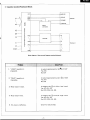
t
B,;ghtn",
Video
amp.
02001
Power
supply
+12V
Horiz. sync.
signal
To horizontal
circuit
To FBT circuit
To CRT heater
To vert.
circuit
To audio
circuit
To video amp.
To sync.
separator
AFC
02002,
02003
V-HOLD V-LlN
H-HOLD
Horiz.
drive
02004
Volume
Horiz.
output
02005
Audio
signal
amp.
IC2002
Video signal
Block Diagram of Display Section
~
Horiz.
osc.
02003
V-SIZE
tr t
Vert. sync.
Vertical
,-----------" signal
,---------------,
horizontal
sync. signal
Vert.osc.
Sync. amp.
amp'/output
02002
amp. IC2001
Video
signal
0---
Audio signal
H
F.B.T
Speaker
t----~IIO ~~~
240NB4
10'
oz-
m
~
tJ)
~
"
t J)
-c
i\1Z SOK
• Trouble Shooting Chart
Problem 1: No picture appears.
No picture
Y
1
N~ Check for CPU board.
1- ..
Check for
+12V power
supply.
Only
raster
appears.
N°rl Check for
CPU board.
Check for
video
input signal.
I----,
~
Ok
Check for VR·
R2002, 02001 and
vide0-40V power
supply.
Check for
video
OkL. circuit.
Neither
L. raster nor
picture
appears.
No
r1
4
IJ
Check for
CRT
heater.
Check for CRT plug.
-1 CRT in trouble.
Check for middle/
Ok..... high voltage
rectification
(02006, 02009 and
FBT.I
Ok
~. CRT in trouble.
L-
Ok
Check for high
'- voltage at K,
f--
G1, G2 and
G3 of CRT.
~
No
~~
Check for
FBT circuit.
No
Check for AFC,
horizontal
oscillator and
drive output
circuit.
Problem 2: Sync operation remains ineffective.
NH Check for CPU
board.
Is there
sync.
signal?
r--
Neither
horizontal nor
Check for sync.
separation (02001
and 020021.
r-" vertical sync.
/
operation is
ineffective.
Check for integrating
circuit (R2012, R2013,
and C2006 to C2oo8).
Only vertical
sync. operation
is ineffective.
Ok
Only horizontal
sync. operation
is ineffective.
L-.,
Check for AFT circuit
(Check point (j) output of
FBT, R2026, C2018 and
R20271.
Problem 3: Raster is too narrow.
N~ Check for V-HOLO VR,
C2OO9 and R2014.
Is vertical oscillatior waveform
normal (at pin @) I - of ICI2001)?
Ok
No
I
Is input waveform
of 12001 (at pin
1(2)) normal?
Ok
Check for
R2018 and
C2012.
I
Is output
waveform of
12001 normal?
NO~
12001 defective
Ok
Check for deflection coil (C20161.
-
I
Problem 4: No sound comes out.
r-
Nr---{ Again set
./
correct program.
Is program
correct?
r-{
Ok
Is there
audio signal?
No
1-O~
Check for CPU
board.
Is input
signal of
12002 (at
pin@)
normal?
I
Check for VR,
N<:.... R2046 and
C2038.
N r i l 2002 defective
f---
Is output
signal of 12002
Ot-' (at pin(1))
normal?
-18-
l
~ Check for C2045 and
Ok
speaker.
I
1
MZ 80K
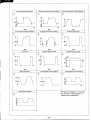
• Waveforms of Display Section
Video output signal
Video input signal
Video output signal
®
CV
(,J)
1111111
+1111111
·+11][111
,+pl l l Il~
1111111
--- 1111111111
5ms
5ms
5ms
Sync. input signal
Sync. signal amp. output
Vertical sync. signal
®
ell
(4)
r--
Tl
Tr-1
12Vpp
L-
L
20l's
Vertical oscillator Circuit
sfVl
® of
2ms
@
~l
TI
10r
I
t
,--
l
1.5Vpp
5ms
nL
-
5ms
AFC waveform
FBT waveform
\1jJ
20l's
Vertical linearity circuit waveform
"ll
5ms
l
..i...:.
5ms
Vertical deflection coil voltage waveform
Horizontal sync. signal waveform
8Vpp
T
1.5Vpp
OV
I~v I~
1J
U')
~
1V
W
Vertical drive collector waveform
IJl
I
+-
1.5V
RH-IX0015
IQ)
Tn
4V
20l's
5ms
Voltage at pin
r-
,
Vertical output waveform
®
(7)
r--
~
!
IL
JJ
,.
.(
@
T
4V
l
5V
T
7V
5V
~
f
201'
-19-
20l's
MZ 80K
Horizontal oscillator waveform
Horizontal oscillator emitter waveform
Horizontal oscillator output waveform
1-
I
7Vpp
--t--
!
8Vpp
5V
5V
\U
'U
OV
OV
20lls
Horizontal drive collector waveform
Horizontal output pulse
Horizontal output base waveform
n
3V
L
AFC pulse
Middle voltage FBT pulse
Video power supply pulse
T
160V
OV
150V
1
I
"
20lls
Audio input signal
Audio amplifier output waveform
Audio amplifier output waveform
5V
li!
OV
0
Audio output waveform
The figures encircled by
in the above
refer to those of "Wiring Diagram" --"Check Points of Waveforms".
5V
III
-20-
I
I\J
.....
JlJlfL
JLJlJL
READ
WRITE
Power supply
for motor
:
0
'"'
I
0
'fl
~
•
Amplifier
circu it
03001,03002
Differentiation circuit
R3005
C3002,R3005
..
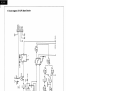
Block Diagram of Cassette Tape Recorder
I
o-o0~
0
Play button
Erase head
-
+5 v
-v
Amp. circuit
limiter
circuit IC3001
( 1/2)
Amp.
circuit
03003
Record/playback head
TAPE
-o~z
m
en
:a
cm
:a
8
m
:a
m
i!."
=I
m
m
en
»
en
o
MZ 80K
• Trouble Shooting Chart
Problem 1: Even if the play button is pushed, neither motor
rotales nor tape moves.
~
Electronic governor
motor defective.
J
Check for motor
voltage: see
if there is +12V t----between M+ and
M-.
N~
No
r-1
Is voltage at the switch
f-(inter·locked with the
play button) in high level?
Switch defective
J
Ok
;--<
Check for vOlt~
at cheak point 4
(SENSE): it must be
I-OV with switch on and
+5V with switch off.
Ok
No
Check for +12V power
supply circuit (for motor
in tape recorder) and CPU
board.
Check for +5V input voltage
and R3024.
I
Problem 2: Record (SAVE) operation of program is impossible.
rI
No
See if the switch SW3001
surely gets in action
when the record button
fis pushed. +5V must be
present at check point
@.
Ok
Switch defective.
I
No
~
Does there come
any signal from I check pOint@?
ok"
Check for CPU board.
N~
Is there any
signal present
at the base
of Q3001.
I
SW3001 defective:
check for R3002.
rOf{ Record/playback
head defective.
Ok
Is there any signal
present at the
record/playback
head.
t--
No
I
Problem 3:
Poor contact of SW3001.
Check for Q3001 and Q3002.
Is voltage applied to the
erase head?
Playback (LOAD) of program is impossible, or error is caused.
O~
Make
su~e.of the tape
I start position.
rD-o-e-s -n-o-rm-a-I--'
waveform
arise at pin
@?
I
I
J
r-C-h-e-c-k-f-o-r-p-o-we-r-s-up-p-I-y"""
N~ +5V of CPU board.
And check for plug and
cable (6 pins).
r-
U Check for power l1 supply +5V.
I
No
No
r--'
The waveform
is not normal with
much noises, or no
waveform develops.
Ok
Check for
each voltage.
l_
I
h1
Ok
Much
noises
Check for IC3001,
each resistor and
SW3001.
Ok
,.........
Check for the size of
~
output voltage waveform
of Q3003.
Check for around Q3003.
........... Azimuth adjustment
The voltage
is too low.
-22-
Doesn't the erase
head operate because
of SW3001 in trouble?
of the record/playback head
is improper.
MZ-80K
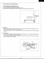
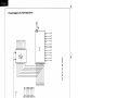
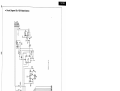
• Azimuth Adjustment and Head Cleaning
* Azimuth adjustment of record/playback head
1. Connect a synchroscope to the collector of 03003.
2. Load a test tape (TEAC, 3kHz-signal recorded) and play it back.
3. Rotate the azimuth adjusting screw so that the waveform on a synchroscope will be the maximum.
Head azimuth
adjusting screw
Record/playback head
,
/
Head cleaning
Clean the heads, capstan and pinch roller often, to remove dust and tape residue. Foreign material on them
impairs the sound quality of both recording and playback.
Open the cassette holder, remove the tape, push the play button and clean them with a soft cloth moistened
in alcohol.
Erase protection
To protect a cassette tape from being accidentally erased it was designed with two removable tabs. ,When the tabs
are removed, it is impossible to push the record button.
When no cassette is inside the machine, no pushing of the record button is allowed, either. Nevertheless, pushing
the button strongly may cause a trouble.
Pinch roller
/
-23-
Head
MZ-80K
• Waveforms of Cassette Tape Recorder
1st stage amp. output waveform
CD
_Iv
~-~-
--
-
Operational amp. input waveform
Operational amp. input waveform
®
CID
L
pp
6mV~
pp
1.8V
T
DV
--
Operational amp. input waveform
Operational amp. output waveform
@
@
n
T{
®
-r-
f1
Output waveform
e-
T
I
1.5Vpp
i
4Vpp
Lv
"
u V
v
~
,
v
v
5Vpp
---'-
L-
I
Record input waveform
CD
v
2
r
,1MB l
®
®
.-
r- .-
~PJ
.-
-
T
e-
i
4.8Vpp
I
_L
I
Record amp. waveform
Record amp. waveform
i
L-
--
~
c-
L-
'--
Head input waveform
Q9J
-,
!
i
6Vpp
,
\
\
I1
~
V
1\
V
1\
I1
-
The figures encircled byOcorrespond to those of
"Wiring Diagram" - "Check Points of Waveforms".
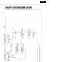
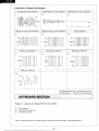
KEYBOARD SECTION
Problem 1: A charactor isn't displayed even if a key is pushed.
(1)
(2)
(3)
Poor soldering
Mechanical key defective
Printed line broken
If there is nothing abnormal in the above checks, proceed with the checkings of "CPU Board Section".
-24-
MZ-80K
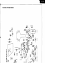
CIRCUITDlAG
• Symbols of CPU Section
r-
(liS-I
<D
Z
U
-
~+
+
3
Il..
U
g
<DN
<t-
'"
u
:> :;: 0 :;:
£::!
+
~*
BSJ ~~
6S:) ~~
09J ~~
19J ~~
<:9J ~~
£9J ~~ v9J ~~
L9J ~~
<:BJ ~~
£BJ ~~
00
B9J ~~
10
t>BJ ~~
69J ~~
ZO
SBJ ~~
OLJ ~~
9BJ ~~
!LO
ILJ ~~
tp()
L8J ~~
UJ ~~
BBJ
~a
~~
I{)
Z
<!)
0J 01 0 il
--'VV'.--
LO
---'VV'r-
If)
--+ -- --
rn
£LJ ~~
'r90 6BJ
-25-
B*
SBJ ~~
I j [] [] [[] [[] [[] [[] [[] [[]] :
99J ~~
~*
~
I
I
I
en
I\J
ISlea5
+5V
7414
'C4
i i i i _ 71
ft_
rnw
iiiEQ
RFSH......--1@i
.HT
'.
+5V
II·
I
27
RD
RESET
6
vec
HALT
iiii
ft
~=
2.
~
I:
+5V
M
MPU AND SYSTEM BUS
A"
A..
AM
A..
Do
D,
D.
::::I
0'
~
f
C.
I»
.~
C
~
D.
~
0
3
Z80 CPU
D4
60
I»
Di'
ce
.
-...
;:;:
C
(')
Ri)
D7
Do
.
IC46
IiIj
•
Q
n
c
I
I
.....
I\J
RAM MEMORY
+12V
+sv
-sv
ADo
AD
A02
A05
AD4
AD I
~
•
I
•
RAS
RAM24
DOUT
RAMI6
DOUT
I
WE
DIN
I
AOAI AlA.A4 AS!:§' CAS
AS
DIN
WE
RAMS
Aa AI A2 A. A4 AS MCAS
DOUT
DIN
RAS WE
11
I
RAS
I
AD AI A2 A3A4 AS~ CAS
DIN
DOUT
RAM7
DIN
I I
DDUT
RAMI5
I
DIN
I
DOUT
I
DIN
DOUT
RAM6
DIN
I I
DOUT
RAMI4
I
DIN
I
DOUT
I
DOUT
DIN
RAMI3
RAM5
DIN
DOUT
DIN
DOUT
I
I I
I
I
DIN
DOUT
II
DOUT
DIN
II
DDUT
DIN
I I
DIN
RAM4
RAM 3
RAM2
DIN I
DOUT 14
DOUT
RAMI2
I
RAMI
4116
DIN
I
2
DOUT
I
DOUT
RAMI I
DOUT
I
DIN
I
DIN
I
DIN
I
DOUT
RAM 10
I
DOUT 14
14
W!
DIN I
;r
WE"
DIN
RAM9
4027
or 4116
..-
I~
RASI
S 7 • 12 " le 131
'"~ 4
AO AI AI A. A4 AS AS CAS
RAS
AD6
.1
DOUT
I
I
14
1
S 7 • II II 10 131"
4
AeAI AIA'A4AS~CAS RAS
RAS.
RAM23
I
RAM22
I
RAM21
I
RAM20
I
RAM 19
I
RAMIS
I
S 7 • II 1I 10 I L
4
.1
AD AI AI A3 A4 Ao ~ CAS RAS WE
AS
4027
DIN I
or 4116
DOUT 14
RAM 17
RAS.
l:i
I.
T
01
DO
WR
I)~
"
D7
06
Do
D4
Do
02
s
b b
9 CS2
I
14
I
07
'06
'Do
OD4
D'
D02
DOl
DDo
•
-2:::s
ler
ra.
c:
"V
n
N
3
~.
;:;:
C
~.
n
I
I
r-J
00
RAS.
11
9
iif-
IC52
LS
~
~a
RAS,
1C52
~
~.
RAS,
>--------i
le: 3
~2
SI
CSO
Q
..
3
RFSH
C
LS74
ICSS
0
PR
4
cs.
3
r
IOk ••
RA 2
CK 11
iiJiEij
3
12
IC54
.
6
ICSI
Y
.*1 1
D~
20
LS
I
-Hr
LS
20
.---...
13
~
LS
20
1C54
R46
I
e
6
3
74
...
'7
....!..
.
+.V
110
9
I
11
2
12
3
13
4
•
14
15
6
16
•
7
CSI
1C54
a
6
RD
Cfl
CS..
CS7
Cii
cn
CSA
Cili
CiC
D07
0D0
DOa
-
DOo
DO.
DO.
DO,
2
00
D.
Ao
Ao
a
LSM4
IC50
28
19
A.
A.
7
.,..
AI
Aa
•
At A3
6
-G(-
18
RAM SELECT AND ROM MEMORY
17 07
le D.
I. 00
140.
1102
13 03
10
---L!
~
~
6
I.
4
17
~
la
A4
A4
Aa
As
As
2
A.
M-ROM
9
112
7
14
18
13
As
Ae
AM)
Au
A7 ... Ae AIO All
I .,
21
I
I
A7
IK
R44
"'0
07
De
:::s
o·
re~
...C.
c:
~
I»
0
....
§
3
(")
~ cso
+5V
...I»
C
iij.
ea
D.
CS.
n
c
;::+
0.
Do
Do
D.
Do
•
(")
:0.
,~
I
I\)
I
co
AI
ADI
AO A7
ADO
A8
AD2
AD3
I
I
IC56
5157
A3
A2
A9
ADDRESS DECODER
RAM ADDRESS MUX AND
Alo
¥
I 12
SI
LsOO
All AS
rI
A8
IC57
150
CS2
0
A
0
~
ffi
....\,
9 8
m
E12I"- •
8
CS6
E6
• CAS
cse:oCsEi CsE2
rrr
B
C
LS42
IC30
I" I~ I.
AA
CSD
CSC
CSA
CSB
CS9
6 Ii
7 6
m
Ell
I.
16 .•
U5 13
14 12
11 10
13 11
10 9
7
4
Ii
CS4
E4
3
0
2
3
CS3
E3
2
4
CS2
E2
m
CSO
1C47
154
G2
GI
19
18
MREO
~
:::I
0'
rSl
a.
III
W
C
."
n
0
~
-
3
;
C
ij'
ea
EO 8
7
El
W OUT
c
n
;;'
10
i R45 n.
+IiV
91 5
12 GND
24 Vet;
•
n
~'
I
w
o
I
'~7
IL4
2
Rl
220
"-
U~
I~:K
IC7
~
IIL~ 10
-1P 1 I
R4
MO
J
rK
a
I C19
IC22
00
LS
IT
~
0 •
10
9
~
---..!.CK
11
LSI07
IK
le 7
~.
f!Y'
'MD.
SYNC COUNTER
I
B
6
IC22
!5
4
IC26
86
T'L---'
IC26
6
IG
131
12 2G
23
~
~ ~~:5 l~~
OD
IC9
LS93
Qc
A
II~
J
~OS7
0 F---
'--! CK
--= J
8
O'~A
QA
QI
9
ICI4
LS93
8
121l
31.2!5K
Qc
8
Cl
Kl
~~
IC25
I
r- J
Q !5
5
101
4
I
2
102 10> 104
2:04
J~Ol J~022~0'JJ
(d) (e) (f)
+.V
~
•
1'13
~
8
C
9
1
IC32
100
~
0
131
(c) (d) (a) (f)
A
I
B
(g) (h) (i) (j)
'
.'~.
0
oc 00
11
17
J11
177
C
:5
.8
IC34
9
OA OK> OB
4
8
201 202 20' 204
J J.J J
(j)
~~, 1~02120>'~D4
(g) (h) (i)
jl
"
hi
91
dl
oL
Q -
$I
r-
I
LS
IC20
!5 08
4
6
U
boJ"
IC20
~LS
>
2 08
K
CK
J
+~
R6
IK
0
CL
LSI07
le.s
06
Q
5
J
4K
lel0
r
~
3
LSI07
...!!CK
I
o~ H-Synch
'--------------------------1~--------H---B-,a-n-k---- H-Blonk
'1
8 CK 1
Cl
~ ell
21'2~
JJJ
'li
177
IC33
OA CK2 OB Qc
A
~~~~~
I
ell
LSI07:5
~
,...!.K
Cl
8 Ct(1
le,s
1
(b)
O.'!"!""r"'!!CK
...!K..!!K
CL
12 CK
~
1:5
IK
IK
IC2S
R17
(a) +.v
R18
+'V
RO (21
L-"RO(;12~1l-=13RO(2J;:::::::...-----'':'
1"'31
B
8
.----~+--------------,
.L~ B
11
'-.'1'_1';:-1,'"
2.1 3,
~
.----~+-------------~
+.v
R1S
I
IC28
(c)
0.>-------------------~------~----------------------~~~+_~_4------------,
4
10
:5
11
04
IC27
8
OB Oc 00
LS93
9
I
It=t:==~ni~~~
01 0203
•
...n
::s
0
a.
~
a..
Cl)
0
C
CD
"g
(")
0
-....
u;
3
Di·
ce
DJ
C
I:
;::j:
Q
~
...wII
• A.
3
4
5
6
7
•
'I
WR
CSll
OIR
9
G
02
LS
13
48
'1
A.~ lA S
2A
SA
AZ~
A'~
4A
As~
G
"J.
LSIS7
L-
IY~
4Y "
5Y 9
A.
6
r--
5""
'Y
IC40
1C21
•
(.)~ 28
58
I
(a)>-----l 18
(.)~
(C)~
1C23
12'~
"
III 18
17
16
15
I.
13
I•
eo"
1tT
9As
CHAR ACTER GENERATOR
AND VIDEO RAM
RC
00
D.
Do
D.
04
00
O.
D.
LS245
IC43
Az
7
As
4
I.o
ft
3
Aa
O.
I
As
18
As
15
et
8J.
4Y
rL-
IL
CS
51""
AI
iI!
10
"d.
A'
I
Oz
As
3
2
As
2A
SA
4A
A<~ lA
A'~
A7~
As~
S
G
'1
'1
LStS?
IY 4
IC 39
2>' 7
.'
3Y
(.)~ 18
AT
(.)~ 48
(9)~ 58
(f)~ 28
As
I
1
81
As
48
A<
A'~
SA
A.~ 4A
(I)~ 38
(j)~
7
Az
•
A.
A<
'1
•
'1
La.S?
A.
I
00
1C38
A.
D.
13
S
2114
I.
00
A.
I
IC42
3
A.
rr
A.
2114
D.
1
'9
Ale>
As
Az
A.
8
5>'
r!!--
-
As
18
4ytlL-
AT
I
A.
04 14
04
"
00 8
01 10
OZ
•
a
.
VOo
d.
'0. .!!....--VO.
05 1&
07 ..!I.--VO'
O. 16
CS.
CG-ROM
CSZ
21 CS)
u=:
I.
IC41
2
Oa
.5V
R19
•
er
:::J
~
~
a.
~
DI
c:
"g
(')
o....
§
D1
3
C~r
c
c:
;+
c;
Q
Q3>
VIDEO GENERATOR
I<,;LU
,'-'"
(g)
q
11
+5V
(2M)
H-Blonk
H-Synch
GND +12V
SND
+12V
GND
GND
SOUND
•
~
o·
~
n
Cl)
(I)
Q.
III
...
CJ
0
"'0
C
(')
2-
3
'::::i
CC
...III
;::;:
0
ii·
n
c:
...Q
1
tu
tu
1
.~
7
GND
26 IVcc
B25~
IC5
35 RESET
A'3 AI
AO
RESET
8
9 Aa
CSEO~CS
Wii~WR
Ro~Ro
04
05
De
07
~
~
~
RA'
+'V
IOK X8
I
1(i)(2)@(4)®OO(rl@®@6'
P80~8
Ps,'S
PB2~
PB."
PS.!!!
2
,
o '
•
4
4
•
•
5 6
'5 A
LSI4~
7 9
6 7
14 B
Tt.;:
§j
PB6~
PB7~
PAD
PA,
8 '0
I3 C
'2 D
9 "
J
PA2
IC6
V-GATE
- " V-Blank
PA.
•
PCO~
PCI~
PCZ 16
PC! 17
PC4 13
u..
PA7fllPC7 10
peG
PCS 12
ICl
,.!.lOUT ~~~
17
•
J
111
I I
1
__ .1'1'4
IC4
LSI4
3
~
C14
I.SK
R23
+OV
01 SCr---t--
RST TRG Vcc
--
001
G
R
+5V
~
2SC373·3
.~
IC4
__
LSI4
1.2K
R36
I
0
,
CASSETTE ANO KEY
R3,
10K
GND
J
CH ..
IOOPF.,.
6
5
.... OI .. F
01
Q
.C'6
CL
--,;-y;
~CK ~~~4
PR
~
2
I~F
I .0
~I---
8
-
IC3
II"~
+12V
+5V
MOTOR
5V
SENSE
READ
WRITE
er:::::I
~
(I)
CD
...Co
OJ
0
I»
c
"'0
n
0
-00....
3
I»
ea
...
m"
0
;:::t."
s::
=0"
n
n
•
-I
I
I
oil>
eN
,~
01
00
7
8
01
Do
CSET
Ao
19
20
21
AI
23
WR
Ri)
Ao
AI
CS
WR
RO
02
6
02
04
22
03
5
03
GATEO
ClKO
OUT
11
9
10
14
15
13
16
18
TIMER AND SOUND
IC18
8253
GATEI
ClKI
OUT!
GATE2
~
04
O~
3
0UT2
ClK2
07
2 D6
4
06
07
17
,~
2M
10K
31.25K
R13
+5V
~ 06
IC3
12
II
n
6
~V
13'
CK
lS74 IIC12
INT
1=>;>
t;,
CRO
555
THRI 6
,
Cs
.......
•
Rl0
,O+~V
I
~~~2
C4
IOOPF
,
Cl
coo
3 10UT
JCt
Q
I
":J4:t
6
s
:::>r..
IC121
lS74
R8
IK
+5V
..
•
..3
--
~
a..0
f
C.
.
OJ
0
I»
c:
"tI
n
a
CD
I»
i·
C
;:+
c
n
Q
,I,~
I
I
U1
w
...
-
[>
(MARK)
G
10RQ
G
G
HALT
RESET
G
G
G
G
G
5
6
7
8
9
10
11
12
13
14
15
16
17
18
19
20
21
22
23
24
All
AIO
A9
A8
A7
A6
A5
A4
A3
A2
AI
AO
G
07
D6
05
D4
03
02
01
G
G
G
G
G
MT
G
WR
G
RO
INT
BUS CONNECTOR DETAIL
25
MREQ
4
AI2
00
G
2
3
AI4
AI3
G
I
AI5
B
I
A
-
-5V
GND
+5V
+12V
"
C38
-25V
=:
=~
~ =+100 J.l
I~~
C37 2SV
IOOJ:J:
25V
C36
o
I-
k)
-5V
GND
10 +5V
P+12V
•
~
er
~
do
en
CD
Cl)
0
OJ
C
n
-a
0
....
S
3
-...
Cl)
0
jji"
ca
.,
;::+"
Q
.,
n
c
~
+r:w
C301
-liI-
II.L-.J
11.
~
-liI~
12
-
0
O
C302
.
"~
g.
E
~
c(
.
~~
~~-
~
E
c4t
+
III
~"I
V..-.v
T~
'H-
~~_
.l8
--u-
.
0401
+
o
-5
~
... IL
0
E
0
+12
&T1,6A
I~I
F401
L402
~
o
+5
'0
+
01
10
If)?~
o
.L~
-'VVIt--It504
& T1.tiA
I~J
F501
C506
-H-
0502
0501
Hf~~1 --=-
*8
C502
"'* - fi
-J'VVV""-a:
J\NIr
~1£~U
~t 1tJ T6
......
L503
~ ~~t@
C403
""""
J\NIr
R405
C40{'"R~' ~~i
w-~
§~~ j .i~~@~
2
;!;
r---- ~~
+
~I)I~ ~~
o~_
Q401
•
o·
::::I
~
CD
(I)
-<
'a
'a
C
(I)
~...
."
o
o
iii
...
-
o
c-
3
!f
I
I
w
.....
L
±IO%
AC 220V
650101
&SWIOI
I
I
I
I
1
1
I
1
rf"\Jl
I 6T!500m
I
F201
POWER SUPPLY CIRCUIT
-
11 ~
6TIOI
I----~ ___ __,
Al
2500}l/55V
C30I ... C3041
\:501
IOll/S5V
Jl78MGU~
VRZOI
12K
.20'
~
ZOOIO
+
C202
470/lOV
~-!5V
L201 6T31!5mA
F202
ZOOO9
Zoo07
F401
MZ-80K
L402
L401
•
er:::J
~
~
-<
'C
'C
(I)
C
~
~
"8
So
3
I»
i'...
ea
C
5'
:::;'
:E
I
I
~
.a
L
AC240V
±IO%
&50101
&5W101
I
I
I
I
I
I
i
&TIOI
I
rrv:>,
(FOR UK)
.:a..
POWER SUPPLY CIRCUIT
III
--------,
C50I ... C!041
25OOp155V
~501
IO~/"V
,
COOl
470/IOV
A
R501
4.7K
....
F202
~-5V
Z0007
L401
F401
+ 12V
MZ-80K
L402
ZOOO9
~
o
-:;
.c:
-"
f
~
er
::J
-<
'tJ
'tJ
en
c
..f
~
o
3
DJ
a::a
Ai"
a::a
C
5"
::;"
.....
I
I
w
co
-~
+ u
+~
R2051
+
A/'
",.
2
I
7
8
R2047
1
R2025
1"""""
+
R2046
VOLUM E
~
..
R~~';6
K
H
..
C
-It-
R2002
'I."
.....
02009
+
CONTRAST
~
EO G
.. ..
-It-
"!;!
,,2
U
fjT
R2042
+
C2051
-If-
2
FOCUS
R2044
Raoeo
..
•
u +T
~
~
0
N
...
V-HOLD
R2017
~
R2037
':;':'
L2001
..
H-HOLO
~
T
NT
U
R2033
~
R2043
--JWv--
~
Si!
0
2
~
•
0
t.,
NO.~
C2025
+
C
2
~.. ~
="
+.
~
TOfj
:f f t!;!~ 02003~
;J.
21uT
i fi I
14 c202
'''D20032
BRIGHTNESS ~
.~
N
...
o
o
N
02007
rl:: I~ ~1
ls
tfu
2:0:
8
7
U
~t::l
~ ~T
o
-I~2018.8 O
.
& ~.I.~
.-~;;;
B
-I~ --"NIl'-~ C2052 ~
R2008
R2048
0
f..2-
02004E~I~f ~
C2
-U-
f
C2032
u~
~u"
S·
NT
C2003
0~
0
1
,t""""
---..,..
-w-0 0
~
•
.... -
--It--
C2001
~
"t"
R2001
"I,'.
g:
§T~ ~
B
I
R2026
C2020
-----f'--
R~
-It--
I
=:
,~ ~ T
L2002
-'"RI'- •
-:t,:005
I(l~~
~ T~ [
I
~
C200!!
~*+
C
QPWBF0261PAZZ
-~
-
::::016
~
+*+
~
~c
02001
'ft
f
- -
'1111'
R2004
02002E
-----f'--
______
--f\-
C2004
O
+1210
-·0
EIO
~
O
'.v...
B
C
g:
R2001
02001
R2011
N
2
5
4
3
6
7
8
9
10
--ANy--
~
E_~
124
~
N
o
o
R2015
~
~ ,..
~
1
'1-:.
R2012
C20ll"
~ 0 --A--
O
SIO
---
+--C2012
I . -u- .+
~~
:::T
CZOl4 Cl
~l
-11; 2
~
;; ~
--M--
___ C2049
+R2011!
R2048
--Hr-
T
fjT..
g.
C2040 +..,
-ilt- C2011!
R2019
C2013
~ +~ +
+ +*
:!!!
.i}ir~
-It- J. If)
~... - I t - ' g
C~,C}~I
u
• J.
o
T'
4
-il1-5
~ ·o------"I>N-
",
cI42
o
J.~
"'OspR2014
T::: ----w...
C20S0
SP
-
::::I
er
S1
f
<
ii'
'C
Vi'
o
o
....
iii
co
<
3
•
en
-
1
"'"
0
1
_.
+12V
GNO
Video
"
Sync
Sound
330
R2026
15.
02013
12.
0015
02004
47
~
_
B-
r
OO33
1c2007-
+___
7
2.7K
10.
R2019
1
,.
V-SIZE
-
C2014
22u/16V
02007
1500<
+
C2003
,OuIl6DY
I.
R2024
llW
I.OK
RC-ElOO29TA
R2023
330
602051
12
L2002
,-----+-"'-1
Rei LZOO5TTA
(:~OO4TAI
V-LIN
R2025
R2021
1.511/2WI
C20I~~12
22~/16V \!!I
SeOK
R2045
20K(BJ(M'r'O~2TA)
R2022
n
>
Ip/35VITNI
~R2014
®
_
•
R201.
27.
lUJ(
IK(1I2W)
R200S
02006
2.2M
-..:1
~.~~:sv +·.tl'"C2..0voiO.-----I--I-~
V-Hold [
R2DI7
50K(B)
B7029TA
1000/
IOV
020151
3.3( II2Wl
C200!'5
I
t-<r-:='=+-+-'
t~:s""
1
~
.l&.Y
•
C2001
II
~
~-i~-'
C2oo2.11200"
R2063
•
Rci lH4070TA
t---:::I~~f=t--;::-JvW~4-llJL---=~
~
0203.
2.~KI2W)
C2036
.IJI/200V
......
,..
E0
~I?
+
.!!!!
IKU)
R2049
47K
.OI/~V
C20~2
+C2048
_22OW
IOOV
~
.~
p
11
...-+------c~ ~
C2047
22a../16V
GI
•• 0)
~
-1-
:~~--Y.~~-~~~~L---~~:-----~~~~~-----~I~---~.g~~~~~34~V~~~~~~~~5~
' 1I 1:>
M
.ri
R2011
I.
R2012
Q.~201.
@
.015
_Iil!
4.7K
02009
R2003
~~~~14~ I
DISPLAY SECTION
R2002~'7
500(8)
RVR-BOOI5PA
CONTRAST
QPWBF 02.,PAZZ
0
~
02001
OZlls..
10
47
R2001
MZ - 80K
•
~
er
:::J
-<
en
m
"C
in·
o
o
....
3
11)
ce
.,
Di·
o
ce
~.'
:::J
~
.....
MZ-80K
• Symbols of Cassette Section
C300t
e
~3001
~R3004 ~~
----'Wtr- R300 3
~
C3002
.x 0
an
o
-1'-.
R3006
ort)
0:
~
rr>
0
::t R3007 J\ ~
R300~,
-r
Q3003
a..
LO
N
o
lJ..
10
-11- ~
~u
R3010
C3006
-1 r-
R3011
~
R30 12
-.J...Nr-
J...
T
~
C3007
-::-Wor-
i t~flJ 30;~:14
o
c2~~lOf
W,
R3018
----Wtr-
R3016
R3022
~
R3023
~
R30~
C3003
_ N
+~
en en
I
0
C~O~
0
~
3=
en
C\I
~009
,
oo
0:
R3017
R3021 13001
R3019
YIlv
~30~20
+-
Ne ~
-tt-e e e
~
D
•
C3009
Q3004
LO
e
e.e~ev
-41-
I
I\J
1
.-.
1000P
.L.
C3OO!II
.1
_
SW 3001
R3007
47K
'Q3OO3
2SC1681
R3012
22K
C3007 R3011
1000P 47K
~
FO 259P
~T1f~~f,~@
r-----------------i
R300I
470
CASSETTE TAPE RECORDER SECTION
K TRC - 0004 PAZZ
C3004 12:! 0
+
MZ-80K
R30ZI
2MG
IOK
~
R3002
~
:s
!er
I
~
2-
Dl
3
ea
C
5°
ea
So
~o
:e•
...
REPLACEMENT PARTS LIST
To
MODEL MZ-80K
REF.
NO.
PART NO.
DESCRIPTION
CODE
* * * CPU BOARD UNIT SECTION * * *
DCPU-0006PAZZ
Assembled CPU Board Unit
INTEGRATED CIRCUIT
t
IC1
IC13
lC2
I
RH-I X0134PAZZ
NE555P
AG
RH-IX0079PAZZ
SN74LS74AN or HD74LS74
AG
RH-IX0038PAZZ
RH-IX0131 PAZZ
RH-IX0136PAZZ
RH-IX0126PAZZ
SN7406N
SN7414N
,uPD8255C
SN74LS145N
AG
AM
BA
AL
IC7
IC211
IC54
F1H-IX0074PAZZ
SN74LS04N or HD74LS04P
AE
IC8 1
IC31 !
RH-I X0040PAZZ
SN74121N
AG
RH-IX0125PAZZ
SN74LS93
AK
F1H-IX0127PAZZ
SN74LS107AN or HD741S1
AG
1
IC121
IC55
IC3
IC4
IC5
IC6
I
~
IC9 \
IC14
IC27
IC10
IC15
IC16
IC19
IC25
IC11
IC17
IC18
IC20
DESCRIPTION
PART NO.
CODE
IC47
IC51
RH-IXOO45PAZZ
RH-I X0177PAZZ
SN74154N
SN7425N
AN
AF
IC53]
IC56
IC57
CG-ROM
M-ROM
RAM
RH-I X0148PAZZ
SN74S157Nor HD74S157
AO
RH-IX0147PAZZ
DPROM0001 PAZZ
RH-IX0171PAZZ
RH-I X0145PAZZ
AM
BS
BL
BE
RAM
RH-IX0121PAZZ
SN74150N
HN462716 or MB8156C
,uPD2332C
16KRAM, ITT4116 or
MB8116
4KRAM, ITT4027 or
MB8227
AV
TRANSISTORS AND DIODES
01
02
03
04
05
06
01
02
VS2SA505 Y //1 A
2SA505-Y
AF
VS2SC373G//1 E
2SC373
AC
VHD1S1555//1A
1S1555
AA
220 ohm
AA
1
RESISTORS
RH-I X0142PAZZ
RH-IX0076PAZZ
RH-I X0146PAZZ
RH-IX0075PAZZ
IC22)
IC24
IC58
IC23 I
IC52 I
IC26
IC28
IC48
IC49
IC29
IC30
IC32
REF.
NO.
I
I
IC33 1
IC34 !
IC35
IC44
IC45
IC50
IC36
IC37
I
I
SN74S126AN
SN74LS10N or HD74LS10P
,uPD8253C
SN74LS08N or HD74LS08P
AH
AE
BC
AE
F1 H-I X0070PAZZ
SN74LSOON or HD74LSOO
AE
F1H-IX0071PAZZ
SN74LS02N or HD74LS02
AE
F1H-1 X0132PAZZ
SN7486N
AF
F1H-IX0128PAZZ
SN74LS20N or HD74LS20
AE
F1H-1 X0129PAZZ
F1H-IX0104PAZZ
F1 H-I X0130PAZZ
SN74LS165N
SN74LS42N or HD74LS42
SN74177N
AO
AH
AO
F1H-1 X0133PAZZ
SN74177N
AL
F1H-1 X0123PAZZ
SN74LS244N
AS
F1H-IX0176PAZZ
SN74LS241N
AS
F1H-IX0083PAZZ
SN74LS157N or HD74LS157
AH
F1H-1 X0122PAZZ
MB8114NC or HM472114P-3
AV
F1H-IX0124PAZZ
fiH-IX0090PAZZ
SN74LS245N
Z80CPU
AR
BF
IC38 [
" IC39 .IC40 I
IC41
IC42
IC43
IC46
I
I
R1
R5
R30
R32
R2 1
R10!
R3
R4
R6
R7
R8
R11
R12
R14
1
R19
R22
R29
R38
R41
R44
1
R48
R9
R26
R36
R13
R27
R28
R31
R33
R35
R39
-43-
I
r
VRD-ST2EF221J
VRD-ST2EE182J
1.8K ohm
AA
VRD-ST2EF222J
VRD-ST2EF561J
2.2K ohm
560 ohm
AA
VRD-ST2EF102J
1K ohm
AA
VRD-ST2EF122J
1.2Kohm
AA
VRD-ST2EF103J
10K ohm
AA
AA
,
IV1Z 80K
PARTS LIST
REF.
NO.
R20
R21
R23
R24
R25
R341
R40
R37
R42
R43
VR
RA1]
RA2J
r
PART NO.
DESCRIPTION
CODE REF.
NO.
VRD-ST2EF271J
VRD-ST2EF822J
VRD-ST2EF152J
VRD-ST2EF473J
VRD-ST2EF123J
270 ohm
8.2K ohm
1.5K ohm
47K ohm
12K ohm
AA
AA
AA
AA
AA
VRD-ST2EF101J
100 ohm
AA
VRD-ST2EF153J
VRD-ST2EF332J
VRD-ST2EF331J
RVR-MOO19PAZZ
15K ohm
3.3K ohm
330 ohm
Variable Resistor 68K ohm
AA
AA
AA
AC
RR-KZ0031 PAZZ
Resistor Array 1OK ohm x 8
AD
CAPACITORS
Cl
C4
C17
C2
C3
C7
1
I
VCCCPR 1H31 OU
1OOPF, Ceramic
AA
VCOYKU1HM332K
0.0033MFD, Film
AA
I
PART NO.
DESCRIPTION
CODE
C361
t
C37
C38
C39
C41
C59
C61
C63
C65
C66
C68
C70
C72
C75
C77
C79
C8l
C82
C84
C86
C88
VCEAAU 1EW107Y
100MFD, 25V, Aluminum
AB
VCSACU 1AE336K
VCSACU 1VE 106M
33MFD, 10V, Tantalum
10MFD, 35V, Tantalum
AD
AE
VCTYPU1ED104Z
O.lMFD, 25V, Ceramic
AB
RC RSA0009PAZZ
OSOCZOO12PAZZ
OSOCZ0010PAZZ
OSOCZOO09PAZZ
Crystal,8.00MHz
40-Pin socket
24-Pin socket
16-Pin socket
AN
AH
AF
AE
OLUGPOOOl PAZZ
16-Pin Descreat platform
AC
OPLGZ0021PAZZ
OPLGZOO18PAZZ
OPLGZOO06PAZZ
OPLGZ0020PAZZ
OPLGZOO16PAZZ
OPLGN0403CEZZ
50-Pin terminal (for Bus lines)
6-Pin terminal (for TV)
6-Pin terminal (for cassette)
3-Pin terminal (for LED)
18-Pin terminal (for Keyboard)
4-Pin terminal (for Power
supply)
Printed Wiring Board
AW
AD
AD
AD
AF
AB
MISCELLANEOUS
C12
C24
C25
C27
XTAL
I
C31
C33
C34
C35
C40
C42
CSl
CS2
CNl
CN2
CN3
CN4
CN5
CN6
I
C58
C60
C62
C64
C67
C69
C71
C73
C74
C76
C78
C80
C83
C85
C87
C89
C90
C91
C92
C5 1
C23 r
C6
C13
C15
C16
C20
C14
C18
C19i
C21
C22
VCTYPUl BD104Z
0.lMFD,12V,Ceramic
I
AB
OPWBN0024PAZZ
BS
~
* * * MONITOR TV UNIT SECTION * * *
DPWB-0176PAZZ
Assembled Monitor TV PWB
BS
ILPC1031H, Vertical deflection
Circuit
LA4030P, Power Amp.
AM
VS2SC1514-/1 E
2SC1514
AF
VS2SA673-C/l E
2SA673
AC
VS2SC1213-C1A
VS2SC681 A-R 1A
2SC1213
2SC681A-R
AC
AM
INTEGRATED CIRCUIT
VCEAAU1CW105Y
lMFD, 16V, Aluminum
VCKZPU1HF103P
O.OlMFD, Ceramic
AA
VCEAAU1CW106Y
VCEAAU 1CW227Y
10MFD, 16V, Aluminum
220MFD, 16V, Aluminum
AB
AC
I
VCEAAU 1CW226Y
22MFD, 16V, Aluminum
AB
VCOYKU1HM103K
O.OlMFD, Film
AB
C26j
C32
VCEAAU1CW107Y
100MFD, 16V, Aluminum
AB
AB
12001
RH-IXOO15TAZZ
12002
RH-IXOO16TAZZ
AK
TRANSISTORS
02001
02002)
02003
02004
02005
-44-
•
~
•
MZ-80K
PARTS LIST
REF.
NO.
DESCRIPTION
PART NO.
CODE
DIODES
D2001
VHD02Z7R5A//A
7,5V Zener, 02Z75A
AC
VHDl N34A///- 1
IN-34A
AB
D20021
i
D2003
D2004
RH-DX0062CEZZ
SI-RECT208
AC
SIR60
AC
RHl
AD
R2001 1
R2003
VRD-ST2EF470J
R2004,
R2002
RV R-B0015PAZZ
I
150K ohm, 1/4W
AA
RV R-B7021T AZZ
AD
R2009
R2010
V RD-ST21::: f-472J
V R Ll-ST2E F4 73J
250K ohm, Variable Resistor
for Brightness
4,7K ohm, 1/4W
47K ohm, 1/4W
AA
AA
AA
AA
1
VRD-ST2EF102J
lK ohm, 1/4W
AA
VRD-ST2EF 153J
Vf-lLl-ST2EF123J
VRD-ST2EF272J
VRC-MT2HC;3R3J
VRD-ST2E:F273J
RVR-B7029TALZ
AA
AA
AA
AA
AA
AD
J
R2018
R2019 '
R2053j
VRLl-ST2EF 122J
15K ohm, 1/4W
12K ohm, 1/4W
2,7K ohm, 1/4W
3,3 ohm, 1/2W
27K ohm, 1/4W
50K ohm, Variable Resistor
for V-Hold
1.2K ohm, 1/4W
VRD-ST2EF103J
10K ohm, 1/4W
AA
f12020'
R2021 !
R2022
VRC-MT2HGl R5J
1,5 ohm, 1/2W
AA
RVR-M7052TAZZ
20K ohm, Variable Resistor
for V-SiLp.
AC
Vf-lD,ST2I:::F331J
330 ohm, 1/4W
AA
RVR-tl7004TAZZ
300 ohm, Variable Resistor
for V-Line
820 ohm, 1/4W
AC
6,8K ohm, 1/4W
AA
VRD-ST2EF822J
8.2K ohm, 1/4W
AA
VRDST2Ef392J
3,9K ohm, 1/4W
AA
R2033 6. VRD·ST2EF330J
33 ohm, 1/4W
AA
R2034;
R2035 ,
R2038
R2039
R2040
R2041
R2042 :
R2043 J
R2044
VRDST2E F332J
3,3K ohm, 1/4W
AA
VRD-ST2EF680J
V RS-PU3DB222J
VRD-ST2FF221J
VRCMT2HG560J
68 ohm, 1/4W
2,2K ohm, 2W
220 ohm, 1/4W
56 ohm, 1/2W
AA
AB
AA
AA
VRC-MT2HG330J
33 ohm, 1/2W
AA
RVR,B7022TAZZ
AD
R20115
VR D-ST2E F564J
lM ohm, Variable Resistor
tor Focus
560K ohm, 1/4W
VRD-ST2EF821J
R2029 :
R2030 f VRD-ST2EF682J
I
j
VRD·ST2EF222J
VRD-ST2EF471J
VRD·ST2EF473J
2.2K ohm, 1/4W
470 ohm, 1/4W
47K ohm, 1/4W
AA
AA
AA
12 ohm, 1/4W
AA
VCOYKU1HM152K
0,0015MFD, Mylar
AA
VCOPSC2DA 104 K
O.lMFD, 200V, Film,
AC
VCEAAU2CW106Y
VCEAAU1CW478Y
10MFD, 160V, Aluminum,
4700MFD, 16V, Aluminum
AE
AH
VCEAAU 1CW108Y
1000MFD, 16V, Aluminum
AD
VCOYKU1HM332K
0.0033MFD, Mylar
AA
VCEAAUl EW475A
4.7MFD, 25V, Aluminum
AB
VCSACUlVE105K
VCEAAU lCW226Y
lMFD, 35V, Tantalum
22MFD, 16V, Aluminum
AC
AC
VCOYKUl HM333K
0,033MFD, Mylar
AB
RC-EZ0029T AZZ
VC EABA 1CW226M
VCEAAU1AW107Y
RC-EZ0024TAZZ
22MFD, 16V, Aluminum
22MFD, 16V, Aluminum
100FMD, 10V, Aluminum
6,8MFD, 25V, Aluminium
AC
VCOYKU1HM153K
0,015MFD, Mylar
AB
VCOYKUl HM683K
VCEAAU1CW107Y
0.068MFD, Mylar
100MFD, 16V, Aluminum
AB
AB
VCOYKU1HM103K
0,01 MFD, Mylar
AB
VCOYKU1HM223K
VCOYKU1HM473K
VCEAAU 1 EW335A
VCOYKUl HM123J
VCOYKU1HM473J
VCCSPU 1 H6101 K
0.022MFD, Mylar
0.047MFD, Mylar
3,3MFD, 25V, Aluminum
0.012MFD, Mylar
0,047MFD, Mylar
100PF, 50V, Ceramic
AB
AB
AB
AB
AB
AA
AA
VCKZPR 1 H F 103P
O,OlMFD, Ceramic AA
AA
AA
VCOPSC2DA683K
VCOPSC2DA223K
VCOPSC2DA 153K
VCEAAU1HW105A
VCOYKU1HM472K
0,068MFD, 200V, Film
0.022MFD, 200V, Film
0.015MFD, 200V, Film
lMFD, 50V, Aluminum
0,0047MFD, Mylar
AB
AB
AB
AB
AA
VCEAAU1CW227Y
220MFD, 16V, Aluminum
AB
VCEAAU2AW227Y
VCEAAU1CW106Y
VCKYPU2HE103P
VCOYKU1HM104K
220MFD, 100V, Aluminum
lOMFD, 16V, Aluminum
O.OlMFD, 500V, Ceramic
O,lMFD, Mylar
AF
AB
AB
AB
AA
DESCRIPTION
CAPACITORS
C2001
C2016 (
C2050J
V f-l D-ST2F F 154J
R2031
R2032
R2036
R2047
R2048
R2049
AD
R2007:
R2050;
R2008
R2028
AD
AA
V RC-MT2HG 102J
VRD-ST2EF225J
R2023 ~
f-l2026 ~
R2025
5K ohm, Variable Resistor
for Volume
47 ohm, 1/4W
R2005
R2006
~
RVR-B7032TAZZ
r
500 ohm, Variable Resistor
for Contrast
1 K ohm, 1/2W
2,2M ohm, 1/4W
I
R2046
C2002i
C2036
C2037J
C2003
C2004
C2005i
RESISTORS
R2011
R2024
R2027
R2037
R2012
R2013
f-l2014
R2015
R2016
R2017
PART NO.
R2051 &. VRD-ST2EF120J
D2005] f-lH·DX0039TAZZ
02008
D2006 1
D2009) RH DX0043TAZZ
D2007
REF.
NO.
C20061
C2007J
C20081
C2012
C2009
C2010
C2011i
C2030j
C2013
C2014
C2015
C2017
C2018i
C2019 J
C2020
C2021
C2022!
C2029 [
i
C2023
C2024
C2025
C2026
C2027
C2028
C20321
C2039
C2040
C2041 (
C2042!
C2043 I
C2046J
C2033
C2034
C2035
C2038
C2044
C2045i
C2047 (
C2051 J
C2048
C2049
C2052
C2053
AC
AB
AG
'I
TRANSFORMER AND COILS
T2001
RTRNTOOl7T AZZ
T2002 6. CTRNF2072TAOl
RCI LH4070TAZZ
-45-
H-Drive Transformer
High Voltage Transformer
Retrection Coi I
AF
AY
AX
MZ-80K
PARTS LIST
REF.
NO.
PART NO.
L2001
L2002
RCILB0021TAZZ
RC I LZ0057T AZZ
DESCRIPTION
H-Hold Variable Coil
H-Lin Coil
CODE REF.
NO.
AG
AG
MISCELLANEOUS
...• (lPWIF0261PAZ.Z.·
PRDAF0147TAZZ
PRDAF0107TAZZ
OSOCV0701SEZZ
OPLGN0404CEZZ
OSOCNOO77PAZZ
OCNW-0009PAZZ
2
GCABC8004PASC
GWAKPOOOl PASC
GCOVZOO05PAZZ
LANG BOO02PAZZ
LAN G B0003P AZZ
DDAI-0004PAZZ
PSHEFOO07PAZZ
LANGOOO05PAZZ
LANGSOO03PAZZ
LANGSOO13CEZZ
3
4
5
6
7
8
9
10
11
12
/J:. V824ONB411KtE
13
14
15
VSP0080P-16Y A
PFTA-0001 PASC
HI N DP0005P ASA
MSPRT0011PAZZ
16
***
DBOXDOO04PAZZ
DOBXDOO05PAZZ
Radiator
Radiator
CRT Socket
4-Pin Plug
Lead Wire with 6-Pin Socket
Lead Wire with 2-Pin Socket
(to Speaker)
TV Cabinet
Front Frame
Front Panel
Support Angle A
Support Angle B
PWB Mounting Plate
Guard Net for Speaker
Display PWB Fixing Angle
Speaker mounting Plate
Speaker Holder
I
f
R4041
R504
VRW-KT3DDR05K
0.05 ohm, 2W, Cement
AC
R4051
R505
VRD-ST2EF563J
56K ohm, 1/4W
AA
AB
AB
AC
AB
AH
AD
VRD-ST2EF472J
4.7K ohm, 1/4W
AA
VRD-ST2EF153J
VRD-ST2EF332J
VRD-ST2EF392J
15K ohm, 1/4W
3.3K ohm, 1/4W
3.9K ohm, 1/4W
AA
AA
AA
BC
AS
AN
AE
AF
AR
RVR-M0010PAZZ
1 K ohm, Variable Resistor
AC
AB
AB
AD
AB
C101 {jj;. RCCZ0114f1AZZ
O.047MFO, 2.5OV. Mylat"
AK
C2011
C404J
C202
VCEAAU 1CM228Y
2200MFD, 16V, Aluminum
AF
VCEAAU1AM477M
470MFD, 10V, Aluminum
AD
VCEAAU 1VM258Y
2500MFD, 35V, Aluminum
AG
VCSACU 1VE 106M
10MFD, 35V, Tantalum
AE
VCOYKU1HM332K
VCOYKU1HM223K
0.0033MFD, 50V, Film
0.022MFD, 50V, Film
AA
AB
C4051
C506 J
C508
VCOYKU1HM183K
0.018MFD, 50V, Film
AB
C4061
C504
C505
VCOYKU1HM102K
O.OOlMFD, 50V, Film
AA
R507J
R508
R509
R409
R410
R510
VR2011
VR401
VR501
I
CAPACITORS
C3011
C302
CAT
SM
Speaker
Back Panel
I ndicator Panel of Control Knob
Spring
AO
AH
AE
C303[
C304
AB
C501J
C502
C402
C403
***
Assembled Power Supply Unit
Assembled Power Supply Unit
(for UK)
INTEGRATED CIRCUIT
ICl
IC2
IC3
CODE
R4071
R408
.•. .fri~. Wirq
POWER SUPPLY UNIT SECTION
DESCRIPTION
PART NO.
AR
RH-IX0178PAZZ
Regulator, /lA78MGU
RH·IX0151PAZZ
Switching Regulator, SG3524
AT
C4011
r
C407 }
C503
C507
VCKYPU1NB104Z
0.lMFD,12V,Ceramic
AB
VCEAAU1AM338Y
3300MFD, lOV, Aluminum
AF
,
TRANSISTORS
0401 1
0501 J
0402 1
0502 J
AN
VS2SA764///-1
2SA764
AC
VS2SA673-C/1 E
2SA673
DIODES
0201
0301
0302
0401
0402
0501
0502
VHDRU2////J.l
VHDSS5R////-l
VHDSS5/////-1
RU2
SS-5R
SS-5
VHDUF3/////-1
UF3
L201
L4011
L502 J
L4021
RTRNZ0010PAZZ
Filter Coil
AH
RTRNZOO07PAZZ
Choke Coil
AP
L501
RTRNZOO09PAZZ
Fi Iter Coil
AL
f
AE
AT
AT
AK
MISCELLANEOUS
RESISTORS
R201
R4011
R501 f
R402
R403
R406
R502
R503
R506
COILS AND TRANSFORMER
VRD-ST2EF123J
12K ohm, 1/4W
VRD-ST2EF101J
100 ohm, 1/4W
AA
AA
&. ~F026QPAZZ
Printed Wiring Board
fZ1011· .•..
•......
.f:_., nst'IOmA
F301~./J:.~FS.c(lg02P~ZZ
,',',
F202 h OftS4KXl1PAU: .. •.FtlM.f:n$nA
F4011 /J:.;OF~Azz
cFIO.11
.....
OFSHC0001 PAZZ
VRD-ST2EF272J
2.7K ohm, 1/4W
AA
-46-
AM
AO
AO
~1:I$8,n •.6A
AD
Fuse Holder
AD
~
.•.
MZ-80K
PARTS LIST
REF.
NO.
PART NO.
19
20
21
GCABA8018PASA
GCABB8018PASA
GCABB8019PASA
PROAR0010PAZZ
OSOCN0016PAZZ
22
LBSHCOO03PAZZ
REF.
NO.
OESCRIPTION
Cabinet
Cabinet
Cabinet (for UK)
Radiator
Lead Wire with 4-pin
Socket
Rubber Bush
PART NO.
DESCRIPTION
COllEj
CAPACITORS
AF
AB
C3001
C3002
C3004
C3006
C3008
C3003
c30051
C3007 J
C3009
VCEAAU 1AW476Y
47MFO, 10V, Aluminum
AB
VCOYKU1HM104K
0.1MFO, Mylar
AB
VCEAAU1AW106Y
10MFO, 10V, Aluminum
AB
VCOYKU1HM102K
1OOOPF, Mylar
AA
VCEAAU 1AW226Y
22 MFO, 10V, Aluminum
AB
Printed Wiring Board
SI ide Switch (2 contacts).
Cassette Tape Recorder
Machinical Unit (Refer
to other table for detailed
parts)
Cabinet
Button
Flap
Indicator Plate of Function
Buttons
Plate
Crossarm Brace
Spring
Lead Wire with 6-Pin Socket
AF
AG
BG
MISCELLANEOUS
* * * CASSETTE TAPE RECORDER SECTION * *
KTRC-0004PAZZ
Assembled Cassette Tape
Recorder Unit
RH·IX0150PAZZ
OP Amp. IlPC358C
AK
TRANSISTORS
03001
03004
03002
03003
I
J
25
26
27
28
GCABE8004PASA
JKNBROO02PASA
GFTAC0001 PASA
HI N OMOO06PASA
29
30
31
32
HOECB0010PASA
MSPRP0089AGFW
MSPRB0029PAFJ
OSOCN0078PAZZ
BT
INTEGRATED CIRCUIT
13001
24
OPWBF0259PAZZ
OSW-S0011V AZZ
KMECA0001 PAZZ
SW3001
VS2SC372-Y/1E
2SC372Y
AC
VS2SC1627·Y-A
VS2SC1681//-1
2SC1627Y
2SC1681
AD
AD
VH01S1555//1 A
1S1555
AA
AP
AC
AN
AG
AC
AB
AA
AH
DIODES
I
03001
03002
03003
03004 J
r
* * * KEY BOARD UNIT SECTION * * *
OKEY-0005PAZZ
Assembled Key Board Unit
BX
Printed Wiring Board
Mechanical Key-Mounting
Plate
Mechanical Key Switch
Key Top (small)
Key Cover (small)
Key Top (double size)
Key Cover (double size)
Lead Wire with l8-pin Socket
Key Seal
AN
AN
RESISTORS
MISCELLANEOUS
R3001 }
R3003
R3002
R3004
R3015
R3022
R3023
R3005
R3006
R3007 }
R3011
R3008
R3009
R3010
R3012
R3013
R3014
VRO-ST2E.F471J
4,0 ohm, 1/4W
AA
V R 0-ST2E F 103J
lOK ohm, 1/4W
AA
V RC-MT2HG4 70J
VRO-ST2EF822J
47 ohm, 1/2W
8.2K ohm, 1/4W
AA
AA
VRO-ST2EF473J
47K ohm, 1/4W
AA
VRO-ST2EF224J
V RO-ST2E F 153J
VRO-ST2EF470J
V R 0-ST2E F223J
VRO-ST2EF 154J
VRO-ST2EF222J
220K ohm, 1/4W
15K ohm, 1/4W
47 ohm, 1/4W
22K ohm, 1/4W
150K ohm, 1/4W
2.2K ohm, 1/4W
AA
AA
AA
AA
AA
AA
VRO-ST2EF103G
10K ohm, 1/4W
AA
VRO-ST2EF560G
VRO-ST2EF562G
V R 0-ST2E F205G
VRO-ST2EF102J
56 ohm, 1/4W
5.6K ohm, 1/4W
2M ohm, 1/4W
1 K ohm, 1/4W
AA
AA
AA
AA
33
34
OPWBF0167PAZZ
LANGOOO03PAZZ
35
36
37
38
39
40
41
OSW-K0001 PAZZ
OSW-KOO09PAZZ
OSW-K0010PAZZ
OSW-K0011PAZZ
OSW-K0012PAZZ
OSOCN0079PAZZ
HINOPOO09PASA
AD
AB
AB
AC
AC
AM
AK
R30161
R30171
R3019
R3018
R3020
R3021
R3024
****
OTHER SECTION
****
DIODES
42
-47-
RH-PX003l PAZZ
LEO,GL-53RG
AF
MZ 80K
•
PARTS LIST
REF.
NO.
PART NO.
DESCRIPTION
CODE REF.
NO.
MISCELLANEOUS
43
44
45
46
47
48
49
50
51
52
QPWBF0172PAZZ
QSOCN0080PAZZ
DCABA8042PASA
GCABB8017PASA
DANG-0006PAZZ
LH LDF0011 PAZZ
GLEGROO01PAZZ
MHNG-0001 PAFC
MARMM0019PAFC
QACCK0050AFZZ
QACCB0001 PAZZ
LBNDC0001 PAZZ
53
Printed Wiring Board for LED
Lead Wire with 3-Pin Socket
Cabinet
Cabinet
Arm Fixing Angle with Screw
CPU Board Holder
LEG
Hinge
Support Arm
A.C. Cord
A.C. Cord (for U K)
Cord Keeper
AB
AE
BL
BD
AE
AB
AB
AQ
AQ
AQ
AQ
AC
54
55
PART NO.
LH LDW9003CEZZ
TI NSGOO02PAZZ
TINSEOO01PAZZ
TINSFOO01PAZZ
HI NDP001 OPASA
HINDMOO07PASA
PCOVP0015PAZZ
DESCRIPTION
Cord Fixer, HW-146
I nstruction Manual (Germany)
Instruction Manual (English)
I nstruction Manual (French)
Key Seal (letters with unlaut)
Decoration Panel
Cover
CODE
AA
BG
AD
AK
AG
(Note)
Be sure to use genuine parts for securing the safety and reliability of
the set.
Parts marked with "&" and parts shaded (in black) are especially important for maintaining the safety and protecting ability of the set.
Be sure to replace them parts of specified part number.
-48-
~
?
I
~
,
@
5
1
I
,
r
./
Qi~
~"......
@
Y
'120'
1
v-1
( H, V)
I
. L---1
@--i
•
•
I
B
1
9) ..,/ '
c
h r;;:;-.
'®
27
~
'--0'
-B
66
65
106
I
@@
71
72
EJECT LEVER ASS'V
(H, VI
cJ
f-.. O/
•
r-e
17
A
@'- I
@--
"'
100
ID.
115
99
98
B2
58
60
6'
62
64
65
69
70
72
73
7'
BO
53
54
3'
40
36
37
3B
22
24
25
27
2B
29
32
33
35
21
19
15
17
""
11
,.•
3
4
5
B
2
NO .
REF .
I
94A00280KCTRM
94ROO380KCTAM
94AOQ480KCTRM
94ROOsaOKCTRM
9 4R008 80K CTR M
94R00980KCTRM
94R01080KCTAM
94AOl180KCTAM
94R01280KCTRM
94RO'480KCTRM
94R01580KCTRM
94R01780KCTAM
94R01980KCTRM
94R02180KCTRM
94A02280KCTRM
94R02480KCTAM
94R02580KCTRM
94R02780KCTAM
94A02880KCTRM
94R02980KCTRM
94 R03280KCTRM
9 4R 03380KCTRM
94R03580KCTRM
94R03680KCTRM
94R03780KCTRM
94R 0 3880K CTRM
94A03980K CTAM
94 AQ4080KC TR M
94A05J80K CTR M
9 4 A05480KC T RM
94R05880KCTRM
94R06080KCTAM
94R06180KCTRM
94R06280KCTAM
94R06480KCTRM
94R06580KCTRM
94R06980KCTRM
94R07080KC TRM
94R07280KCTRM
94R07380KCTRM
9 4 A07980KCTRM
94R08080KCTRM
94R08280KCTRM
94R09880KCTRM
94R09980KCTRM
94R,0080KCTAM
9 4Rl0 180KCTAM
9 4R11580KCTRM
94R 11980KCTRM
PART NO.
Main Boss
Re<::ord Safllly LIIVllr
Spring
Record Sa/lilY Sporkc Au'y
Head Block
Spring
Spring
Co llllr
RP. Head Spflng
P,nd, Rollllr Au' y
Spring
Take'up Reel Au 'y
Supply Ree l A~ s'y
R f Clutch Au'y
Sprong
F ,F . Idlllr A rm An'y
Spflng
Flywheel Holder
Thr uH Spring
Flywhllel Bearong
Auto·S top Lever
Spnng
Main Plate
Spring
Rllw ind A rm
Play Sl ide L llver
Caller
L eaf Switch
Count er
Countllr Belt
sensing Platll A~s'y
R IP Head
Era$ll Hllad
Pack Spring
Motor
Ma,n Belt
Motor Rubbe r
Motor Pu lley
Coller Screw{s)
Flywheel Capltan
EJllct Lever A~s'V
Spri ng
Push Button A n'y
Brakll Arm
Sj:>roog
Brake Shoe
Brak e Arm Shaft
Nylon Wa~her 2.2)( 7 )( 0.5
REC PU$h Platll
DE SC RIPTION
Cassette tape recorder mechanical parts
BRAKE ARM ASS'V
(H,V )
PACK SPR IN G
{H, VI
(H) MOTOR BRACKET ASS 'V
@
.
SENSING PLATE
ASS 'V rH,VI
FLVWHEEL
CAPSTAN
'8
,[,-,-1
I
L
E HEAD ASS'v
(H , V)
@-I
PUSH BUTTON ASS'V
E
(H) COUNT ER ASS'V
AH
AB
AK
AF
AN
AB
AL
AB
AF
AB
AA
AO
AB
AF
AB
AC
AC
AA
AG
AM
AF
AF
AM
AG
AD
AV
AH
AA
AD
AB
AP
AK
AB
AW
AO
AB
AB
AB
AA
AC
AO
AB
AC
AB
AO
AO
AB
AB
AA
ICODE
MZ 80K
®
1-
"",
.
-.
.
L.·;'~'..
"
-
__
®
.
Fig. Display Section
53
MZ-80K
o
o
Fig. Power Supply Section
-54-
MZ-80K
j
j
j
j
j
j
j
j
j
j
j
j
j
j
j
j
j
j
.~
r
.
j
j
j
...it
j
j
j
j
j
Fig. Cassette Tape Recorder Section
-55-
j
j
j
I
®--g
1-(----+-~--(@)
@~
@-----r==J
?-{--~y@
00000000
0000000
0000000
000000
000000
Fig. Key Board Section and Others
-56-
E810905 HO.
Printed in Japan