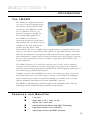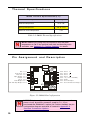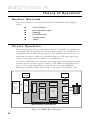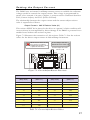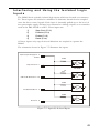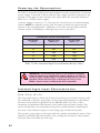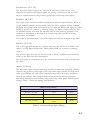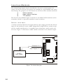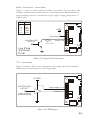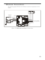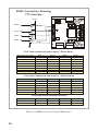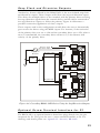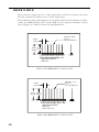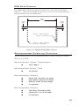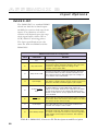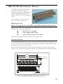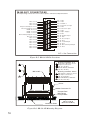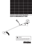
1
T TM intelligent motion systems, inc. Excellence in Motion TM IM483 HIGH PERFORMANCE MICROSTEPPING DRIVER STANDARD DRIVER CONNECTOR OPTIONS DUAL STEP CLOCK INPUT VERSION COOLING SOLUTIONS ACCESSORIES OPERATING INSTRUCTIONS 370 N. MAIN ST., PO BOX 457, MARLBOROUGH, CT 06447 PH. (860) 295-6102, FAX (860) 295-6107 Internet: http://www.imshome.com, E-Mail: [email protected] The information in this book has been carefully checked and is believed to be accurate; however, no responsibility is assumed for inaccuracies. Intelligent Motion Systems, Inc., reserves the right to make changes without further notice to any products herein to improve reliability, function or design. Intelligent Motion Systems, Inc., does not assume any liability arising out of the application or use of any product or circuit described herein; neither does it convey any license under its patent rights of others. Intelligent Motion Systems and are trademarks of Intelligent Motion Systems, Inc. TM Intelligent Motion Systems, Inc.’s general policy does not recommend the use of its products in life support or aircraft applications wherein a failure or malfunction of the product may directly threaten life or injury. Per Intelligent Motion Systems, Inc.’s terms and conditions of sales, the user of Intelligent Motion Systems, Inc., products in life support or aircraft applications assumes all risks of such use and indemnifies Intelligent Motion Systems, Inc., against all damages. IM483 Operating Instructions Revision 08.02.2000 ©1998 by Intelligent Motion Systems, Inc. All Rights Reserved Table of Contents Section 1: Introduction .......................................................................... 5 The IM483 ...................................................................................................................... Features and Benefits .................................................................................................. The Product Manual ...................................................................................................... Notes and Warnings ..................................................................................................... 5 5 6 7 Section 2: Hardware Specifications ....................................................... 8 Section Overview ......................................................................................................... 8 Mechanical Specifications ............................................................................................ 8 Electrical Specifications ................................................................................................ 9 Thermal Specifications ................................................................................................ 10 Pin Assignment and Description ................................................................................. 10 Section 3: Mounting The IM483 .......................................................... 13 Section 4: Theory of Operation ........................................................... 14 Section Overview ....................................................................................................... Circuit Operation .......................................................................................................... Microstep Select (MSEL) Inputs .................................................................................. Stepping ....................................................................................................................... Dual PWM Circuit ......................................................................................................... Fullstep Output Signal ................................................................................................. Timing ........................................................................................................................... 14 14 15 15 16 17 17 Section 5: Power Supply Requirements .............................................. 18 Section Overview ....................................................................................................... Selecting a Power Supply ........................................................................................... Selecting an Opto Supply ............................................................................................ Recommended Wiring ................................................................................................. AC Line Filtering .......................................................................................................... 18 18 20 21 22 Section 6: Motor Requirements ........................................................... 23 Section Overview ....................................................................................................... Selecting a Motor ......................................................................................................... Motor Wiring ................................................................................................................ Connecting the Motor .................................................................................................. 23 23 28 28 Section 7: Interfacing and Controlling the IM483 ............................... 32 Section Overview ....................................................................................................... 32 Layout and Interface Guidelines ................................................................................. 32 Motor Power Connection (+V) .................................................................................... 33 Configuring and Controlling the Output Current .......................................................... 34 Controlling the Output Resolution ................................................................................ 39 Interfacing and Using the Isolated Logic Inputs .......................................................... 41 Connecting and Using the Fault Output ...................................................................... 47 Full Step Output ........................................................................................................... 48 Minimum Connections .................................................................................................. 49 Section 8: Troubleshooting ................................................................. 50 Section Overview ....................................................................................................... Basic Troubleshooting ................................................................................................ Problem Symptoms and Possible Causes .................................................................. Contacting Technical Support ..................................................................................... The IMS Web Site ........................................................................................................ Returning Your Product to IMS .................................................................................... 50 50 50 53 53 53 1 Appendix A: Standard Connection Options ....................................... 54 Appendix Overview .................................................................................................... IM483-34P1 .................................................................................................................. IM483-8P2 .................................................................................................................... IM483-34P1-8P2 .......................................................................................................... IM483-PLG ................................................................................................................... 54 55 60 62 64 Appendix B: Input Options .................................................................. 66 IM483-DC ..................................................................................................................... 66 Appendix C: Cooling Solutions .......................................................... 68 H-4X Heat Sink Kit ....................................................................................................... 68 Thermal Non-Isolating Pad (TN-48) ............................................................................. 68 Appendix D: Accessories ..................................................................... 69 Appendix Overview .................................................................................................... U3-CLP: Side-Mounting Clip ......................................................................................... BB-34-P Breakout Board ............................................................................................. PLG-R Removable Screw Terminal Set ...................................................................... 2 69 69 71 73 List Of Figures Figure 2.1 Figure 2.2 Figure 3.1 Figure 4.1 Figure 4.2 Figure 4.3 Figure 6.1 Figure 6.2 Figure 6.3 Figure 6.4 Figure 6.5 Figure 6.6 Figure 7.1 Figure 7.2 Figure 7.3 Figure 7.4 Figure 7.5 Figure 7.6 Figure 7.7 Figure 7.8 Figure 7.9 Figure 7.10 Figure 7.11 Figure 7.12 Figure A.1 Figure A.2 FIgure A.3 Figure A.4 Figure A.5 Figure A.6 Figure A.7 Figure A.8 Figure A.9 Figure A.10 Figure A.11 Figure A.12 Figure B.1 Figure C.1 Figure D.1 Figure D.2 Figure D.3 Figure D.4 Figure D.5 Figure D.6 IM483 Dimensions ................................................................................... 8 IM483 Pin Configuration ........................................................................ 10 Mounting Recommendations ................................................................ 13 IM483 Block Diagram ............................................................................ 14 Recirculating PWM ................................................................................ 16 Non-Recirculating PWM ........................................................................ 16 Per Phase Winding Inductance ............................................................ 25 8 Lead Motor Series Connections ....................................................... 29 8 Lead Motor Parallel Connections ...................................................... 29 6 Lead Motor Half Coil (Higher Speed) Connections ........................... 30 6 Lead Motor Full Coil (Higher Torque) Connections ........................... 30 4 Lead Motor Connections ................................................................... 31 IM483 Motor Power Connections ......................................................... 34 Current Adjust Resistor Placement ...................................................... 37 Current Reduction Adjust Resistor Placement .................................... 38 MSEL Switch Showing 50 Microsteps/Step Selected ........................ 39 Optically Isolated Inputs ....................................................................... 41 Switch Interface ................................................................................... 44 Open Collector Interface ...................................................................... 45 TTL Interface ........................................................................................ 45 LYNX Interface ..................................................................................... 46 The Fault Output Connected to an LED ................................................ 47 The Full Step Output Connected to an Up/Down Counter ................... 48 IM483 Minimum Required Connections ................................................. 49 IM483-34P1 Connector P1 Mechanical Drawing ................................. 55 IM483-34P1 Connector P1 Pin Locations ............................................ 55 MSEL Connection Using TTL Interface ................................................ 58 Cascading IM483-34P1 Drives Using the Step/Direction Outputs ....... 59 IM483-8P2 - Connector P1 ................................................................... 60 IM483-8P2 - Connector P2 ................................................................... 60 IM483-8P2 PCB Hole Pattern ................................................................ 61 IM483-34P1-8P2 - Connector P1 .......................................................... 62 IM483-34P1-8P2 - Connector P2 .......................................................... 62 IM483-34P1-8P2 PCB Hole Pattern ....................................................... 63 IM483-PLG Connectors ........................................................................ 64 IM483-PLG Pin Location and Orientation .............................................. 65 IM483-DC Connection ........................................................................... 67 H-4X Heat Sink ..................................................................................... 68 U3-CLP Mounting Hole Locations ......................................................... 69 Attaching the U3-CLP to the IM483 ...................................................... 70 Panal Mounting an IM483 Using the U3-CLP Clip Set ........................... 70 BB-34-4P Breakout Board Mechanical Specifications ........................ 71 BB-34-4P Pin Locations ....................................................................... 72 BB-34-4P Mounting Diagram ................................................................ 72 3 List Of Tables Table 2.1 Table 2.2 Table 2.3 Table 2.4 Table 5.1 Table 5.2 Table 7.1 Table 7.2 Table 7.3 Table 7.4 Table A.1 Table B.1 4 Electrical Specifications ......................................................................... 9 IM483 Thermal Specifications .............................................................. 10 Connector P1 - Pin Assignment and Description .................................. 11 Connector P2 - Pin Assignment and Description ................................. 12 Motor Power Supply Requirements ..................................................... 19 +5 VDC Power Supply Requirements .................................................. 20 Current Adjust Resistor Values ........................................................... 37 Microstep Resolution Switch Settings ................................................. 40 Recommended Input Current Limiting Resistor Values ........................ 42 Isolated Logic Input Timing ................................................................... 43 IM483-34P1 - Connector P1 Pin Assignment and Description ........... 56 IM483-DC - Connector P1 Pin Assignment and Description ................ 66 Section 1 Introduction The IM483 The IM483 is a high performance, yet low cost microstepping driver that utilizes surface mount ASIC technology. The IM483 is small, easy to interface and use, yet powerful enough to handle the most demanding applications. The IM483 has 14 built-in microstep resolutions (both binary and decimal). The resolution can be changed at any time without the need to reset the driver. This feature allows the user to rapidly move long distances, yet precisely position the motor at the end of travel without the expense of high performance controllers. With the development of proprietary and patented circuits, ripple current has been minimized to reduce motor heating common with other designs, allowing the use of low inductance motors to improve high speed performance and system efficiency. The IM483, because of its small size and low cost, can be used to increase accuracy and smoothness in systems using higher step angle motors. In many instances mechanical gearing can be replaced with microstepping, reducing cost and eliminating potential maintenance. Available as options for the IM483 are a variety of connector styles, a heat sink and thermal pad and a dual clock input version of the IM483. If intelligent and/or closed loop control is needed the IM483 is available with on-board indexer (IM483I) and indexer/encoder (IM483IE) versions. The IM483 was developed to provide designers with affordable, state-of-the-art technology for the competitive edge needed in today’s market. Features and Benefits Low Cost. Advanced Surface Mount and ASIC Technology. Small Size 2.75” x 3.00” x 1.20” (69.9 x 76.2 x 30.5 mm). High Input Voltage (+12 to +48VDC). High Output Current (3A RMS, 4A Peak). 5 No Minimum Inductance. 20 kHz Chopping Rate. 14 Selectable Resolutions Both in Decimal and Binary. FAULT Output. Optically Isolated Inputs. Single Supply. Up to 10MHz Step Clock Rate. Short Circuit and Over Temperature Protection. Microstep Resolution to 51,200 Steps/Rev. Microstep Resolutions can be Changed “On-The-Fly” Without Loss of Motor Position. Automatically Switches Between Slow and Fast Decay for Unmatched Performance. Adjustable Automatic Current Reduction. At Full Step Output. Optional On-board Indexer and Encoder Feedback. CE Certified. The Product Manual The main sections of this manual address the standard IM483 driver, which come with 8 position screw terminals as a connection medium. The different connector, input options and accessories are covered in detail in the appendices. The indexer (IM483I) and indexer/encoder (IM483IE) versions of the IM483 are not covered in this document, as they have their own manual. Hyperlinks The IM483 product manual in its electronic format (IM483.pdf) can be downloaded from the IMS web site at http://www.imshome.com. This version includes a hyperlink feature that allows the reader to link from a referenced feature to a full description of that feature’s attributes and functions. Words with a hyperlink function are blue, italic and underlined, and are further identifiable because the cursor changes from a normal pointer to a “finger” pointer when placed over the word. 6 Notes and Warnings WARNING! The IM483 components are sensitive to ElectroStatic Discharge (ESD). All handling should be done at an ESD protected workstation. WARNING! Hazardous voltage levels may be present if using an open frame power supply to power the IM483. WARNING! Ensure that the power supply output voltage does not exceed the maximum input voltage of the IM483. 7 Section 2 Hardware Specifications Section Overview This section will acquaint you with the dimensional information, pin description, power, environmental and thermal requirements of the IM483. It is broken down as follows: Mechanical Specifications. Electrical Specifications. Thermal Specifications. Pin Assignment and Description. Mechanical Specifications Shown is the standard 8 position screw terminal set for the IM483. Dimensions and specifications for the different connection options are available in Appendix A: Standard Connection Options, of this document. Dimensions are in inches, parenthesis dimensions are in millimeters. 2.750 (69.9) 2.600 (66.0) 1.000 (25.4) 1 2 3 4 5 6 7 8 0.150 (3.8) 3.000 2.710 (76.2) (68.8) 0.290 (7.4) 4X Ø 0.160 (4X Ø 4.1) Figure 2.1: IM483 Dimensions 8 1.200 (30.5) 0.030 (0.8) Electrical Specifications Test Condition: TA=25°C, +V=48VDC IM483 Electrical Characteristics Specification Test Condition Input Voltage Phase Output Current RMS Phase Output Current P eak Quiescent Current Min Typ Max Unit 12 45 48* V 3 A 4 A 0.4** Inputs/Outputs Floating Active Power Dissipation IOUT=3A RMS Input Forward Current Isolated Inputs Input Forward Voltage Isolated Inputs Input Reverse Breakdown Voltage Isolated Inputs Output Current 70 mA 12 W 7.0 15 mA 1.5 1.7 V 5 V Fault, Fullstep Outputs 25 mA Fault Output 140 V Collector-Emitter Saturation Voltage Fault Output ICS = 25mA DC 0.2 V Drain-Source Voltage Fullstep Output 100 V Drain-Source On Resistance Fullstep Output ICS = 25mA DC Collector-Emitter Voltage 6.5 Ω * Includes motor back EMF. **Lower currents may be used for current reduction. Table 2.1: IM483 Electrical Specifications 9 Thermal Specifications IM4 8 3 T h e rma l S p e c ific a tio n s (°C ) Specification R an g e Ambient Temperature 0° to +50° Storage Temperature -40° to +125° Maximum Plate Temperature +70° Table 2.2: IM483 Thermal Specifications NOTE! Additional cooling may be required to limit the plate temperature to 70°C! An optional heat sink and thermal pad is available, see Appendix C: Cooling Solutions for details. Pin Assignment and Description N /C - P 1 :1 S te p C lo ck - P 1:2 D irection - P 1 :3 O pto S up ply - P 1:4 E na ble - P 1 :5 R es et - P 1 :6 F a ult O u tpu t - P 1:7 O n-F ull-S tep O u tpu t - P 1:8 P 2:8 P 2:7 P 2:6 P 2:5 P 2:4 P 2:3 P 2:2 P 2:1 - M otor A M otor A M otor B M otor B + V (+ 1 2 to + 48 V D C ) GND C u rre nt A d ju st C u rre nt R ed uc tio n A dju st Figure 2.2: IM483 Pin Configuration NOTE! This pin configuration diagram and table represent the pinout of any 8 position connector used for P1. If you purchased the IM483-34P1 option (34 Position Header) the pin configuration diagram and table is located in Appendix A: Standard Connection Options. 10 Connector P1 IM483 Connector P1 Configuration PIN # FUNCTION 1 N/C 2 Step Clock Input A positive going edge on this input advances the motor one increment. The size of the increment is dependent upon the settings of the resolution select switch SW1. 3 Direction Input This input is used to change the direction of the motor. Physical direction also depends upon the connection of the motor windings. 4 Opto Supply This +5VDC input is used to supply power to the isolated logic inputs. A higher voltage may be used, but care must be taken to limit the current through the opto-coupler. 5 Enable/Disable Input This input is used to enable/disable the output section of the driver. When in a Logic HIGH state (open), the outputs are enabled. However, this input does not inhibit the step clock, therefore, the outputs will update by the number of clock pulses (if any) applied to the driver while it was disabled. 6 Reset Input When LOW, this input will reset the driver (phase outputs will disable). When released, the driver will be at its initial state (Phase A OFF, Phase B ON). 7 Fault Output This output indicates that a short circuit condition has occurred. This output is active LOW. 8 On-Full-Step Output DETAILS No connection. This open collector output indicates when the driver is positioned at full step. This output can be used to count the number of full steps the motor has moved, regardless of the number of microsteps in between. This output is active LOW. Table 2.3: Connector P1 - Pin Assignment and Descriptions 11 Connector P2 IM483 Connector P2 Configuration PIN # FUNCTION DETAILS 1 Current Reduction Adjust Phase Current Reduction Adjustment Input. A resistor connected between this pin and pin 2 will proportionately reduce the current in both motor windings approximately .5 seconds after the last positive edge of the step clock input. The amount of current reduced will depend upon the value of the resistor used. 2 Current Adjustment Phase Current Adjustment. A resistor is connected between this pin and P2:3 (GND) to adjust the maximum phase current in the motor. A resistor MUST be connected to this input or the IM483 WILL latch into fault. 3 GND Power Ground. The ground, or return, of the power supply is connected here. 4 +V 5 Phase B ØB of the stepping motor. 6 Phase B ØB of the stepping motor 7 Phase A ØA of the stepping motor. 8 Phase A ØA of the stepping motor. Motor Supply Voltage. +12 to +48VDC. Table 2.4: Connector P2 - Pin Assignment and Descriptions WARNING! The IM483 components are sensitive to ElectroStatic Discharge (ESD). All handling should be done at an ESD protected workstation. WARNING! Hazardous voltage levels may be present if using an open frame power supply to power the IM483. WARNING! Ensure that the power supply output voltage does not exceed the maximum input voltage of the IM483. 12 Section 3 Mounting The IM483 This section has recommended mounting instructions for the standard IM483. Special mounting instructions for any of the connection options for the IM483 are available in Appendix A: Standard Connection Options, of this document. An optional heat sink and thermal pad, the H-4X and TN-48, are available for the IM483. See Appendix C: Cooling Solutions, for details. A B C 1 2 3 4 5 6 7 8 T h e rm a l P a d T N -4 8 o r E q u iv a le n t M o u n tin g P la te o r H e a t S in k S u rfa c e 4 X # 6 (M 3 ) T h re a d e d H o le s . (S e e M e c h a n ica l, F ig u re 2 .1 for H o le P a tte rn D im e n sio n s) The torque specification for the m ounting screws is 5.0 to 7.0 lb-in (0.60 to 0.80 N-m ). Do not overtighten screws! M etric (4 ea.) U.S. (4 ea.) A # 6 X 5 /8 S ta in le s s M a ch in e S cre w A M 3 X 0 .5 S ta in le s s M a ch in e S cre w B # 6 S p lit L o ck W a sh e r, S ta in le ss (.0 4 T H , .2 4 O D ) B M 3 S p lit L o c k W a s h e r, S ta in le ss (.0 8 T H , .6 .2 0 O D ) C C Figure 3.1: Mounting Recommendations NOTE! This diagram focuses on the standard IM483. The IM483-8P2 and IM483-34P1-8P2 feature connector pins which may be soldered directly into a user’s PCB design. Mounting details and a PCB hole pattern may be found in Appendix A: Standard Connection Options. 13 Section 4 Theory of Operation Section Overview This section will cover the circuit operation for the IM483 microstepping driver. Circuit Operation. Microstep Select Inputs. Stepping. Dual PWM Circuit. Fullstep Output. Timing. Circuit Operation Microstepping drives have a much higher degree of suitability for applications that require smooth operation and accurate positioning at low speeds than do half/fullstep drivers and reduction gearing. The IM483, which can to be set to microstep resolutions as high as 51,200 microsteps/rev (256 microsteps/step) using a 1.8° stepping motor, is ideal for such applications. In order to subdivide motor steps into microsteps while maintaining positional accuracy, precise current control is required. The IM483 accomplishes this by the use of a unique Dual PWM circuit built into the patented IM2000 Microstep Controller ASIC, which resides at the heart of the IM483. This O P TO S U P PLY U S ER IN TER FA CE S TE P CLO CK DIRE CT IO N E NA BLE RES ET INP UT LO GIC IS OLAT ION CIRCUITRY P O W ER S U P P LY M IC ROS TEP RES O LUTIO N S ELE CTIO N 20 kH z CH OP. O SC S HO RT C IR C U IT P RO TE C T IO N INP UT LO GIC P H A S E A /B OU TPU T C IR C U IT R Y S INE/CO SINE P OSITIO N G EN ERATO R C U R RE NT C ON TR OL C U R RE NT S E N S IN G IM 2000 MICROSTEP CONT ROLLER P RO TECTIO N CIRCUIT IM 483 M ICR OSTEPPIN G D R IVER Figure 4.1: IM483 Block Diagram 14 OVER CURRENT PROTECTION S TEP PIN G M O TO R PWM circuit uses alternating recirculating/non-recirculating modes to accurately regulate the current in the windings of a two phase stepping motor. Microstep Select (MSEL) Inputs Another unique feature of the IM2000 is the ability to change resolutions at any time. A resolution change can occur whether the motor is being clocked or is at rest. The change will not take place until the rising edge of the next step clock input. At this time, the new resolution is latched and implemented before the step clock pulse takes effect. If a resolution is chosen such that the sine/cosine output of the IM2000 would not land on an electrical fullstep of the motor, then the IM2000 will automatically align itself to the full step position on the step clock pulse that would have caused the motor to rotate past the full step. The step clock pulses, from that point forward, will be equal to the selected resolution. This feature allows the user to switch resolutions at any time without having to keep track of sine/ cosine location. Because of this, the On-Full-Step output of the IM483 can easily be used to monitor position. Configuration settings for the Microstep Resolution are located in Section 7 of this document, Interfacing and Controlling the IM483. Stepping The IM2000 contains a built-in sine/cosine generator used for the generation of Phase A and Phase B position reference. This digitally encoded 9 bit sine and 9 bit cosine signal is directly fed into a digital to analog converter. The step clock (SCLK) and direction (DIR) inputs are buffered using Schmidt triggered buffers for increased noise immunity and are used to increment or decrement the sine/cosine position generator. The position generator is updated on the rising edge of the step clock input. It will increment or decrement by the amount specified by the microstep resolution select (MSEL) inputs. The direction (DIR) input determines the direction of the position generator and hence the direction of the motor. The DIR input is synchronized to the SCLK input. On the rising edge of the SCLK input the state of the DIR input is latched in. The position generator will then look to see if there has been a change in direction and implement that change before executing the next step. By utilizing this method to implement the direction change, the noise immunity is greatly increased and no physical change in the motor occurs if the direction line is toggled prior to the step clock input. The enable/disable input does not affect the step clock input. The sine/cosine generator will continue to update if a signal is applied to the step clock input. 15 The IM2000 outputs both sine and cosine data simultaneously when applying a step clock input. Dual internal look-up tables are used to output a unique position for every step clock input to enhance system performance. Dual PWM Circuit The IM2000 contains a unique dual PWM circuit that efficiently and accurately regulates the current in the windings of a two phase stepping motor. The internal PWM accomplishes this by using an alternating recirculating/non-recirculating mode to control the current. Recirculating In a recirculating PWM, the current in the windings is contained within the output bridge while the PWM is in its OFF state. (After the set current is reached.) This method of controlling the current is efficient when using low inductance motors, but lacks response because of its inability to remove current from the windings on the downward cycle of the sine/cosine wave (See Figure 4.1). D R IV E C U R R E N T R E C IR C U L AT IO N Figure 4.2: Recirculating PWM Non-Recirculating In a non-recirculating PWM, the current flows up through the bridge and back to the supply in the OFF phase of the cycle. This method of controlling current allows for much better response but reduces efficiency and increases current ripple, especially in lower inductance motors (See Figure 4.3). D R IV E C U R R E N T R E C IR C U L AT IO N Figure 4.3: Non-Recirculating PWM 16 The IM2000’s PWM utilizes the best features of both by combining recirculating and non-recirculating current control. On the rising edge of the sine/cosine waveform, the PWM will always be in a recirculating mode. This mode allows the driver to run at peak efficiency while maintaining minimum current ripple even with low inductance motors. On the downward cycle of the sine/cosine waveform, the PWM operates in a two part cycle. In the first part of its cycle, the PWM is in a non-recirculating mode to pull current from the motor windings. In the second part of the cycle the PWM reverts back to recirculating mode to increase efficiency and reduce current ripple. The IM2000 will automatically change the non-recirculating pulse widths to compensate for changes in supply voltage and accommodate a wide variety of motor inductances. This method also allows for the use of very low inductance motors with your IM483 driver, while utilizing a 20kHz chopping rate which reduces motor heating but maintains high efficiency and low current ripple. Fullstep Output Signal The fullstep output signal from the IM483 is an active high output at connector P1:8. This output will be TRUE for the duration of the full step. A full step occurs when either Phase A or Phase B crosses through zero (i.e. full current in one motor winding and zero current in the other winding). This fullstep position is a common position regardless of the microstep resolution selected. The fullstep output can be used to count the number of mechanical fullsteps that the motor has traveled without the need to count the number of microsteps in between. A controller that utilizes this output can greatly reduce its position tracking overhead, thus substantially increasing its throughput. Interface guidelines and a sample application for the fullstep output are located in Section 7 of this document, Interfacing and Controlling the IM483. Timing The direction and microstep resolution select inputs are synchronized with the positive going edge of the step clock input. When the step clock input goes HIGH, the direction and microstep resolution select inputs are latched. Further changes to these inputs are ignored until the next rising edge of the step clock input. After these signals are latched, the IM483 looks to see if any changes have occurred to the direction and microstep resolution select inputs. If a change has occurred, the IM483 will execute the change before taking the next step. Only AFTER the change has been executed will the step be taken. If no change has occurred, the IM483 will simply take the next step. This feature works as an automatic debounce for the direction and microstep resolution select inputs. The reset and enable inputs are asynchronous to any input and can be changed at any time. 17 Section 5 Power Supply Requirements Section Overview This section covers the power supply requirements of the IM483. Precise wiring and connection details are to be found in Section 7: Interfacing and Controlling the IM483. The following is covered by this section: Selecting a Power Supply. Recommended Wiring. AC Line Filtering. Selecting a Power Supply Selecting a Motor Supply (+V) Proper selection of a power supply to be used in a motion system is as important as selecting the drive itself. When choosing a power supply for a stepping motor driver, there are several performance issues that must be addressed. An undersized power supply can lead to poor performance and possibly even damage to your drive. The Power Supply - Motor Relationship Motor windings can basically be viewed as inductors. Winding resistance and inductance result in an L/R time constant that resists the change in current. To effectively manipulate the rate of charge, the voltage applied is increased. When traveling at high speeds, there is less time between steps to reach current. The point where the rate of commutation does not allow the driver to reach full current is referred to as voltage mode. Ideally you want to be in current mode, which is when the drive is achieving the desired current between steps. Simply stated, a higher voltage will decrease the time it takes to charge the coil and, therefore, will allow for higher torque at higher speeds. Another characteristic of all motors is back EMF. Back EMF is a source of current that can push the output of a power supply beyond the maximum operating voltage of the driver. As a result, damage to the stepper driver could occur over a period of time. The Power Supply - Driver Relationship The IM483 is very current efficient as far as the power supply is concerned. Once the motor has charged one or both windings of the motor, all the power supply has to do is replace losses in the system. The charged winding acts as an energy storage in that the current will recirculate within the bridge and in and 18 out of each phase reservoir. This results in a less than expected current draw on the power supply. Stepping motor drivers are designed with the intent that a user’s power supply output will ramp up to greater than or equal to the minimum operating voltage of the drive. The initial current surge is substantial and could damage the driver if the supply is undersized. The output of an undersized power supply could fall below the operating range of the driver upon a current surge. This could cause the power supply to start oscillating in and out of the voltage range of the driver and result in damage to either the supply, the driver, or both. There are two types of supplies commonly used, regulated and unregulated, both of which can be switching or linear. Each have advantages and disadvantages. Regulated vs. Unregulated An unregulated linear supply is less expensive and more resilient to current surges, however, the voltage decreases with increasing current draw. This may cause problems if the voltage drops below the working range of the drive. Fluctuations in line voltage are also a point of concern. These fluctuations may cause the unregulated linear supply to be above or below the anticipated or acceptable voltage. A regulated supply maintains a stable output voltage, which is good for high speed performance. These supplies are also not affected by line fluctuations, however, they are more expensive. Depending on the current regulation, a regulated supply may crowbar or current clamp and lead to an oscillation that, as previously stated, can cause damage to the driver and/or supply. Back EMF can cause problems for regulated supplies as well. The current regeneration may be too large for the regulated supply to absorb. This could lead to an over voltage condition which could damage the output circuitry of the IM483. Non IMS switching power supplies and regulated linear supplies with overcurrent protection are not recommended because of their inability to handle the surge currents inherit in stepping motor systems. Motor Pow er Supply Specifications Specification Recommended Supply Type Unregulated DC Ripple Voltage ±10% Output Voltage +12 to +45 VDC Output Current* 3A P eak * The output current needed is dependent on the power supply voltage, the motor selection and the load. Table 5.1: Motor Power Supply Specifications 19 Recommended IMS Power Supplies IMS has designed a series of low cost miniature unregulated switchers and unregulated linears which can handle extreme varying load conditions. This makes them ideal for stepper motor drives and DC servo motors as well. Each of these is available in either 120 or 240 VAC configuration. See the IMS Catalog or web site (http://www.imshome.com) for information on these supplies. Listed below are the power supplies recommended for use with the IM483. Unregulated Linear Supply IP404 Input Specifications *AC Input Voltage Range .......................................................102-132VAC Output Specifications Voltage (Nominal - No Load) ................................................... 40 VDC Current (Peak) ............................................................................. 4 Amps *Options IP404-240 ................................................................................. 240VAC Input Unregulated Switching Supply ISP200-4 Input Specifications *AC Input Voltage Range .......................................................102-132VAC Frequency ................................................................................... 50-60 Hz Output Specifications Voltage (Nominal - No Load) ................................................... 45 VDC Current (Continuous) ..................................................................... 3 *Options ISP200H-4/7 ........................................................................... 240VAC Input Selecting an Opto Supply Opto Supply Specifications Specification Recommended Supply Type Regulated Linear or Switch Mode DC Ripple Voltage ±10% Output Voltage +5VDC Output Current 100mA NOTE: An opto supply voltage in excess of +5VDC may be used if steps are taken to limit the current to 15mA maximum! Table 5.2: +5VDC Power Supply Specifications 20 Recommended Wiring Rules of Wiring and Shielding Noise is always present in a system that involves both high power and small signal circuitry. Regardless of the power configuration used for your system, there are some wiring and shielding rules that should be followed to keep the noise-to-signal ratio as small as possible. Rules of Wiring Power supply and motor wiring should be shielded twisted pairs run separately from signal carrying wires. A minimum of 1 twist per inch is recommended. Motor wiring should be shielded twisted pairs using 20-gauge wire or, for distance greater than 5 feet, 18 gauge or better. Power ground return should be as short as possible to established ground. Power supply wiring should be shielded twisted pairs. Use 18 gauge wire if load is less than 4 amps, or 16 gauge for more than 4 amps. Do not “Daisy-Chain” power wiring to system components. Rules of Shielding The shield must be tied to zero-signal reference potential. In order for shielding to be effective, it is necessary for the signal to be earthed or grounded. Do not assume that earth ground is true earth ground. Depending on the distance to the main power cabinet, it may be necessary to sink a ground rod at a critical location. The shield must be connected so that shield currents drain to signal-earth connections. The number of separate shields required in a system is equal to the number of independent signals being processed plus one for each power entrance. The shield should be tied to a single point to prevent ground loops. A second shield can be used over the primary shield, however, the second shield is tied to ground at both ends. Recommended Power Supply Cables Power supply cables must not run parallel to logic level wiring as noise will be coupled onto the logic signals from the power supply cables. If more than one driver is to be connected to the same power supply, run separate power and 21 ground leads to each driver from the power supply. The following twisted pair jacketed Belden cable (or equivalent) are recommended for use with the IM483. Belden Part# 9740 or equivalent 18 Gauge AC Line Filtering Since the output voltage of an unregulated power supply will vary with the AC input applied, it is recommended that an AC line filter be used to prevent damage to the IM483 due to a lightning strike or power surge. WARNING! Verify that the power supply wiring is correct prior to power application. If +V and GND are connected in reverse order, catastrophic damage to the IM483 may occur! Ensure that the power supply output voltage does not exceed +48 VDC, which is the maximum input voltage of the IM483! WARNING! Hazardous voltage levels may be present if using an open frame power supply to power the IM483! 22 Section 6 Motor Requirements Section Overview This section covers the motor configurations for the IM483. Selecting a Motor. Motor Wiring. Connecting the Motor. Selecting a Motor When selecting a stepper motor for your application, there are several factors that need to be taken into consideration: How will the motor be coupled to the load? How much torque is required to move the load? How fast does the load need to move or accelerate? What degree of accuracy is required when positioning the load? While determining the answers to these and other questions is beyond the scope of this document, they are details that you must know in order to select a motor that is appropriate for your application. These details will affect everything from the power supply voltage to the type and wiring configuration of your stepper motor. The current and microstepping settings of your IM483 drive will also be affected. Ty p e s a n d C o n s t r u c t i o n o f S t e p p i n g M o t o r s The stepping motor, while classed as a DC motor, is actually an AC motor that is operated by trains of pulses. Although it is called a “stepping motor”, it is in reality a polyphase synchronous motor. This means it has multiple phases wound in the stator and the rotor is dragged along in synchronism with the rotating magnetic field. The IM483 is designed to work with the following types of stepping motors: 1) Permanent Magnet (PM) 2) Hybrid Stepping Motors 23 Hybrid stepping motors combine the features of the PM stepping motors with the features of another type of stepping motor called a variable reluctance motor (VR). VR motors are low torque and load capacity motors which are typically used in instrumentation. The IM483 cannot be used with VR motors as they have no permanent magnet. On hybrid motors, the phases are wound on toothed segments of the stator assembly. The rotor consists of a permanent magnet with a toothed outer surface which allows precision motion accurate to within ± 3 percent. Hybrid stepping motors are available with step angles varying from 0.45° to 15° with 1.8° being the most commonly used. Torque capacity in hybrid steppers ranges from 5 - 8000 ounce-inches. Because of their smaller step angles, hybrid motors have a higher degree of suitability in applications where precise load positioning and smooth motion is required. S i z i n g a M o t o r f o r Yo u r S y s t e m The IM483 is a bipolar driver which works equally well with both bipolar and unipolar motors (i.e. 8 and 4 lead motors, and 6 lead center tapped motors). To maintain a given set motor current, the IM483 chops the voltage using a constant 20kHz chopping frequency and a varying duty cycle. Duty cycles that exceed 50% can cause unstable chopping. This characteristic is directly related to the motor’s winding inductance. In order to avoid this situation, it is necessary to choose a motor with a low winding inductance. The lower the winding inductance, the higher the step rate possible. Winding Inductance Since the IM483 is a constant current source, it is not necessary to use a motor that is rated at the same voltage as the supply voltage. What is important is that the IM483 is set to the motor’s rated current. See Section 7: Interfacing and Controlling the IM483 for more details. As was discussed in the previous section, Power Supply Requirements, the higher the voltage used the faster the current can flow through the motor windings. This in turn means a higher step rate, or motor speed. Care should be taken not to exceed the maximum voltage of the driver. Therefore, in choosing a motor for a system design, the best performance for a specified torque is a motor with the lowest possible winding inductance used in conjunction with highest possible driver voltage. The winding inductance will determine the motor type and wiring configuration best suited for your system. While the equation used to size a motor for your system is quite simple, several factors fall into play at this point. The winding inductance of a motor is rated in milliHenrys (mH) per Phase. The amount of inductance will depend on the wiring configuration of the motor. 24 A ctu a l In d uc ta n ce S e en B y the D riv er A ctu a l In d uc ta n ce S e en B y the D riv er S p e cified P er P ha se Ind u ctan ce S p e cified P er P ha se Ind u ctan ce PH ASE A PH ASE A PH ASE A PH ASE A PH ASE B PH ASE B PH ASE B PH ASE B 8 Lea d S tep ping M otor S erie s C o n fig uration 8 Lea d S tep ping M otor P aralle l C onfigu ra tion (N ote: T h is ex am ple a ls o ap plie s to th e 6 le ad m otor fu ll co pp er c onfigu ration and to 4 lea d step ping m otors) A (N ote: T h is ex am ple a ls o ap plie s to th e 6 le ad m otor ha lf co ppe r co nfig u ra tio n) B Figure 6.1 A & B: Per Phase Winding Inductance The per phase winding inductance specified may be different than the per phase inductance seen by your IM483 driver depending on the wiring configuration used. Your calculations must allow for the actual inductance that the driver will see based upon the wiring configuration. Figure 6.1A shows a stepper motor in a series configuration. In this configuration, the per phase inductance will be 4 times that specified. For example: a stepping motor has a specified per phase inductance of 1.47mH. In this configuration the driver will see 5.88 mH per phase. Figure 6.1B shows an 8 lead motor wired in parallel. Using this configuration the per phase inductance seen by the driver will be as specified. Maximum Motor Inductance (mH per Phase) = .2 X Minimum Supply Voltage NOTE: In calculating the maximum phase inductance, the minimum supply output voltage should be used when using an unregulated supply. Using the following equation we will show an example of sizing a motor for a IM483 used with an unregulated power supply with a minimum voltage (+V) of 18 VDC: .2 X 18 = 3.6 mH The recommended per phase winding inductance we can use is 3.6 mH. 25 Recommended IMS Motors IMS stocks the following 1.8° hybrid stepping motors that are recommended for the IM483. All IMS motors are CE marked. For more detailed information on these motors, please see the IMS Full Line catalog or the IMS web site at http:// www.imshome.com. 17 Frame Single Shaft Double Shaft M2-1713-S .......................................................................... M2-1713-D M2-1715-S .......................................................................... M2-1715-D M2-1719-S .......................................................................... M2-1719-D 23 Frame Single Shaft Double Shaft M2-2215-S .......................................................................... M2-2215-D M2-2220-S .......................................................................... M2-2220-D M2-2232-S .......................................................................... M2-2232-D M2-2240-S .......................................................................... M2-2240-D Enhanced Stepper Motors IMS also carries a new series of 23 frame enhanced stepping motors that are recommended for use with the IM483. These motors use a unique relationship between the rotor and stator to generate more torque per frame size while ensuring more precise positioning and increased accuracy. The special design allows the motors to provide higher torque than standard stepping motors while maintaining a steadier torque and reducing torque drop-off. The motors are available in 3 stack sizes, single or double shaft, with or without encoders. They handle currents up to 3 Amps in series or 6 Amps parallel, and holding torque ranges from 95 oz.-in. to 230 oz.-in (67 N-cm to 162 N-cm). These CE rated motors are ideal for applications where higher torque is required. 23 Frame High Torque Motors Single Shaft Double Shaft MH-2218-S ......................................................................... MH-2218-D MH-2222-S ......................................................................... MH-2222-D MH-2231-S ......................................................................... MH-2231-D 26 IMS Inside Out Stepper Motors The new inside out stepper (IOS) motor was designed by IMS to bring versatility to stepper motors using a unique multi-functional, hollow core design. This versatile new motor can be converted to a ball screw linear actuator by mounting a miniature ball screw to the front shaft face. Ball screw linear actuators offer long life, high efficiency, and can be field retrofitted. There is no need to throw the motor away due to wear of the nut or screw. The IOS motors offer the following features: The shaft face diameter offers a wide choice of threaded hole patterns for coupling. The IOS motor can be direct coupled in applications within the torque range of the motor, eliminating couplings and increasing system efficiency. The IOS motor can replace gearboxes in applications where gearboxes are used for inertia damping between the motor and the load. The induced backlash from the gearbox is eliminated providing improved bi-directional position accuracy. Electrical or pnuematic lines can be directed through the center of the motor enabling the motors to be stacked endto-end or applied in robotic end effector applications. The through hole is stationary, preventing cables from being chaffed by a moving hollow shaft. Light beams can be directed through the motor for refraction by a mirror or filter wheel mounted on the shaft mounting face. The IOS motor is adaptable to valves enabling the valve stem to protrude above the motor frame. The stem can be retrofitted with a dial indicator showing valve position. The motor is compatible with IMS bipolar drivers, keeping the system cost low. The IOS motor can operate up to 3000 rpm’s. The IOS motor is available in the following frames: Frame Size IMS PN 17 Frame .............................................................................M3-1713-IOS 23 Frame .............................................................................M3-2220-IOS 27 Motor Wiring As with the power supply wiring, motor wiring should be run separately from logic wiring to minimize noise coupled onto the logic signals. Motor cabling exceeding 1’ in length should be shielded twisted pairs to reduce the transmission of EMI (Electromagnetic Interference) which can lead to rough motor operation and poor system performance. For more information on wiring and shielding, please refer to Rules of Wiring and Shielding in Section 5 of this manual. NOTE: The physical direction of the motor with respect to the direction input will depend upon the connection of the motor windings. To switch the direction of the motor with respect to the direction input, switch the wires on either Phase A or Phase B outputs. WARNING! Do not connect or disconnect motor or power leads with power applied! Below are listed the recommended motor cables: Dual Twisted Pair Shielded (Separate Shields) < 5 feet ................................................... Belden Part# 9402 or equivalent 20 Gauge > 5 feet ................................................... Belden Part# 9368 or equivalent 18 Gauge When using a bipolar motor, the motor must be within 100 feet of the drive. Connecting the Motor The motor leads are connected to the following connector pins: IM483 Phase Connector: Pin Phase B ........................................................................................ P2: 5 Phase B ........................................................................................ P2: 6 Phase A ....................................................................................... P2: 7 Phase A ....................................................................................... P2: 8 28 8 Lead Motors 8 lead motors offer a high degree of flexibility to the system designer in that they may be connected in series or parallel, thus satisfying a wide range of applications. Series Connection A series motor configuration would typically be used in applications where a higher torque at lower speeds is required. Because this configuration has the most inductance, the performance will start to degrade at higher speeds. Use the per phase (or unipolar) current rating as the peak output current, or multiply the bipolar current rating by 1.4 to determine the peak output current. PHASE A PHASE A PHASE B PHASE B Figure 6.2: 8 Lead Motor Series Connections Parallel Connection An 8 lead motor in a parallel configuration offers a more stable, but lower torque at lower speeds. But because of the lower inductance, there will be higher torque at higher speeds. Multiply the per phase (or unipolar) current rating by 1.96, or the bipolar current rating by 1.4, to determine the peak output current. PHASE A PHASE A PHASE B PHASE B Figure 6.3: 8 Lead Motor Parallel Connections 29 6 Lead Motors Like 8 lead stepping motors, 6 lead motors have two configurations available for high speed or high torque operation. The higher speed configuration, or half coil, is so described because it uses one half of the motor’s inductor windings. The higher torque configuration, or full coil, uses the full windings of the phases. Half Coil Configuration As previously stated, the half coil configuration uses 50% of the motor phase windings. This gives lower inductance, hence, lower torque output. Like the parallel connection of 8 lead motor, the torque output will be more stable at higher speeds. This configuration is also referred to as half copper. In setting the driver output current multiply the specified per phase (or unipolar) current rating by 1.4 to determine the peak output current. PHASE A PHASE A N O C ON NEC TION PHASE B PHASE B N O C ON NEC TION Figure 6.4: 6 Lead Half Coil (Higher Speed) Motor Connections Full Coil Configuration The full coil configuration on a six lead motor should be used in applications where higher torque at lower speeds is desired. This configuration is also referred to as full copper. Use the per phase (or unipolar) current rating as the peak output current. PHASE A N O C ONNEC TION PHASE A PHASE B N O C ONNEC TION PHASE B Figure 6.5: 6 Lead Full Coil (Higher Torque) Motor Connections 30 4 Lead Motors 4 lead motors are the least flexible but easiest to wire. Speed and torque will depend on winding inductance. In setting the driver output current, multiply the specified phase current by 1.4 to determine the peak output current. PHASE A PHASE A PHASE B PHASE B Figure 6.6: 4 Lead Motor Connections 31 Section 7 Interfacing and Controlling the IM483 Section Overview This section covers the interface connections, configuration and control signals of the IM483. Covered are: Layout and Interface Guidelines. Motor Power Connection (+V). Controlling the Output Current Controlling the Output Resolution. Logic Interface Connection and Use. Using the Fault Output. Using the On-Fullstep Output. Minimum Required Connections. Layout and Interface Guidelines Logic level signals should not run parallel to motor phase signals. The motor phase signals will couple noise onto the logic level signals. This will cause rough motor motion and unreliable system operation. The motor phase signals should be run as pairs. When leaving the driver module, motor cables should not run parallel with other wires. Phases should be wired using twisted pairs. If motor cabling in excess of one foot is required, motor cabling should be shielded twisted pairs to reduce the transmission of EMI. The shield must be tied to AC ground at the driver end only, or the supply ground if AC ground is not available. The motor end must be left floating. If more than one driver is connected to the power supply, separate power and ground connections from each driver to the power supply should be used. Do not “daisy chain”. The power supply cables need to be a twisted pair if power is connected from a source external to the board. If multiple drivers are used with an external power source and it is not possible to run separate power and ground connections to each driver, a low impedance electrolytic capacitor equivalent to two times the total capacitance of all driver capacitors and of equal voltage must be placed at the power input of the board. 32 Recommended Wiring Practices The following wiring/cabling is recommended for use with the IM483: Motor Power Belden Part# 9740 or equivalent 18 AWG (shielded twisted pair). Motor The motor cabling recommended for use will depend upon the distance in which the motor will be located from the drive. < 5 feet .................... Belden Part# 9402 or equivalent 20 AWG > 5 feet .................... Belden Part# 9368 or equivalent 18 AWG Logic Wiring Wire Size .................................................................... 20-22 AWG General Practices The following wire strip length and tightening torque is recommended: Wire Strip Length ................................................. 0.238” (6.0 mm) Terminal Screw Tightening Torque ................. 4.5 lb-in (0.5 N-m) WARNING! Do not exceed the recommended tightening torque for the screw terminals! WARNING! Do not connect or disconnect any wiring when power is applied! Motor Power Connection (+V) Figure 7.1 illustrates the motor power (+V) connection to two IM483 drives using a recommended IMS ISP200-4 unregulated switching power supply. Shown are the proper wiring practices of using shielded twisted pair wiring, with the shield tied to AC ground and the driver end left floating. Each drive is wired to the power supply separately, rather than daisy-chained together. Following these principles will reduce the electrical noise in your system and help eliminate a major cause of erratic system perfomance. Please note that an AC line conditioner is also shown. This protects your system from potential damage resulting from line spikes and surges. 33 A C L IN E C O N D IT IO N E R 120VA C IN C hass is G rou nd IM 483 #1 IN TELLIGENT MOTION SYSTEMS, INC. P 2:4 - + V NEUT P 2:1 LINE P 2:3 - G N D EGND GND V+ 75v 48v ISP200 48v 75v PS0020 REV D P 2:4 - + V P 2:3 - G N D P 2:1 N O TE THE FO LLO W IN G : 1] T he us e o f sh ielded tw isted pair ca bling . 2] W iring ru n to e ac h drive se pa ra te ly. 3] A C L ine C o nd ition ing u sed to lim it line spik es an d su rg es . IM 483 #2 Figure 7.1: IM483 Motor Power Connection Configuring and Controlling the Output Cur rent For any given motor, the output current used for microstepping is determined differently from that of a half/full step driver. In the IM483, a sine/cosine output function is used in rotating the motor. Therefore, when microstepping, the specified phase current of the motor is considered an RMS value. The output current is set by means of a current adjustment resistor placed between P2:2 (Current Adjust) and P2:3 (Power Ground). See the next subsection titled “Setting the Output Current” for connection instructions and resistor values. The IM483 also has an automatic current reduction feature, which allows the user to reduce the current in the motor windings to the level required to maintain holding torque, thus allowing for cooler motor operation and greater system power effeciency. This feature is controlled by means of a resistor connected between P2:1 (Reduction Adjust) and P2:2 (Current Adjust). The subsection; “Reducing the Output Current” contains reduction adjustment resistor calculations and connection instructions. 34 Determining the Output Current Stepper motors can be configured as 4, 6 or 8 leads. Each configuration requires different currents. Shown below are the different lead configurations and the procedures to determine the peak per phase output current setting that would be used with different motor/lead configurations. NOTE! The PEAK current will be used to determine the current adjust resistor value, NOT the RMS current! This represents the maximum output current that should be set for your IM483 driver! 4 Lead Motors Multiply the specified phase current by 1.4 to determine the peak output current. EXAMPLE: A 4 lead motor has a specified phase current of 2.0A 2.0A x 1.4 = 2.8 Amps Peak 6 Lead Motors 1) When configuring a 6 lead motor in a half coil configuration (i.e. connected from one end of the coil to the center tap (high speed configuration)) multiply the specified per phase (or unipolar) current rating by 1.4 to determine the peak output current. EXAMPLE: A 6 lead motor in half coil configuration has a specified phase current of 3.0A 3.0A x 1.4 = 4.2 Amps Peak 2) When configuring the motor so the full coil is used (i.e. connected from end-to-end with the center tap floating (higher torque configuration)) use the per phase (or unipolar) current rating as the peak output current. EXAMPLE: A 6 lead motor in full coil configuration with a specified phase current of 3.0A 3.0A per phase = 3.0 Amps Peak 35 8 Lead Motors SERIES CONNECTION: When configuring the motor windings in series, use the per phase (or unipolar) current rating as the peak output current, or multiply the bipolar current rating by 1.4 to determine the peak output current. EXAMPLE: An 8 lead motor in series configuration with a specified unipolar current of 3.0A 3.0A per phase = 3.0 Amps Peak An 8 lead motor in series configuration with a specified bipolar current of 2.8A 2.8 x 1.4 = 3.92 Amps Peak PARALLEL CONNECTION: When configuring the motor windings in parallel, multiply the per phase (or unipolar) current rating by 2.0 or the bipolar current rating by 1.4 to determine the peak output current. EXAMPLE: An 8 lead motor in parallel configuration with a specified unipolar current of 2.0A 2.0A per phase X 2.0 = 4.0 Amps Peak An 8 lead motor in parallel configuration with a specified bipolar current of 2.8A 2.8 x 1.4 = 3.92 Amps Peak WARNING! Although stepping motors will run hot when configured correctly, damage may occur to a motor if a higher than specified current is used. In most cases, the specified motor currents are maximum values and should not be exceeded! 36 Setting the Output Current The IM483 uses an internal 1 milliamp current source to establish the reference voltage needed to control the output current. This voltage is programmed by means of an external 1/8 watt or higher, 1 percent resistor connected between P2:2 (Current Adjust) and P2:3 (Power Ground). The relationship between the output current and the current adjust resistor value is expressed as follows: Output Current = .002 X Resistor Value (Ω) This resistor MUST be in place for the driver to operate! A fault condition will occur and may be accompanied by driver damage if the IM483 is powered in an enabled state without this resistor in place. Figure 7.2 illustrates the connection of this resistor. Table 7.1 lists the resistor values for the driver output current in 200 milliamp increments. NO TE: Resistor leads should be as short as possible to m inim ize the am ount of noise coupled into the driv er! P 2 :3 D river O utput C u rrent = .002 X R esistor Value ( Ω) C u rren t A d ju st R e sisto r 1 /8 W 1% Ω P 2 :2 Figure 7.2: Current Adjust Resistor Placement IM483 Current Adjust Resistor Values Output Current (Amps Peak) Resistor Value (Ohms 1% ) Output Current (Amps Peak) Resistor Value (Ohms 1% ) 0.4 200 2.4 1210 0.6 301 2.6 1300 0.8 392 2.8 1400 1.0 499 3.0 1500 1.2 590 3.2 1580 1.4 698 3.4 1690 1.6 787 3.6 1780 1.8 887 3.8 1910 2.0 1000 4.0 2000 2.2 1100 - - Table 7.1: Current Adjust Resistor Values 37 Reducing/Disabling the Output Current The IM483 has the capability of automatically reducing the current in the motor windings following a move. Use of this feature will reduce motor and driver heating, thus allowing for cooler operation and improved system power efficiency. The output current may be reduced to the level needed to maintain motor holding torque by means of a 1/8 watt or higher, 1 percent resistor. This resistor is connected between P2:1 (Reduction Adjust) and P2:2 (Current Adjust). The value of the reduced output current will also be dependant on the current adjust resistor value as expressed in the equation below. Figure 7.3 illustrates the connection. If no resistor is placed, the current in the motor windings will be at the amount set by the current adjust resistor when the motor is stopped and the driver enabled. To reduce the current in the motor windings to zero between moves, the drive may be disabled by pulling the enable/disable input (P1:5) to ground by means of a sinking output on your controller or PLC, or by placing a shunt between pins 1 and 2 of connector P2. Note that if the controller continues to send step clock pulses to the driver, the internal counter on the IM2000 controller ASIC will continue to increment unless the driver is reset. This will only affect your system if the On-Full-Step output is used for position monitoring. The amount of current reduced will depend upon the value of the reduction adjust resistor (RRed) and the value of the current adjust resistor (RAdj). The current will be reduced aproximately 1.0 seconds after the rising edge of the last step clock pulse. The value of RRed is calculated as follows: I R Red = 500 x Run x I Hold ( IRun - IHold) N O TE : R e sis to r le ad s sh ou ld b e a s sh ort as p os sible to m in im ize the a m o u n t o f no is e co u p led in to th e d rive r! C u rren t A d ju st R e sistor 1/8 W 1% Ω IRun is the desired peak running current. Range 0.4A to 4A Peak IHold is the desired peak holding current. Range 0.2A to 4A Peak R e du ction A d ju st R esisto r 1/8 W 1% Ω P 2 :2 P 2 :1 Figure 7.3: Current Reduction Adjust Resistor Placement 38 Controlling the Output Resolution The number of microsteps per step is selected by the DIP switch (SW1). Table 7.2 lists the standard resolution values along with the associated switch settings for a 1.8° stepping motor. If a motor with a different step angle is used, then the steps per revolution resolution will have to be calculated manually by multiplying the microsteps/ step setting by the number of full steps per motor revolution. For example, a 0.45° step angle motor (800 Fullsteps/Rev) set to 16 microsteps/step will have a resolution of 12,800 steps/rev. These settings may be switched on-the-fly. There is no need to reset or disable the drive in order to change the output resolution. The resolution change will occur upon the rising edge of the step clock pulse following the change. If remote control of the output resolution is required, these signals are brought out on connector P1 on the IM483-34P1. This option is discussed in detail in Appendix A: Standard Connector Options. P1 O N P ositio n T his S id e ON 1 2 3 4 Figure 7.4: MSEL Switch Showing 50 Microsteps/Step Selected NOTE! The table and example settings are for a stepper motor with 1.8° step angle. If using a motor with a different step angle the steps/rev resolution will vary with the step angle. 39 Resolution Microsteps/Step Microstep Select DIP Sw itch Settings Steps/Rev S W 1: 1 (MSEL0) S W 1: 2 (MSEL1) S W 1: 3 (MSEL2) S W 1: 4 (MSEL3) Binary Microstep Resolution Settings (1.8° Motor) 2 400 ON ON ON ON 4 800 OFF ON ON ON 8 1,600 ON OFF ON ON 16 3,200 OFF OFF ON ON 32 6,400 ON ON OFF ON 64 12,800 OFF ON OFF ON 128 25,600 ON OFF OFF ON 256 51,200 OFF OFF OFF ON Decimal Microstep Resolution Settings (1.8° Motor) 5 1,000 ON ON ON OFF 10 2,000 OFF ON ON OFF 25 5,000 ON OFF ON OFF 50 10,000 OFF OFF ON OFF 125 25,000 ON ON OFF OFF 250 50,000 OFF ON OFF OFF Invalid Resolution Settings : May Cause Erratic Operation ON OFF OFF OFF OFF OFF OFF OFF Table 7.2: Microstep Resolution Switch Settings 40 Interfacing and Using the Isolated Logic Inputs The IM483 has 4 optically isolated logic inputs which are located on connector P1. These inputs are isolated to minimize or eliminate electrical noise coupled onto the drive control signals. Each input is internally pulled-up to the level of the optocoupler supply and may be connected to sinking outputs on a controller such as the IMS LYNX or a PLC. These inputs are: 1] Step Clock (P1:2) 2] Direction (P1:3) 3] Enable (P1:5) 4] Reset (P1:6) Of these inputs only step clock and direction are required to operate the IM483. The schematic shown in Figure 7.5 illustrates the inputs. O p tocou pler Supply P1:4 +5V D C 470Ω S tep C lock P 1:2 H P-26 30 470Ω C W /CC W Dire ctio n P 1:3 H P-26 30 470Ω E nable/Disable P1:5 H P-26 30 470Ω R eset P1:6 H P-26 30 Figure 7.5: Optically Isolated Inputs 41 Powering the Optocouplers In order to maintain isolation, the optocouplers must be powered by an external power supply connected to P1:4, with the opto supply ground connected to the ground of the input control circuitry. The logic inputs are internally limited to allow for a +5VDC power supply. A power supply in excess of +5 volts may be used, however a current limiting resistor MUST be placed in series with the input to limit the input forward current to the recommended 7 milliamps. At no time can the input forward current exceed 15 milliamps or damage may occur to the drive. Isolated Input Current Limiting Resistors Opto Supply (+VDC) Resistor Value (Ohms 5% ) Resistor Value (Ohms 1% ) 5 - - 10 680 681 12 1000 1000 15 1300 1300 24 2700 2670 Table 7.3: Recommended Input Current Limiting Resistor Values WARNING! The isolated logic inputs on the IM483 are internally limited to allow for an optocoupler supply voltage of +5 VDC. If using a higher voltage supply, a current limiting resistor must be placed in series with the input or damage will occur to the IM483’s input circuitry, rendering the drive inoperable. Isolated Logic Input Characteristics Step Clock (P1:2) The step clock input is where the motion clock from your control circuitry will be connected. A positive going edge on this input will increment or decrement the sine/cosine position generator in the IM2000 ASIC. The size of this increment or decrement will depend on the microstep resolution setting. The motor will advance one microstep in the plus or minus direction (based upon the state of the direction input) on the rising edge of each clock pulse. The positive going edge of this input will also update and latch the states of the direction and microstep select inputs. If no change has occured to these inputs then the drive will make the next step. 42 Direction (P1:3) The direction input controls the CW/CCW direction of the motor. The direction of motion will depend upon the wiring of the motor phases. This input is synchronized to the positive going edge of the step clock input. Enable (P1:5) This input can be used to enable or disable the driver output circuitry. When in a logic HIGH (default, unconnected) state the driver outputs will be enabled and step clock pulses will cause the motor to advance. When this input is pulled LOW, by means of a switch or sinking output, the driver output circuitry will be disabled. Please note that the internal sine/cosine position generator will continue to increment or decrement as long as step clock pulses are being received by the IM483. This input is asynchronous to any other input and may be changed at any time. Reset (P1:6) The reset input will disable the outputs and reset the driver to its initial state (Phase A OFF, Phase B full ON) when pulled LOW by a switch or sinking output. Use of this input may also be used to clear a “Fault” condition, provided the cause of the fault has been eliminated. The reset input is asynchronous to any other input and may also be changed at any time. Input Timing The direction input and the microstep resolution inputs are internally synchronized to the positive going edge of the step clock input. When the step clock pulse goes HIGH, the state of the direction input and microstep resolution settings are latched. Any changes made to the direction and/or microstep resolution will occur on the rising edge of the step clock pulse following this change. Table 7.4 lists the timing specifications. IM483 Logic Input Timing Specification Input Time Minimum Pulse Width Reset 500 nS Minimum Pulse Width Step Clock 75 nS Typical Execution Time Step Clock 100 nS Typical Execution Time Direction (Also Microstep Resolution Select) 100 nS Table 7.4: Isolated Logic Input Timing 43 Interface Methods The isolated logic inputs may be interfaced to the user’s control system in a variety of ways. In all cases the inputs are normally in a logic HIGH state when left floating. For purposes of this manual we will show three interface methods: 1] Switch Interface. 2] Open Collector Interface. 3] TTL Interface. We will also show IM483 inputs connected to the IMS LYNX modular motion controller, which is a powerful machine control soulution. Switch Interface A switch connected between the input and the opto supply ground will sink the input. If this method is used a SPST (Single-Pole, Single-Throw) switch works well for enable and direction. A normally-open momentary switch works well for reset. Figure 7.6 illustrates a SPST switch connected to the direction input. D irection P1:3 O pto Supply P 1:4 GND +5 VDC O pto Supply + Figure 7.6: Switch Interface 44 Open Collector Interface Figure 7.7 shows an open collector interface connected to the reset input. This interface method may be used with any of the logic inputs. Remember that a current limiting resistor is required if an opto supply voltage greater than +5 VDC is used. +VD C R L IM IT 5 10 12 15 24 ----681 1 0 00 1 3 00 2 6 70 +VDC O p to S u pp ly P 1:4 C O N T R O L LE R OUTPUT R L IM IT … W 1% Ω R e se t P 1 :6 L o w P u lse W ill R e se t D rive r Figure 7.7: Open Collector Interface TTL Interface Figure 7.8 shows a TTL device connected to the enable input. This interface method may be used with any of the logic inputs. +5 V D C C O N T R O LLE R OUTPUT Lo gic LO W w ill disable the d rive. O p to S upply P 1:4 E n able P 1:5 Figure 7.8: TTL Interface 45 I M 4 8 3 I n t e r f a c e d t o a n I M S LY N X The LYNX Controller is a powerful, machine control solution which can be used to meet the system design needs of a wide range of applications. It has the capability of controlling up to three axes sequentially when used with the optional high speed differential I/O module. For more information on the LYNX, browse the IMS web site at www.imshome.com. 4 5 6 21 22 23 SC K+ 24 GND 25 + 5V 26 R X- 31 R X+ 32 +5VDC OUTPU T TX - 33 TX + 34 CGND 35 RX 36 TX IG 1 2 3 GND TM 4 5 6 V+ 31 32 33 34 35 36 1313+ 1414+ 15ZN42 9D GP 59627A D IRD IR+ SC K- DRIVE #2 S te p C lo ck D ire c tio n ZN 429D G P5 962 7A D IR + S C LK + HSIO 13+ 14+ Differential/O MODULE 4 5 6 21 22 23 24 25 26 TM 1 2 3 A0 A1 A2 PT HI UG 1 2 3 Figure 7.9 shows a LYNX Control Module and Differential I/O Module providing step clock, direction and optocoupler supply voltage to two IM483 drivers. The LYNX isolated I/O may also be used to control the enable and reset inputs, the MSEL inputs (IM483-34P1) and receive feedback from the fault and fullstep outputs. 15+ 1616+ +5VDC O pto S upp ly 17- S tepping M otor #2 IM 483 D rive #2 17+ 1818+ GD + 5 V D C O pto S u p p ly Z N429 D G P 596 27A S tep C lock Inpu t Z N4 29D G P 59627 A D irection In put S tepping M otor IM 483 D river Figure 7.9: LYNX Interface 46 P o w e r C o nn e c tio n s Not Shown For S im p lifica tio n Connecting and Using the Fault Output The IM483 has an open collector fault output located on P1:7. This output is non-isolated and has the ability of sustaining maximum driver voltage. It can sink a maximum of 25mA, which is sufficient to drive an LED or a small relay. This output is active when in a LOW state. The following conditions will cause this output to become active: 1] Phase-to-phase short circuit. 2] Phase-to-ground short circuit. 3] Phase over-current condition. When the fault output becomes active, it disables the driver outputs and latches in this condition. It can only be cleared by toggling the reset input LOW, or by powering OFF then powering ON the drive. Figure 7:10 illustrates the fault output connected to an LED. P 2:4 + V (+1 2 to + 48V D C ) F ault O utput P 1:7 LE D C urrent Lim iting R esistor Figure 7.10: The Fault Output Connected to an LED NOTE! Once the fault output is active, it can only be cleared by toggling the reset input LOW, or by powering off the driver. NOTE! The IM483 driver outputs will disable in the event of an over-temperature condition, however, in this case the fault output WILL NOT latch. The driver will begin operating again when the temperature drops below the shut-off threshold. 47 Full Step Output The full step output is a high speed MOSFET (open drain) output located at P1:8. This output will toggle LOW each time the driver makes a full step, and remain so for the duration of the full step. A full step occurs each time the Phase A or Phase B sine wave crosses through zero. At zero crossing there will be full current in one motor winding, zero current in the other. This full step position is a common position regardless of the microstep resolution selected. This high speed output is non-isolated and can sustain maximum driver voltage. It is capable of sinking up to 25mA. This output can be used to count the number of full steps directed by the driver. By so utilizing this output, the user can both measure the repeatability of the stepper system and track motor position. Please note that using this output is not closed-loop control, merely a method of monitoring position and repeatability. It represents full steps commanded by the driver, not actual full steps moved by the motor. The application example shown in figure 7.11 illustrates a method where an up/down counter may be connected to the full step output. The counter will count the number of full steps up or down based upon the state of the direction input. The count input of the counter will increment or decrement with each full step taken. As noted in the drawing, this is only a representation of a possible application of the full step output. Additional interface circuitry may be required between the IM483 and the counter. Check the documentation provided by the manufacturer of your counter for interface requirements. +V D C C ontroller O utput D irection P 1:3 U p/D ow n O pto S upply P 1:4 C ount F ull S tep O utput P 1:8 U p /D ow n C ounter N O T E : This draw ing represents a possib le applica tion of the full ste p output. A dditional interface circuitry m ay be required betw een the IM 483 and th e counter! Figure 7.11: The Full Step Output Connected to an Up/Down Counter 48 Minimum Connections The following figure illustrates the minimum connection requirements for the IM483. S tep C lo ck O scilla to r P 1:1 S tep C lo ck D irectio n A A B B +5 VDC O p to S u p ply + V (+ 1 2 to +4 8 V D C ) P o w e r S up p ly G ro u nd C u rre nt A d justm e nt R e sisto r P 2:1 Figure 7.12:IM483 Minimum Required Connections 49 Section 8 Tr o u b l e s h o o t i n g Section Overview This section will cover the following: Basic Troubleshooting. Common Problems/Solutions. Contacting Technical Support. Product Return Procedure. 24-Month Limited Warranty. B a s i c Tr o u b l e s h o o t i n g In the event that your IM483 doesn’t operate properly, the first step is to identify whether the problem is electrical or mechanical in nature. The next step is to isolate the system component that is causing the problem. As part of this process you may have to disconnect the individual components that make up your system and verify that they operate independently. It is important to document each step in the troubleshooting process. You may need this documentation to refer back to at a later date, and these details will greatly assist our Technical Support staff in determining the problem should you need assistance. Many of the problems that affect motion control systems can be traced to electrical noise, controller software errors, or mistakes in wiring. Problem Symptoms and Possible Causes Symptom Motor does not move. Possible Problem No power. Unit is in a reset condition. Invalid microstep resolution select setting. 50 Current adjust resistor is wrong value or not in place. Fault condition exists. Unit is disabled. Symptom Motor moves in the wrong direction. Possible Problem Motor phases may be connected in reverse. Symptom Unit in fault. Possible Problem Current adjust resistor is incorrect value or not in place. Motor phase winding shorted. Power input or output driver electrically overstressed. Symptom Erratic motor motion. Possible Problem Motor or power wiring unshielded or not twisted pair. Logic wiring next to motor/power wiring. Ground loop in system. Open winding of motor. Phase bad on drive. Invalid microstep resolution select setting. 51 Symptom Motor stalls during acceleration. Possible Problem Incorrect current adjust setting or resistor value. Motor is undersized for application. Acceleration on controller is set too high. Power supply voltage too low. Symptom Excessive motor and driver heating. Possible Problem Inadequate heat sinking / cooling. Current reduction not being utilized. Current set too high. Symptom Inadequate holding torque. Possible Problem Incorrect current adjust setting or resistor value. Increase holding current with the current reduction adjust resistor. 52 C o n t a c t i n g Te c h n i c a l S u p p o r t In the event that you are unable to isolate the problem with your IM483, the first action you should take is to contact the distributor from whom you originally purchased your product or IMS Technical Support at 860-295-6102 or by fax at 860-295-6107. Be prepared to answer the following questions: What is the application? In detail, how is the system configured? What is the system environment? (Temperature, Humidity, Exposure to chemical vapors, etc.) What external equipment is the system interfaced to? The IMS Web Site Another product support resource is the IMS web site located at http:// www.imshome.com. This site is updated monthly with tech tips, applications and new product updates. R e t u r n i n g Yo u r P r o d u c t t o I M S If Technical Support determines that your IM483 needs to be returned to the factory for repair or replacement, you will need to take the following steps: Obtain an RMA (Returned Material Authorization) number and shipping instructions from Customer Service. Fill out the “Reported Problem” field in detail on the RMA form that Customer Service will fax you. Enclose the product being returned, and the RMA form in the box. Package product in its original container if possible. If original packaging is unavailable ensure that the product is enclosed in approved antistatic packing material. Write the RMA number on the box. The normal repair lead time is 10 business days. Should you need your product returned in a shorter time period, you may request that a “HOT” status be placed upon it while obtaining an RMA number. Should the factory determine that the product repair is not covered under warranty, you will be notified of any charges. 53 Appendix A Standard Connection Options Appendix Overview The IM483 has multiple connection options available to the user. In general, these options will not change the operational characteristics of the driver. These connector options give the user multiple choices in how to interface and mount the driver into a system. Listed below are the connector options and how they may be used. IM483-34P1 The IM483-34P1 features the standard 8 pin terminal block at the connector P2 location. P1 has been replaced by a 34 pin header. The typical use for this connector style is remote control of the microstep resolution select inputs. The advantages of this control method are discussed later in this appendix. IM483-8P2 This connector option uses 8 - 0.045 square pins at the P2 connector location. The P1 connector location uses 8 -0.025 square pins. This connector style would be advantageous in a scenario where the user desires to either solder or plug the IM483 directly into a system PCB. Dimensions and PCB hole patterns are given later in this appendix. IM483-34P1-8P2 This option combines the features and potential uses of the IM483-34P1 and the IM483-8P2. IM483-PLG The IM483-PLG replaces both connectors P1 and P2 with an Altech 8 position pluggable interface. The removeable, plug-in screw terminal set is available as an option (PLG-R). This connector option is useful in system designs where ease of removal is desired. For example, the IM483-PLG is pin compatible with the IM804/5PLG. If more power is needed the drives are easily swapped. 54 IM483-34P1 The IM483-34P1 connector configuration replaces the 8 position screw terminal at connector location P1 with a 34 pin header. Connector P2 is still an 8 position screw terminal. There are 2 key features that are added with this connector option: 1] Microstep resolution select inputs (MSEL) on P1 allow for remote control of the output resolution. 2] Step/Direction outputs follow the step/direction inputs, allowing for multiple drives to be cascaded. 0.100 (2.54) 0.230 (5.84) 8X 0.025 (0.64) Sq. Post Tin Plated Bronze 0.100 (2.54) 0.510 (12.95) 34 Pin Connector Pins - P1 Applicable Products: IM483-34P1 Figure A.1: IM483-34P1 Connector P1 Mechanical Drawing Pin Configuration / Description Figure A.2 and Table A.1 show the pin location and description of the 34 pin header. P in 18 P in 1 P in 34 P in 17 Figure A.2: IM483-34P1Connector P1Pin Locations 55 IM483-34P1 Connector P1 Configuration PIN # FUNCTION DETAILS 3 Resolution Select 3 4 Step Clock Input A positive going edge on this input advances the motor one increment. The size of the increment is dependent upon the settings of the resolution select switch SW1. 6 Direction Input This input is used to change the direction of the motor. Physical direction also depends upon the connection of the motor windings. 8 Opto Supply This +5VDC input is used to supply power to the isolated logic inputs. A higher voltage may be used, but care must be taken to limit the current through the opto-coupler. 10 Enable/Disable Input This input is used to enable/disable the output section of the driver. When in a Logic HIGH state (open), the outputs are enabled. However, this input does not inhibit the step clock, therefore, the outputs will update by the number of clock pulses (if any) applied to the driver while it was disabled. 12 Reset Input When LOW, this input will reset the driver (phase outputs will disable). When released, the driver will be at its initial state (Phase A OFF, Phase B ON). 14 Fault Output This output indicates that a short circuit condition has occurred. This output is active LOW. Microstep Resolution Select 3 Input. 16, 26 On-Full-Step Output This open collector output indicates when the driver is positioned at full step. This output can be used to count the number of full steps the motor has moved, regardless of the number of microsteps in between. This output is active LOW. 21 Step Clock Output Non-isolated step clock output follows step input. 22 Direction Output 23 Resolution Select 0 Microstep Resolution Select 0 Input. 24 Resolution Select 2 Microstep Resolution Select 2 Input. 25 Resolution Select 1 Microstep Resolution Select 1 Input. 27 Ground Non-isolated direction output follows direction input. Non-isolated ground. Common with power ground. NOTE: Pin numbers 1, 2, 5, 7, 9, 11, 13, 15, 17, 18, 19, 20, and 28 - 34 are no connect pins (N/C) thus have been ommited from this table. Table A.1: IM483-34P1 Connector P1Pin Assignment and Description 56 The Resolution Select (MSEL) Inputs One of the key features of the 34 pin header is the availability of the resolution select inputs on P1. This allows the user to take external control of the driver output resolution, enabling the user to switch the output resolution “onthe-fly”. An example would be to switch to a lower resolution (higher velocity, lower positional accuracy) during a long move. When the move nears completion, switch back to a higher resolution (lower speed, greater positional accuracy) to accurately position the axis. This on-the-fly “gear shifting” facilitates high speed slewing combined with high resolution positioning at either end of the move. The microstep resolution is synchronized with the step clock input. If the resolution change does not fall on a full step, the IM483 will readjust itself at the next pulse that would overshoot the fullstep position. This feature allows the IM483 to readjust the motor position regardless of the output resolution selected during a resolution change. These inputs are non-isolated and are active when in a logic LOW state (if left open or floating the input is considered to be OFF). They are pulled-up to +5 VDC via 1.5 kΩ resistors. These inputs may to be interfaced via an external switch or sinking output on a control device. Figure A.3 shows the resolution select inputs connected using a TTL interface method. Note that the DIP switch (SW1) is still in place and may be used to control the resolution. If controlling the resolution externally, the four switches need to be in the “OFF” position. The driver output resolution has two modes of operation: decimal and binary. The modes are switched by changing the logic state of MSEL 3. If MSEL 3 is in a logic HIGH (open/floating) state the output resolution will be in decimal mode. Binary mode is entered by sinking MSEL 3 to a 0 state. Typically, in cases where resolution is being switched on-the-fly, only one mode will be used. The desired mode may be selected by positioning the DIP switch (SW1:4) for MSEL 3 to the appropriate state for the selected mode, then the resolution may be controlled by changing the states of MSEL 0 - 2 as needed, thus using only 3 outputs on the control device. NOTE! When controlling the driver output resolution externally, the DIP switches (SW1) should be in the “OFF” position. 57 M SE L Connection Show ing TTL Interface +5VDC A ll S w itch es O FF M SEL 0 P 1 :3 P 1 :2 4 P 1 :2 5 M SEL 1 P 1 :2 7 M SEL 2 M SEL 3 GN D Truth Table: R esolution Select Inputs - Binary M ode M icrosteps per Full Step 2 4 8 16 32 64 128 256 M S EL 0 M S EL 1 0 1 0 1 0 1 0 1 0 0 1 1 0 0 1 1 M S EL 2 M S EL 3 0 0 0 0 0 0 0 0 0 0 0 0 1 1 1 1 Truth Table: R esolution Select Inputs - Decim al M ode M icrosteps per Full Step 5 10 25 50 125 250 M S EL 0 M S EL 1 0 1 0 1 0 1 0 0 1 1 0 0 M S EL 2 0 0 0 0 1 1 M S EL 3 1 1 1 1 1 1 Invalid M icrostep Resolution Settings M icrosteps per Full Step xxxxxxx xxxxxxx M S EL 0 M S EL 1 0 1 1 1 M S EL 2 1 1 Figure A.3: MSEL Connection Using TTL Interface 58 M S EL 3 1 1 Step Clock and Direction Outputs Another key feature offered by the IM483-34P1 is the non-isolated step clock and direction outputs. These outputs will follow the step and direction inputs. This allows for multiple drives to be cascaded, with the primary drive receiving the step/direction signals from the control device, and the drives connected to the step/direction outputs to follow the primary. Figure A.4 illustrates a possible connection/application of these outputs. These outputs used in this configuration would allow the user to electronically gear or ratio the drives using the MSEL inputs. For instance, if the resolution of the primary drive was set to 128 and the secondary drive set to 256, when a move is commanded, the secondary drive will move 1/2 the distance and velocity of the primary drive. D ire ctio n Input S tep C lock Input S tep C lock O scillator S tep C lock O ut D ire ctio n O ut P1:8 +5 V D C + S tep C lock In D ire ctio n In P1:4 P1:6 P1:8 Figure A.4: Cascading IM483-34P1 Drives Using the Step/Direction Outputs O p t i o n a l S c r e w Te r m i n a l I n t e r f a c e f o r P 1 The BB-34-4P is an optional breakout board that plugs directly into the pin receptacle for P1. This gives the user a screw terminal interface to P1. For drawings and details please see Appendix D: Accessories, BB-34-4P. 59 IM483-8P2 This connector option uses 8 - 0.045 square pins at the P2 connector location. The P1 connector location uses 8 -0.025 square pins. This connector style is advantageous in a scenario where the user desires to either solder the IM483 directly into a system PCB or wire-wrap the interface connections. Figures A.5 and A.6 show the pin dimensions. 8X 0.025 (0.64) Sq. Post Tin Plated Bronze 0.200 (5.08) 0.820 0.720 (20.83) (18.29) 8 Pin Connector Pins - P1 Applicable Products: IM483-8P2 Figure A.5: IM483-8P2 - Connector P1 8X 0.045 (1.14) Sq. Post Tin Plated Bronze 0.200 (5.08) 0.914 0.811 (23.16) (20.62) 8 Pin Connector Pins - P2 Applicable Products: IM483-8P2 IM483-34P1-8P2 Figure A6: IM483-8P2 - Connector P2 60 PCB Hole Pattern The IM483-8P2 is ideal for solder-mounting into a user’s PC board design. Figure A.7 illustrates the PCB hole pattern as well as the recommended hole and pad diameter for the IM483-8P2. 2.400 (60.96) 0.200 (5.08) 0.200 (5.08) Hole: 8X 0.069 (1.75) Thru Pad: 8X 0.138 (3.50) Hole: 8X 0.041 ( 1.04) Thru Pad: 8X 0.082 (2.08) Figure A.7: IM483-8P2 PCB Hole Pattern Recommended Soldering Practices The following practices are recommended when solder mounting the IM4838P2 into your PCB: R e c o m m e n d e d S o l d e r Te m p e r a t u r e 315°C (600°F) Recommended Solder Time 10 Seconds Recommended Solders Kester “245” No-clean core solder. Alpha Metals “Telecore Plus Solder. Multicore “X39B” No-clean Solder. Or equivalent. Recommended Solvent Tech Spray “Envirotech 1679”. Chemtronics “Flux-off NR 2000”. Or equivalent. 61 IM483-34P1-8P2 This option combines the features and potential uses of the IM483-34P1 and the IM483-8P2. The connector pins used for connector P2 are identical to those used on the IM483-8P2. The difference between the P1 connector on this model and the standard IM48334P1 is in the pin height of the pin header shipped with the drive. There is no difference in the receptacle used. This option may be solder-mounted or the pins may be wire-wrapped for interfacing. 8X 0.025 (0.64) Sq. Post Tin Plated Bronze 0.100 (2.54) 0.100 (2.54) 0.520 0.800 (13.21) (20.32) 34 Pin Connector Pins - P1 Applicable Products: IM483-34P1-8P2 Figure A.8: IM483-34P1-8P2 - Connector P1 8X 0.045 (1.14) Sq. Post Tin Plated Bronze 0.200 (5.08) 0.914 0.811 (23.16) (20.62) 8 Pin Connector Pins - P2 Applicable Products: IM483-8P2 IM483-34P1-8P2 Figure A9: IM483-34P1-8P2 - Connector P2 62 PCB Hole Pattern The IM483-34P1-8P2 is ideal for solder-mounting into a user’s PC board design. Figure A.10 illustrates the PCB hole pattern and recommended pad diameter for the IM483-8P2. 2.400 (60.96) 0.100 (2.54) 0.200 (5.08) Hole: 8X 0.069 (1.75) Thru Pad: 8X 0.138 (3.50) 0.100 (2.54) Hole: 34X 0.041 ( 1.04) Thru Pad: 34X 0.082 (2.08) Figure A.10: IM483-34P1-8P2 PCB Hole Pattern Recommended Soldering Practices The following practices are recommended when solder mounting the IM48334P1-8P2 into your PCB: R e c o m m e n d e d S o l d e r Te m p e r a t u r e 315°C (600°F) Recommended Solder Time 10 Seconds Recommended Solders Kester “245” No-clean core solder. Alpha Metals “Telecore Plus Solder. Multicore “X39B” No-clean Solder. Or equivalent. Recommended Solvent Tech Spray “Envirotech 1679”. Chemtronics “Flux-off NR 2000”. Or equivalent. 63 Interfacing the Additional I/O on Connector P1 The MSEL inputs and Step/Direction outputs on the IM483-34P1-8P2 are interfaced in the same way as those on the IM483-34P1. See the part of this appendix pertaining to that model of the IM483 for interface and connection details. O p t i o n a l S c r e w Te r m i n a l I n t e r f a c e f o r P 1 The BB-34-4P is an optional breakout board that plugs directly into the pin receptacle for P1. This gives the user a screw terminal interface to P1. For drawings and details please see Appendix D: Accessories, BB-34-4P. IM483-PLG The IM483-PLG replaces both connectors P1 and P2 with an Altech 8 position pluggable interface. The removeable, plug-in screw terminal set is available as an option (PLG-R). This connector option is useful in system designs where ease of removal is desired. For example, the IM483-PLG is pin compatible with the IM804/5-PLG. If more power is needed the drives are easily swapped. These connectors are oriented to prevent plugging the driver in backwards. When the mating connectors are plugged in, they will lock in place. See Figure A.12 for pin locations and orientation. 0.200 (5.08) 8X 0.040 (1.02) Sq. Post Tin Plated Bronze 0.472 (11.99) 0.412 (10.46) PLG Connectors - P1 & P2 Applicable Products: IM483-PLG Figure A.11: IM483-PLG Connectors 64 Connecto r P 2 Connecto r P 1 Figure A.12: IM483-PLG Pin Location and Orientation 65 Appendix B Input Options IM483-DC The IM483-DC is a standard IM483 which has had the isolated inputs modified to receive dual step clock inputs. The direction of motor rotation will depend upon the step clock signal input, either CW or CCW, which is receiving pulses. The input specifications are the same for both the IM483 and the IM483-DC. IM483-DC Connector P1 Configuration PIN # FUNCTION 1 N/C 2 Step Clock CW A positive going edge on this input advances the motor one increment in the clockwise direction. The size of the increment is dependent upon the settings of the resolution select switch SW1. 3 Step Clock CCW A positive going edge on this input advances the motor one increment in the counter- clockwise direction. The size of the increment is dependent upon the settings of the resolution select switch SW1. 4 Opto Supply This +5VDC input is used to supply power to the isolated logic inputs. A higher voltage may be used, but care must be taken to limit the current through the opto-coupler. 5 Enable/Disable Input This input is used to enable/disable the output section of the driver. When in a Logic HIGH state (open), the outputs are enabled. However, this input does not inhibit the step clock, therefore, the outputs will update by the number of clock pulses (if any) applied to the driver while it was disabled. 6 Reset Input When LOW, this input will reset the driver (phase outputs will disable). When released, the driver will be at its initial state (Phase A OFF, Phase B ON). 7 Fault Output This output indicates that a short circuit condition has occurred. This output is active LOW. 8 On-Full-Step Output DETAILS No connection. This open collector output indicates when the driver is positioned at full step. This output can be used to count the number of full steps the motor has moved, regardless of the number of microsteps in between. This output is active LOW. Table B.1: IM483-DC, Connector P1 Pin Assignment and Description 66 S tep C lock O scillator #1 S tep C lock O scillator #2 P 1:1 CW CCW I NT EL LIG E N T M O T IO N SY S T E M S , IN C . 370 N . M A IN S T R E ET M AR LB O RO UG H , C T 064 47 PH O N E (8 60 ) 2 9 5-610 2 FA X : (86 0 ) 2 95-610 7 IM 483 D U A L C L O C K C O N V E R S IO N B O A R D +5 VD C O p to S u pp ly O P 0 007 R E V - Figure B.1: IM483-DC Connection NOTE: The physical direction of the motor with respect to the direction input will depend upon the connection of the motor windings. To switch the direction of the motor with respect to the CW and CCW step clock inputs, switch the wires on either Phase A or Phase B outputs. 67 Appendix C Cooling Solutions H-4X Heat Sink Kit The H-4X heat sink is designed for use with the IM483. When ordering, please specify which drive is being used as this heat sink is also used with the IB46X drivers. The H-4X comes with the following items: (1) H-4X heat sink. (4) 6 X 32 mounting screws/washers. (1) TN-48 non-isolating thermal pad. Mechanical Specifications 6.00 (152.4) 5.50 (139.7) 0.85 (21.6) 3.51 3.15 (89.5) (80.1) 6 X32 Threaded 4 PLACES Figure C.1: H-4X Heat Sink, Dimensions in Inches (mm) Thermal Non-Isolating Pad (TN-48) The TN-48 thermal non-isolating pad is a composite of .0015” (.038 mm) aluminum foil coated on both sides with a .0025” (.063 mm) thick thermally and electrically conductive rubber. These pads have a thermal conductivity of 0.65 W/m-K and a maximum temperature rating of 180°C. One side of the TN-48 pad is adhesive and may be applied directly to the IM483 driver. The TN-48 pad eliminates the problems associated with using thermal grease. This pad are also included in the heat sink kit. 68 Appendix D Accessories Appendix Overview This appendix discusses in detail the optional accessories avalaible for use with the IM483. These accessories are: U3-CLP - Side-mounting clip set for all versions of the IM483. BB-34-4P - Breakout board for the -34P1 connection option. PLG-R - Pluggable screw terminal set for use with the -PLG connection option. U3-CLP: Side-Mounting Clip The U3-CLP mounting clips were specially designed for the IM80X, IM483 series of Microstepping drivers and driver indexers and the ISP200 and ISP300 series power supplies to decrease overall panel space and allow for more flexible mounting patterns. 3 .3 6 (85 .3 4) 0 .5 0 (12 .7 ) Figure D1: U3-CLP Mounting Hole Locations The 2 clips attach easily to the unit for optional side mounting and reduce the amount of panel space required to mount the drive by 42%. The low-profile clips attach to the side of the unit and do not interfere with various connection configurations. Included in the Kit (1) IMS0063 Top Clip (1) IMS0064 Bottom Clip Recommended Hardware (Not Included) 2 - 10 X 32 Pan Head Machine Screw (Length determined by mounting plate thickness) 2 - # 10 Lock Washers 69 4 - # 10 Flat Washers 2 - 10 X 32 Nuts Installation Figure D .2-A : C lips being installed on an IM 483I Figure D .2-B : Clip being inserted onto a ca se Figure D .2-C : Ba ck view show ing clips installed on an IM 483I Figure D.2: Attaching the U3-CLP to the IM483 Using the photographs in Figure D.2, place the clips on the unit to be mounted as shown. The clips must be oriented in a fashion that places the smaller retaining tab between the bottom of the printed circuit board and the aluminum channel case (Figure D.2-B). NOTE: The Mounting Clips MUST be placed on the side for which they are designed. They are not interchangeable. They can, however, be attached to either vertical plate of the aluminum channel case. Mounting The unit should be mounted in accordance with Figure D.3 using the recommended hardware. Ensure that mounting hardware doesn’t interfere with any circuitry or wiring. M o un ting P la te U n it C a se. C om p o n en ts re m o ve d fo r sim plific a tio n . # 10 H a rd w a re U 3 -C LP Figure D.3: Mounting to a Panel 70 WARNING! The maximum plate temperature for all the units that may be used with these clips is 70°C. It may be necessary to install a fan in your enclosure or provide additional heat sinking to remain below this temperature! BB-34-4P Breakout Board The BB-34-4P breakout board is designed to provide a screw terminal interface for the IM48334P1, IM483I, IM483IE and IM804/805-34P1 microstepping driver. This interface is easily inserted into the P1 pin receptacle. Mechanical Specifications and Wiring Recommendations IMS recommends that the following wiring practices be used to interface to the IM483-34P1 using the BB-34-4P: Wire Size: 16 - 22 AWG Strip Length: 0.200” (5mm) Screw Torque: 3.0 lb-in (0.33 N-m) Mechanical specifications are illustrated in Figure D.4. Installation To install the BB-34-4P first remove the 34 pin header from the receptacle by gently rocking it back and forth and lifting the pin header straight upwards. Do not remove at a side-to-side angle. Insert the breakout board into the P1 pin receptacle as shown in Figure D.6. Mount to drive and heat sink plate using the recommended mounting hardware. 2.635 (66.92) 2.441 (62.00) 0.107 (2.72) 2X ØX 0.155 (2X ØX 3.94) 17 1 0.780 (19.81) 18 1.050 (26.67) Dimensions in Inches (mm) Figure D.4: BB-34-4P Mechanical Specifications 71 IM483-34P1 CO NNECTIO NS Se e O perating In structio ns for Pin D es cription & Elec trica l S pecifica tio ns P in P in P in P in P in P in P in P in P in P in P in P in P in P in P in P in P in 18 19 20 21 22 23 24 25 26 27 28 29 30 31 32 33 34 1 : N /C 2 : N /C 3: M S EL 3 4 : S te p C lo c k In p u t 5 : N /C 6 : D ire c tio n In p u t 7 : N /C 8 : O p to S u p p ly 9 : N /C 1 0 : E n a b le In p u t 11 : N /C 1 2 : R e s e t In p u t 1 3 : N /C 1 4 : F a u lt O u tp u t 1 5 : N /C 1 6 : O n -F u ll-S te p O u tp u t 1 7 : N /C 34 17 P in P in P in P in P in P in P in P in P in P in P in P in P in P in P in P in P in 1 18 N /C : N /C : N /C : S te p C lo c k O u tp u t: D ire c tio n O u tp u t: M S EL 0: M S EL 2: M S EL 1: O n -F u ll-S te p O u tp u t: G ro u n d : N /C : N /C : N /C : N /C : N /C : N /C : N /C : N /C = N o C on ne c tio n Figure D.5: BB-34-4P Pin Locations M o un tin g H ar d w are - U .S . # 6 S ta in le s s M a c h in e S c re w # 6 S p lit L o c k W a s h e r (.0 4 T H , .2 4 O D ) #6 Flat Washer, Stainless (.04 TH, .24 OD) BB-34-4P M o un tin g H ar d w are - M etric # M 3 S ta in le ss M a c h in e S c re w # M 3 S p lit L o ck W a s h e r (.0 8 T H , 6 .2 0 O D ) #M3 Flat Washer, Stainless (.05 TH, 6.20 OD) Driver Connector P1 Thermal Pad IMS TN-48 or Equivalent Heat Sink Plate M o unting S c rew Torq ue: 5 .0 to 7 .0 lb-in (0 .6 0 to 0 .80 N -m ) Figure D.6: BB-34-4P Mounting Diagram 72 P L G - R R e m o v a b l e S c r e w Te r m i n a l S e t The PLG-R removable screw terminal set is the optional terminal set for the IM483PLG connection configuration. Because the -PLG is configured to eliminate the possibility of plugging the driver in backwards, the kit includes two unique terminal blocks, one each for both P1 and P2. Replacement terminals may be ordered individually as needed. The order numbers for individual replacements are: Connector P1 ......................................................................... PLG-R2 Connector P2 ......................................................................... PLG-R1 73 T W E N T Y- F O U R M O N T H L I M I T E D WARRANTY Intelligent Motion Systems, Inc., warrants its products against defects in materials and workmanship for a period of 24 months from receipt by the end-user. During the warranty period, IMS will either, at its option, repair or replace products which prove to be defective. EXCLUSIONS The above warranty shall not apply to defects resulting from: improper or inadequate handling by customer; improper or inadequate customer wiring; unauthorized modification or misuse; or operation outside of the electrical and/or environmental specifications for the product. OBTAINING WARRANTY SERVICE To obtain warranty service, a returned material authorization number (RMA) must be obtained from customer service at (860) 295-6102 before returning product for service. Customer shall prepay shipping charges for Products returned to IMS for warranty service and IMS shall pay for return of products to customer. However, customer shall pay all shipping charges, duties and taxes for products returned to IMS from another country. WARRANTY LIMITATIONS IMS makes no other warranty, either expressed or implied, with respect to the product. IMS specifically disclaims the implied warranties of merchantability and fitness for a particular purpose. Some jurisdictions do not allow limitations on how long an implied warranty lasts, so the above limitation or exclusion may not apply to you. However, any implied warranty of merchantability or fitness is limited to the 24-month duration of this written warranty. EXCLUSIVE REMEDIES If your product should fail during the warranty period, call customer service at (860) 295-6102 to obtain a returned material authorization number (RMA) before returning product for service. Please include a written description of the problem along with contact name and address. Send failed product to: Intelligent Motion Systems, Inc., 370 N. Main St, Marlborough, Connecticut 06447. Also enclose information regarding the circumstances prior to product failure. IM483 Operating Instructions OM-IM483 V08.01.2000