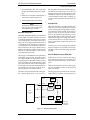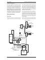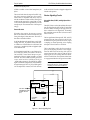
1
GTX
LTR® / Privacy Plus®
900 MHz
Mobile Radio
Service Manual
6880906Z19-O
Product Software License Agreement
THIS LICENSE AGREEMENT BETWEEN YOU, THE USER, AND MOTOROLA, APPLIES TO THE SOFTWARE
EMBEDDED IN OR DELIVERED WITH THE ACCOMPANYING MOTOROLA PRODUCT (“SOFTWARE”),
AND IS APPLICABLE UNLESS A SIGNED LICENSE AGREEMENT COVERING ITS SUBJECT MATTER HAS
BEEN EXECUTED BETWEEN YOU AND MOTOROLA. BY USING THE PRODUCT, YOU ACKNOWLEDGE
THAT THIS AGREEMENT HAS BEEN READ AND UNDERSTOOD AND THAT YOU AGREE TO BE BOUND
BY ITS TERMS AND CONDITIONS. IF YOU DO NOT AGREE, YOU ARE NOT LICENSED TO USE THE PRODUCT, AND IF YOU ARE THE PURCHASER OF THE PRODUCT, YOU SHOULD IMMEDIATELY RETURN THE
PRODUCT IN ITS ENTIRETY TO ITS PLACE OF PURCHASE FOR A REFUND.
Motorola grants to You a non-exclusive license to use the SOFTWARE in the manner described in the documentation associated with the product. Motorola retains ownership of the SOFTWARE including all patent, copyrights,
and other intellectual property rights. You may transfer this license to use the SOFTWARE as long as the transferee
agrees to be bound by the terms of this Agreement.
You agree not to reverse engineer or create derivative works of the SOFTWARE; not to transmit the SOFTWARE
electronically; not to modify, configure, or use the SOFTWARE in any manner not authorized by MOTOROLA;
and, except as an integral part of the product, not to rent, lease, or convey the SOFTWARE.
MOTOROLA SHALL NOT BE LIABLE FOR INCIDENTAL OR CONSEQUENTIAL DAMAGES ARISING FROM
THE USE OF THIS SOFTWARE.
With respect to the U.S. Government, if acquired under FAR policy (52.227-19), the SOFTWARE is provided with
Restricted Rights, and if acquired under DFARS policy (227.7202), then the SOFTWARE is provided only with the
commercial rights of this Agreement.
This license is effective until terminated. It will terminate immediately and automatically if You fail to comply with
any term of this Agreement.
You agree that this is the complete and exclusive statement of the agreement between You and Motorola and that
any modification of these terms shall be made only by mutual agreement and evidenced by written amendment
signed by both parties. This Agreement shall be governed and interpreted by the laws of the State of Illinois,
United States of America.
Computer Software Copyrights
This manual may not be reproduced, in whole or in part, in any form whatsoever, without the express written permission of Motorola, Inc.
The Motorola products described in this manual contain one or more computer programs. These computer programs are protected by copyright law and international treaties. Unauthorized reproduction or distribution of
these programs, or any part thereof, may result in severe civil and criminal penalties, and will be prosecuted to the
maximum extent possible under the law. U.S. and international patents pending.
, MOTOROLA, and PRIVACY PLUS are registered trademarks of Motorola, Inc.
GTX is a trademark of Motorola, Inc.
LTR is a registered trademark of E.F. Johnson Company.
TORX is a registered trademark of Camcar/Textron.
© 2000 by Motorola, Inc. All Rights Reserved.
This product is covered by one or more issued U.S. Patents. Other Patent applications pending.
Table of Contents
Foreword
Scope of Manual . . . . . . . . . . . . . . . . . . . . . . . . . . . . . . . . . . . . . . . . . . . . . . . . . . . . . . . . . . . . . . . . . . . . . . . . . . . . . . . vi
How to Use This Manual. . . . . . . . . . . . . . . . . . . . . . . . . . . . . . . . . . . . . . . . . . . . . . . . . . . . . . . . . . . . . . . . . . . . . . . . vi
Technical Support . . . . . . . . . . . . . . . . . . . . . . . . . . . . . . . . . . . . . . . . . . . . . . . . . . . . . . . . . . . . . . . . . . . . . . . . . . . . . . vi
Service Policy . . . . . . . . . . . . . . . . . . . . . . . . . . . . . . . . . . . . . . . . . . . . . . . . . . . . . . . . . . . . . . . . . . . . . . . . . . . . . . . . . vi
Ordering Replacement Parts. . . . . . . . . . . . . . . . . . . . . . . . . . . . . . . . . . . . . . . . . . . . . . . . . . . . . . . . . . . . . . . . . . . . . vi
Model Chart. . . . . . . . . . . . . . . . . . . . . . . . . . . . . . . . . . . . . . . . . . . . . . . . . . . . . . . . . . . . . . . . . . . . . . . . . . . . . . . . . . vii
Accessories. . . . . . . . . . . . . . . . . . . . . . . . . . . . . . . . . . . . . . . . . . . . . . . . . . . . . . . . . . . . . . . . . . . . . . . . . . . . . . . . . . . . ix
Maintenance Specifications . . . . . . . . . . . . . . . . . . . . . . . . . . . . . . . . . . . . . . . . . . . . . . . . . . . . . . . . . . . . . . . . . . . . . . .x
Radio Model Numbering System. . . . . . . . . . . . . . . . . . . . . . . . . . . . . . . . . . . . . . . . . . . . . . . . . . . . . . . . . . . . . . . . .xii
Section 1
Introduction
Notational Conventions. . . . . . . . . . . . . . . . . . . . . . . . . . . . . . . . . . . . . . . . . . . . . . . . . . . . . . . . . . . . . . . . . . . . . . . . 1-1
Warning. . . . . . . . . . . . . . . . . . . . . . . . . . . . . . . . . . . . . . . . . . . . . . . . . . . . . . . . . . . . . . . . . . . . . . . . . . . . . . . . . . 1-1
Caution . . . . . . . . . . . . . . . . . . . . . . . . . . . . . . . . . . . . . . . . . . . . . . . . . . . . . . . . . . . . . . . . . . . . . . . . . . . . . . . . . . 1-1
Note . . . . . . . . . . . . . . . . . . . . . . . . . . . . . . . . . . . . . . . . . . . . . . . . . . . . . . . . . . . . . . . . . . . . . . . . . . . . . . . . . . . . . 1-1
Scope of this Manual . . . . . . . . . . . . . . . . . . . . . . . . . . . . . . . . . . . . . . . . . . . . . . . . . . . . . . . . . . . . . . . . . . . . . . . . . . 1-1
Safety information . . . . . . . . . . . . . . . . . . . . . . . . . . . . . . . . . . . . . . . . . . . . . . . . . . . . . . . . . . . . . . . . . . . . . . . . . . . . 1-1
Air Bag Warning . . . . . . . . . . . . . . . . . . . . . . . . . . . . . . . . . . . . . . . . . . . . . . . . . . . . . . . . . . . . . . . . . . . . . . . . . . . . . . 1-2
Vehicles Equipped with Air Bags . . . . . . . . . . . . . . . . . . . . . . . . . . . . . . . . . . . . . . . . . . . . . . . . . . . . . . . . . . . . 1-2
LP Gas Warning . . . . . . . . . . . . . . . . . . . . . . . . . . . . . . . . . . . . . . . . . . . . . . . . . . . . . . . . . . . . . . . . . . . . . . . . . . . . . . 1-2
Section 2
Basic Maintenance
Introduction. . . . . . . . . . . . . . . . . . . . . . . . . . . . . . . . . . . . . . . . . . . . . . . . . . . . . . . . . . . . . . . . . . . . . . . . . . . . . . . . . . 2-1
Preventive Maintenance . . . . . . . . . . . . . . . . . . . . . . . . . . . . . . . . . . . . . . . . . . . . . . . . . . . . . . . . . . . . . . . . . . . . . . . 2-1
Inspection . . . . . . . . . . . . . . . . . . . . . . . . . . . . . . . . . . . . . . . . . . . . . . . . . . . . . . . . . . . . . . . . . . . . . . . . . . . . . . . . 2-1
Cleaning . . . . . . . . . . . . . . . . . . . . . . . . . . . . . . . . . . . . . . . . . . . . . . . . . . . . . . . . . . . . . . . . . . . . . . . . . . . . . . . . . 2-1
Plastic Surfaces. . . . . . . . . . . . . . . . . . . . . . . . . . . . . . . . . . . . . . . . . . . . . . . . . . . . . . . . . . . . . . . . . . . . . . . . . . . . 2-1
Circuit Boards and Components . . . . . . . . . . . . . . . . . . . . . . . . . . . . . . . . . . . . . . . . . . . . . . . . . . . . . . . . . . . . . 2-1
Safe Handling of CMOS Devices . . . . . . . . . . . . . . . . . . . . . . . . . . . . . . . . . . . . . . . . . . . . . . . . . . . . . . . . . . . . . . . . 2-1
Precautions . . . . . . . . . . . . . . . . . . . . . . . . . . . . . . . . . . . . . . . . . . . . . . . . . . . . . . . . . . . . . . . . . . . . . . . . . . . . . . . 2-2
Repair Procedures and Techniques . . . . . . . . . . . . . . . . . . . . . . . . . . . . . . . . . . . . . . . . . . . . . . . . . . . . . . . . . . . . . . 2-2
Parts Replacement . . . . . . . . . . . . . . . . . . . . . . . . . . . . . . . . . . . . . . . . . . . . . . . . . . . . . . . . . . . . . . . . . . . . . . . . . 2-2
Rigid Circuit Boards . . . . . . . . . . . . . . . . . . . . . . . . . . . . . . . . . . . . . . . . . . . . . . . . . . . . . . . . . . . . . . . . . . . . . . . 2-2
Chip Components . . . . . . . . . . . . . . . . . . . . . . . . . . . . . . . . . . . . . . . . . . . . . . . . . . . . . . . . . . . . . . . . . . . . . . . . . 2-2
Chip Component Removal . . . . . . . . . . . . . . . . . . . . . . . . . . . . . . . . . . . . . . . . . . . . . . . . . . . . . . . . . . . . . . 2-3
Chip Component Replacement . . . . . . . . . . . . . . . . . . . . . . . . . . . . . . . . . . . . . . . . . . . . . . . . . . . . . . . . . . 2-3
Over-Molded Pad-Array Carrier (OMPAC) . . . . . . . . . . . . . . . . . . . . . . . . . . . . . . . . . . . . . . . . . . . . . . . . . . . 2-3
OMPAC Removal . . . . . . . . . . . . . . . . . . . . . . . . . . . . . . . . . . . . . . . . . . . . . . . . . . . . . . . . . . . . . . . . . . . . . . 2-3
OMPAC Replacement . . . . . . . . . . . . . . . . . . . . . . . . . . . . . . . . . . . . . . . . . . . . . . . . . . . . . . . . . . . . . . . . . . 2-3
Shields . . . . . . . . . . . . . . . . . . . . . . . . . . . . . . . . . . . . . . . . . . . . . . . . . . . . . . . . . . . . . . . . . . . . . . . . . . . . . . . . . . . 2-3
Shield Removal. . . . . . . . . . . . . . . . . . . . . . . . . . . . . . . . . . . . . . . . . . . . . . . . . . . . . . . . . . . . . . . . . . . . . . . . 2-3
Shield Replacement . . . . . . . . . . . . . . . . . . . . . . . . . . . . . . . . . . . . . . . . . . . . . . . . . . . . . . . . . . . . . . . . . . . . 2-4
Replacement of Transistor Q6505 . . . . . . . . . . . . . . . . . . . . . . . . . . . . . . . . . . . . . . . . . . . . . . . . . . . . . . . . . . . . 2-4
September, 2000
6880906Z19-O
i
Table of Contents
GTX LTR / Privacy Plus 900 MHz Mobile Radio Service Manual
Removing Faulty Transistor . . . . . . . . . . . . . . . . . . . . . . . . . . . . . . . . . . . . . . . . . . . . . . . . . . . . . . . . . . . . . 2-4
Preparing Main Board for New Transistor . . . . . . . . . . . . . . . . . . . . . . . . . . . . . . . . . . . . . . . . . . . . . . . . . 2-4
Positioning New Transistor. . . . . . . . . . . . . . . . . . . . . . . . . . . . . . . . . . . . . . . . . . . . . . . . . . . . . . . . . . . . . . 2-5
Soldering Transistor . . . . . . . . . . . . . . . . . . . . . . . . . . . . . . . . . . . . . . . . . . . . . . . . . . . . . . . . . . . . . . . . . . . . 2-5
Installing Flange Capacitors C6567 and C6568. . . . . . . . . . . . . . . . . . . . . . . . . . . . . . . . . . . . . . . . . . . . . . 2-5
Reassembly of Radio . . . . . . . . . . . . . . . . . . . . . . . . . . . . . . . . . . . . . . . . . . . . . . . . . . . . . . . . . . . . . . . . . . . 2-5
Section 3
Test Equipment, Service Aids, and Tools
Test Equipment . . . . . . . . . . . . . . . . . . . . . . . . . . . . . . . . . . . . . . . . . . . . . . . . . . . . . . . . . . . . . . . . . . . . . . . . . . . . . . . 3-1
Field Programming. . . . . . . . . . . . . . . . . . . . . . . . . . . . . . . . . . . . . . . . . . . . . . . . . . . . . . . . . . . . . . . . . . . . . . . . . . . . 3-2
Service Tools . . . . . . . . . . . . . . . . . . . . . . . . . . . . . . . . . . . . . . . . . . . . . . . . . . . . . . . . . . . . . . . . . . . . . . . . . . . . . . . . . 3-3
Section 4
Test Mode, Error Codes and Performance Tests
Front Panel Test Mode . . . . . . . . . . . . . . . . . . . . . . . . . . . . . . . . . . . . . . . . . . . . . . . . . . . . . . . . . . . . . . . . . . . . . . . . . 4-1
Test Mode/Entry . . . . . . . . . . . . . . . . . . . . . . . . . . . . . . . . . . . . . . . . . . . . . . . . . . . . . . . . . . . . . . . . . . . . . . . . . . 4-1
Test Mode/Channel Selection . . . . . . . . . . . . . . . . . . . . . . . . . . . . . . . . . . . . . . . . . . . . . . . . . . . . . . . . . . . . . . . 4-1
Test Mode/Tx Modulation . . . . . . . . . . . . . . . . . . . . . . . . . . . . . . . . . . . . . . . . . . . . . . . . . . . . . . . . . . . . . . . . . . 4-1
Fail Mode . . . . . . . . . . . . . . . . . . . . . . . . . . . . . . . . . . . . . . . . . . . . . . . . . . . . . . . . . . . . . . . . . . . . . . . . . . . . . . . . 4-2
Exiting Test Mode . . . . . . . . . . . . . . . . . . . . . . . . . . . . . . . . . . . . . . . . . . . . . . . . . . . . . . . . . . . . . . . . . . . . . . . . . 4-2
Section 5
Disassembly & Reassembly For 12 W Models
Introduction . . . . . . . . . . . . . . . . . . . . . . . . . . . . . . . . . . . . . . . . . . . . . . . . . . . . . . . . . . . . . . . . . . . . . . . . . . . . . . . . . . 5-1
Disassemble the Radio . . . . . . . . . . . . . . . . . . . . . . . . . . . . . . . . . . . . . . . . . . . . . . . . . . . . . . . . . . . . . . . . . . . . . . . . . 5-1
Remove the Control Head . . . . . . . . . . . . . . . . . . . . . . . . . . . . . . . . . . . . . . . . . . . . . . . . . . . . . . . . . . . . . . . . . . 5-1
Remove the Top Cover . . . . . . . . . . . . . . . . . . . . . . . . . . . . . . . . . . . . . . . . . . . . . . . . . . . . . . . . . . . . . . . . . . . . . 5-1
Remove the Main Board . . . . . . . . . . . . . . . . . . . . . . . . . . . . . . . . . . . . . . . . . . . . . . . . . . . . . . . . . . . . . . . . . . . . 5-2
Disassemble the Control Head . . . . . . . . . . . . . . . . . . . . . . . . . . . . . . . . . . . . . . . . . . . . . . . . . . . . . . . . . . . . . . 5-2
Assemble the Radio . . . . . . . . . . . . . . . . . . . . . . . . . . . . . . . . . . . . . . . . . . . . . . . . . . . . . . . . . . . . . . . . . . . . . . . . . . . 5-3
Assemble the Control Head . . . . . . . . . . . . . . . . . . . . . . . . . . . . . . . . . . . . . . . . . . . . . . . . . . . . . . . . . . . . . . . . . 5-3
Replace the Main Board . . . . . . . . . . . . . . . . . . . . . . . . . . . . . . . . . . . . . . . . . . . . . . . . . . . . . . . . . . . . . . . . . . . . 5-3
Replace the Top Cover and Control Head . . . . . . . . . . . . . . . . . . . . . . . . . . . . . . . . . . . . . . . . . . . . . . . . . . . . . 5-3
Section 6
Disassembly & Reassembly For 30 W Models
Introduction . . . . . . . . . . . . . . . . . . . . . . . . . . . . . . . . . . . . . . . . . . . . . . . . . . . . . . . . . . . . . . . . . . . . . . . . . . . . . . . . . . 6-1
Disassemble the Radio . . . . . . . . . . . . . . . . . . . . . . . . . . . . . . . . . . . . . . . . . . . . . . . . . . . . . . . . . . . . . . . . . . . . . . . . . 6-1
Remove the Control Head . . . . . . . . . . . . . . . . . . . . . . . . . . . . . . . . . . . . . . . . . . . . . . . . . . . . . . . . . . . . . . . . . . 6-1
Remove the Top Cover . . . . . . . . . . . . . . . . . . . . . . . . . . . . . . . . . . . . . . . . . . . . . . . . . . . . . . . . . . . . . . . . . . . . . 6-1
Remove the Main Board . . . . . . . . . . . . . . . . . . . . . . . . . . . . . . . . . . . . . . . . . . . . . . . . . . . . . . . . . . . . . . . . . . . . 6-2
Disassemble the Control Head . . . . . . . . . . . . . . . . . . . . . . . . . . . . . . . . . . . . . . . . . . . . . . . . . . . . . . . . . . . . . . 6-2
Assemble the Radio . . . . . . . . . . . . . . . . . . . . . . . . . . . . . . . . . . . . . . . . . . . . . . . . . . . . . . . . . . . . . . . . . . . . . . . . . . . 6-2
Assemble the Control Head . . . . . . . . . . . . . . . . . . . . . . . . . . . . . . . . . . . . . . . . . . . . . . . . . . . . . . . . . . . . . . . . . 6-2
Replace the Main Board . . . . . . . . . . . . . . . . . . . . . . . . . . . . . . . . . . . . . . . . . . . . . . . . . . . . . . . . . . . . . . . . . . . . 6-3
Replace the Top Cover and Control Head . . . . . . . . . . . . . . . . . . . . . . . . . . . . . . . . . . . . . . . . . . . . . . . . . . . . . 6-3
ii
6880906Z19-O
September, 2000
GTX LTR / Privacy Plus 900 MHz Mobile Radio Service Manual
Table of Contents
Section 7
Radio Tuning Procedure
Radio Tuning Procedure . . . . . . . . . . . . . . . . . . . . . . . . . . . . . . . . . . . . . . . . . . . . . . . . . . . . . . . . . . . . . . . . . . . . . . . 7-1
General . . . . . . . . . . . . . . . . . . . . . . . . . . . . . . . . . . . . . . . . . . . . . . . . . . . . . . . . . . . . . . . . . . . . . . . . . . . . . . . . . . 7-1
Service Menu . . . . . . . . . . . . . . . . . . . . . . . . . . . . . . . . . . . . . . . . . . . . . . . . . . . . . . . . . . . . . . . . . . . . . . . . . . . . . 7-1
Tuning Procedure . . . . . . . . . . . . . . . . . . . . . . . . . . . . . . . . . . . . . . . . . . . . . . . . . . . . . . . . . . . . . . . . . . . . . . . . . . . . . 7-2
Starting the Tuning Procedure. . . . . . . . . . . . . . . . . . . . . . . . . . . . . . . . . . . . . . . . . . . . . . . . . . . . . . . . . . . . . . . 7-2
Alignment Default Data . . . . . . . . . . . . . . . . . . . . . . . . . . . . . . . . . . . . . . . . . . . . . . . . . . . . . . . . . . . . . . . . . . . . 7-2
Tx Power . . . . . . . . . . . . . . . . . . . . . . . . . . . . . . . . . . . . . . . . . . . . . . . . . . . . . . . . . . . . . . . . . . . . . . . . . . . . . . . . . 7-2
Reference Oscillator Alignment . . . . . . . . . . . . . . . . . . . . . . . . . . . . . . . . . . . . . . . . . . . . . . . . . . . . . . . . . . . . . 7-2
Transmitter Power . . . . . . . . . . . . . . . . . . . . . . . . . . . . . . . . . . . . . . . . . . . . . . . . . . . . . . . . . . . . . . . . . . . . . . . . . 7-2
Transmit Current Limit. . . . . . . . . . . . . . . . . . . . . . . . . . . . . . . . . . . . . . . . . . . . . . . . . . . . . . . . . . . . . . . . . . . . . 7-3
Transmit Deviation Balance (Compensation) & Deviation Limit . . . . . . . . . . . . . . . . . . . . . . . . . . . . . . . . . 7-3
Transmit Deviation Limit . . . . . . . . . . . . . . . . . . . . . . . . . . . . . . . . . . . . . . . . . . . . . . . . . . . . . . . . . . . . . . . . . . . 7-3
Squelch . . . . . . . . . . . . . . . . . . . . . . . . . . . . . . . . . . . . . . . . . . . . . . . . . . . . . . . . . . . . . . . . . . . . . . . . . . . . . . . . . . 7-3
Ending the Tuning Procedure . . . . . . . . . . . . . . . . . . . . . . . . . . . . . . . . . . . . . . . . . . . . . . . . . . . . . . . . . . . . . . . 7-4
Section 8
Theory of Operation
Introduction. . . . . . . . . . . . . . . . . . . . . . . . . . . . . . . . . . . . . . . . . . . . . . . . . . . . . . . . . . . . . . . . . . . . . . . . . . . . . . . . . . 8-1
Overview . . . . . . . . . . . . . . . . . . . . . . . . . . . . . . . . . . . . . . . . . . . . . . . . . . . . . . . . . . . . . . . . . . . . . . . . . . . . . . . . 8-1
Receiver Detailed Functional Description . . . . . . . . . . . . . . . . . . . . . . . . . . . . . . . . . . . . . . . . . . . . . . . . . . . . . . . . 8-2
Transmitter Detailed Functional Description . . . . . . . . . . . . . . . . . . . . . . . . . . . . . . . . . . . . . . . . . . . . . . . . . . . . . . 8-3
12 Watt PA. . . . . . . . . . . . . . . . . . . . . . . . . . . . . . . . . . . . . . . . . . . . . . . . . . . . . . . . . . . . . . . . . . . . . . . . . . . . . . . . 8-3
30 Watt PA. . . . . . . . . . . . . . . . . . . . . . . . . . . . . . . . . . . . . . . . . . . . . . . . . . . . . . . . . . . . . . . . . . . . . . . . . . . . . . . . 8-3
Power Control Circuitry . . . . . . . . . . . . . . . . . . . . . . . . . . . . . . . . . . . . . . . . . . . . . . . . . . . . . . . . . . . . . . . . . . . . 8-4
Power Set . . . . . . . . . . . . . . . . . . . . . . . . . . . . . . . . . . . . . . . . . . . . . . . . . . . . . . . . . . . . . . . . . . . . . . . . . . . . . 8-4
Current Limit . . . . . . . . . . . . . . . . . . . . . . . . . . . . . . . . . . . . . . . . . . . . . . . . . . . . . . . . . . . . . . . . . . . . . . . . . 8-4
Thermal Protection. . . . . . . . . . . . . . . . . . . . . . . . . . . . . . . . . . . . . . . . . . . . . . . . . . . . . . . . . . . . . . . . . . . . . 8-4
Synthesizer Detailed Functional Description . . . . . . . . . . . . . . . . . . . . . . . . . . . . . . . . . . . . . . . . . . . . . . . . . . . . . . 8-4
Controller Detailed Functional Description . . . . . . . . . . . . . . . . . . . . . . . . . . . . . . . . . . . . . . . . . . . . . . . . . . . . . . . 8-6
General . . . . . . . . . . . . . . . . . . . . . . . . . . . . . . . . . . . . . . . . . . . . . . . . . . . . . . . . . . . . . . . . . . . . . . . . . . . . . . . . . . 8-6
Voltage Regulators. . . . . . . . . . . . . . . . . . . . . . . . . . . . . . . . . . . . . . . . . . . . . . . . . . . . . . . . . . . . . . . . . . . . . . . . . 8-6
Electronic On/Off . . . . . . . . . . . . . . . . . . . . . . . . . . . . . . . . . . . . . . . . . . . . . . . . . . . . . . . . . . . . . . . . . . . . . . . . . 8-6
Mechanical On/Off . . . . . . . . . . . . . . . . . . . . . . . . . . . . . . . . . . . . . . . . . . . . . . . . . . . . . . . . . . . . . . . . . . . . . . . . 8-6
Ignition . . . . . . . . . . . . . . . . . . . . . . . . . . . . . . . . . . . . . . . . . . . . . . . . . . . . . . . . . . . . . . . . . . . . . . . . . . . . . . . . . . 8-7
Hook . . . . . . . . . . . . . . . . . . . . . . . . . . . . . . . . . . . . . . . . . . . . . . . . . . . . . . . . . . . . . . . . . . . . . . . . . . . . . . . . . . . . 8-7
Microprocessor Clock Synthesizer . . . . . . . . . . . . . . . . . . . . . . . . . . . . . . . . . . . . . . . . . . . . . . . . . . . . . . . . . . . 8-7
Serial Peripheral Interface (SPI) . . . . . . . . . . . . . . . . . . . . . . . . . . . . . . . . . . . . . . . . . . . . . . . . . . . . . . . . . . . . . 8-7
SBEP Serial Interface . . . . . . . . . . . . . . . . . . . . . . . . . . . . . . . . . . . . . . . . . . . . . . . . . . . . . . . . . . . . . . . . . . . . . . . 8-7
Microprocessor (Open Controller) . . . . . . . . . . . . . . . . . . . . . . . . . . . . . . . . . . . . . . . . . . . . . . . . . . . . . . . . . . . 8-7
One-Time Programmable (Flash) Memory . . . . . . . . . . . . . . . . . . . . . . . . . . . . . . . . . . . . . . . . . . . . . . . . . . . . 8-8
Electrically Erasable Programmable Memory (EEPROM) . . . . . . . . . . . . . . . . . . . . . . . . . . . . . . . . . . . . . . . 8-8
Static Random Access Memory (SRAM) . . . . . . . . . . . . . . . . . . . . . . . . . . . . . . . . . . . . . . . . . . . . . . . . . . . . . . 8-9
Control Head . . . . . . . . . . . . . . . . . . . . . . . . . . . . . . . . . . . . . . . . . . . . . . . . . . . . . . . . . . . . . . . . . . . . . . . . . . . . . 8-9
Controller Audio & Signaling Circuits . . . . . . . . . . . . . . . . . . . . . . . . . . . . . . . . . . . . . . . . . . . . . . . . . . . . . . . . . . . 8-9
General . . . . . . . . . . . . . . . . . . . . . . . . . . . . . . . . . . . . . . . . . . . . . . . . . . . . . . . . . . . . . . . . . . . . . . . . . . . . . . . . . . 8-9
Audio Signalling Filter IC (ASFIC) . . . . . . . . . . . . . . . . . . . . . . . . . . . . . . . . . . . . . . . . . . . . . . . . . . . . . . . 8-9
Audio Ground . . . . . . . . . . . . . . . . . . . . . . . . . . . . . . . . . . . . . . . . . . . . . . . . . . . . . . . . . . . . . . . . . . . . . . . . 8-9
Transmit Audio Circuits. . . . . . . . . . . . . . . . . . . . . . . . . . . . . . . . . . . . . . . . . . . . . . . . . . . . . . . . . . . . . . . . . . . 8-10
Mic Input Path . . . . . . . . . . . . . . . . . . . . . . . . . . . . . . . . . . . . . . . . . . . . . . . . . . . . . . . . . . . . . . . . . . . . . . . 8-10
Flat Tx Audio Input Path . . . . . . . . . . . . . . . . . . . . . . . . . . . . . . . . . . . . . . . . . . . . . . . . . . . . . . . . . . . . . . 8-10
PTT Sensing and TX Audio Processing. . . . . . . . . . . . . . . . . . . . . . . . . . . . . . . . . . . . . . . . . . . . . . . . . . . 8-10
Transmit Signalling Circuits . . . . . . . . . . . . . . . . . . . . . . . . . . . . . . . . . . . . . . . . . . . . . . . . . . . . . . . . . . . . . . . 8-10
Sub-audible Data (PL/DPL) . . . . . . . . . . . . . . . . . . . . . . . . . . . . . . . . . . . . . . . . . . . . . . . . . . . . . . . . . . . . 8-11
High Speed Data . . . . . . . . . . . . . . . . . . . . . . . . . . . . . . . . . . . . . . . . . . . . . . . . . . . . . . . . . . . . . . . . . . . . . 8-11
Dual Tone Multiple Frequency (DTMF) Data . . . . . . . . . . . . . . . . . . . . . . . . . . . . . . . . . . . . . . . . . . . . . 8-11
Receive Audio Circuits . . . . . . . . . . . . . . . . . . . . . . . . . . . . . . . . . . . . . . . . . . . . . . . . . . . . . . . . . . . . . . . . . . . . 8-12
September, 2000
6880906Z19-O
iii
Table of Contents
GTX LTR / Privacy Plus 900 MHz Mobile Radio Service Manual
Audio Processing and Digital Volume Control . . . . . . . . . . . . . . . . . . . . . . . . . . . . . . . . . . . . . . . . . . . . 8-13
Audio Amplification Speaker (+) Speaker (-). . . . . . . . . . . . . . . . . . . . . . . . . . . . . . . . . . . . . . . . . . . . . . 8-13
Handset Audio . . . . . . . . . . . . . . . . . . . . . . . . . . . . . . . . . . . . . . . . . . . . . . . . . . . . . . . . . . . . . . . . . . . . . . . 8-13
External Rx Audio . . . . . . . . . . . . . . . . . . . . . . . . . . . . . . . . . . . . . . . . . . . . . . . . . . . . . . . . . . . . . . . . . . . . 8-14
Receive Signalling Circuits . . . . . . . . . . . . . . . . . . . . . . . . . . . . . . . . . . . . . . . . . . . . . . . . . . . . . . . . . . . . . . . . . 8-14
Sub-audible Data (PL/DPL) and High Speed Data Decoder. . . . . . . . . . . . . . . . . . . . . . . . . . . . . . . . . 8-14
Alert Tone Circuits . . . . . . . . . . . . . . . . . . . . . . . . . . . . . . . . . . . . . . . . . . . . . . . . . . . . . . . . . . . . . . . . . . . . 8-15
Hear Clear IC. . . . . . . . . . . . . . . . . . . . . . . . . . . . . . . . . . . . . . . . . . . . . . . . . . . . . . . . . . . . . . . . . . . . . . . . . 8-15
Transmit Path for Radios with Hear Clear . . . . . . . . . . . . . . . . . . . . . . . . . . . . . . . . . . . . . . . . . . . . . . . . 8-15
Receive Path for Radios with Hear Clear . . . . . . . . . . . . . . . . . . . . . . . . . . . . . . . . . . . . . . . . . . . . . . . . . 8-15
Hear Clear Routing of Data/Signalling . . . . . . . . . . . . . . . . . . . . . . . . . . . . . . . . . . . . . . . . . . . . . . . . . . 8-16
Accessory Connector Configurations . . . . . . . . . . . . . . . . . . . . . . . . . . . . . . . . . . . . . . . . . . . . . . . . . . . . . . . . 8-16
Remote Desk Set . . . . . . . . . . . . . . . . . . . . . . . . . . . . . . . . . . . . . . . . . . . . . . . . . . . . . . . . . . . . . . . . . . . . . . 8-16
Public Address . . . . . . . . . . . . . . . . . . . . . . . . . . . . . . . . . . . . . . . . . . . . . . . . . . . . . . . . . . . . . . . . . . . . . . . 8-17
External Alarm . . . . . . . . . . . . . . . . . . . . . . . . . . . . . . . . . . . . . . . . . . . . . . . . . . . . . . . . . . . . . . . . . . . . . . . 8-17
RSSI Buffer . . . . . . . . . . . . . . . . . . . . . . . . . . . . . . . . . . . . . . . . . . . . . . . . . . . . . . . . . . . . . . . . . . . . . . . . . . . 8-17
Section 9
Troubleshooting
Overview . . . . . . . . . . . . . . . . . . . . . . . . . . . . . . . . . . . . . . . . . . . . . . . . . . . . . . . . . . . . . . . . . . . . . . . . . . . . . . . . . . . . 9-1
Troubleshooting Charts . . . . . . . . . . . . . . . . . . . . . . . . . . . . . . . . . . . . . . . . . . . . . . . . . . . . . . . . . . . . . . . . . . . . . . . . 9-1
Troubleshooting Flow Chart for Receiver . . . . . . . . . . . . . . . . . . . . . . . . . . . . . . . . . . . . . . . . . . . . . . . . . . . . . . . . . 9-2
Troubleshooting Flow Chart for Synthesizer . . . . . . . . . . . . . . . . . . . . . . . . . . . . . . . . . . . . . . . . . . . . . . . . . . . . . . 9-4
Troubleshooting Flow Chart for 12 W Power Amplifier . . . . . . . . . . . . . . . . . . . . . . . . . . . . . . . . . . . . . . . . . . . . 9-6
Troubleshooting Flow Chart for 30 W Power Amplifier . . . . . . . . . . . . . . . . . . . . . . . . . . . . . . . . . . . . . . . . . . . . 9-7
Troubleshooting Flow Chart for Controller . . . . . . . . . . . . . . . . . . . . . . . . . . . . . . . . . . . . . . . . . . . . . . . . . . . . . . . 9-8
Troubleshooting Flow Chart for Control Head . . . . . . . . . . . . . . . . . . . . . . . . . . . . . . . . . . . . . . . . . . . . . . . . . . . . 9-9
Schematic Diagrams, Circuit Board Details, and Parts Lists
Schematic Diagram for HLF9003A, HLF9004A, HLF9009A & HLF9010A Main Boards,
Radio Block Diagram Section . . . . . . . . . . . . . . . . . . . . . . . . . . . . . . . . . . . . . . . . . . . . . . . . . . . . . . . . . . . . . . . . . . .1
Schematic Diagram for HLF9003A, HLF9004A, HLF9009A & HLF9010A Main Boards,
Receiver Section . . . . . . . . . . . . . . . . . . . . . . . . . . . . . . . . . . . . . . . . . . . . . . . . . . . . . . . . . . . . . . . . . . . . . . . . . . . . . .2
Schematic Diagram for HLF9003A, HLF9004A, HLF9009A & HLF9010A Main Boards,
Synthesizer Section . . . . . . . . . . . . . . . . . . . . . . . . . . . . . . . . . . . . . . . . . . . . . . . . . . . . . . . . . . . . . . . . . . . . . . . . . . .3
Schematic Diagram for HLF9003A & HLF9004A Main Boards, Power Amplifier Section . . . . . . . . . . . . . . . . . .4
Schematic Diagram for HLF9003A & HLF9004A Main Boards, Power Control Section . . . . . . . . . . . . . . . . . . . .5
Schematic Diagram for HLF9009A & HLF9010A Main Boards, Power Amplifier Section . . . . . . . . . . . . . . . . . .6
Schematic Diagram for HLF9009A & HLF9010A Main Boards, Power Control Section . . . . . . . . . . . . . . . . . . . .7
Schematic Diagram for HLF9003A, HLF9004A, HLF9009A & HLF9010A Main Boards,
Controller Block Diagram . . . . . . . . . . . . . . . . . . . . . . . . . . . . . . . . . . . . . . . . . . . . . . . . . . . . . . . . . . . . . . . . . . . . . .8
Schematic Diagram for HLF9003A, HLF9004A, HLF9009A & HLF9010A Main Boards,
Audio & Digital Controller Section . . . . . . . . . . . . . . . . . . . . . . . . . . . . . . . . . . . . . . . . . . . . . . . . . . . . . . . . . . . . . .9
Schematic Diagram for HLF9003, HLF9004A, HLF9009A & HLF9010A Main Board,
Audio PA & I/O Sections . . . . . . . . . . . . . . . . . . . . . . . . . . . . . . . . . . . . . . . . . . . . . . . . . . . . . . . . . . . . . . . . . . . . .10
Schematic Diagram for HLF9003A, HLF9004A, HLF9009A & HLF9010A Main Boards,
Supply Voltage Section . . . . . . . . . . . . . . . . . . . . . . . . . . . . . . . . . . . . . . . . . . . . . . . . . . . . . . . . . . . . . . . . . . . . . . .11
Schematic Diagram for HLF9003, HLF9004A, HLF9009A & HLF9010A Main Board,
Hear Clear Section . . . . . . . . . . . . . . . . . . . . . . . . . . . . . . . . . . . . . . . . . . . . . . . . . . . . . . . . . . . . . . . . . . . . . . . . . . .12
Circuit Board Details for HLF9003A & HLF9004A Main Boards . . . . . . . . . . . . . . . . . . . . . . . . . . . . . . . . . . . . . .13
Parts List for HLF9003A & HLF9004A Main Boards. . . . . . . . . . . . . . . . . . . . . . . . . . . . . . . . . . . . . . . . . . . . . . . . .14
Circuit Board Details for HLF9009A & HLF9010A Main Boards . . . . . . . . . . . . . . . . . . . . . . . . . . . . . . . . . . . . . .15
Parts List for HLF9009A & HLF9010A Main Boards. . . . . . . . . . . . . . . . . . . . . . . . . . . . . . . . . . . . . . . . . . . . . . . . .16
iv
6880906Z19-O
September, 2000
GTX LTR / Privacy Plus 900 MHz Mobile Radio Service Manual
Table of Contents
Schematic Diagram for FLN8744A Control Head . . . . . . . . . . . . . . . . . . . . . . . . . . . . . . . . . . . . . . . . . . . . . . . . . . . 17
Circuit Board Details & Parts List for FLN8744A Control Head. . . . . . . . . . . . . . . . . . . . . . . . . . . . . . . . . . . . . . . 18
GTX Exploded View & Mechanical Parts List, 30 W. . . . . . . . . . . . . . . . . . . . . . . . . . . . . . . . . . . . . . . . . . . . . . . . . 19
GTX Exploded View & Mechanical Parts List, 12 W. . . . . . . . . . . . . . . . . . . . . . . . . . . . . . . . . . . . . . . . . . . . . . . . . 20
September, 2000
6880906Z19-O
v
Foreword
GTX LTR / Privacy Plus 900 MHz Mobile Service Manual
Scope of Manual
Scope of Manual
This manual is intended for use by experienced technicians familiar with similar types of equipment. It contains all service information required for the
equipment described and is current as of the printing
date. Changes which occur after the printing date are
incorporated by service manual revisions. These revisions are added to the manuals as the engineering
changes are incorporated into the equipment.
How to Use This Manual
This manual contains introductory material such as
model charts, accessories, and specifications, as well as
four sections that deal with specific service aspects of
the GTX Mobile Radio. Refer to the Table of Contents
for a general overview of the manual, or to the “Overview” paragraph in each section for a specific overview
of the information in that section.
Technical Support
To obtain technical support, you may call Motorola’s
Radius Product Services. When you call, we ask that
you have ready the model and serial numbers of the
respective radio or its parts.
Service Policy
If malfunctions occur within 30 days that cannot be
resolved over the phone with Product Services, a
defective major component should be returned. You
must obtain authorization from Radius Product Services before returning the component.
Ordering Replacement Parts
You can order additional components and some piece
parts directly through your Radius price pages. When
ordering replacement parts, include the complete identification number for all chassis, kits, and components.
If you do not know a part number, include with your
vi
order the number of the chassis or kit which contains
the part, and a detailed description of the desired component. If a Motorola part number is identified on a
parts list, you should be able to order the part through
Motorola Parts. If only a generic part is listed, the part
is not normally available through Motorola. If no parts
list is shown, generally, no user serviceable parts are
available for the kit.
Radius 30-Day Warranty
Technical Support
Radius Product Services
8000 W. Sunrise Blvd.
Plantation, FL 33322
Motorola Radio Support Center
Attention: Warranty Return
3761 South Central Avenue
Rockford, IL 61102 USA
1-800-227-6772 (U.S. & Canada)
Radius Major Component Repair
Motorola Radio Support Center
3760 South Central Avenue
Rockford, IL 61102 USA
Motorola Parts
Worldwide System and
Aftermarket Products Division
Attention: Order Processing
1313 E. Algonquin Road
Schaumburg, IL 60196
Worldwide System and
Aftermarket Products Division
Attention: International Order Processing
1313 E. Algonquin Road
Schaumburg, IL 60196
Customer Service
1-800-422-4210
1-847-538-8198 (FAX)
Parts Identification
1-847-538-0021
1-847-538-8194 (FAX)
6880906Z19-O
September, 2000
GTX LTR / Privacy Plus 900 MHz Mobile Service Manual
Foreword
Model Chart
Item
X
X
X
X
X
X
X
X
X
X
September, 2000
X
X
X
X
X
X
X
X
HUF3029_
HUF3031_
HUF3030_
HUF3032_
HCN3018_
HMN3413_
GLN7317_
GKN6270_
6880907Z66
6880907Z20
6880907Z19
Hardware Kit
Main Board, Privacy Plus, 12.5 kHz, 12 W
Main Board, LTR, 12.5 kHz, 12 W
Control Head Board
HLN9634_
HLF9009_
HLF90010_
FLN8744_
Description
GTX
LTR / Privacy Plus
Mobile Radio
900 MHz
12 Watts RF Power
Item
8
M11WGD4CU1_N
GTX LTR, 900 MHz, 12.5 kHz, 12 W
8
M11WGD4CB1_N
GTX Privacy Plus, 900 MHz, 12.5 kHz, 12 W
Freq..
Model
Description
Model Chart
Description
Radio, Privacy Plus, 12.5 kHz, 12 W
Radio, LTR, 12.5 kHz, 12 W
Unified Chassis, Privacy Plus, 12.5 kHz, 12 W
Unified Chassis, LTR, 12.5 kHz, 12 W
Control Head
Compact Microphone
Trunnion
Power Cable
Installation Manual
GTX LTR User’s Guide (English/French)
GTX Privacy Plus User’s Guide (English/French)
6880906Z19-O
X
X
X
X
X
vii
Foreword
GTX LTR / Privacy Plus 900 MHz Mobile Service Manual
Item
X
X
X
X
X
X
X
X
X
viii
HUF3007_
X HUF3011_
HUF3009_
X HUF3013_
X FCN3018
X HMN3413_
X HLN9640_
X HKN4191_
X 6880907Z66
X 6880907Z20
X 6880907Z19
Hardware Kit
Main Board, Privacy Plus, 12.5 kHz, 30 W
Main Board, LTR, 12.5 kHz, 30 W
Control Head Board
HLN9634_
HLF9003_
HLF9004_
FLN8744_
Description
GTX
LTR / Privacy Plus
Mobile Radio
900 MHz
30 Watts RF Power
Item
8
M11WRD4CU1_N
GTX LTR, 900 MHz, 12.5 kHz, 30 W
8
M11WRD4CB1_N
GTX Privacy Plus, 900 MHz, 12.5 kHz, 30 W
Freq.
Model
Description
Model Chart
Description
Radio, Privacy Plus, 12.5 kHz, 30 W
Radio, LTR, 12.5 kHz, 30 W
Unified Chassis, Privacy Plus, 12.5 kHz, 30 W
Unified Chassis, LTR, 12.5 kHz, 30 W
Control Head
Compact Microphone
Trunnion
Power Cable
Installation Manual
GTX LTR User’s Guide (English/French)
GTX Privacy Plus User’s Guide (English/French)
6880906Z19-O
X
X
X
X
X
September, 2000
GTX LTR / Privacy Plus 900 MHz Mobile Service Manual
Foreword
Accessories
Accessories
Audio
HMN3413
Compact Microphone
HMN1035_R
Heavy Duty Palm Microphone
HMN3013
DTMF Non-Backlit Microphone with Hang-Up Clip
AAREX4617
Handset with Hang-up Clip
HLN9073
Hang-up Clip
Speaker
FSN5510
7.5 W External Speaker
Installation
HLN9640
Trunnion Kit; 30 W
GLN7317
Trunnion Kit; 12 W
Cables
HKN4191
Power Cable; 30 W
GKN7270
Power Cable; 12 W
GKN6271
Ignition Sense Cable
GKN6272
External Alarm Relay and Cable
Antennas
RRA4935
900 MHz, 3 dB Gain w/14 ft. Cable
Control Station
RLN4834
Control Station Package; 30 W
HLN3067
Control Station Package; 12 W
GLN7318
Base Station Tray
HPN4001
Power Supply and Cable (greater than 25 W)
HPN4002
Power Supply and Cable (less than or equal to 25 W)
HKN9088
Mobile Mini-U Antenna Adapter
HMN3000
Desk Micophone
Manuals/Kits
6880907Z20
GTX LTR User’s Guide (English/French)
6880907Z19
GTX Privacy Plus User’s Guide (English/French)
6880907Z66
Installation Manual
RVN4150
GTX Radio Service Software Kit
September, 2000
6880906Z19-O
ix
Foreword
GTX LTR / Privacy Plus 900 MHz Mobile Service Manual
Maintenance Specifications
Maintenance Specifications
GENERAL
Frequency:
Model Number:
RF Output:
RF Output (Talkaround):
FCC Description:
Dimensions (H x W x L):
Weight:
900 MHz
M11WRD4CB1_N, M11WRD4CU1_N
M11WGD4CB1_N, M11WGD4CU1_N
30 W
12 W
20 W
10 W
ABZ99FT3004
AZ492FT5782
1.73” x 6.61” x 8.62”
1.73” x 6.61” x 6.67””
(44mm x 168mm x 219mm)
(44mm x 168mm x 169mm)
4.30 lb
2.67 lb
(1.95 kg)
(1.21 kg)
896 – 941 MHz
896 – 902 MHz
935 – 941 MHz
935 – 941 MHz
12.5 kHz
10 Trunked Modes / 10 Conventional Channels
8 Trunked Talkgroups
1.5 ppm
13.6 V dc
13.8 V dc
Frequency Range *:
Transmit
Talkaround
Receive
Channel Spacing:
Channel Capacity:
Group Capacity:
Frequency Stability:
Input Voltage:
Temperature Range:
Operating
Storage
Tx Current:
12.0A (30 W)
* 821 - 825 MHz & 866 - 870 MHz is available outside of the U.S.
-30 to +60°C
-40 to +85°C
6.0A (12 W)
TRANSMITTER
Power Output:
30 W (896 – 902 MHz)
20 W (935 – 941 MHz)
Channel Spacing:
Maximum Frequency Separation:
Modulation Limiting:
FM Hum & Noise:
Conducted / Radiated Emission:
Audio Response (300-3000 Hz):
Audio Distortion:
12 W (896 – 902 MHz)
10 W (835 – 941 MHz)
12.5 kHz
6 MHz
2.5 kHz
-35 dB
-13 dBm
+1 to -3 dB
Less than 5%
RECEIVER
Channel Spacing:
Sensitivity (12dB SINAD):
Intermodulation:
Adjacent Channel Selectivity:
Spurious Rejection:
Audio Output Power:
Audio Distortion @ Rated Audio:
Current Drain:
OFF
Standby
Rated
Conducted Spurious Emission:
x
12.5 kHz
0.35 µV
-65 dB
-65 dB
-65 dB
4W (internal speaker)
7.5W (external speaker)
5%
30 mA
450 mA
1.5A (4W internal speaker)
1.7A (7.5W external speaker)
Per FCC part 90
6880906Z19-O
September, 2000
GTX LTR / Privacy Plus 900 MHz Mobile Service Manual
Foreword
Maintenance Specifications
MIL STANDARDS- THE GTX MOBILE RADIO IS DESIGNED TO MEET OR EXCEED MOST REQUIREMENTS
FOR MIL STD 810 C, D, AND E
810C
Applicable MIL-STD:
Low Pressure
High Temperature
Low Temperature
Temperature Shock
Rain
Humidity
Salt Fog
Dust
Vibration
Shock
Crash Safety Shock
Packaged Vibration
Methods
500.1
501.1
502.1
503.1
506.1
507.1
509.1
510.1
514.2
516.2
Procedures
1
1,2
1
1
2
2
1
1
8,10
1,3,5
810D
Methods
500.2
501.2
502.2
503.2
506.2
507.2
509.2
510.2
514.3
516.3
Procedures
1
1,2
1,2
1
2
2
1
1
1
1,5
810E
Methods
500.3
501.3
502.3
503.3
506.3
507.3
509.3
510.3
514.4
516.4
516.4
514.4
Procedures
1
1,2
1,2
1
2
2
1
1
1
1,5
5
All specifications subject to change without notice.
September, 2000
6880906Z19-O
xi
Foreword
GTX LTR / Privacy Plus 900 MHz Mobile Service Manual
Radio Model Numbering System
Radio Model Numbering System
The model number, serial number, and Motorola FCC designation number are all on a label attached to the back of
your radio.
All GTX LTR and Privacy Plus radio models are synthesized, 8 trunked mode, 10-conventional channel units that
come standard with Tone Private-Line (TPL)/Digital Private-Line (DPL) coded squelch or carrier squelch, which
may be enabled/disabled on a per channel basis. Programming changes can be made by your local dealer.
GTX Privacy Plus
Model Number:
M
1
1
W
R
D
4
C
B
1
A
N
Position:
1
2
3
4
5
6
7
8
9
10
11
12
Position 12 Unique Model Variations
Position 1 - Type of Unit
M = Mobile
Standard Package
Position 11- Version
Position 2 & 3 - Model Series
Version Letter (Alpha) - Major Change
Position 10 - Feature Level
Position 4 - Frequency Band
896-941 MHz
Basic
Position 5 - Power Level
Position 9 - Primary System Type
30 W
Privacy Plus®
Position 8 - Primary Operation
Position 6 - Physical Package
Trunked Twin Type
Standard Control with Display
Position 7 - Channel Spacing
12.5 kHz
GTX LTR
Model Number:
M
1
1
W
R
D
4
C
U
1
A
N
Position:
1
2
3
4
5
6
7
8
9
10
11
12
Position 12 Unique Model Variations
Position 1 - Type of Unit
M = Mobile
Standard Package
Position 11- Version
Position 2 & 3 - Model Series
Version Letter (Alpha) - Major Change
Position 4 - Frequency Band
896-941 MHz
Position 10 - Feature Level
Basic
Position 5 - Power Level
Position 9 - LTR
30 W
Position 6 - Physical Package
Position 8 - Primary Operation
Trunked Twin Type
Standard Control with Display
Position 7 - Channel Spacing
12.5 kHz
xii
6880906Z19-O
September, 2000
GTX LTR / Privacy Plus 900 MHz Mobile Service Manual
Foreword
Radio Model Numbering System
GTX Privacy Plus
Model Number:
M
1
1
W
G
D
4
C
B
1
A
N
Position:
1
2
3
4
5
6
7
8
9
10
11
12
Position 12 Unique Model Variations
Position 1 - Type of Unit
M = Mobile
Standard Package
Position 11- Version
Position 2 & 3 - Model Series
Version Letter (Alpha) - Major Change
Position 10 - Feature Level
Position 4 - Frequency Band
896-941 MHz
Basic
Position 5 - Power Level
Position 9 - Primary System Type
12 W
Privacy Plus®
Position 8 - Primary Operation
Position 6 - Physical Package
Trunked Twin Type
Standard Control with Display
Position 7 - Channel Spacing
12.5 kHz
GTX LTR
Model Number:
M
1
1
W
G
D
4
C
U
1
A
N
Position:
1
2
3
4
5
6
7
8
9
10
11
12
Position 12 Unique Model Variations
Position 1 - Type of Unit
M = Mobile
Standard Package
Position 11- Version
Position 2 & 3 - Model Series
Version Letter (Alpha) - Major Change
Position 4 - Frequency Band
896-941 MHz
Position 10 - Feature Level
Basic
Position 5 - Power Level
Position 9 - LTR
12 W
Position 6 - Physical Package
Position 8 - Primary Operation
Trunked Twin Type
Standard Control with Display
Position 7 - Channel Spacing
12.5 kHz
September, 2000
6880906Z19-O
xiii
Foreword
GTX LTR / Privacy Plus 900 MHz Mobile Service Manual
Radio Model Numbering System
xiv
6880906Z19-O
September, 2000
Section 1
Introduction
Notational Conventions
Safety information
Throughout the text in this publication, you will notice
the use of warnings, cautions, and notes. These notations are used to emphasize that safety hazards exist,
and care must be taken and observed.
Every radio, when transmitting, radiates energy into
the atmosphere which may, under certain conditions,
causes the generation of a spark.
Warning
All users of vehicles fitted with radios should be aware
of the following warnings:
WARNING
WARNING
Indicates a potentially hazardous situation which, if not avoided, COULD result
in death or serious injury.
• Do not operate the radio near flammable liquids or in the vicinity of explosive devices.
Caution
• During normal use, the radio will subject you to radio energy substantially
below the level where any kind of
harm is reported.
CAUTION
Indicates a potentially hazardous situation which, if not avoided, MAY result
in minor or moderate injury. CAUTION
may also be used to alert against unsafe
practices and property-damage-only
accident hazards.
To ensure personal safety, please observe the following
simple rules:
WARNING
Note
• Do not transmit when the antenna is
very close to, or touching, exposed
parts of the body, especially the face
and eyes.
NOTE
An operational procedure, practice, or
condition, etc., which it is essential to
emphasize.
• Do not hold the transmit (PTT) key in
when not desiring to transmit.
Scope of this Manual
This manual includes model/kit information, specifications, disassembly/reassembly procedures, maintenance, alignment, troubleshooting, and all theory,
schematic diagrams, printed circuit board details and
parts lists for all parts in the equipment described.
CAUTION
This manual is intended for use by experienced technicians who are familiar
with similar types of equipment.
September, 2000
• Check the laws and regulations on the
use of two-way mobile radios in the
areas where you drive. Always obey
them. Also, when using your radio
while driving, please:
give full attention to driving,
use hands-free operation, if available,
and
pull off the road and park before making or answering a call if driving conditions so require.
6880906Z19-O
1-1
Introduction
GTX LTR/Privacy Plus 900 MHz Mobile Service Manual
Air Bag Warning
Air Bag Warning
involved in your communication equipment installation.
Vehicles Equipped with Air Bags
LP Gas Warning
WARNING
WARNING
An air bag inflates with great force. Do
not place objects, including communication equipment, in the area over the air
bag or in the air bag deployment area. If
the communication equipment is
improperly installed and the air bag
inflates, this could cause serious injury.
Installation of vehicle equipment should be performed
by a professional installer/technician qualified in the
requirements for such installations.
An air bag’s size, shape and deployment area can vary
by vehicle make, model and front compartment configuration (e.g., bench seat vs. bucket seats). Contact the
vehicle manufacturer’s corporate headquarters, if necessary, for specific air bag information for the vehicle
make, model and front compartment configuration
1-2
6880906Z19-O
It is mandatory that radios installed in
vehicles fueled by liquefied petroleum
gas conform to the National Fire Protection Association standard NFPA 58,
which applies to vehicles with a liquid
propane (LP) gas container in the trunk
or other sealed off space within the interior of the vehicle. The NFPA 58 requires
the following:
• Any space containing radio equipment shall be isolated by a seal from
the space in which the LP gas container and its fittings are located.
• Removable (outside) filling connections shall be used.
• The container space shall be vented to
the outside.
September, 2000
Section 2
Basic Maintenance
Introduction
This section of the manual describes preventive maintenance, safe handling of CMOS devices, and repair
procedures and techniques. Each of these topics provides information vital to the successful operation and
maintenance of your radio.
Preventive Maintenance
The radios do not require a scheduled preventive
maintenance program; however, periodic visual
inspection and cleaning is recommended.
lint-free cloth or tissue should be used to remove the
solution and dry the radio. Make sure that no water
remains entrapped near the connectors, cracks, or crevices.
Circuit Boards and Components
Isopropyl alcohol may be applied with a stiff, nonmetallic, short-bristled brush to dislodge embedded or
caked material located in hard-to-reach areas. The
brush stroke should direct the dislodged material out
and away from the inside of the radio.
CAUTION
Alcohol is a high-wetting liquid and can
carry contamination into unwanted
places if an excessive quantity is used.
Inspection
Check that the external surfaces of the radios are clean,
and that all external controls and switches are functional. A detailed inspection of the interior electronic
circuitry is not needed or desired.
Cleaning
CAUTION
The effects of certain chemical and their
vapors can have harmful results on certain plastics. Aerosol sprays, tuner
cleaners, and other chemicals should be
avoided.
The following procedures describe the recommended
cleaning agents and the methods to be used when
cleaning the external and internal surfaces of the radio.
External surfaces include the front cover, housing and
assembly. These surfaces should be cleaned whenever
a visual inspection reveals the presence of smudges,
grease, and/or grime. Internal surfaces should be
cleaned only when the radio is disassembled for servicing or repair.
The only recommended agent for cleaning the external
radio surfaces is a 0.5%solution of mild dishwashing
detergent in water. the only factory recommended liquid for cleaning the printed circuits boards and their
components is isopropyl alcohol (70% by volume).
Make sure that controls or tunable components are not
soaked with the liquid. Do not use high-pressure air to
hasten the drying process. This could cause the liquid
to puddle and collect in unwanted places. Upon completion of the cleaning process, use a soft, absorbent,
lint-free cloth to dry the area. Do not brush or apply
any isopropyl alcohol to the frame, front cover, or back
cover.
NOTE
Always use a fresh supply of isopropyl
alcohol and a clean container to prevent
contamination by dissolved material
from previous usage.
Safe Handling of CMOS Devices
Complementary metal-oxide semiconductor (CMOS)
devices are used in this family of radios. While the
attributes of CMOS are many, their characteristics
make them susceptible to damage by electrostatic or
high voltage charges. Damage can be latent, resulting
in failures occurring weeks or months later. Therefore,
special precautions must be taken to prevent device
damage during disassembly, troubleshooting, and
repair. Handling precautions are mandatory for CMOS
circuits and are especially important in low humidity
conditions.
Plastic Surfaces
The detergent solution should be applied sparingly
with a stiff non-metallic, short-bristled brush to work
all loose dirt away from the radio. A soft, absorbent,
September, 2000
6880906Z19-O
CAUTION
Do not attempt to disassemble the radio
without observing the following handling precautions.
2-1
Basic Maintenance
GTX LTR/Privacy Plus 900 MHz Mobile Service Manual
Repair Procedures and Techniques
Precautions
1.
Repair Procedures and Techniques
Eliminate static generators (plastics, stryofoam, etc. in the work area.
2.
Remove nylon or double-knit polyester jackets, roll up long sleeves, and remove or tie
back loose hanging neckties.
3.
Store and transport all static-sensitive devices
in ESD-protective containers.
4.
If at all possible, handle CMOS devices by the
package and not by the leads. Prior to touching the unit, touch an electrical ground to
remove any static charge that you may have
accumulated. The package and substrate may
be electrically common. If so, the reaction of a
discharge to the case would cause the same
dame as touching the leads.
5.
6.
Disconnect all power from the unit before
ESD-sensitive components are removed or
inserted unless otherwise noted.
Use a static safeguarded workstation, which
can be accomplished through the use of an
anti-static kit (Motorola part number
0180386A82). This kit includes a writ strap,
two ground cords, a static-control table mat
and a static-control floor mat. For additional
information, refer to Service and Repair Note
SRN F1052, “Static Control Equipment for
Servicing ESD Sensitive Products”, available
form Motorola Literature Distribution 2290
Hammond Drive Schaumburg, IL 60173 (847)
576-2826.
The radio support center is at the following addresses:
Motorola Radio Support Center
3651 South Central Avenue
Rockford, Ill, 61102
Telephone: (800) 227-6772
(815) 847-1400
Refer to the Disassembly and Reassembly section of
the manual for pertinent information prior to replacing
and substituting parts.
Parts Replacement
Special care should be taken to be as certain as possible
that a suspected component is actually the one at fault.
This special care will eliminate unnecessary unsoldering and removal of parts, which could damage or
weaken other components or the printed circuit board
itself.
When damaged parts are replaced, identical parts
should be used. If the identical replacement component is not locally available, check the parts list for the
proper Motorola part number and order the component from the nearest Motorola Communications Parts
office.
Rigid Circuit Boards
This family of radios uses bonded, multi-layer, printed
circuit boards. Since the inner layers are not accessible,
some special considerations are required when soldering and unsoldering components. The printed-through
holes may interconnect multiple layers of the printed
circuit.
When these items are not readily available,
observing the following techniques will minimize chance of damage.
• If a static-sensitive device is to be temporarily
set down, use a conductive surface for placement of the device.
CAUTION
Therefore, care should be exercised to
avoid pulling the plated circuit out of
the hole.
When soldering near the 16 or 18-pin connector, use
care to avoid accidentally getting solder in the connector.
• Make skin contact with a conductive work surface first and maintain this contact when the
device is set down or picked up.
7.
2-2
Always wear a conductive strip when servicing this equipment. the Motorola part number
for a replacement wrist strap that connects to
the table mat is 42-80385A59.
8.
When straightening CMOS pins, provide
ground straps for apparatus used.
9.
When soldering, use a grounded soldering
iron.
CAUTION
Be careful not to form solder bridges
between the connector pins. Closely
examine your work for shorts due to
solder bridges.
Chip Components
Use either the RLN4062 Hot-Air Repair Station or the
Motorola 0180381B45 Repair Station for chip component replacement. When using the 0180381B45 Repair
Station, select the TJ-65 mini-thermojet hand piece. On
either unit, adjust the temperature control to 700˚ F
6880906Z19-O
September, 2000
GTX LTR/Privacy Plus 900 MHz Mobile Service Manual
Basic Maintenance
Repair Procedures and Techniques
(370˚ C), and adjust the airflow to a minimum setting.
Airflow can vary due to component density.
Chip Component Removal
To remove a chip component, select a hot-air hand
piece and position the nozzle of the hand piece approximately 1/8” above the component to be removed.
Begin applying the hot air. Once the solder reflows,
remove the component using a pair of tweezers. Using
solder wick and a soldering iron or a power desoldering station, remove the excess solder from the pads.
Chip Component Replacement
To replace a chip component using a soldering iron,
select the appropriate micro-tipped soldering iron and
apply fresh solder to one of the solder pads. Using a
pair of tweezers, position the new chip component in
place while heating the fresh solder. Once solder wicks
onto the new component, remove the heat from the solder. Heat the remaining pad with the soldering iron
and apply solder until it wicks to the component. If
necessary, touch up the first side. All solder joints
should be smooth and shiny.
To replace a chip component using hot air, select the
hot-air hand piece and reflow the solder on the solder
pads to smooth it. Apply a drop of solder paste flux to
each pad. Using a pair of tweezers, position the new
component in place. Position the hot- air hand piece
approximately 1/8” above the component and begin
applying heat. Once the solder wicks to the component, remove the heat and inspect the repair. All joints
should be smooth and shiny.
Over-Molded Pad-Array Carrier (OMPAC)
ASFIC U0201 is an OMPAC. It must be kept in a sealed
bag with dessicant in the bag (in a “dry box” as supplied by the Motorola Parts Department prior to use. If
the OMPAC is ambient for an unknown amount of
time or for more than 96 hours, then it must be baked
for at least eight hours at 260˚ F (185˚ C).
If neighboring OMPAC components are heated above
365˚ F (185˚ C), they will suffer die-bond delamination
and possible “popcorn” failure.
During all repair procedures, heating neighboring
components can be minimized by:
• Using upper heat only. using the correct size
heat-focus head, approximately the same size as
the carrier being replaced.
• Keeping the heat-focus head approximately 1/
8” (0.3cm) above the printed circuit board when
removing or replacing the device.
September, 2000
OMPAC Removal
To remove the OMPAC, select the R-1319A Air-Flow
Station and the appropriate heat- focus head (approximately the same size as the OMPAC. Attach the heatfocus head to the chimney heater. Adjust the temperature control to approximately 415˚ F (215˚ C) 445˚ F
(230˚ C) maximum. Adjust the airflow slightly above
the minimum setting. Apply the solder paste flux
around the edge of the OMPAC. Place the circuit board
in the R-1070A's circuit board holder, and position the
OMPAC under the heat-focus head. Lower the vacuum
tip and attach it to the OMPAC by turning on the vacuum pump. Lower the heat-focus head until it is
approximately 1/8” (0.3cm) above the carrier. Turn on
the heater and wait until the OMPAC lifts off the circuit
board. Once the part is off, grab it with a pair of tweezers and turn off the vacuum pump. Remove the circuit
board from the R-1070A's circuit board holder.
OMPAC Replacement
To replace the OMPAC, the solder pads on the board
must first be cleaned of all solder to ensure alignment
of the new chip carrier. Prepare the sight by using solder wick and a soldering iron to remove all solder from
the solder pads on the circuit board. If a power desoldering tool is available, it can be used instead of the solder wick. Clean the solder pads with alcohol and a
small brush. Dry and inspect. Ensure that all solder is
removed.
Once the preparation is complete, place the circuit
board back in the R-1070A's circuit board holder. Add
solder paste flux in the trench of the flux block and
spread it using a one-inch putty knife. Flux the
OMPAC by placing it in the trench of the flux block.
Once the flux is applied, place the OMPAC on the circuit board, making certain that it is oriented correctly
on the board. Position the heat-focus head over the
OMPAC and lower it to approximately 1/8” (0.3cm)
over the carrier. Using the same heat and airflow setting used to remove the OMPAC, turn on the heater
and wait for the carrier to reflow (heating and reflow
should take longer than 60 seconds).
Once the carrier reflows, raise the heat-focus head and
wait approximately one minute for the part to cool.
Remove the circuit board and inspect the repair. No
cleaning should be necessary.
Shields
Removing and replacing the shields will be done with
the R-1070A, using the same heat and airflow profile
used to remove and replace OMPAC components.
Shield Removal
Place the circuit board in the R-1070A's holder. Select
the proper heat focus head and attach it to the heater
6880906Z19-O
2-3
Basic Maintenance
GTX LTR/Privacy Plus 900 MHz Mobile Service Manual
Repair Procedures and Techniques
• Thermal compound,
1180382B13.
chimney. Add solder paste flux around the base of the
shield. Position the shield under the heat-focus head.
Lower the vacuum tip and attach it to the shield by
turning on the vacuum pump. Lower the focus head
until it is approximately 1/8”(0.3cm) above the shield.
Turn on the heater and wait until the shield lifts off the
circuit board. Once the shield is off, turn off the heat,
grab the part with a pair of tweezers, and turn off the
vacuum pump. Remove the circuit board from the R1070A's circuit board holder.
No.
1.
Remove main board from radio chassis following procedure provided in Section 6 of this
service
manual,
Motorola
Publication
6880906Z19.
2.
After main board is removed from radio chassis, clean off thermal paste from all surfaces
that have thermal paste on them using low
lint wipers.
Removing Faulty Transistor
Once complete, turn off the heat, raise the heatfocus
head, and wait approximately one minute for the part
to cool. Remove the circuit board and inspect the
repair. No cleaning should be necessary.
1.
Before removing faulty transistor, observe
carefully how flange capacitors C6567 and
C6568 are mounted. This will help you later in
mounting new capacitors.
2.
Set hot air gun for medium temperature and
low air speed. This will ensure that other components in vicinity of Q6505 will not get dislodged and moved accidently.
3.
Train hot air gun on flanges of transistor. After
a few moments, the solder holding flanges
will reflow enabling transistor and flange
capacitors C6567 and C6568 to be lifted off
main board together.
Replacement of Transistor Q6505
This section provides a replacement procedure for
Q6505, the RF power output transistor in the 30-Watt
power amplifier.
Part
• Transistor assembley tool 0293.
Shield Replacement
To replace the shield, add solder to the shield if necessary, using a micro-tipped soldering iron. Next, rub the
soldering iron tip along the edge of the shield to
smooth out any excess solder. Use solder wick and a
soldering iron to remove excess solder from the solder
pads on the circuit board. Place the circuit board back
in the R-1070A's circuit board holder. Place the shield
on the circuit board using a pair of tweezers. Position
the heat-focus head over the shield and lower it to
approximately 1/8” above the shield. Turn on the
heater and wait for the solder to reflow.
Motorola
Preparing Main Board for New Transistor
1.
Using solder wick, isopropyl alcohol, and stiff
bristle brush, remove excess solder and clean
pads on main board where transistor was soldered.
2.
Place main board, with its heavy side up, on
transistor assembly tool. Heavy side is side
with PA module and antenna connector. Make
certain that all guide pins on transistor assembly tool are engaged into their corresponding
holes in main board.
3.
Identify the six pads on main board corresponding to the six flanges on transistor. The
four corner pads are ground; the middle pad
towards antenna connector is the transistor
collector; and the opposite middle pad is the
transistor emitter.
To replace Q6505, proceed as follows:
Before proceeding, ensure that the following tools and
materials are on hand:
• Alcohol (isopropyl).
• High temperature solder, SN96AG04 composition. Motorola Part No. 1180433L04.
• Hot air gun (600 degrees maximum temperature).
• Low lint wipers.
• Soldering station including a soldering iron
with chisel-style tip which is approximately 1/
8-inch in size.
NOTE
In next step, be certain to tin transistor
pads and fill via holes with high temperature solder, composition SN96PB04.
• Solder flux.
• Solder wick.
4.
• Stiff brush, natural bristles approximately 1-cm
high and 1-cm wide.
2-4
6880906Z19-O
Using solder iron, carefully tin each of the six
pads so that they are covered with a thin coat
of solder and all via holes are filled.
September, 2000
GTX LTR/Privacy Plus 900 MHz Mobile Service Manual
Basic Maintenance
Repair Procedures and Techniques
Installing Flange Capacitors C6567 and C6568.
Positioning New Transistor
1.
Place a small spot of flux on each of the six
main-board pads to which the flanges of transistor are to be soldered.
2.
Insert the narrow-diameter side of a spacer,
Motorola Part Number 4380545K01, into each
of the two transistor mounting holes in main
board.
3.
Ensure that new transistor is correct replacement type by verifying that M25C20 is printed
on transistor face.
NOTE
Capacitors C6567 and C6568 get
mounted flat on transistor collector and
ground flanges with non-solderable edge
flush against transistor body. Each capacitor is attached by soldering its outside
solderable edge to one of the transistor
ground flanges and its inside solderable
edge to transistor collector flange. There
must be a gap of approximately 2 millimeters between the two capacitors (i.e.,
room to insert a chisel style solder iron
tip) to ensure that good solder joints can
be made between capacitor leads and
collector flange of transistor.
NOTE
Collector flange of transistor is the one
with its corner cut off.
4.
1.
Position new transistor onto transceiver board
with collector flange oriented towards
antenna connector. Ensure that transistor is
sitting snug on main board with all six flanges
flat on their corresponding main-board pads.
5.
CAUTION
In next two steps, to avoid damage to
transistor and capacitors, ensure that
soldering operations take no more than
three to four seconds to accomplish.
Lower arm of Distaco clamp on transistor
assembly tool. Then lock clamp with its lever
to clamp transistor in place on main board.
2.
Solder outside solderable edge of each capacitor to one transistor ground flange, being certain that each capacitor is flat on transistor
flange with non-solderable edge flush against
transistor body.
3.
Place a small drop of flux on transistor collector flange between capacitors. Place chisel
style solder iron tip between capacitors and
onto collector flange of transistor. Feed in
some high temperature solder (SN96PB04) so
that inside solderable edges of both capacitors
are soldered securely to collector flange of
transistor.
4.
Examine soldered capacitors. Ensure that they
are reasonably flush against transistor body
and are not shorting transistor collector flange
to transistor heat sink.
5.
Examine surrounding components to ensure
that none of them have been damaged or displaced.
Soldering Transistor
1.
Place a small spot of flux on each of the six
transistor flanges.
2.
2. Solder each transistor flange to transceiver
board as follows:
2A. Set soldering iron temperature to approximately 400 degrees Centigrade.
2B.
Melt a small mound of solder onto flat face
of soldering iron.
CAUTION
In next step, to avoid damage to transistor and capacitors, ensure that each soldering operation takes no more than
three to four seconds to accomplish.
3.
4.
Press face of soldering iron firmly to flange for
no more than three to four seconds.
Reassembly of Radio
Inspect transistor flange carefully to ensure it
is soldered securely, and that it is not shorted
to any of the other flanges or to the transistor
heat sink.
September, 2000
Ensure that both capacitors C6567 and C6568
are correct replacement type by verifying that
Motorola Part Number is 2113742B23, value is
12pF, and marking is Cl.
6880906Z19-O
1.
Examine face of transistor heat sink. Ensure
that it is free from burrs and flux, which could
prevent a good thermal contact to radio chassis.
2-5
Basic Maintenance
GTX LTR/Privacy Plus 900 MHz Mobile Service Manual
Repair Procedures and Techniques
2.
Spread thermal compound on heat sink of the
following components:
• Transistor Q6505
3.
• PAmoduleU6501
• Audio PA module U401
2-6
• +9.3V voltage regulator U601
6880906Z19-O
Install transceiver board into radio chassis following procedure provided in Section 6 of
this service manual, Motorola Publication
6880906Z19.
September, 2000
Section 3
Test Equipment,
Service Aids, and Tools
Test Equipment
The list in Table 3-1 includes all standard test equipment required for servicing two-way mobile radios. Batteryoperated test equipment is recommended when available. The “Characteristics” column is included so that equivalent equipment may be substituted; however, when no information is provided in this column, the specific Motorola model listed is either a unique item or no substitution is recommended.
Table 3-1.
Model No.
Description
Recommended Test Equipment
Characteristics
Application
R2000 Series
with trunking option
Communications
System Analyzer
R1053
Dual Trace
Oscilloscope
FLUKE 8012
Digital Multimeter
T1013A
Load resistor
0-1000MHz, 300 W
For use with wattmeter
S1339A
RF Millivolt Meter
10 kHz to 1.2 GHz
100 V to 3V rf
RF level measurements
R1011B
DC Power Supply
0-40Vdc, 30 Amps
Bench supply for 13.8Vdc current
limited
September, 2000
Frequency/deviation meter and signal generator for wide-range troubleshooting and alignment
200 MHz bandwidth,
For waveform measurements
AC/DC voltage and current meter
6880906Z19-O
3-1
Test Equipment, Service Aids, and Tools
GTX LTR/Privacy Plus 900 MHz Mobile Service Manual
Field Programming
Field Programming
The radio can be aligned and programmed in the field. This requires specific equipment and special instructions.
refer to the Radio Service Software User’s Manual for complete field programming information.
Table 3-2.
Part No.
Service Aids
Description
Application
RLN4008B
Radio Interface Box
Enables communications between the radio and the
computer’s serial communications adapter.
EPN4040A
Power Supply
Used to supply power to the RIB (240 VAC).
0180358A56
Power Supply
Used to supply power to the RIB (220 VAC).
0180357A57
110V AC-to-DC Adapter
Used to supply power to the RIB (110 VAC).
3080070N01
Combined Interface Cable
Connects radio to RLN4008B RIB.
GKN6270A
DC Power Cable for radio
Interconnects radio to power supply.
HKN4191B
35 W Power Cable for
radio
Interconnects radio to power supply.
3080369B72
Computer Interface Cable
Connects the computer’s serial communications
adapter (9 pin) to the RIB.
3080369B71
Computer Interface Cable
Connects the computer’s serial communications
adapter (25 pin) to the RIB.
RLN4438A
Adapter
25 pin (F) to 9 pin (M) adapter, for use with 3080369B72
for AT applications.
RVN4150B
Radio Service Software
(RSS)
For GTX radio programming.
68P02948C70
GTX (RSS) Radio Service
Software Manual
Provides detailed instruction on RSS used in GTX radios.
RLN4460A
Test Fixture
For radio testing
3008566C12
Test Cable
For connecting between the radio and RLN4460A.
3-2
6880906Z19-O
September, 2000
GTX LTR/Privacy Plus 900 MHz Mobile Service Manual
Test Equipment, Service Aids, and Tools
Service Tools
Service Tools
The following table lists the tools recommended for working on the radio; these are also available from Motorola.
Note that the R-1070A workstation requires the use of a specific “heat focus head” for each of the components on
which this item is used. Each of these heat focus heads must be ordered separately.
Table 3-3.
Part No.
Service Tools
Description
Application
0180381B45 110 VAC
or
0180300E06 220 VAC
MBT250 Surface-mount/
through-hole repair station
Temperature-controlled, self-contained soldering/desoldering repair station for installation
and removal of surface-mounted devices.
8180369E97
Flux holder/applicator
Allows for the proper amount of flux to be applied to pad grid arrays for repair.
1105139W02
30cc plastic syringe and
flux paste
For use with flux holder/applicator 8180369E97.
0180386A81
Miniature digital readout soldering station (includes 1/64” micropoint
tip)
0180386A78
Illuminated magnifying
glass with lens attachment
0180386A82
Anti-static grounding kit
6684253C72
Straight prober
6680384A98
Brush
1010041A86
Solder (RMA type),
63/37, 0.020” diameter, 1
lb. spool
R-1070A
(superseded by R1319A)
Shields and surfacemounted component - IC
removal/rework station
Removal of surface-mounted integrated circuits
R1319A
Surface-Mounted Device
Rework Station
R1319A Reflow Nozzle
R1319A Reflow Nozzle
R1319A Reflow Nozzle
R1319A Reflow Nozzle
Removal of surface-mounted integrated circuits
Transmitter Assembly
Tool
Replacement for transisator Q6505
6680332E82
6680332E83
6680332E84
6680333E28
0293
September, 2000
6880906Z19-O
Used during all radio assembly and disassembly
procedures
For IC removal (approximate size 0.8 in. x 0.8 in.)
For IC removal (approximate size 0.6 in. x 0.6 in.)
For IC removal (approximate size 0.5 in. x 0.5 in.)
For removal of RF PA
3-3
Test Equipment, Service Aids, and Tools
GTX LTR/Privacy Plus 900 MHz Mobile Service Manual
Service Tools
3-4
6880906Z19-O
September, 2000
Section 4
Test Mode, Error Codes
and Performance Tests
Front Panel Test Mode
• One beep is heard to indicate operation on the
first test frequency (default).
The functions of the radio controls for the Front Panel
Test Mode are as follows:
• Display shows "4 1" .
CHANNEL
Test Mode/Entry
MODE (4 IS INITIAL MODE)
Test Mode allows radio checks to be performed in the
field. To provide a level of protection to the Test Mode
entry, proceed according to the following sequence:
1.
Place radio in TRUNKING operation mode
and wait for 6 seconds. (See Quick Start card
for instructions on how to enter that mode.)
2.
Turn radio off.
3.
Verify that RIB is off.
4.
Turn radio power supply (13.6 V DC) on .
5.
Turn radio on.
Test Mode/Channel Selection
Use the PTT switch for channel selection. A short press
and de-press on the PTT switch (button-like push) will
advance the radio to the next channel (cyclical) . Seven
channels are available during test mode, as shown in
Table 4-1.
Test Mode/Tx Modulation
Use PTT switch for modulation type selection. A continuous press will advance the radio to the next modulation test (cyclic scroll ) and perform Tx test until PTT
is released. The modulation selection is described in
Table 4-2.
The radio enters Test Mode operation:
• Speaker unmutes.
Table 4-1. Test Mode/Channel Selection
Rx Frequency
Tx Frequency
Display
1
935.0125 MHz
896.0125 MHz
“M 1” (2)
2
941.9875 MHz
901.9875 MHz
“M 2” (2)
3
938.5125 MHz
899.5125 MHz
“M 3” (2)
4
CC1 (1)
CC1-45 MHz
“M 4” (2)
5
CC2 (1)
CC2-45 MHz
“M 5” (2)
6
CC3 (1)
CC3-45 MHz
“M 6” (2)
7
CC4 (1)
CC4-45 MHz
“M 7” (2)
Channel Number
1.
2.
CC1-CC4 are control channels programmed in association with the selected trunking system.
M stands for modulation type (0-3). See Table 4-2.
Modulation Type
1.
Table 4-2. Test Mode/Tx Modulation
Internal Speaker Audio Signaling
Internal Microphone Status
Display
CSQ
None
On
“0 C” (1)
Low Speed
Busy Channel
On
“1 C” (1)
High Speed
Call Back
Off
“2 C” (1)
DTMF “#”
DTMF “#”
Off
“3 C” (1)
C stands for the selected channel (1-7). See Table 4-1.
September, 2000
6880906Z19-O
4-1
Test Mode, Error Codes and Performance Tests
GTX LTR/Privacy Plus 900 MHz Mobile Service Manual
Front Panel Test Mode
Fail Mode
There are two categories of errors: critical and non-critical. Critical errors will stop radio normal operation.
Refer to Table 4-3.
The radio will enter Fail Mode upon detecting one of
the following errors:
Exiting Test Mode
To exit Test Mode, proceed as follows:
• Application startup self check error
• Turn radio off.
• Codeplug information check error
Error number
1.
• Turn RIB on.
Table 4-3. Fail Mode
Failure Description
Display
Critical
Tone Sound
1
Internal RAM
F 01
Yes
Illegal tone
2
External RAM
F 02
Yes
Illegal tone
5
OTP checksum
F 05
Yes
Illegal tone
6
Codeplug checksum
E 06
Yes
Illegal tone
7 (1)
Codeplug personality
E 06
No
Illegal Tone (when selected
personality has checksum error)
8
Codeplug tuning error
E 06
Yes
Ilegal tone
For error no. 7, personality (system) change is allowed although the illegal tone is heard. For error no. 8
the temporary illegal tone is heard. (See the Quick Start card for instructions on how to change personality.)
To exit fail mode, power radio off.
Non-critical errors will be temporarily indicated as described in Table 4-2.
Test
Name
Table 4-4.
Communication
Analyzer
Transmitter Performance Checks
Radio
Test Set
Comments
Reference Frequency
Mode: PWR MON
TEST MODE, Dis- PTT to continuous Frequency error to be
2nd channel test frequency
play: 2 0
(during the perfor- < 700 Hz
Monitor. Frequency error inmance check)
put at RF In/Out
Power RF
Same as Above
Voice Modulation
Mode: PWR MON
TEST MODE,
4th channel test frequency
Display: 2 0
atten to -70, input to rf In/
Out Monitor: DVM, AC Volts
Set 1kHz mod Out level for
0.025Vrms at test set,
80mVrms at AC/DC test set
jack.
Low-Speed Data Same as Above
Modulation
800/900
4-2
TEST MODE,
Display: 2 0
TEST MODE,
Display: 2 1
6880906Z19-O
Same as Above
Refer to Maintenance
Specification page x
Same as Above,
meter selector to
mic
Deviation:
800 MHz:
3.6 kHz but 5.0 kHz
900 MHz:
2.5 kH
PTT to continuous Deviation:
(during the perfor- 800 MHz:
mance check)
800 Hz but 1200 Hz
900 MHz:
350 Hz 650 Hz
September, 2000
GTX LTR/Privacy Plus 900 MHz Mobile Service Manual
Test Mode, Error Codes and Performance Tests
Front Panel Test Mode
Test
Name
Table 4-4. Transmitter Performance Checks (Cont'd.)
Communication
Analyzer
Radio
Test Set
Comments
Voice Modulation (Internal)
Mode: PWR MON
2nd channel test frequency
atten to -70, input to RF In/
Out
TEST MODE,
Display: 2 0
Remove modulation input
Press PTT switch on radio. Say “four” loudly
into the radio mic. Measure deviation:
800 MHz:
3.8 kHz but 5.0 kHz
900 MHz:
2.5 kHz
High-Speed
Data Modulation
Same as Above
TEST MODE,
Display: 2 2
PTT to continuous Deviation:
(during the perfor- 800 MHz:
mance check)
2.3 kHz but 3.8 kHz
900 MHz :
1.2 kHz but 2 kHz
DTMF Modula- Same as Above
tion
2nd channel test frequency
(# SIGN)
TEST MODE, Dis- Same as Above
play: 2 3
output at antenna
Deviation:
800 MHz:
2.8 kHz but 3.8 kHz
900 MHz :
1.4 kHz but 1.9 kHz
PL/DPL Modu- Change frequency to a
lation (radios
conventional transmit
with convenfrequency, BW to narrow
tional coded
squelch operation only)
Conventional
coded squelch
personality
Same as Above
Deviation:
800 MHz:
500 Hz but 1000 Hz
900 MHz:
250 Hz but 500 Hz
Same as Above
Deviation:
800 MHz:
3.8 kHz but 5.0 kHz
900 MHz :
1.9 kHz but 2.45 kHz
Talk-around
Modulation (radios with conventional talkaround operation only)
Test
Name
Change frequency to conven- Conventional
tional talk-around frequency. talk-around perMode:PWR MON
sonality
deviation, attenuation to -70,
input to RF In/Out
Monitor: DVM, AC volts
Set 1kHz Mod Out level for
25mVrms at test set.
Table 4-5.
Communication
Analyzer
Receiver Performance Checks
Radio
Test Set
Comments
Rated Audio
Mode: GEN
Output level: 1.0mV RF
1st Channel test frequency
Mod: 1 kHz tone at
3 kHz deviation
Monitor: DVM: AC Volts
TEST MODE,
Channel 0
Modulation Type
1
PTT to OFF (center),
meter to Audio PA
Set volume control to 3.74 Vrms
Distortion
Same as above, except for distortion
Same as Above
Same as Above
Distortion <5.0%
Sensitivity
(SINAD)
Same as above, except SINAD, Same as Above
lower the rf level for 12 dB SINAD
PTT to OFF (center)
RF input to be
<0.35 V
September, 2000
6880906Z19-O
4-3
Test Mode, Error Codes and Performance Tests
GTX LTR/Privacy Plus 900 MHz Mobile Service Manual
Front Panel Test Mode
Test
Name
Noise Squelch
Threshold
(only radios with
conventional system need to be
tested
4-4
Table 4-5. Receiver Performance Checks (Cont'd.)
Communication
Analyzer
Radio
Test Set
RF level set to 1mV RF
Same as Above
As above, except change frequency to a conventional system. Raise RF level from Zero
until radio unsquelches.
out of TEST
Same as Above
MODE, select a
conventional system
6880906Z19-O
Comments
PTT to OFF (center), Set volume conmeter selection to Au- trol to 3.74 Vrms
dio PA, spkr/load to
speaker
Unsquelch to occur at <0.3 V
Preferred SINAD=<12 dB
September, 2000
Section 5
Disassembly & Reassembly
For 12 W Models
Introduction
This chapter explains, step by step, how to disassemble
and assemble the radio, to board level.
Disassemble the Radio
Remove the Control Head
1.
Turn the radio upside down.
2.
Insert a small flat blade screw driver, or similar, in the recess between the control head and
the chassis. Refer to Figure 5-1.
3.
Press until the side of the control head
releases.
4.
Pull the control head away from the radio.
5.
Remove the speaker pad and flat cable from
the connector on the radio side. Refer to
Figure 5-2 and Figure 5-6.
Figure 5-2.
Flat Cable Removal
CONTROL HEAD
RECESS
SIDE RECESS
Figure 5-1.
Control Head Removal
Remove the Top Cover
1.
Turn the radio upside down.
2.
Insert a small flat bladed screw driver in the side
recesses between the cover and the chassis.
3.
Tilt the cover until the side snaps off the latch.
4.
Repeat the operation on the opposite side of
the radio.
September, 2000
6880906Z19-O
Figure 5-3.
Top Cover Removal
5.
Turn the radio right side up.
6.
Lift the top cover over the chassis.
5-1
Disassembly & Reassembly For 12 W Models
GTX LTR/Privacy Plus 900 MHz Mobile Service Manual
Disassemble the Radio
Remove the Main Board
1.
SHIELD
Remove the 3 screws of the PA shield using a
T8 TORX driver. Remove the PA shield by
gently prying up each corner of the shield.
2.
Remove the power and antenna connector
retaining clips by inserting a small flat blade
screw driver between the clip and the top of
the chassis wall and gently prying the clip
upwards.
3.
Pull out the accessory clamp and connector
gasket.
4.
Pull out the accessory kit.
5.
Remove the 8 screws securing the main board
to the chassis.
6.
Carefully remove the main board by rotating
it out of the chassis.
7.
Slowly lift the board on the front edge, the
side with the connector that mates with the
control head, and pull gently toward the front
of the radio.
CLIPS
Figure 5-4.
truding tabs. Remove the board from the control head housing.
CAUTION
The thermal grease can act as an adhesive and cause the leads of the heat dissipating devices to be over stressed if
the board is lifted too quickly.
2.
Disconnect the speaker from the board by
removing it from the socket.
3.
Remove the keypad from the control head
housing by lifting it up from the board. Care
should be taken not to touch or get other contaminates on the conductive pads on the
under side of the keypad or conductive contacts on the printed circuit board.
4.
Take the LCD frame out of the control head.
Disassemble the Control Head
1.
Main Board Removal
To pull out the circuit board from the control
head housing, insert a small bladed screw
driver in the side groove near the four proHOUSING
PART OF LCD FRAME
SPEAKER
VOLUME KNOB
LCD FRAME
TAB
ZEBRA CONNECTOR
KEYPAD
FLAT CABLE
POTENTIOMETER
Figure 5-5.
5-2
Control Head Removal
6880906Z19-O
September, 2000
GTX LTR/Privacy Plus 900 MHz Mobile Service Manual
Disassembly & Reassembly For 12 W Models
Assemble the Radio
Assemble the Radio
3.
Install the 8 screws with 0.4 -07 NM (4-6 in
lbs) of torque using a T8 TORX driver.
4.
Before installing the connector retaining clips,
ensure that the board is sitting flush on the
chassis mounting surface.
5.
Install the PA shield and secure it with 3
screws.
Assemble the Control Head
1.
Insert the LCD frame with LCD and Zebra
connectors into its place.
2.
Place the keypad onto the board assembly,
making sure the keypad is flush with the
board.
3.
Rotate the potentiometer counterclockwise.
Rotate the volume knob counterclockwise.
This will allow you to insert the potentiometer
smoothly into its place in the volume knob.
Replace the Top Cover and Control Head
1.
Position the top cover over the chassis and
replace. Ensure that the chassis crosses snap
into the cover’s openings.
Connect the speaker to the circuit board.
2.
Connect the flat cable to the connector on the
radio.
During the installation of the circuit board,
ensure the four protruding tabs snap into the
recesses.
3.
Assemble the speaker pad by sliding the slit of
the pad over the flat cable. Refer to Figure 5-6.
4.
Push the speaker pad onto the chassis.
5.
Press the control head onto the chassis until
the protruding taps on the chassis snap into
the recesses inside the housing.
4.
Make sure the speaker including the gasket is
well positioned into the pocket of the housing..
5.
6.
Replace the Main Board
1.
Inspect and if necessary, reapply thermal
grease to the heatsinking pads in the chassis.
2.
Rotate the main board into the chassis and
ensure that the board is flush to the chassis.
Figure 5-6.
September, 2000
6880906Z19-O
5-3
Disassembly & Reassembly For 12 W Models
GTX LTR/Privacy Plus 900 MHz Mobile Service Manual
Assemble the Radio
5-4
6880906Z19-O
September, 2000
Section 6
Disassembly & Reassembly
For 30 W Models
Introduction
This chapter explains, step by step, how to disassemble
and assemble the radio, to board level.
Disassemble the Radio
Remove the Control Head
1.
Turn the radio upside down.
2.
Insert a small flat blade screw driver, or similar, in the recess between the control head and
the chassis. Refer to Figure 6-1.
3.
Press until the side of the control head
releases.
4.
Pull the control head away from the radio.
5.
Remove the speaker pad and flat cable from
the connector on the radio side. Refer to
Figure 6-2 and Figure 6-7.
Figure 6-2.
Flat Cable Removal
CONTROL HEAD
RECESS
SIDE RECESS
Figure 6-1.
Control Head Removal
Remove the Top Cover
1.
Turn the radio upside down.
2.
Insert a small flat bladed screw driver in the side
recesses between the cover and the chassis.
3.
Tilt the cover until the side snaps off the latch.
5.
Turn the radio right side up.
4.
Repeat the operation on the opposite side of
the radio.
6.
Lift the top cover over the chassis.
September, 2000
6880906Z19-O
Figure 6-3.
Top Cover Removal
6-1
Disassembly & Reassembly For 30 W Models
GTX LTR/Privacy Plus 900 MHz Mobile Service Manual
Disassemble the Radio
Remove the Main Board
1.
SHIELD
Remove the 4 screws of the PA shield using a
T8 TORX driver.
CAUTION
The PA shield has sharp edges. Handle
with care when removing and replacing.
2.
CLIP
Remove the PA shield as follows:
2A. Hold the shield handle with your index and
middle fingers while pressing your thumb
downward on the shield. Keep all fingers
curled upward as shown in Figure 6-4.
Figure 6-5.
Figure 6-4.
2B.
7.
Remove the 14 screws securing the main
board to the chassis.
8.
Carefully remove the main board by rotating
it out of the chassis.
9.
Slowly lift the board on the front edge, the
side with the connector that mates with the
control head, and pull gently toward the front
of the radio.
CAUTION
The thermal grease can act as an adhesive and cause the leads of the heat dissipating devices to be over stressed if
the board is lifted too quickly.
Shield Removal
Keeping the other hand away from the PA
shield, place your thumb on top of the front
of the radio while placing your fingers
underneath the chassis. Refer to Figure 6-4.
Make sure this hand is away from the PA
shield.
Disassemble the Control Head
1.
To pull out the circuit board from the control
head housing, by inserting a small bladed
screw driver in the side groove near the four
protruding tabs. Remove the board from the
control head housing.
2.
Disconnect the speaker from the board by
removing it from the socket.
3.
Remove the keypad from the control head
housing by lifting it up from the board. Care
should be taken not to touch or get other contaminates on the conductive pads on the
under side of the keypad or conductive contacts on the printed circuit board.
4.
Take the LCD frame out of the control head.
2C. Holding the chassis firmly, remove the PA
shield by pulling upward on the handle.
3.
6-2
Remove the antenna connector retaining clip
by inserting a small flat bladed screw driver
between the clip and the top of the chassis
wall and gently prying the clip upwards.
4.
Pull out the accessory clamp and connector
gasket.
5.
Pull out the accessory kit.
6.
Twist the sleeve of the power cable 90 degrees
and lift up and out from the chassis.
Main Board Removal
6880906Z19-O
September, 2000
GTX LTR/Privacy Plus 900 MHz Mobile Service Manual
Disassembly & Reassembly For 30 W Models
Assemble the Radio
HOUSING
PART OF LCD FRAME
SPEAKER
VOLUME KNOB
LCD FRAME
TAB
ZEBRA CONNECTOR
KEYPAD
FLAT CABLE
POTENTIOMETER
Figure 6-6.
Control Head Removal
Assemble the Radio
5.
Assemble the Control Head
Install the PA shield and secure it with the 4
screws.
Replace the Top Cover and Control Head
1.
Insert the LCD frame with LCD and Zebra
connectors into its place.
1.
2.
Place the keypad onto the board assembly,
making sure the keypad is flush with the
board.
Position the top cover over the chassis and
replace. Ensure that the chassis crosses snap
into the cover’s openings.
2.
Connect the flat cable to the connector on the
radio.
Rotate the potentiometer counterclockwise.
Rotate the volume knob counterclockwise.
This will allow you to insert the potentiometer
smoothly into its place in the volume knob.
3.
Assemble the speaker pad by sliding the slit of
the pad over the flat cable. Refer to Figure 6-7.
4.
Push the speaker pad onto the chassis.
4.
Make sure the speaker is well positioned into
the pocket of the housing.
5.
Press the control head onto the chassis until
the protruding taps on the chassis snap into
the recesses inside the housing.
5.
Connect the speaker to the circuit board.
6.
During the installation of the circuit board,
ensure the four protruding tabs snap into the
recesses.
3.
Replace the Main Board
1.
Inspect and if necessary, reapply thermal
grease to the heatsinking pads in the chassis.
2.
Rotate the main board into the chassis and
ensure that the board is flush to the chassis.
3.
Install the 14 screws with 0.4 -07 NM (4-6 in
lbs) of torque using a T8 TORX driver.
4.
Before installing the connector retaining clip
and power cable, ensure that the board is sitting flush on the chassis mounting surface.
September, 2000
6880906Z19-O
Figure 6-7.
6-3
Disassembly & Reassembly For 30 W Models
GTX LTR/Privacy Plus 900 MHz Mobile Service Manual
Assemble the Radio
6-4
6880906Z19-O
September, 2000
Section 7
Radio Tuning Procedure
Radio Tuning Procedure
CAUTION
Do NOT switch radios in the middle of
any SERVICE procedure. Always use the
EXIT key to return to the MAIN menu
screen before disconnecting the radio.
Improper exits from the SERVICE
screens may leave the radio in an
improperly configured state and result in
seriously degraded radio or system performance.
General
An IBM PC (personal computer) and RSS (Radio Service Software) are required to align the radio. Refer to
the applicable RSS Manual for installation and setup
procedures for the software.
To perform the alignment procedures, the radio must
be connected to the PC, RIB (Radio Interface Box), and
Test Set as shown in Figure 7-1.
The SERVICE screens use the concept of the “Softpot”,
an analog SOFTware controlled POTentiometer used
for adjusting all transceiver alignment controls.
Service Menu
Each SERVICE screen provides the capability to
increase or decrease the ‘softpot’ value with the keyboard UP/DOWN arrow keys respectively. A graphical scale is displayed indicating the minimum,
maximum, and proposed value of the softpot, as
shown in Figure 7-3.
Figure 7-2 illustrates the Main Service Menu structure.
All SERVICE screens read and program the radio codeplug directly; you do NOT have to use the RSS GET/
SAVE functions to program new tuning values.
30 dB PAD
SERVICE MONITOR
or COUNTER
30 dB PAD
WATTMETER
TRANSMIT
BNC
RF GENERATOR
Mini-U BNC
58-80348B33
RECEIVE
AUDIO IN
MIC IN
TEST SET
RLN4460A
RADIO
TX
RX
TEST CABLE
3008566C12
AUDIO GENERATOR
SINAD METER
AC VOLTMETER
Note: Battery can be used in RIB
making power supply optional.
PROGRAM or
TEST CABLE
3080070N01
25-PIN
COMPUTER
15-PIN
DATA
RIB
RLN4008B
GND
COMPUTER INTERFACE CABLE
30-80369B72 (IBM AT, 9-PIN ONLY)
30-80369B71 (IBM XT, 25-PIN ONLY)
RIB POWER SUPPLY
0180357A57, 110 V, USA
0180358A56, 110 V, USA
Figure 7-1.
September, 2000
Radio Alignment Test Setup
6880906Z19-O
7-1
Radio Tuning Procedure
GTX LTR/Privacy Plus 900 MHz Mobile Service Manual
Tuning Procedure
Service
Menu
F2
F6
Board
Replacement
Menu
Alignment
Menu
F2 Logic or RF Board Replacement
F3 Tx Power
F4 Warp Reference Frequency
F5 Tx Power Calibration
F6 Tx Deviation Calibration
F9 Squelch Adjustment
F3 Deviation Adjustment
F5 Reference Oscillator Warp
F7 Transmitter Power
F8 Squelch Adjustment
Figure 7-2.
Service Menu Structure
4.
0
15
Press F6 again to dekey the radio, and then
press F8 to program the softpot value.
Reference Oscillator Alignment
Min.
Value
Max.
Value
NOTE
The frequency of the transmitter must be
checked on installation and at least annually.
MAEPF-22858-O
Figure 7-3.
Softpot Concept
Tuning Procedure
Starting the Tuning Procedure
1.
From the SERVICE menu, press F6 to select
BOARD REPLACEMENT.
2.
Press F2 for LOGIC OR RF BOARD replacement.
Adjustment of the reference oscillator is critical for
proper radio operation. Improper adjustment will not
only result in poor operation, but also a misaligned
radio that will interfere with other users operating on
adjacent channels. For this reason, the reference oscillator should be checked every time the radio is serviced.
The frequency counter used for this procedure must
have a stability of 0.1 ppm (or better).
NOTE
Perform the following procedures in the
sequence indicated.
Alignment Default Data
Press F4 to select the REFERENCE OSCILLATOR softpot.
2.
Press F6 to key the radio. The screen will indicate that the radio is transmitting.
3.
Measure the transmit frequency that appears
on the screen of your frequency counter.
1.
Press F2 to select ALIGNMENT DEFAULT
DATA.
4.
Use the UP/DOWN arrow keys to adjust the
reference oscillator.
2.
Press F8 for PROGRAM VALUE.
5.
Press F6 again to dekey the radio and then
press F8 to program the softpot value.
Tx Power
7-2
1.
Transmitter Power
1.
Press F3 to select Tx POWER.
2.
Press F6 to key the radio. The screen will indicate that the radio is transmitting.
3.
Adjust the transmit power value with the UP/
DOWN arrow keys.
6880906Z19-O
NOTE
During Tx POWER tuning, measure and
note the DC transmit current (ITx ) for
each channel in the high power band.
September, 2000
GTX LTR/Privacy Plus 900 MHz Mobile Service Manual
Radio Tuning Procedure
Tuning Procedure
1.
Press F5 to select the Tx POWER calibration
softpot. The screen will indicate the transmit
test frequencies to be used.
1.
Press F6 to select TX DEVIATION CALIBRATION. The screen will indicate the transmit
test frequencies to be used.
2.
Press F6 to key the radio.
2.
Begin with the lowest test frequency shown on
the screen.
3.
Use the UP/DOWN arrow keys to adjust the
transmit power value.
3.
Press F6 to key the radio. Record this measurement.
4.
Press F4 to select 2.5 kHz.
5.
Use the UP/DOWN arrow keys to adjust the
deviation to within 0.5 dB of the value
recorded in step 3.
6.
Press Enter to move to next softpot value.
7.
Repeat steps 5 and 6 for the remaining frequencies.
8.
Press F8 to program the softpot value.
4.
Press Enter to select next softpot frequency.
5.
Repeat steps 3 and 4 for the remaining test frequencies.
6.
Press F6 to dekey the radio.
7.
Press F8 to program the value.
Transmit Current Limit
NOTE
Larger Softpot values yields increased
CUTBACK resulting in LOWER
POWER.
1.
Transmit Deviation Limit
After Tx POWER tuning the TRANSMIT CURRENT LIMIT screen will appear. Select the frequency with the highest DC transmit current
(ITx) measured during the Tx POWER tuning
procuedure.
2.
Press F6 to key the radio.
3.
Use the UP/DOWN arrow keys to adjust the
DC transmit current value per Table 7-1.
Table 7-1.
The transmit deviation limit softpot sets the maximum
deviation of the carrier. Tuning is performed for 12.5
kHz channel spacing.
Transmit Current Limit Tune Windows
Model
Min
Max
900_12W
4.60 A
5.10 A
900_30W
ITx + 0.4 A
ITx + 1.0 A
4.
Press F6 to dekey the radio.
5.
Press F8 to program the value.
Begin with the lowest test frequency shown on
the screen.
2.
Press F6 to key the radio.
3.
With Test Box 4460A: inject a 1 kHz tone, 2000
mVrms.
4.
Use the UP/DOWN arrow keys to adjust the
deviation to between 2.2 kHz and 2.4kHz.
5.
Press Enter to move to the next softpot value.
6.
Repeat steps 4 and 5 for the remaining frequencies shown on the screen.
7.
Press F6 to dekey the radio.
8.
Press F8 to program the softpot value.
Squelch
Transmit Deviation Balance
(Compensation) & Deviation Limit
The squelch softpots set the signal to noise ratio at
which the squelch opens.
Compensation alignment balances the modulation
sensitivity of the VCO and reference modulation (synthesizer low frequency port) lines. Compensation algorithm is critical to the operation of signaling schemes
that have very low frequency components (e.g. DPL)
and could result in distorted waveforms if improperly
adjusted.
September, 2000
1.
6880906Z19-O
1.
Press F9 to select SQUELCH Adjustment.
2.
Adjust the UP/DOWN arrow key to the minimum squelch value.
3.
Apply a standard RF input level of -47 dBm to
the radio on the test frequency.
7-3
Radio Tuning Procedure
GTX LTR/Privacy Plus 900 MHz Mobile Service Manual
Tuning Procedure
7-4
4.
Adjust the radio’s volume control to obtain
rated audio power at the external speaker of
the accessory connector.
5.
Reduce the RF input level until 10 dB SINAD
is measured.
6.
Adjust the UP/DOWN arrow key until the
squelch just closes. Monitor for squelch chatter and adjust UP as required.
7.
When no chatter is detected press F8 to program.
Ending the Tuning Procedure
6880906Z19-O
1.
Press F2 to continue.
2.
Press F10, F10 to return to the Service menu
September, 2000
Section 8
Theory of Operation
Introduction
This section provides theory of operation information
for the radio. It starts with a block diagram level functional description of the entire radio. This is followed
by a detailed functional description for each of the four
major functions that make up the radio.
Overview
The main radio is a single board design, consisting of
the transmitter, receiver, and controller circuits.
The control head is mounted directly on the front of the
radio. The control head contains a speaker, LED indicators, a microphone connector and buttons which provide the user with interface control over the various
features of the radio and a display.
In addition to the power cable and antenna cable, an
accessory cable can be attached to a connector on the
rear of the radio. The accessory cable provides the necessary connections for items such as external speaker,
foot operated PTT, ignition sensing, public address,
remote desk set and data modem.
AUDIO & LOGIC
AUDIO
PA
RECEIVER
MIXER
3-POLE CERAMIC
PRE-SELECTOR
RF
AMP
3-POLE CERAMIC
PRE-SELECTOR
2-POLE IF
LO SIGNAL
ASFIC
BACK-END
MOD
2.1 MHZ
CPU CLOCK
SPI
CPU
MEMORY
DIRECTIONAL
COUPLER
KEYBOARD
DISPLAY
PENDULUM
HARMONIC
FILTER
16.8 MHZ
RF PA
SYNTHESIZER
FRAC N
IC
RX/TX
VCO
T/R
SWITCH
PA
LINEUP
SYNTHESIZER
LINEUP
MOD
TA
VCO
LOOP
FILTER
POWER
CONTROL
Figure 8-1.
September, 2000
900-MHz Radio Functional Block Diagram
6880906Z19-O
8-1
Theory of Operation
GTX LTR/Privacy Plus 900 MHz Mobile Service Manual
Receiver Detailed Functional Description
Receiver Detailed Functional
Description
mixer IF port to 50 Ohm out of the IF frequency band.
The diplexer consists of R5401, C5404, L5402.
The receiver is composed of four sections: receiver
front end, receiver IF, receiver back end and the Audio
Signal Filter IC (ASFIC) that is part of the controller
section.
The RF signal from the antenna switch in the PA section enters the first bandpass filter (FL5203). The first
bandpass filter has three poles, a 938-MHz center frequency, a 6-MHz wide passband and a 35-dB rejection
for image frequencies (857 to 863MHz).
After the first bandpass filter, the signal passes to a pair
of hot-carrier limiting diodes (D5303) placed in front of
RF preamplifier Q5301. The hot-carrier diodes limit
strong signals to prevent them from overdriving the RF
preamplifier and damaging it.
The RX front end is a Low Noise Amplifier (LNA) that
consists of Q5301. Its main purpuse is to set the noise
figure of the receiver. The front end amplifier as well as
the IF amplifiers are shut off during transmit by K9.1
line via switch Q5230, to provide isolation in talkaround mode.
The IF signal is fed to first crystal filter Y5201 through
matching network L5401, C5200.
Crystal filter Y5201 has two poles. The crystal filter is
followed by matching elements, that match the filter
output impedance to the input impedance of IF amplifier Q5201.
Following the IF amplifier is a matching network that
matches the IF amplifier output impedance to the input
impedance of a second 45.1-MHz crystal filter (Y5202).
The second crystal filter is followed by matching elements that match the output of the second crystal filter
to the input of the receiver back end circuits. After the
matching circuit, the signal passes a pair of hot-carrier
limiting diodes (D5201) placed in front of the back end
circuit.
The receiver back end consists of BBR IC (U5201) that
contains the following functions:
• Preamplifier & mixer to convert the signal to a
second IF frequency of 455 kHz.
• Second LO circuit
• Second IF amplifiers
After the LNA, the signal enters a second bandpass filter (FL5204), which is identical to FL5203. The bandpass filters are fixed tuned from 935 to 941 MHz.
After the second bandpass filter, mixer U5211 downconverts the signal to the IF frequency.
• FM Demodulator
• Audio amplifier
In addition to BBR IC, the back end contains the following components:
• Second LO resonator for 44.645 MHz (Y5211)
The mixer is a passive double-balance mixer that gets a
local oscillator signal in the range of 895.9 to 901.9 MHz
from the synthesizer and works on 4-dBm power. The
IF frequency is 45.1 MHz. A diplexer matches the
• Crystal filters for 455 kHz (FL5201, FL5202)
• Demodulator filter (C5224)
BPF 455 kHz
LOSS = 6 dB
BW = 9 kHz
GAIN = 14 dB
NF = 2 dB
BPF 455 kHz
LOSS = 4 dB
BW = 12 kHz
GAIN = 21 dB
NF = 3.3 dB
IIP3 = 3 dBm
LO_INJ
DET_AUDIO
PRE-SELECTOR
3 ELEMENTS
CERAMIC FILTER
RF
AMP
PRE-SELECTOR
3 ELEMENTS
CERAMIC FILTER
LOSS = 2.0 dB
REJ = -35 dB @ IMAGE
LOSS = 2.0 dB
REJ = -35 dB @ IMAGE
IF BPF
CRYSTAL
2-POLE
IF BPF
CRYSTAL
2-POLE
IF
AMP
C. LOSS = 7.5 dB LOSS = 2.5 dB
REJ = 10 dB @ 12.5KHz
NF = 7.5 dB
BBR
RSSI
LOSS = 2.5 dB
REJ = 10 dB @ 12.5KHz
2ND LO
44.654 MHZ
K9.1
SW 5 V
5V_REG
9V3
ADAPT
Figure 8-2.
8-2
Receiver Functional Block Diagram
6880906Z19-O
September, 2000
GTX LTR/Privacy Plus 900 MHz Mobile Service Manual
Theory of Operation
Transmitter Detailed Functional Description
The IF signal routed to BBR IC is amplified, converted
to 455 kHz, filtered, limited and demodulated.
Demodulated audio comes out of BBR IC at U5201-28
and is fed to the ASFIC, which is part of the radio controller section.
In addition to the audio output signal, the receiver section provides an RSSI (Receiver Signal Strength Indicator) at U5201-11. The RSSI signal is fed to the ASFIC
and accessory connector.
ADAPT signal into U5201-22 controls the BBR IC. The
normally low (0 VDC) ADAPT signal is high (5 VDC)
during change of radio channels, transition from transmit to receive or at turn-on. The ADAPT signal is used
to control precharge of capacitor C5231 at
DEMOD_OUT. This is done in order to eliminate the
transient during frequency change or when the radio
goes from transmit to receive mode.
Transmitter Detailed Functional
Description
Harmonics of the transmitter are attenuated by the harmonic filter. The harmonic filter is formed by inductors
L6513 and L6518 as well as capacitors C6540-C6542,
C6551-C6553. This network forms a low-pass filter to
attenuate harmonic energy of the transmitter to specifications level.
A forward-power detector follows the harmonic filter.
This forward-power detector is a microstrip printed
circuit, which couples a small amount of the forward
energy and to diode CR6506 where it is rectified. This
rectified signal (VFORWARD) forms the forward voltage which the power control circuit holds constant.
Holding this voltage constant (which is proportional to
the RF rectified energy appearing across the diode)
ensures the forward-power out of the radio is held to a
constant value.
Thermistor R6519 senses temperature in the area of the
power module. This signal is fed back into the power
control circuit to protect the power amplifier against
over-temperature conditions.
12 Watt PA
The 12-W PA is a three-stage radio frequency (RF)
power amplifier used to amplify the output from the
TX injection lineup to the radio transmit level. It consists of driver stage Q6501 followed by a two-stage
power module U6501.
The two stages of the power module operate from the
A+ supply voltage. The module is switched on/off by
the K9.1 line through switch U6502 (which connects
the A+ line to pin 2 of U6501 when transmit is enabled).
The RF drive, which is routed into transistor Q6501, is
controlled from Q6506 via the PA control line. The rising control voltage on the PA control line causes a rising collector voltage on Q6501. This causes more
power out of the stage. Conversely, a decreasing control line voltage decreases the power delivered into the
next stage. By controlling the drive power to U6501
and the following stages in the power amplifier lineup,
ALC loop is able to regulate the output power of the
transmitter.
The antenna switch is switched synchronously with
the keyed 9.1 voltage. In the transmit mode, this 9.1
voltage is high—turning on diodes CR6502, CR6503
and CR6504. When CR6502 is turned on, it forms a low
impedance to the RF transmit path and allows the signal to pass through. Diodes CR6503 and CR6504 short
the ends of quarter wavelength lines to ground, presenting a high impedance towards the receiver. In this
way no power is delivered into the receiver, the transmit path remains undisturbed, and the receiver is protected during transmission.
In the receive mode, all these diodes are off. The off
capacitance of CR6502 is tuned by L6508 to form a high
September, 2000
impedance looking into the transmitter. Therefore,
energy coming in the receive mode is channeled to the
RX port.
Resistor R6520, in series with the A+ line supply, feeds
voltage to the power module. The voltage across R6520
is monitored and the difference voltage is channeled to
the power control circuit. The power control circuit
monitors the voltage drop across the resistor which is
determined by the magnitude of the drain current in
U6501. It uses this as a limiting mechanism whereby
the power control circuit limits the magnitude of current that can be drawn by U6501. This protects the
device from over dissipation.
Bias voltage reverse polarity protection for the transmitter is provided by diode CR6508. Under reverse polarity
conditions to the radio, this diode conducts and protects
the radio from damage. This diode also provides transient over-voltage protection by breaking down when
the supply voltage to the radio exceeds 24 V.
30 Watt PA
The 30-Watt PA is a four stage radio frequency (RF)
power amplifier used to amplify the output from the TX
injection lineup to the radio transmit level. It consists of
driver stage Q6501, two-stage power module U6501 and
RF final device transistor Q6505.
Q6505 and U6501 operate from the A+ supply voltage.
U6501 is switched on/off by the K9.1 line through
switch U6502 (which connects the A+ line to pin 2 of
U6501 when transmit is enabled). The RF drive, which is
routed into transistor Q6501, is controlled from Q6506
via the PA control line. The rising control voltage on the
PA control line causes a rising collector voltage on
Q6501. This causes more power out of the stage. Conversely, a decreasing control line voltage decreases the
6880906Z19-O
8-3
Theory of Operation
GTX LTR/Privacy Plus 900 MHz Mobile Service Manual
Synthesizer Detailed Functional Description
power delivered into the next stage. By controlling the
drive power to U6501 and the following stages in the
power amplifier lineup, ALC loop is able to regulate the
output power of the transmitter.
The antenna switch is switched synchronously with the
keyed 9.1 voltage. In the transmit mode, this 9.1 voltage
is high—turning on diodes CR6502, CR6503 and CR1.
When CR6502 is turned on, it forms a low impedance to
the RF transmit path and allows the signal to pass to the
antenna via harmonic filter hybrid H6502. Diode CR1 in
H6502 forms a low impedance that is transformed up to
an open circuit through a quarter wavelength transmission line. This prevents transmitter power from being
delivered into the receiver. Diode CR6503 is also turned
on in transmit mode further isolating the receiver from
transmitter energy. The transmitter power from the
antenna switch passes to the antenna via harmonic filter
hybrid module H6502. H6502 incorporates a low pass
filter, which attenuates harmonic energy out of the
transmitter to specifications level.
In receive mode, diodes CR6502, CR6403 and CR1 are all
off. The off capacitance of CR6502 is tuned by L6512 to
form a high impedance network looking into the transmitter. Therefore, received signal energy from the
antenna is channeled to the input of the receiver with
minimal loss maximizing sensitivity.
A forward power detector utilizing a directional coupler
is included in the harmonic filter hybrid. This forwardpower detector is a microstrip printed circuit, which
couples a small amount of the forward energy to diode
CR2 where it is rectified. This rectified signal (VFORWARD) forms the forward voltage which the power
control circuit holds constant. Holding this voltage constant (which is proportional to the RF rectified energy
appearing across the diode) ensures the forward-power
out of the radio is held to a constant value.
Thermistor R6519 senses temperature in a location near
Q6505. This signal is fed back into the power control circuit to protect Q6505 against over-temperature conditions.
Resistor R6520, in series with the A+ line supply, feeds
voltage to Q6505. The voltage across R6520 is monitored
and the difference voltage is channeled to the power
control circuit. The power control circuit monitors the
voltage drop across the resistor, which is determined by
the magnitude of the collector current in Q6505. It uses
this as a limiting mechanism whereby the power control
circuit limits the magnitude of current that can be drawn
by Q6505. This protects the device from over dissipation.
Bias voltage reverse polarity protection for the transmitter is provided by diode CR6508. Under reverse polarity
conditions to the radio, this diode conducts and protects
the radio from damage. This diode also provides transient over-voltage protection by breaking down when
the supply voltage to the radio exceeds 24 VDC.
8-4
Power Control Circuitry
The power control circuitry consists of three mechanisms:
Power Set
The control loop compares the power output level to
the pre-set value. The VFORWARD voltage from the
forward power detector is amplified by U701 pins 5 -7,
and compared to D/A U702-2 & 4. Should a difference
be detected, an error current is generated in the loop
integrator U702-8 & 9, until equilibrium is obtained.
The use of 2 D/A outputs for power set enables fine
tuning where pin 2 is coarse tune through resistor R703
and pin 4 is fine tune through resistor R706.
Current Limit
Current to the power module U6501 (or RF final device
Q6505) is monitored using R6520 and compared to a
pre-set limit D/A U702-11 and U701-(1-3). When the
limit is exceeded, an error current is generated through
diode CR721 to the loop integrator, which lessens the
PA_CNTRL line and reduces the power amplifier output.
Thermal Protection
When the power module U6501 (or RF final device
Q6505) overheats, the resistance of thermistor R6519
drops. Because of the voltage divider formed by R721,
R725, and R6519, this resistance drop is sensed and
amplified through U701-(12-14). This causes a current
error through diode CR721 to flow into the loop integrator and reduce transmitted output power.
When controller U101-45, detects a voltage proportional to 85 degrees Centigrade through R726-727 it
reduces transmit power by 50 percent during subsequent Tx key-ups.
Synthesizer Detailed Functional
Description
The complete synthesizer subsystem consists of reference oscillator U5700, Fractional-N Synthesizer IC
U5702, two on-board voltage controlled oscillators,
buffer stage U5701, and two discrete buffer amplifiers
Q5707, and Q5705.
Reference oscillator U5700 contains a temperature
compensated crystal which operates at a frequency of
16.8 MHz. The output of the oscillator U5700-10 is
applied to U5702-14 via R5715 and C5733.
There are two varactor tuned VCOs. The oscillator frequency is controlled by the voltage applied via L5701
and L5702. This control voltage ranges from 2.5 to 10.5
VDC. A lower control voltage produces a lower fre-
6880906Z19-O
September, 2000
GTX LTR/Privacy Plus 900 MHz Mobile Service Manual
Theory of Operation
Synthesizer Detailed Functional Description
quency and a higher control voltage produces a higher
frequency respectively.
enabling of these lines allows the microprocessor to
program the synthesizer.
The RX/TX VCO (896 - 902MHz band) provides the
first LO injection frequency which is 39 MHz below the
RX carrier frequency and TX injection for conventional
mode. The RX/TX VCO is selected by pulling U5702-1
low.
The output of the VCO is fed to the buffer input port of
U5701-1. The output of the buffer U5701-5 is applied to
the input of the feedback amplifier Q5703 through an
attenuator network consisting of R5735, R5733 and
R5732. To close the synthesizer loop, the output of
Q5703 is connected to PREIN (U5702-20) of the synthesizer. The buffer output U5701-5 also provides the signal for receiver LO injection and transmit injection lineup. The charge pump current is present at U5702-31.
The Talk-Around (TA) VCO (935 - 941MHz band) provides the transmit frequency in TA mode. The TA VCO
is selected by pulling U5702-1 high.
The buffer stage U5701 and feedback amplifier Q5703
provide the necessary gain and isolation for the synthesizer loop.
Fractional-N Synthesizer IC U5702 consists of:
• Prescaler,
• Programmable loop divider,
The loop filter (which consists of R5716, R5717, R5734,
C5750, C5744, C5745, C5736, C5746, C5747, C5794,
C5795, C5796, C5797, C5798, C5799) will then transform this current into a voltage that will, in turn, be
applied to Vcontrol of the VCOs and steer the output
frequency.
In order to modulate the PLL a two-point modulation
method is utilized. The audio signal is applied to both
the A/D converter (low frequency path) as well as the
balance attenuator (high frequency path) via U5702-8.
• Control divider logic,
• Phase detector,
• Charge pump,
• A/D Converter for low frequency digital modulation,
• Balance attenuator to balance the high and low
frequency analog modulation,
The A/D converter will convert the low-frequency,
analog modulating signal into a digital code that will
in turn be applied to the loop divider. This will cause
the carrier to deviate. The balance attenuator is used to
adjust the VCO deviation sensitivity to high frequency
modulating signals. The output of the balance attenuator is present at the MODOUT port U5702-28.
• 13-V positive voltage multiplier,
• Serial interface for control,
• Super filter for the regulated 9.3 V DC
C5712 is the super filter capacitor. The output voltage
of the super filter U5702-18, drops from 9.3 VDC to
about 8.5 VDC. This filtered 8.5 VDC supplies voltage
for the VCOs, the VCO switching units U5704 & U5705,
feedback amplifier Q5703, and synthesizer charge
pump resistor network R5707- R5709.
The synthesizer supply voltage is provided by the 5
VDC regulator U5703. The 2.1 MHz reference signal at
U5702-11 is generated by dividing down the signal of
reference oscillator U5700 after it is applied to U570214.
The transmit injection line-up consists of two amplifier
stages, Q5707 & Q5705, used to provide a constant output to drive the RF transmitter and provide isolation.
The Q5705 stage is actively biased through Q5701, and
Q5707 has passive biasing. The TX injection line-up is
on only during the transmit mode (K 9.1V line is at
9.1 V).
The first VCO is used for receive LO_INJ and TX_INJ
in the conventional 896-902 MHz transmit band. The
second VCO is used for TX_ INJ in the talk-around 935941 MHz transmit band.
In order to generate a high voltage that supplies the
charge pump output stage at VCP (U5702-32), 13 V DC
is generated at pin 3 of CR5700 by the positive voltage
multiplier circuitry. This voltage multiplier is a diode
capacitor network driven by two 1.05 MHz, 180-degree
out-of-phase signals from U5702-9 &10.
The VCOs get their control voltage through L5701 and
L5702. Q5704 and Q5706 are the oscillation transistors.
C5793, C5792 and C5785, C5784 are the oscillator feedback capacitors. U5706 and U5707 are micro strip resonators. CR5701 and CR5702 are the varactors. C5790
and C5782 determine the VCO KV. C5703 and C5704
determine the VCO operation frequency. C5791 and
C5783 are the coupling capacitors between the tank
and the oscillation transistor.
The serial interface (SPI_DATA) is connected to the
microprocessor via the data line (U5702-5), clock line
(U5702-6), and chip enable line (U5702-5). Proper
The two VCOs are coupled to buffer amplifier Q5702
through C5789 and C5786. The buffer amplifier output
signal is fed to U5701-pin 1 through C5770 & R5736.
September, 2000
6880906Z19-O
8-5
Theory of Operation
GTX LTR/Privacy Plus 900 MHz Mobile Service Manual
Controller Detailed Functional Description
Controller Detailed Functional
Description
UNSW_+5V_CL is only used by a few circuits, which
draw low current and require 5 VDC while the radio is
off.
General
UNSW_+5V_CL is used to save the internal U103 RAM
data. C622 allows the battery voltage to be disconnected for a couple of minutes without losing RAM
parameters. Diode D621 prevents radio circuitry from
discharging this capacitor.
The radio controller consists of four main subsections:
• Digital Control
The SW_+B voltage is monitored by the µP through
voltage divider R641-642. Diode VR641 limits the
divided voltage to 5.1 VDC in order to protect the µP.
• Audio Processing
• Power Control
• Voltage Regulation
The digital section consists of a microprocessor, memory ICs, glue logic circuitry, signal MUX ICs, On/Off
circuit, and general purpose Input/Output circuitry.
The controller is based on the Motorola 68HC11K1
microprocessor-U101, 8-Kbyte SRAM-U103, 32 KbyteFlash memory-U102, and 8 Kbyte EEPROM -U104.
NOTE
From this point on, the 68HC11K1 microprocessor will be referred to as K1µP or
µP.
References to a Control Head will be to
type P+ (Display radio).
Voltage Regulators
Voltage regulation for the controller is provided by 3
separate devices: +5 VDC U631, +9.3 VDC U601, and
UNSW 5V (R621 and VR621). An additional regulator
is located in the RF section.
5 VDC regulation for the digital circuitry is provided
by U631. Input and output capacitors C631, C632 and
C633-635 are used to reduce high-frequency noise and
provide additional charge during short battery transients. This regulator provides a reset output U631-5
that drops to 0 VDC when the regulator output goes
out of regulation. This is used to reset the controller in
order to prevent improper operation. Diode D631 prevents discharge of C632 by negative spikes on the 9.3
voltage.
Regulator U601 is used to generate the 9.3 VDC
required by some audio circuits, the RF circuitry and
power control circuitry. Input and output capacitors
C601-603 and C604-605 are used to reduce high-frequency noise. R602-603 set the regulator output voltage. If the voltage at U601-1 is greater than 1.3 VDC the
regulator output decreases and if the voltage is less
than 1.3 VDC, the regulator output increases. This regulator output is electronically disabled by a 0 VDC signal on U601-2. Q601 and associated circuitry R601,
R604-605 disable the regulator when the radio is
turned off.
8-6
Diode CR6508 located in the PA section acts as protection against transients and reverse polarity of the supply voltage.
Electronic On/Off
The radio has circuitry which allows radio software
and/or external triggers to turn the radio on or off
without direct user action. This allows, for example,
automatic turn-on when ignition is sensed and off
when ignition is off.
Q611 is used to provide SW_B+ to the various radio circuits. Q611 acts as an electronic on/off switch controlled by Q612 (the switch is on while Q612 is on).
When the radio is turned on, the voltage at the base of
Q612 is high (about 0.6 V). Q612 switches on (saturation) and pulls down the voltage at Q611-base. This
turns on Q611 and supplies SW_B+ to the radio. The on
resistance of Q611 is very low (less than 1 OHM), so the
voltage level at SWB+ is essentially the same as A+.
The electronic on/off circuitry can be enabled by the
microprocessor (through ASFIC, B+ _CONTROL), the
mechanical On/Off button on the control head
(ON_OFF_CONTROL), or the ignition sense circuitry
(IGNITION_CONTROL). If one of the three paths
causes a low at the collector of Q612, the electronic ON
process is engaged.
Mechanical On/Off
This refers to the typical on/off button which is located
on the control head and turns the radio on and off.
While the on/off button is turned on, line ON_OFF_
CONTROL goes high during the short pulse generated
by the ON_OFF “one-shot” circuitry in the control
head. This switches the radio on. The microprocessor is
alerted through line ANALOG_ 3 which is pulled to
low by Q925 (in Control Head Model P+) while the on/
off button is turned on. If the software detects a low
state, it asserts B+_CONTROL via ASFIC-GCB2, which
keeps Q612 and Q611 on, and in turn the radio is
switched on.
When the on/off button is turned off, the software
detects the line ANALOG_3 changing to low and
switches the radio off by setting B+_CONTROL to low.
6880906Z19-O
September, 2000
GTX LTR/Privacy Plus 900 MHz Mobile Service Manual
Theory of Operation
Controller Detailed Functional Description
Ignition
this clock source interfere with the specific radio
receive frequency.
Ignition sense is used to prevent the radio from draining the vehicle’s battery while the engine is not running.
When the IGNITION input goes above 1.3VDC, Q450,
Q612 and Q611 turn on, supplying SW_B+ to the radio
and enabling U601 and U631 to supply the regulated
voltage (+5 VDC and 9.3 VDC) to all the circuitry. The
µ P s t a r t s t o ru n t h e s o f t w a re , re a d s t h e l i n e
IGNITION_SENSE, determines from the level that the
IGNITION input is active and sets the B+_CONTROL
(via the ASFIC-GCB2) to high and latches SW_B+ on.
When the IGNITION line drops below 1.3 VDC, Q450
switches off and R441 pulls line IGNITION_SENSE
high. The software is alerted by line
IGNITION_SENSE to switch off the radio by setting B+
CONTROL line to low. Whenever the IGNITION line
goes above 1.3 VDC, the above process will be
repeated—depending if the radio was previously on or
off.
The ignition sense capability can be disabled by turning switch S401-2 & 4 on. This supplies FLT_A+ via
R452 to the ignition sense pin continuously. The radio
is shipped with ignition sense disabled.
Hook
The HOOK line is used to inform the µP when the
Microphone´s hang-up switch is engaged. Depending
on the radio’s programing , the µP turns the audio PA
on or off. The signal is routed from J101-3 and J400-14
through transistor Q101 to the K1µP U101-23. The voltage range of HOOK in normal operating mode is 0-5
VDC.
Microprocessor Clock Synthesizer
The clock source for the controller’s microprocessor
system is generated by the ASFIC (U201). Upon powerup the synthesizer (U5701) generates a 2.1 MHz waveform that is routed from the RF section (via C202) to the
ASFIC (on U201 XTAL_IN). For the main board controller, the ASFIC uses 2.1 MHz as a reference input
clock signal for its internal synthesizer. The ASFIC, in
addition to audio circuitry, has a programmable synthesizer which can generate a synthesized signal ranging from 1200 Hz to 32.769 MHz with steps of 1200 Hz.
While the radio is turned on, the ASFIC generates a
default 3.6864 MHz CMOS square wave µP CLK (on
U201-UPCLK) which is routed to the µP (U101EXTAL). After the µP starts operation, it reprograms
the ASFIC synthesizer clock to a higher µP CLK frequency (usually 7.3728 or 14.7456 MHz) and continues
operation.
The ASFIC synthesizer clock is controlled by the software, and may slightly be changed while harmonics of
September, 2000
The ASFIC synthesizer loop components (C228, C229
and R222) set the switching time and jitter of the clock
output. If the synthesizer cannot generate the required
clock frequency it will switch back to its default
3.6864 MHz frequency.
Serial Peripheral Interface (SPI)
The µP communicates with the other programmable
ICs through its SPI port. This port consists of SPI
TRANSMIT DATA U101-1, SPI RECEIVE DATA U10180, SPI CLK U101-2 and chip select lines going to the
various programmable ICs. This BUS is a synchronous
bus (the timing clock signal CLK is sent with SPI
TRANSMIT DATA or SPI RECEIVE DATA).
In the controller section, there are three ICs on the SPI
BUS: ASFIC (U201-E3), EEPROM (U104-1) and D/A
(U731-6). In the RF sections, there are 2 ICs on the SPI
BUS: Pendulum (Reference Oscillator U5702-24) and
Synthesizer (U5701-7). The SPI TRANSMIT DATA and
CLK lines going to the RF section are filtered with L131
and L132 to minimize noise. The chip select lines for
the ICs are decoded by the address decoder U105.
The SPI BUS is also used for the control head. U106
buffers the SPI TRANSMIT DATA and CLK lines to the
control head. U106 serves also to switch off the CLK
signal for the LCD display while it is not selected via
LCD_CE signal.
When the µP needs to program any of these ICs, it
drops down the chip select line of the specific IC to a
logic 0 and then sends the proper data and clock signals. The data sent to the various ICs are different. For
example the ASFIC receives 21 bytes (168 bits) while
the DAC needs 3 bytes (24 bits). After the data has been
sent the chip select line is returned to a logic 1.
SBEP Serial Interface
The SBEP serial interface line allows the radio to communicate with the Radio Service Software (RSS). This
interface connects to the Microphone connector (J902)
via Control Head connector (J101) and comprises
BUS+ (J101-15). The line is bi-directional, meaning that
either the radio or the DPS can drive the line.
The connection from the Control Head is made
through the BUS+ line, via L421 (SCI_RSS line) and
diode CR151 to the U101-78-RxD and U101-79-TxD
ports.
Microprocessor (Open Controller)
For this radio, the K1µP is configured to operate in the
expanded or bootstrap modes. In expanded mode the
K1µP uses external memory ICs, whereas in bootstrap
mode it uses only its internal memory. In normal radio
6880906Z19-O
8-7
Theory of Operation
GTX LTR/Privacy Plus 900 MHz Mobile Service Manual
Controller Detailed Functional Description
operation, the K1µP is operating in the expanded
mode.
In the radio expanded mode, the K1µP (U101) has
access to three external memory ICs: U102 (Flash memory), U103 (SRAM), U104 (EEPROM). Also, within the
K1µP there are 768 bytes of internal RAM and 640 bytes
of internal EEPROM, as well as glue logic circuitry to
select external memory ICs.
The external EEPROM (U104) as well as the K1µP’s
own internal EEPROM contain the radio information
which is customer specific, referred to as the codeplug.
This information consists of items such as: 1) frequency
operating band, 2) channel frequencies, and 3) general
tuning information. General tuning information and
other more frequently accessed items are stored in the
internal EEPROM (within the 68HC11K1), while the
remaining data is stored in the external EEPROM. (See
the particular IC subsection for more details.)
The external SRAM (U103) as well as the K1µP’s own
internal RAM are used for temporary calculations
required by the software during normal radio operation. All of the data stored in both of these locations is
lost when the radio is powered off. (See the particular
IC subsection for more details.)
The Flash memory contains the actual Radio Operating
Software. This software is common to all radios for the
same model type. For example, Privacy Plus models
have a different version of software in Flash memory
than an LTR model. (See the particular IC subsection
for more details.)
The K1µP has an address bus of 16 address lines (A0A15), a data bus of 8 data lines (D0-D7). and three control lines; CSPROG (U101-29) to select U102-30 (OTP
memory), CSGP2 (U101-28) to select U103-20 (SRAM)
and PG7_R_W for read and write. All other chips
(ASFIC/PENDULLUM/DAC/FRACN/LCD/LED/
EEPROM) are selected by 3 lines of the K1µP using
chip select decoder U105. When the K1µP is functioning normally, the address and data lines should be
within CMOS logic levels.
The low-order address lines (A0-A7) and the data lines
(D0-D7) should change.
On the K1µP the lines XIRQ (U101-30), MODA LIR
(U101-77), MODB VSTPY (U101-76) and RESET (U10175) should be logic high during all normal K1µP operation. Whenever a data or an address line becomes
unloaded or shorted to an adjacent line, a common
symptom is that short negative pulses occur on the
RESET line, with a period of 20 msec. When two lines
are short-circuited, mid logic level (around 2.5 V) may
be observed, while these lines are opposite driven by
two different ICs.
The MODA LIR (U101-77) and MODB VSTPY
(U101-76) inputs to the K1µP must be at a logic 1 level
8-8
for proper operation. After the K1µP starts execution, it
will periodically pulse these lines to determine the
desired operating mode. While the Central Processing
Unit (CPU) is running a new instruction, MODA LIR
(as an open-drain CMOS output) drops low.
However, since it is an open-drain output, the signal
waveform rise has an exponential shape, like an RC circuit.
The µP has eight analog-to-digital converter ports (A/
D): PE0 to PE7. These lines may measure voltage levels
in the range of 0 to 5 VDC and convert that level to a
number ranging from 0 to 255 which can be read by the
software to take appropriate action.
For example, U101-46 is the battery voltage detect line.
R641 and R642 form a resistor divider on SW_B+. With
47.5K and 16.2 K and a voltage range of 11 V to 17 V, the
A/D port would see 2.74 V to 4.24 V which would then
be converted to a digital value in the range of 140 to 217
respectively.
U101-51 is the high reference voltage for the A/D ports
on the K1µP. Resistor R106 and capacitor C106 filter the
+5 VDC reference. If this voltage is lower than +5 VDC
the A/D readings will be incorrect. Likewise U101-50
is the low reference for the A/D ports. This line is normally tied to ground. If this line is not connected to
ground, the A/D readings will be incorrect.
Capacitors C104, C105 serve to filter out any AC noise
which may ride on +5VDC at U101.
One-Time Programmable (Flash) Memory
The 32-KByte Flash memory (U102) contains the
radio’s operating software. This memory is read-only.
The memory access signals (EN_CE, EN_OE and
EN_WE) are generated by the µP.
Capacitor C131 serves to filter out any AC noise which
may ride on +5V at U101, and C132 filters out any AC
noise on Vpp.
Electrically Erasable Programmable
Memory (EEPROM)
EEPROM (U104) contains the radio’s operating parameters such as operating frequency and signalling features, commonly known as the codeplug. It is also used
to store radio operating state parameters such as current mode and volume. U104 is a 8 Kbyte device. This
memory can be written to in excess of 100,000 times
and will retain the data when power is removed from
the radio. The memory access signals (SI, SO and SCK)
are generated by the K1µP and chip select (CS_) is generated by address decoder U105.
Additional EEPROM is contained in the K1µP (U101).
This EEPROM is used to store radio tuning and alignment data. Like the external EEPROM this memory can
6880906Z19-O
September, 2000
GTX LTR/Privacy Plus 900 MHz Mobile Service Manual
Theory of Operation
Controller Audio & Signaling Circuits
be programmed multiple times and will retain the data
when power is removed from the radio.
NOTE
The external EEPROM plus the 640 bytes
of internal EEPROM in the 68HC11K1
comprise the complete codeplug.
DATA BUF is shifted into the display driver by clock
signal LCD CLCK BUF.
Controller Audio & Signaling
Circuits
General
Static Random Access Memory (SRAM)
The SRAM (U103) contains temporary radio calculations or parameters that can change very frequently,
and which are generated and stored by the software
during its normal operation. The information is lost
when the radio is turned off. The device allows an
unlimited number of write cycles. SRAM accesses are
indicated by the EN_CS signal U103-20 (which comes
from U101-28) going low. U103 is commonly referred
to as the external RAM as opposed to the internal RAM
which is the 768 bytes of RAM which is part of the
68HC11K1. Both RAM spaces serve the purpose. However, the internal RAM is used for the calculated values
which are accessed most often. Capacitor C133 serves
to filter out any AC noise which may ride on +5VDC at
U103.
Control Head
Control Head is available for user interface. The Control Head contains the internal speaker, the microphone connector, several buttons to operate the radio
and several indicator LEDs to inform the user about
the radio status. Additionally Control Head uses a 3
digit LCD (Liquid Crystal Display) for the channel
number.
When turned on, the On/Off switch turns the voltage
regulators on by pulling ON_OFF_CONTROL to high
and connects the base of Q925(P), Q825(K) to FLT_A+.
This transistor pulls the line ANALOG_3 to low to
inform the µP that the On/Off button is pressed. If the
radio is switched off, the µP will switch it on and vice
versa. All other buttons work the same way. If a button
is pressed, it will connect one of the 3 lines ANALOG_
1,2,3 to a resistive voltage divider connected to +5VDC.
The voltages of the lines are A/D converted inside the
µP and specify the pressed button.
All the back light and indicator LEDs are driven by current sources and controlled by the µP via SERIAL
PERIPHERAL INTERFACE (SPI) interface. The LED
status is stored in shift register U941(P). Line LED CE
enables the serial write process via Q941(P), while line
LED CLCK BUF shifts the data of line SPI DATA BUF
into the shift register.
Audio Signalling Filter IC (ASFIC)
The ASFIC (U201) used in the controller has four functions;
• RX/TX audio shaping, i.e. filtering, amplification, attenuation
• RX/TX signalling, PL/DPL/HST/LST
• Squelch detection
• Microprocessor clock signal generation (see
Microprocessor Clock Synthesizer Description
Block).
The ASFIC is programmable through the SPI BUS
(U201-E3/F1/F2), normally receiving 21 bytes. This
programming sets up various paths within the ASFIC
to route audio and/or signalling signals through the
appropriate filtering, gain and attenuator blocks. The
ASFIC also has 6 General Control Bits GCB0-5 which
are CMOS level outputs. They are used for AUDIO
_PA _ENABLE (GCB0) to switch the audio PA on and
off, EXTERNAL_ALARM (GCB1) to toggle the
EXTERNAL_ALARM pin on the accessory connector
J400-4, B+_CONTROL (GCB2) to switch the voltage
regulators (and the radio) on, HIGH_LOW_BAND
(GCB4) to enable/disbale HearClear and
FAST_OFF_IGN (GCB5) which forces the radio-on
latch to the off condition. GCB3 is not used.
Audio Ground
VAG is the dc bias used as an audio ground for the opamps that are external to the Audio Signalling Filter IC
(ASFIC). U251 forms this bias by dividing 9V3Vwith
resistors R251, R252, and buffering the 4.65 VDC result
with a voltage follower. VAG emerges at pin 1 of U251.
C235 is a bypass capacitor for VAG. The ASFIC generates its own 2.5V bias for its internal circuitry. C221 is
the bypass for the ASFIC’s audio ground dc bias.
In addition Control Head contains the LCD H931, the
display driver U932 and a transistor Q953 to switch the
display driver on and off. Q953 is controlled by the µP
via shift register U941, The display data of line SPI
September, 2000
6880906Z19-O
NOTE
While there are ASFIC VAG, and BOARD
VAG (U201-1), each of these are separated. They are not connected together.
8-9
Theory of Operation
GTX LTR/Privacy Plus 900 MHz Mobile Service Manual
Controller Audio & Signaling Circuits
Transmit Audio Circuits.
path. PTT can be configured to enable the EXT_MIC
audio path when J400-2 is connected with an external
mic audio input. Data PTT is configured to enable the
flat transmit audio path (when J400-5 is configured for
FLAT_TX_AUDIO).
Mic Input Path
The radio provides two microphone inputs, one on the
control head (internal mic audio) routed through J10116), and one on the accessory connector J400-2 (external mic audio). The two inputs are connected in parallel. The dc bias required by the microphone is provided
by resistor R205, derived from the 9V3 source and filtered by R204 and C209. The microphone audio signal
is applied via R206 and C211, to the ASFIC at U201-B8.
The FLAT_TX_AUDIO signal from accessory connector J400-5 is buffered by op-amp U202-(1-3) and fed via
C205 to the ASFIC U201-D7.
Inside the ASFIC, the mic audio is filtered to eliminate
components outside the 300-3000Hz voice band and
pre-emphasize. The capacitor, C231, between ASFIC
pre-emphasis out U201-C8 and ASFIC limiter in U201E8 AC couples the signal between ASFIC blocks and
prevents the DC bias at the ASFIC output U0201-H8
from shifting when the ASFIC transmit circuits are
enabled. The signal is then limited to prevent the transmitter from over deviating. The limited mic audio is
then routed through a summer which is used to add in
signalling data, and then to a splatter filter to eliminate
high frequency spectral components that could be generated by the limiter. The audio is then routed to the
VCO attenuator, which is tuned in the factory or the
field to set the proper amount of FM deviation. The TX
audio emerges from the ASFIC at U201-H8 MOD IN,
and is routed to the RF section as MOD IN.
PTT Sensing and TX Audio Processing
Transmit Signalling Circuits
MIC PTT is sensed by the µP. PTT can also be generated
by grounding pin 3 on the radio accessory connector,
J400. When microphone PTT is sensed, the µP will
always configure the ASFIC to enable the mic audio
See Figure 8-4 for reference for the following sections.
From a hardware point of view, there are three types of
signalling:
Filter capacitor C210 provides low-pass filtering to
eliminate frequency components above 3 kHz, and
C211 serves as a DC blocking capacitor. The audio signal at U201-B8 should be approximately 80mV for 60%
of full system deviation.
Flat Tx Audio Input Path
D3 COMP BUF IN
HEARCLEAR IC
U350
HPF
CONTROL HEAD
CONNECTOR
COMP OUT
F3
A6
J101
C7
TX IN
MIC AMP OUT
ASFIC U201
16
MIC
MIC IN
B8
FILTERS &
PREEMPHASIS
ACCESSORY
CONNECTOR
2
EXT MIC
LS SUMMER
J400
FLAT TX
AUDIO
5
D7
SPLATTER
FILTER
AUX TX IN
VCO
ATN
HS SUMMER
TO RF
SECTION
(SYNTHESIZER)
H8
MOD IN
LIMITER
ATTENUATOR
PRE EMP OUT
LIM IN
C8
Figure 8-3.
8-10
E8
Transmit Audio Paths
6880906Z19-O
September, 2000
GTX LTR/Privacy Plus 900 MHz Mobile Service Manual
Theory of Operation
Controller Audio & Signaling Circuits
• Sub-audible data (PL/DPL/LST/Connect tone)
that gets summed with transmit voice or signalling,
• DTMF data for telephone communication in
trunked and conventional systems, and
• Audible signalling High speed Trunking.
DPL data pattern. This internal waveform is then lowpass filtered and summed with voice or data. The
resulting summed waveform then appears on U201H8 (MOD IN), where it is sent to the RF board as previously described for transmit audio. A trunking connect tone would be generated in the same manner as a
PL tone.
High Speed Data
NOTE
The hardware supports all three types
while the radio software determines
which signalling type is available.
Sub-audible Data (PL/DPL)
Sub-audible data implies signalling whose bandwidth
is below 300Hz. PL and DPL waveforms are used for
conventional operation and connect tones for trunked
voice channel operation. The trunking connect tone is
simply a PL tone at a higher deviation level than PL in
a conventional system. Although it is referred to as
“sub-audible data,” the actual frequency spectrum of
these waveforms may be as high as 250 Hz, which is
audible to the human ear. However, the radio receiver
filters out any audio below 300Hz, so these tones are
never heard in the actual system.
Only one type of sub-audible data can be generated by
U201 (ASFIC) at any one time. The process is as follows, using the SPI BUS, the µP programs the ASFIC to
set up the proper low-speed data deviation and select
the PL or DPL filters. The µP then generates a square
wave which strobes the ASFIC PL/DPL encode input
PL CLK U201-C3 at twelve times the desired data rate.
For example, for a PL frequency of 103 Hz, the frequency of the square wave would be 1236 Hz.
This drives a tone generator inside U201 which generates a staircase approximation to a PL sine wave or
High speed data refers to the 3600 baud data waveforms, known as Inbound Signalling Words (ISWs)
used in a trunking system for high speed communication between the central controller and the radio. To
generate an ISW, the µP first programs the ASFIC
(U201) to the proper filter and gain settings. It then
begins strobing U201-G1 (TRK CLK IN) with a pulse
when the data is supposed to change states. U201’s 53-2 State Encoder (which is in a 2-state mode) is then
fed to the post-limiter summer block and then the
splatter filter.
From that point it is routed through the modulation
attenuator and then out of the ASFIC to the RF board.
Microphone audio is muted during High Speed Data
signalling.
Dual Tone Multiple Frequency (DTMF) Data
DTMF data is a dual tone waveform used during
phone interconnect operation. It is the same type of
tones which are heard when using a “Touch Tone” telephone.
There are seven frequencies, with four in the low group
(697, 770, 852, 941Hz) and three in the high group
(1209, 1336, 1477Hz).
The high-group tone is generated by the µP (U101-5)
strobing U201-G1 at six times the tone frequency for
ASFIC U201
5
G1 HIGH SPEED
CLOCK IN
7
G2
DTMF
HS
SUMMER
5-3-2 STATE
ENCODER
SPLATTER
FILTER
DTMF
ENCODER
CLOCK
MICRO
CONTROLLER
U101
6
C3
LOW SPEED
CLOCK
PL/DPL/LST
ENCODER
LS
SUMMER
H8
ATTENUATOR
MOD IN
TO RF SECTION
(SYNTHESIZER)
Figure 8-4.
September, 2000
Transmit Signalling Paths
6880906Z19-O
8-11
Theory of Operation
GTX LTR/Privacy Plus 900 MHz Mobile Service Manual
Controller Audio & Signaling Circuits
tones less than 1440Hz or twice the frequency for tones
greater than 1440Hz. The low group tone is generated
by the µP (U101-7) strobing U201-G2 (DTMF CLCK) at
six times the tone frequency. Inside U201 the lowgroup and high-group tones are summed (with the
amplitude of the high group tone being approximately
2 dB greater than that of the low group tone) and then
pre-emphasized before being routed to the summer
and splatter filter. The DTMF waveform then follows
the same path as was described for high-speed data.
DET_AUDIO is routed to the ASFIC’s squelch detect
circuitry input SQIN (U201-H7). All of the squelch
detect circuitry is contained within the ASFIC. Therefore from a user’s point of view, DET_AUDIO enters
the ASFIC, and the ASFIC produces two CMOS logic
outputs based on the result. They are CHACT
(U201-H2) and SQDET (U201-H1).
Squelch Detect
The squelch signal entering the ASFIC is amplified, filtered, attenuated, and rectified. It is then sent to a comparator to produce an active high signal on CHACT. A
squelch tail circuit is used to produce SQDET
(U201-H1) from CHACT. The state of CHACT and SQ
DET is high (logic 1) when carrier is detected, otherwise low (logic 0).
The radio’s RF circuits are constantly producing an
output at the discriminator (U5201-28). This signal
CHACT is routed to U101-25 while SQDET adds up
with LOCK_DET, weighted by resistors R113 and R114,
Receive Audio Circuits
ACCESSORY CONNECTOR
J400
11
13
1
U401
AUDIO
PA
4
EXT RX AUDIO
INT SPKR+ JUMPER
16
1
SPKR+
SPKR-
EXTERNAL
SPEAKER
6
9
INT
SPKR-
INT
SPKR+
CONTROL HEAD CONNECTOR
ATTEN.
2
J101
INTERNAL
SPEAKER
1
C1
EXP
IN
14
U350
HEARCLEAR
HANDSET
AUDIO
J4
RX AUD OUT
H5 UNAT RX OUT
A2
EXP OUT
F4
FF OUT
FFIN
E4
J5 EXP AUDIO IN
VOLUME
ATTEN.
ASFIC U201
H6 RX IN
FILTER &
DEEMPHASIS
J7 PL IN
LIMITER, RECTIFIER
FILTER, COMPARATOR
FROM
RF SECTION
(IFIC)
PL
LIM
PL FILTER
LIMITER
SQ IN
SQUELCH
CIRCUIT
SQ DET
CH ACT
H7
H1
H2
25
DET AUDIO
(DISCRIMINATOR AUDIO)
68
MICRO
CONTROLLER
U101
Figure 8-5.
8-12
A4
10
Receive Audio Paths
6880906Z19-O
September, 2000
GTX LTR/Privacy Plus 900 MHz Mobile Service Manual
Theory of Operation
Controller Audio & Signaling Circuits
and is routed to an A/D converter input U101-43. From
the voltage weighted by the resistors the µP determines whether SQDET, LOCK_DET or both are active.
SQDET is used to determine all audio mute/unmute
decisions except for Conventional Scan. In this case
CHACT is a pre-indicator as it occurs slightly faster
than SQDET.
Audio Processing and Digital Volume Control
The receiver audio signal enters the controller section
from the IF IC (U5201-28) on DET_AUDIO and passes
through RC filter R203 and C208 which filters out IF
noise. The signal is AC coupled by C207 and enters the
ASFIC via PLIN U201-J7.
Inside the ASFIC, the signal goes through two paths in
parallel, the audio path and the PL/DPL path.
The audio path has a programmable amplifier, whose
setting is based on the channel bandwidth being
received, then a LPF filter to remove any frequency
components above 3000Hz and then an HPF to strip off
any sub-audible data below 300Hz. Next, the recovered audio passes through a De-emphasis filter to compensate for Pre-emphasis which is used to reduce the
effects of FM noise. The IC then passes the audio
through the 8-bit programmable attenuator whose
level is set depending on the value of the volume control. Finally the filtered audio signal passes through an
output buffer within the ASFIC. The audio signal exits
the ASFIC at RX_AUDIO (U201-J4).
The µP programs the attenuator, using the SPI bus,
based on the volume setting. The minimum /maximum settings of the attenuator are set by codeplug
parameters.
Since sub-audible signalling is summed with voice
information on transmit, it must be separated from the
voice information before processing. Any sub-audible
signalling enters the ASFIC from the IF IC at PLIN
U201-J7. Once inside it goes through the PL/DPL path.
The signal first passes through one of 2 low pass filters,
either PL low pass filter or DPL/LST low pass filter.
Either signal is then filtered and goes through a limiter
and exits the ASFIC at PLLIM (U201-A4). At this point
the signal will appear as a square wave version of the
sub-audible signal which the radio received. The
microprocessor, U101-10 will decode the signal directly
to determine if it is the tone/code which is currently
active on that mode.
Audio Amplification Speaker (+) Speaker (-)
The ASFIC’s received audio signal output, U201-J4, is
routed through a voltage divider formed by R401 and
R402 to set the correct input level to the audio PA
(U401). This is necessary because the gain of the audio
PA is 46 dB, and the ASFIC output is capable of overdriving the PA unless the maximum volume is limited.
September, 2000
The audio then passes through C401 which provides
AC coupling and low frequency roll-off. C402 provides
high frequency roll-off as the audio signal is routed to
pins 1 and 9 of the audio power amplifier U401.
The outputs of the Audio PA (U401 pins 4 and 6) are
routed to the external speaker via the accessory connector (J400-16 EXT SPKR+, and J400-1 EXT SPKR-,
respectively). One terminal of the radio’s internal
speaker (+) is connected to J400-13 (INT SPKR+), and
the other (-) to U401-6. To enable the internal speaker, a
jumper plug is inserted into J400 which connects pins
13 and 16 together. This completes the path between
the audio power amp U401-4 and the internal
speaker’s (+) terminal.
The audio power amplifier has one inverted and one
non-inverted output that produces the differential
audio output OUT1 and OUT2 (U401-4 & 6). The
inputs for each of these amplifiers are pins 1 and 9
respectively; these inputs are both tied to the received
audio. The audio PAs DC bias is not activated until the
audio PA is enabled at pin 8.
The audio PA is enabled via AUDIO_PA_ENABLE signal from the ASFIC (U201-B5). When the base of Q401
is low, the transistor is off and U401-8 is high, using
pull up resistor R406, the audio PA is ON. The U401-8
must be above 8.5VDC to properly enable the device. If
the voltage is between 3.3 and 6.4V, the device will be
active but has its input (U401-1/9) off. This is a mute
condition which is not employed in this radio design.
R404 ensures that the base of Q401 is high on power
up. Otherwise there may be an audio pop due to R406
pulling U401-8 high before the software can switch on
Q401.
The audio PA can also be muted externally when in the
Data Modem mode, which is selected by turning
switch S401 (1-3) off. This forces analog switch control
line U402-9 high via R442, changing its state. If J400-12
is pulled low, this is transferred via pins 14 and 1 of
U402 to the base of Q415, turning it on and, in turn,
Q401 on. This pulls U401-B low, muting the audio PA.
The EXT_SPKR+ and EXT_SPKR- outputs of the audio
PA have a DC bias which varies proportionately with
FLT A+ (U401-7). FLT A+ of 11V yields DC offset of 5V,
and FLT A+ of 17V yields a DC offset of 8.5V. If either
of these lines is shorted to ground, it is possible that the
audio PA will be damaged. The audio PA contains
internal short-circuit protection, however this situation
should be avoided. EXT_SPKR+ and EXT_SPKR- are
routed to the accessory connector (J400-16 & 1) and, via
the jumper plug connecting J400-16 to 13, to the control
head (connector J101-1 & 2).
Handset Audio
Certain hand-held accessories have a speaker within
them which require a different voltage level than that
provided by U401. For those devices HANDSET
6880906Z19-O
8-13
Theory of Operation
GTX LTR/Privacy Plus 900 MHz Mobile Service Manual
Controller Audio & Signaling Circuits
AUDIO is available at control head microphone jack
J903-8.
The received audio from the output of the ASFIC’s digital volume attenuator (U201-J4) is also routed to
U202-9 where it is amplified 15 dB; this is set by the
10k/68k combination of R233 and R232. This signal is
routed from the output of the op amp U202- 8 to J10114. The control head sends this signal directly out to the
microphone jack. The maximum value of this output is
6.6Vp-p.
External Rx Audio
RX Audio is also routed to the accessory connector
J400-11. This audio level is fixed and not affected by the
setting of the digital volume attenuator. The source of
this audio is selectable as follows:
In the Data Modem mode (switch S401, 1-3 off), U4029 is high, and FLAT_ RX_AUDIO, directly from detector U5201-28 via C230 and R236, is routed from U402
pin 10 to pin 5, amplified by U403 and applied to J40011 via R419 and C419.
In Normal mode (switch S401 1-3 on), U402-9 is low,
and GATED_RX_AUDIO, from ASFIC U201-H5 via
C237 and R235, is routed from U402 pin 6 to pin 5,
amplified by U403 and applied to J0400-11 via R419
and C419. The values of R235 and R236 provide the
correct audio levels for GATED and FLAT_RX
_AUDIO paths, respectively. The GATED_RX_AUDIO
signal is PL-filtered, de-emphasized, and controlled by
the squelch mute gate. The FLAT_ RX_AUDIO signal is
non-de-emphasized, unmuted, and is flat between
DATA FILTER
& DEEMPHASIS
Sub-audible Data (PL/DPL) and High Speed Data
Decoder
The ASFIC (U201) is used to filter and limit all received
data. The data enters the ASFIC at U201-J7. Inside U201
the data is filtered according to data type (HS or LS),
then it is limited to a 0-5V digital level. The trunking
high speed data appears at U201-G4, where it connects
to the µP U101-11.
The low speed limited data output (PL, DPL, and LST)
appears at U201-A4, where it connects to the µP U10110. While receiving low speed data, the µP may output
a sampling waveform depending on the sampling
technique to U201-C3 between 1 and 2 kHz.
The low speed data is read by the µP at twice the frequency of the sampling waveform; a latch configuration in the ASFIC stores one bit every clock cycle. The
external capacitors C223, C225, and C226 set the low
frequency pole for a zero crossings detector in the limiters for PL and HS data. The hysteresis of these limiters is programmed based on the type of received data.
NOTE
During HS data, the µP may generate a
sampling waveform seen at U0201-G1.
FILTER
6
G4
LIMITER
LIMITER
5
11
RX
LIM
OUT
ASFIC U201
LOW SPEED
LIM CAP
8-14
Receive Signalling Circuits
C3
LOW SPEED
CLOCK
G1
HIGH SPEED
CLOCK
J7 PL
IN
DET AUDIO
DISCRIMINATOR AUDIO
FROM RF SECTION
(IFIC)
0.6 Hz and 3 kHz. The radio is shipped configured for
Normal mode operation.
MICRO
CONTROLLER
U101
A4
10
PL
LIM
RX LIM
CAP
C5
J3
Figure 8-6.
Receive Signalling Path
6880906Z19-O
September, 2000
GTX LTR/Privacy Plus 900 MHz Mobile Service Manual
Theory of Operation
Controller Audio & Signaling Circuits
Alert Tone Circuits
When the software determines that it needs to give the
operator an audible feedback (for a good key press, or
for a bad key press), or radio status (trunked system
busy, phone call, circuit failures), it sends an alert tone
to the speaker.
It does so by sending SPI BUS data to U201 which sets
up the audio path to the speaker for alert tones. The
alert tone itself can be generated in one of two ways:
internally by the ASFIC, or externally using the µP and
the ASFIC.
The allowable internal alert tones are 304, 608, 911, and
1823Hz. In this case a code contained within the SPI
BUS load to the ASFIC sets up the path and determines
the tone frequency, and at what volume level to generate the tone. (It does not have to be related to the voice
volume setting).
For external alert tones, the µP can generate any tone
within the 100-3000Hz audio band. This is accomplished by the µP generating a square wave which
enters the ASFIC at U201-C3.
Inside the ASFIC, this signal is routed to the alert tone
generator; the output of the generator is summed into
the audio chain just after the RX audio de-emphasis
block. Inside U201 the tone is amplified and filtered,
then passed through the 8-bit digital volume attenuator, which is typically loaded with a special value for
alert tone audio. The tone exits at U201-J4 and is routed
to the audio PA like receive audio.
Hear Clear IC
Hear Clear (HC) is used for 900 MHz radios. The HC
has three functions within the IC which are used by the
radio: 1) Compressor, 2) Flutter Fighter, and 3)
Expander Circuits. There are six enable/control lines
on the Hear Clear IC which determine its mode of
operation. The IC ENAB line U350-C4 is tied to 9.3 so
whenever the IC is placed on the board, it is always
active. The remaining five lines are contolled by the
ASIFIC General Control Bit Line. Table 8.1 below summarizies the logic control and the IC states.
Transmit Path for Radios with Hear Clear
For transmit, the audio signal comes from the appropriate microphone and enters the ASFIC at U200-B8.
After entering the ASFIC, the signal is internally
routed to U200-A6 ASFIC MIC AMP OUT, where it
leaves the ASFIC and enters the Hear Clear compressor
at U350-D3. The signal then exits the compressor at
U350-F3, where it is routed back to the ASFIC U200-C7.
C361 provides AC coupling. Inside the ASFIC, the signal goes through LPF and HPF that limits the signal
between 0.3-3 kHz . The signal is then pre-emphasized
and exits the ASFIC at U200-C8 and enters the ASFIC
at U200-E8. Again inside the ASFIC, the signal goes
September, 2000
through a limiter, splatter filter, and an attenuator
which sets the amplitude (deviation level) of the signal.
The purpose of having a compressor in the transmit
mode is twofold: 1) improve S/N ratio for low level
audio, and 2) maintain the same dynamic range of
12.5 kHz bandwidth channel as obtained in the 25 KHz
bandwidth.
The compresssor raises low level signals and lowers
high level signals. The compressor circuit produces a
signal whose output voltage at pin U350-F3 is based on
the input voltage level (0200-A6) of the signal. The
voltage transfer function is:
• 20 mV input == 40 mV output
• 80 mV input == 80 mV output
• 50 mV input == 110 mV output
Receive Path for Radios with Hear Clear
The audio signal enters the Hear Clear controller from
BBR signal on DISC. The discriminated audio “DISC”
enters the Hear Clear Flutter Fighter through C300 and
C367. C300 connects the signal to FF IN (U350-E4).
C367 is a beginning of a noise sampling circuit consisting of components: C367, R356, R353, C364, C363, R354
and R355, R357, and C365; and Hear Clear ports Ref,
Noise Filter In, and Noise Filter Out, Noise Hold.
After exiting Hear Clear at the “FF OUT” (U350-F4),
the signal enters ASFIC at RX IN (U200-H6). Within the
ASFIC, the signal passes through a low filter and high
pass filter limiting the audio band width to 0.3-3 kHz.
It then goes through de-emphasis and exits the ASFIC
at U200-H5 FILTERED AUDIO.
After exiting the ASFIC at FILTERED AUDIO, the signal passes through capacitor C350, which provides AC
coupling. The signal then enters the HEAR CLEAR at
EXP IN (U350-C1) and exits the HEAR CLEAR
Expander at EXP OUT (U350-A2). The normalized signal is then routed back to the ASFIC through C360 for
volume adjustment, entering at U200-J5 and exiting the
ASFIC at U200-J4 as RX AUDIO. The audio is trhen
routed to the Audio PA in the same manner as standard receive audio.
The purpose of Flutter Fighter is to sample the amount
of Noise in the receive audio between 10 - 20 Khz using
the Noise Filter in (U350-B5, Noise Filter Out (U350C6) and Noise Hold (U350-D5). In addition, it monitors
the rate of change of RSSI (Receive Signal Strength In)
(U350-F5). The discriminated audio DISC enters into
the Hear Clear Ic at ”FF IN” (U350-E4). The circuit then
reduces the amount of popping Noise associated with
fading. The improved audio exits the IC at ”FF
OUT”(U350-F4).
The expander is used after de-emphasis but before the
ASFIC volume attenuation. The purpose of the
6880906Z19-O
8-15
Theory of Operation
GTX LTR/Privacy Plus 900 MHz Mobile Service Manual
Controller Audio & Signaling Circuits
Table 8-1.
Hear Clear Enable Lines Configuration
Logic
State
Name
Ref. Des
Set By
TX1
RX1
TX2
RX2
IC Enable
UC350-C4
9V3
1
1
X
Flutter Fighter Enable
UC350-E3
U000-A2
X
1
X
0
LO Clamp Disable
UC350-A5
U200-A2
1
1
1
X
LO Clamp Disable
UC350-C2
U200-A2
0
0
X
0
HCI Disable
UC350-B6
U200-A2
1
1
X
1
LO Clamp Disable
UC350-D1
U200-A2
0
0
X
0
TX1: transmit mode with carrier squelch, PL or DPL
RX1: receive voice with carrier squelch, PL or DPL
TX2: transmit mode with all other data HST/MDC/DTMF etc.
RX2: refers to receive mode with all other data HST/MDC/DTMF
Logic State “X” means either 1 or a 0, i.e. ‘don’t care”.
expander is to transpose the compressed audio back to
“normal” audio. As with the compressor circuit, the
expander circuit adjusts the amplitude of a signal
based upon its input amplitude, NOT its frequency.
The voltage transfer function is: EXPOUT=
0.41*(EXPIN/0.28)2.
Example :
100 mV EXPIN == 52 mV EXPOUT
Accessory Connector Configurations
The configuration of the pins of accessory connector
J400 can be changed to support different accessories by
changing the settings of dual switch S401.
S401 (pins 2-4) is turned ON if external Ignition Sense
is not used, and turned OFF if an external Ignition
Sense cable is installed. The operation of the Ignition
Sense circuitry is described above in the “Electronic
On/Off” and “Ignition” sections of the Controller
Detailed Functional Description.
S401 (pins 1 and 3) is turned ON to support Remote
Desk Set, Public Address and External Alarm, and is
turned OFF to configure the accessory connector for
External Data Modem applications.
191 mV EXPIN == 191 mV EXPOUT
250 mV EXPIN == 327 mV EXPOUT
NOTE
This operation is NOT a function of frequency between 300 Hz and 3 kHz .
NOTE
The radio is shipped with Ignition Sense
disabled. and Remote Desk Set, Public
Address and External Alarm enabled.
Hear Clear Routing of Data/Signalling
Remote Desk Set
While transmitting, all data and signalling bypasses
the Hear Clear Compressor.
While receiving, subaudible signals PL/DPL go
through the Flutter Fighter along with the audio, and is
unaffected by the Flutter Fighter operation. On entering the ASFIC, the sub-audible signaling is separated
from the voice and decoded. Sub-audible signaling
never goes through the expander.
While receiving, data and high speed signalling (not
sub-audible), the Flutter Fighter is set to “pass through
mode”. In this mode, the Flutter Fighter is routed from
“FF IN” to “FF OUT” without any adjustment.
8-16
For Remote Desk Set applications, switch S401 (1-3)
should be ON. This pulls the analog switch control line
U402-9 low, and the switch positions of U402 are as
shown in the schematic. The PTT signal from the desk
set at U400-3 is routed via U402-4 and 2 and via U203 1 and 2 (U203 is ON since pin 4 is high via R433 and
R431) to µP port U101-22. The hook signal at U400-14 is
inverted by Q101 and applied to µP port U101-23.
Transmit audio at U400-2 (EXTERNAL_MIC_ AUDIO)
is connected in parallel with the front panel mic audio
input and applied to ASFIC U201-B8. DC bias required
by microphone is provided by R204 and R205.
GATED_RX_AUDIO which is de-emphasized and
controlled by the squelch mute gate is obtained from
6880906Z19-O
September, 2000
GTX LTR/Privacy Plus 900 MHz Mobile Service Manual
Theory of Operation
Controller Audio & Signaling Circuits
ASFIC U201-H5, buffered and amplified by U403 and
sent to the desk set at J400-11.
NOTE
All Data Modem I/O functions are active
low, 0 VDC.
Public Address
Public address operation requires an accessory
HLN9322 Public Address Switch Box and one or more
HSN1000 amplified speakers. In the Public Address
mode, the radio functions simply as a junction box
which routes microphone audio from the front panel
connector directly to the switch box via J400-2, where it
is further amplified and routed to the amplified speakers. Additionally, the microphone PTT does not key the
transmitter, and the microphone off-hook condition is
ignored, appearing to be on-hook.
The reconfigured pin functions of accessories connector J400 are as follows:
For Public Address operation, switch S401 (1-3) should
be ON. This pulls the analog switch control line U402-9
low, and the switch positions of U402 are as shown in
the schematic. When Public Address mode is turned
on using the Switch Box, the switch box pulls J400-12
low. This signal is passed through switch U402 from
pin 14 to 15, which also goes low. The hook line is
pulled low by D401, forcing the microphone to appear
on-hook. The control line to gate U203-4, normally
high via R433, is pulled low, turning off U203 and preventing MIC PTT from being applied to the µP. Thus,
microphone audio is routed to the public address
speakers but the radio does not transmit, and receiver
operation is maintained in the same condition it was
when the microphone was on-hook.
J400-4 is an output from the radio which tells the
modem that the radio is transmitting by pulling J400-4
low. Two non-simultaneous conditions are summed to
recognize transmit mode under all timing conditions.
If PTT is low, Q410 is off and a high is provided via
R440, D403, U402 pins 12-13, and R411, to turn on Q411
and pull J400-4 low. If the transmit-enable voltage
K9V1_ENABLE is high, a high is provided via D403,
U402 pins 12-13, and R411, to turn on Q411 and pull
J0400-4 low.
SW_B+ from J400-9 is supplied to the switch box,
where it powers the internal amplifier stages and also
turns on a rely which applies battery voltage to the
external amplified speakers. Thus, when the radio is
turned off, all PA circuits and amplified speakers are
turned off as well.
External Alarm
For External Alarm installations, switch S401 (1-3)
should be ON. This pulls the analog switch control line
U402-9 low, and the switch positions of U402 are as
shown in the schematic. When the radio’s alarm mode
is enabled and the proper code has been received,
ASFIC port U201-A3 goes high, turning on Q411 via
U402-(11-13) and R411, saturating Q411 and pulling
J400-4 low.
For External Alarm installations, switch S401 (1-3)
should be OFF. This pulls the analog switch control line
U402-9 high via R442, and the switch positions of U402
are the opposite from those shown in the schematic.
Data Modem
For Data Modem installations, switch S401 (1-3) should
be OFF. This pulls the analog switch control line U4029 high and the switch positions of U402 are thrown
opposite of that shown in the schematic.
September, 2000
J400-12 is an input to the radio which allows the data
modem to mute the radio’s speaker audio while data
bursts are being received. The modem pulls J400-12
low, which is routed through switch U402 from pin 14
to 1, and turns on Q415 and, therefore, Q401. This pulls
U401-8 low, muting the audio power amplifier.
J400-15 provides system busy indication by observing
the status of the AUDIO_PA_ENABLE line, which is
low during active receive conditions. This low is provided to J400-15 via D402, indicating a signal is being
received.
J400-3 is DATA_PTT input to the radio, routed via
switch U402 pins 4 to 3, to U101-8. The ASFIC (U201) is
configured for FLAT_TX_AUDIO when DATA_PTT is
asserted at U101--8.
J400-5 provides a FLAT_TX_AUDIO input to the radio,
via C418 and gain-reduction buffer U202 (pins 1, 2, 3),
to U201-D7. This connection is always provided and is
not reconfigured by the setting of switch S401 (1-3).
J400-11 provides a Flat/Unmuted RX Audio Output
from the radio. This audio is obtained directly from
detector U5201-28 via C230 and R236, is routed from
U402 pin 10 to pin 5, amplified by U403 and applied to
J400-11 via R419 and C419.
RSSI Buffer
For special applications, a DC voltage proportional to
received signal strength can be provided to J400-15.
This requires removal of resistor R430 and diode D402,
and insertion of resistor R215. The DC signal-strength
voltage is provided by detector U5201-11, buffered by
U202 (pins 12, 13, 14), and routed via R215 to J400-15.
6880906Z19-O
8-17
Theory of Operation
GTX LTR/Privacy Plus 900 MHz Mobile Service Manual
Controller Audio & Signaling Circuits
8-18
6880906Z19-O
September, 2000
Section 9
Troubleshooting
Overview
This section contains six troubleshooting tables for the
following GTX components:
• Receiver
• Synthesizer
• 12W/30W Power Amplifier
• Controller
• Control Head
Troubleshooting Charts
September, 2000
6880906Z19-O
9-1
Troubleshooting
GTX LTR/Privacy Plus 900 MHz Mobile Service Manual
Troubleshooting Charts
Start
Yes
Is AUDIO_DET
AC level
0.1Vrms,
1KHz?
Check
controller
circuit.
No
Is
RF_REG_5V
present at
Q5320 E-2?
No
Check
DC circuit.
No
Check
logic circuit.
Yes
Is K9.1 0 V
at Q7420-C?
Yes
Check RX_INJ
level.
NOTE:
RF input level is -47dBm.
All the levels indicated have
a tolerance of 10%.
<-50dBm
Check
Rx/Tx switch.
>-50dBm
Check LO_INJ
level.
Check
synthesizer
Circuit.
<0dBm
>0dBm
>-35dBm
Check
Y5201.
Yes
Check IF
level
on L5401.
<-35dBm
Is <-35dBm
present on
Y5201-3?
No
Check
Q5201.
Yes
Is <-20dBm
prsent on
Y5202-1?
No
No
Check
Y5202.
Yes
Is <-22dBm
present on
Y5202-3?
Yes
Is <-48dBm,
No
45.1MHz, present
at U5211-5?
Is <-38dBm
present at
C5312?
Yes
Yes
Is DC
present across
R5302?
No
No
B
Replace
U5211.
End
Replace
Q5301.
Replace
R5302.
Troubleshooting Flow Chart
for Receiver
9-2
6880906Z19-O
September, 2000
GTX LTR/Privacy Plus 900 MHz Mobile Service Manual
Troubleshooting
Troubleshooting Charts
B
Start
>-18 dBM
>-18 dBM
Check RF level
at C5208.
Check RF &
IF circuit.
Check 9.3 VDC at
U5201-13.
<9V
Check DC
circuit.
<4.7V
Check
DC circuit.
9.3V
Check DC at
C5251.
5V
Check ADAPT
at U5201-22.
>1V
Check
control circuit.
OV
-3 dBm 2dB
DIFFERENCE
BETWEEN
IN & OUT
Is RF level
on Y5211 at
44.645MHz?
No
Check Y5211
circuit.
Yes
-13 dBm 2dB
DIFFERENCE
BETWEEN
IN & OUT
Is RF level
No
on FL5201 IN & OUT
at 455KHz?
Check FL5201
circuit.
Yes
-3 dBm 2dB
DIFFERENCE
BETWEEN
IN & OUT
Is RF level
No
on FL5202 IN & OUT
at 455KHz?
Check FL5202
circuit.
Yes
Check
U5201.
Troubleshooting Flow Chart
for Receiver (cont.)
September, 2000
6880906Z19-O
9-3
Troubleshooting
GTX LTR/Privacy Plus 900 MHz Mobile Service Manual
Troubleshooting Charts
SYNTHESIZER DEVIATION
Start
Controller
No
Is AUDIO MOD
present
at C5700?
No
Replace U5702.
Yes
Is there
212mV on
C5750?
Yes
Check synthesizer
loop filter.
SYNTHESIZER PENDULUM
Start
Is 2.1 MHz
present
at R5731?
Yes
Replace R5731.
No
Is 16.8 MHz
present
at U5700-10?
Yes
Yes
No
Check C5733
and R5715.
Yes
No
Replace U5700.
Is 16.8MHz
present
at U5700-10?
Replace U5702.
Is 5V present
at U5700-13?
No
Is 5V present
at L5700?
Yes
Replace L5700.
No
Is 5V present
at U5703-2?
Yes
Check L5704.
No
Check C5738, C5724,
C5713, L5709.
No
Is 9.3V
present
at U5703-1?
Yes
Replace U5703.
Troubleshooting Flow Chart
for Synthesizer
9-4
6880906Z19-O
September, 2000
GTX LTR/Privacy Plus 900 MHz Mobile Service Manual
Troubleshooting
Troubleshooting Charts
NO Tx INJECTION
Start
Is 5V present
at Q5707-C?
Check Q5707
DC circuit.
Is 2.1 MHz
present
at R5731?
Check Q5701 and
Q5705 DC circuits.
Check RF path
line-up.
Troubleshooting Flow Chart
for Synthesizer (cont.)
September, 2000
6880906Z19-O
9-5
Troubleshooting
GTX LTR/Privacy Plus 900 MHz Mobile Service Manual
Troubleshooting Charts
START
Yes
Is Red light on?
No
Is control head
OK?
No
Go to
control head
troubleshooting.
No
Is there
5V at
K9.1 ENB?
Yes
Yes
Is K9.1 OK?
No
Go to controller
troubleshooting.
No
Replace
Q741 and Q742.
Yes
No
Go to synthesizer
troubleshooting.
No
Is TX_INJ
>2dBm?
Yes
Is PA control
at ~0V?
Is there
9.3V at Q741
or Q742?
Yes
Yes
Is there 5V at
PA_ENABLE?
Yes
PA LOGIC SECTION FAULT
No
Is RF at
U6501
~2dBm?
Yes
Check U6502, R6520,
L6519, L6504 ,L6505,
L6506,VR6501.
No
Are voltages
at U6501*
OK?
Yes
No
Replace U6501.
Is RF
at U6501
output ~24dBm?
Yes
Check CR6502, CR6503,
CR6504, R6538, R6539,
R6537.
No
Is RF after
Tx switch
at ~24dBm?
Yes
Check L6513, L6513,
C6543.
Go to
synthesizer
troubleshooting.
No
PA RF SECTION FAULT
Check CR6501, Q6506,
Q6501, L6503, L6502.
Go to controller
troubleshooting.
No
Is RF after
Harmonic Filter
at ~23dBm?
Yes
Replace Antenna
connector.
Is
there ~2V
No
at U702-2
(PA_PWR_SET)
?
Faulty power setting DAC
or software
Yes
Is there ~ 0V at
U701-7?
No
Faulty coupler.
Check CR6509, R6515,
CR6506, R6514, L6516,
R6512.
No
Check R6519, U701,
L6515, R725, R721,
R722, R723.
Yes
Is
U701-14
at <4.5V?
Yes
Is
U701-1
at <4.5V?
No
Faulty current sense
mechanism. Check
R6520, U701 DAC
(U702-11).
Yes
Is
U701-10
~4.6V?
No
Faulty REF voltage.
Check R251, R252,
U251.
Yes
Faulty integrator.
Replace U701.
RF Levels were measured with an
RF probe in series with 0.5pF
capacitor.
*U6501 DC voltages:
Pins 3 and 4: A+-0.1V
Pin 2: 9.1V (during Tx only)
Troubleshooting Flow Chart
for 12 W Power Amplifier
9-6
6880906Z19-O
September, 2000
GTX LTR/Privacy Plus 900 MHz Mobile Service Manual
Troubleshooting
Troubleshooting Charts
START
Yes
Is Red light on?
No
Is control head
OK?
No
Go to
control head
troubleshooting.
No
Is there
5V at
K9.1 ENB?
Yes
Yes
Is K9.1 OK?
No
Go to controller
troubleshooting.
No
Replace
Q741 and Q742.
Yes
No
Go to synthesizer
troubleshooting.
No
Is TX_INJ
>2dBm?
Yes
Is PA control
at ~0V?
Is there
9.3V at Q741
or Q742?
Yes
Yes
Is there 5V at
PA_ENABLE?
Yes
PA LOGIC SECTION FAULT
No
Is RF at
U6501
~2dBm?
Yes
Check U6502, R6520,
L6519, L6504 ,L6505,
L6506,VR6501.
No
Are voltages
at U6501*
OK?
Yes
No
Replace U6501.
Is RF
at U6501
output ~24dBm?
Yes
Check C6555, CR6502,
CR6503, Q6505.
No
Is RF after
Tx switch
at ~24dBm?
Yes
Check H6502, L2,L3,L4.
Go to
synthesizer
troubleshooting.
No
PA RF SECTION FAULT
Check CR6501, Q6506,
Q6501, L6503, L6502.
Go to controller
troubleshooting.
No
Is RF after
Harmonic Filter
at ~29dBm?
Yes
Replace Antenna
connector.
Is
there ~2V
No
at U702-2
(PA_PWR_SET)
?
Faulty power setting DAC
or software
Yes
Is there ~ 0V at
U701-7?
No
Faulty coupler.
Check CR6509, R6515,
CR6506, R6514, L6516,
R6512.
No
Check R6519, U701,
L6515, R725, R721,
R722, R723.
Yes
Is
U701-14
at <4.5V?
Yes
Is
U701-1
at <4.5V?
No
Faulty current sense
mechanism. Check
R6520, U701 DAC
(U702-11).
Yes
Is
U701-10
~4.6V?
No
Faulty REF voltage.
Check R251, R252,
U251.
Yes
Faulty integrator.
Replace U701.
RF Levels were measured with an
RF probe in series with 0.5pF
capacitor.
*U6501 DC voltages:
Pins 3 and 4: A+-0.1V
Pin 2: 9.1V (during Tx only)
Troubleshooting Flow Chart
for 30W Power Amplifier
September, 2000
6880906Z19-O
9-7
Troubleshooting
GTX LTR/Privacy Plus 900 MHz Mobile Service Manual
Troubleshooting Charts
Start
Apply power to radio and
turn on.
Are alert tones
enabled with RSS?
No/Don’t
know
Was good or bad power-on
beep present?
Yes
Yes
Use RSS to enable tones.
No
Was good power-on beep
present?
Yes
Are alert tones
enabled with RSS?
Reprogram radio with
RSS. Apply power to
radio and turn on.
Yes
End
No
No
Check radio connection to RIB and
computer.
Was good poweron beep present?
Yes
Done
Main radio board must be
replaced.
No
RIB/radio
connections OK?
Done
Yes
No
With power connected to radio and the radio turned
on, check the following:
1) 5 V at pin 1 of U631 and pin 71,12,31,41 of U101.
2) Check for 14.7456 MHz at pin 73 of U101.
3) Check DC at pin 75 of U101. If < 4.5V DC check
C202 for 2.1 MHz signal.
4) Check for typical voltages of U101 and U201.
Are tones present
on power up at
U202, pin 8?
Yes
Audio problem. Troubleshoot audio circuitry.
Done
Troubleshooting Flow Chart
for Controller
9-8
6880906Z19-O
September, 2000
GTX LTR/Privacy Plus 900 MHz Mobile Service Manual
Troubleshooting
Troubleshooting Charts
Start
Is the display
on?
No
Is SPI
communication
OK?
Yes
Yes
No
No
Do the LEDs
light?
Check LCD, U932,
Q953, and ZEBRA
connectors.
Check controller.
Check U941,
Q942-4,
D942-4.
Yes
Check U941, Q951,
Q952,D951-D970.
No
Is backlight OK?
Yes
No
Is volume OK?
Check U942, and U970.
Yes
Check R915-922,
R955, and R958.
No
Is keypad
OK?
Yes
End
Troubleshooting Flow Chart
for Control Head
September, 2000
6880906Z19-O
9-9
Troubleshooting
GTX LTR/Privacy Plus 900 MHz Mobile Service Manual
Troubleshooting Charts
9-10
6880906Z19-O
September, 2000
PA_CNTR
CONTROLLER
9V3
CURRENT_SENSE+
LOCK_DET
CURRENT_SENSEDAC_CE
PEND_CE
DAC_CE
VAG
ADAPT
MOD_IN
FLT_A+
SPI_CLK
SW_B+
K9.1_ENABLE
PA_ENABLE
TEMP
RSSI
PA_TEMP
DET_AUDIO
K9V1_ENABLE
SPI_CLCK_SRC
SPI_DATA
SPI_CLCK_SRC
SPI_DATA_SRC
PA_ENABLE
SW_B+
2_1MHZ
K9.1
SPI_DATA_SRC
VAG
FRACN_CE
PA_CNTRL
9V3
VFORWARD
TEMP
PA
FLT_A+
K9.1
CURRENT_SENSEPA_TEMP
PA_CNTRL
CURRENT_SENSE+
RX_IN
PA_K9.1
VFORWARD
SYNTH
9V3
TX_INJ
RX
9V3
2.1MHZ
K9.1
ADAPT
LO_INJ
MOD_IN
RF_REG_5V
PEND_SEL
SPI_CLK
SPI_DATA
SYNT_LOCK
SYNT_SEL
TX_INJ
K9.1
DET_AUDIO
LO_INJ
PA_K9.1
RF_REG_5V
RSSI
RX_IN
Schematic Diagram for HLF9003A, HLF9004A,
HLF9009A & HLF9010A Main Boards,
Radio Block Diagram Section
September, 2000
6880906Z19-O
1
RF_REG_5V
LO_INJ
K9.1
5R
9V3
C5321
39PF
R5311
13K
9V3
C5326
0.01UF
Q5230
R5302
220
R5230
47K
FL5202
FL5201
1
RF_REG_5V
LNA SHIELD
455KHz
IN
MIXER SHIELD
455KHz
IN
GND
GND
2
2
5R
RF_REG_5V
OUT
1
3
OUT
3
R5325
C5323
0.01UF
K9.1
R5312
13K
L5321
4.2NH
L5302
6.8n
R5306
150
C5310
39PF
C5311
0.01UF
390
R5240
C5224
100
1500PF
R5324
K9.1
PA_K9.1
K9.1
R5322
10
C5231
L5322
DET_AUDIO
390
68NH
C5312
8
R5326
0NU
R5327
0
R5323
300
AUDIO_IN
DEMOD_OUT
DEMOD_FILT
LIM_IN
RSSI_OUT
MIXER_IN
RSSI_BYP
U5201
IFIC
LO_IN
SQ_LIM_OUT
OSC_OUT
SQ_RECT_IN
OSC_FB
ADAPT
RF_REG_5V
27
R5328
13
1
14
0NU
C5214
3.9PF
SQ_OUT
T_R
CHAN_DET
B+
DRIVE
9V3
21 2 12 17 34
C5213
36PF
L5401
1
SQ_NOISE
ICO_TUNE
C5324
0.01UF
ADAPT
AUDIO_OUT
SQ_LIM_IN
2
C5322
39PF
9
R5241
0
28
PREAMP_OUT
RIPPLE_FILT
SQ_TAIL_TC
R5321
220
10
PREAMP_IN
GND
D5303
7
0.1UF
DEMODE_FILT
5
C5223
1 4 5
3
IF_AMP_IN
6
31 29
IF_AMP_OUT
2
IF
33 32
5V_REG3
LO
MIXER_OUT
6
CASE
6.8pF
MIXER
36 35
5V_REG2
RF
5V_REG1
CASE
U5211
3
2.5V_REG
Q5301
GND3
C5308
3
5V_REG
FL5204
938MHz
IN
OUT
GND2
RX_IN
4
3pF
GND1
FL5203
938MHz
IN
OUT
0.47UF
RSSI
C5325
0.01UF
11
25
23
20
22
15
18
30
R5223
7.5K
19 16 26 24
C5235
C5239
C5234
39PF
39PF
0.1UF
R5212
5.6K
0.47M
C5204
R5401
51
C5200
22PF
IF AMP SHIELD
R5224
13K
C5227
4.7UF
C5229
39PF
C5236
39PF
C5233
39PF
C5237
39PF
C5228
0.1UF
R5204
5R
C5212
13PF
100
0.1UF
C5404
27PF
R5205
2K
L5402
0.47M
R5202
R5211
820
33K
C5203
0.1UF
Y5201
RF_REG_5V
Y5202
45.1MHz
Q5201
1200NH
3PF
R5201
13K
C5206
.00
L5202
.00H
C5208
R5207
OUT
GND
15PF
C5201
Schematic Diagram for HLF9003A, HLF9004A,
HLF9009A & HLF9010A Main Boards,
Receiver Section
6880906Z19-O
September, 2000
C5211
16PF
3
0
0.1UF
L5203
1.0UH
C5207
.00
D5201
2
2
C5225
3.3UF
0NU
C5205
20PF
6.8K
IN
L5201
R5221
130K
R5203
OUT
GND
C5226
.039UF
R5231
C5202
45.1MHz
IN
Y5211
44.6450M
1
L5211
1200NH
C5251
10UF
C5252
0.1UF
SH5201
SHIELD
SH5202
SHIELD
SH5203
SHIELD
SW_RX
C5764
39PF
4
SYNT_LOCK
+V
2
AUX_OUT
AUX_IN
1
NC
C5741
22NF
GND
C5763
39PF
SPI_CLK
C5765
39PF
8V5
8V5
L5707
1.0UH
R5747
6.8K
MOD_IN
C5811
39pF
R5711
4.7K
C5729
0.1UF
C5728
0.1UF
C5767
39PF
4
Q5700
5V_REG
C5793
2.2pF
IN
NC
C5742
22NF
GND
1.0UH
5
2 3 4 6 7
C5759
39PF
R5745
180
C5792
2.2pF
4
R5703
10K
3
C5754
C5755
C5756
39PF
39PF
39PF
C5802
0.1UF
C5803
0.1UF
R5715
2.2K
C5723
0.1UF
C5752
39PF
C5753
39PF
C5751
33NF
C5735
22NF
SW_TX
R5737
22
C5733
5V_REG
NC
NC
22NF
C5804
0.1UF
32
VMULT2
VCP
10
31
VMULT1
IADAPT
30
11
FREFOUT
GND2
U5702
12
29
DC5V QFP_FRACTIONAL_N IOUT
28
13
MODOUT
GND
14
27
XTAL1
CPB|AS1
15
26
XTAL2
CPB|AS2
16
25
WARP
TEST2
9.3V
R5738
C5710
100PF
R5717
C5795
100PF
C5745
10NF
R5716
2.4K
NC
R5708
200K
C5746
10NF
C5747
10NF
C5794
39PF
R5748
22
R5707
3.3K
C5732
22NF
R5729
0NU
150
R5734
51
C5717
4.7uF
NU
C5720
0.1UF
U5706
M_LIN
C5750
C5782
3.3pF
1.200N
R5721
0NU
R5722
0NU
R5723
0NU
R5724
510
R5725
510
R5726
510
R5727
510
R5743
10K
C5786
R5754
330
C5704
1.8pF
CR5701
C5799
0.1UF
C5798
0.1UF
2.4PF
C5784
2.2pF
C5774
39PF
L5708
150NH
C5785
2.2pF
IN
OUT
C5730
0.1UF
C5810
39PF
GND
C5797
0.1UF
R5720
0NU
R5712
4.7K
1.2pF
L5701
C5796
0.1UF
R5719
0NU
C5719
4.7uF
Q5704
C5736
NU
1.0UH
R5744
180
Q5701
R5752
330
C5778
39PF
8V5
C5748
R5713
4.7K
TX_INJ
0.01UF
R5728
330
RF_REG_5V
9.3V
C5775
39PF
C5787
100PF
C5783
C5749
C5712
10UF
C5806
0.1UF
R5701
R5741
10
2.2K
C5769
39PF
39PF
R5740
51
R5742
6.8K
R5700
C5761
LO_INJ
22
C5744
10NF
R5709
200K
5V_REG
C5805
0.1UF
C5707
39PF
K9.1
8V5
R5731
100
C5702
0.1UF
2.7K
C5721
0.1UF
2.1MHZ
R5706
510
9
5V SQ WAVE (1.05MHz)
C5734
22NF
C5718
4.7UF
C5757
39PF
C5711
100PF
C5737
22NF
8
7
6
5
4
3
2
1
2
5V_REG
R5714
R5704
330
C5771
39PF
Q5705
2.7K
5V_REG
U5703
L5709
1
I
C5772
O
C5724
0.1UF
C5713
10UF
C5706
39PF
R5710
L5704
2
C5725
0.1UF
C5739
22NF
C5814
R5750
E5700
SHIELD
C5714
4.7uF
C5740
22NF
E5703
SHIELD
E5701
SHIELD
E5702
SHIELD
C5758
39PF
E5704
SHIELD
39PF
Q5703
MIMIC
LINE UP
SWITCH
VCO
39PF
10K
C5773
39PF
R5718
1.5K
Q5707
R5735
R5756
270
C5779
39PF
R5757
270
C5776
39PF
51
R5732
100
R5755
22
2.7K
1.0UH
GND
3
560NH
C5738
22NF
INPUTOUTPUT
2.4PF
OUT
NC
9V3
1
51
Q5702
C5703
1.6pF
CR5702
R5736
C5789
R5746
10K
L5702
C5768
39PF
5
39PF
MODIN
CEX
CLK
DATA
GND4
DC5V3
LOCK
AUX3
5
17
18 SUPFCAP
19 SUPFOUT
20 SUPIN
21 PREIN
22 GND1
23 DC5V1
24 DC5V2
TEST1
30
31
32
1
2
3
4
N.C.
N.C.
N.C.
N.C.
N.C.
N.C.
N.C.
1
5
6
7
8
9
10
11
12
13
20
19
18
17
16
15
14
NC
N.C.
N.C.
N.C.
N.C.
N.C.
N.C.
VDD
PEND_SEL
C5770
1PF
12-13.5V DC
C5722
0.1UF
N.C.
N.C.
C_EXT
DET
DE
F_OUT
V_REG
V_OPT
VDD
U5707
M_LIN
C5790
2.7pF
U5701
8
R5705
10K
Q5706
CR5700
TRIPLE_DIODE
6
29 N.C.
28 N.C.
27 N.C.
26 YSSD|YSSA
25 S1
U5700
24 SS
PENDULLUM
23 CE
22 SCK
21 S0
+V
2
AUX_OUT
AUX_IN
1
NC
L5703
1.0UH
C5788
100PF
C5791
C5715
4.7uF
C5726
0.1UF
L5706
150NH
C5708
39PF
0NU
SW_TX
C5762
39PF
C5700
22NF
5V_REG
U5705
GND
C5766
39PF
L5700
1.0UH
C5716
4.7uF
3
C5760
39PF
R5702
5V_REG
C5743
22NF
L5705
150NH
C5705
39PF
R5739
51
5
SPI_DATA
SYNT_SEL
C5701
0.1UF
C5709
100PF
NC
VCC
U5704
3
5V_REG
SW_RX
GND
GND1
GND2
GND3
GND4
C5727
0.1UF
R5733
100
C5731
0.1UF
R5751
2.7K
C5813
39PF
R5753
33
Schematic Diagram for HLF9003A, HLF9004A,
HLF9009A & HLF9010A Main Boards,
Synthesizer Section
September, 2000
6880906Z19-O
3
C6549
0.1UF
Q6506
C6501
0.1UF
RF_INPUT
RF_OUTPUT
3
+DC|SUP.
4
+DC|SUPP. +DC|BIAS
L6502
7.66NH
GND
R6505
39PF
C
L6507
TX_INJ
10
OUT
C6563
2.7pF
C6542
10pF
C6567
12pF
L6513
4.2NH
C6539
10pF
L6509
82nH
7
R6506
560
J6501
ANTENNA CONNECTOR
3
1
RFOUT
130pF
10
R6504
560
H6502
07L01
CR6502
2
3
MA4P1250
L6523
82nH
4 5 6 2
L6522
82nH
C6522
R6532
100K
Q6501
B
C6502
1.2pF
R6528
560
IN
2
23.75NH
L6516
MRF8372
B
2.5nH
2.2pF
R6527
560
C
5
1000PF
R6514
100K
C6555
H6501
04H03
1
GND1
6
C6520
C6540
12pF
C6568
12pF
1
C6505
39PF
C6506
R6526
Q6505
C6541
10pF
This inductor (L6520) is to prevent build-up
of electro-static charge at the output.
VFRWD
U6501
MHW2821-2
68nH
100
C6507
0.1UF
L6512
GND
C6550
0.1UF
GND
C6533
39PF
C6525
L6503
R6540
RCVR
68nH
SWDC
L6517
PA_CNTRL
E
C6509
C6508
E E E
L6521
3.85nH
C6510
L6508
57R01
L6510
57R01
R6509
L6501
68nH
0.01UF
0.01UF
0.01UF
C6511
C6512
C6513
NC
39pF
C6551
C6529
39PF
R6523
0.1UF
C6514
C6515
C6516
C6552
1uF
C6566
0.1uF
C6548
.01uF
C6519
39pF
R6531
22
3
R6530
39
LAMBDA/4 Line
C6526
39PF
1.5K
R6503
1UF
R6515
3.3K
R6508
4.7
C6564
1000pF
R6524
C6538
.01uF
C6565
0.1uF
2
R6525
C6532
39PF
1
CR6501
NC
10
PA_K9.1
C6503
39PF
L6504
L6505
C6546
0.1uF
CR6503
MA4P1250
K9.1
1.5K
C6545
.01uF
C6553
1uF
1UF
1UF
C6535
39PF
CR6509
.01uF
39pF
0.1UF
VFORWARD
68nH
1
100K
C6554
0.1UF
2
L6511
C6523
68nH
7.5pF
L6506
1.5K
C6517
C6518
39PF
39PF
RX_IN
3
VR6501
12V
NC
L6515
R6555
2
220
SH6501
SHIELD
3
L6518
57R01
2
C6524
.022uF
NC
AUX_OUT
AUX_IN
1
NC
4
GND
5
L6514
68nH
C6571
39PF
4
6880906Z19-O
September, 2000
C6537
39PF
L6519
57R01
CURRENT_SENSE+
C6569
0.1UF
C6570
39pF
Power Connector
Schematic Diagram for HLF9003A & HLF9004A Main Boards,
Power Amplifier Section
R6519
47K
4
1.639m
FLT_A+
PA_TEMP
68nH
CURRENT_SENSE-
24V
+V
1
1
CR6508
U6502
R6520
3
C6534
39PF
C714
R711
VAG
.00
22K
R705
R702
560
2.4K
C702
39PF
SW_B+
6
4
7
R704
11
U701
LM2902
22K
C701
39PF
R712
0
0.1uF
C703
39PF
5
VFORWARD
C711
SW_B+
9
4
R713
8
PA_CNTRL
10
11
510
U701
LM2902
C712
0.1uF
SW_B+
C727
0.1uF
SW_B+
R726
TEMP
10K
C724
0.1uF
R703
22K
R706
100K
R728
R729
100K
100K
C723
39PF
C726
39PF
R717
R719
10K
1K
CURRENT_SENSE-
SW_B+
CR721
R727
22K
R718
10.0K
2
4
R714
1
C713
39PF
3
100
U701
LM2902
VAG
11
R716
R715
10K
1K
CURRENT_SENSE+
9V3
9V3
R725
10K
R720
10.0K
R721
5.6K
R730
100K
C722
39PF
11
12
R722
PA_TEMP
13
22K
C725
39PF
14
4 LM2902
U701
R724
3.3K
R731
100K
9V3
C731
PA_PWR_SET
R723
R740
0.1uF
100K
2.2K
U702
16 MC144111
R734
4.7K
VDD
1
SPI_DATA_SRC
6
DAC_CE
10
SPI_CLCK_SRC
NC
NC
DIN
ENABLE_
CLOCK
8
NC1
9
NC2
2
Q1-OUT
4
Q2-OUT
11
Q3-OUT
13
Q4-OUT
NC
3
R1-OUT 5
R2-OUT 12
R3-OUT 14
R4-OUT
NC
NC
NC
NC
DOUT
15
R732
4.7K
R733
4.7K
NC
VSS
7
R736
Q731
PA_ENABLE
4.7K
R737
4.7K
9V3
R741
Q741
Q742
1.5K
K9.1
K9.1_ENABLE
R742
1.5K
R743
1K
C741
39PF
Schematic Diagram for HLF9003A & HLF9004A Main Boards,
Power Control Section
September, 2000
6880906Z19-O
5
C6549
0.1UF
L6517
PA_CNTRL
This inductor (L6520) is to prevent build-up
of electro-static charge at the output.
Q6506
C6501
0.1UF
68nH
L6503
C6550
0.1UF
C6533
39PF
C6505
39PF
L6502
7.66NH
R6506
C6506
R6526
TX_INJ
39PF
C
10
R6528
560
B
L6501
68nH
C
GND
6
22
R6502
R6504
510
CR6502
E
E E E
L6513
L6518
7.66NH
7.66NH
C6552
1.5pF
J6501
ANTENNA CONNECTOR
Microstrip Coupler
C6543
MA4P1250
2
L6507
GND1
7
39PF
C6525
L6508
C6542
1.8PF
82nH
C6540
3.9pF
C6541
1.8PF
23.75NH
R6505
1K
1000PF
R6532
100
R6512
100
R6531
100
L6520
82nH
22
R6538
47
C6509
C6508
R6539
47
C6510
C6502
5.6PF
C6560
3.3pF
0.01UF
0.01UF
R6523
C6553
3.3PF
5
Q6501
MRF8372
B
R6527
560
1
RF_INPUT
RF_OUTPUT
3
+DC|SUP.
4
+DC|SUPP. +DC|BIAS
C6507
0.1UF
Coplanar Match
C6551
1.5pF
U6501
MHW2821-2
68nH
0.01UF
C6512
C6511
NC
C6562
30pF
CR6506
C6513
1
(+)
2
(-)
LAMBDA/4 Line
CR6508
1.5K
R6524
R6503
1.5K
10
0.1UF
0.1UF
C6514
C6515
J6502
POWER CONNECTOR
0.1UF
K9.1
R6525
C6532
39PF
1.5K
2
1
C6526
L6519
NC
CR6501
10PF
C6516
C6503
39PF
1UF
1UF
R6514
3.3K
C6529
39PF
FLT_A+
1UF
CR6503
C6535
39PF
R6515
L6516
3.3K
68nH
VFORWARD
3
L6504
L6505
MA4P1250
C6519
39PF
L6506
NC
L6511
68nH
2
1
CR6509
C6523
15pF
C6517
R6537
47
3
39PF
L6515
CURRENT_SENSE+
C6518
1
39PF
PA_TEMP
68nH
2
C6536
39pF
R6519
47K
R6520
1.639m
C6534
39PF
LAMBDA/4 Line
4
3
CURRENT_SENSEC6527
C6537
39PF
VR6501
12V
NC
RX_IN
39PF
R6555
CR6504
220
3 U6502
+V
L6509
2
C6524
22NF
NC
AUX_OUT
AUX_IN
1
NC
Schematic Diagram for HLF9009A & HLF9010A Main Boards,
Power Amplifier Section
6
6880906Z19-O
September, 2000
C6520
10pF
GND
5
PA_K9.1
68nH
4
L6514
68nH
C6538
39PF
C6544
0.1UF
C6545
39PF
C6546
0.1UF
C714
R711
VAG
39PF
22K
R705
R702
3.3K
22K
C702
39PF
SW_B+
6
4
7
R704
U701
LM2902
22K
11
C701
39PF
R712
2.2K
22NF
C703
39PF
5
VFORWARD
C711
SW_B+
9
4
10
11
R713
8
PA_CNTRL
510
U701
LM2902
C712
0.1uF
SW_B+
C727
R706
200K
0.1uF
SW_B+
R726
TEMP
10K
C724
0.1uF
R703
22K
R728
R729
100K
100K
C723
39PF
C726
39PF
R717
R719
3.74K
1K
CURRENT_SENSE-
SW_B+
CR721
R727
22K
R718
10.0K
2
4
R714
1
C713
39PF
3
100
U701
LM2902
VAG
11
R716
R715
3.74K
1K
CURRENT_SENSE+
9V3
9V3
R725
10K
R720
10.0K
R721
5.6K
R730
100K
C722
39PF
12
R722
PA_TEMP
13
22K
C725
39PF
11
14
4 LM2902
U701
R724
3.3K
R731
100K
9V3
C731
R740
PA_PWR_SET
R723
0.1uF
100K
2.2K
U702
16 MC144111
R734
4.7K
VDD
1
SPI_DATA_SRC
6
DAC_CE
10
SPI_CLCK_SRC
NC
NC
DIN
ENABLE_
CLOCK
8
NC1
9
NC2
2
Q1-OUT
4
Q2-OUT
11
Q3-OUT
13
Q4-OUT
NC
3
R1-OUT 5
R2-OUT 12
R3-OUT 14
R4-OUT
NC
NC
NC
NC
DOUT
15
R732
4.7K
R733
4.7K
NC
VSS
7
R736
Q731
PA_ENABLE
4.7K
R741
Q741
R737
4.7K
9V3
Q742
1.5K
K9.1
K9.1_ENABLE
R742
1.5K
R743
1K
C741
39PF
Schematic Diagram for HLF9009A & HLF9010A Main Boards,
Power Control Section
September, 2000
6880906Z19-O
7
SPI_DATA
SPI_DATA
LOCK_DET
LOCK_DET
PEND_CE
PEND_CE
SPI_DATA_SRC
SPI_DATA_SRC
K9V1_ENABLE
K9V1_ENABLE
SPI_CLCK_SRC
SPI_CLCK_SRC
ADAPT
MOD_IN
MOD_IN
DAC_CE
SPI_CLK
SPI_CLK
FLAT_RX_AUDIO
2_1MHZ
2_1MHZ
FAST_OFF_IGN
VPP
DET_AUDIO
SCI_TX
FRACN_CE
FILTERED_AUDIO
ASFIC_MIC_AUD_OUT
HC_CNTL EXP_AUDIO
DISC
RX_IN
RSSI
TX_IN
DAC_CE
VAG
FLAT_RX_AUDIO
FAST_OFF_IGN
VPP
K9V1_ENABLE
RSSI
FRACN_CE
VAG
VAG
HIGH_LOW_BAND
RSSI
TEMP
TEMP
ADAPT
DET_AUDIO
PA_ENABLE
PA_ENABLE
SCI_TX
INT_SPKR+
INT_SPKR+
INT_SPKR-
INT_SPKR-
FILTERED_AUDIO
EXTERNAL_ALARM
ASFIC_MIC_AUD_OUT
BUS+
EXP_AUDIO
PUBLIC_ADDRESS
RX_IN
DATA_PTT
TX_IN
MIC
EXTERNAL_ALARM
FLT_A+
FLAT_TX_AUDIO
BUS+
PUBLIC_ADDRESS
DATA_PTT
MIC
9V3
HEAR_CLEAR
FLAT_TX_AUDIO
PTT
ON_OFF_CONTROL
B+_CONTROL
HOOK_RSS
RESET
GATED_RX_AUDIO
PTT
B+_CONTROL
HOOK_RSS
9V3
GATED_RX_AUDIO
+5V
BATTERY_VOLTAGE
RSSI_BUF
RSSI_BUF
FLT_A+
FLT_A+
+5V
RX_AUDIO
RX_AUDIO
SW_B+
SW_B+
USW_+5V_CL
9V3
AUDIO_PA_ENABLE
IGNITION_SENSE
AUDIO_&_DIGITAL
AUDIO_PA_ENABLE
IGNITION_CONTROL
IGNITION_SENSE
AUDIO_PA_&_I/O
SUPPLY_VOLTAGE
USW_+5V_CL
+5V
BATTERY_VOLTAGE
RESET
ON_OFF_CONTROL
8
6880906Z19-O
September, 2000
FLT_A+
IGNITION_CONTROL
B+_CONTROL
Schematic Diagram for HLF9003A, HLF9004A,
HLF9009A & HLF9010A Main Boards,
Controller Block Diagram
9V3
9V3
SW_B+
+5V
J100
U203
TP103
L420
15
L421
4
L422
R100
2
ON_OFF_CONTROL
PUBLIC_ADDRESS
MIC
3
R102
R103
200K
200K
200K
L424
L425
0
11
L426
1
13
L427
2
12
L428
INT_SPKR+
R122
L430
INT_SPKR-
9
8
47K
C101
C102
C103
0.1uF
0.1uF
0.1uF
VPP
.01uF
VAG
R133
C132
100K
1uF
+5V
C131
9V3
9V3
10
53
21
7
HOOK_RSS
Q101
R155
47K
+5V
8
20
9
19
10
18
11
17
+5V
16
12
15
13
C107
NC
.01uF
NC
R116
10K
14
NC
73
34
PG6
XTAL
EXTAL
74
IN
IN
IN
IN
29
28
PH6_CSGP2
PH7_CSPROG
IN
IN
IN
IN
27
PH5_CSGP1
26
PH4_CSIO
PH3_PW4
25
23
22
24
PH2_PW3
PH1_PW2
PH0_PW1
41
50
PE2_AN2
PF4_ADDR4
PE3_AN3
PF5_ADDR5
PE4_AN4
PF6_ADDR6
PE5_AN5
PF7_ADDR7
PE6_AN6
PB0_ADDR8
63
1
64
2
0
19
65
3
1
18
66
4
20
2
17
67
5
3
16
68
6
4
15
69
7
5
14
PG0_XA13
PB3_ADDR11
PG1_XA14
PB4_ADDR12
PB5_ADDR13
PB6_ADDR14
PB7_ADDR15
R145
10K
PG2_XA15
PG3_XA16
PG4_XA17
PG5_XA18
13
3
49
0
7
48
1
8
2
47
2
9
31
46
3
45
R117
0NU
4
10
11
1
12
4
44
5
12
43
6
13
5
42
7
14
11
15
10
PE7_AN7
PB1_ADDR9
PB2_ADDR10
76
+5V
PF3_ADDR3
PD2_MISO
54
6
PE1_AN1
40
EN_CE
EN_OE
EN_OE
EN_WE
AM28F010-120
A0
37
15
36
16
35
17
D1
D2
A3
D3
A4
D4
A5
D5
A6
D6
A7
D7
A8
11
21
0
1
12
22
1
2
13
23
2
3
15
25
3
4
16
26
4
5
17
27
5
6
18
28
6
7
19
29
7
A0
IO1
IO2
A17
A10
VPP
U103
A1
A2
IO3
IO4
A3
IO5
A4
IO6
A5
IO7
A6
A7
IO8
A8
A9
A10
9
A11
A11
A12
A12
A13
A13
22
5
U202
27
NC
GND
A14
9
0
8
1
7
2
6
3
5
4
4
5
3
6
C253
10uF
1uF
EEPROM_X25040
8
21
9
23
10
2
11
8
2
SI
SO
R134
0NU
14
14
R131
VSS
4.7K
4
A16
R136
GND
10K
24
2
SPI_CLCK_SRC
+5V
C135
SPI_DATA_SRC
L131
0.1uF
R115
10K
VCC
Q103
1
2
3
Q102
A0
U105
D101
R135
6
9V3
4
VPP
10K
5
R200
VR101
Y1
A2
Y2
CS1
Y4
CS2
Y5
CS3
Y6
GND
10K
Q200
14
L132
NC
12
DAC_CE
11
10
FRACN_CE
9
LED_CE
7
Y7
PEND_CE
Q141
8
LCD_CE
D200
L200
NC
C137
39PF
39PF
0.1uF
R222
47K
.1uF
C136
R142
10K
C200
33uH
C228
SPI_CLK
270nH
13
Y3
+5V
10V
15
Y0
A1
74HC138A
+5V
SPI_DATA
270nH
16
C227
HOLD_ 7
1
CS_ U104
6
3
WP_
SCK
12
13
C134
0.1uF
VCC
5
+5V
A14
A15
C252
7
24
1
R252
47.5K
+5V
25
26
3
NC
7
U251
6
10
63A21
6
A9
U106
1
D0
A2
17
14
U102
A1
0
2
1
NC
16
3
39
38
EN_CS
80
55
4
5
PE0_AN0
PF2_ADDR2
PD1_TxD
56
PF1_ADDR1
79
3
0
47.5K
20
VCC
EN_WE
62
6
PF0_ADDR0
PD0_RxD
57
78
58
2
PC7_DATA7
PA0_IC3
R112
4.7K
R111
4.7K
59
1
PC6_DATA6
11
C642
39PF
0
PC5_DATA5
68HC11K4_TAU
PA1_IC2
60
+5V
PC4_DATA4
U101
68HC11K1_QFP
PA2_IC1
C108
.001uF
VRL
51
PD5_SS
PG7_R_W
10
0.1uF
39PF
VRH
71
31
2
PC3_DATA3
9
77
PC2_DATA2
RESET
32
7
PC1_DATA1
28
0.1uF
30
C147
.00
PC0_DATA0
9V3
R251
8
VCC
XIRQ
MODA_LIR
C643
+5V
33
IRQ
PA3_IC4_OC5
IGNITION_SENSE
RESET
33K
3
7
C100
39PF
C151
L434
75
PA4_OC4_OC1
LCD_CE
7
8
30
6
PA5_OC3_OC1
13
GND
L433
LOCK_DET
61
5
PA6_OC2_OC1
U106
4
7
RSSI
6
BATTERY_VOLTAGE
TEMP
12
E
5
68K
R113
14
VCC
NC
8
39PF
72
R127
4.7K
PA7_PA1_OC1
39PF
R108
10K
R107
2.2K
4
39PF
3
AVDD
R114
12
1
5
+5V
C650
VSS
39PF
39PF
VDD
C651
VDD
C649
AVSS
C648
VSS
39PF
39PF
VSS
C652
70
C647
4.7K
52
C646
R105
32
39PF
39PF
NC
+5V
270
U106
13
C645
+5V
VAG
+5V
R147
C644
VAG
R104
AN_3_OFF
4
11
7
D102
22K
0.1uF
SQDET
3
3.3uF
C111
C133
U106
6
6
GND
C105
R132
+5V
0.1uF
10K
47K
L431
HOOK_RSS
.01uF
+5V
L429
L432
LCD_CE_BUF
.01uF
C114
VDD
5
C113
PD4_SCK
SPI_CLCK_BUF
C110
39pF
C106
R106
PD3_MOSI
2
C109
39pF
.01uF
MODB_VSTBY
1
HANDSET_AUDIO
LED_CE
PA_ENABLE
TP133
C104
R101
10
INT_SPKR-
+5V
4.7K
CNTL
SCI_RSS
R110
270
R109
270
VSS
14
INT_SPKR+
SPI_DATA_BUF
VDD
1
PTT
FLT_A+
L423
16
K9V1_ENABLE
+5V
+5V
L419
17
18
5
FLT_A+
L418
9
4
+5V
FLT_A+
ON_OFF_CONTROL
BUS+
PTT
MIC
HANDSET_AUDIO
ANALOG_1
ANALOG_2
ANALOG_3
LED_CE
C146
24PF
R146
270
C229
+5V
R121
USW_+5V_CL
4.7K
47UF
.01uF
DATA_PTT
FAST OFF CIRCUIT: POT DETECTOR
9V3
+5V
C233
C254
R223
SCI_TX
33pF
47.5K
C234
R233
R232
R231
10K
68K
0NU
R150
0.1uF
47K
BUS+
0.1uF
0
33uF
R221
C223
R123
R153
33K
.01uF
C225
+5V
VAG
9
U202
RESET
SQDET
B+_CONTROL
VCC
7
AN_3_OFF 5
HANDSET_AUDIO
R151
Q150
MC33072D
4 VEE
200K
R152
U251
2K
+5V
R237
68K
CR150
R238
68K
2
VPOS
0.1uF
C226
CR151
6
C232
8
10uF
4.7uF
C224
SCI_RSS
10
1uF
C222
R126
10K
0.1uF
C221
10K
8
NC
U204
NC
4
5
NC
COM
C208
9V3
330pF
C251
C203
C204
39PF
39PF
4
0.1uF
14
U202
H1
H2
F8
E7
D6
C5
J3
B6
A5
H3
B2
NO
C231
.01uF
RESET
CHACT
VAGCAP
BIASRES
BUFFDISC
DCAP
LCAP
RXLIMCAP
LOWSPCAP
UNIVIO
TIMINGCAP
LOOPCAP
VDD
SQDET
GNDA
GND13
GCB4
GCB5
GND
B1
C241
D1
E2
FAST_OFF_IGN
C237
NC
A4
3
GATED_RX_AUDIO
39PF
.033uF
G4
ADAPT
RX_AUDIO
FILTERED_AUDIO
ASFIC_MIC_AUD_OUT
J4
H5
A6
C6
F7
G7
C8
D8
H8
NC
C242
NC
NC
NC
39PF
MOD_IN
AUDIO_PA_ENABLE
EXTERNAL_ALARM
B+_CONTROL
B5
A3
B4
B3
A2
NC
HIGH_LOW_BAND
C4
C243
B7
0.22uF
GCB3
D2
RSSI
GCB2
MICIN
RSSI
G6
10K
PLIN
LIMIN
GND12
G8
GCB1
F6
B8
E8
C207
SQIN
GND11
0.1uF
GCB0
GND10
C206
R203
TX_IN
VCOATN
E6
J7
VAGOUT
AUXTXIN
GND9
DET_AUDIO
EXTMICIN
TXIN
G5
D7
PREMP
GND8
A7
C7
H7
REFATN
AUXRXIN
F5
NC
DACO
U201
RXIN
GND7
0.1uF
FLAT_TX_AUDIO
EXPAUDIO
GND6
10K
NC
VOXO
EXTVOLIN
GND5
J6
F4
R202
100K
J5
H6
MIC
R201
NC
C212
RX_IN
E5
H4
EXP_AUDIO
MICAMPOUT
E4
0.22uF
UNATRXOUT
D5
1
RXAUDOUT
PGMENAB
GND4
C205
U202
2
RXLIMOUT
DTMFCLK
GND3
3
TRKCLKIN
DATA
D4
E3
UPCLK
PLLIM
GND2
G2
F2
VAG
MDCREF
XTALOUT
XTALIN
GND1
C210
.022uF
C209
10uF
CLK
PLCLK
E1
G1
G3
C3
C201
39PF
0.1uF
GNDD
470
F1
470pF
F3
R206
1K
C211
D3
R205
100
1 IN
35U45
9V3
R204
C1
C2
2_1MHZ
J2
6
C202
39PF
13
C230
12
R236
11
R215
R210
0NU
1K
FLAT_RX_AUDIO
R208
4.7uF
100K
RSSI_BUF
10K
R209
10K
Schematic Diagram for HLF9003A, HLF9004A,
HLF9009A & HLF9010A Main Boards,
Audio & Digital Controller Section
September, 2000
6880906Z19-O
9
FLT_A+
+5V
FLT_A+
FAST OFF CIRCUIT: IGN DETECTOR
R442
47K
R460
IGNITION ONE SHOT
200K
7
1
Q460
U460
F401
5
SWB+
S401
SWITCH
Standard/Data
63V
500mA
C442
39PF
3 4
Q450
FAST_OFF_IGN
L403
R451
R464
470K
R449
33K
C451
39PF
4.7K
VR451
5.1V
L404
R421
SCI_TX
4.7K
U402
15
10K
1
2
PTT
3
6
GATED_RX_AUDIO
10
FLAT_RX_AUDIO
EXTERNAL_ALARM
11
12
K9V1_ENABLE
C421
39PF
W0
VR421
14V
14
W1
X0
4
X
L405
R422
X1
Y0
BUS+
5
Y
4.7K
Y1
Z0
C422
39PF
13
Z
+5V
7
VEE
VSS
8
4.7K
7
VR431
14V
C431
39PF
R440
4.7K
L406
R412
4.7K
560
L413
Q411
10K
R427
100K
L407
VR412
33V
C410
39PF
C411
.01uF
L415
16
L416
1
NC
L408
L409
C416
39PF
VR416
14V
560
C425
39PF
0.1UF
C402
.0033uF
R402
1K
L410
INTERNAL
EXT_SPKR-
2
EXTERNAL_MIC_AUDIO
14
L412
C409
.1uF
SW_B+
U401
VCC
R428
10K
R404
10K
8
INV
OUT1
C404
47UF
C407
.01uF
C413
C414
39pF
1000pF
RR
M_SS
OUT2
2
6
NC
D401
INT_SPK+
4.7uF
R417
100K
C426
39PF
FLT_A+
FLT_A+
SW_B+
SW_B+
R418
9V3
R426
200K
5
9V3
R419
10K
10K
C403
NU
VR426
14V
NINV
Q401
R405
AUDIO_PA_ENABLE
4
C405
.001uF
GND2
1
3
EXT_RX_AUDIO
13
C423
39PF
FLAT_TX_AUDIO
7
GND1
9
FLAT_TX_AUDIO
11
C418
+5V
R406
22K
JUMPER
PTT/DATA_PTT
5
BLM21A05
L435
NC
3
BLM21A05
VR415
14V
C415
39PF
D402
VR425
5.1V
SPEAKER
HOOK
BLM21A05
L411
FLT_A+
4.7K
+5V
R435
C401
RX_AUDIO
C406
.001uF
C408
.01uF
2
100
8
R425
1
3 U403
10K
4
VAG
September, 2000
EXT_SPKR+
BLM21A05
R401
6880906Z19-O
SYS_BUSY/RSSI_BUF
BLM21A05
RSSI_BUF
10
EXTERNAL_ALARM/TX_SENSE
15
BLM21A05
VR410
5.1V
R430
4.7K
Schematic Diagram for HLF9003, HLF9004A,
HLF9009A & HLF9010A Main Board,
Audio PA & I/O Sections
PUBLIC_ADDRESS/SPEAKER_MUTE
4
BLM21A05
C412
39PF
R411
12
BLM21A05
Q410
+5V
GROUND
FLT_A+
DATA_PTT
MIC
SCI_DATA_IN
VR422
14V
9
CNTL
D403
HOOK_RSS
6
BLM21A05
Z1
R423
INT_SPKR+
SCI_DATA_OUT
W
+5V
R424
8
BLM21A05
560
16
VDD
R431
PUBLIC_ADDRESS
INT_SPKR-
IGNITION_SENSE
FLT_A+
+5V
NC
10
BLM21A05
R433
VR430
5.1V
VR441
33V
Ignition
R450
4.7K
47K
R462
200K
IGNITION_SENSE
VPP
9
1 2
R461
4
L414
3
6
U460
4.7K
R466
4.7K
R468
10K
Q461
+5V
8
R465
IGNITION_CONTROL
B+_CONTROL
C460
2.2UF
R463
1M
J400
SW_B+
R452
10K
2
R467
10K
6
8
7
5 U403
4
NC
C419
47uF
VR427
14V
R420
100K
C427
39PF
9V3
+5V
+5V
VAG
VAG
1
NC
3
D621
USW_+5V_CL
2
R621
FLT_A+
2.2K
C621
39PF
VR621
5.1V
C622
47uF
U601
4
R606
5
9V3
0
C601
39PF
C602
.1uF
C603
10uF
R601
10K
6
R602
7.5K
2 3 1
C604
33uF
C605
.1uF
R631
1
U631
10
3
8
D631
R632
R603
1.2K
7
2
6
C631
.1uF
10
C632
33uF
5
IN
FDBK
5V_TAP
_ERORR
OUT
SENSE
SHDN
GND
1
+5V
2
3
4
C633
.022uF
C634
47uF
C635
.1uF
Q601
R604
6.8K
R605
22K
RESET
Q611
SW_B+
R611
R612
1.2K
3.3K
C613
39PF
R641
47.5K
TP601
BATTERY_VOLTAGE
R613
R642
16.2K
3.3K
C641
0.1uF
VR641
5.1V
R617
3.3K
ON_OFF_CONTROL
B+_CONTROL
2
3
R614
R615
1K
10K
Q612
D611
1
IGNITION_CONTROL
C611
47uF
R616
10K
C612
0.1uF
Schematic Diagram for HLF9003A, HLF9004A,
HLF9009A & HLF9010A Main Boards,
Supply Voltage Section
September, 2000
6880906Z19-O
11
C374
9V3
C360
0.01UF
EXP_AUDIO
B3
VCC
C4
D1
HC_CNTL
E3
C2
C350
C1
FILTERED_AUDIO
D3
C362
F5
100NF
RSSI
E4
B5
100NF
NC
C300
.220UF
NC
NC
NC
DISC
NC
B1
B4
E5
D6
E6
0.1UF
NFILOUT
ICENAB
FFOUT
U350
CPNENAB 35U50 EXPOUT
FFENAB
CBUFOUT
HIENAB
COMPOUT
EXPIN
LODSAB
CBUFIN
EXPBYP
COMPCAP
RSSIIN
FFIN
VAG
NFILIN
FFCNTL
CFBBYP
NC
CLIPREF
NC1
NOISHLD
NC2
COMPBYP
NC3
HCIDSAB
NC4
GND
EXPADJ
C6
F4
RX_IN
A2
C361
F2
F3
TX_IN
C353
A5
0.1UF
C3
C355
E1
A4
D4
E2
0.33UF
NC
3.3UF
C5
D5
D2
B6
B2
NC
A3
C358
C365
0.33UF
0.1UF
C367
3300PF
C364
R355
1K
3300PF
R357
100K
C356
3.3UF
C363
3300PF
R356
10.0K
R354
100K
C357
ASFIC_MIC_AUD_OUT
0.01UF
R353
1.5K
C354
R351
R350
22K
100K
R352
47.5K
0.01UF
C351
470PF
Schematic Diagram for HLF9003, HLF9004A,
HLF9009A & HLF9010A Main Board,
Hear Clear Section
12
6880906Z19-O
September, 2000
C352
470PF
Circuit Board Details
for HLF9003A & HLF9004A Main Boards
September, 2000
6880906Z19-O
13
Parts List
HLF9003 & HLF9004 Radio, 900 MHz, 30 W
REFERENCE
SYMBOL
Parts List for HLF9003A & HLF9004A Main Boards
14
6880906Z19-O
September, 2000
C100
C101 thru 103
C104
C105
C106
C107
C108
C109, 110
C111
C113, 114
C131
C132
C133 thru 135
C136, 137
C146
C151
C200
C201
C202
C203, 204
C205
C206
C207
C208
C209
C210
C211
C212
C221
C222
C223
C224
C225
C226
C227
C228
C229
C230
C231
C232
C233
C234
C237
C241 thru 243
C251
C252
C253
C254
C300
C350
C351, 352
C353
C354
C355, 356
C357
C358
C360, 361
C362
C363, 364
C365
C367
C374
C401
C402
C404
C405, 406
C407, 408
C409
C410
C411
C412, 413
C414
C415, 416
C418
C419
C421 thru 423
C425 thru 427
C431
C442
C451
C460
MOTOROLA
PART NO.
2113740F41
2113743K15
2113741F49
2311049A42
2113743K15
2113741F49
2113741F25
2113740F41
2113741F49
2113741F49
2113743K15
2311049A07
2113743K15
2113740F41
2113740F36
2113743K15
2113743K15
2113740F41
2113741F17
2113740F41
2113743F08
2113743K15
2113743F08
2113741F13
2311049J26
2113741A53
2113743A19
2113743K15
2113743K15
2311049A07
2113741A57
2311049J11
2113741F49
2113743K15
2311049J44
2311049A01
2113741F49
2311049J11
2113741F49
2311049J26
2113740F39
2113743K15
2113741A57
2113740F41
2113743K15
2311049J23
2311049A07
2113743K15
2113743A23
2113743A19
2113741F17
2311049A04
2113741F49
2311049A42
2113741F49
2311049A04
2113743K15
2113743A19
2113741A33
2113743K15
2113741A33
2113741F49
2113743K15
2113741F37
2311049J44
2113741F25
2113741F49
2109720D14
2113740F41
2113741F49
2113740F41
2113741F25
2113740F41
2311049J11
2311049J44
2113740F41
2113740F41
2113740F41
2113740F41
2113740F41
2311049A09
PL-201021-O
DESCRIPTION
capacitor, fixed: uF +/-15%; 50 V:
unless otherwise stated
39 pF
ceramic 0.1
0.01
tantalum 3.3 ±10%; 6 V
ceramic 0.1
0.01
1000 pF
39 pF
0.01
0.01
ceramic 0.1
tantalum 1 ±10%; 16 V
ceramic 0.1
39 pF
24 pF
ceramic 0.1
ceramic 0.1
39 pF
470 pF
39 pF
ceramic 0.22
ceramic 0.1
ceramic 0.22
330 pF
tantalum 10 ±20%; 16 V
.022 ±10%
0.1 ±10%
ceramic 0.1
ceramic 0.1
tantalum 1 ±10%; 16 V
33 nF
tantalum 4.7 ±10%; 16 V
0.01
ceramic 0.1
tantalum 47 ±20%; 10 V
tantalum 0.1 ±10%; 35 V
0.01
tantalum 4.7 ±10%; 16 V
0.01
10
33 pF
ceramic 0.1
.033
39 pF
ceramic 0.1
tantalum 10 ±10%; 7 V
tantalum 1 ±10%; 16 V
ceramic 0.1
0.220
100 nF
470 pF
0.33
0.01
tantalum 3.3 ±10%; 6 V
0.01
0.33
ceramic 0.1
100 nF
3300 pF
ceramic 0.1
3300 pF
0.01
ceramic 0.1
3.3 nF
tantalum 47 ±20%; 10 V
1000 pF
0.01
ceramic 0.1; low DIST
39 pF
0.01
39 pF
1000 pF
39 pF
tantalum 4.7 ±10%; 16 V
47
39 pF
39 pF
39 pF
39 pF
39 pF
tantalum 2.2 ±10%; 20 V
HLF9003 & HLF9004 Radio, 900 MHz, 30 W
REFERENCE
SYMBOL
C601
C602
C603
C604
C605
C611
C612
C613
C621
C622
C631
C632
C633
C634
C635
C641
C642 thru 652
C701 thru 703
C711, 712
C713
C722, 723
C724
C725, 726
C727
C731
C741
C5200
C5201
C5202
C5203, 5204
C5205
C5208
C5211
C5212
C5213
C5214
C5223
C5224
C5225
C5226
C5227
C5228
C5229
C5231
C5233
C5234
C5235 thru 5237
C5239
C5251
C5252
C5308
C5310
C5311
C5312
C5321, 5322
C5323 thru 5326
C5404
C5700
C5701, 5702
C5703
C5704
C5705 thru 5708
C5709 thru 5711
C5712, 5713
C5714 thru 5717
C5718
C5719
C5720 thru 5731
C5732 thru 5735
C5737 thru 5743
C5744 thru 5747
C5748
C5750
C5751
C5752 thru 5776
C5778, 5779
C5782
C5783
C5784, 5785
C5786
C5787, 5788
C5789
C5790
MOTOROLA
PART NO.
2113740F41
2109720D14
2380090M24
2311049J40
2109720D14
2311049C05
2113743K15
2113740F41
2113740F41
2311049J44
2109720D14
2311049J40
2113743E07
2311049J44
2109720D14
2113743K15
2113740F41
2113740F41
2113743K15
2113740F41
2113740F41
2113743K15
2113740F41
2113743K15
2113743K15
2113740F41
2113740F35
2113740F14
2113740F31
2113743K15
2113740F34
2113743K15
2113740F32
2113740F30
2113740F40
2113740F17
2113743K15
2113741F29
2311049A11
2113743K05
2311049J11
2113743K15
2113740F41
2311049A05
2113740F41
2113743K15
2113740F41
2113740F41
2311049A57
2113743K15
2113740F23
2113740F41
2113741F49
2113740F14
2113740F41
2113741F49
2113740F37
2113743E07
2113743K15
2113740F08
2113740F09
2113740F41
2113740F51
2311049J26
2311049J11
2311049A14
2311049J11
2113743K15
2113743E07
2113743E07
2109720D01
2113741F49
2105248W02
2113741A57
2113740F41
2113740F41
2113740F15
2113740F05
2113740F11
2113740F12
2113740F51
2113740F12
2113740F13
PL-201021-O
DESCRIPTION
39 pF
ceramic 0.1; low DIST
10 ±20%; 50 V SMT
tantalum 33 ±20%; 16 V
ceramic 0.1; low DIST
tantalum 47 ±10%; 16 V
ceramic 0.1
39 pF
39 pF
tantalum 47 ±20%; 10 V
ceramic 0.1; low DIST
tantalum 33 ±20%; 16 V
22 nF
tantalum 47 ±20%; 10 V
ceramic 0.1; low DIST
ceramic 0.1
39 pF
39 pF
ceramic 0.1
39 pF
39 pF
ceramic 0.1
39 pF
ceramic 0.1
ceramic 0.1
39 pF
22 pF
3 pF
15 pF
ceramic 0.1
20 pF
ceramic 0.1
16 pF
13 pF
36 pF
3.9 pF
ceramic 0.1
1500 pF
tantalum 3.3 ±10%; 16 V
ceramic .039
tantalum 4.7 ±10%; 16 V
ceramic 0.1
39 pF
tantalum 0.47 ±10%; 25 V
39 pF
ceramic 0.1
39 pF
39 pF
10
ceramic 0.1
6.8 pF
39 pF
0.01
3 pF
39 pF
0.01
27 pF
ceramic .022
ceramic 0.1
1.6 pF
1.8 pF
39 pF
100 pF
tantalum 10 ±20%; 16 V
tantalum 4.7 ±10%; 16 V
tantalum 4.7 ±10%; 20 V
tantalum 4.7 ±10%; 16 V
ceramic 0.1
ceramic 22 nF
ceramic 22 nF
ceramic 10 nF; low DIST
0.01
1.2 nF
33 nF
39 pF
39 pF
3.3 pF
1.2 pF
2.2 pF
2.4 pF
100 pF side, entry
2.4 pF
2.7 pF
HLF9003 & HLF9004 Radio, 900 MHz, 30 W
REFERENCE
SYMBOL
MOTOROLA
PART NO.
PL-201021-O
DESCRIPTION
C5791
C5792, 5793
C5794
C5795
C5796 thru 5799
C5802, 5803
C5804 thru 5806
C5810, 5811
C5813, 5814
C6501
C6502
C6503
C6505, 6506
C6507
C6508 thru 6510
C6511 thru 6513
C6514 thru 6516
C6517 thru 5719
C6520
C6522
C6523
C6524
C6525
C6526
C6529
C6532 thru 6535
C6537
C6538
C6539
C6540
C6541, 6542
C6545
C6546
C6548
C6549, 6550
C6551
C6552, 6553
C6554
C6555
C6563
C6564
C6565, 6566
C6567, 6568
C6569
C6570, 6571
2113740F03
2113740F11
2113740F41
2113740F51
2109720D14
2109720D14
2113743K15
2113740F41
2113740F41
2113743K15
2113740F05
2113740F41
2113740F41
2113743K15
2113741F49
2311049A01
2311049A08
2113740F41
2113740F11
2113740F41
2113740F24
2113743E07
2113741F25
2113740F41
2113740F41
2113740F41
2113740F41
2113741F49
2113742B22
2113742B23
2113742B22
2113741F49
2311049A01
2113741F49
2113743K15
2113741F49
2311049A08
2113740B39
2111078B45
2111078A15
2113741F25
2311049A01
2113742B23
2113743K15
2113740F41
1 pF
2.2 pF
39 pF
100 pF
ceramic 0.1; low DIST
ceramic 0.1; low DIST
ceramic 0.1
39 pF
39 pF
ceramic 0.1
1.2 pF
39 pF
39 pF
ceramic 0.1
0.01
tantalum 0.1 ±10%; 35 V
tantalum 1 ±10%; 35 V
39 pF
2.2 pF
39 pF
7.5 pF
ceramic .022
1000 pF
39 pF
39 pF
39 pF
39 pF
.01
10 pF
12 pF
10 pF
.01
tantalum 0.1 ±10%; 35 V
.01
ceramic 0.1
.01
1
39 pF
130 pF
2.7 pF
1000 pF
tantalum 0.1 ±10%; 35 V
12 pF
ceramic 0.1
39 pF
CR150, 151
CR721
CR5700
CR5701, 5702
CR6501
CR6502, 6503
CR6508
CR6509
D101, 102
D200
D401, 402
D403
D611
D621
D631
D5201
D5303
4813833C02
4813833C02
4802233J09
4862824C01
4813833C02
4802482J02
4813832B35
4805218N57
4813833C02
4813833C02
4880939T01
4813833C02
4813833C02
4813833C02
4813833C02
4880154K03
4880154K03
diode: (see note 1)
dual 70 V common cathode
dual 70 V common cathode
triple SOT 143-RH
varactor
dual 70 V common cathode
pin diode SMD
transient suppressor SMT
dual Schottky common cathode
dual 70 V common cathode
dual 70 V common cathode
silicon SMT
dual 70 V common cathode
dual 70 V common cathode
dual 70 V common cathode
dual 70 V common cathode
dual Schottky
dual Schottky
F401
6585711L05
fuse:
63 V, 500 mA SMT
FL5201
FL5202
FL5203, 5204
9185747L01
9180098D14
9102603S25
filter:
455 kHz ceramic filter
455 kHz ceramic filter
938 MHz ceramic filter
H6501
H6502
0108704H03
5185807L01
hybrid:
matching hybrid
harmonic filter hybrid
J100
J400
J6500
J6501
J6502
0902636Y01
2804503J01
3080562V01
0905901V06
3080562V01
connector, receptacle:
flexible cable, side entry
accessory 16-pin
power cable
antenna
power cable
2462587Q40
coil, rf:
inductor 270 nH 10%
L131, 132
HLF9003 & HLF9004 Radio, 900 MHz, 30 W
PL-201021-O
REFERENCE
SYMBOL
MOTOROLA
PART NO.
L200
L403 thru 413
L414 thru 416
L418
L419
L420 thru 428
L429, 430
L431 thru 434
L435
L5201
L5203
L5211
L5302
L5321
L5322
L5401, 5402
L5700 thru 5704
L5705, 5706
L5707
L5708
L5709
L6501
L6502
L6503
L6504 thru 6506
L6507
L6508
L6509
L6510
L6511
L6512
L6513
L6514 thru 6517
L6518, 6519
L6521
L6522, 6523
2462587P30
2402601S05
2484657R01
2402601S05
2484657R01
2402601S05
2484657R01
2402601S05
2484657R01
2462587M19
2462587T30
2483411T74
2413926E09
2460591A01
2462587T12
2483411T69
2462587T30
2462587T17
2462587T30
2462587T17
2462587Q44
2462587T13
2460591A11
2462587T13
2484657R01
2484562T01
2484657R01
2460591R53
2484657R01
2462587T13
2460591E24
2460591A01
2462587T13
2484657R01
2409348J03
2460591R53
inductor 33 uH 10%
inductor BLM21A05
ferrite bead
inductor BLM21A05
ferrite bead
inductor BLM21A05
ferrite bead
inductor BLM21A05
ferrite bead 5%
inductor 1200 nH 5%, low PRO
inductor 1.0 uH
inductor 1.2 mH
inductor 6.8 nH 5%
inductor 4.2 nH
inductor 56 nH 5%, low PRO
inductor 0.47 mH
inductor 1.0 uH 5%, low PRO
inductor 150 nH 5%, low PRO
inductor 1.0 uH 5%, low PRO
inductor 150 nH 5%, low PRO
inductor 560 nH 10%
inductor 68 nH 5%, low PRO
inductor 7.66 nH air wound
inductor 68 nH 5%, low PRO
ferrite bead
inductor 2.5 nH
ferrite bead
inductor 82 nH
ferrite bead
inductor 68 nH 5%, low PRO
inductor 23.75 nH air wound
inductor 4.2 nH
inductor 68 nH 5%, low PRO
ferrite bead
inductor 3.85 nH
inductor 82 nH air wound
Q101 thru 103
Q141
Q150
Q200
Q401
Q410, 411
Q415
Q450
Q460, 461
Q601
Q611
Q612
Q731
Q741
Q742
Q5201
Q5230
Q5301
Q5700
Q5701
Q5702 thru 5704
Q5705
Q5706, 5707
Q6501
Q6505
Q6506
4880048M01
4880048M01
4882033T01
4880214G02
4880214G02
4880048M01
4880494U01
4880048M01
4880048M01
4880214G02
4805128M27
4880214G02
4880214G02
4880048M01
4805128M27
4813827A07
4813824A17
4813827A18
4880048M01
4813824A17
4809527E01
4804188K01
4809527E01
4813827A26
4880225C20
4813824B01
transistor: (see note 1)
NPN DTC144EK
NPN DTC144EK
NPN DTC114YK
NPN MMBT3904
NPN MMBT3904
NPN DTC144EK
PNP DTA144EKA
NPN DTC144EK
NPN DTC144EK
NPN MMBT3904
PNP BSR33
NPN MMBT3904
NPN MMBT3904
NPN DTC144EK
PNP BSR33
NPN MMBR941T1
PNP 3906L
NPN MRF9411LT1
NPN DTC144EK
PNP 3906L
NPN RF NE85663
NPN RF NE85634
NPN RF NE85663
NPN RF MRF8372
NPN RF MRF847
NPN 2222AT1
0662057A65
0662057B05
0662057A89
0662057A65
0662057A73
0662057A57
0662057A73
0662057A35
0662057A65
0662057A85
0662057A93
0662057A73
0662057A65
0662057A89
0662057A73
0662057A73
0662057A65
resistor, fixed: +/-5%; 1/8 W:
unless otherwise stated
4.7k
200k
47k
4.7k
10k
2.2k
10k
270 ohm
4.7k
33k
68k
10k
4.7k
47k
10k
10k
4.7k
R100
R101 thru 103
R104
R105
R106
R107
R108
R109, 110
R111, 112
R113
R114
R115, 116
R121
R122
R123
R126
R127
DESCRIPTION
HLF9003 & HLF9004 Radio, 900 MHz, 30 W
REFERENCE
SYMBOL
R131
R132
R133
R135, 136
R142
R145
R146, 147
R150
R151
R152
R153
R155
R200
R201
R202, 203
R204
R205
R206
R208, 209
R210
R221
R222
R223
R232
R233
R236
R237, 238
R251, 252
R350
R351
R352
R353
R354
R355
R356
R357
R401
R402
R404, 405
R406
R411
R412
R417
R418
R419
R420
R421
R422, 423
R424
R425, 426
R427
R428
R430
R431
R433
R435
R440
R442
R449
R450, 451
R452
R460
R461
R462
R463
R464
R465, 466
R467, 468
R601
R602
R603
R604
R605
R606
R611
R612, 613
R614
R615, 616
R617
R621
R631, 632
R641
R642
MOTOROLA
PART NO.
0662057A65
0662057A81
0662057A97
0662057A73
0662057A73
0662057A73
0662057A35
0662057A89
0662057B05
0662057A56
0662057A85
0662057A89
0662057A73
0662057A97
0662057A73
0662057A25
0662057A49
0662057A41
0662057A73
0662057A49
0662057B47
0662057A89
0662057R92
0662057A93
0662057A73
0662057A97
0662057A93
0662057R92
0662057G13
0662057A81
0662057R92
0662057A53
0662057G13
0662057R30
0662057R60
0662057A97
0662057A65
0662057A49
0662057A73
0662057A81
0662057A73
0662057A65
0662057A97
0662057B05
0662057A25
0662057A97
0662057A43
0662057A65
0662057A43
0662057A73
0662057A97
0662057A73
0662057A65
0662057A73
0662057A65
0662057A43
0662057A65
0662057A89
0662057A85
0662057A65
0662057A73
0662057B05
0662057A89
0662057B05
0662057B22
0662057B14
0662057A65
0662057A73
0662057A73
0662057R55
0662057R31
0662057A69
0662057A81
0662057B47
0662057A51
0662057C87
0662057A49
0662057A73
0662057C87
0662057A57
0662057A01
0662057R92
0662057R67
PL-201021-O
DESCRIPTION
4.7k
22k
100k
10k
10k
10k
270
47k
200k
2k
33k
47k
10k
100k
10k
100 ohm
1k
470 ohm
10k
1k
0 ohm
47k
47.5k ±1%; 1/10 W
68k
10k
100k
68k
47.5k ±1%; 1/10 W
100k
22k
47.5k
1.5k
100k
1k
10.0k
100k
4.7k
1k
10k
22k
10k
4.7k
100k
200k
100 ohm
100k
560 ohm
4.7k
560 ohm
10k
100k
10k
4.7k
10k
4.7k
560 ohm
4.7k
47k
33k
4.7k
10k
200k
47k
200k
1M
470k
4.7k
10k
10k
7.50k ±1%; 1/10 W
1.21k
6.8k
22k
0 ohm
1.2k
3.3k
1k
10k
3.3k
2.2k
10 ohm
47.5k
16.2k
HLF9003 & HLF9004 Radio, 900 MHz, 30 W
REFERENCE
SYMBOL
R702
R703, 704
R705
R706
R711
R712
R713
R714
R715
R716 thru 718
R719
R720
R721
R722
R723
R724
R725, 726
R727
R728 thru 731
R732 thru 734
R736, 737
R740
R741, 742
R743
R5201
R5202
R5203
R5204
R5205
R5207
R5211
R5212
R5221
R5223
R5224
R5230
R5240
R5241
R5302
R5306
R5311, 5312
R5321
R5322
R5323
R5324, 5325
R5327
R5401
R5700
R5703
R5704
R5705
R5706
R5707
R5708, 5709
R5710
R5711 thru 5713
R5714
R5715
R5716
R5717
R5718
R5724 thru 5727
R5728
R5729
R5731 thru 5733
R5734 thru 5736
R5737, 5708
R5739, 5740
R5741
R5742
R5743
R5744, 5745
R5746
R5747
R5748
R5750, 5751
R5752
R5753
R5754
R5755
R5756, 5757
R6503
R6504
MOTOROLA
PART NO.
0662057A58
0662057A81
0662057A43
0662057A97
0662057A81
0662057B47
0662057A42
0662057A25
0662057R30
0662057R60
0662057R30
0662057R60
0662057A67
0662057A81
0662057A97
0662057A61
0662057A73
0662057A81
0662057G13
0662057A65
0662057A65
0662057A57
0662057A53
0662057A49
0662057A76
0662057A85
0662057A69
0662057A25
0662057A56
0662057B47
0662057A47
0662057A67
0662057B01
0662057A70
0662057A76
0662057A89
0683962T49
0662057B47
0662057A33
0662057A29
0662057A76
0662057A33
0662057A01
0662057A36
0662057A39
0662057B47
0662057A18
0662057A57
0662057A73
0662057A37
0662057A73
0662057A42
0662057A61
0662057B05
0662057A73
0662057A65
0662057A59
0662057A57
0662057A58
0662057A59
0662057A53
0662057A42
0662057A37
0662057A29
0662057A25
0662057A18
0662057A09
0662057A18
0662057A01
0662057A69
0662057A73
0662057A31
0662057A73
0662057A69
0662057A09
0662057A59
0662057A37
0662057A13
0662057A37
0662057A09
0662057A35
0662057A01
0662057C69
PL-201021-O
DESCRIPTION
2.4k
22k
560 ohm
100k
22k
0 ohm
510 ohm
100 ohm
1k ±1%; 1/10 W
10.0k ±1%; 1/10 W
1k ±1%; 1/10 W
10.0k ±1%; 1/10 W
5.6k
22k
100k
3.3k
10k
22k
100k ±1%
4.7k
4.7k
2.2k
1.5k
1k
13k
33k
6.8k
100
2k
0 ohm
820 ohm
5.6k
130k
7.5k
13k
47k
100 ohm
0 ohm
220 ohm
150 ohm
13k
220 ohm
10 ohm
300 ohm
390 ohm
0 ohm
51 ohm
2.2k
10k
330 ohm
10k
510 ohm
3.3k
200k
10k
4.7k
2.7k
2.2k
2.4k
2.7k
1.5k
510 ohm
330 ohm
150 ohm
100 ohm
51 ohm
22 ohm
51 ohm
10 ohm
6.8k
10k
180 ohm
10k
6.8k
22 ohm
2.7k
330 ohm
33 ohm
330 ohm
22 ohm
270 ohm
10 ohm
560 ohm
HLF9003 & HLF9004 Radio, 900 MHz, 30 W
REFERENCE
SYMBOL
MOTOROLA
PART NO.
PL-201021-O
DESCRIPTION
R6505
R6506
R6508
R6509
R6514
R6515
R6519
R6520
R6523 thru 6525
R6526
R6527, 6528
R6530
R6531
R6532
R6540
R6555
0662057C27
0662057C69
0683962T17
0662057G13
0662057G13
0662057A61
0680361L01
1705603W01
0662057A53
0662057A01
0662057A43
0662057A15
0662057A09
0662057G13
0680195M25
0662057A33
10 ohm
560 ohm
4.7 ohm
100k
100k
3.3k
therm 47k
shunt, 1.639 mH
1.5k
10
560
39
22
100k
100
220
S401
4085797L01
switch:
2-position
E5700
E5701
E5702, 5703
E5704
SH5201
SH5202, 5203
SH6501
2602660J02
2604668E02
2602660J02
2680524L01
2605261V01
2605417V01
2680567V01
shield:
MMIC shield
VCO shield
buffer shield
synthesizer shield
LNA shield
mixer shield
RF power module shield
U101
U102
U103
U104
U105
U106
U201
U202
U203
U204
U251
U350
U401
U402
U403
U460
U601
U631
U701
U702
U5201
U5211
U5700
U5701
U5702
U5703
U5704, 5705
U5706, 5707
U6501
U6502
5180421V01
5108444S61
5185963A21
5108444S49
5113805A30
5113808A07
5105835U45
5113819A04
5109522E13
5109781E79
5113818A03
5105835U50
5109699X01
5180173M02
5113818A10
5113818A03
5105625U25
5105469E65
5113819A02
5113811G02
5180207R01
5185670L01
5105279V31
5105109Z59
5105457W46
5113816A07
4805921T02
4804122K04
5113829D23
4805921T02
integrated circuit: (see note 1)
MC68HC11K1
FLASH memory
SRAM
EEPROM
1 of 8 DCD/demux 74HC138
AND quad 2 INP MC74AC08D
ASFIC
quad op-amp
switch SPDT
switch SDT
dual op-amp
hear clear IC
audio PA
switch SPDT
dual op-amp
dual op-amp
9.3 V regulator LM2941
voltage regulator LP2951AC
quad op-amp
D/A converter 6-bit 4-ch. with SPI
IFIC
mixer DBL balanced
16.8 MHz ref. oscillator mode
MMIC
frac-N syntheizer
regulator 5 V 500 mA MC78M05BDT
switch FMC2
microstrip line resonator
890-950 MHz, 18 W, 12.5 V
switch FMC2
VR101
VR410
VR412
VR415, 416
VR421, 422
VR425
VR426, 427
VR430
VR431
VR441
VR451
VR621
VR641
VR650
4813830A23
4813830A14
4813830A40
4813830A27
4813830A27
4813830A14
4813830A27
4813830A14
4813830A27
4813830A40
4813830A14
4813830A14
4813830A14
14813830A25
Zener diode: (see note 1)
10 V 5%; 225 mW MMBZ5240BL
5.1 V 5%; 225 mW MMBZ5231B
33 V 5%; 225 mW MMBZ5257B
14 V 5%; 225 mW MMBZ5244L
14 V 5%; 225 mW MMBZ5244L
5.1 V 5%; 225 mW MMBZ5231B
14 V 5%; 225 mW MMBZ5244B
5.1 V 5%; 225 mW MMBZ5231B
14 V 5%; 225 mW MMBZ5244L
33 V 5%; 225 MMBZ5257B
5.1 V 5%; 225 mW MMBZ5231B
5.1 V 5%; 225 mW MMBZ5231B
5.1 V 5%; 225 mW MMBZ5231B
12 V 5%; 225 mW MMBZ5242B
Y5201
Y5202
9102651Y01
9102651Y02
crystal: (see note 2)
filter 45.1 MHz
filter 45.1 MHz
HLF9003 & HLF9004 Radio, 900 MHz, 30 W
REFERENCE
SYMBOL
MOTOROLA
PART NO.
PL-201021-O
DESCRIPTION
Y5211
4802653Y01
resonator 44.6450 MHz
notes:
1. For optimum performance, diodes, transistors and integrated circuits must
be ordered by MOTOROLA part numbers.
2. When ordering quartz crystal units or ceramic resonators, specify carrier
frequency, crystal (or resonator) frequency, and crystal (or resonator) type
number.
Circuit Board Details
for HLF9009A & HLF9010A Main Boards
September, 2000
6880906Z19-O
15
Parts List
HLF9009A & HLF9010A Radio, 900 MHz, 12 W
REFERENCE
SYMBOL
Parts List for HLF9009A & HLF9010A Main Boards
16
6880906Z19-O
September, 2000
C100
C101 thru 103
C104
C105
C106
C107
C108
C109, 110
C111
C113, 114
C131
C132
C133 thru 135
C136, 137
C146
C151
C200
C201
C202
C203, 204
C205
C206
C207
C208
C209
C210
C211, 212
C221
C222
C223
C224
C225
C226
C227
C228
C229
C230
C231
C232
C233
C234
C237
C241 thru 243
C251
C252
C253
C254
C300
C350
C351, 352
C353
C354
C355, 356
C357
C358
C360, 361
C362
C363, 364
C365
C367
C374
C401
C402
C404
C405, 406
C407, 408
C409
C410
C411
C412, 413
C414
C415, 416
C418
C419
C421 thru 423
C425 thru 427
C431
C442
C451
C460
C601
MOTOROLA
PART NO.
2113740F41
2113743K15
2113741F49
2311049A42
2113743K15
2113741F49
2113741F25
2113740F41
2113741F49
2113741F49
2113743K15
2311049A07
2113743K15
2113740F41
2113740F36
2113743K15
2113743K15
2113740F41
2113741F17
2113740F41
2113743F08
2113743K15
2113743F08
2113741F13
2311049J26
2113741A53
2113743A19
2113743K15
2311049A07
2113741A57
2311049J11
2113741F49
2113743K15
2311049J44
2311049A01
2113741F49
2311049J11
2113741F49
2311049J26
2113740F39
2113743K15
2113741A57
2113740F41
2113743K15
2311049J23
2311049A07
2113743K15
2113743A23
2113743A19
2113741F17
2311049A04
2113741F49
2311049A42
2113741F49
2311049A04
2113743K15
2113743A19
2113741A33
2113743K15
2113741A33
2113741F49
2113743K15
2113741F37
2311049J44
2113741F25
2113741F49
2109720D14
2113740F41
2113741F49
2113740F41
2113741F25
2113740F41
2311049J11
2311049J44
2113740F41
2113740F41
2113740F41
2113740F41
2113740F41
2311049A09
2113740F41
PL-201022-O
DESCRIPTION
capacitor, fixed: uF +/-15%; 50 V:
unless otherwise stated
39 pF
ceramic 0.1
0.01
tantalum 3.3 ±10%; 6 V
ceramic 0.1
0.01
1000 pF
39 pF
0.01
0.01
0.1
tantalum 1 ±10%; 16 V
ceramic 0.1
39 pF
24 pF
ceramic 0.1
0.1
39 pF
470 pF
39 pF
ceramic 0.22
ceramic 0.1
ceramic 0.22
330 pF
tantalum 10 ±20%; 16 V
.022 ±10%
0.1 ±10%
ceramic 0.1
tantalum 1 ±10%; 16 V
33 nF
tantalum 4.7 ±20%; 10 V
0.01
ceramic 0.1
tantalum 47 ±20%; 10V
tantalum 0.1 ±10%; 35 V
0.01
tantalum 4.7 ±10%; 16 V
0.01
10
33 pF
ceramic 0.1
.033
39 pF
ceramic 0.1
tantalum 10 ±10%; 7 V
tantalum 1 ±10%; 16 V
ceramic 0.1
0.220
100 nF
470 pF
0.33
0.01
3.3
0.01
0.33
ceramic 0.1
100 nF ±10%
3300 pF
ceramic 0.1
3300 pF
0.01
ceramic 0.1
3.3 nF
tantalum 47 ±20%; 10 V
1000 pF
0.01
ceramic 0.1; low DIST
39 pF
0.01
39 pF
1000 pF
39 pF
tantalum 4.7 ±10%; 16 V
tantalum 47 ±20%; 10 V
39 pF
39 pF
39 pF
39 pF
39 pF
tantalum 2.2 ±10%; 20 V
39 pF
HLF9009A & HLF9010A Radio, 900 MHz, 12 W
REFERENCE
SYMBOL
C602
C603
C604
C605
C611
C612
C613
C621
C622
C631
C632
C633
C634
C635
C641
C642 thru 652
C701 thru 703
C711
C712
C713, 714
C722, 723
C724
C725, 726
C727
C731
C741
C5200
C5201
C5202
C5203, 5204
C5205
C5208
C5211
C5212
C5213
C5214
C5223
C5224
C5225
C5226
C5227
C5228
C5229
C5231
C5233
C5234
C5235 thru 5237
C5239
C5251
C5252
C5308
C5310
C5311
C5312
C5321, 5322
C5323 thru 5326
C5404
C5700
C5701, 5702
C5703
C5704
C5705 thru 5708
C5709 thru 5711
C5712, 5713
C5714 thru 5717
C5718 thru 5731
C5732 thru 5735
C5737 thru 5743
C5744 thru 5747
C5748
C5750
C5751
C5752 thru 5779
C5782
C5783
C5784, 5885
C5786
C5787, 5788
C5789
C5790
C5791
C5792, 5793
C5794
MOTOROLA
PART NO.
2109720D14
2380090M24
2311049J40
2109720D14
2311049C05
2113743K15
2113740F41
2113740F41
2311049J44
2109720D14
2311049J40
2113743E07
2311049J44
2109720D14
2113743K15
2113740F41
2113740F41
2113743E07
2113743K15
2113740F41
2113740F41
2113743K15
2113740F41
2113743K15
2113743K15
2113740F41
2113740F35
2113740F14
2113740F31
2113743K15
2113740F34
2113743K15
2113740F32
2113740F30
2113740F40
2113740F17
2113743K15
2113741F29
2311049A11
2113743K05
2311049J11
2113743K15
2113740F41
2311049A05
2113740F41
2113743K15
2113740F41
2113740F41
2311049A57
2113743K15
2113740F23
2113740F41
2113741F49
2113740F14
2113740F41
2113741F49
2113740F37
2113743E07
2113743K15
2113740F08
2113740F09
2113740F41
2113740F51
2311049J26
2311049J11
2311049A14
2113743E07
2113743E07
2109720D01
2113741F49
2105248W02
2113741A57
2113740F41
2113740F15
2113740F05
2113740F11
2113740F12
2113740F51
2113740F12
2113740F13
2113740F03
2113740F11
2113740F41
PL-201022-O
DESCRIPTION
ceramic 0.1; low DIST
10 ±20%; 50 V SMT
tantalum 33 ±20%; 16 V
ceramic 0.1; low DIST
tantalum 47 ±10%; 16 V
ceramic 0.1
39 pF
39 pF
tantalum 47 ±10%; 16 V
ceramic 0.1
tantalum 33 ±20%; 16 V
22 nF
tantalum 47 ±20%; 16 V
ceramic 0.1
ceramic 0.1
39 pF
39 pF
22 nF
ceramic 0.1
39 pF
39 pF
ceramic 0.1
39 pF
ceramic 0.1
ceramic 0.1
39 pF
22 pF
3 pF
15 pF
ceramic 0.1
20 pF
ceramic 0.1
16 pF
13 pF
36 pF
3.9 pF
ceramic 0.1
1500 pF
tantalum 3.3 ±10%; 16 V
.039
tantalum 4.7 ±10%; 16 V
ceramic 0.1
39 pF
tantalum 0.47 ±10%; 25 V
39 pF
ceramic 0.1
39 pF
39 pF
10
ceramic 0.1
6.8 pF
39 pF
0.01
3 pF
39 pF
0.01
27 pF
ceramic .022
ceramic 0.1
1.6 pF
1.8 pF
39 pF
100 pF
tantalum 10 ±20%; 16 V
tantalum 4.7 ±10%; 16 V
tantalum 4.7 ±10%; 20 V
ceramic 22 nF
ceramic 22 nF
ceramic 10 nF; low DIST
0.01
1.2 nF
33 nF
39 pF
3.3 pF
1.2 pF
2.2 pF
2.4 pF
100 pF
2.4 pF
2.7 pF
1 pF
2.2 pF
39 pF
HLF9009A & HLF9010A Radio, 900 MHz, 12 W
REFERENCE
SYMBOL
MOTOROLA
PART NO.
PL-201022-O
DESCRIPTION
C5795
C5796 thru 5799
C5802, 5803
C5804 thru 5806
C5810, 5811
C5813, 5814
C6501
C6502
C6503
C6505, 6506
C6507
C6508 thru 6510
C6511 thru 6513
C6514 thru 6516
C6517 thru 6519
C6520
C6523
C6524
C6525
C6526
C6527
C6529
C6532 thru 6538
C6540
C6541, 6542
C6543
C6544
C6545
C6546
C6549, 6550
C6551, 6552
C6553
C6560
C6562
2113740F51
2109720D14
2109720D14
2113743K15
2113740F41
2113740F41
2113743K15
2113740F21
2113740F41
2113740F41
2113743K15
2113741F49
2311049A01
2311049A08
2113740F41
2113740F27
2113740F31
2113743E07
2113741F25
2113740F27
2113740F41
2113740F41
2113740F41
2111078A19
2111078A09
2113742B29
2113743K15
2113740F41
2113743K15
2113743K15
2111078A06
2111078A17
2113740F15
2113740F38
100 pF
ceramic 0.1; low DIST
ceramic 0.1; low DIST
0.1
39 pF
39 pF
ceramic 0.1
5.6 pF
39 pF
39 pF
ceramic 0.1
0.01
tantalum 0.1 ±10%; 35 V
tantalum 1 ±10%; 35 V
39 pF
10 pF
15 pF
ceramic 22 nF
1000 pF
10 pF
39 pF
39 pF
39 pF
3.9 pF
1.8 pF
39 pF
ceramic 0.1
39 pF
ceramic 0.1
ceramic 0.1
1.5 pF
3.3 pF
3.3 pF
30 pF
CR150, 151
CR721
CR5700
CR5701, 5702
CR6501
CR6502, 6503
CR6504
CR6506
CR6508
CR6509
D101, 102
D200
D401, 402
D403
D611
D621
D631
D5201
D5303
4813833C02
4813833C02
4802233J09
4862824C01
4813833C02
4802482J02
4805129M96
4805218N57
4813832B35
4805218N57
4813833C02
4813833C02
4880939T01
4813833C02
4813833C02
4813833C02
4813833C02
4880154K03
4880154K03
diode: (see note 1)
dual 70 V common cathode
dual 70 V common cathode
triple SOT 143-RH
varactor
dual 70 V common cathode
pin diode SMD
dual
dual
transient suppressor SMT
dual
dual 70 V common cathode
dual 70 V common cathode
silicon SMT
dual 70 V common cathode
dual 70 V common cathode
dual 70 V common cathode
dual 70 V common cathode
dual Schottky
dual Schottky
F401
6585711L05
fuse:
6.3 V, 500 mA SMT
FL5201
FL5202
FL5203, 5204
9185747L01
9180098D14
9102603S25
filter:
455 kHz ceramic filter
455 kHz ceramic filter
938 MHz ceramic filter
J100
J400
J6501
J6502
0902636Y01
2804503J01
0905901V06
0905902V04
connector, receptacle:
flexible cable, side entry
accessory 16-pin
antenna
connector power
L131, 132
L200
L403 thru 413
L414 thru 416
L418
L419
L420 thru 428
L429, 430
L431 thru 434
L435
L5201
L5203
2462587Q40
2462587P30
2402601S05
2484657R01
2402601S05
2484657R01
2402601S05
2484657R01
2402601S05
2484657R01
2462587M19
2462587T30
coil, rf:
inductor, 270 nH
inductor, 33 uH 10%
inductor BLM21A05
ferrite bead
inductor BLM21A05
ferrite bead
inductor BLM21A05
ferrite bead
inductor BLM21A05
ferrite bead 5%
inductor, 1200 nH 5%, low PRO
inductor, 1.0 uH 5%, low PRO
HLF9009A & HLF9010A Radio, 900 MHz, 12 W
PL-201022-O
REFERENCE
SYMBOL
MOTOROLA
PART NO.
L5211
L5302
L5321
L5322
L5401, 5402
L5700 thru 5704
L5705, 5706
L5707
L5708
L5709
L6501
L6502
L6503
L6504 thru 6506
L6507
L6508
L6509
L6511
L6513
L6514 thru 6517
L6518
L6519
L6520
2483411T74
2413926E09
2460591A01
2462587T12
2483411T69
2462587T30
2462587T17
2462587T30
2462587T17
2462587Q44
2462587T13
2460591A11
2462587T13
2484657R01
2460591R53
2460591E24
2462587T13
2462587T13
2460591A11
2462587T13
2460591A11
2484657R01
2460591R53
inductor, 1.2 mH 5%, low PRO
inductor, 6.8 nH 5%, low PRO
inductor, 4.2 nH 5%, low PRO
inductor, 56 nH 5%, low PRO
inductor, 0.47 mH 5%, low PRO
inductor, 1.0 uH 5%, low PRO
inductor, 150 nH 5%, low PRO
inductor, 1.0 uH 5%, low PRO
inductor, 150 nH 5%, low PRO
inductor, 560 nH 10%
inductor, 68 nH 5%, low PRO
inductor, 7.66 nH air wound
inductor, 68 nH, 5%, low PRO
ferrite bead
inductor, 82 nH
inductor, 23.75 nH air wound
inductor, 68 nH 5%, low PRO
inductor, 68 nH 5%, low PRO
inductor, 7.66 nH air wound
inductor, 68 nH 5%, low PRO
inductor, 7.66 nH air wound
ferrite bead
inductor, 82 nH
Q101 thru 103
Q141
Q150
Q200
Q401
Q410
Q411
Q415
Q450
Q460, 461
Q601
Q611
Q612
Q731
Q741
Q742
Q5201
Q5230
Q5301
Q5700
Q5701
Q5702 thru 5704
Q5705
Q5706, 5707
Q6501
Q6506
4880048M01
4880048M01
4882033T01
4880214G02
4880214G02
4880048M01
4880052M01
4880494U01
4880048M01
4880048M01
4880214G02
4805128M27
4880214G02
4880214G02
4880048M01
4805128M27
4813827A07
4813824A17
4813827A18
4880048M01
4813824A17
4809527E01
4804188K01
4809527E01
4813827A26
4813824B01
transistor: (see note 1)
NPN DTC144EK
NPN DTC144EKA
NPN DTC114YK
NPN MMBT3904
NPN MMBT3904
NPN DTC144EKA
NPN RXT_A28_T200
PNP DTA144EKA
NPN DTC144EKA
NPN DTC144EK
NPN MMBT3904
PNP BSR33
NPN MMBT3904
NPN MMBT3904
NPN DTC144EK
PNP BSR33
NPN MMBR941LT1
PNP 3906L
NPN MRF9411LT1
NPN DTC144EK
PNP 3906L
NPN RF NE85633-T2B_R25
NPN RF NE85634
NPN RF NE85633-T2B_R25
NPN RF MRF8372
NPN 2222AT
0662057A65
0662057B05
0662057A89
0662057A65
0662057A73
0662057A57
0662057A73
0662057A35
0662057A65
0662057A85
0662057A93
0662057A73
0662057A65
0662057A89
0662057A73
0662057A73
0662057A65
0662057A65
0662057A81
0662057A97
0662057A73
0662057A73
0662057A73
0662057A35
0662057A89
0662057B05
0662057A56
0662057A85
0662057A89
resistor, fixed: +/-5%; 1/8 W:
unless otherwise stated
4.7k
200k
47k
4.7k
10k
2.2k
10k
270
4.7k
33k
68k
10k
4.7k
47k
10k
10k
4.7k
4.7k
22k
100k
10k
10k
10k
270
47k
200k
2k
33k
47k
R100
R101 thru 103
R104
R105
R106
R107
R108
R109, 110
R111, 112
R113
R114
R115, 116
R121
R122
R123
R126
R127
R131
R132
R133
R135, 136
R142
R145
R146, 147
R150
R151
R152
R153
R155
DESCRIPTION
HLF9009A & HLF9010A Radio, 900 MHz, 12 W
REFERENCE
SYMBOL
MOTOROLA
PART NO.
R200
R201
R202, 203
R204
R205
R206
R208, 209
R210
R221
R222
R223
R232
R233
R236
R237, 238
R251, 252
R350
R351
R352
R353
R354
R355
R356
R357
R401
R402
R404, 405
R406
R411
R412
R417
R418
R419
R420
R421
R422, 423
R424
R425, 426
R427
R428
R430
R431
R433
R435
R440
R442
R449
R450, 451
R452
R460
R461
R462
R463
R464
R465, 466
R467, 468
R601
R602
R603
R604
R605
R606
R611
R612, 613
R614
R615, 616
R617
R621
R631, 632
R641
R642
R702 thru 704
R705
R706
R711
R712
R713
R714
R715
R716, 717
R718
R719
R720
0662057A73
0662057A97
0662057A73
0662057A25
0662057A49
0662057A41
0662057A73
0662057A49
0662057B47
0662057A89
0662057R92
0662057A93
0662057A73
0662057A97
0662057A93
0662057R92
0662057G13
0662057A81
0662057R92
0662057A53
0662057G13
0662057R30
0662057R60
0662057A97
0662057A65
0662057A49
0662057A73
0662057A81
0662057A73
0662057A65
0662057A97
0662057B05
0662057A25
0662057A97
0662057A43
0662057A65
0662057A43
0662057A73
0662057A97
0662057A73
0662057A65
0662057A73
0662057A65
0662057A43
0662057A65
0662057A89
0662057A85
0662057A65
0662057A73
0662057B05
0662057A89
0662057B05
0662057B22
0662057B14
0662057A65
0662057A73
0662057A73
0662057R55
0662057R31
0662057A69
0662057A81
0662057B47
0662057A51
0662057C87
0662057A49
0662057A73
0662057C87
0662057A57
0662057A01
0662057R92
0662057R67
0662057A81
0662057A61
0662057A97
0662057A81
0662057A57
0662057A42
0662057A25
0662057R30
0662057R45
0662057R60
0662057R30
0662057R60
PL-201022-O
DESCRIPTION
10k
100k
10k
100 ohm
1k
470 ohm
10k
1k
0 ohm
47k
47.5k ±1%; 1/10 W
68k
10k
100k
68k
47.5k ±1%; 1/10 W
100k
22k
47.5k
1.5k
100k
1k
10.0k
100k
4.7k
1k
10k
22k
10k
4.7k
100k
200k
100 ohm
100k
560 ohm
4.7k
560 ohm
10k
100k
10k
4.7k
10k
4.7k
560
4.7k
47k
33k
4.7k
10k
200k
47k
200k
1M
470k
4.7k
10k
10k
7.50k ±1%; 1/10 W
1.21k ±1%; 1/10 W
6.8k
22k
0 ohm
1.2k
3.3k
1k
10k
3.3k
2.2k
10 ohm
47.5k
16.2k
22k
3.3k
100k
22k
2.2k
510 ohm
100 ohm
1k ±1%; 1/10 W
3.74k ±1%; 1/10 W
10k ±1%; 1/10 W
1k ±1%; 1/10 W
10k ±1%; 1/10 W
HLF9009A & HLF9010A Radio, 900 MHz, 12 W
REFERENCE
SYMBOL
R721
R722
R723
R724
R725, 726
R727
R728 thru 731
R732 thru734
R736, 737
R740
R741, 742
R743
R5201
R5202
R5203
R5204
R5205
R5207
R5211
R5212
R5221
R5223
R5224
R5230
R5240
R5241
R5302
R5306
R5311, 5312
R5321
R5322
R5323
R5324, 5325
R5327
R5401
R5700
R5703
R5704
R5705
R5706
R5707
R5708, 5709
R5710
R5711 thru 5713
R5714
R5715
R5716
R5717
R5718
R5724 thru 5727
R5728
R5729
R5731 thru 5733
R5734 thru 5736
R5737, 5738
R5739, 5740
R5741
R5742
R5743
R5744, 5745
R5746
R5747
R5748
R5750, 5751
R5752
R5753
R5754
R5755
R5756, 5757
R6502
R6503
R6504
R6505
R6506
R6512
R6514, 6515
R6519
R6520
R6523 thru 6525
R6526
R6527, 6528
R6531, 6532
R6537 thru 6539
MOTOROLA
PART NO.
0662057A67
0662057A81
0662057A97
0662057A61
0662057A73
0662057A81
0662057G13
0662057A65
0662057A65
0662057A57
0662057A53
0662057A49
0662057A76
0662057A85
0662057A69
0662057A25
0662057A56
0662057B47
0662057A47
0662057A67
0662057B01
0662057A70
0662057A76
0662057A89
0683962T49
0662057B47
0662057A33
0662057A29
0662057A76
0662057A33
0662057A01
0662057A36
0662057A39
0662057B47
0662057A18
0662057A57
0662057A73
0662057A37
0662057A73
0662057A42
0662057A61
0662057B05
0662057A73
0662057A65
0662057A59
0662057A57
0662057A58
0662057A59
0662057A53
0662057A42
0662057A37
0662057A29
0662057A25
0662057A18
0662057A09
0662057A18
0662057A01
0662057A69
0662057A73
0662057A31
0662057A73
0662057A69
0662057A09
0662057A59
0662057A37
0662057A13
0662057A37
0662057A09
0662057A35
0662057A09
0662057A01
0662057A42
0662057A49
0662057A09
0662057A25
0662057A61
0680361L01
1705603W01
0662057A53
0662057A01
0662057A43
0662057A25
0662057A17
PL-201022-O
DESCRIPTION
5.6k
22k
100k
3.3k
10k
22k
100k
4.7k
4.7k
2.2k
1.5k
1k
13k
33k
6.8k
100 ohm
2k
0 ohm
820 ohm
5.6k
130k
7.5k
13k
47k
100 ohm
0 ohm
220 ohm
150 ohm
13k
220 ohm
10 ohm
300 ohm
390 ohm
0 ohm
51 ohm
2.2k
10k
330ohm
10k
510
3.3k
200k
10k
4.7k
2.7k
2.2k
2.4k
2.7k
1.5k
510 ohm
330 ohm
150 ohm
100 ohm
51 ohm
22 ohm
51 ohm
10 ohm
6.8k
10k
180
10k
6.8k
22 ohm
2.7k
330 ohm
33 ohm
330 ohm
22 ohm
270 ohm
22 ohm
10 ohm
510 ohm
1k
22 ohm
100 ohm
3.3k
therm 47k
shunt, 1.639 mH
1.5k
10 ohm
560 ohm
100 ohm
47 ohm
HLF9009A & HLF9010A Radio, 900 MHz, 12 W
REFERENCE
SYMBOL
MOTOROLA
PART NO.
PL-201022-O
DESCRIPTION
R6555
0662057A33
220 ohm
S401
4085797L01
switch:
2-position
SH5201
SH5202
SH5203
E5700
E5701
E5702, 5703
E5704
2605261V01
2605417V01
2605417V01
2602660J02
2604668E02
2602660J02
2680524L01
shield:
LNA shield
mixer shield
IF amplifier shield
MMIC shield
VCO shield
buffer shield
synthesizer shield
U101
U102
U103
U104
U105
U106
U201
U202
U203
U204
U251
U350
U401
U402
U403
U460
U601
U631
U701
U702
U5201
U5211
U5700
U5701
U5702
U5703
U5704, 5705
U5706, 5707
U6501
U6502
5180421V01
5108444S61
5185963A21
5108444S49
5113805A30
5113808A07
5105835U45
5113819A04
5109522E13
5109781E79
5113818A03
5105835U50
5109699X01
5180173M02
5113818A10
5113818A03
5105625U25
5105469E65
5113819A02
5113811G02
5180207R01
5185670L01
5105279V31
5105109Z59
5105457W46
5113816A07
4805921T02
4804122K04
5113829D23
4805921T02
integrated circuit: (see note 1)
MC68HC11K1
FLASH memory
SRAM
EEPROM
1 of 8 DCD/demux 74HC138A
AND quad 2 INP MC74AC08D
ASFIC
quad op-amp
switch, SPDT
switch, SPDT
dual op-amp
hear clear IC
audio PA
switch SPDT
dual op-amp
dual op-amp
9.3 V regulator LM2941
voltage regulator LP2951AC
quad op-amp
D/A converter 6-bit 4-ch. with SPI
IFIC
mixer DBL balanced
16.8 MHz ref. oscillator
MMIC
frac-N sythesizer
regulator 5 V 500 mA MC78M05BDT
switch FMC2
microstrip line resonator
890-950 MHz, 18 W; 12.5 V
switch FMC2
VR101
VR410
VR412
VR415, 416
VR421, 422
VR425
VR426, 427
VR430
VR431
VR441
VR451
VR621
VR641
VR650
4813830A23
4813830A14
4813830A40
4813830A27
4813830A27
4813830A14
4813830A27
4813830A14
4813830A27
4813830A40
4813830A14
4813830A14
4813830A14
4813830A25
Zener diode: (see note 1)
10 V 5%; 225 mW MMBZ5240BL
5.1 V 5%; 225 mW MMBZ5231B
33 V 5%; 225 mW MMBZ5257B
14 V 5%; 225 mW MMBZ5244L
14 V 5%; 225 mW MMBZ5244L
5.1 V 5%; 225 mW MMBZ5231B
14 V 5%; 225 mW MMBZ5244B
5.1 V 5%; 225 mW MMBZ5231B
14 V 5%; 225 mW MMBZ5244L
33 V 5%; 225 mW MMBZ5257B
5.1 V 5%; 225 mW MMBZ5231B
5.1 V 5%; 225 mW MMBZ5231B
5.1 V 5%; 225 mW MMBZ5231B
12 V 5%; 225 mW MMBZ5242B
Y5201
Y5202
Y5211
9102651Y01
9102651Y02
4802653Y01
crystal: (see note 2)
filter 45.1 MHz
filter 45.1 MHz
resonator 44.6450 MHz
notes:
1. For optimum performance, diodes, transistors, and integrated circuits
must be ordered by Motorola part numbers.
2. When ordering quartz crystal units or ceramic resonators, specify carrier
frequency, crystal (or resonator) frequency, and crystal (or resonator) type
number.
J101
J901
INT_SPKR+
1
2
INT_SPKR-
15
BUS+
J902
18
1
17
2
J903
R901
BUS+
15
6
16
3
3
5
R933
8
21
VR901
5.1v
10
+5V
VR902
+5V
VR904
14V
VR903
14V
5.1v
VR905
14V
N.C.
C935
0.01UF
R902
OUTPUT_B-8
OUTPUT_B-9
4
GND
24
1K
25
GND
TP902
NC
13
6
SPI_DATA_BUF
5
SPI_CLCK_BUF
NC
14
NC
11
8
OUTPUT_B-6
OUTPUT_B-7
12
7
OUTPUT_B-5
N.C.
FLT_A+
FLT_A+
OUTPUT_B-3
2
FLT_A+
2
OUTPUT_B-2
OUTPUT_B-4
C934
0.1UF
1
TP901
C902
470pF
C901
470pF
OUTPUT_B-1
OSC-IN
100K
R932
N.U.
HANDSET_AUDIO
HANDSET_AUDIO
17
NC
LCD_CE
28
23
18
OUTPUT_B-10
OUTPUT_B-11
CLOCK-IN
OUTPUT_B-12
OUTPUT_B-13
DATA-IN
OUTPUT_B-14
OUTPUT_B-15
N.C
OUTPUT_B-16
OUTPUT_B-17
N.C
OUTPUT_B-18
N.C
OUTPUT_B-19
OUTPUT_B-20
1
N.C
OUTPUT_B-21
OUTPUT_B-22
7
12
DISPLAY UNCATALOGED !!!
22
VDD
HOOK
5
9
U932
MIC_HI
MIC
14
R981
200K
R931
N.U.
PTT
HOOK
16
Q953
N.U.
7
270
PTT
3
0
+5V
INT_SPKR-
4
4
R980
INT_SPKR+
LED_CE
OUTPUT_B-23
OUTPUT_B-24
C903
NU
C904
NU
C972
NU
VR906
5.1v
C973
NU
VR0907
5.1v
OUTPUT_B-25
VR909
NU
VR908
5.1V
OUTPUT_B-26
OUTPUT_B-27
27
26
OUTPUT_B-28
BACKPLANE-IN
OUTPUT_B-29
BACKPLANE-OUT
OUTPUT_B-30
OUTPUT_B-31
OUTPUT_B-32
OUTPUT_B-33
FLEX
17
15
16
16
15
17
14
18
13
19
12
20
1
11
21
2
10
22
3
9
23
4
8
24
5
7
25
6
6
26
7
5
27
4
28
9
3
29
10
44
30
11
43
31
12
42
32
13
41
33
14
40
34
8
39
38
37
36
35
34
33
32
31
30
29
2
+5V
FLT_A+
C911
NU
U942
R974
R973
1M
200K
1
VOLUME UP
7
CR925
C971
NU
NC
1
U970
VOLUME DOWN
4
3
R970
5
D955
green
D959
green
D963
green
D952
green
D956
green
D960
green
D964
green
FLT_A+
2.2K
R956
47K
R972
ON OFF
VR993
14V
LED
(POT)
470K
D941
yellow
+5V
Q925
R919
R920
R921
R922
4.7K
4.7K
4.7K
4.7K
6
2
3
4
5
6
2
3
4
5
6
D942
yellow
PB918
PB917
1
1
2
3
4
5
D953
green
D957
green
D961
green
D965
green
D969
green
D954
green
D958
green
D962
green
D966
green
D970
green
D944
green
D943
red
1
TOUCH_SW
4
PB916
1
TOUCH_SW
2
TOUCH_SW
PB915
R955
4.7K
TOUCH_SW
R957
24K
D967
green
5
47K
R971
200K
D951
green
ON/OFF
R982
4
R926
4.7K
3
6
U970
4.7K
FLT_A+
2
8
R925
1
ON_OFF_CONTROL
FLT_A+
2
C970
2.2UF
18
H931
19
VSS
9
ANALOG_1
CONTROLLER
10
20
6
Q942
3
Q943
Q944
+5V
5
R941
13
GOLD_SW_6P
6
GOLD_SW_6P
GOLD_SW_6P
GOLD_SW_6P
ANALOG_3
10K
PHONE
SCAN
MENU
CALL
C925
NU
+5V
R958
R915
R916
R917
R918
4.7K
4.7K
4.7K
4.7K
4.7K
3
4
5
6
2
U941
3
4
5
6
2
GOLD_SW_6P
8
R948
270
Q951
R951
Q952
20K
3
4
5
6
GOLD_SW_6P
GOLD_SW_6P
GOLD_SW_6P_SHORT
Strobe
3
15
5
OE
Clock
GOLD_SW_6P_SHORT
Q1
5
Q2
6
Q3
7
Q4
14
Q5
13
Q6
12
Q7
11
SEL
C942
10uF
R954
10
NC
NC
Q8
Data
QS_
HM
R953
10K
4
2
MON
R947
47K
20K
1
ANALOG_2
C915
NU
R946
270
16
1
3
11
R945
47K
R952
R942
47K
PB922
1
TOUCH_SW
6
1
TOUCH_SW
4
6
2
TOUCH_SW
4
1
TOUCH_SW
5
2
PB921
PB914
PB913
2
TOUCH_SW
3
R944
270
VDD
PB925
1
R943
47K
C941
0.1UF
Q941
QS
10
9
NC
NC
VSS
8
Schematic Diagram
for FLN8744A Control Head
September, 2000
6880906Z19-O
17
Parts List
FLN8744A Control Head Board
PL-201002-O
display_LCD
J901
J902
J903
0902636Y01
2809926G01
2805924V01
connector, receptacle:
connector, flex cable, side entry
SMT header
mic connector
Q925
Q941
Q942 thru 944
Q951
Q952
4880048M01
4880048M01
4813824A10
4813824A10
4813822A20
transistor: (see note)
NPN DIG 47k/47k
NPN DIG 47k/47k
NPN 40 V 0.2A general purpose
NPN 25 V 5A
NPN_MJD200T4
0662057A65
0662057A89
0662057A82
0662057A65
0662057A89
0662057B05
0662057B14
0662057B05
0662057B22
0662057B47
0662057B05
0662057A57
0662057C61
0662057A49
0662057A65
0662057A65
0662057A97
0662057A73
0662057A89
0662057C61
0662057A89
0662057C61
0662057A89
0662057C61
0662057A80
0662057A80
0662057A73
0680194M01
resistor, fixed: +/-5%; 1/8 W:
unless otherwise stated
4.7k
47k
24k
4.7k
47k
200k
470k
200k
1 Meg.
0 ohm
200k
2.2k
270 ohms
1k
4.7k
4.7k
100k
10k
47k
270 ohms
47k
270 ohms
47k
270 ohms
20k
20k
10k
10 ohms
D956
7202662Y01
U942
D969
H931
D964
D965
4805729G73
4805729G74
4805729G75
4805729G75
4805729G75
D943
D961
D941, 942
D943
D944
D951 thru 967
D969, 970
light emitting diode: (see note)
yellow
red
green
green
green
CR925
1
D957
4813833C02
diode: (see note)
dual 70 V common cathode
PB922
D953
2311049A09
2113741F17
2113743K15
2113741F49
2113743K15
2311049J23
capacitor, fixed: uF +/-5%; 50 V:
unless otherwise stated
2.2
470 pF
ceramic 0.1 pF
0.01 pF
ceramic 0.1
tantalum 10 10%; 7 V
C970
C901, 902
C934
C935
C941
C942
VIEWED FROM SIDE 1
DESCRIPTION
PB913
D941
MOTOROLA
PART NO.
D942
REFERENCE
SYMBOL
1805642V01
5113818A03
5105625U61
5113806A35
VR908
4813830A14
VR901 thru 907 4813830A27
VR993
4813830A27
Zener diode: (see note)
5.1 V 5% 225 mW MMBZ5231B
14 V 5% 225 mW MMBZ5244L
14 V 5% 225 mW MMBZ5244L
note: For optimum performance, diodes, transistors, and integrated circuits
must be ordered by Motorola part numbers.
Circuit Board Details & Parts List for FLN8744A
Control Head
18
6880906Z19-O
September, 2000
D952
D970
D966
D962
D958
D960
H931
PB914
PB925
PB915
D967
D963
D959
D955
D951
J903
PB917
PB916
PB918
VR909
1
J902
U932
6
R922
R921
R920
16
U941
18
7
18
1
17
R955
R919
R956
R901
+
R947
C942
R951
R952
R953
9
TP901
R970
Q952
Q944
4
Q951
R095
8
VR903 VR904
Q942
R932
C935
VR906
Q941
R943
VR901
R941
1
R973
J901
R933
C941
R982
U970
5
8
R972 R974
C970
TP902
C902
R902
R916
R931
R957
C934
Q943
Q953
R944
R915
C911
C904
VR993
Q925
R946
28
40
R942
C915
R945
VR908
R958
C903
R917
R948
C925
R918
29
39
VR907
C901
R925
1
R926
R981
R980
CR925
C791
VIEWED FROM SIDE 2
R971
U942
U970
U932
U941
integrated circuit: (see note)
potentiameter switch
high performance single supply
MM5453VX
MC14094B
D944
1
C792 C793
R955
R956
R957
R958
R970
R971
R972
R973
R974
R980
R981
R982
R901
R902
R915 thru 922
R925, 926
R933
R941
R942, 943
R944
R945
R946
R947
R948
R951
R952
R953
R954
D954
PB921
+
VR902
VR905
Parts List
GTX Mechanical Parts List; 30 W
18
REFERENCE
SYMBOL
17
15
19
24
23
21
22
20
16
14
1
2
3
4
5
6
7
8
9
10
11
12
13, 14, 15
16
17
18
19
20
21
22
23
24
25
26
27
28
29
30, 31, 32
PL-201019-O
MOTOROLA
PART NO.
3605422W02
5480643K01
3608147K01
1580356K01
3280511L01
7580358K01
7202631Y01
2802638Y02
0780360K01
FLN8744
8402618Y01
3202620Y01
0185808L01
---0185787M01
0310907A20
3080562V02
2680567V01
4205938V01
FHN5875
3202606Y01
4280587L01
2680547V01
---7585697M01
2802638Y01
5080442U02
HLN9640
DESCRIPTION
exterior volume knob
logo label
interior volume knob
housing
LCD frame gasket
keypad
LCD display
connector
LCD frame
control head board
flexible circuit
control head gasket
assembly, cover
main board
PA shield
mechanical screw, M3x0.5x18
power cable
PM shield
clip spring
accessory kit
accessory connector gasket
accessory clamp
chassis
FCC label
speaker pad
connector
speaker
trunnion kit
non-referenced items
54-85743M01
LABEL
25
13
12
11
10
9
8
32
7
27
6
5
26
30
4
2
3
28
1
31
29
RPD-20118-0
GTX Exploded View &
Mechanical Parts List, 30 W
September, 2000
6880906Z19-O
19
Parts List
GTX Mechanical Parts List; 12 W
REFERENCE
SYMBOL
1
2
3
4
5
6
7
8
9
10
11
12
13
14
15
16
17
18
19
20
21
22
23
24
25
26
27
28, 29
PL-201020-O
MOTOROLA
PART NO.
3605422W02
5480643K01
3608147K01
1580356K01
3280511L01
7580358K01
7202631Y01
2802638Y02
0780360K01
FLN8744
8402618Y01
3202620Y01
2680439K01
3202619Y01
1580355K01
---2680519K01
0310907A20
4205938V01
4280587L01
3202606Y01
FHN5875
2780354K01
---7585697M01
2802638Y01
5080442U02
GLN7317
DESCRIPTION
18
15
exterior volume knob
logo label
interior volume knob
housing
LCD frame gasket
keypad
LCD display
connector
LCD frame
control head board
flexible circuit
control head gasket
cover shield
cover gasket
cover assembly
main board
PA shield
mechanical screw, M3x0.5x10
clip spring
accessory clamp
accessory connector gasket
accessory kit
chassis
FCC label
speaker pad
connector
speaker
trunnion kit
19
20
17
21
16
22
14
23
13
12
10
11
9
8
7
24
25
6
5
29
4
2
3
26
1
28
27
RPD-20102-0
GTX Exploded View &
Mechanical Parts List, 12 W
20
6880906Z19-O
September, 2000
REPLACEMENT PARTS ORDERING
ORDERING INFORMATION
When ordering replacement parts or equipment information, the complete identification number should
be included. This applies to all components, kits, and chassis. If the component part number is not known,
the order should include the number of the chassis or kit of which it is a part, and sufficient description of
the desired component to identify it.
Crystal and channel element orders should specify the crystal or channel element type number, crystal and
carrier frequency, and the model number in which the part is used.
Orders for active filters, Vibrasender and Vibrasponder resonant reeds should specify type number and
frequency, should identify the owner/operator of the communications system in which these items are to
be used, and should include any serial numbers stamped on the components being replaced.
MAIL ORDERS
Send written orders to the following addresses:
Replacement Parts/
Test Equipment/Manuals
Crystal Service Items:
Motorola Inc.
Americas Parts Division
Attention: Order Processing
1313 E. Algonquin Road
Schaumburg, IL 60196
Federal Government Orders:
International Orders:
Motorola Inc.
Americas Parts Division
Attention: Order Processing
7230 Parkway Drive
Landover, MD 21076
Motorola Inc.
Americas Parts Division
Attention: International
Order Processing
1313 E. Algonquin Road
Schaumburg, IL 60196
TELEPHONE ORDERS
Americas Parts Division:
1-800-826-1913 (For Federal Government Orders)
Call: 847-576-8012
1-847-538-8023 (International Orders)
TELEX/FAX ORDERS
Americas Parts Division:FAX: 847-538-8198
(Domestic)
847-576-3023 (International)
Parts ID: 847-538-8194
Telex: 280127 (Domestic)
403305 (International)
Federal Government Orders:
FAX: 410-712-4991
PARTS CUSTOMER SERVICE
PRODUCT CUSTOMER SERVICE
Americas Parts Division:
Call: 1-800-422-4210
Customer Response Center
(Sales and Service Assistance):
Parts Identification:
Call: 847-538-0021
Call: 1-800-247-2346
FAX: 1-800-232-9272
Motorola, Inc.
Radio Products Group
1000 W. Washington St.
Mt. Pleasant, IA 52641
6880906Z19-O
Copyright© 2000 Motorola, Inc.
All Rights Reserved
Printed In U.S.A.