1
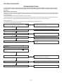
MD-SR50H/50W/60E/60W
SERVICE MANUAL
No. S2006MDSR50H/
MD-SR50H(BL)
MD-SR50H(S)
MD-SR50H(YR)
MD-SR50W(BL)
MD-SR50W(S)
MD-SR60E(GL)
MD-SR60W(S)
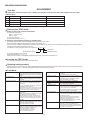
Illustration: MD-SR50H/SR50W
• In the interests of user-safety the set should be restored to its
original condition and only parts identical to those specified be
used.
Illustration: MD-SR60E/SR60W
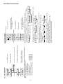
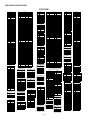
CONTENTS
Page
SAFETY PRECAUTION FOR SERVICE MANUAL ............................................................................................................... 2
SPECIFICATIONS ................................................................................................................................................................. 3
NAMES OF PARTS ............................................................................................................................................................... 4
OPERATION MANUAL .......................................................................................................................................................... 5
DISASSEMBLY ...................................................................................................................................................................... 8
REMOVING AND REINSTALLING THE MAIN PARTS ......................................................................................................... 9
ADJUSTMENT ...................................................................................................................................................................... 10
NOTES ON SCHEMATIC DIAGRAM .................................................................................................................................. 23
TYPES OF TRANSISTOR AND DIODE .............................................................................................................................. 23
VOLTAGE ............................................................................................................................................................................ 24
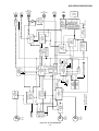
BLOCK DIAGRAM ............................................................................................................................................................... 25
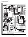
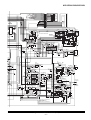
SCHEMATIC DIAGRAM ...................................................................................................................................................... 26
WIRING SIDE OF P.W.BOARD ........................................................................................................................................... 28
WAVEFORMS OF MD CIRCUIT ......................................................................................................................................... 31
TROUBLESHOOTING ......................................................................................................................................................... 32
FUNCTION TABLE OF IC .................................................................................................................................................... 35
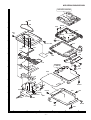
PARTS GUIDE/EXPLODED VIEW
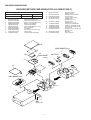
PACKING METHOD (MD-SR50H for U.K./SR60E Only)
SHARP CORPORATION
–1–
This document has been published to be used
for after sales service only.
The contents are subject to change without notice.
MD-SR50H/50W/60E/60W
SAFETY PRECAUTION FOR SERVICE MANUAL
Precaution to be taken when replacing and servicing the Laser Pickup.
The AEL (Accessible Emission Level) of Laser Power Output for this model is specified to be lower than Class I Requirements.
However, the following precautions must be observed during servicing to protect your eyes against exposure to the laser beam.
(1) When the cabinet has been removed, the power is turned on without a compact disc, and the Pickup is on a position
outer than the lead-in position, the Laser will light for several seconds to detect a disc. Do not look into the Pickup Lens.
(2) The Laser Power Output of the Pickup inside the unit and replacement service parts have already been adjusted prior
to shipping.
(3) No adjustment to the Laser Power should be attempted when replacing or servicing the Pickup.
(4) Under no circumstances look directly into the Pickup Lens at any time.
(5) CAUTION - Use of controls or adjustments, or performance of procedures other than those specified herein may result
in hazardous radiation exposure.
CAUTION
LASER KLASSE 1
LUOKAN 1 LASERLAITE
KLASS 1 LASERAPP ARAT
● This Portable MiniDisc Recorder is classified as a CLASS 1 LASER product.
● The CLASS 1 LASER PRODUCT label is located on the bottom.
● Use the Portable MiniDisc Recorder only in accordance with the instructions given in
this manual and do not attempt to interfere with the interlock switch or make any
other adjustment as this may result in exposure to hazardous radiation.
(MD-SR50H/SR60E)
Laser Diode Properties
● Material: GaAlAs
● Wavelength: 785 nm
● Pulse time:
Read mode: 0.8 mW Continuous
Write mode: max 10 mW 0.5S
min cycle 1.5S
Repetition
Laser Diode Properties
● Material: GaAIAs
● Wavelength: 785 nm
● Pulse time:
Read mode; 0.8 mW Continuous
Write mode; max. 10 mW 0.5S
min. cycle 1.5S
Repetition
VAROITUS! LAITTEEN KÄYTTÄMINEN MUULLA KUIN TÄSSÄ KÄYTTÖOHJEESSA
MAINITULLA TAVALLA SAATTAA ALTISTAA
KÄYTTÄJÄN TURVALLISUUSLUOKAN 1 YLITTÄVÄLLE
NÄKYMÄTTÖMÄLLE LASERSÄTEILYLLE.
VARNING - OM APPARATEN ANVÄNDS PÅ ANNAT SÄTT ÄN I DENNA BRUKSANVISNING
SPECIFICERAS. KAN ANVÄNDAREN UTSÄTTAS FÖR OSYNLIG LASERSTRÅLNING, SOM
ÖVERSKRIDER GRÄNSEN FÖR LASERKLASS 1.
(MD-SR50W/SR60W)
VARO !
VARNING!
(MD-SR50H)
Avattaessa ja suojalukitus ohitettaessa olet alttiina näkymättömälle lasersäteilylle. Älä katso säteeseen.
Osynlig laserstralning när denna del är öppnad och spärren är urkopplad. Betrakta ej strälen.
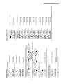
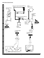
Precaution to be taken when replacing and servicing the laser pickup.
The following precautions must be observed during servicing to protect your eyes against exposure to the laser.
Warning of possible eye damage when repairing:
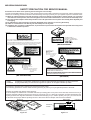
If the AC adaptor or batteries are connected when the top houising (disc cover) of the unit is removed, and the PLAY key is
pressed, the laser will light up during focus access (2-3 seconds). (Fig. 2-1) During the operation, the laser will leak from the
opening between the magnetic head and the mechanical chassis (Fig. 2-2). In order to protect your eyes, you must not look
at the laser during repair. Before repairing be sure to disconnect the AC adaptor and remove the batteries.
Magnet Head
Magnet head
Laser Beam
Mechanism
Chassis
Top Cabinet
Optical pick-up
Spindle motor
Figure 2-1
Main PWB Optical Pick-Up
Figure 2-2
–2–
MD-SR50H/50W/60E/60W
FOR A COMPLETE DESCRIPTION OF THE OPERATION OF THIS UNIT, PLEASE REFER TO
THE OPERATION MANUAL.
SPECIFICATIONS
General
Power source:
(MD-SR50H)
Power source:
(MD-SR50W)
Power source:
(MD-SR60E)
Power source:
(MD-SR60W)
Power consumption:
(MD-SR50H/60E)
Power consumption:
(MD-SR50W)
Power consumption:
(MD-SR60W)
Output power:
Charging time:
The operation time when using an alkaline battery may be
different, depending on the type and manufacturer of the battery
and on the operating temperature.
DC 5V : AC adaptor (AC 220-230V, 50/60 Hz)
DC 1.5V: Commercially available, "AA" (LR6)
size, alkaline battery x 1
DC 1.2V: Optional rechargeable Nickel-Metal
Hydride battery (AD-N70BT) x 1
DC 4.5V: Optional car adaptor, AD-CA20X
(for cars with a 12-24V DC negative
earth electrical system)
DC 5V : AC adaptor (AC 110-240V, 50/60 Hz)
DC 1.5V: Commercially available, "AA" size
(LR6), alkaline battery x 1
DC 1.2V: Optional rechargeable Nickel-Metal
Hydride battery (AD-N70BT) x 1
DC 4.5V: Separately available car adaptor,
AD-CA20X (for cars with a 12-24V
DC negative earth electrical system)
DC 1.2V: Rechargeable Nickel-Metal Hydride
battery (AD-N70BT) x 1
DC 5V : AC adaptor (AC 230-240V, 50/60 Hz)
DC 1.5V: Commercially available, "AA" size
(LR6), alkaline battery x 1
DC 4.5V: Separately available car adaptor,
AD-CA20X (for cars with a 12-24V
DC negative earth electrical system)
DC 1.2V: Rechargeable Nickel-Metal Hydride
battery (AD-N70BT) x 1
DC 5V : AC adaptor (AC 220V, 50 Hz)
DC 1.5V: Commercially available, "AA" size
(LR6), alkaline battery x 1
DC 4.5V: Separately available car adaptor,
AD-CA20X (for cars with a 12-24V
DC negative earth electrical system)
Input sensitivity:
Recording
level
2.5 mV
10 kohms
LINE
100 mV
20 kohms
LINE
—
Continuous recording
Approx. 3 hours
Continuous recording
Approx. 4.5 hours
Continuous play
Approx. 7 hours
Continuous play
Approx. 6.5 hours
—
Maximum
output level
Specified
output
Headphones
LINE
—
10 kohms
Dimensions:
Weight:
(MD-SR50H/SR50W)
Weight:
(MD-SR60W/SR60E)
Input socket:
Output socket:
(MD-SR50H/SR50W)
Output socket:
(MD-SR60W/SR60E)
Load
impedance
10 mW + 10 mW 16 ohms
250 mV (-12 dB)
—
10 kohms
Width: 99.9 mm (3-15/16")
Height: 22.9 mm (29/32")
Depth: 77.9 mm (3-3/32")
168 g (0.37 lbs.) without battery
191 g (0.42 lbs.) with rechargeable
battery
Line/optical digital, microphone
(powered by the main unit)
Earphones (impedance: 32 ohms)
Headphones (impedance: 16 ohms)/
remote control unit
MiniDisc Recorder
Type:
Signal readout:
Audio channels:
Frequency response:
Rotation speed:
Error correction:
Coding:
When using the rechargeable batter
(full charged) included with the unit
Load
impedance
10 mW + 10 mW 32 ohms
250 mV (-12 dB)
Battery life:(MD-SR60W/SR60E)
When using a commercially available,
high capacity, "AA" size (LR6),
alkaline battery
Maximum
output level
Output level:(MD-SR60W/SR60E)
When using the optional rechargeable
batter AD-N70BT(full charged)
Continuous play
Approx. 6.5 hours
MIC L
Earphones
RMS; 20 mW (10 mW + 10 mW) (0.2 % T.H.D.)
Approx. 3.5 hours (90%)
Approx. 5.5 hours (fully charged)
(When using the AC adaptor included with the unit)
Battery life:(MD-SR50H/SR50W)
Continuous play
Approx. 7 hours
10 kohms
Specified
output
6W, 0.06A (AC adaptor)
Continuous recording
Approx. 4.5 hours
0.25 mV
Output level:(MD-SR50H/SR50W)
0.15A (AC adaptor)
Continuous recording
Approx. 3 hours
input
impedance
MIC H
7W (AC adaptor)
When using a commercially available,
high capacity, "AA" (LR6) size,
alkaline battery
Reference
input level
Recording method:
Sampling frequency:
Wow and flutter:
The continuous recording time is for analogue input when the
volume level is set to "VOL 0"
The continuous play time shows the value when the volume level
is set to "VOL 15"
The above values are the standard values when the unit is charged and used at an ambient temperature of 20˚C (68˚F).
Portable MiniDisc recorder
Non-contact, 3-beam semi-conductor
laser pick-up
Stereo 2 channels/monaural (longplay
mode) 1 channel
20 - 20,000 Hz (± 3 dB)
Approx. 400 - 900 rpm
ACIRC (Advanced Cross Interleave
Reed-Solomon Code)
ATRAC (Adaptive Transform
Acoustic Coding), 24-bit computed
type
Magnetic modulation overwrite
method
44.1kHz (32 kHz and 48kHz signals
are converted to 44.1kHz, and then
recorded)
Unmeasurable
(less than ±0.001% W. peek)
Specifications for this model are subject to change without prior
notice
–3–
MD-SR50H/50W/60E/60W
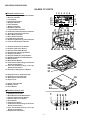
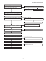
NAMES OF PARTS
■ Remote control unit
1 2 3 4 5 6
7
1. Monaural Long-Play Mode Indicator
2. Record Indicator
3. Level Meter
4. Fast Play Indicator
5. Repeat Indicator
6. TOC Indicator
7. Battery Indicator
8. Random Indicator
9. Track Number Indicator
10. Character/Time Information Indicator
11. Synchro Recording Indicator
12. Disc Mode Indicator
13. Disc Name Indicator
14. Track Name Indicator
15. Remaining Recording Time Indicator
16. Total Track Number Indicator
11
12
13
14
8
9
10
17
17. Volume Down/Cursor Button
18. Volume Up/Cursor Button
19. Record/Track Mark Button
20. Stop/Power Off/Charge Button
21. Play/Pause Button
22. Display/Character Select Button
23. Edit/Auto Mark/Time Mark Button
24. Mode Button
25. Bass/Delete Button
26. Fast Reverse/Recording Level Down/
Name Select Button
27. Fast Forward/Recording Level Up/
Name Select Button
28. Enter/Fast Play/Synchro Button
15 16
18 19 20
21
22 23 24 25 26 27 28
29
30
31
32
29. Earphones/Line Output Socket
30. Optical/Line Input Socket
31. Microphone Input Socket
32. Open Lever
35
33. 5V DC Input Socket
34. Battery Cover
35. Hold Switch
33
34
■ Remote control unit
Illustration: MD-SR60E/SR60W Only
1. Headphones Socket
2. Bass/Delete/Track Mark Button
3. Volume Down/Cursor Button
4. Volume Up/Cursor Button
5. Hold Switch
6. Play/Pause Button
7. Fast Reverse/Recording Level Down/
Name Select Button
8. Fast Forward/Recording Level Up/
Name Select Button
9. Stop/Power Off Button
1
2 34 5
6 7 8 9
–4–
POWER SOURCE
–5–
Notes:
● After charging has been completed, the
AC adaptor may be left connected.
(For example, when charging at night.)
● The battery will not be charged when the
power to the main unit is turned on.
● Do not force the battery cover open too far.
● Do not use a rechargeable battery or an
AC adaptor other than those specified.
● The charging time will vary, depending
on the condition of the battery.
● When the battery is charged for the first
time or is charged after not being used
for a long period, the operating time may
be shorter than normal.The battery life
will recover with normal use i.e. charging and discharging.
● To avoid shortening the service life of the
battery only recharge the battery after it
has been completely discharged.
begin charging.
” will appear, and the battery
●“
will begin charging.
● After about 3.5 hours have
” will go out.
passed, “
This indicates that the battery charging is about 90% complete.
● To charge the battery fully, continue
charging for about 2 more hours.
(In this case, you do not need to press
the :OFF/CHRG ( • ■ ) button. Even if
the :OFF/CHRG ( • ■ ) button is
” will not appear.)
pressed, “
5 Press the :OFF/CHRG ( • ■ ) button to
and then insert the plug on the AC adaptor lead into the DC IN 5V socket.
3 Close the battery cover.
4 Plug the AC adaptor into the AC socket,
ing to the polarity marked on the bottom
of the unit.
2 Insert the rechargeable battery accord-
4
,
5
For MD-SR50H AC 220-230V, 50/60 Hz
For MD-SR50W AC 110-240V, 50/60 Hz
For MD-SR60E AC 230-240V, 50/60Hz
For MD-SR60W AC 220V, 50 Hz
Insert securely
all the way in.
To the DC
IN 5V socket
3
2
● When recording from digital inputs, it is
not necessary to adjust the recording
level.
button, and then start
playback on the equipment connected
to this unit.
2 Press the
mode. (Perform steps 1 - 3 in the “Synchro recording” section.)
1 Place the unit in the recording stand-by
■ Manual recording
connected to this unit.
4 Press the ENTER/SYNC button.
5 Start the playback on the equipment
into the playback stand-by mode.
3 Put the equipment connected to this unit
press the REC button.
2 Insert a recordable MiniDisc, and then
1 Connect the external equipment.
1 Open the battery cover.
● Slide the battery cover as far as it will go
to the outside and then lift to open it.
If the battery cover is lifted without being slid all the way out, it may break.
■ Synchro recording
1
This is the method used for recording digital signals from CDs or MDs exactly as they
are stored on the original. Compared to recordings made from analogue inputs, digital recordings have extremely high-quality
sound.
Digital cable
Recording
Recording
Analogue recording is
possible.
Digital cable
Notes:
● This unit incorporates a sampling rate
converter.
When this unit is connected to digital
equipment such as CS/BS tuners or DAT
tape recorders that use a different sampling frequency (32 kHz or 48 kHz), recordings can still be made. (The sampling frequency of this unit is 44.1 kHz.)
● When making a digital recording from a
portable CD player (if the player has a
sound skip prevention function and this
function is turned on) the optical output
will drop out and digital recording will not
be possible. Be sure to turn the sound
skip prevention function off.
Playback
MD player
Digitally recorded MiniDisc
CD player, MD
player, etc.
Playback
When you attempt to make a new digital
recording from a track that was digitally recorded on a MiniDisc.
● MiniDiscs are designed so that only first
generation digital copies can be made.
Further digital copies are prevented by
the SCMS (Serial Copy Management
System).
There are cases where digital recording
may be impossible.
In the following cases digital recording is
impossible, even if you are using digital
cables.
RECORDING USING THE OPTICAL DIGITAL CABLE
When the rechargeable battery is used for the
first time or when you want to use it after a
long period of disuse, be sure to charge it fully.
■ Rechargeable battery power
You can power this unit with an AC adaptor or a commercially available alkaline battery (LR6, “AA” size).
You can also power this unit with a rechargeable battery (AD-N70BT) or car adaptor
(AD-CA20X) which are available separately.
MD-SR50H/50W/60E/60W
OPERATION MANUAL
When the battery
level is very low
–6–
Notes:
● If you use the battery which you stopped
charging halfway, “
” may appear. It
does not mean that the battery is completely charged.
● When using the unit with an alkaline battery or a rechargeable battery, the battery
indicator will not correctly display the remaining capacity for approximately 10 seconds
after the power has been turned on.
● When the AC adaptor included with this unit
or a separately available car adaptor is
used, the battery indicator will not be shown.
● The number of bars shown in the battery
indicator may increase or decrease, depending on the operation being performed.
This is normal.
● When the battery is completely discharged,
the battery indicator will flash. Recharge the
battery or replace the alkaline battery with
a new one.
● When the battery has run completely out,
“BATT EMPTY” will appear. Then, the
power will be disconnected automatically.
Since the battery level is very low, you
cannot start recording or editing.
When the battery
level is high
< How to read the battery indicator >
To avoid accidental operation of the unit,
use the hold function.
The remaining amount of battery level is
shown by the battery indicator (
) during operation.
Battery indicator
Cancel
Cancel
Hold
Cancel
Hold
Main
unit
If the hold function is active whilst the power
is turned off, the power cannot be turned
on by mistake and the battery will not be
accidentally drained.
Can be operated
from either the
remote control unit or
the main unit.
Cancel
Hold
Can only be operated
from the main unit.
Can only be operated
from the remote
control unit.
Hold
Cannot be operated
from either the
remote control unit or
the main unit.
Remote
control unit
For MD-SR60E/SR60W Only
● To cancel the hold mode, move the
HOLD switch away from the safety position (the opposite direction of the arrow).
For MD-SR60E/SR60W Only
● When the unit is in the hold mode, pressing the buttons will have no affect.
Move the HOLD switch to the safety position (direction indicated by the arrow).
■ To prevent the unit from being
operated by mistake
■ Checking the remaining amount
of battery level
CONVENIENT OPERATION OF THE UNIT
When the unit has condensation inside,
the disc signals cannot be read, and the
unit may not function properly.
● If this happens, remove the disc.
The condensation should evaporate in
approximately 1 hour. The unit will then
function properly.
CAUSE
Is the AC adaptor disconnected?
Is the battery exhausted?
Is the unit in the hold mode?
Has condensation formed inside the unit?
Is the unit being influenced by mechanical shock or by
static electricity?
When this product is subjected to strong
external interference (mechanical shock,
excessive static electricity, abnormal supply voltage due to lightning, etc.) or if it is
operated incorrectly, it may malfunction.
If such a problem occurs, do the following:
1. Unplug the AC adaptor from the AC
socket.
2. Remove the battery.
3. Leave the unit completely unpowered for
approximately 30 seconds.
■ If trouble occurs
Recording and editing
are impossible.
If strange sounds, smell or smoke come out
of the unit or an object is dropped into the
unit, remove the AC adaptor from the AC
socket immediately and contact an
authorised SHARP service centre.
4. Plug the AC adaptor back into the AC
socket and retry the operation.
● Is the MiniDisc protected against accidental erasure?
● Is the unit connected properly to the other equipment?
● Is the AC adaptor unplugged or did a power failure occur whilst recording or editing?
● Is the unit in the hold mode?
● Is an optical signal being output from the external equipment?
Read the operation manual for the external equipment.
● Has the track number or character information been
written on the disc yet?
● Is the unit in the recording or editing mode?
● Is the battery exhausted?
● Is the unit being subjected to excessive vibration?
Some sounds are
skipped.
The MiniDisc cannot be
ejected.
● Is the unit in the hold mode?
● Is the battery exhausted?
● Is the volume set too low?
● Is the earphones plugged in?
● Are you trying to play a MiniDisc with data on it instead
of a MiniDisc containing music?
●
●
●
●
●
When the operation buttons are pressed, the
unit does not respond.
No sound is heard from
the earphones.
The unit does not turn
on.
PROBLEM
Many potential “problems” can be resolved by the owner without calling a service technician.
If something seems to be wrong with this product, check the following before calling your
authorised SHARP dealer or service centre.
● Shortly after turning on a heater.
● When the unit is placed in a room where
there is excessive steam or moisture.
● When the unit is moved from a cool
place to a warm place.
In the following cases, condensation
may form inside the unit.
■ Moisture condensation
TROUBLESHOOTING
MD-SR50H/50W/60E/60W
When the remaining recording time of a
disc is displayed, short tracks less than
12 seconds long may not be included in
the total.
For MiniDiscs on which repeated recording and editing operations were performed, the COMBINE function may not
work.
A cluster (about 2 seconds) is normally the
minimum unit of recording. So, even if a track
is less than 2 seconds long, it will use about
2 seconds of space on the disc.
Therefore, the time actually available for recording may be less than the remaining time
displayed.
If there are scratches on discs, those sections will be automatically avoided (no recording will be placed in those sections). Therefore, the recording time will be reduced.
For MiniDiscs on which repeated recording and editing were performed, some
sounds may be skipped whilst cueing and
reviewing.
If there are scratches or dust on a
MiniDisc, the track numbers following that
track will be increased by one.
Two tracks may not be combined
in editing.
The total of the recorded time and
time remaining on a disc may not
add up to the maximum possible
recording time.
When recorded tracks are played
back using the cue and review operations, some sounds may be
skipped.
A track number can be created in
the middle of a track.
If there are scratches on a disc, the unit
will automatically avoid recording in those
areas. The recording time will be reduced.
Even if several short tracks are
erased, the remaining recording
time may not show an increase.
Even if the number of tracks and
the recording time have not
reached the limit, “DISC FULL”
may be displayed.
Even if the maximum recording
time of a MiniDisc has not been
reached, “DISC FULL” or “TOC
FULL” may be displayed.
When the number of tracks used reaches
the limit, regardless of the remaining recording time, further recording will be
impossible.
(Maximum number of tracks: 255)
If a MiniDisc has been recorded or edited repeatedly or if a MiniDisc has
scratches on it, it may not be possible to
record the maximum number of tracks on
it.
MiniDiscs are recorded using a different system than is used for cassette tapes or DAT
recordings. Therefore, the following conditions may be encountered, depending on how
the disc has been recorded or edited. These are due to system limitations, and should be
considered normal.
MINIDISC SYSTEM LIMITATIONS
● Re-record or replace it with another
recordable disc.
● Check the number of tracks.
● Replace the disc with another recordable disc.
● Recording cannot be performed correctly due to vibration or shock in the unit.
● Editing is impossible.
● Cannot save the TOC information
correctly to a MiniDisc.(A large portion of the disc has been damaged.)
Can’t STAMP
Can’t WRITE
–7–
● Connect the digital cable securely.
● If the portable CD player has a function
to prevent sound skips,deactivate it.
● Playback with the connected unit.
● Replace it with a recordable disc.
● Poor connection of the digital cable.
● No output signal comes out from the
external unit to playback.
● You tried to record on a playbackonly disc.
*: Number or Symbol.
PLAY MD
NO SIGNAL
● Load a disc.
● A disc has not been loaded.
NO DISC
● Return the HOLD switch to its original position.
● The unit is in the hold mode.
● Turn off the power and remove the
MiniDisc.
● To have it repaired, go to the distributor where you purchased the unit.
● You have come to the conclusion
that the unit is out of order.
● The OPEN lever was moved during
recording or editing.
● Replace it with another recordable
disc.
● The disc is out of recording space.
LOCKED
HOLD
Er-MD**
DISC FULL
DEFECT
Can’t REC
● If the sound you hear is not right, try
recording again.
● Replace the disc with another recordable disc.
● Reload the disc or replace it.
● Replace it with another recorded disc.
● The disc data cannot be read because the disc is damaged.
Can’t READ*
● The disc is scratched.
● Change the stop position of the track
and then try editing it.
Can’t EDIT
● A track cannot be edited.
● Replace the disc with a recorded disc.
Remedy
● Charge the rechargeable battery or
replace the alkaline battery (or use
the AC adaptor for power).
● Record using the analogue cable.
● Nothing is recorded.
Meaning
● The battery is run down.
● No copy can be made because of
the SCMS copyright system.
Can’t COPY
BLANK MD
BATT EMPTY
Error messages
ERROR MESSAGES
MD-SR50H/50W/60E/60W
MD-SR50H/50W/60E/60W
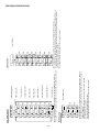
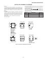
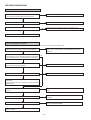
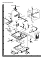
DISASSEMBLY
Cares before disassembling
When assembling the machine after disassembling or
repair, observe the following requirements so as to ensure
safety and performance.
1. Remove the batteries from the machine, and take out the
mini-disc.
2. When assembling after repair, be sure to restore the
initial location of wires.
Since the screws are small, incorrect fixing may result in
malfunction.
3. When repairing, pay utmost attention to static electricity
of IC.
STEP
REMOVAL
PROCEDURE
FIGURE
1
Bottom Cabinet
1. Screw ..................... (A1) x6
8-1
2
Top Cabinet
1. Open the Top cabinet.
2. Open the Battery Cover.
3. Screw ..................... (B1) x4
4. Flexible PWB .......... (B2) x2
8-1
3
Main PWB
1. Screw .................... (C1) x4
2. Flexible PWB ......... (C2) x2
3.Solder joint ............. (C3) x2
8-2
1. Raise the rear part, and
remove in the arrow direction.
8-3
4
Mechanism Unit
(B1)x2
ø1.4x2mm
Top Cabinet
(A1)x2
ø1.4x2mm
(A1)x2
ø1.4x2mm
Battery Cover
Open Lever
(B1)x2
ø1.4x2mm
(A1)x2
ø1.4x2mm
(A1)x2
ø1.4x2mm
Bottom Cabinet
Figu re 8-1
8-2
(C1)x4
ø1.7x2.5mm
(C3)x1
(C3)x1
(B2)x2
pull
pull
pull
pull
pull
Mechanism Unit
pull
(C2)x1*
(C2)x1
Main PWB
Mechanism Unit
Felt
Put the fold on the connector, and apply
with the felt. Sagging may result in
contact with the sheet matal
Caution:
Carefully handle the main PWB and flexible PWB. After removing the
flexible PWB (1*) for the optical pickup from the connector, do not
touch directly the front end of flexible PWB with your hand so as to
prevent damage of optical pickup by static electricity.
Figure 8-3
Figure 8-2
–8–
MD-SR50H/50W/60E/60W
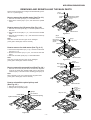
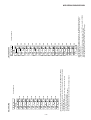
REMOVING AND REINSTALLING THE MAIN PARTS
Remove the mechanism according to the disassembling methods 1 to 4. (See Page 8.)
(A2)x3
ø1.4x2.8mm
Spindle
Motor
How to remove the spindle motor (See Fig. 9-1.)
1. Remove the solder joint (A1) x 1 of flexible PWB.
2. Remove the screws (A2) x 3 pcs., and remove the spindle
motor.
Mechanism Flexible
PWB Solder joint @
(A1)x1
How to remove the Lift motor (See Fig. 9-2.)
1. Remove the solder joints (B1) x 2 of head up/down motor
lead wire.
2. Remove the screw (B2) x 1 pc., and remove the flexible
PWB.
3. Remove the screw (B3) x 1 pc., and remove the head up/
down motor.
Note:
Take care so that the motor gear is not damaged.
(If the gear is damaged, noise is caused.)
MD Mechanism
Figure 9-1
(B3)x1
ø1.4x5.5mm
(B2)x1
ø1.4x1.5mm
Remove the
Solder joint
(B1)x2
Lift Motor
How to remove the sled motor (See Fig. 9-3.)
1. Remove the stop washer (C1) x 1 pc., and remove the drive
gear (C2) x 1 pc.
2. Remove the screws (C3) x 2 pcs., and remove the sled
motor.
3. Remove the solder joints (C4) x 2 of flexible PWB.
Note:
Take care so that the motor gear is not damaged.
(If the gear is damaged, noise is caused.)
MD Mechanism
Figure 9-2
(C3)x2
ø1.4x1.2mm
Stop Washer
(C1)x1
Driver Gear
(C2)x1
How to remove the magnetic head (See Fig. 9-4.)
Sled Motor
Mechanism Flexible
PWB Solder joint
(C4)x2
1. Remove the screws (D1) x4 which connects the magnetic
head to the head relay flexible PWB, remove the spring
washers (D2) x 2 and remove the soldering joints (D3) x 2.
Note:
Mount carefully so as not to damage the magnetic head.
(If the gear is damaged, noise is caused.)
How to reinstall the optical pickup unit
(See Fig. 9-5.)
MD Mechanism
Figure 9-3
1. Remove the screw (E1) x 1 pc.
2. Slowly raise the optical pickup.
(D1)x2
ø1.4x2.2mm
(D2)x2
Spring joint
(E1)x1
ø1.7x3mm
Guide Shaft
Magnetic Head
Thrust Plate Spring
Optical Pickup Unit
(D1)x1
ø1.4x1.5mm
Solder joint
(D1)x1 (D3)x2
ø1.2x1.6mm
MD Mechanism
MD Mechanism
Figure 9-5
Figure 9-4
–9–
MD-SR50H/50W/60E/60W
ADJUSTMENT
Test disc
MD adjustment needs two types of disc, namely recording disc (low reflection disc) and playback-only disc (high
reflection disc).
Type
Parts No.
Test disc
1
High reflection disc MMD-110 (TEAC Test MD)
88GMMD-110
2
Low reflection disc
MMD-212 (TEAC Test MD) 74-minute disc
88GMMD-212
3
Low reflection disc
MMD-213A (TEAC Test MD) 80-minute disc
4
Low reflection disc
Recording minidisc
88GMMD-213A
UDSKM0001AFZZ
Note: Use the low reflection disc on which music has been recorded.
Entering the TEST mode
1. Setting at port (power nonconnected state)
(1) Set the port as follows.
TEST1 : "Low" (TP416)
TEST0 : "High"
(2) Turn the Power ON.
(3) Test Mode START [ T E S T _ ]
2. Setting by special button operation (in standby state)
(1) Holding down the DISP button and ENTER button, press the PLAY button.
(2) Normal mode setting initialization (BASS setting, VOL setting, etc.)
*Since the unit is changed to the setting for production line inspection , be sure to set it to the default setting state in the following default
setting procedure before returning it to the user.
(3) Indication of microcomputer version for one second [ Y 1 9 A b X ]
Destination
Microcomputer version
EEPROM version
(4) Whole LCD lighting for 2 seconds
(5) Test Mode START [ T E S T _ ]
*When the PLAY button is pressed during indication (3) and (4), the process proceeds to (5).
Leaving the TEST mode
(1) Press the STOP button in the TEST mode stop state.
Shipping setting method
Holding down simultaneously the VOLUME-DOWN Button and PLAY Button of the set unit without disc, supply the power from the DC IN plug.
After the indication "INIT" -> "BYE OK" disappears, release the power supply of DC IN.
Test Mode
1. AUTO 1 Mode
2. AUTO 2 Mode
3. TEST-PLAY Mode
4. TEST-REC Mode
5. MANUAL 1 Mode
6. MANUAL 2 Mode
• Perform preliminary automatic adjustment.
• If the combination of mechanism and pickup
PWB has been changed, be sure to start from
AUTO1.
• Perform ATT (attenuator) automatic adjustment.
• Perform continuous playback (error rate display,
jump test)
• Continuous playback from the specified address
is performed.
• 1 line, 10 lines or 384 lines manual jump is
performed.
• C1 error rate display (pit section), ADIP error
rate display (groove section)
• The temperature correction is performed only when
servo start is performed, but the posture correction
is not performed during continuous playback.
• Continuous record from the specified address
is performed.
• Change of record laser output(servo gain is also
changed according to laser output).
• The temperature correction is performed only
when servo start is performed, but the posture
correction is not performed during continuous
recording.
• Temperature is displayed. (Updating in real time)
• Seeing the displayed adjustment value, perform
preliminary manual adjustment.
(Error rate indication, jump test)
• Temperature is displayed. (Updating in real time)
• Seeing the displayed adjustment value perform
manfully the preliminary adjustment.
(Error rate indication, jump test)
• Continuous playback is performed
(error rate display, jump test).
7. RESULT 1 Mode
• The value adjusted in AUTO1 or MANUAL1 is
indicated.
• (Execution in servo "OFF" state").
8. RESULT 2 Mode
• The value adjusted in AUTO 2 or MANUAL 2 is
indicated.
• Adjustment value is changed manually.
(error rate display, jump test).
9. DIGITAL INPUT Mode
• Digital input information is displayed.
10. ERROR INFORMATION • Error information is displayed.
Mode
• Error information is initialized
11. NORMAL Mode
• The mode is changed from the TEST mode to
the normal mode without adjustment.
• In the normal mode the internal operation mode,
memory capacity, etc. areindicated.
• In the normal mode both temperature correction
and posture correction are perfomed.
12. EEPROM Mode
• Factors of digital servo are changed manually.
(Each servo is turned on individually.)
• Cut-off frequency of BASS1, BASS2 and BASS3
is selected manually.
• Temperature detection terminal voltage is
measured, and the reference value is set.
• Defaults are selected and set.
• Setting of EEPROM protect area is updated.
(In case of protect releasing)
13. INNER Mode
• Determine the position where the INNER switch
is turned on. (only high reflection disc).
• The temperature correction is performed only
when servo start is performed, but the posture
correction is not performed.
– 10 –
MD-SR50H/50W/60E/60W
Operation in each TEST mode
1. AUTO1 Mode
• When the STOP button is pressed while the AUTO1 menu appears or during automatic adjustment, the mode changes to the TEST mode
stop state. At this time the adjustment value is not output.
• Be sure to adjust, using the specified disc MMD-213A or MMD-212.
At this time release the EEPROM (IC402) protection. (Refer to EEPROM write procedure.)
• Adjustment NG; Adjustment item out of range, focus ON failure, and adjustment error
• When the PLAY button is pressed while ADJ. OK is displayed, AUTO2 is executed.
2. AUTO2 Mode
• When the STOP button is pressed while the AUTO2 menu appears or during automatic adjustment, the mode changes to the TEST mode
stop state. At this time the adjustment value is not output.
• Adjustment NG; Adjustment item out of range, and adjustment error.
• When the PLAY button is pressed while ADJ. OK is displayed,TEST_PLAY is executed.
3. TEST-PLAY Mode
• When the STOP button is pressed while the TEST-PLAY menu appears, or in TEST-PLAY or continuous playback mode, the mode
changes to the TEST mode stop state.
• When the PLAY button is pressed while the TEST-PLAY menu appears,continuous playback is initiated from the current pickup position.
• Whenever the DISP button is pressed in the TEST-PLAY menu, the target address changes as follows.
0032 — 03C0 — 0700 — 08A0 — 0950— 0032 —
When the PLAY button is pressed while a target address is displayed, continuous playback is performed after searching that address.
• Each time the MODE button is pressed while the TEST-PLAY mode target address is displayed, the digit which is changed by pressing the
SKIP UP/DOWN button is changed as follows.
0032 — 0032 — 0032 — 0032 —
• When the SKIP UP button is pressed in the TEST-PLAY mode target address is displayed, the digit of address specified by the MODE
button is set to +1h. (0 to F)
• When the SKIP DOWN button is pressed in the TEST-PLAY mode target address is displayed, the digit of address specified by the MODE
button is set to -1h. (0 to F)
* When the SKIP UP/DOWN button is held down, the setting changes continuously, one cycle being 100 ms.
• When the BASS button is pressed in the continuous playback mode, the number of jump lines changes as follows.
1 — 10 — 384 — 1
* After the number of jump lines is indicated for one second, the address indication is restored.
[
T R _ ]
• When the SKIP UP button is pressed in the continuous playback mode, the specified number of lines is jumped in the FWD direction.
• When the SKIP DOWN button is pressed in the continuous playback mode, the specified number of lines is jumped in the REV direction.
* When the SKIP UP/DOWN button is held down, jump is repeated every approx. 100 ms.
•Whenever the DISP button is pressed in the continuous playback mode, the indication changes as follows.
* Pre-mastered disc
Continuous playback (SUBQ address indication)
[ S Q
]
|
Continuous playback (C1 error indication)
[ C E
]
|
Continuous playback (SUBQ address indication)
[ S Q
]
* Recordabl disk
Continuous playback (ADIP address indication)
[ A P
]
|
Continuous playback (C1 error indication)
[ C E
]
|
Continuous playback (ADIP error indication)
[ A E
]
|
Continuous playback (ADIP address indication)
[ A P
]
4. TEST-REC Mode
• When the STOP button is pressed while the TEST-REC menu appears, or in the TEST-REC mode or continuous record mode, the mode
changes to the TEST mode stop state.
• When the PLAY button is pressed while the TEST-REC menu appears, the continuous record is initiated from the current pickup position.
• Whenever the DISP button is pressed in the TEST-REC menu, the target address changes as follows.
0032 — 03C0 — 0700 — 08A0 —0950 — 0032 —
When the PLAY button is pressed while a target address is displayed, continuous playback is performed after searching that address.
• Whenever the MODE button is pressed in the TEST-REC mode target address is displayed, the digit which is changed by the SKIP UP/
DOWN button changes as follows.
0032 — 0032 — 0032 — 0320 —
• When the SKIP UP button s pressed in the TEST-REC mode target address is displayed, the digit of address specified by the BASS button
is set to +1h.(0 to F)
• When the SKIP DOWN button is pressed in the TEST-REC mode target address is displayed, the digit of address specified by the BASS
button is set to -1h. (0 to F)
* When the SKIP UP/DOWN button is held down, the setting changes continuously, one cycle being 100 ms.
– 11 –
MD-SR50H/50W/60E/60W
5. NORMAL Mode
• When the STOP button is pressed while the NORMAL menu appears, the mode changes to the TEST mode stop state.
• Indication during operation
Indication of memory capacity on main unit LCD [
] + Level meter
: Internal mode
: Address (Cluster section)
: Address (Sector section)
• Selection of sound volume, BASS, etc. is possible (without indication)
• Recording is also possible.
• If the STOP button is pressed during operation in the NORMAL mode, the NORMAL mode is canceled, and the power is turned off.
6. Error data display Mode
• Reversing when SKIP DOWN button is pressed
• When the STOP button is pressed while the error data indication menu appears or during error data indication, the mode changes to the
TEST mode stop state.
• Error data 0 is the latest error.
• Error which occurred in the TEST mode is also stored in the memory.
• When the DISP button is pressed while the error data indication menu appears, the error data is initialized. [ C L E A R _ ]
•
: Error Code
Explanation of error history code
12h : RF side FG, TG, and TCRS adjustment termination failure
13h : Adjustment servo retraction excessive retrial
16h : C. IN detection time-over
17h : A, B, E, F, and TCRSO offset measurement value out of
tolerable range
21h : Focus retraction completion allowable time-over
23h : Track search completion allowable time-over
24h : Disc linear speed measurement failure
32h : P-TOC read failure
42h : U-TOC read failure
44h : U-TOC write data write disabled/read check error
52h : SD write data write disabled
71h : Pickup position initialization time-over
72h : EEPROM data read check sum error
73h : Record head drive disabled (by EJECT lever)
82h : Power overvoltage detection
91h : Ambient temperature is higher that the allowable temperature.
7. INNER Mode
• when the STOP button is pressed on the INNER menu (SQ______ ), the state is changed to the TEST mode STOP state.
•
: Address
– 12 –
MD-SR50H/50W/60E/60W
EEPROM (IC402) writing procedure
1. Procedure to replace EEPROM and write initial value of microcomputer in EEPROM
(1)
(2)
(3)
(4)
Replace EEPROM.
Refer to the latest EEPROM data list.
Press the Display button, ENTER button and Play button to start the test mode.
Version display
[Ver.
X ]
EEPROM version (b ~ Z)
Microcomputer ROM version
(5) The whole LCD lights.
(6) Test mode stop state.
[ T E S T ]
(7) Press the "BASS" button, and press twice the "SKIP DOWN" button.
[ E E P R O M ]
(8) Perform the operation to display "EEPROM SETTING MODE CHART", compare the EEPROM DATA LIST with the display,
and set according to the EEPROM DATA LIST with the VOL UP or VOL DOWN key.
(9) Set the temperature reference. (Refer to the Temperature Reference Setting Method.)
(10) Set according to the EEPROM DATA LIST.
(11) Press the Stop button.
[ T E S T ]
(12) Press the Stop button.
(13) After data is written in EEPROM, turn off power .
(14) Restore protection of EEPROM.
2. Temperature reference setting method
[1] Measurement, calculation and setting procedure
(1) Set the TEST mode.
• Set TEST 1, 0 = '01', and turn on power (or set PLAY ON in standby state).
(2) Start the EEPROM mode 'Temp' menu.
• Key operation in order of BASS, SKIP-DOWN x 2 times, PLAY, PLAY in the test mode STOP state.
• 'TM$$%%' is displayed. ($$= Temperature code, %% = Temperature reference)
(3) Once press SKIP-UP, and determine the displayed microcomputer TEMP input AD value.
• 'TPin##' is displayed. (## = TEMP input AD value)
(4) At the ambient temperature, determine the temperature corrected value from the temperature measurement value
correction table.
(5) Determine the temperature reference, using the following formula.
• Temperature reference = Microcomputer TEMP input AD value + Temperature corrected value
(6) Set the temperature reference value by button operation , and check whether the temperature code indication corresponds to "Temperature
Code Identification Table".
[2] Temperature measurement value correction table
Ambient
temperature
+ 9oC ~ +11oC
Temperature
correction
- 05h
Center
temperature
+ 10.0oC
+12oC ~ +14oC
+15oC ~ +16oC
+17oC ~ +19oC
- 04h
- 03h
- 02h
+ 12.7oC
+ 15.4oC
+ 18.2oC
+20oC ~ +22oC
+23oC ~ +24oC
+25oC ~ +27oC
+28oC ~ +30oC
- 01h
± 00h
+ 01h
+ 02h
+ 20.9oC
+ 23.6oC
+ 26.3oC
+ 29.0oC
+31oC ~ +33oC
+ 03h
+ 31.8oC
– 13 –
Ambient
temperature
Temperature
correction
Center
temperature
- 9oC ~ +10oC
+ 3oC ~ +21oC
08h
07h
+ 0.5oC
+ 12.5oC
+15oC ~ +33oC
+26oC ~ +43oC
06h
05h
+ 23.6oC
+ 35.0oC
MD-SR50H/50W/60E/60W
EEPROM DATA LIST (EEPROM version b)
TEMP setting
Sled setting
Item display
T M _ _
Set values
Item display
Calculate values
Fucus setting
Item display
Set values
Set values
S L G _
DF
S L 2 _
20
H
S L M _
7F
H
S L V _
AB
S K k _
72
H
H
H
F G _ _
B0
H
S K t _
4C
H
F F 1 _
70
H
S K m _
70
H
F F 2 _
E8
H
W T m _
24
H
F Z H _
ED
H
M V 1 _
44
H
F L n _
0A
H
M V 2 _
88
H
D J G _
14
H
S R V _
00
H
F L V _
20
H
W T f _
20
H
F S S _
E9
H
ADJ. SET setting
Item display
Tracking setting
Item display
Set values
Set values
C O K _
A0
F A T _
C0
H
T A T _
3E
H
H
T G _ _
48
H
C A T _
20
H
T F 1 _
70
H
F A B _
64
H
T F 2 _
E0
H
T F S _
00
H
T B o _
44
H
T B t _
20
H
T K o _
44
H
H Q 1 _
90
H
T K t _
1DH
H Q 2 _
90
H
T D o _
67
H
H S G _
11
H
T D t _
34
H
H S O _
FD
T G R _
00
H
L Q 1 _
90
H
S C t _
40
H
L Q 2 _
90
H
S C m _
53
H
L S G _
11
H
C L p _
18
H
L S O _
00
H
C L r _
28
H
G Q 1 _
98
H
J P I _
01
H
G Q 2 _
84
H
K 1 0 _
65
H
G S G _
11
H
F L p _
08
H
EQ. SET setting
Item display
Set values
H
Spindle setting
Item display
S P G _
S P i
14
_
E0
H
A0
H
S P o _
68
H
10
S P 2 _
60
H
H
S P 3 _
F2
H
S P 4 _
F2
H
S P 5 _
10
H
S P D _
60
S P K _
EB
Item display
H
S P m _
S P 1 _
Control setting
Set values
H
H
BASS setting
Item display
Set values
Set values
C T 0 _
01
H
C T 1 _
11
H
C T 2 _
40
H
C T 3 _
30
H
R C 0 _
C0
H
R C 1 _
FE
H
S Y C _
A6
H
P W L _
01
H
D R 1 _
00
H
D R 2 _
00
H
I N 1 _
C9
H
I N 2 _
64
H
I N 3 _
99
H
I N H _
64
H
0C
H
B S 1 _
3F
H
D R H _
B S 2 _
1F
H
P L E _
1B
H
B S 3 _
E2
H
R C E _
42
H
E L T _
76
H
S L T _
45
H
S P M _
00
H
M S L _
00
H
U S 0 _
00
H
U S 1 _
00
H
U S 2 _
00
H
– 14 –
TEST
REC
– 15 –
SKIP DOWN
SKIP DOWN
SKIP DOWN
SKIP DOWN
SKIP DOWN
SKIP DOWN
SKIP DOWN
SKIP DOWN
DATA
SKIP DOWN
SKIP DOWN
: INNER switch position measurement menu
: EEPROM setting menu
: Error history display menu
: Digital input signal monitor menu
: Test mode normal playback menu
: Continuous record menu
: Continuous playback menu
: ATT adjustment value check menu
: Pre-adjustment value check menu
: ATT manual adjustment menu
: Pre-manual adjustment menu
: ATT auto adjustment menu
: Pre-auto adjustment menu
: Test Mode STOP
* When the [STOP] button is pressed in specific menu, the "TEST MODE STOP" state is set.
* When the [PLAY] button operation is performed in the specific menu, the operation of this
menu is executed.
SKIP UP
INNER
SKIP UP
EEPROM
SKIP UP
NORMAL
SKIP UP
E
SKIP UP
Din Mon
SKIP UP
RSLT2
SKIP UP
RSLT1
SKIP UP
MANU2
SKIP UP
SKIP DOWN
SKIP DOWN
SKIP DOWN
PLAY
MANU1
SKIP UP
T
SKIP UP
T
SKIP UP
AUTO2
SKIP UP
SKIP DOWN
Slide internal
periphery move
AUTO1
BASS
Slide external
periphery move
SKIP UP
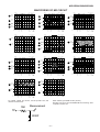
Test Mode Change Chart
Tset Mode Menu
ADJ. NG
Adjustment error
: During ATT automatic adjustment
: Preadjustment normal end (adjustment value output)
: Preadjustment error (adjustment value output)
: During preadjustment adjustment
: Preautomatic Adjustment menu
* When the [STOP] button is pressed in specific menu, the "TEST MODE STOP" state is set.
*"
" represent the adjustment number as follows.
0 0 : Innermost periphery move
0 2 : ABEF offset tentative measurement
0 4 : RF side focus gain coarse adjustment
0 5 : Focus ATT tentative setting
0 6 : RF side bit section tracking gain adjustment
0 7 : COUT level setting for pit section adjustment
0 8 : External periphery move
0 9 : RF side groove section tracking gain adjustment
1 0 : COUT level setting for groove section adjustment
1 1 : RF side TCRS gain adjustment
1 2 : Tracking ATT initial setting
1 3 : RF side focus gain minor adjustment
1 4 : Focus ATT initial setting
1 5 : S gain "High" ABEF offset measurement
1 6 : TCRS offset measurement
1 7 : S gain "Low" ABEF offset measurement
AT2
PLAY
ADJ. OK
Normal end
AT1
PLAY
AUTO1
Preautomatic Adjustment
MD-SR50H/50W/60E/60W
ADJ. NG
Adjustment error
: Continuous playback (high reflection)
: Continuous playback (low reflection)
: ATT adjustment normal end (adjustment value output)
: ATT adjustment error (adjustment value output)
: During ATT autoadjustment
: ATT Autoadjustment menu
* When the [STOP] button is pressed in specific menu, the "TEST MODE STOP" state is set.
*"
" represent the adjustment number as follows.
0 0 : Innermost periphery move
0 3 : Pit section tracking ATT setting
0 4 : Pit section focus ATT setting
0 6 : External periphery move
(low reflection only)
0 7 : TCRS ATT setting
(low reflection only)
0 8 : Groove section tracking ATT setting
(low reflection only)
0 9 : Groove section focus ATT setting
(low reflection only)
SQ####
AP####
PLAY
ADJ. OK
Normal end
AT2
PLAY
AUTO2
ATT Auto Adjustment
PLAY
: Continuous playback menu
PLAY
: Continuous playback (pit section)
: Continuous playback (groove section)
# # # # : Address
: Start address setting
: Continuous playback menu
– 16 –
MODE
DISP
Ad0 3 C 0
MODE
DISP
DISP
0950H
Ad0 9 5 0 H
Ad0 7 0 0
DISP
Ad0 8 A 0
BASS
Ad0 0 3 2
BASS
MODE
Ad0 0 3 2
10TR
BASS
3 8 4TR
* When the [SKIP UP] button is pressed in the continued playback mode, jump of specified
number of lines occurs in the external periphery direction.
If the key is held down jump occurs continuously (100 ms cycle).
* When the [SKIP DOWN] button is pressed in the continuous playback mode, jump of
specified number of lines occurs in the internal periphery direction.
If the key is held down, jump occurs continuously (100 ms cycle).
1TR
* In the start address set state the value of selection digit changes in the range of "0h to Fh"
when the [SKIP UP/DOWN] button is pressed
* In the continuous playback state the number of jump lines changes as follows shown
the [BASS] button is pressed.
1 (initial value)
10
384
Ad0 0 3 2
* In the start address setting state the start address change digit changes when the [BASS] button is pressed.
1st digit (initial value)
2nd digit
3rd digit
Ad0 0 3 2
* When the [STOP] button is pressed in specific menu, the "TEST MODE STOP" state is set.
* In the start address set state the start address changes as follows when the [DISP] button is pressed.
03C0H
0 0 3 2 H (initial value)
0700H
08A0H
SQ####
AP####
PLAY
Ad 0 0 3 2
DISP
T
: Continuous playback (pit section)
: Continuous playback (groove section)
# # # # : Address
• Continuous playback from any address
SQ####
AP####
PLAY
T
• Continuous playback from current pickup position
Continuous Playback
MD-SR50H/50W/60E/60W
REC
PLAY
: Continuous record menu
PLAY
REC
: Continuous record
# # # #: Address
: Start address setting
: Continuous record menu
Ad0 3 c 0
Ad0 9 5 0
Ad0 7 0 0
Ad0 8 A 0
DISP
– 17 –
MODE
Ad0 0 3 2
2nd digit
MODE
Ad0 0 3 2
: INNER switch position measurement menu
MODE
3rd digit
: TEST mode normal playback menu
: Continuous playback
@@@@@@: Mode and address display
* When the [STOP] button is pressed in specific menu, the "TEST MODE STOP" state is set.
* When the NORMAL mode is canceled, the power is turned off.
@@@@@@
PLAY
NORMAL
Test Mode Normal Playback
: Continuous playback (pit section)
# # # # : Address
* When the [STOP] button is pressed in specific menu, the "TEST MODE STOP" state is set.
SQ####
PLAY
INNER
Inner Switch Position Measurement
Ad0 0 3 2
1st digit (initial value)
* In the start address setting state the start address change digit changes when the [BASS] button is pressed.
Ad0 0 3 2
* When the [STOP] button is pressed in specific menu, the "TEST MODE STOP" state is set.
* In the start address set state the start address changes as follows when the [DISP] button is pressed.
0 0 3 2 H (initial value)
03C0H
0700H
08A0H
DISP
DISP
DISP
AP# # # #
PLAY
Ad 0 0 3 2
T
AP# # # #
: Continuous record
# # # #: Address
• Continuous record playback from any address
T
• Continuous record from the current pickup position
Continuous Rrecord
DISPLAY
DATA
SKIP DOWN
SKIP DOWN
SKIP DOWN
SKIP DOWN
SKIP DOWN
SKIP DOWN
SKIP DOWN
SKIP DOWN
: Error history 9 display
§ § : Error code
: Error history 8 display
§ § : Error code
: Error history 7 display
§ § : Error code
: Error history 6 display
§ § : Error code
: Error history 5 display
§ § : Error code
: Error history 4 display
§ § : Error code
: Error history 3 display
§ § : Error code
: Error history 2 display
§ § : Error code
: Error history 1 display
§ § : Error code
: Error history 0 display
§ § : Error code
: Error history display menu
: Error history clear
: Error history display menu
* When the [STOP] button is pressed in specific menu, the "TEST MODE STOP" state is set.
E9§§
SKIP UP
E8§§
SKIP UP
E7§§
SKIP UP
E6§§
SKIP UP
E5§§
SKIP UP
E4§§
SKIP UP
E3§§
SKIP UP
E2§§
SKIP UP
E1§§
SKIP UP
E0§§
SKIP DOWN
DATA
PLAY
E
• Error history display
CLEAR
E
• Error history clear
Error History Display
MD-SR50H/50W/60E/60W
SKIP DOWN
SKIP DOWN
SKIP DOWN
SKIP DOWN
SKIP DOWN
SKIP DOWN
– 18 –
SKIP DOWN
: Control setting menu
: Digital EQ setting menu
: Adjustment setting menu
: BASS setting menu
: Sled setting menu
: Spin setting menu
: Tracking setting menu
: Focus setting menu
: TEMP setting menu
: EEPROM setting menu
SKIP DOWN
SKIP DOWN
: BASS setting menu
* When the [STOP] button is pressed in specific menu, the "TEST MODE STOP" state is set.
* When the [DISP] button operation is performed in the specific state, the menu changes to
"TEMP SETTING menu".
* In the specific state the setting changes in the range of "00h to FFh" when the
[VOL UP/DOWN] button is pressed.
(The upper limit varies depending on the items)
* When the [MODE] button is pressed in each state, the set digit is changed.
BS3
SKIP UP
BS2
SKIP UP
BS1
PLAY
Bass
BASS Setting
* When the [STOP] button is pressed in specific menu, the "TEST MODE STOP" state is set.
* When the [PLAY] button operation is performed in the specific state, the specific setting menu is set.
CTRL
SKIP UP
SKIP UP
DEQSET
SKIP UP
SKIP DOWN
SKIP DOWN
ADJSET
SKIP UP
Bass
SKIP UP
Sled
SKIP UP
Spin
SKIP UP
Track
SKIP UP
Focus
SKIP UP
TEMP
PLAY
EEPROM
EEPROM Setting
SKIP DOWN
SKIP DOWN
SKIP DOWN
SKIP DOWN
SKIP DOWN
SKIP DOWN
SKIP DOWN
SKIP DOWN
: Focus setting menu
* When the [STOP] button is pressed in specific menu, the "TEST MODE STOP" state is set.
* When the [DISP] button operation is performed in the specific state, the menu changes to "TEMP SETTING menu".
* In specific state the setting changed in the range of "00h to FFh" when the [VOL UP/DOWN] button is pressed.
(The upper limit varies depending on the items)
* When the [MODE] button is pressed in each state, the set digit is changed.
FSS
SKIP UP
WTf
SKIP UP
FLV
SKIP UP
DJG
SKIP UP
FLn
SKIP UP
FZH
SKIP UP
FF2
SKIP UP
FF1
SKIP UP
FG
PLAY
Focus
Focus Setting
MD-SR50H/50W/60E/60W
– 19 –
SKIP DOWN
SKIP DOWN
SKIP DOWN
SKIP DOWN
SKIP DOWN
SKIP DOWN
SKIP DOWN
SKIP DOWN
SKIP DOWN
SKIP DOWN
: Spin setting menu
* When the [STOP] button is pressed in specific menu, the "TEST MODE STOP" state is set.
* When the [DISP] button operation is performed in the specific state, the menu changes to
"TEMP SETTING menu".
* In specific state the setting changed in the range of "00h to FFh" when the
[VOL UP/DOWN] button is pressed.
(The upper limit varies depending on the items)
* When the [MODE] button is pressed in each state, the set digit is changed.
SPK
SKIP UP
SPD
SKIP UP
SP5
SKIP UP
SP4
SKIP UP
SP3
SKIP UP
SP 2
SKIP UP
SP 1
SKIP UP
SP o
SKIP UP
SP m
SKIP UP
SP i
SKIP UP
SPG
PLAY
S p i n
Spin Setting
SKIP DOWN
SKIP DOWN
SKIP DOWN
SKIP DOWN
SKIP DOWN
SKIP DOWN
SKIP DOWN
SKIP DOWN
SKIP DOWN
SKIP DOWN
SKIP DOWN
SKIP DOWN
SKIP DOWN
SKIP DOWN
SKIP DOWN
SKIP DOWN
: Tracking setting menu
* When the [STOP] button is pressed in specific menu, the "TEST MODE STOP" state is set.
* When the [DISP] button operation is performed in the specific state, the menu changes to
"TEMP SETTING menu".
* In the specific state the setting changes in the range of "00h to FFh" when the [VOL UP/DOWN]
button is pressed. (The upper limit varies depending on the items)
* When the [MODE] button is pressed in each state, the set digit is changed.
K10
SKIP UP
JPI
SKIP UP
CLr
SKIP UP
CLp
SKIP UP
SCm
SKIP UP
SC t
SKIP UP
TGR
SKIP UP
TDt
SKIP UP
TDo
SKIP UP
TKt
SKIP UP
TKo
SKIP UP
TB t
SKIP UP
TB o
SKIP UP
TFS
SKIP UP
TF 2
SKIP UP
TF 1
SKIP UP
TG
PLAY
T r a c k
Tracking Setting
MD-SR50H/50W/60E/60W
– 20 –
SKIP DOWN
SKIP DOWN
SKIP DOWN
SKIP DOWN
SKIP DOWN
SKIP DOWN
SKIP DOWN
SKIP DOWN
SKIP DOWN
SKIP DOWN
* When the [STOP] button is pressed in specific menu, the "TEST MODE STOP" state is set.
* When the [DISP] button operation is performed in the specific state, the menu changes to
"TEMP SETTING menu".
* In the specific state the setting changes in the range of "00h to FFh" when the
[VOL UP/DOWN] button is pressed.
(The upper limit varies depending on the items)
* When the [MODE] button is pressed in each state, the set digit is changed.
SRV
SKIP UP
MV2
SKIP UP
MV1
SKIP UP
WTm
SKIP UP
SKm
SKIP UP
SKt
SKIP UP
SKk
SKIP UP
SLV
SKIP UP
SLM
SKIP UP
SL2
SKIP UP
SKIP DOWN
: TEMP reference
: Reference
§ § : Temperature code
: TEMP A/D input value
: Measurement value
: Temp setting menu
P-MODE
SKIP DOWN
SKIP DOWN
SKIP DOWN
SKIP DOWN
: Adjustment setting menu
* In the specific state the setting changes in the range of "0h to Fh" when the [VOL UP/DOWN]
button is pressed.
* When the [MODE] button is pressed in each state, the set digit is changed.
P-MODE
* When the [STOP] button is pressed in specific menu, the "TEST MODE STOP" state is set.
* When the [DISP] button operation is performed in the specific state, the menu changes to
"TEMP SETTING menu".
* In the specific setting display state the setting change digit changes when the [P-MODE]
button is pressed.
1st digit (initial value)
2nd digit
FAB
SKIP UP
CAT
SKIP UP
TAT
SKIP UP
FAT
SKIP UP
COK
PLAY
ADJSET
Adjustment Setting
* When the [STOP] button is pressed in specific menu, the "TEST MODE STOP" state is set.
* When the [DISP] button operation is performed in the specific state, the menu changes to
"TEMP SETTING menu".
* In the specific state the setting changes in the range of "00h to FFh" when the
[VOL UP/DOWN] button is pressed.
* When the [MODE] button is pressed in each state, the set digit is changed.
T p i n
SKIP UP
TM§§
SLG
Temp
PLAY
: Slide setting menu
TEMP Setting
PLAY
S l e d
Sled Setting
MD-SR50H/50W/60E/60W
– 21 –
SKIP DOWN
SKIP DOWN
SKIP DOWN
SKIP DOWN
SKIP DOWN
SKIP DOWN
SKIP DOWN
SKIP DOWN
SKIP DOWN
SKIP DOWN
SKIP DOWN
: Digital EQ setting menu
* In the specific state the setting changes in the range of "0h to Fh" when the [VOL UP/DOWN]
button is pressed.
* When the [MODE] button is pressed in each state, the set digit is changed.
P-MODE
P-MODE
* When the [STOP] button is pressed in specific menu, the "TEST MODE STOP" state is set.
* When the [DISP] button operation is performed in the specific state, the menu changes to
"TEMP SETTING menu".
* In the specific setting display state the setting change digit changes
when the [P-MODE] button is pressed.
1st digit (initial value)
2nd digit
FLp
SKIP UP
GSG
SKIP UP
GQ2
SKIP UP
GQ 1
SKIP UP
LSO
SKIP UP
LSG
SKIP UP
LQ 2
SKIP UP
LQ 1
SKIP UP
HSO
SKIP UP
HSG
SKIP UP
HQ2
SKIP UP
HQ 1
PLAY
DEQSET
Digital EQ Setting
SKIP DOWN
SKIP DOWN
SKIP DOWN
SKIP DOWN
SKIP DOWN
SKIP DOWN
SKIP DOWN
SKIP DOWN
SKIP DOWN
SKIP DOWN
SKIP DOWN
SKIP DOWN
SKIP DOWN
SKIP DOWN
Continued to
the next page
SKIP UP
I N H
SKIP UP
I N 3
SKIP UP
I N 2
SKIP UP
I N 1
SKIP UP
DR2
SKIP UP
DR1
SKIP UP
PWL
SKIP UP
SYC
SKIP UP
RC1
SKIP UP
RC0
SKIP UP
CT3
SKIP UP
CT2
SKIP UP
CT1
SKIP UP
CT0
PLAY
CTRL
Control Setting
: Control setting menu
MD-SR50H/50W/60E/60W
– 22 –
SKIP DOWN
SKIP DOWN
SKIP DOWN
SKIP DOWN
SKIP DOWN
SKIP DOWN
SKIP DOWN
SKIP DOWN
SKIP DOWN
SKIP DOWN
P-MODE
* In the specific state the setting changes in the range of "0h to Fh" when the
[VOL UP/DOWN] button is pressed.
* When the [MODE] button is pressed in each state, the set digit is changed.
P-MODE
* When the [STOP] button is pressed in specific menu, the "TEST MODE STOP" state is set.
* When the [DISP] button operation is performed in the specific state, the menu changes to
"TEMP SETTING menu".
* In the specific setting display state the setting change digit changes when the [P-MODE]
button is pressed.
1st digit (initial value)
2nd digit
US2
SKIP UP
US1
SKIP UP
US0
SKIP UP
MSL
SKIP UP
SPM
SKIP UP
SLT
SKIP UP
ELT
SKIP UP
RCE
SKIP UP
PLE
SKIP UP
DRH
SKIP UP
Continued from
the preceding page
MD-SR50H/50W/60E/60W
MD-SR50H/50W/60E/60W
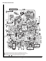
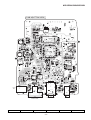
NOTES ON SCHEMATIC DIAGRAM
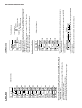
• Resistor:
To differentiate the units of resistors, such symbol as K and
M are used: the symbol K means 1000 ohm and the symbol
M means 1000 kohm and the resistor without any symbol is
ohm-type resistor. Besides, the one with “Fusible” is a fuse
type.
• Capacitor:
To indicate the unit of capacitor, a symbol P is used: this
symbol P means micro-micro-farad and the unit of the
capacitor without such a symbol is microfarad. As to electrolytic capacitor, the expression “capacitance/withstand voltage” is used.
(CH), (TH), (RH), (UJ): Temperature compensation
(ML): Mylar type
B
(G)
(3)
E
(S)
1
TOP
VIEW
• The indicated voltage in each section is the one measured
by Digital Multimeter between such a section and the chassis with no signal given.
• Parts marked with “
”(
) are important for
maintaining the safety of the set. Be sure to replace these
parts with specified ones for maintaining the safety and
performance of the set.
DESCRIPTION
REF. NO
SW401
EJECT
SW402
HOLD
OFF—ON
SW403
LID DETECTION
OFF—ON
SW902
DISC PROTECT
OFF—ON
TOP VIEW
TOP VIEW
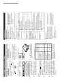
HSB2838
F10J2E
F05J2L
C
(D)
(2)
2SA1832 GR
2SA17457
RN1444 A
UN5213
UN5210
2SD1979 S
2SD1819 AS
TOP VIEW
TOP VIEW
HRB0103 B
RB731U
TOP VIEW
SBE803
2SA1873 GR
Figure 23 TYPES OF TRANSISTOR AND DIODE
– 23 –
POSITION
OFF—ON
MD-SR50H/50W/60E/60W
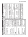
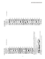
VOLTAGE
IC101
PIN
NO.
1
2
3
4
5
6
7
8
9
10
11
12
13
14
15
16
17
18
19
20
21
22
23
24
25
26
27
28
29
30
31
32
33
34
35
36
37
38
39
40
41
42
43
44
45
46
47
48
VOLTAGE
0.71V
0.71V
0.71V
0.71V
1.24V
1.24V
0V
1.24V
1.24V
1.24V
1.24V
1.24V
2.28V
2.28V
0V
0V
2.48V
0V
0V
1.47V
2.35V
0V
0V
2.48V
1.24V
1.24V
1.24V
1.24V
1.24V
1.2V
1.24V
1.24V
1.24V
0V
1.24V
1.24V
0.16V
1.24V
1.24V
1.24V
1.24V
2.48V
0V
—
1.24V
1.24V
1.24V
0.19V
IC202
PIN
NO.
1
2
3
4
5
6
7
8
9
10
11
12
13
14
15
16
17
18
19
20
PIN
NO.
1
2
3
4
5
6
7
8
9
10
11
12
13
14
15
16
17
18
19
20
21
22
23
24
25
26
27
28
29
30
31
32
33
34
35
36
37
38
39
40
41
42
43
44
45
46
47
48
49
50
1.55V
2.05V
2.57V
1.94V
0.93V
1.43V
0.49V
0.6V
0.6V
2.55V
0.6V
0.99V
0.99V
0.99V
0.8V
1.87V
2.12V
1.66V
1.73V
0V
VOLTAGE
0V
2V
2.73V
IC251
PIN
NO.
1
2
3
4
5
6
7
8
IC353
VOLTAGE
1V
0V
0V
0V
0V
2V
0V
0V
0V
0V
—
2V
0V
0.88V
0.76V
2.46V
1V
2V
0V
1V
1V
0V
0V
0V
—
2V
2V
2V
0V
2V
1V
2V
2V
2V
1V
2V
2V
0V
2.34V
0V
0.3V
0V
0V
1.6V
1.2V
1.7V
0.3V
2.25V
2.34V
0.2V
VOLTAGE
IC253
PIN
NO.
1
2
3
4
5
6
IC258
VOLTAGE
5.36V
5.31V
5.31V
0V
0V
0V
-1.05V
0V
0V
-2.25V
0V
0V
-1.65V
2.72V
IC256
PIN
NO.
1
2
3
4
5
6
VOLTAGE
0V
—
—
0V
0V
0V
IC257
PIN
NO.
1
2
3
4
VOLTAGE
0V
0.59V
4.93V
0V
0V
0V
IC259
VOLTAGE
VOLTAGE
2.07V
0V
0V
0V
5.35V
2.08V
2.08V
2.08V
PIN
NO.
1
2
3
4
5
6
IC255
PIN
NO.
1
2
3
4
5
6
7
8
IC203
PIN
NO.
1
2
3
IC201
VOLTAGE PIN
NO.
51
0.84V
52
2.48V
53
1.22V
54
0V
55
1.24V
56
1.24V
57
1.24V
58
1.24V
59
1.24V
60
2V
61
1.17V
62
2V
63
0V
64
0V
65
0V
66
0V
67
1V
68
0V
69
0V
70
0V
71
0V
72
0V
73
0V
74
0V
75
0V
76
0.5V
77
0.5V
78
0.5V
79
1.4V
80
1.13V
81
2.55V
82
0.5V
83
0.8V
84
0.8V
85
0.8V
86
0.8V
87
1.84V
88
0V
89
1.97V
90
1.38V
91
1.53V
92
0.9V
93
1.9V
94
2.56V
1.66V
95
1.56V
96
0V
97
1.9V
98
1V
99
100
0.9V
VOLTAGE
0V
0V
—
0V
PIN
NO.
1
2
3
4
5
6
VOLTAGE
—
0.56V
0.56V
0V
0.56V
2.63V
IC841
PIN
NO.
1
2
3
4
5
VOLTAGE
—
2.8V
2.06V
2.06V
0V
IC842
PIN
NO.
1
2
3
4
5
VOLTAGE
—
2.81V
2.56V
0V
2.36V
PIN
NO.
1
2
3
4
5
6
7
8
VOLTAGE
2.73V
0V
0V
0V
0V
0V
0V
0V
IC354
PIN
NO.
1
2
3
4
5
VOLTAGE
0V
0V
0V
0V
0V
IC402
PIN
NO.
1
2
3
4
5
6
7
8
VOLTAGE
2.35V
0V
0V
0V
2.34V
0V
2.35V
2.35V
IC404
PIN
NO.
1
2
3
4
5
VOLTAGE
0.2V
0.2V
0V
2.19V
2.5V
IC431
PIN
NO.
1
2
3
4
VOLTAGE
2.34V
2.35V
0V
0V
IC621
PIN
NO.
1
2
3
4
5
6
VOLTAGE
8.58V
0V
0V
0V
2.34V
8.55V
IC260
PIN
NO.
1
2
3
4
5
6
VOLTAGE
2.72V
2.7V
2.7V
0V
0V
—
IC351
PIN
NO.
1
2
3
4
5
6
7
8
9
10
11
12
13
14
VOLTAGE
0V
0V
4.44V
0V
0V
4.44V
0V
0.91V
4.44V
0V
0.91V
4.44V
0V
4.49V
IC821
PIN
NO.
S
G
D
VOLTAGE
0V
—
—
– 24 –
PIN
NO.
1
2
3
4
5
6
7
8
9
10
11
12
13
14
15
16
17
18
19
20
21
22
23
24
25
26
27
28
29
30
31
32
33
34
35
36
37
38
39
40
41
42
43
44
45
46
47
48
49
50
IC401
VOLTAGE PIN
NO. VOLTAGE
51
0V
0V
52
0V
—
53
2.35V
0.29V
54
0V
2.32V
55
2.32V
—
56
0V
0.17V
57
2.35V
0V
58
2.35V
0.22V
59
2.32V
0V
60
2.35V
2.32V
61
2.35V
2.15V
62
2.28V
2.03V
63
2.35V
2.25V
64
2.35V
2.35V
65
2.35V
2.35V
66
1.09V
0V
67
1.12V
2.35V
68
0V
0V
69
0V
2.32V
70
2.34V
0.21V
71
2.35V
2.32V
2.35V
72
2.25V
2V
73
0.2V
2.32V
74
1.55V
2.32V
75
0V
0.15V
76
0V
2.35V
77
1.57V
78
2.35V
1.05V
79
0V
1.75V
80
0V
0.56V
81
2.34V
0V
2.34V
82
0V
2.12V
83
2.35V
1.47V
84
0V
0V
85
0V
0V
86
0V
0V
87
2.34V
0V
88
2.34V
0V
89
0V
0V
90
2.35V
0V
91
2.13V
0V
92
2.7V
0V
93
2.7V
0V
94
0V
2.32V
0V
95
0V
2.35V
96
0V
2.35V
97
2.35V
2.35V
98
2.33V
0V
99
0V
100
2.47V
Preform the measurement on
the IC401 pin 37 in the TEST
mode with GND short-circuited.
(LCD is in "TEST" state.)
IC901
PIN
NO.
1
2
3
4
5
6
7
8
9
10
11
12
13
14
15
16
17
18
19
20
21
22
23
24
VOLTAGE
0V
0V
2.34V
0V
2.49V
0V
2.49V
0V
—
—
—
—
0V
0.75V
—
—
—
0V
0V
0V
0V
0V
0V
0V
IC809
PIN
NO.
1
2
3
4
5
6
VOLTAGE
5.36V
0V
0V
0V
2.35V
5.36V
IC852
PIN
NO.
1
2
3
4
5
6
7
8
VOLTAGE
0V
—
—
0V
2.49V
0V
0.78V
0V
0V
1V
1V
1V
—
—
—
—
IC651
PIN
NO.
1
2
3
4
5
6
7
8
9
10
VOLTAGE
2.73V
—
0V
0V
0V
0V
—
—
—
—
IC771
PIN
NO.
1
2
3
4
5
VOLTAGE
0V
2.74V
2.74V
—
2.5V
IC801
PIN
NO.
1
2
3
VOLTAGE
0V
2V
4.44V
IC802
PIN
NO.
1
2
3
4
5
6
PIN
NO.
1
2
3
4
5
6
7
8
9
10
11
12
13
14
15
16
17
18
19
20
21
22
23
24
25
26
27
28
29
30
31
32
33
34
35
36
37
38
39
40
41
42
43
44
45
46
47
48
0.45V
1.03V
3.28V
0.45V
0.99V
4.38V
VOLTAGE
1.17V
2.8V
0.37V
0V
1.17V
1.17V
1.16V
1.26V
IC892
PIN
NO.
1
2
3
4
5
6
VOLTAGE
0V
0.6V
1.58V
0V
0V
0V
IC851
PIN
NO.
S
G
D
VOLTAGE
0V
—
—
2.34V
0V
—
—
—
8.55V
2.48V
0V
2.38V
0V
2.38V
2.34V
0V
0V
0V
0V
4.67V
0V
0V
0V
4.67V
0V
0V
0V
0V
—
4.67V
2.34V
0V
2.48V
—
—
—
—
2.48V
0V
0V
0V
0V
4.67V
0V
0V
0V
4.67V
—
0V
—
—
IC803
PIN
NO.
1
2
3
4
VOLTAGE
4.4V
4.46V
0V
0V
IC871
PIN
NO.
1
2
3
4
5
VOLTAGE
1V
2.36V
0V
1.18V
2.36V
IC873
PIN
NO.
1
2
3
4
5
PIN
NO.
1
2
3
4
5
6
7
8
9
10
11
12
13
14
15
16
17
18
19
20
21
22
23
24
VOLTAGE
0V
0V
0V
0V
0V
0V
0V
0V
0V
0V
0V
0V
0V
0V
0V
0V
-2.32V
0V
0V
2.42V
0.86V
0V
0V
0V
VOLTAGE
0V
8.59V
2.36V
—
4.47V
IC703
IC701
IC822
PIN
NO.
1
2
3
4
5
6
7
8
VOLTAGE
VOLTAGE
VOLTAGE
1.17V
2.8V
0.67V
0V
1.2V
1.17V
1.16V
1.26V
IC601
IC501
PIN
NO.
1
2
3
4
5
6
7
8
9
10
11
12
13
14
15
16
PIN
NO.
1
2
3
4
5
6
7
8
9
10
11
12
13
14
15
16
17
18
19
20
21
22
23
24
VOLTAGE
0V
0V
0V
0V
0V
2.5V
-2.34V
0V
2.5V
0V
1.26V
0V
2.35V
0V
0V
2.5V
0V
-2.34V
-2.34V
0V
0V
0V
0V
0V
– 25 –
Figure 25 BLOCK DIAGRAM
43
6
VG
39,41
17,21,27,
40,44
VM
IC601
4-CH PWM DRIVER
LV8017W
PLAYBACK SIGNAL
RECORD SIGNAL
6
7,30,35
VCC
NC
SW402
HOLD
IC431
RESET
S80820LN
IC402
EEPROM
58X2402T
1
8
VDD
+2.0V
6-9
9,
11,
13,
48
74
4
75,83
LCD ASS'Y
55,
59,
81,
82
1
SW401
EJECT
SW403
LID
DETECTION
40,65,77,78,98
19
+B
+7V
+2.35V 5
3
2
VCC
2
IC822
IR3M14N
DC/DC
CONVERTER
+2.7V
VCC
2
17
8
-2.5V
L-CH 2
R-CH 3
F841
0.4A,DC 60V
L-CH
R-CH
IC251 FTD2017
IC253 RN4904
IC255 NJM022V
IC256 RN4911
IC257 S80808LN
IC258 259 HN1C01FU
IC260 RN4904
IC809 RN4904
IC892 HN1C01FU
TRANSISTOR,
N-ch MOS FET,
DIGITAL TRANSISTER,
OP AMP,
RESET
2
IC873
62GR4522
4.5V
REGULATOR
5
Q721
IC801 62RP2002
IC802 HN1C01FU
IC803 S80819LN
TRANSISTOR,
RESET IC
+2V
IC841
S8324A28
2.8V UP CONVERTER
6,19
VEE
IC703
AUDIO AMP.
IR3R59N
9,16
IC842
XC62HS02
2.35V REGULATOR
+4.0V
+2.7V
5,6
VCC
2
4,21
+2.5V
IC852
IR3M14N
DC/DC
CONVERTER
IC771 62GR2522
15,16
2,3
+1-2V
KEY FLEXIBLE PWB ASS'Y
62
3
IC621 RN4904
DIGITAL
TRANSISTOR
1, 20-30, 73, 33-35
6
2
+2.5V
2,3 2.5V REGULATOR
5
5
AK4550VT
9 AD/DA CONVERTER
IC501
8
73
74
12,62,68,87
2.0V
REGULATOR
IC203
62FP2002
82-84,86,
89-100
IC401
SYSTEM
MICROCOMPUTER
IX0341AW
1-12
14-17
4
95
1,5,6,7
SW902
DISC
PROTECT
2,13,14,24,
25,36,37
2
AVCC
+2.5V
18-24
IC201
ENDEC/SERVO/
ATRAC
LR37811
66
VEE
17
RIPPLE
FILTER
J801
DC IN
(4~5.5V)
M902
SLED
MOTOR
IC901
SPINDLE MOTOR
DRIVER
LB1971V
5,7
16,18,
20,22
+2.5V
13,14
23
40
3
50
26-29,
32-37,
39-46
VCC
20
24 L-CH
22 R-CH
J703
REMOTE
CONTROL
M
1,2,
21,23
T
1-2
IC101
RF SIGNAL
PROCESSOR
IR3R55
+2.7V
10,12
6
IC701
AUDIO AMP.
IR3R54N
5
R-CH
+2.5V
J703
HEADPHONES
LINE
M901
SPINDLE
MOTOR
M
F
+2.7V
1-9,
11-19
L-CH
J702
MIC IN
(READY FOR
PLUG/IN
POWER)
PICK
+2.5V
+2.7V
VS
VCC
OPIC
LASER
HEAD
+2.5V
10
IC202
IX2567AF
4M D-RAM
OPTICAL IN
UNIT
J701
LINE IN
NOR GATE
IC351 74ACT02T
N-ch MOS FET
IC354 CPH5608
IC353 FTD2005
+2.7V
1
VCC
IC651
MOTER DRIVER
LB1930M
J701
OPTICAL IN
M903
LIFT
MOTOR
M
7,9
MD-SR50H/50W/60E/60W
Ni - MH Battery
or
Dry Battery
(1 pieces)
1.0-1.7V
MD-SR50H/50W/60E/60W
C112
0.033
TP206
C205
0.1
R206
270K
L100
10µH
C100
10/6.3
R416
100K
PGND4
BAT3
OUT3
PGND5
L609
4.7
L610
4.7
L608
4.7
39 EMPH0
40 VCC
41 MCPGI
42 INPGI
IN3
MUTE
4.7
N.C.
EFMO
N.C.
X700KO
LDCNT1
EMPH1
LDCNT2
SPDRR
SLDRF
TRDRR
TRDRF
FODRF
FODRR
SLDRR
SPDRF
TP200
HDON
CIN
PDCNT
SPWDS
VSS
RMDAT
PCRX
DSPSTB
DSPSCK
SCK0
EPCS
DSPDAT
AVSS 87
78 Vref
43 INPGCK
77
AVCC
76
ARQ
CHGCNT 85
TEMP 84
RKEY 83
HKEY1 82
45 RACLK
HKEY2 81
46 PBOPON
HKEY1
HKEY2
80
47 PBLAT
PLVDRY
78
77
76
R425
22K
RPLAY
RCPCNT
PCNT2
PCNT1
DCEXT
EXTAL
VSS
XTAL
VCC
uSTBY
NMI
MD2
RESET
WDTOVF
MD1
MD0
PLVBAT 79
48 LCDRST
RPLAY
DINT
RKEY
TP414
TP413
R423
22K
R402
100K
XL401
4.19 MHz
12
11
10
9
8
7
6
5 N.C.
4 N.C.
3 N.C.
2
1
C603
1
RCPCNT
PCNT1
PCNT2
IC621
RN4904
DIGITAL
TRANSISTOR
C602
1
4
5
6
C622
0.1
R622
1K
D622
MA8075M
VCCPWM
3
2
1
R621
100K
D431
HSB2838
+B
C606
22/6.3
C431
0.47
1
R431
330K
2
OUT
VDD
VSS 4
TP441
D461
RB731U
3
2
1
C454
0.0022
R461
100K
4
5
6
R465
100K
R464
100K
R466
560K
H
• NOTES ON SCHEMATIC DIAGRAM can be found on page 23.
• The numbers 1 to 18 are waveform numbers shown in page 31.
2
3
4
Figure 26 SCHEMATIC DIAGRAM (1/2)
– 26 –
5
SW403
LID DETECTION
3
N.C. 3
IC431
S80820LN
RESET
IC601: 4-CH PWM DRIVER
4
2
1
R463
100K
1
C401
0.1
LDVAR
CHGCNT
TEMP
LDVAR 86
44 RADAT
SW402
HOLD
PDCNT
DSPDAT
DISCPR
INNSW
SPIN
CIN
PLVON
TP401
VSS 88
4.7
C601
1
N.C.
N.C.
TP415
PLVON 89
AURESET
L604
C605
0.1
C608
1
EEPD
EEPK
VSS
EPWP
SYRS
EJSW
SYD1
SYD0
SYRD
SYWR
SYD2
38 TEST0
PLVGIN
92
N.C. BATOFF 91
MCMON 90
IC401
IX0341AW
SYSTEM
MICROCOMPUTER
37 TEST1
EL
R407
CHGON 10K
CHGON 93
PLVGIN
OPICGA
LDON
TP404
LDON 96
34 SENSE
N.C.
R408
100K
99
KHOLD 95
33 XRST
SPDRF
C610
TP601
C609
1
IN1F
IN1R
PGND1
BAT1
OUT1R
BAT2
OUT1F
PGND2
OUT2R
OUT2F
N.C.
MECHANISM FLEXIBLE
PWB ASS'Y
DCNT1
INNSW
SPIN
SYD2
SYD1
SYD0
SYWR
SYRD
SYRS
DSPSCK
ELON
4.7
4.7
37 38 39 40 41 42 43 44 45 46 47 48
SLDRF
13
OUT4R
36
BAT4
35
VG
36 IN4R
N.C. 34 CP4
SLDRR
OUT4F
PH901
PHOTO
INTERUPTER
VCC1
35 VGOFF
PGND6
+
CLK
IC601
LV8017W
N.C. 32 CP2
N.C. 33 CP3
IN4F
G
28 S/S
29 GND 26 VBAT/2MON
-
1
M902 M
SLIDE
MOTOR
25 IN2R
30 VCC2
N.C. 31 CP1
R601
56K
M901
SPINDLE
MOTOR
L601
17 16 15 14 13
12 MUTE1 OPIN+
11 OPOUT OPIN-
27 VBAT
DCNT1
SLSL+
SPVM
M
25
N.C. 26
IN2F
PGND3
HEAD
SW902
DISC PROTECT
M903
LIFT
MOTOR
W
U
V
HDON
99
TP403
L602
L603
24 23 22 21 20 19 18
100
100
VCC 98
OPICGA 97
TP400
TRDRF
TRDRR
N.C.
JPNP 94
D651
F10J2E
+
M
COM
R415
1K
C652
0.1
C651
1
-
R411
1K
TP408
SYD4
27
36 RCLAT
50
TP610
R600
56
TP602
A0 1
N.C. 51 52 53 54 55 56 57 58 59 60 61 62 63 64 65 66 67 68 69 70 71 72 73 74 75
N.C. N.C.
TP402
FODRF
FODRR
CN601
8 VCC
TP411
35 FOK
49 VSS
5
4
3
2 N.C.
1
15
14
16 15 14 13 12 11 10 9 8 7 6 5 4 3 2 1
A1 2
26 SYD3
31 VSS
32 CKSTP
BUZOUT
MCPGIN
INPGIN
INPGCK
AUDATA
AUSCLK
PBMUTE
PBAULT
DSPRST
IC651
LB1930M
MOTOR DRIVE
G
6 G
7 O2 I2
I1
N.C. 8
9 O1
N.C. 10
VCC
A2 3
17 16 15 14 13 12 11 10 9 8 7 6 5 4 3 2 1
PLAY
C912
0.0022
R403
1K
VSS 4
7 WP
30 SYD7
TP405
XRT
SENSE
FOK
RCAULT
TP416
TP417
EMPH0
LDCNT2
LDCNT1
INNSW
PDCNT
TP664
TP663
TP662
TP661
TP660
TP659
TP658
TP657
TP656
TP655
TP654
TP653
TP652
TP651
TP666
F
R922
100K
R921
330
5 SDA
6 SCL
TP410
29 SYD6
CK901
C911
3.3
R901
1
TP409
R414
1K
HPLAY
VOUT 1
TP407
R413
1K
28 SYD5
NIH
UOUT 2
24 RF
SPDRR
REC
STBY 3
23 WOUT
R404
100K
TP665
C910
0.1
RFLAT
21 FCOM
22 N.C.
IC402
58X2402T
EEPROM
N.C.
27
RFLAT
VCC1 5
BRK 4
DISCPR
IC354
IC353
R361
CPH5608
FTD2005
N-ch MOS FET 15
N-ch MOS FET
R406
100K
R412
15K
R424
22K
3
25 24 23 22 21 2 0 19 18
26
+B
HREC
BEEP
UIN
C908
0.047
R908
22K
C201
1
F+
FTT+
1 2 3 4
C361
0.039
VCC2 7
VS 6
VIN
C604
1
G2
S1
G1
1
5
FG 8
WIN
R902
1
VCCHEAD
S2
S2
D2
8 7 6 5
3
N.C. 2
S1
2
4
D1
S
G1
D2
G2
D1
1
C351
27P
(CH)
R903
1
D351
SBE803
5 4 3
E
C901
0.0022 R904
1
TP351
C353
10/6.3
OSC
SPIN
HDON
C354
0.1
DET 10 N.C.
FC 9
N.C.
12
DISCPR
2
CSLP1 11
N.C.
27
26
SW401
EJECT
4
0.022
12
CX
R202
33
28
TP207
1
SYD7
SYD6
SYD5
SYD4
SYD3
R920
100K
13
C905
14
470P
R906 15
C904
1.5M 16
0.33
17
C903
18
0.0022 C902 19
0.0022 20
C
47
+2.7V
C171
33/6.3
IC901
C906
LB1971V
0.022
SPINDLE
MOTOR DRIVE
C907
GND
CSLP2
C913
0.0022
14 VCC
C914
0.0022
C357
0.1
0V
VCCDRAM
VDD2 31
TP171
EFMO
Q901
UN5210
RAA4 32
FODRF
FODRR
TRDRF
TRDRR
SLDRF
SLDRR
SPDRF
SPDRR
TP201
IC351
74ACT02T
NOR GATE
4.5V
0V
RAA6 34
RAA10 30 N.C.
RAA0 29
9 10 11 12 13 14 15 16 17 18 19 20 21 22 23 24 25
R405
10K
R351
4.7
LDCNT2
RAA3
OPTICAL PICKUP UNIT
6
5
4
3
2
1
OPTCNT
26
SYRS
100
97 SYSD7
TP406
GND 7
VXI
RAA2
+B
8
9
10
11
12
13
DAPON
VDD1
VPD
27
OPIC
D
RAA7 35
DINT
APQD
C172
33/6.3
ADPON
99 SYRDX
X176KO
RAA1
R205
330K
VCCLD
F+
T-
F-
T+
RF1
E
F
RF3
RF4
VCC
AGND
RF2
MP/R
LDVAR
VCC
DGND
DGND
LDON
A
CVCC
B
COM
L171
10µH
DGND
X1I
X1O
28
TEST2
96 SYSD6
98 SYWRX
2
+B
RAA8 36
RAA5 33
94 SYSD4
+B
1 2 3 4 5 6 7 8 9 10 11 12 13 14 15 16 17 18 19 20 21 22
N.C.
N.C.
91 SYSD1
92 SYSD2
DGND 38
RAOEX 87
93 SYSD3
95 SYSD5
1 2 3 4 5 6 7 8 9 10 11 12 13 14 15 16 17 18 19 20 21 22
CN101
C211
5P (CH)
R222
1M
90 SYSD0
RACASX 39
DSPSTB
TP122
DIN
RAD2 40
1 2 3 4 5 6 7 8
9
A0
A1
A2
A3
VCC
RAD3 41
IC201
LR37811
ENDEC/SERVO/
ATRAC
89 RSTX
98
6
7
8
9
10
G
I
I
C
RAA9 42
MCCK N.C.
88 DGND
99
I/O1
I/O2
WE
RAS
A9
RARASX 43
87 VDD1
100
1
2
3
4
5
RAD1 45
RAWEX 44
86 DINTX
R161
1.2K
FF+
T+
T-
DOUT
VDD3
DGND
LRCK
BCLK
FEMON
DADATA
ADDATA
DFCK
ACRCER
TEST1
C124
390P
PLCK
48
85
CK224
TP203
CK222
48
84 COUT
CK206
XRT
SYD0 R204
SYD1 1K
SYD2
SYD3
SYD4
SYD5
SYD6
SYD7
SYWR
SYRD
SYRS
C123
390P
49
SBCK
83 SENSE
C203
0.1
C122
270P
(CH)
AUDATA
AUSCLK
RFLAT
TEMP
LDON
LDVAR
OPICGA
SENSE
CIN CK205
DINT
TEMON
TEST0
TP100
R154
1.2K
C130
0.1
CK207 TP204
TP202
3
C121
270P
(CH)
77
78
DGND
CK106
CK104
TP130
81 SFSY
82 FOK
VDD1
24
EFMO
WBI
23
50
VBAT
DVCC
22
TOTMON
FIN
DATA
21
R101
22K
FOK CK204
50
49
TCRS 47
RAD0 46
76
80 SBSY
TCG
CLOCK
20
78
EIN
LATCH
19
25
4
IC202
IX2567A
4M D-RA
TP205
TP212
79 SBO
CK201
CK202
CK203
AVCC
R103
TP131R102 22K
26
22K
27
C207
0.1
C165
0.033
TP132 22K
76
77
EFMI
DTEMP
18
10
28
LDCNT1
75 74 73 72 71 70 69 68 67 66 65 64 63 62 61 60 59 58 57 56 55 54 53 52 51
TP209
TP210
AIN
RF2-1
ADAG
EFMI
DGND
17
TP151
AGND
16
TP145
SGAIN
15
CK101
14
11
TP133 R104
FOUT
C212
5P(CH)
TP208
CK107
29
EOUT
LOGIC
FIN
CK108
17
XL201
33.868MHz
1
C204
0.47
VCCRF
TP114
TP115
TP116
TP117
TP118
TP119
TP120
TP121
TP108
TP109
TP110
TP111
AVCC
EIN
IC101:
RF SIGNAL PROCESSOR
TP105
TP106
EFMO
BOUT
CK105
30
HPF
BIN
16
31
WBO
LPF
AOUT
1.75V
18
33 N.C.
32
22KI
TCGO
2.5V
C161
1
34 N.C.
BIAS
2.5V
VCCPU
35
22KO
AIN
13
Q101
2SA17457
LASER ON/OFF
R106
56K
36
ADLPFO
ADIP
AGC
DISC
12
ADAGC
ADIPI
STBY
11
C106
0.22
37
38
AVCC
B
39
TCGI
BIAS
9
10
40
ADIPO
IC101
IR3R55
RFADD
7
8
41
AGND
DIFF
6 REFO
R105
390K
42
EFMMON
DIFF
SW
REFI
5
TP144
C103
1
C104
0.027
and
RF4
4
43
EFMAGC
RF3
3
EFMAGI
EFM
AGC
CK103
2
C102
1
TTR
GOUT
R
RF2
TP139
N.C.
44
45
46
AGND
47
RF1
1
TP101
TP102
TP103
C109 C107
1
0.012
CK112
48
ROUT
CK102
PLAYBACK SIGNAL
RECORD SIGNAL
C
C209
22P (CH)
+B
C111
0.0033 C110
0.22
BIN
MAIN PWB-A
A
6
MD-SR50H/50W/60E/60W
R451 R452 R453
5.6K 8.2K 18K
HPLAY
HREC
1
EDIT
2
P-MODE
3
BASS
4
SKIP UP
5
VOL
DOWN
6
VOL UP
7
ENTER
8
SKIP DOWN
9
STOP
10
PLAY
11
REC
12
GND
13
CN451
C481
1
TP481
1
IC202
IX2567AF
4M D-RAM
TP482
TP483
C482
1
+B
DSPDAT
DSPSCK
DSPSTB
DSPRST
1
2
3
4
5
6
7
8
9
2
3
4
5
6
7
8
9
TP486
TP487
TP488
TP489
LCD
LCD ASS`Y
R454
56K
HKEY1
DISPLY
1
2
3
4
5
6
7
8
9
10
11
12
13
LCD
DRIVER
TP451
TP452
TP453
TP454
TP455
TP456
TP457
TP458
TP459
TP460
TP461
TP462
TP463
R458
56K
R456
8.2K
KEY FLEXIBLE
PWB ASS'Y
R457
18K
R455
5.6K
HKEY2
DADATA
ADDATA
DFCK
BCLK
LRCK
DIN
ADPON
DAPON
OPTCNT
EMPH1
CN482
14
15
19
21
20
C711
100P
(CH)
C703
0.01
RIHP
AGND
N.C.
24
23
R701
C701 100
10/6.3
2.7K
C721
3.3/10
R-ch
D496
MA8075M
D495
MA8075M
TP712
D494
MA8075M
TP726
R768
4.7
C765
0.22
R766
15
C766
0.22
C753
1
PBAULT
AURESET
C868
1
PBMUTE
BEEP
RCAULT
AUSCLK
AUDATA
TP772
TP729
TP722
TP724
TP723
TP721
R492
1K
TP727
TP728
C869
47/6.3
2
3
1
6
5
2
4
3
1
7
8
TP725
C491
0.1
R-ch
L862
100µH
TP711
C724
0.001
Q721:RIPPLE FILTER
L491
33
R767
R765
15
L-ch 4.7
4
TP713
C722
3.3/10 C723
0.001
R730
2.7K
C492
1
24
23
22
-B
EMPH0
LIHP
LOUT
1
C761
2.2
C771
47/6.3
+B
22
R703
100K
RKEY
RPLAY
2.0V
DGND
N.C.
18
R-
AMPuGAIN SEL.
LHPVEE
17
2
RIN
ATT
RLPFO
LPF
4
RHPVEE
AMPuGAIN SEL.
16
3
R+
5
6
L+
LAT
13
7
8
L-
BIAS
LOGIC
9
3
2
20
0V
KEY
PLAY
L771
100µH
10
LIN
ATT
LLPFO
LPF
BEEP
R757
2.2K
C760
0.1
TP771
VCC2R0V
DCNT1
C872
10/10
1
11
12
N.C.
R758
100
L871
0.47µH
IC203
62FP2002
2V REGULATOR
21
VCC
19
18
L-ch
C754
1
R762
91K
C774
1
HP
5
+B
C206
1
3
C762
2.2
C758
1
R761
220K
N.C. 4
4
LI
IC703
IR3R59N
AUDIO AMP.
R754
150K
TP412
DAT
LHPVCC RHPVCC
+2.7V
1
2
3
RI
VEE
17
16
5
6
J701
R718
OPTICAL/
Q711
1K
LINE IN
RN1444 A
7
TP706
VCC
C715
9
Vout
TP708
1.83V 0.1
8
GND
R713TP707
C713 1
6 N.C.
0V
10K TP701 1
TP702
L702
L
2
TP703
L703
C712
R
3
GND
TP704
100P
4
5
L704
R715 (CH)
100K
R714 Q721 TP705
10K4.5V 2SD1979S
R716
100K
3.9VR725
C714 R726
100
39K 4.5V
1
C726
C725
3.3/10
3.3/10
R728
1K
J702
R724
MIC IN
C731
6.8K TP714
R729 0.22
5.6K
C733
2
1 0.1
-B
IC771
62GR2522
2.5V REGULATOR
C773
0.22
7
8
C702
10/6.3
C704
47/6.3
INPGCK
INPGIN
MCPGIN
6
9
15
14
R702
22
-B
CLK
7
8
10
R717
1K
R-ch
R711 L-ch
C734
0.1
N.C.
L500
47µH
C506
0.001
+B
ROUT
VCCADDA
C503
3.3/10
IC701
IR3R54N
AUDIO AMP. 13
TP500
C551
0.1
AINL
AINR
VSS
VCOM
VDD
DEM0
DEM1
SDTO
9 10 11 12 13 14 15 16
11
12
IC501: AD/DA CONVERTER
C505
0.001
5
PWDA
AOUTL
AOUTR
R202
33
8 7 6 5 4 3 2 1
PWAD
C202
47/6.3
R502 C510
470 2.2
C502
0.0022
C501
0.0022
C511
1
IC501
AK4550VT
VCCDRAM
14
13
12
11
R712
5.6K
R720
8.2K
R719
8.2K
R501 C509
2.2
470
C500
10/6.3
15
MCLK
SCLK
A8
A7
A6
A5
A4
A0
A1
A2
A3
VCC
6
7
8
9
10
L710
47
+2.7V
R727
8.2K
R723
6.8K
GND 20
I/O4 19
I/O3 18
CAS 17
OE 16
I/O1
I/O2
WE
RAS
A9
SDTI
LRCK
1
2
3
4
5
J703
REMOTECONTROL
/HEADPHONES
D492
MA8075M
C825
1
PCNT1
PCNT2
PLVDRY
CHGON
7
1
2
3
IC260
RN4904
6
5
4
R251
100
R288
47K
IC253: DIGIITAL TRANSISTOR
IC258: TRANSISTOR
IC255: OP AMP
IC260: DIGIITAL TRANSISTOR
8
9
R286
2.2K
Q251
2SD1819AS
R255
4.7K
D802
MA8051M
D803
RB520S30
R296
100K
R292
100K
2 VDD
3
BATTERY
TERMINAL,+
VCCBATT
8 7
1 2
TP803
TP804
R291
100
1 OUT
4
2 VDD
3
C291
1 RESET
R254
R257
C253 22K
C252 27K
0.1
0.1
R253
6 5
3 2
R252
39K
150K
D251
1SS400
4 5
3 4 R250
R271
100
68K
C254
0.1
R262 R263 R266
68K 68K 56K
R267
10K
BATTERY
TERMINAL,-
IC257
S80808LN
VSS
-1.6V
+
IC258
HN1C01FU
C259
0.1
6
5
4
0V
-1.15V
-
1
2
3
R256
56K
O
5.1V
R261
1K
D281
1SS400
PLVON
CHGCNT
5.4V
V+
R819
22K
3
2
1
TP809
D823
F10J2E
6
5
4
4
5
6
V-
R279
100
1
2
3
Q257
2SA1832 GR 0V
D822
F10J2E
W403
D DETECTION
3
2
1
+
CPH3403 C828
N-CH MOS 1
FET
4
5
6
1
IC892
R293 HN1C01FU
2.2K TRANSISTOR
Q250
2SA17457
IC259
HN1C01FU
POWER
TRANSISTOR
L821
10µH
G
SIC821
4.5V
C801 C803
1
0.1
-
R833
47
+B
L801
Q891
2SA1873GR
R806
56K
R808
OUT
4
VSS
1
D 1
R282
1M
N.C. 1
N.C.
5
4
0V
C251
0.1
IC255
NJM022V
3
2
5
2
3
S1 3
S1 2
2.1V
1.6V
4
TP802
3
2
1
R294
R295 100K
IC253100K
R281
RN4904
22K
IC842
XC62HS02
2.35V
REGULATOR
R803
1.2K
R810
IC801
IC803
62RP2002
S80819LN 1
2.0V REGULATOR RESET IC
IC809
RN4904
R818 DIGITAL TRANSISTOR
3.3M
IC251
FTD2017
C818
0.1 5 G2
N-ch MOS FET
G1 4
4
5
6
R285
100K
D
C823
220/4
C802
0.01
6 S2
7 S2
8 D
C844
10/6.3
VCCMICOM
RCPCNT
4.5V REGULATER
D821
D1FH3
+2R7
C822
22/6.3
C836
1
C821
3.3
C837
1
IC841
6372C281
2.8V UP
CONVERTER
4.5V
3 2 1
3
2
TP805 TP801
R802
560
4.5V
3.9V
3.9V
O
C842
33/6.3
C848 R841
100K
1
D832
C838
HRB0103B 0.1
C832
0.1
5
3
2
1
C834
0.1
4
D831
HRB0103B
VG
C835
0.1
VCC4R5
IC873
62GR4522
C841
1
4
R283
100K
CTRL 1
TP842
5
R850
C850 100K
0.1
IC822
IR3M14N
DC/DC CONVERTER
RCPCNT
PCNT1
PCNT2
L841
4.7
1
2
3
3
VCC 2
STAND
BY
OSC
VREF
8 ROSC
OUT
4
C847
1
D841
F10J2E
1
R813 C804
10K 0.1
4.5V
0V
R811
1
R812
10K
R807
22K
6
5
4
J801
DC IN
R801 D801
1.1A F05J2L L800
1
R287
560K
CMP
7 EIP
BUF
S
R
6
2
C860
1
1
2
3
Q803
0V
UN5213
VGBATT
R284
390K
R832
180K
C839
0.33
R831
180K
GND
5 EO
Q
C826
100P(CH)
R823
270K
ERRAMP
EIN
4
3
C849
220/4
C845 D842
HRB0103B
0.1
CTRL 1
RSFF
(CH)
OUT
VCC
STAND
BY
OSC
VREF
22K
CMP
EIP
8 ROSC
R824 C827
10K 220P
R827
220K
R
S
7
R853
270K
R826
10M
R825
300K
BUF
EIN
RSFF
6
GND
Q
R857
330K
ERRAMP
TP841
5 EO
C856
330P(CH)
R443
12K
R871
10K
R854 C857
10K 560P
IC852
IR3M14N
DC/DC CONVERTER
R277
39K
R855
390K
DRY
C840
220/4
C851
3.3
G
R462
27K
Q801
2SJ520TL R809
4.5V 1
2.9V
IC802
HN1C01FU
TRANSISTOR 3.4V
F841
0.4A,
DC 60V
R856
10M
EY1
EY2
+B
DCVDD
C846
0.1
D
R814
10K
L851
22µH
C862
1
S
C876
1
R460
68K
0.6V
0V
5
4
R844
47
C853
220/4
VCC
GND
C843
0.22
VAR
GCNT
MP
D851
D1FH3
1
2
3
C830
1
1
D861
F10J2E
PLVON
C852
22/6.3
+2R5
D862
F10J2E
C863
1
0V
R816 R815
1.5K 10K
R422
100K
IC851
CPH3403
N-CH MOS FET
7
Q461
2SD1819AS
IC871
TC7S86FU
EXCLUSIVE OR GATE
C833
0.1
OPICGA
DON
-2R5
C.
SW402
HOLD
+B
R272
100
1
6
IC256
R270
68K RN4911
DIGITAL
C255
0.1
TRANSISTOR
R269
30K
10
Figure 27 SCHEMATIC DIAGRAM (2/2)
– 27 –
11
12
MD-SR50H/50W/60E/60W
A
PWB-A(TOP VIEW)
TP658
9
15
TP655
TP659
13
R101
IC402
8
R404
TP601 R403
TP660
CN601
TP661
C836
E
1
3
4
TP610
13
15 12
10
20
TP654
16
5
30
4
TP666
TP663
TP662
TP664
TP416
C609
IC601
5
45
TP210
C251
C253
R254
TP841
C482
TP458
R455
R458
R456
R457
1
TP451
15
20
TP713
IC501
R729
C721
TP712
1
R501 1
R716
5
L500
R754
C760
R757
R758
15
D496
R492
C492
TP723
13
24
TP772
8
3
5
7
2
TP728 TP727
8
TP453
R808
4
20
TO KEY
FLEXIBLE
PWB ASS'Y
P30 3-E
TP454
D495
TP724 R767
IC703
TP460
TP456
R810
R768
TP771
TP705
7
5
5
10
R762
R714 C714
TP711
J702
MIC IN
R713
TP704
8
3
R730
C722
H
C501
TP714
TP703
10
15
24
13
G
2
R715
R766
1
D494
4
IC701
12
TP461
D492 L491
C491 L801
TP801
TP725
10
C713
9
R761
TP706
R454
TP452
C766
C765
TP702
16
C481
R765
5
TP202
R502
C502
12
R701
TP707
R703
1 C703
R718
TP500
6
C731
R727
TP481
TP412
C758
Q711
C506
C734
R717
C505
C733
TP701
C704
1
11
14
TP457
13
9
1
C715 L710
R801
TP463
TP486
TP483
TP708
R728
R452
TP459
TP487
10
1
R806
TP455
TP462 R451
TP489
TP602
2
R811
TP488
1
R600
EJECT
SW401
C255
R270
D461
R463
1
IC852
6
TP482
F
C826
C827
3
1
C651
3
C825
4
D802
R809
R802
Q891
4
TP419
TP206
48
D822
R803
D431
TP208 R461
R465
TP209
C610
40
36
37
R854
8
R853
R466
TP656
35
C837
45
C603
24
25
TP657
IC873
TO MECHANISM
FLEXIBLE PWB
ASS'Y
P30 6-C
TP406
R921
R922
1
TP405
C828
C860
C431
TP204
L603
L604
C604
35 40
30
2 1 R431
IC431
51
3 4
26
R405
5
C857
TP403
55
50
25
1
TP400
60
20
IC822
8
R823
C830
TP413
R856
TP414
R857
XL401
65
R413
4
C876
TP401
IC401
D823
R827
R824
5
C856
R414
R415
1
R416
R832
TP402
R831
70
10
15
4 TP407
5
1
14
TP804
R825
R826
C839
D803
TP665
R402
75
5
C122 C123
R411
5
10
C357
C121
80
BATTERY
TERMINAL,-
R266
R453
R412
76
85
6
4
R263
CN451
D
7
4 5
C401
90
95
1
3
TP203 TP212
100
1
R103 R104
C124
TP201
IC351
8
R920
CK901
TP122
TP409
TP205
R102
IC256
1
R269
TP207
R424
3
R267
TP809
3
R443 R871
R422
TP415
IC259
R272
R277
C259
R423
TP108
C254
C206
R425
TP404
CK104
3
1
R271
C200
R407
25
24
CK106
TP151
TP145 CK108
TP132
TP651 TP411
TP410
TP653
TP408
TP652
R406
2
TP121
TP120
3
TP351
18
20
C130
CK103
TP119
TP130
22
R408
CK107
TP133
TP117
15
12
13
CK102
TP115
30
4
6
4
4
1
R287
TP200
L610
C103
R105
IC101
TP131
TP111
5
10
TP116
TP109
TP102
C104
1
CK101
CN101
C
R154
TO OPTICAL
PICKUP UNIT
P30 1-D
R283
CK105
35
R279
R855
40
6
IC809
IC255
CN482
45
R284
R255
1
31
3 1 3
Q257
TP417
1
TP139
37
36 R106
4
R253
R252
R257
R250
6
TP726
C107
48
L609
C102
TP103
Q101
TP144
TP101
TP118
TP110
TP105
TP114
C161
6
4
4
IC258
1
C106
6
Q251
IC871
CK112
6
D251
5
8
R261
R262
R464
R256
TP100
C252
R251
IC260
C109
C112
C111
TP441
5
R819
C454
IC251
R281
R286
C291
C172
L171
4
D281
R288
TP106
C171
8
IC253
R292
C110
TP171
1
R285
TP803
B
R293
IC257
C622
BATTERY
TERMINAL,+
R282
R291
Q250
TP842
R296
HOLD
SW402
IC892
R295
R294
16 17
3
TP802
2
1
J801
DC IN
D801
TP722
1
TP729
TP721
L800
TP805
J703
REMOTECONTROL/
HEADPHONES
: Through-hole where the top, bottom and +B patterns are connected.
: Through-hole where the top, bottom and hround patterns are connected.
: Through-hole where the top and bottom patterns are connected.
• The numbers 1 to 18 are waveform numbers shown in page 31.
1
2
3
4
Figure 28 WIRING OF P.W.BOARD (1/3)
– 28 –
5
TO LCD
ASS'Y
P30 5-E
6
MD-SR50H/50W/60E/60W
PWB-A(BOTTOM VIEW)
R841
C846
3
C841 C847
F841
2
C848
D842
4
R850
1
R818
C818
C845
C850
C844
IC842
R844
SW403
LID DETECTION
C202
20
15
16
11
IC841
C833
D831
L841
R202
1
C211
C208
L862
C869
C863
90
CK205 CK206
CK203
CK202
R204
CK201
CK204
C868
C862
Q461
95
C602
C601
10
13 15
L608
C608
R906
C905
C606
C652
R816
C904
D622
3
1
4
5
10
IC651
R813
R812
1
C803
IC801
2
DC IN
J801
IC803
4
L771
7
C711
8
6
L703
L702
C762
R711
C774
C712
3
2
C773
1
5
C771
C726
C510
R702
C509
3
C802
Q721
4
C511
L704
C761 C753
R725
C701 C702
C754
C725
C500
1
J703
REMOTECONTROL/
HEADPHONES
8
9
C503
C724
C801
7
C914
C872
IC771
3
4
Q801
R807
R902
R901
6
C551
C853
C849
R904
R903
L871
5
IC802
C804
1
D651
Q803
R814
20
24
C209
C823
R621
R622
1
5
IC901
L601
C605
R815
C913
L602
IC621
C910
C908
12
C203
R460
R462
C911
C906
C204
D862
3
5 1 D351
R361
C351
C361
1
100
5
4
5
Q901
R205
C207
85
80
76
1
5
J701
OPTICAL/LINE IN
10
Figure 29 WIRING OF P.W.BOARD (2/3)
– 29 –
R724
C723
R723
D861
R206
5
70
75
IC851
4
10
8
IC353
3
C205
IC201
R351
4
2
IC354
20
65
CK207
L851
C165
1
60
XL201
D851
R161
25
15
C851
C840
30
55
C212
R222
C822
40 35
45
C353
C354
L100
R726
C852
6
26
CK224
51 50
IC203
D821
5
CK222
L200
IC821
12
10
C201
R908
R601
C912
C843
C901
D841
C100
R719
R720
R712
C834
C832
R833
C838
L821
IC202
C842
C835
R905
C903
C902
C821
C907
D832
J702
MIC IN
11
12
MD-SR50H/50W/60E/60W
Magnetic Head Flexible PWB (23)
A
M901
Spindle Motor
Optical Pickup
Unit (15)
Magnetic Head (21)
B
SW902
Disc
Protect
Mechanism Flexible PWB (8)
C
PH901
Photo
Interrupter
D
CN601
To Main PWB
P28 1-E
M902
Sled Motor
CN101
To MAIN PWB
P28 1-C
M903
Lift Motor
To MAIN PWB
P28 6-E
CN451
E
To MAIN PWB
P28 6-F
CN482
F
G
H
LCD Ass'y (214)
Key Switch Flexible PWB Ass'y (213)
1
2
3
4
Figure 30 WIRING OF P.W.BOARD (3/3)
– 30 –
5
6
MD-SR50H/50W/60E/60W
WAVEFORMS OF MD CIRCUIT
T
Stopped
CH1=1mV
DC 10:1
1
CH2=500mV
DC 10:1
CH3=5V
DC 10:1
TP208
(FEMON)
5
3
CK205
(SENSE)
4
CK204
(FOK)
CH3=2V
DC 10:1
9
T
=Offset=
CH1 :
0.00V
CH2 :
0.000V
CH3 :
0.00V
CH4 :
0.00V
=Record Length=
Main :
10K
Zoom : 10K
T
Stopped
CH1=2V
DC 10:1
TP601
(VM)
T
MCLK
CH2=2V
DC 10:1
=Trigger=
Mode : NORMAL
Type : EDGE CH4
Detay :
0.0ns
Hold OFF :
MINIMUM
=Filter=
Smoothiing : OFF
BW : FULL
1994 / 12 / 15 23:31:21
50ms/div
(50ms/div)
ENV
Stopped
CH1=2V
DC 10:1
T
13
11
TP209
(TOTMON)
4
=Filter=
Smoothiing : OFF
BW : FULL
SPDRR
10
TP210
(TEMON)
2
3
4
12
1994 / 12 / 16 01:03:40
2ms/div
(2ms/div)
ENV
TP201
(EFMMON)
LRCK
3
8
CH3=500mV
DC 10:1
1
2
T
CH2=2V
DC 10:1
SCLK
2
7
T
Stopped
CH1=1V
DC 10:1
1994 / 12 / 16 00:24:17
CH4=2V
50us/div
DC 10:1
(50us/div)
NORM:100MS / s
1
6
TP122
(F+)
CH2=2V
DC 10:1
SDTi
1
2
T
Stopped
CH1=2V
DC 10:1
1994 / 12 / 15 22:54:19
CH4=2V
50ms/div
DC 10:1
(50ms/div)
NORM:200kS / s
1
1
CH1
CH2
CH3
CH4
=Offset=
:
0.00V
:
0.00V
:
0.00V
:
0.00V
CH2=2V
DC 10:1
=Record Length=
Main :
5K
Zoom : 5K
CH3=2V
DC 10:1
=Trigger=
Mode : AUTO
Type : EDGE CH3
Detay :
0.0ns
Hold OFF :
MINIMUM
=Filter=
Smoothiing : OFF
BW : FULL
1994 / 12 / 18 09:26:46
CH4=2V
1s/div
DC 10:1
(1s/div)
ENV
Stopped
CH1=2V
DC 10:1
=Offset=
:
0.00V
:
0.00V
:
0.000V
:
0.00V
CH1
CH2
CH3
CH4
=Record Length=
Main :
10K
Zoom : 10K
=Trigger=
Mode : NORMAL
Type : EDGE CH2
Detay :
0.0ns
Hold OFF :
MINIMUM
1994 / 12 / 16 01:23:16
500ms/div
(500ms/div)
MORM:200MS/s
TP208
(FEMON)
1
TP210
10 (TEMON)
9
T
TP201
(EFMMON)
T
2
2
14
TP656
(SL+)
15
TP657
(SL-)
3
1
=Tracel=
4
Bandwidth
FULL
20MHz
=Filter=
Smoothiing : OFF
BW : FULL
CH1
CH2
CH3
CH4
=Offset=
:
0.00V
:
0.00V
:
0.00V
:
0.00V
=Record Length=
Main :
10K
Zoom : 10K
T
Stopped
CH1=2V
DC 10:1
CH2=2V
DC 10:1
CH3=500mV
DC 10:1
=Filter=
Smoothiing : OFF
BW : FULL
=Trigger=
Mode : NORMAL
Type : EDGE CH1
Detay :
0.0ns
Hold OFF :
MINIMUM
1994 / 12 / 15 08:57:26
2ms/div
(2ms/div)
ENV
Stopped
CH1=2V
DC 10:1
P-P
1.280V
Smooth
OFF ON
CH1
CH2
CH3
CH4
=Offset=
:
0.00V
:
0.00V
:
0.00V
:
0.00V
CH2=2V
DC 10:1
=Record Length=
Main :
10K
Zoom : 10K
CH3=2V
DC 10:1
=Trigger=
Mode : AUTO
Type : EDGE CH2
Detay :
0.0ns
Hold OFF :
MINIMUM
=Filter=
Smoothiing : OFF
BW : FULL
CH1
CH2
CH3
CH4
Stopped
CH1=2V
DC 10:1
1994 / 12 / 15 09:58:45
CH4=2V
1s/div
DC 10:1
(1s/div)
ENV
=Offset=
:
0.000V
:
0.00V
:
0.00V
:
0.00V
CH2=2V
DC 10:1
=Record Length=
Main :
1K
Zoom : 1K
CH3=2V
DC 10:1
=Trigger=
Mode : AUTO
Type : EDGE CH1
Detay :
0.0ns
Hold OFF :
MINIMUM
1994 / 12 / 15 08:39:46
1s/div
(1s/div)
NORM:1kS/s
T
9
TP201
(EFMMON)
1
TP208
(FEMON)
10
TP210
(TEMON)
12
SPDRR
1
10
2
10
TP210
(TEMON)
11
TP209
(TOTMON)
T
TP210
(TEMON)
1
2
T
1
13
=Filter=
Smoothiing : OFF
BW : FULL
=Offset=
CH1 :
0.00V
CH2 :
0.00V
CH3 :
0.000V
CH4 :
0.0V
Stopped
CH1=500mV
DC 10:1
=Record Length=
Main :
10K
Zoom : 10K
CH2=2V
DC 10:1
3
TP601
(VM)
14
TP656
(SL+)
15
TP657
(SL-)
2
3
4
=Trigger=
Mode : NORMAL
Type : EDGE CH1
Detay :
0.0ns
Hold OFF :
MINIMUM
=Filter=
Smoothiing : OFF
BW : FULL
1994 / 12 / 15 09:10:03
20us/div
(20us/div)
ENV
Stopped
CH1=2V
DC 10:1
9
TP201
(EFMMON)
10
TP210
(TEMON)
=Offset=
CH1 :
0.00V
CH2 :
0.00V
CH3 :
0.00V
CH4 :
0.00V
=Record Length=
Main :
10K
Zoom : 10K
T
CH2=2V
DC 10:1
CH3=1V
DC 10:1
=Trigger=
Mode : AUTO
Type : EDGE CH1
Detay :
0.0ns
Hold OFF :
MINIMUM
=Filter=
Smoothiing : OFF
BW : FULL
CH1
CH2
CH3
CH4
=Offset=
:
0.00V
:
0.00V
:
0.00V
:
0.0V
=Record Length=
Main :
10K
Zoom : 10K
=Trigger=
Mode : AUTO
Type : EDGE CH1
Detay :
0.0ns
Hold OFF :
MINIMUM
1994 / 12 / 15 21:54:52
CH4=1V
500us/div
DC 10:1
(500us/div)
ENV
1
16
CK105
(HPFO)
T
T
2
1
17
CK108
(WBO)
3
2
18
=Filter=
Smoothiing : OFF
BW : FULL
CH1
CH2
CH3
CH4
=Offset=
:
0.000V
:
0.00V
:
0.000V
:
0.0V
=Record Length=
Main :
4K
Zoom : 4K
=Trigger=
Mode : NORMAL
Type : EDGE CH1
Detay :
0.0ns
Hold OFF :
MINIMUM
TP121
(T-)
4
=Filter=
Smoothiing : OFF
BW : FULL
CH1
CH2
CH3
CH4
For TP208, TP209, and TP210, use the specific LPF, and
observe the waveform.
10K
=Offset=
:
0.00V
:
0.00V
:
0.00V
:
0.00V
=Record Length=
Main :
10K
Zoom : 10K
=Trigger=
Mode : NORMAL
Type : EDGE CH2
Detay :
0.0ns
Hold OFF :
MINIMUM
When watching the EEM monitor (TP201)
Set MSL from 00H to 80H with EEPROM control setting. After
completion restore 00H.
Measurement
TP
1000P
– 31 –
MD-SR50H/50W/60E/60W
TROUBLESHOOTING
It is advisable to use the TEST mode (refer to Error Data Display Mode, P19) indicating the causes of troubles before
starting repair. Causes of operation errors (up to 10 errors) are recorded as error codes. This information is useful
for repair.
When does not function
When the CD section does not operate When the objective lens of the optical pickup is dirty,this section may not operate.Clean
the objective lens,and check the playback operation.When this section does not operate even after the above step is taken,check
the following items.
Remove the cabinet and follow the troubleshooting instructions.
"Track skipping and/or no TOC(Table Of Contents) may be caused by build up of dust other foreign matter on the laser pickup lens.
Before attempting any adjustment make certain that the lens is clean. If not, clean it as mentioned below."
Turn the power off.
Gently clean the lens with a lens cleaning tissue and a small amount of isopropyl alcohol.
Do not touch the lens with the bare hand.
Is the power supply turned on when the remote control
button or main unit
button is pressed?
No
Perform the check stated in item "Power is not turned on
when the PLAY button is pressed".
Yes
Perform the check stated in item "Abnormal display".
Does the display operate normally?
No
Yes
Is playback state set?
No
Yes
Perform the check stated in item "Playback state connot be
set".
Perform the check stated in item "Audio playback circuit".
Is audio output normal?
No
Yes
Is recording/playback operation normal?
• Power is not turned on when the
pressed.
/
Is power turned on when the remote control
pressed?
No
Perform the check stated in item "Recording/playback
operation".
Yes
Check the periphery of remote controller and main unit
headphone terminal (J703) and IC401.
button is
button is
No
Is operation normal when the main body button is pressed?
No
Is the pin 95 of IC401 in H state? (TP404)
Check the position of Hold switch.
No
Yes
Does the pin 66 of IC401 oscillate? (TP400)
No
– 32 –
Replace XL401.
MD-SR50H/50W/60E/60W
• Abnormal display
Is waveform output from CN482 pins 6 to 8?
Are the pin 4 (VCC) and pin 5 (GND) normal?
Is waveform output from IC401 pins 9,11,13?
No
No
Yes
Yes
Check between IC401 and
CN482.
Check the periphery of IC401.
Check for pattern breakage of flexible PWB, check for
defects of display microcomputer (replace the display unit).
• Playback state cannot be set
When it has been ascertained that the address up to cluster address is normal in the TEST mode.
Is initialization performed normally in case of high- reflection
disc playback?
Yes
Does the playback time display advance?
No
No
Check IC201 and IC202 connection line.
Is the lead-in photointerrupter set to OFF when the optical
pickup moves to the innermost periphery in NORMAL mode?
(Is TP654 in H level?).
No
Check the lead-in photointerrupter, mechanical flex
PWB soldering and CN601 connection.
Yes
Ia an attempt to repeat repeatedly the TOC part performed
on the low-reflection disc?
No
Replace the disc.
Yes
Position check in INNER mode
• Audio playback clrcult
Although the playback time display is acting., no sound is given during playback in the normal mode.
Is audio wavefrom output from IC501 pins 15 and 16?
Yes
Is audio wavefrom output from IC703 pins 8 and 17.
No
No
Check IC201 pins 70 to 72, pin 74 and IC501 pins 9, 10, 11,
12.
Check the pins 4 and 21 of IC703.
Yes
Is audio wavefrom output from J703 pins 3 and 4.
No
Yes
Check headphones jack,and periphery of headphone.
– 33 –
Check whether there is defective solder joint of audio signal
line between IC703 and J703
MD-SR50H/50W/60E/60W
• The spindle motor fails to run.Does the head move
Does the waveform appear on the IC201 pins 24 and 25 after
TEST mode AUTO2 completion and in this state?
No
Check the IC201 periphery.
Yes
Does waveform appear on the IC601 pin 43?
No
Replace. IC601
Yes
Does waveform appear on IC901 pins 1, 2 and 23?
No
L608, IC201, IC901, CN601 and flex, etc. soldering check
Yes
Replace the spindle motor.
• Recording/playback operation
Insert a low reflection disc, and ascertain audio output by normal playback, and then set TEST REC mode.
Does the head move down, failing to start record even
when the continuous record mode is set after address?
Yes
No
Does the RF waveform appear at TP201 (When monitoring
the RF waveform, set to MSL:80H using the control setting
item of EEPROM) when recording/Playback is performed
Check voltage of pins 52 and 53 of IC201, pins 3, 4, 7, and 9 of
IC651, pins 1 and 2 of CN601. Check whether disc is recordinhibited.
Yes
No
Does level of pins 86 of IC401 and pin 17 of IC101 change
depending on record and playback?
No
Check periphery of IC401 and IC101.
Yes
Is RF pattern output from IC201 pin 50?
No
Check for soldering failure of IC201 .
Yes
Check whether there is any damage in IC101, periphery of
laser diode.
Check for defects of IC351 in head drive flexible PWB,head,
flexible PWB.
Is audio monitor output given in normal mode LINE IN
record?
Yes
Check waveforms of pins 8,10,11,12 of IC501, pins 70 to 73 of
IC201.
No
Is waveform obtained on IC501 pins 2 and 3?
Yes
Check whether the pin 13 of IC501 and the pin 59 of IC201 are
in H state.
No
Does voltage on the IC701 pins 13 to 15 change in case of
record VOLUME UP/DOWN?
No
Is audio waveform observed on the pins 8 and 17 of IC703?
Yes
Check whether input waveform is observed on the pins 4
and 21 of IC703.
– 34 –
MD-SR50H/50W/60E/60W
FUNCTION TABLE OF IC
IC401 RH-iX0341AWZZ: System Microcomputer (IX0341AW) (1/3)
Pin No.
Port Name
Terminal Name Input/Output
Function
1
P12/TCLKA
CIN
Input
Track cross signal/focus drive detection
2
TCLKB
SPIN
Input
Spindle motor FG pulse detection input
3
P14
INNSW
Input
Mechanism inner SW position detection input
4
P15
DISCPR
Input
Disc record inhibition switch input
5
TIOCA2
SPWDS
Input
Spindle motor FG pulse width detection
6
P17
PDCNT
Output
Inner detection PD current control output
7
Vss
VSS
8*
TxD0
RMDAT
Output
—
Remote control indication data output
9
TxD1
DSPDAT
Output
Unit indication data output
10
P32
PCRX
Input
Ground potential
Spare
11
P33
DSPSTB
Output
Main unit's display strobe output
12*
SCK0
SCK0
Output
Serial I/O clock output (not used)
13
SCK1
DSPSCK
Output
Unit indication data clock output
14
PE0
_EPCS
Output
EEPROM chip selection output
15
PE1
EEPD
Input/Output
16
PE2
EEPK
Output
EEPROM serial clock output
17
PE3
EPWP
Output
EEPROM write protection
18
Vss
VSS
19
PE4
_EJSW
20
PE5
SYRS
Output
System LSI register selection output
21
PE6
_SYRD
Output
System LSI read enable output
22
PE7
_SYWR
Output
System LSI write enable output
23-30
PD0-PD7
SYD0-SYD7
31
Vss
VSS
32*
PC0
CKSTP
Output
Microcomputer stand by operation monitor
33
PC1
_XRST
Output
System LSI hand reset output
34
PC2
SENSE
Input
System LSI servo sense input
35
PC3
_FOK
Input
Focus OK signal input
36
PC4
RCLAT
Output
37*
PC5
TEST1
Input
38*
PC6
TEST0
Input
39
PC7
EMPH0
Output
40
Vcc
VCC
41
PB0
_MCPGI
Intput
Microphone plug insertion detection input
42
PB1
_INPGi
Intput
Line/digital plug insertion detection
43
PB2
INPGCK
Intput
Line/digital plug type detection
44
PB3
RADAT
Output
RF/Audio IC serial data output
45
PB4
RACLK
Output
RF/Audio IC data clock output
46
PB5
PBOPON
Output
Audio IC output stage control output
47
PB6
PBLAT
Output
Audio IC data lactch output
48
PB7
_LCDRST
Intput
LCD driver reset output
49
Vss
VSS
—
Input
Input/Output
—
—
—
EEPROM serial data input/output
Ground potential
Ejection lever opertion detection input
System LSI parallel data bus
Ground potential
Record audio IC data latch output
Test mode setting input 1
Test mode setting input 0
Audio emphasis control output 0
Positive power supply
Ground potential
50
PA0
_ELON
Output
EL light control output
51*
PA1
PA1
Output
Spare
52*
PA2
PA2
Output
Spare
53
PA3
RFLAT
Output
FL amplifier IC data latch output
54*
P20
P20
Output
Spare
55
P21
_REC
56
TIOCC3
BUZOUT
57
MD0
MD0
Input
Output
Input
Unit REC buttom operation detection input
Beep sound pulse output
Operation mode selection input 0
In this unit, the terminal with asterisk mark (*) is (open) terminal which is not connected to the outside.
– 35 –
MD-SR50H/50W/60E/60W
IC401 RH-iX0341AWZZ: System Microcomputer (IX0341AW) (2/3)
Pin No.
Port Name
Terminal Name Input/Output
Function
58
MD1
MD1
Input
Operation mode selection input 1
59
P23
_PLAY
Input
Unit PLAY button operation detection input
60
WDTOVF
WDTOVF
61
MD2
MD2
Input
Operation mode selection input 2
62
RES
_RESET
Input
Microcomputer hard reset input
63
NMI
_NMI
Input
Nonmaskable interruption (not used)
64
STBY
_STBY
Input
Microcomputer standby input (not used)
65
Vcc
VCC
—
Positive power supply
66
XTAL
XTAL
—
Crystal connection terminal
67
EXTAL
EXTAL
—
Crystal connection terminal
68
Vss
VSS
—
Ground potential
69
PF7
_DCEXT
70
PF6
PCNT2
Output
Vcc supply control output of power IC
71
PF5
PCNT1
Output
Vref supply control output of power IC
72
PF4
RCPCNT
73
PF3
_DINT
Input
System LSI interruption
74
PF2
_ARQD
Input
Disk cap opens and closes detection/it is started and required
75
PF1
_RPLAY
Input
Remote control PLAY key operation detection
76
IRQ0
_ARQK
Input
It is started by the button input, requirement
77
AVcc
AVCC
—
A/D and D/A converter positive power supply
78
Vref
VREF
—
A/D and D/A converter reference voltage
79
AN0
PLVBAT
Input
Battery voltage detection input
80
AN1
PLCHK
Input
Power supply circuit abnormal detection input
81
AN2
HKEY2
Input
Unit key operation detection input 2
82
AN3
HKEY1
Input
Unit key operation detection input 1
83
AN4
RKEY
Input
Remote control key operation detection
84
AN5
TEMP
Input
Ambient temperature detection inputinput
85
AN6
CHGCNT
Output
86
DA1
LDVAR
Output
87
AVss
AVSS
—
A/D and D/A converter ground potential
88
Vss
VSS
—
Ground potential
Output
Input
Input/Output
Watch dog timer (not used)
DC-IN detection input
Record cir cuit power control output
Charging current control output
P.U. laser power setting output
89
P24
PLVOW
Output
90*
TIOCB4
MCMON
Output
Battery voltage measurement
Internal openation status monitor
91*
P26
P26
Output
Spare
92
P27
PLVGN
Output
Battery voltage detection gain select output
93
PG0
CHGON
Output
94
PG1
JPNP
95
PG2
_KHOLD
96
PG3
LDON
Output
97
PG4
OPICGA
Output
98
Vcc
VDD
Ni-MH Battery charge ON output
Input
Kana conversion/Kana input existencel nonexistence discrimination
Input
Unit key hold switch input
—
P.U. laser ON/OFF control output
P.U. detection sensitivity switching output
Positive power supply
99
P10
DCNT
Output
Mechanism driver enable output
100
P11
HDON
Output
Recording head current control output
In this unit, the terminal with asterisk mark (*) is (open) terminal which is not connected to the outside.
– 36 –
MD-SR50H/50W/60E/60W
IC401 RH-iX0341AWZZ: System Microcomputer (IX0341AW) (3/3)
System LSI expansion output port (6th generation: LR37811)
Pin No.
Port Name
Terminal Name Input/Output
Function
Remarks
52
EXPORT0
LDCNT1
Output
Recording head raising-lowering control output 1
See the separate table *3.
53
EXPORT1
LDCNT2
Output
Recording head raising-lowering control output 2
See the separate table *3.
54
EXPORT2
—
Output
Not used.
(Open)
55
EXPORT3
EMPH1
Output
Audio emphasis control output 1
See the separate table *2.
56
EXPORT4
—
Output
Not used.
(Open)
57
EXPORT5
OPTCNT
Output
Optical digital input circuit control
'H': Circuit operation ON
58
EXPORT6
DAPON
Output
D/A converter operation control output
'H': Operation ON
59
EXPORT7
ADPON
Output
A/D converter operation control output
'H': Operation ON
*1: List of TEST port settings
*2: List of EMPH port settings
TEST1
TEST0
EMPH1
EMPH0
H
H
Normal mode
H
H
H
L
No adjustment mode
H
L
L
H
Test mode
L
L
L
(Settings prohibited)
L
Details
*3: List of LDCNT port settings
LDCNT1
LDCNT0
fs=32K: 'ON'
H
H
Brake
fs=48K: 'ON'
H
L
Drive UP
H
OFF
L
H
Drive DOWN
L
fs=44.1K: 'ON'
L
L
Output OFF
Details
– 37 –
Details
MD-SR50H/50W/60E/60W
—MEMO—
– 38 –
MD-SR50H/50W/60E/60W
PARTS GUIDE
MODEL
MD-SR50H(BL)
MD-SR50H(S)
MD-SR50H(YR)
MD-SR50W(BL)
MD-SR50W(S)
MD-SR60E(GJ)
MD-SR60W(S)
“HOW TO ORDER REPLACEMENT PARTS”
To have your order filled promptly and correctly, please furnish the
following information.
1. MODEL NUMBER
2. REF. No.
3. PART NO.
4. DESCRIPTION
For U.S.A. only
Contact your nearest SHARP Parts Distributor to order.
For location of SHARP Parts Distributor,
Please call Toll-Free;
1-800-BE-SHARP
MARK: SPARE PARTS-DELIVERY SECTION
Explanation of capacitors/resistors parts codes
Capacitors
Resistors
VCC ....................... Ceramic type
VCK ........................ Ceramic type
VCT ........................ Semiconductor type
VC • • MF ............... Cylindrical type (without lead wire)
VC • • MN ............... Cylindrical type (without lead wire)
VC • • TV ................ Square type (without lead wire)
VC • • TQ ............... Square type (without lead wire)
VC • • CY ............... Square type (without lead wire)
VC • • CZ ............... Square type (without lead wire)
VC • • • • • • • • • J .. The 13th character represents capacity difference.
("J" ±5%, "K" ±10%, "M" ±20%, "N" ±30%,
"C" ±0.25 pF, "D" ±0.5 pF, "Z" +80-20%.)
VRD ....................... Carbon-film type
VRS ........................ Carbon-film type
VRN ....................... Metal-film type
VR • • MF ............... Cylindrical type (without lead wire)
VR • • MN ............... Cylindrical type (without lead wire)
VR • • TV ................ Square type (without lead wire)
VR • • TQ ............... Square type (without lead wire)
VR • • CY ............... Square type (without lead wire)
VR • • CZ ............... Square type (without lead wire)
VR • • • • • • • • • J .. The 13th character represents error.
("J" ±5%, "F" ±1%, "D" ±0.5%.)
If there are no indications for the electrolytic capacitors, error is ±20%.
If there are no indications for other parts, the resistors are ±5%
carbon-film type.
NOTE:
Parts marked with “
” are important for maintaining the safety of the set.
Be sure to replace parts with specified ones for maintaining the safety and performance of the set.
– 39 –
MD-SR50H/50W/60E/60W
NO.
PRICE
RANK
PARTS CODE
DESCRIPTION
INTEGRATED CIRCUITS
VHIIR3R55//-1
VHILR37811/-1
J
J
IC202
IC203
IC251
IC253
IC255
IC256
IC257
IC258,259
IC260
IC351
IC353
IC354
IC401
RH-IX2567AFZZ
VHI62FP2002-1
VSFTD2017++-1
VHIRN4904//-1
VHINJM022V/-1
VSRN4911+++-1
VHIS80808LN-1
VHIHN1C01FU-1
VHIRN4904//-1
VHI74ACT02T-1
VHIFTD2005/-1
VHICPH5608/-1
RH-IX0341AWZZ
J
J
J
J
J
J
J
J
J
J
J
J
J
IC402
IC431
IC501
IC601
IC621
IC651
IC701
IC703
IC771
IC801
IC802
IC803
IC809
IC821
IC822
IC841
IC842
IC851
IC852
IC871
IC873
IC892
IC901
VHI58X2402T-1
VHIS80820LN-1
VHIAK4550VT-1
VHILV8017W+-1
VHIRN4904//-1
VHILB1930M/-1
VHIIR3R54N/-1
VHIIR3R59N/-1
VHI62GR2522-1
VHI62RP2002-1
VHIHN1C01FU-1
VHIS80819LN-1
VHIRN4904//-1
VHICPH3403/-1
VHIIR3M14N/-1
VHI6372C281-1
VHIXC62HS02-1
VHICPH3403/-1
VHIIR3M14N/-1
VHITC7S86FU-1
VHI62GR4522-1
VHIHN1C01FU-1
VHILB1971V+-1
J
J
J
J
J
J
J
J
J
J
J
J
J
J
J
J
J
J
J
J
J
J
J
AQ RF Signal Processor,IR3R55
BB ENDEC/SERVO/ATRAC,
LR37811
BA 4M D-RAM,IX2567AF
AE 2V Regulator,62FP2002
AC N-ch MOS FET,FTD2017
AD Digital Transistor,RN4904
AG OP AMP,NJM022V
AD Digital Transistor,RN4911
AE Reset,S80808LN
AD Transistor,HN1C01FU
AD Digital Transistor,RN4904
AE NOR Gate,74ACT02T
AG N-ch MOS FET,FTD2005
AH N-ch MOS FET,CPH5608
System Microcomputer,
IX0341AW
AF EEPROM,58X2402T
AD Reset,S80820LN
AV AD/DA Converter,AK4550VT
AT 4-CH PWM Driver,LV8017W
AD Digital Transistor,RN4904
AH Motor Driver,LB1930M
AQ Audio Amp.,IR3R54N
AN Audio Amp.,IR3R59N
AG 2.5V Regulator,62GR2522
AF 2.0V Regulator,62RP2002
AD Power Transistor,HN1C01FU
AE Reset IC,S-80819LN
AD Digital Transistor,RN4904
AE N-ch MOS FET,CPH3403
AK DC/DC Converter,IR3M14N
AH 2.8V UP Converter,6372C281
AE 2.35V Regulator,XC62HS02
AE N-ch MOS FET,CPH3403
AK DC/DC Converter,IR3M14N
AE Exclusive or Gate, TC7S86FU
AG 4.5V Regulator,62GR4522
AD Power Transistor,HN1C01FU
AR Spindle Motor Driver,LB1971V
VS2SA17457/-1
VS2SA17457/-1
VS2SD1819AS-1
VS2SA1832GR-1
VS2SD1819AS-1
VSRN1444A//-1
VS2SD1979S+-1
VS2SJ520TL+-1
VSUN5213+++-1
VS2SA1873GR-1
VSUN5210+++-1
J
J
J
J
J
J
J
J
J
J
J
AB
AB
AC
AC
AC
AC
AC
AM
AC
AC
AC
Silicon,PNP,2SA17457
Silicon,PNP,2SA17457
Silicon,NPN,2SD1819 AS
Silicon,PNP,2SA1832 GR
Silicon,NPN,2SD1819 AS
Digital,NPN,RN1444 A
Silicon,NPN,2SD1979 S
FET,2SJ520 TL (P-ch)
Digital,NPN,UN5213
Silicon,PNP,2SA1873 GR
Digital,NPN,UN5210
VHD1SS400//-1
VHD1SS400//-1
VHDSBE803//-1
VHDHSB2838+-1
VHDRB731U//-1
VHEMA8075M/-1
VHEMA8075M/-1
VHEMA8075M/-1
VHDF10J2E//-1
VHDF05J2L//-1
VHEMA8051M/-1
VHDRB520S30-1
VHDD1FH3+++-1
VHDF10J2E//-1
VHDHRB0103B-1
VHDF10J2E//-1
VHDHRB0103B-1
VHDD1FH3+++-1
VHDF10J2E//-1
VHPGP1S93K/-1
J
J
J
J
J
J
J
J
J
J
J
J
J
J
J
J
J
J
J
J
AB
AB
AD
AC
AC
AC
AC
AC
AC
AC
Silicon,1SS400
Silicon,1SS400
Silicon,SBE803
Silicon,HSB2838
Silicon,RB731U
Zener,MA8075M
Zener,MA8075M
Zener,MA8075M
Schottky,F10J2E
Schottky,F05J2L
Zener,MA8051M
Schottky,RB520S30
Schottky,D1FH3
Schottky,F10J2E
Schottky,HRB0103B
Schottky,F10J2E
Schottky,HRB0103B
Schottky,D1FH3
Schottky,F10J2E
Photo Interrupter
TRANSISTORS
DIODES
D251
D281
D351
D431
D461
D492
D494~496
D622
D651
D801
D802
D803
D821
D822,823
D831,832
D841
D842
D851
D861,862
PH901(8-2)
PRICE
RANK
PARTS CODE
DESCRIPTION
COILS
IC101
IC201
Q101
Q250
Q251
Q257
Q461
Q711
Q721
Q801
Q803
Q891
Q901
NO.
AC
AE
AC
AC
AC
AC
AE
AC
AF
L100
L171
L491
L500
L601~604
L608~610
L702~704
L710
L771
L800,801
L821
L841
L851
L862
L871
VPBNN100K0000
RCILC0356AFZZ
VRS-TV2AB330J
RCILC0344AFZZ
RCILC0358AFZZ
RCILC0358AFZZ
RCILC0353AFZZ
VRS-TV2AB470J
RCILC0359AFZZ
RCORF0017AWZZ
RCILC0005AWZZ
RCILC0358AFZZ
RCILC0008AWZZ
RCILC0359AFZZ
VPBNNR47K0000
10 µH
10 µH
33 ohms,1/10W
47 µH,Choke
4.7 µH,Choke
4.7 µH,Choke
Tip Solid Induction,100mA
47 ohms,1/10W
100 µH,Choke
Tip Impeder
10 µH,Choke
4.7 µH,Choke
22 µH,Choke
AC 100 µH,Choke
AC 0.47 µH
J
J
J
J
J
J
J
J
J
J
J
J
J
J
J
AC
AC
AA
AC
AC
AC
AB
AA
AC
AE
AF
AC
J
J
AH Crystal,33.868 MHz
AD Ceramic,4.19 MHz
J
J
J
J
J
J
J
J
J
J
J
J
J
J
J
J
J
J
J
J
J
J
J
J
J
J
J
J
J
J
J
J
J
J
J
J
J
J
J
J
J
J
J
J
J
J
J
J
J
J
J
J
J
J
J
J
J
AD
AD
AA
AB
AA
AD
AB
AA
AA
AA
AA
AB
AD
AA
AD
AD
AD
AB
AC
AB
AD
AB
AA
AA
AB
AA
AB
AB
AD
AA
AD
AB
AB
AB
AB
AC
AA
AD
AA
AD
AD
AA
AB
AA
AC
AD
AB
AD
AB
AG
AD
AD
AB
AB
AB
AD
AA
VIBRATORS
XL201
XL401
RCRSC0028AFZZ
RCRM-0201AFZZ
CAPACITORS
C100
C102,103
C104
C106
C107
C109
C110
C111
C112
C121,122
C123,124
C130
C161
C165
C171,172
C201
C202
C203
C204
C205
C206
C207
C209
C211,212
C251
C252
C253~255
C259
C291
C351
C353
C354
C357
C361
C401
C431
C454
C481,482
C491
C492
C500
C501,502
C503
C505,506
C509,510
C511
C551
C601~604
C605
C606
C608
C609,610
C622
C651
C652
C701,702
C703
–1–
VCSATA0JJ106M
VCKYTV1AB105K
VCKYCY1CB273K
VCKYTV1CB224K
VCKYCY1EB123K
VCKYTV1AB105K
VCKYTV1CB224K
VCKYCY1HB332K
VCKYCY1CB333K
VCCCCY1HH271J
VCCSCY1HL391J
VCKYCY1CB104K
VCKYTV1AB105K
VCKYCY1CB333K
RC-SZ1144AFZZ
VCKYTQ1CB105K
VCSATE0JJ476M
VCKYCY1CB104K
VCKYTV1CB474K
VCKYCY1CB104K
VCKYTV1AB105K
VCKYCY1CB104K
VCCCCY1HH220J
VCCCCY1HH5R0C
VCKYCY1CB104K
VCKYTV1CB104K
VCKYCY1CB104K
VCKYCY1CB104K
VCKYTV1AB105K
VCCCCY1HH270J
VCSATA0JJ106M
VCKYCY1CB104K
VCKYCY1CB104K
VCKYTV1HB393K
VCKYCY1CB104K
VCKYTV1CB474K
VCKYCY1HB222K
VCKYTQ1CB105K
VCKYTV1CB104K
VCKYTV1AB105K
VCSATA0JJ106M
VCKYCY1HB222K
VCSATA1AJ335M
VCKYCY1HB102K
VCKYTV1CF225Z
VCKYTV1AB105K
VCKYCY1CB104K
VCKYTV1AB105K
VCKYCY1CB104K
RC-SZ0001AWZZ
VCKYTQ1CB105K
VCKYTV1AB105K
VCKYCY1CB104K
VCKYTV1CF105Z
VCKYCY1CB104K
VCSATA0JJ106M
VCKYCY1EB103K
10 µF,6.3V,Electrolytic,Tantalum
1 µF,10V
0.027 µF,16V
0.22 µF,16V
0.012 µF,25V
1 µF,10V
0.22 µF,16V
0.0033 µF,50V
0.033 µF,16V
270 pF (CH),50V
390 pF,50V
0.1 µF,16V
1 µF,10V
0.033 µF,16V
33 µF,6.3V,Electrolytic,Tantalum
1 µF,16V
47 µF,6.3V,Electrolytic,Tantalum
0.1 µF,16V
0.47 µF,16V
0.1 µF,16V
1 µF,10V
0.1 µF,16V
22 pF (CH),50V
5 pF (CH),50V
0.1 µF,16V
0.1 µF,16V
0.1 µF,16V
0.1 µF,16V
1 µF,10V
27 pF (CH),50V
10 µF,6.3V,Electrolytic,Tantalum
0.1 µF,16V
0.1 µF,16V
0.039 µF,50V
0.1 µF,16V
0.47 µF,16V
0.0022 µF,50V
1 µF,16V
0.1 µF,16V
1 µF,10V
10 µF,6.3V,Electrolytic,Tantalum
0.0022 µF,50V
3.3 µF,10V,Electrolytic,Tantalum
0.001 µF,50V
2.2 µF,16V
1 µF,10V
0.1 µF,16V
1 µF,10V
0.1 µF,16V
22 µF,6.3V,Electrolytic
1 µF,16V
1 µF,10V
0.1 µF,16V
1 µF,16V
0.1 µF,16V
10 µF,6.3V,Electrolytic,Tantalum
0.01 µF,25V
MD-SR50H/50W/60E/60W
NO.
C704
C711,712
C713,714
C715
C721,722
C723,724
C725,726
C731
C733,734
C753
C754
C758
C760
C761,762
C765,766
C771
C773
C774
C801
C802
C803
C804
C818
C821
C822
C823
C825
C826
C827
C828
C830
C832~835
C836
C837
C838
C839
C840
C841
C842
C843
C844
C845,846
C847,848
C849
C850
C851
C852
C853
C856
C857
C860
C862,863
C868
C869
C872
C876
C901~903
C904
C905
C906,907
C908
C910
C911
C912~914
PRICE
RANK
PARTS CODE
VCSATE0JJ476M
VCCCCY1HH101J
VCKYTV1AB105K
VCKYCY1CB104K
VCSATA1AJ335M
VCKYCY1HB102K
VCSATA1AJ335M
VCKYCY1CF224Z
VCKYCY1CB104K
VCKYTV1CF105Z
VCKYTV1AB105K
VCKYTQ1CB105K
VCKYCY1CB104K
VCKYTV1CF225Z
VCKYTV1CB224K
VCSATE0JJ476M
VCKYTV1CB224K
VCKYTV1CF105Z
VCKYTV1AB105K
VCKYCY1EB103K
VCKYCY1CB104K
VCKYTV1CB104K
VCKYCY1CB104K
VCKYTQ1AB335K
RC-SZ0001AWZZ
VCEAPW0GW227M
VCKYTQ1CB105K
VCCCCY1HH101J
VCCCCY1HH221J
VCKYTV1AB105K
VCKYTV1AB105K
VCKYCY1CB104K
VCKYTQ1CB105K
VCKYTV1AB105K
VCKYCY1CB104K
VCKYTV1CB334K
VCEAPW0GW227M
VCKYTV1AB105K
RC-SZ1144AFZZ
VCKYTV1CB224K
VCSATA0JJ106M
VCKYCY1CB104K
VCKYTV1AB105K
VCEAPW0GW227M
VCKYTV1CB104K
VCKYTQ1AB335K
RC-SZ0001AWZZ
VCEAPW0GW227M
VCCCCY1HH331J
VCKYCY1HB561K
VCKYTV1AB105K
VCKYTV1AB105K
VCKYTV1CF105Z
VCSATE0JJ476M
VCSATA1AJ106M
VCKYTV1AB105K
VCKYCY1HB222K
VCKYTV1CB334K
VCKYCY1HB471K
VCKYCY1CB223K
VCKYCY1CB473K
VCKYCY1CB104K
VCKYTQ1AB335K
VCKYCY1HB222K
DESCRIPTION
NO.
J
J
J
J
J
J
J
J
J
J
J
J
J
J
J
J
J
J
J
J
J
J
J
J
J
J
J
J
J
J
J
J
J
J
J
J
J
J
J
J
J
J
J
J
J
J
J
J
J
J
J
J
J
J
J
J
J
J
J
J
J
J
J
J
AD
AA
AD
AB
AB
AA
AB
AB
AB
AB
AD
AD
AB
AC
AB
AD
AB
AB
AD
AA
AB
AA
AB
AF
AG
AD
AD
AA
AA
AD
AD
AB
AD
AD
AB
AC
AD
AD
AD
AB
AD
AB
AD
AD
AA
AF
AG
AD
AA
AA
AD
AD
AB
AD
AE
AD
AA
AC
AA
AA
AA
AB
AF
AA
47 µF,6.3V,Electrolytic,Tantalum
100 pF (CH),50V
1 µF,10V
0.1 µF,16V
3.3 µF,10V,Electrolytic,Tantalum
0.001 µF,50V
3.3 µF,10V,Electrolytic,Tantalum
0.22 µF,16V
0.1 µF,16V
1 µF,16V
1 µF,10V
1 µF,16V
0.1 µF,16V
2.2 µF,16V
0.22 µF,16V
47 µF,6.3V,Electrolytic,Tantalum
0.22 µF,16V
1 µF,16V
1 µF,10V
0.01 µF,25V
0.1 µF,16V
0.1 µF,16V
0.1 µF,16V
3.3 µF,10V
22 µF,6.3V,Electrolytic
220 µF,4.0V,Electrolytic
1 µF,16V
100 pF (CH),50V
220 pF (CH),50V
1 µF,10V
1 µF,10V
0.1 µF,16V
1 µF,16V
1 µF,10V
0.1 µF,16V
0.33 µF,16V
220 µF,4.0V,Electrolytic
1 µF,10V
33 µF,6.3V,Electrolytic,Tantalum
0.22 µF,16V
10 µF,6.3V,Electrolytic,Tantalum
0.1 µF,16V
1 µF,10V
220 µF,4.0V,Electrolytic
0.1 µF,16V
3.3 µF,10V
22 µF,6.3V,Electrolytic
220 µF,4.0V,Electrolytic
330 pF (CH),50V
560 pF,50V
1 µF,10V
1 µF,10V
1 µF,16V
47 µF,6.3V,Electrolytic,Tantalum
10 µF,10V,Electrolytic,Tantalum
1 µF,10V
0.0022 µF,50V
0.33 µF,16V
470 pF,50V
0.022 µF,16V
0.047 µF,16V
0.1 µF,16V
3.3 µF,10V
0.0022 µF,50V
J
J
J
J
J
J
J
J
J
J
J
J
J
J
J
AA
AA
AA
AA
AA
AA
AA
AA
AA
AA
AA
AA
AA
AA
AA
0 ohm,Jumper,0.8×1.55mm,Green
22 kohms,1/16W
390 kohms,1/16W
56 kohms,1/16W
1.2 kohms,1/16W
1.2 kohms,1/16W
33 ohms,1/10W
1 kohm,1/16W
330 kohms,1/16W
270 kohms,1/16W
1 Mohm,1/16W
100 ohm,1/16W
150 kohms,1/16W
39 kohms,1/16W
22 kohms,1/16W
RESISTORS
R101~104
R105
R106
R154
R161
R202
R204
R205
R206
R222
R250,251
R252
R253
R254
VRS-CY1JB000J
VRS-CY1JB223J
VRS-CY1JB394J
VRS-CY1JB563J
VRS-CY1JB122J
VRS-CY1JB122J
VRS-TV2AB330J
VRS-CY1JB102J
VRS-CY1JB334F
VRS-CY1JB274F
VRS-CY1JB105J
VRS-CY1JB101J
VRS-CY1JB154D
VRS-CY1JB393D
VRS-CY1JB223J
–2–
R255
R256
R257
R261
R262,263
R266
R267
R269
R270,271
R272
R277
R279
R281
R282
R283
R284
R285
R286
R287
R288
R291
R292
R293
R294~296
R351
R361
R402
R403
R404
R405
R406
R407
R408
R411
R412
R413~415
R416
R422
R423
R424,425
R431
R443
R451
R452
R453
R454
R455
R456
R457
R458
R460
R461
R462
R463~465
R466
R492
R501,502
R600
R601
R621
R622
R701
R702
R703
R711,712
R713,714
R715,716
R717,718
R719,720
R723,724
R725
R726
R727
R728
R729,730
R754
R757
R758
R761
R762
R765,766
R767,768
PRICE
RANK
PARTS CODE
VRS-CY1JB472J
VRS-CY1JB563J
VRS-CY1JB273D
VRS-CY1JB102J
VRS-CY1JB683D
VRS-CY1JB563D
VRS-CY1JB103D
VRS-CY1JB303D
VRS-CY1JB683D
VRS-CY1JB101J
VRS-CY1JB393J
VRS-CY1JB101J
VRS-CY1JB223J
VRS-CY1JB105J
VRS-CY1JB104J
VRS-CY1JB394J
VRS-CY1JB104J
VRS-CY1JB222J
VRS-CY1JB564J
VRS-CY1JB473J
VRS-CY1JB101J
VRS-CY1JB104J
VRS-CY1JB222J
VRS-CY1JB104J
VRS-TV2AB4R7J
VRS-TQ2BB150J
VRS-CY1JB104J
VRS-CY1JB102J
VRS-CY1JB104J
VRS-CY1JB103J
VRS-CY1JB104J
VRS-CY1JB103J
VRS-CY1JB104J
VRS-CY1JB102J
VRS-CY1JB153J
VRS-CY1JB102J
VRS-CY1JB104J
VRS-CY1JB104J
VRS-CY1JB223F
VRS-CY1JB223J
VRS-CY1JB334J
VRS-CY1JB123J
VRS-CY1JB562J
VRS-CY1JB822J
VRS-CY1JB183J
VRS-CY1JB563J
VRS-CY1JB562J
VRS-CY1JB822J
VRS-CY1JB183J
VRS-CY1JB563J
VRS-CY1JB683J
VRS-CY1JB104J
VRS-CY1JB273J
VRS-CY1JB104J
VRS-CY1JB564J
VRS-CY1JB102J
VRS-CY1JB471J
VRS-CY1JB560J
VRS-CY1JB563J
VRS-CY1JB104J
VRS-CY1JB102J
VRS-CY1JB101J
VRS-CY1JB220J
VRS-CY1JB104J
VRS-CY1JB562J
VRS-CY1JB103J
VRS-CY1JB104J
VRS-CY1JB102J
VRS-CY1JB822J
VRS-CY1JB682J
VRS-CY1JB101J
VRS-CY1JB393J
VRS-CY1JB822J
VRS-CY1JB102J
VRS-CY1JB272J
VRS-CY1JB154J
VRS-CY1JB222J
VRS-CY1JB101J
VRS-CY1JB224J
VRS-CY1JB913J
VRS-CY1JB150J
VRS-CY1JB4R7J
J
J
J
J
J
J
J
J
J
J
J
J
J
J
J
J
J
J
J
J
J
J
J
J
J
J
J
J
J
J
J
J
J
J
J
J
J
J
J
J
J
J
J
J
J
J
J
J
J
J
J
J
J
J
J
J
J
J
J
J
J
J
J
J
J
J
J
J
J
J
J
J
J
J
J
J
J
J
J
J
J
J
AA
AA
AA
AA
AA
AA
AA
AA
AA
AA
AA
AA
AA
AA
AA
AA
AA
AA
AA
AA
AA
AA
AA
AA
AA
AA
AA
AA
AA
AA
AA
AA
AA
AA
AA
AA
AA
AA
AA
AA
AA
AA
AA
AA
AA
AA
AA
AA
AA
AA
AA
AA
AA
AA
AA
AA
AA
AA
AA
AA
AA
AA
AA
AA
AA
AA
AA
AA
AA
AA
AA
AA
AA
AA
AA
AA
AA
AA
AA
AA
AB
AA
DESCRIPTION
4.7 kohms,1/16W
56 kohms,1/16W
27 kohms,1/16W
1 kohm,1/16W
68 kohms,1/16W
56 kohms,1/16W
10 kohm,1/16W
30 kohms,1/16W
68 kohms,1/16W
100 ohm,1/16W
39 kohms,1/16W
100 ohm,1/16W
22 kohms,1/16W
1 Mohm,1/16W
100 kohm,1/16W
390 kohms,1/16W
100 kohm,1/16W
2.2 kohms,1/16W
560 kohms,1/16W
47 kohms,1/16W
100 ohm,1/16W
100 kohm,1/16W
2.2 kohms,1/16W
100 kohm,1/16W
4.7 ohms,1/10W
15 ohms,1/8W
100 kohm,1/16W
1 kohm,1/16W
100 kohm,1/16W
10 kohm,1/16W
100 kohm,1/16W
10 kohm,1/16W
100 kohm,1/16W
1 kohm,1/16W
15 kohms,1/16W
1 kohm,1/16W
100 kohm,1/16W
100 kohm,1/16W
22 kohms,1/16W
22 kohms,1/16W
330 kohms,1/16W
12 kohms,1/16W
5.6 kohms,1/16W
8.2 kohms,1/16W
18 kohms,1/16W
56 kohms,1/16W
5.6 kohms,1/16W
8.2 kohms,1/16W
18 kohms,1/16W
56 kohms,1/16W
68 kohms,1/16W
100 kohm,1/16W
27 kohms,1/16W
100 kohm,1/16W
560 kohms,1/16W
1 kohm,1/16W
470 ohms,1/16W
56 ohms,1/16W
56 kohms,1/16W
100 kohm,1/16W
1 kohm,1/16W
100 ohm,1/16W
22 ohms,1/16W
100 kohm,1/16W
5.6 kohms,1/16W
10 kohm,1/16W
100 kohm,1/16W
1 kohm,1/16W
8.2 kohms,1/16W
6.8 kohms,1/16W
100 ohm,1/16W
39 kohms,1/16W
8.2 kohms,1/16W
1 kohm,1/16W
2.7 kohms,1/16W
150 kohms,1/16W
2.2 kohms,1/16W
100 ohm,1/16W
220 kohms,1/16W
91 kohms,1/16W
15 ohms,1/16W
4.7 ohms,1/16W
MD-SR50H/50W/60E/60W
NO.
R801
R802
R803
R806
R807
R808
R809
R810
R811
R812~815
R816
R818
R819
R823
R824
R825
R826
R827
R831,832
R833
R841
R844
R850
R853
R854
R855
R856
R857
R871
R901~904
R906
R908
R920
R921
R922
PRICE
RANK
PARTS CODE
VHHSMDM110V-1
VRS-CY1JB561J
VRS-CY1JB122J
VRS-CY1JB563J
VRS-CY1JB223J
VRS-TV2AB1R0F
VRS-TV2AB1R0J
VRS-TV2AB1R0F
VRS-TV2AB1R0J
VRS-CY1JB103F
VRS-CY1JB152J
VRS-CY1JB335J
VRS-CY1JB223J
VRS-CY1JB274J
VRS-CY1JB103J
VRS-CY1JB304F
VRS-CY1JB106J
VRS-CY1JB224F
VRS-CY1JB184F
VRS-CY1JB470J
VRS-CY1JB104J
VRS-CY1JB470J
VRS-CY1JB104J
VRS-CY1JB274J
VRS-CY1JB103J
VRS-CY1JB394F
VRS-CY1JB106J
VRS-CY1JB334F
VRS-CY1JB103J
VRS-CY1JB1R0J
VRS-CY1JB155J
VRS-CY1JB223J
VRS-CY1JB104J
VRS-CY1JB331J
VRS-CY1JB104J
J
J
J
J
J
J
J
J
J
J
J
J
J
J
J
J
J
J
J
J
J
J
J
J
J
J
J
J
J
J
J
J
J
J
J
AK
AA
AA
AA
AA
AB
AA
AB
AA
AA
AA
AA
AA
AA
AA
AF
AA
AA
AA
AA
AA
AA
AA
AA
AA
AA
AA
AA
AA
AA
AA
AA
AA
AA
AA
DESCRIPTION
Conductive Resin Switch
560 ohms,1/16W
1.2 kohms,1/16W
56 kohms,1/16W
22 kohms,1/16W
1 ohm,1/10W
1 ohm,1/10W
1 ohm,1/10W
1 ohm,1/10W
10 kohm,1/16W
1.5 kohms,1/16W
3.3 Mohms,1/16W
22 kohms,1/16W
270 kohms,1/16W
10 kohm,1/16W
300 kohms,1/16W
10 Mohm,1/16W
220 kohms,1/16W
180 kohms,1/16W
47 ohms,1/16W
100 kohm,1/16W
47 ohms,1/16W
100 kohm,1/16W
270 kohms,1/16W
10 kohm,1/16W
390 kohms,1/16W
10 Mohm,1/16W
330 kohms,1/16W
10 kohm,1/16W
1 ohm,1/16W
1.5 Mohms,1/16W
22 kohms,1/16W
100 kohm,1/16W
330 ohms,1/16W
100 kohm,1/16W
OTHER CIRCUITRY PARTS
!
CN101
CN451
CN482
CN601
F841
QCNCW801XAFZZ
QCNCW804NAFZZ
QCNCW804JAFZZ
QCNCW716RAFZZ
QFS-L401AAFNZ
J
J
J
J
J
AH
AE
AE
AF
J701
J702
J703
VHLGP1FB95R-1
J
QJAKM0014AWZZ J
QJAKM0015AWZZ J
AP
AF
AL
J801
M901
M902
M903
SW401
SW402
SW403
QJAKC0007AWZZ
RMOTV0028AWZZ
RMOTV0511AFZZ
RMOTV0512AFM1
QSW-M0001AWZZ
QSW-S0948AFZZ
QSW-M0001AWZZ
J
J
J
J
J
J
J
AF
AT
AR
AD
AC
AD
SW902(8-3)
QSW-M0170AFZZ
J
AD
AC
AD
AK
AP
Socket,22Pin
Socket,13Pin
Socket,9Pin
Socket,16Pin
Sguare Tip Type Fuse,0.4A,
DC 60V
Jack,OPTICAL/LINE IN
Jack,Mic IN
Jack,Remote Control/Headphones
Jack,DC IN
Motor Ass’y [Spindle]
Motor Ass’y [Sled]
Motor Ass’y [Lift]
Switch,Push Type [EJECT]
Switch,Slide Type [HOLD]
Switch,Push Type
[LID DETECTION]
Switch,Push Type [Disc Protect]
MECHANICAL PARTS
!
1
2
3
5
6
7
8
8- 1
NGERH0597AFZZ
NSFTD0334AFZZ
MARMM0170AFM1
LHLDX3141AFM1
LCHSM0097AWM1
PCUSG0599AFZZ
QPWBH0004AWM1
————
J
J
J
J
J
J
J
8- 2(PH901)
8- 3(SW902)
9
11
12
13
14
15
16
17
18
19
20
VHPGP1S93K/-1
QSW-M0170AFZZ
MLEVF2641AFZZ
MSPRP0923AFZZ
MSPRP0925AFZZ
NGERH0603AFZZ
LANGF1610AFZZ
RCTRH8194AFZZ
MSPRP0922AFFJ
NSFTM0292AFFW
MSPRT1625AFFJ
MLEVF2637AFM1
MLEVF2640AFZZ
J
J
J
J
J
J
J
J
J
J
J
J
J
AB
—
AF
AD
AE
AC
BM
AD
AC
AD
AH
Wheel,Drive
Screw,Drive
Bracket,Magnetic Field Ass’y
Cartridge Holder Ass’y
Main Chassis Ass’y
Cushion
Magnetic Flexible PWB Ass’y
Magnetic Flexible PWB
(Not Replacement Item)
Photo Interrupter
Switch,Push Type [Disc Protect]
Lever,Eject
Spring,Thrust Plate
Spring,Drive Screw
Gear,Drive
Bracket,Cancel
Optical Pickup Unit
Spring,Drive Grip
Shaft,Guide
Spring,Eject Lever
Lift Working Lever Ass’y
Lever,Lift
NO.
21
22
23
24
25
26
501
502
503
504
505
506
507
508
509
510
511
512
M901
M902
M903
PRICE
RANK
PARTS CODE
RCILH0002AWZZ
PCOVP1339AFZZ
QPWBH0338AFZZ
MLEVF2639AFFW
MLEVF2638AFFW
MSPRD1362AFFJ
LX-BZ0800AFZZ
LX-BZ0804AFFF
LX-BZ0823AFZZ
LX-JZ0148AFZZ
LX-JZ0154AFZZ
LX-WZ9290AFZZ
XSPSN14P01500
XWSSD14-05000
LX-BZ0974AFZZ
LX-WZ9296AFZZ
LX-BZ0991AFZZ
LX-BZ1001AFZZ
RMOTV0028AWZZ
RMOTV0511AFZZ
RMOTV0512AFM1
J
J
J
J
J
J
J
J
J
J
J
J
J
J
J
J
J
J
J
J
J
DESCRIPTION
Magnetic Head
Cover,Mechanism
Magnetic Head Flexible PWB
Lever,Lift Joint
Lever,Block
Spring,Lift Lever
Screw,ø1.4×2.5mm
Screw,ø1.4×2.2mm
Screw,ø1.4×1.2mm
Screw,ø1.7×3mm
Screw,ø1.4×2.8mm
Washer,ø0.8×ø2.4×0.2mm
Screw,ø1.7×2.5mm
Washer,ø1.4×0.5mm
Screw,ø1.4×5.5mm
Washer,ø1.5×ø3.5×0.25mm
Screw,ø1.2×1.6mm
Screw,ø1.4×2.3mm
Motor Ass’y [Spindle]
AT Motor Ass’y [Sled]
AR Motor Ass’y [Lift]
AD
AH
AD
AD
AD
AA
AA
AA
AA
AA
AA
AA
AA
AB
AA
AB
CABINET PARTS
201
GFTAT3008AWM1 J
201
GFTAT3008AWM2 J
201
201
201
202
GFTAT3008AWM3
GFTAT3009AWM1
GFTAT3009AWM2
GCABA1194AWSA
202
GCABA1194AWSB J
203
203
203
203
203
203
203
204
GFTAU3019AWSA
GFTAU3023AWSA
GFTAU3024AWSA
GFTAU3025AWSA
GFTAU3026AWSA
GFTAU3027AWSA
GFTAU3028AWSA
HDECQ0527AWSA
204
HDECQ0527AWSB J
204
204
205
206
207
HDECQ0527AWSC
HDECQ0527AWSD
PSHET0021AWZZ
PSHEF0019AWZZ
GDORB0002AWSA
207
GDORB0002AWSB J
208
209
210
211
212
213
214
215
216
217
218
219
220
221
222
223
224
225
226
227
228
229
230
231
232
233
234
JKNBZ0666AWSA
JKNBZ0625AWSA
TCAUS0044AWZZ
TCAUS0043AWZZ
LANGT0065AWFW
RUNTK0006AWZZ
RUNTZ0016AWZZ
JKNBZ0667AWSA
PSHEZ0066AWZZ
PSHEZ0069AWZZ
PCUSZ0016AWZZ
PSHET0020AWZZ
PCUSZ0015AWZZ
PSHEZ0068AWZZ
PCUSZ0014AWZZ
PCUSZ0022AWZZ
PCUSG0051AWZZ
PCUSG0050AWZZ
MSPRP0033AWFW
PGIDM0030AW00
PCOVW1008AW01
QTANB9020AWFQ
LANGZ0029AWFW
PSHEZ0051AWZZ
PSHEZ0052AWZZ
PCUSS0047AWZZ
PCUSS0046AWZZ
–3–
J
J
J
J
J
J
J
J
J
J
J
J
J
J
J
J
J
J
J
J
J
J
J
J
J
J
J
J
J
J
J
J
J
J
J
J
J
J
J
J
J
J
J
J
AW Top Cabinet
[SR50H-S/SR50W-S]
AW Top Cabinet
[SR50H-BL/SR50W-BL]
AW Top Cabinet [SR50H-YR]
Top Cabinet [SR60W]
AM Top Cabinet [SR60E]
AH Center Cabinet
[Except for SR50H-YR/SR60E]
AH Center Cabinet
[SR50H-YR/SR60E]
AS Bottom Cabinet [SR50H-S]
AS Bottom Cabinet [SR50H-BL]
AS Bottom Cabinet [SR50H-YR]
AS Bottom Cabinet [SR50W-S]
Bottom Cabinet [SR50W-BL]
Bottom Cabinet [SR60W]
AS Bottom Cabinet [SR60E]
AM Decoration Plate [Except for
SR50H-YR/SR50H-BL/
SR50W-BL/SR60E]
AM Decoration Plate
[SR50H-BL/SR50W-BL]
AM Decoration Plate [SR60E]
AM Decoration Plate [SR50H-YR]
AD Insulation Sheet,Bottom Cabinet
AB Felt
AF Cover,Battery
[Except for SR50H-YR/SR60E]
AF Cover,Battery
[SR50H-YR/SR60E]
AF Knob,Eject
AD Knob,Hold
AB Label A,Class 3B
AC Label B,Class 3B
AG Bracket,Display
AQ Key Flexible PWB Ass’y
BB LCD Ass’y
AK Button,Operation
AB Sheet,LCD C
Sheet,Key Flexible PWB
AB Cushion,Display Bracket
AB Sheet,Jack
AB Cushion,Mechanism Front
Spacer,Mechanism
AB Cushion,Mechanism Right
Cushion,Mechanism
AC Rubber,Preventive Vibration B
AC Rubber,Preventive Vibration A
AC Spring B,Cartridge
AC Guide,Battery Terminal
Cover,Battery Terminal,+
AD Terminal,Battery +
AE Bracket,Side
AC Sheet,Operation Button A
AC Sheet,Operation Button B
AB Cushion,LCD B
AB Cushion,LCD A
MD-SR50H/50W/60E/60W
NO.
236
237
240
241
242
601
602
603
605
PRICE
RANK
PARTS CODE
MSPRP0032AWFW
LHLDZ3012AWM1
MSPRP0034AWFW
PCUSZ0021AWZZ
PSPAP0002AW00
LX-BZ1008AFFC
LX-BZ0048AWFN
LX-CZ0107AFFF
LX-BZ0805AFFN
J
J
J
J
J
J
J
J
J
DESCRIPTION
NO.
RPHOH0005AWZZ J
2
RPHOH0001AWZZ J
3
RRMCW0002AWZZ J
4
UBAGC0003AWZZ J
5
5
6
6
TINSE0295AWZZ
TINSE0296AWZZ
SPAKZ0599AWZZ
SPAKZ0600AWZZ
J
J
J
J
6
SPAKZ0601AWZZ
J
!
7
RADPA5402AFZZ
J
!
7
RADPA6435AFZZ
J
!
7
7
RADPA7045AWZZ J
RADPA8046AWZZ J
7
8
9
10
10
RADPA8493AFZZ
QCNWG0382AFZZ
SPAKA0237AWZZ
TINSE0289AWZZ
TINSE0290AWZZ
J
J
J
J
J
10
TINSE0291AWZZ
J
10
10
TINSZ0519AWZZ
TINSZ0520AWZZ
J
J
10
TINSZ0521AWZZ
J
11
SPAKZ0490AWZZ
J
12
13
13
13
UBAGC0006AWSA
SPAKC0944AWZZ
SPAKC0945AWZZ
SPAKC0948AWZZ
J
J
J
J
13
SPAKC0949AWZZ
J
13
13
13
13
SPAKC0950AWZZ
SPAKC0951AWZZ
SPAKC0952AWZZ
SPAKC0970AWZZ
J
J
J
J
13
SPAKC0971AWZZ
J
15
15
15
15
15
TLABE0354AWZZ
TLABE0355AWZZ
TLABE0356AWZZ
TLABE0357AWZZ
TLABE0358AWZZ
J
J
J
J
J
15
TLABE0359AWZZ
J
16
TCADS0003AWZZ
J
17
92LG-CARD1266E J
18
QCNWG0422AFZZ J
19
20
SSAKH0037AWZZ
SPAKZ0624AWZZ
!
!
J
J
DESCRIPTION
P.W.B. ASSEMBLY (Not Replacement Item)
AB Spring A,Cartridge
AF Main Frame Ass’y
AB Spring C,Cartridge
Cushion,Display Bracket
Spacer,Top Cabinet
AB Screw,ø1.4×2mm
Screw,ø1.4×2.5mm
AA Screw,ø1.2×2.5mm
AB Screw,ø1.7×2.5mm
PWB-A
92LPWB3355MDSS J
—
Main
OTHER SERVICE PARTS
ACCESSORIES/PACKING PARTS
1
PRICE
RANK
PARTS CODE
AX Earphones
[SR60W/SR60E Only]
AW Headphones
[SR50H/SR50W Only]
Remote Control
[SR60W/SR60E Only]
Battery Case
[SR60W/SR60E Only]
Quick Guide [SR60E]
Quick Guide [SR50H for U.K.]
Pad,AC Adapter [SR50H/SR60E]
Pad,AC Adapter [SR50W Except
for Australia/New Zealand]
Pad,AC Adapter [SR50W for
Australia/New Zealand/SR60W]
BF AC Adapter [SR50W Except for
Australia/New Zealand]
BG AC Adapter [SR50W for
Australia/New Zealand]
AX AC Adapter [SR50H for Europe]
AC Adapter
[SR60E/SR50H for U.K.]
BH AC Adapter [SR60W]
AK Connecting Cord,RCA Type
Packing Add.
Operation Manual [SR60E]
Operation Manual
[SR50H for U.K.]
Operation Manual [SR50W for
Australia/New Zealand]
Operation Manual [SR60W]
Operation Manual
[SR50H for Europe]
Operation Manual
[SR50W Except for Australia/
New Zealand]
AC Operation Manual Spacer
[SR60W/SR60E/SR50H for
U.K. Only]
Carrying Case
Packing Case [SR60W]
Packing Case [SR60E]
Packing Case
[SR50H-S for Europe]
Packing Case
[SR50H-BL for Europe]
Packing Case [SR50H-YR]
Packing Case [SR50W-S]
Packing Case [SR50W-BL]
Packing Case
[SR50H-S for U.K.]
Packing Case
[SR50H-BL for U.K.]
Label,Bar Code [SR60E]
Label,Bar Code [SR50H-S]
Label,Bar Code [SR50H-BL]
Label,Bar Code [SR50H-YR]
Label,Bar Code [SR50W-S for
Australia/New Zealand]
Label,Bar Code [SR50W-BL for
Australia/New Zealand]
Service Card
[SR50H for U.K./SR60E Only]
AB Guarantee Card [SR50W for
Australia/New Zealand Only]
AQ Connecting Cord,Optical Type
[SR60W/SR60E Only]
Bag,SET
Pad,Protection
–4–
UDSKM0001AFZZ
88GMMD-110
J
J
88GMMD-212
J
88GMMD-213A
J
AZ Recording Mini Disc
BV High Reflection Disc MMD-110
(TEAC Test MD)
BU Low Reflection Disc MMD-212
(TEAC Test MD)
BT Low Reflection Disc MMD-213A
(TEAC Test MD)
MD-SR50H/50W/60E/60W
502x2
508x2
507
A
3
8
8-1
8-2
(PH901)
501
B
16
17
511
21
23
512
C
8-3
(SW902)
505x3
504
503
15
M901
2
509
D
M903
504
12
19
11
1
510
7
24
503x2
506
13
E
6
503
25
F
M902
22
14
5
G
20
9
26
H
18
1
2
3
4
Figure 5 MD MECHANISM EXPLODED VIEW
–5–
5
6
MD-SR50H/50W/60E/60W
MD MECHANISM
A
242
204
220
225x2
B
237
201
601
x2
220
221 222
224
219
C
223
601x2 202
233
234
214
207
230
210
D
208
216
227
215
231
601
228
229
PWB-A
E
232
205
213
217
F
206
236
605x4
218
603
212
G
601x2
203
601
241
240
226
211
241
602
235
601x2
601
H
1
2
3
4
Figure 6 CABINET EXPLODED VIEW
–6–
209
5
6
MD-SR50H/50W/60E/60W
PACKING METHOD (MD-SR50H FOR U.K./SR60E ONLY)
Setting position of switches and knobs
1
2
3
4
5
5
6
7
8
9
10
UNIT
HOLD
OFF
Remote Control
HOLD
CANCEL
RPHOH0005AWZZ
RPHOH0001AWZZ
RRMCW0002AWZZ
UBAGC0003AWZZ
TINSE0295AWZZ
TINSE0296AWZZ
SPAKZ0599AWZZ
RADPA8046AWZZ
QCNWG0382AFZZ
SPAKA0237AWZZ
TINSE0289AWZZ
Earphones [SR60E Only]
Headphones [SR50H for U.K.]
Remote Control [SR60E Only]
Battery Case [SR60E]
Quick Guide [SR60E]
Quick Guide [SR50H for U.K.]
Pad, AC Adapter
AC Adapter
Connecting Cord, RCA Type
Packing Add.
Operation Manual [SR60E]
10
TINSE0290AWZZ
11
12
13
13
SPAKZ0490AWZZ
UBAGC0006AWSA
SPAKC0945AWZZ
SPAKC0970AWZZ
13
SPAKC0971AWZZ
15
15
15
16
18
TLABE0354AWZZ
TLABE0355AWZZ
TLABE0356AWZZ
TCADS0003AWZZ
QCNWG0422AFZZ
19
20
SSAKH0037AWZZ
SPAKZ0624AWZZ
Operation Manual
[SR50H for U.K.]
Operation Manual Spacer
Carrying Case
Packing Case [SR60E]
Packing Case
[SR50H-S for U.K.]
Packing Case
[SR50H-BL for U.K.]
Label, Bar Code [SR60E]
Label, Bar Code [SR50H-S]
Label, Bar Code [SR50H-BL]
Service Card
Conneting Cord, Optical Type
[SR60E Only]
Bag, SET
Pad, Protection
10
3(MD-SR60E Only)
5
16
8
18
(MD-SR60E
Only)
BATTERY
4
11
7
2
20
19
1(MD-SR60E Only)
12
6
9
13
15
–7–
MD-SR50H/50W/60E/60W
—MEMO—
–8–
MD-SR50H/50W/60E/60W
COPYRIGHT
© 2000 BY SHARP CORPORATION
ALL RIGHTS RESERVED.
No part of this publication may be reproduced,
stored in a retrieval system, or transmitted in
any from or by any means, electronic, mechanical,
photocopying, recording, or otherwise, without
prior written permission of the publisher.
SHARP CORPORATION
Communication Systems Group
Quality & Reliability Control Center
Higashihiroshima, Hiroshima 739-0192, Japan
Printed in Japan
A0002-4543NS•HA•M
SG • SK • SCA • SCNZ • EX