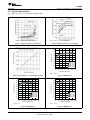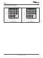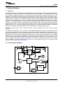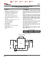
1
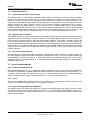
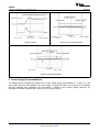
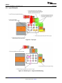
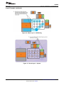
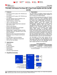
Sample &
Buy
Product
Folder
Support &
Community
Tools &
Software
Technical
Documents
LM3269
SNVS793D – NOVEMBER 2011 – REVISED MAY 2015
LM3269 Seamless-Transition Buck-Boost Converter
for 3G and 4G RF Power Amplifiers
1 Features
3 Description
•
•
•
•
The LM3269 is buck-boost DC-DC converter
designed to generate output voltages above or below
a given input voltage and is particularly suitable for
portable applications powered by a single-cell Li-ion
battery.
1
•
•
•
•
•
•
Operates From a Single Li-Ion Cell: 2.7 V to 5.5 V
Adjustable Output Voltage: 0.6 V to 4.2 V
Automatic PFM or PWM Mode Change
750-mA Maximum Load Capability for
VBATT ≥ 3 V, VOUT = 3.8 V
2.4-MHz (typical) Switching Frequency
Seamless Buck-Boost Mode Transition
Fast Output Voltage Transition: 1.4 V to 3 V
in 10 µs
High-Efficiency: 95% typical at VBATT = 3.7 V,
VOUT = 3.3 V, at 300 mA
Input Overcurrent Limit
Internal Compensation
The LM3269 operates at a 2.4-MHz typical switching
frequency in full synchronous operation and provides
seamless transitions between buck and boost
operating regimes. The LM3269 operates in energysaving Pulse Frequency Modulation (PFM) mode for
increased efficiencies and current savings during lowpower RF transmission modes.
The power converter topology needs only one
inductor and two capacitors. A unique internal power
switch topology enables high overall efficiency.
The LM3269 is internally compensated for buck and
boost modes of operation, thus providing an optimal
transient response.
2 Applications
•
•
•
•
Power Supply for 3G/4G Power Amplifiers
Cellular Phones
Portable Hard Disk Drives
PDAs
When considering using the LM3269 in a system
design, please review the layout instruactions at the
end of this document.
Device Information(1)
PART NUMBER
LM3269
PACKAGE
BODY SIZE (MAX)
DSBGA (12)
2.529 mm x 2.022 mm
(1) For all available packages, see the orderable addendum at
the end of the data sheet.
Typical Application
2.2 PH
SW1
SW2
VBATT: 2.7V to 5.5V
VOUT: 0.6V to 4.2V
PVIN
VOUT
PVIN
FB
RF PA
LM3269
+ -
10 PF
4.7 PF
EN
VCON
SGND
PGND
GPO1
BB
RFIC
DAC
1
An IMPORTANT NOTICE at the end of this data sheet addresses availability, warranty, changes, use in safety-critical applications,
intellectual property matters and other important disclaimers. PRODUCTION DATA.
LM3269
SNVS793D – NOVEMBER 2011 – REVISED MAY 2015
www.ti.com
Table of Contents
1
2
3
4
5
6
7
Features ..................................................................
Applications ...........................................................
Description .............................................................
Revision History.....................................................
Pin Configuration and Functions .........................
Specifications.........................................................
1
1
1
2
3
4
6.1
6.2
6.3
6.4
6.5
6.6
6.7
6.8
4
4
4
4
5
5
6
7
Absolute Maximum Ratings ......................................
ESD Ratings..............................................................
Recommended Operating Conditions.......................
Thermal Information ..................................................
Electrical Characteristics...........................................
System Characteristics ............................................
Switching Characteristics ..........................................
Typical Characteristics ..............................................
Detailed Description .............................................. 9
7.1 Overview ................................................................... 9
7.2 Functional Block Diagram ......................................... 9
7.3 Feature Description................................................. 10
7.4 Device Functional Modes........................................ 10
8
Application and Implementation ........................ 11
8.1 Application Information............................................ 11
8.2 Typical Application ................................................. 11
9 Power Supply Recommendations...................... 14
10 Layout................................................................... 15
10.1 Layout Guidelines ................................................. 15
10.2 Layout Examples................................................... 18
10.3 DSBGA Package Assembly And Use ................... 20
11 Device and Documentation Support ................. 21
11.1
11.2
11.3
11.4
11.5
Device Support......................................................
Documentation Support ........................................
Trademarks ...........................................................
Electrostatic Discharge Caution ............................
Glossary ................................................................
21
21
21
21
21
12 Mechanical, Packaging, and Orderable
Information ........................................................... 21
4 Revision History
Changes from Revision C (May 2013) to Revision D
Page
•
Added Device Information table, Pin Configuration and Functions section, ESD Rating table, Feature Description ,
Device Functional Modes, Application and Implementation, Power Supply Recommendations, Device and
Documentation Support , and Mechanical, Packaging, and Orderable Information sections ................................................ 1
•
Deleted Recommended Capacitance Specifications table as info contained in other tables .............................................. 12
Changes from Revision B (August 2012) to Revision C
•
2
Page
Changed product brief to full data sheet ............................................................................................................................... 1
Submit Documentation Feedback
Copyright © 2011–2015, Texas Instruments Incorporated
Product Folder Links: LM3269
LM3269
www.ti.com
SNVS793D – NOVEMBER 2011 – REVISED MAY 2015
5 Pin Configuration and Functions
YZR Package
12-Pin DSBGA
Top View
A1
A2
A3
A3
A2
A1
B1
B2
B3
B3
B2
B1
C1
C2
C3
C3
C2
C1
D1
D2
D3
D3
D2
D1
Top View
Bottom View
Pin Functions
PIN
NUMBER
NAME
A1
NC
(1)
TYPE (1)
DESCRIPTION
—
Non Connection. Leave this pin floating; do not connect to PVIN or PGND.
A2
NC
—
Non Connection. Leave this pin floating, do not connect to PVIN or PGND.
A3
PVIN
P/I
Power MOSFET input and power current input pin. Optional low-pass filtering may help buck and
buck-boost modes for radiated EMI and noise reduction.
B1
VCON
A/I
Voltage Control analog input. VCON controls the output voltage in PWM and PFM modes.
B2
EN
D/I
Enable pin. Pulling this pin higher than 1.2 V enables part to function.
B3
PVIN
P/I
Power MOSFET input and power current input pin. Optional low-pass filtering may help buck and
buck-boost modes for radiated EMI and noise reduction.
C1
FB
A
Feedback input to inverting input of error amplifier. Connect output voltage directly to this node at
load point.
C2
SGND
G
Signal Ground for analog circuits and control circuitry.
C3
SW1
P/O
D1
VOUT
O
D2
SW2
P/O
D3
PGND
G
Switch pin for Internal Power Switches. Connect inductor between SW1 and SW2.
Regulated output voltage of the LM3269. Connect this to a 4.7-µF ceramic output filter capacitor
to GND.
Switch pin for Internal Power Switches. Connect inductor between SW1 and SW2.
Power Ground for Power MOSFETs and gate drive circuitry.
A: Analog Pin, D: Digital Pin, G: Ground Pin, P: Power Pin, I: Input Pin, O: Output Pin.
Submit Documentation Feedback
Copyright © 2011–2015, Texas Instruments Incorporated
Product Folder Links: LM3269
3
LM3269
SNVS793D – NOVEMBER 2011 – REVISED MAY 2015
www.ti.com
6 Specifications
6.1 Absolute Maximum Ratings
over operating free-air temperature range (unless otherwise noted) (1) (2)
PVIN, VOUT to GND
MIN
MAX
−0.2
6
UNIT
V
(3)
V
EN, VCON to SGND, PGND
−0.2
PVIN + 0.2 V or 6 V
FB to PGND
−0.2
VOUT + 0.2 V or 6 V (3)
V
SW1, SW2
−0.2
PVIN + 0.2 V or 6 V (3)
V
Continuous power dissipation
(4)
Internally limited
Junction temperature, TJ-MAX
−65
Storage temperature, Tstg
(1)
(2)
(3)
(4)
150
°C
150
°C
Stresses beyond those listed under Absolute Maximum Ratings may cause permanent damage to the device. These are stress ratings
only, which do not imply functional operation of the device at these or any other conditions beyond those indicated under Recommended
Operating Conditions. Exposure to absolute-maximum-rated conditions for extended periods may affect device reliability.
If Military/Aerospace specified devices are required, please contact the Texas Instruments Sales Office/Distributors for availability and
specifications.
Whichever is smaller.
Internal thermal circuitry protects the device from permanent damage. Thermal shutdown engages at TJ = 150°C (typical) and
disengages at TJ = 125°C (typical).
6.2 ESD Ratings
V(ESD)
(1)
Electrostatic discharge
Human-body model (HBM), per ANSI/ESDA/JEDEC JS-001
VALUE
UNIT
±2000
V
(1)
JEDEC document JEP155 states that 500-V HBM allows safe manufacturing with a standard ESD control process.
6.3 Recommended Operating Conditions
over operating free-air temperature range (unless otherwise noted) (1) (2)
MIN
NOM
MAX
UNIT
Input voltage
2.7
5.5
Output voltage
0.6
4.2
V
0
750
mA
Junction temperature (TJ)
−30
125
°C
Ambient temperature (TA) (3)
−30
85
°C
Recommended load current
(1)
(2)
(3)
V
Stresses beyond those listed under absolute maximum ratings may cause permanent damage to the device. These are stress ratings
only, and functional operation of the device at these or any other conditions beyond those indicated under recommended operating
conditions is not implied. Exposure to absolute-maximum-rated conditions for extended periods may affect device reliability.
All voltages are with respect to the potential at the GND pins.
In applications where high power dissipation and/or poor package thermal resistance is present, the maximum ambient temperature may
have to be de-rated. Maximum ambient temperature (TA-MAX) is dependent on the maximum operating junction temperature (TJ-MAX-OP =
125°C), the maximum power dissipation of the device in the application (PD-MAX), and the junction-to ambient thermal resistance of the
part/package in the application (RθJA), as given by the following equation: TA-MAX = TJ-MAX-OP – (RθJA × PD-MAX).
6.4 Thermal Information
LM3269
THERMAL METRIC (1)
YZR (DSBGA)
UNIT
12 PINS
RθJA
(1)
(2)
4
Junction-to-ambient thermal resistance (2)
85
°C/W
For more information about traditional and new thermal metrics, see the IC Package Thermal Metrics application report, SPRA953.
Junction-to-ambient thermal resistance is highly application and board-layout dependent. In applications where high maximum power
dissipation exists, special care must be paid to thermal dissipation issues in board design. Junction-to-ambient thermal resistance (RθJA)
is taken from a thermal modeling result, performed under the conditions and guidelines set forth in the JEDEC standard JESD51-7.
Submit Documentation Feedback
Copyright © 2011–2015, Texas Instruments Incorporated
Product Folder Links: LM3269
LM3269
www.ti.com
SNVS793D – NOVEMBER 2011 – REVISED MAY 2015
6.5 Electrical Characteristics
Unless otherwise specified, typical (TYP) limits are for TA = TJ = 25°C, and minimum (MIN) and maximum (MAX) limits apply
over the full operating ambient temperature range (−30°C ≤ TJ = TA ≤ +85°C). Unless otherwise noted, specifications apply to
the Figure 16 with: PVIN = EN = 3.6V. (1) (2)
MIN
TYP
MAX
VFB,
min
Min FB voltage
PARAMETER
VCON = 0.2 V
0.53
0.60
0.67
VFB,
max
Max FB voltage
VCON = 1.4 V
4.13
4.2
4.27
Quiescent current
No switching (3)
0.9
1.2
mA
ISHDN
Shutdown supply current
EN = 0 V, VCON = 0 V,
SW1 = SW2 = VOUT = 0 V
0.02
5
µA
ILIM_L
Input current limit (large)
Open loop (4)
VCON = 1.2 V
1500
1700
1900
750
850
IQ_PWM
TEST CONDITIONS
ILIM_S
Input current limit (small)
Open loop
VCON = 0.2 V
Gain
Internal gain (5)
0.2 V ≤ VCON ≤ 1.4 V
IEN
EN pin pulldown current
IVCON
VCON pin leakage current
–1
VIH
Logic high input threshold for EN
1.2
VIL
Logic low input threshold for EN
IOUT_LEAKAGE
Leakage into VOUT pin of buckboost
(3)
(4)
(5)
V
mA
(4)
(1)
(2)
UNIT
3
5
V/V
10
1
0.6
EN = 0 V, VOUT ≤ 4.2 V
PVIN ≤ 5.5 V
5
µA
V
µA
All voltages are with respect to the potential at the GND pins.
Min and Max limits are specified by design, test, or statistical analysis. Typical numbers are not verified, but do represent the most likely
norm.
IQ specified here is when the part is not switching.
The parameters in the electrical characteristics table are tested under open loop conditions at PVIN = 3.6 V.
To calculate VOUT, use the following equation: VOUT = VCON × 3.
6.6 System Characteristics
The following spec table entries are specified by design and verification provided the component values in the typical
application circuit are used (L = 2.2 µH, DCR = 110 mΩ, MIPSZ2520D2R2/FDK; CIN = 10 µF, 6.3 V, C1608X5R0J106K/TDK
(0603); COUT = 4.7 µF, 6.3 V, C1608X5R0J475M/TDK (0603). These parameters are not verified by production testing.
Typical (TYP) limits are for TA = TJ = 25°C; minimum (MIN) and maximum (MAX) limits apply over the full operating ambient
temperature range (−30°C ≤ TJ = TA ≤ 85°C) and over the VBATT = PVIN = 2.7 V to 5.5 V, unless otherwise specified.
PARAMETER
TEST CONDITIONS
MIN
TYP
MAX
IOUT_MAX
Max output current
VBATT ≥ 3 V, VOUT = 3.8 V
VCON_LIN
VCON linearity
0.2 V ≤ VCON ≤ 1.4 V
Ripple voltage
VBATT ≥ 3.2 V, 0.6 V ≤ VOUT ≤ 4.2 V,
0 mA ≤ IOUT ≤ 430 mA, TA = 25°C
15
PFM ripple
VOUT = 0.6 V, IOUT = 5 mA
45
Ripple voltage in mode
transition
VBATT = 3 V to 5 V,
TR = TF = 30 µs
3.3 V ≤ VOUT ≤ 4.2 V
50
Line regulation
VBATT = 2.7 V to 4.7 V, VOUT = 3.8 V,
IOUT = 500 mA
10
Load regulation
IOUT = 0 mA to 500 mA, VBATT = 2.7 V to 4.7 V
20
VOUT rise time
VBATT = 3.2 V to 4.7 V,
VOUT = 1.4 V to 3 V, 0.1 µs < Tr_VCON < 1 µs
RLOAD = 11.4 Ω
VO_RIPPLE
ΔVOUT
VOUT_TR
750
mA
–2.5%
2.5%
50
mV
10
Submit Documentation Feedback
Copyright © 2011–2015, Texas Instruments Incorporated
Product Folder Links: LM3269
UNIT
mV
µs
5
LM3269
SNVS793D – NOVEMBER 2011 – REVISED MAY 2015
www.ti.com
System Characteristics (continued)
The following spec table entries are specified by design and verification provided the component values in the typical
application circuit are used (L = 2.2 µH, DCR = 110 mΩ, MIPSZ2520D2R2/FDK; CIN = 10 µF, 6.3 V, C1608X5R0J106K/TDK
(0603); COUT = 4.7 µF, 6.3 V, C1608X5R0J475M/TDK (0603). These parameters are not verified by production testing.
Typical (TYP) limits are for TA = TJ = 25°C; minimum (MIN) and maximum (MAX) limits apply over the full operating ambient
temperature range (−30°C ≤ TJ = TA ≤ 85°C) and over the VBATT = PVIN = 2.7 V to 5.5 V, unless otherwise specified.
PARAMETER
η
Efficiency
TEST CONDITIONS
MIN
TYP
VBATT = 3.7 V, VOUT = 0.6 V, IOUT = 10 mA
−30°C ≤ TJ = TA ≤ 85°C
61%
VBATT = 3.7 V, VOUT = 1 V IOUT = 20 mA
−30°C ≤ TJ = TA ≤ 85°C
78%
VBATT = 3.7 V, VOUT = 1.4 V IOUT = 50 mA
−30°C ≤ TJ = TA ≤ 85°C
85%
VBATT = 3.7 V, VOUT = 2.7 V IOUT = 200 mA
−30°C ≤ TJ = TA ≤ 85°C
95%
VBATT = 3.7 V, VOUT = 3.3 V, IOUT = 480 mA
−30°C ≤ TJ = TA ≤ 85°C
94%
VBATT = 3 V, VOUT = 3.6 V, IOUT = 200 mA
−30°C ≤ TJ = TA ≤ 85°C
95%
MAX
UNIT
6.7 Switching Characteristics
over operating free-air temperature range (unless otherwise noted)
PARAMETER
TYP
MAX
TON
EN = L to H, VBATT = 3.7 V, VOUT =
Turnon time (time for output to reach 3.5 V,
0V→90% × 3.5 V)
IOUT = 0 mA
−30°C ≤ TJ = TA ≤ 85°C
35
50
FOSC_PFM
PFM operating frequency
VBATT = 3.7 V, VOUT = 0.6 V, IOUT =
13 mA
63
FOSC_PWM
Internal oscillator frequency
PWM
DMAX
Maximum duty cycle
VOUT_TR
6
VCON change to 90%
TEST CONDITIONS
MIN
2.1
2.4
2.7
50%
Buck
100%
Submit Documentation Feedback
10
µs
kHz
Boost
VBATT = 3.2 V to 4.7 V,
VOUT = 1.4 V to 3 V, 0.1 µs <
Tr_VCON < 1 µs
RLOAD = 11.4 Ω
UNIT
MHz
µs
Copyright © 2011–2015, Texas Instruments Incorporated
Product Folder Links: LM3269
LM3269
www.ti.com
SNVS793D – NOVEMBER 2011 – REVISED MAY 2015
6.8 Typical Characteristics
(PVIN = EN = 3.6 V and TA = 25°C, unless otherwise noted)
VCON = VOUT = SW1 = SW2 = EN = 0 V
VOUT = 3.5 V
Figure 1. Shutdown Current vs. Temperature
IOUT = 300 mA
Figure 2. Switching Frequency vs. Temperature
100
90
EFFICIENCY (%)
80
70
60
50
40
30
PVIN = 2.7V
PVIN = 3.0V
PVIN = 3.6V
PVIN = 4.2V
PVIN = 4.8V
20
10
0
0
20
40
60
80
100
OUTPUT LOAD (mA)
120
VOUT = 0.6 V
Figure 4. PFM Efficiency
100
100
90
90
80
80
EFFICIENCY (%)
EFFICIENCY (%)
Figure 3. VCON Voltage vs. Output Voltage (No Load)
70
60
50
40
PVIN = 2.7V
PVIN = 3.0V
PVIN = 3.6V
PVIN = 4.2V
PVIN = 4.8V
30
20
10
70
60
50
40
PVIN = 2.7V
PVIN = 3.0V
PVIN = 3.6V
PVIN = 4.2V
PVIN = 4.8V
30
20
10
0
0
0
20
40
60
80
100
OUTPUT LOAD (mA)
VOUT = 1 V
120
0
20
40
60
80
100
OUTPUT LOAD (mA)
120
VOUT = 1.4 V
Figure 5. PFM Efficiency
Figure 6. PFM Efficiency
Submit Documentation Feedback
Copyright © 2011–2015, Texas Instruments Incorporated
Product Folder Links: LM3269
7
LM3269
SNVS793D – NOVEMBER 2011 – REVISED MAY 2015
www.ti.com
Typical Characteristics (continued)
100
100
90
90
80
70
60
PVIN = 2.7V
PVIN = 3.0V
PVIN = 3.6V
PVIN = 4.2V
50
EFFICIENCY (%)
EFFICIENCY (%)
(PVIN = EN = 3.6 V and TA = 25°C, unless otherwise noted)
70
60
PVIN = 2.7V
PVIN = 3.0V
PVIN = 3.6V
PVIN = 4.2V
50
40
40
0
100 200 300 400 500 600 700
OUTPUT LOAD (mA)
VOUT = 2.4 V
0
100 200 300 400 500 600 700
OUTPUT LOAD (mA)
VOUT = 3.6 V
Figure 7. PWM Efficiency
8
80
Figure 8. PWM Efficiency
Submit Documentation Feedback
Copyright © 2011–2015, Texas Instruments Incorporated
Product Folder Links: LM3269
LM3269
www.ti.com
SNVS793D – NOVEMBER 2011 – REVISED MAY 2015
7 Detailed Description
7.1 Overview
The LM3269 buck-boost converter provides high-efficiency, low-noise power for RF power amplifiers (PAs) in
mobile phones, portable communicators, and similar battery-powered RF devices. It is designed to allow the RF
PA to operate at maximum efficiency for a wide range of power levels from a single Li-Ion battery cell. The
capability of the LM3269 to provide an output voltage lower than, as well as higher than, the input battery voltage
enables the PA to operate with high linearity for a wide range of battery voltages, thereby extending the usable
voltage range of the battery. The converter feedback loop is internally compensated for both buck and boost
operation, and the architecture is such that it provides seamless transition between buck and boost modes of
operation. The LM3269 operates in energy saving Pulse Frequency Modulation (PFM) mode for increased
efficiencies and current savings during low-power RF transmission modes. The output voltage is dynamically
programmable from 0.6 V to 4.2 V by adjusting the voltage on the control pin VCON without the need for external
feedback resistors. The fast output voltage transient response of the LM3269 makes it suitable for adaptively
adjusting the PA supply voltage depending on its transmitting power, which prolongs battery life.
Additional features include current overload protection, output overvoltage clamp, and thermal overload
shutdown.
The LM3269 is constructed using a chip-scale 12-bump DSBGA package that offers the smallest possible size
for space-critical applications such as cell phones, where board area is an important design consideration. Use of
high switching frequency (2.4 MHz, typical) reduces the size of external components. As shown in the Typical
Application Circuit, only three external power components are required for circuit operation. Use of DSBGA
package requires special design considerations for implementation. (See DSBGA Package Assembly And Use)
Its fine bump-pitch requires careful board design and precision assembly equipment. Use of this package is best
suited for opaque-case applications where its edges are not subjected to high-intensity ambient red or infrared
light. In addition, the system controller should set EN low during power-up and other low supply voltage
conditions. (See Enable And Shutdown Mode.)
7.2 Functional Block Diagram
PVIN
PVIN
To
Analog Supply
SW2
SW1
VOUT
SMALL
FET
LARGE
FET
M6_g
M6
M3
M1
M2
GATE
DRIVE
CIRCUITS
M5
M4
PFM
Comparator
+
1.7A
Ref
-
FB
Network
Error
Amplifier
CONTROL
LOGIC
-
+
+
VCON
-
FB
Input Overcurrent
Protection
EN
One
Shot
Timer
INTERNAL
LOOP
COMPENSATION
M6_g
CLK
PWM RAMP
SGND
PGND
Submit Documentation Feedback
Copyright © 2011–2015, Texas Instruments Incorporated
Product Folder Links: LM3269
9
LM3269
SNVS793D – NOVEMBER 2011 – REVISED MAY 2015
www.ti.com
7.3 Feature Description
7.3.1 Dynamically Adjustable Output Voltage
The LM3269 features a dynamically adjustable output voltage to eliminate the need for external feedback
resistors. The output can be set from 0.6 V to 4.2 V by changing the voltage on the analog VCON pin. This
feature is useful in cell phone RF PA applications where peak power is needed only when the handset is far
away from the base station or when data is being transmitted. In other instances, the transmitting power can be
reduced; therefore the supply voltage to the PA can be reduced, promoting longer battery life. In order to
adaptively adjust the supply voltage to the PA in real time in a cell-phone application, the output voltage
transition should be fast enough to meet the RF transmit signal specifications. The LM3269 offers ultra-fast
output voltage transition without drawing very large currents from the battery supply. For a current limit of 1700
mA (typical), the output voltage can transition from 1.4 V to 3 V in 10 µs with a load resistance of 11.4 Ω.
7.3.2 Seamless Buck Transition
The LM3269 features a unique internal power switch topology that improves converter efficiency, especially
compared to typical non-inverting buck-boost converters. The LM3269 operates either as buck converter or a
boost converter, depending upon the input and output voltage conditions. This creates a boundary between the
buck and boost mode of operation. When the input battery voltage is close to the set output voltage, the
converter automatically switches seamlessly such that the output voltage does not see any perturbations at the
mode boundary. The excellent mode transition capability of the LM3269 enables low noise output with highest
efficiency. Internal feedback loop compensation ensures stable operation in buck, boost and buck-boost mode
transition operation.
7.3.3 Thermal Overload Protection
The LM3269 has a thermal overload protection function that operates to protect itself from short-term misuse and
over-load conditions. When the junction temperature exceeds around 150°C, the device inhibits operation. All
power MOSFET switches are turned off in PWM mode. When the temperature drops below 125°C, normal
operation resumes. Prolonged operation in thermal overload conditions may damage the device and is
considered bad practice.
7.4 Device Functional Modes
7.4.1 Enable And Shutdown Mode
Setting the EN digital pin low (< 0.6 V) places the LM3269 in shutdown mode (0.01 μA typical). During shutdown,
the output of the LM3269 is tri-stated, maintaining charge storage on the output capacitor. Setting EN high (> 1.2
V) enables normal operation. EN should be set low to turn off the LM3269 during power up and undervoltage
conditions when the power supply (PVIN) is less than the 2.7-V minimum operating voltage.
7.4.2 VCON,ON
The output is disabled when VCON is below 125 mV (typical). It is enabled when VCON is above 150 mV
(typical). The threshold has approximately 25 mV (typical) of hysteresis.
7.4.3 Pulse Frequency Modulation (PFM) Mode
The LM3269 enters PFM mode and operates with reduced switching frequency and supply current to maintain
very high efficiencies when the output voltage is less than 1.5 V. In PFM mode, the LM3269 will support up to
120 mA max. In PFM, if the output voltage exceeds 1.5 V, the device will automatically transition into a forced
PWM mode of operation.
10
Submit Documentation Feedback
Copyright © 2011–2015, Texas Instruments Incorporated
Product Folder Links: LM3269
LM3269
www.ti.com
SNVS793D – NOVEMBER 2011 – REVISED MAY 2015
8 Application and Implementation
NOTE
Information in the following applications sections is not part of the TI component
specification, and TI does not warrant its accuracy or completeness. TI’s customers are
responsible for determining suitability of components for their purposes. Customers should
validate and test their design implementation to confirm system functionality.
8.1 Application Information
8.1.1 Setting The Output Voltage
The LM3269 features a pin-controlled variable output voltage which eliminates the need for external feedback
resistors. It can be programmed for an output voltage from 0.6 V to 4.2 V by setting the voltage on the VCON
pin, as in Equation 1.
VOUT = 3 × VCON
(1)
When VCON is between 0.2 V and 1.4 V, the output voltage will follow the formula in Equation 1.
8.1.2 Output Current Capacity
The LM3269 load capability is as shown in Table 1.
Table 1. Output Voltage vs. Maximum Output Current Derating
VOUT
4.2 V
3.8 V
< 1.5 V
VBATT
MAXIMUM IOUT CAPABILITY
>3V
650 mA
2.7 V to 3 V
500 mA
>3V
750 mA
2.7 V to 3 V
600 mA
2.7 V to 5.5 V
120 mA (in PFM mode)
8.2 Typical Application
2.2 PH
SW1
SW2
VBATT: 2.7V to 5.5V
VOUT: 0.6V to 4.2V
PVIN
VOUT
PVIN
FB
RF PA
LM3269
+ -
10 PF
4.7 PF
EN
VCON
SGND
PGND
GPO1
BB
RFIC
DAC
Submit Documentation Feedback
Copyright © 2011–2015, Texas Instruments Incorporated
Product Folder Links: LM3269
11
LM3269
SNVS793D – NOVEMBER 2011 – REVISED MAY 2015
www.ti.com
Typical Application (continued)
8.2.1 Design Requirements
DESIGN PARAMETER
EXAMPLE VALUE
Minimum input voltage
2.7 V
Minimum output voltage
0.6 V
Output current
0 to 750 mA
Switching frequency
2.4 MHz (typical)
8.2.2 Detailed Design Procedure
8.2.2.1 Recommended External Components
8.2.2.1.1 Inductor Selection
A 2.2-μH inductor with a saturation current rating over 1500 mA and low inductance drop at the full DC bias
condition is recommended for almost all applications. An inductor with a smaller DC resistance, such as 110 mΩ
(depending on case size of resistor), should be used for good efficiency.
Table 2. Suggested 2.2-µH Inductors
MODEL
DIMENSIONS (mm)
ISAT
(30% drop)
IRATING
(Δ40°)
DCR
FDK
MIPSZ2520D2R2
2.5 x 2.0 x 1.0
1.5 A
1.1 A
110 mΩ
Murata
LQH2HPN1R0NG0
2.5 x 2.0 x 1.2
2A
1.2 A
112 mΩ
Samsung
CIG22H2R2MNE
2.5 x 2.0 x 1.2
1.9 A
1.6 A
116 mΩ
TDK
TFM201610A2R2M
2.0 x 1.6 x 1.0
1.7 A
1.3 A
180 mΩ
TOKO
DFE201612C2R2N
2.0 x 1.6 x 1.2
2.1 A
1.3 A
155 mΩ
VENDOR
8.2.2.1.2 Input Capacitor Selection
A ceramic input capacitor of 10 µF, 6.3 V, 0603 (1608) is recommended for use in most applications. Place the
input capacitor as close as possible to the PVIN pin and PGND pin of the device. A larger value of higher voltage
rating may be used to improve input filtering. Use X7R, X5R, or B types; do not use Y5V or F. DC board
characteristics of ceramic capacitors must be considered when selecting case sizes like 0402 (1005). The input
filter capacitor supplies current to the PFET (high-side) switch in first half of each cycle and reduces voltage
ripple imposed on the input power source. A ceramic capacitor’s low equivalent series resistance (ESR) provides
the best noise filtering of the input voltage spikes due to this rapidly changing current.
8.2.2.1.3 Output Capacitor Selection
Use a 4.7 µF capacitor for the output capacitor. Use of capacitor types such as X5R, X7R are recommended for
the filter. These provide an optimal balance between small size, cost, reliability, and performance for cell phones
and similar applications. Table 3 lists suggested part numbers and suppliers. DC bias characteristics of the
capacitors must be considered while selecting the voltage rating and case size of the capacitor. Smaller case
sizes for the output capacitor mitigate piezo-electric vibrations of the capacitor when the output voltage is
stepped up and down at fast rates. However, they have a bigger percentage drop in value with DC bias. A 0603
(1608) case size capacitor is recommended for output. For RF Power Amplifier applications, split the output
capacitor between DC-DC converter and RF Power Amplifier(s). (4.7 μF (0402 (1005)) + PA input cap
(0402(1005)/0201(0603)) is recommended.) The optimum capacitance split is application dependent. Place all
the output capacitors very close to their respective device.
NOTE
If using a 4.7 µF, 0402 (1005) as the output capacitor, the total recommended actual
capacitance on VOUT bus should be at least 7 µF (4.7 µF + PA decoupling caps) to take
into account the 0402 (1005) DC bias degradation and other tolerances.
12
Submit Documentation Feedback
Copyright © 2011–2015, Texas Instruments Incorporated
Product Folder Links: LM3269
LM3269
www.ti.com
SNVS793D – NOVEMBER 2011 – REVISED MAY 2015
Table 3. Suggested Capacitors
MODEL
VENDOR
10 µF for CIN
C1608X5R0J106K (0603)
TDK
CL05A106MQ5NUN (0402)
Samsung
C1608X5R0J475M (0603)
TDK
CL05A475MQ5NRN (0402)
Samsung
C1005X5RR0J475M (0402)
TDK
4.7 µF for COUT
8.2.3 Application Curves
PVIN = 3.7 V
VOUT = 0.8 V↔ 2 V
RLOAD = 20 Ω
PVIN= 3.7 V
VOUT = 3.45 V
Load = 500 mA
Load = 500 mA
Figure 10. Buck Mode Operation
Figure 9. VOUT Transient Response (PFM ↔ PWM)
PVIN = 3.37 V
VOUT = 3.2 V
PVIN = 3.8 V
Figure 11. Boost Mode Operation
VOUT = 3.6 V
IOUT = 600 mA
Figure 12. Buck-Boost Operation
Submit Documentation Feedback
Copyright © 2011–2015, Texas Instruments Incorporated
Product Folder Links: LM3269
13
LM3269
SNVS793D – NOVEMBER 2011 – REVISED MAY 2015
PVIN = 3.6 V
VOUT = 3.45 V
www.ti.com
Load = 350 mA
PVIN Step = 3.6 V
↔ 4.2 V
Figure 13. Start-Up
VOUT = 3 V
Load = 320 mA
Figure 14. Line Transient For DC-DC
PVIN = 3.8 V
VOUT = 3.45 V
Figure 15. Load Transient DC-DC
9 Power Supply Recommendations
The LM3269 device is designed to operate from an input voltage supply range between 2.7 V and 5.5 V. This
input supply should be well regulated. If the input supply is located more than a few inches from the LM3269
converter additional bulk capacitance may be required in addition to the ceramic bypass capacitors. An
electrolytic or tantalum capacitor with a value of 47 μF is a typical choice.
14
Submit Documentation Feedback
Copyright © 2011–2015, Texas Instruments Incorporated
Product Folder Links: LM3269
LM3269
www.ti.com
SNVS793D – NOVEMBER 2011 – REVISED MAY 2015
10 Layout
10.1 Layout Guidelines
10.1.1 Overview
PC board layout is critical to successfully designing a DC-DC converter into a product. A properly planned board
layout optimizes the performance of a DC-DC converter and minimizes effects on surrounding circuitry while also
addressing manufacturing issues that can have adverse impact on board quality and final product yield.
10.1.1.1 PCB
Poor board layout can disrupt the performance of a DC-DC converter and surrounding circuitry by contributing to
EMI, ground bounce, and resistive voltage loss in the traces. Erroneous signals could be sent to the DC-DC
converter IC, resulting in poor regulation or instability. Poor layout can also result in re-flow problems leading to
poor solder joints between the DSBGA package and board pads. Poor solder joints can result in erratic or
degraded performance of the converter.
10.1.1.1.1 Energy Efficiency
Minimize resistive losses by using wide traces between the power components and doubling up traces on
multiple layers when possible.
10.1.1.1.2 EMI
By its very nature, any switching converter generates electrical noise. The circuit board designer’s challenge is to
minimize, contain, or attenuate such switcher-generated noise. A high-frequency switching converter, such as the
LM3269, switches Ampere level currents within nanoseconds, and the traces interconnecting the associated
components can act as radiating antennas. The following guidelines are offered to help to ensure that EMI is
maintained within tolerable levels.
To help minimize radiated noise:
• Place the LM3269 switcher, its input capacitor, and output filter inductor and capacitor close together, and
make the interconnecting traces as short as possible.
• Arrange the components so that the switching current loops curl in the same direction. During the first half of
each cycle (buck mode), current flows from the input filter capacitor, through the internal PFET of the LM3269
and the inductor, to the output filter capacitor, then back through ground, forming a current loop. In the
second half of each cycle (buck mode), current is pulled up from ground, through the internal synchronous
NFET of the LM3269 by the inductor, to the output filter capacitor and then back through ground, forming a
second current loop. Routing these loops so the current curls in the same direction prevents magnetic field
reversal between the two half-cycles and reduces radiated noise.
• Make the current loop area(s) as small as possible.
To help minimize conducted noise in the ground-plane:
• Reduce the amount of switching current that circulates through the ground plane: Connect the ground bumps
of the LM3269 and its input/output filter capacitors together using generous component-side copper fill as a
pseudo-ground plane. Then connect this copper fill to the system ground-plane (if one is used) by multiple
vias. These multiple vias help to minimize ground bounce at the LM3269 by giving it a low-impedance ground
connection.
To help minimize coupling to the DC-DC converter's own voltage feedback trace:
• Route noise sensitive traces, such as the voltage feedback path (FB), as directly as possible from the
switcher FB pad to the VOUT pad of the output capacitor, but keep it away from noisy traces between the
power components. If possible, connect FB bump directly to VOUT bump.
To decouple common power supply lines, series impedances may be used to strategically isolate circuits:
• Take advantage of the inherent inductance of circuit traces to reduce coupling among function blocks, by way
of the power supply traces.
• Use star connection for separately routing VBATT to PVIN and VBATT_PA (VCC1).
• Inserting a single ferrite bead in-line with a power supply trace may offer a favorable tradeoff in terms of
board area, by allowing the use of fewer bypass capacitors.
Submit Documentation Feedback
Copyright © 2011–2015, Texas Instruments Incorporated
Product Folder Links: LM3269
15
LM3269
SNVS793D – NOVEMBER 2011 – REVISED MAY 2015
www.ti.com
Layout Guidelines (continued)
10.1.1.2 Manufacturing Considerations
The LM3269 package employs a 12-bump (4 x 3) array of 300 micron solder balls, with a 0.5 mm pad pitch. A
few simple design rules will go a long way toward ensuring a good layout.
• Pad size should be 0.265 ± 0.02 mm. Solder mask opening should be 0.375 ± 0.02 mm.
• As a thermal relief, connect to each pad with 9.5 mil wide, 5 mil long traces and incrementally increase each
trace to its optimal width. Symmetry is important to ensure the solder bumps re-flow evenly. Refer to TI
Application Note AN-1112 DSBGA Wafer Level Chip Scale Package (SNVA009).
10.1.1.3 LM3269 RF Evaluation Board
2. 2 µH
L1
SW1
SW2
VIN: 2.7 V to 5.5 V
VOUT: 0.6 V to 4.2 V
PVIN
V OUT
PVIN
FB
L2
0.1 µF
C4
10 µF
C4
0.1 µF
C4
LM3269
RF GND
RF GND
+ -
VCON
EN
SGND
3G/4G
RF PA
4.7 µF
C4
PA Decoupling Caps
PGND
DAC
RFIC/BB
Figure 16. Simplified LM3269 RF Evaluation Board Schematic
1.
2.
3.
4.
5.
6.
7.
Input Capacitor C2 should be placed closer to LM3269 than C1.
It is optional to add 100 nF (C1) on input of LM3269 for high frequency filtering.
Bulk Output Capacitor C3 should be placed closer to LM3269 than C4.
It is optional to add 100 nF (C4) on output of LM3269 for high frequency filtering.
Connect both GND terminals of C1 and C4 directly to System RF GND layer of phone board.
Connect bumps SGND (C2) directly to System GND.
TI has seen improvement in high frequency filtering for small bypass capacitors (C1 and C4) when they are
connected to System GND instead of same ground as PGND. These capacitors should be 0201 (0603
metric) case size for minimum footprint and best high frequency characteristics.
8. A ferrite bead (L2) may help to improve high frequency noise.
Table 4. Recommended Components
DESIGNATOR
PART NUMBER
VALUE
CASE SIZE
VENDOR
C1*
GMR033R60J104KE19D
0.1 µF
0201 (0603 metric)
Murata
C2
C1608X5R0J106
10 µF
0603 (1608 metric)
TDK
C3
C1608X5RR0J475M
4.7 µF
0603 (1608 metric)
TDK
C4*
GRM033R60J104KE19D
0.1 µF
0201 (0603 metric)
Murata
L1
MIPSZ2520D2R2
2.2 µH
1008 (2520 metric)
FDK
L2*
BLM15AX100SN1
10 Ω
0402 (1005 metric)
Murata
*Optional high frequency caps and high-frequency ferrit bead.
16
Submit Documentation Feedback
Copyright © 2011–2015, Texas Instruments Incorporated
Product Folder Links: LM3269
LM3269
www.ti.com
SNVS793D – NOVEMBER 2011 – REVISED MAY 2015
C2
C1
L2
10.1.1.4 Component Placement
PVIN
SW1
PGND
NC
EN
SGND
SW2
NC
VCON
FB
VOUT
C3
L1
LM3269
PVIN
C4
Figure 17. LM3269 Recommended Parts Placement (Top View)
10.1.1.5 PCB Considerations By Layer
10.1.1.5.1 VBATT
Use a star connection from VBATT to LM3269 and VBATT to PA VBATT (VCC1) connection. Do not daisy-chain
VBATT connection to LM3269 circuit and then to PA device VBATT connection.
1.
2.
3.
4.
5.
6.
Top Layer (Numbers correspond to those in the Layout Examples section.)
Create a PGND island as shown. PGND pads of C2 (CIN) and C3 (COUT) must be isolated from each other.
This PGND island will connect to the dedicated system ground with many vias.
Each SW (C3) and (D2) bump will have a via in pad and an additional via next to it, to drop down the SW
trace to layer
SGND bump (C2) will have a via in pad, and directly connecting it to the system ground.
FB (C1) should connect directly to the VOUT bump (D1).
Have PVIN vias next to optional ferrite bead.
Leave NC bumps (A1 and A2) floating; Do not connect to VBATT or GND
Layer 2
7. VCON and Digital logic signals may be routed on this layer.
8. VOUT (VCC2 of PA) can be routed on this layer.
9. PVIN for the LM3269 can be routed on this layer.
Layer 3
10. Each SW trace is routed on this layer. The width of each trace should be 15 mils (0.381 mm) for current
capabilities. Have two vias bring each SW trace up to the inductor pads.
Layer 4
11. Connect the PGND, SGND, and high Frequency vias from the top layer on this layer.
Submit Documentation Feedback
Copyright © 2011–2015, Texas Instruments Incorporated
Product Folder Links: LM3269
17
LM3269
SNVS793D – NOVEMBER 2011 – REVISED MAY 2015
www.ti.com
10.2 Layout Examples
Figure 18. Top Layer
Figure 19. Board Layer 2 - Logic and PVIN Routing
18
Submit Documentation Feedback
Copyright © 2011–2015, Texas Instruments Incorporated
Product Folder Links: LM3269
LM3269
www.ti.com
SNVS793D – NOVEMBER 2011 – REVISED MAY 2015
Layout Examples (continued)
Figure 20. Board Layer 3 - SW Routing
Figure 21. Board Layer 4 - System
Submit Documentation Feedback
Copyright © 2011–2015, Texas Instruments Incorporated
Product Folder Links: LM3269
19
LM3269
SNVS793D – NOVEMBER 2011 – REVISED MAY 2015
www.ti.com
10.3 DSBGA Package Assembly And Use
Use of the DSBGA package requires specialized board layout, precision mounting, and careful re-flow
techniques, as detailed in Texas Instruments Application Note 1112. Refer to the section Surface Mount
Technology (SMD) Assembly Considerations. For best results in assembly, alignment ordinals on the PC board
should be used to facilitate placement of the device. The pad style used with DSBGA package must be the
NSMD (non-solder mask defined) type. This means that the solder-mask opening is larger than the pad size.
This prevents a lip that otherwise forms if the solder-mask and pad overlap from holding the device off the
surface of the board and interfering with mounting. See Application Note AN-1112 DSBGA Wafer Level Chip
Scale Package (SNVA009) for specific instructions how to do this.
The 12-bump package used for the LM3269 has 300 micron solder balls. The trace to each pad should enter the
pad with a 90° entry angle to prevent debris from being caught in deep corners. Initially, the trace to each pad
should be 9.5 mil wide, for a section approximately 5 mil long, as a thermal relief. Then each trance should neck
up or down to its optimal width. The important criterion is symmetry. This ensures the solder bumps on the
LM3269 re-flow evenly and that the device solders level to the board. In particular, special attention must be paid
to the pads for bumps A3, B3, and D3. Because PVIN and PGND are typically connected to large copper planes,
inadequate thermal relief can result in late or inadequate re-flow of these bumps.
The DSBGA package is optimized for the smallest possible size in applications with red or infrared opaque
cases. Because the DSBGA package lacks the plastic encapsulation characteristic of larger devices, it is
vulnerable to light. Backside metallization and/or epoxy coating, along with front-side shading by the printed
circuit board, reduce this sensitivity. However, the package has exposed die edges. In particular, DSBGA
devices are sensitive to light (in the red and infrared range) shining on the package's exposed die edges.
20
Submit Documentation Feedback
Copyright © 2011–2015, Texas Instruments Incorporated
Product Folder Links: LM3269
LM3269
www.ti.com
SNVS793D – NOVEMBER 2011 – REVISED MAY 2015
11 Device and Documentation Support
11.1 Device Support
11.1.1 Third-Party Products Disclaimer
TI'S PUBLICATION OF INFORMATION REGARDING THIRD-PARTY PRODUCTS OR SERVICES DOES NOT
CONSTITUTE AN ENDORSEMENT REGARDING THE SUITABILITY OF SUCH PRODUCTS OR SERVICES
OR A WARRANTY, REPRESENTATION OR ENDORSEMENT OF SUCH PRODUCTS OR SERVICES, EITHER
ALONE OR IN COMBINATION WITH ANY TI PRODUCT OR SERVICE.
11.2 Documentation Support
11.2.1 Related Documentation
For related documentation see the following:
Texas Instruments Application Note AN-1112 DSBGA Wafer Level Chip Scale Package (SNVA009).
11.3 Trademarks
All trademarks are the property of their respective owners.
11.4 Electrostatic Discharge Caution
These devices have limited built-in ESD protection. The leads should be shorted together or the device placed in conductive foam
during storage or handling to prevent electrostatic damage to the MOS gates.
11.5 Glossary
SLYZ022 — TI Glossary.
This glossary lists and explains terms, acronyms, and definitions.
12 Mechanical, Packaging, and Orderable Information
The following pages include mechanical, packaging, and orderable information. This information is the most
current data available for the designated devices. This data is subject to change without notice and revision of
this document. For browser-based versions of this data sheet, refer to the left-hand navigation.
Submit Documentation Feedback
Copyright © 2011–2015, Texas Instruments Incorporated
Product Folder Links: LM3269
21
PACKAGE OPTION ADDENDUM
www.ti.com
15-Apr-2015
PACKAGING INFORMATION
Orderable Device
Status
(1)
Package Type Package Pins Package
Drawing
Qty
Eco Plan
Lead/Ball Finish
MSL Peak Temp
(2)
(6)
(3)
Op Temp (°C)
Device Marking
(4/5)
LM3269TLE/NOPB
ACTIVE
DSBGA
YZR
12
250
Green (RoHS
& no Sb/Br)
SNAGCU
Level-1-260C-UNLIM
-30 to 85
3269
LM3269TLX/NOPB
ACTIVE
DSBGA
YZR
12
3000
Green (RoHS
& no Sb/Br)
SNAGCU
Level-1-260C-UNLIM
-30 to 85
3269
(1)
The marketing status values are defined as follows:
ACTIVE: Product device recommended for new designs.
LIFEBUY: TI has announced that the device will be discontinued, and a lifetime-buy period is in effect.
NRND: Not recommended for new designs. Device is in production to support existing customers, but TI does not recommend using this part in a new design.
PREVIEW: Device has been announced but is not in production. Samples may or may not be available.
OBSOLETE: TI has discontinued the production of the device.
(2)
Eco Plan - The planned eco-friendly classification: Pb-Free (RoHS), Pb-Free (RoHS Exempt), or Green (RoHS & no Sb/Br) - please check http://www.ti.com/productcontent for the latest availability
information and additional product content details.
TBD: The Pb-Free/Green conversion plan has not been defined.
Pb-Free (RoHS): TI's terms "Lead-Free" or "Pb-Free" mean semiconductor products that are compatible with the current RoHS requirements for all 6 substances, including the requirement that
lead not exceed 0.1% by weight in homogeneous materials. Where designed to be soldered at high temperatures, TI Pb-Free products are suitable for use in specified lead-free processes.
Pb-Free (RoHS Exempt): This component has a RoHS exemption for either 1) lead-based flip-chip solder bumps used between the die and package, or 2) lead-based die adhesive used between
the die and leadframe. The component is otherwise considered Pb-Free (RoHS compatible) as defined above.
Green (RoHS & no Sb/Br): TI defines "Green" to mean Pb-Free (RoHS compatible), and free of Bromine (Br) and Antimony (Sb) based flame retardants (Br or Sb do not exceed 0.1% by weight
in homogeneous material)
(3)
MSL, Peak Temp. - The Moisture Sensitivity Level rating according to the JEDEC industry standard classifications, and peak solder temperature.
(4)
There may be additional marking, which relates to the logo, the lot trace code information, or the environmental category on the device.
(5)
Multiple Device Markings will be inside parentheses. Only one Device Marking contained in parentheses and separated by a "~" will appear on a device. If a line is indented then it is a continuation
of the previous line and the two combined represent the entire Device Marking for that device.
(6)
Lead/Ball Finish - Orderable Devices may have multiple material finish options. Finish options are separated by a vertical ruled line. Lead/Ball Finish values may wrap to two lines if the finish
value exceeds the maximum column width.
Important Information and Disclaimer:The information provided on this page represents TI's knowledge and belief as of the date that it is provided. TI bases its knowledge and belief on information
provided by third parties, and makes no representation or warranty as to the accuracy of such information. Efforts are underway to better integrate information from third parties. TI has taken and
continues to take reasonable steps to provide representative and accurate information but may not have conducted destructive testing or chemical analysis on incoming materials and chemicals.
TI and TI suppliers consider certain information to be proprietary, and thus CAS numbers and other limited information may not be available for release.
Addendum-Page 1
Samples
PACKAGE OPTION ADDENDUM
www.ti.com
15-Apr-2015
In no event shall TI's liability arising out of such information exceed the total purchase price of the TI part(s) at issue in this document sold by TI to Customer on an annual basis.
Addendum-Page 2
PACKAGE MATERIALS INFORMATION
www.ti.com
17-Apr-2015
TAPE AND REEL INFORMATION
*All dimensions are nominal
Device
Package Package Pins
Type Drawing
SPQ
Reel
Reel
A0
Diameter Width (mm)
(mm) W1 (mm)
LM3269TLE/NOPB
DSBGA
YZR
12
250
178.0
8.4
LM3269TLX/NOPB
DSBGA
YZR
12
3000
178.0
8.4
Pack Materials-Page 1
B0
(mm)
K0
(mm)
P1
(mm)
W
Pin1
(mm) Quadrant
2.18
2.69
0.76
4.0
8.0
Q1
2.18
2.69
0.76
4.0
8.0
Q1
PACKAGE MATERIALS INFORMATION
www.ti.com
17-Apr-2015
*All dimensions are nominal
Device
Package Type
Package Drawing
Pins
SPQ
Length (mm)
Width (mm)
Height (mm)
LM3269TLE/NOPB
DSBGA
YZR
LM3269TLX/NOPB
DSBGA
YZR
12
250
210.0
185.0
35.0
12
3000
210.0
185.0
35.0
Pack Materials-Page 2
MECHANICAL DATA
YZR0012xxx
0.600±0.075
D
E
TLA12XXX (Rev C)
D: Max = 2.529 mm, Min =2.469 mm
E: Max = 2.022 mm, Min =1.961 mm
4215049/A
NOTES:
A. All linear dimensions are in millimeters. Dimensioning and tolerancing per ASME Y14.5M-1994.
B. This drawing is subject to change without notice.
www.ti.com
12/12
IMPORTANT NOTICE
Texas Instruments Incorporated and its subsidiaries (TI) reserve the right to make corrections, enhancements, improvements and other
changes to its semiconductor products and services per JESD46, latest issue, and to discontinue any product or service per JESD48, latest
issue. Buyers should obtain the latest relevant information before placing orders and should verify that such information is current and
complete. All semiconductor products (also referred to herein as “components”) are sold subject to TI’s terms and conditions of sale
supplied at the time of order acknowledgment.
TI warrants performance of its components to the specifications applicable at the time of sale, in accordance with the warranty in TI’s terms
and conditions of sale of semiconductor products. Testing and other quality control techniques are used to the extent TI deems necessary
to support this warranty. Except where mandated by applicable law, testing of all parameters of each component is not necessarily
performed.
TI assumes no liability for applications assistance or the design of Buyers’ products. Buyers are responsible for their products and
applications using TI components. To minimize the risks associated with Buyers’ products and applications, Buyers should provide
adequate design and operating safeguards.
TI does not warrant or represent that any license, either express or implied, is granted under any patent right, copyright, mask work right, or
other intellectual property right relating to any combination, machine, or process in which TI components or services are used. Information
published by TI regarding third-party products or services does not constitute a license to use such products or services or a warranty or
endorsement thereof. Use of such information may require a license from a third party under the patents or other intellectual property of the
third party, or a license from TI under the patents or other intellectual property of TI.
Reproduction of significant portions of TI information in TI data books or data sheets is permissible only if reproduction is without alteration
and is accompanied by all associated warranties, conditions, limitations, and notices. TI is not responsible or liable for such altered
documentation. Information of third parties may be subject to additional restrictions.
Resale of TI components or services with statements different from or beyond the parameters stated by TI for that component or service
voids all express and any implied warranties for the associated TI component or service and is an unfair and deceptive business practice.
TI is not responsible or liable for any such statements.
Buyer acknowledges and agrees that it is solely responsible for compliance with all legal, regulatory and safety-related requirements
concerning its products, and any use of TI components in its applications, notwithstanding any applications-related information or support
that may be provided by TI. Buyer represents and agrees that it has all the necessary expertise to create and implement safeguards which
anticipate dangerous consequences of failures, monitor failures and their consequences, lessen the likelihood of failures that might cause
harm and take appropriate remedial actions. Buyer will fully indemnify TI and its representatives against any damages arising out of the use
of any TI components in safety-critical applications.
In some cases, TI components may be promoted specifically to facilitate safety-related applications. With such components, TI’s goal is to
help enable customers to design and create their own end-product solutions that meet applicable functional safety standards and
requirements. Nonetheless, such components are subject to these terms.
No TI components are authorized for use in FDA Class III (or similar life-critical medical equipment) unless authorized officers of the parties
have executed a special agreement specifically governing such use.
Only those TI components which TI has specifically designated as military grade or “enhanced plastic” are designed and intended for use in
military/aerospace applications or environments. Buyer acknowledges and agrees that any military or aerospace use of TI components
which have not been so designated is solely at the Buyer's risk, and that Buyer is solely responsible for compliance with all legal and
regulatory requirements in connection with such use.
TI has specifically designated certain components as meeting ISO/TS16949 requirements, mainly for automotive use. In any case of use of
non-designated products, TI will not be responsible for any failure to meet ISO/TS16949.
Products
Applications
Audio
www.ti.com/audio
Automotive and Transportation
www.ti.com/automotive
Amplifiers
amplifier.ti.com
Communications and Telecom
www.ti.com/communications
Data Converters
dataconverter.ti.com
Computers and Peripherals
www.ti.com/computers
DLP® Products
www.dlp.com
Consumer Electronics
www.ti.com/consumer-apps
DSP
dsp.ti.com
Energy and Lighting
www.ti.com/energy
Clocks and Timers
www.ti.com/clocks
Industrial
www.ti.com/industrial
Interface
interface.ti.com
Medical
www.ti.com/medical
Logic
logic.ti.com
Security
www.ti.com/security
Power Mgmt
power.ti.com
Space, Avionics and Defense
www.ti.com/space-avionics-defense
Microcontrollers
microcontroller.ti.com
Video and Imaging
www.ti.com/video
RFID
www.ti-rfid.com
OMAP Applications Processors
www.ti.com/omap
TI E2E Community
e2e.ti.com
Wireless Connectivity
www.ti.com/wirelessconnectivity
Mailing Address: Texas Instruments, Post Office Box 655303, Dallas, Texas 75265
Copyright © 2015, Texas Instruments Incorporated