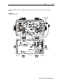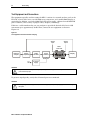
1
S T A R L I N E® S E R I E S
MB*/*
MiniBridger Amplifiers
Installation and Operation Manual
2
ASSEMBLED IN MEXICO
4
5
6
1
3
CAUTION
RISK OF ELECTRIC SHOCK
CAUTION: TO REDUCE THE RISK OF ELECTRIC SHOCK,
DO NOT REMOVE COVER (OR BACK).
NO USER-SERVICEABLE PARTS INSIDE.
REFER SERVICING TO QUALIFIED SERVICE PERSONNEL.
Caution
These servicing instructions are for use by qualified personnel only. To reduce the risk of electrical shock, do not perform any servicing other than
that contained in the Installation and Troubleshooting Instructions unless you are qualified to do so. Refer all servicing to qualified service
personnel.
Special Symbols That Might Appear on the Equipment
This symbol indicates that dangerous voltage levels are present within the equipment. These voltages are not
insulated and may be of sufficient strength to cause serious bodily injury when touched. The symbol may also
appear on schematics.
The exclamation point, within an equilateral triangle, is intended to alert the user to the presence of important
installation, servicing, and operating instructions in the documents accompanying the equipment.
For continued protection against fire, replace all fuses only with fuses having the same electrical ratings marked
at the location of the fuse.
Electrostatic discharge (ESD) can damage the MB*/* unit and circuit card assemblies. Wear an antistatic wrist
strap attached to a chassis ground to prevent ESD damage.
This equipment operates over the marked Voltage and Frequency range without requiring manual setting of any selector
switches. Different types of line cord sets may be used for connections to the mains supply circuit and should comply
with the electrical code requirements of the country of use.
It is recommended that the customer install an AC surge arrestor in the AC outlet to which this device is connected. This is to avoid damaging the
equipment by local lightning strikes and other electrical surges.
FCC Compliance
This equipment has been tested and found to comply with the limits for a Class A digital device, pursuant to Part 15 of the FCC Rules. These
limits are designed to provide reasonable protection against harmful interference when the equipment is operated in a commercial environment.
This equipment generates, uses, and can radiate radio frequency energy and, if not installed and used in accordance with the Installation Manual,
may cause harmful interference to radio communications. Operation of this equipment in a residential area is likely to cause harmful interference
in which case the user will be required to correct the interference at his/her own expense. Any changes or modifications not expressly approved
by Motorola could void the user’s authority to operate this equipment under the rules and regulations of the FCC.
You may find the following booklet, prepared by the Federal Communication Commission, helpful: How to Identify and Resolve Radio-TV
Interference Problems, Stock No. 004-000-0342-4, U.S. Government Printing Office, Washington, DC 20402.
Changes or modification not expressly approved by the party responsible for compliance could void the user’s authority to operate the equipment.
Canadian Compliance
This Class A digital apparatus meets all requirements of the Canadian Interference-Causing Equipment Regulations.
Cet appareil numérique de la classe A respects toutes les exigences du Règlement sur le matériel brouilleur du Canada.
International Declaration of Conformity
We
Motorola, Inc.
101 Tournament Drive
Horsham, PA 19044, U.S.A.
declare under our sole responsibility that the
STARLINE
Model MB*/*
to which this declaration relates is in conformity with one or more of the following standards:
EMC Standards
EN55022
EN55024
EN55013
EN50083-2
CISPR-22
CISPR-24
CISPR-13
EN60825
EN50083-1
EN60950
IEC 60950 + A1: 1992 + A2: 1993 + A3: 1995 + A4: 1996
Safety Standards
EN60065
IEC60065
following the provisions of the Directive(s) of the Council of the European Union:
EMC Directive 89/336/EEC
Low Voltage Directive 73/23/EEC
Copyright © 2002 by Motorola, Inc.
All rights reserved. No part of this publication may be reproduced in any form or by any means or used to make any derivative work (such as
translation, transformation or adaptation) without written permission from Motorola, Inc.
Motorola reserves the right to revise this publication and to make changes in content from time to time without obligation on the part of Motorola to
provide notification of such revision or change. Motorola provides this guide without warranty of any kind, either implied or expressed, including,
but not limited to, the implied warranties of merchantability and fitness for a particular purpose. Motorola may make improvements or changes in
the product(s) described in this manual at any time.
MOTOROLA, STARLINE, LIFELINE and the Stylized M Logo are registered in the US Patent & Trademark Office. All other product or service
names are the property of their respective owners. © Motorola, Inc. 2002
Contents
Section 1
Introduction
Using This Manual............................................................................................................................................................................1-2
Related Documentation ...................................................................................................................................................................1-3
Document Conventions ...................................................................................................................................................................1-3
If You Need Help ...............................................................................................................................................................................1-3
Calling for Repairs............................................................................................................................................................................1-4
Section 2
Overview
Configuration ....................................................................................................................................................................................2-2
Housing .............................................................................................................................................................................................2-3
Gaskets..............................................................................................................................................................................................2-5
Port Locations ..................................................................................................................................................................................2-6
Power Supply....................................................................................................................................................................................2-6
Forward Path.....................................................................................................................................................................................2-9
Models SP and DC .................................................................................................................................................................2-11
Return Path, RA-Kit/H or RA-Kit/L ................................................................................................................................................2-12
Ingress Control Switch ..................................................................................................................................................................2-12
Options and Accessories ..............................................................................................................................................................2-14
Section 3
Amplifier Setup
Forward Path Alignment ..................................................................................................................................................................3-1
Before You Begin.....................................................................................................................................................................3-1
Cable Equalizer ........................................................................................................................................................................3-2
Example 1 ........................................................................................................................................................................3-2
Example 2 ........................................................................................................................................................................3-2
Cable Simulators .....................................................................................................................................................................3-5
Input, Midstage, and Output Pads..........................................................................................................................................3-6
Output Passives.......................................................................................................................................................................3-7
Flatness Control ......................................................................................................................................................................3-8
Directional Coupler Test Points ...........................................................................................................................................3-12
Bode Equalization..................................................................................................................................................................3-12
Amplifier Level Control .........................................................................................................................................................3-12
Manual Gain Control..............................................................................................................................................................3-12
Thermal Drive Unit.................................................................................................................................................................3-14
MB*/* Installation and Operation Manual
ii
Contents
Automatic Drive Unit............................................................................................................................................................. 3-15
ADU Pads and Levels ........................................................................................................................................................... 3-15
Return Path Alignment .................................................................................................................................................................. 3-16
Before You Begin .................................................................................................................................................................. 3-16
Alignment Procedure............................................................................................................................................................ 3-17
Powering and Surge Protection ................................................................................................................................................... 3-18
Section 4
Bench Testing
Before You Begin ............................................................................................................................................................................. 4-1
Test Equipment and Connections.................................................................................................................................................. 4-2
Measuring Forward Gain................................................................................................................................................................. 4-3
Example.................................................................................................................................................................................... 4-3
Testing Return Gain and Response ............................................................................................................................................... 4-4
Example.................................................................................................................................................................................... 4-5
Completing the Test Procedures.................................................................................................................................................... 4-5
Section 5
Installation
Aerial Installation ............................................................................................................................................................................. 5-1
Pedestal Installation ........................................................................................................................................................................ 5-3
Section 6
Operating Tips
Using Amplifiers in Lower Frequency Systems............................................................................................................................ 6-1
Using Amplifiers in Lower Gain Systems...................................................................................................................................... 6-1
Appendix A
Specifications
Model MB87S/XG* ............................................................................................................................................................................A-1
Model MB87S/XX*.............................................................................................................................................................................A-2
Model MB75S/XG* ............................................................................................................................................................................A-3
Model MB75S/XX*.............................................................................................................................................................................A-4
AC Current, MB75*/*, MB87*/* .........................................................................................................................................................A-4
RA-Kit/H Return Amplifier ...............................................................................................................................................................A-5
ADU Automatic Drive Unit...............................................................................................................................................................A-5
Appendix B
Torque Specifications
Abbreviations and Acronyms
MB*/* Installation and Operation Manual
Contents
iii
Figures
Figure 1-1 MB*/* — closed ..............................................................................................................................................................1-2
Figure 2-1 MB*/* — open.................................................................................................................................................................2-1
Figure 2-2 MB*/* configurator.........................................................................................................................................................2-2
Figure 2-3 MB-HSG dimensions — top view.................................................................................................................................2-3
Figure 2-4 MB-HSG dimensions — side view ...............................................................................................................................2-3
Figure 2-5 MBP-HSG dimensions ..................................................................................................................................................2-4
Figure 2-6 Housing gaskets............................................................................................................................................................2-5
Figure 2-7 Housing ports ................................................................................................................................................................2-6
Figure 2-8 MPPS-II block diagram..................................................................................................................................................2-7
Figure 2-9 MPPS-II power pack ......................................................................................................................................................2-7
Figure 2-10 60/90 volt selector .......................................................................................................................................................2-8
Figure 2-11 Power passing fuse locations....................................................................................................................................2-9
Figure 2-12 MB*/* dual output block diagram.............................................................................................................................2-10
Figure 2-13 MB*/S*single output block diagram ........................................................................................................................2-11
Figure 2-14 LL-MB-F3 status monitor..........................................................................................................................................2-13
Figure 2-15 MB*/* options and accessories................................................................................................................................2-15
Figure 3-1 Equalizer slope versus cable .......................................................................................................................................3-4
Figure 3-2 Frequency versus cable slope.....................................................................................................................................3-6
Figure 3-3 SP splitter.......................................................................................................................................................................3-7
Figure 3-4 DC/* directional coupler................................................................................................................................................3-7
Figure 3-5 Flatness controls...........................................................................................................................................................3-8
Figure 3-6 MDR-*MB/*/II board........................................................................................................................................................3-9
Figure 3-7 Effects of flatness controls on the MDR-8MB/*/II board..........................................................................................3-10
Figure 3-8 Effect of flatness controls on the main board: ........................................................................................................3-11
Figure 3-9 TDU cable selector ......................................................................................................................................................3-14
Figure 3-10 ADU.............................................................................................................................................................................3-15
Figure 4-1 Test equipment connections for bench sweeping ....................................................................................................4-2
Figure 5-1 Center-conductor pin length........................................................................................................................................5-1
Figure 5-2 Torque sequence...........................................................................................................................................................5-2
Tables
Table 2-1 MB*/* options and accessories ...................................................................................................................................2-14
Table 3-1 Starline Forward Equalizers — SFE-*-*.........................................................................................................................3-3
Table 3-2 Starline cable simulators ...............................................................................................................................................3-5
Table 3-3 Gain reserve versus ambient temperature.................................................................................................................3-13
Table 3-4 MB*/* AGC pad levels ...................................................................................................................................................3-16
MB*/* Installation and Operation Manual
Section 1
Introduction
®
®
The Motorola STARLINE series of MiniBridger amplifiers, model MB*/*, accept a single input
and provide high operational gain to a single or dual output. The high gain makes the MB*/*
series ideally suited for a hybrid fiber-coax system as well as conventional tree-and-branch
designs. The MB*/* amplifier series complies with IEEE C62.41-1991 and Bell Core GR-1098
specifications for overvoltage testing as recommended by Cable Labs. The MB*/* platform is
also FCC and CE approved.
Features of the MB*/* include:
750 MHz or 870 MHz power doubling technology
(in enhanced gallium arsenide (E-GaAs) or silicon)
Several different modular diplex filter splits
“Ease of use” ergonomics
60/90 Vac line power option
Power factor corrected power supply
Thermal and auto-controlled Bode equalization
−20 dB directional coupler test points
®
Optional return path ingress control and LIFELINE status monitor
Two-way capability
15-amp power passing
Features of the optional MB*/* bypass housing include:
Amplifier bypass for maintenance and upgrades
Accommodation of the optional bypass amplifier
Use of a quick-connect interface probe for RF/AC bypassing
A reversible amplifier module
90-degree port entries
15-amp, 1 GHz electrical performance
MB*/* Installation and Operation Manual
1-2
Introduction
Figure 1-1 illustrates a closed MB*/*:
Figure 1-1
MB*/* — closed
Using This Manual
The following sections provide information and instructions to install and operate the MB*/*.
Section 1
Introduction provides a product description, related documentation, the technical help line,
and repair/return information.
Section 2
Overview describes the MB*/* and includes details on the various options and their
functions.
Section 3
Amplifier Setup provides instructions for full configuration and forward- and return-path
alignment.
Section 4
Bench Testing describes the bench test procedures that are recommended before you
install the MB*/*.
Section 5
Installation provides instructions for installing the MB*/* and options.
Section 6
Operating Tips provides suggestions for handling field-encountered variables and
addressing maintenance tasks.
Appendix A
Specifications lists the applicable technical specifications for the MB*/* and options.
Appendix B
Torque Specifications provides the appropriate torque specifications for the MB*/* and
options.
Abbreviations
and Acronyms
The Abbreviations and Acronyms list contains the full spelling of the short forms used in
this manual.
MB*/* Installation and Operation Manual
Introduction
1-3
This manual assumes that all channels are standard National Television Standards Committee
(NTSC) analog channels. Refer to catalog specifications for further details pertaining to signal
levels of digital channels above 550 MHz.
This manual also uses 870 MHz as the reference frequency unless another frequency is given.
For example, quoted cable loss is understood to be at 870 MHz.
Related Documentation
This Installation and Operation Manual is complete and you should not require any additional
documentation to install, test, or operate the MB*/*.
Document Conventions
Before you begin using the MB*/*, familiarize yourself with the stylistic conventions used in this
manual:
SMALL CAPS
Denotes silk screening on the equipment, typically representing front- and rear-panel
controls and input/output (I/O) connections, and LEDs
* (asterisk)
Indicates that several versions of the same model number exist and the information applies
to all models; when the information applies to a specific model, the complete model number
is given
Italic type
Denotes a displayed variable, or is used for emphasis
If You Need Help
If you need assistance while working with the MB*/*, contact the Motorola Technical Response
Center (TRC):
Inside the U.S.: 1-888-944-HELP (1-888-944-4357)
Outside the U.S.: 215-323-0044
Online: http://www.motorola.com/broadband, click HTML/Modem Version, click
Customer Support, then click Web Support.
The TRC is open from 8:00 AM to 7:00 PM Eastern Time, Monday through Friday and 10 AM to
6 PM Eastern Time, Saturday. When the TRC is closed, emergency service only is available on a
call-back basis. Web Support offers a searchable solutions database, technical documentation,
and low priority issue creation/tracking 24 hours per day, 7 days per week.
MB*/* Installation and Operation Manual
1-4
Introduction
Calling for Repairs
If repair is necessary, call the Motorola Repair Facility at 1-800-642-0442 for a Return for
Service Authorization (RSA) number before sending the unit. The RSA number must be
prominently displayed on all equipment cartons. The Repair Facility is open from 7:00 AM to
4:00 PM Pacific Time, Monday through Friday.
When calling from outside the United States, use the appropriate international access code and
then call 52-631-311-1100, to contact the Repair Facility.
When shipping equipment for repair, follow these steps:
1
Pack the unit securely.
2
Enclose a note describing the exact problem.
3
Enclose a copy of the invoice that verifies the warranty status.
4
Ship the unit PREPAID to the following address:
Motorola, Inc.
Broadband Communications Sector
c/o Excel
Attn: RSA #_________
6908 East Century Park Drive
Suite 100
Tucson, AZ 85706
MB*/* Installation and Operation Manual
Section 2
Overview
The MB*/* is a dual-output amplifier while the MB*/S* is a single-output amplifier used in
CATV distribution systems. Both models accommodate installation of the optional return
amplifier to enable two-way signal flow. All models are high-gain, three-stage hybrid amplifers
designed to drive both a limited cascade and a local distribution system. The MB*/* is powered
by the 60/90 Vac cable supply and can be configured to pass this power to additional amplifiers
and line extenders.
The standard model MB*/* includes an amplifier module with an integrated power supply which
is normally furnished complete in the model MB-HSG housing as illustrated in Figure 2-1:
Figure 2-1
MB*/* — open
MB
87
75
55
S
J
A
K
E
M
G
-20dB
-20dB
JXP
IN
H
IN
JXP 2
FWD
EQ
L
-20dB
JXP 3/4
BODE
FUSE
PORT 2
L
MDR
H
STATUS
MONITOR
OUTPUT
FUSE
ALIGN DOTS
REFER TO
MANUAL FOR
FUSE VALUES
JXP
ADU
MAN
H
L
I
C
S
JXP 2
JXP
POWER
-20dB
DRIVE
UNIT
JXP THERM
-20dB
ADU
ADU
MAN
PORT 3
I
C
S
3
4
JXP 3/4
TDU
-20dB
CONTROL
STATUS
MONITOR
FUSE PORT 4
JXP
RTN
EQ
FUSE
CAUTION:
CONTAINS PARTS
AND ASSEMBLIES
SUSCEPTIBLE TO
DAMAGE BY
ELECTROSTATIC
DISCHARGE (ESD)
-16dB
STATUS
MONITOR
INPUT
JXP
COMMON
ASSEMBLED IN MEXICO
HI
Lid
LO
AC TEST POIN T
NO USER SERVICAB LE
PARTS INSIDE
USE CAUTION WHEN MAKING
INTERNAL ADJUSTMENTS
WITH COVER REMOVED
SEE INSTALLATION MANUAL
FOR SERVICE
Base
FTEC
VOLTAGES IN EXCESS OF
300 VOLTS ARE PRESENT
UNDER COVER AND MAY
BE PRESENT FOR SEVERAL
MINUTES AFTER POWER
IS REMOVED
460132-001
24 V TEST POINT
MPPS-II
MB*/* Installation and Operation Manual
2-2
Overview
Configuration
The MB*/* is fully configured in the factory per customer request. It is recommended that you
verify the configuration listed on the outside of the shipping carton with the configuration that
you ordered. The shipped configuration is also noted in a label on the side of the electronics
chassis and the housing.
Figure 2-2 illustrates the MB*/* configuration notation:
Figure 2-2
MB*/* configurator
Key
Frequency Range
75E 5-30 MHz, 47-750 MHz
75S 5-40 MHz, 52-750 MHz
75K 5-42 MHz, 54-750 MHz
75J 5-55 MHz, 70-750 MHz
75A 5-65 MHz, 85-750 MHz
75M 5-80 MHz, 108-750 MHz
87E 5-30 MHz, 47-870 MHz
87S 5-40 MHz, 52-870 MHz
87K 5-42 MHz, 54-870 MHz
87J 5-55 MHz, 70-870 MHz
87A 5-65 MHz, 85-870 MHz
87M 5-80 MHz, 108-870 MHz
Key
Hybrid Technology
B
Ingress Control Switches
G
E-GaAs (High Output, High Gain)
X
None
X
Special Options
None
X
None
T
TDU
A
ADU 499.25/S
Key
B
ADU 439.25/S
X
None
C
ADU 403.25/S
S
LL-MB-F3
D
ADU 445.25/S
E
ADU 549.00/S
F
ADU 325.25/S
P
34 dB Gain Option
Status Monitoring
Key
Overcurrent Protection
X
20A Auto Fuse
S
Shunt
Return Amp w/JXP-ZX
Key
Housing Size
X
No Return
X
Standard
L
Low Gain Hybrid
B
By-Pass
H
High Gain Hybrid
N
None (Electronics Only)
Key
Reserved
E
Ergonomics
/
Key RF Configurations
X Dual Output
Key
Key
X
Level Control
Key
S
Ingress switching
Standard (High Gain Silicon)
Key
MB
Key
X
Key
X
Reserved
Reserved
Single Output
Station Slope
Key
Voltage Surge Protector
X
Surge Arrestor
C
FTEC; Crowbar
Key
Housing Finish
S,K,E splits: 10 [Fmin-750 MHz], 12 [Fmin-870 MHz]
X
Standard
A split: 9 [Fmin-750 MHz], 10 [Fmin-870 MHz]
C
Chromate
J split: 9.5 [Fmin-750 MHz], 11.5 [Fmin-870 MHz]
S
P
Chromate w/SS plugs
Epoxy
Key
Reserved
X
Reserved
Key
Power Supply
X
Power Factor
Correction (Standard)
N
Non-power
Factor Correction
A
S,K,E splits: 12 [Fmin-750 MHz]
B
S,K,E splits: 14 [Fmin-750 MHz, 870 MHz]
X
Standard (15 Amp)
C
6 [Fmin-750 MHz, 870 MHz]
L
D
8 [Fmin-750 MHz, 870 MHz]
Low Current (10 Amp) - Available
for electronics package only
MB*/* Installation and Operation Manual
Key
AC Current Capability
Overview
2-3
Housing
The MB*/* is furnished in an MB-HSG aluminum housing that protects the electronics from
weather and dissipates internally generated heat.
Figure 2-3 illustrates a top view of the MB-HSG housing and provides its dimensions:
Figure 2-3
MB-HSG dimensions — top view
15.4
9.6
Figure 2-4 illustrates a side view of the MB-HSG and provides its dimensions:
Figure 2-4
MB-HSG dimensions — side view
5.6
Messenger clamp bolts
MB*/* Installation and Operation Manual
2-4
Overview
Figure 2-5 provides top and side view dimensions of the optional MBP-HSG bypass housing:
Figure 2-5
MBP-HSG dimensions
17.7
10.4
7.3
Coaxial cable connections to the housing are made using conventional 5/8 × 24 threads per-inch
stinger-type connectors. Five port plugs in the cover enable access to internal test points
without opening the housing.
The interior platform assembly of the 15A MB-HSG differs from the platform assembly of the
10A MB-HSG (earlier models MB-550D-H, MB-750D-H, and MB-75SH, AH, and JH). However,
you can upgrade the 10A MB*/* to a 15A MB*/* using existing housings. To upgrade the
MB-550D-H or MB-750D-H, use the MB-15A kit P/N 951941-005-00. To upgrade the MB-75SH,
AH, or JH, use the MB-15AII platform assembly kit P/N 951941-007-00. Both kits can be used
in either the standard or bypass housing. Replacing the housing cover brings the test ports in
line with the output test points for both the forward and return signal path.
MB*/* Installation and Operation Manual
Overview
2-5
The included clamp and bolt assemblies enable you to mount the standard and bypass housings.
For instructions on aerial and pedestal installation refer to Section 5, “Installation”.
Gaskets
Each housing is equipped with a recessed woven-wire RF gasket and a silicone-rubber weather
gasket to provide a seal between the housing base and lid. These gaskets provide efficient
ground continuity, RF shielding, and weather protection. Both gaskets must be in place and in
good condition to ensure proper operation and protection of the station. The weather gasket
should be lightly coated with silicone grease each time the amplifier is opened. Replace this
gasket if it becomes damaged or deformed.
Figure 2-6 illustrates the housing gaskets:
Figure 2-6
Housing gaskets
Weather gasket
(silicone rubber)
MB
87
75
55
S
J
A
K
E
M
G
-20dB
-20dB
JXP
IN
H
IN
JXP 2
FWD
EQ
L
-20dB
JXP 3/4
BODE
FUSE
PORT 2
L
MDR
H
STATUS
MONITOR
OUTPUT
FUSE
ALIGN DOTS
REFER TO
MANUAL FOR
FUSE VALUES
JXP
ADU
MAN
H
L
I
C
S
JXP 2
JXP
POWER
-20dB
DRIVE
UNIT
-20dB
ADU
3
ADU
MAN
PORT 3
I
C
S
4
JXP THERM
JXP 3/4
TDU
-20dB
CONTROL
STATUS
MONITOR
FUSE PORT 4
JXP
RTN
EQ
FUSE
CAUTION:
CONTAINS PARTS
AND ASSEMBLIES
SUSCEPTIBLE TO
DAMAGE BY
ELECTROSTATIC
DISCHARGE (ESD)
-16dB
STATUS
MONITOR
INPUT
JXP
COMMON
ASSEMBLED IN MEXICO
HI
LO
AC TEST POIN T
NO USER SERVICAB LE
PARTS INSIDE
USE CAUTION WHEN MAKING
INTERNAL ADJUSTMENTS
WITH COVER REMOVED
SEE INSTALLATION MANUAL
FOR SERVICE
FTEC
VOLTAGES IN EXCESS OF
300 VOLTS ARE PRESENT
UNDER COVER AND MAY
BE PRESENT FOR SEVERAL
MINUTES AFTER POWER
IS REMOVED
460132-001
24 V TEST POINT
MPPS-II
RF gasket
(woven wire)
MB*/* Installation and Operation Manual
2-6
Overview
Port Locations
Five port plugs in the cover enable access to internal test points. The input and output ports
provide connection for coaxial cables and are protected by factory-inserted threaded plugs or
plastic cap plugs. Discard the plastic cap plugs when you install the cable connectors.
Figure 2-7 illustrates the housing port locations:
Figure 2-7
Housing ports
Messenger
clamp bolts
2
1
Port 2
4
IN
Port 1
Port 4
Lid
3
Port 3
Power Supply
The cover of the amplifier houses the model MPPS-II 60/90 power pack. It provides a regulated
24 Vdc output at 1.8 amps maximum over an ac input voltage range from 38 Vac to 90 Vac rms.
The input voltage waveshape is either a squarewave or a sinewave. The surge protector and the
EMI filter protect the power pack and amplifier from transient spikes. An integral fast-acting
zener diode provides additional surge protection.
The preregulator is a fixed frequency switching regulator that presents a near perfect power
factor to the input line and provides overvoltage and overcurrent protection. A precision output
regulator provides a precise output voltage and is also protected against overcurrent and short
circuits. If a short circuit is detected, the power supply shuts down and the regulator initiates a
sequence of line test pulses at approximately one-half second intervals. The regulator continues
these pulses for the duration of the short circuit but returns to normal operation when the fault
is cleared.
MB*/* Installation and Operation Manual
Overview
2-7
Figure 2-8 illustrates a block diagram of the MPPS-II power pack:
Figure 2-8
MPPS-II block diagram
60/90
Vac
EMI Filter
Bridge
rectifier
Isolation
transformer
Preregulator
Precision
regulator
24
Vdc
Overvoltage
and
power-factor
correction
Figure 2-9 illustrates the MPPS-II installed in the upper half of the MB-HSG:
Figure 2-9
MPPS-II power pack
HI
LO
AC TEST POINT
NO USER SERVICABLE
PARTS INSIDE
USE CAUTION WHEN MAKING
INTERNAL ADJUSTMENTS
WITH COVER REMOVED
SEE INSTALLATION MANUAL
FOR SERVICE
FTEC
VOLTAGES IN EXCESS OF
300 VOLTS ARE PRESENT
UNDER COVER AND MAY
BE PRESENT FOR SEVERAL
MINUTES AFTER POWER
IS REMOVED
460132-001
24V TEST POINT
MPPS-II
The MPPS-II also contains a two position LO/HI selector that sets the start-up voltage for 38 Vac
or 55 Vac. The MB*/* is shipped with the selector in the LO position which is the standard
configuration. The selector should be switched to the HI position only for a 90 Vac system. This
sets the start-up voltage at 55 Vac. Because this is only 5 V below 60 Vac, it is not practical to
switch to HI in a 60 Vac system. There is no damage to the amplifier if the selector is not
changed from the standard LO setting. However, changing the selector ensures that the dc
supply does not turn on until the proper input voltage, 38 Vac or 55 Vac, is reached. This
prevents excessive loading of the system power supply during turn-on after a system shutdown.
MB*/* Installation and Operation Manual
2-8
Overview
Figure 2-10 illustrates the location of the LO/HI voltage selector and the gas discharge tube surge
protector on the MPPS-II:
Figure 2-10
60/90 volt selector
Voltage
selector
Gas discharge tube
or optional FTEC
J1
HI
LO
TP1
R 54
TP2
460132-001
You must remove the MPPS-II cover to access the selector illustrated in Figure 2-10.
Section 3, “ Amplifier Setup” explains changing the setting of this selector to meet system
requirements.
The power supply includes a heavy-duty gas discharge tube which you can replace with the
optional fast-transfer electronic-crowbar (FTEC) surge protector. The FTEC fires at
approximately 245 V and presents a short circuit to the line during periods of overvoltage. After
the ac input voltage returns to normal, the FTEC resumes its open state.
MB*/* Installation and Operation Manual
Overview
2-9
Factory installed 20-amp fuses, illustrated in Figure 2-11, provide power passing to additional
amplifiers:
Figure 2-11
Power passing fuse locations
F in
MB
87
75
55
IN
S
J
A
K
E
M
F2
G
-20dB
-20dB
JXP
IN
STATUS
MONITOR
OUTPUT
H
JXP 2
FWD
EQ
L
-20dB
JXP 3/4
BODE
FUSE
PORT 2
L
MDR
H
FUSE
ALIGN DOTS
REF ER TO
MANUAL F OR
FUS E VALUE S
MAN
JXP
ADU
H
L
I
C
S
JXP 2
JXP
POWER
-20dB
DRIVE
UNIT
JXP THERM
-20dB
ADU
ADU
MAN
PORT 3
I
C
S
TDU
3
4
-20dB
CONTROL
STATUS
MONITOR
JXP 3/4
FUSE
PORT 4
JXP
RTN
EQ
FUSE
F3 location
CAUTION:
CONTAINS PARTS
AND AS S EMBLIES
S US CE PTIBLE TO
DAMAGE BY
E LECTRO STAT IC
DISCHARGE (E SD)
-16dB
STATUS
MONITOR
INPUT
JXP
COMMON
ASSEMBLED IN MEXICO
F4
Forward Path
The operational gain of all MB*/* models is 40 dB with 16 dB of return loss in the forward path.
The operating gain includes provisions for the insertion loss of the input cable equalizer and
required reserve gain to operate the Bode equalizer in the middle of its range.
The forward path’s electronics consist of two parallel three-stage paths consisting of:
(1) pre-amplifier (input hybrid), (2) intermediate amplifier (midstage hybrid), and
(3) power-doubling output hybrid stage. The first two stages are common to both paths. The
pre-amplifier stage provides a low noise figure while the output stage contributes the preferred
power at low distortion. The amplifier input provides a facility to install a cable equalizer and a
socket for a model JXP-*B attenuator. The attenuator and equalizer are customer installed
options.
Several circuits comprise the intermediate amplifier stages. A flatness control circuit enables
optimization of the frequency response. The Bode equalizer is a voltage-controlled device that, in
the standard configuration, receives its input from the manual gain control. It also receives its
input from the automatic drive unit (ADU-*) or thermal drive unit (TDU-*) when either of these
options is employed.
MB*/* Installation and Operation Manual
2-10
Overview
Following the Bode board, a JXP pad facility adjusts the RF level into the interstage hybrid
amplifier and the MDR-*MB/*/II controls flatness and provides equalization. Because these
losses are located interstage, the noise figure is only significantly impacted by the insertion loss
of the forward cable equalizer or broadband cable simulator, and the input pad if its value is
increased from zero.
Following the interstage hybrid is a JXP-*B pad socket (or a splitter and two JXP-*B pad
sockets for dual output) leading into the power-doubling output stage.
Figure 2-12 illustrates the interconnection between these components in the dual-output MB*/*:
Figure 2-12
MB*/* dual output block diagram
+18.0 dB E-GaAs
+20.5 dB Silicon
JXP-B
Fltn.
Cntrl.
PP
RF/
AC RF
AC
-1.0 dB R
BODE
JXP-B
+19 dB -4.0 dB
Manual
Auto
ADU/
TDU
H
L
-1.0 dB **
**
-20 dB
TP
Surge
protector
-0.5 dB
**
**
SRE
-0.3 dB
**
THERM
JXP-B
LPF
+25.0 dB L
+30.0 dB H
24 Vdc
JXP-B
Status
Monitor
Input
-0.4 dB
Surge
protector
To status
monitor
OnBrd
Atten
**
**
-4.0 dB
ICS
-1.0 dB R
L
**
-1.0 dB
PD
Port
2
-20 dB
TP
JXP-B
JXP
-1.0 dB
**
-4.0 dB
L
JXP
JXP-B
DC/
SP/
JMP
-0.4 dB
-1.0 dB
-20 dB
TP
**
Plug-in
module
DC
Port
4
RF/
RF AC
AC
-1.0 dB R
Port
3
RF
RF/AC
AC
-0.4 dB
**
-2.0 dB F
**
H
ICS
RF/
RF AC
AC
-0.4 dB
**
Power
supply
MB*/* Installation and Operation Manual
-1.7 dB F
-20 dB
TP
JXP-B
-16 dB
H
**
**
**
Fuse
+18.0 dB E-GaAs
+20.5 dB Hi Gain
JXP-B
-1.0 dB
-0.4 dB
**
-1.0 dB
PP
MDR
**
Fuse
-1.7 dB F
-1.0 dB
**
**
-4.0 dB
-20 dB
TP
Input
port 1
-6.5 dB
**
PD
SP
**
**
Fuse
**
JXP-B
Fuse
-1.0 dB
**
SFE
or
SCS
(Status
-20 dB Monitor
TP
Output)
**
+25.0 dB E-GaAs
+23.0 dB Silicon
-4.0 dB
JMP
Overview
2-11
Figure 2-13 illustrates the interconnection between these components in the single output
MB*/S*:
Figure 2-13
MB*/S*single output block diagram
+25.0 dB E-GaAs
+23.0 dB Silicon
-4.0 dB
**
JXP-B
Fltn.
Cntrl.
PP
-20 dB
TP
-1.7 dB F
RF/
AC RF
AC
-1.0 dB R
**
BODE
Manual
JXP-B
-1.0 dB
**
+19 dB
PP
MDR
Auto
JXP-B
-1.0 dB
ADU/
TDU
H
L
-1.0 dB **
**
-20 dB
TP
-0.4 dB
Surge
protector
-0.5 dB
**
**
SRE
-0.3 dB
**
THERM
JXP-B
LPF
+25.0 dB L
+30.0 dB H
24 Vdc
JXP-B
-0.4 dB
Surge
protector
Fuse
To status
monitor
OnBrd
Atten
PD
(Status
-20 dB Monitor
TP
Output)
**
**
Status
Monitor
Input
**
-1.0 dB
**
JXP-B
L
ICS
JXP
JXP-B
DC/
SP/
JMP
-0.4 dB
-1.0 dB
-20 dB
TP
Power
supply
**
Plug-in
module
DC
RF/
RF AC
AC
-1.0 dB R
**
SP
Port
4
Port
3
RF
RF/AC
AC
-0.4 dB
**
-2.0 dB F
**
H
-16 dB
**
**
+18.0 dB E-GaAs
+20.5 dB Silicon
Fuse
Input
port 1
-6.5 dB
**
**
Fuse
-1.0 dB
**
SFE
or
SCS
JMP
Accurate −20 dB directional coupler test points are available at the input and at the output of
the amplifier. Because these test points are 75-ohm source impedance, they do not require
special test probes.
After the output amplifier, a second directional coupler provides signal to the optional ADU
board. As this signal is used only with the ADU, you do not need to terminate this port when the
ADU is not installed.
Models SP and DC
Port 2 is a dedicated amplifier path in the MB*/*. The other path can feed port 3 or port 4
depending on where you install the furnished JMP jumper. The model SP splitter and model
DC/* directional coupler provide output at both ports 3 and 4. The SP provides equal output
levels, while the DC/* provides one high-level port and one low-level port. The high-level signal
is routed to port 3 or port 4 and is based on the orientation of the DC/* during installation.
Figure 2-1 illustrates the port numbers identified on the amplifier cover and Figure 2-7
illustrates the port numbers cast into the MB-HSG.
When installing a DC/* or an SP, complete the installation and install fuse F3 before you apply
RF power.
MB*/* Installation and Operation Manual
2-12
Overview
Return Path, RA-Kit/H or RA-Kit/L
The circuit board of the MB*/* amplifier accommodates the optional return path. The return
path kit, Model RA-Kit/H or RA-Kit/L, includes the return amplifier hybrid (illustrated in
Figure 2-15) and jumpers. This equips the MB*/* to pass signals in the return or upstream
direction. The standard circuit board contains all components including the diplex filters, with
extended return bandwidth, for the amplifier input and output.
Optional SRE-*-* return equalizers compensate for cable attenuation and are available in 1 dB
increments for S-split, and 2 dB increments for all other splits, from 0 dB through 12 dB. All
items are plug-in and easily installed.
There are JXP-*B pad facilities located at the input and output of the return path. You can use
these pad facilities as test points or signal injection points. The output pad value is normally
selected to control the return signal level into the next upstream amplifier. Select an
appropriate input pad to attenuate excessive input signal.
The return-input test points and the return-output test point are −20 dB directional couplers.
These test points present 75-ohm source impedance and do not require special test probes.
Ingress Control Switch
The ingress control switches (ICS) (illustrated in Figure 2-15) provide return-path signal
attenuation or cutoff in the MB*/*. The dual output MB*/* requires two ICS’s. Switching is
accomplished through the frequency agile LIFELINE Flexstat 3 status-monitoring module,
LL-MB-F3, located in the housing lid next to the power supply, as illustrated in Figure 2-14.
The ICS provides a means of isolating sources of ingress from a centralized location. Using a
downstream command through the LIFELINE status-monitoring system, you can attenuate the
return path through the amplifier by 6 dB or by 38 dB. By reducing the ingress level at the
headend or monitoring point, you can further isolate the ingress source.
After you isolate an ingress source to the last possible amplifier, node, or line extender, you can
shut the return path off at that location. This limits the impact of the ingress on the remainder
of the network while eliminating the source of ingress.
MB*/* Installation and Operation Manual
Overview
2-13
Figure 2-14 illustrates the LL-MB-F3 and the required cable connections to the amplifier
module:
Figure 2-14
LL-MB-F3 status monitor
G- to F-type
adapter
MB
87
75
55
S
J
A
K
E
M
G
-20dB
-20dB
JXP
IN
STATUS
MONITOR
OUTPUT
H
IN
JXP 2
FWD
EQ
L
-20dB
JXP 3/4
BODE
FUSE
PORT 2
L
MDR
H
FUSE
ALIGN DOTS
REFER TO
MANUAL FOR
FUSE VALUES
JXP
ADU
MAN
H
L
I
C
S
JXP 2
JXP
POWER
-20dB
DRIVE
UNIT
JXP THERM
-20dB
ADU
ADU
MAN
PORT 3
I
C
S
3
4
JXP 3/4
TDU
-20dB
CONTROL
STATUS
MONITOR
FUSE
PORT 4
JXP
RTN
EQ
FUSE
CAUTION:
CONTAINS PARTS
AND ASSEMBLIES
SUSCEPTIBLE TO
DAMAGE BY
ELECTROSTATIC
DISCHARGE (ESD)
-16dB
STATUS
MONITOR
INPUT
JXP
COMMON
ASSEMBLED IN MEXICO
HI
LO
LIF E LINE ™
AC TEST POIN T
NO USER SERVICAB LE
PARTS INSIDE
USE CAUTION WHEN MAKING
INTERNAL ADJUSTMENTS
WITH COVER REMOVED
SEE INSTALLATION MANUAL
FOR SERVICE
FTEC
LL -M B- 48-120/5- 42
RX : 52
TX : 5.5
S N/ADD RE S S:
VOLTAGES IN EXCESS OF
300 VOLTS ARE PRESENT
UNDER COVER AND MAY
BE PRESENT FOR SEVERAL
MINUTES AFTER POWER
IS REMOVED
460132-001
24 V TEST POINT
Status
monitor
MPPS-II
MB*/* Installation and Operation Manual
2-14
Overview
Options and Accessories
The factory ships the MB*/* as a fully functional unit, but you must configure it appropriately
for the field location requirements. You must install the correct forward equalizer or broadband
cable simulator and input pad to place the unit in service. Section 3, “ Amplifier Setup” provides
information to assist you in this task. Use model JXP-*B pads to control field signal levels. To
compensate for temperature, install the ADU or TDU before placing the MB*/* in service. You
can install other items such as a return amplifier and additional surge protection at your
discretion, but these options do not render the MB*/* inoperative if they are not included.
Table 2-1 provides a comprehensive list of options and accessories for the MB*/*:
Table 2-1
MB*/* options and accessories
Model
Description
Function
ADU-*
Automatic Drive Unit
This board automatically controls amplifier output levels
that change with cable attenuation and hybrid output.
The selection of a pilot frequency is required.
TDU
Thermal Drive Unit
This board controls amplifier gain and slope for
changes in cable attenuation for the sensed
temperature.
RA-Kit/H or L
Return Amplifier Kit
This kit enables two-way operation and includes a highor low-gain return hybrid and jumpers.
SFE-0, SFE-1
Starline Forward Equalizer
These equalizers are not bandwidth specific and
compensate for 0 dB and 1 dB of cable respectively
from 5 MHz to 1 GHz.
SFE-*-*
Starline Forward Equalizer
This bandwidth specific (750 or 870 MHz) equalizer
compensates for cable properties in 1 dB increments
from 2 dB to 22 dB. You must install the appropriate
value. See the product catalog for additional
information.
SRE-*-*
Starline Return Equalizer
This bandwidth specific equalizer compensates for
cable attenuation in 1 dB increments from 0 dB to
12 dB for S-split (2 dB increments for all other splits).
You must install the appropriate value. See the product
catalog for additional information.
SCS-*
Starline Cable Simulator
This simulator compensates for cable properties. You
must install the appropriate value. See the product
catalog for additional information.
JXP-*B
Fixed attenuator
This pad attenuates excessive input signal. It is
available in 0.5 dB increments from 0 dB to 26 dB. You
must install the appropriate value.
JXP-TH*B
Thermal attenuators
This option compensates for gain changes with
temperature in the return path.
FTEC
Fast Transfer Electronic
Crowbar
This option is used for overvoltage protection and
replaces the existing surge protector.
LL-MB-F3
Status monitor module
This module enables monitoring of the unit’s operating
parameters by the LIFELINE status-monitoring system.
MB*/* Installation and Operation Manual
Overview
2-15
Model
Description
Function
ICS
Ingress Control Switch
This option enables remote monitoring, isolation, and
reduction of ingress on the return path by providing
signal attenuation of 6 dB or cutoff of 38 dB typical. The
unit is shipped with a jumper in this location.
SP or DC/*
Output passives
These options should be installed in place of the JMP
jumper to activate the third output of the MB*/*.
JXP-RPC
Return Path Correction Board
This optional board provides additional flatness
response correction in the return path for systems that
must meet especially stringent return-path flatness
requirements.
MBP-HSG
Bypass housing
This housing accommodates the signal bypass jumper,
which prevents transmission loss to subscribers during
maintenance and upgrades.
Figure 2-15 illustrates the location of options and accessories in the MB*/*:
Figure 2-15
MB*/* options and accessories
Forward
equalizer or
Diplex Cable simulator
filter (SFE-*-* or SCS-*)
20A
fuse
TP
forward
input
Input
pad
(JXP IN)
Mid-stage
pad
(JXP)
Output pad
MDR (JXP 2)
Manual
level
(MAN)
Bode
board
ADU
pad
(JXP
ADU)
Diplex
filter
Output
pad
(JXP 3/4)
TP forward
output
(Status monitor
output)
TP
return
inputs
20A
fuse
SFE-*-*
460246-001
DC/*
Return 20A
equalizer fuse
(SRE-*-*)
Return
output
pad
(JXP)
Optional
(JXP THERM)
Return
hybrid
ADU
or TDU
TP
return
output
DRIVE UNIT/MAN
Drive
control
select jumper
20A
Return
fuse
input
pads
(JXP 2 and
JXP 3/4)
Status Optional Return
Optional
pad
ICS
monitor DC/SP
(JXP
(JXP jumpers
input
common)
shown)
Auto
level
(ADU)
Diplex
filter
TP
forward
output
(3/4)
In the event of ADU or TDU board failure, you can select manual control of the Bode board.
Figure 2-15 illustrates the location of the DRIVE UNIT/MAN jumper on the main circuit board.
MB*/* Installation and Operation Manual
Section 3
Amplifier Setup
This section provides instructions for fully configuring the MB*/* and describes the proper
forward and return path alignment procedures. The following tasks need to be performed for
successful amplifier setup:
Forward path alignment:
Selecting the appropriate cable equalizer or cable simulator
Selecting the appropriate input, midstage, and output pads
Selecting the appropriate output passives
Verify proper flatness control
Verify proper level control
Check return path alignment
Check powering and surge protection options
It is recommended that you read this entire section before you install the MB*/*.
Forward Path Alignment
The following subsections describe the MB*/* alignment procedures required for proper
performance in the forward path.
Before You Begin
Before you begin to set-up the amplifier and perform forward-path alignment, please read the
following instructions and recommendations.
For proper forward alignment obtain:
RF output levels and tilts of all MB*/*s in the forward or return path
RF input level for the MB*/* being set up (from system design or as-built map)
A carrier at the system’s highest frequency. It can be modulated or continuous wave (CW)
and should be inserted in the headend at standard video levels. This carrier is used to
simplify field set-up.
It is recommended that you:
Install the system design value SFE-*-* and a high value (20 dB or above) input pad
(JXP IN) before you install or remove the electronics chassis or apply power to the MB*/*.
Leave the JXP IN pad location open if a high value pad is not available. A more accurate
forward input test point reading is achieved with a high value pad installed.
Do not use wire jumpers to bypass the SFE-*-* location.
Recognize that actual pad and SFE-*-* values may differ slightly from their design values.
This is caused by factors such as walkout errors, worst-case data utilization during design
and temperature variation from 70°F.
MB*/* Installation and Operation Manual
3-2
Amplifier Setup
Secure the electronics chassis in the housing and torque to 18 to 22 in-lbs. to facilitate heat
transfer and avoid damage from overheating.
Perform a bench alignment. Pre-aligning the MB*/* response on the bench (Section 4,
“ Bench Testing” ) for a system signature simplifies field alignment.
Field sweep the entire bandwidth of the amplifier to correct frequency response for passive
signature and roll-off.
Close the housing in accordance with the instructions in Section 5, “ Installation.”
Cable Equalizer
Select the appropriate model SFE-*-* to compensate for cable attenuation versus frequency and
to obtain the proper output tilt. The MB*/* is equipped with the MDR-*MB/*/II interstage
equalizer and flatness board, which compensates for cable attenuation. Any cable or passive
slope beyond that of the MDR-*MB/*/II must be compensated for by selecting and installing the
appropriate SFE-*-* cable equalizer.
Equalizers are available in 1 dB steps from 0 dB to 22 dB. The following examples describe how
to choose the correct equalizer.
Example 1
The amplifier location includes 20 dB of cable (at 870 MHz) between its input and the preceding
amplifier. Consider cable loss only. Exclude any flat loss due to splitters or other passive
devices. The internal equalizer, model MDR-8MB/12/II, compensates for approximately 16 dB of
cable. Subtract this cable length from the 20 dB of this example (20 − 16 = 4). The SFE-87-4 is
the proper equalizer in this case. With this equalizer installed, the amplifier reproduces the
output tilt of the last upstream amplifier.
When selecting an equalizer, choose the next lower value if the exact value is not available or in
cases where the calculated value makes two choices possible.
Example 2
The MB*/* is used in a link following a fiber node. The fiber receiver output is flat and connects
to the input of the amplifier through 18 dB of cable plus passive loss. Determine which is the
proper equalizer to achieve the 11 dB output tilt from the MB*/*.
Calculate the equalizer value using the following equation:
SLOPEeq = TILTout + SIGlo – SIGhi – SLOPEieq
where:
SLOPEeq = required SFE-87-* slope
TILTout
= required amplifier output tilt
SIGlo
= signal input level at 54 MHz (channel 2)
SIGhi
= signal input level at 870 MHz
SLOPEieq = interstage equalizer slope (12 dB)
At an operating frequency of 870 MHz, 18 dB of cable produces approximately 3.9 dB of loss at
54 MHz. This suggests that the channel 2 signal input to the MB*/* is 14.1 dB greater
(18 − 3.9 = 14.1) than at 870 MHz. Our example assumes that the high-end frequency level into
the MB*/* is +12 dBmV.
MB*/* Installation and Operation Manual
Amplifier Setup
3-3
Substituting this information into the above equation provides the following result:
11 dB + 26.1 dB − 12 dBmV − 12 dB = 13.1 dB
The slope of the required equalizer is 13.1 dB. Table 3-1 and the graph in Figure 3-1 show that
13.1 dB of slope is caused by approximately 18 dB of cable at 870 MHz. Therefore, the correct
equalizer is model SFE-87-18.
When selecting an equalizer, choose the next lower value if the exact value is not available or in
cases where the calculated value makes two choices possible.
Table 3-1 helps you choose the correct equalizers and also lists insertion loss at various
frequencies.
Table 3-1
Starline Forward Equalizers — SFE-*-*
Frequency (MHz) versus Insertion Loss (dB)
Equalizer
Value
Equalizer
Slope
50
200
300
450
550
650
750
870
22
16.3
17.3
11.6
9.1
6.0
4.2
2.5
1.0
20
14.8
15.8
10.7
8.4
5.5
3.9
2.4
1.0
18
13.4
14.4
9.7
7.6
5.1
3.6
2.2
1.0
16
11.9
12.9
8.7
6.9
4.6
3.3
2.1
1.0
14
10.4
11.4
7.8
6.1
4.2
3.0
2.0
1.0
12
8.9
9.9
6.8
5.4
3.7
2.7
1.8
1.0
10
7.4
8.4
5.8
4.7
3.3
2.4
1.7
1.0
8
5.9
6.9
4.9
3.9
2.8
2.1
1.6
1.0
6
4.5
5.5
3.9
3.2
2.4
1.9
1.4
1.0
4
3.0
4.0
2.9
2.5
1.9
1.6
1.3
1.0
2
1.5
2.5
2.0
1.7
1.5
1.3
1.1
1.0
22
16.7
17.7
12.4
10.0
7.1
5.4
3.9
2.5
1.0
20
15.2
16.2
11.4
9.2
6.5
5.0
3.6
2.3
1.0
18
13.7
14.7
10.3
8.4
6.0
4.6
3.4
2.2
1.0
16
12.1
13.1
9.3
7.6
5.4
4.2
3.1
2.1
1.0
14
10.6
11.6
8.2
6.7
4.9
3.8
2.8
1.9
1.0
12
9.1
10.1
7.2
5.9
4.3
3.4
2.6
1.8
1.0
10
7.6
8.6
6.2
5.1
3.8
3.0
2.3
1.7
1.0
8
6.1
7.1
5.1
4.3
3.2
2.6
2.0
1.5
1.0
6
4.6
5.6
4.1
3.5
2.7
2.2
1.8
1.4
1.0
4
3.0
4.0
3.1
2.6
2.1
1.8
1.5
1.3
1.0
2
1.5
2.5
2.0
1.8
1.6
1.4
1.3
1.1
1.0
SFE-75-
SFE-87-
MB*/* Installation and Operation Manual
3-4
Amplifier Setup
Figure 3-1 illustrates a graph of the equalizer slope versus equalizer value information
presented in Table 3-1. The amount of cable equals the equalizer value.
Figure 3-1
Equalizer slope versus cable
Slope versus Cable
30
28
26
24
22
20
dB of Cable
18
550 MHz
16
14
650 MHz
12
750 MHz
10
870 MHz
8
6
4
2
0
0
2
4
6
10
12
8
dB of Equalizer Slope
14
16
18
20
When selecting an equalizer, choose the next lower value if the exact value is not available or in
cases where the calculated value makes two choices possible.
Because of errors in cable attenuation, slope in passive devices, and other independent
variables, you may need to change the final value of the equalizer before you install the MB*/*.
MB*/* Installation and Operation Manual
Amplifier Setup
3-5
Cable Simulators
STARLINE cable simulators, model SCS-*, are used in place of fixed equalizers in systems
where: (1) the amplifiers are located close together, (2) there are large amounts of flat loss from
passive components, or (3) it is necessary to compensate for reverse cable tilt. The simulators fit
in the same location as the equalizers.
Table 3-2 and Figure 3-2 help you choose the correct simulators.
Table 3-2
Starline cable simulators
SCS-*
1
2
3
4
Frequency
5
6
7
8
9
10
Cable slope in dB
40 MHz
0.0
0.1
0.1
0.1
0.2
0.2
0.3
0.3
0.3
0.4
45 MHz
0.0
0.0
0.1
0.1
0.1
0.1
0.1
0.1
0.2
0.2
50 MHz
0.0
0.0
0.0
0.0
0.0
0.0
0.0
0.0
0.0
0.0
72 MHz
-0.1
-0.2
-0.2
-0.3
-0.4
-0.4
-0.5
-0.6
-0.7
-0.7
108 MHz
-0.1
-0.3
-0.4
-0.5
-0.6
-0.8
-0.9
-1.0
-1.2
-1.3
150 MHz
-0.2
-0.5
-0.7
-0.9
-1.2
-1.4
-1.6
-1.9
-2.1
-2.3
211 MHz
-0.3
-0.7
-1.0
-1.4
-1.7
-2.1
-2.4
-2.8
-3.1
-3.5
250 MHz
-0.4
-0.8
-1.2
-1.7
-2.1
-2.5
-2.9
-3.3
-3.7
-4.1
300 MHz
-0.5
-1.0
-1.5
-1.9
-2.4
-2.9
-3.4
-3.9
-4.4
-4.9
350 MHz
-0.6
-1.1
-1.7
-2.2
-2.8
-3.3
-3.9
-4.4
-5.0
-5.5
400 MHz
-0.6
-1.2
-1.8
-2.5
-3.1
-3.7
-4.3
-4.9
-5.5
-6.2
450 MHz
-0.7
-1.4
-2.0
-2.7
-3.4
-4.1
-4.7
-5.4
-6.1
-6.8
550 MHz
-0.8
-1.6
-2.4
-3.2
-4.0
-4.8
-5.5
-6.3
-7.1
-7.9
750 MHz
-1.0
-2.0
-3.0
-4.0
-5.0
-6.0
-7.0
-8.0
-9.0
-10.0
870 MHz
-1.1
-2.2
-3.3
-4.4
-5.5
-6.7
-7.8
-8.9
-10.0
-11.1
50 MHz loss (typical)
-1.0
-1.0
-1.0
-1.0
-1.0
-1.0
-1.0
-1.0
-1.0
-1.0
MB*/* Installation and Operation Manual
3-6
Amplifier Setup
The information in Table 3-2 is shown as a graph in Figure 3-2:
Figure 3-2
Frequency versus cable slope
0
Cable slope (dB)
-1
-2
SCS-1
-3
SCS-2
-4
SCS-3
-5
SCS-4
-6
SCS-5
-7
870
800
750
700
650
600
550
500
SCS-10
450
-12
400
SCS-9
350
-11
300
SCS-8
250
-10
200
SCS-7
150
-9
100
SCS-6
40
-8
Frequency (MHz)
Input, Midstage, and Output Pads
Install model JXP-*B pads to attenuate the signal per system design drawings. Generally, this
consists of attenuating excessive input levels. You should pad the input to system level for unity
gain. Select and install the specified pad in the socket labeled JXP-IN on the amplifier cover.
The midstage pad (JXP) and output pads (JXP2 and JXP3/4) can be used to adjust the gain level
and achieve the gain specification. Refer to Section 6, “ Operating Tips” for midstage/output
padding information and recommendations.
MB*/* Installation and Operation Manual
Amplifier Setup
3-7
Output Passives
Use the furnished JMP jumper to select port 3 or port 4 as the second output port. Install the
proper output splitter to obtain signal output at port 3 and port 4. The SP splitter provides
equal output at ports 3 and 4. If you require high-level output at port 3 or 4 and an 8 dB, 10 dB,
or 12 dB lower level at the other port, install the appropriate DC/8, DC/10, or DC/12 directional
coupler.
Figure 3-3 illustrates the SP splitter:
Figure 3-3
SP splitter
Figure 3-4 illustrates the DC/* directional coupler. The arrow indicates the tap port and
therefore, the lower level.
Figure 3-4
DC/* directional coupler
MB*/* Installation and Operation Manual
3-8
Amplifier Setup
Flatness Control
All amplifiers are pre-aligned for optimal station flatness for the slope value ordered therefore,
there is usually no need to adjust the MDR board. However, you can make minor adjustments, if
necessary to achieve flatness across the passband.
The MDR-*MB/*/II board includes flatness controls and a fixed cable equalizer for 750 MHz or
870 MHz. This equalizer, plus the contribution of the hybrid gain stages, produces
approximately the dB of slope indicated by the model number (12 dB of tilt with an
MDR-*MB/12/II).
Adjust the MDR-*MB/*/II board and trimmer capacitors C116 and C118 on the main board to
correct peak-to-valley response variations. Figure 3-5 illustrates the location of the
MDR-*MB/*/II board and the two capacitors. Replace the equalizer if the response exhibits tilt.
Figure 3-5
Flatness controls
Bode
board
Forward
equalizer or
Cable simulator
(SFE-*-* or SCS-*)
MDR
C118
C116
Manual
level
(MAN)
ADU
pad
(JXP
ADU)
SFE-*-*
460246-001
DC/*
Return
equalizer
(SRE-*-*)
DRIVE UNIT/MAN
Drive
control
select jumper
ADU
or TDU
Auto
level (ADU)
You can adjust the variable resistors and capacitors on the MDR-*MB/*/II board to flatten the
response across the passband. Use C1, C2, C3, C4, C6, C7, R2, R3, R4, and R5 on the
MDR-*MB/*/II board (illustrated in Figure 3-6) to obtain a flat response.
MB*/* Installation and Operation Manual
Amplifier Setup
3-9
Figure 3-6
MDR-*MB/*/II board
C3
C2
C7
R2
R3
R4
C6
C4
C1
R5
To obtain maximum flatness:
1
Adjust C6 and R5 for the flattest response in the mid- to lower-portion of the passband.
2
Adjust C1 for the flattest response in the low- to mid-range of the passband.
3
Adjust C3 and R4 for a peak at approximately 100 MHz to 300 MHz using the following
steps:
a. Set R4 to minimum resistance to show where the peak occurs for this RC network
adjustment (R4/C3).
b. Align C3 until the peak is near the mid-frequency limit.
c. Increase R4 until the response is flat.
4
Adjust C2 and R3 for a peak at approximately the lowest forward frequency to 250 MHz
using the following steps:
a. Set R3 to minimum resistance.
b. Align C2 until the peak is near 70 MHz above the lowest forward frequency.
c. Increase R3 until the response is flat.
5
Adjust C7 and R2 for a peak at the lowest forward frequency using the following steps:
a. Set R2 to mid-range.
b. Align C7 until the peak is near the lowest forward frequency.
c. Increase/decrease R2 until the response is flat.
6
Adjust C4 (and if necessary, L5, located on the bottom of the MDR board) to provide a
bandwidth that extends past the highest forward frequency (750 MHz or 870 Mhz) by a
minimum of 10 MHz.
Fine tune all of the above components for the best response. The low-end flatness controls
compensate for the roll-off caused by the diplex filters. Air coils on the bottom of the
MDR-*MB/*/II board may slightly tune the upper portion of the response.
MB*/* Installation and Operation Manual
3-10
Amplifier Setup
Figures 3-7 and 3-8 illustrate the approximate effects on the frequency response of the MB*/*:
Figure 3-7
Effects of flatness controls on the MDR-8MB/*/II board
CH 1 S 21 /M log MAG
2 dB/
REF 41.34 dB
C2 and R3
C3 and R4
C7 and R2
START 5.000 000 MHz
C6
R5
C1
C4
STOP 870.000 000 MHz
The changes in response were obtained by comparison against a normalized trace to emphasize
the effect of the various controls.
MB*/* Installation and Operation Manual
Amplifier Setup
3-11
Figure 3-8
Effect of flatness controls on the main board:
CH1 S21 /M
log MAG
2dB/
REF 41.35dB
Cor
C116
2
1
STOP 870.000 000 MHz
CH 1 START 54.000 000 MHz
CH1 S21 /M
log MAG
2dB/
REF 41.35dB
Cor
C118
2
1
CH 1 START 54.000 000 MHz
STOP 870.000 000 MHz
MB*/* Installation and Operation Manual
3-12
Amplifier Setup
Directional Coupler Test Points
Accurate −20 dB directional-coupler test points are available at the input and at the output of
the MB*/*. Because these test points are 75-ohm source impedance, they do not require special
test probes.
After the output hybrid, a second directional coupler provides signal to the optional ADU board.
This signal is used only when the ADU board is installed. It is not necessary to terminate this
port when the ADU is not installed.
Bode Equalization
The Bode board, which is an electronically controlled equalizer, receives its control input from
either the ADU or TDU control boards. The response of the Bode board compensates for cable
attenuation changes due to temperature. If necessary, you can control the Bode board manually
using the potentiometer labeled MANUAL LEVEL shown in Figure 3-5.
Amplifier Level Control
Signal levels vary in a cable system primarily because cable attenuation changes with
temperature. Other components such as passives and amplifier hybrids are also affected by
temperature changes. To automatically compensate for these signal level fluctuations and
control output level, you must select the optional ADU or TDU. The use of the ADU or TDU is
recommended for improved output level stability.
When necessary and appropriate, you can also use manual gain control. The gain of the MB*/*
is then determined by the potentiometer marked MAN on the electronics chassis cover.
Manual Gain Control
To use manual gain control:
1
Verify that the electronics chassis is installed correctly.
2
Ensure that there is continuity in the forward path by installing the design-value forward
equalizer and design value input JXP-*B attenuator.
3
Ensure that the drive control select jumper is in the MAN position.
4
Use a signal-level meter to measure the high band-edge carrier input level at the input test
point: 750 MHz = channel 116, 870 MHz = channel 136.
This carrier should be at standard analog level, non-scrambled.
5
Verify that the input level agrees with the design specification input.
If the level is different from design, adjust accordingly. For example: the design level is
19 dBmV at the highest frequency and the design pad value is JXP-3B. If the actual
measured level is 21 dBmV, then you must change the pad to a JXP-5B.
If the actual levels are significantly different from the design levels, it is recommended that
you investigate or consult system management before proceeding.
6
Connect the signal-level meter to the output test point and tune the meter to the high-end
channel.
7
Turn the manual gain reserve (MAN) control (illustrated in Figure 3-5) to maximum (fully
clockwise) and then reduce the output as noted in Table 3-3:
MB*/* Installation and Operation Manual
Amplifier Setup
3-13
Table 3-3
Gain reserve versus ambient temperature
Temperature
8
Gain Reserve
Above 110°°F (43°°C)
4 dB
32°°F (0°°C) to 110°°F (43°°C)
5 dB
Below 32°°F (0°°C)
6 dB
Check the amplifier output tilt by measuring the high band- and low band-edge carriers.
High = channel 116 (745.25 MHz) or channel 136 (865.25 MHz)
Low = channel 2 (55.25 MHz) or channel 3 (61.25 MHz)
If the tilt is less than required, install a higher value input equalizer
If the tilt is greater than required, install a lower value input equalizer
If the high value equalizer provides too much tilt and the low value equalizer provides
too little tilt, use the lower value equalizer. Under-equalization is preferred to
over-equalization.
If you use an SCS cable simulator and the design value is changed, you must also adjust the
input pad. For each 1 dB increase in SCS value, 1 dB of loss is introduced at 750 MHz or
1.1 dB of loss at 870 MHz. Therefore, to maintain a proper gain level, it is necessary to
adjust the input pad value as follows:
For each increase in SCS value, decrease the input pad by 1 dB for the MB75* or 1.1 dB
for the MB87*. Pads are available in 0.5 dB increments, therefore, use the closest value
possible.
For each decrease in SCS value, increase the input pad by 1 dB for the MB75* or 1.1 dB
for the MB87*.
If you replace an SFE with an SCS, reduce the value of the input pad by the value of the
SCS for the MB75* or a good estimate for the MB87*. Use the 1 dB loss at 750 MHz to
1.1 dB loss at 870 MHz ratio to be exact.
9
Measure the output level at the highest frequency.
It should be within 1 dB of the system design level. If it is not, you must adjust the midstage
pad (JXP) and/or the output pads (JXP 2 AND JXP 3/4) accordingly. Refer to Section 6,
“ Operating Tips,” for midstage/output padding information and recommendations.
MB*/* Installation and Operation Manual
3-14
Amplifier Setup
Thermal Drive Unit
The TDU senses temperature and controls the Bode board. It is assumed that the cable is
subjected to the same or similar temperature; therefore, the TDU should not be used for
underground installations.
To set-up the TDU:
1
Place the jumper on the TDU (Figure 3-9) to the LOW, MEDIUM, or HIGH position. This setting
specifies the amount of cable for which the TDU compensates at the highest frequency
preceding the MB*/* station. Low = 0 dB to 15 dB of cable, medium = 15 dB to 30 dB of
cable, and high = 30 dB or more of cable.
Figure 3-9
TDU cable selector
Medium
Low
Thermal
level
High
2
Position the drive control select jumper (Figure 2-15) temporarily in the MAN position and
perform the complete procedure described in Manual Gain Control if not already completed.
3
Position the drive control select jumper to DRIVE UNIT.
4
Connect a signal-level meter to the FWD OUT test point and tune the meter to the high
band-edge carrier.
5
Turn the thermal level potentiometer on the TDU fully clockwise and then reduce to obtain
the level obtained in Step 9 under Manual Gain Control.
MB*/* Installation and Operation Manual
Amplifier Setup
3-15
Automatic Drive Unit
The ADU operates by using surface acoustic wave (SAW) filters to select a pilot frequency and
then monitors the amplitude of this frequency. Any change in signal level is fed back to the Bode
equalizer. It is assumed that the encountered signal level changes are due to changes in cable
attenuation and hybrid output associated with a change in temperature. The Bode equalizer
then changes its insertion loss to maintain a constant output level. The ADU (illustrated in
Figure 3-10) maintains the most precise output level of the three available methods.
Figure 3-10
ADU
AUTOMATIC
DRIVE UNIT
ADU/ _______________
Pilot frequency
To set-up the ADU:
1
Position the drive control select jumper (Figure 2-15) temporarily to the MAN position and
perform the complete procedure described in Manual Gain Control if not already completed.
2
Verify that the frequency stamped on the ADU control unit is the same as the system pilot
frequency. The pilot frequency is a CW pilot or an available NTSC television channel not
scrambled using sync suppression.
3
Position the drive control select jumper to DRIVE UNIT.
4
Connect a signal-level meter to the FWD OUT test point and tune the meter to the high
band-edge carrier.
5
Turn the auto level (ADU) potentiometer (illustrated in Figure 2-15) fully clockwise and
then reduce to obtain the level obtained in Step 9 under Manual Gain Control.
ADU Pads and Levels
This ADU subsection provides information regarding the proper ADU padding requirements for
the MB*/*.
A JXP-*B pad is installed in the input line to the ADU location. This pad adjusts the ADU input
level for the standard application of the MB*/* but can be changed depending on the operational
output. In general, a JXP-14B pad is recommended in the MB*/* ADU circuit. This is the
standard pad value shipped from the manufacturing facility and is appropriate for an amplifier
output level range from +42 dBmV to +50 dBmV at 550 MHz.
Motorola does not recommend operating at levels above 52 dBmV.
MB*/* Installation and Operation Manual
3-16
Amplifier Setup
Table 3-4 provides the AGC pad values for other output levels. Recommended pad values are
shaded.
Table 3-4
MB*/* AGC pad levels
Amplifier
ADU Control Range (dBmV)
MB*/* AGC Pad (10
to 14 dB tilt)
Minimum Level at
547.25 MHz
Midpoint Level at
547.25 MHz
Maximum Level at
547.25 MHz
6
35
39
43
7
36
40
44
8
37
41
45
9
38
42
46
10
39
43
47
11
40
44
48
12
41
45
49
14
42
46
50
15
43
47
51
16
44
48
52
17
45
49
53
18
46
50
54
19
47
51
55
20
48
52
56
The use of the ADU or TDU is recommended for improved output level stability although you
can operate the MB*/* in the manual mode. Select manual mode by placing the drive control
select jumper, illustrated in Figure 3-5, in the MAN position. The gain of the MB*/* is then
determined by the potentiometer marked MAN on the amplifier cover.
Return Path Alignment
The following subsections describe the MB*/* alignment procedures required for proper
performance in the return path.
Before You Begin
Before you begin to set-up the amplifier and perform return-path alignment, please read the
following instructions and recommendations.
For proper return alignment obtain:
RF alignment levels and insertion points for all MB*/*s
RF reference output level of the headend optical receivers
MB*/* Installation and Operation Manual
Amplifier Setup
3-17
Equipment required for return-path alignment includes:
Full complement of JXP-*B pads and STARLINE Return Equalizers (SRE-*-*)
Reverse signal generator — must produce at least one signal within the return bandpass
and have variable output
Return sweep or alignment equipment
It is recommended that you:
Do not use wire jumpers to bypass the SRE-*-* location
Perform the return optical link set up before performing amplifier set up
Specify reverse alignment design levels for a single carrier
Consider sweep equipment as a single carrier and operate at design levels
Do not include injection point losses in reverse design levels
If JXP THERM devices (JXP-TH*B) are specified for level control, they should be installed in
the JXP THERM pad facility (illustrated in Figure 2-15) prior to alignment.
Alignment Procedure
The return amplifier configuration includes one low-gain (25 dB) or one high-gain (30 dB) return
amplifier hybrid, and an appropriate SRE-*-* equalizer. All components are plug-in and are
easily installed.
To align the return path:
1
If the MB*/* is powered, remove all fuses before you perform the following steps.
2
If necessary, carefully install a reverse hybrid amplifier.
3
Ensure that both hybrid screws are tight. Torque the screws to 10 to 12 in-lbs. Over-torque
can damage the hybrid.
4
Install the design value pad in the return output pad location (JXP).
5
Install the design value return equalizer, SRE-*-*, in the location “ RTN EQ” .
6
Verify that the return input pad locations (JXP 2 and JXP 3/4) have 0 dB pads
(or JXP-ZX jumpers) installed.
7
If the optional ICS is ordered, verify that the two switches (or one switch for single output
MB*/S*) are installed in the ICS locations. Otherwise, leave the factory-installed jumpers in
the two ICS locations.
8
Verify that the return pad (JXP COMMON) has a 0 dB pad (or JXP-ZX jumper) installed.
9
Verify that the return output pad socket (JXP THERM), located between the hybrid output
and the SRE-*-*, has a 0 dB pad (or JXP-ZX jumper) or a JXP-TH*B installed.
10 Set the sweep equipment output level to the amplifier’s design input level. Add insertion
point loss.
11 If required, change the return output pad (JXP) and/or return equalizer to achieve, as close
as possible, a match of the reference level as compared to the node.
12 Verify the sweep response of all insertion points, if applicable.
MB*/* Installation and Operation Manual
3-18
Amplifier Setup
13 Verify that the pad and equalizer values are similar to the map design values.
You can verify proper return alignment by injecting a carrier, at the design level, into any
amplifier at random. Proper alignment is achieved if you observe the reference level at the
headend optical receiver output.
Return levels used for alignment are not necessarily operational system levels. These levels
vary from system to system due to differences in equipment, architectures and design
philosophies. For an in-depth analysis and discussion of the return path, refer to Motorola
reference guide Return Path Level Selection, Setup and Alignment Procedure.
Powering and Surge Protection
In conventional applications, MB*/*s are powered through the input port.
CAUTION!
To avoid damage to the hybrids, it is recommended that you remove the input pad (JXP-IN) before you apply power to
the MB*/*.
A 20-ampere, blade-type fuse is furnished in the three active ports of the dual output amplifier
module and provides overcurrent protection for ac power applied to the input. You can power
the MB*/* from the output without passing power through to the input port. To block power
from the input port, remove the 20-amp fuse (F1) located in the input port as illustrated in
Figure 2-11.
WARNING!
To avoid possible injury to personnel or damage to the equipment, remove 60/90 volt ac power from the system
before you remove any components from the housing.
The MB*/* is shipped from the factory configured for 38 through 90 Vac powering as described
in Section 2, “ Overview” . To configure the MB*/* for 55 Vac through 90 Vac operation:
1
Remove the power-supply cover.
2
Move the LO/HI selector (jumper J1 on the power-supply board) from the LO to HI position.
Figure 2-10 illustrates the jumper location.
3
Re-install the power-supply cover and torque the screws to 10 to 12 in-lbs.
Standard surge protection is provided in the power supply by a heavy-duty, 230-volt, gas
discharge surge protector. As an option, you can replace the gas discharge tube with the FTEC.
The FTEC has a firing potential of approximately 245 volts.
To install the FTEC:
1
Remove the power-supply cover.
2
Remove the gas-tube surge protector, illustrated in Figure 2-10.
3
Replace it with the FTEC.
4
Re-install the power-supply cover and torque the screws to 10 to 12 in-lbs.
MB*/* Installation and Operation Manual
Section 4
Bench Testing
Motorola’s recommended procedure for placing a new MB*/* into service is to fully test it on the
bench before it is field installed. There are specific alignment procedures that ensure proper
functioning of all components and simplify final installation. If the MB*/* is properly aligned on
the bench, only minor adjustments may be required in the field.
The following subsections provide instructions to bench align the MB*/*.
Before You Begin
The MB*/* is shipped with a 20 ampere blade-type fuse in the three active ports of the dual
output amplifier module for overcurrent protection.
CAUTION!
To avoid applying 60/90 Vac to the test equipment during testing, remove the fuse from the connected
output port (F2 or F4) illustrated in Figure 2-11. Terminate all unused ports.
Open the housing and remove the chassis cover. Refer to your system drawings or records to
confirm the presence of the required options as described in Section 2, “Overview,” Options and
Accessories.
MB*/* Installation and Operation Manual
4-2
Bench Testing
Test Equipment and Connections
The equipment typically used for testing the MB*/* consists of a network analyzer, such as the
HP 8711, 8712 or 8713 series, a model 1076 sweep comparator, and a model 1901C display or
equivalent. In addition, you need a 60/90 Vac bench power supply, a Motorola model SSP-PIN
power combiner, and a variety of jumper cables, adapters, and fittings.
Fabricate a cable simulator that you can configure to provide the desired cable loss in 1 dB
increments up to approximately 30 dB. Then, connect the test equipment as shown in
Figure 4-1:
Figure 4-1
Test equipment connections for bench sweeping
Sweep
input
Sweep
output
IN
Network
analyzer
Sweep
comparator
Cable
simulator
Power
combiner
2
Display
3
60/90 Vac
117
Vac
A S S E M BL E D I N M E X I C O
MB*/*
under test
4
ac power
supply
CAUTION!
To protect the network analyzer and sweep comparator, you must configure the SSP-PIN power combiner to block ac
power from the input port.
To preserve signal quality, verify that all unused ports are terminated.
CAUTION!
Before you begin the following subsection, remove the input pad (JXP-IN) before you apply power to avoid damage to
the hybrids.
MB*/* Installation and Operation Manual
Bench Testing
4-3
Measuring Forward Gain
This subsection provides instructions for measuring the full gain and the operational gain and
flatness of the MB*/*.
To measure the full gain of the amplifier:
1
Determine whether the power-supply jumper (J1) is positioned for LO or HI operation.
2
Connect the MB*/* to the test equipment as illustrated in Figure 4-1 and apply power.
3
Verify that the dc voltage is 24 V ± 0.4 V and re-install the input pad.
4
Apply the sweep signal and adjust test equipment as needed.
5
Select manual gain by placing the drive control select jumper in the MAN position and turn
the MANUAL LEVEL control (Figure 2-15) fully clockwise.
6
Measure the gain at mixed forward frequency using the procedure outlined in the operator
manual provided with the test equipment in use.
To correct this number, add the insertion loss of the SSP-PIN power combiner (0.5 dB at 550
MHz, 0.6 dB at 750 MHz, or 0.7 dB at 870 MHz), the loss of the cable simulator at mixed
forward frequency, and the loss of the cable equalizer (1.0 dB), if it is installed.
Example
The test equipment indicates a measured gain of 12.5 dB with an MB75S/* and the cable
simulator is set to 20 dB.
0.6 dB (power combiner)
+ 1.0 dB (cable equalizer)
+ 20.0 dB (cable simulator)
+ 12.5 dB (measured gain).
34.1 dB (unit gain).
The result must meet advertised specifications for the unit.
The operational gain of the MB*/* provides reduced gain capability. This enables the unit to
operate in the proper region of the Bode board when it is controlled by the ADU or TDU drive
units.
MB*/* Installation and Operation Manual
4-4
Bench Testing
To measure the operational gain and flatness of the amplifier:
1
Perform steps 1 through 6 in Measuring Forward Gain above.
2
Estimate the ambient temperature and find the required gain reserve by referring to
Table 3-3. Reduce the gain at the highest frequency by the amount given in the table.
Example:
The ambient temperature is 70°F. The table indicates that the required gain reserve is 5 dB.
Reduce the gain by 5 dB.
The operational gain is the sum of the measured gain after performing Step 2, plus all
losses, such as power combiner, cable loss, equalizer, and cable simulator.
The sweep response is essentially flat at this point. If the response exhibits tilt, the cable
equalizer must be changed. Install a higher equalizer value if the gain is greater at the low
frequencies; install the next lower equalizer value if the gain is less at the low-end
frequencies.
3
Measure the gain excursions from an average value within the bandpass.
The result is the peak-to-valley flatness. Some improvement is possible by adjusting the
flatness controls on the MDR-*MB/*/II board as described in Section 3, “ Amplifier Setup,”
Flatness Control. Figure 3-6 illustrates the location of these controls on the MDR-*MB/*/II
board.
Testing Return Gain and Response
After configuring the return path, you can test the return bandpass to ensure compliance with
specifications. When testing the return amplifier, remember that it is a flat amplifier. Therefore,
the cable simulator must remain in the test setup and must remain set to the same cable
equivalent as in the forward sweep test. This provides an approximate indication of the
frequency response, which you can achieve in the field.
To test for return gain and response:
1
Reconnect the test equipment and switch the sweep input and sweep output leads of the
MB*/* under test to be opposite of the connection shown in Figure 4-1.
2
Remove the 20 A fuse (F IN) at the input port and replace the 20 A fuse (F2 or F4) at the
output port (Port 2 or Port 4) (Figure 2-11) before you apply power.
3
Re-adjust the test equipment to sweep from 4 MHz through the maximum return band
frequency plus 10 MHz.
The expected response is flat. Any tilt, which is due to the return equalizer, must average
out to a flat response in a cascade of amplifiers. A slope adjustment is not available in the
return bandpass.
MB*/* Installation and Operation Manual
Bench Testing
4
4-5
Measure the gain at the maximum return band frequency (example, 40 MHz for S-split).
The amplifier gain is the sum of: the measured gain, the insertion loss of the return cable
equalizer at the maximum return band frequency, the insertion loss of the power combiner,
any pads installed in either the input or output pad locations, plus the cable simulator loss
at the maximum return band frequency. The measured gain must meet advertised
specifications for the return amplifier.
Example
12.5 dB (measured gain)
+ 1.0 dB (equalizer insertion loss)
+ 0.6 dB (power combiner)
+ 0.0 dB (pads)
+ 4.6 dB (cable simulator at 40 MHz)
18.7 dB (unit gain)
Completing the Test Procedures
The amplifier is now approximately tailored for a specific field location. Additional adjustments
after installation are minor in nature. Re-install the fuses removed during testing.
Complete station records by recording pertinent information. Remove test-equipment
connections and close the housing following instructions provided in Section 5, “ Installation,”
Closing the Housing.
MB*/* Installation and Operation Manual
Section 5
Installation
The field installation procedures presented in the following subsections assume that the
amplifier was previously tested and bench aligned. Cable power and RF signal must be
available on the system. Although it is preferable to have a full complement of channels
available for balancing, you can adjust the MB*/* adequately with a limited number of channels.
You can install the MB-HSG or MBP-HSG on a messenger strand (aerial) or on a pedestal. The
following subsections provide details on each application.
Aerial Installation
The housing is normally mounted without the electronics chassis to avoid possible damage
during installation. Connections are made using standard pin-type connectors with a nominal
center-conductor diameter of 0.067 inches. The minimum length of the center-conductor pin is
1.5 inches and the maximum length is 1.65 inches. Longer pins can extend past the
center-conductor seizure mechanism and degrade the match. Extremely long pins can result in a
short circuit.
Figure 5-1
Center-conductor pin length
1.65" MAX
1.50" MIN
To install the unit:
1
Power down the cable before you install the housing. This avoids blown fuses, tripped circuit
breakers, and possible personal injury.
2
Mount the housing and torque the two 5/16-inch messenger clamp bolts, located on the long
sides of the housing, (illustrated in Figures 2-4 and 2-7) to 10 to 12 ft-lbs.
3
Form the customary expansion loops and make all cable connections according to system design.
a. Tighten the center-conductor seizure screw using a Phillips-head screw driver. An
alternative method is to use a 3/16-inch socket and a torque wrench. The recommended
torque is 12 in-lbs. maximum.
b. To avoid water ingress, ensure that aluminum connectors are torqued to the specifications
recommended by the connector manufacturer.
4
If previously removed, re-install the electronics chassis and fasten it to the housing with the four
captive bolts. Torque to 18 to 22 in-lbs.
5
Remove the input pad (JXP-IN) to avoid damage to the hybrids.
6
Apply power to the unit and allocate a few minutes for warm up.
MB*/* Installation and Operation Manual
5-2
7
Installation
Check the ac voltage setting (jumper J1, Figure 2-10).
J1 position
Description
LO
The voltage must be greater than 38 Vac as read with a true rms voltmeter or 42 Vac
when using a conventional, average reading, ac voltmeter.
HI
The voltage must be greater than 55 Vac when read with a true rms voltmeter or
61 Vac when using a conventional, average reading, ac voltmeter.
8
Check the dc voltage. Verify that it is between 23.6 V and 24.4 V and reinstall the input pad.
9
If necessary, rebalance the amplifier following the instructions in Section 3, “Amplifier Setup.”
10
Check the tightness of the electronic chassis cover screws (10 to 12 in-lbs.) and electronics
chassis hold-down bolts (18 to 22 in-lbs.).
11
Check the condition of the RF and weather gaskets and replace them if necessary. If needed, also
apply a light coating of silicone grease.
12
Ensure that the electronic chassis handles are folded down and that the cable between the power
pack and the electronics chassis is not pinched.
13
Close the housing and use a torque wrench to sequentially and progressively tighten the housing
bolts to a final torque of 12 ft-lb in the sequence specified on the housing cover and illustrated in
Figure 5-2.
Figure 5-2
Torque sequence
Torque in the
sequence shown
to 12 ft-lbs
MB*/* Installation and Operation Manual
Installation
5-3
Pedestal Installation
Pedestal installation is similar to the aerial installation with the exeception of temperature and
mounting procedure. In an aerial installation, the cable and amplifier are subject to the same
temperature. In contrast, pedestal installation provides a stable temperature environment for
the buried cable while subjecting the elevated amplifier to higher temperatures. The ADU, if
installed, functions the same as in an aerial installation and does not require further attention.
See Section 3, “Amplifier Setup,” Amplifier Level Control for additional information.
Manual thermal compensation provided by the TDU can be inaccurate and result in signal level
changes with ambient temperature change. One approach to this problem is to select the least
amount of cable setting (low) on the TDU. This results in minimal gain change with
temperature. A preferred approach is to install a JXP-TH*B thermal attenuator while operating
the MB*/* in the manual mode.
To mount the MB*/* on a pedestal:
1
Remove two 5/16-inch messenger clamp bolts located on the long sides of the MB*/* housing.
2
Locate the two 5/16-inch holes 7.7 inches center-to-center cast in the lower housing.
3
Use the two 5/16-inch bolts to install the MB*/* to the pre-drilled pedestal mounting plate
and torque to 10 to 12 ft-lbs.
MB*/* Installation and Operation Manual
Section 6
Operating Tips
This section describes using amplifiers in lower frequency systems and in lower gain systems.
Using Amplifiers in Lower Frequency Systems
When using the MB*/* in 750 MHz or 550 MHz systems, you must consider the best method for
handling the reduced bandwidth and channel-loading requirement. The following information
helps you determine the best approach.
For distribution systems designed and installed as 870 MHz systems, but carrying a reduced
channel load, there are no further concerns. You can add or remove channels at your discretion.
If the system operates with ADUs, the pilot channel cannot be disturbed. Reduced channel
loading improves distortion.
For lower-frequency systems, such as 750 MHz or 550 MHz, to maintain amplifier gain it is
optimal to use the amplifier and equalizers that match the system frequency. For example,
750 MHz equalizers used in 550 MHz systems, result in reduced amplifier gain. Note also, that
the equalizer cuts off at the frequency value for which it is designed. For example, an SFE-75-*
cuts off frequencies above 750 MHz. Therefore, if you have an 870 MHz system and need the
equalizer to perform to 870 MHz, you should use an SFE-87-*. In the MB*/* the SFE, as well as
the MDR, are designed and optimized to a specific passband. When possible, in addition to using
the equalizers that correspond to your system frequency, also install the amplifiers designed for
that frequency. For example, in a 750 MHz system, a 750 MHz amplifier is preferred but not
required.
Using Amplifiers in Lower Gain Systems
There are three pad facilities in the forward path: (1) is the pad location (JXP-IN) at the input to
the amplifier, (2) is the midstage pad (JXP) located between the pre-amplifier and the interstage
hybrid, and (3) are the output pads (JXP 2 and JXP 3/4) located between the interstage hybrid
and the output hybrids.
The input pad (JXP-IN) is normally changed to accommodate excessive input levels. When
operating at the same output levels, an MB*/* with an input pad has the same carrier-to-noise
(c/n) and distortion performance as an MB*/* without the input pad. Because it only attenuates
excess signal, it has no effect on the overall performance of the MB*/*.
If necessary, to achieve the gain specification, you can use the midstage pad (JXP) or output
pads (JXP2 and JXP 3/4) to reduce the gain of the MB*/*. However, this will affect amplifier
performance. Output padding degrades the station distortion performance while having
minimal effect on the carrier-to-noise performance. Midstage padding is the opposite and
therefore has little effect on distortions, but degrades the carrier-to-noise performance. In
general, we recommend you pad to the gain specification on the output. However, if you are
unsure about the optimal padding technique for your system, we recommend you split the
required padding evenly between the midstage and output pad(s).
It is recommended that you contact Motorola’s TRC or your account representative for more
specific information regarding use of the midstage and output pads.
MB*/* Installation and Operation Manual
Appendix A
Specifications
Specifications are valid over the given bandpass and operating temperature range of −40°F to
+140°F (−40°C to +60°C). Specifications are stated typical unless otherwise noted, and are
subject to change. Refer to the Motorola BCS web site or contact your account representative for
the latest specifications.
Model MB87S/XG*
Specification
Forward Amplifier
Passband
52 through 870 MHz
Gain
Full
45 dB (with SFE-*-*)
Operational
40 dB (with SFE-*-* and slope reserves)
Flatness
52 through 870 MHz
±0.75 dB maximum
Level control, automatic
Bode board using ADU/TDU
Gain control
Fixed pads, JXP-∗B
Performance - reference frequency
(MHz)
870/750/52
870/550/52
870/550/52
At typical output (dBmV)
43/47/37
47.5/48.5/41.5
43/44/37
Channels
112 analog/120 MHz
digital (suppressed by
6 dB)
79 analog/320 MHz
digital (suppressed
by 6 dB)
79 analog/320 MHz
digital (suppressed
by 6 dB)
Crossmod (worst case)
–60 dB
–56 dB
–65 dB
CTB (worst case)
–63 dB
–67 dB
–75 dB
CSO (worst case)
–65 dB
–66.5 dB
–71 dB
Noise figure
At 52 MHz
12 dB (with SFE-1)
At 870 MHz
10 dB (with SFE-1)
Interstage equalizer,
MDR-8MB/12/G/II
12 ±1 dB
Hum modulation
–65 dB
Return loss, input/output
16 dB at operational level
Test points, input/output
20 ±1.0 dB
Housing dimensions
15.4 L × 5.5 W× 9.6 D inches (39.1 × 13.97 × 24.3 cm)
Weight
15 pounds (6.8 kg)
MB*/* Installation and Operation Manual
A-2
Specifications
Model MB87S/XX*
Specification
Forward Amplifier
Passband
52 through 870 MHz
Gain
Full
45 dB (with SFE-*-*)
Operational
40 dB (with SFE-*-* and slope reserves)
Flatness
52 through 870 MHz
±0.75 dB maximum
Level control, automatic
Bode board using ADU/TDU
Gain control
Fixed pads, JXP-∗B
Performance - reference frequency (MHz)
870/750/52
870/550/52
At typical output (dBmV)
43/47/37
43/44/37
Channels
112 analog/120 MHz digital
(suppressed by 6 dB)
79 analog/320 MHz digital
(suppressed by 6 dB)
Crossmod (worst case)
–62 dB
–67 dB
CTB (worst case)
–61 dB
–71 dB
CSO (worst case)
–67 dB
–75 dB
Noise figure
At 52 MHz
12 dB (with SFE-1)
At 870 MHz
10 dB (with SFE-1)
Interstage equalizer, MDR-8MB/12/II
12 ±1 dB
Hum modulation
–65 dB
Return loss, input/output
16 dB at operational level
Test points, input/output
20 ±1.0 dB
Housing dimensions
15.4 L × 5.5 W× 9.6 D inches (39.1 × 13.97 × 24.3 cm)
Weight
15 pounds (6.8 kg)
MB*/* Installation and Operation Manual
Specifications
A-3
Model MB75S/XG*
Specification
Forward Amplifier
Passband
52 through 750 MHz
Gain
Full
45 dB (with SFE-*-*)
Operational
40 dB (with SFE-*-* and slope reserves)
Flatness
52 through 750 MHz
±0.75 dB maximum
Level control, automatic
Bode board using ADU/TDU
Gain control
Fixed pads, JXP-∗B
Performance - reference frequency (MHz)
750/52
750/550/52
750/550/52
At typical output (dBmV)
47/37
45.5/48.5/41.5
41/44/37
Channels
112 analog
79 analog/200 MHz
digital (suppressed
by 6 dB)
79 analog/200 MHz
digital (suppressed
by 6 dB)
Crossmod (worst case)
–60 dB
–56 dB
–65 dB
CTB (worst case)
–63 dB
–67 dB
–75 dB
CSO (worst case)
–65 dB
–66.5 dB
–71 dB
Noise figure
At 52 MHz
12 dB (with SFE-1)
At 750 MHz
10 dB (with SFE-1)
Interstage equalizer, MDR-7MB/10/G/II
10 ±1 dB
Hum modulation
–65 dB
Return loss, input/output
16 dB at operational level
Test points, input/output
20 ±1.0 dB
Housing dimensions
15.4 L × 5.5 W× 9.6 D inches (39.1 × 13.97 × 24.3 cm)
Weight
15 pounds (6.8 kg)
MB*/* Installation and Operation Manual
A-4
Specifications
Model MB75S/XX*
Specification
Forward Amplifier
Passband
52 through 750 MHz
Gain
Full
45 dB (with SFE-*-*)
Operational
40 dB (with SFE-*-* and slope reserves)
Flatness
52 through 750 MHz
±0.75 dB maximum
Level control, automatic
Bode board using ADU/TDU
Gain control
Fixed pads, JXP-∗B
Performance - reference frequency (MHz)
750/52
750/550/52
At typical output (dBmV)
47/37
41/44/37
Channels
112 analog
79 analog/200 MHz digital (suppressed by
6 dB)
Crossmod (worst case)
–59 dB
–68 dB
CTB (worst case)
–57 dB
–69 dB
CSO (worst case)
–59 dB
–68 dB
Noise figure
At 52 MHz
12 dB (with SFE-1)
At 750 MHz
10 dB (with SFE-1)
Interstage equalizer slope, MDR-7MB/10/II
10 ±1 dB
Hum modulation
–65 dB
Return loss, input/output
16 dB at operational level
Test points, input/output
20 ±1.0 dB
Housing dimensions
15.4 L × 5.5 W× 9.6 D inches (39.1 × 13.97 × 24.3 cm)
Weight
15 pounds (6.8 kg)
AC Current, MB75*/*, MB87*/*
AC Voltage
One-way
(typical E-GaAs)
With RA-Kit
(typical E-GaAs)
One-way
(typical Silicon)
With RA-Kit
(typical Silicon)
90 Vac
0.51 A
0.55 A
0.48 A
0.53 A
75 Vac
0.62 A
0.68 A
0.59 A
0.65 A
60 Vac
0.74 A
0.81 A
0.71 A
0.78 A
53 Vac
0.85 A
0.92 A
0.81 A
0.89 A
45 Vac
0.95 A
1.08 A
0.95 A
1.04 A
38 Vac
1.20 A
1.31 A
1.14 A
1.25 A
MB*/* Installation and Operation Manual
Specifications
A-5
RA-Kit/H Return Amplifier
Parameter
Specification
Passband
5 through 40 MHz
Gain, station (minimum)
20 dB (18 dB for M-split)
Flatness
±0.50 dB
Level control
Fixed pads, JXP-∗B, input and output
Performance – reference frequency (MHz)
40
At typical output
41 dBmV, flat
Channels
4 NTSC
Crossmod
–69 dB
Single triple beat
–78 dB
Single second order
–76 dB
Noise figure
9 dB
Power requirements
24 Vdc, 125 mA
ADU Automatic Drive Unit
Parameter
Specification
Pilot channel
See current catalog
Adjacent channel frequency
±6 MHz
Minimum MB*/* output at pilot frequency
+36 dBmV
ALC stiffness
±0.3 output change for ±3.0 dB input change
Power requirement
24 Vdc, 75 mA
MB*/* Installation and Operation Manual
Appendix B
Torque Specifications
Torque specifications are valid for the MB*/*.
In-lbs
Torque
Ft-lbs
N •M
1/2 inch
120-144
10-12
13.6-16.3
5/16-18
1/2 inch
144
12.0
16.3
Test point plugs
5/8-24
1/2 inch
25-40
2.1-3.3
2.8-4.5
Seizure screw
#8-32
3/16 inch or
Phillips
12
1.0
1.4
Hybrid
#6-32
Phillips
10-12
0.8-1.0
1.1-1.4
Chassis (electronics
module)
#10-32
5/16 inch
18-22
1.5-1.8
2.0-2.4
Chassis cover
#6-32
1/4 inch or
Phillips
10-12
0.8-1.0
1.1-1.4
Status monitor
#10-32
5/16 inch
24-30
2.0-2.5
2.7-3.4
Power supply cover
#6-32
1/4 inch or
Phillips
10-12
0.8-1.0
1.1-1.4
In-lbs
Torque
Ft-lbs
N •M
Fastener
Screw Size
Wrench Size
Strand clamp/pedestal
mounting
5/16-18
Housing/lid closure
Torque specifications are valid for the MB-BYPASS*/*.
Fastener
Screw Size
Wrench Size
Strand clamp/pedestal
mounting
5/16-18
1/2 inch
120-144
10-12
13.6-16.3
Housing/lid closure
1/4-20
7/16 inch
72
6.0
8.1
Test point plugs
5/8-24
1/2 inch
25-40
2.1-3.3
2.8-4.5
Seizure screw
#8-32
3/16 inch or
Phillips
12
1.0
1.4
Hybrid
#6-32
Phillips
10-12
0.8-1.0
1.1-1.4
Chassis (electronics
module)
#10-32
5/16 inch
18-22
1.5-1.8
2.0-2.4
Chassis cover
#6-32
1/4 inch or
Phillips
10-12
0.8-1.0
1.1-1.4
Status monitor
#10-32
5/16 inch
24-30
2.0-2.5
2.7-3.4
Power supply cover
#6-32
Phillips
10-12
0.8-1.0
1.1-1.4
MB*/* Installation and Operation Manual
Abbreviations and Acronyms
The abbreviations and acronyms list contains the full spelling of the short forms used in this
manual.
ADU
Automatic Drive Unit
c/n
carrier-to-noise
CSO
Composite Second Order
CTB
Composite Triple Beat
cw
Continuous wave
dB
Decibel
dBmV
Decibels referenced to one millivolt
FTEC
Fast Transfer Electronic Crowbar
ICS
Ingress Control Switch
MHz
Megahertz
NTSC
National Television Standards Committee
rms
root-mean-square
RSA
Return for Service Authorization
SAW
Surface Acoustic Wave
SCS-*
STARLINE Cable Simulator
SFE-*-*
STARLINE Forward Equalizer
SRE-*-*
STARLINE Return Equalizer
TDU
Thermal Drive Unit
TRC
Technical Response Center
MB*/* Installation and Operation Manual
475486-001
6/02
MGBI