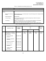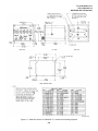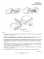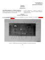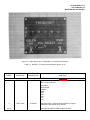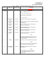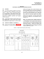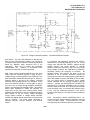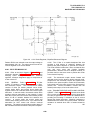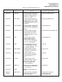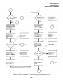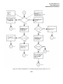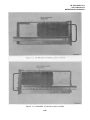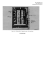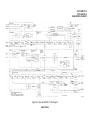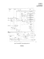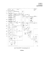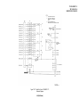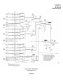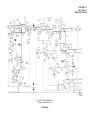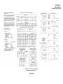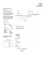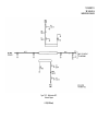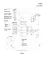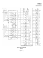
1
ARMY TM 11-5820-815-14
NAVY NAVELEX 0967-LP-544-5010
AIR FORCE TO 31R2-2GRC171-2
TECHNICAL MANUAL
SERVICE AND CIRCUIT DIAGRAMS
RADIO SET
AN/GRC-171
DEPARTMENTS OF THE ARMY, THE NAVY, AND THE AIR FORCE
1 MARCH 1975
TO 31R2-2GRC171-2
TM 11-5820-815-14
NAVELEX 0967-LP-544-5010
Technical orders are normally distributed promptly after printing. Date(s) shown on the title page (lower right) are for
identification only. This is not a distribution date. Processing time sometimes causes distribution to only appear to have
been delayed.
INSERT LATEST CHANGED PAGES. DESTROY SUPERSEDED PAGES.
LIST OF EFFECTIVE PAGES
NOTE. The portion of the text affected by the changes is
Indicated by a vertical line in the outer margins of
the page. Changes to illustrations are indicated
by miniature pointing hands Changes to wiring
diagrams are indicated by shaded areas.
Dates of issue for original and changed pages are’
TOTAL NUMBER OF PAGES IN THIS PUBLICATION IS 214 CONSISTING OF THE FOLLOWING:
Page
Change
No
No
Title ................................. 0
A ..................................... 0
i - ix ................................. 0
1-0 - 1-16 ...................... 00
2-1................................... 0
2-2 Blank......................... 0
2-3 - 2-9 .......................... 0
2-10 Blank....................... 0
2-11 - 2-12 ...................... 0
3-1 - 3-5 .......................... 0
3-6 Blank......................... 0
3-7 - 3-9 .......................... 0
3-10 Blank....................... 0
4-1 - 4-5 .......................... 0
4-6 Blank......................... 0
4-7 - 4-53 ........................ 0
4-54 Blank....................... 0
5-1 - 5-51 ........................ 0
5-52 Blank....................... 0
5-53................................. 0
5-54 Blank....................... 0
6-1 - 6-3 .......................... 0
6-4 Blank......................... 0
6-5................................... 0
6-6 Blank......................... 0
6-7................................... 0
6-8 Blank......................... 0
6-9................................... 0
6-10 Blank....................... 0
6-11................................. 0
6-12 Blank....................... 0
6-13................................. 0
6-14 Blank....................... 0
6-15................................. 0
6-16 Blank....................... 0
6-17................................. 0
6-18 Blank....................... 0
Page
Change
No
No
6-19 ................................ 0
6-20 Blank ...................... 0
6-21 ................................ 0
6-22 Blank ...................... 0
6-23 ................................ 0
6-24 Blank ...................... 0
6-25 ................................ 0
6-26 Blank ...................... 0
6-27 ................................ 0
6-28 Blank ...................... 0
6-29 ................................ 0
6-30 Blank ...................... 0
6-31 ................................ 0
6-32 ................................ 0
6-33 ................................ 0
6-34 Blank ...................... 0
6-35 ................................ 0
6-36 Blank ...................... 0
6-37 ................................ 0
6-38 Blank ...................... 0
6-39 ................................ 0
6-40 Blank ...................... 0
6-41 ................................ 0
6-42 Blank ...................... 0
6-43 ................................ 0
6-44 Blank ...................... 0
6-45 ................................ 0
0 46................................. 0
6-47 ................................ 0
6-48 Blank ...................... 0
6-49 ................................ 0
6-50 ................................ 0
6-51 ................................ 0
6-52 Blank ...................... 0
6-53 ................................ 0
6-54 Blank ...................... 0
6-55 ................................ 0
Page
Change
No
No
6-56 Blank ...................... 0
6-57 ................................ 0
6-58 Blank ...................... 0
6-59 ................................ 0
6-60 Blank ...................... 0
6-61 ................................ 0
6-62 Blank ...................... 0
6-63 ................................ 0
6-64 Blank ...................... 0
6-65 ................................ 0
6-66 Blank ...................... 0
6-67 ................................ 0
6-68 Blank ...................... 0
6-69 ................................ 0
6-70 Blank ...................... 0
6-71 ................................ 0
6-72 Blank ...................... 0
6-73 ................................ 0
6-74 Blank ...................... 0
6-75 ................................ 0
6-76 Blank ...................... 0
6-77 ................................ 0
6-78 Blank ...................... 0
6-79 ................................ 0
6-80 Blank ...................... 0
6-81 ................................ 0
6-82 Blank ...................... 0
6-83 ................................ 0
6-84 Blank ...................... 0
6-85 ................................ 0
6-86 Blank ...................... 0
6-87 ................................ 0
6-88 Blank ...................... 0
6-89 ................................ 0
6-90 Blank ...................... 0
6-91 ................................ 0
6-92 Blank ...................... 0
Page
Change
No
No
6-93 ...............................0
6-94 Blank .....................0
6-95 ...............................0
6-96 Blank .....................0
6-97 ...............................0
6-98 Blank .....................0
6-99 ...............................0
6-100 Blank ...................0
6-101 .............................0
6-102 Blank ...................0
6-103 .............................0
6-104 Blank ...................0
6-105 .............................0
6-106 Blank ...................0
6-107 .............................0
6-108 Blank ...................0
6-109 .............................0
6-110 Blank ...................0
6-111 .............................0
6-112 Blank ...................0
6-113 .............................0
6-114 Blank ...................0
6-115 .............................0
6-116 Blank ...................0
Index 1 - Index 5............0
Index 6 Blank.................0
Upon receipt of the second and subsequent changes to this technical order, personnel responsible for maintaining this
publication in current status %will ascertain that all previous changes have been received and incorporated. Action should
be taken promptly if the publication is incomplete.
* The asterisk indicates pages changed, added, or deleted by the current change.
ADDITIONAL COPIES OF THIS PUBLICATION MAY BE OBTAINED BY USAF ACTIVITIES
IN ACCORDANCE WITH T.O. OO-5-2.
A
USAF
TO 31R2-2GRC171-2
TM 11-5820-815-14
NAVELEX 0967-LP-544-5010
TABLE OF CONTENTS
Section
Page
CHAPTER 1. GENERAL INFORMATION
1-1
1-8
1-20
1-22
1-24
1-26
Description and Purpose .........................................................................
Description of Modules ............................................................................
Leading Particulars ..................................................................................
Capabilities and Limitations .....................................................................
Equipment Supplied.................................................................................
Equipment Required But Not Supplied ....................................................
1-1
1-1
1-3
1-3
1-3
1-3
CHAPTER 2. INSTALLATION
I.
II.
III.
IV.
INSTALLATION PLANNING
2-1
General ....................................................................................................
2-3
Mounting ..................................................................................................
2-6
Cabling.....................................................................................................
2-1
2-1
2-1
LOGISTICS
2-8
2-10
2-12
2-14
2-17
Receiving Data ........................................................................................
Material Handling.....................................................................................
Unpacking................................................................................................
Cable Requirements ................................................................................
Environmental Considerations.................................................................
2-3
2-3
2-3
2-3
2-4
INSTALLATION PROCEDURES
2-19
Mounting . ................................................................................................
2-24
Initial Setup Procedure ............................................................................
2-33
Initial Checkout Procedure.......................................................................
2-5
2-5
2-7
PREPARATION FOR RESHIPMENT
2-35
Preparation for Reshipment.....................................................................
2-11
CHAPTER 3. OPERATION
I.
CONTROLS AND INDICATORS .............................................................................................
3-1
II.
OPERATING INSTRUCTIONS
3-2
General ....................................................................................................
3-4
Local Operation .......................................................................................
3-8
Remote Operation ...................................................................................
3-7
3-7
3-8
EMERGENCY OPERATION
3-12
Emergency Operation..............................................................................
3-9
III.
i
TO 31R2-2GRC171-2
TM 11-5820-815-14
NAVELEX 0967-LP-544-5010
TABLE OF CONTENTS (Cont)
Section
Page
CHAPTER 4. PRINCIPLES OF OPERATION
I.
FUNCTIONAL SYSTEM OPERATION
4-3
4-5
4-11
4-22
4-29
II.
4-1
4-1
4-2
4-3
4-5
FUNCTIONAL OPERATION OF ELECTRONIC CIRCUITS
4-35
4-38
4-42
4-60
4-98
4-135
4-182
4-213
4-221
4-241
4-292
4-304
III.
General ....................................................................................................
Overall System Operation........................................................................
Transmitter Operation..............................................................................
Receiver Operation..................................................................................
Power Distribution....................................................................................
General ....................................................................................................
Radio Set Control C-7999/GRC-171 .......................................................
D/A Servo Amplifier Module Al ................................................................
Frequency Synthesizer Module A2..........................................................
Receiver RF Module A3...........................................................................
Audio Module A4......................................................................................
DC-DC Converter Module A5 ..................................................................
Voltage Regulator Module A6..................................................................
RF Filter Module A7.................................................................................
Power Amplifier Module A8 .....................................................................
Keyer Module A9 .....................................................................................
Chassis A10.............................................................................................
4-7
4-7
4-8
4-10
4-22
4-27
4-34
4-39
4-40
4-43
4-50
4-51
FUNCTIONAL OPERATION OF MECHANICAL ASSEMBLIES
4-310
4-312
General ....................................................................................................
RF Filter Tuning Drive Assembly .............................................................
4-53
4-53
CHAPTER 5. MAINTENANCE
I.
ORGANIZATIONAL/INTERMEDIATE MAINTENANCE
5-1
5-3
5-5
5-7
5-9
5-11
5-13
5-18
5-20
II.
General . ..................................................................................................
Maintenance Test Equipment ..................................................................
Test Points...............................................................................................
Performance Tests ..................................................................................
Voltage Requirements and Sources ........................................................
Alignment ................................................................................................
Adjustment...............................................................................................
Troubleshooting .......................................................................................
Removal/Replacement ............................................................................
SPECIAL MAINTENANCE (To Be Supplied)
ii
5-1
5-1
5-1
5-7
5-28
5-28
5-28
5-29
5-29
TO 31R2-2GRC171-2
TM 11-5820-815-14
NAVELEX 0967-LP-544-5010
TABLE OF CONTENTS (Cont)
Section
Page
CHAPTER 6. CIRCUIT DIAGRAMS
6-1
6-3
6-5
General ....................................................................................................
Effectivities...............................................................................................
Index of Diagrams ...................................................................................
6-1
6-1
6-1
ALPHABETICAL INDEX...........................................................................................................
Index-1
CROSS-REFERENCE INDEX .................................................................................................
vii
LIST OF ILLUSTRATIONS
Figure
Page
CHAPTER 1. GENERAL INFORMATION
1-1
1-2
Radio Set AN/GRC-171 . .........................................................................................................
Radio Receiver-Transmitter RT-980/GRC-171, Module Identification .....................................
1-0
1-2
CHAPTER 2. INSTALLATION
2-1
2-2
2-3
2-4
2-5
2-6
Radio Set Control C-7999/GRC-171, Outline and Mounting Diagram .....................................
Primary Power Strapping..........................................................................................................
Audio Module A4, Strapping Options Diagram.........................................................................
Keyer Module A9, Strapping Options Diagram ........................................................................
Noise Blanker (P/O Receiver RF Module A3). Strapping Options Diagram.............................
Module Packaging Instructions ................................................................................................
2-6
2-7
2-8
2-8
2-9
2-12
CHAPTER 3. OPERATION
3-1
3-2
Radio Receiver-Transmitter RT-980/GRC-171 Controls and Indicators ..................................
Radio Set Control C-7099/GRC-171 Controls and Indicators..................................................
3-1
3-2
CHAPTER 4. PRINCIPLES OF OPERATION
4-1
4-2
Phase-Locked Loop Frequency Synthesis by 2-Modulus Prescaling.......................................
Low-Band Decoder, Simplified Logic Diagram and Truth Table ..............................................
iii
4-12
4-14
TO 31R2-2GRC171-2
TM 11-5820-815-14
NAVELEX 0967-LP-544-5010
LIST OF ILLUSTRATIONS (Cont)
Figure
4-3
4-4
4-5
4-6
4-7
4-8
4-9
4-10
Page
High-Band Decoder, Simplified Logic Diagram and Truth Table .............................................
Voltage-Controlled Oscillator, Simplified Schematic Diagram .................................................
Frequency Synthesizer Transmit-Receive Switch,
Simplified Schematic Diagram .................................................................................................
Regenerative Divider, Simplified Schematic Diagram..............................................................
Squelch Circuit, Simplified Schematic Diagram .......................................................................
+12-V Series Regulator, Simplified Schematic Diagram..........................................................
Power Amplifier Modulator, Simplified Schematic Diagram .....................................................
RF Filter Tuning Drive Assembly, Mechanical Diagram...........................................................
4-15
4-16
4-17
4-19
4-33
4-40
4-47
4-53
CHAPTER 5. MAINTENANCE
5-1
5-2
5-3
5-4
5-5
5-6
5-7
5-8
5-9
5-10
5-11
5-12
5-13
Radio Receiver-Transmitter RT-980/GRC-171, Test Point Location .......................................
Test Setup for Receiver Sensitivity,
AGC Squelch and Compressor Performance,
Narrow- and Wide-Band Receiver Response,
and Receiver Audio Distortion..................................................................................................
Test Setup for IF Measurement ...............................................................................................
Test Setup for Image Response ..............................................................................................
Test Setup for Noise Blanker Test ...........................................................................................
Test Setup for RF Power Output, Frequency Tolerance, and Modulation ...............................
Test Setup for Transmitter Sidetone and Modulation Distortion ..............................................
Test Setup for Radio Set Control C-7999/GRC-171 ................................................................
Radio Set AN/GRC-171 Troubleshooting Procedures . ...........................................................
RT-980/GRC-171 Module Location, Top View.........................................................................
RT-980/GRC-171 Module Location, Left Side .........................................................................
RT-980/GRC-171 Module Location, Right Side .......................................................................
RT-980/GRC-171 Module Location, Top View Partial..............................................................
CHAPTER 6. CIRCUIT DIAGRAMS
FO-1
FO-2
FO-3
FO-4
FO-5
FO-6
FO-7
FO-8
FO-9
FO-10
FO-11
FO-12
FO-13
FO-14
FO-15
FO-16
FO-17
Radio Receiver-Transmitter RT-980/GRC-171, Outline and Mounting Dimensions
Diagram............................................................................................................................... 6-3
Radio Set AN/GRC-171, Installation Wiring Diagram ......................................................... 6-7
Radio Set AN/GRC-171, Block Diagram ............................................................................. 6-9
D/A Servo Amplifier Module Al, Block Diagram ................................................................ 6-11
Frequency Synthesizer Module A2, Block Diagram.......................................................... 6-13
Receiver RF Module A3, Block Diagram........................................................................... 6-15
Audio Module A4, Block Diagram...................................................................................... 6-17
DC-DC Converter Module A5, Block Diagram .................................................................. 6-19
RF Filter Module A7, Block Diagram ................................................................................. 6-21
Power Amplifier Module AS, Block Diagram ..................................................................... 6-23
Frequency Synthesizer Variable Divider, Simplified Schematic and Timing Diagram ...... 6-25
Frequency Synthesizer Frequency/Phase Detector, Limiter Amplifier, and
Lock Monitor, Simplified Schematic and Timing Diagram................................................. 6-31
Regulating DC-DC Converter, Functional Diagram........................................................... 6-33
Radio Set AN/GRC-171, Power Distribution Diagram....................................................... 6-35
Radio Set AN/GRC-171, Receive Signal Diagram............................................................ 6-37
Radio Set AN/GRC-171, Transmit Signal Diagram .......................................................... 6-41
Radio Set Control C-7999/GRC-171, Schematic Diagram ............................................... 6-45
iv
5-6
5-25
5-25
5-26
5-26
5-27
5-27
5-28
5-30
5-47
5-49
5-49
5-51
TO 31R2-2GRC171-2
TM 11-5820-815-14
NAVELEX 0967-LP-544-5010
LIST OF ILLUSTRATIONS (Cont)
Figure
FO-18
FO-19
FO-20
FO-21
FO-22
FO-23
FO-24
FO-25
FO-26
FO-27
FO-28
FO-29
FO-30
FO-31
FO-32
FO-33
FO-34
Page
D/A Servo Amplifier Module Al, Schematic Diagram ...............................................................
Frequency Synthesizer Module A2, Schematic Diagram.........................................................
Receiver RF Module A3, Schematic Diagram..........................................................................
Audio Module A4, Schematic Diagram.....................................................................................
DC-DC Converter Module A5, Schematic Diagram .................................................................
Voltage Regulator Module A6, Schematic Diagram .................................................................
RF Filter Module A7, Schematic Diagram ................................................................................
Power Amplifier Module A8, Schematic Diagram ....................................................................
ALC/Modulator A8A1, Schematic Diagram ..............................................................................
RF Preamplifier/Modulator A8A2, Schematic Diagram ............................................................
RF Predriver/ALC Attenuator A8A3, Schematic Diagram ........................................................
RF Driver A8A4, Schematic Diagram.......................................................................................
RF Amplifier A8A5/A6, Schematic Diagram .............................................................................
Reflectometer ABA7, Schematic Diagram ...............................................................................
Keyer Module A9, Schematic Diagram ....................................................................................
Chassis A10, Schematic Diagram............................................................................................
Audio Test Fixture, Schematic Diagram...................................................................................
6-47
6-53
6-61
6-67
6-73
6-79
6-83
6-87
6-89
6-93
6-95
6-97
6-99
6-101
6-103
6-105
6-115
LIST OF TABLES
Table
Page
CHAPTER 1. GENERAL INFORMATION
1-1
1-2
1-3
1-4
Leading Particulars...................................................................................................................
Capabilities and Limitations......................................................................................................
Equipment Supplied ................................................................................................................ .
Equipment Required But Not Supplied.....................................................................................
1-3
1-4
1-9
1-11
CHAPTER 2. INSTALLATION
2-1
Receiving Data .........................................................................................................................
2-3
CHAPTER 3. OPERATION
3-1
AN/GRC-171 Controls and Indicators ......................................................................................
3-2
CHAPTER 4. PRINCIPLES OF OPERATION
4-1
4-2
Radio Control Frequency Select Coding ..................................................................................
VCO and Radio Control Frequency Versus VCO Band ...........................................................
V
4-7
4-13
TO 31R2-2GRC171-2
TM 11-5820-815-14
NAVELEX 0967-LP-544-5010
LIST OF TABLES (Cont)
Table
Page
CHAPTER 5. MAINTENANCE
5-1
5-2
5-3
5-4
Test Equipment Required......................................................................................................
Test Points ............................................................................................................................
Radio Receiver-Transmitter RT-980/GRC-171 Performance Tests .....................................
Radio Set Control C-7999/GRC-171 Performance Test .......................................................
vi
5-1
5-3
5-7
5-24
TO 31R2-2GRC171-2
TM 11-5820-815-14
NAVELEX 0967-LP-544-5010
CROSS-REFERENCE INDEX
(Prefix each Reference Number with the Chapter Number denoted by the Column.)
(KEY: Numbers preceded by "f" are illustrations; "t" are tables; others are paragraphs.)
OFFICIAL
NOMENCLATURE
Common Name
Chapter 1
General
Information
Chapter 2
Installation
AUDIO
MODULE
A4
12
27, f3
CHASSIS
A10
18
26, f2
D/A SERVO
AMPLIFIER
MODULE A1
9
DC-DC
CONVERTER
MODULE A5
13
FREQUENCY
SYNTHESIZER
MODULE A2
10
KEYER
MODULE A9
17
Chapter 3
Operation
Chapter 4
Principles
of Operation
12, 13, 14
20, 25, 27
135 thru
181, f7,
fFO-7,
fFO-21
10, 27, 30,
31, 34,
fFO-33
1, 9, 41,
42, 43, 44,
45, 46, 47,
48, 49, 50,
51, 52, 53,
54, 55, 56,
57, 58, 59,
fFO-4,
fFO-18
32, 33, 34
182 thru
212,
fFO-8,
fFO-13,
fFO-22
15, 16, 41
60, 61
thru 97,
t2, fl, f2.
f3, f4, f5.,
f6, fFO-5.
fFO-11,
fFO-12,
fFO-19
14, 28, 292,
293, 294,
295, 296,
297, 298,
299, 300,
301, 302,
303,
fFO-32
29, f4
vii
Chapter 5
Org/Itmd
28, t3, f8
46, t3, f8
19, t3, f8
31, t3, f8,
f9
22, t3, f8
43, t3,
f11
Adjustment
14, 15, 16,
17
TO 31R2-2GRC171-2
TM 11-5820-815-14
NAVELEX 0967-LP-544-5010
OFFICIAL
NOMENCLATURE
Common Name
Chapter 1
General
Information
CROSS-REFERENCE INDEX (Cont)
Chapter 4
Chapter 2
Chapter 3
Principles
Installation
Operation
of Operation
POWER
AMPLIFIER
MODULE A8
16
RADIO
RECEIVERTRANSMITTER
RT-980/GRC171
ReceiverTransmitter
RADIO SET
CONTROL
C-7999/
GRC-171
Radio Control
RECEIVER
RF
MODULE A3
fl, f2
4, 20, t1
IFO-1,
fFO-2
1, 6, t1,
f1
f1
5,. 22, t1
fl, fFO-2
8, t1, f2
11
31, f5
RF
FILTER
MODULE A7
VOLTAGE
REGULATOR
MODULE A6
15
14
viii
12, 15, 16,
18, 21, 241
thru 291,
f9,
fFO-10,
fFO-25,
fFO-26
thru
fFO-31
6, 7, 20,
36,
fFO-3,
fFO-15,
fFO-15,
fFO-16
Chapter 5
Org/Itmd
40, t3, f8
8, t3, f1,
f8
6, 20, 27,
38, 39, 40,
41,
fFO-17
8, t4
7, 23, 24,
25, 98
thru
134.
fFO-6,
fFO-20
16, 23, 24,
26, 221
thru 240
32, 213
thru 220,
f8,
fFO-23
25, t3, f8
37, t3, f8
34, t3, f8,
f10
Adjustment
TO 31R2-2GRC171-2
TM 11-5820-815-14
NAVELEX 0967-LP-544-5010
INTRODUCTION
This technical manual provides information for servicing
Radio Set AN/GRC-171, Collins part number 622-1627001, manufactured by Collins Radio Group/ Rockwell
International, Cedar Rapids, Iowa. Radio Set AN/GRC171 consists of the following: Radio Receiver-Transmitter
RT-980/GRC-171, Collins part number 622-1628-001;
Radio Set Control C-7999/ GRC-171, Collins part
number 622-1629-001; cable interface kit, Collins part
number 622-7846-001; and slide mounting hardware kit,
Collins part number 623-5818-001. Radio Set AN/GRC171 provides air traffic control communications at
collocated vhf/uhf receiver-transmitter sites. The
equipment is capable of providing AM communications
on any of the 7,000 channels in the 225to 399.975-MHz
band with 20watt AM carrier output.
ASA-STDY32-16-1965
Electrical and Electronic Reference
Designations
MILITARY SPECIFICATIONS
MIL-M-38730
Technical
Manuals,
General
Requirements for Preparation of
MIL-M-4410
Technical Manuals: Title Pages, List of
Effective Pages, and Reproduction
Assembly Sheet; Photolith Negatives;
Printing; and Binders
MIL-T-9941
Technical Manuals: Ground C-E
Equipment Facility, Site, and System
TECHNICAL ORDERS
Chapter 1 provides an overall electrical and mechanical
description of the equipment.
31-1-141
Chapter 2 provides information on installation, of the
equipment.
Basic Electronics
Testing Practices
Technology
and
EFFECTIVITY
Each equipment, unit, and assembly provided is marked
with a manufacturing alphabetic identifier in addition to
the basic part number. The alphabetic identifier will be
preceded by the letters REV(revision) and will start with 0
if no changes have been processed. The first change will
be identified as A, the second as B, and continuing
through Z to AA and ultimately to ZZ. Because minor
electrical and/or mechanical differences exist between
various revisions, where applicable, an effectivity-versusrevision identifier cross-reference is provided on the
schematic diagram.
Chapter 3 provides operating instructions.
Chapter 4 describes the basic operating principles of the
equipment.
Chapter 5 provides maintenance instructions, including
performance tests and adjustment procedures.
Chapter 6 provides information on the use of circuit
diagrams and equipment effectivity. All foldout diagrams
appear in chapter 6 of this manual regardless of their
applicability to any one chapter.
Each effectivity applies to a group of revision identifiers
and is indicated by a key (Ï) on both the effectivity table
and
the
appropriate
schematic
diagram.
A complete illustrated parts breakdown of the equipment
is provided in TO 31R2-2GRC171-4.
The following publications were used in the preparation
of this manual.
MILITARY STANDARDS
MIL-STD-12B
Abbreviations for Use on Drawings
and in Technical-Type manuals
VIIL-STD-15-1A Graphic Symbols for Electrical and
Electronic Diagrams
ix
TO 31R2-2GRC171-2
TM 11-5820-815-14
NAVELEX 0967-LP-544-5010
Figure 1-1. Radio Set AN/GRC-171 1-0
1-0
TO 31R2-2GRC171-2
TM 11-5820-815-14
NAVELEX 0967-LP-544-5010
CHAPTER 1
GENERAL INFORMATION
information from the radio control into servo motor drive
to position the rf filter in the rf filter module.
1-1. DESCRIPTION AND PURPOSE.
1-2. PURPOSE. Radio Set AN/GRC-171, shown in figure
1-1, is a uhf receiver-transmitter for air traffic control
communications at collocated vhf/uhf receivertransmitter sites. The equipment provides AM and wideband data communications on any 1 of 7000 channels
(25-kHz channel spacing) in the 225to 399.975-MHz
band. The equipment is completely solid state providing
20-watt AM carrier output.
1-10. FREQUENCY SYNTHESIZER MODULE A2. The
frequency synthesizer module contains a phaselocked
loop (p11) and transmit/receive transfer switch that
converts frequency select information from the radio
control into transmit rf that is transferred to the power
amplifier module or receive injection that is transferred to
the receiver rf module.
1-11. RECEIVER RF MODULE A3. The receiver rf
module contains a double conversion uhf receiver that
converts receive rf from the rf filter module into receive
audio (or data) to the audio module. The receiver rf
module includes a noise channel to blank receive audio
of impulse type noise.
1-3. DESCRIPTION. Radio Set AN/GRC-171 (radio set)
consists of Radio Receiver-Transmitter RT980/GRC-171
(receiver-transmitter), Radio Set Control C-7999/GRC171 (radio control), a cable interface kit, and a slide
mounting hardware kit.
1-4. The RT-980/GRC-171 consists of nine plug-in
modules (shown in figure 1-2) contained within a
chassis. The modules are attached to the chassis by
captive screws or by a module retaining bracket. All
electrical connections to the RT-980/GRC-171 are made
through four connectors mounted on the rear panel of
the chassis. Front panel test meter and test points are
provided for maintenance and troubleshooting. The unit
mounts in a standard 482.6-mm (19-in) rack cabinet and
is cooled by convection. The RT-980/GRC-171 can be
operated locally with front panel controls or remotely at
distances up to 45.7 m (150 ft) with Radio Set Control
C-7999/GRC-171.
1-12. AUDIO MODULE A4. The audio module contains a
receive audio circuit with squelch, a transmit audio
circuit, and a transmitter keying circuit. The audio circuit
amplifies and shapes the frequency response of receive
audio (or data) from the receiver rf module and applies
the audio (or data) to the headset and main audio output
(or data output) of the receiver-transmitter. The transmit
audio circuit amplifies and shapes the frequency
response of input audio (or data) and applies transmit
audio (or data) to the modulator of the power amplifier
module. The transmit keying circuit converts remote
push-to-talk keying into transmit key lines.
1-13. DC-DC CONVERTER MODULE A5. The dc-dc
converter module contains a regulating dc-dc converter
and a nonregulating dc-dc converter. The regulating dcdc converter converts unregulated dc from the
transformer/rectifier circuit on the chassis into regulated
+26 V dc. The nonregulating dc-dc converter converts
+26 V dc into unregulated voltages to the voltage
regulator module.
1-5. The cable interface kit contains a 1.83-m (6-ft) 120V ac power cord and all multiple pin mating connectors
for the RT-980/GRC-171 and C-7999/ GRC-171. All
interconnecting wiring except the 120-V ac power cord is
supplied by the user.
1-6. The slide mounting hardware kit contains the
cabinet slides, brackets, and hardware required to mount
the RT-80/GRC-171 in a standard 482.6-mm (19-in) rack
cabinet. Slide rails are attached to the RT-980/GRC-171
at the factory.
1-14. VOLTAGE REGULATOR MODULE A6. The
voltage regulator module converts unregulated voltages
to power circuits of the receiver-transmitter and radio
control.
1-7. Radio Set Control C-7999/GRC-171 contains
controls for remote frequency select, power on-off,
squelch on-off, and receive audio level control.
1-15. RF FILTER MODULE A7. The rf filter module
contains a transmit/receive switch, tunable rf filter, and
directional coupler that transfers and filters transmit rf
from the power amplifier module to the antenna or
receive rf from the antenna to the receiver rf module.
1-8. DESCRIPTION OF MODULES.
1-9. D/A SERVO AMPLIFIER MODULE Al. The d/a
servo amplifier contains a digital-to-analog converter and
servo amplifier that converts frequency select
1-1
TO 31R2-2GRC171-2
TM 11-5820-815-14
NAVELEX 0967-LP-544-5010
Figure 1-2. Radio Receiver-Transmitter RT-980/GRC-171, Module Identification
1-2
TO 31R2-2GRC171-2
TM 11-5820-815-14
NAVELEX 0967-LP-544-5010
1-16. POWER AMPLIFIER MODULE A8. The power
amplifier module contains a modulator circuit and rf
driver and power amplifier circuits with automatic load
control. The power amplifier amplitude modulates
transmit rf from the synthesizer module with transmit
audio from the audio module to provide transmit rf to the
rf filter module.
squelch, modulation, and headset volume along with
jacks for a headset and microphone. In addition, the
chassis front panel contains a local-remote switch and all
the controls necessary for local frequency select,
transmitter keying, and squelch on-off.
1-17. KEYER MODULE A9. The keyer module contains
a keyer circuit that converts remote voltage, current, or
audio loop keying into remote keying to the transmit
keying circuit of the audio module. In addition, the keyer
module contains a squelch operated relay circuit.
1-21. Table 1-1 lists the leading particulars of Radio Set
AN/GRC-171.
1-20. LEADING PARTICULARS.
1-22. CAPABILITIES AND LIMITATIONS.
1-23. Table 1-2 lists the capabilities and limitations of
Radio Set AN/GRC-171.
1-18. CHASSIS AND FRONT PANEL A10. The chassis
contains all connectors, wires, and coaxial cables
necessary to interconnect the nine modules of the
receiver-transmitter. In addition, the chassis contains an
emi filter that filters all wires that enter or leave the
receiver-transmitter. The chassis contains power supply
components that convert input ac power into unregulated
dc voltage to the dc-dc converter module.
1-24. EQUIPMENT SUPPLIED.
1-25. Table 1-3 provides a list of equipment supplied,
together with dimensions and weight.
1-26. EQUIPMENT REQUIRED BUT NOT SUPPLIED.
1-19. The chassis front panel contains the power on-off
switch, power supply fuses, a meter circuit and test
points, level controls for receive audio, sidetone,
1-27. Table 1-4 lists the test equipment required to
maintain Radio Set AN/GRC-171. Equivalent test
equipment may be used. Refer to table 5-1 for test
equipment test characteristics.
Table 1-1. Leading Particulars (Sheet 1 of 2)
ITEM
Power source
Primary power
DESCRIPTION
95 to 132 V ac; 189 to 264 V ac; 47 to 63 Hz; 380 to 420 Hz; single-phase.
NOTE
Primary power strapping is provided for ac line voltages of 105, 120, 210,
and 240 V ac +10%. The AN/GRC-171 is shipped strapped for 120 V ac.
Emergency power
24-V dc battery.
NOTE
A 24-V dc battery bus may be floated across the dc input to the RT980/GRC-171 to provide emergency power in the event of an ac power failure.
The switch over to battery power is automatic.
Alternate power
22 to 30 V dc.
NOTE
In place of ac power, the AN/GRC-171 may be operated from a dc power
source of 22 to 30 V dc. The AN/GRC-171 is capable of rated performance while
being operated on dc power.
1-3
TO 31R2-2GRC171-2
TM 11-5820-815-14
NAVELEX 0967-LP-544-5010
Table 1-1. Leading Particulars (Sheet 2 of 2)
ITEM
Power input
Ambient temperature
Operating
Nonoperating/storage
Altitude
Relative humidity
Weight
RT-980/GRC-171
C-7999/GRC-171
Overall dimensions
RT-980/GRC-171
(including slide
rails)
C-7999/GRC-171
Mounting
RT-980/GRC-171
C-7999/GRC-171
Ventilation
Cabling requirements
CHARACTERISTIC
Frequency range
Number of channels
DESCRIPTION
450 watts transmit, 150 watts receive.
-29 °C (-20 °F) to 60 °C (140 'F).
-62 °C (-80 'F) to 71 °C (160 °F).
-0 to 3048 m (10,000 ft) ms1.
5 to 95%.
33.8 kg (74.5 lb).
0.31 kg (0.69 lb).
222.3 mm (8.75 in) high, 482.6 mm (19 in) wide, and 533.4 mm (21 in)
deep.
66.7 mm (2.62 in) high, 82.6 mm (3.25 in) wide, and 114.3 mm (4.5 in)
deep.
Standard 482.6-mm (19-in) rack with slide mounting.
Panel mounting.
Convection cooling.
Maximum cable length between RT-980/GRC-171 and C-7999/GRC-171
is 45.7 m (150 ft) when interconnect cabling consists of unshielded #22
AWG wire. Cable length can be extended from 45.7 m (150 ft) to a
maximum of 305 m (1000 ft) if the requirements of figure FO-2, chapter 6,
are met.
Table 1-2. Capabilities and Limitations (Sheet 1 of 6)
SPECIFICATION
GENERAL
225.000 to 399.975 MHz.
7000.
1-4
TO 31R2-2GRC171-2
TM 11-5820-815-14
NAVELEX 0967-LP-544-5010
CHARACTERISTIC
Channel spacing
Table 1-2. Capabilities and Limitations (Sheet 2 of 6)
SPECIFICATION
GENERAL (Cont)
25 kHz.
NOTE
Frequency stability
Frequency accuracy
Tuning time 10
Warm-up time
Duty cycle
Transmitter
Receiver
Antenna input
Sensitivity
Selectivity
The radio set is capable of tuning to 1 of 7000 frequency channels spaced at 25kHz intervals. However, the receiver selectivity is determined by the crystal filter
(A4FL1) installed in the 10.7-MHz if circuit of receiver rf module A3. The bandwidth
of the filter supplied with the radio set is 36 kHz (6-dB resonant response). This
makes the radio set compatible with 50-kHz channel spacing. To make the radio
set compatible with 25-kHz channel spacing, the filter must be replaced with a 20kHz bandwidth filter. To allow reception of wide bandwidth data, the filter must be
replaced with a 60-kHz bandwidth filter (100-kHz channel spacing).
0.0005% both transmit and receive.
±0.0005% both transmit and receive.
seconds maximum after selection of last digit.
2 minutes.
90% with 9 minutes (90%, 1-kHz modulation) transmit and 1 minute receive.
Continuous.
50-ohm, N-type connector.
RECEIVER
3 microvolts (30% modulation, 1000 Hz) applied at the antenna will produce an
audio output of 100 milliwatts into 600 ohms with a 10-dB (minimum) signal-plusnoise to noise ratio.
Receiver selectivity is determined by the crystal filter (A4FL1) installed in the 10.7MHz if amplifier. Refer to note in general specifications of this table.
RESONANT RESPONSE
(dB)
Narrow bandwidth
36-kHz filter
(50-kHz channel
spacing)
6
20
40
60
80
1-5
TOTAL BANDWIDTH
(kHz)
36
54
62
70
80
TO 31R2-2GRC171-2
TM 11-5820-815-14
NAVELEX 0967-LP-544-5010
Table 1-2. Capabilities and Limitations (Sheet 3 of 6)
CHARACTERISTIC
SPECIFICATION
RECEIVER (Cont)
RESONANT RESPONSE
TOTAL BANDWIDTH
(dB)
(kHz)
Narrow bandwidth
20-kHz filter
(25-kHz channel
spacing)
6
20
40
60
80
20
28
30
32
40
Wide bandwidth
60-kHz filter
(100-kHz channel
spacing)
6
60
80
60
104
120
Audio outputs
Narrow bandwidth audio
Two transformer output circuits simultaneously deliver the following power output
levels when receiving a 3-microvolt, 30% modulated (1000-Hz tone) signal.
Main audio: At least 100 milliwatts into a 600-ohm external resistive load;
adjustable by a recessed (screwdriver adjustable) control located on the front panel
of the RT-980/GRC-171.
Headset audio: At least 100 milliwatts into a 600-ohm external resistive load;
controllable by a volume control located on the front panel of the RT-980/GRC-171.
Wide bandwidth audio
Audio bandpass
Main/headset audio
Secure/data audio
Audio distortion
Audio level control
Secure/data audio: At least 0.5 volt across a 10,000-ohm resistive load when
receiving a 3-microvolt, 30% modulated (1000-Hz tone) signal.
SIGNAL
(Hz)
REFERENCE LEVEL CHANGE
(dB)
100
300
1,000 (ref)
3,000
10,000
-10
+1, -2
0
+1, -2
-10
16
1,000 (ref)
25,000
+1, -3
0
+1, -3
10% or less when receiving a 1-volt input signal modulated 30% (300, 1500, and
3000 Hz) and with the audio level adjusted to an output of 100 milliwatts into 600ohm load. 15% or less for the same rf input modulated at 90%.
3-dB or less increase in audio output level (100-milliwatt output reference for 30%
modulation) as modulation increases from 30 to 907% (10-microvolt rf input).
1-6
TO 31R2-2GRC171-2
TM 11-5820-815-14
NAVELEX 0967-LP-544-5010
Table 1-2. Capabilities and Limitations (Sheet 4 of 6)
CHARACTERISTIC
SPECIFICATION
RECEIVER (Cont)
Audio level regulation
Automatic gain control (AGC)
AGC time constant
Squelch
Carrier-operated relay
Noise blanker
4-dB or less decrease in audio output voltage level (100-milliwatt
output reference for 600-ohm load resistor) for a 5-to-1 reduction
(120 ohms) in load resistor.
3-dB or less change in audio output level (100-milliwatt output
reference for 6-microvolt input signal, modulated 30%) as the input
signal increases from 6 microvolts to 1 volt.
100-millisecond attack time, 500-millisecond release time.
A carrier-operated noise silencer mutes the receiver output pending
application of carrier inputs not greater than 3 microvolts with squelch
sensitivity at maximum setting and not less than 50 microvolts with
squelch sensitivity at minimum setting.
A spdt relay operates in synchronism with the squelch circuit for use
with external devices.
A noise blanker circuit reduces the presence of impulse noise at the
receiver audio output when rf pulses with the following characteristics
are introduced into the receiver input.
PULSE
WIDTH
PULSE
REPETITION FREQUENCY
PULSE
SHAPE
10 ±2 µs
360 ±60 prf
Rise and decay time
less than 1 µs
2 ±1 µs
900 ±600 prf
Rise and decay time
less than 0.1 µs
NOTE
Noise blanker can be disabled by a noise blanker strapping option
on receiver rf module A3, or by grounding the external noise
blanker disable line of rear panel connector J22 pin j, or by
installing the wide bandwidth filter (A4FL1) which has a special
noise blanker disable pin.
Hum and noise
Not less than 50 dB below the rated audio output level of 100 milliwatts.
TRANSMITTER
Power output
20 watts into a 50-ohm resistive load throughout the frequency range
225 to 399.975 MHz.
NOTE
The transmitter power output will automatically reduce to approxi
mately 4 watts if the pa heat-sink temperature exceeds 100 °C, or
if the antenna vswr exceeds 3.1, or if the rf filter insertion loss
increases above approximately 2 dB.
1-7
TO 31R2-2GRC171-2
TM 11-5820-815-14
NAVELEX 0967-LP-544-5010
Table 1-2. Capabilities and Limitations (Sheet 5 of 6)
CHARACTERISTIC
SPECIFICATION
TRANSMITTER (Cont)
Output impedance
50 ohms.
Output vswr
1.3:1 or less normal; 3:1 maximum.
Automatic load control (ALC)
ALC maintains the carrier power level between -1 and +1 dB of the rated power
output level at all operating frequencies under normal operating conditions when
operating into load vswr of 3:1 or less.
Modulation
Amplitude modulation to the level of 90% from the following modulation inputs.
Modulation inputs
Main audio:. -15 to +10 dB mW (-35 to -15 dB mW optional), 600/150 ohms,
balanced, ungrounded.
Secure/data audio:
0 dB mW, 600 ohms, unbalanced, grounded.
Microphone:
Dynamic and carbon microphone, low impedance.
Modulation limiting and compression
Automatically limited to 90% maximum and maintained at 80 to 90% for above
modulation inputs; will not overmodulate for inputs above +10 dB mW.
Modulation response
SIGNAL
(Hz)
REFERENCE LEVEL CHANGE
(dB)
Main audio
100
300
1,000 (ref)
6,000
10,000
-10 or greater
+1, -2
0
+1, -2
-10 or greater
Secure/data audio
16
1,000 (ref)
25,000
+1, -3
0
+1, -3
Modulation distortion
10% or less under conditions of 0-dB mW compression; 15% or less under
conditions of maximum compression and limiting.
Sidetone
Detected rf applied to receiver main/headset audio circuits provides at least 100
milliwatts across 600 ohms when transmitter is modulated 90% with a 1000-Hz
tone; level adjustable by a recessed (screwdriver adjustable) control located on
the front panel of the RT-980/GRC-171.
Carrier hum and noise
Not less than 50 dB below a 1000-Hz test tone with transmitter operating at 20watt carrier power, 90% modulated.
Harmonic and spurious output
At least 80 dB below level of carrier fundamental.
1-8
TO 31R2-2GRC171-2
TM 11-5820-815-14
NAVELEX 0967-LP-544-5010
Table 1-2. Capabilities and Limitations (Sheet 6 of 6)
CHARACTERISTIC
SPECIFICATION
TRANSMITTER (Cont)
Keying
Main audio center tap
keying
Ground (optional 6, 26, or 48 volts) keying. For ground keying, key line keying provides
22-volt keying potential.
Remote ptt keying
Ground keying.
Local ptt keying
Ground keying through carbon or dynamic microphone ptt switch or front panel
PTT/CARRIER TEST switch.
Loop keying
Voltage: 6 volts (optional 26, 48, or 100 volts) with loop impedance of 47 kilohms.
Current: 20 or 60 milliamperes with loop impedance of 150 ohms.
Audio: 0.245 V rms audio tone, 300 to 3000 Hz, 600 ohms (optional VOX keying).
Table 1-3. Equipment Supplied (Sheet 1 of 3)
QTY
1
NOMENCLATURE
Radio Receiver-Transmitter,
RT-980/GRC-171 consisting
of the following:
D/a servo amplifier
module A1
621-6607-001
1
Frequency synthesizer
module A2
621-7956-001
1
Receiver rf module A3
621-7957-001
1
Audio module A4
621-6606-003
1
Dc-dc converter
module A5
621-7959-001
1
Voltage regulator
module A6
621-7958-001
Rf filter module A7
WEIGHT
kg
(lb)
LENGTH
WIDTH
HEIGHT
487.7
(19.20)
482.6
(19.00)
221.5
(8.72)
622-1628-001
1
1
DIMENSIONS
mm
(in)
COLLINS
PART
NUMBER
621-7960-001
1-9
33.8
(74.5)
QTY
TM 11-5820-815-14 TO 31R2-2GRC171-2
NAVELEX 0967-LP-544-5010
Table 1-3. Equipment Supplied (Sheet 2 of 3)
DIMENSIONS
COLLINS
mm
NOMENCLATURE
PART
(in)
WEIGHT
NUMBER
kg
LENGTH
WIDTH
HEIGHT
(lb)
1
Power amplifier
module A8
621-7955-001
1
Keyer module A9
621-7961-001
1
Receiver-transmitter
chassis A10
621-7975-001
1
Coaxial jumper (part of
receiver-transmitter
chassis A10)
357-8992-010
1
Radio Set Control
C-7999/GRC-171
622-1629-001
114.3
(4.50)
82.6
(3.25)
66.7
(2.62)
0.31
(0.69)
1
Cable interface kit consisting
of the following:
621-7846-001
355.6
(14)
355.6
(14)
50.8
(2)
0.74
(1.63)
711.2
(28)
177.8
(7)
101.5
(4)
3.4
(7.5)
2
Lockscrew assembly
371-0040-000
1
Hood
371-0187-000
1
Remote control cable
connector
371-0358-240
1
Remote control cable
connector
371-6271-000
1
Audio connector
361-6523-000
1
Electrical power
cable
623-5949-001
1
Slide mounting hardware kit
consisting of the following:
623-5818-001
1
Left cabinet slide
015-3622-010
1
Right cabinet slide
015-3622-020
4
Flat washer
310-0048-000
10
Flat washer
310-0050-000
8
Lockwasher
310-0072-000
10
Lockwasher
310-0286-000
2
Lockwasher
310-0288-000
1-10
TO 31R2-2GRC171-2
TM 11-5820-815-14
NAVELEX 0967-LP-544-5010
Table 1-3. Equipment Supplied (Sheet 3 of 3)
QTY
NOMENCLATURE
DIMENSIONS
mm
(in)
COLLINS
PART
NUMBER
LENGTH
8
Nut
313-0017-000
2
Nut
313-0082-000
8
Screw
342-1350-350
10
Screw
343-1540-000
2
Guide
623-5735-001
1
Front left slide bracket
623-5813-001
1
Front right slide bracket
623-5813-002
1
Rear left slide bracket
623-5814-001
1
Rear right slide bracket
623-5814-002
WIDTH
WEIGHT
kg
(lb)
HEIGHT
Table 1-4. Equipment Required But Not Supplied (Sheet 1 of 6)
OFFICIAL
NOMEN
AN/USM-323
COMMON
NAME
Rf generator/
frequency
counter
PART NO OR
MFR MODEL NO
HP 8640B
PURPOSE AND DESCRIPTION
Provides rf input signal for testing. Dc to 500 MHz, checks
frequency during operational
checks. Quantity two required.
MAINT
LEVEL,
O, I, D
Provides rf signal for noise
blanking test and modulation percentage.
Rf voltmeter
Boonton 91DA
Provides millivolt measurement in the rf range.
O, I, D
Audio oscillator
HP 200CD
Provides audio input for
testing.
O, I, D
Distortion analyzer
HP 333A
Measures audio output level and
O, I, D
percent output distortion for
testing.
Wattmeter
Bird 43
Measures rf forward power
output and reflected power.
1-11
O, I, D
TO 31R2-2GRC171-2
TM 11-5820-815-14
NAVELEX 0967-LP-544-5010
Table 1-4. Equipment Required But Not Supplied (Sheet 2 of 6)
COMMON
PART NO OR
MAINT
NAME
MFR MODEL NO
PURPOSE AND DESCRIPTION
LEVEL
OFFICIAL
NOMEN
Plug-in element
Bird 50D
With wattmeter,
forward
power
reflected power.
measures rf
output
and
Variable attenuator
General Radio
874-GAL
Provides sample of rf output.
O, I, D
Rf load
Bird 8130
50 ohms nonreactive, 30 watts;
used for testing.
O, I, D
Decade resistance box
General Radio1432N
0 to 200 ohms in 1-ohm steps;
provides test select resistor for
testing
D
Vom
Simpson 260
Continuity, general voltage and
resistance checks.
O. I, D
Attenuator
Measurements
Corp 80 ZH3
testing.
Provides a constant impedance
to the rf generator during
O, I, D
Pulse generator
Data Pulse 101
Provides pulse modulation for
rf signal generator for noise
blanking test.
I, D
Power divider
Weinschel 1506N
Provides method of combining
two rf signals for noise
blanking test.
I, D
Power supply
HP 6268B
Provides primary power for dc-dc
converter module testing.
D
O, I, D
MIL-0-9960C
Oscilloscope
Provides display of modulation
envelope and waveforms for
fault isolation.
O, I, D
H-169U
Handset
Provides method to operate the
RT-980/GRC-171 in the local
mode.
O, I, D
Digital multimeter
Fluke 8000A-01
Provides voltage measurements
for testing.
O, I, D
Double balanced
mixer
HP 10514A
Provides test signal to oscilloscope for percent modulation
check.
O, I, D
Cable assemblies
kit
CPN 622-1802-001
Provides five extender cables
and five coaxial cables required
to perform limited module
repair.
I
1-12
TO 31R2-2GRC171-2
TM 11-5820-815-14
NAVELEX 0967-LP-544-5010
Table 1-4. Equipment Required But Not Supplied (Sheet 3 of 6)
OFFICIAL
NOMEN
COMMON
NAME
PART NO OR
MFR MODEL NO
PURPOSE AND DESCRIPTION
MAINT
LEVEL
Audio test fixture
Locally fabricated
(Refer to figure
FO-34.)
Provides access to remote audio
and keying functions for the purpose of interconnecting test
equipment to test remote
operation.
O, I
Power supply
HP 6299A with
option 09
Provides voltages and current
source to check keyer module
for proper operation.
O, I
Rf filter test set
CPN 622-1795-001
Provides a method of:
D
a. Interconnecting test devices
to the module being tested.
b. Measuring outputs of the
module being tested.
c. Supplying motor voltage and
feedback information to the
module being tested.
d. Selecting various operating
frequencies.
e. Simulating a key line.
Provides supply voltages for the
module being tested for performing module testing and repair.
Test set includes two tracking
covers, one reference plate,
and one centering tool.
D/a servo
amplifier
test set
CPN 622-1796-001
Provides a method of;
a. Measuring key interlock,
alternate key interlock,
servo motor, and position
feedback voltages.
b. Simulating bcd channel
information, synthesizer
lock input, bit key enable,
and feedback information
from the rf filter.
Provides supply voltages for the
module being tested for performing module testing and
repair.
1-13
D
TO 31R2-2GRC171-2
TM 11-5820-815-14
NAVELEX 0967-LP-544-5010
Table 1-4. Equipment Required But Not Supplied (Sheet 4 of 6)
OFFICIAL
NOMEN
COMMON
NAME
Frequency
synthesizer
test set
PART NO OR
MFR MODEL NO
CPN 622-1797-001
MAINT
LEVEL
PURPOSE AND DESCRIPTION
Provides a method of:
a.
b.
c.
d.
D
Interconnecting test devices
to the module being tested.
Obtaining frequency output
of the module being tested.
Simulating receive-transmit
control functions.
Displaying lock-monitor
output.
Provides supply voltages for
the module being tested for
performing module testing
and repair.
Receiver rf
test set
CPN 622-1798-001
Provides a method of:
a.
b.
c.
D
Interconnecting test devices
to the module being tested.
Measuring 10.7-MHz if
output, audio output, AGC
sample, and the rf
attenuator output.
Producing 30-MHz if output.
Provides supply voltages for
the module being tested for
performing module testing
and repair.
Audio module
test set
CPN 622-1799-001
Provides a method of:
a.
b.
c.
(Cont)
Interconnecting test devices
to the module being tested.
Simulating AGC input,
squelch input, modulation
gain control, squelch on-off,
ptt and key lines, p11 fault
logic level, and rf filter
fault logic level.
Monitoring transmit audio,
receive audio, and ready
condition.
1-14
D
TO 31R2-2GRC171-2
TM 11-5820-815-14
NAVELEX 0967-LP-544-5010
Table 1-4. Equipment Required But Not Supplied (Sheet 5 of 6)
OFFICIAL
NOMEN
COMMON
NAME
PART NO OR
MFR MODEL NO
Audio module
test set (Cont)
Voltage regulator
MAINT
LEVEL
PURPOSE AND DESCRIPTION
Provides supply voltages for the
module being tested for performing module testing and
repair.
CPN 622-1800-001
Provides a method of:
test set
a. Interconnecting test devices
to the module being tested.
b. Evaluating regulator
operation.
c. Measuring output voltages
and their ripple content.
D
Provides supply voltages for
the module being tested for
performing module testing
and repair.
Power amplifier
test set
CPN 622-1801-001
Provides a method of:
a.
b.
c.
d.
D
Interconnecting test devices
to the module being tested.
Measuring modulation
percentage.
Performing hum, noise, and
distortion tests.
Simulating forward and
reflected power analog
inputs.
Provides supply voltages for
the module being tested for
performing module testing
and repair.
Dc-dc converter
test set
CPN 622-1812-001
Provides a method of:
a.
b.
c.
Interconnecting test devices
to the module being tested.
Measuring output voltages
and their ripple content.
Simulating operational loads.
Provides supply voltages for the
module being tested for performing module testing and
repair.
1-15
D
TO 31R2-2GRC171-2
TM 11-5820-815-14
NAVELEX 0967-LP-544-5010
Table 1-4. Equipment Required But Not Supplied (Sheet 6 of 6)
OFFICIAL
NOMEN
COMMON
NAME
AN/USM-216
Digital multimeter
PART NO OR
MFR MODEL NO
PURPOSE AND DESCRIPTION
MAINT
LEVEL
Provides method of measuring
the d/a servo amplifier module
digital-to-analog converter
circuit voltages with an
accuracy exceeding ±0.025%.
D
Power oscillator
AILTECH 445
Provides an adjustable rf
power source for testing and
alignment of the rf filter
module.
D
Uhf plug-in head
AILTECH 186
Provides means to operate the
power oscillator AILTECH 445
in the uhf range with power
output up to 35 watts.
D
50-ohm coupling
capacitor
General Radio
874K
Provides means of coupling
signal and blocking dc voltage
during rf filter receiver
attenuation test.
D
Maintenance level abbreviations:
O - organization
I - intermediate
D - depot
1-16
TO 31R2-2GRC171-2
TM 11-5820-815-14
NAVELEX 0967-LP-544-5010
CHAPTER 2
INSTALLATION
INTRODUCTION
This chapter provides the information necessary for the
installation of Radio Set AN/GRC-171. Section I,
installation planning, briefly describes installation
considerations. Section II contains logistic data per-
taining to receiving and unpacking the equipment, and
section III provides instructions for installing and
checking the equipment. Instructions for reshipment of
the equipment are provided in section IV.
SECTION I
INSTALLATION PLANNING
2-1. GENERAL.
2-2. There are no special instructions required for
installation planning. A discussion of mounting and
cabling follows.
2-5. Radio Set Control C-7999/GRC-171 requires a 82.6mm (3.25-in) by 66.7-mm (2.62-in) mounting space for
the front panel with approximately 152.4-mm (6.00-in)
front-to-rear clearance to allow for the unit and the
mating connector. The unit is mounted with four screws,
one in each corner of the front panel.
2-3. MOUNTING.
2-6. CABLING.
2-4. Radio Receiver-Transmitter RT-980/GRC-171
mounts on slides in a standard482.6-mm (19-in) rack.
The unit requires 222.3 mm (8.75 in) of vertical
clearance and 546.1 mm (21.50 in) of front-to-rear
clearance. Rack slides are included in the slide mounting
hardware kit.
2-7. A cable interface kit is supplied with Radio Set
AN/GRC-171. The kit contains mating multiple pin
connectors for the receiver-transmitter and the control
units. The interconnecting wiring is supplied by the user.
The maximum wire length between RT-980/GRC-171
and C-7999/GRC-171 is 305 m (1000 ft). Refer to figure
FO-2, chapter 6.
2-1/(2-2 blank)
TO 31R2-2GRC171-2
TM 11-5820-815-14
NAVELEX 0967-LP-544-5010
SECTION II.
LOGISTICS
2-8. RECEIVING DATA.
2-14. CABLE REQUIREMENTS.
2-9. The equipment is supplied in three shipping cases.
Table 2-1 lists the items contained within each case.
2-15. A cable interface kit is supplied with Radio Set
AN/GRC-171. The interface kit contains the mating
connectors required to provide all electrical connections
to the RT-980/GRC-171 and the C-7999/GRC171. All
interconnecting wiring, except the 1.83-m (6-ft) 120-V ac
power cord, is supplied by the user.
The 120-V ac power cord is factory prewired to the
mating connector for the primary power jack.
2-10. MATERIAL HANDLING.
2-11. The shipping cases and contents weigh
approximately 56.02 kg (123.5 lb) and may be carried by
2 men.
2-16. An installation wiring diagram for the radio set is
shown in figure FO-2. The diagram shows all the wiring
necessary for installation in the user facility. The
interconnecting wiring should be in place and mating
connectors installed before the units are installed.
Provide enough slack in cables to allow the RT980/GRC-171 to be pulled fully forward on the slides.
Observe the following precautions when installing the
interconnecting wiring.
2-12. UNPACKING.
2-13. Use standard unpacking procedures to remove the
equipment from the shipping case. When unpacking, be
careful not to damage the equipment.
Inspect all components for damage, such as dents,
marred finishes, etc. Check that all components of the
RT-980/GRC-171 and the C-7999/GRC-171 are securely
fastened in place. Check the equipment against the
packing slip and table 2-1 to be sure that all components
have been received. Report any damage or missing
components to the proper personnel.
Save all packing material.
a. For minimum pickup of electrostatic and
magnetic interference on audio and microphone lines,
use shielded twisted pair, with one end grounded.
Standard twisted telephone cable pairs may be used for
remote operation.
Table 2-1. Receiving Data
ITEM
LENGTH
*DIMENSIONS
mm
(in)
WIDTH
HEIGHT
*WEIGHT
kg
(lb)
Radio Receiver-Transmitter RT-980/GRC-171,
CPN 622-1628-001
838.2
(33)
736.6
(29)
508
(20)
44.23
(97.5)
Radio Set Control C-7999/GRC-171,
CPN 622-1629-001
203
(8)
177.8
(7)
127
(5)
1.81
(4)
Cable/hardware kit containing the following:
711.2
(28)
355.6
(14)
203
(8)
5.44
(12)
Cable interface kit, CPN 622-7846-001
Slide mounting hardware kit,
CPN 623-5818-001
*Includes packing material.
2-3
TO 31R2-2GRC171-2
TM 11-5820-815-14
NAVELEX 0967-LP-544-5010
b. Keep wires and cables away from circuits
carrying heavy currents, pulses, and other sources of
interference.
2-17. ENVIRONMENTAL CONSIDERATIONS.
2-18. There are no special environmental considerations
for installation and operation of the RT-980/ GRC-171 or
the C-7999/GRC-171. TheRT-980/GRC171 is convection
cooled and is designed to operate at room ambient
temperature. Minimum spacing between units is 88.9
mm (3.5 in). However, do not mount the RT-980/GRC171 over equipment, including other Radio ReceiverTransmitters RT-980/GRC171, that produce substantial
amounts of heat such that the ambient temperature for
any one RT-980/ GRC-171 can rise above 60 C. The
ambient operating temperature range and other
environmental characteristics are given in table 1-1.
c. Unless otherwise indicated on the installation
wiring diagram, mating connectors are designed to
accept up to #20 AWG wire size.
d. Maximum run length between RT-980/GRC171 and C-7999/GRC-171 should not exceed 45.7 m
(150 ft) when using unshielded wire. When using twisted,
shielded pairs, the cable run can be extended from 45.7
m (150 ft) to a maximum of 305 m (1000 ft) providing the
requirements of figure FO-2, chapter 6, are met.
2-4
TO 31R2-2GRC171-2
TM 11-5820-815-14
NAVELEX 0967-LP-544-5010
SECTION III
INSTALLATION PROCEDURES
2-19. MOUNTING.
2-20.
NOTE
RADIO RECEIVER-TRANSMITTER
RT-980/GRC-171.
Do not secure unit until after initial setup has
been performed.
2-21. The RT-980/GRC-171 mounts in a standard
482.6-mm (19-in) rack cabinet. The unit requires 222.3
mm (8.75 in) of vertical clearance and 546.1 mm (21.50
in) of front-to-rear clearance as shown in figure FO-1.
To mount the unit, proceed as follows:
f. Slide unit into rack and secure with four screws
and flat washers provided by the user.
2-22.
RADIO SET CONTROL C-7999/GRC-171.
2-23. The
C-7999/GRC-171
maybe
mounted
anywhere within 305 m (1000 ft) of the RT-980/GRC171. Refer to paragraph 2-14 for cable requirements.
The mounting space required by the front panel is 82.6
mm (3.25 in) wide by 66.7 mm (2.62 in) high as shown in
figure 2-1. Front-to-rear clearance required allowing for
the mating connector is at least 152.4 mm (6.00 in). To
mount the C-7999/ GRC-171, proceed as follows:
NOTE
Slide rails are attached to the RT-980/ GRC 171
at the factory. The cabinet mounted slides are
contained in slide mounting hardware kit, Collins
part number 623-5818-001. Inventory the slide
mounting hardware kit using figure FO-1 prior to
installing the kit. The kit contains four slide
brackets designated as front left, front right, rear
left, and rear right. The brackets are easily
identified by comparing the part number
stamped on each bracket with figure FO-1.
NOTE
The C-7999/GRC-171 is designed to mount in an
existing user-supplied panel.
If it should be
necessary to cut a mounting hole, refer to panel
mounting detail of figure 2-1 for dimensions. Drill
screw holes for 4-40 tap or use #27 clearance drill.
a. Mount slides in cabinet using hardware provided.
Refer to figure FO-1.
b. Install RT-980/GRC-171 on slides in cabinet.
a. Connect mating connector to J1 at rear of unit.
c. Install ground wire on lug provided at rear of unit.
b. Fasten unit in place with four 4-40 roundheaded
screws and lockwashers.
CAUTION
2-24.
Do not apply primary power to unit until after
checking primary power strapping. Refer to
primary power strapping, para- graph 2-26 and
figure 2-2.
INITIAL SETUP PROCEDURE.
2-25. The initial setup procedures ensure that the RT980/GRC-171 matches the operational requirements of
the user station. There are no initial setup procedures
for the C-7999/GRC-171.
d. Connect cables to A100A2J6, A100J7, A100A2J8
(if used), A10A2J9, and A10A2J22 at rear of unit.
CAUTION
Do not apply primary power to the RT-980/ GRC171 until primary power strapping has been
checked. Refer to paragraph 2-26 and figure 2-2.
e. At front panel, verify that the coaxial jumper is
connected between ANT and XCVR jacks.
2-5
TO 31R2-2GRC171-2
TM 11-5820-815-14
NAVELEX 0967-LP-544-5010
Figure 2-1. Radio Set Control C-7999/GRC-171, Outline and mounting Diagram
2-6
TO 31R2-2GRC171-2
TM 11-5820-815-14
NAVELEX 0967-LP-544-5010
Figure 2-2. Primary Power Strapping
2-26.
PRIMARY POWER STRAPPING.
a. Extend RT-980/GRC-171 on the rack slides and
remove the top cover.
keying options are determined by strapping on the keyer
module and are shown in figure 2-4. To verify or change
the strapping, proceed as follows:
b. Check to ensure that the strapping on A10TB1
matches the station primary power supply. Change if
necessary. Refer to figure 2-2.
a. Remove keyer module A9. (Refer to removal/’
replacement procedures in chapter 5, section I, of this
manual.)
2-27.
b. Verify that strapping matches station requirements. Refer to figure 2-4. Change if necessary.
AUDIO MODULE A4 STRAPPING.
2-28. The audio module A4 has strapping options for
audio input level and transmitter keying. Audio input
level strapping provides for normal level (-15 to +10 dB
mW) and -35 dB mW (-35 to -15 dB mW) audio inputs.
The transmitter is normally keyed by applying a ground
or dc voltage to the center tap of the audio input line
transformer (A10A2J22-D/E) as determined by the
strapping on audio module A4. The strapping options for
audio input level and transmitter keying are listed in
figure 2-3. To verify or change strapping option, proceed
as follows:
c. Replace keyer module.
2-31.
NOISE BLANKER (P/O RECEIVER RF
MODULE A3).
2-32. The noise blanker provides muting of the
receiver from impulse noise received at the antenna.
The noise blanker has two strapping options. The
strapping options are listed in figure 2-5. To verify or
change the strapping, proceed as follows:
a. Remove audio module A4. (Refer to removal/
replacement procedures in chapter 5, section I, of this
manual.)
a. Remove receiver rf module A3 (refer to removal/
replacement procedures in chapter 5, section I, of this
manual).
b. Verify that strapping matches station requirements. Refer to figure 2-3. Change if necessary.
b. Verify that strapping matches station requirements. Refer to figure 2-5. Change if necessary.
c. Replace audio module A4.
2-29.
c. Replace receiver rf module A3.
KEYER MODULE A9
2-33.
2-30. The keyer module provides a tone/VOX keying
option, current keying option, and four voltage keying
options. Tone/VOX keying option and the four voltage
INITIAL CHECKOUT PROCEDURE.
2-34. Upon completion of the installation and initial
setup procedures, check to ensure that the equipment is
operating properly by performing the operating
instructions in chapter 3, section II, of this manual.
2-7
TO 31R2-2GRC171-2
TM 11-5820-815-14
NAVELEX 0967-LP-544-5010
Figure 2-3. Audio Module A4, Strapping Options Diagram
Figure 2-4. Keyer Module A9, Strapping Options Diagram
2-8
TO 31R2-2GRC171-2
TM 11-5820-815-14
NAVELEX 0967-LP-544-5010
Figure 2-5. Noise Blanker (P/O Receiver RF Module A3), Strapping Options Diagram
2-9/(2-10 blank)
TO 31R2-2GRC171-2
TM 11-5820-815-14
NAVELEX 0967-LP-544-5010
SECTION IV
PREPARATION FOR RESHIPMENT
2-35.
PREPARATION FOR RESHIPMENT.
2-37. Standard packaging procedures for electronic
equipment should be followed in preparing the
RT980/GRC-171 modules for reshipment. Refer to
figure 2-6 for one method of properly packaging modules
for reshipment. Make certain that the module, including
pendant cabling when applicable, is held securely in
place. Include a packing list that itemizes the contents of
the container.
2-36. No special procedures are necessary for crating
Radio Set AN/GRC-171 reshipment. Repack the radio
set in a suitable container that will meet the requirements. Make certain that each unit, including the
hardware and rack slides, are held securely in place.
Include a packing list that itemizes the contents of the
container. The equipment should be itemized in terms of
individual components as shown in table 2-1.
2-11
TO 31R2-2GRC171-2
TM 11-5820-815-14
NAVELEX 0967-LP-544-5010
NOTES:
1. CUSHIONING MATERIAL: 2-INCH MATCHED CONVOLUTED POLYURETHANE “ETHER” (OVAL-EGG SHAPED),
1.15 DENSITY, ILD 18-24 POUNDS
2. MATERIAL REQUIREMENTS SHALL BE CORRUGATED, DOMESTIC, SINGLE WALL, 200 LBS BURSTING
STRENGTH, B-FLUTE FIBERBOARD CONFORMING TO FEDERAL SPECIFICATION PPP-F-320.
3. THE STANDARD 2-INCH DEEP CONTAINER WILL ACCOMMODATE AN ITEM UP TO ONE INCH THICK. ANY
THICKNESS OR DEPTH OVER ONE INCH WILL REQUIRE THAT AMOUNT TO BE ADDED TO THE CONTAINER
DEPTH (EXAMPLE AN ITEM HAVING 2 INCH DEPTH WILL REQUIRE THE CONTAINER TO BE 3 INCHES IN
DEPTH).
4. TWO INCHES MUST ALWAYS BE ADDED TO THE ITEM LENGTH AND WIDTH TO OBTAIN CORRECT
CONTAINER SIZE FOR THE ITEM (EXAMPLE ITEM SIZE MAXIMUM DIMENSIONS 10" L X 8" W X 2 1/4"D WILL
REQUIRE CONTAINER SIZE INNER DIMENSIONS 12" L X 10" W X 3 1/4"D).
5. THICKNESS OF POLYURETHANE FOAM WILL ALWAYS BE 2 INCHES REGARDLESS OF THE CONTAINER
DEPTH (VIEW B SHOWS A VOID).
6. MAXIMUM WEIGHT OF AN ITEM TO BE PACKED IN THIS CONTAINER SHOULD NOT EXCEED 5 POUNDS.
TP4 0632-011
Figure 2-6 . Module Packaging Instructions
2-12
TO 31R2-2GRC171-2
TM 11-5820-815-14
NAVELEX 0967-LP-544-5010
CHAPTER 3
OPERATION
INTRODUCTION
This chapter provides all the information necessary to
operate RadioSetAN/GRC-171. Section I describes the
operating controls and indicators for Radio ReceiverTransmitter RT-980/GRC-171 and Radio Set
Control C-7999/GRC-171. Section H1 provides operating instructions. Section HI provides emergency
operating instructions.
SECTION I
CONTROLS AND INDICATORS
3-1. The operating controls and indicators for the RT-980/GRC-171 and the C-7999/GRC-171 are shown in figures 3-1
and 3-2 and described in table 3-1.
Figure 3-1. Radio Receiver-Transmitter RT-980/GRC-171 Controls and Indicators
3-1
TO 31R2-2GRC171-2
TM 11-5820-815-14
NAVELEX 0967-LP-544-5010
Figure 3-2. Radio Set Control C-7999/GRC-171 Controls and Indicators
Table 3-1. AN/GRC-171 Controls and Indicators (Sheet 1 of 4)
INDEX
1
CONTROL OR
INDICATOR
REFERENCE
DESIGNATION
FUNCTION
RADIO RECEIVER-TRANSMITTER RT-980/GRC-171 (Figure 3-1)
TEST switch
A10A1S2
12-position rotary switch. Selects OFF or 1 of 9 inputs to
TEST meter as follows:
FWD PWR
REFLD PWR
% MOD
TEMP
+26V
+22V
+12V
+5V
-12V
2
(Cont)
TEST meter
A10A1M1
Multiscale meter. Presents visual indication of signals
selected by TEST switch S2 as follows:
FWD PWR and REFLD PWR on WATTS scale.
3-2
INDEX
2
(Cont)
TO 31R2-2GRC171-2
TM 11-5820-815-14
NAVELEX 0967-LP-544-5010
Table 3-1. AN/GRC-171 Controls and Indicators (Sheet 2 of 4)
CONTROL OR
REFERENCE
INDICATOR
DESIGNATION
FUNCTION
RADIO RECEIVER-TRANSMITTER RT-980/GRC-171 (Figure 3-1) (Cont)
% MOD on % scale.
TEMP on OVER TEMP scale.
+26V and +22V on 30 VOLT scale.
+12V and -12V on 15 VOLT scale.
+5V on 6 VOLT scale.
3
REMOTE/LOCAL
switch
A10A1S3
Toggle switch. Selects remote or local operation.
4
MEGAHERTZ
switch
A10A1S6
8-position thumb-wheel switch. Selects tuned frequency
in 100-MHz steps.
5
MEGAHERTZ
switch
A10A1S7
10-position thumb-wheel switch. Selects tuned
frequency in 10-MHz steps.
6
MEGAHERTZ
switch
A10A1S8
10-position thumb-wheel switch. Selects tuned
frequency in 1-MHz steps.
7
MEGAHERTZ
switch
A10A1S9
10-position thumb-wheel switch. Selects tuned
frequency in 0.1-MHz steps.
8
MEGAHERTZ
switch
A10A1S10
8-position thumb-wheel switch. Selects tuned
frequency in 25-kHz steps.
NOTE
MEGAHERTZ switches S6 through S10 are operative only when REMOTE/LOCAL switch S3 is in
the LOCAL position.
9
READY
A10A1DS2
Indicator lamp. When lit, indicates tuning complete.
NOTE
READY lamp DS2 is operative only when REMOTE/
LOCAL switch S3 is in the LOCAL position.
10
PTT/CARRIER
TEST switch
A10A1S4
Toggle switch. Selects push-to-talk or continuous
carrier operation.
NOTE
PTT/CARRIER TEST switch S4 is operative
only when REMOTE/LOCAL switch S3 is in
LOCAL position.
3-3
TO 31R2-2GRC171-2
TM 11-5820-815-14
NAVELEX 0967-LP-544-5010
INDEX
11
Table 3-1. AN/GRC-171 Controls and Indicators (Sheet 3 of 4)
CONTROL OR
REFERENCE
INDICATOR
DESIGNATION
FUNCTION
RADIO RECEIVER-TRANSMITTER RT-980/GRC-171 (Figure 3-1) (Cont)
SQUELCH ON/
A10A1S5
Toggle switch. Selects squelch operation.
OFF switch
NOTE
SQUELCH ON/OFF switch S5 is operative only when
REMOTE/LOCAL switch S3 is in LOCAL position.
12
VOL
A10A1R1
Potentiometer. Controls audio output level to HEADSET
jack J3 and DYNAMIC jack J4.
13, 14
POWER AC
A10A1F2,
A10A1F3
Indicator fuseholders. When lit, indicates ac power fuse
is blown.
15
POWER DC
A10A1F1
Indicator fuseholder. When lit, indicates dc power fuse
is blown.
16
POWER
A10A1DS1
Indicator lamp. When lit, indicates dc-to-dc converter
is operating.
17
POWER ON/OFF
switch
A10A1S1
Toggle switch. Applied ac or dc primary power to the
receiver-transmitter power supply.
1
FREQUENCY
switch
2
FREQUENCY
switch
S6
10-position thumb-wheel switch. Selects tuned frequency
in 10-MHz steps.
3
FREQUENCY
switch
S5
10-position thumb-wheel switch. Selects tuned frequency
in 1-MHz steps.
4
FREQUENCY
switch
S4
10-position thumb-wheel switch. Selects tuned frequency
in 0.1-MHz steps.
5
FREQUENCY
switch
S3
8-position thumb-wheel switch. Selects tuned frequency
in 25-kHz steps.
RADIO SET CONTROL C-7999/GRC-171 (Figure 3-2)
S7
8-position thumb-wheel switch. Selects tuned frequency
in 100-MHz steps.
NOTE
FREQUENCY switches S3 through S7 are operative only when
REMOTE/LOCAL switch S3 on RT-980/GRC-171 is in the
REMOTE position.
3-4
TO 31R2-2GRC171-2
TM 11-5820-815-14
NAVELEX 0967-LP-544-5010
Table 3-1. AN/GRC-171 Controls and Indicators (Sheet 4 of 4)
INDEX
6
CONTROL OR
INDICATOR
REFERENCE
DESIGNATION
FUNCTION
RADIO RECEIVER-TRANSMITTER RT-980/GRC-171 (Figure 3-2) (Cont)
PWR ON/OFF
S1
Toggle switch. Enables receiver-transmitter dc-to-dc
switch
converter.
NOTE
PWR ON/OFF switch S1 is operative only when RT-980/GRC-171
POWER ON/OFF switch SI is in the ON position.
7
READY
DS1
Indicator lamp. When lit, indicates receiver-transmitter tuning
complete.
NOTE
READY lamp DS1 is operative only when REMOTE/LOCAL switch
S3 on RT-980/GRC-171 is in the REMOTE position.
8
VOL
R1
Potentiometer. Controls receiver-transmitter audio output level at remote speaker or headset location.
9
SQLCH ON/OFF
switch
S2
Toggle switch. Selects squelch operation.
NOTE
SQLCH ON/OFF switch S2 is operative only when
REMOTE/LOCAL switch S3 on RT-980/GRC-171 is in the
REMOTE position.
3-5/(3-6 blank)
TO 31R2-2GRC171-2
TM 11-5820-815-14
NAVELEX 0967-LP-544-5010
SECTION II
OPERATING INSTRUCTIONS
b. Set TEST switch to the following positions and
verify proper indications on VOLT scale of TEST meter.
3-2. GENERAL.
3-3. The operating instructions are divided into three
parts: local operation, remote operation, and emergency operation.
Local operation is primarily for
checkout and servicing. The normal mode of opera- tion
is remote. The operation of the AN/GRC-171 in local or
remote is the same for either standard bandwidth or
wide-band (secure voice) data. Emer- gency operation
describes certain steps that can be taken to establish or
maintain communication under adverse operating
conditions. If at any time the opera- tion of this unit
becomes abnormal, refer to the performance tests in
chapter 5, section I, of this manual.
SWITCH POSITION
NORMAL INDICATION
+26V
26 (±1.5)
+22V
22 (±1.5)
+12V
12 (±1.0)
+5V
5.1 (±0.5)
-12V
12 (±1.0)
c. Set MEGAHERTZ switches to an authorized
operating frequency. Observe that the READY lamp
lights.
3-4. LOCAL OPERATION.
3-5. The following paragraphs provide operating instructions for local (front panel) operation of the RT980/GRC-171.
d. Adjust VOL control for suitable headset reception. If squelch operation is desired, set SQUELCH
ON/OFF switch to ON.
3-6. PRELIMINARY SETUP.
NOTE
a. At RT-980/GRC-171 front panel, set switches
and controls to the following positions:
CONTROL/SWITCH
POSITION
POWER ON/OFF
OFF
TEST
OFF
REMOTE/LOCAL
LOCAL
PTT/CARRIER TEST
PTT
VOL
Approx
1/4 turn cw
SQUELCH ON/OFF
When PTT/CARRIER TEST switch is set to
CARRIER TEST position, any audio input will
be transmitted.
NOTE
Before transmitting, the operator must be
certain that the equipment is operating on an
authorized frequency.
e. Set PTT/CARRIER TEST switch to CARRIER
TEST position.
f. Set TEST switch to FWD PWR position. TEST
meter should indicate 16 to 24 on the WATTS scale.
OFF
g. Set TEST switch to REFLD PWR position. Test
meter should indicate 0 to 25 percent of FWD PWR.
b. Connect headset and microphone to appropriate
front panel jacks.
h. Return PTT/CARRIER TEST switch to PTT
position.
3-7. OPERATION.
a. Set POWER ON/OFF switch to ON. Verify that
POWER indicator lamp lights.
i.
NOTE
Allow approximately a 2-minute warmup and
then proceed with operating instructions.
3-7
Set TEST switch to % MOD position.
TO 31R2-2GRC171-2
TM 11-5820-815-14
NAVELEX 0967-LP-544-5010
j. Key transmitter and observe TEST meter while
speaking into microphone. Needle deflection between 0
and 95 on % scale indicates carrier modulation. When
transmission is complete, release key.
k.
NOTE
The READY indicator and PTT/CARRIER
TEST,
SQUELCH
ON/OFF,
and
MEGAHERTZ switches on RT-980/GRC171 front panel are inoperative as long as
REMOTE/LOCAL switch is in REMOTE.
Set TEST switch to OFF position.
l. To shut down the RT-980/GRC-171,
POWER ON/OFF switch to OFF.
set
3-11.
OPERATION.
3-8. REMOTE OPERATION.
a. At Radio Set Control C-7999/GRC-171, set
PWR ON/OFF switch to ON. READY lamp lights.
3-9. The following paragraphs provide operating instructions for remote operation of the RT-980/ GRC-171
from the C-7999/GRC-171.
3-10.
NOTE
PRELIMINARY SETUP.
Allow approximately a 2-minute warmup and
then proceed with operating instructions.
a. At C-7999/GRC-171 front panel, set switches
and controls as follows:
CONTROL/SWITCH
POSITION
PWR ON/OFF
OFF
SQLCH ON/
OFF
OFF
VOL
Approx 1/4 turn cw
b. Set FREQUENCY switches to an authorized
operating frequency. Observe that READY lamp is lit.
c. Adjust VOL control for suitable headset reception.
If squelch operation is desired, set SQLCH
ON/OFF switch to ON.
NOTE
Before transmitting, the operator must be
certain that the equipment is being operated on
an authorized frequency.
b. At RT-980/GRC-171 front panel, set switches
and controls as follows:
CONTROL/SWITCH
POSITION
REMOTE/LOCAL
REMOTE
TEST
OFF
POWER ON/OFF
ON (POWER lamp will not
light until PWR ON/OFF
switch at C-7999/GRC-171
is set to ON.)
d. To transmit, key transmitter and speak into
microphone. When transmission is complete, release
key.
e. To shut down the RT-980/GRC-171, set PWR
ON/OFF switch on C-7999/GRC-171 to OFF.
3-8
TO 31R2-2GRC171-2
TM 11-5820-815-14
NAVELEX 0967-LP-544-5010
SECTION III
EMERGENCY OPERATION
3-12.
EMERGENCY OPERATION.
3-13.
2-MINUTE WARMUP.
3-14. Under emergency conditions, the 2-minute
warmup time may be omitted and the unit placed into
immediate operation.
3-15.
OVERTEMPERATURE CONDITION.
3-16. Under extremely adverse environmental and
operating conditions the RT-980/GRC-171 may go into
the overtemperature operating mode. This condition is
determined by setting the TEST switch to TEMP and
observing an indication in the OVER TEMP range on the
TEST meter. When this condition occurs, the
output power from the unit is automatically reduced to
approximately 4 watts. Should this condition occur,
check the rack ventilation or provide additional ventilation
as required.
3-17.
BATTERY OPERATION.
3-18. With an external battery connected to the RT980/GRC-171, if ac power failure occurs, the RT980/GRC-171 automatically switches to battery power
without an interruption to the receiver- transmitter
operation. The unit will continue to operate on battery
power until ac power is reapplied to the receivertransmitter.
Radio Set AN/GRC-171 will function
normally on both receive and transmit operation.
3-9/(3-10 blank)
TO 31R2-2GRC171-2
TM 11-5820-815-14
NAVELEX 0967-LP-544-5010
CHAPTER 4
PRINCIPLES OF OPERATION
4-1. INTRODUCTION.
cuits. Section III covers operating theory of mechani- cal
assemblies. Refer to TO 31-1-141 for principles of
operation of basic electronic circuits. Unless otherwise
indicated, the discussion and figures in this chapter
cover the latest effectivities. Where differences in
effectivities are minor (value changes, slight changes in
circuit configuration, etc), they are not discussed.
4-2. This chapter contains a discussion of Radio Set
AN/GRC-171 based on functional block diagrams,
simplified schematic diagrams, and complete schematic diagrams of the equipment. Section I covers the
AN/GRC-171 on an overall functional basis. Sec- tion II
provides detailed coverage of electronic cir-
SECTION I
FUNCTIONAL SYSTEM OPERATION
4-3. GENERAL.
section (upper half of figure FO-3).
Through a
transmit/receive switch, the transmitter and receiver
share a common rf filter at the antenna port of the
receiver-transmitter. The rf filter is tuned to the radio
control frequency so that it passes only the desired
transmit and receive signals and rejects all other signals.
With the exception of the rf filter, the only other common
circuits between the receiver section and transmitter
section are frequency control, key line, and power supply
voltage. Frequency control is provided by a phaselocked loop frequency synthesizer. The phase-locked
loop receives binary- coded-decimal (bcd) frequency
select information from the radio control and provides
through a transmit/ receive switch either a transmit rf
signal (225.000 to 399.975 MHz) to the transmitter or a
receive injection signal (195.00 to 369.975 MHz) to the
receiver. Receiver-transmitter keying is provided by
keying circuits that convert remote key information into
two transmitter key lines (key 1 and key 2). Power
supply voltages are provided by a transformer/ rectifier,
two dc-dc converters, and a voltage regulator that
together convert input ac power line voltage (or dc input
voltage) into regulated power supply voltages.
4-4. This section discusses the overall system operation of Radio Set AN/GRC-171 followed by a discus- sion
of the transmit, receive, and power distribution functions.
Also discussed is system keying and dis- able circuits
along with frequency control circuits. Figure FO-3 shows
an overall block diagram of the AN/GRC-171. Figure
FO-16 shows transmit signal flow of the transmitter
section, and figure FO-15 shows receive signal flow of
the receiver section of the AN/GRC-171. Figure FO-14
shows power dis- tribution of the overall radio set. Power
distribution will be discussed in detail in this section.
4-5. OVERALL SYSTEM OPERATION.
4-6. Refer to figure FO-3. The radio set is capable of
transmitting or receiving either narrow-band voice audio
or wide-band data (including secure voice data) on 1 of
7000 channels (25-kHz channel spacing) in the ultrahighfrequency (uhf) band of 225.000 to 399.975 MHz. The
radio set can be operated either locally by controls
located on the front panel of Radio Receiver-Transmitter
RT-980/ GRC-171 (receiver-transmitter) or remotely by
controls located on Radio Set Control C-7999/GRC-171
(radio control).
For the purpose of this general
discussion, assume the system is operated remotely
from the radio control. The radio set can be powered
from either a 120- or 240-V ac power line or from a 22to 30-V dc source or from a 24-V dc battery.
4-8. The receiver section of the receiver-transmitter is a
double-conversion receiver with the first inter- mediate
frequency (if) of 30 MHz derived from mixing the
incoming receive rf signal with the receive injection
signal. The second intermediate frequency of 10.7 MHz
is derived from mixing the 30-MHz if signal with a 19.3MHz oscillator signal. The 10.7-MHz if signal is detected
into receive audio. The receive audio is amplified,
filtered, and then fed
4-7. The receiver-transmitter consists of a receiver
section (lower half of figure FO-3) and a transmitter
4-1
TO 31R2-2GRC171-2
TM 11-5820-815-14
NAVELEX 0967-LP-544-5010
output audio level that will not overmodulate the
transmitter. The output of the compression amplifier is
passed through a low-pass and high-pass filter that
together shape the audio response of the transmit audio
signal. The input data signal to be transmitted is fed
around the compression amplifier and applied to a
second high-pass filter. This filter in conjunction with the
low-pass filter following the percent modulation (% MOD)
control shapes the frequency response of the transmit
data signal. The output of the high- pass filter is applied
to the % MOD control located on the front panel of the
receiver-transmitter. The % MOD control is adjusted to
set the audio level to give the desired percent of
modulation of the transmit rf signal. The audio signal
from the % MOD control is passed through the
clipper/low-pass filter of audio module A4 to the
modulator of power amplifier module A8. The clipper
removes audio peaks that could overmodulate the
transmitter.
to the headset output and audio (or data) output of the
receiver-transmitter. Impulse type noise is blanked from
the audio output by a noise channel blanking circuit in
the 30-MHz if circuit. Receive squelch is provided by a
squelch circuit in the audio circuit. Receiver selectivity is
determined by a crystal filter in the 10.7-MHz if circuit.
Audio (or data) response is determined by active filters in
the audio circuit. The crystal filter (36-kHz bandwidth)
supplied with the radio set provides for 50-kHz channel
spacing. An optional narrow bandwidth (20-kHz) or wide
bandwidth data (60-kHz) filter can be installed for 25-kHz
channel spacing or 100-kHz channel spacing
respectively. Noise channel blanking is disabled when
the wide bandwidth filter is installed.
4-9. The transmitter section of the receiver- transmitter
contains a broadband rf amplifier that amplifies the
transmit rf signal from the frequency synthesizer to
provide 16- to 24-watt (nominal 20- watt) carrier power at
the antenna. An automatic load control (ALC) circuit
receives forward and reflected power signals to maintain
control of the power output level. The transmit rf signal
is amplitude modulated by input audio (or data) that is
amplified, filtered, and applied to the modulator of the
power amplifier. Harmonics in the transmit rf signal are
attenuated by the rf filter.
4-14
To key the transmitter, push-to-talk (ptt) keying
information from the receiver-transmitter front panel
REMOTE/LOCAL switch is applied to the keying con- trol
circuit of audio module A4. The keying control circuit
provides two transmitter key lines, one a fast attack-slow
release key line (key 1) and the other a slow attack-fast
release key line (key 2). For remote operation, keying
from five separate inputs can key the transmitter. They
are the audio loop, current loop, and voltage loop keying
inputs, the remote ptt key-line input, and the keying
information supplied on the audio inputs (CT 1 and CT 2)
to the receiver-transmitter. The audio loop, current loop,
and voltage keying signals are applied through the emi
filter to the keyer circuit of keyer module A9. The remote
key output of the keyer is applied to the remote side of
the REMOTE/LOCAL switch. The remote pit key line is
applied directly to the remote side of the
REMOTE/LOCAL switch. Keying information sup- plied
on the audio input lines is applied to the remote ptt keyer
of audio module A4. The remote ptt output of the remote
ptt keyer is applied to the remote side of the
REMOTE/LOCAL switch. For local operation, the ptt
lines from the MIC jacks and from the PTT/ CARRIER
TEST switch on the front panel of the receivertransmitter are connected to the local side of the
REMOTE/LOCAL switch.
4-10. A meter circuit in the receiver-transmitter allows
measurement (from the front panel) of power supply
voltages, antenna forward and reflected powers, the
percent modulation of the transmit rf signal, and the
relative heat-sink temperature of the power amplifier.
4-11.
TRANSMITTER OPERATION.
4-12. Refer to the transmit signal flow diagram of
figure FO-16. The transmit section of the receivertransmitter consists of power amplifier module A8,
transmit audio circuits of audio module A4, and the
common rf signal path through rf filter module A7.
Transmitter keying circuits are contained in audio module
A4 and keyer module A9. Tuning for the rf filter of rf filter
module A7 is provided by d/a servo amplifier Al.
4-13. For remote operation, three audio inputs can be
applied to the transmitter. They are the micro- phone
input, audio input, and data input. All three inputs are
applied to audio module A4 through the electromagnetic
interference (emi) filter on chassis A10 of the receivertransmitter. For local operation, microphone audio is
applied to audio module A4 from jacks located on the
front panel (chassis A10) of the receiver-transmitter.
The input audio is coupled through transformer T1 to the
compression amplifier. The microphone audio is applied
directly to the compression amplifier. The compression
amplifier amplifies the audio signal and maintains a
constant
4-15. Refer to figure FO-16, sheet 2. The rf signal to
be transmitted is generated by the phase-locked loop
(p11) of frequency synthesizer module A2. The frequency of the rf signal is determined by bcd frequency
select information applied to the phase-locked loop from
the radio control. During transmit mode, the output of
the phase-locked loop is applied to power amplifier
module A8 through the frequency synthesizer
transmit/receive switch (actually a diode switch) that is
closed by the slow attack-fast release transmitter key line
(key 2).
4-16. The transmit rf signal (carrier signal) from
frequency synthesizer module A2 is applied to the
4-2
TO 31R2-2GRC171-2
TM 11-5820-815-14
NAVELEX 0967-LP-544-5010
high-level modulated rf amplifiers in power amplifier
module A8 where the rf signal is amplitude modulated by
the output of the modulator. The modulated rf signal is
then applied to the rf predriver/ALC attenuator where it is
attenuated by an ALC control voltage to provide a
Constant carrier power output to the antenna. The
attenuated rf signal is then amplified by rf power
amplifiers and applied through the reflecto-meter to rf
filter module A7. The forward and reflected powers of
the transmit rf signal from the power amplifier are
detected by the reflecto-meter and fed back to the ALC
circuit where they are used to develop ALC control
voltage.
comparator is amplified by the servo amplifier to develop
the servo motor drive voltage. To tune the rf filter, the
servo motor runs until the position feedback signal nulls
the output of the d/a servo potentiometer comparator.
The center frequency of the rf filter is aligned so that the
position feedback signal for each of the 7000 frequency
channels tracks the d/a analog voltage. Thus, when the
output of the d/a servo potentiometer comparator nulls,
the rf filter is tuned to the selected transmit frequency.
4-20. A READY lamp is located on the front panel of
the receiver-transmitter and on the C-7999/GRC-171
(figure FO-16, sheet 1). The REMOTE/'LOCAL switch
selects the C-7999/GRC-171 READY lamp for remote
operation and the front panel READY lamp for local
operation. The selected READY lamp is turned on and
off by the output of the fault switch of audio module A4.
The pll fault signal from the phase-locked loop of
frequency synthesizer A2 and the rf filter fault signal from
the servo fault amplifier of d/a servo amplifier module Al
are applied to the fault switch. The selected READY
lamp is turned on by the fault switch whenever the
phase-locked loop is locked and the rf filter is tuned to a
frequency between 225.000 and 399.975 MHz. The pll
fault signal causes the selected READY lamp to turn off
if the phase-locked loop is in the process of tuning or if
the phase-locked loop malfunctions. The rf filter fault
signal causes the selected READY lamp to turn off if the
rf filter is in the process of tuning, or if the frequency
select control is set to a frequency below 220 MHz, or if
the servo amplifier malfunctions. In addition to turning
off the selected READY lamp, the fault switch inhibits the
key 2 key line to prevent the power amplifier from being
keyed on.
4-17. The transmit rf signal from power amplifier
module A8 is applied through the transmit/receive switch
(actually a diode switch) of rf filter module A7 to the rf
filter. The transmit/receive switch is closed by the fast
attack-slow release transmitter key line (key 1) whenever
the transmitter is keyed. Harmonic content of the
transmit rf signal is filtered out by the rf filter which
consists of four capacity- tuned resonators that provide a
2-dB bandwidth of about ±1.5 MHz from center
frequency and greater than 40 dB of attenuation beyond
7 MHz. The output of the rf filter is applied through the
directional coupler to the antenna. The forward and
reflected power of the transmit rf signal applied to the
antenna are detected by the directional coupler. The
detected power signals are amplified and fed back to the
ALC circuit where they are used to develop ALC control
voltage.
4-18. Although not shown in figure FO-16, the pa and
antenna forward and reflected power signals are
monitored by a voltage standing-wave ratio (vswr)
comparator and a pa/antenna power ratio comparator in
the ALC circuit of power amplifier module A8. Also, the
heat-sink temperature of the power amplifier module is
monitored. If the antenna vswr exceeds 3 to 1, or if the
pa power output exceeds the power to the antenna by
more than about 2 dB, or if the heat- sink temperature
exceeds 100 degrees Celsius, the ALC circuit develops
ALC voltage that reduces the rf power output by about 7
dB to approximately 4 watts.
4-21. The power amplifier is turned off by the key 2
key line whenever the receiver-transmitter is un-keyed or
when the READY lamp is turned off by the fault switch as
described above. The key 2 key line is applied to the
ALC circuit of power amplifier module A8. When unkeyed, the ALC circuit develops ALC control voltage that
causes maximum attenuation to the rf transmit signal. At
the same time, the transmit rf signal is removed from the
input to the power amplifier module by the
transmit/receive switch of the frequency synthesizer
module. This turns off the power amplifier. The fast
release of key 2 assures that the power amplifier is
turned off before the transmit/receive switch of the rf filter
module is switched to receive by the slow release of key
1.
4-19. The servo motor that positions the rf filter is
controlled by servo motor drive voltage supplied from d/a
servo amplifier module A1. The servo motor drive
voltage is developed as follows: Bcd frequency select
information from either the local frequency select control
or the C-7999/GRC-171 frequency select control is
applied to the d/a con- verter of d/a servo amplifier
module A1. For each frequency between 225 and
399.975 MHz, the d/a converter develops a unique d/a
analog voltage that represents 1 of the 7000 frequency
channels. The d/a analog voltage is applied to the d/a
servo potentiometer comparator where it is compared to
the position feedback signal from the position feedback
potentiometer of rf filter module A7. The resulting error
voltage from the d/a servo potentiometer
4-22.
RECEIVER OPERATION.
4-23. Refer to the receive signal flow diagram of figure
FO-15. The receive section of the receiver- transmitter
consists of receiver rf module A3, receive audio circuits
of audio module A4, and the common rf signal path
through rf filter module A7. Receive squelch is contained
in audio module A4.
4-3
TO 31R2-2GRC171-2
TM 11-5820-815-14
NAVELEX 0967-LP-544-5010
4-24. During receive mode, the incoming rf signal from
the antenna is applied through the directional coupler to
the rf filter of rf filter module A7.
To eliminate
interference from collocated equipment, the rf filter is
tuned (as described in paragraph 4-19) to the radio
control frequency.
This prevents large out-of-band
signals from being applied to receiver rf module A3. The
output from the rf filter is applied to the transmit/receive
switch (actually a diode type switch) that also acts as an
rf attenuator to provide front-end signal attenuation. The
amount of attenuation is controlled by the rf attenuation
(AGC) signal from the AGC amplifier of receiver rf
module A3 and is dependent upon rf signal strength.
When the trans- mitter is un-keyed, the slow release of
key 1 causes the receive rf output of the rf filter module
transmit/ receive switch to be routed to the uhf mixer of
receiver rf module A3. Also, when the transmitter is unkeyed, the fast release of key 2 causes the receive
injection output of the frequency synthesizer module
transmitter receive switch to be routed to the uhf mixer.
The receive injection signal is generated by the same
phase-locked loop that generates the transmit rf signal.
However, when the transmitter is un-keyed, the key 1
key line and the 30-MHz decode circuit of frequency
synthesizer module A2 cause the phase- locked loop to
shift down in frequency by 30 MHz. This results in a
receive injection signal that is 30 MHz less than the
selected radio control frequency. The slow release of
key 1 assures that the switch to receive mode has been
made before the phase- locked loop is shifted in
frequency.
transmitter. The receive signal is also applied to the
compression amplifier.
The compression amplifier
maintains a constant output level for variations in percent
modulation of the receive signal. The output of the
compression amplifier is passed through a high-pass
filter and a low-pass filter that together shape the audio
response of the receive audio signal. The output of the
low-pass filter is then applied to the receive audio (RCV
AUDIO) control and to the headset volume (VOL) control
located on the front panel of the receiver-transmitter.
The RCV AUDIO control is adjusted to set the receivertransmitter audio output level, and the VOL control is
adjusted to set the headset audio level. The output of
the RCV AUDIO control is applied to the 100-milliwatt
power amplifier of audio module A4. The output of the
power amplifier is transformed into two 150-ohm lines by
transformer A4T2 and then applied through chassis A10
emi filter to the audio output of the receiver-transmitter.
The output of the VOL control is applied to a second
100-milliwatt power amplifier in audio module A4. The
output of this amplifier is transformed into a 600-ohm
output by transformer A4T3 and then applied to the
headset jack on the front panel of the receivertransmitter through chassis A10 emi filter to headset
audio out (J22-k).
4-26. During the transmit mode, sidetone audio is
taken from the output of the forward power amplifier in rf
filter module A7 and applied to the SIDETONE control on
the front panel of the receiver- transmitter. The output of
the SIDETONE control is applied to the compression
amplifier to provide sidetone audio in the output audio
signal or in the headset during transmit mode.
4-25. In the receiver rf module, the uhf mixer mixes
the receive rf signal (225 to 399.975 MHz) with the
receive injection signal (195 to 369.975 MHz) to produce
the 30-MHz if signal that is applied to the 30-MHz if
amplifier. The 30-MHz if signal is split into two signal
paths; one to the second mixer and one to the noise
channel. The 30-MHz if signal that is applied to the
second mixer is mixed with the 19.3-MHz output signal
from the injection amplifier to produce the 10.7-MHz if
signal. Impulse type noise that is received at the
antenna is routed through the noise channel where it is
used to disable the 19.3-MHz oscillator input to the
second mixer. This action mutes the receive so that the
noise pulse does not appear at the receiver audio output.
The output of the second mixer is applied to the 10.7MHz if amplifier where the 10.7-MHz if signal is amplified
and applied to the detector and to the if jack of the
receiver- transmitter. The detector demodulates the
amplitude modulated signal to produce AGC voltage and
the receive audio signal (or data signal) to audio module
A4. The AGC voltage is amplified by the AGC amplifiers
and applied to the 10.7-MHz if amplifiers, 30- MHz if
amplifiers, and to rf filter module A7 to control the gain of
the receiver. The receive signal is applied to the
bandpass filter.
The bandpass filter shapes the
frequency response of the receive data signal and
applies it to the data output of the receiver-
4-27. For receive squelch, the squelch sample signal
developed from AGC voltage is applied to the squelch
control circuit of audio module A4. Also applied to the
squelch control circuit is the squelch reference input from
the SQUELCH control on the front panel of the receivertransmitter. The squelch control circuit compares the
squelch sample signal, which is a function of the level of
the incoming rf signal, to the squelch reference input.
The output of the squelch control circuit operates the
squelch gate to mute the receive audio whenever the
incoming rf signal is below the squelch threshold (as set
by the SQUELCH control). When operating remotely
through the front panel REMOTE/LOCAL switch, the
squelch can be disabled by the SQLCH ON/OFF switch
of C-7999/ GRC-171. When operating locally, the
squelch can be disabled by the front panel SQUELCH
ON/OFF switch.
4-28. The output from the squelch control circuit of
audio module A4 is also applied to keyer module A9.
When the squelch is turned on and the incoming rf signal
is above squelch threshold, the squelch com- parator
and relay driver circuit of keyer module A9 causes
squelch relay A9K1 to energize.
The squelch
4-4
TO 31R2-2GRC171-2
TM 11-5820-815-14
NAVELEX 0967-LP-544-5010
relay is deenergized if the squelch is turned off, or if the
incoming rf signal decreases below squelch threshold, or
if the transmitter is keyed (key 1 key line).
4-29.
POWER DISTRIBUTION.
4-30. Refer to the power distribution diagram of figure
FO-14. The power supply for the receiver- transmitter
consists of de-de converter module A5, voltage regulator
module A6, and power supply components mounted on
chassis A10. Unless otherwise specified, reference
designators apply to chassis A10.
4-31. Input ac voltage (J7-B and A) or battery voltage
(J7-E and D) is applied to the front panel POWER
ON/OFF switch (A10AlSl) through the emi filter and the
filter formed from chassis-mounted inductors and
capacitors. When the POWER switch is on, ac voltage
is applied through fuses A10A1F2 and A10A1F3 to
transformer T1. In figure FO-14, transformer T1 is
shown connected for 120-volt operation. Through a
strapping option on chassis A10 (refer to figure FO-34),
the input to transformer T1 can also be connected for
105-, 210-, or 240-volt operation. The output of T1 is
rectified and filtered into an unregulated dc voltage by
rectifier diodes CR1 and CR2 and filter capacitors C15
and C16. The battery voltage from the power switch is
applied to the filter capacitors through fuse AlOAlF1 and
diode CR3. Diodes CR1, CR2, and CR3 provide
isolation between the ac and dc power sources. Either
power source can power the radio set. Floating the
battery across the power supply provides automatic
backup power in the event of an ac power failure.
Through a battery charger connected to the battery
charger output (J22-c), the battery can be maintained in
a fully charged condition while operating off the ac power
line.
4-32. The unregulated de voltage is applied to the
regulating dc-dc converter of de-de converter module A5.
Through a remote sensed output, the dc-dc con- verter
maintains regulated +26 V de across filter capacitor C14
The regulated +26 V de is applied through filters FL1 and
FL2 to power amplifier module A8 and through a lowpass filter (L5-C6) to the 22-volt series regulator of
voltage regulator
module A6. In addition, the +26-V de voltage is applied
to the C-7999/GRC-171 to power panel lights and to the
power lamp (AlOAlDS1) on the front panel to provide
indication that the radio set is turned on.
4-33. Internal to dc-dc converter module A5, +26 V dc
is applied to a second dc-dc converter that develops 100,
10, and -17 V dc (-12 and +5 V dc). The 100-V dc output
is applied through a low-pass filter (L10- C12) to rf filter
module A7. The other two voltages from the dc-dc
converter are applied through low-pass filters (L1-C1, L2C2, L7-C8, and L8-C9)tothe+5.1- and -12-volt series
regulators of voltage regulator module A6. Positive 26 V
dc from the regulating dc-de converter is applied through
a low-pass filter (L4-C4) to the +12-volt series regulator.
In addition to +5.1, Ù12, and +22 V dc, the voltage
regulator module provides zener regulated +14 V dc and
a diode developed -0.7 V de. The output voltages from
the voltage regulator module are applied to circuits of the
receiver- transmitter. The -0.7-V dc voltage is applied to
the REMOTE/LOCAL switch.
The purpose of this
voltage is to compensate for the diode drop of isolation
diodes used in the frequency select circuit and in the
power on-off circuit.
4-34. The remote on/off input to the regulating de-dc
converter is used to turn the radio set on and off. When
the remote on/off input is open, the regulating dc-dc
converter is on and power supply voltages are applied to
turn the radio set on. When the remote on/off input is
ground (0 volt applied), the regulating dc-dc converter is
off. This causes all power supply voltages to go to zero
to turn the radio set off. When the REMOTE/LOCAL
switch is in the REMOTE position, the radio set is turned
on by setting the C-7999,/ GRC-171 PWR ON,/OFF
switch to ON which opens the remote on/off line. When
the PWR ON/OFF switch is set to the OFF position, -0.7
V de is applied through diode CR16 of the C-7999/GRC171. This applies 0 volt to the remote on/off line to turn
the radio set off. To turn the radio set on locally when it
has been turned off remotely, the REMOTE/LOCAL
switch is set to the LOCAL position. This opens the
remote on/off line to turn the radio set on. To turn the
radio set off locally when it has been turned on remotely,
the front panel POWER switch is set to OFF. This
removes input voltage from the regulating dc-de
converter.
.
4-5/(4-6 blank)
TO 31R2-2GRC171-2
TM 11-5820-815-14
NAVELEX 0967-LP-544-5010
SECTION II
FUNCTIONAL OPERATION OF ELECTRONIC CIRCUITS
4-35.
switches (S3 through S7) for remote frequency select
and two spst switches (S1 and S2) for remote power
on/off and squelch on/off of the receiver-transmitter. It
also contains a potentiometer (R1) for control of audio
level from the receiver-transmitter and a ready lamp
(DS1) that indicates the radio set is tuned and ready for
use.
When off, the lamp indicates the receivertransmitter is in the process of tuning or that there has
been a circuit malfunction. The panel lights provide
illumination for labeling on the front panel of the C7999/GRC-171.
GENERAL.
4-36. This section provides a detailed circuit description of Radio Set Control C-7999/GRC-171 and of each
module of Radio Receiver-TransmitterRT-980/GRC171. The description of each module includes a functional description that is supported by a block diagram
and a detailed description of electronic circuits that is
supported by simplified schematic and complete
schematic diagrams.
4-37. In this section reference is made to logic 0 and
logic 1 voltage levels. A logic 0 voltage level is defined
as a voltage between 0 and +0.4 V dc. A logic 1 voltage
level is defined as a voltage between +2.4 and +5.5 V dc.
4-38.
4-40. The frequency select switches develop bcd
frequency select information in accordance with table 41. When applied to the 15-frequency select lines to the
receiver-transmitter, the bcd frequency select information
tunes the radio set to the frequency displayed on the
thumb-wheel switches. Diodes CR1 through CR15
provide isolation between the frequency select switches
of the C-7999/GRC-171 and the switches of the local
frequency select located on the
RADIO SET CONTROL C-7999/GRC-171.
4-39. Refer to the schematic diagram of figure FO-17.
The C-7999/GRC-171 contains five thumb-wheel
Table 4-1. Radio Control Frequency Select Coding
4-7
TO 31R2-2GRC171-2
TM 11-5820-815-14
NAVELEX 0967-LP-544-5010
front panel of the receiver-transmitter. Depending upon
the frequency displayed, each switch applies either -0.7V dc power supply voltage or an open circuit to the
cathode of the diodes. When connected to pullup
resistors in the d/a servo amplifier module, each
frequency select line applies either a logic 0 or logic 1
voltage to the receiver-transmitter.
servo fault circuit provides a tune-in-progress indi- cation
or an indication of invalid circuit conditions.
4-45. LOCAL/REMOTE
FREQUENCY
SELECT
LINES. Refer to figure FO-18. Pullup resistors R1
through R13 located in the d/a servo amplifier module
provide termination for the local and remote frequency
select lines. The resistors convert an open circuit
frequency select line into a logic 1 voltage and a
grounded (actually about -0.7 V dc) frequency select line
into a logic 0 voltage. Diodes CR1 through CR13 isolate
the local (front panel) frequency select switches from the
remote (C-7999/ GRC-171) frequency select switches.
Isolation diodes for the remote frequency select switches
are located in the C-7999/GRC-171.
Refer to
paragraphs 4-40 and 4-41 for further discussion of
frequency select lines.
4-41. The receive signal flow diagram of figure FO-16
shows a typical (10-MHz) frequency select line for the
radio set. The choice between local frequency control or
remote frequency control is provided by the
REMOTE/LOCAL switch (A10A1S3).
When the
REMOTE/LOCAL switch is in the REMOTE position, the
-0.7-V dc power supply voltage is applied to the
frequency select switches of the C-7999,/GRC-171.
Depending upon the frequency selected, the C-7999/
GRC-171 applies either a logic 0 or logic 1 voltage (note
pullup resistor in the d/a servo amplifier module) to the
frequency select lines going to the frequency synthesizer
module and to the d/a servo amplifier module. When the
REMOTE/LOCAL switch is in the LOCAL position, the 0.7-V dc power voltage is applied to the local frequency
select switches on the front panel of the receivertransmitter. Depending upon the frequency selected, the
local frequency select applies either the -0.7-V dc power
supply voltage or an open circuit to the frequency select
lines to the d/a servo amplifier module. Isolation diodes
and pullup resistors in the d/a servo amplifier module
convert the -0.7-V dc voltage or open circuit into a logic 0
or logic I voltage. respectively, and apply the result to
the d/a converter and to the frequency select lines to the
frequency synthesizer module.
4-42.
4-46. DIGITAL-TO-ANALOG CONVERTER. Refer to
figure FO-18. The d/a converter consists of four voltage
amplifiers (U1A, U2B, U1B, U2A) that amplify the output
voltage from a reference voltage amplifier (U3B). The
gain and, therefore. the output voltage of each voltage
amplifier is varied by connecting resistors (R27 through
R32 and R41) to ground through transistor switches (Q1l
through Q13) that are turned on by logic 1 voltage of the
applied bcd frequency select information. The output
voltage from each voltage amplifier is summed together
(R45) and amplified (U4B, U4A) to produce the analog
voltage to the servo amplifier. The analog voltage varies
from about -8 V dc for a radio control frequency of 225
MHz to about +8 V dc for a frequency of 400 MHz. The
following describes individual circuits of the d/a
converter.
D/A SERVO AMPLIFIER MODULE Al.
4-43. Refer to the block diagram of figure FO-4 and
schematic diagram of figure FO-18 while reading the
following circuit descriptions.
Unless otherwise
specified, reference designators apply to components of
the d/a servo amplifier module Al.
4-47. The 0.1-MHz voltage amplifier (U1A). 1.0-MHz
voltage amplifier (U2B), and the 10.0-MHz voltage
amplifier (UIB) all function identically. Therefore. only the
0.1-MHz voltage amplifier will be discussed in detail.
Resistors R27 through R30 that are connected to the
inverting input of the 0.1-MHz voltage amplifier vary the
amplifier gain when they are connected to ground
through transistors Q1, Q2, Q3, and Q4. The transistors
turn on in accordance with 0.1-MHz bcd frequency select
information applied to the d/a servo amplifier module.
The transistors are connected in the reverse beta mode
so that their collector-to-emitter voltage is approximately
0 V dc when turned on by a logic 1 applied to their base.
The reference voltage amplifier (U3B) amplifies +12-V
and -12-V dc power supply voltages to produce a
reference voltage (approximately +3.56 V de) that is
applied to the non-inverting input of the 0.1-MHz voltage
amplifier. As the radio control 0.1-MHz frequency digit
(bcd frequency select information) varies from 0 (0000)
to 9 (1001), the 0.1-MHz voltage amplifier amplifies the
reference voltage to produce an output voltage that
varies from about 3.56 to about 7.60 volts in
approximately 0.447-volt steps
4-44. GENERAL. Refer to figure FO-4. D/a servo
amplifier module Al contains the digital-to-analog (d/a)
converter and the servo amplifier that controls the servo
mechanism in rf filter module A7 to tune the rf filter. The
d/a converter changes bcd frequency select information
from the radio control into a d/a analog control signal that
represents the frequency as selected on the radio
control. The servo amplifier receives the d/a analog
control signal and compares it to a position feedback
signal from the position feedback potentiometer in the rf
filter module that represents the tuned frequency of the rf
filter. When the two signals differ (frequencies differ), the
servo amplifier drives the servo mechanism. to position
the rf filter to the desired frequency. The servo amplifier
disable circuit prevents the servo mechanism from being
driven past its end stops. The
4-8
TO 31R2-2GRC171-2
TM 11-5820-815-14
NAVELEX 0967-LP-544-5010
per 0.1-MHz digit. In a like manner, the output voltages
from the 1.0-MHz voltage amplifier (U2B) and the 10.0MHz voltage amplifier (U1B) vary from about 3.56 to
about 7.60 volts as the corresponding radio control
frequency is changed from 0 to 9.
is zero. Resistor R70 combines the position feedback
signal with the d/a analog signal in such a manner as to
compensate for nonlinear tracking characteristics of the
rf filter.
4-48. The 200/300-MHz voltage amplifier (U2A)
amplifies the output voltage from the reference voltage
amplifier. Resistor R41 varies the amplifier gain when it
is connected to ground through transistor Q13. When
the 100-MHz frequency select line is changed from logic
0 (200 MHz) to logic 1 (300 MHz). transistor Q13 turns
from off to on to ground resistor R41. This causes the
output voltage from the 200/300-MHz voltage amplifier to
vary from about 3.56 to about 8.05 V dc. Adjustable
resistor R42 varies the output voltage to compensate for
the dc offset of U2A.
4-52. The d/a servo potentiometer comparator (U7)
develops the servo error signal by comparing the
amplified position feedback signal with the d/a converter
analog signal. Diodes CR19 and CR20 limit the input to
U7 to approximately Ù0.7 Vdc. Capacitor C12 in parallel
with resistor R77 provides lag for servo amplifier stability.
4-53. The servo error amplifier (US) amplifies the
servo error signal from the d/a servo potentiometer
comparator (U7) to develop either a positive or negative
output voltage to the servo motor drive circuits (Q15
through Q23). When the output voltage is positive, the
down frequency servo drive circuit (Q15, Q22, Q18)
applies voltage to the servo motor to position the rf filter
down in frequency. When the output voltage from U8 is
negative, the up frequency servo drive circuit (Q17, Q16,
Q23, Q20) applies voltage to the servo motor to position
the rf filter up in frequency. Servo motor voltage applied
through resistors R84 and R86 provides negative
feedback to U8 to control the gain of the overall servo
amplifier. For large servo error signals, the servo
amplifier applies about 13 V dc to the servo motor. As
the servo error signal approaches the null, the servo
amplifier reduces the voltage applied to the servo motor
to stop the servo motor and prevent overshoot when the
null is reached.
4-49. The summing network (R45) and the voltage
swing amplifier (U4B) together form a summing amplifier
that sums and amplifies the output voltages from the four
voltage amplifiers (U1A, U2B, U1B, and U2A) and the
reference voltage amplifier (U3B). When summed
together, the five input voltages produce an output
voltage from the voltage swing amplifier that varies from
about +2.07 volts for a frequency of 225.0 MHz to about 5.75 volts for a frequency of 399.9 MHz in approximately
4.47-millivolt steps per 100 kHz. Diode CR15 provides
temperature compensation for the d/a converter.
4-50. The dc centering amplifier (U4A) sums and
amplifies the voltage swing amplifier (U4B) output
voltage, the reference voltage amplifier output voltage,
and the +12and -12-V dc power supply voltages. The
+12and -12-V dc power supply voltages are applied to
the dc centering amplifier to compensate for changes in
the reference voltages. When summed together. the
four input voltages produce an output voltage from the dc
centering amplifier that varies from about -8 V dc for a
frequency of 225.0 MHz to about +7.995 V dc for a
frequency of 399.9 MHz in approximately 9-millivolt steps
per 100 kHz. To obtain this voltage range versus
frequency, variable resistor R47 allows adjustment for a
total output voltage swing of about 15.995 V dc when the
frequency is changed from 225.0 to 399.9 MHz, and
variable resistor R50 allows adjustment to center the
output voltage at about -1.15 V dc for a frequency of
299.9 MHz. The analog output voltage from the dc
centering amplifier is applied to the servo amplifier.
Each 9millivolt step between -8 and +8 V dc represents a
specific radio control frequency.
4-54. Rf filter tuning occurs as follows. The rf filter
position with respect to frequency is calibrated so that
the output voltage from the position feedback
potentiometer (A7R20) when amplified by a factor of 2
(U6 output) tracks (equals) the output voltage from the
d/a converter (U4A output) for each 100-kHz frequency
step between 225.0 and 399.9 MHz. Therefore, to tune
the rf filter, it is only necessary to drive the servo motor
which drives the position feedback potentiometer in the
direction that equalizes the two voltages at the input to
d/a servo potentiometer comparator U7. When the
voltages are equal, the servo error signal nulls to stop
the servo motor. When this occurs. the rf filter is tuned
to the same frequency as the radio control frequency.
4-55. When the radio control is set to a higher
frequency the d/a analog voltage at the non-inverting
input of U7 becomes positive with respect to the position
feedback voltage at the inverting input of U7. This
results in a positive servo error signal to the inverting
input of the servo error amplifier, U8. The resulting
negative output voltage from U8 reverse biases
transistors Q15 of the down frequency servo drive circuit
(Q15, Q22, Q18) and forward biases transistor Q17 of
the up frequency servo drive circuit (Q17, Q16, Q23,
Q20). When Q17 is forward biased, transistors
4-51. SERVO AMPLIFIER. Refer to figure FO-18. The
servo potentiometer amplifier (U6) amplifies the position
feedback signal by a voltage gain of about 2. Variable
resistor R73 allows adjustment of the gain of U6.
Potentiometer R74 allows adjustment for zero output
voltage from U6 when the input voltage
4-9
TO 31R2-2GRC171-2
TM 11-5820-815-14
NAVELEX 0967-LP-544-5010
Q17, Q16, and Q23 amplify the negative output voltage
from U8 to control base drive to transistor Q20.
Transistor Q23 also provides base drive through resistor R92 to the up frequency enable transistor, Q19,
causing it to turn on. Transistor Q20, when turned on,
provides’ voltage to the servo motor (positive voltage to
P1-22). Transistor Q19 provides a ground return for the
servo motor (P1-Z). Servo amplifier gain maintains
approximately 13 V dc across the servo motor to drive
the rf filter toward the higher frequency. As the new
frequency is approached, the output of U8 goes toward 0
volt which in turn reduces the base drive to transistors
Q20 and Q19. At the null, transistors Q20 and Q19 turn
off to stop the rf filter at the new frequency.
voltage. which would be the case if the d/a analog signal
tries to drive the rf filter above 400 MHz, or if the rf filter
actually is driven above 400 MHz, the output of U9A
goes positive to turn on transistor Q24. When on, Q24
shunts to ground base drive to transistor Q19. This turns
Q19 off which opens the motor circuit to prevent the rf
filter from being driven any higher in frequency. In a
similar manner, if the resulting voltage exceeds the lower
limit voltage, which would be the case if the d/a analog
signal tries to drive the rf filter below 225 MHz or if the rf
filter is actually driven below 225 MHz, the output of U9B
goes negative to turn on transistor Q25. When on, Q25
shunts to ground base drive to transistor Q21. This turns
Q21 off which opens the motor circuit to prevent the rf
filter from being driven any lower in frequency. Through
this circuit action, the rf filter is prevented from being
driven above 400 MHz (upper end stop) or below 225
MHz (lower end stop).
4-56. When the radio control is set to a lower frequency, the d/a analog voltage at the non-inverting input
of U7 becomes negative with respect to the position
feedback voltage at the inverting input of U7. This
results in a negative servo error signal to the inverting
input of the servo error amplifier, U8. The resulting
positive output voltage from U8 reverse biases
transistors Q17 of the up frequency servo drive circuit
(Q17, Q16, Q23, Q20) and forward biases transistor Q15
of the down frequency servo drive circuit (Q15. Q22,
Q18). When Q15 is forward biased, transistors Q15 and
Q22 amplify the positive output voltage from U8 to
control base drive to transistor Q18. Transistor Q22 also
provides base drive through resistor R101 to the down
frequency enable transistor, Q21, causing it to turn on.
Transistor Q18, when turned on, provides voltage to the
servo motor (positive voltage to P1-Z). Transistor Q21
provides a ground return for the servo motor (P1-22).
The applied voltage to the servo motor drives the rf filter
toward the lower frequency. As the new frequency is
approached, the output of U8 goes toward 0 volt which in
turn reduces the base drive to transistors Q18 and Q21.
At the null, transistors Q18 and Q21 turn off to stop the rf
filter at the new frequency.
4-58. SERVO FAULT AMPLIFIER. The servo fault
amplifier (Q14 of figure FO-18) receives inputs from the
servo amplifier through diodes CR17 and CR18 and from
the 200- to 219-MHz decoder (U5) through diode CR32
and provides at its output a dual-purpose rf filter fault
signal. The fault signal goes to logic 0 to indicate an
invalid circuit condition if the radio control frequency is
set below 220 MHz or if a servo malfunction causes
voltage to be applied to the servo motor at times other
than normal tuning. For normal servo operation, the rf
filter fault signal goes to logic 0 to provide a tune-inprogress indication whenever the rf filter is in the process
of being tuned.
4-59. The circuit operates as follows. Whenever the
radio control frequency is set below 220 MHz, all inputs
to the 200- to 219-MHz decoder, U5, become logic 0.
This results in a logic 1 output voltage that is applied
through diode CR32 to the base of servo fault amplifier
transistor Q14 causing it to turn on. When Q14 turns on,
the rf filter fault output (P1-3) goes to logic 0 to indicate
an invalid circuit condition. If the radio control frequency
is set at 220 MHz or above, the rf filter fault output goes
to logic 0 whenever the voltage applied to the servo
motor exceeds a threshold (about 7.5 V dc) established
through voltage divider action of diode CR17 or CR18,
zener diode VR1, and resistors R60, R59, and R61.
Servo motor voltages greater than the threshold develop
sufficient voltage across R61 to forward bias transistor
Q14 and turn it on. Capacitor C10 and resistors R59 and
R61 form a slow release circuit to hold the filter fault
output at logic 0 f or at least 10 milliseconds after the
servo motor voltage decreases below the threshold.
4-57. SERVO AMPLIFIERDISABLE. The servo amplifier disable circuit (U9A, U9B, Q24, Q25 of figure FO18) functions as a double ended limit detector to turn off
the servo motor if it tries to run past the end stops of the
servo mechanism. Resistor R106 of voltage divider
R108-R106-R105 is test selected to set the upper limit
voltage applied to the inverting input of U9A
(approximately +4.1 V dc). Resistor R107 of voltage
divider R109-R107-R68 is test selected to set the lower
limit voltage applied to the inverting input of U9B
(approximately -4.1 V dc). The position feedback signal
is applied to the non-inverting inputs of both U9A and
U9B. Also, the d/a analog signal is applied through
resistor R70 to the non-inverting inputs. If the resulting
voltage from these two signals is between the upper and
lower limit voltage, the output of U9A will be negative to
turn off transistor Q24 and the output of U9B will be
positive to turn off transistor Q25. If the resulting voltage
exceeds the upper limit
4-60.
FREQUENCY SYNTHESIZER MODULE A2.
4-61. GENERAL. Frequency synthesizer module A2
utilizes a 2-modulus prescaler form of digital phase-lock
loop (p11) to generate the transmit frequency to
4-10
TO 31R2-2GRC171-2
TM 11-5820-815-14
NAVELEX 0967-LP-544-5010
power amplifier module A8 and to receive injection
frequency to receiver rf module A3. Refer to figure 4-1.
The p11 frequency synthesizer operates as follows: The
variable divider divides the output frequency (FO) by N
and applies the resulting frequency (FV) to the phase
detector. The phase detector compares FV in both
frequency and phase to the reference frequency (FR).
The frequency or phase difference between the two
signals produces an error signal which is filtered and
applied to the voltage-controlled oscillator (vco). The vco
changes frequency until FV equals FR. Phase lock
occurs when FV equals FR and their phase difference is
constant, The system equation is FO = FR x N.
to start a new cycle. For the complete cycle, the number
of pulses counted by the variable divider is 2 [(41)(A) +
40 (Np - A)]. (In the example frequency of figure 4-1, the
number of pulses counted is 2 [(41)(35)- 40(325-35)] or
26.070.) The total number of pulses counted is the
division ratio (N) of the variable divider. The system
equation for the phase- lock loop is, therefore, given by
the following equation:
FO = (FR)(2) [41 (A) + 40 (Np - A)]
Where:
4-62. The variable divider functions as a counter
where one output pulse is generated for every N input
pulse. The variable divider consists of a divide-by-2 fixed
prescaler, a divide-by-Np ( Np) programmable counter, a
divide-by-A ( A) programmable counter, and a 2modulus prescaler. The A programmable counter is
programmed (preset to a certain count) by the three least
significant digits of the radio control while the -Np
programmable counter is programmed by the three most
significant digits of the radio control and the
transmit/receive key line. The 2-modulus prescaler is
controlled by the A programmable counter to divide by
either 40 or 41.
FR = reference frequency
A = preset count set into
A programmable counter
Np = preset count set into
Np programmable counter
4-64. When operating in the receive mode, the
transmit/receive key line causes the division ratio of the
Np programmable counter to decrease by 30. This
causes a 30-MHz decrease in the fre- quency
synthesizer output frequency. When mixed with the
received signal, the difference results in the 30-MHz if
frequency.
4-63. In the 2-modulus prescaling technique, frequency division occurs as follows: At the beginning of a
cycle, the A programmable counter is preset to a count
of A and the Np programmable counter to a count of
Np as determined by the radio control. (For the example
frequency given in figure 4-1, A is 35 and Np is 325.) The
2-modulus prescaler divides the output of the fixed
prescaler by 41 to produce one output pulse for every 41
input pulses (82 cycles of FO). The output pulse causes
the preset count of the -A programmable counter and
+Np program- mable counter to decrement by 1. (These
counters count down from the preset count to zero.) This
process continues until the A programmable counter is
decremented to zero. When the
A programmable
counter reaches zero count, it feeds back a control signal
to the 2-modulus prescaler to change its division ratio
from 41 to 40. To this point, the total number of pulses
(cycles of FO) counted is 2 x 41 x A. Since the Np
programmable counter decrements by the same number
of counts as the A programmable counter, the count
remaining in the -. Np programmable counter is Np A.
As the cycle continues, the output of the 2modulusprescaler continues to decrement the
Np
programmable counter except now it only requires 40
input pulses to produce one output pulse. When the
Np programmable counter is decremented to zero, it
produces one output pulse to the phase detector and at
the same time resets the Np programmable counter
and A programmable counter to the preset count of Np
and A, respectively.
4-65. The condition for phase lock occurs when the
phase difference between the variable divider output and
frequency reference output becomes constant at a value
necessary to produce a vco frequency that when divided
by N produces 12.5 kHz at the phase detector. The
output frequency of the variable divider locks onto and
tracks the phase of the reference frequency. The phase
difference between the variable divider output and the
reference frequency produces a correc- tion voltage at
the input to the vco. The level of this correction voltage
is such that it will pull the vco frequency in a direction that
will cause the variable divider output to phase-track the
reference frequency. Thus, for each setting of the radio
control, a digital code presets the variable count to an
integral number (N) representing a desired out put
frequency. For each desired output frequency there is a
corresponding unique phase difference and tuning
voltage to the vco. At each tuned condition the variable
divider output is phase locked to the reference frequency
and the two frequencies are equal to 12.5 kHz. The
output fre- quency (vco frequency) is therefore equal to
the following:
vco frequency = N x 12.5 kHz
4-66. Refer to figure FO-5 for a block diagram of
frequency synthesizer module A2. The low-band,
4-11
TO 31R2-2GRC171-2
TM 11-5820-815-14
NAVELEX 0967-LP-544-5010
Figure 4-1. Phase-Locked Loop Frequency Synthesis by 2-Modulus Prescaling
4-12
TO 31R2-2GRC171-2
TM 11-5820-815-14
NAVELEX 0967-LP-544-5010
midband, or high-band vco generates the synthesizer
output signal which appears at the transmit rf output or
receive injection output. The band decoder processes
10- and 100-MHz frequency select informa- tion from the
radio control and transmitter key line (key 1) information
to enable one of the three voltage- controlled oscillators
in accordance with table 4-2. The power splitter couples
the vco signal to the synthesizer output and to the
variable divider input and provides isolation between the
two paths. Rf amplifiers amplify the vco signal to the
proper level for receiver injection and transmitter
excitation. Key 2 controls the transmit/receive switch to
select either the receive injection output during receive
mode or the transmit rf output during transmit mode.
The regenerative divider, 2-modulus prescaler,
A
programmable counter, and Np programmable counter
form the variable divider which divides (as described
previously) the output of the power splitter by N to give
12.5 kHz at the frequency/phase detector when phase
locked. The reference divider divides the output of the
3.2-MHz frequency reference by 256 to provide a 12.5kHz reference signal at the reference input of the
frequency/phase detector.
The frequency/ phase
detector compares the two signals and generates an
asymmetrical output waveform whose duty cycle is
proportional to the phase difference between the two
signals. The low-pass filter filters the waveform into a dc
tuning voltage that is proportional to the duty cycle. The
tuning voltage drives the vco to the proper frequency. In
the variable divider, 30-MHz decode and transmit/receive
control logic decreases the division ratio by 30 whenever
the transmitter is un-keyed to decrease the synthesizer
output frequency (receive injection output) by 30 MHz.
The lock monitor compares the frequency reference to
the variable divider output to provide a pll fault logic
signal when- ever the synthesizer is not phase locked.
4-67. The following details operation of individual
functions of the synthesizer. Unless otherwise specified, reference designators apply to components of
frequency synthesizer module A2.
4-68. BAND DECODERS.
The synthesizer uses
NAND and NOR gate logic to decode transmitter key line
information and 10-, 20-, 40-, 80-, and 100-MHz radio
control frequency select information into frequency band
information. The low-band decoder (figures FO-19 and
4-2) provides a logic 1 output voltage through resistor
A2A7R18 to enable the low-band vco, A2A1, whenever
the radio control is set below 250 MHz in transmit mode
or below 280 MHz in receive mode. The high-band
decoder (figures FO-19 and 4-3) provides a logic 1
output voltage through resistor A2A7R20 to enable the
high-band vco, A2A3, whenever the radio control is set to
320 MHz or above in transmit mode or to 350 MHz or
above in receive mode. The midband decoder (NOR
gate A2A7U21B of figure FO-19) decodes the outputs of
the low- and high-band decoders to provide a logic 1
voltage through resistor A2A7R19 to enable the midband
vco, A2A2. The mid- band decoder output is only logic 1
when the low- and high-band decoder outputs are logic
0. This occurs when the radio control frequency is set
between 250 and 319.975 MHz for transmit mode and
between 280 and 349.975 MHz for receive mode. Truth
tables for the low-band decoder and high-band decoder
are given in figures 4-2 and 4-3 respectively.
4-69. VOLTAGE-CONTROLLED OSCILLATORS.
The low-band, midband, and high-band voltagecontrolled oscillators, A2A1, A2A2. and A2A3 (figure
FO-19 and figure 4-4) are identical except for the
inductance value of L1 and capacitance value of C4.
These components allow the oscillators to be adjusted to
cover the three different frequency ranges of the
Table 4-2. VCO and Radio Control Frequency Versus VCO Band
ENABLED
VCO
RRADIO CONTROL
FREQUENCY
(MHz)
XMT MODE
VCO FREQUENCY
(MHz)
RCV MODE
XMT MODE
RCV MODE
LOW-BAND
225.000 thru
249.975
225.000 thru
279.975
225.000 thru
249.975
195.000 thru
249.975
MIDBAND
250.000 thru
319.975
280.000 thru
349.975
250.000 thru
319.975
250.000 thru
349.975
HIGH-BAND
320.000 thru
399.975
350.000 thru
399.975
320.000 thru
399.975
320.000 thru
369.975
4-13
TO 31R2-2GRC171-2
TM 11-5820-815-14
NAVELEX 0967-LP-544-5010
Figure 4-2. Low-Band Decoder, Simplified Logic Diagram and Truth Table
4-14
TO 31R2-2GRC171-2
TM 11-5820-815-14
NAVELEX 0967-LP-544-5010
Figure 4-3. High-Band Decoder, Simplified Logic Diagram and Truth Table
4-15
TO 31R2-2GRC171-2
TM 11-5820-815-14
NAVELEX 0967-LP-544-5010
Figure 4-4. Voltage-Controlled Oscillator . Simplified Schematic Diagram
three bands. The only other difference is that the lowband vco has a low-pass filter (A2A1L3, C8, and C9) at
its output to filter second harmonic frequencies which fall
below the 400-MHz upper frequency limit of the
synthesizer. Each vco is a sealed, non repairable,
nonadjustable unit.
However, to understand circuit
operation the low-band vco will be discussed.
in conjunction with capacitors A2A1C4 and A2A1C5,
determines the oscillating frequency of the vco. Tuning
voltage from low-pass filter A2A5FL1 applied through
resistor A2A1R1 and choke A2A1L2 to varactor
A2AlCR1 causes the frequency of the vco to vary. As the
tuning voltage increases, the capacitance of A2A1CR1
decreases causing the frequency to increase.
By
adjusting A2A1L1 and A2A1C3, the range of the vco
frequency is set so varactor A2A1CR1 controls the
frequency from below the lowest frequency (195 MHz) to
above the highest frequency (250 MHz) of the low band.
The vco output signal is developed across emitter
resistor A2A1R4 and fed through coupling capacitor
A2A1C7. resistive pad A2A1R6-R7-R8, low-pass filter
A2A1C8-L3-C9, and diode A2A4CR2 to the vco output.
Resistor values of A2A1R6, R7, and R8 are test selected
to set the output of the vco to about 800 millivolts which,
in turn, sets the synthesizer transmit rf and receive
injection output levels at 14 ±2 dB mW when loaded into
50 ohms.
4-70. Radio control frequencies that fall in the low- band
range cause the low-band decoder to apply a logic 1
voltage through resistors A2A7R18 and A2A1R5 to the
base of transistor switch A2A1Q2 turning it on. When on,
A2A1Q2 applies a ground to the voltage- controlled
oscillator circuit exciting A2A1Q1 into oscillation. At the
same time A2A1Q2 provides a current path to ground
from the +12-V dc supply through A2A4R15, A2A4CR2,
A2A1L3, and resistive pad A2A1R6-R7-R8. This forward
biases diode A2A4CR2 to enable the low-band vco
output and at the same time reverse biases diodes
A2A4CR3 and A2A4CR4 to open the midband and highband outputs. In the vco circuit, voltage developed
across resistor A2A1R3 of voltage divider A2A1R2A2AlR3 and applied through choke A2A1L4 sets the bias
point of A2A1Q1. The tuned circuit, composed of
capacitor A2A1C3, varactor A2AlCRl, and inductor
A2A1L1
4-71.
Decoupling network A2A7R4-C61-C4-L1 decouples the three voltage-controlled oscillators from the
+18-V dc supply voltage. This prevents the 3.2- MHz
tcxo frequency from interfering with the vco frequency.
4-16
TO 31R2-2GRC171-2
TM 11-5820-815-14
NAVELEX 0967-LP-544-5010
4-72. POWER SPLITTER. Capacitor A2A4C11 (figure
FO-19, sheet 3) couples the output of the selected vco to
the power splitter which separates the vco signal into two
signal paths. One signal path feeds output amplifier
circuit A2A6 through -12-dB pad A2A4R12-R13-R14.
The other signal path feeds the regenerative divider
circuit of the variable divider through -15-dB pad
A2A4R11-A2A7R21-R22-R23. Besides separating the
vco signal, the power splitter provides isolation between
the half frequency of the regenerative divider and vco
signal being fed to power amplifier circuit A2A6.
proximately 29 milliamperes. For the other two stages,
resistor R8 sets the collector current of Q4 at
approximately 29 milliamperes, and resistor R12 sets the
collector current of Q6 at approximately 51 milliamperes.
In the rf path, variable capacitor C1, variable capacitor
C5 in series with inductor L3, and variable capacitor C8
in parallel with inductor L4 allow adjustment of the 3stage rf amplifier for maximum flatness over the
frequency range of the synthesizer. In the base circuit of
Q2. capacitor C23 compensates for lead inductance of
Q2. In the t12-V dc circuit, inductors L10, L5, andL2and
capacitors C11, C7, and C4 form a decoupling network
to decouple the rf amplifier from the +12-V dc line. At the
output of rf amplifier Q6, the signal is coupled through
C10 to the transmit/receive switch and is loosely coupled
through capacitor C12 to detector diode CR1. The dc
voltage developed across CR1 is brought out to the pll
output (testpoint 4 on chassis A10) to give an indication
as to the level of rf at the input to the transmit/receive
switch.
4-73. OUTPUT AMPLIFIER A2A6. Reference designators apply to output amplifier A2A6, Output amplifier
A2A6 (figure FO-19) consists of a 3-stage rf amplifier (rf
amplifiers Q2, Q4, andQ6 and associated bias amplifiers
Q1, Q3, and Q5) followed by a diode type (CR2 and
CR3) transmit/receive switch. In the 3-stage rf amplifier,
bias amplifiers Q1, Q3, and Q5 set the collector currents
of Q2, Q4, and Q6 respectively. Since all bias amplifiers
function the same, only bias amplifier Q1 will be
discussed. The voltage divider R2-R3 sets the base
voltage of Q1 at about 9.4 V dc which fixes the emitter
voltage at about 10.0 V dc. The resulting voltage drop
(about 2 V dc) across R4 sets the collector current of Q1
at ap-
4-74. TRANSMIT/RECEIVE SWITCH.
Reference
designators apply to A2A6. The transmit/receive switch
(figures FO-19 and 4-5) enables either the transmit rf
output of the synthesizer or the receive injection output.
In transmit mode, a logic 0 key 2
Figure 4-5. Frequency Synthesizer Transmit-Receive Switch, Simplified Schematic Diagram
4-17
TO 31R2-2GRC171-2
TM 11-5820-815-14
NAVELEX 0967-LP-544-5010
4-79. The variable divider functions by counting N
input cycles of the vco frequency to produce one output
pulse to the frequency/phase detector. For the example
frequency of 334.350 MHz, N would be 26,748 to give
12.5 kHz at the frequency/phase detector. Dividing
26,748 by the regenerative divider fixed division ratio of
2, leaves a count of 13,374 to be counted by the
remaining circuits of the variable divider. To accomplish
this, at the beginning of each count period. preset
pulses (waveforms G and W) preset the .+A
programmable counter to a count of 14 and the +Np
programmable counter to a count of 334. The 25-, 50-,
and 100-kHz frequency select information from the radio
control (350 kHz for the example frequency) is preset
into the . A program- mable counter to set its count at
14. It therefore requires 14 input pulses (waveform ) to
get one out- put pulse (waveform X). The 1-, 10-. and
100-MHz frequency select information (334 MHz for the
example frequency) is preset into the
NP
programmable counter to set its count to 334. For this
counter, it requires 334 input pulses (waveform Z) to get
one output pulse (waveform G). At the beginning of a
count period just following the preset pulses, the 2modulus prescaler divides by 41 to produce one output
pulse (waveform F) for every input pulse (waveform A).
The output pulse is fed to both the Np programmable
counter (waveform Z) and A programmable counter
(waveform I). The A programmable counter counts 14
of these pulses after which time it feeds back a logic
control signal (waveform H) to the 2-modulus prescaler
to change its division ratio to 40. For the remainder of
the period, the 2-modulus prescaler divides by 40. As a
result of this, for the first 14 pulses counted by the Np
programmable counter, the 2-modulus prescaler divides
by 41. For the remaining 320 pulses counted by the N
programmable counter. the 2-modulus prescaler divides
by 40. The total number of input pulses to the 2-modulus
prescaler would therefore be 14 (41) + 320 (40) or
13,374 which is the desired count following the
regenerative divider. The output pulses (waveforms G
and W) fed to the frequency/ phase detector are also fed
back as preset pulses to preset the programmable
counter to start a new count period.
signal turns level shifter amplifier Q7 off. With Q7 off,
+12 V dc applied through L10, L11, R17, C18, L8, CR3,
L7, and R15 to ground develops approximately 6 V dc at
the cathode of diodes CR2 and CR3. Zener diode VR1
applies +5.1 V dc through C15 and L9 to the anode of
diode CR2 causing CR2 to be back biased. This blocks
the synthesizer rf signal from being applied to the receive
injection input to receiver rf module A3. Forward-biased
diode CR3 allows the synthesizer transmit rf signal to be
applied through C14 to the transmit rf input of power
amplifier module A8.
4-75. In receive mode, a logic 1 key 2 signal turns
level shifter amplifier Q7 on. With Q7 on, +12 V de
applied through L10, L11, R17, R16, and Q7 to ground
develops approximately 4 V dc at the junction of R16,
R17, C18, and L8. This voltage is applied to the anode
of diode CR3 through C18 and L8. Zener diode VR1
applies +5.1 V dc through C15, L9, and CR2 to the
cathode of diode CR3. This back-biases diode CR3
blocking the synthesizer rf signal from being applied to
the transmit rf input of power amplifier module A8.
Forward-biased diode CR2 allows the synthesizer
receive injection signal to be applied through C17 to the
receive injection input of receiver rf module A3.
4-76. When switching from receive mode to transmit
mode, current flows through CR3 to back-bais CR2. This
results in some overlap where both diodes are on at the
same time (make before break). This prevents switching
transients from being reflected back through the power
amplifier to affect vco frequency which could result if the
transmit/receive switch were to open while switching
(break before make). In a similar manner, current flows
through CR2 to back-bias CR3 when switching from
transmit to receive mode.
4-77. At the receiver injection output, capacitor C17
and inductor L9 form a high-pass filter to attenuate 30MHz spurious (if frequency) that may be present in the
receiver injection signal.
4-78. VARIABLE DIVIDER. Refer to figure FO-1l. The
variable divider consists of the regenerative divider, 2A programmable counter,
Np
modulus prescaler,
programmable counter, and various control logic. The
simplified schematic diagram of the complete variable
divider presented by figure FO-11 includes a timing
diagram for radio control frequency of 334.350 MHz.
Encircled letters appearing on the variable divider
simplified schematic diagram make reference to
waveforms shown on the timing diagram.
The
waveforms pictured are theoretical and may not appear
as square waves when measured with a wide-band
oscilloscope. In the text, reference to waveforms will be
by letter, ie, waveform A, waveform B, waveform AB,
presetpulse G, etc.
4-80. Regenerative Divider. Reference designators
apply to digital section A2A7.
To divide the vco
frequency by 2, the regenerative divider circuit (figures
FO-19 and 4-6) employs a double balanced mixer, Z1,
that mixes the incoming vco frequency with one-half the
vco frequency which is derived from the if output of the
double balanced mixer. The circuit operates as follows:
RfamplifierQ3 amplifies the vco frequency and applies it
through transformer T1 to the rf port of double balanced
mixer Z1. The if output of mixer Z11 feeds rf amplifier
Q4 whose output circuit is tuned by transformer T2 and
varactor diode CR2 to one-half the vco frequency. When
starting up, frequency components at the mixer if output
that
4-18
TO 31R2-2GRC171-2
TM 11-5820-815-14
NAVELEX 0967-LP-544-5010
Figure 4-6. Regenerative Divider, Simplified Schematic Diagram
are in the frequency range of one-half the vco frequency
are amplified by Q4 and applied to the local oscillator
port of mixer Z1. Mixer Z1 mixes the vco frequency with
the frequency present at the local oscillator port to
produce a difference frequency at the if output. For this
circuit to be stable, the frequency present at the if output
must be equal to the frequency applied to the local
oscillator port. This occurs only when the if output is
exactly equal to one-half the vco frequency. (Vco
frequency mixed with one-half vco frequency equals onehalf vco frequency.) As a result, for any vco frequency
applied, the circuit locks up and becomes regenerative at
one-half the vco frequency.
4-81. To maintain regeneration over the range of the
three voltage-controlled oscillators, varactor CR2 tunes
the output tank circuit (T2 and CR2) of Q4 to one-half the
center frequency of the frequency band enabled. For
high-band vco frequencies (320 to 400 MHz), varactor
tuning voltage (about 13 V dc) developed across R40 of
voltage divider R37-R40 is applied through resistor R30
to the cathode of varactor CR2. This decreases the
capacity of CR2 causing the resonant frequency of T2
and CR2 to be approximately 180 MHz. For midband
vco frequencies (250 to 320 MHz), the logic 1 midband
decoder output voltage turns midband switch Q6 on.
This connects R38 in parallel with R40 to reduce the
varactor
tuning
voltage
to
4-19
TO 31R2-2GRC171-2
TM 11-5820-815-14
NAVELEX 0967-LP-544-5010
divides by 10 four times for a total count of 40 input
pulses.
about 8 V dc. This increases the capacitance of varactor
CR20 causing the resonant frequency of T2 and CR2 to
decrease to approximately 140 MHz. For low-band vco
frequencies (195 to 250 MHz), the logic 1 low-band
decoder output voltage turns low-band switch Q7 on.
This connects R39 in parallel with R40 to reduce the
varactor tuning voltage to about 6.2 V dc. This further
increases the capacitance of varactor CR20 to reduce
the resonant frequency of T2 and CR2 to approximately
110 MHz.
4-86. ÷A Programmable Counter. The ÷A programmable counter (figures FO-11 and FO-19) consists of
two dual D flip-flops (25-kHz flip-flop U14A and 50-kHz
flip-flop U14B) and one programmable decade counter
(U13) connected together to form a ÷A down counter.
Through frequency select information, the ÷A
programmable counter controls the number of times the
2-modulus prescaler divides by 41.
The following
paragraph details the operation of the ÷A programmable
counter for the example frequency of 334.350 MHz.
4-82. Rf amplifier Q5 amplifies the half vco frequency
output of the regenerative divider and applies the
resulting output signal through transformer T3 and
coupling capacitor C25 to the ÷10/11 prescaler of the 2modulus prescaler circuit. Resistors R35 and R36
convert the signal to logic levels compatible (ECL logic)
with the ÷10/11 prescaler input.
4-87. Preset pulse W presets the 100-kHz decade
counter, U13, to counter state 3. Preset pulse G presets
the true output (waveform M) of the 25-kHz flip-flop,
U14A, to logic 0 and the true output (waveform P) of the
50-kHz flip-flop, U14B, to logic 1. This, in effect, presets
the ÷A programmable counter to a count of 14. For this
condition, the borrow output (BO) of the 100-kHz decade
counter, U13, is logic 1 causing the output (waveform X)
of the modulus control gate, U23D, to be logic 1. This
enables the clock enable gate, U23A, and allows pulses
(waveform F) from the 2-modulus prescaler to be fed to
the clock input of the ÷A programmable counter
(waveform I). Also, the logic 1 output of the modulus
control gate, U23D, is inverted by U19D and applied as
logic 0 (waveform H) to the ÷40 prescale enable gate,
U18A. As long as this input and preset pulse G are logic
0, the 2-modulus prescaler will divide by 41. The output
of the modulus control gate, U23D, remains at logic 1
until after the ÷A programmable counter has counted 14
input pulses (positive transitions). The counting process
can be observedth from the timing diagram of figure FO11. After the 14 pulse, the BO of the 100-kHz decade
counter, U13, goes to logic 0 causing the input
(waveform R) to the modulus control gate, U23D, to go
to logic 1. The next input pulse (positive transition of
waveform I) to the ÷A programmable counter causes the
false output (waveform J) of the 25-kHz flip-flop, U14A,
to go to logic 1 which, in turn, causes the output
(waveform X) of the modulus control gate, U23D, to go
to logic 0. This inhibits the clock enable gate, U23A,
from applying any additional pulses to the clock input of
the ÷A programmable counter. This locks up the ÷A
programmable counter causing it to remain in its present
state until the next preset time. The logic 0 output of the
modulus control gate, U23D, is inverted by U19D
(waveform H) and applied to the ÷40 prescaler enable
gate, U18A, causing its output to go to logic 1 (waveform
Y). This enables the 2-modulus prescaler to divide by
40. The 2-modulus prescaler will continue to divide by
40 until the ÷A programmable counter is preset. At the
instant the ÷A programmable counter is preset (T333
time), waveform H goes to logic 1. The logic 1 preset
pulse G keeps the 2-modulus prescaler enabled to divide
by 40 during preset time.
4-83. Rf amplifiers Q3, Q4, and Q5 operate from the 12-V dc power supply voltage (figure FO-19). Capacitors
C28, C62, C15, C18, and C23 and inductors L2, L3, and
L4 form a decoupling network to decouple the rf
amplifiers from each other and from the -12- V dc line.
Zener diode VR3 and resistor R25 develop about -8.7-V
dc bias voltage to bias Q3, Q4, and Q5 at approximately
10-milliampere collector current. Capacitors C14, C17,
and C22 and inductors L1 and L5 decouple the base
circuits of Q3, Q4, and Q5.
4-84. 2-Modulus Prescaler. The 2-modulus prescaler
(figures FO-11 and FO-19) consists of a ÷10/11
prescaler (U17), two divide-by-2 flip-flops (U16, U15),
and a logical OR control gate(U18B). The 2-modulus
prescaler divides by 41 as long as the output of the ÷40
prescale enable gate (U18A) is logic 0. When the output
goes to logic 1, the 2-modulus prescaler divides by 40.
The following paragraph details the operation of the 2modulus prescaler.
4-85.
The ÷10/11 prescaler, U17, divides by 10
whenever its prescale enable (PE) input is logic 1;
otherwise, it divides by 11. As long as the two inputs
(waveforms G and H) to the ÷40 prescale enable gate
(U18A) are logic 0, the ÷10 prescale enable gate (U18B)
decodes the true outputs of U16 and U15 (waveforms C
and E) to control the PE input. From the timing diagram
(figure FO-11), it can be seen that the ÷10/11 prescaler
PE input (waveform Y) is logic 0 only once out of every
four count periods of the ÷10/11 prescaler (such as T0 to
T1 time). Therefore, to get 1 output pulse from the 2modulus prescaler (waveform F), the ÷10/11 prescaler
divides by 10, divides by 10, divides by 11, and divides
by 10 for a total count of 41 input pulses. Whenever
either input (waveform G or H) to the ÷40 prescale
enable gate, U18A, goes to logic 1, the PE input to the
÷10/11 prescaler is held at logic 1 causing the ÷10/11
prescaler to divide by 10 all the time (such as, T333 to T0
time). For this condition, to get 1 output pulse from the
2-modulus
prescaler,
the
÷10/11
prescaler
4-20
TO 31R2-2GRC171-2
TM 11-5820-815-14
NAVELEX 0967-LP-544-5010
4-88. ÷Np Programmable Counter. The ÷Np programmable counter (figures FO-11 and FO-19) consists
of two programmable decade down counters (1-MHz
decade counter U12 and 10-MHz decade counter U11),
two J-K flip-flops connected as a 4-state up counter
(100-MHz counter U10, U9). and an ANDed input J-K
flip-flop (counter preset flip-flop U8) used as an end-ofcount decoder to generate the output pulses to the
frequency/phase detector. The 100-MHz counter is
programmed by 100-MHz frequency select information to
count from state 0 to state 3 for 300-MHz radio control
frequencies and from state 1 to state 3 for 200-MHz
frequencies. Through frequency select informa-tion, the
÷Np programmable counter is preset to a count that
represents the transmit frequency. When the transmitter is unkeyed, control logic reduces the count by 30
to cause a 30-MHz decrease in frequency. The following
details the operation of the ÷Np programmable counter
for the example frequency of 334.350 MHz. Refer to
figure FO-11 for a timing diagram.
This is a result of the 30-MHz decoder(U26B, U19F).
The 30-MHz decoder decodes the QA, QB, and QC
outputs of 10-MHz decade counter U11. After the 295th
clock pulse (T295), the outputs QA, QB, and QC of the
10-MHz decade counter U11 (waveforms AE, AF, and
AG) go to logic 1, logic 1, and logic 0 respectively. This
results in a logic 0 output from the 30-MHz decoder.
During receive mode, the logic 1 key 1 input enables
gate U25A and allows the logic 0 output of the 30-MHz
decoder to be applied through U25A and U25B to the
input of the counter preset logic. This causes waveform
AP to go to logic 0 when the 30-MHz decoder output
goes to logic 0 which occurs after the 295th clock pulse
(T295). The other three inputs (waveforms AA, AC, and
AD) to the counter preset logic go to logic 0 when the
QA, QC, and QD outputs of 1-MHz decade counter U12
go to logic 0. This occurs after 302 clock pulses (T302)
when the counter reaches state 2. The output (waveform AR) goes to logic 1 to make the J-input to counter
preset flip-flop U8 logic 1.
4-89. Preset pulse W presets 1-MHz decade counter
U12 to counter state 4 and 10-MHz decade counter U11
to counter state 3. Preset pulses G and W preset 100MHz counter U10-U9 to counter state 0. This, in effect,
presets the ÷Np programmable counter to a count of 334.
The process of counting input pulses (waveform Z) can
be observed from the timing diagram. For the purpose
of discussion, these pulses will be referred to as clock
pulses.
4-92. With the J-input to counter preset flip-flop U8 at
logic 1, the next clock pulse (T333 for transmit mode, T303
for receive mode) to the ÷Np programmable counter
(inverted by U19C and applied to the clock input of U8)
causes U8 to change state. This generates the output
pulses (waveforms G and W) to the frequency/phase
detector which are also the reset pulses. The reset
pulses reset the ÷Np programmable counter causing the
J-input to counter preset flip-flop U8 to go to logic 0.
With the J-input back to logic 0, the next input pulse to
the ÷Np programmable counter causes counter preset
flip-flop U8 to revert back to its original state to start a
new count period. Therefore, for transmit mode, the total
number of clock pulses counted by the ÷Np
programmable counter is 334 which is equal to the
preset count for a frequency of 334.350 MHz. For
receive mode, the total number of clock pulses counted
is 304, which is 30 less than the preset count.
4-90. For both transmit and receive mode, the count
terminates two clock pulses after all inputs (waveforms
AK, AL, and AR) to the ANDed J-input of counter preset
flip-flop U8 go to logic 1. Waveforms AK and AL from
the 100-MHz counter both go to logic 1 after the 235th
clock pulse (T235). Waveform AR from the counter
preset logic (U20C/D, U25C, and U21B) goes to logic 1
when all inputs (waveforms AA, AC, AD, and AP) to the
counter preset logic go to logic 0. This occurs as follows:
During transmit mode, the logic 0 key 1 input is inverted
by U19A and applied as logic 1 to gate U25D. This
enables gate U25D and allows the BO output of 10-MHz
decade counter U11 to be applied through gates U25D
and U25B to the input of the counter preset logic. This
causes waveform AP to go to logic 0 when the BO output
(waveform AN) of 10-MHz decade counter U11 goes to
logic 0 which occurs after the 327th clock pulse (T327).
The other three inputs (waveforms AA, AC, and AD) to
the counter preset logic go to logic 0 when the QA, QC,
and QD outputs of 1-MHz decade counter U12 go to
logic 0. This occurs after the 332nd clock pulse (T332)
when the counter reaches state 2. With all inputs to the
counter preset logic at logic 0, the output (waveform AR)
goes to logic 1 to make the J-input to counter preset flipflop U8 logic 1.
4-93.
REFERENCE DIVIDER AND 3.2-MHz FREQUENCY REFERENCE. The reference divider (figure
FO-19) consists of two bcd counters (A2A7U5, A2A7U7)
connected to divide by 256. The 3.2-MHz frequency
reference consists of a highly stable, temperaturecontrolled crystal oscillator (A2A8). By dividing the 3.2MHz frequency reference output by 256, the reference
divider provides a highly stable 12.5-kHz signal to oneshot A2A7U4B. The one-shot generates both a logic 1
and logic 0 output pulse at its output for each positive
transition at its input. The RC time constant of resistor
A2A7R13 and capacitor A2A7C7 determine the pulse
width (about 100 microseconds). The logic 1 pulse is
applied to the frequency/phase detector reference input.
Both pulses are applied to the lock monitor reference
input.
4-91. During receive mode, waveform AR goes to logic
1, 30 clock pulses sooner than during transmit mode.
4-94.
FREQUENCY/PHASE DETECTOR, LIMITER
AMPLIFIER, AND LOW-PASS FILTER.
Reference
designators apply to A2A7. The frequency/phase
4-21
TO 31R2-2GRC171-2
TM 11-5820-815-14
NAVELEX 0967-LP-544-5010
4-97. VOLTAGE REGULATOR. The voltage regulator
(A2A7U1, A2A7Q1 of figure FO-19) develops regulated
+18 V dc from regulated +22 V dc. Amplifier A2A7U1
compares a reference voltage developed across zener
diode A2A7VR1 to a sample of the 18-V dc output
developed across voltage divider A2A7R3-R6-R7. The
output of A2A7U1 provides base drive to turn on series
pass transistor A2A7Q1.
Resistor A2A7R7 is test
selected to give about +18-V dc output voltage.
detector (figure FO-12) consists of two J-K flip-flops
(U3A, U3B), two NAND gates (U2C, U2B), and a crosscoupled NAND gate flip-flop (U2D, U2A). Under phaselocked conditions, variable divider and reference divider
input pulses alternate with a certain phase difference
between them. From the timing diagram of figure FO-12,
it can be observed that variable divider pulses (FV) set
the frequency/phase detector output (waveform C) to a
logic 1, and reference divider pulses (FR) set the output
to a logic 0. This produces an asymmetric output
waveform with duty cycle that represents the phase error
between the two input pulses. Limiter amplifier Q2
inverts and limits the output waveform to specific logic
levels before applying it to the low-pass filter. This
eliminates amplitude variations in the frequency/phase
detector output. The low-pass filter filters the limiter
amplifier output waveform to produce a dc tuning voltage
to the vco. The level of the dc tuning voltage is
proportional to the duty cycle of the waveform.
4-98. RECEIVER RF MODULE A3.
4-99. Refer to the block diagram of figure FO-6 and
schematic diagram of figure FO-20 while reading the
following circuit description. Unless otherwise specified,
reference designators apply to components of receiver rf
module A3.
4-100. GENERAL. Receiver rf module A3 receives AM
rf signals from rf filter module A7 and provides detected
audio to audio module A4. Refer to block diagram of
figure FO-6. The incoming receive rf signal (225.000 to
399.975 MHz) is mixed with the receive injection signal
(195.000 to 369.975 MHz) from the synthesizer to
produce the 30-MHz if signal. The if signal is filtered,
amplified, and separated into two signal paths. The
upper signal path feeds the second mixer directly
through a filter/delay network and if amplifier. The lower
signal path feeds the noise channel if amplifier. The
noise channel if amplifier processes impulse type noise
to turn off the 19.3-MHz oscillator signal to the second
mixer whenever a pulse with certain characteristics is
detected. The filter/delay network in the upper signal
path slows the noise pulse so that it arrives at the second
mixer during the time when the 19.3-MHz oscillator
signal is turned off. This circuit action mutes the receive
rf so noise pulses do not appear at the output.
4-95. LOCK MONITOR. Reference designators apply to
A2A7. The lock monitor (figure FO-12) consists of two JK flip-flops (U6A, U6B), a NOR gate (U20A), and a oneshot (U4A). From the timing diagram, it can be observed
that for phase-locked conditions, the J-inputs to flip-flops
U6A and U6B are always logic 0 just prior to applications
of pulses (FV and FR) to their clock inputs. As long as FV
and FR pulses alternate, the true outputs (waveforms I
and J) of U6A and U6B remain at logic 0 and the p11
fault output of one-shot U4A remains at logic 1.
4-96. When the frequency of the variable divider output
becomes much greater or much less than the reference
divider, the lock monitor indicates a p11 fault. From the
timing diagram it can be seen that if the variable divider
frequency becomes much greater than the reference
divider so that the reference divider (FR) and variable
divider (FV) pulses no longer alternate, then the second
variable divider pulse causes the output of flip-flop U6A
to go to logic 1. The resulting negative transition at the
input to one-shot U4A causes the one-shot to generate a
logic 0 output pulse (about 15 milliseconds wide) to
indicate an out-of-lock condition. In a similar manner, if
the variable divider frequency becomes much less than
the reference divider, the output of flip-flop U6B goes to
logic 1 to produce a logic 0 p11 fault output from oneshot U4A. The one-shot is resettable such that each
negative transition at its inverting input resets the oneshot to timeout for about 15 milliseconds. Keying the
transmitter generates a positive pulse at the noninverting input to one-shot U4A. This results in a logic 0
p11 fault output from U4A each time the transmitter is
keyed. The p11 fault output is applied to the keyer
control circuit in audio module A4. When the transmitter
is keyed, the logic 0 p11 fault signal inhibits the key line
(key 2) to power amplifier A8 for about 15 milliseconds.
This allows the frequency synthesizer to stabilize at the
transmit frequency before the power amplifier begins
transmitting the rf signal
4-101. At the second mixer, the 30-MHz if signal is
mixed with the 19.3-MHz oscillator signal to produce the
10.7-MHz if signal. The 10.7-MHz if signal is filtered,
amplified, and applied to the detector where it is
demodulated into an audio signal superimposed on a dc
level that is proportional to the average carrier level at
the detector. The audio is amplified and fed to the
receiver af output. The dc voltage is fed to the AGC
circuit where it is integrated, amplified, and applied to if
amplifier and shunt attenuator circuits to control receive
gain. The integrator provides the proper AGC time
constant (attack and release times). AGC voltage is fed
to the squelch circuit on audio module A4 to provide
receiver squelch control and to rf filter module A7 to
provide front-end rf signal attenuation.
4-102. When the transmitter is keyed, the mute circuit
increases AGC voltage to force the rf receiver gain to
provide maximum attenuation to the receive rf signal.
This mutes the receiver.
4-22
TO 31R2-2GRC171-2
TM 11-5820-815-14
NAVELEX 0967-LP-544-5010
output of Q3 to 30 MHz. Capacitor C29 and resistor R7
decouple the amplifier from the +12-V dc line. Resistor
R8 provides bias voltage.
4-103. The following describes individual circuit functions of receiver rf module A3. Refer to figure FO-20.
4-104. UHF MIXER. The uhf mixer (U1 of figure FO-20)
functions as an active balanced mixer to generate the
30-MHz if signal. Capacitor C1 couples the receive rf
signal to the signal input port of coupling transformer T1.
Transformer T1 transforms the signal into two balanced,
180-degree-phase-related signals and applies them to
the source inputs of the two junction field-effect
transistors (JFET) of U1. In a similar manner, capacitor
C11 couples the receive injection signal through the local
oscillator port of T1 to the source inputs of U1.
Transformer T1 applies the receive injection signal in
phase. The level of the receive injection signal is such
that it causes the grounded gate JFET’s of U1 to operate
in the square law region for mixing action and conversion gain. The uhf mixer provides about 3 dB of gain
and, therefore, acts as an rf preamplifier to the receiver rf
input signal. The 30-MHz difference frequency appears
across the secondary of transformer T2.
4-109. NOISE CHANNEL IF AMPLIFIERS (U2, U3).
The noise channel if amplifiers (U2 and U3 of figure FO20) consist of two gain-controlled integrated circuit
amplifiers that produce about 40 dB of open loop gain
per stage. Capacitor C30 couples the 30-MHz if signal to
the first noise channel if amplifier (U2). Capacitor C34
and inductor L23 tune the output of U2 to 30 MHz.
Variable capacitor C35 couples the output of U2 to the
input of the second noise channel if amplifier (U3) which
is tuned to 30 MHz by capacitor C36 and inductor L24.
Variable capacitor C41, capacitor C42, and inductor L25
tune the output of U3 to 30 MHz. Variable capacitor C43
couples the output of U3 to the noise channel detector
circuit (CR5). Variable capacitors C35 and C43 are
adjusted for maximum rf gain through the noise channel
if amplifiers. Noise channel AGC voltage developed by
the noise channel AGC amplifier is applied through
resistors R9 and R11 to control the gain of the noise
channel if amplifiers for a nearly constant signal level at
the input to the noise channel detector. Capacitors C32
and C104 and resistor R102 form a low-pass filter to
decouple the first noise channel if amplifier (U2) from the
+12-V dc line. Capacitors C37 and C105 and resistor
R103 decouple the second noise channel if amplifier
(U3) from the +12-V dc line.
4-105. In the uhf mixer circuit, variable capacitors C2
and C12 provide broadband tuning to the input of
transformer T1. The capacitors are adjustable to provide
maximum flatness of the output signal over the
frequency range of the uhf mixer. Capacitors C13 and
C19 tune the output of transformer T2 to 30 MHz.
Resistor R2 and capacitor C20 decouple the uhf mixer
from the +12-V dc line. Resistor R1 provides bias
voltage.
4-110. NOISE CHANNEL DETECTOR. The noise
channel detector (CR5 of figure FO-20) demodulates the
30-MHz noise channel if signal and develops the
detected signal across capacitor C45. The detected
signal contains impulse noise superimposed on a dc
level that is proportional to the average carrier level.
Bias network R14-CR3-CR4-C40 applies a dc voltage
equivalent to two diode drops through inductor L16 to the
anode end of noise detector diode CR5. Inductor L26
and capacitor C44 form a parallel resonant circuit at 30
MHz. This provides a low impedance path for the bias
voltage and a high impedance path for the 30-MHz if
signal. The bias voltage compensates for the diode drop
across CR5 and the emitter-to-base junction voltage of
the emitter follower (Q4) to bias Q4 at the point of
conduction. This makes the noise channel AGC voltage
independent of the voltage drop across detector diode
CR5 and the base-to-emitter junction of Q4.
4-106. 30-MHz FILTER. The 30-MHz filter (FL3 of
figure FO-20) is a single-tuned, high Q filter that passes
the 30-MHz difference frequency from the uhf mixer to
the first 30-MHz if amplifier. Variable capacitor C10 in
parallel with capacitors C78 and C102 and inductor L7
tunes the center frequency of the filter and the output of
transformer T2 to 30 MHz. Capacitor C102 provides
temperature compensation.
4-107. FIRST 30-MHz IF AMPLIFIER. The first 30- MHz
if amplifier (Q1 and Q2 of figure FO-20) is a low-noise rf
amplifier that amplifies the 30-MHz if signal by about 14
dB to ensure the remaining if stages will not degrade the
overall receiver noise figure. Capacitor C22 couples the
30-MHz if signal from the 30-MHz filter to the base of
transistor Q1. Bias amplifier Q2 biases transistor Q1 at
approximately 60 milliamperes. Capacitor C23 couples
the output of Q1 to the filter/delay circuit (FL2) in the
main receiver if channel and through coupling capacitor
C102 to the noise channel if amplifier.
4-111. EMITTER FOLLOWER. The emitter follower
(Q4 of figure FO-20) provides a high impedance load to
the noise channel detector (CR5). The impulse type
noise developed across emitter resistor R19 is coupled
through a differentiator formed by capacitor C49 and
resistor R22 to the noise pulse detector. The dc voltage
developed across R19 is applied to the noise channel
AGC amplifier (Q5, Q6).
4-108. NOISE CHANNEL IF AMPLIFIER (Q3). The
noise channel if amplifier (Q3 of figure FO-20) is a selfbiased FET rf amplifier circuit with a gain of about 4 dB.
Variable capacitor C33 and inductor L22 tune the
4-23
TO 31R2-2GRC171-2
TM 11-5820-815-14
NAVELEX 0967-LP-544-5010
4-112. NOISE CHANNEL AGC AMPLIFIER. The noise
channel AGC amplifier (Q5 and Q6 of figure FO-20) is a
2-transistor, dc coupled, high-gain amplifier.
The
amplifier amplifies small changes in carrier-derived dc
voltage developed across resistor R19 into the proper
level to control the gain of noise channel if amplifiers U2
and U3. Resistor R13 is test selected to set the noise
channel if amplifier gain for optimum noise blanking.
Capacitor C46 filters the audio component superimposed on the dc voltage. Noise blanking can be
disabled by applying a ground to the external noise
blanker disable line (P1-15). This turns transistor Q6 off
which, in turn, causes maximum AGC voltage to be
applied to U2 and U3 to mute (disable) the noise channel
if amplifier.
4-115. NOISE BLANKER GATE. The noise blanker
gate (Q15 of figure FO-20) is a transistor switch that
turns the injection amplifier (Q13) off whenever there is a
noise blanking pulse generated by the one-shot. The
noise blanking pulse applied through R36 causes
transistor Q15 to turn on. When on, Q15 shunts base
current from transistor Q13 to turn it off. With Q13 off,
the 19.3-MHz injection signal to the second mixer is
removed causing the receiver to mute for about 8
microseconds. This prevents the noise pulse which
initiated the triggering of the one-shot from appearing at
the receiver output.
4-116. Applying a ground to the noise blanker disable
line or installing a wide bandwidth 10.7-MHz crystal filter
(FL1), which has a special grounding pin, disables the
noise blanker gate making it nonresponsive to noise
blanking pulses from the one-shot.
4-113. NOISE PULSE DETECTOR. The noise pulse
detector (Q7 of figure FO-20) processes impulse type
noise to provide a negative-going trigger pulse to the
one-shot (Q9, Q8). Capacitor C49 and resistor R22 form
a differentiator that is responsive to the fast rise time of
impulse type noise but nonresponsive to the slow rise
time of voice audio. This allows impulse noise to be
coupled to the base of transistor Q7 to turn it on. When
Q7 turns on, capacitor C50 (which is charged to about
+12 V dc) discharges through Q7 to develop a negative
trigger pulse at the base of one-shot transistor Q9.
Negative voltage developed across resistor R29 of
voltage divider R29-R28 speeds up the discharge of
capacitor C50 to produce a fast rise time trigger pulse,
and therefore, faster triggering of the one-shot.
4-117. FILTER/DELAY. The filter/delay circuit (FL2 of
figure FO-20) is a triple-tuned interstage filter that
terminates the first if amplifier in the main if channel.
The filter/delay provides about a 1.2-microsecond delay
to the 30-MHz if signal so that the noise blanking pulse
can disable the second mixer before the noise pulse
arrives there. Variable capacitors C14, C16, and C18
tune the filter/delay to pass the 30-MHz center frequency
and provide about 54-dB rejection of signals at ±1.5 MHz
from center frequency. Capacitor C28 couples the
output of the filter/delay circuit to the second if amplifier.
4-118. SECOND 30-MHz IF FILTER. The second 30MHz if amplifier (Q12 of figure FO-20) is a temperaturecompensated rf amplifier that compensates for gain
variations within the amplifier and second mixer. The
room temperature gain is about 8 dB. Thermistor RT1 is
the temperature-sensitive component that varies the gain
of the amplifier. As the temperature increases, the
resistance of RT1 decreases. This causes the ac
impedance of the emitter circuit of Q12 to decrease
which, in turn, causes the gain of the second 30-MHz if
amplifier to increase with temperature. Transformer T3
couples the output of the second 30-MHz if amplifier to
the second mixer.
4-114. ONE-SHOT. The one-shot circuit (Q8 and Q9 of
figure FO-20) is a monostable multivibrator that
generates a pulse at the collector of Q9 whenever there
is a negative-going trigger pulse applied to the base of
Q9. In the stable state, +12 V dc applied through resistor
R32 biases Q9 on, and the negative voltage developed
across R29 and applied through resistor R30 biases Q8
off. During this time, C51 charges to approximately 12 V
dc. Whenever a noise pulse is detected, capacitor C50
couples a negative-going pulse to the base of Q9
causing it to turn off. When Q9 turns off, capacitor C52
couples the rising collector voltage of Q9 to the base of
Q8, turning it on. Transistor Q9 collector voltage applied
through resistor R33 keeps Q8 biased on once the
collector voltage reaches its final value of +12 V dc.
With QB on, capacitor C51 applies a negative voltage to
the base of Q9 to keep it turned off and the one-shot in
its unstable state. Transistor Q9 remains off for the
length of time (about 8 microseconds) required for C51
to discharge through R32 and Q8. When C51 begins to
charge positive, the positive voltage applied to the base
of Q9 turns Q9 on which, in turn, turns Q8 off; and the
one-shot reverts back to its stable state. The pulse
generated at the collector of Q9 is the noise blanking
pulse applied to the noise blanker gate.
4-119.
19.3-MHz OSCILLATOR AND INJECTION
AMPLIFIER. The 19.3-MHz oscillator (Q14 of figure FO20) is a crystal-controlled oscillator that generates the
19.3-MHz local oscillator frequency for the second mixer.
Variable capacitor C71 adjusts the oscillator frequency to
exactly 19.3 MHz. The injection amplifier (Q13) amplifies
the 19.3-MHz signal to about 2 V rms and applies it to
the local oscillator port of the second mixer.
4-120. SECOND MIXER. The second mixer (Q10 and
Q11 of figure FO-20) is an active balanced mixer that
mixes the 30-MHz if signal with the 19.3-MHz injection
signal to produce the 10.7-MHz if signal
4-24
TO 31R2-2GRC171-2
TM 11-5820-815-14
NAVELEX 0967-LP-544-5010
4-122. 10.7-MHz IF AMPLIFIER. The 10.7-MHz if
amplifier (U4, U5, and Q16 of figure FO-20) consists of
two gain-controlled integrated circuit if amplifiers (U4 and
U5) and a temperature-compensated transistor if
amplifier (Q16) that together provide about 88 dB of
open loop gain. Capacitor C75 couples the 10.7-MHz if
signal to if amplifier U4. AGC voltage developed by the
AGC circuit is applied through resistor R62 to control the
gain of U4. Inductor L18 and swamping resistor R65
broadband tune the output of U4 to 10.7 MHz. Resistor
R65 is test selected to adjust the 10.7-MHz if amplifier
gain to produce an AGC voltage that sets the squelch
threshold at about 3 microvolts when the squelch control
is set for maximum sensitivity.
Capacitor C92,
temperature-compensation network RT2-R66-R67, and
capacitor C93 couple the output of if amplifier U4 to the
input of if amplifier U5. AGC voltage applied through
resistor R63 controls the gain of U5. The output of U5 is
broadband tuned to 10.7 MHz by inductor L20 and
coupled through capacitor C96 to if amplifier Q6.
Capacitor C87 and inductor L21 tune the output of Q16
to 10.7 MHz. Capacitor C85 couples the output of Q16
to voltage divider R72-R73 which provides isolation for
the 10.7-MHz if output. The signal level at the 10.7-MHz
if output is about 10 millivolts when loaded externally by
a 50-ohm termination. Capacitor C86 couples the 10.7MHz if signal to the detector.
Temp-eraturecompensation network RT3-R71-C84 in the emitter
circuit of Q16 and temperature-compensation network
RT2-R67-R66 between if amplifiers U4 and U5 improve
closed-loop gain characteristics by making the if gain
less dependent upon temperature. Low-pass filters L17C77, L19-C94, and C97-R70 decouple each stage of the
10.7-MHz if amplifier from the ±12-Vdc line.
The secondary of transformer T3 transforms the 30-MHz
if signal into two balanced, 180-degree-phase-related
signals and applies them to the gates of FET’s Q10 and
Q11. Variable capacitor C61 is adjustable to allow
balancing of the mixer. The 19.3- MHz injection signal
is applied to the sources of FET’s Q10 and Q11. The dc
level from the injection amplifier provides bias voltage to
FET’s Q10 and Q11 so that when the 19.3-MHz injection
signal is applied, the FET’s operate in the square law
region for mixing action and conversion gain. The
second mixer provides about 12 dB of gain to the if
signal. The 10.7-MHz difference frequency is devel-oped
across the secondary of transformer T3 and is coupled
to the 10.7-MHz crystal filters (FL1). Capacitors C62 and
C63 tune the primary of T4 to 10.7 MHz.
4-121. 10.7-MHz CRYSTAL FILTER. The 10.7-MHz
crystal filter (FL1 of figure FO-10) determines the
receiver selectivity. To be compatible with 50-kHz
channel spacing, the filter provides an if bandwidth of
±15 kHz from center frequency with maximum attenuation of 2 dB within this bandwidth. At ±18 kHz from
center frequency, the filter provides a maximum of 6 dB
of attenuation. At ±40 kHz from center frequency, the
filter provides a minimum of 80 dB of attenuation.
Variable capacitor C64 and test select capacitor C109
tune the filter input while variable capacitor C74 tunes
the filter output for minimum ripple through the passband
of the filter. Resistors R60 and R61 provide the proper
load to terminate the filter.
NOTE
To receive wide bandwidth data, the 10.7MHz crystal filter can be replaced with a
wide bandwidth filter having an if bandwidth
of ±25 kHz from center frequency with
maximum attenuation of 1 dB. At ±30 kHz
from center frequency the wide bandwidth
filter provides a maximum of 6 dB of
attenuation, and at ±60 kHz from center
frequency the filter provides a minimum of
80 dB of attenuation. When installed in the
radio set, a special ground pin on the wideband filter disables the noise blanker circuit.
4-123. DETECTOR. The detector (CR9 of figure FO20) demodulates the 10.7-MHz if signal and develops the
detected signal across RC filter network R75-C89. The
detected signal contains the audio signal superimposed
on a dc level that is proportional to the carrier level. Bias
network R74-CR10-C91 applies a dc voltage equivalent
to one diode drop through inductor L29 to the anode end
of detector diode CR9. This biases detector diode CR9
at the point of conduction to make the AGC voltage
independent of the diode drop across detector diode
CR9.
NOTE
4-124. AF AMPLIFIER. The af amplifier (U6A of figure
FO-20) amplifies the detected audio signal and the
carrier derived dc voltage by a voltage gain of about 5.6
volts per volt (V/V). Capacitor C90 couples the amplified
audio signal through voltage divider R78-R79 to the
receiver af output of receiver rf module A3. The audio
voltage developed across R79 is about 225 millivolts for
a 30-percent modulated receive rf input signal. The
amplified dc signal is direct coupled to integrator U6B in
the AGC circuit where it is used to develop AGC voltage
to control receiver gain
To be compatible with 25-kHz channel
spacing, the 10.7-MHz crystal filter can be
replaced with a narrow bandwidth filter
having an if bandwidth of ±10 kHz from
center frequency with maximum attenuation
of 6 dB. At ±25 kHz from center frequency
the filter provides a minimum of 80 dB of
attenuation
4-25
TO 31R2-2GRC171-2
TM 11-5820-815-14
NAVELEX 0967-LP-544-5010
back to about 2.5 V dc, integrator U6B components R81
and C82 determine the release time.
4-125. AGC CIRCUIT. Refer to figure FO-20. The AGC
circuit consists of an integrator (U6B), three AGC
amplifiers (U7A, U7B, Q17), and two shunt attenuators
(CR6, CR1). In addition, a series/shunt attenuator in rf
filter module A7 receives AGC voltage to form a part of
the overall receiver gain control circuit. This circuit will
be discussed as part of rf filter module A7.
4-129. Receiver gain is controlled in stages. Over the
range from about 3 to about 10 microvolts at the
antenna, the 10.7-MHz AGC voltage applied to the 10.7MHz if amplifiers controls receiver gain. Once the input
signal exceeds 10 microvolts, the gain of the 10.7-MHz if
amplifiers is varied slower, and the rf attenuator (AGC)
voltage applied to the series attenuator in the rf filter
module controls most of the receiver gain up to
approximately 100-microvolt input signal. At that point,
the series attenuator reaches maximum attenuation.
Above 100 microvolts, the rf attenuator voltage applied to
the shunt attenuator in the rf filter module and the 30MHz AGC voltage applied to the two shunt attenuators of
the receiver rf module control receiver gain.
4-126. By nature of the AGC circuit, the carrier-derived
dc output voltage from af amplifier U6A is automatically
held at about 2.5 V dc whenever there is a nonvarying
receive rf signal applied to the rf receiver input. This can
be seen by considering the operation of integrator U6B.
Voltage divider R83-R84 develops an AGC reference
voltage (approximately ±2.5 V dc) that is applied through
resistor R85 to the noninverting input of integrator U6B.
The carrier-derived dc voltage from af amplifier U6A is
applied through resistor R81 to the inverting input of
U6B. Integrator U6B compares these two voltages and
integrates the difference to develop the AGC output
voltage. The AGC voltage is inverted and amplified by
AGC amplifier U7A and applied through resistors R64,
R62, and R63 to the gain control inputs (pin 2) of 10.7MHz if amplifiers U4 and U5. A portion of the output of
U7A is amplified by AGC amplifiers U7B and Q17 and
applied as 30-MHz AGC voltage to the two shunt
attenuators, CR6 and CR1. Also, the rf attenuator (AGC)
voltage output of AGC amplifier U7B is applied to rf filter
module A7 to control the series and shunt attenuators in
that module.
4-130. The 10.7-MHz AGC voltage that controls the first
stage of gain reduction is developed as follows: The
AGC voltage at the output of integrator U6B (test point
10) varies from about -0.65 to about -4.4 V dc for input
signal variations from 1 microvolt to 1 volt. AGC
amplifier U7A amplifies this AGC voltage to produce the
10.7-MHz AGC voltage that is applied to 10.7-MHz if
amplifiers U4 and U5. For AGC voltages that range from
0 to -1 V dc, the gain of amplifier U7A is about 7.5 V/V.
For AGC voltages above -1 V dc, zener diode VR2
begins to conduct to change the gain of U7A to about
0.25 V/V. This nonlinear gain characteristic causes the
10.7- MHz AGC voltage to increase from 0 to about 7.8
V dc for an increase in AGC voltage from 0 to -1 V dc
respectively. Above -1 V dc, the 10.7-MHz AGC voltage
only increases to about 8.6 V dc for a -4.4 V dc AGC
voltage. This results in a 0- to approximately 20-dB
receiver gain reduction by the 10.7-MHz if amplifier for
the first volt of AGC voltage and a nearly constant 20-dB
gain reduction for AGC voltage above -1 V dc.
4-127. To control receiver gain, the integrator output
voltage (AGC voltage) settles at whatever AGC voltage
necessary to give a carrier-derived voltage from the af
amplifier equal to the AGC reference voltage (voltage
divider R83-R84). This is the only stable output from the
integrator (other than end stops). Any other carrierderived voltage compared to the AGC reference voltage
will cause the integrator to integrate up or down to
change the receiver gain until the af amplifier output
equals the AGC reference voltage.
4-131. The rf attenuator (AGC) voltage that controls the
second stage of gain reduction is developed as follows:
AGC amplifier U7B, which has a gain factor of about 5.2
V/V, amplifies a divided down portion of the 10.7-MHz
AGC voltage from U7A. Through voltage divider action
of resistors R90 and R91 across 7.5 V dc zener diode
VR2, the voltage developed across resistor R90 is about
0.4 V dc whenever the AGC voltage exceeds -1 V dc.
This voltage in conjunction with the reduced gain of U7A
(about 0.25 V/V when AGC voltage exceeds -1 V dc)
results in a positive voltage at the noninverting input of
U7B that varies from about 0.65 to about 0.9 V dc as the
AGC voltage increases from -1 to -2 V dc. When
amplified by U7B, the resulting rf attenuator (AGC)
voltage applied to the rf filter module varies from about
3.5 V dc for -1 V dc of AGC voltage to about 4.7 V dc for
-2 V dc of AGC voltage. This voltage is in the active
range
of
the
series
attenuator
in
the
4-128. The time constant of integrator U6B determines
the attack time and release time of the AGC circuit.
Resistor R82 and capacitor C82 set the attack time at
about 100 milliseconds. Resistor R81 and capacitor C82
set the release time at about 500 milliseconds. When a
signal is first applied to the receiver, the carrier-derived
voltage will be large until the AGC voltage reduces the
receiver gain. If the carrier-derived voltage exceeds the
zener voltage of VR1, it will be applied to integrator U6B
through resistor R82, diode CR11, and zener diode VR1.
This changes the RC time constant components of
integrator U6B from R81 and C82 to R82 and C82 to
control the attack time. Once the receiver has stabilized
and
the
carrier-derived
voltage
settles
4-26
TO 31R2-2GRC171-2
TM 11-5820-815-14
NAVELEX 0967-LP-544-5010
rf filter module. The series attenuator begins to provide
attenuation to the rf signal when rf attenuator (AGC)
voltage exceeds about 3.4 V dc and provides maximum
attenuation after the voltage exceeds approximately 5 V
dc. Refer to the circuit description of rf filter module A7
(paragraph 4-221) for circuit operation of the series
attenuator. The gain reduction by the 10.7-MHz if
amplifiers and the gain reduction by the series attenuator
overlap so there is a smooth transition at the crossover
point.
transistor Q19 off. This turns mute switch Q18 on.
When on, Q18 applies about 9 V dc to the 10.7-MHz
AGC line which, in turn, causes AGC amplifiers U7B and
Q17 to apply about 10 V dc to the 30-MHz AGC line and
about 11 V dc to the rf attenuator (AGC) line. This high
AGC voltage mutes the receiver by turning the receiver
gain down to provide maximum attenuation to the rf
signal.
4-132. For AGC voltage above -2 volts, the third stage of
gain reduction is controlled by rf attenuator (AGC)
voltage applied to the shunt attenuator in the rf filter
module and by 30-MHz AGC voltage applied to shunt
attenuators (CR1 and CR6) in the receiver rf module.
Refer to the circuit description of rf filter module A7
(paragraph 4-221) for circuit operation of the shunt
attenuator in that module. In receiver rf module A3, the
shunt attenuator (CR1) at the output of the uhf mixer
(U1) functions as follows: When forward biased, pin
diode CR1 acts as an rf attenuator by shunting part of
the 30-MHz if signal to ground through capacitor C21.
The amount of attenuation is controlled by the amount of
forward bias applied through the parallel combination of
diode CR2 and resistor R25. For 30-MHz AGC voltage
below about 3.8 V dc, negative voltage developed across
resistor R26 of voltage divider R24-R26 reverse biases
CR1 so that it offers no attenuation to the 30-MHz if
signal. As the 30-MHz AGC voltage increases above 3.8
V dc, pin diode CR1 becomes forward biased to begin
attenuating the 30-MHz if signal. Maximum attenuation
(approximately 25 dB of receiver gain reduction) is
attained when the AGC voltage exceeds about 4.4 V dc.
In a similar manner, pin diode CR6 attenuates the 30MHz if signal at the output of the second if amplifier
(Q12).
4-136. Refer to the block diagram of figure FO-7 and
schematic diagram of figure FO-21 while reading the
following circuit description. Unless otherwise specified,
reference designators apply to components of audio
module A4.
4-135. AUDIO MODULE A4.
4-137. GENERAL. Audio module A4 is composed of a
transmit audio circuit, receive audio circuit with squelch,
a ptt keyer circuit, and a keyer control circuit. The
transmit audio circuit receives voice audio from the main
audio input and microphone input or wide bandwidth data
from the data audio input. Voice audio that can range in
level from -15 to +10 dB mW is coupled through the input
transformer to the audio level strapping circuit. For
normal strapping, the voice audio is attenuated by 20 dB
and applied to the compression amplifier. For voice
audio levels that range from -35 to -15 dB mW, optional
audio level strapping couples the signal directly to the
compression amplifier without attenuation. To prevent
overmodulation of the transmitter, the compression
amplifier maintains a constant output level for input
levels that vary from -35 to +10 dB mW depending on
the strapping option used. In addition, the compression
amplifier amplifies the microphone input to hold
microphone audio at the same constant output level.
The constant level output signal from the compression
amplifier is passed through a low-pass filter followed by a
high-pass filter to shape the audio response so that the
modulation amplitude does not vary by more than +1 to 2 dB from 300 to 6000 Hz. The output of the high-pass
filter passes through a second high-pass filter to the
percent modulation control. The percent modulation
control sets the modulation audio level to modulate the
transmitter at the desired modulation percentage. The
output of the percent modulation control is passed
through a clipper to remove audio peaks that could
overmodulate the transmitter. The output of the clipper
passes through a second low-pass filter to provide
transmit audio to the modulator circuit of power amplifier
module A8. The second high-pass and low-pass filters
have no effect (other than signal amplification) on the
audio response of the voice audio since they have cutoff
frequencies of 16 Hz and 25 kHz respectively. These
filters shape the frequency response of the wide
bandwidth data so that the modulation amplitude does
not vary by more than -1 to -3 dB from 16 Hz to 25 kHz.
The modulation level of the wide bandwidth data is set by
a potentiometer at the data audio input.
4-133. The 30-MHz AGC voltage is developed as
follows: When the AGC voltage is -1 V dc, AGC
amplifier Q17 amplifies the output of U7B to produce a
30-MHz AGC voltage of about 3.4 V dc. This is just
below the turn-on point of the shunt attenuators. As
AGC voltage increases above -1 V dc, pin diodes CR1
and CR2 of the shunt attenuators begin to turn on to
provide receiver gain reduction. Once the receiver input
signal increases to the point where the AGC voltage
exceeds about -2 V dc, the 30-MHz AGC voltage
exceeds 4.7 V dc and the shunt attenuators (including
the shunt attenuator of rf filter module A7) take over to
provide receiver gain reduction. The gain reduction of
the series attenuator overlaps the gain reduction of the
shunt attenuators so there is a smooth transition of the
crossover point.
4-134. RECEIVER MUTE. The receiver mute circuit
(Q19 and Q18 of figure FO-20) turns down the receiver
gain to mute the receiver whenever the transmitter is
keyed. When the transmitter is keyed, the ground
applied through resistor R98 turns mute
4-27
TO 31R2-2GRC171-2
TM 11-5820-815-14
NAVELEX 0967-LP-544-5010
4-138. The receive audio circuit receives detected audio
(receive af input) from receiver rf module A3. The
receive af signal is amplified and passed through the
bandpass filter to the receive data audio output. The
bandpass filter shapes the response of the signal so that
its amplitude does not vary by more than +1 to -3 dB
from 16 Hz to 25 kHz. The receive af signal is also
applied to the compression amplifier. The compression
amplifier maintains a constant output level for input audio
levels that vary as a function of the percent modulation of
the receive rf signal. The constant level output signal
from the compression amplifier is passed through a highpass filter followed by a low-pass filter to shape the audio
response of the signal so that the signal amplitude does
not vary by more than +1 or -2 dB from 300 to 3000 Hz.
The audio level from the low-pass filter is adjusted by the
headset volume control and applied to the power
amplifier to drive the headset. Also, the audio level from
the low-pass filter is adjusted by the receive audio level
control and applied to a second power amplifier to set
the audio level at the main audio output. Both outputs
are capable of 100 milliwatts of output power.
inhibited by the keyer control circuit.
4-139. During transmit mode, transmit audio is detected
at the antenna (rf filter module A7) and fed back as
sidetone audio. This audio is applied to the amplifier in
the compression amplifier circuit so that sidetone audio
can be heard at the receive audio output (headset).
4-145. The microphone input is coupled directly to the
variable attenuator through coupling capacitor C1 and
resistor R7. A -12 V dc applied through resistors R10
and R11 provide dc current to the carbon microphone.
Resistor R10 provides a load to the microphone.
4-140. The squelch control and squelch gate provide
receiver muting. AGC voltage that is related to rf signal
strength is compared by the squelch control to the
squelch reference input (squelch potentiometer) that sets
the squelch threshold. When the rf input signal to the
radio set decreases below the squelch threshold, as set
by the squelch potentiometer, the squelch gate mutes
the receiver. The squelch on/off line disables the
squelch gate whenever the squelch is turned off.
4-146.
COMPRESSION AMPLIFIER (TRANSMIT
AUDIO). The transmit audio compression amplifier
(figure FO-21) consists of the variable attenuator circuit
(Q1), amplifier circuit (U1A), and detector circuit (U2A,
U2B, Q2, Q3). Functionally, the circuit maintains a
nearly constant audio output signal (about 180 millivolts
rms at test point TP16) for audio input signals (test point
TP6) that range from about 14 (-35 dB mW) to about 245
millivolts (-15 dB mW). Compression is achieved by
controlling the attenuation ratio of variable attenuator Q1
which in turn controls the level of audio applied to
amplifier U1A. Positive or negative audio peaks from the
output of amplifier U1A that exceed the threshold of the
detector (about 250 millivolts peak or 180 millivolts rms)
are converted into a dc control voltage and applied to the
gate of variable attenuator Q1 to control the attenuation
ratio of the variable attenuator. As the audio input signal
increases, the detector reduces the control voltage
applied to the variable attenuator to increase its
attenuation ratio. This reduces and maintains the audio
level at the input to amplifier U1A at the level necessary
to hold the output of the amplifier just at the detector
threshold. The compression amplifier attack time is
about 4 milliseconds; release time is about 150
milliseconds.
4-143. The following describes individual circuit functions of audio module A4. Refer to figure FO-21.
4-144. INPUT TRANSFORMER AND AUDIO LEVEL
STRAPPING. Transformer T1 (figure FO-21) terminates 150- or 600-ohm main audio input lines. Connected in series (P1-C to P1-D), the primary windings of
T1 provides 600-ohm termination; individually, the
primary windings provide 150-ohm termination. Voice
audio applied to the main audio input is coupled through
transformer T1 to the audio level strapping circuit where
voltage divider R2-R3-R4 attenuates the -15- to +10-dB
mW audio signal by about 20 dB (normal strapping).
The attenuated audio signal (-35 to -10 dB mW) is
applied to the variable attenuator (R6-Q1) of the
compression amplifier circuit. For -35- to -15-dB mW
voice audio input signals, the optional -35-dB mW audio
level strapping (strap E2 to E3 removed and strap E1 to
E2 added) applies the output of T1 directly to the variable
attenuator.
4-141. Keying information received at the main audio
input is applied to the ptt keyer. The ptt keyer has
strapping options that allow selection of normal ground
ptt keying or optional 6-, 26-, or 48-volt keying. The
remote ptt output of the keyer is connected to the
REMOTE/LOCAL switch (front panel of chassis A10)
which applies the remote ptt keying signal to the ptt input
of the keying control circuit whenever the radio set is
operating in the remote mode.
4-142. The keying control circuit receives ptt keying and
radio set fault information and provides at its output two
transmitter key lines and a fault switch circuit. The fault
switch circuit turns on the ready lamp (radio control for
remote operation or front panel of chassis A10 for local
operation). When a synthesizer fault (ptt fault input) or rf
filter servo fault (rf filter fault input) is detected, the ready
lamp is turned off and the key 2 key line is
4-147. Variable Attenuator. The variable attenuator
consists of resistor R6 and FET Q1 that together function
as a variable voltage divider. The drain to source
resistance of FET Q1 varies from infinity to
4-28
TO 31R2-2GRC171-2
TM 11-5820-815-14
NAVELEX 0967-LP-544-5010
approximately 100 ohms as the detector-developed
control voltage applied to its gate varies from -12 V dc to
0 volt. Through voltage divider action, the audio signal
applied to the noninverting input of amplifier U1A
decreases as the detector output voltage decreases
toward zero.
amplifier. When audio is first applied or the level of
audio is increased, the fast discharge of capacitor C9
through resistor R23 sets the attack time at about 4
milliseconds. When audio is removed or the level is
decreased, the slow charge of C9 through R24 sets the
release time at about 150 milliseconds.
4-148. Amplifier. Amplifier U1A provides a voltage gain
of about 57 V/V. Together, the variable attenuator and
amplifier provide a variable compression amplifier gain
that varies from about 57 to less than 1. The minimum
gain depends upon the minimum turn-on resistance of
FET Q1.
4-151. LOW-PASS FILTER (U1B). The low-pass filter
(U1B of figure FO-21) shapes the high-frequency
response of the output signal from the transmit audio
compression amplifier. The low-pass filter is a 3-pole,
active filter with unity gain and cutoff frequency of 6 kHz.
The three poles are determined by resistor-capacitor
networks R12-C10, R13-C11, and R14-C12. In the
passband, the output varies less than +1 or -2 dB when
referenced to the output at 1000 Hz. In the stopband,
the output is down greater than -10 dB at 10 kHz.
4-149. Detector. The detector circuit (U2A, U2B, Q2,
and Q3) functions as a peak waveform detector to
reduce compression amplifier gain whenever positive or
negative audio peaks at the output of amplifier U1A try to
exceed the detector threshold (approximately 0.25 volt).
Resistor R22 of voltage divider R21-R22 sets the
detector threshold by developing a bias voltage of about
-0.23 V dc that is applied to the inverting inputs of
amplifiers U2A and U2B. Each amplifier amplifies the
bias voltage by a voltage gain of about 15.4 V/V to
produce a positive output voltage of about 3.55 V dc.
The high positive voltage biases transistors Q2 and Q3
into cutoff. With Q2 and Q3 off, -12-V dc power supply
voltage applied through resistor R24 charges capacitor
C9 to about -12 V dc. This voltage, when applied to the
gate of FET Q1, results in maximum FET resistance and
therefore maximum compression amplifier gain. When
audio is applied to the compression amplifier, the audio
signal present at the output of amplifier U1A is coupled
to the inverting input of amplifier U2A through capacitor
C4 and resistor R15 and to the noninverting input of
amplifier U2B through capacitor C5. Each amplifier
amplifies the audio signal by a gain of about 16.2 V/V to
produce an ac output voltage that is superimposed on
the amplified bias voltage applied to Q2 and Q3. When
positive peaks of the output audio signal from U1A
exceed the detector threshold, the ac output voltage from
U2A forward biases Q2 for the period of time the peak
voltage exceeds the threshold. In the same manner,
when negative peaks exceed the detector threshold, the
ac output voltage from U2B forward bias Q3. When Q2
and/or Q3 are forward biased, they turn on and allow
capacitor C9 to discharge through resistor R23. The
ratio of on time to off time determines the average
negative voltage developed across C9. This voltage,
when applied to the variable attenuator (gate of Q1),
controls the compression amplifier gain to maintain the
peak voltage at the output of U1A at the detector
threshold. Through this circuit action, the compression
amplifier output voltage is held at about 180 millivolts
(rms) for the approximate 14- to 250-millivolt range of
audio input signals.
4-152. HIGH-PASS FILTER (U7B). The high-pass filter
(U7B of figure FO-21) shapes the low-frequency
response of the output signal from the compression
amplifier that is passed through the low-pass filter (U1B).
The high-pass filter is a 3-pole, active filter with a voltage
gain of about 3.9 V/V and cutoff frequency of 300 Hz.
The three poles are determined by resistor-capacitor
networks R62-C28, R63-C29, and R64-C30. In the
passband, the output varies less than +1 or -2 dB when
referenced to the output at 1000 Hz. In the stopband,
the output is down greater than -10 dB at 100 Hz.
4-153. HIGH-PASS FILTER (U3). The high-pass filter
(U3 of figure FO-21) shapes the low-frequency response
of the wide bandwidth data applied at the data audio
input. The high-pass filter is a 3-pole, active filter with a
voltage gain of about 9 V/V and cutoff frequency of 16
Hz. The three poles are determined by resistor-capacitor
networks R26-C14, R28-C15, and R27-C16. In the
passband, the filter response varies less than +1 or -3 dB
when referenced to the output at 1000 Hz. Because of
the low cutoff frequency, high-pass filter U3 does not
affect the frequency response of the voice audio signal
from high-pass filter U7B. It does, however, amplify the
voice audio signal by a voltage gain of about 9. Variable
resistor R107 allows the output of the high-pass filter to
be set up for proper modulation level when transmitting
wide bandwidth data.
4-154. PERCENT MODULATION CONTROL. The
transmit audio output signal from audio module A4
(A4P1-13/A10J13-13) is fed to the percent modulation
(% MOD) control located on the front panel of receivertransmitter.
The percent modulation control allows
adjustment of the audio level applied to the modulator
circuit of power amplifier A8 to set up the modulation
percent of the transmitted rf signal.
The percent
modulation control (figure FO-16) consists of resistors
A10A1R6 and A10A1R7 and variable resistor A10A1R2.
Resistor
A10A1R7
and
4-150. Resistors R24 and R23 and capacitor C9 determine the attack and release time of the compression
4-29
TO 31R2-2GRC171-2
TM 11-5820-815-14
NAVELEX 0967-LP-544-5010
variable resistor A10A1R2 are connected to give fine
control for high percentages of modulation and course
control for low percentages of modulation. Resistor
A10A1R6 in parallel with A10A1R7 provides a nearly
constant load to the audio signal from the audio module.
The variable audio output from the modulation control is
applied to the clipper and low-pass filter circuits (A4P114/A10J13-14) of audio module A4.
removed and strap E13 to E10 is added. This removes
keyer driver transistor Q4 from the remote ptt keyer
circuit and adds a voltage divider composed of resistor
R109 (P1-C) or R110 (P1-D) in series with zener diode
VR7 and resistors R40 and R41. For this strapping
option, ptt keyer transistor Q5 turns on whenever the
keying voltage applied to pin C or pin D of P1 exceeds
about 4.6 volts.
4-155. CLIPPER AND LOW-PASS FILTER (U7A). To
prevent overmodulation of the transmitter, the clipper
(CR3 and CR4 of figure FO-21) removes excessive
voltage peaks that may be present on the transmit audio
signal. The output of the clipper is applied through
voltage divider R31-R32 to the low-pass filter (U7A). The
voltage divider attenuates the audio signal by a factor of
about 0.24 before applying the signal to the low-pass
filter.
4-159. Optional 26-Volt Remote Keying. For 26-volt
keying, straps E4 to E5. E6 to E7, and E8 to E9 are
removed and strap E13 to E11 is added. This removes
keyer driver transistor Q4 from the remote ptt keyer
circuit and adds a voltage divider composed of resistor
R109 or R110 in series with zener diode VR5 and
resistors R40 and R41. For this strapping option, ptt
keyer transistor Q5 turns on whenever the keying voltage
applied to pin C or pin D of P1 exceeds about 22 volts.
4-156. The low-pass filter (U7A of figure FO-21) shapes
the high-frequency response of the wide bandwidth data
to be transmitted. The filter is a 2-pole, active filter with
unity gain and cutoff frequency of 25 kHz. The two poles
are determined by resistor-capacitor networks R33-C64
and R35-C65. In the passband, the filter response
varies less than +1 or -3 dB when referenced to the
output at 1000 Hz. Because of the high cutoff frequency,
high-pass filter U7A does not affect the frequency
response of the voice audio signal to be transmitted.
4-160. Optional 48-Volt Remote Keying. For 48-volt
keying, straps E4 to E5, E6 to E7, and E8 to E9 are
removed and strap E13 to E 12 is added. This removes
keyer driver transistor Q4 from the remote ptt keyer
driver and adds a voltage divider composed of resistor
R109 or R110 in series with zener diode VR6 and
resistors R40 and R41. For this strapping option, ptt
keyer transistor Q5 turns on whenever the keying voltage
applied to pin C or pin D of P1 exceeds about 35 volts.
4-161. The remote ptt keyer output (P1-A) is connected
to the REMOTE/LOCAL switch (A10A1S3 of figure FO16) located on the front panel of chassis A10. When in
the remote position, the remote ptt keying signal is
applied to the ptt input (P1-K) of the keyer control circuit.
4-157. REMOTE PTT KEYER. The remote ptt keyer
(Q4 and Q5 of figure FO-21) converts external keying
information applied to the center tap of the main audio
input (P1-C or P1-D) into remote ptt keying (P1-A).
When operating in the remote mode, the remote ptt
output is applied to the keying control circuit input (P1-K).
Figure FO-16 shows the interconnection between the
remote ptt keyer and the keying control circuit. Strapping
options on audio module A4 provide for selection of the
following types of external keying: normal ground keying
or optional 6-, 26-, or 48-volt keying. Strapping as shown
on figure FO-21 provides for ground keying. When a
ground is applied (keyed) to pin C or D of P1, keyer
driver transistor Q4 turns on to forward bias ptt keyer
transistor Q5 turning it on. When on, Q5 applies a
ground to the ptt input (P1-K) of the keying control circuit
to key the radio set (remote operation). When the
ground is removed (unkeyed) from pin C or D of P1, +22
V dc applied through resistors R111, R36, and R37
reverse bias diodes CR1 and CR2. This prevents keyline noise from turning on keyer driver transistor Q4
which is reverse biased by +5 V dc applied through
resistors R38 and R39. When Q4 turns off, ptt keyer
transistor Q5 turns off to unkey the radio set.
4-162. KEYING CONTROL CIRCUIT. The keying control circuit (Q6, Q7, Q8, Q9, and Q10 of figure FO-21)
converts ptt keying into two key-line circuits (key 1 and
key 2) and one ready lamp circuit. Key 1 key line
provides fast attack-slow release keying to the 30-MHz
frequency shift circuit of frequency synthesizer module
A2, the receiver mute circuit of receiver rf module A3,
and transmit/receive switch in rf filter module A7. Key 2
key line provides slow attack- fast release keying to the
transmit/receive switch of frequency synthesizer module
A2 and to the ALC circuit of power amplifier module A8.
In addition, when a fault is detected in the phase locked
loop (p11 fault), or in the rf filter (rf filter fault), or in the
d/a servo amplifier circuit (rf filter fault), the keying
control circuit inhibits grounding of the key 2 key line and
turns off the ready lamp.
4-163. When the ptt fault (P1-L) and rf filter fault (P1-10)
inputs are both logic 1 (no fault), fault switch Q8 is on
and key 2 inhibit transistor Q9 is off. When on, fault
switch Q8 provides a ground to the ready lamp circuit to
turn
on
the
radio
control
4-158. Optional 6-Volt Remote Keying. For 6-volt
keying, straps E4 to E5, E6 to E7, and E8 to E9 are
4-30
TO 31R2-2GRC171-2
TM 11-5820-815-14
NAVELEX 0967-LP-544-5010
VR3-VR4. Pad R65-R66 provides a 10-kilohm load to
the receive data output line. Zener diodes VR3 and VR4
provide protection to the audio circuit against highvoltage noise spikes that may be present on the receive
data audio output line from the radio set.
ready lamp (remote operation) or chassis A10 ready
lamp (local operation). Figure FO-16 shows ready lamp
circuit. When off, key 2 inhibit transistor Q9 allows keyer
transistor Q10 to be turned on and off by key driver
transistor Q6. Under the above conditions, a ground
applied to the ptt input (P1-K) turns key driver transistor
Q6 on which, in turn, turns keyer transistors Q7 and Q10
on to ground the key 1 (P1-5) and key 2 (P1-M) key
lines. When a fault is detected, the logic 0 fault signal
applied to the p11 fault or rf filter fault inputs turns fault
switch Q8 off. This ungrounds the ready lamp circuit to
turn off the ready lamp. In addition, Q8 turns on key 2
inhibit transistor Q9 to turn off keyer transistor Q10. This
ungrounds the key 2 key line to unkey the power
amplifier. Key 1 key line remains grounded to mute the
receiver.
4-169.
COMPRESSION
AMPLIFIER
(RECEIVE
AUDIO).
The receive audio compression amplifier
(figure FO-21) is composed of the variable attenuator
circuit (Q11), amplifier circuit (U5A), and detector circuit
(Q13). Functionally, the compression amplifier maintains
a constant (within 3 dB) audio output signal (about 1.6
volts rms at test point TP13) for voice audio input signals
(receive af input, P1-7) that vary as a result of the
percent modulation of the received rf signal.
Compression begins when the input signal exceeds
about 0.22 volt rms.
4-164. Capacitor C21, diode CR6, and resistors R46
and R47 provide fast attack-slow release keying to the
key 1 keyer circuit. When Q6 turns on (ptt input
grounded), the fast charge of capacitor C21 through CR6
provides fast attack to ground key 1. When Q6 turns off,
the slow discharge (relative to charge time) of capacitor
C21 through R46 and R47 provides slow release to
unground key 1.
4-170. Compression is achieved by controlling the
attenuation ratio of variable attenuator Q11 which in turn
controls the level of audio applied to amplifier U5A.
Negative audio peaks that exceed the threshold of
detector Q13 (about 2.24 volts peak or 1.6 V rms) are
converted into a dc control voltage and applied to the
gate of variable attenuator FET Q11 to control the
attenuation ratio of the variable attenuator. As the audio
input signal increases, detector Q13 decreases the
control voltage applied to the gate of variable attenuator
Q11 to increase its attenuation ratio. This reduces and
maintains the audio level applied to the amplifier input at
the level necessary to hold the output of the amplifier just
at the detector threshold. The compression amplifier has
an attack time of about 4 milliseconds and a release time
of about 150 milliseconds.
4-165. Capacitor C22 and resistors R45 and R50 provide slow attack-fast release keying to the key 2 keyer
circuit. When Q6 turns on, the charge of capacitor C22
through resistor R45 provides slow attack to ground key
2. When Q6 turns off, the fast discharge (relative to
charge time) of capacitor C22 through R50 provides fast
release to unground key 2.
4-166. BANDPASS FILTER/’AMPLIFIER. The bandpass filter/amplifier (U4 of figure FO-21) amplifies and
shapes the frequency response of the received wide
bandwidth data signal from receiver rf module A3
(receive af input, P1-7). The filter is a 6-pole, active filter
with a voltage gain of about 4.2 V/V and cutoff
frequencies of 16 Hz and 25 kHz. The three poles that
control the low-frequency response are determined by
resistor-capacitor networks R57-C23, R56-C24, and
R58-C25.
The three poles that control the highfrequency response are determined by resistor-capacitor
networks R112-C69, R113-C70, and R114-C67. In the
passband, the output varies less than +1 or -3 dB when
referenced to the output at 1000 Hz.
4-171. Variable Attenuator. The variable attenuator is
composed of resistors R67 and R68 and FET Q11 that
together function as a variable voltage divider. FET Q11
acts as a variable resistor that changes from infinite
resistances to some finite value as the detectordeveloped control voltage applied to its gate decreases
from -12 V dc toward 0 volt.
4-172. Amplifier. Amplifier U5A provides a voltage gain
of about 48 V/V. Together, the variable attenuator and
amplifier provide a variable compression amplifier gain
that varies from about 7.1 V/V to less than 0.64 V/V. The
minimum gain depends upon the minimum turn-on
resistance of FET Q11. In addition, amplifier U5A
provides a voltage gain of about 3.7 V/V to sidetone
audio. During transmit mode, transmit audio detected at
the antenna (rf filter module) is fed back and inserted
into the receive audio path at this point so that it appears
as sidetone in the audio output. Receive audio is muted
by receiver rf module A3 during this time. During receive
mode, sidetone mute switch Q18 is turned on by the
logic 1 key 1 key line. This grounds the sidetone input to
amplifier U5A.
4-167. Bias voltage of about +0.64 V dc developed
across resistor R59 of voltage divider R60-R59 biases
the output voltage of U4 to approximately 5 volts with no
input audio signal. This allows the output of U4 a
maximum swing of approximately ±17 volts when an
audio input signal is applied.
4-168. Capacitor C32 couples the output of U4 to the
receive data audio output (P1-15) through impedance
matching pad R65-R66 and transient protection circuit
4-31
TO 31R2-2GRC171-2
TM 11-5820-815-14
NAVELEX 0967-LP-544-5010
4-173. Detector. The detector circuit functions as a
peak detector to reduce compression amplifier gain
whenever negative audio peaks at the output of amplifier
U5A try to exceed the detector threshold (approximately 2.24 volts). Resistor R74 of voltage divider R75-R74
sets the detector threshold by developing a bias voltage
of about +1.54 V dc that reverse biases transistor Q13.
With Q13 off, -12-V dc power supply voltage applied
through resistor R76 charges capacitor C36 to about -12
V dc to turn FET Q11 completely off. When audio is
applied to the compression amplifier, output audio from
U5A appears at the base of transistor Q13
superimposed on the bias voltage.
When negative
audio peaks exceed about -2.24 volts, the voltage
applied to the base of Q13 exceeds the bias voltage plus
base-to-emitter junction voltage of Q13. This brings Q13
into conduction to allow capacitor C36 to discharge
through resistor R117 for the length of time Q13 is turned
on. The ratio of on time to off time determines the
average negative voltage developed across C36. This
voltage, when applied to the variable attenuator (gate of
Q11), controls the compression amplifier gain to
maintain negative peaks at the output of amplifier U5A at
about -2.24 volts. Through this circuit action, the audio
output of the compression is held at about 1.6 V rms
over the range of the variable attenuator which is
approximately 25 dB. Diodes CR10 and CR11 clip
positive peaks that exceed approximately 3 volts.
Capacitor C72, resistor R121, and diode CR14 comprise
an averaging detector which reduces the reverse-bias
voltage on Q13 when receiving a high peak-to-average
receive audio signal. This regulates the compression
amplifier output and compensates for average power
output changes that would occur between high peak-toaverage and low peak-to-average receive audio signals.
about +0.29 volt for minimum setting of squelch
potentiometer A10A1R4 (maximum squelch sensitivity)
to about +1.35 volts for maximum setting of A10A1R4
(minimum squelch sensitivity). For no rf input signal or
for rf input signals below squelch threshold, the absolute
value of the negative AGC voltage is less than the
positive squelch reference bias. This results in a positive
voltage at the summing point of R79 and R80 and, thus,
a negative output voltage from U5B (approximately -10
Vdc). This forward biases squelch gate Q12 to turn it on.
When on, Q12 shunts receive audio to ground to mute
the receiver output. When the rf input signal exceeds
the squelch reference, the voltage applied to U5B goes
negative. This causes the output of U5B to go positive
(approximately +10 V dc) to reverse bias Q12 and
unmute the receive audio. To prevent random muting of
the receiver when the rf input is right at squelch
threshold, resistors R84 and R85 form a positive
feedback path around U5B to provide about 20 millivolts
of hysteresis to the input signal.
4.176. A ground on the squelch on/off line disables the
squelch circuit by grounding the base of squelch gate
Q12. Thus unmutes the receive audio independently of
the output of squelch control U5B.
4-177. HIGH-PASS FILTER (U6A). The high-pass filter
(U6A of figure FO-21) shapes the low-frequency
response of the output signal from the receive audio
compression amplifier. The high-pass filter is a 3-pole,
active filter with unity gain and cutoff frequency of 300
Hz. The three poles are determined by resistor-capacity
networks R86-C39, R88-C40, and R87-C41. In the
passband, the output varies less than +1 or -2 dB when
referenced to the output at 1000 Hz. In the stopband,
the output is down more than -10 dB at 10 kHz.
4-174. Resistors R117 and R76 and capacitor C36
determine the attack and release time of the compression amplifier. When audio is first applied to the
compression amplifier or the level of audio increases, the
fast discharge of capacitor C36 through resistor R117
sets the attack time at about 4 milliseconds. When audio
is removed or the level of audio decreases, the slow
charge of C36 through R76 sets the release time at
about 150 milliseconds.
4-178. LOW-PASS FILTER (U6B). The low-pass filter
(U6B of figure FO-21) shapes the high-frequency
response of the output signal from the compression
amplifier that is passed through the high-pass filter
(U6A). The low-pass filter is a 3-pole, active filter with
unity gain and cutoff frequency of 3000 Hz. The three
poles are determined by resistor-capacity networks R89-C43, R90-C45-C44, and R91-C46. In the passband,
the output varies less than +1 or -2 dB when referenced
to the output at 1000 Hz. In the stopband, the output is
down more than -10 dB at 10 kHz.
4-175. SQUELCH CIRCUIT. Refer to figures FO-21
and 4-7. The squelch control (U5B) compares AGC
voltage to a squelch reference input voltage from the
squelch potentiometer (A10A1R1 of figure 4-7) to mute
the receiver whenever the rf input signal to the receiver is
below squelch threshold as determined by the squelch
potentiometer setting.
Summing network R79-R80
compares negative AGC voltage (squelch sample) to the
positive squelch reference bias developed across
resistor R82 and applies the resulting sum to the
inverting input of squelch control U5B.
Squelch
reference bias developed across R82 of voltage divider
R82-R83-R81
varies
from
4-179. HEADSET VOLUME AND RECEIVE AUDIO
LEVEL CONTROLS. The output signal (audio to gain
controls) from audio module A4 (A4P1-S/A10J13-S) is
fed to the headset volume control (VOL) and the receive
audio level control (RCV AUDIO) located on the front
panel of the receiver-transmitter. The headset volume
control (A10A1R1 of figure FO-15) allows adjustment of
the audio level to the headset. The receive audio level
control
(A10A1R3
of
figure
FO-15)
4-32
TO 31R2-2GRC171-2
TM 11-5820-815-14
NAVELEX 0967-LP-544-5010
Figure 4-7. Squelch Circuit, Simplified Schematic Diagram
4-33
TO 31R2-2GRC171-2
TM 11-5820-815-14
NAVELEX 0967-LP-544-5010
converter. In addition, the 40-kHz timing signal provides
switching voltage to the -5.1-V dc converter to convert
+12 V dc into a -5.1-V dc power supply voltage. When
the radio set is turned off (remote on/off line at ground),
the dc- dc converter is in the standby state (startup
regulator turned off and the dc-dc converter output at 0
volt). Removing the ground from the remote on/off line
turns on the startup regulator and causes the voltage
monitor output to enable the pulse width gate. This in
turn enables the dc-dc converter to provide +26-V dc
regulated output voltage at its output. Once this occurs,
the 26-V dc output voltage is fed back (boot-strapped) to
the dc power supply to develop the internally-used 25-V
dc output voltage.
allows adjustment of the receive audio output from the
radio set. The variable output of the headset volume
control is applied to the headset gain input (A4P122/A10J13-22) of audio module A4. The variable output
of the receive audio level control is applied to the main af
gain input (A4P1-T,/’A10J13-T) of audio module A4.
4-180. HEADSET POWER AMPLIFIER. The headset
power amplifier (U8A, Q16, and Q17 of figure FO-21)
amplifies the headset gain input signal to provide a 100milliwatt minimum headset audio output signal to the
headset when the headset volume control is set at
maximum volume. Capacitor C55 couples the input
signal through resistor R98 to audio amplifier U8A that
drives complementary output transistors Q16 and Q17.
Resistors R98 and R104 determine the power amplifier
gain and improve crossover distortion of Q16 and Q17.
Resistors R102 and R103 in the emitter circuit of Q16
and Q17 provide thermal stability. Resistor R105 and
capacitor C57 improve high-frequency stability.
Transformer T3 matches the output impedance of the
power amplifier to the 600-ohm load of the headset.
4-185. The following discussion assumes the dc-dc
converter has been on long enough to reach steadystate regulation. Refer to the functional diagram of figure
FO-13. Regulation is achieved by remote sensing the
output voltage at the load.
The error amplifier
(A5A1V4A) compares the remote sense voltage to a
reference voltage to produce an output voltage sense
level (e). Fluctuations in output voltage at the load
appear as changes in the voltage sense level (±∆e error
voltages). The voltage comparator (A1U3B) compares
the voltage sense level to a ramp voltage generated by
the reference ramp circuit (A5A1U5B, A5A1Q13,
A5A1VR11). To develop the ramp voltage, the reference
ramp circuit processes the 40-kHz timing signal and the
input voltage level to provide a ramp voltage with 40-kHz
timing and a slope that is a function of the input voltage
level. This provides for input regulation of the dc-dc
converter. By comparing the voltage sense level to the
reference ramp voltage, the voltage comparator
generates a 40-kHz output switching voltage. The duty
cycle of the switching voltage is a function of changes in
the dc-dc converter output voltage or changes in input
voltage. Refer to the function diagram of figure FO-13
for effects that changes in input or output voltage have
on the duty cycle. The output of the voltage comparator
is inverted and applied to the pulse width gate
(A5A1U5A) where it is NANDed with the 40-kHz timing
signal and the logic 1 voltage monitor (A5A1U4B) output.
The positive edge of the resulting 40-kHz output signal
moves right or left with respect to changes in dc-dc
converter input or output voltages. Approximately the
last 4 microseconds of the positive half of the signal is
always held in logic 1. This is dead zone time which will
be discussed later. The output of the pulse width gate is
applied to the on-time switches (A5A1U1B, A5A1Q10,
A5A1Q11) and off-time switch A5A1Q17/Q12). The
negative edge of the signal controls the on-time
switches. The moving positive edge controls the off-time
switch. The moving positive edge, therefore, controls the
on time to off time ratio of the output switching circuit
4-186. To understand how regulation is achieved, the
switching action of the output switching circuits
4-181. MAIN AUDIO POWER AMPLIFIER. The main
audio power amplifier (U8B, Q14, and Q15 of figure FO21) amplifies the main af gain input signal to provide a
100-milliwatt minimum main audio output signal (into 600
ohms) when the receive audio level control is set at
maximum level. The circuit functions identically to the
headset power amplifier. Diodes CR12 and CR13
provide transient protection to the power amplifier
against high-voltage noise spikes that may be present on
the receive audio output lines from the radio set.
4-182. DC-DC CONVERTER MODULE A5.
4-183. GENERAL. Dc-dc converter module A5 (figures
FO-8 and FO-22) contains two dc-dc converters. One
dc-dc converter is a switching regulator type converter
that remote senses its output voltage to provide a
regulated +26-V dc voltage to power amplifier module A8
and to other circuits of the receiver-transmitter. The
second dc-dc converter is a nonregulating, saturating
core type converter that provides +10 and -17 V dc to
voltage regulator module A6, and 100 V dc to rf filter
module A7.
4-184. The regulating dc-dc converter (figure FO-8)
functions as follows: When input voltage (+25 to +50 V
dc unregulated) is first applied to the converter, the
startup regulator develops a regulated voltage of about
21 V dc from the unregulated input. This voltage is
applied to the dc power supply which develops +20 V dc,
(goes to +25 V dc once dc-dc converter output goes to
26 V dc), +12 V dc, and +5.1 V dc to power circuits
internal to the dc-dc converter module. With voltage
applied, the 40-kHz multivibrator generates a 40-kHz
timing signal to provide basic timing for the dc-dc
4-34
TO 31R2-2GRC171-2
TM 11-5820-815-14
NAVELEX 0967-LP-544-5010
will be discussed. Refer to figures FO-13 and FO-22.
Without getting into detailed circuit theory at this time,
on-time switch A1Q11 turns output transistor switch
A5Q2/Q3 on. This allows current from the unregulated
input to flow through the top half of step-up
autotransformer A5T1. Off-time switch A5A1Q17/Q12
turns output transistor switch A5Q2/Q3 off to disrupt the
current flow. For one cycle of the pulse width gate output
signal, output transistor switch A5Q2/Q3 turns on and
off, the length of on time being determined by the duty
cycle of the signal. In a similar manner at the beginning
of the next cycle, on-time switch A5A1Q10 turns output
transistor switch A5Q4/Q6 on. This allows current to
flow through the lower half of step-up autotransformer
A5T1.
Off-time switch A5A1Q17/Q12 turns output
transistor switch A5Q4/Q6 off. For this cycle of the pulse
width gate output signal, output transistor switch
A5Q4/Q6 turns on then off. This alternating action of
turning A5Q2/Q3 on then off and then A5Q4/Q6 on then
off develops a variable pulse width voltage across stepup autotransformer A5T1. The induced ac voltage
across A5T1 is rectified and filtered into an average dc
voltage. To summarize the regulating process of the dcdc converter, variations in output voltage are remote
sensed and used to vary the duty cycle of the 40-kHz
switching voltage that controls the on time of the output
transistor switches.
The output transistor switches
alternately turn on and off to apply voltage to the load in
the form of voltage pulses that vary in width as a function
of the remote sensed voltage. By filtering the voltage
pulses, the output voltage at the load appears as dc with
the level being a function of the voltage pulse width. As
load voltage variations are sensed, the pulse width is
varied to counteract the voltage change and maintain a
nearly constant dc voltage level at the load.
receives the instantaneous current sense voltage and
compares it to an instantaneous current reference
voltage that determines the maximum peak output
current limit (about 20 amperes). When the peak output
current exceeds the current limit, the output of the
current comparator goes positive to turn off the output
transistor switch (A5Q2/Q3 or A5Q4/Q6) that is on at that
instant. The instantaneous current limit is set higher
than the average current limit so that transitory
overcurrent conditions that are greater than the average
current limit but less than the instantaneous current limit
do not affect the dc-dc converter output.
4-188. The voltage monitor (A5A1U4B) monitors for
invalid power supply voltages, excessive input voltage, or
a grounded remote on/off line. Should a power supply
voltage be invalid, or the input voltage exceed about 64 V
dc, or the remote on/off line go to ground, the output of
the voltage monitor will go to 0 volt to inhibit the pulse
width gate. This shuts down the dc-dc converter output
by turning both output transistor switches (A5Q2/Q3 and
A5Q4./Q6) off.
4-189.
The following describes individual circuit
functions of the dc-dc converter module. Refer to figure
FO-22.
4-190. STARTUP REGULATOR. The startup regulator
(A5Q5, A5A1Q4, and A5A1Q15 of figure FO-22)
produces a regulated output voltage (about 21 V dc) for
input voltages that vary from 25 to 50 V dc. Removing
the ground from the remote on/off line allows a reference
voltage (about 12 V dc) to be developed across zener
diode A5A1VR3 and applied to the base of transistors
A5A1Q15. Transistor A5A1Q15 functions as an error
amplifier by comparing the reference voltage to a sample
of the output voltage developed across resistor A5A1R11
of voltage divider A5A1R63-A5A1R11.
The output
voltage at the emitter of A5Q5 increases until the voltage
drop across A5A1R11 is one base-to-emitter drop less
than the reference voltage (about 11.5 V dc across
A5A1R11 or about 21 V dc at the emitter of A5Q5). At
this point, A5A1Q15 controls the base current to
A5A1Q4 and A5Q5 to hold the output at about 21 V dc.
The output of the startup regulator is applied to the dc
power supply and to the voltage monitor.
4-187.
The instantaneous current comparator
(A5A1U3A) and average current comparator (A5A1U6)
provide overcurrent circuit protection (current limiting).
Output current from the dc-dc converter is sensed by
current sense transformer A5T2.
The induced ac
voltage is rectified, filtered, and applied to the two
comparators as an average current sense voltage and
an instantaneous current sense voltage. The average
current comparator receives the average current sense
voltage and compares it to a current reference voltage
that determines the average output current limit of the
dc-dc converter (about 15 amperes). Whenever the
output current exceeds the average current limit, the
average current sense voltage exceeds the average
current reference voltage. When this occurs for longer
than several cycles of the switching frequency, the output
of the average current comparator decreases toward
zero which causes the voltage sense level to decrease.
This in effect reduces the output voltage of the dc-dc
converter (26 volt) such that the average current remains
at the average current limit point. In a similar manner the
instantaneous
current
comparator
4-191. DC POWER SUPPLY. The dc power supply
(A5Q1 and A5A1VR5 of figure FO-22) receives voltage
from the startup regulator through diode A5A1CR53 to
produce +5.1-, 12-, and 25-V dc regulated output
voltages. The 25-V dc output is approximately 20 V dc
when being supplied from the startup regulator. Once
the dc-dc converter provides a regulated output, 26-V dc
output voltage is applied through diode A5A1CR22 and
choke A5A1L2 to back-bias diode A5A1CR53 and to
supply input voltage to the dc power supply
4-35
TO 31R2-2GRC171-2
TM 11-5820-815-14
NAVELEX 0967-LP-544-5010
4-192. 40-kHz MULTIVIBRATOR. The 40-kHz multivibrator (A5A1U2) generates an asymmetrical, nominal
40-kHz output waveform to provide basic timing for the
dc-dc converter.
Resistor A5A1R39 and capacitor
A5A1C29 set the low-level time of the waveform to about
4 microseconds. Resistors A5A1R38 and A5A1R39 and
capacitor A5A1C29 set the high-level time to about 21
microseconds. Resistor A5A1R38 is test selected for an
output frequency of 39.2 to 40.8 kHz.
down the dc-dc converter until the overvoltage condition
is removed. Resistor A5A1R41 is test selected to set the
trip lever at 64 ±0.5-V dc input voltage.
4-196.
ERROR AMPLIFIER.
The error amplifier
(A5A1U4A of figure FO-22) compares the remote
sensed dc-dc converter output voltage to a reference
voltage developed across zener diode A5A1VR12 (about
6.2 V dc). The amplified difference voltage determines
the voltage sense level at the input to voltage comparator
A5A1U3.
For nominal input voltage to the dc-dc
converter, the voltage sense level determines the
quiescent output voltage from the dc-dc converter. Test
select resistors A5A1R53 and A5A1R54 allow
adjustment of the error amplifier gain to set the voltage
sense level for 26 ±0.15-V dc at the dc-dc converter
output. Fluctuations in output voltage appear as error
voltage around the voltage sense level. At the input to
the voltage comparator, diode A5A1CR52 clamps the
maximum voltage sense level to about +5.7 V dc. Diode
A5A1CR51 clamps the minimum voltage sense level to
about -0.6 V dc. Resistor A5A1R49 and capacitor
A5A1C34 provide lag for closed-loop stability.
4-193.
-5.1-V DC CONVERTER.
The -5.1-V dc
converter (A5A1U1A, A5A1Q6, A5A1Q7, and A5A1Q8 of
figure FO-22) converts the 12-V dc power supply voltage
to a -5.1-V dc power supply voltage. Flip-flop A5A1U1A
receives the 40-kHz timing signal to produce a
symmetrical, 20-kHz switching voltage to the base of
transistor A5A1Q8. This switches A5A1Q8 on and off at
the 20-kHz rate which, in turn, alternately switches
transistors A5A1Q6 and A5A1Q7 on. When A5A1Q6 is
on, capacitor A5A1C19 charges through diode
A5A1CR25 to approximately 10 V dc. When A5A1Q7 is
on, A5A1C19 discharges through A5A1C20, A5A1R16,
and A5A1CR24. This action causes A5A1C20 to charge
toward -10 V dc. Zener diode A5A1VR9 clamps the
output to about -5.1 V dc.
4-197. VOLTAGE COMPARATOR AND REFERENCE
RAMP. The voltage comparator (A5A1U3B of figure FO22) converts voltage changes at its input into a variable
duty cycle waveform that drives the output switching
circuits to maintain regulation. The variable duty cycle
waveform is generated by comparing the voltage sense
level from error amplifier A5A1U4A to the positive ramp
voltage developed across capacitor A5A1C33 of the
reference ramp circuit (A5A1Q13, A5A1U5B).
4-194. VOLTAGE MONITOR. The voltage monitor
(A5A1U4B, A5A1Q9, and A5A1VR10 of figure FO-22)
compares power supply voltages to produce a validity
signal (logic 1) to enable the pulse width gate
(A5A1U5A). In addition, the voltage monitor monitors
the remote on/off line and 25- to 50-V dc unregulated
input line. With the remote on/off line open and all power
supply voltages valid, the output of A5A1U4B is low
(approximately -3.6 V dc). This back-biases diode
A5A1CR55 causing transistor A5A1Q9 to be turned off.
The positive collector voltage of A5A1Q9 back-biases
diode A5A1CR49 and A5A1CR50 and enables pulse
width gate A5A1U5A.
If a power supply voltage
becomes invalid, the output of A5A1U4B goes high
(approximately 10 Vdc). This forward biases A5A1CR55
to turn on A5A1Q9. When on, A5A1Q9 forward biases
A5A1CR49 and A5A1CR5[0] and inhibits pulse width
gate A5A1U5A to shut down the dc-dc converter.
Forward-biased diode A5A1CR50 discharges capacitor
A5A1C34 to decrease the voltage sense level to about 0
V dc. Forward-biased diode A5A1CR49 decreases the
current reference voltage to about 0 V dc. Reducing
these voltages to near zero allows the output of the dc-dc
converter to come up slowly once the fault is removed.
Capacitor A5A1C23 and resistors A5A1R24 and
A5A1R25 form a fast attack-slow release time for
momentary faults.
4-198. To develop the ramp voltage, A5A1U5B inverts
the 40-kHz timing signal to provide a nominal 40-kHz
switch voltage at the base of A5A1Q13. The 40-kHz
timing signal causes the A5A1Q13 to turn on for about 4
microseconds and off for about 21 microseconds. When
A5A1Q13 turns on, A5A1C33 discharges rapidly to
ground through diode A5A1CR48. When A5A1Q13
turns off, the dc-dc converter input voltage applied
through resistors A5A1R44 and A5A1R45 charges
A5A1C33 for about 21 microseconds. Since the RC time
constant of the charge path is about 88 microseconds,
the voltage developed across A5A1C33 for 21
microseconds approximates a ramp voltage. The slope
of the ramp voltage is a function of the dc voltage level
applied to the input to the dc-dc converter. Zener diode
A5A1VR11 limits the maximum ramp voltage to about
6.2 V dc.
4-199. By comparing the voltage sense level to the ramp
voltage, the voltage comparator (A5A1U3B) generates
an output waveform that changes from low level to high
level at the point where the ramp voltage level equals the
voltage sense level. Refer to waveforms of figure FO-13.
Since
the
ramp
4-195. Zener diode A5A1VR10 monitors the 25- to 50-V
dc unregulated input voltage. Input voltages which
exceed about 64 V dc cause A5A1VR10 to conduct and
forward bias A5A1Q9. This turns A5A1Q9 on to shut
4-36
TO 31R2-2GRC171-2
TM 11-5820-815-14
NAVELEX 0967-LP-544-5010
output current limit point will lower and cause the actual
current limit to be about 12 amperes.
voltage varies as a function of input voltage applied to
the dc-dc converter and the voltage sense level varies as
a function of the output voltage from the converter, the
duty cycle of the voltage comparator output is a function
of variations in both input and output voltages. The
variable duty cycle signal, when applied to the output
switching circuits, controls switching times to counteract
the voltage variations that originally caused the change in
duty cycle.
4-201. INSTANTANEOUS CURRENT COMPARATOR
The instantaneous current comparator (A5A1U3A of
figure FO-22) compares a current sense voltage derived
from actual output current flow from the dc-dc converter
to a reference voltage that determines the instantaneous
(peak) current limit of the dc-dc converter.
The
instantaneous current reference voltage (about 2 V dc) is
developed through voltage divider action of resistors
A5A1R46, A5A1R47, A5A1R48, and A5A1R70 and is
applied to the inverting input of A5A1U3A. The voltage
divider sets the instantaneous current limit (about 20
amperes peak) higher than the average current limit. To
develop the instantaneous current sense voltage, current
sense transformer A5T2 senses current flow through the
turned-on output transistor switch (A5Q2/Q3 or
A5Q4/’Q6). The resulting ac voltage from A5T2 is fullwave rectified by diodes A5A1CR31 through A5A1CR34
and applied through diode A5A1CR53 to the noninverting
input of A5A1U3A. When the instantan-eous current
sense voltage (peak output current) exceeds the current
reference voltage (peak current limit), the output of
A5A1U3A goes positive. Transistor A5A1Q14 inverts the
positive voltage and applies a logic 0 voltage to the input
of pulse width gate A5A1U5A. This causes the output of
the pulse width gate to go to a logic 1 to turn off the
output transistor switch that is on at that instant. This
circuit action will continue until the overload condition
goes away and the peak output current becomes less
than the current limit.
4-200. AVERAGE CURRENT COMPARATOR. The
average current comparator (A5A1U6 of figure FO-22)
compares a current sense voltage derived from actual
output current flow from the dc-dc converter to an
average current reference voltage that determines the
average current limit of the dc-dc converter. The
average current reference voltage (about 1.5 V dc) is
developed through voltage divider action of resistors
A5A1R46, A5A1R47, A5A1R48, and A5A1R70 and is
applied to the noninverting input of A5A1U6. Resistor
A5A1R47 is test selected to set the average output
current limit of the dc-dc converter module to about 15
amperes.
To develop the average current sense
voltage, current sense transformer A5T2 senses current
flow through the turned-on output transistor switch
(A5Q2/Q3 or A5Q4/Q6). The resulting ac voltage from
A5T2 is full-wave rectified by diodes A5A1CR31 through
A5A1CR34 and applied to a fast attack-slow release
peak voltage detector composed of diode A5A1CR13,
resistor A5A1R67, and capacitor A5A1C39. The dc
voltage developed across resistor A5A1R67 and stored
by capacitor A5A1C39 is the average current sense
voltage and is proportional to the level of current flow
through the output transistor switches. This voltage,
when applied through resistor A5A1R68 to the inverting
input of A5A1U6, is compared by A5A1U6 to the average
current reference voltage. When the average current
sense voltage (output current) is less than the average
current reference voltage (output current limit), the output
voltage from A5A1U6 is positive enough to reverse bias
diode A5A1CR14. With A5A1CR14 reverse biased, the
output of A5A1U6 has no effect on the input voltage to
A1U3B. As the output current increases and approaches
the current limit point, the increase in average current
sense voltage causes the output of A5A1U6 to become
less positive and forward biases A5A1CR14. With
A5A1CR14 forward biased, the output of A5A1U6 takes
control of the voltage sense level input to voltage
comparator A5A1U3B. When this occurs, output current
flow, as opposed to output voltage level, controls the duty
cycle of the voltage com- parator output. Any additional
increase in output current flow causes the duty cycle (on
time of output switching transistors) to decrease. The
reduction in duty cycle lowers the output voltage and
causes the average output current to start limiting at
approximately 15 amperes. Due to resistor A5A1R75
feeding back output voltage to the current reference
input
to
A5A1U6,
the
4-202. To prevent the voltage and current comparators
from tripping more than once per period of the 40-kHz
timing signal, diode A5A1CR47 makes the comparator
circuit self-latching. When the output of either the
voltage comparator or current comparator goes positive,
the positive voltage is fed back through A5A1CR47 to the
noninverting input of A5A1U3A. This latches the output
of A5A1U3A positive. The latch is reset by the 40-kHz
timing signal during dead zone time. Application of the
0-voltage portion of the 40-kHz timing signal to the
strobe input of A5A1U3 (pins 2 and 8) forces the output
of A5A1U3 to 0 volt independent of its inputs.
4-203.
PULSE WIDTH GATE.
Pulse width gate
A5A1U5A NANDs the inverted (by A5A1Q14), variable
duty cycle signal from the output of the voltage/current
comparator (A5A1U3) with the 40-kHz timing signal and
the voltage monitor output signal. Whenever the output
of the voltage monitor is valid (logic 1), A5A1U5A applies
the variable duty cycle signal to the output switching
circuit. During the logic 0 portion of the variable duty
cycle signal, one of the output transistor switches
(A5Q2/Q3 or A5Q4/Q6) is on the length of time
determined by the width of the logic 0 pulse. During the
logic
1
portion
of
the
variable
duty
4-37
TO 31R2-2GRC171-2
TM 11-5820-815-14
NAVELEX 0967-LP-544-5010
A5A1C25 to reverse bias on-time switch A5A1Q10. This
keeps A5A1Q10 turned off. When A5A1Q11 turns on, a
pulse of current (startup pulse current) flows through
winding 4-3 of A5T3 to ground. This induces a positive
voltage across A5T3 winding 7-6 (plus at 7) and a
negative voltage across winding 8-9 (negative at 8). The
positive-induced voltage turns A5Q2/Q3 on.
The
negative-induced voltage charges capacitors A5A3C3,
A5A3C13, and A5A3C14 through resistor to develop a
negative voltage at the base of A5Q4,/Q6. This assures
A5Q4/Q6 remains turned off while A5Q2/Q3 is turned on.
When A5Q2,/Q3 turns on, current flow through winding
11-10 of A5T3 induces a positive voltage across winding
7-6 (plus to 7) to keep A5Q2/Q3 turned on once the
startup pulse terminates. Transistor switch A5Q2/Q3
remains on until off-time switch A5A1Q17/Q12 turns it
off.
cycle signal, both output transistor switches are off. The
40-kHz timing signal assures both output transistors are
turned off for approximately 4 microseconds out of each
switching cycle. This is dead zone time which allows the
output switching circuit to settle. The voltage monitor
output, when logic 0, shuts down the dc-dc converter by
causing the output of A5A1U5A to remain at logic 1.
4-204. OUTPUT SWITCHING CIRCUIT. Refer to figure
FO-22. The dc-dc converter output switching circuit
consists of the following functional circuits: on-time
switches A5A1QO1, A5A1Q11; off-time switch
A5A1Q17/Q12; current base drive transformer A5T3;
output transistor switches A5Q2/Q3 and A5Q4/Q5; stepup autotransformer A5T2, and rectifier/filter A5CR15CR16, A5L1-A10C14 (capacitor A10C14 is located on
the chassis). Because of their interrelationship, these
circuits will be discussed as one unit.
4-207. In the off-time switching circuit, the logic 1 to
logic 0 transition from pulse width gate A5A1U5A that
turned A5A1Q11 on, also applies a ground to the
cathode end of diode A5A1CR42. This back-biases
diode A5A1CR43 causing A5A1Q17/Q12 to be turned off
as long as the signal is at logic 0. When the output of
pulse width gate A5A1U5A changes from logic 0 to logic
1, the ground is removed from A5A1CR42. This results
in the reverse biasing of A5A1CR42 and forward biasing
of A5A1CR43 to turn A5A1Q17/Q12 on. When on,
A5A1Q12 shorts winding 1-5 to A5T3 to ground through
diodes A5A1CR45 and A5A1CR46. The shorted primary
winding of A5T3 squelches the induced voltage in the
secondary winding causing A5Q2/Q3 to turn off.
4-205. In general, the output switching circuit functions
as follows: On-time switch A5A1Q11 controls the turnon time of output transistor switch A5Q2/Q3. On-time
switch A5A1Q10 controls the turn-on time of output
transistor switch A5Q4/Q6. Only one transistor is on at
any one time. Off-time switch A5A1Q17/Q12 controls
the turnoff time of both A5Q2/Q3 and A5Q4/Q6. Current
base drive transformer A5T3 couples start and stop base
drive signals from the on-time and off-time switches to
the base circuits of A5Q2/Q3 and A5Q4/Q6 to switch
them on and off. In addition, A5T3 couples back a base
drive signal to sustain base drive once A5Q2/Q3 or
A5Q4/Q6 is turned on. Step-up auto-transformer A5T1
combines the current flow through A5Q2/Q3 and
A5Q4/Q6 into a stepped up ac voltage (actually a series
of variable width, voltage pulses). Rectifier diodes
A5CR15 and A5CR16 and low-pass filter A5L1-A10C14
rectify and filter the ac voltage into an average dc output
voltage from the dc-dc converter.
4-208. This completes one-half cycle of the output
switching sequence. For one complete cycle of the
variable duty cycle waveform (output of A5A1U5A),
output transistor switch A5Q2/Q3 turns on, then off, to
allow current flow through winding 1-2 of step-up autotransformer A5T1. This induces a positive-to- negative
voltage pulse across winding 4-2 of A5T1 that appears at
low-pass filter A5L1-A10OC14 through forward-biased
rectifier diode A5CR15.
4-206. The variable duty cycle waveform from pulse
width gate A5A1U5A is fed to both the on-time switching
circuit (A5A1U1B, A5A1Q10, and A5A1Q11) and off-time
switching circuit (A5A1Q17/Q12).
In the on-time
switching circuit, each logic 1 to logic 0 transition applied
to the clock input of flip-flop A5A1U15 causes its outputs
to change state. This results in a 20-kHz square wave at
the true and false outputs of A5A1U1B. Because of the
frequency division, one complete cycle of the output
switching circuit requires two cycles of the variable duty
cycle waveform. As a starting point, assume that the first
logic 1 to logic 0 transition causes the false output of
A5A1U1B to change from logic 1 to logic 0. The
negative-going transition is coupled through capacitor
A5A1C26 causing base current to flow in on-time switch
A5A1Q11. This turns A5A1Q1 on for the length of time
required for A5A1C26 to charge. At the same time, the
logic 0 to logic 1 transition from the true output of
A5A1U1B
is
coupled
through
capacitor
4-209. In a similar manner, the next cycle of the variable
duty cycle waveform controls the on time of output
transistor switch A5Q4/Q6. The logic 1 to logic 0
transition causes flip-flop A5A1U1B to change state.
The resulting logic 1 to logic 0 transition from the true
output of A5A1U1B turns on-time switch A5A1Q10 on
allowing a pulse of current to flow through winding 2-3 of
A5T3. The induced positive voltage across winding 8-9
(plus at 8) turns A5Q4/Q6 on. Once A5Q4/Q6 turns on,
current flow through winding 12-13 of A5T3 induces a
positive voltage across winding 8-9 to keep A5Q4/Q6
turned on. Off-time switch A5A1Q17/Q12 turns A5Q4/Q6 off when the variable duty cycle waveform changes
from logic 0 to logic 1. The current flow through
4-38
TO 31R2-2GRC171-2
TM 11-5820-815-14
NAVELEX 0967-LP-544-5010
A5T1 while A5Q4/Q6 is on induces a positive-to-negative
voltage pulse across terminals 5 and 2 of A5T3. This
positive voltage appears at low-pass filter A5L1-A10C14
through forward-biased rectifier diode A5CR16.
4-216. +12-V SERIES REGULATOR. Refer to figure 48. A 26-V dc input voltage is applied to transistor Q3 of
the +12-V series regulator. To develop the +12-V dc
output voltage, a sample of the output voltage is
developed across resistors R12 and R13 of voltage
divider R11-R12-R13 and applied to the inverting input of
the error amplifier of U2. A stable reference voltage of
about 7.15 V dc is developed by U2 and applied to the
noninverting input of the error amplifier. The error
amplifier compares the sample of the output voltage
developed across R12 and R13 to the reference voltage
and applies the result to the base of the series pass
transistor of U2. The series pass transistor controls
base current to transistor Q3 to control the output
voltage. Resistors R12 and R13 are test selected to set
the output voltage to about +12 V dc. To achieve
regulation, small changes in output voltage are amplified
by the error amplifier to control base current to Q3. If the
output voltage tries to increase, the error amplifier output
decreases to reduce base current to Q3. This causes
Q3 to conduct less to bring the output voltage back to
+12 V dc. The opposite occurs if the output tries to
decrease.
4-210. Since the variable edge of the 40-kHz variable
duty cycle waveform controls the off-time switch, voltage
is only applied to the low-pass filter during the time when
output transistor switch A5Q2/Q3 or A5Q4/Q6 is turned
on. No voltage is applied for the remainder of the 40kHz period. This results in a voltage in the form 40-kHz
pulses, but due to the filter action of filter choke A5L1
and chassis A10 filter capacitor C14, the voltage pulses
appear at the load as an average dc voltage level that is
a function of the voltage pulse width. Through remote
sensing, the dc-dc converter varies the width of the
voltage pulse to maintain an average +26-V dc output
voltage.
4-211. Zener diodes A5A3VR11 and A5A3VR2 across
output transistor switches A5Q2/Q3 and A5Q4/Q6 limit
the voltage applied across these transistors to about 140
V dc when they are turned off. Resistor-capacitor
networks A5A3R59-C15, A5A3R57-C4, A5A3R60-C16,
A5A3R58-C5, A5A3R1-C8, and A5A3R2-C9 suppress
switching transients to protect the transistors from
damage that could result from overvoltage conditions.
4-217. Current limiting resistor R10 limits the output
current from the +12-V series regulator to approximately
1.6 amperes. Current flow through R10 develops a
voltage drop which is applied between the base and
emitter of the current limiting transistor of U2. When the
output current begins to exceed approximately 1.6
amperes, the voltage drop across R10 begins to forward
bias the current limiting transistor and turn it on. When
on, the current limiting transistor shunts base current
from the series pass transistor causing it to reduce base
current to Q3. This decreases collector current through
Q3 to limit the current through resistor R10 to
approximately 1.6 amperes.
4-212.
OVERVOLTAGE CROWBAR.
Overvoltage
crowbar A5A1Q16 shuts the output switching circuit off if
the output voltage exceeds approximately 30 V dc.
Zener diode A5A1VR13 conducts when the output
voltage exceeds the zener voltage of about 30 volts.
This develops a voltage across resistor A5A1R60 which
fires SCR A5A1Q16. When A5A1Q16 fires, it grounds
the primary winding of current base drive transformer
A5T3. This squelches base drive to A5Q2/Q3 and
A5Q4/Q6 causing whichever transistor pair is turned on,
to turn off.
4-218. -12-V SERIES REGULATOR. Circuit operation
of the -12-V series regulator is similar to that of the +12V series regulator (paragraph 4-216). Resistors R17 and
R18 are test selected to set the output voltage to
approximately -12 V dc. Voltage sensed across resistor
R16 limits the output current to about 1.6 amperes.
4-213. VOLTAGE REGULATOR MODULE A6.
4-214. GENERAL. Refer to figure FO-23. Voltage
regulator module A6 consists of four series regulators, a
zener diode regulator, and a 1-diode-drop voltage
source. The four series pass regulators receive 10-, 26and 17-V dc unregulated voltage from dc-dc converter
module A5 and provide 5.1-, 12-, -12-, and 22-V dc
regulated voltage to circuits of the receiver-transmitter.
The zener diode (VR1) regulator develops about +14 V
dc from the 26-V dc input. The 1-diode-drop voltage
source (A6A2R1-R2-CR1) develops about -1.0 V dc from
the -12-V dc output. This output is named -0.7 V dc
throughout the radio set. Diode A6A2CR2 prevents the
voltage from going positive by more than about +0.7 V dc
4-219. +5.1-V SERIES REGULATOR. Circuit operation
of the +5.1-V series regulator is similar to that of the +12V dc series regulator (paragraph 4-216) with the
exception that voltage divider R4-R5-R6 divides down
the internal reference voltage of U1 to set the output
voltage. Resistors R4 and R5 are test selected to set the
output voltage of the +5.1-V series regulator to
approximately +5.1 V dc. Voltage sensed across resistor
R3 limits the output current to about 5.3 amperes.
4-220. +22-V SERIES REGULATOR. Circuit operation
of the +22-V series regulator is similar to that of the +12V
series
regulator
(paragraph
4-216).
4-215. Since circuit operation of all four series regulators
is functionally the same, only the +12-V dc series
regulator will be discussed in detail.
4-39
TO 31R2-2GRC171-2
TM 11-5820-815-14
NAVELEX 0967-LP-544-5010
Figure 4-8. +12-V Series Regulator, Simplified Schematic Diagram
4-224. The rf filter is a tunable bandpass filter that
provides a high degree of selectivity between the
antenna and power amplifier or antenna and receiver.
The rf filter module includes the rf filter, mechanical drive
train, and servo motor with position feedback
potentiometer, whereas d/a servo amplifier module A1
provides control to the servo motor to position the rf filter
to the desired frequency.
Resistor R30 is test selected to set the output voltage to
approximately +22 V dc. The output current from the 22V series regulator is not current limited.
4-221. RF FILTER MODULE A7.
4-222. Refer to the block diagram of figure FO-9 and
schematic diagram of figure FO-24 while reading the
following circuit descriptions.
Unless otherwise
specified, reference designators apply to components of
rf filter module A7.
4-225. The directional coupler senses forward and
reflected power into the antenna during transmit mode.
Outputs from the directional coupler are amplified and
fed back to the power amplifier module A8 for automatic
load control and to the meter circuit on the front panel of
chassis A10. Percent modulation, derived from the
forward power output, is fed to the meter circuit.
4-223. GENERAL. Refer to figure FO-9. Rf filter
module A7 contains a transmit/receive switch, rf filter,
and directional coupler. The transmit/receive switch
consists of three pin diodes (transmit series diode,
receive series diode, and receive shunt diode) that
together function as a transfer switch and receive signal
attenuator. In transmit mode, the transmit series diode
provides minimum attenuation to the transmit rf signal
while the receive series and receive shunt diodes provide
about 36 dB of isolation between the antenna and
receiver. In receive mode, the receive series and
receive shunt diodes provide from 0- up to about 36-dB
attenuation for AGC control and receiver overload
protection. The transmit series diode provides about 20
dB of isolation between the antenna and power amplifier.
4-226. TRANSMIT/RECEIVE SWITCH AND CONTROL
CIRCUIT. Refer to figure FO-24. Transmit series diode
CR1, receive series diode CR2, and receive shunt diode
CR3 are pin-type diodes that exhibit the characteristic of
providing an increasing rf resistance as the dc current
through the diodes decreases. Maximum resistance is
attained when the diodes are reverse biased. Minimum
resistance is attained when CR1 is forward biased at
about
100
4-40
TO 31R2-2GRC171-2
TM 11-5820-815-14
NAVELEX 0967-LP-544-5010
current is supplied to transistor Q3 through resistors R27
and R29. This forward biases Q3 causing it to turn on
and enable receive attenuator Q4. The positive voltage
(about +25 V dc) developed by voltage divider action of
R29, R27, and the base circuit of Q3 reverse biases
diode CR8. This enables shunt diode control amplifier
U1A. When enabled, U1A and Q4 control receive shunt
diode CR3 and receive series diode CR2 respectively.
The positive voltage developed by voltage divider action
of R29, R27, and the base circuit of Q3 is also applied
through resistor R15 to the cathode of transmit series
diode CR1. This reverse biases CR1 and causes it to
provide maximum attenuation to the rf signal between
the transmitter and antenna ports of the transmit/receive
switch. Rf attenuation (AGC) voltage determines the rf
resistance of the receive series and receive shunt diodes
which, in turn, determines the rf signal attenuation
between the receiver and antenna ports.
milliamperes and CR2 and CR3 at about 10 milliamperes. The control circuits process rf attenuation
(AGC) voltage and key-line voltage to control dc current
flow through the diodes. Chokes L1, L2, L3, and L4
isolate the rf path from the dc control circuits.
4-227.
In the control circuit, series diode control
amplifier U1B and receive attenuator Q4 control dc
current flow through receive series diode CR2. The
current path is from the 5.1-V dc line (P4-9) through
current shaping network R1-R2-R3-CR4-CR5, capacitor
C6, choke L2, series receive diode CR2, choke L4,
capacitor C9, and receive attenuator Q4 and to ground
through receive enable switch Q3. Shunt diode control
amplifier U1A controls dc current flow through receive
shunt diode CR3. The current path is from the 5.1-V dc
line through current shaping network R1-R2-R3-CR4CR5, capacitor C6, choke L2, receive shunt diode CR3,
capacitor C7, and resistor R8 and to ground through
U1A. The transmit-to-receive and receive-to-transmit
transfer function of the transmit/receive switch is
controlled by the combined circuit action of key off delay
transistor Q1, transmit enable switch Q2, receive enable
switch Q3, and diodes CR8, CR10, and CR16.
4-230. In receive mode, rf attenuation occurs in stages.
Rf attenuation (AGC) voltage (P4-11) from receiver rf
module A3 increases in a positive direction as the rf
signal strength at the antenna increases. For rf signals
that develop an rf attenuation (AGC) voltage of less than
2.5 V dc, the transmit/receive switch provides minimum
attenuation to the receive rf signal. As the signal
strength increases and the rf attenuation voltage
increases above 2.5 V dc, series diode control amplifier
U1B and receive attenuator Q4 begin to reduce the
current flow through receive series diode CR2 to series
attenuate the receive rf signal. At an rf attenuation
(AGC) voltage of approximately 4.8 V dc, CR2 reaches
maximum signal attenuation. Above 4.8 V dc, shunt
diode control amplifier U1A begins to increase the
current flow through receive shunt diode CR2 to shunt
attenuate the receive signal.
4-228. The transfer function of the transmit/receive
switch operates as follows. To switch from receive to
transmit mode, the logic 0 key 1 voltage (P4-13) turns
transistor Q1 off which, in turn, turns transmit enable
switch Q2 on. When on, transistor Q2 provides a dc
current path to ground for receive shunt diode CR3 and
transmit series diode CR1. This forward biases CR3 and
CR1 (minimum rf resistance) and causes the rf signal to
be shunted to ground through capacitors C7-C2-C16 and
C8. Transistor Q2 also shunts to ground base drive to
transistor Q3 causing Q3 to turn off. This opens the dc
current path through receive attenuator Q4 and allows a
voltage of about +75 V dc to be developed across
resistor R14 by voltage divider action of resistor R28 and
R14. This voltage, when applied through choke L4 to the
cathode of receive series diode CR2, reverse biases
CR2. The combination of CR2 being reverse biased and
CR3 being forward biased provides maximum
attenuation to the rf signal between the receiver and
antenna ports of the transmit/receive switch. Forwardbiased transmit series diode CR1 provides minimum
attenuation to the rf signal between the power amplifier
and antenna ports.
4-231. The following describes circuit action of shunt
diode control amplifier U1A, series diode control amplifier
U1B, and receive attenuator Q4 as the rf attenuation
(AGC) voltage varies from 2.5 to 8 V dc (active range of
rf attenuation). Positive 5.1-V dc power supply voltage
supplied through resistor R5 to the noninverting input of
U1A biases the output of U1A at about 7 V dc when AGC
voltage applied through resistor R4 to its inverting input
is 0 volt. This reverse biases receive shunt diode CR3.
At 2.5-V dc AGC voltage, the output of U1A decreases to
about +5.6 V dc which is still sufficient to reverse bias
CR3 (minimum shunt rf atten-uation). Series diode
control amplifier U1B receives the +2.5-V dc voltage at
its inverting input through resistor R9. The voltage at its
noninverting input (slightly greater than +2.5 V dc) is a
function of the current flow through CR2 and the voltage
drop across the current shaping network (R1, R2, R3,
CR4, CR5). Under these conditions, the output of U1B is
positive which forward biases Q4 on and causes current
flow through series diode CR2 (minimum series rf
attenuation)
4-229. To switch from transmit to receive mode, the
logic 1 key 1 voltage turns transistor Q1 on which, in
turn, turns transmit enable switch Q2 off. Resistors R16,
R17, capacitor C15, and diode CR7 provide about 100microsecond delay to the turn-on time of Q1. This delay
assures the power amplifier output power level has
dropped completely to zero before series transmit diode
CR1 is biased off.
When Q2 turns off, base
4-41
TO 31R2-2GRC171-2
TM 11-5820-815-14
NAVELEX 0967-LP-544-5010
The level of current flow is a function of the current
shaping network which allows current to decrease at an
exponential rate from about 100 to 0 milliampere as the
voltage drop across it varies from 5 to 0 V dc. As the
AGC voltage increases above 2.5 V dc, the output of
U1B decreases which, in turn, begins to turn receive
attenuator Q4 off. This increases the voltage drop
across Q4 and reduces the voltage drop across the
current shaping network. The result of this circuit action
causes the voltage applied to the noninverting input to
U1B to increase and track the AGC voltage and at the
same time reduces the voltage drop across the current
shaping network to reduce current flow through CR2
(increases series rf attenuation). When the AGC voltage
reaches about 4.8 V dc (maximum voltage attainable at
the noninverting input to U1B), the output of U1B goes
negative and turns Q4 off completely. This reduces the
current flow through CR2 to about zero. Receive series
diode CR2 now provides maximum attenuation to the
receive rf signal.
of variable capacitor C22, capacitors C24 and C26,
resistor R31, and detector diode CR12. The reflected
power sensor consists of variable capacitor C21,
capacitors C23 and C25, resistor R30, and detector
diode CR11. Both sensors develop 3.5 to 4 V dc for 20
watts of forward or reflected power.
4-236. FORWARD POWER AMPLIFIER. Forward
power amplifier U2A (figure FO-24) amplifies the forward
power output of directional coupler A7A2 to provide at its
output approximately 4 volts per 20 watts (2 volts per 5
watts) of forward power. The circuit functions as follows.
Forward power output from the directional coupler of
approximately 2 volts per 20 watts (1 volt per 5 watts) is
applied to the noninverting input of U2A through resistors
R34 and temperature-compensation network R32-R33.
A negative voltage from potentiometer R41 of voltage
divider R44-R43-R41 is also applied to the noninverting
input of U2A through resistor R39 and temperaturecompensation diode CR14.
This negative voltage
provides forward-biased voltage to direction coupler
detector diode CR12 to bias it at the point of conduction
(approximately 100 microamperes). To compensate for
the
negative
bias
voltage,
negative
voltage
(approximately -0.4 V dc) is developed across resistor
R47 of voltage divider R45-R46-R47 and applied to the
inverting input of U2A. Potentiometer R41 is adjusted to
give zero output voltage from U2A when forward power
is 0 watt. Variable resistor R49 controls the gain of U2A
and is adjusted to give 4-volt output voltage for 20 watts
of forward power. Capacitor C32 in conjunction with
resistor R45 and capacitor C27 in conjunction with
resistor R44 decouple the bias voltages applied to the
forward power amplifier from the -12-V dc line.
4-232. When AGC voltage exceeds about 4.8 V dc, the
output of shunt diode control amplifier U1A decreases
below +4.2 V dc and begins to forward bias receive
shunt diode CR3 to reduce its rf resistance. As AGC
voltage increases to about 8 V dc, the output voltage of
U1A decreases which, in turn, increases the voltage
across the current shaping network. This allows current
through CR3 to increase as the AGC voltage increases.
As current through CR3 increases, the rf resistance to
ground (through C7) decreases to attenuate the rf signal.
When the transmitter is keyed, the rf attenuation voltage
goes to about 11 V dc. This causes maximum signal
attenuation (receiver muting) to the receive rf module.
4-233. RF FILTER. Rf filter A7A1 (figure FO-24) is a 4pole, tunable bandpass filter. Under control of d/a servo
amplifier module A1, servo motor B1 positions the filter
to the center frequency as determined by the radio set
control. Position feedback potentiometer R20 feeds
position information back to d/a servo amplifier module
A1.
Balance potentiometers R21 and R22 allow
adjustment of the voltage across R20 so that the position
feedback voltage tracks the filter position with respect to
center frequency.
4-237. REFLECTED POWER AMPLIFIER. Reflected
power amplifier U3 (figure FO-24) amplifies the reflected
power output of directional coupler A7A2 to provide at its
output approximately 4 volts per 5 watts of reflected
power. The circuit functions the same as forward power
amplifies U2A except variable resistor R53 is adjusted to
give 4-volt output voltage for 5 watts of reflected power.
Variable resistor R40 is adjusted to give a slight negative
output voltage (about -0.120 V dc) for 0 watt of reflected
power. This negative voltage prevents the pa/antenna
power comparator circuits in power amplifier module A8
from tripping at small forward power levels or during
modulation troughs.
4-234. The filter provides a bandwidth of ±1.5 MHz from
center frequency and maximum insertion loss of about 2
dB within this bandwidth. At ±7 MHz from center
frequency, the filter provides more than 40 dB of
attenuation; at ±15 MHz from center frequency, the filter
provides more than 70 dB of attenuation; and at ±30
MHz from center frequency, the filter provides more than
80 dB of attenuation.
4-238. PERCENT MODULATION MONITOR. The
percent modulation monitor (figure FO-24), consisting of
amplifier U2B and variable attenuator Q5, processes the
forward power output signal from U2A to develop a dc
percent modulation output voltage (P4-14) that is
proportional to the percent modulation of the transmitted
signal. The forward power output signal is composed of
an audio component that represents the modulation
envelope
superimposed
on
a
positive
4-235. DIRECTIONAL COUPLER. The directional
coupler (A7A2 of figure FO-24) senses forward and
reflected power. The forward power sensor consists
4-42
TO 31R2-2GRC171-2
TM 11-5820-815-14
NAVELEX 0967-LP-544-5010
voltage in accordance with audio content of the transmit
audio signal which, in turn, varies the gain of the highlevel modulated rf amplifiers to amplitude modulate the
transmit rf signal.
Modulation feedback from the
modulation transistor and envelope feedback taken from
the power amplifier forward power signal are fed back as
negative feedback to control ac gain of the modulator
and to reduce distortion in the transmitted rf signal.
dc component that represents the average forward
power level.
Capacitor C33 couples the audio
component to peak detector circuit CR15-C34 where the
negative peak voltage of the modulation envelope is
developed across capacitor C34. The negative voltage
is applied to the input of U2B where it is amplified by a
voltage gain of about 2.4 V/V (inverting). The output of
U2B is applied to a voltage divider consisting of resistor
R60 and FET Q5 of the variable attenuator.
4-245.
The output rf signal from rf preamplifier/
modulator A8A2 is applied to the pin diode ALC
attenuator of rf predriver/ALC attenuator A8A3. Under
the control of ALC voltage, the pin diode ALC attenuator
varies circuit gain to maintain a constant forward power
output from the receiver-transmitter. ALC voltage is
developed from the ALC circuit which consists of an
inner (secondary) control loop and outer (primary) control
loop. In the secondary control loop, power amplifier
forward power from reflectometer A8A7 is processed by
the ALC amplifiers. In the primary control loop, antenna
forward power from the rf filter module is processed.
Under normal circuit conditions, the primary control loop
controls the power output from the receiver- transmitter.
Variations in the antenna forward power signal caused
by changes in loading will cause the ALC voltage to
affect the pin diode ALC attenuator in such a manner as
to counteract the variations to maintain a constant power
output. The rf output signal of the pin diode ALC
attenuator is amplified by the two linear rf amplifiers and
applied to rf driver A8A4.
4-239.
FET Q5 operates in the voltage-controlled
resistor mode.
Negative voltage developed across
potentiometer R59 and applied to the gate of Q5 through
R64 biases Q5 to a high resistance. As forward power
increases, the positive dc output voltage from U2A is
applied to the gate of Q5 through resistor R58.
Capacitor C35 filters out the audio component. The
positive dc voltage makes the gate voltage less negative
to reduce the drain to source resistance of Q5 which
increases the attenuation of the output signal from U2B.
For a constant modulation percentage, this circuit action
compensates for the increase in peak-to-peak amplitude
of the modulation envelope as the power level increases.
The result is a nearly constant voltage applied across
R61 and the meter circuit of chassis A10 to indicate the
percent modulation.
4-240. Potentiometer R59 allows calibration of the
percent modulation monitor.
4-241. POWER AMPLIFIER MODULE A8.
4-246.
The output signal from rf predriver/ALC
attenuator A8A3 Is applied to the gain slope pad of rf
driver A8A4. The gain slope pad provides frequencyversus-gain compensation for the rf power amplifier
module. The output of the gain slope pad is amplified by
the rf amplifier (no 6) to provide about 12-watt output
carrier level.
4-242. Power amplifier module A8 consists of seven
subassemblies A8A1 through A8A7 and a chassis
(finned heat sink). Each subassembly has an individual
schematic diagram (figures FO-26 through FO- 31) and
the chassis (A8) an interconnect diagram (figure FO-25)
that ties all the subassemblies together. A block diagram
of the overall rf power amplifier module is shown in figure
FO-10.
4-247. The output signal from rf driver A8A4 is applied
to the 3-dB, 90-degree hybrid coupling circuit (A8HY1)
where the signal is split into two signals. Each signal is
then applied to a 3-dB, 90-degree hybrid coupler in each
of the amplifiers, A8A5 and A8A6, where each signal is
again split into two signals. Through the two tiers of
hybrid couplers, the rf signal is applied to four broadband
rf amplifiers that are isolated from one another and
operate in parallel to share one-fourth the load. The rf
signals are amplified by the four rf amplifiers and
combined into one rf signal by two tiers of 3-dB, 90degree hybrid couplers to produce about 30-watt carrier
level at the output of hybrid A8HY2.
4-243. GENERAL. Refer to figure FO-10. The transmit
rf signal (+12 to +16 dB mW) from the synthesizer
module to be transmitted is applied to the resistive tee
attenuator of rf preamplifier/modulator ABA2.
The
resistive tee attenuator compensates for gain variations
in the three rf amplifiers of A8A2. The amount of
attenuation is determined through a test select process
to provide about 0.3- watt carrier level output from A8A2
for +14-dB mW input.
4-244. The transmit audio signal from the audio module
to be transmitted is applied to the modulator of
ALC/modulator A8A1. The modulator amplifies the
transmit audio signal to provide a modulation base drive
signal to the modulation transistor that controls power
supply voltage applied to the high-level modulated rf
amplifiers. The modulation transistor varies the supply
4-248. The output signal from hybrid A8HY2 is applied
to reflectometer A8A7 where the level of power amplifier
forward power and reflected power is detected and
applied to ALC/modulator A8A1. The rf output signal
from the reflectometer is applied to the rf filter module.
4-43
TO 31R2-2GRC171-2
TM 11-5820-815-14
NAVELEX 0967-LP-544-5010
4-249. ALC/modulator A8A1 includes a monitor circuit
that reduces the power amplifier rf output to about 4
watts if a high heat-sink temperature, high vswr, or high
rf filter insertion loss is detected. The monitor circuit
consists of antenna vswr comparator, pa/antenna power
comparator, and the overtemperature detector. The
antenna vswr comparator compares antenna reflected
power to antenna forward power to activate the pa power
turndown switch (via the OR gate) if the antenna vswr
exceeds about 3 to 1.
The pa/antenna power
comparator compares pa forward power to antenna
forward power to activate the pa power turndown switch
if the pa to antenna power ratio exceeds about 2 dB.
The overtemperature detector activates the pa power
turndown switch if the heat-sink temperature at the rf
amplifier transistors exceeds 100 degrees Celsius.
When activated, the pa power turndown switch reduces
the pa power output reference voltage. The reference
voltage is compared to the pa and antenna forward
power signals to develop the ALC voltage. When the
reference voltage decreases, the ALC voltage increases.
This causes the pin diode ALC attenuator to attenuate
the transmit rf signal by about 7 dB. The one-shot
stretches momentary vswr faults into a greater than 300millisecond activating signal to the pa power turn-down
switch. For momentary faults, this allows the ALC
control loop to stabilize at low power before returning to
normal power.
4-253. RF PREAMPLIFIER/MODULATOR A8A2. Refer
to figure FO-27. The transmit rf input signal is coupled to
the stage 1 class A rf amplifier, Q1, through the resistive
tee attenuator composed of resistors R1, R2, and R3
and through the impedance matching network composed
of inductors L1 and L2; capacitors C1, C2, and C3; and
resistor R4. Resistors R1, R2, and R3 are test selected
to provide proper input impedance (50 ohms) and input
signal attenuation so that the rf output from A2 is about
0.3-watt carrier power for a +14-dB mW transmit rf input
signal. Transistor Q1 is biased to about 30-milliampere
collector current by base current supplied from bias
transistor Q4. Transistor Q4 controls base current to Q1
by comparing a reference voltage developed across
resistor R6 and diode CR1 of voltage divider R6-CR1FL2-R7 to the voltage developed across resistor R8
which is a function of base current and collector current
of Q1. Diode CR1 provides temperature compensation
for Q1.
4-254. The amplified output of Q1 is coupled to the
stage 2 high-level modulated rf amplifier, Q2, through the
impedance matching network composed of inductors L3
and L4 and capacitors C4, C5, and C6. Transistor Q2 is
biased by base current supplied from bias network R10CR2-FL5 and applied to the base of Q2 through resistor
R9. Resistor R10 is test selected to produce a reference
voltage across diode CR2 that biases Q2 to about 13milliampere collector current.
Diode CR2 provides
temperature compensation for Q2.
4-250. The transmitter keying control (key 2) is applied
to the pa turndown switch, receive mode shutdown
switch, and ALC precharge amplifier of ALC/modulator
A1. When the transmitter is unkeyed, the receive mode
shutdown switch causes the ALC amplifiers to apply
maximum ALC voltage to the pin diode ALC attenuator.
This provides maximum rf signal attenuation during
receive mode. In addition, the power amplifier turndown
switch removes bias (+5 V dc switched) voltage from the
predriver amplifier causing the power output of the rf
predriver/ALC attenuator, A8A3, to go to 0 watt. This
turns off the power amplifier during receive mode.
4-255. The amplified output of Q2 is coupled to the
stage 3 high-level modulated rf amplifier, Q3, through the
impedance matching network composed of induc- tors
L5, L6, and L7; capacitors C7, C9, C10, and C11; and
resistor R11. Transistor Q3 is biased by base current
supplied from bias network R13-CR3-C12 and applied to
the base of Q3 through resistor R12. Resistor R13 is
test selected to produce a reference voltage across
diode CR3 that biases Q3 to about 12-milliampere
collector current. Diode CR2 provides temperature
compensation for Q3.
4-251. When the transmitter is unkeyed, the ALC
precharge amplifier applies a voltage to the ALC
amplifiers that represents an antenna forward power
slightly above the normal power output from the transmitter. The time constant control circuit allows this to
occur in minimum time. The ALC precharge voltage
preconditions the ALC circuit so that when the transmitter is again keyed, the ALC circuit will be turning the
power output down at the same time as the power output
is coming up. The combination of this circuit action
results in the transmitter going to full power output with
no overshoot and in minimum key-on time (about 120
milliseconds).
4-256. The amplified output of Q3 is coupled to the
output of A2 through the impedance matching network
composed of inductors L8, L9, and L10; capacitor C13;
and resistor R15.
4-257. Refer to paragraph 4-270 for a discussion of the
modulation of transistors A8A2Q2 and A8A2Q3.
4-258. RF PREDRIVER/ALC ATTENUATOR A8A3.
Refer to figure FO-28. Capacitor C1 couples the input rf
signal to the pin diode ALC attenuator where the signal is
attenuated in accordance with the level of applied ALC
voltage. To understand the operation of the pin diode
ALC attenuator, consider the operation of hybrid couplers
in general. Hybrid couplers used in this equipment
consist of four terminal devices containing two coupled,
quarter
wavelength
lines
4-252. The following is a detailed description of the
individual subassemblies of the rf power amplifier
module.
4-44
TO 31R2-2GRC171-2
TM 11-5820-815-14
NAVELEX 0967-LP-544-5010
produce a reference voltage across diode CR4 that
biases Q1 to about 20 milliamperes. Thermistor RT12
provides temperature compensation for the stage 4
linear rf amplifier.
cut to the center of the uhf operating frequency. Refer to
A8HY1 and A8HY2 of figure FO-25. When terminals E2,
E3, and E4 of A8HY1 are terminated into 50 ohms
(characteristic impedance of the quarter wavelength
lines), the input rf signal applied to terminal E1 divides
equally and appears at output terminals E3 and E4, 3 dB
down (half power) and 90-degree phase related. No
signal appears at terminal E2. The isolation between
output terminals is approximately 25 dB. When two rf
signals are simultaneously applied to terminals E3 and
E4, the signals add together and appear at either
terminal E1 or terminal E2 depending upon the 90degree phase relationship of the input signals. In the
case of A8HY2 of figure FO-25, the rf signals add at
terminal E1 and cancel at terminal E2. If the loading at
terminals E3 and E4 of A8HY1 becomes greater than 50
ohms, the reflected power that results from the mismatch
adds together and appears at terminal E2. This reduces
the power output at terminals E3 and E4 and increases
the power at terminal E2. The hybrid coupler used in the
pin diode ALC attenuator of figure FO-28 uses this
principle to attenuate the input rf signal.
4-261. The amplified output of Q1 is coupled to the
stage 5 linear rf amplifier, Q2, through the impedance
matching network composed of capacitors C17, C18,
and C19, inductor L5, and resistors R18 and R19.
Transistor Q2 is biased by base current supplied from
bias network R13-R10-RT14-CR5 and applied to the
base of Q2 through inductor L7 and impedance network
Z2 (ferrite beads). Resistor R10 is test selected to
produce a reference voltage across diode CR5 that
biases Q2 to about 20 milliamperes. Thermistor RT14
provides temperature compensation for the stage 5
linear rf amplifier. The amplified output of Q2 is coupled
to the output of A3 through the impedance matching
network composed of inductors L8, L9, and L10 and
capacitors C20, C21, C22, C25, and C26.
4-262. When the transmitter is unkeyed, the voltage
applied to the +5-V dc switched input is reduced to 0 V
dc and the applied ALC voltage is increased to a high
positive value. This removes the bias voltage from Q1
and Q2 and causes maximum signal attenuation by the
pin diode ALC attenuator. The result of this circuit action
is to provide maximum attenuation in the rf signal path
through A8A3.
4-259. Refer to figure FO-28. ALC voltage applied
through rf chokes L1 and L2 to the anode of pin diodes
CR1 and CR2 causes the resistance to ground at
terminals E3 and E4 of HY1 to vary as a function of the
ALC voltage. When the ALC voltage is a high positive
value, the resistance of CR1 and CR2 is low causing the
resistance to ground at terminals E3 and E4 to be
approximately 50 ohms (R2 in parallel with R3 and R4 in
parallel with R5). For this condition, the pin diode ALC
attenuator provides maximum signal attenuation since
almost all the rf input signal applied to terminal E1
appears across resistors R2, R3, R4, and R5 and very
little appears at terminal E2. The rf signal that does
appear at terminal E2 is shunted to ground through pin
diode CR3 and capacitor C4. Pin diode CR3 offers
minimum resistance because of ALC voltage applied
through HY1 from terminal E4 to terminal E2. As the
ALC voltage decreases toward zero and becomes
negative, the resistance of CR1, CR2, and CR3
increases causing the resistance to ground at terminals
E2, E3, and E4 to increase. As the resistance increases
from 50 ohms, the increase in reflected power resulting
from the mismatch appears at terminal E2. Thus, as the
ALC voltage decreases, the attenuation of the pin diode
ALC attenuator decreases causing the signal at terminal
E2 to increase. This signal is applied to the base of
transistor Q1 of the stage 4 linear rf amplifier through the
impedance matching network composed of capaci-tors
C5, C6, C7, C8, and C9; inductors L3 and L4; and
resistor R7.
4-263. RF DRIVER A8A4. Refer to figure FO-29. The rf
input signal is coupled to the broadband rf power
amplifier, Q1, through the gain slope pad composed of
inductors L1 and L2, resistors R1, R2, and R3, and
capacitor C1. The gain slope pad compensates for loss
in power amplifier gain as the frequency of the applied rf
input signal increases. The pad loss is about -5 dB at
225 MHz, -2 dB at 300 MHz, and -0.5 dB at 399 MHz. Rf
power amplifier Q1 amplifies the rf signal to
approximately 12-watt carrier power. Refer to paragraph
4-266 for a description of the rf amplifier.
4-264. RF AMPLIFIERS A8A5 AND A8A6. Refer to
figure FO-30. The rf input signal is applied to terminal
E2 of hybrid HY1. HY1 splits the signal into two separate
signals that are 3 dB down from the input signal and 90degree phase related and applies them to two broadband
rf amplifiers, Q1 and Q2. The amplified outputs of Q1
and Q2 are applied to terminals E3 and E4, respectively,
of hybrid HY2 where they are shifted back into phase
and coupled to the rf output at terminal E2. Refer to
paragraph 4-266 for a description of the rf amplifiers.
4-265. Refer to figures FO-25 and FO-30. Isolation
resistors A8R3 and A8R5 connected to rf amplifier A8A5
dissipate any reflected power that may result from
impedance unbalance at the input or output of
4-260. Transistor Q1 is biased by base current supplied
from bias network R11-R9-RT12-CR4 and applied to the
base of Q1 through resistor R8 and impedance network
Z1 (ferrite beads). Resistor R9 is test selected to
4-45
TO 31R2-2GRC171-2
TM 11-5820-815-14
NAVELEX 0967-LP-544-5010
rf amplifiers A8A5Q1 or A8A5Q2. In a like manner,
isolation resistors A8R2 and A8R6 dissipate reflected
power from rf amplifiers A8A6Q1 or A8A6Q2.
differential input voltage to develop the base drive signal
to A8Q1. Potentiometer A8A1R11 is adjusted to set the
collector voltage of A8Q1 to about 6 V dc.
4-266.
RF AMPLIFIERS A8A4Q1, ASA5Q1/Q2,
A8A6Q1/Q2. The rf amplifier (A8A4Q1 of figure FO-29)
of rf driver A8A4 and the rf amplifier pair (A8A5Q1/Q2
and A8A6Q1/Q2 of figure FO-30) of rf amplifiers A8A5
and A8A6 are all identical. Therefore, only rf amplifier
ASA5Q1 of figure FO-30 will be discussed in detail.
Transistors Q1 and Q2 or rf amplifiers A8A5 and A8A6
are a matched quad so that the gain through each of the
four parallel paths is identical.
4-271.
When transmit audio is applied, capacitor
A8A1C3 couples the audio signal to the noninverting
input of A8A1U1. The audio signal, when amplified by
A8A1U1, causes the collector voltage of A8Q1 to vary at
the audio rate which, in turn, causes the collector voltage
of A8A2Q2 and A8A2Q3 to vary at the audio rate. By
varying the collector voltage, the gain of A8A2Q2 and
A8A2Q3 is modulated at the audio rate which causes the
transmit rf signal to be amplitude modulated.
4-267. Refer to figure FO-30. The output of hybrid HY1
is coupled to the base of rf amplifier transistor Q1
through the impedance matching network composed of
inductors L1 and L11 and capacitors C1, C2, C3, and
C4. Transistor Q1 is biased by a reference voltage
developed across diode CR1 of bias network CR1-R2C1 and applied to the base of Q1 through resistor R1.
The amplified output of Q1 is coupled to hybrid HY2
through the impedance matching network composed of
inductors L12, L4, L3, and L5 and capacitors C5 through
C9. Capacitors C12, C13, and C10 and inductor L2
decouple the rf amplifier from the +26-V dc line. The
amplifier power gain is approximately 8 dB.
4-272. Ac gain of the modulator is controlled by negative
feedback of the modulation signal applied to the inverting
input of ABA1U1. The ac component of the modulation
feedback signal (P1-5) is applied to the inverting input of
A8A1U1 through voltage divider A8A1R7-R15, resistor
A8A1R9, and capacitor A8A1C9
Capacitor A8A1C7 provides an ac ground for resistor
A8A1R10. The ac component of the pa forward power
signal detected at reflectometer A8A7 and amplified by
A8A1U3A is fed back as envelope feedback to the
inverting input of A8A1U1 through voltage divider
A8A1R19-R20, (A8A1R20 grounded through A8A1U2D),
resistor A8A1R18, and capacitor A8A1C9. When a vswr,
pa/antenna power, or temperature fault is detected, the
envelope feedback control switch, A8A1U2F and
A8A1U2D, opens the ground circuit to resistor A8A1R20
to increase the level of the envelope feedback signal.
The ac gain of the modulator circuit is such that
approximately 0.85 volt of transmit audio modulates the
transmit rf signal to 90 percent. Envelope feedback
improves the audio quality (reduces distortion) of the
transmitted audio signal.
4-268. REFLECTOMETER A8A7. Refer to figure FO31. The reflectometer senses forward and reflected
power at the output of the power amplifier module. The
forward power sensor consists of resistor R2, capacitors
C1 and C3, and detector diode CR1. The reflected
power sensor consists of resistor R1, capacitors C2 and
C4, and detector diode CR2. Both sensors develop
approximately 1 volt for 20 watts (0.5 volt at 5 watts) of
forward or reflected power.
4-273. ALC Circuit. Refer to figure FO-26. Reference
designators apply to A8A1. The ALC circuit consists of
the following circuits of ALC/modulator A8A1: pa forward
power amplifier U3A, buffer U7A, ALC differential
amplifier U6B, ALC differential amplifier U4A, ALC output
amplifier Q3-Q4, pa power output reference source U6A,
ALC precharge amplifier U4B-Q5, and time constant
control Q1-Q6-Q7. In the primary control loop, the ALC
circuit receives the antenna forward power signal (P1-1)
from the rf filter module and provides ALC voltage (P111) to the pin diode ALC attenuator of rf predriver/ALC
attenuator A8A3 to control power output at the antenna.
In the secondary control loop, the ALC circuit receives
the pa forward power signal (P1-6) from reflectometer
A8A7 and provides ALC voltage (P1-11) to the pin diode
ALC attenuator (A8A2) to control power output from the
rf power amplifier module. The secondary control loop
takes over control if, for some reason, the rf filter module
fails to provide power to the antenna or has a high
insertion loss. The ALC circuit functions as follows.
4-269. ALC/MODULATOR A8A1. ALC/modulator A8A1
contains the modulator circuit, ALC circuit, antenna vswr
monitor, pa/antenna power monitor, and the temperature
monitor.
4-270. Modulator Circuit. Refer to figures 4-9, FO-25,
FO-26, and FO-27. With no transmit audio applied,
modulation amplifier A8A1U1 sets the quiescent
modulation input voltage applied to rf preamplifier/
modulator A8A2 at about 6 V dc. In A8A2, this voltage is
applied as collector voltage to the high-level modulated rf
amplifiers, A8A2Q2 and A8A2Q3. To set the quiescent
modulation input level, modulation amplifier ASA1U1
compares a reference voltage to a modulation feedback
voltage (P1-5) to control base drive to modulation
transistor A8Q1.
The reference voltage developed
across resistor A8A1R6 of voltage divider A8A1R5-R6 is
applied to the noninverting input of ASA1U1. The
feedback voltage developed at the arm of potentiometer
A8A1R11 of voltage divider A8A1R8-R11-R12 is applied
through resistor A8A1R10 to the inverting input of
A8A1U1.
A8A1U1
amplifies
the
4-46
TO 31R2-2GRC171-2
TM 11-5820-815-14
NAVELEX 0967-LP-544-5010
Figure 4-9. Power Amplifier Modulator, Simplified Schematic Diagram
4-47
TO 31R2-2GRC171-2
TM 11-5820-815-14
NAVELEX 0967-LP-544-5010
4-274. The pa power output reference source, U6A,
amplifies (by unity gain) a portion of the reference
voltage from U1 applied across voltage divider R56-R57R58 to produce the pa power output reference voltage.
This reference voltage, as set by potentio-meter R57,
determines the power output from the receivertransmitter.
be varied to set the receiver-transmitter power output to
the desired rf level. To maintain a constant power output
from the receiver-transmitter, variations in power output
appear as variations in the forward power signal. These
variations, when compared to the pa power output
reference voltage, cause the ALC voltage to change in
such a direction to counteract the power output
variations.
4-275. In the primary ALC control loop, when the
transmitter is keyed (logic 0 key 2 voltage), the ALC
differential amplifier, U6B, compares the antenna
forward power signal applied to its noninverting input
through low-pass filter C13-R41 to the pa power output
reference voltage applied to its inverting input through
resistor R62. Low-pass filter C13-R41 removes modulation from the antenna forward power signal. The amplified difference signal at the output of U6B is applied to
the noninverting input of U4A through resistor R64.
4-280. If a vswr, pa/antenna power, or temperature fault
is detected, the ALC voltage is increased to reduce the
power output to approximately 4 watts.
This is
accomplished by the following circuit action: When a
fault is detected, the pa power turndown switch, U2A,
connects resistor R59 to ground in parallel with
potentiometer R57 and resistor R58. This decreases the
voltage applied to the pa power output reference source
(U6A) by about 7 dB which, in turn, causes the output of
U6A to decrease by the same amount. The decrease in
pa power output reference voltage causes an increase in
the differential input voltage at the input of U4A. This
increase in voltage, when amplified by the ALC
differential amplifier, U4A, and ALC output amplifier, Q3Q4, causes the ALC voltage to go to a high positive
value to reduce the power output of the receivertransmitter to 0 watt. As a result of this, the antenna
forward power and pa forward power go to zero, but
because of the antenna forward power voltage stored in
capacitor C13 and the lag in the output of U6B, the
reduction in reference voltage applied to U6B does not
cause an instantaneous increase in its output voltage.
The resulting voltage at the output of U6B, when applied
to U4A, holds the ALC voltage at a high positive value
until the charge across capacitor C13 discharges. As the
charge across C13 decreases, the output of U6B
decreases which, in turn, causes the ALC voltage to
decrease. After a period of time, power again appears at
the antenna, but because of the reduction in the pa
power output reference voltage, the new power output
level is approximately 4 watts.
4-276. In the circuit of U6B, diode CR7 prevents the
output from going negative by more than about -0.6 V dc.
Capacitor C12 in parallel with resistor R63 in conjunction
with U6 forms an active low-pass filter to remove
modulation. Diode CR8 provides temperature stability.
During transmit mode, the ALC precharge amplifier,
U4B-Q5, and time constant control Q1-Q6-Q7, have no
effect on the output of U6B, since the logic 0 key 2
voltage causes Q5 to be turned off and FET’s Q6 and Q7
to be biased at maximum resistance.
4-277. In the secondary ALC control loop, the pa
forward power amplifier, U3A, amplifies the pa forward
power signal and applies the result to the noninverting
input of U4A through low-pass filter C10-R44, voltage
divider R45-R53, buffer U7, and isolation diode CR12.
Resistor R67 in the circuit of U3A is test selected to
adjust the gain of U3A to compensate for level variations
in pa forward power that exist between different
reflectometer, A8A7, subassemblies. Low-pass filter
C10-R44 removes modulation from the pa forward
power signal. Under normal circuit conditions, the output
voltage from U6B is greater than the output of U7,
therefore, making it the primary controlling signal. Diode
CR12 isolates the two control loops so that they do not
interfere with each other.
4-281. When the fault is cleared, the pa power turndown switch, U2A, removes resistor R59 from ground
and allows capacitor C11 to charge. The RC time
constant of R59 and C11 determines the rise time of the
pa power output reference voltage which, in turn,
determines the power up time of the power amplifier
module to the normal power output level.
4-278. ALC differential amplifier U4A compares the
voltage from either U6B or U7 applied to its noninverting
input to the pa power output reference voltage applied
through resistor R74 to its inverting input. The amplified
difference voltage from U4A drives the ALC output
amplifier, Q3-Q4, to produce the ALC voltage.
4-282. When the receiver-transmitter is unkeyed, the
logic 1 key 2 voltage (P1-9) causes the following circuit
actions to occur to turn off the rf power amplifier and to
precondition the ALC circuit.
4-279. As a result of the above circuit action, ALC
voltage applied to the pin diode ALC attenuator is a
function of both the pa power output reference voltage
and either the antenna forward power or pa forward
power. By adjusting potentiometer R57, the ALC voltage
(via the pa power output reference voltage) can
4-283. Logic 1 key 2 voltage applied to U2E of the pa
turndown switch causes transistor Q2 to turn off. When
Q2 turns off, +5 V dc is removed from the +5 V dc
switched output (P1-2) and from the antenna vswr and
pa/antenna
power
comparators
(U5A,
U5B).
4-48
TO 31R2-2GRC171-2
TM 11-5820-815-14
NAVELEX 0967-LP-544-5010
When the +5-V dc switched voltage goes to 0 volt, bias
voltage is removed from the linear rf amplifiers of the rf
predriver/ALC attenuator, A8A3. Removing +5 V dc from
U5A and U5B causes the output of the antenna vswr and
pa/antenna power comparators to remain low,
independent of their inputs.
4-286.
Antenna VSWR and PA/Antenna Power
Temperature Monitor. Refer to figure FO-26. The
antenna vswr comparator, U5A, detects antenna voltage
standing-wave ratios that exceed about 3 to 1. Voltage
developed across resistor R24 of voltage divider R17R30-R24 sets a positive reference voltage at the
inverting input of U5A that is a function of the antenna
forward power voltage (about 4 volts at 20 watts).
Voltage developed across resistor R32 of voltage divider
R31-R43-R32 and applied to the noninverting input of
U5A is a function of the antenna reflected power voltage
(about 4 volts at 5 watts). Whenever the antenna vswr
exceeds about 3 to 1, the reflected power voltage across
R32 increases above the forward power reference
voltage across R24. This causes the output of U5A to go
from low to high whenever the vswr exceeds 3 to 1.
Resistor R33 provides positive feedback (hysteresis) to
the circuit. This prevents the antenna vswr comparators
from tripping more than once whenever the vswr is at the
trip threshold. Resistor-capacitor networks R31-C15 and
R17-C14 form low-pass filters to filter out high-frequency
interference (radar pulses) conducted into the circuit
from the antenna. When the antenna forward and
reflected power outputs are both zero, positive voltage
(+12 V dc applied through voltage divider R16-R17-R30R24) applied to the inverting input of U5A holds the
output of U5A low.
4-284. Logic 1 key 2 voltage applied to the base of time
constant control transistor Q1 through resistor R85
causes Q1 to turn on. When Q1 turns on, the +12-V dc
gate voltage that biased FET’s Q6 and Q7 off is shunted
to ground causing Q6 and Q7 to turn on. When on, Q6
provides a low resistance path in parallel with resistor
R63 and capacitor C12 (fast discharge path for C12).
When on, Q7 provides a low resistance path across
resistor R62. Together, the low resistance of Q6 and Q7
changes the gain and time constant characteristics of the
ALC differential amplifier, U6B.
4-285. The logic 1 key 2 voltage applied to the cathode
of CR18 of the ALC precharge amplifier (U4B-Q5)
reverse biases CR18 and allows the pa power output
reference voltage to be applied to the noninverting input
(through R87) of U4B. This causes the output of U4B to
go positive, turn on Q5, and apply a positive voltage to
the noninverting input of U6B. ALC differential amplifier
U6B compares the output of Q5 to the pa power output
reference voltage and develops an output voltage that
applied to the voltage divider formed by resistors R64,
R69, and R72. The voltage across R72 is applied
through resistor R55 to the inverting input of U4B. The
closed-loop gain of U4B, Q5, U6B, and the voltage
divider (R64-R69-R72) is such that the final voltage
(precharge voltage) at the noninverting input of U6B is
just slightly above the level present when the receivertransmitter is keyed. The precharge voltage represents
a forward power slightly above the normal forward power
output from the power amplifier. When the receivertransmitter is keyed, the ALC circuit takes the precharge
voltage as being the antenna forward power output even
through the actual antenna forward power output is zero
at that instance.
The ALC circuit processes the
precharge voltage to develop an ALC voltage that
causes the pin diode ALC attenuator to reduce the power
output at the same time as the rf power amplifier is
turning on. The net result of this circuit action is to bring
the power output up in minimum key-on time (120
milliseconds) and very little overshoot. The logic 1 key 2
voltage applied to the receive mode pa shutdown switch,
U2C, causes resistor R50 to be connected to ground
through U2C to increase the gain of U4A-Q3- Q4. When
this occurs, U4A amplifies the positive output voltage
from U6B and drives the ALC voltage at the output of the
ALC output amplifiers, Q3-Q4, to a high positive value.
This voltage, when applied to the pin diode ALC
attenuator, causes maximum attenuation in the transmit
rf signal path of the rf predriver/ALC attenuator, A8A3.
4-287. The pa,/antenna power comparator, U5B, detects
pa to antenna power ratios that exceed about 2 dB.
Voltage developed across resistor R66 of voltage divider
R34-R66 sets a positive reference voltage at the
noninverting input of U5B that is a function of the pa
forward power voltage (approximately 1 volt at 20 watts).
Voltage developed across resistor R40 of voltage divider
R39-R40 and applied to the inverting input of U5B is a
function of the antenna forward power voltage
(approximately 4 volts at 20 watts). Resistor R66 is test
selected so that whenever the pa power output exceeds
the antenna forward power by more than about 2 dB, the
pa forward power voltage across R66 just exceeds the
antenna forward power reference voltage across R40.
This causes the output of U5B to go from low to high
whenever the antenna power decreases such that pa
power output exceeds the antenna power by more than 2
dB.
Resistor R35 provides positive feedback
(hysteresis) to the circuit. This prevents the pa/antenna
power comparator from tripping more than once
whenever the pa/antenna power ratio is at the trip
threshold. When the pa and antenna forward power
voltages are both zero, negative voltage (-12 V dc
applied through voltage divider R65-R66) applied to the
noninverting input of U5B holds the output of U5B to low.
4-288. The overtemperature detector, U7B, detects
power amplifier heat-sink temperatures that exceed
about 100 degrees Celsius. Thermistor A8RT1 (figure
FO-25) connected from P1-14 to ground forms a voltage
divider with resistor R78.
For low heat-sink
4-49
TO 31R2-2GRC171-2
TM 11-5820-815-14
NAVELEX 0967-LP-544-5010
temperatures, the negative voltage developed across
A8RT1 and applied to the noninverting input of U7B is
more negative than the voltage developed across
resistor R79 and applied to the inverting input of U7B.
This causes the output of U7B to be negative. As the
temperature increases, the resistance of A8RT1
decreases causing the voltage across it to decrease
also. When the heat-sink temperature at the rf amplifier
transistors exceeds about 100 degrees Celsius, the
voltage across A8RT1 becomes less negative than the
voltage applied to the inverting input of U7B. This
causes the output of U7B to go positive (approximately
10 V dc). To prevent the detector from tripping more
than once at threshold, resistive divider R75-R76 applies
a positive voltage through resistor R77 to the
noninverting input of U7B. This provides hysteresis so
that the temperature has to decrease by a certain
amount before the voltage across A8RT1 becomes more
negative than the voltage applied to the inverting input of
U7B.
and a transmitter keyer circuit. The squelch operated
relay circuit provides a set of spdt relay contacts at the
receiver-transmitter input/output connector J22 for use
external to the AN/GRC-171. The squelch relay is
activated whenever the receiver is not muted by squelch
or when squelch is turned off. Keying the transmitter
inhibits the squelch relay from being activated.
4-294. The keyer circuit provides interface between the
transmitter key line and external audio loop, current loop,
or voltage loop type push-to-talk or keying circuits. For
audio loop keying, the transmitter can be keyed by a
300- to 3000-Hz tone at a level of -10 to 0 dB mW. An
optional jumper on keyer module A9 provides for voice
operated keying (VOX) through the audio loop. For
current loop keying, the transmitter can be keyed by a
20- to 60-milliampere dc current loop. For voltage loop
keying, the transmitter can be keyed by external push-totalk or keying circuits that employ 6-, or optional 26-, 28-,
or 100-V dc keying voltages. Strapping options on keyer
module A9 allow for selection of one of the voltage
levels.
4-289. When an antenna vswr fault, or pa/antenna
power fault, or a heat-sink temperature of over 100
degrees Celsius is detected, the voltage at the cathodes
of diodes CR2 and CR3 goes to a positive level. This
causes the output of the pa power turndown switch, U2A,
to be low (ground) to reduce the power output from the rf
power amplifier module. Otherwise, for no fault, the
voltage at the cathodes of CR2 and CR3 is about 0 V dc.
This causes the output of U2A to be high (open) for
normal power output.
4-295. SQUELCH OPERATED RELAY CIRCUIT. Refer
to figures 4-7 and FO-32. Squelch comparator A9U1
compares the voltage applied to the squelch on/ off line
to a bias voltage (about -0.26 V dc) developed across
resistor A9R2 of voltage divider A9R1-A9R2. The
voltage applied to the squelch on/off input is dependent
upon the squelch mode of the receiver which can be one
of the following: squelch off, squelch on and the rf input
signal level to the receiver below the squelch threshold,
or squelch on and the rf input signal above the squelch
threshold. With squelch off (ground applied to the
squelch on/off input), the bias applied to the inverting
input of A9U1 causes the output of A9U1 to be positive
(about +3.2 V dc). The positive voltage turns squelch
relay driver transistor A9Q1 on to energize squelch relay
A9K1.
4-290. Refer to paragraph 4-272 for a description of the
envelope feedback control switch, U2F-U2D.
4-291. The one-shot, U3B, stretches a momentary
antenna vswr fault or pa/antenna power fault into
approximately a 300-millisecond pulse.
When a
momentary fault is detected, the output of U2A goes to
ground. This allows capacitor C5 to discharge to ground
through U2A and develop a negative voltage across
resistor R25. When applied to the inverting input of U3B,
the negative voltage causes the output of U3B to go high
(about 10 V dc) and develop a positive voltage (about 2.3
V dc) across resistor R29 of voltage divider R28-R29.
Diode CR1 applies the positive voltage to the input of
U2A to hold the output of U2A at ground. At the same
time, capacitor C4 begins to charge toward the voltage
across R29. The positive voltage developed across
resistor R23 as C4 charges holds the output of U3B high
as long as the voltage exceeds an approximate +0.54-V
dc bias voltage developed across resistor R25 of voltage
divider R26-R25. The RC time constant of C4 and R23
determines the length of time the output of U3B is held
high
4-296. With the squelch turned on and an rf receive
signal level above the squelch threshold as set by
squelch potentiometer A10A1R4, the output of squelch
control A4U5B is a positive dc voltage of approximately
10 V dc. (Refer to paragraph 4-175 for a discussion of
the squelch control circuit.) This positive voltage is
applied through A4R78 and A9R3 to the noninverting
input to A9U1 causing the output of A9U1 to be positive
to energize relay A9K1. Diode A9CR1 limits the positive
voltage applied to the input of A9U1 to about 0.7 V dc.
4-297. Under the above conditions with relay A9K1
energized, keying the transmitter applies a ground (key 1
input) through diode A9CR4 to the base of A9Q1. The
ground turns A9Q1 off to deenergize A1K1 whenever the
transmitter is keyed. Diode A9CR5 biases the emitter of
A9Q1 one diode drop above ground to ensure A9Q1 will
turn off when a ground is applied to key 1 input.
4-292. KEYER MODULE A9.
4-293. GENERAL. Refer to figure FO-32. The keyer
module is composed of a squelch operated relay circuit
4-50
TO 31R2-2GRC171-2
TM 11-5820-815-14
NAVELEX 0967-LP-544-5010
4-298. With the squelch turned on and the rf receiver
signal level below the squelch threshold, the output of
A4U5B is a negative dc voltage of approximately -10 V
dc. This negative voltage is applied through resistors
A4R78 and A9R3 to the non-inverting input of A9U1
causing the output of A9U1 to be negative (about -0.6 V
dc). The negative voltage turns A9Q1 off to de-energize
A9K1.
developed across R14 and R15 is applied to keyer
comparator U2 through the resistive divider formed by
resistors R16 and R17 and the approximate 4890-ohm
equivalent resistance of the reference voltage resistor
network. The resistive divider attenuates the voltage by
about -26 dB to set the keying threshold at about 1.57
volts. This represents a current flow of about 14
milliamperes through resistors R14 and R15.
‘
4-302. For audio loop keying, the audio tone is applied
to the input of U2 through resistive divider R20-R21-R22R23 which attenuates the input signal by about -’5.9 dB.
Positive audio peaks which exceed the reference voltage
(about 109 mV rms at the audio loop input) are amplified
by U2 to produce a square- wave output. Diode CR3
rectifies and capacitor C3 filters the square wave to
produce a dc voltage that turns keyer transistor Q2 on.
For VOX operation, strapping of E7 to E8 adds capacitor
C4 in parallel with capacitor C3. Capacitor C4 and
resistors R25 and R26 determine the keyer attack and
release times. When the output of keyer comparator U2
goes positive, the charge time of C4 through diode CR3
and the output impedance of U2 set the attack time at
less than 10 milliseconds. When the output of U2 goes
negative, CR3 is back biased. This causes C4 to
discharge through R25 and R26 and the base resistance
of Q2 to set the release time at about 1.25 seconds.
4-299. KEYER CIRCUIT. Refer to figure FO-32.
Three resistive divider networks attenuate the three loop
input signals and apply the attenuated signals to keyer
comparator U2. Under normal use, only one loop is
employed at any one time. Keyer comparator U2
compares the attenuated input loop signal to a reference
voltage (about 0.078 V dc) applied across the differential
input of U2. The reference voltage is developed by
voltage divider action of 12 V dc applied through
resistors R18 through R24 and is negative with respect
to the plus-to-minus input of U2. Attenuated input loop
signals greater than the reference voltage cause the
output of U2 to go positive (about +3.2 V dc). This
provides base current to keyer transistor Q2 causing it to
turn on. When the AN/GRC-171 is operating in the
remote mode, turned-on keyer transistor Q2 applies
aground through REMOTE/LOCAL switch AlOAlS3 to the
ptt key line (figure FO-16) to key the transmitter.
Attenuated input loop signals less than the reference
voltage cause the output of U2 to be negative (about -0.6
V dc). This causes keyer transistor Q2 to turn off and
remove the ground from the ptt key line to
unkey the transmitter.
4-303. Zener diodes VR2, VR3, VR4, and VR5 limit the
input voltage to keyer comparator U2 to about ±4 volts.
This provides circuit protection against voltage spikes
that may be conducted into the radio set on the voltage
loop, current loop, or audio loop input lines.
4-300. For voltage loop keying, input loop voltage is
applied to the input of keyer comparator U2 through the
resistive divider formed by resistors R7, R8, R12, and
R13 and the equivalent resistance of the reference
voltage resistor network (resistors R18, R19, R20, and
R21 in parallel with resistors R22 and R23,
approximately 4890 ohms). The attenuation ratio of the
resistive divider determines the input level (threshold) at
which keying occurs. For 6-voltkeying ( no strap),
resistors R12 andR13 are test selected so that the
resistive divider attenuates the input loop voltage by
about -35 dB to set the keying threshold between 4 and 5
V dc (4.4 V dc nominal). For 26-volt keying, strapping E5
to E6 adds R11 to the resistive divider. This changes the
attenuation of the resistive divider to about -47 dB to set
the keying threshold at about 18 V dc. For 48-volt
keying, strapping E3 to E4 (strap E5 to E6 removed)
adds R10 to the resistive divider. This changes the
attenuation of the resistive divider to about -52 dB to set
the keying threshold at about 30 V dc. For 100-volt
keying, strapping E1 to E2 (strap E3 to E4 removed)
adds R9 to the resistive divider. This changes the
attenuation of the resistive divider to about -56 dB to set
the keying threshold at about 49 V dc.
4-304. CHASSIS A10.
4-305. Refer to the schematic diagram of figure FO-33.
Chassis A10 contains connectors and wiring that
interconnect the nine modules of the receiver-transmitter
and provide connections through the emi filter (A10A3) to
the rear panel power connector (J7), control connector
(J6), and input/output connector (J22). Also contained
on chassis A10 are power supply components and filter
networks that form part of the power distribution circuit of
the receiver-transmitter. The front panel (A01A1) of
chassis A10 contains controls and indicators that are
used to setup and locally operate and maintain the radio
set. With the exception of the emi filter and the front
panel meter and test points, all circuits of chassis A10
have been previously discussed and will not be repeated
here.
4-306. EMI FILTER. The emi filter (A10A3 of figure FO33) provides filtering for all wires that enter and leave the
receiver-transmitter. This prevents internal interference
from being conducted into the
4-301. For current loop keying, input loop current is
applied through resistors R14 and R15. The voltage
4-51
TO 31R2-2GRC171-2
TM 11-5820-815-14
NAVELEX 0967-LP-544-5010
receiver-transmitter and external noise from being
conducted out of the receiver-transmitter by wiring to the
radio set. In addition, all audio and data lines (J22-A
through F and J22-L through S) that enter and leave
have
transient
suppression
circuits (A10A3CR3
through A10A3CR16, A10A3VR1, and A10A3VR2) that
provide protection to the receiver-transmitter from
destructive transient voltages or spikes.
an aid to fault isolation. The meter consists of a 12position selector switch (A10A1S2) and a meter circuit
composed of dc milliameter A10A1M1, resistor
A10A1R8, and diodes A10A1CR1 and A10A1CR2.
Diodes A10A1CR1 and A10A1CR2 provide protection to
the 0- to 1-milliampere dc milliameter from application of
excessive voltage by shunting excess current around the
dc mllliameter when the voltage drop across A10A1R8 in
series with A10A1M1 exceeds about 200 millivolts. To
measure voltage, resistors located in the voltage
regulator and power amplifier modules are selected by
A10A1S2. These resistors limit current through the
meter in proportion to the voltage being measured to
provide the proper indication on the meter scale. Meter
accuracy is about 5 percent for voltage measurements
and about 10 percent for power and percent modulation
measurements.
4-307. TEST POINTS. Refer to figure FO-33 and to
figures FO-14, FO-15, and FO-16.
Test points
A10A1TP1 through A10A1TP14 provide front panel
access to signals within the receiver-transmitter and can
be used to monitor system performance or as an aid to
fault isolation. Refer to table 5-2 of chapter 5 for the
signals monitored by each test point.
4-308. METER. Refer to figure FO-33. The meter
provides indication of power supply voltages and signal
levels within the receiver-transmitter and can be used to
monitor system performance or as
4-309. Refer to table 5-2 of chapter 5 for the voltage and
signals measured by each position of the selector switch.
4-52
TO 31R2-2GRC171-2
TM 11-5820-815-14
NAVELEX 0967-LP-544-5010
SECTION III
FUNCTIONAL OPERATION OF MECHANICAL ASSEMBLIES
4-310. GENERAL.
4-311. This section contains a functional description of
the mechanical tuning assembly of rf filter module A7.
Refer to section II of this chapter for detailed description
of the electronic circuits controlling and utilizing this
mechanical assembly.
4-312. RF FILTER TUNING DRIVE ASSEMBLY.
potentiometer R20 through speed-reduction gears
(figure 4-10). Gear MP1 on the motor drives the
outer gear of MP2. The inner gear of MP2 rotates
the outer gear of MP3. Gear MP3 rotates a shaft
that positions the position feedback control R20. The
inner gear of MP3 rotates gear MP4. Gear MP4
rotates the shaft connected to the rotor assembly of
the rf filter.
4-313. Motor B1 is a dc motor that adjusts the rotor
assembly of the rf filter and the position feedback
Figure 4-10. RF Filter Tuning Drive Assembly, Mechanical Diagram
4-53/(4-54 blank)
TO 31R2-2GRC171-2
TM 11-5820-815-14
NAVELEX 0967-LP-544-5010
CHAPTER 5
MAINTENANCE
INTRODUCTION
This chapter provides maintenance instructions for uhf
AM Radio Set AN/GRC-171. Section I provides information on organizational/intermediate maintenance.
Section II provides special maintenance procedures.
This chapter presupposes that maintenance personnel
are thoroughly familiar with the physical makeup and
theory of operation of Radio Set AN/GRC-171.
SECTION I
ORGANIZATIONAL/INTERMEDIATE
MAINTENANCE
AN/GRC-171. Equivalent test equipment may be used.
Audio test fixture (figure FO-34) may be used to facilitate
connecting test equipment to the RT-980/GRC-171.
5-1. GENERAL.
5-2. This section contains all maintenance instructions
necessary for the organizational or intermediate
maintenance technician.
5-5. TEST POINTS.
5-6. Table 5-2 lists all test points and provides a
functional description for each test point. Refer to
figure 5-1 for test point location.
5-3. MAINTENANCE TEST EQUIPMENT.
5-4. Table 5-1 lists the recommended test equipment
required for checkout and maintenance of Radio Set
Table 5-1. Test Equipment Required (Sheet 1 of 3)
TEST EQUIPMENT
RF Generator/Frequency Counter
AN/USM -323
TEST CHARACTERISTICS
Rf generator
Frequency Range: 225 to 400 MHz, ± 0.0015 MHz.
Output level: 3.0 µV to 1.0 V.
Modulation level: 30 to 90%.
Modulation frequency: 400 to 10,000 Hz.
Frequency counter: 225 MHz ±1125 Hz to 399.975 MHz
± 2000 Hz.
Boonton RF Voltmeter Model 91DA
0 to 30 ± 0.6 mV rms, 0 to 30 ± 0.06 V rms.
Frequency range: 10 to 400 MHz.
5-1
TO 31R2-2GRC171-2
TM 11-5820-815-14
NAVELEX 0967-LP-544-5010
Table 5-1. Test Equipment Required (Sheet 2 of 3)
TEST EQUIPMENT
HP 200CD Audio Oscillator
TEST CHARACTERISTICS
Frequency: 16 Hz to 25 kHz.
Output level: 0 to 4.75 V rms into 600-ohm load.
Distortion: Less than 0.50%.
HP 333A Distortion Analyzer
Distortion frequency range: 5 Hz to 600 kHz.
Distortion level: 0 to 100%.
Voltmeter (audio level): 0 to 9.0 V rms.
Bird Model 43 Wattmeter with Bird 50D
Plug-in Element
Frequency range: 225 to 400 MHz.
Power: 50 watts.
Input/output impedance: 50 ohms, resistive.
General Radio 874-GAL Variable Attenuator
Power: 0 to 30 W.
Attenuation: 0 to 60 dB.
Frequency: 225 to 400 MHz.
Input/output impedance: 50 ohms.
Bird 8130 RF Load
Power: 50 W.
Frequency range: 225 to 400 MHz.
Impedance: 50 ohms.
Simpson 260 VOM
0 to 30 V dc, ± 10%.
Measurements Corporation Type 80ZH3
Attenuator
Attenuation: 6 dB.
Input/output impedance: 50 ohms.
Data Pulse Model 101 Pulse Generator
Pulse width: 2 to 12 ps.
Pulse repetition rate: 300 to 1500 prf.
Rise and fall time: Less than 1/10 µs.
Amplitude: 5 V into 50 ohms.
Weinschel 1506N Power Divider
Two input ports and one output port.
Frequency range: 225 to 400 MHz.
Modulation: 2- to 12-ps pulse at 300 to 1500 prf.
Input power: 500 mW average.
Insertion loss: 6 dB.
5-2
TO 31R2-2GRC171-2
TM 11-5820-815-14
NAVELEX 0967-LP-544-5010
Table 5-1. Test Equipment Required (Sheet 3 of 3)
TEST EQUIPMENT
TEST CHARACTERISTICS
Oscilloscope MIL-O-9960C
Dc: 0 to 150 V.
Ac: 0 to 200 mV peak-to-peak.
Display modulation envelope
Rf frequency: 2 MHz.
Modulation frequency: 1000 Hz.
Modulation: 0 to 100%.
Amplitude, vertical: 0.1 V/cm.
Horizontal sweep: 0.5 ms/cm.
Fluke 8000A-01 Digital Multimeter
Audio: 0 to 1 V rms + 3%.
Dc: 0 to 10 V dc + 1%, 0 to 26 V dc + 2%, 0 to 100 V dc ± 10%,
0 to -4 V dc ± 1%, 0 to -12 V dc ± 4%.
HP 10514A Double Balanced Mixer
Frequency: 225 to 400 MHz.
Modulation: 0 to 100%.
Input: 40 mA maximum.
Power: 5 mW nominal.
HP 6299A with Option 09 Power Supply
Voltage output: 0 to 100 V dc.
Current output: 0 to 750 mA.
Input voltage: 115 V ac.
Input frequency: 48 to 440 Hz.
Input current: 1.5 A.
Power consumption: 135 W.
Handset H-169U
Transmitter: Low impedance, dynamic.
Receiver: Impedance 600 ohms.
Table 5-2. Test Points (Sheet 1 of 4)
REFERENCE
DESIGNATION
TEST meter
A10A1M1
TEST POINT
FWD PWR
FUNCTION
Provides indication of transmitter
forward power. Power will be 16
to 24 watts for antenna vswr of
3:1 or less.
5-3
MODULE TO WHICH
TEST POINT APPLIES
Rf filter A7 and power amplifier A8
TO 31R2-2GRC171-2
TM 11-5820-815-14
NAVELEX 0967-LP-544-5010
Table 5-2. Test Points (Sheet 2 of 4)
REFERENCE
DESIGNATION
TEST POINT
FUNCTION
MODULE TO WHICH
TEST POINT APPLIES
TEST meter
A10A1M1
RE FLD PWR
Provides indication of antenna
reflected power. Power will be
0 (1:1 vswr) to 5 (3:1 vswr)
watts.
Antenna
TEST meter
A1OA1M1
% MOD
Provides indication of transmitter rf carrier modulation.
Percent of modulation will be
0 to 95%.
Rf filter A7, power amplifier A8,
and audio A4
TEST meter
A10A1M1
TEMP
Provides indication of power
amplifier over temperature.
Over temperature indicated
when meter reads in OVER
TEMP range.
Power amplifier A8
TEST meter
A10A1M1
+26V
Provides indication of dc-dc
converter output. Voltage will
be +26 + 1.5 V dc.
Dc-dc converter A5
TEST meter
A10A1M1
+22V
Provides indication of +22-volt
regulated supply output. Voltage will be +22 + 1.5 V de.
Voltage regulator A6 and dc-dc
converter A5
TEST meter
A10A1M1
+12V
Provides indication of +12-volt
regulated supply output. Voltage will be +12 + 1.0 V de.
Voltage regulator A6 and dc-dc
converter A5
TEST meter
A10A1M1
+5V
Provides indication of +5.1-volt
regulated supply output. Voltage will be +5.1 + 0.5 V dc.
Voltage regulator A6 and dc-dc
converter A5
TEST meter
A10A1M1
-12V
Provides indication of -12-volt
regulated supply output. Voltage will be -12 + 1.0 V dc.
Voltage regulator A6 and dc-dc
converter A5
A10A1TP1
SERVO +
Provides sample of servo motor
(red lead) voltage. Voltage will
be 0 to +6.5 V dc normal and 10
V de relative to SERVO - while
tuning to a higher frequency.
D/a servo amplifier A1
A10A1TP2
SERVO -
Provides sample of servo motor
(black lead) voltage. 0 to +6.5
V dc normal and 10 V dc relative to SERVO + while tuning
to a lower frequency.
D/a servo amplifier A1
A10A1TP3
TUNE VOLT
Provides sample of servo position
feedback voltage. Voltage will be
-0.54 to -0.60 V dc (RT-980/
GRC-171 frequency of 300.000
MHz).
D/a servo amplifier A1 and rf
filter A7
5-4
TO 31R2-2GRC171-2
TM 11-5820-815-14
NAVELEX 0967-LP-544-5010
Table 5-2. Test Points (Sheet 3 of 4 )
REFERENCE
DESIGNATION
TEST POINT
A10A1TP4
PLL OUT
Provides sample of frequency
synthesizer phase-locked loop
output level. Voltage will be
+ 0.5 to + 1.5 V dc.
Frequency synthesizer A2
A10A1TP5
PLL FAULT
Provides sample of frequency
synthesizer lock monitor output.
Voltage will be + 2.0 to + 5.0 V
dc (locked) and 0 to + 0.5 V dc
(unlocked).
Frequency synthesizer A2
A10A1TP6
PA FWD PWR
Provides sample of power amplifier power output. Voltage will
be + 0.5 to + 1.2 V dc (16 to 24
watts).
Power amplifier A8
A10A1TP7
PA RE FLD PWR
Provides sample of reflected
power at the power amplifier.
Voltage will be - 0.3 to + 0.3
V dc (1:1 vswr) and + 0.7 V dc
(3:1 vswr).
Rf filter A7 and power amplifier A8
A10A1TP8
ALC
Provides sample of power
amplifier automatic load
control voltage. Voltage will
be + 0.5 to + 2.5 V dc (keyed)
and + 12 V dc (unkeyed).
Power amplifier A8
A10A1TP9
KEY
Provides sample of key 2 output. Voltage will be + 0.05 to
+ 0.5 V dc (keyed) and + 3.8 V
dc or greater (unkeyed).
Audio A4
A10A1TP10
RCV AUDIO
Provides sample of receiver
audio output. Voltage will be
0.16 to 0.3 V rms.
Receiver rf A3
A10A1TP11
XMT AUDIO
Provides sample of audio
module output (to modulator).
Voltage will be 0 to 1.1 V
rms.
Audio A4
A10A1TP12
IF AGC
Provides sample of AGC
SQUELCH voltage. Voltage
will be + 0.3 to - 0.7 Vdc
(receive) and greater than
+ 0.6 V dc (transmit).
Receiver rf A3
A10A1TP13
RECT DC
Provides access to transformer
rectifier output. Voltage will be
+ 21 to + 60 V dc.
Chassis A10
A10A1TP14
GND
Return for all front panel test
points.
A10W2J1/
A10W3J2
ANT-XCVR
Provides access to transmitter
output or point of injection for
receiver test signal.
FUNCTION
5-5
MODULE TO WHICH
TEST POINT APPLIES
Receiver rf A3, frequency
synthesizer A2, and
power amplifier A8
TO 31R2-2GRC171-2
TM 11-5820-815-14
NAVELEX 0967-LP-544-5010
Table 5-2. Test Points (Sheet 4 of 4)
REFERENCE
DESIGNATION
TEST POINT
FUNCTION
MODULE TO WHICH
TEST POINT APPLIES
A10A1DS1
POWER
(lamp)
Lamp is lit when power switch
is closed and dc-dc converter
is operating.
Chassis A10
A10A1DS2
READY
(lamp)
Lamp is lit when frequency
synthesizer (pll) is locked
and servo loop is balanced.
D/a servo amplifier A1, frequency
synthesizer A2, and rf filter A7
A10A1J4
MIC DYNAMIC
Handset audio input/output.
Provides vocal/aural input
or output as required.
Audio A4
A10A2J8
(rear
panel)
IF
Provides access to receiver
output (10.7 MHz) or point of
injection of test signal.
Receiver rf A3
A10A1J3
HEADSET
Provides vocal/aural output
as required.
Audio A4
A10A1J5
MIC CARBON
Provides vocal input
as required.
Audio A4
TP3-9894-017
Figure 5-1. Radio Receiver-Transmitter RT-980/GRC-171, Test Point Location
5-6
TO 31R2-2GRC171-2
TM 11-5820-815-14
NAVELEX 0967-LP-544-5010
Radio Receiver-Transmitter RT-980.GRC-171 and Radio
Set Control C-7999/GRC-171 respectively. If any step
results in an incorrect response, troubleshoot the radio set using Radio Set AN/GRC-171
troubleshooting procedures, figure 5-9, and block
diagrams and schematic diagrams in chapters 4 and 6.
5-7. PERFORMANCE TESTS.
5-8. PERFORMANCE STANDARDS. Tables 5-3 and
Radio Receiver-Transmitter RT-980/GRC-171 and 5-4
list the step-by-step procedures to be followed Radio Set
Control C-7999/GRC-171 respectively, when performing
performance standards tests on
Table 5-3. Radio Receiver-Transmitter RT-980/GRC-171 Performance Tests (Sheet 1 of 17)
STEP
OPERATION OF TEST
EQUIPMENT
POINT OF TEST
CONTROL SETTINGS
AND OPERATION
OF EQIPMENT
PERFORMANCE
STANDARD
POWER SUPPLY
1
Connect rf load to RT-980/
GRC-171 antenna connector (J9 rear panel).
2
3
POWER lamp
(A10A1DS1)
and READY
lamp
(A10A1DS2)
Set RT-980/GRC-171
switches as follows:
TEST
meter
(A10A1M1)
Rotate TEST meter
selector through
the following settingsand verify the readings:
REMOTE/LOCAL to
LOCAL, PTT/
CARRIER TEST to
PTT, SQUELCH to
OFF, TEST meter
selector to OFF,
POWER to ON.
+26V
+22V
+12V
+5V
-12V
TEMP
4
Connect dvm to RT-980/
GRC-171 RECT DC test
point.
RECT DC
(A10A1TP13)
26 ± 1.5 V dc.
22 ± 1.5 V dc.
12 + 1.0 V dc.
5.1 ± 0.5 V dc.
12 ± 1.0 V dc.
Meter does not read in
OVER TEMP range.
21 to 60 V dc.
RECEIVER MAIN AUDIO (NARROW BAND) OUTPUT
5
POWER lamp and
READY lamp are
lit.
Connect equipment as
shown in figure 5-2.
5-7
TO 31R2-2GRC171-2
TM 11-5820-815-14
NAVELEX 0967-LP-544-5010
Table 5-3. Radio Receiver-Transmitter RT-980/’GRC-171 Performance Tests (Sheet 2 of 17)
STEP
OPERATION OF TEST
EQUIPMENT
POINT OF TEST
CONTROL SETTINGS
AND OPERATION
OF EQUIPMENT
PERFORMANCE
STANDARD
RECEIVER MAIN AUDIO (NARROW BAND) OUTPUT (Cont)
6
Connect distortion
analyzer and 600-ohm
load to RT-980/
GRC-171 AUDIO
OUTPUT 1 and 2
(A10A2J22-N/’S).
7
Set rf signal generator for
rf output level 3 µV at
225.000 MHz, 30% modulation at 1 kHz.
8
Set distortion analyzer
FUNCTION control to
VOLTMETER.
9
Increase rf signal
generator rf input level
to 1.0 V (into 50 ohms)
and determine increase
in audio output from that
measured in step 8.
Set REMOTE/LOCAL
switch to LOCAL,
PTT/CARRIER
TEST switch to PTT,
SQUELCH switch to
OFF and frequency
switches to
225.000 MHz.
AUDIO OUTPUT
(A10A2J22-N/S)
Adjust RCV AUDIO
level control to
obtain a main
audio output level
of 100 mW (7.75
V rms across
600-ohm load).
Not more than 3 dB.
RECEIVER SIGNAL-PLUS-NOISE TO NOISE RATIO
10
Set rf signal generator for
rf output level of 3.0 ,tV
at 225.000 MHz, 30%
modulation at 1 kHz. Observe distortion analyzer
meter. Set the level to
0 dB (some convenient
reference).
11
Set distortion analyzer
FUNCTION control to
DISTORTION and determine noise level of 1
kHz signal in dB.
7.75 V rms.
5-8
TO 31R2-2GRC171-2
TM 11-5820-815-14
NAVELEX 0967-LP-544-5010
Table 5-3. Radio Receiver-Transmitter RT-980/GRC-171 Performance Tests (Sheet 3 of 17)
STEP
OPERATION OF TEST
EQUIPMENT
POINT OF TEST
CONTROL SETTINGS
AND OPERATION
OF EQIPMENT
PERFORMANCE
STANDARD
RECEIVER SIGNAL-PLUS-NOISE TO NOISE RATIO (Cont)
12
Determine signal-plusnoise to noise ratio as
the dB decrease from
step 10 to step 11.
13
Repeat steps 7 through
12 for the following
frequencies: 300.000
and 399.975 MHz.
AUDIO OUTPUT
(A10A2J22-N/S)
Not less than 10 dB.
Not less than 10 dB.
RECEIVER WIDE-BAND AUDIO OUTPUT
14
Connect equipment as
shown in figure 5-2.
Connect 10-kΩ load
and distortion analyzer
to RT-980/GRC-171
DATA OUTPUT
(A10A2J22-L/M).
15
Set rf signal generator for
rf input level of 3.0 µV at
300.000 MHz, 30% modulation at 1 kHz. Measure
wide-band audio output.
16
Increase rf signal
generator rf input
level to 6 µV.
DATA OUTPUT
(A10A2J22-L/M)
Set REMOTE/LOCAL
switch to LOCAL,
PTT/CARRIER
switch to PTT,
SQUELCH switch
to OFF, and frequency switches
to 300.000 MHz.
1.0 V rms or greater.
RECEIVER SQUELCH
17
(Cont)
1.0 V rms or greater.
Set rf signal generator for
rf output level of 50 RV at
300.000 MHz, 30% modulation at 1 kHz. Connect
600-ohm load and distortion analyzer to
RT-980/GRC -171
AUDIO OUTPUT
(A10A2J22-N/S). Connect vom to RT-980/
GRC-171 SQUELCH
Set SQUELCH
switch to ON
and frequency
switches to
300.000 MHz.
5-9
TO 31R2-2GRC171-2
TM 11-5820-815-14
NAVELEX 0967-LP-544-5010
Table 5-3. Radio Receiver-Transmitter RT-980/GRC-171 Performance Tests (Sheet 4 of 17)
STEP
OPERATION OF TEST
EQUIPMENT
POINT OF TEST
CONTROL SETTINGS
AND OPERATION
OF EQIPMENT
PERFORMANCE
STANDARD
RECEIVER SQUELCH (Cont)
17
(Cont)
RELAY NC and
SQUELCH RELAY
COM (A10A2J22-Z/a).
Set vom for continuity
check.
18
Observe distortion analyzer and vom.
N and S),
SQUELCH RELAY
NC (A10A2J22-Z)
and SQUELCH
RELAY COM
(A10A2J22-a)
19
Increase modulation to
90%. Observe distortion analyzer and vom.
Measure audio
output increase
in dB from that
measured in step
18.
AUDIO OUTPUT
increase: Not more
than 3 dB. SQUELCH
RELAY COM to NC
continuity: Not less
than 100 kΩ.
20
Reduce signal level to 25
µV. Observe distortion
analyzer and vom.
Observe squelch
gate closes and
note audio output
voltage.
AUDIO OUTPUT voltage: Not more than
0.1 V rms. SQUELCH
RELAY COM to NC
continuity: Not more
than 1Ω.
21
Observe distortion
analyzer and vom.
Set SQUELCH
switch to OFF.
AUDIO OUTPUT voltage and SQUELCH
RELAY COM to NC
continuity returns to
levels measured in
step 19.
Repeat step 20
with REMOTE/
LOCAL switch
set to REMOTE
and C-7999/
GRC-171 frequency switches
set to 300.000
MHz and
SQUELCH
switch set to
ON.
Same as step 20.
AUDIO OUTPUT
(A10A2J22, pins
22
5-10
AUDIO OUTPUT: 7.25
to 9.0 V rms.
SQUELCH RELAY
COM to NC continuity:
Not less than 100 kΩ.
TO 31R2-2GRC171-2
TM 11-5820-815-14
NAVELEX 0967-LP-544-5010
Table 5-3. Radio Receiver-Transmitter RT-980/GRC-171 Performance Tests (Sheet 5 of 17)
STEP
OPERATION OF TEST
EQUIPMENT
POINT OF TEST
CONTROL SETTINGS
AND OPERATION
OF EQIPMENT
PERFORMANCE
STANDARD
RECEIVER SQUELCH (Cont)
23
Set rf signal generator for
rf input level of 3 µV at
300.00 MHz, 30%
modulation at 1 kHz.
24
Set REMOTE/LOCAL
switch to LOCAL and
SQUELCH switch to
ON. Adjust
SQUELCH level
control counterclockwise until
audio output signal
is just obtained.
Observe the audio
output voltage.
7.25 to 9.0 V rms.
Remove rf signal
input. Observe
that squelch gate
closes and note
audio output
voltage.
Not more than 0.03
V rms.
RECEIVER HEADSET AUDIO
25
With the equipment set up
as in step 17, connect
600-ohm load and distortion analyzer to
RT-980/GRC-171
HEADSET OUTPUT
(A10A1J3).
HEADSET
OUTPUT
(A10A1J3)
Adjust VOL control to obtain
output level of
100 mW (7.75
V rms).
7.75 V rms.
RECEIVER NARROW-BAND AUDIO RESPONSE
26
Connect equipment as
shown in figure 5-2. Set
rf signal generator for
rf input level of 500 µV
at 300.000 MHz, 30%
modulation at 100 Hz
to 10 kHz.
27
Set rf signal generator for
1000-Hz modulation
signal.
AUDIO OUTPUT
(A10A2J22-N/S)
Set REMOTE/LOCAL
switch to LOCAL,
PTT/CARRIER TEST
switch to PTT,
SQUELCH switch to
OFF, and frequency
switches to 300.000
MHz.
Observe and note
the audio output
level.
5-11
This measurement will
be a reference for
measurements taken in
step 28.
TO 31R2-2GRC171-2
TM 11-5820-815-14
NAVELEX 0967-LP-544-5010
Table 5-3. Radio Receiver-Transmitter RT-980/GRC-171 Performance Tests (Sheet 6 of 17)
STEP
OPERATION OF TEST
EQUIPMENT
POINT OF TEST
CONTROL SETTINGS
AND OPERATION
OF EQIPMENT
PERFORMANCE
STANDARD
RECEIVER NARROW-BAND AUDIO RESPONSE (Cont)
28
Set rf signal generator for
the following modulation
signals:
Observe and compare audio output
level for each
modulation frequency with reference level
determined in
a. 100 Hz
b. 300 Hz.
step 27.
a. Not less than 10 dB
below reference.
b. Reference +1.0,
-2.0 dB.
c. 3000 Hz.
c. Reference +1.0,
-2.0 dB.
d. 10.000 Hz.
d. Not less than 10 dB
below reference.
RECEIVER WIDE-BAND AUDIO RESPONSE
29
Connect equipment as
shown in figure 5-2 and
connect 10-kΩ load and
distortion analyzer to
RT-980/GRC-171 DATA
OUTPUT (A10A2J22L/M). Set rf signal
generator for rf input
level of 500 µV at
300.000 MHz, 30%
modulation at 16 Hz
to 25 kHz.
DATA OUTPUT
(A10A2J22-L/M)
Set REMOTE/LOCAL
switch to LOCAL,
PTT/CARRIER TEST
to PTT, SQUELCH
switch to OFF, and
frequency switches
to 300.000 MHz.
NOTE
Before proceeding, inspect receiver rf module A3 to determine the bandpass of filter
A3FL1. After determining filter A3FL1 bandpass, proceed with step 30 and applicable
parts of step 31.
30
Set rf signal generator for
1000-Hz modulation
signal.
Observe and note
the audio output
level.
5-12
This measurement will
be a reference for
measurements taken
in step 31.
TO 31R2-2GRC171-2
TM 11-5820-815-14
NAVELEX 0967-LP-544-5010
Table 5-3. Radio Receiver-Transmitter RT-980/GRC-171 Performance Tests (Sheet 7 of 17)
STEP
OPERATION OF TEST
EQUIPMENT
POINT OF TEST
CONTROL SETTINGS
AND OPERATION
OF EQIPMENT
PERFORMANCE
STANDARD
RECEIVER WIDE-BAND AUDIO RESPONSE (Cont)
31
Set rf signal generator for
the following modulation
frequencies:
Observe and compare audio output
level for each
modulation frequency with
reference level
determined in
step 30.
20-kHz
BW
36-kHz
BW
60-kHz
BW
20-kHz
BW
36-kHz
BW
60-kHz
BW
a.
16 Hz
16 Hz
16 Hz
a.
Ref +1,-3 dB
Ref +1,-3 dB
Ref +1,-3 dB
b.
300 Hz
300 Hz
300 Hz
b.
Ref ±1 dB
Ref +1 dB
Ref +1 dB
c.
8 kHz
8 kHz
8 kHz
c.
Ref +1 dB
Ref +1 dB
Ref ±1 dB
d.
NA
25 kHz
25 kHz
d.
NA
Ref ±1 dB
Ref ±1 dB
e.
20 kHz
36 kHz
60 kHz
e.
Ref - 6 dB
Ref - 6 dB
Ref - 6 dB
RECEIVER AUDIO DISTORTION
32
Connect equipment as
shown in figure 5-2 and
connect 600-ohm load
and distortion analyzer
across RT-980/
GRC-171 AUDIO
OUTPUT
(A10A2J22-N/S).
AUDIO OUTPUT
(A10A2J22-N/S)
33
Set rf signal generator for
rf input level of 1.0 V
(into 50-ohm load) at
300.000 MHz, 30%
modulation at 1000 Hz.
Measure total distortion of receiver
output.
Maximum 10%.
34
Increase rf signal
generator modulation
to 90%.
Measure total distortion of receiver
output.
Maximum 15%.
5-13
Set REMOTE/LOCAL
switch to LOCAL,
PTT/CARRIER TEST
switch to PTT,
SQUELCH switch to
OFF, and frequency
switches to 300.000
MHz.
TO 31R2-2GRC171-2
TM 11-5820-815-14
NAVELEX 0967-LP-544-5010
Table 5-3. Radio Receiver-Transmitter RT-980/GRC-171 Performance Tests (Sheet 8 of 17)
STEP
OPERATION OF TEST
EQUIPMENT
POINT OF TEST
CONTROL SETTINGS
AND OPERATION
OF EQUIPMENT
PERFORMANCE
STANDARD
IF OUTPUT
35
Connect equipment as
shown in figure 5-3.
Set rf signal generator
for rf output level of
6 µV at 300.000 MHz.
IF output
(A10A2J8)
Set REMOTE/LOCAL
switch to LOCAL,
PTT/CARRIER TEST
switch to PTT,
SQUELCH switch to
OFF, and frequency
switches to 300.000
MHz. Measure the
IF output voltage.
5 to 15 mV.
RECEIVER IMAGE RESPONSE
36
Connect equipment as
shown in figure 5-4.
Set rf signal generator
for rf output level of
6 µV at 399.975 MHz.
37
Adjust rf signal generator
for 339.975 MHz with
60,000-µV rf output.
IF AGC
(A10A1TP12)
Set REMOTE/LOCAL
switch to LOCAL,
PTT/CARRIER TEST
switch to PTT,
SQUELCH switch to
OFF, and frequency
switches to 399.975
MHz. Measure and
note IF AGC
(A10A1TP12)
voltage.
This measurement will
be a reference for
measurements taken
in step 37.
Same as step 36.
Observe and compare the IF AGC
voltage with reference voltage
determined in
step 36.
More positive than
reference voltage.
NOISE BLANKER
NOTE
The oscilloscope can be used as an aid in setting up the pulse generator pulse width
and pulse recurrence frequency. Noise blanker operation can be observed with the
oscilloscope connected to the RT-980/GRC-171 AUDIO OUTPUT (A10A2J22-N/S).
5-14
TO 31R2-2GRC171-2
TM 11-5820-815-14
NAVELEX 0967-LP-544-5010
Table 5-3. Radio Receiver-Transmitter RT-980/GRC-171 Performance Tests (Sheet 9 of 17)
STEP
OPERATION OF TEST
EQUIPMENT
POINT OF TEST
CONTROL SETTINGS
AND OPERATION
OF EQUIPMENT
PERFORMANCE
STANDARD
NOISE BLANKER (Cont)
38
Connect equipment as
shown in figure 5-5.
Set rf signal generator
A for 300.000 MHz,
30% modulation at
400 Hz with rf output
level of 6 µV (3 µV
at RT-980/GRC-171
XCVR jack). Set rf
signal generator B
for minimum output.
39
Using the distortion
analyzer (distortion
function and null 400Hz modulation frequency),
measure RT-980/GRC171 signal/noise and
record value.
40
Adjust pulse generator
for a 10-is, 2-V
amplitude, 300-prf
pulse. Adjust rf signal
generator B for 100µV pulse modulated
output.
41
Using the distortion
analyzer, measure
and record RT-980/
GRC-171 signal/
noise.
42
With RT-980/GRC-171
noise blanker disabled,
measure RT-980/
GRC-171 signal/noise
with the distortion
analyzer.
43
Repeat steps 40 through
42 using a modulation
pulse of 10-ps, 2-V
amplitude, and 1500
prf.
AUDIO OUTPUT
(A10A2J22-N/S)
Set REMOTE/’LOCAL
switch to LOCAL,
PTT/CARRIER TEST
to PTT, SQUELCH
switch to OFF, and
frequency switches to
300.000 MHz.
10 dB or greater.
Less than 1.5-dB
degradation from
value measured in
step 39.
Disable RT-980/
GRC-171 noise
blanker by
grounding NOISE
BLANKER DISABLE (A10A2J22-j).
At least 4 dB greater
than value measured
in step 41.
Step 41 will have less
than 2-dB degradation
from value measured
in step 39.
Step 42 will be at least
4 dB greater than value
measured in step 41.
5-15
TO 31R2-2GRC171-2
TM 11-5820-815-14
NAVELEX 0967-LP-544-5010
Table 5-3. Radio Receiver-Transmitter RT-980/GRC-171 Performance Tests (Sheet 10 of 17)
STEP
OPERATION OF TEST
EQUIPMENT
POINT OF TEST
CONTROL SETTINGS
AND OPERATION
OF EQUIPMENT
PERFORMANCE
STANDARD
TRANSMITTER POWER OUTPUT, REFLECTED POWER, AND FREQUENCY
NOTE
The following steps require the transmitter to be keyed. Transmitter duty cycle is
9 minutes on and 1 minute off.
44
Connect equipment as
shown in figure 5-6.
Set variable attenuator to 60 dB.
45
While transmitter is
keyed, reduce variable
attenuator until frequency counter stabilizes
(between 20 and 10
dB). After observing
forward power, set
wattmeter for reflected
power and observe
reflected power.
Set frequency
switches to 300.000
MHz and PTT/
CARRIER TEST to
CARRIER TEST.
Observe wattmeter and frequency counter.
Forward power: 16 to
24 watts. Reflected
power: Not more than
forward power divided
by 4. Frequency:
300.000 ± 0.0015 MHz.
46
Repeat step 45 for
225.000 MHz.
Forward and reflected
power same as step 45.
Frequency: 225.000
± 0.001125 MHz.
47
Repeat step 45 for
399.975 MHz.
Forward and reflected
power same as step 45.
Frequency: 399.975
± 0.001999 MHz.
48
Set REMOTE/LOCAL
switch to LOCAL,
PTT/CARRIER TEST
switch to PTT,
POWER switch to
ON.
49
XCVR
(A10W3J2)
XCVR
(A10W3J2)
Set 100-MHz digit
of frequency selector switches to
position 3 And
turn each of the
remaining switches
through its range.
Key transmitter at
each selected frequency and observe
frequency counter.
5-16
Frequency set on frequency select switches
+ 1.125 kHz. If error
exceeds 1.125 kHz,
compute actual allowable frequency range
(selected frequency
+ 0.0005%).
TO 31R2-2GRC171-2
TM 11-5820-815-14
NAVELEX 0967-LP-544-5010
Table 5-3. Radio Receiver-Transmitter RT-980/GRC-171 Performance Tests (Sheet 11 of 17)
STEP
OPERATION OF TEST
EQUIPMENT
POINT OF TEST
CONTROL SETTINGS
AND OPERATION
OF EQUIPMENT
PERFORMANCE
STANDARD
TRANSMITTER NARROW-BAND MODULATION
50
Connect equipment as
shown in figure 5-6.
Set audio oscillator
for 2.45 V rms (+10
dB mW) at 1000-Hz
input to RT-980/
GRC-171 as observed
on digital multimeter.
Set rf signal generator to 298.000 MHz.
While observing oscilloscope display,
adjust rf signal
generator output level
to obtain RT-980/
GRC-171 modulation
envelope.
51
Measure and determine
the modulation percentage using the oscilloscope display and the
following formula:
E
-E
E
+E
MAX
M=
MAX
XCVR
(A10W3J2)
Set REMOTE/LOCAL
switch to LOCAL,
PTT/CARRIER TEST
switch to CARRIER
TEST, SQUELCH
switch to OFF, and
frequency switches
to 300.000 MHz.
Adjust % MOD
adjustment if
necessary to obtain required
percent of
modulation.
85 to 95%.
MIN
x 100%
MIN
52
Set audio oscillator level
for 0.135 V rms (-15 dB
mW) at 1000-Hz input to
RT-980/GRC-171 as observed on digital voltmeter. Measure and
determine modulation
percentage.
75 to 95%.
53
Set audio oscillator
level for 7.75 V rms
(+20 dB mW) at 1000Hz input to RT-980/
GRC-171 as observed
on digital voltmeter.
Observe that overmodulation does not
occur (a minimum rf
level of zero corresponds to overmodulation of the
RT-980/GRC-171).
5-17
TO 31R2-2GRC171-2
TM 11-5820-815-14
NAVELEX 0967-LP-544-5010
Table 5-3. Radio Receiver-Transmitter RT-980/GRC-171 Performance Tests (Sheet 12 of 17)
STEP
OPERATION OF TEST
EQUIPMENT
POINT OF TEST
CONTROL SETTINGS
AND OPERATION
OF EQUIPMENT
PERFORMANCE
STANDARD
TRANSMITTER WIDE-BAND MODULATION
54
Disconnect audio oscillator from RT-980/
GRC-171 main audio
input. Connect audio
oscillator to RT-980/
GRC-171 DATA INPUT (A10A2J22-A/B).
55
Set audio oscillator level
for 0.775 V rms (0 dB
mW) at 1000-Hz input
to RT-980/GRC-171 as
observed on digital voltmeter. Determine
modulation percentage.
DATA INPUT
(A10A2J22-A/B)
85 to 95%.
TRANSMITTER SIDETONE
56
Connect equipment as
shown in figure 5-7.
57
Set audio oscillator for
2.45 V rms at 1000-Hz
input to RT-980/
GRC-171.
sidetone audio.
AUDIO OUTPUT
(A10A2J22-N/S)
Adjust SIDE TONE
adjustment if
necessary to obtain required
7.75 V rms (100 mW).
MODULATION DISTORTION
58
Connect equipment as
shown in figure 5-7.
Set audio oscillator
for 1-kHz tone. 0.135V output.
59
Using distortion analyzer, measure the modlation distortion.
Set RT-980/GRC-171
REMOTE/LOCAL
switch to LOCAL,
SQUELCH switch to
OFF. PTT/
CARRIER TEST
to PTT, and frequency selectors
to 300.000 MHz.
AUDIO OUTPUT
(A10A2J22-N/S)
5-18
Less than 10%.
TO 31R2-2GRC171-2
TM 11-5820-815-14
NAVELEX 0967-LP-544-5010
Table 5-3. Radio Receiver-Transmitter RT-980/GRC-171 Performance Tests (Sheet 13 of 17)
STEP
OPERATION OF TEST
EQUIPMENT
POINT OF TEST
CONTROL SETTINGS
AND OPERATION
OF EQUIPMENT
PERFORMANCE
STANDARD
TRANSMITTER KEYING
NOTE
Squelch relay, A9K1, is a mercury-wetted contact type relay. For the squelch relay to
function properly, the RT-980/GRC-171 must be in its normal operating position.
60
Connect rf load to
RT-980/GRC-171
antenna connector
(J9 rear panel).
Connect C-7999/
GRC-171 to RT980/GRC-171.
TEST meter
(A10A1M1)
Set RT-980/GRC-171
switches as follows:
REMOTE/LOCAL to
REMOTE, PTT/
CARRIER TEST to
PTT, SQUELCH to
OFF, TEST meter
selector to FWD
PWR, and POWER
to ON.
61
Set C-7999/GRC-171
switches as follows:
PWR to ON, SQLCH
to OFF.
NOTE
Inspect audio module A4 and keyer module A9 to determine strapping options used.
Perform applicable sections of steps 62, 63, and 66.
62
(Cont)
TEST meter
(A10A1M1)
b. Adjust power supply
for 6-V dc output and
connect the power supply voltage output to
RT-980/GRC-171
connector A10A2J22D/E.
5-19
a. Key transmitter
by grounding the
center tap of the
AUDIO INPUT
(A10A2J22-D/E)
thru a 3300-ohm
resistor. Observe the transmitter is keyed.
a. Power indication
TEST meter.
b. Observe the
transmitter is
keyed.
b. Power indication on
TEST meter.
TO 31R2-2GRC171-2
TM 11-5820-815-14
NAVELEX 0967-LP-544-5010
Table 5-3. Radio Receiver-Transmitter RT-980/GRC-171 Performance Tests (Sheet 14 of 17)
STEP
OPERATION OF TEST
EQUIPMENT
POINT OF TEST
CONTROL SETTINGS
AND OPERATION
OF EQUIPMENT
PERFORMANCE
STANDARD
TRANSMITTER KEYING (Cont)
62
(Cont)
c. Adjust power supply
for 26-V dc output and
connect the power supply voltage output to
RT-980/GRC-171
connector
A10A2J22-D/E.
c. Observe the
transmitter is
keyed.
c. Power indication on
TEST meter.
d. Adjust power supply
for 48-V dc output
and connect the
power supply voltage output to
RT-980/GRC-171
connector
A10A2J22-D/E.
d. Observe the
transmitter is
keyed.
d. Power indication on
TEST meter.
63
a. Remove 3300-ohm
resistor from
AUDIO INPUT
center tap
(A10A2J22-D/E).
b. Disconnect power supply from RT-980/
GRC-171.
c. Disconnect power supply from RT-980/
GRC-171.
d. Disconnect power supply from RT-980/
GRC-171
64
TEST meter
(A10A1M1)
Key transmitter by
grounding the
REMOTE PTT
(A10A2J22-J).
Observe the
transmitter is
keyed.
Power indication on
TEST meter.
65
TEST meter
(A10A1M1)
Set RT-980/GRC-171
REMOTE/LOCAL
switch to LOCAL.
Key transmitter by
grounding DYNAMIC
MIC PTT line
(A10A1J4-E).
Power indication on
TEST meter.
5-20
TO 31R2-2GRC171-2
TM 11-5820-815-14
NAVELEX 0967-LP-544-5010
Table 5-3. Radio Receiver-Transmitter RT-980/GRC-171 Performance Tests (Sheet 15 of 17)
STEP
OPERATION OF TEST
EQUIPMENT
POINT OF TEST
CONTROL SETTINGS
AND OPERATION
OF EQUIPMENT
PERFORMANCE
STANDARD
TRANSMITTER KEYING (Cont)
66
a. Adjust power supply
for 6-V dc output and
and connect power
supply to RT-980/
GRC-171 VOLTAGE
LOOP input
(A10A2J22-X/Y).
TEST meter
(A10A1M1)
a. Observe the
transmitter
is keyed.
a. Power indication
on TEST meter.
b. Adjust power supply
for 26-V dc output
and connect power
supply to RT-980/
GRC-171 VOLTAGE
LOOP input
(A10A2J22-X/Y).
b. Observe the
transmitter is
keyed.
b. Power indication
on TEST meter.
c.
c.
c.
Adjust power supply
for 48-V dc output
and connect power
supply to RT-980/
GRC-171 VOLTAGE
LOOP input
(A10A2J22-X/Y).
d. Adjust power supply
for 100-V dc output
and connect power
supply to RT-980/
GRC-171 VOLTAGE
LOOP input
(A10A2J22-X/Y).
67
Adjust power supply to
current limit at 20 mA
and connect power supply to RT-980/
GRC-171 CURRENT
LOOP input
(A10A2J22-V/W).
68
Disconnect power supply
from RT-980/GRC-171.
69
Connect audio oscillator
to RT-980/GRC-171
AUDIO LOOP input
(A10A2J22-T/U) and
adjust audio oscillator for 1000-Hz tone
at 0.245-V rms
output.
Observe the
transmitter is
keyed.
Power indication
on TEST meter.
d. Observe the
transmitter is
keyed.
d. Power indication
on TEST meter.
TEST meter
(A10A1M1)
Observe the
transmitter
is keyed.
Power indication on
TEST meter.
TEST meter
(A10A1M1)
Observe the
transmitter is
keyed.
Power indication on
TEST meter.
5-21
TO 31R2-2GRC171-2
TM 11-5820-815-14
NAVELEX 0967-LP-544-5010
Table 5-3. Radio Receiver-Transmitter RT-980/GRC-171 Performance Tests (Sheet 16 of 17)
STEP
OPERATION OF TEST
EQUIPMENT
POINT OF TEST
CONTROL SETTINGS
AND OPERATION
OF EQUIPMENT
PERFORMANCE
STANDARD
TRANSMITTER KEYING (Cont)
70
Disconnect audio
oscillator from
RT-980/GRC-171.
RADIO RECEIVER-TRANSMITTER OPERATIONAL PERFORMANCE
71
Connect RT-980/GRC171, C-7999/GRC-171,
and antenna as for normal operation. Connect
Handset H-169U to
RT-980/GRC-171
DYNAMIC MIC jack.
meter selector to
OFF, POWER to ON,
and frequency selector to an authorized
assigned frequency.
72
Set RT-980/GRC-171
switches as follows:
REMOTE/LOCAL
to LOCAL,
SQUELCH to ON,
PTT/CARRIER TEST
to PTT, TEST
TEST meter
(A10A1M1)
Key transmitter and
rotate the TEST
meter selector
through the following settings and
verify readings:
FWD PWR
RFLD PWR
% MOD (talk into
handset microphone on this
setting)
TEMP
+26V
+22V
+12V
+5V
-12V
73
Connect digital multimeter to the following
RT-980/GRC-171 front
panel test points and
verify readings:
TUNE VOLT
(Cont)
16 to 24 watts.
Not more than 25%, of
forward power.
Observe needle
movement.
Meter does not read
in OVER TEMP range.
26 + 1.5 V dc.
22 + 1.5 V dc.
12 + 1.0 V dc.
5.1 + 0.5 V dc.
12 ± 1.0 V dc.
Key transmitter.
TUNE VOLT
(A10A1TP3)
-0.54 to -0.60 V dc
(300.000 MHz).
5-22
TO 31R2-2GRC171-2
TM 11-5820-815-14
NAVELEX 0967-LP-544-5010
Table 5-3. Radio Receiver-Transmitter RT-980/GRC-171 Performance Tests (Sheet 17 of 17)
STEP
OPERATION OF TEST
EQUIPMENT
POINT OF TEST
CONTROL SETTINGS
AND OPERATION
OF EQUIPMENT
PERFORMANCE
STANDARD
RADIO RECEIVER-TRANSMITTER OPERATIONAL PERFORMANCE (Cont)
73
(Cont)
74
PLL OUT
PLL OUT
(A10A1TP4)
0.5 to 1.5 V dc.
PLL FAULT
(A10A1TP5)
PLL FAULT
2.0 to 5.0 V dc.
PA FWD
(A10A1TP6)
PA FWD
0.5 to 1.2 V dc.
PA REFL
(A10A1TP7)
PA RE FL
-0.3 to 0.3 V dc.
ALC
(A10A1TP8)
ALC
0.5 to 2.5 V dc.
KEY
(A10A1TP9)
KEY
0.05 to 0.5 V dc.
XMT AUDIO
(A10A1TP11)
XMIT AUDIO
RECT DC
(A10A1TP13)
RECT DC
21 to 60 V dc.
Connect vom between
SERVO + and GND and
SERVO - and GND test
points on the
RT-980/GRC-171.
SERVO +
(A10A1TP1)
SERVO+ and SERVOto ground (in quiescent
state) 0 to 6.5 V dc.
Whistle or hum into
microphone.
0.6 to 1.1 V rms.
GND
(A10A1TP14)
SERVO (A10A1TP2)
75
76
Connect digital multimeter to the following
RT-980/GRC-171 test
points and verify
readings:
Unkey transmitter.
RCV AUDIO
RCV AUDIO
(A10A1TP10)
0.16 to 0.3 V rms.
IF AGC
IF AGC
(A10A1TP12)
-0.3 to -0.7 V dc.
Turn off and disconnect
all test equipment from
RT-980/GRC-171.
required.
Place Radio Set
AN/GRC-171 in
operational status
5-23
TO 31R2-2GRC171-2
TM 11-5820-815-14
NAVELEX 0967-LP-544-5010
Table 5-4. Radio Set Control C-7999/GRC-171 Performance Test
STEP
1
OPERATION OF TEST
EQUIPMENT
POINT OF TEST
Connect equipment as shown
in figure 5-8. Set variable
attenuator to 60 dB.
and POWER ON/
OFF switch to ON.
2
CONTROL SETTINGS
AND OPERATION
OF EQUIPMENT
PERFORMANCE
STANDARD
Set RT-980/GRC-171
REMOTE/LOCAL
switch to REMOTE
C-7999/GRC-171
panel lights and
READY lamp
On C-7999/GRC-171 set PWR
switch to ON.
C-7999/GRC-171 is
lit and READY
lamp is on.
XCVR
(A10W3J2)
Set 100-MHz digit of
remote frequency
select switches to
position 3 and turn
each of the remaining switches through
its range. Key the
transmitter from the
remote station at
each selected frequency and observe
the frequency
counter.
Frequency set on
frequency select
switches + 1.125
kHz. If error exceeds 1.125 kHz,
compute actual
allowable error
(selected frequency
+ 0.0005%).
RT-980/GRC-171
front panel and
C-7999/GRC-171
front panel
On C-7999/GRC-171
set PWR switch to
OFF
RT-980/GRC-171
POWER lamp and
C-7999/GRC-171
READY lamp are
OFF.
5
On C-7999/GRC-171
set PWR switch to
ON.
RT-980/GRC-171
POWER lamp and
C-7999/GRC-171
READY lamp are
ON.
6
Set C-7999/GRC171 PWR switch to
OFF and RT-980/
GRC-171 REMOTE/
LOCAL switch to
LOCAL.
3
Reduce variable attenuator
setting until frequency
counter stabilizes (20 to
10 dB).
4
7
Turn off and disconnect
all test equipment from
Radio Set AN/GRC-171.
Place Radio Set
AN/GRC-171 in
operational status
required.
5-24
TO 31R2-2GRC171-2
TM 11-5820-815-14
NAVELEX 0967-LP-544-5010
Figure 5-2. Test Setup for Receiver Sensitivity, AGC Squelch and Compressor Performance,
Narrow- and Wide-Band Receiver Response, and Receiver Audio Distortion
Figure 5-3. Test Setup for IF Measurement
5-25
TO 31R2-2GRC171-2
TM 11-5820-815-14
NAVELEX 0967-LP-544-5010
Figure 5-4. Test Setup for Image Response
Figure 5-5. Test Setup for Noise Blanker Test
5-26
TO 31R2-2GRC171-2
TM 11-5820-815-14
NAVELEX 0967-LP-544-5010
Figure 5-6. Test Setup for RF Power Output, Frequency Tolerance, and Modulation
Figure 5-7. Test Setup for Transmitter Sidetone and Modulation Distortion
5-27
TO 31R2-2GRC171-2
TM 11-5820-815-14
NAVELEX 0967-LP-544-5010
Figure 5-8. Test Setup for Radio Set Control C-7999/GRC-171
5-9.
a. Connect distortion analyzer and 600-ohm load
across the RT-980/GRC-171 main audio output.
VOLTAGE REQUIREMENTS AND SOURCES.
5-10. Radio Set AN/GRC-171 and test equipment
require 120-V ac, 60-Hz, single-phase power for
operation.
5-11.
b. Set the rf signal generator for rf output level of 2
to 2.5 µV at 300.000 MHz, 30 percent modulation at 1
kHz.
ALIGNMENT.
c. Set the RT-980/GRC-171 REMOTE/LOCAL
switch to LOCAL, PTT/CARRIER TEST switch to PTT,
SQUELCH switch to ON, and frequency switches to
300.000 MHz.
5-12. No alignment is required at the organizational/
intermediate maintenance level. Alignment is performed
at the module level and is covered in section H.
5-13.
d. Set distortion analyzer FUNCTION control to
VOLTMETER and observe RT-980/GRC-171 main audio
output voltage.
ADJUSTMENT.
5-14. RECEIVE AUDIO. To adjust the receive audio
level, connect equipment as shown in figure 5-2 and
proceed as follows:
e. Adjust SQUELCH level control (behind front
panel access door) counterclockwise from maximum
until an audio output signal is obtained (main audio
output voltage will be 7.25 to 9.0 V rms).
a. Connect distortion analyzer and 600-ohm load
across the RT-980/GRC-171 main audio output.
b. Set the rf signal generator for rf output level of 3
µV at 225.000 MHz, 30 percent modulation at 1 kHz.
5-16. MODULATION PERCENTAGE. To adjust the
transmitter modulation percentage, connect equipment
as shown in figure 5-5 for modulation check and proceed
as follows:
c. Set the RT-980/GRC-171 REMOTE/LOCAL
switch to LOCAL, PTT/CARRIER TEST switch to PTT,
SQUELCH switch to OFF, and frequency switches to
225.000 MHz.
a. Set the RT-980/GRC-171 REMOTE/LOCAL
switch to LOCAL, PTT/CARRIER TEST switch to
CARRIER TEST, SQUELCH switch to OFF, and frequency switches to 300.000 MHz.
d. Set distortion analyzer FUNCTION control to
VOLTMETER and observe RT-980/GRC-171 main audio
output voltage.
b. Set audio oscillator output for 2.45 V rms (+10
dB mW) at 1000-Hz input to RT-980/GRC-171 as
observed on the digital multimeter.
e. Adjust RCV AUDIO level control (behind front
panel access door) to obtain 7.75 V rms (100 mW)
across the 600-ohm load.
c. Set rf signal generator to 298.000 MHz and while
observing oscilloscope display, adjust rf signal generator
output to obtain the RT-980/GRC-171 modu-lation
envelope.
5-15. SQUELCH. To adjust the squelch level, connect
equipment as shown in figure 5-2 and proceed as
follows.
5-28
TO 31R2-2GRC171-2
TM 11-5820-815-14
NAVELEX 0967-LP-544-5010
d. Measure and determine modulation percentage
using the oscilloscope display and the following formula:
M =
E
E
5-22. REMOVAL OF MODULE. To remove d/a servo
amplifier module from chassis, refer to figure 5-10 and
proceed as follows:
-E
MAX MIN x 100%
+E
MAX MIN
a. Remove top cover.
e. Adjust % MOD control (behind front panel
access door) to obtain 85 to 95 percent modulation.
b. Loosen six captive screws around periphery of
module retainer bracket and remove bracket.
NOTE
c. Disconnect transmit rf cable A10A2P1 from
A2A6J1.
Ensure that over modulation does not occur.
A minimum rf level of zero corresponds
to over modulation of the RT-980/GRC-171.
d. Remove module by carefully sliding module to
the rear, disengaging A1P1 from A10A2J10, and lifting
module from chassis.
5-17. SIDETONE. To adjust transmitter sidetone,
connect equipment as shown in figure 5-6 for transmitter
power output and proceed as follows:
5-23. REPLACEMENT OF MODULE. Replace module in the reverse order of its removal.
CAUTION
a. Connect audio oscillator and 600-ohm load
across the RT-980/GRC-171 main audio input.
Ensure proper module-to-chassis plug and
pin alignment is achieved before sliding
module into position. Do not exert abnormal
force to seat module.
b. Connect distortion analyzer and 600-ohm load
across the RT-980/GRC-171 main audio output and set
distortion analyzer FUNCTION control to VOLTMETER.
c. Set audio oscillator output for 2.45 V rms at
1000-Hz input to RT-980/GRC-171 as observed on
digital multimeter.
5-24.
5-25. REMOVAL OF MODULE. To remove frequency
synthesizer module from chassis, refer to figure 5-10 and
proceed as follows:
d. Set RT-980/GRC-171 REMOTE/LOCAL switch
to LOCAL, PTT/CARRIER TEST switch to CARRIER
TEST, SQUELCH switch to OFF, and frequency
switches to 300.000 MHz.
a. Remove top cover.
b. Loosen six captive screws around periphery of
module retainer bracket and remove bracket.
e. Adjust SIDETONE level control (behind front
panel access door) to obtain 7.75 V rms (100 mW) audio
output as observed on distortion analyzer VOLTMETER.
c. Disconnect transmit rf cable A10A2P1 from
A2A6J1 and the receive injection cable A2A6P2 from
A3J1.
5-18. TROUBLESHOOTING.
5-19. Troubleshooting procedures are presented in
flow-chart form.
Figure 5-9 is the troubleshooting
procedures for Radio Set AN/GRC-171.
In
troubleshooting Radio Set AN/GRC-171, use the block
diagrams and schematic diagrams of chapters 4 and 6
with the troubleshooting procedures of figure 5-9 for
trouble analysis and location.
5-20.
FREQUENCY SYNTHESIZER MODULE A2.
d. Remove module by carefully sliding module to
the rear, disengaging A2P1 from AlOA2Jll, and lifting
module from chassis.
5-26. REPLACEMENT OF MODULE. Replace module in the reverse order of its removal.
REMOVAL/REPLACEMENT.
CAUTION
CAUTION
Ensure proper module-to-chassis plug and
pin alignment is achieved before sliding module into position. Do not exert abnormal force
to seat module.
Turn power off before removal or replacement of any module.
5-21.
D/A SERVO AMPLIFIER MODULE A1.
5-29
TO 31R2-2GRC171-2
TM 11-5820-815-14
NAVELEX 0967-LP-544-5010
Figure 5-9. Radio Set AN/GRC-171 Troubleshooting Procedures (Sheet 1 of 17)
5-30
TO 31R2-2GRC171-2
TM 11-5820-815-14
NAVELEX 0967-LP-544-5010
Figure 5-9. Radio Set AN/GRC-171 Troubleshooting Procedures (Sheet 2 of 17)
5-31
TO 31R2-2GRC171-2
TM 11-5820-815-14
NAVELEX 0967-LP-544-5010
Figure 5-9. Radio Set AN/GRC-171 Troubleshooting Procedures (Sheet 3 of 17) 5-32
TO 31R2-2GRC171-2
TM 11-5820-815-14
NAVELEX 0967-LP-544-5010
Figure 5-9. Radio Set AN/GRC-171 Troubleshooting Procedures (Sheet 4 of 17)
5-33
TO 31R2-2GRC171-2
TM 11-5820-815-14
NAVELEX 0967-LP-544-5010
Figure 5-9. Radio Set AN/GRC-171 Troubleshooting Procedures (Sheet 5 of 17)
5-34
TO 31R2-2GRC171-2
TM 11-5820-815-14
NAVELEX 0967-LP-544-5010
Figure 5-9. Radio Set AN/GRC-171 Troubleshooting Procedures (Sheet 6 of 17)
5-35
TO 31R2-2GRC171-2
TM 11-5820-815-14
NAVELEX 0967-LP-544-5010
Figure 5-9. Radio Set AN/GRC-171 Troubleshooting Procedures (Sheet 7 of 17)
5-36
TO 31R2-2GRC171-2
TM 11-5820-815-14
NAVELEX 0967-LP-544-5010
Figure 5-9. Radio Set AN/GRC-171 Troubleshooting Procedures (Sheet 8 of 17)
5-37
TO R-2GRC171-2
TM 11-5820-815-14
NAVELEX 0967-LP-544-5010
Figure 5-9. Radio Set AN/GRC-171 Troubleshooting Procedures (Sheet 9 of 17)
5-38
TO 31R2-2GRC171-2
TM 11-5820-815-14
NAVELEX 0967-LP-544-5010
Figure 5-9. Radio Set AN/GRC-171 Troubleshooting Procedures (Sheet 10 of 17)
5-39
TO 31R2-2GRC171-2
TM 11-5820-815-14
NAVELEX 0967-LP-544-5010
Figure 5-9. Radio Set AN/GRC-171 Troubleshooting Procedures (Sheet 11 of 17)
5-40
TO 31R2-2GRC171-2
TM 11-5820-815-14
NAVELEX 0967-LP-544-5010
Figure 5-9. Radio Set AN/GRC-171 Troubleshooting Procedures (Sheet 12 of 17)
5-41
TO 31R2-2GRC171-2
TM 11-5820-815-14
NAVELEX 0967-LP-544-5010
Figure 5-9. Radio Set AN/GRC-171 Troubleshooting Procedures (Sheet 13 of 17)
5-42
TO 31R2-2GRC171-2
TM 11-5820-815-14
NAVELEX 0967-LP-544-5010
Figure 5-9. Radio Set AN/GRC-171 Troubleshooting Procedures (Sheet 14 of 17)
5-43
TO 31R2-2GRC171-2
TM 11-5820-815-14
NAVELEX 0967-LP-544-5010
Figure 5-9. Radio Set AN/GRC-171 Troubleshooting Procedures (Sheet 15 of 17)
5-44
TO 31R2-2GRC171-2
TM 11-5820-815-14
NAVELEX 0967-LP-544-5010
Figure 5-9. Radio Set AN/GRC-171 Troubleshooting Procedures (Sheet 16 of 17)
5-45
TO 31R2-2GRC171-2
TM 11-5820-815-14
NAVELEX 0967-LP-544-5010
Figure 5-9. Radio Set AN/GRC-171 Troubleshooting Procedures (Sheet 17 of 17)
5-46
TO 31R2-2GRC171-2
TM 11-5820-815-14
NAVELEX 0967-LP-544-5010
Figure 5-10. RT-980/GRC-171 Module Location, Top View
5-47
TO 31R2-2GRC171-2
TM 11-5820-815-14
NAVELEX 0967-LP-544-5010
5-27.
5-33.
RECEIVER RF MODULE A3. 5-28.
DC-DC CONVERTER MODULE A5.
5-28. REMOVAL OF MODULE. To remove receiver
rf module A3 from chassis, refer to figure 5-10 and
proceed as follows:
5-34. REMOVAL OF MODULE. To remove module
from chassis, refer to figures 5-10 and 5-11 and proceed
as follows:
a. Remove top cover.
b. Loosen six captive screws around periphery of
module retainer bracket and remove bracket.
c. Disconnect receive injection cable A2P2 from
A3J1 and receive rf cable A7A3P2 from A3J2.
d. Remove module by carefully sliding module to
the rear, disengaging A3A1P1 from A10OA2J12, and
lifting module from chassis.
a. Remove top cover.
b. Loosen two captive screws on AlOA2J15 and
carefully disengage AlOA2J15 from A5P1.
c. Loosen ten captive screws around periphery of
module.
d. Remove module from chassis.
5-35. REPLACEMENT OF MODULE.
module in the reverse order of its removal.
5-29. REPLACEMENT OF MODULE. Replace module in the reverse order of its removal.
CAUTION
CAUTION
Ensure
proper
module-tochassis plug and pin alignment
is achieved before tightening
the captive screws on the
chassis plug.
Do not exert
abnormal force to seat plug.
Ensure
proper
module-tochassis plug and pin alignment
is achieved before sliding
module into position. Do not
exert abnormal force to seat
module.
5-30.
Replace
5-36.
AUDIO MODULE A4.
VOLTAGE REGULATOR MODULE A6.
5-37. REMOVAL OF MODULE. To remove module
from chassis, refer to figures 5-10 and 5-12 and proceed
as follows:
5-31. REMOVAL OF MODULE. To remove audio
module A4 from chassis, refer to figure 5-10 and
proceed as follows:
a. Remove top cover.
b. Loosen two captive screws on A10OA2J16 and
carefully disengage A10OA2J16 from A6P1.
c. Loosen ten captive screws around periphery of
module.
d. Remove module from chassis.
a. Remove top cover.
b. Loosen six captive screws around periphery of
module retainer bracket and remove bracket.
c. Disconnect receive rf cable A7A3P2 from A3J2.
d. Remove module by carefully sliding module to
the rear, disengaging A4P1 from A10OA2J13, and lifting
module from chassis.
5-38
REPLACEMENT OF MODULE.. Replace module in the reverse order of its removal.
5-32. REPLACEMENT OF MODULE. Replace module in the reverse order of its removal.
CAUTION
Ensure
proper
module-tochassis plug and pin alignment
is achieved before tightening
the captive screws on the
chassis plug.
Do not exert
abnormal force to seat plug.
CAUTION
Ensure
proper
module-tochassis plug and pin alignment
is achieved before sliding
module into position. Do not
exert abnormal force to seat
module.
5-48
TO 31R2-2GRC171-2
TM 11-5820-815-14
NAVELEX 0967-LP-544-5010
Figure 5-12. RT-980/GRC-171 Module Location, Left Side
5-49
TO 31R2-2GRC171-2
TM 11-5820-815-14
NAVELEX 0967-LP-544-5010
5-39.
a. Remove top cover.
b. Remove d/a servo amplifier module A1
(paragraph 5-21).
c. Remove frequency synthesizer module A2
(paragraph 5-24).
d. Remove module from chassis by carefully
sliding module forward, disengaging A9P1 from
AlOA2J14, and lifting module from chassis.
RF FILTER MODULE A7.
5-40. REMOVAL OF MODULE. To remove module
from chassis, refer to figure 5-10 and proceed as
follows:
a. Remove top cover.
b. Remove screw from top. rear left corner of
module and screw from top, right edge of module.
c. Disconnect receiver rf cable connector A7A3P2
from A3J2.
d. Remove module from chassis by carefully lifting
module up and disengaging module plugs from chassis
jack.
5-47. REPLACEMENT OF MODULE. Replace module in the reverse order of its removal.
CAUTION
Ensure
proper
module-tochassis plug and pin alignment
is achieved before seating
module in to position. Do not
exert abnormal force to seat
module.
5-41. REPLACEMENT OF MODULE. Replace module in the reverse order of ifs removal.
CAUTION
Ensure
proper
module-tochassis plug and pin alignment
is achieved before seating
module into position. Do not
exert abnormal force to seat
module.
5-42.
5-48.
FRONT PANEL (P/O CHASSIS A10).
5-49. REMOVAL OF PANEL. To remove front panel
from chassis, proceed as follows:
POWER AMPLIFIER MODULE A8.
a. Disconnect antenna/transceiver U-shaped connector from ANT and XCVR jacks (AlOW2J1/
A10W3J2).
b. Remove three screws from forward, left side of
chassis and three screws from forward, right side of
chassis.
c. Remove five screws from bottom edge of front
panel.
d. Remove three screws from center of front panel
(two screws behind TEST POINT access door).
e. Front panel can now be brought forward and laid
face down.
5-43. REMOVAL OF MODULE. To remove module
from chassis, refer to figure 5-10 and proceed as
follows:
a. Remove top cover.
b. Loosen four captive screws on corners of
module.
c. Remove module from chassis by carefully lifting
module up and disengaging module plugs from chassis
jacks.
5-44. REPLACEMENT OF MODULE. Replace module
in the reverse order of its removal.
5-50. REPLACEMENT OF PANEL. Replace front
panel in the reverse order of its removal.
CAUTION
CAUTION
Ensure proper module-to-chassis plug and pin alignment
is achieved before seating module into position. Do not
exert abnormal force to seat module.
5-45.
Do not place excessive strain
on inter-connecting cabling and
wiring during removal and
replacement of front panel.
Ensure interconnecting cabling
and wiring is not pinched
between chassis and front panel
during installation of front panel.
KEYER MODULE A9
5-46. REMOVAL OF MODULE. To remove module
from chassis, refer to figures 5-10 and 5-13 and proceed
as follows:
5-50
TO 31R2-2GRC171-2
TM 11-5820-815-14
NAVELEX 0967-LP-544-5010
Figure 5-13. RT-980/GRC-171 Module Location, Top View Partial
5-51/(5-52 blank)
TO 31R2-2GRC171-2
TM 11-5820-815-14
NAVELEX 0967-LP-544-5010
SECTION II
SPECIAL MAINTENANCE
(To Be Supplied)
5-53/(5-54 blank)
TO 31R2-2GRC171-2
TM 11-5820-815-14
NAVELEX 0967-LP-544-5010
CHAPTER 6
CIRCUIT DIAGRAMS
addition to the basic part number. The alphabetic
identifier will be preceded by the letters REV (revision)
and will start with 0 if no changes have been processed.
The first change will be identified as A, the second as B,
and continuing through Z to AA, and ultimately to ZZ.
Because minor electrical and/or mechanical differences
exist between various re-visions, where applicable, an
effectivity-versus-re-vision identifier cross-reference is
provided on the schematic diagram.
6-1. GENERAL.
6-2. The purpose of these diagrams is to assist the
technician in understanding the component makeup and
circuit arrangement in the equipment. The diagrams
furnish the technician with visual assistance for tracing
continuity and trouble analysis and provide a reference
during maintenance work on the equipment. General
information pertaining to individual diagrams is included
in the form of notes on the face of each diagram.
Each effectivity applies to a group of revision identifiers
and is indicated by a key ( C< ) on both the effectivity
table and the appropriate schematic diagram.
6-3. EFFECTIVITIES.
6-4. Each equipment, unit, and assembly provided is
marked with a manufacturing alphabetic identifier in
6-5. INDEX OF DIAGRAMS.
Figure
FO-1
FO-2
FO-3
FO-4
FO-5
FO-6
FO-7
FO-8
FO-9
FO-10
FO-11
FO-12
FO-13
FO-14
FO-15
FO-16
FO-17
FO-18
FO-19
FO-20
FO-21
FO-22
FO-23
FO-24
FO-25
FO-26
FO-27
FO-28
FO-29
FO-30
Title
Page
Radio Receiver-Transmitter RT-980/GRC- 171, Outline and Mounting Dimensions Diagram ............ 6-3
Radio Set AN/GRC-171, Installation Wiring Diagram ........................................................................ 6-7
Radio Set AN/GRC-171, Block Diagram ........................................................................................... 6-9
D/A Servo Amplifier Module Al, Block Diagram............................................................................... 6-11
Frequency Synthesizer Module A2, Block Diagram ......................................................................... 6-13
Receiver RF Module A3, Block Diagram ......................................................................................... 6-15
Audio Module A4, Block Diagram.................................................................................................... 6-17
DC-DC Converter Module A5, Block Diagram ................................................................................. 6-19
RF Filter Module A7, Block Diagram ............................................................................................... 6-21
Power Amplifier Module A8, Block Diagram.................................................................................... 6-23
Frequency Synthesizer Variable Divider, Simplified Schematic and Timing Diagram ...................... 6-25
Frequency Synthesizer Frequency/Phase Detector, Limiter Amplifier, and Lock
Monitor, Simplified Schematic and Timing Diagram........................................................................ 6-31
Regulating DC-DC Converter, Functional Diagram ......................................................................... 6-33
Radio Set AN/GRC-171, Power Distribution Diagram...................................................................... 6-35
Radio Set AN/GRC-171, Receive Signal Diagram .......................................................................... 6-37
Radio Set AN/GRC-171, Transmit Signal Diagram.......................................................................... 6-41
Radio Set Control C-7999/GRC-171, Schematic Diagram............................................................... 6-45
D/A Servo Amplifier Module Al, Schematic Diagram....................................................................... 6-47
Frequency Synthesizer Module A2, Schematic Diagram ................................................................. 6-53
Receiver RF Module A3, Schematic Diagram ................................................................................. 6-61
Audio Module A4, Schematic Diagram............................................................................................ 6-67
DC-DC Converter Module A5, Schematic Diagram ......................................................................... 6-73
Voltage Regulator Module A6, Schematic Diagram......................................................................... 6-79
RF Filter Module A7, Schematic Diagram ....................................................................................... 6-83
Power Amplifier Module A8, Schematic Diagram ............................................................................ 6-87
ALC/Modulator A8A1, Schematic Diagram...................................................................................... 6-89
RF Preamplifier/Modulator A8A2, Schematic Diagram.................................................................... 6-93
RF Predriver/ALC Attenuator A8A3, Schematic Diagram ................................................................ 6-95
RF Driver A8A4, Schematic Diagram.............................................................................................. 6-97
RF Amplifier A8A5/A6, Schematic Diagram .................................................................................... 6-99
6-1
TO 31R2-2GRC171-2
TM 11-5820-815-14
NAVELEX 0967-LP-544-5010
Figure
FO-31
FO-32
FO-33
FO-34
Title
Page
Reflectometer A8A7, Schematic Diagram ..................................................................................... 6-101
Keyer Module A9, Schematic Diagram.......................................................................................... 6-103
Chassis A10, Schematic Diagram ................................................................................................. 6-105
Audio Test Fixture, Schematic Diagram........................................................................................ 6-115
6-2
TO 31R2-2GRC171-2
TM 11-5820-815-14
NAVELEX 0967-LP-544-5010
ALPHABETICAL INDEX
Paragraph
Figure, Table
Number
Subject
A
Adjustment....................................................
Modulation percentage ..........................
Receive audio
.................................
Sidetone
.................................
Squelch
.................................
Alignment
.................................
Audio module A4
.................................
Audio level strapping .............................
Bandpass filter/amplifier ........................
Block diagram
.................................
Clipper
.................................
Compression amplifier, receive
audio
.................................
Compression amplifier, transmit
audio
.................................
Description of module............................
General
.................................
Headset volume control .........................
High-pass filter, U3 ................................
High-pass filter, U6A..............................
High-pass filter, U7B..............................
Input transformer and audio level
strapping
.................................
Keyer control circuit ...............................
Low-pass filter, U1B...............................
Low-pass filter, U6B...............................
Low-pass filter, U7A...............................
Percent modulation control ....................
Power amplifier, headset .......................
Power amplifier, main audio ..................
Receive audio level control....................
Remote ptt keyer .................................
Removal/replacement............................
Schematic diagram................................
Squelch circuit
.................................
Audio test fixture, schematic diagram............
C (Cont)
Capabilities and limitations............................
.................................
Chassis A10
.................................
Description of module............................
Emi filter................................................
Meter.....................................................
5-13
5-16
5-14
5-17
5-15
5-11
4-135
4-27,
4-144,
F 2-3
4-166
F FO-7
4-155
Primary power strapping ........................
Test points.............................................
Schematic diagram................................
Controls and indicators .................................
Radio Receiver-Transmitter
RT-980/GRC-171..............................
Radio Set AN/GRC-171 .........................
Radio Set Control
C-7999/GRC-171..............................
4-169
4-146
1-12
4-137
4-179
4-153
4-177
4-152
.................................
.................................
1-22,
T 1-2
4-304
1-18
4-306
T 5-2,
4-308
2-26
T 5-2,
4-307,
5-5
F FO-33
3-1
F 3-1
T 3-1
F 3-2
D
D/a servo amplifier module A1 ......................
Block diagram........................................
Description of module............................
Digital-to-analog converter.....................
General .................................................
Local/remote frequency select
lines..................................................
Removal/replacement............................
Schematic diagram................................
Servo amplifier
.................................
Servo amplifier disable ..........................
Servo fault amplifier ..............................
Dc-dc converter module A5...........................
Average current comparator ..................
Block diagram........................................
Dc power supply ....................................
Description of module............................
Error amplifier........................................
General .................................................
Instantaneous current comparator..........
Output switching circuit..........................
Overvoltage crowbar .............................
Pulse width gate ....................................
4-144
4-162
4-151
4-178
4-155
4-154
4-180
4-181
4-179
4-157
5-30
F FO-21
F 4-7,
4-175
F FO-34
C
Cable interface kit
Cable requirements
Paragraph,
Figure, Table
Number
Subject
T 1-3
2-14
Index-1
4-42
F FO-4
1-9
4-46
4-44
4-45
5-21
F FO-18
4-51
4-57
4-58
4-182
4-200
F FO-8
4-191
1-13
4-196
4-183
4-201
4-204
4-212
4-203
TO 31R2-2GRC171-2
TM 11-5820-815-14
NAVELEX 0967-LP-544-5010
ALPHABETICAL INDEX (Cont)
Paragraph,
Figure, Table
Number
Subject
F (Cont)
D (Cont)
Reference ramp .................................
Regulating dc-dc converter
functional diagram ............................
Removal/replacement............................
Schematic diagram................................
Startup regulator .................................
Voltage comparator ...............................
Voltage monitor .................................
-5-V dc converter .................................
40-kHz multivibrator ..............................
Description and purpose................................
Description
.................................
Purpose
.................................
Description of modules .................................
Audio module A4 .................................
Chassis and front panel A10 ..................
D/a servo amplifier module A1...............
Dc-dc converter module A5 ...................
Frequency synthesizer module A2 .........
Keyer module A9 .................................
Power amplifier module A8....................
Receiver rf module A3...........................
Rf filter module A7.................................
Voltage regulator module A6 .................
Block diagram
..................................
F FO-5
Description of module .................................
1-10
Frequency/phase detector,
limiter amplifier, and lock
monitor, simplified schematic
and timing diagram................................ F FO-12
Frequency/phase detector, limiter
amplifier, and low-pass filter ..................
4-94
Frequency synthesizer transmitreceive switch, simplified
schematic diagram ................................
F 4-5
General
.................................
4-61
Lock monitor
.................................
4-95
Output amplifier A2A6 .................................
4-73
Phase-locked loop frequency
synthesis by 2-modulus
prescaling
.................................
F 4-1
Power splitter
........... ..............................
4-72
Reference divider and 3.2-MHz
frequency reference...............................
4-93
Regenerative divider .................................
4-80,
.................................
F 4-6
Removal/replacement .................................
5-24
Schematic diagram
................................. F FO-19
Transmit/receive switch.................................
4-74
Variable divider ................ .........................
4-78
Variable divider, simplified
schematic and timing diagram ............... F FO-11
Vco and radio control frequency
versus vco band .................................
T 4-2
Voltage-controlled oscillators.........................
4-74
Voltage regulator ......... ................................
4-97
2-modulus prescaler .................................
4-84
÷A programmable counter..................................
4-86
÷Np programmable counter...........................
4-88
4-197
F FO-13
5-33
F FO-22
4-190
4-197
4-194
4-193
4-192
1-1
1-3
1-2
1-8
1-12
1-18
1-9
1-13
10
1-17
1-16
1-11
1-15
1-14
E
Effectivities
.................................
Emergency operation ..................................
Battery operation ..................................
Overtemperature condition ..... ..............
2-minute warmup . ..............................
Environmental considerations .......................
Equipment required but not supplied .............
Equipment supplied
.................................
.................................
6-3
3-12
3-17
3-15
3-13
2-17
1-26,
T 1-4
1-24,
T 1-3
G
F
Frequency synthesizer module A2.................
Band decoders
.................................
.................................
.................................
Paragraph,
Figure, Table
Number
Subject
General
Circuit diagrams .................................
Functional operation of electronic
circuits
.................................
Functional system operation ..................
4-60
4-68,
F 4-2,
F 4-3
Index 2
6-1
4-35
4-3
TO 31R2-2GRC171-2
TM 11-5820-815-14
NAVELEX 0967-LP-544-5010
ALPHABETICAL INDEX (Cont)
Paragraph,
Figure, Table
Number
Subject
L (Cont)
G (Cont)
Installation
Maintenance
.................................
.................................
Local operation
.................................
Operation
.................................
Preliminary setup .................................
Local/remote frequency select lines ..............
2-1
5-1
H
Hardware kit, slide mounting .........................
Maintenance test equipment .........................
Material handling
.................................
Mounting
.................................
6-5
2-33
2-24
F 2-3,
2-27
F 2-4,
2-29
Radio Receiver-Transmitter
RT-980/GRC-171..............................
Radio Set Control C-7999/GRC-171 ......
Overall system operation ..............................
Power distribution .................................
Receiver operation ................................
Transmitter operation.............................
2-31
F 2-5
F 2-2,
2-26
.................................
.................................
2-20
2-22
4-5
4-29
4-22
4-11
P
Packaging instructions .................................
Performance standards .................................
Performance tests
.................................
Radio Receiver- Transmitter
RT-980/GRC-171 .................................
Radio Set Control C-7999/GRC-171 ......
Power amplifier module A8 ...........................
ALC circuit
.................................
ALC/modulator A8A1 .............................
.................................
Ant vswr monitor .................................
Block diagram.
.................................
Description of module............................
General
.................................
Interconnect diagram .............................
4-292
1-17
4-293
4-299
5-45
F FO-32
F 4-7,
4-295
F 2-4,
2-29
L
Leading particulars
5-3
2-10
2-3,
2-19
O
K
Keyer module A9
.................................
Description of module............................
General
.................................
Keyer circuit
.................................
Removal/replacement............................
Schematic diagram................................
Squelch operated relay circuit................
.................................
Strapping
.................................
.................................
3-4
3-7
3-6
4-45
M
T 1-3
I
Index of diagrams
.................................
Initial checkout procedure .............................
Initial setup procedure .................................
Audio module A4 strapping....................
.................................
Keyer module A9 .................................
.................................
Noise blanker (P/O receiver rf
module A3)
.................................
Noise blanker strapping .........................
Primary power strapping ........................
.................................
Paragraph,
Figure, Table
Number
Subject
1-20,
T 1-1
Index 3
F 2-6
5-8
5-7
T 5-3
T 5-4
4-241
4-273
F FO-26,
4-269
4-286
F FO-10
1-16
4-243
F FO-25
TO 31R2-2GRC171-2
TM 11-5820-815-14
NAVELEX 0967-LP-544-5010
ALPHABETICAL INDEX (Cont)
Paragraph,
Figure, Table
Number
Subject
Subject
R (Cont)
P (Cont)
Modulator circuit
.................................
.................................
Pa/antenna power monitor .....................
Reflectometer A8A7 ..............................
.................................
Removal/replacement............................
Rf amplifiers A8A4Q1, A8A5Q1/Q2,
A8A6Q1/Q2
.................................
Rf amplifiers A8A5 and A8A6 ................
.................................
Rf driver A8A4
.................................
.................................
Rf preamplifier/modulator A8A2.............
.................................
Rf predriver/ALC attenuator
A8A3
.................................
.................................
Temperature monitor .............................
Power distribution..........................................
Preparation for reshipment............................
Primary power strapping................................
.................................
Radio Set Control C-7999/GRC-171..............
Controls and indicators ..........................
.................................
Outline and mounting dimensions..........
Schematic diagram................................
Receiver operation
.................................
Receiver rf module A3 .................................
Af amplifier
.................................
AGC circuit
.................................
Block diagram
.................................
Description of module............................
Detector
.................................
Emitter follower .................................
Filter/delay
.................................
First 30-MHz if amplifier ........................
General
.................................
Noise blanker gate.................................
Noise blanker strapping. ........................
Noise channel AGC amplifier.................
Noise channel detector ..........................
Noise channel if amplifiers.....................
.................................
Noise pulse detector ..............................
One-shot
.................................
Receive mute
.................................
Removal/replacement............................
Schematic diagram................................
Second mixer
.................................
Second 30-MHz if amplifier ...................
Uhf mixer
.................................
10.7-MHz crystal filter............................
10.7-MHz if amplifier .............................
19.3-MHz oscillator and injection
amplifier
.................................
30-MHz filter
.................................
Receiving data
.................................
.................................
Remote operation
.................................
Operation
.................................
Preliminary setup .................................
Removal/replacement .................................
Audio module A4 ..................................
D/a servo amplifier module A1...............
Dc-dc converter module A5 ...................
Frequency synthesizer module A2 .........
F 4-9,
4-270
4-286
F FO-31,
4-268
5-42
4-266
F FO-30,
4-264
F FO-29,
4-263
F FO-27,
4-253
F FO-28,
4-258
4-286
4-29
2-35
F 2-2,
2-26
R
Radio control frequency select
coding
.................................
Radio Receiver-Transmitter
RT-980/GRC-171
Controls and indicators .....................
.................................
Module identification.........................
Outline and mounting dimensions.....
Test point location ............................
Radio Set AN/GRC-171 ................................
Block diagram .................................
Controls and indicators .....................
Installation wiring diagram ................
Power distribution diagram ...............
Receive signal diagram ....................
Transmit signal diagram ...................
Troubleshooting procedures..............
Paragraph,
Figure, Table
Number
T 4-1
F 3-1,
T 3-1
F1-2
F FO-1
F 5-1
F 1-1
F FO-3
T 3-1
F FO-2
F FO-14
F FO-15
F FO-16
F 5-9
Index 4
4-38
F 3-2,
T 3-1
F 2-1
F FO-17
4-22
4-98
4-124
4-125
F FO-6
1-11
4-123
4-111
4-117
4-107
4-100
4-115
F 2-5
4-112
4-110
4-108,
4-109
4-113
4-114
4-134
5-27
F FO-20
4-120
4-118
4-104
4-121
4-122
4-119
4-106
2-8,
T 2-1
3-8
3-11
3-10
5-20
5-30
5-21
5-33
5-24
TO 31R2-2GRC171-2
TM 11-5820-815-14
NAVELEX 0967-LP-544-5010
ALPHABETICAL INDEX (Cont)
Paragraph,
Figure, Table
Number
Subject
Paragraph,
Figure, Table
Number
Subject
R (Cont)
T (Cont)
Front panel (P/O chassis A10) ...............
5-48
Keyer module A9 .................................
5-45
Power amplifier module A8....................
5-42
Receiver rf module A3...........................
5-27
Rf filter module A7.................................
5-39
Voltage regulator module A6 .................
5-36
Rf filter module A7
.................................
4-221
Block diagram
.................................
F FO-9
Description of module ............................
1-15
Directional coupler.................................
4-235
Forward power amplifier ........................
4-236
General
.................................
4-223
Percent modulation monitor...................
4-238
Reflected power amplifier. .....................
4-237
Removal/replacement............................
5-39
Rf filter
..................................
4-233
Rf filter tuning drive assembly ...............
4-312
Rf filter tuning drive assembly,
mechanical diagram ..............................
F 4-10
Schematic diagram................................ F FO-24
Transmit/receive switch and
control circuit .................................
4-226
RT-980/GRC-171 module location
Left side
.................................
F 5-11
Right side
.................................
F 5-12
Top view
.................................
F 5-10
Top view partial .................................
F 5-13
Noise blanker test .................................
Radio Set Control C-7999/GRC-171 ......
Receiver sensitivity, AGC squelch
and compressor performance,
narrow- and wide-band receiver
response, and receiver audio
distortion
.................................
Rf power output, frequency
tolerance, and modulation.................
Transmitter sidetone and
modulation
.................................
Transmitter operation .................................
Troubleshooting
.................................
T
Test equipment required ...............................
Test points
.................................
.................................
Test setup
If measurement .................................
Image response .................................
T 5-1
5-5,
T 5-2
F 5-5.
F 5-8
F 5-2
F 5-6
F 5-7
4-11
5-18
U
Unpacking
.................................
2-12
V
Voltage regulator module A6 .........................
Description of module............................
General
.................................
Removal/replacement............................
Schematic diagram................................
+5.1-V series regulator ..........................
-12-V series regulator ............................
+12-V series regulator ....... ...................
.................................
+22-V series regulator ...........................
Voltage requirements and sources ................
F 5-3
F 5-4
Index 5/(Index 6 blank)
4-213
1-14
4-214
5-36
F O-23
4-219
4-218
F 4-8,
4-216
4-220
5-9
TO 31R2-2GRC171-2
TM 11-5820-815-14
NAVELEX 0967-LP-544-5010
By Order of the Secretaries of the Army, the Navy, and the Air Force:
Official:
JOHN A. WICKHAM, JR.
General, United States Army
Chief of Staff
ROBERT M. JOYCE
Major General, United States Army
The Adjutant General
G. B. SHICK
Rear Admiral United States Navy
Commander, Naval Electronic
Systems Command
Official:
CHARLES A. GABRIEL, General USAF
Chief of Staff
JAMES P. MULLINS
General, USAF, Commander, Air Force
Logistics Command
* U.S.GOVERNMENT PRINTING OFFICE : 1992 - 311-831 (43881)
TO 31R-2GRC171-2
TM 11-5820-815-14
NAVELEX 0967-LP-544-5010
Figure FO-1. Radio Receiver Transmitter RT-980/grc-171, Outline and Mounting
Dimensions Diagram (Sheet 1 of 2)
6-3/(6-4 blank)
TO 31R-2GRC171-2
TM 11-5820-815-14
NAVELEX 0967-LP-544-5010
Figure FO-1. Radio Receiver Transmitter RT-980/GRC-171, Outline and Mounting
Dimensions Diagram (Sheet 2 of 2) 6-5/(6-6 blank)
TO 31R-2GRC171-2
TM 11-5820-815-14
NAVELEX 0967-LP-544-5010
Figure FO-2. Radio Set AN/GRC-171, Installation Wiring Diagram
6-7/(6-8 blank)
TO 31R-2GRC171-2
TM 11-5820-815-14
NAVELEX 0967-LP-544-5010
Figure FO-3. Radio Set AN/GRC-171, Block Diagram
6-9/(6-10 blank)
TO 31R-2GRC171-2
TM 11-5820-815-14
NAVELEX 0967-LP-544-5010
Figure FO-4. D/A Servo Amplifier Module A1, Block Diagram
6-11/(6-12 blank)
TO 31R-2GRC171-2
TM 11-5820-815-14
NAVELEX 0967-LP-544-5010
Figure FO-5. Frequency Synthesizer Module A2, Block Diagram
6-13/(6-14 blank)
TO 31R2-2GRC171-2
TM 11-5820-815-14
NAVELEX 0967-LP-544-5010
Figure FO-6. Receiver RF Module A3, Block Diagram
6-15/(6-16 blank)
TO 31R2-2GRC171-2
TM 11-5820-815-14
NAVELEX 0967-LP-544-5010
Figure FO-7. Audio Module A4, Block Diagram
6-17/(6-18 blank)
TO 31R2-2GRC171-2
TM 11-5820-815-14
NAVELEX 0967-LP-544-5010
Figure FO-8. DC-DC Converter Module A5,
Block Diagram
6-19/(6-20 blank)
TO 31R2-2GRC171-2
TM 11-5820-815-14
NAVELEX 0967-LP-544-5010
Figure FO-9. RF Filter Module A7, Block Diagram
6-21/(6-22 blank)
TO 31R2-2GRC171-2
TM 11-5820-815-14
NAVELEX 0967-LP-544-5010
Figure FO-10. Power Amplifier Module A8, Block Diagram
6-23/(6-24 blank)
TO 31R2-2GRC171-2
TM 11-5820-815-14
NAVELEX 0967-LP-544-5010
Figure FO-11. Frequency Synthesizer Variable Divider, Simplified Schematic and
Timing Diagram (Sheet 1 of 3)
6-25/(6-26 blank)
TO 31R2-2GRC171-2
TM 11-5820-815-14
NAVELEX 0967-LP-544-5010
Figure FO-11. Frequency Synthesizer Variable Divider, Simplified Schematic and
Timing Diagram (Sheet 2 of 3)
6-27/(6-28 blank)
TO 31R2-2GRC171-2
TM 11-5820-815-14
NAVELEX 0967-LP-544-5010
Figure FO-11. Frequency Synthesizer Variable Divider, Simplified Schematic and
Timing Diagram (Sheet 3 of 3)
6-29/(6-30 blank)
TO 31R-2GRC171-2
TM 11-5820-815-14
NAVELEX 0967-LP-544-5010
Figure FO-12 . Frequency Synthesizer Frequency/Phase Detector, Limiter Amplifier, and Lock Monitor,
Simplified Schematic and Timing Diagram
6-31/(6-23 blank)
TO 31R-2GRC171-2
TM 11-5820-815-14
NAVELEX 0967-LP-544-5010
Figure FO-13. Regulating CD-DC Converter, Functional Diagram
6-33/(6-34 blank)
TO 31R-2GRC171-2
TM 11-5820-815-14
NAVELEX 0967-LP-544-5010
Figure FO-14. Radio Set AN/GRC-171, Power Distribution Diagram
6-35/(6-36 blank)
TO 31R-2GRC171-2
TM 11-5820-815-14
NAVELEX 0967-LP-544-5010
Figure FO-15. Radio Set AN/GRC-171, Receive Signal Diagram (Sheet 1 of 2)
6-37/(6-38 blank)
TO 31R-2GRC171-2
TM 11-5820-815-14
NAVELEX 0967-LP-544-5010
Figure FO-15. Radio Set AN/GRC-171, Receive Signal Diagram (Sheet 2 of 2)
6-39/(6-40 blank)
TO 31R-2GRC171-2
TM 11-5820-815-14
NAVELEX 0967-LP-544-5010
Figure FO-16. Radio Set AN/GRC-171, Transmit Signal Diagram (Sheet 1 of 2)
6-41/(6-42 blank)
TO 31R2-2GRC171-2
TM 11-5820-815-14
NAVELEX 0967-LP-544-5010
Figure FO-16. Radio Set AN/GRC-171, Transmit
Signal Diagram (Sheet 2 of 2)
6-43/(6-44 blank)
TO 31R2-2GRC171-2
TM 11-5820-815-14
NAVELEX 0967-LP-544-5010
Figure FO-17. Radio Set Control C-7999/GRC-171,
Schematic Diagram
6-45/(6-46 blank)
TO 31R2-2GRC171-2
TM 11-5820-815-14
NAVELEX 0967-LP-544-5010
Figure FO-18. D/A Servo Amplifier Module A1,
Schematic Diagram (Sheet 1 of 3)
6-47/(6-48 blank)
TO 31R2-2GRC171-2
TM 11-5820-815-14
NAVELEX 0967-LP-544-5010
Figure FO-18. D/A Servo Amplifier Module A1,
Schematic Diagram (Sheet 2 of 3)
6-49/(6-50 blank)
TO 31R2-2GRC171-2
TM 11-5820-815-14
NAVELEX 0967-LP-544-5010
Figure FO-19. Frequency Synthesizer Module A2,
Schematic Diagram (Sheet 1 of 4)
6-53/(6-54 blank)
TO 31R2-2GRC171-2
TM 11-5820-815-14
NAVELEX 0967-LP-544-5010
Figure FO-19. Frequency Synthesizer Module A2,
Schematic Diagram (Sheet 2 of 4)
6-55/(6-56 blank)
TO 31R2-2GRC171-2
TM 11-5820-815-14
NAVELEX 0967-LP-544-5010
Figure FO-18 D/A Servo Amplifier Module A1,
Schematic Diagram (Sheet 3 of 3)
6-51/(6-52 blank)
TO 31R2-2GRC171-2
TM 11-5820-815-14
NAVELEX 0967-LP-544-5010
Figure FO-19. Frequency Synthesizer Module A2,
Schematic Diagram (Sheet 3 of 4)
6-57/(6-58 blank)
TO 31R2-2GRC171-2
TM 11-5820-815-14
NAVELEX 0967-LP-544-5010
Figure FO-19. Frequency Synthesizer Module A2,
Schematic Diagram (Sheet 4 of 4)
6-59/(6-60 blank)
TO 31R2-2GRC171-2
TM 11-5820-815-14
NAVELEX 0967-LP-544-5010
Figure FO-20. Receiver RF Module A3,
Schematic Diagram (Sheet 1 of 3)
6-61/(6-62 blank)
TO 31R2-2GRC171-2
TM 11-5820-815-14
NAVELEX 0967-LP-544-5010
Figure FO-20. Receiver RF Module A3,
Schematic Diagram (Sheet 2 of 3)
6-63/(6-64 blank)
TO 31R2-2GRC171-2
TM 11-5820-815-14
NAVELEX 0967-LP-544-5010
Figure FO-20. Receiver RF Module A3,
Schematic Diagram (Sheet 3 of 3)
6-65/(6-66 blank)
TO 31R-2GRC171-2
TM 11-5820-815-14
NAVELEX 0967-LP-544-5010
Figure FO-21 . Audio Module A4, Schematic Diagram
(Sheet 1 of 3)
6-67/(6-68 blank)
TO 31R-2GRC171-2
TM 11-5820-815-14
NAVELEX 0967-LP-544-5010
Figure FO-21 . Audio Module A4, Schematic Diagram (Sheet 2 of 3)
6-69/(6-70 blank)
TO 31R-2GRC171-2
TM 11-5820-815-14
NAVELEX 0967-LP-544-5010
Figure FO-21 . Audio Module A4, Schematic Diagram
(Sheet 3 of 3)
6-71/(6-72 blank)
TO 31R-2GRC171-2
TM 11-5820-815-14
NAVELEX 0967-LP-544-5010
Figure FO-22 . DC-DC Converter Module A5,
Schematic Diagram (Sheet 1 of 3)
6-73/(6-74 blank)
TO 31R-2GRC171-2
TM 11-5820-815-14
NAVELEX 0967-LP-544-5010
Figure FO-22 . DC-DC Converter Module A5,
Schematic Diagram (Sheet 2 of 3)
6-75/(6-76 blank)
TO 31R-2GRC171-2
TM 11-5820-815-14
NAVELEX 0967-LP-544-5010
Figure FO-22 . DC-DC Converter Module A5,
Schematic Diagram (Sheet 3 of 3)
6-77/(6-78 blank)
TO 31R2-2GRC171-2
TM 11-5820-815-14
NAVELEX 0967-LP-544-5010
Figure FO-23. Voltage Regulator Module A6, Schematic Diagram (Sheet 1 of 2)
6-79/(6-80 blank)
TO 31R2-2GRC171-2
TM 11-5820-815-14
NAVELEX 0967-LP-544-5010
Figure FO-23. Voltage Regulator Module A6, Schematic Diagram (Sheet 2 of 2)
6-81/(6-82 blank)
TO 31R2-2GRC171-2
TM 11-5820-815-14
NAVELEX 0967-LP-544-5010
Figure FO-24. RF Filter Module A7, Schematic Diagram (Sheet 1 of 2)
6-83/(6-84 blank)
TO 31R2-2GRC171-2
TM 11-5820-815-14
NAVELEX 0967-LP-544-5010
Figure FO-24. RF Filter Module A7, Schematic Diagram (Sheet 2 of 2)
6-85/(6-86 blank)
TO 31R2-2GRC171-2
TM 11-5820-815-14
NAVELEX 0967-LP-544-5010
Figure FO-25. Power Amplifier Module A8, Schematic Diagram
6-87/(6-88 blank)
TO 31R2-2GRC171-2
TM 11-5820-815-14
NAVELEX 0967-LP-544-5010
Figure FO-26. ALC/Modular A8A1, Schematic Diagram (Sheet 1 of 2)
6-89/(6-90 blank)
TO 31R2-2GRC171-2
TM 11-5820-815-14
NAVELEX 0967-LP-544-5010
Figure FO-26. ALC/Modulator A8A1, Schematic Diagram (Sheet 2 of 2)
6-91/(6-92 blank)
TO 31R-2GRC171-2
TM 11-5820-815-14
NAVELEX 0967-LP-544-5010
Figure FO-27 . RF Preamplifier/Modulator A8A2,
Schematic Diagram
6-93/(6-94 blank)
TO 31R-2GRC171-2
TM 11-5820-815-14
NAVELEX 0967-LP-544-5010
Figure FO-28 . RF Predriver/ALC Attenuator A8A3,
Schematic Diagram
6-95/(6-96 blank)
TO 31R-2GRC171-2
TM 11-5820-815-14
NAVELEX 0967-LP-544-5010
Figure FO-29 . RF Driver A8A4, Schematic Diagram
6-97/(6-98 blank)
TO 31R-2GRC171-2
TM 11-5820-815-14
NAVELEX 0967-LP-544-5010
Figure FO-30 . RF Amplifier A8A5/A6,
Schematic Diagram
6-99/(6-100 blank)
TO 31R-2GRC171-2
TM 11-5820-815-14
NAVELEX 0967-LP-544-5010
Figure FO-31 . Reflectometer A8A7,
Schematic Diagram
6-101/(6-102 blank)
TO 31R-2GRC171-2
TM 11-5820-815-14
NAVELEX 0967-LP-544-5010
Figure FO-32 . Keyer Module A9, Schematic Diagram
6-103/(6-104 blank)
TO 31R2-2GRUC171-2
TM 11-5820-815-14
NAVELEX 0967-LP-544-5010
Figure FO-33. Chassis A10, Schematic Diagram
(Sheet 1 of 5)
6-105/(6-106 blank)
TO 31R2-2GRUC171-2
TM 11-5820-815-14
NAVELEX 0967-LP-544-5010
Figure FO-33. Chassis A10, Schematic Diagram
(Sheet 2 of 5)
6-107/(6-108 blank)
TO 31R2-2GRUC171-2
TM 11-5820-815-14
NAVELEX 0967-LP-544-5010
Figure FO-33. Chassis A10, Schematic Diagram
(Sheet 3 of 5)
6-109/(6-110 blank)
TO 31R2-2GRUC171-2
TM 11-5820-815-14
NAVELEX 0967-LP-544-5010
Figure FO-33. Chassis A10, Schematic Diagram
(Sheet 4 of 5)
6-111/(6-112 blank)
TO 31R2-2GRUC171-2
TM 11-5820-815-14
NAVELEX 0967-LP-544-5010
Figure FO-33. Chassis A10, Schematic Diagram
(Sheet 5 of 5)
6-113/(6-114 blank)
TO 31R2-2GRUC171-2
TM 11-5820-815-14
NAVELEX 0967-LP-544-5010
Figure FO-34. Audio Test Fixture, Schematic Diagram
6-115/(6-116 blank)
PIN: 022903-000
This fine document...
Was brought to you by me:
Liberated Manuals -- free army and government manuals
Why do I do it? I am tired of sleazy CD-ROM sellers, who take publicly
available information, slap “watermarks” and other junk on it, and sell it.
Those masters of search engine manipulation make sure that their sites that
sell free information, come up first in search engines. They did not create it...
They did not even scan it... Why should they get your money? Why are not
letting you give those free manuals to your friends?
I am setting this document FREE. This document was made by the US
Government and is NOT protected by Copyright. Feel free to share,
republish, sell and so on.
I am not asking you for donations, fees or handouts. If you can, please
provide a link to liberatedmanuals.com, so that free manuals come up first in
search engines:
<A HREF=http://www.liberatedmanuals.com/>Free Military and Government Manuals</A>
– Sincerely
Igor Chudov
http://igor.chudov.com/