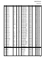
1
VERTEX STANDARD CO., LTD. 4-8-8 Nakameguro, Meguro-Ku, Tokyo 153-8644, Japan VERTEX STANDARD VX-1700 Series US Headquarters 10900 Walker Street, Cypress, CA 90630, U.S.A. YAESU UK LTD. HF Multi Mode Mobile Radio Service Manual For USA Version ©2011 VERTEX STANDARD CO., LTD. Unit 12, Sun Valley Business Park, Winnall Close Winchester, Hampshire, SO23 0LB, U.K. VERTEX STANDARD HK LTD. Unit 1306-1308, 13F., Millennium City 2, 378 Kwun Tong Road, Kwun Tong, Kowloon, Hong Kong VERTEX STANDARD (AUSTRALIA) PTY., LTD. EC051H95E Tally Ho Business Park, 10 Wesley Court, East Burwood, VIC, 3151 Introduction This manual provides the technical information necessary for servicing the VX-1700 HF Transceiver. Servicing this equipment requires expertise in handing surface-mount chip components. Attempts by nonqualified persons to service this equipment may result in permanent damage not covered by the warranty, and may be illegal in some countries. Two PCB layout diagrams are provided for each double-sided board in this transceiver. Each side of the board is referred to by the type of the majority of components installed on that side (“Side A” or “Side B”). In most cases one side has only chip components (surface-mount devices), and the other has either a mixture of both chip and leaded components (trimmers, coils, electrolytic capacitors, ICs, etc.), or leaded components only. As described in the pages to follow, the advanced microprocessor design of the VX-1700 Transceiver allows a complete alignment of this transceiver to be performed without opening the case of the radio; all adjustments can be performed from the front panel, using the “Alignment Mode” menu. While we believe the information in this manual to be correct, VERTEX STANDARD assumes no liability for damage that may occur as a result of typographical or other errors that may be present. Your cooperation in pointing out any inconsistencies in the technical information would be appreciated. Contents Specifications ...................................................................................................................................................... 2 Exploded View & Miscellaneous Parts .......................................................................................................... 3 Block Diagram ..................................................................................................................................................... 5 Connection Diagram .......................................................................................................................................... 6 Circuit Description ............................................................................................................................................. 7 Connector Pinout Diagrams ........................................................................................................................... 10 Alignment .......................................................................................................................................................... 11 ALE-1 Automatic Link Establishment Unit Installation ........................................................................... 19 CE77 PC Programming Software ................................................................................................................... 21 Board Units (Schematics, Layouts & Parts) MAIN Unit .................................................................................................................................................. 49 PA-2 Unit ..................................................................................................................................................... 77 PANEL Unit ................................................................................................................................................ 91 GPS-INTERFACE Unit .............................................................................................................................. 97 MIC Unit .................................................................................................................................................... 107 ENC Unit ................................................................................................................................................... 108 ALE Unit (Option) .................................................................................................................................... 109 1 Specifications General Receiver Frequency Range: Transmitter Frequency: Emission Modes: Frequency Synthesizer Step: Frequency Stability: Operating Temperature Range: Antenna Impedance: Supply Voltage: Power Consumption: Dimensions (WxHxD): Weight (approx.): 30 kHz ~ 30.0000 MHz 1.600 ~ 30.0000 MHz A1A (CW), J3E (LSB/USB), A3E (AM), J2B (USB/LSB) 10 Hz, 100 Hz, 1 kHz ±1 ppm (Typical) 14° F ~ 131° F (–10° ~ +55° C) @Duty Cycle TX:RX = 1 min.: 4 min. 50 Ohms 13.8 Volts DC ±15%, negative ground 25 mA (Standby) 1.0 A (Receive, no signal) 1.5 A (Receive) 22 A (Transmit, 125 Watts output) 9.5” x 3.9” x 11.2” (241 x 99 x 285 mm) 9.5 lbs (4.3 kg) Transmitter Power Output: Modulation Types: Spurious Radiation: J3E Carrier Suppression: Undesired Sideband Suppression: J3E Audio Response: Occupied Bandwidth: Microphone Impedance: 125 Watts (A1A, J2B, J3E @1.6000 ~ 3.9999 MHz) 100 Watts (A1A, J2B, J3E @4.0000 ~ 30.0000 MHz) 31 Watts AM Carrier (A3E @1.6000 ~ 3.9999 MHz) 25 Watts AM Carrier (A3E @4.0000 ~ 30.0000 MHz) J3E: PSN type modulator, A3E: Low-level (early stage) Better than –56 dB Better than 50 dB below peak output Better than 60 dB below peak output Not more than –6 dB from 400 Hz ~ 2500 Hz A1A: less than 0.5 kHz J3E: less than 3.0 kHz A3E: less than 6.0 kHz 200 ~ 10 k Ohms (600 Ohms Nominal) Receiver Circuit Type: Intermediate Frequencies: Sensitivity: Squelch Sensitivity (A1A/J2B/J3E): IF Rejection: Image Rejection: Selectivity: Audio Output: Audio Output Impedance: Conducted Radiation: Double-conversion Superheterodyne 1st: 45.274 MHz, 2nd: 24 kHz A1A/J2B/J3E A3E 0.1 ~ 0.5 MHz: — — 0.5 ~ 1.6 MHz: 1.41 µV 8 µV 1.6 ~ 30 MHz: 0.16 µV 1 µV (A1A/J2B/J3E/A3E: S/N 10 dB) 0.1 ~ 0.5 MHz: — 0.5 ~ 1.6 MHz: 2.5 µV 1.6 ~ 30 MHz: 2 µV Better than 80 dB Better than 80 dB –6 dB –60 dB A1A(W), J2B(W), J3E: > 2.2 kHz < 4.5 kHz A1A(N), J2B(N): > 500 Hz < 2.0 kHz A3E: > 6 kHz < 20 kHz At least 2.2 Watts into 8 Ohms @ 10% THD 4 ~ 16 Ohms (8 Ohms Nominal) Less than 4000 µµW Specifications are subject to change without notice or obligation. 2 Exploded View & Miscellaneous Parts 14 14 14 14 14 RA0695200 COVER (TOP) 14 14 13 RA0809600 SPONGE RUBBER 14 1 13 2 RA0809600 SPONGE RUBBER 13 13 P1091335 CONNECTOR (FM-MDR-MI) 6 PA UNIT RA0809600 SPONGE RUBBER 6 6 13 RA0809600 SPONGE RUBBER 6 3 15 5 RA0635400 CHASSIS RA0695600 HOLDER PLATE (CW) 5 T9207202A WIRE ASSY PANEL UNIT RA0695700 HOLDER PLATE (D-SUB) 12 RA069610A REFLECTOR SHEET RA0727200 DIFFUSER SHEET (BLIND) (2pcs) 9 4 RA0695800 INTER CONNECTOR (2pcs) 9 G6090162 LCD MAIN UNIT 4 10 RA0695000 FRONT PLATE (A) RA0727100 DIFFUSER SHEET (LCD) 12 RA0694600 PACKING PAD (SP) RA069450A RUBBER KNOB (PW) RA0695900 LIGHT GUIDE (LCD) 12 M4090146 SPEAKER 12 11 MIC UNIT 11 RA0695500 PACKING PAD (CHASSIS) GPS INTERFACE UNIT RA0696000 LCD HOLDER RA0696200 SPONGE RUBBER (LCD) 2 2 RA0809700 PLATE 13 8 RA0725400 FRONT PANEL ASSY 9 REF. P0001 P0002 P0004 P0005 P0006 P0007 P0008 RA080950A GUARD PLATE RA0695300 COVER (BOTTOM) 9 14 4 RA0695000 FRONT PLATE (B) 14 RA069420A RUBBER KNOB (12KEY) 4 RA069430A RUBBER KNOB (4KEY) RA069440A RUBBER KNOB (UP/DOWN) RA0694800 KNOB (L) RA0694900 KNOB (S) 14 S4000054 CASE LEG R3100700A FOOT 14 7 SUPPLIED ACCESSORIES DESCRIPTION MH-31A8J Hand Microphone DC Power Cord Spare Fuse (25 A Blade Type) QTY. 1 1 1 13 M2090040 FAN ENC UNIT VXSTD P/N A06870001 T9023725 Q0000074 R3100700A FOOT 7 R0145630 STAND S4000054 CASE LEG REF. 1 2 3 4 5 6 7 8 9 10 11 12 13 14 15 VXSTD P/N U02308002 U03308002 U04410002 U10306001 U20205002 U20306002 U20406007 U20430002 U24106002 U24108002 U24206001 U24208002 U24308002 U31306007 U70004012 CONNECTION CABLES VXSTD P/N DESCRIPTION T9315504 Coaxial Cable (J1001 J2006) T9315905 Coaxial Cable (J1002 J2001) T9207203 30-pin Flat Cable (J1003 J2002) T9207210 13-pin Molex (J1008 J4001) T9207211 8-pin Molex (J1005 J6002) T9207209 8-pin Molex (J3004 J6101) T9207117A 30-pin Flat Cable (J1004 J3001) DESCRIPTION SEMS SCREW SEMS SCREW SEMS SCREW TRUSS HEAD SCREW BINDING HEAD SCREW BINDING HEAD SCREW BINDING HEAD SCREW BINDING HEAD SCREW TAPTITE SCREW TAPTITE SCREW TAPTITE SCREW TAPTITE SCREW TAPTITE SCREW OVAL HEAD SCREW PLAIN WASHER SM3X8NI ASM3X8NI HSM4X10NI M3X6 M2.6X5NI M3X6NI M4X6B M4X30(Ni) M2X6NI M2X8NI M2.6X6 M2.6X8NI M3X8NI M3X6B FW4BSNI QTY. 4 7 1 4 2 4 2 4 6 3 2 4 14 12 1 Non-designated parts are available only as part of a designated assembly. 3 Exploded View & Miscellaneous Parts Note 4 Block Diagram 5 Connection Diagram 6 Circuit Description Receive Signal Path Incoming RF signal from the ANT jack is delivered to the PA Unit, and passes through the TX/RX relay RL2009 to J2006. The RF signal is then applied to J1001 on the MAIN Unit, and passed through the limiter circuit consisting of D1006, D1007, D1008, and D1009 (all RLS245) to prevent distortion from high RF signal input, and is fed to one of eight band-pass filters which strip away unwanted signals prior to delivery of the incoming signal to the RF amplifiers, Q1022 and Q1024 (both 2SK520-K41). The amplified RF signal passes through a low-pass filter to the doubly-balanced mixer D1032 (HSB88WS), where the RF signal is mixed with the 1st local signal delivered from buffer amplifier Q1029 (2SC2954), resulting in a 45.274 MHz 1st IF signal. The 45.274 MHz 1st IF signal is fed through monolithic crystal filter XF1001, which strips away unwanted mixer products, and is amplified by 1st IF amplifier Q1050 (3SK151GR); the 1st IF signal is then applied to the 2nd mixer Q1052 (RF2713), where it is mixed with the 45.25 MHz 2nd local signal which is divided from 90.5 MHz reference signal delivered from buffer amplifier Q1075 (2SC2714Y), resulting in a 24 kHz 2nd IF signal. The 24 kHz 2nd IF signal is fed through buffer amplifiers Q1030 and Q1041 (both UPC4572G2) to the A/D converter Q1071 (AK4528A), then delivered to the DSP IC Q1035 (UPD77115), where the 24 kHz 2nd IF signal is demodulated in accordance with the mode selection data from the main CPU Q1018 (HD64F2134). The demodulated signal is delivered to the D/A converter Q1081 (AK4550VT) which converts the demodulated signal to audio. The audio signal from the D/A converter Q1081 (AK4550VT) is fed through a low-pass filter at Q1036 (UPC4572G), which eliminates high-pitched noise on the audio signal, and is fed to the AF mute gate Q1092 (2SJ125D), then applied to the audio amplifier Q1055 (TDA2003H). The amplified audio signal is delivered to J3001 on the PANEL Unit, then passes through the speaker switch RL3001/Q3006 (DTC143ZE) to the internal or external speaker. The DSP IC Q1035 (UPD77115) outputs AGC data which is proportionate to the received signal strength to the main CPU Q1018 (HD64F2134). The main CPU Q1018 (HD64F2134), in turn, outputs a DC voltage in accordance with the received signal strength. This DC voltage is fed through buffer amplifier Q1039 (LM2904PW) to RF amplifiers Q1022 & Q1024 (both 2SK520) and gate 2 of IF amplifier Q1050 (3SK151GR), to reduce their gains when strong signals are present in the receiver passband. Transmit Signal Path The speech audio from the microphone is delivered to J6001 on the MIC Unit, then applied to J1005 on the MAIN Unit. The speech audio is amplified by Q1032-1 (UPC4572G2), then passed though the clipper, D1044 (MC2850), and further amplified by Q1032-2 (UPC4572G2). The amplified speech audio is fed through the A/D converter Q1081 (AK4550VT), then delivered to the DSP IC Q1035 (UPD77115), where the speech audio is modulated in the 24 kHz TX 1st IF signal in accordance with the mode selection data from the main CPU, Q1018 (HD64F2134). The modulated signal is fed through the D/A converter Q1071 (AK4528A) and buffer amplifier Q1034 (UPC4572G2) to the mixer Q1054 (RF2713) where the 24 kHz TX 1st IF signal is mixed with 1st local signal delivered from buffer amplifier Q1075 (2SC2714Y), resulting in a 45.274 MHz IF signal. The resulting 45.274 MHz IF signal is buffered by Q1049 (3SK151GR), then delivered to the monolithic crystal filter XF1001, which strips away unwanted mixer products, and then is amplified by Q1043 (3SK151GR). The amplified IF signal is delivered to doubly-balanced mixer D1032 (HSB88WS), where it is mixed with the PLL local signal from the buffer amplifier, Q1029 (2SC2954). The resulting the RF signal at the transmit frequency is fed through a low-pass filter circuit, and then is amplified by Q1026 (2SC2714Y) and buffer amplifier Q1025 (2SC3357), and then filtered by one of eight band-pass filters to suppress out-of-band responses. The RF signal is then amplified by Q1001 (2SC2954) and delivered to the PA Unit. 7 Circuit Description On the PA Unit, the low-level RF signal from the MAIN Unit is amplified by pre-driver Q2001 (RD06HHF1), push-pull driver Q2008/Q2009 (both RD16HHF1), and push-pull final amplifier Q2012/ Q2013 (both SD1405), which provides up to 120 watts of RF output power. The RF output from the final amplifier is fed through the one of seven low-pass filters, sampling directional coupler T2005, and TX/RX relay RL2009 before delivery to the antenna jack. The sampling directional coupler senses forward and reverse power output, which is rectified by D2017 and D2018 (both MA729), respectively, and the DC voltage is then amplified by Q2015 (LM2904PW) on the PA Unit. The DC voltages derived from forward and reverse power are applied to J1003 on the MAIN Unit, and then amplified by Q1040 (LM2904PW) and Q1044 (2SC2812). The amplified DC voltage is fed back to the 2nd gate of the 45.275 MHz IF amplifier Q1043 (3SK151GR), so that the transmitter’s IF gain can be regulated by this sensing of the power output, preventing overdrive or damage caused by transmission into an excessive impedance mismatch at the antenna. PLL Circuit The PLL local signal for the receiver 1st local and the transmitter final local is generated by one of two VCOs: Q1072 or Q1073 (both 2SK210GR) in conjunction with varactor diodes D1047, D1048, D1049, D1050, D1051, D1052, D1053, and D1054 (all HVU359) on the MAIN Unit. The oscillating frequency is determined primarily by the level of DC voltage applied to the varactor diodes. The VCO output is buffered by Q1066 (2SK302Y), amplified by Q1074 (2SC2714Y), and band-pass filtered by capacitors C1389, C1391, C1397, C1400, C1409, and C1420 and coils L1070, L1071, L1074, and L1076. The filtered PLL local signal is fed through buffer amplifiers Q1027 (2SC2714Y), Q1028 (2SC3356), and Q1029 (2SC2954) to the TX final mixer or RX 1st mixer D1032 (HSB88WS). A portion of the output of buffer amplifier Q1066 (2SK302Y ) is further amplified by Q1064 (2SC2714Y), then delivered to the PLL subsystem 8 IC Q1056 (ADF4001BRU), which contains a reference divider, serial-to-parallel data latch, programmable divider, phase comparator and a swallow counter. The sample VCO signal is divided by the programmable divider section of the Q1056 (ADF4001BRU). Meanwhile, the output from the 22.625 MHz TCXO reference oscillator, X1003, is amplified by Q1062 (TC7S04FU) and divided by the DDS IC Q1060 (AD9833BRM) in accordance with the PLL dividing data from the main CPU, Q1018 (HD64F2134), then fed through the buffer amplifiers Q1063 (2SC2714Y) to ceramic filter CF1001. The divided and filtered reference signal is applied to the reference divider section of the PLL subsystem IC Q1056 (ADF4001BRU), where it is divided by 25/ 26 to produce the loop reference. The divided signal from the programmable divider (derived from the VCO), and that derived from the reference oscillator, are applied to the phase detector section of the PLL subsystem IC Q1056 (ADF4001BRU), which produces a pulsed output with pulse duration depending on the phase difference between the input signals. This pulse train is fed through the loop filter, consisting of resistors R1222, R1233, & R1247 and capacitors C1278, C1284, C1298, C1308, & C1418, then fed back to the VCO varactor diodes D1047, D1048, D1049, D1050, D1051, D1052, D1053, and D1054 (all HVU359). Changes in the DC voltage applied to these varactor diodes affect the reactance in the tank circuit of VCOs Q1072 and Q1073 (both 2SK210GR), changing the oscillating frequency according to the phase difference between the signals derived from the VCO and the TCXO reference oscillator. The VCO is thus phase-locked to the reference frequency standard. A portion of the output of reference signal from TCXO X1003 is multiplied by four at Q1070 (2SC2714Y). The resulting 90.5 MHz signal is buffered by Q1075 (2SC2714Y), then applied to a lowpass filter, consisting of capacitors C1401, C1405, C1410, C1411, and C1421 and coils L1075 and L1077. The filtered reference signal is applied to the TX 1st mixer Q1054 and RX 2nd mixer Q1052 (both RF2713). Circuit Description Control Circuit TX/RX Control Major frequency control functions such as channel selection, display, and PLL divider control are performed by main CPU Q1018 (HD64F2134) on the MAIN Unit, at the command of the user via the tuning knob and function switches on the front panel. When the PTT switch is pressed, pin 21 of the main CPU Q1018 (HD64F2134) goes low, which causes pin 60 of the main CPU Q1018 (HD64F2134) to go low. This signal disables the receiver 12 V bus at Q1046 (2SA1602A). At the same time, pin 59 of the main CPU Q1018 (HD64F2134) goes low to activate the transmit 12 V bus at Q1048 (2SA1365). The programmable divider data for the PLL from the main CPU is applied directly to DDS IC Q1016 (AD9833BRM) and PLL subsystem IC Q1056 (ADF4001BRU). The Mode selection data from the main CPU is also delivered to DSP IC Q1035 (UPD77115) to control the various circuits required for the selected mode. The Band selection binary data from the main CPU is decoded (BCD to Decimal) by Q1011 (TC4028BF). The resulting decimal outputs are level-shifted by Q1003 (TD62783AF) to select the active band-pass filter on the MAIN Unit required for the operating frequency. Also, the decimal outputs from Q1003 (TD62783AF) are delivered to PA Unit, where they are used to select the active low-pass filter required for the operating frequency. Power Supply & Regulation The +5 V bus for the main CPU Q1018 (HD64F2134) is derived from the 13.5 V bus via regulator Q1012 (BA05FP) on the MAIN Unit. The +8 V bus is derived from the 13.5 V bus via regulator Q1007 (KIA7808API) on the MAIN Unit. A portion of the +8 V bus is regulated by Q1008 (L78M05T) for the +5 V bus, and is regulated by Q1006 (UPC2926) for the +2.6 V bus required by the DSP IC Q1035 (UPD77115GK). 9 Connector Pinout Diagrams MIC Jack GPS Jack (As Viewed From Front Panel) (As Viewed From Rear Panel) Connected with , , , and . GPS Data Input. N/C (Lot. 1~25) GPS Data Output (Lot. 26 & 27 : When the firmware is updated. GPS Data Output (Lot. 28~) Connected with , , , and . GPS Data. Connected with , , , and . Connected with , , , and . Connected with , , , and . N/C (Lot. 1~25) GND (Lot. 26~) P ENB CNTL GND PTT MIC MIC GND + 5V UP DOWN Pin 3 PTT Open Circuit Voltage: 5 V, Closed Circuit Current: 1 mA ACC Jack TUNE Jack DATA Jack (As Viewed From Rear Panel) (As Viewed From Rear Panel) (As Viewed From Rear Panel) +13.8 V OUT TX GND GND BAND DATA A BAND DATA B BAND DATA C BAND DATA D TX-INH EXT ALC Input TX REQ Pin 1 +13.8 V Max. 1 A This terminal is connected in parallel with the pin 1 of TUNE Jack. Pin 2 TX GND Open Collector (Max. 60 V, 1A) This terminal is connected in parallel with the pin 2 of TUNE Jack. +13.8 V OUT TX GND GND RX D TX D TUNER SENSE RESET TX-INH Pin 1 +13.8 V Max. 1 A This terminal is connected in parallel with the pin 1 of ACC Jack. Pin 2 TX GND Open Collector (Max. 60 V, 1A) This terminal is connected in parallel with the pin 2 of ACC Jack. DATA IN GND DATA PTT DCD DATA OUT SQL OUT Pin 1 DATA IN 60 mVp-p @1 kΩ. Pin 5 DATA OUT 500 mVp-p @1 kΩ Pin 6 SQL OUT SQL OPEN: 5 V SQL CLOSE: 0 V Accessory Port (Located on the MAIN Unit) ENCR_TXIN ENCR_RXIN INDICATOR CODE (8) CODE (4) CODE (2) CODE (1) ENCR_RXOUT CLEAR/SCRAMBLE PTT VCC GND ENCR_TXOUT 10 Alignment The VX-1700 is carefully aligned at the factory for the specified performance across the entire operating frequency range. Realignment should therefore not be necessary except in the event of a component failure. All component replacement and service should be performed only by an authorized Vertex Standard representative, or the warranty policy may be void. ed, the interactions of some adjustments may require that more complex adjustments be performed afterwards. Do not attempt to perform only a single step unless it is clearly isolated electrically from all other steps. Have all test equipment ready before beginning, and follow all of the steps in a section in the order presented. The following procedures cover the sometimes critical and tedious adjustments that are not normally required once the product has left the factory. However, if damage occurs and some parts subsequently are replaced, realignment may be required. If a sudden problem occurs during normal operation, it is likely due to component failure; realignment should not be done until after the faulty component has been replaced. RF Signal Generator with calibrated output level at 30 MHz In-line Wattmeter with 5% accuracy at 30 MHz 50 Ohm RF Dummy Load with power rating of 200 W at 30 MHz 150 Ohm RF Dummy Load with power rating of 200 W at 30 MHz Frequency Counter with 0.02 ppm accuracy at 100 MHz AF Signal Generator AC Voltmeter DC Voltmeter: High input impedance DC Ammeter HF Sampling Coupler IBM ® PC / compatible Computer with Windows® 95/98/ME/XP/2000. Internet Explorer 4.0 or higher Vertex Standard CT-62 Programming Cable & CE77 Programming/Alignment Software We recommend that servicing be performed only by authorized Vertex Standard service technicians who are experienced with the circuitry and fully equipped for repair and alignment. Therefore, if a fault is suspected, contact the dealer from whom the product was purchased for instructions regarding repair. Authorized Vertex Standard service technicians realign all circuits and make complete performance checks to ensure compliance with factory specifications after replacing any faulty components. Those who do undertake any of the following alignments are cautioned to proceed at their own risk. Problems caused by unauthorized attempts at realignment are not covered by the warranty policy. Also, Vertex Standard reserves the right to change circuits and alignment procedures in the interest of improved performance, without notifying owners. Under no circumstances should any alignment be attempted unless the normal function and operation of the product are clearly understood, the cause of the malfunction has been clearly pinpointed and any faulty components replaced, and realignment determined to be absolutely necessary. The following test equipment (and thorough familiarity with its correct use) is necessary for complete realignment. Correction of problems caused by misalignment resulting from use of improper test equipment is not covered under the warranty policy. While most steps do not require all of the equipment list- Required Test Equipment Alignment Preparation & Precautions A 50-Ohm RF Dummy Load and in-line wattmeter must be connected to the ANT jack in all procedures that call for transmission, except where specified otherwise. Correct alignment is not possible with an antenna. After completing one step, read the following step to determine whether the same test equipment will be required. If not, remove the test equipment (except dummy load and wattmeter, if connected) before proceeding. Correct alignment requires that the ambient temperature be the same as that of the radio and test equipment, and that this temperature be held constant between 68° F ~ 86° F (20° C and 30° C). When the radio is brought into the shop from hot or cold air, it should be allowed time to come to room temperature before alignment. 11 Alignment Whenever possible, alignments should be made with oscillator shields and circuit boards firmly affixed in place. Also, the test equipment must be thoroughly warmed up before beginning. Note: Signal levels in dB referred to in the alignment procedure are based on 0dBµ = 0.5µV. Set up the test equipment as shown below, and apply 13.8V DC power to the transceiver. The VX-1700 must be programmed for use in the intended system before alignment is attempted. The frequency and other parameters are loaded from the file during the alignment process. In order to facilitate alignment over the complete operating range of the equipment, it is recommended that the channel data first be uploaded and then stored to disk. Alignment Channel data should then be downloaded. The original data can be replaced at the end of the alignment process. RF Signal Generator 50-ohm Dummy Load Inline Wattmeter Frequency Counter RF Sampling Coupler ANT Transceiver TUNER INPUT Power Supply 13.8 VDC CT-62 Programming Cable COM Port CE77 Programming Software 12 Reference & Local Alignment PLL REFERENCE FREQUENCY ALIGNMENT Connect the Frequency Counter to pin 4 of Q1062 (Lot. 1~6) or TP1073 (Lot. 7~) on the MAIN Unit. Adjust X1003 on the MAIN Unit (Lot. 1~6) or Trimmer on the REF Unit (Lot. 7~) for 22.625 MHz ±10 Hz on the frequency Counter. 2ND LOCAL OUTPUT LEVEL Connect the RF millivoltmeter to TP1043 on the MAIN Unit. Adjust T1013 on the MAIN Unit for 160 mVrms (±50 mVrms) on the RF millivoltmeter. PLL Alignment VCO VCV ALIGNMENT Connect the DC voltmeter to TP1048 on the MAIN Unit, and referring to the Table below, switch the transceiver to each channel listed. Then adjust the listed component for the required voltage or confirm that the correct voltage is present. Tune to Adjust or Confirm 13.499 MHz Adjust T1066 0.100 MHz Confirm 29.999 MHz Adjust T1067 13.5000 MHz Confirm For 5.2 V ± 0.1 V More than 0.6 V 5.3 V ± 0.1 V More than 0.5 V PLL OUTPUT LEVEL Connect the RF millivoltmeter to TP1039 on the MAIN Unit, then tune the radio to 7.500 MHz. Confirm that the output level is more than 10 dBm. Alignment Transmitter Alignment Receiver Alignment TX IF COILS ALIGNMENT RX IF COILS ALIGNMENT Connect the 50 Ohm Dummy Load to the ANT jack. Remove the coaxial plug from J1002 on the MAIN Unit, then connect the RF millivoltmeter and 50 Ohm resistor to J1002. Connect the AF Generator to pin 4 of the MIC jack. Tune the radio to 7.500 MHz, USB mode. Inject a 0.5 mVrms @1 kHz audio signal from the AF Generator. Key the transmitter (connect pin 3 of the MIC jack to GND), then adjust T1008, T1009, T1010, and T1011 on the MAIN Unit in succession several times for maximum indication on the RF millivoltmeter while transmitting. Connect the RF Signal Generator to the ANT jack, and connect the AF millivoltmeter to the EXT SP jack. Tune the radio to 19.900 MHz, CW mode. Inject a 19.900 MHz signal from the RF Signal Generator, then adjust the RF Signal Generator output level to 0 dB. Adjust T1012 on the MAIN Unit for maximum indication on the AF millivoltmeter. MIC JACK PINOUT PIN 4 OF Q1062 J1002 T1067 T1066 TP1048 X1003 TP1039 T1012 T1010 T1008 T1009 T1010 MAIN UNIT ALIGNMENT POINTS 13 Alignment DRIVER SECTION IDLING CURRENT ALIGNMENT PA Unit Alignment PRE-DRIVER SECTION IDLING CURRENT ALIGNMENT Connect the 50 Ohm Dummy Load to the ANT jack. Remove the shorting-plug from J2003 on the PA Unit, then connect the DC Ammeter to J2003 (pin 1: “–” lead, pin 2: “+” lead). Set VR2001 on the PA Unit fully counter-clockwise. Tune the radio to 7.500 MHz, USB mode. Key the transmitter (connect pin 3 of the MIC jack to GND) with no microphone input, and adjust VR2001 for 300 mA (± 30 mA) on the DC Ammeter. Disconnect the DC Ammeter, and replace the shorting-plug into J2003. Connect the 50 Ohm Dummy Load to the ANT jack. Remove the shorting-plug from J2004 on the PA Unit, then connect the DC Ammeter to J2004 (pin 1: “–” lead, pin 2: “+” lead). Set VR2002 on the PA Unit fully counter-clockwise. Tune the radio to 7.500 MHz, USB mode. Key the transmitter (connect pin 3 of the MIC jack to GND) with no microphone input, and adjust VR2002 for 300 mA (± 30 mA) on the DC Ammeter. Disconnect the DC Ammeter, and replace the shorting-plug into J2004. MIC JACK PINOUT TP2020 TP2021 TC2001 J2004 VR2003 VR2002 J2003 VR2001 TP2018 PA UNIT ALIGNMENT POINTS 14 Alignment FINAL SECTION IDLING CURRENT ALIGNMENT CM COUPLER BALANCE Connect the 50 Ohm Dummy Load to the ANT jack. Remove the solder jumper which is connected between TP2020 and TP2021 on the PA Unit, then connect the “+” lead of the DC Ammeter to TP2020 and the “–” lead to TP2021. Set VR2003 on the PA Unit fully counter-clockwise. Tune the radio to 7.500 MHz, USB mode. Key the transmitter (connect pin 3 of the MIC jack to GND) with no microphone input, and adjust VR2003 for 300 mA (± 30 mA) on the DC Ammeter. Disconnect the DC Ammeter, and re-connect the solder jumper between TP2020 and TP2021. Connect the 50 Ohm Dummy Load and Inline Wattmeter to the ANT jack, and connect the CW keyer to the KEY jack. Connect the DC voltmeter to TP2018 (“+” lead, “–” lead: GND) on the PA Unit. Tune the radio to 29.000 MHz, A1A mode. Key the transmitter (close the CW key). Now adjust TC2001 on the PA Unit for minimum indication on the DC voltmeter. 15 Alignment Software Menu Alignment The ANT jack should be connected to a Dummy Load (in the case of transmission) or RF Signal Generator (in the case of reception). General alignment conditions are as follows, unless otherwise noted. VOL Knob: Center (12 o’clock position). SQL Knob: Fully counter-clockwise. TX Output Power: HIGH VOX:Off The channel data in the radio is preset per the chart below. Connect the 50 Ohm Dummy Load and Inline Wattmeter to the ANT jack. Referring to the Table below, press the [T]/[S] key to recall each parameter listed, then key the transmitter (connect pin 3 of the MIC jack to GND) and rotate the CH knob for the required output. Parameter Output Power Parameter Output Power 1PO-VH 125 W (± 5 W) 5PO-H 95 W (± 5 W) 1PO-H 100 W (± 5 W) 5PO-MH 50 W (± 5 W) 1PO-MH 50 W (± 5 W) 5PO-ML 25 W (± 2 W) Channel Frequency 1PO-ML 25 W (± 2 W) 5PO-L 10 W (± 1 W) 1-001 1.7000 MHz 1PO-L 10 W (± 1 W) 6PO-H 100 W (± 5 W) 1-002 3.5000 MHz 2PO-VH 125 W (± 5 W) 6PO-MH 50 W (± 5 W) 1-003 5.5000 MHz 2PO-H 100 W (± 5 W) 6PO-ML 25 W (± 2 W) 1-004 7.5000 MHz 2PO-MH 50 W (± 5 W) 6PO-L 10 W (± 1 W) 1-005 12.0000 MHz 2PO-ML 25 W (± 2 W) 7PO-H 95 W (± 5 W) 1-006 19.8000 MHz 2PO-L 10 W (± 1 W) 7PO-MH 50 W (± 5 W) 1-007 29.0000 MHz 3PO-H 100 W (± 5 W) 7PO-ML 25 W (± 2 W) 7PO-L 10 W (± 1 W) Press and hold in the keypad’s [ 1 ( MODE )] , [4(STEP)], [7(V/M)], and [F] keys simultaneously, and turn on the radio while holding them in; the alignment menu will then be activated. In the alignment procedures, each alignment parameter is selected by pressing the [T ]/[S ] key. Each alignment item is selected by rotating the CH Knob. To store the alignment parameters when you are satisfied with the adjustment, press the [F] key for longer than a half second. Note that a few alignment parameters are not adjustable, and are to be left as set at the factory. 16 TX OUTPUT POWER ALIGNMENT 3PO-MH 50 W (± 5 W) 3PO-ML 25 W (± 2 W) 3PO-L 10 W (± 1 W) 4PO-H 100 W (± 5 W) 4PO-MH 50 W (± 5 W) 4PO-ML 25 W (± 2 W) 4PO-L 10 W (± 1 W) Alignment TX GAIN ALIGNMENT REV ALC ALIGNMENT Connect the 50 Ohm Dummy Load and Inline Wattmeter to the ANT jack. Connect the AF Generator to pin 4 of the MIC jack, and adjust the AF Generator output level to 0.5 mV @1 kHz. Referring to the Table below, press the [T]/[S] key to recall each parameter listed, then key the transmitter (connect pin 3 of the MIC jack to GND) and rotate the CH knob for the required output. Connect the 150 Ohm Dummy Load (or three 50 Ohm Dummy Loads in parallel) to the ANT jack. Referring to the Table below, press the [T]/[S] key to recall each parameter listed, then key the transmitter (connect pin 3 of the MIC jack to GND) and rotate the CH knob just to the point when the S-meter reading is changed from S-7 to S-8. Parameter Output Power Parameter Output Power 1TX-G-H 50 W (± 10 W) 1TX-G-L 5 W (± 1 W) 2TX-G-H 63 W (± 10 W) 2TX-G-L 5 W (± 1 W) 3TX-G-H 50 W (± 10 W) 3TX-G-L 5 W (± 1 W) 4TX-G-H 50 W (± 10 W) 4TX-G-L 5 W (± 1 W) 5TX-G-H 50 W (± 10 W) 5TX-G-L 5 W (± 1 W) 6TX-G-H 50 W (± 10 W) 6TX-G-L 5 W (± 1 W) 7TX-G-H 50 W (± 10 W) 7TX-G-L 5 W (± 1 W) MIC JACK PINOUT Parameter S-meter reading 1R-ALC S-7 to S-8 threshold. 2R-ALC S-7 to S-8 threshold. 3R-ALC S-7 to S-8 threshold. SWR ALIGNMENT Connect the 150 Ohm Dummy Load (or three 50 Ohm Dummy Loads in parallel) to the ANT jack. Press the [T ]/[S ] key to recall the parameter “1_SWR3.” Key the transmitter (connect pin 3 of the MIC jack to GND), then press the [ENT] key. Press the [S] key momentarily to recall the parameter “2_SWR3.” Key the transmitter (connect pin 3 of the MIC jack to GND), then press the [ENT] key. Press the [S] key momentarily to recall the parameter “3_SWR3.” Key the transmitter (connect pin 3 of the MIC jack to GND), then press the [ENT] key. This completes the internal alignment routine. To save all settings and exit, press and hold in the [F] key for at least one second. To exit without saving, press the POWER key. 17 Alignment Note 18 ALE-1 Automatic Link Establishment Unit Installation Installation Make sure that the transceiver off. Remove the DC Power Cable, Microphone, and Antenna from the transceiver. Referring to Figure 1, remove the four screws from the side of the transceiver (two screws for each side), along with four screws affixing the bottom case; remove the bottom case. Referring to Figure 2, disconnect the 13-pin connector from J4001 on the GPS-INTERFACE Unit, remove the two HEX bolts which and four screws affixing the GPS-INTERFACE Unit. Remove the GPS-INTERFACE Unit from the transceiver. Install the ALE-1 Unit to the place where it has the GPS-INTERFACE Unit. Fix the ALE-1 Unit with two HEX bolts and four screws. Connect the 13-pin connector to J4001 on the ALE-1 Unit. Replace the bottom case with its eight screws. Connect the DC Power Cable, Microphone, and Antenna to the transceiver. FIGURE 1 Connect the CT-62 Programming Cable between computer’s 9-pin COM port and the transceiver’s TUNER jack. Press and hold in the [F] and [9(M/W)] keys while turning the power on to enter the clone mode. Execute the CE77 Programming Soft, then upload the current programming data from the transceiver via the “Upload” menu in the “Radio” parameter. Click the left mouse button on the “Common” parameter, then click the left mouse button on the “Option” parameter to involve a pop-up window, select the “Option Board” item, and change its setting to “ALE Unit.” Click the left mouse button on the [OK] button to close the pop-up window. Program the ALE features. Download the revised programming data to the transceiver from the computer via the “Download” menu in the “Radio” parameter. Installation and programming are now complete. Disconnect the CT-62 Programming Cable from the transceiver’s TUNER jack. GPS-INTERFACE Unit J4001 Programming MAIN Unit Cooling Fan FIGURE 2 19 ALE-1 Automatic Link Establishment Unit Installation Note 20 CE77 PC Programming Software The CE77 PC Programming Software is used to program the VX-1700 HF Communications Transceiver. With the CE77 PC Programming Software, you can quickly and easily program the Vertex Standard VX-1700 operating channels and configuration from your personal computer. In the event of an accidental memory failure, channel memory and configuration data may be re-loaded in a matter of minutes. Main Programming Screen (VFO Screen) VFO/MEMORY This parameter switches the Main Programming Screen between the “VFO Screen” and the “Memory Channel Screen.” STEP This column selects the VFO step size. To select the step size, double click the left mouse button on this column to select the desired step size from among “10 Hz,” “100 Hz,” and “1 kHz.” RECEIVE FREQUENCY This field sets the Default Receive Frequency of the VFO. To enter the Receive Frequency, double click the left mouse button on this column, then enter the desired Receive Frequency from the keyboard, then press the [ENTER] key to lock in the new frequency. The available values are “0.0300 (MHz)” to “30.0000 (MHz).” TRANSMIT FREQUENCY This field sets the Default Transmit frequency of the VFO. When you enter a Receive frequency, the Transmit frequency will automatically be set to the same frequency. To change the transmit frequency (only), double click the left mouse button on this column, enter the desired Transmit Frequency from the keyboard, then press the [ENTER] key to lock in the new frequency. The available data entry values are “0.0300 (MHz)” to “30.0000 (MHz).” However, the range over which transmission may actually occur is from “1.6000 (MHz)” to “30.0000 (MHz).” MAIN PROGRAMMING SCREEN (VFO SCREEN) 21 CE77 PC Programming Software MODE This column selects the Operating Mode. To select the Operating Mode, double click the left mouse button on this column to invoke a pop-up window, select the desired Operating Mode, then click the [OK] button to accept the new Operating Mode. The available selections are “J3E (USB),” “J3E (LSB),” “J2B,” “A1A,” and “A3E.” FILTER This column selects the bandwidth of the IF filter. To select the bandwidth, double click the left mouse button on this column to toggle the desired bandwidth between “Wide (W): 2.2 kHz.” and “Narrow (N): 600 Hz.” This column does not function when the “VFO MODE” parameter has been set to “J3E” or “A3E.” CLAR VALUE This column allows entry of the Clarifier Offset Frequency. To enter the Offset Frequency, double click the left mouse button on this column, enter the desired Offset Frequency from the keyboard, then press the [ENTER] key to accept the new frequency. If an incorrect entry is made, the software will round off the entry to the nearest valid frequency automatically. Available values are “-1.00” to “+1.00” (kHz). PWR This column selects the Transmit Output Power. To select the TX power, double click the left mouse button on this column, then select the desired TX power from among “Low,” “Mid,” and “High.” 22 SHIFT This column may used to move a spurious response “Birdie” from the CPU clock away from the operating frequency, should it cause interference. To program this column, double click the left mouse button on this column, then select the desired shift value from among “1,” “2,” “3,” and “Off (-).” ENCRYPTION ENCR This column turns the Voice Encryption feature “on (v)” or “off (-).” To select this feature, double click the left mouse button on this column, then set the Voice Encryption feature “on (v)” or “off (-).” This column will not function in the software when the Encryption Unit has been activated (determined from the “Encryption Unit” parameter on the “Option” tab in the “Common” Menu), or if the optional Encryption Unit is not installed. ENCRYPTION CODE This column selects the desired Encryption code. To program this column, double click the left mouse button on this column to invoke a pop-up window, select the desired Encryption code, then click the [OK] button to lock in the new Encryption code. SELCALL SELF ID This column programs the 4-digit ID for your transceiver, utilized when using the SELCALL feature. To enter the 4-digit ID, double click the left mouse button on this column, enter the desired 4-digit ID code (numeric only) from the keyboard, then press the [ENTER] key to accept the new ID code. CE77 PC Programming Software Main Programming Screen (Memory Screen) CHN (CHANNEL) This number is used to identify the memory channel. They do not have to occur in order, and you can duplicate numbers from other groups (do not duplicate within a group). For example, each group may have a channel 1, but a particular group may not have two channel 4s. Double click the left mouse button to toggle lock the channel lock between “Enable” and “Disable.” The Channel lines displayed in Thin Black are unlocked and enabled, channel lines displayed in Gray are locked and disabled. PRI This column set the Priority Channel. Double click the left mouse button on this column to toggle this selection “On (P)” or “Off (-).” When this column is set to “On (P),” the current channel will be designated as the Priority Channel. TAG This column is used for entry of the six character Alpha/Numeric “Tag” used to identify the channel. To enter the Alpha/Numeric “Tag,” double click the left mouse button on this column, type the characters of the desired Alpha/Numeric Tag (up to 6 characters), then press the [ENTER] key to save the programmed “Tag.” TAG TYPE This column selects the display indication of the channel. To select the display indication, double click the left mouse button on this column to select the desired display indication from among “Freq,” “TAG,” and “ALT.” Freq: Indicates the memory channel by showing the actual channel frequency TAG: Indicates the memory channel by showing the channel’s Alpha/numeric Tag ALT: Indicates the memory channel by showing the channel frequency and the channel’s Alpha/numeric Tag alternately. MAIN PROGRAMMING SCREEN (MEMORY SCREEN) 23 CE77 PC Programming Software RECEIVE FREQUENCY This column is used for entry of the Receive Frequency. To enter the Receive Frequency, double click the left mouse button on this column, enter the desired Receive Frequency from the keyboard, then press the [ENTER] key to lock in the new frequency. The available values are “0.0300 (MHz)” to “30.0000 (MHz).” TRANSMIT FREQUENCY This column is used for entry of the Transmit frequency. When you enter a Receive frequency, the Transmit frequency will automatically be set to the same frequency. To change the transmit frequency (only), double click the left mouse button on this column, enter desired Transmit Frequency from the keyboard, then press the [ENTER] key to accept the new frequency. The available data entry values are “0.0300 (MHz)” to “30.0000 (MHz).” However, the range over which transmission may actually occur is from “1.6000 (MHz)” to “30.0000 (MHz).” MODE This column selects the Operating Mode. To select the Operating Mode, double click the left mouse button on this column to invoke a pop-up window, select the desired Operating Mode, then click the [OK] button to accept the new Operating Mode. The available selections are “J3E (USB),” “J3E (LSB),” “J2B,” “A1A,” and “A3E.” FILTER This column selects the bandwidth of the IF filter. To select the bandwidth, double click the left mouse button on this column to toggle the desired bandwidth between “Wide (W): 2.2 kHz” and “Narrow (N): 600 Hz.” This column does not function when the “OPERATING MODE” parameter has been set to “J3E” or “A3E.” CLAR VALUE This column allows entry of a Clarifier Offset Frequency, if desired. To enter the Offset Frequency, double click the left mouse button on this column, enter the desired Off- 24 set Frequency from the keyboard, then press the [ENTER] key to accept the new frequency. If an incorrect entry is made, the entry will be rounded off to the nearest valid frequency automatically. Available values are “-1.00” to “+1.00” (kHz). WRITE PROTECT This column defines whether the Filed Programming feature will be “Enabled (OVERWRITE)” or “Disabled (PROTECT).” PWR This column selects the Transmit Output Power. To select the TX power, double click the left mouse button on this column to select the desired TX power from among “Low,” “Mid,” and “High.” SHIFT This column may used to move a spurious response “Birdie” from the CPU clock away from the operating frequency, should it cause interference. To program this column, double click the left mouse button on this column, then select the desired shift value from among “1,” “2,” “3,” and “Off (-).” ENCRYPTION ENCR This column turns the Voice Encryption feature “on (v)” or “off (-).” To select this feature, double click the left mouse button on this column, then set the Voice Encryption feature “on (v)” or “off (-).” This column will not function in the software when the Encryption Unit has been activated using the “Encryption Unit” parameter on the “Option” tab in the “Common” Menu, or if the optional Encryption Unit is not installed. ENCRYPTION CODE This column selects the desired Encryption code. To program this column, double click the left mouse button on this column to invoke a pop-up window, select the desired Encryption code, then click the [OK] button to lock in the new Encryption code. SELCALL SELF ID This column programs the 4-digit ID for your transceiver, utilized when using the SELCALL feature. To enter the 4-digit ID, double click the left mouse button on this column, enter the desired 4-digit ID code (numeric only) from the keyboard, then press the [ENTER] key to accept the new ID code. CE77 PC Programming Software File Menu NEW Opens a new file. Click the left mouse button on the “New” parameter in the File menu; this will open the default configuration of the CE77 software. Shortcuts Toolbar: Keys: CTRL+N OPEN Opens a previously-saved configuration from the disk. Click the left mouse button on the “Open” parameter in the File menu; a pop-up window will appear which shows you all the current files saved in the specified path. The current folder that is saved the current file is in the top box, and the name of the current file is in the bottom box. Double click the left mouse button on the desired file to open its file. Shortcuts Toolbar: Keys: CTRL+O SAVE Saves the programming session to the disk with the same name and directory. Click the left mouse button on the “Save” parameter in the File menu to save the current file. Shortcuts Toolbar: Keys: CTRL+S SAVE AS Save the programming session to the disk with the new name. Click the left mouse button on the “Save As” parameter in the File menu, a pop-up window appears which shows you all the current files saved to the specified path. To save the programming session with the new name, type a file name in the bottom box, then click the left mouse button on the [SAVE] box. PRINT Prints a configuration to hard copy. Click the left mouse button on the “Print” parameter in the File menu; the “Printer” window will open to enable printing. Shortcuts Toolbar: Keys: CTRL+P PRINT PREVIEW Previews a print configuration for subsequent printing of a hard copy. Click the left mouse button on the “Print Preview” parameter in the File menu; the “Printer” window will appear. PRINT SETUP Sets the configuration of the printer. Click the left mouse button on the “Print Setup” parameter in the File menu; the “Printer” window will open to enable setting of the configuration of the printer. PRINTOUT LIST Selects the printout list for printing of a hard copy. Click the left mouse button on the “Printout” parameter in the File menu, the “Printout List” window open to enable selecting the printout list to be printed. CONFIGURE Selects the communication port which is connected to the CT-62 PC Programming Cable (which is connected to the radio). FILE MENU EXIT Quits the program and closes the window. If the present configuration has not been saved to disk, you will be asked to confirm whether you wish to save it. 25 CE77 PC Programming Software Edit Menu View Menu COPY Use this command to copy selected data onto the clipboard. This command is unavailable if there is no data currently selected. Copying data to the clipboard replaces the contents previously stored there. Shortcuts Toolbar: Keys: CTRL+C TOOL BAR The toolbar is displayed across the top of the application window, below the menu bar. The toolbar provides quick mouse access to many tools used in CE77. To hide or display the Toolbar, click the left mouse button on the “Toolbar” parameter in the “View” menu. PASTE Use this command to insert a copy of the clipboard contents at the insertion point. This command is unavailable if the clipboard is empty. Shortcuts Toolbar: Keys: CTRL+V EDIT MENU STATUS BAR The Status Bar is displayed at the bottom of the CE77 window. The left area of the Status Bar describes actions of menu items as you use the arrow keys to navigate through menus. This area similarly shows messages that describe the actions of Toolbar buttons as you depress them, before releasing them. If after viewing the description of the Toolbar button command you wish not to execute the command, then release the mouse button while the pointer is off the Toolbar button. To display or hide the Status Bar, click the left mouse button on the “Status Bar” parameter in the “View” menu. The right areas of the Status Bar indicate which of the following keys are latched down: Indicator Description CAP The “Caps Lock” key is latched down. NUM The “Num Lock” key is latched down. SCRL The “Scroll Lock” key is latched down. ITEM This parameter commands the channel data item to appear or disappear on the main screen. Put a check mark on the item to display it on the main screen. VIEW MENU 26 CE77 PC Programming Software Common Menu A1A (CW) FUNCTION PARAMETERS This parameter programs the various configuration items of the A1A (CW) mode. Put a check mark into the check box to enable adjustment of its parameter from the transceiver’s set (“menu”) mode. The available parameters are: CW Delay, CW QSK, Side Tone SET, and Side Tone Level. CW DELAY This parameter sets the CW delay time. To program the delay time, double click the left mouse button on this column, then enter the desired delay time from the keyboard, then press the [ENTER] key to accept the new delay time. The available values are “30mSec” to “3000mSec,” (10 mSec multiples) and “FULL.” To enter the “FULL” option, double click the left mouse button on this column, enter “0” from the keyboard, then press the [ENTER] key to accept the new delay time. CW QSK This parameter sets the delay time between the instant when the telegraph key is closed (key down) and the moment the actual carrier envelope is transmitted. The available values are “10mSec” to “30mSec” (5 mSec multiples). SIDE TONE SET This parameter defines whether the CW side tone level is linked to the front panel’s VOL knob (“LINK”), or not linked (“FIX”). SIDE TONE LEVEL This parameter sets the CW side-tone (monitor) level. To program the CW side-tone level, double click the left mouse button on this column, enter desired side-tone volume level from the keyboard, then press the [ENTER] key to accept the CW side tone level. When the “SIDE TONE SET” parameter is set to “FIX,” the available selections are “0” to “100.” When the “SIDE TONE SET” parameter is set to “LINK,” the available selections are “-100” to “100.” COMMON MENU "A1A (CW) FUNCTION" PARAMETERS 27 CE77 PC Programming Software HARDWARE PARAMETERS Put a check mark into the check box to enable adjustment of its parameter from the transceiver’s set (“menu”) mode. The available parameters are: 1.6 - 4 MHz RF Power, 4 - 30 MHz RF Power, Dimmer Level-1, and Dimmer Level-2. 1.6 - 4 MHz RF POWER This parameter programs the TX output power on the 1.6 - 4 MHz band for each power setting level. To program the TX output power, double click the left mouse button on this column; enter desired TX output power from the keyboard, then press the [ENTER] key to accept the new TX output power. The available values are “10 (W)” to “125 (W)” for “High” power setting on the 1.6 - 4 MHz band, and “10 (W)” to “125 (W)” for “High” power setting on the 4 - 30 MHz band, “Medium” power setting, and “Low” power setting. 4 - 30 MHz RF POWER This parameter programs the TX output power on the 4 - 30 MHz band for each power setting level. To program the TX output power, double click the left mouse button on this column, enter desired TX output power from the keyboard, then press the [ENTER] key to accept the new TX output power. The vailable values are “10 (W)” to “100 (W).” DIMMER LEVEL - 1 This parameter programs the Display Back-light Level and Back-light Options when “DIM” is not selected. The available Back-light Levels are “1” to “10,” and “OFF.” The available Back-light Options are “ON” (always on) and “Key On 10S” (Back-light on for ten seconds after any key stroke). DIMMER LEVEL - 2 This parameter programs the Display Back-light Level and Back-light Options when “DIM” is selected. The available Back-light Levels are “1” to “10,” and “OFF.” The available Back-light Options are “ON” (always on) and “Key On 10S” (Back-light on for ten seconds after any key stroke). "HARDWARE" PARAMETERS 28 CE77 PC Programming Software KEY FUNCTION PARAMETERS This parameter sets the configurations for the keypad and button functions of the radio. Put a check mark into the check box to enable adjustment of its parameter from the transceiver’s set (“menu”) mode. The available parameters are: P1 SET, P2 SET, P3 SET, P4 SET, and PU/D SET. P1 SET - P4 SET This parameter programs the Programmable Function Button feature. The available selections are: 1CH, 2CH, 3CH, 4CH, 1 MHz UP, 1 MHz Down, CLAR (+), CLAR (-), DW, ENCRYPTION, LOCK, PRI, SCAN, SPK OFF, RF PWR SEL, VOX, ALE, CALL, MONI, RCV MSG, SELCALL,TELCALL, AUX TOGGLE, AUX PRS TO H, AUX PRS TO L, and N/A. PU/D SET This parameter programs the Programmable Function Button feature which is located between the CH and VOL knobs. The available selections are: 2182-ALARM: Pressing the left button activates the alarm generator. Pressing the right button places the radio in the “Emergency Channel” mode. Press both buttons to transmit the alarm tone. UP-DWN: Press the buttons to select the frequency control method among the “VFO mode,” “ITU mode,” and “Memory mode.” "KEY FUNCTION" PARAMETERS Selection Key Function 1CH 2CH 3CH 4CH 1 MHz UP 1 MHz Down CLAR (+) CLAR (–) DW ENCRYPTION LOCK PRI SCAN SPK OFF RF PWR SEL VOX ALE CALL MONI Recalls the Dealer pre-programmed channel “1” directly while operating in the Memory Channel mode. Recalls the Dealer pre-programmed channel “2” directly while operating in the Memory Channel mode. Recalls the Dealer pre-programmed channel “3” directly while operating in the Memory Channel mode. Recalls the Dealer pre-programmed channel “4” directly while operating in the Memory Channel mode. Tunes the VFO frequency upward in 1 MHz steps while operating in the VFO mode. Tunes the VFO frequency downward in 1 MHz steps while operating in the VFO mode. Tunes the receiver frequency upward without changing the transmit frequency (Clarifier function). Tunes the receiver frequency downward without changing the transmit frequency (Clarifier function). Activates the Dual Watch feature. Toggles the Encryption feature “on” and “off.” Toggles the Key Lockout feature “on” and “off.” Activates the Priority Scan. Activates Scanning. Toggles the internal speaker (or external speaker, if used) “on” and “off.” Selects the transmit power output level (“Low,” “Medium,” and “High”). Accessory Port “3” Toggles the VOX feature “on” and “off.” Accessory Port “2” Toggles the ALE (Automatic Link Establishment) feature “on” and “off.” Transmits a Selcall (or ALE) while operating in the Selcall (or ALE) mode. Accessory Port “1” Disables the noise squelch action (to hear background noise). Press again this key to activate the noise squelch (quiet the noise). Recalls the last-received Selcall or ALE Message. Toggles the SELCALL feature “on” and “off.” MAIN Unit Transmits a Telcall while operating in the Selcall mode. Toggles the optional accessory port “3” “on” and “off.” Turns the optional accessory port “2” to “High.” Turns the optional accessory port “1” to “Low.” RCV MSG SELCALL TELCALL AUX TOGGLE AUX PRS TO H AUX PRS TO L 29 CE77 PC Programming Software MARKETING PARAMETERS This parameter indicates the Market Application Number and Serial Number of the radio. The available parameters are Market Applications and Serial Number. MARKET APPLICATIONS This parameter indicates the Alpha/numeric “Tag” (up to 16 digits) used for identifying the owner or application of the radio. SERIAL NUMBER This parameter presently is not supported. It will be used in the future. "MARKETING" PARAMETERS MISCELLANEOUS PARAMETERS This parameter programs the miscellaneous configuration options of the radio. Put a check mark into the check box to enable adjustment of its parameter from the transceiver’s set (“menu”) mode. The available parameters are: Alarm AF SET, Alarm Vol SET, Beep Tone, Beep AF SET, Beep VOL, Dual Watch Mode, Lock Mode, Scan Resume, Standby Beep, VOX Gain, and VOX Delay. ALARM AF SET This parameter defines whether the Alarm tone level is linked to the front panel’s VOL knob (“LINK”) or not linked (“FIX”). ALARM VOL SET This parameter sets the Alarm level of the Emergency, Selcall, and ALE features. To program the Alarm level, double click the left mouse button on this column, enter the desired Alarm level from the keyboard, then press the [ENTER] key to accept the programmed alarm level. When the “ALARM AF SET” parameter is set to “FIX,” the available selections are “0” to “100.” When the “ALARM AF SET” parameter is set to “LINK,” the available selections are “-100” to “100.” "MISCELLANEOUS" PARAMETERS 30 CE77 PC Programming Software BEEP TONE This parameter sets the Beep Tone (frequency). The available selections are “LOW,” “NORMAL,” and “HIGH.” SCAN RESUME This parameter selects the Scan Resume Mode. The available selections are “Carrier” and “Timer.” BEEP AF SET This parameter defines whether the Beep volume is linked to the front panel’s VOL knob (“LINK”) or not linked (“FIX”). STANDBY BEEP This parameter toggles the Standby Beep feature “ON” or “OFF.” When this parameter is set to “ON,” an “Alarm” beep will be heard and transmitted when the PTT switch is released. BEEP VOL This parameter sets the Beep volume level. To program the Beep volume level, double click the left mouse button on this column, enter desired Beep volume level from the keyboard, then press the [ENTER] key to accept the Beep volume level. When the “BEEP AF SET” parameter is set to “FIX,” the available selections are “0” to “100.” When the “BEEP AF SET” parameter is set to “LINK,” the available selections are “-100” to “100.” DUAL WATCH MODE This parameter defines the priority channel for the dual watch feature. The channels currently programmed into the radio will appear in the drop-down list. VOX GAIN This parameter sets the gain of the VOX circuit. To program the VOX gain, double click the left mouse button on this column, enter desired VOX gain from the keyboard, then press the [ENTER] key to accept the VOX gain. The available values are “0” to “100.” VOX DELAY This parameter sets the VOX delay time. To program the VOX delay time, double click the left mouse button on this column, enter desired VOX delay time from the keyboard, then press the [ENTER] key to accept the VOX delay time. The available values are “100 mSec” to “3000 mSec” (100 mSec multiples). LOCK MODE This parameter selects from among the available function locking schemes. The available selections are “CH,” “KEYPAD,” and “ALL.” 31 CE77 PC Programming Software SYSTEM PARAMETERS This parameter programs the various system configurations of the radio. Put a check mark into the check box to enable adjustment of its parameter from the transceiver’s set (“menu”) mode. The available parameters are: APO, Clarifier Backup Type, Carrier Offset, Display Offset, J2B MODE, MIC Gain, Password Set, SP Mute Act, SP Mute Level, TOT, Tuning, VFO, VOL Limit, DEALER MODE, RETURN, CLOCK SHIFT, DW CH SEL, ENCRPT CODE, and MEMORY WRITE. APO This parameter determines the power-off time for the Automatic Power Off feature. The available values are “1/2/4/6/8/10/12” hours or “off.” CLARIFIER BACKUP TYPE This parameter determines the Clarifier offset frequency when the memory channel is recalled. The available selections are “PRESET,” “MOMENTARILY,” and “LAST MEMORY.” PRESET: Sets the Clarifier offset frequency to the memorized offset frequency of the memory channel, and disables the Clarifier for offset frequency tuning. MOMENTARILY: Sets the Clarifier offset frequency to the memorized offset frequency of the memory channel, and enables the Clarifier for offset frequency tuning. LAST MEMORY: Sets the Clarifier offset frequency to the last tuned offset frequency, and enables the Clarifier for offset frequency tuning. CARRIER OFFSET This parameter sets the carrier point during the J2B mode. To program the carrier point, double click the left mouse button on this column, enter desired frequency from the keyboard, then press the [ENTER] key to accept the carrier point. The available selections are “0Hz” to “3000Hz.” (10 Hz multiples) DISPLAY OFFSET This parameter sets the frequency display offset for the J2B mode. To program the frequency display offset, double click the left mouse button on this column, enter desired offset from the keyboard, then press the [ENTER] key to accept the frequency display offset. The available selections are “-3000 Hz” to “3000 Hz.” (10 Hz multiples) "SYSTEM" PARAMETERS 32 J2B MODE This column selects the Operating Mode (injection sideband) for the J2B mode. The available selections are “USB” and “LSB.” CE77 PC Programming Software MIC GAIN This parameter programs the Microphone Input Sensitivity. The available values for the Microphone Gain are “LOW,” “NORMAL,” or “HIGH.” PASSWORD SET This parameter programs the password for the entering to the Dealer mode of the transceiver. To enter the password, double click the left mouse button on this column, enter the desired password (four digits; numeric only) from the keyboard, then press the [ENTER] key to accept the new password. SP MUTE ACT This parameter selects the Speaker Mute function. The available selections are “DCD-L MUTE” and “DCD-H MUTE.” DCD-L MUTE: Reduces the speaker audio output while the DCD terminal (pin 4 of the DATA Jack) is set to “LOW.” DCD-H MUTE: Reduces the speaker audio output while the DCD terminal (pin 4 of the DATA Jack) is set to “High.” SP MUTE LEVEL This parameter sets the Audio mute level. To program the Audio mute level, double click the left mouse button on this column, enter desired mute level from the keyboard, then press the [ENTER] key to accept the new mute level. The available selections are “-100” to “0.” TOT This parameter determines the Time-Out Timer countdown Time. The available values are “1/2/3/5/10/15/20” minutes or “off.” TUNING This parameter programs the Automatic Antenna Tuner function. The available selections are: OFF: Disables the automatic tuning function of the Automatic Antenna Tuner. To initiate antenna tuning on a particular, with this selection set to “Off,” you must press the keypad’s [3(TUNER)] key on the front panel. CH CHANGE: Activates the Automatic Antenna Tuning function when the memory channel is changed. POWER ON: Activates the Automatic Antenna Tuning function on all channels of the current Memory Bank when the radio is turned on. VFO This parameter defines whether the “VFO” mode shall be “Enabled” or “Disabled” from the front panel’s [V/M] key. VOL LIMIT This parameter determines the audio volume level when the VOL knob is fully counter-clockwise (but not into the click) position. To program this parameter, double click the left mouse button on this column, enter the desired audio volume level (0 - 100), then press the [ENTER] key to save and exit. DEALER MODE This parameter defines whether the “DEALER MODE” selection shall be “Enabled” or “Disabled” from the transceiver’s set (“menu”) mode. RETURN This parameter defines whether the “RETURN” selection shall be “Enabled” or “Disabled” from the transceiver’s set (“menu”) mode. CLOCK SHIFT This parameter defines whether the “CLOCK SHIFT” selection shall be “Enabled” or “Disabled” from the transceiver’s set (“menu”) mode. 33 CE77 PC Programming Software DW CH SEL This parameter defines whether the “DW CH SEL” selection shall be “Enabled” or “Disabled” from the transceiver’s set (“menu”) mode. ENCRPT CODE This parameter defines whether the “ENCRPT CODE” selection shall be “Enabled” or “Disabled” from the User Set Mode. MEMORY WRITE This parameter defines whether the “MEMORY WRITE” selection shall be “Enabled” or “Disabled” from the User Set Mode. OPTION PARAMETERS This parameter programs the configurations of optional modules for the radio. These include the Encryption Unit and the Option Board. ENCRYPTION UNIT This parameter selects whether the Encryption Unit shall be “Enabled” (ON) or “Disabled” (OFF). OPTION BOARD This parameter selects the Optional Unit to be used. The available selections are “GPS Interface” and “ALE Unit.” "OPTION" PARAMETERS 34 CE77 PC Programming Software Selcall Menu SELCALL PARAMETERS This parameter programs the various Selcall configurations of the radio. Put a check mark into the check box to enable adjustment of its parameter from the transceiver’s set (“menu”) mode. Note: The Selcall is only activated on the J3E mode. The available parameters are Selcall, Kill System, Stun System, Beacon Request, GPS Position Request. GPS Position Send, Preamble, Offset Time, Radio ID, Message, All Call, Answer Back, Group Call, Sub Group Call, Tel Call, TX ID, and Selcall Self ID. SELCALL This parameter determines whether the radio is able to receive or transmit a Selcall. The available selections are “RX,” “TX,” “TX+RX,” and “OFF.” RX: Enables the receiving of a Selcall and disables the sending of a Selcall. TX: Enables the sending of a Selcall and disables the receiving of a Selcall. TX+RX: Enables both the receiving and sending of a Selcall. OFF: Disables both the receiving and sending of a Selcall. KILL SYSTEM This parameter determines whether the radio is able to receive a Kill System command or transmit a Kill System acknowledge command. The available selections are “RX,” “TX+RX,” “POS TX+RX,” and “OFF.” RX: Enables the receiving of a Kill System command and disables the sending of a Kill System acknowledge command. TX+RX: Enables the receiving of a Kill System command and sending of a Kill System acknowledge command. POS TX+RX: Enables the receiving of a Kill System command, and the sending of a Kill System acknowledge command along with the radio’s current positionÚ. OFF: Disables both the receiving of a Kill System command and sending of a Kill System acknowledge command. Ú: Requires the after-market GPS receiver. Note: The KILL System is ignored while activating the ALE feature. STUN SYSTEM This parameter determines whether the radio is able to receive a Stun System command or transmit a Stun System acknowledge command. The available selections are “RX,” “TX+RX,” “POS TX+RX,” and “OFF.” RX: Enables the receiving of a Stun System and disables the sending of a Stun System acknowledge command. TX+RX: Enables the receiving a Stun System command and sending of a Stun System acknowledge command. POS TX+RX: Enables the receiving of a Stun System command, and the sending of a Stun System acknowledge command along with the radio's current positionÚ. OFF: Disables both the receiving a Stun System command and sending of a Stun System acknowledge command. Ú: Requires the after-market GPS receiver. Note: The STUN System is ignored while activating the ALE feature. BEACON REQUEST This parameter determines whether the radio is able to receive or transmit a Beacon request feature. The available selections are “RX,” “TX,” “TX+RX,” and “OFF.” RX: Enables the receiving of a Beacon request and disables the sending of that request. TX: Enables the sending of a Beacon request and disables the receiving of a Beacon request. TX+RX: Enables both the receiving and sending of a Beacon request. OFF: Disables both the receiving and sending of a Beacon request. SELCALL MENU 35 CE77 PC Programming Software GPS POSITION REQUEST This parameter determines whether the radio is able to receive or transmit a GPS position request. The available selections are “RX,” “TX,” “TX+RX,” and “OFF.” RX: Enables the receiving of a GPS position request and disable the sending of a GPS position request. TX: Enables the sending of a GPS position request and disables the receiving of a GPS position request. TX+RX: Enables both the receiving and sending of a GPS position request. OFF: Disables both the receiving and sending of a GPS position request. Ú: Requires the after-market GPS receiver for transmitting your GPS position. GPS POSITION SEND This parameter determines whether the radio is able to receive or transmit your GPS position. The available selections are “RX,” “TX,” “TX+RX,” and “OFF.” RX: Enables the receiving a GPS position send command and disables the sending of your GPS position. TX: Enables the sending of your GPS position and disables the receiving of a GPS position send command. TX+RX: Enables the receiving and sending of a GPS position. OFF: Disables both the receiving and sending of a GPS position. Ú: Requires the after-market GPS receiver for transmitting your GPS position. PREAMBLE This parameter sets the preamble time for a Selcall. The radio will transmit just a carrier signal (without the data) for this “Preamble” period. The available selections are “1 sec” to “16 sec.” OFFSET TIME This parameter sets the offset time between the Local time and UTC time. 36 RADIO ID This parameter programs the transceiver’s Alpha/ Numeric self-identification for the KILL and STUN systems. To enter the Alpha/Numeric self-identification, double click the left mouse button on the desired column, type the characters of the desired Alpha/ Numeric self-identification (up to 58 characters), then press the [ENTER] key to save the programmed self identification. MESSAGE This parameter programs the Alpha/Numeric messages for the Selcall feature. To enter the Alpha/Numeric message, double click the left mouse button on the desired column, type in the characters of the desired Alpha/Numeric message (up to 64 characters), then press the [ENTER] key to save the programmed messages. This parameter is also used to remote control the VX-1700 using the “KILL,” “STUN,” and “REVIVE” feature. If the “CILLIK” command with the “Radio ID (example: TEST6111)” is entered in this parameter (total message is “CILLIKTEST6111”), the VX1700 which has the “TEST6111” radio ID will be “killed” when this message is received. Similarly, if the “ECNUTS” command with the “Radio ID (example: TEST6111)” is entered in this parameter (total message is “ECNUTSTEST6111”), the VX-1700 which has the “TEST6111" radio ID will be “stunned” (disabled, but capable of field revival) when this message is received. To revive the stunned VX-1700, send the “SVIVER” command with the “Radio ID” (in this example, TEST6111) (total message is “SVIVERTEST6111”). Note: A “killed” VX-1700 cannot be revived by a remote control command. To revive a killed VX1700, the channel setup cloning process must be performed again. Kill Command: CILLIK Stun Command: ECNUTS Revive Command: SVIVER CE77 PC Programming Software ALL CALL This parameter determines whether the “All Call” function of the Selcall feature shall be “Enabled” or “Disabled”. ANSWER BACK This parameter determines whether the “Answer Back” function shall be “Enabled” or “Disabled” when receiving a Selcall. GROUP CALL This parameter determines whether the “Group Call” function of the Selcall feature shall be “Enabled” or “Disabled.” SUB GROUP CALL This parameter determines whether the “Sub Group Call” function of the Selcall feature shall be “Enabled” or “Disabled.” TEL CALL This parameter determines whether the radio is able to receive or transmit a Tel Call. The available selections are “RX,” “TX,” “TX+RX,” and “OFF.” RX: Enables the receiving of a Tel Call and disables the sending of a Tel Call. TX: Enables the sending of a Tel Call and disables the receiving of a Tel Call. TX+RX: Enables both the receiving and sending of a Tel Call. OFF: Disables both the receiving and sending of a Tel Call. TX ID Put a check mark into the check box to enable programming of the TX ID from the transceiver’s set (“menu”) mode. SELCALL SELF ID Put a check mark into the check box to enable programming of the Selcall Self ID from the transceiver’s set (“menu”) mode. SELCALL SECTION 37 CE77 PC Programming Software TX ID PARAMETER This parameter programs the Selcall TX ID to be called. To program this parameter, enter the TX ID (4 digits) into the “TX ID” column, then set the desired effective channel range (i.e. 1-001, 1-050, 2-051, etc.) for the TX ID into the “FROM” and “TO” columns. Enter the Alpha/Numeric Tag (8 digits) of the TX ID into the “TAG” column, if desired. "TX ID" PARAMETERS TELEPHONE NUMBER PARAMETERS This parameter programs the telephone number for the Telcall feature. To enter the telephone number, double click the left mouse button on the desired column, type in the telephone number (up to 16 digits), then press the [ENTER] key to save the programmed number. Select the Telcall type from the “Tel Call Type” Drop Down list. The available selections are B16 (BARRETT®16), C12 (CODAN®12), and C16 (CODAN®16). Put a check mark into the check box to enable programming of the Selcall Self ID from the transceiver’s set (“menu”) mode. "TELEPHONE NUMBER" PARAMETERS 38 CE77 PC Programming Software ALE Menu ALE COMMON PARAMETERS This parameter programs the various configurations for the ALE (Automatic Link Establishment) system of the radio. The ALE system allows the radio to select the channel with the best LQA (Link Quality Analysis) score from the programmed channels. Put a check mark into the check box to enable adjustment of its parameters from the transceiver’s set (“menu”) mode. The available parameters are ALE, Alert Tone, Auto Address, External Alert, Link TOT, Minimum LQA Score, PTT Time Out, and Net Number. ALE This parameter selects whether the ALE System shall be “Enabled (ON)” or “Disabled (OFF)”. ALERT TONE This parameter selects the Alert Tone ringing period once the ALE link is established. The available selections are “2 Sec,” “5 Sec,” “20 Sec,” “CONTINUOUS,” and “OFF.” LINK TOT This parameter define whether the Link TOT feature shall be “Enabled (ON)” or “Disabled (OFF).” When this parameter is set to “ON,” the link to the other radio will be automatically disconnected unless you press the PTT within 30 seconds after receiving an ALE call. MINIMUM LQA SCORE This parameter determine the minimum LQA (Link Quality Analysis) score required to establish a link. To program this parameter, double click the left mouse button on this column, enter the desired minimum LQA value, then press the [ENTER] key to save and exit. Available selections are “0” to “100.” PTT TIME OUT This parameter selects the delay time between the releasing of the PTT switch and the disconnecting of the ALE link. The available selections are “1 minute” to “10 minutes” and “OFF.” AUTO ADDRESS This parameter toggles the Auto Address feature “ON” and “OFF.” When this parameter is set “ON,” the radio will add an unknown incoming call address to the “Other Station Address” directory automatically. EXTERNAL ALERT This parameter defines whether the External Alert port (Open Collector: Max. 60 V, 1A) shall be “Enabled (ON)” or “Disabled (OFF).” When this parameter is set to “Enabled (ON),” the External Alert port turns to “ON,” when a call is received. ALE MENU External Alert port D-Sub Connector GPS-INTERFACE Unit "ALE COMMON" PARAMETERS 39 CE77 PC Programming Software NET NUMBER Put a check mark into the check box to enable adjustment of its parameter from the transceiver’s set (“menu”) mode. AMD MESSAGE PARAMETERS This parameter programs the Alpha/Numeric messages in accordance with the AMD definition. To enter the Alpha/Numeric message, double click the left mouse button on the desired column, type the characters of the desired Alpha/Numeric message (up to 90 characters), then press the [ENTER] key to save the programmed “message.” Put a check mark into the check box to enable adjustment of its parameter from the transceiver’s set (“menu”) mode. "AMD MESSAGE" PARAMETERS OTHER STATION ADDRESS PARAMETERS This parameter programs the Net Member’s Alpha/ Numeric identification for the ALE feature. To enter the Net Member’s Alpha/Numeric identification, double click the left mouse button on the desired column, type in the characters of the Alpha/ Numeric identification (up to 15 characters), then press the [ENTER] key to save the programmed identification. Put a check mark into the check box to enable adjustment of its parameter from the transceiver’s set (“menu”) mode. "OTHER STATION ADDRESS" PARAMETERS 40 CE77 PC Programming Software ALE MISCELLANEOUS PARAMETERS This parameter programs the various configurations for the ALE (Automatic Link Establishment) system of the radio. Put a check mark into the check box to enable adjustment of these parameters from the transceiver’s set (“menu”) mode. The available parameters are Net Number, Sounding, All Call Set, LQA Request, Master/Slave, Net Name, Occupancy Detection, Self Address, Silent Mode, Scan Rate, and Tune Time. NET NUMBER This pull-down list selects the Network number to be programmed. SOUNDING This parameter defines the interval of the automatic sounding feature which is a method for testing the quality of communication channels and propagation paths under field conditions. The available selections are “30,” 60,” 90,” and “120” (minutes). ALL CALL SET This parameter determines whether the ALE is able to receive or transmit an All Call feature. The available selections are “RX,” “TX,” “TX+RX,” and “OFF.” RX: Enables the receiving of All Call and disables the sending of All Call. TX: Enables the sending of All Call and disables the receiving of All Call. TX+RX: Enables both the receiving and sending of All Call. OFF: Disables both the receiving and sending of All Call. LQA REQUEST This parameter defines whether the LQA (Link Quality Analysis) request shall be “Enabled (ON)” or “Disabled (OFF).” When this parameter is set to “Enabled (ON),” the ALE will ask the called station for a report on the quality of the communication path every time that a call is initiated. MASTER/SLAVE This parameter defines whether the radio shall be act as a “Master” or “Slave” unit. NET NAME This parameter programs the network name for the ALE feature. To enter the network name, double click the left mouse button on the desired column, type in the characters of the desired network name (up to 15 characters), then press the [ENTER] key to save the programmed name. OCCUPANCY DETECTION This parameter defines whether the channel “Occupancy” check function shall be “Enabled” or “Disabled” after sending an ALE call. "ALE MISCELLANEOUS" PARAMETERS SELF ADDRESS This parameter programs the transceiver’s Alpha/ Numeric self identification for the ALE feature. To enter the Alpha/Numeric self identification, double click the left mouse button on the desired column, type the characters of the desired Alpha/ Numeric self-identification name (up to 15 characters), then press the [ENTER] key to save the programmed self-identification name. 41 CE77 PC Programming Software SILENT MODE This parameter defines whether the Silent mode shall be “Enabled (SILENT)” or “Disabled (NORMAL).” When this parameter is set to “Enabled (SILENT),” the network can initiate calls but the network is not allowed to respond to an ALE transmission. SCAN RATE This parameter toggles the scan speed between the “2 sec/ch” (2 seconds per channel) and “5 sec/ ch” (5 seconds per channel) when the radio is in the ALE mode. We recommend that this parameter is set to “2 sec/ch” when the ALE Unit and Antenna Tuner Unit is used simultaneously. AUTO DIAL PARAMETER This parameter programs the address and message for the ALE Call. To enter the address, double click the left mouse button on the desired “Address” to invoke a pop-up window, select the desired address, then click the [OK] button to accept the address. To enter the message, if you desired, select the Network Member to be programmed from the pulldown list, then double click the left mouse button on the desired “Message” to invoke a pop-up window, select the desired message, then click the [OK] button to accept the message. Put a check mark into the check box to enable adjustment of its parameter from the transceiver’s set (“menu”) mode. TUNE TIME This parameter sets the maximum time that the current ALE will wait for the called station to respond. The available selections are “1 Sec” to “20 Sec,” and “OFF (0 Sec).” However, please set this parameter to “OFF (0 Sec)” at all times. NET NUMBER This pull-down list selects the Network number to be programmed. "AUTO DIAL" PARAMETERS 42 CE77 PC Programming Software NET MEMBER ADDRESS PARAMETER This parameter defines the network member address to be called. To enter the network nember address, select the network from the pull-down list, then double click the left mouse button on the desired bank to invoke a pop-up window, select the desired address, then click the [OK] button to accept the address. Note: Please make sure that the “SELF ADDRESS” setting position is not piled up the other transceiver’s setting, and does not duplicate the “SELF ADDRESS” setting to the other bank. SCAN CHANNEL LIST PARAMETERS This parameter defines the memory channel to be scanned. To program the list, select the network from the pulldown list, then double click the left mouse button on each memory channel to be included in the scanning list. If you put on the “Chn” radio button, indicate the Scan Channel by the “Frequency” display. Meanwhile, If you put on the “TAG” radio button, indicate the Scan Channel by the “Alpha/numeric Tag” display. "NET MEMBER ADRESS" PARAMETERS "SCAN CHANNEL LIST" PARAMETERS 43 CE77 PC Programming Software Channel Menu Radio Menu CHANNEL ALLOCATION PARAMETER The VX-1700 is capable of allocating up to 200 channels into 5 banks. By default, Bank-1 is filled with all memories (200 channels); Bank-2 through Bank-5 are disabled (empty). Bank-2 will be enabled once Bank-1 is filled to capacity, and will start being filled by the extra memories carried over. UPLOAD PARAMETER Reads the configuration data from the radio to the computer. Existing data on the screen will be overwritten with data from the radio, and will be lost unless you save it. NOTE: Make sure to select the correct communications port to ensure proper operation. The program will lock-up if there is a conflict between the mouse port and PC Programming Cable Port. Shortcuts Toolbar: RADIO MENU "CHANNEL ALLOCATION" PARAMETERS "UPLOAD" PARAMETER 44 CE77 PC Programming Software DOWNLOAD PARAMETER Writes the configuration data from the computer to the radio. Data will be verified for integrity by the program before downloading is initiated. NOTE: Make sure to select the correct communications port to ensure proper operation. The program will lock-up if there is a conflict between the mouse port and PC Programming Cable Port. Shortcuts Toolbar: REVIVE PARAMETER This parameter returns the radio to the normal mode from the STUN mode. Turn the stunned radio on and wait 2 seconds, then click the [Revive] button to return the radio to the normal mode. "REVIVE" PARAMETER "DOWNLOAD" PARAMETER 45 CE77 PC Programming Software Programming Example 1 Selcall Feature Basic Setup 1. Assign the “SELCALL” function into the “Programmable Function key 1 (P1 SET)” and the “CALL” function to the “Programmable Function key 2 (P2 SET)” from the “KEY FUNCTION” parameter in the “Common” menu. 2. Set the “SELCALL” parameter in the “Selcall” menu to the “TX+RX” option, to enable the receiving and sending of a Selcall. 3. Enter the your radio’s Selcall ID (four digits) into the “Selcall Self ID” column on the “Main Programming Screen (Memory Screen)” for each memory channel. 4. Enter the station’s Selcall ID (four digits) of the station to be called into the “TXID” parameter in the “Selcall” menu. 5. Set the effective channel range (i.e.1-001 and 1200) for the TX ID into the “FROM“ and “TO“columns of the “TX ID” parameter in the “Selcall” menu. 6. Download the programming data to the transceiver from the computer via the “Download” parameter in the “Radio” menu. d e f 46 g CE77 PC Programming Software Programming Example 2 ALE Feature Basic Setup 1. Set the “Optional Board” parameter which is located in the “Option” folder in the “Common” menu to the “ALE Unit” to activate the optional ALE-1 Unit. 2. Set the “ALE” parameter in the “ALE Common” folder in the “ALE” menu to “ON” to enable the ALE feature. 3. Enter the Network Address to be used into the “Net Name” parameter in the “ALE Miscellaneous” folder in the “ALE” menu. 4. Enter the to-be-called Station’s Address (Net Member’s Alpha/Numeric identification) to be called into the “Other Station Address” parameter in the “ALE” menu. 5. Enter your unit’s identifying Address into the “Self Address” parameter on the “ALE Miscellaneous” folder in the “ALE” menu. 6. Define the Network Member Address to be called from the “Network Member Address” parameter in the “ALE” menu. 7. Define the Memory Channels to be scanned during ALE operation from the “Scan Channel List” parameter in the “ALE” menu. 8. Download the programming data to the transceiver from the computer via the “Download” parameter in the “Radio” menu. g c d e f h i 47 CE77 PC Programming Software Programming Example 3 Programming Example 5 Kill Command Setup Enter the Kill Command (CILLIK) and Radio ID (ex. TEST6111) into the “Message” parameter on the “Selcall” folder in the “Selcall” menu. Revive Command Setup Enter the Revive Command (SVIVER) and Radio ID (ex. TEST6111) into the “Message” parameter on the “Selcall” folder in the “Selcall” menu. Programming Example 4 Stun Command Setup Enter the Stun Command (ECNUTS) and Radio ID (ex. TEST6111) into the “Message” parameter on the “Selcall” folder in the “Selcall” menu. 48 MAIN Unit (Lot. 1~18) Circuit Diagram 49 MAIN Unit (Lot. 1~18) Note 50 MAIN Unit (Lot. 1~18) Parts Layout (Side A) A HD64F2134 (Q1018) UPD77115GK (Q1035) 2SA1365 (Q1048) 2SA1602A (MF) (Q1010, 1046) AK4528VF (Q1071) 2SC2714 (QY) (Q1016, 1021, 1023, 1026, 1027, 1063, 1064, 1070, 1074, 1075) 2SC2812 (LG) (Q1002, 1044) 2SC3356 (R24) (Q1028) 1 2SC2954 (QK) (Q1001, 1029) 2SC3357 (RK) (Q1025) 2SD2211 (DQR) (Q1076) KIA7808API (Q1007) TDA2003H (Q1055) C BA05FP (Q1012) D TC7S04FU (E5) (Q1059, 1062) E F G H I J K TC7ST08FU (Q1080) 2 3 2SJ125D (JD) (Q1091, 1092) 2SK520 (K41) (Q1022, 1024) 2SK210GR (YG) (Q1072, 1073) 2SK302Y (TY) (Q1066) B PDTC144EE (08) (Q1005. 1009, 1037, 1038, 1045, 1047, 1053, 1065, 1068, 1069, 1082, 1083, 1084) L78M05T (Q1008) UPC2926T (Q1006) 4 5 BR24L64 (Q1015) LM2904PWR (Q1039, 1040, 1078) M51945BPF (Q1004) TC7W04FU (Q1089) UPC4572G2 (Q1030, 1032, 1033, 1034, 1036, 1041) ADF4001BRU (Q1056) CD4094BPWR (Q1014, 1017) AK4550VT (Q1081) DAN235U (M) (D1031, 1033, 1034) MC2848 (A6) (D1003, 1035) M62354FP (Q1020) RF2713 (Q1052, 1054) DAP236U (X) (D1046) HZM27WA (27A) (D1056) 6 7 8 TD62783AFN (Q1003) BU4052BCF (Q1079) TC4028BF (Q1011) TC74HC4040AF (Q1088) AD9833BMR (Q1060) 3SK151GR (UH) (Q1043, 1049, 1050) 2SC4047 (ZY) (Q1013) DTC114EUA (24) (Q1019) DTD143TK (F03) (Q1093) HSB88WSTR (D1032) HZM7.5NB3 (D1036, 1064) IMN10 (N10) (D1001) MC2850 (A7) (D1044, 1045) 51 MAIN Unit (Lot. 1~18) Parts Layout (Side B) a 1 2 3 4 5 6 7 8 52 b c d e f g h i j k MAIN Unit (Lot. 19~) Circuit Diagram 53 MAIN Unit (Lot. 19~) Note 54 MAIN Unit (Lot. 19~) Parts Layout (Side A) A AK4528VF (Q1071) HD64F2134 (Q1018) UPD77115GK (Q1035) L78M05T (Q1008) UPC2926T (Q1006) 2SC2714 (QY) 2SC2954(QK)(Lot.1-18) (Q1016, 1021, 1023, 2SC5415E (EA) (Lot. 1026, 1027, 1063, 19-) 1064, 1070, 1074, (Q1001, 1029) 1075) 2SC3357 (RK) 2SC2812 (LG) (Q1025) (Q1002, 1044) 2SD2211 (DQR) 2SC3356 (R24) (Q1076) (Q1028) TDA2003H (Q1055) C BA05FP (Q1012) D E TC7S04FU (E5) (Q1059, 1062) F G H I J K TC7ST08FU (Q1080) (Q1031:Lot. 19-) 2 3 2SJ125D (JD) (Q1091, 1092) 2SK520 (K41) (Q1022, 1024) 2SK210GR (YG) (Q1072, 1073) 2SK302Y (TY) (Q1066) KIA7808API (Q1007) 1 B 2SA1365 (Q1048) 2SA1602A (MF) (Lot. 1-24) ISA1602AM1 (MF) (Lot. 25-37 2SA1576A (Lot. 38-) (Q1010, 1046) 4 5 ADF4001BRU PDTC144EE (08) (Q1056) (Q1005. 1009, 1037, 1038, 1045, 1047, CD4094BPWR 1053, 1065, 1068, (Q1014, 1017) 1069, 1082, 1083, AK4550VT 1084) (Q1081) M62354FP (Q1020) RF2713 (Q1052, 1054) BR24L64 (Q1015) LM2904PWR (Q1039, 1040) M51945BPF (Q1004) TC7W04FU (Q1089) UPC4572G2 (Q1030, 1032, 1033, 1034, 1036, 1041) DAN235U (M) (D1031, 1033, 1034) MC2848 (A6) (Lot.1-37) DAN202U (N) (Lot. 38-) (D1003, 1035) 6 DAP236U (X) (D1046) HZM27WA (27A) (D1056) 7 8 TD62783AFN (Q1003) BU4052BCF (Q1079) TC4028BF (Q1011) TC74HC4040AF (Q1088) AD9833BMR (Q1060) 3SK151GR (UH) (Q1043, 1049, 1050) 2SC4047 (ZY) (Q1013) DTC114EUA (24) (Q1019) DTD143TK (F03) (Q1093) HSB88WSTR (D1032) HZM7.5NB3 (D1036, 1064) IMN10 (N10) (D1001) MC2850 (A7) (Lot. 1-37) DAN217U (A7) (Lot. 38-) (D1044, 1045) 55 MAIN Unit (Lot. 19~) Parts Layout (Side B) a 1 2 3 4 5 6 7 8 56 b c d e f g h i j k MAIN Unit Parts List REF. DESCRIPTION VALUE V/W TOL. PCB with Components Printed Circuit Board C 1002 C 1002 C 1003 C 1003 C 1008 C 1008 C 1009 C 1009 C 1014 C 1014 C 1015 C 1015 C 1018 C 1018 C 1019 C 1019 C 1020 C 1020 C 1024 C 1024 C 1025 C 1025 C 1026 C 1026 C 1027 C 1027 C 1029 C 1029 C 1030 C 1030 C 1032 C 1032 C 1034 C 1034 C 1035 C 1035 C 1036 C 1038 C 1039 C 1039 C 1041 C 1041 C 1042 C 1042 C 1043 C 1043 C 1044 C 1045 C 1045 C 1047 C 1048 C 1049 C 1049 C 1050 C 1051 C 1051 C 1052 C 1052 C 1053 C 1053 C 1054 C 1054 C 1055 C 1056 C 1057 C 1057 C 1058 C 1058 CHIP CAP. CHIP CAP. CHIP CAP. CHIP CAP. CHIP CAP. CHIP CAP. CHIP CAP. CHIP CAP. CHIP CAP. CHIP CAP. CHIP CAP. CHIP CAP. CHIP CAP. CHIP CAP. CHIP CAP. CHIP CAP. CHIP CAP. CHIP CAP. CHIP CAP. CHIP CAP. CHIP CAP. CHIP CAP. CHIP CAP. CHIP CAP. CHIP CAP. CHIP CAP. CHIP CAP. CHIP CAP. CHIP CAP. CHIP CAP. CHIP CAP. CHIP CAP. CHIP CAP. CHIP CAP. CHIP CAP. CHIP CAP. CHIP CAP. CHIP CAP. CHIP CAP. CHIP CAP. CHIP CAP. CHIP CAP. CHIP CAP. CHIP CAP. CHIP CAP. CHIP CAP. CHIP TA.CAP. CHIP CAP. CHIP CAP. CHIP TA.CAP. CHIP TA.CAP. CHIP CAP. CHIP TA.CAP. CHIP TA.CAP. CHIP CAP. CHIP CAP. CHIP CAP. CHIP CAP. CHIP CAP. CHIP CAP. CHIP CAP. CHIP CAP. CHIP CAP. AL.ELECTRO.CAP. CHIP CAP. CHIP CAP. CHIP CAP. CHIP CAP. MFR’S DESIG AC051H000 0.01uF 0.01uF 0.01uF 0.01uF 0.01uF 0.01uF 0.01uF 0.01uF 0.01uF 0.01uF 0.01uF 0.01uF 0.01uF 0.01uF 0.01uF 0.01uF 0.01uF 0.01uF 0.022uF 0.022uF 0.01uF 0.01uF 0.01uF 0.01uF 0.01uF 0.01uF 0.022uF 0.022uF 0.01uF 0.01uF 0.01uF 0.01uF 0.01uF 0.01uF 0.022uF 0.022uF 0.1uF 470pF 0.022uF 0.022uF 0.01uF 0.01uF 0.022uF 0.022uF 0.022uF 0.022uF 1uF 0.022uF 0.022uF 4.7uF 4.7uF 0.1uF 22uF 2.2uF 0.01uF 0.01uF 0.01uF 0.01uF 0.01uF 0.01uF 0.01uF 0.01uF 0.1uF 470uF 0.01uF 0.01uF 0.01uF 0.01uF 25V 50V 25V 50V 25V 50V 25V 50V 25V 50V 25V 50V 25V 50V 25V 50V 25V 50V 25V 50V 25V 50V 25V 50V 25V 50V 25V 50V 25V 50V 25V 50V 25V 50V 25V 50V 16V 50V 25V 50V 25V 50V 25V 50V 25V 50V 16V 25V 50V 16V 25V 25V 4V 16V 25V 50V 25V 50V 25V 50V 25V 50V 16V 16V 25V 50V 25V 50V B B B B B B B B B B B B B B B B B B B B B B B B B B B B B B B B B B B B B CH B B B B B B B B B B B B B B B B B B B B B B B B GRM39B103K25PT GRM188B11H103KA01D GRM39B103K25PT GRM188B11H103KA01D GRM39B103K25PT GRM188B11H103KA01D GRM39B103K25PT GRM188B11H103KA01D GRM39B103K25PT GRM188B11H103KA01D GRM39B103K25PT GRM188B11H103KA01D GRM39B103K25PT GRM188B11H103KA01D GRM39B103K25PT GRM188B11H103KA01D GRM39B103K25PT GRM188B11H103KA01D GRM39B223K25PT GRM188B11H223KA01D GRM39B103K25PT GRM188B11H103KA01D GRM39B103K25PT GRM188B11H103KA01D GRM39B103K25PT GRM188B11H103KA01D GRM39B223K25PT GRM188B11H223KA01D GRM39B103K25PT GRM188B11H103KA01D GRM39B103K25PT GRM188B11H103KA01D GRM39B103K25PT GRM188B11H103KA01D GRM39B223K25PT GRM188B11H223KA01D GRM188B11C104KA01D GRM1882C1H471JA01D GRM39B223K25PT GRM188B11H223KA01D GRM39B103K25PT GRM188B11H103KA01D GRM39B223K25PT GRM188B11H223KA01D GRM39B223K25PT GRM188B11H223KA01D TEESVA1C105M8R GRM39B223K25PT GRM188B11H223KA01D TEESVA1C475M8R TEESVB21E475M8R GRM21BB11E104KA01L TEESVP0G226M8R TEESVA1C225M8R GRM39B103K25PT GRM188B11H103KA01D GRM39B103K25PT GRM188B11H103KA01D GRM39B103K25PT GRM188B11H103KA01D GRM39B103K25PT GRM188B11H103KA01D GRM188B11C104KA01D RE3-16V471MG3# GRM39B103K25PT GRM188B11H103KA01D GRM39B103K25PT GRM188B11H103KA01D VXSTD P/N CS1853002 FR010270F FR010270G K22144803 K22174823 K22144803 K22174823 K22144803 K22174823 K22144803 K22174823 K22144803 K22174823 K22144803 K22174823 K22144803 K22174823 K22144803 K22174823 K22144803 K22174823 K22144807 K22174839 K22144803 K22174823 K22144803 K22174823 K22144803 K22174823 K22144807 K22174839 K22144803 K22174823 K22144803 K22174823 K22144803 K22174823 K22144807 K22174839 K22124805 K22174249 K22144807 K22174839 K22144803 K22174823 K22144807 K22174839 K22144807 K22174839 K78120009 K22144807 K22174839 K78120031 K78140019 K22140811 K78060047 K78120015 K22144803 K22174823 K22144803 K22174823 K22144803 K22174823 K22144803 K22174823 K22124805 K40129066 K22144803 K22174823 K22144803 K22174823 VERS. LOT. SIDE LAY ADR 1-18 1912812812812812812812812812812812812812812812812812812811128128128128112811125112812812812811128128- A A A A A A A A A A A A A A A A A A A A A A A A A A A A A A A A A A A A A A A A A A A A A A A A A A A A A A A A A A A A A A A A A A A A B7 B7 A2 A2 B7 B7 A2 A2 B7 B7 A2 A2 C7 C7 A2 A2 A2 A2 G2 G2 A2 A2 A2 A2 A3 A3 G2 G2 A2 A2 A2 A2 A3 A3 G2 G2 H1 H1 H1 H1 H1 H1 H2 H2 H1 H1 H1 H1 H1 C6 B6 A4 A4 H2 C5 C5 B5 B5 B5 B5 B1 B1 A4 A5 C5 C5 B5 B5 57 MAIN Unit Parts List REF. C 1059 C 1059 C 1060 C 1061 C 1062 C 1063 C 1064 C 1065 C 1066 C 1066 C 1067 C 1068 C 1069 C 1070 C 1070 C 1071 C 1072 C 1072 C 1073 C 1073 C 1074 C 1074 C 1075 C 1076 C 1076 C 1077 C 1077 C 1078 C 1079 C 1079 C 1080 C 1080 C 1081 C 1081 C 1082 C 1082 C 1083 C 1083 C 1084 C 1084 C 1085 C 1085 C 1086 C 1086 C 1087 C 1087 C 1088 C 1088 C 1089 C 1090 C 1091 C 1092 C 1093 C 1094 C 1095 C 1096 C 1097 C 1097 C 1098 C 1099 C 1100 C 1101 C 1102 C 1103 C 1104 C 1105 C 1106 C 1107 C 1108 C 1109 C 1110 58 DESCRIPTION CHIP CAP. CHIP CAP. AL.ELECTRO.CAP. CHIP TA.CAP. CHIP TA.CAP. CHIP TA.CAP. CHIP CAP. CHIP TA.CAP. CHIP CAP. CHIP CAP. CHIP CAP. CHIP CAP. CHIP CAP. CHIP CAP. CHIP CAP. CHIP CAP. CHIP CAP. CHIP CAP. CHIP CAP. CHIP CAP. CHIP CAP. CHIP CAP. CHIP CAP. CHIP CAP. CHIP CAP. CHIP CAP. CHIP CAP. CHIP TA.CAP. CHIP CAP. CHIP CAP. CHIP CAP. CHIP CAP. CHIP CAP. CHIP CAP. CHIP CAP. CHIP CAP. CHIP CAP. CHIP CAP. CHIP CAP. CHIP CAP. CHIP CAP. CHIP CAP. CHIP CAP. CHIP CAP. CHIP CAP. CHIP CAP. CHIP CAP. CHIP CAP. CHIP TA.CAP. CHIP TA.CAP. CHIP TA.CAP. CHIP TA.CAP. CHIP TA.CAP. CHIP TA.CAP. CHIP TA.CAP. CHIP TA.CAP. CHIP CAP. CHIP CAP. CHIP CAP. CHIP CAP. CHIP CAP. CHIP CAP. CHIP CAP. CHIP CAP. CHIP CAP. CHIP CAP. CHIP CAP. CHIP CAP. CHIP CAP. CHIP CAP. CHIP CAP. VALUE 0.047uF 0.047uF 470uF 4.7uF 4.7uF 10uF 0.1uF 1.5uF 0.01uF 0.01uF 0.1uF 0.1uF 0.1uF 0.01uF 0.01uF 0.1uF 0.01uF 0.01uF 0.047uF 0.047uF 0.022uF 0.022uF 0.1uF 0.022uF 0.022uF 0.01uF 0.01uF 1uF 0.01uF 0.01uF 0.022uF 0.022uF 0.022uF 0.022uF 0.022uF 0.022uF 0.022uF 0.022uF 0.022uF 0.022uF 0.022uF 0.022uF 0.022uF 0.022uF 0.022uF 0.022uF 27pF 10pF 10uF 10uF 10uF 10uF 10uF 10uF 10uF 10uF 47pF 12pF 220pF 150pF 120pF 56pF 22pF 12pF 0.5pF 100pF 68pF 47pF 24pF 15pF 12pF V/W 16V 25V 16V 16V 16V 10V 25V 16V 25V 50V 16V 16V 50V 25V 50V 16V 25V 50V 16V 25V 25V 50V 16V 25V 50V 25V 50V 16V 25V 50V 25V 50V 25V 50V 25V 50V 25V 50V 25V 50V 25V 50V 25V 50V 25V 50V 50V 50V 16V 16V 16V 16V 16V 16V 16V 16V 50V 50V 50V 50V 50V 50V 50V 50V 50V 50V 50V 50V 50V 50V 50V TOL. B B B B B B B B B B B B B B B B B B B B B B B B B B B B B B B B B B B B B B B B CH CH CH CH CH CH CH CH CH CH CK CH CH CH CH CH CH MFR’S DESIG GRM39B473K16PT GRM188B11E473KA01D RE3-16V471MG3# TEESVA1C475M8R TEESVA1C475M8R TEESVA1A106M8R GRM21BB11E104KA01L TEESVA1C155M8R GRM39B103K25PT GRM188B11H103KA01D GRM188B11C104KA01D GRM188B11C104KA01D GRM42-6B104K50PT GRM39B103K25PT GRM188B11H103KA01D GRM188B11C104KA01D GRM39B103K25PT GRM188B11H103KA01D GRM39B473K16PT GRM188B11E473KA01D GRM39B223K25PT GRM188B11H223KA01D GRM188B11C104KA01D GRM39B223K25PT GRM188B11H223KA01D GRM39B103K25PT GRM188B11H103KA01D TEESVA1C105M8R GRM39B103K25PT GRM188B11H103KA01D GRM39B223K25PT GRM188B11H223KA01D GRM39B223K25PT GRM188B11H223KA01D GRM39B223K25PT GRM188B11H223KA01D GRM39B223K25PT GRM188B11H223KA01D GRM39B223K25PT GRM188B11H223KA01D GRM39B223K25PT GRM188B11H223KA01D GRM39B223K25PT GRM188B11H223KA01D GRM39B223K25PT GRM188B11H223KA01D GRM1882C1H270JA01D GRM1882C1H100JA01D TEESVB21C106M8R TEESVB21C106M8R TEESVB21C106M8R TEESVB21C106M8R TEESVB21C106M8R TEESVB21C106M8R TEESVB21C106M8R TEESVB21C106M8R GRM1882C1H470JA01D GRM1882C1H120JA01D GRM1882C1H221JA01D GRM1882C1H151JA01D GRM1882C1H121JA01D GRM1882C1H560JA01D GRM1882C1H220JA01D GRM1882C1H120JA01D GRM1884C1HR50CZ01D GRM1882C1H101JA01D GRM1882C1H680JA01D GRM1882C1H470JA01D GRM1882C1H240JZ01D GRM1882C1H150JA01D GRM1882C1H120JA01D VXSTD P/N K22124804 K22144811 K40129066 K78120031 K78120031 K78100028 K22140811 K78120020 K22144803 K22174823 K22124805 K22124805 K22171820 K22144803 K22174823 K22124805 K22144803 K22174823 K22124804 K22144811 K22144807 K22174839 K22124805 K22144807 K22174839 K22144803 K22174823 K78120009 K22144803 K22174823 K22144807 K22174839 K22144807 K22174839 K22144807 K22174839 K22144807 K22174839 K22144807 K22174839 K22144807 K22174839 K22144807 K22174839 K22144807 K22174839 K22174221 K22174211 K78120025 K78120025 K78120025 K78120025 K78120025 K78120025 K78120025 K78120025 K22174227 K22174213 K22174243 K22174239 K22174237 K22174229 K22174219 K22174213 K22174201 K22174235 K22174231 K22174227 K22174220 K22174215 K22174213 VERS. LOT. SIDE LAY ADR 1281111111281111281128128128112812811281281281281281281281281281311111111131111111111111- A A A A A A A A A A A A A A A A A A A A A A A A A A A A A A A A A A A A A A A A A A A A A A A A A A A A A A A A A A A A A A A A A A A A A A A B5 B5 A5 C6 B5 B6 A4 A4 B2 B2 A4 A4 I1 E2 E2 C3 I1 I1 J1 J1 I2 I2 B2 I2 I2 I2 I2 I2 E2 E2 F2 F2 F2 F2 G2 G2 G2 G2 G2 G2 H2 H2 H2 H2 I2 I2 C3 C3 F3 F3 G3 G3 H3 H3 H3 I3 C3 C3 F2 G2 G2 H2 H2 I2 I2 F2 G2 G2 H2 H2 I2 MAIN Unit Parts List REF. C 1111 C 1112 C 1112 C 1114 C 1115 C 1116 C 1117 C 1118 C 1119 C 1120 C 1121 C 1122 C 1123 C 1124 C 1125 C 1126 C 1127 C 1128 C 1129 C 1130 C 1131 C 1132 C 1133 C 1133 C 1134 C 1135 C 1136 C 1137 C 1138 C 1139 C 1140 C 1141 C 1141 C 1142 C 1142 C 1143 C 1143 C 1144 C 1144 C 1145 C 1145 C 1146 C 1146 C 1147 C 1147 C 1148 C 1148 C 1149 C 1149 C 1150 C 1150 C 1151 C 1152 C 1152 C 1153 C 1154 C 1154 C 1155 C 1155 C 1156 C 1156 C 1157 C 1157 C 1158 C 1158 C 1159 C 1159 C 1160 C 1161 C 1161 C 1162 DESCRIPTION CHIP CAP. CHIP CAP. CHIP CAP. CHIP CAP. CHIP CAP. CHIP CAP. CHIP CAP. CHIP CAP. CHIP CAP. CHIP CAP. CHIP CAP. CHIP CAP. CHIP TA.CAP. CHIP CAP. CHIP CAP. CHIP CAP. CHIP CAP. CHIP CAP. CHIP CAP. CHIP CAP. CHIP CAP. CHIP CAP. CHIP CAP. CHIP CAP. CHIP CAP. CHIP CAP. CHIP CAP. CHIP CAP. CHIP CAP. CHIP CAP. CHIP CAP. CHIP CAP. CHIP CAP. CHIP CAP. CHIP CAP. CHIP CAP. CHIP CAP. CHIP CAP. CHIP CAP. CHIP CAP. CHIP CAP. CHIP CAP. CHIP CAP. CHIP CAP. CHIP CAP. CHIP CAP. CHIP CAP. CHIP CAP. CHIP CAP. CHIP CAP. CHIP CAP. CHIP TA.CAP. CHIP CAP. CHIP CAP. CHIP CAP. CHIP CAP. CHIP CAP. CHIP CAP. CHIP CAP. CHIP CAP. CHIP CAP. CHIP CAP. CHIP CAP. CHIP CAP. CHIP CAP. CHIP CAP. CHIP CAP. CHIP TA.CAP. CHIP CAP. CHIP CAP. CHIP TA.CAP. VALUE 8pF 10pF 8pF 200pF 470pF 330pF 220pF 150pF 120pF 75pF 47pF 360pF 10uF 200pF 100pF 68pF 39pF 24pF 15pF 12pF 8pF 1uF 0.022uF 0.022uF 220pF 150pF 120pF 62pF 18pF 12pF 0.5pF 0.022uF 0.022uF 0.022uF 0.022uF 0.022uF 0.022uF 0.022uF 0.022uF 0.022uF 0.022uF 0.022uF 0.022uF 0.022uF 0.022uF 0.022uF 0.022uF 0.01uF 0.01uF 0.01uF 0.01uF 2.2uF 0.022uF 0.022uF 0.1uF 0.022uF 0.022uF 0.022uF 0.022uF 0.022uF 0.022uF 0.022uF 0.022uF 0.01uF 0.01uF 0.01uF 0.01uF 2.2uF 0.022uF 0.022uF 10uF V/W 50V 50V 50V 50V 50V 50V 50V 50V 50V 50V 50V 50V 10V 50V 50V 50V 50V 50V 50V 50V 50V 10V 25V 50V 50V 50V 50V 50V 50V 50V 50V 25V 50V 25V 50V 25V 50V 25V 50V 25V 50V 25V 50V 25V 50V 25V 50V 25V 50V 25V 50V 16V 25V 50V 16V 25V 50V 25V 50V 25V 50V 25V 50V 25V 50V 25V 50V 16V 25V 50V 10V TOL. CH CH CH CH CH CH CH CH CH CH CH CH CH CH CH CH CH CH CH CH F B B CH CH CH CH CH CH CK B B B B B B B B B B B B B B B B B B B B B B B B B B B B B B B B B B B B B MFR’S DESIG GRM1882C1H8R0DZ01D GRM1882C1H100JA01D GRM1882C1H8R0DZ01D GRM1882C1H201JA01D GRM1882C1H471JA01D GRM1882C1H331JA01D GRM1882C1H221JA01D GRM1882C1H151JA01D GRM1882C1H121JA01D GRM1882C1H750JZ01D GRM1882C1H470JA01D GRM1882C1H361JA01D TEESVA1A106M8R GRM1882C1H201JA01D GRM1882C1H101JA01D GRM1882C1H680JA01D GRM1882C1H390JA01D GRM1882C1H240JZ01D GRM1882C1H150JA01D GRM1882C1H120JA01D GRM1882C1H8R0DZ01D GRM188F11A105ZA01D GRM39B223K25PT GRM188B11H223KA01D GRM1882C1H221JA01D GRM1882C1H151JA01D GRM1882C1H121JA01D GRM1882C1H620JZ01D GRM1882C1H180JA01D GRM1882C1H120JA01D GRM1884C1HR50CZ01D GRM39B223K25PT GRM188B11H223KA01D GRM39B223K25PT GRM188B11H223KA01D GRM39B223K25PT GRM188B11H223KA01D GRM39B223K25PT GRM188B11H223KA01D GRM39B223K25PT GRM188B11H223KA01D GRM39B223K25PT GRM188B11H223KA01D GRM39B223K25PT GRM188B11H223KA01D GRM39B223K25PT GRM188B11H223KA01D GRM39B103K25PT GRM188B11H103KA01D GRM39B103K25PT GRM188B11H103KA01D TEESVA1C225M8R GRM39B223K25PT GRM188B11H223KA01D GRM188B11C104KA01D GRM39B223K25PT GRM188B11H223KA01D GRM39B223K25PT GRM188B11H223KA01D GRM39B223K25PT GRM188B11H223KA01D GRM39B223K25PT GRM188B11H223KA01D GRM39B103K25PT GRM188B11H103KA01D GRM39B103K25PT GRM188B11H103KA01D TEESVA1C225M8R GRM39B223K25PT GRM188B11H223KA01D TEESVA1A106M8R VXSTD P/N K22174209 K22174211 K22174209 K22174242 K22174249 K22174253 K22174243 K22174239 K22174237 K22174232 K22174227 K22174254 K78100028 K22174242 K22174235 K22174231 K22174225 K22174220 K22174215 K22174213 K22174209 K22105001 K22144807 K22174839 K22174243 K22174239 K22174237 K22174230 K22174217 K22174213 K22174201 K22144807 K22174839 K22144807 K22174839 K22144807 K22174839 K22144807 K22174839 K22144807 K22174839 K22144807 K22174839 K22144807 K22174839 K22144807 K22174839 K22144803 K22174823 K22144803 K22174823 K78120015 K22144807 K22174839 K22124805 K22144807 K22174839 K22144807 K22174839 K22144807 K22174839 K22144807 K22174839 K22144803 K22174823 K22144803 K22174823 K78120015 K22144807 K22174839 K78100028 VERS. LOT. SIDE LAY ADR 113111111111111111111112811111111281281281281281281281281281281128112812812812812812811281- A A A A A A A A A A A A A A A A A A A A A A A A A A A A A A A A A A A A A A A A A A A A A A A A A A A A A A A A A A A A A A A A A A A A A A A I2 C3 C3 F3 F3 G3 G3 H3 H3 I3 I3 F3 C2 F3 F3 G3 G3 H3 H3 I3 I3 C2 C2 C2 F3 G3 G3 H3 H3 I3 I3 F3 F3 F3 F3 G3 G3 G3 G3 G3 G3 H3 H3 H3 H3 I3 I3 B4 B4 A4 A4 I4 I4 I4 I4 I4 I4 I1 I1 I4 I4 I4 I4 H4 H4 H4 H4 H3 H4 H4 I4 59 MAIN Unit Parts List REF. C 1163 C 1164 C 1164 C 1165 C 1165 C 1166 C 1166 C 1167 C 1167 C 1168 C 1169 C 1169 C 1170 C 1170 C 1171 C 1171 C 1172 C 1173 C 1173 C 1174 C 1175 C 1176 C 1176 C 1177 C 1178 C 1178 C 1179 C 1180 C 1181 C 1181 C 1183 C 1183 C 1184 C 1184 C 1185 C 1186 C 1186 C 1187 C 1188 C 1188 C 1189 C 1190 C 1191 C 1191 C 1192 C 1192 C 1193 C 1194 C 1194 C 1195 C 1195 C 1196 C 1197 C 1198 C 1198 C 1199 C 1199 C 1200 C 1200 C 1201 C 1202 C 1202 C 1203 C 1203 C 1204 C 1204 C 1205 C 1205 C 1206 C 1206 C 1207 60 DESCRIPTION CHIP TA.CAP. CHIP CAP. CHIP CAP. CHIP CAP. CHIP CAP. CHIP CAP. CHIP CAP. CHIP CAP. CHIP CAP. CHIP CAP. CHIP CAP. CHIP CAP. CHIP CAP. CHIP CAP. CHIP CAP. CHIP CAP. CHIP CAP. CHIP CAP. CHIP CAP. CHIP TA.CAP. CHIP TA.CAP. CHIP CAP. CHIP CAP. CHIP TA.CAP. CHIP CAP. CHIP CAP. CHIP TA.CAP. CHIP TA.CAP. CHIP CAP. CHIP CAP. CHIP CAP. CHIP CAP. CHIP CAP. CHIP CAP. CHIP CAP. CHIP CAP. CHIP CAP. CHIP CAP. CHIP CAP. CHIP CAP. CHIP CAP. CHIP TA.CAP. CHIP CAP. CHIP CAP. CHIP CAP. CHIP CAP. CHIP CAP. CHIP CAP. CHIP CAP. CHIP CAP. CHIP CAP. CHIP CAP. CHIP CAP. CHIP CAP. CHIP CAP. CHIP CAP. CHIP CAP. CHIP CAP. CHIP CAP. CHIP CAP. CHIP CAP. CHIP CAP. CHIP CAP. CHIP CAP. CHIP CAP. CHIP CAP. CHIP CAP. CHIP CAP. CHIP CAP. CHIP CAP. CHIP CAP. VALUE 1uF 0.022uF 0.022uF 0.01uF 0.01uF 0.01uF 0.01uF 0.047uF 0.047uF 0.001uF 0.022uF 0.022uF 0.022uF 0.022uF 0.047uF 0.047uF 0.001uF 0.047uF 0.047uF 1uF 4.7uF 0.01uF 0.01uF 1uF 0.01uF 0.01uF 10uF 2.2uF 0.01uF 0.01uF 0.022uF 0.022uF 0.022uF 0.022uF 68pF 0.022uF 0.022uF 56pF 0.022uF 0.022uF 100pF 10uF 0.022uF 0.022uF 0.022uF 0.022uF 68pF 0.022uF 0.022uF 0.022uF 0.022uF 0.001uF 12pF 0.022uF 0.022uF 0.022uF 0.022uF 0.022uF 0.022uF 10pF 0.022uF 0.022uF 0.022uF 0.022uF 0.022uF 0.022uF 0.022uF 0.022uF 0.022uF 0.022uF 0.022uF V/W 16V 25V 50V 25V 50V 25V 50V 16V 25V 50V 25V 50V 25V 50V 16V 25V 50V 16V 25V 16V 16V 25V 50V 16V 25V 50V 10V 16V 25V 50V 25V 50V 25V 50V 50V 25V 50V 50V 25V 50V 50V 16V 25V 50V 25V 50V 50V 25V 50V 25V 50V 50V 50V 25V 50V 25V 50V 25V 50V 50V 25V 50V 25V 50V 25V 50V 25V 50V 25V 50V 25V TOL. B B B B B B B B B B B B B B B B B B B B B B B B B B B B CH B B CH B B CH B B B B CH B B B B B CH B B B B B B CH B B B B B B B B B B B MFR’S DESIG TEESVA1C105M8R GRM39B223K25PT GRM188B11H223KA01D GRM39B103K25PT GRM188B11H103KA01D GRM39B103K25PT GRM188B11H103KA01D GRM39B473K16PT GRM188B11E473KA01D GRM188B11H102KA01D GRM39B223K25PT GRM188B11H223KA01D GRM39B223K25PT GRM188B11H223KA01D GRM39B473K16PT GRM188B11E473KA01D GRM188B11H102KA01D GRM39B473K16PT GRM188B11E473KA01D TEESVA1C105M8R TEESVA1C475M8R GRM39B103K25PT GRM188B11H103KA01D TEESVA1C105M8R GRM39B103K25PT GRM188B11H103KA01D TEESVA1A106M8R TEESVA1C225M8R GRM39B103K25PT GRM188B11H103KA01D GRM39B223K25PT GRM188B11H223KA01D GRM39B223K25PT GRM188B11H223KA01D GRM1882C1H680JA01D GRM39B223K25PT GRM188B11H223KA01D GRM1882C1H560JA01D GRM39B223K25PT GRM188B11H223KA01D GRM1882C1H101JA01D TEESVB21C106M8R GRM39B223K25PT GRM188B11H223KA01D GRM39B223K25PT GRM188B11H223KA01D GRM1882C1H680JA01D GRM39B223K25PT GRM188B11H223KA01D GRM39B223K25PT GRM188B11H223KA01D GRM188B11H102KA01D GRM1882C1H120JA01D GRM39B223K25PT GRM188B11H223KA01D GRM39B223K25PT GRM188B11H223KA01D GRM39B223K25PT GRM188B11H223KA01D GRM1882C1H100JA01D GRM39B223K25PT GRM188B11H223KA01D GRM39B223K25PT GRM188B11H223KA01D GRM39B223K25PT GRM188B11H223KA01D GRM39B223K25PT GRM188B11H223KA01D GRM39B223K25PT GRM188B11H223KA01D GRM39B223K25PT VXSTD P/N K78120009 K22144807 K22174839 K22144803 K22174823 K22144803 K22174823 K22124804 K22144811 K22174821 K22144807 K22174839 K22144807 K22174839 K22124804 K22144811 K22174821 K22124804 K22144811 K78120009 K78120031 K22144803 K22174823 K78120009 K22144803 K22174823 K78100028 K78120015 K22144803 K22174823 K22144807 K22174839 K22144807 K22174839 K22174231 K22144807 K22174839 K22174229 K22144807 K22174839 K22174235 K78120025 K22144807 K22174839 K22144807 K22174839 K22174231 K22144807 K22174839 K22144807 K22174839 K22174821 K22174213 K22144807 K22174839 K22144807 K22174839 K22144807 K22174839 K22174211 K22144807 K22174839 K22144807 K22174839 K22144807 K22174839 K22144807 K22174839 K22144807 K22174839 K22144807 VERS. LOT. SIDE LAY ADR 1A I4 1A H4 28- A H4 1A I1 28- A I1 1A H4 28- A H4 1A I4 28- A I4 1A I4 1A H5 28- A H5 1A I4 28- A I4 1A H4 28- A H4 1A I6 1A H4 28- A H4 1A I4 1A I4 1A A2 28- A A2 1A I4 1A H5 28- A H5 1A B2 1A H5 1A J6 28- A J6 1A B2 28- A B2 1A J6 28- A J6 1A I5 1A H5 28- A H5 1A I5 19- A B7 28- A B7 1A J6 1A I5 1A I6 28- A I6 1A I5 28- A I5 1A I5 1A I6 28- A I6 1A C5 28- A C5 1A I6 1A I6 1A I6 28- A I6 1A H7 28- A H7 1A I7 28- A I7 1A I7 1A H5 28- A H5 1A I6 28- A I6 1A I6 28- A I6 1A C5 28- A C5 1A I6 28- A I6 1A H7 MAIN Unit Parts List REF. C 1207 C 1208 C 1209 C 1209 C 1210 C 1211 C 1211 C 1212 C 1213 C 1214 C 1215 C 1216 C 1216 C 1217 C 1217 C 1218 C 1219 C 1220 C 1222 C 1222 C 1223 C 1224 C 1224 C 1225 C 1225 C 1226 C 1226 C 1227 C 1228 C 1228 C 1229 C 1229 C 1230 C 1230 C 1231 C 1232 C 1232 C 1233 C 1233 C 1234 C 1235 C 1236 C 1237 C 1237 C 1238 C 1239 C 1239 C 1240 C 1240 C 1241 C 1241 C 1242 C 1242 C 1243 C 1243 C 1244 C 1245 C 1245 C 1246 C 1246 C 1247 C 1248 C 1249 C 1250 C 1251 C 1252 C 1252 C 1253 C 1253 C 1254 C 1254 DESCRIPTION CHIP CAP. CHIP TA.CAP. CHIP CAP. CHIP CAP. CHIP CAP. CHIP CAP. CHIP CAP. CHIP TA.CAP. CHIP TA.CAP. CHIP TA.CAP. CHIP TA.CAP. CHIP CAP. CHIP CAP. CHIP CAP. CHIP CAP. CHIP CAP. CHIP CAP. CHIP CAP. CHIP CAP. CHIP CAP. CHIP TA.CAP. CHIP CAP. CHIP CAP. CHIP CAP. CHIP CAP. CHIP CAP. CHIP CAP. CHIP TA.CAP. CHIP CAP. CHIP CAP. CHIP CAP. CHIP CAP. CHIP CAP. CHIP CAP. CHIP CAP. CHIP CAP. CHIP CAP. CHIP CAP. CHIP CAP. CHIP TA.CAP. CHIP CAP. CHIP CAP. CHIP CAP. CHIP CAP. CHIP CAP. CHIP CAP. CHIP CAP. CHIP CAP. CHIP CAP. CHIP CAP. CHIP CAP. CHIP CAP. CHIP CAP. CHIP CAP. CHIP CAP. AL.ELECTRO.CAP. CHIP CAP. CHIP CAP. CHIP CAP. CHIP CAP. CHIP TA.CAP. CHIP CAP. CHIP CAP. AL.ELECTRO.CAP. AL.ELECTRO.CAP. CHIP CAP. CHIP CAP. CHIP CAP. CHIP CAP. CHIP CAP. CHIP CAP. VALUE 0.022uF 10uF 0.022uF 0.022uF 2pF 0.022uF 0.022uF 22uF 10uF 0.22uF 1uF 0.01uF 0.01uF 0.022uF 0.022uF 15pF 0.001uF 0.001uF 0.022uF 0.022uF 10uF 0.022uF 0.022uF 0.022uF 0.022uF 0.022uF 0.022uF 10uF 0.022uF 0.022uF 0.022uF 0.022uF 0.022uF 0.022uF 0.5pF 0.022uF 0.022uF 0.022uF 0.022uF 4.7uF 0.033uF 0.001uF 0.01uF 0.01uF 100pF 0.022uF 0.022uF 0.022uF 0.022uF 0.022uF 0.022uF 0.022uF 0.022uF 0.022uF 0.022uF 470uF 0.022uF 0.022uF 0.022uF 0.022uF 10uF 150pF 0.1uF 470uF 470uF 0.022uF 0.022uF 0.022uF 0.022uF 0.01uF 0.01uF V/W 50V 10V 25V 50V 50V 25V 50V 10V 10V 35V 35V 25V 50V 25V 50V 50V 50V 50V 25V 50V 16V 25V 50V 25V 50V 25V 50V 16V 25V 50V 25V 50V 25V 50V 50V 25V 50V 25V 50V 25V 16V 50V 25V 50V 50V 25V 50V 25V 50V 25V 50V 25V 50V 25V 50V 16V 25V 50V 25V 50V 10V 50V 16V 16V 16V 25V 50V 25V 50V 25V 50V TOL. B B B CK B B B B B B CH B B B B B B B B B B B B B B B B CK B B B B R B B B CH B B B B B B B B B B B B B B CH B B B B B B B MFR’S DESIG GRM188B11H223KA01D TEESVA1A106M8R GRM39B223K25PT GRM188B11H223KA01D GRM1884C1H2R0CZ01D GRM39B223K25PT GRM188B11H223KA01D TEESVB21A226M8R TEESVA1A106M8R TEESVA1V224M8R TEESVA1V105M8R GRM39B103K25PT GRM188B11H103KA01D GRM39B223K25PT GRM188B11H223KA01D GRM1882C1H150JA01D GRM188B11H102KA01D GRM188B11H102KA01D GRM39B223K25PT GRM188B11H223KA01D TEESVB21C106M8R GRM39B223K25PT GRM188B11H223KA01D GRM39B223K25PT GRM188B11H223KA01D GRM39B223K25PT GRM188B11H223KA01D TEESVB21C106M8R GRM39B223K25PT GRM188B11H223KA01D GRM39B223K25PT GRM188B11H223KA01D GRM39B223K25PT GRM188B11H223KA01D GRM1884C1HR50CZ01D GRM39B223K25PT GRM188B11H223KA01D GRM39B223K25PT GRM188B11H223KA01D TEESVB21E475M8R GRM188R11C333KA01D GRM188B11H102KA01D GRM39B103K25PT GRM188B11H103KA01D GRM1882C1H101JA01D GRM39B223K25PT GRM188B11H223KA01D GRM39B223K25PT GRM188B11H223KA01D GRM39B223K25PT GRM188B11H223KA01D GRM39B223K25PT GRM188B11H223KA01D GRM39B223K25PT GRM188B11H223KA01D RE3-16V471MG3# GRM39B223K25PT GRM188B11H223KA01D GRM39B223K25PT GRM188B11H223KA01D TEESVA1A106M8R GRM1882C1H151JA01D GRM188B11C104KA01D RE3-16V471MG3# RE3-16V471MG3# GRM39B223K25PT GRM188B11H223KA01D GRM39B223K25PT GRM188B11H223KA01D GRM39B103K25PT GRM188B11H103KA01D VXSTD P/N K22174839 K78100028 K22144807 K22174839 K22174203 K22144807 K22174839 K78100029 K78100028 K78160027 K78160032 K22144803 K22174823 K22144807 K22174839 K22174215 K22174821 K22174821 K22144807 K22174839 K78120025 K22144807 K22174839 K22144807 K22174839 K22144807 K22174839 K78120025 K22144807 K22174839 K22144807 K22174839 K22144807 K22174839 K22174201 K22144807 K22174839 K22144807 K22174839 K78140019 K22124801 K22174821 K22144803 K22174823 K22174235 K22144807 K22174839 K22144807 K22174839 K22144807 K22174839 K22144807 K22174839 K22144807 K22174839 K40129066 K22144807 K22174839 K22144807 K22174839 K78100028 K22174239 K22124805 K40129066 K40129066 K22144807 K22174839 K22144807 K22174839 K22144803 K22174823 VERS. LOT. SIDE LAY ADR 2811281128111112812811112811281281281128128128112812811112811281281281281281128128119111128128128- A A A A A A A A A A A A A A A A A A A A A A A A A A A A A A A A A A A A A A A A A A A A A A A A A A A A A A A A A A A A A A A A A A A A A A A H7 I7 H6 H6 H7 H5 H5 I6 B5 I7 I7 I7 I7 B4 B4 H7 H6 H7 H6 H6 H5 H6 H6 H6 H6 G7 G7 H6 G6 G6 H6 H6 G7 G7 G6 H6 H6 G6 G6 I5 G6 G6 H6 H6 G7 G6 G6 G6 G6 E4 E4 G6 G6 G7 G7 B6 G6 G6 G6 G6 F6 I5 A7 B6 A7 F6 F6 F7 F7 B6 B6 61 MAIN Unit Parts List REF. C 1255 C 1255 C 1256 C 1257 C 1258 C 1259 C 1259 C 1260 C 1261 C 1262 C 1263 C 1264 C 1265 C 1265 C 1266 C 1266 C 1267 C 1269 C 1270 C 1271 C 1271 C 1272 C 1272 C 1273 C 1276 C 1276 C 1277 C 1277 C 1278 C 1279 C 1279 C 1280 C 1281 C 1282 C 1283 C 1284 C 1285 C 1286 C 1287 C 1288 C 1289 C 1290 C 1291 C 1291 C 1292 C 1292 C 1293 C 1294 C 1294 C 1296 C 1296 C 1298 C 1298 C 1299 C 1299 C 1300 C 1300 C 1301 C 1301 C 1302 C 1303 C 1303 C 1304 C 1305 C 1305 C 1306 C 1307 C 1308 C 1308 C 1309 C 1310 62 DESCRIPTION VALUE CHIP CAP. CHIP CAP. CHIP CAP. AL.ELECTRO.CAP. CHIP CAP. CHIP CAP. CHIP CAP. CHIP CAP. CHIP CAP. CHIP TA.CAP. CHIP CAP. CHIP TA.CAP. CHIP CAP. CHIP CAP. CHIP CAP. CHIP CAP. CHIP CAP. CHIP TA.CAP. CHIP TA.CAP. CHIP CAP. CHIP CAP. CHIP CAP. CHIP CAP. CHIP TA.CAP. CHIP CAP. CHIP CAP. CHIP CAP. CHIP CAP. FILM CAP. CHIP CAP. CHIP CAP. CHIP TA.CAP. CHIP CAP. CHIP CAP. CHIP CAP. FILM CAP. CHIP TA.CAP. CHIP CAP. CHIP TA.CAP. CHIP CAP. CHIP CAP. CHIP CAP. CHIP CAP. CHIP CAP. CHIP CAP. CHIP CAP. CHIP CAP. CHIP CAP. CHIP CAP. CHIP CAP. CHIP CAP. FILM CAP. FILM CAP. CHIP CAP. CHIP CAP. CHIP CAP. CHIP CAP. CHIP CAP. CHIP CAP. CHIP CAP. CHIP CAP. CHIP CAP. CHIP CAP. CHIP CAP. CHIP CAP. CHIP CAP. CHIP CAP. FILM CAP. FILM CAP. CHIP TA.CAP. CHIP CAP. 0.022uF 0.022uF 0.1uF 47uF 220pF 0.022uF 0.022uF 0.1uF 0.1uF 10uF 0.1uF 3.3uF 0.01uF 0.01uF 0.01uF 0.01uF 150pF 10uF 10uF 0.022uF 0.022uF 0.022uF 0.022uF 10uF 0.022uF 0.022uF 0.047uF 0.047uF 0.039uF 0.01uF 0.01uF 1uF 47pF 47pF 100pF 0.082uF 10uF 27pF 10uF 22pF 22pF 22pF 0.01uF 0.01uF 0.01uF 0.01uF 10pF 0.01uF 0.01uF 0.022uF 0.022uF 0.0056uF 0.012uF 0.0082uF 0.0082uF 0.0082uF 0.0082uF 0.01uF 0.01uF 470pF 0.01uF 0.01uF 100pF 0.01uF 0.01uF 22pF 22pF 0.0056uF 0.012uF 10uF 22pF V/W 25V 50V 16V 16V 50V 25V 50V 16V 16V 10V 16V 16V 25V 50V 25V 50V 50V 10V 10V 25V 50V 25V 50V 10V 25V 50V 16V 25V 16V 25V 50V 16V 50V 50V 50V 16V 10V 50V 10V 50V 50V 50V 25V 50V 25V 50V 50V 25V 50V 25V 50V 16V 16V 25V 50V 25V 50V 25V 50V 50V 25V 50V 50V 25V 50V 50V 50V 16V 16V 10V 50V TOL. B B B CH B B B B B B B B B CH B B B B B B B B B B CH CH CH CH CH CH CH B B B B CH B B B B B B B B B B CH B B CH B B CH CH CH MFR’S DESIG GRM39B223K25PT GRM188B11H223KA01D GRM188B11C104KA01D EEE1CA470SP GRM1882C1H221JA01D GRM39B223K25PT GRM188B11H223KA01D GRM188B11C104KA01D GRM188B11C104KA01D TEESVA1A106M8R GRM188B11C104KA01D TEESVB21C335M8R GRM39B103K25PT GRM188B11H103KA01D GRM39B103K25PT GRM188B11H103KA01D GRM1882C1H151JA01D TEESVA1A106M8R TEESVA1A106M8R GRM39B223K25PT GRM188B11H223KA01D GRM39B223K25PT GRM188B11H223KA01D TEESVA1A106M8R GRM39B223K25PT GRM188B11H223KA01D GRM39B473K16PT GRM188B11E473KA01D ECHU1C393JX5 GRM39B103K25PT GRM188B11H103KA01D TEESVA1C105M8R GRM1882C1H470JA01D GRM1882C1H470JA01D GRM1882C1H101JA01D ECHU1C823JX5 TEESVA1A106M8R GRM1882C1H270JA01D TEESVA1A106M8R GRM1882C1H220JA01D GRM1882C1H220JA01D GRM1882C1H220JA01D GRM39B103K25PT GRM188B11H103KA01D GRM39B103K25PT GRM188B11H103KA01D GRM1882C1H100JA01D GRM39B103K25PT GRM188B11H103KA01D GRM39B223K25PT GRM188B11H223KA01D ECHU1C562JX5 ECHU1C123JX5 GRM39B822M25PT GRM188B11H822KA01D GRM39B822M25PT GRM188B11H822KA01D GRM39B103K25PT GRM188B11H103KA01D GRM1882C1H471JA01D GRM39B103K25PT GRM188B11H103KA01D GRM1882C1H101JA01D GRM39B103K25PT GRM188B11H103KA01D GRM1882C1H220JA01D GRM1882C1H220JA01D ECHU1C562JX5 ECHU1C123JX5 TEESVA1A106M8R GRM1882C1H220JA01D VXSTD P/N K22144807 K22174839 K22124805 K48120005 K22174243 K22144807 K22174839 K22124805 K22124805 K78100028 K22124805 K78120010 K22144803 K22174823 K22144803 K22174823 K22174239 K78100028 K78100028 K22144807 K22174839 K22144807 K22174839 K78100028 K22144807 K22174839 K22124804 K22144811 K57120023 K22144803 K22174823 K78120009 K22174227 K22174227 K22174235 K57120024 K78100028 K22174221 K78100028 K22174219 K22174219 K22174219 K22144803 K22174823 K22144803 K22174823 K22174211 K22144803 K22174823 K22144807 K22174839 K57120022 K57120031 K22144801 K22174837 K22144801 K22174837 K22144803 K22174823 K22174249 K22144803 K22174823 K22174235 K22144803 K22174823 K22174219 K22174219 K57120022 K57120031 K78100028 K22174219 VERS. LOT. SIDE LAY ADR 128111912811111128128191112812811281281128111111111111281281128128119128128128112811281111911- A A A A A A A A A A A A A A A A A A A A A A A A A A A A A A A A A A A A A A A A A A A A A A A A A A A A A A A A A A A A A A A A A A A A A A A F6 F6 F7 A7 H5 F7 F7 F7 F7 F7 F7 B7 F5 F5 F5 F5 H5 F6 F6 F6 F6 F6 F6 E6 E6 E6 D5 D5 F5 E5 E5 D5 F6 F6 F5 F5 D5 E5 F6 E5 E5 E5 E5 E5 D5 D5 E5 D5 D5 F6 F6 F5 F5 D7 D7 C7 C7 F5 F5 E5 E5 E5 F5 G5 G5 E5 E5 F5 F5 E5 E5 MAIN Unit Parts List REF. C 1311 C 1312 C 1313 C 1313 C 1315 C 1316 C 1317 C 1318 C 1319 C 1319 C 1320 C 1321 C 1323 C 1324 C 1325 C 1326 C 1326 C 1327 C 1328 C 1329 C 1330 C 1331 C 1332 C 1335 C 1335 C 1336 C 1337 C 1338 C 1339 C 1339 C 1341 C 1341 C 1342 C 1343 C 1344 C 1346 C 1346 C 1347 C 1348 C 1348 C 1349 C 1349 C 1350 C 1351 C 1352 C 1353 C 1354 C 1354 C 1355 C 1355 C 1356 C 1357 C 1358 C 1359 C 1360 C 1361 C 1362 C 1363 C 1364 C 1365 C 1365 C 1366 C 1366 C 1367 C 1367 C 1368 C 1369 C 1369 C 1370 C 1371 C 1372 DESCRIPTION VALUE CHIP CAP. CHIP CAP. CHIP CAP. CHIP CAP. CHIP TA.CAP. CHIP CAP. CHIP CAP. CHIP TA.CAP. CHIP CAP. CHIP CAP. CHIP TA.CAP. CHIP CAP. CHIP CAP. CHIP CAP. CHIP CAP. CHIP CAP. CHIP CAP. CHIP CAP. CHIP CAP. CHIP CAP. CHIP CAP. CHIP CAP. CHIP TA.CAP. CHIP CAP. CHIP CAP. AL.ELECTRO.CAP. CHIP CAP. CHIP CAP. CHIP CAP. CHIP CAP. CHIP CAP. CHIP CAP. CHIP CAP. CHIP TA.CAP. CHIP TA.CAP. CHIP CAP. CHIP CAP. CHIP CAP. CHIP CAP. CHIP CAP. CHIP CAP. CHIP CAP. CHIP CAP. CHIP CAP. CHIP CAP. CHIP CAP. CHIP CAP. CHIP CAP. CHIP CAP. CHIP CAP. CHIP CAP. CHIP CAP. CHIP CAP. CHIP CAP. CHIP CAP. CHIP TA.CAP. CHIP TA.CAP. CHIP CAP. CHIP TA.CAP. CHIP CAP. CHIP CAP. CHIP CAP. CHIP CAP. CHIP CAP. CHIP CAP. CHIP TA.CAP. CHIP CAP. CHIP CAP. CHIP TA.CAP. CHIP TA.CAP. CHIP CAP. 0.1uF 0.1uF 0.01uF 0.01uF 10uF 0.0039uF 1pF 10uF 0.01uF 0.01uF 10uF 2pF 430pF 430pF 0.0033uF 0.01uF 0.01uF 390pF 390pF 430pF 430pF 5pF 10uF 0.022uF 0.022uF 100uF 0.0033uF 0.0033uF 0.01uF 0.01uF 0.01uF 0.01uF 0.001uF 10uF 10uF 0.01uF 0.01uF 47pF 0.022uF 0.022uF 0.022uF 0.022uF 0.22uF 0.22uF 100pF 100pF 0.01uF 0.01uF 0.01uF 0.01uF 47pF 47pF 0.1uF 100pF 100pF 10uF 10uF 47pF 10uF 0.01uF 0.01uF 0.022uF 0.022uF 0.022uF 0.022uF 10uF 0.022uF 0.022uF 10uF 10uF 0.022uF V/W 16V 16V 25V 50V 10V 50V 50V 10V 25V 50V 10V 50V 50V 50V 50V 25V 50V 50V 50V 50V 50V 50V 10V 25V 50V 16V 50V 50V 25V 50V 25V 50V 50V 10V 10V 25V 50V 50V 25V 50V 25V 50V 10V 10V 50V 50V 25V 50V 25V 50V 50V 50V 16V 50V 50V 10V 10V 50V 10V 25V 50V 25V 50V 25V 50V 10V 25V 50V 10V 10V 25V TOL. B B B B B CK B B CK CH CH B B B CH CH CH CH CH B B B B B B B B B B B CH B B B B B B CH CH B B B B CH CH B CH CH CH B B B B B B B B B MFR’S DESIG GRM188B11C104KA01D GRM188B11C104KA01D GRM39B103K25PT GRM188B11H103KA01D TEESVA1A106M8R GRM188B11H392KA01D GRM1884C1H1R0CZ01D TEESVA1A106M8R GRM39B103K25PT GRM188B11H103KA01D TEESVA1A106M8R GRM1884C1H2R0CZ01D GRM1882C1H431JA01D GRM1882C1H431JA01D GRM188B11H332KA01D GRM39B103K25PT GRM188B11H103KA01D GRM1882C1H391JA01D GRM1882C1H391JA01D GRM1882C1H431JA01D GRM1882C1H431JA01D GRM1882C1H5R0CZ01D TEESVA1A106M8R GRM39B223K25PT GRM188B11H223KA01D RC2-16V101MF1#-T58 GRM188B11H332KA01D GRM188B11H332KA01D GRM39B103K25PT GRM188B11H103KA01D GRM39B103K25PT GRM188B11H103KA01D GRM188B11H102KA01D TEESVA1A106M8R TEESVA1A106M8R GRM39B103K25PT GRM188B11H103KA01D GRM1882C1H470JA01D GRM39B223K25PT GRM188B11H223KA01D GRM39B223K25PT GRM188B11H223KA01D GRM188B11A224KA01D GRM188B11A224KA01D GRM1882C1H101JA01D GRM1882C1H101JA01D GRM39B103K25PT GRM188B11H103KA01D GRM39B103K25PT GRM188B11H103KA01D GRM1882C1H470JA01D GRM1882C1H470JA01D GRM188B11C104KA01D GRM1882C1H101JA01D GRM1882C1H101JA01D TEESVA1A106M8R TEESVA1A106M8R GRM1882C1H470JA01D TEESVA1A106M8R GRM39B103K25PT GRM188B11H103KA01D GRM39B223K25PT GRM188B11H223KA01D GRM39B223K25PT GRM188B11H223KA01D TEESVA1A106M8R GRM39B223K25PT GRM188B11H223KA01D TEESVA1A106M8R TEESVA1A106M8R GRM39B223K25PT VXSTD P/N K22124805 K22124805 K22144803 K22174823 K78100028 K22174830 K22174202 K78100028 K22144803 K22174823 K78100028 K22174203 K22174256 K22174256 K22174831 K22144803 K22174823 K22174255 K22174255 K22174256 K22174256 K22174206 K78100028 K22144807 K22174839 K46120007 K22174831 K22174831 K22144803 K22174823 K22144803 K22174823 K22174821 K78100028 K78100028 K22144803 K22174823 K22174227 K22144807 K22174839 K22144807 K22174839 K22104801 K22104801 K22174235 K22174235 K22144803 K22174823 K22144803 K22174823 K22174227 K22174227 K22124805 K22174235 K22174235 K78100028 K78100028 K22174227 K78100028 K22144803 K22174823 K22144807 K22174839 K22144807 K22174839 K78100028 K22144807 K22174839 K78100028 K78100028 K22144807 VERS. LOT. SIDE LAY ADR 11128111112811111128111111128111128128111128112812811111281281111111111281281281128111- A A A A A A A A A A A A A A A A A A A A A A A A A A A A A A A A A A A A A A A A A A A A A A A A A A A A A A A A A A A A A A A A A A A A A A A D4 D6 E5 E5 D4 E7 F5 E5 F5 F5 D6 G5 F7 F7 E7 G5 G5 C7 D7 F7 F7 G5 E7 E7 E7 G4 F7 F7 G5 G5 F5 F5 G4 C7 D7 D6 D6 D5 C7 C7 D7 D7 C7 D7 D7 D7 G4 G4 F5 F5 E6 E6 D2 D7 D7 E6 D7 G5 E6 D6 D6 E6 E6 D7 D7 F6 E6 E6 E7 E7 E7 63 MAIN Unit Parts List REF. C 1372 C 1373 C 1373 C 1374 C 1375 C 1376 C 1377 C 1378 C 1378 C 1379 C 1380 C 1381 C 1382 C 1383 C 1384 C 1385 C 1385 C 1386 C 1386 C 1387 C 1388 C 1388 C 1389 C 1390 C 1390 C 1391 C 1392 C 1392 C 1393 C 1393 C 1394 C 1394 C 1395 C 1396 C 1396 C 1397 C 1398 C 1398 C 1399 C 1400 C 1401 C 1402 C 1402 C 1403 C 1404 C 1404 C 1405 C 1406 C 1407 C 1407 C 1408 C 1408 C 1409 C 1410 C 1411 C 1412 C 1412 C 1413 C 1413 C 1414 C 1414 C 1415 C 1415 C 1416 C 1416 C 1417 C 1417 C 1418 C 1419 C 1419 C 1420 64 DESCRIPTION CHIP CAP. CHIP CAP. CHIP CAP. CHIP CAP. CHIP CAP. CHIP CAP. CHIP CAP. CHIP CAP. CHIP CAP. CHIP CAP. CHIP CAP. CHIP CAP. CHIP TA.CAP. CHIP CAP. CHIP CAP. CHIP CAP. CHIP CAP. CHIP CAP. CHIP CAP. CHIP CAP. CHIP CAP. CHIP CAP. CHIP CAP. CHIP CAP. CHIP CAP. CHIP CAP. CHIP CAP. CHIP CAP. CHIP CAP. CHIP CAP. CHIP CAP. CHIP CAP. CHIP CAP. CHIP CAP. CHIP CAP. CHIP CAP. CHIP CAP. CHIP CAP. CHIP CAP. CHIP CAP. CHIP CAP. CHIP CAP. CHIP CAP. CHIP CAP. CHIP CAP. CHIP CAP. CHIP CAP. CHIP CAP. CHIP CAP. CHIP CAP. CHIP CAP. CHIP CAP. CHIP CAP. CHIP CAP. CHIP CAP. CHIP CAP. CHIP CAP. CHIP CAP. CHIP CAP. CHIP CAP. CHIP CAP. CHIP CAP. CHIP CAP. CHIP CAP. CHIP CAP. CHIP CAP. CHIP CAP. FILM CAP. CHIP CAP. CHIP CAP. CHIP CAP. VALUE 0.022uF 0.022uF 0.022uF 15pF 22pF 15pF 10pF 0.022uF 0.022uF 0.0012uF 0.0012uF 56pF 10uF 33pF 33pF 0.022uF 0.022uF 27pF 30pF 0.22uF 0.01uF 0.01uF 68pF 33pF 36pF 39pF 0.01uF 0.01uF 0.01uF 0.01uF 0.01uF 0.01uF 1uF 0.01uF 0.01uF 68pF 0.01uF 0.01uF 0.1uF 39pF 43pF 0.01uF 0.01uF 100pF 0.01uF 0.01uF 8pF 100pF 0.01uF 0.01uF 0.01uF 0.01uF 68pF 56pF 24pF 0.01uF 0.01uF 0.01uF 0.01uF 0.01uF 0.01uF 0.01uF 0.01uF 0.01uF 0.01uF 0.01uF 0.01uF 0.0056uF 0.01uF 0.01uF 39pF V/W 50V 25V 50V 50V 50V 50V 50V 25V 50V 50V 50V 50V 10V 50V 50V 25V 50V 50V 50V 10V 25V 50V 50V 50V 50V 50V 25V 50V 25V 50V 25V 50V 10V 25V 50V 50V 25V 50V 16V 50V 50V 25V 50V 50V 25V 50V 50V 50V 25V 50V 25V 50V 50V 50V 50V 25V 50V 25V 50V 25V 50V 25V 50V 25V 50V 25V 50V 16V 25V 50V 50V TOL. B B B UJ CH CH CH B B B B CH CH UJ B B CH CH B B B CH CH CH CH B B B B B B B B B CH B B B CH CH B B CH B B CH CH B B B B CH CH CH B B B B B B B B B B B B B B CH MFR’S DESIG GRM188B11H223KA01D GRM39B223K25PT GRM188B11H223KA01D GRM1883U1H150JZ01D GRM1882C1H220JA01D GRM1882C1H150JA01D GRM1882C1H100JA01D GRM39B223K25PT GRM188B11H223KA01D GRM188B11H122KA01D GRM188B11H122KA01D GRM1882C1H560JA01D TEESVA1A106M8R GRM1882C1H330JA01D GRM1883U1H330JZ01D GRM39B223K25PT GRM188B11H223KA01D GRM1882C1H270JA01D GRM1882C1H300JZ01D GRM188B11A224KA01D GRM39B103K25PT GRM188B11H103KA01D GRM1882C1H680JA01D GRM1882C1H330JA01D GRM1882C1H360JZ01D GRM1882C1H390JA01D GRM39B103K25PT GRM188B11H103KA01D GRM39B103K25PT GRM188B11H103KA01D GRM39B103K25PT GRM188B11H103KA01D GRM21BB11A105KA01L GRM39B103K25PT GRM188B11H103KA01D GRM1882C1H680JA01D GRM39B103K25PT GRM188B11H103KA01D GRM188B11C104KA01D GRM1882C1H390JA01D GRM1882C1H430JZ01D GRM39B103K25PT GRM188B11H103KA01D GRM1882C1H101JA01D GRM39B103K25PT GRM188B11H103KA01D GRM1882C1H8R0DZ01D GRM1882C1H101JA01D GRM39B103K25PT GRM188B11H103KA01D GRM39B103K25PT GRM188B11H103KA01D GRM1882C1H680JA01D GRM1882C1H560JA01D GRM1882C1H240JZ01D GRM39B103K25PT GRM188B11H103KA01D GRM39B103K25PT GRM188B11H103KA01D GRM39B103K25PT GRM188B11H103KA01D GRM39B103K25PT GRM188B11H103KA01D GRM39B103K25PT GRM188B11H103KA01D GRM39B103K25PT GRM188B11H103KA01D ECHU1C562JX5 GRM39B103K25PT GRM188B11H103KA01D GRM1882C1H390JA01D VERS. K22174839 K22144807 K22174839 K22174312 K22174219 K22174215 K22174211 K22144807 K22174839 K22174810 K22174810 K22174229 K78100028 K22174223 K22174320 K22144807 K22174839 K22174221 K22174222 K22104801 K22144803 K22174823 K22174231 K22174223 K22174224 K22174225 K22144803 K22174823 K22144803 K22174823 K22144803 K22174823 K22100802 K22144803 K22174823 K22174231 K22144803 K22174823 K22124805 K22174225 K22174226 K22144803 K22174823 K22174235 K22144803 K22174823 K22174209 K22174235 K22144803 K22174823 K22144803 K22174823 K22174231 K22174229 K22174220 K22144803 K22174823 K22144803 K22174823 K22144803 K22174823 K22144803 K22174823 K22144803 K22174823 K22144803 K22174823 K57120022 K22144803 K22174823 K22174225 LOT. SIDE LAY ADR 2812811111281111111281531128115311281281281128112811112811281112812811112812812812812812811281- A A A A A A A A A A A A A A A A A A A A A A A A A A A A A A A A A A A A A A A A A A A A A A A A A A A A A A A A A A A A A A A A A A A A A A A E7 F6 F6 G4 G5 G4 F5 E7 E7 E6 F6 D6 D6 G4 G4 D6 D6 F4 F4 E7 G5 G5 G5 G4 G4 G5 E5 E5 J4 J4 J4 J4 J2 E6 E6 G5 J4 J4 J2 H5 E5 J2 J2 J3 J4 J4 E6 J3 J4 J4 J2 J2 H5 E5 E6 J3 J3 J4 J4 J2 J2 J2 J2 J2 J2 J3 J3 F5 J3 J3 H5 MAIN Unit Parts List REF. C 1421 C 1422 C 1422 C 1423 C 1423 C 1424 C 1424 C 1426 C 1427 C 1427 C 1428 C 1428 C 1429 C 1429 C 1431 C 1432 C 1433 C 1434 C 1434 C 1435 C 1435 C 1436 C 1436 C 1437 C 1437 C 1438 C 1439 C 1440 C 1441 C 1442 C 1443 C 1444 C 1444 C 1445 C 1446 C 1447 C 1448 C 1449 C 1450 C 1451 C 1451 C 1452 C 1453 C 1454 C 1455 C 1455 C 1456 C 1456 C 1457 C 1458 C 1458 C 1459 C 1459 C 1460 C 1461 C 1461 C 1463 C 1464 CF1001 D 1001 D 1002 D 1003 D 1003 D 1004 D 1005 D 1006 D 1007 D 1008 D 1009 D 1010 D 1011 DESCRIPTION CHIP CAP. CHIP CAP. CHIP CAP. CHIP CAP. CHIP CAP. CHIP CAP. CHIP CAP. CHIP CAP. CHIP CAP. CHIP CAP. CHIP CAP. CHIP CAP. CHIP CAP. CHIP CAP. CHIP TA.CAP. CHIP CAP. CHIP CAP. CHIP CAP. CHIP CAP. CHIP CAP. CHIP CAP. CHIP CAP. CHIP CAP. CHIP CAP. CHIP CAP. CHIP CAP. CHIP CAP. CHIP CAP. CHIP CAP. CHIP CAP. CHIP TA.CAP. CHIP CAP. CHIP CAP. CHIP CAP. CHIP CAP. CHIP CAP. CHIP CAP. CHIP CAP. CHIP TA.CAP. CHIP CAP. CHIP CAP. CHIP TA.CAP. CHIP CAP. CHIP CAP. CHIP CAP. CHIP CAP. CHIP TA.CAP. CHIP TA.CAP. CHIP TA.CAP. CHIP CAP. CHIP CAP. CHIP CAP. CHIP CAP. CHIP CAP. CHIP CAP. CHIP CAP. FILM CAP. FILM CAP. CERAMIC FILTER DIODE DIODE DIODE DIODE DIODE DIODE DIODE DIODE DIODE DIODE DIODE DIODE VALUE 33pF 0.01uF 0.01uF 0.01uF 0.01uF 0.01uF 0.01uF 0.001uF 0.022uF 0.022uF 0.01uF 0.01uF 0.01uF 0.01uF 10uF 33pF 15pF 0.01uF 0.01uF 0.01uF 0.01uF 0.01uF 0.01uF 0.01uF 0.01uF 0.0022uF 0.0022uF 1uF 1uF 0.1uF 10uF 0.022uF 0.022uF 1uF 1uF 0.1uF 470pF 470pF 3.3uF 0.001uF 0.001uF 3.3uF 0.0039uF 0.0033uF 0.022uF 0.022uF 10uF 47uF 10uF 0.022uF 0.022uF 0.001uF 0.001uF 0.1uF 0.01uF 0.01uF 0.0056uF 0.0056uF V/W 50V 25V 50V 25V 50V 25V 50V 50V 25V 50V 25V 50V 25V 50V 10V 50V 50V 25V 50V 25V 50V 25V 50V 25V 50V 50V 50V 10V 10V 16V 10V 25V 50V 10V 10V 16V 50V 50V 16V 50V 50V 16V 50V 50V 25V 50V 10V 4V 10V 25V 50V 50V 50V 16V 25V 50V 16V 16V TOL. CH B B B B B B B B B B B B B CH CH B B B B B B B B B B B B B B B B B B CH CH B B B B B B B B B B B B B MFR’S DESIG GRM1882C1H330JA01D GRM39B103K25PT GRM188B11H103KA01D GRM39B103K25PT GRM188B11H103KA01D GRM39B103K25PT GRM188B11H103KA01D GRM188B11H102KA01D GRM39B223K25PT GRM188B11H223KA01D GRM39B103K25PT GRM188B11H103KA01D GRM39B103K25PT GRM188B11H103KA01D TEESVA1A106M8R GRM1882C1H330JA01D GRM1882C1H150JA01D GRM39B103K25PT GRM188B11H103KA01D GRM39B103K25PT GRM188B11H103KA01D GRM39B103K25PT GRM188B11H103KA01D GRM39B103K25PT GRM188B11H103KA01D GRM188B11H222KA01D GRM188B11H222KA01D GRM21BB11A105KA01L GRM21BB11A105KA01L GRM188B11C104KA01D TEESVA1A106M8R GRM39B223K25PT GRM188B11H223KA01D GRM21BB11A105KA01L GRM21BB11A105KA01L GRM188B11C104KA01D GRM1882C1H471JA01D GRM1882C1H471JA01D TEESVB21C335M8R GRM188B11H102KA01D GRM188B11H102KA01D TEESVB21C335M8R GRM188B11H392KA01D GRM188B11H332KA01D GRM39B223K25PT GRM188B11H223KA01D TEESVA1A106M8R SK7-0G476M-RA TEESVA1A106M8R GRM39B223K25PT GRM188B11H223KA01D GRM188B11H102KA01D GRM188B11H102KA01D GRM188B11C104KA01D GRM39B103K25PT GRM188B11H103KA01D ECHU1C562JX5 ECHU1C562JX5 SFSRA6M50DF00-B0 IMN10 T108 RB521S-30 TE61 MC2848-T111-1 DAN202U T106 RB060L-40 TE25 RB521S-30 TE61 RLS245 TE-11 RLS245 TE-11 RLS245 TE-11 RLS245 TE-11 1SS356TW11 1SV271(TPH3.F) VXSTD P/N K22174223 K22144803 K22174823 K22144803 K22174823 K22144803 K22174823 K22174821 K22144807 K22174839 K22144803 K22174823 K22144803 K22174823 K78100028 K22174223 K22174215 K22144803 K22174823 K22144803 K22174823 K22144803 K22174823 K22144803 K22174823 K22174813 K22174813 K22100802 K22100802 K22124805 K78100028 K22144807 K22174839 K22100802 K22100802 K22124805 K22174249 K22174249 K78120010 K22174809 K22174821 K78120010 K22174830 K22174831 K22144807 K22174839 K78100028 K78060048 K78100028 K22144807 K22174839 K22174809 K22174821 K22124805 K22144803 K22174823 K57120022 K57120022 H3900560 G2070078 G2070642 G2070694 G2070162 G2070744 G2070642 G2070834 G2070834 G2070834 G2070834 G2070468 G2070476 VERS. LOT. SIDE LAY ADR 11281281281128128128111128128128128111111128111111128111128131128128713286-18 6-18 11113811111111- A A A A A A A A A A A A A A A A A A A A A A A A A A A A A A A A A A A A A A A A A A A A A A A A A A A A A A A A E5 J4 J4 J3 J3 J3 J3 D5 C4 C4 A2 A2 A2 A2 C2 H4 I6 A3 A3 A3 A3 A3 A3 J4 J4 C7 D7 E7 E7 D6 D6 C6 C6 C7 D7 G6 E5 J2 B6 B7 B7 B6 E7 E7 E7 E7 E7 E7 D7 D7 D7 B7 B7 I1 C2 C2 A A A A A A A A A A A A A E4 B7 A4 H2 H2 A4 A4 I1 I1 J1 J1 H2 I2 65 MAIN Unit Parts List REF. D 1012 D 1013 D 1014 D 1015 D 1016 D 1017 D 1018 D 1019 D 1020 D 1021 D 1022 D 1023 D 1024 D 1025 D 1026 D 1027 D 1028 D 1029 D 1030 D 1031 D 1032 D 1033 D 1034 D 1035 D 1035 D 1036 D 1037 D 1038 D 1039 D 1040 D 1041 D 1042 D 1043 D 1044 D 1044 D 1045 D 1045 D 1046 D 1047 D 1048 D 1049 D 1050 D 1051 D 1052 D 1053 D 1054 D 1055 D 1055 D 1056 D 1059 D 1060 D 1061 D 1062 D 1063 D 1064 D 1065 D 1067 FB1001 J 1001 J 1001 J 1001 J 1002 J 1002 J 1003 J 1004 J 1005 J 1008 J 1014 J 1014 J 1015 J 1015 66 DESCRIPTION DIODE DIODE DIODE DIODE DIODE DIODE DIODE DIODE DIODE DIODE DIODE DIODE DIODE DIODE DIODE DIODE DIODE DIODE DIODE DIODE DIODE DIODE DIODE DIODE DIODE DIODE LED LED DIODE DIODE DIODE DIODE LED DIODE DIODE DIODE DIODE DIODE DIODE DIODE DIODE DIODE DIODE DIODE DIODE DIODE DIODE DIODE DIODE LED LED LED DIODE DIODE DIODE DIODE DIODE CHIP COIL CONNECTOR CONNECTOR CONNECTOR CONNECTOR CONNECTOR CONNECTOR CONNECTOR CONNECTOR CONNECTOR CONNECTOR CONNECTOR CONNECTOR CONNECTOR VALUE V/W TOL. MFR’S DESIG VXSTD P/N 1SV271(TPH3.F) 1SV271(TPH3.F) 1SV271(TPH3.F) 1SV271(TPH3.F) 1SV271(TPH3.F) 1SV271(TPH3.F) 1SV271(TPH3.F) 1SV271(TPH3.F) 1SS356TW11 1SS356TW11 1SS356TW11 1SS356TW11 1SS356TW11 1SS356TW11 1SS356TW11 1SS356TW11 1SS356TW11 1SS356TW11 1SV271(TPH3.F) DAN235U TL HSB88WS TR-E DAN235U TL DAN235U TL MC2848-T111-1 DAN202U T106 HZM7.5NB3-TL-E SML-210MTT86 SML-210MTT86 UDZS TE-17 5.6B RB521S-30 TE61 1SS356TW11 1SS356TW11 SML-210MTT86 MC2850-T111-1 DAN217U T106 MC2850-T111-1 DAN217U T106 DAP236U T106 HVU359 TRF-E HVU359 TRF-E HVU359 TRF-E HVU359 TRF-E HVU359 TRF-E HVU359 TRF-E HVU359 TRF-E HVU359 TRF-E D1F20-5063 D1F60-5053 HZM27WA TR-E SML-210MTT86 SML-210VTT86 SML-210DTT86 RB521S-30 TE61 RB521S-30 TE61 HZM7.5NB3-TL-E UDZS TE-17 6.8B BAS316 BLM21PG300SN1D TMP-J01X-A2 SJ070010 TMP-S01X-C1 TMP-J01X-A2 TMP-S01X-C1 30FLT-SM2-TB(LF)(SN)(M) 30FLT-SM2-TB(LF)(SN)(M) SB20-08WS SB20-13WS SG8035#01 S-G8036#01 SG8035#01 S-G8036#01 G2070476 G2070476 G2070476 G2070476 G2070476 G2070476 G2070476 G2070476 G2070468 G2070468 G2070468 G2070468 G2070468 G2070468 G2070468 G2070468 G2070468 G2070468 G2070476 G2070176 G2070290 G2070176 G2070176 G2070694 G2070162 G2070786 G2070524 G2070524 G2070910 G2070642 G2070468 G2070468 G2070524 G2070704 G2071236 G2070704 G2071236 G2070592 G2070452 G2070452 G2070452 G2070452 G2070452 G2070452 G2070452 G2070452 G2070474 G2071240 G2070530 G2070524 G2070768 G2070772 G2070642 G2070642 G2070786 G2070888 G2070716 L1690840 P1090255 P1091262 P1091254 P1090255 P1091254 P1091142 P1091142 P0090615 P0090620 P1090350 P1091390 P1090350 P1091390 VERS. LOT. SIDE LAY ADR 11111111111111111111111138111111111381381111111111441111111171147141111154154- A A A A A A A A A A A A A A A A A A A A A A A A A A A A A A A A A A A A A A A A A A A A A A A A A A A A A A A A A A A A A A A A A A A A A A A F2 F2 G2 G2 H2 H2 I2 I2 F3 G3 G3 H3 I3 I3 H3 F3 I4 H4 H4 I5 I6 I7 H7 F4 F4 H6 C4 F1 I7 I7 H6 H6 F5 C7 C7 D7 D7 G4 G4 H4 F4 F4 G4 H4 F4 F4 J3 J3 J3 E1 E1 E1 A2 C2 H5 G6 A2 J3 I1 I1 I1 G1 G1 A2 A3 C7 H1 K6 K6 K5 K5 MAIN Unit Parts List REF. J 1016 J 1016 J 1017 J 1018 J 1019 JP1003 JP1003 JP1006 L 1001 L 1002 L 1003 L 1004 L 1005 L 1006 L 1007 L 1008 L 1009 L 1010 L 1011 L 1012 L 1013 L 1013 L 1014 L 1015 L 1016 L 1017 L 1018 L 1019 L 1020 L 1020 L 1021 L 1022 L 1023 L 1024 L 1025 L 1026 L 1027 L 1028 L 1028 L 1029 L 1030 L 1031 L 1032 L 1033 L 1034 L 1035 L 1036 L 1036 L 1037 L 1038 L 1039 L 1040 L 1041 L 1042 L 1043 L 1044 L 1044 L 1045 L 1046 L 1047 L 1048 L 1049 L 1050 L 1051 L 1052 L 1053 L 1054 L 1055 L 1056 L 1057 L 1058 DESCRIPTION CONNECTOR CONNECTOR CONNECTOR CONNECTOR CONNECTOR CHIP RES. CHIP RES. CHIP RES. M.RFC M.RFC M.RFC M.RFC M.RFC M.RFC M.RFC CHIP COIL CHIP COIL CHIP COIL CHIP COIL CHIP COIL CHIP COIL CHIP COIL CHIP COIL CHIP COIL CHIP COIL CHIP COIL CHIP COIL CHIP COIL CHIP COIL CHIP COIL CHIP COIL CHIP COIL CHIP COIL CHIP COIL CHIP COIL CHIP COIL CHIP COIL CHIP COIL CHIP COIL CHIP COIL CHIP COIL CHIP COIL CHIP COIL CHIP COIL CHIP COIL CHIP COIL CHIP COIL CHIP COIL CHIP COIL M.RFC CHIP COIL CHIP COIL CHIP COIL CHIP COIL CHIP COIL CHIP COIL CHIP COIL CHIP COIL M.RFC CHIP COIL M.RFC CHIP COIL CHIP COIL CHIP COIL CHIP COIL M.RFC M.RFC M.RFC M.RFC M.RFC M.RFC VALUE 0 0 0 100uH 100uH 100uH 100uH 180uH 100uH 470uH 27uH 18uH 10uH 5.6uH 3.9uH 2.2uH 2.2uH 1.5uH 68uH 39uH 27uH 22uH 12uH 6.8uH 6.8uH 4.7uH 68uH 15uH 10uH 5.6uH 3.3uH 1.8uH 1.2uH 1.2uH 1uH 68uH 68uH 39uH 27uH 18uH 12uH 6.8uH 6.8uH 4.7uH 470uH 27uH 18uH 10uH 5.6uH 3.9uH 2.2uH 2.2uH 1.5uH 100uH 5.6uH 10uH 0.18uH 10uH 0.22uH 1mH 180uH 180uH 180uH 180uH 180uH 180uH V/W 1/16W 1/16W 1/16W TOL. 5% 5% 5% 2% 2% 5% 2% 2% 2% 5% 2% 2% 2% MFR’S DESIG VXSTD P/N TCS7705-012010 TCS7705-5120177 M50006020-IIBA R41-9553D M50-008-020 R41-9553F 09FMN-BMTTN-TFT(LF)(SN) RMC1/16 000JATP RMC1/16 000JATP RMC1/16 000JATP FLC32T-101J FLC32T-101J FLC32T-101J FLC32T-101J FLC32T-181J FLC32T-101J FLC32T-471J LQH32MN270K23L LQH32MN180K23L LQH32MN100K23L LQH32MN5R6K23L LQH32MN3R9M23L LQH32MN2R2K23L C2520C-2R2G-RA C2520C-1R5G-RA LQH32MN680K23L LQH32MN390K23L LQH32MN270K23L LQH31MN220J03L LQH31MN120J03L C2520F-6R8K NLV-25T-6R8J-PF C2520C-4R7G-RA LQH32MN680K23L LQH32MN150K23L LQH32MN100K23L LQH32MN5R6K23L LQH32MN3R3K23L LQH32MN1R8K23L LQH32MN1R2M23L C2520C-1R2G-RA C2520C-1R0G-RA LQH32MN680K23L LQH32MN680K23L LQH32MN390K23L LQH32MN270K23L LQH31MN180J03L LQH31MN120J03L C2520F-6R8K NLV-25T-6R8J-PF C2520C-4R7G-RA FLC32T-471J LQH32MN270K23L LQH32MN180K23L LQH32MN100K23L LQH32MN5R6K23L LQH32MN3R9M23L LQH32MN2R2K23L C2520C-2R2G-RA C2520C-1R5G-RA FLC32T-101J LQH31MN5R6J03L FLC32T-100J LQH32MNR18M23L LQH32MN100K23L C2520C-R22J LQH43MN102K03L FLC32T-181J FLC32T-181J FLC32T-181J FLC32T-181J FLC32T-181J FLC32T-181J P1091203 P1091244 P1090925 P1091132 P1091089 J24185000 J24185000 J24185000 L1690227 L1690227 L1690227 L1690227 L1690230 L1690227 L1690235 L1690092 L1690090 L1690087 L1690084 L1690082 L1690079 L1691313 L1691311 L1690097 L1690094 L1690092 L1691005 L1691002 L1690594 L1691434 L1691317 L1690097 L1690089 L1690087 L1690084 L1690081 L1690078 L1690076 L1691310 L1691309 L1690097 L1690097 L1690094 L1690092 L1691004 L1691002 L1690594 L1691434 L1691317 L1690235 L1690092 L1690090 L1690087 L1690084 L1690082 L1690079 L1691313 L1691311 L1690227 L1690999 L1690215 L1690069 L1690087 L1690548 L1690108 L1690230 L1690230 L1690230 L1690230 L1690230 L1690230 VERS. LOT. SIDE LAY ADR 14111426411111111111114111111110111111114111111111011111111411111111111111- A A A A A A A A A A A A A A A A A A A A A A A A A A A A A A A A A A A A A A A A A A A A A A A A A A A A A A A A A A A A A A A A A A A A A A A J4 J4 J2 J3 B5 D5 D5 A4 B7 B7 B7 C7 H2 J1 F2 F2 G2 G2 H2 H2 H2 H2 I2 F3 G3 G3 H3 H3 I3 I3 I3 F3 F3 G3 G3 H3 H3 H3 H3 I3 F3 F3 G3 G3 H3 H3 I3 I3 I3 F3 F3 G3 G3 H3 H3 I3 I3 I3 B4 I4 J6 I5 J5 I6 I7 H5 H6 H6 H6 F7 F7 67 MAIN Unit Parts List REF. L 1059 L 1060 L 1061 L 1063 L 1064 L 1065 L 1066 L 1067 L 1068 L 1069 L 1070 L 1071 L 1072 L 1073 L 1074 L 1075 L 1076 L 1077 L 1078 L 1079 L 1080 L 1081 L 1082 L 1083 L 1084 L 1086 Q 1001 Q 1001 Q 1002 Q 1003 Q 1004 Q 1005 Q 1006 Q 1007 Q 1008 Q 1009 Q 1010 Q 1010 Q 1010 Q 1011 Q 1012 Q 1013 Q 1014 Q 1015 Q 1016 Q 1017 Q 1018 Q 1019 Q 1020 Q 1021 Q 1022 Q 1023 Q 1024 Q 1025 Q 1026 Q 1027 Q 1028 Q 1029 Q 1029 Q 1030 Q 1031 Q 1032 Q 1033 Q 1034 Q 1035 Q 1036 Q 1037 Q 1038 Q 1039 Q 1040 Q 1041 68 DESCRIPTION M.RFC M.RFC CHIP COIL M.RFC M.RFC CHIP COIL COIL 10RF COIL 10RF M.RFC M.RFC CHIP COIL CHIP COIL M.RFC M.RFC CHIP COIL CHIP COIL CHIP COIL CHIP COIL M.RFC M.RFC M.RFC M.RFC M.RFC M.RFC M.RFC CHIP COIL TRANSISTOR TRANSISTOR TRANSISTOR IC IC TRANSISTOR IC IC IC TRANSISTOR TRANSISTOR TRANSISTOR TRANSISTOR IC IC TRANSISTOR IC IC TRANSISTOR IC IC TRANSISTOR IC TRANSISTOR FET TRANSISTOR FET TRANSISTOR TRANSISTOR TRANSISTOR TRANSISTOR TRANSISTOR TRANSISTOR IC IC IC IC IC IC IC TRANSISTOR TRANSISTOR IC IC IC VALUE 100uH 100uH 0.33uH 3.3uH 3.3uH 2.2uH 4.7uH 4.7uH 0.15uH 0.15uH 4.7uH 4.7uH 0.12uH 0.068uH 0.12uH 0.047uH 180uH 100uH 100uH 100uH 100uH 100uH 1.5uH 0.33uH V/W TOL. 2% 10% 2% MFR’S DESIG VXSTD P/N FLC32T-101J FLC32T-101J C2520C-R33G-RA FLC32T-3R3K FLC32T-3R3K C2520C-2R2K-RK 0.49U 0.36U FLC32T-4R7K FLC32T-4R7K C2520C-R15J C2520C-R15J FLC32T-4R7K FLC32T-4R7K C2520C-R12J C2520C-68NK C2520C-R12J C2520C-47NK FLC32T-181J FLC32T-101J FLC32T-101J FLC32T-101J FLC32T-101J FLC32T-101J LK1608 1R5K-T C2520C-R33G-RA 2SC2954-T2 2SC5415E-TD-E 2SC2812N6-CPA-TB-E TD62783AFNG(5.S.EL) M51945BFP-CF0R PDTC144EE UPC2926T(TAPE) KIA7808API L78M05T-TL PDTC144EE 2SA1602A-T111-1F ISA1602AM1-T111-1F 2SA1576A T106 R TC4028BF(EL.N) BA05FP-E2 2SC4047-TA CD4094BPWR BR24L64F-WE2 2SC2714Y(TE85R.F) CD4094BPWR HD64F2134ATF20V(FLASH) DTC114EUA T106 M62354FP-75NC 2SC2714Y(TE85R.F) 2SK520-T2B K41 2SC2714Y(TE85R.F) 2SK520-T2B K41 2SC3357-T2 RF 2SC2714Y(TE85R.F) 2SC2714Y(TE85R.F) 2SC3356-T2B R25 2SC2954-T2 2SC5415E-TD-E UPC4572G2-E2 TC7ST08FU(TE85L.F) UPC4572G2-E2 UPC4572G2-E2 UPC4572G2-E2 UPD77115GK-9EU UPC4572G2-E2 PDTC144EE PDTC144EE LM2904PWR LM2904PWR UPC4572G2-E2 L1690227 L1690227 L1691300 L1690209 L1690209 L1690731 L0021398 L0021400 L1690211 L1690211 L1690546 L1690546 L1690211 L1690211 L1690545 L1690542 L1690545 L1690540 L1690230 L1690227 L1690227 L1690227 L1690227 L1690227 L1690846 L1691300 G3329547 G3354158E G3328128F G1092700 G1091990 G3070244 G1093833 G1093164 G1091731 G3070244 G3116028F G3070380 G3115768R G1093433 G1093209 G3340477 G1093866 G1093876 G3327147Y G1093866 G1093985 G3070084 G1091842 G3327147Y G3805207A G3327147Y G3805207A G3333577F G3327147Y G3327147Y G3333567E G3329547 G3354158E G1092042 G1092221 G1092042 G1092042 G1092042 G1093832 G1092042 G3070244 G3070244 G1094010 G1094010 G1092042 VERS. LOT. SIDE LAY ADR 111911111111111111111-25 111111911911111111125381111111111111111111191191111111111- A A A A A A A A A A A A A A A A A A A A A A A A A A A A A A A A A A A A A A A A A A A A A A A A A A A A A A A A A A A A A A A A A A A A A A A F6 D5 I5 G4 G4 G5 G4 G4 G4 F4 G5 G5 H5 F5 H5 E6 H5 E6 D2 J2 C7 C7 J5 J4 E5 H5 G1 G1 H2 B2 A4 H2 C5 A5 B5 B3 A3 A3 A3 B2 A4 A4 E3 C3 I1 E2 B3 C3 B3 I4 I4 I1 I4 H4 H4 I6 I6 I6 I6 F6 B6 C7 D7 F7 B4 E7 H6 C4 E4 F4 E6 MAIN Unit Parts List REF. Q 1043 Q 1044 Q 1045 Q 1046 Q 1046 Q 1046 Q 1047 Q 1048 Q 1048 Q 1049 Q 1050 Q 1052 Q 1053 Q 1054 Q 1055 Q 1056 Q 1059 Q 1060 Q 1062 Q 1063 Q 1064 Q 1065 Q 1066 Q 1068 Q 1069 Q 1070 Q 1071 Q 1072 Q 1073 Q 1074 Q 1075 Q 1076 Q 1078 Q 1079 Q 1080 Q 1081 Q 1082 Q 1083 Q 1084 Q 1088 Q 1089 Q 1090 Q 1091 Q 1092 Q 1092 Q 1092 Q 1093 R 1001 R 1002 R 1003 R 1004 R 1005 R 1006 R 1007 R 1008 R 1009 R 1010 R 1011 R 1012 R 1013 R 1014 R 1015 R 1016 R 1017 R 1018 R 1019 R 1020 R 1020 R 1021 R 1021 R 1022 DESCRIPTION FET TRANSISTOR TRANSISTOR TRANSISTOR TRANSISTOR TRANSISTOR TRANSISTOR TRANSISTOR TRANSISTOR FET FET IC TRANSISTOR IC IC IC IC IC IC TRANSISTOR TRANSISTOR TRANSISTOR FET TRANSISTOR TRANSISTOR TRANSISTOR IC FET FET TRANSISTOR TRANSISTOR TRANSISTOR IC IC IC IC TRANSISTOR TRANSISTOR TRANSISTOR IC IC POLY SWITCH FET FET FET FET TRANSISTOR CHIP RES. CHIP RES. CHIP RES. CHIP RES. CHIP RES. CHIP RES. CHIP RES. CHIP RES. CHIP RES. CHIP RES. CHIP RES. CHIP RES. CHIP RES. CHIP RES. CHIP RES. CHIP RES. CHIP RES. CHIP RES. CHIP RES. CHIP RES. CHIP RES. CHIP RES. CHIP RES. CHIP RES. VALUE 270 18 270 10k 100k 100 10k 47 100k 4.7k 10 220 10k 10k 1.8k 12k 10k 1.8k 15k 8.2k 15k 1.8k 2.2k 3.9k V/W 1/16W 1/16W 1/16W 1/16W 1/16W 1/16W 1/16W 1/16W 1/16W 1/16W 1/16W 1/16W 1/16W 1/16W 1/16W 1/16W 1/16W 1/16W 1/16W 1/16W 1/16W 1/16W 1/16W 1/16W TOL. 5% 5% 5% 5% 5% 5% 5% 5% 5% 5% 5% 5% 5% 5% 5% 5% 5% 5% 5% 5% 5% 5% 5% 5% MFR’S DESIG 3SK151GR(TE85R.F) 2SC2812N6-CPA-TB-E PDTC144EE 2SA1602A-T111-1F ISA1602AM1-T111-1F 2SA1576A T106 R PDTC144EE 2SA1365-T12-2G 2SA1365-T12-2G 3SK151GR(TE85R.F) 3SK151GR(TE85R.F) RF2713(TAPE) PDTC144EE RF2713(TAPE) TDA2003H ADF4001BRUZ-REEL7 TC7S04FU(TE85R.F) AD9833BRMZ-REEL7 TC7S04FU(TE85R.F) 2SC2714Y(TE85R.F) 2SC2714Y(TE85R.F) PDTC144EE 2SK302Y(TE85R.F) PDTC144EE PDTC144EE 2SC2714Y(TE85R.F) AK4528VF E2 2SK210-GR(TE85R.F) 2SK210-GR(TE85R.F) 2SC2714Y(TE85R.F) 2SC2714Y(TE85R.F) 2SD2211 T100 QR LM2904PWR BU4052BCF-E2 TC7ST08FU(TE85L.F) AK4550VT PDTC144EE PDTC144EE PDTC144EE TC74HC4040AF(EL.F) TC7W04FU(TE12L.F) RUEF250 2SJ125D-T12-1D 2SJ125D-T12-1D 2SJ125C-T112-1C 2SJ125D-T12-1D DTD143TK T146 RMC1/16 271JATP RMC1/16 180JATP RMC1/16 271JATP RMC1/16 103JATP RMC1/16 104JATP RMC1/16 101JATP RMC1/16 103JATP RMC1/16 470JATP RMC1/16 104JATP RMC1/16 472JATP RMC1/16 100JATP RMC1/16 221JATP RMC1/16 103JATP RMC1/16 103JATP RMC1/16 182JATP RMC1/16 123JATP RMC1/16 103JATP RMC1/16 182JATP RMC1/16 153JATP RMC1/16 822JATP RMC1/16 153JATP RMC1/16 182JATP RMC1/16 222JATP RMC1/16 392JATP VXSTD P/N G4801517G G3328128F G3070244 G3116028F G3070380 G3115768R G3070244 G3113657G G3113658G G4801517G G4801517G G1093831 G3070244 G1093831 G1090815 G1093977 G1091530 G1093580 G1091530 G3327147Y G3327147Y G3070244 G3803027Y G3070244 G3070244 G3327147Y G1093829 G3802107G G3802107G G3327147Y G3327147Y G3422117Q G1094010 G1093661 G1092221 G1094072 G3070244 G3070244 G3070244 G1091457 G1091539 G9090135 G3701257D G3701257D G3701257C G3701257D G3070250 J24185271 J24185180 J24185271 J24185103 J24185104 J24185101 J24185103 J24185470 J24185104 J24185472 J24185100 J24185221 J24185103 J24185103 J24185182 J24185123 J24185103 J24185182 J24185153 J24185822 J24185153 J24185182 J24185222 J24185392 VERS. LOT. SIDE LAY ADR 111125381134111111111111111111111111-6 111111111111119711111111111111111111251251- A A A A A A A A A A A A A A A A A A A A A A A A A A A A A A A A H6 I7 H6 H6 H6 H6 H6 H6 H6 G7 G6 F6 C2 F7 A6 F5 E5 E5 D5 E5 F5 G5 G5 G5 G5 D6 D6 G4 F4 G5 E6 J3 A A A A A A A A A A A A A A A A A A A A A A A A A A A A A A A A A A A A A A D2 B4 D6 E2 E2 E2 C6 C6 J5 J2 B7 B7 B7 B3 G2 G2 G2 C2 C2 G2 C3 C7 C2 C4 H1 H1 H2 H2 G1 H2 H2 H1 H2 A4 A4 A4 A4 H2 69 MAIN Unit Parts List REF. R 1023 R 1024 R 1025 R 1026 R 1027 R 1028 R 1029 R 1030 R 1031 R 1032 R 1033 R 1034 R 1035 R 1036 R 1037 R 1038 R 1039 R 1040 R 1041 R 1042 R 1043 R 1044 R 1045 R 1046 R 1047 R 1048 R 1049 R 1050 R 1051 R 1052 R 1053 R 1054 R 1055 R 1056 R 1057 R 1059 R 1060 R 1061 R 1062 R 1063 R 1064 R 1065 R 1066 R 1067 R 1068 R 1069 R 1070 R 1071 R 1072 R 1073 R 1074 R 1075 R 1076 R 1077 R 1078 R 1079 R 1080 R 1081 R 1082 R 1083 R 1084 R 1085 R 1086 R 1087 R 1088 R 1089 R 1090 R 1091 R 1092 R 1093 R 1094 70 DESCRIPTION CHIP RES. CHIP RES. CHIP RES. CHIP RES. CHIP RES. CHIP RES. CHIP RES. CHIP RES. CHIP RES. CHIP RES. CHIP RES. CHIP RES. CHIP RES. CHIP RES. CHIP RES. CHIP RES. CHIP RES. CHIP RES. CHIP RES. CHIP RES. CHIP RES. CHIP RES. CHIP RES. CHIP RES. CHIP RES. CHIP RES. CHIP RES. CHIP RES. CHIP RES. CHIP RES. CHIP RES. CHIP RES. CHIP RES. CHIP RES. CHIP RES. CHIP RES. CHIP RES. CHIP RES. CHIP RES. CHIP RES. CHIP RES. CHIP RES. CHIP RES. CHIP RES. CHIP RES. CHIP RES. CHIP RES. CHIP RES. CHIP RES. CHIP RES. CHIP RES. CHIP RES. CHIP RES. CHIP RES. CHIP RES. CHIP RES. CHIP RES. CHIP RES. CHIP RES. CHIP RES. CHIP RES. CHIP RES. CHIP RES. CHIP RES. CHIP RES. CHIP RES. CHIP RES. CHIP RES. CHIP RES. CHIP RES. CHIP RES. VALUE 10k 100k 6.8k 47k 47k 2.2k 100 470 470 10k 1.8k 4.7k 4.7k 3.3k 3.3k 3.3k 3.3k 3.3k 3.3k 3.3k 3.3k 68 68 68 68 68 68 68 68 47k 470 2.2k 560 47k 47k 3.3k 3.3k 3.3k 3.3k 3.3k 3.3k 3.3k 3.3k 1k 1k 10k 3.3k 3.3k 4.7k 2.2k 68k 4.7k 2.2k 100 22 0 3.3k 3.3k 4.7k 3.3k 150 470 4.7k 22k 270 2.2M 3.3k 10k 3.3k 470 820 V/W 1/16W 1/16W 1/16W 1/16W 1/16W 1/16W 1/16W 1/16W 1/16W 1/16W 1/16W 1/16W 1/16W 1/16W 1/16W 1/16W 1/16W 1/16W 1/16W 1/16W 1/16W 1/4W 1/4W 1/4W 1/4W 1/4W 1/4W 1/4W 1/4W 1/16W 1/16W 1/16W 1/16W 1/16W 1/16W 1/16W 1/16W 1/16W 1/16W 1/16W 1/16W 1/16W 1/16W 1/16W 1/16W 1/16W 1/16W 1/16W 1/16W 1/16W 1/16W 1/16W 1/16W 1/16W 1/16W 1/16W 1/16W 1/16W 1/16W 1/16W 1/16W 1/16W 1/16W 1/16W 1/4W 1/16W 1/16W 1/16W 1/16W 1/16W 1/16W TOL. 5% 5% 5% 5% 5% 5% 5% 5% 5% 5% 5% 5% 5% 5% 5% 5% 5% 5% 5% 5% 5% 5% 5% 5% 5% 5% 5% 5% 5% 5% 5% 5% 5% 5% 5% 5% 5% 5% 5% 5% 5% 5% 5% 5% 5% 5% 5% 5% 5% 5% 5% 5% 5% 5% 5% 5% 5% 5% 5% 5% 5% 5% 5% 5% 5% 5% 5% 5% 5% 5% 5% MFR’S DESIG RMC1/16 103JATP RMC1/16 104JATP RMC1/16 682JATP RMC1/16 473JATP RMC1/16 473JATP RMC1/16 222JATP RMC1/16 101JATP RMC1/16 471JATP RMC1/16 471JATP RMC1/16 103JATP RMC1/16 182JATP RMC1/16 472JATP RMC1/16 472JATP RMC1/16 332JATP RMC1/16 332JATP RMC1/16 332JATP RMC1/16 332JATP RMC1/16 332JATP RMC1/16 332JATP RMC1/16 332JATP RMC1/16 332JATP RMC1/4 680JATP RMC1/4 680JATP RMC1/4 680JATP RMC1/4 680JATP RMC1/4 680JATP RMC1/4 680JATP RMC1/4 680JATP RMC1/4 680JATP RMC1/16 473JATP RMC1/16 471JATP RMC1/16 222JATP RMC1/16 561JATP RMC1/16 473JATP RMC1/16 473JATP RMC1/16 332JATP RMC1/16 332JATP RMC1/16 332JATP RMC1/16 332JATP RMC1/16 332JATP RMC1/16 332JATP RMC1/16 332JATP RMC1/16 332JATP RMC1/16 102JATP RMC1/16 102JATP RMC1/16 103JATP RMC1/16 332JATP RMC1/16 332JATP RMC1/16 472JATP RMC1/16 222JATP RMC1/16 683JATP RMC1/16 472JATP RMC1/16 222JATP RMC1/16 101JATP RMC1/16 220JATP RMC1/16 000JATP RMC1/16 332JATP RMC1/16 332JATP RMC1/16 472JATP RMC1/16 332JATP RMC1/16 151JATP RMC1/16 471JATP RMC1/16 472JATP RMC1/16 223JATP RMC1/4 271JATP RMC1/16 225JATP RMC1/16 332JATP RMC1/16 103JATP RMC1/16 332JATP RMC1/16 471JATP RMC1/16 821JATP VXSTD P/N J24185103 J24185104 J24185682 J24185473 J24185473 J24185222 J24185101 J24185471 J24185471 J24185103 J24185182 J24185472 J24185472 J24185332 J24185332 J24185332 J24185332 J24185332 J24185332 J24185332 J24185332 J24245680 J24245680 J24245680 J24245680 J24245680 J24245680 J24245680 J24245680 J24185473 J24185471 J24185222 J24185561 J24185473 J24185473 J24185332 J24185332 J24185332 J24185332 J24185332 J24185332 J24185332 J24185332 J24185102 J24185102 J24185103 J24185332 J24185332 J24185472 J24185222 J24185683 J24185472 J24185222 J24185101 J24185220 J24185000 J24185332 J24185332 J24185472 J24185332 J24185151 J24185471 J24185472 J24185223 J24245271 J24185225 J24185332 J24185103 J24185332 J24185471 J24185821 VERS. LOT. SIDE LAY ADR 11111111111111111111111111111111111111111111111111111111111111111111111- A A A A A A A A A A A A A A A A A A A A A A A A A A A A A A A A A A A A A A A A A A A A A A A A A A A A A A A A A A A A A A A A A A A A A A A H2 B3 B3 A4 A4 I1 J1 E2 E3 C3 I2 I2 I2 B4 B4 B4 B4 B4 B4 B4 B4 F2 F2 G2 G2 H2 H2 I2 I2 C3 E2 F2 F2 C3 C3 B3 B4 B3 B4 B4 B3 B4 B3 I4 I4 I4 B4 B3 C2 I4 I4 H4 H4 H4 H4 B4 B3 B4 H4 B3 I4 H4 I1 H4 H4 I4 B4 H4 B3 H4 I4 MAIN Unit Parts List REF. R 1095 R 1096 R 1097 R 1098 R 1099 R 1100 R 1101 R 1102 R 1103 R 1104 R 1105 R 1106 R 1107 R 1108 R 1109 R 1110 R 1111 R 1112 R 1113 R 1114 R 1115 R 1116 R 1117 R 1118 R 1119 R 1120 R 1121 R 1122 R 1123 R 1124 R 1125 R 1126 R 1127 R 1128 R 1129 R 1130 R 1131 R 1132 R 1133 R 1134 R 1135 R 1136 R 1137 R 1138 R 1139 R 1140 R 1141 R 1142 R 1144 R 1145 R 1146 R 1147 R 1148 R 1149 R 1150 R 1151 R 1152 R 1153 R 1154 R 1155 R 1156 R 1157 R 1158 R 1158 R 1159 R 1160 R 1161 R 1162 R 1163 R 1164 R 1165 DESCRIPTION CHIP RES. CHIP RES. CHIP RES. CHIP RES. CHIP RES. CHIP RES. CHIP RES. CHIP RES. CHIP RES. CHIP RES. CHIP RES. CHIP RES. CHIP RES. CHIP RES. CHIP RES. CHIP RES. CHIP RES. CHIP RES. CHIP RES. CHIP RES. CHIP RES. CHIP RES. CHIP RES. CHIP RES. CHIP RES. CHIP RES. CHIP RES. CHIP RES. CHIP RES. CHIP RES. CHIP RES. CHIP RES. CHIP RES. CHIP RES. CHIP RES. CHIP RES. CHIP RES. CHIP RES. CHIP RES. CHIP RES. CHIP RES. CHIP RES. CHIP RES. CHIP RES. CHIP RES. CHIP RES. CHIP RES. CHIP RES. CHIP RES. CHIP RES. CHIP RES. CHIP RES. CHIP RES. CHIP RES. CHIP RES. CHIP RES. CHIP RES. CHIP RES. CHIP RES. CHIP RES. CHIP RES. CHIP RES. CHIP RES. CHIP RES. CHIP RES. CHIP RES. CHIP RES. CHIP RES. CHIP RES. CHIP RES. CHIP RES. VALUE 4.7k 56 390 2.2k 100 10k 8.2k 4.7k 56 560 82 390 3.3k 100 10k 10k 4.7k 10k 56 2.2k 10 560 1k 3.3k 10 5.6k 3.3k 100 220 47k 47k 120 4.7k 3.3k 4.7k 100k 47k 100k 10k 4.7k 470 4.7k 47k 47k 10k 150k 150k 220 100 3.3k 22k 3.3k 47k 82 820 47k 12k 47k 4.7k 4.7k 1.2k 3.3k 1.5M 1M 47k 47k 47k 47k 47k 47k 470 V/W 1/16W 1/16W 1/16W 1/16W 1/16W 1/16W 1/16W 1/16W 1/16W 1/16W 1/16W 1/16W 1/16W 1/16W 1/16W 1/16W 1/16W 1/16W 1/16W 1/16W 1/16W 1/16W 1/16W 1/16W 1/16W 1/16W 1/16W 1/16W 1/16W 1/16W 1/16W 1/16W 1/16W 1/16W 1/16W 1/16W 1/16W 1/16W 1/16W 1/16W 1/16W 1/16W 1/16W 1/16W 1/16W 1/16W 1/16W 1/16W 1/16W 1/16W 1/16W 1/16W 1/16W 1/16W 1/16W 1/16W 1/16W 1/16W 1/16W 1/16W 1/16W 1/16W 1/16W 1/16W 1/16W 1/16W 1/16W 1/16W 1/16W 1/16W 1/16W TOL. 5% 5% 5% 5% 5% 5% 5% 5% 5% 5% 5% 5% 5% 5% 5% 5% 5% 5% 5% 5% 5% 5% 5% 5% 5% 5% 5% 5% 5% 5% 5% 5% 5% 5% 5% 5% 5% 5% 5% 5% 5% 5% 5% 5% 5% 5% 5% 5% 5% 5% 5% 5% 5% 5% 5% 5% 5% 5% 5% 5% 5% 5% 5% 5% 5% 5% 5% 5% 5% 5% 5% MFR’S DESIG RMC1/16 472JATP RMC1/16 560JATP RMC1/16 391JATP RMC1/16 222JATP RMC1/16 101JATP RMC1/16 103JATP RMC1/16 822JATP RMC1/16 472JATP RMC1/16 560JATP RMC1/16 561JATP RMC1/16 820JATP RMC1/16 391JATP RMC1/16 332JATP RMC1/16 101JATP RMC1/16 103JATP RMC1/16 103JATP RMC1/16 472JATP RMC1/16 103JATP RMC1/16 560JATP RMC1/16 222JATP RMC1/16 100JATP RMC1/16 561JATP RMC1/16 102JATP RMC1/16 332JATP RMC1/16 100JATP RMC1/16 562JATP RMC1/16 332JATP RMC1/16 101JATP RMC1/16 221JATP RMC1/16 473JATP RMC1/16 473JATP RMC1/16 121JATP RMC1/16 472JATP RMC1/16 332JATP RMC1/16 472JATP RMC1/16 104JATP RMC1/16 473JATP RMC1/16 104JATP RMC1/16 103JATP RMC1/16 472JATP RMC1/16 471JATP RMC1/16 472JATP RMC1/16 473JATP RMC1/16 473JATP RMC1/16 103JATP RMC1/16 154JATP RMC1/16 154JATP RMC1/16 221JATP RMC1/16 101JATP RMC1/16 332JATP RMC1/16 223JATP RMC1/16 332JATP RMC1/16 473JATP RMC1/16 820JATP RMC1/16 821JATP RMC1/16 473JATP RMC1/16 123JATP RMC1/16 473JATP RMC1/16 472JATP RMC1/16 472JATP RMC1/16 122JATP RMC1/16 332JATP RMC1/16 155JATP RMC1/16 105JATP RMC1/16 473JATP RMC1/16 473JATP RMC1/16 473JATP RMC1/16 473JATP RMC1/16 473JATP RMC1/16 473JATP RMC1/16 471JATP VXSTD P/N J24185472 J24185560 J24185391 J24185222 J24185101 J24185103 J24185822 J24185472 J24185560 J24185561 J24185820 J24185391 J24185332 J24185101 J24185103 J24185103 J24185472 J24185103 J24185560 J24185222 J24185100 J24185561 J24185102 J24185332 J24185100 J24185562 J24185332 J24185101 J24185221 J24185473 J24185473 J24185121 J24185472 J24185332 J24185472 J24185104 J24185473 J24185104 J24185103 J24185472 J24185471 J24185472 J24185473 J24185473 J24185103 J24185154 J24185154 J24185221 J24185101 J24185332 J24185223 J24185332 J24185473 J24185820 J24185821 J24185473 J24185123 J24185473 J24185472 J24185472 J24185122 J24185332 J24185155 J24185105 J24185473 J24185473 J24185473 J24185473 J24185473 J24185473 J24185471 VERS. LOT. SIDE LAY ADR 11111111111111111111111111111111111111111111111111111111111111131111111- A A A A A A A A A A A A A A A A A A A A A A A A A A A A A A A A A A A A A A A A A A A A A A A A A A A A A A A A A A A A A A A A A A A A A A A I2 I6 H4 H4 I5 I6 H4 H4 H5 J6 I6 J6 B4 J6 A3 A2 C4 B5 H5 I5 I6 J6 J6 B4 B2 J6 J6 I6 I5 C5 C5 I6 C4 I7 C4 F4 F4 F3 F3 C4 H7 C4 F4 F3 B5 F3 F4 I7 I6 B4 I6 H7 C4 H6 H6 H7 I6 C4 I7 H6 H6 I7 I7 I7 B4 C4 C4 C4 C4 C4 C4 71 MAIN Unit Parts List REF. R 1166 R 1167 R 1168 R 1169 R 1170 R 1171 R 1172 R 1173 R 1174 R 1175 R 1176 R 1177 R 1178 R 1179 R 1180 R 1181 R 1182 R 1183 R 1184 R 1185 R 1187 R 1188 R 1189 R 1190 R 1191 R 1192 R 1193 R 1194 R 1196 R 1198 R 1199 R 1200 R 1201 R 1202 R 1203 R 1204 R 1205 R 1206 R 1207 R 1208 R 1209 R 1210 R 1211 R 1213 R 1214 R 1215 R 1216 R 1217 R 1218 R 1220 R 1221 R 1222 R 1223 R 1224 R 1225 R 1226 R 1226 R 1227 R 1227 R 1229 R 1230 R 1231 R 1232 R 1233 R 1234 R 1236 R 1237 R 1239 R 1240 R 1243 R 1244 72 DESCRIPTION CHIP RES. CHIP RES. CHIP RES. CHIP RES. CHIP RES. CHIP RES. CHIP RES. CHIP RES. CHIP RES. CHIP RES. CHIP RES. CHIP RES. CHIP RES. CHIP RES. CHIP RES. CHIP RES. CHIP RES. CHIP RES. CHIP RES. CHIP RES. CHIP RES. CHIP RES. CHIP RES. CHIP RES. CHIP RES. CHIP RES. CHIP RES. CHIP RES. CHIP RES. CHIP RES. CHIP RES. CHIP RES. CHIP RES. CHIP RES. CHIP RES. CHIP RES. CHIP RES. CHIP RES. CHIP RES. CHIP RES. CHIP RES. CHIP RES. CHIP RES. CHIP RES. CHIP RES. CHIP RES. CHIP RES. CHIP RES. CHIP RES. CHIP RES. CHIP RES. CHIP RES. CHIP RES. CHIP RES. CHIP RES. CHIP RES. CHIP RES. CHIP RES. CHIP RES. CHIP RES. CHIP RES. CHIP RES. CHIP RES. CHIP RES. CHIP RES. CHIP RES. CHIP RES. CHIP RES. CHIP RES. CHIP RES. CHIP RES. VALUE 330 4.7k 0 3.3M 0 3.9k 100 6.8 150 6.8 150 100 10k 1k 2.2k 100k 6.8k 68k 1k 22 10k 1.5k 10 270 100k 15k 10k 4.7k 100 220 47k 4.7 1k 56 220 4.7 330 330 470 220 220 47k 470 33k 33k 10k 10 220 220 220 2.2k 2.2k 220 220 220 15k 33k 15k 33k 470 10k 1M 3.9k 1k 3.9k 100 15k 1k 100k 15k 100 V/W 1/16W 1/16W 1/16W 1/16W 1/16W 1/16W 1/16W 1/16W 1/16W 1/16W 1/16W 1/16W 1/16W 1/16W 1/16W 1/16W 1/16W 1/16W 1/16W 1/16W 1/16W 1/16W 1/16W 1/16W 1/16W 1/16W 1/16W 1/16W 1/16W 1/10W 1/16W 1/10W 1/16W 1/16W 1/4W 1/10W 1/16W 1/16W 1/16W 1/16W 1/16W 1/16W 1/16W 1/16W 1/16W 1/16W 1/16W 1/16W 1/16W 1/16W 1/16W 1/16W 1/16W 1/16W 1/16W 1/16W 1/16W 1/16W 1/16W 1/16W 1/16W 1/16W 1/16W 1/16W 1/16W 1/16W 1/16W 1/16W 1/16W 1/16W 1/16W TOL. 5% 5% 5% 5% 5% 5% 5% 5% 5% 5% 5% 5% 5% 5% 5% 5% 5% 5% 5% 5% 5% 5% 5% 5% 5% 5% 5% 5% 5% 5% 5% 5% 5% 5% 5% 5% 5% 5% 5% 5% 5% 5% 5% 5% 5% 5% 5% 5% 5% 5% 5% 5% 5% 5% 5% 5% 5% 5% 5% 5% 5% 5% 5% 5% 5% 5% 5% 5% 5% 5% 5% MFR’S DESIG RMC1/16 331JATP RMC1/16 472JATP RMC1/16 000JATP RMC1/16 335JATP RMC1/16 000JATP RMC1/16 392JATP RMC1/16 101JATP RMC1/16 6R8JATP RMC1/16 151JATP RMC1/16 6R8JATP RMC1/16 151JATP RMC1/16 101JATP RMC1/16 103JATP RMC1/16 102JATP RMC1/16 222JATP RMC1/16 104JATP RMC1/16 682JATP RMC1/16 683JATP RMC1/16 102JATP RMC1/16 220JATP RMC1/16 103JATP RMC1/16 152JATP RMC1/16 100JATP RMC1/16 271JATP RMC1/16 104JATP RMC1/16 153JATP RMC1/16 103JATP RMC1/16 472JATP RMC1/16 101JATP RMC1/10T 221J RMC1/16 473JATP RMC1/10T 4R7J RMC1/16 102JATP RMC1/16 560JATP RMC1/4 221JATP RMC1/10T 4R7J RMC1/16 331JATP RMC1/16 331JATP RMC1/16 471JATP RMC1/16 221JATP RMC1/16 221JATP RMC1/16 473JATP RMC1/16 471JATP RMC1/16 333JATP RMC1/16 333JATP RMC1/16 103JATP RMC1/16 100JATP RMC1/16 221JATP RMC1/16 221JATP RMC1/16 221JATP RMC1/16 222JATP RMC1/16 222JATP RMC1/16 221JATP RMC1/16 221JATP RMC1/16 221JATP RMC1/16 153JATP RMC1/16 333JATP RMC1/16 153JATP RMC1/16 333JATP RMC1/16 471JATP RMC1/16 103JATP RMC1/16 105JATP RMC1/16 392JATP RMC1/16 102JATP RMC1/16 392JATP RMC1/16 101JATP RMC1/16 153JATP RMC1/16 102JATP RMC1/16 104JATP RMC1/16 153JATP RMC1/16 101JATP VXSTD P/N J24185331 J24185472 J24185000 J24185335 J24185000 J24185392 J24185101 J24185689 J24185151 J24185689 J24185151 J24185101 J24185103 J24185102 J24185222 J24185104 J24185682 J24185683 J24185102 J24185220 J24185103 J24185152 J24185100 J24185271 J24185104 J24185153 J24185103 J24185472 J24185101 J24205221 J24185473 J24205479 J24185102 J24185560 J24245221 J24205479 J24185331 J24185331 J24185471 J24185221 J24185221 J24185473 J24185471 J24185333 J24185333 J24185103 J24185100 J24185221 J24185221 J24185221 J24185222 J24185222 J24185221 J24185221 J24185221 J24185153 J24185333 J24185153 J24185333 J24185471 J24185103 J24185105 J24185392 J24185102 J24185392 J24185101 J24185153 J24185102 J24185104 J24185153 J24185101 VERS. LOT. SIDE LAY ADR 11111111111111111111111111111111111111111111111111111111313111111111111- A A A A A A A A A A A A A A A A A A A A A A A A A A A A A A A A A A A A A A A A A A A A A A A A A A A A A A A A A A A A A A A A A A A A A A A F1 I7 C5 C4 I7 H6 H6 H7 G7 G7 G7 G7 H6 G6 H6 H5 H5 G6 G6 G7 G7 G7 G6 G6 H5 H5 G7 G7 G6 A7 C2 A7 G7 F6 A7 A7 F7 F7 F5 E6 E6 C2 E1 F6 F6 F5 D5 F5 F5 F5 F5 F5 E5 E5 E5 F6 F6 F6 F6 E1 C2 E5 D7 F5 C7 E5 E7 E5 E5 E7 G5 MAIN Unit Parts List REF. R 1245 R 1246 R 1247 R 1248 R 1252 R 1253 R 1254 R 1255 R 1256 R 1259 R 1259 R 1260 R 1260 R 1261 R 1262 R 1263 R 1264 R 1265 R 1266 R 1267 R 1268 R 1269 R 1270 R 1272 R 1273 R 1274 R 1275 R 1279 R 1280 R 1281 R 1282 R 1283 R 1284 R 1285 R 1286 R 1287 R 1288 R 1289 R 1290 R 1291 R 1292 R 1293 R 1294 R 1295 R 1296 R 1297 R 1298 R 1299 R 1300 R 1301 R 1302 R 1303 R 1304 R 1305 R 1306 R 1307 R 1308 R 1309 R 1310 R 1311 R 1312 R 1313 R 1314 R 1315 R 1316 R 1317 R 1318 R 1319 R 1320 R 1321 R 1322 DESCRIPTION CHIP RES. CHIP RES. CHIP RES. CHIP RES. CHIP RES. CHIP RES. CHIP RES. CHIP RES. CHIP RES. CHIP RES. CHIP RES. CHIP RES. CHIP RES. CHIP RES. CHIP RES. CHIP RES. CHIP RES. CHIP RES. CHIP RES. CHIP RES. CHIP RES. CHIP RES. CHIP RES. CHIP RES. CHIP RES. CHIP RES. CHIP RES. CHIP RES. CHIP RES. CHIP RES. CHIP RES. CHIP RES. CHIP RES. CHIP RES. CHIP RES. CHIP RES. CHIP RES. CHIP RES. CHIP RES. CHIP RES. CHIP RES. CHIP RES. CHIP RES. CHIP RES. CHIP RES. CHIP RES. CHIP RES. CHIP RES. CHIP RES. CHIP RES. CHIP RES. CHIP RES. CHIP RES. CHIP RES. CHIP RES. CHIP RES. CHIP RES. CHIP RES. CHIP RES. CHIP RES. CHIP RES. CHIP RES. CHIP RES. CHIP RES. CHIP RES. CHIP RES. CHIP RES. CHIP RES. CHIP RES. CHIP RES. CHIP RES. VALUE 470 100k 1k 1M 12k 3.3k 3.3k 4.7k 4.7k 100k 1k 100k 1k 100 390 100k 100k 100k 100k 180 180 100k 100 4.7k 22k 180 180 10k 10k 4.7k 10k 10k 4.7k 10k 10k 1.8k 5.6k 150 100k 10k 10 150 1k 1k 100 22k 22k 10k 10k 1k 1k 330 330 330 330 68k 10 100k 100k 220 220 47 100 100 100k 100 220 22 470 220 220 V/W 1/16W 1/16W 1/16W 1/16W 1/16W 1/16W 1/16W 1/16W 1/16W 1/16W 1/16W 1/16W 1/16W 1/16W 1/16W 1/16W 1/16W 1/16W 1/16W 1/16W 1/16W 1/16W 1/16W 1/16W 1/16W 1/16W 1/16W 1/16W 1/16W 1/16W 1/16W 1/16W 1/16W 1/16W 1/16W 1/16W 1/16W 1/16W 1/16W 1/16W 1/16W 1/16W 1/16W 1/16W 1/16W 1/16W 1/16W 1/16W 1/16W 1/16W 1/16W 1/16W 1/16W 1/16W 1/16W 1/16W 1/16W 1/16W 1/16W 1/16W 1/16W 1/16W 1/16W 1/16W 1/16W 1/16W 1/16W 1/16W 1/4W 1/16W 1/16W TOL. 5% 5% 5% 5% 5% 5% 5% 5% 5% 5% 5% 5% 5% 5% 5% 5% 5% 5% 5% 5% 5% 5% 5% 5% 5% 5% 5% 5% 5% 5% 5% 5% 5% 5% 5% 5% 5% 5% 5% 5% 5% 5% 5% 5% 5% 5% 5% 5% 5% 5% 5% 5% 5% 5% 5% 5% 5% 5% 5% 5% 5% 5% 5% 5% 5% 5% 5% 5% 5% 5% 5% MFR’S DESIG RMC1/16 471JATP RMC1/16 104JATP RMC1/16 102JATP RMC1/16 105JATP RMC1/16 123JATP RMC1/16 332JATP RMC1/16 332JATP RMC1/16 472JATP RMC1/16 472JATP RMC1/16 104JATP RMC1/16 102JATP RMC1/16 104JATP RMC1/16 102JATP RMC1/16 101JATP RMC1/16 391JATP RMC1/16 104JATP RMC1/16 104JATP RMC1/16 104JATP RMC1/16 104JATP RMC1/16 181JATP RMC1/16 181JATP RMC1/16 104JATP RMC1/16 101JATP RMC1/16 472JATP RMC1/16 223JATP RMC1/16 181JATP RMC1/16 181JATP RMC1/16 103JATP RMC1/16 103JATP RMC1/16 472JATP RMC1/16 103JATP RMC1/16 103JATP RMC1/16 472JATP RMC1/16 103JATP RMC1/16 103JATP RMC1/16 182JATP RMC1/16 562JATP RMC1/16 151JATP RMC1/16 104JATP RMC1/16 103JATP RMC1/16 100JATP RMC1/16 151JATP RMC1/16 102JATP RMC1/16 102JATP RMC1/16 101JATP RMC1/16 223JATP RMC1/16 223JATP RMC1/16 103JATP RMC1/16 103JATP RMC1/16 102JATP RMC1/16 102JATP RMC1/16 331JATP RMC1/16 331JATP RMC1/16 331JATP RMC1/16 331JATP RMC1/16 683JATP RMC1/16 100JATP RMC1/16 104JATP RMC1/16 104JATP RMC1/16 221JATP RMC1/16 221JATP RMC1/16 470JATP RMC1/16 101JATP RMC1/16 101JATP RMC1/16 104JATP RMC1/16 101JATP RMC1/16 221JATP RMC1/16 220JATP RMC1/4 471JATP RMC1/16 221JATP RMC1/16 221JATP VXSTD P/N J24185471 J24185104 J24185102 J24185105 J24185123 J24185332 J24185332 J24185472 J24185472 J24185104 J24185102 J24185104 J24185102 J24185101 J24185391 J24185104 J24185104 J24185104 J24185104 J24185181 J24185181 J24185104 J24185101 J24185472 J24185223 J24185181 J24185181 J24185103 J24185103 J24185472 J24185103 J24185103 J24185472 J24185103 J24185103 J24185182 J24185562 J24185151 J24185104 J24185103 J24185100 J24185151 J24185102 J24185102 J24185101 J24185223 J24185223 J24185103 J24185103 J24185102 J24185102 J24185331 J24185331 J24185331 J24185331 J24185683 J24185100 J24185104 J24185104 J24185221 J24185221 J24185470 J24185101 J24185101 J24185104 J24185101 J24185221 J24185220 J24245471 J24185221 J24185221 VERS. LOT. SIDE LAY ADR 1111111111131131111111111111111111111111111111111111111111111111111111111- A A A A A A A A A A A A A A A A A A A A A A A A A A A A A A A A A A A A A A A A A A A A A A A A A A A A A A A A A A A A A A A A A A A A A A A F5 G5 F5 D5 E7 C7 D7 E7 F7 C2 C2 C2 C2 G5 G5 C2 C2 C7 D7 F7 F7 G5 G4 G5 G5 F7 F7 E7 F7 F7 E7 F7 F7 F6 F6 C7 D7 G5 D6 D5 D6 G5 D7 D7 D5 G4 F5 E6 E6 D7 D7 E6 F6 E7 F6 G5 E6 G4 F4 E7 E7 G5 G5 E7 D6 E5 E6 E6 I3 J3 J3 73 MAIN Unit Parts List REF. R 1323 R 1324 R 1325 R 1326 R 1327 R 1328 R 1329 R 1330 R 1331 R 1333 R 1334 R 1335 R 1336 R 1337 R 1338 R 1339 R 1340 R 1341 R 1342 R 1343 R 1344 R 1346 R 1347 R 1352 R 1353 R 1354 R 1355 R 1356 R 1357 R 1358 R 1359 R 1360 R 1361 R 1361 R 1362 R 1364 R 1365 R 1366 R 1367 R 1368 R 1369 R 1370 R 1371 R 1372 R 1373 R 1374 R 1375 R 1376 R 1377 R 1378 R 1379 R 1379 R 1380 R 1381 R 1382 R 1383 R 1384 R 1385 R 1386 R 1387 R 1388 R 1389 R 1390 R 1391 R 1391 R 1392 R 1392 R 1393 R 1393 R 1395 R 1396 74 DESCRIPTION CHIP RES. CHIP RES. CHIP RES. CHIP RES. CHIP RES. CHIP RES. CHIP RES. CHIP RES. CHIP RES. CHIP RES. CHIP RES. CHIP RES. CHIP RES. CHIP RES. CHIP RES. CHIP RES. CHIP RES. CHIP RES. CHIP RES. CHIP RES. CHIP RES. CHIP RES. CHIP RES. CHIP RES. CHIP RES. CHIP RES. CHIP RES. CHIP RES. CHIP RES. CHIP RES. CHIP RES. CHIP RES. CHIP RES. CHIP RES. CHIP RES. CHIP RES. CHIP RES. CHIP RES. CHIP RES. CHIP RES. CHIP RES. CHIP RES. CHIP RES. CHIP RES. CHIP RES. CHIP RES. CHIP RES. CHIP RES. CHIP RES. CHIP RES. CHIP RES. CHIP RES. CHIP RES. CHIP RES. CHIP RES. CHIP RES. CHIP RES. CHIP RES. CHIP RES. CHIP RES. CHIP RES. CHIP RES. CHIP RES. CARBON FILM RES. CHIP RES. CARBON FILM RES. CHIP RES. CHIP RES. CHIP RES. CHIP RES. CHIP RES. VALUE 220 220 1k 470 1k 1k 1k 1k 1k 1k 1k 1k 1k 1k 1k 1k 10k 1k 100k 22k 1 100k 100k 47k 100k 100k 100k 47k 47k 47k 10k 220 100 0 4.7k 470 470 470 1k 1k 33k 33k 33k 33k 10k 10k 47k 0 1k 100k 33k 18k 68k 100k 8.2k 12k 220 220 220 220 2.7k 4.7k 4.7k 100k 100k 100k 100k 2.2k 1.2k 100k 100k V/W TOL. 1/16W 5% 1/16W 5% 1/16W 5% 1/16W 5% 1/16W 5% 1/16W 5% 1/16W 5% 1/16W 5% 1/16W 5% 1/16W 5% 1/16W 5% 1/16W 5% 1/16W 5% 1/16W 5% 1/16W 5% 1/16W 5% 1/16W 5% 1/16W 5% 1/16W 5% 1/16W 5% 1W 5% 1/16W 5% 1/16W 5% 1/16W 5% 1/16W 5% 1/16W 5% 1/16W 5% 1/16W 5% 1/16W 5% 1/16W 5% 1/16W 5% 1/16W 5% 1/16W 5% 1/16W 5% 1/16W 5% 1/16W 5% 1/16W 5% 1/16W 5% 1/16W 5% 1/16W 5% 1/16W 5% 1/16W 5% 1/16W 5% 1/16W 5% 1/16W 5% 1/16W 5% 1/16W 5% 1/16W 5% 1/16W 5% 1/16W 5% 1/16W 5% 1/16W 5% 1/16W 5% 1/16W 5% 1/16W 5% 1/16W 5% 1/16W 5% 1/16W 5% 1/16W 5% 1/16W 5% 1/16W 5% 1/16W 5% 1/16W 5% 1/6W 5% 1/16W 5% 1/6W 5% 1/16W 5% 1/16W 5% 1/16W 5% 1/16W 5% 1/16W 5% MFR’S DESIG RMC1/16 221JATP RMC1/16 221JATP RMC1/16 102JATP RMC1/16 471JATP RMC1/16 102JATP RMC1/16 102JATP RMC1/16 102JATP RMC1/16 102JATP RMC1/16 102JATP RMC1/16 102JATP RMC1/16 102JATP RMC1/16 102JATP RMC1/16 102JATP RMC1/16 102JATP RMC1/16 102JATP RMC1/16 102JATP RMC1/16 103JATP RMC1/16 102JATP RMC1/16 104JATP RMC1/16 223JATP RMC1 1R0JTE RMC1/16 104JATP RMC1/16 104JATP RMC1/16 473JATP RMC1/16 104JATP RMC1/16 104JATP RMC1/16 104JATP RMC1/16 473JATP RMC1/16 473JATP RMC1/16 473JATP RMC1/16 103JATP RMC1/16 221JATP RMC1/16 101JATP RMC1/16 000JATP RMC1/16 472JATP RMC1/16 471JATP RMC1/16 471JATP RMC1/16 471JATP RMC1/16 102JATP RMC1/16 102JATP RMC1/16 333JATP RMC1/16 333JATP RMC1/16 333JATP RMC1/16 333JATP RMC1/16 103JATP RMC1/16 103JATP RMC1/16 473JATP RMC1/16 000JATP RMC1/16 102JATP RMC1/16 104JATP RMC1/16 333JATP RMC1/16 183JATP RMC1/16 683JATP RMC1/16 104JATP RMC1/16 822JATP RMC1/16 123JATP RMC1/16 221JATP RMC1/16 221JATP RMC1/16 221JATP RMC1/16 221JATP RMC1/16 272JATP RMC1/16 472JATP RMC1/16 472JATP RD16PJ104 100K RMC1/16 104JATP RD16PJ104 100K RMC1/16 104JATP RMC1/16 222JATP RMC1/16 122JATP RMC1/16 104JATP RMC1/16 104JATP VXSTD P/N J24185221 J24185221 J24185102 J24185471 J24185102 J24185102 J24185102 J24185102 J24185102 J24185102 J24185102 J24185102 J24185102 J24185102 J24185102 J24185102 J24185103 J24185102 J24185104 J24185223 J24305010 J24185104 J24185104 J24185473 J24185104 J24185104 J24185104 J24185473 J24185473 J24185473 J24185103 J24185221 J24185101 J24185000 J24185472 J24185471 J24185471 J24185471 J24185102 J24185102 J24185333 J24185333 J24185333 J24185333 J24185103 J24185103 J24185473 J24185000 J24185102 J24185104 J24185333 J24185183 J24185683 J24185104 J24185822 J24185123 J24185221 J24185221 J24185221 J24185221 J24185272 J24185472 J24185472 J01225104 J24185104 J01225104 J24185104 J24185222 J24185122 J24185104 J24185104 VERS. LOT. SIDE LAY ADR 11111111111111111-6 1-6 1-6 1-6 11111111111113111111111111111113111111111-6 111717131313- A A A A A A A A A A A A A A A A H5 F5 J2 J2 J2 J2 J2 J3 J3 J4 J4 J4 J4 J4 J4 J4 A A A A A A A A A A A A A A A A A A A A A A A A A A A A A A A A A A A A A A A A B6 J4 B2 C2 B2 E3 E3 E3 E3 E4 E4 H4 C3 C3 B2 C7 D7 E1 F7 F7 I1 I1 G1 H1 G1 G1 D7 H1 I3 I2 B7 B7 B7 B7 B6 E7 E7 E7 D7 D7 A A A A A A A A A A G7 G7 I1 I1 I4 I4 H6 H6 D2 D2 MAIN Unit Parts List REF. DESCRIPTION R 1397 R 1399 R 1998 R 1999 S 1001 T 1001 T 1001 T 1002 T 1002 T 1003 T 1003 T 1004 T 1004 T 1005 T 1006 T 1006 T 1007 T 1007 T 1008 T 1009 T 1010 T 1011 T 1012 T 1013 TH1001 X 1002 X 1003 X 1004 X 1004 XF1001 CARBON FILM RES. CHIP RES. CHIP RES. CHIP RES. DIP SWITCH COIL WIDE-TRANS. COIL WIDE-TRANS. COIL WIDE-TRANS. COIL WIDE-TRANS. COIL WIDE-TRANS. COIL WIDE-TRANS. COIL WIDE-TRANS. COIL WIDE-TRANS. COIL WIDE-TRANS. COIL WIDE-TRANS. COIL WIDE-TRANS. COIL WIDE-TRANS. COIL WIDE-TRANS. COIL 07RF COIL 07RF COIL 07RF COIL 07RF COIL 07RF COIL 07RF THERMISTOR XTAL OSC TCXO XTAL TSS-6035B XTAL TSS-6035B XTAL FILTER SHIELD CASE SHIELD CASE COVER SHIELD CASE VALUE 1k 0 0 0 47MHz 47MHz 47MHz 47MHz 47MHz 90MHz 36.864MHz 22.625MHz 19.82MHz 19.82MHz V/W 1/6W 1/8W 1/16W 1/16W TOL. 5% 5% 5% 5% MFR’S DESIG RD16PJ102 1K RMC1/8T 000J RMC1/16 000JATP RMC1/16 000JATP SSGM140100 040812480 080812764 040812480 080812764 040812480 080812764 040812480 080812764 EKMA07PB07 040812479 080812765 92H5 040812479 080812765 92H5 47.0M 47.0M 47.0M 47.0M 47.0M 90.0M R12-S602A 157-152-53009-TP TPS11XC 36.864MHZ TTS01NS-P1 22.625MHZ 19.820MHZ 19.820MHZ MFT45N 45.275MHZ VXSTD P/N J01225102 J24215000 J24185000 J24185000 N7090148 L0022904 L0023036 L0022904 L0023036 L0022904 L0023036 L0022904 L0023036 L0021123 L0022905 L0023037 L0022905 L0023037 L0021546 L0021536 L0021537 L0021546 L0021546 L0020803 G9090123 H9500770 H9500840 H0103262 H0103262A H1102390 R0128100 R0128110 R0131630 VERS. LOT. SIDE LAY ADR 26261-3 1-3 11451451451451145145111111111171111- A A A A A A A A A A A A A A A A A A A A A A A A A A B2 G1 G1 H1 H1 I1 I1 I5 I5 I5 I6 I6 I6 I6 I7 H7 H6 G7 G6 D5 G6 C5 D5 C3 C3 H7 75 MAIN Unit Note 76 PA-2 Unit (Lot. 1~18) Circuit Diagram 77 PA-2 Unit (Lot. 1~18) Note 78 PA-2 Unit (Lot. 1~18) Parts Layout (Side A) A B C D E F G H I J 1 SD1405 (Q2012, 2013) 2SB1143S (Q2002) 2 KIA7808API (Q2003) LM2904PWR (Q2015) 3 2SC3420GR (Q2007) RD06HHF1 (Q2001) RD16HHF1 (Q2008, 2009) 4 5 DTC114TK (04) (Q2006) DTC124GUA (K25) (Q2004, 2010) 6 DTC323TK (H02) (Q2011) TA75S01F (SA) (Q2005, 2014) 7 DAN202K (N) (D2004) 8 79 PA-2 Unit (Lot. 1~18) Parts Layout (Side B) a 1 2 3 4 5 6 7 8 80 b c d e f g h i j PA-2 Unit (Lot. 19~) Circuit Diagram 81 PA-2 Unit (Lot. 19~) Note 82 PA-2 Unit (Lot. 19~) Parts Layout (Side A) A B C D E F G H I J 1 2SC2879A (Q7012, 7013) 2SB1143S (Q7002) 2 KIA7808API (Q7003) LM2904PWR (Q7015) 3 2SC3420GR (Q7007) RD06HHF1 (Q7001) RD16HHF1 (Q7008, 7009) 4 5 DTC114TK (04) (Q7006) DTC124GUA (K25) (Q7004, 7010) 6 DTC323TK (H02) (Q7011) TA75S01F (SA) (Q7005) 7 DAN202K (N) (D7004) 8 83 PA-2 Unit (Lot. 19~) Parts Layout (Side B) a 1 2 3 4 5 6 7 8 84 b c d e f g h i j PA-2 Unit Parts List REF. DESCRIPTION VALUE V/W TOL. PCB with Components Printed Circuit Board C 7001 C 7001 C 7002 C 7003 C 7003 C 7004 C 7005 C 7006 C 7008 C 7009 C 7010 C 7011 C 7012 C 7012 C 7013 C 7015 C 7017 C 7018 C 7019 C 7021 C 7025 C 7027 C 7027 C 7029 C 7030 C 7031 C 7031 C 7034 C 7034 C 7036 C 7037 C 7040 C 7042 C 7044 C 7047 C 7047 C 7048 C 7048 C 7049 C 7050 C 7051 C 7052 C 7053 C 7054 C 7055 C 7055 C 7057 C 7057 C 7060 C 7062 C 7064 C 7065 C 7066 C 7067 C 7068 C 7070 C 7071 C 7072 C 7073 C 7073 C 7074 C 7076 C 7076 C 7077 C 7077 C 7078 C 7078 C 7079 CHIP CAP. CHIP CAP. CHIP CAP. CHIP CAP. CHIP CAP. CHIP CAP. AL.ELECTRO.CAP. CHIP CAP. CHIP CAP. CHIP CAP. AL.ELECTRO.CAP. CHIP CAP. CHIP CAP. CHIP CAP. CHIP CAP. CHIP CAP. AL.ELECTRO.CAP. CHIP CAP. CHIP CAP. AL.ELECTRO.CAP. CHIP CAP. CHIP CAP. CHIP CAP. CHIP CAP. CHIP CAP. CHIP CAP. CHIP CAP. CHIP CAP. CHIP CAP. CHIP CAP. AL.ELECTRO.CAP. CHIP CAP. CHIP CAP. CHIP CAP. CHIP CAP. CHIP CAP. CHIP CAP. CHIP CAP. CHIP CAP. AL.ELECTRO.CAP. CHIP CAP. CHIP CAP. CHIP CAP. AL.ELECTRO.CAP. CHIP CAP. CHIP CAP. CHIP CAP. CHIP CAP. CHIP CAP. CHIP CAP. CHIP CAP. CHIP CAP. FILM CAP. FILM CAP. AL.ELECTRO.CAP. CHIP CAP. CHIP CAP. CHIP CAP. CHIP CAP. CHIP CAP. AL.ELECTRO.CAP. CHIP CAP. CHIP CAP. CHIP CAP. CHIP CAP. CHIP CAP. CHIP CAP. CHIP CAP. MFR’S DESIG AC051H000 0.047uF 0.047uF 470pF 0.047uF 0.047uF 0.047uF 10uF 0.1uF 0.1uF 0.047uF 1uF 0.1uF 0.01uF 0.01uF 0.01uF 0.1uF 1uF 68pF 68pF 10uF 0.01uF 0.047uF 0.047uF 0.047uF 0.047uF 0.047uF 0.047uF 0.047uF 0.047uF 150pF 10uF 0.001uF 0.1uF 0.001uF 0.047uF 0.047uF 0.047uF 0.047uF 0.001uF 10uF 0.1uF 0.1uF 0.01uF 1000uF 0.047uF 0.047uF 0.047uF 0.047uF 0.1uF 0.1uF 0.1uF 0.1uF 330pF 330pF 1uF 0.047uF 0.1uF 0.001uF 0.01uF 0.01uF 10uF 0.047uF 0.047uF 0.047uF 0.047uF 0.047uF 0.047uF 0.047uF 16V 25V 50V 16V 25V 50V 50V 25V 25V 50V 50V 25V 25V 50V 50V 25V 50V 50V 50V 50V 50V 16V 25V 50V 50V 16V 25V 16V 25V 200V 50V 50V 25V 50V 16V 25V 16V 25V 50V 50V 250V 250V 50V 16V 16V 25V 16V 25V 25V 25V 250V 250V 500V 500V 50V 50V 50V 50V 25V 50V 50V 16V 25V 16V 25V 16V 25V 16V B B B B B B B B B B B B B B CH CH B B B B B B B B B CH B B B B B B B B X7R X7R B B B B B B B X7R X7R B B B B B B B B B B B B GRM39B473K16PT GRM188B11E473KA01D GRM188B11H471KA01D GRM39B473K16PT GRM188B11E473KA01D GRM21BB11H473KA01L RE2-50V100ME3#-T2 GRM21BB11E104KA01L GRM21BB11E104KA01L GRM21BB11H473KA01L RE2-50V010ME3#-T2 GRM21BB11E104KA01L GRM39B103K25PT GRM188B11H103KA01D GRM188B11H103KA01D GRM21BB11E104KA01L RE2-50V010ME3#-T2 GRM1882C1H680JA01D GRM1882C1H680JA01D RE2-50V100ME3#-T2 GRM188B11H103KA01D GRM39B473K16PT GRM188B11E473KA01D GRM21BB11H473KA01L GRM21BB11H473KA01L GRM39B473K16PT GRM188B11E473KA01D GRM39B473K16PT GRM188B11E473KA01D GRM21B2C2D151JV01L RE2-50V100ME3#-T2 GRM188B11H102KA01D GRM21BB11E104KA01L GRM188B11H102KA01D GRM39B473K16PT GRM188B11E473KA01D GRM39B473K16PT GRM188B11E473KA01D GRM188B11H102KA01D RE2-50V100ME3#-T2 GRM32DR72E104KW01L GRM32DR72E104KW01L GRM188B11H103KA01D RE3-16V102MH3# GRM39B473K16PT GRM188B11E473KA01D GRM39B473K16PT GRM188B11E473KA01D GRM21BB11E104KA01L GRM21BB11E104KA01L GRM32DR72E104KW01L GRM32DR72E104KW01L UC342H3300J-T UC342H3300J-T RE2-50V010ME3#-T2 GRM21BB11H473KA01L GRM42-6B104K50PT GRM188B11H102KA01D GRM39B103K25PT GRM188B11H103KA01D RE2-50V100ME3#-T2 GRM39B473K16PT GRM188B11E473KA01D GRM39B473K16PT GRM188B11E473KA01D GRM39B473K16PT GRM188B11E473KA01D GRM39B473K16PT VXSTD P/N CS1854001 FR011850E FR014750A K22124804 K22144811 K22174805 K22124804 K22144811 K22170823 K46170021 K22140811 K22140811 K22170823 K46170017 K22140811 K22144803 K22174823 K22174823 K22140811 K46170017 K22174231 K22174231 K46170021 K22174823 K22124804 K22144811 K22170823 K22170823 K22124804 K22144811 K22124804 K22144811 K22230230 K46170021 K22174821 K22140811 K22174821 K22124804 K22144811 K22124804 K22144811 K22174821 K46170021 K22245801 K22245801 K22174823 K40129096 K22124804 K22144811 K22124804 K22144811 K22140811 K22140811 K22245801 K22245801 K33279014 K33279014 K46170017 K22170823 K22171820 K22174821 K22144803 K22174823 K46170021 K22124804 K22144811 K22124804 K22144811 K22124804 K22144811 K22124804 VERS. LOT. SIDE LAY ADR 1191281128111111112811111111281112812811111128128111111128128111111111112811281281281- A A A A A A A A A A A A A A A A A A A A A A A A A A A A A A A A A A A A A A A A A A A A A A A A A A A A A A A A A A A A A A A A A A A A I8 I8 I8 I7 I7 H7 H7 H7 I1 H7 G8 H7 G7 G7 D8 H6 G8 G6 G6 I6 F7 G8 G8 G6 H5 J4 J4 I5 I5 G6 I3 F6 G6 E8 I4 I4 H8 H8 E8 I5 G5 H4 E6 I2 H2 H2 H8 H8 H2 I2 F3 H3 F3 G3 H8 H1 H1 H8 G1 G1 F1 D7 D7 D6 D6 D5 D5 D4 85 PA-2 Unit Parts List REF. C 7079 C 7080 C 7080 C 7081 C 7081 C 7082 C 7082 C 7084 C 7085 C 7086 C 7087 C 7088 C 7089 C 7089 C 7090 C 7091 C 7091 C 7092 C 7093 C 7095 C 7096 C 7096 C 7097 C 7098 C 7099 C 7100 C 7101 C 7102 C 7103 C 7105 C 7106 C 7107 C 7108 C 7109 C 7110 C 7111 C 7112 C 7113 C 7114 C 7115 C 7116 C 7117 C 7117 C 7118 C 7118 C 7119 C 7119 C 7120 C 7121 C 7122 C 7123 C 7124 C 7124 C 7125 C 7125 C 7126 C 7127 C 7128 C 7129 C 7130 C 7131 C 7132 C 7133 C 7134 C 7135 C 7136 C 7137 C 7138 C 7139 C 7140 C 7141 86 DESCRIPTION CHIP CAP. CHIP CAP. CHIP CAP. CHIP CAP. CHIP CAP. CHIP CAP. CHIP CAP. CHIP CAP. CHIP CAP. CHIP CAP. CHIP CAP. CHIP CAP. CHIP CAP. CHIP CAP. CHIP CAP. CHIP CAP. CHIP CAP. CHIP CAP. CHIP CAP. CHIP CAP. CHIP CAP. CHIP CAP. CHIP CAP. CHIP CAP. CHIP CAP. CHIP CAP. CHIP CAP. CHIP CAP. FILM CAP. CHIP CAP. CHIP CAP. CHIP CAP. CHIP CAP. CHIP CAP. CHIP CAP. CHIP CAP. CHIP CAP. CHIP CAP. CHIP CAP. CHIP CAP. CHIP CAP. CHIP CAP. FILM CAP. CHIP CAP. CHIP CAP. CHIP CAP. CHIP CAP. CHIP CAP. CHIP CAP. CHIP CAP. CHIP CAP. CHIP CAP. FILM CAP. CHIP CAP. CHIP CAP. CHIP CAP. CHIP CAP. CHIP CAP. CHIP CAP. CHIP CAP. CHIP CAP. CHIP CAP. CHIP CAP. CHIP CAP. CHIP CAP. CHIP CAP. CHIP CAP. CHIP CAP. CHIP CAP. CHIP CAP. CHIP CAP. VALUE 0.047uF 0.047uF 0.047uF 0.047uF 0.047uF 0.047uF 0.047uF 0.001uF 820pF 560pF 330pF 120pF 160pF 82pF 100pF 0.047uF 0.047uF 330pF 39pF 39pF 120pF 100pF 82pF 10pF 220pF 10pF 82pF 68pF 100pF 56pF 8pF 39pF 3pF 15pF 12pF 8pF 8pF 0.001uF 820pF 470pF 470pF 180pF 10pF 220pF 120pF 160pF 82pF 560pF 390pF 330pF 47pF 160pF 330pF 6pF 100pF 82pF 330pF 120pF 680pF 18pF 270pF 27pF 180pF 15pF 120pF 8pF 56pF 27pF 27pF 22pF 10pF V/W 25V 16V 25V 16V 25V 16V 25V 500V 500V 500V 500V 200V 500V 200V 200V 16V 25V 500V 200V 200V 200V 200V 200V 200V 500V 200V 200V 200V 500V 200V 200V 200V 200V 200V 200V 200V 200V 500V 500V 500V 500V 500V 500V 500V 200V 500V 200V 500V 500V 500V 200V 500V 500V 200V 200V 200V 500V 200V 500V 200V 500V 200V 200V 200V 200V 200V 200V 200V 200V 200V 200V TOL. B B B B B B B CH CH CH CH CH CH CH CH B B CH CH CH CH CH CH CH CH CH CH CH CH CH CH CJ CH CH CH CH CH CH CH CH CH CH CH CH CH CH CH CH CH CH CH CH CH CH CH CH CH CH CH CH CH CH CH CH CH CH CH CH MFR’S DESIG GRM188B11E473KA01D GRM39B473K16PT GRM188B11E473KA01D GRM39B473K16PT GRM188B11E473KA01D GRM39B473K16PT GRM188B11E473KA01D CF43CH102J500AT CF43CH821J500AT CF43CH561J500AT CF43CH331J500AT GRM21B2C2D121JV01L CF43CH161J500AT GRM21B2C2D820JV01L GRM21B2C2D101JV01L GRM39B473K16PT GRM188B11E473KA01D CF43CH331J500AT GRM2192C2D390JV01D GRM2192C2D390JV01D GRM21B2C2D121JV01L GRM21B2C2D101JV01L GRM21B2C2D820JV01L GRM2192C2D100JV01D CF43CH221J500AT GRM2192C2D100JV01D GRM21B2C2D820JV01L GRM21B2C2D680JV01L UC342H1000J-T GRM2192C2D560JV01D GRH708CH080D200PT GRM2192C2D390JV01D GRM2193C2D3R0CY21D GRM2192C2D150JV01D GRM2192C2D120JV01D GRM2192C2D8R0DY21D GRM2192C2D8R0DY21D CF43CH102J500AT CF43CH821J500AT CF43CH471J500AT CF43CH471J500AT CF43CH181J500AT UC232H0100D-T CF43CH221J500AT GRM21B2C2D121JV01L CF43CH161J500AT GRM21B2C2D820JV01L CF43CH561J500AT CF43CH391J500AT CF43CH331J500AT GRM2192C2D470JV01D CF43CH161J500AT UC342H3300J-T GRM2192C2D6R0DY21D GRM21B2C2D101JV01L GRM21B2C2D820JV01L CF43CH331J500AT GRM21B2C2D121JV01L CF43CH681J500AT GRM2192C2D180JV01D CF43CH271J500AT GRM2192C2D270JV01D GRM21B2C2D181JY21L GRM2192C2D150JV01D GRM21B2C2D121JV01L GRM2192C2D8R0DY21D GRM2192C2D560JV01D GRM2192C2D270JV01D GRM2192C2D270JV01D GRM2192C2D220JV01D GRM2192C2D100JV01D VXSTD P/N K22144811 K22124804 K22144811 K22124804 K22144811 K22124804 K22144811 K22277222 K22277220 K22277216 K22277210 K22230229 K22277203 K22230227 K22230228 K22124804 K22144811 K22277210 K22230223 K22230223 K22230229 K22230228 K22230227 K22230216 K22277206 K22230216 K22230227 K22230226 K33279031 K22230225 K22230201 K22230223 K22230210 K22230218 K22230217 K22230214 K22230214 K22277222 K22277220 K22277214 K22277214 K22277204 K33279019 K22277206 K22230229 K22277203 K22230227 K22277216 K22277212 K22277210 K22230224 K22277203 K33279014 K22230212 K22230228 K22230227 K22277210 K22230229 K22277218 K22230219 K22277208 K22230221 K22230231 K22230218 K22230229 K22230214 K22230225 K22230221 K22230221 K22230220 K22230216 VERS. LOT. SIDE LAY ADR 28128128128111111541128111119541111111111111111111751541541111175154541111111111-18 11111- A A A A A A A A A A A A A A A A A A A A A A A A A A A A A A A A A A A A A A A A A A A A A A A A A A A A A A A A A A A A A A A A A A A A A A A D4 D3 D3 D2 D2 D2 D2 D7 E6 D5 E4 D3 D3 D3 D2 C1 C1 D7 D6 D4 D3 D3 D2 D2 D8 D8 D5 D5 D6 D4 D4 D4 D4 D2 D2 D3 D3 C7 D6 C5 D4 C3 C3 D3 D3 C2 C2 C7 C6 C5 D4 C3 C3 C3 C3 C2 C5 C5 C8 C8 C6 C6 C4 C4 C4 C4 C2 C2 C3 C3 B1 PA-2 Unit Parts List REF. C 7142 C 7143 C 7144 C 7145 C 7146 C 7147 C 7148 C 7149 C 7150 C 7152 C 7153 C 7154 C 7155 C 7156 C 7158 C 7158 C 7159 C 7160 C 7161 C 7162 C 7163 C 7165 C 7166 C 7167 C 7168 C 7169 C 7169 C 7170 C 7170 C 7171 C 7172 C 7173 C 7174 C 7174 C 7175 C 7176 C 7177 C 7178 C 7179 C 7179 C 7180 C 7181 C 7181 C 7182 C 7183 C 7184 C 7188 C 7189 C 7190 C 7190 C 7191 C 7191 C 7192 C 7192 C 7193 C 7193 C 7194 C 7194 C 7195 C 7195 C 7196 C 7196 C 7198 C 7199 C 7199 C 7200 C 7201 C 7201 C 7202 C 7202 C 7203 DESCRIPTION CHIP CAP. CHIP CAP. CHIP CAP. CHIP CAP. CHIP CAP. CHIP CAP. CHIP CAP. CHIP CAP. CHIP CAP. FILM CAP. CHIP CAP. CHIP CAP. CHIP CAP. CHIP CAP. CHIP CAP. CHIP CAP. CHIP CAP. CHIP CAP. CHIP CAP. CHIP CAP. CHIP CAP. CHIP CAP. CHIP CAP. CHIP CAP. CHIP CAP. CHIP CAP. CHIP CAP. CHIP CAP. CHIP CAP. CHIP CAP. CHIP CAP. CHIP CAP. CHIP CAP. CHIP CAP. CHIP CAP. CHIP CAP. CHIP CAP. CHIP CAP. CHIP CAP. FILM CAP. CHIP CAP. CHIP CAP. CHIP CAP. CHIP CAP. CHIP CAP. CHIP CAP. CHIP CAP. CHIP CAP. CHIP CAP. CHIP CAP. CHIP CAP. CHIP CAP. CHIP CAP. CHIP CAP. CHIP CAP. CHIP CAP. CHIP CAP. CHIP CAP. CHIP CAP. CHIP CAP. CHIP CAP. CHIP CAP. CHIP CAP. CHIP CAP. CHIP CAP. CHIP CAP. CHIP CAP. CHIP CAP. CHIP CAP. CHIP CAP. CHIP CAP. VALUE 220pF 180pF 0.001uF 820pF 560pF 390pF 120pF 120pF 82pF 120pF 56pF 10pF 56pF 7pF 0.022uF 0.022uF 820pF 680pF 0.001uF 27pF 560pF 390pF 47pF 270pF 27pF 180pF 100pF 10pF 82pF 56pF 47pF 39pF 0.022uF 0.022uF 560pF 390pF 270pF 180pF 120pF 100pF 56pF 39pF 39pF 220pF 100pF 39pF 22pF 22pF 0.047uF 0.047uF 0.047uF 0.047uF 0.047uF 0.047uF 0.047uF 0.047uF 0.047uF 0.047uF 0.047uF 0.047uF 0.047uF 0.047uF 0.1uF 0.01uF 0.1uF 470pF 0.1uF 0.01uF 0.001uF 470pF 0.001uF V/W 50V 200V 500V 500V 500V 500V 200V 200V 200V 500V 200V 200V 200V 200V 25V 50V 500V 500V 500V 200V 500V 500V 200V 500V 200V 500V 200V 200V 200V 200V 200V 50V 25V 50V 500V 500V 500V 500V 500V 500V 200V 200V 200V 50V 200V 200V 200V 200V 16V 25V 16V 25V 16V 25V 16V 25V 16V 25V 16V 25V 16V 25V 25V 50V 25V 500V 25V 50V 50V 500V 50V TOL. CH CH CH CH CH CH CH CH CH CH CH CH CH B B CH CH CH CH CH CH CH CH CH CH CH CH CH CH CH CH B B CH CH CH CH CH CH CH CH CH CH CH CH CH B B B B B B B B B B B B B B B B B CH B B B CH B MFR’S DESIG GRM1882C1H221JA01D GRM21B2C2D181JY21L CF43CH102J500AT CF43CH821J500AT CF43CH561J500AT CF43CH391J500AT GRM21B2C2D121JV01L GRM21B2C2D121JV01L GRM21B2C2D820JV01L UC342H1200J-T GRM2192C2D560JV01D GRM2192C2D100JV01D GRM2192C2D560JV01D GRM2192C2D7R0DY21D GRM39B223K25PT GRM188B11H223KA01D CF43CH821J500AT CF43CH681J500AT CF43CH102J500AT GRM2192C2D270JV01D CF43CH561J500AT CF43CH391J500AT GRM2192C2D470JV01D CF43CH271J500AT GRM2192C2D270JV01D CF43CH181J500AT GRM21B2C2D101JV01L GRM2192C2D100JV01D GRM21B2C2D820JV01L GRM2192C2D560JV01D GRM2192C2D470JV01D GRM1882C1H390JA01D GRM39B223K25PT GRM188B11H223KA01D CF43CH561J500AT CF43CH391J500AT CF43CH271J500AT CF43CH181J500AT CF32CH121J500AT UC342H1000J-T GRM2192C2D560JV01D GRM2192C2D390JV01D GRM2192C2D390JV01D GRM1882C1H221JA01D GRM21B2C2D101JV01L GRM2192C2D390JV01D GRM2192C2D220JV01D GRM2192C2D220JV01D GRM39B473K16PT GRM188B11E473KA01D GRM39B473K16PT GRM188B11E473KA01D GRM39B473K16PT GRM188B11E473KA01D GRM39B473K16PT GRM188B11E473KA01D GRM39B473K16PT GRM188B11E473KA01D GRM39B473K16PT GRM188B11E473KA01D GRM39B473K16PT GRM188B11E473KA01D GRM21BB11E104KA01L GRM188B11H103KA01D GRM21BB11E104KA01L CF43CH471J500AT GRM21BB11E104KA01L GRM188B11H103KA01D GRM188B11H102KA01D CF43CH471J500AT GRM188B11H102KA01D VXSTD P/N K22174243 K22230231 K22277222 K22277220 K22277216 K22277212 K22230229 K22230229 K22230227 K33279026 K22230225 K22230216 K22230225 K22230213 K22144807 K22174839 K22277220 K22277218 K22277222 K22230221 K22277216 K22277212 K22230224 K22277208 K22230221 K22277204 K22230228 K22230216 K22230227 K22230225 K22230224 K22174225 K22144807 K22174839 K22277216 K22277212 K22277208 K22277204 K22275247 K33279031 K22230225 K22230223 K22230223 K22174243 K22230228 K22230223 K22230220 K22230220 K22124804 K22144811 K22124804 K22144811 K22124804 K22144811 K22124804 K22144811 K22124804 K22144811 K22124804 K22144811 K22124804 K22144811 K22140811 K22174823 K22140811 K22277214 K22140811 K22174823 K22174821 K22277214 K22174821 VERS. LOT. SIDE LAY ADR 11111111111111128111111111154154111128111111911-9 19111111281281281281281281281-6 171-6 17171- A A A A A A A A A A A A A A A A A A A A A A A A A A A A A A A A A A A A A A A A A A A A A A A A A A A A A A A A A A A A A A A A A B1 B3 B7 C6 B5 C4 C3 B2 B3 C6 B5 C4 C3 B2 B1 B1 B8 B8 B5 B5 B6 B4 B4 B4 B4 B2 B2 B2 B2 B3 B3 B2 B1 B1 A6 A6 A5 A4 A4 A4 A3 A2 A2 B2 A6 A6 A3 A2 A7 A7 A6 A6 A5 A5 A5 A5 A4 A4 A3 A3 A2 A2 I1 E7 E7 A A A A A D8 D8 B7 B7 I5 87 PA-2 Unit Parts List REF. C 7203 C 7204 C 7204 C 7205 C 7205 C 7207 C 7208 C 7301 C 7301 C 7302 C 7302 C 7303 C 7303 D 7001 D 7002 D 7003 D 7004 D 7005 D 7006 D 7007 D 7008 D 7009 D 7010 D 7011 D 7012 D 7013 D 7014 D 7015 D 7016 D 7017 D 7018 D 7026 D 7027 J 7001 J 7001 J 7002 J 7003 J 7004 J 7005 J 7006 J 7006 JP7001 L 7001 L 7002 L 7003 L 7004 L 7005 L 7006 L 7007 L 7008 L 7009 L 7010 L 7011 L 7012 L 7013 L 7014 L 7015 L 7016 L 7017 L 7018 L 7019 L 7020 L 7021 L 7022 L 7023 L 7024 L 7025 L 7026 L 7027 L 7028 L 7029 88 DESCRIPTION CHIP CAP. CHIP CAP. CHIP CAP. FILM CAP. CHIP CAP. FILM CAP. CHIP CAP. CHIP CAP. CHIP CAP. FILM CAP. FILM CAP. FILM CAP. FILM CAP. DIODE DIODE DIODE DIODE DIODE DIODE DIODE DIODE DIODE DIODE DIODE DIODE DIODE DIODE SURGE ABSORBER DIODE DIODE DIODE DIODE DIODE CONNECTOR CONNECTOR CONNECTOR CONNECTOR CONNECTOR CONNECTOR CONNECTOR CONNECTOR WIRE ASSY CHIP COIL CHIP COIL M.RFC M.RFC RFC WITH BEADS TOROIDAL COIL TOROIDAL COIL TOROIDAL COIL TOROIDAL COIL TOROIDAL COIL TOROIDAL COIL TOROIDAL COIL TOROIDAL COIL TOROIDAL COIL TOROIDAL COIL TOROIDAL COIL TOROIDAL COIL TOROIDAL COIL TOROIDAL COIL TOROIDAL COIL M.RFC TOROIDAL COIL TOROIDAL COIL TOROIDAL COIL TOROIDAL COIL TOROIDAL COIL TOROIDAL COIL COIL A1 M.RFC VALUE 0.1uF 330pF 0.001uF 100pF 0.001uF 100pF 330pF 680pF 680pF 820pF 820pF 470pF 470pF 1.5uH 0.56uH 33uH 2.2uH 41uH 3.22uH 2.24uH 1.38uH 0.84uH 0.62uH 0.35uH 0.27uH 1.61uH 2.69uH 1.1uH 0.72uH 0.52uH 0.27uH 0.21uH 470uH 1.51uH 0.85uH 0.72uH 0.43uH 0.27uH 0.21uH 470uH V/W 25V 500V 50V 500V 50V 500V 500V 500V 500V 500V 500V 500V 500V TOL. B CH B B CH CH CH 10% MFR’S DESIG VXSTD P/N GRM21BB11E104KA01L CF43CH331J500AT GRM188B11H102KA01D UC342H1000J-T GRM188B11H102KA01D UC342H1000J-T CF43CH331J500AT CF43CH681J500AT CF43CH681J500AT UC552H8200J-T UC552H8200J-T UC342H4700J-T UC342H4700J-T BAS316 UDZS TE-17 16B 10EDB10 DAN202K T146 10EDB10 BAS316 BAS316 BAS316 BAS316 BAS316 BAS316 BAS316 BAS316 BAS316 RHCA-301Q43U BAS316 MA729-(TX) MA729-(TX) RB060L-40 TE25 UDZS TE-17 6.8B TMP-J01X-A2 TMP-S01X-C1 30FLT-SM2-TB(LF)(SN)(M) IMSA-9202B-1-02-T IMSA-9202B-1-02-T B2B-ZR-SM4-TFT(LF)(SN) TMP-J01X-A2 TMP-S01X-C1 VIO 30 <5>/<5> C2520C-1R5K-RK C2520C-R56J LAL03TA330K LAL04NA2R2M FB-43-5111 41.00U 3A FR9.5°5 3.22U T68-2 2.24U T68-2 1.38U T68-6 0.84U T68-6 0.62U T68-6 0.35U T68-6 0.27U T68-6 1.61U T68-2 2.69U T68-2 1.10U T68-6 0.72U T68-6 0.52U T68-6 0.27U T68-6 0.21U T68-6 FLC32T-471J 1.51U T68-2 0.85U T68-2 0.72U T68-6 0.43U T68-6 0.27U T68-6 0.21U T68-6 3.5T9.0D1.2UEW R FLC32T-471J K22140811 K22277210 K22174821 K33279031 K22174821 K33279031 K22277210 K22277218 K22277218 K33279016 K33279016 K33279015 K33279015 G2070716 G2070914 G2090781 G2070182 G2090781 G2070716 G2070716 G2070716 G2070716 G2070716 G2070716 G2070716 G2070716 G2070716 Q9000827 G2070716 G2070320 G2070320 G2070744 G2070888 P1090255 P1091254 P1091142 P0091174 P0091174 P0091342 P1090255 P1091254 T9318189 L1690729 L1690553 L1790101 L1190319 L1020015 L0021432 L0022858 L0022860 L0022956 L0022912 L0022949 L0022951 L0022909 L0022862 L0022859 L0022914 L0022911 L0022952 L0022909 L0022953 L1690235 L0022955 L0022863 L0022911 L0022910 L0022909 L0022953 L0022145 L1690235 VERS. LOT. SIDE LAY ADR 717177771971971911111111111111111111171111171-18 11111111111111111111111111111- A A A A A A A I5 E8 E8 E7 E7 B7 C7 A A A A A A A A A A A A A A A A A A A A A A A A A A A A A A A A A A A A A A A A A A A A A A A A A A A A A A A A A A G7 F6 I4 G8 H3 H2 H2 E7 E6 E5 E4 E3 E2 E2 C1 C1 B1 B2 F7 F7 I8 I8 D8 H7 J3 C8 C1 C1 B1 I7 H8 I7 H7 I4 H5 D7 D6 D5 D4 D4 D3 D2 C6 C7 C5 C4 C4 C3 C2 B1 B7 B6 B5 B4 B4 B3 B2 B2 PA-2 Unit Parts List REF. P 7001 P 7001 P 7002 P 7002 P 7003 P 7003 P 7004 P 7004 Q 7001 Q 7001 Q 7002 Q 7003 Q 7003 Q 7004 Q 7005 Q 7006 Q 7007 Q 7007 Q 7008 Q 7008 Q 7009 Q 7009 Q 7010 Q 7011 Q 7012 Q 7012 Q 7013 Q 7013 Q 7015 R 7001 R 7002 R 7003 R 7004 R 7005 R 7006 R 7007 R 7009 R 7010 R 7011 R 7012 R 7013 R 7014 R 7015 R 7016 R 7017 R 7018 R 7019 R 7020 R 7021 R 7021 R 7022 R 7023 R 7024 R 7025 R 7026 R 7027 R 7028 R 7029 R 7030 R 7031 R 7032 R 7033 R 7034 R 7035 R 7036 R 7037 R 7038 R 7039 R 7040 R 7041 R 7042 DESCRIPTION CONNECTOR CONNECTOR WIRE ASSY WIRE ASSY CONNECTOR CONNECTOR TERMINAL TERMINAL FET FET TRANSISTOR IC IC TRANSISTOR IC TRANSISTOR TRANSISTOR TRANSISTOR FET FET FET FET TRANSISTOR TRANSISTOR TRANSISTOR TRANSISTOR TRANSISTOR TRANSISTOR IC CHIP RES. CHIP RES. CHIP RES. CHIP RES. CHIP RES. CHIP RES. CHIP RES. CHIP RES. CHIP RES. CHIP RES. CHIP RES. CHIP RES. CHIP RES. CHIP RES. CHIP RES. CHIP RES. CHIP RES. CHIP RES. CHIP RES. CHIP RES. CHIP RES. METAL FILM RES. METAL FILM RES. CHIP RES. METAL FILM RES. CHIP RES. CHIP RES. METAL FILM RES. CHIP RES. CHIP RES. CHIP RES. CHIP RES. CHIP RES. CHIP RES. CHIP RES. CHIP RES. CHIP RES. CHIP RES. METAL FILM RES. METAL FILM RES. METAL FILM RES. METAL FILM RES. VALUE 470 150 150 1.8k 10k 1k 2.7k 10k 10k 1.8k 2.7k 0 10k 470 100 100 100k 100 100 220 390 8.2 8.2 2.2k 470 1k 1k 470 1k 2.2k 10k 47k 1 1 1 1 10 10 100 100 100 100 V/W 1/16W 1/4W 1/4W 1/16W 1/16W 1/4W 1/16W 1/16W 1/16W 1/16W 1/16W 1/16W 1/16W 1/4W 1/2W 1/2W 1/16W 1/16W 1/16W 1/16W 1/16W 2W 2W 1/16W 3W 1/4W 1/4W 3W 1/16W 1/16W 1/16W 1/16W 1W 1W 1W 1W 1/2W 1/2W 3W 3W 3W 3W MFR’S DESIG 5% 5% 5% 5% 5% 5% 5% 5% 5% 5% 5% 5% 5% 5% 5% 5% 5% 5% 5% 5% 5% 5% 5% 5% 5% 5% 5% 5% 5% 5% 5% 5% 5% 5% 5% 5% 5% 5% 5% 5% 5% 5% IMSA-9206H-T IMSA-9206H-T AC051H AC051H IMSA-9206H-T IMSA-9206H-T B3 B3 RD06HHF1-01 RD06HHF1-01 2SB1143S KIA7808API KIA7808API DTC124GUA T106 TA75S01F(TE85R.F) DTC114TK T146 2SC3420-GR(Q) 2SC3420-GR(Q) RD16HHF1 RD16HHF1 RD16HHF1 RD16HHF1 DTC124GUA T106 DTC323TK T146 2SC2879A 2SC2879A 2SC2879A 2SC2879A LM2904PWR RMC1/16 471JATP RMC1/4 151JATP RMC1/4 151JATP RMC1/16 182JATP RMC1/16 103JATP RMC1/4 102JATP RMC1/16 272JATP RMC1/16 103JATP RMC1/16 103JATP RMC1/16 182JATP RMC1/16 272JATP RMC1/16 000JATP RMC1/16 103JATP RMC1/4 471JATP RK73B2HTTE101J RK73B2HTTE101J RMC1/16 104JATP RMC1/16 101JATP RMC1/16 101JATP RMC1/16 221JATP RMC1/16 391JATP ERX-2SJ8R2P 8.2 ERX-2SJ8R2P 8.2 RMC1/16 222JATP ERG-3SJ471P 470 RMC1/4 102JATP RMC1/4 102JATP ERG-3SJ471P 470 RMC1/16 102JATP RMC1/16 222JATP RMC1/16 103JATP RMC1/16 473JATP RMC1 1R0JTE RMC1 1R0JTE RMC1 1R0JTE RMC1 1R0JTE RK73B2HTTE100J RK73B2HTTE100J ERG-3SJ101P 100 ERG-3SJ101P 100 ERG-3SJ101P 100 ERG-3SJ101P 100 VXSTD P/N P1090988 P1090988 T9207202A T9207202A P1090988 P1090988 Q6000113 Q6000113 G3090145 G3090145 G3211430S G1093164 G1093164 G3070184 G1091593 G3070073 G3334200G G3334200G G3090148 G3090148 G3090148 G3090148 G3070184 G3070042 G3328790A G3328790A G3328790A G3328790A G1094010 J24185471 J24245151 J24245151 J24185182 J24185103 J24245102 J24185272 J24185103 J24185103 J24185182 J24185272 J24185000 J24185103 J24245471 J24279017 J24279017 J24185104 J24185101 J24185101 J24185221 J24185391 J22339020 J22339020 J24185222 J22359019 J24245102 J24245102 J22359019 J24185102 J24185222 J24185103 J24185473 J24305010 J24305010 J24305010 J24305010 J24279005 J24279005 J22359023 J22359023 J22359023 J22359023 VERS. FCC ON UNIT B FCC ON UNIT B FCC ON UNIT B FCC ON UNIT B FCC ON UNIT B FCC ON UNIT B FCC ON UNIT B FCC ON UNIT B FCC ON UNIT B FCC ON UNIT B FCC ON UNIT B SIDE LAY ADR 1-21 221-21 221-21 221-21 221-21 2211-21 221111-21 221-21 221-21 22111-21 221-21 221111111111111111111117111111111111111111111- A A A A A A A A A A A A A A A A A A A A A A A A A A A A A A A A A A A A A A A A A A A A A A A A A A A A A A A A A A A A A A A I7 I7 G7 F7 F7 G7 G8 F6 I4 I4 F5 F5 I6 I6 F6 H8 F4 F4 G4 G4 E7 I7 I8 I7 H7 G7 G8 G8 G8 F8 G8 G8 H6 G8 G6 G6 H6 G8 G6 G6 I6 I6 I6 J6 G8 F6 G6 H6 I5 F6 G8 F6 G8 G4 G4 H4 H4 G4 H4 G5 H3 G5 I4 89 PA-2 Unit Parts List REF. R 7043 R 7044 R 7045 R 7046 R 7047 R 7048 R 7049 R 7050 R 7051 R 7052 R 7053 R 7054 R 7075 R 7077 RL7001 RL7002 RL7003 RL7004 RL7005 RL7006 RL7007 RL7008 RL7009 RL7010 RL7011 RL7012 RL7013 RL7014 RL7015 RL7016 T 7001 T 7002 T 7002 T 7003 T 7004 T 7005 TC7001 TC7001 TH7001 TP7019 TP7020 TP7020 TP7021 VR7001 VR7001 VR7002 VR7003 VR7003 90 DESCRIPTION METAL FILM RES. CHIP RES. CHIP RES. CHIP RES. CHIP RES. CHIP RES. CHIP RES. CHIP RES. CHIP RES. CHIP RES. CHIP RES. CHIP RES. CHIP RES. CHIP RES. RELAY RELAY RELAY RELAY RELAY RELAY RELAY RELAY RELAY RELAY RELAY RELAY RELAY RELAY RELAY RELAY COIL 10WIDE COIL PWR-WIDE COIL PWR-WIDE TOROIDAL COIL COIL PWR-WIDE COIL WIDE-TRANS. TRIMMER CAP. TRIMMER CAP. THERMISTOR TERMINAL TERMINAL TERMINAL TERMINAL POT. POT. POT. POT. POT. VALUE 15 56 47k 6.8k 10k 56 56 10k 56 56 1k 150 560 560 20pF 20pF 2.2k 2.2k 1k 470 470 V/W 2W 1W 1/16W 1/16W 1/16W 1/2W 1/2W 1/16W 1/2W 1/2W 1/16W 1/16W 1/10W 1/10W DC12V DC12V DC12V DC12V DC12V DC12V DC12V DC12V DC12V DC12V DC12V DC12V DC12V DC12V DC12V DC12V TOL. 5% 5% 5% 5% 5% 5% 5% 5% 5% 5% 5% 5% 5% 5% MFR’S DESIG ERG-2SJ150P 15 RMC1 560JTE RMC1/16 473JATP RMC1/16 682JATP RMC1/16 103JATP RMC1/2 560JTE RMC1/2 560JTE RMC1/16 103JATP RMC1/2 560JTE RMC1/2 560JTE RMC1/16 102JATP RMC1/16 151JATP RMC1/10T 561J RMC1/10T 561J ACP331 DC12V G5V-1 DC12V G5V-1 DC12V G5V-1 DC12V G5V-1 DC12V G5V-1 DC12V G5V-1 DC12V G5V-1 DC12V AG231344 DC12V G5V-1 DC12V G5V-1 DC12V G5V-1 DC12V G5V-1 DC12V G5V-1 DC12V G5V-1 DC12V G5V-1 DC12V #223153 D12A RIB10 D12A RIB10 D12A RI16X8X8(H007) D12A RIB16 #223093 ECR-JA020E11X TZB4R200AA10R00 112103-2 TP-H MK-10160 TP-H MK-10160 TP-H MK-10160 TP-H MK-10160 EVN-5ESX50BE3 EVM3VSX50BE3 EVN-5ESX50B13 EVN-5ESX50BQ2 EVM3VSX50BQ2 VXSTD P/N J22339023 J24305560 J24185473 J24185682 J24185103 J24275560 J24275560 J24185103 J24275560 J24275560 J24185102 J24185151 J24205561 J24205561 M1190175 M1190120 M1190120 M1190120 M1190120 M1190120 M1190120 M1190120 M1190145 M1190120 M1190120 M1190120 M1190120 M1190120 M1190120 M1190120 L0022857 L0022249A L0022249B L0022745 L0022856 L0022792 K91000228 K91000217 G9090043 Q5000037 Q5000037 Q5000037 Q5000037 J51811222 J51843222 J51811102 J51811471 J51843471 VERS. LOT. SIDE LAY ADR 1111111111111-6 71111111111111111111111116611-6 1771651169- A A A A A A A A A A A A A A A A A A A A A A A A A A A A A A A A A A A A A A A A A A A A A A A A H7 G8 C1 B1 E8 B1 B1 E7 B1 B1 B1 I8 B3 F7 H1 E6 E5 E5 E4 E3 E2 E1 C1 A7 A6 A5 A5 A4 A3 A2 H6 G5 G5 I3 G1 A1 A2 A2 F3 H2 H1 H1 H1 I8 I8 I6 J6 J6 PANEL Unit Circuit Diagram 91 PANEL Unit Note 92 PANEL Unit Parts Layout (Side A) A B C D E F G H I 1 2 3 4 93 PANEL Unit Parts Layout (Side B) a b c 1 2 3 4 2SC4154 (E) (Q3005) 94 CPH6102 (AB) (Q3005) DTC143ZE (E23) (Q3006) LC75884W (Q3001) d e f g h i PANEL Unit Parts List REF. C 3001 C 3001 C 3002 C 3002 C 3003 C 3004 C 3008 C 3009 C 3015 C 3017 C 3018 C 3020 C 3023 C 3026 C 3026 C 3028 C 3029 C 3032 C 3036 D 3013 D 3014 D 3016 D 3017 D 3018 D 3019 D 3025 D 3026 D 3027 D 3028 D 3030 DS3001 J 3001 J 3002 J 3004 JP3003 JP3003 JP3005 JP3008 Q 3001 Q 3004 Q 3005 Q 3005 Q 3006 R 3001 R 3005 R 3006 R 3010 R 3011 R 3012 R 3013 R 3014 R 3015 R 3038 R 3041 R 3043 R 3044 R 3046 R 3047 R 3048 R 3049 R 3997 R 3998 R 3999 RL3001 S 3003 S 3004 S 3005 S 3007 S 3008 DESCRIPTION PCB with Components Printed Circuit Board CHIP CAP. CHIP CAP. CHIP CAP. CHIP CAP. CHIP TA.CAP. CHIP CAP. CHIP CAP. CHIP CAP. CHIP CAP. CHIP CAP. CHIP CAP. CHIP CAP. CHIP CAP. CHIP CAP. CHIP CAP. CHIP CAP. CHIP CAP. CHIP CAP. CHIP CAP. LED LED LED LED LED LED DIODE DIODE DIODE DIODE DIODE LCD CONNECTOR CONNECTOR CONNECTOR CHIP RES. CHIP RES. CHIP RES. CHIP RES. IC TRANSISTOR TRANSISTOR TRANSISTOR TRANSISTOR CHIP RES. CHIP RES. CHIP RES. CHIP RES. CHIP RES. CHIP RES. CHIP RES. CHIP RES. CHIP RES. CHIP RES. CHIP RES. CHIP RES. CHIP RES. CHIP RES. CHIP RES. CHIP RES. CHIP RES. CHIP RES. CHIP RES. CHIP RES. RELAY TACT SWITCH TACT SWITCH TACT SWITCH TACT SWITCH TACT SWITCH VALUE V/W TOL. 0.047uF 0.047uF 680pF 680pF 10uF 0.01uF 0.01uF 0.01uF 0.1uF 0.01uF 0.01uF 0.01uF 0.01uF 0.047uF 0.047uF 0.01uF 0.01uF 0.01uF 0.01uF 16V 25V 25V 50V 10V 50V 50V 50V 25V 50V 50V 50V 50V 16V 25V 50V 50V 50V 50V B B CH CH 0 0 0 0 1/16W 1/16W 1/16W 1/16W 5% 5% 5% 5% 47k 120 120 470 10k 10k 10k 47k 47k 0 470 2.2k 470 0 0 0 0 0 0 0 1/16W 1/10W 1/10W 1/10W 1/16W 1/16W 1/16W 1/16W 1/16W 1/16W 1/16W 1/16W 1/10W 1/16W 1/16W 1/16W 1/16W 1/16W 1/16W 1/16W DC12V 5% 5% 5% 5% 5% 5% 5% 5% 5% 5% 5% 5% 5% 5% 5% 5% 5% 5% 5% 5% B B B B B B B B B B B B B B MFR’S DESIG VXSTD P/N AC051H000 GRM39B473K16PT GRM188B11E473KA01D GRM39CH681J25PT GRM1882C1H681JA01D TEESVA1A106M8R GRM188B11H103KA01D GRM188B11H103KA01D GRM188B11H103KA01D GRM21BB11E104KA01L GRM188B11H103KA01D GRM188B11H103KA01D GRM188B11H103KA01D GRM188B11H103KA01D GRM39B473K16PT GRM188B11E473KA01D GRM188B11H103KA01D GRM188B11H103KA01D GRM188B11H103KA01D GRM188B11H103KA01D MA10-1104Q7NC-WK MA10-1104Q7NC-WK MA10-1104Q7NC-WK MA10-1104Q7NC-WK MA10-1104Q7NC-WK MA10-1104Q7NC-WK BAS316 BAS316 BAS316 BAS316 BAS316 A70680 30FLT-SM2-TB(LF)(SN)(M) B2B-PH-SM4-TBT(LF)(SN) 52746-0870 RMC1/16 000JATP RMC1/16 000JATP RMC1/16 000JATP RMC1/16 000JATP LC75884W CPH6102-TL 2SC4154-T111-1E 2SC4081 T106 R DTC143ZE TL RMC1/16 473JATP RMC1/10T 121J RMC1/10T 121J RMC1/10T 471J RMC1/16 103JATP RMC1/16 103JATP RMC1/16 103JATP RMC1/16 473JATP RMC1/16 473JATP RMC1/16 000JATP RMC1/16 471JATP RMC1/16 222JATP RMC1/10T 471J RMC1/16 000JATP RMC1/16 000JATP RMC1/16 000JATP RMC1/16 000JATP RMC1/16 000JATP RMC1/16 000JATP RMC1/16 000JATP AGQ200A12Z DC12V SKRPABE010 SKRPABE010 SKRPABE010 SKRPABE010 SKRPABE010 CB2833001 FR0118600 K22124804 K22144811 K22144203 K22174274 K78100028 K22174823 K22174823 K22174823 K22140811 K22174823 K22174823 K22174823 K22174823 K22124804 K22144811 K22174823 K22174823 K22174823 K22174823 G2070878 G2070878 G2070878 G2070878 G2070878 G2070878 G2070716 G2070716 G2070716 G2070716 G2070716 G6090162 P1091142 P0091368 P1091163 J24185000 J24185000 J24185000 J24185000 G1094014 G3070223 G3341548E G3340818R G3070102 J24185473 J24205121 J24205121 J24205471 J24185103 J24185103 J24185103 J24185473 J24185473 J24185000 J24185471 J24185222 J24205471 J24185000 J24185000 J24185000 J24185000 J24185000 J24185000 J24185000 M1190188 N5090133 N5090133 N5090133 N5090133 N5090133 VERS. LOT. SIDE LAY ADR 1128128111111111128111111111111111111142844111381111111111111111111-3 1-3 1-3 111111- B B B B B B B B B B B B B B B B B B B A A A A A A B B B B B A B B B B B B B B B B B B B B B B B B B B B B B B B B B B B e1 e1 e2 e2 d2 g3 c2 d2 e2 g2 g3 f1 g3 e1 e1 c2 c2 h2 c1 G1 G1 G2 A2 A1 A1 d1 d1 d1 d1 g1 D1 g2 h1 d3 g1 g1 g1 g2 e1 c1 c2 c2 f1 e2 c1 c1 c2 c1 c2 c2 c2 c2 e1 c1 c1 c2 e2 e2 e2 e2 B A A A A A g1 G1 H1 I1 G1 H1 95 PANEL Unit Parts List REF. S 3009 S 3010 S 3011 S 3012 S 3013 S 3014 S 3015 S 3016 S 3017 S 3018 S 3019 S 3020 S 3021 S 3022 96 DESCRIPTION TACT SWITCH TACT SWITCH TACT SWITCH TACT SWITCH TACT SWITCH TACT SWITCH TACT SWITCH TACT SWITCH TACT SWITCH TACT SWITCH TACT SWITCH TACT SWITCH TACT SWITCH TACT SWITCH DIFFUSER SHEET REFLECTOR SHEET LIGHT GUIDE LCD HOLDER REFLECTOR SHEET REFLECTOR SHEET INTER CONNECTOR SPONGE RUBBER VALUE V/W TOL. MFR’S DESIG SKRPABE010 SKHHDU SKRPABE010 SKRPABE010 SKRPABE010 SKHHDU SKRPABE010 SKRPABE010 SKRPABE010 SKHHDU SKHHDU SKHHDU SKHHDU SKHHDU (LCD) (BLIND) (LCD) (LCD) VXSTD P/N N5090133 N5090080 N5090133 N5090133 N5090133 N5090080 N5090133 N5090133 N5090133 N5090080 N5090080 N5090080 N5090080 N5090080 RA0727100 RA0727200 RA0695900 RA0696000 RA0696100 RA069610A RA0695800 RA0696200 VERS. LOT. SIDE LAY ADR 1111111111111111111311- A A A A A A A A A A A A A A I1 D3 G2 H2 I2 E3 G3 H3 I3 H4 H3 I4 I3 A4 GPS-INTERFACE Unit (Lot. 1~6) Circuit Diagram 97 GPS-INTERFACE Unit (Lot. 1~6) Parts Layout (Side A) A B 1 2 3 4 TC7W04FU (Q4019) 98 2SC4154 (E) (Q4010, 4012) C D E F GPS-INTERFACE Unit (Lot. 1~6) Parts Layout (Side B) a b c d e f 1 2 3 4 99 GPS-INTERFACE Unit (Lot. 7~25) Circuit Diagram 100 GPS-INTERFACE Unit (Lot. 7~25) Parts Layout (Side A) A B C D E F 1 2 3 4 TC7W04FU (Q4019) 2SC4154 (E) (Q4010, 4012) 101 GPS-INTERFACE Unit (Lot. 7~25) Parts Layout (Side B) a 1 2 3 4 102 b c d e f GPS-INTERFACE Unit (Lot. 26~) Circuit Diagram 103 GPS-INTERFACE Unit (Lot. 26~) Parts Layout (Side A) A B 1 2 3 4 TC7W04FU (Q4019) 104 2SC4154 (E) (Q4010, 4012) C D E F GPS-INTERFACE Unit (Lot. 26~) Parts Layout (Side B) a b c d e f 1 2 3 4 105 GPS-INTERFACE Unit Parts List REF. DESCRIPTION VALUE V/W TOL. PCB with Components Printed Circuit Board C 4014 C 4014 C 4016 C 4016 C 4033 C 4034 C 4035 C 4038 C 4040 C 4042 C 4045 D 4009 D 4011 J 4001 J 4003 JP4013 L 4001 L 4007 L 4010 L 4011 L 4012 L 4013 L 4014 L 4015 Q 4010 Q 4010 Q 4011 Q 4012 Q 4013 Q 4019 Q 4019 Q 4024 Q 4024 Q 4025 Q 4025 R 4060 R 4063 R 4074 R 4098 R 4105 R 4105 R 4108 R 4110 R 4113 R 4114 R 4115 R 4122 R 4129 R 4130 R 4131 R 4132 R 4133 R 4134 R 4137 S 4002 S 4003 106 CHIP CAP. CHIP CAP. CHIP CAP. CHIP CAP. CHIP CAP. CHIP CAP. CHIP CAP. CHIP CAP. CHIP TA.CAP. CHIP CAP. CHIP CAP. LED DIODE CONNECTOR CONNECTOR CHIP RES. M.RFC M.RFC M.RFC M.RFC M.RFC M.RFC M.RFC M.RFC TRANSISTOR TRANSISTOR IC TRANSISTOR PHOTO COUPLER IC IC TRANSISTOR TRANSISTOR TRANSISTOR TRANSISTOR CHIP RES. CHIP RES. CHIP RES. CHIP RES. CHIP RES. CHIP RES. CHIP RES. CHIP RES. CHIP RES. CHIP RES. CHIP RES. CHIP RES. CHIP RES. CHIP RES. CHIP RES. CHIP RES. CHIP RES. CHIP RES. CHIP RES. SLIDE SWITCH SLIDE SWITCH MFR’S DESIG AC051H000 0.01uF 0.01uF 0.01uF 0.01uF 0.1uF 0.1uF 0.1uF 0.1uF 10uF 0.1uF 0.1uF 25V 50V 25V 50V 16V 16V 16V 16V 6.3V 16V 16V B B B B B B B B 0 22uH 22uH 22uH 22uH 22uH 22uH 22uH 22uH 1/16W 5% 100 100 560 1k 100 10 22k 10k 2.2k 330 330 0 3.9k 2.2k 2.2k 120 120 1k 0 1/16W 1/16W 1/10W 1/16W 1/16W 1/16W 1/16W 1/16W 1/16W 1/4W 1/4W 1/16W 1/16W 1/16W 1/16W 1/4W 1/4W 1/16W 1/16W B B 5% 5% 5% 5% 5% 5% 5% 5% 5% 5% 5% 5% 5% 5% 5% 5% 5% 5% 5% GRM39B103K25PT GRM188B11H103KA01D GRM39B103K25PT GRM188B11H103KA01D GRM188B11C104KA01D GRM188B11C104KA01D GRM188B11C104KA01D GRM188B11C104KA01D TEESVP0J106M8R GRM188B11C104KA01D GRM188B11C104KA01D SML-310FTT86KL 1SS355 TE-17 SB20-13WS XM2C-0942-232L RMC1/16 000JATP LK2125 220M-T LK2125 220M-T LK2125 220M-T LK2125 220M-T LK2125 220M-T LK2125 220M-T LK2125 220M-T LK2125 220M-T 2SC4154-T111-1E 2SC4081 T106 R ADM202EARU-REEL 2SC4154-T111-1E TLP281(GB-TP) TC7W14FU(TE12L.F) SN74HC14APW(TAPE) ISA1602AM1-T111-1F 2SA1576A T106 R 2SC4154-T111-1E 2SC4081 T106 R RMC1/16 101JATP RMC1/16 101JATP RMC1/10T 561J RMC1/16 102JATP RMC1/16 101JATP RMC1/16 100JATP RMC1/16 223JATP RMC1/16 103JATP RMC1/16 222JATP RMC1/4 331JATP RMC1/4 331JATP RMC1/16 000JATP RMC1/16 392JATP RMC1/16 222JATP RMC1/16 222JATP RMC1/4 121JATP RMC1/4 121JATP RMC1/16 102JATP RMC1/16 000JATP SSSS820201 SSSS820201 VXSTD P/N CB3183001 FR011870B FR011870C FR011870D K22144803 K22174823 K22144803 K22174823 K22124805 K22124805 K22124805 K22124805 K78080055 K22124805 K22124805 G2071026 G2070470 P0090620 P0091409 J24185000 L1690335 L1690335 L1690335 L1690335 L1690335 L1690335 L1690335 L1690335 G3341548E G3340818R G1092958 G3341548E G0090037 G1093321 G1094227 G3070380 G3115768R G3341548E G3340818R J24185101 J24185101 J24205561 J24185102 J24185101 J24185100 J24185223 J24185103 J24185222 J24245331 J24245331 J24185000 J24185392 J24185222 J24185222 J24245121 J24245121 J24185102 J24185000 N6090107 N6090107 VERS. LOT. SIDE LAY ADR 1-6 7-25 2612612626126261262611112611126126126138261-25 11262638263811111261-25 1-25 1-25 261-25 1262626262626262626- A A A A A A A A A A A A A A A A C2 C2 C2 C2 B2 B2 B2 B2 B2 A2 A2 C2 A2 C1 A1 A2 A A A A A A A A A A B1 B1 A1 B1 A3 C1 A2 C2 C2 B2 A A A A A A A A A A A A A B2 B2 B2 B2 B2 B2 B2 C1 B1 C2 C2 B2 B2 A A A A A A A A A A A A A2 A2 D2 B2 B2 B2 B2 B2 B2 A3 A3 A3 MIC Unit Circuit Diagram Parts Layout Side A Side B Parts List REF. J 6001 J 6002 DESCRIPTION PCB with Components Printed Circuit Board CONNECTOR CONNECTOR VALUE V/W TOL. MFR’S DESIG AC051H000 R41-2509R B8B-ZR-SM3-TFT VXSTD P/N CB3199001 FR0136100 P1091243 P0091414 VERS. LOT. SIDE LAY ADR 111- A B A1 a1 107 ENC Unit Circuit Diagram Parts Layout Side A Side B Parts List REF. C 6101 J 6101 S 6101 VR6101 VR6102 108 DESCRIPTION PCB with Components Printed Circuit Board CHIP CAP. CONNECTOR ROTARY ENCODER POT. POT. VALUE 0.1uF V/W 16V TOL. B MFR’S DESIG VXSTD P/N AC051H000 GRM188B11C104KA01D 52746-0890 EC11B15204AU RH96N74 23F B103 RY-7862 RH96N220 23F B103 RY-7861 CB3200001 FR0136200 K22124805 P1091163 Q9000837 J60800285 J60800284 VERS. LOT. SIDE LAY ADR 111111- B B A A A ALE Unit (Option) Circuit Diagram 109 ALE Unit (Option) Parts Layout Parts Layout (Side B) A B C D E F a 1 1 2 2 3 3 4 4 Side A 110 HD64F2134 (Q4009) ADM202EARU (Q4009) NJM2902V (Q4007) BR24L64F (Q4008) M51945BFP (Q4002) TC7W14FU (Q4019) BA05FP (Q4005) LH52256CT (Q4001) 2SC4047 (ZY) (Q4006) 2SC4154 (E) (Q4003, 4010, 4012, 4021) 2SD2211 (DQR) (Q4004) TC7S04FU (E5) (Q4023) MC2850 (A7) (D4010) b c d e f Side B ALE Unit (Option) Parts List REF. DESCRIPTION Printed Circuit Board CHIP CAP. CHIP CAP. CHIP CAP. CHIP CAP. CHIP CAP. CHIP CAP. CHIP TA.CAP. AL.ELECTRO.CAP. AL.ELECTRO.CAP. CHIP CAP. CHIP CAP. CHIP CAP. CHIP CAP. CHIP CAP. CHIP CAP. CHIP CAP. AL.ELECTRO.CAP. CHIP CAP. CHIP TA.CAP. AL.ELECTRO.CAP. CHIP CAP. CHIP CAP. CHIP CAP. CHIP CAP. CHIP CAP. CHIP CAP. CHIP CAP. CHIP CAP. CHIP CAP. CHIP CAP. CHIP CAP. CHIP CAP. CHIP CAP. CHIP CAP. CHIP TA.CAP. CHIP TA.CAP. CHIP CAP. AL.ELECTRO.CAP. CHIP CAP. CHIP CAP. CHIP CAP. CHIP CAP. DIODE DIODE DIODE DIODE DIODE DIODE DIODE CONNECTOR CONNECTOR CONNECTOR M.RFC M.RFC M.RFC M.RFC M.RFC M.RFC M.RFC M.RFC M.RFC M.RFC M.RFC IC IC IC IC IC TRANSISTOR IC VALUE C 4001 0.1uF C 4002 0.1uF C 4003 0.1uF C 4004 0.1uF C 4005 0.1uF C 4006 0.1uF C 4007 1.5uF C 4008 220uF C 4009 220uF C 4011 0.1uF C 4012 0.1uF C 4013 0.1uF C 4014 0.1uF C 4015 0.1uF C 4016 0.1uF C 4017 0.1uF C 4018 220uF C 4019 0.01uF C 4020 1uF C 4021 10uF C 4022 0.022uF C 4023 0.001uF C 4024 0.01uF C 4025 0.0047uF C 4026 0.1uF C 4027 1uF C 4028 0.01uF C 4029 0.01uF C 4030 0.01uF C 4031 0.01uF C 4032 0.01uF C 4033 0.01uF C 4034 0.01uF C 4035 0.01uF C 4038 10uF C 4039 4.7uF C 4040 0.1uF C 4042 220uF C 4043 0.1uF C 4044 0.1uF C 4045 0.1uF C 4046 0.1uF D 4001 D 4002 D 4003 D 4004 D 4005 D 4006 D 4007 J 4001 J 4002 J 4005 L 4001 22uH L 4002 22uH L 4003 22uH L 4004 22uH L 4005 22uH L 4006 22uH L 4007 22uH L 4008 22uH L 4009 22uH L 4010 22uH L 4011 22uH Q 4001 Q 4002 Q 4003 Q 4004 Q 4005 Q 4006 Q 4007 Ú: Please contact VERTEX STANDARD V/W 25V 16V 16V 16V 16V 16V 16V 16V 16V 16V 16V 16V 16V 16V 16V 16V 16V 50V 16V 16V 50V 50V 50V 50V 16V 10V 50V 50V 50V 50V 50V 50V 50V 50V 6.3V 16V 16V 16V 16V 16V 16V 16V TOL. B B B B B B B B B B B B B B B B B B B F B B B B B B B B B B B B B MFR’S DESIG AC051H000 GRM21BB11E104KA01L GRM188B11C104KA01D GRM188B11C104KA01D GRM188B11C104KA01D GRM188B11C104KA01D GRM188B11C104KA01D TEESVA1C155M8R EMVA160ADA221MF80G EMVA160ADA221MF80G GRM188B11C104KA01D GRM188B11C104KA01D GRM188B11C104KA01D GRM188B11C104KA01D GRM188B11C104KA01D GRM188B11C104KA01D GRM188B11C104KA01D EMVA160ADA221MF80G GRM40B103M50PT TEESVA1C105M8R RV2-16V100MB55U-R GRM216B11H223KA01D GRM216B11H102KA01D GRM40B103M50PT GRM216B11H472KA01D GRM188B11C104KA01D GRM188F11A105ZA01D GRM40B103M50PT GRM40B103M50PT GRM40B103M50PT GRM40B103M50PT GRM40B103M50PT GRM40B103M50PT GRM40B103M50PT GRM40B103M50PT TEESVP0J106M8R TEESVA1C475M8R GRM188B11C104KA01D EMVA160ADA221MF80G GRM188B11C104KA01D GRM188B11C104KA01D GRM188B11C104KA01D GRM188B11C104KA01D RB521S-30 TE61 RB060L-40 TE25 RB521S-30 TE61 RB060L-40 TE25 MC2850-T111-1 1SS355 TE-17 RB060L-40 TE25 SB20-13WS B7B-ZR(LF)(SN) 1210-062-09P-AA LK2125 220M-T LK2125 220M-T LK2125 220M-T LK2125 220M-T LK2125 220M-T LK2125 220M-T LK2125 220M-T LK2125 220M-T LK2125 220M-T LK2125 220M-T LK2125 220M-T HD64F2134ATF20V LH52256CT-70LL BR24L64F-WE2 M51945BFP-CF0R BA05FP-E2 2SC4047-TA NJM2902V-TE1 VXSTD P/N FR011870B K22140811 K22124805 K22124805 K22124805 K22124805 K22124805 K78120020 K48120021 K48120021 K22124805 K22124805 K22124805 K22124805 K22124805 K22124805 K22124805 K48120021 K22170817 K78120009 K48120014 K22170821 K22170825 K22170817 K22170813 K22124805 K22105001 K22170817 K22170817 K22170817 K22170817 K22170817 K22170817 K22170817 K22170817 K78080055 K78120031 K22124805 K48120021 K22124805 K22124805 K22124805 K22124805 G2070642 G2070744 G2070642 G2070744 G2070704 G2070470 G2070744 P0090620 P0090649 P0091208 L1690335 L1690335 L1690335 L1690335 L1690335 L1690335 L1690335 L1690335 L1690335 L1690335 L1690335 Ú G1093162 G1093876 G1091990 G1093209 G3340477 G1091679 VERS. LOT. SIDE LAY ADR 11111111111111111111111111111111111111111111111111111111111111111111111- A A A A A A A A A A A A A A A A A A A A A A A A A A A A A A A A A A A A A A A A A A A A A A A A A A A C4 A4 C3 B3 C4 E4 B3 B3 D4 B3 B3 D4 C2 D1 C2 C2 C2 C2 C2 C2 C2 B2 B2 B2 D2 D3 D2 C3 C3 C2 C3 B2 B2 B2 B2 C3 B2 B2 B2 C2 B2 A2 C3 C2 C3 B1 B3 B3 C3 C1 F2 A A A A A A A A A A A A A A A A A C1 C1 C1 C1 C1 B1 B1 B1 B1 A1 E3 C4 D4 C2 B3 D4 C3 111 ALE Unit (Option) Parts List REF. Q 4009 Q 4010 Q 4011 Q 4012 Q 4013 Q 4014 Q 4015 R 4002 R 4003 R 4004 R 4005 R 4007 R 4008 R 4009 R 4010 R 4011 R 4012 R 4013 R 4014 R 4015 R 4016 R 4017 R 4018 R 4019 R 4025 R 4026 R 4027 R 4028 R 4029 R 4030 R 4031 R 4033 R 4034 R 4035 R 4036 R 4037 R 4038 R 4039 R 4040 R 4041 R 4042 R 4044 R 4045 R 4046 R 4047 R 4048 R 4049 R 4050 R 4051 R 4052 R 4053 R 4054 R 4055 R 4056 R 4057 R 4058 R 4059 R 4060 R 4061 R 4062 R 4064 R 4065 R 4066 R 4067 R 4068 R 4069 R 4070 R 4071 R 4072 R 4073 R 4074 112 DESCRIPTION IC TRANSISTOR PHOTO COUPLER TRANSISTOR IC TRANSISTOR TRANSISTOR CHIP RES. CHIP RES. CHIP RES. CHIP RES. CHIP RES. CHIP RES. CHIP RES. CHIP RES. CHIP RES. CHIP RES. CHIP RES. CHIP RES. CHIP RES. CHIP RES. CHIP RES. CHIP RES. CHIP RES. CHIP RES. CHIP RES. CHIP RES. CHIP RES. CHIP RES. CHIP RES. CHIP RES. CHIP RES. CHIP RES. CHIP RES. CHIP RES. CHIP RES. CHIP RES. CHIP RES. CHIP RES. CHIP RES. CHIP RES. CHIP RES. CHIP RES. CHIP RES. CHIP RES. CHIP RES. CHIP RES. CHIP RES. CHIP RES. CHIP RES. CHIP RES. CHIP RES. CHIP RES. CHIP RES. CHIP RES. CHIP RES. CHIP RES. CHIP RES. CHIP RES. CHIP RES. CHIP RES. CHIP RES. CHIP RES. CHIP RES. CHIP RES. CHIP RES. CHIP RES. CHIP RES. CHIP RES. CHIP RES. CHIP RES. VALUE 0 0 100 0 1k 47k 47k 47k 47k 47k 47k 8.2k 1.8k 47k 47k 47k 47k 100k 47k 120k 150k 100k 100k 68k 33k 3.3k 0 47k 4.7k 3.3k 0 0 0 47k 47k 47k 47k 47k 47k 47k 47k 47k 47k 47k 47k 47k 47k 47k 47k 47k 47k 47k 47k 47k 47k 47k 0 0 0 100k 0 0 0 0 V/W 1/16W 1/16W 1/16W 1/16W 1/16W 1/16W 1/16W 1/16W 1/16W 1/16W 1/16W 1/10W 1/10W 1/10W 1/10W 1/16W 1/16W 1/16W 1/16W 1/16W 1/16W 1/16W 1/16W 1/16W 1/16W 1/16W 1/16W 1/16W 1/16W 1/16W 1/16W 1/16W 1/16W 1/16W 1/16W 1/16W 1/16W 1/16W 1/16W 1/16W 1/16W 1/16W 1/16W 1/16W 1/16W 1/16W 1/16W 1/16W 1/16W 1/16W 1/16W 1/16W 1/16W 1/16W 1/16W 1/16W 1/16W 1/16W 1/16W 1/16W 1/16W 1/16W 1/16W 1/16W TOL. 5% 5% 5% 5% 5% 5% 5% 5% 5% 5% 5% 5% 5% 5% 5% 5% 5% 5% 5% 5% 5% 5% 5% 5% 5% 5% 5% 5% 5% 5% 5% 5% 5% 5% 5% 5% 5% 5% 5% 5% 5% 5% 5% 5% 5% 5% 5% 5% 5% 5% 5% 5% 5% 5% 5% 5% 5% 5% 5% 5% 5% 5% 5% 5% MFR’S DESIG VXSTD P/N ADM202EARU-REEL 2SC4154-T111-1E TLP281(GB-TP) 2SC4154-T111-1E TC7W14FU(TE12L.F) 2SA1602A-T111-1F 2SC4154-T111-1E RMC1/16 000JATP RMC1/16 000JATP RMC1/16 101JATP RMC1/16 000JATP RMC1/16 102JATP RMC1/16 473JATP RMC1/16 473JATP RMC1/16 473JATP RMC1/16 473JATP RMC1/16 473JATP RMC1/16 473JATP RMC1/10T 822J RMC1/10T 182J RMC1/10T 473J RMC1/10T 473J RMC1/16 473JATP RMC1/16 473JATP RMC1/16 104JATP RMC1/16 473JATP RMC1/16 124JATP RMC1/16 154JATP RMC1/16 104JATP RMC1/16 104JATP RMC1/16 683JATP RMC1/16 333JATP RMC1/16 332JATP RMC1/16 000JATP RMC1/16 473JATP RMC1/16 472JATP RMC1/16 332JATP RMC1/16 000JATP RMC1/16 000JATP RMC1/16 000JATP RMC1/16 473JATP RMC1/16 473JATP RMC1/16 473JATP RMC1/16 473JATP RMC1/16 473JATP RMC1/16 473JATP RMC1/16 473JATP RMC1/16 473JATP RMC1/16 473JATP RMC1/16 473JATP RMC1/16 473JATP RMC1/16 473JATP RMC1/16 473JATP RMC1/16 473JATP RMC1/16 473JATP RMC1/16 473JATP RMC1/16 473JATP RMC1/16 473JATP RMC1/16 473JATP RMC1/16 473JATP RMC1/16 473JATP RMC1/16 473JATP RMC1/16 473JATP RMC1/16 000JATP RMC1/16 000JATP RMC1/16 000JATP RMC1/16 104JATP RMC1/16 000JATP RMC1/16 000JATP RMC1/16 000JATP RMC1/16 000JATP G1092958 G3341548E G0090037 G3341548E G1093321 G3116028F G3341548E J24185000 J24185000 J24185101 J24185000 J24185102 J24185473 J24185473 J24185473 J24185473 J24185473 J24185473 J24205822 J24205182 J24205473 J24205473 J24185473 J24185473 J24185104 J24185473 J24185124 J24185154 J24185104 J24185104 J24185683 J24185333 J24185332 J24185000 J24185473 J24185472 J24185332 J24185000 J24185000 J24185000 J24185473 J24185473 J24185473 J24185473 J24185473 J24185473 J24185473 J24185473 J24185473 J24185473 J24185473 J24185473 J24185473 J24185473 J24185473 J24185473 J24185473 J24185473 J24185473 J24185473 J24185473 J24185473 J24185473 J24185000 J24185000 J24185000 J24185104 J24185000 J24185000 J24185000 J24185000 VERS. LOT. SIDE LAY ADR 11111111111111111111111111111111111111111111111111111111111111111111111- A A A A A D2 A3 B2 B2 B2 A A A A3 C3 C4 A A A A A A A A A A A A A A A A A A A A A A A A A A A A A A A A A A A A A A A A A A A A A A A A A A A A A A A A A A A A D4 D3 D3 C3 E2 E2 E2 E2 D1 D1 E3 E3 E3 E2 E2 E2 E2 E2 E2 E2 E2 E2 E2 E2 E3 E2 E3 E2 E3 E2 E2 D3 F2 E3 E2 E3 E2 E3 E2 D3 D2 D3 D2 D3 D2 D3 C1 D3 D2 D2 D3 D2 D3 D2 D3 D2 D3 D3 D2 A3 ALE Unit (Option) Parts List REF. R 4075 R 4076 R 4077 R 4078 R 4079 R 4080 R 4081 R 4082 R 4083 R 4084 R 4085 R 4086 R 4087 R 4088 R 4089 R 4090 R 4091 R 4092 R 4093 R 4094 R 4095 R 4096 R 4097 R 4098 R 4099 R 4100 R 4101 R 4102 R 4103 R 4104 R 4105 R 4106 R 4107 R 4108 R 4109 R 4117 R 4122 R 4135 R 4137 R 4139 R 4140 R 4141 R 4142 R 4143 R 4144 R 4145 R 4146 R 4147 R 4148 R 4149 R 4150 R 4152 R 4153 S 4001 S 4002 S 4003 S 4004 X 4001 DESCRIPTION CHIP RES. CHIP RES. CHIP RES. CHIP RES. CHIP RES. CHIP RES. CHIP RES. CHIP RES. CHIP RES. CHIP RES. CHIP RES. CHIP RES. CHIP RES. CHIP RES. CHIP RES. CHIP RES. CHIP RES. CHIP RES. CHIP RES. CHIP RES. CHIP RES. CHIP RES. CHIP RES. CHIP RES. CHIP RES. CHIP RES. CHIP RES. CHIP RES. CHIP RES. CHIP RES. CHIP RES. CHIP RES. CHIP RES. CHIP RES. CHIP RES. CHIP RES. CHIP RES. CHIP RES. CHIP RES. CHIP RES. CHIP RES. CHIP RES. CHIP RES. CHIP RES. CHIP RES. CHIP RES. CHIP RES. CHIP RES. CHIP RES. CHIP RES. CHIP RES. CHIP RES. CHIP RES. SLIDE SWITCH TACT SWITCH SLIDE SWITCH SLIDE SWITCH TCXO VALUE 0 0 0 0 0 0 0 0 0 0 0 0 0 0 0 0 0 0 0 0 0 0 0 0 0 0 0 0 0 0 0 0 0 0 0 0 0 0 47k 330 0 2.2k 10k 22k 100 100 100 22 2.2k 2.2k 120 1k 10k 16.8MHz V/W 1/16W 1/16W 1/16W 1/16W 1/16W 1/16W 1/16W 1/16W 1/16W 1/16W 1/16W 1/16W 1/16W 1/16W 1/16W 1/16W 1/16W 1/16W 1/16W 1/16W 1/16W 1/16W 1/16W 1/16W 1/16W 1/16W 1/16W 1/16W 1/16W 1/16W 1/16W 1/16W 1/16W 1/16W 1/16W 1/16W 1/16W 1/16W 1/16W 1/4W 1/16W 1/16W 1/16W 1/16W 1/16W 1/16W 1/16W 1/16W 1/16W 1/16W 1/4W 1/16W 1/16W TOL. 5% 5% 5% 5% 5% 5% 5% 5% 5% 5% 5% 5% 5% 5% 5% 5% 5% 5% 5% 5% 5% 5% 5% 5% 5% 5% 5% 5% 5% 5% 5% 5% 5% 5% 5% 5% 5% 5% 5% 5% 5% 5% 5% 5% 5% 5% 5% 5% 5% 5% 5% 5% 5% MFR’S DESIG RMC1/16 000JATP RMC1/16 000JATP RMC1/16 000JATP RMC1/16 000JATP RMC1/16 000JATP RMC1/16 000JATP RMC1/16 000JATP RMC1/16 000JATP RMC1/16 000JATP RMC1/16 000JATP RMC1/16 000JATP RMC1/16 000JATP RMC1/16 000JATP RMC1/16 000JATP RMC1/16 000JATP RMC1/16 000JATP RMC1/16 000JATP RMC1/16 000JATP RMC1/16 000JATP RMC1/16 000JATP RMC1/16 000JATP RMC1/16 000JATP RMC1/16 000JATP RMC1/16 000JATP RMC1/16 000JATP RMC1/16 000JATP RMC1/16 000JATP RMC1/16 000JATP RMC1/16 000JATP RMC1/16 000JATP RMC1/16 000JATP RMC1/16 000JATP RMC1/16 000JATP RMC1/16 000JATP RMC1/16 000JATP RMC1/16 000JATP RMC1/16 000JATP RMC1/16 000JATP RMC1/16 473JATP RMC1/4 331JATP RMC1/16 000JATP RMC1/16 222JATP RMC1/16 103JATP RMC1/16 223JATP RMC1/16 101JATP RMC1/16 101JATP RMC1/16 101JATP RMC1/16 220JATP RMC1/16 222JATP RMC1/16 222JATP RMC1/4 121JATP RMC1/16 102JATP RMC1/16 103JATP SSSS820201 SKQDAA SSSS820201 SSSS820201 TTS05VS-M1 16.8MHZ VXSTD P/N J24185000 J24185000 J24185000 J24185000 J24185000 J24185000 J24185000 J24185000 J24185000 J24185000 J24185000 J24185000 J24185000 J24185000 J24185000 J24185000 J24185000 J24185000 J24185000 J24185000 J24185000 J24185000 J24185000 J24185000 J24185000 J24185000 J24185000 J24185000 J24185000 J24185000 J24185000 J24185000 J24185000 J24185000 J24185000 J24185000 J24185000 J24185000 J24185473 J24245331 J24185000 J24185222 J24185103 J24185223 J24185101 J24185101 J24185101 J24185220 J24185222 J24185222 J24245121 J24185102 J24185103 N6090107 N5090051 N6090107 N6090107 H9500830 VERS. LOT. SIDE LAY ADR 1111111111111111111111111111111111111111111111111111111111- A A A A A A A A A A A A A A A A A A A A A A A A A A A A A A A A A A A A A A A D3 D2 D3 D2 D3 D3 D3 D3 D3 D3 D2 D2 D2 D2 D2 D2 D2 D2 D2 D2 D2 D2 D2 C2 C3 C2 C2 C2 C3 C3 B2 C3 C2 B2 C3 C3 D2 B2 A3 A A A A A D3 A3 A3 A3 E1 113 ALE Unit (Option) Note 114 115 Copyright 2011 VERTEX STANDARD CO., LTD. All rights reserved No portion of this manual may be reproduced without the permission of VERTEX STANDARD CO., LTD. 116