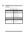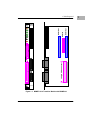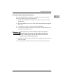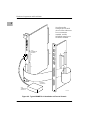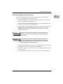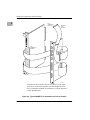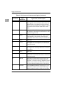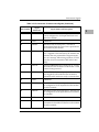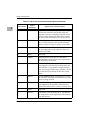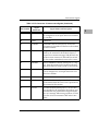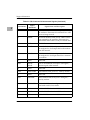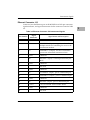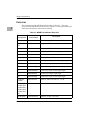
1
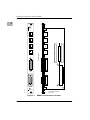
MVME712-10
Transition Module
User’s Manual
(MVME712-10/D1)
Notice
While reasonable efforts have been made to assure the accuracy of this document,
Motorola, Inc. assumes no liability resulting from any omissions in this document, or
from the use of the information obtained therein. Motorola reserves the right to revise
this document and to make changes from time to time in the content hereof without
obligation of Motorola to notify any person of such revision or changes.
No part of this material may be reproduced or copied in any tangible medium, or
stored in a retrieval system, or transmitted in any form, or by any means, radio,
electronic, mechanical, photocopying, recording or facsimile, or otherwise, without the
prior written permission of Motorola, Inc.
It is possible that this publication may contain reference to, or information about
Motorola products (machines and programs), programming, or services that are not
announced in your country. Such references or information must not be construed to
mean that Motorola intends to announce such Motorola products, programming, or
services in your country.
Restricted Rights Legend
If the documentation contained herein is supplied, directly or indirectly, to the U.S.
Government, the following notice shall apply unless otherwise agreed to in writing by
Motorola, Inc.
Use, duplication, or disclosure by the Government is subject to restrictions as set forth
in subparagraph (c)(1)(ii) of the Rights in Technical Data and Computer Software
clause at DFARS 252.227-7013.
Motorola, Inc.
Computer Group
2900 South Diablo Way
Tempe, Arizona 85282
Safety Summary
Safety Depends On You
The following general safety precautions must be observed during all phases of operation, service, and
repair of this equipment. Failure to comply with these precautions or with speciÞc warnings elsewhere in
this manual violates safety standards of design, manufacture, and intended use of the equipment. Motorola,
Inc. assumes no liability for the customer's failure to comply with these requirements.
The safety precautions listed below represent warnings of certain dangers of which Motorola is aware. You,
as the user of the product, should follow these warnings and all other safety precautions necessary for the
safe operation of the equipment in your operating environment.
Ground the Instrument.
To minimize shock hazard, the equipment chassis and enclosure must be connected to an electrical ground.
The equipment is supplied with a three-conductor ac power cable. The power cable must either be plugged
into an approved three-contact electrical outlet or used with a three-contact to two-contact adapter, with the
grounding wire (green) Þrmly connected to an electrical ground (safety ground) at the power outlet. The
power jack and mating plug of the power cable meet International Electrotechnical Commission (IEC) safety
standards.
Do Not Operate in an Explosive Atmosphere.
Do not operate the equipment in the presence of ßammable gases or fumes. Operation of any electrical
equipment in such an environment constitutes a deÞnite safety hazard.
Keep Away From Live Circuits.
Operating personnel must not remove equipment covers. Only Factory Authorized Service Personnel or
other qualiÞed maintenance personnel may remove equipment covers for internal subassembly or
component replacement or any internal adjustment. Do not replace components with power cable
connected. Under certain conditions, dangerous voltages may exist even with the power cable removed. To
avoid injuries, always disconnect power and discharge circuits before touching them.
Do Not Service or Adjust Alone.
Do not attempt internal service or adjustment unless another person, capable of rendering Þrst aid and
resuscitation, is present.
Use Caution When Exposing or Handling the CRT.
Breakage of the Cathode-Ray Tube (CRT) causes a high-velocity scattering of glass fragments (implosion).
To prevent CRT implosion, avoid rough handling or jarring of the equipment. Handling of the CRT should
be done only by qualiÞed maintenance personnel using approved safety mask and gloves.
Do Not Substitute Parts or Modify Equipment.
Because of the danger of introducing additional hazards, do not install substitute parts or perform any
unauthorized modiÞcation of the equipment. Contact your local Motorola representative for service and
repair to ensure that safety features are maintained.
Dangerous Procedure Warnings.
Warnings, such as the example below, precede potentially dangerous procedures throughout this manual.
Instructions contained in the warnings must be followed. You should also employ all other safety
precautions which you deem necessary for the operation of the equipment in your operating environment.
!
WARNING
Dangerous voltages, capable of causing death, are present in
this equipment. Use extreme caution when handling,
testing, and adjusting.
The computer programs stored in the read only memories of this device contain
material copyrighted by Motorola, Inc., Þrst published 1988, and may be used only
under a license such as the License for Computer Programs (Article 14) contained in
MotorolaÕs Terms and conditions of Sale, Rev. 1/79.
!
WARNING
This equipment generates, uses, and can radiate radio
frequency energy and if not installed and used in
accordance with the documentation for this product, may
cause interference to radio communications. It has been
tested and found to comply with the limits for a Class A
Computing Device pursuant to Subpart J of Part 15 of FCC
rules, which are designed to provide reasonable protection
against such interference when operated in a commercial
environment. Operation of this equipment in a residential
area is likely to cause interference in which case the user, at
the userÕs own expense, will be required to take whatever
measures necessary to correct the interference.
Motorola¨ and the Motorola symbol are registered trademarks of Motorola, Inc.
VMEmodule is a trademark of Motorola, Inc.
All other products mentioned in this document are trademarks or registered
trademarks of their respective holders.
© Copyright Motorola 1993
All Rights Reserved
Printed in the United States of America
May 1993
Preface
The MVME712-10 Transition Module UserÕs Manual provides general information,
hardware preparation, installation instructions, and support information for the
MVME712-10 Transition Module.
The MVME712-10 is used as the interface between MotorolaÕs MVME166 Single Board
Computers and their peripheral devices.
This manual is intended for anyone who wants to design OEM systems, supply
additional capability to an existing compatible system, or in a lab environment for
experimental purposes.
A basic knowledge of computers and digital logic is assumed.
To use this manual, you should be familiar with the publications listed in the related
documentation paragraphs on the following page.
Related Documentation
The Motorola publications listed in the table below are referenced in this document. If
not shipped with this product, manuals may be purchased by contacting your local
Motorola sales ofÞce.
Motorola
Publication
Number
Document Title
MVME166 Single Board Computer UserÕs Manual
MVME166/D
MVME166/MVME167/MVME187 ProgrammerÕs
Reference Manual
MVME187PG/D
N ote
Although not shown in the above table, each Motorola
Computer Group manual publication number is suffixed
with characters which represent the revision level of the
document, such as Ò/D2Ó (the second revision of a manual);
a supplement bears the same number as the manual but has
a suffix such as Ò/A1Ó (the first supplement to the manual).
The SCSI speciÞcation referenced in this document is the following:
SCSI-2 (Small Computer Systems Interface - 2), draft document X3.131,
Revision 10c; Global Engineering Documents, P.O. Box 19539, Irvine, CA
92714.
Contents
Introduction 1-1
Features 1-1
SpeciÞcations 1-2
Cooling Requirements 1-3
FCC Compliance 1-3
General Description 1-4
Cables Required 1-4
Introduction 2-1
Unpacking Instructions 2-1
MVME712-10 Module Preparation 2-1
Serial Port ConÞguration 2-3
Serial Port DCE Configuration 2-3
Serial Port DTE Configuration 2-3
Configuration Register 2-3
Installation Instructions 2-8
MVME712-10 Module Installation 2-8
Front Chassis Mount, External SCSI Devices 2-9
Front Chassis Mount, Internal SCSI Devices 2-11
2-12
Rear Chassis Mount, Internal SCSI Devices 2-13
Introduction 3-1
Manual Terminology 3-1
Interconnect Signals 3-1
EIA-232-D Connectors J1, J2, J3, and J4 3-2
SCSI Connectors J5 and J7 3-3
SCSI Connector J6 3-4
Printer/Parallel Connector J8 3-5
I/O Connector J9 3-6
Ethernet Connector J10 3-13
Parts List 3-14
Schematic Diagram 3-17
vii
List of Figures
MVME712-10 Transition Module with MVME166 1-5
MVME712-10 Connector Locations 2-2
MVME712-10 Serial Port ConÞgured as DCE (to Terminal) 2-5
MVME712-10 Serial Port ConÞgured as DTE (to Modem) 2-6
MVME712-10 ConÞguration Register 2-7
Typical MVME712-10 Installation at Front of Chassis 2-10
Typical MVME712-10 Installation at Front of Chassis 2-12
Typical MVME712-10 Installation at Rear of Chassis 2-14
MVME712-10 Parts Location 3-16
List of Tables
MVME712-10 SpeciÞcations 1-2
EIA-232-D Connectors J1, J2, J3, and J4 Interconnect Signals 3-2
SCSI Connectors J5 and J7 Interconnect Signals 3-3
SCSI Connector J6 Interconnect Signals 3-4
Printer/Parallel Connector J8 Interconnect Signals 3-5
I/O Connector J9 Interconnect Signals 3-6
Ethernet Connector J10 Interconnect Signals 3-13
MVME712-10 Module Parts List 3-14
ix
x
GENERAL INFORMATION
1
Introduction
This manual provides general information, hardware preparation, installation
instructions, and support information for the MVME712-10 Transition
Module.
The MVME712-10 is used as the interface between MotorolaÕs MVME166
Single Board Computer VMEmodule and its peripheral devices.
Features
The features of the MVME712-10 Transition Module include:
❏
Four shielded RJ45 jacks for EIA-232-D serial I/O
❏
Shielded DB-25 external parallel or printer port
❏
Shielded external DB-15 Ethernet interface port
❏
SCSI converter (high-density to low-density):
Ð
68-pin high-density, 16-bit-wide SCSI connector and high-density "P
cable" for connection to the MVME166
Ð
50-pin low-density, 8-bit-wide SCSI connector for connection to the
internal SCSI device(s)
❏
100-pin I/O connector and high-density cable for connection to the
MVME166 for I/O
❏
Radio Frequency Interference (RFI) protection on front panel
❏
Electrostatic Discharge (ESD) protection on front panel
MVME712-10/D11-1
1
General Information
Specifications
The MVME712-10 specifications are given in Table 1-1.
Table 1-1: MVME712-10 Specifications
Characteristics
SpeciÞcations
Power requirements
I/O ports
Serial
+5 Vdc, 150 mA typical
+12 Vdc, 50 mA typical
-12 Vdc, 50 mA typical
Four shielded EIA-232-D serial ports
with RJ45 connectors
SCSI connector converter
Printer
Shielded parallel port, DB-25
Ethernet
Height
Shielded parallel port, DB-15
0 degrees to 55 degrees C at point of entry
of forced air (approximately 5 CFM)
-40 degrees to 85 degrees C
5% to 90% (non-condensing)
9.187 inches (233.35 mm)
Depth
3.2 inches (80 mm)
Operating temperature
Storage temperature
Relative humidity
Physical
characteristics
Front panel width
1-2
0.8 inches (20.32 mm)
MVME712-10 Transition Module and I/O Distribution Set UserÕs Manual
Specifications
Cooling Requirements
Motorola VMEmodules are specified, designed, and tested to operate reliably
with an incoming air temperature range from 0 degrees C to 55 degrees C (32
degrees F to 131 degrees F) with forced air cooling.
Temperature qualification is performed in a standard Motorola MVME900
series chassis. Twenty-five watt load boards are inserted in the two card slots,
one on each side, adjacent to the board under test to simulate a high power
density system configuration. An assembly of three axial fans, rated at 71 CFM
per fan, is placed directly under the MVME card cage. The incoming air
temperature is measured between the fan assembly and the card cage where
the incoming airstream first encounters the module under test.
Test software is executed as the module is subjected to ambient temperature
variations. Case temperatures of critical, high power density integrated
circuits are monitored to ensure component vendor specifications are not
exceeded.
While the exact amount of airflow required for cooling depends on the
ambient air temperature and the type, number, and location of boards and
other heat sources, adequate cooling can usually be achieved with 5 CFM
flowing over the module. Less air flow is required to cool the module in
environments having lower maximum ambients.
Under more favorable thermal conditions it may be possible to operate the
module reliably at higher than 55 degrees C with increased air flow. It is
important to note that there are several factors, in addition to the rated CFM of
the air mover, which determine the actual volume of air flowing over a
module.
FCC Compliance
The MVME712-10 transition board was tested in an FCC-compliant chassis,
and meets the requirements for Class A equipment. FCC compliance was
achieved under the following conditions:
❏
Shielded cables on all external I/O ports.
❏
Cable shields connected to earth ground via metal shell connectors
bonded to a conductive module front panel.
❏
Conductive chassis rails connected to earth ground. This provides the
path for connecting shields to earth ground.
❏
Front panel screws properly tightened.
MVME712-10/D1
1-3
1
1
General Information
For minimum RF emissions, it is essential that the conditions above be
implemented; failure to do so could compromise the FCC compliance of the
equipment containing the modules.
General Description
The MVME712-10 Transition Module is a low-cost I/O transition board for
MotorolaÕs MVME166 Single Board Computer VMEmodules and their
peripheral devices. Refer to Figure 1-1.
The MVME712-10 routes the signals to the appropriate industry standard
connectors on its front panel. This board can be mounted either next to the
MVME166 or in the back of the chassis. The board contains four shielded 8-pin
RJ45 jacks for EIA-232-D serial interface, a shielded DB-15 connector for
Ethernet, and a shielded DB-25 connector for parallel interface.
The MVME712-10 also provides conversion from the 68-pin high-density SCSI
connector to a standard 50-pin low-density SCSI connector.
Each EIA-232-D serial port transmits the following signals:
❏
Data carrier detect
❏
Request to send
❏
Transmit data
❏
Receive data
❏
Clear to send
❏
Data terminal ready
Cables Required
The following cables are needed in order to connect the MVME712-10 to the
MVME166 and other devices:
1-4
❏
One 100-conductor, 25 mil pitch cable to connect the MVME712-10 to the
MVME166 for I/O (a 1-foot-long cable is furnished by Motorola).
❏
One 68-conductor, 25 mil pitch P cable to connect the SCSI port on the
MVME712-10 to the SCSI port on the MVME166 (a 1-foot-long cable is
furnished by Motorola).
❏
One 50-conductor, 50 mil pitch A cable for 8-bit wide SCSI connection to
internal SCSI devices (customer-supplied).
MVME712-10 Transition Module and I/O Distribution Set UserÕs Manual
Cables Required
MVME
166
MVME
712-10
SCSI Out
SCSI In
PORT 2
TERM VSB
PORT 1
LAN RPWR
SCSI VME
CONSOLE
RUN SCON
SCSI Out
FAIL STAT
ABORT
PORT 3
RESET
PORT 4
PARALLEL/PRINTER PORT
I/O
ETHERNET PORT
100-pin I/O Connector
SCSI
MOTOROLA
MOTOROLA
Figure 1-1. MVME712-10 Transition Module with MVME166
MVME712-10/D1
1-5
1
1
General Information
1-6
MVME712-10 Transition Module and I/O Distribution Set UserÕs Manual
HARDWARE PREPARATION AND
INSTALLATION INSTRUCTIONS
2
Introduction
This chapter provides unpacking instructions, hardware preparation, and
installation instructions for the MVME712-10 Transition Module.
Unpacking Instructions
N ote
If the carton is damaged upon receipt, request that carrier's
agent be present during unpacking and inspection of the
equipment.
Unpack the equipment from the shipping carton. Refer to the packing list and
verify that all items are present. Save the packing material for storing and
reshipping of the equipment.
MVME712-10 Module Preparation
The location of the connectors on the MVME712-10 is illustrated in Figure 2-1.
The module has been factory tested and is configured for DTE, but can be
operated as DCE with an appropriate external adapter if desired. The
connectors are:
❏
Four RJ45 EIA-232-D serial ports with DTE configuration (J1, J2, J3, J4)
❏
SCSI converter connectors (J5, J6, J7)
❏
Printer/parallel connector (J8)
❏
I/O connector (J9)
❏
Ethernet connector (J10)
MVME712-10/D12-1
Hardware Preparation and Installation
2
MVME
712-10
J1
PORT1
CONSOLE
J2
PORT2
J3
PORT3
J4
PORT 4
J7
J6
J5
PRIMARY SIDE
J8
PARALLEL/PRINTER PORT
J9
COMPONENTS REMOVED
FOR CLARITY
Figure 2-1.
2-2
J10
ETHERNET
1142 9302
MOTOROLA
MVME712-10 Connector Locations
MVME712-10 Transition Module and I/O Distribution Set UserÕs Manual
MVME712-10 Module Preparation
Serial Port Configuration
2
The four RJ45 EIA-232-D serial ports are factory configured as terminal (DTE)
for connection to modem. However, they can be used as modem-to-terminal
(DCE) by using an appropriate user-supplied external DCE adapter.
Serial Port DCE Configuration
Figure 2-2 shows the schematic representation of the DCE configuration of
serial ports 1 through 4, using a user-supplied external DCE adapter.
Serial Port DTE Configuration
Figure 2-3 shows the schematic representation of the DTE configuration of
serial ports 1 through 4, using a user-supplied external DTE adapter.
Configuration Register
Figure 2-4 illustrates the function of the configuration register on the
MVME712-10. The application software on the MVME166 can read the
configuration information to identify the transition board(s) in the system.
On the MVME166, the MC68230 interrupt level is the same as the CD2401. The
interrupt vector is as programmed in the MC68230. The interrupt priority is (1)
first the CD2401, and (2) then the MC68230.
To read the configuration information, the MC68230 (PI/T) must be
programmed as follows:
❏
❏
Port A direction must be:
Ð
Mode 0, submode 1X
Ð
Bits 7 to 4 as inputs
Ð
Bits 3 to 0 as outputs.
Port B direction must be:
Ð
Mode 0, submode 1X
Ð
Bit 7 as an output
Ð
Bits 6 to 0 as inputs
Write port B bits 7 to 0 set configuration mode. Now port A bits 3 to 0 are used
to select a port.
MVME712-10/D1
2-3
Hardware Preparation and Installation
2
Port A Bits 3 to 0
Port Selected
0
1
2
3
0
1
2
3
Port A bits 7 to 4 are the configuration data returned from the port selected:
ConÞguration
Register
Port A Bits 7 to 4
0
1
2-8
9
A-F
Module Type
EIA-232 DCE
EIA-232 DTE
Reserved
EIA-232 RJ45 DTE
Reserved
Module Implemented on
MVME712-06
MVME712-06
MVME712-10
Refer to the MVME166/MVME167/MVME187 Single Board Computer
ProgrammerÕs Reference Manual for more information.
2-4
MVME712-10 Transition Module and I/O Distribution Set UserÕs Manual
MVME712-10/D1
D
RTS
RXCO
RXCI
TXCI
DD
RR
RXD
TXD
RR
R
DCD
DSR
D
100-PIN
CABLE
DTR
CTS
2401
MVME 166
1.5K
1.5K
1.5K
MC145406
MC145406
MC145406
MC145406
MC145406
MC145406
0
MVME712-10
TRANSITION
BOARD
+5V
GND
TXD
RXD
DCD
GND
RTS
DTR
CTS
6
4
5
1
3
2
8
7
RJ45
1
8
6
4
5
1
3
2
8
7
3
5
4
8
6
7
1
2
RJ45
ADAPTER
DTE (TERMINAL)
DEVICE TO RJ45
RJ45 JACK
NOTE: PIN 1 IS TO THE LEFT
WITH THE OPENING FACING YOU
3
5
4
8
6
7
1
2
CROSSOVER
CABLE
RJ45 TO RJ45
GND
RXD
TXD
DTR
DSR
CTS
DCD
RTS
1130 9302
7
3
2
20
6
5
8
4
DB25
MVME712-10 Module Preparation
2
Figure 2-2. MVME712-10 Serial Port Configured as DCE (to Terminal)
2-5
2-6
D
RTS
RXCO
RXCI
TXCI
DD
RR
RXD
TXD
RR
R
DCD
DSR
D
100-PIN
CABLE
DTR
CTS
2401
MVME 166
1.5K
1.5K
1.5K
MC145406
MC145406
MC145406
MC145406
MC145406
MC145406
0
MVME712-10
TRANSITION
BOARD
+5V
GND
6
4
5
1
8
6
4
5
1
1
DCD
RXD
3
2
8
7
3
2
8
7
RJ45
GND
RTS
DTR
CTS
3
5
4
8
6
7
1
2
RJ45
NC
ADAPTER
DCE (MODEM)
DEVICE TO RJ45
RJ45 JACK
NOTE: PIN 1 IS TO THE LEFT
WITH THE OPENING FACING YOU
3
5
4
8
6
7
1
2
CROSSOVER
CABLE
RJ45 TO RJ45
GND
TXD
RXD
DCD
DSR
RTS
DTR
CTS
1129 9302
7
2
3
8
6
4
20
5
DB25
Hardware Preparation and Installation
2
Figure 2-3. MVME712-10 Serial Port Configured as DTE (to Modem)
MVME712-10 Transition Module and I/O Distribution Set UserÕs Manual
MVME712-10/D1
PB0
PB1
PB2
PB3
PB4
PB5
PB6
PB7
HI
H2
H3
H4
PA0
PA1
PA2
PA3
PA4
PA5
PA6
PA7
MC68230
SGPIO<8>
SGPIO<9>
SGPIO<10>
SGPIO<11>
SGPIO<0>
SGPIO<1>
SGPIO<2>
SGPIO<3>
SGPIO<4>
SGPIO<5>
SGPIO<6>
SGPIO<7>
MVME166
SRI1
SRI2
SRI3
SRI4
SLL1
SLL2
SLL3
SLL4
+5V
+5V
1.5K
+5V
1.5K
1.5K
+5V
1.5K
4.7K
4.7K
+5V
+5V
STM1
STM2
STM3
STM4
+5V
4.7K
MVME712-10
E
A
B
C
Y0
Y1
Y2
Y3
Y4
Y5
Y6
Y7
LS138
OE1
OE2
OE1
OE2
BCT244
1.5K
+5V
1131 9303
PORT 4
1.5K CONFIGURATION
INFORMATION
+5V
PORT 3
1.5K CONFIGURATION
INFORMATION
+5V
PORT2
1.5K CONFIGURATION
INFORMATION
+5V
PORT 1
1.5K CONFIGURATION
INFORMATION
+5V
MVME712-10 Module Preparation
2
Figure 2-4. MVME712-10 Configuration Register
2-7
Hardware Preparation and Installation
2
Installation Instructions
Installation of the MVME712-10 is described in the following paragraphs and
illustrations. The basic procedure for installation is as follows:
1.
Turn all equipment power OFF and disconnect the power cable from the
AC power source.
C aution
Connecting modules while power is applied may result in
damage to components on the module.
!
Dangerous voltages, capable of causing death, are present in
this equipment. Use extreme caution when handling,
testing, and adjusting.
WARNING
2.
Remove the chassis cover as instructed in the equipment user's manual.
3.
Determine whether you wish to install the MVME712-10 at the front of the
chassis or at the rear of the chassis.
4.
Remove the Þller panel(s) from the appropriate card slot(s) at the front of
the chassis, or at the rear of the chassis (if the chassis has a rear card cage),
depending upon whether you are installing the MVME712-10 at the front
or at the back. Other modules in the unit may have to be moved to allow
space for the cables for the MVME712-10.
5.
Ensure that the MVME166 has been properly installed in the chassis and
then proceed with the installation instructions that follow.
MVME712-10 Module Installation
The MVME712-10 can be installed either in the front of the chassis or at the
rear, and can be cabled to the MVME166 and to SCSI peripherals in different
configurations. The configurations are described and illustrated on the
following pages.
The recommended configuration is the MVME712-10 installed in the front of
the chassis, connected to the MVME166 using the Motorola-supplied I/O and
SCSI P cables, with external SCSI drives connected to the MVME712-10 using
a customer-supplied cable, as illustrated in Figure 2-5.
Other configurations may require user-supplied cables designed for the
specific chassis and SCSI configuration.
An Ethernet cable, a printer, and/or terminals can be connected to the
respective connectors on the front panel of the MVME712-10.
2-8
MVME712-10 Transition Module and I/O Distribution Set UserÕs Manual
Installation Instructions
Front Chassis Mount, External SCSI Devices
2
To mount the MVME712-10 in the front of the chassis with external SCSI
devices, proceed as follows and see Figure 2-5.
1.
Connect the furnished 100-conductor I/O cable to connector J9 on the
MVME712-10.
2.
Install the MVME712-10 in a slot to the right of the MVME166 and tighten
the screws.
3.
Connect the I/O cable to connector J9 on the MVME166.
4.
Connect the furnished P cable from connector J8 on the MVME166 to the
external SCSI peripheral device.
C aution
SCSI terminators must be installed on the devices that are
physically located at each end of the SCSI cable, and must
not be on other devices on the cable. Refer to the SCSI
specification for detailed instructions.
5.
Install the cover that you previously removed, making sure that it does not
pinch any cables.
6.
Connect the power cable to the AC power source and turn the unit on.
MVME712-10/D1
2-9
Hardware Preparation and Installation
2
Note that in this
example, the last SCSI
device on the cable must
have a terminator
installed, and the
MVME166 must have a
terminator enabled.
P1
MVM
E
166
MVM
E
712-10
PORT 1
SCSI
TERMINATOR
ENABLED
SCSI
PORT 2
P2
J8
J7
J5
J6
PORT 3
PORT 4
J9
I/O
PARALLEL/PRINTER PORT
J9
MOT
ORO
LA
ETHERNET
EXTERNAL
SCSI DEVICE
SCSI
TERMINATOR
INSTALLED
1143 9303
Figure 2-5. Typical MVME712-10 Installation at Front of Chassis
2-10
MVME712-10 Transition Module and I/O Distribution Set UserÕs Manual
Installation Instructions
Front Chassis Mount, Internal SCSI Devices
2
To mount the MVME712-10 at the front of the chassis with internal SCSI
devices, proceed as follows and see Figure 2-6.
1.
Insert the MVME712-10 module into the selected slot at the front of the
chassis and tighten the attaching screws.
2.
Connect the furnished P cable from connector J6 on the MVME712-10 to
connector J8 on the front of the MVME166.
3.
If the P cable at J6 on the MVME712-10 covers connector J5, connect a usersupplied cable with compatible pinouts from connector J7 on the
MVME712-10 to the internal SCSI device. If connector J7 is covered,
connect the cable to J5.
C aution
J5 and J7 are functionally the same. Do NOT use both at the
same time, because to do so would create a SCSI stub greater
than .1 meter.
C aution
SCSI terminators must be installed on the devices that are
physically located at each end of the SCSI cable, and must
not be on other devices on the cable. Refer to the SCSI
specification for detailed instructions.
4.
Connect the furnished 100-conductor I/O cable from connector J9 on the
MVME712-10 to I/O connector J9 on the MVME166.
5.
Install the cover that you previously removed, making sure that it does not
pinch any cables.
6.
Connect the power cable to the AC power source and turn the unit on.
MVME712-10/D1
2-11
Hardware Preparation and Installation
2
SCSI
TERMINATOR
INSTALLED
INTERNAL
SCSI
DEVICES
P1
MVM
E
166
MVM
E
712-10
P2
PORT 2
SCSI
J8
PORT 1
SCSI
TERMINATOR
ENABLED
J7
J5
J6
PORT 3
PORT 4
J9
J9
PARALLEL/PRINTER PORT
I/O
MOT
ORO
LA
ETHERNET
1137 9303
Note that in this example, the last SCSI device on the cable
must have a terminator installed, and the MVME166 must
have a terminator enabled. No terminator would be required
on the MVME712-10.
Figure 2-6. Typical MVME712-10 Installation at Front of Chassis
2-12
MVME712-10 Transition Module and I/O Distribution Set UserÕs Manual
Installation Instructions
Rear Chassis Mount, Internal SCSI Devices
2
To mount the MVME712-10 at the rear of the chassis with internal SCSI
devices, proceed as follows and see Figure 2-7.
1.
Insert the MVME712-10 module into the selected slot at the rear of the
chassis and tighten the attaching screws.
2.
Connect the furnished P cable from connector J6 on the MVME712-10 to
connector J8 on the front of the MVME166. A longer cable may be needed
for some chassis conÞgurations.
3.
If the P cable at J6 on the MVME712-10 covers connector J5, connect a usersupplied cable with compatible pinouts from connector J7 on the
MVME712-10 to the internal SCSI device. If connector J7 is covered,
connect the cable to J5.
C aution
J5 and J7 are functionally the same. Do NOT use both at the
same time, because to do so would create a SCSI stub greater
than .1 meter.
C aution
SCSI terminators must be installed on the devices that are
physically located at each end of the SCSI cable, and must
not be on other devices on the cable. Refer to the SCSI
specification for detailed instructions.
4.
Connect the furnished 100-conductor I/O cable between connector J9 on
the MVME712-10 and I/O connector J9 on the MVME166. A longer cable
may be needed for some chassis conÞgurations.
5.
Install the cover that you previously removed, making sure that it does not
pinch any cables.
6.
Connect the power cable to the AC power source and turn the unit on.
MVME712-10/D1
2-13
Hardware Preparation and Installation
2
INTERNAL
SCSI
DEVICES
SCSI
DEVICE
SCSI
TERMINATOR
INSTALLED
SCSI
DEVICE
MVME712-10
MVME166
1
2
P1
3
J5
J7
J8
SCSI
TERMINATOR
ENABLED
J6
4
SCSI
J8
P2
J10
J9
J9
BACK
FRONT
ENCLOSURE
1136 9309
Note that in this example, the last SCSI device on the cable
must have a terminator installed, and the MVME166 must
have a terminator enabled. No terminator would be required
on the MVME712-10.
Figure 2-7. Typical MVME712-10 Installation at Rear of Chassis
2-14
MVME712-10 Transition Module and I/O Distribution Set UserÕs Manual
SUPPORT INFORMATION
3
Introduction
This chapter provides the interconnection signals, parts lists with parts
location illustrations, and schematic diagrams for the MVME712-10 Transition
Module.
Manual Terminology
An asterisk (*) following the signal name for signals which are level significant
denotes that the signal is true or valid when the signal is low.
An asterisk (*) following the signal name for signals which are edge significant
denotes that actions initiated by that signal occur on high to low transition.
Interconnect Signals
80-pin connectors J1 through J4 on the MVME712-10 correspond to the RJ45
EIA-232-D serial ports on the MVME712-10 front panel.
J5 and J7 are identical 50-pin connectors for low-density 8-bit-wide SCSI cable
(one is accessible from the front and one from the back of the board) and are
connected internally to J6, a high-density 16-bit-wide SCSI connector for the P
cable. Connector J6 is cabled to connector J8 on the MVME166.
C aution
J5 and J7 are functionally the same. Do NOT use both at the
same time, because to do so would create a SCSI stub greater
than .1 meter.
J8 is a 25-pin connector for the printer port, and J10 is a 15-pin connector for
the Ethernet interface.
J9 is a 100-pin connector that is cabled to connector J9 on the MVME166 SBC
for I/O.
All front panel connectors have metal shells and jack posts that are electrically
connected to the front panel. If the front panel is electrically connected to the
chassis ground then the shells and jack posts are connected to chassis ground.
This allows shielded cable to be used for effective reduction of EMI and RFI
problems.
MVME712-10/D13-1
Support Information
EIA-232-D Connectors J1, J2, J3, and J4
Connectors J1, J2, J3, and J4 are 8-pin connectors that correspond to the RJ45
EIA-232-D serial ports 1, 2, 3, and 4, respectively, on the front of the
MVME712-10. Each pin connection, signal mnemonic, and signal
characteristic for the connectors is listed in Table 3-1.
3
Table 3-1: EIA-232-D Connectors J1, J2, J3, and J4 Interconnect Signals
Pin Number
Signal
Mnemonic
Signal Name and Description
1
DCD
DATA CARRIER DETECT - Sent by the modem to
the terminal to indicate that a valid carrier is being
received.
2
RTS
REQUEST TO SEND - RTS is supplied by the terminal to the modem when it is required to transmit a message. With RTS off, the modem carrier
remains off. When RTS is turned on, the modem
immediately turns on the carrier.
3
GND
GROUND
4
TXD
TRANSMIT DATA - data to be transmitted is furnished on this line to the modem from the terminal.
5
RXD
RECEIVE DATA - data that is demodulated from
the receive line is presented to the terminal by the
modem.
6
GND
GROUND
7
CTS
CLEAR TO SEND - CTS is a function supplied to
the terminal by the modem, and indicates that it is
permissible to begin transmission of a message.
When using a modem, CTS follows the off-to-on
transition of RTS after a time delay.
8
DTR
DATA TERMINAL READY (serial port 1) - A signal from the terminal to the modem indicating
that the terminal is ready to send or receive data.
3-2
MVME712-10 Transition Module and I/O Distribution Set UserÕs Manual
Interconnect Signals
SCSI Connectors J5 and J7
Connectors J5 and J7 are identical; two connectors are provided for
convenience of access. They convert low-density 8-bit-wide SCSI connectors to
the high-density 16-bit-wide connector J6 (theP cable connector). Each pin
connection, signal mnemonic, and signal characteristic for the connectors is
listed in Table 3-2. Refer also to the schematic diagram for SCSI interconnect
lines.
Table 3-2: SCSI Connectors J5 and J7 Interconnect Signals
Pin Number
Signal
Mnemonic
Signal Name and Description
1
GND
GROUND
2 - 21
SCSI06SCSI25
SCSI interconnect lines.
22
GND
GROUND
23, 24
25, 26
Not used.
TERMPWR*
27, 28
TERMINATOR POWER
Not used.
29, 30
SCSI26,
SCSI27
SCSI interconnect lines.
31
GND
GROUND - This ground isolated from rest of
board for SCSI only.
32-48
SCSI28SCSI44
SCSI interconnect lines.
49
GND
GROUND - This ground isolated from rest of
board for SCSI only.
50
SCSI45
SCSI interconnect lines.
MVME712-10/D1
3-3
3
Support Information
SCSI Connector J6
Connector J6 is a high-density 16-bit-wide SCSI P cable connector that is
connected internally to the low-density 8-bit wide SCSI connectors J5 and J7.
Each pin connection, signal mnemonic, and signal characteristic for the
connector is listed in Table 3-3. Refer also to the schematic diagram for SCSI
interconnect lines.
3
Table 3-3: SCSI Connector J6 Interconnect Signals
Pin Number
Signal
Mnemonic
1-10
Signal Name and Description
Not connected.
11
GND
GROUND - This ground isolated from rest of
board for SCSI only.
12-31
SCSI06SCSI25
SCSI interconnect lines.
32
GND
GROUND - This ground isolated from rest of
board for SCSI only.
33-36
TERMPWR
TERMINATOR POWER
37, 38
Not used.
39, 40
SCSI26,
SCSI27
SCSI interconnect lines.
41
GND
GROUND - This ground isolated from rest of
board for SCSI only.
42-58
SCSI28SCSI44
SCSI interconnect lines.
59
GND
GROUND - This ground isolated from rest of
board for SCSI only.
60
SCSI45
SCSI interconnect lines.
61-68
3-4
Not connected.
MVME712-10 Transition Module and I/O Distribution Set UserÕs Manual
Interconnect Signals
Printer/Parallel Connector J8
Connector J8 is the Printer/Parallel port on the MVME712-10. Each pin
connection, signal mnemonic, and signal characteristic for the connector is
listed in Table 3-4.
3
Table 3-4: Printer/Parallel Connector J8 Interconnect Signals
Pin Number
Signal
Mnemonic
Signal Name and Description
1
PRSTB*
DATA STROBE (Printer) - an active low output
pulse used to clock data from the system to the
printer.
2-9
PRD0-PRD7
DATA (bits 0-7) (Printer)
10
PRACK*
DATA ACKNOWLEDGE (Printer) - a low level
input pulse indicating that the next character may
be sent.
11
PRBSY
BUSY (Printer) - an input signal indicating that the
printer cannot receive data.
12
PRPE
PAPER EMPTY (Printer) - out of paper.
13
PRSEL
SELECTED (Printer) - an input signal indicating
that the printer is selected.
14
Not used.
15
PRFAULT*
FAULT (Printer) - an input signal that indicates a
printer fault condition.
16
INPRIME*
INPUT PRIME (Printer) - an output signal that
clears the printer buffer and initializes the logic.
17
18-25
MVME712-10/D1
Not used.
GND
GROUND
3-5
Support Information
I/O Connector J9
Connector J9 on the MVME712-10 is used to cable to the MVME166. Each pin
connection, signal mnemonic, and signal characteristic for the connector is
listed in Table 3-5.
3
Table 3-5: I/O Connector J9 Interconnect Signals
Pin Number
Signal
Mnemonic
Signal Name and Description
1
C+
COLLISION + (Input) (Ethernet) - a signal to indicate that multiple stations are contending for
access to the transmission medium.
2
C-
COLLISION - (Input) (Ethernet) - part of a differential pair.
3
T+
TRANSMIT + (Output) (Ethernet) - this line is
intended to operate into terminated transmission
lines.
4
T-
TRANSMIT - (Output) (Ethernet) - part of a differential pair.
5
R+
RECEIVE + (Input) (Ethernet) - a data input
sourced by the MAU.
6
R-
RECEIVE - (Input) (Ethernet) - part of a differential pair.
7
GND
GROUND
8-15
PRD0-PRD7
DATA (bits 0-7) (Printer)
16
GND
GROUND
17
PRSTB*
DATA STROBE (Printer) - an active low output
pulse used to clock data from the system to the
printer.
18
INPRIME*
INPUT PRIME (Printer) - an output signal that
clears the printer buffer and initializes the logic.
19
GND
GROUND
3-6
MVME712-10 Transition Module and I/O Distribution Set UserÕs Manual
Interconnect Signals
Table 3-5: I/O Connector J9 Interconnect Signals (Continued)
Pin Number
Signal
Mnemonic
Signal Name and Description
3
20
PRACK*
DATA ACKNOWLEDGE (Printer) - a low level
input pulse indicating that the next character may
be sent.
21
PRBSY
BUSY (Printer) - an input signal indicating that the
printer cannot receive data.
22
PRPE
PAPER EMPTY (Printer) - out of paper.
23
PRSEL
SELECTED (Printer) - an input signal indicating
that the printer is selected.
24
PRFAULT*
FAULT (Printer) - an input signal that indicates a
printer fault condition.
25
GND
GROUND
26
STXD1B
TRANSMIT DATA (serial port 1) - data to be
transmitted is furnished on this line to the modem
from the terminal.
27
SRTS1B
REQUEST TO SEND (serial port 1) - RTS is supplied by the terminal to the modem when it is
required to transmit a message. With RTS off, the
modem carrier remains off. When RTS is turned
on, the modem immediately turns on the carrier.
28
SDTR1B
DATA TERMINAL READY (serial port 1) - a signal from the terminal to the modem indicating
that the terminal is ready to send or receive data.
29
SRXCO1B
RECEIVE CLOCK OUT (serial port 1) - this line
can be conÞgured to clock input data from a terminal to a modem.
30
GND
GROUND
31
SRXD1
RECEIVE DATA (serial port 1) - data that is
demodulated from the receive line is presented to
the terminal by the modem.
MVME712-10/D1
3-7
Support Information
Table 3-5: I/O Connector J9 Interconnect Signals (Continued)
Pin Number
3
Signal
Mnemonic
Signal Name and Description
32
SCTS1
CLEAR TO SEND (serial port 1) - CTS is a function supplied to the terminal by the modem, and
indicates that it is permissible to begin transmission of a message. When using a modem, CTS follows the off-to-on transition of RTS after a time
delay.
33
SDCD1
DATA CARRIER DETECT (serial port 1) - sent by
the modem to the terminal to indicate that a valid
carrier is being received.
34
SDSR1
DATA SET READY (serial port 1) - DSR is a function supplied by the modem to the terminal to
indicate that the modem is ready to transmit data.
35
GND
GROUND
36
STXCI1
TRANSMIT CLOCK (serial port 1) - this line can
be conÞgured to clock output data to the modem
from the terminal.
37
SRXCI1
RECEIVE CLOCK IN (serial port 1) - this line can
be conÞgured to clock input data from a terminal
to a modem.
38
GND
GROUND
39
STXD2B
TRANSMIT DATA (serial port 2) - data to be
transmitted is furnished on this line to the modem
from the terminal.
40
SRTS2B
REQUEST TO SEND (serial port 2) - RTS is supplied by the terminal to the modem when it is
required to transmit a message. With RTS off, the
modem carrier remains off. When RTS is turned
on, the modem immediately turns on the carrier.
41
SDTR2B
DATA TERMINAL READY (serial port 2) - a signal from the terminal to the modem indicating
that the terminal is ready to send or receive data.
3-8
MVME712-10 Transition Module and I/O Distribution Set UserÕs Manual
Interconnect Signals
Table 3-5: I/O Connector J9 Interconnect Signals (Continued)
Pin Number
Signal
Mnemonic
Signal Name and Description
3
42
SRXCO2B
RECEIVE CLOCK OUT (serial port 2) - this line
can be conÞgured to clock input data from a terminal to a modem.
43
GND
GROUND
44
SRXD2
RECEIVE DATA (serial port 2) - data that is
demodulated from the receive line is presented to
the terminal by the modem.
45
SCTS2
CLEAR TO SEND (serial port 2) - CTS is a function supplied to the terminal by the modem, and
indicates that it is permissible to begin transmission of a message. When using a modem, CTS follows the off-to-on transition of RTS after a time
delay.
46
SDCD2
DATA CARRIER DETECT (serial port 2) - sent by
the modem to the terminal to indicate that a valid
carrier is being received.
47
SDSR2
DATA SET READY (serial port 2) - DSR is a function supplied by the modem to the terminal to
indicate that the modem is ready to transmit data.
48
GND
GROUND
49
STXCI2
TRANSMIT CLOCK (serial port 2) - this line can
be conÞgured to clock output data to the modem
from the terminal.
50
SRXCI2
RECEIVE CLOCK IN (serial port 2) - this line can
be conÞgured to clock input data from a terminal
to a modem.
51
GND
GROUND
52
STXD3B
TRANSMIT DATA (serial port 3) - data to be
transmitted is furnished on this line to the modem
from the terminal.
MVME712-10/D1
3-9
Support Information
Table 3-5: I/O Connector J9 Interconnect Signals (Continued)
Pin Number
3
Signal
Mnemonic
Signal Name and Description
53
SRTS3B
REQUEST TO SEND (serial port 3) - RTS is supplied by the terminal to the modem when it is
required to transmit a message. With RTS off, the
modem carrier remains off. When RTS is turned
on, the modem immediately turns on the carrier.
54
SDTR3B
DATA TERMINAL READY (serial port 3) - a signal from the terminal to the modem indicating
that the terminal is ready to send or receive data.
55
SRXCO3B
RECEIVE CLOCK OUT (serial port 3) - this line
can be conÞgured to clock input data from a terminal to a modem.
56
GND
GROUND
57
SRXD3
RECEIVE DATA (serial port 3) - data that is
demodulated from the receive line is presented to
the terminal by the modem.
58
SCTS3
CLEAR TO SEND (serial port 3) - CTS is a function supplied to the terminal by the modem, and
indicates that it is permissible to begin transmission of a message. When using a modem, CTS follows the off-to-on transition of RTS after a time
delay.
59
SDCD3
DATA CARRIER DETECT (serial port 2) - sent by
the modem to the terminal to indicate that a valid
carrier is being received.
60
SDSR3
DATA SET READY (serial port 4) - DSR is a function supplied by the modem to the terminal to
indicate that the modem is ready to transmit data.
61
GND
GROUND
62
STXCI3
TRANSMIT CLOCK (serial port 3) - this line can
be conÞgured to clock output data to the modem
from the terminal
3-10
MVME712-10 Transition Module and I/O Distribution Set UserÕs Manual
Interconnect Signals
Table 3-5: I/O Connector J9 Interconnect Signals (Continued)
Pin Number
Signal
Mnemonic
Signal Name and Description
3
63
SRXCI3
RECEIVE CLOCK IN (serial port 4) - this line can
be conÞgured to clock input data from a terminal
to a modem.
64
GND
GROUND
65
STXD4B
TRANSMIT DATA (serial port 3) - data to be
transmitted is furnished on this line to the modem
from the terminal.
66
SRTS4B
REQUEST TO SEND (serial port 4) - RTS is supplied by the terminal to the modem when it is
required to transmit a message. With RTS off, the
modem carrier remains off. When RTS is turned
on, the modem immediately turns on the carrier.
67
SDTR4B
DATA TERMINAL READY (serial port 3) - a signal from the terminal to the modem indicating
that the terminal is ready to send or receive data.
68
SRXCO4B
RECEIVE CLOCK OUT (serial port 4) - this line
can be conÞgured to clock input data from a terminal to a modem.
69
GND
GROUND
70
SRXD4
RECEIVE DATA (serial port 4) - data that is
demodulated from the receive line is presented to
the terminal by the modem.
71
SCTS4
CLEAR TO SEND (serial port 4) - CTS is a function supplied to the terminal by the modem, and
indicates that it is permissible to begin transmission of a message. When using a modem, CTS follows the off-to-on transition of RTS after a time
delay.
MVME712-10/D1
3-11
Support Information
Table 3-5: I/O Connector J9 Interconnect Signals (Continued)
Pin Number
3
Signal
Mnemonic
Signal Name and Description
72
SCD4
DATA CARRIER DETECT (serial port 4) - sent by
the modem to the terminal to indicate that a valid
carrier is being received.
73
SDSR4
DATA SET READY (serial port 4) - DSR is a function supplied by the modem to the terminal to
indicate that the modem is ready to transmit data.
74
GND
GROUND
75
STXCI4
TRANSMIT CLOCK (serial port 4) - this line can
be conÞgured to clock output data to the modem
from the terminal.
76
SRXCI4
RECEIVE CLOCK IN (serial port 4) - this line can
be conÞgured to clock input data from a terminal
to a modem.
77
GND
GROUND
78-81
SLL1BSLL4B
LOCAL LOOPBACK (serial ports 1 through 4) reroutes signal within modem.
82
GND
GROUND
83-86
STM1-STM4
TEST MODE (serial ports 1-4) - used by modem.
87
GND
GROUND
88-91
SRI1-SRI4
RING INDICATOR (serial ports 1 through 4) used by modem.
92
RDCONFG*
READ CONFIG - reads conÞguration for transition board serial I/O test mode.
93,94
-12V
-12 Vdc POWER - fused on MPU board.
95,96
+12VF
+12 Vdc POWER - fused on MPU board.
97-100
+5V
+5Vdc POWER - fused on MPU board.
3-12
MVME712-10 Transition Module and I/O Distribution Set UserÕs Manual
Interconnect Signals
Ethernet Connector J10
Connector J10 is the Ethernet port on the MVME712-10. Each pin connection,
signal mnemonic, and signal characteristic for the connector is listed in Table
3-6.
Table 3-6: Ethernet Connector J10 Interconnect Signals
Pin Number
Signal
Mnemonic
Signal Name and Description
1
GND
GROUND
2
C+
COLLISION + (Input) - a signal to indicate that
multiple stations are contending for access to the
transmission medium.
3
T+
TRANSMIT + (Output) - this line is intended to
operate into terminated transmission lines.
4
GND
GROUND
5
R+
RECEIVE + (Input) - a data input sourced by the
MAU.
6
GND
GROUND
7
Not used.
8
GND
GROUND
9
C-
COLLISION - (Input) - part of a differential pair.
10
T-
TRANSMIT - (Output) - part of a differential pair.
11
GND
GROUND
12
R-
RECEIVE - (Input) - part of a differential pair.
13
+12VF
+12 Vdc POWER - fused on MPU board.
14
GND
GROUND
15
MVME712-10/D1
Not used.
3-13
3
Support Information
Parts List
The components of the MVME712-10 are listed in Table 3-7. The parts
locations of the MVME712-10 are shown in Figure 3-1. These parts reflect the
latest issue of hardware at the time of printing.
3
Table 3-7: MVME712-10 Module Parts List
Reference
Designation
Motorola
Part Number
Description
84-W8825B01C
Printed wiring board
C1-C14, C19C22
21NW9711A02
Capacitor, SMD, ceramic, .1 uF @ 50 Vdc
C15-C17
23NW9712A06
Capacitor, SMD, tantalum,33 uF @ 16 Vdc
C18,C23
21NW9711A14
Capacitor, SMD, ceramic, 330 pF @ 50 Vdc
CR1-CR24
48NW9644A01
Diode, zener
CR25,CR26
48NW9638A04
Diode, Schottky, SMT, 1 A
J1-J4
29NW9802K05
Modular jack, 8 pin, shielded, right-angle
J5,J7
28NW9802F67
Connector, 50-pin IDC
J6
28NW9802J78
Connector, 68-pin socket
J8
28NW9802H21
Connector, 25-pin socket, right-angle
J9
28NW9802J79
Connector, 100-pin, right-angle
J10
28NW9802J64
Connector, 15-pin socket, right-angle
R1,R4,R10,
R12,R48
06SW-967A25
Resistor, SMD, 100 ohm, 5%, 1/4 W
R2,R5,R13,
R14,R20,R22R24,R26-R28,
R30,R31,R33R35,R37,R39R41
06SW-965A22
Resistor, SMD, 1.5K ohm, 5%, 1/8 W
R3,R6,R8,R9
51NW9635A28
Resistor, 16-pin, 8-100 ohm
3-14
MVME712-10 Transition Module and I/O Distribution Set UserÕs Manual
Parts List
Table 3-7: MVME712-10 Module Parts List
Reference
Designation
Motorola
Part Number
Description
3
R7,R11,R36
51NW9635A13
Resistor, 16-pin, 8-22 ohm
R15-R19,R38,
R42-R47,R49,
R50
06SW-965A11
Resistor, SMD, 4.7K ohm, 1/8 W, 5%
R21,R25,R29,
R32
29NW9814A01
Resistor, 0 ohm
U1, U3-U5
51NW9615Z19
IC, MC145406DW, 16-pin SOL package
U2,U6,U8,U9
51NW9637D11
IC, SN74BCT244DB, 20-pin, SSOP
U7
51NW9615U11
IC, SN74LS138D, 16-pin, SO package
MVME712-10/D1
3-15
Support Information
U2
C4
C7
C6
49
50
49
50
R9
J3
67
68
8
7
U4
C8
2
1
J7
J6
J5
C10
8
7
C9
J4
U5
C11
C14
C12
C13
U6
1
2
13
25
1
2
1
2
+ C15
R12
R14
R13
J8
99
100
CR26
1
14
J9
R32
U3
C5
2
1
R29
C2
C3
R8
8
7
PRIMARY SIDE
+ C17
CR25
PARALLEL/PRINTER PORT
R25
U1
C1
J2
CR7 CR9 CR11 CR13 CR15 CR17 CR19 CR21 CR23
R6
2
1
PORT 4
C18
J10
C20
8
15
ETHERNET
1
2
R47
R46
R45
R44
R43
R42
R41
R40
R39
R38
R37
1
9
C22
U9
C21
U8
R50
R49
C23
R48
R7
CR8 CR10 CR12 CR14 CR16 CR18 CR20 CR22 CR24
8
7
PORT3
R36
U7
C19
CR1 CR3 CR5
J1
PORT2
R21
R17
R19
R20
R22
R23
R24
R26
R27
R28
R30
R31
R33
R34
R35
R16
R18
R15
CR2 CR4 CR6
2
1
PORT1
C16 +
R5
R4
CONSOLE
R11
VIEW A-A
MOTOROLA
1123 9302
MVME712-10 Transition Module and I/O Distribution Set UserÕs Manual
3-16
R3
3
R10
R2
R1
MVME
712-10
Figure 3-1. MVME712-10 Parts Location
Schematic Diagram
Schematic Diagram
The MVME712-10 schematic diagram is illustrated in Figure 3-2.
3
MVME712-10/D1
3-17
Support Information
3
3-18
MVME712-10 Transition Module and I/O Distribution Set UserÕs Manual
Index
A
E
airflow required 1-3
asterisk 3-1
Electrostatic Discharge (ESD) 1-1
ESD (see Electrostatic Discharge) 1-1
Ethernet connector 1-2
Ethernet port 3-13
C
cable, shielded 3-1
cables, user-supplied 1-4, 2-8
capacitors 3-14
cautions 2-8, 2-9, 2-11, 2-13, 3-1
CD2401 2-3
characteristics, physical 1-2
components, MVME712-10 3-14
configuration register 2-3, 2-7
configuration, recommended 2-8
connector locations 2-2
connector, Ethernet 3-1, 3-13
connector, I/O 3-1, 3-6
connector, printer 3-1
connector, printer port 3-5
connector, SCSI 3-1, 3-3, 3-4
connector, serial port 3-2
connectors 3-14
connectors, serial port 3-1
D
DCE configuration 2-5
DCE/DTE configuration 2-3
depth 1-2
description, general 1-4
documentation, related 6
DTE configuration 2-6
DTE/DCE configuration 2-3
F
FCC compliance 1-3
features 1-1
front chassis mount 2-9, 2-10, 2-11, 2-12
G
grounding 3, 1-3
H
hardware preparation 2-1
height 1-2
humidity, relative 1-2
I
I/O ports 1-2
I/O, connector 1-1
ICs 3-15
information, general 1-1
installation 2-8
installation instructions 1-1, 2-8
installation, front chassis mount 2-9
installation, front of chassis 2-10, 2-12
installation, rear of chassis 2-14
interconnect signals 3-1
interrupt level, CD2401 2-3
interrupt level, MC68230 2-3
IN-19
Index
J
J1, J2, J3, J4 signals 3-2
J10 signals 3-13
J5, J7 signals 3-3
J6 signals 3-4
J8 signals 3-5
J9 signals 3-6
jacks, RJ45 1-1, 1-2
jacks, telephone 3-14
M
MC68230 2-3
MVME712-10 and MVME166 illustration
1-5
O
operating temperature 1-2
P
parallel ports 1-2
parts lists 3-13
parts location 3-16
parts locations 3-14
physical characteristics 1-2
PI/T 2-3
power requirements 1-2
preparation, hardware 1-1, 2-1
preparation, MVME712-10 2-1
printer port 1-2
printer/parallel port 3-5
I
N
D
E
X
SCSI specification 6
SCSI, connectors 1-1, 1-2, 2-11, 2-13, 3-1,
3-3, 3-4
SCSI, conversion 1-4
SCSI, external devices 2-9
SCSI, internal devices 2-11, 2-13
SCSI, stub 2-11, 2-13, 3-1
SCSI, terminators 2-9, 2-11, 2-13
serial port configuration 2-3
serial ports 1-2, 3-2
servicing 3
shielded cables 1-3
signal, I/O 3-6
signal, SCSI 3-4
signals, Ethernet 3-13
signals, interconnection 3-1
signals, printer port 3-5
signals, SCSI 3-3
signals, serial port 3-2
specifications, MVME712-10 1-2
storage temperature 1-2
stub, SCSI 2-11, 2-13, 3-1
support information 3-1
T
temperature qualification 1-3
temperature range 1-3
temperature, operating 1-2
temperature, storage 1-2
terminators, SCSI 2-9
R
U
Radio Frequency Interference (RFI) 1-1
rear chassis mount 2-14
relative humidity 1-2
RF emission 1-4
RFI (see Radio Frequency Interference)
1-1
unpacking instructions 2-1
S
safety precautions 3
schematic diagram 3-17
IN-20
W
warnings 3, 4, 2-8