1
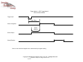
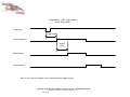
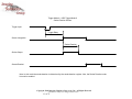
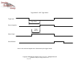
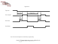
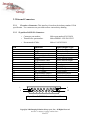
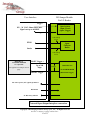
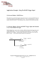
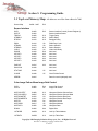
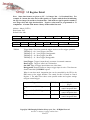
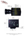
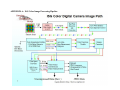
LightWise Camera Series
LW-5-S-1394 FireWireTM
Smart Digital Imaging Module
LW-5-S-1394-C – Color
Available in Color Only.
Specification and Users Guide
Revision 2.1a
Copyright, 2004 Imaging Solutions Group of NY, Inc., All Rights Reserved
Revision 2.1 Subject to change without notice.
1 of 33
Table of Contents:
1 LW-5-S-1394 Introduction and Specification Overview
1.1 Product Description
1.2 Key Specifications
1.3 5 MP Image Sensor
1.4 Programming and User Configuration Options
1.5 Automatic Gain and Offset Correction
1.6 On-Board Image Buffer
1.7 Digital Panning & Scaling (Zoom)
1.8 JPEG Compression
1.9 Simplified Block Diagram
2
External Signals and Connectors
2.1 External Trigger Modes
2.2 External Connectors
3
Programming Guide
3.1 Top Level Memory Map
3.2 Register Detail
4
Mechanical Information
4.1 Lens Mount
4.2 Tripod Connection
4.3 Digital Imaging Module Dimensions
4.4 Module Components
4.5 Operating Conditions
5
Firmware and FPGA Upgrade Process
Appendix A: Color Image Processing Pipeline
Appendix B: IIDC 1394-based Digital Camera Specification
Copyright, 2004 Imaging Solutions Group of NY, Inc., All Rights Reserved
Revision 2.1 Subject to change without notice.
2 of 33
Section 1: LW-5-S-1394-C Introduction and Specification Overview
1.1 Product Description
The ISG LW-5-S-1394-C 'Smart' Digital Imaging Module provides a High Resolution
area imaging solution with outstanding flexibility. The low cost and ease of integration
into existing systems make it an excellent solution for a wide variety of applications. The
interfaces to the Imager are industry standard to provide ease of integration into target
systems. Applications include:
Automated Inspection Systems
2D Bar Code Reading
Machine Vision Systems
Encoding and Positioning
Parcel Scanning
Programmable Smart Camera Applications
Smart Surveillance
Security and Homeland Defense.
Copyright, 2004 Imaging Solutions Group of NY, Inc., All Rights Reserved
Revision 2.1 Subject to change without notice.
3 of 33
1.2 Key Specifications
•
Resolution: 2592 x 1944 Pixels
•
Color only Available
•
Synchronous Shutter (Rolling) with advanced Trigger/Strobe capability
•
Data Rate:
o Up to 15 Frames / second full resolution (2592 x 1944)
o Up to 23 Frames / second partial frame (3 Mp – 2048 x 1536)
o Up to 35 Frames / second partial frame (2 Mp – 1600 x 1200)
o Up to 48 Frames / second partial frame (1.3 Mp – 1280 x 1024)
o Up to 70 Frames / second VGA
o Scalable frame rate as a function of Region of Interest
o Please note that 1394a bus bandwidth limitation may limit
sustained video throughput rates.
•
Data Resolution: On-Chip 12 bit A to D
•
Dynamic Range >70dB Signal to Noise Ration > 38dB
•
On-Board FPN Correction
•
On-Board Multiple Frame Image Buffer (SRAM)
o For up to 3 Color Images
•
Optional JPEG and M-JPEG – not possible with current board set but ISG
can offer this with additional engineering contract for new board set.
•
Digital Panning with Flexible Region of Interest
•
Standard FireWireTM (1394a) Interface (see TM note, page 23)
o Fully compliant to IEEE-1394a IIDC DCAM Specification Version 1.3
•
Single 12V Supply via FireWire
•
Compact Form Factor
•
User Programmable Exposure Timing and Frame Rate
•
Built-In Test Pattern
Copyright, 2004 Imaging Solutions Group of NY, Inc., All Rights Reserved
Revision 2.1 Subject to change without notice.
4 of 33
•
I/O for Triggers and Synchronization Flexibility
•
On-Board FPGA for User-Configurability
o Customized Image Processing Capability
o Customized Programmable I/O
•
High Quality Digital Panning and Zoom Capabilities.
1.2.1 ISG Color Image Processing Pipeline
The LW-5-S-1394-C Color Imaging Module utilizes the ISG Hardware Image Processing
Pipeline implemented in a XilinxTM FPGA. All color processing parameters are fully
programmable by the user. Appendix B describes the image path.
1.3 5 MP CMOS Image Sensor
The module utilizes a 5 MP CMOS image sensor. Please contact ISG for Sensor details
if needed. 2592 x 1944.
1.4 Programming and User Configuration Options
The LW-5-S-1394-C offers several levels of programmability and user configurability.
These include:
-
Full Parameter Control, Set-Up and Operation Control via the ISG Graphical
User Interface Software. This software is included with each unit.
-
Full Parameter Control, Set-Up and Operation Control via direct access of the
module’s register set. Section 3 is the programmer's reference for this mode of
operation.
- Customization of on-board FPGA. The on-board FPGA can be customized to
include 'Smart' Camera functionality, such as specialized image processing, data feature
Copyright, 2004 Imaging Solutions Group of NY, Inc., All Rights Reserved
Revision 2.1 Subject to change without notice.
5 of 33
extraction, custom dynamic range mapping, JPEG Compression , etc. This method can
also be used to configure the external I/O signals for custom functionality. Imaging
Solutions Group is available for consulting with customers to design or enable custom
configurations via the on-board FPGA. Contact [email protected] for information.
1.5 Automatic Gain and Offset Correction
The LW-5-S-1394-C will provide on-board FPN correction through gain and offset
compensation. The FPGA algorithms in conjunction with an on-board dual 8-bit DAC
perform automatic offset correction and semiautomatic gain corrections. These functions
can be selected and activated by the provided ISG Graphical User Interface (GUI)
software, or can be accessed directly via register programming.
1.6 On-Board Image Buffer
The LW-5-S-1394-C provides on-board image buffering for up to one raw or 5 JPEG
frame color or three frames raw monochrome full resolution 2592 x 1944. Combined
with the module’s flexible trigger modes, this image buffer enables capturing a sequence
of frames at the maximum frame rate of the sensor, then transferring the frames at any
available 1394 bandwidth.
1.7 Digital Panning Scaling (Zoom)
The LW-5-S-1394-C camera provides full frame rate smooth digital panning. This
allows a region of interest of any size to be swept through the entire active viewing area
via host computer control. A very high quality digital scaling function is also
implemented for Zoom feature capability.
1.8 JPEG Compression
The current board set cannot offer this option. However, ISG can add this option, with
associated NRE.
Copyright, 2004 Imaging Solutions Group of NY, Inc., All Rights Reserved
Revision 2.1 Subject to change without notice.
6 of 33
1.9 Simplified Block Diagram
Image
Conditioning and
Control FPGA
5 MP
CMOS
Sensor
With
Onboard
12-bit
ADC
Timing
Generator.
'Smart"
Algorithm Space
On-Board
Image Buffers
Up to 3 frames for Color
for full resolution
2592 x 1944
Power Ckts.,
Regulators
1394a
Controller/
Drivers/
Receivers
1394A (+12V in)
OptoIsolators
LW-5-S-1394-C
Programmable I/O
(with +5V, +12V out)
Copyright, 2004 Imaging Solutions Group of NY, Inc., All Rights Reserved
Revision 2.1 Subject to change without notice.
7 of 33
Section 2:
Connectors and Trigger Modes
Section 2.1:
ISG Camera Module Triggering Description
The ISG camera module provides a variety of triggering modes and flexibility using features
internal to the FPGA controller as well as the sensor. For a more detailed description of the
registers referenced in this document see the Programmers Reference manual.
Register Description:
Trigger Delay – A 16 bit value used to delay the start of integration from the active edge of the
input trigger. This value can be programmed in steps of 20.83us to a maximum value of 1.37s.
Strobe Advance – This 8 bit register is used to apply the strobe signal a programmed amount of
time before the start of sensor integration to allow for illumination turn on time. This value can be
programmed in steps of 5.21us to a maximum value of 1.33ms. Note: The trigger delay must be
greater then the strobe advance.
Strobe Delay – This 16 bit register is used to delay the strobe signal a programmed amount of
time after the start of sensor integration. This delay is intended for use with flash illumination
devices. This value can be programmed in steps of .65us to a maximum value of 42.7ms. Note:
The strobe delay must not exceed the integration time of the sensor. If a value is programmed for
Strobe Advance the Strobe Delay value will be ignored.
Retrigger Delay – The 16 bit value in this register is used to program the time between
integration intervals when in Retrigger Mode. This value can be programmed in steps of 5.2us to
a maximum value of 341ms.
Strobe Duration - This register is used to program the duration of the strobe pulse when strobe
duration mode is enabled. This value can be programmed in steps of 5.2us to a maximum value of
341ms. Note: The strobe output will go inactive at the end of sensor integration no mater what
the strobe duration is set to.
Trigger and Strobe Description:
The input trigger sense can be active low or high. A software trigger is also available to the
programming interface (Host Mode) as well as a trigger status bit. The strobe output is intended
to control an illumination system and can be selected to be active low or high as well as always
high or always low. The diagrams on the following pages show the trigger as active low and the
strobe as active high.
Copyright, 2004 Imaging Solutions Group of NY, Inc., All Rights Reserved
Revision 2.1 Subject to change without notice.
8 of 33
Trigger Mode A = IIDC Trigger Mode 0
Strobe Advance Shown
Trigger Input
Trigger Delay
Sensor Integration
Strobe
Advance
Strobe Output
SensorReadout
Note: In this mode the integratin time is determined by a register setting.
Copyright, 2004 Imaging Solutions Group of NY, Inc., All Rights Reserved
Revision 2.1 Subject to change without notice.
9 of 33
Trigger Mode A = IIDC Trigger Mode 0
Strobe Delay Shown
Trigger Input
Trigger Delay
Sensor Integration
Strobe
Delay
Strobe Output
SensorReadout
Note: In this mode the integratin time is determined by a register setting.
Copyright, 2004 Imaging Solutions Group of NY, Inc., All Rights Reserved
Revision 2.1 Subject to change without notice.
10 of 33
Trigger Mode A = IIDC Trigger Mode 0
Strobe Duration Shown
Trigger Input
Trigger Delay
Sensor Integration
Strobe Duration
Strobe Output
SensorReadout
Note: In this mode the strobe duration is determined by the strobe duration registor. Also, the Strobe Duration mode
bit must be enabled.
Copyright, 2004 Imaging Solutions Group of NY, Inc., All Rights Reserved
Revision 2.1 Subject to change without notice.
11 of 33
Trigger Mode B = IIDC Trigger Mode 1
Trigger Input
Trigger Delay
Sensor Integration
Strobe
Advance
Strobe Output
SensorReadout
Note: In this mode the integratin time is determined by the trigger duration.
Copyright, 2004 Imaging Solutions Group of NY, Inc., All Rights Reserved
Revision 2.1 Subject to change without notice.
12 of 33
Trigger Mode C
Trigger Input
Trigger Delay
Rerigger Delay
Sensor Integration
Strobe
Advance
Strobe
Advance
Strobe Output
SensorReadout
Note: In this mode the integratin time is determined by a register setting.
Copyright, 2004 Imaging Solutions Group of NY, Inc., All Rights Reserved
Revision 2.1 Subject to change without notice.
13 of 33
2.2 External Connectors
2.2.1
FirewireTM Connector: This interface is based on the industry standard 1394a
specification. Two connectors are provided to allow camera daisy chaining.
2.2.2 15-position D-SUB I/O Connector:
o Connector part number:
o Thumb Screw part number:
Molex part number 83612-9020
Molex MDSM – 9PE-Z10-VR25
o Recommended Cable:
Molex CA 83422-9014
Pin
Function
Input/Output Type
1
2
3
4
5
6
7
8
9
10
11
12
13
14
15
Trigger +
Trigger GND
DC Input (Optional)
Strobe
Programmable PWM
GND
DC Input (Optional)
RS422 Trigger +
RS422 Trigger DC +5V Output
Programmable Output +
Programmable Output Reserved
GND
Optoisolated Input
Optoisolated Input
Power Input
Open Collector Output
Open Collector Output
Power Input
Diff. TTL Input
Diff. TTL Input
Power Output
Optoisolated Output
Optoisolated Output
1
8
9
15
15-pin Micro-D EXT IO Connector, Front View
Copyright, 2004 Imaging Solutions Group of NY, Inc., All Rights Reserved
Revision 2.1 Subject to change without notice.
14 of 33
ISG Imager Module
Ext I/O Header
User Interface
Trigger +
Opto Isolator
Input Circuit
(Opto Trigger)
10V – 24 V DC, 20ma source max.
Signal rate up to 60 KHZ
Trigger -
4.7K Pull-up
To 5V
PWM
Open
Collector
Buffer
Strobe
4.7K Pull-up
To 5V
RS422 Driver
TI SN65HVD3082ED
Or equivalent
See applications example on next
page.
RS422 Trigger +
Up to 200
kbps
50 Ohm
RSS422 Trigger -
RS422 Receiver
TI SN65HVD3082ED
(Differential Trigger)
DC source power (12V typical) @ 200 mA
DC Return
5V DC Out @ 250 mA
External Input Output Interface connection
Copyright, 2004 Imaging Solutions Group of NY, Inc., All Rights Reserved
Revision 2.1 Subject to change without notice.
15 of 33
Applications Example: Using The RS422 Trigger Input
1) Preferred Method – RS422 Driver
The optimal way to utilize this input to trigger the camera is to drive the RS422 Receiver
in the camera with the corresponding driver device. The recommended driver is TI part
number SN65HVD3082ED. This method provides a balanced, robust differential input.
2) Alternate Method - Driving the RS422 Trigger Input with Standard
3.3 or 5 Volt CMOS/TTL Logic
Standard digital logic can be used to simulate a differential signal and trigger the camera
using the RS422 input. This can be accomplished by generating a 3.3 or 5 Volt logic
signal for RS422 Trigger +, and providing a logically inverted output of this signal for
RS422 Trigger -. The following diagram illustrates this approach:
Trigger
Trigger + (to pin 9)
Non-Inverting Buffer
3.3 or 5 Volt Logic
Trigger - (to pin 10)
Inverting Buffer
3.3 or 5 Volt Logic
Copyright, 2004 Imaging Solutions Group of NY, Inc., All Rights Reserved
Revision 2.1 Subject to change without notice.
16 of 33
Section 3: Programming Guide
3.1 Top Level Memory Map:
Sensor Map
All addresses are offset from address 0x7000
0x000 - 0x3ff
B12
SICR
SISTAT
TRGDLY
STRBDLY
RTGDLY
PWM
STRADV
STRDUR
VVDLY
IBISCR
INTCNT0
INTCNT1
INTCNT2
INTCNT3
0x400
0x404
0x408
0x40C
0x410
0x414
0x418
0x41C
0x420
0x424
0x428
0x42C
0x430
0x434
B15
PADCNT
IBACCUM
0x43C
0x440
U32
Not Used
Not Used
STATVAR
0x444
U5
Not Used
CLKCR
0x448
U5
Clock Divider/Control
SERRB
0x44C
Sensor Interface
Sensor Interface Control (Control Register1)
Sensor Interface Status
Trigger Delay
Strobe Delay
Retrigger Delay
PWM Duty Cycle
Strobe Advance
Strobe Duration
Video Valid Delay
Not Used
Not Used
Not Used
Not Used
Not Used
U16
U16
U16
U8
U8
U16
U4
B10
U32
U32
U32
U32
Data from serial (delayed) read
Color Image Path or Mono Image Path Control
IPCR
IPSTAT
0x800
0x804
B14
B2
Image Path Control
Image Path Status
HISTCOLSTRT
HISTCOLWIDTH
HISTROWSTRT
HISTROWDEPTH
HISTCR
HISTADDR
HISTDATA
0x808
0x80C
0x810
0x814
0x818
0x81C
0x820
U12
U12
U11
U11
B4
U5
U26
Histogram Window Column Start
Histogram Window Column Width
Histogram Window Row Start
Histogram Window Row Depth
Histogram Control
Histogram Address
Histogram Data
DGAIN
0x824
U4.4
Digital Gain
LUTADDR
0x8B4
U10
Look Up Table Address
LUTDATA
0x8B8
U10
Look Up Table Data
Copyright, 2004 Imaging Solutions Group of NY, Inc., All Rights Reserved
Revision 2.1 Subject to change without notice.
17 of 33
3.2 Register Detail
Note: Some data formats are given as (S/U # of integer bits. # of fractional bits). For
example, S1.3 means the value can be either positive or negative with the first bit indicating
the sign, one integer bit and three fractional bits. U0.8 means no sign bit (positive number),
zero integer bits and eight fractional bits. Negative values must be programmed as 2’s
complement. A format of Bn means a binary format with n bits used.
Address : 400x0 (CNTL1)
Data format : B15
Default Value: 00h
15
7
IMRST
TRIGM:
14
Not used
6
TRGSNS
13
12
5
VIDEN
4
HTRIG
11
10
OUTFMT[3:0]
3
2
STRBM[1:0]
9
8
LUTEN
1
0
TRIGM[1:0]
Trigger Mode. These bits control the trigger source as well as trigger operation.
TRIGM[1:0] = 00 : Local Trigger, One Shot
TRIGM[1:0] = 01 : Local Trigger, Retriggerable
TRIGM[1:0] = 10 : Host Trigger, One Shot
TRIGM[1:0] = 11 : Host Trigger, Retriggerable
Local Trigger: Trigger is input directly to camera via external connector.
Host Trigger: Trigger is issued via 1394 interface.
One Shot: Edge on trigger input initiates one video frame.
Retriggerable: Repeats Frames as long as trigger input is active. Time between
frames controlled by RTGDLY register.
When in one-shot mode, integration time can be controlled by the FPGA, the
IBIS sensor or the trigger duration. The control for this is located in Control
Register 2. The table below shows some possible modes and register settings
using an external trigger.
Trigger Mode
TRIGM[1:0]
Trigger mode A (IIDC Trigger Mode
0)
Trigger mode B (IIDC Trigger Mode
1)
Trigger mode C
00b
00b
01b
IBMODE[1:0] (Control
Reg 2)
10b Use FPGA register to
control integration time.
11b Use trigger duration to
control integration time.
01b Use sensor register to
control integration time.
Copyright, 2004 Imaging Solutions Group of NY, Inc., All Rights Reserved
Revision 2.1 Subject to change without notice.
18 of 33
STRBM :
Strobe Mode. These bits control the functionality of the Strobe output to the
illumination system.
STRBM[1:0] = 00 : Active high (Activated by trigger).
STRBM[1:0] = 01 : Active Low (Activated by trigger).
STRBM[1:0] = 10 : Always high (Not activated by trigger).
STRBM[1:0] = 11 : Always low (Not activated by trigger).
HTRIG :
Host trigger bit. Asserted via 1394 interface.
VIDEN :
Video Enable bit. This bit is set after imager is initialized.
TRGSNS:
Trigger Sense
IMRST:
Imager Reset, Controls the SS_RESET pin on IBIS Sensor
OUTFMT:
Output Format. These bits control the output data format.
OUTFMT[3:0] = 0000 : 8 bit data output. (default)
OUTFMT[3:0] = 0001 : 10 bit data output in 16 bit field with LSB’s padded with
0.
OUTFMT[3:0] = 0010 : 10 bit data output in 16 bit field with MSB’s padded
with 0.
OUTFMT[3:0] = 0100 : Test pattern Enable
OUTFMT[3:0] = 1000 : 10 bit data. No padding.
LUTEN:
Look up Table Enable. Set this bit to ‘1’ to enable 10 bit to 10 bit data mapping
via programmable look up table. Reset this bit to ‘0’ to bypass look up table.
Address : 0x404 (STAT)
Data format : B1
Default Value: 00h
7
TSTAT :
6
5
4
not used
3
2
1
Trigger Status. This read only bit is high when local trigger is asserted.
Copyright, 2004 Imaging Solutions Group of NY, Inc., All Rights Reserved
Revision 2.1 Subject to change without notice.
19 of 33
0
TSTAT
Address : 0x408 (TRGDLY)
Data format : U16
Default Value: 00h
15
14
13
12
11
TRGDLY(15:8)
10
9
8
7
6
5
4
3
TRGDLY(7:0)
2
1
0
TRGDLY :
This 16 bit Value is used to program a delay from the time trigger is received to
when strobe is activated. A delay between 0 and 1.37s in 20.83us steps can be
achieved. The default value is 0.
Address : 0x40c (STBADV)
Data format : U16
Default Value: 00h
15
14
13
12
11
STBADV(15:8)
10
9
8
7
6
5
4
2
1
0
STBADV :
3
STBADV(7:0)
This 8 bit Value is used to program the delay between the Strobe output
(illumination) and tart of sensor integration. The default value is 0.
Copyright, 2004 Imaging Solutions Group of NY, Inc., All Rights Reserved
Revision 2.1 Subject to change without notice.
20 of 33
Address : 0x410 (RTGDLY)
Data format : U16
Default Value: 00h
15
14
13
12
11
RTGDLY(15:8)
10
9
8
7
6
5
4
3
RTGDLY(7:0)
2
1
0
RTGDLY :
trigger
This 16 bit Value is used to program the delay between video frames in continues
Mode. A delay between 0 and 341ms in 5.21us steps can be achieved. The
default value is 0.
Address : 0x414 (PWM)
Data format : U8
Default Value : 80h
7
6
PWM :
5
4
3
PWM(7:0)
2
1
0
PWM Duty Cycle. This register controls the duty cycle of the 13Khz PWM
signal fed to the illumination system. FFh = 100%, 80h = 50%, 00h = .4%.
Address : 0x41c (VERREG)
Data format : B8
Default Value : 0Bh
7
6
VERREG :
5
4
3
VERREG(7:0)
2
1
The value in this register is used to identify the FPGA firmware revision.
Copyright, 2004 Imaging Solutions Group of NY, Inc., All Rights Reserved
Revision 2.1 Subject to change without notice.
21 of 33
0
Address : 0x420 (VVDLY)
Data format : B4
Default Value : 02h
7
6
5
4
3
not used
VVDLY :
2
1
VVDLY(3:0)
0
Video Valid Delay. The value in this register is used to move the video relative to
the video valid signal internal to the FPGA.
Address : 0x448 (CLKCR)
Data format : U5
Default Value: 0h
7
6
not used
5
4
INV
3
2
1
CLKDIV(3:0)
0
INV:
When this bit is set, the sensor clock is inverted.
CLKDIV :
Clock Divider. The sensor base clock rate is 48Mhz for Micron and
48Mhz for IBIS. This value is R/W.
Address : 0x824 (DGAIN)
Data format : U4.4
Default Value : 10h
7
DGAIN :
6
5
4
3
DGAIN(7:0)
2
1
0
Digital Gain. The input video is multiplied by this value. The result is truncated
to 1023. The range of DGAIN is 0 to 15.9375 in steps of 1/16. This value is R/W.
Copyright, 2004 Imaging Solutions Group of NY, Inc., All Rights Reserved
Revision 2.1 Subject to change without notice.
22 of 33
Address : 0x818 (HCS)
Data format : B2
7
6
5
4
3
2
not used
1
STAT
0
LOCK
LOCK :
Histogram lock out control. This bit is R/W
0 = Histogram values are updated at the end of each frame.
1 = Histogram values are NOT updated at the end of each frame. Lock out
updates to read the Histogram results. Setting this bit also clears the status bit.
STAT : Status bit is set at the end of a frame when the histogram is available. The status bit is
cleared by setting the LOCK bit.
Address : 0x2xx (HIST0L)
Data format : U21
23
22
not used
21
20
15
14
13
7
6
5
HIST0 :
19
18
HIST0[20:16]
17
16
12
11
HIST0[15:8]
10
9
8
4
3
HIST0[7:0]
2
1
0
Histogram Bin 0. This register is Read Only.
Address : 0x2d0 – 0x2e8 (HIST1 – HIST7)
Histogram Bins 1 thru 7 follow the same format as Histogram Bin 0.
Copyright, 2004 Imaging Solutions Group of NY, Inc., All Rights Reserved
Revision 2.1 Subject to change without notice.
23 of 33
Address : 0x8b4 (LUTAD)
Data format : U10
15
14
13
12
11
10
9
8
LUTAD[9:8]
4
3
LUTAD[7:0]
2
1
not used
7
6
5
0
LUTAD :
LUT Address Register. Reads and writes from the LUT data register use
the value in this register as the address into the LUT. Reads/Writes to the data register
causes the value in this register to be incremented by 1. Hence, the LUTs can be loaded
by successive writes to the data register. This register is R/W.
Address : 0x8b8 (LUTDATA)
Data format : 2x U10
15
14
13
12
11
10
not used
7
6
5
4
3
LUTDATA-E[7:0]
2
9
8
LUTADATA [9:8]
1
0
LUTDATA : LUT Address Register. Values written to this register are written to the
LUT at the location specified by LUTAD. Reads/Writes to this register cause the
LUTAD register to be incremented. This register is R/W.
Copyright, 2004 Imaging Solutions Group of NY, Inc., All Rights Reserved
Revision 2.1 Subject to change without notice.
24 of 33
Section 4: Mechanical Information
4.1 Lens Mount
A Case-Mount CS type (1.0” diameters with 12.5 mm spacing between the surface of the
sensor and top of the lens-mount) lens mount is provided for both system configurations.
C-Type Lenses: A five mm extender will change the CS to C-Type lens mount with
17.5 mm Back Focal Length.
F-Type Lenses: Using the Cannon 50mm F-type FD series + the Canon "C-type to Ftype" adapter will covert the camera to F-type with 39.9 mm Back Focal Length.
4.2 Tripod Connection
A standard female tripod connection is provided at the bottom of the Digital Imaging
Module and the Evaluation platform
Copyright, 2004 Imaging Solutions Group of NY, Inc., All Rights Reserved
Revision 2.1 Subject to change without notice.
25 of 33
4.3 LW-5-S-1394-C Digital Imaging Module Dimensions
2.875”
(73 mm)
Front View
1”
1.625”
(39 mm)
CS Lens Mount
(25.4mm)
2.0625”
(52 mm)
Mini-USB2.0 Connector
For debug and development
CPU Status
Imaging Status
LEDs
FireWireTM
Connector 2
Back View
Trigger / Strobe
Connector
FireWireTM
Connector 1
Screw holes for
securing camera
Female Tripod
Socket
1.25”
(31 mm)
Bottom View
1.25”
(31 mm)
Copyright, 2004 Imaging Solutions Group of NY, Inc., All Rights Reserved
Revision 2.1 Subject to change without notice.
26 of 33
Copyright, 2004 Imaging Solutions Group of NY, Inc., All Rights Reserved
Revision 2.1 Subject to change without notice.
27 of 33
4.4 Module Components:
The ISG LW-5-S-1394-C Digital Imaging Module hardware design is partitioned into
four separate boards: 1) Sensor, 2) Controller, 3) Power Management and 4) I/O boards.
These boards are SMT type 2 (double sides) and are connected to each others as shown
below:
Copyright, 2004 Imaging Solutions Group of NY, Inc., All Rights Reserved
Revision 2.1 Subject to change without notice.
28 of 33
4.5 Operating Conditions
Measured Average Power Consumption via 1394 cable:
12V, 250 ma rms / 3.0W
Ambient Operating Temperature Range:
-10 to 45 C
FCC and CE Qualification: In progress.
Test results available upon request.
Vibration and Shock Testing: In progress.
Target specification: 7G rms (10Hz to 2000Hz) Random, Shock
70G. Test results available upon request.
Copyright, 2004 Imaging Solutions Group of NY, Inc., All Rights Reserved
Revision 2.1 Subject to change without notice.
29 of 33
5.0 ISG Firmware + FPGA Upgrade Process
This process will use the ISG Camera Control GUI application software on the host PC,
to update firmware and/or FPGA code on the ISG 1394 camera. The camera’s
firmware/FPGA code is loaded through the 1394 interface using the ISG GUI.
A customer wishing to do a firmware or FPGA upgrade should perform the following
steps:
1) Extract, and copy the firmware/FPGA binary data files to a directory on your host PC.
The files are named isgcpu_ccxx_xxxx.bin for updating the camera firmware, and
isgfpga_ccxx_xxxx.bin for updating the camera hardware (i.e. FPGA device code). The
ccxx field represents the camera type, and the xxxx field will hold the version number.
2) To upgrade the firmware on the camera, start by running the ISG Lightwise GUI. Note
that the ISG supplied driver for the camera must be installed in order to use the ISG GUI.
It is recommended that the camera viewer window be closed before continuing.
3) Click on the “Camera Control Dialog” button on the ISG GUI.
4) Select the “Camera Setup” tab from the Camera Control Dialog page. The Camera
Setup page can be used to update either the firmware or the FPGA code of the camera, or
both.
5) Use the browse button (labeled “…”) to search for and select either the isgcpu or
isgfpga binary file defined in step 1 above, depending on which part of the camera you
are updating.
6) To begin the actual download procedure, click on the “Download to CPU” or
“Download to HW” button as appropriate. A popup box will ask if you are sure that you
want to continue the process.
7) Confirm that you are sure you want to proceed with the upgrade by answering, "yes"
within the confirmation popup dialog. Once confirmed, insure that this process is not
interrupted (i.e. maintain 1394 cable connection). The progress bar will show the status
of the update. Note that an FPGA update will take a few minutes to complete. The
process is completed once the dialog states "Done" on the download button. At this
point, the camera is upgraded with new firmware/FPGA code.
8) Exit the GUI. Power cycle the camera by disconnecting and reconnecting the 1394
cable to allow the new code to be executed.
Copyright, 2004 Imaging Solutions Group of NY, Inc., All Rights Reserved
Revision 2.1 Subject to change without notice.
30 of 33
9). After the camera is connected, you can right click in the top toolbar of the GUI and
select “about isg camera system” to read the new version numbers.
Trade Mark Note:
FireWire™ is a registered trademark of Apple Inc
Copyright, 2004 Imaging Solutions Group of NY, Inc., All Rights Reserved
Revision 2.1 Subject to change without notice.
31 of 33
APPENDIX A: ISG Color Image Processing Pipeline
Copyright, 2004 Imaging Solutions Group of NY, Inc., All Rights Reserved
Revision 2.1 Subject to change without notice.
33 of 33