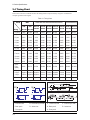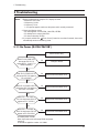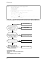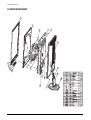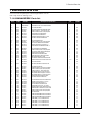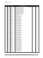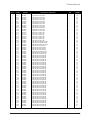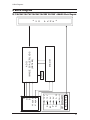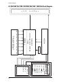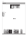
1
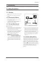
TFT-LCD MONITOR
Chassis
MJ15AS*
MJ15BS*
MJ17AS*
MJ17BS*
MJ19AS*
MJ19BS*
MJ19ES*
MJ19US*
MJ19QS*
MJ19DS*
SERVICE
TFT-LCD MONITOR
Model
510N
510T
710N
710T
910N, 911N, 920N
910T
913N
915N
913T, 910B
912T
Manual
CONTENTS
1. Precautions
2. Product Specifications
3. Disassembly & Reassembly
4. Alignments & Adjustments
5. Troubleshooting
6. Exploded View & Parts List
Simple Stand
Pivot Stand
7. Electrical Parts List
8. Block Diagram
9. Wiring Diagram
10. PCB Layout
11. Schematic Diagrams
12. Panel Description
Simple Stand
1 Precautions
1 Precautions
Follow these safety, servicing and ESD precautions to prevent damage and to protect against potential hazards such as electrical shock.
1-1 Safety Precautions
1-1-1 Warnings
1.
For continued safety, do not attempt to modify the circuit
board.
2.
Disconnect the AC power and DC power jack before
servicing.
(READING SHOULD
NOT BE ABOVE 0.5mA)
1-1-2 Servicing the LCD Monitor
1.
When servicing the LCD Monitor, Disconnect the AC
line cord from the AC outlet.
2.
It is essential that service technicians have an accurate
voltage meter available at all times. Check the
calibration of this meter periodically.
LEAKAGE
CURRENT
TESTER
DEVICE
UNDER
TEST
TEST ALL
EXPOSED METAL
SURFACES
2-WIRE CORD
*ALSO TEST WITH
PLUG REVERSED
(USING AC ADAPTER
PLUG AS REQUIRED)
1-1-3 Fire and Shock Hazard
Before returning the monitor to the user, perform the
following safety checks:
1.
Inspect each lead dress to make certain that the leads are
not pinched or that hardware is not lodged between the
chassis and other metal parts in the monitor.
2.
Inspect all protective devices such as nonmetallic control
knobs, insulating materials, cabinet backs, adjustment
and compartment covers or shields, isolation resistorcapacitor networks, mechanical insulators, etc.
3.
Leakage Current Hot Check (Figure 1-1):
WARNING: Do not use an isolation
transformer during this test.
Use a leakage current tester or a metering system that
complies with American National Standards Institute
(ANSI C101.1, Leakage Current for Appliances), and
Underwriters Laboratories (UL Publication UL1410,
59.7).
EARTH
GROUND
Figure 1-1. Leakage Current Test Circuit
4.
With the unit completely reassembled, plug the AC line
cord directly into a 120V AC outlet. With the unit’s AC
switch first in the ON position and then OFF, measure
the current between a known earth ground (metal water
pipe, conduit, etc.) and all exposed metal parts,
including: metal cabinets, screwheads and control shafts.
The current measured should not exceed 0.5 milliamp.
Reverse the power-plug prongs in the AC outlet and
repeat the test.
1-1-4 Product Safety Notices
Some electrical and mechanical parts have special safetyrelated characteristics which are often not evident from visual
inspection. The protection they give may not be obtained by
replacing them with components rated for higher voltage,
wattage, etc. Parts that have special safety characteristics are
identified by ! on schematics and parts lists. A substitute
replacement that does not have the same safety characteristics
as the recommended replacement part might create shock, fire
and/or other hazards. Product safety is under review
continuously and new instructions are issued whenever
appropriate.
1-1
1 Precautions
1-2 Servicing Precautions
WARNING:
An electrolytic capacitor installed with the wrong polarity might explode.
Caution:
Before servicing units covered by this service manual, read and follow the Safety Precautions
section of this manual.
Note:
If unforeseen circumstances create conflict between the following servicing precautions and any of the
safety precautions, always follow the safety precautions.
1-2-1 General Servicing Precautions
1.
2.
3.
Always unplug the unit’s AC power cord from the AC
power source and disconnect the DC Power Jack before
attempting to:
(a) remove or reinstall any component or assembly, (b)
disconnect PCB plugs or connectors, (c) connect a test
component in parallel with an electrolytic capacitor.
Some components are raised above the printed circuit
board for safety. An insulation tube or tape is sometimes
used. The internal wiring is sometimes clamped to
prevent contact with thermally hot components. Reinstall
all such elements to their original position.
After servicing, always check that the screws,
components and wiring have been correctly reinstalled.
Make sure that the area around the serviced part has not
been damaged.
4.
Check the insulation between the blades of the AC plug
and accessible conductive parts (examples: metal panels,
input terminals and earphone jacks).
5.
Insulation Checking Procedure: Disconnect the power
cord from the AC source and turn the power switch ON.
Connect an insulation resistance meter (500 V) to the
blades of the AC plug.
The insulation resistance between each blade of the AC
plug and accessible conductive parts (see above) should
be greater than 1 megohm.
6.
Always connect a test instrument’s ground lead to the
instrument chassis ground before connecting the positive
lead; always remove the instrument’s ground lead last.
1-3 Electrostatically Sensitive Devices (ESD) Precautions
Some semiconductor (solid state) devices can be easily damaged by static electricity. Such components are commonly called
Electrostatically Sensitive Devices (ESD). Examples of typical ESD are integrated circuits and some field-effect transistors. The
following techniques will reduce the incidence of component damage caused by static electricity.
1.
Immediately before handling any semiconductor
components or assemblies, drain the electrostatic charge
from your body by touching a known earth ground.
Alternatively, wear a discharging wrist-strap device. To
avoid a shock hazard, be sure to remove the wrist strap
before applying power to the monitor.
2.
After removing an ESD-equipped assembly, place it on a
conductive surface such as aluminum foil to prevent
accumulation of an electrostatic charge.
3.
Do not use freon-propelled chemicals. These can
generate electrical charges sufficient to damage ESDs.
4.
Use only a grounded-tip soldering iron to solder or
desolder ESDs.
5.
Use only an anti-static solder removal device. Some
solder removal devices not classified as “anti-static” can
generate electrical charges sufficient to damage ESDs.
1-2
6.
Do not remove a replacement ESD from its protective
package until you are ready to install it. Most
replacement ESDs are packaged with leads that are
electrically shorted together by conductive foam,
aluminum foil or other conductive materials.
7.
Immediately before removing the protective material
from the leads of a replacement ESD, touch the
protective material to the chassis or circuit assembly into
which the device will be installed.
Caution: Be sure no power is applied to the
chassis or circuit and observe all
other safety precautions.
8.
Minimize body motions when handling unpackaged
replacement ESDs. Motions such as brushing clothes
together, or lifting your foot from a carpeted floor can
generate enough static electricity to damage an ESD.
2 Product Specifications
2 Product Specifications
2-1 MJ15AS*/MJ15BS*/MJ17AS*/MJ17BS* Specifications
Description
Item
MJ15AS*/MJ15BS*
MJ17AS*/MJ17BS*
LCD Panel
TFT-LCD panel, RGB vertical stripe, normally black transmissive,
15-Inch viewable, 0.297 (H) x 0.297 (V) mm pixel pitch
TFT-LCD panel, RGB vertical stripe, normally black transmissive,
17-Inch viewable, 0.264 (H) x 0.264 (V) mm pixel pitch
Scanning Frequency
Horizontal : 31 kHz ~ 61 kHz (Automatic)
Vertical : 50 Hz ~ 75 Hz
Horizontal : 30 kHz ~ 81 kHz (Automatic)
Vertical : 56 Hz ~ 75 Hz
Display Colors
16.2 Million colors
Maximum Resolution
Horizontal : 1024 Pixels
Vertical : 768 Pixels
Input Video Signal
Analog, 0.714 Vp-p ± 5% positive at 75 Ω, [Digital(TMDS): MJ15BS*, MJ17BS*]
internally terminated
Input Sync Signal
Type : Separate H/V sync, Composite H/V
Level : TTL level (V high ≥ 2.0 V, V low ≤ 0.8 V), Sync-on-Green (≤ –0.25 V)
Maximum Pixel Clock rate
80 MHz
135 MHz
Active Display
Horizontal/Vertical
304.1 mm / 228.1 mm
338 ± 3 mm / 270 ± 3 mm
AC power voltage & Frequency
AC 90 ~ 264 Volts, 60/50 Hz ± 12V / 3A
AC 90 ~ 264 Volts, 60/50 Hz ± 3 Hz
Power Consumption
25W (normal)
34W (normal)
Dimensions
Set (W x D x H)
Horizontal : 1280 Pixels
Vertical : 1024 Pixels
Simple Stand / Pivot Stand
Simple Stand
Package
13.3 x 2.2 x 10.7 Inches (338.0 x 56.3 x 272.0 mm) State of stand disassembled
14.6 x 2.4 x 12.4 Inches (370.0 x 60.3 x 316.0 mm) State of stand disassembled
13.3 x 6.9 x 13.3 Inches (338.0 x 175.0 x 337.0 mm) State of stand installed 14.6 x 6.9 x 15 Inches (370.0 x 175.0 x 381.0 mm) State of stand installed
15.3 x 4.9 x 15.1 Inches (388 x 125 x 383 mm) 17.9 x 5.6 x 17.2 Inches (455 x 141 x 437 mm)
Weight (Set/Package)
3.1 kg (6.8 lbs) / 4.25 kg (9.4 lbs)
4.5 kg (9.9 lbs) / 6.15 kg (13.6 lbs)
Dimensions
Set (W x D x H)
Pivot Stand
-
14.6 x 2.4 x 12.4 Inches (370.0 x 60.3 x 316.0 mm) State of stand disassembled
14.6 x 7.5 x 16.0 Inches (370.0 x 190.9 x 406.8 mm) State of stand installed
20.0 x 10.1 x 16.0 Inches (508 x 256 x 407 mm)
-
6.25 kg (13.8 lbs) / 7.95 kg (17.5 lbs)
Package
Weight (Set/Package)
Environmental Considerations
Operating Temperature : 50°F ~ 104°F (10°C ~ 40°C)
Operating Humidity : 10 % ~ 80 %
Storage Temperature : -13°F ~ 113°F (-25°C ~ 45°C)
Storage Humidity : 5 % ~ 95 %
• Designs and specifications are subject to change without prior notice.
2-1
2 Product Specifications
2-3 Pin Assignments
Sync
Type
Pin No.
1
2
3
4
5
6
7
8
9
10
11
12
13
14
15
15-Pin D-Sub Signal Cable Connector
Separate
Composite
Sync-on-green
Red
Green
Blue
GND
DDC Return (GND)
GND-R
GND-G
GND-B
DDC Power Input (+5V)
Self Raster
GND
Bi-Dr Data (SDA)
H-Sync.
V-Sync.
DDC Clock (SCL)
Red
Green
Blue
GND
DDC Return (GND)
GND-R
GND-G
GND-B
DDC Power Input (+5V)
Self Raster
GND
Bi-Dr Data (SDA)
H/V-Sync.
Not Used
DDC Clock (SCL)
Red
Green + H/V Sync.
Blue
GND
DDC Return (GND)
GND-R
GND-G
GND-B
DDC Power Input (+5V)
Self Raster
GND
Bi-Dr Data (SDA)
Not Used
Not Used
DDC Clock (SCL)
Sync
Type
Pin No.
24P DVI-D
1
Rx2-
13
No Connection
2
Rx2+
14
+5V_M
3
GND
15
Self Raster
4
No Connection
16
+5V_M
5
No Connection
17
Rx0-
6
DDC Clock (SCL)
18
Rx0+
7
DDC Data (SDA)
19
NC
8
NC
20
No Connection
9
Rx1-
21
No Connection
10
Rx1+
22
NC
11
NC
23
RxC+
12
No Connection
24
RxC-
2-3
2 Product Specifications
2-4 Timing Chart
This section of the service manual describes the timing that the computer industry recognizes as standard for
computer-generated video signals.
Table 2-1 Timing Chart
VESA
(MJ15AS*/MJ15BS*/MJ17AS*/MJ17BS*/MJ19AS*/MJ19BS*/MJ19ES*/MJ19US*/MJ19QS*)
IBM
Mode
VGA2/
70 Hz
Timing
VGA3/
60 Hz
VESA(MJ17AS*/MJ17BS*/
MJ19AS*/MJ19BS*/MJ19ES*/MJ19US*/MJ19QS*)
640/75 Hz 800/60 Hz 800/75 Hz 1024/60 Hz 1024/75 Hz 1280/60 Hz 1280/75 Hz
720 x 400 640 x 480
640x480
800x600
800x600
1024x768 1024x768 1280x1024 1280x1024
fH (kHz)
31.469
31.469
37.500
37.879
46.875
48.363
60.023
63.981
79.975
A µsec
31.777
31.778
26.667
26.400
21.333
20.677
16.660
11.852
12.504
B µsec
3.813
3.813
2.032
3.200
1.616
2.092
1.219
1.037
1.067
C µsec
1.589
1.589
3.810
2.200
3.232
2.462
2.235
2.296
1.837
D µsec
26.058
26.058
20.317
20.000
16.162
15.754
13.003
9.259
9.481
E µsec
0.318
0.318
0.508
0.000
0.323
0.369
0.203
0.000
0.119
fV (Hz)
70.087
59.940
75.000
60.317
75.000
60.004
75.029
60.020
75.025
O msec
14.268
16.683
13.333
16.579
13.333
16.666
13.328
16.005
13.329
P msec
0.064
0.064
0.080
0.106
0.064
0.124
0.050
0.047
0.038
Q msec
0.858
0.794
0.427
0.607
0.448
0.600
0.466
0.594
0.475
R msec
13.155
15.761
12.800
15.840
12.800
15.880
12.795
15.630
12.804
S msec
0.191
0.064
0.027
0.0261
0.021
0.062
0.017
0.016
0.013
28.322
26.175
31.500
40.000
49.500
75.000
78.750
108.000
Clock
Freq.
(MHz)
135.000
Polarity
H.Sync
Negative Negative Negative Positive
Positive Negative
Positive
Positive
Positive
V.Sync
Positive Negative Negative Positive
Positive Negative
Positive
Positive
Positive
Remark
Separate Separate Separate Separate Separate Separate Separate Separate Separate
H/V Composite Sync
Separate Sync
Video
Video
C
D
E
Q
R
S
Sync-on-Green
Sync
Sync
B
P
A
O
A : Line time total
B : Horizontal sync width
O : Frame time total
P : Vertical sync width
C : Back porch
D : Active time
Q : Back porch
R : Active time
E : Front porch
2-4
S : Front porch
3 Disassembly and Reassembly
3 Disassembly and Reassembly
This section of the service manual describes the disassembly and reassembly procedures for the
MJ15AS*/MJ17AS*/MJ19AS*/MJ15BS*/MJ17BS*/MJ19BS*/MJ19ES* TFT-LCD monitors.
!
WARNING: This monitor contains electrostatically sensitive devices. Use caution when handling
these components.
3-1 Disassembly
!
Cautions:
1. Disconnect the monitor from the power source before disassembly.
1. After placing monitor on the cushioned table,
remove two screws on the left and right of the
bottom.
2
2. Disconnect back cover from monitor after
grabbing the right edge of the set ( 1 ) and
lifting the stand( 2 ).
1
3. Remove 2 screws from the shield.
4. Disconnect function cable from the cover front
and lift up the panel. Remove 4 screws from
the panel shield. (Right / Left)
5. Lift up the panel shield and carefully remove
the silicon glue on the cables with a nipper.
! Caution : Lamp wire may be easily damaged.
Please use caution when removing the silicon.
3-1
3 Disassembly and Reassembly
6. Remove 7 screws, 4 hexa screws from the boards
and lift up the boards.
! Caution : When repairing panel only,
disconnect just LVDS cable, Panel-Lamp /
Wire marked in circle in the picture without
removing the screws on board in order to lift
the board up.
7. This picture is panel.
3-2 MJ19ES*/MJ19BS*/MJ19US*/MJ19QS* Disassembly
1. After placing monitor on the cushioned table,
remove 6 screws on the left and right of the
bottom.
2. Lift the stand and lift up the back cover.
3. Remove 2 screws from the shield.
4. Disconnect function cable from the cover front and
lift up the panel. Remove 4 screws from the panel
shield. (Right / Left)
3-2
3 Disassembly and Reassembly
5. Lift up the panel shield and disconnect cables.
6. Remove 5 screws, 2 hexa screws from the boards
and lift up the boards.
! Caution : When repairing panel only,
disconnect just LVDS cable, Panel-Lamp /
Wire marked in circle in the picture without
removing the screws on board in order to lift
the board up.
7. This picture is panel.
3-2 Reassembly
Reassembly procedures are in the reverse order of disassembly procedures.
3-3
4 Alignments and Adjustments
4 Alignments and Adjustments
This section of the service manual explains how to use the RS232 JIG.
This function is needed for AD board change and program memory (IC110) change.
4-1 Required Equipment
The following equipment is necessary for adjusting the monitor:
• Computer with Windows 95, Windows 98, or Windows NT.
• MTI-2031 DDC MANAGER JIG
4-2 Automatic Color Adjustment
To input video, use 16 gray or any pattern using black and white.
1. Select english for OSD language.
2. Press the “
(Enter/Source)” key for 5 seconds.
4-3 DDC EDID Data Input
1. Input DDC EDID data when replacing AD PCB.
2. Receive/Download the proper DDC file for the model from HQ quality control department.
Install the below jig (Figure 1) and enter the data.
Figure 1.
4-4 OSD Adjustment When Replacing Panel
1. Adjust brightness and contrast to 0. Then, press the (Enter/Source) key for 5 second.
Service function OSD will appear on screen.
2. Press the + key to place the cursor on the panel. Press the menu key for 5 seconds.
4-5 OSD Adjustment When Replacing Lamp Only
1. Adjust brightness and contrast to 0. Then, press the exit key for 5 seconds.
Service function OSD will appear on the screen.
2. Press the + key. Select upper lamp and press the menu key for 5 seconds.
Then, select lower lamp and press the menu key for 5 seconds.
❇ Note
: Please be sure to read the following instructions for details on service function.
4-1
4 Alignments and Adjustments
4-6 Service Function Spec.
4-6-1 How to Display Service Function OSD
1. The value for brightness and contrast should be changed to zero.
2. Within 5 seconds, press the (Enter/Source) key.
3. Service function OSD will be displayed.
❇
If you want to disable the service function OSD, you will have to power off.
Panel Information
Softward Version
Checksum
Figure 2. The example of service function OSD
The service function OSD is based on a grid of 29 columns x 12 rows.
The service function OSD consists of panel information, software version and MICOM checksum.
4-6-2 How to Control Service Function OSD
1. With the panel selected on OSD, whenever you press the right key, the base color will change to blue from
“Panel” to “Upper Lamp”, “Lower Lamp”.
Figure 3.
4-2
4 Alignments and Adjustments
4-6-3 How to Control Service Function OSD
•After change the panel or lamp, you must reset service function OSD.
•The case of panel change
After changeing the panel, press the menu key within 5 seconds,.
Then, panel Ch. No increases one step and the panel time information is reset to zero.
Simultaneously, other information is reset to zero (Upper/Lower lamp, Panel cycle).
Figure 4.
4-6-4 How to Control Service Function OSD
•In the case of Upper Lamp or Lower Lamp change
After changeing the Upper Lamp or Lower Lamp,
1. Select the Upper Lamp or Lower Lamp
2. Press the Menu key within an 5 seconds.
Then, Ch. No and time will be reset to zero (selected item only).
Figure 5, 6.
4-3
4 Alignments and Adjustments
Memo
4-4
5 Troubleshooting
5 Troubleshooting
Notes:
1. Before troubleshooting, setup the PC’s display as below.
• Resolution: 1024 x 768
• H-frequency: 61 kHz
• V-frequency: 75 Hz
2. If no picture appears, make sure the power cord is correctly connected.
3. Check the following circuits.
• No raster appears: Function PBA, Main PBA, I/D PBA
• 5V develop but no screen: Main PBA
• 5V does not develop: I/D PBA
4. If you push and hold the “ (Enter, Source)” button for more than 5 seconds, the monitor
automatically returns to the factory preset.
5-1-1 No Power (MJ15A*/MJ15B*)
Check Function Ass’y.
Yes
❇
When Pin 4 of CN600 is 0V
does proper DC 13V, 5V
appear at Pin 1, 2 and 6, 7 of
CN600 separately?
No
Change IP Board.
Yes
When Pin 3 of IC602 is DC 5V
does proper DC 3.3V appear at
Pin 4 of IC602?
No
Check IC602 and related circuit.
Yes
When Pin 4 of IC600 is DC 5V
does proper DC 3.3V appear at
Pin 5 and 6 of IC600?
No
Check IC600 and related circuit.
Yes
When Pin 2, 3 of IC601 is
DC 3.3V does proper DC 4.3V
appear at Pin 1 of IC601?
No
Check IC601 and related circuit.
Yes
When Pin 2, 3 of IC601 is
DC 4.3V does proper DC 2.5V
appear at Pin 4 of IC601?
No
Check IC601 and related circuit.
* 0V means power on state.
When the monitor work well except DPMS and power
switch off,
0V should be applied to number 4 of CN600.
5-1
5 Troubleshooting
Notes: 1. Before troubleshooting, setup the PC’s display as below.
• Resolution: 1280 x 1024
• H-frequency: 64 kHz
• V-frequency: 60 Hz
2. If no picture appears, make sure the power cord is correctly connected.
3. Check the following circuits.
• No raster appears: Function PBA, Main PBA, I/P PBA
• 5V develop but no screen: Main PBA
• 5V does not develop: I/P PBA
4. If you push and hold the “ (Enter/Source)” button for more than 5 seconds, the monitor
automatically returns to the factory preset.
5-1-2 No Power (MJ17A*/MJ19A*/MJ17B*/MJ19B*/MJ19E*/MJ19US*/MJ19QS*)
Check Function Ass’y.
Yes
❇
When Pin 4 of CN600 is 0V
does proper DC 13V, 5V
appear at Pin 1, 2 and 6, 7 of
CN600 separately?
No
Change IP Board.
Yes
When Pin 4 of IC600 is DC 0.5V
does proper DC 0.5V appear at
Pin 5 and 6 of IC600?
No
Check IC600 and related circuit.
Yes
When Pin 2, 3 of IC601 is
DC 3.3V does proper DC 4.3V
appear at Pin 1 of IC601?
No
Check IC601 and related circuit.
Yes
When Pin 2, 3 of IC601 is
DC 4.3V does proper DC 2.5V
appear at Pin 4 of IC601?
No
Check IC601 and related circuit.
* 0V means power on state.
When the monitor work well except DPMS and power
switch off,
0V should be applied to number 4 of CN600.
5-2
5 Troubleshooting
5-2-1 No Video (ANALOG)
Check signal cable connection and
power.
1
X400 oscillate properly?
No
Replace or check related circuit.
Yes
Is there R, G, B input at
R100, R101 and R103?
No
Check input part.
Yes
Is there Hsync, Vsync waveform
2
3
No
Check IC400 and related circuit.
at Pin 100, 1 of IC 400?
Yes
Is there Hsync, Vsync waveform
2
3
No
Check IC200 and related circuit.
at Pin 43, 44 of IC 200?
Yes
Does the output signal appear
at Pin 17~20, 22~27 of CN400?
No
Check IC400 and related circuit.
Yes
There are DC 5V at Pin 1, 2
and 3 of CN400?
No
Check the panel EN signal at R222
and BL_EL signal at R603.
Yes
Replace LCD Panel.
5-3
5 Troubleshooting
WAVEFORMS
1
3
5-4
2
5 Troubleshooting
5-2-2 No Video (DIGITAL)
Check signal cable connection and
power.
1
X400 oscillate properly?
No
Replace or check related circuit.
Yes
Is there R, G, B input at
4
5
6
No
Check input part.
R110, R112, R114, R111,
R113 and R115?
Yes
Is there waveform
7
No
Check input part.
at R11, R117?
Yes
Does the output signal appear
at Pin 17~20, 22~27 of
CN400?
No
Check IC400 and related circuit.
Yes
There are DC 5V at Pin 1, 2
and 3 of CN400?
No
Check the panel EN signal at R222
and BLEL signal at R603.
Yes
Replace LCD Panel.
5-5
5 Troubleshooting
WAVEFORMS
1
2
3
4
5
6
7
5-6
6 Exploded View & Parts List
6 Exploded View and Parts List
❈ You can search for updated part codes through ITSELF web site.
URL : http://itself. sec. samsung.co.kr
6-1 MJ15AS*
6-1
6 Exploded View & Parts List
6-2 MJ15BS*
6-2
6 Exploded View & Parts List
6-3 MJ17AS*
6-3
6 Exploded View & Parts List
6-4 MJ17BS*
6-4
6 Exploded View & Parts List
6-5 MJ19AS*
6-5
6 Exploded View & Parts List
6-6 MJ19BS*
6-6
6 Exploded View & Parts List
6-7 MJ19ES*/MJ19US*/MJ19QS*
6-7
7 Electrical Parts List
7 Electrical Parts List
-You can search for updated part codes through ITSELF web site.
URL : http://itself.sec.samsung.co.kr/
7-1 LS19MJAKSZ/EDC Parts list
Level
Loc. No.
0
Code No.
Description & Specification
LS19MJAKSZ/EDC
920N,SGM2/S19A6-LMJ,19,LCD-MO,NETHERLAND
EA
SA/SNA
0.1
..2
...3
...3
...3
...3
...3
...3
M0216
M0216
M0081
M0081
T0063
T0081
STD
M0122
BN90-00486H
BN96-01064A
6003-000269
6003-001086
BN61-01061A
BN61-01062A
BN61-01067A
BN96-01062A
ASSY STAND;MJ19BS/AS
ASSY STAND P-SIMPLE;MJ19AS/BS,ABS HB,BK0
SCREW-TAPTITE;BH,+,-,S,M3,L6,ZPC(YEL),SW
SCREW-TAPTITE;BH,+,B,M3,L12,ZPC(BLK),SWR
STAND-FRONT;GS19VS,ABS HB,BK07
STAND-REAR;GS19VS,ABS HB,BK07
STAND-BRKT HINGE;GS19VS,SECC,T1.6,NAT
ASSY MISC P-HINGE;MJ19AS/BS,ZNDC2
1
1
4
6
1
1
1
1
S.N.A
S.A
S.N.A
S.A
S.N.A
S.N.A
S.N.A
S.N.A
0.1
..2
..2
...3
...3
M0002
M0081
M0013
M0113
M0006
BN90-00641D
6003-000337
BN96-01055B
BN61-00377A
BN63-01215B
ASSY COVER REAR;MJ19AS
SCREW-TAPTITE;BH,+,S,M4,L10,ZPC(BLK),SWR
ASSY COVER P-REAR;MJ19AS,ABS HB,BK07
BRACKET-VESA;GOYA19"(193V),SECC,T1.0
COVER-REAR;MJ19AS,ABS HB,BK07,NONE,1.5
1
4
1
1
1
S.N.A
S.A
S.A
S.A
S.N.A
0.1
..2
..2
...3
...3
...3
...3
...3
..2
M0001
M0081
T0003
T0245
M0112
M0007
M0105
M0145
T0382
BN90-00835K
6003-001086
BN96-01057X
BN61-01243A
BN63-01214A
BN64-00288A
BN67-00120A
BN96-01111A
BP61-00495C
ASSY COVER FRONT;LS19MJAKSZ/EDC
SCREW-TAPTITE;BH,+,B,M3,L12,ZPC(BLK),SWR
ASSY COVER P-FRONT;MJ19AS (S/M920N),HSD
HOLDER-PCB;MJ17,ABS HB,BK07
COVER-FRONT;MJ19A/BS,ABS,HB,GR70
KNOB-FUNCTION;MJ17,ABS,PC,GR70,SPRAY
LENS-LED;MATISSE,ACRYL,CLEAR
ASSY BOARD P-FUNCTION;MATISSE,FUNCTION
HOLDER-CARE;PJT,ACRYL-FOAM,T0.25,W30.0mm
1
2
1
1
1
1
1
1
0.16
S.N.A
S.A
S.A
S.N.A
S.N.A
S.N.A
S.N.A
S.A
S.N.A
0.1
..2
M0215
BN91-00939Q
BN07-00256A
ASSY LCD-NTZ;MJ19AS
LCD-PANEL;HSD190ME12-A10,Matisse,6bit FR
1
1
S.N.A
S.A
0.1
..2
..2
..2
..2
..2
..2
..2
..2
CCM1
M0081
M0081
M0114
M2893
M2893
T0081
T0376
BN91-01001J
6001-000364
6003-000117
6003-000276
BN39-00244A
BN39-00513A
BN39-00523C
BN61-01234A
BN96-01060F
ASSY SHIELD-NTZ;MJ19AS*
SCREW-MACHINE;FH,+,M3,L8,ZPC(YEL),SWRCH1
SCREW-TAPTITE;BH,+,B,M3,L6,ZPC(YEL),SWRC
SCREW-TAPTITE;BH,+,-,B,M3,L10,ZPC(YEL),S
CBF SIGNAL;BU15AO(T541A),15P/15P,20276-N
LEAD CONNECTOR;MJ17AS(BS),UL1571#30,UL/C
LEAD CONNECTOR;MJ17/19*,UL1061#28,UL/CSA
HOLDER-INVERTER;MATISSE,ABS V0,BK07
ASSY MISC P-SHIELD COVER;MJ19AS
1
4
1
1
1
1
1
2
1
S.N.A
S.N.A
S.A
S.N.A
S.A
S.A
S.A
S.N.A
S.N.A
0.1
..2
..2
..2
...3
...3
...3
...3
...3
...3
....4
....4
....4
....4
....4
....4
....4
....4
....4
....4
M0017
M0174
M0107
M0014
T0245
CN101
CN600
M0081
M0081
T0174
D101
D102
D104
ZD100
ZD101
ZD103
ZD104
ZD105
ZD109
ZD110
BN91-01015A
BN44-00089B
BN61-01103D
BN94-00828H
0202-001522
3701-001219
3711-004712
6003-000117
6003-000117
BN97-00797F
0401-001056
0401-001056
0401-001056
0403-001411
0403-001411
0403-001411
0403-001411
0403-001411
0403-001411
0403-001411
ASSY CHASSIS-NTZ,W/W;MJ19AS*,HANNSTAR,W/
IP BOARD;IP-35135A (D),MJ17*,3.2~4.8mA,6
BRACKET-PCB;GS19ES/ET,SECC,T1.0
ASSY PCB MAIN-NTZ,W/W;MJ19AS,W/W
SOLDER-WIRE FLUX;LFA3-107,-,D1.2,96.5Sn/
CONNECTOR-DSUB;15P,3R,FEMALE,ANGLE,AUF
HEADER-BOARD TO CABLE;BOX,9P,1R,2mm,STRA
SCREW-TAPTITE;BH,+,B,M3,L6,ZPC(YEL),SWRC
SCREW-TAPTITE;BH,+,B,M3,L6,ZPC(YEL),SWRC
ASSY SMD;MJ19AS
DIODE-SWITCHING;MMBD4148SE,100V,200MA,SO
DIODE-SWITCHING;MMBD4148SE,100V,200MA,SO
DIODE-SWITCHING;MMBD4148SE,100V,200MA,SO
DIODE-ZENER;-,5.49-5.73V,200MW,SOD-323,T
DIODE-ZENER;-,5.49-5.73V,200MW,SOD-323,T
DIODE-ZENER;-,5.49-5.73V,200MW,SOD-323,T
DIODE-ZENER;-,5.49-5.73V,200MW,SOD-323,T
DIODE-ZENER;-,5.49-5.73V,200MW,SOD-323,T
DIODE-ZENER;-,5.49-5.73V,200MW,SOD-323,T
DIODE-ZENER;-,5.49-5.73V,200MW,SOD-323,T
1
1
1
1
1
1
1
5
2
1
1
1
1
1
1
1
1
1
1
1
S.A
S.A
S.N.A
S.N.A
S.N.A
S.A
S.A
S.A
S.A
S.N.A
S.A
S.A
S.A
S.A
S.A
S.A
S.A
S.A
S.A
S.A
7-1
7 Electrical Parts List
Level
....4
....4
....4
....4
....4
....4
....4
....4
....4
....4
....4
....4
....4
....4
....4
....4
....4
....4
....4
....4
....4
....4
....4
....4
....4
....4
....4
....4
....4
....4
....4
....4
....4
....4
....4
....4
....4
....4
....4
....4
....4
....4
....4
....4
....4
....4
....4
....4
....4
....4
....4
....4
....4
....4
....4
....4
....4
....4
....4
....4
....4
....4
....4
....4
....4
....4
....4
7-2
Loc. No.
ZD112
ZD201
ZD106
ZD200
Q603
Q604
Q409
IC109
IC112
T0087
T0087
R100
R101
R102
R103
R104
R105
R245
R270
R107
R108
R109
R110
R111
R112
R226
R227
R228
R229
R231
R233
R239
R240
R242
R243
R244
R247
R248
R249
R250
R251
R253
R254
R255
R610
R234
R124
R225
R257
R130
R201
R202
R205
R208
R209
R210
R212
R213
R214
R215
R216
R217
R218
R219
R220
R230
R605
Code No.
0403-001411
0403-001411
0406-001061
0406-001061
0501-002080
0501-002080
0505-001957
1003-001813
1103-001023
1203-002425
1203-002844
2007-000070
2007-000070
2007-000070
2007-000070
2007-000070
2007-000070
2007-000070
2007-000070
2007-000074
2007-000074
2007-000074
2007-000074
2007-000074
2007-000074
2007-000074
2007-000074
2007-000074
2007-000074
2007-000074
2007-000074
2007-000074
2007-000074
2007-000074
2007-000074
2007-000074
2007-000074
2007-000074
2007-000074
2007-000074
2007-000074
2007-000074
2007-000074
2007-000074
2007-000074
2007-000077
2007-000078
2007-000078
2007-000083
2007-000084
2007-000084
2007-000084
2007-000084
2007-000084
2007-000084
2007-000084
2007-000084
2007-000084
2007-000084
2007-000084
2007-000084
2007-000084
2007-000084
2007-000084
2007-000084
2007-000084
2007-000084
Description & Specification
DIODE-ZENER;-,5.49-5.73V,200MW,SOD-323,T
DIODE-ZENER;-,5.49-5.73V,200MW,SOD-323,T
DIODE-TVS;MMQA5V6T3,5.32/5.6/5.88V,24W,S
DIODE-TVS;MMQA5V6T3,5.32/5.6/5.88V,24W,S
TR-SMALL SIGNAL;2SC2412K,NPN,200mW,SC-59
TR-SMALL SIGNAL;2SC2412K,NPN,200mW,SC-59
FET-SILICON;NTR2101P,P,-8V,-3.7A,0.052oh
IC-LCD CONTROLLER;SE16AWL,PQFP,100P,20x1
IC-EEPROM;24C08,1Kx8,SOP,8P,5x4mm,2.5/5.
IC-POSI.FIXED REG.;AP1117,SOT-223,3P,138
IC-POSI.FIXED REG.;AP1117D-18A,TO-252-3L
R-CHIP;0ohm,5%,1/10W,TP,1608
R-CHIP;0ohm,5%,1/10W,TP,1608
R-CHIP;0ohm,5%,1/10W,TP,1608
R-CHIP;0ohm,5%,1/10W,TP,1608
R-CHIP;0ohm,5%,1/10W,TP,1608
R-CHIP;0ohm,5%,1/10W,TP,1608
R-CHIP;0ohm,5%,1/10W,TP,1608
R-CHIP;0ohm,5%,1/10W,TP,1608
R-CHIP;100ohm,5%,1/10W,TP,1608
R-CHIP;100ohm,5%,1/10W,TP,1608
R-CHIP;100ohm,5%,1/10W,TP,1608
R-CHIP;100ohm,5%,1/10W,TP,1608
R-CHIP;100ohm,5%,1/10W,TP,1608
R-CHIP;100ohm,5%,1/10W,TP,1608
R-CHIP;100ohm,5%,1/10W,TP,1608
R-CHIP;100ohm,5%,1/10W,TP,1608
R-CHIP;100ohm,5%,1/10W,TP,1608
R-CHIP;100ohm,5%,1/10W,TP,1608
R-CHIP;100ohm,5%,1/10W,TP,1608
R-CHIP;100ohm,5%,1/10W,TP,1608
R-CHIP;100ohm,5%,1/10W,TP,1608
R-CHIP;100ohm,5%,1/10W,TP,1608
R-CHIP;100ohm,5%,1/10W,TP,1608
R-CHIP;100ohm,5%,1/10W,TP,1608
R-CHIP;100ohm,5%,1/10W,TP,1608
R-CHIP;100ohm,5%,1/10W,TP,1608
R-CHIP;100ohm,5%,1/10W,TP,1608
R-CHIP;100ohm,5%,1/10W,TP,1608
R-CHIP;100ohm,5%,1/10W,TP,1608
R-CHIP;100ohm,5%,1/10W,TP,1608
R-CHIP;100ohm,5%,1/10W,TP,1608
R-CHIP;100ohm,5%,1/10W,TP,1608
R-CHIP;100ohm,5%,1/10W,TP,1608
R-CHIP;100ohm,5%,1/10W,TP,1608
R-CHIP;470ohm,5%,1/10W,TP,1608
R-CHIP;1Kohm,5%,1/10W,TP,1608
R-CHIP;1Kohm,5%,1/10W,TP,1608
R-CHIP;3Kohm,5%,1/10W,TP,1608
R-CHIP;4.7Kohm,5%,1/10W,TP,1608
R-CHIP;4.7Kohm,5%,1/10W,TP,1608
R-CHIP;4.7Kohm,5%,1/10W,TP,1608
R-CHIP;4.7Kohm,5%,1/10W,TP,1608
R-CHIP;4.7Kohm,5%,1/10W,TP,1608
R-CHIP;4.7Kohm,5%,1/10W,TP,1608
R-CHIP;4.7Kohm,5%,1/10W,TP,1608
R-CHIP;4.7Kohm,5%,1/10W,TP,1608
R-CHIP;4.7Kohm,5%,1/10W,TP,1608
R-CHIP;4.7Kohm,5%,1/10W,TP,1608
R-CHIP;4.7Kohm,5%,1/10W,TP,1608
R-CHIP;4.7Kohm,5%,1/10W,TP,1608
R-CHIP;4.7Kohm,5%,1/10W,TP,1608
R-CHIP;4.7Kohm,5%,1/10W,TP,1608
R-CHIP;4.7Kohm,5%,1/10W,TP,1608
R-CHIP;4.7Kohm,5%,1/10W,TP,1608
R-CHIP;4.7Kohm,5%,1/10W,TP,1608
R-CHIP;4.7Kohm,5%,1/10W,TP,1608
EA
1
1
1
1
1
1
1
1
1
1
1
1
1
1
1
1
1
1
1
1
1
1
1
1
1
1
1
1
1
1
1
1
1
1
1
1
1
1
1
1
1
1
1
1
1
1
1
1
1
1
1
1
1
1
1
1
1
1
1
1
1
1
1
1
1
1
1
SA/SNA
S.A
S.A
S.A
S.A
S.A
S.A
S.A
S.A
S.A
S.A
S.A
S.A
S.A
S.A
S.A
S.A
S.A
S.A
S.A
S.A
S.A
S.A
S.A
S.A
S.A
S.A
S.A
S.A
S.A
S.A
S.A
S.A
S.A
S.A
S.A
S.A
S.A
S.A
S.A
S.A
S.A
S.A
S.A
S.A
S.A
S.A
S.A
S.A
S.A
S.A
S.A
S.A
S.A
S.A
S.A
S.A
S.A
S.A
S.A
S.A
S.A
S.A
S.A
S.A
S.A
S.A
S.A
7 Electrical Parts List
Level
....4
....4
....4
....4
....4
....4
....4
....4
....4
....4
....4
....4
....4
....4
....4
....4
....4
....4
....4
....4
....4
....4
....4
....4
....4
....4
....4
....4
....4
....4
....4
....4
....4
....4
....4
....4
....4
....4
....4
....4
....4
....4
....4
....4
....4
....4
....4
....4
....4
....4
....4
....4
....4
....4
....4
....4
....4
....4
....4
....4
....4
....4
....4
....4
....4
....4
....4
Loc. No.
R131
R236
R252
R400
R401
R602
R603
R604
R606
R607
R106
R403
R113
R114
R115
R126
R127
R608
R609
C416
C418
C210
C109
C106
C208
C209
C204
C111
C100
C101
C102
C103
C104
C105
C107
C130
C200
C207
C211
C400
C402
C403
C404
C405
C406
C407
C408
C409
C410
C411
C412
C413
C414
C415
C417
C419
C421
C423
C424
C605
C607
C610
C611
C615
C618
C619
C620
Code No.
2007-000090
2007-000090
2007-000090
2007-000090
2007-000090
2007-000090
2007-000090
2007-000090
2007-000090
2007-000090
2007-000821
2007-000821
2007-001164
2007-001164
2007-001164
2007-001164
2007-001164
2007-002899
2007-002899
2203-000041
2203-000041
2203-000189
2203-000236
2203-000257
2203-000257
2203-000257
2203-000426
2203-000998
2203-005005
2203-005005
2203-005005
2203-005005
2203-005005
2203-005005
2203-005005
2203-005005
2203-005005
2203-005005
2203-005005
2203-005005
2203-005005
2203-005005
2203-005005
2203-005005
2203-005005
2203-005005
2203-005005
2203-005005
2203-005005
2203-005005
2203-005005
2203-005005
2203-005005
2203-005005
2203-005005
2203-005005
2203-005005
2203-005005
2203-005005
2203-005005
2203-005005
2203-005005
2203-005005
2203-005005
2203-005005
2203-005005
2203-005005
Description & Specification
R-CHIP;10Kohm,5%,1/10W,TP,1608
R-CHIP;10Kohm,5%,1/10W,TP,1608
R-CHIP;10Kohm,5%,1/10W,TP,1608
R-CHIP;10Kohm,5%,1/10W,TP,1608
R-CHIP;10Kohm,5%,1/10W,TP,1608
R-CHIP;10Kohm,5%,1/10W,TP,1608
R-CHIP;10Kohm,5%,1/10W,TP,1608
R-CHIP;10Kohm,5%,1/10W,TP,1608
R-CHIP;10Kohm,5%,1/10W,TP,1608
R-CHIP;10Kohm,5%,1/10W,TP,1608
R-CHIP;390ohm,1%,1/10W,TP,1608
R-CHIP;390ohm,1%,1/10W,TP,1608
R-CHIP;75ohm,1%,1/10W,TP,1608
R-CHIP;75ohm,1%,1/10W,TP,1608
R-CHIP;75ohm,1%,1/10W,TP,1608
R-CHIP;75ohm,1%,1/10W,TP,1608
R-CHIP;75ohm,1%,1/10W,TP,1608
R-CHIP;10ohm,1%,1/10W,TP,1608
R-CHIP;10ohm,1%,1/10W,TP,1608
C-CER,CHIP;0.01nF,0.25pF,50V,C0G,1608
C-CER,CHIP;0.01nF,0.25pF,50V,C0G,1608
C-CER,CHIP;100nF,+80-20%,25V,Y5V,1608
C-CER,CHIP;0.1nF,5%,50V,C0G,1608
C-CER,CHIP;10nF,10%,50V,X7R,1608
C-CER,CHIP;10nF,10%,50V,X7R,1608
C-CER,CHIP;10nF,10%,50V,X7R,1608
C-CER,CHIP;0.018nF,5%,50V,C0G,1608
C-CER,CHIP;0.047nF,5%,50V,C0G,1608
C-CER,CHIP;100nF,10%,16V,X7R,1608
C-CER,CHIP;100nF,10%,16V,X7R,1608
C-CER,CHIP;100nF,10%,16V,X7R,1608
C-CER,CHIP;100nF,10%,16V,X7R,1608
C-CER,CHIP;100nF,10%,16V,X7R,1608
C-CER,CHIP;100nF,10%,16V,X7R,1608
C-CER,CHIP;100nF,10%,16V,X7R,1608
C-CER,CHIP;100nF,10%,16V,X7R,1608
C-CER,CHIP;100nF,10%,16V,X7R,1608
C-CER,CHIP;100nF,10%,16V,X7R,1608
C-CER,CHIP;100nF,10%,16V,X7R,1608
C-CER,CHIP;100nF,10%,16V,X7R,1608
C-CER,CHIP;100nF,10%,16V,X7R,1608
C-CER,CHIP;100nF,10%,16V,X7R,1608
C-CER,CHIP;100nF,10%,16V,X7R,1608
C-CER,CHIP;100nF,10%,16V,X7R,1608
C-CER,CHIP;100nF,10%,16V,X7R,1608
C-CER,CHIP;100nF,10%,16V,X7R,1608
C-CER,CHIP;100nF,10%,16V,X7R,1608
C-CER,CHIP;100nF,10%,16V,X7R,1608
C-CER,CHIP;100nF,10%,16V,X7R,1608
C-CER,CHIP;100nF,10%,16V,X7R,1608
C-CER,CHIP;100nF,10%,16V,X7R,1608
C-CER,CHIP;100nF,10%,16V,X7R,1608
C-CER,CHIP;100nF,10%,16V,X7R,1608
C-CER,CHIP;100nF,10%,16V,X7R,1608
C-CER,CHIP;100nF,10%,16V,X7R,1608
C-CER,CHIP;100nF,10%,16V,X7R,1608
C-CER,CHIP;100nF,10%,16V,X7R,1608
C-CER,CHIP;100nF,10%,16V,X7R,1608
C-CER,CHIP;100nF,10%,16V,X7R,1608
C-CER,CHIP;100nF,10%,16V,X7R,1608
C-CER,CHIP;100nF,10%,16V,X7R,1608
C-CER,CHIP;100nF,10%,16V,X7R,1608
C-CER,CHIP;100nF,10%,16V,X7R,1608
C-CER,CHIP;100nF,10%,16V,X7R,1608
C-CER,CHIP;100nF,10%,16V,X7R,1608
C-CER,CHIP;100nF,10%,16V,X7R,1608
C-CER,CHIP;100nF,10%,16V,X7R,1608
EA
1
1
1
1
1
1
1
1
1
1
1
1
1
1
1
1
1
1
1
1
1
1
1
1
1
1
1
1
1
1
1
1
1
1
1
1
1
1
1
1
1
1
1
1
1
1
1
1
1
1
1
1
1
1
1
1
1
1
1
1
1
1
1
1
1
1
1
SA/SNA
S.A
S.A
S.A
S.A
S.A
S.A
S.A
S.A
S.A
S.A
S.A
S.A
S.A
S.A
S.A
S.A
S.A
S.A
S.A
S.A
S.A
S.A
S.A
S.A
S.A
S.A
S.A
S.A
S.A
S.A
S.A
S.A
S.A
S.A
S.A
S.A
S.A
S.A
S.A
S.A
S.A
S.A
S.A
S.A
S.A
S.A
S.A
S.A
S.A
S.A
S.A
S.A
S.A
S.A
S.A
S.A
S.A
S.A
S.A
S.A
S.A
S.A
S.A
S.A
S.A
S.A
S.A
7-3
7 Electrical Parts List
Level
Loc. No.
Code No.
Description & Specification
EA
SA/SNA
....4
....4
....4
....4
....4
....4
....4
....4
....4
....4
....4
....4
....4
....4
....4
....4
....4
....4
....4
....4
....4
....4
....4
.....5
....4
....4
....4
C420
C604
C606
C614
C201
C202
C205
C422
C401
C608
C609
C612
C630
T0052
T0052
X400
T0568
T0568
T0568
T0568
CN400
CN200
MICOM
IC520
CIS5
R410
T0077
2203-005065
2203-005065
2203-005065
2203-005065
2203-005437
2203-005437
2203-005437
2203-005437
2402-001128
2402-001128
2402-001128
2402-001128
2402-001128
2703-001334
2703-001334
2801-003326
3301-001145
3301-001145
3301-001145
3301-001145
3711-005470
3711-005543
BN97-00798F
0903-001397
0202-001477
2007-000109
BN41-00652C
C-CER,CHIP;1000nF,+80-20%,10V,Y5V,1608
C-CER,CHIP;1000nF,+80-20%,10V,Y5V,1608
C-CER,CHIP;1000nF,+80-20%,10V,Y5V,1608
C-CER,CHIP;1000nF,+80-20%,10V,Y5V,1608
C-CER,CHIP;10000nF,+80-20%,10V,Y5V,3216
C-CER,CHIP;10000nF,+80-20%,10V,Y5V,3216
C-CER,CHIP;10000nF,+80-20%,10V,Y5V,3216
C-CER,CHIP;10000nF,+80-20%,10V,Y5V,3216
C-AL,SMD;100UF,20%,16V,WT,TP,6.3X5.7MM
C-AL,SMD;100UF,20%,16V,WT,TP,6.3X5.7MM
C-AL,SMD;100UF,20%,16V,WT,TP,6.3X5.7MM
C-AL,SMD;100UF,20%,16V,WT,TP,6.3X5.7MM
C-AL,SMD;100UF,20%,16V,WT,TP,6.3X5.7MM
INDUCTOR-SMD;1.5uH,10%,2012
INDUCTOR-SMD;1.5uH,10%,2012
CRYSTAL-SMD;24MHZ,30PPM,28-ABX,20PF,50OH
BEAD-SMD;60ohm,4516,TP,70ohm/45MHz,82ohm
BEAD-SMD;60ohm,4516,TP,70ohm/45MHz,82ohm
BEAD-SMD;60ohm,4516,TP,70ohm/45MHz,82ohm
BEAD-SMD;60ohm,4516,TP,70ohm/45MHz,82ohm
HEADER-BOARD TO CABLE;BOX,30P,1R,1.25mm,
HEADER-BOARD TO CABLE;BOX,6P,1R,1.25mm,S
ASSY MICOM-NTZ,W/W;MJ19AS
IC-MICROCONTROLLER;WT61P4,8Bit,PLCC,44P,
SOLDER-CREAM;LST309-M,-,D20~45§-,96.5Sn/
R-CHIP;1Mohm,5%,1/10W,TP,1608
PCB MAIN;MATISSE2/GOYA2,STH,2L,MP1.2,1.6
1
1
1
1
1
1
1
1
1
1
1
1
1
1
1
1
1
1
1
1
1
1
1
1
1
1
1
S.A
S.A
S.A
S.A
S.A
S.A
S.A
S.A
S.A
S.A
S.A
S.A
S.A
S.A
S.A
S.A
S.N.A
S.N.A
S.N.A
S.N.A
S.A
S.A
S.A
S.N.A
S.N.A
S.A
S.N.A
0.1
M0019
BN92-00329Y
ASSY LABEL;MJ/GS,W/W
1
S.N.A
0.1
..2
..2
..2
..2
M0113
T0376
T0524
P/M
M0081
BN92-01136F
6902-000379
6902-000520
6902-000604
6902-000609
ASSY P/MATERIAL;MJ19ASK*/*,NEW SIMPLE
BAG AIR;LDPE,T0.2,W1000,L1800,TRP,-,-BAG PE;HDPE/NITRON(DOUBLE),T0.015/T0.5(D
BAG WRAPPING;LDPE,T0.02,W500,L10000,TRP,
BAG ROLL;LDPE,T0.05,W2400,L1000,TRP,-,-
1
0.004
1
3
0.1
S.N.A
S.N.A
S.N.A
S.N.A
S.N.A
0.1
..2
...3
...3
..2
M0003
M0120
M0103
M0102
BOX
BN92-01640X
BH75-10529A
BN72-60001A
BN72-60002A
BN69-00756S
ASSY BOX;LS19MJAKSZ/EDC
UNIT-HANDLE PACKING;LXA410TLMU,PE,-,WHIT
LEVER-TOP;LSD210TL,PE-LD,WHITE,TFT_LCD
LEVER-BOTTOM;LSD210TL,PE-LD,WHITE,TFT-LC
BOX-00;S/M920N(MJ19AS),SY-01,A-1,W497*D4
1
1
1
1
1.02
S.N.A
S.N.A
S.N.A
S.N.A
S.N.A
0.1
..2
...3
...3
...3
...3
...3
...3
...3
...3
..2
...3
...3
...3
...3
...3
...3
....4
....4
M0045
M0013
M0081
T0524
STAND/BASE
CIS4
M0111
T0004
T0059
M0126
M0045
T0268
T0524
ACCESSORY
ACCESSORY
T0059
M0215
QSG
IB
BN92-01645N
BN96-01462A
6003-000142
6902-000389
BN61-01384A
BN61-01435A
BN63-01491A
BN63-01492A
BN68-00473W
BN73-00077A
BN96-02896S
3903-000042
6902-000110
BH68-70438A
BH68-70448A
BN68-00907A
BN96-02987A
BH68-00376L
BN59-00501A
ASSY ACCESSORY;LS19MJAKSZ/EDC
ASSY STAND P-BASE;MATISSE19",ABS HB,SILV
SCREW-TAPTITE;FH,+,B,M3,L8,ZPC(BLK),SWRC
BAG PE;HDPE/NITRON/HDPE,T0.015/T0.5/T0.0
BRACKET-STAND BOTTOM;MJ19,SECC,T1.6
HOLDER-STAND;CH,+,M4,L10(4),ZPC(WHT),SWR
COVER-STAND;MJ19,ABS HB,BK07
COVER-STAND BASE;MJ19,ABS HB,BK07
MANUAL FLYER-CARD;Goya2 Stand Guide,Sync
RUBBER-FOOT;MATISSE,BUMPON,¨ª13.5,T2.0,6
ASSY ACCESSORY;LS19MJAKSZ/EDC
CBF-POWER CORD;DT,EU,FP3/YES,IEC320 C13/
BAG PE;LDPE,T0.05,W250,L400,TRP,28,2
CARD-12,BLOC WARRANTY;TFT LCD,BASIC,EU,M
CARD-01;TFT LCD,SRC,RUSSIA,S/W,120,W210*
MANUAL FLYER-CARD;COMM,SAMSUNG,18 LANG,E
ASSY MANUAL P-IB+QSG;911N,SyncMaster,W/W
MANUAL FLYER-04,QSG;LCDQUICK SETUP GUIDE
S/W DRIVER-00,IB;COMM,W/W,SYNCMASTER,MAT
1
1
10
1
1
1
1
1
1
4
1
1
1
1
1
1
1
1
1
S.N.A
S.A
S.N.A
S.N.A
S.N.A
S.N.A
S.N.A
S.N.A
S.N.A
S.N.A
S.A
S.A
S.N.A
S.N.A
S.N.A
S.N.A
S.N.A
S.N.A
S.N.A
7-4
(ON)+ 5V
+ 0~ 3.3
+ 5V
+ 5V
+ 13V
INV ERT ER
IP BOARD
S
M
P
S
+ 13V
R
G
B
H- sy nc
V - sy nc
12MHz
M ICOM
A DC/
IM A GE SCA L ER/ L V DS
(SE7889)
P
A
N
E
L
L
C
D
8 Block Diagrams
8 Block Diagram
8-1 MJ15AS*/MJ17AS*/MJ19AS*/MJ19ES*/MJ19US* ANALOG Block Diagram
8-1
8-2
(ON)+ 5V
+ 0~ 3.3
+ 5V
+ 5V
+ 13V
INV ERT ER
IP BOARD
S
M
P
S
+ 13V
(PC)ANALOG
R
G
B
H- sy nc
V - sy nc
12MHz
M ICOM
A DC/
IM A GE SCA L ER/ L V DS
(SE7888)
T M DS
RX2+ RX2- RX1+ RX1- RX0+ RX0- RXC+ RXC-
(PC)DIGIT AL
P
A
N
E
L
L
C
D
8 Block Diagrams
8-2 MJ15BS*/MJ17BS*/MJ19BS*/MJ19QS* DIGITAL Block Diagram
9 Wiring Diagram
9 Wiring Diagram
(MJ15BS*/MJ17BS*/MJ19BS*)
9-1
10 PCB Layout
10 PCB Layout
10-1 MJ15AS* ANALOG PCB
Loc. No.
Description
X
Y
60.5
78.3
73.6
68.0
10.5
107.1
17.1
16.0
12.3
12.2
12.4
46.1
11.3
69.6
55.0
110.7
96.6
95.2
56.0
27.5
17.4
12.8
14.0
12.9
30.9
8.5
46.9
55.8
35.5
56.1
DIODE
D100
D101
D103
D105
D600
ZD200
ZD600
DIODE-ZENER
DIODE-SWITCHING
DIODE-SWITCHING
DIODE-SWITCHING
DIODE-RECTIFIER
DIODE-ZENER
DIODE-ZENER
IC
IC105
IC106
IC200
IC201
IC400
IC600
IC601
IC602
DIODE-TVS
DIODE-TVS
IC-MICROCONTROLLER
IC-EEPROM
IC-LCD CONTROLLER
FET-SILICON
IC-DUAL VOLTAGE REGULATOR
IC-VOLTAGE REGULATOR
X
Y
10-1
10 PCB Layout
10-2 MJ15BS* DIGITAL PCB
Loc. No.
Description
X
Y
60.5
78.3
43.4
73.6
43.3
68.0
37.1
31.0
24.4
9.0
13.5
37.2
31.1
24.5
23.5
49.2
10.5
107.1
17.1
16.0
12.3
14.0
12.2
19.6
12.4
19.9
19.9
19.9
26.2
14.6
14.0
14.0
14.0
25.5
22.3
46.1
11.3
69.6
15.8
55.0
110.7
11.0
96.6
95.2
56.0
27.5
17.4
12.8
23.6
14.0
12.9
9.6
30.9
8.5
46.9
55.8
35.5
56.1
DIODE
D100
D101
D102
D103
D104
D105
D106
D107
D108
D109
D110
D111
D112
D113
D114
D115
D600
ZD200
ZD600
DIODE-ZENER
DIODE-SWITCHING
DIODE-SWITCHING
DIODE-SWITCHING
DIODE-SWITCHING
DIODE-SWITCHING
DIODE-SWITCHING
DIODE-SWITCHING
DIODE-SWITCHING
DIODE-ZENER
DIODE-ZENER
DIODE-SWITCHING
DIODE-SWITCHING
DIODE-SWITCHING
DIODE-ZENER
DIODE-ZENER
DIODE-RECTIFIER
DIODE-ZENER
DIODE-ZENER
IC
IC101
IC105
IC106
IC107
IC200
IC201
IC400
IC600
IC601
IC602
IC-EEPROM
DIODE-TVS
DIODE-TVS
DIODE-TVS
IC-MICROCONTROLLER
IC-EEPROM
IC-LCD CONTROLLER
FET-SILICON
IC-DUAL VOLTAGE REGULATOR
IC-VOLTAGE REGULATOR
Q100
TR-SMALL SIGNAL
TRANSISTOR
X
Y
10-2
7.0
21.1
10 PCB Layout
10-3 MJ17AS*/MJ19AS*/MJ19ES*/MJ19US* ANALOG PCB
Loc. No.
Description
X
Y
60.5
78.3
73.6
68.0
10.5
107.1
17.1
16.0
12.3
12.2
12.4
46.1
11.3
69.6
55.0
110.7
96.6
95.2
56.0
27.5
17.4
14.0
12.9
30.9
8.5
46.9
55.8
35.5
DIODE
D100
D101
D103
D105
D600
ZD200
ZD600
DIODE-ZENER
DIODE-SWITCHING
DIODE-SWITCHING
DIODE-SWITCHING
DIODE-RECTIFIER
DIODE-ZENER
DIODE-ZENER
IC
IC105
IC106
IC200
IC201
IC400
IC600
IC601
DIODE-TVS
DIODE-TVS
IC-MICROCONTROLLER
IC-EEPROM
IC-LCD CONTROLLER
FET-SILICON
IC-DUAL VOLTAGE REGULATOR
X
Y
10-3
10 PCB Layout
10-4 MJ17BS*/MJ19BS*/MJ19QS* DIGITAL PCB
Loc. No.
Description
X
Y
60.5
78.3
43.4
73.6
43.3
68.0
37.1
31.0
24.4
9.0
13.5
37.2
31.1
24.5
23.5
49.2
10.5
107.1
17.1
16.0
12.3
14.0
12.2
19.6
12.4
19.9
19.9
19.9
26.2
14.6
14.0
14.0
14.0
25.5
22.3
46.1
11.3
69.6
15.8
55.0
110.7
11.0
96.6
95.2
56.0
27.5
17.4
23.6
14.0
12.9
9.6
30.9
8.5
46.9
55.8
35.5
DIODE
D100
D101
D102
D103
D104
D105
D106
D107
D108
D109
D110
D111
D112
D113
D114
D115
D600
ZD200
ZD600
DIODE-ZENER
DIODE-SWITCHING
DIODE-SWITCHING
DIODE-SWITCHING
DIODE-SWITCHING
DIODE-SWITCHING
DIODE-SWITCHING
DIODE-SWITCHING
DIODE-SWITCHING
DIODE-ZENER
DIODE-ZENER
DIODE-SWITCHING
DIODE-SWITCHING
DIODE-SWITCHING
DIODE-ZENER
DIODE-ZENER
DIODE-RECTIFIER
DIODE-ZENER
DIODE-ZENER
IC
IC101
IC105
IC106
IC107
IC200
IC201
IC400
IC600
IC601
IC-EEPROM
DIODE-TVS
DIODE-TVS
DIODE-TVS
IC-MICROCONTROLLER
IC-EEPROM
IC-LCD CONTROLLER
FET-SILICON
IC-DUAL VOLTAGE REGULATOR
TRANSISTOR
Q100
X
Y
10-4
TR-SMALL SIGNAL
7.0
21.1
11 Schematic Diagrams
11 Schematic Diagrams
❈ This Document can not be used without Samsung’s authorization.
+5V_IN
+5V_IN
VCC_MCU
Vcc_PANEL_IN
+5V_IN
VCC_MCU
R200
0
1/16W
15" : +3.3V In
81
BUSTYPE
82
NC
83
NC
84
NC
85
NC
86
VDDC
87
GNDC
88
GNDP
89
VDDP
90
NC
91
NC
92
AD0
93
AD3
94
HWRESET
95
XIN
96
XOUT
97
AVDD_MPLL
98
AVSS_MPLL
99
HSYNC0
100
9
IPB SC
2SC2412K-Q
50V
REFM
REFP
AVDD
RINOP
AVSS
RINOM
GIN0M
GIN0P
SOGIN0
BIN0M
BIN0P
ALE_CS
AVSS
C606
C605
100nF
16V
1uF
10V
MO
Q601
+3.3V_MAIN
10K
4.7K
R202
R212
R211
R210
R207
R206
R209
R208
R205
1/16W
4.7K
4.7K
4.7K
4.7K
4.7K
4.7K
10K
4.7K
4.7K
10K
R214
R203
R204
R246
470
R216
R217
NC
PD0/PWM5/SSYNCO
P34/T0
P35/T1
NT68F63GL
PD1/HSYNCO
PD2/VSYNCO
PB3/ADC3/INTE1
PD3/PWM6/HALFO
PB2/ADC/INTE0
PD4/PWM7/HALFI
PB1/ADC1
PB0/ADC0
PD5/CLMPO
PA0/PWM8
39
38
7
36
35
34
33
32
31
30
29
R249
6.8Kohm
1/10W
C206
1uF
4.7K
AUDIO_VOL
R248
6.8Kohm
1/10W
M/M OPTION
PC4/PWM1
NC
PC6/PWM3/IRO
PC7/PWM4/LBNKO
IC200
P31/TXD
PC5/PWM2/PATTO
VSYNCI
HSYNCI
PC3/PWM0
PC1*/DP
PC2/SOGI
3
OSCI
P30/RXD
C202
C208
1uF
10V
NVRAM_CON
DDC_CON
BL_EN
SCL_MCU
SDA_MCU
100
R231
ALE
R237
100
AD0
R232
R234
100
100
R235
R236
100
100
SCL_DDC_D
SDA_DDC_D
R239
R240
R242
SCL_DDC_A
SDA_DDC_A
100
100
100
AD1
AD2
AD3
R244
10K
1/16W
IC201
M24C08-WMN1T
1
R247
7
3
NVRAM_CON
SCL_MCU
SDA_MCU
1/16W
8
2
100
6
4
5
100
R223
+3.3V_MAIN
R224
100
C419
100nF
16V
100nF
16V
4.7K
1/16W
+3.3V_MAIN
HSYNC_IN_A
R245 4.7K
6
5
4
3
2
1
44
43
42
41
40
DVI_INT
RD
WR
ALE
C421
100nF
16V
Changed on APR 22
+5V_IN
VSYNC_IN_A
CIM10J121NC
CIM10J121NC
VCC_MCU
C203
100nF
16V
MO
C420
R603
E
B
470 1/16W
R243
C412
100nF
16V
B
C413
100nF
16V
+3.3V_MAIN
BL_EN
B
C411
100nF
16V
AD2
AD1
C
slcon9p
CN600
ADJ_BL
LED_GREEN
GNDP
LVA3P
LVA3M
GNDP
VDDP
LVACKP
LVA2P
LVACKM
LVA2M
LVA1M
LVA1P
LVA0M
GNDP
VDDP
GNDC
LVB3P
VDDC
LVB2P
LVB3M
LVB2M
LVBCKM
LVBCKP
VDDP
LVB1M
LVB1P
LVA0P
AVSS
ADJ_BL
AVDD
1
AVDD_PLL
AVSS_PLL
1
TP604
HC-49/S-SMD(12MHz,30ppm)
C418
18pF
RIZ_SCL
WRZ_SDA
C409 C410
100nF 100nF
16V
16V
BD200
BD201
1
2
3
4
5
6
7
8
9
10
11
12
13
14
15
16
17
18
19
20
21
22
23
24
25
26
27
28
29
30
8
TP603
NC
NC
REXT
X400
NULL
MO
7
AD1
PWM1
RWM0
INT
CKAVDD_DVI
1/16W
C604
100nF
1
6
NC
AD2
SE7888/SE7889
CK+
TP602
AD0
AD3
Q0
5
1
RESET_SCALER
NULL
MO
BAVSS_DVI
R604
10K
B+
C416
18pF
50V
1
VDDP
AVDD_DVI
TP601
4
VSYNC0
AVSS_DVI
3
Q1
To IP Board
2
VDDP
GNDP
C408
100nF
16V
C407
100nF
16V
50
49
48
47
46
45
44
43
42
41
40
39
38
37
36
35
34
33
32
31
VDDC
GNDC
G+
G-
+3.3V_MAIN
XTL_OUT
1
VDDC
GNDC
GNDP
AVSS_DVI
BYPASS
C414
100nF
16V
MO
+3.3V_MAIN
80
79
78
77
76
75
74
73
72
71
70
69
68
67
66
65
64
63
62
61
60
59
58
57
56
55
54
53
52
51
16V
100nF
C402
C404
100nF
16V
LVB0P
GNDP
C406
100nF
16V
R+
R-
C405
100nF
16V
AVSS_MPLL
LVB0M
C403
100nF
16V
TP600
R233
3Kohm
1/10W
+5V_IN
PANEL_EN
10K
PB4*/ISCL*
IC400
MST9131B
OSCO
PB5*/ISDA*
R401
10K
+2.5V_MAIN
100
100
0
100
100
100
R226
R227
R228
R229
R230
DVI_INT
RESET_SCALER
KEY2
KEY1
GND
PB7*/DSDA*
PB6*/DSCL*
R225
WR
RD
Parallel Communication
PANEL_EN
7
8
9
10
11
12
13
14
15
16
17
XTL_OUT
PA1/PWM9
Reserved
+3.3V_MAIN
50V
C207
18pF
PA3/PWM11
PA2/PWM10
Changed on APR 26
Audio Line(25V Cap)
A_GND
GOYA 2 M/M Only (Option)
1
4.7K
4.7K
1/16W
50V
100
CHK_DSUB
CHK_DVI
V33
VCC
C603
1uF
10V
C204
18pF
C602
100nF
25V
C601
100uF
25V
Q0
X200
C205
10000nF
10V
MO
RSTB
D2_1 5
PC0*/DM
D2 6
G2
PA5*/PWM13*
S2
4
4.7K
PA4*/PWM12*
3
AUDIO_EN
10K
16V
MO
R222
Changed on APR 26
PA7*/PWM15*
D1_1 7
R219
2SC2412K-Q
R602
100Kohm
1/10W
+14V_IN
4.7K
1K
R241
3
4
5
1
7
6
2
8
9
11
10
12
13
15
14
16
17
19
18
20
22
21
23
24
26
25
29
30
27
M/M OPTION
R220
R400
Q1
E
G1
R213
10K
1/16W
18
19
20
21
22
23
24
25
26
27
28
R601
15K
Q600
D1
C200
100nF
16V
M/M OPTION
C401
82uF
C400
100nF
8
S1
HC-49/S-SMD(12MHz,30ppm)
Must be used
1
C
B
R221
470
1/16W
(0505-001772)
FDS9933/SI9933
IC600
SUPLECODE
2
AUDIO_EN
OEM OPTION
PA6*/PWM14*
C600
1uF
10V
MO
SC
VD
C201
10000nF
10V
MO
+14V_AUDIO
R600
10K
C613
22uF
35V
OEM OPTION
R238
2203-006336
28
+5V(17"/19")/+3.3V(15")
+14V_IN
Not used
CN400
MGND1
12505WR-30A01
GOYA 2 M/M Only (Option)
change 10V->25V
MGND2
R201
0
1/16W
UDZS5.6B-TE-17
ZD201
Vcc_PANEL
+3.3V_MAIN
OEM FOR ESD
5V
5V
5V
RxO0RxO0+
RxO1RxO1+
RxO2RxO2+
GND
RxOCRxOC+
RxO3RxO3+
RxE0RxE0+
GND
RxE1RxE1+
GND
RxE2RxE2+
GND
RxECRxEC+
GND
RxE3RxE3+
GND
NC
17"/19" : +5V In
+2.5V_MAIN
GOYA 2 M/M Only (Option)
R403
390ohm
C423
100nF
16V
C417
10nF
50V
MO
R402
1K
1/16W
C422
10uF
16V
1/16W
C415
100nF
16V
+14V_AUDIO
C424
100nF
16V
IC502
1
IN
MC7806
OUT
3
GND
2
2
C608
100nF
6
C607
100uF
1
1
OUT1OUT2N.C.
SGND
PGND2
VC2
OUT2+
1
CN500
slcon9p
1
2
13
TP502 1
12
3
11
10
TP503
1
TP504
1
TP505
1
TP506
1
4
9
AMP_R
AMP_L
A_GND
HSYNC_IN_A
R-IN_A
VSYNC_IN_A
G-IN_A
SCL_DDC_A
B-IN_A
SDA_DDC_A
G+IN_A
CHK_DSUB
B+IN_A
B
A
B
A
5
R502
0
R503
0
6
7
1
8
D500
CDS3C05GTA
9
2
2
A_GND
A_GND
A_GND
A_GND
1.5uH
R121
VCC_MCU
75ohm
R124
75ohm
1K
B
A
C114
100nF
16V
R118
1
1
TP501
1201-001805
C112
100nF
16V
1.5uH
75ohm
BD101
3
C
1
3
2
+5V_DDC_D
3
C
B
VI(2)
14
R500
A_GND A_GND
C115
100pF
50V
MO
C116
100pF
50V
MO
1.5uH
R120
R119
R+IN_A
R-IN_A
G+IN_A
G-IN_A
B+IN_A
B-IN_A
BD106
2
3
C
B
Not used
R122
4.7K
1/16W
MMBD4148SE
1
A
NULL
MO
7
VP
PGND1
TP500
15
1
5.2V ~ 6.0V
C110
100nF
16V
MMBD4148SE
D107
C120
220nF
16V
6
N.C.
C117
47pF
50V
MO
C118
100pF
50V
MO
1
NULL
MO
A
C119
220nF
16V
1uF
VI(1)
16
OUT1+
D100
UDZS5.6B-TE-17
2
C
1
3
D103
MMBD4148SE
D105
MMBD4148SE
D106
C503
4
N.C.
D501
CDS3C05GTA
D101
MMBD4148SE
RXC-
RX1-
RX0+
RX0-
RXC+
RX1+
RX2-
RX2+
VSYNC_IN_A
HSYNC_IN_A
SCL_DDC_D
SDA_DDC_D
CHK_DVI
2
3
C
B
MMBD4148SE
1
A
NULL
MO
2
1/10W
1/10W
1/10W
1/10W
1/10W
1/10W
1/10W
1/10W
R110
R111
R112
R113
R114
R115
R116
R117
3
2
B
1
A
7
D104
C113
220nF
16V
R109
75ohm
R108
75ohm
1uF
N.C.
VC1
5.1K
R107
75ohm
Not used
C502
5
R501
5.1K
1/16W
C107
15pF
50V
MO
R106
390ohm
C109
15pF
50V
MO
Not used
C
NULL
MO
Not used
CN200
2
C1
1
5
C4
6
3
A1
C2
4
A2
ZD102
UDZS5.6B-TE-17
ZD104
UDZS5.6B-TE-17
1
8
15
6
14
13
10
5
4
3
12
11
2
1
ZD103
UDZS5.6B-TE-17
CN101
d_sub15p
9
1
7
R127
15K
1/16W
1
1
1
1
1
1
ZD101
UDZS5.6B-TE-17
ZD100
UDZS5.6B-TE-17
1
3
R126
15K
1/16W
SCL_DDC_D
U2
TP43
R130
510
1/16W
R129
100
1/16W
IC101
3
R128
100
1/16W
C224
100nF
25V
MO
C221
10nF
50V
MO
C222
10nF
50V
MO
TP200
1
TP201
1
TP202
1
TP203
TP204
1
1
2
3
4
5
6
MGND1
MGND2
AT24C02N-10SC
MMBD4148SE
R131
10K
1/16W
TP39
TP40
TP44
TP41
TP48
TP49
C3
C
C126
100nF
16V
MO
8
7
6
5
LED_GREEN
KEY2
KEY1
SDA_DDC_D
MMBD4148SE
1
A
B
C
2
D112
2
IC106
5.32V ~ 5.88
MMQA5V6T3
11
19
4
12
20
5
13
21
6
14
22
7
15
23
8
16
24
25
26
10
18
3
C
1
9
17
2
NULL
MO
1
2
3
4
2.5V ~ 5.5V
D113
C128
220nF
16V
5.2V ~ 6.0V
1
1
NULL
MO
1
3
2
A1
C1
C2
1
6
5
4
A2
C3
2
C
B
5.2V ~ 6.0V
*Operating Range*
C127
220nF
16V
D109
UDZS5.6B-TE-17
B 2
A
5.32V ~ 5.88
1
A
3
NULL
MO
D110
UDZS5.6B-TE-17
A
2 B
IC107
MMQA5V6T3
R125
1K
1/16W
C4
2
C
B
1
A
MMBD4148SE
D111MMBD4148SE
C125
220nF
16V
+5V_IN
+5V_DDC_D
3
NULL
MO
To Function PCB
C220
100nF
16V
MO
R123
10K
1/16W
12507WR-06L
D108
C123
220nF
16V
B
15" Only(Option)
6
1
C612
100uF
2
C108
15pF
50V
MO
D102
MMBD4148SE
C111
220nF
16V
A
3
D115
UDZS5.6B-TE-17
OUT
GND
UDZS5.6B-TE-17
D114
IN
22ohm
22ohm
22ohm
22ohm
22ohm
22ohm
22ohm
22ohm
4
VD IC602
SC G960T45R
1
C611
100uF
16V
5
+3.3V_MAIN
17"/19" Only(Option)
Not used
R505
51Kohm
1/10W
51Kohm
1/10W
8
R+IN_A
2
1
A
B
SOG
R504
+3.3V_MAIN
2
C106
50V
10nF
FT600
R137
33ohm
1/10W
R138
33ohm
1/10W
3
AMP_R
AMP_L
2
75ohm
B1/10W
BD103
75ohm
B1/10W
RX2RX1RX0RX2+
RX1+
RX0+
RXC+
RXC-
BD102
Vcc_PANEL_IN
R139
33ohm
1/10W
R134
33ohm
1/10W
R135
33ohm
1/10W
2
AUDIO_VOL
C
R136
33ohm
1/10W
C101
100nF
16V
C100
100nF
16V
C103
100nF
16V
75ohm
APL5522KCTR
C102
100nF
16V
B1/10W
C105
100nF
16V
BD105
IC601
BEAD-SMD,60ohm
TDA7053A
A_GND
C104
100nF
16V
0.8Vmax
C610
100nF
IC500
A_GND
3
16V
5
VOUT2 GND
B1/10W
GND
C609
100uF
75ohm
VIN
7
B1/10W
4
GND
BD100
3
S1G
*Drop Voltage*
VOUT1 GND
VIN
75ohm
B1/10W
2
UDZS5.6B-TE-17
ZD200
8
1
BD104
D600
C500
100uF
C501
100nF
Code No : 0402-001614
B
E
CN102
tpcon26p
DVI-DíSUB
Q100
2SC2412K-Q
DDC_CON
R132
4.7K
Changed on APR 22
11-1
11 Schematic Diagrams
1
2
3
5
6
7
11-2
4
12 Panel Description
12 Panel Description
Maker
VENDOR P/N
PANEL_CODE
PANEL_ABB
STICKER_CODE
Remarks
BN68-00239H
-
SEC
LT140X1-002
BN07-00004A
SA
SEC
LT150XS-L01
BN07-00009A
SB
-
SEC
LT150XS-L01-B
BN07-00022A
SC
-
SEC
LTM150XS-L02
BN07-00005A
SD
-
SEC
LT181E2-132
BN07-00001A
SE
-
SEC
LT150XS-T01
BN07-00010A
SF
-
SEC
LTM181E3-132
BN07-00019A
SG
-
SEC
LT170E2-131
BN07-10001D
SH
-
SEC
LT181E2-131
BN07-10001E
SJ
-
SEC
LTM170E4-L01
BN07-00018A
SK
-
SEC
LTM240W1-L01
BN07-00015A
SL
-
SEC
LTM213U3-L01
BN07-00016A
SM
-
SEC
LTM150XH-L01
BN07-00026A
SN
-
SEC
LTM150XH-L03
BN07-00027A
SP
-
SEC
LTM150XS-L01
BN07-00032A
SQ
DELL(ZPD)
PVA
SEC
LTM181E4-L01
BN07-00034A
SR
SEC
LTM170EH-L01
BN07-00036A
SS
TN
SEC
LTM170E5-L01
BN07-00037A
SU
PVA
SEC
LTM150XH-L11
BN07-00041A
SV
-
SEC
LTM213U4-L01
BN07-00039A
SW
PVA
SEC
LTM150XH-L01(ZPD)
BN07-00045A
SX
ZPD
SEC
LTM150XH-L04
BN07-00046A
SY
"New panel with high brightness"
SEC
LTM170W1-L01
BN07-00047A
SZ
Panel for TV
SEC
LTM150XH-L06
BN07-00053A
EA
Panel for TV/ High luminance for 450cd _ SONY&EOS Team Panel for TV
SEC
LTM153W1-L01
BN07-00054A
EB
Use NIKE MODEL
SEC
LTM170EH-L05
BN07-00055A
EC
Panel EOS proj. for high brightness of 17" EH-L05
SEC
LTM170E5-L03
BN07-00056A
ED
Dell 1702FP pro. E4. EH mechanicalCompatible
SEC
LTM190E1-L01
BN07-00057A
EE
DELL 1900 FP
SEC
LTM181E5-L01
BN07-00061A
EF
18" narrow bezel GH18PS
SEC
LTM150XP-L01
BN07-00065A
EG
AMLCD PVA PANEL
SEC
LTM240W1-L02
BN07-00062A
EH
Panel for 15" Wide TV
SEC
LTM170EU-L01
BN07-00071A
EJ
Slim design, TN
SEC
LTM170E5-L04
BN07-00072A
EK
E5-L04 6 bits FRC... for IBM
SEC
LTA220W1-L01
BN07-00074A
EL
Panel for 22" TV
SEC
LTM170E6-L02
BN07-00075A
EM
AMLCD Narrow & slim design 17" PVAmode
SEC
LTM170W1-L01
BN07-00082A
EN
LTM170W1-L01 ZPD panel
SEC
LTM170EH-L01
BN07-00080A
EP
LTM170EH-L01 ZPD panel
SEC
LTM170E5-L01
BN07-00081A
EQ
LTM170E5-L01 ZPD panel
SEC
LTM170EH-L05
BN07-00083A
ER
LTM170EH-L05 ZPD panel
SEC
LTM170E5-L03
BN07-00084A
ES
LTM170E5-L03 ZPD panel
SEC
LTM170EU-L01
BN07-00085A
ET
LTM170EU-L01 ZPD panel
SEC
LTM170E5-L04
BN07-00086A
EU
LTM170E5-L04 ZPD panel
SEC
LTM170E6-L02
BN07-00087A
EV
LTM170E6-L02 ZPD panel
"Color coordinates change for LCD TV"
SEC
LTM150XH-L06
BN07-00091A
EW
SEC
LTM153W1-L01
BN07-00092A
EX
AMLCD WIDE 15",9/10
SEC
LTM170W1-L01
BN07-00100A
EY
"Color Coordinates change code management"
SEC
LTM170EH-L05
BN07-00097A
EZ
"LTM170E5-L05 Color Coordinates Change Panel Code"
SEC
LTA400W1-L01
BN07-00109A
S1
"PANEL of AMLCD 40"" TV"
SEC
LTM153W1-L01
BN07-00110A
S2
"Color coordinates change 0.280/0.290, 10000k & ZPD Panel"
SEC
LTM150XH-L06
BN07-00111A
S3
"Color coordinates change 0.280/0.290, 10000k & ZPD Panel"
SEC
LTM170W1-L01
BN07-00112A
S4
"Color coordinates change 0.280/0.290, 10000k & ZPD Panel"
SEC
LTM170EH-L05
BN07-00113A
S5
"Color coordinates change 0.280/0.290, 10000k & ZPD Panel"
SEC
LTM220W1-L01
BN07-00114A
S6
"ZPD Panel for AMLCD 22"" TV"
12-1
12 Panel Description
Maker
VENDOR P/N
PANEL_CODE
PANEL_ABB
STICKER_CODE
Remarks
SEC
LTM150XH-L06
BN07-00117A
S7
SEC
LTM153W1-L01
BN07-00118A
S8
"ZPD Panel code"
"ZPD Panel code"
SEC
LTM170WP-L01
BN07-00119A
S9
"PVA Panel for NIKE"
21.3" NARROW
SEC
LTM213U4-L01
BN07-00039A
E1
SEC
LTA260W1-L01
BN07-00121A
E2
VENUS
SEC
LTA220W1-L01
BN07-00074B
E3
"Panel B-level panel code for 22"" TV Panel "
SEC
LTA320W1-L01
BN07-00108A
E4
"Panel for AMLCD 32"" TV"
SEC
LTM213U4-L01
BN07-00124A
E5
NARROW BEZEL 21 " PANEL
SEC
LTM170E6-L04
BN07-00129A
E6
"HIGHLAND 17"" LOW PANEL (Panel only for TCO03)"
SEC
LTM190E1-L01
BN07-00088A
E7
LTM190E1-L01 ZPD panel
SEC
M150X4-L06
BN07-00137A
E8
15" Narrow & Slim panel
SEC
LTA170V1
BN07-00139A
E9
"17"" Panel for Muse 4:3 VGA TV"
SEC
LTM190E1-L02
BN07-00128A
E10
"New Panel from AMLCDl, Specification : 6bit Driver IC"
SEC
LTM170EX-L01
BN07-00143A
E11
"Development new Panel from AMLCD"
SEC
LTM170E8-L01
BN07-00144A
E12
"Development new Panel from AMLCD"
"ZPD panel for AMLCD (Panel only for TCO03)"
SEC
LTM170E6-L04
BN07-00129B
E13
SEC
LTA320W1-L02
BN07-00108B
E14
"Creat B-level Panel code for AMLCD 32"" TV"
SEC
LTM190E1-L03
BN07-00151A
E15
"Development new 19"" Panel form AMLCD (Panel only for TCO03)"
SEC
LTM240W1-L03
BN07-00134A
E16
"AMLCD 24"" panel development"
SEC
LTM190E1-L02
BN07-00128B
E17
"New Panel from AMLCD, Specification : 6bit Driver IC(ZPD)"
SEC
LTM190E4-L01
BN07-00145A
E18
"AMLCD 24"" new panel development"
SEC
LTM170E8-L01
BN07-00158A
E19
"ZPD code derivation"
SEC
LTM170EX-L01
BN07-00159A
E20
"ZPD code derivation"
SEC
LTM190E1-L03
BN07-00151B
E21
"Creat new panel code for AMLCD 19"" (Panel only for TCO03)"
SEC
LTA460H1-L01
BN07-00157A
E22
"creat panel code for AMLCD 46"" TV "
SEC
LTM170EU-L11
BN07-00160A
E23
"creat new panel code for AMLCD 17"" (Panel only for TCO03)"
SEC
LTM240W1-L03
BN07-00134B
E24
"24"" panel ZPD code derivation"
SEC
LTM190E4-L01
BN07-00145B
E25
"AMLCD 19"" ZPD Panel code derivation"
SEC
LTM240W1-L03
BN07-00134B
E26
24" panel ZPD code derivation
SEC
LTM150XO-L01
BN07-00164A
E27
AMLCD 15" XO-L01 new panel development
SEC
LTM150XO-L01
BN07-00164B
E28
AMLCD 15" XO-L01 ZPD code derivation
SEC
LTM170EU-L11
BN07-00160B
E29
AMLCD 17" NEW panel code derivation
SEC
LTA320W2-L01
BN07-00172A
SPZ
AMLCD 32" NEW panel
SEC
LTM213U4-L01
BN07-00124B
SPZ
21.3" Narrow PANEL ZPD Panel derivation
SEC
LTM170EU-L11
BN07-00189A
STH
AMLCD EU-L11 Pb free panel code derivtion
SEC
LTM170EU-L11
BN07-00189B
STZ
AMLCD EU-L11 Pb free panel ZPD code derivation
SEC
LTM240W1-L04
BN07-00188A
SPH
24" A-DCC new panel development
SEC
LTM190EX-L01
BN07-00191A
STH
AMLCD 19" TN new Panel
SEC
LTM190EX-L02
BN07-00191B
STZ
AMLCD 19" TN new Panel ZPD derivation
SEC
LTA230W1-L02
BN07-00184A
SPZ
AMLCD 23" 16:9 new Panel
SEC
LTA260W2-L01
BN07-00185A
SPZ
AMLCD 26" 16:9 new Panel
SEC
LTM240M1-L01
BN07-00195A
SPH
24" panel with high brightness deveiopment
SEC
LTA400W2-L01
BN07-00186A
SPZ
AMLCD 40" 16:9 new Panel
SEC
LTM150XO-L01
BN07-00197A
STH
AMLCD 15" XO-L01 Pb free panel code
SEC
LTM150XO-L01
BN07-00197B
STZ
AMLCD 15" XO-L01 Pb free panel ZPD code
SEC
LTM170EU-L21
BN07-00202A
STZ
AMLCD EU-L21 ZPD new code derivation
SEC
LTA460W2-L03
BN07-00187A
SPZ
BEETOVEN 46"ZPD new Panel
CPT
CLAA150XG09
BN07-00141A
PA
CPT 15" Monitor new panel development
CPT
CLAA170EA02
BN07-00148A
PB
17" CPT NEW development panel
CPT
CLAA170EA02
BN07-00148B
PC
17" CPT ZPD panel code derivation
CPT
CLAA150XG09
BN07-00141B
PTZ
"CPT 15"" panel ZPD code derivation (GOYA-PJT)"
CPT
CLAA150XP01
BN07-00173A
PTH
CPT 15" PSWG code derivation
CPT
CLAA150XP01
BN07-00173B
PTZ
CPT 15" PSWG panel ZPD code
12-2
12 Panel Description
Maker
VENDOR P/N
PANEL_CODE
PANEL_ABB
STICKER_CODE
Remarks
CPT
CLAA170EA07
BN07-00174A
PTH
"CPT 17"" PSWG panel code derivation?
CPT
CLAA170EA07
BN07-00174B
PTZ
CPT 17"""" PSWG type new Panel code"""
CPT
CLAA170EA07
BN07-00174B
PTZ
CPT 17" PSWG type new Panel code
TOSHIBA
LTM15C419(A)
BN07-00002A
TA
-
TOSHIBA
LTM15C423(B)
BN07-00006A
TB
-
TOSHIBA
LTM18C161
BN07-00008A
TC
-
TOSHIBA
LTM15C443
BN07-00031A
TD
-
TOSHIBA
LTM15C458
BN07-00043A
TE
-
TOSHIBA
LTM15C458S
BN07-00077A
TF
"TSB 15"" high brightness Panel"
TOSHIBA
LTM15C458
BN07-00078A
TG
Toshiba ZPD panel
TOSHIBA
LTM15C458S
BN07-00099A
TH
TSB LTM15C458S ( ZPD )
HANNSTAR
HSD150MX41A(A)
BN07-00020A
NA
"TTL type"
HANNSTAR
HSD150MX12
BN07-00030A
NB
"TTL type"
HANNSTAR
HSD170ME13
BN07-00180A
NTH
Hannstar 17" TN new panel development
HANNSTAR
HSD170ME13
BN07-00180B
NTZ
Hannstar 17" TN new panel development ZPD code derivation
TORISAN
TM150XG-22L03(A)
BN07-00021A
RA
-
TORISAN
TM150XG-26L06
BN07-00042A
RB
-
TORISAN
TM181SX-76N01
BN07-00048A
RC
-
TORISAN
TM150XG-26L06
BN07-00059A
RD
15" XGA TN MODE(ZPD)
TORISAN
TM290WX-71N31
BN07-00063A
RE
"RS24NS (TORISAN 29"" NEW PANEL)"
TORISAN
TM396WX-71N31
BN07-00064A
RF
"RS24NS (TORISAN 40"" NEW PANEL)"
TORISAN
TM150XG-26L09
BN07-00073A
RG
"Panel for 15"" TV"
TORISAN
TM150XG-26L10
BN07-00089A
RH
"L10(change except D/IC) ZPD"
TORISAN
TM150XG-26L10
BN07-00090A
RJ
L10 NORMAL
TORISAN
TM190SX-70N01
BN07-00098A
RK
Torisan 19" Panel
TORISAN
TM181SX-76N01
BN07-00106A
RL
ZPD Panel code
TORISAN
TM190SX-70N01
BN07-00107A
RM
ZPD Panel code
TORISAN
TM290WX-71N31
BN07-00115A
RN
"Color Coordinates change panel for TORISAN 29"" TV"
TORISAN
TM396WX-71N31
BN07-00116A
RP,Q
"Color Coordinates change panel for TORISAN 40"" TV"
TORISAN
TM22OWX-71N31
BN07-00125A
RR
"Development TORISAN 22"" TV PANEL (ZPD)"
TORISAN
TM22OWX-71N31
BN07-00127A
RS
"Development TORISAN 22"" TV PANEL (HPD)"
TORISAN
TM396WX-71N32A
BN07-00150A
RT
120V inverter Exclusive panel
TORISAN
TM190SX-70N02
BN07-00154A
RMH
Torisan 6bit panel code Derivation
TORISAN
TM190SX-70N02
BN07-00154B
RMZ
Torisan 6bit panel code Derivation
SHARP
LQ181E1DG11(A)
BN07-10001C
PA
-
SHARP
LQ150X1LW71
BN07-00067A
PB
SHARP 15" PVA PANEL
HITACHI
TX38D12VC0CAA(A)
BN07-00003A
HA
-
HITACHI
TX43DVCOCAB
BN07-00060A
HB
17" SXGA PVA MODE
HITACHI
TX43D15VC0CAB
BN07-00101A
HC
ZPD Panel
HITACHI
TX51D11VC0CAB
BN07-00122A
HD
20.1" NARROW
HITACHI
TX54D11VC0CAB
BN07-00123A
HE
21.3" NARROW
HITACHI
TX80D12VC0CAB
BN07-00169A
HIZ
"Development new panel for Hitachi 32"" TV (ZPD)"
HITACHI
TX54D11VC0CAB
BN07-00123B
HIZ
Hitachi 21.3"ZPD panel
IBM
ITSX94S
BN07-00017A
IA
-
UNIPAC
UM170E0
BN07-00028A
UA
Loaded by cisdba
HYUNDAI
HT15X13
BN07-00035A
DA
-
12-3
12 Panel Description
Maker
VENDOR P/N
PANEL_CODE
PANEL_ABB
STICKER_CODE
Remarks
HYUNDAI
HT17E11-200
BN07-00049A
DB
TN MODE
HYUNDAI
HT17E11-300
BN07-00093A
DC
HT17E11-300 ZPD panel
HYUNDAI
HT17E11-400
BN07-00094A
DD
HT17E11-400 normal panel
HYUNDAI
HT17E11-400
BN07-00095A
DE
HT17E11-400 ZPD panel code
HYUNDAI
HT17E12
BN07-00096A
DF
HT17E12 ( Narow & slim Design )
HYUNDAI
HT17E12
BN07-00105A
DG
ZPD Panel code
HYUNDAI
HT15X15-D00
BN07-00146A
DH
"Development for Ares 15"" Hydis TV"
HYUNDAI
HT15X15-D01
BN07-00146B
DJ
"Derivation panel HPD for Ares 15"" Hydis TV "
HYUNDAI
HT17E13-100
BN07-00167A
DTH
"PINEHURST-2(IBM) PJT 17"" HYDIS PANEL Derivation"
HYUNDAI
HT17E13-100
BN07-00167B
DTZ
"PINEHURST-2(IBM) Hydis 17"" ZPD code Derivation"
ACER
L170E3
BN07-00044A
AA
TN(ADT)
ACER
M170EN05
BN07-00076A
AB
AU 17" Panel (Narrow & slim design)
ACER
M170EN05
BN07-00102A
AC
ZPD Panel code
ACER
M190EN02
BN07-00170A
AMH
"AU Monitor 19"" new panel development (P19-1S)"
ACER
M190EN02
BN07-00170B
AMZ
"AU 19"" ZPD code derivation (ZPD)"
ACER
M170EN06
BN07-00171A
ATH
"AU Monitor 17"" New panel development"
ACER
T260XW01
BN07-00163A
AMZ
"AU 26"" new panel development (NF26EO)"
ACER
A201SN01
BN07-00177A
ATZ
"AU TV panel 20.1"" TN SVGA new panel development"
ACER
M170EN06
BN07-00171B
ATZ
"AU Monitor 17"" ZPD code Derivation
ACER
T315XW01
BN07-00194A
AMZ
AU 32" new
ACER
M170EG01
BN07-00192A
ATH
AU TN PSWG type new Panel code
ACER
M170EG01
BN07-00192B
ATZ
AU TN PSWG type NEW panel code derivation
CHIMEI
M170E3-LO1
BN07-00050A
CA
TN PANEL
CHIMEI
M150X3-L01
BN07-00051A
CB
COMPATIBLE
CHIMEI
M170E4-L01
BN07-00052A
CC
MVA PANEL
CHIMEI
M150X2-L01
BN07-00066A
CD
CHIME 15"I PVA PANEL
CHIMEI
M150X3-L01
BN07-00079A
CE
Chimei ZPD panel
CHIMEI
M170E3-L01
BN07-00103A
CF
ZPD Panel code
CHIMEI
M170E4-L01
BN07-00104A
CG
ZPD Panel code
CHIMEI
V296W1-L01
BN07-00120A
CH
MVA
CHIMEI
M170E6-L02
BN07-00126A
CJ
HIGHLAND 17" LOW PANEL
CHIMEI
M190E2-L01
BN07-00131A
CK
GH19AS,BS CHIMEI PANEL
CHIMEI
M150X4-L06
BN07-00137A
CL
15" Narrow & Slim panel
CHIMEI
M170E6-L01
BN07-00133A
CM
"2003-03-11 vendor change"
CHIMEI
M170E6-L01
BN07-00133B
CN
"ZPD derivation panel"
CHIMEI
V201V1-T01
BN07-00135A
CP
"CHIMEI 20.1"" panel development"
CHIMEI
M170E6-L02
BN07-00126B
CQ
"HIGHLAND 17"" LOW PANEL ZPD derivation panel"
CHIMEI
M170E6-L05
BN07-00152A
CR
"CMO 17"" new panel development code"
CHIMEI
M170E6-L05
BN07-00152B
CS
"CMO 17"" ZPD panel code derivation"
CHIMEI
M150X4-L06
BN07-00137B
CT
Chimei 15" Narrow & Slim panel ZPD derivation
CHIMEI
M170E5-L05
BN07-00165A
CTH
CMO 17" new panel development code (GOYA2-PJT)
CHIMEI
M170E5-L05
BN07-00165B
CTZ
CMO 17" ZPD panel(GOYA2-PJT)
12-4