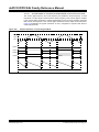
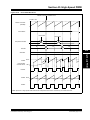
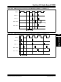
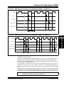
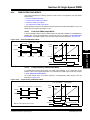
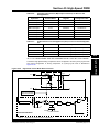
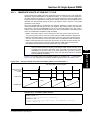
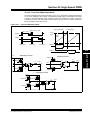
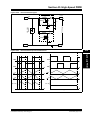
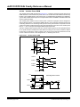
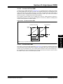
1
Section 43. High-Speed PWM
HIGHLIGHTS
This section of the manual contains the following major topics:
© 2008-2012 Microchip Technology Inc.
DS70323E-page 43-1
43
High-Speed PWM
43.1 Introduction .................................................................................................................. 43-2
43.2 Features....................................................................................................................... 43-2
43.3 Control Registers ......................................................................................................... 43-3
43.4 Architecture Overview................................................................................................ 43-32
43.5 Module Description .................................................................................................... 43-35
43.6 PWM Generator ......................................................................................................... 43-45
43.7 PWM Triggers ............................................................................................................ 43-57
43.8 PWM Interrupts .......................................................................................................... 43-64
43.9 PWM Operating Modes.............................................................................................. 43-65
43.10 PWM Fault Pins ......................................................................................................... 43-70
43.11 Special Features ........................................................................................................ 43-82
43.12 PWM Output Pin Control............................................................................................ 43-88
43.13 Immediate Update of PWM Duty Cycle ..................................................................... 43-91
43.14 Power-Saving Modes................................................................................................. 43-92
43.15 External Control of Individual Time Base(s) (Current Reset Mode) ........................... 43-93
43.16 Application Information .............................................................................................. 43-93
43.17 Burst Mode Implementation ..................................................................................... 43-103
43.18 PWM Interconnects with Other Peripherals (ADC, Analog Comparator and Interrupt
Controller) ................................................................................................................ 43-103
43.19 Register Map............................................................................................................ 43-107
43.20 Related Application Notes........................................................................................ 43-109
43.21 Revision History ....................................................................................................... 43-110
dsPIC33F/PIC24H Family Reference Manual
Note:
This family reference manual section is meant to serve as a complement to device
data sheets. Depending on the device variant, this manual section may not apply to
all dsPIC33F/PIC24H devices.
Please consult the note at the beginning of the “High-Speed PWM” chapter in the
current device data sheet to check whether this document supports the device you
are using.
Device data sheets and family reference manual sections are available for
download from the Microchip Worldwide Web site at: http://www.microchip.com
43.1
INTRODUCTION
This section describes the High-Speed PWM module and its associated operational modes. The
High-Speed PWM module supports a wide variety of PWM modes and is ideal for power
conversion applications. Some of the common applications that the High-Speed PWM module
supports are:
•
•
•
•
•
•
•
•
•
•
43.2
AC-to-DC converters
Power Factor Correction (PFC)
Interleaved Power Factor Correction (IPFC)
Inverters
DC-to-DC converters
Battery chargers
Digital lighting
Uninterruptable Power Supply (UPS)
AC and DC motors
Resonant converters
FEATURES
The High-Speed PWM module consists of the following major features:
•
•
•
•
•
•
•
•
•
•
•
•
•
•
•
•
•
•
•
Up to nine PWM generators
Two PWM outputs per PWM generator
Individual time base and duty cycle for each PWM output
Duty cycle, dead time, phase shift and frequency resolution of 1.04 ns
Independent fault and current-limit inputs for all PWM outputs
Redundant output
True independent output
Center-aligned PWM mode
Output override control
Special Event Trigger
Prescaler for input clock
Dual trigger to Analog-to-Digital Converter (ADC) per PWM period
PWMXL and PWMXH output pin swapping
Independent PWM frequency, duty cycle and phase shift changes
Leading-edge Blanking (LEB) functionality
PWM capture functionality
Up to two master time bases
Dead-time compensation
PWM chopping
Note:
DS70323E-page 43-2
Duty cycle, dead-time, phase shift and frequency resolution is 8.32 ns in
Center-aligned PWM mode.
© 2008-2012 Microchip Technology Inc.
Section 43. High-Speed PWM
43.3
CONTROL REGISTERS
This section outlines the specific functions of each register that controls the operation of
High-Speed PWM module.
© 2008-2012 Microchip Technology Inc.
DS70323E-page 43-3
43
High-Speed PWM
• PTCON: PWM Time Base Control Register
- Enables or disables the High-Speed PWM module
- Sets the Special Event Trigger for the Analog-to-Digital Converter (ADC) and enables
or disables the Primary Special Event Trigger interrupt
- Enables or disables immediate period updates
- Selects the synchronizing source for the master time base
- Specifies synchronization settings
• PTCON2: PWM Clock Divider Select Register
- Provides the clock prescaler to all PWM time bases
• PTPER: Master Time Base Period Register
- Provides the PWM time period value
• SEVTCMP: PWM Special Event Compare Register
- Provides the compare value that is used to trigger the ADC module and generates the
Primary Special Event Trigger interrupt
• STCON: PWM Secondary Master Time Base Control Register
- Sets the secondary Special Event Trigger for the ADC and enables or disables the
Secondary Special Event Trigger interrupt
- Enables or disables immediate period updates for the secondary master time base
- Selects synchronizing source for the secondary master time base
- Specifies synchronization settings for the secondary master time base
• STCON2: PWM Secondary Clock Divider Select Register
- Provides the clock prescaler to the PWM secondary master time base
• STPER: Secondary Master Time Base Period Register
- Provides the PWM time period value for the secondary master time base
• SSEVTCMP: PWM Secondary Special Event Compare Register
- Provides the compare value for the secondary master time base that is used to trigger
the ADC module and generates the Secondary Special Event Trigger interrupt
• CHOP: PWM Chop Clock Generator Register
- Enables and disables the chop signal used to modulate the PWM outputs
- Specifies the period for the chop signal
• MDC: PWM Master Duty Cycle Register
- Provides the PWM master duty cycle value
• PWMCONx: PWM Control Register
- Enables or disables fault interrupt, current-limit interrupt, primary trigger interrupt
- Provides the Interrupt status for fault interrupt, current-limit interrupt and primary
trigger interrupt
- Selects the type of time base (master time base or independent time base)
- Selects the type of duty cycle (master duty cycle or independent duty cycle)
- Controls Dead Time mode
- Enables or disables Center-aligned mode
- Controls external PWM Reset operation
- Enables or disables immediate updates of the duty cycle, phase offset and
independent time base period
• PDCx: PWM Generator Duty Cycle Register
- Provides the duty cycle value for the PWMxH and PWMxL outputs, if master time base
is selected
- Provides the duty cycle value for the PWMxH output, if independent time base is
selected
dsPIC33F/PIC24H Family Reference Manual
• PHASEx: PWM Primary Phase Shift Register
- Provides the phase shift value for the PWMxH and/or PWMxL outputs, if master time
base is selected
- Provides the independent time base period for the PWMxH and/or PWMxL outputs, if
independent time base is selected
• DTRx: PWM Dead Time Register
- Provides the dead time value for the PWMxH output, if positive dead time is selected
- Provides the dead time value for the PWMxL output, if negative dead time is selected
• ALTDTRx: PWM Alternate Dead Time Register
- Provides the dead time value for the PWMxL output, if positive dead time is selected
- Provides the dead time value for the PWMxH output, if negative dead time is selected
• SDCx: PWM Secondary Duty Cycle Register
- Provides the duty cycle value for the PWMxL output, if independent time base is
selected
• SPHASEx: PWM Secondary Phase Shift Register
- Provides the phase shift for the PWMxL output, if the master time base and Independent
Output mode are selected
- Provides the independent time base period value for the PWMxL output, if the
independent time base and Independent Output mode are selected
• TRGCONx: PWM Trigger Control Register
- Enables the PWMx trigger postscaler start event
- Specifies the number of PWM cycles to skip before generating the first trigger
- Enables or disables the primary PWM trigger event with the secondary PWM trigger
event
• IOCONx: PWM I/O Control Register
- Enables or disables PWM pin control feature (PWM control or GPIO)
- Controls the PWMxH and PWMxL output polarity
- Controls the PWMxH and PWMxL output if any of the following modes is selected:
• Complementary mode
• Push-Pull mode
• True Independent mode
• FCLCONx: PWM Fault Current-Limit Control Register
- Selects the current-limit control signal source
- Selects the current-limit polarity
- Enables or disables the Current-Limit mode
- Selects the fault control signal source
- Configures the fault polarity
- Enables or disables the Fault mode
• TRIGx: PWM Primary Trigger Compare Value Register
- Provides the compare value to generate the primary PWM trigger
• STRIGx: PWM Secondary Trigger Compare Value Register
- Provides the compare value to generate the secondary PWM trigger
• LEBCONx: Leading-Edge Blanking Control Register (Version 1)
- Selects the rising or falling edge of the PWM output for LEB
- Enables or disables LEB for fault and current-limit inputs
• LEBCONx: Leading-Edge Blanking Control Register (Version 2)
- Selects rising or falling edge of the PWM output for Leading-Edge Blanking
- Enables or disables Leading-Edge Blanking for Fault and current-limit inputs
- Specifies the state of blanking for the Fault input and current-limit signals when the
selected blanking signal (PWMxH, PWMxL or other specified signal by the PWM State
Blank Source Select bits (BLANKSEL<3:0>) in the PWM Auxiliary Control register
(AUXCONx<11:8>)) is high or low
DS70323E-page 43-4
© 2008-2012 Microchip Technology Inc.
Section 43. High-Speed PWM
• LEBDLYx: Leading-Edge Blanking Delay Register
- Specifies the blanking time for the selected Fault input and current-limit signals
• AUXCONx: PWM Auxiliary Control Register
- Enables or disables the high-resolution PWM period and the duty cycle in order to
reduce the system power consumption
- Selects the state blanking signal for the current-limit signals and the Fault inputs
• PWMCAPx: Primary PWM Time Base Capture Register
- Provides the captured independent time base value when a leading-edge is detected
on the current-limit input
43
High-Speed PWM
© 2008-2012 Microchip Technology Inc.
DS70323E-page 43-5
dsPIC33F/PIC24H Family Reference Manual
Register 43-1:
PTCON: PWM Time Base Control Register
R/W-0
PTEN(3)
bit 15
U-0
—
R/W-0
SYNCEN(1,2)
bit 7
R/W-0
bit 14
bit 13
bit 12
bit 11
bit 10
bit 9
bit 8
bit 7
bit 6-4
bit 3-0
Note 1:
2:
3:
HS/HC-0
SESTAT
R/W-0
R/W-0
SYNCSRC<2:0>(1,2)
R/W-0
SEIEN
R/W-0
EIPU(1)
R/W-0
R/W-0
SYNCPOL(1,2) SYNCOEN(1,2)
bit 8
R/W-0
R/W-0
R/W-0
SEVTPS<3:0>(1)
R/W-0
bit 0
Legend:
R = Readable bit
-n = Value at POR
bit 15
R/W-0
PTSIDL
HC = Cleared in Hardware HS = Set in Hardware
W = Writable bit
U = Unimplemented bit, read as ‘0’
‘1’ = Bit is set
‘0’ = Bit is cleared
x = Bit is unknown
PTEN: PWM Module Enable bit(3)
1 = PWM module is enabled
0 = PWM module is disabled
Unimplemented: Read as ‘0’
PTSIDL: PWM Time Base Stop in Idle Mode bit
1 = PWM time base halts in CPU Idle mode
0 = PWM time base runs in CPU Idle mode
SESTAT: Special Event Interrupt Status bit
1 = Special Event Interrupt is pending
0 = Special Event Interrupt is not pending
SEIEN: Special Event Interrupt Enable bit
1 = Special Event Interrupt is enabled
0 = Special Event Interrupt is disabled
EIPU: Enable Immediate Period Updates bit(1)
1 = Active Period register is updated immediately
0 = Active Period register updates occur on PWM cycle boundaries
SYNCPOL: Synchronize Input and Output Polarity bit(1,2)
1 = SYNCIx/SYNCO polarity is inverted (active-low)
0 = SYNCIx/SYNCO is active-high
SYNCOEN: Primary Time Base Sync Enable bit(1,2)
1 = SYNCO output is enabled
0 = SYNCO output is disabled
SYNCEN: External Time Base Synchronization Enable bit(1,2)
1 = External synchronization of primary time base is enabled
0 = External synchronization of primary time base is disabled
SYNCSRC<2:0>: Synchronous Source Selection bits(1)
011 = SYNCI4
010 = SYNCI3
001 = SYNCI2
000 = SYNCI1
SEVTPS<3:0>: PWM Special Event Trigger Output Postscaler Select bits(1)
1111 = 1:16 Postscaler generates Special Event Trigger on every sixteenth compare match event
•
•
•
0001 = 1:2 Postscaler generates Special Event Trigger on every second compare match event
0000 = 1:1 Postscaler generates Special Event Trigger on every compare match event
These bits should be changed only when PTEN = 0.
The PWM Time base synchronization must only be used in the master time base with no phase shifting.
When the PWM module is enabled by setting PTCON<15> = 1, a delay will be observed before the PWM
outputs start switching. This delay is equal to:
PWM Turn ON delay = (2/ACLK) + (3 • (PCLKDIV setting)/ACLK) + 15 ns
DS70323E-page 43-6
© 2008-2012 Microchip Technology Inc.
Section 43. High-Speed PWM
Register 43-2:
PTCON2: PWM Clock Divider Select Register
U-0
U-0
U-0
U-0
U-0
U-0
U-0
U-0
—
—
—
—
—
—
—
—
bit 15
bit 8
U-0
U-0
—
U-0
—
—
U-0
—
U-0
—
R/W-0
R/W-0
PCLKDIV<2:0>
R/W-0
(1)
bit 7
bit 0
Legend:
R = Readable bit
W = Writable bit
U = Unimplemented bit, read as ‘0’
-n = Value at POR
‘1’ = Bit is set
‘0’ = Bit is cleared
Unimplemented: Read as ‘0’
bit 2-0
PCLKDIV<2:0>: PWM Input Clock Prescaler (Divider) Select bits(1)
111 = Reserved
110 = Divide by 64, maximum PWM timing resolution
101 = Divide by 32, maximum PWM timing resolution
100 = Divide by 16, maximum PWM timing resolution
011 = Divide by 8, maximum PWM timing resolution
010 = Divide by 4, maximum PWM timing resolution
001 = Divide by 2, maximum PWM timing resolution
000 = Divide by 1, maximum PWM timing resolution (power-on default)
Note 1:
Note:
43
These bits should be changed only when PTEN = 0. Changing the clock selection during operation will
yield unpredictable results.
The PWM input clock prescaler will affect all timing parameters of the PWM module, including period, duty
cycle, phase, dead-time, triggers, leading-edge blanking and PWM capture.
© 2008-2012 Microchip Technology Inc.
DS70323E-page 43-7
High-Speed PWM
bit 15-3
x = Bit is unknown
dsPIC33F/PIC24H Family Reference Manual
Register 43-3:
PTPER: Master Time Base Period Register
R/W-1
R/W-1
R/W-1
R/W-1
R/W-1
R/W-1
R/W-1
R/W-1
PTPER<15:8>
bit 15
bit 8
R/W-1
R/W-1
R/W-1
R/W-1
R/W-1
R/W-0
R/W-0
R/W-0
PTPER<7:0>
bit 7
bit 0
Legend:
R = Readable bit
W = Writable bit
U = Unimplemented bit, read as ‘0’
-n = Value at POR
‘1’ = Bit is set
‘0’ = Bit is cleared
bit 15-0
x = Bit is unknown
PTPER<15:0>: Master Time Base (PMTMR) Period Value bits
Note 1: The PWM time base has a minimum value of 0x0010, and a maximum value of 0xFFF8.
2: Any period value that is less than 0x0028 must have the Least Significant 3 bits (LSbs) set to ‘0’. This
yields a period resolution of 8.32 ns (at fastest Auxiliary Clock rate) for these very short PWM period
pulses.
DS70323E-page 43-8
© 2008-2012 Microchip Technology Inc.
Section 43. High-Speed PWM
Register 43-4:
SEVTCMP: PWM Special Event Compare Register
R/W-0
R/W-0
R/W-0
R/W-0
R/W-0
R/W-0
R/W-0
R/W-0
SEVTCMP<12:5>
bit 15
bit 8
R/W-0
R/W-0
R/W-0
R/W-0
R/W-0
SEVTCMP<4:0>
U-0
U-0
U-0
—
—
—
bit 7
bit 0
Legend:
R = Readable bit
W = Writable bit
U = Unimplemented bit, read as ‘0’
-n = Value at POR
‘1’ = Bit is set
‘0’ = Bit is cleared
bit 15-3
SEVTCMP<12:0>: Primary Special Event Compare Count Value bits
bit 2-0
Unimplemented: Read as ‘0’
x = Bit is unknown
Note 1: 1 LSb = 1.04 ns. Therefore, minimum SEVTCMP resolution is 8.32 ns at the fastest PWM clock divider
setting (PTCON2<2:0> = 0).
2: The Special Event Trigger is generated on a compare match with the PWM Master Time Base Counter
(PMTMR).
High-Speed PWM
3: This register is used in conjunction with the PTCON<3:0> bit field.
© 2008-2012 Microchip Technology Inc.
43
DS70323E-page 43-9
dsPIC33F/PIC24H Family Reference Manual
Register 43-5:
STCON: PWM Secondary Master Time Base Control Register
U-0
U-0
—
—
U-0
HS/HC-0
—
SESTAT
R/W-0
SEIEN
R/W-0
(1)
EIPU
R/W-0
SYNCPOL
R/W-0
(1,2)
SYNCOEN
bit 15
bit 8
R/W-0
R/W-0
(1,2)
R/W-0
SYNCSRC<2:0>
SYNCEN
R/W-0
R/W-0
R/W-0
(1)
R/W-0
SEVTPS<3:0>
bit 7
bit 0
Legend:
HC = Cleared in Hardware
R = Readable bit
W = Writable bit
U = Unimplemented bit, read as ‘0’
-n = Value at POR
‘1’ = Bit is set
‘0’ = Bit is cleared
HS = Set in Hardware
x = Bit is unknown
bit 15-13
Unimplemented: Read as ‘0’
bit 12
SESTAT: Special Event Interrupt Status bit
1 = Secondary special event interrupt is pending
0 = Secondary special event interrupt is not pending
bit 11
SEIEN: Special Event Interrupt Enable bit
1 = Secondary special event interrupt is enabled
0 = Secondary special event interrupt is disabled
bit 10
EIPU: Enable Immediate Period Updates bit(1)
1 = Active Secondary Period register is updated immediately.
0 = Active Secondary Period register updates occur on PWM cycle boundaries
bit 9
SYNCPOL: Synchronize Input and Output Polarity bit(1,2)
1 = The falling edge of SYNCIN resets the SMTMR; SYNCO2 output is active-low
0 = The rising edge of SYNCIN resets the SMTMR; SYNCO2 output is active-high
bit 8
SYNCOEN: Secondary Master Time Base Sync Enable bit(1,2)
1 = SYNCO2 output is enabled
0 = SYNCO2 output is disabled
bit 7
SYNCEN: External Secondary Master Time Base Synchronization Enable bit(1,2)
1 = External synchronization of secondary time base is enabled
0 = External synchronization of secondary time base is disabled
bit 6-4
SYNCSRC<2:0>: Secondary Time Base Sync Source Selection bits(1)
011 = SYNCI4
010 = SYNCI3
001 = SYNCI2
000 = SYNCI1
bit 3-0
SEVTPS<3:0>: PWM Secondary Special Event Trigger Output Postscaler Select bits(1)
1111 = 1:16 Postcale
•
•
•
0001 = 1:2 Postcale
0000 = 1:1 Postscale
Note 1:
2:
R/W-0
(1)
These bits should be changed only when PTEN = 0.
The PWM Time base synchronization must only be used in the master time base with no phase shifting.
DS70323E-page 43-10
© 2008-2012 Microchip Technology Inc.
Section 43. High-Speed PWM
Register 43-6:
STCON2: PWM Secondary Clock Divider Select Register
U-0
U-0
U-0
U-0
U-0
U-0
U-0
U-0
—
—
—
—
—
—
—
—
bit 15
bit 8
U-0
U-0
—
U-0
—
—
U-0
—
U-0
—
R/W-0
R/W-0
PCLKDIV<2:0>
R/W-0
(1)
bit 7
bit 0
Legend:
R = Readable bit
W = Writable bit
U = Unimplemented bit, read as ‘0’
-n = Value at POR
‘1’ = Bit is set
‘0’ = Bit is cleared
Unimplemented: Read as ‘0’
bit 2-0
PCLKDIV<2:0>: PWM Input Clock Prescaler (Divider) Select bits(1)
111 = Reserved
110 = Divide by 64, maximum PWM timing resolution
101 = Divide by 32, maximum PWM timing resolution
100 = Divide by 16, maximum PWM timing resolution
011 = Divide by 8, maximum PWM timing resolution
010 = Divide by 4, maximum PWM timing resolution
001 = Divide by 2, maximum PWM timing resolution
000 = Divide by 1, maximum PWM timing resolution (power-on default)
Note 1:
Note:
43
These bits should be changed only when PTEN = 0. Changing the clock selection during operation will
yield unpredictable results.
The PWM input clock prescaler will affect all timing parameters of the PWM module, including period, duty
cycle, phase, dead-time, triggers, leading-edge blanking and PWM capture.
© 2008-2012 Microchip Technology Inc.
DS70323E-page 43-11
High-Speed PWM
bit 15-3
x = Bit is unknown
dsPIC33F/PIC24H Family Reference Manual
Register 43-7:
STPER: Secondary Master Time Base Period Register
R/W-1
R/W-1
R/W-1
R/W-1
R/W-1
R/W-1
R/W-1
R/W-1
STPER<15:8>
bit 15
bit 8
R/W-1
R/W-1
R/W-1
R/W-1
R/W-1
R/W-0
R/W-0
R/W-0
STPER<7:0>
bit 7
bit 0
Legend:
R = Readable bit
W = Writable bit
U = Unimplemented bit, read as ‘0’
-n = Value at POR
‘1’ = Bit is set
‘0’ = Bit is cleared
bit 15-0
x = Bit is unknown
STPER<15:0>: Secondary Master Time Base (SMTMR) Period Value bits
Note 1: The PWM time base has a minimum value of 0x0010, and a maximum value of 0xFFF8.
2: Any period value that is less than 0x0028 must have the Least Significant 3 bits (LSbs) set to ‘0’. This
yields a period resolution of 8.32 ns (at fastest Auxiliary Clock rate) for these very short PWM period
pulses.
Register 43-8:
SSEVTCMP: PWM Secondary Special Event Compare Register
R/W-0
R/W-0
R/W-0
R/W-0
R/W-0
R/W-0
R/W-0
R/W-0
SSEVTCMP<12:5>
bit 15
bit 8
R/W-0
R/W-0
R/W-0
R/W-0
R/W-0
SSEVTCMP<4:0>
U-0
U-0
U-0
—
—
—
bit 7
bit 0
Legend:
R = Readable bit
W = Writable bit
U = Unimplemented bit, read as ‘0’
-n = Value at POR
‘1’ = Bit is set
‘0’ = Bit is cleared
x = Bit is unknown
bit 15-3
SSEVTCMP<12:0>: PWM Secondary Special Event Compare Count Value bits
bit 2-0
Unimplemented: Read as ‘0’
Note 1: 1 LSb = 1.04 ns. Therefore, minimum SSEVTCMP resolution is 8.32 ns at the fastest PWM Clock divider
setting (STCON2<2:0> = 0).
2: The Secondary Special Event Trigger is generated on a compare match with the PWM Secondary Master
Time Base Counter (SMTMR).
3: This register is used in conjunction with the STCON<3:0> bit field.
DS70323E-page 43-12
© 2008-2012 Microchip Technology Inc.
Section 43. High-Speed PWM
Register 43-9:
CHOP: PWM Chop Clock Generator Register
R/W-0
U-0
U-0
U-0
U-0
U-0
CHPCLKEN
—
—
—
—
—
R/W-0
R/W-0
CHOP<6:5>
bit 15
bit 8
R/W-0
R/W-0
R/W-0
R/W-0
R/W-0
CHOP<4:0>
U-0
U-0
U-0
—
—
—
bit 7
bit 0
Legend:
R = Readable bit
W = Writable bit
U = Unimplemented bit, read as ‘0’
-n = Value at POR
‘1’ = Bit is set
‘0’ = Bit is cleared
x = Bit is unknown
bit 15
CHPCLKEN: Enable Chop Clock Generator bit
1 = Chop clock generator is enabled
0 = Chop clock generator is disabled
bit 14-10
Unimplemented: Read as ‘0’
bit 9-3
CHOP<6:0>: Chop Clock Divider bits
Value in 8.32 ns increments. The frequency of the chop clock signal is calculated as follows:
Chop Frequency = 1/(16.64 * (CHOP<6:0> + 1) * Primary Master PWM Input Clock/PCLKDIV<2:0>
R/W-0
R/W-0
R/W-0
R/W-0
R/W-0
R/W-0
R/W-0
R/W-0
MDC<15:8>
bit 15
bit 8
R/W-0
R/W-0
R/W-0
R/W-0
R/W-0
R/W-0
R/W-0
R/W-0
MDC<7:0>
bit 7
bit 0
Legend:
R = Readable bit
W = Writable bit
U = Unimplemented bit, read as ‘0’
-n = Value at POR
‘1’ = Bit is set
‘0’ = Bit is cleared
bit 15-0
x = Bit is unknown
MDC<15:0>: Master PWM Duty Cycle Value bits
Note 1: The smallest pulse width that can be generated on the PWM output corresponds to a value of 0x0008,
while the maximum pulse width generated corresponds to a value of Period + 0x0008.
2: MDC < 0x0008 will produce 0% duty cycle. MDC > Period + 0x0008 will produce 100% duty cycle.
3: As the Duty Cycle gets closer to 0% or 100% of the PWM Period (0 ns to 40 ns, depending on the mode
of operation), PWM Duty Cycle resolution will increase from 1 LSb to 3 LSbs.
© 2008-2012 Microchip Technology Inc.
DS70323E-page 43-13
High-Speed PWM
Register 43-10: MDC: PWM Master Duty Cycle Register
43
dsPIC33F/PIC24H Family Reference Manual
Register 43-11: PWMCONx: PWM Control Register
HS/HC-0
HS/HC-0
FLTSTAT(1)
CLSTAT
(1)
HS/HC-0
TRGSTAT
R/W-0
R/W-0
FLTIEN
CLIEN
R/W-0
TRGIEN
R/W-0
(3)
ITB
R/W-0
MDCS(3)
bit 15
bit 8
R/W-0
R/W-0
DTC<1:0>
(3)
R/W-0
(3,6)
DTCP
U-0
R/W-0
—
MTBS
R/W-0
(2,3,5)
CAM
R/W-0
R/W-0
(4)
XPRES
bit 7
IUE
bit 0
Legend:
HC = Cleared in Hardware HS = Set in Hardware
R = Readable bit
W = Writable bit
U = Unimplemented bit, read as ‘0’
-n = Value at POR
‘1’ = Bit is set
‘0’ = Bit is cleared
x = Bit is unknown
bit 15
FLTSTAT: Fault Interrupt Status bit(1)
1 = Fault interrupt is pending
0 = No Fault interrupt is pending
This bit is cleared by setting FLTIEN = 0.
bit 14
CLSTAT: Current-Limit Interrupt Status bit(1)
1 = Current-limit interrupt is pending
0 = No current-limit interrupt is pending
This bit is cleared by setting CLIEN = 0.
bit 13
TRGSTAT: Trigger Interrupt Status bit
1 = Trigger interrupt is pending
0 = No trigger interrupt is pending
This bit is cleared by setting TRGIEN = 0.
bit 12
FLTIEN: Fault Interrupt Enable bit
1 = Fault interrupt is enabled
0 = Fault interrupt is disabled and FLTSTAT bit is cleared
bit 11
CLIEN: Current-Limit Interrupt Enable bit
1 = Current-limit interrupt enabled
0 = Current-limit interrupt disabled and CLSTAT bit is cleared
bit 10
TRGIEN: Trigger Interrupt Enable bit
1 = A trigger event generates an IRQ
0 = Trigger event interrupts are disabled and TRGSTAT bit is cleared
bit 9
ITB: Independent Time Base Mode bit(3)
1 = PHASEx/SPHASEx registers provide time base period for this PWM generator
0 = PTPER/STPER register provides timing for this PWM generator
bit 8
MDCS: Master Duty Cycle Register Select bit(3)
1 = MDC register provides duty cycle information for this PWM generator
0 = PDCx and SDCx registers provide duty cycle information for this PWM generator
Note 1:
2:
3:
4:
5:
6:
Software must clear the interrupt status, and the corresponding IFS bit in the Interrupt Controller.
The Independent Time Base mode (ITB = 1) must be enabled to use Center-Aligned mode. If ITB = 0, the
CAM bit is ignored.
These bits should not be changed after the PWM is enabled (PTEN = 1).
Configure FCLCONX<8> = 0 and PWMCONX<9> = 1, to operate in External Period Reset mode.
Center-aligned mode ignores the Least Significant 3 bits of the duty cycle, phase and dead time registers.
The highest CAM resolution available is 8.32 ns with the clock prescaler set to the fastest clock.
DTC<1:0> = 11 for DTCP to be effective; otherwise, DTCP is ignored.
DS70323E-page 43-14
© 2008-2012 Microchip Technology Inc.
Section 43. High-Speed PWM
Register 43-11: PWMCONx: PWM Control Register (Continued)
DTC<1:0>: Dead Time Control bits(3)
11 = Dead time Compensation mode
10 = Dead time function is disabled
01 = Negative dead time actively applied for all output modes
00 = Positive dead time actively applied for all output modes
bit 5
DTCP: Dead-Time Compensation Polarity bit(3,6)
When set to ‘1’:
If DTCMPx = 0, PWMxL is shortened and PWMxH is lengthened.
If DTCMPx = 1, PWMxH is shortened and PWMxL is lengthened.
When set to ‘0’:
If DTCMPx = 0, PWMxH is shortened and PWMxL is lengthened.
If DTCMPx = 1, PWMxL is shortened and PWMxH is lengthened.
bit 4
Unimplemented: Read as ‘0’
bit 3
MTBS: Master Time Base Select bit
1 = PWM generator uses the secondary master time base for synchronization and as the clock source
for the PWM generation logic (if secondary time base is available)
0 = PWM generator uses the primary master time base for synchronization and as the clock source
for the PWM generation logic
bit 2
CAM: Center-aligned Mode Enable bit(2,3,5)
1 = Center-aligned mode is enabled
0 = Edge-aligned mode is enabled
bit 1
XPRES: External PWM Reset Control bit(4)
1 = Current-limit source resets the time base for this PWM generator if it is in Independent Time Base
mode
0 = External pins do not affect PWM time base
bit 0
IUE: Immediate Update Enable bit
1 = Updates to the active MDC/PDCx/SDCx registers are immediate
0 = Updates to the active MDC/PDCx/SDCx registers are synchronized to the local PWM time base
Note 1:
2:
3:
4:
5:
6:
Software must clear the interrupt status, and the corresponding IFS bit in the Interrupt Controller.
The Independent Time Base mode (ITB = 1) must be enabled to use Center-Aligned mode. If ITB = 0, the
CAM bit is ignored.
These bits should not be changed after the PWM is enabled (PTEN = 1).
Configure FCLCONX<8> = 0 and PWMCONX<9> = 1, to operate in External Period Reset mode.
Center-aligned mode ignores the Least Significant 3 bits of the duty cycle, phase and dead time registers.
The highest CAM resolution available is 8.32 ns with the clock prescaler set to the fastest clock.
DTC<1:0> = 11 for DTCP to be effective; otherwise, DTCP is ignored.
© 2008-2012 Microchip Technology Inc.
DS70323E-page 43-15
43
High-Speed PWM
bit 7-6
dsPIC33F/PIC24H Family Reference Manual
Register 43-12: PDCx: PWM Generator Duty Cycle Register
R/W-0
R/W-0
R/W-0
R/W-0
R/W-0
R/W-0
R/W-0
R/W-0
PDCx<15:8>
bit 15
bit 8
R/W-0
R/W-0
R/W-0
R/W-0
R/W-0
R/W-0
R/W-0
R/W-0
PDCx<7:0>
bit 7
bit 0
Legend:
R = Readable bit
W = Writable bit
U = Unimplemented bit, read as ‘0’
-n = Value at POR
‘1’ = Bit is set
‘0’ = Bit is cleared
bit 15-0
x = Bit is unknown
PDCx<15:0>: PWM Generator x Duty Cycle Value bits
Note 1: In Independent Output mode, the PDCx register controls the PWMxH duty cycle only. In Complementary,
Redundant and Push-Pull PWM modes, the PDCx register controls the duty cycle of PWMxH and PWMxL.
2: The smallest pulse width that can be generated on the PWM output corresponds to a value of 0x0008,
while the maximum pulse width generated corresponds to a value of Period + 0x0008.
3: PDCx < 0x0008 produces 0% duty cycle. PDCx > Period + 0x0008 produces 100% duty cycle.
4: As the Duty Cycle gets closer to 0% or 100% of the PWM Period (0 ns to 40 ns, depending on the mode
of operation), the PWM Duty Cycle resolution will increase from 1 LSb to 3 LSbs.
DS70323E-page 43-16
© 2008-2012 Microchip Technology Inc.
Section 43. High-Speed PWM
Register 43-13: SDCx: PWM Secondary Duty Cycle Register
R/W-0
R/W-0
R/W-0
R/W-0
R/W-0
R/W-0
R/W-0
R/W-0
SDCx<15:8>
bit 15
bit 8
R/W-0
R/W-0
R/W-0
R/W-0
R/W-0
R/W-0
R/W-0
R/W-0
SDCx<7:0>
bit 7
bit 0
Legend:
R = Readable bit
W = Writable bit
U = Unimplemented bit, read as ‘0’
-n = Value at POR
‘1’ = Bit is set
‘0’ = Bit is cleared
bit 15-0
x = Bit is unknown
SDCx<15:0>: Secondary Duty Cycle bits for the PWMxL Output Pin
Note 1: The SDCx register is used in Independent Output mode only. When used in Independent Output mode,
the SDCx register controls the PWMxL duty cycle. This register is ignored in other PWM modes.
2: The smallest pulse width that can be generated on the PWM output corresponds to a value of 0x0008,
while the maximum pulse width generated corresponds to a value of Period + 0x0008.
3: SDCx < 0x0008 produces 0% duty cycle. SDCx > Period + 0x0008 produces 100% duty cycle.
© 2008-2012 Microchip Technology Inc.
DS70323E-page 43-17
High-Speed PWM
4: As the Duty Cycle gets closer to 0% or 100% of the PWM Period (0 ns to 40 ns, depending on the mode
of operation), PWM Duty Cycle resolution will increase from 1 LSb to 3 LSbs.
43
dsPIC33F/PIC24H Family Reference Manual
Register 43-14: PHASEx: PWM Primary Phase Shift Register
R/W-0
R/W-0
R/W-0
R/W-0
R/W-0
R/W-0
R/W-0
R/W-0
PHASEx<15:8>
bit 15
bit 8
R/W-0
R/W-0
R/W-0
R/W-0
R/W-0
R/W-0
R/W-0
R/W-0
PHASEx<7:0>
bit 7
bit 0
Legend:
R = Readable bit
W = Writable bit
U = Unimplemented bit, read as ‘0’
-n = Value at POR
‘1’ = Bit is set
‘0’ = Bit is cleared
bit 15-0
x = Bit is unknown
PHASEx<15:0>: PWM Phase Shift Value or Independent Time Base Period bits for the PWM Generator
Note 1: If PWMCONx<9> = 0 (Master Time Base mode), the following applies based on the mode of operation:
• Complementary, Redundant and Push-Pull PWM Output mode (IOCONx<11:10> = 00, 01 or 10)
PHASEx<15:0> = Phase shift value for PWMxH and PWMxL outputs.
• True Independent PWM Output mode (IOCONx<11:10> = 11) PHASEx<15:0> = Phase shift value
for PWMxH only.
• When PHASEx/SPHASEx register provides the phase shift with respect to the master time base,
the valid range of values is 0x0000 – Period.
2: If PWMCONx<9> = 1 (Independent Time Base mode), the following applies based on the mode of
operation:
• Complementary, Redundant and Push-Pull PWM Output mode (IOCONx<11:10> = 00, 01 or 10)
PHASEx<15:0> = Independent time base period value for PWMxH and PWMxL outputs.
• True Independent PWM Output mode (IOCONx<11:10> = 11) PHASEx<15:0> = Independent time
base period value for PWMxH only.
• When PHASEx/SPHASEx register provides the local period, the valid range of values
are 0x0010 – 0xFFF8.
DS70323E-page 43-18
© 2008-2012 Microchip Technology Inc.
Section 43. High-Speed PWM
Register 43-15: SPHASEx: PWM Secondary Phase Shift Register
R/W-0
R/W-0
R/W-0
R/W-0
R/W-0
R/W-0
R/W-0
R/W-0
SPHASEx<15:8>
bit 15
bit 8
R/W-0
R/W-0
R/W-0
R/W-0
R/W-0
R/W-0
R/W-0
R/W-0
SPHASEx<7:0>
bit 7
bit 0
Legend:
R = Readable bit
W = Writable bit
U = Unimplemented bit, read as ‘0’
-n = Value at POR
‘1’ = Bit is set
‘0’ = Bit is cleared
bit 15-0
x = Bit is unknown
SPHASEx<15:0>: Secondary Phase Offset bits for the PWMxL Output Pin (used in Independent
PWM mode only)
Note 1: If PWMCONx<9> = 0, the following applies based on the mode of operation:
2: If PWMCONx<9> = 1, the following applies based on the mode of operation:
• Complementary, Redundant and Push-Pull PWM Output mode (IOCONx<11:10> = 00, 01 or 10)
SPHASEx<15:0> = Not used.
• True Independent PWM Output mode (IOCONx<11:10> = 11) SPHASEx<15:0> = Independent time
base period value for PWMxL only.
• When PHASEx/SPHASEx register provides the local period, the valid range of values
are 0x0010 – 0xFFF8.
© 2008-2012 Microchip Technology Inc.
DS70323E-page 43-19
43
High-Speed PWM
• Complementary, Redundant and Push-Pull PWM Output mode (IOCONx<11:10> = 00, 01 or 10)
SPHASEx<15:0> = Not used.
• True Independent PWM Output mode (IOCONx<11:10> = 11) SPHASEx<15:0> = Phase shift value
for PWMxL only.
• When the PHASEx/SPHASEx register provides the phase shift with respect to the master time
base, the valid range of values is 0x0000 – Period.
dsPIC33F/PIC24H Family Reference Manual
Register 43-16: DTRx: PWM Dead Time Register
U-0
U-0
—
—
R/W-0
R/W-0
R/W-0
R/W-0
R/W-0
R/W-0
DTRx<13:8>
bit 15
bit 8
R/W-0
R/W-0
R/W-0
R/W-0
R/W-0
R/W-0
R/W-0
R/W-0
DTRx<7:0>
bit 7
bit 0
Legend:
R = Readable bit
W = Writable bit
U = Unimplemented bit, read as ‘0’
-n = Value at POR
‘1’ = Bit is set
‘0’ = Bit is cleared
x = Bit is unknown
bit 15-14
Unimplemented: Read as ‘0’
bit 13-0
DTRx<13:0>: Unsigned 14-bit Dead Time Value bits for PWMxH Dead Time Unit
Register 43-17: ALTDTRx: PWM Alternate Dead Time Register
U-0
U-0
—
—
R/W-0
R/W-0
R/W-0
R/W-0
R/W-0
R/W-0
ALTDTRx<13:8>
bit 15
bit 8
R/W-0
R/W-0
R/W-0
R/W-0
R/W-0
R/W-0
R/W-0
R/W-0
ALTDTRx<7:0>
bit 7
bit 0
Legend:
R = Readable bit
W = Writable bit
U = Unimplemented bit, read as ‘0’
-n = Value at POR
‘1’ = Bit is set
‘0’ = Bit is cleared
x = Bit is unknown
bit 15-14
Unimplemented: Read as ‘0’
bit 13-0
ALTDTRx<13:0>: Unsigned 14-bit Dead Time Value bits for PWMxL Dead Time Unit
DS70323E-page 43-20
© 2008-2012 Microchip Technology Inc.
Section 43. High-Speed PWM
Register 43-18: TRGCONx: PWM Trigger Control Register
R/W-0
R/W-0
R/W-0
R/W-0
TRGDIV<3:0>
U-0
U-0
U-0
U-0
—
—
—
—
bit 15
bit 8
R/W-0
DTM
U-0
(1)
R/W-0
—
R/W-0
R/W-0
R/W-0
R/W-0
R/W-0
TRGSTRT<5:0>
bit 7
bit 0
Legend:
R = Readable bit
W = Writable bit
U = Unimplemented bit, read as ‘0’
-n = Value at POR
‘1’ = Bit is set
‘0’ = Bit is cleared
bit 15-12
x = Bit is unknown
TRGDIV<3:0>: Trigger # Output Divider bits
1111 = Trigger output for every 16th trigger event
1110 = Trigger output for every 15th trigger event
1101 = Trigger output for every 14th trigger event
1100 = Trigger output for every 13th trigger event
1011 = Trigger output for every 12th trigger event
1010 = Trigger output for every 11th trigger event
1001 = Trigger output for every 10th trigger event
1000 = Trigger output for every 9th trigger event
0111 = Trigger output for every 8th trigger event
0110 = Trigger output for every 7th trigger event
0101 = Trigger output for every 6th trigger event
0100 = Trigger output for every 5th trigger event
0011 = Trigger output for every 4th trigger event
0010 = Trigger output for every 3rd trigger event
0001 = Trigger output for every 2nd trigger event
0000 = Trigger output for every trigger event
43
High-Speed PWM
bit 11-8
Unimplemented: Read as ‘0’
bit 7
DTM: Dual Trigger Mode bit(1)
1 = Secondary trigger event is combined with the primary trigger event to create PWM trigger
0 = Secondary trigger event is not combined with the primary trigger event to create PWM trigger. Two
separate PWM triggers are generated
bit 6
Unimplemented: Read as ‘0’
bit 5-0
TRGSTRT<5:0>: Trigger Postscaler Start Enable Select bits
111111 = Wait 63 PWM cycles before generating the first trigger event after the module is enabled
•
•
•
000010 = Wait 2 PWM cycles before generating the first trigger event after the module is enabled
000001 = Wait 1 PWM cycles before generating the first trigger event after the module is enabled
000000 = Wait 0 PWM cycles before generating the first trigger event after the module is enabled
Note 1:
The secondary trigger event (STRIGx) cannot generate PWM trigger interrupts.
© 2008-2012 Microchip Technology Inc.
DS70323E-page 43-21
dsPIC33F/PIC24H Family Reference Manual
Register 43-19: IOCONx: PWM I/O Control Register
R/W-0
R/W-0
PENH
PENL
R/W-0
POLH
R/W-0
POLL
R/W-0
R/W-0
PMOD<1:0>(1)
R/W-0
R/W-0
OVRENH
OVRENL
bit 15
bit 8
R/W-0
R/W-0
OVRDAT<1:0>(2)
R/W-0
R/W-0
FLTDAT<1:0>(2)
R/W-0
R/W-0
CLDAT<1:0>(2)
R/W-0
R/W-0
SWAP
OSYNC
bit 7
bit 0
Legend:
R = Readable bit
W = Writable bit
U = Unimplemented bit, read as ‘0’
-n = Value at POR
‘1’ = Bit is set
‘0’ = Bit is cleared
x = Bit is unknown
bit 15
PENH: PWMxH Output Pin Ownership bit
1 = PWM module controls PWMxH pin
0 = GPIO module controls PWMxH pin
bit 14
PENL: PWMxL Output Pin Ownership bit
1 = PWM module controls PWMxL pin
0 = GPIO module controls PWMxL pin
bit 13
POLH: PWMxH Output Pin Polarity bit
1 = PWMxH pin is active-low
0 = PWMxH pin is active-high
bit 12
POLL: PWMxL Output Pin Polarity bit
1 = PWMxL pin is active-low
0 = PWMxL pin is active-high
bit 11-10
PMOD<1:0>: PWM # I/O Pin Mode bits(1)
11 = PWM I/O pin pair is in the True Independent PWM Output mode
10 = PWM I/O pin pair is in the Push-Pull PWM Output mode
01 = PWM I/O pin pair is in the Redundant PWM Output mode
00 = PWM I/O pin pair is in the Complementary PWM Output mode
bit 9
OVRENH: Override Enable for PWMxH Pin bit
1 = OVRDAT<1> provides data for output on PWMxH pin
0 = PWM generator provides data for PWMxH pin
bit 8
OVRENL: Override Enable for PWMxL Pin bit
1 = OVRDAT<0> provides data for output on PWMxL pin
0 = PWM generator provides data for PWMxL pin
bit 7-6
OVRDAT<1:0>: State for PWMxH and PWMxL Pins if Override is Enabled bits(2)
If OVERENH = 1, OVRDAT<1> provides data for PWMxH
If OVERENL = 1, OVRDAT<0> provides data for PWMxL
bit 5-4
FLTDAT<1:0>: State for PWMxH and PWMxL Pins if FLTMOD is Enabled bits(2)
FCLCONx<15> = 0: Normal Fault mode:
If Fault active, then FLTDAT<1> provides state for PWMxH
If Fault active, then FLTDAT<0> provides state for PWMxL
FCLCONx<15> = 1: Independent Fault mode:
If Current-limit active, then FLTDAT<1> provides state for PWMxH
If Fault active, then FLTDAT<0> provides state for PWMxL
Note 1:
2:
These bits should not be changed after the PWM module is enabled (PTEN = 1).
State represents Active/Inactive state of the PWM depending on the POLH and POLL.
DS70323E-page 43-22
© 2008-2012 Microchip Technology Inc.
Section 43. High-Speed PWM
Register 43-19: IOCONx: PWM I/O Control Register (Continued)
bit 3-2
CLDAT<1:0>: State for PWMxH and PWMxL Pins if CLMOD is Enabled bits(2)
FCLCONx<15> = 0: Normal Fault mode
If current-limit active, then CLDAT<1> provides state for PWMxH
If current-limit active, then CLDAT<0> provides state for PWMxL
FCLCONx<15> = 1: Independent Fault mode
CLDAT<1:0> is ignored
bit 1
SWAP: SWAP PWMxH and PWMxL Pins bit
1 = PWMxH output signal is connected to PWMxL pins; PWMxL output signal is connected to PWMxH
pins
0 = PWMxH and PWMxL pins are mapped to their respective pins
bit 0
OSYNC: Output Override Synchronization bit
1 = Output overrides through the OVRDAT<1:0> bits are synchronized to the PWM time base
0 = Output overrides through the OVRDAT<1:0> bits occur on next CPU clock boundary
Note 1:
2:
These bits should not be changed after the PWM module is enabled (PTEN = 1).
State represents Active/Inactive state of the PWM depending on the POLH and POLL.
43
High-Speed PWM
© 2008-2012 Microchip Technology Inc.
DS70323E-page 43-23
dsPIC33F/PIC24H Family Reference Manual
Register 43-20: TRIGx: PWM Primary Trigger Compare Value Register
R/W-0
R/W-0
R/W-0
R/W-0
R/W-0
R/W-0
R/W-0
R/W-0
TRGCMP<12:5>
bit 15
bit 8
R/W-0
R/W-0
R/W-0
R/W-0
R/W-0
TRGCMP<4:0>
U-0
U-0
U-0
—
—
—
bit 7
bit 0
Legend:
R = Readable bit
W = Writable bit
U = Unimplemented bit, read as ‘0’
-n = Value at POR
‘1’ = Bit is set
‘0’ = Bit is cleared
x = Bit is unknown
bit 15-3
TRGCMP<12:0>: Trigger Control Value bits
When the primary PWM functions in local time base, this register contains the compare values that
can trigger the ADC module.
bit 2-0
Unimplemented: Read as ‘0’
Register 43-21: STRIGx: PWM Secondary Trigger Compare Value Register
R/W-0
R/W-0
R/W-0
R/W-0
R/W-0
R/W-0
R/W-0
R/W-0
STRGCMP<12:5>
bit 15
bit 8
R/W-0
R/W-0
R/W-0
R/W-0
R/W-0
STRGCMP<4:0>
U-0
U-0
U-0
—
—
—
bit 7
bit 0
Legend:
R = Readable bit
W = Writable bit
U = Unimplemented bit, read as ‘0’
-n = Value at POR
‘1’ = Bit is set
‘0’ = Bit is cleared
x = Bit is unknown
bit 15-3
STRGCMP<12:0>: Secondary Trigger Control Value bits
When the secondary PWM functions in local time base, this register contains the compare values that
can trigger the ADC module.
bit 2-0
Unimplemented: Read as ‘0’
Note:
The STRIGx register cannot generate the PWM trigger interrupts.
DS70323E-page 43-24
© 2008-2012 Microchip Technology Inc.
Section 43. High-Speed PWM
Register 43-22: FCLCONx: PWM Fault Current-Limit Control Register
R/W-0
IFLTMOD
bit 15
R/W-0
R/W-0
R/W-0
R/W-0
R/W-0
R/W-0
CLSRC<4:0>(2,4)
R/W-0
FLTSRC<4:0>(3,4)
R/W-0
bit 7
Legend:
R = Readable bit
-n = Value at POR
bit 15
bit 14-10
W = Writable bit
‘1’ = Bit is set
R/W-0
R/W-0
R/W-0
FLTPOL(1)
R/W-0
CLPOL(1)
R/W-0
CLMOD
bit 8
R/W-0
R/W-0
FLTMOD<1:0>
bit 0
U = Unimplemented bit, read as ‘0’
‘0’ = Bit is cleared
x = Bit is unknown
IFLTMOD: Independent Fault Mode Enable bit
1 = Independent Fault mode: Current-limit input maps FLTDAT<1> to PWMxH output, and Fault input
maps FLTDAT<0> to PWMxL output. The CLDAT<1:0> bits are not used for override functions
0 = Normal Fault mode: Current-Limit mode maps CLDAT<1:0> bits to the PWMxH and PWMxL
outputs. The PWM Fault mode maps FLTDAT<1:0> to the PWMxH and PWMxL outputs
CLSRC<4:0>: Current-Limit Control Signal Source Select bits for PWM Generator #(2,4)
These bits also specify the source for the dead-time compensation input signal, DTCMPx.
For devices with remappable I/O:
11111 = Reserved
43
High-Speed PWM
•
•
•
01000 = Reserved
00111 = Fault 8
00110 = Fault 7
•
•
•
00001 = Fault 2
00000 = Fault 1
For devices without remappable I/O:
11111 = Reserved
11110 = Fault 23
•
•
•
01001 = Fault 2
01000 = Fault 1
00111 = Reserved
00110 = Reserved
00101 = Reserved
00100 = Reserved
00011 = Analog Comparator 4
00010 = Analog Comparator 3
00001 = Analog Comparator 2
00000 = Analog Comparator 1
Note 1:
2:
3:
4:
These bits should be changed only when PTEN = 0.
When Independent Fault mode is enabled (IFLTMOD = 1), and Fault 1 is used for Current-limit mode
(CLSRC<4:0> = ‘b0000), the Fault Control Source Select bits (FLTSRC<4:0>) should be set to an
unused Fault source to prevent Fault 1 from disabling both the PWMxL and PWMxH outputs.
When Independent Fault mode is enabled (IFLTMOD = 1) and Fault 1 is used for Fault mode
(FLTSRC<4:0> = ‘b0000), the Current-limit Control Source Select bits (CLSRC<4:0>) should be set to an
unused current-limit source to prevent the current-limit source from disabling both the PWMxH and
PWMxL outputs.
Refer to the “Pin Diagrams” section in the specific device data sheet for more details on the number of
available Fault pins.
© 2008-2012 Microchip Technology Inc.
DS70323E-page 43-25
dsPIC33F/PIC24H Family Reference Manual
Register 43-22: FCLCONx: PWM Fault Current-Limit Control Register (Continued)
CLPOL: Current-limit Polarity bit for PWM Generator #(1)
1 = The selected current-limit source is active-low
0 = The selected current-limit source is active-high
CLMOD: Current-limit Mode Enable bit for PWM Generator #
1 = Current-limit mode is enabled
0 = Current-limit mode is disabled
FLTSRC<4:0>: Fault Control Signal Source Select bits for PWM Generator #(3,4)
For devices with remappable I/O:
11111 = Reserved
bit 9
bit 8
bit 7-3
•
•
•
01000 = Reserved
00111 = Fault 8
00110 = Fault 7
•
•
•
00001 = Fault 2
00000 = Fault 1
For devices without remappable I/O:
11111 = Reserved
11110 = Fault 23
•
•
•
01001 = Fault 2
01000 = Fault 1
00111 = Reserved
00110 = Reserved
00101 = Reserved
00100 = Reserved
00011 = Analog Comparator 4
00010 = Analog Comparator 3
00001 = Analog Comparator 2
00000 = Analog Comparator 1
FLTPOL: Fault Polarity bit for PWM Generator #(1)
1 = The selected Fault source is active-low
0 = The selected Fault source is active-high
FLTMOD<1:0>: Fault Mode bits for PWM Generator #
11 = Fault input is disabled
10 = Reserved
01 = The selected Fault source forces PWMxH and PWMxL pins to FLTDAT values (cycle)
00 = The selected Fault source forces PWMxH and PWMxL pins to FLTDAT values (latched condition)
bit 2
bit 1-0
Note 1:
2:
3:
4:
These bits should be changed only when PTEN = 0.
When Independent Fault mode is enabled (IFLTMOD = 1), and Fault 1 is used for Current-limit mode
(CLSRC<4:0> = ‘b0000), the Fault Control Source Select bits (FLTSRC<4:0>) should be set to an
unused Fault source to prevent Fault 1 from disabling both the PWMxL and PWMxH outputs.
When Independent Fault mode is enabled (IFLTMOD = 1) and Fault 1 is used for Fault mode
(FLTSRC<4:0> = ‘b0000), the Current-limit Control Source Select bits (CLSRC<4:0>) should be set to an
unused current-limit source to prevent the current-limit source from disabling both the PWMxH and
PWMxL outputs.
Refer to the “Pin Diagrams” section in the specific device data sheet for more details on the number of
available Fault pins.
DS70323E-page 43-26
© 2008-2012 Microchip Technology Inc.
Section 43. High-Speed PWM
Register 43-23: LEBCONx: Leading-Edge Blanking Control Register (Version 1)
R/W-0
R/W-0
R/W-0
R/W-0
R/W-0
R/W-0
PHR
PHF
PLR
PLF
FLTLEBEN
CLLEBEN
R/W-0
R/W-0
LEB<6:5>
bit 15
bit 8
R/W-0
R/W-0
R/W-0
R/W-0
R/W-0
U-0
U-0
U-0
—
—
—
LEB<4:0>
bit 7
bit 0
Legend:
R = Readable bit
W = Writable bit
U = Unimplemented bit, read as ‘0’
-n = Value at POR
‘1’ = Bit is set
‘0’ = Bit is cleared
x = Bit is unknown
bit 15
PHR: PWMxH Rising Edge Trigger Enable bit
1 = Rising edge of PWMxH will trigger leading-edge blanking counter
0 = Leading-edge blanking ignores rising edge of PWMxH
bit 14
PHF: PWMxH Falling Edge Trigger Enable bit
1 = Falling edge of PWMxH will trigger leading-edge blanking counter
0 = Leading-edge blanking ignores falling edge of PWMxH
bit 13
PLR: PWMxL Rising Edge Trigger Enable bit
1 = Rising edge of PWMxL will trigger leading-edge blanking counter
0 = Leading-edge blanking ignores rising edge of PWMxL
bit 12
PLF: PWMxL Falling Edge Trigger Enable bit
1 = Falling edge of PWMxL will trigger leading-edge blanking counter
0 = Leading-edge blanking ignores falling edge of PWMxL
bit 11
FLTLEBEN: Fault Input Leading-Edge Blanking Enable bit
1 = Leading-edge blanking is applied to selected fault input
0 = Leading-edge blanking is not applied to selected fault input
bit 10
CLLEBEN: Current-limit Leading-Edge Blanking Enable bit
1 = Leading-edge blanking is applied to selected current-limit input
0 = Leading-edge blanking is not applied to selected current-limit input
bit 9-3
LEB<6:0>: Leading-Edge Blanking for Current-Limit and Fault Input bits
The Blanking can be incremented in 2n * 1/(Auxiliary Clock Frequency) ns steps, where ’n’ is the
PCLKDIV<2:0> bits (PTCON2<2:0>) setting.
bit 2-0
Unimplemented: Read as ‘0’
High-Speed PWM
Note:
43
At the highest PWM resolution, the LEB<6:0> bits support the blanking (ignoring) of the current-limit and
Fault pins for a period of 0 ns to 1057 ns in 8.32 ns increments, following any specified rising and falling
edge of the PWMxH and PWMxL signals.
© 2008-2012 Microchip Technology Inc.
DS70323E-page 43-27
dsPIC33F/PIC24H Family Reference Manual
Register 43-24: LEBCONx: Leading-Edge Blanking Control Register (Version 2)
R/W-0
PHR
bit 15
R/W-0
PHF
R/W-0
PLR
R/W-0
PLF
R/W-0
FLTLEBEN
R/W-0
CLLEBEN
U-0
—
bit 8
U-0
—
U-0
—
R/W-0
BCH(1)
R/W-0
BCL
R/W-0
BPHH
R/W-0
BPHL
R/W-0
BPLH
bit 7
Legend:
R = Readable bit
-n = Value at POR
bit 15
bit 14
bit 13
bit 12
bit 11
bit 10
bit 9-6
bit 5
bit 4
bit 3
bit 2
bit 1
bit 0
Note 1:
U-0
—
W = Writable bit
‘1’ = Bit is set
R/W-0
BPLL
bit 0
U = Unimplemented bit, read as ‘0’
‘0’ = Bit is cleared
x = Bit is unknown
PHR: PWMxH Rising Edge Trigger Enable bit
1 = Rising edge of PWMxH will trigger Leading-Edge Blanking counter
0 = Leading-Edge Blanking ignores rising edge of PWMxH
PHF: PWMxH Falling Edge Trigger Enable bit
1 = Falling edge of PWMxH will trigger Leading-Edge Blanking counter
0 = Leading-Edge Blanking ignores falling edge of PWMxH
PLR: PWMxL Rising Edge Trigger Enable bit
1 = Rising edge of PWMxL will trigger Leading-Edge Blanking counter
0 = Leading-Edge Blanking ignores rising edge of PWMxL
PLF: PWMxL Falling Edge Trigger Enable bit
1 = Falling edge of PWMxL will trigger Leading-Edge Blanking counter
0 = Leading-Edge Blanking ignores falling edge of PWMxL
FLTLEBEN: Fault Input Leading-Edge Blanking Enable bit
1 = Leading-Edge Blanking is applied to selected Fault input
0 = Leading-Edge Blanking is not applied to selected Fault input
CLLEBEN: Current-Limit Leading-Edge Blanking Enable bit
1 = Leading-Edge Blanking is applied to selected current-limit input
0 = Leading-Edge Blanking is not applied to selected current-limit input
Unimplemented: Read as ‘0’
BCH: Blanking in Selected Blanking Signal High Enable bit(1)
1 = State blanking (of current-limit and/or Fault input signals) when selected blanking signal is high
0 = No blanking when selected blanking signal is high
BCL: Blanking in Selected Blanking Signal Low Enable bit(1)
1 = State blanking (of current-limit and/or Fault input signals) when selected blanking signal is low
0 = No blanking when selected blanking signal is low
BPHH: Blanking in PWMxH High Enable bit
1 = State blanking (of current-limit and/or Fault input signals) when PWMxH output is high
0 = No blanking when PWMxH output is high
BPHL: Blanking in PWMxH Low Enable bit
1 = State blanking (of current-limit and/or Fault input signals) when PWMxH output is low
0 = No blanking when PWMxH output is low
BPLH: Blanking in PWMxL High Enable bit
1 = State blanking (of current-limit and/or Fault input signals) when PWMxL output is high
0 = No blanking when PWMxL output is high
BPLL: Blanking in PWMxL Low Enable bit
1 = State blanking (of current-limit and/or Fault input signals) when PWMxL output is low
0 = No blanking when PWMxL output is low
The blanking signal is selected through the BLANKSEL bits in the AUXCONx register.
DS70323E-page 43-28
© 2008-2012 Microchip Technology Inc.
Section 43. High-Speed PWM
Register 43-25: LEBDLYx: Leading-Edge Blanking Delay Register
U-0
U-0
U-0
U-0
—
—
—
—
R/W-0
R/W-0
R/W-0
R/W-0
LEB<8:5>
bit 15
bit 8
R/W-0
R/W-0
R/W-0
R/W-0
R/W-0
LEB<4:0>
U-0
U-0
U-0
—
—
—
bit 7
bit 0
Legend:
R = Readable bit
W = Writable bit
U = Unimplemented bit, read as ‘0’
-n = Value at POR
‘1’ = Bit is set
‘0’ = Bit is cleared
x = Bit is unknown
bit 15-12
Unimplemented: Read as ‘0’
bit 11-3
LEB<8:0>: Leading-Edge Blanking Delay bits for Current-Limit and Fault Inputs
Value in 8.32 ns increments.
bit 2-0
Note:
Unimplemented: Read as ‘0’
© 2008-2012 Microchip Technology Inc.
DS70323E-page 43-29
43
High-Speed PWM
At the highest PWM resolution, the LEB<8:0> bits support the blanking (ignoring) of the current-limit and
Fault pins for a period of 0 ns to 4252 ns in 8.32 ns increments, following any specified rising and falling
edge of the PWMxH and PWMxL signals.
dsPIC33F/PIC24H Family Reference Manual
Register 43-26: AUXCONx: PWM Auxiliary Control Register
R/W-0
R/W-0
U-0
U-0
HRPDIS
HRDDIS
—
—
R/W-0
R/W-0
R/W-0
R/W-0
BLANKSEL<3:0>
bit 15
bit 8
U-0
U-0
—
—
R/W-0
R/W-0
R/W-0
R/W-0
CHOPSEL<3:0>
R/W-0
R/W-0
CHOPHEN
CHOPLEN
bit 7
bit 0
Legend:
R = Readable bit
W = Writable bit
U = Unimplemented bit, read as ‘0’
-n = Value at POR
‘1’ = Bit is set
‘0’ = Bit is cleared
x = Bit is unknown
bit 15
HRPDIS: High-Resolution PWM Period Disable bit
1 = High-resolution PWM period is disabled to reduce power consumption
0 = High-resolution PWM period is enabled
bit 14
HRDDIS: High-Resolution PWM Duty Cycle Disable bit
1 = High-resolution PWM duty cycle is disabled to reduce power consumption
0 = High-resolution PWM duty cycle is enabled
bit 13-12
Unimplemented: Read as ‘0’
bit 11-8
BLANKSEL<3:0>: PWM State Blank Source Select bits
The selected state blank signal will block the current-limit and/or Fault input signals (if enabled through
the BCH and BCL bits in the LEBCONx register).
1001 = PWM9H selected as state blank source
1000 = PWM8H selected as state blank source
0111 = PWM7H selected as state blank source
0110 = PWM6H selected as state blank source
0101 = PWM5H selected as state blank source
0100 = PWM4H selected as state blank source
0011 = PWM3H selected as state blank source
0010 = PWM2H selected as state blank source
0001 = PWM1H selected as state blank source
0000 = No state blanking
bit 7-6
Unimplemented: Read as ‘0’
bit 5-2
CHOPSEL<3:0>: PWM Chop Clock Source Select bits
The selected signal will enable and disable (CHOP) the selected PWM outputs.
1001 = PWM9H selected as CHOP clock source
1000 = PWM8H selected as CHOP clock source
0111 = PWM7H selected as CHOP clock source
0110 = PWM6H selected as CHOP clock source
0101 = PWM5H selected as CHOP clock source
0100 = PWM4H selected as CHOP clock source
0011 = PWM3H selected as CHOP clock source
0010 = PWM2H selected as CHOP clock source
0001 = PWM1H selected as CHOP clock source
0000 = Chop clock generator selected as CHOP clock source
bit 1
CHOPHEN: PWMxH Output Chopping Enable bit
1 = PWMxH chopping function is enabled
0 = PWMxH chopping function is disabled
bit 0
CHOPLEN: PWMxL Output Chopping Enable bit
1 = PWMxL chopping function is enabled
0 = PWMxL chopping function is disabled
DS70323E-page 43-30
© 2008-2012 Microchip Technology Inc.
Section 43. High-Speed PWM
Register 43-27: PWMCAPx: Primary PWM Time Base Capture Register
R-0
R-0
R-0
R-0
R-0
R-0
R-0
R-0
PWMCAP<12:5>
bit 15
bit 8
R-0
R-0
R-0
R-0
R-0
PWMCAP<4:0>
U-0
U-0
U-0
—
—
—
bit 7
bit 0
Legend:
R = Readable bit
W = Writable bit
U = Unimplemented bit, read as ‘0’
-n = Value at POR
‘1’ = Bit is set
‘0’ = Bit is cleared
x = Bit is unknown
bit 15-3
PWMCAP<12:0>: Captured PWM Time Base Value bits
The value in this register represents the captured PWM time base value when a leading edge is
detected on the current-limit input.
bit 2-0
Unimplemented: Read as ‘0’
43
Note 1: The Capture feature is available only on primary output (PWMxH).
3: The minimum capture resolution is 8.32 ns.
4: This feature can be used only when XPRES = 0 (PWMCONx<1>).
© 2008-2012 Microchip Technology Inc.
DS70323E-page 43-31
High-Speed PWM
2: This feature is active only after the LEB processing on the current-limit input signal is complete.
dsPIC33F/PIC24H Family Reference Manual
43.4
ARCHITECTURE OVERVIEW
Figure 43-1 illustrates an architectural overview of the High-Speed PWM module and its
interconnection with the CPU and other peripherals.
Figure 43-1:
High-Speed PWM Module Architectural Overview
Primary Special
Event Trigger Interrupt
Secondary Special
Event Trigger Interrupt
SYNCI1/2/3/4
Data Bus
Master Time Base
SYNCO
Synchronization Signal
PWM1 Interrupt
PWM1H
PWM
Generator 1
PWM1L
Fault, Current-Limit
and Dead-Time Compensation
Synchronization Signal
PWM2 Interrupt
PWM2H
PWM
Generator 2
PWM2L
Fault, Current-Limit
and Dead-Time Compensation
CPU
PWM3 through PWM7
Synchronization Signal
PWM8 Interrupt
PWM8H
PWM
Generator 8
PWM8L
Fault, Current-Limit
and Dead-Time Compensation
Synchronization Signal
PWM9 Interrupt
PWM9H
PWM
Generator 9
Primary Trigger
PWM9L
Secondary Trigger
ADC Module
Special Event Trigger
Secondary Special
Event Trigger
DS70323E-page 43-32
Fault and
Current Limit
© 2008-2012 Microchip Technology Inc.
Section 43. High-Speed PWM
The High-Speed PWM module contains upto nine PWM generators. Each PWM generator
provides two PWM outputs: PWMxH and PWMxL. A master time base generator provides a
synchronous signal as a common time base to synchronize the various PWM outputs. Each
generator can operate independently or in synchronization with the master time base. The
individual PWM outputs are available on the output pins of the device. The input fault signals and
current-limit signals, when enabled, can monitor and protect the system by placing the PWM
outputs into a known “safe” state.
Each PWM can generate a trigger to the ADC module to sample the analog signal at a specific
instance during the PWM period. In addition, the High-Speed PWM module also generates a
Special Event Trigger to the ADC module based on the master time base.
In Master Time Base mode, the High-Speed PWM module can synchronize itself with an external
signal or can act as a synchronizing source to any external device. The SYNCIx pins are the input
pins, which can synchronize the High-Speed PWM module with an external signal. The SYNCO
pin is an output pin that provides a synchronous signal to an external device.
The High-Speed PWM module can be used for a wide variety of power conversion applications
that require the following:
•
•
•
•
•
•
•
High operating frequencies with good resolution
Ability to dynamically control PWM parameters, such as duty cycle, period and dead time
Ability to independently control each PWM
Ability to synchronously control all PWMs
Independent resource allocation for each PWM generator
Fault handling capability
CPU load staggering to execute multiple control loops
© 2008-2012 Microchip Technology Inc.
DS70323E-page 43-33
43
High-Speed PWM
Each High-Speed PWM module function is described in the subsequent sections. Figure 43-2
illustrates the interconnection between various registers in the High-Speed PWM module.
dsPIC33F/PIC24H Family Reference Manual
Figure 43-2:
High-Speed PWM Module Register Interconnection Diagram
PTCON, PTCON2
SYNCI1
Module Control and Timing
Special Event
Postscaler
Comparator
Comparator
SYNCI4
SYNCO1
Special Event Compare Trigger
SEVTCMP
PTPER
SYNCI3
SYNCI2
Special Event Trigger
Primary Master Time Base Counter
Clock
Prescaler
PMTMR
Primary Master Time Base
SYNCI1
STPER
SSEVTCMP
Comparator
Comparator
Master Duty Cycle
SYNCO2
Secondary Special
Event Postscaler Secondary
Special Event
Trigger
Clock
Prescaler
Secondary Master Time Base
Master Duty Cycle Register
PWM Generator 1
PDCx
MUX
Master Period
16-Bit Data Bus
Synchronization
MDC
SYNCI4
Secondary Special Event
Compare Trigger
Secondary Master Time Base Counter
SMTMR
SYNCI3
SYNCI2
PWM Output Mode
Control Logic
Comparator
PWMCAPx
ADC Trigger
PTMRx
Comparator
PHASEx
SDCx
TRIGx
User Override Logic
Dead-Time
Logic
Current-Limit
Override Logic
Pin
Control
Logic
PWM1H
PWM1L
Fault Override Logic
Secondary PWM
MUX
DTCMPx
Interrupt
Logic
STMRx
Master Period
SPHASEx
Master Duty Cycle
Synchronization
Comparator
PWMCONx
Fault and
Current-Limit
Logic
FCLCONx
TRGCONx
FLTx or
Analog
Comparator
IOCONx
ALTDTRx
LEBCONx
DTRx
PWMxH
PWMxL
PWM Generator 2 through PWM Generator 9
FLTx or
Analog
Comparator
DTCMPx
DS70323E-page 43-34
© 2008-2012 Microchip Technology Inc.
Section 43. High-Speed PWM
43.5
MODULE DESCRIPTION
43.5.1
PWM Clock Selection
The auxiliary clock generator must be used to generate the clock for the PWM module
independent of the system clock. The Primary Oscillator Clock (POSCCLK), Primary
Phase-Locked Loop (PLL) Output (FVCO), and Internal FRC Clock (FRCCLK) can be used with
an auxiliary PLL to obtain the Auxiliary Clock (ACLK). The auxiliary PLL consists of a fixed 16x
multiplication factor. Example 43-1 shows the configuration of auxiliary clock using FRC.
Example 43-2 shows the configuration of auxiliary clock using primary oscillator (POSC).
The Auxiliary Clock Control register (ACLKCON) selects the reference clock and enables the
auxiliary PLL and output dividers for obtaining the necessary auxiliary clock. Equation 43-1
provides the relationship between the Reference Clock (REFCLK) input frequency and the ACLK
frequency. Figure 43-3 illustrates the oscillator system.
Figure 43-3:
Oscillator System
Primary Oscillator
POSCCLK
R(2)
XT, HS, EC
XTPLL, HSPLL,
ECPLL, FRCPLL
S3
PLL
S1
OSC2
DOZE<2:0>
S2
POSCMD<1:0>
(1)
FCY
DOZE
OSC1
S1/S3
FVCO(1)
FRC
Oscillator
FRCDIVN
FP
S7
FOSC
FRCDIV<2:0>
TUNE bits
FRCDIV16
÷ 16
FRC
LPRC
LPRC
Oscillator
Secondary Oscillator
SOSC
SOSCO
S6
S0
S5
S4
LPOSCEN
SOSCI
Clock Fail
Clock Switch
Reset
Reference Clock Generation
S7
NOSC<2:0> FNOSC<2:0>
WDT, PWRT,
FSCM
POSCCLK
÷ N
FOSC
REFCLKO(3)
ROSEL
Timer 1
RODIV<3:0>
Auxiliary Clock Generation
POSCCLK
FRCCLK
APLL
x16
ASRCSEL
Note
1:
FRCSEL
FVCO(1)
(112 MHz - 120 MHz
max)
ACLK
To PWM/ADC
÷ N
ENAPLL
SELACLK
APSTSCLR<2:0>
Refer to the “Oscillator Configuration” chapter in the specific device data sheet for PLL details.
2:
If the Oscillator is used with XT or HS modes, an external parallel resistor with the value of 1 MΩ must be connected.
3:
REFCLK0 functionality is not available if the Primary Oscillator is used.
© 2008-2012 Microchip Technology Inc.
43
÷ 2
DS70323E-page 43-35
High-Speed PWM
FRCDIV
To ADC and
Auxiliary Clock
Generator
dsPIC33F/PIC24H Family Reference Manual
For devices with remappable I/O, refer to Section 42. “Oscillator (Part IV)” (DS70307), for
more information on configuring the clock generator. For devices without remappable I/O, refer
to Section 48. “Oscillator (Part V)” (DS70596).
Equation 43-1:
ACLK Frequency Calculation
× M1
ACLK = REFCLK
-------------------------------------N
Where,
REFCLK = Internal FRC Clock frequency (7.37 MHz), if the Internal FRC is selected as the
clock source
(or)
REFCLK = Primary Oscillator Clock frequency (POSCCLK), if the Primary Oscillator (POSC)
is selected as the clock source
M1 = 16, if the auxiliary PLL is enabled by setting the ENAPLL bit (ACLKCON<15>)
(or)
M1 = 1, if the auxiliary PLL is disabled
N = Postscaler ratio selected by the Auxiliary Postscaler bits (APSTSCLR<2:0>) in the
Auxiliary Clock Control register (ACLKCON<2:0>)
Note 1: The nominal input clock to the PWM should be 120 MHz. Refer to the “Electrical
Characteristics” chapter in the specific device data sheet for the full operating
range.
2: Use the TUN<5:0> bits of OSCTUN register to tune the FRC clock frequency to
7.49 MHz to obtain a maximum PWM resolution of 1.04 ns. Refer to the “Oscillator
Configuration” section of the device data sheet for more information.
3: The
auxiliary
clock
post
scaler
must
be
configured
to
Divide-by-1 (APSTSCLR<2:0>) = 111), for proper operation of the PWM module.
Example 43-1:
Using FRC for Setting the ACLK
/* Setup for the Auxiliary clock to use the FRC as the REFCLK */
/* ((FRC * 16) / APSTSCLR) = (7.49 * 16) / 1 = 119.84 MHz */
ACLKCONbits.FRCSEL = 1;
/* FRC is input to Auxiliary PLL */
ACLKCONbits.SELACLK = 1;
/* Auxiliary Oscillator provides the clock
source */
ACLKCONbits.APSTSCLR = 7;
/* Divide Auxiliary clock by 1 */
ACLKCONbits.ENAPLL = 1;
/* Enable Auxiliary PLL */
while(ACLKCONbits.APLLCK != 1);
/* Wait for Auxiliary PLL to Lock */
Example 43-2:
Using POSC for Setting the ACLK
/* Setup for the Auxiliary clock to use the primary oscillator(7.37 MHz) as
the REFCLK */
/*((primary oscillator* 16) / APSTSCLR) = (7.37 * 16) / 1 = 117.9 MHz */
/* Primary Oscillator is the Clock Source */
ACLKCONbits.ARCSEL = 1;
/* Input clock source is determined by ASRCSEL bit setting */
ACLKCONbits.FRCSEL = 0;
/* Auxiliary Oscillator provides the clock source */
ACLKCONbits.SELACLK = 1;
/* Divide Auxiliary clock by 1 */
ACLKCONbits.APSTSCLR = 7;
/* Enable Auxiliary PLL */
ACLKCONbits.ENAPLL = 1;
/* Wait for Auxiliary PLL to Lock */
while(ACLKCONbits.APLLCK != 1);
DS70323E-page 43-36
© 2008-2012 Microchip Technology Inc.
Section 43. High-Speed PWM
The ACLK for the PWM module can be derived from the system clock while the device is running
in the primary PLL mode. Equation 43-3 provides the relationship between the FVCO frequency
and ACLK frequency. The block diagram for FVCO as the clock source for ACLK is illustrated in
Figure 43-4. The formula to calculate Fvco is shown in Equation 43-2. The example for using
FVCO as the auxiliary clock source is shown in Example 43-3.
Figure 43-4:
FVCO is the Clock Source for Auxiliary Clock
0.8 MHz - 8.0 MHz
Here(1)
Source (Crystal, External
Clock or Internal RC)
FIN
PLLPRE
X
FVCO
112 MHz -120 MHz
Here(1)
VCO
PLLDIV
N1
Divide by
2-33
Note 1:
M
Divide by
2-513
12.5 MHz - 60 MHz
Here(1)
FOSC
PLLPOST
N2
Divide by
2, 4, 8
This frequency range must be satisfied when using FVCO as the clock source for Auxiliary Clock.
Equation 43-2:
43
FVCO Calculation
Where,
FVCO = VCO output frequency
FIN = Input frequency from source (Crystal, External Clock, or Internal RC)
M = PLL feedback divider selected by PLLDIV<8:0>
N1 = PLL prescaler ratio selected by PLLPRE<4:0>
Equation 43-3:
ACLK Frequency Calculation using FVCO
F VCO
ACLK = ------------N
Where,
N = Postscaler ratio selected by the APSTSCLR<2:0> bits (ACLKCON<2:0>)
FVCO = VCO output frequency
ACLK = Auxiliary clock frequency
Note:
If the primary PLL is used as a source for the auxiliary clock, then the primary PLL
should be configured up to a maximum operation of FCY = 30 MHz or less, and FVCO
must be in the range of 112 MHz to 120 MHz. The minimum PWM resolution when
Fvco is the clock source for the auxiliary clock is 8.32 ns.
© 2008-2012 Microchip Technology Inc.
DS70323E-page 43-37
High-Speed PWM
F IN × M
PLLDIV + 2
F VCO = ------------------- = F IN × ⎛⎝ --------------------------------⎞⎠
PLLPRE + 2
N1
dsPIC33F/PIC24H Family Reference Manual
Example 43-3:
Using FVCO as the Auxiliary Clock Source
/*
/*
/*
/*
/*
/*
/*
Assume Primary Oscillator is 8 MHz and FCY = 30 MHz. */
Therefore, FOSC = 60 MHz */
Setup for the Auxiliary clock to use Fvco as the source */
Fosc = Primary Oscillator * (PLLDIV / PLLPOST * PLLPRE) */
Fvco = Fosc * N2 */
Fosc = 60 MHz; N2 = 2; Fvco = 120 MHz; M = 30 */
Input to the Vco = 4 MHz; N1 = 2; Fin = 8 MHz */
ACLKCONbits.SELACLK = 0;
/* Primary PLL (Fvco) provides the source
clock for the auxiliary clock divider */
/* Configuring PLL prescaler, PLL Post scaler, PLL divider */
PLLFBD = 28;
/* M = 30 */
CLKDIVbits.PLLPOST = 0;
/* N1 = 2 */
CLKDIVbits.PLLPRE = 0;
/* N2 = 2 */
ACLKCONbits.APSTSCLR = 7;
/* Divide Auxiliary click by 1 */
while (OSCCONbits.LOCK == 1);/* Wait for PLL to lock */
43.5.2
Time Base
Each PWM output in a PWM generator can use either the master time base or an independent
time base. The High-Speed PWM module input clock consists of the prescaler (divider)
options 1:1 to 1:64, which can be selected using the PWM Input Clock Prescaler (Divider) Select
bits (PCLKDIV<2:0>) in the PWM Generator Duty Cycle register (PTCON2<2:0>). This prescaler
affects all PWM time bases. The prescaled value will also reflect the PWM resolution, which
helps to reduce the power consumption of the High-Speed PWM module. The prescaled clock is
the input to the PWM clock control logic block. The maximum clock rate provides a duty cycle
and period resolution of 1.04 ns.
For example:
• If a prescaler option 1:2 is selected with ACLK = 120 MHz, the PWM duty cycle and period
resolution can be set at 2.08 ns. Therefore, the power consumption of the High-Speed
PWM module is reduced by approximately 50 percent of the maximum speed operation.
• If a prescaler option 1:4 is selected with ACLK = 120 MHz, the PWM duty cycle and period
resolution can be set at 4.16 ns. Therefore, the power consumption of the High-Speed
PWM module is reduced by approximately 75 percent of the maximum speed operation.
The High-Speed PWM module can operate in either the standard edge-aligned or center-aligned
time base.
43.5.3
Standard Edge-Aligned PWM
Figure 43-5 illustrates the standard edge-aligned PWM waveforms. To create the edge-aligned
PWM, a timer or counter circuit counts upward from zero to a specified maximum value, called
the Period. Another register contains the duty cycle value, which is constantly compared with the
timer (period) value. When the timer or counter value is less than or equal to the duty cycle value,
the PWM output signal is asserted. When the timer value exceeds the duty cycle value, the PWM
signal is deasserted. When the timer is greater than or equal to the period value, the timer resets
itself, and the process repeats.
Figure 43-5:
Standard Edge-Aligned PWM Mode
Duty Cycle Match
Period
Timer Resets
Period
Value
Timer
Value
PWM1H
TON
TOFF
0
PWMxH
Duty Cycle
Period
DS70323E-page 43-38
New Duty Cycle
© 2008-2012 Microchip Technology Inc.
Section 43. High-Speed PWM
43.5.4
Center-Aligned PWM
The center-aligned PWM waveforms as illustrated in Figure 43-6, align the PWM signals to a
reference point such that half of the PWM signal occurs before the reference point and the
remaining half of the signal occurs after the reference point. Center-aligned mode is enabled
when the Center-Aligned Mode Enable bit (CAM) in the PWM Control register (PWMCONx<2>)
is set.
When operating in Center-aligned mode, the effective PWM period is twice the value that is
specified in the PWM Primary Phase Shift registers (PHASEx) because the independent time
base counter in the PWM generator is counting up and then counting down during the cycle. The
up/down count sequence doubles the effective PWM cycle period. This mode is used in many
motor control and uninterrupted power supply applications. The configuration of edge-aligned or
center-aligned mode selection is shown in Example 43-4. The typical application of
center-aligned PWM mode in UPS applications is illustrated in Figure 43-7.
Note:
Independent Time Base mode (ITB = 1) must be enabled to use Center-aligned
mode. If ITB = 0, the CAM bit (PWMCONx<2>) is ignored.
Figure 43-6:
Center-Aligned PWM Mode
Period
PHASEX
Local Time-Base Value
PDC1
PDC2
43
High-Speed PWM
0
PWM1H
PWM2H
2 x Period
Example 43-4:
Edge-Aligned or Center-Aligned Mode Selection
/* Select Edge-Aligned PWM */
PWMCON1bits.CAM = 0; /* For Edge-Aligned Mode */
/* Select Center-Aligned PWM */
PWMCON1bits.CAM = 1; /* For Center-Aligned Mode */
PWMCON1bits.ITB = 1; /* Enable Independent Time Base */
Figure 43-7:
Center-Aligned PWM Mode in Power Inverter/UPS Applications
+
PWM1H
PWM2H
S3
S1
IL
L
VDC
N
PWM2L
PWM1L
S2
S4
–
© 2008-2012 Microchip Technology Inc.
DS70323E-page 43-39
dsPIC33F/PIC24H Family Reference Manual
43.5.4.1
ADVANTAGES OF CENTER-ALIGNED MODE IN UPS APPLICATIONS
The current ripple frequency and noise frequency are double the switch frequency. A lower
magnitude of current ripple is achieved as the switch frequency of the current ripple is doubled.
Lower current ripple contributes to relaxed requirements for the DC input capacitor and output
filter inductor and capacitor. Lower current ripple contributes to lower output current harmonics.
Figure 43-8 illustrates the typical waveforms of UPS, configured for Unipolar Gate Drive in
Center-aligned mode.
Figure 43-8:
Unipolar Gate Drive in Center-Aligned Mode
PTPER
PDC2
PDC1
PWM1H
PWM1L
PWM2H
PWM2L
IL
DS70323E-page 43-40
© 2008-2012 Microchip Technology Inc.
Section 43. High-Speed PWM
43.5.5
Master Time Base/Synchronous Time Base
The PWM functionality in the master time base is illustrated in Figure 43-9.
Figure 43-9:
Master Time Base Block Diagram
Edge Detector SYNCEN
SYNCI1
SYNCI2
SYNCI3
SEVTPS
PWM Clock
SYNCSRC
1:1 Special Event
Trigger to ADC
Reset
M
U
X
PMTMR/
SMTMR
SYNCI4
1:16
SYNCPOL
SYNCOEN
SEVTCMP/
SSEVTCMP
PTPER/
STPER
SYNCO
Synchronization Signal
Some of the common tasks of the master time base are:
43
The master time base for a PWM generator is set by loading a 16-bit value into the Time Period
register (PTPER/STPER). In the Master Time Base mode, the value in the PHASEx and
SPHASEx registers provide phase shift between the PWM outputs. The clock for the PWM
timer (PMTMR/SMTMR) is derived from the system clock.
© 2008-2012 Microchip Technology Inc.
DS70323E-page 43-41
High-Speed PWM
• Generates time reference for all the PWM generators
• Generates special event ADC trigger and interrupt
• Supports synchronization with the external SYNC signal
(SYNCI1/SYNCI2/SYNCI3/SYNCI4)
• Supports synchronization with external devices using the SYNCO signal
dsPIC33F/PIC24H Family Reference Manual
43.5.6
Time Base Synchronization
The master time base can be synchronized with the external synchronization signal through the
master time base synchronization signal (SYNCI1/SYNCI2/SYNCI3/SYNCI4). The
synchronization source (SYNCI1, SYNCI2, SYNCI3 and SYNCI4), can be selected using the
Synchronous Source Selection bits (SYNCSRC<1:0>) in the PWM Time Base Control register
(PTCON<5:4>). The Synchronize Input Polarity bit (SYNCPOL) in the PWM Time Base Control
register (PTCON<9>/STCON<9>), selects the rising or falling edge of the synchronization pulse,
which resets the timer (PMTMR/SMTMR). The External Synchronization feature can be enabled
or disabled with the External Time Base Synchronization Enable bit (SYNCEN) in the PWM Time
Base Control register (PTCON<7>/STCON<7>). The pulse width of the external synchronization
signal (SYNCI1/SYNCI2/SYNCI3/SYNCI4) should be more than 200 ns to ensure the reliable
detection by the master time base.
The external device can also be synchronized with the master time base using the
synchronization output signal (SYNCO). The SYNCO signal is generated when the
PTPER/STPER register resets the PMTMR/SMTMR timer. The SYNCO signal pulse is 12 TCY
clocks wide (about 300 ns at 40 MIPS) to ensure other devices can sense the signal. The polarity
of the SYNCO signal is determined by the SYNCPOL bit in the PTCON/STCON register. The
SYNCO signal can be enabled or disabled by selecting the Primary Time Base Sync Enable bit
(SYNCOEN) in the PTCON/STCON register (PTCON<8>/STCON<8>).
Note 1: The period of SYNCI pulse should be larger than the PWM period value.
2: The SYNCI pulse should be continuous with a minimum pulse width of 200 ns.
3: The PWM cycles are expected to be distorted for the first two SYNCI pulses.
4: The period value should be a multiple of 8 (Least Significant 3 bits set to ‘0’) for the
external synchronization to work in the Push-Pull mode.
5: When using external synchronization in the push-pull mode, the external
synchronization signal must be generated at twice the frequency of the desired
PWM frequency.
6: There is a delay from the input of a SYNC signal until the internal time base counter
is Reset. This will be approximately 30 ns.
7: The External Time Base Synchronization must not be used with phase shifted
PWM as the synchronization signal may not maintain the phase relationships
between the multiple PWM channels.
8: The External Time Base Synchronization cannot be used in Independent Time
Base mode.
The advantage of synchronization is that it ensures the beat frequencies are not generated when
multiple power controllers are in use. The configuration of synchronizing master time base with
external signal is shown in Example 43-5.
Example 43-5:
Synchronizing Master Time Base with External Signal
/* Synchronizing Master Time base with External Signal */
PTCONbits.SYNCSRC = 0; /* Select SYNC1 input as synchronizing source */
PTCONbits.SYNCPOL = 0; /* Rising edge of SYNC1 resets the PWM Timer */
PTCONbits.SYNCEN = 1; /* Enable external synchronization */
The configuration of synchronizing external device with master time base is shown in
Example 43-6.
Example 43-6:
Synchronizing External Device with Master Time Base
/* Synchronizing external device with Master time base */
PTCONbits.SYNCPOL = 0; /* SYNCO output is active-high */
PTCONbits.SYNCOEN = 1; /* Enable SYNCO output */
DS70323E-page 43-42
© 2008-2012 Microchip Technology Inc.
Section 43. High-Speed PWM
43.5.7
Special Event Trigger
The High-Speed PWM module consists of a master Special Event Trigger that can be used as a
CPU interrupt source and for synchronization of analog-to-digital conversions with the PWM time
base. The analog-to-digital sampling time can be programmed to occur any time within the PWM
period. The Special Event Trigger allows the user-assigned application to minimize the delay
between the time the analog-to-digital conversion results are acquired and the time the duty cycle
value is updated. The Special Event Trigger is based on the master time base.
The master Special Event Trigger value is loaded into the PWM Special Event Compare
register (SEVTCMP/SSEVTCMP). In addition, the PWM Special Event Trigger Output
Postscaler Select bits (SEVTPS<3:0>) in the PWM Time Base Control register (PTCON<3:0>)
or the PWM Secondary Master Time Base Control register (STCON<3:0>), control the Special
Event Trigger operation. To generate a trigger to the ADC module, the value in the PWM Master
Time Base Counter (PMTMR/SMTMR) is compared to the value in the SEVTCMP/SSEVTCMP
register. The Special Event Trigger consists of a postscaler that allows 1:1 to 1:16 postscaler
ratio. The postscaler is configured by writing to the (SEVTPS<3:0>) control bits (PTCON<3:0>).
Special Event Trigger pulses are generated if the following conditions are satisfied:
• On a match condition regardless of the status of the Special Event Interrupt Enable bit,
SEIEN bit (PTCON<11>)
• If the compare value in the SEVTCMP/SSEVTCMP register is a value from zero to a
maximum value of the PTPER/STPER register
The Special Event Trigger output postscaler is cleared on these events:
• Any device Reset
• When PTEN = 0 (PTCON<15>)
43
Example 43-7:
ADC Special Event Trigger Configuration
/* ADC Special Event Trigger configuration */
SEVTCMP = 1248;
PTCONbits.SEVTPS = 0;
PTCONbits.SEIEN = 0;
while (PTCONbits.SESTAT == 0);
/* Special Event Trigger value set at ~25%
of period value (4999)*/
/* Special Event Trigger output postscaler
set to 1:1 selection (trigger generated
every PWM cycle */
/* Special event interrupt is disabled */
/* Wait for special event status change */
In addition to generating ADC triggers, the Special Event Trigger can also be used to generate
the primary and secondary Special Event trigger interrupts, on a compare match event.
© 2008-2012 Microchip Technology Inc.
DS70323E-page 43-43
High-Speed PWM
The configuration of ADC special event trigger is shown in Example 43-7.
dsPIC33F/PIC24H Family Reference Manual
43.5.8
Independent PWM Time Base
The PWM functionality in the independent time base is illustrated in Figure 43-10.
Figure 43-10: Independent Time Base Block Diagrams for Devices without a Secondary Master Time Base
15
0
15
PTPER
MUX
0
15
0
1
0
15
MUX
0
ITB
1
ITB
16
16
Equality Comparator >
Equality Comparator >
16
16
15
15
0
Reset
PTMRx
0
Reset
STMRx
CLK
CLK
ITB = 1, Controls PWMxL only
ITB = 0, Not applicable
ITB = 1, Controls PWMxH only
ITB = 0, Controls PWMxH and PWMxL
Figure 43-11:
0
SPHASEx
PTPER
PHASEx
Independent Time Base Block Diagrams for Devices with a Secondary Master Time Base
15
0
PTPER/STPER
0
15
15
0
PTPER/STPER
0
PHASEx
MUX
1
0
ITBx
15
0
SPHASEx
MUX
1
ITBx
16
16
Equality Comparator >
Equality Comparator >
16
16
15
15
0
PTMRx
Reset
ITB = 1, Controls PWMxH only
ITB = 0, Controls PWMxH and PWMxL
CLK
0
STMRx
Reset
CLK
ITB = 1, Controls PWMxL only
ITB = 0, Not applicable
In Independent Time Base mode, each PWM generator can operate in:
• A shared time base for both the primary (PWMxH) and secondary (PWMxL) outputs
This operation occurs during Complementary, Redundant or Push-Pull mode. The
independent time base periods for both PWM outputs (PWMxH and PWMxL) are provided
by the value in the PHASEx register.
• A dedicated time base for each of the primary (PWMxH) and secondary (PWMxL) outputs
This operation occurs only during Independent Output mode. The independent time base
period for PWMxH output is provided by the value in the PHASEx register. The independent
time base period for PWMxL output is provided by the value in the PWM Secondary Phase
Shift register (SPHASEx).
Note:
DS70323E-page 43-44
The PTMRx and STMRx values are not readable to the user-assigned application.
© 2008-2012 Microchip Technology Inc.
Section 43. High-Speed PWM
43.6
PWM GENERATOR
This section describes the functionality of the PWM generator.
43.6.1
PWM Period
The PWM period value defines the switching frequency of the PWM pulses. The PWM period
value can be controlled either by the PTPER/STPER register, or by the Independent Time Period
PHASEx and SPHASEx registers for the respective primary and secondary PWM outputs.
The PWM period value can be controlled in two ways when the High-Speed PWM module
operates in Independent Time Base mode (PWMCONx<9> = 1):
• In Complementary, Redundant and Push-Pull modes, the PHASEx register controls the
PWM period of the PWM output signals (PWMxH and PWMxL).
• In the True Independent PWM Output mode, the PHASEx register controls the PWM period
of the PWMxH output signal and the SPHASEx register controls the PWM period of the
PWMxL output signal.
For detailed information about various PWM modes and their features, refer to 43.9 “PWM
Operating Modes”.
When the High-Speed PWM module operates in the Master Time Base mode, the
PTPER/STPER register holds the 16-bit value, that specifies the counting period for the
PMTMR/SMTMR timer. When the High-Speed PWM module operates in the Independent Time
Base mode, the PHASEx and SPHASEx registers hold the 16-bit value that specifies the
counting period for the PTMRx and STMRx timer, respectively. The PWM period can be updated
during run-time by the user-assigned application. The PWM time period can be determined using
Equation 43-4.
PERIOD, PHASEx and SPHASEx Register Value Calculation
ACLK × 8 × DesiredPWMPeriod
PTPER, STPER, PHASEx, SPHASEx = ⎛⎝ ----------------------------------------------------------------------------------------------------------------------------⎞⎠ – 8
PWMInputClockPrescalerDivider ( PCLKDIV )
× M1 Refer to Equation 43-1
ACLK = REFCLK
-------------------------------------N
(or)
F VCO
ACLK = ------------N
Refer to Equation 43-2
Where,
REFCLK = FRC = 7.49 MHz (ACLKCON<6> = 1)
M1 = 16 Auxiliary PLL (ENAPLL = 1) Enabled
N = Post scaler ratio selected by the Auxiliary Post Scaler bits (APTSTSCLR<2:0>) in the
clock control register (ACLKCON<2:0>)
Note 1: Use the TUN<5:0> bits of OSCTUN register to tune the FRC clock frequency to
7.49 MHz to obtain a maximum PWM resolution of 1.04 ns. Refer to the “Oscillator
Configuration” section of the device data sheet for more information.
© 2008-2012 Microchip Technology Inc.
DS70323E-page 43-45
High-Speed PWM
Equation 43-4:
43
dsPIC33F/PIC24H Family Reference Manual
Based on Equation 43-4, while operating in the PTPER register or the PHASEx and SPHASEx
registers, the register value to be loaded is shown in Example 43-8.
Example 43-8:
PWM Time Period Calculation
ACLK =
7.49 MHz * 16
= 119.84 MHz
1
Where,
REFCLK = 7.49 MHz
M1 = 16
N=1
PTPER, STPER, PHASEx, SPHASEx =
119.84 MHz * 8 * 10 μs
- 8 = 9579
1
Where,
PCLKDIV = 1:1
Desired PWM Period =
1
Desired PWM Switching Frequency
Desired PWM Switching Frequency = 100 kHz
The maximum available PWM period resolution is 1.04 ns. The PWM Input Clock
Prescaler (Divider) Select bits, PCLKDIV<2:0> (PTCON2<2:0>/STCON2<2:0>) determine the
type of PWM clock. The timer/counter is enabled or disabled by setting or clearing the PWM
Module Enable bit, PTEN (PTCON<15>). The PMTMR/SMTMR timer is also cleared using the
PTEN bit (PTCON<15>).
If the Enable Immediate Period Updates bit, EIPU (PTCON<10>/STCON<10>) is set, the active
master period register (an internal shadow register) is updated immediately instead of waiting for
the PWM cycle to end. The EIPU bit affects the PMTMR/SMTMR master time base. The clock
prescaler selection is shown in Example 43-9. The PWM time period selection is shown in
Example 43-10. The PWM time period initialization is shown in Example 43-11.
Example 43-9:
Clock Prescaler Selection
/* Select PWM time base input clock prescaler */
/* Choose divide ratio of 1:2, which affects all PWM timing operations */
PTCON2bits.PCLKDIV = 1;
Example 43-10: PWM Time Period Selection
/* Select time base period control */
/* Choose one of these options */
PWMCON1bits.ITB = 0; /* PTPER provides the PWM time period value */
PWMCON1bits.ITB = 1; /* PHASEx/SPHASEx provides the PWM time period value */
Example 43-11: PWM Time Period Initialization
/* Choose PWM time period based on FRC input clock */
/* PWM frequency is 100 kHz */
/* Choose one of the following options */
DS70323E-page 43-46
PTPER = 9579;
/* When PWMCONx<9> = 0 */
PHASEx = 9579;
/* When PWMCONx<9> = 1 */
SPHASEx = 9579;
/* When PWMCONx<9> = 1 */
© 2008-2012 Microchip Technology Inc.
Section 43. High-Speed PWM
43.6.2
PWM Duty Cycle Control
The duty cycle determines the period of time that the PWM output must remain in the active state.
Each duty cycle register allows a 16-bit duty cycle value that is to be specified. The duty cycle
values can be updated any time by setting the Immediate Update Enable bit,
IUE (PWMCONx<0>). If the IUE bit (PWMCONx<0>) is ‘0’, the active Duty Cycle register (PDCx,
SDCx or MDC) updates at the start of the next PWM cycle.
The Master Duty Cycle register (MDC) enables multiple PWM generators to share a common
duty cycle register. The MDC register has an important role in Master Time Base mode.
In addition, each PWM generator has a Primary Duty Cycle register (PDCx) and a Secondary
Duty Cycle register (SDCx) that provides separate duty cycles to each PWM.
43.6.2.1
MASTER DUTY CYCLE (MDC)
The MDC register can be used to provide the same duty cycle to multiple PWM generators. The
MDC register can be used in any PWM mode, and also Master or Independent Time Base. The
Master Duty Cycle Register Select bit, MDCS (PWMCONx<8>), determines whether the duty
cycle of each of the PWMxH and PWMxL outputs are controlled by the PWM MDC register or the
PDCx and SDCx registers.
The MDC register enables sharing of the common duty cycle register among multiple PWM
generators and saves the CPU overhead required in updating multiple duty cycle registers.
43.6.2.2
PRIMARY DUTY CYCLE (PDCx)
Figure 43-12: Primary Duty Cycle Comparison
15
0
CLK
PMTMR or PTMRx
Compare Logic
0
PWMxH and/or PWMxL signal
<=
MDCS select
MUX
1
15
0
PDCx Register
15
0
MDC Register
Note: In Independent Output mode, PDCx affects PWMxH only.
43.6.2.3
SECONDARY DUTY CYCLE (SDCx)
The SDCx register is only used in Independent Output mode. It is ignored in Complementary,
Redundant and Push-Pull modes. In Independent Output mode, the SDCx register is an input
register that provides the duty cycle value for the secondary PWM output (PWMxL) signal. The
secondary duty cycle comparison is illustrated in Figure 43-13.
© 2008-2012 Microchip Technology Inc.
DS70323E-page 43-47
43
High-Speed PWM
The PDCx register can be used for generating the duty cycle for an individual PWM generator.
In the Complementary, Redundant or Push-Pull modes, the PDCx register provides the duty
cycle for both PWMxH and PWMxL outputs. In Independent Output mode, the PDCx register only
provides the duty cycle for the PWMxH output. The primary duty cycle comparison is illustrated
in Figure 43-12.
dsPIC33F/PIC24H Family Reference Manual
Figure 43-13: Secondary Duty Cycle Comparison
15
0
CLK
STMRx
Compare Logic
0
PWMxL signal
<=
MDCS select
MUX
1
15
0
SDCx Register
15
0
MDC Register
Note: In Independent Output mode, SDCx affects PWMxL only, SDCx is ignored in all other PWM
output modes.
The Duty Cycle can be determined using Equation 43-5.
Equation 43-5:
MDC, PDCx and SDCx Calculation
ACLK × 8 × DesiredPWMDutyCycle
MDC, PDCx, SDCx = ⎛⎝ ----------------------------------------------------------------------------------------------------------------------------⎞⎠
PWMInputClockPrescalerDivider ( PCLKDIV )
× M1 Refer to Equation 43-1
ACLK = REFCLK
-------------------------------------N
(or)
F VCO
ACLK = ------------N
Refer to Equation 43-2
× 16- = 119.84MHz
ACLK = 7.49MHz
---------------------------------1
Where,
REFCLK = 7.49 MHz
M1 = 16
N=1
119.84MHz × 8 × 5μs
MDC, PDCx, SDCx = ⎛⎝ ------------------------------------------------------⎞⎠ = 4794
1
Where,
The maximum PWM Duty Cycle resolution is 1.04 ns.
Desired PWM Duty Cycle = 5 µs
Note: The FRC clock can be tuned using the TUN<5:0> bits of OSCTUN special
function register to obtain a maximum PWM resolution of 1.04 ns. For further information
refer to the section on “Oscillator Configuration” in the device data sheet.
Note 1: If a duty cycle value is smaller than the minimum value (0x0008), a signal will have
zero duty cycle. A value of 0x0008 is the minimum usable duty cycle value that
produces an output pulse from the PWM generators.
2: A duty cycle value greater than (Period + 0x0008) produces 100% duty cycle.
3: If a duty cycle value is greater than or equal to the period value, a signal will have
a duty cycle of 100%.
DS70323E-page 43-48
© 2008-2012 Microchip Technology Inc.
Section 43. High-Speed PWM
Based on Equation 43-5, when the master, independent primary or independent secondary duty
cycle is used, the register value is loaded in the MDC, PDCx or SDCx register, respectively. The
PWM duty cycle selection is shown in Example 43-12. The PWM duty cycle initialization is shown
in Example 43-13.
Example 43-12: PWM Duty Cycle Selection
/* Select either Master Duty cycle or Independent Duty cycle */
PWMCON1bits.MDCS = 0; /* PDCX/SDCX provides duty cycle value */
PWMCON1bits.MDCS = 1; /* MDC provides duty cycle value */
Example 43-13: PWM Duty Cycle Initialization
/* Initialize PWM Duty cycle value */
PDC1 = 4794;/* Independent Primary Duty Cycle is 5 µs from Equation 43-5 */
SDC1 = 4794;/* Independent Secondary Duty Cycle is 5 µs from Equation 43-5 */
MDC = 4794; /* Master Duty Cycle is 5 µs from Equation 43-5 */
43.6.2.4
DUTY CYCLE RESOLUTION
When ACLK = 120 MHz, the PWM duty cycle and period resolution is 1.04 ns per LSb with the
PWM clock configured for the highest prescaler setting. The PWM duty cycle bit resolution can
be determined using Equation 43-6:
Equation 43-6:
43
Bit Resolution Calculation
Where,
1
DesiredPWMPeriod = ⎛ -------------------------------------------------------------------------------------------⎞
⎝ DesiredPWMSwitchingFrequency⎠
The duty cycle bit resolution versus PWM frequencies at highest PWM clock frequency is shown
in Table 43-1.
Table 43-1:
PWM Frequency and Duty Cycle Resolution
PWM Duty Cycle Resolution
PWM Frequency
16 bits
14.6 kHz
15 bits
29.3 kHz
14 bits
58.6 kHz
13 bits
117.2 kHz
12 bits
234.4 kHz
11 bits
468.9 kHz
10 bits
937.9 kHz
9 bits
1.87 MHz
8 bits
3.75 MHz
At the highest clock frequency, the clock period is 1.04 ns. The PWM resolution becomes coarser
by configuring other PWM clock prescaler settings.
© 2008-2012 Microchip Technology Inc.
DS70323E-page 43-49
High-Speed PWM
ACLK × 8 × DesiredPWMPeriod
BitResolution = log2 × ⎛ ----------------------------------------------------------------------------------------------------------------------------⎞
⎝ PWMInputClockPrescalerDivider ( PCLKDIV )⎠
dsPIC33F/PIC24H Family Reference Manual
43.6.3
Dead Time Generation
Dead time refers to a programmable period of time (specified by the Dead Time register (DTRx)
or the Alternate Dead Time registers (ALTDTRx)), which prevents a PWM output from being
asserted until its complementary PWM signal has been deasserted for the specified time.
The High-Speed PWM module consists of four dead time control units. Each dead time control
unit has its own dead time value.
Dead time generation can be provided when any of the PWM I/O pin pairs are operating in
Complementary PWM Output mode. Many power converter circuits require dead time because
power transistors cannot switch instantaneously. To prevent current shoot-through, some amount
of time must be provided between the turn-off event of one PWM output and the turn-on event of
the other PWM output in a complementary pair or the turn-on event of the other transistor.
The High-Speed PWM module provides the positive dead time and negative dead time. The
positive dead time prevents overlapping of PWM outputs. Positive dead time generation is
available for all output modes. Positive dead time circuitry works by blanking the leading edge of
the PWM signal. Negative dead time is the forced overlap of the PWMxH and PWMxL signals.
Negative dead time works when the extended time period of the currently active PWM output
overlaps the PWM output that is just asserted. Certain converter techniques require a limited
amount of current shoot-through.
Negative dead time is specified only for complementary PWM signals. Negative dead time does
not apply to user or current-limit, or fault overrides. This mode can be implemented by using
phase shift values in the PHASEx/SPHASEx registers that shift the PWM outputs so that the
outputs overlap another PWM signal from a different PWM output channel.
The dead time logic acts as a gate and allows an asserted PWM signal or an override value to
propagate to the output. The dead time logic never asserts a PWM output on its own initiative.
The dual dead time waveforms for dead time disabled, positive dead time and negative dead time
are illustrated in Figure 43-14.
Figure 43-14: Dual Dead Time Waveforms
Dead Time Disabled
PWMxH
PWMxL
Positive Dead Time
PWMxH
PWMxL
Negative Dead Time
PWMxH
PWMxL
DTRx
ALTDTRx
The Dead Time feature can be disabled for each PWM generator. The dead time functionality is
controlled by the Dead Time Control bits, DTC<1:0> (PWMCONx<7:6>). Dead time is not
supported for Independent PWM Output mode.
DS70323E-page 43-50
© 2008-2012 Microchip Technology Inc.
Section 43. High-Speed PWM
43.6.4
Dead Time Generators
Each complementary output pair for the High-Speed PWM module has a 12-bit down counter to
produce the dead time insertion. Each dead time unit has a rising and falling edge detector
connected to the duty cycle comparison output. Depending on whether the edge is rising or
falling, one of the transitions on the complementary outputs is delayed until the associated dead
time timer generates the specific delay period.
The dead time logic monitors the rising and falling edges of the PWM signals. The dead time
counters reset when the associated PWM signal is inactive and starts counting when the PWM
signal is active. Any selected signal source that provides the PWM output signal is processed by
the dead time logic.
The dead time can be determined using the formula shown in Equation 43-7:
Equation 43-7:
Dead Time Calculation
DTRX, ALTDTRX =
Note:
ACLK * 8 * Desired Dead Time
PWM Input Clock Prescaler Divider (PCLKDIV)
Maximum dead time resolution is 1.04 ns.
Example 43-14:
7.49 MHz * 16
= 119.84 MHz (Refer to Equation 43-1)
1
Where,
REFCLK = 7.49 MHz
M1 = 16
N=1
Desired Dead Time = 100 ns
, =
DTRx ALTDTRx
119.84 MHz * 8 * 100 ns
1
= 96
There are three Dead Time Control modes:
• Positive Dead Time
Positive Dead Time mode describes a period of time when both the PWMxH and PWMxL
outputs are not asserted. This mode is useful when the application must allocate time to
disable a power transistor prior to enabling other transistors. This is similar to a “Break
before Make” switch. When Positive Dead Time mode is specified, the DTRx registers
specify the dead time for the PWMxH output, and the ALTDTRx register specifies the dead
time for the PWMxL output.
• Negative Dead Time
Negative Dead Time mode describes a period of time when both the PWMxH and PWMxL
outputs are asserted. This mode is useful in current fed topologies that need to provide a
path for current to flow when the power transistors are switching. This is similar to a “Make
before Break” switch. When Negative Dead Time mode is specified, the DTRx register
specifies the negative dead time for the PWMxL output, and the ALTDTRx register specifies
the negative dead time for the PWMxH output. Negative dead time is specified only for
complementary PWM output signals.
• Dead Time Disabled
Dead time logic can be disabled per PWM generator. The dead time functionality is
controlled by the DTC<1:0> bits (PWMCONx<7:6>).
© 2008-2012 Microchip Technology Inc.
DS70323E-page 43-51
43
High-Speed PWM
ACLK =
dsPIC33F/PIC24H Family Reference Manual
43.6.5
Dead Time Ranges
The dead time duration provided by each dead time unit is set by specifying an unsigned value
in the DTRx and ALTDTRx registers. At maximum operating clock frequency with a 1.04 ns duty
cycle resolution, the dead time resolution is 1.04 ns. At the highest PWM resolution, the
maximum dead time value is 17.03 µs.
43.6.6
Dead Time Distortion
For duty cycle values near 0% or 100%, the PWM signal becomes nonlinear if dead time is
active. For any duty cycle value less than the dead time, the PWM output is zero. For duty
cycle values greater than (100% - dead time), the PWM output is same as if the duty cycle
is (100% - dead time).
43.6.7
Dead Time Resolution
At the highest clock rate, the dead time resolution is 1.04 ns under normal operating conditions.
However, there are some exceptions: For fault current-limit, or user override events, the highest
possible dead time resolution is 8.32 ns (bit 3 in the DTRx and ALTDTRx registers) at maximum
CPU speed and prescaler.
Note:
When current-limit or fault override data is set to ‘0’, dead time is not applied, and
the “zero” override data is applied immediately.
The configuration of PWM dead time control is shown in Example 43-15. The configuration of
PWM dead time initialization is shown in Example 43-16.
Example 43-15: PWM Dead Time Control
/* Select Dead Time control */
/* Choose one of these options */
PWMCON1bits.DTC = 0;
PWMCON1bits.DTC = 1;
/* Positive Dead Time applied for all modes */
/* Negative Dead Time applied for all modes */
Example 43-16: PWM Dead Time Initialization
/* Dead Time value for PWM generator */
/* Refer to Equation 43-7 */
DTR1 = 96;
/* Dead Time value is 100 ns */
ALTDTR1 = 96;
/* Alternate Dead time value is 100 ns */
Note:
DS70323E-page 43-52
For duty cycle values greater than (100% - dead time), and the application
demands 100% duty cycle (that is, there is no dead time in the PWM output);
therefore, configure DTC = 2 in the PWMCONx register.
© 2008-2012 Microchip Technology Inc.
Section 43. High-Speed PWM
43.6.8
Dead Time Insertion in Center-Aligned Mode
While using Center-Aligned mode and complementary PWM, only the ALTDTRx register must
be used for dead time insertion. The dead time is inserted in the PWM waveform is illustrated in
Figure 43-15.
Note:
With IUE = 1, all the three cases as described in 43.13 “Immediate Update of
PWM Duty Cycle” hold good in Center-aligned mode.
Figure 43-15: Dead Time Insertion in Center-Aligned Mode
2x Period
Period
PHASEx
PDCx
0
43
High-Speed PWM
PWMxH
PWMxL
ALTDTRx
43.6.9
ALTDTRx
ALTDTRx
ALTDTRx
Phase Shift
Phase shift is the relative offset between PWMxH or PWMxL with respect to the master time
base. In Independent Output mode, the PHASEx register determines the relative phase shift
between PWMxH and the master time base. The SPHASEx register determines the relative
phase shift between PWMxL and the master time base. The contents of the PHASEx register are
used as an initialization value for the PTMRx register and the contents of SPHASEx register are
used as an initialization value for the STMRx register.
Figure 43-16 and Figure 43-17 provide example waveforms for phase shifting in Complementary
mode and Independent Output mode, respectively.
© 2008-2012 Microchip Technology Inc.
DS70323E-page 43-53
dsPIC33F/PIC24H Family Reference Manual
Figure 43-16: Phase Shifting (Complementary Mode)
PHASEx
PWMxH without Phase Shift
PWMxH with Phase Shift
PWMxL without Phase Shift
PWMxL with Phase Shift
Note:
In Complementary, Push-Pull and Redundant PWM Output modes, PHASEx controls the phase shift for
PWMxH and PWMxL outputs.
Figure 43-17: Phase Shifting (Independent Output Mode)
PHASEx
PWMxH without Phase Shift
PWMxH with Phase Shift
SPHASEx
PWMxL without Phase Shift
(different duty cycle)
PWMxL with Phase Shift
Note:
In Independent Output mode, SPHASEx controls the phase shift for PWMxL output, and PHASEx controls the
phase shift for PWMxH output.
In addition, there are two shadow registers for the PHASEx and SPHASEx registers that are
updated whenever new values are written by the user-assigned application. These values are
transferred from the shadow registers to the PHASEx and SPHASEx registers on a Master time
base Reset. The actual application of these phase offsets on the PWM output occur on a master
time base Reset. Figure 43-18 provides the timing diagram that illustrates how these events are
generated.
The phase offset value can be any value between zero and the value in the PTPER register. Any
PHASEx or SPHASEx value greater than the PERIOD value is treated as a value equal to the
Period. It is not possible to create phase shifts greater than the Period. Example 43-17 provides
the PWM phase shift initialization.
DS70323E-page 43-54
© 2008-2012 Microchip Technology Inc.
Section 43. High-Speed PWM
Figure 43-18: Phase Shift Waveforms
PMTMR rollover on PTPER match
PTPER =100
Master Time Base
(PMTMR)
Period Match
Next Phase
Requested PHASEx
Next Phase
25
75
50
50
75
25
PHASEx
43
PTMRx
High-Speed PWM
SPHASEx
PDCx
Load PHASEx
on MTB rollover
PWMxH
STMRx SDCx
PWMxL
Note: Operation of High-Speed PWM module with independent time base is controlled by the master time base.
© 2008-2012 Microchip Technology Inc.
DS70323E-page 43-55
dsPIC33F/PIC24H Family Reference Manual
Example 43-17: PWM Phase Shift Initialization
/* Initialize phase shift value for the PWM output */
/* Phase shifts are initialized when operating in Master Time Base */
PHASEx = 100; /* Primary phase shift value of 104 ns */
SPHASEx = 100; /* Secondary phase shift value of 104 ns */
The bit resolution of PWM duty cycle, phase and dead time with respect to different input clock
prescaler selections are shown in Table 43-2.
Table 43-2:
DS70323E-page 43-56
Duty Cycle, Phase, Dead Time Bit Resolution Vs. Prescaler Selection
Bit Resolution
PWM Clock
Prescaler
64 ns
32 ns
16 ns
8 ns
4 ns
2 ns
1 ns
1:1
bit 6
bit 5
bit 4
bit 3
bit 2
bit 1
bit 0
1:2
bit 5
bit 4
bit 3
bit 2
bit 1
bit 0
—
1:4
bit 4
bit 3
bit 2
bit 1
bit 0
—
—
1:8
bit 3
bit 2
bit 1
bit 0
—
—
—
1:16
bit 2
bit 1
bit 0
—
—
—
—
1:32
bit 1
bit 0
—
—
—
—
—
1:64
bit 0
—
—
—
—
—
—
© 2008-2012 Microchip Technology Inc.
Section 43. High-Speed PWM
43.7
PWM TRIGGERS
For the ADC module, the TRIGx and STRIGx registers specify the triggering point for the
PWMxH and PWMxL outputs, respectively. An ADC trigger signal is generated when the
independent time base counter (PTMRx or STMRx) register value matches with the specified
TRIGx or STRIGx register value.
The Output Divider bits (TRGDIV<3:0>) in the PWM Trigger Control register (TRGCONx<15:12)
act as a postscaler for the TRIGx register to generate ADC triggers. This allows the trigger signal
to the ADC to be generated once for every 1, 2, 3.... and 16 trigger events. These bits specify
how frequently the ADC trigger is generated.
Each PWM generator consists of the Trigger Postscaler Start Enable Select bits,
TRGSTRT<5:0> (TRGCONx <5:0>), that specify how many PWM cycles to wait before
generating the first ADC trigger. The logic for ADC triggering by the High-Speed PWM module is
illustrated in Figure 43-19.
Figure 43-19: PWM Trigger for Analog-to-Digital Conversion
Clock
PTMRx
1:1
.
..
CMP
PWM Trigger Interrupt, PWMxH Trigger to ADC
43
1:16
TRIGx
Delay
PWMx Trigger to ADC
TRGDIV
1
Clock
0
0
STMRx
CMP
1:1
..
.
DTM
PWMxL Trigger to ADC
1:16
STRIGx
Depending on the settings of the TRGDIV<3:0> bits (TRGCONx<15:12>) and the
TRGSTRT<5:0> bits (TRGCONx <5:0>), triggers are generated at different PWM intervals, as
illustrated in Figure 43-20 through Figure 43-27.
© 2008-2012 Microchip Technology Inc.
DS70323E-page 43-57
High-Speed PWM
TRGSTRT
dsPIC33F/PIC24H Family Reference Manual
Figure 43-20: PWM Trigger Signal in Relation to the PWM Output (TRGDIV = 0, TRGSTRT = 0)
1
2
3
4
5
6
7
PWMxH
TRIGx = 0
TRIGx = 8
TRIGx = 4808
TRIGx = 9616
PTPER = 9616
Figure 43-21: PWM Trigger Signal in Relation to the PWM Output (TRGDIV = 0, TRGSTRT = 1)
PWMxH
1
2
3
4
5
6
7
TRIGx = 0
TRIGx = 8
TRIGx = 4808
TRIGx = 9616
PTPER = 9616
DS70323E-page 43-58
© 2008-2012 Microchip Technology Inc.
Section 43. High-Speed PWM
Figure 43-22: PWM Trigger Signal in Relation to the PWM Output (TRGDIV = 0, TRGSTRT = 2)
PWMxH
1
2
3
4
5
TRIGx = 0
TRIGx = 8
TRIGx = 4808
TRIGx = 9616
PTPER = 9616
Figure 43-23: PWM Trigger Signal in Relation to the PWM Output (TRGDIV = 1, TRGSTRT = 0)
43
1
2
3
4
5
6
TRIGx = 0
TRIGx = 8
TRIGx = 4808
TRIGx = 9616
PTPER = 9616
© 2008-2012 Microchip Technology Inc.
DS70323E-page 43-59
High-Speed PWM
PWMxH
dsPIC33F/PIC24H Family Reference Manual
Figure 43-24: PWM Trigger Signal in Relation to the PWM Output (TRGDIV = 1, TRGSTRT = 1)
PWMxH
1
2
3
4
5
6
7
TRIGx = 0
TRIGx = 8
TRIGx = 4808
TRIGx = 9616
PTPER = 9616
Figure 43-25: PWM Trigger Signal in Relation to the PWM Output (TRGDIV = 2, TRGSTRT = 0)
PWMxH
1
2
3
4
5
6
7
TRIGx = 0
TRIGx = 8
TRIGx = 4808
TRIGx = 9616
PTPER = 9616
DS70323E-page 43-60
© 2008-2012 Microchip Technology Inc.
Section 43. High-Speed PWM
Figure 43-26: PWM Trigger Signal in Relation to the PWM Output (TRGDIV = 2, TRGSTRT = 2)
3
1
PWMxH
4
6
5
7
TRIGx = 0
TRIGx = 8
TRIGx = 4808
TRIGx = 9616
PTPER = 9616
Figure 43-27: PWM Trigger Signal in Relation to the PWM Output (TRGDIV = 2, TRGSTRT = 3)
1
4
5
6
7
8
9
10
11
TRIGx = 0
TRIGx = 8
TRIGx = 4808
TRIGx = 9616
PTPER = 9616
The trigger divider allows the user-assigned application to tailor the ADC sample rates to the
requirements of the control loop.
When the Dual Trigger Mode bit, DTM (TRGCONx<7>), is set to ‘1’, the ADC TRIGx output is a
Boolean OR of the ADC trigger pulses for the TRIGx and the STRIGx time base comparisons.
The DTM mode of operation allows the user-assigned application to take two ADC samples on
the same pin within a single PWM cycle.
If ADC triggers are generated at a rate faster than the rate that the ADC can process, the
operation can result in loss of some samples. However, the user-assigned application can
ensure that the time it provides is enough to complete two ADC operations within a single PWM
cycle.
The trigger pulse is generated regardless of the state of the Trigger Interrupt Enable bit, TRGIEN
(PWMCONx<10>). If the TRGIEN bit (PWMCONx<10>) is set to ‘1’, an interrupt request (IRQ)
is generated. The configuration of independent PWM ADC triggering is shown in Example 43-18.
Note:
The secondary trigger comparison (STRIGx) does not generate PWM interrupts
regardless of the state of the DTM bit (TRGCONx<7>).
© 2008-2012 Microchip Technology Inc.
DS70323E-page 43-61
High-Speed PWM
PWMxH
43
dsPIC33F/PIC24H Family Reference Manual
Example 43-18: Independent PWM ADC Triggering
/* Independent PWM ADC triggering */
TRIG1 = 1248;
/* Point at which the ADC module is to be
triggered by primary PWM */
STRIG1 = 2496;
/* Point at which the ADC module is to be
triggered by secondary PWM */
TRGCON1bits.TRGDIV = 0;
/* Trigger output divider set to trigger
ADC on every trigger match event */
TRGCON1bits.DTM = 1;
/* Primary and Secondary triggers combined
to create ADC trigger */
TRGCON1bits.TRGSTRT = 4;
/* First ADC trigger event occurs after
four trigger match events */
PWMCON1bits.TRGIEN = 1;
/* Trigger event generates an interrupt
request */
while (PWMCON1bits.TRGSTAT = = 1);/* Wait for PWM trigger interrupt status
change */
Note 1: The TRGSTAT bit is cleared only by clearing the TRGIEN bit (PWMCONx<10>). It
is not cleared automatically.
2: Dynamic triggering can show some advantages where multiple PWM channels are
used in applications such as IPFC and multi-phase buck regulators. TRIGx values
can be changed based on the PWM period, duty, load current, etc. This is to ensure
that the trigger points are separated from the PWM channel’s rise and fall
instances.
DS70323E-page 43-62
© 2008-2012 Microchip Technology Inc.
Section 43. High-Speed PWM
Figure 43-28: Effect of Phase Shift on PWM Triggers
PMTMR rollover on PTPER match
PTPER = 100
Master
Time Base
(PMTMR)
Next Phase
Requested
PHASEx
50
75
25
Load PHASEx on PTMRx rollover
(EIPU = 0)
Load PHASEx on PTMRx rollover
(EIPU = 0)
PHASEx
Next Phase
50
75
Load PTMRx with PHASEx
on PMTMR rollover
Load PTMRx with PHASEx
on PMTMR rollover
PTPER = 100
PTMRx = 75
PWM Timer
PTMRx
PTMRx = 75
60
PTMRx = 50
PTMRx = 50
60
60
PTMRx = 25
TRIGx = 60
Trigger event is missed
when PHASEx is increased
TRIGx = 60
TRIGx = 60
When phase shifting the PWM signal, the PWM timer value is updated to reflect the new phase
value. There is a possibility of missing trigger events when changing the phase from a smaller
value to a larger value. The user-assigned application must ensure that this does not affect any
control loop execution.
© 2008-2012 Microchip Technology Inc.
DS70323E-page 43-63
43
High-Speed PWM
Load PTMRx with PHASEx
on PMTMR rollover
25
dsPIC33F/PIC24H Family Reference Manual
43.8
PWM INTERRUPTS
The High-Speed PWM module can generate interrupts based on internal timing signals or
external signals through the current-limit and fault inputs. The primary time base module can
generate an IRQ when a specified event occurs. Each PWM generator module provides its own
IRQ signal to the interrupt controller. The interrupt for each PWM generator is a Boolean OR of
the trigger event IRQ, the current-limit input event, and the fault input event for that module.
Besides the individual PWM IRQs from each of the PWM generators, the interrupt controller
receives an IRQ signal from the primary time base on special events.
The three IRQs coming from each PWM generator are called Individual PWM interrupts. The IRQ
for each of the individual interrupts can come from the PWM individual trigger, PWM fault logic,
or PWM current-limit logic. Each PWM generator consists of the PWM interrupt flag in an IFSx
register. When an IRQ is generated by any of the above sources, the PWM interrupt flag
associated with the selected PWM generator is set.
If more than one IRQ source is enabled, the interrupt source is determined using the
user-assigned application by checking the Trigger Interrupt Status bit, TRGSTAT
(PWMCONx<13>), the Fault Interrupt Status bit, FLTSTAT (PWMCONx<15>), and the
Current-Limit Interrupt Status bit, CLSTAT (PWMCONx<14>).
43.8.1
PWM Time Base Interrupts
In each PWM generator, the High-Speed PWM module can generate interrupts based on the
master time base and/or the individual time base. The SEVTCMP register specifies timer based
interrupts for the primary time base, and the TRIGx registers specify timer based interrupts for
the individual time bases.
The primary time base special event interrupt is enabled through the SEIEN bit (PTCON<11>).
In each PWM generator, the individual time base interrupts generated by the trigger logic are
controlled by the TRGIEN bits (PWMCON<10>).
Note:
DS70323E-page 43-64
When an appropriate match condition occurs, the Special Event Trigger signal and
the individual PWM trigger pulses to the ADC are always generated regardless of
the setting of their respective interrupt enable bits.
© 2008-2012 Microchip Technology Inc.
Section 43. High-Speed PWM
43.9
PWM OPERATING MODES
This section describes the following operation modes, which are supported by the High-Speed
PWM module:
•
•
•
•
Push-Pull PWM Output Mode
Complementary PWM Output Mode
Redundant PWM Output Mode
True Independent PWM Output Mode
These operating modes can be selected using the PWM # I/O Pin Mode bits (PMOD<1:0>) in the
PWM I/O Control register (IOCONx<11:10>).
43.9.1
Push-Pull PWM Output Mode
In Push-Pull PWM Output mode, the PWM outputs are alternately available on the PWMxH and
PWMxL pins. Some typical applications of Push-Pull mode are provided in 43.16 “Application
Information”. The PWM outputs in the Push-Pull PWM mode are illustrated in Figure 43-29.
Figure 43-29: Push-Pull PWM Output Mode
Duty Cycle Match
Period - DCX + DTR
DCX - DTR
Timer Resets
Period
Value
PWM1H
Timer
Value
TON
TOFF
PWM1L
43
Dead Time
Period
Dead Time
0
Dead Time
PWMxH
Duty Cycle
Period
PWMxL
43.9.2
Duty Cycle
Complementary PWM Output Mode
In Complementary PWM Output mode, the PWM output PWMxH, is the complement of the
PWMxL output. Some typical applications of Complementary PWM Output mode are provided
in 43.16 “Application Information”.
The PWM outputs when the module operates in Complementary PWM Output mode are
illustrated in Figure 43-30.
Figure 43-30: Complementary PWM Output Mode
Duty Cycle Match
Dead Time(1) Dead Time(1)
Dead Time(1)
Timer Resets
Period
Value
Timer
Value
PWM1H
PWM1L
0
Period
PWMxH
Duty Cycle
Period
Note 1: Positive Dead Time is shown.
© 2008-2012 Microchip Technology Inc.
PWMxL
(Period-duty cycle)
DS70323E-page 43-65
High-Speed PWM
Period
dsPIC33F/PIC24H Family Reference Manual
43.9.3
Redundant PWM Output Mode
In Redundant PWM Output mode, the High-Speed PWM module has the ability to provide two
copies of a single-ended PWM output signal per PWM pin pair (PWMxH, PWMxL). This mode
uses the PDCx register to specify the duty cycle. In this output mode, the two PWM output pins
provide the same PWM signal unless the user-assigned application specifies an override value.
Redundant PWM Output mode is illustrated in Figure 43-31.
Figure 43-31: Redundant PWM Output Mode
Period
Value
Duty
Cycle
Timer
Value
0
PWMxH
Programmed
Duty Cycle
PWMxL
Table 43-3 provides the PWM register functionality for the PWM modes.
Table 43-3:
Time
Base
Primary Master
Time Base
Secondary Master
Time Base(1)
Independent Time Base
Function
PWMxH
PWMxL
PWMxH
PWMxL
PWMxH
PWMxL
PWM
Period
PTPER
PTPER
STPER
STPER
PHASEx
PHASEx
MDC/PDCx
MDC/PDCx
N/A
N/A
PWM
Duty
Cycle
MDC/PDCX MDC/PDCX MCD/PDCx MDC/PDCx
PWM
Phase
Shift
ADC
Trigger
Note 1:
2:
DS70323E-page 43-66
Complementary, Push-Pull and Redundant PWM Output Mode Register
Functionality
PHASEx
PHASEx
SEVTCMP/ SEVTCMP/
TRIGx/
TRIGx/
STRIGx
STRIGx
PHASEx
SSEVTCMP/TRI
Gx/
STRIGx
PHASEx
SSEVSEVTCMP(2) SEVTCMP(2)
/SSEV/SSEVTCMP/TRI
TCMP(2)/TRI TCMP(2)/TRI
Gx/
Gx/
Gx/
STRIGx
STRIGx
STRIGx
Refer to the specific device data sheet for the availability of Secondary Master
Time Base.
Selection of trigger source as SEVTCMP or SSEVTCMP depends on the MTBS
(PWMCONx<3>) bit setting. Refer to the specific device data sheet for the availability
of MTBS bit.
© 2008-2012 Microchip Technology Inc.
Section 43. High-Speed PWM
43.9.4
True Independent PWM Output Mode
In True Independent PWM Output mode (PMOD = 11), the PWM outputs (PWMxH and PWMxL)
can have different duty cycles. The PDCx register specifies the duty cycle for the PWMxH output,
whereas the SDCx register specifies the duty cycle for the PWMxL output. In addition, the
PWMxH and PWMxL outputs can either have different periods or they can be phase-shifted
relative to each other.
• When ITB = 1, the PHASEx register specifies the PWM period for the PWMxH output and
the SPHASEx register specifies the PWM period for the PWMxL output
• When ITB = 0, the PHASEx register specifies the phase shift for the PWMxH output and
the SPHASEx register specifies the phase shift for the PWMxL output
Independent PWM Output mode is illustrated in Figure 43-32. PWM Output Pin mode selection
is shown in Example 43-19.
Note:
In Independent Time Base mode (ITB = 1), there may not be a deterministic phase
relationship between the PWMxH and PWMxL outputs.
Figure 43-32: True Independent PWM Output Mode
PMTMR = 0
Master Time Base
Phase = 0
SPHASE = 0
PWMxH
Duty Cycle 1
High-Speed PWM
PWMxL
43
Duty Cycle 2
Period
PMTMR = 0
PWMxH
Duty Cycle 1
Master Time Base
with Phase Shift
Phase 2
PWMxL
Duty Cycle 2
Period
Duty Cycle 1
PWMxH
Period 1
ITB = 1
PWMxL
Duty Cycle 2
.
Period 2
© 2008-2012 Microchip Technology Inc.
DS70323E-page 43-67
dsPIC33F/PIC24H Family Reference Manual
Example 43-19: PWM Output Pin Mode Selection
/* Select PWM I/O pin Mode – Choose one of the following output modes */
IOCON1bits.PMOD = 0; /* For Complementary Output mode */
IOCON1bits.PMOD = 1; /* For Redundant Output mode */
IOCON1bits.PMOD = 2; /* For Push-Pull Output mode */
IOCON1bits.PMOD = 3; /* For True Independent Output mode */
Table 43-4 provides the PWM register functionality for the Independent Output mode.
Table 43-4:
Independent Output Mode Register Functionality
Time Base
Primary Master Time
Base
Function
PWM
Period
PWM Duty
Cycle
Note 1:
2:
Independent Time Base
PWMxH
PWMxL
PWMxH
PWMxL
PWMxH
PWMxL
PTPER
PTPER
STPER
STPER
PHASEx
SPHASEx(2)
MDC/PDCX MDC/SDCX MCD/PDCx MDC/PDCx MDC/PDCx MDC/SDCx
PWM
Phase Shift
ADC
Trigger
Secondary Master Time
Base(1)
PHASEx
SPHASEx(2)
SEVTCMP/ SEVTCMP/
TRIGx/
TRIGx/
STRIGx
STRIGx
PHASEx
SPHASEx(2)
N/A
N/A
SSEVTCMP/TRI
Gx/
STRIGx
SSEVTCMP/TRI
Gx/
STRIGx
TRIGx
STRIGx
Refer to the specific device data sheet for the availability of Secondary Master Time
Base.
The SPHASEx register is used only in Independent Output mode.
Table 43-5 provides the PMOD<1:0> bits selections for the different topologies and configuration.
DS70323E-page 43-68
© 2008-2012 Microchip Technology Inc.
Section 43. High-Speed PWM
Table 43-5:
PMOD Bit Selection for Different Topologies and Configuration
Topology(1)
Item
Configuration
PMOD<1:0>
Setting
1
Flyback Converter
True Independent Output mode/Redundant
Output mode
11 or 01
2
Boost/PFC Converter
True Independent Output mode/Redundant
Output mode
11 or 01
3
Interleaved PFC Converter True Independent Output mode with Master
Time Base
4
Forward Converter
True Independent Output mode/Redundant
Output mode
11 or 01
5
Double Ended Forward
Converter
True Independent Output mode/Redundant
Output mode
11 or 01
6
Active Clamp Forward
Converter
Complementary PWM Output mode
00
7
LLC Half-Bridge Series
Converter
Complementary PWM Output mode
00
8
Half-Bridge Converter
Push-Pull PWM Output mode
10
11
9
Push-Pull Converter
Push-Pull PWM Output mode
10
10
Full-Bridge Converter
Push-Pull PWM Output mode
10
11
Phase Shifted Full-Bridge
Converter
Complementary PWM Output mode
00
43
12
Single-Phase
Synchronous Buck
Regulator
Complementary PWM Output mode
00
13
Multi-Phase Synchronous
Buck Regulator
Complementary PWM Output Mode with
Master Time Base and Phase Staggering
between each Buck converter PWM gate
drives
00
High-Speed PWM
Note 1:
The listed topologies can be configured both in the voltage and in the current (i.e.,
Average and Peak Current) mode control.
© 2008-2012 Microchip Technology Inc.
DS70323E-page 43-69
dsPIC33F/PIC24H Family Reference Manual
43.10
PWM FAULT PINS
The key functions of the PWM Fault input pins are as follows:
• For devices with re-mappable I/Os each PWM generator can select its fault input source
from up to eight Fault sources (the input to each of the fault sources can be assigned as
any of the re-mappable pins or the outputs of analog comparators using the virtual pins). To
configure the analog comparator as one of the Fault sources, refer to 43.10.1 “PWM Fault
Generated by the Analog Comparator”.
• For devices without re-mappable I/Os each PWM generator can select its fault input source
from up to 23 Fault pins and up to four analog comparator outputs.
• Each PWM generator has Fault Control Signal Source Select bits (FLTSRC<4:0>) in the
PWM Fault Current-Limit Control registers (FCLCONx<7:3>). These bits specify the source
for its fault input signal.
• Each PWM generator has the Fault Interrupt Enable bit, FLTIEN (PWMCONx<12>). This
bit enables the generation of fault IRQs.
• Each PWM generator has an associated Fault Polarity bit FLTPOL (FCLCONx<2>). This
bit selects the active state of the selected fault input.
• Upon occurrence of a Fault condition, the PWMxH and PWMxL outputs can be forced to
one of the following states:
- If Independent Fault Mode bit, IFLTMOD(FCLCONx<15>) is enabled, the
FLTDAT<1:0> bits (High/Low) (IOCONx<5:4>) provides data values to be assigned to
the PWMxH and PWMxL outputs. In this mode, the current limit source provides the
fault input for PWMxH pin and Fault source provides the fault input for PWMxL pin and
CLDAT<1:0> bits are ignored.
- In the Fault mode, the FLTDAT<1:0> bits (High/Low) (IOCONx<5:4>) provide the data
values to be assigned to the PWMxH and PWMxL outputs.
The following list describes major functions of the fault input pin:
• A fault can override the PWM outputs. The Fault Override Data bits, (FLTDAT<1:0>)
(IOCONx<5:4>) can have a value of either ‘0’ or ‘1’. If FLTDAT is set to ‘0’, it is processed
asynchronously to enable the immediate shutdown of the associated power transistors in
the application circuit. If FLTDAT is set to ‘1’, it is processed by the dead time logic and then
applied to the PWM outputs.
• The fault signals can generate interrupts. The FLTIEN bit (PWMCONx<12>) controls the
fault interrupt signal generation. The user-assigned application can specify interrupt signal
generation even if the Fault Mode bits, FLTMOD<1:0> (FCLCONx<1:0>), disable the fault
override function. This allows the fault input signal to be used as a general purpose external IRQ signal.
• The fault input signal that can be used as a trigger signal to the ADC, which initiates an
ADC conversion process. The ADC trigger signals are always active regardless of the state
of the High-Speed PWM module, the FLTMOD<1:0> bits (FCLCONx<1:0>), or the
FLTIEN bit (PWMCONx<12>).
The FLTx pins are normally active-high. The FLTPOL bit (FCLCONx<2>), when set to ‘1’, inverts
the selected fault input signal; therefore, these pins are set as active-low.
The fault pins are also readable through the port I/O logic when the High-Speed PWM module is
enabled. This allows the user-assigned application to poll the state of the fault pins in software.
DS70323E-page 43-70
© 2008-2012 Microchip Technology Inc.
Section 43. High-Speed PWM
Figure 43-33: PWM Fault Control Module Block Diagram for Devices with Remappable I/O
PWMxH, PWMxL Signals
2
0
PWM
Generator #
2
PWMxH, PWMxL
FLTDAT<1:0> 2
1
Latch
FLTSTAT
PMTMR/SMTMR
Clear
00000
FLT2
00001
FLT3
00010
FLT4
00011
FLT5
00100
FLT6
00101
FLT7
00110
FLT8
00111
Fault
Mode
Selection
Logic
43
High-Speed PWM
FLT1
FLTMOD<1:0>
FLTSRC<4:0>
© 2008-2012 Microchip Technology Inc.
DS70323E-page 43-71
dsPIC33F/PIC24H Family Reference Manual
Figure 43-34: PWM Fault Control Module Block Diagram for Devices without Remappable I/O
PWMxH, PWMxL Signals
PWM
Generator #
CMP1x
Analog Comparator 2
CMP2x
Analog Comparator 3
CMP3x
Analog Comparator 4
CMP4x
0
2
PWMxH, PWMxL
FLTDAT<1:0>
Analog Comparator
Module
Analog Comparator 1
2
2
1
00000
Latch
00001
FLTSTAT
00010
PMTMR/SMTMR
00011
Clear
FLT1
01000
FLT2
01001
FLT3
01010
FLT4
01011
FLT5
01100
FLT6
01101
FLT7
01110
FLT8
01111
FLT23
11110
Fault
Mode
Selection
Logic
FLTMOD<1:0>
FLTSRC<4:0>
Note:
For more details on the available analog comparator outputs and Fault pins, refer to the specific device data sheet.
DS70323E-page 43-72
© 2008-2012 Microchip Technology Inc.
Section 43. High-Speed PWM
43.10.1 PWM Fault Generated by the Analog Comparator
Note:
This section only applies to devices with remappable I/O. Refer to the Controller
Family tables in the specific device data sheet for the list of available peripherals.
For devices without remmappable I/O the analog comparators can be directly
assigned as fault source by configuring the FLTSRC<4:0> (FCLCONx<7:3>) bits as
shown in Figure 43-34.
To use the comparator output as one of the fault/current-limit sources, remap the comparator
output to a general I/O (GPIO) pin and remap one of the external faults as an input to the same
pin. Remapping can be to a GPIO pin or to a virtual pin.
Virtual pins are identical in functionality to all other RPx pins, with the exception of pinouts. The
four virtual pins are internal to the devices and are not connected to a physical device pin. The
comparator output remap to the virtual pin is illustrated in Figure 43-35.
For example, the output of the Analog Comparator and the PWM fault input can be configured
for RP32. This configuration allows the Analog Comparator to trigger PWM faults without the use
of actual physical pin on the device. Refer to the “I/O Ports” chapter in the specific device data
sheet for more details on virtual pins.
Example 43-20 shows the configuration of the Analog Comparator 1 as one of the fault sources
to the PWM that is connected to the fault input pin 1. The following output and input functions are
used:
• Output Function: Analog Comparator 1
• Input Function: PWM Fault Pin 1
Example 43-20: Configuring Analog Comparator as a Fault Source to the PWM
High-Speed PWM
/* Unlock Registers */
__builtin_write_OSCCONL(OSCCON & ~(1<<6));
/* Configure Comparator Output Function */
RPOR16bits.RP32R = 0b100111; /* Assign ACMP1 To Pin RP32 */
/* Configure Fault Input Function */
RPINR29bits.FLT1R=32; /* Assign Fault1 To Pin RP32 */
/* Lock Registers */
__builtin_write_OSCCONL(OSCCON | (1<<6));
Note:
The comparator output can also be remapped to a general purpose I/O (GPIO) pin.
Figure 43-35: Comparator Output Remap to the Virtual Pin
00000
00001
Analog Comparator Module
00010
RPx
CMP1x
00011
Virtual Pin
00100
00101
00110
00111
FLTSRC<4:0>/CLSRC<4:0>
© 2008-2012 Microchip Technology Inc.
43
DS70323E-page 43-73
dsPIC33F/PIC24H Family Reference Manual
Note:
In RPx, if x = 32, 33, 34 or 35, the comparator output is remapped to a virtual pin,
which is unavailable to the user.
43.10.2 Fault Interrupts
The FLTIENx bits (PWMCONx<12>) determine whether an interrupt will be generated when the
FLTx input is asserted high. The FLTDAT<1:0> bits (High/Low) (IOCONx<5:4>) supply the data
values to be assigned to the PWMxH and PWMxL pins in case of a fault.
The PWM Fault state is available on the Fault Interrupt Status bit, FLTSTAT (PWMCONx<15>).
The FLTSTAT bit (PWMCONx<15>) displays the fault IRQ latch. If fault interrupts are not
enabled, the FLTSTAT bit (PWMCONx<15>) displays the status of the selected FLTx input in
positive logic format. When the fault input pins are not used in association with a PWM generator,
these pins can be used as general purpose I/O or interrupt input pins.
In addition to its operation as the PWM logic, the fault pin logic can also operate as an external
interrupt pin. If the faults are not allowed to affect the PWM generators in the FCLCONx register,
the fault pin can be used as a general purpose interrupt pin.
43.10.2.1 FAULT INPUT PIN MODES
The fault input pin consists of the following modes of operation:
• Latched mode: In Latched mode, the PWM outputs follow the states defined in the FLTDAT
bits in the IOCONx registers when the fault pin is asserted. The PWM outputs remain in this
state until the fault pin is deasserted and the corresponding interrupt flag is cleared in software. When both these actions occur and the appropriate fault exit sequence (as described
in 43.10.4 “Fault Exit”) is followed the PWM outputs return to normal operation at the beginning of next PWM cycle boundary. If the FLTSTAT bit (PWMCONx<15>) is cleared before the
Fault condition ends, the High-Speed PWM module waits until the fault pin is no longer
asserted. Software can clear the FLTSTAT bit (PWMCONx<15>) by writing ‘0’ to the FLTIEN
bit (PWMCONx<12>).
• Cycle-by-Cycle mode: In Cycle-by-Cycle mode, the PWM outputs remain in the deasserted PWM state as long as the fault input pin remains asserted. In Complementary PWM
Output mode, PWMxH is low (deasserted) and PWMxL is high (asserted). After the fault pin
is driven high, the PWM outputs return to normal operation at the beginning of the following
PWM cycle.
The operating mode for each fault input pin is selected using the FLTMOD<1:0>
bits (FCLCONx<1:0>).
43.10.3 Fault Entry
With respect to the device clock signals, the PWM pins always provide asynchronous response
to the fault input pins. Therefore, if FLTDAT bits are deasserted(set to ‘0’) the PWM generator
will immediately deassert the associated PWM outputs and if the specified FLTDAT bits are
asserted (set to ‘1’), the FLTDAT<1:0> bits (High/Low) (IOCONx<5:4>) are processed by the
dead time logic prior to being output as a PWM signal.
For more information on data sensitivity and behavior in response to the current-limit or Fault
events, refer to 43.12.4 “Fault/Current-Limit Override and Dead Time Logic”.
43.10.4 Fault Exit
After a Fault condition has ended, the PWM signals must be restored at a PWM cycle boundary
to ensure proper synchronization of PWM signal edges and manual signal overrides.
If Cycle-by-Cycle Fault mode is selected, the fault is automatically reset on every PWM cycle. No
additional coding is needed to exit the Fault condition.
For Latched Fault mode, the following sequence must be followed to exit the Fault condition:
1.
2.
3.
DS70323E-page 43-74
Poll the PWM Fault source to determine if the fault signal has been deasserted.
Set the OVRDAT<1:0> (IOCONx<7:6>) bits to ‘0’.
Enable overrides for PWMxH and PWMxL by setting the OVRENH (IOCONx<9>) and
© 2008-2012 Microchip Technology Inc.
Section 43. High-Speed PWM
OVRENL(IOCONx<8>) to high.
Disable the PWM fault by setting FLTMOD<1:0> bits (FCLCONx<1:0>) = ‘0b11.
Provide a delay of at least 1 PWM cycle.
Enable the PWM fault by setting FLTMOD<1:0> bits (FCLCONx<1:0>) =‘0b00.
If PWM Fault interrupt is enabled then perform the following sub-steps and then proceed
to step 8. If not then skip this step and proceed to step 8.
- a) Complete the PWM fault Interrupt Service Routine.
- b) Disable the PWM fault interrupt by clearing the FLTIEN bit (PWMCONx<12> = 0.
- c) Enable the PWM fault interrupt by setting the FLTIEN bit (PWMCONx<12>) = 1.
8. Disable the override by clearing the OVRENH (IOCONx<9>) and OVRENL (IOCONx<8>)
bits.
4.
5.
6.
7.
43.10.5 Fault Exit with PMTMR Disabled
There is a special case for exiting a Fault condition when the PWM time base is
disabled (PTEN = 0). When a fault input is programmed for Cycle-by-Cycle mode, the PWM
outputs are immediately restored to normal operation when the fault input pin is deasserted. The
PWM outputs should return to their default programmed values. When a fault input is
programmed for Latched mode, the PWM outputs are restored immediately when the fault input
pin is deasserted and the FLTSTAT bit (PWMCONx<15>) is cleared in software.
43.10.6 Fault Pin Software Control
The fault pin can be controlled manually in software. Since the fault input is shared with a GPIO
port pin, this pin can be configured as an output by clearing the corresponding TRIS bit. When
the port bit for the GPIO pin is set, the fault input will be activated.
43
High-Speed PWM
© 2008-2012 Microchip Technology Inc.
DS70323E-page 43-75
dsPIC33F/PIC24H Family Reference Manual
43.10.7 PWM Current-Limit Pins
The key functions of the PWM current-limit pins are as follows:
• For devices with re-mappable I/Os each PWM generator can select its current-limit input
source from up to eight Fault sources (the input to each of the fault sources can be
assigned as any of the re-mappable pins or the outputs of analog comparators using the
virtual pins). To configure the analog comparator as one of the current-limit sources, refer
to 43.10.1 “PWM Fault Generated by the Analog Comparator”.
• For devices without re-mappable I/Os each PWM generator can select its current-limit input
source from up to 23 Fault pins and up to four analog comparator outputs.
• Each PWM generator has Current-Limit Control Signal Source Select bits CLSRC<4:0>
(FCLCONx<14:10>). These bits specify the source for its current-limit signal.
• Each PWM generator has a corresponding Current-Limit Interrupt Enable bit,
CLIEN (PWMCONx<11>). This bit enables the generation of current-limit IRQs.
• Each PWM generator has an associated Current-Limit Polarity bit, CLPOL (FCLCONx<9>).
• Upon occurrence of current-limit condition, outputs of the PWMxH and PWMxL generator
change to one of the following states:
- If the Independent Fault Enable bit, IFLTMOD (FCLCONx<15>) is set, the
CLDAT<1:0> bits (IOCONx<3:2>) are not used for override functions.
- If the IFLTMOD bit (FCLCONx<15>) is clear, and the CLMOD bit (FCLCONx<8>) is
set, enabling the current-limit function, then the CLDAT<1:0> bits (High/Low)
(IOCONx<3:2>) supply the data values to be assigned to the PWMxH and PWMxL
outputs when a current limit is active.
The major functions of the current-limit pin are as follows:
• A current-limit can override the PWM outputs. The CLDAT<1:0> bits (IOCONx<3:2>) can
have a value of either ‘0’ or ‘1’. If CLDAT is set to ‘0’, it is processed asynchronously to
enable immediate shutdown of the associated power transistors in the application circuit. If
CLDAT is set to ‘1’, it is processed by the dead time logic and then applied to the PWM
outputs.
• The current-limit signals can generate interrupts. The CLIEN bit (PWMCONx<11>) controls
the current-limit interrupt signal generation. The user-assigned application can specify
interrupt generation even if the CLMOD bit (FCLCONx<8>) disables the current-limit
override function. This allows the current-limit input signal to be used as a general purpose
external IRQ signal.
• The current-limit input signal that can be used as a trigger signal to the ADC, which initiates
an ADC conversion process. The ADC trigger signals are always active regardless of the
state of the High-Speed PWM module, the FLTMOD<1:0> bits (FCLCONx<1:0>), or the
FLTIEN bit (PWMCONx<12>).
DS70323E-page 43-76
© 2008-2012 Microchip Technology Inc.
Section 43. High-Speed PWM
43.10.7.1 CONFIGURATION OF CURRENT RESET MODE
A current-limit signal resets the time base for the affected PWM generator with the following
configuration:
- The CLMOD bit for the PWM generator is ‘0’.
- The External PWM Reset Control bit, XPRES (PWMCONx<1>) is ‘1’.
- The PWM generator is in Independent Time Base mode (ITB = 1).
The configuration of Current Reset mode is shown in Example 43-21. For more information, refer
to 43.16.5 “Current Reset PWM”.
Example 43-21: Configuration of Current Reset Mode
/* Configuration of Current Reset mode */
FCLCONxbits.CLMOD = 0;
/* Current-limit mode is disabled */
PWMCONxbits.XPRES = 1;
/* External PWM Reset mode is enabled */
PWMCONxbits.ITB = 1;
/* Independent Time Base mode is enabled */
The PWM current-limit circuit logic diagram is illustrated in Figure 43-36. The selection of input
and output sources for remappable pins is shown in Table 43-6 and Table 43-7.
Figure 43-36: PWM Current-Limit Control Circuit Logic Diagram for Devices with Remappable I/O
PWMxH, PWMxL Signals
0
43
2
PWMxH, PWMxL
CLDAT<1:0>
EN
2
1
XPRES
PMTMR
FLT1
00000
FLT2
00001
FLT3
00010
FLT4
00011
FLT5
00100
FLT6
00101
FLT7
00110
FLT8
00111
Cycle-by-Cycle
Mode
CLMOD<1:0>
CLSRC<4:0>
© 2008-2012 Microchip Technology Inc.
DS70323E-page 43-77
High-Speed PWM
PWM
Generator #
2
dsPIC33F/PIC24H Family Reference Manual
Figure 43-37: PWM Current-Limit Control Circuit Logic Diagram for Devices without Remappable I/O
2
PWMxH, PWMxL Signals
0
PWM
Generator #
2
PWMxH, PWMxL
EN
CLDAT<1:0>
2
1
XPRES
CMP1x
Analog Comparator
Module
Analog Comparator 1
CMP2x
CMP3x
CMP4x
Analog Comparator 2
Analog Comparator 3
Analog Comparator 4
PMTMR/SMTMR
00000
Cycle-by-Cycle
Mode
00001
00010
00011
FLT1
01000
FLT2
01001
FLT3
01010
FLT4
01011
FLT5
01100
FLT6
01101
FLT7
01110
FLT8
01111
FLT9
10000
FLT23
11110
CLMOD<1:0>
DTCMPx
CLSRC<4:0>
DS70323E-page 43-78
© 2008-2012 Microchip Technology Inc.
Section 43. High-Speed PWM
Table 43-6:
Selectable Input Sources (Maps Input to Function) for Devices with
Remappable I/O
Input Name
Function Name
Register
Configuration Bits
PWM Fault Input 1
FLT1
RPINR29
FLT1R<5:0>
PWM Fault Input 2
FLT2
RPINR30
FLT2R<5:0>
PWM Fault Input 3
FLT3
RPINR30
FLT3R<5:0>
PWM Fault Input 4
FLT4
RPINR31
FLT4R<5:0>
PWM Fault Input 5
FLT5
RPINR31
FLT5R<5:0>
PWM Fault Input 6
FLT6
RPINR32
FLT6R<5:0>
PWM Fault Input 7
FLT7
RPINR32
FLT7R<5:0>
PWM Fault Input 8
FLT8
RPINR33
FLT8R<5:0>
Table 43-7:
Output Selection for Remappable Pin (RPn) for Devices with Remappable
I/O
Function
RPORn<5:0>
Output Name
ACMP1
100111
RPn tied to Analog Comparator Output 1
ACMP2
101000
RPn tied to Analog Comparator Output 2
ACMP3
101001
RPn tied to Analog Comparator Output 3
ACMP4
101010
RPn tied to Analog Comparator Output 4
The built-in High-Speed Analog Comparator can be configured to set the Cycle-by-Cycle mode.
The typical configuration of Analog Comparator in Cycle-by-Cycle mode is illustrated in
Figure 43-38.
Figure 43-38: Digital Peak Current Mode Boost Converter
L
VIN +
VBoost
D
PWMxH/
PWMxL
R
S
IS
R
R
VIN -
High-Speed PWM
Fault Source
Slope Compensation
ADC
Comp
Virtual I/O(1)
dsPIC33FJXXGSXXX
Note 1:
DAC
CMREF
PI
Control
MUX
AVDD/2 INTREF EXTREF
Targeted Voltage
Applicable only to devices with re-mappable I/O.
© 2008-2012 Microchip Technology Inc.
DS70323E-page 43-79
High-Speed PWM
43.10.7.2 CONFIGURING ANALOG COMPARATOR IN CYCLE-BY-CYCLE MODE
43
dsPIC33F/PIC24H Family Reference Manual
The analog comparator provides high-speed operation with a typical delay of 20 ns. The positive
input of the comparator is connected to an analog multiplexer (INSEL<1:0>) in the CMPCONx
register. The positive input of the comparator measures the current signal (voltage signal).
The negative input of the comparator is always connected to the DAC circuit. For more
information, refer to Figure 45-1 in Section 45. “High-Speed Analog Comparator” (DS70296).
The typical DAC settling time is 650 ns. The DAC settling time is measured when Range = 1 (high
range) and CMREF<9:0> transitions from 0x1FF to 0x300. Each analog comparator has a
dedicated 10-bit DAC that is used to program the comparator threshold voltage.
The DAC range can be selected using ‘RANGE’ in the Comparator Control register (CMPCONx).
The dsPIC33F “GS” series devices with remappable I/O support four virtual RPn pins (RP32,
RP33, RP34 and RP35) that are identical in functionality to all other RPn pins, with the exception
of pinouts. Refer to the “I/O Ports” chapter in the specific device data sheet for more information.
These pins provide a simple way for inter-peripheral connection without utilizing a physical pin.
For example, the output of the analog comparator can be connected to RP32 and the PWM Fault
Source (FLT1) can also be configured for RP32. The virtual pin configuration is shown
in Example 43-22.
Example 43-22: Virtual Pin Configuration for Devices with Remappable I/O
RPINR29bits.FLT1R = 0b100000; /* Fault Source(FLT1) connected to RP32 */
RPOR16bits.RP32R = 0b100111;
/* Output of the analog computer 1 connected
to RP32 */
43.10.8 Current-Limit Interrupts
The state of the PWM current-limit conditions is available on the CLSTAT bit (PWMCONx<14>).
The CLSTAT bits display the current-limit IRQ flag if the CLIEN bit (PWMCONx<11>) is set. If
current-limit interrupts are not enabled, the CLSTAT bits display the status of the selected
current-limit inputs in positive logic format. When the current-limit input pin associated with a
PWM generator is not used, these pins can be used as general purpose I/O or interrupt input
pins.
The current-limit pins are normally active-high. If set to ‘1’, the CLPOL bit (FCLCONx<9>) inverts
the selected current-limit input signal and drives the signal into active-low state.
The interrupts generated by the selected current-limit signals are combined to create a single
IRQ signal. This signal is sent to the interrupt controller, which has its own interrupt vector,
interrupt flag bit, interrupt enable bit and interrupt priority bits associated with it.
The fault pins are also readable through the port I/O logic when the High-Speed PWM module is
enabled. This capability allows the user-assigned application to poll the state of the fault pins in
software.
43.10.9 Simultaneous PWM Faults and Current-Limits
The current-limit override function, if enabled and active, forces the PWMxH and PWMxL pins to
read the values specified by the CLDAT<1:0> bits (IOCONx<3:2>), unless the Fault function is
enabled and active. If the selected fault input is active, the PWMxH and PWMxL outputs read the
values specified by the FLTDAT<1:0> bits (IOCONx<5:4>).
DS70323E-page 43-80
© 2008-2012 Microchip Technology Inc.
Section 43. High-Speed PWM
43.10.10 PWM Fault and Current-Limit Trigger Outputs to ADC
The CLSRC<4:0> bits (FCLCONx<14:10>) and FLTSRC<4:0> bits (FCLCONx<7:3>) and
control the fault selection to each PWM generator module. The control multiplexers select the
desired fault and current-limit signals for their respective modules. The selected fault and
current-limit signals which are also available to the ADC module as trigger signals, initiate ADC
sampling and conversion operations. The configuration of PWM fault, current-limit and
leading-edge blanking is shown in Example 43-23.
Example 43-23: PWM Fault, Current-Limit and Leading-Edge Blanking Configuration
/* PWM Fault, Current-Limit, and Leading-Edge Blanking Configuration */
//FCLCON1bits.IFLTMOD = 0;
/* CLDAT bits and FLTDAT bits control PWMxH/PWMxL pins on occurrence of
current limit and fault inputs respectively */
//FCLCON1bits.CLSRC = 0;
/* Fault 1 is selected as source for the Current Limit Control signal */
//FCLCON1bits.FLTSRC = 3; /* Fault 4 is selected as source for the Fault Control Signal source */
//FCLCON1bits.CLPOL = 1; /* Current-limit source is active-low */
//FCLCON1bits.FLTPOL = 1; /* Fault Input source is active-low */
//FCLCON1bits.CLMOD = 1; /* Enable current-limit function */
//FCLCON1bits.FLTMOD = 1; /* Enable Cycle-by-Cycle Fault mode */
FCLCON1 = 0x031D;
IOCON1bits.FLTDAT = 0;
IOCON1bits.CLDAT = 0;
/* PWMxH and PWMxL are driven inactive on occurrence of fault */
/* PWMxH and PWMxL are driven inactive on occurrence of current-limit */
/*
/*
/*
/*
/*
/*
/*
Rising edge of PWMxH will trigger LEB counter */
Falling edge of PWMxH is ignored by LEB counter */
Rising edge of PWMxL will trigger LEB counter */
Falling edge of PWMxL is ignored by LEB counter */
Enable fault LEB for selected source */
Enable current-limit LEB for selected source */
Blanking period of 8.32 ns */
LEBCON1 = 0xAC40;
PWMCON1bits.XPRES = 0;
PWMCON1bits.FLTIEN = 1;
PWMCON1bits.CLIEN = 1;
Note:
/* External pins do not affect PWM time base reset */
/* Enable fault interrupt */
/* Enable current-limit interrupt */
The code in Example 43-23 applies to devices with remappable I/O only.
© 2008-2012 Microchip Technology Inc.
DS70323E-page 43-81
43
High-Speed PWM
//LEBCON1bits.PHR = 1;
//LEBCON1bits.PHF = 0;
//LEBCON1bits.PLR = 1;
//LEBCON1bits.PLF = 0;
//LEBCON1bits.FLTLEBEN = 1;
//LEBCON1bits.CLLEBEN = 1;
//LEBCON1bits.LEB = 8;
dsPIC33F/PIC24H Family Reference Manual
43.11
SPECIAL FEATURES
The following special features are available in the High-Speed PWM module:
•
•
•
•
•
Leading-Edge Blanking (LEB)
Individual time base capture
PWM pin swapping
PWM output pin control and override
PWM immediate update
43.11.1 Leading-Edge Blanking (LEB)
Each PWM generator supports LEB of the current-limit and fault inputs through the LEB<6:0>
bits (LEBCONx<9:3>)
and
the
PHR
(LEBCONx<15>),
PHF
(LEBCONx<14>),
PLR (LEBCONx<13>),
PLF
(LEBCONx<12>,
FLTLEBEN
(LEBCONx<11>)
and
CLLEBEN (LEBCONx<10>) bits in the Leading-Edge Blanking Control registers. The purpose
of LEB is to mask the transients that occur on the application printed circuit board when the
power transistors are turned ON and OFF.
The LEB<6:0> bits (LEBCONx<9:3>) are edge-sensitive, and support the blanking (ignoring) of
the current-limit and fault inputs for a period of 0 ns to 1057 ns in 8.32 ns increments following
any specified rising or falling edge of the PWMxH and PWMxL signals.
Equation 43-8:
LEB Calculation for Devices without Remappable I/O
LEB Duration @ Maximum Clock Rate = (LEBDLYx<8:0>) * 8.32 ns
Equation 43-9:
LEB Calculation for Devices with Remappable I/O
LEB Duration @ Maximum Clock Rate = (LEBCONx<6:0>) * 8.32 ns
In High-Speed Switching applications, switches (such as MOSFETs/IGBTs) typically generate
very large transients. These transients can cause problematic measurement errors. The LEB
function enables the user-assigned application to ignore the expected transients caused by the
MOSFETs/IGBTs switching that occurs near the edges of the PWM output signals.
The PHR bit (LEBCONx<15>), PHF bit (LEBCONx<14>), PLR bit (LEBCONx<13>) and PLF
bit (LEBCONx<12>) select the edge type of the PWMxH and PWMxL signals, which starts the
blanking timer. If a new selected edge triggers the LEB timer while the timer is still active from a
previously selected PWM edge, the timer reinitializes and continues counting.
The FLTLEBEN bit (LEBCONx<11>) and the CLLEBEN bit (LEBCONx<10>) enable the
application of the blanking period to the selected fault and current-limit inputs. Figure 43-39
illustrates how an application ignores the fault signal in the specified blanking period.
On devices with the LEB Version 2 register, it is possible to specify periods of time where the
current-limit and/or Fault signal is entirely ignored. The BCH, BCL, BPHH, BPHL, BPLH and
BPLL bits in the LEBCONx register select the PWMxH, PWMxL and/or CHOP clock signals as
the source of the state blanking function. It is also possible to blank the selected Fault or
current-limit signal when the PWMxH output is high and/or low, and if the PWMxL is high and/or
low. The PWM State Blank Source Select bits (BLANKSEL<3:0>) in the PWM Auxiliary Control
register (AUXCONx<11:8>) select the PWM generator used as the blanking signal source.
Note:
DS70323E-page 43-82
Refer to the “High-Speed PWM” chapter in the specific device data sheet to
determine the LEB version that is available for your device.
© 2008-2012 Microchip Technology Inc.
Section 43. High-Speed PWM
Figure 43-39: Leading-Edge Blanking
Switching Noise
PWM Output
High Power Signal
Blanking Signal
Power signal as seen
by fault circuitry
Fault and current-limit
circuitry ignores the
switching noise
Blanking time is determined by the
LEB<9:3> bits in the LEBCONx registers
43.11.2 Individual Time Base Capture
The Capture register is used in current-limit PWM control applications that use the analog
comparators or external circuitry to terminate the PWM duty cycle or period. By reading the
independent time base value at the current threshold, the user-assigned application can
calculate the slope of the current rise in the inductor. The secondary independent time base does
not have an associated Capture register.
43.11.3 Dead-Time Compensation
In AC motor control applications, when the dead time is applied to the PWM signals, the
transistors are disabled. During the dead time, motor current continues to flow through the
recirculating diodes, but the applied voltage is zero. The zero applied voltage during dead time
causes a distortion of the desired voltage waveform and subsequently, a motor current distortion.
This distortion causes torque variations that can affect the stability of the control system and the
performance of the motor. When Dead-Time Compensation mode is selected through the
DTC<1:0> bits (PWMCONx<7:6>), an external input signal, DTCMPx, will cause the value in the
DTRx register to be added to, or subtracted from, the duty cycle specified by the MDC/PDCx
registers. The ALTDTRx register will specify the dead-time period for both the PWMxH and
PWMxL output signals. Dead-time compensation is available only for Positive Dead-Time mode.
Negative dead times are not supported with compensation. Figure 43-40 illustrates the
dead-time compensation timing diagram.
© 2008-2012 Microchip Technology Inc.
DS70323E-page 43-83
43
High-Speed PWM
Each PWM generator has a Primary PWM Time Base Capture register (PWMCAPx) that
automatically captures the independent time base counter value when the rising edge of the
current-limit signal is detected. This feature is active only after the application of the LEB function.
The user-assigned application should read the register before the next PWM cycle causes the
capture register to be updated again.
dsPIC33F/PIC24H Family Reference Manual
Figure 43-40: Dead-Time Compensation
Normal PWM
Stretched PWM through DTR
Shortened PWM through DTR
DTCMPx selected PWMxH
Create PWMxL
PWMxH with ALDTR Dead Time
PWMxL with ALDTR Dead Time
Note:
Dead-time compensation only applies to Complementary PWM Output mode.
Specifying dead-time compensation in any other PWM Output mode will yield
unpredictable results.
43.11.4 Chop Mode
Many power control applications use transistor configurations that require an isolated transistor
gate drive. An example is a three-phase “H-bridge” configuration, where the upper transistors are
at an elevated electrical potential.
One method to achieve an isolated gate drive circuit is to use pulse transformers to couple the
PWM signals across a galvanic isolation barrier to the transistors. Unfortunately, in applications
that use either long duty cycle ratios, or slow PWM frequencies, the transformer’s low-frequency
response is poor. The pulse transformer cannot pass a long duration PWM signal to the isolated
transistor(s). If the PWM signals are “chopped” or gated by a high-frequency clock signal, the
high-frequency alternating signal easily passes through the pulse transformer. The chopping
frequency is typically hundreds or thousands of times higher in frequency as compared to the
PWM frequency. The higher the chopping (carrier) frequency relative to the PWM frequency, the
more the PWM duty cycle resolution is preserved.
Figure 43-41 illustrates an example waveform of high-speed PWM chopping. In this example,
a 20 kHz PWM signal is chopped with a 500 kHz carrier generated by the chop clock.
DS70323E-page 43-84
© 2008-2012 Microchip Technology Inc.
Section 43. High-Speed PWM
Figure 43-41: High-Frequency PWM Chopping
50 μsec
Unchopped PWM
1 μsec
Chopping Signal
Chopped PWM
Note: Not drawn to scale.
The chopping function performs a logical AND operation of the PWM outputs. Because of the
finite period of the chopping clock, the resultant PWM duty cycle resolution is limited to one half
of the chop clock period.
The PWMxH Output Chopping Enable bit, CHOPHEN (AUXCONx<1>), and the PWMxL Output
Chopping Enable bit, CHOPLEN (AUXCONx<0>), enable the chop clock to be applied to the
PWM outputs. The PWM Chop Clock Source Select bits, CHOPSEL<3:0> (AUXCONx<5:2>)
select the desired source for the chop clock. The default selection is the chop clock generator
controlled by the CHOP register. The CHOPSEL<3:0> bits (AUXCONx<5:2>) enable the user to
select other PWM generators as a chop clock source.
If the CHOPHEN bit (AUXCONx<1>) or the CHOPLEN bit (AUXCONx<0>) is set, the chopping
function is applied to the PWM output signals after the current-limit and Fault functions are
applied to the PWM signal. The CHPCLK signal is available for output from the module for use
as an output signal for the device.
Normally, the chopping clock frequency is higher than the PWM cycle frequency, but new
applications can use chop clock frequencies that are much lower than the PWM cycle frequency.
Figure 43-42 illustrates a low-frequency PWM chopping waveform. In this figure, another PWM
generator operating at a lower frequency chops or “blanks” the PWM signal.
Figure 43-42: Low-Frequency PWM Chopping
50 ms
Chopping Signal
1 μsec
Unchopped PWM
Chopped PWM
Note: Not drawn to scale.
© 2008-2012 Microchip Technology Inc.
DS70323E-page 43-85
43
High-Speed PWM
The PWM Chop Clock Generator register (CHOP) enables the user to specify a chopping clock
frequency. The CHOP value specifies a PWM clock divide ratio. The chop clock divider operates
at the PWM clock frequency specified by the PCLKDIV<2:0> bits (PTCON2<2:0>). The
CHPCLKEN bit in the CHOP register enables the chop clock generator.
dsPIC33F/PIC24H Family Reference Manual
43.11.5 PWM Pin Swapping
The SWAP PWMxH and PWMxL Pins bit, SWAP (IOCONx<1>), if set to ‘1’, enables the
user-assigned application to connect the PWMxH signal to the PWMxL pin and the PWMxL
signal to the PWMxH pin. If the SWAP bit (IOCONx<1>) is set to ‘0’, the PWM signals are
connected to their respective pins.
To perform the swapping function on the PWM cycle boundaries, the Output Override
Synchronization bit, OSYNC (IOCONx<0>), must be set. If the user-assigned application
changes the state of the SWAP bit (IOCONx<1>) when the module is operating and the OSYNC
bit (IOCONx<0>) is clear, the SWAP function attempts to execute in the middle of a PWM cycle
and the operation yields unpredictable results.
The SWAP function must be executed prior to the application of dead time. Dead time processing
is required since execution of switch function can enable the transistors in the user-assigned
application that are previously in disable state, possibly causing current shoot-through.
The SWAP feature is useful for the applications that support multiple switching topologies with a
single application circuit board. It also enables the user-assigned application to change the
transistor modulation scheme in response to changing conditions.
The SWAP function can be implemented by using either of the following methods:
• Dynamic Swapping: In the dynamic swapping, the state of the SWAP bit can be changed
dynamically based on the system response (for example, SMPS Power Control).
• Static Swapping: In static swapping, the SWAP bit is set during the start-up configuration
and remains unchanged during the program execution or on-the-fly (for example, Motor
Control).
43.11.5.1 EXAMPLE 1: PIN SWAPPING WITH SMPS POWER CONTROL
The SMPS Power Control example describes dynamic swapping. In power conversion
applications, the transistor modulation technique can be changed between the full-bridge Zero
Voltage Transition (ZVT) and standard full-bridge “on-the-fly” transition to meet different load and
efficiency requirements. The generic full-bridge converter as illustrated in Figure 43-43, can
operate in Push-Pull mode. The transistors are configured as follows:
• Q1 = Q4
• Q2 = Q3
The generic full-bridge converter can also operate in ZVT mode. The transistors are configured
as follows:
•
•
•
•
Q1 = PWM1H
Q2 = PWM1L
Q3 = PWM2H
Q4 = PWM2L
Figure 43-43: SMPS Power Control
+VIN
Q1
Q3
T1
VOUT
+
Q2
Q4
DS70323E-page 43-86
© 2008-2012 Microchip Technology Inc.
Section 43. High-Speed PWM
43.11.5.2 EXAMPLE 2: PIN SWAPPING WITH MOTOR CONTROL
The Motor Control example describes static swapping. Consider a generic motor control system,
that is capable of driving two different types of motors, such as DC motors and three-phase AC
induction motors.
Brushed DC motors typically use a full-bridge transistor configuration, as illustrated in
Figure 43-44. The Q1 and Q4 transistors are driven with similar waveforms, while the Q2 and Q3
transistors are driven with the complementary waveforms. This is also known as “driving the
diagonals”. Note that the Q5 and Q6 transistors are not used in a brushed DC motor.
The transistors are configured as follows:
•
•
•
•
Q1 = PWM1H
Q2 = PWM1L
Q3 = PWM2L
Q4 = PWM2H
Figure 43-44: Motor Control
+VIN
Q1
Q2
+VIN
Q3
Q5
Q4
Q6
43
When compared to the DC motor, an AC induction motor uses all the transistors in the full-bridge
configuration. However, the significant difference is that the transistors are now driven as three
half-bridges where the upper transistors are driven by the PWMxH outputs and the lower
transistors are driven by PWMxL outputs.
The transistors are configured as follows:
•
•
•
•
•
•
Q1 = PWM1H
Q2 = PWM1L
Q3 = PWM2H (note the difference with DC motors)
Q4 = PWM2L (note the difference with DC motors)
Q5 = PWM3H
Q6 = PWM3L
Example 43-24 shows the PWM pin swapping.
Example 43-24: PWM Pin Swapping
/* PWM Pin Swapping feature */
IOCONxbits.SWAP = 1;
/* PWMxH output signal is connected to the PWMxL pin and vice versa */
© 2008-2012 Microchip Technology Inc.
DS70323E-page 43-87
High-Speed PWM
Full-Bridge Converter
dsPIC33F/PIC24H Family Reference Manual
43.12
PWM OUTPUT PIN CONTROL
If the High-Speed PWM module is enabled, the priority of PWMxH/PWMxL pin ownership from
lowest to highest priority is as follows:
•
•
•
•
•
•
PWM generator (lowest priority)
Swap function
PWM output override logic
Current-limit override logic
Fault override logic
PENX (GPIO/PWM) ownership (highest priority)
If the High-Speed PWM module is disabled, the GPIO module controls the PWMx pins.
Example 43-25: PWM Output Pin Assignment
/* PWM Output pin control assigned to PWM generator */
IOCON1bits.PENH = 1;
IOCON1bits.PENL = 1;
Example 43-26: PWM Output Pins State Selection
/* High and Low switches set to active-high state */
IOCON1bits.POLH = 0;
IOCON1bits.POLL = 0;
Example 43-27: Enabling the High-Speed PWM Module
/* Enable High-Speed PWM module */
PTCONbits.PTEN = 1;
43.12.1 PWM Output Override Logic
The PWM output override feature is used to drive the individual PWM outputs to a desired state
based on system requirements. The output can be driven to both the active state as well as the
inactive state. The High-Speed PWM module override feature has the priority as assigned in the
list above. All control bits associated with the PWM output override function are contained in the
IOCONx register. If the PWMxH Output Pin Ownership bit, PENH (IOCONx<15>), and the
PWMxL Output Pin Ownership bit, PENL (IOCONx<14>) are set, the High-Speed PWM module
controls the PWMx output pins. The PWM Output Override bits allow the user-assigned
application to manually drive the PWM I/O pins to specified logic states, independent of the duty
cycle comparison units.
The State for PWMxH and PWMxL Pins if Override is Enabled bits, OVRDAT<1:0>
(IOCONx<7:6>), determine the state of the PWM I/O pins when a particular output is overridden
by the Override Enable for PWMxH Pin bit, OVRENH (IOCONx<9>) and the Override Enable for
PWMxL Pin bit, OVRENL bit (IOCONx<8>).
The OVRENH bit (IOCONx<9>) and the OVRENL bit (IOCONx<8>) are active-high control bits.
When these bits are set, the corresponding OVRDAT bit overrides the PWM output from the
PWM generator.
When the PWM is in Complementary PWM Output mode, the dead time generator is still active
with overrides. The output overrides and fault overrides generate control signals used by the
dead time unit to set the outputs as requested. Dead time insertion can be performed when the
PWM channels are overridden manually.
Note:
DS70323E-page 43-88
When the PWM is configured for a resolution other than 1.04 ns (that is,
PTCON2<2:0> = 1, 2, 3, ... 7 or STCON2<2:0> = 1, 2, 3, ... 7), a NOP instruction
must be inserted between consecutive bit-writes to the OVRENH bit (IOCONx<9>)
and the OVRENL bit (IOCONx<8>).
© 2008-2012 Microchip Technology Inc.
Section 43. High-Speed PWM
Example 43-28: PWM Output Override Control
/* Define override state of the PWM outputs. PWMxH and PWMxL outputs will be
at logic level ‘0’when overridden. */
IOCON1bits.OVRDAT = 0;
/* Override PWMxH and PWMxL outputs */
IOCON1bits.OVRENH = 1;
__builtin_nop();
IOCON1bits.OVRENL = 1;
.
.
.
/* Clear overrides of PWMxH and PWMxL outputs */
IOCON1bits.OVRENH = 0;
__builtin_nop();
IOCON1bits.OVRENL = 0;
43.12.2 Override Priority
When the PENH bit (IOCONx<15>) and the PENL bit (IOCONx<14>) are set, the following
priorities apply to the PWM output:
1.
2.
4.
43.12.3 Override Synchronization
If the OSYNC bit (IOCONx<0>) is set, the output overrides performed by the OVRENH bit
(IOCONx<9>), OVRENL bit (IOCONx<8>) and OVRDAT<1:0> bits (IOCONx<7:6>) bits are
synchronized to the PWM time base. Synchronous output overrides occur when the time base is
zero. If PTEN = 0, meaning the PWM timer is not running, writes to IOCONx take effect on the
next TCY boundary.
43.12.4
Fault/Current-Limit Override and Dead Time Logic
In the event of a Fault and Current-Limit condition, the data in the FLTDAT<1:0>
bits (IOCONx<5:4>) or CLDAT<1:0> bits (IOCONx<3:2>) determine the state of the PWM I/O
pins.
If any of the FLTDAT<1:0> bits (IOCONx<5:4>) or CLDAT<1:0> bits (IOCONx<3:2>) are ‘0’, the
PWMxH and/or PWMxL outputs are driven inactive immediately, bypassing the dead time logic.
This behavior turns off the PWM outputs immediately without any additional delays. This can aid
many power conversion applications that require a fast response to fault shutdown signals to limit
circuitry damage and control system accuracy.
If any of the FLTDAT<1:0> bits (IOCONx<5:4>) or CLDAT<1:0> bits (IOCONx<3:2>) are ‘1’, the
PWMxH and/or PWMxL outputs are driven active immediately passing through the dead time
logic and, therefore, are delayed by the specified dead time value. In this case, dead time is
inserted even if a Fault or Current-Limit condition occurs.
© 2008-2012 Microchip Technology Inc.
DS70323E-page 43-89
43
High-Speed PWM
3.
If a fault is active, the FLTDAT<1:0> bits (IOCONx<5:4>) override all other potential
sources and set the PWM outputs.
If a fault is not active, but a current-limit event is active, the CLDAT<1:0> bits
(IOCONx<3:2>) are selected as the source to set the PWM outputs.
If neither a fault nor a current-limit event is active, and a user Override Enable bit is set to
OVRENH and OVRENL, the associated OVRDAT<1:0> bits (IOCONx<7:6>) set the PWM
output.
If no override conditions are active, the PWM signals generated by the time base and duty
cycle comparator logic are the sources that set the PWM outputs.
dsPIC33F/PIC24H Family Reference Manual
43.12.5 Asserting Outputs through Current-Limit
In response to a Current-Limit event, the CLDAT bits (IOCONx<3:2>) can be used to assert the
PWMxH and PWMxL outputs. Such behavior can be used as a current force feature in response
to an external current or voltage measurement that indicates a sudden sharp increase in the load
on the power-converter output. Forcing the PWM to an ON state can be considered a
feed-forward action that allows quick system response to unexpected load increases without
waiting for the digital control loop to respond.
Note:
In Complementary PWM Output mode, the dead time generator remains active
under override condition. The output overrides and fault overrides generate control
signals used by the dead time unit to set the outputs as requested, including dead
time. Dead time insertion can be performed when the PWM channels are
overridden manually.
43.12.6 PENx (GPIO/PWM) Ownership
Most of the PWM output pins are normally multiplexed with other GPIO pins. When the Debugger
halts the device, the PWM pins will take the GPIO characteristics that is multiplexed on that pin.
For example, if the PWM1L and PWM1H pins are multiplexed with RE0 and RE1, the
configuration of GPIO pins will decide the PWM output status when halted by the Debugger.
Example 43-29: Code Example
/* PWM output will be pulled to low when the device is halted by the
debugger */
TRISE = 0x0000; RE0 and RE1 configured for an output
LATE = 0x0000; RE0 and RE1 configured as Low output
/* PWM output will be pulled to high when the device is halted by the
debugger */
TRISE = 0x0000; RE0 and RE1 configured for an output
LATE = 0x0003; RE0 and RE1 configured as high output
/* PWM output will be in tristate when the device is halted by the debugger */
TRISE = 0x0003; RE0 and RE1 configured for an input
DS70323E-page 43-90
© 2008-2012 Microchip Technology Inc.
Section 43. High-Speed PWM
43.13
IMMEDIATE UPDATE OF PWM DUTY CYCLE
The high performance PWM control-loop application requires a maximum duty cycle update rate.
Setting the IUE bit (PWMCONx<0>) enables this feature. In a closed-loop control application,
any delay between the sensing of a system state and the subsequent output of PWM control
signals that drive the application reduces the loop stability. Setting the IUE bit (PWMCONx<0>)
minimizes the delay between writing the duty cycle registers and the response of the PWM
generators to that change.
The IUE bit (PWMCONx<0>) enables the user-assigned application to update the duty cycle
values immediately after writing to the duty cycle registers, than waiting until the end of the time
base period. If the IUE bit (PWMCONx<0>) is set, an immediate update of the duty cycle is
enabled. If the bit is cleared, immediate update of the duty cycle is disabled. The following three
cases are possible when immediate update is enabled:
• Case 1: If the PWM output is active at the time the new duty cycle is written and the new
duty cycle is greater than the current time base value, the PWM pulse width is lengthened.
• Case 2: If the PWM output is active at the time the new duty cycle value is written and the
new duty cycle is less than the current time base value, the PWM pulse width is shortened.
• Case 3: If the PWM output is inactive when the new duty cycle value is written and the new
duty cycle is greater than the current time base value, the PWM output becomes active
immediately and remains active for the newly written duty cycle value.
Note:
The duty cycle update times when immediate updates are enabled (IUE = 1) is illustrated in
Figure 43-45. The configuration of immediate update selection is shown in Example 43-30.
Figure 43-45: Duty Cycle Update Times When Immediate Updates are Enabled (IUE = 1)
New Values Written to PDCx Register
Latest Duty Cycle
Value Written
to PDCx
50%
90%
10%
90%
PWM Output
Case 1
Case 2
Case 3
PMTMR Value
Example 43-30: Immediate Update Selection
/* Enable Immediate update of PWM */
PTCONbits.EIPU = 1;
/* Update Active period register immediately */
PWMCON1bits.IUE = 1;
/* Update active duty cycle, phase offset, and independent time period
registers immediately */
© 2008-2012 Microchip Technology Inc.
DS70323E-page 43-91
43
High-Speed PWM
In case of the occurrence of case 3 in Complementary mode, that is, if the PWM
output is inactive when the new duty cycle value is written and the new duty cycle
is greater than the current time base value, the PWM output becomes active
immediately and remains active for the newly written duty cycle value. However,
whenever the PWM output becomes active, the dead times will not be asserted
between PWMxH and PWMxL.
dsPIC33F/PIC24H Family Reference Manual
43.14
POWER-SAVING MODES
This section discusses the operation of the High-Speed PWM module in Sleep mode and Idle
mode.
43.14.1 High-Speed PWM Operation in Sleep Mode
When the device enters Sleep mode, the system clock is disabled. Since the clock for the PWM
time base is derived from the system clock source (TCY), that clock is also disabled and all
enabled PWM output pins that are in effect prior to entering Sleep mode are frozen in the output
states. If the High-Speed PWM module is used to control load in a power application, the
High-Speed PWM module outputs must be placed into a safe state before executing the PWRSAV
instruction. Depending on the application, the load can begin to consume excessive current
when the PWM outputs are frozen in a particular output state. In such a case, the override
functionality can be used to drive the PWM output pins into the inactive state.
If the fault inputs are configured for the High-Speed PWM module, the fault input pins continue
to function normally when the device is in Sleep mode. If one of the fault pins is driven low while
the device is in Sleep mode, the PWM outputs are driven to the programmed fault states. The
fault input pins can also wake the CPU from Sleep mode. If the fault pin interrupt priority is greater
than the current CPU priority, program execution starts at the fault pin interrupt vector location
upon wake-up. Otherwise, execution continues from the next instruction following the PWRSAV
instruction.
43.14.2 High-Speed PWM Operation in Idle Mode
The PWM module consists of a PWM Time Base Stop in Idle Mode bit, PTSIDL (PTCON<13>).
ThE PTSIDL bit (PTCON<13>) determines whether the PWM module continues to operate or
stop when the device enters Idle mode. If PTSIDL = 0, the module continues to operate as
normal. If PTSIDL = 1, the module is shutdown and its internal clocks are stopped. The system
cannot access the Special Function Registers (SFRs) in this mode. This is the minimum power
mode for the module. Stopped Idle mode functions such as Sleep mode and fault pins are
asynchronously active. The control of the PWM pins revert back to the GPIO bits associated with
the PWM pins if the PWM module enters an Idle state.
It is recommended that the user-assigned application disable the PWM outputs prior to entering
Idle mode. If the PWM module is controlling a power conversion application, the action of putting
the device into Idle mode will cause any control loops to be disabled, and most applications are
likely to experience issues unless they are explicitly designed to operate in an open loop mode.
Note:
For more information on power-saving modes, refer to Section 9. “Watchdog
Timer (WDT) and Power-Saving Modes” (DS70196).
43.14.3 Low-Speed Mode
This mode suggests two methods to reduce power consumption:
1.
2.
DS70323E-page 43-92
The PWM clock prescaler, selected through the PCLKDIV<2:0> bits (PTCON2<2:0>) and
(STCON2<2:0>), configures the PWM module to operate at slower speeds to reduce
power consumption. The power reduction can be achieved with the loss of PWM
resolution.
The High-Resolution PWM Period Disable bit, HRPDIS (AUXCONx<15>) and the
High-Resolution PWM Duty Cycle Disable bit, HRDDIS (AUXCONx<14>) disable the circuitry associated with the high-resolution duty cycle and PWM period. If the HRDDIS bit
is set, the circuitry associated with the high-resolution duty cycle, phase offset and dead
time for the respective PWM generator is disabled. If the HRPDIS bit (AUXCONx<15>) is
set, the circuitry associated with the high-resolution PWM period for the respective PWM
generator is disabled. Many applications typically need either a high-resolution duty cycle
or phase offset (for fixed frequency operation), or a high-resolution PWM period for variable frequency modes of operation (such as Resonant mode). Very few applications
require both high-resolution modes simultaneously. The ability to reduce operating current
is always an advantage. When the HRPDIS bit is set, the smallest unit of measure for the
PWM period is 8 ns. If the HRDDIS bit is set, the smallest unit of measure for the PWM
duty cycle, phase offset and dead time is 8 ns.
© 2008-2012 Microchip Technology Inc.
Section 43. High-Speed PWM
43.15
EXTERNAL CONTROL OF INDIVIDUAL TIME BASE(S)
(CURRENT RESET MODE)
External signals can reset the primary dedicated time bases, if the XPRES bit (PWMCONx<1>)
is set. This mode of operation is called Current Reset PWM mode. If the user-assigned
application sets the Independent Time Base Mode bit, ITB (PWMCONx<9>), a PWM generator
operates in Independent Time Base mode. If the user-assigned application sets the XPRES bit
and operates the PWM generator in Master Time Base mode, the results can be unpredictable.
The current-limit source signal specified by the CLSRC<4:0> bits (FCLCONx<14:10>) causes
the independent time base to reset. The active edge of the selected current-limit signal is
specified by the CLPOL bit (FCLCONx<9>).
In Primary Independent Time Base mode, and Hysteresis and Critical Conduction mode, PFC
applications must maintain the inductor current value above minimum desired current level.
These applications use the external Reset feature. If the inductor current falls below the desired
value, the PWM cycle is terminated early so that the PWM output can be asserted to increase
the inductor current. The PWM period varies according to the application need. This type of
application is a variable frequency PWM mode.
Note:
43.16
With XPRES = 1 and SWAP = 1, the PWM generator will still require the signal
arriving at the PWMxH pin to be inactive to Reset the PWM counter.
APPLICATION INFORMATION
Typical applications that use different PWM operating modes and features are as follows:
Complementary PWM Output Mode
Push-Pull PWM Output Mode
Multi-Phase PWM
Variable Phase PWM
Current Reset PWM
Constant Off-Time PWM
Current-Limit PWM
Each application is described in the following sections.
43.16.1 Complementary PWM Output Mode
The Complementary PWM Output mode illustrated in Figure 43-46, is generated in a manner that
is similar to Standard Edge-Aligned mode. This mode provides a second PWM output signal on
the PWMxL pin that is the complement of the primary PWM signal (PWMxH).
© 2008-2012 Microchip Technology Inc.
43
High-Speed PWM
•
•
•
•
•
•
•
DS70323E-page 43-93
dsPIC33F/PIC24H Family Reference Manual
Figure 43-46: Complementary PWM Output Mode
Duty Cycle Match
Dead Time(1) Dead Time(1)
Timer Resets
Period
Value
Dead Time(1)
Timer
Value
PWM1H
PWM1L
0
PWMxH
Period
Duty Cycle
Period
Note 1: Positive Dead Time shown.
PWMxL
(Period-duty cycle)
Series Resonant/LLC Half-Bridge Converter
Synchronous Buck Converter
L1
VOUT
+VIN
+VIN
PWM1H
CR
LR
T1
VOUT
+
PWM1L
DS70323E-page 43-94
+
PWM1H
PWM1L
© 2008-2012 Microchip Technology Inc.
Section 43. High-Speed PWM
43.16.2 Push-Pull PWM Output Mode
The Push-Pull PWM Output mode, illustrated in Figure 43-47, alternately outputs the PWM signal
on one of two PWM pins. In this mode, complementary PWM output is not available. This mode
is useful in transformer-based power converter circuits that avoid flow of direct current that
saturates their cores. Push-Pull mode ensures that the duty cycle of the two phases is identical,
thereby yielding a net DC bias of zero.
Figure 43-47: Push-Pull PWM Output Mode
Duty Cycle Match
Period - DCX + DTR
DCX - DTR
Period
Value
PWM1H
Timer
Value
TON
TOFF
PWM1L
Period
Dead Time
Timer Resets
Period
Dead Time
0
Dead Time
PWMxH
Duty Cycle
Period
PWMxL
Half-Bridge Converter
Push-Pull Converter
PWM1H
+
T1
PWM1H
L1
VOUT
+VIN
+
+
+
PWM1L
L1
VOUT
T1
PWM1L
Full-Bridge Converter
+VIN
PWH1H
PWH1L
L1
VOUT
+
PWH1L
PWH1H
© 2008-2012 Microchip Technology Inc.
T1
DS70323E-page 43-95
High-Speed PWM
+VIN
43
Duty Cycle
dsPIC33F/PIC24H Family Reference Manual
43.16.3 Multi-Phase PWM
The Multi-Phase PWM, illustrated in Figure 43-48, uses phase shift values in the PHASEx
registers to shift the PWM outputs with respect to the primary time base. Because the phase shift
values are added to the primary time base, the phase shifted outputs occur earlier than a PWM
signal that specifies zero phase shifts. In Multi-Phase mode, the specified phase shift is fixed by
the design of the application. Phase shift is available in all PWM modes that use the master time
base.
43.16.3.1 MULTI-PHASE BUCK REGULATOR
Multi-Phase PWM is often used in DC-to-DC converters that handle fast load current transients,
and need to meet smaller space requirements. A multi-phase converter is essentially a parallel
array of buck converters that are operated slightly out of phase with each other. The multiple
phases create an effective switching speed equal to the sum of the individual converters.
If a single phase is operating at a PWM frequency of 333 kHz, the effective switching frequency
for the circuit, illustrated in Figure 43-48, is 1 MHz. This high switching frequency greatly reduces
input and output capacitor size requirements. It also improves load transient response and ripple
figures.
Figure 43-48: Multi-Phase PWM
Multi-Phase DC/DC Converter
+VIN
PWM1H
PWM2H
PWM3H
VOUT
L1
+
L2
L3
PWM1L
PWM2L
PWM3L
PWM1H
PWM1L
PWM2H
PWM2L
PWM3H
PWM3L
43.16.3.2 INTERLEAVED POWER FACTOR CORRECTION (IPFC)
Interleaving of multiple boost converters in PFC circuits is becoming very popular in the recent
applications. The typical interleaved PFC circuit configuration is illustrated in Figure 43-49. The
interleaved PFC operational waveforms is illustrated in Figure 43-50.
By staggering the channels at uniform intervals, multichannel interleaved PFC can reduce the
input current ripple significantly due to ripple cancellation effect. Smaller input current ripple
indicates low Differential Mode (DM) noise filter. It is generally believed that the reduced
differential mode noise magnitude makes the differential mode filter smaller. The output capacitor
voltage ripples are also reduced significantly as a function of the duty cycle.
DS70323E-page 43-96
© 2008-2012 Microchip Technology Inc.
Section 43. High-Speed PWM
Figure 43-49: Interleaved PFC Diagram
ILoad
ID1
IL1
IIN
PWM1
Ic
ID2
IL2
PFC Output
90V - 265V
Rectifier
IS1
PWM2
IS2
43
Figure 43-50: Interleaved PFC Operational Waveforms
PWM1
PWM2
PWM2
IL1
IL1
IL2
IL2
(IL1 + IL2)
(IL1 + IL2)
When duty cycle is > 50%
© 2008-2012 Microchip Technology Inc.
High-Speed PWM
PWM1
When duty cycle is = 50%
DS70323E-page 43-97
dsPIC33F/PIC24H Family Reference Manual
43.16.4 Variable Phase PWM
The Variable Phase PWM, illustrated in Figure 43-51, constantly changes the phase shift among
PWM channels to control the flow of power, which is in contrast with most PWM circuits that vary
the duty cycle of PWM signal to control power flow. In variable phase applications, the PWM duty
cycle is often maintained at 50 percent. The phase shift value is available to all PWM modes that
use the master time base.
The variable phase PWM is used in newer power conversion topologies that are designed to
reduce switching losses. In the standard PWM methods, when a transistor switches between the
conducting state and non-conducting state (and vice versa), the transistor is exposed to the full
current and voltage condition during the time when the transistor turns ON or OFF and the power
loss (V * I * TSW * FPWM) becomes appreciable at high frequencies.
The Zero Voltage Switching (ZVS) and Zero Current Switching (ZVC) circuit topologies attempt
to use quasi-resonant techniques that shift either the voltage or the current waveforms relative
to each other to change the value of voltage or the current to zero when the transistor turns ON
or OFF. If either the current or the voltage is zero, no switching loss occurs.
Figure 43-51: Variable Phase PWM
PWM1H
Duty Cycle
Phase 2 (old value)
Duty Cycle
Duty Cycle
Phase 2 (new value)
Duty Cycle
PWM2H
Period
PWM1H
PWM1L
PWM2H
PWM2L
Variable Phase Shift
+VIN
PWM1H
Full-Bridge ZVT Converter
PWM2H
VOUT
+
PWM1L
DS70323E-page 43-98
PWM2L
T1
© 2008-2012 Microchip Technology Inc.
Section 43. High-Speed PWM
43.16.5 Current Reset PWM
The Current Reset PWM, illustrated in Figure 43-52, is a variable frequency mode where the
actual PWM period is less than or equal to the specified period value. The independent time base
is reset externally after the PWM signal has been deasserted. The Current Reset PWM mode
can be used in Constant PWM On-Time mode. To operate in PWM Current Reset, the PWM
generator must be in Independent Time Base. If an external Reset signal is not received, the
PWM period uses the PHASEx register value by default.
Note:
In the Current Reset mode, the local time base resetting is based on the leading
edge of the current-limit input signal after completion of the PWMxH/L duty cycle.
In Current Reset mode, the PWM frequency varies with the load current. This is different than
most PWM modes because the user-assigned application sets the maximum PWM period and
an external circuit measures the inductor current. When the inductor current falls below a
specified value, the external current comparator circuit generates a signal that resets the PWM
time base counter. The user-assigned application specifies a PWM ON time, and then some time
after the PWM signal becomes inactive, the inductor current falls below a specified value and the
PWM counter is reset earlier than the programmed PWM period. This is called Constant On-Time
Variable Frequency PWM output and is used in Critical Conduction mode PFC applications.
This should not be confused with cycle-by-cycle current-limiting PWM output where the PWM
output is asserted, an external circuit generates a current fault and the PWM signal is turned off
before its programmed duty cycle normally turns it off. Here, the PWM frequency is fixed for a
given time base period.
The advantages of the Current Reset PWM mode in PFC applications are as follows:
© 2008-2012 Microchip Technology Inc.
DS70323E-page 43-99
43
High-Speed PWM
• As the PFC boost inductor does not require to store energy at the end of each switching
cycle, a smaller inductor can be used. Usage of the smaller inductor leads to reduced cost.
• Commutation of Boost diode from ON to OFF happens at zero current. Slower diodes can
be used to reduce the cost.
• Inner current feedback loop is much faster, since feedback is received for every cycle.
dsPIC33F/PIC24H Family Reference Manual
Figure 43-52: Current Reset PWM
Programmed Period
External Reset
Period Value
Duty Cycle
PWMxH/L
Duty Cycle
Duty Cycle
Programmed
Period
PWMxH/L
Duty Cycle
Duty Cycle
New
Period
External current comparator resets PWM counter. PWM cycle restarts earlier than the programmed period.
This is a Constant On-Time Variable Frequency PWM mode.
IL
L
D
VOUT
˜
+ COUT
ACIN
PWMxH/L
High-Speed
PWM Generator
Fault Source
˜
dsPIC33FJXXGSXXX
ADC
Comp
Virtual I/O(1)
DAC
CMREF
PID
Control
MUX
AVDD/2 INTREF EXTREF
Targeted Voltage
Note 1:
Applicable only to devices with re-mappable I/O.
DS70323E-page 43-100
© 2008-2012 Microchip Technology Inc.
Section 43. High-Speed PWM
43.16.6 Constant Off-Time PWM
Constant Off-Time PWM illustrated in Figure 43-53, is a variable-frequency PWM output where
the actual PWM period is less than or equal to the specified period value. The PWM time base
resets externally after the PWM signal duty cycle value is reached and the PWM signal is
deasserted. This is implemented by enabling the On-Time PWM output called Current Reset
PWM and using the complementary PWM output (PWMxL).
The Constant Off-Time PWM can be enabled only when the PWM generator operates in
independent time base. If an external Reset signal is not received, by default, the PWM period
uses the value specified in PHASEx register.
Figure 43-53: Constant Off-Time PWM
External Timer Reset
External Reset
Period
Value
Timer
Value
0
43
Duty Cycle
PWMxH/L
Actual Period
Programmed Period
Note: Duty Cycle represents OFF-Time.
43.16.7 Current-Limit PWM
The cycle-by-cycle current-limit, illustrated in Figure 43-54, truncates the asserted PWM signal
when the selected external fault signal is asserted. The PWM output values are specified by the
CLDAT<1:0> bits (IOCONx<3:2>). The override outputs remain in effect until the beginning of
the next PWM cycle. This is sometimes used in PFC circuits where the inductor current controls
the PWM On-Time. This is a constant frequency PWM.
© 2008-2012 Microchip Technology Inc.
DS70323E-page 43-101
High-Speed PWM
Duty Cycle
dsPIC33F/PIC24H Family Reference Manual
Figure 43-54: Current-Limit PWM
FLTx Negates PWM
FLTx Negates PWM
Period Value
Duty Cycle
0
Programmed Period
PWMxH/L
Programmed
Duty Cycle
Programmed
Duty Cycle
PWMxH/L
Actual
Duty Cycle
Actual
Duty Cycle
L
D
IL
VOUT
+ COUT
S
˜
PWM
Current-Limit
Current-Limit
Programmed Duty Cycle
PWMxH/L
IL
New Duty Cycle
PWMxH/L
DS70323E-page 43-102
© 2008-2012 Microchip Technology Inc.
Section 43. High-Speed PWM
43.17
BURST MODE IMPLEMENTATION
In applications where the load current drawn from the converter is much smaller than its nominal
current/converter operating at no load, the power drawn from the source can be reduced by
forcing the converter into Discontinuous mode. This is achieved by deasserting the PWM outputs
for a specific amount of time using the manual override feature.
Typically, the converter PWM output can be turned off over a period of time based on the output
voltage regulation, which can reduce the no load power requirements significantly.
43.18
PWM INTERCONNECTS WITH OTHER PERIPHERALS
(ADC, ANALOG COMPARATOR AND INTERRUPT CONTROLLER)
Most power conversion applications require close synchronization of the PWM module with other
peripherals, such as the High-Speed 10-bit ADC and the High-Speed Analog Comparator. Due
to the critical timing requirements for power conversion applications, this interconnection must
be accomplished with little or no CPU overhead. The interconnection should also ensure a fast
response time, often in the order of nanoseconds.
The High-Speed PWM module contains a number of enhancements for direct interconnects with
the High-Speed 10-bit ADC and the High-Speed Analog Comparator modules. This section
describes each of these enhancements and also identifies examples where these enhancements
are beneficial for power conversion applications.
43.18.1 PWM – ADC Interconnect
43
43.18.1.1 PRECISE TRIGGERING OF ADC
Incorrect triggering of the ADC could have a major impact on the operation of the power
converter. As an example, Figure 43-55 illustrates a DC-DC boost converter with the current
sensor located in series with the source pin of the power MOSFET. This configuration eliminates
the need for a differential amplifier with a high common mode voltage capability, and therefore,
provides a low cost sensing solution. The trade-off is that the ADC only sees the MOSFET
current.
If the digital control system is configured to measure the peak current, a small delay in triggering
the ADC will yield a result of 0x0000. This delay may be caused by software overheads or if the
ADC is busy at the sampling instant.
Figure 43-55: Need for Precise ADC Triggering
Critical Edge
Example Boost Converter
IL
+VIN
X
PWM
VOUT
L
IL
PWM
Desired sample point
+
X
IR
COUT
X
Late sample yields zero data
VISENSE
Note:
R
IR
Measuring peak inductor current is very important.
© 2008-2012 Microchip Technology Inc.
DS70323E-page 43-103
High-Speed PWM
In digital power supplies, the ADC is used for measurement of feedback signals. These feedback
signals can have complex waveforms or high noise content; therefore, precise triggering of the
ADC is important.
dsPIC33F/PIC24H Family Reference Manual
The scenario previously described can be prevented by using the flexible ADC triggering
features of the High-Speed PWM module. The Special Event Trigger, primary PWM trigger and
secondary PWM trigger can be used to generate an ADC conversion request with no software
overhead. This feature guarantees that the ADC conversion is triggered exactly when needed by
the circuitry. As the trigger is sent from the PWM to the ADC module directly in hardware, this
feature prevents any triggering delays caused by software.
The exact instant when the trigger is generated is determined by the SEVTCMP register for the
special event trigger, or the TRIGx and STRIGx registers for the PWM primary and secondary
triggers. For more information on the PWM trigger generation, refer to 43.7 “PWM Triggers”.
The High Speed 10-bit ADC provides multiple S&H circuits to allow simultaneous sampling. This
feature overcomes the problem of the ADC being busy at the sampling instant. For configuring
the trigger sources of ADC, refer to Section 44. “High-Speed 10-bit ADC” (DS70321).
43.18.1.2 PWM CURRENT-LIMIT TRIGGERING OF ADC
The example of Figure 43-55 can also be implemented using Peak Current mode control. In this
method, the PWM is automatically truncated by the Current-Limit feature. While the current
limiting feature is capable of closely controlling the current, the position of the PWM falling edge
cannot be predicted. As a result, the Special Event Trigger, primary PWM and secondary PWM
triggers cannot be used to effectively trigger the ADC conversion.
This problem is mitigated by generating the ADC trigger signal directly using the PWM
current-limit source. Using this feature the ADC conversion is triggered at the exact instant as the
falling edge of the PWM pulse. Therefore, the peak current measurement can be made reliably
on every falling edge of the PWM signal.
43.18.2 PWM – Analog Comparator Interconnect
43.18.2.1 COMPARATOR CURRENT-LIMITS AND FAULTS
The Current-Limit and Fault functions can be used to limit any system parameter, including
current, voltage, power or temperature on a PWM cycle-by-cycle basis. The Analog Comparator
provides a unique way of truncating the PWM output directly in hardware.
The truncation of the PWM pulse is accomplished with no software intervention, and can be
programmed to respond to a variable threshold. The Analog Comparator can also be
programmed for inverted polarity selection. For example, the inverted polarity may be useful in
detecting an under-voltage condition or the absence of a system load.
The cycle-by-cycle Current-Limit or Fault, in conjunction with the analog comparator can also be
used for peak current mode control. Figure 43-35 describes the control scheme for implementing
peak current mode control in a boost converter application.
Some instances require the use of the latched fault modes for protecting the system hardware.
The High-Speed PWM module provides the latched fault mode by which the PWM outputs are
shut down until the fault has been cleared by software. The Analog Comparator may be used for
latching the PWM outputs OFF when the input to the comparator exceeds the Fault threshold.
A good example for using latched fault mode is for short circuit protection. A short circuit event
may cause catastrophic damage to a power converter, and therefore, cycle-by-cycle Fault is not
preferred. Instead, the PWM outputs can be latched off indefinitely until the software detects that
the Fault has been cleared.
For more information on how to configure the Analog Comparator as a Current-limit or Fault
source for the PWM module, refer to 43.10.1 “PWM Fault Generated by the Analog
Comparator”.
43.18.2.2 EXTERNAL PERIOD RESET MODE
The External Period Reset mode is similar to the Fault/Current-Limit operation, with the exact
opposite effect. Instead of shutting down the PWM output, this mode actually resets the PWM
period, and therefore restarts the PWM sooner than the programmed period.
An example of using the analog comparator for the external period reset mode is described
43.16.5 “Current Reset PWM”.
DS70323E-page 43-104
© 2008-2012 Microchip Technology Inc.
Section 43. High-Speed PWM
43.18.3 PWM – Interrupt Controller Interconnect
43.18.3.1 PWM INTERRUPTS
PWM Interrupts can be generated based on either a PWM fault, current-limit or trigger event.
This feature is useful when certain software needs to be executed every time such an event
occurs.
For example, the PWM Interrupt service routine may contain the fault handling routine that
should be executed after the PWM has been turned OFF. Tasks such as data logging, external
communication of the fault, or the fault recovery routine can be performed here.
The PWM interrupt may also be used for execution of the control algorithm, or update system
variables or control references.
43.18.3.2 ADC INTERRUPTS AND STAGGERING OF CPU LOAD
One of the unique advantages of using a digital signal controller for power conversion is the
ability to control multiple stages using a single controller. When multiple control loops are
executed on the same device, the execution of each loop must be carefully sequenced to avoid
any delays in processing the data from the ADC.
The PWM module provides a trigger divider option that can generate the ADC triggers every few
PWM cycles. In addition to this feature, the generation of the first trigger can be delayed to
stagger the control loops in the available CPU time.
Figure 43-56 describes the sequence of control loop executions in a system where two power
converters are simultaneously controlled by a single dsPIC DSC.
© 2008-2012 Microchip Technology Inc.
DS70323E-page 43-105
43
High-Speed PWM
As illustrated in Figure 43-56, the ADC pair interrupts are used for executing control algorithms
for each power converter stage. Each ADC pair conversion is triggered using the PWM triggers.
Each PWM trigger is generated every other PWM cycle by using the TRGDIV<3:0> bits
(TRGCONx<15:12>). Generation of the first trigger from PWM2 is delayed by one PWM cycle
using the TGSTRT<5:0> bits (TRGCONx<5:0>). With this configuration, the control loop
execution for each power converter is performed on alternate PWM cycles, thus effectively
utilizing the CPU bandwidth.
dsPIC33F/PIC24H Family Reference Manual
Figure 43-56: Staggering of CPU Load
PWM2 Trigger
PWM1 Trigger
PWM1 Trigger
PWM2 Trigger
PWM1 Trigger
PWM2 Trigger
PWM2H
PWM2L
PWM1H
PWM1L
Execute
First
Control
Loop
Sample
and
Convert
AN0 and AN1
(Pair 0)
Idle
Loop
Execute
Second
Control
Loop
Sample
and
Convert
AN2 and AN3
(Pair 1)
DS70323E-page 43-106
Execute
First
Control
Loop
Execute
First
Control
Loop
Idle
Loop
Sample Idle
and
Loop
Convert
AN0 and AN1
(Pair 0)
Execute
Second
Control
Loop
Sample
and
Convert
AN2 and AN3
(Pair 1)
Idle
Loop
Sample Idle
and
Loop
Convert
AN0 and AN1
(Pair 0)
Execute
Second
Control
Loop
Sample
and
Convert
AN2 and AN3
(Pair 1)
© 2008-2012 Microchip Technology Inc.
© 2008-2012 Microchip Technology Inc.
43.19
REGISTER MAP
Table 43-8 and Table 43-9 map the bit functions for the High-Speed PWM control registers.
Table 43-8:
High-Speed PWM Register Map for Devices with Remappable I/O
File Name
Bit 15
Bit 14
Bit 13
Bit 12
Bit 11
Bit 10
PTCON
PTCON2
PTEN
—
PTSIDL
SESTAT
SEIEN
EIPU
—
—
—
—
—
—
Bit 9
Bit 8
—
—
—
Bit 4
Bit 3
SYNCSRC<1:0>
—
—
Bit 2
Bit 1
Bit 0
SEVTPS<3:0>
—
0000
PCLKDIV<2:0>
0000
—
—
—
MDC<15:0>
FLTSTAT
CLSTAT
TRGSTAT
FLTIEN
PENH
PENL
POLH
POLL
IFLTMOD
CLIEN
TRGIEN
PMOD<1:0>
CLSRC<4:0>
ITB
MDCS
DTC<1:0>
OVRENL
OVRDAT<1:0>
CLPOL
CLMOD
PHASEx
0000
0000
OVRENH
PDCx
All
Resets
FFF8
SEVTCMP<12:0>
MDC
FCLCONx
—
—
Bit 5
PTPER<15:0>
SEVTCMP
IOCONx
Bit 6
SYNCPOL SYNCOEN SYNCEN
PTPER
PWMCONx
Bit 7
—
—
FLTDAT<1:0>
FLTSRC<4:0>
—
CAM
CLDAT<1:0>
FLTPOL
XPRES
IUE
SWAP
OSYNC
FLTMOD<1:0>
0000
0000
0000
PDCx<15:0>
0000
PHASEx<15:0>
0000
DTRx
—
—
DTRx<13:0>
0000
ALTDTRx
—
—
ALTDTRx<13:0>
0000
SDCx
SPHASEx
TRGCMP<12:0>
TRGCONx
TRGDIV<3:0>
—
STRIGx
Legend:
Note:
—
—
—
—
DTM
—
STRGCMP<12:0>
PWMCAPx
LEBCONx
0000
0000
PWMCAPx<12:0>
PHR
PHF
PLR
PLF
FLTLEBEN CLLEBEN
LEB<6:0>
—
—
0000
—
—
—
0000
—
—
—
0000
—
—
—
0000
TRGSTRT<5:0>
0000
x = unknown value on Reset, — = unimplemented, read as ‘0’. Reset values are shown in hexadecimal.
Not all bits in these registers are available on all devices. Refer to the “High-Speed PWM” chapter in the specific device data sheet for more information on available registers.
DS70323E-page 43-107
Section 43. High-Speed PWM
TRIGx
SDCx<15:0>
SPHASEx<15:0>
43
High-Speed PWM
High-Speed PWM Register Map for Devices without Remappable I/O
File Name
Bit 15
Bit 14
Bit 13
Bit 12
Bit 11
Bit 10
PTCON
PTEN
—
PTSIDL
SESTAT
SEIEN
EIPU
PTCON2
—
—
—
—
—
—
Bit 9
Bit 8
—
—
—
Bit 5
Bit 4
Bit 3
—
—
SYNCSRC<2:0>
—
—
Bit 2
Bit 1
Bit 0
SEVTPS<3:0>
0000
FFF8
SEVTCMP<12:0>
STCON
—
—
—
SESTAT
SEIEN
EIPU
STCON2
—
—
—
—
—
—
—
SYNCPOL SYNCOEN SYNCEN
—
—
STPER
—
SYNCSRC<2:0>
—
—
—
—
SEVTPS<3:0>
—
—
PCLKDIV<2:0>
0000
FFF8
SSEVTCMP<12:0>
CHPCLKEN
—
—
—
—
—
CHOP<6:0>
MDC
—
—
—
0000
—
—
—
0000
CAM
XPRES
IUE
MDC<15:0>
FLTSTAT
CLSTAT
TRGSTAT
FLTIEN
CLIEN
TRGIEN
ITB
0000
0000
STPER<15:0>
SSEVTCMP
All
Resets
0000
PCLKDIV<2:0>
PTPER<15:0>
SEVTCMP
PWMCONx
Bit 6
SYNCPOL SYNCOEN SYNCEN
PTPER
CHOP
Bit 7
0000
MDCS
DTC<1:0>
DTCP
—
MTBS
0000
PDCx
PDCx<15:0>
0000
SDCx
SDCx<15:0>
0000
PHASEx<15:0>
0000
PHASEx
SPHASEx
SPHASEx<15:0>
DTRx
—
ALTDTRx
—
TRGCONx
IOCONx
—
—
PENL
POLH
—
POLL
CLSRC<4:0>
PHR
PHF
PLR
PLF
© 2008-2012 Microchip Technology Inc.
—
—
—
—
AUXCONx
HRPDIS
HRDDIS
—
—
Legend:
Note:
—
OVRENH
OVRENL
DTM
0000
—
OVRDAT<1:0>
TRGSTRT<5:0>
FLTDAT<1:0>
CLDAT<1:0>
CLPOL
—
CLMOD
FLTSRC<4:0>
FLTPOL
STRGCMP<12:0>
LEBDLYx
PWMCAPx
—
TRGCMP<12:0>
IFLTMOD
STRIGx
LEBCONx
—
PMOD<1:0>
TRIGx
FCLCONx
0000
ALTDTRx<13:0>
TRGDIV<3:0>
PENH
0000
DTRx<13:0>
FLTLEBEN CLLEBEN
—
—
—
—
BCH
BCL
BPHH
LEB<8:0>
BLANKSEL<3:0>
PWMCAPx<12:0>
—
OSYNC
0000
—
—
0000
FLTMOD<1:0>
0000
—
—
—
0000
BPHL
BPLH
BPLL
0000
—
—
—
—
0000
SWAP
CHOPSEL<3:0>
CHOPHEN CHOPLEN
—
—
x = unknown value on Reset, — = unimplemented, read as ‘0’. Reset values are shown in hexadecimal.
Not all bits in these registers are available on all devices. Refer to the “High-Speed PWM” chapter in the specific device data sheet for more information on available registers.
—
0000
0000
0000
dsPIC33F/PIC24H Family Reference Manual
DS70323E-page 43-108
Table 43-9:
Section 43. High-Speed PWM
43.20
RELATED APPLICATION NOTES
This section lists application notes that are related to this section of the manual. These
application notes may not be written specifically for the dsPIC33F/PIC24H product family, but the
concepts are pertinent and could be used with modification and possible limitations. The current
application notes related to the High-Speed PWM module are:
Title
Application Note #
No related application notes are available at this time.
Note:
N/A
Please visit the Microchip web site (www.microchip.com) for additional Application
Notes and code examples for the dsPIC33F/PIC24H family of devices.
43
High-Speed PWM
© 2008-2012 Microchip Technology Inc.
DS70323E-page 43-109
dsPIC33F/PIC24H Family Reference Manual
43.21
REVISION HISTORY
Revision A (February 2008)
This is the initial released version of the document
Revision B (September 2008)
This revision incorporates the following updates:
• Equations:
- Updated Equation 43-4 in 43.6 “PWM Generator”
- Updated Equation 43-5 in 43.6.2.3 “Secondary Duty Cycle (SDCx)”
• Examples:
- Added an example for PWM Clock Code in 43.5.1 “PWM Clock Selection”
• Figures:
- Updated the labels in Figure 43-6
- Included new figure in 43.6.7 “Dead Time Resolution” (see Figure 43-15)
- Updated the fault source values in Figure 43-33 and Figure 43-36
• Headings:
- Added Auxiliary PLL as a new section (see 43.5.1 “PWM Clock Selection”)
in 43.5 “Module Description”
- The description for Dead Time Distortion has been corrected in 43.6.6 “Dead Time
Distortion”
- Added a new section on Dead-Time Insertion in Center-Aligned Mode
(see 43.6.8 “Dead Time Insertion in Center-Aligned Mode”
- Added a new sub-section for PWM Fault Generator (see 43.10.1 “PWM Fault
Generated by the Analog Comparator”) in 43.10 “PWM Fault Pins”
• Notes:
- Added a note on nominal input clock to the PWM in 43.5.1 “PWM Clock Selection”
- Added a note for the boundary conditions of the PWM resolution in the following
registers:
• MDC: PWM Master Duty Cycle Register (see Note 2 in Register 43-10)
• PDCx: PWM Generator Duty Cycle Register (see Note 2 in Register 43-12)
• SDCx: PWM Secondary Duty Cycle Register (see Note 2 in Register 43-13)
- Added a note for using Fault 1 for Current-Limit mode (CLSRC<4:0> = b0000) in
Register 43-22 (see Note 2)
- Added a note for configuring the auxiliary clock in 43.5.1 “PWM Clock Selection”
- Added a note on resetting the local time base in 43.16.5 “Current Reset PWM”
• Registers:
- The register descriptions for the PDCx: PWM Generator Duty Cycle Register and
SDCx: PWM Secondary Duty Cycle Register have been corrected
- The bit descriptions for bit 14-10 and bit 7-3 in Register 43-22 have been corrected
- Updated the bit field value of LEB as LEB<4:0> and LEB<6:5> in LEBCONx:
Leading-Edge Blanking Control Register (see Register 43-23)
- The Read/Write state for the bit 3 through bit 15 have been corrected in PWMCAPx:
Primary PWM Time Base Capture Register (see Register 43-27)
• Sections:
- The terms Complementary PWM Output Mode and Complementary PWM Mode have
been corrected as Complementary Mode in the entire document
- The terms Push-Pull PWM Output Mode and Push-Pull Mode have been corrected as
Push-Pull Mode in the entire document
• Changes to text and formatting were incorporated throughout the document
DS70323E-page 43-110
© 2008-2012 Microchip Technology Inc.
Section 43. High-Speed PWM
Revision C (March 2010)
© 2008-2012 Microchip Technology Inc.
DS70323E-page 43-111
43
High-Speed PWM
• Equations:
- Updated the following equations: Equation 43-1, Equation 43-3 through Equation 43-7
- Added the following equations: Equation 43-2 and Equation 43-9
• Examples:
- Updated the following examples:
• Example 43-1, Example 43-4, Example 43-8, Example 43-11 and Example 43-23
• Updated the following changes in Example 43-2: Updated the example and
re-arranged the example to be placed after Example 43-1
• Updated the following changes in Example 43-12 and Example 43-13: Updated the
example and re-arranged the example from 43.6.2.4 “Duty Cycle Resolution”
to 43.6.2.3 “Secondary Duty Cycle (SDCx)”
- Added the following examples: Example 43-3, Example 43-5, Example 43-14,
Example 43-21, Example 43-22 and Example 43-29
• Figures:
- Updated the following figures: Figure 43-7, Figure 43-9, Figure 43-10, Figure 43-20
through Figure 43-27, Figure 43-33, Figure 43-36, Figure 43-39 through Figure 43-54
- Added the following figures: Figure 43-3, Figure 43-4, Figure 43-8, Figure 43-38,
Figure 43-49 and Figure 43-50
• Notes:
- Added a Note with information to customer for utilizing family reference manual
sections and data sheets as a joint reference (see note above 43.1 “Introduction”)
- Added Note 2 in Register 43-2 and Register 43-3
- Added a Note 1 in Register 43-4
- Added Note 5 in Register 43-11
- Updated the following changes in Register 43-14:
• Added a sub note in Note 1 and Note 2
• Deleted a sub note in Note 2
- Updated the following changes in Register 43-15:
• Updated the second sub note in Note 1
• Updated the sub note in Note 2
- Updated the bit text description for bit 13-0, in Register 43-16 and Register 43-17
- Deleted the note reference for bit 7, and deleted the following note in Register 43-18:
The secondary PWM generator cannot generate PWM trigger interrupts
- Added Note 2 in Register 43-19
- Added a Note in Register 43-21
- Updated Note 1 in Register 43-22
- Added a Note 1 in Register 43-23
- Added Note 3 and Note 4 in Register 43-27
- Updated the following Note in 43.5.1 “PWM Clock Selection”: If the primary PLL is
used as a source for the auxiliary clock, then the primary PLL should be configured up
to a maximum operation of FCY = 30 MHz or less, and FVCO must be in the range
of 112 MHz - 120 MHz
- Added Note 1 through Note 7 in 43.5.6 “Time Base Synchronization”
- Added a Note on duty cycle values in 43.6.7 “Dead Time Resolution”
- Added a Note on dynamic triggering in 43.7 “PWM Triggers”
- Deleted the following Note in Table 43-3: In the independent time base, the PWMxH
duty cycle is controlled by either MDC or PDCx, and the PWMxL duty cycle is
controlled by MDC or SDCx
- Deleted the following Note in Table 43-4: In the Independent output base, the PWMxH
duty cycle is controlled by either MDC or PDCx, and the PWMxL duty cycle is
controlled by MDC or SDCx
dsPIC33F/PIC24H Family Reference Manual
Revision C (March 2010) (Continued)
- Added a Note on power-saving modes, in 43.14.2 “High-Speed PWM Operation in
Idle Mode”
- Updated the Note in 43.16.5 “Current Reset PWM”
• Registers:
- Updated the register description for “PWMCAPx: Primary PWM Time Base Capture
Register”, in 43.3 “Control Registers”
- Corrected the term “PDCx” as “MDC/PDCx/SDCx” in the bit text ‘0’ description for
bit 0, in Register 43-11
- Corrected the term “Data” as “State” in bit 3-2, bit 5-4 and bit 7-6, in Register 43-19
- Rearranged Register 43-17: STRIGx: PWM Secondary Trigger Compare Value
Register after Register 43-20 as Register 43-21
- Corrected the bit text description for bit 9-3 as “The Blanking can be incremented
in 8.32 ns steps” in Register 43-23
• Sections:
- Added “Interleaved Power Factor Correction (IPFC)” in the common applications for
the High-Speed PWM, in 43.1 “Introduction”
- Updated the following changes in the list of major High-Speed PWM features,
in 43.2 “Features”
• Removed “PWM Capture feature”
• Updated “Dual trigger from PWM to Analog-to-Digital Converter (ADC) per PWM
period” as “Dual trigger to Analog-to-Digital Converter (ADC) per PWM period”
• Updated “Remappable PWMxH and PWMxL Pins” as “Remappable PWM4H and
PWM4L pins”
- Updated the following changes in 43.5.1 “PWM Clock Selection”:
• Added the term “Primary PLL Output (FVCO)” in the first paragraph
• Corrected the term “PLLCLK” as “FVCO” in the following description: The auxiliary
clock for the PWM module can be derived from the system clock while the device is
running in the primary PLL mode. Equation 43-3 gives the relationship between the
Primary PLL Clock (FVCO) frequency and the Auxiliary Clock (ACLK) frequency.
- Added 43.5.4.1 “Advantages of Center-Aligned Mode in UPS Applications”.
- Updated the following changes in 43.5.6 “Time Base Synchronization”:
• Corrected the pulse width “130 ns” as “200 ns”
• Added the following description: The SYNCO signal pulse 200 ns ensures that other
devices reliably sense the signals
- Updated the event “When PTEN = 0” as “When PTCON<PTEN> = 0”,
in 43.5.7 “Special Event Trigger”
- Deleted the following description in 43.5.8 “Independent PWM Time Base”: The
PHASEx and SPHASEx registers provide the time period value for the PWMx
outputs (PWMxH and PWMxL) in Independent Time Base mode
- Updated the following changes in 43.6.3 “Dead Time Generation”:
• Added the following description: Dead time is not supported for Independent PWM
Output mode
• Removed “(gating)” in the description
- Added the following description in the “Negative Dead Time” sub-section,
in 43.6.4 “Dead Time Generators”: Negative dead time is specified only for
complementary PWM output signals
- Deleted the following description in 43.6.7 “Dead Time Resolution”: If devices do not
implement the High-Resolution PWM option and the PWM clock prescaler resolution
is 1.04 ns, 2.08 ns or 4.16 ns, the highest possible dead time resolution is 8.32 ns
- Updated “Dual Trigger Mode bit (DTM<7>) in the TRGCONx register” as “Dual Trigger
Mode bit (DTM) in the PWM Trigger Control register (TRGCONx<DTM> = 7)” in
43.7 “PWM Triggers”
DS70323E-page 43-112
© 2008-2012 Microchip Technology Inc.
Section 43. High-Speed PWM
Revision C (March 2010) (Continued)
•
•
•
© 2008-2012 Microchip Technology Inc.
DS70323E-page 43-113
43
High-Speed PWM
•
- Updated the following changes in 43.10.4 “Fault Exit”:
• Removed the following description: The next PWM cycle begins when the PTMR value
is zero
• Updated step “c)”
- Corrected the term “FSTAT” as “FLTSTAT” in 43.10.5 “Fault Exit with PMTMR
Disabled”
- Updated the following changes in 43.10.7 “PWM Current-Limit Pins”:
• Replaced the description “This behavior is called Current Reset mode, which is
used in some Power Factor Correction applications” as “Refer
to 43.16.5 “Current Reset PWM” for more details”
• Added 43.10.7.2 “Configuring Analog Comparator in Cycle-by-Cycle Mode”.
- Updated the following changes in 43.11.1 “Leading-Edge Blanking (LEB)”:
• Updated “8.4 ns” as “8.32 ns”
• Added the following description: In High-Speed Switching applications, switches (such
as MOSFETs/IGBTs) typically generate very large transients. These transients can
cause problematic measurement errors. The LEB function enables the user-assigned
application to ignore the expected transients caused by the transistor switching that
occurs near the edges of the PWM output signals.
- Corrected the term “current mode control” as “current-limit PWM control”
in 43.11.2 “Individual Time Base Capture”
- Updated the following changes in 43.12.4 “Fault/Current-Limit Override and Dead
Time Logic”:
• Corrected the following terms in the description: “low” is updated as “inactive” and
“impact” is updated as “aid”
• Added the terms “are driven active” in the description
- Added 43.12.6 “PENx (GPIO/PWM) Ownership”
- Updated the following changes in 43.15 “External Control of Individual Time
Base(s) (Current Reset Mode)”:
• Updated the title “External Control of Individual Time Base(s)” as “External
Control of Individual Time Base(s) (Current Reset Mode)”
• Added “Hysteresis and Critical Conduction mode” in the description
- Re-arranged the second paragraph in 43.16.3 “Multi-Phase PWM” as new sub
section 43.16.3.1 “Multi-Phase Buck Regulator”
- Added 43.16.3.2 “Interleaved Power Factor Correction (IPFC)”
- Added the advantages of Current Reset mode in PFC applications,
in 43.16.5 “Current Reset PWM”
- Added 43.17 “Burst Mode Implementation”
Tables:
- Updated the following tables: Table 43-3 and Table 43-4
- Added the following tables: Table 43-5 through Table 43-7
Specific references to “dsPIC33F” are updated as “dsPIC33F/PIC24H” in this Family
Reference Manual
Renamed the Family Reference Manual name “dsPIC33F Section 43. High-Speed
PWM” as “dsPIC33F/PIC24H Section 43. High-Speed PWM”
Changes to text and formatting were incorporated throughout the document
dsPIC33F/PIC24H Family Reference Manual
Revision D (March 2011)
This revision includes the following updates:
• Updated the definitions for the PTCON2, PHASEx, and SPHASEx registers in
43.3 “Control Registers”
• Added Note 2 and Note 3 to the PTCON register (Register 43-1)
• Added Note 2 and Note 3 to the shaded note below the SEVTCMP register (Register 43-4)
• Removed Note 1 from the STCON register (Register 43-5)
• Added Notes 1, 2, and 3 to the SSEVTCMP register (Register 43-8)
• Added a new Note 2 to the shaded note below the MDC register (Register 43-10)
• Updated Note 1 and added a new Note 3 to the shaded note below the PDCx register
(Register 43-12)
• Updated Note 1 and added a new Note 3 to the shaded note below the SDCx register
(Register 43-13)
• Updated Note 1 and Note 2 in the shaded note below the PHASEx register
(Register 43-15)
• Added a reference to Note 2 to the CLDAT<1:0> bits in the IOCONx register
(Register 43-19)
• Updated Note 1 and updated the bit definition for the LEB<6:0> bits in the LEBCONx
register (Register 43-23)
• Updated Note 4 in the shaded note in the PWMCAPx register (Register 43-27)
• Updated the first sentence of the fourth paragraph in 43.4 “Architecture Overview”
• Updated the High-Speed PWM Module Architectural Overview diagram (see Figure 43-1)
• Added 120 MHz max to the FVCO reference in the Auxiliary Clock Generation block of the
oscillator system diagram (see Figure 43-3)
• Updated the code in Using FVCO as the Auxiliary Clock Source (see Example 43-3)
• Updated prescaler option selections in 43.5.2 “Time Base”
• Updated the comments and added a line for enabling the independent time base in
Edge-Aligned or Center-Aligned Mode Selection (see Example 43-4)
• Updated 43.5.7 “Special Event Trigger”
• Updated the code in ADC Special Event Trigger Configuration (see Example 43-7)
• Updated 43.5.8 “Independent PWM Time Base”
• Updated the second, fourth, and sixth paragraphs and the first bulleted item in
43.6.1 “PWM Period”
• Updated the second comment in Clock Prescaler Selection (see Example 43-9)
• Added comments to the three lines of code in PWM Time Period Initialization (see
Example 43-11)
• Updated the first paragraph in 43.6.2 “PWM Duty Cycle Control”
• Updated the first paragraph in 43.6.2.1 “Master Duty Cycle (MDC)”
• Updated the first paragraph in 43.6.2.2 “Primary Duty Cycle (PDCx)”
• Changed the PWMx signal reference in Primary Duty Cycle Comparison to PWMxH and/or
PWMxL (see Figure 43-12)
• Updated the first paragraph in 43.6.2.3 “Secondary Duty Cycle (SDCx)”
• Changed the PWMx signal reference in Secondary Duty Cycle Comparison to PWMxL and
updated the note (see Figure 43-13)
• Updated the first sentence of the first paragraph in 43.6.2.4 “Duty Cycle Resolution”
• Updated the PWM Trigger for Analog-to-Digital Conversion by adding a zero value input to
the DTM multiplexer (see Figure 43-19)
• Added the new section 43.18 “PWM Interconnects with Other Peripherals (ADC,
Analog Comparator and Interrupt Controller)”
DS70323E-page 43-114
© 2008-2012 Microchip Technology Inc.
Section 43. High-Speed PWM
Revision E (July 2012)
This revision incorporates the following updates:
© 2008-2012 Microchip Technology Inc.
DS70323E-page 43-115
43
High-Speed PWM
• Examples:
- Updated 8 MHz to 7.37 MHz, and updated 120 MHz to 117.9 MHz, in Example 43-2
• Equations:
- Added Equation title for Equation 43-1 through Equation 43-3
- Updated 1.04 ns to 1.06 ns in “The maximum PWM Duty Cycle resolution is 1.04 ns”,
in Equation 43-5
• Figures:
- Updated the label FVCO(1) (120 MHz max) to FVCO(1) (80 MHz to 120 MHz max), in
Figure 43-3
- Updated Figure 43-8
- Updated the label “clk” to “CLK” in Figure 43-12 and Figure 43-13
- Updated the font of the decimal numbers to Computer text in the figure title, in
Figure 43-22, Figure 43-25 through Figure 43-27
- Updated PTMTMR to PMTMR in Figure 43-28
• Notes:
- Updated any references of LSB to LSb in Register 43-8, Register 43-10,
Register 43-12 and Register 43-13
- Updated Period - 0x0008 to Period + 0x0008 in Note 1and Note 2, in Register 43-10
- Updated Period - 0x0008 to Period + 0x0008 in Note 2 and Note 3, in Register 43-12
and Register 43-13
- Updated 1023 ns to 1058 ns in Note 1, in Register 43-23
- Updated the following in Register 43-24:
• Removed Note 1, and removed the Note 1 reference in register title
• Updated the note references for bit 5 and bit 4
- Updated 1023 ns to 4258 ns in the Note 1, in Register 43-25
- Added Note 2 in the note box below Equation 43-1, in 43.5.1 “PWM Clock Selection”
- Updated the following in 43.5.6 “Time Base Synchronization”:
• Replaced Note 1: The period of SYNCI pulse should be smaller than the PWM period
value to Note 1: The period of SYNCI pulse should be larger than the PWM period
value
• Added Note 5
- Updated SCDx to SDCx in the Note, in Figure 43-13
- Updated - 0x0008 to + 0x0008 in the Note 1 (above Equation 43-5), in
43.6.2.3 “Secondary Duty Cycle (SDCx)”
- Added a note in 43.6.8 “Dead Time Insertion in Center-Aligned Mode”
- Updated the note in 43.10.1 “PWM Fault Generated by the Analog Comparator”
- Added a note in 43.13 “Immediate Update of PWM Duty Cycle”
- Added a note in 43.15 “External Control of Individual Time Base(s) (Current Reset
Mode)”
• Registers:
- Updated PMTMR to SMTMR in Register 43-7
- Updated the bit 15-3 name in Register 43-8
- Updated any references of PWMLx and PWMHx to PWMxL and PWMxH in
Register 43-11
- Updated the bit value 0 description for bit 0, in Register 43-11
- Updated OVDDAT<1:0> bits to OVRDAT<1:0> bits for bit 0, in Register 43-19
- Updated 2n * 8.32 ns to 2n * [1/(Auxiliary Clock Frequency)] ns, in Register 43-23
dsPIC33F/PIC24H Family Reference Manual
Revision E (July 2012) (Continued)
• Sections:
- Updated “The SYNCO signal pulse 200 ns ensures that other devices reliably sense
the signals” to “The SYNCO signal pulse is 12 TCY clocks wide (about 300 ns at
40 MIPS) to ensure other devices can sense the signal”, in 43.5.6 “Time Base
Synchronization”
- Replaced Least Significant Byte (LSB) with LSb in 43.6.2.4 “Duty Cycle Resolution”
- Updated the term ‘pin’ to ‘GPIO pin’ in the following sentence: When the port bit for the
pin is set, the fault input will be activated, in 43.10.6 “Fault Pin Software Control”
- Updated the following in 43.10.7 “PWM Current-Limit Pins”:
• Updated the first bullet
• Updated the term “fault input signal” to “current-limit signal” in the second bullet
• Updated the sub bullet “In Independent Fault mode of the IFLTMOD bit, the
CLDAT<1:0> bits are not used for override functions” to “If the Independent Fault
Enable bit, IFLTMOD (FCLCONx<15>) is set, the CLDAT<1:0> bits (IOCONx<3:2>)
are not used for override functions”
• Updated the sub bullet “In the Current-Limit Mode Enable bit (CLMOD), the
current-limit function is enabled. The CLDAT<1:0> bits (High/Low) supply the data
values to be assigned to the PWMxH and PWMxL outputs” to “If the IFLTMOD bit
(FCLCONx<15>) is clear, and the CLMOD bit (FCLCONx<8>) is set, enabling the
current-limit function, then the CLDAT<1:0> bits (High/Low) (IOCONx<3:2>) supply the
data values to be assigned to the PWMxH and PWMxL outputs when a current limit is
active”
• Tables:
- Updated bit 6 to bit 4 for the PWM Clock Prescaler 1:1 in the 16 ns column, in
Table 43-2
• Minor updates to text and formatting were incorporated throughout the document
DS70323E-page 43-116
© 2008-2012 Microchip Technology Inc.
Note the following details of the code protection feature on Microchip devices:
•
Microchip products meet the specification contained in their particular Microchip Data Sheet.
•
Microchip believes that its family of products is one of the most secure families of its kind on the market today, when used in the
intended manner and under normal conditions.
•
There are dishonest and possibly illegal methods used to breach the code protection feature. All of these methods, to our
knowledge, require using the Microchip products in a manner outside the operating specifications contained in Microchip’s Data
Sheets. Most likely, the person doing so is engaged in theft of intellectual property.
•
Microchip is willing to work with the customer who is concerned about the integrity of their code.
•
Neither Microchip nor any other semiconductor manufacturer can guarantee the security of their code. Code protection does not
mean that we are guaranteeing the product as “unbreakable.”
Code protection is constantly evolving. We at Microchip are committed to continuously improving the code protection features of our
products. Attempts to break Microchip’s code protection feature may be a violation of the Digital Millennium Copyright Act. If such acts
allow unauthorized access to your software or other copyrighted work, you may have a right to sue for relief under that Act.
Information contained in this publication regarding device
applications and the like is provided only for your convenience
and may be superseded by updates. It is your responsibility to
ensure that your application meets with your specifications.
MICROCHIP MAKES NO REPRESENTATIONS OR
WARRANTIES OF ANY KIND WHETHER EXPRESS OR
IMPLIED, WRITTEN OR ORAL, STATUTORY OR
OTHERWISE, RELATED TO THE INFORMATION,
INCLUDING BUT NOT LIMITED TO ITS CONDITION,
QUALITY, PERFORMANCE, MERCHANTABILITY OR
FITNESS FOR PURPOSE. Microchip disclaims all liability
arising from this information and its use. Use of Microchip
devices in life support and/or safety applications is entirely at
the buyer’s risk, and the buyer agrees to defend, indemnify and
hold harmless Microchip from any and all damages, claims,
suits, or expenses resulting from such use. No licenses are
conveyed, implicitly or otherwise, under any Microchip
intellectual property rights.
Trademarks
The Microchip name and logo, the Microchip logo, dsPIC,
KEELOQ, KEELOQ logo, MPLAB, PIC, PICmicro, PICSTART,
PIC32 logo, rfPIC and UNI/O are registered trademarks of
Microchip Technology Incorporated in the U.S.A. and other
countries.
FilterLab, Hampshire, HI-TECH C, Linear Active Thermistor,
MXDEV, MXLAB, SEEVAL and The Embedded Control
Solutions Company are registered trademarks of Microchip
Technology Incorporated in the U.S.A.
Analog-for-the-Digital Age, Application Maestro, chipKIT,
chipKIT logo, CodeGuard, dsPICDEM, dsPICDEM.net,
dsPICworks, dsSPEAK, ECAN, ECONOMONITOR,
FanSense, HI-TIDE, In-Circuit Serial Programming, ICSP,
Mindi, MiWi, MPASM, MPLAB Certified logo, MPLIB,
MPLINK, mTouch, Omniscient Code Generation, PICC,
PICC-18, PICDEM, PICDEM.net, PICkit, PICtail, REAL ICE,
rfLAB, Select Mode, Total Endurance, TSHARC,
UniWinDriver, WiperLock and ZENA are trademarks of
Microchip Technology Incorporated in the U.S.A. and other
countries.
SQTP is a service mark of Microchip Technology Incorporated
in the U.S.A.
All other trademarks mentioned herein are property of their
respective companies.
© 2008-2012, Microchip Technology Incorporated, Printed in
the U.S.A., All Rights Reserved.
Printed on recycled paper.
ISBN: 978-1-62076-441-1
QUALITY MANAGEMENT SYSTEM CERTIFIED BY DNV == ISO/TS 16949 == © 2008-2012 Microchip Technology Inc.
Microchip received ISO/TS-16949:2009 certification for its worldwide
headquarters, design and wafer fabrication facilities in Chandler and
Tempe, Arizona; Gresham, Oregon and design centers in California
and India. The Company’s quality system processes and procedures
are for its PIC® MCUs and dsPIC® DSCs, KEELOQ® code hopping
devices, Serial EEPROMs, microperipherals, nonvolatile memory and
analog products. In addition, Microchip’s quality system for the design
and manufacture of development systems is ISO 9001:2000 certified.
DS70323E-page 43-117
Worldwide Sales and Service
AMERICAS
ASIA/PACIFIC
ASIA/PACIFIC
EUROPE
Corporate Office
2355 West Chandler Blvd.
Chandler, AZ 85224-6199
Tel: 480-792-7200
Fax: 480-792-7277
Technical Support:
http://www.microchip.com/
support
Web Address:
www.microchip.com
Asia Pacific Office
Suites 3707-14, 37th Floor
Tower 6, The Gateway
Harbour City, Kowloon
Hong Kong
Tel: 852-2401-1200
Fax: 852-2401-3431
India - Bangalore
Tel: 91-80-3090-4444
Fax: 91-80-3090-4123
India - New Delhi
Tel: 91-11-4160-8631
Fax: 91-11-4160-8632
Austria - Wels
Tel: 43-7242-2244-39
Fax: 43-7242-2244-393
Denmark - Copenhagen
Tel: 45-4450-2828
Fax: 45-4485-2829
India - Pune
Tel: 91-20-2566-1512
Fax: 91-20-2566-1513
France - Paris
Tel: 33-1-69-53-63-20
Fax: 33-1-69-30-90-79
Japan - Osaka
Tel: 81-66-152-7160
Fax: 81-66-152-9310
Germany - Munich
Tel: 49-89-627-144-0
Fax: 49-89-627-144-44
Atlanta
Duluth, GA
Tel: 678-957-9614
Fax: 678-957-1455
Boston
Westborough, MA
Tel: 774-760-0087
Fax: 774-760-0088
Chicago
Itasca, IL
Tel: 630-285-0071
Fax: 630-285-0075
Cleveland
Independence, OH
Tel: 216-447-0464
Fax: 216-447-0643
Dallas
Addison, TX
Tel: 972-818-7423
Fax: 972-818-2924
Detroit
Farmington Hills, MI
Tel: 248-538-2250
Fax: 248-538-2260
Indianapolis
Noblesville, IN
Tel: 317-773-8323
Fax: 317-773-5453
Los Angeles
Mission Viejo, CA
Tel: 949-462-9523
Fax: 949-462-9608
Santa Clara
Santa Clara, CA
Tel: 408-961-6444
Fax: 408-961-6445
Toronto
Mississauga, Ontario,
Canada
Tel: 905-673-0699
Fax: 905-673-6509
Australia - Sydney
Tel: 61-2-9868-6733
Fax: 61-2-9868-6755
China - Beijing
Tel: 86-10-8569-7000
Fax: 86-10-8528-2104
China - Chengdu
Tel: 86-28-8665-5511
Fax: 86-28-8665-7889
China - Chongqing
Tel: 86-23-8980-9588
Fax: 86-23-8980-9500
Netherlands - Drunen
Tel: 31-416-690399
Fax: 31-416-690340
Korea - Daegu
Tel: 82-53-744-4301
Fax: 82-53-744-4302
Spain - Madrid
Tel: 34-91-708-08-90
Fax: 34-91-708-08-91
China - Hangzhou
Tel: 86-571-2819-3187
Fax: 86-571-2819-3189
Korea - Seoul
Tel: 82-2-554-7200
Fax: 82-2-558-5932 or
82-2-558-5934
China - Hong Kong SAR
Tel: 852-2401-1200
Fax: 852-2401-3431
Malaysia - Kuala Lumpur
Tel: 60-3-6201-9857
Fax: 60-3-6201-9859
China - Nanjing
Tel: 86-25-8473-2460
Fax: 86-25-8473-2470
Malaysia - Penang
Tel: 60-4-227-8870
Fax: 60-4-227-4068
China - Qingdao
Tel: 86-532-8502-7355
Fax: 86-532-8502-7205
Philippines - Manila
Tel: 63-2-634-9065
Fax: 63-2-634-9069
China - Shanghai
Tel: 86-21-5407-5533
Fax: 86-21-5407-5066
Singapore
Tel: 65-6334-8870
Fax: 65-6334-8850
China - Shenyang
Tel: 86-24-2334-2829
Fax: 86-24-2334-2393
Taiwan - Hsin Chu
Tel: 886-3-5778-366
Fax: 886-3-5770-955
China - Shenzhen
Tel: 86-755-8203-2660
Fax: 86-755-8203-1760
Taiwan - Kaohsiung
Tel: 886-7-536-4818
Fax: 886-7-330-9305
China - Wuhan
Tel: 86-27-5980-5300
Fax: 86-27-5980-5118
Taiwan - Taipei
Tel: 886-2-2500-6610
Fax: 886-2-2508-0102
China - Xian
Tel: 86-29-8833-7252
Fax: 86-29-8833-7256
Thailand - Bangkok
Tel: 66-2-694-1351
Fax: 66-2-694-1350
UK - Wokingham
Tel: 44-118-921-5869
Fax: 44-118-921-5820
China - Xiamen
Tel: 86-592-2388138
Fax: 86-592-2388130
China - Zhuhai
Tel: 86-756-3210040
Fax: 86-756-3210049
DS70323E-page 43-118
Italy - Milan
Tel: 39-0331-742611
Fax: 39-0331-466781
Japan - Yokohama
Tel: 81-45-471- 6166
Fax: 81-45-471-6122
11/29/11
© 2008-2012 Microchip Technology Inc.