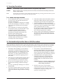
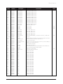
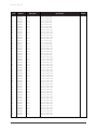
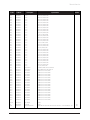
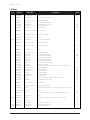
1
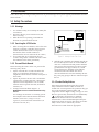
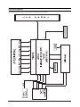
TFT-LCD MONITOR
Chassis
Degas
SERVICE
Model
DS17BS*
Manual
TFT-LCD MONITOR
CONTENTS
1. Precautions
2. Product Specifications
3. Disassembly & Reassembly
4. Alignment & Adjustments
5. Troubleshooting
6. Exploded View & Parts List
7. Electrical Parts List
8. Block Diagram
9. Wiring Diagram
10. PCB Layout
11. Schematic Diagrams
12. Panel Description
1 Precautions
Follow these safety, servicing and ESD precautions to prevent damage and to protect against potential hazards such as
electrical shock.
1-1 Safety Precautions
1-1-1 Warnings
1.
For continued safety, do not attempt to modify the
circuit board.
2.
Disconnect the AC power and DC Power Jack
before servicing.
3.
(READING SHOULD
NOT BE ABOVE 0.5mA)
When the chassis is operating, semiconductor
heatsinks are potential shock hazards.
TEST ALL
EXPOSED METAL
SURFACES
1-1-2 Servicing the LCD Monitor
1.
2.
1-1-3 Fire and Shock Hazard
Before returning the monitor to the user, perform the
following safety checks:
1.
Inspect each lead dress to make certain that the
leads are not pinched or that hardware is not
lodged between the chassis and other metal parts in
the monitor.
2.
Inspect all protective devices such as nonmetallic
control knobs, insulating materials, cabinet backs,
adjustment and compartment covers or shields,
isolation resistor-capacitor networks, mechanical
insulators, etc.
3.
2-WIRE CORD
When servicing the LCD Monitor, remove the static
charge by connecting a 10k ohm resistor in series
with an insulated wire (such as a test probe)
between the chassis and the anode lead.
(Disconnect the AC line cord from the AC outlet.)
It is essential that service technicians have an
accurate voltage meter available at all times. Check
the calibration of this meter periodically.
Leakage Current Hot Check (Figure 1-1):
WARNING: Do not use an isolation transformer during
this test.
Use a leakage current tester or a metering system
that complies with American National Standards
Institute (ANSI C101.1, Leakage Current for
Appliances), and Underwriters Laboratories (UL
Publication UL1410, 59.7).
DS17BS*
LEAKAGE
CURRENT
TESTER
DEVICE
UNDER
TEST
ALSO TEST WITH
PLUG REVERSED
(USING AC ADAPTER
PLUG AS REQUIRED)
EARTH
GROUND
Figure 1-1. Leakage Current Test Circuit
4.
With the unit completely reassembled, plug the AC
line cord directly into a 120V AC outlet. With the
unit’s AC switch first in the ON position and then
OFF, measure the current between a known earth
ground (metal water pipe, conduit, etc.) and all
exposed metal parts, including: metal cabinets,
screwheads and control shafts. The current
measured should not exceed 0.5 milliamp. Reverse
the power-plug prongs in the AC outlet and repeat
the test.
1-1-4 Product Safety Notices
Some electrical and mechanical parts have special
safety-related characteristics which are often not
evident from visual inspection. The protection they give
may not be obtained by replacing them with
components rated for higher voltage, wattage, etc. Parts
that have special safety characteristics are identified by
! on schematics and parts lists. A substitute
replacement that does not have the same safety
characteristics as the recommended replacement part
might create shock, fire and/or other hazards. Product
safety is under review continuously and new
instructions are issued whenever appropriate.
1-1
1 Precautions
1-2 Servicing Precautions
WARNING:
An electrolytic capacitor installed with the wrong polarity might explode.
Caution:
Before servicing units covered by this service manual, read and follow the Safety Precautions
section of this manual.
Note:
If unforeseen circumstances create conflict between the following servicing precautions and any of the
safety precautions, always follow the safety precautions.
1-2-1 General Servicing Precautions
1.
2.
3.
Always unplug the unit’s AC power cord from the
AC power source and disconnect the DC Power
Jack before attempting to:
(a) remove or reinstall any component or assembly,
(b) disconnect PCB plugs or connectors, (c) connect
a test component in parallel with an electrolytic
capacitor.
Some components are raised above the printed
circuit board for safety. An insulation tube or tape
is sometimes used. The internal wiring is
sometimes clamped to prevent contact with
thermally hot components. Reinstall all such
elements to their original position.
4.
Check the insulation between the blades of the AC
plug and accessible conductive parts (examples:
metal panels, input terminals and earphone jacks).
5.
Insulation Checking Procedure: Disconnect the
power cord from the AC source and turn the power
switch ON. Connect an insulation resistance meter
(500 V) to the blades of the AC plug.
The insulation resistance between each blade of the
AC plug and accessible conductive parts (see
above) should be greater than 1 megohm.
6.
After servicing, always check that the screws,
components and wiring have been correctly
reinstalled. Make sure that the area around the
serviced part has not been damaged.
Always connect a test instrument’s ground lead to
the instrument chassis ground before connecting
the positive lead; always remove the instrument’s
ground lead last.
1-3 Electrostatically Sensitive Devices (ESD) Precautions
Some semiconductor (solid state) devices can be easily damaged by static electricity. Such components are commonly
called Electrostatically Sensitive Devices (ESD). Examples of typical ESD are integrated circuits and some field-effect
transistors. The following techniques will reduce the incidence of component damage caused by static electricity.
1.
Immediately before handling any semiconductor
components or assemblies, drain the electrostatic
charge from your body by touching a known earth
ground. Alternatively, wear a discharging wriststrap device. To avoid a shock hazard, be sure to
remove the wrist strap before applying power to
the monitor.
6.
Do not remove a replacement ESD from its
protective package until you are ready to install it.
Most replacement ESDs are packaged with leads
that are electrically shorted together by conductive
foam, aluminum foil or other conductive materials.
7.
2.
After removing an ESD-equipped assembly, place it
on a conductive surface such as aluminum foil to
prevent accumulation of an electrostatic charge.
Immediately before removing the protective
material from the leads of a replacement ESD,
touch the protective material to the chassis or
circuit assembly into which the device will be
installed.
3.
Do not use freon-propelled chemicals. These can
generate electrical charges sufficient to damage
ESDs.
Caution: Be sure no power is applied to the
chassis or circuit and observe all
other safety precautions.
4.
Use only a grounded-tip soldering iron to solder or
desolder ESDs.
5.
Use only an anti-static solder removal device. Some
solder removal devices not classified as “anti-static”
can generate electrical charges sufficient to damage
ESDs.
1-2
8.
Minimize body motions when handling
unpackaged replacement ESDs. Motions such as
brushing clothes together, or lifting your foot from
a carpeted floor can generate enough static
electricity to damage an ESD.
DS17BS*
2 Product Specifications
2-1 Specifications
Item
Description
LCD Panel
TFT-LCD panel, RGB vertical stripe, normaly white, 17-Inch viewable,
0.264 mm pixel pitch
Scanning Frequency
Horizontal : 30 kHz ~ 81kHz (Automatic)
Vertical : 56 Hz ~ 75 Hz (Automatic)
Display Colors
16.2 M
Maximum Resolution
Horizontal : 1280 Pixels
Input Video Signal
Analog, 0.7 Vp-p ± 1% positive at 75 Ω , internally terminated
Input Sync Signal
Type : Seperate H/V sync, Composite H/V, Sync-on-Green (option), automatic
synchronization without external switch of sync type
Level : TTL level
Maximum Pixel Clock rate
135 MHz
Active Display (H / V)
337.92 mm / 270.336 mm
AC power voltage & Frequency
AC 100 ~ 240 VAC ( + / - 10%), 60 / 50 Hz ~ ± 3 Hz
Power Consumption
40 W (MAX)
Dimensions(W x D x H)
Set
Vertical : 1024 Pixels
Package
14.2 x 14.3 x 7.6 Inches (361.6 x 363.0 x 193.9 mm) After installation of stand
14.2 x 13.0 x 2.2 Inches (361.6 x 330.6x 55.0 mm) Without stand
18.1 x 5.6 x 15.5 Inches (461 x 142 x 393 mm)
Weight
Set
Package
3.75 kg (8.3 lbs)
5.45 kg (12.0 lbs)
Environmental Considerations
Operating Temperature : 50 °F ~ 104 °F (10 °C ~ 40 °C)
Operating Humidity : 10 % ~ 80 %
Storage Temperature : 13 °F to 113 °F (-25 °C ~ 45 °C)
Storage Humidity : 5 % ~ 95 %
•Designs and specifications are subject to change without prior notice.
DS17BS*
2-1
2 Product Specifications
2-2 Pin Assignments
Sync
Type
Pin No.
1
2
3
4
5
6
7
8
9
10
11
12
13
14
15
2-2
15-Pin Signal Cable Connector
Separate
Red
Green
Blue
GND
GND (DDC Return)
GND-R
GND-G
GND-B
No Connection
GND-Sync/Self Test
GND
DDC Data
H-Sync
V-Sync
DDC Data
Composite
Red
Green
Blue
GND
GND (DDC Return)
GND-R
GND-G
GND-B
No Connection
GND-Sync/Self Test
GND
DDC Data
H/V-Sync
Not Used
DDC Data
Sync-on-green (Option)
Red
Green + H/V Sync
Blue
GND
GND (DDC Return)
GND-R
GND-G
GND-B
Not Used
GND-Sync/Self Test
GND
DDC Data
Not Used
Not Used
DDC Data
DS17BS*
2 Product Specifications
2-3 Timing Chart
This section of the service manual describes the timing that the computer industry recognizes as standard
for computer-generated video signals.
Table 2-1 Timing Chart
Mode
IBM
VGA1/70 Hz
VESA
VGA2/70 Hz
VGA3/60 Hz
640/72 Hz
640/75 Hz
800/56 Hz
800/60 Hz
640 x 350
720 x 400
640 x 480
640 x 480
640 x 480
800 x 600
800 x 600
fH (kHz)
31.469
31.469
31.469
37.861
37.500
35.156
37.879
A µsec
31.778
31.777
31.778
26.413
26.667
28.444
26.400
B µsec
3.813
3.813
3.813
1.270
2.032
2.000
3.200
C µsec
1.589
1.589
1.589
3.810
3.810
3.556
2.200
D µsec
26.058
26.058
26.058
20.825
20.317
22.222
20.000
E µsec
0.318
0.318
0.318
0.508
0.508
0.667
1.000
fV (Hz)
70.086
70.087
59.940
72.809
75.000
56.250
60.317
O msec
14.268
14.268
16.683
13.735
13.333
17.778
16.579
P msec
0.064
0.064
0.064
0.079
0.080
0.057
0.106
Q msec
1.716
0.858
0.794
0.528
0.427
0.626
0.607
R msec
11.504
13.155
15.761
13.100
12.800
17.067
15.840
S msec
0.985
0.191
0.064
0.026
0.027
0.028
0.026
Clock
Frequency
(MHz)
25.175
28.322
25.175
31.500
31.500
36.000
40.000
Polarity
H.Sync
Positive
Negative
Negative
Negative
Negative
Positive
Positive
V.Sync
Negative
Positive
Negative
Negative
Negative
Negative
Positive
Remark
Separate
Separate
Separate
Separate
Separate
Separate
Separate
Timing
H/V Composite Sync
Separate Sync
Horizontal
Vertical
Video
Video
DD
E
E
Q
S
Vertical
Horizontal
Video
Video
CC
VIDEO
R
Q
A
P
RR
Q
S S
B
O
Sync
Sync
Sync
Sync
BB
PP
AA
O O
A : Line time total
B : Horizontal sync width
O : Frame time total
P : Vertical sync width
C : Back porch
D : Active time
Q : Back porch
R : Active time
E : Front porch
DS17BS*
S : Front porch
2-3
2 Product Specifications
Table 2-2 Timing Chart
Mode
IBM
VESA
VGA2/
70 Hz
VGA3/
60 Hz
720 x 400
640 x 480
fH (kHz)
31.469
A µsec
1024/75 Hz 1280/60 Hz 1280/75 Hz
1280 x 1024 1280 x 1024
1024 x 768
(Analog)
(Analog)
640/75 Hz
800/60 Hz
800/75 Hz
1024/60 Hz
640 x 480
800 x 600
800 x 600
1024 x 768
31.469
37.500
37.879
46.875
48.363
60.023
63.981
79.975
31.777
31.778
26.667
26.400
21.333
20.677
16.660
11.852
12.504
B µsec
3.813
3.813
2.032
3.200
1.616
2.092
1.219
1.037
1.067
C µsec
1.589
1.589
3.810
2.200
3.232
2.462
2.235
2.296
1.837
D µsec
26.058
26.058
20.317
20.000
16.162
15.754
13.003
9.259
9.481
E µsec
0.318
0.318
0.508
0.000
0.323
0.369
0.203
0.000
0.119
fV (Hz)
70.087
59.940
75.000
60.317
75.000
60.004
75.029
60.020
75.025
O msec
14.268
16.683
13.333
16.579
13.333
16.666
13.328
16.005
13.329
P msec
0.064
0.064
0.080
0.106
0.064
0.124
0.050
0.047
0.038
Q msec
0.858
0.794
0.427
0.607
0.448
0.600
0.466
0.594
0.475
R msec
13.155
15.761
12.800
15.840
12.800
15.880
12.795
15.630
12.804
S msec
0.191
0.064
0.027
0.0261
0.021
0.062
0.017
0.016
0.013
Clock
Freq.
(MHz)
28.322
26.175
31.500
40.000
49.500
75.000
78.750
108.000
135.000
Polarity
H.Sync
Negative
Negative
Negative
Positive
Positive
Negative
Positive
Positive
Positive
V.Sync
Positive
Negative
Negative
Positive
Positive
Negative
Positive
Positive
Positive
Remark
Separate
Separate
Separate
Separate
Separate
Separate
Separate
Separate
Separate
Timing
H/V Composite Sync
Separate Sync
Vertical
Video
Video
DD
E E
Q
S
Vertical
Horizontal
Video
Video
CC
VIDEO
R
Q
A
Horizontal
P
RR
Q
S S
B
O
Sync
Sync
Sync
Sync
BB
PP
AA
O O
A : Line time total
B : Horizontal sync width
O : Frame time total
P : Vertical sync width
C : Back porch
D : Active time
Q : Back porch
R : Active time
E : Front porch
2-4
S : Front porch
DS17BS*
4 Alignments and Adjustments
This section of the service manual explains how to use the RS232 JIG.
This function is needed for AD board change and program memory (IC110) change.
4-1 Required Equipment
The following equipment is necessary for adjusting the monitor:
• Computer with Windows 95, Windows 98, or Windows NT.
• MTI-2031 DDC MANAGER JIG
4-2 Automatic Color Adjustment
To input video, use 16 gray or any pattern using black and white.
1. If OSD settings vary with relevant sales region, OSD language for ‘Auto Color’ displays default
language setting for each region.
2. Press the “Exit” key for 5 seconds.
* Note : For models supporting the 4 languages (English, Simplified Chinese, Japanese, Korean), select
English and press and hold the ‘Exit’ key for 5 seconds.
4-3 DDC EDID Data Input
1. Input DDC EDID data when replacing AD PCB.
2. Receive/Download the proper DDC file for the model from HQ quality control department.
Install the below jig (Figure 1) and enter the data.
Figure 1.
4-4 OSD Adjustment When Replacing Panel
1. Adjust brightness and contrast to 0. Then, press the exit key for 5 second.
Service function OSD will appear on screen.
2. Press the + key to place the cursor on the panel. Press the menu key for 5 seconds.
4-5 OSD Adjustment When Replacing Lamp Only
1. Adjust brightness and contrast to 0. Then, press the exit key for 5 seconds.
Service function OSD will appear on the screen.
2. Press the + key. Select upper lamp and press the menu key for 5 seconds.
Then, select lower lamp and press the menu key for 5 seconds.
Note : Please be sure to read the following instructions for details on service function.
DS17BS*
4-1
4 Alignments and Adjustments
4-6 Service Function Spec.
4-6-1 How to Display Service Function OSD
1. The value for brightness and contrast should be changed to zero.
2. Within 5 seconds, press the exit key.
3. Service function OSD will be displayed.
If you want to disable the service function OSD, you will have to power off.
Panel Information
Software Version
Check sum
Figure 2. The example of service function OSD
The service function OSD is based on a grid of 29 columns x 12 rows.
The service function OSD consists of panel information, software version and MICOM check sum.
4-6-2 How to Control Service Function OSD
1. With the panel selected on OSD, whenever you press the right key, the base color will change to blue
from “Panel” to “Country”, “Pixel Shift”, “Lower Lamp”, “Upper Lamp”.
Figure 3.
4-2
DS17BS*
4 Alignments and Adjustments
4-6-3 How to Control Service Function OSD
• After change the panel or lamp, you must reset service function OSD.
• The case of panel change
After changeing the panel, press the menu key within 5 seconds,.
Then, panel Ch. No increases one step and the panel time information is reset to zero.
Simultaneously, other information is reset to zero (Upper/Lower lamp, Panel cycle).
Figure 4.
4-6-4 How to Control Service Function OSD
• In the case of Upper Lamp or Lower Lamp change
After changeing the Upper Lamp or Lower Lamp,
1. Select the Upper Lamp or Lower Lamp
2. Press the Menu key within an 5 seconds.
Then, Ch. No and time will be reset to zero (selected item only).
Figure 5.
DS17BS*
Figure 6.
4-3
4 Alignments and Adjustments
4-6-5 Pixel shift and language selection change
* Note : Use the '-' key to vary values for new pixel shift and country menu.
1. Pixel shift : on
off
- When a same picture is displayed with no change for an extended period of time, this function prevents
the display panel from image sticking.
* On for '0 x 01' with EEPROM 0x2E, Off for others; Always restart the monitor after EEPROM adjustment.
- Motion path : see Figure 7. One-step movement requires 4 minutes (total of 32 steps : 128 minutes)
Figure 7.
- Location is reset.
a) the monitor is restarted
b) image mode is adjusted
c) user adjusts a key
* Note : Pixel shift is not a vailable in service menu.
2. Country : Worldwide
Korean
Chinese
Japanese
- This function enables to select relevant OSD language for each region / country.
- Worldwide : 7 languages (English, German, Spanish, French, Italian, Swedish, Russian)
- Korean : 2 languages (Korean, English)
- Chinese : 2 languages (Simplified Chinese, English)
- Japanese : 2 languages (Japanese, English)
Figure 8.
4-4
Figure 8-1.
DS17BS*
4 Alignments and Adjustments
DS17BS*
Figure 8-2.
Figure 8-3.
Figure 9.
Figure 9-1.
4-5
4 Alignments and Adjustments
Memo
4-6
DS17BS*
3 Disassembly and Reassembly
This section of the service manual describes the disassembly and reassembly procedures for the
DS17BS* monitor.
WARNING: This monitor contains electrostatically sensitive devices. Use caution when handling
these components.
3-1 Disassembly
Cautions : 1. Disconnect the monitor from the power source before disassembly.
2. Follow these directions carefully; never use metal instruments to pry apart the cabinet.
3. R/Cover opening jig : BH81-00001A
1. Place monitor face down on cushioned table.
Remove rear cover from the monitor and
remove 5 screws from the mointor.
(CAUTION : Remove screw grip don’t on the
stand than fall the stand from the top side of
the foot)
2. Disconnect function cable and lift up the
stand. Remove 5 screws from the monitor.
3. Open the rear cover and disconnect power
cable from the shield.
4. Remove the cover front and remove 5 screws
from the shield.
5. Remove 4 screws from the shield paenl coners
and lift up the shield.
DS17BS*
3-1
3 Disassembly and Reassembly
6. Disconnect LVDS cable and inverter cable.
3-2 Replacement Order of Lamp Assemblies
*Do not replace lamp for the LTM170EX-L01 panel.
*Note : No speciflc color for the wire connector of panel lamp is required.
You can change a connector assemble.
3-3 Reassembly
Reassembly procedures are in the reverse order of disassembly procedures.
3-2
DS17BS*
5 Troubleshooting
Notes: 1. Before troubleshooting, setup the PC’s display as below.
• Resolution: 1280 x 1024
• H-frequency: 48 kHz
• V-frequency: 60 Hz
2. If no picture appears, make sure the power cord is correctly connected.
3. Check the following circuits.
• No raster appears: SMPS PCB, Main PCB
• 14V develop but no screen: Main PCB
• 14V does not develop: SMPS PCB
4. If you push and hold the “EXIT” button for more than 5 seconds, the monitor automatically turns back
to the factory preset.
5-1 No Power
Does proper DC 14 V appear at
Pin 39, 40 or Pin 41 of CN01?
No
Check SMPS.
Yes
Does proper DC 5 V appear at
Pin 2 of IC104?
No
Check IC104 and it’s related circuit.
Yes
Does proper DC 5 V appear at
Pin 5 of IC102?
No
Check IC104 or IC102
and it’s related circuit.
No
Check X102 or check
it’s related circuit.
No
Check function key or
check it’s related circuit.
Yes
2
Does the pulse appear at X102?
Yes
While pushing the power key
does voltage drop from 5V to 0V
at Pin 16 of IC102?
Yes
Replace IC102.
DS17BS*
5-1
5 Troubleshooting
5-2 No Video
Power indicator is green.
Does DC 5V appear at
Pin 1, 2 and 3 of CN04?
No
Replace IC109 or
check it’s related circuit.
Yes
3 4
Does the pulse
appear at Pin 74
and 75 of IC101?
No
5 6
No
7 8
Yes
Yes
1
Replace LCD panel.
Does the pulse appear at
Pin 126 and 127 of IC101?
Does the pulse
appear at Pin 122 of IC101?
Yes
Replace IC101.
Does the pulse appear
at Pin 8 and 10 of IC110?
No
Yes
No
Check IC102 and
check it’s related circuit.
Check IC110 or
check CN01 and
check it’s related circuit.
Replace X101 or
check it’s related circuit.
5-2
DS17BS*
5 Troubleshooting
WAVEFORMS
1
2
3
4
5
6
7
8
DS17BS*
5-3
5 Troubleshooting
5-3 No OSD
There is video but no OSD.
Press exit key for more than 5
seconds to do the factory preset.
When pushing a front control
button, does any change appear
at Pin 16 and 17 of IC102?
No
Replace front control button.
Yes
Replace IC101 and
check its related circuit.
5-4
DS17BS*
7 Electrical Parts List
You can search for updated part codes through CMS web site.
URL : http://ecms. samsungelectronics. com/
7-1 Main PCB Parts
Loc. No.
Code No.
Description
Specification
Remarks
CIS2
CIS3
CIS6
CIS7
CIS5
CIS4
CIS10
BN94-00479B
0202-001044
0202-001222
0204-001095
0204-001677
BN39-00395B
BN39-00419A
BN63-01079A
ASSY PCB MAIN
SOLDER-WIRE.
SOLDER-WIRE FLUX
THINNER
FLUX
LEAD CONNECTOR
LEAD CONNECTOR
GASKET
DS17BS
S63S-W3.0,S63S,D3,63Sn/37Pb,RS-107,RS60-1.2AA,D1.2,SN60/PB40,#4520,-,-,DF-201TVS,MIX,0.820,FLUX 13%,G
DS17BS,UL1571#30,UL/CSA,30P,90mm,#30,12507HS-30,HS-30-BB100,BK,90mm,1571#30,SJ03
DS17BS,UL1571#30,UL/CSA,12P,60MM,AWG30,12507HS-12L,12507HS-12L,BK,SJ03-01-288,NO
,CONDUCTIVE FAB,4MM,10MM,10MM,GRAY,32K,71TSSK-10-4-10-13
CIS9
BN96-00799A
ASSY COVER P-PCB
172X,ABS+PC 5V,GR70,SPRAY
SNA
BD101
BD102
BD103
BD104
BD105
BD106
BD107
BD110
BD111
BD112
C101
C102
C103
C104
C105
C106
C110
C111
C112
C113
C114
C115
C116
C117
C118
C119
C120
C121
C122
C123
C124
C125
C126
C127
C128
C129
C134
C135
C136
BN97-00239B
2703-001334
2703-001334
2703-001334
2703-001334
2703-001334
2703-001334
2703-001334
2007-000070
2007-000070
2007-000070
2203-005005
2203-005005
2203-005005
2203-005005
2203-005005
2203-005005
2203-005005
2203-005437
2203-005005
2203-005005
2203-005005
2203-005005
2203-005005
2203-005005
2203-000384
2203-000384
2203-005437
2203-005005
2203-005005
2203-005005
2203-005005
2203-005005
2203-005005
2203-005437
2203-005005
2203-005437
2203-005437
2203-005005
2203-000626
ASSY SMD
INDUCTOR-SMD
INDUCTOR-SMD
INDUCTOR-SMD
INDUCTOR-SMD
INDUCTOR-SMD
INDUCTOR-SMD
INDUCTOR-SMD
R-CHIP
R-CHIP
R-CHIP
C-CER,CHIP
C-CER,CHIP
C-CER,CHIP
C-CER,CHIP
C-CER,CHIP
C-CER,CHIP
C-CER,CHIP
C-CER,CHIP
C-CER,CHIP
C-CER,CHIP
C-CER,CHIP
C-CER,CHIP
C-CER,CHIP
C-CER,CHIP
C-CER,CHIP
C-CER,CHIP
C-CER,CHIP
C-CER,CHIP
C-CER,CHIP
C-CER,CHIP
C-CER,CHIP
C-CER,CHIP
C-CER,CHIP
C-CER,CHIP
C-CER,CHIP
C-CER,CHIP
C-CER,CHIP
C-CER,CHIP
C-CER,CHIP
DS17BS
1.5uH,10%,2012
1.5uH,10%,2012
1.5uH,10%,2012
1.5uH,10%,2012
1.5uH,10%,2012
1.5uH,10%,2012
1.5uH,10%,2012
0ohm,5%,1/10W,TP,1608
0ohm,5%,1/10W,TP,1608
0ohm,5%,1/10W,TP,1608
100nF,10%,16V,X7R,TP,1608
100nF,10%,16V,X7R,TP,1608
100nF,10%,16V,X7R,TP,1608
100nF,10%,16V,X7R,TP,1608
100nF,10%,16V,X7R,TP,1608
100nF,10%,16V,X7R,TP,1608
100nF,10%,16V,X7R,TP,1608
10000nF,+80-20%,10V,Y5V,TP,3216
100nF,10%,16V,X7R,TP,1608
100nF,10%,16V,X7R,TP,1608
100nF,10%,16V,X7R,TP,1608
100nF,10%,16V,X7R,TP,1608
100nF,10%,16V,X7R,TP,1608
100nF,10%,16V,X7R,TP,1608
0.015NF,5%,50V,C0G,TP,1608
0.015NF,5%,50V,C0G,TP,1608
10000nF,+80-20%,10V,Y5V,TP,3216
100nF,10%,16V,X7R,TP,1608
100nF,10%,16V,X7R,TP,1608
100nF,10%,16V,X7R,TP,1608
100nF,10%,16V,X7R,TP,1608
100nF,10%,16V,X7R,TP,1608
100nF,10%,16V,X7R,TP,1608
10000nF,+80-20%,10V,Y5V,TP,3216
100nF,10%,16V,X7R,TP,1608
10000nF,+80-20%,10V,Y5V,TP,3216
10000nF,+80-20%,10V,Y5V,TP,3216
100nF,10%,16V,X7R,TP,1608
0.022NF,5%,50V,C0G,TP,1608
SNA
DS17BS*
SNA
SNA
SNA
SNA
SNA
SNA
7-1
7 Electrical Parts List
Loc. No.
C137
C138
C139
C140
C141
C142
C143
C144
C145
C146
C147
C148
C149
C150
C151
C152
C153
C154
C155
C156
C157
C158
C159
C160
C161
C162
C167
C168
C169
C170
C171
C172
C173
C174
C175
C176
C177
C178
C179
C180
C181
C182
C185
C186
C187
C188
C189
CIS1
CIS8
CN01
CN02
CN04
CN05
D101
D102
7-2
Code No.
2203-000626
2203-005437
2203-005005
2402-001042
2203-000041
2203-000041
2203-000236
2203-000315
2203-000236
2203-000257
2203-005437
2203-005005
2203-000236
2203-000257
2203-000257
2203-000257
2203-005065
2203-005065
2203-005005
2402-001128
2402-001128
2203-005005
2203-005437
2203-005437
2409-001065
2203-005005
2402-001128
2203-005005
2402-001128
2203-005005
2203-000257
2203-005005
2203-005005
2203-005005
2203-005005
2203-005005
2203-005005
2203-005005
2203-005437
2203-005437
2402-001042
2203-000257
2203-005005
2203-005005
2203-005005
2402-000176
2402-000176
BN60-00011A
0202-001162
3711-005076
3708-001878
3711-005470
3711-005471
0401-001056
0401-001056
Description
C-CER,CHIP
C-CER,CHIP
C-CER,CHIP
C-AL,SMD
C-CER,CHIP
C-CER,CHIP
C-CER,CHIP
C-CER,CHIP
C-CER,CHIP
C-CER,CHIP
C-CER,CHIP
C-CER,CHIP
C-CER,CHIP
C-CER,CHIP
C-CER,CHIP
C-CER,CHIP
C-CER,CHIP
C-CER,CHIP
C-CER,CHIP
C-AL,SMD
C-AL,SMD
C-CER,CHIP
C-CER,CHIP
C-CER,CHIP
C-ORGANIC
C-CER,CHIP
C-AL,SMD
C-CER,CHIP
C-AL,SMD
C-CER,CHIP
C-CER,CHIP
C-CER,CHIP
C-CER,CHIP
C-CER,CHIP
C-CER,CHIP
C-CER,CHIP
C-CER,CHIP
C-CER,CHIP
C-CER,CHIP
C-CER,CHIP
C-AL,SMD
C-CER,CHIP
C-CER,CHIP
C-CER,CHIP
C-CER,CHIP
C-AL,SMD
C-AL,SMD
FASTENER-PEM/NUT
SOLDER-CREAM
CONNECTOR-HEADER
CONNECTOR-FPC/FFC/PIC
CONNECTOR-HEADER
CONNECTOR-HEADER
DIODE-SWITCHING
DIODE-SWITCHING
Specification
0.022NF,5%,50V,C0G,TP,1608
10000nF,+80-20%,10V,Y5V,TP,3216
100nF,10%,16V,X7R,TP,1608
100uF,20%,16V,GP,TP,6.6x6.6x5.4mm
0.01NF,0.25PF,50V,C0G,TP,1608
0.01NF,0.25PF,50V,C0G,TP,1608
0.1NF,5%,50V,C0G,TP,1608
0.12NF,5%,50V,C0G,TP,1608
0.1NF,5%,50V,C0G,TP,1608
10nF,10%,50V,X7R,TP,1608
10000nF,+80-20%,10V,Y5V,TP,3216
100nF,10%,16V,X7R,TP,1608
0.1NF,5%,50V,C0G,TP,1608
10nF,10%,50V,X7R,TP,1608
10nF,10%,50V,X7R,TP,1608
10nF,10%,50V,X7R,TP,1608
1000nF,+80-20%,10V,Y5V,TP,1608
1000nF,+80-20%,10V,Y5V,TP,1608
100nF,10%,16V,X7R,TP,1608
100UF,20%,16V,WT,TP,6.3X5.7MM
100UF,20%,16V,WT,TP,6.3X5.7MM
100nF,10%,16V,X7R,TP,1608
10000nF,+80-20%,10V,Y5V,TP,3216
10000nF,+80-20%,10V,Y5V,TP,3216
82UF,20%,16V,WT,TP,8X6.9MM,100nF,10%,16V,X7R,TP,1608
100UF,20%,16V,WT,TP,6.3X5.7MM
100nF,10%,16V,X7R,TP,1608
100UF,20%,16V,WT,TP,6.3X5.7MM
100nF,10%,16V,X7R,TP,1608
10nF,10%,50V,X7R,TP,1608
100nF,10%,16V,X7R,TP,1608
100nF,10%,16V,X7R,TP,1608
100nF,10%,16V,X7R,TP,1608
100nF,10%,16V,X7R,TP,1608
100nF,10%,16V,X7R,TP,1608
100nF,10%,16V,X7R,TP,1608
100nF,10%,16V,X7R,TP,1608
10000nF,+80-20%,10V,Y5V,TP,3216
10000nF,+80-20%,10V,Y5V,TP,3216
100uF,20%,16V,GP,TP,6.6x6.6x5.4mm
10nF,10%,50V,X7R,TP,1608
100nF,10%,16V,X7R,TP,1608
100nF,10%,16V,X7R,TP,1608
100nF,10%,16V,X7R,TP,1608
10uF,20%,16V,GP,TP,4.3x4.3x5.4
10uF,20%,16V,GP,TP,4.3x4.3x5.4
MINERVA,SUM24L(SN),M3,-,7.0,6.8,WHT
RMA-20-21L,S63,-,SN63/PB36.6/AG0.4,FLUX9.5%
BOX,41P,2R,0.625MM,SMD-A,AUF,BLK
6P,1mm,SMD-A,SnPb
BOX,30P,1R,1.25mm,SMD-A,Sn+Pb,IVR
BOX,12P,1R,1.25mm,SMD-A,Sn+Pb,IVR
MMBD4148SE,75V,200MA,SOT-23,TP
MMBD4148SE,75V,200MA,SOT-23,TP
Remarks
SNA
SNA
DS17BS*
7 Electrical Parts List
Loc. No.
D103
D104
D105
D106
D107
D108
D109
D110
D111
D112
D113
D115
FT101
FT102
FT103
FT104
FT106
FT107
FT108
FT109
FT110
IC101
IC102_SOCKET
IC103
IC104
IC107
IC108
IC109
IC110
IC111
L101
L102
MP1.0
Q101
R100
R101
R102
R103
R104
R105
R106
R107
R108
R109
R110
R111
R112
R113
R114
R115
R116
R117
R118
R119
R120
DS17BS*
Code No.
0401-001056
0401-001056
0401-001056
0401-001056
0401-001056
0401-001056
0401-001056
0401-001056
0401-001056
0401-001056
0401-001056
0402-001019
2901-001114
3301-001145
3301-001145
3301-001145
2901-001114
2901-001114
2901-001114
2901-001114
2901-001114
1003-001586
3704-000001
1103-001023
1203-001448
1203-001293
1203-002450
0505-001772
0803-000117
1103-000129
BN27-00009A
3301-001595
BN41-00340A
0501-002080
2007-000072
2007-000072
2007-000072
2007-000072
2007-000072
2007-000072
2007-000072
2007-000072
2007-000072
2007-000072
2007-000072
2007-000072
2007-000072
2007-000072
2007-000072
2007-000072
2007-000072
2007-000072
2007-000072
2007-000072
2007-000309
Description
DIODE-SWITCHING
DIODE-SWITCHING
DIODE-SWITCHING
DIODE-SWITCHING
DIODE-SWITCHING
DIODE-SWITCHING
DIODE-SWITCHING
DIODE-SWITCHING
DIODE-SWITCHING
DIODE-SWITCHING
DIODE-SWITCHING
DIODE-SCHOTTKY
FILTER-EMI SMD
BEAD-SMD
BEAD-SMD
BEAD-SMD
FILTER-EMI SMD
FILTER-EMI SMD
FILTER-EMI SMD
FILTER-EMI SMD
FILTER-EMI SMD
IC-LCD CONTROLLER
SOCKET-IC
IC-EEPROM
IC-SWITCH VOL.REG
IC-POSI.FIXED REG.
IC-VOLTAGE REGULATOR
FET-SILICON
IC-TTL
IC-EEPROM
COIL CHOKE
BEAD-SMD
PCB MAIN
TR-SMALL SIGNAL
R-CHIP
R-CHIP
R-CHIP
R-CHIP
R-CHIP
R-CHIP
R-CHIP
R-CHIP
R-CHIP
R-CHIP
R-CHIP
R-CHIP
R-CHIP
R-CHIP
R-CHIP
R-CHIP
R-CHIP
R-CHIP
R-CHIP
R-CHIP
R-CHIP
Specification
MMBD4148SE,75V,200MA,SOT-23,TP
MMBD4148SE,75V,200MA,SOT-23,TP
MMBD4148SE,75V,200MA,SOT-23,TP
MMBD4148SE,75V,200MA,SOT-23,TP
MMBD4148SE,75V,200MA,SOT-23,TP
MMBD4148SE,75V,200MA,SOT-23,TP
MMBD4148SE,75V,200MA,SOT-23,TP
MMBD4148SE,75V,200MA,SOT-23,TP
MMBD4148SE,75V,200MA,SOT-23,TP
MMBD4148SE,75V,200MA,SOT-23,TP
MMBD4148SE,75V,200MA,SOT-23,TP
MBRS340,40V,3000MA,DO-214AB,TP
25VDC,2.0ADC,-,100nF,3.2x1.6x1
AB,4.5x1.6x1.6mm,-,AB,4.5x1.6x1.6mm,-,AB,4.5x1.6x1.6mm,-,25VDC,2.0ADC,-,100nF,3.2x1.6x1
25VDC,2.0ADC,-,100nF,3.2x1.6x1
25VDC,2.0ADC,-,100nF,3.2x1.6x1
25VDC,2.0ADC,-,100nF,3.2x1.6x1
25VDC,2.0ADC,-,100nF,3.2x1.6x1
MST9131E,PQFP,128P,20X14MM,-,1UA,TR,PLASTIC,3.3V,0TO+70C,-,3.30,IBM L170(P)
44P,PLCC,SN,524C80D81,1028x8Bit,SOP,8P,150MIL,10mS,5V,10%,PLASTIC,0to+70C,110uA,CMOS,TP
2596,TO-263,5P,-,PLASTIC,4.750/5.250V,-,-40TO+125C,3A,-,ST
033,T0-252,3P,6.5MIL,PLASTIC,3
MC33375ST-2.5T3,SOT-223,4P,137MIL,PLASTIC,2.475/2.525V,-,-40TO+125C,300MA,-,TP
FDS9933A,P,-20V,-3.8A,0.075OHM,2W,SO-8
74F14,INVERTER,SOP,14P,150MIL,
24C02,256x8BIT,SOP,8P,150MIL,1
SMD 12X12X6,EOS,33UH,15%,-,0.12ߟ MAX,2A,DR10X5.0MM,18.5TS,12X12X6,1.8MM,1UEW 0.
1KOHM,7.0X6.0X4.5MM,4000MA,TP,FERRITE,0.012OHM
DS17BS,FR-4,2L,1.0,1.0T,117.84,4A
2SC2412K,NPN,200mW,SC-59,TP,120-270
47ohm,5%,1/10W,TP,1608
47ohm,5%,1/10W,TP,1608
47ohm,5%,1/10W,TP,1608
47ohm,5%,1/10W,TP,1608
47ohm,5%,1/10W,TP,1608
47ohm,5%,1/10W,TP,1608
47ohm,5%,1/10W,TP,1608
47ohm,5%,1/10W,TP,1608
47ohm,5%,1/10W,TP,1608
47ohm,5%,1/10W,TP,1608
47ohm,5%,1/10W,TP,1608
47ohm,5%,1/10W,TP,1608
47ohm,5%,1/10W,TP,1608
47ohm,5%,1/10W,TP,1608
47ohm,5%,1/10W,TP,1608
47ohm,5%,1/10W,TP,1608
47ohm,5%,1/10W,TP,1608
47ohm,5%,1/10W,TP,1608
47ohm,5%,1/10W,TP,1608
47ohm,5%,1/10W,TP,1608
10ohm,5%,1/10W,TP,1608
Remarks
SNA
SNA
SNA
SNA
SNA
7-3
7 Electrical Parts List
Loc. No.
R121
R122
R123
R124
R125
R126
R127
R128
R129
R130
R131
R132
R133
R134
R135
R136
R140
R142
R143
R150
R151
R153
R154
R155
R156
R157
R158
R161
R162
R163
R164
R165
R166
R167
R168
R169
R170
R171
R172
R174
R175
R176
R177
R178
R179
R180
R181
R182
R183
R185
R186
R187
R188
R189
R190
7-4
Code No.
2007-000309
2007-000309
2007-000309
2007-000309
2007-000309
2007-000309
2007-000309
2007-000074
2007-000074
2007-000074
2007-000074
2007-000074
2007-000074
2007-001167
2007-001167
2007-001167
2007-000090
2007-000074
2007-000821
2007-000090
2007-000090
2007-000078
2007-000090
2007-000084
2007-000084
2007-000092
2007-000092
2007-000084
2007-000084
2007-000084
2007-000084
2007-000084
2007-000084
2007-000084
2007-000084
2007-000084
2007-000090
2007-000084
2007-000084
2007-000074
2007-000074
2007-000074
2007-000074
2007-000074
2007-000074
2007-000074
2007-000074
2007-000074
2007-000074
2007-000074
2007-000074
2007-000074
2007-000074
2007-000074
2007-000074
Description
R-CHIP
R-CHIP
R-CHIP
R-CHIP
R-CHIP
R-CHIP
R-CHIP
R-CHIP
R-CHIP
R-CHIP
R-CHIP
R-CHIP
R-CHIP
R-CHIP
R-CHIP
R-CHIP
R-CHIP
R-CHIP
R-CHIP
R-CHIP
R-CHIP
R-CHIP
R-CHIP
R-CHIP
R-CHIP
R-CHIP
R-CHIP
R-CHIP
R-CHIP
R-CHIP
R-CHIP
R-CHIP
R-CHIP
R-CHIP
R-CHIP
R-CHIP
R-CHIP
R-CHIP
R-CHIP
R-CHIP
R-CHIP
R-CHIP
R-CHIP
R-CHIP
R-CHIP
R-CHIP
R-CHIP
R-CHIP
R-CHIP
R-CHIP
R-CHIP
R-CHIP
R-CHIP
R-CHIP
R-CHIP
Specification
Remarks
10ohm,5%,1/10W,TP,1608
10ohm,5%,1/10W,TP,1608
10ohm,5%,1/10W,TP,1608
10ohm,5%,1/10W,TP,1608
10ohm,5%,1/10W,TP,1608
10ohm,5%,1/10W,TP,1608
10ohm,5%,1/10W,TP,1608
100ohm,5%,1/10W,TP,1608
100ohm,5%,1/10W,TP,1608
100ohm,5%,1/10W,TP,1608
100ohm,5%,1/10W,TP,1608
100ohm,5%,1/10W,TP,1608
100ohm,5%,1/10W,TP,1608
75ohm,5%,1/10W,TP,1608
75ohm,5%,1/10W,TP,1608
75ohm,5%,1/10W,TP,1608
10Kohm,5%,1/10W,TP,1608
100ohm,5%,1/10W,TP,1608
390ohm,1%,1/10W,TP,1608
10Kohm,5%,1/10W,TP,1608
10Kohm,5%,1/10W,TP,1608
1Kohm,5%,1/10W,TP,1608
10Kohm,5%,1/10W,TP,1608
4.7Kohm,5%,1/10W,TP,1608
4.7Kohm,5%,1/10W,TP,1608
15Kohm,5%,1/10W,TP,1608
15Kohm,5%,1/10W,TP,1608
4.7Kohm,5%,1/10W,TP,1608
4.7Kohm,5%,1/10W,TP,1608
4.7Kohm,5%,1/10W,TP,1608
4.7Kohm,5%,1/10W,TP,1608
4.7Kohm,5%,1/10W,TP,1608
4.7Kohm,5%,1/10W,TP,1608
4.7Kohm,5%,1/10W,TP,1608
4.7Kohm,5%,1/10W,TP,1608
4.7Kohm,5%,1/10W,TP,1608
10Kohm,5%,1/10W,TP,1608
4.7Kohm,5%,1/10W,TP,1608
4.7Kohm,5%,1/10W,TP,1608
100ohm,5%,1/10W,TP,1608
100ohm,5%,1/10W,TP,1608
100ohm,5%,1/10W,TP,1608
100ohm,5%,1/10W,TP,1608
100ohm,5%,1/10W,TP,1608
100ohm,5%,1/10W,TP,1608
100ohm,5%,1/10W,TP,1608
100ohm,5%,1/10W,TP,1608
100ohm,5%,1/10W,TP,1608
100ohm,5%,1/10W,TP,1608
100ohm,5%,1/10W,TP,1608
100ohm,5%,1/10W,TP,1608
100ohm,5%,1/10W,TP,1608
100ohm,5%,1/10W,TP,1608
100ohm,5%,1/10W,TP,1608
100ohm,5%,1/10W,TP,1608
DS17BS*
7 Electrical Parts List
Loc. No.
Code No.
Description
Specification
R191
R195
R196
R197
R198
R199
R200
R201
R202
R203
R204
R205
R206
R210
R211
R213
R214
R215
R216
R217
R218
R219
R220
R221
R223
R224
R225
R226
R227
R228
R229
X101
X102
ZD102
ZD103
ZD104
ZD105
ZD106
ZD107
ZD108
ZD109
ZD110
ZD111
ZD112
ZD113
ZD115
ZD116
ZD117
ZD118
ZD120
ZD121
2007-000074
2007-000074
2007-000074
2007-000074
2007-000074
2007-000074
2007-000074
2007-000074
2007-000074
2007-000074
2007-000077
2007-000109
2007-000074
2007-000074
2007-000074
2007-000074
2007-000078
2007-000090
2007-000090
2007-000070
2007-000090
2007-000074
2007-000097
2007-000097
2007-000074
2007-000074
2007-000074
2007-000090
2007-000074
2007-000074
2007-000070
2801-003667
2801-003773
0403-000258
0403-000258
0403-000258
0403-000258
0403-000258
0403-000258
0403-000258
0403-000258
0403-000258
0403-000258
0403-000258
0403-000258
0403-000258
0403-000258
0403-000258
0403-000258
0403-000258
0403-000258
R-CHIP
R-CHIP
R-CHIP
R-CHIP
R-CHIP
R-CHIP
R-CHIP
R-CHIP
R-CHIP
R-CHIP
R-CHIP
R-CHIP
R-CHIP
R-CHIP
R-CHIP
R-CHIP
R-CHIP
R-CHIP
R-CHIP
R-CHIP
R-CHIP
R-CHIP
R-CHIP
R-CHIP
R-CHIP
R-CHIP
R-CHIP
R-CHIP
R-CHIP
R-CHIP
R-CHIP
CRYSTAL-SMD
CRYSTAL-SMD
DIODE-ZENER
DIODE-ZENER
DIODE-ZENER
DIODE-ZENER
DIODE-ZENER
DIODE-ZENER
DIODE-ZENER
DIODE-ZENER
DIODE-ZENER
DIODE-ZENER
DIODE-ZENER
DIODE-ZENER
DIODE-ZENER
DIODE-ZENER
DIODE-ZENER
DIODE-ZENER
DIODE-ZENER
DIODE-ZENER
100ohm,5%,1/10W,TP,1608
100ohm,5%,1/10W,TP,1608
100ohm,5%,1/10W,TP,1608
100ohm,5%,1/10W,TP,1608
100ohm,5%,1/10W,TP,1608
100ohm,5%,1/10W,TP,1608
100ohm,5%,1/10W,TP,1608
100ohm,5%,1/10W,TP,1608
100ohm,5%,1/10W,TP,1608
100ohm,5%,1/10W,TP,1608
470ohm,5%,1/10W,TP,1608
1Mohm,5%,1/10W,TP,1608
100ohm,5%,1/10W,TP,1608
100ohm,5%,1/10W,TP,1608
100ohm,5%,1/10W,TP,1608
100ohm,5%,1/10W,TP,1608
1Kohm,5%,1/10W,TP,1608
10Kohm,5%,1/10W,TP,1608
10Kohm,5%,1/10W,TP,1608
0ohm,5%,1/10W,TP,1608
10Kohm,5%,1/10W,TP,1608
100ohm,5%,1/10W,TP,1608
47Kohm,5%,1/10W,TP,1608
47Kohm,5%,1/10W,TP,1608
100ohm,5%,1/10W,TP,1608
100ohm,5%,1/10W,TP,1608
100ohm,5%,1/10W,TP,1608
10Kohm,5%,1/10W,TP,1608
100ohm,5%,1/10W,TP,1608
100ohm,5%,1/10W,TP,1608
0ohm,5%,1/10W,TP,1608
14.3182MHZ,50PPM,28-AAN,16,50OHM,TP
12MHZ,30PPM,28-AAN,20PF,50OHM,TP
BZX84C5V6,5.6V,5.2-6.0V,225mW,
BZX84C5V6,5.6V,5.2-6.0V,225mW,
BZX84C5V6,5.6V,5.2-6.0V,225mW,
BZX84C5V6,5.6V,5.2-6.0V,225mW,
BZX84C5V6,5.6V,5.2-6.0V,225mW,
BZX84C5V6,5.6V,5.2-6.0V,225mW,
BZX84C5V6,5.6V,5.2-6.0V,225mW,
BZX84C5V6,5.6V,5.2-6.0V,225mW,
BZX84C5V6,5.6V,5.2-6.0V,225mW,
BZX84C5V6,5.6V,5.2-6.0V,225mW,
BZX84C5V6,5.6V,5.2-6.0V,225mW,
BZX84C5V6,5.6V,5.2-6.0V,225mW,
BZX84C5V6,5.6V,5.2-6.0V,225mW,
BZX84C5V6,5.6V,5.2-6.0V,225mW,
BZX84C5V6,5.6V,5.2-6.0V,225mW,
BZX84C5V6,5.6V,5.2-6.0V,225mW,
BZX84C5V6,5.6V,5.2-6.0V,225mW,
BZX84C5V6,5.6V,5.2-6.0V,225mW,
MICOM
CIS
IC102
BN97-00242U
BN82-00104B
0903-001266
ASSY MICOM
A/S MICOM
IC-MICROCONTROLLER
DS17BS
DS17BS
NT68F63,8BIT,PLCC,44P,653MIL,12MHZ,ST,CMOS,PLASTIC,5V,-,-0TO+70C,256B,4KB,-,-,MC
DS17BS*
Remarks
SNA
SNA
7-5
7 Electrical Parts List
7-2 Others
Loc. No.
Code No.
Description
Specification
Remarks
C/F+C/R
BN90-00560B
6003-001083
ASSY COVER FRONT
SCREW-TAPTITE
DS17BS
BH,+,B,M3,L8,NI PLT,SWRCH18A
SNA
SNA
C/F
C/F
C/F
C/F
C/F
BN96-00602A
6003-000343
BH73-60304J
BN63-00873A
BN64-00193A
ASSY COVER P-FRONT
SCREW-TAPTITE
RUBBER-SUPPORT
COVER-FRONT
KNOB-FUNCTION
172X,ABS HB,GR70,SPRAY
CH,+,B,M2.6,L4,ZPC(YEL),SWRCH18A
172X,NEOPRENE 94,5*7,3.2,BLACK
172X,ABS,HB,GR70,SPRAY
172X,ABS,HB,GR70
SNA
SNA
SNA
SNA
C/F
BN96-00096A
ASSY MISC P-BRKT-GROUND
MO15PS/ES,SECC T1.0
SNA
C/F
BN96-00738A
ASSY BOARD P-FUNCTION
DS17bS,FUNCTION,1350*8
SNA
BN90-00562B
C/R+SH/PCB 6003-001518
ASSY COVER REAR
SCREW-TAPTITE
DS17BS
BH,+,B,M3,L4,NI PLT,SWRCH18A,-
SNA
C/R
BN96-00603A
ASSY COVER P-REAR
172X,ABS HB,GR70,SPRAY
C/R
BN96-00798A
ASSY COVER P-HINGE
172X,ABS HB,GR70,SPRAY
SNA
-
BN90-00564B
ASSY STAND
DS17BS
SNA
STD
STD
STD
STD
STD
STD
STD
STD
STD
STD
STD
STD
STD
STD
STD
STD
STD
BN96-00604A
6003-000117
6003-000276
6003-000301
6003-000343
6003-001010
6011-001445
BH63-30103A
BN39-00420A
BN61-00649A
BN61-00650A
BN61-00651A
BN61-00652A
BN61-00653A
BN61-00654A
BN63-00951A
BN73-00049C
ASSY COVER P-STAND
SCREW-TAPTITE
SCREW-TAPTITE
SCREW-TAPTITE
SCREW-TAPTITE
SCREW-TAPTITE
BOLT-SOCKET
FELT-STAND
CBF-STAND CABLE
STAND-NECK FRONT
STAND-NECK REAR
STAND-BASE
STAND-TOP
STAND-BASE CAP
STAND-BOTTOM
GASKET
RUBBER-FOOT
172X,ABS HB,GR70,SPRAY
BH,+,B,M3,L6,ZPC(YEL),SWRCH18A
BH,+,B,M3,L10,ZPC(YEL),SWCH10
BH,+,S,M4,L6,ZPC(YEL),SWRCH18A
CH,+,B,M2.6,L4,ZPC(YEL),SWRCH18A
FH,+,B,M3,L6,ZPC(YEL),SWRCH18A
4-40 UNC,L7,NI PLT,BRASS,HEX SOCKET
MCM1755,FELT,T1.0,W10,L4
DS17BS,UL20379,UL/CSA,24P,15P/41P,195.6MM,BLACK,DC-JACK,DSUB,DVI,FI-W41S,BK,SJ03
172X,ABS,GR70,SPRAY
172X,ABS,GR70,SPRAY
172X,ABS,GR70,SPRAY
172X,ABS,GR70,SPRAY
172X,ABS,GR70,SPRAY
SECC,T2.0,NTR,SLIM
RT15NS,CONDUCTIVE FAB,5,17,60,GRAY,32K,71TSSK-17-5-60-13
DS17BS,CR(V0),10*10,60,T1.5,BLACK
SNA
SNA
SNA
SNA
SNA
SNA
SNA
SNA
STD
BN96-00617A
ASSY MISC P-HINGE
172X,HINGE-ASS
SNA
CIS
BN91-00493A
BN44-00071A
ASSY MISC-ADAPTOR
ADAPTOR
MT17BO,MT17BO-SXV2/8384
APO04214-UV,LCDTM,90~264V,47 - 63 HZ,+14VDC,3.0A,AC/DC,0 TO +40 C,120*55*31
SNA
LCD
BN91-00598N
BN07-00143A
ASSY LCD
LCD
DS17BS
LTM170EX-L01,1703,16.7M,358.5*296.5*17.5,16.7M,70,0.264*0.264,0~50,5V,TN
SNA
SNA
INVERTER
BN91-00677B
BN44-00103A
ASSY CHASSIS
INVERTER
DS17BS
172X,SIC841,48Khz,13.5V/5.0V,2.0mA,7.4mA,100*71*8mm,4Lamp,48KHz
SNA
CIS
M/PCB+SH/PCB
PAN+SH/PCB
BN91-00679B
0203-001160
6003-000117
6001-000346
ASSY SHIELD
TAPE-FILAMENT
SCREW-TAPTITE
SCREW-MACHINE
DS17BS
SCOTCH#8915,T0.16,W48,L55M,TRP
BH,+,B,M3,L6,ZPC(YEL),SWRCH18A
FH,+,M3,L4,ZPC(YEL),SM20C,-
7-6
SNA
SNA
SNA
SNA
SNA
SNA
SNA
DS17BS*
7 Electrical Parts List
Loc. No.
Code No.
Description
Specification
Remarks
CIS
BN96-00768A
ASSY MISC P-SHIELD PCB
172X
SNA
BOX
BOX
BOX
CIS
CIS
BN92-00871B
BH68-00329C
BH75-10529C
BN69-00622A
BN72-60001A
BN72-60002C
ASSY BOX
LABEL BAR CODE
UNIT-HANDLE/PACKING
BOX
LEVER-TOP
LEVER-BOTTOM
DS17BS
-,ALL,TCO99,DOMESTIC,ART-PAPER 90G,-,WHT,BLACK,-,-,S/M170MP,PE-LD,PE-HD,-,WHITE,S/M172X(DS17BS) W/W,CB-SW4,WHT OFFSET,A-1,L449*W381*H118,SILVER
LSD210TL,PE-LD,WHITE,TFT_LCD
S/M170MP,PE-HD,BLUE
SNA
SNA
SNA
SNA
SNA
P/M
P/M
P/M
P/M
P/M
P/M
P/M
P/M
P/M
P/M
P/M
P/M
P/M
BN92-00877B
0203-001100
6902-000379
6902-000561
6902-000576
BH69-00328C
BH69-00457C
BH69-40379A
BN68-00129A
BN69-00140E
BN69-00140M
BN69-00300B
BN69-00569A
BN69-00577B
ASSY P/MATERIAL
TAPE-OPP MASKING
BAG AIR
BAG PE
BAG ROLL
PAD-EDGE
PACKING-PAD
PACKING-WRAP
LABEL SHIPPING
PAD-PALLET COVER
PAD-PALLET COVER
CUSHION-EPE
CUSHION
PALLET
DS17BS
OPP/W75/CLR,T0.05,W75,L800000,CLR
HDPE,T0.2,L1800,W1000,TRP,,,PAPER
HDPE+NITRON(DOUBLE),T0.015+T0.5,W500,L400,TRP,28,2
LDPE,T0.05,W2400,L1000,TRP,-,CN15,DW3,200,1410,-,-,YEL,-,CY15PO,FOAM,T3.0,1320,880
LDPE,W500*T0.02,-,-,LABEL SHIPPING,ART-PAPER,100G,-,WHT,BLACK,-,-,ML17,SW,1100*4000,1362,-,-,-,-,IBM15,SW,800*3540,1295,-,-,-,-,152X,EPE,5,125,85,WHITE
172X,EPS M50,WHITE,C=0.02
DS17BS,WOODEN,1390,790,120
SNA
SNA
SNA
SNA
SNA
SNA
SNA
SNA
SNA
SNA
SNA
SNA
SNA
SNA
P/M
BN96-00196B
ASSY MISC P-SCREW
152X,WALL MOUNTING
SNA
P/M
BN96-00618A
ASSY MISC P-BRKT VESA
172X,BRKT VESA ASSY
SNA
-
BN92-00901E
ASSY ACCESSORY
DS15ASDS/EDC,EDC,NETHERLANDS
SNA
CIS
ACCESSORY
ACCESSORY
ACCESSORY
ACCESSORY
ACCESSORY
ACCESSORY
ACCESSORY
ACCESSORY
BN96-00649E
0203-000214
6801-001073
6902-000110
BH39-10339H
BH68-00374A
BH68-00489A
BH68-70438A
BH68-70448A
ASSY ACCESSORY
TAPE-OPP MASKING
CARD-REGISTRATION
BAG PE
CBF POWER CORD
CARD WARRANTY-01
MANUAL-02
CARD-BLOC WARRANTY-09
CARD-01
DS15ASDS/EDC,EDC,NETHERLANDS
OPP/W50/CLR,T0.05,W50,L400000,
RUS,XEV,RUS,MOJO100,-,W220,L318,2,LDPE,T0.05,L356,W240,TRP,28,2,PE MARK
DET,H05VV-F,250V/10,16A,BLK,25
ASC List,Samsung,ART100G,Russian,EDC,295,210
RUSSIAN W/CARD,SER,RUSSIAN,RUSSIA,MOJO100G
TFT LCD,BASIC,EU,MOJO,100G,W21
TFT LCD,SRC,RUSSIA,S/W,120,W210*L120,INSTALL CARD
ACCESSORY BN96-00674A
CIS
BH68-00376L
CIS
BN59-00371A
ASSY MANUAL P-IB+QSG
MANUAL-01
S/W DRIVER-IB
DS15AS,SyncMaster,W/W,18 Langs,BN59-371A+BH68-376L
LCDQUICK SETUP GUIDE,SYNCMASTER,E/F/S/G/P/I..13LANGS,W/W,MOJO100G,298,420
152X,172X,Degas,SyncMaster,13 Langs
SNA
CIS
CIS
ASSY LABEL
LABEL-BARCODE
LABEL RATING
DS17BSDS/EDC,EDC,NETHERLANDS
W/W,PE,T0.05,60*35,POLYESTER,BLK
DS17BS(GH17PS),SS,PE,T0.05,90*30,BLK,POLYESTER,EDC
SNA
SNA
SNA
DS17BS*
BN92-00946Q
BN68-00219P
BN68-00460B
SNA
SNA
SNA
SNA
SNA
SNA
SNA
SNA
7-7
7 Electrical Parts List
Memo
7-8
DS17BS*
8 Block Diagram
This Document can not be used without Samsung’s authorization.
DS17BS*
8-1
8 Block Diagrams
Memo
8-2
DS17BS*
9 Wiring Diagram
DS17BS*
9-1
9 Wiring Diagram
Memo
9-2
DS17BS*
11 Schematic Diagrams
This Document can not be used without Samsung’s authorization.
CN04
VCC
+5V_PANEL
1
2
3
4
5
VCC
47
47
47
47
47
47
1
R174
AD3
AD0
SDA
VSYNC0
CS
AVSS_3
R143
390ohm
1/16W
10
10
10
10
10
10
10
10
39
C125
100nF
16V
REFM
C126
100nF
16V
C102
100nF
16V
C104
100nF
16V
C103
100nF
16V
R171
+14V
4
2
BD110
ACB1608L-015-T
D1_1 7
D2 6
D2_1 5
1
R212
0
R213
100
PC5
PC4
PC3
PC2
PC1
PC0
HSYNCI
VSYNCI
V33
CVV
4.7K
4.7K
4.7K
R168
R169
4.7K
4.7K
R165
R166
R164
R167
4.7K
4.7K
R163
4.7K
15K
4.7K
15K
R158
R162
4.7K
R161
4.7K
R157
+5V
R214
1K
1/16W
R216
10K
1/16W
1.5uH
1.5uH
100
1.5uH
C143
100pF
50V
MO
C141
10pF
50V
MO
BD103
BD102
C145
C144
0.12nF 100pF
50V
50V
MO
MO
VSYNC_IN
C142
10pF
50V
MO
2
R219
BD101
2
HSYNC_IN
BL_EN
13
O_O
I5
3
12
I1
O_5
4
11
O_1
I4
5
10
I2
O_4
6
9
O_2
I3
7
1
LOW : ON
8
12
C160
10000nF
10V
MO
Q101
2SC2412K-Q
E
+14V_INV
HIGH : OFF
1
11
10
9
8
7
6
5
4
HSYNC
3
2
1
8
VSYNC
O_3
7
C161
82uF
16V
VCC
C162
100nF
16V
1
SUPLECODE
CN05
CN02
ZD104
ZD105
ZD106
A
1
3
C
A
BD104
1.5uH
BD105
1.5uH
BD106
1.5uH
BD107
1.5uH
2
LED_G
4
1
3
5
6
7
KEY2
KEY1
8
R221
47K
1/16W
ZD110
BZX84C5V1
ZD111
BZX84C5V1
3
2
1
1
C149
100pF
50V
MO
3
3
C171
10nF
50V
MO
2
C152
10nF
50V
MO
1
C151
10nF
50V
MO
3
C150
10nF
50V
MO
2
D_DDC_SCL
D_DDC_SDA
R224
100
1/16W
C148
100nF
16V
MO
1
R223
100
1/16W
R220
47K
1/16W
1
A
ZD109
IC111
BZX84C5V1 AT24C02N-10SC
8
1
7
2
6
3
5
4
1
2 B
C
3
1
1
DSUB #14
DSUB #13
DSUB #15
DSUB #12
DSUB #01
DSUB #04,05,11
DSUB #06
DSUB #02
DSUB #07
DSUB #03
DSUB #08
DSUB #09
DSUB #10
DVI-D #16
DVI-D #14
2 B
C
3
B 2
1
1
1
+5V
ZD108
BZX84C5V1
1
3
3
ZD120
ZD103
2
ZD102
1
2
V-SYNC
H-SYNC
DSUB_SCL
DSUB_SDA
4
5
3
R-VIDEO
DSUB_GND
6
G-VIDEO
R-GND
7
G-GND
9
8
B-VIDEO
11
10
DSUB_+5V
CHK_DSUB
B-GND
12
13
14
FRM_GND
15
DVI_+5V
HPD
17
18
DVI-D #26,29,31,32
DVI-D #15
DVI-D #24
DVI-D #23
DVI-D #22
DVI-D #17
DVI-D #18
DVI-D #19
DVI-D #9
DVI-D #10
DVI-D #11
DVI-D #1
DVI-D #2
DVI-D #3
R218
10K
1
1
DVI-D #6
1
1/16W
BZX84C5V1
16
DVI_GND
19
CHK_DVI
20
21
RxC-
RxC+
22
RxC-GND
23
Rx024
25
Rx0+
Rx0-GND
26
Rx127
28
Rx1+
Rx1-GND
29
Rx230
31
Rx2+
Rx2-GND
32
DVI_SCL
33
1
1
B
HSYNC_OUT
ZD107
BZX84C5V1
DVI_SDA
R215
10K
C
VCC
DDC_5V
DVI-D #7
1
ADJ_BL
R217
DDC_5V
SOUND_CTRL
C159
10000nF
MO
14
IO
2
ZD121
34
4
2
1
1
With Buffer
MC74F14D
IC110
3
AUDIO_DPMS
GND
C158
100nF
C147
10000nF
MO
2
35
ON_OFF
C157
100uF
16V
C156
100uF
16V
C146
10nF
50V
MO
2
1
MMBD4148SE
1
3
36
3
3
VOUT
+5V
3
3
3
3
3
2
1
VIN
2
2
R225
100
1/16W
P-GND
P-GND
37
38
+14VDC
+14VDC
P-GND
39
+14VDC
1
GND
C155
100nF
GND
2
C
IC108
MC33375ST-2.5T3
1 IN OUT 3
IC109
FDS9933A
VSYNC_IN
DDC_SCL
DDC_SDA
HSYNC_IN
R_GND
R_IN
G_GND
G_IN
5V_PC
B_GND
B_IN
CHK_DSUB
S2
G2
MGND2
D1
G1
B 2
A
To Inverter
S1
2
4
IC107
BA033FP
8
1
3
SW_REG_EN
3
3
3
3
2
1
D113
D109
SGM32F1E104-2A
1
PANEL_EN
R146
680K
1/16W
1
2
1
2
1
2
1
D112
D108
3.3VDV
C154
1uF
10V
FT110
1
HIGH : OFF
5
R_IN
CHK_DVI
RXC-
RX0-
RXC+
R_GND
G_IN
RX0+
G_GND
RX1-
RX1+
RX2-
RX2+
B_IN
B_GND
D_DDC_SCL
D_DDC_SDA
C153
1uF
10V
LOW : ON
2.5VDD
0
D106
D107
2
C
+3.3V
+3.3V
HIGH : OFF
+5V
B
MGND1
3
C
B
4
C132
10000nF
MO
LOW : ON
D111
MMBD4148SE
B
2
3
6
1
A
3
C130
100nF
16V
+5V
+5V
+5V_PANEL
C131
10nF
50V
MO
7
3
40
C
1 A
8
C133
100nF
16V
D110
4
P-GND
2
3
B
B
BD111
ACB1608L-015-T
B
BD112
ACB1608L-015-T
3
R145
120
1/16W
D105
INSTPAR
41
B
SGM32F1E104-2A
IC106
GS1881-CKA
D104
FT103
BLM41P600S
P-GND
SGM32F1E104-2A
1 A
3.3VPLL
+5V
2
ZD118
42
3.3VPO
FT107
C170
100nF
16V
C169
100uF
16V
D115
MBRS340T3
C
3
BLM41P600S
FT104
C
HSYNC_OUT1
L102
43
1
A
C168
100nF
16V
2
3
3
C
C
2
2
C187
100nF
16V
2
B
A
1
B
FT109
1
+14V
2
1
L101
3
To Function PCB
1
3.3VAD
1 A
W/O Buffer
B
+3.3V
SGM32F1E104-2A
F_B
SOG_CSYNC
R144
0
1/16W
D103
+5V +14V
A
VCC
3.3VDPLL
MMBD4148SE
3
2
D_DDC_SCL
D_DDC_SDA
DDC_SCL
DDC_SDA
AD0
AD1
AD2
AD3
AD4
AD5
AD6
AD7
100
100
100
100
100
100
100
100
SGM32F1E104-2A
B
A
2
100
100
100
100
1 A
D102
C186
100nF
16V
ZD117
BZX84C5V1
DS17BS*
CS_ALE
100
R136
75
1
3
C167
100uF
16V
Not inserted(SOG Only)
C109
4.7pF
50V
MMBD4148SE
1
R195
FT106
ON_OFF
1
B
A
2
2
C185
100nF
16V
CN01
29
25 26 27 28
6
OUT
Vin
1
3
21 22 23 24
+5V
IC104
D101
MMBD4148SE
ZD116
BZX84C5V1
2
31
FT108
ZD115
BZX84C5V1
1
32
30
PA0
PB0
C129
10000nF
10V
MO
R133
100
1/16W
R132
100
1/16W
R135
75
+5V
C140
100uF
16V
100
100
100
100
R196
R197
R198
R199
R200
R201
R202
R203
C106
100nF
16V
C108
4.7pF
50V
R134
75
FT102
BLM41P600S
100
3.3VPLL
C128
100nF
16V
C105
100nF
16V
R131
100
1/16W
R130
100
1/16W
R129
100
1/16W
C107
4.7pF
50V
+14V_INV
34
33
R227
R228
R190
R191
5
1
R185
R186
R187
R188
R189
35
LM2596S-5.0
R128
100
1/16W
1
PD4
36
3.3VAD
C127
10000nF
10V MO
C189
10uF
16V
C188
10uF
16V
38
REFP
37
36
RMID
AVDD_2
34
40
GND1
1
PD3
PD5
PB1
17
ADJ_BL
PANEL_EN
BL_EN
HSYNC_OUT
VSYNC_OUT
M_SCL
M_SDA
37
DVI_INT
SCL_RDZ
SDA_WRZ
CS_ALE
41
C124
100nF
16V
C101
100nF
16V
R226
10K
1/16W
35
AVSS_2
33
32
RON0
RINOM
SOGIN0
31
30
GIN0
GINOM
29
28
27
BIN0
BINOM
26
NC_7
NC_8
25
NC_6
23
24
NC_5
22
NC_4
21
NC_3
20
19
NC_2
AVSS_1
AVDD_1
17
18
16
AVSS_PLL
AVDD_PLL
15
REXT
AVDD_DVI_2
14
CK_
13
11
12
CK
AVSS_DVI_3
10
9
B
B_
AVDD_DVI_1
8
G_
7
6
5
G
AVSS_DVI_2
R
R_
NC_1
1
R120
R121
R122
R123
R124
R125
R126
R127
4
AVSS_DVI_1
NC_20
5
RX2+
RX2RX1+
RX1RX0+
RX0RXC+
RXC-
C122
100nF
16V
PB2
16
18 19 20
GND
C120
C121
10000nF
100nF
10V
16V
MO
6
C123
100nF
16V
PD2
NT68F63L
PB3
15
38
43
42
SCL
HSYNC0
127
3.3VDV
INT
AVSS_MPLL_2
126
2
C119
15pF
50V
MO
C118
15pF
50V
MO
PWM0
AVDD_MPLL
128
V_sync
PD0
PD1
44
XOUT
125
H_sync
PC6
PC7
IC102
P35
14
39
NC2
P34
13
R206
100
1/16W
42 41 40
PWM1
XIN
HSYNC_OUT1
VSYNC_OUT
47
44 43
NC1
P30
P31
12
45
124
Q1
48
46
NC_9
HWRESET
122
123
Q0
50
49
AD2
AD1
1
PB4
AD4
DDCROM_CLK
DDCROM_DAT
2
OSCI
11
100
100
100
0
100
100
100
3
4
OSCO
9
10
R180
R178
R179
R229
R181
R182
R183
CHK_DVI
SDA_WRZ
SCL_RDZ
DVI_INT
RST#
KEY2
KEY1
CHK_DSUB
1
121
RST#
52
5
GND
PB5
DDC1_CLK
AD7
AD6
AD5
AD4
AD3
AD2
AD1
AD0
53
51
7
8
PB6
MST9131
DDC1_DAT
120
55
54
AD5
HSYNC
LED_G
6
X102
PB7
AD6
3
X101
HC-49/S-SMD(14.31818MHZ)
1
AD7
118
119
VDDP_1
VDDP_7
DDC2_CLK
117
R142
GNDP_1
GNDP_9
DDC2_DAT
100
1/16W
56
VSYNC
2
114
57
PA1
GNDC_4
113
58
PA2
VDDC_4
112
115
116
GNDC_1
IC101
MST9131e
100
HIGH : ON
LOW : OFF
PA7
NC_19
100
C139
100nF
16V
RSTB
VDDC_1
NC_18
110
59
ALE
NC_17
109
C136
22pF
50V
MO
C137
22pF
50V
MO
PA3
RDZ
R176
R177
B
108
C180
10000nF
10V
MO
C111
10000nF
10V
MO
60
VDDP_6
111
C116
100nF
16V
R205
HC-49/S-SMD(12MHz,30ppm) 1M
1/16W
61
107
3.3VDPLL
C177
100nF
16V
PA4
VDDP_2
C176
100nF
16V
C117
100nF
16V
PA5
GNDP_2
GNDP_8
C175
100nF
16V
62
100
470
Q0
NC_16
C174
100nF
16V
C138
10000nF
10V
MO
Q1
106
C114
100nF
16V
63
R175
R204
2
PA6
65
GNDC_2
NC_15
105
C115
100nF
16V
VDDC_2
BYPASS
104
C113
100nF
16V
C112
100nF
16V
C173
C172
100nF 100nF
16V
16V
64
103
C178
100nF
16V
Serial Communicatiom
3.3VPO
WRZ
GNDP_3
NC_10
66
67
68
NC_11
69
BUSTYPE
70
LVA3P
LVA3M
71
72
VDDP_3
LVACKP
GNDP_4
74
73
75
LVACKM
76
LVA2P
77
LVA1P
LVA1M
LVA2M
79
78
80
LVA0P
LVA0M
81
82
VDDP_4
GNDP_5
83
GNDC_3
VDDC_3
84
85
86
LVB3P
LVBCKP
LVB3M
87
88
89
LVBCKM
LVB2M
LVB2P
91
90
92
LVB1P
97
96
93
LVB1M
VDDP_5
98
94
GNDP_6
99
100
102
101
95
LVBOP
LVBOM
NC_12
NC_13
NC_14
GNDP_7
AVSS_MPLL_1
C179
10000nF
10V
MO
C110
100nF
16V
SW_REG_EN
SOG_CSYNC
R172
R211
100
2.5VDD
R141
0
100
M_SDA
Parallel Communication
R170
R140
10K
3
R156
M_SCL
5
R155
6
4
1K
R210
100
7
3
10K
VCC
8
2
10K
1
R154
IC103
M24C08-WMN1T
10K
C135
100nF
16V
MO
R151
C134
10000nF
10V
MO
100uF
R150
+5V
C181
4.7K
C182
10nF
R153
C
3
R114
R115
R116
R117
R118
R119
R112
R113
R106
R107
R108
R109
R110
R111
R100
R101
R102
R103
R104
R105
B2
A
4.7K
47
47
47
47
47
47
47
47
47
47
47
47
47
47
FT101
SGM32F1E104-2A
4
10K
6
7
8
9
10
11
12
13
14
16
15
17
18
19
20
22
21
23
24
25
27
26
28
29
MGND1
30
MGND2
ZD112
BZX84C5V1
ZD113 2
BZX84C5V1
11-1
11 Schematic Diagrams
1
2
3
4
5
6
7
8
11-2
DS17BS*
Samsung Electronics Co.,Ltd.
416, Maetan-3Dong, Paldal-Gu, Suwon City, Kyungki-Do, Korea, 442-742
Printed in Korea
This Service Manual is a property of Samsung
P/N : BN82-00105C-00
Electronics Co., Ltd.
http : //www.samsungmonitor.com (SyncMaster Worldwide)
Any unauthorized use of Manual can be punished
http : //www.samsung-monitor.com (SyncMaster USA)
under applicable International and/or domestic law.
URL : http://ecms. samsungelectronics. com/