1
Embedded Computing for
Business-Critical ContinuityTM
MVME4100 Single Board Computer
Programmer’s Reference
P/N: 6806800H19B
April 2009
©
2009 Emerson
All rights reserved.
Trademarks
Emerson, Business-Critical Continuity, Emerson Network Power and the Emerson Network Power logo are trademarks and service
marks of Emerson Electric Co. © 2008 Emerson Electric Co. All other product or service names are the property of their respective
owners.
Intel® is a trademark or registered trademark of Intel Corporation or its subsidiaries in the United States and other countries.
Java™ and all other Java-based marks are trademarks or registered trademarks of Sun Microsystems, Inc. in the U.S. and other
countries.
Microsoft®, Windows® and Windows Me® are registered trademarks of Microsoft Corporation; and Windows XP™ is a trademark of
Microsoft Corporation.
PowerPC is a trademark of IBM Corp. and used under license. FlashFX Tera™ is a trademark of Datalight, Inc..
PICMG®, CompactPCI®, AdvancedTCA™ and the PICMG, CompactPCI and AdvancedTCA logos are registered trademarks of the PCI
Industrial Computer Manufacturers Group.
UNIX® is a registered trademark of The Open Group in the United States and other countries.
Notice
While reasonable efforts have been made to assure the accuracy of this document, Emerson assumes no liability resulting from any
omissions in this document, or from the use of the information obtained therein. Emerson reserves the right to revise this document
and to make changes from time to time in the content hereof without obligation of Emerson to notify any person of such revision or
changes.
Electronic versions of this material may be read online, downloaded for personal use, or referenced in another document as a URL to
a Emerson website. The text itself may not be published commercially in print or electronic form, edited, translated, or otherwise
altered without the permission of Emerson,
It is possible that this publication may contain reference to or information about Emerson products (machines and programs),
programming, or services that are not available in your country. Such references or information must not be construed to mean that
Emerson intends to announce such Emerson products, programming, or services in your country.
Limited and Restricted Rights Legend
If the documentation contained herein is supplied, directly or indirectly, to the U.S. Government, the following notice shall apply
unless otherwise agreed to in writing by Emerson.
Use, duplication, or disclosure by the Government is subject to restrictions as set forth in subparagraph (b)(3) of the Rights in
Technical Data clause at DFARS 252.227-7013 (Nov. 1995) and of the Rights in Noncommercial Computer Software and
Documentation clause at DFARS 252.227-7014 (Jun. 1995).
Contact Address
Emerson Network Power - Embedded Computing
2900 South Diablo Way, Suite 190
Tempe, AZ 85282/USA
Contents
About this Manual . . . . . . . . . . . . . . . . . . . . . . . . . . . . . . . . . . . . . . . . . . . . . . . . . . . . . . . . . . . . . . . . . . . . . . . 11
1
Introduction . . . . . . . . . . . . . . . . . . . . . . . . . . . . . . . . . . . . . . . . . . . . . . . . . . . . . . . . . . . . . . . . . . . . . . . . . 15
1.1
1.2
1.3
1.4
1.5
2
Memory Maps . . . . . . . . . . . . . . . . . . . . . . . . . . . . . . . . . . . . . . . . . . . . . . . . . . . . . . . . . . . . . . . . . . . . . . . 21
2.1
3
Overview . . . . . . . . . . . . . . . . . . . . . . . . . . . . . . . . . . . . . . . . . . . . . . . . . . . . . . . . . . . . . . . . . . . . . . . . . . 15
Features . . . . . . . . . . . . . . . . . . . . . . . . . . . . . . . . . . . . . . . . . . . . . . . . . . . . . . . . . . . . . . . . . . . . . . . . . . . 15
Block Diagram . . . . . . . . . . . . . . . . . . . . . . . . . . . . . . . . . . . . . . . . . . . . . . . . . . . . . . . . . . . . . . . . . . . . . 18
Functional Description . . . . . . . . . . . . . . . . . . . . . . . . . . . . . . . . . . . . . . . . . . . . . . . . . . . . . . . . . . . . . . 19
Programming Model . . . . . . . . . . . . . . . . . . . . . . . . . . . . . . . . . . . . . . . . . . . . . . . . . . . . . . . . . . . . . . . . 19
Overview . . . . . . . . . . . . . . . . . . . . . . . . . . . . . . . . . . . . . . . . . . . . . . . . . . . . . . . . . . . . . . . . . . . . . . . . . . 21
2.1.1 Default Processor Memory Map . . . . . . . . . . . . . . . . . . . . . . . . . . . . . . . . . . . . . . . . . . . . . . . . 21
2.1.2 Suggested Processor Memory Map . . . . . . . . . . . . . . . . . . . . . . . . . . . . . . . . . . . . . . . . . . . . . 21
2.1.3 PCI Memory Map. . . . . . . . . . . . . . . . . . . . . . . . . . . . . . . . . . . . . . . . . . . . . . . . . . . . . . . . . . . . . 22
2.1.4 VME Memory Map. . . . . . . . . . . . . . . . . . . . . . . . . . . . . . . . . . . . . . . . . . . . . . . . . . . . . . . . . . . . 23
Register Descriptions . . . . . . . . . . . . . . . . . . . . . . . . . . . . . . . . . . . . . . . . . . . . . . . . . . . . . . . . . . . . . . . . . 25
3.1
Overview . . . . . . . . . . . . . . . . . . . . . . . . . . . . . . . . . . . . . . . . . . . . . . . . . . . . . . . . . . . . . . . . . . . . . . . . . . 25
3.1.1 System Status Register . . . . . . . . . . . . . . . . . . . . . . . . . . . . . . . . . . . . . . . . . . . . . . . . . . . . . . . 28
3.1.2 System Control Register . . . . . . . . . . . . . . . . . . . . . . . . . . . . . . . . . . . . . . . . . . . . . . . . . . . . . . 29
3.1.3 Status Indicator Register . . . . . . . . . . . . . . . . . . . . . . . . . . . . . . . . . . . . . . . . . . . . . . . . . . . . . . 30
3.1.4 NOR Flash Control/Status Register . . . . . . . . . . . . . . . . . . . . . . . . . . . . . . . . . . . . . . . . . . . . . 31
3.1.5 Interrupt Register 1 . . . . . . . . . . . . . . . . . . . . . . . . . . . . . . . . . . . . . . . . . . . . . . . . . . . . . . . . . . 33
3.1.6 Interrupt Register 2 . . . . . . . . . . . . . . . . . . . . . . . . . . . . . . . . . . . . . . . . . . . . . . . . . . . . . . . . . . 34
3.1.7 Presence Detect Register . . . . . . . . . . . . . . . . . . . . . . . . . . . . . . . . . . . . . . . . . . . . . . . . . . . . . 35
3.1.8 PCI Bus Status Registers. . . . . . . . . . . . . . . . . . . . . . . . . . . . . . . . . . . . . . . . . . . . . . . . . . . . . . . 36
3.1.9 NAND Flash Chip 1 Control Register . . . . . . . . . . . . . . . . . . . . . . . . . . . . . . . . . . . . . . . . . . . . 38
3.1.10 NAND Flash Chip 1 Select Register . . . . . . . . . . . . . . . . . . . . . . . . . . . . . . . . . . . . . . . . . . . . . 38
3.1.11 NAND Flash Chip 1 Presence Register . . . . . . . . . . . . . . . . . . . . . . . . . . . . . . . . . . . . . . . . . . . 39
3.1.12 NAND Flash Chip 1 Status Register . . . . . . . . . . . . . . . . . . . . . . . . . . . . . . . . . . . . . . . . . . . . . 40
3.1.13 NAND Flash Chip 2 Control Register . . . . . . . . . . . . . . . . . . . . . . . . . . . . . . . . . . . . . . . . . . . . 40
3.1.14 NAND Flash Chip 2 Select Register . . . . . . . . . . . . . . . . . . . . . . . . . . . . . . . . . . . . . . . . . . . . . 41
3.1.15 NAND Flash Chip 2 Presence Register . . . . . . . . . . . . . . . . . . . . . . . . . . . . . . . . . . . . . . . . . . . 42
3.1.16 NAND Flash Chip 2 Status Register . . . . . . . . . . . . . . . . . . . . . . . . . . . . . . . . . . . . . . . . . . . . . 42
MVME4100 Single Board Computer Programmer’s Reference (6806800H19B)
3
Contents
Contents
3.1.17
3.1.18
3.1.19
3.1.20
3.1.21
3.1.22
3.1.23
3.1.24
3.1.25
Watch Dog Timer Load Register . . . . . . . . . . . . . . . . . . . . . . . . . . . . . . . . . . . . . . . . . . . . . . . 43
Watch Dog Control Register . . . . . . . . . . . . . . . . . . . . . . . . . . . . . . . . . . . . . . . . . . . . . . . . . . . 43
Watch Dog Timer Resolution Register . . . . . . . . . . . . . . . . . . . . . . . . . . . . . . . . . . . . . . . . . . 44
Watch Dog Timer Count Register . . . . . . . . . . . . . . . . . . . . . . . . . . . . . . . . . . . . . . . . . . . . . . 45
PLD Revision Register . . . . . . . . . . . . . . . . . . . . . . . . . . . . . . . . . . . . . . . . . . . . . . . . . . . . . . . . . 46
PLD Date Code Register . . . . . . . . . . . . . . . . . . . . . . . . . . . . . . . . . . . . . . . . . . . . . . . . . . . . . . . 46
Test Register 1 . . . . . . . . . . . . . . . . . . . . . . . . . . . . . . . . . . . . . . . . . . . . . . . . . . . . . . . . . . . . . . . 47
Test Register 2 . . . . . . . . . . . . . . . . . . . . . . . . . . . . . . . . . . . . . . . . . . . . . . . . . . . . . . . . . . . . . . . 47
External Timer Registers . . . . . . . . . . . . . . . . . . . . . . . . . . . . . . . . . . . . . . . . . . . . . . . . . . . . . . 48
3.1.25.1 Prescaler Register . . . . . . . . . . . . . . . . . . . . . . . . . . . . . . . . . . . . . . . . . . . . . . . . . . . 48
3.1.25.2 Control Registers . . . . . . . . . . . . . . . . . . . . . . . . . . . . . . . . . . . . . . . . . . . . . . . . . . . 49
3.1.25.3 Compare Registers . . . . . . . . . . . . . . . . . . . . . . . . . . . . . . . . . . . . . . . . . . . . . . . . . . 50
3.1.25.4 Counter Register . . . . . . . . . . . . . . . . . . . . . . . . . . . . . . . . . . . . . . . . . . . . . . . . . . . . 51
3.1.26 Geographical Address Register . . . . . . . . . . . . . . . . . . . . . . . . . . . . . . . . . . . . . . . . . . . . . . . . 51
4
Programming Details . . . . . . . . . . . . . . . . . . . . . . . . . . . . . . . . . . . . . . . . . . . . . . . . . . . . . . . . . . . . . . . . . 53
4.1
4.2
4.3
4.4
4.5
4.6
4.7
4.8
4.9
4.10
4.11
Overview . . . . . . . . . . . . . . . . . . . . . . . . . . . . . . . . . . . . . . . . . . . . . . . . . . . . . . . . . . . . . . . . . . . . . . . . . . 53
MPC8548E Reset Configuration . . . . . . . . . . . . . . . . . . . . . . . . . . . . . . . . . . . . . . . . . . . . . . . . . . . . . . 53
MPC8548E Interrupt Controller . . . . . . . . . . . . . . . . . . . . . . . . . . . . . . . . . . . . . . . . . . . . . . . . . . . . . . 60
Local Bus Controller Chip Select Assignments . . . . . . . . . . . . . . . . . . . . . . . . . . . . . . . . . . . . . . . . . . 61
I2C Device Addresses . . . . . . . . . . . . . . . . . . . . . . . . . . . . . . . . . . . . . . . . . . . . . . . . . . . . . . . . . . . . . . . 62
User Configuration EEPROM . . . . . . . . . . . . . . . . . . . . . . . . . . . . . . . . . . . . . . . . . . . . . . . . . . . . . . . . . 62
VPD EEPROM . . . . . . . . . . . . . . . . . . . . . . . . . . . . . . . . . . . . . . . . . . . . . . . . . . . . . . . . . . . . . . . . . . . . . . 63
RTM VPD EEPROM . . . . . . . . . . . . . . . . . . . . . . . . . . . . . . . . . . . . . . . . . . . . . . . . . . . . . . . . . . . . . . . . . . 63
Ethernet PHY Address . . . . . . . . . . . . . . . . . . . . . . . . . . . . . . . . . . . . . . . . . . . . . . . . . . . . . . . . . . . . . . . 63
Flash Memory . . . . . . . . . . . . . . . . . . . . . . . . . . . . . . . . . . . . . . . . . . . . . . . . . . . . . . . . . . . . . . . . . . . . . . 64
PCI/PCI-X Configuration . . . . . . . . . . . . . . . . . . . . . . . . . . . . . . . . . . . . . . . . . . . . . . . . . . . . . . . . . . . . . 64
4.11.1 PCI IDSEL and Interrupt Definition . . . . . . . . . . . . . . . . . . . . . . . . . . . . . . . . . . . . . . . . . . . . . . 65
4.11.2 PCI Arbitration Assignments . . . . . . . . . . . . . . . . . . . . . . . . . . . . . . . . . . . . . . . . . . . . . . . . . . . 66
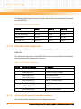
4.12 Other Software Considerations . . . . . . . . . . . . . . . . . . . . . . . . . . . . . . . . . . . . . . . . . . . . . . . . . . . . . . . 66
4.12.1 MRAM . . . . . . . . . . . . . . . . . . . . . . . . . . . . . . . . . . . . . . . . . . . . . . . . . . . . . . . . . . . . . . . . . . . . . . 67
4.12.2 Real Time Clock . . . . . . . . . . . . . . . . . . . . . . . . . . . . . . . . . . . . . . . . . . . . . . . . . . . . . . . . . . . . . . 67
4.12.3 Quad UART. . . . . . . . . . . . . . . . . . . . . . . . . . . . . . . . . . . . . . . . . . . . . . . . . . . . . . . . . . . . . . . . . . 67
4.12.4 LBC Timing Parameters . . . . . . . . . . . . . . . . . . . . . . . . . . . . . . . . . . . . . . . . . . . . . . . . . . . . . . . 68
4.12.5 USB Oscillator Configuration . . . . . . . . . . . . . . . . . . . . . . . . . . . . . . . . . . . . . . . . . . . . . . . . . . 68
4
MVME4100 Single Board Computer Programmer’s Reference (6806800H19B)
Contents
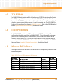
4.13 Clock Distribution . . . . . . . . . . . . . . . . . . . . . . . . . . . . . . . . . . . . . . . . . . . . . . . . . . . . . . . . . . . . . . . . . . 69
4.13.1 System Clock . . . . . . . . . . . . . . . . . . . . . . . . . . . . . . . . . . . . . . . . . . . . . . . . . . . . . . . . . . . . . . . . 70
4.13.2 Real Time Clock Input. . . . . . . . . . . . . . . . . . . . . . . . . . . . . . . . . . . . . . . . . . . . . . . . . . . . . . . . . 70
4.13.3 Local Bus Controller Clock Divisor . . . . . . . . . . . . . . . . . . . . . . . . . . . . . . . . . . . . . . . . . . . . . . 70
A
Programmable Configuration Data . . . . . . . . . . . . . . . . . . . . . . . . . . . . . . . . . . . . . . . . . . . . . . . . . . . . . 71
A.1
A.2
A.3
A.4
A.5
A.6
A.7
A.8
A.9
A.10
B
Overview . . . . . . . . . . . . . . . . . . . . . . . . . . . . . . . . . . . . . . . . . . . . . . . . . . . . . . . . . . . . . . . . . . . . . . . . . . 71
List of Devices . . . . . . . . . . . . . . . . . . . . . . . . . . . . . . . . . . . . . . . . . . . . . . . . . . . . . . . . . . . . . . . . . . . . . . 71
Vital Product Data (VPD) Introduction . . . . . . . . . . . . . . . . . . . . . . . . . . . . . . . . . . . . . . . . . . . . . . . . . 72
How to Read and Modify VPD Information . . . . . . . . . . . . . . . . . . . . . . . . . . . . . . . . . . . . . . . . . . . . . 72
What Happens if VPD Information is Corrupted . . . . . . . . . . . . . . . . . . . . . . . . . . . . . . . . . . . . . . . . 72
How to Fix Corrupted VPD Information . . . . . . . . . . . . . . . . . . . . . . . . . . . . . . . . . . . . . . . . . . . . . . . . 73
What if Your Board Has the Wrong VPD? . . . . . . . . . . . . . . . . . . . . . . . . . . . . . . . . . . . . . . . . . . . . . . 73
How to Fix Wrong VPD Problems . . . . . . . . . . . . . . . . . . . . . . . . . . . . . . . . . . . . . . . . . . . . . . . . . . . . . 73
Vital Product Data CRC Calculation . . . . . . . . . . . . . . . . . . . . . . . . . . . . . . . . . . . . . . . . . . . . . . . . . . . 73
VPD Contents for MVME4100 Boards . . . . . . . . . . . . . . . . . . . . . . . . . . . . . . . . . . . . . . . . . . . . . . . . . 76
Related Documentation . . . . . . . . . . . . . . . . . . . . . . . . . . . . . . . . . . . . . . . . . . . . . . . . . . . . . . . . . . . . . . . 85
B.1
B.2
B.3
Emerson Network Power - Embedded Computing Documents . . . . . . . . . . . . . . . . . . . . . . . . . . . 85
Manufacturers’ Documents . . . . . . . . . . . . . . . . . . . . . . . . . . . . . . . . . . . . . . . . . . . . . . . . . . . . . . . . . . 85
Related Specifications . . . . . . . . . . . . . . . . . . . . . . . . . . . . . . . . . . . . . . . . . . . . . . . . . . . . . . . . . . . . . . . 88
MVME4100 Single Board Computer Programmer’s Reference (6806800H19B)
5
Contents
Contents
6
MVME4100 Single Board Computer Programmer’s Reference (6806800H19B)
List of Tables
Table 1-1
Table 1-2
Table 2-1
Table 2-2
Table 2-3
Table 3-1
Table 3-2
Table 3-3
Table 3-4
Table 3-5
Table 3-6
Table 3-7
Table 3-8
Table 3-9
Table 3-10
Table 3-11
Table 3-12
Table 3-13
Table 3-14
Table 3-15
Table 3-16
Table 3-17
Table 3-18
Table 3-19
Table 3-20
Table 3-21
Table 3-22
Table 3-23
Table 3-24
Table 3-25
Table 3-26
Table 3-27
Table 3-28
Table 3-29
Table 3-30
Table 3-31
Board Variants . . . . . . . . . . . . . . . . . . . . . . . . . . . . . . . . . . . . . . . . . . . . . . . . . . . . . . . . . . . . . . 15
Features List . . . . . . . . . . . . . . . . . . . . . . . . . . . . . . . . . . . . . . . . . . . . . . . . . . . . . . . . . . . . . . . . 15
Default Processor Address Map . . . . . . . . . . . . . . . . . . . . . . . . . . . . . . . . . . . . . . . . . . . . . . . 21
Suggested Processor Address Map . . . . . . . . . . . . . . . . . . . . . . . . . . . . . . . . . . . . . . . . . . . . 21
PCI Memory Map . . . . . . . . . . . . . . . . . . . . . . . . . . . . . . . . . . . . . . . . . . . . . . . . . . . . . . . . . . . . 22
System I/O Memory Map . . . . . . . . . . . . . . . . . . . . . . . . . . . . . . . . . . . . . . . . . . . . . . . . . . . . . 25
System Status Register . . . . . . . . . . . . . . . . . . . . . . . . . . . . . . . . . . . . . . . . . . . . . . . . . . . . . . . 28
System Control Register . . . . . . . . . . . . . . . . . . . . . . . . . . . . . . . . . . . . . . . . . . . . . . . . . . . . . 29
Status Indicator Register . . . . . . . . . . . . . . . . . . . . . . . . . . . . . . . . . . . . . . . . . . . . . . . . . . . . . 30
NOR Flash Control/Status Register . . . . . . . . . . . . . . . . . . . . . . . . . . . . . . . . . . . . . . . . . . . . 31
Interrupt Register 1 . . . . . . . . . . . . . . . . . . . . . . . . . . . . . . . . . . . . . . . . . . . . . . . . . . . . . . . . . . 33
Interrupt Register 2 . . . . . . . . . . . . . . . . . . . . . . . . . . . . . . . . . . . . . . . . . . . . . . . . . . . . . . . . . . 34
Presence Detect Register . . . . . . . . . . . . . . . . . . . . . . . . . . . . . . . . . . . . . . . . . . . . . . . . . . . . . 35
PCI Bus 1 Status Register . . . . . . . . . . . . . . . . . . . . . . . . . . . . . . . . . . . . . . . . . . . . . . . . . . . . . 36
PCI Bus 2 Status Register . . . . . . . . . . . . . . . . . . . . . . . . . . . . . . . . . . . . . . . . . . . . . . . . . . . . . 36
PCI Bus 3 Status Register . . . . . . . . . . . . . . . . . . . . . . . . . . . . . . . . . . . . . . . . . . . . . . . . . . . . . 37
NAND Flash Chip 1 Control Register . . . . . . . . . . . . . . . . . . . . . . . . . . . . . . . . . . . . . . . . . . . 38
NAND Flash Chip 1 Select Register . . . . . . . . . . . . . . . . . . . . . . . . . . . . . . . . . . . . . . . . . . . . 38
NAND Flash Chip 1 Presence Register . . . . . . . . . . . . . . . . . . . . . . . . . . . . . . . . . . . . . . . . . . 39
NAND Flash Chip 1 Status Register . . . . . . . . . . . . . . . . . . . . . . . . . . . . . . . . . . . . . . . . . . . . 40
NAND Flash Chip 2 Control Register . . . . . . . . . . . . . . . . . . . . . . . . . . . . . . . . . . . . . . . . . . . 40
NAND Flash Chip 2 Select Register . . . . . . . . . . . . . . . . . . . . . . . . . . . . . . . . . . . . . . . . . . . . 41
NAND Flash Chip 2 Presence Register . . . . . . . . . . . . . . . . . . . . . . . . . . . . . . . . . . . . . . . . . . 42
NAND Flash Chip 2 Status Register . . . . . . . . . . . . . . . . . . . . . . . . . . . . . . . . . . . . . . . . . . . . 42
Watch Dog Timer Load Register . . . . . . . . . . . . . . . . . . . . . . . . . . . . . . . . . . . . . . . . . . . . . . . 43
Watch Dog Timer Control Register . . . . . . . . . . . . . . . . . . . . . . . . . . . . . . . . . . . . . . . . . . . . 43
Watch Dog Timer Resolution Register . . . . . . . . . . . . . . . . . . . . . . . . . . . . . . . . . . . . . . . . . 44
Watch Dog Timer Count Register . . . . . . . . . . . . . . . . . . . . . . . . . . . . . . . . . . . . . . . . . . . . . 45
PLD Revision Register . . . . . . . . . . . . . . . . . . . . . . . . . . . . . . . . . . . . . . . . . . . . . . . . . . . . . . . . 46
PLD Date Code Register . . . . . . . . . . . . . . . . . . . . . . . . . . . . . . . . . . . . . . . . . . . . . . . . . . . . . . 46
Test Register 1 . . . . . . . . . . . . . . . . . . . . . . . . . . . . . . . . . . . . . . . . . . . . . . . . . . . . . . . . . . . . . . 47
Test Register 2 . . . . . . . . . . . . . . . . . . . . . . . . . . . . . . . . . . . . . . . . . . . . . . . . . . . . . . . . . . . . . . 47
Prescaler Register . . . . . . . . . . . . . . . . . . . . . . . . . . . . . . . . . . . . . . . . . . . . . . . . . . . . . . . . . . . 48
Tick Timer Control Registers . . . . . . . . . . . . . . . . . . . . . . . . . . . . . . . . . . . . . . . . . . . . . . . . . . 49
Tick Timer Compare Registers . . . . . . . . . . . . . . . . . . . . . . . . . . . . . . . . . . . . . . . . . . . . . . . . 50
Tick Timer Counter Register . . . . . . . . . . . . . . . . . . . . . . . . . . . . . . . . . . . . . . . . . . . . . . . . . . 51
MVME4100 Single Board Computer Programmer’s Reference (6806800H19B)
7
List of Tables
Table 4-1
Table 4-2
Table 4-3
Table 4-4
Table 4-5
Table 4-6
Table 4-7
Table 4-8
Table 4-9
Table 4-10
Table 4-11
Table 4-12
Table 4-13
Table A-1
Table A-2
Table A-3
Table A-4
Table B-1
Table B-2
Table B-3
8
MPC8548E POR Configuration Settings . . . . . . . . . . . . . . . . . . . . . . . . . . . . . . . . . . . . . . . . 54
MPC8548E Interrupt Controller . . . . . . . . . . . . . . . . . . . . . . . . . . . . . . . . . . . . . . . . . . . . . . . 60
LBC Chip Select Assignments . . . . . . . . . . . . . . . . . . . . . . . . . . . . . . . . . . . . . . . . . . . . . . . . . 61
I2C Bus Device Addressing . . . . . . . . . . . . . . . . . . . . . . . . . . . . . . . . . . . . . . . . . . . . . . . . . . . . 62
PHY Types and MII Management Bus Addresses . . . . . . . . . . . . . . . . . . . . . . . . . . . . . . . . . 63
NOR Flash Memory Configurations . . . . . . . . . . . . . . . . . . . . . . . . . . . . . . . . . . . . . . . . . . . . 64
NAND Flash Memory Configurations . . . . . . . . . . . . . . . . . . . . . . . . . . . . . . . . . . . . . . . . . . . 64
IDSEL and Interrupt Mapping for PCI Devices . . . . . . . . . . . . . . . . . . . . . . . . . . . . . . . . . . . . 65
Planar PCI Device Identification . . . . . . . . . . . . . . . . . . . . . . . . . . . . . . . . . . . . . . . . . . . . . . . 66
PCI Arbitration Assignments . . . . . . . . . . . . . . . . . . . . . . . . . . . . . . . . . . . . . . . . . . . . . . . . . . 66
LBC Timing Parameters . . . . . . . . . . . . . . . . . . . . . . . . . . . . . . . . . . . . . . . . . . . . . . . . . . . . . . 68
Clock Assignments . . . . . . . . . . . . . . . . . . . . . . . . . . . . . . . . . . . . . . . . . . . . . . . . . . . . . . . . . . 69
Clock Frequencies . . . . . . . . . . . . . . . . . . . . . . . . . . . . . . . . . . . . . . . . . . . . . . . . . . . . . . . . . . . 70
Programmable Devices . . . . . . . . . . . . . . . . . . . . . . . . . . . . . . . . . . . . . . . . . . . . . . . . . . . . . . 71
Onboard Serial EEPROMs . . . . . . . . . . . . . . . . . . . . . . . . . . . . . . . . . . . . . . . . . . . . . . . . . . . . . 71
Static VPD Contents . . . . . . . . . . . . . . . . . . . . . . . . . . . . . . . . . . . . . . . . . . . . . . . . . . . . . . . . . 76
Variable VPD Contents . . . . . . . . . . . . . . . . . . . . . . . . . . . . . . . . . . . . . . . . . . . . . . . . . . . . . . . 83
Emerson Network Power - Embedded Computing Publications . . . . . . . . . . . . . . . . . . . 85
Manufacturer’s Publications . . . . . . . . . . . . . . . . . . . . . . . . . . . . . . . . . . . . . . . . . . . . . . . . . . 85
Related Specifications . . . . . . . . . . . . . . . . . . . . . . . . . . . . . . . . . . . . . . . . . . . . . . . . . . . . . . . 88
MVME4100 Single Board Computer Programmer’s Reference (6806800H19B)
List of Figures
Figure 1-1
Figure 3-1
Block Diagram . . . . . . . . . . . . . . . . . . . . . . . . . . . . . . . . . . . . . . . . . . . . . . . . . . . . . . . . . . 18
Boot Flash Bank . . . . . . . . . . . . . . . . . . . . . . . . . . . . . . . . . . . . . . . . . . . . . . . . . . . . . . . . . 32
MVME4100 Single Board Computer Programmer’s Reference (6806800H19B)
9
List of Figures
10
MVME4100 Single Board Computer Programmer’s Reference (6806800H19B)
About this Manual
Overview of Contents
This manual is divided into the following chapters and appendices:
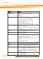
Chapter 1, Introduction, provides a brief product description and a block diagram showing the
architecture of the MVME4100 Single Board Computer.
Chapter 2, Memory Maps, provides information on the board’s memory maps.
Chapter 3, Register Descriptions, contains status registers for the system resources.
Chapter 4, Programming Details, includes additional programming information for the board.
Appendix A, Programmable Configuration Data, provides additional programming information
including IDSEL mapping, interrupt assignments for the MPC8548E interrupt controller, Flash
memory, two-wire serial interface addressing, and other device and system considerations.
Appendix B, Related Documentation, provides a listing of related Emerson manuals, vendor
documentation, and industry specifications.
Abbreviations
This document uses the following abbreviations:
Acronym
Description
ASCII
American Standard Code for Information Interchange
CRC
Cyclic Redundancy Check
EEPROM
Electrically Erasable Programmable Read Only Memory
FRU
Field Replaceable Unit
Flash
Flash Memory
GB
Gigabyte
HEX
Hexadecimal
Hz
Hertz
IPMI
Intelligent Platform Management Interface
MVME4100 Single Board Computer Programmer’s Reference (6806800H19B)
11
About this Manual
About this Manual
Acronym
Description
MB
Megabyte
Mfg
Manufacturing
SPD
Serial Presence Detect
VPD
Vital Product Data
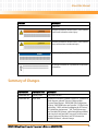
Conventions
The following table describes the conventions used throughout this manual.
Notation
Description
0x00000000
Typical notation for hexadecimal numbers (digits are
0 through F), for example used for addresses and
offsets
0b0000
Same for binary numbers (digits are 0 and 1)
bold
Used to emphasize a word
Screen
Used for on-screen output and code related elements
or commands in body text
Courier + Bold
Used to characterize user input and to separate it
from system output
Reference
Used for references and for table and figure
descriptions
File > Exit
Notation for selecting a submenu
<text>
Notation for variables and keys
[text]
Notation for software buttons to click on the screen
and parameter description
...
Repeated item for example node 1, node 2, ..., node
12
.
Omission of information from example/command
that is not necessary at the time being
.
.
..
12
Ranges, for example: 0..4 means one of the integers
0,1,2,3, and 4 (used in registers)
MVME4100 Single Board Computer Programmer’s Reference (6806800H19B)
About this Manual
Notation
Description
|
Logical OR
Indicates a hazardous situation which, if not avoided,
could result in death or serious injury
Indicates a hazardous situation which, if not avoided,
may result in minor or moderate injury
Indicates a property damage message
No danger encountered. Pay attention to important
information
Summary of Changes
Part Number
Publication Date
Description
6806800H19A
January 2009
Early access version
6806800H19B
April 2009
Update for final release, updated "Feature List", updated the
block diagram, updated "System I/O Memory Map",
"System Status Register", "MPC8548E POR Configuration
Settings", "MPC8548E Interrupt Controller", "I2C Bus Device
Addressing ", "IDSEL and Interrupt Mapping for PCI Devices",
"PCI Arbitration Assignments ", "LBC Timing Parameters"
and "Variable VPD Contents", added information on MRAM,
real time clock and Quad UART, removed "Serial Presence
Detect Checksum Calculation" and "SPD Contents for
MVME4100 Boards", editorial changes
MVME4100 Single Board Computer Programmer’s Reference (6806800H19B)
13
About this Manual
About this Manual
Comments and Suggestions
We welcome and appreciate your comments on our documentation. We want to know what
you think about our manuals and how we can make them better.
Mail comments to us by filling out the following online form:
http://www.emersonnetworkpowerembeddedcomputing.com/ > Contact Us > Online Form
In "Area of Interest" select "Technical Documentation". Be sure to include the title, part number,
and revision of the manual and tell us how you used it.
14
MVME4100 Single Board Computer Programmer’s Reference (6806800H19B)
Chapter 1
Introduction
1.1
Overview
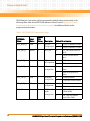
This chapter briefly describes the board level hardware features of the MVME4100 Single Board
Computer. Refer to the MPC8548E Reference Manual listed in Appendix B, Related
Documentation, for more detail and programming information.
At the time of publication of this manual, the MVME4100 is available in the configurations
shown below.
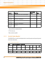
Table 1-1 Board Variants
1.2
Marketing Number
Processor
MVME4100-0171
1.3 GHz MPC8548E, 4 GB NAND flash, 2 GB DDR2, Scanbe handles
MVME4100-0173
1.3 GHz MPC8548E, 4 GB NAND flash, 2 GB DDR2, IEEE handles
Features
Refer to the following table for a summary of the features common to all board variations.
Table 1-2 Features List
Function
Features
Processor / Host Controller /
Memory Controller
One MPC8548E Integrated Processor
One e500 core with integrated L2
Core frequency of 1.3 GHz
One integrated four channel DMA controller
One integrated PCI-E interface
One integrated PCI-X interface
Four integrated 10/100/1000 Ethernet controllers
One integrated DUART
Two integrated I2C controllers
One integrated Programmable Interrupt Controller
One integrated Local Bus Controller
One integrated DDR2 SDRAM controller
MVME4100 Single Board Computer Programmer’s Reference (6806800H19B)
15
Introduction
Table 1-2 Features List (continued)
Function
Features
System Memory
One DDR2 SO-CDIMM for SDRAM with ECC
2 GBytes
Up to DDR533
I2
C
One 8 KB VPD serial EEPROM
Two 64 KB user configuration serial EEPROMs
One Real Time Clock (RTC) with removable battery
Dual temperature sensor
One SPD for memory on SO-CDIMM
Connection to XMCspan and rear transition module
Flash
128 MB soldered NOR flash with two alternate 1 MB boot sectors
selectable via hardware switch
H/W switch or S/W bit write protection for entire logical bank
4 GB NAND flash
NVRAM
One 512 KB MRAM extended temperature range (-40 °C to
+105 °C/-40 °F to +221 °F)
PCI_E
8X Port to XMC Expansion
I/O
One front panel mini DB-9 connector for front I/O: one serial channel
Two front panel RJ-45 connectors with integrated LEDs for front I/O:
two 10/100/1000 Ethernet channels
One front panel USB Type A upright receptacle for front I/O: one USB
2.0 channel
PMC site 1 front I/O and rear P2 I/O
PMC site 2 front I/O
USB
One four-channel USB 2.0 controller: one channel for front panel I/O
Ethernet
Four 10/100/1000 MPC8548E Ethernet channels: two front panel
Ethernet connectors and two channels for rear P2 I/O
Serial Interface
One 16550-compatible, 9.6 to 115.2 Kbaud, MPC8548E,
asynchronous serial channel: one channel for front panel I/O
One quad UART (QUART) controller to provide four 16550compatible, 9.6 to 115.2 Kbaud, asynchronous serial channels: four
channels for rear P2 I/O
Timers
Four 32-bit MPC8548E timers
Four 32-bit timers in a PLD
16
MVME4100 Single Board Computer Programmer’s Reference (6806800H19B)
Introduction
Table 1-2 Features List (continued)
Function
Features
Watchdog Timer
One watchdog timer in PLD
VME Interface
VME64 (ANSI/VITA 1-1994) compliant (3 row backplane 96-pin VME
connector)
VME64 Extensions (ANSI/VITA 1.1-1997) compliant (5 row
backplane 160-pin VME connector)
2eSST (ANSI/VITA 1.5-2003) compliant
ANSI/VITA 1.7-2003 compliant (Increased Current Level for 96 pin &
160 pin DIN/IEC Connector Standard)
VITA 41.0, version 0.9 compliant
Two five-row P1 and P2 backplane connectors
One Tsi148 VMEbus controller
Form Factor
Standard 6U VME, one slot
Miscellaneous
One front panel RESET/ABORT switch
Six front panel status indicators:
z
Two 10/100/1000 Ethernet link/speed and activity (4 total)
z
Board fail
z
User S/W controlled LED
Planar status indicators
One standard 16-pin COP header
One standard 20-pin JTAG header
Boundary scan support
Switches for VME geographical addressing in a three-row backplane
Software Support
VxWorks OS support
Linux OS support
MVME4100 Single Board Computer Programmer’s Reference (6806800H19B)
17
Introduction
1.3
Block Diagram
The following figure is a block diagram of the MVME4100 architecture.
Figure 1-1
USB
Block Diagram
GigE GigE
RJ-45 RJ-45
PMC1 Front IO
COM
PMC2 Front IO
Front Panel
ABT/RST
PHY
5482
2 GB DDR2
SO-CDIMM
XCVR
RS-232
Serial Port 0
GigE 1
User
128 KB
DDR2 MC
DUART
TSEC1
GigE 2
GigE 3
MPC8548E
Processor
TSEC3
GIgE 4
I2C Bus
I2C
TSEC2
TSEC4
LBC
PCI-E
PCI-X
Serial Ports 1-4
Device
Bus
QUART
16C554
XMCspan
VPD
8 KB
RTC
DS1375
CPLD
Decode
Timers/Regs
Flash
128 MB
Temp
MAX6649
Flash
(opt)
MRAM
512 KB
PHY
5482
PCI-X
Bridge
PCI-X
Bridge
USB
uPD720101
PMC 1
XCVR
22501
XCVR
RS-232
GigE 3
GigE 4
VME Bus
COM2COM5
P2
18
VME
Tsi148
PMC 2
PMC 1 Jn4 IO
I2C Bus
P1
MVME4100 Single Board Computer Programmer’s Reference (6806800H19B)
Introduction
1.4
Functional Description
The MVME4100 VMEbus board is based on the MPC8548E system-on-chip (SoC) processor.
The MVME4100 provides front panel access to one serial port with a micro DB-9 connector,
two 10/100/1000 Ethernet ports with two RJ-45 connectors, and one USB port with one type
A connector. The front panel includes a fail indicator LED, user-defined indicator LED, and a
reset/abort switch.
The MVME7216E transition module provides rear panel access to four serial ports with one
RJ-45 connector per port and two 10/100/1000 Ethernet ports with two RJ-45 connectors. The
transition module also provides two planar connectors for one PIM with front I/O.
The block diagram for the MVME4100 is shown in Figure 1-1 and the block diagram for the
MVME7216E transition module is shown in section "Transition Module" of the MVME4100 Single
Board Computer Installation and Use manual.
1.5
Programming Model
The MVME4100 programming model is based on the MPC8548E local memory map, which
refers to the 32-bit address space seen by the processor as it accesses memory and I/O space.
DMA engines also see the same local memory map. All memory accessed by the MPC8548E
DDR2 SDRAM and local bus memory controllers exists in this memory map in addition to all
memory mapped configuration, control, and status registers. Memory maps and registers are
described in Chapter 2, Memory Maps and Chapter 3, Register Descriptions.
MVME4100 Single Board Computer Programmer’s Reference (6806800H19B)
19
Introduction
20
MVME4100 Single Board Computer Programmer’s Reference (6806800H19B)
Chapter 2
Memory Maps
2.1
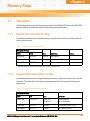
Overview
The following sections describe the memory maps for the MVME4100. Refer to the MPC8548E
Reference Manual for additional details and/or programming information.
2.1.1
Default Processor Memory Map
The following table describes a default memory map from the point of view of the processor
after a processor reset.
Table 2-1 Default Processor Address Map
Processor Address
Start
End
Size
Definition
Notes
0000 0000
FF6F FFFF
4087 M
Not mapped
FF70 0000
FF7F FFFF
1M
MPC8548E CCSR Registers
FF80 0000
FFFF FFFF
8M
Flash
1
1. The e500 core fetches the first instruction from FFFF FFFC following a reset.
2.1.2
Suggested Processor Memory Map
The following table describes a suggested physical memory map from the point of view of the
processor. This table reflects the address map implemented by the board level firmware at
release time.
Table 2-2 Suggested Processor Address Map
Processor Address
Start
End
Size
Definition
0000 0000
top_dram - 1
dram_size
System Memory
(2 GB max)
(on-board DRAM)
8000 0000
CFFF FFFF
1.25 GB
PCI 0 Memory Space / VME
D000 0000
DFFF FFFF
256 MB
PCI 1 Memory Space
MVME4100 Single Board Computer Programmer’s Reference (6806800H19B)
21
Memory Maps
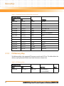
Table 2-2 Suggested Processor Address Map (continued)
Processor Address
2.1.3
Start
End
Size
Definition
E000 0000
EFFF FFFF
256 MB
Not used
F000 0000
F07F FFFF
8 MB
PCI 0 I/O Space
F080 0000
F0FF FFFF
8 MB
PCI 1 I/O Space
F100 0000
F10F FFFF
1 MB
MPC8548E CCSR
F110 0000
F1FF FFFF
15 MB
Not used
F200 0000
F200 FFFF
64 KB
Status/Control Registers
F201 0000
F201 FFFF
64 KB
UARTs
F202 0000
F202 FFFF
64 KB
Timers
F203 0000
F203 FFFF
64 KB
NAND Flash
F204 0000
F23F FFFF
3.9 MB
Not used
F240 0000
F247 FFFF
512 KB
MRAM
F248 0000
F7FF FFFF
91.5 MB
Not used
F800 0000
FFFF FFFF
128 MB
NOR Flash
PCI Memory Map
The following table is the suggested PCI memory map for each PCI bus. This table reflects the
address map implemented by the board level firmware at release time.
Table 2-3 PCI Memory Map
Processor Address
Start
End
Size
Definition
0000 0000
top_dram - 1
dram_size
System Memory
Notes
(on-board DRAM)
22
MVME4100 Single Board Computer Programmer’s Reference (6806800H19B)
Memory Maps
2.1.4
VME Memory Map
The MVME4100 is fully capable of supporting both the PReP and the CHRP VME Memory Map
examples with RAM size limited to 2 GB.
MVME4100 Single Board Computer Programmer’s Reference (6806800H19B)
23
Memory Maps
24
MVME4100 Single Board Computer Programmer’s Reference (6806800H19B)
Chapter 3
Register Descriptions
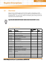
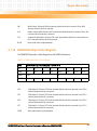
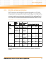
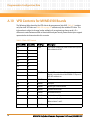
3.1
Overview
System resources including system control and status registers, external timers, and the
QUART are mapped into a 16 MB address range accessible from the MVME4100 local bus via
the MPC8548E LBC. The memory map is defined in the following table including the LBC bank
chip select used to decode the register.
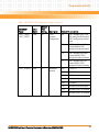
Any address that is not listed in the table blelow is unused and reserved for future use.
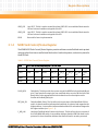
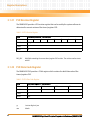
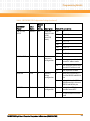
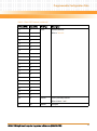
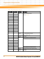
Table 3-1 System I/O Memory Map
Address
Definition
LBC Bank/Chip
Select
Notes
F200 0000
System Status Register
4
3
F200 0001
System Control Register
4
3
F200 0002
Status Indicator Register
4
3
F200 0003
NOR Flash Control/Status Register
4
3
F200 0004
Interrupt Register 1
4
3
F200 0005
Interrupt Register 2
4
3
F200 0006
Presence Detect Register
4
3
F200 0008
PCI Bus Status Register 1
4
3
F200 0009
PCI Bus Status Register 2
4
3
F200 000A
PCI Bus Status Register 3
4
3
F200 0010
NAND Flash Chip 1 Control Register
4
3
F200 0011
NAND Flash Chip 1 Select Register
4
3
F200 0012
Reserved
4
1
F200 0013
Reserved
4
1
F200 0014
NAND Flash Chip 1 Presence Register
4
3
F200 0015
NAND Flash Chip 1 Status Register
4
3
MVME4100 Single Board Computer Programmer’s Reference (6806800H19B)
25
Register Descriptions
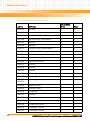
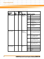
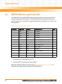
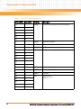
Table 3-1 System I/O Memory Map (continued)
26
Address
Definition
LBC Bank/Chip
Select
Notes
F200 0016
Reserved
4
1
F200 0017
Reserved
4
1
F200 0018
NAND Flash Chip 2 Control Register
4
3
F200 0019
NAND Flash Chip 2 Select Register
4
3
F200 001A
Reserved
4
1
F200 001B
Reserved
4
1
F200 001C
NAND Flash Chip 2 Presence Register
4
3
F200 001D
NAND Flash Chip 2 Status Register
4
3
F200 001E
Reserved
4
1
F200 001F
Reserved
4
1
F200 0020
Watch Dog Timer Load
4
3
F200 0021
Reserved
4
1
F200 0022
Reserved
4
1
F200 0023
Reserved
4
1
F200 0024
Watchdog Control
4
3
F200 0025
Watchdog Resolution
4
F200 0026 F200 0027
Watchdog Count
4
F200 0028
Reserved (32 bits)
4
1
F200 002C
Reserved (32 bits)
4
1
F200 0030
PLD Revision
4
3
F200 0031
Reserved
4
1
F200 0032
Reserved
4
1
F200 0033
Reserved
4
1
F200 0034
PLD Date Code (32 bits)
4
3
F200 0038
Test Register 1 (32 bits)
4
3
F200 003C
Test Register 2 (32 bits)
4
3
MVME4100 Single Board Computer Programmer’s Reference (6806800H19B)
Register Descriptions
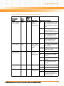
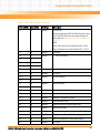
Table 3-1 System I/O Memory Map (continued)
Address
Definition
F200 0018 -
Reserved
LBC Bank/Chip
Select
Notes
1
F200 0FFF
F201 1000 -
COM 2 (QUART channel 1)
5
COM 3 (QUART channel 2)
5
COM 4 (QUART channel 3)
5
COM 5 (QUART channel 4)
5
F201 1FFF
F201 2000 F201 2FFF
F201 3000 F201 3FFF
F201 4000 F201 4FFF
F201 5000 -
Reserved
1
F201 FFFF
F202 0000
External PLD Tick Timer Prescaler Register
6
2
F202 0010
External PLD Tick Timer 1 Control Register
6
2
F202 0014
External PLD Tick Timer 1 Compare Register
6
2
F202 0018
External PLD Tick Timer 1 Counter Register
6
2
F202 001C
Reserved
6
2
F202 0020
External PLD Tick Timer 2 Control Register
6
2
F202 0024
External PLD Tick Timer 2 Compare Register
6
2
F202 0028
External PLD Tick Timer 2 Counter Register
6
2
F202 002C
Reserved
6
2
F202 0030
External PLD Tick Timer 3 Control Register
6
2
F202 0034
External PLD Tick Timer 3 Compare Register
6
2
F202 0038
External PLD Tick Timer 3 Counter Register
6
2
F202 003C
Reserved
6
2
F202 0040
External PLD Tick Timer 4 Control Register
6
2
F202 0044
External PLD Tick Timer 4 Compare Register
6
2
MVME4100 Single Board Computer Programmer’s Reference (6806800H19B)
27
Register Descriptions
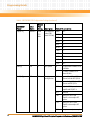
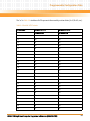
Table 3-1 System I/O Memory Map (continued)
Address
Definition
LBC Bank/Chip
Select
Notes
F202 0048
External PLD Tick Timer 4 Counter Register
6
2
F202 004C -
Reserved
6
1
F203 0000
NAND Chip 1 Data Register
2
3
F203 0001 -
Reserved
2
1
F203 1000
NAND Chip 2 Data Register
2
3
F203 1001 -
Reserved
2
1
F2FF FFFF
F203 0FFF
F203 FFFF
1. Reserved for future implementation.
2. 32-bit write only.
3. Byte read/write capable.
3.1.1
System Status Register
The MVME4100 has a System Status Register that is a read only register used to provide general
board status information.
Table 3-2 System Status Register
28
REG
System Status Register - 0xF200 0000
BIT
7
6
5
4
3
2
1
Field
SW8
MASTER
WP
PCI 66
PCI MODE
SAFE_
START
RSDV
BD_TYPE
OPER
R
RESET
X
X
X
X
X
0
0
0
0
MVME4100 Single Board Computer Programmer’s Reference (6806800H19B)
Register Descriptions
BD_TYPE
Board Type. These bits indicate the board type.
00: VME SBC
01: PrPMC
10-11: reserved
3.1.2
SAFE_START
ENV Safe Start. This bit reflects the current state of the ENV safe start select
switch. A cleared condition indicates that the ENV settings programmed in
NVRAM should be used by the firmware. A set condition indicates that firmware
should use the safe ENV settings.
PCI MODE
PCI mode. This bit reflects the current state of the PCI Mode switch. A cleared
condition indicates the switch is off. A set condition indicates the switch is on.
PCI 66
PCI 66. This bit reflects the current state of the PCI 66 switch. A cleared condition
indicates the switch is off. A set condition indicates the switch is on.
MASTER WP
MASTER WP. This bit reflects the current state of the MASTER WP switch. A
cleared condition indicates the switch is off. A set condition indicates the switch
is on. When this switch is on, the NOR FLASH, NAND FLASH, MRAM and I2C
EEPROMs are write protected. When this switch is off, NOR FLASH, NAND
FLASH, MRAM and I2C EEPROMs are not write protected by this function. This
switch does not write protect the SPD on the SO-CDIMM. Other switches and
control bits may write protect individual devices.
SW8
SW8. This bit reflects the current state of SW8. A cleared condition indicates the
switch is off. A set condition indicates the switch is on.
System Control Register
The MVME4100 has a System Control Register that provides general board control bits.
Table 3-3 System Control Register
REG
System Control Register - 0xF200 0001
BIT
7
Field
6
4
3
2
1
0
BRD_RST
RSVD
RSVD
RSVD
EEPROM_
WP
RSVD
OPER
R/W
R
R
R
R/W
R
RESET
0
0
0
0
1
0
0
5
0
MVME4100 Single Board Computer Programmer’s Reference (6806800H19B)
29
Register Descriptions
3.1.3
EEPROM_WP
EEPROM Write Protect. This bit is to provide protection against inadvertent
writes to the on-board EEPROM devices. Clearing this bit will enable writes to
the EEPROM devices. Setting this bit write protects the devices. The devices are
write protected following a reset.
BRD_RST
Board Reset. These bits are used to force a hard reset of the board. If a pattern is
written in bits 5-7 where bit 7 is set, bit 6 is cleared, and bit 5 is set (101), a hard
reset is generated. Any other pattern written in bits 5-7, does not generate a
hard reset. These bits are cleared automatically when the board reset has been
completed. These bits are always cleared during a read.
RSVD
Reserved for future implementation.
Status Indicator Register
The MVME4100 provides a Status Indicator Register that may be read by the system software
to determine the state of the on-board status indicator LEDs or written to by system software
to illuminate the corresponding on-board LEDs.
Table 3-4 Status Indicator Register
30
REG
Status Indicator Register - 0xF200 0002
BIT
7
6
5
4
3
2
Field
RSVD
RSVD
RSVD
RSVD
USR3
USR2
1
0
USR1
USR1
Y
R
OPER
R
R
R
R
R/W
R/W
R/W
R/W
RESET
0
0
0
0
0
0
0
1
USR1R
User LED 1 RED. This bit is used to control the USR1 bi-color LED located on the front panel.
A set condition illuminates the red segment of the front panel LED and a cleared condition
extinguishes the red segment of the front panel LED.
USR1Y
User LED 1 Yellow. This bit is used to control the USR1 bi-color LED located on the front
panel. A set condition illuminates the yellow segment of the front panel LED and a cleared
condition extinguishes the yellow segment of the front panel LED.
MVME4100 Single Board Computer Programmer’s Reference (6806800H19B)
Register Descriptions
3.1.4
USR2_LED
User LED 2. This bit is used to control the planar USR2 LED. A set condition illuminates the
LED and a cleared condition extinguishes the LED.
USR3_LED
User LED 3. This bit is used to control the planar USR3 LED. A set condition illuminates the
LED and a cleared condition extinguishes the LED.
RSVD
Reserved for future implementation
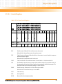
NOR Flash Control/Status Register
The MVME4100 Flash Control/Status Register provides software controlled bank write protect
and map select functions as well as boot block select, bank write protect, and activity status for
the NOR flash.
Table 3-5 NOR Flash Control/Status Register
REG
NOR Flash Control/Status Register - 0xF200 0003
BIT
7
6
5
4
3
2
1
0
Field
RSVD
RSVD
RSVD
MAP_SE
L
F_WP_S
W
F_WP_H
W
FBT_BLK
_SEL
FLASH_
RDY
OPER
R
R
R
R/W
R/W
R
R
R
RESET
0
0
0
0
1
X
X
1
FLASH_RDY
Flash Ready. This bit provides the current state of the NOR flash devices Ready/Busy#
pins. These open drain output pins from each flash device are wire OR'd to form Flash
Ready. Refer to the appropriate flash device data sheet for a description on the
function of the Ready/Busy# pin.
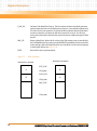
FBT_BLK_SEL
Flash Boot Block Select. This bit reflects the current state of the Boot Block B Select
switch. A cleared condition indicates that boot block A is selected and mapped to the
highest address. A set condition indicates that boot block B is selected and mapped to
the highest address (see Figure 3-1).
F_WP_HW
Hardware Flash Bank Write Protect switch status. This bit reflects the current state of
the FLASH BANK WP switch. A set condition indicates that the NOR Flash bank is write
protected. A cleared condition indicates that the flash bank is not write protected.
MVME4100 Single Board Computer Programmer’s Reference (6806800H19B)
31
Register Descriptions
F_WP_SW
Software Flash Bank Write Protect. This bit provides software-controlled protection
against inadvertent writes to the flash memory devices. A set condition indicates that
the entire flash is write-protected. A cleared condition indicates that the flash bank is
not write-protected, only when the HW write-protect bit is not set. This bit is set
during reset and must be cleared by the system software to enable writing of the flash
devices.
MAP_SEL
Memory Map Select. When this bit is cleared, the flash memory map is controlled by
the Flash Boot Block Select switch (see the MVME4100 Installation and Use manual for
switch settings). When the Map Select bit is set, boot block A is selected and mapped
to the highest address (see Figure 3-1).
RSVD
Reserved for future implementation.
Figure 3-1
Boot Flash Bank
Boot block B is selected
Boot block A is selected
FFFF_FFFF
A
B
FFF0_0000
FFEF_FFFF
B
FFE0_0000
A
FFDF_FFFF
FF00_0000
32
MVME4100 Single Board Computer Programmer’s Reference (6806800H19B)
Register Descriptions
3.1.5
Interrupt Register 1
The MVME4100 provides an Interrupt Register that may be read by the system software to
determine which of the Ethernet PHYs originated their combined (OR'd) interrupt
Table 3-6 Interrupt Register 1
REG
Interrupt Register 1 - 0xF200 0004
BIT
7
6
5
4
3
2
1
0
Field
RSVD
RSVD
RSVD
RSVD
PHY4
PHY3
PHY2
PHY1
OPER
R
RESET
0
0
0
0
0
0
0
0
PHY1
TSEC1 PHY Interrupt. If cleared, the TSEC1 interrupt is not asserted. If set, the TSEC1
interrupt is asserted.
PHY2
TSEC2 PHY Interrupt. If cleared, the TSEC2 interrupt is not asserted. If set, the TSEC2
interrupt is asserted.
PHY3
TSEC3 PHY Interrupt. If cleared, the TSEC3 interrupt is not asserted. If set, the TSEC4
interrupt is asserted.
PHY4
TSEC4 PHY Interrupt. If cleared, the TSEC4 interrupt is not asserted. If set, the FEC interrupt
is asserted.
RSVD
Reserved for future implementation.
MVME4100 Single Board Computer Programmer’s Reference (6806800H19B)
33
Register Descriptions
3.1.6
Interrupt Register 2
The RTC, TEMP sensor and Abort switch interrupts are OR'd together. The MVME4100 provides
an Interrupt Register that may be read by the system software to determine which device
originated the interrupt. This register also includes bits that allow the interrupt sources to be
mask.
Table 3-7 Interrupt Register 2
REG
Interrupt Register 2 - 0xF200 0005
BIT
7
6
5
4
3
2
1
0
Field
RSVD
RTC
TEMP
ABORT
RSVD
RTC
TEMP
ABORT
Mask
Mask
Mask
Status
Status
Status
X
X
0
OPER
R
R/W
RESET
0
1
R
1
1
0
ABORT Status ABORT Status. This bit reflects the current state of the on-board abort signal. This is a
debounced version of the abort switch and may be used to determine the state of the
abort switch. A cleared condition indicates that the abort switch is not depressed while
a set condition indicates that the abort switch is asserted.
34
TEMP Status
TEMP Status. If cleared, the Temperature sensor output is not asserted. If set, the
Temperature sensor output is asserted.
RTC Status
RTC Status. If cleared, the RTC output is not asserted. If set, the RTC output is asserted.
ABORT Mask
ABORT Mask. This bit is used to mask the abort switch output. If this bit is cleared, the
abort switch output is enabled to generate an interrupt. If the bit is set, the abort switch
output is disabled from generating an interrupt.
TEMP Mask
TEMP Mask. This bit is used to mask the MAX6649 temperature sensor thermostat
output. If this bit is cleared, the thermostat output is enabled to generate an interrupt. If
the bit is set, the thermostat output is disabled from generating an interrupt.
RTC Mask
RTC Mask. This bit is used to mask the RTC output. If this bit is cleared, the RTC output is
enabled to generate an interrupt. If the bit is set, the RTC output is disabled from
generating an interrupt.
RSVD
Reserved for future implementation.
MVME4100 Single Board Computer Programmer’s Reference (6806800H19B)
Register Descriptions
3.1.7
Presence Detect Register
The MVME4100 provides a Presence Detect Register that may be read by the system software
to determine the presence of optional devices.
Table 3-8 Presence Detect Register
REG
Presence Detect Register - 0xF200 0006
BIT
7
6
5
4
3
2
1
0
Field
RSVD
RSVD
ERDY2
ERDY1
RSVD
XEP
PMC2P
PMC1P
OPER
R
RESET
0
0
0
0
0
X
X
X
PMC1P
PMC Module 1 Present. If cleared, there is no PMC module installed in site 1. If set, the PMC
module is installed.
PMC2P
PMC Module 2 Present. If cleared, there is no PMC module installed in site 2. If set, the PMC
module is installed.
XEP
XMCspan Present. If cleared, there is no XMCspan module installed. If set, the XMCspan
module is installed.
ERDY1
EREADY1. Indicates that the PrPMC module installed in PMC site 1 is ready for enumeration
when set. If cleared, the PrPMC module is not ready for enumeration. If no PrPMC is
installed, this bit is always set.
ERDY2
EREADY2. Indicates that the PrPMC module installed in PMC site 2 is ready for enumeration
when set. If cleared, the PrPMC module is not ready for enumeration. If no PrPMC is
installed, the bit is always set.
RSVD
Reserved for future implementation
MVME4100 Single Board Computer Programmer’s Reference (6806800H19B)
35
Register Descriptions
3.1.8
PCI Bus Status Registers
The MVME4100 Status Registers provide PCI bus configuration information for each of the PCI
busses.
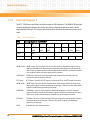
Table 3-9 PCI Bus 1 Status Register
REG
PCI Bus 1 Status Register - 0xF200 0008
BIT
7
6
5
4
3
2
1
Field
RSVD
RSVD
RSVD
RSVD
PCI_1_64B
PCIX_1
PCI_1_SPD
OPER
R
R
R
R
R
R
R
R
RESET
0
0
0
0
1
X
1
0
0
PCI_1_SPD
PCI Bus 1 Speed. Indicates the frequency of PCI bus 1.
00: 33 MHz
01: 66 MHz
10: 100 MHz
11: 133 MHz
PCIX_1
PCI-X Bus 1. A set condition indicates that bus 1 is operating in PCI-X mode.
Cleared indicates PCI mode.
PCI_1_64B
PCI Bus 1 64-bit. A set condition indicates that bus 1 is enabled to operate in 64bit mode. Cleared indicates 32-bit mode.
RSVD
Reserved for future implementation.
Table 3-10 PCI Bus 2 Status Register
36
REG
PCI Bus 2 Status Register - 0xF200 0009
BIT
7
6
5
4
3
2
1
Field
3.3V_VIO
5.0V_VIO
RSVD
RSVD
PCI_2_64B
PCIX_2
PCI_2_SPD
OPER
R
R
R
R
R
R
R
R
RESET
X
X
X
0
1
X
X
X
0
MVME4100 Single Board Computer Programmer’s Reference (6806800H19B)
Register Descriptions
PCI_2_SPD
PCI Bus 2 Speed. Indicates the frequency of PCI bus 2.
00: 33 MHz
01: 66 MHz
10: 100 MHz
11: 133 MHz
PCIX_2
PCI-X Bus 2. A set condition indicates that bus 2 is operating in PCI-X mode. Cleared
indicates PCI mode.
PCI_2_64B
PCI Bus 2 64-bit. A set condition indicates that bus 2 is enabled to operate in 64-bit
mode. Cleared indicates 32-bit mode.
5.0V_VIO
5.0V VIO Enabled. This bit set indicates that the PMC bus (PCI Bus 2) is configured for
5.0V VIO.
3.3V_VIO
3.3V VIO Enabled. This bit set indicates that the PMC bus (PCI Bus 2) is configured to
3.3V VIO.
Table 3-11 PCI Bus 3 Status Register
REG
PCI Bus 3 Status Register - 0xF200 000A
BIT
7
6
5
4
3
2
1
Field
RSVD
RSVD
RSVD
RSVD
PCI_3_64B
PCIX_3
PCI_3_SPD
OPER
R
R
R
R
R
R
R
R
RESET
0
0
0
0
0
0
0
0
0
PCI_3_SPD
PCI Bus 3 Speed. Indicates the frequency of PCI bus 3.
00: 33 MHz
01: 66 MHz
10: 100 MHz
11: 133 MHz
PCIX_3
PCI-X Bus 3. A set condition indicates that bus 3 is operating in PCI-X mode. Cleared
indicates PCI mode.
PCI_3_64B
PCI Bus 3 64-bit. A set condition indicates that bus 3 is enabled to operate in 64-bit
mode. Cleared indicates 32-bit mode.
RSVD
Reserved for future implementation.
MVME4100 Single Board Computer Programmer’s Reference (6806800H19B)
37
Register Descriptions
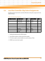
3.1.9
NAND Flash Chip 1 Control Register
The MVME4100 provides a Control Register for the NAND Flash device.
Table 3-12 NAND Flash Chip 1 Control Register
REG
NAND Flash Chip 1 Control Register - 0xF200 0010
BIT
7
6
5
4
3
2
1
0
Field
CLE
ALE
WP
RSVD
RSVD
RSVD
RSVD
RSVD
OPER
R/W
RESET
0
0
0
0
0
R
0
1
0
WP
Write Protect. If cleared, WP is not asserted when the device is accessed. If set, WP is
asserted when the device is accessed.
ALE
Address Latch Enable. If cleared, ALE is not asserted when the device is accessed. If set, ALE
is asserted when the device is accessed.
CLE
Command Latch Enable. If cleared, CLE is not asserted when the device is accessed. If set,
CLE is asserted when the device is accessed.
RSVD
Reserved for future implementation.
3.1.10 NAND Flash Chip 1 Select Register
The MVME4100 provides a Select Register for the NAND Flash device.
Table 3-13 NAND Flash Chip 1 Select Register
38
REG
NAND Flash Chip 1 Select Register - 0xF200 0011
BIT
7
6
5
4
3
2
1
0
Field
CE1
CE2
CE3
CE4
RSVD
RSVD
RSVD
RSVD
OPER
R/W
RESET
0
0
0
0
R
0
0
0
0
MVME4100 Single Board Computer Programmer’s Reference (6806800H19B)
Register Descriptions
CE4
Chip Enable 4. If cleared, CE4 is not asserted when the device is accessed. If set, CE4 is asserted
when the device is accessed.
CE3
Chip Enable 3. If cleared, CE3 is not asserted when the device is accessed. If set, CE3 is asserted
when the device is accessed.
CE2
Chip Enable 2. If cleared, CE2 is not asserted when the device is accessed. If set, CE2 is asserted
when the device is accessed.
CE1
Chip Enable 1. If cleared, CE1 is not asserted when the device is accessed. If set, CE1 is asserted
when the device is accessed.
RSVD
Reserved for future implementation.
3.1.11 NAND Flash Chip 1 Presence Register
The MVME4100 provides a Presence Register for the NAND Flash device.
Table 3-14 NAND Flash Chip 1 Presence Register
REG
NAND Flash Chip 1 Presence Register - 0xF200 0014
BIT
7
6
5
4
3
2
1
0
Field
C1P
RSVD
RSVD
RSVD
RSVD
RSVD
RSVD
RSVD
OPER
R
RESET
X
0
0
0
0
0
0
0
C1P
Chip 1 Present. If cleared, chip 1 is not installed on the board. If set, chip 1 is installed
on the board.
RSVD
Reserved for future implementation.
MVME4100 Single Board Computer Programmer’s Reference (6806800H19B)
39
Register Descriptions
3.1.12 NAND Flash Chip 1 Status Register
The MVME4100 provides a Status Register for the NAND Flash device.
Table 3-15 NAND Flash Chip 1 Status Register
REG
NAND Flash Chip 1 Status Register - 0xF200 0015
BIT
7
6
5
4
3
2
1
0
Field
RB1
RB2
RB3
RB4
RSVD
RSVD
RSVD
RSVD
OPER
R
RESET
1
1
1
1
0
0
0
0
RB4
Ready/Busy 4. If cleared, Device 4 is busy. If set, device 4 is ready.
RB3
Ready/Busy 3. If cleared, Device 3 is busy. If set, device 3 is ready.
RB2
Ready/Busy 2. If cleared, Device 2 is busy. If set, device 2 is ready.
RB1
Ready/Busy 1. If cleared, Device 1 is busy. If set, device 1 is ready.
RSVD
Reserved for future implementation.
3.1.13 NAND Flash Chip 2 Control Register
The MVME4100 provides a Control Register for the NAND Flash device.
Table 3-16 NAND Flash Chip 2 Control Register
40
REG
NAND Flash Chip 2 Control Register - 0xF200 0018
BIT
7
6
5
4
3
2
1
0
Field
CLE
ALE
WP
RSVD
RSVD
RSVD
RSVD
RSVD
OPER
R/W
RESET
0
0
0
0
0
R
0
1
0
MVME4100 Single Board Computer Programmer’s Reference (6806800H19B)
Register Descriptions
WP
Write Protect. If cleared, WP is not asserted when the device is accessed. If set, WP is
asserted when the device is accessed.
ALE
Address Latch Enable. If cleared, ALE is not asserted when the device is accessed. If set, ALE
is asserted when the device is accessed.
CLE
Command Latch Enable. If cleared, CLE is not asserted when the device is accessed. If set,
CLE is asserted when the device is accessed.
RSVD
Reserved for future implementation.
3.1.14 NAND Flash Chip 2 Select Register
The MVME4100 provides a Select Register for the NAND Flash device.
Table 3-17 NAND Flash Chip 2 Select Register
REG
NAND Flash Chip 2 Select Register - 0xF200 0019
BIT
7
6
5
4
3
2
1
0
Field
CE1
CE2
CE3
CE4
RSVD
RSVD
RSVD
RSVD
OPER
R/W
RESET
0
0
0
0
R
0
0
0
0
CE4
Chip Enable 4. If cleared, CE4 is not asserted when the device is accessed. If set, CE4 is
asserted when the device is accessed.
CE3
Chip Enable 3. If cleared, CE3 is not asserted when the device is accessed. If set, CE3 is
asserted when the device is accessed.
CE2
Chip Enable 2. If cleared, CE2 is not asserted when the device is accessed. If set, CE2 is
asserted when the device is accessed.
CE1
Chip Enable 1. If cleared, CE1 is not asserted when the device is accessed. If set, CE1 is
asserted when the device is accessed.
RSVD
Reserved for future implementation.
MVME4100 Single Board Computer Programmer’s Reference (6806800H19B)
41
Register Descriptions
3.1.15 NAND Flash Chip 2 Presence Register
The MVME4100 provides a Presence Register for the NAND Flash device.
Table 3-18 NAND Flash Chip 2 Presence Register
REG
NAND Flash Chip 2 Presence Register - 0xF200 001C
BIT
7
6
5
4
3
2
1
0
Field
C2P
RSVD
RSVD
RSVD
RSVD
RSVD
RSVD
RSVD
OPER
R
RESET
X
0
0
0
0
0
0
0
C2P
Chip 2 Present. If cleared, chip 1 is not installed on the board. If set, chip 2 is installed on
the board.
RSVD
Reserved for future implementation.
3.1.16 NAND Flash Chip 2 Status Register
The MVME4100 provides a Status Register for the NAND Flash device.
Table 3-19 NAND Flash Chip 2 Status Register
42
REG
NAND Flash Chip 2 Status Register - 0xF200 001D
BIT
7
6
5
4
3
2
1
0
Field
RB1
RB2
RB3
RB4
RSVD
RSVD
RSVD
RSVD
OPER
R
RESET
1
1
1
1
0
0
0
0
RB4
Ready/Busy 4. If cleared, Device 4 is busy. If set, device 4 is ready.
RB3
Ready/Busy 3. If cleared, Device 3 is busy. If set, device 3 is ready.
RB2
Ready/Busy 2. If cleared, Device 2 is busy. If set, device 2 is ready.
MVME4100 Single Board Computer Programmer’s Reference (6806800H19B)
Register Descriptions
RB1
Ready/Busy 1. If cleared, Device 1 is busy. If set, device 1 is ready.
RSVD
Reserved for future implementation.
3.1.17 Watch Dog Timer Load Register
The MVME4100 provides a watch dog timer load register.
Table 3-20 Watch Dog Timer Load Register
REG
Watch Dog Timer Control Register - 0xF200 0020
BIT
7
Field
Load
OPER
R/W
RESET
0
LOAD
6
5
4
3
2
1
0
0
0
0
0
0
0
0
Counter Load. When the pattern 0xDB is written the watch dog counter will be loaded with
the count value.
3.1.18 Watch Dog Control Register
The MVME4100 provides a watch dog timer control register.
Table 3-21 Watch Dog Timer Control Register
REG
Watch Dog Timer Control Register - 0xF200 0024
BIT
7
6
5
4
3
2
1
0
Field
EN
SYS RST
RSVD
RSVD
RSVD
RSVD
RSVD
RSVD
OPER
R/W
RESET
0
0
0
0
0
0
R
0
0
MVME4100 Single Board Computer Programmer’s Reference (6806800H19B)
43
Register Descriptions
SYSRST
System Reset. If cleared a board-level reset is generated when a time-out occurs. If set, a
VMEbus SYSRST is generated when a time-out occurs. If MVME4100 is SYSCON then a local
reset will also result in a VMEbus SYSRST.
EN
Enable. If cleared the watch dog timer is disabled. If set the watch dog timer is enabled.
RSVD
Reserved for future implementation.
3.1.19 Watch Dog Timer Resolution Register
The MVME4100 provides a watch dog timer resolution register.
Table 3-22 Watch Dog Timer Resolution Register
REG
Watch Dog Timer Resolution Register - 0xF200 0025
BIT
7
6
5
4
3
Field
RSVD
RSVD
RSVD
RSVD
RES
OPER
R
RESET
0
RES
44
2
1
0
R/W
0
0
0
9
Resolution.
These bits define the resolution of the counter.
0:
2 μs
1:
4 μs
2:
8 μs
3:
16 μs
4:
32 μs
5:
64 μs
6:
128 μs
7:
256 μs
8:
512 μs
9:
1 ms (default)
MVME4100 Single Board Computer Programmer’s Reference (6806800H19B)
Register Descriptions
10:
2 ms
11:
4 ms
12:
8 ms
13:
16 ms
14:
32 ms
15:
64 ms
RSVD
Reserved for future implementation.
3.1.20 Watch Dog Timer Count Register
The MVME4100 provides a watch dog timer count register.
Table 3-23 Watch Dog Timer Count Register
REG
Watch Dog Timer Counter Register - 0xF200 0026
BIT
15:0
Field
Count
OPER
R/W
RESET
03FF
COUNT
Count. These bits define the watch dog timer count value. When the watch dog counter is
enabled or there is a write to the load register, the watch dog counter is set to the count
value. When enabled the watch dog counter will decrement at a rate defined by the
resolution register. The counter will continue to decrement until it reaches zero or the
software writes to the load register. If the counter reaches zero a system or board-level
reset will be generated.
MVME4100 Single Board Computer Programmer’s Reference (6806800H19B)
45
Register Descriptions
3.1.21 PLD Revision Register
The MVME4100 provides a PLD revision register that can be read by the system software to
determine the current revision of the timers/registers PLD.
Table 3-24 PLD Revision Register
REG
PLD Revision Register - 0xF200 0030
BIT
7
Field
PLD_REV
OPER
R
RESET
01
PLD_REV
6
5
4
3
2
1
0
8-bit field containing the current timer/register PLD revision. The revision number starts
with 01.
3.1.22 PLD Date Code Register
The MVME4100 PLD provides a 32-bit register which contains the build date code of the
timers/registers PLD.
Table 3-25 PLD Date Code Register
46
REG
Date Code Register 1 - 0xF200 0034
BIT
31:24
23:16
15:8
7:0
Field
yy
mm
dd
vv
OPER
R
RESET
xxxx
yy
Last two digits of year
mm
Month
MVME4100 Single Board Computer Programmer’s Reference (6806800H19B)
Register Descriptions
dd
Day
vv
Version of the day
3.1.23 Test Register 1
The MVME4100 provides a 32-bit general purpose read/write register which can be used by
software for PLD test or general status bit storage.
Table 3-26 Test Register 1
REG
Test Register 1 - 0xF200 0038
BIT
31:0
Field
TEST1
OPER
R/W
RESET
0000
TEST1
General purpose 32-bit R/W field.
3.1.24 Test Register 2
The MVME4100 provides a second 32-bit test register that reads back the complement of the
data in Test Register 1.
Table 3-27 Test Register 2
REG
Test Register 2 - 0xF200 003C
BIT
31:0
Field
TEST2
OPER
R/W
RESET
FFFF
MVME4100 Single Board Computer Programmer’s Reference (6806800H19B)
47
Register Descriptions
TEST2
A read from this address will return the complement of the data pattern in Test Register 1.
A write to this address will write the uncomplemented data to register TEST1.
3.1.25 External Timer Registers
The MVME4100 provides a set of tick timer registers for access to the four external timers
implemented in the timers/registers PLD. Note that these registers are 32-bit registers and are
not byte writable. The following sections describe the external timer prescaler and control
registers.
3.1.25.1 Prescaler Register
The Prescaler Adjust value is determined by this formula:
Prescaler Adjust=256-(CLKIN/CLKOUT)
Where CLKIN is the input clock source in MHz and CLKOUT is the desired output clock reference
in MHz.
Table 3-28 Prescaler Register
REG
Prescaler Register - 0xF202 0000 (8 bits of a 32-bit register)
BIT
7
Field
Prescaler Adjust
OPER
R/W
RESET
$E7
6
5
4
3
2
1
0
The prescaler provides the clock required by each of the four timers. The tick timers require a
1 MHz clock input. The input clock to the prescaler is 25 MHz. The default value is set for $E7
which gives a 1 MHz reference clock for a 25 MHz input clock source.
48
MVME4100 Single Board Computer Programmer’s Reference (6806800H19B)
Register Descriptions
3.1.25.2 Control Registers
Table 3-29 Tick Timer Control Registers
Tick Timer 1 Control Register - 0xF202 0010 (32 bits)
Tick Timer 2 Control Register - 0xF202 0020 (32 bits)
Tick Timer 3 Control Register - 0xF202 0030 (32 bits)
REG
Tick Timer 4 Control Register - 0xF202 0040 (32 bits)
BIT
31
…
11
10
9
8
7
Field
R
…
R
I
C
E
OVF
S
S
N
I
V
V
T
D
D
S
6
5
4
3
2
1
0
R
C
C
E
N
S
O
O
N
N
I
V
V
C
C
T
N
D
F
0
0
0
0
T
OPER
R/W
RESET
0
ENC
…
0
0
0
0
0
0
0
0
Enable counter. When the bit is set the counter increments
When the bit is cleared the counter does not increment.
COC
Clear Counter on Compare. When the bit is set the counter is reset to 0 when it compares
with the compare register.
When the bit is cleared the counter is not reset.
COVF
Clear Overflow Bits. The overflow counter is cleared when a 1 is written to this bit.
OVF
Overflow Bits. These bits are the output of the overflow counter. The overflow counter is
incremented each time the tick timer sends an interrupt to the local bus interrupter. The
overflow counter can be cleared by writing a 1 to the COVF bit.
ENINT
Enable Interrupt. When the bit is set the interrupt is enabled.
When the bit is cleared the interrupt is not enabled.
CINT
Clear Interrupt.
INTS
Interrupt Status.
RSVD
Reserved for future implementation.
MVME4100 Single Board Computer Programmer’s Reference (6806800H19B)
49
Register Descriptions
3.1.25.3 Compare Registers
The tick timer counter is compared to the Compare Register. When they are equal, the tick
timer interrupt is asserted and the overflow counter is incremented. If the clear-on-compare
mode is enabled the counter is also cleared. For periodic interrupts this equation should be
used to calculate the compare register value for a specific period (T):
Compare register value=T (us)
When programming the tick timer for periodic interrupts the counter should be cleared to zero
by software and then enabled. If the counter does not initially start at zero, the time to the first
interrupt may be longer or shorter than expected. Note that the rollover time for the counter
is 71.6 minutes.
Table 3-30 Tick Timer Compare Registers
Tick Timer 1 Compare Register - 0xF202 0014 (32 bits)
Tick Timer 2 Compare Register - 0xF202 0024 (32 bits)
Tick Timer 3 Compare Register - 0xF202 0034 (32 bits)
50
REG
Tick Timer 4 Compare Register - 0xF202 0044 (32 bits)
BIT
31
Field
Tick Timer Compare Value
OPER
R/W
RESET
0
…
0
MVME4100 Single Board Computer Programmer’s Reference (6806800H19B)
Register Descriptions
3.1.25.4 Counter Register
When enabled the tick timer counter register increments every microsecond. software may
read or write the counter at any time.
Table 3-31 Tick Timer Counter Register
Tick Timer 1 Counter Register - 0xF202 0018 (32 bits)
Tick Timer 2 Counter Register - 0xF202 0028 (32 bits)
Tick Timer 3 Counter Register - 0xF202 0038 (32 bits)
REG
Tick Timer 4 Counter Register - 0xF202 0048 (32 bits)
BIT
31
Field
Tick Timer Counter Value
OPER
R/W
RESET
0
…
0
3.1.26 Geographical Address Register
The VMEbus Status Register in the Tsi148 provides the VMEbus geographical address of the
MVME4100. This register reflects the inverted states of the geographical address pins at the 5row, 160-pin P1 connector. Applications not using the 5-row backplane can use the planar
switch described in the MVME4100 Installation and Use manual to assign a geographical
address.
MVME4100 Single Board Computer Programmer’s Reference (6806800H19B)
51
Register Descriptions
52
MVME4100 Single Board Computer Programmer’s Reference (6806800H19B)
Chapter 4
Programming Details
4.1
Overview
This chapter includes additional programming information for the MVME4100. Items
discussed include:
4.2
z
MPC8548E Reset Configuration on page 53
z
MPC8548E Interrupt Controller on page 60
z
Local Bus Controller Chip Select Assignments on page 61
z
I2C Device Addresses on page 62
z
User Configuration EEPROM on page 62
z
VPD EEPROM on page 63
z
RTM VPD EEPROM on page 63
z
Ethernet PHY Address on page 63
z
Flash Memory on page 64
z
PCI/PCI-X Configuration on page 64
z
PCI IDSEL and Interrupt Definition on page 65
z
PCI Arbitration Assignments on page 66
z
LBC Timing Parameters on page 68
z
Other Software Considerations on page 66
z
Clock Distribution on page 69
MPC8548E Reset Configuration
The MVME4100 supports the power-on reset (POR) pin sampling method for processor reset
configuration. The states of the various configuration pins on the processor are sampled when
reset is deasserted to determine the desired operating modes. Combinations of pull-up and
pull-down resistors are used to set the options. Some options are fixed and some are selectable
at build time by installing appropriate pull up/pull down resistor combinations for the board's
MVME4100 Single Board Computer Programmer’s Reference (6806800H19B)
53
Programming Details
Bill of Materials. Each option and the corresponding default setting are described in the
following table. Refer to the MPC8548E reference manual, listed in Appendix B, Related
Documentation, Manufacturers’ Documents on page 85 for additional details and/or
programming information.
Table 4-1 MPC8548E POR Configuration Settings
MPC8548E
Signal
Select
Option
Default
POR
Setting
PCI1_REQ64_L
Fixed
0
PCI2_GNT3_L
PCI1_GNT1_L
PCI1_GNT2_L
PCI1_GNT3_L
PCI1_GNT4_L
EC_MDC
54
Resistor
Resistor
Fixed
Fixed
PLD
0
0
1
1
0
Fixed
0
Description
State of Bit vs. Function
PCI1-32
Configuration
0
PCI1/PCI-X interface is 64-bit
1
PCI1/PCI-X interface is 32-bit
PCI1_CLK
0
PCI1_CLK is used as the PCI1
clock
1
SYSCLK is used as the PCI
clock
PCI1 interface
I/O impedance
0
25 Ohm drivers
1
42 Ohm drivers
PCI arbiter
configuration
0
Disable on-chip PCI/PCI-X
arbiter
1
Enable on-chip PCI/PCI-X
arbiter
PCI debug
configuration
0
PCI debug enabled
1
PCI operates in normal mode
PCI/PCI-X
configuration
0
PCI-X mode
1
PCI mode
TSEC 1 and 2
width
configuration
0
TSEC 1 and 2 in reduced mode
(RTBI or RGMII)
1
TSEC 1 and 2 in standard
mode (TBI or GMII)
MVME4100 Single Board Computer Programmer’s Reference (6806800H19B)
Programming Details
Table 4-1 MPC8548E POR Configuration Settings (continued)
MPC8548E
Signal
Select
Option
Default
POR
Setting
TSEC1_TXD[0],
TSEC1_TXD[7]
Fixed
10
TSEC1_TCD[6:4]
Fixed
111
Description
State of Bit vs. Function
TSEC1
protocol
configuration
00
TSEC1 controller uses 16-bit
FIFO mode (8-bit FIFO mode if
TSEC1 configured in reduced
mode
01
TSEC1 controller uses MII
protocol (RMII id TSEC1
configured in reduced mode)
10
TSEC1 controller uses GMII
protocol (RGMII if TSEC1
configured in reduced mode)
11
TSEC1 controller uses TBI
protocol (RTBI if TSEC1
configured in reduced mode)
000
PCI1/PCI-X
001
DRR SDRAM
010
PCI2
011
Serial Rapid IO
100
PCI Express
101
Local bus GPCM- 8-bit ROM
110
Local bus GPCM - 16-bit ROM
111
Local bus GPCM - 32-bit ROM
Boot ROM
location
MVME4100 Single Board Computer Programmer’s Reference (6806800H19B)
55
Programming Details
Table 4-1 MPC8548E POR Configuration Settings (continued)
MPC8548E
Signal
Select
Option
Default
POR
Setting
TSEC1_TCD[3:1]
Fixed
111
TSEC2_TXD[0],
TSEC2_TXD[7]
TSEC2_TXD[1,
TSEC2_RX_ER]
56
Fixed
Fixed
10
11
Description
State of Bit vs. Function
I/O port
selection
000
Reserved
001
Reserved
010
Reserved
011
Serial Rapid IO x4 (2.5 Gbps);
PCI Express x4
100
Serial Rapid IO x4
(1.25 Gbps); PCI Express x4
101
Serial Rapid IO x4
(3.125 Gbps)
110
Serial Rapid IO x4 (1.25 Gbps)
111
PCI Express x8
00
TSEC2 controller uses 16-bit
FIFO mode (8-bit FIFO mode if
TSEC2 configured in reduced
mode
01
TSEC2 controller uses MII
protocol (RMII if TSEC2
configured in reduced mode)
10
TSEC2 controller uses GMII
protocol (RGMII if TSEC2
configured in reduced mode)
11
TSEC2 controller uses TBI
protocol (RTBI if TSEC2
configured in reduced mode)
00
Reserved
01
DDR1
10
Reserved
11
DDR2
TSEC2
protocol
configuration
DDR DRAM
type
MVME4100 Single Board Computer Programmer’s Reference (6806800H19B)
Programming Details
Table 4-1 MPC8548E POR Configuration Settings (continued)
MPC8548E
Signal
Select
Option
Default
POR
Setting
TSEC3_TXD[0],
TSEC3_TXD[1]
Fixed
10
TSEC3_TXD[2]
TSEC4_TXD[0],
TSEC4_TXD[7]
TSEC4_TXD[2]
LA[27]
Fixed
Fixed
Fixed
Fixed
0
10
1
1
Description
State of Bit vs. Function
TSEC3
protocol
configuration
00
TSEC3 controller uses 16-bit
FIFO mode (8-bit FIFO mode if
TSEC3 configured in reduced
mode
01
TSEC3 controller uses MII
protocol (RMII id TSEC3
configured in reduced mode)
10
TSEC3 controller uses GMII
protocol (RGMII if TSEC3
configured in reduced mode)
11
TSEC3 controller uses TBI
protocol (RTBI if TSEC3
configured in reduced mode)
TSEC 3 and 4
configuration
width
0
TSEC 3 and 4 in reduced mode
(RTBI or RGMII)
1
TSEC 3 and 4 in standard
mode (TBI or GMII)
TSEC4
protocol
configuration
00
Reserved
01
TSEC4 controller uses RMII
protocol
10
TSEC3 controller uses RGMII
protocol
11
TSEC3 controller uses RTBI
protocol
0
SerDes interface is disabled
1
SerDes interface is enabled
0
CPU boot hold off mode
1
e500 core boots without
waiting for configuration by
an external master
SerDes enable
CPU boot
configuration
MVME4100 Single Board Computer Programmer’s Reference (6806800H19B)
57
Programming Details
Table 4-1 MPC8548E POR Configuration Settings (continued)
MPC8548E
Signal
Select
Option
Default
POR
Setting
LA[28:31]
Resistors
1000
533
MHz
LWE[0]
LWE[1:3]_L
58
PLD
PLD
1
111
Description
State of Bit vs. Function
CCB clock PLL
ratio (CBB
clock:SYSCLK)
0000
16:1
0100
2:1
0011
3:1
0100
4:1
0101
5:1
0110
6:1
1000
8:1
1001
9:1
1010
10:1
1100
12:1
1101
20:1
0
PCI at or below 33 MHz; PCI-X
at 66 MHz
1
PCI above 33 MHz; PCI-X
above 66 MHz
000
Agent of RapidIO and PCI
Express; host for PCI1/PCI-X
001
Agent of a RapidIO; host PCI
Express and PCI1/PCI-x
010
Endpoint PCI Express; host
RapidIO and PCI/PCI-X
011
Reserved
100
Agent PCI1/PCI-X and
RapidIO; root complex PCI
Express
110
Agent PCI1/PCI-X; host
RapidIO; root complex PCI
Express
111
Host processor/root complex
PCI1 speed
Host/agent
configuration
MVME4100 Single Board Computer Programmer’s Reference (6806800H19B)
Programming Details
Table 4-1 MPC8548E POR Configuration Settings (continued)
MPC8548E
Signal
Select
Option
Default
POR
Setting
LBCTL, LALE,
LGPL2
Resistors
101
LGPL3, LGPL5
MSRCID0
MSRCID1
Fixed
Fixed
Fixed
11
1
1
Description
State of Bit vs. Function
e500 core
clock PLL ratio
(e500
core:CCB
clock)
000
4:1
001
9:2 (4.5:1)
010
1:1
011
3:2 (1.5:1)
100
2:1
101
5:2 (2.5:1)
110
3:1
111
7:2 (3.5:1)
00
Reserved
01
Boot sequencer enabled with
normal I2C address mode
10
Boot sequencer enabled with
extended I2C address mode
11
Boot sequencer disabled
0
Debug info from the LBC is
driven on MSRCID and MDVAL
pins
1
Debug info from the DDR
SDRAM controller is driven on
MSRCID and MDVAL pins
0
Debug info on ECC pins
instead of normal ECC
1
ECC pins function in normal
mode
Boot
sequencer
configuration
Memory
debug
configuration
DDR debug
configuration
MVME4100 Single Board Computer Programmer’s Reference (6806800H19B)
59
Programming Details
4.3
MPC8548E Interrupt Controller
The MVME4100 uses the MPC8548E integrated programmable interrupt controller (PIC) to
manage locally generated interrupts. Currently defined external interrupting devices and
interrupt assignments, along with corresponding edge/levels and polarities, are shown in the
following table.
Table 4-2 MPC8548E Interrupt Controller
Interrupt #
Edge/Level
Polarity
Interrupt Source
0
Level
Low
Tsi148 INTA
1
Level
Low
Tsi148 INTB
2
Level
Low
Tsi148 INTC
3
Level
Low
Tsi148 INTD
4
Level
Low
PMC1, PMC2, USB
5
Level
Low
PMC1, PMC2, USB
6
Level
Low
PMC1, PMC2, USB
7
Level
Low
PMC1, PMC2
8
Level
Low
XMCspan
9
Level
Low
RTC, TEMP, Abort
10
Level
Low
PHYs
11
Level
Low
UARTs, External Timer
Notes
1,2
1. External timers are implemented in a PLD.
2. External UARTs are implemented using a QUART.
Refer to the MPC8548E Reference Manual listed in Appendix B, Related Documentation, for
additional details regarding the operation of the MPC8548E PIC.
60
MVME4100 Single Board Computer Programmer’s Reference (6806800H19B)
Programming Details
4.4
Local Bus Controller Chip Select Assignments
The following table shows local bus controller (LBC) bank and chip select assignments for the
MVME4100 board.
Table 4-3 LBC Chip Select Assignments
LBC Bank / Chip Select
Local Bus Function
Size
Data Bus Width
Notes
0
Boot flash bank
128 MB
32 bits
1
1
Boot flash bank
128 MB
32 bits
1
2
NAND flash bank
64 KB
8 bits
-
3
MRAM
512 KB
16 bits
4
4
Control/status registers
64 KB
32 bits
2
5
Quad UART
64 KB
8 bits
-
6
32-bit Timers
64 KB
32 bits
3
7
Not Used
-
-
-
1. Flash bank size determined by VPD flash packet.
2. Control/Status registers are byte read and write capable.
3. 32-bit timer registers are byte readable, but must be written as 32 bits.
4. MRAM is byte read and write capable.
MVME4100 Single Board Computer Programmer’s Reference (6806800H19B)
61
Programming Details
4.5
I2C Device Addresses
A two-wire serial interface is provided by an I2C compatible serial controller integrated into the
MPC8548E. The MPC8548E I2C controller is used by the system software to read the contents
of the various I2C devices located on the MVME4100. The following table contains the I2C
devices used for the MVME4100 and their assigned device addresses.
Table 4-4 I2C Bus Device Addressing
I2C Bus
Address
Device Address
A2 A1 A0
(binary)
Size (bytes)
Device Function
Notes
$98
N/A
N/A
MAX6649 temperature sensor
-
$A0
000
256 x 8
SO-CDIMM SPD
1
$A4
010
65,536 x 8
User configuration
2
$A6
011
65,536 x 8
User configuration
2
$A8
100
8192 x 8
VPD (on-board system configuration)
2
$AA
101
8192 x 8
RTM VPD (off-board configuration)
2, 3
$AC
110
8192 x 8
XMCSpan VPD
-
$AE
111
-
Reserved
-
$D0
N/A
N/A
DS1375 real-time clock
-
1. Each SPD defines the physical attributes of each bank or group of banks.
2. This is a dual address serial EEPROM.
3. The device address is user selectable using switches on the RTM. The recommended
address setting for the MVME4100 is $AA.
4.6
User Configuration EEPROM
The board provides two 64 KB dual address serial EEPROMs for a total of 128 KB user
configuration storage. These EEPROMs are hardwired to have device IDs as shown in Table 4-4
on page 62, and each device ID will not be used for any other function. Refer to the EEPROM
Datasheet listed in Appendix B, Related Documentation, for additional details.
62
MVME4100 Single Board Computer Programmer’s Reference (6806800H19B)
Programming Details
4.7
VPD EEPROM
The MVME4100 board provides an 8 KB dual address serial EEPROM containing Vital Product
Data (VPD) configuration information specific to the MVME4100. Typical information that may
be present in the EEPROM may include: manufacturer, board revision, build version, date of
assembly, memory present, options present, L2 cache information, etc. The VPD EEPROM is
hardwired to have a device ID as shown in Table 4-4 on page 62. Refer to the EEPROM Datasheet
listed in Appendix B, Related Documentation, for additional details.
4.8
RTM VPD EEPROM
The MVME4100 RTM provides an 8 KB dual address serial EEPROM containing VPD
configuration information specific to the MVME4100 RTM. Typical information that may be
present in the EEPROM may include: manufacturer, board revision, build version, date of
assembly, options present, etc. The RTM VPD EEPROM device ID is user selectable with the
recommended value for MVME4100 as shown in Table 4-4 on page 62. Refer to the EEPROM
Datasheet listed in Appendix B, Related Documentation, for additional details.
4.9
Ethernet PHY Address
The assigned Ethernet PHY addresses on the MPC8548E MII management (MIIM) bus is shown
in the following table.
Table 4-5 PHY Types and MII Management Bus Addresses
MPC8548E
Ethernet Port
Function/Location
PHY Types
PHY MIIM
Address [4:0]
TSEC1
Gigabit Ethernet port 1 routed to front panel
BCM5482SH
01
TSEC2
Gigabit Ethernet port 2 routed to front panel
BCM5482SH
02
TSEC3
Gigabit Ethernet port routed to P2
BCM5482SH
03
TSEC4
Gigabit Ethernet port routed to P2
BCM5482SH
04
MVME4100 Single Board Computer Programmer’s Reference (6806800H19B)
63
Programming Details
4.10
Flash Memory
The MVME4100 is designed to provide 128 MB of soldered-on NOR flash memory. Two +3.0 V
devices are configured to operate in 16-bit mode to form a 32-bit flash bank. This flash bank is
also the boot bank and is connected to LBC Chip Select 0 and 1. The NOR flash is accessed via
the MPC8548E local bus. The next table shows memory size and device IDs.
Table 4-6 NOR Flash Memory Configurations
Device Part Number
Data Bus Width
Bank Size
Device Size
Vendor ID
Device ID
S29GL512P10
32 bits
128 MB
512 megabit
AMD0001h
7E23h
A hardware Flash Bank write-protect switch is provided on the MVME4100 to enable write
protection of the NOR flash. Regardless of the state of the software flash write-protect bit in
the NOR Flash Control/Status register, write protection is enabled when this switch is ON.
When the switch is OFF, write protection is controlled by the state of the software flash writeprotect bits. It is only disabled by clearing this bit in the NOR Flash Control/Status register (refer
to section NOR Flash Control/Status Register on page 31). Note that the F_WP_HW bit reflects
the state of the switch and is only software readable whereas the F_WP_SW bit supports both
read and write operations.
Also included is one bank of NAND flash which is accessed via the MPC8548E local bus. The
next table shows the emory sizes and device IDs.
Table 4-7 NAND Flash Memory Configurations
4.11
Device Part Number
Data Bus Width
Bank Size
Device Size
Vendor ID
Device ID
K9WBG08U1M
8 bits
4 GB
4 GB
Samsung = ECh
D7h
PCI/PCI-X Configuration
The next sections provide information that details the PCI/PCI-X configuration of the various
on-board PCI devices.
64
MVME4100 Single Board Computer Programmer’s Reference (6806800H19B)
Programming Details
4.11.1 PCI IDSEL and Interrupt Definition
Each PCI device has an associated address line connected via a resistor to its IDSEL pin for
Configuration Space accesses. The following table shows the IDSEL assignments for the PCI
devices and slots on each of the PCI busses on the board along with the corresponding interrupt
assignment to the PIC external interrupt pins. Refer to the MPC8548E datasheet and the PLX
PCI6520 data sheet for details on generating configuration cycles on each of the PCI busses.
Table 4-8 IDSEL and Interrupt Mapping for PCI Devices
PCI Bus
PCI1
(8548E)
PCI1
Device
Number
Field
AD Line
for IDSEL
(PCI6520)
Device/Slot INT to MPC8548E IRQ
INTA#
INTB#
INTC#
INTD#
0b0_0000
internal
MPC8548E
-
-
-
-
0b0_0001
17
Tsi148 VME
IRQ0
IRQ1
IRQ2
IRQ3
0b0_0010
18
PCI6520
-
-
-
-
0b0_0011
19
PCI6520
-
-
-
-
0b0_0000
20
PMC1
Primary
IRQ4
IRQ5
IRQ6
IRQ07
0b0_0001
21
PMC1
Secondary
IRQ5
IRQ6
IRQ7
IRQ4
0b0_0010
22
PMC2
Primary
IRQ6
IRQ7
IRQ4
IRQ5
0b0_0011
23
PMC2
Secondary
IRQ7
IRQ4
IRQ5
IRQ6
0b0_0010
20
uPD720101
IRQ4
IRQ5
IRQ6
-
(PCI6520)
PCI2
PCI Device
or Slot
USB
Refer to the MPC8548E reference manual for additional details about the MPC8548E PIC
operation.
MVME4100 Single Board Computer Programmer’s Reference (6806800H19B)
65
Programming Details
The following table shows the Vendor ID and the Device ID for each of the planar PCI devices
on the MVME4100.
Table 4-9 Planar PCI Device Identification
Function
Device
Vendor ID
Device ID
System Controller
MPC8548E
0x1957
0x0012
PCI-X to PCI-X Bridge
PCI6520
0x10B5
0x6520
VME Controller
TSi148
0x10E3
0x0148
USB Controller
μPD720101
0x1033
0x0035
4.11.2 PCI Arbitration Assignments
The integrated PCI/X arbiters internal to the PLX PCI6520 provide PCI arbitration for the
MVME4100.
The arbitration assignments on the MVME4100 are shown in the next table so that software
may set arbiter priority assignments if necessary.
Table 4-10 PCI Arbitration Assignments
4.12
PCI Bus
Arbitration Assignment
PCI Master(s)
1
8548E REQ/GNT[0]
PCI6520 PCI-X to PCI-X Bridge
1
8548E REQ/GNT[1]
PCI6520 PCI-X to PCI-X Bridge
1
8548E REQ/GNT[2]
Tsi148 VME controller
2
PCI6520 REQ/GNT[0]
PMC site 1 primary master
2
PCI6520 REQ/GNT[1]
PMC site 1 secondary master
2
PCI6520 REQ/GNT[2]
PMC site 2 primary master
2
PCI6520 REQ/GNT[3]
PMC site 2 secondary master
3
PCI6520 REQ/GNT[0]
μPD720101 USB Controller
Other Software Considerations
This section provides information on various board components.
66
MVME4100 Single Board Computer Programmer’s Reference (6806800H19B)
Programming Details
4.12.1 MRAM
The MVME4100 provides 512 K bytes of fast non-volatile storage in the form of MRAM
(Magnetoresistive Random Access Memory). The MRAM is directly accessible by software in
the same manner as the DRAM (that means using processor load and store instructions). The
only difference is that the MRAM retains its contents even if the board is power cycled. The
MRAM is accessed through the LBC.
The MRAM may be write protected by hardware switches and/or hardware registers. To write
the MRAM successfully, software must first ensure that the MRAM’s write protection
mechanisms have been modified to allow write access to the MRAM.
4.12.2 Real Time Clock
The MVME4100 provides a battery backed up DS1375 RTC (Real TIme Clock) chip. The RTC chip
provides time keeping and alarm interrupts. The RTC chip is an I2C device and is accessed via
the I2C bus at address 0xD0.
4.12.3 Quad UART
The MVME4100 console RS232 port is driven by the UART built into the MPC8548E chip. In
addition, the MVME4100 includes a Quad UART chip which provides the user with four
additional 16550 compatible UARTs. These additional UARTs are internally accessed through
the LBC bus. The Quad UART chip clock input (which is internally divided to generate the baud
rate) is 1.8432 Mhz. These four UARTS physically connect to RS232 DB9 serial ports via the
RTM. For programming details refer to the vendor's datasheet referenced in Appendix B.
MVME4100 Single Board Computer Programmer’s Reference (6806800H19B)
67
Programming Details
4.12.4 LBC Timing Parameters
The following table defines the timing parameters for the devices on the local bus.
Table 4-11 LBC Timing Parameters
0
1
4
5
6
NOR Flash
2
NAND Flash
3
NOR Flash
MRAM
CSR
UART
Timers
LBCTLD
0
0
0
0
0
0
0
CSNT
1
1
1
1
0
1
0
ACS
0
0
0
0
0
0
0
XACS
0
0
0
0
0
0
0
SCY
4
4
2
1
5
3
5
SETA
0
0
0
0
0
0
0
TRLX
0
0
1
1
0
0
0
EHTR
0
0
0
0
0
0
0
EAD
0
0
0
0
0
0
0
4.12.5 USB Oscillator Configuration
Software must configure the USB chip for the correct clock input of 48 MHz.
68
MVME4100 Single Board Computer Programmer’s Reference (6806800H19B)
Programming Details
4.13
Clock Distribution
The clock function generates and distributes all of the clocks required for system operation.
The PCI-E clocks are generated using a four output differential clock driver. The PCI/PCI-X bus
clocks are generated using a MPC9855 clock generator. Additional clocks required by
individual devices are generated near the devices using individual oscillators. The following
table lists the clocks required on the MVME4100 along with their frequency and source.
Table 4-12 Clock Assignments
Device
Clock Signal
Frequency
(MHz)
Clock Tree Source
Qty
VIO
MPC8548E
CLK_CPU
66
Oscillator
1
+3.3 V
MPC8548E
CLK125MHZ
125
Oscillator
1
+2.5 V
MPC8548E
CLK_RTC
1
PLD
1
+3.3 V
MPC8548E
CLK_PCI
66/100
MPC9855
1
+3.3 V
PMC1
CLK_PCI1
33/66/100
MPC9855
1
+3.3 V
PMC2
CLK_PCI2
33/66/100
MPC9855
1
+3.3 V
Tsi148
CLK_PCI3
66/100
MPC9855
1
+3.3 V
USB
CLK_PCI4
33
MPC9855
1
+3.3 V
BCM5482S
CLK2_25MHZ
25
Oscillator/Buffer
1
+2.5 V
BCM5482S
CLK3_25MHZ
25
Oscillator/Buffer
1
+2.5 V
Control and
Timers PLD
CLK1_25MHZ
25
Oscillator/Buffer
1
+3.3 V
CLK_LBP
MPX CLK / 8
MPC8548E
1
+3.3 V
QUART
CLK_1.8M
1.8432
Oscillator
1
+3.3 V
USB
CLK_48MHZ
48
Oscillator
1
+3.3 V
RTC
CLK_32K
32.768 KHz
Crystal
1
+3.3 V
ICS9FG104
CLK4_33MHZ
25
Oscillator/Buffer
1
+3.3 V
MPC8548E
CLK_PCIE0
100
ICS9FG104
1
DIFF
XMCspan
CLK_PCIE1
100
ICS9FG104
1
DIFF
MVME4100 Single Board Computer Programmer’s Reference (6806800H19B)
69
Programming Details
4.13.1 System Clock
The system clock is driven by an oscillator. The following table defines the clock frequency.
Table 4-13 Clock Frequencies
SYSCLK
Core
MXP (Platform)
DDR2
LB
66.67 MHz
1.3 GHz
533 MHz
266 MHz
33 MHz
4.13.2 Real Time Clock Input
The RTC clock input is driven by 1 MHz clock generated by the Control and Timers PLD. This
provides a fixed clock reference for the MPC8548E PIC timers which software can use as a
known timing reference.
4.13.3 Local Bus Controller Clock Divisor
The Local Bus Controller (LBC) clock output is connected to the PLD but is not used by the
internal logic.
70
MVME4100 Single Board Computer Programmer’s Reference (6806800H19B)
Appendix A
A
Programmable Configuration Data
A.1
Overview
This appendix provides data and specifications pertaining to programmable parts used on the
MVME4100. The board is shipped after the programmable parts have been programmed
through ATE or boundary scan according to the In-Circuit Test specifications.
Table A-1 Programmable Devices
A.2
Location
Raw Part #
Manufacturer Part #
Specification
Data File
Description
U49
51NL9637X71
AT24C64CN-TH-T
VPD Contents
MVME4100 VPD
List of Devices
Several serial EEPROMs with I2C interfaces exist on the board to store information needed by
software to properly configure the board upon start up. There types of configuration data are:
z
Vital Product Data (VPD) pertaining to all board functions - only one on the board
z
Vital Product Data (VPD) for the RTM
z
Serial Presence Detect (SPD) pertaining to SDRAM characteristics - one per bank
z
EEPROMs for configuration data storage
The following table lists the onboard and transition module serial EEPROMs.
Table A-2 Onboard Serial EEPROMs
Master
Device Function
Size
Device Address (A2A1A0)
I2C Address
I2C1
DRAM SPD
256
000b
$A0
I2C1
User defined
65536
010b
$A4
I2C1
User defined
65536
011b
$A6
I2C1
VPD and GEV
8192
100b
$A8
I2C1
RTM VPD
8192
101b
$AA
I2C1
XMCspan VPD
8192
110b
$AC
MVME4100 Single Board Computer Programmer’s Reference (6806800H19B)
Notes
71
Programmable Configuration Data
A.3
Vital Product Data (VPD) Introduction
The data listed in the following tables are for general reference information. The VPD identifies
board information that may be useful during board initialization, configuration and
verification. This section includes information on how to perform various tasks to read, modify
and correct Vital Product Data, as well as specific format and content information for this
product. Information that is contained in the VPD includes:
A.4
z
Marketing Product Number (MVME4100-0171, MVME4100-0173)
z
Factory Assembly Number (0106855E03x, 0106855E04x)
z
Serial number of the specific MVME4100
z
Processor family number (xxx)
z
Hardware clock frequencies (internal, external, fixed, PCI bus)
z
Component configuration information (connectors, Ethernet, addresses, flash bank ID, L2
cache ID)
z
Security information (VPD type, version and revision data, 32-bit CRC protection)
How to Read and Modify VPD Information
vpdDisplay may be used to display VPD information.
vpdEdit can be used to modify the VPD information.
A.5
What Happens if VPD Information is Corrupted
If the VPD information becomes corrupted, the following occurs:
72
z
A warning message is displayed in the startup banner.
z
The firmware ignores the VPD contents and attempts to acquire information from other
sources.
z
Some device drivers will not work.
z
Some diagnostic tests will fail.
z
The board will run much slower than usual.
MVME4100 Single Board Computer Programmer’s Reference (6806800H19B)
Programmable Configuration Data
A.6
How to Fix Corrupted VPD Information
If you encounter corrupted VPD information, use the following method to fix the corrupted
data:
A.7
z
The firmware is designed to reach the prompt with bad VPD.
z
Use the vpdEdit command to fix the VPD.
What if Your Board Has the Wrong VPD?
If your board has the wrong VPD information, the following occurs:
A.8
z
No warning message is displayed.
z
Incorrect VPD information is seen as correct by the firmware.
z
The board may hang during startup (no-start condition).
z
The board may be very unstable if it reaches the prompt.
z
Device drivers, diagnostic tests and firmware commands may hang or fail in unexpected
ways.
How to Fix Wrong VPD Problems
If you suspect that your board has problems, as a result of wrong VPD information, select SAFE
mode by setting S1:1 ON and reboot the MVME4100. At this point, the firmware will ignore all
SROM contents. Use SROM or the IBM command to change the VPD to the correct parameters.
A.9
Vital Product Data CRC Calculation
When computing the CRC this field (for example, 4 bytes) is set to zero. The CRC only covers
the range as specified in the size field (4-bytes). Integer values are formatted/stored in bigendian byte ordering. The VPD CRC generation code is shown in the following example.
/*
* vpdGenerateCRC - generate CRC data for the passed buffer
* description:
MVME4100 Single Board Computer Programmer’s Reference (6806800H19B)
73
Programmable Configuration Data
* This function's purpose is to generate the CRC for the
* passed VPD SROM buffer.
* call:
* argument #1 = buffer pointer
* argument #2 = number of elements
* return:
* CRC data
*/
unsigned int
vpdGenerateCRC(pVpdBuffer, vpdSromSize)
unsigned char *pVpdBuffer;
unsigned int vpdSromSize;
{
unsigned int crcValue;
unsigned int crcValueFlipped;
unsigned char dataByte;
unsigned int index, dataBitValue, msbDataBitValue;
crcValue = 0xffffffff;
for (index = 0; index < vpdSromSize; index++)
{
dataByte = *pVpdBuffer++;
for (dataBitValue = 0; dataBitValue < 8; dataBitValue++)
{
msbDataBitValue = (crcValue >> 31) & 1;
74
MVME4100 Single Board Computer Programmer’s Reference (6806800H19B)
Programmable Configuration Data
crcValue <<= 1;
if (msbDataBitValue ^ (dataByte & 1))
{
crcValue ^= 0x04c11db6;
crcValue |= 1;
}
dataByte >>= 1;
}
}
crcValueFlipped = 0;
for (index = 0; index < 32; index++)
{
crcValueFlipped <<= 1;
dataBitValue = crcValue & 1;
crcValue >>= 1;
crcValueFlipped += dataBitValue;
}
crcValue = crcValueFlipped ^ 0xffffffff;
return (crcValue);
}
MVME4100 Single Board Computer Programmer’s Reference (6806800H19B)
75
Programmable Configuration Data
A.10 VPD Contents for MVME4100 Boards
The following tables describe the VPD data to be programmed into U49. Table A-3 contains
only the static VPD data and Table A-4 on page 83 contains only the variable VPD data. This
information is subject to change (under authority of an engineering change order). If a
difference is noted between either or these tables and your board, please contact your support
representative to determine which is accurate.
Table A-3 Static VPD Contents
Offset (HEX)
Data (HEX)
Field Type
Description
00
45
ASCII
01
4D
Eye-Catcher ("EMERSON") Note: Lowest CRC byte for
the calculation of CRC.
02
45
03
52
04
53
05
4F
06
4E
07
20
08
02
BINARY
09
00
Size of VPD area in bytes. The size is viewed as
logical; it is not the size of the EEPROM. 512 bytes in
this VPD architecture
0A
0F
BINARY
VPD Revision Packet
0B
04
BINARY
# of Bytes
0C
00
BINARY
Board Type: Processor Board
0D
03
BINARY
Architecture Revision
0E
00
BINARY
Board Build Revision
0F
00
BINARY
Revision Reason Flags
10
01
BINARY
Product Identifier Packet
Refer to Notes 1 and 2.
11
76
14
BINARY
# of bytes
MVME4100 Single Board Computer Programmer’s Reference (6806800H19B)
Programmable Configuration Data
Table A-3 Static VPD Contents (continued)
Offset (HEX)
Data (HEX)
Field Type
Description
12
xx
ASCII
Product Identifier.
13
xx
14
xx
15
xx
16
xx
17
xx
18
xx
19
xx
1A
xx
1B
xx
1C
xx
1D
xx
1E
xx
1F
xx
20
xx
21
xx
22
xx
23
xx
24
xx
25
xx
26
02
Refer to Table A-4.
BINARY
Factory Assembly Number.
Refer to Notes 1 and 2.
27
0D
BINARY
# of bytes
MVME4100 Single Board Computer Programmer’s Reference (6806800H19B)
77
Programmable Configuration Data
Table A-3 Static VPD Contents (continued)
Offset (HEX)
Data (HEX)
Field Type
Description
28
xx
ASCII
Factory Assembly Number.
29
xx
2A
xx
2B
xx
2C
xx
2D
xx
2E
xx
2F
xx
30
xx
31
xx
32
xx
33
xx
34
xx
35
03
Refer to Table A-4.
BINARY
**Serial number to be filled in.
Refer to Notes 2 and 3.
78
36
07
BINARY
# of bytes
37
xx
ASCII
Most significant serial number character
38
xx
39
xx
3A
xx
3B
xx
3C
xx
3D
xx
3E
06
BINARY
External Processor Clock Frequency Packet
3F
05
BINARY
# of bytes
Least significant serial number character
MVME4100 Single Board Computer Programmer’s Reference (6806800H19B)
Programmable Configuration Data
Table A-3 Static VPD Contents (continued)
Offset (HEX)
Data (HEX)
Field Type
Description
40
03
BINARY
Four bytes containing the SYSCLK frequency.
41
F9
42
40
43
AA
44
01
BINARY
First Processor
45
08
BINARY
Ethernet MAC Address Packet
46
07
BINARY
# of bytes
47
xx
BINARY
Six bytes containing the lowest Ethernet address.
48
xx
49
xx
4A
xx
4B
xx
4C
xx
4D
00
BINARY
Ethernet Controller 0
4E
08
BINARY
Ethernet MAC Address Packet
4F
07
BINARY
# of bytes
50
xx
BINARY
Six bytes containing the next Ethernet address.
51
xx
52
xx
53
xx
54
xx
55
xx
56
01
BINARY
Ethernet Controller 1
57
08
BINARY
Ethernet MAC Address Packet
58
07
BINARY
# of bytes
0x03F940AA = 66.66 MHz
MVME4100 Single Board Computer Programmer’s Reference (6806800H19B)
79
Programmable Configuration Data
Table A-3 Static VPD Contents (continued)
80
Offset (HEX)
Data (HEX)
Field Type
Description
59
xx
BINARY
Six bytes containing the next Ethernet address.
5A
xx
5B
xx
5C
xx
5D
xx
5E
xx
5F
02
BINARY
Ethernet Controller 2
60
08
BINARY
Ethernet MAC Address Packet
61
07
BINARY
# of bytes
62
xx
BINARY
Six bytes containing the highest Ethernet address.
63
xx
64
xx
65
xx
66
xx
67
xx
68
03
BINARY
Ethernet Controller 3
69
09
BINARY
Processor Identifier Packet
6A
05
BINARY
# of bytes
6B
xx
ASCII
Processor type
6C
xx
6D
xx
6E
xx
6F
xx
Refer to Table A-4.
MVME4100 Single Board Computer Programmer’s Reference (6806800H19B)
Programmable Configuration Data
Table A-3 Static VPD Contents (continued)
Offset (HEX)
Data (HEX)
Field Type
Description
70
0A
BINARY
EPROM CRC
When computing the CRC this field (4 bytes) is set to
zero. This CRC only covers the range as Integer (4byte). Refer to Vital Product Data CRC Calculation on
page 73.
Note:
Lower CRC byte for the calculation of CRC = 0x00
Upper CRC byte for the calculation of CRC = 0x1FF
71
04
BINARY
# of bytes
72
xx
BINARY
** CRC to be filled in
73
xx
74
xx
75
xx
76
0B
BINARY
Bank 1 Flash Memory Configuration Packet
77
0C
BINARY
# of bytes
78
00
BINARY
Vendor Identifier
79
01
7A
7E
BINARY
Device Identifier
7B
23
7C
10
BINARY
Single device width in bits
7D
02
BINARY
Number of devices or sockets present
7E
01
BINARY
Number of interleave columns
7F
20
BINARY
Column width in bits
80
20
BINARY
Minimum write/erase data width in bits
81
01
BINARY
Flash bank number
82
6E
BINARY
Flash access speed in nanoseconds: 0x6E = 110 ns
83
09
BINARY
Total bank size [(1<<n)*256K bytes]: 0x09 = 128 MB
84
0B
BINARY
Bank 2 Flash Memory Configuration Packet
85
0C
BINARY
# of bytes
MVME4100 Single Board Computer Programmer’s Reference (6806800H19B)
81
Programmable Configuration Data
Table A-3 Static VPD Contents (continued)
Offset (HEX)
Data (HEX)
Field Type
Description
86
00
BINARY
Vendor Identifier
87
EC
88
D5
BINARY
Device Identifier
89
51
8A
08
BINARY
Single device width in bits
8B
01
BINARY
Number of devices or sockets present
8C
01
BINARY
Number of interleave columns
8D
08
BINARY
Column width in bits
8E
08
BINARY
Minimum write/erase data width in bits
8F
02
BINARY
Flash bank number
90
2D
BINARY
Flash access speed in nanoseconds: 0x2D = 45 ns
91
xx
BINARY
Total bank size [(1<<n)*256K bytes]: 0x0E = 4 GB,
0x0F = 8 GB.
Refer to Table A-4.
92
FF
BINARY
Not Used
:
:
:
:
1FF
FF
BINARY
Not Used
Notes
1. This data is not static. Each board must be assigned with an entity unique to the board
assembly number.
2. The method used to program the Product Identifier, Factory Assembly Number, and Serial
Number packets requires that these packets be located in absolute fixed locations. For this
reason, these packets shall have fixed sizes and shall immediately follow the header.
3. This data is not static. Each board's Serial Number packet must be unique. The board's
serial number is obtained from the onboard serial number label.
82
MVME4100 Single Board Computer Programmer’s Reference (6806800H19B)
Programmable Configuration Data
The "xx" in Table A-4 at address 0x32 represents the assembly revision letter (A=41, B=42, etc.).
Table A-4 Variable VPD Contents
Offset (Hex)
MVME4100-0171
MVME4100-0173
0106855E03x
0106855E04x
-
-
-
12
4D
4D
13
56
56
14
4D
4D
15
45
45
16
34
34
17
31
31
18
30
30
19
30
30
1A
2D
2D
1B
31
31
1C
37
37
1D
31
33
1E
20
20
1F
20
20
20
20
20
21
20
20
22
20
20
23
20
20
24
20
20
25
20
20
-
-
-
28
30
30
29
31
31
MVME4100 Single Board Computer Programmer’s Reference (6806800H19B)
83
Programmable Configuration Data
Table A-4 Variable VPD Contents (continued)
Offset (Hex)
84
MVME4100-0171
MVME4100-0173
0106855E03x
0106855E04x
2A
30
30
2B
36
36
2C
38
38
2D
35
35
2E
35
35
2F
45
45
30
30
30
31
33
34
32
XX
XX
33
00
00
34
00
00
-
-
-
40
03
03
41
F9
F9
42
40
40
43
AA
AA
-
-
-
91
0F
0F
MVME4100 Single Board Computer Programmer’s Reference (6806800H19B)
Appendix B
B
Related Documentation
B.1
Emerson Network Power - Embedded
Computing Documents
The Emerson Network Power - Embedded Computing publications listed below are referenced
in this manual. You can obtain electronic copies of Emerson Network Power - Embedded
Computing publications by contacting your local Emerson sales office. For documentation of
final released (GA) products, you can also visit the following website:
www.emersonnetworkpower.com/embeddedcomputing > Solution Services > Technical
Documentation Search. This site provides the most up-to-date copies of Emerson Network
Power - Embedded Computing product documentation.
Table B-1 Emerson Network Power - Embedded Computing Publications
B.2
Document Title
Publication Number
MVME4100 Single Board Computer Installation and Use
6806800H18
MOTLoad Firmware Package User’s Manual
6806800C24
Manufacturers’ Documents
For additional information, refer to the following table for manufacturers’ data sheets or user’s
manuals. As an additional help, a source for the listed document is provided. Please note that,
while these sources have been verified, the information is subject to change without notice.
Table B-2 Manufacturer’s Publications
Document Title and Source
Publication Number
Spansion
S29GL-P MirrorBitTM Flash Family
Revision A Amendment 11
S29GL01GP, S29GL512P, S29GL256P, S29GL128P
June 11, 2008
1 Gigabit, 512 Megabit, 256 Megabit and 128 Megabit
3.0 Volt-only Page Mode Flash Memory featuring
90 nm MirrorBit Process Technology 27631
MVME4100 Single Board Computer Programmer’s Reference (6806800H19B)
85
Related Documentation
Table B-2 Manufacturer’s Publications (continued)
Document Title and Source
Publication Number
Atmel Corporation
2-Wire Serial EEPROM
5174B-SEEPR-12/06
32K (4096 x 8), 64K (8192 x 8)
AT24C32C, AT24C64C
2-Wire Serial EEPROM
Rev. 1116K-SEEPR-1/04
512K (65,536 x 8)
AT24C512
NEC Corporation
Data Sheet
S16265EJ3V0DS00
μPD720101
April 2003
USB2.0 Host Controller
Freescale Corporation
MPC8548E Integrated Host Processor Reference Manual
MPC8548ERM
Rev. 2
02/2007
MPC8548E Errata
MPC8548E IntegratedProcessor Hardware Specifications
MPC8548EEC
Rev. 1
10/2007
Freescale MR2A16A 512 MB MRAM
MR2A16A
Rev. 5
9/2007
Texas Instruments
Data Sheet
SCES357E
SN74VMEH22501
Revised March 2004
8-bit Universal Bus Transceiver and Two 1-bit Bus Transceivers with
Split LVTTL Port, Feedback Path, and 3-state Outputs
Exar
86
ST16C554/554D, ST68C554
Version 4.0.1
Quad UART with 16-Byte FIFO's
June 2006
MVME4100 Single Board Computer Programmer’s Reference (6806800H19B)
Related Documentation
Table B-2 Manufacturer’s Publications (continued)
Document Title and Source
Publication Number
Maxim Integrated Products
DS1375 Serial Real-Time Clock
REV: 121203
MAX3221E/MAX3223E/MAX3243E ±15kV ESD-Protected, 1μA, 3.0V
to 5.5V, 250kbps,
19-1283
RS-232 Transceivers with AutoShutdown
10/03
MAX811/MAX812
19-0411
4-Pin μP Voltage Monitors
Rev 3
With Manual Reset Input
3/99
MAX6649 Digital Temperature Sensor
19-2450
Rev 5
Rev 3
05/07
Tundra Semiconductor Corporation
Tsi148 PCI/X-to-VME Bus Bridge User Manual
FN 80A3020
MA001_08
MVME4100 Single Board Computer Programmer’s Reference (6806800H19B)
87
Related Documentation
Table B-2 Manufacturer’s Publications (continued)
Document Title and Source
Publication Number
Broadcom Corporation
BCM5482S
5482S-DS06-R
10/100/1000BASE-T Gigabit Ethernet Transceiver
2/15/07
PLX Technology
PCI6520
Version 2.0
PCI-X to PCI-X Bridge
Databook
B.3
Related Specifications
For additional information, refer to the following table for related specifications. As an
additional help, a source for the listed document is provided. Please note that, while these
sources have been verified, the information is subject to change without notice.
Table B-3 Related Specifications
Organization and Standard
Document Title
VITA Standards Organization
VME64
ANSI/VITA 1-1994
VME64 Extensions
ANSI/VITA 1.1-1997
2eSST Source Synchronous Transfer
ANSI/VITA 1.5-2003
Increased Current Level for 96 pin & 160 pin DIN/IEC Connector Standard
ANSI/VITA 1.7
Processor PMC
ANSI/VITA 32-2003
PCI-X on PMC
ANSI/VITA 39-2003
PMC I/O Module (PIM) Draft Standard
VITA 36
Draft Rev 0.1
July 19, 1999
Universal Serial Bus
Universal Serial Bus Specification
Revision 2.0
April 27, 2000
88
MVME4100 Single Board Computer Programmer’s Reference (6806800H19B)
Related Documentation
Table B-3 Related Specifications (continued)
Organization and Standard
Document Title
PCI Special Interest Group
PCI Local Bus Specification, Revision 2.2
PCI Rev 2.2
December 18, 1998
PCI-X Electrical and Mechanical Addendum to the PCI Local Bus
Specification, Revision 2.0a
PCI-X EM 2.0a
PCI-X Protocol Addendum to the PCI Local Bus Specification, Revision
2.0a
PCI-X PT 2.0a
August 22, 2003
July 22, 2003
Institute for Electrical and Electronics Engineers, Inc.
IEEE Standard for a Common Mezzanine Card Family: CMC Family
IEEE Std 1386 - 2001
IEEE Standard Physical and Environmental Layer for PCI Mezzanine Cards
(PMC)
IEEE Std 1386.1 - 2001
MVME4100 Single Board Computer Programmer’s Reference (6806800H19B)
89
Related Documentation
90
MVME4100 Single Board Computer Programmer’s Reference (6806800H19B)
HOW TO REACH LITERATURE AND TECHNICAL SUPPORT:
Tempe, Arizona, USA
1 800 759 1107
1 602 438 5720
Munich, Germany
+49 89 9608 0
For literature, training, and technical assistance and support programs, visit
www.emersonnetworkpowerembeddedcomputing.com
Emerson Network Power.
The global leader in enabling Business-Critical Continuity™
AC Power Systems
Connectivity
DC Power Systems
Embedded Computing
Embedded Power
Integrated Cabinet Solutions
www.emersonnetworkpowerembeddedcomputing.com
Outside Plant
Power Switching & Control
Precision Cooling
Services
Site Monitoring
Surge & Signal Protection
Emerson, Business-Critical Continuity, Emerson Network Power and the Emerson Network Power logo are trademarks and service marks of Emerson Electric Co.
All other product or service names are the property of their respective owners.
© 2009 Emerson Electric Co.