1
CY8CKIT-042
PSoC® 4 Pioneer Kit Guide
Doc. # 001-86371 Rev. *D
Cypress Semiconductor
198 Champion Court
San Jose, CA 95134-1709
Phone (USA): 800.858.1810
Phone (Intnl): +1.408.943.2600
http://www.cypress.com
Copyrights
Copyrights
© Cypress Semiconductor Corporation, 2013. The information contained herein is subject to change without notice. Cypress
Semiconductor Corporation assumes no responsibility for the use of any circuitry other than circuitry embodied in a Cypress
product. Nor does it convey or imply any license under patent or other rights. Cypress products are not warranted nor
intended to be used for medical, life support, life saving, critical control or safety applications, unless pursuant to an express
written agreement with Cypress. Furthermore, Cypress does not authorize its products for use as critical components in lifesupport systems where a malfunction or failure may reasonably be expected to result in significant injury to the user. The
inclusion of Cypress products in life-support systems application implies that the manufacturer assumes all risk of such use
and in doing so indemnifies Cypress against all charges.
Any Source Code (software and/or firmware) is owned by Cypress Semiconductor Corporation (Cypress) and is protected by
and subject to worldwide patent protection (United States and foreign), United States copyright laws and international treaty
provisions. Cypress hereby grants to licensee a personal, non-exclusive, non-transferable license to copy, use, modify, create
derivative works of, and compile the Cypress Source Code and derivative works for the sole purpose of creating custom software and or firmware in support of licensee product to be used only in conjunction with a Cypress integrated circuit as specified in the applicable agreement. Any reproduction, modification, translation, compilation, or representation of this Source
Code except as specified above is prohibited without the express written permission of Cypress.
Disclaimer: CYPRESS MAKES NO WARRANTY OF ANY KIND, EXPRESS OR IMPLIED, WITH REGARD TO THIS MATERIAL, INCLUDING, BUT NOT LIMITED TO, THE IMPLIED WARRANTIES OF MERCHANTABILITY AND FITNESS FOR A
PARTICULAR PURPOSE. Cypress reserves the right to make changes without further notice to the materials described
herein. Cypress does not assume any liability arising out of the application or use of any product or circuit described herein.
Cypress does not authorize its products for use as critical components in life-support systems where a malfunction or failure
may reasonably be expected to result in significant injury to the user. The inclusion of Cypress’ product in a life-support systems application implies that the manufacturer assumes all risk of such use and in doing so indemnifies Cypress against all
charges.
Use may be limited by and subject to the applicable Cypress software license agreement.
PSoC and CapSense are registered trademarks of Cypress Semiconductor Corporation. PSoC Designer, PSoC Creator,
SmartSense, and CapSense Express are trademarks of Cypress Semiconductor Corporation. All other products and company names mentioned in this document may be the trademarks of their respective holders.
Purchase of I2C components from Cypress or one of its sublicensed Associated Companies conveys a license under the
Philips I2C Patent Rights to use these components in an I2C system, provided that the system conforms to the I2C Standard
Specification as defined by Philips. As from October 1st, 2006 Philips Semiconductors has a new trade name - NXP Semiconductors.
Flash Code Protection
Cypress products meet the specifications contained in their particular Cypress Datasheets. Cypress believes that its family of
products is one of the most secure families of its kind on the market today, regardless of how they are used. There may be
methods, unknown to Cypress, that can breach the code protection features. Any of these methods, to our knowledge, would
be dishonest and possibly illegal. Neither Cypress nor any other semiconductor manufacturer can guarantee the security of
their code. Code protection does not mean that we are guaranteeing the product as "unbreakable."
Cypress is willing to work with the customer who is concerned about the integrity of their code. Code protection is constantly
evolving. We at Cypress are committed to continuously improving the code protection features of our products.
2
CY8CKIT-042 PSoC 4 Pioneer Kit Guide, Doc. # 001-86371 Rev. *D
Contents
Safety Information
1. Introduction
1.1
1.2
1.3
1.4
1.5
1.6
1.7
3.3
3.4
3.5
17
Pioneer Kit USB Connection......................................................................................18
Programming and Debugging PSoC 4 ......................................................................19
3.2.1 Using the Onboard PSoC 5LP Programmer and Debugger ..........................19
3.2.2 Using CY8CKIT-002 MiniProg3 Programmer and Debugger.........................21
USB-UART Bridge .....................................................................................................22
USB-I2C Bridge .........................................................................................................24
Updating the Onboard Programmer Firmware ..........................................................25
4. Hardware
4.1
4.2
4.3
11
Install Kit Software .....................................................................................................11
Install Hardware.........................................................................................................12
Install Software ..........................................................................................................12
Uninstall Software......................................................................................................13
Develop Code Fast and Easy with Code Examples ..................................................13
Open an Example Project in PSoC Creator...............................................................15
3. Kit Operation
3.1
3.2
7
Kit Contents .................................................................................................................7
PSoC Creator™...........................................................................................................9
Getting Started.............................................................................................................9
Additional Learning Resources....................................................................................9
Technical Support........................................................................................................9
Document Revision History ......................................................................................10
Documentation Conventions .....................................................................................10
2. Software Installation
2.1
2.2
2.3
2.4
2.5
2.6
5
27
Board Details .............................................................................................................27
Theory of Operation...................................................................................................29
Functional Description ...............................................................................................30
4.3.1 PSoC 4...........................................................................................................30
4.3.2 PSoC 5LP ......................................................................................................31
4.3.3 Power Supply System ....................................................................................33
4.3.4 Programming Interface...................................................................................35
4.3.5 Arduino Compatible Headers (J1, J2, J3, J4, and J12 - unpopulated)...........36
4.3.6 Digilent Pmod Compatible Header (J5 - unpopulated)...................................38
4.3.7 PSoC 5LP GPIO Header (J8) ........................................................................39
4.3.8 CapSense Slider ............................................................................................40
4.3.9 Pioneer Board LEDs ......................................................................................41
4.3.10 Push Buttons..................................................................................................42
CY8CKIT-042 PSoC 4 Pioneer Kit Guide, Doc. # 001-86371 Rev. *D
3
Contents
5. Code Examples
5.1
5.2
5.3
5.4
6. Advanced Topics
6.1
6.2
6.3
6.4
4
63
Using PSoC 5LP as USB-UART Bridge .................................................................... 63
Using PSoC 5LP as USB-I2C Bridge ........................................................................ 76
Developing Applications for PSoC 5LP ..................................................................... 84
6.3.1 Building a Bootloadable Project for PSoC 5LP .............................................. 84
6.3.2 Building a Normal Project for PSoC 5LP ....................................................... 92
PSoC 5LP Factory Program Restore Instructions ..................................................... 93
6.4.1 PSoC 5LP is Programmed with a Bootloadable Application.......................... 93
6.4.2 PSoC 5LP is Programmed with a Standard Application ................................ 98
A. Appendix
A.1
A.2
A.3
A.4
A.5
A.6
A.7
43
Project: Blinking LED................................................................................................. 46
5.1.1 Project Description......................................................................................... 46
5.1.2 Hardware Connections .................................................................................. 46
5.1.3 Flow Chart ..................................................................................................... 47
5.1.4 Verify Output .................................................................................................. 47
Project: PWM............................................................................................................. 49
5.2.1 Project Description......................................................................................... 49
5.2.2 Hardware Connections .................................................................................. 49
5.2.3 Flow Chart ..................................................................................................... 50
5.2.4 Verify Output .................................................................................................. 51
Project: Deep Sleep................................................................................................... 51
5.3.1 Project Description......................................................................................... 51
5.3.2 Hardware Connections .................................................................................. 51
5.3.3 Flow Chart ..................................................................................................... 52
5.3.4 Verify Output .................................................................................................. 53
Project: CapSense..................................................................................................... 53
5.4.1 CapSense (Without Tuning)........................................................................... 53
5.4.2 CapSense (With Tuning)................................................................................ 55
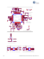
101
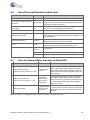
CY8CKIT-042 Schematics.......................................................................................101
Pin Assignment Table..............................................................................................104
Program and Debug Headers..................................................................................106
Use of Zero-ohm Resistors and No Load ................................................................107
Error in Firmware/Status Indication in Status LED ..................................................107
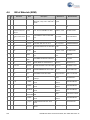
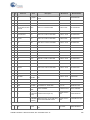
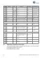
Bill of Materials (BOM).............................................................................................108
Regulatory Compliance Information ........................................................................110
CY8CKIT-042 PSoC 4 Pioneer Kit Guide, Doc. # 001-86371 Rev. *D
Safety Information
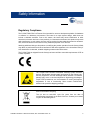
Regulatory Compliance
The CY8CKIT-042 PSoC® 4 Pioneer Kit is intended for use as a development platform for hardware
or software in a laboratory environment. The board is an open system design, which does not
include a shielded enclosure. Due to this reason, the board may cause interference to other
electrical or electronic devices in close proximity. In a domestic environment, this product may cause
radio interference. In such cases, the user may be required to take adequate preventive measures.
Also, this board should not be used near any medical equipment or RF devices.
Attaching additional wiring to this product or modifying the product operation from the factory default
may affect its performance and cause interference with other apparatus in the immediate vicinity. If
such interference is detected, suitable mitigating measures should be taken.
The CY8CKIT-042 as shipped from the factory has been verified to meet with requirements of CE as
a Class A product.
The CY8CKIT-042 contains electrostatic discharge (ESD) sensitive
devices. Electrostatic charges readily accumulate on the human body
and any equipment, and can discharge without detection. Permanent
damage may occur on devices subjected to high-energy discharges.
Proper ESD precautions are recommended to avoid performance
degradation or loss of functionality. Store unused CY8CKIT-042
boards in the protective shipping package.
End-of-Life/Product Recycling
This kit has an end-of-life cycle five years from the date of
manufacturing mentioned on the back of the box. Contact your nearest
recycler for discarding the kit.
CY8CKIT-042 PSoC 4 Pioneer Kit Guide, Doc. # 001-86371 Rev. *D
5
Safety Information
General Safety Instructions
ESD Protection
ESD can damage boards and associated components. Cypress recommends that the user perform
procedures only at an ESD workstation. If an ESD workstation is not available, use appropriate ESD
protection by wearing an antistatic wrist strap attached to the chassis ground (any unpainted metal
surface) on the board when handling parts.
Handling Boards
CY8CKIT-042 boards are sensitive to ESD. Hold the board only by its edges. After removing the
board from its box, place it on a grounded, static free surface. Use a conductive foam pad if
available. Do not slide board over any surface.
6
CY8CKIT-042 PSoC 4 Pioneer Kit Guide, Doc. # 001-86371 Rev. *D
1.
Introduction
Thank you for your interest in the PSoC® 4 Pioneer Kit. The kit is designed as an easy-to-use and
inexpensive development kit, showcasing the unique flexibility of the PSoC 4 architecture. Designed
for flexibility, this kit offers footprint-compatibility with several third-party Arduino™ shields. This kit
has a provision to populate an extra header to support Digilent® Pmod™ peripheral modules. In
addition, the board features a CapSense® slider, an RGB LED, a push button switch, an integrated
USB programmer, a program and debug header, and USB-UART/I2C bridges. This kit supports
either 5 V or 3.3 V as power supply voltages.
The PSoC 4 Pioneer Kit is based on the PSoC 4200 device family, delivering a programmable
platform for a wide range of embedded applications. The PSoC 4 is a scalable and reconfigurable
platform architecture for a family of mixed-signal programmable embedded system controllers with
an ARM® Cortex™-M0 CPU. It combines programmable and reconfigurable analog and digital
blocks with flexible automatic routing.
1.1
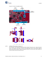
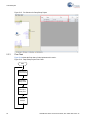
Kit Contents
The PSoC 4 Pioneer kit contains:
■
PSoC 4 Pioneer board
■
Quick start guide
■
USB standard A to mini-B cable
■
Jumper wires
CY8CKIT-042 PSoC 4 Pioneer Kit Guide, Doc. # 001-86371 Rev. *D
7
Introduction
Figure 1-1. Kit Contents
Inspect the contents of the kit; if you find any part missing, contact your nearest Cypress sales office
for help: www.cypress.com/go/support.
8
CY8CKIT-042 PSoC 4 Pioneer Kit Guide, Doc. # 001-86371 Rev. *D
Introduction
1.2
PSoC Creator™
PSoC Creator is a state-of-the-art, easy-to-use integrated design environment (IDE). It introduces
revolutionary hardware and software co-design, powered by a library of pre-verified and precharacterized PSoC Components™.
With PSoC Creator, you can:
■
Drag and drop PSoC components to build a schematic of your custom design
■
Automatically place and route components and configure GPIOs
■
Develop and debug firmware using the included component APIs
PSoC Creator also enables you to tap into an entire tools ecosystem with integrated compiler chains
and production programmers for PSoC devices.
For more information, visit www.cypress.com/Creator.
1.3
Getting Started
This guide helps you to get acquainted with the PSoC 4 Pioneer Kit. The Software Installation
chapter on page 11 describes the installation of the kit software. The Kit Operation chapter on
page 17 explains how to program the PSoC 4 with a programmer and debugger – either the onboard
PSoC 5LP or the external MiniProg3 (CY8CKIT-002). The Hardware chapter on page 27 details the
hardware operation. The Code Examples chapter on page 43 describes the code examples. The
Advanced Topics chapter on page 63 deals with topics such as building projects for PSoC 5LP, USBUART functionality, and USB-I2C functionality of PSoC 5LP. The Appendix on page 101 provides the
schematics, pin assignment, use of zero-ohm resistors, troubleshooting, and the bill of materials
(BOM).
1.4
Additional Learning Resources
Visit www.cypress.com/PSoC4 for additional learning resources in the form of datasheets, technical
reference manual, and application notes.
1.5
■
Beginner resources – PSoC Creator Training: www.cypress.com/go/creatorstart/creatortraining
■
Engineers looking for more – Visit www.cypress.com/appnotes to view a growing list of application notes for PSoC 3, PSoC 4, and PSoC 5LP.
■
Learning from peers – Cypress Developer Community Forums: www.cypress.com/forums
Technical Support
For assistance, go to our support web page, www.cypress.com/support, or contact our customer
support at +1 (800) 541-4736 Ext. 8 (in the USA) or +1 (408) 943-2600 Ext. 8 (International).
CY8CKIT-042 PSoC 4 Pioneer Kit Guide, Doc. # 001-86371 Rev. *D
9
Introduction
1.6
Document Revision History
Table 1-1. Revision History
Revision
1.7
Issue Date
Origin of
Change
Description of Change
**
04/23/2013
ANCY
Initial version of kit guide.
*A
04/25/2013
ANCY
Minor changes across the guide.
*B
05/23/2013
RKAD
Updated Figure 1-1 and minor changes across the guide.
Added PSoC 5LP Factory Program Restore Instructions on page 93.
*C
08/23/2013
SASH
Updated Figure 5-2 and Figure 5-3. Minor changes across the guide.
*D
11/26/2013
SASH
Updated PSoC Creator training web link.
Updated PSoC Creator images; added figure captions.
Modified the CapSense code example.
Documentation Conventions
Table 1-2. Document Conventions for Guides
Convention
10
Usage
Courier New
Displays file locations, user entered text, and source code:
C:\ ...cd\icc\
Italics
Displays file names and reference documentation:
Read about the sourcefile.hex file in the PSoC Designer User Guide.
[Bracketed, Bold]
Displays keyboard commands in procedures:
[Enter] or [Ctrl] [C]
File > Open
Represents menu paths:
File > Open > New Project
Bold
Displays commands, menu paths, and icon names in procedures:
Click the File icon and then click Open.
Times New Roman
Displays an equation:
2+2=4
Text in gray boxes
Describes cautions or unique functionality of the product.
CY8CKIT-042 PSoC 4 Pioneer Kit Guide, Doc. # 001-86371 Rev. *D
2.
2.1
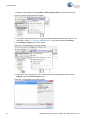
Software Installation
Install Kit Software
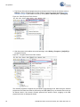
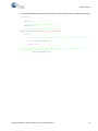
Follow these steps to install the PSoC 4 Pioneer Kit software:
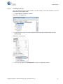
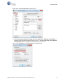
1. Download and install the PSoC 4 Pioneer Kit software from www.cypress.com/go/CY8CKIT-042.
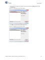
2. Select the folder to install the CY8CKIT-042 related files. Choose the directory and click Next.
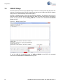
Figure 2-1. Installation Folder
CY8CKIT-042 PSoC 4 Pioneer Kit Guide, Doc. # 001-86371 Rev. *D
11
Software Installation
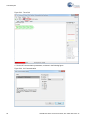
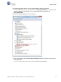
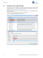
3. Select the installation type and click Next.
Figure 2-2. Installation Type Options
After the installation is complete, the kit contents are available at the following location:
<Install_Directory>:\CY8CKIT-042 PSoC 4 Pioneer Kit\<version>
Note For Windows 7 users, the installed files and the folder are read-only. To change the property,
right-click the folder and select Properties > Attributes; disable the Read-only radio button. Click
Apply and OK to close the window.
2.2
Install Hardware
There is no additional hardware installation required for this kit.
2.3
Install Software
When installing the PSoC 4 Pioneer Kit, the installer checks if the required software is installed in the
system. If the required applications are not installed, then the installer prompts you to download and
install them.
The following software is required:
12
■
PSoC Creator 3.0 or later: Download the latest software from www.cypress.com/go/Creator.
■
PSoC Programmer 3.19.1 or later: Download the latest software from
www.cypress.com/go/Programmer.
■
Code examples: After the kit installation is complete, the code examples are available in the kit
firmware folder. Download the CD ISO image or the setup files to install the kit from
www.cypress.com/go/CY8CKIT-042.
CY8CKIT-042 PSoC 4 Pioneer Kit Guide, Doc. # 001-86371 Rev. *D
Software Installation
2.4
Uninstall Software
The software can be uninstalled using one of the following methods:
2.5
■
Go to Start > All Programs > Cypress > Cypress Update Manager > Cypress Update Manager; select the Uninstall button.
■
Go to Start > Control Panel > Programs and Features; select the Uninstall/Change button.
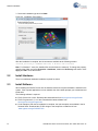
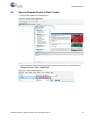
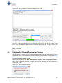
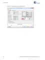
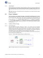
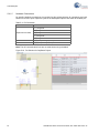
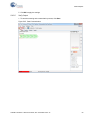
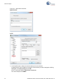
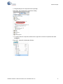
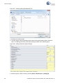
Develop Code Fast and Easy with Code Examples
PSoC Creator provides several example projects that make code development fast and easy. To
access these projects, click Find Example Project… under the Example and Kits section in the
Start Page of PSoC Creator or navigate to the Creator tool bar and select File > Example Project.
Figure 2-3. Find Example Project
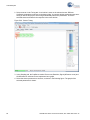
The Find Example Project section has various filters that help to locate the most relevant project.
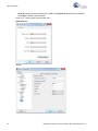
PSoC Creator also provides several starter designs for each device family. These designs highlight
features that are unique to each PSoC family. They provide users with a starting place instead of
creating a new empty design. These starter projects come loaded with various pre-selected components. To use a starter design, navigate to File > New > Project and select the design required.
CY8CKIT-042 PSoC 4 Pioneer Kit Guide, Doc. # 001-86371 Rev. *D
13
Software Installation
Figure 2-4. Starter Designs
In addition to the example projects and starter designs that are available within PSoC Creator,
Cypress continuously strives to provide the best support. Click here to view a growing list of application notes for PSoC 3, PSoC 4, and PSoC 5LP.
14
CY8CKIT-042 PSoC 4 Pioneer Kit Guide, Doc. # 001-86371 Rev. *D
Software Installation
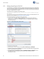
2.6
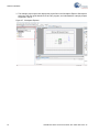
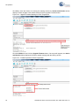
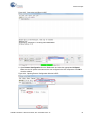
Open an Example Project in PSoC Creator
1. Launch PSoC Creator from the Start menu.
Figure 2-5. PSoC Creator Start Page
2. Open the example project from the Start Page by clicking <Project.cywrk> present below the
Examples and Kits > Kits > CY8CKIT-042.
Figure 2-6. Open Example Project
CY8CKIT-042 PSoC 4 Pioneer Kit Guide, Doc. # 001-86371 Rev. *D
15
Software Installation
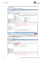
3. The example project opens and displays the project files in the Workspace Explorer. Subsequent
sections of this user guide describe how to build, program, and understand the example projects
supported in this kit.
Figure 2-7. Workspace Explorer
16
CY8CKIT-042 PSoC 4 Pioneer Kit Guide, Doc. # 001-86371 Rev. *D
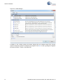
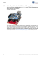
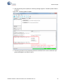
3.
Kit Operation
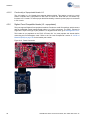
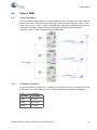
The PSoC 4 Pioneer Kit can be used to develop applications using the PSoC 4 family of devices and
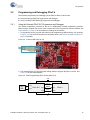
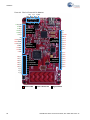
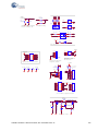
the Arduino shields and Digilent Pmod daughter cards. Figure 3-1 is an image of the PSoC 4
Pioneer board with a markup of the onboard components.
Figure 3-1. PSoC 4 Pioneer Board
Programmer Status LED
System Power Arduino
Supply Jumper Compatible (J9)
I/O Header (J3)
PSoC 4 Arduino
Compatible Power Supply RGB I/O Header (J4) Jumper (J13) LED
Arduino Compatible ICSP
I/O Header (J12)
10‐Pin SWD Debug and Programming Header (J7) for PSoC 5LP
USB Connector (J10)
Power LED
VIN (J11)
CapSense
Slider
PSoC 4 Additional Program Header (J6)
PSoC 5LP I/O Header (J8)
PSoC 4 Reset Button
Digilent Pmod Compatible I/O Header (J5)
Arduino PSoC 5LP
PSoC 4
Programmer Compatible 44 TQFP
I/O Header and (J1)
Debugger
CY8CKIT-042 PSoC 4 Pioneer Kit Guide, Doc. # 001-86371 Rev. *D
Arduino
Compatible I/O Header (J2)
User Button
17
Kit Operation
3.1
Pioneer Kit USB Connection
The PSoC 4 Pioneer Kit connects to the PC over a USB interface. The kit enumerates as a
composite device and three separate devices appear under the Device Manager window in the
Windows operating system.
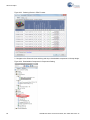
Table 3-1. PSoC 4 Pioneer Kit in Device Manager after Enumeration
Port
Description
USB Input Device
USB-I2C bridge
KitProg
Programmer and debugger
KitProg USB-UART
USB-UART bridge will appear as a COM# port
Figure 3-2. KitProg Driver Installation
Figure 3-3. KitProg Driver Installation
18
CY8CKIT-042 PSoC 4 Pioneer Kit Guide, Doc. # 001-86371 Rev. *D
Kit Operation
3.2
Programming and Debugging PSoC 4
The kit allows programming and debugging of the PSoC 4 device in two modes:
3.2.1
■
Using the onboard PSoC 5LP programmer and debugger
■
Using a CY8CKIT-002 MiniProg3 programmer and debugger
Using the Onboard PSoC 5LP Programmer and Debugger
The default programming interface for the kit is a USB-based, onboard programming interface.
Before trying to program the device, PSoC Creator and PSoC Programmer must be installed. See
Install Software on page 12 for information on installing the kit software.
1. To program the device, plug the USB cable into the programming USB connector J10, as shown
in Figure 3-4. The kit will enumerate as a composite device. See Pioneer Kit USB Connection on
page 18 for details.
Figure 3-4. Connect USB Cable to J10
2. The onboard PSoC 5LP uses serial wire debug (SWD) to program the PSoC 4 device. See
Figure 3-5 for this implementation.
Figure 3-5. SWD Programming PSoC 4 Using PSoC 5LP
VDD
Mini
USB
D+
D-
P15[6]
P15[7]
PSoC 5LP
P2[1]
SWDCLK
P2[0]
SWDIO
P2[4]
Reset
CY8CKIT-042 PSoC 4 Pioneer Kit Guide, Doc. # 001-86371 Rev. *D
P3[2]
P3[3]
PSoC 4
XRES
19
Kit Operation
3. The Pioneer Kit’s onboard programmer will enumerate on the PC and in the software tools as
KitProg. Load an example project in PSoC Creator (such as the project described in Install
Software on page 12) and initiate the build by clicking Build > Build Project or [Shift]+[F6].
Figure 3-6. Build Project in PSoC Creator
4. After the project is built without errors and warnings, select Debug > Program or [Ctrl]+[F5] to
program the device.
Figure 3-7. Program Device from PSoC Creator
The onboard programmer supports only the RESET programming mode. When using the onboard
programmer, the board can either be powered by the USB (VBUS) or by an external source such as
an Arduino shield. If the board is already powered from another source, plugging in the USB
programmer does not damage the board.
20
CY8CKIT-042 PSoC 4 Pioneer Kit Guide, Doc. # 001-86371 Rev. *D
Kit Operation
3.2.2
Using CY8CKIT-002 MiniProg3 Programmer and Debugger
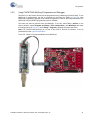
The PSoC 4 on the Pioneer Kit can also be programmed using a MiniProg3 (CY8CKIT-002). To use
MiniProg3 for programming, use the J6 connector on the board, as shown in Figure 3-8. With
MiniProg3, programming is similar to the onboard programmer; however, the setup enumerates as a
MiniProg3. Only the RESET programming mode is available.
The board can also be powered from the MiniProg3. To do this, select Tool > Options. In the
Options window, expand Program and Debug > Port Configuration; click MiniProg3 and select
the settings shown in Figure 3-9. Click Debug > Program to program and power the board.
Note The CY8CKIT-002 MiniProg3 is not part of the PSoC 4 Pioneer Kit contents. It can be
purchased from the Cypress Online Store.
Figure 3-8. PSoC 4 Programming/Debug Using MiniProg3
CY8CKIT-042 PSoC 4 Pioneer Kit Guide, Doc. # 001-86371 Rev. *D
21
Kit Operation
Figure 3-9. MiniProg3 Configuration
3.3
USB-UART Bridge
The onboard PSoC 5LP can also act as a USB-UART bridge to transfer and receive data from the
PSoC 4 device to the PC via the COM terminal software. When the USB mini-B cable is connected
to J10 of the PSoC 4 Pioneer Kit, a device named KitProg USBUART is available under Ports
(COM & LPT) in the device manager. For more details about the USB-UART functionality, see Using
PSoC 5LP as USB-UART Bridge on page 63.
To use the USB-UART functionality in the COM terminal software, select the corresponding COM
port as the communication port for transferring data to and from the COM terminal software.
The UART lines from PSoC 5LP are brought to the P12[6] (J8_9) and P12[7] (J8_10) pins of header
J8. This interface can be used to send or receive data from any PSoC 4 design that has a UART by
connecting the pins on header J8 to the RX and TX pins assigned in PSoC 4. The UART can be
used as an additional interface to debug designs. This bridge can also be used to interface with
other external UART-based devices. Figure 3-10 shows the connection between the RX and TX
lines of the PSoC 5LP and PSoC 4. In this example, the PSoC 4 UART has been routed to the J3
header; the user must connect the wires between the PSoC 5LP RX and TX lines available on
header J8.
22
CY8CKIT-042 PSoC 4 Pioneer Kit Guide, Doc. # 001-86371 Rev. *D
Kit Operation
Figure 3-10. Example RX and TX Line Connection of PSoC 5LP and PSoC 4
Table 3-2 lists the specifications supported by the USB-UART bridge.
Table 3-2. Specifications Supported by USB-UART Bridge
Parameter
Baud Rate
Supported Values
1200, 2400, 4800, 9600, 19200, 38400, 57600, and 115200
Data Bits
8
Parity
None
Stop Bits
1
Flow Control
None
File transfer protocols
supported
Xmodem, 1K Xmodem, Ymodem, Kermit, and Zmodem (only speeds greater
than 2400 baud).
CY8CKIT-042 PSoC 4 Pioneer Kit Guide, Doc. # 001-86371 Rev. *D
23
Kit Operation
3.4
USB-I2C Bridge
The PSoC 5LP also functions as a USB-I2C bridge. The PSoC 4 communicates with the PSoC 5LP
using an I2C interface and the PSoC 5LP transfers the data over the USB to the USB-I2C software
utility on the PC, called the Bridge Control Panel (BCP).
The BCP is available as part of the PSoC Programmer installation. This software can be used to
send and receive USB-I2C data from the PSoC 5LP. When the USB mini-B cable is connected to
header J10 on the Pioneer Kit, the KitProg USB-I2C is available under Connected I2C/SPI/RX8
Ports in the BCP.
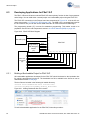
Figure 3-11. Bridge Control Panel
To use the USB_I2C functionality, select the KitProg USB-I2C in the BCP. On successful
connection, the Connected and Powered tabs turn green.
24
CY8CKIT-042 PSoC 4 Pioneer Kit Guide, Doc. # 001-86371 Rev. *D
Kit Operation
Figure 3-12. KitProg USB-I2C Connected in Bridge Control Panel
USB-I2C is implemented using the USB and I2C components of PSoC 5LP. The SCL (P12_0) and
SDA (P12_1) lines from the PSoC 5LP are connected to SCL (P3_0) and SDA (P3_1) lines of the
PSoC 4 I2C. The USB-I2C bridge currently supports I2C speed of 50 kHz, 100 kHz, 400 kHz, and
1 MHz.
Refer to Using PSoC 5LP as USB-I2C Bridge on page 76 for building a project, which uses USB-I2C
Bridge functionality.
3.5
Updating the Onboard Programmer Firmware
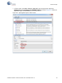
The firmware of the onboard programmer and debugger, PSoC 5LP, can be updated from PSoC
Programmer. When a new firmware is available or when the KitProg firmware is corrupt (see Error in
Firmware/Status Indication in Status LED on page 107), PSoC Programmer displays a warning
indicating that new firmware is available.
Open PSoC Programmer from Start > All Programs > Cypress > PSoC Programmer<version>.
When PSoC Programmer opens, a WARNING! window pops up saying that the programmer is
currently out of date.
Figure 3-13. Firmware Update Warning
CY8CKIT-042 PSoC 4 Pioneer Kit Guide, Doc. # 001-86371 Rev. *D
25
Kit Operation
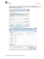
Click OK to close the window. On closing the warning window, the Action and Results window
displays “Please navigate to the Utilities tab and click the Upgrade Firmware button”.
Figure 3-14. Upgrade Firmware Message in PSoC Programmer
Click the Utilities tab and click the Upgrade Firmware button. On successful upgrade, the Action
and Results window displays the firmware update message with the KitProg version.
Figure 3-15. Firmware Updated in PSoC Programmer
26
CY8CKIT-042 PSoC 4 Pioneer Kit Guide, Doc. # 001-86371 Rev. *D
4.
4.1
Hardware
Board Details
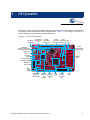
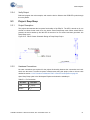
The PSoC 4 Pioneer Kit consists of the following blocks:
■
PSoC 4
■
PSoC 5LP
■
Power supply system
■
Programming interfaces (J6, J7 - unpopulated, J10)
■
Arduino compatible headers (J1, J2, J3, J4, and J12 - unpopulated)
■
Digilent Pmod compatible header (J5 - unpopulated)
■
PSoC 5LP GPIO header (J8)
■
CapSense slider
■
Pioneer board LEDs
■
Push buttons (Reset and User buttons)
Figure 4-1. PSoC 4 Pioneer Kit Details
Programmer Status LED
System Power Arduino Supply Jumper Compatible (J9)
I/O Header (J3)
PSoC 4 Arduino Compatible Power Supply RGB I/O Header (J4) Jumper (J13) LED
Arduino Compatible ICSP
I/O Header (J12)
10‐Pin SWD Debug and Programming Header (J7) for PSoC 5LP
USB Connector (J10)
Power LED
VIN (J11)
CapSense
Slider
PSoC 4 Additional Program Header (J6)
PSoC 5LP I/O Header (J8)
PSoC 4 Reset Button
Digilent Pmod Compatible I/O Header (J5)
Arduino PSoC 5LP
PSoC 4
Programmer Compatible 44 TQFP
I/O Header and (J1)
Debugger
CY8CKIT-042 PSoC 4 Pioneer Kit Guide, Doc. # 001-86371 Rev. *D
Arduino Compatible I/O Header (J2)
User Button
27
Hardware
Figure 4-2. PSoC 4 Pioneer Kit Pin Mapping
P12_6 P3_4
P5_VDD
P3_6
P0_0
GND
PSoC 5LP
I/O Header (J8)
P3_0
P3_7
P12_7
P0_1
P1_2
P3_5
VCC/P4_VDD
GND/GND
SCK/P0_6
MISO/P3_1
MOSI/P3_0
Digilent Pmod
Compatible
I/O Header (J5)
P4_0
P4_1
SS/P3_5
P1_7/AREF
GND/GND
NC
Arduino
Compatible
I/O Header (J3)
OREF/P4_VDD
RESET/RESET
3.3V/V3.3_EXT
5V/VBUS
Arduino
Compatible
I/O Header (J1)
P0_6/D13
P3_1/D12
P3_0/D11
P3_4/D10
P3_6/D9
GND/GND
P2_6/D8
GND/GND
Vin/VIN
P2_7/D7
P1_0/D6
A0/P2_0
P0_2
A1/P2_1
P0_3
A2/P2_2
VDD
A3/P2_3
P1_5
A4/P2_4
P1_4
A5/P2_5
P1_3
P0_0
GND
P0_1
P1_2
P1_0
P1_1
P3_5/D5
Arduino
Compatible
I/O Header (J2)
Arduino UNO
28
Arduino
Compatible
I/O Header (J4)
P0_0/D4
P3_7/D3
P0_7/D2
P0_5/D1
P0_4/D0
PSoC 4 Pioneer Kit
Digilent Pmod
CY8CKIT-042 PSoC 4 Pioneer Kit Guide, Doc. # 001-86371 Rev. *D
Hardware
4.2
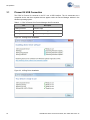
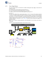
Theory of Operation
This section provides the block-level description of the PSoC 4 Pioneer Kit.
Figure 4-3. Block Diagram
The PSoC 4 is a new generation of programmable system-on-chip devices from Cypress for
embedded applications. It combines programmable analog, programmable digital logic,
programmable I/O, and a high-performance ARM Cortex-M0 subsystem. With the PSoC 4, you can
create the combination of peripherals required to meet the application specifications.
The PSoC 4 Pioneer Kit features an onboard PSoC 5LP, which communicates through the USB to
program and debug the PSoC 4 using serial wire debug (SWD). The PSoC 5LP also functions as a
USB-I2C bridge and USB-UART bridge.
The Pioneer Kit has an RGB LED, a status LED, and a power LED. The RGB LED is connected to
the PSoC 4 and the status LED is connected to the PSoC 5LP. For more information on the status
LED, see section A.5 Error in Firmware/Status Indication in Status LED on page 107. This kit also
includes a reset button that connects to the PSoC 4 XRES, a user button, and a five-segment
CapSense slider, which can be used to develop touch-based applications. The PSoC 4 pins are
brought out onto headers J1 to J4 on the kit to support Arduino shields. The PSoC 5LP pins are
brought out onto header J8 to enable using the onboard PSoC 5LP to develop custom applications.
The PSoC 4 Pioneer Kit can be powered from the USB Mini B, the Arduino compatible header, or an
external power supply. The input voltage is regulated by a low drop-out (LDO) regulator to 3.3 V. You
can select between VBUS (5 V) and 3.3 V by suitably plugging the jumper onto the voltage selection
header VDD.
CY8CKIT-042 PSoC 4 Pioneer Kit Guide, Doc. # 001-86371 Rev. *D
29
Hardware
4.3
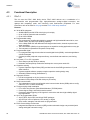
Functional Description
4.3.1
PSoC 4
This kit uses the PSoC 4200 family device. PSoC 4200 devices are a combination of a
microcontroller with programmable logic, high-performance analog-to-digital conversion, two
opamps with comparator mode, and commonly used fixed-function peripherals. For more
information, refer to the PSoC 4 web page and the PSoC 4200 family datasheet.
Features
■
■
■
■
■
■
■
■
■
■
30
32-bit MCU subsystem
❐ 48 MHz ARM Cortex-M0 CPU with single cycle multiply
❐ Up to 32 KB of flash with read accelerator
❐ Up to 4 KB of SRAM
Programmable analog
❐ Two opamps with reconfigurable high-drive external and high-bandwidth internal drive, comparator modes, and ADC input buffering capability
❐ 12-bit 1-Msps SAR ADC with differential and single-ended modes; channel sequencer with
signal averaging
❐ Two current DACs (IDACs) for general-purpose or capacitive sensing applications on any pin
❐ Two low-power comparators that operate in deep sleep
Programmable digital
❐ Four programmable logic blocks called universal digital blocks (UDBs), each with eight Macrocells and data path
❐ Cypress-provided peripheral component library, user-defined state machines, and Verilog
input
Low power 1.71 to 5.5 V operation
❐ 20-nA Stop mode with GPIO pin wakeup
❐ Hibernate and Deep-Sleep modes allow wakeup-time versus power trade-offs
Capacitive sensing
❐ Cypress Capacitive Sigma-Delta (CSD) provides best-in-class SNR (greater than 5:1) and
water tolerance
❐ Cypress-supplied software component makes capacitive sensing design easy
❐ Automatic hardware tuning (SmartSense™)
Segment LCD drive
❐ LCD drive supported on all pins (common or segment)
❐ Operates in Deep-Sleep mode with 4 bits per pin memory
Serial communication
❐ Two independent run-time reconfigurable serial communication blocks (SCBs) with re-configurable I2C, SPI, or UART functionality
Timing and pulse-width modulation
❐ Four 16-bit Timer/Counter Pulse-Width Modulator (TCPWM) blocks
❐ Center-aligned, Edge, and Pseudo-random modes
❐ Comparator-based triggering of Kill signals for motor drive and other high-reliability digital
logic applications
Up to 36 programmable GPIOs
❐ 44-pin TQFP, 40-pin QFN, and 28-pin SSOP packages
❐ Any GPIO pin can be Capsense, LCD, analog, or digital
❐ Drive modes, strengths, and slew rates are programmable
PSoC Creator design environment
❐ Integrated development environment (IDE) provides schematic design entry and build (with
analog and digital automatic routing)
CY8CKIT-042 PSoC 4 Pioneer Kit Guide, Doc. # 001-86371 Rev. *D
Hardware
Applications Programming Interface (API) component for all fixed-function and programmable
peripherals
Industry-standard tool compatibility
❐ After schematic entry, development can be done with ARM-based industry-standard development tools
❐
■
For more information see the CY8C42 family datasheet.
4.3.2
PSoC 5LP
An onboard PSoC 5LP is used to program and debug PSoC 4. The PSoC 5LP connects to the USB
port of the PC through a USB Mini B connector and to the SWD interface of the PSoC 4 device.
PSoC 5LP is a true system-level solution providing MCU, memory, analog, and digital peripheral
functions in a single chip. The CY8C58LPxx family offers a modern method of signal acquisition,
signal processing, and control with high accuracy, high bandwidth, and high flexibility. Analog
capability spans the range from thermocouples (near DC voltages) to ultrasonic signals. For more
information, refer to the PSoC 5LP web page.
Features
■
■
■
■
32-bit ARM Cortex-M3 CPU core
❐ DC to 67-MHz operation
❐ Flash program memory, up to 256 KB, 100,000 write cycles, 20-year retention, and multiple
security features
❐ Up to 32-KB flash error correcting code (ECC) or configuration storage
❐ Up to 64 KB SRAM
❐ 2-KB electrically erasable programmable read-only memory (EEPROM) memory, 1 M cycles,
and 20 years retention
❐ 24-channel direct memory access (DMA) with multilayer AHB bus access
a.Programmable chained descriptors and priorities
b.High bandwidth 32-bit transfer support
Low voltage, ultra low power
❐ Wide operating voltage range: 0.5 V to 5.5 V
❐ High-efficiency boost regulator from 0.5 V input to 1.8 V to 5.0 V output
❐ 3.1 mA at 6 MHz
❐ Low power modes including:
a.2-µA sleep mode with real time clock (RTC) and low-voltage detect (LVD) interrupt
b.300-nA hibernate mode with RAM retention
Versatile I/O system
❐ 28 to 72 I/Os (62 GPIOs, 8 SIOs, 2 USBIOs)
❐ Any GPIO to any digital or analog peripheral routability
❐ LCD direct drive from any GPIO, up to 46×16 segments
❐ CapSense support from any GPIO[3]
❐ 1.2 V to 5.5 V I/O interface voltages, up to 4 domains
❐ Maskable, independent IRQ on any pin or port
❐ Schmitt-trigger transistor-transistor logic (TTL) inputs
❐ All GPIOs configurable as open drain high/low, pull-up/pull-down, High-Z, or strong output
❐ Configurable GPIO pin state at power-on reset (POR)
❐ 25 mA sink on SIO
Digital peripherals
❐ 20 to 24 programmable logic device (PLD) based universal digital blocks (UDBs)
❐ Full CAN 2.0b 16 RX, 8 TX buffers
❐ Full-Speed (FS) USB 2.0 12 Mbps using internal oscillator
CY8CKIT-042 PSoC 4 Pioneer Kit Guide, Doc. # 001-86371 Rev. *D
31
Hardware
Four 16-bit configurable timers, counters, and PWM blocks
❐ 67-MHz, 24-bit fixed point digital filter block (DFB) to implement finite impulse response (FIR)
and infinite impulse response (IIR) filters
❐ Library of standard peripherals
a.8-, 16-, 24-, and 32-bit timers, counters, and PWMs
b.Serial peripheral interface (SPI), universal asynchronous transmitter receiver (UART), and
I2C
c.Many others available in catalog
❐ Library of advanced peripherals
a.Cyclic redundancy check (CRC)
b.Pseudo random sequence (PRS) generator
c.Local interconnect network (LIN) bus 2.0
d.Quadrature decoder
❐ Analog peripherals (1.71 V VDDA 5.5 V)
❐ 1.024 V ±0.1% internal voltage reference across –40 °C to +85 °C
❐ Configurable delta-sigma ADC with 8- to 20-bit resolution
❐ Sample rates up to 192 ksps
❐ Programmable gain stage: ×0.25 to ×16
❐ 12-bit mode, 192 ksps, 66-dB signal to noise and distortion ratio (SINAD), ±1-bit INL/DNL
❐ 16-bit mode, 48 ksps, 84-dB SINAD, ±2-bit INL, ±1-bit DNL
❐ Up to two SAR ADCs, each 12-bit at 1 Msps
❐ Four 8-bit 8 Msps current IDACs or 1-Msps voltage VDACs
❐ Four comparators with 95-ns response time
❐ Four uncommitted opamps with 25-mA drive capability
❐ Four configurable multifunction analog blocks. Example configurations are programmable
gain amplifier (PGA), transimpedance amplifier (TIA), mixer, and sample and hold
❐ CapSense support
Programming, debug, and trace
❐ JTAG (4 wire), SWD (2 wire), single wire viewer (SWV), and TRACEPORT interfaces
❐ Cortex-M3 flash patch and breakpoint (FPB) block
❐ Cortex-M3 Embedded Trace Macrocell™ (ETM™) generates an instruction trace stream
❐ Cortex-M3 data watchpoint and trace (DWT) generates data trace information
❐ Cortex-M3 Instrumentation Trace Macrocell (ITM) can be used for printf-style debugging
❐ DWT, ETM, and ITM blocks communicate with off-chip debug and trace systems via the SWV
or TRACEPORT
❐ Bootloader programming supportable through I2C, SPI, UART, USB, and other interfaces
Precision, programmable clocking
❐ 3- to 62-MHz internal oscillator over full temperature and voltage range
❐ 4- to 25-MHz crystal oscillator for crystal PPM accuracy
❐ Internal PLL clock generation up to 67 MHz
❐ 32.768-kHz watch crystal oscillator
❐ Low-power internal oscillator at 1, 33, and 100 kHz
❐
■
■
For more, see the CY8C58LPxx family datasheet.
32
CY8CKIT-042 PSoC 4 Pioneer Kit Guide, Doc. # 001-86371 Rev. *D
Hardware
4.3.3
Power Supply System
The power supply system on this board is versatile, allowing the input supply to come from the
following sources:
■
5-V power from onboard USB programming header J10
■
5-V to 12-V power from Arduino shield using J1_01 header
■
VTARG - power from the onboard SWD programming using J6 or J7
■
VIN - J11
The PSoC 4 and PSoC 5LP are powered with either a 3.3 V or 5 V source. The selection between
3.3 V and 5 V is made through the J9 jumper. The board can supply 3.3 V and 5 V to the I/O headers
and receive 3.3 V from the I/O headers. The board can also be powered with an external power
supply through the VIN (J11) header; the allowed voltage range for the VIN is 5 V to 12 V. The LDO
regulator regulates the VIN down to 3.3 V. Figure 4-4 shows the power supply block diagram and
protection circuitry.
Note: The 5-V domain is directly powered by the USB (VBUS). For this reason, this domain is
unregulated.
Figure 4-4. Power Supply Block Diagram with Protection Circuits
I/O Header
5V
3.3V
Vin
MOSFET based Protection Ckt
D4
D1
PSoC 4
USB
LDO
USB
5V
D2
D3
J9
PSoC 5LP
PTC
ESD
Protection
P4 10pin
Debug
P5LP 10pin
Debug
CY8CKIT-042 PSoC 4 Pioneer Kit Guide, Doc. # 001-86371 Rev. *D
P5LP I/O
Header
33
Hardware
4.3.3.1
Protection Circuit
The power supply rail has reverse-voltage, over-voltage, short circuits, and excess current protection
features, as seen in Figure 4-4.
4.3.3.2
■
The Schottky diode (D1) ensures power cannot be supplied to the 5-V domain of the board from
the I/O header.
■
The series protection diode (D2) ensures VIN (power supply from the I/O header) does not back
power the USB.
■
The Schottky diode (D3) ensures 3.3 V from I/O header does not back power the LDO.
■
The series protection diode (D4) ensures that the reverse-voltage cannot be supplied from the
VIN to the regulator input.
■
A PTC resettable fuse is connected to protect the computer's USB ports from shorts and overcurrent.
■
The MOSFET-based protection circuit provides over-voltage and reverse-voltage protection to
the 3.3-V rail. The PMOS Q1 protects the board components from a reverse-voltage condition.
The PMOS Q2 protects the PSoC from an over-voltage condition. The PMOS Q2 will turn off
when a voltage greater than 4.2 V is applied, protecting the PSoC 4.
■
The output voltage of the LDO is adjusted such that it takes into account the voltage drop across
the Schottky diode and provides 3.3 V.
Procedure to Measure PSoC 4 Current Consumption
The following three methods are supported for measuring current consumption of the PSoC 4
device.
■
When the board is powered through the USB port (J10), remove jumper J13 and connect an
ammeter, as shown in Figure 4-5.
Figure 4-5. PSoC 4 Current Measurement when Powered from USB Port
■
When using a separate power supply for the PSoC 4 with USB powering (regulator output on the
USB supply must be within 0.5 V of the separate power supply).
❐
34
Remove jumper J13. Connect the positive terminal of voltage supply to the positive terminal of
the ammeter and the negative terminal of the ammeter to the lower pin of J13. Figure 4-6
shows the required connections.
CY8CKIT-042 PSoC 4 Pioneer Kit Guide, Doc. # 001-86371 Rev. *D
Hardware
Figure 4-6. PSoC 4 Current Measurement when Powered Separately
VOLTAGE
SOURCE
■
When the PSoC 4 is powered separately and the PSoC 5LP is not powered, make these changes
to avoid leakage while measuring current:
❐
Remove the zero-ohm resistors R24 and R25. Removing these resistors will affect the USBI2C functionality.
❐
Remove R11, R15, and R16, which are meant for programming the PSoC 4. Removing these
resistors disables the PSoC 5LP capability for programming.
❐
Connect an ammeter between pins 1 and 2 of header J13 to measure current.
Figure 4-7. Zero-ohm Resistor Position
4.3.4
Programming Interface
The kit allows programming and debugging of the PSoC 4 in two modes:
■
Using the Onboard PSoC 5LP Programmer and Debugger
■
Using CY8CKIT-002 MiniProg3 Programmer and Debugger
CY8CKIT-042 PSoC 4 Pioneer Kit Guide, Doc. # 001-86371 Rev. *D
35
Hardware
4.3.5
Arduino Compatible Headers (J1, J2, J3, J4, and J12 - unpopulated)
This kit has five Arduino compatible headers; J1, J2, J3, J4 and J12. You can develop applications
based on the Arduino shield’s hardware.
Figure 4-8. Arduino Header
The J1 header contains I/O pins for reset, internal reference voltage (IOREF), and power supply line.
The J2 header is an analog port. It contains I/O pins for SAR ADC, comparator, and opamp. The J3
header is primarily a digital port. It contains I/O pins for PWM, I2C, SPI, and analog reference. The
J4 header is also a digital port. It contains I/O pins for UART and PWM. The J12 header is an
Arduino ICSP compatible header for the SPI interface. This header is not populated. Refer to the “No
Load Components” section of A.6 Bill of Materials (BOM) on page 108 for the header part number.
36
CY8CKIT-042 PSoC 4 Pioneer Kit Guide, Doc. # 001-86371 Rev. *D
Hardware
Figure 4-9. Arduino Compatible Headers
Arduino
Compatible
I/O Header (J4)
Arduino
Compatible
I/O Header (J3)
Arduino
Compatible ICSP
I/O Header (J12)
Arduino
Compatible
I/O Header (J2)
Arduino
Compatible
I/O Header (J1)
P4_VDD
0603
R8
2.2K
I2C Pull up
R9
2.2K Resistors
0603
TVS4
18V 350W BI
J3
VBUS
VIN
P4_0
P4_1
J1
1
2
3
4
5
6
7
8
D4
SOD123
V3.3_EXT
/XRES
IOREF
P4_VDD
10
9
8
7
6
5
4
3
2
1
P1_7
P0_6
P3_1
P3_0
P3_4
P3_6
P2_6
8x1 RECP
10X1 RECP
J2
P2_0
P2_1
P2_2
P2_3
P2_4
P2_5
P0_0
P0_1
P1_0
1
3
5
7
9
11
13
15
17
2
4
6
8
10
12
14
16
18
P0_2
P0_3
P1_5
P1_4
P1_3
P1_2
P1_1
P4_VDD
J4
P0_4
P0_5
P0_7
P3_7
P0_0
P3_5
P1_0
P2_7
9x2 RECP
1
2
3
4
5
6
7
8
P4_VDD
J12
P3_1
P0_6
/XRES
1
3
5
2
4
6
P3_0
3x2 RECPT
NO LOAD
8x1 RECP
(J1-J4) Arduino Compatible Headers
4.3.5.1
Additional Functionality of Header J2
The J2 header is a 9×2 header that supports Arduino shields. The port 0, port 1, and port 2 pins of
PSoC 4 are brought to this header. The port 1 pins additionally connect to the onboard CapSense
slider through 560- resistors. When the CapSense feature is not used, remove these resistors to
ensure a better performance with these pins.
CY8CKIT-042 PSoC 4 Pioneer Kit Guide, Doc. # 001-86371 Rev. *D
37
Hardware
4.3.5.2
Functionality of Unpopulated Header J12
The J12 header is a 2×3 header that supports Arduino shields. This header is used on a small
subset of shields and is unpopulated on the PSoC 4 Pioneer Kit. Note that the J12 header only
functions in 5.0 V mode. To ensure proper shield functionality, ensure the power jumper is connected
in 5.0 V mode.
4.3.6
Digilent Pmod Compatible Header (J5 - unpopulated)
This port supports Digilent Pmod peripheral modules. Pmods are small I/O interfaces, which connect
with the embedded control boards through either 6- or 12-pin connectors. The PSoC Pioneer Kit
supports the 6-pin Pmod type 2 (SPI) interface. For Digilent Pmod cards, go to www.digilentinc.com.
This header is not populated on the PSoC 4 Pioneer Kit. You must populate this header before
connecting the Pmod daughter cards. Refer to the “No Load Components” section of A.6 Bill of
Materials (BOM) on page 108 for the header part number.
Figure 4-10. Pmod Connection
38
CY8CKIT-042 PSoC 4 Pioneer Kit Guide, Doc. # 001-86371 Rev. *D
Hardware
Figure 4-11. Digilent Pmod Interface
J5
P4_VDD
P3_5
P3_0
P3_1
P0_6
1
2
3
4
5
6
6X1 CONN FEMALE
NO LOAD
J5 Digilent PMOD Cards
Compatible Headers
See A.2 Pin Assignment Table on page 104 for details on the pin descriptions for the J5 header.
4.3.7
PSoC 5LP GPIO Header (J8)
A limited set of PSoC 5LP pins are brought to this header. Refer to 6.3 Developing Applications for
PSoC 5LP on page 84 for details on how to develop custom applications. See A.2 Pin Assignment
Table on page 104 for pin details.
Figure 4-12. PSoC 5LP GPIO Header (J8)
P5LP_VDD
J8
P5LP0_0
P5LP3_4
P5LP3_6
P5LP12_6
1
3
5
7
9
11
2
4
6
8
10
12
P5LP1_2
P5LP0_1
P5LP3_5
P5LP3_7
P5LP12_7
P5LP3_0
6x2 RECPT
PSoC 5LP GPIO Extension Header
CY8CKIT-042 PSoC 4 Pioneer Kit Guide, Doc. # 001-86371 Rev. *D
39
Hardware
4.3.8
CapSense Slider
The kit has a five-segment linear capacitive touch slider on the board, which is connected to pins
P1[1] to P1[5] of the PSoC 4 device.
The modulation capacitor (Cmod) is connected to pin P4[2] and an optional bleeder resistor (R1) can
be connected across the Cmod. This board supports CapSense designs that enable waterproofing.
The waterproofing design uses a concept called shield, which is a conductor placed around the
sensors. This shield must be connected to a designated shield pin on the device to function. The
shield must be connected to the ground when not used. On the PSoC 4 Pioneer Kit, the connection
of the shield to the pin or to the ground is made by resistors R44 and R45, respectively. By default,
R45 is mounted on the board, which connects the shield to the ground. Populate R44 when
evaluating waterproofing designs, which will connect the shield to the designated pin, P0[1]. This
shield is different from the Arduino shields, which are boards that connect over the Arduino header.
Refer to the CapSense Design Guide for further details related to CapSense.
Figure 4-13. CapSense Slider
P1_5
P1_4
P1_3
P1_2
P1_1
Figure 4-14. CapSense Slider Connection
Shunt
Resistor
NO LOAD
P4_2
R44 ZERO
P0_1
Shield
0603
1
560 ohm
2
560 ohm
3
560 ohm
4
560 ohm
5
560 ohm
R17 R18 R19 R20 R21
R1
NO LOAD
C1
2200 pF
R45 ZERO
CSS1
0603
CapSense Slider 5 Seg
40
CAPSENSE TUNING CIRCUITRY
Default Loaded For CSD
Shield Setting
CY8CKIT-042 PSoC 4 Pioneer Kit Guide, Doc. # 001-86371 Rev. *D
Hardware
4.3.9
Pioneer Board LEDs
The PSoC 4 Pioneer board has three LEDs. A green LED (D10) indicates the status of the
programmer. See A.5 Error in Firmware/Status Indication in Status LED for a detailed list of LED
indications. An amber LED (D3) indicates status of power supplied to the board. The kit also has a
general-purpose tricolor LED (D9) for user applications that connect to specific PSoC 4 pins.
Figure 4-15 shows the indication of all these LEDs on the board. Figure 4-16 and Figure 4-17 detail
the LED schematic.
Figure 4-15. Pioneer Kit LEDs
Figure 4-16. Status LED and Power LED
P5LP_VDD
R31
VDD
D10
2
1
2
0805
330 ohm
D3
R3 560 ohm
P5LP3_1
0805
1
0805
Status LED Green
Power LED
Figure 4-17. RGB LED
D9
R28
P1_6
2.2K
R29
1
P4_VDD
1.5K
4
R
G
2
P0_2
R30
1.5K
3
P0_3
B
RGB LED
CY8CKIT-042 PSoC 4 Pioneer Kit Guide, Doc. # 001-86371 Rev. *D
41
Hardware
4.3.10
Push Buttons
The kit contains a Reset push button and a User push button, as shown in Figure 4-18.
The Reset button is connected to the XRES pin of PSoC 4 and is used to reset the onboard PSoC 4
device. The User button is connected to P0[7] of PSoC 4 device. Both the push buttons connect to
ground on activation (active low).
Figure 4-18. Push Buttons
SW1
/XRES
1
2
EVQ-PE105K
RESET
SW2
P0_7
1
2
EVQ-PE105K
USER BUTTON
42
CY8CKIT-042 PSoC 4 Pioneer Kit Guide, Doc. # 001-86371 Rev. *D
5.
Code Examples
The code examples described in this chapter introduce the functionality of the PSoC 4 device and
the onboard components. To access the examples, download the CD ISO image or setup files from
the kit web page. The code examples will be available in the firmware folder in the install location.
Follow these steps to open and program code examples:
1. Launch PSoC Creator from the Start menu.
2. Open the code example by clicking <Project.cywrk> below Examples and Kits > Find Example Project > Kits > CY8CKIT-042.
Figure 5-1. Open Code Example from PSoC Creator
CY8CKIT-042 PSoC 4 Pioneer Kit Guide, Doc. # 001-86371 Rev. *D
43
Code Examples
3. Build the code example by clicking Build > Build <Project name> to generate the hex file.
Figure 5-2. Build Project from PSoC Creator
4. To program, connect the board to a computer using the USB cable connected to port J10, as
described in section 3.1 Pioneer Kit USB Connection. The board is detected as KitProg.
5. Click Debug > Program from PSoC Creator.
Figure 5-3. Program Device from PSoC Creator
6. If the device is not yet acquired, PSoC Creator will open the programming window. Select
KitProg/ and click the Port Acquire button.
Figure 5-4. Acquire Device from PSoC Creator
44
CY8CKIT-042 PSoC 4 Pioneer Kit Guide, Doc. # 001-86371 Rev. *D
Code Examples
7. After the device is acquired, it is shown in a tree structure below the KitProg. Now, click the
Connect button.
Figure 5-5. Connect Device from PSoC Creator
8. Click OK to exit the window and start programming.
Figure 5-6. Program Device from PSoC Creator
CY8CKIT-042 PSoC 4 Pioneer Kit Guide, Doc. # 001-86371 Rev. *D
45
Code Examples
5.1
Project: Blinking LED
5.1.1
Project Description
This example uses a pulse-width modulator (PWM) to illuminate the RGB LED. The PWM output is
connected to pin P0_3 (blue) of the RGB LED. The frequency of blinking is set to 1 Hz with a duty
cycle of 50 percent. The blinking frequency and duty cycle can be varied by varying the period and
compare value respectively.
Note: The PSoC 4 Pioneer Kit is factory-programmed with this example.
Figure 5-7. PSoC Creator Schematic Design of Blinking LED Project
5.1.2
Hardware Connections
No specific hardware connections are required for this project because all connections are hardwired on the board. Open Blinking LED.cydwr in the Workspace Explorer and select the suitable pin.
Table 5-1. Pin Connection
Pin Name
PWM
46
Port Name
P0_3 (Blue)
CY8CKIT-042 PSoC 4 Pioneer Kit Guide, Doc. # 001-86371 Rev. *D
Code Examples
Figure 5-8. Pin Selection for Blinking LED Project
5.1.3
Flow Chart
Figure 5-7 shows the flow chart of code implemented in main.c.
Figure 5-9. Blinking LED Project Flow Chart
5.1.4
Verify Output
Build and program the code example onto the device. Observe the frequency and duty cycle of the
blinking LED. Change the period and compare value in the PWM component, as shown in
Figure 5-10. Rebuild and reprogram the device to vary the frequency and duty cycle.
CY8CKIT-042 PSoC 4 Pioneer Kit Guide, Doc. # 001-86371 Rev. *D
47
Code Examples
Figure 5-10. PWM Component Configuration Window
48
CY8CKIT-042 PSoC 4 Pioneer Kit Guide, Doc. # 001-86371 Rev. *D
Code Examples
5.2
Project: PWM
5.2.1
Project Description
This code example demonstrates the use of the PWM component. The project uses three PWM outputs to set the color of RGB LED on the Pioneer Kit. The LED cycles through seven colors – violet >
indigo > blue > green > yellow > orange > red (VIBGYOR). Each color is maintained for a duration of
one second. The different colors are achieved by changing the pulse width of the PWMs.
Figure 5-11. PSoC Creator Schematic Design of PWM Project
5.2.2
Hardware Connections
No specific hardware connections are required for this project because all connections are hardwired on the board. Open PWM.cydwr in the Workspace Explorer and select the suitable pins.
Table 5-2. Pin Connections
Pin Name
Port Name
PWM1
P1_6 (Red)
PWM2
P0_2 (Green)
PWM3
P0_3 (Blue)
CY8CKIT-042 PSoC 4 Pioneer Kit Guide, Doc. # 001-86371 Rev. *D
49
Code Examples
Figure 5-12. Pin Selection for PWM Project
5.2.3
Flow Chart
Figure 5-13 shows the flow chart of code implemented in main.c.
Figure 5-13. PWM Project Flow Chart
50
CY8CKIT-042 PSoC 4 Pioneer Kit Guide, Doc. # 001-86371 Rev. *D
Code Examples
5.2.4
Verify Output
Build and program the code example, and reset the device. Observe the RGB LED cycles through
the color pattern.
5.3
Project: Deep Sleep
5.3.1
Project Description
This project demonstrates the low-power functionality of the PSoC 4. The LED is turned on for one
second to indicate Active mode; then, the device enters Deep-Sleep mode. When switch SW2 is
pressed, the device wakes up and the LED is turned on for one second and then goes back into
Deep-Sleep mode.
Figure 5-14. PSoC Creator Schematic Design of Deep-Sleep Project
5.3.2
Hardware Connections
No extra connections are required for the project functionality because the connections are hardwired onto the board. To make low-power measurements using this project, refer to the use case
detailed in section 4.3.3.2 Procedure to Measure PSoC 4 Current Consumption on page 34.
Open Deep Sleep.cydwr in the Workspace Explorer and select the suitable pin.
Table 5-3. Pin Connection
Pin Name
Port Name
LED
P1_6 (Red)
Switch
P0_7
CY8CKIT-042 PSoC 4 Pioneer Kit Guide, Doc. # 001-86371 Rev. *D
51
Code Examples
Figure 5-15. Pin Selection for Deep-Sleep Project
5.3.3
Flow Chart
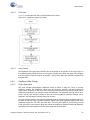
Figure 5-16 shows the flow chart of code implemented in main.c.
Figure 5-16. Deep-Sleep Project Flow Chart
Start
Turn LED on
for one second
Enter DeepSleep mode
Interrupt on
SW2 press
Clear the
interrupt
52
CY8CKIT-042 PSoC 4 Pioneer Kit Guide, Doc. # 001-86371 Rev. *D
Code Examples
5.3.4
Verify Output
Build and program the code example, and reset the device. LED is on for one second and turns off,
which indicates that the device has entered Deep-Sleep mode. Press SW2 switch to wake up the
device from Deep-Sleep mode and enter Active mode. The device goes back to sleep after one second.
Note: When the device is in Deep-Sleep mode, the programmer must reacquire the device before
programming can start.
5.4
Project: CapSense
This code example can be executed in two ways – with and without CapSense tuning. The same
project can be used to demonstrate the CapSense functionality as well as CapSense tuning using
the Tuner Helper GUI in PSoC Creator. This is done by commenting and uncommenting the line
#define ENABLE_TUNING in the main.c file of the code example. PSoC Creator does not compile
the code under the #ifdef (if defined) statement when the #define statement is commented (/
*…… */ or //). Similarly, when the #define statement is uncommented, the code required for working with Tuner GUI is compiled. By default, the project is set to work without CapSense tuning by
commenting the #define.
5.4.1
CapSense (Without Tuning)
5.4.1.1
Project Description
This code example demonstrates CapSense on PSoC 4. The example uses the five-segment
CapSense slider on the board. Each capacitive sensor on the slider is scanned using Cypress’s
CapSense Sigma Delta (CSD) algorithm implemented in the CapSense component. This project is
pre-tuned to take care of the board parasitics. For more information on the CapSense component
and CapSense tuning, see the CapSense component datasheet in PSoC Creator.
In this code example, the brightness of the green and red LEDs are varied, based on the position of
the user’s finger on the CapSense slider.
Figure 5-17. PSoC Creator Schematic Design of CapSense Project
Note: The EzI2C component is not used when tuning is disabled.
CY8CKIT-042 PSoC 4 Pioneer Kit Guide, Doc. # 001-86371 Rev. *D
53
Code Examples
5.4.1.2
Hardware Connections
No specific hardware connections are required for this project because all connections are hardwired on the board. Open CapSense.cydwr in the Workspace Explorer and select the suitable pins.
Table 5-4. Pin Connection
Pin Name
Port Name
P1_1 Segment1
P1_2 Segment2
CapSense linear slider
P1_3 Segment3
P1_4 Segment4
P1_5 Segment5
LEDs
P1_6 (Red) and P0_2 (Green)
I2C communication lines
P3_0 (SCL) and P3_1 (SDA)
Note: The I2C communication lines are not used when tuning is disabled.
Figure 5-18. Pin Selection for CapSense Project
54
CY8CKIT-042 PSoC 4 Pioneer Kit Guide, Doc. # 001-86371 Rev. *D
Code Examples
5.4.1.3
Flow Chart
Figure 5-19 shows the flow chart of code implemented in main.c.
Figure 5-19. CapSense Project Flow Chart
5.4.1.4
Verify Output
The brightness of the green and red LEDs are varied based on the position of the user’s finger on
the CapSense slider. When the finger is on segment 5 (P1[5]) of the slider, the green LED is brighter
than the red LED; when the finger is on segment 1 (P1[1]) of the slider, the red LED is brighter than
the green LED.
5.4.2
CapSense (With Tuning)
5.4.2.1
Project Description
This code example demonstrates CapSense tuning on PSoC 4 using the "Tuner" to monitor
CapSense outputs. The CapSense outputs such as rawcounts, baseline, and signal (difference
count) can be monitored on the Tuner GUI. The project uses the auto-tuning feature, which sets all
CapSense parameters to the optimum values automatically. The parameter settings can be monitored in the GUI but cannot be altered. In the manual tuning method, parameter settings can be
changed in the GUI and the resulting output can be seen.
The code example uses the five-segment CapSense slider on the board. Each capacitive sensor on
the slider is scanned using Cypress's CapSense Sigma Delta (CSD) algorithm implemented in the
CapSense component. The code uses tuner APIs. The tuner API CapSense_TunerComm() is used
in the main loop to scan sensors, which also sends the CapSense variables RawCounts, Baseline,
and Difference Counts (Signal) to the PC GUI through I2C communication.
CY8CKIT-042 PSoC 4 Pioneer Kit Guide, Doc. # 001-86371 Rev. *D
55
Code Examples
In this example, the brightness of the green and red LEDs are varied, based on the position of the
user's finger on the CapSense slider.
See Figure 5-17 for the project schematic.
5.4.2.2
Hardware Connections
No specific hardware connections are required for this project because all connections are hardwired on the board. Open CapSense.cydwr in the Workspace Explorer and select the suitable pins.
See Table 5-4 and Figure 5-18 for the CapSense project pin connections.
5.4.2.3
Flow Chart
Figure 5-20. CapSense with Tuning Flow Chart
Start
Initialise and start the
PWM and CapSense
Tuner
Start Tuner
communication
Get the finger position on
the slider
Set the PWM output width to
adjust the brightness of the
RGB LED
56
CY8CKIT-042 PSoC 4 Pioneer Kit Guide, Doc. # 001-86371 Rev. *D
Code Examples
5.4.2.4
Launching Tuner GUI
The Tuner GUI from PSoC Creator should be up and running for the code example to work. To
launch the GUI follow these steps:
1. Go to the project's TopDesign.cysch file.
Figure 5-21. Top Design File
2. To open the tuner, right-click on the CapSense_CSD component in PSoC Creator and click
Launch Tuner.
Figure 5-22. Launch Tuner
3. The Tuner GUI opens. Click Configuration to open the configuration window.
CY8CKIT-042 PSoC 4 Pioneer Kit Guide, Doc. # 001-86371 Rev. *D
57
Code Examples
Figure 5-23. Tuner GUI
4. Set the I2C communication parameters, as shown in the following figure.
Figure 5-24. I2C Communication
58
CY8CKIT-042 PSoC 4 Pioneer Kit Guide, Doc. # 001-86371 Rev. *D
Code Examples
5. Click OK to apply the settings.
5.4.2.5
Verify Output
1. To start the scanning and communication process, click Start.
Figure 5-25. Start Communication
CY8CKIT-042 PSoC 4 Pioneer Kit Guide, Doc. # 001-86371 Rev. *D
59
Code Examples
2. Select a sensor in the Tuning tab. A red outline is seen on the selected sensor. Different
CapSense parameters are shown on the bottom-right. You cannot edit the settings because autotuning is used in this project; auto-tuning automatically sets all the parameters. Touch the
selected sensor and observe the response in the tuner window.
Figure 5-26. Sensor Tuning
3. In the Graphing tab, the CapSense results: Raw counts, Baseline, Signal (difference count) and
On/Off status for each sensor are represented as a graph.
4. Select the sensor parameters to observe, as shown in the following figure. The graph of the
selected parameters is shown.
60
CY8CKIT-042 PSoC 4 Pioneer Kit Guide, Doc. # 001-86371 Rev. *D
Code Examples
Figure 5-27. Sensor Parameter Graph
CY8CKIT-042 PSoC 4 Pioneer Kit Guide, Doc. # 001-86371 Rev. *D
61
Code Examples
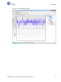
5. Touch a sensor or slider element and see the increase in raw counts.
Figure 5-28. Raw Count Increase
62
CY8CKIT-042 PSoC 4 Pioneer Kit Guide, Doc. # 001-86371 Rev. *D
6.
6.1
Advanced Topics
Using PSoC 5LP as USB-UART Bridge
The PSoC 5LP serves as a USB-UART bridge, which can communicate with the COM terminal
software. This section explains how to create a PSoC 4 code example to communicate with the
COM terminal software. This project is available with other code examples for the PSoC 4 Pioneer
Kit at the element14 web page, 100 Projects in 100 days.
Users who have a Windows operating system that does not have HyperTerminal can use an
alternate terminal software such as PuTTY.
1. Open a new PSoC 4 project in the PSoC Creator. Select an appropriate location for your project
and rename the project as required.
Figure 6-1. Opening New Project from PSoC Creator
CY8CKIT-042 PSoC 4 Pioneer Kit Guide, Doc. # 001-86371 Rev. *D
63
Advanced Topics
2. Drag and drop a UART (SCB) component to the top design.
Figure 6-2. UART Component Under Component Catalog
3. To configure the UART, double-click or right-click on the UART component and select Configure.
Figure 6-3. Open UART Configuration Window
64
CY8CKIT-042 PSoC 4 Pioneer Kit Guide, Doc. # 001-86371 Rev. *D
Advanced Topics
4. Configure the UART as shown in the following figures.
Figure 6-4. UART Configuration Window
Figure 6-5. UART Basic Configuration Window
CY8CKIT-042 PSoC 4 Pioneer Kit Guide, Doc. # 001-86371 Rev. *D
65
Advanced Topics
Figure 6-6. UART Advanced Configuration Window
5. Select P0[4] for UART RX and P0[5] for UART TX in the Pins tab of <Project.cydwr>.
Figure 6-7. Pin Selection
66
CY8CKIT-042 PSoC 4 Pioneer Kit Guide, Doc. # 001-86371 Rev. *D
Advanced Topics
6. Place the following code in your main.c project file. The code will echo any UART data received.
int main()
{
uint8 ch;
/* Start SCB UART TX+RX operation */
UART_Start();
/* Transmit String through UART TX Line */
UART_UartPutString("CY8CKIT-042 USB-UART");
for(;;)
{
/* Get received character or zero if nothing has been received yet
*/
ch = UART_UartGetChar();
if(0u != ch)
{
/* Send the data through UART. This functions is blocking and waits until
there is an entry into the TX FIFO. */
UART_UartPutChar(ch);
}
}
}
CY8CKIT-042 PSoC 4 Pioneer Kit Guide, Doc. # 001-86371 Rev. *D
67
Advanced Topics
7. Build the project by clicking Build > Build {Project Name} or [Shift] + [F6]. After the project is
built without errors and warnings, program (by clicking Debug > Program) the project to PSoC 4
through the PSoC 5LP USB programmer or MiniProg3.
Connect the RX line of the PSoC 4 to J8_10 and TX line of the PSoC 4 to J8_9, as shown in the
following figures.
Figure 6-8. UART Connection Between PSoC 4 and PSoC 5LP
Figure 6-9. Block Diagram of UART Connection Between PSoC 4 and PSoC 5LP
J8_9
J8_10
P12[7]
P12[6]
UART RX UART TX
USB
Mini B
D+
D-
P15[6]
P15[7]
PSoC 5LP
P0[4]
UART RX
P0[5]
UART TX
PSoC 4
Note: UART RX and UART TX can be routed to any digital pin on PSoC 4 based on the configuration of the UART component. An SCB implementation of UART will route the RX and TX pins to
either one of the following subsets: (P0[4], P0[5]) or (P3[0],P3[1]) or (P4[0],P4[1]).
68
CY8CKIT-042 PSoC 4 Pioneer Kit Guide, Doc. # 001-86371 Rev. *D
Advanced Topics
To communicate with the PSoC 4 from the terminal software, follow this procedure:
1. Connect USB Mini B to J10. The kit enumerates as a KitProg USB-UART and is available under
the Device Manager, Ports (COM & LPT). A communication port is assigned to the
KitProg USB-UART.
Figure 6-10. KitProg USB-UART in Device Manager
2. Open HyperTerminal and select File > New Connection and enter a name for the new connection and click OK.
For PuTTY, double click the putty icon and select Serial under Connection.
CY8CKIT-042 PSoC 4 Pioneer Kit Guide, Doc. # 001-86371 Rev. *D
69
Advanced Topics
Figure 6-11. Open New Connection
HyperTerminal
PuTTY
3. A new window opens, where the communication port can be selected.
In HyperTerminal, select COMX (or the specific communication port that is assigned to KitProg
USB-UART) in Connect using and click OK.
In PuTTY enter the COMX in Serial line to connect to.
This code example uses COM12.
70
CY8CKIT-042 PSoC 4 Pioneer Kit Guide, Doc. # 001-86371 Rev. *D
Advanced Topics
Figure 6-12. Select Communication Port
HyperTerminal
PuTTY
4. In HyperTerminal, select 'Bits per second', 'Data bits', 'Parity', 'Stop bits', and 'Flow control' under
Port Settings and click OK.
Make sure that the settings are identical to the UART settings configured for PSoC 4.
In PuTTY select 'Speed (baud)', 'Data bits', 'Stop bits', 'Parity' and 'Flow control' under Configure
the serial line. Click Session and select Serial under Connection type.
CY8CKIT-042 PSoC 4 Pioneer Kit Guide, Doc. # 001-86371 Rev. *D
71
Advanced Topics
Serial line shows the communication port (COM12) and Speed shows the baud rate selected.
Click Open to start the communication.
Figure 6-13. Configure the Communication Port
HyperTerminal
PuTTY
72
CY8CKIT-042 PSoC 4 Pioneer Kit Guide, Doc. # 001-86371 Rev. *D
Advanced Topics
Figure 6-14. Select Communication Type in PuTTY
5. Enable Echo typed characters locally under File > Properties > Settings > ASCII Setup, to
display the typed characters on HyperTerminal. In PuTTY, enable the Force on under Terminal >
Line discipline options to display the typed characters on the PuTTY.
Figure 6-15. Enabling echo of typed characters in HyperTerminal
CY8CKIT-042 PSoC 4 Pioneer Kit Guide, Doc. # 001-86371 Rev. *D
73
Advanced Topics
Figure 6-16. Enabling echo of typed characters in PuTTY
6. The COM terminal software displays both the typed data and the looped back data from the
PSoC 4 UART.
Figure 6-17. Data Displayed on HyperTerminal
74
CY8CKIT-042 PSoC 4 Pioneer Kit Guide, Doc. # 001-86371 Rev. *D
Advanced Topics
Figure 6-18. Data Displayed on PuTTY
CY8CKIT-042 PSoC 4 Pioneer Kit Guide, Doc. # 001-86371 Rev. *D
75
Advanced Topics
6.2
Using PSoC 5LP as USB-I2C Bridge
The PSoC 5LP serves as a USB-I2C bridge, which can be used to communicate with the USB-I2C
software running on the PC. This project is available with other code examples for the PSoC 4 Pioneer Kit at the element14 web page, 100 Projects in 100 days.
The following steps describe how to use the USB-I2C bridge, which can communicate between the
BCP and the PSoC 4.
1. Open a new project targeting the PSoC 4 device in PSoC Creator.
Figure 6-19. Opening a New Project in PSoC Creator
76
CY8CKIT-042 PSoC 4 Pioneer Kit Guide, Doc. # 001-86371 Rev. *D
Advanced Topics
2. Drag and drop an I2C component to the top design.
Figure 6-20. I2C Component in Component Catalog
3. To configure the I2C component, double-click or right-click on the I2C component and select
Configure.
Figure 6-21. Open I2C Configuration Window
CY8CKIT-042 PSoC 4 Pioneer Kit Guide, Doc. # 001-86371 Rev. *D
77
Advanced Topics
4. Configure the I2C with the following settings.
Figure 6-22. I2C Configuration Tab
Figure 6-23. I2C Tab
5. Select pin P3[0] for the I2C SCL and pin P3[1] for the I2C SDA in the Pins tab of <poject.cydwr>.
78
CY8CKIT-042 PSoC 4 Pioneer Kit Guide, Doc. # 001-86371 Rev. *D
Advanced Topics
Figure 6-24. Pin Selection
6. Place the following code in your main.c project file. The code will enable the PSoC 4 device to
transmit and receive I2C data to and from the BCP application.
int main()
{
uint8 wrBuf[10];
uint8 rdBuf[10];
uint8 indexCntr;
uint32 byteCnt;
/* I2C write buffer */
/* I2C read buffer */
/* Enable the Global Interrupt */
CyGlobalIntEnable;
/* Start I2C Slave operation */
I2C_Start();
/* Initialize write buffer */
I2C_I2CSlaveInitWriteBuf((uint8 *) wrBuf, 10);
/* Initialize read buffer */
I2C_I2CSlaveInitReadBuf((uint8 *) rdBuf, 10);
for(;;) /* Loop forever */
{
/* Wait for I2C master to complete a write */
CY8CKIT-042 PSoC 4 Pioneer Kit Guide, Doc. # 001-86371 Rev. *D
79
Advanced Topics
if(0u != (I2C_I2CSlaveStatus() & I2C_I2C_SSTAT_WR_CMPLT))
{
/* Read the number of bytes transferred */
byteCnt = I2C_I2CSlaveGetWriteBufSize();
/* Clear the write status bits*/
I2C_I2CSlaveClearWriteStatus();
/* Move the data written by the master to the read buffer so that the
master can read back the data */
for(indexCntr = 0; indexCntr < byteCnt; indexCntr++)
{
rdBuf [indexCntr] = wrBuf[indexCntr]; /* Loop back the data to the read
buffer */
}
/* Clear the write buffer pointer so that the next write operation will
start from index 0 */
I2C_I2CSlaveClearWriteBuf();
/* Clear the read buffer pointer so that the next read operations starts
from index 0 */
I2C_I2CSlaveClearReadBuf();
}
/* If the master has read the data , reset the read buffer pointer to 0
and clear the read status */
if(0u != (I2C_I2CSlaveStatus() & I2C_I2C_SSTAT_RD_CMPLT))
{
/* Clear the read buffer pointer so that the next read operations starts
from index 0 */
I2C_I2CSlaveClearReadBuf();
/* Clear the read status bits */
I2C_I2CSlaveClearReadStatus();
}
}
}
6. Build the project by clicking Build > Build Project or [Shift]+[F6]. After the project is built without
errors and warnings, program ([Ctrl]+[F5]) this code onto the PSoC 4 through the PSoC 5LP programmer or MiniProg3.
7. Open the BCP from Start > All Programs > Cypress > Bridge Control Panel <version number>.
8. Connect to KitProg/ under Connected I2C/SPI/RX8 Ports.
80
CY8CKIT-042 PSoC 4 Pioneer Kit Guide, Doc. # 001-86371 Rev. *D
Advanced Topics
Figure 6-25. Connecting to KitProg/ in BCP
9. Open Protocol Configuration from the Tools menu and select the appropriate I2C Speed.
Make sure the I2C speed is the same as the one configured in the I2C component. Click OK to
close the window.
Figure 6-26. Opening Protocol Configuration Window in BCP
CY8CKIT-042 PSoC 4 Pioneer Kit Guide, Doc. # 001-86371 Rev. *D
81
Advanced Topics
10.From the BCP, transfer five bytes of data to the I2C device with slave address 0x08. The log
shows whether the transaction was successful. A '+' indication after each byte indicates that the
transaction was successful and a '–' indicates that the transaction was a failure.
Figure 6-27. Entering Commands in BCP
82
CY8CKIT-042 PSoC 4 Pioneer Kit Guide, Doc. # 001-86371 Rev. *D
Advanced Topics
Figure 6-28. NACK Indication in BCP
11. From the BCP, read five bytes of data from the I2C slave device with slave address 0x08. The log
shows whether the transaction was successful.
Figure 6-29. Read Data Bytes from the BCP
Note: Refer Help Contents under Help in BCP or press [F1] for details of I2C commands.
CY8CKIT-042 PSoC 4 Pioneer Kit Guide, Doc. # 001-86371 Rev. *D
83
Advanced Topics
6.3
Developing Applications for PSoC 5LP
The PSoC 4 Pioneer Kit has an onboard PSoC 5LP whose primary function is that of a programmer
and a bridge. You can build either a normal project or a bootloadable project using the PSoC 5LP.
The PSoC 5LP connections in the Pioneer board are summarized in Figure 6-30. J8 is the I/O connector (see section 4.3.7 PSoC 5LP GPIO Header (J8)). The USB (J10) is connected and used as
the PC interface. But you can still use this USB connection to create customized USB designs.
The programming header (J7) is meant for standalone programming. This header needs to be
populated. See the 'No Load Components' section in A.6 Bill of Materials (BOM) on page 108.
Figure 6-30. PSoC 5LP Block Diagram
D+
P15_6
Mini USB (J10)
P15_7
D-
10-pin SWD
programming
and debugging
header
(J7)
SWDIO
P1_0
SWDCLK
P1_1
SWO
P1_3
TDI
P1_4
XRES
XRES
P1_2
PSoC 5LP
P0_0
P0_1
P3_4
P3_5
P3_6
P3_7 P12_6 P12_7 P3_0
J8_2
J8_3
J8_4
PSoC 5LP
I/O Header
(J8)
J8_5
J8_6
J8_7
J8_8
J8_9
J8_10
J8_12
6.3.1
Building a Bootloadable Project for PSoC 5LP
All bootloadable applications developed for the PSoC 5LP should be based on the bootloader hex
file, which is programmed onto the kit. The bootloader hex file is available in the kit files or can be
downloaded from the kit web page.
The hex files are included in the following kit installer directory:
<Install Path>\CY8CKIT-042 PSoC 4 Pioneer Kit\
<version>\Firmware\Programmer\KitProg_Bootloader
Figure 6-31. KitProg Bootloader Hex File Location
To build a bootloadable application for the PSoC 5LP, follow this procedure:
84
CY8CKIT-042 PSoC 4 Pioneer Kit Guide, Doc. # 001-86371 Rev. *D
Advanced Topics
1. In PSoC Creator, select New > Project > PSoC 5LP; click the expand button adjacent to
Advanced and select the Device as CY8C5868LTI-LP039, as shown in Figure 6-33. Select the
Application Type as Bootloadable from the drop-down list.
Figure 6-32. Opening New Project in PSoC Creator
CY8CKIT-042 PSoC 4 Pioneer Kit Guide, Doc. # 001-86371 Rev. *D
85
Advanced Topics
Figure 6-33. Selecting Device in PSoC Creator
2. Navigate to the Schematic view and drag and drop a bootloadable component on the top design.
Figure 6-34. Bootloadable Component in Component Catalog
86
CY8CKIT-042 PSoC 4 Pioneer Kit Guide, Doc. # 001-86371 Rev. *D
Advanced Topics
Set the dependency of the Bootloadable component by selecting the Dependencies tab in the
configuration window and clicking the Browse button. Select the KitProg_Bootloader.hex and
KitProg_Bootloader.elf files; click Open.
Figure 6-35. Configuration Window of Bootloadable Component
Figure 6-36. Selecting KitProg Bootloader Hex File
CY8CKIT-042 PSoC 4 Pioneer Kit Guide, Doc. # 001-86371 Rev. *D
87
Advanced Topics
Figure 6-37. Selecting KitProg Bootloader Elf File
3. Develop your custom project.
4. The NVL setting of the Bootloadable project and the KitProg_Bootloader project must be the
same. The KitProg_Bootloader.cydwr system settings is shown in the following figure.
Figure 6-38. KitProg Bootloader System Settings
5. Build the project in PSoC Creator by selecting Build > Build Project or [Shift]+[F6].
88
CY8CKIT-042 PSoC 4 Pioneer Kit Guide, Doc. # 001-86371 Rev. *D
Advanced Topics
6. To download the project on to the PSoC 5LP device, open the Bootloader Host Tool, which is
available from PSoC Creator. Select Tools > Bootloader Host.
Figure 6-39. Opening Bootloader Host Tool from PSoC Creator
7. In the Bootloader Host tool, click Filters and add a filter to identify the USB device. Set VID as
0x04B4, PID as 0xF13B, and click OK.
Figure 6-40. Port Filters Tab in Bootloader Host Tool
CY8CKIT-042 PSoC 4 Pioneer Kit Guide, Doc. # 001-86371 Rev. *D
89
Advanced Topics
8. In the Bootloader Host tool, click the Open File button to browse to the location of the bootloadable file (*.cyacd).
Figure 6-41. Opening Bootloadable File from Bootloader Host Tool
9. Keep the reset switch (SW1) pressed and plug in the USB Mini-B connector. If the switch is
pressed for more than 100 ms, the PSoC 5LP enters into bootloader. Press the Program button
in the Bootloader Host tool to program the device. The PSoC 5LP also enters into bootloader
when the power supply jumper for the PSoC 4 (J13) is removed and subsequently the USB MiniB connector is plugged into header J10.
Figure 6-42. Selecting Bootloadable .cyacd File from Bootloader Host
90
CY8CKIT-042 PSoC 4 Pioneer Kit Guide, Doc. # 001-86371 Rev. *D
Advanced Topics
10.If bootload is successful, the log of the tool displays "Successful"; otherwise, it displays "Failed"
and a statement for the failure.
Notes:
1. The PSoC 5LP pins are brought to the PSoC 5LP GPIO header (J8). These pins are selected to
support high-performance analog and digital projects. See A.2 Pin Assignment Table on
page 104 for pin information.
2. Take care when allocating the PSoC 5LP pins for custom applications. For example, P2[0]–P2[4]
are dedicated for programming the PSoC 4. Refer to A.1 CY8CKIT-042 Schematics on page 101
before allocating the pins.
3. When a normal project is programmed onto the PSoC 5LP, the initial capability of the PSoC 5LP
to act as a programmer, USB-UART bridge, or USB-I2C bridge in not available.
4. The status LED does not function unless used by the custom project.
For additional information on bootloaders, refer to Cypress application note, AN73503 - USB HID
Bootloader for PSoC 3 and PSoC 5LP.
CY8CKIT-042 PSoC 4 Pioneer Kit Guide, Doc. # 001-86371 Rev. *D
91
Advanced Topics
6.3.2
Building a Normal Project for PSoC 5LP
A normal project is a completely new project created for the PSoC 5LP device on the CY8CKIT-042.
Here the entire flash of the PSoC 5LP is programmed, overwriting all bootloader and programming
code. To recover the programmer, reprogram the PSoC 5LP device with the factory-set KitProg.hex
file, which is shipped with the kit installer.
The KitProg.hex file is available at the following location:
<Install Path>/CY8CKIT-042 PSoC 4 Pioneer Kit\<version>\Firmware\Programmer\KitProg
This advanced functionality requires a MiniProg3 programmer, which is not included with this kit. The
MiniProg3 can be purchased from www.cypress.com/go/CY8CKit-002.
To build a normal project for the PSoC 5LP, follow these steps:
1. In PSoC Creator, select New > Project > PSoC 5LP; click the expand button adjacent to
Advanced and select Device as CY8C5868LTI-LP039; select Application Type as Normal
from the drop-down list.
Figure 6-43. Opening New Project in PSoC Creator
2. Develop your custom project.
3. Build the project in PSoC Creator by selecting Build > Build Project or [Shift]+[F6].
4. Connect the 10-pin connector of MiniProg3 to the onboard 10-pin SWD debug and programming
header J7 (which needs to be populated).
5. To program the PSoC 5LP with PSoC Creator, click Debug > Program or [Ctrl]+[F5]. The Programming window shows MiniProg3 and the selected device in the project under it
(CY8C5868LTI-LP039).
92
CY8CKIT-042 PSoC 4 Pioneer Kit Guide, Doc. # 001-86371 Rev. *D
Advanced Topics
6. Click on the device and click Connect to program.
Notes:
1. The 10-pin SWD debug and programming header (J7) is not populated. See the 'No Load Components' section of A.6 Bill of Materials (BOM) for details.
2. The PSoC 5LP pins are brought to the PSoC 5LP GPIO header (J8). These pins are selected to
support high-performance analog and digital projects. See A.2 Pin Assignment Table for pin information.
3. Take care when allocating the PSoC 5LP pins for custom applications. For example, P2[0]–P2[4]
are dedicated for programming the PSoC 4. Refer to A.1 CY8CKIT-042 Schematics before allocating the pins.
4. When a normal project is programmed onto the PSoC 5LP, the initial capability of the PSoC 5LP
to act as a programmer, USB-UART bridge, or USB-I2C bridge in not available.
5. The status LED does not function unless used by the custom project.
6.4
PSoC 5LP Factory Program Restore Instructions
The CY8CKIT-042 PSoC 4 Pioneer Kit features a PSoC 5LP device that comes factory-programmed
as the onboard programmer and debugger for the PSoC 4 device.
In addition to creating applications for the PSoC 4 device, you can also create custom applications
for the PSoC 5LP device on this kit. For details, see section 6.3 Developing Applications for PSoC
5LP on page 84. Reprogramming or bootloading the PSoC 5LP device with a new flash image will
overwrite the factory program and forfeit the ability to use the PSoC 5LP device as a programmer/
debugger for the PSoC 4 device. Follow the instructions to restore the factory program on the PSoC
5LP and enable the programmer/debugger functionality.
6.4.1
PSoC 5LP is Programmed with a Bootloadable Application
If the PSoC 5LP is programmed with a bootloadable application, restore the factory program by
using one of the following two methods.
6.4.1.1
Restore PSoC 5LP Factory Program Using PSoC Programmer
1. Launch PSoC Programmer 3.18 or later from Start > Cypress > PSoC Programmer.
2. Configure the Pioneer Kit in Service Mode. To do this, while holding down the reset button (SW1
Reset), plug in the PSoC 4 Pioneer Kit to the computer using the included USB cable (USB A to
mini-B). This puts the PSoC 5LP into service mode, which is indicated by the blinking green status LED.
CY8CKIT-042 PSoC 4 Pioneer Kit Guide, Doc. # 001-86371 Rev. *D
93
Advanced Topics
3. The following message appears in the PSoC Programmer results window “KitProg Bootloader
device is detected”.
Figure 6-44. PSoC Programmer Results Window
4. Switch to the Utilities tab in PSoC Programmer and press the Upgrade Firmware button.
Unplug all other PSoC programmers (such as MiniProg3 and DVKProg) from the PC before
pressing the Upgrade Firmware button.
Figure 6-45. Upgrade Firmware
94
CY8CKIT-042 PSoC 4 Pioneer Kit Guide, Doc. # 001-86371 Rev. *D
Advanced Topics
5. After programming has completed, the following message appears: “Firmware Update Finished
at <time>”.
Figure 6-46. Firmware Update Complete
KitProg Version 2.03
6. The factory program is now successfully restored on the PSoC 5LP. It can be used as the programmer/debugger for the PSoC 4 device.
CY8CKIT-042 PSoC 4 Pioneer Kit Guide, Doc. # 001-86371 Rev. *D
95
Advanced Topics
6.4.1.2
Restore PSoC 5LP Factory Program Using USB Host Tool
1. Launch the Bootloader Host tool from Start > Cypress > PSoC Creator.
2. Using the File > Open menu, load the Kit Prog.cyacd file, which is installed with the kit software.
The default location for this file is: <Install Path>\CY8CKIT-042 PSoC 4 Pioneer
Kit\<version>\Firmware\Programmer\KitProg\KitProg.cyacd
Figure 6-47. Load KitProg.cyacd File
96
CY8CKIT-042 PSoC 4 Pioneer Kit Guide, Doc. # 001-86371 Rev. *D
Advanced Topics
3. Configure the Pioneer Kit in Service Mode. To do this, while holding down the reset button (SW1
Reset), plug in the PSoC 4 Pioneer Kit to the computer using the included USB cable (USB A to
mini-B). This puts the PSoC 5LP into service mode, which is indicated by the blinking green status LED.
4. In the Bootloader Host tool, set the filters for the USB devices with VID: 04B4 and PID: F13B.
USB Human Interface Device port appears in the Ports list. Click that port to select it.
Figure 6-48. Select USB Human Interface Device
5. Click the Program button (or menu item Actions > Program) to restore the factory-program by
bootloading it onto the PSoC 5LP.
6. After programming has completed, the following message appears: “Programming Finished Successfully”.
CY8CKIT-042 PSoC 4 Pioneer Kit Guide, Doc. # 001-86371 Rev. *D
97
Advanced Topics
Figure 6-49. Programming Finished Successfully
7. The factory program is now successfully restored on the PSoC 5LP. It can be used as the programmer/debugger for the PSoC 4 device.
6.4.2
PSoC 5LP is Programmed with a Standard Application
If PSoC 5LP is programmed with a standard application, restore the factory program by using the following method.
1. Launch PSoC Programmer 3.18 or later from Start > Cypress > PSoC Programmer.
2. Use the File > Open menu to load the KitProg.hex factory program hex file, which is shipped with
the kit. The default location for this file is: <Install Path>\CY8CKIT-042 PSoC 4 Pioneer
Kit\<version>\Firmware\Programmer\KitProg
3. Connect a CY8CKIT-002 MiniProg3 (sold separately) to the computer. The 10-pin connector
cable on the MiniProg3 plugs into the header [J7]. Note that the J7 header is unpopulated. For
more details, see A.6 Bill of Materials (BOM) on page 108.
98
CY8CKIT-042 PSoC 4 Pioneer Kit Guide, Doc. # 001-86371 Rev. *D
Advanced Topics
4. Ensure that MiniProg3 is the selected port in PSoC Programmer and the 10-pin connector (10p
option) is selected, as shown in the following figure. If the board is not powered over USB, select
the Power Cycle programming mode.
Figure 6-50. Select MiniProg3
5. When ready, press the Program button (or File > Program) to program the PSoC 5LP device.
6. After programming has completed, the following message appears: “Program Finished at
<time>”.
CY8CKIT-042 PSoC 4 Pioneer Kit Guide, Doc. # 001-86371 Rev. *D
99
Advanced Topics
Figure 6-51. Program Finished
7. The factory program is now successfully restored on the PSoC 5LP. It can be used as the programmer/debugger for the PSoC 4 device.
100
CY8CKIT-042 PSoC 4 Pioneer Kit Guide, Doc. # 001-86371 Rev. *D
A.
A.1
Appendix
CY8CKIT-042 Schematics
C10
1.0 uF
PLACE CAPS CLOSE TO POWER PINS
0603
P4_VDD
P1_7
P1_6
P1_5
P1_4
P1_3
P1_2
P1_1
P1_0
P4_VDD
C2
0.1 uF
VCCD
C3
1.0 uF
0402
C5
1.0 uF
44
43
42
41
40
39
38
37
36
35
34
U2
0603
P4_VDD
33
32
31
30
29
28
27
26
25
24
23
VCCD
XRES
P0_7
P0_6
P0_5
P0_4
P0_3
P0_2
P0_1
P0_0
P4_3
CY8C4245AXI-483 44TQFP
/XRES
P0_7
P0_6
P0_5
P0_4
P0_3
P0_2
P0_1
P0_0
P4_3
C7
0.1 uF
C8
1.0 uF
0402
0603
J13
1
2
C9
10000 pF
Sh_tank
1
2
2 PIN HDR
NO LOAD
R6 ZERO
VDD
12
13
14
15
16
17
18
19
20
21
22
P3_0
VSS
P2_0
P2_1
P2_2
P2_3
P2_4
P2_5
P2_6
P2_7
VSS
P3_0
P3_1
P3_2_SWDIO
P3_3_SWDCLK
P3_4
P3_5
P3_6
P3_7
VDDD
P4_0
P4_1
P4_2
1
2
3
4
5
6
7
8
9
10
11
P2_0
P2_1
P2_2
P2_3
P2_4
P2_5
P2_6
P2_7
P1_7
P1_6
P1_5
P1_4
P1_3
P1_2
P1_1
P1_0
VSSA
VDDA
VDDD
0603
P4_VDD
0805
P4_0
P4_1
P4_2
P3_1
SWDIO
SWDCLK
P3_4
P3_5
P3_6
P3_7
VTARG
R4 ZERO
0603
P4_VDD
0603
P4_VDD
R10
4.7K
/XRES
PSoC 4
Power Supply
NO LOAD
TP2 RED
Input Voltage Range VIN is 5-12V
VBUS
USB MiniB
NO LOAD
TP1 RED
V3.3
2
VBUS
D1
F1
SOD123
PTC Resettable Fuse
SOD123
NCP1117DTARKG
U1
2
4
R36
120 ohm
LDO
3216
D12
+ C6
22 uFd 16v
J10
8
9
0603
C26
1.0 uF
S3
S4
R35
232 ohm
VBUS
DM
DP
ID
GND
1
2
3
4
5
USB MINI B
VDD
J11
VIN
D3
R3 560 ohm
2
1
1
2
3
2
1
3
2
1
0805
1
2
Power LED
100K R13
0402
VDD
V3.3
0402
VBUS
DM
DP
D8
TAB
D7
VOUT
ADJ
D6
+
VIN
S1
S2
3216
0603
1
D13
0603
3
6
7
0603
SOD123
C4
10 uFd 25v
1
SOD123
R2 ZERO
SOD123
VIN
D11
0603
D2
NO LOAD
C16 0.01 uF
2 PIN HDR
NO LOAD
J9
CY8CKIT-042 PSoC 4 Pioneer Kit Guide, Doc. # 001-86371 Rev. *D
101
C11
1.0 uF
C12
0.1 uF
0603
0402
P5LP2_4
P5LP2_3
P5LP2_2
P5LP2_1
P5LP2_0
P5LP_VDD
C13
1.0 uF
VDD
R5 ZERO
P5LP_VDD
0603
ZERO
ZERO
ZERO
ZERO
ZERO
R11
R12
R14
R15
R16
C14
0.1 uF
P5LP_VDD
C15
0.1 uF
0402
U3
69
68
67
66
65
64
63
62
61
60
59
58
57
56
55
54
53
52
0402
VSSD
P5LP_VCCD
0805
0603
0603
0603
0603
0603
VTARG
NO LOAD
C29
1.0 uF
Del Sig Bypass
Capacitor
C28
1.0 uF
SAR Bypass
Capacitor
NO LOAD
0603
1
2
3
4
5
6
7
8
9
10
11
12
13
14
15
16
17
P2_6
P0_3
P2_7
P0_2
P12_4 I2C0_SCL, SIO
P0_1
P12_5 I2C0_SDA, SIO
P0_0
VSSB
SIO_P12_3
IND
SIO_P12_2
VBOOST
VSSD
CY8C5868LTI-LP039 QFN68
VBAT
VDDA
VSSD
VSSA
XRES
VCCA
P1_0
P15_3
P1_1
P15_2
P1_2
SIO, I2C1_SDA P12_1
P1_3
SIO, I2C1_SCL P12_0
P1_4
P3_7
P1_5
P3_6
VDDIO1
VDDIO3
P1_6
P1_7
P12_6_SIO
P12_7_SIO
P15_6 DP
P15_7 DM
VDDD
VSSD
VCCD
P15_0
P15_1
P3_0
P3_1
P3_2
P3_3
P3_4
P3_5
VSSD
P5LP_XRES
P5LP_SWDIO
P5LP_SWDCLK
P5LP1_2
P5LP_SWO
P5LP_TDI
EPAD
P2_5
VDDIO2
P2_4
P2_3
P2_2
P2_1
P2_0
P15_5
P15_4
VDDD
VSSD
VCCD
P0_7
P0_6
P0_5
P0_4
VDDIO0
0603
R7 ZERO
P5LP0_3
P5LP0_2
P5LP0_1
P5LP0_0
P5LP12_3
P5LP12_2
VSSD
0603
P5LP_VDD
C17
0.1 uF
P5LP12_1
P5LP12_0
P5LP3_7
P5LP3_6
C19
1.0 uF
0603
P5LP0_4 to P5LP0_7,
P5LP3_2, P5LP3_3 are
reserved for HW REV ID
P5LP_VDD
R40
3K
R38
3K
0402
C22
0.1 uF
R41
4.7K
0603
R37
1.5K
0402
C21
0.1 uF
P5LP_VDD
DP
DM
R39
1.5K
0603
P5LP_VDD
P5LP3_4
P5LP3_5
P5LP3_0
P5LP3_1
P5LP1_7
P5LP12_6
P5LP12_7
22E R26 DP_P
DM_P
22E R27
VSSD
P5LP_VCCD
VTARG
0603
VBUS
0603
P5LP1_6
0402
C20
0.1 uF
C18
1.0 uF
0402
18
19
20
21
22
23
24
25
26
27
28
29
30
31
32
33
34
P5LP_VDD
51
50
49
48
47
46
45
44
43
42
41
40
39
38
37
36
35
C23
1.0 uF
0603
0402
C24
0.1 uF
P5LP_XRES
P5LP12_3
0603
R22
2.2K
R23
2.2K
0603
P5LP12_2
PSoC 5LP Programmer / Debugger
R24
P5LP12_1
P3_1
0603
ZERO
R25
P5LP12_0
P3_0
0603
ZERO
I2C Connection b/w PSoC 5LP and PSoC 4
P5LP_VDD
VTARG
R32 ZERO
SWDIO
J7
R33 ZERO
C27
SWDCLK
0402
R34 ZERO
/XRES
0.1 uF
TVS2
5V 350W
P5LP2_0
P5LP2_1
P5LP2_2
P5LP2_3
P5LP2_4
1
3
5
7
9
2
4
6
8
10
P5LP_SWDIO
P5LP_SWDCLK
P5LP_SWO
P5LP_TDI
P5LP_XRES
0603
2
4
6
8
10
0603
0.1 uF
1
3
5
7
9
0603
0402
TVS1
5V 350W
J6
C25
50MIL KEYED SMD
50MIL KEYED SMD
NO LOAD
PSoC 5LP Program/Debug Header
PSoC 4 / External PSoC Program/Debug Header
102
CY8CKIT-042 PSoC 4 Pioneer Kit Guide, Doc. # 001-86371 Rev. *D
Shield
P1_5
P1_4
R44 ZERO
P0_1
P1_3
NO LOAD
P4_2
P1_2
P1_1
Shunt
Resistor
SW1
R17 R18 R19 R20 R21
0603
C1
2200 pF
R45 ZERO
1
/XRES
1
560 ohm
2
560 ohm
3
560 ohm
4
560 ohm
5
560 ohm
R1
NO LOAD
2
EVQ-PE105K
RESET
0603
CSS1
SW2
CAPSENSE TUNING CIRCUITRY
Default Loaded For CSD
Shield Setting
1
P0_7
2
EVQ-PE105K
CapSense Slider 5 Seg
USER BUTTON
D9
R28
2.2K
1
P1_6
R29
1.5K
R30
1.5K
4
P4_VDD
R
P0_2
G
2
3
P0_3
B
RGB LED
P5LP_VDD
R31
D10
2
1
P5LP3_1
0805
0805
330 ohm
Status LED Green
User Interface
P4_VDD
J5
P3_5
P3_0
P3_1
P0_6
P5LP_VDD
J8
P5LP1_2
P5LP0_1
P5LP3_5
P5LP3_7
P5LP12_7
P5LP3_0
2
4
6
8
10
12
P4_VDD
1
3
5
7
9
11
P5LP0_0
P5LP3_4
P5LP3_6
P5LP12_6
J12
P3_1
P0_6
/XRES
1
2
3
4
5
6
2
4
6
P3_0
3x2 RECPT
NO LOAD
6X1 CONN FEMALE
NO LOAD
J12 Arduino ICSP
compatible header for
SPI Interface
6x2 RECPT
PSoC 5LP GPIO Extension Header
1
3
5
J5 Digilent PMOD Cards
Compatible Headers
P4_VDD
TP4
BLACK
TP5
BLACK
TP6
BLACK
R8
2.2K
I2C Pull up
R9
2.2K Resistors
J3
VIN
VBUS
TP3
BLACK
TVS4
18V 350W BI
NO LOAD
0603
NO LOAD
0603
NO LOAD
P4_0
P4_1
J1
1
2
3
4
5
6
7
8
D4
SOD123
V3.3_EXT
/XRES
IOREF
P4_VDD
10
9
8
7
6
5
4
3
2
1
P1_7
P0_6
P3_1
P3_0
P3_4
P3_6
P2_6
8x1 RECP
10X1 RECP
J2
P2_0
P2_1
P2_2
P2_3
P2_4
P2_5
P0_0
P0_1
P1_0
1
3
5
7
9
11
13
15
17
2
4
6
8
10
12
14
16
18
P0_2
P0_3
P4_VDD
J4
P0_4
P0_5
P0_7
P3_7
P0_0
P3_5
P1_0
P2_7
P1_5
P1_4
P1_3
P1_2
P1_1
9x2 RECP
1
2
3
4
5
6
7
8
8x1 RECP
(J1-J4) Arduino Compatible Headers
NO LOAD
R46 ZERO
Vz=2V(BZT52C2V0-7-F)
TVS3
5V 350W
Q1
PMOS( DMP3098L-7)
NO LOAD
0603
V3.3_EXT
PMOS( DMP3098L-7)
V3.3
Q2
R43
442 ohm
Q3
PMOS( DMP3098L-7)
D5
R42
1K ohm
Protection Circuit
CY8CKIT-042 PSoC 4 Pioneer Kit Guide, Doc. # 001-86371 Rev. *D
103
A.2
Pin Assignment Table
This section provides the pin map of the headers and their usage.
A.2.1
Arduino Compatible Headers (J1, J2, J3, J4, and J12)
J1
Pin
Kit Signal
Description
J1_01
VIN
Input voltage to the board
J1_02
GND
GND
J1_03
GND
GND
J1_04
5V
5 V voltage
J1_05
3.3V
3.3 V voltage
J1_06
RESET
/XRES
J1_07
IOREF
I/O voltage reference
J1_08
NC
Not connected
J2
Pin
PSoC 4 Signal
PSoC 4 Description
Pin
PSoC 4 Signal
PSoC 4 Description
J2_01
P2[0]
A0 (SARADC input)
J2_02
P0[2]
Comparator 2+
J2_03
P2[1]
A1 (SARADC input)
J2_04
P0[3]
Comparator 2–
J2_05
P2[2]
A2 (SARADC input)
J2_06
VDD
VDD
J2_07
P2[3]
A3 (SARADC input)
J2_08
P1[5]
Opamp 2+
J2_09
P2[4]
A4 (SARADC input)
J2_10
P1[4]
Opamp 2–
J2_11
P2[5]
A5 (SARADC input)
J2_12
P1[3]
Opamp 2out
J2_13
P0[0]
Comparator 1+
J2_14
GND
GND
J2_15
P0[1]
Comparator 1–
J2_16
P1[2]
Opamp 1out
J2_17
P1[0]
Opamp 1+
J2_18
P1[1]
Opamp 1–
J3
Pin
PSoC 4 Signal
PSoC 4 Description
J3_01
P2[6]
D8
J3_02
P3[6]
D9(PWM)
J3_03
P3[4]
D10(PWM/SS)
J3_04
P3[0]
D11(PWM/MOSI)
J3_05
P3[1]
D12(MISO)
J3_06
P0[6]
D13(SCK)
J3_07
GND
GND
J3_08
P1[7]
AREF
J3_09
P4[1]
SDA
J3_10
P4[0]
SCL
104
CY8CKIT-042 PSoC 4 Pioneer Kit Guide, Doc. # 001-86371 Rev. *D
J4
Pin
PSoC 4 Signal
PSoC 4 Description
J4_01
P0[4]
D0(RX)
J4_02
P0[5]
D1(TX)
J4_03
P0[7]
D2
J4_04
P3[7]
D3(PWM)
J4_05
P0[0]
D4
J4_06
P3[5]
D5(PWM)
J4_07
P1[0]
D6(PWM)
J4_08
P2[7]
D7
J12
Pin
Kit Signal
PSoC 4 Description
J12_01
P3[1]
MISO
J12_02
PSoC 4_VDD
VDD
J12_03
P0[6]
SCK
J12_04
P3[0]
MOSI
J12_05
/XRES
PSoC 4 RESET
J12_06
GND
GND
A.2.2
Digilent Pmod Cards Support Header (J5)
J5
Pin
Kit Signal
PSoC 4 Description
(Default Pmod Signals)
J5_01
P3[5]
SPI_SS (multiplex with J4_06)
J5_02
P3[0]
SPI_MOSI
J5_03
P3[1]
SPI_MISO
J5_04
P0[6]
SPI_SCK
J5_05
GND
GND
J5_06
VDD
VCC
CY8CKIT-042 PSoC 4 Pioneer Kit Guide, Doc. # 001-86371 Rev. *D
105
A.2.3
PSoC 5LP GPIO Header (J8)
J8 is a 2×6 header that connects PSoC 5LP pins to support GPIO controls for custom PSoC 5LP projects.
J8
Pin
PSoC 5LP Signal
PSoC 5LP Description
PSoC 5LP
Signal
Pin
PSoC 5LP Description
J8_01
PSoC 5LP_VDD
VDD
J8_02
P1[2]
Digital I/O
J8_03
P0[0]
Delta Sigma ADC + input
J8_04
P0[1]
Delta Sigma ADC – input
J8_05
P3[4]
SAR – input
J8_06
P3[5]
SAR + input
J8_07
P3[6]
Buffered VDAC
J8_08
P3[7]
Buffered VDAC
J8_09
P12[6]
UART RX
J8_10
P12[7]
UART TX
J8_11
GND
GND
J8_12
P3[0]
IDAC output
A.3
Program and Debug Headers
A.3.1
PSoC 4 Direct Program/Debug Header (J6)
J6
Pin
PSoC 5LP
Signal
PSoC 4
Signal
Description
PSoC 5LP
Signal
Pin
PSoC 4
Signal
Description
J6_01
VDD
VDD
VCC
J6_02
P2[0]
P3[2]
TMS/SWDIO
J6_03
GND
GND
GND
J6_04
P2[1]
P3[3]
TCLK/SWCLK
J6_05
GND
GND
GND
J6_06
P2[2]
NC
TDO/SWO
J6_07
NC
GND
GND
J6_08
P2[3]
NC
TDI
J6_09
GND
GND
GND
J6_10
P2[4]
XRES
RESET
A.3.2
PSoC 5LP Direct Program/Debug Header (J7)
J7
Pin
PSoC 5LP
Signal
Description
Pin
PSoC 5LP
Signal
Description
J7_01
VDD
VCC
J7_02
P1[0]
TMS/SWDIO
J7_03
GND
GND
J7_04
P1[1]
TCLK/SWCLK
J7_05
GND
GND
J7_06
P1[3]
TDO/SWO
J7_07
GND
GND
J7_08
P1[4]
TDI
J7_09
GND
GND
J7_10
XRES
RESET
106
CY8CKIT-042 PSoC 4 Pioneer Kit Guide, Doc. # 001-86371 Rev. *D
A.4
Use of Zero-ohm Resistors and No Load
Unit
Resistor
Usage
Power supply
R2
Solder zero-ohm resistors to access voltage from VBUS (USB).
I2C connection between PSoC 5LP
and PSoC 4
R24 and R25
Unsolder the resistors to communicate with an external PSoC
using the PSoC 5LP. Removing these will disable the PSoC 4 programming by the PSoC 5LP device.
PSoC 4/external PSoC program/
debug header
R32, R33, and
R34
Unsolder the resistors to disconnect SWD lines from the PSoC 4.
Use J6 to connect and program an external PSoC.
Protection circuit
R46
Solder zero-ohm resistors to bypass the entire protection circuitry.
CapSense tuning circuitry
R1
Used when RBleed mode of the CSD is used. To use this feature,
you must populate an Rbleed resistor. Refer to the CapSense component datasheet.
CapSense shield setting
R44, R45
Unsolder R45, which connects the shield to ground and solder R44
with zero-ohm resistors to connect Vref via P0_1.
PSoC 4
R4, R6
Unsolder R4 to remove supply to VTARG and solder zero-ohm
resistors R6 to supply P4_VDD with VDD instead of J13.
PSoC 5LP programmer/debugger
R11, R12, R14,
R15, R16
For future use.
R5
Unsolder the zero-ohm resistor to cut the VDD supply to PSoC 5LP.
R7
For future use.
A.5
Error in Firmware/Status Indication in Status LED
User Indication
1
2
3
LED blinks at a fast rate
(ON Time = 0.25s, OFF Time = 0.25s)
LED blinks at a slow rate
(ON Time = 1.5s, OFF Time = 1.5s)
LED glows steadily
Scenario
Bootloadable file
is corrupt
Entered Bootloader by pressing the PSoC 4
Reset switch
Programmer application is running
successfully
Action Required by user
Bootload the *.cyacd file over the USB interface,
which is shipped with PSoC Programmer using the
Bootloader Host GUI shipped with PSoC Creator. The
files are located in the PSoC Programmer root installation directory.
a) Unplug power and plug it in again if you entered
this mode by mistake; the LED gives the indication.
b) If the mode entry was intentional, bootload the new
*.cyacd file using the Bootloader Host tool shipped
with PSoC Creator.
USB is enumerated successfully and the programmer
is up and running.The PSoC 4 device can now be programmed any time using the onboard PSoC 5LP programmer.
Note: LED status is not applicable when a custom project is running in PSoC 5LP.
CY8CKIT-042 PSoC 4 Pioneer Kit Guide, Doc. # 001-86371 Rev. *D
107
A.6
No.
Bill of Materials (BOM)
Qty
Reference
Value
Description
Manufacturer
Mfr Part Number
PCB,3.32"x2.1" CAF resistant High Tg
ENIG finish, 4 layer, Color = RED, Silk = Cypress
WHITE.
1
CAP CER 2200PF 50V 5% NP0 0805
Murata
GRM2165C1H222JA0
1D
C2,C7,C12,C14,C15,C
17,C20,C21,C22,C24, 0.1 uFd
C25,C27
CAP .1UF 16V CERAMIC Y5V 0402
Panasonic - ECG
ECJ-0EF1C104Z
11
C3,C5,C8,C10,C11,C1
3,C18,C19,C23,C26,C 1.0 uFd
28
CAP CERAMIC 1.0UF 25V X5R 0603
10%
Taiyo Yuden
TMK107BJ105KA-T
5
1
C4
10 uF 25V
CAP TANT 10UF 25V 10% 1210
AVX Corporation
TPSB106K025R1800
6
1
C6
22 uF 16V
CAP TANT 22UF 16V 10% 1210
AVX Corporation
TPSB226K016R0600
7
1
C9
10000 pFd
CAP CER 10000PF 50V 5% NP0 0805 Murata
GRM2195C1H103JA0
1D
8
1
C16
0.01 uFd
CAP 10000PF 16V CERAMIC 0402
SMD
Panasonic - ECG
ECJ-0EB1C103K
9
6
D1,D2,D4,D11,D12,D1
MBR05
3
DIODE SCHOTTKY 0.5A 20V SOD123
Fairchild Semiconductor
MBR0520L
10
1
D3
Power LED
Amber
LED AMBER 591NM DIFF LENS 2012
Sharp MicroelectronLT1ZV40A
ics
11
1
D5
2V Zener
DIODE ZENER 2V 500MW SOD123
Diodes Inc
12
3
D6, D7, D8
ESD diode
SUPPRESSOR ESD 5VDC 0603 SMD Bourns Inc.
CG0603MLC-05LE
13
1
D9
RGB LED
LED RED/GREEN/BLUE PLCC4 SMD
Cree, Inc.
CLV1A-FKBCJ1M1F1BB7R4S3
14
1
D10
Status LED
Green
LED GREEN CLEAR 0805 SMD
Chicago Miniature
CMD17-21VGC/TR8
15
1
F1
FUSE
PTC Resettable Fuses 15Volts
100Amps
Bourns
MF-MSMF050-2
16
2
J1, J4
8x1 RECP
CONN HEADER FEMALE 8POS .1"
GOLD
Sullins Connector
Solutions
PPPC081LFBN-RC
17
1
J2
9x2 RECP
CONN HEADER FMAL 18PS.1" DL
GOLD
Sullins Connector
Solutions
PPPC092LFBN-RC
18
1
J3
10x1 RECP
CONN HEADER FMALE 10POS .1"
GOLD
Sullins Connector
Solutions
PPPC101LFBN-RC
19
1
J6
50MIL
CONN HEADER 10 PIN 50MIL KEYED
Samtec
KEYED SMD SMD
20
1
J8
6x2 RECP
CONN HEADER FMAL 12PS.1" DL
GOLD
Sullins Connector
Solutions
PPPC062LFBN-RC
21
1
J9
3p_jumper
CONN HEADER VERT SGL 3POS
GOLD
3M
961103-6404-AR
22
1
J10
USB Mini B
CONN USB MINI AB SMT RIGHT
ANGLE
TE Connectivity
1734035-2
2
1
C1
3
12
4
108
2200 pFd
BZT52C2V0-7-F
FTSH-105-01-L-DV-K
CY8CKIT-042 PSoC 4 Pioneer Kit Guide, Doc. # 001-86371 Rev. *D
No.
Qty
Reference
Value
Description
Manufacturer
Mfr Part Number
23
1
J13
2p_jumper
CONN HEADER VERT SGL 2POS
GOLD
3M
961102-6404-AR
24
3
Q1,Q2,Q3
PMOS
MOSFET P-CH 30V 3.8A SOT23-3
Diodes Inc
DMP3098L-7
25
1
R3
560
RES 560 1/8W 5% 0805 SMD
Panasonic - ECG
ERJ-6GEYJ561V
26
12
R4,R11,R12,R14,R15,
R16,R24,R25,R32,R33 ZERO
,R34,R45
RES 0.0 1/10W 0603 SMD
Panasonic-ECG
ERJ-3GEY0R00V
27
1
R5
ZERO
RES 0.0 1/8W 0805 SMD
Panasonic-ECG
ERJ-6GEY0R00V
28
4
R8,R9,R22,R23
2.2K
RES 2.2 k 1/10W 5% 0603 SMD
Panasonic - ECG
ERJ-3GEYJ222V
29
2
R10,R41
4.7K
RES 4.7 k 1/10W 5% 0603 SMD
Panasonic-ECG
ERJ-3GEYJ472V
30
1
R13
100K
RES 100 k 1/10W 5% 0402 SMD
Panasonic - ECG
ERJ-2GEJ104X
31
5
R17,R18,R19,R20,R21 560
RES 560 1/10W 5% 0603 SMD
Panasonic-ECG
ERJ-3GEYJ561V
32
2
R26, R27
22E
RES 22 1/10W 1% 0603 SMD
Panasonic - ECG
ERJ-3EKF22R0V
33
1
R28
2.2K
RES 2.2 k 1/8W 5% 0805 SMD
Panasonic - ECG
ERJ-6GEYJ222V
34
2
R29,R30
1.5K
RES 1.5 k 1/8W 5% 0805 SMD
Panasonic - ECG
ERJ-6GEYJ152V
35
1
R31
330
RES 330 1/8W 5% 0805 SMD
Panasonic - ECG
ERJ-6GEYJ331V
36
1
R35
232
RES 232 1/10W 1% 0603 SMD
Panasonic - ECG
ERJ-3EKF2320V
37
1
R36
120
RES 120 1/10W 1% 0603 SMD
Panasonic - ECG
ERJ-3EKF1200V
38
2
R37,R39
1.5K
RES 1.5K 1/10W 5% 0603 SMD
Panasonic - ECG
ERJ-3GEYJ152V
39
2
R38,R40
3K
RES 3.0K 1/10W 5% 0603 SMD
Panasonic - ECG
ERJ-3GEYJ302V
40
1
R42
1K
RES 1K 1/8W 5% 0805 SMD
Panasonic - ECG
ERJ-6GEYJ102V
41
1
R43
442
RES 442 1/10W 1% 0603 SMD
Panasonic - ECG
ERJ-3EKF4420V
42
2
SW1,SW2
SW PUSHBUTTON
SWITCH TACTILE SPST-NO 0.05A
12V
Panasonic - ECG
EVQ-PE105K
43
1
TP5
BLACK
TEST POINT PC MINI .040"D Black
Keystone Electronics 5001
44
2
TVS1,TVS2
5V 350W
TVS UNIDIR 350W 5V SOD-323
Dioded Inc.
SD05-7
45
1
TVS4
18V 350W
TVS DIODE 18V 1CH BI SMD
Bourns Inc.
CDSOD323-T18C
46
1
U1
NCP1117DT
ARKG
NCP1117DTARKG
ON Semiconductor
NCP1117DTARKG
47
1
U2
PSoC 4
(CY8C4245A 44TQFP PSoC4A target chip
XI-483)
Cypress Semiconductor
CY8C4245AXI-483
48
1
U3
PSoC 5LP
68QFN PSoC 5LP chip for USB debug Cypress Semicon(CY8C5868L
channel and USB-Serial interface
ductor
TI-LP039 )
CY8C5868LTI-LP039
No Load Components
49
1
C29
1.0 uFd
CAP CERAMIC 1.0UF 25V X5R 0603
10%
CY8CKIT-042 PSoC 4 Pioneer Kit Guide, Doc. # 001-86371 Rev. *D
Taiyo Yuden
TMK107BJ105KA-T
109
No.
Qty
Reference
Value
Description
50
1
J5
6X1 RECP
RA
51
1
J7
50MIL
CONN HEADER 10 PIN 50MIL KEYED
Samtec
KEYED SMD SMD
52
1
J11
2 PIN HDR
CONN HEADER FEMALE 2POS .1"
GOLD
Sullins Connector
Solutions
PPPC021LFBN-RC
53
1
J12
3x2 RECPT
CONN HEADER FMAL 6PS .1" DL
GOLD
Sullins Connector
Solutions
PPPC032LFBN-RC
54
5
R1,R2,R7,R44,R46
ZERO
RES 0.0 1/10W 0603 SMD
Panasonic-ECG
ERJ-3GEY0R00V
55
1
R6
ZERO
RES 0.0 1/8W 0805 SMD
Panasonic-ECG
ERJ-6GEY0R00V
56
2
TP1,TP2
RED
TEST POINT PC MINI .040"D RED
Keystone Electronics 5000
57
3
TP3,TP4,TP6
BLACK
TEST POINT PC MINI .040"D Black
Keystone Electronics 5001
58
1
TVS3
5V 350W
TVS UNIDIR 350W 5V SOD-323
Dioded Inc.
SD05-7
3M
SJ61A6
CONN FEMALE 6POS .100" R/A
GOLD
Manufacturer
Mfr Part Number
Sullins Connector
Solutions
PPPC061LGBN-RC
FTSH-105-01-L-DV-K
Install on Bottom of PCB As per the Silk Screen in the Corners
59
4
N/A
N/A
BUMPON CYLINDRICAL.312X.215
BLACK
Special Jumper Installation Instructions
60
1
J9
Install jumper
Rectangular Connectors MINI JUMPER
across pins 1
Kobiconn
GF 6.0MM CLOSE TYPE BLACK
and 2
151-8010-E
61
1
J13
Install jumper
Rectangular Connectors MINI JUMPER
across pins 1
Kobiconn
GF 6.0MM CLOSE TYPE BLACK
and 2
151-8010-E
Label
62
1
N/A
N/A
LBL, Kit Product Identification Label,
Vendor Code, Datecode, Serial Number Cypress Semiconductor
CY8CKIT-042 Rev** (YYWWVVXXXXX)
63
1
N/A
N/A
LBL, PCBA Anti-Static Warning, 10mm Cypress SemiconX 10mm
ductor
64
1
N/A
N/A
Assembly Adhesive Label, Manufactur- Cypress Semiconing ID
ductor
65
1
N/A
N/A
Kit QR code
A.7
Cypress Semiconductor
Regulatory Compliance Information
The CY8CKIT-042 PSoC 4 Pioneer Kit has been tested and verified to comply with the following
electromagnetic compatibility (EMC) regulations:
110
■
EN 55022:2010 Class A - Emissions
■
EN 55024:2010 Class A - Immunity
CY8CKIT-042 PSoC 4 Pioneer Kit Guide, Doc. # 001-86371 Rev. *D