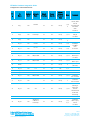
1
Intelligent BTv4.0 Dual-Mode Module Part # BT900-SA-0x, BT900-SC-0x HARDWARE INTEGRATION GUIDE VERSION 1.2 Americas: +1-800-492-2320 Europe: +44-1628-858-940 Hong Kong: +852-2923-0610 Embedded Wireless Solutions Support Center: http://ews-support.lairdtech.com www.lairdtech.com/bluetooth BT900-Sx Hardware Integration Guide Intelligent BTv4.0 Dual Mode Module REVISION HISTORY Version Revision Date 1.0 Change History Initial Version 1.1 13 Feb 2015 Added system clock and tick count period table. 1.2 24 Feb 2015 Edits to clarify OTA app download works over VSP (command mode) Embedded Wireless Solutions Support Center: http://ews-support.lairdtech.com www.lairdtech.com/bluetooth Laird Americas: +1-800-492-2320 Europe: +44-1628-858-940 Hong Kong: +852 2923 0610 BT900-Sx Hardware Integration Guide Intelligent BTv4.0 Dual Mode Module CONTENTS Revision History ............................................................................................................................................ 2 Contents ....................................................................................................................................................... 3 1 2 Overview and Key Features .................................................................................................................. 5 1.1 Features & Benefits......................................................................................................................... 5 1.2 Application Areas ........................................................................................................................... 5 Specification .......................................................................................................................................... 6 2.1 3 4 Hardware Specifications ....................................................................................................................... 8 3.1 Block Diagram and Pin-out ............................................................................................................. 8 3.2 Pin Definitions ................................................................................................................................ 9 3.3 Electrical Specifications ................................................................................................................. 13 3.3.1 Absolute Maximum ratings ............................................................................................. 13 3.3.2 Recommended Operating Parameters ............................................................................. 14 3.3.3 nAutoRUN pin and Operating Modes .............................................................................. 17 3.3.4 OTA (Over the Air) smart BASIC application download .................................................... 17 Power Consumption ............................................................................................................................ 18 4.1 5 Specification Summary ................................................................................................................... 6 Power Consumption across Clock Frequencies ............................................................................. 18 Functional Description ........................................................................................................................ 20 5.1 Power Management (includes brown-out and power on reset) .................................................... 20 5.2 Clocks and Timers ........................................................................................................................ 20 5.2.1 Clocks ............................................................................................................................. 20 5.2.2 Timers ............................................................................................................................. 21 5.3 Memory for smart BASIC Application Code and Data ................................................................... 21 5.4 RF................................................................................................................................................. 21 5.5 UART Interface ............................................................................................................................. 21 5.6 SPI Bus ......................................................................................................................................... 22 5.7 I2C Interface ................................................................................................................................ 23 5.8 General Purpose I/O, ADC, PWM/FREQ and Host-wakeup ............................................................ 23 5.9 5.8.1 GPIO ............................................................................................................................... 23 5.8.2 ADC ................................................................................................................................ 23 5.8.3 PWM and FREQ signal output on up to two SIO pins....................................................... 24 nRESET pin ................................................................................................................................... 24 5.10 nAutoRUN pin .............................................................................................................................. 24 5.11 smartBASIC runtime engine firmware upgrade ............................................................................. 24 Embedded Wireless Solutions Support Center: http://ews-support.lairdtech.com www.lairdtech.com/bluetooth Laird Americas: +1-800-492-2320 Europe: +44-1628-858-940 Hong Kong: +852 2923 0610 BT900-Sx Hardware Integration Guide Intelligent BTv4.0 Dual Mode Module 5.12 Wake-up BT900 ........................................................................................................................... 24 5.12.1 Waking up BT900 from Host ........................................................................................... 24 5.12.2 Wake up Host from BT900 .............................................................................................. 25 5.13 Low Power Modes........................................................................................................................ 25 5.14 BT and Wi-Fi Coexistence ............................................................................................................. 25 5.15 BT900-SA on-board chip antenna characteristics .......................................................................... 25 6 Hardware Integration Suggestions .................................................................................................... 26 6.1 Circuit .......................................................................................................................................... 26 6.2 PCB Layout on Host PCB - General ............................................................................................... 28 6.3 PCB Layout on Host PCB for BT900-SA......................................................................................... 28 6.4 7 8 9 6.3.1 Antenna keep-out on host PCB ....................................................................................... 28 6.3.2 Antenna keep-out and Proximity to Metal or Plastic ........................................................ 29 External Antenna Integration with BT900-SC ............................................................................... 29 Mechanical Details .............................................................................................................................. 30 7.1 BT900 Mechanical Details ............................................................................................................ 30 7.2 Host PCB Land Pattern and Antenna Keep-out for BT900-SA ....................................................... 31 Application Note for Surface Mount Modules .................................................................................. 32 8.1 Introduction ................................................................................................................................. 32 8.2 Shipping ....................................................................................................................................... 32 8.3 Reflow Parameters ....................................................................................................................... 33 FCC and IC Regulatory Statements..................................................................................................... 34 9.1 Power Exposure Information ........................................................................................................ 35 9.2 OEM Responsibilities .................................................................................................................... 35 10 Japan (MIC) Regulatory ...................................................................................................................... 37 10.1 Antenna Information .................................................................................................................... 37 11 CE Regulatory ...................................................................................................................................... 38 11.1 Antenna Information .................................................................................................................... 38 12 EU Declarations of Conformity ........................................................................................................... 39 12.1 BT900-SA / BT900-SC .................................................................................................................. 39 13 Ordering Information ......................................................................................................................... 40 13.1 General Comments ...................................................................................................................... 40 14 Bluetooth SIG Qualification ................................................................................................................ 40 Additional Assistance ............................................................................................................................. 41 Embedded Wireless Solutions Support Center: http://ews-support.lairdtech.com www.lairdtech.com/bluetooth Laird Americas: +1-800-492-2320 Europe: +44-1628-858-940 Hong Kong: +852 2923 0610 BT900-Sx Hardware Integration Guide Intelligent BTv4.0 Dual Mode Module 1 OVERVIEW AND KEY FEATURES BT900 Series modules from Laird Technologies make it easy to add Classic BT and Bluetooth Low Energy (BLE) functionality to small, portable, power-conscious devices, including those powered by batteries. The fully approved, programmable modules feature Laird’s innovative, event-driven smartBASIC programming language, which significantly reduces OEM development risk and speeds time to market. Based on the Cambridge Silicon Radio (CSR) 8811 silicon and a low power Cortex M3 microcontroller, the BT900 modules provide exceptionally low power consumption with outstanding wireless range, all within a compact footprint of 19 mm x 12.5 mm. The modules incorporate all the hardware and firmware required to support development of Dual Mode applications, including: Complete radio hardware UART, I2C, SPI, ADC, and GPIO interfaces Embedded BTv4.0 software stack - Classic BT profile - SPP - GATT Client & Peripheral Modes What makes the modules truly innovative is smartBASIC, an event-driven programming language that enables standalone operation of the module. Laird has extended the implementation of smartBASIC from the popular BL6xx series of single mode BLE modules into the BT900 series. This allows developers the flexibility of utilising the Core and BLE specific smartBASIC functions from the BL6xx series to create fully interchangeable BLE applications between these product ranges. Without the need for any external processor, a simple smartBASIC application encapsulates the complete end-to-end process of reading, writing, and processing of sensor data and then using Classic Bluetooth or BLE to transfer it to / from any Bluetooth device. Ultimately smartBASIC accelerates initial development, creation of prototypes, and mass production by providing you with your own Bluetooth expert within the module. In addition to carrying FCC modular, IC, CE and MIC approvals, BT900 modules are fully qualified as a Bluetooth product, enabling designers to integrate the modules in devices without the need for further Bluetooth testing. A low-cost developer’s kit including simple software tools simplifies module integration and guarantees the fastest route to market. 1.1 Features & Benefits Bluetooth v4.0 - Dual Mode (Classic Bluetooth and BLE) External or Internal Antennas smartBASIC programming language Full Bluetooth EPL Compact Footprint Programmable TX power 8dBm to -20dBm RX sensitivity: -90dBm Ultra low power consumption TX: 85 mA peak (at +8dBm) Standby Doze: 2.7mA (see Note2 in Power Consumption Deep Sleep: 233uA UART, GPIO, ADC, PWM, FREQ output, TIMERS, I2C, and SPI interfaces Fast Time to Market FCC, CE, IC, and Japan certified; other certs on request No external components required Embedded Wireless Solutions Support Center: http://ews-support.lairdtech.com www.lairdtech.com/bluetooth 1.2 Application Areas Medical devices Wellness devices Automotive Diagnostic Equipment Bar Code Scanners Industrial Cable Replacement Home automation Laird Americas: +1-800-492-2320 Europe: +44-1628-858-940 Hong Kong: +852 2923 0610 BT900-Sx Hardware Integration Guide Intelligent BTv4.0 Dual Mode Module 2 SPECIFICATION 2.1 Specification Summary Table 1: Specifications Categories Wireless Specification Feature Implementation Bluetooth® V4.0 – Dual-Mode Frequency 2.402 - 2.480 GHz Transmit Power + 8 dBm (maximum) Configurable down to -20 dBm Receive Sensitivity -90 dBm (typical) Link Budget 98 dB Raw Data Rates (Air) 3 Mbps (Classic BT – BR/EDR) UART Interface Host Interface and Peripherals Profiles Maximum Connections Programmability GPIO 18 (maximum – configurable) lines. O/P drive strength (4 mA) Pull-up resistor (33 KOhms) control (via smartBASIC) Read pin-level I2C Interface 1 (configurable from GPIO total). Up to 400 kbps SPI 1 (configurable from GPIO total). Up to 4 Mbps ADC Interface 2 channels (configured from GPIO total). Up to 12-bit resolution Conversion time 2.0uS (at VCC 2.7V to 3.6V) Reference voltage AVCC (external, same as VCC) pre-scaling to match BL600 ADC PWM or FREQ output Output a PWM or FREQ on up to 3 GPIO output pins. PWM output duty cycle: 0%-100% PWM output frequency: 500 kHz FREQ output frequency: 0 MHz to 4 MHz (50% duty cycle) Wi-Fi-BT coexistence 3 dedicated pins Classic Bluetooth SPP (Serial Port Profile) –Greater than 500kbps Bluetooth Low Energy GATT Client & Peripheral – Any Custom Services Classic Bluetooth Bluetooth Low Energy 7 clients 5 clients smartBASIC On-board programming language similar to BASIC smartBASIC application Via UART or Over the Air Embedded Wireless Solutions Support Center: http://ews-support.lairdtech.com www.lairdtech.com/bluetooth TX, RX, CTS, RTS DTR, DSR, DCD, RI can be implemented in smartBASIC- using General Purpose I/O Default 115200, N, ,8, 1 From 1,200 to 921600 RX buffer size (1024 bytes) Laird Americas: +1-800-492-2320 Europe: +44-1628-858-940 Hong Kong: +852 2923 0610 BT900-Sx Hardware Integration Guide Intelligent BTv4.0 Dual Mode Module Categories Feature Implementation Any that can be implemented using smartBASIC vSP – Virtual Serial Port for BLE – Command Mode Only Control Protocols Via UART FW upgrade smartBASIC runtime engine FW upgrade Coexistence 802.11 (Wi-Fi) 3 wire CSR schemes supported (Unity-3 for classic BT, Unity-3e for BLE) Self-contained Run Mode Selected by nAutoRUN pin status: LOW (0V). Then runs $autorun$ (smartBASIC application) if it exists. Interactive Development Mode HIGH (VCC). Then runs via at+run (and “file name” of smartBASIC application script). Supply 1.8V – 3.6V (Note 6) 1.8V operation not supported in current FW (v9.1.2.0) Current Max Peak Current (TX Power @ +8 dBm TX): 85 mA Operating Modes Supply Voltage Standby Doze (waitevent) – 2.7mA (at 4MHz clock) (Note 5) Power Consumption Deep Sleep – 233 uA (external signal wakeup) See Note 5 User Configurable Clocking User configurable clocking (40MHz, 20MHz, 4MHz), so user can reduce current consumption further. Dimensions 19 mm x 12.5 mm x 2.5 mm; Pad Pitch 0.8 mm Operating -40°C to +85°C Storage -40°C to +85°C Lead Free Lead-free and RoHS compliant Warranty One Year Development Tools Development Kit Development board and free software tools Software Tools Utilities Windows, Android and iOS applications UART Firmware Upgrade Bluetooth® Complete Declaration ID FCC / IC / CE / MIC All BT900 Series Physical Environmental Miscellaneous Approvals Note 1: DSR, DTR, RI, and DCD can be implemented in the smart BASIC application. Note 2: With I2C interface selected, pull-up resistors on I2C SDA and I2C SCL MUST be connected externally as per I2C standard. Note 3: SPI interface consists of SPI MOSI, SPI MISO and SPI CLK. SPI CS is created by customer using any spare SIO pin within their smartBASIC application script allowing multi-dropping. Note 4: BT900 module comes loaded with smart BASIC runtime engine FW, but does not come loaded with any smart BASIC application script (as that is dependent on customer end application or use). Laird provides many sample smart BASIC applications covering the services listed. Embedded Wireless Solutions Support Center: http://ews-support.lairdtech.com www.lairdtech.com/bluetooth Laird Americas: +1-800-492-2320 Europe: +44-1628-858-940 Hong Kong: +852 2923 0610 BT900-Sx Hardware Integration Guide Intelligent BTv4.0 Dual Mode Module Note 5: Deep sleep consumes 233uA of power when the BT900 internal radio chip 32.768kHz is used. The smartBASIC runtime engine firmware (v9.1.2.0) has SIO (DIO default function) input pins that are PULL-UP enabled by default. You may disable the internal PULL_UP through a smartBASIC application script. Lower Power consumption may be achieved when all SIO pins are set as outputs and low (in your smart BASIC application script). In deep sleep 7uA can be achieved if all SIO pins are set as output and low. Note 6: 3 1.8V operation not supported in current smartBASIC runtime engine FW v9. HARDWARE SPECIFICATIONS 3.1 Block Diagram and Pin-out 47 connection pads User smartBASIC Application GPIO/PWM I2C ADC Flash 32.768Khz Crystal ARM Cortex M3 running smartBASIC RAM Serial Flash (SPI) SPI I/O, UART,I2C,SPI Drivers UART Example App PRINT "Laird BT900 Module" WaitEvent Non-Vol File System for smartBASIC Apps smartBASIC run-time engine (provides safe access to BT/BLE stack, drivers and non-vol stores) Non-Vol Data Store Blutooth 4.0 Radio ( Classic BT & BLE ) Internal Antenna OR UFL Bluetooth Classic & Bluetooth Low Energy Stack Figure 1: Functional HW and SW block Diagram for BT900 series Dual-Mode BT/ BLE smartBASIC module Embedded Wireless Solutions Support Center: http://ews-support.lairdtech.com www.lairdtech.com/bluetooth Laird Americas: +1-800-492-2320 Europe: +44-1628-858-940 Hong Kong: +852 2923 0610 BT900-Sx Hardware Integration Guide Intelligent BTv4.0 Dual Mode Module Figure 2: BT900-Sx module pin-out (top view) 3.2 Pin Definitions Table 2: Pin definitions # Pin Name Default Funct. Alternate Funct. Default Direction Supply Domain Internal Pull-up or Pull-down State Notes 1 UART_CTS UART SIO_3 or WKUP4 or Ext Interrupt IN VCC Pull-up 1, 2, 6, 7, 12 2 SIO_4 DIO 3 nAutoRUN Pin 4 SIO_5 5 VCC 6 GND 7 SIO_6 DIO IN Pull-up VCC Pull-up In ONLY SIO_22 or Ext Interrupt IN Ext Interrupt IN VCC Pull Up 1, 2, 12 IN 1.75V-3.6V See Table 4 16 IN VCC Pull Up 1, 2, 6, 9 DIO Embedded Wireless Solutions Support Center: http://ews-support.lairdtech.com www.lairdtech.com/bluetooth VCC 2 SPI MISO 1, 2, 12 Comment Laird Devkit: UART_DTR via CON12 Laird Devkit: UART_DSR via CON12 Laird Devkit: UART_DCD via CON12 SPIOPEN() in smartBASIC Laird Americas: +1-800-492-2320 Europe: +44-1628-858-940 Hong Kong: +852 2923 0610 BT900-Sx Hardware Integration Guide Intelligent BTv4.0 Dual Mode Module Pin # Pin Name Default Funct. 8 SIO_7 DIO 9 SIO_8 DIO 10 SIO_9 DIO 11 SIO_10 DIO 12 SIO_11 DIO 13 GND 14 SIO_12 DIO 15 SIO_13 DIO 16 nRESET 17 SIO_14 DIO 18 SIO_15 DIO 19 SIO_16 DIO 20 SIO_17 DIO 21 SIO_18 DIO 22 SIO_19 23 GND 24 SIO_20 Alternate Funct. Internal Pull-up or Pull-down State Notes Comment IN VCC Pull Up 1, 2, 6, 9 IN VCC Pull Up 1, 2, 12 Laird Devkit: UART_RI via CON12 IN VCC Pull Up 1, 2, 6, 9 IN VCC Pull Up 1, 2, 6, IN VCC Pull Up 1, 2, 6, FREQ or PWM IN VCC Pull Up 1, 2, 13 Laird Devkit: Buzzer output via CON15 FREQ or PWM IN VCC Pull Up 1, 2, 13 Laird Devkit: Button1 input IN VCC Pull Up 8 System Reset (Active low) IN VCC N/A 2, 14 IN VCC Pull Up 2 ***** IN VCC N/A 2, 14 FREQ or PWM IN VCC Pull Up 1, 2, 13 Laird Devkit: LED1 via CON14 IN VCC Pull Up 2 Laird Devkit: LED2 via CON14 Pull Up 1, 2, 10 Pull to GND externally (at power-up) to enter VSP Command mode (enable OTA functionality) Pull Up 1, 2, 3, 4, 12 SPI MOSI Ext Interrupt SPI CLK I2C SDA I2C SCL ***** VSP AIN (ADC01) or WKUP1 or Ext Interrupt Embedded Wireless Solutions Support Center: http://ews-support.lairdtech.com www.lairdtech.com/bluetooth Supply Domain selects SPI function, MOSI and CLK are outputs when in SPI master mode. See Note 9 DIO DIO Default Direction IN IN VCC VCC I2COPEN() in smartBASIC selects I2C function Laird Devkit: Button 2 input; Trim Pot via CON14 Laird Americas: +1-800-492-2320 Europe: +44-1628-858-940 Hong Kong: +852 2923 0610 BT900-Sx Hardware Integration Guide Intelligent BTv4.0 Dual Mode Module # Pin Name Default Funct. Alternate Funct. Default Direction Supply Domain Internal Pull-up or Pull-down State Notes Comment 25 SIO_21 DIO AIN (ADC00) IN VCC Pull Up 1, 2, 3, 4 Laird Devkit: Temp Sensor input via CON14 26 AVCC IN 1.7V-3.6V See Table 4 16 27 NC 28 AVREF 29 GND 30 GND 31 BT_VREG_IN_HV 32 BT_VREG_OUT_HV DIO 33 GND DIO 34 BT_Ext_DS_CLK DIO 35 BT_NC 36 BT_NC 37 BT_NC 38 BT_NC 39 Pin Reserved for future use. Do NOT connect. NC IN See Table 4 16 3.3V See Table 4 16 1.8V See Table 4 16 IN BT_VDD_IO Weak Pull-down Do not connect DIO OUT BT_VDD_IO Weak Pull-down Do not connect DIO OUT BT_VDD_IO Weak Pull-down Do not connect OUT BT_VDD_IO Weak Pull-down Do not connect NC IN BT_VDD_IO Weak Pull-down Do not connect BT_ACTIVE DIO OUT BT_VDD_IO Weak Pull-down 17 Do not connect 40 WLAN_ACTIVE DIO INs BT_VDD_IO Weak Pull-down 17 Also called WLAN_DENY 41 BT_#SEL DIO IN BT_VDD_IO Weak Pull-down 11 Must add 100K to GND externally 42 BT_PRIORITY DIO OUT BT_VDD_IO Weak Pull-down 17 Also called BT_STATUS 43 BT_VDD_IO 3.3V or 1.8V See Table 4 16 44 UART_RX DIO SIO_0 or WKUP2 IN VCC Pull-up 1, 2, 6, 7, 12, 15 45 UART_TX DIO SIO_1 OUT VCC Set high in FW 1, 2, 6, 7, 15 46 UART_RTS DIO SIO_2 OUT VCC Set low in FW 1, 2, 6, 7, 15 IN only IN only IN only Embedded Wireless Solutions Support Center: http://ews-support.lairdtech.com www.lairdtech.com/bluetooth UARTCLOSE() selects DIO functionality and UARTOPEN() selects UART comms behaviour Laird Americas: +1-800-492-2320 Europe: +44-1628-858-940 Hong Kong: +852 2923 0610 BT900-Sx Hardware Integration Guide Intelligent BTv4.0 Dual Mode Module Pin # Pin Name 47 GND Default Funct. Alternate Funct. Default Direction Supply Domain Internal Pull-up or Pull-down State Notes Note 1: Alternate function is selectable in the smartBASIC application. Note 2: DIO – Digital Input or Output. Note 3: AIN – Analog Input. Note 4: DIO or AIN functionality is selected using the GpioSetFunc() function in smartBASIC. Note 5: AIN configuration selected using GpioSetFunc() function. Note 6: I2C, UART, SPI controlled by xxxOPEN() functions in smartBASIC. Comment I/O voltage level tracks VCC. Note 7: SIO_0 to SIO_3 are DIO by default when $autorun$ app runs on power up. Note 8: Pull the nRESET pin low for minimum 500 nS in order for the BT900 to reset. The BT900 module start-up time is ~1.6 seconds. Start-up time is the time taken from power-up to being able to run a smartBASIC command. Out of this, 1.6 seconds, ~1.3 seconds is for radio initialisation. 1.6 seconds is also the time when coming out of reset through AT command (ATZ) or AT command for factory default (at&f*). You must fit an external pull-up resistor (10K) on nRESET (pin 16) to VCC for BT900 to be out of reset. Note 9: SPI CS is created by the customer using any spare SIO pin within their smartBASIC application script allowing multi-dropping. Note 10: It is possible to download smart BASIC applications Over the Air (OTA) to the BT900. To enable this feature, SIO_19 must be pulled low to GND externally (on power up). Refer to the firmware release documentation for details. Note 11: You must connect 100 K pull-down resistor on BT_#SEL externally to GND. Note 12: UART_CTS (pin 1), UART_RX (pin 44) and SIO_20/ADC01 (pin 24) are WKUP (wake-up) pins that allow the BT900 module to be woken up from Deep Sleep by the host. smartBASIC function will be added in the future to allow you to select which WKUP pin (or all) from which to wake up. Note 13: PWM output signal is an alternative function on SIO_12, SIO_13 and SIO_17. FREQ output signal is an alternative function on SIO pins SIO_12, SIO_13, SIO_17. Up to three SIO pins are allowed to output FREQ signal or PWM signal. Refer to smartBASIC User Guide for details. Note 14: It is mandatory that you specifically set script SIO_14 and SIO_16 as either input or output in your smartBASIC application. Embedded Wireless Solutions Support Center: http://ews-support.lairdtech.com www.lairdtech.com/bluetooth Laird Americas: +1-800-492-2320 Europe: +44-1628-858-940 Hong Kong: +852 2923 0610 BT900-Sx Hardware Integration Guide Intelligent BTv4.0 Dual Mode Module Note 15: smartBASIC runtime engine firmware (9.2.1.0) has DIO (default function) input pins that are PULL-UP enabled by default. You can disable internal PULL_UP through your smartBASIC application script All the SIO pins (with a default function of DIO) are mostly inputs (unless stated otherwise in Table 2) – with no internal pull-up. SIO_1 and SIO_2 are outputs: - SIO_1 (alternative function UART_TX) is an output, set high (in FW) - SIO_2 (alternative function UART_RTS) is an output, set low (in FW) - SIO_0 (alternative function UART_RX) is an input, set with internal - SIO_3 (alternative function UART_CTS) is an input, set with internal pull-up - SIO_19 is an input, needs an external pull-down. It is used for download smart BASIC applications over-the-air. See the latest FW release documentation for details. Lowest Power consumption is achieved when all SIO pins are set as outputs and low. Note 16: 1.8V operation not supported in current smartBASIC runtime engine FW v9.1.2.0) hence Customer must operate BT900 from nominal 3.3V supply (2.8-3.6V, refer to Table4, note4) for how to operate BT900 from 3.3V. Basically connect the external 3.3V supply to pin 31 (BT_VREG_IN_HV), pin 5 (VCC), and pin 43 (BT_VDD_IO). Customer MUST leave pin 32 (BT_VREG_OUT_HV) unconnected. Note 17: Dedicated BT900 BT-WiFi coexistence pins for CSR scheme Unity3 (used for classic BT) and Unity3e (used for BLE). Refer to smartBASIC user manual for details on how to enable coexistence. The BT900 module is delivered with the integrated smart BASIC runtime engine FW loaded (but no onboard smartBASIC application script). Because of this, it starts up in AT command mode by default. At reset, all SIO lines are configured as the defaults shown above. SIO lines can be configured through the smart BASIC application script to be either inputs (with pull-ups or none) or outputs. When an alternative SIO function is selected (such as I2C or SPI), the firmware does not allow the setup of internal pull-up. Therefore, when I2C interface is selected, pull-up resistors on I2C SDA and I2C SCL MUST be connected externally as per I2C standard. UART_RX, UART_TX, UART_CTS are 3.3 V level logic (if VCC is 3.3 V, i.e. SIO pin I/O levels track VCC). For example, when RX and TX are idle, they sit at 3.3 V (if VCC is 3.3 V). Conversely, handshaking pins CTS and RTS at 0 V are treated as assertions. Pin 3 (nAutoRUN) is an input, with active low logic. In the development kit (DVK-BT900-sx) it is connected so that the state is driven by the host’s DTR output line. The nAutoRUN pin must be externally held high or low to select between the following two BT900 operating modes: Self-contained Run mode (nAutoRUN pin held at 0 V). Interactive / development mode (nAutoRUN pin held at VCC). smartBASIC runtime engine firmware checks for the status of nAutoRUN during power-up or reset. If it is low and if there is a smartBASIC application script named $autorun$, then the smartBASIC runtime engine FW executes the application script automatically; hence the name Self-contained Run Mode. 3.3 Electrical Specifications 3.3.1 Absolute Maximum ratings Absolute maximum ratings for supply voltage and voltages on digital and analogue pins of the module are listed below. Exceeding these values causes permanent damage. The average SIO pin output current is defined as the average current value flowing through any one of the corresponding pins for a 100mS period. The total average SIO pin output current is defined as the average Embedded Wireless Solutions Support Center: http://ews-support.lairdtech.com www.lairdtech.com/bluetooth Laird Americas: +1-800-492-2320 Europe: +44-1628-858-940 Hong Kong: +852 2923 0610 BT900-Sx Hardware Integration Guide Intelligent BTv4.0 Dual Mode Module current value flowing through all of the corresponding pins for a 100mS period. The maximum output current is defined as the value of the peak current flowing through any one of the corresponding pins. Table 3: Maximum Current Ratings Parameter Min Max Unit -0.3 VSS-0.5 VSS-0.5 2.3 1.7 -0.4 -40 +3.6 VSS+4.6 VSS+4.6 4.8 2.0 3.6 0 VCC+0.3 4 -4 10 -10 50 -50 100 -100 +85 V V V V V V V V mA mA mA mA mA mA mA mA ºC Parameter Min Typ Max Unit VCC (Note 1, Note4) AVCC (AVCC=VCC) (Note 1) 1 AVREF (when AVCC>=2.7V 1 AVREF (when AVCC<2.7V) VCC Maximum ripple or noise (Note 2) VCC rise time (0 to 1.8V) (Note 2) VCC shut down time (1.8V to 0V) (Note 2) BT_VREG_IN_HV (Note 4) BT_VREG_OUT_HV (Note 4) BT_VDD_IO (Note 4) 1.75 1.75 3.3 3.3 3.6 3.6 V V Voltage at VCC pin AVCC AVREF BT_VREG_IN_HV BT_VREG_OUT_HV BT_VDD_IO Voltage at GND pin Voltage at SIO pin SIO “L” level average output current SIO “H” level average output current SIO “L” level maximum output current SIO “H” level maximum output current SIO “L” level total average output current SIO “H” level total average output current SIO “L” level total maximum output current SIO “H” level total maximum output current Storage temperature -0.3 3.3.2 Recommended Operating Parameters Table 4: Power Supply Operating Parameters Operating Temperature Range 2.7V AVCC AVCC 2.3 1.75 1.2 -40 - AVCC V <10%of VCC 0.1 1 3.6 1.95 3.6 % mS mS V V V +85 ºC Note 1: Notes on power on. Turn on/off in the following order or at same time. Turning on: VCC > AVCC > AVRH. Turning off: AVRH > AVCC > VCC. If not using the ADC convertor, connect AVCC=VCC. 1.8V operation is not supported in current smartBASIC runtime engine FW v9.1.2.0. See Note 4. Note 2: The maximum VCC ripple or noise (at any frequency) should not exceed 10% of VCC. Ensure transient fluctuation rate does not exceed 0.1V/uS. Note 3: nRESET input time is minimum 500nS. Customer must fit an external pull-up resistor (10K) on nRESET (pin 16) to VCC for BT900 to be out of reset. BT900 module start-up time is ~1.6 seconds; start-up time is the time taken from power-up to being able to run a smart BASIC command. Most Embedded Wireless Solutions Support Center: http://ews-support.lairdtech.com www.lairdtech.com/bluetooth Laird Americas: +1-800-492-2320 Europe: +44-1628-858-940 Hong Kong: +852 2923 0610 BT900-Sx Hardware Integration Guide Intelligent BTv4.0 Dual Mode Module of this is for radio initialisation. 1.6 seconds is also the time when coming out of reset through AT command (atz) or AT command for factory default (at&f*). Note 4: The Bluetooth chip in the BT900 has two internal regulators, a high voltage (input pin BT_VREG_IN_HV) and low voltage (input pin BT_VREG_OUT_HV) regulator. ONLY ONE regulator MUST be used to power the radio chip. Method 1: If the BT900 is required to operate from 3.3V, connect the external 3.3V supply to pin 31 (BT_VREG_IN_HV), pin 5 (VCC), and pin 43 (BT_VDD_IO). Customer MUST leave pin 32 (BT_VREG_OUT_HV) unconnected. Method 2: If the BT900 is required to operate from 1.8V, connect the external 1.8V supply to pin 32 (BT_VREG_OUT_HV), pin 5 (VCC) and pin 43 (BT_VDD_IO). Customer MUST leave pin 31 (BT_VREG_IN_HV) unconnected. Note that 1.8V operation is not supported in current smartBASIC runtime engine FW v9.1.2.0. Table 5: Signal Levels for Interface, SIO Parameter VIH Input high voltage VIL Input low voltage VOH Output high voltage (std. drive, 4mA) See Note 1 VOL Output low voltage (std. drive, 4mA) Pull up resistance Condition Min VCC < 2.7V VCC ≥ 2.7V VCC < 2.7V VCC ≥ 2.7V VCC < 2.7V VCC ≥ 2.7V VCC < 2.7V VCC ≥ 2.7V VCC < 2.7V VCC ≥ 2.7V 0.7VxCC 0.8VxCC Typ Max 33 5 VCC+0.3 VCC+0.3 0.3xVCC 0.2xVCC VCC VCC 0.4 0.4 134 66 15 VSS-0.3 VCC-0.45 VCC-0.5 VSS VSS 21 Input capacitance Unit V V V V V V V kΩ kΩ pF Note 1: 50mA is the total average SIO pin output current which is defined as the average current value flowing through all of the corresponding pins for a 100mS period. Table 6: SIO pin alternative function AIN (ADC) specification Parameter Min AVCC (AVCC = VCC) 1.75 AVCC current draw (ADC 1 unit operation) AVCC current draw (ADC stop) AVREF (when AVCC ≥ 2.7V 2.7 V AVREF (when AVCC < 2.7V) AVCC AVREF current draw (ADC 1 unit operation) AVREF current draw (ADC stop) ADC input pin (AIN) voltage maximum ADC input port (AIN) current draw Time required to convert single sample 12 bit mode ADC input resistor impedance (during operation) (Note 1) AVCC ≥ 2.7V Embedded Wireless Solutions Support Center: http://ews-support.lairdtech.com www.lairdtech.com/bluetooth VSS 2 Typ 3.3 0.27 0.03 0.72 0.02 Max 3.6 0.42 10 AVCC AVCC 1.29 2.6 Unit V mA uA V V mA uA AVREF V 5 uA 10 uS 2.2 kOhm Laird Americas: +1-800-492-2320 Europe: +44-1628-858-940 Hong Kong: +852 2923 0610 BT900-Sx Hardware Integration Guide Intelligent BTv4.0 Dual Mode Module Parameter 1.8V ≥ AVCC < 2.7V Min Typ ADC input capacitance impedance 1 (during operation) Max 5.5-10.5 Unit kOhm 9.4 pF Note 1: ADC input impedance is estimated mean impedance of the ADC (AIN) pins. The ADC is highly sensitive to the impedance of the source. The ADC (AIN) input impedance is 2.2-10.5k. Normally, when not sampling, the ADC (AIN) impedance will have very high value and can be considered an open circuit. The moment ADC is sampling, ADC(AIN) impedance is 2.2-10.5k. Figure 3: ADC Diagram Rext: Output impedance of external circuit (kOhms) Rext: Sampling time (nS) Ts ≥ (RAIN + Rext) x CAIN x 9 RAIN: Input resistor of ADC(kOhms)=2.2kOhms at 2.7V≤AVCC≤3.6V Input resistor of ADC(kOhms)=5.5kOhms at 1.8V≤AVCC≤2.7V CAIN: Input capacity of ADC(pF)=9.4pF at .8V≤AVCC≤3.6V You MUST fit an external series resistor (Rext) when using ADC pins, whose value is selected to get required Sample Time (Ts). 1K to 10K may be suitable. Table 7: Digital I/O Characteristics (ONLY those BT900 IO pins with names beginning with “BT_”) Normal Operation Min Typ Max Unit VIL input logic level low -0.4 - 0.4 V VIH input logic level high 0.7 x BT_VDD_IO - BT_VDD_IO+ 0.4 V VOL output logic level low, IOL = 4.0 mA - - 0.4 V VOH output logic level high, IOL = 4.0 mA 0.75 x BT_VDD_IO - - V -150 -40 -10 µA Strong pull-down 10 40 150 µA Weak pull-up -5 -1.0 -0.33 µA Input Voltage Output Voltage Input and Tristate Currents Strong pull-up Embedded Wireless Solutions Support Center: http://ews-support.lairdtech.com www.lairdtech.com/bluetooth Laird Americas: +1-800-492-2320 Europe: +44-1628-858-940 Hong Kong: +852 2923 0610 BT900-Sx Hardware Integration Guide Intelligent BTv4.0 Dual Mode Module Normal Operation Min Typ Max Unit Weak pull-down 0.33 1.0 5.0 µA CI 1.0 - 5.0 pF input capacitance This table applies to those BT900 pins ONLY with names beginning with BT_: BT_Ext_DS_CLK (pin 34) BT_NC (pin 35) BT_NC (pin 36) BT_NC (pin 37) BT_NC (pin 38) BT_ACTIVE (pin 39) WLAN_ACTIVE (pin 40) BT_#SEL (pin 41) BT_PRIORITY (pin 42) 3.3.3 nAutoRUN pin and Operating Modes Operating modes (refer to the smart BASIC manual for details): Self-contained mode Interactive / Development mode Table 7: nAutoRUN pin Signal Name Pin No nAutoRUN 3 I/O I Comments Input with active low logic. Operating mode selected by nAutoRun pin status: If Low (0V), runs $autorun$ if it exists; If High (VCC), runs via at+run (and “file name” of application). Pin 3 (nAutoRUN) is an input, with active low logic. In the development board (DVK-BT900-sx) it is connected so that the state is driven by the host’s DTR output line. nAutoRUN pin needs to be externally held high or low to select between the two BT900 operating modes: Self-contained Run mode (nAutoRUN pin held at 0V). Interactive / Development mode (nAutoRUN pin held at VCC). The smartBASIC runtime engine firmware checks for the status of nAutoRUN during power-up or reset. If it is low and if there is a smartBASIC application named $autorun$ then the smartBASIC runtime engine executes the application automatically; hence the name self-contained run mode. 3.3.4 OTA (Over the Air) smart BASIC application download It is possible to download smart BASIC applications Over the Air (OTA) to the BT900. To enable this, SIO_19 must be pulled low to GND externally (on power up). OTA smartBASIC download is possible from a remote host when in vSP command mode only. The OTA smart BASIC application download is useful because it allows the module to be soldered into an end product without pre-configuration; the application can then be downloaded over the air once the product has been pre-tested. It is the smart BASIC application that is downloaded over the air and NOT the firmware. Since this is primarily meant for production environments with multiple collocated programming stations, the transmit power is limited. Table 8: VSP pin description Signal Name Pin No I/O SIO_19 22 I Comments Internal pull up (default). Enter VSP Command mode by externally pulling SIO_19 pin to GND at power-up. OTA functionality is enabled through VSP Command mode. Embedded Wireless Solutions Support Center: http://ews-support.lairdtech.com www.lairdtech.com/bluetooth Laird Americas: +1-800-492-2320 Europe: +44-1628-858-940 Hong Kong: +852 2923 0610 BT900-Sx Hardware Integration Guide Intelligent BTv4.0 Dual Mode Module 4 POWER CONSUMPTION The BT900 module has User configurable clocking (40MHz, 20MHz, 4MHz), so user can reduce current consumption at expense of speed. The default is 40MHz. Please note that when using the 4MHz clock, the maximum supported board rate is 115200. This data was taken at VCC 3.3V and a temperature of 25ºC. 4.1 Power Consumption across Clock Frequencies Table 9: Power consumption at 40MHz, 20MHz, and 4 MHz Parameter At 40 MHz Min At 20 MHz Typ Max Min At 4 MHz Typ Max Min Typ Max Unit Active Peak current (Note 1) TX only run peak current @TX pwr = +8 dBm 85 85 85 mA TX only run peak current @TX pwr = +4 dBm 71 71 71 mA TX only run peak current @TX pwr= 0 dBm 61 61 61 mA TX only run peak current @TX pwr= -4 dBm 55 55 55 mA TX only run peak current @TX pwr= -8 dBm 52 52 52 mA TX only run peak current @TX pwr= -12 dBm 49 49 49 mA TX only run peak current @TX pwr= -16 dBm 48 48 48 mA TX only run peak current @TX pwr= -20 dBm 48 48 48 mA TBD TBD TBD 9.4 5.9 2.7 mA 233 233 233 uA Inquiring Mode (AT+BTI) 18 18 34 Note 6 mA Wait for Connection or Discoverable 32 30 50 Note 6 mA Note 6 RX only ‘peak’ current Low Power Mode 1 Standby Doze (waitevent) (Note 2) Low Power Mode 2 (Note 3) Deep Sleep (Note 3) Classic BT Mode (Note 5) BT900 Master Role (connection ACL) 5) Connecting Mode (ATDxxx) 31 28 53 Connected Mode (No Data Transfer) 31 28 50 Connected Mode (Max Data Transfer) 40 31 Connecting Mode (ATDxxx) 33 33 Connected Mode (No Data Transfer) 16 12 Connected Mode (Max Data Transfer) 31 23 Scan interval: 640ms, Scan Window: 320ms 18 18 Scan interval 1920ms, Scan Window 960ms 18 11 Max with adv. interval (min) 20 mS 16 12 9 mA Min with adv. interval (max) 10240 mS 11 7 5 mA Note 6 mA mA mA BT900 Slave Role (connection ACL) (Note 5) mA Note 6 mA mA Inquiring (Note 5) Note 6 mA mA BLE Mode Active Mode Average Current (Note 4) Advertising Average Current Draw Embedded Wireless Solutions Support Center: http://ews-support.lairdtech.com www.lairdtech.com/bluetooth Laird Americas: +1-800-492-2320 Europe: +44-1628-858-940 Hong Kong: +852 2923 0610 BT900-Sx Hardware Integration Guide Intelligent BTv4.0 Dual Mode Module Parameter At 40 MHz Min At 20 MHz Typ Max Min At 4 MHz Typ Max Min Typ Max Unit Connection Average Current Draw Max, with conn. interval (min) 8 mS 19 10 8 mA with conn. interval 68 mS 19 9 8 mA Min, with conn. interval (max) 4000 mS 19 9 7 mA 31 31 26 mA Scanning (Note 5) Active Scan Interval = 80ms, Scan Window = 40ms Note 1: Peak current is the current seen only during the duration of radio activity burst where TX is on and transmit power in Table 9 is transmitted. Note 2: Standby Doze is entered automatically (when a waitevent statement is encountered within a smartBASIC application script). In Standby Doze, all enabled peripherals remain on and may re-awaken the chip. The module wakes up from Standby Doze via an interrupt (such as a received character on the UART Rx line). The module wakes up every millisecond to service the interrupt. If the module receives a UART character from either the external UART or the radio, it wakes up. Note 3: To achieve the lowest power consumption, set all SIO pins as outputs and set low. In Deep Sleep, everything is disabled and the only wake-up sources are reset and changed on pins on which sense is enabled. The current typical consumption is ~233 uA. 7uA may be achieved if all SIO pins are set to outputs and low. Current smart BASIC runtime engine firmware (v9.1.2.0) requires a hardware reset to come out of deep sleep. Future firmware releases will allow the module to transition from Deep Sleep to Standby Doze through GPIO signals through the reset vector. Enter Deep Sleep mode via a command in your smart BASIC application script. Note 4: The BLE radio taken with a TX power of 8 dBm and all peripherals off (UART OFF after radio event), slave latency of 0 (in a connection). Average current consumption depends on a number of factors including a TX power and VCC accuracy of 26 MHz and 32.768 kHz. With these factors fixed, the largest variable is the advertising or connection interval set. Factors include: Advertising Interval range: - 20 ms to 10240 ms in multiples of 0.625 ms for Advert type=ADV_IND and ADV_DIRECT_IND 100 ms to 10240 ms in multiples of 0.625 ms for Advert type=ADV_SCAN_IND and ADV_NONCONN_IND For advertising timeout, if the advert type is ADV_DIRECT_IND, the timeout is limited to 1.28 seconds (1280 ms). For an advertising event… - The minimum average current consumption is when the advertising interval is large 10240 mS (this may cause long discover times for the advertising event by scanners. The maximum average current consumption is when the advertising interval is small (around 20 ms). Other factors that are also related to average current consumption include the advertising payload bytes in each advertising packet, as well as whether the BT900 is continuously advertising or periodically advertising. Connection Interval range: Embedded Wireless Solutions Support Center: http://ews-support.lairdtech.com www.lairdtech.com/bluetooth Laird Americas: +1-800-492-2320 Europe: +44-1628-858-940 Hong Kong: +852 2923 0610 BT900-Sx Hardware Integration Guide Intelligent BTv4.0 Dual Mode Module - 7.5 ms to 4000 ms in multiples of 1.25 ms. For a connection event… - The minimum average current consumption is when the connection interval is large (around 4000 ms) The maximum average current consumption is with the shortest connection interval of 7.5 ms; no slave latency. Other factors related to average current consumption include whether transmitting 6 packets per connection interval and if each packet contains 20 bytes (which is the maximum for each packet). An inaccurate 32 kHz master clock accuracy would increase the average current consumption. Note 5 Average current measurement using a multimeter with averaging performed over 100mS measurement interval. Note 6 At 4 MHz clocking, slower throughput. 5 FUNCTIONAL DESCRIPTION The BT900 dual mode (BT/BLE) module is a self-contained Bluetooth Low Energy product and requires only power and a user’s smartBASIC application to implement full BLE functionality. The integrated, high performance antenna combined with the RF and base-band circuitry provides the Bluetooth Low Energy wireless link, and any of the SIO lines provide the OEM’s chosen interface connection to the sensors. The user’s smartBASIC application binds the sensors to the BLE wireless functionality. The variety of hardware interfaces and the smartBASIC programming language allow the BT900 module to serve a wide range of wireless applications, while reducing overall time to market and the learning curve for developing dual-mode BT/ BLE products. To provide the widest scope for integration, a variety of physical host interfaces/sensors are provided. The major BT900 series module functional blocks described below. 5.1 Power Management (includes brown-out and power on reset) Power management features: System Standby Doze/Deep Sleep modes. Brownout Reset Open/Close peripherals (UART, SPI, I2C, SIO’s and ADC) with a command in a smartBASIC application script Pin wake-up system from Deep sleep Power supply features: Supervisor HW to manage power on reset, brownout (and power fail). 1.8V to 3.6V operating supply range. 5.2 Clocks and Timers 5.2.1 Clocks The integrated high accuracy (+/-20 ppm) 32.768 kHz crystal oscillator provides protocol timing and helps with radio power consumption in the system Standby Doze/Deep sleep modes by reducing the time that the RX window must be open. Standard accuracy clocks tend to have lower accuracy +/-250 ppm. Embedded Wireless Solutions Support Center: http://ews-support.lairdtech.com www.lairdtech.com/bluetooth Laird Americas: +1-800-492-2320 Europe: +44-1628-858-940 Hong Kong: +852 2923 0610 BT900-Sx Hardware Integration Guide Intelligent BTv4.0 Dual Mode Module The integrated high accuracy 26 MHz (+/-10 ppm) crystal oscillator helps with Radio operation and also helps reduce power consumption in the Active modes. 5.2.2 Timers In keeping with the event driven paradigm of smartBASIC, the timer subsystem enables the writing of smartBASIC which allows the generation of future events based on timeouts. Regular Timer – There are eight built-in timers (regular timer) derived from a single multifunction timer clock which are controlled solely by smartBASIC functions. The resolution of the regular timer is dependent on the selected system clock frequency can be obtained from Table 10. Table 10: System Clock and Tick Count Period System Clock (MHz) Tick Count Period (uS) 40 6.4 20 12.8 4 64 Tick Timer – This is a 31-bit free running counter that increments every one millisecond. The resolution of this counter is dependent on the selected system clock frequency and can be obtained from Table 10. Refer to the smart BASIC User Manual for more information. 5.3 Memory for smart BASIC Application Code and Data Up to approximately 48 Kb of data memory is available for the smartBASIC application script and up to 4 Kb is available for data. 5.4 RF 2402–2480 MHz Bluetooth 4.0 Dual Mode (BT and BLE); 1 Mbps to 3 Mbps over the air data rate. TX output power of +8 dBm programmable (via smartBASIC command) to -20 dBm in steps of four dB. Receiver (with integrated channel filters) to achieve maximum sensitivity -90 dBm @ 1 Mbps BLE or Classic BT, 2 Mbps, 3 Mbps). RF conducted interface available in 2-ways: - BT900-SA: RF connected to on-board antenna on the BT900-SA - BT900-SC: RF connected to on-board uFL RF connector on the BT900-SC Antenna options: - Integrated monopole chip antenna on the BT900-SA - External dipole antenna connected with to uFL RF connector on the BT900-SC. 5.5 UART Interface The Universal Asynchronous Receiver/Transmitter (UART) offers fast, full-duplex, asynchronous serial communication with built-in flow control support (UART_CTS, UART_RTS) in hardware up to 2 Mbps baud. No parity checking, 8 data bits, and 1 stop bit are supported. UART_TX, UART_RX, UART_RTS, and UART_CTS form a conventional asynchronous serial data port with handshaking. The interface is designed to operate correctly when connected to other UART devices such as the 16550A. The signalling levels are nominal 0 V and 3.3 V (tracks VCC) and are inverted with respect to the signalling on an RS232 cable. Two-way hardware flow control is implemented by UART_RTS and UART_CTS. UART_RTS is an output and UART_CTS is an input. Both are active low. Embedded Wireless Solutions Support Center: http://ews-support.lairdtech.com www.lairdtech.com/bluetooth Laird Americas: +1-800-492-2320 Europe: +44-1628-858-940 Hong Kong: +852 2923 0610 BT900-Sx Hardware Integration Guide Intelligent BTv4.0 Dual Mode Module These signals operate according to normal industry convention. UART_RX, UART_TX, UART_CTS, and UART_RTS are 3.3 V level logic (tracks VCC). For example, when RX and TX are idle they sit at 3.3 V. Conversely for handshaking pins CTS, RTS at 0 V is treated as an assertion. The module communicates with the customer application using the following signals: Port/TXD of the application sends data to the module’s UART_RX signal line Port/RXD of the application receives data from the module’s UART_TX signal line Application - Host BT900 Note: UART_TX /RXD UART_RX /TXD UART_CTS /RTS UART_RTS /CTS The BT900 serial module output is at 3.3V CMOS logic levels (tracks VCC). Level conversion must be added to interface with an RS-232 level compliant interface. Some serial implementations link CTS and RTS to remove the need for handshaking. We do not recommend linking CTS and RTS except for testing and prototyping. If these pins are linked and the host sends data when the BT900 deasserts its RTS signal, there is significant risk that internal receive buffers will overflow, which could lead to an internal processor crash. This drops the connection and may require a power cycle to reset the module. We recommend that you adhere to the correct CTS/RTS handshaking protocol for proper operation. Table 11: UART Interface Signal Name Pin No SIO_1 / UART_TX SIO_0 / UART_RX 45 44 I/O O I SIO_2 / UART_RTS SIO_3 / UART_CTS 46 1 O I Comments SIO_1 (alternative function UART_TX) is an output, set high (in FW). SIO_0 (alternative function UART_RX) is an input, set with internal pull-up (in FW). SIO_2 (alternative function UART_RTS) is an output, set low (in FW). SIO_3 (alternative function UART_CTS) is an input, set with internal pull-up (in FW). The UART interface is also used to load customer developed smart BASIC application script. UART has a deep buffer (UART_RX deep buffer) of 1024 bytes. 5.6 SPI Bus The SPI interface is an alternate function on SIO pins, configurable by smart BASIC. The module is a master device that uses terminals SPI_MOSI, SPI_MISO, and SPI_CLK. SPI_CSB is implemented using any spare SIO digital output pins to allow for multi-dropping. The SPI interface enables full duplex synchronous communication between devices. It supports a 3-wire (SPI_MOSI, SPI_MISO, SPI_SCK,) bi-directional bus with fast data transfers to and from multiple slaves. Individual chip select signals are necessary for each of the slave devices attached to a bus, but control of these is left to the application through use of SIO signals. I/O data is double buffered. The SPI peripheral supports SPI mode 0, 1, 2, and 3. Table 12: Peripheral supports Signal Name Pin No I/O Embedded Wireless Solutions Support Center: http://ews-support.lairdtech.com www.lairdtech.com/bluetooth Comments Laird Americas: +1-800-492-2320 Europe: +44-1628-858-940 Hong Kong: +852 2923 0610 BT900-Sx Hardware Integration Guide Intelligent BTv4.0 Dual Mode Module SPI_MOSI SPI_MISO 8 7 O I SPI_CLK 10 O This interface is an alternate function configurable by smart BASIC. Default in the FW pin 8 and 10 are inputs. SPIOPEN() in smart BASIC selects SPI function and changes pin 8 and 10 to outputs (when in SPI master mode). 5.7 I2C Interface The I2C interface is an alternate function on SIO pins, configurable by smart BASIC command. The two-wire interface can interface a bi-directional wired-OR bus with two lines (SCL, SDA) and has master/slave topology. The interface is capable of clock stretching. Data rates of 100 kbps and 400 kbps are supported. An I2C interface allows multiple masters and slaves to communicate over a shared wired-OR type bus consisting of two lines which normally sit at VCC. The BT900 module can only be configured as an I2C master and can be the only master on the bus. The SCL is the clock line which is always sourced by the master; the SDA is a bi-directional data line which can be driven by any device on the bus. IMPORTANT: It is essential to remember that pull-up resistors on both SCL and SDA lines are not provided in the module and MUST be provided external to the module. Table 13: I2C Interface Signal Name I2C_SDA I2C_SCL Pin # 11 I/O I/O 12 I/O Comments This interface is an alternate function on each pin, configurable by smartBASIC. I2COPEN() in smartBASIC selects I2C function. 5.8 General Purpose I/O, ADC, PWM/FREQ and Host-wakeup 5.8.1 GPIO The 18 SIO pins are configurable by smartBASIC and can be accessed individually. Each has the following user configured features: Input/output direction (output drive strength – 4mA). For inputs, Internal pull up resistors (33K typical) or no pull-up. 5.8.2 ADC The ADC is an alternate function on SIO pins and is configurable by smart BASIC. The BT900 provides access to 2-channel 12-bit incremental ADC. This enables sampling multiple external signals through a front end MUX. The ADC has configurable input. Note: 5.8.2.1 Current smartBASIC runtime engine firmware (v9.1.2.0) provides access to 12-bit mode resolution. Analog Interface (ADC) Table 14: Analog interface Signal Name AIN – Analog Input AIN – Analog Input Pin # 24 I/O I 25 I Embedded Wireless Solutions Support Center: http://ews-support.lairdtech.com www.lairdtech.com/bluetooth Comments This interface is an alternate function on each pin, configurable by smartBASIC. AIN configuration selected using GpioSetFunc() function. 12 bit resolution. Laird Americas: +1-800-492-2320 Europe: +44-1628-858-940 Hong Kong: +852 2923 0610 BT900-Sx Hardware Integration Guide Intelligent BTv4.0 Dual Mode Module 5.8.3 PWM and FREQ signal output on up to two SIO pins The PWM and FREQ output is an alternate function on SIO pins and is configurable by smart BASIC. The ability to output a PWM (Pulse Width Modulated) signal or FREQ output signal on up to three GPIO (SIO) output pins has been available as of smartBASIC runtime engine firmware v9.1.2.0 and can be selected using the GpioSetFunc() function. PWM output signal has a frequency and duty cycle property. PWM output is generated using 32-bit hardware timers. The timers are clocked by a 4 MHz clock source. Frequency is adjustable (up to 1 MHz) and the Duty cycle can be set over range from 0% to 100% (both configurable by smart BASIC command). Note: The frequency driving the two SIO pins is the same but the duty cycle can be independently set for each pin. FREQ output signal frequency can be set over a range of 0 Hz to 4 MHz (with 50% mark-space ratio). 5.9 nRESET pin Table 15: nRESET pin Signal Name nRESET Note: Pin No 16 I/O I Comments BT900 HW reset (active low). Pull the nRESET pin low for minimum 500 nS in order for the BT900 to reset. You MUST fit an external pull-up resistor (10K) on nRESET (pin 16) to VCC for the BT900 to be out of reset. nRESET needs to be held low (0V) for greater than 500 nS to reset the module. 5.10 nAutoRUN pin Refer to section nAutoRUN pin and Operating Modes regarding operating modes and the nAutoRUN pin. Self-contained Run mode Interactive/Development mode 5.11 smartBASIC runtime engine firmware upgrade The BT900 software consists of the following: BT900 smartBASIC runtime engine FW (loaded at production, may be upgraded by the customer). BT900 smartBASIC application script developed by customer (loaded through UART by the customer). To allow customer the capability to upgrade the BT900 smartBASIC runtime engine FW to the latest version released from Laird), the current smartBASIC runtime engine firmware (v9.x.y.z) only allows this upgrade via the UART. 5.12 Wake-up BT900 5.12.1 Waking up BT900 from Host Wake-up the BT900 from the host using wake-up pins (UART_CTS, UART_RX, SIO_20 (ADC01)). Refer to the smartBASIC user manual for details. You may configure the BT900’s wakeup pins via smartBASIC to: Wake up when signal is low Wake up when signal is high Wake up when signal changes BT900 also has pins that are external interrupts; refer to the smartBASIC user manual for details. Embedded Wireless Solutions Support Center: http://ews-support.lairdtech.com www.lairdtech.com/bluetooth Laird Americas: +1-800-492-2320 Europe: +44-1628-858-940 Hong Kong: +852 2923 0610 BT900-Sx Hardware Integration Guide Intelligent BTv4.0 Dual Mode Module 5.12.2 Wake up Host from BT900 This may be done by use of the BT900 SIO pin. Refer to the smartBASIC user manual for details. 5.13 Low Power Modes The BT900 has three power modes: Run, Standby Doze and Deep Sleep. Further, the BT900 has user configurable clocking (40MHz, 20MHz, 4MHz) allowing power consumption trade-off in Run and Standby Doze modes. The module is placed automatically in Standby Doze if there are no events pending (when waitevent statement is encountered within a customer’s smartBASIC script). The module will wake up from Standby Doze via an interrupt e.g. received character on the UART Rx line. The module wakes up every millisecond to service the interrupt. If the module receives a UART character from either the external UART or the radio, that will cause it to wake up. Deep sleep is the lowest power mode. Once awakened, the system will go through a system reset. 5.14 BT and Wi-Fi Coexistence The BT900 supports the following CSR BT-WiFi coexistence schemes: Unity-3 (for use with Classic BT) Unity-3e (for use with BLE) Refer to the smartBASIC user manual for details. 5.15 BT900-SA on-board chip antenna characteristics The BT900-SA on-board chip monopole antenna’s radiated performance depends on the host PCB layout. The BT900 development board was used for BT900 development and antenna performance evaluation. To obtain similar performance follow guidelines in section PCB Layout on Host PCB for BT900-SA to allow the on-board antenna to radiate and reduce proximity effects due to nearby host PCB GND copper or metal covers. BT900-SA on-board antenna datasheet: http://www.acxc.com.tw/product/at/at3216/AT3216-B2R7HAA_S-R00-N198_2.pdf Antenna performance on DVK-BT900-V01 Development board is shown below. XY-plane Embedded Wireless Solutions Support Center: http://ews-support.lairdtech.com www.lairdtech.com/bluetooth Peak gain Avg. gain -2.6 -7.4 Laird Americas: +1-800-492-2320 Europe: +44-1628-858-940 Hong Kong: +852 2923 0610 BT900-Sx Hardware Integration Guide Intelligent BTv4.0 Dual Mode Module XZ-plane YZ-plane 6 Peak gain Avg. gain -2.8 -5.9 Peak gain Avg. gain -1.6 -4.7 HARDWARE INTEGRATION SUGGESTIONS 6.1 Circuit The BT900-series module is easy to integrate and requires few external components on your board aside from what is required for development and in the end application. Checklist (for schematic): VCC External power source within the operating range, rise time, and noise/ripple specification of BT900. Add decoupling capacitors for filtering the external source. The power-on reset circuitry within BT900 series module incorporates brown-out detector, which simplifies the power supply design. Upon application of power, the internal power-on reset ensures that the module starts correctly. You may add a bulk capacitor (if required) to smooth out any noise that may be present on the VCC supply due to BT900 activity. Decide if BT900 is to be powered by 3.3V or 1.8V external Power Supply The BT radio chip in the BT900 has two internal regulators, a high voltage (input pin BT_VREG_IN_HV) and a low voltage (input pin BT_VREG_OUT_HV). ONLY one regulator can be used to power radio chip. - Method 1: If the BT900 is required to operate from 3.3V, connect the external 3.3V supply to pin 31 BT_VREG_IN_HV, pin 5 (VCC), and pin 43 (BT_VDD_IO). Customer MUST leave pin 32 BT_VREG_OUT_HV UNCONNECTED. Embedded Wireless Solutions Support Center: http://ews-support.lairdtech.com www.lairdtech.com/bluetooth Laird Americas: +1-800-492-2320 Europe: +44-1628-858-940 Hong Kong: +852 2923 0610 BT900-Sx Hardware Integration Guide Intelligent BTv4.0 Dual Mode Module Method 2: If the BT900 is required to operate from 1.8V, connect the external 1.8V supply to pin 32 BT_VREG_OUT_HV, Pin 5 (VCC), and pin 43 (BT_VDD_IO). Customer MUST leave pin 31 BT_VREG_IN_HV UNCONNECTED. Note that 1.8V operation is not supported in the current smartBASIC runtime engine FW v9.1.2.0). You must operate the BT900 from nominal 3.3V supply (2.8-3.6V). Place decoupling capacitor 0.1 uF on pin 43 (BT_VDD_IO) to GND. Value 0.1uF or value suitable to filter the noise present. VCC Turn on/off in the following order or preferably at the same time. Turning on: VCC(BT_VREG_IN_HV, BT_VDD_IO) > AVCC > AVRH. Turning off: AVRH > AVCC > VCC(BT_VREG_IN_HV, BT_VDD_IO). If not using the ADC convertor, connect AVCC=VCC. You must connect a 100 K pull-down resistor on BT_#SEL externally to GND. AIN (ADC) and SIO pin IO voltage levels BT900 SIO voltage levels are at VCC. Ensure that input voltage levels into SIO pins are also at VCC. (if VCC source is a battery whose voltage will drop). Ensure that the ADC pin maximum input voltage for damage is not violated. Filter the external supply that is being connected to BT900 AVCC and AVREF pins. Filter depends on the noise present on your external supply. See the DVK-BT900-V01 schematic. UART This is required for loading your smartBASIC application script during development (or for subsequent upgrades). Add connector to allow UART to be interfaced to PC (via UART–RS232 or UART-USB). UART_RX and UART_CTS SIO_0 (alternative function UART_RX) is an input, set with internal pull-up (in FW). The pull-up prevents the module from going into deep sleep when UART_RX line is idling. SIO_3 (alternative function UART_CTS) is an input, set with external pull-down. This pull-down ensures that the default state of the UART_CTS will be asserted; this means it can send data out of the UART_TX line (in the case when UART_CTS is not connected, which we do not recommend). nAutoRUN pin and operating mode selection The nAutoRUN pin must be externally held high or low to select between the two BT900 operating modes at power-up: - Self-contained Run mode (nAutoRUN pin held at 0V). - Interactive/development mode (nAutoRUN pin held at VCC). Make provisions to allow operation in the required mode. Add a jumper to allow nAutoRUN pin to be held high or low (via 10K resistor) or driven by host GPIO. I2C IMPORTANT: Pull-up resistors on both I2C_SCL and I2C_SDA lines are not provided in the BT900 module and MUST be provided externally to the module as per I2C standard. SPI Implement SPI chip select using any unused SIO pin within your smartBASIC application script to control SPI_CS from the smartBASIC application to allow multi-dropping. SIO pin direction For BT900 modules shipped from production with smart BASIC runtime engine firmware, most SIO pins (with a default function of DIO) are digital inputs (see Table 2). Remember to change the direction SIO pin (in your smart BASIC application script) if that particular pin is wired to a device that expects to be driven by the BT900 SIO pin configured as an output. Also, SIO pins that are inputs are set in firmware by default to have internal pull-up resistor enabled (on SIO_xx pins, not BT_xxxx pins). You may configure this in your smartBASIC application script. - Note: The internal pull-up takes current from VCC. Lowest power consumption is achieved when all SIO pins are set as outputs and low. Embedded Wireless Solutions Support Center: http://ews-support.lairdtech.com www.lairdtech.com/bluetooth Laird Americas: +1-800-492-2320 Europe: +44-1628-858-940 Hong Kong: +852 2923 0610 BT900-Sx Hardware Integration Guide Intelligent BTv4.0 Dual Mode Module SIO_19 pin and VSP Command SIO_19 pin must be pulled to GND externally to enable VSP (virtual serial Port) Command mode for BLE. SIO_19 is an input, set with internal pull-up in the firmware. VSP Command mode is used to load smartBASIC scripts OTA (over the air) from a BLE-enabled host. nRESET pin (active low) Hardware reset. Wire out to push button or drive by host. By default, the module is out of reset (internal weak-pull-up) when power is applied to the VCC pin. You MUST fit an external pull-up resistor (10K) on nRESET (pin 16) to VCC for the BT900 to be out of reset. nRESET needs to be held low (0V)for greater than 500nS to reset the module. 6.2 PCB Layout on Host PCB - General PCB Checklist You MUST place the BT900-Sx module close to the edge of PCB (mandatory for BT900-SA for on-board chips antenna to radiate properly). Use solid GND plane on the inner layer (for best EMC and RF performance). All module GND pins MUST be connected to host PCB GND. Place GND vias as close to module GND pads as possible. Unused PCB area on surface layer can be flooded with copper but place GND vias regularly to connect copper flood to inner GND plane. If GND, flood copper underside the module then connect with GND vias to inner GND plane. Route traces to avoid noise being picked up on VCC supply and AIN (analogue) and SIO (digital) traces. Do NOT run any track near pin 34 of the BT900-Sx. Ensure no exposed copper is on the underside of the module (refer to land pattern of BT900 development board). 6.3 PCB Layout on Host PCB for BT900-SA 6.3.1 Antenna keep-out on host PCB The BT900-SA has an integrated chip antenna and its performance is sensitive to host PCB. It is critical to locate the BT900-SA on the edge of the host PCB (or corner) to allow the antenna to radiate properly. Refer to guidelines in section Host PCB Land Pattern and Antenna Keep-out for BT900-SA. Some of those guidelines are repeated below. Ensure there is no copper in the antenna keep-out area on any layers of the host PCB. Keep all mounting hardware and metal clear of the area to allow proper antenna radiation. For best antenna performance, place the BT900-SA module on the edge of the host PCB, preferably in the corner with the antenna facing the corner. The BT900 development board has the BT900-SA module on the edge of the board (not in the corner). The antenna keep-out area is defined by the BT900 development board which was used for module development and antenna performance evaluation is shown in Figure 4, where the antenna keep-out area is ~5.18 mm wide, 31.7 mm long; with PCB dielectric height 0.6 mm sitting under the BT900-SA antenna. A different host PCB thickness dielectric will have small effect on antenna. The antenna-keep-out defined in Host PCB Land Pattern and Antenna Keep-out for BT900-SA applies when the BT900-SA is placed in the corner of the host PCB. When BT900-SA cannot be placed as such, it must be placed on the edge of the host PCB and the antenna keep out must be observed. An example is shown in Figure 4. Embedded Wireless Solutions Support Center: http://ews-support.lairdtech.com www.lairdtech.com/bluetooth Laird Americas: +1-800-492-2320 Europe: +44-1628-858-940 Hong Kong: +852 2923 0610 BT900-Sx Hardware Integration Guide Intelligent BTv4.0 Dual Mode Module BT900-SA module Note: Antenna Keepout 1. BT900 module placed on edge of host PCB. 2. Copper cut-away on all layers in the Antenna Keep-out area under the BT900 on the host PCB. Figure 4: Antenna keep-out area (shown in red), corner of the BT900 development board for BT900-SA module. 6.3.2 Antenna keep-out and Proximity to Metal or Plastic Checklist (for metal/plastic enclosure): The minimum safe distance for metals without seriously compromising the antenna (tuning) is 40 mm top/bottom and 30 mm left or right. Metal in close proximity to the BT900-SA chip monopole antenna (bottom, top, left, right, any direction) will have degradation on the antenna performance. The amount of degradation is system-dependent; some testing will be required in your host application. The presence of metal closer than 20 mm starts to significantly degrade performance (S11, gain, radiation efficiency). We recommend that you test the range with a product mock-up (or actual prototype) to assess the effects of enclosure height and the applicable material (metal or plastic). 6.4 External Antenna Integration with BT900-SC Please refer to the regulatory sections for FCC, IC, CE, and Japan for details of use of BT900-Sx with external antennas in each regulatory region. The BT900 family has been designed to operate with the external antennas listed below (with a maximum gain of 2.0 dBi). The required antenna impedance is 50 ohms. See Table 16. External antennas improve radiation efficiency. Table 16: External antennas for the BT900 External Antenna PN Mfg. Type Gain (dBi) Connector Type BT900 PN Nearson Dipole 2.0 uFL Note 1 BT900-SC MAF94045 Laird PCB Dipole 2.0 uFL Note 1 BT900-SC MAF94017 Laird Dipole 2.0 SMA BT900-SC MAF94019 Laird Dipole 1.5 uFL BT900-SC S181FL-L-RMM-2450S Embedded Wireless Solutions Support Center: http://ews-support.lairdtech.com www.lairdtech.com/bluetooth Laird Americas: +1-800-492-2320 Europe: +44-1628-858-940 Hong Kong: +852 2923 0610 BT900-Sx Hardware Integration Guide Intelligent BTv4.0 Dual Mode Module 7 MECHANICAL DETAILS 7.1 BT900 Mechanical Details Figure 5: BT900 Mechanical drawings Development Kit Schematics can be found in the documentation tab of the BT900 product page: http://www.lairdtech.com/products/bt900-series/ Embedded Wireless Solutions Support Center: http://ews-support.lairdtech.com www.lairdtech.com/bluetooth Laird Americas: +1-800-492-2320 Europe: +44-1628-858-940 Hong Kong: +852 2923 0610 BT900-Sx Hardware Integration Guide Intelligent BTv4.0 Dual Mode Module 7.2 Host PCB Land Pattern and Antenna Keep-out for BT900-SA Figure 6: Host PCB - Top View Dimensions in mm. NOTES 1. Ensure there is no copper in the antenna ‘keep out area’ on any layers of the host PCB. Also keep all mounting hardware or any metal clear (Refer to 6.3.2) on of the area to reduce effects of proximity detuning the antenna and to help antenna radiate properly. 3. For BT900-SA (has on-board chip antenna) best antenna performance, the module BT900-SA MUST be placed on the edge of the host PCB and preferably in the corner with the antenna facing the corner. Above “Keep Out Area” is the module placed in corner of PCB. If BT900-SA is not placed in corner but on edge of host PCB, the antenna “Keep Out Area” is extended (see Note4). 4. BT900 development board has BT900-SA placed on the edge of the PCB board (and not in corner) for that the Antenna keep out area is extended down to the corner of the development board, see section PCB Layout on Host PCB for BT900-SA. This was used for module development and antenna performance evaluation. 5. Ensure no exposed copper under module on host PCB. 6. The user may modify the PCB land pattern dimensions based on their experience and / or process capability. Embedded Wireless Solutions Support Center: http://ews-support.lairdtech.com www.lairdtech.com/bluetooth Laird Americas: +1-800-492-2320 Europe: +44-1628-858-940 Hong Kong: +852 2923 0610 BT900-Sx Hardware Integration Guide Intelligent BTv4.0 Dual Mode Module 8 APPLICATION NOTE FOR SURFACE MOUNT MODULES 8.1 Introduction Laird‘s surface mount modules are designed to conform to all major manufacturing guidelines. This application note is intended to provide additional guidance beyond the information that is presented in the User Guide. This application note is considered a living document and is updated as new information is presented. The modules are designed to meet the needs of a number of commercial and industrial applications. They are easy to manufacture and conform to current automated manufacturing processes. 8.2 Shipping Modules are shipped in ESD (Electrostatic Discharge) safe trays that can be loaded into most manufacturers pick and place machines. Layouts of the trays are provided in Error! Reference source not found.. Figure 7: BT900 Shipping Tray Details Embedded Wireless Solutions Support Center: http://ews-support.lairdtech.com www.lairdtech.com/bluetooth Laird Americas: +1-800-492-2320 Europe: +44-1628-858-940 Hong Kong: +852 2923 0610 BT900-Sx Hardware Integration Guide Intelligent BTv4.0 Dual Mode Module 8.3 Reflow Parameters Prior to any reflow, it is important to ensure the modules were packaged to prevent moisture absorption. New packages contain desiccate (to absorb moisture) and a humidity indicator card to display the level maintained during storage and shipment. If directed to bake units on the card, see Table 17 and follow instructions specified by IPC/JEDEC J-STD-033. A copy of this standard is available from the JEDEC website: http://www.jedec.org/sites/default/files/docs/jstd033b01.pdf Note: The shipping tray cannot be heated above 65°C. If baking is required at the higher temperatures displayed in in Table 17, the modules must be removed from the shipping tray. Any modules not manufactured before exceeding their floor life should be re-packaged with fresh desiccate and a new humidity indicator card. Floor life for MSL (Moisture Sensitivity Level) 3 devices is 168 hours in ambient environment ≤30°C/60%RH. Table 17: Recommended baking times and temperatures 125°C Baking Temp. MSL 3 90°C/≤ 5%RH Baking Temp. 40°C/ ≤ 5%RH Baking Temp. Saturated @ 30°C/85% Floor Life Limit + 72 hours @ 30°C/60% Saturated @ 30°C/85% Floor Life Limit + 72 hours @ 30°C/60% Saturated @ 30°C/85% Floor Life Limit + 72 hours @ 30°C/60% 9 hours 7 hours 33 hours 23 hours 13 days 9 days Laird surface mount modules are designed to be easily manufactured, including reflow soldering to a PCB. Ultimately it is the responsibility of the customer to choose the appropriate solder paste and to ensure oven temperatures during reflow meet the requirements of the solder paste. Laird surface mount modules conform to J-STD-020D1 standards for reflow temperatures. Important: During reflow, modules should not be above 260°C and not for more than 30 seconds. Figure 8: Recommended Reflow Temperature Temperatures should not exceed the minimums or maximums presented in Table 18. Embedded Wireless Solutions Support Center: http://ews-support.lairdtech.com www.lairdtech.com/bluetooth Laird Americas: +1-800-492-2320 Europe: +44-1628-858-940 Hong Kong: +852 2923 0610 BT900-Sx Hardware Integration Guide Intelligent BTv4.0 Dual Mode Module Table 18: Recommended Maximum and minimum temperatures Specification Temperature Inc./Dec. Rate (max) Temperature Decrease rate (goal) Soak Temp Increase rate (goal) Flux Soak Period (Min) Flux Soak Period (Max) Flux Soak Temp (Min) Flux Soak Temp (max) Time Above Liquidous (max) Time Above Liquidous (min) Time In Target Reflow Range (goal) Time At Absolute Peak (max) Liquidous Temperature (SAC305) Lower Target Reflow Temperature Upper Target Reflow Temperature Absolute Peak Temperature 9 Value Unit 1~3 2-4 .5 - 1 70 120 150 190 70 50 30 5 218 240 250 260 °C / Sec °C / Sec °C / Sec Sec Sec °C °C Sec Sec Sec Sec °C °C °C °C FCC AND IC REGULATORY STATEMENTS Model US/FCC CANADA/IC BT900-SA BT900-SC SQGBT900 3147A-BT900 SQGBT900 3147A-BT900 The BT900-SA and BT900-SC hold full modular approvals. The OEM must follow the regulatory guidelines and warnings listed below to inherit the modular approval. PART # FORM FACTOR TX OUTPUT ANTENNA BT900-SA-0X Surface Mount 8 dBm Ceramic BT900-SC-0X Surface Mount 8 dBm u.FL *Last two slots "0X" in Part # are used for production firmware release changes. Can be values 01-99, aa-zz The BT900 family has been designed to operate with the antennas listed below with a maximum gain of 2.0 dBi. The required antenna impedance is 50 ohms. Item 1 2 3 4 5 Note: Part Number AT3216-B2R7HAA S181FL-L-RMM-2450S MAF94045 MAF94017 MAF94019 Mfg. ACX Nearson Laird Laird Laird Type Ceramic Dipole PCB Dipole Dipole Dipole Gain (dBi) 0.5 2.0 2.0 2.0 1.5 Model BT900-SA BT900-SC BT900-SC BT900-SC BT900-SC The OEM is free to choose another vendor’s antenna of like type and equal or lesser gain as an antenna appearing in the table and still maintain compliance. Reference FCC Part 15.204(c)(4) for further information on this topic. To reduce potential radio interference to other users, the antenna type and gain should be chosen so that the equivalent isotropic radiated power (EIRP) is not more than that permitted for successful communication. Embedded Wireless Solutions Support Center: http://ews-support.lairdtech.com www.lairdtech.com/bluetooth Laird Americas: +1-800-492-2320 Europe: +44-1628-858-940 Hong Kong: +852 2923 0610 BT900-Sx Hardware Integration Guide Intelligent BTv4.0 Dual Mode Module 9.1 Power Exposure Information Federal Communication Commission (FCC) Radiation Exposure Statement: This EUT is in compliance with SAR for general population/uncontrolled exposure limits in ANSI/IEEE C95.1-1999 and had been tested in accordance with the measurement methods and procedures specified in OET Bulletin 65 Supplement C. This transceiver must not be co-located or operating in conjunction with any other antenna, transmitter, or external amplifiers. Further testing / evaluation of the end product will be required if the OEM’s device violates any of these requirements. The BT900 is fully approved for mobile and portable applications. 9.2 OEM Responsibilities WARNING: The OEM must ensure that FCC labelling requirements are met. This includes a clearly visible label on the outside of the OEM enclosure specifying the appropriate Laird Technology FCC identifier for this product. Contains FCC ID: SQGBT900 IC: 3147A-BT900 If the size of the end product is larger than 8x10cm, then the following FCC part 15.19 statement has to also be available on visible on outside of device: The enclosed device complies with Part 15 of the FCC Rules. Operation is subject to the following two conditions: (1) This device may not cause harmful interference, and (2) This device must accept any interference received, including interference that may cause undesired operation Label and text information should be in a size of type large enough to be readily legible, consistent with the dimensions of the equipment and the label. However, the type size for the text is not required to be larger than eight point. CAUTION: The OEM should have their device which incorporates the BT900 tested by a qualified test house to verify compliance with FCC Part 15 Subpart B limits for unintentional radiators. CAUTION: Any changes or modifications not expressly approved by Laird could void the user’s authority to operate the equipment. Note: This equipment has been tested and found to comply with the limits for a Class B digital device, pursuant to Part 15 of the FCC Rules. These limits are designed to provide reasonable protection against harmful interference in a residential installation. This equipment generates, uses, and can radiate radio frequency energy and, if not installed and used in accordance with the instructions, may cause harmful interference to radio communications. However, there is no guarantee that interference will not occur in a particular installation. If this equipment does not cause harmful interference to radio or television reception, which can be determined by turning the equipment off and on, the user is encouraged to correct the interference by one or more of the following measures: Re-orient or relocate the receiving antenna Increase the separation between the equipment and the receiver Connect the equipment to an outlet on a circuit that is different from that to which the receiver is connected. Consult the dealer or an experienced radio/TV technician for help. Embedded Wireless Solutions Support Center: http://ews-support.lairdtech.com www.lairdtech.com/bluetooth Laird Americas: +1-800-492-2320 Europe: +44-1628-858-940 Hong Kong: +852 2923 0610 BT900-Sx Hardware Integration Guide Intelligent BTv4.0 Dual Mode Module FCC Warning: “THIS DEVICE COMPLIES WITH PART 15 OF THE FCC RULES AND INDUSTRY CANADA LICENSE-EXEMPT RSS STANDARD(S). OPERATION IS SUBJECT TO THE FOLLOWING TWO CONDITIONS: (1) THIS DEVICE MAY NOT CAUSE HARMFUL INTERFERENCE, AND (2) THIS DEVICE MUST ACCEPT ANY INTERFERENCE RECEIVED, INCLUDING INTERFERENCE THAT MAY CAUSE UNDESIRED OPERATION. Industry Canada (IC) Warning: This device complies with Industry Canada license-exempt RSS standard(s). Operation is subject to the following two conditions: (1) this device may not cause interference, and (2) this device must accept any interference, including interference that may cause undesired operation of the device. French equivalent is: Le présent appareil est conforme aux CNR d'Industrie Canada applicable aux appareils radio exempts de licence. L'exploitation est autorisée aux deux conditions suivantes : (1) l'appareil ne doit pas produire de brouillage, et (2) l'utilisateur de l'appareil doit accepter tout brouillage radioélectrique subi, même si le brouillage est susceptible d'en compromettre le fonctionnement. IC Radiation Exposure Statement This EUT is compliance with SAR for general population/uncontrolled exposure limits in IC RSS-102 and had been tested in accordance with the measurement methods and procedures specified in IEEE 1528. REMARQUE IMPORTANTE Déclaration IC d'exposition aux radiations Ce EUT est conforme avec SAR pour la population générale / limites d'exposition non contrôlée à IC RSS-102 et a été testé en conformité avec les méthodes de mesure et procédures spécifiées dans la norme IEEE 1528. Modular Approval OEM integrator is still responsible for testing their end product for any additional compliance requirements required with this module installed (for example, digital device emissions, PC peripheral requirements, etc.). Approbation modulaire OEM intégrateur est toujours responsable de tester leur produit final pour les exigences de conformité supplémentaires nécessaires à ce module installé (par exemple, les émissions de périphériques numériques, les exigences de périphériques PC, etc.) IMPORTANT NOTE: In the event that these conditions cannot be met (for example certain laptop configurations or co-location with another transmitter), then the Canada authorization is no longer considered valid and the IC ID cannot be used on the final product. In these circumstances, the OEM integrator will be responsible for re-evaluating the end product (including the transmitter) and obtaining a separate Canada authorization. NOTE IMPORTANTE: Dans le cas où ces conditions ne peuvent être satisfaites (par exemple pour certaines configurations d'ordinateur portable ou de certaines co-localisation avec un autre émetteur), l'autorisation du Canada n'est plus considéré comme valide et l'ID IC ne peut pas être utilisé sur le produit final. Dans ces circonstances, l'intégrateur OEM sera chargé de réévaluer le produit final (y compris l'émetteur) et l'obtention d'une autorisation distincte au Canada. Le produit final doit être étiqueté dans un endroit visible avec l'inscription suivante: " BT900-SA and BT900-SC Contient des IC: TBC". Embedded Wireless Solutions Support Center: http://ews-support.lairdtech.com www.lairdtech.com/bluetooth Laird Americas: +1-800-492-2320 Europe: +44-1628-858-940 Hong Kong: +852 2923 0610 BT900-Sx Hardware Integration Guide Intelligent BTv4.0 Dual Mode Module 10 JAPAN (MIC) REGULATORY The BT900 is approved for use in the Japanese market. The part numbers listed below hold WW type certification. Refer to ARIB-STD-T66 for further guidance on OEM’s responsibilities. Model BT900-SA Certificate Number 142150156/AA/00 Antenna Ceramic BT900-SC 142150157/AA/00 uFL 10.1 Antenna Information The BT900 was tested with antennas listed below. The OEM can choose a different manufacturers antenna but must make sure it is of same type and that the gain is lesser than or equal to the antenna that is approved for use. Item 1 2 3 4 5 Part Number AT3216-B2R7HAA S181FL-L-RMM-2450S MAF94045 MAF94017 MAF94019 Embedded Wireless Solutions Support Center: http://ews-support.lairdtech.com www.lairdtech.com/bluetooth Mfg. ACX Nearson Laird Laird Laird Type Ceramic Dipole PCB Dipole Dipole Dipole Gain (dBi) 0.5 2.0 2.0 2.0 1.5 Model BT900-SA BT900-SC BT900-SC BT900-SC BT900-SC Laird Americas: +1-800-492-2320 Europe: +44-1628-858-940 Hong Kong: +852 2923 0610 BT900-Sx Hardware Integration Guide Intelligent BTv4.0 Dual Mode Module 11 CE REGULATORY The BT900-SA / BT900-SC have been tested for compliance with relevant standards for the EU market. The BT900-SC module was tested with a 2.21 dBi antenna. The OEM can operate the BT900-SC module with any other type of antenna but must ensure that the gain does not exceed 2.21 dBi to maintain the Laird approval. The OEM should consult with a qualified test house before entering their device into an EU member country to make sure all regulatory requirements have been met for their complete device. Table 19 provides a full list of the standards to which the modules were tested. Test reports are available from the website’s product page. 11.1 Antenna Information The antennas listed below were tested for use with the BT900. For CE mark countries, the OEM is free to use any manufacturer’s antenna and type of antenna as long as the gain is less than or equal to the highest gain approved for use (2.21dBi) Contact a Laird representative for more information regarding adding antennas. Item 1 2 3 4 5 Part Number AT3216-B2R7HAA S181FL-L-RMM-2450S MAF94045 MAF94017 MAF94019 Embedded Wireless Solutions Support Center: http://ews-support.lairdtech.com www.lairdtech.com/bluetooth Mfg. ACX Nearson Laird Laird Laird Type Ceramic Dipole PCB Dipole Dipole Dipole Gain (dBi) 0.5 2.0 2.0 2.0 1.5 Model BT900-SA BT900-SC BT900-SC BT900-SC BT900-SC Laird Americas: +1-800-492-2320 Europe: +44-1628-858-940 Hong Kong: +852 2923 0610 BT900-Sx Hardware Integration Guide Intelligent BTv4.0 Dual Mode Module 12 EU DECLARATIONS OF CONFORMITY 12.1 BT900-SA / BT900-SC Manufacturer: Product: EU Directive: Conformity Assessment: Laird BT900-SA, BT900-SC RTTE 1995/5/EC Annex IV Table 19: Reference standards used for presumption of conformity Article Number Requirement Reference standard(s) 3.1a Health and Safety EN60950-1:2006+A11:2009+A1:2010+A12:2011 3.1b Protection requirements with respect to electromagnetic compatibility EN 301 489-1 V1.9.2 (2011-09) EN 301 489-17 V2.2.1 (2012-09) Emissions: EN55022:2006/A1:2007 (Class B) Immunity: EN61000-4-2:2009 EN61000-4-3:2006/A1:2008/A2:2010 3.2 Means of the efficient use of the radio frequency spectrum EN 300 328 V1.8.1 (2012-06) Declaration: We, Laird, declare under our sole responsibility that the essential radio test suites have been carried out and that the above product to which this declaration relates is in conformity with all the applicable essential requirements of Article 3 of the EU Directive 1999/5/EC, when used for its intended purpose. Place of Issue: Laird Saturn House, Mercury Park Wooburn Green HP100HH, United Kingdom tel: +44 (0)1628 858 940 fax: +44 (0)1628 528 382 Date of Issue: July 2014 Name of Authorized Person: Andrew Dobbing, Engineering Manager Signature: Embedded Wireless Solutions Support Center: http://ews-support.lairdtech.com www.lairdtech.com/bluetooth Laird Americas: +1-800-492-2320 Europe: +44-1628-858-940 Hong Kong: +852 2923 0610 BT900-Sx Hardware Integration Guide Intelligent BTv4.0 Dual Mode Module 13 ORDERING INFORMATION Part Number Description BT900-SA-0x BT900-SC-0x DVK – BT900-SA-0x DVK – BT900-SC-0x Intelligent BTv4.0 Dual Mode Module featuring smart BASIC – integrated antenna Intelligent BTv4.0 Dual Mode Module featuring smart BASIC – IPEX MHF4 connector Development board with BT900-SA module soldered in place Development board with BT900-SC module soldered in place 13.1 General Comments This is a preliminary datasheet. Please check with Laird for the latest information before commencing a design. If in doubt, ask. 14 BLUETOOTH SIG QUALIFICATION The BT900 module is listed on the Bluetooth SIG website as qualified End Products. Design Name Owner Declaration ID Link to listing on the SIG website BT900 Laird Technologies D023116 https://www.bluetooth.org/tpg/QLI_viewQDL.cfm?qid=23116 It is a mandatory requirement of the Bluetooth Special Interest Group (SIG) that every product implementing Bluetooth technology has a Declaration ID. Every Bluetooth design is required to go through the qualification process, even when referencing a Bluetooth Design that already has its own Declaration ID. The Qualification Process requires each company to registered as a member of the Bluetooth SIG – www.bluetooth.org The following link provides a link to the Bluetooth registration page: https://www.bluetooth.org/login/register/ For each Bluetooth Design it is necessary to purchase a Declaration ID. This can be done before starting the new qualification, either through invoicing or credit card payment. The fees for the Declaration ID will depend on your membership status, please refer to the following webpage: https://www.bluetooth.org/en-us/test-qualification/qualification-overview/fees For a detailed procedure of how to obtain a new Declaration ID for your design, refer to the following document: https://www.bluetooth.org/DocMan/handlers/DownloadDoc.ashx?doc_id=283698&vId=317486 To start the listing, go to: https://www.bluetooth.org/tpg/QLI_SDoc.cfm In step 1, select the option, Reference a Qualified Design and enter xXXXX in the End Product table entry. You can then select your pre-paid Declaration ID from the drop down menu or go to the Purchase Declaration ID page. Note: Unless the Declaration ID is pre-paid or purchased with a credit card, you cannot proceed until the SIG invoice is paid. Once all the relevant sections of step 1 are finished, complete steps 2, 3, and 4 as described in the help document. Your new Design will be listed on the SIG website and you can print your Certificate and DoC. For further information please refer to the following training material: https://www.bluetooth.org/en-us/test-qualification/qualification-overview/listing-process-updates Embedded Wireless Solutions Support Center: http://ews-support.lairdtech.com www.lairdtech.com/bluetooth Laird Americas: +1-800-492-2320 Europe: +44-1628-858-940 Hong Kong: +852 2923 0610 BT900-Sx Hardware Integration Guide Intelligent BTv4.0 Dual Mode Module Additional Assistance Please contact your local sales representative or our support team for further assistance: Laird Technologies Connectivity Products Business Unit Support Centre: http://ews-support.lairdtech.com Email: [email protected] Phone: Americas: +1-800-492-2320 Option 2 Europe: +44-1628-858-940 Hong Kong: +852 2923 0610 Web: http://www.lairdtech.com/bluetooth Embedded Wireless Solutions Support Center: http://ews-support.lairdtech.com www.lairdtech.com/bluetooth Laird Americas: +1-800-492-2320 Europe: +44-1628-858-940 Hong Kong: +852 2923 0610 BT900-Sx Hardware Integration Guide Intelligent BTv4.0 Dual Mode Module Laird is the world leader in the design and manufacture of customized, performance-critical products for wireless and other advanced electronics applications. Laird Technologies partners with its customers to find solutions for applications in various industries such as: Network Equipment Telecommunications Data Communications Automotive Electronics Computers Aerospace Military Medical Equipment Consumer Electronics Laird offers its customers unique product solutions, dedication to research and development, as well as a seamless network of manufacturing and customer support facilities across the globe. Americas: +1-800-492-2320 Option 2 Europe: +44-1628-858-940 Hong Kong: +852-2923-0610 www.lairdtech.com/bluetooth http://ews-support.lairdtech.com CONN-HIG- BT900 Copyright © 2014 Laird. All rights reserved. The information contained in this manual and the accompanying software programs are copyrighted and all rights are reserved by Laird Technologies, Inc. Laird Technologies, Inc. reserves the right to make periodic modifications of this product without obligation to notify any person or entity of such revision. Copying, duplicating, selling, or otherwise distributing any part of this product or accompanying documentation/software without the prior consent of an authorized representative of Laird Technologies, Inc. is strictly prohibited. All brands and product names in this publication are registered trademarks or trademarks of their respective holders. This material is preliminary Information furnished by Laird Technologies in this specification is believed to be accurate. Devices sold by Laird Technologies are covered by the warranty and patent indemnification provisions appearing in its Terms of Sale only. Laird Technologies makes no warranty, express, statutory, and implied or by description, regarding the information set forth herein. Laird Technologies reserves the right to change specifications at any time and without notice. Laird Technologies’ products are intended for use in normal commercial and industrial applications. Applications requiring unusual environmental requirements such as military, medical life-support or life-sustaining equipment are specifically not recommended without additional testing for such application. Limited Warranty, Disclaimer, Limitation of Liability Embedded Wireless Solutions Support Center: http://ews-support.lairdtech.com www.lairdtech.com/bluetooth Laird Americas: +1-800-492-2320 Europe: +44-1628-858-940 Hong Kong: +852 2923 0610