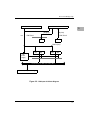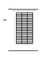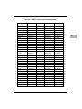
1
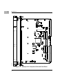
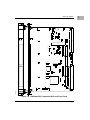
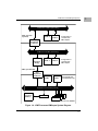
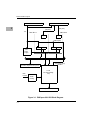
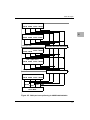
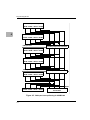
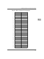
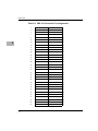
PMCspan
PMC Adapter Carrier Module
Installation and Use
PMCSPANA/IH2
Notice
While reasonable efforts have been made to assure the accuracy of this document,
Motorola, Inc. assumes no liability resulting from any omissions in this document, or from
the use of the information obtained therein. Motorola reserves the right to revise this
document and to make changes from time to time in the content hereof without obligation
of Motorola to notify any person of such revision or changes.
No part of this material may be reproduced or copied in any tangible medium, or stored in
a retrieval system, or transmitted in any form, or by any means, radio, electronic,
mechanical, photocopying, recording or facsimile, or otherwise, without the prior written
permission of Motorola, Inc.
It is possible that this publication may contain reference to, or information about Motorola
products (machines and programs), programming, or services that are not announced in
your country. Such references or information must not be construed to mean that Motorola
intends to announce such Motorola products, programming, or services in your country.
Restricted Rights Legend
If the documentation contained herein is supplied, directly or indirectly, to the U.S.
Government, the following notice shall apply unless otherwise agreed to in writing by
Motorola, Inc.
Use, duplication, or disclosure by the Government is subject to restrictions as set forth in
subparagraph (c)(1)(ii) of the Rights in Technical Data and Computer Software clause at
DFARS 252.227-7013.
Motorola, Inc.
Computer Group
2900 South Diablo Way
Tempe, Arizona 85282
Preface
The PMCspan PMC Adapter Carrier Module Installation and Use manual provides the
following information for the PMCspan:
❏
Hardware preparation and installation instructions
❏
Operating instructions
❏
A functional description
❏
Interfacing information and data
This manual is intended for anyone who wants to supply OEM systems, add capability to
an existing compatible system, and/or work in a lab environment for experimental
purposes. A basic knowledge of computers and digital logic is assumed.
After using this manual, you may wish to become familiar with the publications listed in
Appendix A.
© Copyright Motorola, Inc. 1999
All Rights Reserved
Printed in the United States of America
February 1999
Safety Summary
Safety Depends On You
The following general safety precautions must be observed during all phases of operation, service, and repair of this
equipment. Failure to comply with these precautions or with specific warnings elsewhere in this manual violates safety
standards of design, manufacture, and intended use of the equipment. Motorola, Inc. assumes no liability for the
customer’s failure to comply with these requirements.
The safety precautions listed below represent warnings of certain dangers of which Motorola is aware. You, as the
user of the product, should follow these warnings and all other safety precautions necessary for the safe operation of
the equipment in your operating environment.
Ground the Instrument.
To minimize shock hazard, the equipment chassis and enclosure must be connected to an electrical ground. The
equipment is supplied with a three-conductor ac power cable. The power cable must be plugged into an approved
three-contact electrical outlet. The power jack and mating plug of the power cable meet International Electrotechnical
Commission (IEC) safety standards.
Do Not Operate in an Explosive Atmosphere.
Do not operate the equipment in the presence of flammable gases or fumes. Operation of any electrical equipment in
such an environment constitutes a definite safety hazard.
Keep Away From Live Circuits.
Operating personnel must not remove equipment covers. Only Factory Authorized Service Personnel or other
qualified maintenance personnel may remove equipment covers for internal subassembly or component replacement
or any internal adjustment. Do not replace components with power cable connected. Under certain conditions,
dangerous voltages may exist even with the power cable removed. To avoid injuries, always disconnect power and
discharge circuits before touching them.
Do Not Service or Adjust Alone.
Do not attempt internal service or adjustment unless another person capable of rendering first aid and resuscitation is
present.
Use Caution When Exposing or Handling the CRT.
Breakage of the Cathode-Ray Tube (CRT) causes a high-velocity scattering of glass fragments (implosion). To
prevent CRT implosion, avoid rough handling or jarring of the equipment. Handling of the CRT should be done only
by qualified maintenance personnel using approved safety mask and gloves.
Do Not Substitute Parts or Modify Equipment.
Because of the danger of introducing additional hazards, do not install substitute parts or perform any unauthorized
modification of the equipment. Contact your local Motorola representative for service and repair to ensure that safety
features are maintained.
Dangerous Procedure Warnings.
Warnings, such as the example below, precede potentially dangerous procedures throughout this manual. Instructions
contained in the warnings must be followed. You should also employ all other safety precautions which you deem
necessary for the operation of the equipment in your operating environment.
!
WARNING
To prevent serious injury, use extreme caution when handling,
testing, and adjusting this equipment. Dangerous voltages,
capable of causing death are present.
All Motorola printed wiring boards (PWBs) are manufactured by UL-recognized
manufacturers, with a flammability rating of 94V-0.
!
WARNING
This equipment generates, uses, and can radiate electro-magnetic energy.
It may cause or be susceptible to electro-magnetic interference (EMI) if
not installed and used in a cabinet with adequate EMI protection.
If any modifications are made to the product, the modifier assumes
responsibility for radio frequency interference issues. Changes or
modifications not expressly approved by Motorola Computer Group could
void the user’s authority to operate the equipment.
European Notice: Board products with the CE marking comply with the EMC
Directive (89/336/EEC). Compliance with this directive implies conformity to
the following European Norms:
EN55022 (CISPR 22)
Radio Frequency Interference
EN50082-1 (IEC801-2, IEC801-3, IEC801-4)
Electromagnetic Immunity
The product also fulfills EN60950 (product safety) which is essentially the requirement
for the Low Voltage Directive (73/23/EEC).
This board product was tested in a representative system to show compliance with the
above mentioned requirements. A proper installation in a CE-marked system will maintain
the required EMC/safety performance.
For minimum RF emissions, it is essential that you implement the following conditions:
1. Install shielded cables on all external I/O ports.
2. Connect conductive chassis rails to earth ground to provide a path for connecting
shields to earth ground.
3. Tighten all front panel screws.
The computer programs stored in the Read Only Memory of this device contain material
copyrighted by Motorola Inc. and may be used only under a license such as those contained
in Motorola’s software licenses.
The software described herein and the documentation appearing herein are furnished under
a license agreement and may be used and/or disclosed only in accordance with the terms of
the agreement.
The software and documentation are copyrighted materials. Making unauthorized copies is
prohibited by law.
No part of the software or documentation may be reproduced, transmitted, transcribed,
stored in a retrieval system, or translated into any language or computer language, in any
form or by any means without the prior written permission of Motorola, Inc.
Contents
CHAPTER 1
Introduction
Product Overview ......................................................................................................1-1
PMCspan Models.......................................................................................................1-1
PMCspan Features .....................................................................................................1-5
Electrical Requirements......................................................................................1-6
Product Reliability (MTBF)................................................................................1-6
VME Processor/PMCspan System ............................................................................1-6
CHAPTER 2
Hardware Installation
Introduction................................................................................................................2-1
Packaging ...................................................................................................................2-1
ESD Precautions ........................................................................................................2-2
Installing PMC Adapters............................................................................................2-2
Installing a PMCspan-001 or PMCspan-002 .............................................................2-4
Installing a PMCspan-010..........................................................................................2-9
CHAPTER 3
Functional Description
Introduction................................................................................................................3-1
PCI-to-PCI Bridge Chip.............................................................................................3-1
On-Board 3.3 Volt Power Supply ..............................................................................3-4
PMC Interface ............................................................................................................3-4
PCI Expansion ...........................................................................................................3-4
Secondary Expansion.................................................................................................3-4
Clock Configuration...................................................................................................3-5
PMC Present Signals..................................................................................................3-5
Front Panel LEDs.......................................................................................................3-5
PMC Performance......................................................................................................3-5
vii
CHAPTER 4
Programming Model
Introduction ............................................................................................................... 4-1
21150 Configuration Registers .................................................................................. 4-1
Configuration Transactions ....................................................................................... 4-1
Type 0 Configuration Cycles.............................................................................. 4-3
Type 1 Configuration Cycles.............................................................................. 4-3
Type 1 to Type 1 Forwarding ............................................................................. 4-4
Special Cycles .................................................................................................... 4-4
PMC Interrupts .......................................................................................................... 4-5
PMC Clock, Request, Grant Assignment .................................................................. 4-9
PMC Present Signal Assignment............................................................................... 4-9
CHAPTER 5
Connectors
Introduction ............................................................................................................... 5-1
VMEbus Connectors (P1/P2) .................................................................................... 5-1
PMC Slot Connectors (J11/J12/J14) (J21/J22/J24) ................................................... 5-4
PMCspan-001/-002 PCI Expansion Connector (P4/P5).......................................... 5-11
PMCspan-001/-002 Secondary PCI Bus Connector (J3) ........................................ 5-13
PMCspan-010 PCI Bus Connector (P3) .................................................................. 5-15
APPENDIX A
Related Documentation
Related Specifications .............................................................................................. A-1
FIGURES
Figure 1-1. PMCspan-001 Component Side and Front Panel ................................... 1-2
Figure 1-2. PMCspan-002 Component Side and Front Panel ................................... 1-3
Figure 1-3. PMCspan-010 Component Side and Front Panel ................................... 1-4
Figure 1-4. VME Processor/PMCspan System Diagram .......................................... 1-7
Figure 2-1. PMC Module Placement on PMCspan ................................................... 2-3
Figure 2-2. PMCspan-001 Installation on an MVME3600 ....................................... 2-5
Figure 2-3. PMCspan-002 Installation on an MVME2300 ....................................... 2-6
Figure 2-4. PMCspan-010 Installation onto a PMCspan-001/002 .......................... 2-10
Figure 3-1. PMCspan-001/-002 Block Diagram ....................................................... 3-2
Figure 3-2. PMCspan-010 Block Diagram................................................................ 3-3
Figure 4-1. 21150 PCI Configuration Registers ........................................................ 4-2
Figure 4-2. PMCspan Interrupt Routing for MVME2600/3600/4600 ...................... 4-7
Figure 4-3. PMCspan Interrupt Routing for MVME2300......................................... 4-8
Figure 4-4. Serial Clock Mask................................................................................. 4-10
viii
TABLES
Table 3-1. PowerPC 60x Bus to PMCspan PMC Access Timing..............................3-6
Table 3-2. PMCspan PMC to ECC Memory Access Timing.....................................3-7
Table 4-1. Secondary Device Number to IDSEL Mapping .......................................4-4
Table 4-2. PMC Interrupt Routing .............................................................................4-5
Table 4-3. PMC Clock, Request, Grant Assignments................................................4-9
Table 4-4. PMC Present to GPIO Assignments .......................................................4-10
Table 5-1. VME P1 Connector Pin Assignments ......................................................5-1
Table 5-2. VME P2 Connector Pin Assignments ......................................................5-3
Table 5-3. PMC J11 Connector Pin Assignments ......................................................5-5
Table 5-4. PMC J12 Connector Pin Assignments......................................................5-6
Table 5-5. PMC J14 Connector Pin Assignments......................................................5-7
Table 5-6. PMC J21 Connector Pin Assignments......................................................5-8
Table 5-7. PMC J22 Connector Pin Assignments......................................................5-9
Table 5-8. PMC J24 Connector Pin Assignments....................................................5-10
Table 5-9. PMCspan-001/-002 P4/P5 Connector Pin Assignments.........................5-11
Table 5-10. PMCspan-001/-002 J3 Connector Pin Assignments.............................5-13
Table 5-11. PMCspan-010 P3 Connector Pin Assignments.....................................5-15
ix
x
1Introduction
1
Product Overview
PMCspan is a PMC carrier module that provides PCI expansion capability
for an MVME2300/MVME2600/MVME2700/MVME3600/ or
MVME4600 host VME processor module. The PMCspan has two PMC
slots which support either two single-wide PMC adapters or one doublewide PMC adapter. Two PMCspan modules can be stacked on a host VME
processor, allowing up to four additional PMC adapters.
PMCspan Models
There are three PMCspan models:
❏
PMCspan-001: Primary PMC Carrier Module that attaches to the
MVME2600/2700/3600/4600 and provides two PMC slots. It
includes a DEC 21150 PCI-to-PCI bridge chip with 32-bit PCI
support and accepts a PMCspan-010 Secondary PCI Expansion
Module.
❏
PMCspan-002: Primary PMC Carrier Module that attaches to the
MVME2300 and provides two PMC slots. It includes a DEC 21150
PCI-to-PCI bridge chip with 32-bit PCI support, and accepts a
PMCspan-010 Secondary PCI Expansion Module.
❏
PMCspan-010: Secondary PMC Carrier Module that attaches to
either a PMCspan-001 or PMCspan-002 and provides two PMC
slots. The PMCspan-010 is identical to the PMCspan-001/-002
except that the PCI-to-PCI bridge chip, the Clock Configuration
logic, and the primary PCI expansion connector are not present.
All PMCspan models provide both front panel and VME bus I/O.
1-1
Introduction
C7
C5
L1
CR1
C8
Q1
C3
A1
B1
C1
C6
C4
C1
R1
Q2
C9
C12
+
C11
C10 C14
+
+
+
C15
+
C17
P1
R2 R3
C13
C15
R5
J3
2
C2
DS2
2
1
1
2
C18
+
R4
C21
C20
J22
J21
C30 C31
C27
+
64
1
2
C32
+
C33
J24
63
64
1
2
2
R16
C34
R26
R27
1
R17
R18
R25
R24
R23
R22
R21
R20
R19
64
R25
63
63
C24 C29 R14
C28
C23
C26
U2
+
C36
Z1
A1
B1
C1
D1
U3
J12
+
C38
J11
C36
R29
R28
R32
R31
R30
63
64
1
2
64
63
P2
R34
R33
C40
R35
J14
C42
C41
PCI MEZZANINE CARD
+
R36
64
63
Z32
A32
B32
C32
D32
C50
C43
C49
C47
J2
C51
4
1
C45
C44
C48
C45
Figure 1-1. PMCspan-001 Component Side and Front Panel
A32
B32
C32
R10
R8
R11
R13
R12
R6
C22
PCI MEZZANINE CARD
R7
R9
C19
U1
+
+
+
DS1
PMC2
PMC1
2015 9703
1-2
1
113
114
1
C7
C5
L1
A1
B1
C1
C6
C8
Q1
C3
R1
Q2
+
C11
C10 C14
C12
C9
+
P1
C15
R2 R3
C13
+
C17
C15
R5
J3
2
CR1
C4
C1
DS2
1
C2
+
+
DS1
PMC2
PMC1
2
1
1
2
C18
+
R4
C21
C20
C30 C31
C26
C27
+
64
1
2
C32
+
C33
J24
C34
63
64
1
2
R26
R27
2
R16
C36
R18
R25
R24
R23
R22
R21
R20
R19
1
R25
64
R17
+
63
63
C24 C29 R14
C28
C23
J21
J22
A32
B32
C32
R10
R8
R11
R13
R12
R6
C22
PCI MEZZANINE CARD
R7
R9
C19
U1
+
+
+
Z1
A1
B1
C1
D1
U3
J12
+
C38
J11
C36
R29
R28
R32
R31
R30
63
64
1
2
64
63
P2
R34
R33
C40
R35
U4
J14
C42
C41
PCI MEZZANINE CARD
+
R36
64
63
Z32
A32
B32
C32
D32
C50
C43
C49
C47
J2
C51
4
1
C45
C44
C48
C45
2016 9703
Figure 1-2. PMCspan-002 Component Side and Front Panel
1-3
1
PMCspan Models
113
114
Introduction
1
C7
C5
C2
L1
CR1
C8
Q1
C3
R1
Q2
C12
C9
+
C11
C10 C14
+
+
A1
B1
C1
C6
C4
C1
+
C15
+
C17
P1
R2 R3
C15
C13
DS2
DS1
PMC2
PMC1
R5
2
1
2
1
C18
+
R4
C21
C20
R11
63
64
1
2
64
63
R25
C32
+
R17
C33
J24
R16
C34
R25
R24
R23
R22
R21
R20
R19
+
C36
63
64
1
2
2
1
R27
R26
Z1
A1
B1
C1
D1
J12
+
C38
J11
C36
R29
R28
R32
R31
63
64
1
2
64
63
P2
R34
C40
R35
C42
J14
C41
PCI MEZZANINE CARD
+
R36
64
63
Z32
A32
B32
C32
D32
C50
C43
C49
C47
J2
C51
4
1
C45
C44
C48
C45
2017 9703
Figure 1-3. PMCspan-010 Component Side and Front Panel
C30 C31
C26
C27
+
C24 C29 R14
C28
C23
R6
R13
R12
R8
J21
J22
A32
B32
C32
R10
R7
R9
C19
U1
C22
PCI MEZZANINE CARD
1-4
+
+
+
PMCspan Features
PMCspan Features
PMCspans have the following features:
❏
They are operational with the MVME2300/2600/2700/3600/4600
processor modules.
❏
They provide support for two single-width PMC adapters or one
double-width PMC adapter.
❏
They incorporate 5V bus signaling voltage.
❏
They incorporate both PMC Bus and VMEbus connectors with the
following features:
– Two sets of three EIA E700 AAAB connectors for 32-bit PMC
interface to secondary PCI bus and user specific I/O.
– P1 connector for power and BGNT and IACK daisy chaining.
– 5-row P2 connector for power and PMC I/O.
❏
They incorporate a DEC 21150 PCI-to-PCI Bridge Interface device,
with the following features (PMCspan-001/-002 only):
– PCI Revision 2.1 compliant.
– 32-bit primary bus interface.
– 32-bit secondary bus interface.
– Delayed transactions for all PCI configuration, I/O, and memory
read commands, allowing up to three transactions
simultaneously in each direction
– Buffering (data and address) for posted memory write
commands in each direction, allowing up to five posted write
transactions simultaneously in each direction.
– Read data buffering in each direction.
– Concurrent primary and secondary bus operation to isolate
traffic.
– Enhanced address decoding.
– PCI transaction forwarding.
1-5
1
1
Introduction
Electrical Requirements
The voltage and current requirements for the PMCspan are as follows:
+5V
290 mA typical
440 mA maximum
+12V
None
-12V
None
Product Reliability (MTBF)
The reliability for the PMCspan is 75,000 hours MTBF.
VME Processor/PMCspan System
Figure 1-4 shows a block diagram of a PMCspan system: a VME processor
module, a PMCspan-001/-002 primary PMC carrier module, and a
PMCspan-010 secondary PMC carrier module.
The primary PMCspan interfaces to the VME processor module via the
PCI expansion connector. The expansion connector on the secondary bus
supports the secondary PMCspan. The PCI-to-PCI Bridge chip on the
PMCspan provides the interface between the primary PCI bus and the
secondary PCI bus.
1-6
VME Processor/PMCspan System
32-Bit PCI Local Bus (Secondary)
PMC span-010
(optional)
PMC 3
2 single wide or
1 double wide
PMC adapter
PMC 4
Secondary
Expansion
Connector
32-Bit PCI Local Bus (Secondary)
PCI-PCI
Bridge
PMC 1
2 single wide or
1 double wide
PMC adapter
PMC 2
PMC span-001/-002
PCI
Expansion
Connector
PMC
(second PMC slot
on MVME2300 only)
PMC
32/64-Bit PCI Local Bus (Primary)
Processor/
Memory
Raven
PCI Devices
VME Processor Module
Figure 1-4. VME Processor/PMCspan System Diagram
1-7
1
1
Introduction
1-8
2Hardware Installation
2
Introduction
The following sections discuss the installation of the PMCspan modules
and PMC adapters. The following installation procedures are provided:
❏
PMC adapter on a PMCspan
❏
PMCspan-001/-002 Primary PMC Carrier Module on a
MVME2300/2600/2700/3600/4600 VME processor module
❏
PMCspan-010 Secondary PMC Carrier Module on a PMCspan001/-002 Primary PMC Carrier Module
Refer to the installation instructions in VME processor module’s
installation and use manual before proceeding with these instructions.
Packaging
The PMCspan is packed in an anti-static package to protect it from any
static discharge. Observe standard handling practices of static sensitive
equipment.
Note
Each PMCspan ships with a standoff hardware kit for
attaching the primary PMCspan to the
MVME2300/2600/2700/3600/4600 and the secondary
PMCspan to the primary PMCspan.
2-1
ESD Precautions
2
ESD Precautions
Use ESD
Wrist Strap
Motorola strongly recommends that you use an antistatic wrist strap and a
conductive foam pad when installing or upgrading a system. Electronic
components such as disk drives, computer boards, and memory modules
can be damaged by ESD. After removing the component from the system
or its protective wrapper, place the component on a grounded and staticfree surface (and in the case of a board, component side up). Do not slide
the component over any surface.
If an ESD station is not available, you can avoid damage resulting from
ESD by wearing an antistatic wrist strap (available locally) that is attached
to an unpainted metal part of the system chassis.
Installing PMC Adapters
PCI mezzanine card (PMC) adapters mount on the PMCspan. Install the
PMC adapter modules on the PMCspan prior to installing the PMCspan
onto the VME processor module. Refer to the installation instructions that
come with the PMC adapter for any prerequisites.
Note
The PMCspan is keyed to accept only 5V PMC adapter
modules.
To install a PMC adapter, refer to Figure 2-1 and proceed as follows:
1. Position the PMCspan with the P1 and P2 connectors facing you.
!
Avoid touching areas of integrated circuitry; static discharge
can damage these circuits.
Caution
2. Remove the PMC slot filler panel from the PMCspan front panel.
2-2
Hardware Installation
2
2021 9704
Figure 2-1. PMC Module Placement on PMCspan
3. Slide the PMC module port connector into the PMC slot opening on
the PMCspan front panel
4. Align the PMC adapter over the PMCspan.
– Align the connectors on the underside of the PMC adapter with
the corresponding connectors (J11, J12, and J14) on the
PMCspan.
– Align the keying hole on the PMC adapter with the keying pin
on the PMcspan.
5. Gently press the PMC adapter onto the PMCspan.
6. Turn the PMCspan component-side down.
7. Insert the four short Phillips screws supplied with the PMC adapter
through the holes on the underside of the PMCspan, into the
standoffs at the corners of the PMC adapter (note that some PMC
adapters take a screw at each corner; others require only two screws
at the forward corners). Tighten the screws.
2-3
Installing a PMCspan-001 or PMCspan-002
2
Installing a PMCspan-001 or PMCspan-002
The difference between the PMCspan -001 and -002 is that the PMCspan001 mounts on top of the 2600/2700/3600/4600 series VME processor
module and The PMCspan-002 mounts onto an MVME2300 series
processor module. To upgrade or install a PMCspan, refer to Figure 2-2
(PMCspan-001) or Figure 2-3 (PMCspan-002) and proceed as follows:
1. Attach an ESD strap to your wrist. Attach the other end of the ESD
strap to the chassis as a ground. The ESD strap must be secured to
your wrist and to ground while you are performing the installation
procedure.
2. Perform an operating system shutdown. Turn the AC or DC power
off and remove the AC cord or DC power lines from the system.
Remove chassis or system cover(s) as necessary for access to the
VME module card cage.
!
Inserting or removing modules with power applied may result
in damage to module components.
Caution
!
Warning
Dangerous voltages, capable of causing death, are present in
this equipment. Use extreme caution when handling, testing,
and adjusting.
3. Carefully remove the VME processor module from the VMEbus
card slot and lay it flat, with connectors P1 and P2 facing you.
!
Avoid touching areas of integrated circuitry; static discharge
can damage these circuits.
Caution
4. Install the PMC adapter modules on the PMCspan and VME
processor module. Refer to Installing PMC Adapters on page 2-2
and the installation instructions that are supplied with the PMC
adapters.
2-4
Hardware Installation
2
P5
J5
2024 9704
Figure 2-2. PMCspan-001 Installation on an MVME3600
2-5
Installing a PMCspan-001 or PMCspan-002
2
P4
J4
2022 9704
Figure 2-3. PMCspan-002 Installation on an MVME2300
2-6
Hardware Installation
5. Attach the four standoffs to the VME processor module. For each
standoff:
– Insert the threaded end into the standoff hole at each corner of
the VME processor module.
– Thread the locking nuts onto the standoff tips.
– Tighten the nuts with a box-end wrench or a pair of needle nose
pliers.
Note
!
Caution
On the MVME2600, use the short standoff in corner with the
LED mezzanine module.
Do not remove an MVME3600 or MVME4600 processor
board from the base board. Use a small box-end wrench or
needle nose pliers to hold the nut in place.
6. Place the PMCspan on top of the VME processor module. Align the
mounting holes in each corner to the standoffs, and align PMCspan
connector (P4 or P5) with VME processor module connector (J4 or
J5).
7. Gently press the PMCspan and VME processor module together,
making sure that P4/P5 is fully seated into J4/J5.
8. Insert the four short Phillips screws through the holes at the corners
of the PMCspan and into the standoffs on the VME processor
module. Tighten the screws.
Note
The screws have two different head diameters. Use the
screws with the smaller heads on the standoffs next to
VMEbus connectors P1 and P2.
2-7
2
Installing a PMCspan-001 or PMCspan-002
9. Install the VME processor module and PMCspan into the card slots.
Be sure the modules are well seated in the backplane connectors. Do
not damage or bend connector pins.
2
10. Replace the chassis or system cover(s), reconnect the system to the
AC or DC power source, and turn the equipment power on.
2-8
Hardware Installation
Installing a PMCspan-010
2
The PMCspan-010 Secondary PMC Adapter Carrier Module mounts on
top of a PMCspan-001/-002 Primary PMC Adapter Carrier Module. To
install a PMCspan, refer to Figure 2-2 and proceed as follows:
1. Attach an ESD strap to your wrist. Attach the other end of the ESD
strap to the chassis as a ground. The ESD strap must be secured to
your wrist and to ground while you are performing the installation
procedure.
2. Perform an operating system shutdown. Turn the AC or DC power
off and remove the AC cord or DC power lines from the system.
Remove chassis or system cover(s) as necessary for access to the
VME module card cage.
!
Inserting or removing modules with power applied may result
in damage to module components.
Caution
!
Warning
Dangerous voltages, capable of causing death, are present in
this equipment. Use extreme caution when handling, testing,
and adjusting.
3. If the Primary PMC Carrier Module/VME processor module
assembly is in the VME chassis, carefully remove the modules from
the VMEbus card slot and lay it flat, with the P1 and p2 connectors
facing you.
!
Avoid touching areas of integrated circuitry; static discharge
can damage these circuits.
Caution
4. Install the PMC adapter modules on the PMCspan module. Refer to
Installing PMC Adapters on page 2-2 and the installation
instructions that are supplied with the PMC adapters.
2-9
Installing a PMCspan-010
2
P3
J3
2023 9704
Figure 2-4. PMCspan-010 Installation onto a PMCspan-001/002
2-10
Hardware Installation
5. Remove the four short Phillips screws from the standoffs in each
corner of the Primary PMC Carrier Module.
6. Attach the four standoffs to the Primary PMC Carrier Module.
7. Place the Secondary PMCspan module on top of the Primary
PMCspan module. Align the mounting holes in each corner to the
standoffs, and align secondary PMCspan connector P3 with primary
PMCspan connector J3.
8. Gently press the two PMCspan modules together, making sure that
P3 is fully seated in J3.
9. Insert the four short Phillips screws through the holes at the corners
of the secondary PMCspan and into the standoffs on the primary
PMCspan. Tighten the screws.
Note
The screws have two different head diameters. Use the
screws with the smaller heads on the standoffs next to
VMEbus connectors P1 and P2.
10. Install the VME processor module/PMCspan assembly into the card
slots. Be sure the modules are well seated in the backplane
connectors. Do not damage or bend connector pins.
11. Replace the chassis or system cover(s), reconnect the system to the
AC or DC power source, and turn the equipment power on.
2-11
2
Installing a PMCspan-010
2
2-12
3Functional Description
3
Introduction
This chapter describes the physical and electrical structure of the
PMCspan. Figure 3-1 and Figure 3-1 show the detailed block diagrams of
the PMCspan and its primary interfaces.
PMC adapter I/O is available through the PMCspan front panel opening
(for PMC adapters with front panel connectors) or through the PMCspan
VMEbus P2 backplane connector.
PCI-to-PCI Bridge Chip
The primary component on the PMCspan is the DEC 21150 PCI-to-PCI
bridge chip. This device provides the interface between the primary PCI
bus (processor side), and the secondary PCI bus, which provides the
interface to the PMC adapter. The bridge chip connects to the VMEbus
processor module PCI bus through the PCI Expansion connector. The
secondary PCI bus connects to each of the PCM slots and a an optional
secondary expansion connector. For a detailed description of the 21150
chip, refer to the 21150 data sheet, DEC part number EC-QPDLB-TE.
The DEC 21150 PCI-to-PCI Bridge chip supports a 32-bit primary bus
interface and a 32-bit secondary bus interface. This chip provides full
support for delayed transactions which enables the buffering of memory
read, I/O, and configuration transactions. It supports buffering of
simultaneous multiple posted write and delayed transactions in both
directions.
The 21150 has clock and arbitration pins to support PCI bus masters on the
secondary bus. These are used to provide clocks an bus arbitration for the
PMC adapter. The 21150 supports concurrent operation on the primary
and secondary PCI busses providing traffic isolation between the primary
and secondary busses.
3-1
Functional Description
VME P2 Connector (PMC I/O)
VME P1 Connector
3
(46 pins)
(64 pins)
+5V
PMC Slot 2
PMC Slot 1
J14
J24
PMC V(I/O)
J11
J12
J22
J21
3.3V
Power
Supply
32-bit PCI @ 33 MHz (Secondary Bus)
Secondary V(I/O)
ISA Bus
Secondary Expansion Receptacle
PMC
Present
21150
PCI-to-PCI Bridge
Chip
Clock
Config
PCI Expansion Connector
Figure 3-1. PMCspan-001/-002 Block Diagram
3-2
PCI-to-PCI Bridge Chip
VME P2 Connector (PMC I/O)
VME P1 Connector
3
(46 pins)
(64 pins)
+5V
PMC Slot 2
PMC Slot 1
J14
J24
PMC V(I/O)
J11
J12
J21
J22
3.3V
Power
Supply
32-bit PCI @ 33 MHz (Secondary Bus)
Secondary Expansion Plug
Figure 3-2. PMCspan-010 Block Diagram
3-3
Functional Description
On-Board 3.3 Volt Power Supply
The on-board PMCspan power supply circuit generates the 3.3 volts used
by the PCI-to-PCI bridge chip. The PCI-to-PCI bridge consumes 400 mA
maximum, leaving 4.6 Amps available to the PMC adapters. On the
PMCspan-010, 5 Amps is available to the PMC adapters.
3
PMC Interface
Each PMC slot has three EIA E700 AAAB connectors for a 32-bit PMC
interface to secondary PCI bus and user specific I/O. The PMCspan VME
backplane connector P2 provides 64 I/O signals for PMC 1, and 46 P2 I/O
signals for PMC 2. Refer to Chapter 5, Connectors, for the pin signal
assignments.
PCI Expansion
The PCI Expansion interface is provided by a 114-pin plug connector (P4
or P5) on the secondary side of the PMCspan. This mates to the PCI
Expansion connector on the VME processor module. Refer to Chapter 5,
Connectors, for the pin signal assignments.
The IDSEL for the 21150 chip is connected to AD20 on the PMCspan.
Therefore the 21150 Device Number on the primary PCI bus is 1_0100b.
Secondary Expansion
Secondary PCI bus expansion is provided by a 114-pin receptacle
connector, J3, on the primary side of the PMCspan-001/-002. This mates
to a 114-pin plug connector, P3, mounted on the secondary side of the
PMCspan-010. Refer to Chapter 5, Connectors, for the pin signal
assignments.
3-4
Clock Configuration
Clock Configuration
The DEC 21150 PCI-to-PCI Bridge chip will access the Clock
Configuration logic following a primary PCI bus reset. The 21150 will
automatically enable the PCI clock for all four PMC slots.
3
PMC Present Signals
The PMC PRESENT signal (BUSMODE1#) from each of the PMC
adapters (up to four) may be read any time following a reset through the
General Purpose I/O interface in the 21150. Refer to PMC Present Signal
Assignment on page 4-9.
Front Panel LEDs
There are two green LEDs located on the front panel of the PMCspan, one
for each PMC adapter. Both LEDs will be illuminated during reset. An
individual LED will be illuminated whenever a PMC adapter has been
granted bus mastership of the secondary PCI bus.
PMC Performance
All PMCspan models support 32-bit PCI operations at 33 MHz on the
PMC (secondary) side. The PMCspan-001/-002 primary carrier module
supports 32-bit PCI operations on the processor (primary) side. Refer to
the 21150 data sheet (EC-QPDLB-TE) for PCI transaction timing
information across the bridge.
Writes to the PCI bus are also posted by the Raven chip ASIC, so this
section will focus mainly on read cycles. The read access latency for
PMCspan-bound cycles initiated by 60X bus master consists of the
following components:
3-5
Functional Description
3
Tstart
Start-up time (TS# to PCI bus Request).
Tstart is 6 system clocks.
Tarb
On-board PCI bus arbitration time.
Tac
On-board PCI access time (FRAME# to TRDY#).
Tlat
Latency through PCI-to-PCI bridge.
Tdelay
Delay time from TRDY# on PCI to TA# on 60X bus. Tdelay
is 4 system clocks.
Table 3-1 shows the access timings for various types of transfers initiated
by a 60X system bus master to a PMCspan module.
Table 3-1. PowerPC 60x Bus to PMCspan PMC Access Timing
System Clock Periods Required for:
Access Type
1st Beat
2nd Beat
3rd Beat
4th Beat
Total
Clocks
4-Beat Read
(32-bit PCI Target)
49
1
1
1
52
4-Beat Write
(32-bit PCI Target)
4
1
1
1
7
1-Beat Read
(aligned, 4 bytes or less)
38
-
-
-
38
1-Beat Write
4
-
-
-
4
Notes Write cycles are posted by the Raven ASIC.
Assumes no pipeline. Pipelined cycles would improve
these numbers.
Tarb is assumed to be 4 system clocks (2 PCI clocks).
Tac is assumed to be 6 system clocks (3 PCI clocks):
Medium DEVSEL# target, zero wait PCI timing.
3-6
PMC Performance
Table 3-2 shows the ECC memory access latency for PMCspan-initiated
cycles.
3
Table 3-2. PMCspan PMC to ECC Memory Access Timing
PCI Clock Periods Required for:
Access Type
1st Beat
2nd Beat
3rd Beat
nth Beat
32-bit Burst Reads
17
1
1
1
32-bit Burst Writes
3
1
1
1
1-Beat Read
17
-
-
-
1-Beat Write
3
-
-
-
Notes 1. The latency assumes two system clocks
for 60X system bus arbitration.
2. The latency is based on 60ns, fast-page
DRAM timing. It is also assumed that L2
is either disabled or missed.
3. Write timings assume write posting
FIFO is initially empty.
3-7
Functional Description
3
3-8
4Programming Model
4
Introduction
This chapter describes the programming model for the PMCspan.
21150 Configuration Registers
The PCI Configuration Registers for the DEC PCI-to-PCI Bridge 21150
chip are shown in Figure 4-1. For a detailed register bit description, refer
to the 21150 data sheet, DEC part number EC-QPDLB-TE.
Configuration Transactions
PCI configuration transactions are used to initialize the PCI system
including the PCI-to-PCI bridge and devices on the PMC adapter. All
21150 registers are accessible only in the configuration space. In addition
to accepting configuration transactions for initialization of its own
configuration registers, the 21150 also forwards configuration transactions
bound for devices on the PMC adapter, as well as special cycle generation
on the secondary PCI bus. These two types of configuration transactions
are supported by Type 0 and Type 1 configuration cycles.
4-1
Programming Model
Device ID ($0022)
Vendor ID ($1011)
$00
Status
Command
$04
Class Code
Reserved
4
Header Type
Primary Latency
Timer
Revision ID
$08
Cache Line Size
$0C
Reserved
$10
Reserved
$14
Secondary Latency
Timer
Subordinate Bus
Number
Secondary Bus
Number
Primary Bus
Number
$18
Secondary Status
I/O Limit Address
I/O Base Address
Memory Limit Address
Memory Base Address
$20
Prefetchable Memory Limit Address
Prefetchable Memory Base Address
$24
$1C
Prefetchable Memory Base Address Upper 32 Bits
$28
Prefetchable Memory Limit Address Upper 32 Bits
$2C
I/O Limit Address Upper 16 Bits
I/O Base Address Upper 16 Bits
$30
Subsystem ID
Subsystem Vendor ID
$34
Reserved
$38
Bridge Control
Interrupt Pin
Reserved
$3C
Arbiter Control
Diagnostic Control
Chip Control
$40
Reserved
$44
Reserved
$48
Reserved
$4C
Reserved
$50
Reserved
$54
Reserved
$58
Reserved
$5C
Reserved
$60
GPIO Input Data
GPIO Output
Enable Control
GPIO Output Data
p_serr_l Event
Disable
Reserved
p_serr_l Status
Secondary Clock Control
Reserved
$68
$6C$FF
Note
Writes to Reserved locations are don’t care.
Reads to Reserved locations return zeros.
Figure 4-1. 21150 PCI Configuration Registers
4-2
$64
Configuration Transactions
Type 0 Configuration Cycles
Type 0 configuration cycles are issued to configure devices on the same
bus as the initiator. The processor will access configuration registers
within the 21150, issuing a Type 0 cycle on the primary PCI bus by
programming the Raven CONADD Register for Bus Number 0, and
Device Number 1_0100 (binary). The Function Code is ignored by the
21150 since it is a single-function device. The RAVEN chip will translate
this configuration address to an IDSEL# on AD20, which is connected to
the DEVSEL# on the 21150 on the PMCspan.
The 21150 limits all configuration register accesses to a single double
word data transfer and returns a target disconnect with the first data
transfer if additional data phases are requested. All bytes of the requested
double word are returned, regardless of the PCI byte enable bits. Type 0
configuration transactions do not use the 21150 data buffers so these
transactions are completed immediately regardless of the state of the data
buffers.
The 21150 will ignore all Type 0 transactions initiated on the secondary
PCI bus.
Type 1 Configuration Cycles
Type 1 configuration cycles are issued to configure PMC adapters. The
processor will access configuration registers within the PMC adapters by
issuing a Type 1 cycle on the primary PCI bus by programming the Raven
CONADD Register for Bus Number $01 (i.e., the Bus Number
programmed into the Secondary Bus Number register), and the Device
Number per Table 4-1. The Function Code is dependent on the PMC
adapters.
The 21150 will perform a Type 1 to Type 0 translation when the Type 1
transaction generated on the primary bus is intended for a PMC adapter on
the secondary bus. The PMC adapter can then respond to the Type 0
transaction.
The 21150 forwards Type 1 to Type 0 configuration transactions as
delayed transactions which are limited to a single data transfer.
4-3
4
Programming Model
Table 4-1. Secondary Device Number to IDSEL Mapping
Device
Number
(Hex)
Secondary AD(31:16)
(Binary)
AD Bit
Used as
IDSEL#
Purpose
0-1
0000_0000_0000_0001 0000_0000_0000_0010
-
Implemented by 21150 but not
used
2
0000_0000_0000_0100
18
PMC 1 IDSEL#
(Slot 1 on PMCspan-001/-002)
3
0000_0000_0000_1000
19
PMC 2 IDSEL#
(Slot 2 on PMCspan-001/-002)
4
0000_0000_0001_0000
20
PMC 3 IDSEL#
(Slot 1 on PMCspan-010)
5
0000_0000_0010_0000
21
PMC 4 IDSEL#
(Slot 2 on PMCspan-010)
6-F
0000_0000_0100_0000 1000_0000_0000_0000
22 - 31
Implemented by 21150 but not
used
10 - 1E
0000_0000_0000_0000
None
Not implemented by 21150
1F
Special Cycle Data
-
Special Cycles for PMC
4
Type 1 to Type 1 Forwarding
If the 21150 detects a Type 1 configuration transaction intended for a PCI
bus downstream from the secondary bus (i.e., another PCI bus on a PMC
adapter), the 21150 will forward the transaction unchanged to the
secondary bus. This transaction will eventually get translated to a Type 0
transaction or a Special Cycle by a downstream PCI-to-PCI bridge.
Special Cycles
Special Cycle transactions generated on the primary PCI bus are ignored
by the 21150. However, Special Cycle commands can be sent to the PMC
adapter using a Type 1 Configuration transaction. The 21150 will generate
a Special Cycle on the secondary bus when it detects a Type 1 transaction
on the primary bus with the following conditions:
4-4
PMC Interrupts
❏
The lower two primary address bits AD(1:0) are 01 (binary)
❏
The device number in AD(15:11) is 1_1111 (binary)
❏
The function number in AD(10:8) is 111 (binary)
❏
The register number in AD(7:2) is 00_0000 (binary)
❏
The bus number in AD(23:16) is $01 (i.e., the value in the
Secondary Bus Number Register)
❏
The bus command on C/BE# is a configuration write command
4
The 21150 translates the Type 1 Configuration command to a Special
Cycle and forwards the address and data unchanged. The transaction is
forwarded as a delayed transaction but the target response is not forwarded
back because Special Cycles result in a master abort. If more than one data
transfer is requested during a Special Cycle, the 21150 responds with a
target disconnect during the first data phase.
PMC Interrupts
The routing of interrupts from each PMC adapter is described in Table 4-2.
Figure 4-2 and Figure 4-3 show the overall routing back to the Raven chip
on the VME processor modules.
Table 4-2. PMC Interrupt Routing
Device on
Secondary Bus
(Hex)
Device
(PMC Adapter)
Interrupt Pin
PCI Interrupt
02 (PMC 1)
INTA#
INTC#
INTB#
INTD#
INTC#
INTA#
INTD#
INTB#
4-5
Programming Model
Table 4-2. PMC Interrupt Routing
Device on
Secondary Bus
(Hex)
Device
(PMC Adapter)
Interrupt Pin
PCI Interrupt
03 (PMC 2)
INTA#
INTD#
INTB#
INTA#
INTC#
INTB#
INTD#
INTC#
INTA#
INTA#
INTB#
INTB#
INTC#
INTC#
INTD#
INTD#
INTA#
INTB#
INTB#
INTC#
INTC#
INTD#
INTD#
INTA#
4
04 (PMC 3)
05 (PMC 4)
4-6
PMC Interrupts
PMC 4 (PMC Slot 2)
INTA# INTB#
INTC#
INTD#
4
PMC 3 (PMC Slot 1)
INTA# INTB#
INTC#
INTD#
Secondary Expansion Connector
PMCspan-010
Secondary Expansion Connector
PMC 2 (PMC Slot 2)
INTC#
INTA# INTB#
INTD#
PMC 1 (PMC Slot 1)
INTA# INTB#
INTC#
INTD#
PMCspan-001
PCI Expansion Connector
PMC Slot
INTA# INTB#
INTC#
INTA# INTB#
IRQ9
IRQ10
INTD#
INTC#
IRQ11
INTD#
IRQ12
Raven MPIC
MVME2600/3600/4600
Figure 4-2. PMCspan Interrupt Routing for MVME2600/3600/4600
4-7
Programming Model
PMC 4 (PMC Slot 2)
INTA# INTB#
4
INTC#
INTD#
PMC 3 (PMC Slot 1)
INTA# INTB#
INTC#
INTD#
PMCspan-010
Secondary Expansion Connector
PMC 2 (PMC Slot 2)
INTA# INTB#
INTC#
INTD#
PMC 1 (PMC Slot 1)
INTA# INTB#
INTC#
INTD#
PMCspan-002
PCI Expansion Connector
PMC Slot 2
INTA# INTB# INTC#
PMC Slot 1
INTA# INTB# INTC#
MVME2300
INTD#
INTD#
INTA# INTB# INTC# INTD#
IRQ9 IRQ10 IRQ11 IRQ12
Raven MPIC
Figure 4-3. PMCspan Interrupt Routing for MVME2300
4-8
PMC Clock, Request, Grant Assignment
PMC Clock, Request, Grant Assignment
The 21150 bridge chip provide individual clock sources and arbitration
logic for each PMC adapter on the secondary PCI bus. The PMCspan
routes the secondary PCI bus Clock, Request and Grant signals between
the 21150 bridge chip and the PMC slots as shown in Table 4-3.
4
Table 4-3. PMC Clock, Request, Grant Assignments
PMC
21150
Clock Source
21150
Request
21150
Grant
1 (Slot 1 on PMCspan-001/-002)
s_clk_o(0)
s_req_l(0)
s_gnt_l(0)
2 (Slot 2 on PMCspan-001/-002)
s_clk_o(1)
s_req_l(1)
s_gnt_l(1)
3 (Slot 1 on PMCspan-010)
s_clk_o(2)
s_req_l(2)
s_gnt_l(2)
4 (Slot 2 on PMCspan-010)
s_clk_o(3)
s_req_l(3)
s_gnt_l(3)
PMC Present Signal Assignment
The PMCspan hardwires the BUSMODE(4:2)# encoding signals to 001
(binary) for each PMC slot indicating that the PMCspan supports PCI
protocol. The signal BUSMODE1# returned from each PMC adapter
indicates there is a PMC adapter installed in the slot and that the PMC
adapter supports PCI protocol. The PMC Present signals from each PMC
slot may be read at any time following a reset on the 21150 GPIO pins.
Table 4-4 shows the assignment of the PMC Present signals to the GPIO
pins. Figure 4-4 shows the values in the Serial Clock Mask register
following a reset. Serial Clock Mask bit 13 is 0 in order to enable
s_clk_o(9) for the 21150 s_clk input.
4-9
Programming Model
Table 4-4. PMC Present to GPIO Assignments
PMC Present Signal
4
GPIO bit
1 (Slot 1 on PMCspan-001/-002)
0
2 (Slot 2 on PMCspan-001/-002)
1
3 (Slot 1 on PMCspan-010)
2
4 (Slot 2 on PMCspan-010)
3
15
14
13
12
11
10
9
8
7
6
5
4
3
2
1
0
0
0
0
1
1
1
1
1
0
0
0
0
0
0
0
0
Figure 4-4. Serial Clock Mask
4-10
5Connectors
5
Introduction
The PMCspan module connectors provide I/O and for interfaces to the
VME processor modules and to other PMCspan modules. The pin
assignments for the connectors PMCspan connections are provided in the
following sections.
VMEbus Connectors (P1/P2)
The VMEbus P1 connector is a partially populated version of the 96-pin
DIN type connector. The P1 Connector contains 23 pins and is used to
provide +5V power to the PMCspan module. IACK and Bus Grant signals
are passed through as required by the VME specification. The P2 VMEbus
connector is a 5-row 160-pin connector and provides P2 I/O for the PMC
adapter modules.
The pin assignments for P1 and P2 are shown in Table 5-1 and 5.2.
Table 5-1. VME P1 Connector Pin Assignments
ROW A
ROW B
ROW C
1
1
2
2
3
3
4
BG0IN_L
4
5
BG0OUT_L
5
6
BG1IN_L
6
7
BG1OUT_L
7
8
BG2IN_L
8
9
GND
BG2OUT_L
GND
9
5-1
Connectors
Table 5-1. VME P1 Connector Pin Assignments (Continued)
ROW A
10
11
5
GND
ROW B
ROW C
BG3IN_L
10
BG3OUT_L
11
12
12
13
13
14
14
15
GND
15
16
17
16
GND
17
18
19
18
GND
20
GND
20
21
IACKIN_L
21
22
IACKOUT_L
22
23
5-2
19
GND
23
24
24
25
25
26
26
27
27
28
28
29
29
30
30
31
-12V
32
+5.0V
+5.0V
+12V
31
+5.0V
32
VMEbus Connectors (P1/P2)
Table 5-2. VME P2 Connector Pin Assignments
1
2
3
4
5
6
7
8
9
10
11
12
13
14
15
16
17
18
19
20
21
22
23
24
25
26
27
28
29
30
31
32
ROW Z
PMC2IO2
GND
PMC2IO5
GND
PMC2IO8
GND
PMC2IO11
GND
PMC2IO14
GND
PMC2IO17
GND
PMC2IO20
GND
PMC2IO23
GND
PMC2IO26
GND
PMC2IO29
GND
PMC2IO32
GND
PMC2IO35
GND
PMC2IO38
GND
PMC2IO41
GND
PMC2IO44
GND
PMC2IO46
GND
ROW A
PMC1IO2
PMC1IO4
PMC1IO6
PMC1IO8
PMC1IO10
PMC1IO12
PMC1IO14
PMC1IO16
PMC1IO18
PMC1IO20
PMC1IO22
PMC1IO24
PMC1IO26
PMC1IO28
PMC1IO30
PMC1IO32
PMC1IO34
PMC1IO36
PMC1IO38
PMC1IO40
PMC1IO42
PMC1IO44
PMC1IO46
PMC1IO48
PMC1IO50
PMC1IO52
PMC1IO54
PMC1IO56
PMC1IO58
PMC1IO60
PMC1IO62
PMC1IO64
ROW B
+5.0V
GND
GND
+5.0V
GND
GND
+5.0V
ROW C
PMC1IO1
PMC1IO3
PMC1IO5
PMC1IO7
PMC1IO9
PMC1IO11
PMC1IO13
PMC1IO15
PMC1IO17
PMC1IO19
PMC1IO21
PMC1IO23
PMC1IO25
PMC1IO27
PMC1IO29
PMC1IO31
PMC1IO33
PMC1IO35
PMC1IO37
PMC1IO39
PMC1IO41
PMC1IO43
PMC1IO45
PMC1IO47
PMC1IO49
PMC1IO51
PMC1IO53
PMC1IO55
PMC1IO57
PMC1IO59
PMC1IO61
PMC1IO63
ROW D
PMC2IO1
PMC2IO3
PMC2IO4
PMC2IO6
PMC2IO7
PMC2IO9
PMC2IO10
PMC2IO12
PMC2IO13
PMC2IO15
PMC2IO16
PMC2IO18
PMC2IO19
PMC2IO21
PMC2IO22
PMC2IO24
PMC2IO25
PMC2IO27
PMC2IO28
PMC2IO30
PMC2IO31
PMC2IO33
PMC2IO34
PMC2IO36
PMC2IO37
PMC2IO39
PMC2IO40
PMC2IO42
PMC2IO43
PMC2IO45
GND
No Connect
1
2
3
4
5
6
7
8
9
10
11
12
13
14
15
16
17
18
19
20
21
22
23
24
25
26
27
28
29
30
31
32
5-3
5
Connectors
PMC Slot Connectors (J11/J12/J14)
(J21/J22/J24)
Each PMC slot has a set of three 64-pin connectors (EIA E700 AAAB) for
connection to the 32-bit secondary PCI bus and for PMC I/O. The PMC
Slot 1 connectors are as J11, J12 and J14; the PMC Slot 2 connectors are
J21, J22 and J24.
All 64 I/O signals from PMC 1 (J14) are routed to P2, while only the first
46 I/O signals of PMC 2 (J24) are routed to P2. The pin assignments for
these connectors are shown in tables 5-3 through 5-8.
5
5-4
PMC Slot Connectors (J11/J12/J14) (J21/J22/J24)
Table 5-3. PMC J11 Connector Pin Assignments
1
TCK
-12V
2
3
GND
PMCINTAD#
4
5
PMCINTBA#
PMCINTCB#
6
7
PMC13P#
+5.0V
8
9
PMCINTDC#
PCI-RSVD
10
11
GND
PCI-RSVD
12
13
PMC13CLK
GND
14
15
GND
PMC13GNT#
16
17
PMC13REQ#
+5.0v
18
19
V(I/O)
S_AD31
20
21
S_AD28
S_AD27
22
23
S_AD25
GND
24
25
GND
S_C/BE3#
26
27
S_AD22
S_AD21
28
29
S_AD19
+5.0V
30
31
V(I/O)
S_AD17
32
33
S_FRAME#
GND
34
35
GND
S_IRDY#
36
37
S_DEVSEL#
+5.0V
38
39
GND
S_LOCK#
40
41
S_SDONE#
S_SBO#
42
43
S_PAR
GND
44
45
V(I/O)
S_AD15
46
47
S_AD12
S_AD11
48
49
S_AD9
+5.0V
50
51
GND
S_C/BE0#
52
53
S_AD6
S_AD5
54
55
S_AD4
GND
56
57
V(I/O)
S_AD3
58
59
S_AD2
S_AD1
60
61
S_AD0
+5.0V
62
63
GND
S_REQ64#
64
5
5-5
Connectors
Table 5-4. PMC J12 Connector Pin Assignments
5
5-6
1
+12V
TRST#
2
3
TMS
PMC24TDI (TDO)
4
5
PMC13TDI
GND
6
7
GND
PCI-RSVD
8
9
PCI-RSVD
PCI-RSVD
10
11
BUSMODE2#
+3.3V
12
13
S_PCIRST#
BUSMODE3#
14
15
3.3V
BUSMODE4#
16
17
PCI-RSVD
GND
18
19
S_AD30
S_AD29
20
21
GND
S_AD26
22
23
S_AD24
+3.3V
24
25
PMC13IDSEL
S_AD23
26
27
+3.3V
S_AD20
28
29
S_AD18
GND
30
31
S_AD16
S_C/BE2#
32
33
GND
PMC-RSVD
34
35
S_TRDY#
+3.3V
36
37
GND
S_STOP#
38
39
S_PERR#
GND
40
41
+3.3V
S_SERR#
42
43
S_C/BE1#
GND
44
45
S_AD14
S_AD13
46
47
GND
S_AD10
48
49
S_AD8
+3.3V
50
51
S_AD7
PMC-RSVD
52
53
+3.3V
PMC-RSVD
54
55
PMC-RSVD
GND
56
57
PMC-RSVD
PMC-RSVD
58
59
GND
PMC-RSVD
60
61
S_ACK64#
+3.3V
62
63
GND
PMC-RSVD
64
PMC Slot Connectors (J11/J12/J14) (J21/J22/J24)
Table 5-5. PMC J14 Connector Pin Assignments
1
PMC13IO1
PMC13IO2
2
3
PMC13IO3
PMC13IO4
4
5
PMC13IO5
PMC13IO6
6
7
PMC13IO7
PMC13IO8
8
9
PMC13IO9
PMC13IO10
10
11
PMC13IO11
PMC13IO12
12
13
PMC13IO13
PMC13IO14
14
15
PMC13IO15
PMC13IO16
16
17
PMC13IO17
PMC13IO18
18
19
PMC13IO19
PMC13IO20
20
21
PMC13IO21
PMC13IO22
22
23
PMC13IO23
PMC13IO24
24
25
PMC13IO25
PMC13IO26
26
27
PMC13IO27
PMC13IO28
28
29
PMC13IO29
PMC13IO30
30
31
PMC13IO31
PMC13IO32
32
33
PMC13IO33
PMC13IO34
34
35
PMC13IO35
PMC13IO36
36
37
PMC13IO37
PMC13IO38
38
39
PMC13IO39
PMC13IO40
40
41
PMC13IO41
PMC13IO42
42
43
PMC13IO43
PMC13IO44
44
45
PMC13IO45
PMC13IO46
46
47
PMC13IO47
PMC13IO48
48
49
PMC13IO49
PMC13IO50
50
51
PMC13IO51
PMC13IO52
52
53
PMC13IO53
PMC13IO54
54
55
PMC13IO55
PMC13IO56
56
57
PMC13IO57
PMC13IO58
58
59
PMC13IO59
PMC13IO60
60
61
PMC13IO61
PMC13IO62
62
63
PMC13IO63
PMC13IO64
64
5
5-7
Connectors
Table 5-6. PMC J21 Connector Pin Assignments
5
5-8
1
TCK
-12V
2
3
GND
PMCINTBA#
4
5
PMCINTCB#
PMCINTDC#
6
7
PMC24P#
+5.0V
8
9
PMCINTAD#
PCI-RSVD
10
11
GND
PCI-RSVD
12
13
PMC24CLK
GND
14
15
GND
PMC24GNT#
16
17
PMC24REQ#
+5.0v
18
19
V(I/O)
S_AD31
20
21
S_AD28
S_AD27
22
23
S_AD25
GND
24
25
GND
S_C/BE3#
26
27
S_AD22
S_AD21
28
29
S_AD19
+5.0V
30
31
V(I/O)
S_AD17
32
33
S_FRAME#
GND
34
35
GND
S_IRDY#
36
37
S_DEVSEL#
+5.0V
38
39
GND
S_LOCK#
40
41
S_SDONE#
S_SBO#
42
43
S_PAR
GND
44
45
V(I/O)
S_AD15
46
47
S_AD12
S_AD11
48
49
S_AD9
+5.0V
50
51
GND
S_C/BE0#
52
53
S_AD6
S_AD5
54
55
S_AD4
GND
56
57
V(I/O)
S_AD3
58
59
S_AD2
S_AD1
60
61
S_AD0
+5.0V
62
63
GND
S_REQ64#
64
PMC Slot Connectors (J11/J12/J14) (J21/J22/J24)
Table 5-7. PMC J22 Connector Pin Assignments
1
+12V
TRST#
2
3
TMS
PMC24TDO(TDO)
4
5
PMC24TDI (TDI)
GND
6
7
GND
PCI-RSVD
8
9
PCI-RSVD
PCI-RSVD
10
11
BUSMODE2#
+3.3V
12
13
S_PCIRST#
BUSMODE3#
14
15
3.3V
BUSMODE4#
16
17
PCI-RSVD
GND
18
19
S_AD30
S_AD29
20
21
GND
S_AD26
22
23
S_AD24
+3.3V
24
25
PMC24IDSEL
S_AD23
26
27
+3.3V
S_AD20
28
29
S_AD18
GND
30
31
S_AD16
S_C/BE2#
32
33
GND
PMC-RSVD
34
35
S_TRDY#
+3.3V
36
37
GND
S_STOP#
38
39
S_PERR#
GND
40
41
+3.3V
S_SERR#
42
43
S_C/BE1#
GND
44
45
S_AD14
S_AD13
46
47
GND
S_AD10
48
49
S_AD8
+3.3V
50
51
S_AD7
PMC-RSVD
52
53
+3.3V
PMC-RSVD
54
55
PMC-RSVD
GND
56
57
PMC-RSVD
PMC-RSVD
58
59
GND
PMC-RSVD
60
61
S_ACK64#
+3.3V
62
63
GND
PMC-RSVD
64
5
5-9
Connectors
Table 5-8. PMC J24 Connector Pin Assignments
5
5-10
1
PMC24IO1
PMC24IO2
2
3
PMC24IO3
PMC24IO4
4
5
PMC24IO5
PMC24IO6
6
7
PMC24IO7
PMC24IO8
8
9
PMC24IO9
PMC24IO10
10
11
PMC24IO11
PMC24IO12
12
13
PMC24IO13/
PMC24IO14
14
15
PMC24IO15
PMC24IO16
16
17
PMC24IO17
PMC24IO18
18
19
PMC24IO19
PMC24IO20
20
21
PMC24IO21
PMC24IO22
22
23
PMC24IO23
PMC24IO24
24
25
PMC24IO25
PMC24IO26
26
27
PMC24IO27
PMC24IO28
28
29
PMC24IO29
PMC24IO30
30
31
PMC24IO31
PMC24IO32
32
33
PMC24IO33
PMC24IO34
34
35
PMC24IO35
PMC24IO36
36
37
PMC24IO37
PMC24IO38
38
39
PMC24IO39
PMC24IO40
40
41
PMC24IO41
PMC24IO42
42
43
PMC24IO43
PMC24IO44
44
45
PMC24IO45
PMC24IO46
46
47
N/C
N/C
48
49
N/C
N/C
50
51
N/C
N/C
52
53
N/C
N/C
54
55
N/C
N/C
56
57
N/C
N/C
58
59
N/C
N/C
60
61
N/C
N/C
62
63
N/C
N/C
64
PMCspan-001/-002 PCI Expansion Connector (P4/P5)
PMCspan-001/-002 PCI Expansion Connector
(P4/P5)
A 114-pin plug connector provides the interface to the VME processor module’s
PCI expansion bus. P5 on the PMCspan-001 connects to J5 on the
MVME2600/2700/3600/4600; P4 on the PMCspan-002 connects to J4 on
MVME2300. The pin assignments for these connectors are shown in Table 5-9.
Table 5-9. PMCspan-001/-002 P4/P5 Connector
Pin Assignments
1
3
5
7
9
11
13
15
17
19
21
23
25
27
29
31
33
35
37
39
41
43
45
47
49
3.3V
P_PCICLK
GND
PURST#
HRESET#
PCIXTDO(TDO)
TMS
TRST#
PCIXGNT#
P_PERR#
P_LOCK#
P_DEVSEL#
GND
P_TRDY#
P_STOP#
GND
P_ACK64#
P_REQ64#
P_PAR
P_C/BE1#
P_C/BE3#
P_AD1
P_AD3
P_AD5
GND
GND
GND
GND
GND
GND
GND
GND
GND
GND
GND
GND
GND
GND
GND
GND
GND
GND
GND
+5V
+5V
+5V
+5V
+5V
+5V
3.3V
INTA#
INTB#
INTC#
INTD#
21150TDI(TDI)
TCK
PCIXP#
PCIXREQ#
-12 V
P_SERR#
P_SDONE
P_SBO#
GND
P_IRDY#
P_FRAME#
GND
Reserved
Reserved
P_PCIRST#
P_C/BE0#
P_C/BE2#
P_AD0
P_AD2
P_AD4
5
2
4
6
8
10
12
14
16
18
20
22
24
26
28
30
32
34
36
38
40
42
44
46
48
50
5-11
Connectors
Table 5-9. PMCspan-001/-002 P4/P5 Connector
Pin Assignments (Continued)
51
53
55
57
59
61
63
65
67
69
71
73
75
77
79
81
83
85
87
89
91
93
95
97
99
101
103
105
107
109
111
113
5
5-12
P_AD7
P_AD9
P_AD11
P_AD13
P_AD15
P_AD17
P_AD19
P_AD21
P_AD23
P_AD25
P_AD27
P_AD29
P_AD31
P_PAR64
P_C/BE5#
P_C/BE7#
P_AD33
P_AD35
P_AD37
P_AD39
P_AD41
P_AD43
P_AD45
P_AD47
P_AD49
P_AD51
P_AD53
P_AD55
P_AD57
P_AD59
P_AD61
P_AD63
+5V
+5V
+5V
+5V
+5V
+5V
+5V
+5V
+5V
+5V
+5V
+5V
+5V
GND
GND
GND
GND
GND
GND
GND
GND
GND
GND
GND
GND
GND
GND
GND
GND
GND
GND
GND
P_AD6
P_AD8
P_AD10
P_AD12
P_AD14
P_AD16
P_AD18
P_AD20
P_AD22
P_AD24
P_AD26
P_AD28
P_AD30
Reserved
P_C/BE4#
P_C/BE6#
P_AD32
P_AD34
P_AD36
P_AD38
P_AD40
P_AD42
P_AD44
P_AD46
P_AD48
P_AD50
P_AD52
P_AD54
P_AD56
P_AD58
P_AD60
P_AD62
52
54
56
58
60
62
64
66
68
70
72
74
76
78
80
82
84
86
88
90
92
94
96
98
100
102
104
106
108
110
112
114
PMCspan-001/-002 Secondary PCI Bus Connector (J3)
PMCspan-001/-002 Secondary PCI Bus
Connector (J3)
A 114-pin receptacle connector, J3, provides the secondary PCI bus
expansion interface on the PMCspan-001 and PMCspan-002. It connects
to P3 on the PMCspan-010. The pin assignments for this connector are
shown in Table 5-10.
Table 5-10. PMCspan-001/-002 J3 Connector Pin Assignments
1
3
5
7
9
11
13
15
17
19
21
23
25
27
29
31
33
35
37
39
41
43
45
47
49
51
SCLK2ST
SCLK3ST
GND
Reserved
Reserved
PCIXTDO(TDO)
TMS
TRST#
SGNT2#
SGNT3#
S_PERR#
S_LOCK#
S_DEVSEL#
GND
S_TRDY#
S_STOP#
GND
S_ACK64#
S_REQ64#
S_PAR
S_C/BE1#
S_C/BE3#
S_AD1
S_AD3
S_AD5
S_AD7
GND
GND
GND
GND
GND
GND
GND
GND
GND
GND
GND
GND
GND
GND
GND
GND
GND
GND
+5V
+5V
+5V
+5V
+5V
+5V
+5V
+5V
PMC3P#
INTA#
INTB#
INTC#
INTD#
PMC3TDI(TDI)
TCK
PMC4P#
SREQ2#
SREQ3#
S_SERR#
S_SDONE
S_SBO#
GND
S_IRDY#
S_FRAME#
GND
Reserved
Reserved
S_PCIRST#
S_C/BE0#
S_C/BE2#
S_AD0
S_AD2
S_AD4
S_AD6
2
4
6
8
10
12
14
16
18
20
22
24
26
28
30
32
34
36
38
40
42
44
46
48
50
52
5-13
5
Connectors
Table 5-10. PMCspan-001/-002 J3 Connector Pin Assignments
53
55
57
59
61
63
65
67
69
71
73
75
77
79
81
83
85
87
89
91
93
95
97
99
101
103
105
107
109
111
113
5
5-14
S_AD9
S_AD11
S_AD13
S_AD15
S_AD17
S_AD19
S_AD21
S_AD23
S_AD25
S_AD27
S_AD29
S_AD31
+5V
+5V
+5V
+5V
+5V
+5V
+5V
+5V
+5V
+5V
+5V
GND
GND
GND
GND
GND
GND
GND
GND
GND
GND
GND
GND
GND
GND
GND
GND
GND
GND
GND
GND
S_AD8
S_AD10
S_AD12
S_AD14
S_AD16
S_AD18
S_AD20
S_AD22
S_AD24
S_AD26
S_AD28
S_AD30
54
56
58
60
62
64
66
68
70
72
74
76
78
80
82
84
86
88
90
92
94
96
98
100
102
104
106
108
110
112
114
PMCspan-010 PCI Bus Connector (P3)
PMCspan-010 PCI Bus Connector (P3)
A 114-pin receptacle connector, P3, provides the secondary PCI bus
expansion interface for the PMCspan-010. It connects to J3 on the
PMCspan-001/-002. The pin assignments for this connector are shown in
Table 5-11.
Table 5-11. PMCspan-010 P3 Connector Pin Assignments
1
3
5
7
9
11
13
15
17
19
21
23
25
27
29
31
33
35
37
39
41
43
45
47
49
51
PMC3CLK
PMC4CLK
GND
Reserved
Reserved
SXTDO(TDO)
TMS
TRST#
PMC3GNT#
PMC4GNT#
S_PERR#
S_LOCK#
S_DEVSEL#
GND
S_TRDY#
S_STOP#
GND
S_ACK64#
S_REQ64#
S_PAR
S_C/BE1#
S_C/BE3#
S_AD1
S_AD3
S_AD5
S_AD7
GND
GND
GND
GND
GND
GND
GND
GND
GND
GND
GND
GND
GND
GND
GND
GND
GND
GND
GND
+5V
+5V
+5V
+5V
+5V
+5V
+5V
PMC13P#
SXINTA#
SXINTB#
SXINTC#
SXINTD#
SXTDI(TDI)
TCK
PMC24P#
PMC3REQ#
PMC4REQ#
S_SERR#
S_SDONE
S_SBO#
GND
S_IRDY#
S_FRAME#
GND
Reserved
Reserved
S_PCIRST#
S_C/BE0#
S_C/BE2#
S_AD0
S_AD2
S_AD4
S_AD6
5
2
4
6
8
10
12
14
16
18
20
22
24
26
28
30
32
34
36
38
40
42
44
46
48
50
52
5-15
Connectors
Table 5-11. PMCspan-010 P3 Connector Pin Assignments (Continued)
53
55
57
59
61
63
65
67
69
71
73
75
77
79
81
83
85
87
89
91
93
95
97
99
101
103
105
107
109
111
113
5
5-16
S_AD9
S_AD11
S_AD13
S_AD15
S_AD17
S_AD19
S_AD21
S_AD23
S_AD25
S_AD27
S_AD29
S_AD31
+5V
+5V
+5V
+5V
+5V
+5V
+5V
+5V
+5V
+5V
+5V
+5V
GND
GND
GND
GND
GND
GND
GND
GND
GND
GND
GND
GND
GND
GND
GND
GND
GND
GND
GND
S_AD8
S_AD10
S_AD12
S_AD14
S_AD16
S_AD18
S_AD20
S_AD22
S_AD24
S_AD26
S_AD28
S_AD30
54
56
58
60
62
64
66
68
70
72
74
76
78
80
82
84
86
88
90
92
94
96
98
100
102
104
106
108
110
112
114
ARelated Documentation
A
Related Specifications
If you need more detailed information about this product, you may want to
order one or more of the documents listed in this appendix. Documents
may be ordered by using any of the following methods:
❏
Contacting your local Motorola sales office.
❏
Accessing the World Wide Web site listed on the back cover of this
and other MCG manuals and selecting “Product Literature”, or
❏
(USA and Canada only) - Contacting the Literature Center via
phone or fax at the numbers listed under Product Literature at
MCG’s World Wide Web site, http//: www.mcg.mot.com
Any supplements issued for a specific revision of a manual or guide are
furnished with that document. The “type” and “revision level” of a specific
manual are indicated by the last three characters of the document number,
such as “/IH2” (the second revision of an installation manual); a
supplement bears the same number as a manual but has two additional
characters that indicate the revision level of the supplement, for example
“/IH2A1” (the first supplement to the second edition of the installation
manual).
A-1
A
Related Specifications
The following documents provide additional information related to this
product:
Document Title
Publication
Number
Source
MVME2600 Single Board Computer
Installation and Use
V2600A/IH
Motorola Computer Group
MVME3600 Single Board Computer
Installation and Use
V3600A/IH
Motorola Computer Group
MVME4600 Single Board Computer
Installation and Use
V4600A/IH
Motorola Computer Group
PCI Local Bus Specification
Revision 2.1
10/21/94
PCI Special Interest Group
P.O. Box 14070
Portland, OR 97214
Draft Standard Physical and Environmental P1386.1/Draft 2.0
Layers for PCI Mezzanine Cards: PMC
April 4, 1995
Bus Architecture Standards
Committee of the IEEE
Computer Society.
Draft Standard for a Common Mezzanine
Card Family: CMC
P1386/Draft 2.0
April 4, 1995
Bus Architecture Standards
Committee of the IEEE
Computer Society.
Digital Semiconductor 21150 PCI-to-PCI
Bridge Data Sheet
EC-QPDLB-TE
Preliminary
Digital Equipment
Corporation
Maynard, Massachusetts
A-2
Index
A
access time, PCI 3-6
access timing
PMC 3-6
PMC to ECC memory 3-7
antistatic wrist strap 2-2
B
block diagram
PMCspan-001/-002 3-2
PMCspan-010 3-3
VME processor/PMCspan system 1-7
bus arbitration time 3-6
bus signaling voltage 1-5
C
clock configuration 3-5
clock periods required 3-6, 3-7
Clock, Request and Grant signals 4-9
components
PMCspan-001 1-2
PMCspan-002 1-3
PMCspan-010 1-4
configuration
clock 3-5
cycles, Types 0 and 1 4-3
registers, PCI 4-2
transactions 4-1
connectors 5-1
J12 5-6
J14 5-7
J21 5-8
J22 5-9
J24 5-10
J3 5-13
P1 5-1
P2 5-3
P3 5-15
P4/P5 5-11
PCI expansion 5-11
PMC slot 5-4
secondary PCI bus 5-13, 5-15
current requirements 1-6
D
DEC 21150 1-5, 3-1, 4-1
delay time 3-6
DRAM timing 3-7
E
ECC memory access latency 3-7
EIA E700 AAAB connectors 3-4
electrical
requirements 1-6
structure 3-1
ESD precautions 2-2
expansion
connector, PCI 5-11
PCI 3-4
secondary 3-4
F
features 1-5
front panel LEDs 3-5
functional description 3-1
IN-1
Index
G
GPIO bits 4-10
H
hardware installation 2-1
I
IDSEL, mapping secondary device number
to 4-4
initialize PCI system 4-1
installation
hardware 2-1
PMC modules onto PMCspan 2-2
PMCspan-001/-002 processor module 2-4
PMCspan-010 to PMCspan-001/-002 2-9
interface, PMC 3-4
interrupt routing
for MVME2600/3600/4600 4-7
PMC 4-5
interrupts, PMC 4 -5
J
J11 connector pin assignments 5-5
J12 connector pin assignments 5-6
J14 connector pin assignments 5-7
J21 connector pin assignments 5-8
J22 connector pin assignments 5-9
J24 connector pinaAssignments 5-10
J3 connector pin assignments 5-13
L
latency, read access 3-5
LEDs, front panel 3-5
M
I
N
D
E
X
manufacturers’ documents A-1, A-2
models, PMCspan 1-1
MTBF 1-6
P
P1 and P2 connectors 5-1
P1 connector pin assignments 5-1
P2 connector pin assignments 5-3
IN-2
P3 connector pin assignments 5-15
P4/P5 connector pin assignments 5-11
packaging 2-1
PCI
clock periods required 3-7
configuration registers 4-2
configuration transactions 4-1
expansion 3-4
expansion connector 5-11
PCI-to-PCI
Bridge chip 3-1, 4-1
Bridge Interface device 1-5
performance, PMC 3-5
physical structure 3-1
PMC
access timing 3-6
adapters supported 1-5
adapters, configuring 4-3
Bus connectors 1-5
clock, request, grant assignment 4-9
interface 3-4
interrupt routing 4-5
interrupts 4-5
slot connectors 5-4
PMC Present
GPIO assignment 4-10
signal 3-5
signal assignment 4-9
PMC to ECC memory access timing 3-7
PMC1, PMC2 LEDs 3-5
PMCspan-001
block diagram 3-2
board layout drawing 1-2
PCI expansion connector 5-11
secondary PCI bus connector 5-13
PMCspan-002
block diagram 3-2
board layout drawing 1-3
PCI expansion connector 5-11
secondary PCI bus connector 5-13
Computer Group Literature Center Web Site
PMCspan-010
block diagram 3-3
board layout drawing 1-4
PCI bus connector 5-15
power supply circuit 3-4
processor modules supported 1-5
product reliability 1-6
programming model 4-1
R
Raven ASIC 3-5, 3-6
read access latency 3-5
related specifications A-1, A-2
S
secondary device number IDSEL mapping 4-4
secondary expansion 3-4
signal, PMC Present 3-5
Special Cycle transactions 4-4
standoffs -1
start-up time 3-6
structure, physical and electrical 3-1
system clock periods required 3-6
T
transactions
Special Cycles 4-4
Types 0 and 1 4-3
Type 0 configuration cycles 4-3
Type 1 configuration cycles 4-3
Type 1 to Type 1 forwarding 4-4
V
VME processor/PMCspan system diagram 1-7
VMEbus connectors 1-5
voltage requirements 1-6
I
N
D
E
X
W
wrist strap, antistatic 2-2
write timings 3-7
http://www.mcg.mot.com/literature
IN-3
Index
I
N
D
E
X
IN-4
Computer Group Literature Center Web Site
PMCspan
PMC Adapter
Carrier Board
Installation and Use
Cover
34 pages
1/8” spine
36 - 84 pages
3/16” & 1/4” spine
86 - 100 pages
5/16” spine
102 - 180 pages
3/8” - 1/2” spine
182 - 308 pages
5/8” - 1 1/8” spine
2 lines allowed
®
™
®
™
PMCspan PMC Adapter Carrier Board Installation and Use
®
™